watelectronics basics
Must Watch!
What is Hall Effect : Working & Its Experiment
Hall Effect is a technique of the measurement of the voltage that is transverse.
It was proposed by Edwin Hall in the year 1879.
The purpose of this effect is to study the behavior of the current carried in the respective conductors present in the circuits.
It is also used in various application sensors such as pressure sensors, current sensors, etc… For the measurement of the intensity of the magnetic field in the circuit, hall effect sensors are utilized.
The measurement of this magnetic field results in the study of the current in the conductor.
What is Hall Effect?
The current flow in the conductor results in the generation of the transverse force on the moving carriers that possess certain charges.
Once the force is applied, the buildup is formed across the sides of the conductor.
Hence, it results in the generation of the voltage.
This effect is known as the Hall Effect because this voltage is responsible for the study of the current evolved in the conductors.
This effect can be measured with the kind of sensors known as Hall Effect sensors.
Hall Effect Sensor
These sensors are utilized in the measurement of the magnitude of the intensity of the magnetic field.
Once the magnetic field is detected in the circuit, a voltage is generated.
This voltage is referred to as Hall Voltage. This voltage is responsible for the detection of the density of magnetic flux.
These sensors are generally acting as linear transducers.
Working Principle
The principle involved in the Hall Effect sensor is similar to that of the hall voltage.
Let us consider a conductor with a thin strip and it is provided with the electric supply.
Once the current is provided to the conductor, the charge flows in a straight direction in a line that is perpendicular to the direction of the magnetic field of the conductor. In this way, some carriers like electrons will be gathered at one side of the field.
![]() Hall Effect Sensor
Now the conductor plane is partitioned in two ways.
One side acts as positively charged and the other as negatively charged.
Because of this difference in the potential, the voltage gets generated.
This is referred to as the Hall voltage.
Until the balance is obtained, the charge carriers tend to move from one side to another.
This changes the value of the magnetic flux.
Once the separation in the conductor stops the density value of the magnetic flux is obtained. In this way, the Hall Effect sensor works.
Hall Effect Sensor
Now the conductor plane is partitioned in two ways.
One side acts as positively charged and the other as negatively charged.
Because of this difference in the potential, the voltage gets generated.
This is referred to as the Hall voltage.
Until the balance is obtained, the charge carriers tend to move from one side to another.
This changes the value of the magnetic flux.
Once the separation in the conductor stops the density value of the magnetic flux is obtained. In this way, the Hall Effect sensor works.
Experiment
Now let us discuss the hall effect experiment.
Aim: To determine the value of the hall voltage.
Apparatus Required
Two solenoids.
Constant current supply.
Four probes.
Digital Gauss meters.
Hall Effect Apparatus with the constant current generator (CCG), Probes, and the Digital Voltmeter.
Theory
When the current supply is provided to the conducting material and it is placed in between the solenoids that are present in the perpendicular direction of the magnetic fields.
The voltage is generated because of the potential difference across the sides of the material.
This voltage is known as the Hall voltage.
This voltage is responsible to determine the type of material.
![]() Hall Effect in Conductor
The equation that determines the hall voltage is
Hall Effect in Conductor
The equation that determines the hall voltage is
![]() Where 'I' is current, 'B' represents the magnetic field and 't' denotes the thickness of the material.
Where 'I' is current, 'B' represents the magnetic field and 't' denotes the thickness of the material.
![]()
![]() Here R H represents the coefficient of the Hall voltage.
Procedure
Establish the connection between the current source which is constant with the solenoids.
The set of four probes is provided the connection with the gaussmeter and kept in between the solenoids.
Switch ON the meter and the current source.
Varying the current present in the solenoids with a certain fixed amount of intervals of current through certain values.
With the gaussmeter, the readings are noted.
Then OFF the switch of the meter and the source of the current.
Then knob is turned towards the minimum value of the current.
Hall probe is fixed on the stand of wood.
Then pair of wires that are available in green color are connected to CCG.
The remaining pair of red wires are connected to the voltmeter in the apparatus of the Hall.
Replace the probes with the apparatus probes.
Keep the material required to be identified between the terminals of the solenoids.
Then switch on the respective connected devices.
Increase the value of the current from CCG.
To the present magnetic field measure the different values of the Hall Voltage.
The thickness of the placed sample can be measured by the apparatus called screw-gauge.
Then calculate the coefficient of the hall and the concentration of the carrier.
Results
To determine the value of the Hall Voltage = ________.
Coefficient of the Hall of the placed material = _________.
Here R H represents the coefficient of the Hall voltage.
Procedure
Establish the connection between the current source which is constant with the solenoids.
The set of four probes is provided the connection with the gaussmeter and kept in between the solenoids.
Switch ON the meter and the current source.
Varying the current present in the solenoids with a certain fixed amount of intervals of current through certain values.
With the gaussmeter, the readings are noted.
Then OFF the switch of the meter and the source of the current.
Then knob is turned towards the minimum value of the current.
Hall probe is fixed on the stand of wood.
Then pair of wires that are available in green color are connected to CCG.
The remaining pair of red wires are connected to the voltmeter in the apparatus of the Hall.
Replace the probes with the apparatus probes.
Keep the material required to be identified between the terminals of the solenoids.
Then switch on the respective connected devices.
Increase the value of the current from CCG.
To the present magnetic field measure the different values of the Hall Voltage.
The thickness of the placed sample can be measured by the apparatus called screw-gauge.
Then calculate the coefficient of the hall and the concentration of the carrier.
Results
To determine the value of the Hall Voltage = ________.
Coefficient of the Hall of the placed material = _________.
Hall Effect Applications
There are various applications of the Hall Effect.
Some of them are listed as follows:
The probes that are present in the Hall devices are utilized in magnetometers.
The devices that perform Hall Effect is immune from the dust, dirt, etc… hence these devices can be used as the sensing elements of the position, in another electronic sensing.
It is very helpful in sensing the magnetic field for industrial applications.
The sensor that possesses Hall Effect can be used in automobiles for the detection of fuel levels.
These effect sensors are useful in digital electronics.
In this way, there are various applications involved in the device that performs the Hall Effect.
Generally, there exist two types of sensors based on the relation that exists between the density of the magnetic flux and the hall voltage, they are linear and threshold sensors.
In these sensors, if the relation between the magnetic flux and the voltage generated at the output is linear, then the sensors are defined as linear sensors.
But in the threshold sensors, for each value of the density of magnetic flux, there observed a decrease in the voltage generated at the output.
Now can you describe which type of sensor is most widely preferred for digital electronic applications?
What is an RC Oscillator : Circuit & Its Working
An oscillator is used to produce periodic oscillating signals in an electronics circuit.
The oscillations are mainly produced in the form of a square wave or sine wave.
The oscillators can convert DC to AC and used in a number of electronic devices like clock generators, digital instruments like calculators.
The oscillating signals are used in television transmitters, wall clocks, radios, and many more.
A feedback oscillator is a type of oscillator in which the output signal is feedback into the input to provide positive feedback.
These oscillators are classified according to the frequency selective filters that are used in the feedback network.
An RC oscillator is a type of feedback oscillator where the filter is made up of a network of capacitors and resistors.
What is the RC Oscillator?
Definition: An RC oscillator is basically a type of feedback oscillator which consists of a transistor, an amplifying device, a vacuum tube, and an op-amp.
This device also consists of a network of resistors & capacitors which form an RC network.
The RC network is used to achieve positive feedback which generates an oscillating sinusoidal voltage.
These oscillators are mainly used to produce lower frequencies like audio frequencies.
Such types of devices are extensively used as audio signal generators in electronic musical instruments.
The output oscillations are generated because of the phase shift between the stages of the RC oscillator.
The phase of the RC Oscillator is shifted 180 degrees through the feedback circuit.
RC Oscillators can be implemented using an om-amp, a BJT, or a FET.
There we have discussed the working and implementation of om-amp using an om-amp and a BJT.
Working Principle
An RC oscillator consists of an RC network which can be used to bring about a phase shift which is required by the response signal.
This kind of oscillators has excellent frequency strength.
They can also produce a pure sine wave as output which can be used for a large range of loads.
In order to produce oscillations, a total phase shift of 360 degrees must be present in the circuit.
The amplifier produces a phase shift of 180 degrees and the RC phase shift network produces another 180 degrees phase shift.
Hence, a phase shift of 360 degrees is achieved which is also equal to zero degrees.
RC Phase Shift Oscillator using BJT
A transistor can be used as an active element in the amplifier stage of the RC Phase Shift Oscillator circuit.
The figure given below shows an RC oscillator circuit where the transistor has been used as an active element.
![]() RC Phase Shift Oscillator using BJT
The active region of the transistor has been established by the resistors R1, R2, RC, RE, and the supply voltage Vcc.
The bypass capacitor used in the circuit is CE.
All the three RC sections are identical.
The resistance produced in the last section of the circuit is R'=R-hie.
Here, 'hie' is the input resistance which is added to R' so that the net resistance of the circuit becomes R.
The biasing resistors like R1 and R2 have a very large value and hence have no effect on the AC operation.
Also, the RE-CE combination offers negligible impedance to the circuit and it also has no effect on the AC operations.
When the power supply is given to the circuit, the noise voltage will start the oscillations.
The base current is capable of producing a current which has a phase shift of 180 degrees.
When this signal is again given as a feedback to the input terminal of the amplifier, then the signal will again be phase-shifted by 180 degrees.
When the loop game becomes unity, then sustained oscillations will be produced in the circuit.
The frequency of oscillations is given by:
f = 1/ (2 p R C v ((4Rc / R) + 6))
If Rc/R << 1, then
f= 1/ (2 p R C v 6)
For sustained oscillations, the condition is:
hfe (min) = (4 Rc/ R) + 23 + (29 R/Rc)
In case of a phase shift oscillator which has R = Rc, the value of 'hfe' must be 56 in order to attain sustained oscillations.
From the above equations, we can see that if we wish to change the frequency of oscillations, the value of 'R' and 'C' will have to be changed.
RC Phase Shift Oscillator using BJT
The active region of the transistor has been established by the resistors R1, R2, RC, RE, and the supply voltage Vcc.
The bypass capacitor used in the circuit is CE.
All the three RC sections are identical.
The resistance produced in the last section of the circuit is R'=R-hie.
Here, 'hie' is the input resistance which is added to R' so that the net resistance of the circuit becomes R.
The biasing resistors like R1 and R2 have a very large value and hence have no effect on the AC operation.
Also, the RE-CE combination offers negligible impedance to the circuit and it also has no effect on the AC operations.
When the power supply is given to the circuit, the noise voltage will start the oscillations.
The base current is capable of producing a current which has a phase shift of 180 degrees.
When this signal is again given as a feedback to the input terminal of the amplifier, then the signal will again be phase-shifted by 180 degrees.
When the loop game becomes unity, then sustained oscillations will be produced in the circuit.
The frequency of oscillations is given by:
f = 1/ (2 p R C v ((4Rc / R) + 6))
If Rc/R << 1, then
f= 1/ (2 p R C v 6)
For sustained oscillations, the condition is:
hfe (min) = (4 Rc/ R) + 23 + (29 R/Rc)
In case of a phase shift oscillator which has R = Rc, the value of 'hfe' must be 56 in order to attain sustained oscillations.
From the above equations, we can see that if we wish to change the frequency of oscillations, the value of 'R' and 'C' will have to be changed.
RC Oscillator using Op-amp
The Op-amp RC oscillators are more commonly used as compared to transistorized oscillators.
The RC Phase Shift oscillator consists of an operational amplifier as the amplifier stage.
It also has three cascaded RC networks which form the feedback circuit.
The figure below shows an RC Oscillator circuit using Op-amp.
![]() RC Oscillator using Op-amp
The operational amplifier is used in the inverting mode and the output signal is phase-shifted by 180 degrees to the input signal.
An additional 180 degrees phase shift is obtained because of the RC feedback network.
Hence, all the conditions are satisfied and oscillation is produced.
The gain of the op-amp can be adjusted with the help of R1 and R2 resistors.
In order to achieve the required oscillations, we will have to adjust the gain in such a way that the product of gain of feedback and om-amp gain is always slightly greater than 1.
The frequency of oscillations is given by:
1/ (2 p R C v 6)
The condition of oscillations: A = 29.
RC Oscillator using Op-amp
The operational amplifier is used in the inverting mode and the output signal is phase-shifted by 180 degrees to the input signal.
An additional 180 degrees phase shift is obtained because of the RC feedback network.
Hence, all the conditions are satisfied and oscillation is produced.
The gain of the op-amp can be adjusted with the help of R1 and R2 resistors.
In order to achieve the required oscillations, we will have to adjust the gain in such a way that the product of gain of feedback and om-amp gain is always slightly greater than 1.
The frequency of oscillations is given by:
1/ (2 p R C v 6)
The condition of oscillations: A = 29.
Applications
The applications of an RC oscillator include the following.
RC oscillators can be used to generate signals having a huge range of frequencies.
They are used extensively in voice synthesis and musical instruments.
RC oscillators are also used in GPS units.
FAQs
1).
What is the main function of RC Oscillators?
The main function of RC oscillators is to generate a huge range of frequencies.
2).
What kind of feedback is used in the RC phase shift oscillator?
In RC Phase Shift Oscillators, a positive feedback network is used.
3).
What are the advantages of RC Oscillators over LC oscillator?
An RC Oscillator circuit is easy to design and it is also capable of producing sinusoidal waveform.
4).
Why are oscillators used in circuits?
Oscillators are used in circuits to produce periodic oscillating signals.
It is used in various electronic devices.
5).
What is the main disadvantage of the RC Oscillator?
The main disadvantage of RC Oscillators is that the frequency stability becomes extremely poor in case there is a change in temperature.
Thus, this is all about an overview of the RC oscillator.
It is an extremely important electronic component from an industrial point of view and has a wide number of applications.
What, according to you, is the main application of RC Phase Shift Oscillators?
What is Half Adder : Circuit Diagram & Its Applications
Half Adder is of the kind of basic digital circuit.
Earlier there are various operations performed in Analog Circuits.
After the discovery of digital electronics, similar operations are performed in it.
The digital systems are considered to be effective and are reliable.
Among the various operations, one of the most prominent operations is Arithmetic.
It includes Addition, Subtraction, Multiplication, and Division.
However, it is already known that it might be a computer, any electronic gadget like a calculator can perform mathematical operations.
These operations are performed are consists of binary values.
This is possible by the presence of certain circuits in it.
These circuits are referred to as Binary Adders and Subtractors.
This type of circuits is designed for the binary codes, Excess-3 codes, and other codes as well.
Further Binary Adders are classified into two types.
They are:
Half Adder and
Full Adder
What is a Half Adder?
A digital electronic circuit that functions to perform the addition on the binary numbers is defined as Half Adder.
The process of addition is denary the sole difference is the number system chosen.
There exists only 0 and 1 in the binary numbering system.
The weight of the number is completely based on the positions of the binary digits.
Among those 1 and 0, 1 is treated as the largest digit and 0 as the smaller one.
The Block diagram of this adder is
![]() Half Adder
Half Adder
Half Adder Circuit Diagram
A half adder consists of two inputs and produces two outputs.
It is considered to be the simplest digital circuits. The inputs to this circuit are the bits on which the addition is to be performed.
The outputs obtained are the sum and carry.
![]() Half Adder
The circuit of this adder comprises of two gates.
They are AND and XOR gates.
The applied inputs are the same for both the gates present in the circuit.
But the output is taken from each gate.
The output of the XOR gate is referred to as SUM and the output of AND is known CARRY.
Half Adder
The circuit of this adder comprises of two gates.
They are AND and XOR gates.
The applied inputs are the same for both the gates present in the circuit.
But the output is taken from each gate.
The output of the XOR gate is referred to as SUM and the output of AND is known CARRY.
Half Adder Truth Table
To obtain the relation of the output obtained to the applied input can be analyzed using a table known as Truth Table.
![]() Half Adder Truth Table
From the above truth table the points are evident as follows:
If A=0, B=0 that is both the inputs applied are 0.
Then both the outputs SUM and CARRY are 0.
Among two inputs applied if anyone the input is 1 then the SUM will b e1 but the CARRY is 0.
If both the inputs are 1 then the SUM will be equal to 0 and the CARRY will be equal to 1.
Based on the inputs applied the half adder proceeds with the operation of addition.
Half Adder Truth Table
From the above truth table the points are evident as follows:
If A=0, B=0 that is both the inputs applied are 0.
Then both the outputs SUM and CARRY are 0.
Among two inputs applied if anyone the input is 1 then the SUM will b e1 but the CARRY is 0.
If both the inputs are 1 then the SUM will be equal to 0 and the CARRY will be equal to 1.
Based on the inputs applied the half adder proceeds with the operation of addition.
Equation
The equation for this type of circuits can be realized by the concepts of Sum of Products (SOP) and Products of Sum (POS).
The Boolean Equation for this type of circuits determines the relation between the applied inputs to the obtained outputs.
To determine the equation the k-maps are drawn based on the truth table values.
It consists of two equations because two logic gates are used in it.
The k-map of the carry is
![]() K-Map AND Gate
The output equation of CARRY is obtained from the AND gate.
C=A.B
The Boolean Expression for the SUM is realized by the SOP form.
Hence the K-map for the SUM is
K-Map AND Gate
The output equation of CARRY is obtained from the AND gate.
C=A.B
The Boolean Expression for the SUM is realized by the SOP form.
Hence the K-map for the SUM is
![]() K-Map for Sum (XOR)
The equation determined is
S= A B
K-Map for Sum (XOR)
The equation determined is
S= A B
Applications
The applications of this basic adder are as follows
To perform additions on binary bits the Arithmetic and Logic Unit present in the computer prefers this adder circuit.
The combination of half adder circuits leads to the formation of the Full Adder circuit.
These logic circuits are preferred in the design of calculators.
To calculate the addresses and tables these circuits are preferred.
Instead of only addition, these circuits are capable of handling various applications in digital circuits.
Further, this becomes the heart of digital electronics.
VHDL Code
The VHDL code for the Half Adder circuity is
library ieee;
use ieee.std_logic_1164.all;
entity half_adder is
port(a,b: in bit; sum,carry:out bit);
end half_adder;
architecture data of half_adder is
begin
sum<= a xor b;
carry <= a and b;
end data;
FAQs
1.
What do you mean by Adder?
The Digital Circuits whose sole purpose is to perform addition is known as Adders.
These are the main components of ALU's.
Adders operate in addition to the various formats of numbers.
The outputs of the adders are the sum and carry.
2.
What are the Limitations of Half Adder?
The carry bit generated from the previous bit cannot be added is the limitation of this adder.
To perform addition for multiple bits these circuits cant be preferred.
3.
How to Implement Half Adder using NOR Gate?
The implementation of this type of adder can also be done by using the NOR gate.
This is another Universal Gate.
![]() Half Adder using NOR gates
4.
How to Implement Half Adder using NAND Gate?
The NAND gate is one of the kinds of universal gates.
It indicates that any kind of circuit designing is possible by the use of NAND gates.
Half Adder using NOR gates
4.
How to Implement Half Adder using NAND Gate?
The NAND gate is one of the kinds of universal gates.
It indicates that any kind of circuit designing is possible by the use of NAND gates.
![]() Half Adder
From the above circuit, the carry output can be generated by applying the output of one NAND gate to the input as other NAND gate.
That is nothing but familiar to the output obtained from AND gate.
The output equation of SUM can be generated by applying the output of the initial NAND gate along with the individual inputs of A and B to further NAND gates.
Finally, the outputs obtained by those NAND gates are applied to the gate again.
Hence the output for the SUM is generated.
Therefore the basic adder in the digital circuit can be designed by using various logic gates. But the multiple bits addition gets complicated and considered to be the limitation of the half adder.
Can you describe which IC is used for the increment operation in any practical counters?
Half Adder
From the above circuit, the carry output can be generated by applying the output of one NAND gate to the input as other NAND gate.
That is nothing but familiar to the output obtained from AND gate.
The output equation of SUM can be generated by applying the output of the initial NAND gate along with the individual inputs of A and B to further NAND gates.
Finally, the outputs obtained by those NAND gates are applied to the gate again.
Hence the output for the SUM is generated.
Therefore the basic adder in the digital circuit can be designed by using various logic gates. But the multiple bits addition gets complicated and considered to be the limitation of the half adder.
Can you describe which IC is used for the increment operation in any practical counters?
What is a Feedback Amplifier : Working, Types & Its Characteristics
Feedback amplifier is the basic design of amplifiers.
The connection of these amplifiers can be done in such a way that the output is fed back to the input.
However, amplifiers are devices that increase the strength of the signal.
The increase in the strength of the signal can also introduce the noise in the system.
Usually, these are of various types and based on the requirement of the factors, these are designed.
Whenever a circuit is designed during the operations performed, then it results in the generation of noise.
This noise can affect the system and this condition can be prevented by applying feedback to the system.
What is Feedback Amplifier?
Definition: An amplifier that has a feedback connection established between the output to the input is known as the feedback amplifier.
There exists a feedback factor between the generated feedback signal and the applied input signal.
Feedback Amplifiers Working
In an amplifier, the output signal is generated because of the applied input signal that is again given as feedback to the input signal is known as the feedback amplifier.
In this, based on the applied topologies, this amplifier works.
![]() Block Diagram of Feedback Amplifier
Block Diagram of Feedback Amplifier
Types of Feedback Amplifiers
These are basic devices and designed in such a way that the output is fed back to the input and the noise generated in the circuit due to the operations performed by it can be minimized.
These are classified into two types.
They are:
Positive Feedback Amplifier
The feedback applied to the input increases the input signal that can be a voltage signal.
This is referred to as the positive type.
It is also known as a direct amplifier.
But these kinds of amplifiers are not good at amplification but can be used in the various types of oscillators.
Negative Feedback Amplifier
The feedback signal applied to the amplifier if its input signal decreases because of its application.
The applied input can be of voltage or current signals.
This type of feedback is known as a negative type.
It is also referred to as an inverse amplifier.
In this case, the noise generated in the circuit is reduced.
Hence, it is most widely used in the amplification of the signals.
Feedback Amplifiers Topologies
In the feedback amplification of the signals, either the voltage or the current signals can be applied at the input of the amplifiers.
Hence the topologies that are known for its series and the shunt characteristics are applied for both the voltage and the current signals.
Hence the four topologies of these amplifiers are as follows:
Voltage Series
In this type of amplifier, the feedback in the circuit is designed in such a way that the output signal applied to input is in series connection.
The feedback circuit to the output signal is in parallel so that there observed minimum output impedance.
Whereas the feedback circuit is in series with the input signal so that impedance at this stage can be enlarged.
Voltage Shunt
In this type, the voltage signal generated at the output is fed back to the input through the feedback circuit.
But in this case, the feedback circuit is connected in shunt with the input.
In this case, both the input and the output are connected in shunt with the feedback circuit.
Hence at both sides, the value of the impedance maintained is low.
Current Series
In this type of feedback amplification of the signals the part of the output signal that is fed back to the input signal is related in terms of series to the feedback circuit.
Due to the series connection established in the output and the input signals concerning the feedback circuit thee impedance value is high at both sides.
Current Shunt
The feedback circuit connected in series for the output and parallel to the input signal is known as a current shunt feedback amplifier.
Due to the parallel connection with the input the value of impedance is low at this point.
Whereas the output connected in terms of series makes the value of impedance high.
![]() Topologies of Feedback Amplifier
In this way, the topologies of the feedback amplifiers for voltage or the current signals have been classified above.
Topologies of Feedback Amplifier
In this way, the topologies of the feedback amplifiers for voltage or the current signals have been classified above.
Feedback Amplifier Characteristics
The most widely preferred amplifier among the two types of the amplifier is the negative feedback amplifier.
The characteristics of this amplifier are:
In the topology of the feedback amplifiers in the voltage series feedback the input impedance value increases and the output impedance decreases.
In the topology of the voltage shunt feedback, both the input and the output resistances values are decreases.
In the current series feedback circuits, both the input and the output resistances are increased because of its topology.
In the current shunt feedback topology, the amplifiers input resistance decreases and the output resistance decreases because of its connectivity of the input, output and feedback circuit.
In this way, the characteristics are defined based on the various topologies.
Each topology defined has its significance of utilization.
Applications of Feedback Amplifier
The positive feedback amplifier is good at obtaining the gain value but it results in the distortion of the signals.
Hence it is not preferred during amplification.
But the negative feedback consists of the characteristic that minimizes the noise levels from the system.
The applications of negative feedback are listed as follows.
It can be preferred in the regulated power supply (RPS).
The amplifiers where the large bandwidth is required to these feedback amplifiers are used.
It can be used in various amplifiers' design of the electronics field.
Hence we can give a conclusion on the feedback amplifiers with the basic block diagram and the basic topologies that enhances its functionality.
It is well defined with its two basic types of positive and the negative.
Whereas the negative feedback is preferred over positive feedback in the amplification of the signals.
Now can you describe the practical applications of the positive feedback amplifier?
What is an Instrumentation Amplifier : Circuit and Its Working
Instrumentation Amplifier is the basic amplifier and the designing of this can be done based on the requirement in different applications.
For example, measurement of temperature or it might be humidity for the industrial applications.
These measurements must be converted in terms of signals that are in electrical form.
Finally, this signal must be provided as the input to this amplifier so that the amplification of the signals can be obtained.
The main intention of this amplifier is to eliminate the noise from the circuit.
The basic requirements that must be considered while designing of these amplifiers are that it must possess the resistance at the input must be high, the Common-Mode Rejection Ratio (CMRR) must be maintained high with slew rate at high levels but the resistance at output must be low for matching of impedance.
What is the Instrumentation Amplifier?
Definition: A basic amplifier that is designed for amplifying the low-level output signals.
It is designed in such a way that while amplification of the signal, it eliminates the noise and the interference.
This type of amplifier can be defined as an Instrumentation amplifier.
Instrumentation Amplifier Characteristics
The important points to be noted in this amplifier are listed as follows:
These amplifiers are known for the amplification of the low-level output signals.
Hence it must possess high values of gain.
It contains a higher amount of input impedance.
It possesses a low amount of output impedance.
To protect the circuit from the effect of loading.
To generate the maximum outcome such that it can generate undistorted output signals.
It must have high slew rates.
High CMRR is the most important consideration because the input of this amplifier is from the output of the transducer.
In this way, the instrumentation amplifier possesses certain important characteristics in comparison to the other amplifiers.
Instrumentation Amplifier using Op-amp
The design of this instrumentation amplifier can be obtained with the basic op-amps.
It utilizes 'three' op-amps for obtaining instrumentation amplifier configuration.
The design can be implemented with the two op-amps but with the 'three' op-amps configuration, it is the most widely preferred one.
At the input, it consists of two op-amps and at the output, one op-amp is considered.
The inputs are applied to the non-inverting amplifiers present at the input.
The output of these amplifiers can be provided as the input to the differential amplifier.
Ideally, the gain for the non-inverting amplifiers must be unity.
But in this case, the resistors are connected to the outputs of these amplifiers.
Hence a potentiometer can be connected in this circuit such that the variable gain can be obtained.
Instrumentation Amplifier Circuit
As discussed earlier, it consists of two non-inverting amplifiers along with a differential amplifier.
It consists of resistors with the respective terminals.
The intention is to design an amplifier with a high CMRR value along with the maximum undistorted value of signals.
![]() instrumentation-amplifier-circuit
instrumentation-amplifier-circuit
Working
The instrumentation amplifier working requires the following steps.
The initial amplifiers like non-inverting ones are considered as the buffers.
It can be evident from the circuit that for those two buffers three resistors are connected.
The values of the resistors connected in the circuit will be equal.
Except for the resistor R gain.
At point 1 in the circuit, the voltage will be considered as V1.
Similarly, at point 2, the voltage will be considered equal to V 2.
The potential drop generated at the R gain is the difference between the voltages V 1 and V 2.
Because of this reason the current flow through that point that is through R gain.
This indicates that there is no current flow is observed through the feedback.
Then this results in the same amount of the current flow through resistors that are connected above and below in the circuit.
In this way, the instrumentation amplifier works.
Instrumentation Amplifier Derivation
The derivation for this amplifiers output voltage can be obtained as follows
Vout = (R3/R2)(V1-V2)
Let us see the input stage that is present in the instrumentation amplifier.
![]() input-stage-of-the-instrumentation-amplifier
From the input stage, it is clear that due to the concept of virtual nodes, the voltage at node 1 is V 1.
Similarly, the voltage at the node in the above circuit is V2.
Initially, the current through the op-amps considered zero.
Hence no current can flow through the resistors.
At node 3 and node 4, the equations of current can be obtained by the application of the ohms law.
Therefore the equations are
I = (V1-V2)/(R1+Rgain+R1)….(1)
I= (V1-V2)/(2R1+Rgain)….(2)
As considered there is no current flowing through resistors at the input.
The equations at node 1 and 2 are
I = (V1-V2)/Rgain
On equating both the current equations
(V1-V2)/(2R1+Rgain) = (V1-V2)/Rgain…….(3)
The output equation of the differential amplifier can be given as
Vout = (R3/R2)(V1-V2)
(V1-V2) = (R3/R2) Vout
On substituting the above equation in (3)
(R2/R3)Vout/(2R1=Rgain) = (V1-V2)/Rgain
(R2/R3)Vout= (2R1=Rgain) (V1-V2)/Rgain
Vout = (R2/R3)[(2R1=Rgain) (V1-V2)/Rgain]
In this way, this output voltage equation of this amplifier can be derived.
input-stage-of-the-instrumentation-amplifier
From the input stage, it is clear that due to the concept of virtual nodes, the voltage at node 1 is V 1.
Similarly, the voltage at the node in the above circuit is V2.
Initially, the current through the op-amps considered zero.
Hence no current can flow through the resistors.
At node 3 and node 4, the equations of current can be obtained by the application of the ohms law.
Therefore the equations are
I = (V1-V2)/(R1+Rgain+R1)….(1)
I= (V1-V2)/(2R1+Rgain)….(2)
As considered there is no current flowing through resistors at the input.
The equations at node 1 and 2 are
I = (V1-V2)/Rgain
On equating both the current equations
(V1-V2)/(2R1+Rgain) = (V1-V2)/Rgain…….(3)
The output equation of the differential amplifier can be given as
Vout = (R3/R2)(V1-V2)
(V1-V2) = (R3/R2) Vout
On substituting the above equation in (3)
(R2/R3)Vout/(2R1=Rgain) = (V1-V2)/Rgain
(R2/R3)Vout= (2R1=Rgain) (V1-V2)/Rgain
Vout = (R2/R3)[(2R1=Rgain) (V1-V2)/Rgain]
In this way, this output voltage equation of this amplifier can be derived.
Applications
The instrumentation amplifier applications involve when the environment possesses high noise.
The requirement of this amplifier is to achieve high gain.
The applications of these amplifiers are as follows
In the amplification of the signals with the high frequency, these amplifiers are preferred.
In the systems where the acquisition of the data is required these amplifiers are utilized.
Practically, in the design of the light intensity meters, temperature control systems these amplifiers are used.
Thus, these amplifiers are preferred, where the physical parameters should be measured.
But the input to this amplifier will be from the outcome of the transducers.
Because the signal must be converted in to electrical before it must be provided to the amplifier.
The circuit of this instrumentation amplifier involves non-inverting and differential amplifiers.
Even the virtual node concept is utilized in this circuitry of the instrumentation amplifier.
In industrial areas, these amplifiers play a major role.
Finally, physical monitoring becomes easier because of these amplifiers.
Can you describe why a non-inverting amplifier is preferred over the inverting amplifier in this circuit?
Capacitor Filter using Half Wave Rectifier and Full Wave Rectifier
During the process of rectification, the output generated will not result in the pure DC form.
Instead, there is the presence of ripples in the output.
The ripples are the unwanted AC part present in the output DC.
This affects the efficiency of the circuit.
The frequencies that are undesirable to the circuit can be filtered by connecting the capacitor filter across the load.
As we use voltage regulators these capacitor filters are kept after it so that the output that is generated gets smoothened.
Hence it is proved n to be more advantageous to the half and full-wave rectifier circuit.
What is Capacitor Filter?
Capacitors that connected across the load in order to filter the generated output are known as the capacitor filter.
Generally, a load resistor is present in both the half and full-wave circuits in order to remove the ripples from the output DC this filter is placed along with the load.
This is the main intention of introducing capacitor filters in the rectifiers.
As excited voltage flows through the connection terminals of the capacitor it gets charged enough and the current is supplied to the load.
The capacitor tends to charge enough until reaches the maximum value of the applied input wave.
Once the maximum is reached then the voltage of the rectifier slowly gets degraded as well as the capacitor gets discharged.
The degradation in the wave occurred is not complete it will just come down but the continuity is present because the next peak occurs simultaneously.
Hence this phenomenon is in continuation and the output generated if there are any ripples in it the filter connected to it just removes it in order to make it smooth.
Analyzing Half Wave Rectifier
Half-wave rectification is the process occurred in the half-wave rectifier circuitry where the input signal rectification is either dependent on the positive half of the negative half of the cycle.
There is a loss of power in this type of rectifier.
The output generated consists of AC components that are nothing but the ripples in the circuit.
The circuit is not that great efficient for practical applications because its ripple factor is high compared to other rectifiers.
![]() half-wave-rectifier
The operational analysis of the half-wave rectifier circuit can be done based on the above circuit that is a basic half-wave rectifier it consists of semiconductor diode in series with the input AC supply as well as the load is connected in series to the diode.
The half-wave rectification is done either based on the positive cycle of the supply or the negative side of the supply as it cannot consider booth at a single duration.
Once the positive side of the cycle considered as per the diode functionality it will be in forwarding bias that results in the establishment of the path for the flow of current and rectification process takes place.
If the negative side of the cycle is considered in that case the diode-connected must be reconnected by altering its direction.
Once the diode direction is reversed and necessary changes are made the diode gets interacted to the negative supply of the cycle provided.
As per that diode, conduction takes place and the rectification process is further carried out.
In the case of positive cycle consideration, the negative cycle is blocked and during the negative cycle consideration, the positive cycle is blocked.
half-wave-rectifier
The operational analysis of the half-wave rectifier circuit can be done based on the above circuit that is a basic half-wave rectifier it consists of semiconductor diode in series with the input AC supply as well as the load is connected in series to the diode.
The half-wave rectification is done either based on the positive cycle of the supply or the negative side of the supply as it cannot consider booth at a single duration.
Once the positive side of the cycle considered as per the diode functionality it will be in forwarding bias that results in the establishment of the path for the flow of current and rectification process takes place.
If the negative side of the cycle is considered in that case the diode-connected must be reconnected by altering its direction.
Once the diode direction is reversed and necessary changes are made the diode gets interacted to the negative supply of the cycle provided.
As per that diode, conduction takes place and the rectification process is further carried out.
In the case of positive cycle consideration, the negative cycle is blocked and during the negative cycle consideration, the positive cycle is blocked.
Output Analysis without Capacitor Filter Application
As the output generated because of the above process of half-wave rectification is consisting of ripples in the circuit.
Either it may be a positive cycle or negative cycle considered the output generated will be in the form of pulses.
As the intention of generating pure DC as it's output is not gained here.
Hence this cannot be sufficient for practical applications.
![]() output waveforms of a half-wave rectifier
output waveforms of a half-wave rectifier
Analyzing Half Wave Rectifier with Capacitor Filter
As the process described for half-wave rectifier above it will remain the same but the only difference here is to the same circuit of half-wave rectifier a capacitor is connected that will carry the functionality of the filtering of output generated.
![]() half-wave rectifier with capacitor filter
half-wave rectifier with capacitor filter
Output Analysis with Capacitor Filter
The excited DC is obtained from the general half-wave circuit.
This is time-varying DC.
In order to overcome this problem a capacitor that smoothens the output is connected.
It is just like a filtering circuit.
![]() output waveforms of the half-wave rectifier with capacitor filter
output waveforms of the half-wave rectifier with capacitor filter
Analyzing Full Wave Rectifier
As there is the problem of loss of power in half-wave rectifier because only one of the cycle consideration and this can be overcome by utilizing both the cycles for rectification.
This is the main purpose of a full-wave rectifier.
It is further classified as the center-tapped and bridge full-wave rectifiers.
![]() Full Wave Rectifier (Center-Tapped)
This circuit consists of two diodes and the resistive load connected parallel to each other.
In addition to it, a center-tapped transformer is present that is a general transformer that has a wire at the center of the secondary winding.
But this type of transformer makes the circuitry costliest.
Full Wave Rectifier (Center-Tapped)
This circuit consists of two diodes and the resistive load connected parallel to each other.
In addition to it, a center-tapped transformer is present that is a general transformer that has a wire at the center of the secondary winding.
But this type of transformer makes the circuitry costliest.
![]() full-wave bridge rectifier basic model
Hence another type of full-wave rectifier is designed that consists of four diodes connected in a bridge topology.
So it is referred to as the Bridge rectifier.
In this, the diodes are connected in a diagonal manner.
The oppositely faced diodes are acting towards the same bias whereas the remaining two are reversed biased.
Hence this is the technique behind the bridge rectifier.
full-wave bridge rectifier basic model
Hence another type of full-wave rectifier is designed that consists of four diodes connected in a bridge topology.
So it is referred to as the Bridge rectifier.
In this, the diodes are connected in a diagonal manner.
The oppositely faced diodes are acting towards the same bias whereas the remaining two are reversed biased.
Hence this is the technique behind the bridge rectifier.
Output Analysis of Full Wave Rectifier without Capacitor Across the Load
As both the cycle utilized here without any loss of the power and this increases the efficiency of the circuit.
Hence continuity is observed in the output.
However, there is the chance of the presence of ripples in the output generated.
But compared to half-wave rectifier its ripple factor is less.
![]() output waveforms of the full-wave rectifier
output waveforms of the full-wave rectifier
Analyzing Full-Wave Rectifier with Capacitor Filter
The process of rectification remains the same whether there is a filter connected or not it doesn't make any difference there.
But there is a chance of presence of ripples even in the full-wave rectifier.
So in order to make the output ripple-free, a capacitor is connected across the load.
Hence this capacitor filter is helpful to remove the ripples and make the output purer.
![]() Full Wave Rectifier (Center-Tapped) with capacitor filter
As the capacitor is connected across the load one can see the further changes in the output as follows.
Full Wave Rectifier (Center-Tapped) with capacitor filter
As the capacitor is connected across the load one can see the further changes in the output as follows.
![]() output waveforms of the full-wave rectifier with capacitor filter
Hence the analysis is obtained for the capacitor connected across the half-wave and full-wave rectifiers and then the purpose of the connecting capacitor is proven beneficial because it can remove unnecessary ripples from the generated output.
After analyzing the purpose of the capacitor is there any other type of filter that exists or preferred so that it can improve the purity of output?
output waveforms of the full-wave rectifier with capacitor filter
Hence the analysis is obtained for the capacitor connected across the half-wave and full-wave rectifiers and then the purpose of the connecting capacitor is proven beneficial because it can remove unnecessary ripples from the generated output.
After analyzing the purpose of the capacitor is there any other type of filter that exists or preferred so that it can improve the purity of output?
What is Varistor : Working Principle, Construction and Its Applications
A resistor is an electric component that is used to limit the flow of current in an electric circuit.
It is basically a resistive component.
It has two terminals and is used in almost all electric circuits.
It can also be sued to adjust signal levels and terminate transmission lines.
There are different types of resistors available each meant for a specific purpose.
A varistor is one such type of resistor, used to change the resistance in the circuit by changing the voltage.
Its design is almost similar to that of a capacitor.
These are generally of two types which are metal oxide and silicon carbide.
What is Varistor?
A varistor is a type of resistor in which we can alter the resistance by altering the applied voltage.
It is also called a voltage-dependent resistor.
It is a nonlinear semiconductor device.
The word is derived from the words variable resistor.
These are generally used as safety devices to prevent excess transient voltage in the circuit so that the components of the circuits remain protected.
It even controls the operating conditions of the circuit.
The design of this component is just the same as that of a normal capacitor.
The IEEE symbol of this is shown below.
![]() IEEE-symbol
The ICE symbol of this is shown below.
IEEE-symbol
The ICE symbol of this is shown below.
![]() ice-symbol
ice-symbol
Varistor Working Principle
A varistor does not obey Ohm's law and hence it is not like an ohmic resistor.
It is basically a non-ohmic resistor that does not follow Ohm's law and hence it is also called a non-linear resistor or a voltage-dependent resistor.
The basic difference between a normal resistor and a voltage-dependent resistor is that would the resistance of a resistor can be altered only by manual action but we can alter the resistance by altering the voltage.
The working principle of this is similar to that of a PN junction diode during reverse bias operation.
Construction of Varistor
These are mainly of two types: metal oxide and silicon carbide.
The metallic oxide type is the most common type of varistor.
This device consists of a matrix of a metal oxide containing a ceramic mass of zinc oxide.
Some of the commonly used metals are bismuth, cobalt, and manganese.
![]() varistor-construction
The metal oxide layer basically contains 90% of zinc oxide and 10% of other metals.
The metal oxide layer is sandwiched between two metal electrodes.
The matrix acts as a binding agent so that the zinc oxide granules can be kept intact between the two metal electrodes.
The boundary surface behaves like a junction of a semiconductor diode.
varistor-construction
The metal oxide layer basically contains 90% of zinc oxide and 10% of other metals.
The metal oxide layer is sandwiched between two metal electrodes.
The matrix acts as a binding agent so that the zinc oxide granules can be kept intact between the two metal electrodes.
The boundary surface behaves like a junction of a semiconductor diode.
Varistor Working and Characteristics
In a normal situation, this does not conduct any current.
But when the applied voltage crosses the reverse breakdown voltage, the diode starts to conduct electric current.
Under normal conditions, a barrister has a very high voltage.
However, when the transient voltage in the circuit starts to increase, then the resistance of this will start to decrease so that the transient voltage remains fixed at a certain level.
The Resistance of a Varistor
The working of a varistor can be explained using the resistance graph.
It is a graph drawn between the resistance of the resistor and the applied voltage.
The graph indicates that during normal conditions, the resistance is very high.
However, if the applied voltage exceeds the rated value of the resistor, then the resistance of this will start to decrease.
![]() resistance-of-varistor
resistance-of-varistor
The V-I Characteristics
From the V-I characteristics graph, we can see that even a small change in the amount of applied voltage can lead to a huge change in the amount of current in the circuit.
In the V-I characteristics graph, we can see that the varistor acts as if two Zener diodes have been connected back to back.
The voltage level at which the current starts to flow is 1mA.
During this state, the varistor changes from an insulator to a conductor.
This occurs because of the fact that the applied voltage becomes greater than or equal to the rated voltage of the device.
This leads to the Avalanche effect of the semiconductor material thus turning a varistor from an insulator to a conductor.
![]() v-i-characteristics
v-i-characteristics
Applications of a Varistor
The applications are
1).
These can be used to protect electrical circuits from excessively high voltage.
The following circuit shows how a metal oxide type can be connected to a circuit to protect it from high voltage.
![]() metal-oxide
2).
The devices connected in an electronic circuit are extremely sensitive to change in voltage.
So we use this component in the circuit to protect the different components of the electric circuit.
Here, we can see how this can be used to protect a transistor in the circuit.
metal-oxide
2).
The devices connected in an electronic circuit are extremely sensitive to change in voltage.
So we use this component in the circuit to protect the different components of the electric circuit.
Here, we can see how this can be used to protect a transistor in the circuit.
![]() varistor-to-protect-transistor
3).
It can also be used to provide surge protection in AC and DC motors.
varistor-to-protect-transistor
3).
It can also be used to provide surge protection in AC and DC motors.
![]() varistor-in-ac-dc-motors
varistor-in-ac-dc-motors
Advantages
The advantages of Varistors are
It can be used to protect the electric components of an electric circuit.
It provides surge protection to the AC and DC motors.
Disadvantages
The disadvantages of Varistors are
It cannot provide protection from current during a short circuit.
It cannot provide protection from current surges during the startup of the device.
It cannot provide protection from voltage sags.
FAQs
1).
Does a varistor have polarity?
In the case of metal oxide varistor, a zinc-oxide layer is basically sandwiched between two metal electrodes.
As a result, there is no polarity.
2).
What happens when a varistor fails?
This may fail due to two reasons: degradation and catastrophic failure.
Catastrophic failure mainly occurs when we do not limit a large surge and the magnitude of the energy is higher than the value which the capacitor can handle.
As a result of a failure, non-uniform joule heating may occur in the circuit.
3).
What is the varistor voltage?
The voltage generated across the terminals of a varistor when a current of 1mA is allowed to pass through it is called varistor voltage.
It is basically the voltage rating.
4).
How do you test a metal oxide varistor?
A metal-oxide type can be tested using a multimeter.
One probe of this should touche the free varistor lead and the other probe should touch the connected lead.
5).
What is the difference between varistor and thermistor?
A varistor is an electric element that has a variable resistance and which can protect an electric circuit against power surges.
A thermistor, on the other hand, is a resistor whose resistance varies according to the change in temperature.
Thus, this is all about an overview of varistor that can serve as a very important device in an electric circuit.
Its main use is that it can be used in the protection of electric circuits.
It has various other uses as well.
How do you think a varistor can be used in real-life projects?
Sum of Products and Product of Sums : Types and Schematic Diagrams
We are all more familiar with the terms SUM and PRODUCT in mathematics.
Based on these terms, AND and OR logical operations are derived.
Any kind of logical expression can be represented through these terms and there are many ways of expressing a logical function.
AND represents the product relationship between the terms whereas OR represents sum relationship.
So, Sum of Products and Product of Sums are the equivalent approaches of representing a logical expression.
Through few principles, these two forms are interchangeable and let's go with a clear discussion on what is POS and SOP?
What is Called Sum of Products?
The Sum of Products is abbreviated as SOP.
It is the logical expression in Boolean algebra where all the input terms are PRODUCTed first and then summed together.
Here the product in Boolean algebra is the logical AND, and the sum is the logical OR.
To be clearer in the concept of SOP, we need to know how a minterm operates.
Min Term
So, the term SOP is also defined as the expression which is completely of minterms.
The word minterm holds true for a minimal number of combinations of input terms.
As the output of AND gate is only true when all the input terms are in logic '1', so minterms are the logical 'AND' of input combinations.
The below table clearly describes the concept of minterms.
An SOP is even stated as Disjunctive Normal Form As because all the product terms are added together through logic OR.
| X
|
Y
|
Z |
Min Term |
| L |
L |
L |
y0 = X'Y'Z'
|
| L
|
L
|
H |
y1 = X'Y'Z |
| L |
H |
L |
y2 = X'YZ'
|
| L
|
H
|
H |
y3 = X'YZ |
| H |
L |
L |
y4 = XY'Z'
|
| H
|
L
|
H |
y5 = XY'Z |
| H |
H |
L |
y6 = XYZ'
|
| H |
H |
H |
y7 = XYZ
|
Types of Sum of Products
To express the logical expression in SOP format there are mainly three types and those are of:
Canonical SOP
Non-Canonical SOP
Minimal SOP
Canonical Sum of Products
This is also called a standard SOP form.
Here, all the minterms for which the outputs are true are ORed.
So, SOP is defined as Sum of Its Min Terms or the other name is Canonical Disjunctive Normal Form.
So, this is represented by the sign S and all the minterms are enclosed in brackets.
Let's have a clear interpretation with the below example
| X
|
Y |
Z |
F
|
| L
|
L |
L |
L -y0 |
| L |
L |
H |
H - y1
|
| L |
H
|
L |
H - y2 |
| L |
H |
H |
H - y3
|
| H
|
L |
L |
L - y4 |
| H |
L |
H |
H - y5
|
| H
|
H
|
L |
L - y6 |
| H |
H |
H |
L - y7
|
So, the canonical SOP is represented as
F = S (y1, y2, y3, y5)
As the sign ('S') is the representation for summation.
The F is
F = y1 + y2 + y3 + y5
In the expression of minterms, F = X'Y'Z + X'YZ' + X'YZ + XY'Z
Non-canonical Sum of Products
The name itself indicates that this is the non-standardized form of SOP.
The simplified minterms are PRODUCTed and then the result is ORed.
The above example in the non-canonical SOP is represented as follows:
F = X'Y'Z + X'YZ' + X'YZ + XY'Z
F = X'Y'Z + X'Y (Z' + Z) + XY'Z
F = X'Y'Z + X'Y (1) + XY'Z
F = X'Y'Z + X'Y + XY'Z
So, the expression F is in the SOP form, but in a non-canonical form.
Minimal Sum of Products Form
Here also the name itself indicates that the expression is a very simplified one.
Minimal SOP expression can be developed through Boolean theorems whereas the simplification of the expression will be easily done through K-map.
In many of the situations, minimal SOP form is implemented because of its minimal size, reduced development cost makes use of the minimum number of gates and inputs and also quick speed.
The expression stated above can be represented in minimal SOP form as follows:
As the output is true for y1, y2, y3, and y5, through K-map, the output is exemplified as
F = Y'Z + X'Z
![]() minimal SOP
So, the main benefit of minimal SOP form is it requires only 2 AND gates and one OR gate rather than 3 AND gates and 1 OR gate.
These are three types of SOP expression redundant forms.
minimal SOP
So, the main benefit of minimal SOP form is it requires only 2 AND gates and one OR gate rather than 3 AND gates and 1 OR gate.
These are three types of SOP expression redundant forms.
Schematic Design of Sum of Products
SOP form is implemented using AND-OR gates where it is the group of AND gates and one OR gate.
The design is that all the input terms are PRODUCTed and the resultant outputs are then ORed.
Based on the logical expression, the circuit goes with a number of AND and OR gates.
The below diagrams represent the schematic diagrams of SOP in canonical and minimal forms.
![]() schematic canonical form SOP
schematic canonical form SOP
![]() schematic minimal form SOP
schematic minimal form SOP
What are called Product of Sums?
Product of Sums is abbreviated a POS.
It is the logical expression in Boolean algebra where all the input terms are ORed first and the results are PRODUCTed.
The summing operation is not the arithmetic or sum, but it is the logical OR operation.
As this is the reverse operation for what SOP is performed, it is even termed as Dual of SOP.
The other name for POS is the Conjunctive Normal form where logical AND is performed.
Max Term
So, the term SOP is also defined as the expression which is complete of max terms.
The word maxterm holds true for a maximum number of combinations of input terms or even defined as false for only one input combination.
The below table clearly describes the concept of max terms.
| X
|
Y |
Z |
Max term
|
| L
|
L
|
L |
A0 = X+Y+Z |
| L |
L |
H |
A1 = X+Y+Z'
|
| L
|
H
|
L |
A2 = X+Y'+Z |
| L |
H |
H |
A3 = X+Y'+Z
|
| H
|
L |
L |
A4 = X'+Y+Z |
| H |
L |
H |
A5 = X'+Y+Z'
|
| H
|
H |
L |
A6 = X'+Y'+Z |
| H |
H |
H |
A7 = X'+Y'+Z'
|
Even the outputs of POS are represented as a complement of SOP outputs.
For example:
A3 = (y3)' = (X'YZ)'
= X + Y' + Z (By Demorgan's Law)
Types of Product of Sums
To express the logical expression in POS format there are mainly three types and those are of:
Canonical POS
Non-Canonical POS
Minimal POS
Canonical Product of Sums
This is also called a standard POS form.
Here, all the outputs for which the output is false are PRODUCTed.
So, POS is defined as Product of its max terms or the other name is Canonical Conjunctive Normal Form.
So, this is represented by the sign and all the max terms are enclosed in brackets.
Let's have a clear interpretation with the below example
| X
|
Y |
Z |
F
|
| L
|
L |
L |
L - Y0 |
| L |
L |
H |
H - Y1
|
| L
|
H |
L |
H - Y2
|
| L |
H |
H |
H - Y3
|
| H
|
L |
L |
L - Y4 |
| H |
L |
H |
H - Y5
|
| H
|
H |
L |
L - Y6 |
| H |
H |
H |
L -Y7
|
So, F = (Y0, Y4, Y6, Y7) or Y0.Y4.Y6.Y7
Expanding the terms F = (X+Y+Z) (X'+Y+Z) (X'+Y'+Z) (X'+Y'+Z')
Non-Canonical Product of Sums
The name itself indicates that this is the non-standardized form of POS.
The above example in non-canonical POS is represented as follows:
F = (X+Y+Z) (X'+Y+Z) (X'+Y'+Z) (X'+Y'+Z')
F = (Y+Z) (X'+Y'+Z) (X'+Y'+Z')
And the final minimized expression in non-canonical form is
F = B +C
Minimal Product of Sums
Here also the name itself indicates that the expression is a very simplified one.
Minimal POS expression can be developed through Boolean theorems whereas the simplification of the expression will be easily done through K-map.
In many of the situations, minimal POS form is implemented because of its minimal size, reduced development cost makes use of a minimum number of gates and inputs and also quick speed.
The expression stated above can be represented in minimal SOP form as follows:
Through K-map, the output is exemplified as
![]() minimal POS
F = (Y+Z)(X' + Y')
So, the main benefit of minimal POS form is it requires only 2 OR gates and one AND gate rather than 4 OR gates and 1 AND gate.
These are three types of POS expression redundant forms.
minimal POS
F = (Y+Z)(X' + Y')
So, the main benefit of minimal POS form is it requires only 2 OR gates and one AND gate rather than 4 OR gates and 1 AND gate.
These are three types of POS expression redundant forms.
Schematic Design of Product of Sum
POS form is implemented using OR-AND gates where it is the group of OR gates and one OND gate.
The design is that all the input terms are ORed and the resultant outputs are then PRODUCTed.
Based on the logical expression, the circuit goes with a number of OR and AND gates.
The below diagram represents the schematic diagram of POS canonical and minimal forms..
![]() schematic canonical POS
The below diagram represents the schematic diagram of POS minimal forms.
schematic canonical POS
The below diagram represents the schematic diagram of POS minimal forms.
![]() schematic minimal POS
schematic minimal POS
Canonical SOP to Canonical POS
Along with these, let's go with the discussion of conversion from canonical SOP to canonical POS.
The SOP expression is
F = X'Y'Z + X'YZ' + X'YZ + XY'Z
F = S (y1, y2, y3, y5)
The remaining terms in the expression are called max terms and those are A0, A4, A6, and A7.
Max terms are represented in POS form and represented as
F = (Y0, Y4, Y6, Y7)
F = (X+Y+Z) (X'+Y+Z) (X'+Y'+Z) (X'+Y'+Z')
Canonical POS to Canonical SOP
The POS form can be converted only when the expression is in canonical form.
Canonical POS and SOP expression can be interchanged.
For example, the POS canonical expression is
F = (X+Y+Z) (X'+Y+Z) (X'+Y'+Z) (X'+Y'+Z')
F = (Y0, Y4, Y6, Y7)
The remaining terms in the expression are called max terms and those are A0, A4, A6, and A7.
Max terms are represented in POS form and represented as
F = S (y1, y2, y3, y5)
F = X'Y'Z + X'YZ' + X'YZ + XY'Z
FAQs
1.
How do you convert the product of sums to the sum of products?
The SOP expressions can be converted to POS expression through complement.
Where product term expressions are converted to sum term expressions.
XY+YZ is converted as (X+Y) (Y+Z).
2.
What is the sum of product form?
It is the Boolean logical expression where the input terms are PRODUCTed and the results are ORed.
3.
What is the difference between the sum of product SOP and product of sum POS?
The difference between the two expressions lies in the product and sum of their inputs.
These two are a complement to each other where logical AND in one form is represented as logical OR and vice-versa.
4.
What is SOP expression?
SOP expression is the Boolean algebraic expression which is derived through minterms.
5.
What is the standard SOP form?
In the standard SOP, every product term might not contain all the literals.
So, it is termed as a canonical form in the SOP format.
As because of the wide range of advantages in these SOP and POS forms, they are mostly implemented in many of the logical circuit derivations.
Know what are the more conversions and examples of Sum of Products and Product of Sums forms?
Shift Registers its Types, Truth Table, Code and Applications
Shift Registers are constructed using latches or the Flip-Flops.
These Sequential circuits are used to generate certain delays in the digital waveforms or signals.
To send data bits into the microprocessors/microcontrollers and for reading data out these, shift registers are used.
The 'n' number of stages in the register is proportional to the delay generated in the circuit by n times.
These registers play a vital role in long distance communication (like UART) between two processors to avoid the complexity of parallel wiring and its slow data transmission. To the conversion of data from parallel to serial, these registers are used.
What is Shift Register?
Shift Registers are the logic circuits of sequential type.
These circuits are influenced by both present stage inputs and Past values. The basic purpose of these circuits is to store and transfer the data.
The data stands for binary information.
These registers are comprised of latches which are of D-type. The number of bits is directly proportional to the number of latches used.
The formation of shift registers is dependent on the latches used.
The most frequently used one is the register with eight bits.
The data transfer or the data taken for storage can follow the process of parallel or serial both.
What are shift registers Used for?
These registers are used in computers and calculators.
During the initial stages of arithmetic operation and to store the bits these devices are preferred. To convert the data from serial to parallel and vice-versa these registers are installed at the input or output side. The number of registers used are connected serially.
This type of connection is also referred to as Daisy Chain Configuration.
In this type of connection, the output of the previous stage is provided as input to the register present at the next stage.
These devices are powered up with a clock to achieve synchronous operation.
There exist a Reset or the Clear option in these registers.
In the data transfer operation, the bit is loaded into the register and then forwarded.
Types of Shift Registers, Counters & Truth Table, Code, and Applications
Based on the operating modes and the structure followed by input and output bits these registers are classified as
Serial in and Serial out
Serial in and Parallel out
Parallel in and Serial out
Parallel in and Parallel out
Serial in serial Out
The register in which the data is applied serially.
That is one after another and the output is obtained in a similar manner.
It indicates that the bit is inserted one at a time and the bit leaves are also one at a time.
![]() Shift Register (SISO)
Shift Register (SISO)
Serial in parallel Out
The register for the purpose of the conversion of serial input into the parallel output. The input bits are applied one after another.
But the output is obtained at once that is in a parallel manner.
![]() Shift Register (SIPO)
Shift Register (SIPO)
Parallel in Serial Out
The registers operated by applying the input bits in a parallel manner.
All the bits are applied once at the input.
But the output bits are obtained one after the other.
![]() Shift Register (PISO)
Shift Register (PISO)
Parallel in Parallel Out
In this mode of operation of these registers, the inputs are applied in a parallel manner.
Simultaneously the output bits are obtained in the same manner.
![]() Shift Register (PIPO)
Shift Register (PIPO)
Bidirectional
This is a special case of the registers.
This register is responsible for the operation of shifting bits in both the directions.
Usually, there are two cases of shifting based on the direction that is left and Right.
If the value of the bit is shifted 'left' by one position resembles that the bit is multiplied by '2'.
If the bit is shifted right by one position that is in equivalence to the bit divided by 2.
Among the two directions, one can be chosen based on modes in the single circuit.
If the mode is set to high that is selected as 1 then the circuit operates as Right Shift Register. Similarly, the value of the mode is chosen as 0 the circuit operates as Left Shift Register.
What are Universal Shift Registers?
This is a special case of shift registers. The registers are capable of loading and retrieving the data.
It can be either in serial or parallel mode.
By shifting the bits either left or right.
The combination of 'Unidirectional' and 'Bidirectional' Registers with a Parallel Load provision can be referred to as Universal shift Registers.
Counters
Counters are one of the applications of shift registers.
These are designed based on the serial input applied and output derived serially.
The output of the last stage of the register is fed back to the first stage, forming a ring.
The most widely used counters of this type are:
Ring Counter
Johnson Counter
Ring Counter
The basic type of counter designed by using D-Flipflops known as a Ring counter. Even this counter can be realized by using J-K flip-flops.
The Flip-flops are arranged such that the output of one stage is fed back to the previous stage as input. But the output of the final stage that is Q is again fed back to the first stage flip-flop as input.
![]() Shift Register (Ring Counter)
Johnson Counter
The realization of this counter is similar to the ring counter.
A similar process of arrangement of flip-flops which is followed in the ring counter is followed.
The only difference is the inverted output obtained at the final stage is fed back to the input at the first stage.
Shift Register (Ring Counter)
Johnson Counter
The realization of this counter is similar to the ring counter.
A similar process of arrangement of flip-flops which is followed in the ring counter is followed.
The only difference is the inverted output obtained at the final stage is fed back to the input at the first stage.
![]() Shift Register (Johnson Counter)
But both the counters can suffer from a condition called 'Lock-out'.
This difficulty can be overcome by using an additional gate.
Further, there are various applications of shift registers.
Some of them are listed as follows:
The chain of Flip-flops connected together acts as a memory element.
These are used in 'Finite Memory Machines'.
To generate Delays in the circuit these are preferred.
To convert data from serial to parallel and parallel to serial.
These registers are preferred.
The above are some of the applications of shift registers.
Shift Register (Johnson Counter)
But both the counters can suffer from a condition called 'Lock-out'.
This difficulty can be overcome by using an additional gate.
Further, there are various applications of shift registers.
Some of them are listed as follows:
The chain of Flip-flops connected together acts as a memory element.
These are used in 'Finite Memory Machines'.
To generate Delays in the circuit these are preferred.
To convert data from serial to parallel and parallel to serial.
These registers are preferred.
The above are some of the applications of shift registers.
Verilog Code For Shift Register:
The below code is for a Shift Left Register of 8 bits 'Serial In and Serial Out' with a Positive edge.
module shift(clk, si, so);
input clk, si;
output so;
reg [7:0] tmp;
always @(posedge clk)
begin
tmp <= tmp<<1;
tmp[0] <=si;
end
assign so=tmp[7];
endmodule
The Flipflops connected in the number of stages can be used for various purposes in the digital circuits.
As per the name shift, the data bits are shifted for the purpose of transferring the data.
This shift can be of two types either left, right or both based on the mode selected.
Can you describe what is a Shift Right Register?
What is a Bypass Capacitor : Types, Functions & Its Applications
A capacitor is a device that can be used to store electric energy.
It has two terminals and its effect is called capacitance.
A capacitor basically consists of two metal plates that act as a conductor with a dielectric medium in between.
The conductor may be in the form of electrodes or metal plates or thin foil.
The dielectric material is used to increase the capacitance.
There are different types of capacitors and a bypass capacitor is one of them.
It is a component in an electric circuit that is placed between the power supply VCC and the ground GND in the circuit.
It can be used to reduce the power supply noise.
It can also be used to provide current supply to the integrated circuits that require a large supply of current.
What is a Bypass Capacitor?
It is a type of capacitor which is used to produce a clean DC signal.
It shorts the AC signals to the ground such that the AC noise present on the DC signal can be easily removed thus producing a proper DC signal.
It can bypass the AC noise to produce a better quality signal.
It filters out the AC and removes the AC ripples to produce a clean DC signal.
Thus, it is basically a filtering device.
![]() bypass-capacitor
Here in the diagram, we can see that the capacitor conducts AC and the AC is regularly removed from an AC/DC combination.
After that, the DC can freely pass through the bypassed components.
bypass-capacitor
Here in the diagram, we can see that the capacitor conducts AC and the AC is regularly removed from an AC/DC combination.
After that, the DC can freely pass through the bypassed components.
Types Of Bypass Capacitors
There are different types of bypass capacitors which include the following.
Emitter Type
If we add an emitter resistance in a Common Emitter amplifier circuit, the voltage gain of the amplifier is greatly reduced.
However, the input impedance of the amplifier increases.
When we connect a bypass capacitor and an emitter resistance in parallel connection, the voltage gain of the Common Emitter amplifier increases.
If we remove this capacitor from the circuit, it results in an extreme degeneration in the amplifier circuit and this will lead to the reduction of voltage gain in the amplifier.
![]() emitter-bypass-capacitor
emitter-bypass-capacitor
Cathode Type
In the case of a cathode type, the cathode resistor which is present in a triode preamp is bypassed within a very large capacitor.
This eliminates the negative feedback.
This is also called cathode degeneration which can greatly increase the voltage gain.
![]() cathode-bypass-capacitor
If the capacitor used is sufficiently large, it is capable of acting as a short circuit for audio frequencies.
It can then eliminate the negative feedback.
It can also act as an open circuit for direct current.
In this way, it can maintain the DC grid bias.
We can also introduce a treble boost in the circuit.
This can be done by lowering the capacitor value of the capacitor which acts as a short circuit.
This operation is mainly done in the preamp's bright channel.
If an extra gain is achieved, then we can eliminate the capacitor completely from the circuit.
cathode-bypass-capacitor
If the capacitor used is sufficiently large, it is capable of acting as a short circuit for audio frequencies.
It can then eliminate the negative feedback.
It can also act as an open circuit for direct current.
In this way, it can maintain the DC grid bias.
We can also introduce a treble boost in the circuit.
This can be done by lowering the capacitor value of the capacitor which acts as a short circuit.
This operation is mainly done in the preamp's bright channel.
If an extra gain is achieved, then we can eliminate the capacitor completely from the circuit.
Functions:
The most important function of a bypass capacitor is that it can be used to bypass the AC signal to the ground.
The capacitor is connected between a wire and the ground.
If an AC signal is received by the capacitor, then the capacitor performs short on the AC signal and bypasses it completely.
The capacitor behaves as an open circuit for a DC signal.
The DC signal is directly fed to the integrated circuit.
Some of the important characteristics of the bypass capacitor which makes it an important electric component have been mentioned below:
The impedance of this capacitor is very low.
It can be used to electrify an electric circuit.
It can be used to ground the noise current.
It can decrease the amount of noise current in the circuit.
Applications of a bypass capacitor
A bypass capacitor can be used for the following purposes:
Power factor correction and Power conditioning
Real-time clock calendar
DC/DC Converter
Voltage Reference
DSL Amplifiers
Signal coupling
Signal Decoupling
High pass filter and low pass filter
Thus, this is all about an overview of a bypass capacitor, it can be considered as a very essential component of an electric circuit.
It can be used to lower the high-frequency noise in the circuit which is generally produced by the other circuits.
The inductance value plays an important role in determining the efficiency of the bypass capacitor.
Therefore, we should choose a bypass capacitor for our circuit based on the inductance of the capacitor.
Here, the inductance plays a much more important role than the capacitance.
The bypass capacitor should be kept close to the integrated circuits which require a very large amount of current.
The capacitor should have very low inductance and series resistance which is functional only at higher frequencies.
FAQs
1).
What is the difference between the bypass capacitor and the coupling capacitor?
Coupling capacitors are basically used to decouple the dc and when ac signals are given as input to the circuit.
They make sure that the quiescent points of the circuit are not disturbed.
On the other hand, the bypass capacitor removes the ac ripples from the dc signal thereby providing a very low impedance path.
Coupling Capacitor is used to soothen the signal whereas bypass capacitor is used to shunt the signal.
2).
What is an electronic bypass?
An electronic bypass refers to the process of providing an alternate path to the flow of electric current in a circuit.
In this capacitor, the ac signals are bypassed.
3).
What will happen if the bypass capacitor is removed?
If we remove the bypass capacitor from our circuit, an extreme degeneration will be produced in the circuit as a result of which the voltage gain in the amplifier circuit will also be reduced.
4).
What is the effect of the bypass capacitor?
The most important effect of a bypass capacitor is that it can be used to remove power supply noise.
It is also used to produce clean DC signals by removing AC ripples from it.
The bypass capacitor is placed between the VCC and the GND in the electric circuit.
5).
How do find the value of bypasscapacitor ?
The value of the bypasscapacitor can be calculated using the formula
C = 1/(2PiFXc) where Pi =3.14, F= frequency of the electical signal which is generally various per country and Xc is the reactance. When a bypass capacitor is connected across a resistor then the reactance would be 1/10 of the resistor.
i.e.
Xc = resistance/10.
What is a Surge Protector: Working, Types, Advantages & Disadvantages
There are various types of electronic devices used in our day to day activities.
Many of these appliances require a power supply as the basic unit for functioning.
This supply provided at home or for the business purpose is not constant as there would a lot of surge.
The generation of the surge is due to the thunder striking or it may be because of the type of electromagnetic noise generated or may also be due to grid switching. To protect the appliances from such voltage spikes protection is required.
For such cases Surge protector is installed in the appliance.
This protection is also possible by using a component called 'Metal Oxide Varistor'. Not completely but to a specified level or range, the spikes or surges can be minimized.
Besides including the MOV surge protection circuit is also required.
What is a Surge Protector?
A surge is a condition occurred in the voltage or the power supply due to the sudden change in the value.
In terms of electricity, these are termed as Voltage spikes or Voltage transients. It occurs for a short span but strong enough to destroy the circuits.
To protect from such spikes an electronic device that is installed in the appliances such that the circuit protection from spikes and surges is provided.
This type of device is known as Surge Protector.
![]() Surge Protector
This type of circuit protects the circuit from the permanent damages of the components.
Surges reduces the life span of the devices.
The surge protectors have the capability of handling the spikes about kilovolts range. For a short duration of time, these protection circuits can withstand the spikes.
In the building or the offices, the surge protection is installed in a place where all the devices are provided with the power supply.
Hence all the appliances can be protected from the surge.
This type of circuit approach is known as Universal Surge Protection.
In case each appliance has its protection circuits then there is no need for such a universal approach.
Surge Protector
This type of circuit protects the circuit from the permanent damages of the components.
Surges reduces the life span of the devices.
The surge protectors have the capability of handling the spikes about kilovolts range. For a short duration of time, these protection circuits can withstand the spikes.
In the building or the offices, the surge protection is installed in a place where all the devices are provided with the power supply.
Hence all the appliances can be protected from the surge.
This type of circuit approach is known as Universal Surge Protection.
In case each appliance has its protection circuits then there is no need for such a universal approach.
How does Surge Protector Works?
The surge protector circuit can cut down the power supply as soon as a spike in the power is noticed.
The components of this type of circuit are controller, Latch or unlatch circuitry and voltage sensor.
The voltage sensor's purpose is to monitor the line of voltage.
If there is any variation or transient condition noticed.
The information is sensed by the controller.
The abrupt changes and the cut down of supply required information are sent to the latch or unlatch circuit by the controller.
The latch or unlatch circuit is for connecting or disconnecting the voltage line.
Instead of cutting down the voltage there is a type in the surge protection circuit that is capable of clamping the voltage.
The transient behavior is noticed for that duration the voltage is clamped and the energy of it is absorbed.
This type of technology is seen in self-installed surge protection circuits.
Surge Protector Types
surge protectors are classified into two categories.
These are known as Primary and Secondary surge protectors.
Primary
These are large in sizes need not be fit inside the room with the appliances.
It can installed where the power lines enter into the building.
These are physically visible.
It can protect the entire appliances that get supply from those power lines.
It is proven to be much effective than other types.
In addition to it, these protectors have access to wires of internal ground such that the effectiveness factor can be increased.
Secondary
These are the physically available variety of surge protectors such that appliances are plugged in it.
But these are less effective in comparison to the primary category of the surge protector. These are more convenient and are portable to use.
Power Strips are the second category of protecting devices.
It protects the device by cutting down the supply of power when the surge has occurred in the circuit.
Uninterrupted Power Supply (UPS) is also a secondary sure protecting device.
This consists of the battery such that during the power cut due to spike the power supply is provided continuously with the battery.
The above are some of the types of surge protectors.
Advantages and Disadvantages
The advantages of the surge protector are:
The devices with the in-built circuit of surge protectors are protected from the spikes and surges.
The maintenance of the circuit is easy.
Repairing of the device and the cost of replacement is reduced.
The disadvantage of the surge protection circuits is that it can withstand the spikes at a defined specific level.
After a duration, the circuit may get destroyed.
Applications
A surge protector is all about the protection of the appliances from the damages occurred due to the transient behavior of the supply.
The surge protectors are used in appliances such as Television, Routers, Speakers, etc… Where there is a need for protection of the device these circuits are installed.
FAQ's
1.
What does a Surge Protector do?
The purpose of the surge protector is to protect the device.
This is possible by controlling the supply provided if the changes are in the behavior of supply are observed.
Either the supply is stopped or the voltage can be clamped until the spike has been removed.
2.
Does a surge protector protect against lighting?
If the light striking is distant from the appliances surge protectors are capable of protecting it.
The lesser distance between the appliances and the lighting results in the increment of chances of devices getting damaged.
3.
Can Surge Protectors catch fire?
Due to the overloading and the improper use of the surge protector it may catch fire.
In the world of modernization where the multiple electronic items are used.
It can be protected by a single knob.
These are the additional elements not mandatory.
But still, these are proven to be very economical in the areas which are more prone to spikes and thunder striking.
Can Earthing act as a surge protector?
An Overview on the Concept of Frequency Modulation
Amplitude Modulation is not only the approach of modulating the signal, but there also exist many other kinds of modulation techniques.
Frequency Modulation is one of the types of modulation.
In the earlier days of communications, the necessary bandwidth for transmission of signals was not wide and even they do not hold the ability to reduce the interference signals.
In such a scenario, frequency modulation was introduced but it was not much accurate compare with amplitude modulation.
Then after, “Edwin Armstrong”, modified the intensity and bandwidth capacity of FM transmitters and this introduction enhanced its implementation to transmit a wide range of frequencies.
So, let's dive into the detailed concepts of frequency modulation, waveforms, and derivatives.
What is Frequency Modulation?
In general, Frequency Modulation is termed as modulating a continuous transmitting wave which has no intervals and holds the information.
While as per the basic definition, it is defined as “A carrier signal which has no information varies its frequency in correspondence with the change in amplitude of the modulating signal”.
The below pictures clearly depict the explanation of the above-stated definition.
![]() FM signal
The initial one is the message signal which holds certain information, while the second signal has no information and is called the carrier signal.
The modulation of these waves results in an FM modulated wave.
The FM modulated wave is more crucial as the frequency of this moves up and down based on the amplitude of the message signal and this change in frequency is represented in the form of kilohertz.
For example, when the frequency deviation is 3 kHz up and down, then it is represented as ±3 kHz.
FM signal
The initial one is the message signal which holds certain information, while the second signal has no information and is called the carrier signal.
The modulation of these waves results in an FM modulated wave.
The FM modulated wave is more crucial as the frequency of this moves up and down based on the amplitude of the message signal and this change in frequency is represented in the form of kilohertz.
For example, when the frequency deviation is 3 kHz up and down, then it is represented as ±3 kHz.
![]() FM block diagram
FM block diagram
Representation of Frequency Modulation
The modulating signal (input signal) is represented as
i(t) = ß.sin (2fit)
The carrier signal is represented as
c(t) = Ac cos(2fct)
And in the expressions, Ac represents the amplitudes of the carrier signal while fi and fc are the frequencies of the two waves correspondingly.
Solving the two expressions, the modulated wave is represented as
F(t) = Ac.
cos [2fct + ß.sin (2fit)]
And, ß represents the modulation index of the frequency-modulated wave
Modulation Index
The modulation index in FM is stated as the ratio of maximum carrier frequency deviation to the modulating signal (input message signal) frequency and it is denoted with ß.
The equation of modulation index is
= f/fi
FM Bandwidth
Bandwidth is defined as the difference that is between maximum and minimum frequencies of them resultant frequency modulated signal.
In amplitude modulation, it is easy to calculate the bandwidth as it is twice the frequency of the message signal.
While in frequency modulation, bandwidth has to be considered in two cases where one is in narrowband and the other in a wide band.
So, narrowband FM is stated as the circumstance where ß is too minimal to make the whole terms after the initial two in the frequency modulation equation and that is negligible.
It is represented as
![]() FM bandwidth
ß = w/2fi which is almost less than 0.2 (where it could be a minimum 0.5 or more).
B.W is approximately 2wi
And in the case of wideband frequency modulation, the bandwidth is stated as to when a corresponding number of sidebands are with substantial amplitudes.
And it is
B.W = 2w
FM bandwidth
ß = w/2fi which is almost less than 0.2 (where it could be a minimum 0.5 or more).
B.W is approximately 2wi
And in the case of wideband frequency modulation, the bandwidth is stated as to when a corresponding number of sidebands are with substantial amplitudes.
And it is
B.W = 2w
Constant Bandwidth System in FM
Frequency modulation is considered to be a constant bandwidth system because of below reasons:
The amplitude of the frequency-modulated wave remains to be constant
The transmitted signal power all through the transmission stays as constant
Unless the modulation frequency is increased, the bandwidth is not increased and remains constant
To be clear, let's go with the below examples
When f = 75 kHz and fi = 200 Hz, then B.W = 2 [75 + (200/1000)] = 150.4 kHz
When f = 75 kHz and fi = 2000 Hz, then B.W = 2 [75 + (2000/1000)] = 154 kHz
When f = 75 kHz and fi = 20000 Hz, then B.W = 2 [75 + (20000/1000)] = 190 kHz
So, even when the frequency is increased from 20 to 20000, B.W lies only in the range of 150 to 190.
Thus, because frequency modulation is stated to be a constant bandwidth system.
FM Spectrum Analysis
To analyze the frequency spectrum of the frequency modulated signal, we need to consider the sine wave modulation having the modulation frequency as fi.
Where i(t) = Ai cos (2fit)
This produces the FM modulated wave with the frequency of
Fi(t) = fc + kfAi Cos (2fit)
The above equation says that Fi moves up and down through a carrier frequency of fc over the specified range of ± kfAi.
This is generally stated in correspondence with the modulated FM signal's frequency variation and is
f = kfAi
And indicated that it is the maximum deviation in the swing on both the negative and positive sides of fc.
Nd it is based on the amplitude of the message signal and not on fi.
FM Spectrum Representations
Based on the values of the modulation index, the FM spectrum expands and the distance between sidebands increases.
So, the sidebands move apart from the carrier signal by the frequencies of fc±fi, fc±2fi, fc±3fi and so like that.
So, the spectrums are as below:
![]() FM spectrum
The initial bands will contain maximum power (nearly 80%) and so these are considered to be significant sidebands.
As per the rule of Carson's, approximately 98% of the modulated signal power exists where the bandwidth is equal to the frequency variation and twice the frequency of the message signal.
FM spectrum
The initial bands will contain maximum power (nearly 80%) and so these are considered to be significant sidebands.
As per the rule of Carson's, approximately 98% of the modulated signal power exists where the bandwidth is equal to the frequency variation and twice the frequency of the message signal.
Generation of FM signals
There are various approaches to generating FM signals.
It means that frequency modulators are of many types and those generators are of:
Varactor Diode Oscillator: Here, the generation of FM signal is possible by placing a varactor diode in the tuned circuit of the oscillator circuit or to make use of the varactor diode in the crystal oscillator circuit.
But, when crystal oscillator, the modulated signals are with minimum frequency and it has to be amplified.
So narrowband FM signals are only achievable through this approach.
Phase-Locked Loop - This method is considered to be the best approach to generating FM signals.
It is probably necessary to handle the constraints that are in the loop precisely but in the initial time itself, it generates accurate solutions.
Differences between AM and FM
At first, both amplitude and frequency modulations are used to transmit information through the technique of varying the carrier signal.
Diagrammatically, the difference between these two are represented as:
As per the definition, in amplitude modulation, the amplitude of the modulating signal varies as per the carrier signal's amplitude.
The AM signals make use of lower frequencies to transmit information to long distances.
While in frequency modulation, the frequency of the modulating signal varies as per the carrier signal's amplitude.
The bandwidth of the frequency-modulated signals is higher than that of AM modulated signals that help to transmit better quality voice signals.
| Frequency Modulation
|
Amplitude Modulation
|
| FM has multiple numbers of sidebands |
AM has only two sides.
|
| FM has a frequency range of 88 to 108 MHz |
AM has a frequency range of 535 to 1705 MHz
|
| In FM, phase and amplitude stays as constant |
In AM phase and frequency stays as constant
|
| The modulation index stays always more than 1 in FM |
Modulation index always stays in the range of 0 to 1 in AM
|
| FM signals cannot transmit for small distances as these have an only minimal range |
AM signals can transmit for long distances as these have greater ranges to transmit.
|
| FM modulated signal is more effective |
AM modulated signal is not more effective |
| FM signals operate in the range of medium and high frequencies |
AM signals operate in the range of very high and ultra-high frequencies |
| FM signals need a bandwidth of range 200 kHz |
AM signals need less bandwidth of range 10 kHz
|
| FM signals are less effected to interferences and distortions |
AM signals are more effected to interferences and distortions |
| No power is wasted as the whole power is carried by the message signal in FM |
More power is wasted in AM
|
| In FM, when more signals are transmitted with similar frequency, the receiver receives only the strong signal and removes the weak signal |
In AM when more signals are transmitted with similar frequency, all the transmitted signals are demodulated but causes interference
|
Advantages and Disadvantages of Frequency Modulation
Advantages
The foremost benefit of FM is its resilience to any level of signal deviations.
It is in the way that any level of signal deviations does not impose an effect on the audio, where the signal will not be at the level where the receiver will not cope.
As a consequence of this, FM modulated signals are perfect for mobile and radio communications along with many other portable applications.
Also, FM waves are not prone to any kind of distortions.
So, FM signals are ideal for enhanced quality of broadcast transmissions.
The other benefit is that it is likely to implement modulation even at the minimal stage of transmitters and it is not required to make use of the linear kind of amplification to enhance the signal power.
It is even more possible to make use of the non-linear RF amplifiers to add up FM signals in a transmitter and these are of extremely effective than that of the linear ones necessary for signals having any kind of amplitude differences.
This implies that for the provided power output, minimal battery power is necessary, and this shows that FM signals are more worthwhile for compact two-way kind of radio applications.
Disadvantages
Few of the disadvantages that are in FM signals are
FM demodulators are somewhat complicated to construct, but not considered much as because radio integrated circuits are built up with internal demodulators in themselves.
As FM signals are extended to infinity, in some cases they need filters to reduce the sidebands extendibility.
As because of this, some level of distortion is introduced because of filters.
So, this is one of the indirect disadvantages of FM.
FM signals have less spectral efficiency than compared with that of the other modulation techniques.
Applications
The applications of FM transmission include
Seismic prospecting
Magnetic tape recording
Radar transmissions
Radio broadcastings
Telemetry
Music synthesis
Observation of EEG signals
FAQs
How is frequency modulation done?
FM is done through the process of transmitting a carrier signal with that of the message signal and this results in the generation of FM signal varying the signal frequency as per the amplitude of the message signal.
How is FM bandwidth calculated?
Using the formula of 2(f + fi), the bandwidth is calculated
What is the modulation index formula?
The formula of modulation index in FM is f/fi
What is the frequency swing?
It is stated as the peak variation in between the minimum and maximum values of the instantaneous frequency.
What is the modulation coefficient?
The modulation rises and declines the voltage both above and below the certain value by a maximum quantity which is represented as Ea.
The ratio of Ea/Ec is termed as the modulation coefficient (m).
Even there are disadvantages, frequency modulation can be widely used in many commercial and personal applications.
Know more about the concepts of what are the other types and derivatives of frequency modulation?
Logic Gate: Working principle, Types, and Uses
In this digital world of electronics, the information is stored in the form of bits (Binary).
Certain arithmetical operations like addition, subtraction, multiplication, and division are to be performed on these bits. The combination of 'Arithmetic Operation' with certain 'logic' using binary numbers was established by Leibniz.
Further, the electrical circuits of switching based on vacuum tubes were designed.
The invention of relays replaced the 'vacuum tubes' in switching circuits.
Finally, all the inventions lead to the destination of the logic gate.
As there was a step by step revolutions in digital electronics, Konrad Zuse is the man who was behind the development and the design of 'Electrochemical Logic Gate'. The 'Boolean Algebra' and the switching operation from then on were carried out by the logic gates.
Let now get in detail how are these logic gates designed and its different available types.
Table of Contents
What is Logic Gate?
Types of Logic Gates
AND
OR
NOT
NAND
NOR
XOR
X NOR
3.
Uses of Logic Gates
4.
FAQ's
What is Logic Gate?
A digital electronic circuit that is made to perform certain logical operations is defined as Logic Gate.
It can be designed using any 'Non-Linear Device'. The sole condition is that it must consist of two different regions for operation.
The most commonly known devices with non-linear characteristics are Diode and the Bipolar Junction Transistors (BJT).
The logic levels of voltages are assigned to the circuits to carry out the operation.
The logic assignment of supply voltages can be of two types.
It can be classified as a Positive Logic System and Negative Logic System. In the positive system, logic 1 is +5 Volts and logic o is 0 volts.
The level assignment is reversed in the negative logic system. The most commonly preferred system is Positive Logic.
The most common example of an assignment of the logic level is 'Light Bulb'.
It gets switch ON or OFF based on logic 1 and logic 0 applied.
Types of Logic Gates
The design of digital circuits is based on logic gates.
The combination of input signals is applied to generate a single output. Initially, there are three basic logic gates.
They are AND, OR and NOT.
The output generation is based on the type of input bits applied.
For instance, if the input 11 is applied for AND gate the output is 1 and for the NAND gate, it will be 0. Similarly, the values differ based on the type of logic gate chosen.
AND Gate
It consists of 'two' or more inputs and produces only one output.
If each of the inputs applied to the gate is logic 1 then the output will be logic 1.
Otherwise, if any one of the input is 0 the output generated will be 0.
This type of functionality gate is defined as an AND gate.
The AND gate is also known as 'ALL' or 'NOTHING' gate.
![]() AND Gate Truth Table
If the inputs applied are A, B.
Then the output 'Z' generated can be expressed as Z= AB.
The symbol for AND Gate is
AND Gate Truth Table
If the inputs applied are A, B.
Then the output 'Z' generated can be expressed as Z= AB.
The symbol for AND Gate is
![]() AND Gate Symbol
The realization of AND gates is also done by using Transistors and the Diodes. When the two diodes are connected along with a resistor and based on the supply provided the output is generated.
AND Gate Symbol
The realization of AND gates is also done by using Transistors and the Diodes. When the two diodes are connected along with a resistor and based on the supply provided the output is generated.
![]() AND Gate Realization using Diodes
when both A and B are applied with +5 Volts.
The diodes remain OFF.
Hence there is no chance of occurrence of Voltage Drop across the resistor.
Therefore the output obtained is high. When both the input values are provided with 0 Volts the circuit will be short-circuited.
Practically o volts are not possible it refers to 0.6 or 0.5 volts.
The circuit of AND can also be realized by using transistors.
When both the inputs or even any one of the output is o then the base current drives the Q3 to ON.
Therefore, the output obtained because of Q3 is 0 volts.
AND Gate Realization using Diodes
when both A and B are applied with +5 Volts.
The diodes remain OFF.
Hence there is no chance of occurrence of Voltage Drop across the resistor.
Therefore the output obtained is high. When both the input values are provided with 0 Volts the circuit will be short-circuited.
Practically o volts are not possible it refers to 0.6 or 0.5 volts.
The circuit of AND can also be realized by using transistors.
When both the inputs or even any one of the output is o then the base current drives the Q3 to ON.
Therefore, the output obtained because of Q3 is 0 volts.
![]() AND Gate (Using Transistors)
When both the inputs are +5Volts both Q1 and Q2 are ON.
Hence no base current can drive the transistor Q3.
Therefore Q3 is OFF and the output obtained is +5Volts.
AND Gate (Using Transistors)
When both the inputs are +5Volts both Q1 and Q2 are ON.
Hence no base current can drive the transistor Q3.
Therefore Q3 is OFF and the output obtained is +5Volts.
OR Gate
Likewise, the AND gate the OR gate has two or more inputs and one output.
The output of the OR gate is high if both the inputs are high or even one of the inputs is high.
![]() OR Logic Gate
The Truth table of OR clearly states that the value of output remains high even if the single output is high. If the inputs applied are A and B and the output obtained is denoted by Z.
OR Logic Gate
The Truth table of OR clearly states that the value of output remains high even if the single output is high. If the inputs applied are A and B and the output obtained is denoted by Z.
![]() OR Truth Table
The same circuit realization can be done based on diodes.
To the applied inputs the diode behaves accordingly.
When both the applied inputs are 0 volts then diodes remain OFF.
Then no chance of current flow through the circuit.
Hence there is no voltage drop crossover the resistor.
Therefore the output generated is 0 volts.
OR Truth Table
The same circuit realization can be done based on diodes.
To the applied inputs the diode behaves accordingly.
When both the applied inputs are 0 volts then diodes remain OFF.
Then no chance of current flow through the circuit.
Hence there is no voltage drop crossover the resistor.
Therefore the output generated is 0 volts.
![]() Logic Gate OR
If anyone of the input or both the inputs applied are high.
Then both the diodes or either of the diode is high the current flows through the circuit.
The output generated due to this is high.
Similarly, the same operation of OR is realized using transistors in the circuit.
Logic Gate OR
If anyone of the input or both the inputs applied are high.
Then both the diodes or either of the diode is high the current flows through the circuit.
The output generated due to this is high.
Similarly, the same operation of OR is realized using transistors in the circuit.
NOT Gate
Last but not the least in the category of basic gates is the NOT gate.
Generally, it consists of one input and one output.
If the value applied at the input is 1 the output will be 0 and vice-versa.
The symbol for the logic NOT gate is
![]() Logic Gate NOT
The Truth Table for the NOT gate is
Logic Gate NOT
The Truth Table for the NOT gate is
![]() Truth Table Not Gate
Truth Table Not Gate
NAND Gate
The combination of AND and NOT gates connected in series is defined as the NAND gate.
All types of binary operations are performed by these gates.
![]() NAND Gate Symbol
The Truth Tabe of the NAND gate is
NAND Gate Symbol
The Truth Tabe of the NAND gate is
![]() Truth Table of NAND Gate
When both the inputs applied are 1 the output obtained is 0.
The operation of the NAND gate can be understood based on the circuit diagram and the applied inputs.
Truth Table of NAND Gate
When both the inputs applied are 1 the output obtained is 0.
The operation of the NAND gate can be understood based on the circuit diagram and the applied inputs.
![]() Logic Circuit Diagram (NAND Gate)
As per the above circuit connection between diodes and an NPN transistor the circuit for NAND gate is designed.
It is the combination of AND gate followed by an inverter.
If both the inputs that are A and B applied with 1 both the diodes are reverse biased.
Then the overall supply reaches the base of the transistor Q1.
This turns the transistor ON and the voltage gets short-circuited to ground.
Hence the output obtained becomes zero.
Similarly, the diodes are forward biased for the other applied inputs and the transistor is in OFF mode.
Therefore the outputs obtained in such cases are high.
Logic Circuit Diagram (NAND Gate)
As per the above circuit connection between diodes and an NPN transistor the circuit for NAND gate is designed.
It is the combination of AND gate followed by an inverter.
If both the inputs that are A and B applied with 1 both the diodes are reverse biased.
Then the overall supply reaches the base of the transistor Q1.
This turns the transistor ON and the voltage gets short-circuited to ground.
Hence the output obtained becomes zero.
Similarly, the diodes are forward biased for the other applied inputs and the transistor is in OFF mode.
Therefore the outputs obtained in such cases are high.
NOR Gate
The combination of an OR gate followed by an inverter is determined as the NOR gate.
The reverse operation of the OR gate is observed in the NOR gate.
In OR gate the outputs are high if any one of the inputs or both the inputs is high.
But in this gate, the output is high if both the inputs are 0 or LOW.
The symbolic representation of NOR gate is
![]() Logic Symbol of NOR Gate
The Truth table for this gate is
Logic Symbol of NOR Gate
The Truth table for this gate is
![]() NOR Gate Truth Table
This type of gate generates output as high when both the inputs are 0 volts.
NOR Gate Truth Table
This type of gate generates output as high when both the inputs are 0 volts.
![]() Logic Circuit Diagram of NOR Gate
When both the inputs applied are of 0 volts both the transistors Q1 and Q2 are OFF.
Hence there is no voltage drop developed across the resistor.
The final output generated is of +5 volts.
For the other applied input, either one of the transistors will be ON or both the transistors are ON.
In this situation, a certain voltage drop is generated.
This produces low levels of output.
Logic Circuit Diagram of NOR Gate
When both the inputs applied are of 0 volts both the transistors Q1 and Q2 are OFF.
Hence there is no voltage drop developed across the resistor.
The final output generated is of +5 volts.
For the other applied input, either one of the transistors will be ON or both the transistors are ON.
In this situation, a certain voltage drop is generated.
This produces low levels of output.
XOR
Two inputs applied to the gate to generate a single output which is capable of producing logic 1 as output when any one of the input is high.
The purpose of this gate is to detect the inequality.
This is also referred to as 'Inequality Detector'.
By the connection of logic 1 to any of the input terminals, the circuit behaves as an inverter.
![]() Logic Gate XOR
The Truth Tabe for this XOR gate is
Logic Gate XOR
The Truth Tabe for this XOR gate is
![]() Truth Table of XOR Gate
From the truth table, it can be intelligibly stated that for the applied odd inputs of 1 the resultant will be logic 1.
If more than two inputs are considered then the behavior of this gate is decided based on its implementation. The operation performed by XOR is excluding the carry bit.
This is the reason for defining this gate as an Exclusive OR gate.
The Boolean Expression to define the operation of the XOR gate is
Z= AB
The logic circuit diagram for this exclusive gate is designed in the combination of AND and OR gate at the output.
Truth Table of XOR Gate
From the truth table, it can be intelligibly stated that for the applied odd inputs of 1 the resultant will be logic 1.
If more than two inputs are considered then the behavior of this gate is decided based on its implementation. The operation performed by XOR is excluding the carry bit.
This is the reason for defining this gate as an Exclusive OR gate.
The Boolean Expression to define the operation of the XOR gate is
Z= AB
The logic circuit diagram for this exclusive gate is designed in the combination of AND and OR gate at the output.
![]() Logic Circuit Diagram of XOR Gate
Logic Circuit Diagram of XOR Gate
XNOR
The combination of the XOR gate with the basic NOT gate results in the formation of the XNOR gate.
![]() Logic Symbol (X NOR Gate)
The reverse operation of XOR is performed in X NOR.
When both the inputs are o or if both the inputs are 1 the resultant is logic 1 otherwise logic 0 for further inputs.
The truth table for the gate is
Logic Symbol (X NOR Gate)
The reverse operation of XOR is performed in X NOR.
When both the inputs are o or if both the inputs are 1 the resultant is logic 1 otherwise logic 0 for further inputs.
The truth table for the gate is
![]() Truth Table of X NOR Gate
The logic circuit diagram for this kind of operation is
Truth Table of X NOR Gate
The logic circuit diagram for this kind of operation is
![]() Logic Circuit Diagram of X NOR Gate
Logic Circuit Diagram of X NOR Gate
Uses of Logic Gates
Logic gates are the essentials for the designing of digital circuits.
Some of them are described as follows:
In the design of the combinational circuits called Demultiplexers, Multiplexers and other digital circuits, these gates are used.
The detection of the number of events that took place in any situation can be estimated using these gates in the circuits.
In certain cases of generation and checking of parity bits, these gates are used.
FAQ's
1.
Who invented Logic Gates?
Konrad Zuse is the man behind the basic design of logic gates.
2.
What is the Principle of Logic Gates?
The logic gate works on the principle of discrete connection of non-linear devices.
For example, the combination of transistors is connected to form the logic gates.
3.
What are the three basic Logic Gates?
The three basic logic gates are AND, OR and NOT.
4.
What are the seven Logic Gates?
The seven logic gates are AND, OR, NOT, NAND, NOR, XOR and X NOR.
After the overview of all the basic logic gates.
One can predict importance of it in digital circuits.
Can you determine what is the most preferred IC for such arithmetic operations?
Coupling Capacitor Construction, Working, Calculation, and Applications
Coupling capacitor is the basic type of capacitors.
A capacitor is a storage device that is known for storing the charge.
Its structure is very simple in design.
Parallel plates that are present in a capacitor are separated by the dielectric.
Hence this makes the capacitor capable to store charges. A capacitor is available in various forms.
One of the forms of this capacitor is coupling capacitors.
The purpose of this type of capacitors is that to couple the output of the signal in AC form to the other circuit as input.
Because the capacitor is known for its property of blocking DC signals.
Hence these types of capacitors are useful when the circuit desires of the AC signals.
The best suitable example will be the microphone because in this the circuit elements are powered ON because of DC.
But the input and the output signals are both of the form of speech that is AC signals.
What is a Coupling Capacitor?
A capacitor that couples the output AC signal generated in one circuit to another circuit as input is defined as the coupling capacitor.
In this case, the capacitor blocks the entering of signal that is DC into the other circuit from the previous circuit.
These are the widely used in the audio circuits and mostly preferable where the concern is about AC signals.
Construction:
The coupling capacitor is a general parallel plate capacitor.
Its construction is very simple.
Just a dielectric is present in between the parallel plate capacitors.
This coupling capacitor is good at obtaining final output as AC signals.
There exist decoupling capacitors as well in which the output generated is consisting of DC signals.
Hence coupling capacitors are preferred in analog circuits.
In the case of decoupling capacitors, these are preferred in digital circuits.
![]() Coupling capacitor General Representation
Coupling capacitor General Representation
Coupling Capacitor Working
The coupling capacitor, generally only allows the AC signal to be transmitted from one circuit to another.
Let us see how it happens. AC signal is sinusoidal it has both negative and positive cycle whereas a DC signal is just a straight signal.
When a DC signal is applied to the capacitor, it just charges and once the capacitor is full charge there will not be any flow of current.
Whereas when a AC signal is applied during the positive cycle of the signal the capacitor charges as ususal but when negative cycle is applied the holes and electrons starts moving in the opposite direction as a result the capacitor discharges and so there is a continous flow of current. This capacitor is proven to be very advantageous in various fields.
These kinds of coupling capacitors are present in the circuits that are preferably known for its audio transmission.
These are connected in a series concerning the load.
Coupling Capacitor Calculation
The capacitance of the coupling capacitor can be calculated similarly to that of the basic capacitor.
Capacitance is measured in terms of the unit known as Farads.
But the farad is the largest unit so it is divided into sub-units of picofarads, micro farads, and nano farads
C=1/2*3.14*f*X c
The above equation gives the value of minim capacitance required for AC coupling.
Applications:
There are various coupling capacitors applications.
Some of them are listed below.
Substation
In the purpose of the communication of the power line, the coupling capacitors are preferred.
After the trap of wave, these are placed.
It ranges from 2200 pf to 10,000 pf.
If the circuit possesses high-frequency signals then the capacitor functions in such a way that it offers low impedance value and vice-versa.
Voltage Transformer
The voltage transformers that are connected along with the transformers in such a way that the values of the voltages converted into measuring values which are derived from the high transmission lines.
This type of circuit is known as switch gear.
The Capacitor Voltage Transformers (CVT) is used in the voltmeters, tariff meters, and relay circuits designed for protection… Generally, a voltage transformer purpose is to step down the values of the voltages to design a protecting circuit with the help of relays.
PLCC
PLCC is power line communication control equipment.
The design of this PLCC is to make use of it in telecontrol and telemetry.
The PLCC design mainly consists of a coupling capacitor as basic equipment of PLCC.
![]() Coupling Capacitor PLCC
The carrier equipment and the respective transmission line are coupled via the coupling capacitor.
It allows the carrier frequency to enter into the respective carrier equipment.
It offers the value of impedance low to the carrier frequency and the high impedance for the respective power frequency.
BJT
In BJT, it is utilized in the circuits of amplification it requires multiple-stage involvement for this purpose.
During multiple stages, a capacitor is connected between the two stages.
So that output of one stage can be coupled as the input to the next stage. In this coupling capacitors are utilized in the BJT's.
Coupling Capacitor PLCC
The carrier equipment and the respective transmission line are coupled via the coupling capacitor.
It allows the carrier frequency to enter into the respective carrier equipment.
It offers the value of impedance low to the carrier frequency and the high impedance for the respective power frequency.
BJT
In BJT, it is utilized in the circuits of amplification it requires multiple-stage involvement for this purpose.
During multiple stages, a capacitor is connected between the two stages.
So that output of one stage can be coupled as the input to the next stage. In this coupling capacitors are utilized in the BJT's.
![]() Coupling Capacitor in BJT
From the above description it can be known that the coupling capacitor is mostly part and parcel of any circuit and. Can you calculate how much capacitance should be preferred in substations?
Coupling Capacitor in BJT
From the above description it can be known that the coupling capacitor is mostly part and parcel of any circuit and. Can you calculate how much capacitance should be preferred in substations?
RC Coupled Amplifier Circuit Working, Types and Frequency Response
RC coupled amplifier is a basic type of amplifier with the various stages present in it.
In other words, if we describe RC coupled amplifier we can say that an amplifier that consists of resistors and capacitors which acts a voltage divides and couplers to form multiple/single stage for better amplification.
These are the basic circuits that are present in the various types of electronic equipment especially in RF signal or other communication devices as it helps in improving the signal strength through amplification.
What is an RC Coupled Amplifier?
An amplifier with the multiple stages based on the necessary levels of amplification can be defined as an RC coupled amplifier.
It can be connected in any transistor configurations based on the efficiency of the system.
It is widely used in audio and video communication devices.
RC Coupled Amplifier Circuit Diagram
The RC coupled Amplifier circuit may consists of various types of transistor configurations connected with the resistors and the capacitors.
The configurations can be of the common emitter, common collector or the common base. In this article, we are discussing a single stage and two stages RC coupled amplifiers.
Single Stage RC Coupled Amplifier
Single-stage RC coupled amplifier can be termed as a preamplification circuit.
Because these circuits are designed to improve the strength of the weak signals for the further amplification process.
![]() Single Stage RC Coupled Amplifier
Single Stage RC Coupled Amplifier
Working:
This type of amplifier in the single-stage consists of the resistors R1, R2 and the capacitor.
Here the capacitor is utilized so that it can provide the smoothing effect to the signal.
It is capable of preventing the DC signals to enter and allow the AC one's.
The resistors R1 and the R2 that is connected at the input side to see to that the proper biasing voltage reaches the transistor so that the amplification process starts.
Further, the resistors that are present at the emitter and the collector are responsible to maintain the voltage drop to a minimum of up to 50 percent.
With the help of the capacitors that are present at the emitter and the collector to avoid negative feedback because the stability is a major concern.
In this way, the single-stage amplifier acts as the pre-amplifier.
Two-Stage RC Coupled Amplifiers
When the gain in the circuit is the major concern in such cases multiple stages for the amplifiers are designed.
The purpose of this design is that it can improve performance by increasing the factor of gain in the circuit.
![]() Two stage RC Coupled Amplifier
After the processing of the signal in the first stage the output of the first stage, the amplifier is connected to the second stage as the input.
This made possible with the coupling capacitor present at the output of the first stage of the amplifier.
One can observe after processing occurs at the second stage the output signal obtained has the increased gain factor in it and it is in phase with the input signal.
In this way, the two stages RC coupled amplifier works.
Two stage RC Coupled Amplifier
After the processing of the signal in the first stage the output of the first stage, the amplifier is connected to the second stage as the input.
This made possible with the coupling capacitor present at the output of the first stage of the amplifier.
One can observe after processing occurs at the second stage the output signal obtained has the increased gain factor in it and it is in phase with the input signal.
In this way, the two stages RC coupled amplifier works.
Frequency Response of RC Coupled Amplifier
Bandwidth can be considered to be the major factor during the amplification of the signals.
This can even influence the gain factor.
When the curve or the graph is plotted in between the values of the gain and the frequency of the amplifier the resultant curve obtained is known as the frequency response of that particular amplifier.
The bandwidth is the difference between the high and low frequency in which the gain remains at its higher value.
It could be seen in the below graph that at a lower frequency the gain is low because the reactance of the capacitor is low at lower frequency and similarly at higher frequency the capacitor CE acts a short cirucuit an so again the gain is low.
![]() Frequency Response of the RC Coupled Amplifier
Frequency Response of the RC Coupled Amplifier
Experiment:
This experiment of the RC coupled amplifier can be performed with the basic resistors and the capacitors with the transistor circuit.
So let us discuss the experiment in detail.
Aim: the purpose of the experiment is to obtain the frequency response and the gain of voltage for the RC coupled amplifier.
Apparatus Required:
The apparatus required for the experiment is as follows:
Transistor (BC107) - 2
Resistors (3.3K, 33K, 330 ohms, 1K) - 2
Capacitors (100 micro F, 10 micro F) - 3 and 2
CRO
RPS
Breadboard
Theory:
The experiment performed here is consists of a two-stage RC coupled amplifier.
This is very efficient in terms of gain.
The output of the first stage is coupled to the second stage as input through the capacitor.
The capacitor is also known for blocking the DC signals and providing the smoothing effect to the signals obtained at the output.
As the gain obtained at the two stages will be different this gain values obtained are plotted on the curve with the frequency values.
The final gain will be calculated with the product of the individual gains obtained at each stage.
The curve obtained from this is known as the frequency response of the amplifier.
Procedure
The input signal is applied with the function generator.
The values of the voltage are observed and noted at the first stage and the second stage.
Based on the values noted the gains at the individual stages are calculated.
This is continued for multiple frequencies.
Finally, the graph is plotted in between the gain values and the multiple frequencies applied to the circuit.
Observations
The observations of the output voltage & voltage gain for applied frequency can be done by using the above experiment and note down the values in the tabular form.
Precautions
The type of transistor used and its terminals must be identified correctly for providing proper connection.
The connections established must be tight.
Result
In this way, the gain value of the voltage and the frequency response of the RC coupled amplifier is calculated.
Applications of RC Coupled Amplifier
The applications of the RC coupled amplifier are as follows:
Based on the frequency response of the RC coupled amplifier the gain remains constant to the maximum extent for the frequencies applied.
Hence this makes this amplifier to be suitable for amplification of the audio signals.
These amplifiers are preferred as Preamplifiers.
This amplifier is also widely used in the amplification of the voltage signals.
In this way the these are proven to be very advantageous because of its low cost and the frequency response obtained.
The presence of the components called resistor and the capacitors in this circuit makes it of low cost.
This RC coupled amplifer can be made a multistaged one.
For an even staged amplifier the output would be in phase with the input but for a odd stage amplifier like 3 or 5 the output would be in phase shift with the input.
But as the circuit becomes older day by day it tends to get easily affected by the noise an so there would a loss in the quality of the signal.
However, it is very advantageous in terms of the amplification of audio signals.
But other than this can you tell what the major drawback of this amplifier is?
SMD Capacitor Working principle, Polarity Types, and Identification
SMD capacitor is the capacitor designed with different technology.
SMD sometimes referred to as SMT which means 'Surface Mounted Technology'.
This technology is about manufacturing the capacitors with such ease so that bulk manufacturing becomes easier.
In this technology the capacitor is designed without leads.
This makes convenient in placing the printed circuit boards (PCBs).
With the use of this technology, various types of capacitors namely Ceramic and Tantalum are designed.
Among those Ceramic ones are the most predominant ones.
The ease of manufacturing reduces the final productivity cost. Based on the respective codes and the design one can identify the variant of it. Overall this technology is utilized in modern designs due to its reduced size and flexible connections.
Further, this modification has its disadvantages.
Still, modifications are undergoing to achieve efficient results.
What is SMD Capacitor?
A capacitor that is designed with the 'Surface Mounted Technology' can be referred to as an SMD capacitor.
Instead of leads, it possesses the metals to provide convenient connections.
Because of this, the value of the inductance is less. Hence it makes these capacitors more flexible.
SMD Capacitor working principle and Types
The capacitor can be electrolytic or non-electrolytic can be manufactured using SMD technology.
Other than this there is no difference noticed in the construction of it.
There will be two electrodes that are separated by the material that has insulating properties.
Based on the supply provided the flow of charge occurs and charging and the discharging of the capacitor occurs.
To know more on click on how a capacitor works ?
Basing on the type of the 'Dielectric material' chosen there are various capacitors classified.
Some of the widely preferred ones are discussed here.
Ceramic SMD Capacitors
These capacitors consists of the dielectric made of ceramic material.
Inside it metal electrodes are present.
A multi layer concept is utilized in its process of designing.
Because of this structure, the value of capacitance is huge per single quantity of volume.
By using 'silver palladium' alloy or by the barrier initially made with silver and coated with the nickel and the final coating of tin is applied over it.
These capacitors after coating are heated on the temperatures about a range of 1100 to 1300 degrees Celsius.
Certain techniques and precautions were taken while designing these Ceramic Capacitors.
Electrolytic SMD Capacitors
The SMD technique can be applied to the electrolytic capacitors.
This makes the design and cost convenient.
The manufactured ones can be identified by certain codes printed on them.
It consist of markings to represent the values of the 'Working Voltages'.
The functionality of it remains the same.
Tantalum SMD Capacitors
To achieve the higher range of capacitance the tantalum capacitors are preferred.
It follows the 'EIA' specifications in terms of design and the value of capacitance and its coding to identify the value of the capacitor. Basing on these various packages of it is designed.
By following certain respective standards, marking and coding techniques these capacitor values are identified.
SMD Capacitor Codes, Polarity, Sizes and Identification
The essential classification of a capacitor that has been designed with polarity is differentiated.
Other than that the remaining characteristics don't change. Certain codes are followed in electrolytic capacitors manufactured with SMD technique.
In this, the units named micro farads are printed directly on it.
In some cases, these capacitors can be identified with the help of codes on it. In some situations, there codes are represented using alphabets which are based on the fixed standards.
![]() SMD Capacitors- Electrolytic Codes
On some specific capacitor, the three-digit code is present.
In which the last digit is treated as the multiplier.
The units are measured in terms of farads.
As discussed earlier that these capacitors manufactured don't consist of leads.
Hence the design of it is compact in size.
By adopting various latest techniques the size is even minimized and made comfortable for the design criterion of various modern pieces of equipment.
SMD Capacitors- Electrolytic Codes
On some specific capacitor, the three-digit code is present.
In which the last digit is treated as the multiplier.
The units are measured in terms of farads.
As discussed earlier that these capacitors manufactured don't consist of leads.
Hence the design of it is compact in size.
By adopting various latest techniques the size is even minimized and made comfortable for the design criterion of various modern pieces of equipment.
![]() SMD Capacitor-Tantalum
Let us consider the above example of the SMD tantalum capacitor.
On it, one can notice the value of capacitance printed.
Therefore, the various values of the capacitors are identified based on the standard followed by it. Sometimes it is printed as 33.6 where the value of the capacitance can be determined as 33 micro farads and the number after the decimal point indicates the value of the working voltage.
SMD Capacitor-Tantalum
Let us consider the above example of the SMD tantalum capacitor.
On it, one can notice the value of capacitance printed.
Therefore, the various values of the capacitors are identified based on the standard followed by it. Sometimes it is printed as 33.6 where the value of the capacitance can be determined as 33 micro farads and the number after the decimal point indicates the value of the working voltage.
Uses :
The reduced size, convenience in terms of the absence of leads, flexible with the help of coding makes this capacitor a predominant in modern devices.
Because of these reasons, there are many practical uses of these capacitors.
However, the basic properties of the capacitor manufactured with the SMD technique only gains certain changes but rest of the properties remains the same. In the high-end frequency applications, these are preferred.
Ceramic capacitors are more preferred for a reduced sized SMD capacitors.
They use the concept of multiple layers during its manufacturing.
Even the minimize nature of size has a drawback.
It makes difficult to handle it for connections. It has certain limitations if it is pushed over it then the capacitor gets damaged.
During the design of the mass application-oriented pieces of equipment, these capacitors are mounted on it. But with the surface mounted technology the capacitors designed results in the low cost.
Finally, we can say that this technology has a wide area and scope of applications.
Along with it certain precautions and preventive measures are also taken during this utilization of capacitors.
Further information about these capacitors can be obtained in its datasheet of SMD Capacitor. Now can you identify various SMD capacitors and note its capacitance values?
Capacitors in Series, Parallel Their Working and Examples
The capacitor is an energy storage device.
These are classified as Electrolytic and Non-Electrolytic Capacitors based on the Dielectrics and Polarities. It must be connected in the circuit in such a way that a required value of the capacitance is obtained. There are other combinations of capacitors used during connecting it in the circuit.
Among which series and parallel are the basic ones.
The multiple capacitors that are connected acts as the 'Single Equivalent Capacitor'.
The total amount of capacitance in a ciruuit on the number of individual capacitors connected in series in circuit and would be less than the any one of the capacitor in the circuit.
The spacing between the plates of the capacitor also affects the capacitance of the capacitor.
In the power distribution systems where the level of voltages gets to fall below the level specified.
These components called capacitors are used to maintain the line of voltage.
These components can minimize the loss of power.
With the basic series and parallel combinations, further complicated connections can be derived.
What is Capacitor in Series?
The connection made in between the capacitors placed in one single line can be defined as capacitors connected in series. The plate of positive charges of one capacitor is connected to another capacitor plate of the negative charge.
In this type of connection, each capacitor has equal amounts of charge value and the Charging current.
Even though the charging current is the same but it differs at the voltage drop.
Each capacitor has different drops of voltages. But the overall voltage drop that is applied between the input and the output lines is the same as the sum of the voltages of the individual drops.
Capacitors in Series Working and Equation
The capacitor connected in a series usually possesses less amount of capacitance.
When these connections are made the current flowing through the circuit is the same. Hence the charge stored around each of the capacitors is also the same.
![]() Capacitors Connected in Series
Usually, the capacitors are connected in a 'daisy chain' configuration.
In such kinds of circuits, the flow of current for charging will be equal.
This is because of the path establish is the same.
Total Current = Current at C1 = Current at C2
Instead of capacitance, the charge in each capacitor is the same.
Because the plates of each capacitor are connected in an adjacent manner.
Total Charge = Charge at C1= Charge at C2
When the capacitors follow the series connection and more than three capacitors are connected.
The C1 is provided with the supply and the C3 will be connected at the output end.
Whereas the C2 in the middle is isolated from the direct interaction of voltage supply(DC).
Due to this, the voltage drops across each capacitor are different.
It depends upon the individual capacitances of each capacitor.
Generally, the charge, capacitance and the drop of voltage are related as
Q=CV
The formula can be rewritten as
C=Q/V
The voltage across capacitors can be calculated as
Total Voltage = Voltage at C1 + voltage at C2
Total Voltage (Q/C) = Q1/C1 + Q2/C2
In Series, the charge will be equal that is Q1=Q2
Finally, on dividing the equation with Q on both sides
1/C = 1/C1 +1/C2
Hence the above equation is to calculate the capacitance for the series connection of capacitors.
Capacitors Connected in Series
Usually, the capacitors are connected in a 'daisy chain' configuration.
In such kinds of circuits, the flow of current for charging will be equal.
This is because of the path establish is the same.
Total Current = Current at C1 = Current at C2
Instead of capacitance, the charge in each capacitor is the same.
Because the plates of each capacitor are connected in an adjacent manner.
Total Charge = Charge at C1= Charge at C2
When the capacitors follow the series connection and more than three capacitors are connected.
The C1 is provided with the supply and the C3 will be connected at the output end.
Whereas the C2 in the middle is isolated from the direct interaction of voltage supply(DC).
Due to this, the voltage drops across each capacitor are different.
It depends upon the individual capacitances of each capacitor.
Generally, the charge, capacitance and the drop of voltage are related as
Q=CV
The formula can be rewritten as
C=Q/V
The voltage across capacitors can be calculated as
Total Voltage = Voltage at C1 + voltage at C2
Total Voltage (Q/C) = Q1/C1 + Q2/C2
In Series, the charge will be equal that is Q1=Q2
Finally, on dividing the equation with Q on both sides
1/C = 1/C1 +1/C2
Hence the above equation is to calculate the capacitance for the series connection of capacitors.
Example
The two capacitors connected in series of values 10 microfarads and 20 microfarads.
Find the value of capacitance in the circuit?
solution: Given C1= 10 µf
C2= 20µf
The total capacitance can be calculated by the reciprocal of individual capacitances.
1/C = 1/10 +1/20
1/C = 0.15 microfarads
What is the Capacitor is in Parallel?
As there are two plates in the capacitors the first plate of the capacitor is connected to the first plate of the second capacitor. This is known as capacitors in parallel.
Therefore, the capacitors in the parallel connection possess the same amount of voltage values.
The total value of capacitance is the sum of the individual capacitances.
Capacitors in Parallel Working and Equation
When the capacitors are connected in parallel.
Each of the capacitors in the circuit has direct interaction with the conductor.
This results in the potential of the capacitor to remain the same.
The charge will be as same as that of each capacitor is having an individual connection with the provided supply.
The value of the total charge can be calculated by the sum of the individual charges.
Total Charge (Q) = Q1+Q2+…….
If two capacitors are connected in a parallel manner.
Then, Q = Q1+Q2.
Where Q= CV
CV= C1V1+C2V2
In parallel combination V= V1= V2
CV = (C1+C2)V
Therefore, C= C1 +C2
Example
Find the value of total capacitance if the two capacitors of 10 microfarads and the 20 microfarads are connected in the circuit?
Solution:
Given C1= 10 microfarads
C2= 20 microfarads
In the parallel combination, the total capacitance can be calculated as
C= C1+C2
C= 10 + 20 =30 microfarads
Based on the above formulae the value of capacitance can be calculated.
The capacitors can be connected in the combination of series and parallel.
During those situations, the connection must be identified.
Based on the identification suitable formulae of series and the parallel combination are used.
Example
Find the value of capacitance where three capacitors of 10 microfarads are connected in the circuit?
![]() Capacitors in Series and Parallel Combination
Solution:
Given the above circuit consists of C1, C2, and C3 Capacitors.
From the circuit analysis the capacitors C1 and C2 are in series combination.
The C1 and C2 equivalence capacitance can be calculated by using the formula
1/C = 1/C1 +1/C2
1/C= 1/10 + 1/ 10
1/C= 2/10
Finally, C= 10/2 = 5 microfarads.
Further, this C is connected in parallel with the capacitor C3.
The Equivalence capacitance of the circuit can be found by
C (Total) = C+ C3 = 5 + 10 = 15 microfarads
Hence the value of the capacitance can be realized based on the series and parallel analysis. It is noticed as the value of the capacitance is decreases in terms of series combinations.
In the parallel combination, the value of capacitance is increased.
But in case of resistance, it is the opposite. From the above analysis can you determine if you have to store a huge amount of energy then which combination of connection is preferred?
Capacitors in Series and Parallel Combination
Solution:
Given the above circuit consists of C1, C2, and C3 Capacitors.
From the circuit analysis the capacitors C1 and C2 are in series combination.
The C1 and C2 equivalence capacitance can be calculated by using the formula
1/C = 1/C1 +1/C2
1/C= 1/10 + 1/ 10
1/C= 2/10
Finally, C= 10/2 = 5 microfarads.
Further, this C is connected in parallel with the capacitor C3.
The Equivalence capacitance of the circuit can be found by
C (Total) = C+ C3 = 5 + 10 = 15 microfarads
Hence the value of the capacitance can be realized based on the series and parallel analysis. It is noticed as the value of the capacitance is decreases in terms of series combinations.
In the parallel combination, the value of capacitance is increased.
But in case of resistance, it is the opposite. From the above analysis can you determine if you have to store a huge amount of energy then which combination of connection is preferred?
What are Ferromagnetic Materials : Magnetization & Their Applications
For many decades, magnetism has been an anomaly that gained the sight of humanity.
Any of the instances in mankind's life, one might surely confront permanent magnets and so today we shall move with the discussion to know the concepts of magnetism and what ferromagnetism and ferromagnetic are? Initially, the concept of magnetism arises from the magnetic dipole moment of an electron which means that an electron acts like a small magnet generating the magnetic field.
The swirl of the electrons in atoms is the crucial source of generating ferromagnetism even there exists support from the orbital angular momentum of an electron.
Let's move ahead to understand the detailed concepts of ferromagnetism and ferromagnetic materials.
What are the Ferromagnetic Materials?
Ferromagnetic materials are those which exhibit strong magnetic properties when placed in a similar direction of the field.
At first, we shall know the concept of domain.
It is generally a small locale in these materials that has a particular spin alignment because of quantum mechanical exertion.
The permeability nature of these materials is extremely high, and it ranges almost several thousand.
The reverse magnetic effects of the electron spin and orbital motion will not get eliminated in these materials.
There exists a correspondingly substantial contribution from every atom that helps in the development of the internal magnetic field.
Due to this internal magnetic field, the property of the magnetic field will be increased.
![]() ferromagnetic material magnetization
In the scope of electrical engineering, it seems to completely suffice to categorize the magnetic materials as ferromagnetic and non-ferromagnetic.
Ferromagnetic materials have the property of permeability more than one whereas non-ferromagnetic has permeability equals one.
Ferromagnetic materials are categorized as
Soft Type of Materials
Hard Type of Materials
Ferrites
ferromagnetic material magnetization
In the scope of electrical engineering, it seems to completely suffice to categorize the magnetic materials as ferromagnetic and non-ferromagnetic.
Ferromagnetic materials have the property of permeability more than one whereas non-ferromagnetic has permeability equals one.
Ferromagnetic materials are categorized as
Soft Type of Materials
Hard Type of Materials
Ferrites
Soft Ferromagnetic Materials
These materials exhibit the properties of high permeability, reduced coercive force, they can be magnetized and demagnetized simply and also exhibit low hysteresis.
A few of the examples of these are iron, nickel, aluminum, tungsten, and cobalt.
The process of easily magnetizing and demagnetizing let these materials to be implemented in the applications of generators, telephone receivers, electromagnets, transformers, inductors, relays and in many others.
Even they are utilized for magnetic screening.
The above-stated properties of these materials can also be enhanced through proper manufacturing and heating and slow galvanizing so that they gain an enhanced level of purity.
Extended magnetic moment maintained at room temperature allows soft ferromagnetic materials to be used for magnetic circuits but then these are good conductors and deteriorate as because of eddy current which is developed inside them.
Hard Ferromagnetic Materials
These materials exhibit the properties of low permeability, extended coercive force, they are so complicated to get magnetized and demagnetized.
A few of the examples of these are cobalt steel, nickel, few of the alloys of cobalt, and aluminum.
They keep hold of a high range of their magnetization and maintain increased hysteresis also.
The properties of these let them be implemented in speakers, measuring tools and in many others.
Ferrites
These are the separate classification of ferromagnetic materials that hold the properties between ferromagnetic and non-ferromagnetic materials.
These are made up of tiny particles of ferromagnetic materials that have extreme permeability nature and they are all connected with a supporting resin.
The magnetic moment in the ferrites holds great commercial value whereas magnetic saturation is not that much of ferromagnetic materials.
These are also categorized as soft and hard ferrites.
• Soft Ferrites
These materials are with the properties of high resistance and have a square shape of hysteresis.
The resistivity is in the range of almost 109 ohm-cm.
Thus because eddy currents resulting from the alternating fields are so decreased and the properties exhibited by these materials allow them to be used in high frequencies like microwaves.
Soft ferrites are manufactured through the combination of powdered oxides, condensing and sintering at extremely increased temperatures.
• Hard Ferrites
The crucial group of these kinds of ferromagnetic materials is with the composition of MOFe2O3 where M is Barium or Strontium.
These are in a hexagonal shape and have high-density nature.
These materials are employed in motors, generators, and relays.
Even these are utilized as seals, latches, door closer and in the manufacturing various toys.
The Magnetization of Ferromagnetic Materials
These materials have distinctive magnetic moments that are aligned in parallel directions, whereas the other kinds of magnetic materials have the moment only is one direction.
The north poles will easily attract the other direction poles, whereas the same poles repulse each other (North to North and South to South).
They are with similar and opposite moments repulsing the other one.
![]() ferromagnetic material magnetization
ferromagnetic material magnetization
List of Ferromagnetic Materials
Below is the list of ferromagnetic materials
| Material
|
Curie Temperature |
Magnetic Moment |
Nature and Applications
|
| Fe
|
1043 |
2.22
|
Nanowires, shape-memory alloys and power generation, and distribution |
| Co
|
1388 |
1.72 |
Carbon nanotubes ad electronics
|
| Ni
|
627 |
0.606
|
The scientific term for a sudden cooling |
| Gd
|
292 |
7.63
|
Neutron absorber in nuclear reactors |
| Dy
|
88 |
10.2
|
High magnetic susceptibility and easy polarization |
| CrO2
|
386 |
2.03 |
Magnetic tape emulsions |
| MnAs |
318 |
3.4
|
Rarely used ferromagnetic materials
|
| MnBi
|
630 |
+ 3.6 Mn
-0.15 Bi
|
| EuO
|
69 |
6.8 |
| NiO/Fe
|
858 |
2.4
|
| Y3Fe5O12
|
560 |
5.0
|
Concept of Hysteresis in Ferromagnetic Materials
When there is the removal of an external magnetic field, these materials will not get demagnetized to the whole.
So as to let them lose complete magnetism, the reverse magnetic field has to be applied in the opposite direction.
So, this procedure of ferromagnetic materials holding magnetization even the removal of the external field is termed hysteresis.
And the material magnetization evaluated in magnetic flux density (B) v/s applied external magnetic field (H) will result in a loop and this is termed as a hysteresis loop.
The figure clearly depicts this procedure.
![]() ferromagnetic material hysteresis
ferromagnetic material hysteresis
Properties
Few of the properties exhibited by ferromagnetic materials are as discussed below:
The atoms those are ferromagnetic substances are with permanent dipole moment and they have existed in domains.
When the external magnetic field applied, the atomic dipoles in these substances are aligned in a similar direction.
Exhibits extensive magnetic dipole moment and it is in the orientation of the magnetizing field.
These materials are with high intensity of magnetization (M) and positive.
M is in linear position with that of H (Magnetizing field).
Thus, because saturation is completely based on material nature.
These also have high and positive magnetic susceptibility (Xm), where Xm is defined as M/H, M corresponds to the intensity of magnetization and H corresponds to applied magnetic field strength.
Ferromagnetic materials also function under high and positive magnetic flux density.
Inside these materials, the magnetic field lines are so concentrated.
Magnetic flux density (B) is defined as µ0(H + M) where µ0 is the free space magnetic permittivity, H is the applied magnetic field strength and M is the intensity of magnetization.
These materials also have the nature of high relative permeability and it differs in linear with the magnetizing field.
It also holds the propensity of attracting a greater number of magnetic lines of force and the relative permeability equals one.
These materials have a strong tendency to get attracted by the field.
Thus, in a non-uniform field, they will stay at the poles where the strong magnetic field exists.Liquefying these materials let those to lose ferromagnetic properties as because of increased temperatures.
Applications
There are two crucial technological applications of ferromagnetic materials.
They are
Used as flux multipliers developing the nucleus of electromagnetic machines
Preservations of either data (magnetic recording) or energy (magnets).
The applications are
Used for non-volatile data storage in hard drives, tapes and in many others.
Employed in information processing because of the collaboration of electric light and power with magnetic influence.
Utilized in the equipment like transducers, microphones, and capacitors.
Implemented in the applications where those need extensive piezoelectric-coupling constant.
Used in devices such as generators, telephone, loudspeakers, electric motors and magnetic strips at the backside of debit and credit cards.
In relation to that of other magnetic types, ferromagnetism is the most dominant one.
These materials are found in a variety of applications Their advantages, properties, and applications allowed them to gain more prominence.
Discuss more on the strategies of how ferromagnetic materials are functioned and their related concepts?
FAQ's
1.
What is called a curie temperature for ferromagnetic materials?
It is the temperature where the materials lose their ferromagnetic property and that can be retained through external magnetism.
2.
What happens when ferromagnetic materials are heated at high temperatures?
They will completely lose their magnetic property and becomes paramagnetic in nature and it is because of the non-alignment of electrons.
3.
How can a magnet be demagnetized?
There are various methods a demagnetize a magnet.
They are of
Heat above their allowed temperatures
Position the magnet in reverse fields
Hammer the magnets
Placing magnets alone for longer periods
4.
What is called retentivity and coercivity in ferromagnetism hysteresis?
Retentivity corresponds to the ability of the object to regain its magnetic nature when the magnetic force is stopped.
Coercivity corresponds to the intensity of the magnetic field which is necessary to decrease the magnetic nature to zero.
Sequential Circuits : Types & Its Applications
In the current digitized technology, there has been an enormous progression in the prospects of developing electronic circuits both in the digital and analog domains.
In parallel with the development, the complexity also enhances at a quick rate.
This enhancement in the complexity allows designers and developers to bring up modern engineered structures and designs in the electronics domain.
And, in the scope of this evolution of sequential circuits took place.
The article explains a clear scenario on the design and optimization of sequential circuits with maximum functionality and with the utilization of a minimum number of logic gates.
Let's go with a comprehensive approach to the functionality and performance of a sequential circuit.
Table of Contents
What is a sequential circuit
Types of sequential circuitsSynchronous sequential circuits
Asynchronous sequential circuits
Sequential circuit examplesFlip flop
Master-slave JK flip flop
Delay flip flop
Toggle flip flop
State in sequential circuits
Applications of sequential circuits
The need of sequential circuits
Multiplexer: A sequential circuit or not?
Register in sequential circuits
FAQ's
What is a Sequential Circuit?
A sequential circuit is the assimilation of a combinational logic circuit and a storage element.
With the applied inputs to the combinational logic, the circuit outputs are derived.
These sequential circuits deliver the output based on both the current and previously stored input variables.
The derived output is passed on to the next clock cycle.
Sequential circuits consist of memory devices to store binary data.
This binary information describes the current state of the sequential circuit.
As sequential circuits work along with the combinational circuit, there are two types of combinational logic inputs where those are
External inputs where these are not monitored by the circuit
Internal inputs are the function of previous state output.
![]() basic sequential circuit
As every digital and memory circuit is built based on the finite state machines, sequential circuits are implemented for the construction of these machines.
So, these circuits hold more prominence in digital and electronics technology.
basic sequential circuit
As every digital and memory circuit is built based on the finite state machines, sequential circuits are implemented for the construction of these machines.
So, these circuits hold more prominence in digital and electronics technology.
Types of Sequential Circuits
Here comes the discussion on the types of sequential circuits.
These are of mainly two types and are discussed below:
1.
Synchronous Sequential Circuits
2.
Asynchronous Sequential Circuits
1).
Synchronous Sequential Circuits
Synchronous sequential circuits use level inputs and clock signals as the circuit inputs having limitations on the circuit propagation time and pulse width to generate the output.
The duration of the output pulse is like the clock pulse of the clocked circuits.
Level output modified its state at the beginning of an input pulse and continues in that until the next clock pulse arrives.
Until the arrival of the next pulse, these circuits perform no activity and so the operation is a bit slower than that of asynchronous circuits.
![]() synchronous sequential circuit
Again, synchronous circuits are of two types clocked and unclocked.
synchronous sequential circuit
Again, synchronous circuits are of two types clocked and unclocked.
a).
Clocked Sequential Circuit
Clocked circuits use flip-flops and gated latches as the memory elements.
The operation of the circuit is operated by the periodic clock pulses where these are connected to the clock inputs to synchronize all the internal modifications of the state.
![]() clocked sequential circuit
clocked sequential circuit
b).
Unclocked Sequential Circuit
These circuits do not require any clock.
The internal changes of the state are based on the pulse transitions between 0-pulse or 1 -pulse.
This is designed to act in response to the pulses of specific time; the periodic signals in between the null and spacer signals.
![]() unclocked sequential circuit
Applications
Synchronous sequential circuits are implemented in the design of flip-flops, counters and to develop MOORE-MEALY state-controlled machines.
unclocked sequential circuit
Applications
Synchronous sequential circuits are implemented in the design of flip-flops, counters and to develop MOORE-MEALY state-controlled machines.
2).
Asynchronous Sequential Circuits
Asynchronous sequential circuits perform their operation without depending on the clock signal but use the input pulses and generate the output.
As there is no clock pulse dependency, these circuits can switch to the next state quickly when the input signal is changed.
So, there is a faster operation with asynchronous sequential circuits.
![]() asynchronous sequential circuit
Applications
Asynchronous sequential circuits are cost-effective to be used in small independent systems that need only a few elements.
The communication between two elements, each hold its own independent clock, and this will be achieved by these circuits.
asynchronous sequential circuit
Applications
Asynchronous sequential circuits are cost-effective to be used in small independent systems that need only a few elements.
The communication between two elements, each hold its own independent clock, and this will be achieved by these circuits.
Sequential Circuit Examples
To describe there are various examples of sequential circuits.
Few of the examples are
1).
Flip Flop
It is an example of a sequential circuit that generates an output based on the sampled inputs and changes the output at certain intervals of time but not periodically.
A flip flop is an edge-sensitive device.
2).
S-R Flip Flop
S-R flip flop is the combination of NAND gates and an enable input.
The output is generated only when the enable input is in the active mode i.e.
E=1.
Whereas when E=0, there is no change in the output.
Block Diagram
The basic diagram of S-R flip flop is
![]() S-R flip flop
Circuit Diagram
S-R flip flop works in perfect condition when the circuit is connected as below
S-R flip flop
Circuit Diagram
S-R flip flop works in perfect condition when the circuit is connected as below
![]() S-R circuit diagram
Truth Table
The output is clearly described in the below truth table
S-R circuit diagram
Truth Table
The output is clearly described in the below truth table
| Inputs
|
|
Comments
|
| E |
S |
R |
Qn+1
|
Qn+1'
|
| 1
|
0 |
0 |
Qn
|
Qn' |
No Change
|
| 1
|
0 |
1 |
0 |
1 |
Reset
|
| 1 |
1 |
0 |
1 |
0 |
Set
|
| 1 |
1 |
1 |
× |
× |
Indeterminate
|
2).
Master-Slave JK Flip Flop
This is the combination of two S-R flip flop's connecting the output received from the second FF to the first FF.
Master is considered as the positive level triggered one.
But with the presence of clock line inverter, slave acts in response only to the negative level.
So, when the clock is in '1' state, the master becomes active and slave is in inactive mode.
And when the clock is in '0' state, the master becomes inactive and the slave is in active mode.
Circuit Diagram
Master-slave JK Flip Flop works in perfect condition when the circuit is connected as below
![]() master-slave JK FF
Truth Table
The output is clearly described in the below truth table
master-slave JK FF
Truth Table
The output is clearly described in the below truth table
| Inputs
|
|
Comments |
| E
|
J |
K |
Qn+1
|
Qn+1'
|
| 1
|
0 |
0 |
Qn
|
Qn' |
No Change |
| 1 |
0 |
1 |
0 |
1 |
Reset
|
| 1 |
1 |
0 |
1 |
0 |
Set
|
| 1 |
1 |
1 |
Qn
|
Qn' |
Toggle
|
3).
Delay Flip Flop
D flip flop is the combination of a simple SR flip flop with a NAND inverter which is connected in between the S and R inputs.
D flip flop has one input and the input information appears at the output after some delay.
So, this delay names this flip flop as Delay flip flop.
Here, in the conditions of S = R = 0 or S = R = 1, then the input condition will not appear.
Block Diagram
The basic diagram of Delay flip flop is
![]() Delay FF block diagram
Circuit Diagram
Delay Flip Flop works in perfect condition when the circuit is connected as below
Delay FF block diagram
Circuit Diagram
Delay Flip Flop works in perfect condition when the circuit is connected as below
![]() Delay FF circuit diagram
Truth Table
The output is clearly described in the below truth table
Delay FF circuit diagram
Truth Table
The output is clearly described in the below truth table
| Inputs
|
Outputs |
Comments |
| E |
D |
Qn+1
|
Qn+1'
|
| 1
|
0 |
0 |
1 |
Reset |
| 1 |
1 |
1 |
0 |
Set
|
4).
Toggle Flip Flop
Toggle flip flop is generally a JK FF with J and K inputs connected.
Here only one input is present, and this flip flop is positive-edge triggered.
Block Diagram
The basic diagram of toggle flip flop is
![]() Toggle FF block diagram
Truth Table
The output is clearly described in the below truth table
Toggle FF block diagram
Truth Table
The output is clearly described in the below truth table
| Inputs
|
Outputs |
Comments
|
| E
|
T |
Qn+1
|
Qn+1'
|
| 1
|
0 |
Qn
|
Qn' |
No Change |
| 1 |
1 |
Qn' |
Qn
|
Toggle
|
State in Sequential Circuits
As the output of sequential circuits is based on both the current and previous conditions, a storage element is more crucial in the sequential logic.
So, the output of the entire storage elements in the sequential circuit and the binary information they contain is termed as the “State of the Circuit”.
This state holds more importance in defining the output values.
Also, the binary data describes the state of the sequential circuit at the time.
To be clear, a flip-flop is the memory element used to store binary data and has two states; where one state defines as “1” and the other state as “0”.
So, information storage means to store the state.
Applications of Sequential Circuits
As the definition of the sequential circuit itself defines that these operate on the memory elements, the major application of these circuits is to build up the memory unit.
From a small memory card to a huge computer memory, the application of the sequential circuit must be there.
The extensive applications of sequential logic circuits are:
Shift registers
Flip flops
Analog to digital and digital to analog converters
Counters
Clocks
Used as registers inside microprocessors and controllers to store temporary information
Applied in programmable devices such as CPLD, PLD, and FPGA
The Need of Sequential Circuits
Well, these days digital electronics observed widespread progression and of the numerous elements, the one that received extensive prominence is sequential circuits.
These sequential circuits stand as fundamental building blocks.
We need these circuits to gain improved performance and they are employed in the operations that work with less power.
Moreover, the speed of operation in processing the activities also gained the sight of many.
Multiplexer is a Sequential Circuit or Not?
Multiplexers are not sequential circuits.
They are the combinational circuits having 2n inputs and a single output.
Register in Sequential Circuits
So, we have discussed the operation of how a sequential circuit works.
As it presents the output based on the past and current inputs, There has to be one element to store the past information, and the one that is used to store the data is “Register”.
A register is a device used to store multiple bits of information.
FAQ's
1.
Do sequential circuit work on memory elements?
Yes, Sequential circuits deliver output based on the past state inputs and current input where past information is stored in a memory element.
2.
What are the three main classifications of sequential logic circuits?
The basic classification of sequential circuits is event-driven, pulse driven, and clock-driven.
3.
What makes the difference between flip flop and latch?
The basic difference between the two is the process of modifying their state.
The latch does not work with clock input whereas flip flop has clock input.
4.
What is the basic example of event-driven circuits?
A digital alarm is the fundamental example of an event-driven sequential circuit where it is activated by the event that raised up the alarm.
5.
What are the two different conditions of an asynchronous circuit?
Asynchronous circuits exist in stable and unstable conditions.
When the subsequent state of the circuit is the same as the current one, it is in stable condition.
While, when the input gets modified, the circuit moves into an unstable condition.
With the enhanced operations and implementations using the sequential circuit, these are almost present in every digital circuit that is in use today.
Enhanced prominence of sequential circuits also enhances the prominence of digital electronics.
Have a look at all the other operations of sequential circuits, and how they are implemented?
ASCII Numbering System and its Conversion from ASCII to Hex
ASCII Numbering system is an interlink between the system hardware to the computer's screen for the user's understanding.
It is treated as a common language for computers. It is the composition of the 'American Standard Code for Information Interchange'.
The words of the text can be configured and encrypted in the form of certain codes.
This is possible by using the conversion table provided.
These codes are standardized and are accepted everywhere.
These ASCII codes are also referred to as 'Alphanumeric Codes'.
The 128 characters present in the English language are coded as numbers.
Each character is assigned with a number from 0 to 127.
To make possible the data transfer from one computer to the other computer these codes are preferred. The name suggests that these codes are a combination of alphabets and numbers.
These types of codes are generally preferred for the transmission of the data.
This type of encoded data can be exchanged between Computers or it can be its IO devices.
There are various alphanumeric codes.
Among those alphanumeric codes, ASCII Numbering System and the EBCDIC, Numbering System are the popular ones. In the programming languages, the abbreviated letters of the words are used.
So, the analysis becomes simpler.
Even though alphanumeric and the numeric codes are different in terms of values present in it.
But both belong to the category of Binary Codes.
ASCII Numbering System
This Numbering System is one of the formats of expressing numbers in the form of characters.
It is abbreviated as the 'American Standard Code for Information Interchange'.
This is the standard code that has a specific set of notations for the characters.
This type of coding is widely preferred in computers mainly where the Text Files are used.
The operating systems like 'UNIX & DOS' prefer this format.
These codes are usually developed for the origin of Telegraphic codes.
This numbering system is similar to that of basic other systems including binary, octal, and decimal.
This is also known for coding the data.
But it is a user-friendly language.
It is very efficient in terms of storing large units of data.
Hence the conversion becomes easier with the help of the conversion table.
It is known as the 'base 16' system.
There are various programs written in various languages so that just by a single click the value of one format is converted into another.
ASCII to HEX Conversion Table
The standard values of ASCII in terms of ASCII can be provided in the conversion table.
![]() ASCII to Hex Conversion Table
ASCII to Hex Conversion Table
ASCII to Hex Converter and Examples
This conversion is about converting the characters in terms of the 16-bit format.
The characters might be alphabets or numbers or it might space, NULL characters, etc… each of them has some specific code.
Basing on this coding the data can be converted.
Let us consider the programming language JAVA.
The steps involved in the conversion are
The given strings of letters must be converted into a basic character array.
Further, it is converted into the integer value.
Finally from the integers, it can be converted easily into a Hex value.
Certain languages follow certain code formats basing on which the conversion is possible.
Example
Convert sa$# ASCII value into a hexadecimal
As per the coding table, the value of s is coded as 73.
The small letter 'a' can be coded as 61.
Then $ can be converted as 24 and # can be converted into 23.
Therefore, sa$# can be written as 73612423.
Convert Awesome ASCII value into Hexadecimal format
The values of ASCII in terms of hex are
A can be coded as 41.
The letter w can be coded as 77.
Likewise, e can be coded as 65.
Similarly, s can be written as 73.
The value o in hexadecimal is 6f; m is 6d and e can be coded as 65.
Finally, the word Awesome can be written as 417765736f6d65.
Convert 1c value that is ASCII into Hex
The 1 value of ASCII in Hexadecimal can be encoded as 31.
The value c can be written as 63.
Further, the value 1c can be encoded as 3163 in terms of Hex.
In this way by using the code conversion table we can convert the characters of ASCII into Hexadecimal code.
However, the ASCII code conversion is mandatory because it might be user-friendly but not machine friendly.
The convenience of entering the data in the systems is easier while using a hexadecimal format.
Hence many of the digital systems prefer Hex language.
Hex to ASCII Converter and Examples
It is equally important to convert the encoded value into the original format.
For this reason, Hex to ASCII converters is equally important.
The conversion of HEX into ASCII follows certain steps.
First, divide the hex values into groups of two digits each.
After this grouping, these are cast in terms of the character followed by certain codes.
Finally, these are coded in terms of codes provided into ASCII.
By using the above steps and certain code lines the HEX values can be easily converted into ASCII codes.
Based on the standard values of conversion let us discuss certain examples.
Convert 73612423 hexadecimal values into ASCII
The value of 73 that is in hexadecimal can be written as's' in ASCII format.
Similarly, 61 can be coded as 'a'.
While 24 and 23 can be encoded as $, #.
Finally, 73612423 in hex can be encoded as sa$#.
Convert 656667 Hex values into ASCII
The conversion can be made possible by grouping the digits into two.
65 66 67
e f g
Hence these are encoded as efg in terms of ASCII.
Hope the above examples gives an idea on how the ASCII code can be converted hex and vice versa. As the alphanumeric codes are standardized one conversion tables are preferred for code transformation from one form to another.
After discussing these codes can you describe the basic difference between the alphanumeric codes and numeric codes?
Piezoelectric Sensor and Its Operation
In this digitized world, most of mankind's life turns around sensors and sensors hold a prominent role in our lives.
Making every activity as automatic, one can find multiple kinds of sensors in their workstation, home, car and in many other places.
So, let's start with the definition of what sensor means to and how it created a great impact on the lives of mankind ? Sensors are the devices where those receive input signals and provides an output in correspondence with the physical change.
The input signals might be heat, pressure, light, motion, vibrations, etc.
Current day sensors can easily communicate with electronic devices and used for calculating and many other purposes.
Various enhancements in technology allow the development of various kinds of sensors having comprehensive features, augmented fidelity, and enhanced reliability.
And the most prominent one of all the available sensors is the Piezoelectric sensor.
Piezoelectric Sensor Definition
Piezoelectric sensors are also termed as piezoelectric transducers are the devices which utilize the piezoelectric effect to exploit few measurable modifications in the forms of temperature, pressure, force, acceleration or strain by converting to the electrical charge.
The capability of the piezoelectric material to transform the applied mechanical pressure into electrical change is termed as a piezoelectric effect.
The generated electrical charge is directly proportional to the applied pressure.
Piezoelectric Sensor Working
When certain pressure or acceleration is applied to the piezoelectric material, the corresponding amount of electrical charge starts to generate across all the edges of the crystal.
The generated voltage can be measured in proportion to the applied pressure or acceleration.
Piezoelectric sensors also work on the mechanism of the inverse piezoelectric effect.
Here, the principle of operation is, applying certain voltage on the piezoelectric material will trigger the material to alter its shape.
The applied static force outcomes in the subsequent electrical charge across the sensor.
On the other hand, this charge will leak away over time because of flawed actions like imperfect insulation, attached electronics, internal sensor resistance, and others.
Accordingly, piezoelectric sensors generally do not suit to measure static pressure.
The generated output signal tends to zero also in the availability of constant pressure.
The devices are receptive to the dynamic alterations in pressure across the extended scope of pressures and frequencies.
So, this dynamic receptiveness corresponds that the devices perform well even to measure minimal modifications in pressure even in the circumstance of a high range of pressure environments.
While in accelerometers, a certain amount of seismic pressure is applied to the crystal to pass the applied pressure to the piezoelectric devices.
When movement is initiated, seismic pressure starts to load the piezoelectric material as per Newton's second law of motion.
Then the device discharges the charge that is utilized for the calibration of movement.
Specifications
The specifications of this sensor include the following.
Sensitivity - It is measured in the proportion of relative output signal to the resultant change.
Reliability - This corresponds to the ability of the sensor to maintain certain features in limit under working circumstances.
Works under the impedance value of =500O
Operates in the voltage range of =30Vp-p
Operating temperature 20°C~+60°C
Generally stored under the temperatures of 30°C~+70°C
Low Soldering temperature Minimal
Strain sensitivity 5V/µ
Mostly used material Quartz (Due to enhanced flexibility)
Basic Circuit
The below diagram explains the operation of the piezoelectric sensor and shows the result of it.
![]() basic circuit result
basic circuit result
Piezoelectric Sensor Circuit using Arduino
As there are numerous applications on how to implement a piezoelectric sensor using Arduino, here we go with the application of how to use a piezo element to identify vibration in the element (might be door knock or table knock).
Required Hardware Components
Arduino Board
Piezoelectric plate
1M resistor
Solid surface
Working
As we have already discussed that piezoelectric devices generate output voltage when it is provided with a motion of vibration or mechanical pressure.
In the same way, when the corresponding amount of voltage is applied across the piezo element, it results in motion and produces a tone.
The sketch read out the piezo result through the analogRead () command, thus converting 0 to 5 volts voltage range to the numerical range of 0 to 1023 in the procedure that is stated as an analog to digital conversion or ADC.
When the delivered output range is greater than that of a specified threshold limit, then the board delivers the tone “Knock” across the serial port.
Initially, piezoelectric elements are polarized which means that voltage is passed through them in a particular direction.
In general, make the connections as follow
• Black wire - Connected to the minimal voltage (Ground)
• Red wire - Connected to the maximum voltage pin (Analog pin 0)
• 1M resistor - Connected in parallel to the piezo element (Limits both I (current) and V (voltage) generated by the piezo and to handle the analog input).
Schematic Diagram
The below image specifies the detailed pin connection of the piezoelectric sensor using Arduino including with input and output pins along with power supply.
![]() schematic diagram
schematic diagram
Code
The below code defines that the incoming piezo information is measured relative to the threshold value specified by the user.
One can either maximize or minimize this limit, to boost up the sensor's whole sensitivity value.
const int ledPin = 13; // LED is connected to pin D13
const int knock sensorknockSensor = 40; //piezo element is connected to Analog input A0 (pin 40)
const int threshold = 100; //specified threshold limit when the detected sound is either knock or not
//altering variables
int sensorReading = 0; // declaration of a variable to store the value sent from sensor pin
int ledState = LOW; // declaration of a variable to store the status of LED, to toggle the light
void setup (){
pinMode (ledPin, OUTPUT); // declaring ledPin as the output pin
Serial.begin (9600); // using of serial port
}
void loop (){}
sensorReading = analogRead (knockSensor);
if (sensorReading >= threshold)}
ledState = !ledState; // toggle the state of the ledPin
digitalWrite (ledPin, ledState); //automatically update the status of LED pin
serial.println(“Knock”); // sends back the Knock string to the computer
}
delay(100); // declared to avoid any kind of overloading of the serial port buffer
}
Piezoelectric Sensor Applications
These Days, the additional enhancement of humanmade piezo objects — consisting of piezoelectric ceramics — the implementation of piezoelectricity in electronic appliances is increasing at an exciting speed.
A few of the applications are as below.
Piezoelectric sensors in industrial applications as engine knock sensors
Piezoelectric actuators in industrial applications as diesel fuel injectors
Piezoelectric sensors in medical applications as ultrasound imaging
Piezoelectric actuators in consumer electronics as piezoelectric printers
Music applications
Défense applications and many more
So, there are a vast number of applications using piezoelectric sensor devices right from its developmental phase.
Here is a question for you, what are the benefits of a piezoelectric sensor?
Binary Adder and Subtraction Circuits and its Types
Binary Adder and Subtraction Circuits are known for the operations that are used in digital computations.
There are various processes performed by the digital circuits among which arithmetic operations are prominent.
The operations can be successfully implemented by using 'Logic Gates'.
There are various gates such as AND, OR, NOT and NAND,exclusive OR etc… among all those exclusive OR is preferred for the addition of binary values.
There is a basic difference between the Inclusive type of OR gate and the Exclusive type.
The inclusive is known for the addition of the integers.
For the binary arithmetic operations, exclusive OR gates are preferred.
What is a Binary Adder?
The adder that performs the addition of the binary values and generates the sum in the same format can be referred to as Binary Adders. These types of circuits are utilized in the calculators, computers for ALU units, etc…
Binary Addition Circuits
The basic arithmetic operations are additions and subtractions of the binary digits.
The simplest operations of additions are
0+0= 0
0+1=1
1+0=1
1+1= 10
The sum value produced by the above operations produces the value of the single-digit .
But in the case where both the bits are present, that is '11' a carry is generated.
The first term used besides is known as augends and the second term is known as an addend.
The operation performed is dependent upon the number of bits.
If the addition of two bits is to be done then half adder is preferred.
If it is about three bits then the full adder circuit is preferred.
Half Adder
This the circuit is of combinational type.
The two inputs of binary are applied for which it results in two binary outputs.
When the addition of inputs takes place the resultant generates a 'Sum' and the 'Carry'.
![]() Half Adder Block Diagram
The circuit with logic gates and the truth table of this circuit is as follows;
Half Adder Block Diagram
The circuit with logic gates and the truth table of this circuit is as follows;
![]() Half Adder Circuit
Half Adder Circuit
![]() Half Adder Truth Table
Half Adder Truth Table
Full Adder
The half adder circuit can only add two numbers. If it is required to considered the carry bit for the next sequence of addition then in that case the half adder circuit will not work.
In this scenario, we go in for a full adder circuit which takes in the three inputs. Among those three the two bits results in sum and the third bit is for carrybit from the previous addition .
At the outputs two bits are obtained which is the sum and the carryout. The addition of the bits initiates from LSB.
If the carry is generated in the first LSB bits then it will be passed further.
![]() Full Adder Block Diagram
The circuit diagram and the truth table of this circuit are as follows:
Full Adder Block Diagram
The circuit diagram and the truth table of this circuit are as follows:
![]() Full Adder Circuit Diagram
Full Adder Circuit Diagram
![]() Full Adder Truth Table
Full Adder Truth Table
Binary Subtraction Circuits
The subtraction is not just as simple as an addition.
When the two bits of these numbers have used the complement of the value at 'subtrahend' must be added to the 'minuend'.
Hence by taking the complement of the number instead of subtraction we need to add the value.
Therefore the method of the subtraction can be converted into addition.
There is no necessity for special circuits in such cases.
Even the adder circuit is sufficient for subtraction.
Like half and full adders, there are circuits for subtraction known as half subtractors and full subtractors.
Half Subtractor
This is also a combinational type of circuit.
It possesses multiple outputs.
Initially, two digits of input applied to generate two values of outputs that are difference bit and the borrow bit.
This process of operation can be carried out by the XOR gate including the AND gate as an additional one. Where the value of the input is complemented by NOT gate before given to AND gate.
![]() Half Subtractor Block Diagram
The circuit diagram for the half subtractors and the truth table is
Half Subtractor Block Diagram
The circuit diagram for the half subtractors and the truth table is
![]() Half Subtractor Circuit
Half Subtractor Circuit
![]() Half Subtractor Truth Table
Half Subtractor Truth Table
2.Full Subtractor
Full Subtractor performs the subtraction process which involves three bits of input that generates two bits as output. Among those three digits, two are preferable digits for subtraction and the other digit, borrow generated from the previous operation.
The circuit representation and its truth table can be described as
![]() Full Subtractor Circuit
Full Subtractor Circuit
![]() Full Subtractor Truth Table
Full Subtractor Truth Table
Parallel Binary Adder
The parallel circuit for the addition of the binary values can be obtained by establishing a connection between the 'Full Adders'.
The connection is possible by connecting the output carries as the input to the other adders.
Based on the number of bits number of full adders is connected.
![]() Parallel Adder
These circuits of adders are enclosed in the form of IC's.
These are designed such that it must have terminals of four augends and terminals for the adding the bits.
The two numbers can be added simultaneously in these circuits.
But there is no value of carrying at the least position.
In these adders, the primary block is half adder followed by full adders.
Parallel Adder
These circuits of adders are enclosed in the form of IC's.
These are designed such that it must have terminals of four augends and terminals for the adding the bits.
The two numbers can be added simultaneously in these circuits.
But there is no value of carrying at the least position.
In these adders, the primary block is half adder followed by full adders.
Parallel Binary Subtractor
The parallel type of Binary Subtractor can be designed with 4 bits.
Let us consider A-B.
In this case to perform subtraction one has to take two's Complement of B.
then that complemented value should be added to A.
The two's complement can be carried out by taking the one's complement of the number then by adding the value 1 to the least significant bit of the complemented value.
There are various ways through which these subtractors are designed.
Even the combination of half and full subtractors can be used for the design of these subtractors.
![]() Parallel Subtractor
The bit values 'A3A2A1A0' known as Minuends in the circuits are subtracted by the Subtrahend of 'B3B2B1B0'.
The borrow generated can be connected further as the input value for the preceding subtraction unit.
Parallel Subtractor
The bit values 'A3A2A1A0' known as Minuends in the circuits are subtracted by the Subtrahend of 'B3B2B1B0'.
The borrow generated can be connected further as the input value for the preceding subtraction unit.
Binary Adder-Subtractor
In this case, both the arithmetic operations called addition and subtraction are performed in one circuit.
This is possible by using the logic gate called X-OR.
There is a mode control provided which decides it must be an adder or a subtractor.
When M value is 0 the circuit performs the addition operation.
If M=1 then the circuit performs subtraction.
![]() Binary Adder or Subtractor
Each of the XOR gate used in the circuit consists of two input connections.
Among those two inputs, one is for M and the other is for B.
as the S value is maintained 0 B XOR of 0= B.
Then the circuit performs the task of addition. When S =1 the circuit produces B XOR of 0 = Complement of B.
Then the value that is complemented is added to A. This kind of operation is also referred to as two's complement.
Hence the two arithmetic operations are performed in a single circuit.
Practically in the process of addition and subtraction can be performed by these circuits in computers, the devices where the micro controller is the basic units and the digital calculators.
These are also preferred in networking as well as the Digital Processing of the Signals.
We have discussed the parallel adder above.
In that process, the carry has been forwarded to the next stage. If in certain stage carry is not generated the circuit generates time delay.
To overcome another adder circuitry is designed.
Can you identify which circuit can overcome the delay in the addition operations?
Binary Adder or Subtractor
Each of the XOR gate used in the circuit consists of two input connections.
Among those two inputs, one is for M and the other is for B.
as the S value is maintained 0 B XOR of 0= B.
Then the circuit performs the task of addition. When S =1 the circuit produces B XOR of 0 = Complement of B.
Then the value that is complemented is added to A. This kind of operation is also referred to as two's complement.
Hence the two arithmetic operations are performed in a single circuit.
Practically in the process of addition and subtraction can be performed by these circuits in computers, the devices where the micro controller is the basic units and the digital calculators.
These are also preferred in networking as well as the Digital Processing of the Signals.
We have discussed the parallel adder above.
In that process, the carry has been forwarded to the next stage. If in certain stage carry is not generated the circuit generates time delay.
To overcome another adder circuitry is designed.
Can you identify which circuit can overcome the delay in the addition operations?
Basics of UART Communication
Communication plays a significant role in transferring information from one end to another end (source to destination).
In this digital landscape where most of the day-to-day tasks are completed through portable devices, communicating the data effectively by utilizing conventional resources is a crucial task.
Moreover, with the existence of myriad modes of communication devices and embedded platforms in a single architecture, transferring data without any disturbance or noise in the signal is a time-consuming process.
Notably, in a wireless medium such as mobile, telephone, and computers revolving around a microcontroller, enabling security and removing the barrier between transmitter and receiver in terms of latency, granularity, and overhead in real-time is inevitable.
To overcome these challenges, numerous researchers have stepped in with a unique data transmission device that empowers users to transfer their data in an efficient manner.
In this article, Universal Asynchronous Receiver and transmitter (UART) are discussed along with its features, functionalities, applications, and future scope.
Introduction to UART
The Universal Asynchronous Receiver/Transmitter, acronymed as UART, is an intergrated circuit in a computer or an microcontroller used for serial communication. A microcontroller might have one or two pheripherals of UART integrated into it.
A typical UART module is operated on the basis of the logic level of the control signal and setting up a similar baud rate on both transmitter and receiver end.
Individual data bits are converted in the form of logic high, low, and stop bits to initiate data transmission.
The generic features of UART are as follows,
1).
Universal Accepted: The speed, data size, and velocity can be configured easily to ascertain the requirements of the clients and follows the same protocol around the world.
2).
Short Distance Transmission: UART is frequently used in short-range transmission.
In wired communication, the distance can be configured in terms of baud rate.
| Baud Rate
|
Max.
Length of Cable (Feet)
|
|
19200
|
50 |
| 9600
|
500 |
| 4800 |
1000
|
| 2400 |
3000
|
The relationship between the transmission distance and speed in UART is proportional to each other.
Shorter distance results in a faster data transfer rate.
The transmission distance can vary from few inches to meters on the basis of desired speed, noise generated due to external source, and quality of the external device.
3).
Low-Cost Protocol: The non-requirement of a clock signal and single wire utilization to transmit data keeps the hardware simple, which in turn makes it cost-efficient compared to other data transfer modules.
Basic Block Diagram of UART
The generic block diagram of UART comprises two components namely transmitter and receiver, as shown in Fig.
1.
![]() UART-communication-interface
In UART, possibilities to exchange data between the transmitter and receiver can be divided into three modes, namely simplex, half-duplex systems and full-duplex system. Whether UART functions as a half-duplex or full duplex systems it depends on the processor in which it integrated.
Some microcontrollers support half-duplex and some support full duplex systems.
Almost most of the latest microcontrolers support full duplex systems.
Simplex Systems: In this type of communication, the data bits are transmitted only from a single end (i.e., source device).
Half Duplex Systems: Data transmission can be achieved from either direction, but only one user can transmit data at a time.
Since the hardware structure shares the same data bus and control buffer, users are allowed to either receive or transmit data at that particular instant.
Full Duplex Systems: Data transmission can happen in either direction, both the devices which are communicating through this system can receive and transmitt data at the same time and they also have individual data buffers for Tx and Rx.
UART-communication-interface
In UART, possibilities to exchange data between the transmitter and receiver can be divided into three modes, namely simplex, half-duplex systems and full-duplex system. Whether UART functions as a half-duplex or full duplex systems it depends on the processor in which it integrated.
Some microcontrollers support half-duplex and some support full duplex systems.
Almost most of the latest microcontrolers support full duplex systems.
Simplex Systems: In this type of communication, the data bits are transmitted only from a single end (i.e., source device).
Half Duplex Systems: Data transmission can be achieved from either direction, but only one user can transmit data at a time.
Since the hardware structure shares the same data bus and control buffer, users are allowed to either receive or transmit data at that particular instant.
Full Duplex Systems: Data transmission can happen in either direction, both the devices which are communicating through this system can receive and transmitt data at the same time and they also have individual data buffers for Tx and Rx.
UART Implementation
The development of a UART module is simple in nature.
It requires only two signal pins, namely Transmission (Txd) and Reciever (Rxd).
Serial to parallel converter will be placed at the input transmission end and parallel to serial communication at the output to convert signals to the desired voltage level and enhance the speed during low distance transmission.
The detailed description of the architecture is explained in the following stages.
![]() UART-transmitter-and-receiver-module
As shown in Fig.
2, the transmitter section is further categorized into three stages namely
1).
Transmitter holding register: This block holds the control of outgoing information and from the UART buffer signal before processing to the next step.
2).
Transmitter shift register: Once the data is processed from holding register, this block shifts the data by moving bits from left to right or vice versa until the final bit is transmitted or received.
It also converts the input strings from parallel to serial data combinations and transfers the data in the form of bit by bit operation.
3).
Control Logic: As the name suggests, it controls the data flow between transmitter and receiver, and avoids sending blank/error data during transmission.
Similarly, the receiver block encompasses receive hold register, shift register, and control logic.
The functionality is similar to that of the transmitter block, where the collected data is initially processed through a receiver shift register to convert into parallel mode.
The receiver holding the converter dispatches the data to the user. Control logic is used to initiate read and write operations.
UART-transmitter-and-receiver-module
As shown in Fig.
2, the transmitter section is further categorized into three stages namely
1).
Transmitter holding register: This block holds the control of outgoing information and from the UART buffer signal before processing to the next step.
2).
Transmitter shift register: Once the data is processed from holding register, this block shifts the data by moving bits from left to right or vice versa until the final bit is transmitted or received.
It also converts the input strings from parallel to serial data combinations and transfers the data in the form of bit by bit operation.
3).
Control Logic: As the name suggests, it controls the data flow between transmitter and receiver, and avoids sending blank/error data during transmission.
Similarly, the receiver block encompasses receive hold register, shift register, and control logic.
The functionality is similar to that of the transmitter block, where the collected data is initially processed through a receiver shift register to convert into parallel mode.
The receiver holding the converter dispatches the data to the user. Control logic is used to initiate read and write operations.
UART Data Communication Framework
In most of the communication devices such as computers and microcontroller, the data transfer is achieved without the requirement of a clock signal to the receiver-leveraging UART techniques.
Prior to data transmission, both the sender and receiver have to accept with the timing parameters by configuring the same baud rate and synchronizing the settings.
![]() UART-data-frame-structure
UART-data-frame-structure
UART Serial Interface
Two types of signals, namely Txd and Rxd, are used to complete data transmission.
Txd signifies the transmission side, which is the output signal from UART.
Rxd represents the receiver end and acts as an input signal for UART.
The start bit is used to notify the receiver about transferring a bit of data and forcing the receiver clock to synchronize with transmitter clock frequency.
Initially, the transmitter will be at idle state, driving data lines to logic high.
Individual data bits are transferred in a sequence with the least significant bit at the higher-order to the most significant bit at a lower order of the data line.
The transmission rate should maintain an equal time sequence.
When all the data bits are accepted from the receiver end, it evaluates parity bit and rises end stop bit.
During these processes, the signal can result in framing error if there is no stop bit or variations in the timing sequences.
In this condition, irrespective of received bits, UART neglect start, stop, and parity signal and awaits to receive the new transmitted data bits.
Transmission signal enters idle conditions during the absence of input data set.
In UART, the input data packet is considered as a combination of four basic components namely
1).
Start Bit: High to low-level voltage change represents the start of data transmission
2).
Input Data: Data stored in the form of bits
3).
Parity Bit: It is used to evaluate the fault in received data
4).
Stop Bit: Terminates data transfer
Applications of UART Communication
Achieving communication amongst distant computers around 900 meters.
Transferring data through PC serial port.
Baud rate generation for numerous applications that helps to determine the speed of data transmission.
Microcontroller to implement wireless data communication.
Bluetooth and GPS modules.
Advantages and Limitations of UART Communication
Only two communication signals are sufficient to achieve data transmission.
Non-requirement of clock and timing signals.
Parity bits to ensure integrated error validation.
Limitations (Disadvantages) of UART Communication
Limited amount of input data frame.
Both parties should follow similar data transfer settings.
The data transfer rate is minimal compared to parallel communication.
Several masters and slave methodologies are not supported.
In general, UART is a fundamental communication protocol used to transfer short-range data in a simple, cost-effective, and efficient manner.
There is also a related protocol which can also communicate synchronously which is known as USART.
However, with the evolution of technologies, most of the serial communication channels are redefined and restructured to an innovative state-of-art wireless data conveyer strategies that can transfer data with less latency, minimal power consumption, and higher throughput.
Decimal to Octal and Octal to Decimal Conversion
Decimal & Octal Numbering System
The Octal Numbering system is another number systems which is used in the digial world.
In the electronics based systems the processors and the devices prefer Binary format.
The decimal system is the standard numbering format which is understandable by all humans but the binary number is difficult for humans to remember or read.
Hence Octal and hexadecimal systems came into existence .
These are used in processors/machines.
It is because, a number in digital system when represented with a higher base value could occupy less memory space. Apart from that, higher base value number systems are easy to refer address locations in processors. The normally used higher base value numbering systems are hexa decimal and octal number system.
In this octal system, the values present are from 0 to 7.
As there are eight digits in this system, the radix of it is eight.
This system is known as the 'Base 8 System'.
There are various direct and indirect methods available to convert decimal system to Octal .
In the method called indirect, the decimal format can be converted in the form of binary using decimal to binary conversion.
Once it is converted the digits are grouped into three bits and the octal values are extracted. The direct method of conversion from digital to Octal can be seen below.
Decimal to Octal Conversion
Decimal and Octal Conversion follows the method of division.
By dividing the decimal with eight one can obtain the octal value.
The value is divided by eight because of the radix representation of octal which is eight.
The steps followed to convert decimal into octal are
Firstly, take the given decimal number.
If the value of the given decimal number is lesser than '8'.
Then the given decimal number will be in the same octal format.
If the given value of decimal is greater than that of eight.
Then in such cases start by dividing the by eight.
Note down the remainders obtained after divisions.
The process continues until the remainder obtained is less than eight.
Then obtained remainders are written in the 'reverse order'.
The number finally extracted can be the equivalent value of the octal format.
Examples
Let us discuss the above conversion in detail followed by an example.
Convert Decimal 378 into Octal
The given decimal value 378 can be converted by the method of division.
378/8 = 47(Quotient) and 2 is the Remainder.
The quotient 47 is further divided by 8.
47/8 = 5 (Quotient) and 7 is the Remainder.
As the quotient 5 is less than 8.
Then in such case 5 is the octal number.
Then these remainders are written collectively in reverse order.
Hence 572 is the octal representation of 378 decimals.
Convert decimal 50 to octal
The given decimal value 50 is divided by 8.
On dividing 50/8= 6(Quotient) and the Remainder is 2.
The quotient obtained in the previous state that is 6 is less than 8.
Then 6 can be treated as an octal value.
Hence collectively 82 is the octal value of 50 decimal.
Based on these steps the conversion of decimal to octal is performed.
Even though online programming tools and converters are available for the conversion.
Its better to have a understanding on how it ca be done manually or how these converters work.
The conversion of the Decimal values into octal is possible by the method of the division until it reaches its quotient to 0.
The obtained last remainder is treated as MSD.
The conversion of a mixed decimal number is simple by converting both the integer and the fraction parts separately.
The fraction part of it can be converted by multiplication of the digit 8 till the product value reaches 0 or it reaches the required value of accuracy.
In this case, the first integer is treated as MSD.
Octal to Decimal Conversion
As the decimal to octal conversion is discussed let us deal with the reverse process of it.
The steps involved in this conversion are as follows:
The given octal number must be converted to a decimal by multiplication method.
The octal value must be multiplied by 8.
Based on the positions from the rightmost digits the power values are assigned in increment order.
Finally obtained values are added to obtain the resultant decimal value.
If there are mixed octal numbers.
In such cases, the part of integers and the part of fractions are separately converted.
The integers must be multiplied with the positional weight of 8.
The fraction part must be divided into 8.
It is just the replicate process of decimal to octal conversion.
Examples
Convert 572 value of octal into Decimal
Based on the positions 2 is considered to be the LSD.
That is 5*8^2+7*8^1+2*8^0
5*64+7*8+2 = 320+56+2 = 378
Hence 378 can be known as the decimal value of the given octal number 572.
Convert 57.1 value of octal into decimal
As it is a position based system.
The given number is mixed decimal.
57 is known as the integer part and 1 is the fractional part.
The integer part must be multiplied by 8 and the fraction must be divided by 8.
5*8^1+7*8^0+1*8^-1 = 40+7+0.125 = 47.125.
Hence 47.125 is the decimal representation of the value 57.1 in octal.
Decimal to Octal Conversion Table
The table of conversion for the digits to convert from decimal to octal or octal to decimal is as follows
![]() Decimal and Octal Numbering System
Hence the conversion of octal number into decimal and vice versa is very simple. Even there are various programs in different languages like C, Java,python, php that convert one form of code into another format. There are also encoding and the decoding circuits which are used in circuits for hardcore conversions. The Encoders are placed at the inputs of the circuits.
However, the conversion must be handled with care while the mixed decimals are provided.
Can you convert the value of octal 4057.07 into a decimal?
Decimal and Octal Numbering System
Hence the conversion of octal number into decimal and vice versa is very simple. Even there are various programs in different languages like C, Java,python, php that convert one form of code into another format. There are also encoding and the decoding circuits which are used in circuits for hardcore conversions. The Encoders are placed at the inputs of the circuits.
However, the conversion must be handled with care while the mixed decimals are provided.
Can you convert the value of octal 4057.07 into a decimal?
Decimal to Hex and Hex to Decimal Conversion
Decimal to Hex and Hex to Decimal conversions are the mostly widely used one in processors.
Both systems belongs to represent the number in different codes.
Based on the number of digits present the respective base of the system is defined.
The Decimal system consists of ten digits that are from 0 to 9.
The Hexadecimal system consists of 16 digits from 0 to F.
The conversion from the other base numbering system like octal,binary,hexa to decimal can be done through one of the method called the Positional Method.
In this system, the rightmost bit is known as LSB.
The last bit at the left is treated as MSB.
With the help of this, base values are applied and powers are raised on it. The conversion of Decimal into other bases requires the division of the number with the respective base.
Decimal Numbering System and Hexadecimal Numbering System
The type of conversion from Decimal to Hex and Hex to Decimal is termed to be very simple and easy to analyze.
This can be done by using the Tabular Chart.
It consists of values of decimals as well as hexadecimal.
By remembering the chart we can proceed with the conversions.
To convert them by manual calculation the number that is in Decimal form to Hexadecimal from 1 to 15 is easy.
But the numbers greater than 15 can be converted by dividing that particular value with 16.
Because 16 is the radix of the Hexadecimal System.
The remainder obtained after dividing with 16 is considered to be the 'Equivalent Hex Number' .
The numbers from 0 to 9 are represented in the same way as the decimal number in Hex.
But the remaining values from 10 to 15 are represented from A to F Characters. There are various Digital Converters available online.
By simply inserting the value the format of one code is changes to another.
Decimal to Hex Conversion
The conversion can be done with the table.
but the steps involved in this conversion are:
In this step, the given value of decimal must be divided into the radix value of the system.
That is '16'.
The Remainder is kept aside.
Further, the obtained quotient is divided with the value '16'.
This process continues until the quotient value reaches '0'.
Then the remainders obtained in each case of division are taken in the 'Reverse Order'.
Then the reversely order arranged value can be termed as the hexadecimal number.
It can be understandable by microcontrollers and processors.
Examples
The above conversions can be analyzed by solving further examples.
Convert 54 Decimal into Hex
The conversions begin by dividing 54 with 16.
The division results in the quotient of 3 and the remainder as 6.
As per the process followed the value obtained at the remainder is kept aside.
The quotient obtained is further divided by 16.
when 3 is divided the quotient obtained is 0.
The remainder value will be 3.
By writing the values of remainder in reverse.
The resultant Hex value is 36.
Hence the decimal value of 54 is 36 in hex.
2.
Convert 980 Decimal into Hex
As per the procedure, the decimal value 980 must be divided by 16.
The quotient obtained for the first step of division is 60.
The remainder is 20.
The remainder is left for the final step.
But the quotient 60 is divided further by 16.
On dividing 60 with 16.
The quotient obtained is 3 and the remainder is 12.
Further, the quotient 3 is divided by 16.
Finally, the quotient obtained is 0 and the remainder is 3.
Now write the remainders in reverse order.
The value obtained is 31220.
The first remainder 20 is greater than 15.
In such a case, it must be converted into hex by the division method.
The hex value 20 can be written as 14.
Such that '1' is the carry and 4 is the final digit.
Then 12 becomes 13 due to carry.
Finally, the Equivalent Hex Number is 3D4.
Hence the Conversions can be obtained for Decimal to Hex by following the above process.
Hex to Decimal Conversion
For converting decimal to hex we have followed the procedure of division.
To convert the Hex value into decimal we have to multiply the value 16 based on the positions.
The LSB value without any decimal point must be multiplied with 16 power raised to 0.
Further, the other digits towards MSB must be multiplied with the value of 16 in an increasing order of it.
Example
Convert 65C Hex value into Decimal
The Conversion can be possible by multiplying the 16 to the respective positions.
The values positioning must be starting from C.
6 5 C
16^2 16^1 16^0
C*16^0= C*1=C.
The C value in decimal is 12.
5*16^1=5*16=80.
6*16^2=6*16*16=1536
Finally, by adding the results the value obtained is
1536+80+12=1628
65C Hex value can be written as 1628 in Decimal.
2.Convert 5C3 Hex value into Decimal
The same multiplication process is followed based on the positions.
The positioning starts from 3 that is the LSB digit.
5 C 3
16^2 16^1 16^0
3*16^0=3*1=3.
C*16^1=C*16.
C in decimal is 12.
That is 12*16 = 192.
5*16^2=5*16*16=1280.
Finally, the resultant can be obtained by summing up the individual values.
3+192+1280=1475
5C3 Hex can be written as 1475 in Decimal.
Decimal to Hex Conversion Table
The conversion table consists of decimal numbers and their equivalents in terms of Hexadecimals.
The decimals constitute of 0 to 9.
A similar representation is used in Hexadecimal.
But after 9 the alphabets are used in representation till 15.
However after 15 further numbers must be simplified by using carry methods and the values are converted.
![]() Decimal Numbering to Hexadecimal Numbering System Conversion Table
Let us consider the example of 20.
20 is greater than 15.
It doesn't have any alphabetic representation.
This further simplified by dividing with radix value of the required numbering system.
The resultant is 14 when the Hexadecimal system is considered.
Where 1 is used for carrying and increment the previous value.
Decimal Numbering to Hexadecimal Numbering System Conversion Table
Let us consider the example of 20.
20 is greater than 15.
It doesn't have any alphabetic representation.
This further simplified by dividing with radix value of the required numbering system.
The resultant is 14 when the Hexadecimal system is considered.
Where 1 is used for carrying and increment the previous value.
Encoder
Encoders are the circuits that are known for converting one code into another. This Conversions can be chosen based on the requirement of the operation.
These circuits are placed at the input sides.
In various languages of programming, the programs are written to convert Decimal to Hex and vice-versa.
There are various programs based on the required conversions available in various languages.
Like Encoders, there are Decoders to retain the previous numbering format.
Can you convert 1435 that is Decimal Value into Hex and verify it by converting it back from Hex to Decimal?
Octal Numbering System,Conversion of it to Binary
Octal Numbering System
The numbering system that consists of '8' digits of numbers in it can be known as Octal Numbering System.
This system is almost the same as that of the Hexadecimal system.
In this, each number is encoded with three bits grouped.
In similar to another system the coding is based on positions.
The position allotment starts from the LSB.
The weight of each position is the power value of 8.
The numbers present in this system are 0, 1,2,3,4,5,6,7.
During the earlier stages of computations in the 'mini-computers', this numbering system is preferred.
The advantage of this system is that from this format the number can be easily converted into binary.
Octal Numbering System Uses
When the question arises of dealing the large numbers to make the system more efficient for computations this number coding is preferred.
Generally, the computer or the processor in it works with binary values.
Still, for making it user-friendly this coding is preferred.
The length of the coding of this system is one-third of the binary system.
By using the binary digits we can show the encrypted data.
But certainly to make the operator understand some coding and decoding is needed.
For such purposes, programs can be written in certain languages to convert one numbering format into another.
In sectors like aviation and the computations, these coding systems are preferred.
The modernized systems use '16-bits, 32-bits, 64 bits' words which are further categorized into 8 bits.
In the techniques of encryption, these coding of octal is preferred.
This type of encryption is possible with the help of certain devices called encoders.
In practice the Transponders used in Aircraft uses Octal Numbering format for transmitting the code.
Further, these codes interrogated with the radar present in the ground. Nowadays because of the new methods of conversion the digital systems prefer the other coding formats.
Binary to Octal Conversion
The difference between the Binary system of numbering and the Octal is that its base representation.
The base value of the binary system is 2 whereas the base representation of the octal system is 8.
The digits present in binary can be grouped first into three digits. The fact behind this is 2^3=8.
The steps involved in the binary to octal conversion are as follows:
The most prominent step is to identify the given number is in which format.
The representation of a binary number can be understood by its subscript 2.
The other step involves the grouping of these binary digits from the right side.
In case while grouping if any group is not filled with three digits.
Then 0 bits are added to that group.
Finally, the number obtained is represented by the subscript of the octal system that is '8'.
Examples
Let us discuss the above conversions in detail followed by examples.
Convert the given code that is in binary 010011 into Octal.
The conversion begins with grouping the digits into three.
That is
010 011
After the grouping is completed.
Check whether three digits in the group are present or not.
If this step is verified then the conversion starts.
As it is based on positions each group is converted by adding the binary coded numbers.
That is 421 for each group.
010 011
421 421
The binary number where 0 is present.
The final number after the code conversion obtained will be zero.
If the number is 1 after the conversion it will be the same coded number.
For 010 the number obtained is 020 and for 011 the number obtained is 021.
After the coded numbers are obtained it must be added in their respective groups.
That is for 010 it is 0+2+0=2.
For 011 it is 0+2+1=3.
Therefore the final obtained number is 23 in octal format.
Further, if the number has any decimal values.
Then it is better to prefer the values of the conversion table.
Hence by the above method, one form of binary values can be converted into octal.
Sometimes the octal language is preferred in the computational systems.
Octal to Binary Table
The purpose of this table is to know for what values of binary the values of octal format are assigned.
It makes the conversion simple.
As already discussed regards to decimal digits conversion, one can prefer this.
![]() Octal Numbering System Conversion Table
Octal Numbering System Conversion Table
Octal to Binary Conversion
The numbers can be converted from binary to octal even the binary values can be further converted to octal.
It is absolutely a reversible process.
The important point to be considered while conversion is that each octal must possess three digits of binary.
Based on the numbers given in octal are written in terms of powers of 8.
Basing on their positions they are converted into binary digits.
It becomes very simpler with the help of the conversion table as discussed above.
The other alternate algorithm is to convert the given octal number into a decimal format.
Then these decimals can be converted into binary.
Examples
The conversion can be understood in detail with the help of this example.
Convert octal 150 into binary.
By looking at the conversion table of octal to binary 150 can be converted as
1 5 0
001 101 000
Hence 150 in octal can be represented as 001101000.
Convert octal number 270.54 into binary.
Based on the representation of digits in the conversion table, it can be converted as
2 7 0. 5 4
010 111 000 101 100
Hence the octal value 270.54 can be converted as 010111000.101100 into binary.
There are different numbering formats in which each has a specific pattern of representation and applications in various sectors.
Coding and decoding can be done through the online tools available. However, the conversion into binary from any other numbering format is necessary because all the digital circuits understand only this format.
Can you convert 470.52 that is an octal number into binary?
Decimal Numbering System and Binary Numbering System Conversions
Decimal Numbering System is an extension of the Hindu-Arabic Numeral Numbering system.
Earlier Counting of larger number was difficult but by the introduction of Decimal Numbering System it became easier. This system is represented with the radix 10 or base 10.
This number system came into existence after the invention of zero by an indian mathematician.
This is the widely used number system throughout the world.
Likewise in the machine to machine communication or man to machine communication where the information has to be fed in an understandsable format to the computers or any devices that consist of processors and microcontrollers Binary number systems is used.
It has it origin in different countries like India, China, Egypt etc. Binary numbering system can be easily implemented in digital circuity using logic gates and so it is machine understandable .
Decimal number system can be converted to binary number and similarly binary number can be converted to decimal number.
The numbers in decimal are represented from 0 to 9. The binary numbers are represented as '0' and '1'.
Encoder are available which can convert one number system to the other which we shall discuss at the end, but now let us convert one number system to the other.
Binary to Decimal Converter
Even though there is availability of Binary to Decimal Converters there are few steps involved if it is to be converted manually.
Let us discuss the steps involved behind this with an example.
The given series of binary numbers are written accordingly.
Based on the positions from right to left they are marked in term of increment order of powers of 2.
Example of Binary to Decimal Conversion
1 0 1 1 0 1 1
2^6 2^5 2^4 2^3 2^2 2^1 2^0
Based on the position of the numbers the power values of respective positions are mentioned.
1 0 1 1 0 1 1
64 32 16 8 4 2 1
The next step is to multiply the given binary digits with the obtained position values.
The same value is written when it is multiplied with the binary value 1.
It is written as 0 when it is multiplied with the binary value 0.
Finally, the resultant number is obtained by summing up the values.
64+0+16+8+0+2+1=91
Hence the final value of the given binary sequence in terms of the decimal is that 91.
It is represented as 91 with base 10.
Doubling Method
The other method for converting binary values into decimal is by using a method called 'Doubling Method'.
The method starts from the position left.
The very first digit is considered a number with zero value.
This number is doubled by multiplying it with 2 and adds the binary value that is present in that position.
It is a chained process.
The final value is dependent on the result of the previous value.
Let us consider the same example we have used above.
1 0 1 1 0 1 1
0*2+1=1
1*2+0=2
2*2+1=5
5*2+1=11
11*2+0=22
22*2+1=45
45*2+1=91
By using this technique one can convert any base or radix value to decimals.
Decimal to Binary Converter
Example
Convert 150 Decimal into Binary Numbering System
In the very first step let us divide the 150 with the value 2.
The reminder in this step will be 0 followed by quotient is 75.
The resultant 75 is further divided by 2.
In this case, the reminder will be 1.
Because the quotient obtained is 37.
Further 37 are divided by 2.
The quotient obtained is 18 and the reminder is 1.
Then 18 on dividing by 2 results in quotient as 9 and the reminder will be 0.
Further on dividing 9 with 2 the resultant reminder of it is 1 and the quotient is 4.
4 when divided by 2 results in the reminder as 0 and quotient as 2.
Finally, when 2 are divided with 2 the remainder is 0 and the quotient is 1.
The process stops when the quotient is obtained as 1.
Then the binary value obtained is written as 10010110.
The values are written from the final reminder to the reminder obtained in the first step.
This can even be verified by using the above binary to decimal process.
One important point to be noted from the above division is that when the quotient obtained is odd the reminder obtained as 1.
Otherwise, the obtained reminder is 0. There are other methods of conversions.
But the division method is simple to understand and analyze.
Binary to Decimal Table
The below table consists of the values of decimals and the way they are represented in binary.
By remembering these table values or looking at the table one can also do the conversions easily.
![]() Decimal Numbering System to Binary Numbering System table
Decimal Numbering System to Binary Numbering System table
Encoder
In the digital systems where the chips are to be mounted and the conversion should be done automatically the ICs are designed which are known as the encoder.
The purpose is to convert the one numbering system format into another based on the requirements.
Generally, the most utilized numbering format is decimal.
This is the human-understandable system.
But the other formats are used based on requirements in the digital circuits or systems. Can you convert 250 Decimal numbers into Binary?
Tantalum Capacitor Working, Polarity, Marking and Uses
Tantalum Capacitor is among one of the types of the 'Electrolytic capacitors'.
This type of capacitor is Polarized in nature. In this capacitor a porous tantalum metal is used as Anode.
It is further covered by the conductive layer known as Cathode.
There is a layer of oxide present in it which acts as the Dielectric.
It is known for the capability of generating higher amounts of capacitance/volume.
The reason for generating the capacitance high is that the dielectric in it is of very thin type apart from that they occupy less space so they are most popularly found on laptops .
What is Tantalum Capacitor?
A capacitor with a terminal of 'Tantalum' metal as an anode can be defined as the Tantalum Capacitor.
The polarized nature of these capacitors makes it suitable in the dc supplies. While connecting this capacitor in any circuit the polarity of the terminals need to be considered.
![]() Tantalum Capacitor Symbol
The above figure represents the symbol of tantalum capacitor.
When positive voltage is applied to the anode terminal a oxide layer forms on the anode, which acts as the dielectric. The dielectric which forms in this capacitor is generally a thin layer around 1.7nm/v. The size of the dielectric depends on the amount of the voltage applied. Then after the formation of an oxide layer it is then dipped into an electrolyte solution which acts as the cathode .
That's how a Tantalum capacitor is constructed.
As we know a sintered anode terminal will increase the capacitance of the capacitor.
Similarly in tantalum capacitor also the anode terminal is sintered by which the electrode area increase and so its capacitance also.
The Tantalum capacitors work on the principle of 'Electrolytic Capacitors'.
Tantalum Capacitor Symbol
The above figure represents the symbol of tantalum capacitor.
When positive voltage is applied to the anode terminal a oxide layer forms on the anode, which acts as the dielectric. The dielectric which forms in this capacitor is generally a thin layer around 1.7nm/v. The size of the dielectric depends on the amount of the voltage applied. Then after the formation of an oxide layer it is then dipped into an electrolyte solution which acts as the cathode .
That's how a Tantalum capacitor is constructed.
As we know a sintered anode terminal will increase the capacitance of the capacitor.
Similarly in tantalum capacitor also the anode terminal is sintered by which the electrode area increase and so its capacitance also.
The Tantalum capacitors work on the principle of 'Electrolytic Capacitors'.
Tantalum Capacitor Polarity and Markings
These capacitors are known for their Polarized behavior.
Only the capacitor made with Aluminum as anode can be able to tolerate the voltages in reverse and these capacitors are unable to tolerate it.
It leads to the condition that breaks the Dielectric present in it.
This may even result in the 'Short Circuit'.
These circuits possess positive and negative terminals.
The positive one stands for the anode.
The negative one is the cathode.
While in the case of this capacitor the + symbol is marked on it.
![]() Tantalum Electrolyte Capacitor
Tantalum Electrolyte Capacitor
Failure
There exists a mode called Failure in this capacitor.
It is due to the spikes of voltage.
The anode of this capacitor responds to these spikes which reacts with the Manganese Dioxide, an electrolyte which acts as the cathode. The energy released due to the spike becomes sufficient for the 'Chemical Reaction' to take place.
It leads to the generation of heat in the capacitor.
Further production of heat leads to the production of the flame and the smoke.
This condition is referred to as 'Thermal Runaway'.
This type of condition can be prevented by the help of preventive circuits which are known as 'Thermal Fuses' or 'Current Limiters'.
Uses and SMD Sizes
These types of capacitors are known for their highly stablility and reliablility.
The current leakage is low in these capacitors.
The uses of these capacitors are:
These are utilized in the circuits of 'Sample and Hold'.
It usually relies on the 'Low Leakage Current' so that long holding condition is achieved.
Because of the stability and the compact size, these are used in the supply circuits for filtering.
It can be used in the 'Military Specifications Versions (MIL-SPEC)'.
It offers high values of tolerances with a wider range of operating temperatures.
In the field of electronics which are used in Medical, these capacitors are preferred because of the stable behavior.
In the practical applications of the Audio Amplifier circuits, Tantalum Capacitors are used.
The above are some of the practical uses of Tantalum Capacitors.
If these capacitors are designed based on the technique of 'Surface Mounting' then they are referred to as 'SMD Tantalum Capacitors'. As the high capacitance, reliablility is available in smaller sizes these are more preferred in PCB's.
The capacitors made with 'Aluminum' are not designed with the 'SMD' technique as they are unable to tolerate the ranges of temperature required at the time of soldering.
However, the capacitors built with tantalum are preferred for these reasons.
These capacitors of 'SMD' can be made in various sizes.
These standards are based on the 'Electronic Industries Alliance (EIA)'.
![]() Tantalum Capacitor SMD Sizes
Tantalum Capacitor SMD Sizes
Difference between Tantalum and Ceramic Capacitor
The difference between the Tantalum and the Ceramic capacitors are as follows:
| Tantalum Capacitor
|
Ceramic Capacitor
|
| 1.
These capacitors are Polarized. |
1.
These capacitors are not Polarized. |
| 2.
The part of Tantalum coating is referred to as a positive terminal. |
2.
The Dielectric chosen in this capacitor is of Ceramic. |
| 3.
These capacitors possess a large area of the plate. |
3.
In comparison to Tantalum capacitors, these capacitors possess less overall plate area. |
| 4.
The layer of Dielectric is Thin. |
4.
The layers of Dielectric are thick in comparison to other capacitors. |
| 5.
It cannot tolerate Reverse Voltages. |
5. It can tolerate a reverse voltage |
6.
The symbol of this capacitor is as follows
![]()
|
6.
The symbol of this capacitor is as follows
![]()
|
The above are the basic differences that give a comparison between both ceramic and the tantalum capacitors.
Tantalum Capacitors are mostly known for their 'Packed Densities'.
These are compact sizes.
Because of its stabilized nature these are preferred over 'Aluminum Electrolytic Capacitors'.
Its consistency as discussed above results in achieving high amounts of gains.
The compactness and the efficiency makes it a ease for flexible operations for the modern electronic equipment's. The limiting circuits provided as extensions of this circuits acts as protectants.
The necessity of these limiters is due to the polarizing effect involved in this capacitor. And to avoid any reverse connection a marking of the '+' sign is done on the capacitor.
The markings and its classification based on polarity must be handled with care.
Based on the points discussed above can you tell what must be the operating voltage range of the Tantalum Capacitor?
Summing Amplifier its Output Voltage Calculation and Applications
Summing amplifier, as the name goes it sums up the multiple inputs and provides a single output. At the input side, the inputs applied consists of multiple signals that is connected parallelly. This type of amplification circuit can be designed based on inverting or an non-inverting amplifiers.
The single output from a summing amplifier can be determined by using the concept of the ohms law.
Multiple input signals applied consists of resistors attached before it is connected to the terminal.
The value of the input is equivalent to its connected resistor that means that applied signals proportional to the number of resistors connected to it.
What is a Summing Amplifier?
An amplifier that is designed such that it adds up the applied input signals to generate the single output is defined as a summing amplifier.
This type of circuit is also known as ADDER.
It is very simple to construct.
Even the functionality of this amplifier is simple to analyze.
The audio mixer is one of the best examples of the summing amplifiers in which the signals are mixed with the help of a mixer or adder.
Changing the gain value of the summing amplifier is easier as it involves only the change of the input signal values.
If the input signal value has to be constant in that case the resistor values can be altered accordingly to obtain the required gain.
Op-Amp Summing Amplifier
In this type of operational amplifier, multiple resistors are connected to each of the applied input signals.
These are summed up in such a way that an individual output signal is obtained.
It is generally an inverting amplifier with the multiple input signals.
Non-Inverting Summing Amplifier
A non-inverting summing amplifier can be designed similar to that of the inverting amplifier.
In this case, the input signals are applied to the non-inverting terminal whereas the feedback is provided to the inverting terminal.
This is possible by the voltage divider biasing circuit.
![]() Non-Inverting Summing Amplifier
To design these amplifier circuits firstly it is designed based on the required gain.
Once it is done then the necessary resistors are arranged based on it. If the resistors considered are equal then in such case the output value of the voltage will be given as
V o= V a +V b
From the above equation, the value of the output voltage can be calculated.
Non-Inverting Summing Amplifier
To design these amplifier circuits firstly it is designed based on the required gain.
Once it is done then the necessary resistors are arranged based on it. If the resistors considered are equal then in such case the output value of the voltage will be given as
V o= V a +V b
From the above equation, the value of the output voltage can be calculated.
Summing Amplifier Output Voltage Calculation
Let us consider the summing amplifier designed based on the inverting amplifier with the multiple input signals applied to it.
Its value of the output voltage can be calculated as
V OUT= - (Rf / R in) V in
The above equation represents the output voltage in the circuit of the inverting amplifier.
![]() Inverting Summing Amplifier
The output voltage Vout value can find out for the summing amplifier with the help of the equation shown below
V OUT=- {(Rf / R in 1) V in 1 + (Rf / R in 2) V in 2 + (Rf / R in 3) V in 3}
If the values of the resistors are not equal in such case the amplifier is known as scaling amplifier which is type of summing amplifier.
But here we are considering the summing circuit with equal resistance values.
Then, in that case, the equation can be written as
V OUT=- {(Rf / R in 1)} { V in 1 + V in 2 + V in 3}
Hence the above equation is useful while calculating the value of the output voltage for the summing amplifier with the three applied input signals.
Inverting Summing Amplifier
The output voltage Vout value can find out for the summing amplifier with the help of the equation shown below
V OUT=- {(Rf / R in 1) V in 1 + (Rf / R in 2) V in 2 + (Rf / R in 3) V in 3}
If the values of the resistors are not equal in such case the amplifier is known as scaling amplifier which is type of summing amplifier.
But here we are considering the summing circuit with equal resistance values.
Then, in that case, the equation can be written as
V OUT=- {(Rf / R in 1)} { V in 1 + V in 2 + V in 3}
Hence the above equation is useful while calculating the value of the output voltage for the summing amplifier with the three applied input signals.
Voltage Adder Example
The loop gain that is considered as closed loop gains can be calculated as
![]() Voltage Adder Example
A 1= - (Rf / R1) = -100/10 = -10
A 2 = - (Rf / R2) = -100/20 = -5
A 3= - (Rf / R 3) = -100/40 = -2.5
The value of the output value of the summing amplifier can be given as
V OUT= - (A 1 V 1+ A 2 V 2 +A 3 V 3)
V OUT= - (10*100 m V +5* 200 m V+2.5* 300 m V)
V OUT= -2750/1000 Volts
V OUT= - 2.75 Volts
Voltage Adder Example
A 1= - (Rf / R1) = -100/10 = -10
A 2 = - (Rf / R2) = -100/20 = -5
A 3= - (Rf / R 3) = -100/40 = -2.5
The value of the output value of the summing amplifier can be given as
V OUT= - (A 1 V 1+ A 2 V 2 +A 3 V 3)
V OUT= - (10*100 m V +5* 200 m V+2.5* 300 m V)
V OUT= -2750/1000 Volts
V OUT= - 2.75 Volts
Applications:
There are various applications of summer amplifiers.
Some of them are discussed below.
Digital Analogue Converter (DAC)
These are the basic converters in which the basic digital values that are in the form of binary equivalents are converted in terms of analog data.
Hence these are known as digital to analog converters.
In the circuits where the microcomputers/microcontrollers are utilized in such real-time monitoring systems to monitor the devices through the relays, the sensors or the motors require this type of converters.
![]() Digital to Analog Converter
In these cases of the converters, the resistors are present to the respective branches of the applied input signals.
But the values of the resistors are chosen in such a way that the one branch resistor value considered must be double in comparison to the previous value of the resistor.
Digital to Analog Converter
In these cases of the converters, the resistors are present to the respective branches of the applied input signals.
But the values of the resistors are chosen in such a way that the one branch resistor value considered must be double in comparison to the previous value of the resistor.
Audio Mixer
It is very useful in terms of adding multiple signals.
This is possible in various musical instruments where the frequency of the two signals with different instruments to be mixed.
Firstly these are converted in terms of voltage signals with the utilization of the transducers in the circuit.
Then these signals are connected to the input side of the summing amplifier.
There is no chance of interference of the signals because the signals applied are connected through the resistors.
One end is connected to the resistors and whereas the other is connected to the ground.
In this way, the basic applications of the summing amplifiers are discussed.
Summing amplifiers are the basic circuitry that is very advantageous because of its simple to design and the analyzing techniques.
Only the resistors involvement in the circuit makes the design also very easier.
If the values of the input resistors are chosen in such a way that it is equivalent to the feedback resistor value.
Then the gain obtained from such amplifiers is equal to that of unity.
This can be designed based on inverting or non-inverting type.
After discussing it can you describe the most preferred summing amplifier among these two types?
Hexadecimal Numbering System Conversion to Binary Numbering System
Hexadecimal Numbering System and the Binary Numbering System are used to represent the numbers in the 'Digital Systems'. The language of all the computational processors which we used in our daily life cannot understand the general words.
It can understand only 1's and 0's.
The words or the programming languages need to be converted to machine languag to make the processor understand the language.
The conversion of values from hexadecimal to binary seems to be easier.
This is the main reason why many programming languages prefer this hexadecimal system.
The radix or the base of this hexadecimal system is represented by digit '16'. In case of Binary it is represented by '2'.
The representation suggests that total terminology in this system is dependent on '1' and '0'. Let us discuss in detail about these systems and conversions.
HexaDecimal Numbering System
The numbers that are represented in binary are grouped in terms of four.
These four digits of 0's and 1's constitute a number in the Hexadecimal Numbering System.
This is even preferred in the computers as well as the digital systems.
As this is considered to be the system that considers base value as 16, it consists of 16 numbers in it.
It is in the range of zero to fifteen.
There is an issue with this system because decimals can be represented from 0 to 9.
This can be overcome by representing the values 10 to 16 with alphabets 'A, B, C, D, E, F'.
The number representation starts with LSB (Least Significant Bit) that is from the 'right-hand side'.
To represent these systems or to get it identified from the other different numbers'#' and the '$' are used before the value.
The example for this is $D4CA or #D4CA.
The maximum value represented in the hexadecimal system is 'FFFF with base 16'.
It is equivalent to '65535' in the decimal.
Hexadecimal to Binary Converstion
The numbers in this hexadecimal are referred to as 'Bits'.
Each bit is either represented using '1' or '0' value. The representation of the decimals in this system depends upon its position.
Each position is consists of the power raised to the base '2'.
Its initial representation starts from 2^0 that is from the right-hand side.
Hence the dependency of the values on the positions makes this system a 'Positional Number System'.
For small decimals, it is easier to analyze but for the large values of decimals, the length of its string tends to increase.
It is difficult for humans during analysis.
In the expression of 'Boolean Algebra' and the various 'Digital Encoding' techniques, this system is preferably used.
On the digital platform of electronics let us consider the example of the switch.
It has preferably two states.
One is ON and the other is OFF.
ON stage is represented by using '1' and the OFF stage is represented by using '0'.
The simplest and easiest way of Hexadecimal to Binary is by the representation of each digit into a grouping of four bits. There is no specific hexadecimal to binary converter formula.
But based on the fixed chart provided the values are substituted.
The tabular representation of these systems is
![]() Hexadecimal and Binary Number System Representation
Hexadecimal and Binary Number System Representation
Convert Hexadecimal Value C1 to Binary
C1 is the hexadecimal value where C is the value 12 in the decimal system.
The conversion can be done by using the above chart.
The 'C' representation in terms of binary is 1100 and '1' is represented as 0001.
Hence C1 in hex is equivalent to 1100 0001 in terms of binary.
Four bits are considered to be 'a half byte'.
Hence this indicates that the conversion of hex in the binary requires dividing each digit into four bits. The above is considered as one of the examples of this conversion.
Let us discuss this in detail with further examples.
Convert #4A into Binary
In binary 4 can be written 0100 and A can be written as 1010.
Altogether it can be written as 0100 1010.
Convert 25 Hex into Binary
In binary 2 can be written as 0010 and 5 can be represented as 0101.
Therefore it can be written as 0010 0101.
Convert $1E3 into Binary
In the binary system, 1 is represented as 0001, where E is denoted as 1110 and 3 can be written as 0011.
Overall the binary form of this 1E3 is 0001 1110 0011.
Based on the tabular chart of the binary value are shown the given hex values are converted in the form of binary.
Hexadecimal to Binary Encoder
The encoder for this conversion in digital systems is designed by utilizing the NAND logic gates and the IC is also available specifically for this purpose.
They can be called as encoder.
It takes input as hexadecimal value and the output is generated in terms of four binary bits.
In the coding techniques to make the machine understand the instructions, this conversion is needed at the final stage. A decoder is also placed to decode the information.
Mostly the 7430 ICs are used for this purpose.
There are various applications of each numbering system.
For example, the various representations of colors can be represented by the usage of this hexadecimal numbering system that must possess 6 digits.
The binary system is also advantageous because, using it in the programming languages reduces complexity.
Even the error during the computations is reduced or minimized. There are various programs written to convert hexadecimal values in to binary.
After Conversion it is difficult to understand by humans.
The complements of the numbers can be easily obtained when the value is converted in terms of binary.
Hence there are various applications in the digital platform for these types of conversions. The conversions are based on the fixed values provided in the chart.
For detection of the electrical signals requires the binary conversion.
This is because the state of the signal can be easily understood by fixed values of 1 and 0.
The binary values can also be converted to hexadecimal.
To know about it click on Binary to hexadecimal convertion.
Can you convert #25A into Binary?
Binary Numbering System Conversion into Hexadecimal Numbering System
Binary Numbering System is the simple representation of decimals in terms of '0' and '1'.
The hexadecimal system is the compact way of representing the decimals.
When the large values of decimals are considered the representation of it in terms of binary becomes lengthy.
The binary system is based on the position of the digits starts from the right-hand side as its first preferred digit.
This system dependency on the position value makes this system to refer to as 'weighted or position system'.
Both numbering system representations are most convenient, simple to analyze and get converted from one to another.
Each has its advantage based on its utilization.
Binary systems depend on the representation of the values in the form of '0' and '1'.
Whereas the Hexadecimal Numbering Systems are depended upon on the decimals from 0-9, further 10-15 are represented by alphabets A-F.
Binary Numbering System Uses
There are various uses of this binary numbering system.
Some of them are listed as follows:
The devices that require the involvement of processors prefers this numbering system.
To represent the state of the voltage in the circuit follows this system.
The value '0' at the input side indicates the OFF stage and the '1' represents the ON stage.
Practically this type of requirement is present in the device or the circuit called Switch.
The Micro-controllers also prefer the logic of binary in the computations.
Hexadecimal Numbering System Uses
For the smaller applications used in the digital world binary system seems to be convenient.
It is known for its minimum computational errors.
But when the digital system designed is focused on high application orientation.
In such cases the conversion becomes lengthy and the system task gets affected due to it.
Further to avoid complexity each digit in the binary is grouped in the form of four.
This group represents the half byte of the total value.
This system of four grouped digits is another kind of numbering system that is referred to as the Hexadecimal Numbering System. The base of it is represented by the value 16.
As for the radix value is 16 this system consists of sixteen numbers in it.
It is a little bit complicated in comparison to the other numbering systems such as decimal and binary. But when dealing with larger systems which requires addressing the locations in the memory to fetch or store data for computational efforts this system is preferred.
The presence of two hexadecimal produces the range of bytes from '00 to FF'.
Binary to Hex Converter
A numerous number of calculators are available online or even a scientific calculator has this factor of converting binary into hex without any extraneous efforts. The hexadecimal system represents the binary with four bits.
It starts with the right-hand side.
Some of the points to be noted during this conversion are as follows:
Four digits are mandatory for conversion.
If that is absent in such case zeroes must be inserted.
Suppose if the '1' is represented by '01' but in the hexadecimal system it must be represented as '0001'.
Let us discuss this in detail with the following example of 1100
The initial digit at the right-hand side that is 0 it must be multiplied by '1'.
The number next to the initial digit must be multiplied with '2' or '2 to the power of 1'.
The digit present at the third digit multiplied with '4'or'2 to the power of 2'.
The fourth position digit must be multiplied with '8'or '2 to the power of 3'.
After performing multiplication add these values to obtain the final hex value.
1*8+1*4+0*2+0*1= 8+4=12
Hence the 12 is represented as C in the Hex Numbering system.
The above procedure is followed for converting any binary values into hexadecimal.
In case if there exists the string of the binary digits.
Then in such cases, it must be divided into four bits groups.
These groups of four digits are further converted into each term of hexadecimal.
Examples
Let us consider another example for detailed analysis 000100011100 convert this given binary string of digits into hexadecimal.
The first step is to group the digits.
0001 0001 1100
After groupings perform the above method each group must be multiplied with 8421 as shown above and added to obtain the final value.
The conversions of these systems are depending upon the following table.
![]() Binary Numbering System to Hexadecimal Conversion Table
By looking at the conversion table we can easily find the numbers.
0001 is represented as '1' in the hexadecimal numbering system.
1100 is represented as C in the hexadecimal numbering system.
Therefore the hexadecimal number for the given binary string is '#11C'.
Based on this conversion table or by following the 8421 coding technique many conversions can be done conveniently.
The only thing to be noted during these conversions is that digit representation must be of four bits.
For example, if the binary string is 000111 then to convert it into hex grouping is required.
That is 00 0111.
In this case, the second group doesn't have four bits.
This must be overcome by adding zeroes in that group.
Further, the string becomes 0000 0111.
Now the conversion is possible.
This can be represented as '07' in hexadecimal. These are the various techniques utilized during the conversions.
Binary Numbering System to Hexadecimal Conversion Table
By looking at the conversion table we can easily find the numbers.
0001 is represented as '1' in the hexadecimal numbering system.
1100 is represented as C in the hexadecimal numbering system.
Therefore the hexadecimal number for the given binary string is '#11C'.
Based on this conversion table or by following the 8421 coding technique many conversions can be done conveniently.
The only thing to be noted during these conversions is that digit representation must be of four bits.
For example, if the binary string is 000111 then to convert it into hex grouping is required.
That is 00 0111.
In this case, the second group doesn't have four bits.
This must be overcome by adding zeroes in that group.
Further, the string becomes 0000 0111.
Now the conversion is possible.
This can be represented as '07' in hexadecimal. These are the various techniques utilized during the conversions.
Binary to Hexadecimal Encoder
These systems are usually preferred during the design and the preference of digital systems.
However, there is certain logic gates are utilized for these purposes.
The conversions have a wide range of applications in the modern digitized world of electronics.
An encoding technique is applied at the input stages based on the necessity.
These encoders are compressed with various logic gates in it.
These are available in the form of ICs.
The basic purpose of this encoder is to convert the binary information into the hexadecimal values.
That is, it converts one code into another.
There are certain languages in which the programs are written to convert binary into hexadecimal.
Can you convert 001111111100 Binary String into Hexadecimal Numbering Format?
Inverting Amplifier Circuit Working and Applications
Inverting Amplifier Theory
Inverting amplifier is one of a simple circuit in which the output is in phase shift with respect to the input.
It consists of two input terminals named as inverting and the non-inverting input terminals.
As the inverting terminal of it is provided with the input supply it is referred to as inverting amplifier.
The output generated after the operation performed this signal is again fed back to the input terminal.
In this way, the feedback is provided so that the noise levels and distortions can be minimized in the circuit.
Negative feedback is preferred in this case of amplifiers.
The design criterion of the amplifier is simple.
The gain of the inverting amplifiers is high. The other terminal that is non-inverting is connected to the ground.
As the gain is high for these kinds of amplifiers small values of the input voltage or signal is enough to generate the maximum value at the output.
What is Inverting Amplifier?
The value of the input applied at inverting terminal where the non-inverting terminal is connected to the ground or the zero potential.
The output generated is again feedback to the inverting terminal.
This type of amplifier is defined as the inverting amplifier.
This feedback condition of the amplifiers makes the gain factor high.
Inverting Amplifier Op-Amp
Generally, a basic operational amplifier consists of two input terminals in which one acts as an inverting terminal and the other is a non-inverting one.
Only one terminal is present at the output side.
In case of the inverting amplifiers, the non-inverting terminal is connected to the ground.
But the potential maintained is the same at both the terminals.
The output signal generated requires a minimum value of the input to be applied.
This type of amplifier possesses the maximum gain value because the output that is generated is again applied to the inverting terminal through a feedback resistor. It is only because of the feedback resistor we get an amplified signal.
If there is no feedback resistor then op-amp would try to maintain the voltage level at the inverting input terminal same as the non-inverting terminal which is ground .
In that scenario the output voltage would be same as the input as there is no difference between the input voltages. The feedback resistor plays a important role for an operational amplifier to function as an inverting amplifier or an non-inverting amplifier.
![]() Inverting Amplifier as Op-Amp
Inverting Amplifier as Op-Amp
Circuit Diagram:
This can be designed with the basic operational amplifier.
At the input inverting terminal is supplied with the voltage signal through the input resistor connected to it.
The non-inverting terminal concerning the circuit is connected to the ground.
The output terminal is again connected to the input inverting terminal through the feedback resistor.
If the op-amp is considered to be ideal in such cases the gain of the circuit will be at its peak.
However, the negative feedback is followed by the amplifier makes the gain factor high.
![]() Inverting Amplifier Circuit Diagram
The output signal that is generated due to this amplifier is that will be of angle 180 degrees out-of-phase in comparison to the applied input signal.
The voltage that is applied at the inverting terminal its potential value will be the same as that of the potential at the non-inverting terminal.
The behavior of this amplifier resembles the differential amplifier.
Inverting Amplifier Circuit Diagram
The output signal that is generated due to this amplifier is that will be of angle 180 degrees out-of-phase in comparison to the applied input signal.
The voltage that is applied at the inverting terminal its potential value will be the same as that of the potential at the non-inverting terminal.
The behavior of this amplifier resembles the differential amplifier.
Inverting Amplifier Gain
The gain of the inverting amplifier can be given as the ratio of the output voltage to the applied input voltage.
Gain of the Voltage= output voltage/ input voltage
The gain can also be obtained with the help of the resistors.
That is the ratio of the feedback resistor to the resistor present at the input terminal determines the gain value.
As it is an inverting amplifier the gain is represented by the negative sign.
The voltage gain can be denoted by 'A'.
A= -Rf / R in
Waveform :
The waveform of the inverting amplifier clearly states that to the applied input voltage the output generated is the out of phase.
That means if the applied input voltage is positive the generated output will be negative and vice-versa.
![]() Inverting Amplifier Wave forms
Inverting Amplifier Wave forms
Advantages and Disadvantages of Inverting Amplifier
The advantages of the inverting amplifier are as follows
It follows the negative feedback.
The gain factor of these amplifiers is very high.
The output generated will be out of phase with the applied input signal.
The potential values at both the inverting and the non-inverting terminals maintained at zero.
The disadvantages of the inverting amplifier are as follows
The gain is high but the feedback that is followed must be maintained to be distortion less.
The applied input signal should not contain the noise because small value applied will be multiplied and obtained at the output.
Applications :
This amplifier is advantageous because it follows the feedback called negative.
Because of these reasons among the other operational amplifiers, it possesses the high gain value.
Even it maintains the same potential of voltage at both the terminals.
This makes the this amplifier to be utilized in many fields. Some of the applications of the inverting amplifier are as follows
As the output generated is of the 180-degree phase shift.
It can be used as a phase shifter.
It can be practically used in the applications of the integration.
At the applications where the signal must be balanced inverting amplifiers are utilized.
In the concept of mixers when the radio frequency signals are present these amplifiers are used.
Any applications or the system prototype that is designed with the sensors prefer inverting amplifiers at the output stage.
It is utilized in various fields where the gain and the minimum noise is the major concern.
But mainly where the analog signals are considered these amplifiers are widely used.
Hence it is a good phase shifter with the maximum gain.
This makes the amplifier very worthful because of negative feedback.
However, it is among the very widely used amplifiers.
Finally, it is a best-suited amplifier for both the analog and the digital signals.
Can you describe the practical implementation of the inverting amplifier?
Basics of Operational Amplifier (Op-amp) : Types and Uses
Basics of Operational Amplifier (Op-amp)
An Op-amp (operational amplifier) is the device that possesses linear characteristics.
It is good at the conditioning of the signals as well as it is utilized for the amplification of the voltage signals.
This is a basic differential amplifier which consists of three terminals.
Among these three terminals, two are used for the input and the one is utilized for the output.
The first terminal at the input is known as the inverting one it is represented by the minus sign.
The second terminal at the input represents the non-inverting and it is represented as a plus sign.
These are abbreviated as Op-Amps.
It is capable of performing basic mathematical operations that is addition, subtraction, multiplication, and division.
The single output terminal is capable of sinking and the sourcing of both the current and the voltage signals.
This type of amplifier can also be used as a good option for the filtering of signals.
What is an Operational Amplifier (Op-amp)?
A basic device that consists of three terminals from which two terminals represent the input and the one is for output is defined as a basic Operational Amplifier.
The signal generated at the output is the result of the multiplication of the two factors one is the input signal that is applied and the other is the gain of the amplifier.
These amplifiers are coupled with the components like resistors and the capacitors so that the efficiency of the amplification can be improved.
These op-amps are also designed with different features and to operate with various characteristics.
![]() Symbol of Op-amp
Symbol of Op-amp
Block Diagram and the Working of Operational Amplifier
A basic operational amplifier can be divided into four main blocks.
They are
Input Stage
Gain Stage
The Phase Level Shift
Output Stage
The initial input stage consists of a basic differential amplifier where it can operate in the differential mode.
As there are inverting and the non-inverting terminals present at the input side.
When the Ac signal applied at the non-inverting terminal the signal generated at the output of this stage will be of the same polarity.
But the signal applied at the inverting terminal produces the output with the phase shift of about 180 degrees.
![]() Block Diagram of Op-amp
Hence this makes the op-amp dual input and the single output amplifier.
Then the outcome of the first stage is forwarded to the intermediate stage.
The required gain of the voltage is introduced at this stage of the amplifier.
As well as at this stage the direct coupling is present.
It means that the output of the intermediate stage has the value of the voltage that must be above the ground potential.
Hence this paves the way to make the voltage that is DC to shift down it to zero.
For this reason, the third stage with a level shifter is introduced.
In this stage, the circuit of emitter follower transistor is present along with the source of current that is maintained at constant. Further, the output of the level shifting stage is given to the final stage in which there exists the amplifier of the type push-pull which increments the swing in the voltage that is generated at the output.
In this way, the four stages describe the basic structure of an operational amplifier.
Block Diagram of Op-amp
Hence this makes the op-amp dual input and the single output amplifier.
Then the outcome of the first stage is forwarded to the intermediate stage.
The required gain of the voltage is introduced at this stage of the amplifier.
As well as at this stage the direct coupling is present.
It means that the output of the intermediate stage has the value of the voltage that must be above the ground potential.
Hence this paves the way to make the voltage that is DC to shift down it to zero.
For this reason, the third stage with a level shifter is introduced.
In this stage, the circuit of emitter follower transistor is present along with the source of current that is maintained at constant. Further, the output of the level shifting stage is given to the final stage in which there exists the amplifier of the type push-pull which increments the swing in the voltage that is generated at the output.
In this way, the four stages describe the basic structure of an operational amplifier.
Characteristics of Operational Amplifier (Op-amp)
Some of the characteristics of an operational amplifier are as follows:
The value of the input impedance is high.
The value of the impedance at the output is low.
The frequency range of the amplifying signals is from zero Hz to 1 Mega Hz.
The value of the offset voltages and the currents are low.
The gain of the voltage is high.
Ideal Operational Amplifier
An ideal operational is not possible practically.
The characteristics of the ideal operational amplifier are:
There is no basic offset voltage is present in the ideal op-amp.
The gain of the open-loop in this ideal case is infinite.
The impedance at the input is infinite.
Therefore it acts as the voltmeter in the ideal condition.
The impedance at the output is zero.
This type of ideal op-amp possesses the characteristics of voltage source at the ideal stage.
There is zero noise level in the ideal op-amp.
The value of the bandwidth is of infinite range.
That's how the characteristics of the ideal op-amp differ from the practical op-amp.
Operational Amplifier Types
The op-amps are classified based on the gains.
They are
1).
Low Gain Amplifiers
The amplifiers with the low gain value are known as low gain amplifiers.
These are used as the buffers and for the matching of the impedance.
2).
Medium Gain Amplifiers
If the intensity of the gain of the amplifiers is of medium value then these amplifiers are defined as the medium gain amplifiers.
It has tremendous applications in the field of medicine.
These are used in recording the waveforms of ECG and to require the value of the muscle potentials.
3).
High Gain Amplifiers
As the gain of the amplifiers is high these are utilized to record the sensitive data for example while recording the information of the signals from the brain these amplifiers are used.
Operational Amplifier Uses
There are various uses of operational amplifiers.
It can be used for the amplification of the voltage signals.
It can be used as the inverting amplifier by connecting the terminal of the non-inverting at the input to the ground.
It can also be used as a non-inverting amplifier by making necessary circuit modifications.
The changes made in the input voltage can affect the output voltages.
This makes the op-amp to use it as a voltage follower.
The most important and frequently used Operational Amplifier is the comparator.
It has the capability of comparing the signals.
These comparators are used in performing various digital logic operations.
Because the voltage in this case produced at the output is limited.
The above are some of the uses of the operational amplifiers.
The signal given at the input goes through the various stages in between before it reaches the output.
Every stage has its own level of specification.
Finally, the output obtained is a well defined amplified signal.
Now can you describe if these op-amps are suitable for the amplification of the power signals?
Super Capacitor Working, Charging Circuit & Applications
Super Capacitor can be considered as the king of all capacitors where in future it might even replace the batteries. These are known for their 'Double-layer' properties.
These are also referred to as the 'Electric Double Layer Capacitor (EDLC)'. Like a normal capacitor they also consist of two electrodes separated by a dielectric.
But here the distance between electrode is very small and the dielectric is only a thin layer of insulating material . The electrode with the insulating material is then dipped into a electrolyte which is organic or acqueous type.
There are two storage principles involved in Super Capacitors first one is the electrostatic storage followed by an eletrochemical storage.
The electrostatic one is called as the Double Layered Capacitance and electrochemical is called the Pseudo capacitance.
The amount of the charge stored per unit voltage depends on the the size of the electrode. Higher is the electrode size higher is it charging capacity.
Super capacitors consist of the highest specific power.
This capacitor possesses the fastest charging and discharging times.
It possesses very low resistance internally.
It means in the lesser duration of the time the capacitor can be charged.
Hence these are referred to as Ultra capacitors.
The Maximum Charging Voltage of these capacitors lies in about the range of '2.5 and 2.7 Volts'.
These capacitors are faster in responses as well as Charging and in terms of Discharging.
What is a Super Capacitor?
The combination of the properties of basic Capacitors, as well as the Batteries, can be defined as the Super Capacitors.
These are designed in such a way that it holds the large value of capacitance.
These enhanced properties make these capacitor's performance and utilization different from other capacitors.
![]() Super Capacitor
Super Capacitor
Super Capacitor Working & Applications
Like the other basic Capacitors, even these are classified as Passive devices.
The purpose of this is to store and then draw the energy based on the requirement.
This is possible by creating or forming the Potential Difference across the 'two electrodes'.
These electrodes are further separated by the medium of Dielectric.
The created Potential Difference makes the charge to store in the component.
Once the Capacitor is connected to any other component by removing the potential Difference the charge tends to flow.
If the density of the energy is high then such capacitors can be defined as Super Capacitors.
The working is similar but the difference is present in the construction.
Normally, the other 'Electrolytic Capacitors' consists of a single layer of the Dielectric.
In this type of capacitor there exist two layers.
It can be used widely in various applications because these capacitors are considered between the general capacitors and the batteries.
These are very popular because of its fast nature.
One of the basic applications of it is to store the energy in the 'Kinetic Energy Recovery Systems' of the Automation industry.
In the flashes used in the photography, Static RAMs, mp3 players where the lower values of the Output voltages that must be constant are required.
These types of capacitors are preferred.
In the future, all the other devices like Electric Cars, Cell Phones, and the Laptops which used to run on the various batteries can be replaced by these capacitors.
The above discussed are some of the major applications of Super Capacitors.
How to Charge a Super Capacitor?
As it is compared to the battery these possess low density in terms of charge.
Even worsen where the characteristics are considered of discharging these capacitors.
Super Capacitors can be charged and discharged unliminited number of times.
By Proper maintenance it can be made to use and last for many years.
In comparison with the battery, these Super capacitors possesses a very low value of 'Equivalent Series Resistance'.
These capacitors have higher amounts of in and the outsourcing of the currents.
The fastness of this capacitor makes it prevent the condition of the 'Thermal Runaway'.
To charge this capacitor there are two rules to be considered.
These capacitors are classified under the category of the polarized components.
The correct side of the terminal or the polarity must be connected while charging the device.
In comparison to the total capacity , the required charging voltage must not exceed 90 percent of it.
This is how a Super Capacitor gets charged.
![]() Super Capacitor Charging Circuit
Super Capacitor vs Battery
Let us consider the battery made up of lithium.
The comparison between this capacitor and the battery is as follows.
Super Capacitor Charging Circuit
Super Capacitor vs Battery
Let us consider the battery made up of lithium.
The comparison between this capacitor and the battery is as follows.
| Super Capacitor
|
Battery
|
| 1.
These capacitors consist of 'Longer Life spans'.
|
1.
In comparison with the mentioned capacitor, the battery possesses 'Shorter Life Span'.
|
| 2.
The output voltage is proportional to the discharge.
As the process of discharge occurs the voltage at the output tends to decrease.
|
2.
These are known for maintaining nearer value about the constant output of the voltage until they are about to die.
|
| 3.
It takes several weeks to get self- discharged.
|
3.
It takes more than a month to get self-discharged.
|
| 4.
Compared to batteries these possess very low amounts of 'Equivalent Series resistance'.
|
4.
These devices possess good amounts of 'Equivalent Series Resistance'.
|
Solar Inverter using Super Capacitor
Inverter designed with the help of the super capacitor can be designed based on solar energy.
This energy obtained from the rays of the sun converted into 'Electrical Energy'.
This conversion is based on the 'Photo Voltaic Cells' present.
As it is based on the solar charging the charge stored in the day can be utilized during night hours.
Based on the amount of energy stored in the solar cell the battery gets charged up.
A super capacitor is connected to this circuitry in such a way that it enhances the battery life. These circuits can be provided with the provision of ON and OFF switch.
Hence the devices connected to it can be operated based on the requirement.
The working of the Super Capacitors resembles similar to that of various general capacitors.
The various introductory specifications in this make it more compatible than batteries.
Other than Inverters can you tell practically where u can make use of these Super Capacitors?
Flip Flops, Its Basics and Various Types with Block Diagrams
Flip-Flops are the basic elements of switching circuits whose main purpose is to act like an on/off switch.
Based on the memory element switching has been classified as combinational or sequential.
Whenever the term of the digital system rises there must be some sequence between the present and passed inputs this can only be achieved by a sequential switching circuit.
The processed outputs are based on the present and the previous states in sequential but in combinational it is purely based on the present state of the given input.
Based on the applications switching circuits are preferably used.
The most widely used application of the sequential switching circuit is counters.
In our daily routine, we set alarms for various purposes, allotting the time limit while taking selfies etc.
The applications of sequential circuits coming to digital electronics are vast enough.
This can be possible by the memory element present in the sequential circuit.
The most prominent and highly used element for the purpose of storing the states is FLIP-FLOPS.
These are like the foundation of the sequential circuits.
Many modifications have been taken place in this field so that its versatility can be increased.
Its versions updated then its transistorized version has been used in the field of computation.
At present, the flip-flops made from LOGIC GATES are preferred.
Even logic gates don't have storing capabilities but still, their arrangement can make it possible by necessary modifications.
Analysis of Flip-Flops
![]() Generalized Symbol of Flip-Flops
Where Q represents normal output and Q' represents inverted output.
There can be 'n' inputs to a flip-flop that is responsible for the simultaneous changes in their states.
These signals are known as “excitation's”.
Some flip-flops are termed as latches.
The only difference aroused between a latch and a flip-flop is the clock signal.
Latches are known for their non-clocked behavior.
The flip-flop because of its states is classified into four basic types:
S-R flip-flop (set-reset)
D flip-flop (delay)
J-K flip-flop
T flip-flop
Generalized Symbol of Flip-Flops
Where Q represents normal output and Q' represents inverted output.
There can be 'n' inputs to a flip-flop that is responsible for the simultaneous changes in their states.
These signals are known as “excitation's”.
Some flip-flops are termed as latches.
The only difference aroused between a latch and a flip-flop is the clock signal.
Latches are known for their non-clocked behavior.
The flip-flop because of its states is classified into four basic types:
S-R flip-flop (set-reset)
D flip-flop (delay)
J-K flip-flop
T flip-flop
(1) SET-RESET Flip-Flop
This flip-flop possesses a property of holding a state until any further signal applied.
There are two inputs to the flip-flop set and reset.
When the set signal is applied it sets the value of flip-flop output to 1, the outputs are switched to 0 when the reset signal is applied.
If the excitation of both R and S is done simultaneously that leaves the flip-flop operation in an unpredictable manner.
It is also known as a BI STABLE MULTIVIBRATOR; because of its number of stable states are two.
![]() S-R Flip-Flop Block Diagram
As the s-r flip-flop is a result of cross-coupled NOR and NAND gates their excitations based on the behavior of the gates based on the applied inputs.
When the inputs applied are at 0 then the change in the states left undetermined.
When both are at 1 there is no chance of change in the results.
The problem aroused because of NAND and NOR gates is its excitation becomes invalid.
This condition to an extent is modified by using two AND gates at the input side by providing a synchronizing clock.
In order to provide proper functioning one can restrict the clock pulse length and its frequency.
Block diagram
S-R Flip-Flop Block Diagram
As the s-r flip-flop is a result of cross-coupled NOR and NAND gates their excitations based on the behavior of the gates based on the applied inputs.
When the inputs applied are at 0 then the change in the states left undetermined.
When both are at 1 there is no chance of change in the results.
The problem aroused because of NAND and NOR gates is its excitation becomes invalid.
This condition to an extent is modified by using two AND gates at the input side by providing a synchronizing clock.
In order to provide proper functioning one can restrict the clock pulse length and its frequency.
Block diagram
| VariationsFrom To
|
Required inputS R
|
| 0 |
0 |
0 |
- |
| 0 |
1 |
1 |
0 |
| 1 |
0 |
0 |
1 |
| 1 |
1 |
- |
0 |
Excitation table for S-R flip-flops
(2) D Flip-Flop
The output is the exact replica of the applied input value.
The input passes when the value of clock is high i.e., 1 it enters the SET state, otherwise into reset or clear state.
![]() D-Flip-Flop Block Diagram
The functionality is completely based on the edge of the clock applied at the input.
D-Flip-Flop Block Diagram
The functionality is completely based on the edge of the clock applied at the input.
| Q |
D |
Q' |
| 0 |
0 |
0 |
| 0 |
1 |
1 |
| 1 |
0 |
0 |
| 1 |
1 |
1 |
Transition table of a D flip-flop
(3) J-K Flip-Flop
There is no much difference between S-R and J-K flip-flop but it has no invalid states like S-R flip-flop.
It possesses the characteristics of both including S-R and Triggered flip-flops.
The intermediate states in between of the J-K flip-flop are more precise compared to the S-R flip-flop.
![]() J-K Flip-Flop Block Diagram
J and K are like the set and clear inputs.
In this when both J and K values are equal to 1 this combination leads the flip-flop to act like a trigger resulting it to complement state.
There exists a toggle condition in J-K flip-flop.
J-K Flip-Flop Block Diagram
J and K are like the set and clear inputs.
In this when both J and K values are equal to 1 this combination leads the flip-flop to act like a trigger resulting it to complement state.
There exists a toggle condition in J-K flip-flop.
| ChangesFrom
|
ChangesTo
|
InputJ
|
InputK
|
| 0 |
0 |
0 |
- |
| 0 |
1 |
1 |
- |
| 1 |
0 |
- |
1 |
| 1 |
1 |
- |
0 |
Excitation table of J-K flip-flop
Toggling condition:
When J=K=1 the flip-flop moves in the opposite state to its applied edge results in the toggle.
This condition is also termed as a race around condition.
This type of condition is monitored by setting the time limit of the flip-flop lesser than its propagation delay.
It can be achieved by applying pulse-triggering to the flip-flops paves the way for the development of master-slave flip-flops.
(5) T Flip-Flop
It is the highly simplified version of J-K flip-flop.
It consists of one controlled input value.
T represents TOGGLE.
When T is at the HIGH state it begins to toggle as soon as it detects the new clock signal, otherwise remains at the same state as it was previously.
Like J-K we can restrict the pulse-width in this flip-flop.
![]() T-Flip-Flop Block Diagram
T-Flip-Flop Block Diagram
| ChangesFrom
|
ChangesTo
|
InputT
|
| 0 |
0 |
0 |
| 0 |
1 |
1 |
| 1 |
1 |
0 |
| 1 |
0 |
1 |
Excitation table of T flip-flops
When the input applied is at 0 then the resultant and the next state remains in the same condition.
If the input is at 1 then the current and the next state will be inversely related to one another.
From this, we can conclude that T is the combined value of J and k flip-flop.
These T flip-flops can also be realized from the S-R flip-flops.
These flip-flops are the basic elements of any digital electronic systems.
Can you give any practical and the most frequently used flip-flops from the mentioned ones?
Ceramic Capacitor Construction, Function, Code and Applications
Ceramic Capacitors are non-polarized and fixed value capacitors.
In circuits where a small size of capacitor is required Ceramic capacitors comes into picture.
These where intially developed in German as replacement for mica.
Before 1920's due to insulating properties of mica it was used as a dielectric material in a capacitor.
Later, as there was shortage for mica a paraelectric titanium oxide was used as a dielectric which formed the Ceramic Capacitor.
The first Ceramic Capacitor was disc shaped and now it is available in different shapes and sizes.
When the ceramic capacitor are layered multiple times it becomes MLCC.
Depending on the shapes and sizes they are used as feed-through capacitors, electro magnetic interference supressers and even as power capacitors in transmittors.
What is Ceramic Capacitor?
The capacitors in which the CERAMIC material such a paralectric titanium oxide or ferroelectic is used as the Insulating Material or dielectric is known as the Ceramic Capacitors.
Construction :
The Ceramic Capacitor is made by making a finely grounded powder of a dielectric material which is either paraelectric material like the Titanium dioxide or ferroelectic material like the barium titanate.
These materials will be added with additivies like Magnesium,Tantalum,Zinc,Zirconium (preferred for paraelectric material) and Aluminium oxide , Magnesium silicate, Aluminium silicate(preferred for ferroelectric material).
The electrodes are metalized over the ceramic layer.
The connecting points are connected to the electrodes.
The added additives determine the permittivity of the capacitor. The capacitor made of paraelectric material and its additives will have low permittivity, linear behaviour over temperature changes and stable compared to the one made of ferroelectric material which has a high permittivity range.
Based on the type of the material used the Ceramic Capacitor is classified as Class1,Class2,Class3 .
The Class2 capacitors which uses ferroelectric material is more preferred nowadays compared to the Class1 capacitors which uses a paraelectric material.
Class3 uses a semiconductor material which is hardly in use nowadays.
Ceramic Capacitor Types
The most widely preferred types of this Ceramic Capacitors are
Ceramic Disc Capacitor
These are in the shape of Discs.
It is possible to manufacture them by making the silver coating on the sides of the Discs.
Where this coating is considered to be as electrodes and the disc is made of Ceramic considered to be as Dielectric.
![]() Ceramic Disc Capacitor
Multi-layer Ceramic Capacitor (MLCC)
In this design “Multiple Layers of Ceramic Material” acts as Dielectric.
The electrodes for this are adjusted in between the layers.
These layers and the electrodes are arranged in contact with the terminals.
The size and the number of layers determines the capacitivity of this capacitor.
Ceramic Disc Capacitor
Multi-layer Ceramic Capacitor (MLCC)
In this design “Multiple Layers of Ceramic Material” acts as Dielectric.
The electrodes for this are adjusted in between the layers.
These layers and the electrodes are arranged in contact with the terminals.
The size and the number of layers determines the capacitivity of this capacitor.
![]() Ceramic Capacitor (MLCC)
Ceramic Capacitor (MLCC)
Ceramic Capacitor Symbol and the Polarity
Generally, like other types of capacitors called Tantalum Bead which do not possess any polarity, even these capacitors do not have any polarity.
This makes it flexible in placing it in the circuit with any side.
![]() Ceramic Capacitor symbol
Ceramic Capacitor symbol
Ceramic Capacitor Code
The ceramic capacitor code remains the same for its various types.
The capacitors of this type consist of three digits followed by one alphabet.
The initial digits that are first two, represents the value of the capacitance.
The third number present on it represents the multiplier for the initial values.
The overall value of this capacitance of these capacitors can be represented in terms of picofarads.
An alphabet is also present in some capacitors.
This is for the representation of Tolerance.
This is based on the “EIA” coding System.
Values :
The same coding method of “EIA” is applied for the various values of the Ceramic Capacitors.
For example, let us consider the capacitor printed on it with the value as 104.
![]() Ceramic Capacitor 104
In this, the first initial two digits represent its value in the capacitance of pico-farads.
The last digit printed is 4 it indicates that it is a multiplier of the value (10^4).
Finally, the value of the capacitance can be generated as, 10*10^4= 10*10000 = 100000 picofarads.
If there is no last number present in that case the initial two numbers represent the overall value of capacitance without any Multiplier in it.
Ceramic Capacitor 104
In this, the first initial two digits represent its value in the capacitance of pico-farads.
The last digit printed is 4 it indicates that it is a multiplier of the value (10^4).
Finally, the value of the capacitance can be generated as, 10*10^4= 10*10000 = 100000 picofarads.
If there is no last number present in that case the initial two numbers represent the overall value of capacitance without any Multiplier in it.
![]() Capacitor Codes Based on EIA
Capacitor Codes Based on EIA
Advantages and Disadvantages of Ceramic Capacitor
The various advantages of the ceramic capacitor are as follows:
The physical structure of this capacitor is a compact one.
Because of the non-polarized nature, it is well suited for application of AC signals.
These capacitors perform better in signal interference suppression like Radio frequency suppression, electromagnectic interference suppression.
This cost of this capacitor is not high and at the same time this capactiors can withstand upto 100v.
The disadvantages of using these capacitors are as follows:
These capacitors consist of the capacitance value of fewer than one micro-farads.
Sometimes these components are responsible to generate the Microphonic effect in the circuits.
It cannot tolerate high voltages.
Because the dielectric present in it can easily get affected by it.
This results in the breakdown.
Applications :
There exist various applications for these kinds of capacitors.
Some of them are listed as follows:
In the Transmitter stations in the Resonant circuits, these capacitors are used because of their “high power applications”.
Even these capacitors are preferred as General Purpose Capacitors.
The reason behind this is, it is a Non-Polarized Capacitor.
To maintain the minimum value of RF Noise these are placed across the Brush Dc Motors.
In the converters of DC-DC, these capacitors are preferred.
SMD types of ceramic capacitors are mainly used in the PCB's.
There are various types in the Ceramic Capacitors.
Above all the MLCC variant is the most prominent one. As per the discussion above it clearly states the basic steps of involvement in its construction.
It is very popular because of its non-polarized nature.
Hence these capacitors can be connected with any side because of its nature.
Have you come through any other capacitor which possesses non-polarized type?
Electrolytic Capacitor Construction, Polarity, Types & Applications
Electrolytic Capacitor is one of the kind of General Capacitors.
With the motive of achieving the larger value of the capacitance, these capacitors were designed. In this type, the Insulating Material utilized is “Electrolytic”.
The ions present in this Electrolyte will be high in concentration.
The electrolyte chosen is of gel or fluid in type.
It possesses 'two terminals' like other capacitors.
In this type of capacitor, the terminals of it are polarized.
This indicates the existence of positive and negative value on the terminals.
The voltage value on the terminal which is positive is always greater than that of the negative terminal Voltage. These capacitors are further classified into various types based on the variant in dielectric chosen.
Further enhancements in its construction paved the way for the design of the special case of capacitors known as “Super Capacitors“.
What is Electrolytic Capacitor?
The Electrolytic Capacitor is designed with polarity and managed to achieve a high amount of capacitance.
This follows the principle of the “Forward Bias” of the Diode.
The two terminals in it can be considered as 'Anode' and the 'Cathode'.
The voltage value at the terminal anode must be higher than that of the terminal cathode.
These capacitors require intense care during handling.
Because it can get easily overheated due to the 'Reverse Voltages'.
To protect it from the conditions of Over Heat a Safety Valve is placed in the capacitor.
Some other types of Electrolytic Capacitors are designed so that it can withstand the AC Source.
It means a Non-Polarized capacitor for these types also exists.
Definition of Electrolytic Capacitor
“A capacitor that is formed by the concept of anodization of the value metal to generate a high amount of capacitance value is known as Electrolytic Capacitor”.
Non- Electrolytic Capacitor
The capacitor in which it consists of “Insulating Material” called Dielectric in non-electrolytic form.
These capacitors can be defined as Non-Electrolytic Capacitors.
These are the generally preferred and are Non-Polarized.
Symbol & Polarity:
As already discussed it consists of two terminals with positive and the negative Polarities.
It means polarity exists in these capacitors.
In terms of conduction to obtain the high-value capacitance the capacitor must in “Forward Biased.” The slight changes in the voltage from forward to reverse may affect or even damage the capacitor.
Hence polarity is the important concern during the use of these capacitors in any circuit.
![]() Electrolytic Capacitor Symbol
Electrolytic Capacitor Symbol
Construction:
It is constructed between the two plates separated with an Electrolyte.
It consists of the terminals called 'Anode' and 'Cathode'.
These metals are covered with the 'Oxidized Layer'.
This layer is the Insulating Material of the component.
Based on the type of material chosen as dielectric these are classified as
Aluminum Electrolytic Capacitor
Tantalum Electrolytic Capacitor
Niobium Oxide Electrolytic Capacitor
The above is the most preferred Electrolytic Capacitor type.
Let us discuss them in detail.
Aluminum Electrolytic Capacitor
These are the capacitors that are manufactured by using the foils of aluminum on which it is coated with oxide.
Upon anodization of the aluminium electrolyte it form Aluminium dioxide Al2o3 which forms the dielectric layer. The other terminal with no coating is used as Cathode.
There are two variants in these capacitors.
Firstly it is Plain type and the other is the Etched type.
![]() Aluminum Electrolyte Capacitor
These two capacitors are used in different applications.
The plain one is preferred in providing the smoothening effect in Power Supply Circuits.
The other one is preferred in the BYPASS circuits.
The range of this capacitor is from 1 micro farad to 47000 micro farads.
The maximum voltage range is up to 500 volts.
Aluminum Electrolyte Capacitor
These two capacitors are used in different applications.
The plain one is preferred in providing the smoothening effect in Power Supply Circuits.
The other one is preferred in the BYPASS circuits.
The range of this capacitor is from 1 micro farad to 47000 micro farads.
The maximum voltage range is up to 500 volts.
Tantalum Electrolytic Capacitor
The capacitors in which the 'Tantalum Pent Oxide' is used as the insulating material.
These capacitors can be defined as Tantalum Electrolytic Capacitors.
Even these come under the polarized category.
These are available in both Wet and the Dry forms.
One terminal of it is smaller than that of the other ones.
The smaller one is made up of the Manganese Dioxide.
Upon Anodization Tantalum forms Tantalum pentoxide Ta2O3 which acts as the dielectric.
![]() Tantalum Electrolyte Capacitor
In comparison to aluminum capacitors, these are considered to be more stable.
The Capacitance range is from 47 nano farads to 470 micro farads.
The maximum range of voltage is about 50 Volts.
These capacitors are more costly in comparison to the Aluminum Capacitors.
Tantalum Electrolyte Capacitor
In comparison to aluminum capacitors, these are considered to be more stable.
The Capacitance range is from 47 nano farads to 470 micro farads.
The maximum range of voltage is about 50 Volts.
These capacitors are more costly in comparison to the Aluminum Capacitors.
Niobium Oxide Electrolytic Capacitor
Even this is made like other capacitors discussed above.
The Anode of this capacitor is coated with “Niobium Monoxide”.
These are polarized ones.
It can work more efficiently with Dc Voltages.
Upon Anodization Niobium oxide forms Niobium Pentoxide Nb2O5 which is amorphous.
![]() Niobium Electrolyte Capacitor
The above three discussed are the types of Electrolytic Capacitors.
Niobium Electrolyte Capacitor
The above three discussed are the types of Electrolytic Capacitors.
Advantages & Disadvantages of Electrolytic Capacitor
The advantages of these capacitors are listed as follows:
These capacitors are used wherever their is a requirement is to achieve a high value of capacitance.
Among all the other types tantalum capacitors are preferred for its stability reasons and are widely used one's.
It is useful in low-frequency applications.
The disadvantages of these capacitors are as follows:
This capacitor must be used in combination with the non-electrolyte capacitor.
This increases the size of the capacitor.
As these capacitors possess polarity, while making connections in the circuit attention should be given.
Electrolytic capacitors gets easily affected due to change in temperature.
The above are some of the advantages and disadvantages of these capacitors.
Applications:
The various applications of the 'Electrolytic Capacitor' are as follows:
These can be used in the various Filtering applications to reduce the content of ripple in the voltage.
Practically, in the Audio amplification circuits to reduce the 'hums' in the circuit.
In the smoothening of both the applied input and the output signals that are generated from Low Pass Filter (LPF).
These capacitors are used.
There are various applications of these capacitors.
There is polarity effect and overheat conditions in these capacitors.
This doesn't go well with the signals of high frequency.
It gets affected by the resistance present in it.
This resistance is known as Equivalent series Resistance.
The main reason of this is Power dissipation.
Which is the Electrolytic Capacitor that you have used in your recent circuit?
Paper Capacitor Construction, Working, Advantages and Disadvantages
Paper capacitors are among one of the basic types of capacitors.
Generally, in a capacitor the conducting material is separated by the dielectric.
Based on the variant that is utilized as dielectric different types of capacitors are formed.
The construction of this capacitor is similar to that of other capacitors, for example, plastic capacitors.
The only difference between the other capacitors and this capacitor is that the dielectric chosen is of paper type.
What is a Paper Capacitor?
A capacitor that is constructed with a paper as the dielectric medium which is capable enough of storing the electric charge in it is defined as a paper capacitor.
These are the capacitors that prefer fixed amounts of the charge value to be stored.
Hence these capacitors categorized under the fixed type ones.
To take care or protect the dielectric from the environmental effects it is soaked into wax or oil.
These capacitors offer a fixed amount of capacitance.
Construction:
The construction of this type of capacitor is simple.
It is based on the sheet of paper chosen.
Hence based on the construction, these are classified into two types.
They are:
Paper Sheet
Metalized Paper
Paper Sheet Type Capacitor
In this case, the capacitor is constructed by placing a sheet of paper in between the aluminum sheets.
The sheet of paper that is placed in between the aluminum sheets acts as the dielectric.
The aluminum sheets act as the electrodes of the capacitor.
Hence the sheet of paper is not a good conductor.
So, the flow of the carriers and the passing of the electric current are not possible.
![]() Paper Capacitor with Paper Sheet
But the possibility is that the electric field is allowed to pass through it.
Therefore the barrier between the electrodes is the sheet of paper.
These sheets further are rolled in the form of a cylinder and the wire heads are attached.
Finally, these are coated using wax or any plastic resin so that these acts as protectants from the environment moisture that is present in the air.
In this way, this type of capacitor with a sheet of paper is constructed.
Paper Capacitor with Paper Sheet
But the possibility is that the electric field is allowed to pass through it.
Therefore the barrier between the electrodes is the sheet of paper.
These sheets further are rolled in the form of a cylinder and the wire heads are attached.
Finally, these are coated using wax or any plastic resin so that these acts as protectants from the environment moisture that is present in the air.
In this way, this type of capacitor with a sheet of paper is constructed.
Metalized Paper Capacitor
The paper sheet in this type of capacitor is built with the firm coating of either zinc or aluminum on it.
After the coating is applied it is rolled just like the cylinder.
These coated parts act as electrodes and the sheet of paper the same as before considered being dielectric.
The roll of the cylinder is further provided with a coating of plastic resin or the wax.
So that these capacitors are protected from the environmental constraints.
While using the coating of zinc the drawback is that because of the chemical reactions zinc gets easily destroyed.
So aluminum is widely preferred in this type of capacitor.
Because of the direct coating on the paper in this type, the capacitor size is small compared to the paper sheet capacitor.
![]() Metalized Paper Capacitor
In this way, the capacitor with the metalized layer is constructed.
Metalized Paper Capacitor
In this way, the capacitor with the metalized layer is constructed.
Working:
This is a capacitor that is constructed in such a way that its capacitance value is fixed.
In this type of capacitor, there is the absence of electrolyte so it functions as a general parallel plate capacitor.
Capacitor Values
The value of this capacitor can be identified by following various steps:
The number present on the capacitor represents the capacitance of the respective capacitor in terms of pico-farads.
If in the 3-digit number the third represented number is '0'.
Then the value represents P.
If the printed number is of three digits then the third digit represents the number of zeroes.
Some of the capacitors follow color coding.
Based on this the values of capacitors and their types are found.
Paper capacitor ranges in between 300 pico Farads to 4 micro Farads.
It's working voltage exceeds rarely about 600 volts.
Paper Capacitor Advantages and Disadvantages
The advantages of this capacitor are classified under the category of the fixed value of capacitors.
These capacitors provide fixed amounts of capacitance.
The capacitance amount is fixed during manufacturing by the manufacturer.
The disadvantage or the drawback of using this capacitor is that it gets easily affected due to the moisture content that is present in the air.
Because of these absorbing nature insulating nature of the dielectric becomes affected.
Applications
There are various applications of the paper capacitors.
Some of them are:
This can be used in various electrical and electronic applications.
This can be utilized in filtering applications.
In the high voltage required applications these are used.
In the high current requirements, these capacitors are used.
This capacitor designing can be very simple as It is a fixed capacitor. Which paper capacitor you have recently used?
Capacitor Introduction, Working & Applications
Capacitors are the basic element of any circuit that requires the smoothening of signals.
These elements are widely preferred for the blocking of the DC signals. Whenever a capacitor is supplied with the DC voltage the positive charge is settled at one side of the plate.
The remaining negative charges are shifted at another plate.
In this way, the charges have attained a state of stability.
Hence the positive and the negative charges neutrally arranged on the plates.
This is the reason when the capacitor gets supplied with DC it gets charged.
No evident flow of current is observed in such cases.
When the capacitor supplied with the AC the current flow can be observed in the circuit.
These are available in small forms as well as large forms based on the requirements.
What is a Capacitor?
A component that is designed with the separation of parallel plates in which the material of insulation is present.
This material is known as Dielectric.
This type of component is defined as a capacitor.
The meaning that defines the name capacitor is, to store the charges in terms of the electric field.
Capacitor Symbol
A capacitor consists of two plates that are parallel to each other.
In the same way, the symbol represents the plates along with the separation.
Even two end terminals that are used in the circuit connections can be shown in the symbol.
These capacitors are available in various symbols and types.
These can be in the shapes of the rectangle, it can be a square, spherical, cylindrical or circular.
![]() Various Symbols of Capacitors
Various Symbols of Capacitors
Working :
The two plate's devices when connected to the supply of the voltage.
Let us consider the supply is of DC.
The positive terminal of that used battery will be connected to one plate and the negative terminal of it is connected to the other end of the plate.
The electrons that are negatively charged tend to flow the from positive terminal of that battery to the negative one.
But due to the presence of insulating material called dielectric in between the plates the charges cannot pass through it.
Instead of flowing it gets settled at the other side of the plate.
Now one of the plate has more number of electrons accumulated.
This indicates that the capacitor is charged.
Only the charging is possible with when a DC supply is applied.
![]() Capacitor working
The important point to be considered is that in the capacitors when the applied or the supply of the voltage is equal to the voltage at charging.
Even though the battery is provided it stops getting charged. Due to this even if the battery is removed the charge that is present in the capacitor is stored. But If we replace a battery with a load the capacitor gets discharged.
Instead of DC if the capacitor is provided with the AC supply in this case both the halves of the cycles are present.
Due to this reason, the capacitor faces both the phenomenon of charging and the discharging.
Because positive half of the supply makes the capacitor to get charged and negative half makes the capacitor gets discharged.
In the case where AC supply is provided the Charging and the Discharging are dependent upon the frequency of the source signal.
This is the basic principle involved in the functioning capacitor.
Capacitor working
The important point to be considered is that in the capacitors when the applied or the supply of the voltage is equal to the voltage at charging.
Even though the battery is provided it stops getting charged. Due to this even if the battery is removed the charge that is present in the capacitor is stored. But If we replace a battery with a load the capacitor gets discharged.
Instead of DC if the capacitor is provided with the AC supply in this case both the halves of the cycles are present.
Due to this reason, the capacitor faces both the phenomenon of charging and the discharging.
Because positive half of the supply makes the capacitor to get charged and negative half makes the capacitor gets discharged.
In the case where AC supply is provided the Charging and the Discharging are dependent upon the frequency of the source signal.
This is the basic principle involved in the functioning capacitor.
Why Capacitors are Important?
The capacitor is the capable passive element that is used in various electronic systems.
Some of the importance requirements of the capacitor is illustrated below :
These are the components that are good enough at storing the charges.
Even at the necessities the charge can be utilized or dissipated in the circuit.
Capacitors are preferred during the coupling of the circuits.
It can be used during the amplification of a certain range of frequencies.
In the applications of power, the utilization of this capacitor makes it more Economical.
In the applications of filtering where it is required to make the generated signal ripple-free, capacitors are preferred.
In the application that relates to power supply units, these capacitors are preferred.
Even in the practical example, if you observe, in the photographs with flash the capacitors play a vital role.
In this way, this component called a capacitor is utilized in the systems where either Dc or Ac supplies are present.
In the various systems, these are utilized randomly.
The Capacitance of a Capacitor
The property or the ability of the capacitor to store the amount of the charge within it can be defined as the capacitance of the capacitor.
The physicist called Michael Faraday is the person behind the detailed study of capacitors.
The units of the capacitance can be denoted in terms of FARADAY.
Let us consider one volt of the supply is provided to the capacitor such that one coulomb of the charge has flowed.
Hence the capacitance of one Farad is generated in it.
The value of the capacitance is dependent on the shape and the material used in the construction of the capacitor.
Even the type of dielectric also affects capacitance.
The charge is present on both the plates.
This charge can be denoted as 'Q'.
There exists some value of the difference in the potential across the plates denoted by 'V'.
Therefore the value of capacitance of a particular capacitor can be defined by the ratio between the charge existing and the difference in potential created.
C= Q/V
Where “C” in the equation determines the value of the capacitance to the Charge and the Potential Difference across the plates.
It is evident from the equation that Capacitance is directly related to charge in the capacitor and inversely related to the Potential Difference.
Hence by increasing the plates in number one can increase the value of its capacitance.
But the area of that capacitor will be incremented.
Capacitor Formula
The formula of the capacitor based on the permittivity can be written as
![]() Where “C” is the capacitance denoted in terms of farads.
Where “C” is the capacitance denoted in terms of farads.
Standard Units of Capacitance
Generally, the capacitance value is measured in terms of Farads.
But this is the large unit.
Instead of this, its sub-units are used in various cases.
These are widely preferred in the Real-Time Applications.
The subunits are “milli farads (mF), micro-farads, nano-farads (nF) and picofarads (pF)”. To convert the value of one unit into another unit a converter referred to as “Electrical Capacitance Unit Converter” is used.
1 milli farad (mF) = 10^-3 F = 1000 micro F = 10^6 nF.
1 micro farad = 10^-6 F=10^3 nF =10^6 pF.
1 nano farad (nF) = 10^-9 F = 1000 pF.
1 pico farad (pF) = 10^-12 F.
The above units are considered as the Standard Units which are preferred in the various applications.
Voltage Rating of a Capacitor
The performance of this component is determined by the rating of the voltage.
Each capacitor has its rating of voltage.
This rating is provided during the manufacturing time.
This plays a major role to determine the performance of the system.
Like every component even the capacitor has a certain limited rating that is further exceeding the voltage may destroy the component.
Capacitor operates in three modes based on which the voltage rating of a capacitor can be chosen.
When there is no supply provided the capacitor has remained at uncharged mode.
Once the supply is provided the capacitor functions in such a way that it gets charged.
While charging as it reaches the maximum rating based on the load connected the capacitor enters into discharging mode.
The main important factor n which the voltage depends upon is the dielectric material used in between the plates of the capacitor.
There is a term relates to voltage known as let u.
The maximum rating is chosen in such a way that it must possess the Working Voltage 50 percent more than the applied Maximum Voltage in the circuit.
In the case with DC, it doesn't get affected.
But AC has an RMS factor.
Applications :
The applications of these component are as follows:
In the amplification circuits, the capacitors are included to permit Ac signals and block Dc.
These are used as Couplers.
To couple the different circuits.
These are also used as decouplers.
This prevents fluctuations in voltage.
It even reduces the noise factor in the circuits of Power Supply.
To smoothen the signals generated at the output.
To use as a tuner in the radios, any other transmitters … these capacitors are preferred.
In this way, there are various capacitors are used based on the required applications.
There are various applications of the capacitors in the practical world.
As we know that it has two plates that are parallel to each other.
But when the other plate is inserted between these plates and connected in such a way that it establishes the connection with the ground.
The capacitance of that capacitor can be reduced to value zero. let us know How will you identify which type of capacitor is used in the circuit?
Film Capacitor, Introduction, Working, Types, and Uses
Film Capacitor is one of the most popular and widely used capacitors.
These possess a difference in their properties of dielectric.
In the modern type of film capacitor, there is the 'direct electrical connection' establishment with the electrodes that are present on both the winding's.
This keeps the path of the current to the electrode very short. This capacitor has various benefits like it has very low ESR(ohmic resistance) and ESL(Parasitic Inductance).
This can be preferred in various AC applications.
Even in the application where the high frequencies are used these capacitors are used.
The construction of it consists of 'Plastic Films'.
These films are designed to be very thin.
Once the 'Film drawing process' gets completed the designed film can be either coated with a metal or left based on the requirement.
There are various types of films.
Some of them are metalized, polyester(PET), polypropylene, PEN and polystyrene films.
Polypropylene based have a very low electrical losses and they have a very linear behaviour over a wide range of frequencies.
What is Film Capacitor?
In this type of capacitor, the dielectric chosen is any type of film required.
This type of capacitor possesses a low manufacturing cost.
These are classified under the category of non-polarized capacitors.
Hence in the power applications and the AC signals, these capacitors are preferred.
A Film Capacitor can be chosen its film based on the requirement of stability and where the cost is concerned.
Definition
A capacitor whose dielectric is chosen is of the 'Film' type. This type posses stable behavior, low manufacturing cost.
These types of capacitors are defined as film capacitors.
Film Capacitor Working
The same principle of 'General Purpose Capacitor' is followed by these film Capacitors.
The energy and the charge are stored on the respective electrodes present.
As it is non-polarized it can be connected in any way in the circuit.
When the supply is provided it gets charged.
If the supply is of AC type for the positive part of the cycle it gets charged.
The remaining negative part of the load connected to it tends to discharge.
So, the working principle is similar to other capacitors.
The only difference is its dielectric chosen.
The working diagram of this capacitor is the same as the general capacitors.
Film Capacitor Symbol
The symbol of this capacitor is the same as that of the general-purpose ones.
![]() Film Capacitor symbol
Film Capacitor symbol
Film Capacitor Types
Based on construction these capacitors are classified into two basic types.
Film-Foil
Metalized
Film-Foil Capacitors
These are made by using two sheets of plastic followed by the sheets of Aluminum Foils.
These sheets are then folded in the shape of a cylinder.
The leads are then attached to the 'Aluminum Sheets'.
Hence the sheet of aluminum acts as 'Electrodes'.
The sheets of plastics are used as 'Dielectric'.
The various dielectrics can be chosen and followed the same procedure.
Metalized Film Capacitors
On the layer, the foil of aluminum is replaced by the Vacuum.
The layer of metal preferred is either of aluminum type or zinc.
Same as foil type the layers of aluminum acts as 'Electrodes'.
The layers of these capacitor's plastic films act as 'Dielectric'.
One can change or manage the resistance of heat and the thickness of these types of capacitors.
Film Capacitor Markings and Codes
Based on the size of the respective capacitor chosen the markings are done.
It can be either on the top or at the side of that particular component.
The marking consists of the value of the 'capacitance', its 'tolerance' value and the 'manufacturing date.'
The codes are specified based on the 'IEC 60062:2004' standard.
There will be certain coding tables based on that chosen values for respective tolerance, capacitance and the dates on which they have manufactured.
These are marked on the capacitor.
The marking of the capacitor is either done by using INK-JET or LASER.
Laser marking is the more efficient one among them and environment-friendly.
Film Capacitor Values are marked on it in terms of picofarads.
Let us consider an example of the 'Mylar Film Capacitor'.
![]() Film Capacitor-Mylar
The markings of this capacitor are made in the center of it.
683 indicates the value of the 'capacitance' in picofarads.
The third digit acts as the 'Multiplier'.
That is the value of this capacitor is 68,000 picofarads.
In this type of capacitor, there exists 'Three Exceptions' for the usage of 'The last Digit'.
'7' cannot be used.
If the last digit is '8'.
Then the further digits that are leading are multiplied by the value '0.01'.
If the last digit is '9'.
In this case, the capacitance value is multiplied by '0.1'.
The above are the exceptions for it.
Other than this the marking is done such that it indicates the value of 'Breakdown Voltage'.
For the above example considered '100 volts' is the breakdown value.
As noticed on the capacitor consists of 'no indication' represents that Film Capacitors are non-polarized.
Film Capacitor-Mylar
The markings of this capacitor are made in the center of it.
683 indicates the value of the 'capacitance' in picofarads.
The third digit acts as the 'Multiplier'.
That is the value of this capacitor is 68,000 picofarads.
In this type of capacitor, there exists 'Three Exceptions' for the usage of 'The last Digit'.
'7' cannot be used.
If the last digit is '8'.
Then the further digits that are leading are multiplied by the value '0.01'.
If the last digit is '9'.
In this case, the capacitance value is multiplied by '0.1'.
The above are the exceptions for it.
Other than this the marking is done such that it indicates the value of 'Breakdown Voltage'.
For the above example considered '100 volts' is the breakdown value.
As noticed on the capacitor consists of 'no indication' represents that Film Capacitors are non-polarized.
Film Capacitor Uses
There are various applications in which these capacitors are used.
The 'Power Film Capacitors' is utilized in the Electronic Devices where power is the major concern in the flashes of 'X-Rays', Analog to Digital Converters … these are used.
To provide the Smoothing effect these capacitors are used.
It can be preferred as the 'Energy Storage' units or components.
In the operation and the starting of lights made of fluorescent.
It used to have 'Ballasts'.
But in this case, the 'Power Factor' is less.
To overcome these Film capacitors are utilized.
The circuits that are designed for protecting devices make use of Film Capacitors.
In this way, these capacitors have many popular uses.
Film capacitors are very simple and easy to analyze and construct.
These are known for their stability.
It has a very low manufacturing cost.
Even at the signals that possess high frequency by the usage of these capacitors, the losses get minimized.
There are various applications of these capacitors.
Can you give one name of this Film Capacitor which you have used recently?
Variable Capacitor Construction, Working Types and Uses
Variable Capacitor is one of the type of basic capacitors.
Based on the capacitance, capacitors are classified under two categories.
These are referred to as 'Fixed Capacitors' and the 'Variable Capacitors'.
The capacitors with the capacitance value are fixed are known as 'Fixed Capacitors'.
Similarly, the capacitors that are with varying amounts of capacitance are known as Variable Capacitors.
This type of capacitor has the capability of changing the values of its capacitance either “Electrically” or “Mechanically”.
Instead of deciding the values during manufacturing like Fixed Capacitors, certain ranges of values are provided in Variable Capacitors.
Based on the required values these capacitors are chosen.
In most of the Tuning Circuits, this type of capacitor is preferred.
What is a Variable Capacitor?
A capacitor whose capacitance can be varied based on the requirement to a certain range of values is defined as a Variable Capacitor.
These types of capacitors consist of plates made of metals.
Among these plates, one will be fixed while the other is movable.
The range of the capacitance provided by these capacitors is from 10 picofarads to 500 picofarads.
These capacitors can be interconnected with each other.
This can be referred to as 'Ganged Capacitors'.
This combination is done in such a way that one shaft is sufficient for rotating the ends of the capacitors that are variable.
In this way, the variable capacitors can be defined.
The symbol for this type of capacitor is simple.
It consists of an arrow on it to represent that it is a variable one.
![]() Variable Capacitor Symbol
Variable Capacitor Symbol
Construction :
The construction of this capacitor is possible by plates of metal in it.
In this some of them are 'Fixed Plates' and the remaining is 'Movable Plates'.
Because of the rotation of the plates that are movable the area in between the Fixed and the plates that are movable also changes.
Each type of capacitor in this has a different way of construction.
Working :
The working of the 'Variable Capacitor' is based on the type of design and the moving metal plate determines the value of the capacitance.
In this article, we are about to discuss the most popular types of these capacitors.
Let us discuss them in detail.
Variable Capacitor Types :
The most popularly used Variable Capacitors are
Tuning Capacitors
Trimmer Capacitors
The capacitance of these capacitors can be varied with the help of screwdrivers or by any other devices manually.
Tuning Capacitors
These capacitors are constructed with the help of a frame.
It consists of a 'Stator' and a 'Rotor'.
The frame in this capacitor provides support to the capacitor made of mica and the 'Stator' present in it.
With the help of the shaft, the rotor tends to rotate.
While the stator is stationary.
Once the plates of the movable rotor enter into the stationary stator.
At this situation, the capacitance is considered to be at the maximum level.
Otherwise, the value of the capacitance is considered to be minimum.
![]() Tuning Capacitor
The range of the values of capacitance provided by these capacitors is from certain 'pico farads' to 'tens of picofarads'.
In the receivers used in Radios which possess 'LC circuits' these types of capacitors are preferred.
These types of capacitors are also known as “Tuning Condensers”.
That's how the Tuning Capacitors works and utilized based on preferred requirements.
Tuning Capacitor
The range of the values of capacitance provided by these capacitors is from certain 'pico farads' to 'tens of picofarads'.
In the receivers used in Radios which possess 'LC circuits' these types of capacitors are preferred.
These types of capacitors are also known as “Tuning Condensers”.
That's how the Tuning Capacitors works and utilized based on preferred requirements.
Trimmer Capacitors
The capacitors that consist of screws on it so that one can change the value of capacitance are known as Trimmer Capacitors.
These capacitors are adjusted with the capacitance such that it is fixed based on requirements with the help of 'Screw Driver'.
This type of capacitor consists of three 'Leads'.
Among those three leads, one is connected to the stationary part; the other lead is connected to the part that is responsible for the movement called rotary.
The other lead is Common.
The movement can be seen through the movable disc.
It is in the shape of a semi-circle.
The shape of the Trimmer Capacitor consists of the two plates that are parallel to each other.
These are separated by the Dielectric.
Based on the type of dielectric chosen these are classified as 'Air Trimmer Capacitors' and 'Ceramic Trimmer Capacitors'.
![]() Trimmer Capacitor
Among two plates one of the plates is considered to be fixed and the other is considered to be in movement or movable.
The Dielectric present in this capacitor is 'Fixed'.
The movable plate is moved in the opposite towards the area in between the fixed and the movable electrodes.
In this way, the capacitance of the capacitor can be altered.
The capacitance value and the area are proportional to each other.
If the area between the electrodes tends to increase the value of capacitance increases.
and that's how a Trimmer Capacitor works.
Trimmer Capacitor
Among two plates one of the plates is considered to be fixed and the other is considered to be in movement or movable.
The Dielectric present in this capacitor is 'Fixed'.
The movable plate is moved in the opposite towards the area in between the fixed and the movable electrodes.
In this way, the capacitance of the capacitor can be altered.
The capacitance value and the area are proportional to each other.
If the area between the electrodes tends to increase the value of capacitance increases.
and that's how a Trimmer Capacitor works.
Variable Capacitor Uses
There are various applications of these Variable Capacitors.
Some of them are listed as follows:
In this capacitor, the type called Trimmer Capacitor can be easily used on the 'Printed Circuit Board'.
These are preferred in the 'Calibration' of the equipment.
These are used in the 'Receivers' of radio.
Where the LC circuits are present.
The above are the most practical uses of the Variable Capacitors.
These are very flexible and efficient in terms of matching the values of impedance.
The above-discussed capacitors are tuned mechanically which are widely used.
Even there exists electronically type of Variable Capacitors.
Which one of the Variable Capacitor you are familiar with?
Capacitor Basics and its Different Types Along with its Symbols
Capacitor Basics
Capacitor is the basic electronic components of any analog or digital circuit and it is known for its charge storing capabilities.
There are different Capacitor types available.
Capacitor is made up of two conducting metal plates separated by a non-conducting dielectric material like paper,ceramic etc.
When ever a supply is applied to the capacitor the electrons start moving from one plate to the other and it starts accumulating on the other plate as the dielectric in between does not conduct.
As a result of which one plate has lot of postive charges and other plate has lot of negative charges because of this a electric field forms in between the two plates .
Because of the electric field the molecules in the dielectric gets aligned towards the field in a direction thereby preventing the charge carriers from moving across.
That's when a capacitor is said to be fully charged.
Now if a load is connected between the two metal plates the capacitor discharges.
That's how a capacitor works.
Capacitors have many advantages but one of its important points of consideration is that it acts as a filter.
It is capable enough of blocking the DC signals.
The capacitors in the amplification circuits provide a smoothening effect to the signals. Even in the multiple stages of amplifiers, the output of the one-stage can be provided to the other stage as the input through the concept of coupling of capacitors.
It is proven to be very effective for any kind of transistor configurations.
The charge stored in the capacitor is in electrical form.
Capacitor Types
Capacitors are the electrical components that have multiple uses either it can be in biasing or smoothing the signals or it can be filtering of the signals.
In every aspect, the capacitors are utilized but in various forms. Like resistors, capacitors are of various types.
These are designed in various forms. Based on the dielectric present in between the plates there are different Capacitor Types.
They are:
Dielectric Capacitors
The capacitors that are formed with the plates that are separated with the dielectric are known as Dielectric capacitors.
These are used in various applications of tuning during transmitting and receiving of the signals.
The plates present in these capacitors are included both variable and fixed ones.
The value of capacitance can be calculated by the position of the movable plates from the fixed plates.
While coming to the requirements of the capacitors for the tuning of the high voltage values.
The capacitors for such cases are designed with the huge gaps of air present in between the plates.
Hence these dielectric capacitors come in various types and most preferable in the tuning circuits.
Variable Capacitors
These are the capacitors that are capable enough of changing the value of the capacitance either mechanically or by electronically.
Hence these are termed as variable capacitors.
These types of capacitors can be utilized in the resonance circuits where there is a requirement to set the frequency as per the circuit.
These are of compact sizes its major application area is of small screwdrivers.
As the capacitance values are pre-set in the circuit these variable capacitors are also known as trimmers.
![]() Symbol of Variable Capacitor
Symbol of Variable Capacitor
Film Capacitors
These are the most commonly preferred capacitors in which there exist variable dielectric properties in it.
There exist thin films in between the plates which might be in the form of cylindrical winding .
These types of capacitors are known as Film capacitors.
The film can be of zinc type or aluminum type or paper or plastic.
Plastic is preferred for high temperature ranges.
These types of capacitors possess a direct connection between the electrodes that are present on the part of the winding and its internal circuitry.
These types of capacitors are preferred in the areas of AC power applications and the applications that require high frequencies.
Ceramic Capacitors
The capacitor that is constructed with the layers of the ceramic present in between the plates is known as ceramic capacitors.
These are the combinations of ceramic and the metal layers.
The ceramic present in the layers acts as the dielectric of the capacitor whereas the metal acts as the electrodes. In this way, the ceramic capacitor is constructed.
![]() Ceramic Type Capacitor
These capacitors possess three digits of code on it.
Where the first two of the digits present on it represents the value of that particular capacitor and the last digit on it resembles the zeroes added on it.
Ceramic Type Capacitor
These capacitors possess three digits of code on it.
Where the first two of the digits present on it represents the value of that particular capacitor and the last digit on it resembles the zeroes added on it.
Polypropylene Capacitors
These are one of the types of film capacitors.
In this the film, which is the layer of the dielectric present is polypropylene.
Therefore it is known as polypropylene capacitors.
The main property of these capacitors is that it can work up to the voltage range of 3000 volts.
These types of capacitors are preferred in the power amplifier circuits where high powers are utilized.
Polycarbonate Capacitors
These are also the variety of the film capacitors in which the polycarbonate is utilized as the dielectric.
It possesses a good tolerance of temperature coefficients hence it can be preferred in various circuits.
But it cannot be preferred during the applications of high tolerance.
These are also utilized in the switching circuits.
Silver Mica Capacitors
The capacitors in which the elements called silver or mica are utilized as the part of the dielectric.
These are known as silver mica capacitors.
It possesses high performance in comparison to all the other capacitors.
It is not utilized in the applications of coupling as well as decoupling. But these are preferred in radio frequency oscillator circuits.
Electrolytic Capacitors
The capacitors in which the anode is present in it such a way that it possesses a layer of oxidized material which acts as the dielectric.
Hence these are known as the Electrolytic capacitors. These are preferred in the DC power application circuits.
![]() Symbol of Electrolytic Capacitor
In this way there exist various Capacitor Types.
All the types or the classification of the capacitors are based on the type of dielectric layer present between the plates. Each capacitor is chosen based on the requirements.
Can you give the best example of electrolytic capacitors?
Symbol of Electrolytic Capacitor
In this way there exist various Capacitor Types.
All the types or the classification of the capacitors are based on the type of dielectric layer present between the plates. Each capacitor is chosen based on the requirements.
Can you give the best example of electrolytic capacitors?
Capacitor Polarity, Identification of Polarities for Various Types
Capacitor Polarity is an important point to be considered during the connections.
There are various capacitors, some of them are 'polarized' and some are classified under the category of 'non-polarized'.
Both types possess 'two terminals'.
The difference between these two types of capacitors is very simple.
If the capacitors considered are polarized then the terminals classified are referred to as 'Anode' and 'Cathode'.
These must be connected based on the supply's polarity.
If the capacitors considered are non-polarized.
These capacitors can be connected without any consideration of polarity.
Capacitors are initially classified based on the value of capacitance.
If the capacitance is fixed these are classified as “Fixed Capacitors”.
If the capacitance is variable then these are classified as “Variable Capacitors”.
These fixed ones are further classified into 'Polarized' and 'Non-Polarized' capacitors. Each type of capacitor is chosen based on the requirement of capacitance.
What is Capacitor Polarity?
A capacitor that consists of the terminals which possess certain voltage values that is either positive or negative. This type of terminal's classification leads to the determination of the capacitor with polarity or without polarity.
![]() Polarized Capacitor Symbol
The above symbolic representation is also known as Capacitor Polarity Schematic.
Polarized Capacitor Symbol
The above symbolic representation is also known as Capacitor Polarity Schematic.
How is the Polarity of a Capacitor Determined?
There are multiple ways of determining the polarities of the capacitors.
One of them is 'Labeling' the capacitors.
Certain capacitors have variation in the height of the terminals.
On Non-Polarized it is mentioned as 'NP' and 'BP'.
Some are labeled with 'Positive sign' on it.
In some cases, arrows play a vital role in identifying the polarity of the capacitors.
The above are some of the ways of determining Capacitor Polarity.
The terminal with the postitive polarity is known as Anode and other terminal is Cathode.
Ceramic Capacitor
These are the most widely preferred capacitors because of its 'small sizes'.
Further, when we require a capcaitor which has larger capacity to storage charges these ceramic ones are preferred.
This component is designed by using the pair of electrodes for conduction.
This pair is separated by the medium of non conducting ceramic material which is referred to as Dielectric.
These are the set of capacitors that belongs to the category of non-polarized capacitors.
![]() Ceramic Capacitor
Hence this doesn't possess any polarity.
It provides the flexibility of connecting this capacitor in the circuit.
Ceramic Capacitor
Hence this doesn't possess any polarity.
It provides the flexibility of connecting this capacitor in the circuit.
Film Capacitor
Even these capacitors are designed without polarities.
Based on the construction these are further classified into various types.
These types also don't possess any polarity.
![]() Film Capacitor
Film Capacitor
Electrolytic Capacitor
The above capacitors discussed are considered to be the 'Capacitor without Polarity'.
The determination of these capacitors is done based on the markings.
The presence of Stripe indicates that a particular terminal as a negative one.
In the type of 'Axial', an arrow indication is provided to determine the negative terminal presence in the capacitor.
This also states the charge flow direction in the respective capacitor.
if you could have observed multiple capacitor some capacitors do have their positive terminal longer in comparison with the negative terminal.
The Tantalum Capacitor that belongs to the category of Electrolytic Capacitors its terminals can be determined with the plus sign indication present on it.
Non-polarized capacitors can be connected without any trouble of identifying the terminals before connecting it.
But the polarized ones must be connected with the attention because it may lead to the damage of the circuitry.
Even it results in the Over Heating of the circuit.
Capacitor Polarity Markings
Markings made on the capacitors help identify the polarity.
Polarity on the Big Capacitor.
![]() Capacitor Polarity Indication
The 'plus sign' indication near the terminal indicates that the respective terminal is positive.
So, it is considered as Anode.
The other terminal has to be treated as Cathode.
Capacitor polarity can be identified based on arrow representation.
Capacitor Polarity Indication
The 'plus sign' indication near the terminal indicates that the respective terminal is positive.
So, it is considered as Anode.
The other terminal has to be treated as Cathode.
Capacitor polarity can be identified based on arrow representation.
![]() Capacitor Polarity Based on Arrow
The arrow pointing towards the terminal is considered to be negative.
This is the process followed in 'Capacitor Polarity Identification' that can be done. But there must be some identification for the Non-polarized Capacitors.
In case of Non-polarized capacitors it is marked as NP on the capacitor for example NPA or NPR where NP stands for Non-polarized,A stand for axial and R stands for Radial.
Hence there exists various ways of determining the capacitor polarity.
There may be certain indications marked on it during the manufacturing time.
Certain capacitors are even marked with the bar on it.
Still, the care must be taken while fixations of it in the circuitry.
Which of the above capacitors do you prefer for high voltage applications polarized or non-polarized ones?
Capacitor Polarity Based on Arrow
The arrow pointing towards the terminal is considered to be negative.
This is the process followed in 'Capacitor Polarity Identification' that can be done. But there must be some identification for the Non-polarized Capacitors.
In case of Non-polarized capacitors it is marked as NP on the capacitor for example NPA or NPR where NP stands for Non-polarized,A stand for axial and R stands for Radial.
Hence there exists various ways of determining the capacitor polarity.
There may be certain indications marked on it during the manufacturing time.
Certain capacitors are even marked with the bar on it.
Still, the care must be taken while fixations of it in the circuitry.
Which of the above capacitors do you prefer for high voltage applications polarized or non-polarized ones?
Non-Inverting Amplifier Circuit Diagram, Gain & Applications
Non-Inverting Amplifier Theory
The non-inverting amplifier is the basic circuit obtained from amplifiers.
As it name goes the circuit helps in achieving the non-inverted output at the final stage.
Although the inverting amplifier is preferred in many cases it has two drawbacks.
Firstly, the output obtained at the final stage of it is an inverted one.
Obtaining an inverted output further requires any other setup to be connected to further invert the inverted output. The second drawback which is the most major one is that the impedance at the input is dependent on the resistor connected at the input.
To prevent the effect of loading in the larger systems the impedance considered must be of greater value that is up to 10 times in comparison with the preceding circuit. For this reason, the value of the resistor connected at the input must be chosen accordingly.
This further creates other problems in the circuit. It can be overcome by the non-inverting amplifiers.
What is a Non-Inverting Amplifier?
The amplifier in which the input signal is applied to the non -inverting terminal so that the output obtained is non-inverted.
It is similar to that of the inverting amplifier.
The same parts of the inverting amplifier are utilized in this amplifier.
The only design criteria that must be chosen is that the non-inverting amplifier must possess the high value of the impedance at the input.
Circuit Diagram
The non-inverting amplifier are designed using an the operational amplifier. In the op-amps there are three basic terminals among those three two will be the input terminals and one is for output consideration.
The applied input to the respective terminal decides whether it is an inverting one or non-inverting one.
If it is inverting the input is applied to the negative terminal otherwise if the input is applied to the non-inverting/positive terminal.
The circuit designed for a non-inverting amplifier consists of a basic op-amp where the input is connected to a non-inverting terminal.
The output obtained from this circuit is a non-inverted one.
This is again feedback towards input but to the inverting terminal via a resistor.
Further, one more resistor is connected to the inverting terminal in concern to connect it to the ground.
Hence the overall gain of the circuit is dependent on these two resistors that are responsible for the feedback connection.
Those two resistors will behave as a voltage divider of the feedback fed to the inverting terminal. Generally R2 is chosen to be greater than the R1.
![]() Non-Inverting Operational Amplifier Circuit
Non-Inverting Operational Amplifier Circuit
Non-Inverting Amplifier Gain
As already discussed the constructional view of the non-inverting amplifier it can be considered that the inputs applied at both the terminals are the same.
The voltage levels are the same and even the feedback is dependent on both the resistors R1 and R2.
In this way, it makes simple and easy to determine the gain for such types of amplifiers.
As the voltage levels applied for both the terminals remain the same indirectly results in the gain levels to be high.
The voltage level determined at the inverting terminal is because of the presence of the potential-divider circuit.
Then this results in the equation of the voltage that is:
![]() But the gain is the ratio between the ratios of the output values to input values of the applied signals.
Therefore,
But the gain is the ratio between the ratios of the output values to input values of the applied signals.
Therefore,
![]() Where;
Av represents the overall gain obtained in the circuit.
R1 represents the resistance connected to the ground.
R2 represents the resistor connected to the feedback.
The resistance considered in the above equation is in ohms.
Where;
Av represents the overall gain obtained in the circuit.
R1 represents the resistance connected to the ground.
R2 represents the resistor connected to the feedback.
The resistance considered in the above equation is in ohms.
Non-Inverting Summing Amplifier
A summing amplifier is can also be constructed using the non-inverting Op-Amp.
When an different voltage signals in parallel are fed to the non-inverting terminal of the Op-Amp then it becomes a Non-Inverting Summing Amplifier.
![]() Non-Inverting Summing Amplifier
If the used resistors in the circuit are considered to be equal in terms of resistance.
In that case, the equation for the output can be determined as
Non-Inverting Summing Amplifier
If the used resistors in the circuit are considered to be equal in terms of resistance.
In that case, the equation for the output can be determined as
![]()
Output Wave forms
This amplifier generates the output the same as that of the applied input signal.
Both the signals that are applied input and the generated output are in phase.
Because of this reason, the potential difference across both the terminals remains the same.
![]() Output Wave form of the Non-Inverting Amplifier
Output Wave form of the Non-Inverting Amplifier
Advantages and Disadvantages of Non-Inverting Amplifier
The advantages of the non-inverting amplifier are as follows:
The output signal is obtained without phase inversion.
In comparison to the impedance value of the input at the inverting amplifier is high in the non-inverting amplifier.
The voltage gain in this amplifier is variable.
Better matching of impedance can be obtained with the non-inverting amplifiers.
It has a positive voltage gain.
The disadvantages of the non-inverting amplifier are as follows:
More stages are utilized based on the requirement of achieving desired gain.
Based on the respective amplifiers chosen the input and the output resistance gets varied.
The above are some of the advantages and disadvantages of non-inverting amplifiers.
Applications
The applications of the non-inverting amplifiers are as follows:
The circuits that have the requirement of the high input impedance non-inverting amplifiers are utilized.
To isolate the respective cascaded circuits these are used.
In the varying gains consideration, these amplifiers are used.
These non-inverting amplifiers have various applications in terms of the higher values of input impedance.
These amplifiers possess unit gain value.
It has many valid features in terms of negative feedback applied to it.
The output has a minimum or zero value of resistance.
Because of this reason, the matching of the other circuits becomes easier.
The separation of cascaded circuits even becomes simpler.
What can be the IC number of this type of Operational amplifier that is widely used in various practical applications?
Push-Pull Amplifiers Circuit Diagram, Working and Applications
Push-pull amplifiers are the combinations of two bipolar junction transistors that is one of P-N-P type and the other is of N-P-N type.
In this combination one act as push type and the other acts as pull type.
If the single-stage amplifiers are utilized lot of heat dissipation occurs in the circuit and so the efficiency is less though it gives 90% amplification of the input signal.
But where the higher values of efficiency are concerned then these amplifiers with two stages are utilized.
One stage is referred to as push where the positive half of the cycle is utilized and at the pull stage, the negative cycle is utilized.
What is a Push-Pull Amplifier?
A amplifier designed with two stages where one is utilizing the positive cycle that is referred to as the push stage and the negative cycle can be pulled at another stage.
This design is referred to as the push-pull amplifier or Class B amplifiers.
Push-Pull Amplifiers Circuit Diagram
The push-pull amplifiers are the combination of P-N-P and the N-P-N transistors.
This combination has its significance in terms of amplification.
It acts as a dual-stage amplifier.
The N-P-N transistor here acts as a push amplifier where the positive cycle is amplified.
P-N-P in this transistor acts as the pull amplifier where it enacts on the negative cycle of the applied input signal.
![]() Push-Pull Amplifier Circuit Diagram
Push-Pull Amplifier Circuit Diagram
Push-Pull Amplifiers Working
The push-pull amplifier is designed based on the above circuit diagram. At the input side one single resistor is connected in between both the Q1 and the Q2 transistors.
The other resistor that is connected at the output acts as a load.
These two transistors can be of type BJT or MOSFET.
The one transistor that is connected provides the current to the load as the source.
The other transistor that is connected acts in such a way that it sinks the current from the load.
The operation of the push-pull amplifiers is in such a way that it makes the signal to split into the form of out of phase that is 180 degree.
At the input one transformer is connected such that it acts as an input coupler.
This coupler splits the signal in such a way that one half of the signal is given to one transistor and the other is given to the other transistor.
In this way, the push-pull amplifier works.
It can be classified into various types.
They are class A, class B, and Class AB.
Among all these class B is best suited as the push-pull amplifier.
Class A Amplifier
In this type of configuration, there is only one single transistor present in it.
In this case, this transistor is remained ON always.
Because of which the distortions are minimum in this case and the amplitude obtained in this is maximum.
But the efficiency of this class is very low that is nearly around 30 percent.
Class B Amplifier
This type of amplifier satisfies the condition of the push-pull amplifier.
In this case, the two transistors are connected in such a way that each transistor is operated per each half-cycle provided to it.
It is good at providing greater efficiency than class A amplifiers.
But it has a drawback that it suffers from the problem of crossover distortion.
This occurs because of the dead zone which get created as either of the transistor(NPN or PNP) cannot turns on at the same time.
To overcome this problem another class of amplifiers is designed such that these are provided with some interfacing diodes .
Class AB Amplifier
The problem of class B amplifier can be overcome by connecting the diodes in such a way that the diodes are biased just above the value of the cut-off.
This helps in the overcoming the problem of cross over distortions.
Push-Pull Amplifier Advantages
The advantages of the push-pull amplifier are as follows:
1.
It can eliminate distortions that have been occurred in the circuit.
2.
It is capable of generating high gains.
3.
As the class B amplifier follows the principle of the push-pull amplifier the efficiency of the circuit is high enough.
4.
The transformers that are utilized at the output are less costly and smaller in size.
In this way, the push-pull amplifier has many advantages in terms of gain efficiency and the output power generated.
But the condition that must be satisfied for this type of amplifier is that the two transistors that are utilized in this situation apart from being complimentary it must be identical in properties otherwise both positive and the negative halves of the cycles are amplified individually instead of decreasing distortion it tends to increase the distortion values.
Push-Pull Amplifier Applications
This type of amplifier circuit is utilized in many applications.
They are:
1.
Whenever the matter of low-cost design arises push-pull amplifiers are the best-suited ones.
2.
These amplifiers are utilized in RF systems.
3.
These amplifiers are also used in digital switching designs.
4.
In the cards that are used in mobile phone, computers required for audio amplifications also these amplifiers are used.
5.
At the conditions where the power dissipation values should be less these amplifiers are used.
Each amplifier design has its significance in terms of its generation of high-quality output and efficiency gains.
The push-pull amplifier designed consists of two stages.
One stage acts as a source to the load and the other enact as a sink from the load.
The major criterion of this design is to provide a highly efficient circuit with minimum distortions and low heat dissipation which inturn reduces the usage of heat sink.
But there are certain cases where these amplifiers are prone to the harmonic distortions.
So depending upon the requirement of the circuit the amplifiers has to be chosen.
Now can you describe whether a class AB amplifier is worth-full in practical applications?
Power Amplifier Circuit Diagram, Types and Applications
Basics of Power Amplifier
Power amplifier are the basic category of amplifiers which is used to amplify the power of the input signal which may be either a digital signal or an analog signal from few milli watts to several milli watts depending on the need of amplification. These types of amplifiers are found in almost every analog to digital devices sorrounding us.
From radio tuners to microwave to laptops to cell phones use power amplifiers in some form or the other.
What is a Power Amplifier?
The amplifier that has the property of converting the applied DC power that comes from the supply into AC power so that the load is provided with the sufficient amount of power, these types of amplifiers are defined as power amplifiers.
In this case of amplifiers, the magnitude of the applied power tends to increase.
Hence these amplifiers are used in various applications where the power requirement is to drive the load.
![]() Power Amplifier Circuit Diagram
Power Amplifier Circuit Diagram
Types:
The amplifiers are classified based on the applied signals either it is the voltage signal or the power signal.
This can be done based on the obtained characteristics of the input values and the output values.
The type of devices that are connected to the amplifiers results in its classification as
1.
Audio Power Amplifiers
The amplifiers where the amplification is required to amplify the audio signals are known as audio power amplifiers.
In the headphones, transmitters, radio devices etc… these amplifiers are utilized.
For example, the signal is of milliwatts after amplification it has the capacity of converting it into thousands of watts.
2.
Radio Frequency Power Amplifiers
This type of amplifier is used frequently in long distances transmissions, that is the transmission over wireless media.
The transmission of such signals requires amplification so that the strength of the signals can be improved and the data can be transmitted to long distances.
These amplifiers are most widely used for the FM signals broadcasting.
3.
DC Power Amplifiers
These amplifiers are used to amplify the Pulse Width Modulated signals. In this width of the pulse is modulated so that logic signals can be given to the motors to work based on it.
The input will be taken from micro-controller units and the power of it will be increased and provides the amplified signals to the motors of DC type.
Classes of Power Amplifier
In multiple ways, the circuit of the power amplifier can be designed.
Each circuit design possesses different characteristics as well as it produces various outputs.
So to differentiate these amplifiers the classification is done in the alphabetical order.
The input signals that needs to be amplified can be either an analog signal or a digital signal. Based on that the power amplifer is classified as ClassA, B, AB or C and D, E, F,T etc… .
For Analog signals either ClassA, ClassB, ClassAB, ClassC power amplifier are used.
For digital signals ClassD,ClassE, ClassF power amplifiers are used.
1.
Class A:
In this class of amplification, the signals of alternating current that consists of both positive and the negative halves are amplified by the single transistor in the circuit.
Hence the construction of the class A circuit is simple in design.
Because of this reason these amplifiers are the most frequently used one.
![]() Class A Power Amplifier Circuit
The drawback of this circuit is that the transistor present in this circuit remains always on as it conducts in both positive and negative cycle of the input signal.
Since the transistor is active for both the half cycles it dissipates lots of heat and this results in the decrease in the overall efficiency of the circuit.
It also requires a heat sink to absorb the heat dissipated by the circuit.
The angle of conduction for this class of amplifier is considered to be 360 degrees.
The distortion in this type of amplifier is said to be minimum which results in better performance.
Class A Power Amplifier Circuit
The drawback of this circuit is that the transistor present in this circuit remains always on as it conducts in both positive and negative cycle of the input signal.
Since the transistor is active for both the half cycles it dissipates lots of heat and this results in the decrease in the overall efficiency of the circuit.
It also requires a heat sink to absorb the heat dissipated by the circuit.
The angle of conduction for this class of amplifier is considered to be 360 degrees.
The distortion in this type of amplifier is said to be minimum which results in better performance.
2.
Class B
To overcome the drawback of the unnecessary heating of the device class B circuit of the power amplifier was designed.
Rather than using the single transistor, in this circuit it is designed with the help of the two transistors( one NPN and other PNP) that complement each other.
The angle of conduction for these kinds of class amplifiers is 180 degrees.
Therefore one half of the cycle that is positive cycle is amplified by one transistor and the remaining half that is the negative cycle is amplified by the second transistor.
The corresponding transistor gets ON when the respective halves are amplified and thereby the overall signal gets amplified.
![]() Class B Power Amplifier Circuit
In this way, the efficiency compared to the class A amplifier is improved to 70 percent (theoretically).
These are mostly preferred for the devices that operate with the help of batteries.
But here the two transistors follow superposition that leads to the distortion over the cross-region.
These kinds of distortions was taken care in the design of class AB amplifiers.
Class B Power Amplifier Circuit
In this way, the efficiency compared to the class A amplifier is improved to 70 percent (theoretically).
These are mostly preferred for the devices that operate with the help of batteries.
But here the two transistors follow superposition that leads to the distortion over the cross-region.
These kinds of distortions was taken care in the design of class AB amplifiers.
3.
Class C
This class of amplifiers possesses greater efficiencies but the design gets compromised because it goes through severe distortions.
The greater efficiencies but the lesser are the conduction angle that is up to 90 degrees.
![]() Class C Power Amplifier Circuit
As the signal generated from this circuit is of maximum distortion it cannot be preferred for the amplification of the audio signals.
It is preferred in the oscillators that have frequency consisting high in range.
It consists of the tuning load through which the input signals are filtered and amplified.
Other than the considered frequency rest of the frequency signals are suppressed.
This type is used for frequency modulation of the signals which are required for FM transmissions.
In this way, the various classes of the amplifiers are designed and discussed.
There are other classes such as class D, Class E, class F, etc… where the pulse width modulated signals are amplified.
These classes are generally preferred during switching applications or digital logic operations.
Class C Power Amplifier Circuit
As the signal generated from this circuit is of maximum distortion it cannot be preferred for the amplification of the audio signals.
It is preferred in the oscillators that have frequency consisting high in range.
It consists of the tuning load through which the input signals are filtered and amplified.
Other than the considered frequency rest of the frequency signals are suppressed.
This type is used for frequency modulation of the signals which are required for FM transmissions.
In this way, the various classes of the amplifiers are designed and discussed.
There are other classes such as class D, Class E, class F, etc… where the pulse width modulated signals are amplified.
These classes are generally preferred during switching applications or digital logic operations.
Applications:
There are wide varieties of applications of these amplifiers in the various sectors.
• These are used in varieties of devices such as headphones, microwave ovens, home theater systems, etc… these are the most important part of the basic electronics that comes under the category of the consumer's range and household needs.
• To control servo motors and the specific DC motors the power amplifiers are utilized.
• As the wireless transmission requires high-frequency range for the transmission of the signals over a long distance the power amplification is beneficial in such cases.
Higher the levels of power higher the transfer rate of data and its usability.
• It is also utilized in the types of equipment designed for the communication of the satellites.
Hence the above are some of the applications of power amplifiers in the various fields.
Now after discussing all the basic things that relate to power amplifiers can you describe the design criteria of class AB amplifiers?
Audio Amplifier Circuit, Working, and Applications
Audio amplifier is the basic circuit configuration that is required to amplify, the audio signal received through a device like a microphone or the audio signal that is to be transmitted out through a speaker/ Radio device/Wireless transmitter etc.
In early stages, in the year around 1912 vaccum tubes where used for audio amplification but at around 1970s it was replaced by BJT and MOSFETS. ClassD power amplifiers (which uses transistors/MOSFETS) are the most widely in audio amplification.
ClassAB power amplifiers can also be used but ClassD is more preferred because of its light weight and low heat dissipation characteristics.
Audio amplifiers are used in many application from Radio wave transmitter, Hi-fi devices, Home audio systems, talking toys, Robots and even in military as an acoustic weapon.
What is Audio Amplifier?
A basic power amplifier that is designed to take input as the low strength audio signal and generate the output signal that consists of the high strength value.
This process of amplification is utilized in the various domains where an electical signal is converted to an acoustic signal.
This type of amplifiers is known as audio amplifiers.
Any circuit which processes the audio signal has the audio amplifier both at the input and also at the output.
For example, if a microphone receives a sound wave input signal it need a pre-amplification of the signal before processing it further and similar before sending an electrical signal to a speaker it needs to be amplified.
Audio Amplifier Circuit
The circuit of the audio amplifier consists of a transistor a device to apply the input signals and a speaker at the output.
The transistors are connected based on the necessity.
The important factors that need to be considered while designing a audio amplifier is gain,noise, frequency response and distortion.
Higher the gain higher will be the distortion and noise however a negative feedback would reduce the gain of the amplifier.
![]() Audio Amplifier Circuit
Audio Amplifier Circuit
Audio Amplifier Working
The working of the amplifier is not on a single stage.
This amplification of the audio signals is carried out in various stages.
Based on the criteria of the hall, infrastructure, and the impedance value the amplification of the signals takes place.
The power generated at the output of these amplifiers depends upon its utility.
The input signal is applied with the help of any mike and as it reaches the transistor the movements of majority and the minority carriers takes place.
If the transistor is of n-p-n-type, in that case, the connections of the supply are provided in such a way that the width of the depletion region should be less which indicates that the transistor should be in fully conducting mode.
The amplifiers can be designed with multiple transistors in it. Based on these movements of the carriers the signal reaches to its destination.
This process signal reaching to the destination with the replica of the input signal but boosted in terms of strength is known as amplification.
This is just about the single stage of the amplification based on the criteria this number of stages varies.
The stages are dependent on the amplification strength value.
In this way, the amplifier works.
Based on the criteria of amplification it may vary but the factors called impedance, power etc…remains same.
Applications
There are various usages of audio amplifiers.
Some of them are listed as follows:
In the sound systems, these amplifiers are most widely used.
In various instruments that relate to music, these amplifiers are installed.
In the radio signals broadcasting these amplifiers are used.
The signal transmission for long-distance communication is the most amplifiers that are utilized.
For the wireless transmission of the signals, audio amplification is required.
Nx Audio Amplifier
This Nx audio amplifier is a type of amplifier that is good enough at amplifying the strength of the sound signals.
This amplifier comes in various versions.
Each version can be designed from the various manufacturers.
It supports class-AB amplifiers.
Each type of supports two channels.
The various versions possess various maximum power varying capabilities.
It also has various impedance values.
![]() Nx Audio Amplifiers
In this way, one can describe that it is an amplifier that relates to sound amplification with various parameters of sound like power varying, impedance varying in it.
Lm386 Audio Amplifier
This is a kind of operational amplifier that is designed to perform certain tasks like if the input signal applied to the amplifier then it gets modulated ten times, a hundred times and even better. It is a basic amplifier in the form of a chip that consists of 8 pins.
The starting pin that is 1 and the pin, at last, that is 8 denote the gain values of that particular amplifier.
This gain value can be adjusted by connecting a capacitor to the circuit.
Nx Audio Amplifiers
In this way, one can describe that it is an amplifier that relates to sound amplification with various parameters of sound like power varying, impedance varying in it.
Lm386 Audio Amplifier
This is a kind of operational amplifier that is designed to perform certain tasks like if the input signal applied to the amplifier then it gets modulated ten times, a hundred times and even better. It is a basic amplifier in the form of a chip that consists of 8 pins.
The starting pin that is 1 and the pin, at last, that is 8 denote the gain values of that particular amplifier.
This gain value can be adjusted by connecting a capacitor to the circuit.
![]() Lm386 Audio Amplifier
A potentiometer is connected to it so that one can control the volume of the amplifier.
In this kind of amplifiers, the distortion of the amplified signal will be low.
This kind of audio amplifier chip operates on the battery.
As the pins that are used in this chip can alter and manage the gains of the amplifier this can act as a flexible amplifier.
Hence Lm386 can be used in various applications of portable amplifiers of audio, ultrasonic sensors, and the power converters, etc…
Audio amplifiers are the basic power amplifiers that can be of various types like it is designed in various versions.
There are various parameters technically and even the parameters related to infrastructure also affect the audio amplification.
The audio amplifiers are designed in the form of chips and various sizes.
Many manufacturing companies designs this set of amplifiers based on the criteria provided by the client.
The best practical example of the audio amplifier is the siren that has the capability of increasing the strength of the applied signal and give an output with the maximum strength of the signal.
Now can you give another practical example where lively you can notice the application of the audio amplifier?
Lm386 Audio Amplifier
A potentiometer is connected to it so that one can control the volume of the amplifier.
In this kind of amplifiers, the distortion of the amplified signal will be low.
This kind of audio amplifier chip operates on the battery.
As the pins that are used in this chip can alter and manage the gains of the amplifier this can act as a flexible amplifier.
Hence Lm386 can be used in various applications of portable amplifiers of audio, ultrasonic sensors, and the power converters, etc…
Audio amplifiers are the basic power amplifiers that can be of various types like it is designed in various versions.
There are various parameters technically and even the parameters related to infrastructure also affect the audio amplification.
The audio amplifiers are designed in the form of chips and various sizes.
Many manufacturing companies designs this set of amplifiers based on the criteria provided by the client.
The best practical example of the audio amplifier is the siren that has the capability of increasing the strength of the applied signal and give an output with the maximum strength of the signal.
Now can you give another practical example where lively you can notice the application of the audio amplifier?
Amplifier - Construction, Working, Types, and Applications
An amplifier can be considered as the basic electronic device.
These amplifiers do exist in various types.
Based on the operations performed in various modes and the types of configurations used the amplifiers are classified.
The basic operation of these devices is to enhance and increase the strength of the applied input signal.
Amplifiers can be classified under various categories it may be an operational amplifier, small-signal strength, and large-signal or power amplifiers.
These devices consist of a basic unit as transistors.
There are three regions of operation in transistors.
Among those three regions the transistor works in the active region, this makes it a good option for amplification of the signals.
What is an Amplifier?
The amplifier is the device that consists of its major component as a transistor.
The devices that are used to perform the amplification of the applied input signals and which enhances the strength of the signal can be defined as amplifiers.
For example in music players, in speakerphones, these amplifiers are used in various devices to enhance the strength of the signal.
There are many practical examples of amplifiers.
Even for long-distance communication or wireless communication, these devices are utilized.
Amplifier Circuit
A basic amplifier circuit consists of any type of transistor it may be BJT, FET or any other transistor.
The designing of this amplification circuit is simple.
![]() Common Emitter Amplifier Circuit
In the above circuit, common emitter configuration has been chosen in the design of the amplifier.
The circuit consists of potential divider circuitry that consists of resistors at the input side for the applied input signal to pass through this circuit.
The input signal is applied across the emitter and the base junction.
The output is taken across the terminal called the collector.
Here emitter is the common terminal present in both the input and the output sides.
Common Emitter Amplifier Circuit
In the above circuit, common emitter configuration has been chosen in the design of the amplifier.
The circuit consists of potential divider circuitry that consists of resistors at the input side for the applied input signal to pass through this circuit.
The input signal is applied across the emitter and the base junction.
The output is taken across the terminal called the collector.
Here emitter is the common terminal present in both the input and the output sides.
Amplifier Construction
Let us consider a basic amplifier circuit with a bipolar junction transistor (BJT).
BJT is of two different types N-P-N and P-N-P based on the type of semiconductor material chosen.
In the above circuit, we have considered common emitter with N-P-N type.
By connecting the resistors across the input and the emitter terminal along with that a resistor must also be connected across the output.
Capacitors and the presence of the resistor in the circuit make the transistor to get biased properly.
Once it will be done the amplification of the signal task will become efficient and simpler.
Amplifier Working Principle
The basic principle involved in the working of these amplifiers is that the applied input signal must be applied at the junction that must be forward biased.
The output can be collected across the junction of reverse bias.
The accurate measurement of the signal can be obtained through the above way.
The input side through which the signal is applied consists of a low value of resistance.
The minimum amount of change in the input can produce an extreme change at the output.
Types of Amplifiers
Based on the size of the amplifier designed, and the processing of the signals amplifiers can be classified into various types.
Each classification has its significance.
Based on the type of the signal requirement its classification for the respective circuit has been chosen.
Either the signal chosen can be of larger value or the smaller values.
| Signal Type |
Configuration |
Classification |
Operation Frequency |
| 1.If the type of the signal is considered to be small |
The type of configuration chosen is of Common Emitter. |
Class A amplifier |
Operates through the Direct current(DC) |
| 2.
If the considered signals are of large type |
The type of configuration can be of Common Base. |
Class B Amplifier |
Operates in the range of Audio Frequency. |
|
The type of configuration can be of Common Collector. |
Class AB Amplifier |
Operates in the range of Radio Frequency |
|
|
Class C Amplifier |
Operates at VHF, SHF, and UHF ranges. |
Generally, the classification is based on the variant of the signal.
If it is of small-signal then these amplifiers can be utilized in the pre-amplification of the signals or as instrumentation amplifiers.
While in the large signals amplifications the power must drive the load.
Hence these are known as power amplifiers.
These are connected to the output stages.
In practical examples, these are seen in the output stages of loudspeakers.
The amplifiers can be chosen based on its operating frequency ranges.
Each amplifier based on its operating frequency can be further classified into various classes.
The amplifiers utilized in audio amplification are classified in the alphabetical order of the classes.
The classification is characterized based on the applied input and the output relation and its characteristics.
Applications of Amplifiers
There are various practical amplifiers which have very prominent applications.
Some of the applications of the amplifiers are:
Audio Amplifiers
The low values of signals that are generated from the microphones or any disks etc…are amplified with the help of voltage amplifiers.
Other than this the amplifiers are known for performing the various functions such as Equalizers, tone corrector and so on.
Intermediate Frequency of Amplifiers
These amplifiers are known for operating in the mid-frequency ranges.
These act as tuners in the circuits of radio sets, in the TV sets and so on.
The purpose behind such kind of amplifiers is to provide the major values of the amplification of the signals in TV and the radar before the information carried out by the signals gets separated from the signals of radio.
Radio Frequency Amplifiers
These give very low noise and are preferred as the turners.
These are preferred at the initial stages of the receivers.
To drive the antennas of the respective transmitter these are used.
Ultrasonic Amplifiers
In this, the amplifier operates at the range of ultrasonic waves.
The practical examples of this are seen in the ultrasound scanning for diagnostic services.
These are also used in the remote control systems.
But the limitation is that the system functioning should in the range of ultrasonic frequencies.
Direct Coupled Amplifiers
To amplify the frequency signals with the lowest values.
The output obtained at one stage is coupled to another so that the frequency of the signal is increased. In the systems that are designed for measurement and the various control systems, these kinds of amplifiers are used.
The above are some of the applications of the amplifiers.
The design of the amplifiers is simple and easy to construct.
These have many advantages in the field of electronics.
Various types of amplifiers can be used with various configurations.
For each application there exist different types of amplifier.
Can you tell me that operational amplifiers are preferred for what type of amplification?
Junction Field Effect Transistor : Working, Characteristics & Applications
A JFET or Junction Field Effect Transistor is a transistor that classified under the category of FET.
These are known for its voltage-controlled transistors where it doesn't depend on the current for biasing.
These consist of source, gate and drain as its terminals.
This transistor comes under unipolar devices.
The reason for this is that the conduction is dependent on the majority of the charge carriers.
These FETs has the capability of consuming lesser amounts of power.
It can be manufactured in the compressed and the much smaller sizes in comparison with the BJT.
So it can be a great replacement when these points are a major concern.
Even JFET is the extension of the FET.
Like BJT ,the FETs also consists of three terminals and in between the terminals, the channels are present for conduction.
The FET has many advantages over BJT and the major one is the high impedance value at the input.
What is a Junction Field Effect Transistor?
JFET is a Junction Field Effect Transistor that is formed by the diodes with the junction of P-N.
The conduction in the FET because of the type of channel formed between the terminals defines the JFET.
The JFET is classified as
(1) N-Channel JFET
![]() Symbol of N-Channel JFET
(2) P-Channel JFET
Symbol of N-Channel JFET
(2) P-Channel JFET
![]() Symbol for P-Channel JFET
These are the symbols that define the difference in their functionalities based on their arrow indication.
The arrow indication determines the flow of current when the gate and source terminal is forward biased.
Symbol for P-Channel JFET
These are the symbols that define the difference in their functionalities based on their arrow indication.
The arrow indication determines the flow of current when the gate and source terminal is forward biased.
N-channel JFET
A channel is responsible for the conduction in JFET when a voltage is applied between the terminals of the source and the drain.
If the channel is of n-type then it is referred to as N-Channel JFET.
This channel consists of the doping concentration of the impurities type of donor indicating that the majority of the negative charges flow through it.
Hence the majority of the concentration of carriers here in this channel is of type electrons.
JFET Working (N-Channel)
In this JFET on end of the n-channel is connected through a ohmic contact to the drain terminal and another end is connected to the source terminal. The two p type material is connected to the gate terminal.
When the drain to source terminal is forward biased with the external supply the conduction begins. Due to the biasing a two pn junction becomes reverse biased near the drain and source terminal.
The region of the source is powered with a lower value of the potential than the drain due to this the region of depletion is more at the drain terminal compared to the source terminal.
As the potential is increased, the width of the region of depletion at the junctions tends to increase.
![]() N-Channel JFET Representation
This is the major reason due to which the flow of the majority concentration of carriers can be evident from the terminal drain to the lower potential applied terminal called source.
These majority charge carriers flow is noted in a linear manner.
As the value of the differences in potential increases between the terminals of drain and the source, the flow of the currents tends to be in continuous.
But the at a particular voltage at the drain and the source, the transistor reaches the condition of voltage known as the pinch-off voltage.
Here current flow reaches the saturation level at the transistor.
In this case, the transistor is referred to as the resistor that is controlled by the voltage.
N-Channel JFET Representation
This is the major reason due to which the flow of the majority concentration of carriers can be evident from the terminal drain to the lower potential applied terminal called source.
These majority charge carriers flow is noted in a linear manner.
As the value of the differences in potential increases between the terminals of drain and the source, the flow of the currents tends to be in continuous.
But the at a particular voltage at the drain and the source, the transistor reaches the condition of voltage known as the pinch-off voltage.
Here current flow reaches the saturation level at the transistor.
In this case, the transistor is referred to as the resistor that is controlled by the voltage.
Modes of FETs
As the voltages applied to the input terminal decides the various modes of the FET.
(1) Ohmic Region
The region at which the current value of the drain behaves linearly to the applied voltage as input at the drain and the source terminal is referred to as the Ohmic Region of field-effect transistor.
In this case, the FET acts like a resistor that is controlled by the voltage.
(2) Pinch-OFF Region
The resistance value at the channel present between the terminals of the source and the drain is at peak during this region.
Theoritically there should be no evident flow of the current at the pinch off condition.
But when the gate to source terminal is zero the drain current reaches the saturation level.
(3) Saturation Region
In this region, the behavior of the transistor turns as the conductor.
The current at the drain gets controlled by the amount of the voltage applied at the terminals of the source and gate.
Where the voltage value at the drain and the source don't get affected but at this region, the maximum value of the current flows from the terminals of drain towards the source.
This region in FET is also referred to as Active Region.
Hence the FET is considered to be fully ON at this region.
(4) Breakdown Region
As the value of the voltage applied between the terminals of the drain and the source is considered to be high due to this the current value at the drain tends to increase drastically.
Hence the channel at the drain and the terminal source gets affected resulting in the breakdown condition.
The device should not be operated under this condition.
These voltage values are generally specified in the data sheet.
Hence the above discussed are the operating modes involved in the field-effect transistor.
JFET Characteristics
The curves plotted in between the current value at the drain and the voltage applied in between drain and the source by considering the voltage at the gate and the source as the parameter decides the characteristics of output that are also referred to as the drain characteristics.
![]() N-Channel JFET Characteristics
N-Channel JFET Characteristics
Drain Characteristics of Junction Field Effect Transistor(JFET)
The drain characteristics of the JFET are
When the positive voltage is applied to the drain to source terminal of JFET and when the gate to source voltage is zero, the Drain current starts flowing and the device is said to be in ohmic region.
As the drain voltage is increased the channel of conductance tends to become narrower and narrower and current at the drain terminal gets smaller .
At a particular drain to source voltage called the pinch-off voltage the drain current reaches the saturation level.
Now if a negative voltage is applied to the gate terminal then, in that case, the channel present at the gate is reverse biased and the saturation current starts decreasing further.
At a particular gate voltage the device stops conduction this is called the cut-off-voltage.
But if the drain to source voltage is increased further then the device reaches the breakdown region in which the drain current increases indefinitely.
In this way, the various modes, as well as the region which determines the characteristics of FET, are discussed.
Can you tell which can be preferred n-channel or p-channel for various amplification or switching applications?
Basics of P-Channel MOSFET, Working and Characteristics
P-Channel MOSFET is a classification of Metal Oxide Semiconductor Device.
This consists of the n-substrate in the middle with light doping concentration.
These are the three terminals devices.
It possesses uni-polar characteristics because its operation is dependent on the majority of the charge carriers.
In this, the majority of the carriers are holes because of two p materials utilized in the circuitry.
It is further classified based on the existence of the channels.
If the channel exists by default then it is known as depletion mode of the p-channel or if the channel is induced due to the voltage applied then it is known as enhancement mode of the p-channel.
What is P-Channel MOSFET?
A MOSFET formed when a lightly doped N-type substrate is connected to the two P-type materials which are highly doped.
Doping means the amount concentration of the impurities added to the atom.
![]() The p-channel formed in between the two P-type substrate can be either due to the induced voltages or it might already exists in prior.
Based on this the p-channel MOSFET's are classified as
(1) P-channel with the Enhancement MOSFET
(2) P-channel with the Depletion MOSFET
The p-channel formed in between the two P-type substrate can be either due to the induced voltages or it might already exists in prior.
Based on this the p-channel MOSFET's are classified as
(1) P-channel with the Enhancement MOSFET
(2) P-channel with the Depletion MOSFET
Working
The working of the P-channel MOSFET is based on the channel formed/exists and the concentration of the majority charge carriers in the channel.
In this case, the majority carriers are the holes.
P Channel with Enhancement MOSFET
This MOSFET is designed with the n-substrate which is lightly doped.
The two heavily doped p type materials are separated by the length (L).
This L is known as the channel length.
The thin layer of type silicon dioxide is deposited above the substrate.
This layer is generally known as the dielectric layer.
The two P type forms the source and the drain respectively.
The aluminum which is used as the plating above the dielectric forms the gate terminal.
The source and the MOSFET's body is connected to the ground.
A negative voltage has been applied to the gate terminal.
Due to the effect of the capacitance, the positive concentration of the charges gets settle below at the layer called dielectric.
The electrons that present at the n substrate due to the repulsive forces get shifted and the uncovered value of the positive ions layer can be found there.
The holes which are minority carriers in n-type susbstrate combines with few of the electrons to form a bond.
But on further application of the negative voltage breaks the covalent bonds and thereby the pairs formed between electron and holes breaks. This formation leads to the generation of the holes and leads to the increment in the carrier concentration of holes in the channel.
When a negative voltage is applied to the drain terminal the channel becomes conductive hence the flow of the current occurs in the transistor.
P Channel Depletion MOSFET
The formation of p channel depletion is just in reverse as compared with the n channel depletion MOSFET.
Here the channel is pre-build due to the impurities of the p-type present in it.
When the negative value of the voltage is applied at the terminal gate the free holes that represent the minority carriers at the n-type gets attracted towards the channel of the impurity ions of positive type.
Under this condition when a drain terminal is reverse biased the device starts conducting but as the negative voltage in the drain terminal is increased it results in the formation of the depletion layer.
This region is dependent on the concentration of the layer formed due to the positive ions.
The width of the region of depletion affects the value of the conductivity of the channel.
By variations of the voltage value of the region, the current at the terminal gets controlled.
Finally, the gate and the drain remain at the negative polarity whereas the source remains at the zero value.
P Channel MOSFET Characteristics
The MOSFET's represents the voltage controlled devices.
The input impedance values of these devices are high.
In P-channel the conductivity of the channel is due to the negative polarity application at the gate terminal.
The value of Drain current tends to increase but in terms of the reverse direction but the value of the voltage at drain and source seems to decrease.
This represents the device operating in the ohmic region.
The characteristics of the p channel are similar to that of the n channel but only the difference of the polarities is the matter because the substrates values are different here.
Now can you tell which one is most preferable during the applications of amplification either n- channel or p-channel?
Zener Diode Working and Its Characteristics
A basic semiconductor diode can operate in forward bias but it cannot conduct during reverse bias.
The special type of diode that can conduct in reverse bias is referred to as a Zener diode.
This diode can conduct in forward bias just like a normal diode.
The junction for the Zener diode will be heavily doped.
Because of this reason, it can work as normally as a basic junction in forwarding bias and can tolerate the reverse currents during reverse bias.
The main purpose of it is to use in stabilizers.
What is a Zener Diode?
A diode in which the flow of current is from anode to cathode and cathode to anode defining that it has the capacity of conducting in both forward and reverse biases are referred to a Zener diode.
![]() Symbol of Zener Diode
Symbol of Zener Diode
Working Principle:
Usually, the condition of the diode with basic p-n as its junction during reverse bias is that there is no chance of conduction because the depletion region width is comparatively high.
As the applied reverse voltage tends to increase that result in the increment of the width of the depletion region.
Even there exist some minority carriers which gain some energy because of increment of reverse voltage.
Due to the gain in kinetic energy of the minority carriers, these free electrons in movement collide with the stationary ions.
This results in the formation of more free electrons.
Further, these again collide with remaining stationary ions and this process continues it is referred to as carrier multiplication.
Because of carrier multiplication, a huge multiple of free electrons are created and the complete region of the diode becomes conductive resulting in the breakdown known as avalanche breakdown.
Generally, this is not the case in the Zener diode.
In Zener diode, the junction is doped with the highest concentration.
Because of this reason when the reverse voltage has applied the width of the depletion region tends to minimize.
As there exist the maximum concentration of the impure atoms in it.
It creates the maximum number of ions in it.
As soon as the diode exceeds the threshold value the electrons that are in the covalent bonds tend to come out in the depletion region so that it can make depletion region conductive.
Hence this type of breakdown is referred to as Zener breakdown. The occurrence of this breakdown will be at certain voltage termed as Zener voltage.
Just as cut in voltage in normal diode here it is Zener voltage.
Once the applied voltage exceeds the value of voltage it tends to conduct.
This value of the Zener voltage is properly adjusted at the time of manufacturing by the proper concentration in doping.
In case of occurring of break down further, there is no possibility of occurrence of avalanche breakdown.
This is the principle lying behind the functioning of the diode.
Zener Diode Circuit
The circuit for this type of diode is very simple.
One has to connect the highly doped junction in reverse bias.
The circuit can be represented as follows.
![]() Zener Diode Circuit
Zener Diode Circuit
Characteristics
The graphical representation can give basic characteristics.
These are normally termed as V-I characteristics.
![]() Zener Diode V-I Characteristics Curve
As per the above analysis, it is evident that during forwarding bias Zener diode characteristics will remain the same as that of the normal diode.
Whereas after the applied voltage crosses the value of Zener voltage (Vz ) the Zener breakdown takes place.
After the breakdown, the flow of the current in the circuit tends to increase immediately.
Zener Diode V-I Characteristics Curve
As per the above analysis, it is evident that during forwarding bias Zener diode characteristics will remain the same as that of the normal diode.
Whereas after the applied voltage crosses the value of Zener voltage (Vz ) the Zener breakdown takes place.
After the breakdown, the flow of the current in the circuit tends to increase immediately.
Experiment
The main aim of this experiment lies in to find out the basic value of the Zener voltage.
Once the values are found it should be plotted as characteristics curve.
Zener voltage is the basic voltage that is set as the cut-off value, and the breakdown value of the voltage must be lying close to the desired value that we want it is just approximated.
![]() Zener Diode Experiment
The list of the components of equipment required to perform this experiment mainly include Zener diode, Milliammeter, Voltmeter, and DC supply(variable), and Resistors
Firstly the connections are made as per the circuit diagram.
To the circuit, the reverse voltage applied varies slowly.
Then simultaneously note down the voltmeter and ammeter readings.
There are two ammeters present in the circuit.
One is connected in series to the diode whereas other is connected in series to the resistor.
As the minimum voltage applied to the circuit exceeds one can observe sudden spikes in ammeter connected to the diode.
At this time note down the readings for both ammeters and voltmeter.
Even further application of voltage values can see that current values increase in the circuit but the voltage remains constant across the diode.
This has been done by connecting the diode in reverse bias voltage and current readings are tabulated.
Similarly, experiment by keeping the diode in forwarding bias and tabulate the readings.
Once the values are noted the plot of characteristics curves between voltage and current is plotted.
From the plot at which point of voltage the spike in current is noticed that voltage value is referred to as Zener breakdown voltage.
Based on the requirement of the voltage for the particular device the diode with that particular breakdown voltage has been chosen.
Hence in this way, the experiment is performed so that the breakdown voltage value can be found.
Zener Diode Experiment
The list of the components of equipment required to perform this experiment mainly include Zener diode, Milliammeter, Voltmeter, and DC supply(variable), and Resistors
Firstly the connections are made as per the circuit diagram.
To the circuit, the reverse voltage applied varies slowly.
Then simultaneously note down the voltmeter and ammeter readings.
There are two ammeters present in the circuit.
One is connected in series to the diode whereas other is connected in series to the resistor.
As the minimum voltage applied to the circuit exceeds one can observe sudden spikes in ammeter connected to the diode.
At this time note down the readings for both ammeters and voltmeter.
Even further application of voltage values can see that current values increase in the circuit but the voltage remains constant across the diode.
This has been done by connecting the diode in reverse bias voltage and current readings are tabulated.
Similarly, experiment by keeping the diode in forwarding bias and tabulate the readings.
Once the values are noted the plot of characteristics curves between voltage and current is plotted.
From the plot at which point of voltage the spike in current is noticed that voltage value is referred to as Zener breakdown voltage.
Based on the requirement of the voltage for the particular device the diode with that particular breakdown voltage has been chosen.
Hence in this way, the experiment is performed so that the breakdown voltage value can be found.
Applications
The applications for this diode are illustrated below.
As it has the property of maintaining the low voltages even though high voltages are applied.
These are preferably applicable in voltage regulators.
It is preferably used in ammeters, voltmeters, and ohmmeters because here the reference voltage is required.
Zener Diode as Shunt Regulator
As the principle of the Zener diode is already discussed.
When the reverse voltage applied to it crosses the basic Zener voltage the diode starts conducting.
![]() Shunt Regulator
Once the voltage limit has been crossed there is no increment in the voltage after it but in the current, we can see the increment.
The range of breakdown/zener voltage lies is from 12v to 1200 v based on its typical application.
The voltage that is to be regulated is across the resistor Rz.
To it, a diode is connected.
Whatever the voltage has been selected to be regulated it must not cross the limit value that is Vz.
Based on it a diode with certain breakdown voltage has been selected so that it satisfies the above criteria.
Zener diode is connected in reverse bias, so once the Zener voltage exceeds then the current flows through the diode but there is an unnoticeable voltage drop.
Hence in this way the voltage is limited across the load.
In this way, it is used as a voltage regulator.
This is considered as the basic application of Zener diode.
Shunt Regulator
Once the voltage limit has been crossed there is no increment in the voltage after it but in the current, we can see the increment.
The range of breakdown/zener voltage lies is from 12v to 1200 v based on its typical application.
The voltage that is to be regulated is across the resistor Rz.
To it, a diode is connected.
Whatever the voltage has been selected to be regulated it must not cross the limit value that is Vz.
Based on it a diode with certain breakdown voltage has been selected so that it satisfies the above criteria.
Zener diode is connected in reverse bias, so once the Zener voltage exceeds then the current flows through the diode but there is an unnoticeable voltage drop.
Hence in this way the voltage is limited across the load.
In this way, it is used as a voltage regulator.
This is considered as the basic application of Zener diode.
Power Dissipation of Zener
As the points discussed till now make it very clear that Zener diode will be conducting in reverse bias.
Generally, the power dissipated is the multiplication of overall current and voltage values.
In Zener diode, it is determined as
P = VZ X IR
Where VZ stands for Zener voltage and IR represents the reverse current.
Differences between Diode and Zener Diode
| Diode
|
Zener Diode
|
| (1) The basic diode with p-n as its junction its conduction will be limited in forwarding bias.
|
(1) Here the conduction is evident in both forward and reverses biases.
|
| (2) The level of doping is low in this type of diode.
|
(2) The level of doping here is high.
|
| (3) As the reverse current flows here the diode junction gets damaged.
|
(3)As it is conductible in reverse bias the reverse current will not affect the junction of it.
|
| (4) This obeys Ohms law.
|
(4)It doesn't prefer Ohms law
|
| (5) It is basically used during the rectification.
|
(5) It can be applicable for controlling voltages as shunt regulators etc.,
|
The above comparison between both types gives us a basic knowledge of it.
It is very much clear that diode with basic or lightly doped junction has the only capability of carrying the forward current but this diode has the strength of handling both forward and reverse currents because of its highly doped junction.
Then can you answer a simple question can we utilize Zener diode for rectification as well as for regulation at a time in a single circuit?
MOSFET as a Switch and Its Characteristics
MOSFET Switch is a metal oxide semiconductor device that consists of three terminals known as source, gate, and the drain.
It comes under the classification of basic field-effect transistor (FET). The conduction is either dependent on the flow of electrons or holes as per the type of the channel.
This makes the device to be unipolar.
Other than three terminals there exists one more type of terminal that is referred to as the substrate or the body but it is neither used in input nor output connections.
These types of transistors are preferred in many of the most frequently used analog and digital circuits.
The functionality of the MOSFET is dependent on the width of the channel that is varying.
In Which Region MOSFET Operate as Switch?
MOSFET has many regions for operation based on its ability to perform conduction for the applied biasing voltage and the flow of charges.
(1) Ohmic Region
In this region for a fixed value of the drain and the source voltage the channel width will change according to the gate and source voltage.
Under this condition FET will work as a variable resistor that is controlled by the voltage.
There is no value of Pinch-OFF present in this case as the source to drain voltage is constant.
This is the reason the current at the drain terminal tends to increase.
(2) Saturation Region
In this region, the current at the drain terminal is dependent on the voltage at the junction of the gate and the source terminals other than the voltage at the drain and the source terminals.
When the value of the voltage that is at the gate and the source terminals is zero the maximum amount of drain current flows through the device.
When the polarity of this voltage is shifted to negative the current at the drain tends to decrease.
At some point, if the applied voltage is maintained to be constant in that case the value of the current flows is also maintained to be constant.
(3) Cut-Off Region
In this region drain current goes to zero value even when a gate to source voltage is applied. Then at this stage, the device is considered to be OFF.
Hence the above discussed are the three regions of operations of the FET.
In order to make the MOSFET to operate as a switch saturation region is preferred.
MOSFET as a Switch Circuit
MOSFET as discussed earlier saturation region is preferred to make it work as a switch.
Once the voltage at the gate and the source terminals are crossed the levels of the threshold value of the voltage a channel is created for conduction or the existing channel tends to conduct.
Hence the channel formation after the application of the voltage or the existing channel conductance then this functionality of the MOSFET is classified as Enhancement mode or depletion mode MOSFET.
When the voltage value of the gate and the source is greater than the threshold then it is referred to as the region of saturation where the device tends to turn ON.
But it is dependent on the voltage across the terminals of the drain as well as the source.
The resistance is maintained to be constant during this stage.
When the value of the voltage at the terminals of the gate and the source is less than the threshold the device turns to be OFF this region of operation is known as the cut-off region.
As the device turning ON and OFF is dependent on the value of the voltages applied this device is known to be voltage-driven.
In this way, a MOSFET is considered to be as a switch.
Based on the types of the channels used in the MOSFET it is classified as p-channel and the n-channel MOSFET.
![]() I-V Characteristic of N-Channel MOSFET
I-V Characteristic of N-Channel MOSFET
N-Channel MOSFET Switch Circuit
In this switching circuit where n-channel is used and the gate-source terminals are supplied by the positive polarity of the voltage.
This positive polarity makes the device that is connected to the transistor makes it turn ON.
The arrow marks in the symbol indicates the direction of flow of charge carriers.
![]() The symbol for N-Channel MOSFET Working as a Switch
The symbol for N-Channel MOSFET Working as a Switch
P-Channel MOSFET Switch Circuit
As the channel considered here is made up of p-type then, in this case, the negative voltage must be applied to the gate so that the device gets turned ON.
In order to use MOSFET for switching instead of the resistor, the preference must be given to the inductor and the capacitor as the loads.
The reason is that it can act as protection ailments for the devices that are operated with these transistors.
The regions that are preferred during the switching application is that it should be completely OFF that is possible during the cut-off stage and the other is completely ON that can be achieved by making the device to operate in the saturation region.
In this way, the transistors are possibly designed so that based on the areas of its applications these varieties of transistors can be implanted and utilized.
Now can you choose which model is preferred to make this MOSFET to work as a switch.
MOSFET Switching Frequency
The switching frequency can be determined by the time taken for switching, it can be either for turning ON or for turning OFF.
This can be provided while manufacturing in the respective datasheet of that device.
The time taken for the device to reach the level of the defined threshold is known as the delay time. The rise time is referred to as the final value reached by the device after crossing the limit of the threshold.
Here it is the combination of the delay as well as the time required to rise.
The time taken by the device where its voltage value at the gate and the source tend to drop below 90% for the voltage-driven by the gate is known as delay time to turn OFF.
The time taken for which the voltage reaches a particular threshold beyound which the device turns off is Fall time.
This turn OFF time is the combination of the delay as well as the fall time.
Can you tell which type of FET is better when switching is considered?
Basics of N-Channel MOSFET, Working and Characteristics
N-Channel MOSFET is a type of metal oxide semiconductor field-effect transistor that is categorized under the field-effect transistors (FET). MOSFET transistor operation is based on the capacitor.
This type of transistor is also known as an insulated-gate field-effect transistor (IGFET).
Sometimes it is also known as a metal-insulator field-effect transistor (MIFET).
This type of transistor is further classified as p-type and n-type.
These p-types and n-type MOSFET's are further classified as enhancement and depletion based MOSFETs.
This classification is based on the formation of the channel in prior or the operation induced due to the existing channel.
These transistors also consist of three terminals which referred to as the source, drain, and the gate.
The functionality of the MOSFET's is dependent on these terminals.
What is N-Channel MOSFET?
The MOSFET formed in which the conduction is due to the channel of majority charge carriers called electrons.
When this MOSFET is activated as ON this condition results in the maximum amount of the current flow through the device.
This type of MOSFET is defined as N-channel MOSFET.
![]() Symbols for N-channel Depletion and Enhancement Types
These n-channel MOSFETs are further classified as
N-Channel with Enhancement MOSFET and
N-Channel with Depletion MOSFET
Symbols for N-channel Depletion and Enhancement Types
These n-channel MOSFETs are further classified as
N-Channel with Enhancement MOSFET and
N-Channel with Depletion MOSFET
Working
The working of the n-channel MOSFET is based on the majority of the carriers that are electrons.
These electrons move in the channel is responsible for the flow of current in the transistor.
The p-substrate material is required in the formation of the gate terminals.
(1) N-Channel with Enhancement MOSFET
In n-channel MOSFET's the body that is formed due to the p-substrate material that is technically referred to as the substrate.
The n-type material is required for the formation of the terminals called source and the drain.
Here the p substrate impurities are doped with light concentration whereas n-type is doped heavily.
![]() N-Channel Enhancement MOSFET
The device body that is formed due to p-type and the terminal source are connected to a common ground.
A positive polarity of the voltage is applied to the terminal gate.
Because of this positivism, it corresponds to an effect of the capacitor.
Hence in the p substrate, the minority carriers that are free electrons get attracted and move towards the terminal gate.
Due to this a layer that is because of uncovered ions is formed bellow the layer of dielectric where the combinations of the holes with electrons occur.
As the positive voltage applied gradually increases and crosses the minimum threshold the electrons which are minority carriers would be able to overcome the recombination with the holes and they form the channel between the two p type material .
Further application of the positive voltage value at the drain leads to the flow of current through the transistor.
The concentrations of the electrons are dependent on the potential applied.
These concentrations of the electrons are responsible for the formation of the channel and the application of the voltage at gate enhances the flow of the current.
Hence it is termed as N- channel MOSFET of enhancement type.
N-Channel Enhancement MOSFET
The device body that is formed due to p-type and the terminal source are connected to a common ground.
A positive polarity of the voltage is applied to the terminal gate.
Because of this positivism, it corresponds to an effect of the capacitor.
Hence in the p substrate, the minority carriers that are free electrons get attracted and move towards the terminal gate.
Due to this a layer that is because of uncovered ions is formed bellow the layer of dielectric where the combinations of the holes with electrons occur.
As the positive voltage applied gradually increases and crosses the minimum threshold the electrons which are minority carriers would be able to overcome the recombination with the holes and they form the channel between the two p type material .
Further application of the positive voltage value at the drain leads to the flow of current through the transistor.
The concentrations of the electrons are dependent on the potential applied.
These concentrations of the electrons are responsible for the formation of the channel and the application of the voltage at gate enhances the flow of the current.
Hence it is termed as N- channel MOSFET of enhancement type.
(2) N-Channel Depletion MOSFET
The construction is similar to the enhancement MOSFET but the working is different in comparison to it.
The space that is present in between the terminals of drain and the terminal source is composed of the impurities of n-type.
A difference in potential applied at the drain and the terminal source leads to the flow of current through the region n.
![]() N-Channel Depletion MOSFET
A voltage value with the negative polarity is applied at the gate.
The electrons present in it get repelled and settles down at the dielectric layer.
This is the reason due to which the depletion of the charge carriers occurs and results in the reduction of the overall conductance.
At this situation after applying the same value of the voltage at the terminal drain still, the current value gets reduced.
By making the variations at the depletion charge carriers the flow of current at drain can be controlled.
This is the reason it is defined as depletion MOSFET.
Here the potential value at the drain is positive and the gate has negative polarity and the terminal source remains at the potential value of zero.
The difference of the values of potential is more at the terminals drain and the gate in comparison to the terminals of the source, and the gate.
The depletion width will be evident more at the drain in comparison with the source.
N-Channel Depletion MOSFET
A voltage value with the negative polarity is applied at the gate.
The electrons present in it get repelled and settles down at the dielectric layer.
This is the reason due to which the depletion of the charge carriers occurs and results in the reduction of the overall conductance.
At this situation after applying the same value of the voltage at the terminal drain still, the current value gets reduced.
By making the variations at the depletion charge carriers the flow of current at drain can be controlled.
This is the reason it is defined as depletion MOSFET.
Here the potential value at the drain is positive and the gate has negative polarity and the terminal source remains at the potential value of zero.
The difference of the values of potential is more at the terminals drain and the gate in comparison to the terminals of the source, and the gate.
The depletion width will be evident more at the drain in comparison with the source.
N-Channel Characteristics
In n-channel enhancement mode, no current flows through the transistor until the voltage at the gate and terminal source exceed the minimum voltage cut in value.
If the voltage at the drain and the terminal source is applied then even there is no evident flow of the current.
![]() I-V Characteristic of N-Channel MOSFET
After the discussion on the basis of n-channel MOSFET can you tell the importance of n-channel enhancement over depletion type?
I-V Characteristic of N-Channel MOSFET
After the discussion on the basis of n-channel MOSFET can you tell the importance of n-channel enhancement over depletion type?
Basics of MOSFET : Working, Types and Its Applications
MOSFET is a metal oxide semiconductor that is under the category of the field-effect transistor (FET).
These transistors are widely used under the varieties of the applications relating to the amplification and the switching of the devices.
Because of its fabrication MOSFET's are available in smaller sizes.
It consists of a source, drain, gate and the substrate of the transistor as its terminals.
For the circuitry of analog or it be digital this one is the widely preferred transistor.
Based on the variation at the depletion region width and the flow of the majority concentration of the carriers the working of the MOSFET is classified as depletion type and enhancement type.
What is MOSFET?
A FET that is designed with the gate terminal being insulted from the substrate which is either the p-type or n-type material is called as Metal Oxide Semiconductor Field Effect Transistor.
The Gate terminal which is a metal piece is insulated by material like silicon dioxide(Si02). The working of these MOSFETs depends upon the conduction of the charges through the channels based on the gate-source voltage.
Types of MOSFETs
Firstly based on the types of the channel it is classified as p-channel or n-channel MOSFETs.
The presence of the channel in the transistor makes the MOSFET to operate into two different modes.
If the channel exists and once the biasing is provided it starts to conduct then it is referred to as Depletion mode.
Due to the biasing if the channel is created and then the conduction began then it is this referred to as Enhancement mode.
(1) Enhancement Mode
The application of the voltage makes the device to turn into ON mode known as Enhancement Mode.
Generally, it is known for the characteristics similar to that of an open switch.
(2) Depletion Mode
In this mode, the application of the voltage makes the device turn into OFF mode.
Hence these mode characteristics are equivalent to the closed switch.
MOSFET Symbol
The symbol of the MOSFET consists of the terminals and the representation of the channels based on the condition of the biasing and the way channel reacts to it make the device to conduct the flow of the charge carriers.
The direction of the arrow in the below symbols represents the direction of the flow of charge carriers.
In N- channel type it flows outward towards the gate and in P- channel type it flows inward away from the gate terminal.
![]() Symbols for N-channel Depletion and Enhancement Types
Symbols for N-channel Depletion and Enhancement Types
Structure of MOSFET
The structure of the MOSFET is highly dependent on the influence of the majority of the charge carriers.
Hence it makes the designing of this type of structure as the quite difficult one in comparison with the structure of the JFET.
The formations of the electric field in this MOSFET either enhancement or depletion is completely dependent on the voltage applied at the terminal gate which in turn depends on the channel .
If it is p-channel the majority of the concentration of the carriers will be holes and for n-type the majority of the concentration of the carriers are electrons.
Based on the biasing applied at the terminal gate the transistor conducts.
If there is no conducting voltage provided then, in that case, it will remain in non-conducting mode.
So these are generally preferred in switching the devices because it makes the device to turn ON or OFF based on the biasing.
Threshold Voltage
The voltage that is applied between the gate and the source terminal upon which the device turns on or off is called threshold voltage and it is also referred to as the gate voltage.
MOSFET Working
MOSFET working is highly dependent on the channel present in between the terminals.
The presence of a p-type channel makes the transistor conduction possible due to its majority charge carriers referred to as holes.
In the n-type channel, the transistor conductivity is based on their majority charge concentrations that are known as electrons.
(1) P-Channel
In this type of MOSFET, the source and drain are highly doped with a p-type material and they have very lightly doped n-type substrate.
When the space between the drain and source are doped with a p-type impurities which becomes a channel between the source and the drain then it is a P-type depletion mode MOSFET and if the channel is formed between drain and source by the application of the gate voltage then it is P-type enhancement mode MOSFET.
P-Channel Enhancement Mode Working
Here the device starts conducting when a negative voltage is applied to the Gate terminal. When a negative voltage is applied to all the holes which are minority carriers in the n-type moves toward the gate terminal.
But on its way, some of them combine with the some of the electrons which are minority carriers in the p-type drain and source.
But at a particular voltage known as the threshold voltage, the holes will be able to overcome the recombination resulting in the formation of the channel between the drain and the source.
Under this condition when a negative voltage is applied to the drain terminal the device starts conducting.
Since the channel formed here is of holes it is called as P-channel Enhancement MOSFET.
![]() P-Channel Enhancement MOSFET
P-Channel Enhancement MOSFET
P-Channel Depletion Mode Working
In this Mode when the gate voltage is zero and when a negative voltage is applied between the drain and the source then the holes start moving towards the drain because of the negative voltage and the device starts conducting.
When a positive voltage is applied to the Gate terminal then the holes in the p channel get pushed toward the N-type substrate and start the recombine with the electrons in the N-type substrate.
As the voltage increase, the number of recombination increases and this results in the depletion of the charge carriers(holes) which results in the reduction of the drain current.
At a particular positive voltage of the gate terminal, the device stops conducting this voltage is called the Pinch-off voltage.
When a negative voltage is applied to the Gate terminal then the holes which are the minority carriers in the n-type substrate moves directly towards the channel, as a result, the Drain current starts increasing.
As the negative voltage of the Gate terminal increases the Drain current also increases.
This region is called the Enhancement region.
![]() P-Channel Depletion MOSFET
The variation in the width of the regions impacts the conductivity of the transistor.
This is the reason it is known as the depletion type of p-channel MOSFET.
P-Channel Depletion MOSFET
The variation in the width of the regions impacts the conductivity of the transistor.
This is the reason it is known as the depletion type of p-channel MOSFET.
(2) N-Channel
In an N-type MOSFET, the source and the drain have a highly doped N-type material and lightly doped P-type substrate.
Based on the way the channel is formed these are also classified as enhancement and the depletion type of MOSFETs.
N-Channel Enhancement Mode Working
The positive polarity of the voltage is considered here because n-channel consists of the majority of the carriers as electrons.
The operation is similar to p-type MOSFET except that the device starts conducting when a positive voltage applied to the gate terminal. As the positive voltage in the gate terminal is increased at a particular threshold voltage and a channel gets formed drain and source.
Under this condition, if a positive voltage is applied between the drain and source the device starts conducting.
![]() N-Channel Enhancement MOSFET
N-Channel Enhancement MOSFET
N-Channel Depletion Mode Working
This mode of operation is similar to the P-type depletion-mode except that the drain to source terminal should be forward biased and a positive voltage should be applied to the Gate terminal for the current to flow from the drain to source.
When a negative voltage is applied the major charge carriers get repelled towards the substrate and combines with the electrons resulting in the depletion of the major charge carriers in the channel and so then there will be a reduction in the drain current.
At a particular negative voltage, the drain current becomes zero.
This voltage is called a pinch-off voltage. Hence this type of MOSFET is known as the N-channel Depletion mode MOSFET.
![]() N-Channel Depletion MOSFET
The enhancement mode is known for its characteristics based on the applied voltage whereas depletion is based on the variation of its width of the depletion region.
N-Channel Depletion MOSFET
The enhancement mode is known for its characteristics based on the applied voltage whereas depletion is based on the variation of its width of the depletion region.
MOSFET Characteristics
The characteristics of the MOSFET are also dependent on the depletion and the enhancement modes.
Enhancement Mode Characteristics
The most preferred transistor in MOSFET is of enhancement type.
In this type, there is no conduction seen if the voltage at the gate and the source terminals are zero.
As the voltage reaches the threshold the conductivity tends to increase.
Depletion Mode Characteristics
In this mode, the width of this depletion region is dependent on the applied voltage at the terminal gate.
If it is increased in terms of the positive polarity considered then this increment can be seen in the width of the depletion region.
This mode of a transistor is very rarely preferred during the design of the electronic circuitry.
![]() I-V Characteristic of N-Channel MOSFET
I-V Characteristic of N-Channel MOSFET
MOSFET Applications
The applications of the MOSFET are vast in terms of the electronics
(1) The switching consequence of the devices based on the threshold value makes the MOSFET to work as a switch.
Based on the channels the polarity of the biasing voltage may vary.
(2) By the application of the pulse-width modulation technique (PWM) the movement of the motors like DC, Stepper, etc… can get controlled.
(3) The amplifiers designed from these devices are used in the systems of the sounds as well as the radio frequency systems.
(4) The operation of the switching leads to the exploitation of the circuits of the chopper.
In this, the value of the DC voltages is converted into the AC voltage by maintaining the same levels for the amplitudes.
(5) If the depletion region of the MOSFET is made in the configuration of the source follower then these circuits are utilized as the voltage regulators in the linear mode.
(6) As the sources that provide the constant value of the current these transistors are utilized.
(7) In order to drive the current or the value of the voltage at a high level, these are preferred in the circuits of oscillators or the mixers.
(8) These are the transistors with the impedance at the high level and possess the switching speed to be at a high level.
Because of these characteristics, these are preferred for digital electronics.
(9) It is preferred in various types of systems of sound in the automobiles and the reinforced systems of the sound.
(10) These are preferred in the designing of the calculators.
Hence the above are some of the various applications of the MOSFET.
In this way, the types of MOSFETs are discussed. Though it has a complex design than JFET it is more preferred in analog and digital electronics.
This has the features that are responsible for its tremendous growth in technology.
Now based on the description can you anyone give an example of an application that used JFET but later replaced with the MOSFET?
Basics of FET, Working Types and Its Applications
FET stands for the Field-effect transistor.
These transistors are designed to overcome the drawbacks of the bipolar junction transistors.
As the basic transistors have the junction of the emitter in the mode of forwarding bias this makes the device to operate at low impedance levels.
This introduces considerable amounts of noise levels.
FETs possess all the characteristics which can overcome the drawbacks of bipolar junction transistors and can be a good replacement for the vacuum tubes as well as BJTs.
It also consists of three terminals.
But these terminals are referred to as the source, drain, and gate.
These FETs are known for their unipolar characteristics.
The reason behind its characteristics is that the functioning of this transistor depends upon the concentration of either holes or electron carriers. Field effect transistors can also be used in switching circuits, buffer amplification circuits and in integrated circuits.
What is a FET?
The transistor that is capable of transferring the signals from the high resistance to the low resistance values same like bipolar junction transistors but by overcoming the disadvantages of it in its uni-polar way is defined as a field-effect transistor (FET).
FET is designed in such a way there exist three terminals that are known as source, gate and the drain.
These terminals are responsible for the influencing of the majority carriers by supplying it with possible supplies of voltages.
This leads to the generation of the current.
The flow of current can be controlled by the applying the voltage justifying the characteristics that it is a voltage-controlled device.
Types of FET
Based on its construction FET's are classified as
(1) Junction Field Effect Transistor (JFET)
These JFET's working is based on the channels formed between the terminals.
The channel can be of either n-type or the p-type.
Because of the n-type channel, it is referred to as n- channel JFET and due to a p-type channel formed it is referred to as p-channel JFET.
![]() Symbol of N-Channel JFET
Symbol of N-Channel JFET
JFET Working
The construction of the JFET is as similar to that of BJT it can be formed by using n-type and p-type materials.
N-type is placed in between p-types or the p-types is placed in between n-types.
As like N-P-N and P-N-P transistors formed in BJT, these are also formed in FET.
These JFET's consists of the channel that may be n or p-type.
![]() Symbol for P-Channel JFET
Based on the channel it is known as n-channel JFET or the p-channel JFET.
For the n-channel JFET, the positive side is connected to the source terminal.
The drain terminal receives the highest potential in comparison with the gate in this n-channel JFET.
The junction formed due to the interaction of the drain and the gate terminal will be in reverse bias.
Due to this reason, the width of the depletion region that is present near to the drain is greater in comparison with the source.
Because of this condition, the majority of the charge carriers that are electrons flow can be seen from the terminals drain to the source.
As this potential at drain tends to increase the flow of carriers increases the flow of current also increases.
But certain increment at the voltages at drain and source the flow of current is stopped.
The JFET is generally known for the characteristics of controlling the current by the application of the input voltages.
The value of the input impedance is at a peak in this transistor.
When the JFET is in its ideal mode there is no current evidence at the gate terminal.
That how a n-channel JFET works.
Only the variation at the polarities of the supplies makes the FET work as p-channel JFET.
Symbol for P-Channel JFET
Based on the channel it is known as n-channel JFET or the p-channel JFET.
For the n-channel JFET, the positive side is connected to the source terminal.
The drain terminal receives the highest potential in comparison with the gate in this n-channel JFET.
The junction formed due to the interaction of the drain and the gate terminal will be in reverse bias.
Due to this reason, the width of the depletion region that is present near to the drain is greater in comparison with the source.
Because of this condition, the majority of the charge carriers that are electrons flow can be seen from the terminals drain to the source.
As this potential at drain tends to increase the flow of carriers increases the flow of current also increases.
But certain increment at the voltages at drain and source the flow of current is stopped.
The JFET is generally known for the characteristics of controlling the current by the application of the input voltages.
The value of the input impedance is at a peak in this transistor.
When the JFET is in its ideal mode there is no current evidence at the gate terminal.
That how a n-channel JFET works.
Only the variation at the polarities of the supplies makes the FET work as p-channel JFET.
(2) Metal Oxide Semiconductor Field Effect Transistor (MOSFET)
In MOSFETs, the functioning is based on the channels which already exist or formed when a voltage is applied.
Based on these modes of operations MOSFETs are further classified into Depletion mode and the enhancement mode.
In the enhanacement mode the channel is induced due to the application of the voltage at the gate but in the depletion mode, the MOSFET is operated due to the already existing channel in it.
![]() MOSFET
MOSFET
MOSFET Types:
The depletion model of MOSFET is also classified into ntype and ptype.
The only difference between this is the deposition of the substrates.
Due to the concentration of the carriers that are preferably the majority is responsible for the formation of the region called depletion.
This width of the depletion is responsible for the effect of conductivity.
In the enhancement mode when a voltage applied to the gate terminal beyound a threshold voltage a channel is formed.
It may be n-type for P type susbstrate and p- type for an N type substate.
Based on the channel formation enhancement mode is classified as N type Enhancement MOSFET and P type Enhancement MOSFET.
Enhancement type MOSFET are most widely used than the depletion type.
Biasing
The FET biasing is also done like transistor biasing.
It can be fixed bias, self-bias, and the potential- Divider biasing.
(1) Fixed Bias
Fixed bias in the FET can be obtained by supplying with the battery voltage.
The terminal gate must connect with the negative supply of the battery and no current flow is evident through the resistor.
(2) Self Bias
As the name suggests if the external supply is not provided for the circuitry.
This type of bias is known as self-bias.
Any changes in the transconductance values that reflect the distortion of the operating point.
These parameters can be controlled and they are not easily affected in the self-bias.
(3) Potential Divider Bias
The circuit is provided with the supply at the input but the two resistors are connected in such a way that the voltage at the input is divided with the help of resistors.
Hence this circuitry is referred to as potential divider.
These biasing techniques are chosen based on the necessity and the increment of the conductance values.
Characteristics
The FET characteristics mainly depend on the various operating regions.
The regions are ohmic, saturation, cut-off and the breakdown region.
(1) Ohmic Region
The region at which the transconductance shows the linear response and the current at the terminal gate is opposed by the resistance is known as ohmic region.
(2) Saturation Region
At this region, the device is at fully ON mode.
During this condition the maximum amount of current flow through the transistor at a steady state.
(3) Cut- off Region
There is no flow of current can be evident at the transistor during this region.
Hence it is referred to as the device in the OFF condition.
(4) Breakdown Region
When the applied voltage exceeds the condition of the maximum value of the voltage then the transistor enters into the breakdown condition indicating that the transistor resists the flow of current.
Applications
The applications of the FET are as follows
For applications like low noise, these types of transistors are preferred.
FET's have a preferred utilization during the applications of it as a buffer.
These are used in the cascade amplifiers.
The main feature behind this is that its input capacitance is low.
For analog switching, the FET is preferred.
It is preferred during oscillation circuits.
For the current limiting circuits JFET's are preferred.
In this way, the field-effect transistors have many applications.
It may be JFET or the MOSFET both have many applications based on its highly unified characteristics.
Each of it is preferred as switches and can be used in amplifications etc…
FET as a Switch
FET can be used as one of the applications of switching because it can be operated as either fully ON and the fully OFF.
Similar to BJTs a FET also consists of the active region, cut-off region, and the saturation region as mentioned above.
As the voltage applied at the junction of gate and source is zero then the working condition of FET is in saturation because the maximum amount of the current flows through it.
When the applied voltage that is lesser than the cut-in voltage or more negative.
Then the operating region of the FET is considered to be in cut-off mode.
During its working in the cut-off region, there is no evident flow of the current through the circuit.
These are the reasons due to which the FET operates as a switch.
When the FET is connected with the load in a parallel manner then it acts as an analog switch.
FET's can also be connected in the series to act as a series switch.
In this way, the basic operation of the FET along with its types and the biasing techniques have been discussed above.
The junction field-effect transistor is the first classification of the FET that is classified based on the junctions formed of -type or p-type.
These FETs classification based on the channels formed are done known as MOSFETs.
After analyzing the types of FETs can you describe which one is better and mostly the preferable one among JFET and MOSFET?
Basics of Common Collector Amplifier, Characteristics and Applications
A Common Collector Amplifier is formed from the basic Bipolar Junction transistor (BJT). Basically it is required to have four terminals so that two are preferred for the input and the remaining two is for output side.
But it has only three terminals named as collector, base and the emitter. Among these terminals one is made common so that it can be connected on both sides of input as well as output.
This leads to the formation of three configurations that are common base, common collector and the common emitter.
Each configuration based on its voltage and the current gains is utilized for respective specifications.
It can either be of P-N-P or N-P-N type configurations. The configuration of the common collector is also known as emitter follower because of its dependence on emitter terminal and its currents.
The above are the some of the basics before we understand the emitter follower or the common collector amplifier.
What is CC Amplifier?
An amplifier circuitry which is designed by considering the collector terminal to be common for the input and the output sides is defined as Common Collector Amplifier.
It is highly known for its feature of producing higher values of the gain in current.
![]() Common Collector Circuit Diagram
Common Collector Circuit Diagram
Common Collector Amplifier Design/Working
The basic purpose of the amplifier is to amplify the signals and that improvises the strength of the signal.
The input is to be applied at the base terminal.
The collector is to be treated common for both input and the output sides or sometimes considered to be grounded.
The current at the output is to be taken from the emitter.
Hence the load receives the currents from the base and the emitter.
The emitter current generated is the sum of the base and the collector currents.
This results in the increase amount of current and the gain value of the current is maximum in this case.
The input value of the voltage and the output value of the voltage generated are in direct relation with each other.
Hence there is no phase shifts are evident in between the applied input and the output signals generated.
Based on the resistors connected at the respective terminals it is responsible for maintaining the quiescent point in the active region.
Hence the transistor behaves efficiently in such cases and acts as an amplifier results in the increase of the signal strength.
But it is unable to match the requirements so that its design can be considered to be having large amounts in current gain because of its ups and downs in the input impedance values.
In order to overcome this pair of this common collector configure transistors are connected.
Darlington Emitter Follower
The drawback of the emitter follower can be overcome by connecting them in pairs.
The pairs are connected in such a way that the output of the transistor is connected to the input of the base of the second transistor.
The efficiency of the transistor is increased due to the Darlington pair configuration.
![]() Symbol of Darlington Transistor Pair Configuration of Common Collector Configuration
This connection makes the output current generated at the emitter terminal of the first transistor as the input current of the second transistor for the base terminal.
Hence the overall gain of the current is the product of the individual transistor gains.
This makes the gain of the configuration to become high because of the Darlington pair configuration.
Symbol of Darlington Transistor Pair Configuration of Common Collector Configuration
This connection makes the output current generated at the emitter terminal of the first transistor as the input current of the second transistor for the base terminal.
Hence the overall gain of the current is the product of the individual transistor gains.
This makes the gain of the configuration to become high because of the Darlington pair configuration.
Characteristics
The basic characteristics of the common collector amplifier are as follows.
The variation in between the applied input and the output voltage is directly related to each other.
That is increase in the input voltage also makes the output voltage to increase.
Practically if there simulation results are noted there will be only 0.7 volts difference between the signals generated at the output because of the input.
As the circuit of this configuration is designed its input is taken across base and the output is across the emitter.
In this type of amplifier the load resistance is able to receive the currents from both the emitter and the base terminals.
The resultant emitter current is the combination of the base and the collector currents.
This makes the circuit to achieve the higher current gains.
It maintains the gain of the voltage at the level of unity.
The gain of power for this transistor is to be at medium.
There is no evident phase shift between applied input and the generated output signals.
The resistance at the input of this circuit is high enough.
The resistance value at the output for this circuit is considered to be low.
The above discussed are the some of the characteristics of the common collector amplifier.
Applications of Common Collector Amplifier
The common collector has the great applications because of its high current gains.
It is also known for its direct relation between the applied input and the output voltages.
Some of the applications are listed as follows.
In the matching circuitry of impedance these circuits are utilized.
It is well known for its capability of switching technique.
For the buffering applications these transistors are used.
In the isolation of the circuits these transistors are used.
The above discussed are the some of the basic applications of the common collector amplifier.
The collector terminal is made common and designed in such a way that it can be resulting in the efficient high current gains.
Because of low resistance at the input it can be used in various applications where there is no phase shifting is evident between the applied input and the considered output signals.
As the emitter terminal is responsible here for getting high current gains its common collector configuration is known as the emitter follower.
Whereas the drawbacks in the common collector can be overcome by the pairing concept of the transistors this is possible by the Darlington pair.
It can be used in the last stage of the amplifying circuits where the signal generation is possible.
What is reason behind preferring the common collector amplifiers during the generation of the circuits can you describe?
Common Emitter Amplifier Working, Characteristics and Applications
Common Emitter as an Amplifier is a configuration of the basic Bipolar Junction Transistor (BJT).
As it consists of three basic terminals that are base, emitter and the collector but for the input and the output circuit connections it require minimum of four terminals.
In order to overcome this drawback a terminal among those three terminals made common so that it behaves in common for both input and output circuitry connections. When emitter is made common to both input and output then it becomes Common Emitter Transistor.
This is one among the three configurations of these terminals.
This configuration is the most widely preferred one because it has both current and the voltage gains which produces the high power gain value.
When it operates in between cut-off and the region of saturation the transistor is said to be working as switch.
In order to make function as amplifier it must be operating in the region that is active.
What is a Common Emitter Amplifier?
A transistor in which the emitter terminal is made common for both the input and the output circuit connections is known as common emitter configuration.
When this configuration is provided with the supply of the alternating current (AC) and operated in between the both positive and the negative halves of the cycle in order to generate the specific output signal is known as common emitter amplifier.
In this type of configuration the input is applied at the terminal base and the considered output is to be collected across the terminal collector.
By keeping emitter terminal is common in both the cases of input as well as output.
Working of Common Emitter Amplifier
Let us considered a CE circuit is provided with the divider circuit of the voltage such that it is provided with the two resistors connected at the input side.
In this type of configuration the base is considered to be the input terminal whereas the collector is for collecting the output.
![]() Circuit for Common Emitter Amplifier
Other than this there are various electronic components are to be included in this circuit.
One is the resistor R1 that is the one to make the transistor to function in the forward biasing mode.
The R2 is responsible to make the biasing possible.
There is the load resistor and the resistor that is connected at the emitter so that it controls the stability related to thermal issue. The resistors R1 and R2 connected across the terminal base as it is the input side.
The load resistor is connected at the output side that is across the collector terminal.
There are capacitors as well in the circuit.
The capacitor C1 is at the input side and the capacitor C2 is connected across the emitter resistor.
The C1 capacitor is responsible to separate the value of the AC signals from that of DC signals.
There exists the inverse relation between the R1 resistor and the biasing.
As R2 tends to increase the biasing tends to increase and vice-versa.
Hence to the smaller or the weaker signals that are applied to the base gets amplified at the obtained output signals.
Hence this is the reason it is known as CE amplifier.
Circuit for Common Emitter Amplifier
Other than this there are various electronic components are to be included in this circuit.
One is the resistor R1 that is the one to make the transistor to function in the forward biasing mode.
The R2 is responsible to make the biasing possible.
There is the load resistor and the resistor that is connected at the emitter so that it controls the stability related to thermal issue. The resistors R1 and R2 connected across the terminal base as it is the input side.
The load resistor is connected at the output side that is across the collector terminal.
There are capacitors as well in the circuit.
The capacitor C1 is at the input side and the capacitor C2 is connected across the emitter resistor.
The C1 capacitor is responsible to separate the value of the AC signals from that of DC signals.
There exists the inverse relation between the R1 resistor and the biasing.
As R2 tends to increase the biasing tends to increase and vice-versa.
Hence to the smaller or the weaker signals that are applied to the base gets amplified at the obtained output signals.
Hence this is the reason it is known as CE amplifier.
Voltage Gain
The ratio of the output voltage generated when the input voltage applied decides the voltage gain of the common emitter amplifier.
Further this ratio can be equated to the ratio of the resistance at the collector to the resistance value of the emitter.
Here the load resistance is the resistor connected across the collector.
The ratio in between the output current to the applied input current gives the current gain.
This is denoted as beta.
In this way the values of the voltage gain and the current gain are calculated for this amplifier configuration.
Characteristics
The characteristics of the common emitter configuration amplifier configuration are as follows
The voltage gain value obtained for the common emitter amplifier is medium.
It also consists of the current gain in the medium range.
Because of both the voltage and the current gains the power gain value of this configuration is referred to be high.
There is some resistance value at the inputs as well as the output but in this configuration it is maintained at the medium value.
As the signals at the output generated because of the input signals applied are in 180 degree shift of the phase.
These all the characteristics of the common emitter configuration make it as a most widely used one among the two remaining configurations.
As the signals of input and the output are maintaining 180 degree phase shift makes the transistor configuration as an inverting amplifier.
But it has the high impedance value at the output by maintaining low impedance at the input.
As the applied base voltage increases the voltage produced at the output tends to decrease and vice-versa.
This is the reason of the circuit acting in an inverting manner.
Applications
The applications of this CE amplifier are as follows
These amplifiers are preferably used as the current amplifier than a voltage amplifier as it has more current gain than the voltage gain.
In the radio frequency circuitry this configuration is preferred.
For the lower values of noise and its amplification this configuration is preferred.
The above are the some of the applications of the amplifier circuit.
This configuration is simple in design while operating as switch it operates under cut-off and the saturating regions.
But while operating as an amplifier there must be certain point in it that must be lying at the center of the active region.
This point decides the output signal quality.
This is the basic model of the amplifier circuitry.
This type of configuration is preferred in various circuits based on its efficiency of the signal amplification.
Now after discussing all the details regards to common emitter configuration can you tell which configuration functions well as an amplifier?
What is Amplifier : Circuit Working and Its Applications
An amplifier is a basic circuit that is obtained from the transistors.
These devices are designed in such a way that the transistors with the low value of the input signal are converted in terms of the signals which possess high strength.
These are most widely used in the concept of long-distance communication and also at the place where the wireless data transmission is used as the media.
These are the basic devices installed in the transmitters and the receivers.
As the transistor is common of various types it can be a bipolar junction transistor (BJT), Field Effect Transistor (FET) and Metal Oxide Semiconductor Field Effect Transistor (MOSFET).
Amplifiers are derived from the transistors because they are capable of operating under three regions active, cut-off and saturation.
For the purpose of amplification, the focus will be on the active region.
The main purpose of these amplifiers is to enhance the strength of the applied input signal without alteration.
Transistor as an Amplifier
Amplifiers are the circuits that are designed to improve the intensity of the signals.
The applied input can be of voltage or the current signals as per the requirement.
This process of amplification is utilized in radio signals, long-distance communication, etc…
A transistor must be efficient in terms of gain, linearity.
It must possess the bandwidth high.
If these parameters exist in the transistor it can be used in various applications specifically in the audio amplifiers.
The transistor circuit for the amplification is designed in such a way that the input is always applied at the junction that is forward biased.
Similarly, the output can be collected across the reverse-biased junction of the transistor.
The reason for considering this condition is that it provides the results of amplification accurately.
At the input side, the transistor is provided with the low resistance value because of that reason it can provide the changes in the output value if there is any significant change in the input signal.
![]() Transistor as Amplifier Circuit
Even the DC voltage can be applied to the circuit.
In this way, the low value of the signal is applied at the input because of the internal circuitry design the output signal generated possesses the strength of the output signal as high.
Overall the circuit designed here acts as an amplifier.
In order to satisfy the parameters and the design considerations generally, the configuration of the common-emitter is utilized in the amplifier applications.
Transistor as Amplifier Circuit
Even the DC voltage can be applied to the circuit.
In this way, the low value of the signal is applied at the input because of the internal circuitry design the output signal generated possesses the strength of the output signal as high.
Overall the circuit designed here acts as an amplifier.
In order to satisfy the parameters and the design considerations generally, the configuration of the common-emitter is utilized in the amplifier applications.
Working
Let us consider a circuit of an amplifier designed with the basic common emitter configuration.
In this configuration, the voltage is applied at the base and the emitter terminals.
Because the junction present in between them is considered to be in forwarding bias mode.
The considered output is taken across the resistor that acts as a load which is connected in between the collector and the base.
As the low resistance is present at the input side in the circuit designed the signals of low strength have been applied at the input and the output generated will be evident with the strength of its signal obtained.
In this way, the transistor works as an amplifier.
There are various type of amplifiers exists.
They are firstly the Bipolar Junction transistors that classified as a common base, common emitter, and the common collector as its configurations. Secondly, the classes of the amplifiers classified based on the input applied and the output collected.
They are class A, class B, class AB, class C, and class D, etc… lastly the amplifiers designed based on its main factor called efficiency.
In order to achieve efficiency it can be designed in the form of stages they are single-stage, multi-stage, etc…
Project
The electronic circuits generally utilize the N-P-N type of BJT.
It is considered too be the most frequently used one.
Specifically, the common-emitter configuration is chosen because of its gain capacity.
The input side can be consists of the resistor connected in such a way that it forms a potential divider circuit.
This kind of bias is most frequently used in the amplifiers that are designed with the help of BJT.
Audio Amplification
The transistor at the input side having a resistor makes it a single-stage amplifier.
If the output of the single-stage is given as the input to the transistor that is interconnected to it then it becomes a multi-stage amplifier.
The design of the transistor by this kind of bias makes the transistor circuit more stable.
Hence the whole functionality of the transistor is completely dependent on the biasing applied to the transistor.
Applications of Transistor as an Amplifier
Transistor working as an amplifier has various advantages and applications in the field of electronics and communication.
They are
1.
It can be used in long-distance communication because the intensity of the signal obtained at the output will be high.
2.
In the radio signals amplification, these transistor amplifiers are utilized.
3.
The amplifiers play a prominent role in wireless communication.
4.
The amplification of the signals using transistors as amplifiers can be utilized in the FM signals broadcasting.
5.
In the optical Fiber Communication also these types of amplifiers are utilized.
6.
The basic application of this transistor amplifier is as an audio amplifier and this is used in our day to day activities that we come across.
In this way, the amplifier designed with transistors has many applications.
It is very simple to design.
Just a circuit designed with the resistor and provided with the voltage supplies across the terminals of the transistor.
The design can be of various types which design will vary based on its requirement.
In this way after analyzing the transistor which can work as the amplifier can you describe other than amplification where you can utilize transistors?
Transistor as a Switch - Circuit Diagram, Working & Applications
Basically transistor is a type of semiconductor device.
These devices consist of three numbers of terminals.
The interaction among the two terminals will be in such a way that two junctions are formed in it.
These junctions and altogether the terminals are responsible for the generation of the current either the current controlled or the respective voltage-controlled devices are designed.
This article discusses below about Transistor as a Switch along with its working and applications.
The basic application one can see frequently is in use is the device working as a switch.
The basic concept behind its functioning is dependent on the operating modes of it.
A device that prefers a low value of the voltage of DC can be switched either ON or OFF by using transistors.
Transistor as a Switch
Basically as per the generations of the electronic circuits gets revolutionized and improved for better and comfortable living the transistors played a prominent role by replacing themselves with vacuum tubes.
This leads to an improvement in efficiency and compression in size.
The main functionality of the transistor can be observed either by making it be used for amplification or to the basic application in the digital circuitry of switching.
The main reason behind using this transistor for the purpose of the switch is that the current at the base controls the current present at the collector directly.
If the current at the base exceeds the minimum cut-off value of voltage then the behavior of the transistor is like a close switch otherwise it will remain in open switch condition.
![]() Transistor as Switch
By the application of bias to the base of the transistor both the types in the bipolar junction transistor can be used as switches.
The areas at which the operation of the switch is preferred is either it should be completely in the region called saturation or the cut-off operating region.
The main theme behind using these regions is that switch mode should be completely ON or OFF.
Transistor as Switch
By the application of bias to the base of the transistor both the types in the bipolar junction transistor can be used as switches.
The areas at which the operation of the switch is preferred is either it should be completely in the region called saturation or the cut-off operating region.
The main theme behind using these regions is that switch mode should be completely ON or OFF.
How Transistors Works?
The working of a transistor is based on the operating regions.
At the cut-off region the base current will be at zero.
As the input is zero the collector current will also be at zero by keeping the voltage at a maximum at the collector.
This is for N-P-N transistor whereas for P-N-P transistor the value of the voltage at the emitter must be negative.
As there is no flow of carriers in this condition the width of the region called depletion increases stating that no current flow is evident at this condition.
This type of region is referred to as the cut-off region.
Next condition in which switch is operated is saturation here the currents at the base and the collector is at maximum by keeping the voltage at the collector as a minimum.
This operating condition makes the transistor to operate at fully ON mode.
This is for N-P-N transistor whereas for P-N-P the emitter voltage value must be kept positive with respect to that of the base.
This operation of the transistor is known as a single pole single throw (SPST).
This indicates that when the zero of the signal applied to the base the transistor will be ON otherwise it will be OFF.
N-P-N Transistor as a Switch
Once the voltage has been applied to the region of base based on it the operation of the switching is performed.
Similar to the condition of the diode there exist the cut-in voltage.
Between the region of the emitter and the base, the voltage applied must reach the cut-in voltage.
If its crosses it the transistor is said to be ON otherwise OFF.
Once the transistor is in ON condition the current generated tends to flow from source to the load.
The load can be either the led or the resistor, load depends based on the requirement.
P-N-P Transistor as a Switch
The operating conditions of the P-N-P and N-P-N transistor differ in the application positive or the negative voltages.
But the criteria of the operation remain the same.
If it is in ON condition the flow of current is observed otherwise it is OFF.
The load here is connected to the respective ground of the transistor and then the transistor P-N-P switches power.
In this case, the terminal base is connected to the ground
The above is the basic application of the transistor as a switch for the P-N-P and N-P-N bipolar junction transistors.
Applications
The applications of the transistor used as a switch are as follows:
The most frequently used practical application that is used for the transistor as a switch is functioning of LED.
The relay operation can be controlled by making the necessary changes in the circuit so that any external device is connected with respect to the relay and gets controlled.
The dc motors can be controlled and monitored by using this concept of transistors.
In order to turn ON the motor and OFF it this application is used.
By varying the values of the frequencies of transistor the speed of the motor can be varied.
One of the examples of these switches is light-bulb.
It facilitates to switch on the light provided a bright environment and switches off based on the dark environment.
It is done by using a light-dependent resistor (LDR).
A component called thermistor that senses the surrounding temperature can be monitored by using this switching technique.
The thermistor is referred to as a resistor.
This resistance tends to increase when the sensed temperature is low and a decrease in the resistance is observed when the sensed temperature is high.
There are many applications in the practical world regarding relays, motors, etc., in every practical involvement plays a major role in switching the devices.
This can be either for the alternating supply or the direct supply.
Nowadays in the curiosity of providing comfortable and secure living the design of automation systems or the fire detection systems this switching technique of the devices plays a dominant role.
Can you explain the basic purpose of usage of relays in the automation circuits?
Types of Diodes and their Applications
A basic diode consists of two terminals.
This terminal is referred to as anode and cathode.
It has a property of conducting the flow of current in a single and unified direction.
This basic property of the diode makes it as a basic building block in the power supply units.
because there it is preferred in the process of rectification.
It is used during the modulation of the signals.
There exist many uses for the diodes based on the requirements in various fields of electronics as well as electrical.
Generally, the diodes are made from the semiconductors such as silicon or germanium based on the necessity the type of semiconductor material is preferred.
Various Types of Diodes
Firstly, it started with a basic diode that consists of a p-n junction.
Further developments and the increase in the needs and the demands for various subsystems paved the way in the formation of various types of diodes.
Each diode has its own significance coming to the area of the electronics.
The usage of the diode in the electronic modules is vast.
However, the special cases of the diodes have been constructed so that it can operate in reverse bias as well as to satisfy the respective terminologies.
Let us see the various types of diodes that are used in basic electronics.
They are
1) P-N Junction Diode
This is the basic diode formed with the interaction of p-type and n-type materials.
It deals with the concept of biasing.
This biasing make it classify into various operating modes.
This diode conducts only during forwarding bias.
In reverse bias, there is no evident flow of the current.
It indicates that current gets blocked during reverse bias.
![]() Symbol of P-N Junction Diode
These are utilized where the applications are preferred for low currents such as signal diodes.
one of the basic application of this as the rectifiers.
Symbol of P-N Junction Diode
These are utilized where the applications are preferred for low currents such as signal diodes.
one of the basic application of this as the rectifiers.
2) Zener Diode
It is the diode designed in such a way that it can operate in the reverse bias mode.
For the applied forward bias the operating characteristics will be similar to that of normal diode with the basic p-n junction.
![]() Zener Diode
When the diode is in reverse bias mode after it reaches the minimum Zener voltage there we can see the increment in the values of current but the voltage remains constant after that point.
This makes it applicable to making use of it in the regulation of voltages.
The specialty of the diode lies when it starts conducting during reverse bias.
The more zen voltage of this type of diode is fixed by the manufacturers.
Because of this reason, more zen diodes with various more zen voltages can be manufactured
Zener Diode
When the diode is in reverse bias mode after it reaches the minimum Zener voltage there we can see the increment in the values of current but the voltage remains constant after that point.
This makes it applicable to making use of it in the regulation of voltages.
The specialty of the diode lies when it starts conducting during reverse bias.
The more zen voltage of this type of diode is fixed by the manufacturers.
Because of this reason, more zen diodes with various more zen voltages can be manufactured
3) Schottky Diodes
A diode that can operate with fast switching times in it is referred to as Schottky diode.
The voltage drop that is considered to be forward is very low.
![]() Schottky Diode
The applications of this type of diodes can be seen as evident in clamping circuits that are fast enough.
This type of diodes can be seen operating in the range of gigahertz.
That is it can be preferred during high-frequency applications.
Schottky Diode
The applications of this type of diodes can be seen as evident in clamping circuits that are fast enough.
This type of diodes can be seen operating in the range of gigahertz.
That is it can be preferred during high-frequency applications.
4) Shockley Diodes
These are another type of diodes that are also utilized for the applications of switching.
It is having some basic voltage that is referred to as trigger voltage.
![]() The symbol for Shockley Diode
If the voltage applied to this is less than the basic trigger value it cannot switch because it remains in high resistance mode.
As the applied voltage exceeds the basic trigger value the low resistance path will be established.
In this way, the Shockley diodes operate.
The symbol for Shockley Diode
If the voltage applied to this is less than the basic trigger value it cannot switch because it remains in high resistance mode.
As the applied voltage exceeds the basic trigger value the low resistance path will be established.
In this way, the Shockley diodes operate.
5) Varactor or Varicap Diode
This is another special category of the diode where the application of reverse voltage varies the capacitance at the junction. As it is variable capacitance diode it can be abbreviated as varicap.
![]() The symbol for Varicap Diode
The applied value of the reverse voltage can affect the junction width.
These are directly proportional to each other.
But these are inversely related with capacitance at the junction.
This is the main reason that makes them applicable in the oscillators.
The change in the value of capacitance makes the circuit to work as a tuner.
The symbol for Varicap Diode
The applied value of the reverse voltage can affect the junction width.
These are directly proportional to each other.
But these are inversely related with capacitance at the junction.
This is the main reason that makes them applicable in the oscillators.
The change in the value of capacitance makes the circuit to work as a tuner.
6) Barrett Diode
BARITT stands for barrier injection transit time.
In this type of diode, the emission is due to thermal energy.
This consists of less noise compare to another type of diodes.
These are applicable in various devices such as mixers, it can be amplifiers based on the small-signal capability or it may be oscillators.
7) Gunn Diode
It is a basic diode that has two terminals.
It doesn't possess the junction of P-N like various other diodes.
The oscillators made from Gunn diodes are used during radio communications.
![]() Gunn Diode
These are also utilized in military areas.
The basic tachometers consist of this diode in it.
Nowadays in the monitoring systems for opening the doors sensors are required this can be made possible by the Gunn diodes.
In the intruder alarms circuitry also this diode is preferred.
Gunn Diode
These are also utilized in military areas.
The basic tachometers consist of this diode in it.
Nowadays in the monitoring systems for opening the doors sensors are required this can be made possible by the Gunn diodes.
In the intruder alarms circuitry also this diode is preferred.
8) Light Emitting Diode(LED's)
This is the types of diodes that operate during forwarding bias operating region.
As the diode starts conducting during this region there is a flow of the current.
This current is referred to as forwarding current.
During this process, the light gets emitted from the diode.
![]() Light Emitting Diode
These include various types in LED.
Namely blinking one that can act as on and off for a certain amount of time.
They can be tricolor leads more than two colors get emitted based on the amount of received a positive amount of voltage.
Further, there are LED's that emits infrared light.
The practical application of it can be seen in remote controls.
The above discussed are some of the types present in LED.
Light Emitting Diode
These include various types in LED.
Namely blinking one that can act as on and off for a certain amount of time.
They can be tricolor leads more than two colors get emitted based on the amount of received a positive amount of voltage.
Further, there are LED's that emits infrared light.
The practical application of it can be seen in remote controls.
The above discussed are some of the types present in LED.
9) LASER Diode
It cannot be referred to as the same as that normal LED.
Because other than normal light is emitted from this type of diode is termed as coherent light.
This light is focused as a spot that consists of diameter less than one micrometer.
![]() LASER Diode
As the response time is faster in this type of diodes these are used as optical storage devices as well as in CD players.
Nowadays one can see bar code scanners these are one of the applications of LASER diode.
These are also seen in the printers of LASER's, Fax machines, etc…
LASER Diode
As the response time is faster in this type of diodes these are used as optical storage devices as well as in CD players.
Nowadays one can see bar code scanners these are one of the applications of LASER diode.
These are also seen in the printers of LASER's, Fax machines, etc…
10) Photo Diode
As the name suggests when the diode gets interacted with the light current gets generated.
That means during the stage of darkness there cannot be any flow of the current indicating that it is an open circuit condition.
When the diode comes in contact with the light it gets interacted and the amount of current flows in the circuit making the diode bright. The functionality of photodiode resembles more zen diode because it can also conduct during reverse bias.
![]() Photo Diode
The current value and the value of the intensity of the light are directly proportional to each other.
These also have the response times that are fast enough that is in nanoseconds.
This type of diodes can also have the capacity of generating electricity.
Photo Diode
The current value and the value of the intensity of the light are directly proportional to each other.
These also have the response times that are fast enough that is in nanoseconds.
This type of diodes can also have the capacity of generating electricity.
11) PIN Diode
This diode gets characterized during its construction itself.
In this type of diode, it has both standards of p-type and n-type.
But the junction formed due to its interactions here will be having no doping concentration in it referred to an intrinsic semiconductor.
![]() The symbol for PiN Diode
This region is helpful during applications like switching.
The symbol for PiN Diode
This region is helpful during applications like switching.
12) Fast Recovery Diode
As per the title, the diode will possess faster recovery time.
During rectification, AC is applied as the input signal.
This has positive and negative levels in it.
For the change in the polarities from the positive to negative or from negative to positive, the recovery time must be fast.
During high-frequency applications, this becomes mandatory to possess the fastest recovery times.
Hence this diode is preferred in such cases.
This results in the representation must be in an accurate manner and maintain signal integrity.
13) Tunnel Diode
It is a diode with a basic junction of p-n that does has the property of negative resistance.
In this type of diode voltage and current values are inversely related to each other.
![]() Tunnel Diode
In the range of ultra-high-speed, these tunnel diodes have used switches.
The switching time will be in nano or picoseconds.
Because of the concept of negative resistance involved in it, this is used in the terminology of relaxation oscillator circuitry.
Tunnel Diode
In the range of ultra-high-speed, these tunnel diodes have used switches.
The switching time will be in nano or picoseconds.
Because of the concept of negative resistance involved in it, this is used in the terminology of relaxation oscillator circuitry.
14) Step Recovery Diode
It can be referred to as a part of the microwave diode.
During the high-frequency range, this tends to generate pulses.
These diodes are dependent on the type of diodes that have the characteristics of turning-off fast based on their operation.
![]() Symbol of Step Recovery Diode
Hence the various types of diodes along with there applications are discussed above.
Each diode is unique in its way of representation as well as application.
The above we discussed various types in a diode with respect to its applications.
Can you describe the functionality of the various types of diodes?
Symbol of Step Recovery Diode
Hence the various types of diodes along with there applications are discussed above.
Each diode is unique in its way of representation as well as application.
The above we discussed various types in a diode with respect to its applications.
Can you describe the functionality of the various types of diodes?
Types of Encoders and Decoders with Truth Tables & Applications
![]() The encoders and decoders play an essential role in digital electronics projects; encoders & decoders are used to convert data from one form to another form.
These are frequently used in communication system such as telecommunication, networking, etc..to transfer data from one end to the other end.
Similarly, in the digital domain, for easy transmission of data, it is often encrypted or placed within codes, and then transmitted.
At the receiver, the coded data is decrypted or gathered from the code and is processed in order to be displayed or given to the load accordingly.
The encoders and decoders play an essential role in digital electronics projects; encoders & decoders are used to convert data from one form to another form.
These are frequently used in communication system such as telecommunication, networking, etc..to transfer data from one end to the other end.
Similarly, in the digital domain, for easy transmission of data, it is often encrypted or placed within codes, and then transmitted.
At the receiver, the coded data is decrypted or gathered from the code and is processed in order to be displayed or given to the load accordingly.Types of Encoders and Decoders
An encoder is an electronic device used to convert an analogue signal to a digital signal such as a BCD code.
It has a number of input lines, but only one of the inputs is activated at a given time and produces an N-bit output code that depends on the activated input.
The encoders and decoders are used in many electronics projects to compress the multiple number of inputs into smaller number of outputs.
The encoder allows 2 power N inputs and generates N-number of outputs.
For example, in 4-2 encoder, if we give 4 inputs it produces only 2 outputs.
![]() Encoder
Encoder
Truth Table Of The Encoder
The decoders and encoders are designed with logic gate such as an OR-gate.
There are different types of encoders and decoders like 4 , 8, and 16 encoders and the truth table of encoder depends upon a particular encoder chosen by the user.
Here, a 4-bit encoder is being explained along with the truth table.
The four-bit encoder allows only four inputs such as A0, A1, A2, A3 and generates the two outputs F0, F1, as shown in below diagram.
![]() Simple Encoder
Simple Encoder
![]() Encoder Truth Table
Encoder Truth Table
Priority Encoder
A normal encoder has a number of input lines amongst which only one of which is activated at a given time while a priority encoder has more than one input, which is activated based on priority.
Which means that, the priority encoders are used to control interrupt requests by acting according to the highest priority request? If two or more inputs are equal to one - at the same time, the input having the highest priority will be preferred to take.
Internal hardware will check this condition and priority, which is set.
![]() Priority Encoder
Priority Encoder
Multiplexer
The multiplexers and demultiplexers are digitalelectronic devices that are usedto control applications.
A multiplexer is a device that allows multiple input signals and produces a single output signal.
For example, sometimes we need to produce a single output from multiple input lines.
Electronic multiplexer can be considered as a multiple input and single output lines.
In this case, the multiplexer used selects the input line to be sent to the output.
The digital code is applied to the selected inputs to generate respective output.
The digital code is applied to the selected inputs to generate respective output A common application of multiplexing occurs when several embedded system devices share a single transmission line or bus line while communicating with the device.
Each device in succession has a brief time to send and receive the data.
This is the special advantage of using this MUX.
![]() Multiplexer
Multiplexer
Introduction Of Decoder
The decoder is an electronic device that is used to convert digital signal to an analogue signal.
It allows single input line and produces multiple output lines. The decoders are used in many communication projects that are used to communicate between two devices.
The decoder allows N- inputs and generates 2 power N-numbers of outputs.
For example, if we give 2 inputs that will produce 4 outputs by using 4 by 2 decoder.
![]() Decoder
Decoder
Truth Table Of The Decoder
The encoders and decoders are designed with logic gates such as AND gate.
There are different types of decoders like 4, 8, and 16 decoders and the truth table of decoder depends upon a particular decoder chosen by the user. The subsequent description is about a 4-bit decoder and its truth table.
The four bit decoder allows only four outputs such as A0, A1, A2, A3 and generates two outputs F0, F1, as shown in the below diagram.
![]() Decoder Circuit
Decoder Circuit
![]() Decoder Truth T
2-to-4 line Decoder
In this type of encoders and decoders, decoders contain two inputs A0, A1, and four outputs represented by D0, D1, D2, and D3.
As you can see in the truth table - for each input combination, one output line is activated.
Decoder Truth T
2-to-4 line Decoder
In this type of encoders and decoders, decoders contain two inputs A0, A1, and four outputs represented by D0, D1, D2, and D3.
As you can see in the truth table - for each input combination, one output line is activated.
![]() 2-to-4 Decoder
In this example, you can notice that, each output of the decoder is actually a minterm, resulting from a certain inputs combination, that is:
D0 =A1 A0, ( minterm m0) which corresponds to input 00
D1 =A1 A0, ( minterm m1) which corresponds to input 01
D2 =A1 A0, ( minterm m2) which corresponds to input 10
D3 =A1 A0, ( minterm m3) which corresponds to input 11
The circuit is implemented with AND gates, as shown in the figure.
In this circuit, the logic equation for D0 is A1/A0, and so on.
Thus, each output of the decoder will be generated to the input combination.
2-to-4 Decoder
In this example, you can notice that, each output of the decoder is actually a minterm, resulting from a certain inputs combination, that is:
D0 =A1 A0, ( minterm m0) which corresponds to input 00
D1 =A1 A0, ( minterm m1) which corresponds to input 01
D2 =A1 A0, ( minterm m2) which corresponds to input 10
D3 =A1 A0, ( minterm m3) which corresponds to input 11
The circuit is implemented with AND gates, as shown in the figure.
In this circuit, the logic equation for D0 is A1/A0, and so on.
Thus, each output of the decoder will be generated to the input combination.
3-8 DECODERS
This type of decoder contains two inputs: A0, A1, A2; and four outputs represented by D0, D1, D2, D3, D4, D5, D6, and D7.
As you can see in the truth table, for each input combination, one output line is activated.
For example, an input will activate the line A0, A1, A3 as 01 at the input has activated line D1, and so on.
![]() 3-to-8 Decoder
In this example, you can notice that, each output of the decoder is actually a minterm, resulting from a certain inputs combination, that is;
D0 =A2 A1 A0, ( minterm m0) which corresponds to input 000
D1 = A2 A1 A0, ( minterm m1) which corresponds to input 001
D2 = A2 A1 A0, ( minterm m2) which corresponds to input 010
D3 = A2 A1 A0, ( minterm m3) which corresponds to input 011
D4 = A2 A1 A0, ( minterm m0) which corresponds to input 100
D5 = A2 A1 A0, ( minterm m1) which corresponds to input 101
D6 = A2 A1 A0, ( minterm m2) which corresponds to input 110
D7 = A2 A1 A0, ( minterm m3) which corresponds to input 111
The circuit is implemented with AND gates, as shown in the figure.
In this circuit, the logic equation for D0 is A2/A1/A0/, and so on.
Thus, each output of the decoder will be generated to the input combination.
3-to-8 Decoder
In this example, you can notice that, each output of the decoder is actually a minterm, resulting from a certain inputs combination, that is;
D0 =A2 A1 A0, ( minterm m0) which corresponds to input 000
D1 = A2 A1 A0, ( minterm m1) which corresponds to input 001
D2 = A2 A1 A0, ( minterm m2) which corresponds to input 010
D3 = A2 A1 A0, ( minterm m3) which corresponds to input 011
D4 = A2 A1 A0, ( minterm m0) which corresponds to input 100
D5 = A2 A1 A0, ( minterm m1) which corresponds to input 101
D6 = A2 A1 A0, ( minterm m2) which corresponds to input 110
D7 = A2 A1 A0, ( minterm m3) which corresponds to input 111
The circuit is implemented with AND gates, as shown in the figure.
In this circuit, the logic equation for D0 is A2/A1/A0/, and so on.
Thus, each output of the decoder will be generated to the input combination.
Decoder Design with NAND Gates
Some decoders are constructed with NAND rather than AND gates. In this case, all decoder outputs will be 1's except the one corresponding to the input code which will be 0.
2-to-4 line decoder with an enable input constructed with NAND gates.
The circuit operates with complemented outputs and enables input E', which is also complemented to match the outputs of the decoder NAND gate.
The decoder enabled when E' is equal to zero.
As represented by the truth table, only one output can be equal to zero at any given time, all other outputs being equal to one.
The outputs represent minterm selected by the inputs A1 and A0.
The circuit is disabled when E' is equal to one, regardless of the values of the other two inputs.
If the circuit is disabled, then none of the outputs are equal to zero.
Applications Of Decoder And Encoder
1) Speed Synchronization of Multiple Motors in Industries
This system is used to synchronize motor speed by using RF technology.
This project is applicable to many industries like steel plants, paper plants and textile mills, where the motors are used to design simultaneously.
All these motors used on conveyer are designed to be synchronized.
![]() Speed Synchronization of Multiple Motors in Industries
In this system, one motor output is given as the reference speed for the other motors to follow same speed.
The proposed system consists of two blocks: transmitter and receiver blocks, which are built with encoder and decoder.
A particular speed is sent by the transmitter with the help of the decoder.
The receiver receives the data and converts the digital format to send the receiver system, and maintains same speed as it has received.
Thus, if a particular speed is set by the transmitter, then other motors run with the same speed by utilizing radio-frequency communication.
Speed Synchronization of Multiple Motors in Industries
In this system, one motor output is given as the reference speed for the other motors to follow same speed.
The proposed system consists of two blocks: transmitter and receiver blocks, which are built with encoder and decoder.
A particular speed is sent by the transmitter with the help of the decoder.
The receiver receives the data and converts the digital format to send the receiver system, and maintains same speed as it has received.
Thus, if a particular speed is set by the transmitter, then other motors run with the same speed by utilizing radio-frequency communication.
2) War- Field -Flying Robort with a Night Vision Flying Camera
This system with a wireless camera can wirelessly transmit a real-time video with night vision capabilities using RF technology, which is for remote operation.
This kind of robot can be helpful for spying in War fields.
![]() War Field Flying Robort with NJight Vision Flying Camera
In the transmitting end push buttons are used; commands are sent to the controller for controlling the movement of the robot either in forward, backward, left, right, directions.
The RF transmitter acts as a RF remote control that has the advantage of adequate range (up to 200 meters) with proper antenna, while the receiver decodes before feeding it to another microcontroller to drive DC motors via motor-driver IC for necessary work.
A wireless camera is mounted on the robot body for spying purposes, even in complete darkness by using infrared lighting.
The basic schematic diagram is shown above.
War Field Flying Robort with NJight Vision Flying Camera
In the transmitting end push buttons are used; commands are sent to the controller for controlling the movement of the robot either in forward, backward, left, right, directions.
The RF transmitter acts as a RF remote control that has the advantage of adequate range (up to 200 meters) with proper antenna, while the receiver decodes before feeding it to another microcontroller to drive DC motors via motor-driver IC for necessary work.
A wireless camera is mounted on the robot body for spying purposes, even in complete darkness by using infrared lighting.
The basic schematic diagram is shown above.
3) Robotic Vehicle with Metal Detector
The project is designed to devolpa robotic vehicle that can sense metals ahead of it on its path similar to sensing land mines.
The robot is controlled by a remote using RF technology.
At the transmitting end, using push buttons, commands are sent to the receiver to control the movement of the robot either in forward, backward and left or right directions.
At the receiving end, two motors are interfaced to the microcontroller where they are used for the movement of the vehicle.
The RF transmitter acts as a RF remote control that has the advantage of adequate range (up to 200 meters) with proper antenna, while the receiver decodes before feeding it to another microcontroller to drive DC motors via motor-driver IC for necessary work.
![]() Robotic Vehicle with Metal Detector
The RF transmitter acts as a RF remote control that has the advantage of adequate range (up to 200 meters) with proper antenna, while the receiver decodes before feeding it to another microcontroller to drive DC motors via motor driver IC for necessary work.
Robotic Vehicle with Metal Detector
The RF transmitter acts as a RF remote control that has the advantage of adequate range (up to 200 meters) with proper antenna, while the receiver decodes before feeding it to another microcontroller to drive DC motors via motor driver IC for necessary work.
4) RF based Home Automation System
The main goal of this project is to develop a home automation system with an RF- controlled remote.
As technology is advancing so houses are also getting smarter.
Modern houses are gradually shifting from conventional switches to a centralized control system, involving RF controlled switches.
![]() RF based Home Automation System
Presently, conventional wall switches located in different parts of the house make it difficult for the user to approach them for operations.
Furthermore, it becomes more & more difficult for the elderly or physically handicapped people to do so.
Remote controlled home automation system provides a simpler solution with RF technology.
RF based Home Automation System
Presently, conventional wall switches located in different parts of the house make it difficult for the user to approach them for operations.
Furthermore, it becomes more & more difficult for the elderly or physically handicapped people to do so.
Remote controlled home automation system provides a simpler solution with RF technology.
5) Automatic Wireless Health Monitoring System in Hospitals for Patients
In this project, a wireless communication system is designed and developed for remote patient monitoring.
The primary function of this system is to monitor the temperature of a patient's body, and display the same to the doctor through RF communication.
It is a very tedious method.
In this proposed system, a transmitting module continuously reads patient's body temperature through a digital temperature sensor; displays it on the LCD screen and sends it to the microcontroller, which then transmits the encoded serial data over the air by RF (radio frequency) through an RF module.
![]() Automatic Wireless Health Monitoring System in Hospitals for Patients Block Diagram
Automatic Wireless Health Monitoring System in Hospitals for Patients Block Diagram
6) Secret Code Enabled Secure Communication using RF Technology
The project is designed to send secure message by using a secret code from a computer keyboard connected to the transmitting unit via RF technology.
The message is retrieved at the receiver end only upon entering the secret code used by the transmitter.
Thus, complete secrecy is maintained in this communication process.
This project has a unique feature of tagging the message with a secret code as selected by the sender.
The message is then transmitted through the RF transmitting module.
At the receiver end, the signal is received by the RF receiver module.
The message is then retrieved only if the secret code is known to the receiving personnel.
In this project, the encoders and decoders are used to transmit and receive the information. Once the secret code is entered, then message is displayed on the receiving unit on the LCD display.
![]() Secret Code Enabled Secure Communication using RF Technology Block Diagram
This is all about encoder & decoder, types of encoder and decoder and its applications in communication based projects.
we believe that, you might have got a better idea about this concept, furthermore, any doubts regarding this article please give your valuable suggestions by commenting in the comment section below.
Secret Code Enabled Secure Communication using RF Technology Block Diagram
This is all about encoder & decoder, types of encoder and decoder and its applications in communication based projects.
we believe that, you might have got a better idea about this concept, furthermore, any doubts regarding this article please give your valuable suggestions by commenting in the comment section below.
Principle and Explanation of NMOS Fabrication Technology
![]() NMOS Fabrication Process
There are a huge number and assortment of fundamental fabrication steps utilized as a part of the generation of present-day MOS ICs.
A similar procedure can be utilized for the planned of NMOS or PMOS or CMOS devices.
The most commonly used material could be either metal or poly-silicon.
The most regularly utilized substrate is mass silicon or silicon-on-sapphire (SOS).
In order to keep a strategic distance from the nearness of parasitic transistors, varieties are acquired the systems that are utilized to isolate the devices in the wafer.
The NMOS fabrication steps are as per the following.
NMOS Fabrication Process
There are a huge number and assortment of fundamental fabrication steps utilized as a part of the generation of present-day MOS ICs.
A similar procedure can be utilized for the planned of NMOS or PMOS or CMOS devices.
The most commonly used material could be either metal or poly-silicon.
The most regularly utilized substrate is mass silicon or silicon-on-sapphire (SOS).
In order to keep a strategic distance from the nearness of parasitic transistors, varieties are acquired the systems that are utilized to isolate the devices in the wafer.
The NMOS fabrication steps are as per the following.
NMOS Fabrication Steps
Using the fundamental processes, usual processing steps of the poly-Si gate self-aligning nMOS technology are discussed below.
It can be superior understood by allowing for the fabrication of a single enhancement-type transistor.
The step by step procedure of NMOS fabrication steps include the following
Step1:
Processing is passed on single crystal Si of high purity on which necessary P impurities is initiated as the crystal is developed.
The diameter of such wafers are about 75-150 mm and 0.4 mm thick and they are doped with say boron to impurity absorption of 10 to power 15/cm3 to 10 to the power 16 /cm3.
![]() Step2:
A SiO2 (silicon dioxide) layer normally 1 micrometer broad is grown all above the exterior of the wafer to guard the surface, performs as a barrier to the dopant through processing, and offers a generally protecting substrate on to which extra layers may be deposited and decorative.
Step2:
A SiO2 (silicon dioxide) layer normally 1 micrometer broad is grown all above the exterior of the wafer to guard the surface, performs as a barrier to the dopant through processing, and offers a generally protecting substrate on to which extra layers may be deposited and decorative.
![]() Step 3:
The exterior (surface) is now enclosed with the photo oppose which is deposit onto the wafer and spun to an even distribution of the necessary thickness.
Step 3:
The exterior (surface) is now enclosed with the photo oppose which is deposit onto the wafer and spun to an even distribution of the necessary thickness.
![]() Step 4:
The photoresist coating is then uncovered to ultraviolet (UV) light through masking which describes those areas into which transmission is to take place as one with transistor channels.
Suppose, for example, that those areas uncovered to UV radiations are polymerized, but that the areas necessary for diffusion are protected by the cover and remain unchanged.
Step 4:
The photoresist coating is then uncovered to ultraviolet (UV) light through masking which describes those areas into which transmission is to take place as one with transistor channels.
Suppose, for example, that those areas uncovered to UV radiations are polymerized, but that the areas necessary for diffusion are protected by the cover and remain unchanged.
![]() Step 5:
These regions are consequently readily fixed away together with the original silicon-di-oxide so that the surface of the wafer is uncovered in the window defined by the mask.
Step 5:
These regions are consequently readily fixed away together with the original silicon-di-oxide so that the surface of the wafer is uncovered in the window defined by the mask.
![]() Step 6:
A thin layer of SiO2 (0.1 micro m typical) is grown over the chip surface after removing the remains of photoresist.
Further, a gate structure is created by depositing polysilicon on the top of it.
Factors like precise control of thickness, impurity concentration, and resistivity are necessary for the fabrication of fine pattern devices.
Step 6:
A thin layer of SiO2 (0.1 micro m typical) is grown over the chip surface after removing the remains of photoresist.
Further, a gate structure is created by depositing polysilicon on the top of it.
Factors like precise control of thickness, impurity concentration, and resistivity are necessary for the fabrication of fine pattern devices.
![]() Step 7:
Further, the photoresist coating and masking allows the polysilicon to be patterned.
After this, the thin oxide is removed to expose the areas.
These areas are defused with n-type impurities by heating the wafer to a high temperature and passing the gas of desired n-type impurities to form the source and the drain.
Step 7:
Further, the photoresist coating and masking allows the polysilicon to be patterned.
After this, the thin oxide is removed to expose the areas.
These areas are defused with n-type impurities by heating the wafer to a high temperature and passing the gas of desired n-type impurities to form the source and the drain.
![]() Note: The polysilicon has an underlying thin oxide which acts as a mask during diffusion.
This is called self-aligning.
Step 8:
Again a thick oxide of SiO2 is grown over and then masked with photoresist.
Now it is etched to expose selected areas of the polysilicon gate, drain and the source where connections are to be made.
Note: The polysilicon has an underlying thin oxide which acts as a mask during diffusion.
This is called self-aligning.
Step 8:
Again a thick oxide of SiO2 is grown over and then masked with photoresist.
Now it is etched to expose selected areas of the polysilicon gate, drain and the source where connections are to be made.
![]() Step 9:
Now the whole chip has the deposits of the metal (aluminum) over its surface, typically to a thickness of 1micro m.
This metal layer is masked and then etched to form the required interconnection pattern.
Step 9:
Now the whole chip has the deposits of the metal (aluminum) over its surface, typically to a thickness of 1micro m.
This metal layer is masked and then etched to form the required interconnection pattern.
![]() The above fabrication steps let only the arrangement of nMOS enhancement type transistors on a chip.
But, if depletion type transistors are also to be created, one extra step is required for the arrangement of n-diffusions in the channel sections where depletion transistors are to be shaped.
It engages one extra step that is, requires one extra mask to describe channel regions following a diffusion procedure using the ion implantation technique.
For detailed information regarding the NMOS fabrication process.
We hope that you have got a better understanding of this concept.
Furthermore any queries regarding this concept or to implement any electronic projects please post your ideas and queries by commenting on the comment section below.
The above fabrication steps let only the arrangement of nMOS enhancement type transistors on a chip.
But, if depletion type transistors are also to be created, one extra step is required for the arrangement of n-diffusions in the channel sections where depletion transistors are to be shaped.
It engages one extra step that is, requires one extra mask to describe channel regions following a diffusion procedure using the ion implantation technique.
For detailed information regarding the NMOS fabrication process.
We hope that you have got a better understanding of this concept.
Furthermore any queries regarding this concept or to implement any electronic projects please post your ideas and queries by commenting on the comment section below.
Ohmmeter Circuit Diagram and Working Principle
![]() Ohmmeter
While testing, repairing or troubleshooting electronic equipment, you use different meters and different types of test equipment to test proper circuit currents, resistances, voltages and to decide whether the wiring is faulty.
Without knowing the operation of the Ohmmeter, it is not possible to connect this instrument to a circuit to test the component.
However, to be a competent technician, we need to be competent to do more than merely read a test instrument.
For that we need a basic knowledge of how test instruments operate.
It is an electronic device used to measure electrical resistance of a circuit element.
Electrical resistance is a measure of how much an object opposes allowing an electrical current to pass through it.
Ohmmeters come with different levels of sensitivity.
Some Ohmmeters are designed to measure low-resistance materials, and some are used for measuring high-resistance materials.
This article discusses the operating principles of an Ohmmeter that you use in equipment's troubleshooting.
Ohmmeter
While testing, repairing or troubleshooting electronic equipment, you use different meters and different types of test equipment to test proper circuit currents, resistances, voltages and to decide whether the wiring is faulty.
Without knowing the operation of the Ohmmeter, it is not possible to connect this instrument to a circuit to test the component.
However, to be a competent technician, we need to be competent to do more than merely read a test instrument.
For that we need a basic knowledge of how test instruments operate.
It is an electronic device used to measure electrical resistance of a circuit element.
Electrical resistance is a measure of how much an object opposes allowing an electrical current to pass through it.
Ohmmeters come with different levels of sensitivity.
Some Ohmmeters are designed to measure low-resistance materials, and some are used for measuring high-resistance materials.
This article discusses the operating principles of an Ohmmeter that you use in equipment's troubleshooting.
What is an Ohmmeter?
Ohmmeter is an electronic instrument which is widely used to check a complete circuit or to measure the resistance of a circuit element.
Micro Ohmmeter, Mega Ohmmeter and Milli- Ohmmeters are used to measure resistance in different applications of electrical testing.
A Micro Ohmmeter is used to measure extremely low resistances with high accuracy at particular test currents and is used for bonding contact applications.
Micro Ohmmeter fluke is a small portable device, which is used to measure voltage, current and test diodes.
This meter has multi selectors to select the desired function, and it automatically ranges to select most measurements.
Mega Ohmmeter is used to measure large resistance values.
Milli Ohmmeter is used to measure low resistance at high accuracy confirming the value of any electrical circuit.
An Ohmmeter consists of a DC ammeter and few added characteristics:
A DC source of potential (generally a 3V battery)
One or more resistors (one of which is variable)
To design an Ohmmeter two types of schemes are used; they are series type Ohmmeter and Shunt type Ohmmeter.
Series Type Ohmmeter
The basic circuit diagram of a series type meter is shown below.
In a series type Ohmmeter, the R1 is the current limiting resistor, the Rx is the unknown resistor, the R2 is the zero adjust resistor, the Rm is the internal resistance, E is the internal battery voltage, and A and B are the output terminals of the Ohmmeter.
![]() Series Type Ohmmeter
If A&B terminals are connected together the resistors R1 and R2, the battery, the meter form a simple series circuit.
The Resistor R2 is adjusted to get full-scale current through the movement, then the Current I=Ifsd.
The needle drives back to the maximum position on the scale.
So, the current reading on the full scale is marked as 0 Ohms.
If A & B terminals are open circuited, no current will flow and the needle will not move.
So, the zero current reading on full scale will be marked as infinite to indicate an infinite resistance.
Series Type Ohmmeter
If A&B terminals are connected together the resistors R1 and R2, the battery, the meter form a simple series circuit.
The Resistor R2 is adjusted to get full-scale current through the movement, then the Current I=Ifsd.
The needle drives back to the maximum position on the scale.
So, the current reading on the full scale is marked as 0 Ohms.
If A & B terminals are open circuited, no current will flow and the needle will not move.
So, the zero current reading on full scale will be marked as infinite to indicate an infinite resistance.
Shunt Type Ohmmeter
The basic circuit diagram of a Shunt type Ohmmeter is shown below.
Shunt type Ohmmeter is used to measure small values of resistance.
In this type of Ohmmeter, the movement mechanism is connected parallel to the unknown resistance Rx.
In this circuit, it is compulsory to use a switch, if not; the current will always flow in the movement mechanism.
![]() Shunt Type Ohmmeter
When the A and B terminals are closed, then the unknown resistor Rx is short circuited, the needle reads zero because full current flows through the resistor Rx, and I=0 through the meter.
Therefore, zero current reading is marked as 0 Ohms.
When the A and B terminals are opened, then the unknown resistor RX is open circuited, no current flows through the RX and full-scale current flows through the meter as the resistor R1 is adjusted.
So, maximum current reading is marked 8 Ohms.
Shunt Type Ohmmeter
When the A and B terminals are closed, then the unknown resistor Rx is short circuited, the needle reads zero because full current flows through the resistor Rx, and I=0 through the meter.
Therefore, zero current reading is marked as 0 Ohms.
When the A and B terminals are opened, then the unknown resistor RX is open circuited, no current flows through the RX and full-scale current flows through the meter as the resistor R1 is adjusted.
So, maximum current reading is marked 8 Ohms.
![]() Ohmmeter Scale
Ohmmeter Scale
Ohmmeter Working
In an Ohmmeter, the deflection of the needle is controlled by the amount of battery current.
Before calculating the resistance of an unknown electrical circuit or resistor, first of all, the test leads of the Ohmmeter are shorted together.
![]() A simple ohmmeter circuit
When the leads are shorted, the meter is adjusted for proper operation on the selected range and the needle drives back to the maximum position on the Ohms scale and the meter current is max.
After using an Ohmmeter, the test leads should be removed.
If the test leads remain connected to the Ohmmeter, then the battery of the meter gets discharged.
When the rheostat is adjusted properly, with the test leads shorted, the needle of the meter comes to zero position, and this specifies a zero resistance between the test leads.
A simple ohmmeter circuit
When the leads are shorted, the meter is adjusted for proper operation on the selected range and the needle drives back to the maximum position on the Ohms scale and the meter current is max.
After using an Ohmmeter, the test leads should be removed.
If the test leads remain connected to the Ohmmeter, then the battery of the meter gets discharged.
When the rheostat is adjusted properly, with the test leads shorted, the needle of the meter comes to zero position, and this specifies a zero resistance between the test leads.
Measuring Circuit Working with an Ohmmeter
When this meter is adjusted for zero reading on the Ohms scale, it is ready for measuring resistance in a circuit.
The arrangement of Ohmmeter with a typical circuit is shown below.
The power switch of the circuit should always be in the off position.
Because the source voltage is applied to the circuit across the meter could damage the meter.
When the test leads of the Ohmmeter are connected serially to the circuit, this causes the current to flow through the circuit being tested.
If the meter's test leads are connected at a point a & b in the circuit, then the amount of the current in the meter coil will depend on the resistance of the meter and the total resistance of the resistors R1&R2.
As the meter in the above circuit is pre-adjusted one, the amount of coil movement, therefore, depends exclusively on the resistance of the R1 & R2.
The addition of R1 and R2 raises the total series resistance, decreasing the current and therefore decreasing the needle deflection.
The needle then comes to rest at a scale for indicating the combined resistance of the R1 and R2.
![]() Circuit working with an ohmmeter
If the current limiting resistor R1 or zero adjusts resistor R2 or both are replaced with a larger value resistor, then the current flow and the deflection in the moving coil of the meter will be decreased.
Thus, this article concludes with a brief discussion about the Ohmmeter and its working principle with a circuit diagram which works based on Ohms law principle.
For more information regarding the same or phase sequence meters please post your queries by commenting below.
Photo Credits:
Ohmmeter by iofferphoto
Series Type Ohmmeter by avstop
Shunt Type Ohmmeter by avstop
Ohmmeter scale by avstop
A simple ohmmeter circuit by tpub
Circuit Working with an Ohmmeterby earth2
Circuit working with an ohmmeter
If the current limiting resistor R1 or zero adjusts resistor R2 or both are replaced with a larger value resistor, then the current flow and the deflection in the moving coil of the meter will be decreased.
Thus, this article concludes with a brief discussion about the Ohmmeter and its working principle with a circuit diagram which works based on Ohms law principle.
For more information regarding the same or phase sequence meters please post your queries by commenting below.
Photo Credits:
Ohmmeter by iofferphoto
Series Type Ohmmeter by avstop
Shunt Type Ohmmeter by avstop
Ohmmeter scale by avstop
A simple ohmmeter circuit by tpub
Circuit Working with an Ohmmeterby earth2
What is Crystal Oscillator Circuit and its Working?
![]() An electronic circuit or electronic device that is used to generate periodically oscillating electronic signal is called as an electronic oscillator.
The electronic signal produced by an oscillator is typically a sine wave or square wave.
An electronic oscillator converts the direct current signal into an alternating current signal.
The radio and television transmitters are broad casted using the signals generated by oscillators.
The electronic beep sounds and video game sounds are generated by the oscillator signals.
These oscillators generate signals using the principle of oscillation.
There are different types of oscillator electronic circuits such as Linear oscillators - Hartley oscillator, Phase-shift oscillator, Armstrong oscillator, Clapp oscillator, Colpitts oscillator, and so on, Relaxation oscillators - Royer oscillator, Ring oscillator, Multivibrator, and so on, and Voltage Controlled Oscillator (VCO).
In this article, let us discuss in detail about Crystal oscillator like what is crystal oscillator, a crystal oscillator circuit, working, and use of crystal oscillator in electronic circuits.
An electronic circuit or electronic device that is used to generate periodically oscillating electronic signal is called as an electronic oscillator.
The electronic signal produced by an oscillator is typically a sine wave or square wave.
An electronic oscillator converts the direct current signal into an alternating current signal.
The radio and television transmitters are broad casted using the signals generated by oscillators.
The electronic beep sounds and video game sounds are generated by the oscillator signals.
These oscillators generate signals using the principle of oscillation.
There are different types of oscillator electronic circuits such as Linear oscillators - Hartley oscillator, Phase-shift oscillator, Armstrong oscillator, Clapp oscillator, Colpitts oscillator, and so on, Relaxation oscillators - Royer oscillator, Ring oscillator, Multivibrator, and so on, and Voltage Controlled Oscillator (VCO).
In this article, let us discuss in detail about Crystal oscillator like what is crystal oscillator, a crystal oscillator circuit, working, and use of crystal oscillator in electronic circuits.
What is Crystal Oscillator?
![]() Quartz Crystal Oscillator
An electronic circuit that is used to generate an electrical signal of precise frequency by utilizing the vibrating crystal's mechanical resonance made of piezoelectric material.
There are different types of piezoelectric resonators, but typically, quartz crystal is used in these types of oscillators.
Hence, these oscillator electronic circuits are named as crystal oscillators.
Quartz Crystal Oscillator
An electronic circuit that is used to generate an electrical signal of precise frequency by utilizing the vibrating crystal's mechanical resonance made of piezoelectric material.
There are different types of piezoelectric resonators, but typically, quartz crystal is used in these types of oscillators.
Hence, these oscillator electronic circuits are named as crystal oscillators.
Crystal Oscillator Circuit Diagram
The quartz crystal oscillator circuit diagram can be represented as follows:
![]() Electronic Symbol for Piezoelectric Crystal Resonator
The above diagram represents the electronic symbol for a piezoelectric crystal resonator which consists of two metalized electrodes and quartz crystal.
Electronic Symbol for Piezoelectric Crystal Resonator
The above diagram represents the electronic symbol for a piezoelectric crystal resonator which consists of two metalized electrodes and quartz crystal.
![]() Equivalent Circuit Diagram of Quartz Crystal
The above figure shows the equivalent circuit diagram of quartz crystal in an electronic oscillator that consists of resistor, inductor, and capacitors which are connected as shown in the figure.
Equivalent Circuit Diagram of Quartz Crystal
The above figure shows the equivalent circuit diagram of quartz crystal in an electronic oscillator that consists of resistor, inductor, and capacitors which are connected as shown in the figure.
Crystal Oscillator Working
The atoms, molecules, ions are packed in an order in three spatial dimensions with repeating pattern to form a solid that can be called as a crystal.
The crystal can be made by almost any object that is made of elastic material by using appropriate electrical transducers.
As every object consists of natural resonant frequency of vibration, steel consists of high speed of sound and is also very elastic.
Thus, steel is frequently used instead of quartz in mechanical filters.
This resonant frequency depends on different parameters such as size, elasticity, speed of sound, and shape of the crystal.
In general, the shape of high frequency crystals is simple rectangular plate and the shape of low frequency crystals is tuning fork shape as shown in the figure below.
![]() High Frequency-Rectangular Plate Crystals and Low Frequency-Tuning Fork Crystals
Crystal oscillator circuit works on the principle of the inverse piezoelectric effect, i.e., a mechanical deformation is produced by applying an electric field across certain materials.
Thus, it utilizes the vibrating crystal's mechanical resonance which is made of a piezoelectric material for generating an electrical signal of a specific frequency.
These quartz crystal oscillators are highly stable, consists of good quality factor, they are small in size, and are very economical.
Hence, quartz crystal oscillator circuits are superior compared to other resonators such as LC circuits, turning forks, and so on.
Generally, 8MHz crystal oscillator is used in microprocessors and microcontrollers.
The equivalent electrical circuit also represents the crystal action of the crystal.
The basic components used in the circuit, inductance L1 represent crystal mass, capacitance C1 represents compliance, resistance R1 represents the crystal's internal structure friction, and C0 is used to represent the capacitance that is formed because of crystal's mechanical moulding.
The quartz crystal oscillator circuit diagram consists of series resonance and parallel resonance, i.e., two resonant frequencies.
If the reactance produced by capacitance C1 is equal and opposite to the reactance produced by inductance L1, then the series resonance occurs.
The series and parallel resonant frequencies are represented by fs and fp respectively, and the values of fs and fp can be determined by using the following equations shown in the figure below.
High Frequency-Rectangular Plate Crystals and Low Frequency-Tuning Fork Crystals
Crystal oscillator circuit works on the principle of the inverse piezoelectric effect, i.e., a mechanical deformation is produced by applying an electric field across certain materials.
Thus, it utilizes the vibrating crystal's mechanical resonance which is made of a piezoelectric material for generating an electrical signal of a specific frequency.
These quartz crystal oscillators are highly stable, consists of good quality factor, they are small in size, and are very economical.
Hence, quartz crystal oscillator circuits are superior compared to other resonators such as LC circuits, turning forks, and so on.
Generally, 8MHz crystal oscillator is used in microprocessors and microcontrollers.
The equivalent electrical circuit also represents the crystal action of the crystal.
The basic components used in the circuit, inductance L1 represent crystal mass, capacitance C1 represents compliance, resistance R1 represents the crystal's internal structure friction, and C0 is used to represent the capacitance that is formed because of crystal's mechanical moulding.
The quartz crystal oscillator circuit diagram consists of series resonance and parallel resonance, i.e., two resonant frequencies.
If the reactance produced by capacitance C1 is equal and opposite to the reactance produced by inductance L1, then the series resonance occurs.
The series and parallel resonant frequencies are represented by fs and fp respectively, and the values of fs and fp can be determined by using the following equations shown in the figure below.
![]() Series Resonant Frequency and Parallel Resonant Frequency
Thus, the impedance is approximately equal to the resistance R1 during this condition.
If the series resonant leg reactance is equal to the reactance caused due to capacitance C0, then parallel resonance occurs.
Thus, the external circuit if offered a very high impedance by the crystal during this condition.
Series Resonant Frequency and Parallel Resonant Frequency
Thus, the impedance is approximately equal to the resistance R1 during this condition.
If the series resonant leg reactance is equal to the reactance caused due to capacitance C0, then parallel resonance occurs.
Thus, the external circuit if offered a very high impedance by the crystal during this condition.
![]() Impedance vs Frequency Graph
The above figure shows the graph between impedance and frequency of the quartz crystal oscillator circuit.
Typically, crystal oscillators are having a frequency range from 32KHz to 200MHz.
Impedance vs Frequency Graph
The above figure shows the graph between impedance and frequency of the quartz crystal oscillator circuit.
Typically, crystal oscillators are having a frequency range from 32KHz to 200MHz.
Use of Crystal Oscillator
In general, we know that, crystal oscillators are used in the microprocessors and microcontrollers for providing the clock signals.
Let us consider 8051 microcontroller for which an external crystal oscillator circuit of 12MHz is essential, even though (based on model) 8051 microcontroller is capable to run at 40 MHz (max).
8051 requires 12 clock cycles for one machine cycle, such that to give effective cycle rate at 1MHz (considering 12MHz clock) to 3.33MHz (considering maximum 40MHz clock).
This crystal oscillator is used to generate clock pulses required for the synchronization of all the internal operations.
There are numerous applications for crystal oscillator in various fields and a few crystal oscillator applications are shown below:
Application of Crystal Oscillator in Military and Aerospace
The use of crystal oscillator in military and aerospace, is to establish an efficient communication system, for the navigation purpose, electronic warfare, in the guidance systems, and so on.
Use of Crystal Oscillator in Research and Measurement
The crystal oscillator is used in research and measurement for celestrial navigation, space tracking purpose, in the measuring instruments and medical devices, and so on.
Industrial Applications of Crystal Oscillator
There are a huge number of industrial applications of crystal oscillator such as in computers, digital systems, instrumentation, phase locked loop systems, marine, modems, sensors, telecommunications, disk drives, and so on.
Use of Crystal Oscillator in Automotive
Crystal oscillator is used for engine controlling, stereo, clock and to trip computer, and in GPS system.
Consumer Applications of Crystal Oscillator
Crystal oscillators are used in many consumer goods such as cable television systems, personal computers, video cameras, toys and video games, radio systems, cellular phones, and so on.
Do you know the types of crystal oscillator circuits? Furthermore, technical assistance can be provided based on your comments posted in the comments below.
Zener Diode as Voltage Regulator
A Zener diode is a type of semiconductor diode.
Generally, a normal diode with p and n junction will not function or blocks the flow of the charge carriers' results in no flow of the current is seen during the reverse biasing of the device.
Hence this condition is known as Breakdown.
The main purpose of designing this device is to make the device to conduct in the reverse biasing condition.
It can normally function just like a diode with p-n junction in forwarding biased condition.
In this type of diode, there exists two cases of breakdown one are known as avalanche breakdown and the other is known as Zener breakdown.
Zener Diode as the Voltage Regulator Theory
The purpose of the Zener diode is to stabilize the value of the output voltage.
Hence it can be used as the voltage regulator.
A resistor that limits the current is connected across the load along with the Zener diode.
This resistor is responsible for the stabilization of the output.
In this case, the Zener diode consists of an anode and the cathode as its terminals.
The terminal cathode is connected with the positive side of the supply of DC.
Hence this connection is known as reverse biasing and it makes the diode to operate in the reverse bias condition.
The purpose behind the resistor connection is to limit the maximum flow of the current through the circuit.
If the load is not powered up with any supply then there is no evident load current.
So that the total amount of the flow of current is seemed to be through the diode.
This results in the dissipation of the power to be at the maximum.
![]() Once the load is connected in parallel in such a way that in order to maintain the same amount of the voltage at the resistor as well as the diode.
In order to make the voltage stabilize first of all the current passing through the diode must be limited to the minimum value.
Then only the stabilization of the voltage becomes more effective.
The maximum limit for the current is determined by the rating that is provided.
But the only problem for this kind of circuits is that they tend to generate noise as the DC supply is provided.
But this kind of noise doesn't affect the operation of stabilizing.
The capacitor is also connected across the diode so that the output generated gets smoothed because the capacitor acts as a filter.
Once the load is connected in parallel in such a way that in order to maintain the same amount of the voltage at the resistor as well as the diode.
In order to make the voltage stabilize first of all the current passing through the diode must be limited to the minimum value.
Then only the stabilization of the voltage becomes more effective.
The maximum limit for the current is determined by the rating that is provided.
But the only problem for this kind of circuits is that they tend to generate noise as the DC supply is provided.
But this kind of noise doesn't affect the operation of stabilizing.
The capacitor is also connected across the diode so that the output generated gets smoothed because the capacitor acts as a filter.
Zener Diode Load Regulation
There exist two types of regulation one with the variation of the voltage applied at the input is known as line regulation and the other with the load resistance is known as the load regulation.
The value of the voltage is stabilized and adjusted based on the varying load values.
But the operation is dependent on the finite range.
Basing on the input value of the voltage applied the current varies.
![]() Overall the connection of resistor in parallel form and the design of the Zener diode is to limit the flow of the value of the voltage so that changes in the current doesn't affect the device.
Hence it is preferred in the protection circuitry so that high currents and the fluctuation in the current should not affect the functionality of the device.
The Zener diode behaves ideally during forwarding bias and the conduction possibility in reverse bias.
Now can you list other than voltage regulation where the Zener diode is been utilized?
Overall the connection of resistor in parallel form and the design of the Zener diode is to limit the flow of the value of the voltage so that changes in the current doesn't affect the device.
Hence it is preferred in the protection circuitry so that high currents and the fluctuation in the current should not affect the functionality of the device.
The Zener diode behaves ideally during forwarding bias and the conduction possibility in reverse bias.
Now can you list other than voltage regulation where the Zener diode is been utilized?
Arduino Uno Board with Real-Time Application Projects
![]() Arduino Uno Board
Arduino is a single-board microcontroller meant to make the application more accessible which are interactive objects and its surroundings.
The hardware features with an open-source hardware board designed around an 8-bit Atmel AVR microcontroller or a 32-bit Atmel ARM.
Current models consists a USB interface, 6 analog input pins and 14 digital I/O pins that allows the user to attach various extension boards.
The Arduino Uno board is a microcontroller based on the ATmega328.
It has 14 digital input/output pins in which 6 can be used as PWM outputs, a 16 MHz ceramic resonator, an ICSP header, a USB connection, 6 analog inputs, a power jack and a reset button.
This contains all the required support needed for microcontroller.
In order to get started, they are simply connected to a computer with a USB cable or with a AC-to-DC adapter or battery.
Arduino Uno Board varies from all other boards and they will not use the FTDI USB-to-serial driver chip in them.
It is featured by the Atmega16U2 (Atmega8U2 up to version R2) programmed as a USB-to-serial converter.
Arduino Uno Board
Arduino is a single-board microcontroller meant to make the application more accessible which are interactive objects and its surroundings.
The hardware features with an open-source hardware board designed around an 8-bit Atmel AVR microcontroller or a 32-bit Atmel ARM.
Current models consists a USB interface, 6 analog input pins and 14 digital I/O pins that allows the user to attach various extension boards.
The Arduino Uno board is a microcontroller based on the ATmega328.
It has 14 digital input/output pins in which 6 can be used as PWM outputs, a 16 MHz ceramic resonator, an ICSP header, a USB connection, 6 analog inputs, a power jack and a reset button.
This contains all the required support needed for microcontroller.
In order to get started, they are simply connected to a computer with a USB cable or with a AC-to-DC adapter or battery.
Arduino Uno Board varies from all other boards and they will not use the FTDI USB-to-serial driver chip in them.
It is featured by the Atmega16U2 (Atmega8U2 up to version R2) programmed as a USB-to-serial converter.
![]() Arduino Uno with Digital Input/Output
There are various types of Arduino boards in which many of them were third-party compatible versions.
The most official versions available are the Arduino Uno R3 and the Arduino Nano V3.
Both of these run a 16MHz Atmel ATmega328P 8-bit microcontroller with 32KB of flash RAM 14 digital I/O and six analogue I/O and the 32KB will not sound like as if running Windows.
Arduino projects can be stand-alone or they can communicate with software on running on a computer.
For e.g.
Flash, Processing, Max/MSP).
The board is clocked by a 16 MHz ceramic resonator and has a USB connection for power and communication.
You can easily add micro SD/SD card storage for bigger tasks.
Arduino Uno with Digital Input/Output
There are various types of Arduino boards in which many of them were third-party compatible versions.
The most official versions available are the Arduino Uno R3 and the Arduino Nano V3.
Both of these run a 16MHz Atmel ATmega328P 8-bit microcontroller with 32KB of flash RAM 14 digital I/O and six analogue I/O and the 32KB will not sound like as if running Windows.
Arduino projects can be stand-alone or they can communicate with software on running on a computer.
For e.g.
Flash, Processing, Max/MSP).
The board is clocked by a 16 MHz ceramic resonator and has a USB connection for power and communication.
You can easily add micro SD/SD card storage for bigger tasks.
Features of the Arduino Uno Board:
It is an easy USB interface.
This allows interface with USB as this is like a serial device.
The chip on the board plugs straight into your USB port and supports on your computer as a virtual serial port.
The benefit of this setup is that serial communication is an extremely easy protocol which is time-tested and USB makes connection with modern computers and makes it comfortable.
It is easy-to-find the microcontroller brain which is the ATmega328 chip.
It has more number of hardware features like timers, external and internal interrupts, PWM pins and multiple sleep modes.
It is an open source design and there is an advantage of being open source is that it has a large community of people using and troubleshooting it.
This makes it easy to help in debugging projects.
It is a 16 MHz clock which is fast enough for most applications and does not speeds up the microcontroller.
It is very convenient to manage power inside it and it had a feature of built-in voltage regulation.
This can also be powered directly off a USB port without any external power.
You can connect an external power source of upto 12v and this regulates it to both 5v and 3.3v.
13 digital pins and 6 analog pins.
This sort of pins allows you to connect hardware to your Arduino Uno board externally.
These pins are used as a key for extending the computing capability of the Arduino Uno into the real world.
Simply plug your electronic devices and sensors into the sockets that correspond to each of these pins and you are good to go.
This has an ICSP connector for bypassing the USB port and interfacing the Arduino directly as a serial device.
This port is necessary to re-bootload your chip if it corrupts and can no longer used to your computer.
It has a 32 KB of flash memory for storing your code.
An on-board LED is attached to digital pin 13 to make fast the debugging of code and to make the debug process easy.
Finally, it has a button to reset the program on the chip.
Arduino was created in the year 2005 by two Italian engineers David Cuartielles and Massimo Banzi with the goal of keeping in mind about students to make them learn how to program the Arduino uno microcontroller and improve their skills about electronics and use it in the real world.
Arduino uno microcontroller can sense the environment by receiving input from a variety of sensors and can affect its surroundings by controlling lights, motors, and other actuators.
The microcontroller is programmed using the Arduino programming language (based on Wiring) and the Arduino development environment (based on Processing).
ATmega168/328-Arduino Pin Mapping:
![]() ATmega168-328Arduino Pin Mapping
ATmega168-328Arduino Pin Mapping
Programming:
The Arduino integrated development environment (IDE) is a cross-platform application written in Java, and is derived from the IDE for the Processing programming language and the Wiring projects
The Arduino Uno board can be programmed with the Arduino software.
Select “Arduino Uno from the Tools > Board menu (according to the microcontroller on your board).
The ATmega328 on the Arduino Uno comes preburned with a bootloader that allows you to upload new code to it without the use of an external hardware programmer.
It communicates using the original STK500 protocol.
You can also bypass the bootloader and program the microcontroller through the ICSP (In-Circuit Serial Programming) header.
The ATmega16U2 (or 8U2 in the rev1 and rev2 boards) firmware source code is available .
![]() Pin Diagram of Arduino Uno
The ATmega16U2/8U2 is loaded with a DFU bootloader, which can be activated by:
On Rev1 boards: connecting the solder jumper on the back of the board (near the map of Italy) and then resetting the 8U2.
On Rev2 or later boards: there is a resistor that pulling the 8U2/16U2 HWB line to ground, making it easier to put into DFU mode.
You can then use Atmel's FLIP software (Windows) or the DFU programmer (Mac OS X and Linux) to load a new firmware.
Or you can use the ISP header with an external programmer (overwriting the DFU bootloader).
Pin Diagram of Arduino Uno
The ATmega16U2/8U2 is loaded with a DFU bootloader, which can be activated by:
On Rev1 boards: connecting the solder jumper on the back of the board (near the map of Italy) and then resetting the 8U2.
On Rev2 or later boards: there is a resistor that pulling the 8U2/16U2 HWB line to ground, making it easier to put into DFU mode.
You can then use Atmel's FLIP software (Windows) or the DFU programmer (Mac OS X and Linux) to load a new firmware.
Or you can use the ISP header with an external programmer (overwriting the DFU bootloader).
![]() Arduino Uno Starter Kit
Microcontroller ATmega328
Operating Voltage 5V
Input Voltage (recommended) 7-12V
Input Voltage (limits) 6-20V
Digital I/O Pins 14 (of which 6 provide PWM output)
Analog Input Pins 6
DC Current per I/O Pin 40 Ma
DC Current for 3.3V Pin 50 Ma
Flash Memory 32 KB (ATmega328) of which 0.5 KB used by bootloader
SRAM 2 KB (ATmega328)
EEPROM 1 KB (ATmega328)
Clock Speed 16 MHz
Arduino Uno Starter Kit
Microcontroller ATmega328
Operating Voltage 5V
Input Voltage (recommended) 7-12V
Input Voltage (limits) 6-20V
Digital I/O Pins 14 (of which 6 provide PWM output)
Analog Input Pins 6
DC Current per I/O Pin 40 Ma
DC Current for 3.3V Pin 50 Ma
Flash Memory 32 KB (ATmega328) of which 0.5 KB used by bootloader
SRAM 2 KB (ATmega328)
EEPROM 1 KB (ATmega328)
Clock Speed 16 MHz
Real-Time Applications of Arduino Uno Board
Arduino Based Home Automation System
The project is designed by using Arduino uno board for the development of home automation system with Bluetooth which is remotely controlled and operated by an Android OS smart phone.
Houses are becoming smarter and well developed by using such kind of advanced technologies.
Modern houses are gradually increasing the way of design by shifting to centralized control system with remote controlled switches instead of conventional switches.
![]() Arduino Based Home Automation
In order to achieve this, a Bluetooth module is interfaced to the Arduino Uno board at the receiver end while on the transmitter end, a Graphical User Interface application on the cell phone sends ON/OFF commands to the receiver where loads are connected.
By touching the identified location on the Graphical User Interface, lamps are used as loads in this project can be turned ON/OFF remotely by using this technology.
The loads are operated by using Arduino Uno board through thyristors using triacs and OPTO-Isolators.
Arduino Based Home Automation
In order to achieve this, a Bluetooth module is interfaced to the Arduino Uno board at the receiver end while on the transmitter end, a Graphical User Interface application on the cell phone sends ON/OFF commands to the receiver where loads are connected.
By touching the identified location on the Graphical User Interface, lamps are used as loads in this project can be turned ON/OFF remotely by using this technology.
The loads are operated by using Arduino Uno board through thyristors using triacs and OPTO-Isolators.
Arduino based Auto Intensity Control of Street Lights
As the intensity is cannot be controlled by using High Intensity Discharge (HID) lamps power saving is not possible in street lights with these lamps as the density on roads is decreasing from peak hours of nights to early morning.
![]() Arduino Based Auto Intensity Control
Thus, this system overcomes this problem by controlling the intensity of LED lights on street by gradually reducing intensity by controlling the voltage applied to these lamps.
This system uses arduino board to produce PWM pulses and it is programmed in such a way that it decreases the voltage applied to these lamps gradually till late nights and completely shutdowns at morning.
Thus, Arduino development board can sense the environment by receiving input from different sensors and affects its surroundings by controlling motors, lights and other actuators.
The microcontroller on the board is programmed using the Arduino programming language.
Thanks for your attention to this article and clarify doubts about Arduino projects by commenting below.
Photo Credits:
Arduino Uno Board by adafruit
Arduino Uno with Digital Input/Output by cprogramming
ATmega168/328-Arduino Pin Mapping by arduino
Pin Diagram of Arduino Uno by cmb
Arduino starter kit by generationrobots
Arduino Based Auto Intensity Control
Thus, this system overcomes this problem by controlling the intensity of LED lights on street by gradually reducing intensity by controlling the voltage applied to these lamps.
This system uses arduino board to produce PWM pulses and it is programmed in such a way that it decreases the voltage applied to these lamps gradually till late nights and completely shutdowns at morning.
Thus, Arduino development board can sense the environment by receiving input from different sensors and affects its surroundings by controlling motors, lights and other actuators.
The microcontroller on the board is programmed using the Arduino programming language.
Thanks for your attention to this article and clarify doubts about Arduino projects by commenting below.
Photo Credits:
Arduino Uno Board by adafruit
Arduino Uno with Digital Input/Output by cprogramming
ATmega168/328-Arduino Pin Mapping by arduino
Pin Diagram of Arduino Uno by cmb
Arduino starter kit by generationrobots
What is PIC Microcontroller and Its Architecture
![]() PIC Microcontroller
PIC microcontroller was developed in the year 1993 by microchip technology.
The term PIC stands for Peripheral Interface Controller.
Initially this was developed for supporting PDP computers to control its peripheral devices, and therefore, named as a peripheral interface device.
These microcontrollers are very fast and easy to execute a program compared with other microcontrollers.
PIC Microcontroller architecture is based on Harvard architecture.
PIC microcontrollers are very popular due to their ease of programming, wide availability, easy to interfacing with other peripherals, low cost, large user base and serial programming capability (reprogramming with flash memory), etc.
We know that the microcontroller is an integrated chip which consists of CPU, RAM, ROM, timers, and counters, etc.
In the same way, PIC microcontroller architecture consists of RAM, ROM, CPU, timers, counters and supports the protocols such as SPI, CAN, and UART for interfacing with other peripherals.
At present PIC microcontrollers are extensively used for industrial purpose due to low power consumption, high performance ability and easy of availability of its supporting hardware and software tools like compilers, debuggers and simulators.
PIC Microcontroller
PIC microcontroller was developed in the year 1993 by microchip technology.
The term PIC stands for Peripheral Interface Controller.
Initially this was developed for supporting PDP computers to control its peripheral devices, and therefore, named as a peripheral interface device.
These microcontrollers are very fast and easy to execute a program compared with other microcontrollers.
PIC Microcontroller architecture is based on Harvard architecture.
PIC microcontrollers are very popular due to their ease of programming, wide availability, easy to interfacing with other peripherals, low cost, large user base and serial programming capability (reprogramming with flash memory), etc.
We know that the microcontroller is an integrated chip which consists of CPU, RAM, ROM, timers, and counters, etc.
In the same way, PIC microcontroller architecture consists of RAM, ROM, CPU, timers, counters and supports the protocols such as SPI, CAN, and UART for interfacing with other peripherals.
At present PIC microcontrollers are extensively used for industrial purpose due to low power consumption, high performance ability and easy of availability of its supporting hardware and software tools like compilers, debuggers and simulators.
What is a PIC Microcontroller?
PIC (Programmable Interface Controllers) microcontrollers are the worlds smallest microcontrollers that can be programmed to carry out a huge range of tasks.
These microcontrollers are found in many electronic devices such as phones, computer control systems, alarm systems, embedded systems, etc.
Various types of microcontrollers exist, even though the best are found in the GENIE range of programmable microcontrollers.
These microcontrollers are programmed and simulated by a circuit-wizard software.
Every PIC microcontroller architecture consists of some registers and stack where registers function as Random Access Memory( RAM) and stack saves the return addresses.
The main features of PIC microcontrollers are RAM, flash memory, Timers/Counters, EEPROM, I/O Ports, USART, CCP (Capture/Compare/PWM module), SSP, Comparator, ADC (analog to digital converter), PSP(parallel slave port), LCD and ICSP (in circuit serial programming) The 8-bit PIC microcontroller is classified into four types on the basis of internal architecture such as Base Line PIC, Mid Range PIC, Enhanced Mid Range PIC and PIC18
Architecture of PIC Microcontroller
The PIC microcontroller architecture comprises of CPU, I/O ports, memory organization, A/D converter, timers/counters, interrupts, serial communication, oscillator and CCP module which are discussed in detailed below.
![]() Architecture of PIC Microcontroller
Architecture of PIC Microcontroller
CPU (Central Processing Unit)
It is not different from other microcontrollers CPU and the PIC microcontroller CPU consists of the ALU, CU, MU and accumulator, etc.
Arithmetic logic unit is mainly used for arithmetic operations and to take logical decisions.
Memory is used for storing the instructions after processing.
To control the internal and external peripherals, control unit is used which are connected to the CPU and the accumulator is used for storing the results and further process.
Memory Organization
The memory module in the PIC microcontroller architecture consists of RAM (Random Access Memory), ROM (Read Only Memory) and STACK.
Random Access Memory (RAM)
RAM is an unstable memory which is used to store the data temporarily in its registers.
The RAM memory is classified into two banks, and each bank consists of so many registers.
The RAM registers are classified into two types: Special Function Registers (SFR) and General Purpose Registers (GPR).
General Purpose Registers (GPR)
These registers are used for general purpose only as the name implies.
For example, if we want to multiply two numbers by using the PIC microcontroller.
Generally, we use registers for multiplying and storing the numbers in other registers.
So these registers don't have any special function,- CPU can easily access the data in the registers.
Special Function Registers
These registers are used for special purposes only as the name SFR implies.
These registers will perform according to the functions assigned to them , and they cannot be used as normal registers.
For example, if you cannot use the STATUS register for storing the data, these registers are used for showing the operation or status of the program.
So, user cannot change the function of the SFR; the function is given by the retailer at the time of manufacturing.
![]() Memory Organization
Memory Organization
Read Only Memory (ROM)
Read only memory is a stable memory which is used to store the data permanently.
In PIC microcontroller architecture, the architecture ROM stores the instructions or program, according to the program the microcontroller acts.
The ROM is also called as program memory, wherein the user will write the program for microcontroller and saves it permanently, and finally the program is executed by the CPU.
The microcontrollers performance depends on the instruction, which is executed by the CPU.
Electrically Erasable Programmable Read Only Memory (EEPROM)
In the normal ROM, we can write the program for only once we cannot use again the microcontroller for multiple times.
But, in the EEPROM, we can program the ROM multiple times.
Flash Memory
Flash memory is also programmable read only memory (PROM) in which we can read, write and erase the program thousands of times.
Generally, the PIC microcontroller uses this type of ROM.
Stack
When an interrupt occurs, first the PIC microcontroller has to execute the interrupt and the existing process address.
Then that is being executed is stored in the stack.
After completing the execution of the interrupt, the microcontroller calls the process with the help of address, which is stored in the stack and get executes the process.
I/O Ports
The series of PIC16 consists of five ports such as Port A, Port B, Port C, Port D & Port E.
Port A is an 16-bit port that can be used as input or output port based on the status of the TRISA (Tradoc Intelligence Support Activity) register.
Port B is an 8- bit port that can be used as both input and output port.
Port C is an 8-bit and the input of output operation is decided by the status of the TRISC register.
Port D is an 8-bit port acts as a slave port for connection to the microprocessor BUS.
Port E is a 3-bit port which serves the additional function of the control signals to the analog to digital converter.
BUS
BUS is used to transfer and receive the data from one peripheral to another.
It is classified into two types such as data bus and address.
Data Bus: It is used for only transfer or receive the data.
Address Bus: Address bus is used to transmit the memory address from the peripherals to the CPU.
I/O pins are used to interface the external peripherals; UART and USART both are serial communication protocols which are used for interfacing serial devices like GSM, GPS, Bluetooth, IR , etc.
![]() BUS
BUS
A/D converters
The main intention of this analog to digital converter is to convert analog voltage values to digital voltage values.
A/D module of PIC microcontroller consists of 5 inputs for 28 pin devices and 8 inputs for 40 pin devices.
The operation of the analog to digital converter is controlled by ADCON0 and ADCON1 special registers.
The upper bits of the converter are stored in register ADRESH and lower bits of the converter are stored in register ADRESL.
For this operation, it requires 5V of an analog reference voltage.
![]() A/D CONVERTER
A/D CONVERTER
Timers/ Counters
PIC microcontroller has four timer/counters wherein the one 8-bit timer and the remaining timers have the choice to select 8 or 16-bit mode.
Timers are used for generating accuracy actions, for example, creating specific time delays between two operations.
Interrupts
PIC microcontroller consists of 20 internal interrupts and three external interrupt sources which are associated with different peripherals like ADC, USART, Timers, and so on.
Serial Communication
Serial communication is the method of transferring data one bit at a time sequentially over a communication channel.
USART: The name USART stands for Universal synchronous and Asynchronous Receiver and Transmitter which is a serial communication for two protocols.
It is used for transmitting and receiving the data bit by bit over a single wire with respect to clock pulses.
The PIC microcontroller has two pins TXD and RXD.
These pins are used for transmitting and receiving the data serially.
SPI Protocol: The term SPI stands for Serial Peripheral Interface.
This protocol is used to send data between PIC microcontroller and other peripherals such as SD cards, sensors and shift registers.
PIC microcontroller support three wire SPI communications between two devices on a common clock source.
The data rate of SPI protocol is more than that of the USART.
I2C Protocol: The term I2C stands for Inter Integrated Circuit , and it is a serial protocol which is used to connect low speed devices such as EEPROMS, microcontrollers, A/D converters, etc.
PIC microcontroller support two wire Interface or I2C communication between two devices which can work as both Master and Slave device.
![]() Serial Communication
Serial Communication
Oscillators
Oscillators are used for timing generation.
Pic microcontroller consist of external oscillators like RC oscillators or crystal oscillators.
Where the crystal oscillator is connected between the two oscillator pins.
The value of the capacitor is connected to every pin that decides the mode of the operation of the oscillator.
The modes are crystal mode, high-speed mode and the low-power mode.
In case of RC oscillators, the value of the resistor & capacitor determine the clock frequency and the range of clock frequency is 30KHz to 4MHz.
CCP module
The name CCP module stands for capture/compare/PWM where it works in three modes such as capture mode, compare mode and PWM mode.
Capture Mode: Capture mode captures the time of arrival of a signal, or in other words, when the CCP pin goes high, it captures the value of the Timer1.
Compare Mode: Compare mode acts as an analog comparator.
When the timer1 value reaches a certain reference value, then it generates an output.
PWM Mode: PWM mode provides pulse width modulated output with a 10-bit resolution and programmable duty cycle.
PIC Microcontroller Applications
The PIC microcontroller projects can be used in different applications, such as peripherals, audio accessories, video games, etc. For better understanding of this PIC microcontroller, the following project demonstrates PIC microcontroller's operations.
Street Light that Glows on Detecting Vehicle Movement:
The main intention of this project is to detect the movement of vehicles on highways to switch on a block of street lights ahead of it, and also switch off the trailing lights to conserve energy.
In this project, a PIC microcontroller is done by using assembly language or embedded C.
![]() Street Light that Glows on Detecting Vehicle Movement by Edgefxkits.com
The power supply gives the power to the total circuit by stepping down, rectifying, filtering and regulating AC mains supply.
When there are no vehicles on highway, then all lights will turn OFF so that the power can be conserved.
The IR sensors are placed on the road to sense the vehicle movement.
When there are vehicles on highway, then the IR sensor senses the vehicle movement immediately, it sends the commands to the PIC microcontroller to switch ON/OFF the LEDs.
A bunch of LEDS will be turned on when a vehicle come near to the sensor and once the vehicle passes away from the sensor the intensity will become lower than the LEDs will turn OFF
Street Light that Glows on Detecting Vehicle Movement by Edgefxkits.com
The power supply gives the power to the total circuit by stepping down, rectifying, filtering and regulating AC mains supply.
When there are no vehicles on highway, then all lights will turn OFF so that the power can be conserved.
The IR sensors are placed on the road to sense the vehicle movement.
When there are vehicles on highway, then the IR sensor senses the vehicle movement immediately, it sends the commands to the PIC microcontroller to switch ON/OFF the LEDs.
A bunch of LEDS will be turned on when a vehicle come near to the sensor and once the vehicle passes away from the sensor the intensity will become lower than the LEDs will turn OFF
Advantages of PIC Microcontroller:
PIC microcontrollers are consistent and faulty of PIC percentage is very less.
The performance of the PIC microcontroller is very fast because of using RISC architecture.
When comparing to other microcontrollers, power consumption is very less and programming is also very easy.
Interfacing of an analog device is easy without any extra circuitry
Disadvantages of PIC Microcontroller:
The length of the program is high due to using RISC architecture (35 instructions)
One single accumulator is present and program memory is not accessible
Thus, this is all about PIC microcontroller tutorial which includes PIC microcontroller architecture, advantages, disadvantage and applications.
Apart from this, for any help regarding any electronic and electrical projects, you can contact us by commenting in the comment section below.
Understanding About CMOS Fabrication Technology
![]() CMOS Fabrication
In early 1960's the semiconductor manufacturing process was initiated from Texas and in 1963 CMOS or complementary metal oxide semiconductor was patented by Frank Wanlass. Integrated circuits are manufactured by utilizing the semiconductor device fabrication process.
These ICs are major components of every electrical and electronic devices which we use in our daily life.
Many complex and simple electronic circuits are being designed on a wafer made of semiconductor compounds and mostly silicon by using different fabrication steps.
The complementary of the Commodore Semiconductor Group (CSG) or Metal Oxide Semiconductor (MOS) is called as CMOS technology.
This technology is used in developing the microprocessors, microcontrollers, digital logic circuits and many other integrated circuits.
It facilitates low- power dissipation and high-packing density with very less noise margin.
It is mostly used to build digital circuitry.
CMOS Fabrication
In early 1960's the semiconductor manufacturing process was initiated from Texas and in 1963 CMOS or complementary metal oxide semiconductor was patented by Frank Wanlass. Integrated circuits are manufactured by utilizing the semiconductor device fabrication process.
These ICs are major components of every electrical and electronic devices which we use in our daily life.
Many complex and simple electronic circuits are being designed on a wafer made of semiconductor compounds and mostly silicon by using different fabrication steps.
The complementary of the Commodore Semiconductor Group (CSG) or Metal Oxide Semiconductor (MOS) is called as CMOS technology.
This technology is used in developing the microprocessors, microcontrollers, digital logic circuits and many other integrated circuits.
It facilitates low- power dissipation and high-packing density with very less noise margin.
It is mostly used to build digital circuitry.
20 Steps of CMOS Fabrication Process
The CMOS can be fabricated using different processes such as:
N-well process for CMOS fabrication
P-well process
Twin tub-CMOS-fabrication process
The fabrication of CMOS can be done by following the below shown twenty steps, by which CMOS can be obtained by integrating both the NMOS and PMOS transistors on the same chip substrate.
For integrating these NMOS and PMOS devices on the same chip, special regions called as wells or tubs are required in which semiconductor type and substrate type are opposite to each other.
A P-well has to be created on a N-substrate or N-well has to be created on a P-substrate.
In this article, the fabrication of CMOS is described using the P-substrate, in which the NMOS transistor is fabricated on a P-type substrate and the PMOS transistor is fabricated in N-well.
The fabrication process involves twenty steps, which are as follows:
Step1: Substrate
Primarily, start the process with a P-substrate.
![]() Step2: Oxidation
The oxidation process is done by using high-purity oxygen and hydrogen, which are exposed in an oxidation furnace approximately at 1000 degree centigrade.
Step2: Oxidation
The oxidation process is done by using high-purity oxygen and hydrogen, which are exposed in an oxidation furnace approximately at 1000 degree centigrade.
![]() Step3: Photoresist
A light-sensitive polymer that softens whenever exposed to light is called as Photoresist layer.
It is formed.
Step3: Photoresist
A light-sensitive polymer that softens whenever exposed to light is called as Photoresist layer.
It is formed.
![]() Step4: MaskingThe photoresist is exposed to UV rays through the N-well mask
Step4: MaskingThe photoresist is exposed to UV rays through the N-well mask
![]() Step5: Photoresist removalA part of the photoresist layer is removed by treating the wafer with the basic or acidic solution.
Step5: Photoresist removalA part of the photoresist layer is removed by treating the wafer with the basic or acidic solution.
![]() Step6: Removal of SiO2 using acid etching
The SiO2 oxidation layer is removed through the open area made by the removal of photoresist using hydrofluoric acid.
Step6: Removal of SiO2 using acid etching
The SiO2 oxidation layer is removed through the open area made by the removal of photoresist using hydrofluoric acid.
![]() Step7: Removal of photoresist
The entire photoresist layer is stripped off, as shown in the below figure.
Step7: Removal of photoresist
The entire photoresist layer is stripped off, as shown in the below figure.
![]() Step8: Formation of the N-wellBy using ion implantation or diffusion process N-well is formed.
Step8: Formation of the N-wellBy using ion implantation or diffusion process N-well is formed.
![]() Step9: Removal of SiO2Using the hydrofluoric acid, the remaining SiO2 is removed.
Step9: Removal of SiO2Using the hydrofluoric acid, the remaining SiO2 is removed.
![]() Step10: Deposition of polysiliconChemical Vapor Deposition (CVD) process is used to deposit a very thin layer of gate oxide.
Step10: Deposition of polysiliconChemical Vapor Deposition (CVD) process is used to deposit a very thin layer of gate oxide.
![]() Step11: Removing the layer barring a small area for the GatesExcept the two small regions required for forming the Gates of NMOS and PMOS, the remaining layer is stripped off.
Step11: Removing the layer barring a small area for the GatesExcept the two small regions required for forming the Gates of NMOS and PMOS, the remaining layer is stripped off.
![]() Step12: Oxidation process
Next, an oxidation layer is formed on this layer with two small regions for the formation of the gate terminals of NMOS and PMOS.
Step12: Oxidation process
Next, an oxidation layer is formed on this layer with two small regions for the formation of the gate terminals of NMOS and PMOS.
![]() Step13: Masking and N-diffusionBy using the masking process small gaps are made for the purpose of N-diffusion.
Step13: Masking and N-diffusionBy using the masking process small gaps are made for the purpose of N-diffusion.
![]() The n-type (n+) dopants are diffused or ion implanted, and the three n+ are formed for the formation of the terminals of NMOS.
The n-type (n+) dopants are diffused or ion implanted, and the three n+ are formed for the formation of the terminals of NMOS.
![]() Step14: Oxide strippingThe remaining oxidation layer is stripped off.img class=”aligncenter size-medium wp-image-1062 src=”https://www.watelectronics.com/wp-content/uploads/14-300×64.jpg” alt=”” width=”300 height=”64 />
Step15: P-diffusion
Similar to the above N-diffusion process, the P-diffusion regions are diffused to form the terminals of the PMOS.
Step14: Oxide strippingThe remaining oxidation layer is stripped off.img class=”aligncenter size-medium wp-image-1062 src=”https://www.watelectronics.com/wp-content/uploads/14-300×64.jpg” alt=”” width=”300 height=”64 />
Step15: P-diffusion
Similar to the above N-diffusion process, the P-diffusion regions are diffused to form the terminals of the PMOS.
![]() Step16: Thick field oxide
A thick-field oxide is formed in all regions except the terminals of the PMOS and NMOS.
Step16: Thick field oxide
A thick-field oxide is formed in all regions except the terminals of the PMOS and NMOS.
![]() Step17: MetallizationAluminum is sputtered on the whole wafer.
Step17: MetallizationAluminum is sputtered on the whole wafer.
![]() Step18: Removal of excess metal
The excess metal is removed from the wafer layer.
Step18: Removal of excess metal
The excess metal is removed from the wafer layer.
![]() Step19: Terminals
The terminals of the PMOS and NMOS are made from respective gaps.
Step19: Terminals
The terminals of the PMOS and NMOS are made from respective gaps.
![]() Step20: Assigning the names of the terminals of the NMOS and PMOS
Step20: Assigning the names of the terminals of the NMOS and PMOS
![]()
Fabircation of CMOS using P-well process
Among all the fabrication processes of the CMOS, N-well process is mostly used for the fabrication of the CMOS.
P-well process is almost similar to the N-well.
But the only difference in p-well process is that it consists of a main N-substrate and, thus, P-wells itself acts as substrate for the N-devices.
Twin tub-CMOS Fabrication Process
![]() In this process, separate optimization of the n-type and p-type transistors will be provided.
The independent optimization of Vt, body effect and gain of the P-devices, N-devices can be made possible with this process.
Different steps of the fabrication of the CMOS using the twintub process are as follows:
Lightly doped n+ or p+ substrate is taken and, to protect the latch up, epitaxial layer is used.
The high-purity controlled thickness of the layers of silicon are grown with exact dopant concentrations.
The dopant and its concentration in Silicon are used to determine electrical properties.
Formation of the tub
Thin oxide construction
Implantation of the source and drain
Cuts for making contacts
Metallization
By using the above steps we can fabricate CMOS using twintub process method.
In this process, separate optimization of the n-type and p-type transistors will be provided.
The independent optimization of Vt, body effect and gain of the P-devices, N-devices can be made possible with this process.
Different steps of the fabrication of the CMOS using the twintub process are as follows:
Lightly doped n+ or p+ substrate is taken and, to protect the latch up, epitaxial layer is used.
The high-purity controlled thickness of the layers of silicon are grown with exact dopant concentrations.
The dopant and its concentration in Silicon are used to determine electrical properties.
Formation of the tub
Thin oxide construction
Implantation of the source and drain
Cuts for making contacts
Metallization
By using the above steps we can fabricate CMOS using twintub process method.
CMOS Logic Gates
![]() The P-type and N-type transistors are called as fundamental building blocks of CMOS circuits.
If the input voltage is low, then P-type MOSFET acts as closed switch and, if the input voltage is high, then the P-type MOSFET acts as open switch.
If the input voltage is high, then the N-type MOSFET acts as a closed switch and, if input the voltage is low, then the N-type MOSFET acts as an open switch.
Combining the P-type and N-type MOSFETs without any conduction path between the supply voltage and the ground is the basic idea behind developing the CMOS technology.
With this combination, very little energy is consumed by the CMOS circuits.
The P-type and N-type transistors are called as fundamental building blocks of CMOS circuits.
If the input voltage is low, then P-type MOSFET acts as closed switch and, if the input voltage is high, then the P-type MOSFET acts as open switch.
If the input voltage is high, then the N-type MOSFET acts as a closed switch and, if input the voltage is low, then the N-type MOSFET acts as an open switch.
Combining the P-type and N-type MOSFETs without any conduction path between the supply voltage and the ground is the basic idea behind developing the CMOS technology.
With this combination, very little energy is consumed by the CMOS circuits.
CMOS Inverter
The below CMOS inverter circuit is the simplest CMOS logic gate which can be used as a light switch.
If the input voltage is low (0V), then the transistor (P-type) T1 conducts (switch closed) while the transistor T2 doesn't conduct (switch open).
Hence, the output of the circuit will be equal to the supply voltage (5V).
![]() Similarly, if the input voltage is high (5V), then the transistor (N-type) T2 conducts (switch close) while the transistor T1 doesn't conduct (switch open).
Hence, the output of the circuit will be low (0V).
The above truth table shows the function of the CMOS inverter circuit and, from the table, we can observe that the output of the circuit is the inverse of the input.
Everytime whether the input is low or high, one of the two transistors conducts such that no current flows from the supply to ground.
For detailed information regarding the fabrication process of CMOS, which includes P-type and twintub processes and also advanced-fabrication process such as combination of Bipolar and CMOS ( BiCMOS fabrication), please post your ideas and queries by commenting below.
Similarly, if the input voltage is high (5V), then the transistor (N-type) T2 conducts (switch close) while the transistor T1 doesn't conduct (switch open).
Hence, the output of the circuit will be low (0V).
The above truth table shows the function of the CMOS inverter circuit and, from the table, we can observe that the output of the circuit is the inverse of the input.
Everytime whether the input is low or high, one of the two transistors conducts such that no current flows from the supply to ground.
For detailed information regarding the fabrication process of CMOS, which includes P-type and twintub processes and also advanced-fabrication process such as combination of Bipolar and CMOS ( BiCMOS fabrication), please post your ideas and queries by commenting below.
Rectifier Diode : Circuit, Biasing and Its Applications
A basic semiconductor, in that there is the presence of two terminals in which one is preferred as a cathode and the other as an anode.
It is formed by the two different materials referred to as p-type and n-type.
Generally, it is termed as p-n junction diode.
As it is application-oriented it is also referred to as rectifier diode.
The main purpose of this p-n junction diode is that it is used for the conversion of the applied alternating current (AC) into direct current (DC).
This process of conversion is termed as rectification.
This can be used as the basic module in the power supply unit in any electronic appliances where DC is considered for powering up the device.
What is a Rectifier Diode?
A rectifier diode is a basic semiconductor device which is used in various applications but one of its applications includes the conversion of power that is from low currents into high currents generally referred to as rectification.
![]() symbol of diode
The basic symbol of a diode that consists of both anode and cathode in it is sufficient enough to represent it as a diode.
The alignment of this diode can be done in such a way that it becomes application-oriented.
In general terms, it can work as a rectifier.
The structure of the arrowhead in the above representation indicated the flow of the conventional current.
symbol of diode
The basic symbol of a diode that consists of both anode and cathode in it is sufficient enough to represent it as a diode.
The alignment of this diode can be done in such a way that it becomes application-oriented.
In general terms, it can work as a rectifier.
The structure of the arrowhead in the above representation indicated the flow of the conventional current.
Rectifier Diode Circuit Working
A diode with its two basic terminals that are formed by the doping of p-type and n-type material on a single crystal has the presence of some inbuilt potential in it.
If the diode is provided with some external voltage then the diode is said to be biased.
This biasing is further classified as forward and reverse based on the application of external voltage to the respective terminals.
1).
Unbiased Rectifier Diode
A device or component without any external supply provide to it is referred as to be in unbiased mode or condition.
Once a rectifier diode is considered it has some inbuilt potential in it even though there is an absence of external supply in it.
As it has two partitions in it one side it has p-type and another side it has n-type material in it.
There exists the concept of majority and minority carriers in it.
In n-type electrons will come under the majority of the charge carriers and holes in the minority.
Coming to p-type holes will be in majority and electrons will be in minority.
Hence in n-type, the majority is of electrons so the free electrons in it tend to move towards p-side and the process of recombination takes place resulting in diffusion.
Because of this, the immobile ions gets deposited across the junction.
This deposition leads in the formation of the depletion region.
This region is also referred to as barrier.
In which there exists some barrier potential that avoids further movement in the charge carriers from one side to another.
![]() Unbiased-Rectifier Diode
Unbiased-Rectifier Diode
(2) Forward Biased Diode
This condition in the diode can be due to the biasing.
If the positive side of the supply is connected to the p-type of the diode terminal and the negative side of the supply provided is connected to the n-type of the diode terminal results in the forward bias condition.
![]() forward bias
When positive supply is provided to the p-type and negative supply to the n-type the majority carriers tends to repel each other because the polarity of the voltage and charge on the majority carriers is similar.
Hence the process of drift occurs.
Once the electrons in n-type tend to drift there is the generation of drift current.
Hence in n-type, the current is due to electrons and in p-type it is due to holes.
So drift current is due to the drifting of the majority carriers.
This type of current is referred to as forward current and the direction will be from the positive terminal to the negative terminal of the source and opposite to the direction of the flow of electrons.
forward bias
When positive supply is provided to the p-type and negative supply to the n-type the majority carriers tends to repel each other because the polarity of the voltage and charge on the majority carriers is similar.
Hence the process of drift occurs.
Once the electrons in n-type tend to drift there is the generation of drift current.
Hence in n-type, the current is due to electrons and in p-type it is due to holes.
So drift current is due to the drifting of the majority carriers.
This type of current is referred to as forward current and the direction will be from the positive terminal to the negative terminal of the source and opposite to the direction of the flow of electrons.
(3) Reverse Biased Diode
If the biasing done in such a way that the positive side of the supply connected to the n-type terminal of the diode and the negative side of the supply connected to the p-type terminal of the diode results in reverse bias.
![]() Reverse Bias
As per the connections of the diode in reverse bias, there is no forward current evident here except the reverse saturation current.
As there is the presence of depletion region but its width tends to increase.
However, there is no flow can be seen in majority carriers but due to minority carrier's effect, some current is generated referred to as reverse saturation current.
If the reverse saturation current tends to increase in the diode then a point comes where the width of the depletion region is completely eliminated resulting in a large amount of flow of reverse current in the diode resulting in the breakdown of the diode.
Reverse Bias
As per the connections of the diode in reverse bias, there is no forward current evident here except the reverse saturation current.
As there is the presence of depletion region but its width tends to increase.
However, there is no flow can be seen in majority carriers but due to minority carrier's effect, some current is generated referred to as reverse saturation current.
If the reverse saturation current tends to increase in the diode then a point comes where the width of the depletion region is completely eliminated resulting in a large amount of flow of reverse current in the diode resulting in the breakdown of the diode.
Applications
Few applications of the diode are listed below as follows
It is used in the rectifier circuit as the basic block of rectification.
It is used in clamping circuits and the purpose behind this is to work as level shifter or to restore DC.
It is used in the designing of logic gates in order to perform digital operations.
It is applicable in the voltage multipliers.
In order to provide protection to the solar panels, other types of diodes are preferably used.
During the suppression of spikes in voltage, the diodes are applicable.
LASER is also one of the applications of the diode.
Detection and mixing of the signals are also can be done by the diode.
Let us discuss the important application of the diode that is rectifier.
These rectifiers based on the diodes used are classified into various types.
Half Wave Diode Rectifier
In this, a single diode is used it is connected in series with the load and the supply.
This is the basic diode rectifier that utilized only a single cycle either positive or negative for rectification.
For positive half of the cycle, the diode will be in forward bias that is in conducting mode.
For the negative half, it will be in reverse bias that is in the blocking stage as per the property of diode.
However, there will be a loss of power due to this.
This kind of circuit is not suitable for practical applications because its ripple factor will be high leads to low circuit efficiency.
![]() half wave rectifier
half wave rectifier
Full Wave Diode Rectifier
In this type of rectifier, more than one diode is utilized during rectification.
In half-wave rectifier, there is the loss of power due to the usage of only one cycle in order to overcome this problem full-wave rectifier is designed.
It utilizes both the cycles for the rectification.
Further, it is classified into two types
1).
Center Tapped
In this a transformer that has a wire in the secondary winding at the center it is used along with two diodes and followed by a resistive load.
![]() Full Wave Rectifier (Center-Tapped)
For the positive cycle, D1 conducts and for the negative cycle D2 conducts.
However, both the cycles are utilized and the loss of power is minimized and also the ripple factor by increasing efficiency of the circuit.
The only drawback is that the transformer utilized here is costly enough.
Full Wave Rectifier (Center-Tapped)
For the positive cycle, D1 conducts and for the negative cycle D2 conducts.
However, both the cycles are utilized and the loss of power is minimized and also the ripple factor by increasing efficiency of the circuit.
The only drawback is that the transformer utilized here is costly enough.
2).
Diode Bridge Rectifier
As the center-tapped transformer making the circuit costly a rectifier with four diodes connected in the bridge topology is designed.
![]() full-wave rectifier (bridge)
Once the circuit is provided with the sufficient supply for the positive duration of the cycle D1 and D2 will be in forward bias and the path has been established for the flow of current.
Whereas D3 and D4 will remain in reverse bias condition.
For the negative half of the cycle, D3 and D4 will be in conduction mode whereas D1 and D2 in the blocked state.
Hence both the cycles are utilized in this process making circuit efficient enough.
Compared to the center-tapped, a diode bridge rectifier is of less cost.
It is simple to analyze and consists of minimum ripple factor value providing maximum efficiency comparable to that of a half-wave rectifier.
However, the output generated consists of ripples in it indicating that the output is not in its purest form.
For the effect of smoothening of the output generated capacitors are connected across the load so that they can function as filters.
Hence the part of rectification is completely dependent on the component used referred to a diode.
Based on the number of diodes required cycles rectification can take place.
Because of the biasing conditions of the diode, it is suitable in various applications.
As per the above realizations is there any existence of current when the diode is in unbiased mode?
full-wave rectifier (bridge)
Once the circuit is provided with the sufficient supply for the positive duration of the cycle D1 and D2 will be in forward bias and the path has been established for the flow of current.
Whereas D3 and D4 will remain in reverse bias condition.
For the negative half of the cycle, D3 and D4 will be in conduction mode whereas D1 and D2 in the blocked state.
Hence both the cycles are utilized in this process making circuit efficient enough.
Compared to the center-tapped, a diode bridge rectifier is of less cost.
It is simple to analyze and consists of minimum ripple factor value providing maximum efficiency comparable to that of a half-wave rectifier.
However, the output generated consists of ripples in it indicating that the output is not in its purest form.
For the effect of smoothening of the output generated capacitors are connected across the load so that they can function as filters.
Hence the part of rectification is completely dependent on the component used referred to a diode.
Based on the number of diodes required cycles rectification can take place.
Because of the biasing conditions of the diode, it is suitable in various applications.
As per the above realizations is there any existence of current when the diode is in unbiased mode?
Ripple Factor for Half Wave and Full Wave Rectifiers
As already known the purpose of the rectifier is to convert alternating current (AC) into direct current (DC).
It is the basic unit of any DC supply.
The designing of the rectifier and its suitability for practical applications is dependent on the characteristics of that particular rectifier.
Its characteristics include RMS value, average output value, ripple factor, peak inverse value and so on.
After the completion of the process of rectification, the output DC generated consists of some AC components in it.
This indicates that output is not in the pure form.
This is measured in terms of ripple factor.
So here the important topic of concern is the ripple factor of the rectifiers.
What is Ripple Factor?
After the process of rectification if the output generated consists of some AC components in it are referred to as ripples.
These ripples are measured in terms of Ripple Factor.
The ratio in between the RMS value of the particular AC components present in the output to the presence of DC in that particular output generated is referred to as ripple factor denoted by 'r'.
r=Irms/IDC
For any rectifier to measure its effectiveness ripple factor is utilized.
Let us discuss the information regarding the ripple factor with the two basic rectifier's half-wave and full-wave.
Introduction to the Basic Model of Half Wave Rectifier
It is a basic model of the rectifier.
In this, only a single diode is used for the purpose of rectification.
Here only a single cycle of the input is utilized during rectification other cycle gets blocked.
Hence there is a loss of power in the circuitry.
The basic model consists of a semiconductor diode connected in series with the supply and the load resistor.
The functionality and the output obtained depend on the type of cycle chosen either positive or negative.
![]() half wave rectifier
If the cycle considered is positive then in that case as per the basic functionality of the diode it will be in forward bias and it allows the path for the flow of current in the circuit.
It blocks the negative cycle.
This is referred to as a positive half-wave rectifier.
The only change made if the negative cycle is to be considered is that change in the direction of the diode-connected.
Then the remaining process remains the same.
Now it is referred to as negative half-wave rectifier.
However, the output generated consists of ripples.
This can be eliminated by connecting a capacitor across the load.
This capacitor functions as the filter and smoothens the output obtained from the rectifier.
half wave rectifier
If the cycle considered is positive then in that case as per the basic functionality of the diode it will be in forward bias and it allows the path for the flow of current in the circuit.
It blocks the negative cycle.
This is referred to as a positive half-wave rectifier.
The only change made if the negative cycle is to be considered is that change in the direction of the diode-connected.
Then the remaining process remains the same.
Now it is referred to as negative half-wave rectifier.
However, the output generated consists of ripples.
This can be eliminated by connecting a capacitor across the load.
This capacitor functions as the filter and smoothens the output obtained from the rectifier.
![]() half wave rectifier with capacitor filter
Once the circuit is connected to the supply if the positive cycle is supplied then capacitor gets enough charged and it holds the voltage of the diode at its peak value and after that capacitor tends to degrade at the load slowly because of reverse bias condition in the diode.
half wave rectifier with capacitor filter
Once the circuit is connected to the supply if the positive cycle is supplied then capacitor gets enough charged and it holds the voltage of the diode at its peak value and after that capacitor tends to degrade at the load slowly because of reverse bias condition in the diode.
Ripple Factor for the Basic Model of Half Wave Rectifier
Generally, the ripple factor for the basic half-wave rectifier is
r=Irms/IDC
The RMS value of the AC component in the output is defined as
Irms=Im/2
The DC value of the output wave is
IDC= Im/p
The I_rrms value can be obtained by
Irrms=v(Irms)2-IDC)2
After substituting the values and the further simplification results in obtaining the final value of the ripple factor as r=1.21
Ripple Factor of Half Wave Rectifier with Capacitor Filter
After the rectification, the capacitor is connected across the load for further smoothening.
This capacitor has the phenomenon of charging and discharging.
This results in the induction of ripple voltage.
As the capacitor filter is connected the ripple factor gets reduced.
Hence the ripple factor for the half-wave rectifier with capacitor filter is given by
r=1/(2v3 f RLC)
Here the 'f' stands for the frequency of the DC wave that obtained after rectification in the form of pulses.
It is the same as that of the applied AC frequency.
Based on the output voltage the value of the ripple factor can be estimated as
r=(Vrpp/2v3)/(Vp - 0.5Vrpp )
The peak value for the output voltage is denoted as Vp and peak to peak ripple voltage value can be referred to as Vrpp.
Introduction to the Full Wave Rectifier Circuit
The main drawback of a half-wave rectifier is that it utilizes only one cycle during rectification resulting in the loss of power.
This can be overcome by the full-wave rectifier.
In the full-wave, both the cycles are utilized for rectification.
Hence the circuit minimizes the loss in power.
Full-wave is classified into two types.
(1) Center-Tapped Transformer
In this, the basic transformer with a wire at the center of the secondary winding is tapped.
Hence it is known as a center-Tapped transformer.
The two diodes are connected in parallel to the resistive load.
If the positive half of the cycle is applied as the input in that case diode D1 will be in forward bias whereas D2 remains in reverse bias.
![]() Full Wave Rectifier (Center-Tapped)
If the negative cycle is considered in that case one diode acts in forward and the other in reverse.
But the transformer utilized here is costly.
Hence the other model of full-wave rectifier has been designed.
Full Wave Rectifier (Center-Tapped)
If the negative cycle is considered in that case one diode acts in forward and the other in reverse.
But the transformer utilized here is costly.
Hence the other model of full-wave rectifier has been designed.
(2) Full Wave Rectifier (Bridge)
The positive and the negative halves of the input are utilized here for rectification.
In this type rather than considering a transformer that is center-tapped a rectifier is designed by connecting four diodes in a bridge topology.
The diodes that are connected in a diagonally opposite facing follows the same bias and the rest of the two will remain oppositely biased.
Hence this is referred to as Bridge rectifier.
![]() full wave rectifier (bridge)
However, the output generated will consist of some ripples in the output.
This can be made more effective by connecting a capacitor across the load for the filtering of the rectified output.
Ripple Factor of Full Wave Rectifier (Similar for Both Centres- Tapped as Well As Bridge)
Here the ripple factor is given by
r=Vrrms/VDC
The Vrrms is the ripple factor of the peak to peak is
Vrrms=vVrms2- VDC2
Vrms is the RMS value of the voltage it is given by
Vrms=Vm/v2
The output DC value can be given as
VDC= (2Vm)/p
On substituting and solving results in the value of the ripple factor of the full-wave rectifier as r= 0.483
full wave rectifier (bridge)
However, the output generated will consist of some ripples in the output.
This can be made more effective by connecting a capacitor across the load for the filtering of the rectified output.
Ripple Factor of Full Wave Rectifier (Similar for Both Centres- Tapped as Well As Bridge)
Here the ripple factor is given by
r=Vrrms/VDC
The Vrrms is the ripple factor of the peak to peak is
Vrrms=vVrms2- VDC2
Vrms is the RMS value of the voltage it is given by
Vrms=Vm/v2
The output DC value can be given as
VDC= (2Vm)/p
On substituting and solving results in the value of the ripple factor of the full-wave rectifier as r= 0.483
Ripple Factor of Full Wave Rectifier with Capacitor Filter Derivation
Here the output waveform generated as per the characteristics of capacitor involved with the rectifier circuit is considered in order to analyze the ripple factor of the full-wave rectifier.
![]() output waveforms of full-wave rectifier with capacitor filter
The charge of the capacitor acquired is referred to as
Vrrms*C
Charge lost on it is given as
Idc*T2
However, both the equations of acquired and lost are equated
Vrrms*C = Idc*T2
If the considered capacitor or the resistor of the filter is large enough then
T2 = T/2 = 1/2f
Then,
Vrrms = Idc/2fC
As per the assumptions based consider that ripple factor waveform in the shape of a triangle
Vr rms=Vrrms/(2v3)
On substituting the known value of Vrrms the above equation can be rewritten as
Vrrms=Idc/(4v3 fC)
Therefore by the concept of ohms law;
Idc=Vdc/RL
Then,
Vrrms=Vdc/(4v3 fCRL )
(Vrrms)/Vdc =1/(4v3 fCRL )
From the above equation, it is clearly evident that the value of the ripple factor in the output signal is inversely related to the value of the capacitor and the resistor.
Hence from the above analysis, the necessity of the filtering circuit after the rectification of the output is clearly evident.
The importance of the capacitor filter is analyzed here.
Similarly, can you compare the capacitor filter with the inductor filter and decide which one is well suited?
output waveforms of full-wave rectifier with capacitor filter
The charge of the capacitor acquired is referred to as
Vrrms*C
Charge lost on it is given as
Idc*T2
However, both the equations of acquired and lost are equated
Vrrms*C = Idc*T2
If the considered capacitor or the resistor of the filter is large enough then
T2 = T/2 = 1/2f
Then,
Vrrms = Idc/2fC
As per the assumptions based consider that ripple factor waveform in the shape of a triangle
Vr rms=Vrrms/(2v3)
On substituting the known value of Vrrms the above equation can be rewritten as
Vrrms=Idc/(4v3 fC)
Therefore by the concept of ohms law;
Idc=Vdc/RL
Then,
Vrrms=Vdc/(4v3 fCRL )
(Vrrms)/Vdc =1/(4v3 fCRL )
From the above equation, it is clearly evident that the value of the ripple factor in the output signal is inversely related to the value of the capacitor and the resistor.
Hence from the above analysis, the necessity of the filtering circuit after the rectification of the output is clearly evident.
The importance of the capacitor filter is analyzed here.
Similarly, can you compare the capacitor filter with the inductor filter and decide which one is well suited?
Full Wave Rectifier Working and Its Applications
The purpose of the rectifier is to convert alternating current (AC) to direct current (DC).
As in the half-wave rectifier, the rectifier output DC consists of AC components or ripples in it.
To overcome this filter can be connected across the load so that the ripples can be reduced but this kind of circuitry is suitable for low power required applications.
To overcome the problem of the half-wave rectifier, the model of the full-wave rectifier circuit is developed.
In full-wave rectifier, full cycles of the supply are considered.
The output of this circuit compared to half-wave rectifier consists of fewer ripples.
What is a Full Wave Rectifier?
A rectifier that utilizes both the positive and the negative half of the input cycle and undergoes rectification is defined as a full-wave rectifier.
The average value of the output is higher in the full-wave rectifier compare to that of a half-wave rectifier.
The numbers of ripples in the full-wave rectifier circuit are less in number producing the smoothest output.
Full Wave Rectifier Theory
In a full-wave rectifier, the two cycles of the supply input are rectified.
To implement this technique basic full-wave rectifier requires two diodes.
Each diode is utilized during each cycle.
When the positive cycle is applied one diode conducts and during a negative cycle, the other tends to conduct.
In this way, rectification is possible for a full-wave rectifier.
Because of both the cycle's utilization, there is no loss in power.
Hence in this way, the working of a full-wave rectifier is described.
![]()
Types of Full Wave Rectifier
The full-wave rectifier can be designed by using with a minimum of two basic diodes or it can use four diodes based on the topology suggested.
As we all know the basic principle of the diode it can conduct the flow of current in one single direction and the other is blocked.
Using this concept as the basis many rectifiers are designed.
Based on this the full-wave rectifier can be classified into two types.
They are
(1) Center - Tapped
A center-tapped full-wave rectifier circuit consists of two diodes, a transformer, and a resistive load.
Full Wave Rectifier Circuit for Center - Tapped
A center-tapped transformer is a normal transformer that has a slight modification in it.
Its secondary winding has a wire connected at the center.
Hence the input supply AC voltage while passing through the secondary winding its voltage is divided into two halves.
The one half is referred to positive half of the voltage.
Whereas the remaining half of the voltage is for the negative part of the cycle.
The circuit consists of two diodes that are connected in parallel to each other along with the resistive load.
The load is connected at the center-tapped wire of the secondary winding.
Full Wave Rectifier (Center- Tapped) working
The input is provided to the center-tapped transformer as it reaches the secondary winding the voltage is divided into two halves.
During the positive half of the input cycles, the diode D1 is in forwarding bias condition indicating the conducting mode and the diode D2 is in the non-conducting mode because it is in reverse bias condition.
The flow of current is observed at the terminal of diode D1.
During the negative half of the cycle, the diode D2 conducts because of the center-tapped transformer property and the diode D1 is in reverse bias condition that is in non-conduction mode.
During this consequence the terminal at D2 one can find the flow of current through it and at D1 there is no evident flow of current or the current is blocked at D1 terminal.
During positive cycle diode D1 is in the range of conduction and when the negative cycle is provided the diode D2 will be in the conducting stage.
Hence both the cycles are utilized here for rectification without any loss of input power.
Hence we can say that the average output voltage of the half-wave rectifier is doubled compared to that of the half-wave rectifier.
(2) Full Wave Rectifier (Bridge)
A full-wave bridge rectifying circuit consists of four diodes connected in a diagonal manner that is nothing but in bridge topology.
The functioning is very much similar like a center-tapped transformer.
Even in this, both the positive side and the negative side of the cycles are utilized for rectification.
The only difference is two more diodes in addition to the center-tapped are present here and there is no center-tapped transformer is used.
Other than that remaining functionality is the same.
Full Wave Bridge Rectifier Circuit
As discussed earlier regarding the center-tapped transformer the bridge rectifier is also a type of full-wave rectifier.
The four diodes connected in a bridge form.
The technique used here is that the diagonally opposite diodes conduct during one half of the cycle and during the second half the remaining two diode conducts.
Hence this basic model is simple to construct compare to that of any other rectifier circuit.
Working of Full Wave Bridge Rectifier
The diode A and C are diagonally opposite to each other whereas B and D are also connected in a diagonally opposite manner.
During this the diodes A and C are in forwarding bias condition that is in conduction mode acts like closed switch then the path is established for the flow of current.
Whereas diodes B and D are in reverse bias mode.
As the negative cycle of the supply reaches the bridge rectifying circuit diodes A and C becomes reverse bias and the diodes B and D act in forwarding bias mode.
Hence the path is established for the flow of current between B and D.
Where A and C diodes act like an open circuit and block the flow of current.
Full Wave Rectifier Experiment
Connect the circuit as per the circuit diagram is given.
Provide it with the proper AC supply as per the given instructions.
By using the CRO at the output side the voltage values can be measured.
DC voltmeter ifs used to measure the load resistance value.
Once the voltage and resistance values are calculated the other characteristics values can be calculated by simple substitution method in the respective equations.
![]()
Precision Full Wave Rectifier
It is a type of rectifier that consists of super diodes and mainly its configuration is based on operational amplifiers (opamps) so that its characteristics resemble ideal of the diode and also rectifier.
During high precision signal processing, it is proven to be beneficial.
In the normal rectifiers that have ordinary semiconductor devices as basic pieces of equipment can lead to the voltage drop.
This can be overcome by using precision rectifiers.
![]() In the precision full-wave rectifiers, it considers both positive and the negative halves of the cycle.
But either the output generated is completely inverted or non-inverted.
When the operation is performed on the precision rectifier the output generated as considered positive full-wave rectifier can be given as
Vo = |Vi|
The output generated for the negative full-wave rectifier can be given as
Vo = -|Vi|
In the precision full-wave rectifiers, it considers both positive and the negative halves of the cycle.
But either the output generated is completely inverted or non-inverted.
When the operation is performed on the precision rectifier the output generated as considered positive full-wave rectifier can be given as
Vo = |Vi|
The output generated for the negative full-wave rectifier can be given as
Vo = -|Vi|
Advantages
The full-wave rectifier has more efficiency compared to that of a half-wave rectifier.
There is the utilization of both the cycles.
Hence there is no loss in the output power.
As both the cycles used in rectification.
There will be no loss in the input voltage signal.
Ripple factor is less compared to that of the half-wave rectifier.
Greater mean in DC value is achieved.
Compare to the center-tapped full-wave rectifier bridge rectifier is cost-effective because the center-tapped is more costly.
Applications
The amplitude for the modulating radio signal is detected using the full-wave bridge rectifier circuit.
In electric wielding to supply steady DC voltage in a polarized way, this circuit is preferred.
As the efficiency of rectification is high in this rectifier circuit, it is used in various appliances as a part of the power supply unit.
It has the capability of converting high AC voltage to low DC value.
In case of powering up of the devices like motors and LED devices these are used.
The above are some of the advantages and the applications of the full-wave rectifier circuit.
It is used in various applications.
These rectifiers are utilized more effectively compare to that of the half-wave rectifiers.
The efficiency is high in these rectifiers and this is the main reason behind its wide usage in various application scenarios of power supply circuitry.
Full-wave rectifiers have more advantages compare to disadvantages in the power supply sector.
The only disadvantage of this circuit is that the center-tapped transformer utilized here is costly.
To overcome this disadvantage bridge rectifier circuit is constructed where the four diodes are connected in a bridge topology.
Now can you just find out what is the basic difference between normal rectifiers and precision rectifiers?
Half Wave Rectifier : Working and Its Characteristics
The purpose of the rectifier is to convert alternating current (AC) to direct current (DC) that is to undergo rectification.
As the diode used in this process allows the flow of current in a unidirectional manner.
Basing on this property of the diode the various types of rectifiers are designed.
From the number of diodes used in the circuit the classification of rectifiers is done.
Basically, the half-wave rectifier can be designed by using a single diode termed as single-phase rectifier.
But if it is constructed using three diodes then it comes under the category of the three-phase rectifiers.
What is a Half Wave Rectifier?
A rectifier circuit in which the half part of the cycle either positive or negative of AC is converted to DC is defined as the half-wave rectifier.
If the positive half cycle is considered then the negative half cycle of the source gets blocked or if the negative cycle of the source is considered in that case positive cycle gets blocked.
Working of a Half-Wave Rectifier
The circuit consists of a single diode in series with the AC supply and the load resistor.
As the sufficient supply is provided the diode converts AC to DC the resultant will be unidirectional by utilizing the half cycle of the supply.
![]() Half-wave rectification is carried out during the positive side of the supply.
Because as per p-n junction diode concept it is evident that diode conducts during forwarding bias.
But in reverse bias condition leakage current is generated due to which there is no possibility of conduction.
In order to consider the operation for negative supply, the diode connected in the positive supply case must be changed its direction and reversely connected.
Half-wave rectification is carried out during the positive side of the supply.
Because as per p-n junction diode concept it is evident that diode conducts during forwarding bias.
But in reverse bias condition leakage current is generated due to which there is no possibility of conduction.
In order to consider the operation for negative supply, the diode connected in the positive supply case must be changed its direction and reversely connected.
![]() output waveforms of a half-wave rectifier
output waveforms of a half-wave rectifier
Half Wave Rectification for Positive Cycle Consideration
When the circuit is provided with a positive half cycle sufficient amount of voltage reaches the diode resulting it to function in forwarding bias condition.
Hence the diode conduction takes place during forwarding bias.
The process of rectification occurs at the load resistance where the generated voltage in the circuit is consumed by the load.
The property of the load resistor is to block the excess current produced in the circuit due to the diode or consume the unused current in the circuit.
Based on the type of cycle used describes the type of rectifier.
Here the positive side of the supply is considered so it is termed as a positive half-wave rectifier.
In this way, the operation of half-wave rectifier for positive supply is considered.
Half-wave Rectification for Negative Cycle Consideration
The direction of the diode is changed in the circuitry.
The remaining process is similar to that of diode conduction takes place during positive supply case.
Now in this type of rectifier, the diode direction is changed so it begins to conduct during the applied negative supply of the voltage and the positive cycle gets blocked.
The current produced in the circuit gets measured at the load resistor.
The output generated consists of all the negative pulses and there is no positive pulse present.
Hence the operation of half-wave rectifier for the negative supply considered is discussed here.
The output generated in both the cases produces the rectified output but in the form of pulses.
It means that due to half-wave rectification the output generated consists of pulsating Dc .but the intention of rectification is to produce constant DC.
Half Wave Rectifier with Capacitor Filter
In the above-generalized circuit of the half-wave rectifier, the output generated in the form of pulses.
This pulsating DC is nowhere used or considered.
In order to overcome this problem capacitor filter is introduced.
The purpose of the filter is to convert the pulsating DC into its purest form.
As the output generated at the load resistor is time-varying.
But coming to practicality one cannot prefer pulsating DC for any kind of electronic systems it requires DC in the purest form.
The pulses formed are nothing but the ripples in the output.
In order to make the DC in the pure form, the ripples must be suppressed.
This is possible by connecting the capacitor or inductor filter across the load resistor.
![]() Here the capacitor filter is used for this purpose.
The capacitor filter is connected across the load resistor and suppresses the ripples so that obtained output gets smoothened and the ripples are eliminated.
In this, the output from pulsating DC is converted to its purest form in DC.
Here the capacitor filter is used for this purpose.
The capacitor filter is connected across the load resistor and suppresses the ripples so that obtained output gets smoothened and the ripples are eliminated.
In this, the output from pulsating DC is converted to its purest form in DC.
Half Wave Rectifier Experiment
Consider the half-wave rectifier circuit with resistive load.
Firstly take any four diodes and measure the threshold voltage value (V_T) using DMM.
Once the threshold voltage is confirmed.
Then the selected diode is connected in series with the supply voltage and the resistive load.
The circuit is powered ON.
The RMS and the average of the output voltage are measured.
In this way, the output DC voltage is measured for the circuit and its characteristics can be calculated by using the formula.
![]()
Characteristics of Half Wave Rectifier
Some of the characteristics of the half-wave rectifier are as follows
RMS Value of a Half-Wave Rectifier
RMS is defined as the root mean square value.
For load current, the RMS value can be given as
IRMS = Im/2
The RMS value of the output voltage is given as
VRMS = IRMS RL
On substituting the value of I_RMS from the above equation the equation for RMS voltage can be rewritten as
VRMS = Im/2 * RL
Form Factor of a Half-Wave Rectifier
The ratio of the RMS value to the DC value is defined as the form factor of that rectifier.
Form Factor=(RMS Value)/(DC Value)
Upon general calculation, the value of the form factor is 1.57.
The efficiency of a Half-Wave Rectifier
The efficiency of the rectifier is the ratio between the generated output power to the applied input power.
E = Pdc / Pac
The maximum efficiency produced is 40.6%.
Ripple Factor of a Half-Wave Rectifier
The output produced consists of pulsating DC rather than constant DC.
These pulses in the output referred to as ripples.
The number of ripples present at the output can be measured in terms of ripple factor.
The symbol used for representing the ripple factor is.
If the value of the ripple factor is high it indicates that there are a number of ripples in the output DC of the rectifier.
If it is low it indicated that less number of ripples present in the output DC of the rectifier.
Ripple Factor=(presence of AC component in the output voltage and its RMS value)/( DC component present in the output voltage )
It is also defined as
Ripple Factor=(Ripple voltage at the output)/( dc output voltage )
The ripple factor for half-wave rectifier is given as
=v((Vrms/VDC )2 -1)
The ripple factor value is 1.21.
If the percentage is considered then it is 121% indicating that it has the highest ripple factor value.
So this type of rectifier is not considered for practical applications.
The design of a half-wave rectifier is simple and cheap at the same time.
Other than this output consists of ripples and practical implementation of this kind of circuit is highly impossible.
Hence this rectifier has many disadvantages compared to that of advantages.
Advantages
Requirements list of the components is less.
The cost for the construction is low.
Less number of components presence results in the construction of rectifier in the easiest manner.
It is simple to analyze because the designed circuit is straight forward.
Disadvantages
The output generated in this rectifier is in the form of pulses.
It indicates the presence of ripples in the circuit.
The ripple factor is high.
During rectification, it considers either the positive cycle of the supply or negative cycle of the supply.
However, in both the cases one cycle is ignored resulting in the power loss of the circuit.
The voltage produced at the output is low.
The transformer utilization factor (TUF) of the half-wave rectifier is low.
Here the output generated requires the filter to be connected across the load because of the ripples generated at the output voltage.
The above discussed are some of the advantages and disadvantages of the half-wave rectifier.
Applications
The requirement of generating dc output voltage paves the way for the application of the half-wave rectifier circuit with the filter attached across the load.
In the power supplies circuitry where the constant DC at the output is not considered as the major requirement at that case, the half-wave rectifier can be used.
Some of the basic advantages, disadvantages, and applications of the half-wave rectifier are discussed above.
The basic idea of the half-wave rectifier and its characteristics are analyzed.
As it has less efficiency it is not suitable for practical applications.
As it is a type of rectifier why it is not considered for audio applications?
Different Types of Rectifiers & their Working Compared
The basic p-n junction diode that is used for the conversion of AC to DC can be referred to as a rectifier.
This process is known as rectification.
Based on its efficiency of converting AC to DC these rectifiers are chosen so that it can satisfy the essential requirements of the power supply unit in the electronic systems.
Various basic electrical or electronic components are preferred in order to design rectifiers it can be diodes, MOSFET'S, etc.
Considering the suitable application essential components are used and rectifiers are designed.
A rectifier consists of single or multiple diodes as the basic necessity of the electronic components.
In this article, the initial types of rectifiers are classified as single phase and three phases.
These rectifiers are further classified into controllable and uncontrollable rectifiers.
Further classification of half wave and full wave rectifiers is overviewed with the help of a diagram.
Full wave rectifiers based on the diodes used connected with center tap transformer where two diodes are preferred for rectification.
The other type of full wave rectifier is where the four diodes are preferred for rectification connected in the bridge topology.
These classifications are overviewed in the below article.
There are different properties related to the rectifiers based on which these types are compared.
This also clearly tabulated in the below article.
Once the rectifiers are described its factor can easily be described and its comparison is done.
The comparison is done briefly so that one can choose a suitable rectifier based on its requirement.
Different Types of Rectifiers
There are certain factors like supply provided that can be either of positive value or negative, presence of essential components and the type of configuration used, based on which the types of rectifiers are classified.
Hence these come under the category of the properties of the rectifiers.
Based on the number of diodes present in the circuit give rise to the initial classification of the rectifier as:
(1) Single phase rectifier
(2) Three phase rectifier
Single Phase Rectifiers
If the rectifier consists of only one single diode for rectification it is referred to as single phase rectifiers.
These rectifiers are further classified into uncontrolled, half controlled and fully controlled circuits.
Uncontrolled single phase rectifiers again divided into half and full wave circuits where the full wave circuit is classified as center-tapped or bridge rectifiers.
Three Phase Rectifiers
In three-phase, there is three number of diodes present in the circuit in order to complete the process of rectification.
Like-wise single phase it also classified as uncontrolled, half controlled and fully controlled circuits.
Whereas uncontrolled and fully controlled are classified as half wave and full bridge rectifiers.
The only difference between the controlled and the uncontrolled rectifiers is that in the controlled rectifiers the output is controllable whereas in the uncontrolled rectifiers the output is not in control.
In this case instead of using normal p-n junction diode, in the controlled rectifiers the silicon controlled rectifiers are used rest of the process will be similar to that of uncontrolled rectifiers.
The silicon controlled rectifiers consist of three terminals.
Like diode, it has anode and cathode but the most important terminal here is the third terminal known as a gate.
The purpose of the gate is to control the output.
![]()
Half-Wave Rectifiers
The AC is provided as the supply unit to the circuit.
The diode is connected in series with the load resistor.
In the single phase circuit, there exists only one diode.
In the three-phase circuit there exist three numbers of diodes.
This is the only difference between single phase and three phase half-wave rectifiers.
![]() The purpose of half -wave rectifier is to consider half of the cycle.
In this way, it is further divided into two types
The purpose of half -wave rectifier is to consider half of the cycle.
In this way, it is further divided into two types
(1) Positive half wave rectifier
In this, the rectification process considers the positive half cycle of the alternating current (AC) and this positive half is only converted into direct current (DC).
(2) Negative half wave rectifier
In this, the negative half cycle of the alternating current undergoes rectification and converted into direct current.
In the half-wave, only half of the input signal gets interacted with the circuit because other half is not considered here based on the priority.
Hence the output produced here requires more filtering.
Full-wave Rectifier:
In this type rectifier, both the cycles of alternating current reaches the circuit and the direction of the flow of current at the load will be in the same direction it doesn't get influenced whether it is negative half of the cycle or the positive half of the cycle at the input.
In the circuit, there are two diodes.
The two diodes purpose is one is conducted during the positive half and the other is during the negative half of the cycle.
Full wave rectifier is further classifies into two types
(1) Centre-Tapped Full Wave Rectifier
In this circuit of full wave rectifier transformed is used as the input supply unit where its secondary winding center is tapped.
Hence the two diodes are present in the circuit one diode gets the input supply from the upper-half of the cycle other gets it from the negative half of the cycle.
It indicates that both the cycles get utilized by the diodes.
This results in an increase in the efficiency of the circuit.
![]()
(2) Full-wave Bridge Rectifier
Instead of using center-tapped transformed here a normal transformer is considered here but in this rectifier, four diodes are connected in such a way that it follows bridge topology.
Hence it is termed as a full-wave bridge rectifier.
In this, the ac supply rectification is carried out diagonally.
The load resistor is connected at the different ends of the diagonals.
![]() As the positive part of the AC, supply is provided diode D1 and D2 acts like they follow forward bias condition and diode D3 and D4 remain in reverse bias condition.
Similarly, when the negative part of the supply is provided the diode D1 and D2 will be in reverse bias and diode D3 and D4 will be in forward bias.
In this way, the circuit responds for both positive and negative side of the AC supply.
As the positive part of the AC, supply is provided diode D1 and D2 acts like they follow forward bias condition and diode D3 and D4 remain in reverse bias condition.
Similarly, when the negative part of the supply is provided the diode D1 and D2 will be in reverse bias and diode D3 and D4 will be in forward bias.
In this way, the circuit responds for both positive and negative side of the AC supply.Comparison of Different Types of Rectifiers
The various types of rectifiers include a half-wave rectifier, full-wave based on center tapped and bridge concept.
These rectifiers are compared based on its number of diodes present in the circuitry.
Various factors lie ripple current, RMS current, maximum efficiency of the rectifier, average current value are the properties based on which rectifier's comparison table has been drawn.
|
Properties of Rectifier
|
Half-wave Rectifier
|
Full-Wave (Center-Tapped) Rectifier
|
Full-Wave(Bridge) Rectifier
|
| Number of diodes present in the circuitry
|
1
|
2
|
4
|
| Is the transformer required?
|
No
|
Yes
|
No
|
| DC average
|
I_m/p |
2I_m/p |
2I_m/p |
| Maximum current value
|
V_m/(r_f+R_L ) |
V_m/(r_f+R_L ) |
V_m/(2r_f+R_L ) |
| Ripple Factor
|
1.21
|
0.482
|
0.482
|
| Maximum Efficiency
|
40.6%
|
81.2%
|
81.2%
|
| Peak Inverse Voltage
|
V_m |
2V_m |
2V_m |
| Ripple Frequency
|
50Hz
|
100Hz
|
100Hz
|
| Output Frequency
|
f_in |
2f_in |
2f_in |
| T.U.F
|
0.287
|
0.693
|
0.812
|
The majority of electronic appliances require DC voltages as its source.
The conversion of AC to DC is done with the help of basic electronic device referred to as the p-n junction diode.
During its forward bias, the diode conducts and reverse bias the diode doesn't conduct indicating the unique flow for the direction of the current.
This is the reason p-n junction diode is suitable for rectification.
Based on these rectifiers are classified.
The output obtained from the half-wave rectifier rectifies only either positive cycles or negative cycles.
Hence its output consists of ripples.
In order to overcome this ripples problem capacitor around the resistor must be placed.
However, half of the AC supply remains unused in this type of rectifiers.
Because of these reasons practical implementation of these circuits practically is not possible.
This reason paved the way for the introduction of full wave rectifiers.
In the first case of full wave rectifier, it is center tapped where two diodes are considered.
In the second full wave, the rectifier is designed with four diodes using bridge topology.
It has the capacity of producing double output voltage value comparable to that of half wave rectifier.
These p-n junction diode rectifiers come under uncontrolled rectifiers where silicon controlled rectifiers come under controlled rectifiers.
However, the consideration of controlled or uncontrolled single phase or three phases is completely based on its requirement.
Even half wave rectifiers with certain modifications are preferred in some electronic modules.
What will be the most used household thing where you prefer the concept of half wave rectifier?
What is a Rectifier : Working and Its Applications
A basic diode has various applications it includes rectifiers in it as well.
Rectification can be done through the basic diode.
It may be current or voltage the AC values will be converted into DC.
The basic property of the diode is that it can establish the path for the flow of current in one direction that is possible during forwarding bias.
However, during reverse bias, the diode remains in non-conducting mode.
It doesn't participate for the establishment of the path for the flow of current.
Hence this made the diode to utilize it for rectification.
This article covers the basics of Rectifier, its working theory, functioning, circuit diagram, equations and furthermore its applicstions.
What is Rectifier?
Definition: A normal diode with its junction formed due to p-type and n-type interaction is utilized for the purpose of conversion of alternating currents into direct currents.
This process is referred to as rectification and the respective circuitry designed for rectification is defined as a rectifier.
As the property of diode suggests, whether a diode with the junction as p-n can operate in forwarding bias or block the flow during reverse bias.
The diode in forwarding bias is in conducting mode because the p-type is connected to the positive part of the supply and the n-type is connected to the negative part of the supply.
There is the movement of electrons from the n-side towards the p-side and the holes movement can be evident from the p-side towards the n-side.
As these are the majority charge carriers from both sides.
Their movement makes to generate the current that is referred to as forwarding current.
If the diodes p-type is connected to the negative part of the supply and n-type is connected to the positive part of the supply.
This type of connection makes the diode to be in reverse bias.
Hence the majority of the charge carriers get attracted towards the respective terminals of the battery.
Then the existence of minority carriers makes the presence and the reverse saturation current flows in the circuit.
But the reverse current in the diode is because of the influence of minority charge carriers.
So that it can be neglected.
Hence these conditions are utilized and make the diode as the part of the application.
These are the basic biasing techniques that make a part of the rectifier theory.
Functioning
Biasing basically done by using the supply in terms of DC but as per the consideration of rectifier, the terms must be realized by considering AC as the supply.
As the representation of AC and DC is already known, AC in terms of sinusoidal wave and the DC representation is done with a straight line.
The upper part of the wave denotes the positive side of the supply and the lower part denotes the negative side of the supply.
Positive half is the representation of the forward bias voltage of DC and the negative half representation will be of the reverse bias voltage of DC.
![]() general diagram of power supply
The waveform of AC is not constant it is a variant of time.
As it reaches the positive peak value it tends to degrade the same will be followed for the negative value after reaching zero again it will come back to zero lines.
Now let us begin the working of rectifier by applying AC as the input.
For the positive half of the cycle, the diode acts in forward bias mode.
Hence the path is established for the movement of charge carriers.
Once the negative part of the cycle is applied to the diode it blocks the value of the current because the movement of minority charge carriers in it can be neglected.
Simply one can define the working of the diode as conducting in forward bias and blocking in reverse bias to the flow of current.
Hence the flow of current is evident during the positive part of the cycle applied to the diode.
The output obtained it must be converted from AC into DC.
In this way the basic diode functions as a rectifier.
general diagram of power supply
The waveform of AC is not constant it is a variant of time.
As it reaches the positive peak value it tends to degrade the same will be followed for the negative value after reaching zero again it will come back to zero lines.
Now let us begin the working of rectifier by applying AC as the input.
For the positive half of the cycle, the diode acts in forward bias mode.
Hence the path is established for the movement of charge carriers.
Once the negative part of the cycle is applied to the diode it blocks the value of the current because the movement of minority charge carriers in it can be neglected.
Simply one can define the working of the diode as conducting in forward bias and blocking in reverse bias to the flow of current.
Hence the flow of current is evident during the positive part of the cycle applied to the diode.
The output obtained it must be converted from AC into DC.
In this way the basic diode functions as a rectifier.
General Representation of Power Supply
But these rectifiers generally don't produce any pure form of DC.
It consists of an impure form of AC components in the obtained output.
Hence these AC components are referred to as ripples.
These ripples can be removed by using a filter connected across the rectified output in order to obtain the smoothening effect.
It is said to be maximum efficient if its ripple factor value is at a minimum.
Rectifier Circuits
Basically, the rectifier circuits can be classified as
Half Wave Rectifiers
Full Wave Rectifiers
Rectifier Circuit of Half Wave
A half-wave rectifier is a basic circuitry with a single diode used in it.
This connected to a series AC supply as well as a series load resistor.
It follows the property of the diode by conducting to the positive cycle.
This consideration makes this circuitry a simple one to analyze.
![]() half-wave rectifier
Rectifier Equations of Half Wave Rectifier
The average value of voltage,
Vavg= Vm/p
The average value of the current can be given as
Iavg=Im/p
The value of RMS voltage can be given as
Vrms=Vm/2
The value of RMS current can be given as
Irms=Im/2
The ripple factor value of half-wave rectifier is
Ripple Factor=1.21
The efficiency value of the rectifier is given as
maximum efficiency=40.6%
The form factor value is
form factor=1.57
The above are some of the rectifier equations that relate to the half-wave rectifier.
half-wave rectifier
Rectifier Equations of Half Wave Rectifier
The average value of voltage,
Vavg= Vm/p
The average value of the current can be given as
Iavg=Im/p
The value of RMS voltage can be given as
Vrms=Vm/2
The value of RMS current can be given as
Irms=Im/2
The ripple factor value of half-wave rectifier is
Ripple Factor=1.21
The efficiency value of the rectifier is given as
maximum efficiency=40.6%
The form factor value is
form factor=1.57
The above are some of the rectifier equations that relate to the half-wave rectifier.
Rectifier Circuit of Full Wave
A full-wave rectifier can be classified as a center-tapped and bridge rectifier circuits.
It is more efficient compared to that of half-wave.
It can utilize both the cycles so that the loss in power is minimum.
Centre Tapped Full Wave Rectifier Circuit
It consists of a center-tapped transformer with two diodes connected with a resistive load.
The positive point of it is that one diode responds during one part of the cycle and the other during another part of the cycle.
In this way, there is no loss of the output power.
![]() full-wave rectifier center-tapped
full-wave rectifier center-tapped
Centre Tapped Rectifier Circuit
The drawback for this kind of rectifier is that the usage of the center-tapped transformer makes it costly.
Hence another circuit referred to as bridge rectifier has been designed.
Bridge Rectifier Circuit
A rectifier with four diodes connected in such a way that it follows bridge topology referred to a bridge rectifier.
It has been drawn to overcome the drawback of the center-tapped rectifier.
![]() full-wave rectifier (bridge)
Diodes D1 and D2 acts for one part of the cycle and D2 and D3 responds to the other part of the cycle so that it can utilize both the halves of the cycles and makes the circuit less costly by using a normal transformer.
full-wave rectifier (bridge)
Diodes D1 and D2 acts for one part of the cycle and D2 and D3 responds to the other part of the cycle so that it can utilize both the halves of the cycles and makes the circuit less costly by using a normal transformer.
Rectifier Equations for Full Wave
The average value of the voltage can be given as
Vavg=(2Vm)/p
The average value of the current can be given as
Iavg=(2Im)/p
The RMS value of the voltage is given as
Vrms=Vm/v2
The RMS value of the current is given as
Irms=Im/v2
The maximum efficiency of the full-wave rectifier can be given as
E=81.2%
The form factor value is
form factor=1.11
The above are some of the equations of the full-wave rectifier.
Furthermore, Rectifier Equations are
1) Average Value
The instantaneous value for the signal considered its average for the arithmetic is referred to as the average value of the given rectifier.
Avg.value=(area present under the curve)/( complete value of the base )
2) RMS Value for the Rectifier
It can be referred to as the square root of the respective means.
RMS value of the given signal=v((area present under the respective curve squared)/( length of the base) )
The heat produced by the AC signal RMS value is the same as that of the flowing DC current of the equal value through similar resistance.
3) Peak Factor of the Rectifier
The ratio between the maximum peak value for the applied signal to the RMS value of the respective signal is referred to as the peak factor.
Peak factor=(max.peak value)/(RMS value )
4) Form Factor of the Rectifier
The ratio of the RMS value of the applied signal to its average value is referred to like the form factor.
Form factor=(RMS value of the input signal)/( average value of that signal )
5) Ripple Factor
It can be defined as the ratio of the AC component's RMS value to the DC component present at the output.
=VAC/VDC
The final equation for the ripple factor is
=v((VRMS/VDDC )^2- 1)
6) Efficiency of the Rectifier
The ratio between the generated DC output power to the applied input power gives the efficiency of the respective rectifier.
E=PDC/PAC
Advantages
The basic advantage of the rectifier is that it can convert alternating current into direct current.
Applications
Because of its property of rectification, it can be utilized as a part of the power supply circuitry.
It can be utilized in power supply units with switching-mode technique.
During the detection of the amplitude for the modulated radio signals rectifiers are used.
In order to supply the voltage in a polarized manner for the purpose of wielding rectifiers are used.
Hence the overview for the basic rectifiers is given.
It can be the useful part for the application of the power supply unit but it can't be used in practical applications without applying it to a filter Now can you tell are the rectifiers useful in ADC conversions or any further way is there to convert it?
Difference Between Drift Current and Diffusion Current
In a semiconductor either it may be p-type or n-type there exists some of the majority and the minority charge carriers.
As the p-type and n-type present on a single crystal at the center, there is the formation of the p-n junction.
The basic device formed because of the above process is the p-n junction diode.
We cover the basic differences between Drift Current and Diffusion Current below with a comparison table.
In the p-n junction diode if it is doped non-uniformly then there exists a movement of charge carriers from higher concentration to lower concentration.
This results in the recombination of the carriers and leads to the process of diffusion.
Another process occurs is the drift of the charge carriers.
It is based on the applied electric field.
Differences Between Drift and Diffusion Current
|
Drift Current
|
Diffusion Current
|
|
(1) The random motion of charge carriers is stopped in semiconductors due to the application of electric field ad drift takes place.
The current generated in the process is known as Drift Current.
|
(1)If the concentration of the carriers differs then there exists concentration gradient.
In order to overcome this and attain an equilibrium state, the process of diffusion takes place.
The current generated due to this process is referred to as Diffusion Current.
|
|
(2) Drift current is generated based on the applied electric field.
|
(2) It doesn't require any external electric field some amount of any external energy is sufficient for the process.
|
| (3) It gets influenced by the application of external electric field and the charge carrier concentration.
|
(3)It is dependent on the recombination of charge carriers so that it gets easily influenced by the rate of charge carrier concentration per unit length.
|
| (4)Drift current obeys the ohms law.
|
(4) It obeys Fick's law.
|
|
(5) The holes and electron direction will be opposite to each other.
|
(5)For holes and electrons, the diffusion densities are opposite in sign to each other.
|
| (6) The direction of the electric field and the drift current will be in the same direction.
|
(6) The slope of carrier concentration decides the direction of the diffusion current.
|
Points to Remember:
(1) The drift current is because of the electric field or external supply applied on it and the diffusion is because of non-uniformity of the charge carriers and to attain the uniformity without any application of external supply.
(2) drift current and electric field that is applied will be in the same direction.
Where the diffusion current direction is decided by the slope of the concentration gradient.
But the overall current density is the sum of the drift and diffusion currents.
The drift and the diffusion both are the important process occurred in the semiconductor once the doping is done.
It is not compulsory that both should occur at one time.
After the process of drift and diffusion occurred is responsible for the generation of currents in the circuit.
But at the condition of equilibrium sum of the drift and diffusion currents that is the total current density must be zero.
Then is it any possibility of occurrence of both the process occurring at one time?
Diffusion Current Explained with Diagram & Derivation
Diffusion current is mainly generated in semiconductors.The doping done in the semiconductors is non-uniform.
In order to achieve uniformity, the flow of charge carriers takes place from higher concentration area to lower concentration area.
It is referred to as diffusion.
This process generally doesn't occur in conductors.
Fick's law well describes the diffusion of flux from that the thesis is derived for the diffusion of electrons as well as for holes.
The necessity of the diffusion current in the semiconductor is because of the reason behind the dominating current at the junction.
At the equilibrium condition, the net currents are zero because the forward current is balanced by the reverse drift current but inside the depletion region, both drift and diffusion currents are present.
What do you mean by Diffusion Current?
Generally in semiconductors, one can find the movement of charge carriers.
This movement of the carriers is termed as Diffusion.
The movement of carriers is observed from the higher concentration area to the lower concentration area.
In this process of movement, there is some generation of the current.
This type of current is referred to as Diffusion Current for the semiconductors.
Diagram
Diffusion current can occur in the semiconductors that are non- uniformly doped because in non- uniformity only one can find the majority and the minority concentration so that movement can be observed for the carriers from higher concentration to the lower concentration.
Let us take the example of n-type semiconductor that doped non-uniformly.
In this, the majority of the concentration of carriers is of electrons and the minority of the concentration of carriers is of holes.
But while dealing with diffusion the property of majority carriers is considered here.
Once the movement of electrons is from higher concentration area to lower concentration area recombination takes place and it achieves uniformity and the current is generated in this process.
![]() If it is n-type electrons move from higher concentration to lower concentration and in case if it is p-type holes tends to move from higher concentration area to lower concentration area.
Drift and diffusion both the process occur in semiconductors but diffusion mainly occurs without the interference of external voltage.
If it is n-type electrons move from higher concentration to lower concentration and in case if it is p-type holes tends to move from higher concentration area to lower concentration area.
Drift and diffusion both the process occur in semiconductors but diffusion mainly occurs without the interference of external voltage.
Concentration Gradient
In any semiconductor, there is the presence of the concentration of electrons or holes.
The difference in this concentration of electrons or holes is referred to as a concentration gradient.
Diffusion current density is proportional to the concentration gradient.
If the value of the concentration gradient is high then the density will be high.
If concentration gradient value is low in that case diffusion density will also be low.
Equations in between concentration gradients and the densities can be written as
(1) The equation for diffusion current density and concentration gradient of the n-type semiconductor
![]() (2) The equation for diffusion current density and concentration gradient of the p-type semiconductor
(2) The equation for diffusion current density and concentration gradient of the p-type semiconductor
![]() Here represents the density with respect to electrons and represents the density with respect to holes.
Here represents the density with respect to electrons and represents the density with respect to holes.Diffusion Current Density Equation
The diffusion density because of the carrier concentration of electrons is given by
![]() Similarly, the diffusion density because of the carrier concentration of holes can be written as
Similarly, the diffusion density because of the carrier concentration of holes can be written as
![]() Here stands for the diffusion coefficient with respect to electrons and stands for the diffusion coefficient with respect to holes.
The above equation is for the densities of diffusion densities with respect to electrons and holes but the overall density of the current of respective holes or electrons can be given by the sum of the diffusion current and the drift current.
The overall diffusion density with respect to electrons can be given as
Here stands for the diffusion coefficient with respect to electrons and stands for the diffusion coefficient with respect to holes.
The above equation is for the densities of diffusion densities with respect to electrons and holes but the overall density of the current of respective holes or electrons can be given by the sum of the diffusion current and the drift current.
The overall diffusion density with respect to electrons can be given as
![]() The overall diffusion density with respect to holes can be given by the equations for the individual densities of electrons as well as holes.
Therefore the overall current density can be given by
The overall diffusion density with respect to holes can be given by the equations for the individual densities of electrons as well as holes.
Therefore the overall current density can be given by
![]() In this way, the equations for the diffusion current densities are described for holes as well as electrons.
The diffusion current in the semiconductor has occurred before the application of external supply.
It is also termed as the process of recombination in order to achieve uniformity.
But have you ever thought why the diffusion doesn't take place in conductors?
In this way, the equations for the diffusion current densities are described for holes as well as electrons.
The diffusion current in the semiconductor has occurred before the application of external supply.
It is also termed as the process of recombination in order to achieve uniformity.
But have you ever thought why the diffusion doesn't take place in conductors?
Basics of PNP Transistor - Construction, Working & Circuit Diagram
PNP Transistor is a type of bipolar junction transistor.
This transistor also consists of three terminals known as collector, emitter, and base.
While discussing its structure in comparison with N-P-N it is completely different.
Instead of two n-types here it is two p-type semiconductors are involved in the process, whereas the separation region between these types is due to the n-type.
The majority participation of the carriers in this type of transistor is due to the holes because two p-types are involved in the process.
Is there construction may differ but the operation and the respective characteristics remain the same.
This PNP transistor is known as the current control device.
PNP Transistor Symbol
The symbol of P-N-P consists of three terminals emitter, base, and the collector.
The arrow is sharply pointing towards the base indicating the flow of current from the emitter terminal to the base.
![]() Symbol of P-N-P Transistor
Symbol of P-N-P Transistor
Construction
The construction of it is similar to that of N-P-N transistor but here the differences arise in the polarities of the voltages applied.
The characteristics tend to differ because here the voltage has been applied in between the terminal base is negative and that of the emitter is positive.
The formation of the PNP transistor is due to the majority of the p-types and the one n-type in it.
As the majority of charge carriers are holes here the formation of the current in this is due to the movement in the holes.
Here the junction formed because of the terminal base and the emitter is to be kept at positive the reason behind this is that the holes in the terminal collector must not get into the base.
The junction formed due to the terminal collector and the base is at reverse biased but the base must be kept positive in comparison with the collector.
Hence the holes from collector must not enter into the base.
Hence we can conclude regarding the voltage supplies in such a way that the emitter must be supplied with the positive voltage in the comparison with the collector and the base voltages.
This indicates that the biasing of the emitter must be in a positive manner with respect to that of collector and the base.
Working
The junction formed here is because of its terminals are the emitter and the base as well as the collector and the base.
The junction in between the terminals of the emitter and the base is biased in forwarding condition.
As it is in forwarding mode the majority carriers here are the holes these get inserted into the base region.
Hence the generation of the current in emitter takes place.
As the base is of n-type in this transistor the electrons are present in it.
These electrons get combined with the holes entered in this region that inserted into the base.
Some of the electrons are gets combined remaining tends to move towards the collector.
The reason behind this is that the base at the PNP transistor is doped with light concentration.
Hence this leads to the generation of the current at the base terminal.
As the junction formed due to the terminals of collector and the base is in the reverse bias mode. The electrons entered in it get collected.
Hence the generation of the current at the collector takes place.
P-N-P Transistor as Switch
In order to make transistor to work as a switch, it must be operated in certain regions.
As it is already known that there are three operating regions in the bipolar junction transistors either it may be NPN or PNP.
There are three terminals emitter, base, and collector because of which two junctions are formed in it because the base terminal is in middle and commonplace of interaction for emitter and collector.
Based on this, the way biasing is done for the junctions the regions of the transistors are classified.
The three regions are:
Active Region - In this one of the junction must be kept in the forward mode of biasing and the other junction is at reverse biasing.
This type of operating region in the transistor is referred to as the active region.
Saturation Region - In this both the junctions formed due to the interaction of the terminals must be kept in forward biasing mode.
This type of region is completely active for both the junctions referred to as saturation region.
Cut-off Region - The formed junction because of the terminals must be kept in the reverse biasing mode.
Indicates that no external supply is provided to any of the terminals.
Hence this type of region is referred to as the cut-off region.
![]() P-N-P Transistor Construction as a Switch
All these regions are formed in the transistors.
In order to make the transistor to work as a switch only two transistors are preferred either both the junctions must be completely ON that is saturation mode or the junctions must be completely OFF that is in cut-off mode.
This process of operation is referred to as a switch. But the active region is not used for this purpose because the q-point in this region lies at the center.
P-N-P Transistor Construction as a Switch
All these regions are formed in the transistors.
In order to make the transistor to work as a switch only two transistors are preferred either both the junctions must be completely ON that is saturation mode or the junctions must be completely OFF that is in cut-off mode.
This process of operation is referred to as a switch. But the active region is not used for this purpose because the q-point in this region lies at the center.
Applications
The applications of the PNP transistor are as follows:
(1) These transistors are used when the outcome of the device requires current.
Therefore in this the collector collects the current.
(2) The application of this type of transistor is such that it can be implemented as a switch.
(3) It can also be preferred during the circuits of amplification.
(4) During the cases of shutdowns in emergency shutdowns, the PNP transistors are preferred.
(5) As the pair of Darlington transistors are constructed this PNP transistor is utilized
(6) In order to control the flow of the current for the motors that are heavy, these transistors are useful.
(7) For the applications of robotics, these transistors are preferred.
In this way, the PNP transistor is constructed and it can be used as a switch.
Now can you choose which type of BJT transistor is preferred as a Switch?
Darlington Transistor Working, Pair Configuration and Applications
Darlington transistor is a pair of transistors that are connected in such a way that it enhances the features of the respective application.
This transistor pair is invented by Sydney Darlington. It is formed in such a way that either two P-N-P or N-P-N transistors are connected so that the emitter of the one transistor is connected to the base of the other transistor.
Both the transistors interlinked so that one can act as input other can refer to as output one.
The output of the transistor is given to the second transistor as input.
So that it can be used in those fields where it is the higher necessity of amplification is required.
These transistors provide the resultant value with the gain at it its highest.
The input currents applied at the lower values but output gain is produced to be high.
What is Darlington Transistor?
The combination of the transistors either P-N-P or N-P-N of BJT type connected in order to form a pair is known as Darlington Transistor.
This pair of transistors is efficient in terms of gain.
The interconnection between the pair provides the current produced at the emitter terminal acts as the input current for the terminal base of the next transistor.
Hence this pair is also referred to as “Super-Alpha Circuit”.
Working of Darlington Transistor
A Darlington transistor is a pair of transistor but these transistors are considered to be one while performing an operation.
This works under the application of the low base currents and can operate the devices that of larger in terms of power values.
The gain because of this transistor is considered to be high.
A bipolar junction transistor (BJT) can provide the current gain but when considered during amplifications it requires more amount of current gain.
Hence the formation of the Darlington pair proven to be much useful in such cases.
As the sufficient value of the current is supplied at the terminal base such that it plays a major role in the flow of the current from the collector.
This indicates that BJT is entered in the saturation mode.
This output is connected to the next transistor and further process continues.
The BJT is known for its characteristics of switching the devices ON and OFF.
Whether it is P-N-P's configuration or the N-P-N's configuration the follow up is same towards the applications.
Darlington Transistor Symbol
This symbol consists of pair of either N-P-N or P-N-P transistors interconnected.
![]() Symbol of Darlington Transistor Pair Configuration of N-P-N
Symbol of Darlington Transistor Pair Configuration of N-P-N
Basic Darlington Transistor Configuration
Let us consider two N-P-N transistors connected through their respective collectors.
So that the emitter terminal in which the current is produced it's been provided to the base of the second transistor.
It acts as the input of the second transistor.
Now the current at the terminal collector becomes the multiplication value of beta along with the base current.
Hence the gain value of the current is maintained at the unity.
The final value of the current at the collector is the sum of the individual currents at the first transistor and the second transistor.
But the current at the terminal base of the second transistor is equal to the emitter terminal current of the first transistor.
As both the transistors have their individual gains.
These gains are multiplied together which gives the overall gain of the Darlington pair.
Hence the product in between shows that the overall gain of the transistor is high. Similarly there will be a huge increase in the resistance value.
Applications
The applications of these transistors are
It is highly capable of detecting the current value passed one it comes in to skin contact.
Hence it provides a great application in the sensitive touch devices like touch pad etc…
For the high current requirements these transistors are utilized.
The motors or it can be relays where the control of these devices is provided based on the computer this pair of transistors proven to be helpful.
These transistor pairs are used in amplification circuits where the gain required being high.
The above are the some of the applications of the Darlington pair of transistors.
Example
The pair of transistors N-P-N is connected and these are useful as a switch for a lamp.
This lamp operates at 10V 50W.
By neglecting the drops at the voltages the gain at the connected first transistor is to be 30.
The current gain at the second transistor is at 60.then find the value of the current at the terminal base?
Sol: Now the current generated at the collector = the current required to switch on the lamp.
I Lamp= P/V
I Lamp=50/10= 5 Amps
Given the beta 1= 30, beta 2= 60
The equation used to find the current at the terminal base is
Therefore after substitution the current at the base is
I B= 5/ (30+ (30*60) +60)
I B= 2.6 m Amps
Hence from the above problem it can be concluded that for the small amount of the currents formed at the base a lamp with 50 watts can be made to switch ON and as well as OFF.
In case if the two transistors that are used is of some bipolar type configuration then the current gain value of both the transistors is considered to be equal.
Therefore the current at the terminal equation gets simplified and considered as
I C= I B
A Darlington transistor consists of minimum value of the voltage drop in between the terminals of the emitter and the base.
The respective base terminal present in this pair is sensitive in a manner that any changes at the input it gets responded.
But overall drop is the combination of the individual transistors.
The resultant value of the voltage drop is incremented in such a way that a heat sink must be provided for the purpose of cooling.
This pair of Darlington is sensitive for the temperature changes, voltage drop is at its maximum and the terminal base gets affected due to the input changes.
In order to overcome this type of situation a transistor pair known as Sziklai has been introduced.
Sziklai Darlington Transistor Configuration
This pair is named after the inventor called George Sziklai from Hungary.
This is formed by the combination of the BJT transistors that complements each other.
That is if in the pair is one P-N-P transistor is present the other is N-P-N and vice-versa.
The combination leads to the slower response times as usual they are present in the Darlington pair.
But the minimum value required is of about 0.6 volts in order to turn ON the device.
The gain value is further the combination of the complementary values of the respective transistors.
![]() Sziklai Pair Configuration
These transistor pairs are used in various push-pull types of amplifiers and the audio amplifiers of the class AB at the stages of output these transistor pairs have been used.
In this way initially the pair of same type of transistors is interfaced so that a Darlington pair has been formed.
But due to the drawbacks in it Sziklai pair based on the interconnection of the complementary transistors has been formed.
But can you tell which one is preferred during amplification and switching of the devices.
Which is the better one among Darlington and Sziklai pair configurations?
Sziklai Pair Configuration
These transistor pairs are used in various push-pull types of amplifiers and the audio amplifiers of the class AB at the stages of output these transistor pairs have been used.
In this way initially the pair of same type of transistors is interfaced so that a Darlington pair has been formed.
But due to the drawbacks in it Sziklai pair based on the interconnection of the complementary transistors has been formed.
But can you tell which one is preferred during amplification and switching of the devices.
Which is the better one among Darlington and Sziklai pair configurations?
Bipolar Junction Transistor : Working, Types and Its Applications
The invention of the Bipolar Junction Transistor (BJT) is done in the year 1948.
Transistors are the basic electronic devices that are formed because of the combination of the diodes that are referred to as bipolar junction transistor.
These bought the revolutions in the modern electronic system.
These inventions of transistors are the major reasons for the replacement of vacuum tubes.
Individual diodes of the junction p-n that are connected back to back lead to the formation of the transistor.
These are the three-terminal devices.
Emitter, base, and collector are referred to as the terminals.
The base region is the common terminal for the base and the collector.
These transistors formed are included in different types of semiconductors.
This makes the transistor to either act in completely ON mode or the OFF mode.
This paved the way for the transistor to enable the application of the switching.
What is a Bipolar Junction Transistor?
The two diodes with the junction of p and n-types are connected in such a way that leads to the formation of the transistor defined as the bipolar junction transistor.
These terminals are responsible for the movement of the charge carriers that results in the flow of current.
Types of BJT
Basically the bipolar junction transistors are classified based on its contact whether it is point contact or the junction.
But the transistors with the junctions are most commonly used these days.
These bipolar junction transistors are formed due to the combination of the semiconductor diodes is classified based on the p-types and n-types connected.
If two p-types are connected with an-type in the middle is defined as P-N-P transistor.
If the two n-types are connected with a p-type in the middle of it is defined as the N-P-N transistor.
These N-P-N and P-N-P both come under the category of BJT or referred to as the types of BJT.
There is another type in BJT which is referred to as hetero bipolar junction transistor in this different material of semiconductors are preferred based on which different junctions in the transistor are designed.
In this way, the bipolar junction transistors are classified.
The Symbol for Bipolar Junction Transistor
The symbolic representations of both the N-P-N and P-N-P transistors are as follows
![]() The only difference between P-N-P and the N-P-N transistors are that the movement of the current based on which the arrows are indicated.
The only difference between P-N-P and the N-P-N transistors are that the movement of the current based on which the arrows are indicated.
Working Principle of BJT
The three terminals present in the BJT are responsible for the formation of the junctions of the emitter and the base as well as a collector and the base.
As considered the junction of base and the emitter is in the forward bias and the collector-base junction is in revere bias.
Because of the forward biasing at the base and the emitter the flow of the majority carriers takes place from the emitter to the base.
As the region at the base is of light doping concentration, not all the majority carriers combine some of them tends to flow towards the collector.
In this way, the currents at the emitter, base, and the collector are generated.
The emitter current generated is the sum of the base and the collector currents.
The amount of generated base current is less compared to that of the currents generated at the emitter and the collector.
The working principle remains the same for both P-N-P and the N-P-N transistor but the only difference between them is there majority charge carriers.
In P-N-P the majority of the carriers are holes and in N-P-N the majority of the carriers are the electrons.
Equivalent Circuit of BJT
As the discussion of transistors makes it very clear that the formation of the transistor is due to the involvement of the two diodes connected back to the back of it.
Hence these diodes lead to the formation of the two respective junctions which further relates to the presence of terminals in it.
![]() P-N-P Transistor Equivalent Circuit Representation (BJT)
Hence the circuit of BJT can be represented by the two diodes with the junction P-N.
This represents the equivalent circuit of BJT.
P-N-P Transistor Equivalent Circuit Representation (BJT)
Hence the circuit of BJT can be represented by the two diodes with the junction P-N.
This represents the equivalent circuit of BJT.
Bipolar Junction Transistor Biasing
The biasing of the bipolar junction transistor is nothing but the application of the external supply of the voltages to the respective junctions involved in it.
This biasing leads to the major process of the transistor based on which the regions are classified.
(1) Cut-off region
As both the junctions of the transistors are not supplied with any external supply.
Hence there is no evident supply of the voltages seen.
The region formed is defined as the cut-off region.
(2) Active region
In this, the one junction must be kept in the mode of forwarding bias the other will be at the reverse bias.
This type of region is referred to as the active region.
In this, the q-point will be at the center of the characteristics curve so that it is most frequently used during the operations.
(3) Saturation region
In this both the junctions must be at the forward mode that is on highly conducting mode.
This type of region is referred to as the saturation region.
During the application of the transistor as a switch, the cut-off mode and the saturation modes are preferred.
That is either it should function in completely ON mode or the OFF mode.
Hence this Q-point concept in the active region and in the other modes in order to make it stable there is the requirement of the biasing.
(1) Fixed Bias
This bias is also referred to as the base bias.
In this type of bias, the connection of the single power supply will be maintained between the base and the collector with the help of the two resistors.
If the values of the resistance are varied based on it the current at the terminal base can be adjusted.
In this way, the Q-point can also be monitored.
(2) Collector-Base Bias
In this, the resistor of the base is collected across the collector rather than connecting it to the supply.
This type of bias is preferred during the stabilization of the Q-point against the temperature changes.
If the collector current tends to increase there can be the voltage drop at the resistor resulting in the reduction of the value of the voltage across the resistor of the base.
In this way, the current at the base gets reduced simultaneously the current value at the collector is reduced.
This will reduce the effect of the temperature on the Q-point by making it stable
(3) Self-Bias
This type of bias is also referred to as the voltage divider bias.
This type of bias is the most frequently used.
The resistors arranged in the form of potential divider circuitry.
Hence the equal or the fixed amounts of the voltages are supplied to the base terminal.
In this way, the biasing techniques for the transistors are classified.
Bipolar Junction Transistor Characteristics
The characteristics of the BJT depends upon the configurations of it are classified whether it is of the common emitter, common base, and the common collector.
In this way, the characteristics for the various configurations of the bipolar junction transistor are compared.
Voltage Gain
The voltage gain is defined as the ratio between the output voltages to the applied input voltage.
This voltage gain depends on the currents generated based on its configurations and the resistors connected across it.
Current Gain
The ratio of the currents generated at the output to the input value of the current referred to as the current gain of the particular transistor.
The highest current gain is obtained at the common collector the configuration.
With the very lesser voltage gain value, the highest current gains are obtained in the common collector configuration.
Applications of BJT
The applications of the bipolar junction transistor are as follows:
1) These are the transistors that are preferred in the logic circuits.
2) It is used in the circuits of amplification.
3) These are preferred in the oscillation circuits.
4) These are preferred in the multi-vibrator circuits.
5) In the clipping circuits, these are preferred for wave shaping circuits.
6) It used in the circuits of the timer and the circuits of the time delay.
7) These are used in the circuits of switching.
8) Used in the circuits of detector or as demodulation.
These bipolar junction transistors are constructed in a simpler manner.
These are considered as the basic classification of the transistors.
The basic application of this transistor is evident frequently as the switches.
The reason behind this is that its design is less complex compared to other transistors.
Now can you define why the configurations in the BJT are classified and the importance of it in the electronic systems?
What is Zener Breakdown & Avalanche breakdown & their differences?
In a basic semiconductor, a junction is formed due to the interaction between p-type and n-type.
This junction can be dope heavily or lightly based on circumstances.
As it is already known that a basic diode that is of junction p-n can conduct during forward bias.
Once the stage of reverse bias entered it cannot conduct and some breakdowns arise.
These are mainly due to the multiplication of the carriers as well as due to the doping concentration made high at the junction.
There are two types of breakdown
(1) Avalanche Breakdown
(2) Zener Breakdown
What is Avalanche Breakdown?
As the functionality of the basic diode is already known in reverse bias condition the diode gets affected as it is non-conducting mode.
But still there is the movement noticed and that is due to minority carriers.
The current generated because of the minority charge is referred to as reverse saturation current and this is responsible for the occurrence of avalanche breakdown.
However in a diode, if p-type and n-type material is utilized the interacted part of it is termed as the junction.
At this junction there exist depletion region.
Both p and n types have some majority and minority carriers in it.
As the reverse bias is considered the focus is on minority carriers.
P-type has electrons and n-type has holes for this purpose.
As the width of the depletion region at the junction is variable.
It is dependent on the type of bias is supplied to the diode.
In the case of the reverse bias, the width of the region will be more.
This can affect the working condition of the diode.
But in this condition, the minority charges gets sufficient kinetic velocity so that it can overcome the barrier of the junction.
Due to this, collisions in between occurs.
These are responsible for the generation of free charges.
As this process goes on the further generation of carriers takes place resulting in the formation of more number of free carriers.
This phenomenon is referred to as carrier multiplication.
Hence the flow of reverse current is noticed.
This leads to the condition in the diode breakdown referred to an avalanche breakdown.
This can damage the junction completely and it is non-refundable.
What is Zener Breakdown?
In the basic diode, a junction is formed due to the interaction of p-type and n-type.
This has the depletion region at the junction.
The width of this region is also the factor of the doping concentration.
The doping at the junction can be done lightly or heavily.
The width of the depletion and the doping levels are inversely related to each other.
It means if the junction is heavily doped then the width will be minimum and vice-versa.
If the considered junction is of high doping value then undergoes the phenomena of zener breakdown.
If it has a minimum width of depletion region it suggests that it has the number of free charges present.
These tend to cross the junction.
Because it has the highest electric intensity of the field the rapid movement in the carriers is noticed.
Hence it results in the formation of free carriers and the flow of reverse current can be seen.
This eliminates the depletion region.
This type of phenomena is known as zener breakdown.
But in zener breakdown, the depletion region will retain back once the reverse voltage has been removed.
In this way, the types of breakdowns in the basic diode due to the reverse biasing condition has been discussed.
What is an Avalanche Diode?
A diode that is designed to operate in the reverse biasing condition and it's junction is lightly doped.
But it comes under the special category of the diode. The symbolic representation for both zener and avalanche diodes are the same.
![]() What is a Zener Diode?
What is a Zener Diode?
A basic diode with a normal junction of p-n cannot operate in reverse bias.
In order to make this one possible a special diode has to be designed, that has the normal characteristics during forward bias but during reverse bias, it can operate and tolerate the currents.
Hence this is referred to as zener diode.
This type of diode is having good doping concentration at its junction.
Difference between Zener and Avalanche Breakdown
Both the zener and the avalanche breakdowns occur in the reverse biasing stage.
The zener breakdown's voltage is comparatively lesser than the breakdown of an avalanche.
The basic differences of both the breakdowns can be listed as follows
|
Avalanche Breakdown
|
Zener Breakdown
|
| (1) The reason behind the occurrence of this breakdown is mainly due to the collision that takes place between the carriers.
|
(1) The reason here behind this breakdown is due to the high intensity of the electric field.
|
|
(2) The region of the depletion region is thick enough.
|
(2) The width of the region of depletion is thin.
|
| (3) The concentration of doping at the junction is at the minimum.
|
(3) The concentration level of doping is high at the junction.
|
| (4) Focused on the production of a pair of electrons and holes.
|
(4) Mainly the production of electrons focused here.
|
| (5) The intensity of the electric field is low.
|
(5) The intensity of the electric field is strong enough.
|
| (6) The coefficient of temperature is of positive value.
|
(6) The coefficient of temperature is of negative value.
|
| (7) The ionization occurred here is due to the influence of collision effect.
|
(7) The ionization in this breakdown is due to the strong intensity of the electric field.
|
| (8) The breakdown voltage and the temperature are directly related to each other.
|
(8) The breakdown voltage and the temperature are inversely related to each other.
|
| (9) Once the breakdown has occurred the voltage tend to vary.
|
(9) The occurrence of breakdown doesn't affect the voltage.
|
| (10) Once it undergoes the breakdown the junction gets destroyed completely it cannot retain back its position.
|
(10) As the reverse voltage is removed from the diode the junction gets back to its normal position.
|
Hence in this way, the analysis for the types of breakdown is done.
Both the breakdowns have their own standards.
Now based on the above analysis can determine which type of diode either avalanche or zener is used in protection circuitry?
Comparison between BJT and FET
A BJT or FET both shares the same category of transistors.
These transistors have the property of both conduction as well as insulation.
BJT as well as FET consists of three basic terminals in it.
These transistors are found everywhere as the basic components of electronic systems.
In this article we will discuss about the basics and comparison between BJT and FET.
It comes under various sizes and with multiple shapes.
The main criteria of this transistors is to control the flow of current that passes through one channel by making the variations in the intensity of the currents that are very smaller which flows through the second channel.
BJT or FET both have the features resembles to switch as well as amplifiers.
Basics of BJT
BJT stands for bipolar junction transistor.
It consists of one p-type and both n-types referred to as n-p-n or one n-type and both p-types referred to as p-n-p.
Generally the ideology behind this is two diodes with the p-n junction can be connected in such a way that a bipolar junction has been formed.
The three terminals in BJT can be classified as
Base
Emitter
Collector
![]() The conduction or the flow of the current can be seen from collector as well as emitter and it is controlled by base terminal.
Basics of FET
It also belongs to the category of transistor that in which the current flow is controlled by the electric field. The operation here is based on one single carrier.
However there are two types of charge carriers exist they are electrons and holes.
But in the FETs the operation conduction is based on either holes or electrons.
Hence these transistors are also referred to as UNIPOLAR transistors.
This transistor also consists of three terminals.
They are
Source
Drain
Gate
The conduction or the flow of the current can be seen from collector as well as emitter and it is controlled by base terminal.
Basics of FET
It also belongs to the category of transistor that in which the current flow is controlled by the electric field. The operation here is based on one single carrier.
However there are two types of charge carriers exist they are electrons and holes.
But in the FETs the operation conduction is based on either holes or electrons.
Hence these transistors are also referred to as UNIPOLAR transistors.
This transistor also consists of three terminals.
They are
Source
Drain
Gate
![]() From the terminal source the charges gets involved into the channel.
Drain is considered as the terminal for leaving the charges from the channel.
Gate is responsible for the channels conductivity modulation.
Comparison between BJT and FET
The basic comparison between BJT and FET are made as follows
From the terminal source the charges gets involved into the channel.
Drain is considered as the terminal for leaving the charges from the channel.
Gate is responsible for the channels conductivity modulation.
Comparison between BJT and FET
The basic comparison between BJT and FET are made as follows
|
BJT
|
FET
|
| (1) It is referred to be as a transistor with bipolar junction.
|
(1) It is a transistor with uni junction.
|
| (2) In this type of transistor the operation is dependent on both the charge carriers.
|
(2) In FET the operation performed is due to the majority of the carriers it may be either electrons or due to holes.
|
|
(3) This device is known for its current control.
|
(3) This device is known for its voltage control.
|
|
(4) The offset voltage is required.
|
(4) There is no requirement of offset voltage.
|
|
(5) Consumption of power is more.
|
(5) Consumption of power is less.
|
|
(6) The gain is more in this type of transistor.
|
(6) These transistors gain will be less.
|
|
(7) The output value of impedance becomes
high because of its gain value is high.
|
(7) Lesser the gain lesser the value of the
output impedance.
|
|
(8) The requirement of low currents makes this transistor in use.
|
(8) Low voltage requirements utilize FET.
|
In this way the comparison is done in between BJT and FET.
As per the detailed overview of the differences can you give a practical example for both the transistors BJT and FET?
Center Tapped Full Wave Rectifier Circuit, Working, Equations
A Rectifier is said to be center tapped if it can rectify both the positive and the negative halves of the cycle.
By using a transformer with a presence of wire at the secondary winding it makes the transformer center tapped.
This is the reason it is termed as a Center Tapped Full Wave Rectifier.
The reason behind using this type of transformer is that it can utilize both halves of the cycle by connecting two diodes respectively.
Compare to half-wave rectifier center tapped full wave has greater efficiency.
What is a Center Tapped Full Wave Rectifier?
A rectifier that utilizes both the cycles during rectification is said to be a full wave rectifier.
If the rectification is done by the usage of the center tapped transformer in the full wave.
It is said to be a center tapped full wave rectifier.
Full Wave Center Tapped Rectifier Circuit
A full wave rectifier based on center tap consists of two diodes in it as well as a center tapped transformer along with that a resistive load is connected across it.
![]() Full Wave Center Tapped Rectifier Circuit Diagram
Hence the connections as per the above circuit diagram as made in order to form a center tapped full wave rectifier circuitry.
The wire at the center separates the respective cycles for both the diodes functioning during respective halves.
Full Wave Center Tapped Rectifier Circuit Diagram
Hence the connections as per the above circuit diagram as made in order to form a center tapped full wave rectifier circuitry.
The wire at the center separates the respective cycles for both the diodes functioning during respective halves.
Full Wave Center Tapped Transformer Working
The concept of additional wire has been introduced in this type of transformer.
The connections of the wire have been found in the middle of the secondary winding.
The functionality is remaining the same as that of the normal transformer it can be preferred for increment or decrement in the voltage levels.
Another important point is to be noted here is that the applied input of alternating current (AC) is divided so that it can make the two diodes function during both the halves.
As the secondary winding is concerned the upper half above the center tapped is representing the positive half of the cycle.
The remaining part deals with the negative half of the cycle.
However, the final generated output will always represent that the flow of current will be in a unified direction.
Full Wave Center Tapped Rectifier Working
As the input applied to the circuit it gets equally split at the center that is positive half and the negative half.
For the positive half, the upper part of the diode will be in forward bias that is in conducting mode.
Hence a path is established so that the current flows in the circuit.
Whereas for the first half the other diode in the lower part will be in reverse bias.
Hence it is unable to conduct.
In the above case, the direct current (DC) is observed across the load due to the first diode D1.
For the next half of the cycle, the diode D1 will be in reverse bias.
So there is no evident flow of the current.
But D2 will be in the forward bias mode that makes the conduction possible for the negative half of the cycle.
So the rectified output at the load is observed across the load is because of the diode D2.
Hence the current at the load can be calculated based on the sum of the flow of the individual currents across the respective diodes.
Hence both the cycles are utilized and the output after rectification is obtained it must be in the form of DC.
But rectified output will always contain some ripples in it.
In order to obtain the purest form of DC, the rectified output must be connected to the filter circuit.
These filters can be either capacitors or inductors.
The output generated in this type of circuit is recognized to be double of that of the half wave rectifier output.
Hence this increases the efficiency of the circuit.
Output Waveforms
The output generated for the center tapped rectifier can be as follows
![]() Center Tapped Rectifier Output Waveforms
It is evident that there is the presence of output for both the positive and the negative halves of the cycle.
Hence no loss of cycle here and there is any loss in the output power as well.
But finally generated outputs across the load will not be in its purest form of DC.
Center Tapped Rectifier Output Waveforms
It is evident that there is the presence of output for both the positive and the negative halves of the cycle.
Hence no loss of cycle here and there is any loss in the output power as well.
But finally generated outputs across the load will not be in its purest form of DC.
Equations
There are certain characteristics of the center tapped full wave rectifier.
They are
(1) Ripple Factor
The output generated consists of a certain amount of ripples in it.
These are measured in terms of the ripple factor.
The equation of the ripple factor can be given as

(2) Efficiency
It can be defined as the ratio between the generated DC output power to the applied input power in terms of AC.

(3) Peak Inverse Voltage
The amount of the voltage that can be able to withstand the diode during reverse bias condition is referred to as peak inverse voltage.
 The above are some of the equations of the center tapped rectifier.
Advantages
Some of the advantages of the center tapped rectifier are as follows
The circuit is more efficient compared to that of half wave rectifier.
There is no loss in power because both the cycles are utilized during rectification.
The amount of ripples at the output generated is minimum.
Disadvantages
The only disadvantage of the center tapped rectifier is that the presence of center tapped transformer makes the circuit expensive, as well as the amount of space required here, is more.
Applications
The conversion between high AC to low DC can be done by using this type of rectifiers.
The efficiency is high in these circuits make it capable of using it as a basic component in the power supply units.
In the criteria of powering on the devices like LED's or it may be motors this type of rectifiers are preferred.
Hence in this way the center tapped rectifier is designed and analyzed in order to identify its basic applications.
After so much of great advantages, the term costly added to it.
This is the main reason for adopting the full wave with a bridge rectifier.
Then can you name an application where center tapped rectifier is preferred more than bridge rectifier?
Uni Junction Transistor Working, Types and Applications
A Uni Junction Transistor (UJT) is a device that is formed with a single junction of p-type and the n-type of the semiconductor material.
It resembles to that of the diode with a single junction of the P-N.
It looks almost like that of the Junction Field Effect Transistor (JFET).
But the operation is completely different in comparison with it.
As the name suggesting it is a single junction transistor but it is widely used in the circuits of timing, triggering circuits and so on… it is a device that consists of dual layers along with three terminals present in it.
It is having very different characteristics in comparison with the other transistors.
Its three terminals are named as base1, base2 and the emitter.
The current at the terminal emitter tends to increase as the input gets triggered. These are used during switching of the devices other than amplification.
What is a Uni Junction Transistor?
A transistor that is formed because of the P-type and the N-type material so that a single junction is formed because of them this type of transistor is defined as uni junction transistor.
These transistors are similar to that of JFET's but their operations completely differ.
Hence this transistor doesn't suits for amplification techniques.
This can be utilized during the switching of the devices to ON/OFF.
These transistors switching operation is completely different in comparison with the Field Effect Transistors (FET) and the Bipolar Junction Transistor (BJT).
If the channel in this transistor is formed of N-type semiconductor that is low in doping concentration the P-type is infused on it.
This p-type is of high in doping concentration.
Working Principle of UJT
The basic functionality of the UJT depends on the value of the voltage applied.
If the voltage applied in between the terminals of the emitter and the base1 are supposed to be zero this UJT doesn't conduct.
Hence the N-Type material tends to acts as a resistor.
As the applied voltage tends to increase at the terminal of emitter the value of resistance tends to increase and the device begin to conduct.
In the whole process the conduction is completely dependent on the majority of the charge carriers.
This is the basic principle involved in UJT.
UJT Symbol and the Construction of UJT
The symbol of UJT is designed in such a way that arrow is bent and shown that it is in the direction towards the channel.
It resembles of JFET.
If the channel is made of the N-type then the terminal called emitter is of P-type and vice-versa.
But the other type is rarely used.
The junction in between the terminal of emitter and the bases are positioned in such a closer way to form a better communication.
When the arrow from the emitter is pointing towards the terminals base 1 and the base 2 indicates that the terminal from which the arrow is coming that is emitter is positive whereas the base is of negative nature.
![]() Symbol of UJT
The construction of the UJT is simple as it has one junction.
The construction resembles diode. The difference in between the UJT and the diode is that it consists of three terminals in comparison with the diode.
The higher resistance value is present at the bar that is of n-type.
The maximum value for the resistance is formed in between the terminals of the base 1 and the emitter in comparison with the resistance value of the terminals base2 and the emitter.
The reason for this is that the positioning of the emitter is nearer or closer to the base 2 rather than base 1.
The above connections makes a basic circuit diagram of UJT.
This transistor is operated by making the junction of the terminal in the forward biasing mode.
The operation of this UJT is unique but it doesn't amplify the signals but capable enough of handling and controlling the larger vale of the power applied in terms of AC. It also exhibits the resistance in terms of negative polarity.
This makes the UJT to utilize it as an oscillator circuit.
Symbol of UJT
The construction of the UJT is simple as it has one junction.
The construction resembles diode. The difference in between the UJT and the diode is that it consists of three terminals in comparison with the diode.
The higher resistance value is present at the bar that is of n-type.
The maximum value for the resistance is formed in between the terminals of the base 1 and the emitter in comparison with the resistance value of the terminals base2 and the emitter.
The reason for this is that the positioning of the emitter is nearer or closer to the base 2 rather than base 1.
The above connections makes a basic circuit diagram of UJT.
This transistor is operated by making the junction of the terminal in the forward biasing mode.
The operation of this UJT is unique but it doesn't amplify the signals but capable enough of handling and controlling the larger vale of the power applied in terms of AC. It also exhibits the resistance in terms of negative polarity.
This makes the UJT to utilize it as an oscillator circuit.
UJT Characteristics
The characteristics of the UJT are as follows
It requires very low amounts of the voltage to get triggered.
It is capable of controlling the current pulse.
It consists of the negative value of the resistance.
The cost of this transistor is very low.
![]() UJT Characteristics Curve
As the current in the UJT tends to increase there can be evident drop in voltage value. Hence this transistor shows the negative characteristics of resistance.
This paves the way to make the UJT to work as a relaxation oscillator.
The basic functional unit of this oscillator consists of resistor and the capacitor with UJT as the active unit for the oscillator to perform operation.
UJT Characteristics Curve
As the current in the UJT tends to increase there can be evident drop in voltage value. Hence this transistor shows the negative characteristics of resistance.
This paves the way to make the UJT to work as a relaxation oscillator.
The basic functional unit of this oscillator consists of resistor and the capacitor with UJT as the active unit for the oscillator to perform operation.
UJT Relaxation Oscillator
UJT is a transistor with one junction.
This possesses the resistance with negative characteristics.
This makes the UJT to function as an oscillator.
This is an oscillator with the basic resistor and capacitor.
As it is good at switching and it takes minimum value of the nano seconds for switching the devices.
The circuitry of the relaxation oscillator consists of the resistors and the capacitor.
The resistors act as the limiters of the current.
Initially when the voltage is applied the UJT is considered to be OFF. The capacitor tends to charge through the resistor present there that is R. This charging of the capacitor is exponential in nature.
As the diode exceeds the minimum value the device starts conducting by making the emitter junction to be in forward biasing mode.
Hence the transistor is considered to be ON.
This makes the resistance value between the emitter and the Base 1 to decrease and the device enters in to the region of saturation that is fully conducting. The flow of current of the terminal emitter through the resistor that is R1 takes place.
![]() UJT as Relaxation Oscillator
By making the capacitor to get discharged because the resistor R1 is of low ohmic value.
The discharge value of the capacitor is lesser than that of the charging value of the capacitor.
Once the voltage across the capacitor tends to decrease more than that of the time of holding the device tends to get turned OFF. Based on the voltage applied as input dependent o it the device is managed to be turned ON or OFF.
UJT as Relaxation Oscillator
By making the capacitor to get discharged because the resistor R1 is of low ohmic value.
The discharge value of the capacitor is lesser than that of the charging value of the capacitor.
Once the voltage across the capacitor tends to decrease more than that of the time of holding the device tends to get turned OFF. Based on the voltage applied as input dependent o it the device is managed to be turned ON or OFF.
Difference between UJT and BJT
The basic differences between the UJT and the BJT are as follows.
| Uni junction Transistor (UJT)
|
Bipolar Junction Transistor (BJT)
|
| 1.
Only one junction is present in UJT.
|
1.
It consists of two Junctions.
It is a two junction transistor.
|
| 2.
The conduction in this transistor is based on the flow of the majority of the carriers through it.
|
2.
The conduction in this transistor is completely based on the flow of the both majority as well as the minority carriers through it.
|
| 3.
It can be used as the voltage control device.
|
3.
It can be categorized as the current control device.
|
| 4.
UJT cannot be preferred for amplification.
|
4.
BJT can be used as amplifiers.
|
| 5.
UJTs are preferred for the switching applications.
|
5.
Based on the operating regions it can be preferred for amplification as well as suitable for the switching of the devices.
|
In this way the UJT and the BJTs are classified based on the basic operating differences.
As the applied voltage decides the flow of current and thus making the device to get turn ON and OFF this makes the device as voltage control capable.
As it is dependent only on the majority of the flow of carriers it is referred to as the uni junction device.
It possesses very unique operating characteristics.
It cannot support amplification but can provide good switching because it has nano seconds of the time in between the switching of the devices.
Hence the UJT possesses the characteristics of the negative value of the resistance by making the device too use it in an oscillator.
It can be used in various triggering circuits because of the operation is dependent on the triggering of the emitter.
Over all UJT looks like JFET resembles like diode because of one junction in it but its way of operation is completely different.
In this way UJT is defined with its own specifications.
As it is a good switch but still it possesses unique characteristics in comparison with other transistors.
Now can you describe the practical example of the UJT?
Transistor Configuration Types & Characteristics
Transistors are the basic equipment required for the formation of the devices.
Hence the development of these transistors has been a replacement for the vacuum tubes.
A basic transistor can be formed by the combination of the p-type semiconductor and the n-type semiconductor.
This combination is sandwiched between one p-type and two n-types.
The other combination is of two p-types and one n-type.
Therefore N-P-N and the P-N-P transistors are formed.
These transistors can be classified based on the conduction of which the carrier flow is evident.
If the conduction is due to both the majority and the minority charge carriers the transistor is classified to be bipolar.
If the conduction is only due to the majority then it is referred to as unipolar.
In this way the bipolar junction transistors (BJT) and the field effect transistors (FET) are formed.
Transistor Circuit Design
The transistor is designed in such a way that they consist of three terminals commonly known as emitter, base and the collector.
The main reason for designing such configurations is that it requires four terminals in order to provide the input and the output connections of the circuit.
Hence this can be made possible by making one terminal in common either it can be base or the emitter or the collector.
This designs aims to make the usage of this circuitry in the various applications.
The designed configurations based on its requirements are utilized in the electronic modules.
Different Configurations of Transistor
Three configurations for these transistors are possible known as common base, common emitter and the common collector.
Each configuration has its own significance in terms of gain.
In the common base configuration there is no current gain but the gain in terms of the voltage is present.
In the common collector there is current gain but there will be no voltage gain.
The common emitter is the configuration in which both current and the voltage gains are present.
Hence the common emitter is the most widely used configurations.
1) Common Base Configuration
As the name suggests the configuration is of the common terminal base this remains common for both the input and the output circuit connections.
The voltage is applied at the junction of the emitter and the base.
Here the emitter and the base are referred to as the input side and the collector is known for the output side of the circuit connection.
The value of the current flowing from the terminal base to the emitter is must be of the higher value.
This indicates the current value at the collector is less than the value of the current flowing through the emitter.
The characteristic of the input is based on the voltage applied at the terminals base and the emitter and the current at the emitter terminal.
The output characteristic for this configuration is based on the parameters of the voltage applied at the terminals of the base and the collector and the current generated at the collector terminal.
![]() Common Base Configuration
The value of the current gain in this case is either equal or considered to be less than the unit value.
The signals of the input and the output that are generated will remain in-phase.
This kind of configuration has the highest value of the impedance rather than output. The characteristics of the output signals are showcase the similarities as of diode working in forward biased manner.
Common Base Configuration
The value of the current gain in this case is either equal or considered to be less than the unit value.
The signals of the input and the output that are generated will remain in-phase.
This kind of configuration has the highest value of the impedance rather than output. The characteristics of the output signals are showcase the similarities as of diode working in forward biased manner.
Input Characteristics
The input characteristics for this type of configuration is measured by the variation at the voltage value at the terminals of the emitter and the base at different points by keeping the voltage value at the collector and the base as constant.
From this the input value of the current that is at emitter is measured.
Based on which the graph is plotted.
![]() Common Base Input Characteristics
Common Base Input Characteristics
Output Characteristics
The graph is plotted between the voltage at the output and the current by keeping the input value of the current at the constant gives the output characteristics for this configuration.
![]() Common Base Output Characteristics
Common Base Output Characteristics
2) Common Collector Configuration
This is the configuration in which the collector terminal is made common for both the input and the output connections of the circuit.
In this the voltage at the terminal emitter follows the voltage of the base terminal.
Hence this circuit is referred to as the emitter following circuit.
This kind of the circuitry is helpful in the applications as buffer.
![]() Common Collector Configuration
The input value of the impedance is high.
Hence these are applicable during the matching of the impedance techniques.
The considered input signals are applied in between the terminals of the collector and the base.
The output is to be taken or considered in between the terminals of the collector and the emitter.
The generated input and the output signals remains in-phase.
The input parameters are the voltage between terminals base and the collector and the current at the terminal base.
The output parameters are the collector current and the voltage at the terminals emitter and the collector.
Common Collector Configuration
The input value of the impedance is high.
Hence these are applicable during the matching of the impedance techniques.
The considered input signals are applied in between the terminals of the collector and the base.
The output is to be taken or considered in between the terminals of the collector and the emitter.
The generated input and the output signals remains in-phase.
The input parameters are the voltage between terminals base and the collector and the current at the terminal base.
The output parameters are the collector current and the voltage at the terminals emitter and the collector.
Input Characteristics
The characteristics for this type of configuration are very different in comparison with other configurations.
Here the voltage at the collector and the base terminal is determined by the level of the voltage at the emitter and the collector.
![]() Common Collector Input Characteristics
By maintaining voltage at the collector and the emitter at the constant values the graph is plotted between the parameters of the base current and the voltage value at the collector and the base terminals.
Common Collector Input Characteristics
By maintaining voltage at the collector and the emitter at the constant values the graph is plotted between the parameters of the base current and the voltage value at the collector and the base terminals.
Output Characteristics
As the collector configuration is known to follow the emitter configuration the operation of the output is similar to that of the emitter configuration.
In this configuration if there is no voltage is applied at the base terminal there will be no amount of current flow is evident in the circuitry.
![]() Common Collector Output Characteristics
The graph is plotted between the emitter current and the voltage at the terminals of the collector and the emitter by maintaining the value at the base current at constant.
Common Collector Output Characteristics
The graph is plotted between the emitter current and the voltage at the terminals of the collector and the emitter by maintaining the value at the base current at constant.
3) Common Emitter Configuration
This is the most widely used configuration because of the gain in both voltage and the currents increments the gain value of the power.
In this the voltage of the input is applied in between the terminals of the emitter and the base.
The output is taken across the terminals of emitter and the collector.
Hence this circuit of inverting type.
![]() Common Emitter Configuration
The parameters of the input for this type of configuration are the voltage at the base and the emitter and the current at the base terminal.
The parameters based on which the output signals characterized are the voltage at the terminals of the collector and the emitter as well as the current at the terminal collector.
It is the most widely utilized configurations in comparison with the other configurations in the amplifier circuitry.
The value of the current at the terminal emitter is the sum of the individual currents at the base and the collector. The impedance at the input as well as the output are of minimum value.
This makes the configuration more efficient.
The gain between the ratio of current at the collector terminal and the emitter terminal is measured in terms of alpha.
The gain for the ratio between the currents of the collector terminal and the base is measured in terms of beta.
The generated output signal has the shifting in phase about 180 degrees that represents the input and the output signals are inversely related in terms of phases.
Input characteristics
The graph is plotted between the current at the base and the voltage value at the terminals of base and the emitter.
Common Emitter Configuration
The parameters of the input for this type of configuration are the voltage at the base and the emitter and the current at the base terminal.
The parameters based on which the output signals characterized are the voltage at the terminals of the collector and the emitter as well as the current at the terminal collector.
It is the most widely utilized configurations in comparison with the other configurations in the amplifier circuitry.
The value of the current at the terminal emitter is the sum of the individual currents at the base and the collector. The impedance at the input as well as the output are of minimum value.
This makes the configuration more efficient.
The gain between the ratio of current at the collector terminal and the emitter terminal is measured in terms of alpha.
The gain for the ratio between the currents of the collector terminal and the base is measured in terms of beta.
The generated output signal has the shifting in phase about 180 degrees that represents the input and the output signals are inversely related in terms of phases.
Input characteristics
The graph is plotted between the current at the base and the voltage value at the terminals of base and the emitter.
![]() Common Emitter Input Characteristics
Output Characteristics
The graph is plotted between the values of the collector current and the voltage value of the terminals of collector and the emitter.
Common Emitter Input Characteristics
Output Characteristics
The graph is plotted between the values of the collector current and the voltage value of the terminals of collector and the emitter.
![]() Common Emitter Output Characteristics
Common Emitter Output Characteristics
Transistor Configuration Comparison Table
Basically a Bipolar Junction Transistor (BJT) consists of the terminals emitter, base and the collector.
To these terminals these configurations basing on making one terminal common so that it can act in common for both the input and the output circuits has been designed.
|
Configurations of Transistors
|
Common Base
|
Common Collector
|
Common Emitter
|
|
1.
The value of Current Gain is
|
Low
|
High
|
Medium
|
|
2. The value of Voltage Gain is
|
High
|
Low
|
Medium
|
|
3. The value of the Power Gain is
|
Low
|
Medium
|
High
|
|
4. The value of the phase relationship between the signals of input and output are
|
Zero Degree
|
Zero Degree
|
180 Degree
|
|
5.
Resistance at the Input
|
Low
|
High
|
Medium
|
|
6. Resistance at the Output
|
High
|
Low
|
Medium
|
The above there exist three configurations of the transistors based on three terminal present in it.
These configurations have certain similarities as well as certain differences in terms of design, input and the output parameters consideration.
The values also differ when power, voltage and the current gains are considered.
The most frequently used configuration is of common emitter type.
It consists of both the voltage and the current gains.
Hence it makes the overall power gain high.
The common base configuration of the transistor is generally utilized single stage circuits of the amplifier.
Hence the configuration of the base that is in common has the highest responses of frequencies.
These transistors can be used in amplifiers used in radio frequencies.
Can you tell what is the reason that common collector is known as emitter follower?
Basics of Transistor, Working and Its Types
Transistors are also comes under the category of semiconductors.
These are responsible for the revolutionary changes in the field of electronics.
The first practical transistor was introduced in the year 1927 is known as point contact transistor by John Bardeen, Walter Brattain and William Shockley.
The compression of the sizes of the electronic devices is only because of the invention of transistors.The word transistor can be split into two basic words.
The very first one 'trans' is referred to as transferring of the signals.
The second part of the word is 'istor' this referred to as the property of the resistance that is offered at the respective junctions.
It possesses the characteristics of a switch.
It has the capability of participating in the process of amplification as well as rectification of the signals either it may be voltage signals or current signals.
What is a Transistor?
A circuit that has low resistance participates in the transfer of the signals that are weak to the circuit with the high resistance.
This type of circuit is defined as a transistor.
Construction of Transistor
A transistor is formed while two diodes of p-n junction can be connected in such a way that both back end connected together.
In middle the connected area is very thin that is referred to as base.
One side is referred to as emitter that other is referred to as collector.
In this way the transistors are constructed.
Emitter is present on the right to the transistor whereas the collector presence can be observed on the left.
Types of Transistors
A basic transistor can be classified into two types based on the type of its construction.
One is referred to as p-n-p and the other is referred to as n-p-n.
The construction of this p-n-p and n-p-n is very simple.
The transistor with center as n-type and both the p-types results in the formation of p-n-p.
The transistor formed with center as p-type and both the n-types on the either sides results in the formation of n-p-n.
There are the indications that are represented by using arrows which shows the conventional current flows in that particular direction.
This can be the referred as the only difference present between n-p-n and p-n-p transistors.
Each transistor has three basic terminals.
These three terminals are named as
Base
Emitter
Collector
![]() Basic Transistor Symbols Along with its Terminals
Basic Transistor Symbols Along with its Terminals
(1) Base
This lies at the center of the transistor.
It has the interference with the two circuits one is referred to as input circuitry and the other is the output one.
The input one is formed because of the emitter and base interaction and the output one is formed due to the collector and base.
The lower resistance can be seen at the input circuit that is emitter base interference side.
The higher resistance is offered at the output circuit of base and collector.
The doping concentration at the base is low.
The size of the base is thin.
(2) Emitter
In order to supply the majority of the charge carriers always, the emitter base respective junction should be supplied with forward bias.
It is doped with heavy consistency so that the majority of the carriers can be injected into the base.
The size of the emitter will be moderate.
(3) Collector
As the name suggests it acts like a collector of the majority of the carriers.
Hence it is considered for the collection of outputs this is the reason the interacted part of collector and base remain in reverse bias.
The doping consistency of the collector is moderate but the size of it is large compare to that of base and emitter.The above are the terminals present in the basic transistor.
Transistor Working Principle
The element named silicon is generally preferred for transistor construction.
The silicon is less sensitive to the temperature.
It has the capability of handling the high values of voltages and the greater ranges of currents.
As it is known that the emitter base junction must be in forward bias and the collector base junction remain in reverse bias.
Because of the forward bias condition at the emitter base junction there is the majority of the carriers entered in to the base.
This is the reason for the constitution of the base current that tends to flow through the region of base.
This current tends to flow towards the collector and in response the electron movement is observed in the collector region from base.
The base current is also responsible for creation of vacancy at the collector.
But it has small magnitude.
As we already know that the base present in the transistor has always lightly doped.
This is the reason there will be the lesser amount of charge carriers like electrons are less in amount in comparison with that of the emitter.
These few amounts of electrons get interacted with respect to the holes at the base whereas the left over amount of electrons can be seen moving towards the collector.
This paved the way for the generation of collector current.
Hence the variations at the base can constitute large amount of current at the collector.
Transistor Operating Modes
The condition that results in the various operating modes are decided due to the junctions formed at the emitter base and the collector base.
The emitter base junction being forward biased and collector base junction being reverse biased results in the active region of that particular transistor in this way based on the further biasing conditions at the junction the various operating modes can be analyzed.
(1) FR
Considering the cases of emitter base and collector base junctions in this case the emitter base junction is forward biased whereas the collector base junction is at reverse bias.
Hence these conditions results the transistor to operate in the active region.
Once it is in active region the currents at collector are dependent on the current at the emitter.
(2) FF
At this condition the junction of emitter base and the collector base are at forward bias.
This type of condition results the transistor to be in saturation region.
This region is responsible for making the current at the collector independent of the current that is generated at the emitter.
(3) RR
Hence this case deals with the state where both the junctions of transistor operating at the reverse bias.
As far as considered at reverse bias there is no conduction observed at the circuitry.
This type of region is known as cut-off region.
The emitter at this stage is not able to supply the majority of the charge carriers and there is no collection of this carrier can be evident at the collector.
This type of situation results the transistor to act like a closed switch.
(4) RF
The emitter base junction of the transistor is connected in reverse bias whereas the collector base junction is made forward bias in this condition.
As collector is doped with light consistency it is not capable of supplying the majority charge carriers to the respective base of that transistor.
Hence the transistor action is poor in this case.
In this way based on the type of bias at the junction applied the various types of operating regions is determined.
Based on the essentials transistor biasing is done.
Applications and the Uses of Transistor
In the modern world of electronics everything is somewhere or somehow dependent on the electronics.
Either it can be an amplification circuitry or the switching circuitry there are various types of transistors can be utilized for the various purposes.
(1) The basic use of the transistor is as amplifier in various types of oscillators, modulators etc., further in the field of digital circuitry this transistors can be used for switching mechanism.
(2) In a case of transistor when the amount of light falls on it the generation of the current is noticed these are categorized as photo-transistors.
(3) Based on the requirement where the flow of large amount of current is needed from emitter to collector by keeping the base current at minimum amounts the transistor named BJT is required.
(4) In the devices where the control of voltages are required field effect transistors (FET) are utilized.
This is because it consists of input impedance at higher value that results in the minimization's of the current value.
(5) The requirements where the gain of the current must be high then a special type of transistors named Darlington pair of transistors are utilized.
The main application of it is notices in creating sensitive touch buttons because these are capable of picking the value of currents from the human skin.
(6) In some cases there is the requirement for diverting the input currents that are high in order to prevent the transistor from entering in to the saturation region.
(7) If suppose the higher values of currents needed to be switched with in less duration of time avalanche transistors are useful for this purpose.
The above are the some of the applications and the uses of the transistors.
In this way the basics of transistors are discussed.
Do all the transistors have three terminals?
Basics of NPN Transistor - Construction and Its Working
N-P-N transistor is a type that comes under the category of the bipolar junction transistor.
As it is the combination of the n-types and the p-type semiconductor in it.
In between both n-type semiconductor, the p-type semiconductor is fixed in it.
Hence the two n-types are present in it.
The majority of the carriers due to the n-types are electrons.
There are three terminals present in this emitter, base, and collector.
The flow of the majority carriers in this type is from the emitter to the respective collector.
This flow is responsible for the generation of current in the N-P-N transistor.
What is an N-P-N Transistor?
A bipolar junction transistor that is formed because of the connection established between two n-types and one p-type in the middle of it.
This type formed is referred to as the N-P-N transistor.
In this way, we can define the N-P-N transistor.
For the applications of switching and regarding the amplification of the signals this N-P-N transistor is preferred.
![]() Symbol of N-P-N Transistor
Symbol of N-P-N Transistor
N-P-N Transistor Circuit Construction
The N-P-N transistor is constructed by two diodes connected in such a way that its backs get connected to one another.
These diodes connection made in such a way that the three terminals are formed known as collector base and emitter.
The two junctions are formed in it one is emitter-base and the other is collector base.
The emitter-base junction is involved at the input side whereas the collector base is involved at the output side.
The middle part of this transistor that is p-type is lightly doped this is the most important fact that is considered during its working.
The emitter is considered to be doped moderately and the collector part is doped heavily.
N-P-N Transistor Circuit
In the N-P-N circuitry, the emitter and the base junction is connected in the forward bias mode whereas the collector and the base junction is connected in the reverse bias mode.
The collector of this transistor must be connected to the positive supply provided and the emitter is connected to the negative supply.
The base is responsible for the controlling of ON and OFF switching states of the transistor.
![]() N-P-N Transistor Circuit
N-P-N Transistor Circuit
N-P-N Transistor Working
The working of this transistor can be considered to be complex.
As per the circuit diagram the connections are made.
The junctions as mentioned the collector and the base junction in reverse bias and the emitter and the base junction in the forward bias.
There is a comparison is made in between the forward and the reverse bias voltages as per that the forward voltage is small in comparison with the reverse-biased voltage.
As the forward biasing appears at the emitter terminal the movement in the majority of the carriers can be noticed towards the base.
hence the current generated is referred to as emitter current.
As the electrons entered into it the combination of holes with the electrons takes place in the p-type semiconductor.
As the base in this transistor is doped lightly only a few numbers of the electrons get recombined.
Then the remaining electrons are responsible for the generation of the current referred to as base currency.
This current finally enters into the collector region.
As the junction of collector and the base is reverse biased because of the highly attractive forces implied on it the electrons get collected in the terminal called the collector.
Finally, we can conclude that the emitter current generated is the sum of the collector and the respective base current.
N-P-N Transistor as a switch
The complete switching operation is based on the amount of the voltage applied to the terminal base.
As the applied voltage exceeds the cut-off value the transistor can be seen in an operating mode called saturation region.
The other condition is at which there is no voltage applied to the base.
This type of condition leads to the operating region referred to as mode called cut off.
This type of operation is referred to as a switch.
The type of switching involved in it is of lower cost compared to that of the relays that are conventional.
In this switching phenomenon, the load that can be connected is a resistor or any other device can be connected to the switching output.
One of the practical and easier examples of the switch can be a led.
During cut-off mode, the LED is in OFF mode.
As the transistor is in saturation region the device gets turned ON.
N-P-N Transistor Pin Out
The BC-547 transistor is a basic bipolar junction transistor N-P-N transistor that consists of a collector, base, and emitter as its terminals.
At the collector pin, the current flows through the transistor.
The base pin is responsible for controlling the applied bias to the transistor.
The current gets drained out through the transistor.
![]() N-P-N Transistor Pin Out
N-P-N Transistor Pin Out
N-P-N Transistor Applications
1.
The applications like switching mainly make use of N-P-N transistor.
2.
The amplifier circuits include N-P-N transistor.
3.
The Darlington transistors include N-P-N transistors during the applications of the weak signals.
4.
The requirement of sinking the current paves the way for the utilization of the N-P-N transistors.
5.
The push-pull amplification circuitry includes the N-P-N transistors.
6.
The temperature measuring sensors utilize the N-P-N transistors.
7.
The log value converters include N-P-N transistors.
8.
For the high-end frequency applications this type of transistors is used.
In this way, an N-P-N transistor is designed.
It is preferred during various applications.
The presence of the majority of n-types made in it the majority of the carriers as electrons.
The regions are doped lightly at the center responsible for the generation of base current.
The amount of bias is dependent upon or it is controlled from the base terminal the collector must get positive supply these are the some of the operating restrictions of the N-P-N transistor.
After discussing this in detail and dealing with its various applications what is the type of bipolar junction transistor that can be preferred for amplification of the signals P-N-P or N-P-N?
DC Load Line Analysis
Semiconductors formed with differently doped p-type and n-type material on a single crystal forms the basic electronic devices like diodes, transistors, etc.
These have their own significance in the development of modern electronic systems.
Basics of electronics are dependent on the characteristics of such components.
The characteristics of voltage and current help to analyze the equipment better.
This article discusses what is a dc load line and its significance.
What is a DC Load Line?
A circuit supplied with dc power as the external source of the circuit.
There exist both alternating and direct currents in the circuit.
The reactive components of the circuits are made zero and the straight line is drawn above the voltage-current characteristics curves.
Hence these results in the formation of intersecting point referred to an operating point.
The straight that is drawn for this purpose is defined as the DC load line.
Q Point in a DC Load Line
For any non-linear circuitry, if the analyses of its characteristics curve were done it is based on voltage and current parameters.
During this graphical analysis as the characteristic curve is plotted above that straight line is drawn.
This straight line is termed as dc load line because at this point reactive components are zero.
This is the constraint applied to the non-linear element by the external circuit.
Hence the characteristic curve and the straight line are dawn above each other so that they can intersect each other at a point.
The intersection point formed in between is known as Q point.
It is also referred to as the correct DC operating point.
Significance
The linear analysis of the circuit is obtained for the non-linear devices like diode or transistors by using this concept.
The main intention behind the analysis of the load line is to find the operating point referred to as the quiescent point (Q-point).
The Q-points formed by the dc load line are the centers at which the voltage and current parameters equivalent to each other for both the parts of the circuit.
For transistor like BJT, in this case, the operating regions formed here because of the load line analysis method makes the device to remain in an active region.
The signals that should be amplified are lesser than millivolts.
The active region concept define by load analysis method is important here so that the amplification process is carried out here.
From this, the operating point obtained is essential while drawing the ac load lines.
If the resistance is constant and the dc voltage applied to the circuit varies.
The load lone concept is significant for analyzing the circuit in an efficient manner.
DC Load Line of a Diode and Its Equation
DC load line for a non-linear device is drawn by making the reactive components as zero.
Hence a diode is considered as a non-linear device and its voltage and current characteristics are exponentially related to each other.
The formation of the intersection point for the characteristic curve and the straight line or dc-load line can be analyzed better by considering the example for the diode as in forward bias condition.
Let us consider a diode connected to the resistor(R), source of voltage (VDD) in series.
The diode is connected in forward bias so that the forward current and the forward voltages flowing through the circuit.
As per the Kirchhoff's current law, the current flowing through the diode (ID) and the resistor (IR) is equal.
ID = IR
Analysis of the circuit is done by applying Kirchhoff's voltage law (KVL).
This law results in the formation of the final equation for the dc load line.
Here the dc voltage is the biasing voltage of the circuit by keeping any further reactive components as zero.
![]() diode-operating-in-forward-bias-for-the-analysis-of-dc-load
Once the Kirchhoff's voltage law is applied to the circuit an equation is obtained for voltages and currents in the circuit.
VDD = VD + IDR
VD = IDR-VDD
Where VDD, is the applied dc source voltage and VD is the voltage across the diode.
Hence the above can be considered as the equation for the diode.
The voltage and current characteristics of the diode in forward bias condition can be drawn.
By our previous analysis on the condition of the diode in forward bias applied a voltage and the generated current in the circuit are exponentially related to each other.
After a certain cut-off voltage, the diode starts operating in forward bias condition.
To this slope, the technique is considered and a straight line on the v-i characteristics is drawn.
The slope here for the above general circuit for the diode is VDD/R.
Then the intersection of the lines results in the formation of diode operating point as already discussed.
diode-operating-in-forward-bias-for-the-analysis-of-dc-load
Once the Kirchhoff's voltage law is applied to the circuit an equation is obtained for voltages and currents in the circuit.
VDD = VD + IDR
VD = IDR-VDD
Where VDD, is the applied dc source voltage and VD is the voltage across the diode.
Hence the above can be considered as the equation for the diode.
The voltage and current characteristics of the diode in forward bias condition can be drawn.
By our previous analysis on the condition of the diode in forward bias applied a voltage and the generated current in the circuit are exponentially related to each other.
After a certain cut-off voltage, the diode starts operating in forward bias condition.
To this slope, the technique is considered and a straight line on the v-i characteristics is drawn.
The slope here for the above general circuit for the diode is VDD/R.
Then the intersection of the lines results in the formation of diode operating point as already discussed.
![]() dc-load-line-and-the-formation-of-operating-point
In this way, the analysis for the dc-load line is done for the non-linear device like a diode.
Depending on the type of non-linear device some part of the analysis differs but the technique remains the same.
This type of method comes under the graphical analysis because here the characteristics curve is considered for the formation of the dc-load line.
Once the characteristics curve is formed the slope is identified then with respect to that line is drawn.
Everything is graphical here.
In this way, the analysis for this is done in the above article.
The main purpose of the analysis of the dc load line is that operating point is formed that is accurate in all terms and helpful for the further processing of the circuit.
But for the overall analysis of the circuit Kirchhoff's laws play a major role.
This is for the diode but transistor is also a non-linear device then based on its configurations the operating point is formed.
Then what must be the reason so that to operate BJT the operating point mostly should remain in the active region and why the active region is preferred above the remaining other regions?
dc-load-line-and-the-formation-of-operating-point
In this way, the analysis for the dc-load line is done for the non-linear device like a diode.
Depending on the type of non-linear device some part of the analysis differs but the technique remains the same.
This type of method comes under the graphical analysis because here the characteristics curve is considered for the formation of the dc-load line.
Once the characteristics curve is formed the slope is identified then with respect to that line is drawn.
Everything is graphical here.
In this way, the analysis for this is done in the above article.
The main purpose of the analysis of the dc load line is that operating point is formed that is accurate in all terms and helpful for the further processing of the circuit.
But for the overall analysis of the circuit Kirchhoff's laws play a major role.
This is for the diode but transistor is also a non-linear device then based on its configurations the operating point is formed.
Then what must be the reason so that to operate BJT the operating point mostly should remain in the active region and why the active region is preferred above the remaining other regions?
Bridge Rectifier Working, Characteristics, Types & Applications
The purpose of bridge rectifier can be in many DC power up systems it can be home appliances where the dc power is required so that from the rectification AC can be converted into DC.
Hence it can be considered as the major part of the power supply units.
Based on the load requirements one can preferably select the particular rectifier for it.
Bridge rectifiers are efficient enough and it consists of minimum ripple value.
This type of rectifier is designed in order to overcome the drawback of the center-tapped transformer of the full-wave rectifying circuit.
What is a Bridge Rectifier?
A circuit designed consisting of four or more number of diodes in such a way that it follows bridge topology.
It is referred to as Bridge Rectifier.
It can be designed using normal diodes or by making use of controlled switches in it.
It utilizes both the positive and the negative halves of the cycles so that it leads to the full wave rectification.
Types of Bridge Rectifier
Based on the initial supply provided and the essentials used in the design of it and its controlling features the bridge rectifiers are classified into two types.
Basically, these two types are supply based single phase and three phases.
Further, these basic types are classified into controlled and uncontrolled rectifiers.
Single and Three Phase Rectifiers
In the single-phase circuitry of rectifiers four diodes are connected to the AC supply.
Whereas three phase consists of six diodes in its circuitry.
These are the basic rectifiers that are further classified as controlled and uncontrolled based on the components used like diodes, silicon controlled rectifiers, etc.
![]() Single Phase Supply Circuit
Single Phase Supply Circuit
![]() Three Phase Supply Circuit
Three Phase Supply Circuit
Uncontrolled Bridge Rectifiers
In this type of rectifier, it utilizes diodes in the circuitry.
As the property of diodes clearly states that the flow of current can be in a single direction.
Hence this will be the basic component of uncontrolled rectifier so that the power in the rectifier remains same even the load requirement varies.
Hence these are referred to as constant rectifiers.
![]() Basic Circuit Representing Uncontrolled Rectifier
Basic Circuit Representing Uncontrolled Rectifier
3.
Controlled Rectifiers (Bridge)
In this type of rectifiers instead of using normal diodes for this circuit silicon controlled rectifiers (SCR's) are preferred.
Instead of using only SCR's, MOSFET's and other controlling devices can be used.
In this, the power value of output is varying based on the load requirements.
This can be done by applying various voltages to it. The technique used here is for this purpose of changing the output voltage across the load is referred to as triggering.
![]() Bridge Rectifier Circuit Representing Controlled Rectifiers
The above are the types of bridge rectifiers that are classified based on the supply provided as well as further classified based on the output power has been controlled or varied.
Based on the necessity the type of rectifier is chosen preferably.
Bridge Rectifier Circuit Representing Controlled Rectifiers
The above are the types of bridge rectifiers that are classified based on the supply provided as well as further classified based on the output power has been controlled or varied.
Based on the necessity the type of rectifier is chosen preferably.
Bridge Rectifier Circuit
The bridge rectifier is a full-wave rectifying circuit that utilizes both the cycles for rectification.
The only difference between this circuit and another circuit of the full wave with center-tapped transformer is that here the diodes are connected in bridge topology with no necessity of the center-tapped transformer in it.
As the center-tapped transformer usage made the circuit costly.
This rectifier is designed to overcome this drawback as well as the efficiency remains the same in both the cases.
![]() Bridge Full Wave Rectifier Circuit
The above is the bridge rectifier circuit that consists of the initial AC supply as well the four diodes connected in a bridge topology and a load resistor connected to it.
At the initial stage, the power is supplied using a step- down transformer.
Based on the characteristics are concerned for the requirements in a rectifier it can be the ratings of current or peak inverse voltage and so on the respective diodes have been chosen.
After the processing of input signals done at the diode bridge another stage for the rectifier will be its load.
Here the load is taken as the resistor.
Once rectification is done as the input AC is converted into pulsating DC but the requirement will be of pure DC.
In that case, another component called a capacitor or inductor is added across the load.
So that it can remove the ripples from the circuit and make the output smooth.
Bridge Full Wave Rectifier Circuit
The above is the bridge rectifier circuit that consists of the initial AC supply as well the four diodes connected in a bridge topology and a load resistor connected to it.
At the initial stage, the power is supplied using a step- down transformer.
Based on the characteristics are concerned for the requirements in a rectifier it can be the ratings of current or peak inverse voltage and so on the respective diodes have been chosen.
After the processing of input signals done at the diode bridge another stage for the rectifier will be its load.
Here the load is taken as the resistor.
Once rectification is done as the input AC is converted into pulsating DC but the requirement will be of pure DC.
In that case, another component called a capacitor or inductor is added across the load.
So that it can remove the ripples from the circuit and make the output smooth.
Bridge Rectifier Circuit Operation
Here the considered circuit is a single phase rectifier and there are four diodes in the bridge topology.
These are further connected to the resistive load.
The operation of the diodes is dependent on the cycles applied and based on the action of the diodes according to it.
![]() Bridge Wave Rectifier Operation Analysis
Let us consider the above basic circuit in order to analyze the bridge rectifier.
The four are connected in such a diagonal manner that it looks like a diode bridge.
Assume that the circuit is powered on indicating the first positive cycle will enter the circuit.
As the positive cycle gets into the circuitry diode D1 and diode D2 will get into the forward bias condition and allows the path for the flow of current.
Whereas diode D3 and diode D4 will remain in reverse bias condition.
Hence D3 and D4 will not conduct.
As soon as the negative cycle gets into the circuitry D3 and D4 will be in conducting mode. D1 and D2 will remain in reverse bias condition.
This results in the utilization of both positive and the negative halves of the cycle.
One can observe whether it is a positive cycle or negative cycle applied results to the flow of current in the same single direction in order to satisfy the property of the diode. Hence the circuit becomes more efficient.
However after rectification there exist some ripples in the generated output that can be smoothened by the filtering technique.
The ripple factor value is less in this type of rectifier compare to that of a half-wave rectifier.
Bridge Wave Rectifier Operation Analysis
Let us consider the above basic circuit in order to analyze the bridge rectifier.
The four are connected in such a diagonal manner that it looks like a diode bridge.
Assume that the circuit is powered on indicating the first positive cycle will enter the circuit.
As the positive cycle gets into the circuitry diode D1 and diode D2 will get into the forward bias condition and allows the path for the flow of current.
Whereas diode D3 and diode D4 will remain in reverse bias condition.
Hence D3 and D4 will not conduct.
As soon as the negative cycle gets into the circuitry D3 and D4 will be in conducting mode. D1 and D2 will remain in reverse bias condition.
This results in the utilization of both positive and the negative halves of the cycle.
One can observe whether it is a positive cycle or negative cycle applied results to the flow of current in the same single direction in order to satisfy the property of the diode. Hence the circuit becomes more efficient.
However after rectification there exist some ripples in the generated output that can be smoothened by the filtering technique.
The ripple factor value is less in this type of rectifier compare to that of a half-wave rectifier.
Characteristics of the Full Wave (Bridge) Rectifier
The characteristics of the full wave rectifiers are similar for both center-tapped as well as a bridge rectifier.
(1) Ripple Factor
As discussed in the above circuit analysis of the bridge rectifier the output generated after rectification consists of some AC component present in it.
These components are referred to as ripples.
The ripples can be measured in terms of Ripple Factor.
It can be stated as the ratio between the presence of the AC component in the output generated to the obtained DC in the output.
The symbol 'r' is used for representing the ripple factor.
 For the bridge rectifier, the ripple factor value is r =0.483.
This ripple factor is important for the analysis of the efficiency of the circuit.
Ripple factor value and the efficiency of the circuit are inversely related to each other.
(2) The efficiency of the Bridge Rectifier
The efficiency of the rectifier is defined as the ratio between the output of the DC power to the applied AC as the input power.
E= (generated DC power )/(applied input AC power)
The obtained efficiency of the bridge rectifier circuit is 81.2 %.
As per efficiency wise compared to half wave circuit, it is more efficient and in comparison with a center-tapped transformer, it is very cheap.
The overall analysis of bridge rectifier is simple to understand.
However, it also requires filter support in order to make use of it in practical applications.
Advantages of a Bridge Rectifier
In comparison to the half-wave rectifier, the bridge rectifier circuit is more efficient.
There is no loss in the output power because of the utilization of both the halves of the cycle.
There is no loss in the input signal as the output has fully rectified.
Ripple factor value in the bridge rectifier is less because the circuit is more efficient.
The mean in DC of its highest value is achieved because of full wave bridge rectifier circuitry.
In terms of cost, it is very less because the concept of center-tapped transformer is eliminated from the bridge rectifier.
As per the analysis and the efficiency is concerned bridge rectifier has many advantages compared to that of disadvantages.
But for practical applications, some necessary modifications must be done.
Applications of Bridge Rectifier
In the modulating radio signals to detect its amplitude concept of the bridge rectifier is essential.
For electric wielding it requires a steady supply of DC in a polarized manner, this is possible by the full-wave rectifying circuit.
Because of the efficient nature of the bridge rectifier, it is preferred as the part of the various appliances power supply unit.
The high AC voltage can be converted into the low DC value with the capable nature of the bridge rectifier.
For the powering up of the devices it may be LED or DC motor this type of rectifiers are preferably used.
The above are some of the applications of the bridge rectifier.
Bridge rectifiers designing and analysis made it simpler to understand as well as its efficiency and ripple factor made it highly efficient.
For practical applications consideration either center-tapped or bridge rectifier which one is preferred?
Image Credits
Bridge Rectifier Circuit Representing Controlled Rectifiers - Allaboutcircuits.com
P-N Junction Diode VI Characteristics
A p-n junction formed by the doping f p-type and n-type material on a single crystal.
The basic device formed from this p-n junction is of two terminals.
This is referred to as the p-n junction diode.
It is a basic semiconductor device that allows the flow of current in a unified direction.
Either germanium or silicon is used as the semiconductor for the purpose of the formation of the diode.
Once the voltage is provided to the p-n junction it is termed as biasing of the diode.
It can be operated in forward bias as well as in reverse bias.
As the voltage is applied the characteristics of the diode are non-linear and it behaves in an exponential way with respect to the applied voltage and generated current in the circuit.
The above are some of the basics of the PN junction diode and this article covers about the VI characteristics of the P-N Junction Diode.
VI Characteristics of the P-N Junction Diode
There is the presence of carriers at the junction.
The potential developed across the junction due to the influence of the carriers is termed as diffusion voltage.
It can be represented as
![]() diffusion-voltage
Because of the potential across the junction, a barrier is formed so that further movement of the carriers can be noticed.
This movement in the depletion region is dependent on the applied voltage.
This reflects the width of the depletion region.
Poisson's equation determines the relation of the width of the depletion region and the bias voltage.
diffusion-voltage
Because of the potential across the junction, a barrier is formed so that further movement of the carriers can be noticed.
This movement in the depletion region is dependent on the applied voltage.
This reflects the width of the depletion region.
Poisson's equation determines the relation of the width of the depletion region and the bias voltage.
![]() poisson's-equation
Here V represents the biasing voltage and e represents the permittivity of the given semiconductor.
Once the voltage applied there is some amount of current generated in the circuit.
It is represented as
poisson's-equation
Here V represents the biasing voltage and e represents the permittivity of the given semiconductor.
Once the voltage applied there is some amount of current generated in the circuit.
It is represented as
![]() generated-current
Here in the above equation, I_s represents the saturation current, where V is the biasing voltage and I the total current generated.
Whereas k is the Boltzmann constant e is the charge on the electron and T is the temperature in the Kelvin scale.
Here the biasing voltage, width of the depletion region based on biasing and the current generated in the circuit are related to the general characteristics of the pn junction diode.
generated-current
Here in the above equation, I_s represents the saturation current, where V is the biasing voltage and I the total current generated.
Whereas k is the Boltzmann constant e is the charge on the electron and T is the temperature in the Kelvin scale.
Here the biasing voltage, width of the depletion region based on biasing and the current generated in the circuit are related to the general characteristics of the pn junction diode.
Zero Biased Condition in P-N Junction Diode
Zero bias is the condition of the diode without any external supply.
Under the unbiased condition, the diode consists of both p-type and n-type semiconductor material and the process of diffusion takes place.
This recombination leads to the formation of the electric field.
As the electric field is formed it tends to oppose the further movement in the charge carriers.
The region formed in between is termed as the depletion region.
This leads to the formation of thermal equilibrium state in p-n junction diode.
P-N Junction Diode in Forward Bias
The diode is said to be in forward bias when the p-type is connected to the positive terminal and the n-type is connected to the negative supply of the supply.
The width of the depletion region decreases in the p-n junction diode during forward bias.
The VI Characteristics of the PN Junction Diode in Forward Bias
In forward bias condition, the diode gets enough voltage so that it can exceed the value of threshold voltage and provides the carriers with sufficient energy so that it can overcome barrier potential.
Hence the forward current is generated in the circuit.
The diode tends to conduct once the threshold is crossed.
P-N Junction Diode in Reverse Bias
Once the p-type is connected to the negative terminal of the battery and the n-type is connected to the positive side of the supply the diode is said to be in reverse bias.
The width of the depletion region is more in reverse bias of the p-n junction diode.
The VI Characteristics of the PN Junction Diode in Reverse Bias
Due to minority carriers, there is some generation of the leakage current in the circuit.
After some excess reverse voltage, the diode tends to conduct for some time and undergoes breakdown condition.
This type of current generated is referred to as Reverse Saturation Current.
As the reverse voltage brings sudden changes in the current is termed as Reverse Breakdown Voltage.
![]() V-I Characteristics of P-N Junction Diode
The above are the basics of the p-n junction diode.
The voltage and current characteristics are well suited for the explanation of the functioning of the circuit.
The circuit can be analyzed better and analysis becomes simpler.
The functioning is evident but have you ever given a thought what are the devices that only functions either in forward bias or in reverse bias?
V-I Characteristics of P-N Junction Diode
The above are the basics of the p-n junction diode.
The voltage and current characteristics are well suited for the explanation of the functioning of the circuit.
The circuit can be analyzed better and analysis becomes simpler.
The functioning is evident but have you ever given a thought what are the devices that only functions either in forward bias or in reverse bias?
P-N Junction Diode and Its Biasing
The fundamental unit that evolved because of the same crystal added with acceptor and donor impurities on it.
This is highly beneficial because of its features paved the way for the development of modern electronics.
This device consists of two terminals but the flow of current will be in a unified direction.
The characteristic of this device is tested between the applied voltage and the way current generated in the circuit reacts to it.
It can't be linear but one can determine the relationship between the applied voltage and the circuit current is exponential.
This article discusses about P-N Junction Diode theory its Biasing, Forward Bias & Reverse Bias.
Define P-N Junction Diode
A piece of semiconductor with two terminals is referred to as the word Diode.
One side of the terminal is added with acceptor impurity and the other is doped accordingly with donor impurity.
It is clearly evident that one side is p-type and the other end will be n-type.
Hence this type of semiconductor is known as p-n junction diode.
The main purpose o this type of device is to facilitate the flow of current in a single direction.
Symbol Representing P-N Junction Diode
The symbol has been designed in such a way that it has an arrowhead pointing in the direction showcasing the flow of direction of the current.
A diode consists of two terminals one side of the terminal is known as anode and another side is for the representation of the cathode.
![]() P-N Junction Diode Symbol
P-N Junction Diode Symbol
P-N Junction Diode Theory
A diode has two regions that are p-type and n-type where it is operated.
But on the condition of the applied voltage, the biasing conditions are classified into three types.
Zero Bias
The condition of the p-n junction diode where the device doesn't have any external supply is known as Zero bias or Unbiased.
Forward Bias
When the positive side of the supply is connected to the p-type and n-type is connected to the negative side of the supply.
This bias condition is known as forward bias.
Reverse Bias
When the negative side of the supply is connected to the p-type and the n-type is connected to the positive side of the supply.
This type of bias is known as reverse bias.
Working of P-N Junction Diode-type
P-N junction diode working is completely based on the type of bias as well as the p and n-types interact with each other.
In p-type the majority carriers are holes and the minority concentration is of electrons.
Whereas in n-type the majority of charge carriers will be electrons and the minority of the carriers will be holes.
Basing on the type of bias the diode working can be explained as follows:
P-N Junction Diode under Zero Bias Condition
Zero bias is the condition of thermal equilibrium where the number of charge carriers on both the ends is balanced.
As there is no external power supply to the diode the electrons diffuse towards p-side and the diffusion of holes is towards n-side resulting in the generation of the electric field because of these charge carriers diffusion.
This generated electric field generated by both the carriers tends to oppose each other.
Further, there is no movement of the charge carriers in the depletion region.
In this way, the diode is worked under zero bias in order to attain the state of thermal equilibrium.
P-N Junction Diode Working in Forward Bias
This is the condition in which the p-n junction diode is provided with positive supply because the p-type is connected to the positive terminal of the supply.
As there is some majority of charge carriers concentration on both the sides tends to attract at the junction resulting in a decrease of the width of the depletion region.
This condition results in the establishment of a low impedance path where the high amount of current flows in the circuit.
![]() P-N Junction Diode Working in Forward Bias
P-N Junction Diode Working in Forward Bias
P-N Junction Diode Working in Reverse Bias
When the p-type is connected to the negative terminal and the n-type is connected to the positive terminal of the supply leads to the condition of reverse bias.
As the condition is established the holes in p-type gets distracted from the junction because the p-type is connected to the negative terminal.
The same condition is inferred to the electrons in n-type as it is connected to the positive side of the battery and the charged ions left behind during this process.
This condition tends to increase the width of the depletion region.
Hence the diode becomes completely resistive to the flow of current.
In this way, the diode works during reverse bias.
![]() P-N Junction Diode Working in Reverse Bias
P-N Junction Diode Working in Reverse Bias
How Voltage and Current are Affected in Various Biasing Conditions?
When the curve is plotted between the voltage across the junction and that influences the flow of charged particles that results in the generation of current in the circuit.
This voltage and current curve give the characteristics of the p-n junction formed.
The respective voltage and current values get influenced by biasing conditions so based on biasing its characteristics varies
Under Zero Bias
In this type of bias, there is no external supply as there is the presence of barrier potential in this condition no carriers are in the movement because the condition of equilibrium is attained.
Then the current flowing through the circuit is zero.
Because the external voltage applied is zero.
V-I under forward bias
Once the p-n junction is in forward bias it means that forward voltages are applied.
Due to this forward biasing the depletion region present at the junction its width tends to decrease.
As the width decreases the impedance becomes low and the path established allows high currents to flow.
The point from which there is a sudden increment in the flow of current is termed as knee point.
In forward bias, the flow of current through the junction and its magnitude is completely dependent on the supplied voltage.
The approximated current equation when the junction is in forwarding bias is
![]() Current Equation
Here Is represents the saturation current; VT is the volt-equivalent temperature, and n is the emission coefficient.
V-I under Reverse Bias
Generally, in the reverse bias, the p-n junction will be offering the highest resistance to the flow of current.
Still, some amount of leakage current flows through the junction.
When the reverse voltage applied is of maximum value then the junction gets overheated due to which the breakdown condition occurs and a maximum flow of current is recognized in the circuit.
There is a very tiny amount of current is flowing through the junction as it is in reverse bias.
Hence the equation for it is given as
Current Equation
Here Is represents the saturation current; VT is the volt-equivalent temperature, and n is the emission coefficient.
V-I under Reverse Bias
Generally, in the reverse bias, the p-n junction will be offering the highest resistance to the flow of current.
Still, some amount of leakage current flows through the junction.
When the reverse voltage applied is of maximum value then the junction gets overheated due to which the breakdown condition occurs and a maximum flow of current is recognized in the circuit.
There is a very tiny amount of current is flowing through the junction as it is in reverse bias.
Hence the equation for it is given as
![]() Equation for Tiny Amount of Current
Whereas Is represents the saturation current; VT is the volt-equivalent temperature, and n is the emission coefficient.
Equation for Tiny Amount of Current
Whereas Is represents the saturation current; VT is the volt-equivalent temperature, and n is the emission coefficient.
Experimental Analysis of P-N Junction Diode
The analysis of the p-n junction diode can be done easily by considering it as a switch.
This application of the diode is considered for the experimental setup because of its both biasing conditions execution.
![]() Experimental Analysis of P-N Junction Diode
The biasing conditions of p-n junction's diode clearly state that during forward bias the diode is in conducting mode acting like a closed circuit.
Whereas during reverse bias the diode is in non-conducting or acting as an open circuit.
This paved the way the diode to act as a switch.
The switch is on during forward bias that is conducting and during reverse bias the switch will be off indicating that it is in non-conducting mode.
Experimental Analysis of P-N Junction Diode
The biasing conditions of p-n junction's diode clearly state that during forward bias the diode is in conducting mode acting like a closed circuit.
Whereas during reverse bias the diode is in non-conducting or acting as an open circuit.
This paved the way the diode to act as a switch.
The switch is on during forward bias that is conducting and during reverse bias the switch will be off indicating that it is in non-conducting mode.
Energy Band Diagram of P-N Junction Diode
Energy bands are affected based on the biasing techniques applied.
The Fermi levels vary when the diode is unbiased as well as it is forward biased or reverse biased.
Energy Band of Unbiased Diode
When the diode is unbiased the state of the junction will be at equilibrium.
It indicates that there is no movement in the charge carriers because both p-type and n-type are at the neutral condition.
![]() Energy Band of Unbiased Diode
Energy Band of Unbiased Diode
Energy Band of Forward Biased Diode
During the forward bias condition, the p-type is connected to the positive side so that it is convenient for the movement of electrons to flow across the junction in order to combine with the vacancy present there near to the junction.
![]() Energy Band of Reverse Biased Diode
Energy Band of Reverse Biased Diode
Energy Band of Reverse Biased Diode
As the diode is in reverse bias it reflects the condition in energy band where the p-side is supplied with negative voltages that reduces the conduction.
Parameters of P-N Junction Diode
The parameters in the p-n junction diode are as follows:
Reverse Saturation Current - when the p-n junction diode is in reverse bias few amounts of current tends to flow through the diode this is because of the influence of minority charge carriers in it.
This is defined as the reverse saturation current.
Barrier Voltage - The voltage that is responsible for the opposing of the flow of majority carriers at the p-n junction from both sides that is p-type as well as n-type is known as barrier voltage.
Reverse Breakdown Voltage - The basic minimum voltage applied to the diode when it is in reverse bias so that the behavior of the diode will change from insulator to conductor for some period of time is defined as the reverse breakdown voltage.
The above are some of the parameters of the p-n junction diode.
Applications of P-N Junction Diode
The p-n junction diode working under forward bias is very useful for the light emitting diode application.
The p-n junction diode during the reverse bias is highly sensitive to the light so that it can be used in photodiode application.
P-N junction during forward bias offers low impedance path whereas during reverse bias acts as an insulator.
This process is known as Rectification.
Hence p-n junction diode can be used as a Rectifier.
For the purpose of DC restoration, the diodes are preferably used in clamping circuits.
These diodes are also utilized in voltage regulation as well as voltage multipliers.
The above mentioned are some of the uses of the p-n junction diodes.
This is all about the p-n junction diode.
As it is like a base for modern electronics this concept is utilized in various applications.
It's been used for LED application as well.
But for led's have you ever thought it is operated in which bias?
Difference between P-type and N-type Semiconductors
Both p and n are the basic semiconductors arrived from the concept of doping.
Hence the basic difference between p and n-type is the way or the nature of the doping involved.
Semiconductors can be differentiated as intrinsic and extrinsic as per the matter of purity concerned. P-type and N-type semiconductors come under extrinsic semiconductors.
Although they are categorized under the same category of extrinsic there behaviors are extremely different based on its dopants.
However, they have Fermi levels lying towards conduction or valence band based on its type.
Comparison Between P-Type and N-Type Semiconductors
The difference between p-type & n-type semiconductors is discussed below.
| P-Type Semiconductor
|
N-Type Semiconductor
|
|
(1)P-type is formed because it is doped with a trivalent impurity.
|
(1)N-type is formed because it is doped with a pentavalent impurity.
|
| (2) As the impurity inserted is of third group elements it is responsible for creating a vacancy of the electrons termed as holes.
|
(2) In N-type, the impurity inserted is of a fifth group providing an excess of electrons.
|
| (3) Holes formed here are termed as Acceptors.
|
(3) Electrons in the n-type are termed as Donors.
|
| (4) The examples of trivalent impurity added are Al, Ga, In, etc.
|
(4) The examples of pentavalent impurity added are P, As, Sb, etc.
|
| (5) The concentration of holes is more in p-type.
|
(5) The concentration of electrons is more in n-type.
|
| (6)The major concentration of the carrier's movement can be observed from a higher level of concentration to a lower level of concentration.
|
(6) The majority of the carrier's movement can be seen from lower level to higher level.
|
| (7) As the holes concentration is high p-type carries the positive charge.
|
(7) In n-type, the electrons are the majority carriers.
Hence the n-type preferably carries a negative charge.
|
| (8) The energy level of acceptor lies nearer too valence band but away from the conduction band.
|
(8) The energy level for donor lies nearer to the conduction band but away from the valence band.
|
| (9) Fermi level presence can be observed between the energy level of acceptor and the valence band.
|
(9) In this case, the presence of the Fermi level is in between the energy level of donor and the conduction band.
|
(10) Basic example for the formation of P-type semiconductor.
![]() Formation of P-Type Semiconductor
Formation of P-Type Semiconductor
|
(10) Basic example for the formation of N-type semiconductor.
![]() Formation of N-Type Semiconductor
Formation of N-Type Semiconductor
|
| (11) Because of majority carrier influence, the density of holes is comparatively greater than the density of electrons.
|
(11) Whereas the majority of carriers in n-type are electrons.
So here the density of electrons is comparatively greater than that of holes.
|
One can easily analyze that basic P-type is considered majority as holes and as its charge is positive it is abbreviated as P-type.
Whereas the carrier concentration of electron is more in n-type it is abbreviated because of its negative charge in it.
Hence the densities of particular charges are also dependent on its types of semiconductors.
key Difference between P-Type & N-Type Semiconductors
Both p and n are the basic semiconductors arrived from the concept of doping.
Hence the basic difference between p and n-type is the way or the nature of the doping involved.
Semiconductors can be differentiated as intrinsic and extrinsic as per the matter of purity concerned.
P-type & N-type semiconductors both come under extrinsic semiconductors.
Although they are categorized under the same category of extrinsic there behaviors are extremely different based on its dopants.
However, they have Fermi levels lying towards conduction or valence band based on its type.
In this article, the basic differences involved in P-type and N-type semiconductors are classified is described.
The factors such as Fermi levels, energy levels based on the types they move towards either conduction band or valence band is clearly observed.
As the p-type and n-type is distinguished based on its addition of a type of impurity the existence of majority and minority carriers and the polarities are classified.
As per the concentration concerned its density is described.
Analyzing Drift Current : Relation with Velocity & Derivation
Drift current is the concept involved in a doped semiconductor, there are free charges available, once the voltage is applied we can notice the movement of the charge carriers based on the polarity of the charges it gets attracted towards the respective terminals.
Hence the electric field is applied due to which the motion of charge carriers observed results in the production of current.
The velocity required for the movement of charge carriers is referred to as drift velocity.
In order to describe this type of current direction, it is dependent on the collision occurring with the atoms.
Generally, the flow of electrons will be in the Brownian motion.
But here the electric field is responsible for them to arrange in a single direction.
What is Drift Current?
The current generated because of the application of external voltage that results in the movement of charge carriers is defined as Drift current.
The main reason behind the occurrence of this current is because of the application of external forces it can be either electric field or voltages.
Density in Semiconductors
As the external supply is provided there is the movement in the majority of the concentration of the carriers.
Based on the type of semiconductors its majority of the carriers vary.
However, both holes and electrons in the majority or in minority are present in any type of extrinsic semiconductor.
![]() Movement of Charge Carriers Based on the Supply Provided
Holes are the positive carriers and electrons being negatively charged, holes always prefer the direction with respect to electric field whereas the direction of the flow of electrons can be evident opposite to the path of an electric field.
This net motion in the concentration of the particles that are either holes or electrons can be referred to as the drift current of that particular semiconductor.
Movement of Charge Carriers Based on the Supply Provided
Holes are the positive carriers and electrons being negatively charged, holes always prefer the direction with respect to electric field whereas the direction of the flow of electrons can be evident opposite to the path of an electric field.
This net motion in the concentration of the particles that are either holes or electrons can be referred to as the drift current of that particular semiconductor.
Drift Current Calculation :
In this way, this current is calculated.
It is measured in terms of Amperes.
The velocity achieved by the charge carriers due to the application of external voltage is referred to as Drift velocity.
The drift velocity for the carrier concentration of electrons is
Vn = µnE
Where Vn is the drift velocity representing the carrier concentration of electrons.
µn is the mobility of the particular electrons and
E represents the electric field applied to the n-type of the semiconductor.
Drift velocity of the holes concentration is
Vp= µpE
Here Vp is the drift velocity referred to the concentration of holes
µp refers to the mobility of the concentration of holes and E representing the electric field acting upon it.
General Relation between Current and Drift Velocity
Suppose that there are n number of electrons per cubic centimeter as well as the drift velocity (Vd).
In a certain moment of time, the electron tends to move this is referred to as the distance Vdt.
Its volume is
AVdt
Then the motion of a number of free electrons in that particular region is
AVdt
Similarly, the charge crossed across the area is given by
q = nqAVdt
Therefore
I= Q/ t = nqaVd
Hence the above equation shows the relationship between current and the drift velocity.
Derivation for Density
The current caused by the movement of charge carriers either by free electrons or holes per square unit area is referred to as the density of the drift current or Drift current Density.
The density is variable based on its type of charge carriers.
The drift current is preferably measured in terms of Ampere per square centimeter.
The drift current density with respect to the concentration of electrons is
Jn = qnµnE
The drift current density based on the concentration of holes is
Jp = qpµpE
Here n represents the number of electrons present per cubic centimeter
p represents the number of holes per cubic centimeter
q is related to the charge carried by the concentration of carriers
Therefore
q = 1.6X10⁻¹⁹ coulomb
µn is the mobility of electrons its units are cm2/ Vs
µp is the mobility of holes and its units are cm2/ Vs
E is the electric field applied on it and it is measured in terms of V/ cm
Then the overall density is calculated by the sum of the individual current densities of electrons and holes.
Therefore
J = Jn + Jp
J = qnµnE + qpµpE
J = q (nµnE+pµpE)
This the final equation obtained for the overall current density.
As per the analysis made can the presence is detected in the unbiased condition of the diode with p-n junction?
What is Modulation? Different Types of Modulation Techniques
![]() Types of Modulation
Communication is the basic attraction of mankind as it gives the knowledge of what is going on around us.
In our daily life, we communicate with many people and use the entertainment media like television, radio, internet and newspaper to get ourselves involved.
These entertainment media act as a source of communication. Electronic communication comprises TV, radio, internet, etc. When we want to transmit a signal from one location to another, we have to strengthen the signal.
After undergoing strenghthening process the signal travels to a long distance.
This is called as modulation, and this article gives an overview of the modulation and types of modulation techniques.
Communication is nothing but, the process of exchanging (two way communication) or passing (one way communication) information from one person to another.
The basic electronic communication system consists of these components: transmitter, receiver and communication channel.
Types of Modulation
Communication is the basic attraction of mankind as it gives the knowledge of what is going on around us.
In our daily life, we communicate with many people and use the entertainment media like television, radio, internet and newspaper to get ourselves involved.
These entertainment media act as a source of communication. Electronic communication comprises TV, radio, internet, etc. When we want to transmit a signal from one location to another, we have to strengthen the signal.
After undergoing strenghthening process the signal travels to a long distance.
This is called as modulation, and this article gives an overview of the modulation and types of modulation techniques.
Communication is nothing but, the process of exchanging (two way communication) or passing (one way communication) information from one person to another.
The basic electronic communication system consists of these components: transmitter, receiver and communication channel.
![]() Communication System
A transmitter is a group of electronic circuits designed to convert the information into a signal for transmission over a given communication medium.
A receiver is a group of electronic circuits designed to convert the signal back to the original information.
The communication channel is the medium which is designed to transmit the electronic signal from one place to another.
Communication System
A transmitter is a group of electronic circuits designed to convert the information into a signal for transmission over a given communication medium.
A receiver is a group of electronic circuits designed to convert the signal back to the original information.
The communication channel is the medium which is designed to transmit the electronic signal from one place to another.
What is Modulation?
Modulation is nothing but, a carrier signal that varies in accordance with the message signal.
Modulation technique is used to change the signal characteristics.
Basically, the modulation is of following two types:
![]() Modulation Techniques
Analog Modulation
Digital Modulation
Modulation Techniques
Analog Modulation
Digital Modulation
Analog Modulation
In analog modulation, analog signal (sinusoidal signal) is used as a carrier signal that modulates the message signal or data signal.
The general function Sinusoidal wave's is shown in the figure below, in which, three parameters can be altered to get modulation - they are amplitude, frequency and phase; so, the types of analog modulation are:
![]() Analog Modulation
Amplitude Modulation (AM)
Frequency Modulation (FM)
Phase Modulation (PM)
Analog Modulation
Amplitude Modulation (AM)
Frequency Modulation (FM)
Phase Modulation (PM)
Amplitude Modulation
Amplitude modulation was developed in the beginning of the 20th century.
It was the earliest modulation technique used to transmit voice by radio.
This type of modulation technique is used in electronic communication.
In this modulation, the amplitude of the carrier signal varies in accordance with the message signal, and other factors like phase and frequency remain constant.
The modulated signal is shown in the below figure, and its spectrum consists of the lower frequency band, upper frequency band and carrier frequency components.
This type of modulation requires more power and greater bandwidth; filtering is very difficult.
Amplitude modulation is used in computer modems, VHF aircraft radio, and in portable two-way radio
Frequency Modulation
In this type of modulation, the frequency of the carrier signal varies in accordance with the message signal, and other parameters like amplitude and phase remain constant.
Frequency modulation is used in different applications like radar, radio and telemetry, seismic prospecting and monitoring newborns for seizures via EEG, etc.
This type of modulation is commonly used for broadcasting music and speech, magnetic tape recording systems, two way radio systems and video transmission systems.
When noise occurs naturally in radio systems, frequency modulation with sufficient bandwidth provides an advantage in cancelling the noise.
Phase Modulation
In this type of modulation, the phase of the carrier signal varies in accordance with the message signal.
When the phase of the signal is changed, then it affects the frequency.
So, for this reason, this modulation is also comes under the frequency modulation.
Generally, phase modulation is used for transmitting waves.
It is an essential part of many digital transmission coding schemes that underlie a wide range of technologies like GSM, WiFi, and satellite television.
This type of modulation is used for signal generation in al synthesizers, such as the Yamaha DX7 to implement FM synthesis.
![]() Types of Analog Modulation
Therefore, Analog modulation includes AM, FM and PM and these are more sensitive to noise.
If noise enters into a system, it persists and gets carried up to the end receiver.
So, this drawback can be overcome by the digital modulation technique.
Types of Analog Modulation
Therefore, Analog modulation includes AM, FM and PM and these are more sensitive to noise.
If noise enters into a system, it persists and gets carried up to the end receiver.
So, this drawback can be overcome by the digital modulation technique.
Digital Modulation
For a better quality and efficient communication, digital modulation technique is employed.
The main advantages of the digital modulation over analog modulation include available bandwidth , high noise immunity and permissible power.
In digital modulation, a message signal is converted from analog to digital message, and then modulated by using a carrier wave.
![]() Digital Modulation
The carrier wave is switched on and off to create pulses such that the signal is modulated.
Similar to the analog, in this system, the type of the digital modulation is decided by the variation of the carrier wave parameters like amplitude, phase and frequency.
The most important digital modulation techniques are based on keying such as
Amplitude Shift Keying, Frequency Shift Keying, Phase Shift Keying, Differential Phase Shift Keying, Quadrature Phase Shift Keying, Minimum Shift Keying, Gaussian Minimum Shift Keying, Orthogonal Frequency Division Multiplexing, etc., as shown in the figure.
In an Amplitude shift keying, the amplitude of the carrier wave changes based on the message signal or on the base-band signal, which is in digital format.
It is sensitive to noise and used for low-band requirements.
In frequency shift keying, the frequency of the carrier wave is varied for each symbol in the digital data.
It needs larger bandwidths as shown in the figure.
Similarly, the phase shift keying changes the phase of the carrier for each symbol and it is less sensitive to noise.
Digital Modulation
The carrier wave is switched on and off to create pulses such that the signal is modulated.
Similar to the analog, in this system, the type of the digital modulation is decided by the variation of the carrier wave parameters like amplitude, phase and frequency.
The most important digital modulation techniques are based on keying such as
Amplitude Shift Keying, Frequency Shift Keying, Phase Shift Keying, Differential Phase Shift Keying, Quadrature Phase Shift Keying, Minimum Shift Keying, Gaussian Minimum Shift Keying, Orthogonal Frequency Division Multiplexing, etc., as shown in the figure.
In an Amplitude shift keying, the amplitude of the carrier wave changes based on the message signal or on the base-band signal, which is in digital format.
It is sensitive to noise and used for low-band requirements.
In frequency shift keying, the frequency of the carrier wave is varied for each symbol in the digital data.
It needs larger bandwidths as shown in the figure.
Similarly, the phase shift keying changes the phase of the carrier for each symbol and it is less sensitive to noise.
![]() Types of Digital Modulation
Types of Digital Modulation
Communication-Based Project Ideas
Communication based projects mainly covers a wide range of areas such as GSM, GPS, Bluetooth, RFID, DTMF, Mobile, Ethernet, RF, XBEE, Networking, Data Acquisition and Smart Card.
The following is a list of communication based projects for engineering students:
Cell Phone Based DTMF Controlled Garage Door Opening System
Zigbee Technology Based Industrial Automation
Display of Dialed Telephone Numbers on Seven Segment Displays
Automatic Dialing to any Telephone Using I2C Protocol on Detecting Burglary
DTMF Based Load Control System
Cell Phone Controlled Robotic Vehicle
GSM Based Energy Meter Reading with Load Control
Railway Track Security System
GSM Based Wireless Electronic Notice Board
RFID Technology Based Device Control and Authentication system using PIC Microcontroller
Theft Intimation of Vehicle Over SMS to Owner
GSM Based Energy Meter Reading With Load Control Using PIC Microcontroller
RF Controlled Robotic Vehicle With Laser Beam Arrangement
Automatic Bus Location Announcement System using Microcontroller and GPS
Pick N Place Robot With Soft Catching Gripper
Fire Fighting Robotic Vehicle
War Field Spying Robot with Night Vision Wireless Camera
Wireless Power Transfer
Speed Synchronization of Multiple Motors in Industries
RF based Unique Office Communication System
Touch Screen Based Home Automation System
RFID Security Access Control System
RFID Based Attendance System
RFID Based Passport Details
Device Control and Authentication using RFID
Wireless Message Communication between Two Computers
XBEE Based Remote Monitoring of 3 Parameters on Transformer / Generator Health
XBEE Based Remote Monitoring of 3 Parameters on Transformer / Generator Health with Voice Announcement and Wireless PC Interface
Remote AC Power Control by Android Application with LCD Display
Advanced Embedded System Based Remote Robot using RF
War Field Spying Robot with Night Vision Wireless Camera by Android Applications
Remote Induction Motor Control by Android Application with 7 Segment Display
Remote Operated Domestic Appliances Control by Android Application
Remote Password Operated Load Control by Android Applications
Density Based Auto Traffic Signal Control with Android Based Remote Override
Four Quadrant Operation of DC Motor Remotely Controlled by Android Applications.
Wireless Data Communication Project on Data Encryption and Decryption Using Zigbee
These are the different types of modulation in communication system and communication projects.
Therefore, the readers, can share their ideas, suggestions and comments in the comment section below.
Difference between Insulated Gate Bipolar Transistor (IGBTs) and High-Voltage Power MOSFETs?
![]() MOSFET Vs IGBT
In today's world there are wide varieties of solid-state, switch-mode, power-supply transistors to perform switching operations in power-electronic systems.
All these have their own specifications in terms of current, voltage, switching speed, load, driver circuitry and temperature.
Each one has its limitations and advantages as well, but its usage depends on the requirements of the application.
In most of the switching applications Metal-Oxide Semiconductor Filed Effect Transistor (MOSFET) and Insulated Gate Bipolar Transistors (IGBTs) are predominant than the other switching devices due to their superior characteristics.
These applications include Uninterruptable Power Supplies (UPS), Solar Inverters and Converters, various motor driver systems, Pulse Width Modulation (PWM) technique based applications, Switch Mode Power Supplies (SMPS), etc.
Let us see the prominent differences that make these switching devices suitable for appropriate applications.
In this regard, the description of the following two switching devices is pertinent.
MOSFET Vs IGBT
In today's world there are wide varieties of solid-state, switch-mode, power-supply transistors to perform switching operations in power-electronic systems.
All these have their own specifications in terms of current, voltage, switching speed, load, driver circuitry and temperature.
Each one has its limitations and advantages as well, but its usage depends on the requirements of the application.
In most of the switching applications Metal-Oxide Semiconductor Filed Effect Transistor (MOSFET) and Insulated Gate Bipolar Transistors (IGBTs) are predominant than the other switching devices due to their superior characteristics.
These applications include Uninterruptable Power Supplies (UPS), Solar Inverters and Converters, various motor driver systems, Pulse Width Modulation (PWM) technique based applications, Switch Mode Power Supplies (SMPS), etc.
Let us see the prominent differences that make these switching devices suitable for appropriate applications.
In this regard, the description of the following two switching devices is pertinent.
High-Voltage Power MOSFET
![]() Power MOSFET
MOSFET is a most commonly used switching device, which is voltage-controlled power device unlike the BJT, which is a current controlled device.
MOSFET is a low-current, low-voltage and high-frequency switching device.
It consists of three terminals: gate, drain and source.
It comes with two different modes: enhancement and depletion modes and the MOSFETs can be P-channel or N-channel MOSFETs.
MOSFETs vary depending on the voltage level of the gate terminal.
In a depletion mode, maximum conductance takes place between the source and the drain if there is no voltage at the gate terminal, whereas a positive or negative voltage at the gate decreases the conductivity.
In an enhancement mode, the MOSFET doesn't conduct if there is no voltage at the gate terminal, and if the voltage is more, conduction takes place.
Power MOSFET
MOSFET is a most commonly used switching device, which is voltage-controlled power device unlike the BJT, which is a current controlled device.
MOSFET is a low-current, low-voltage and high-frequency switching device.
It consists of three terminals: gate, drain and source.
It comes with two different modes: enhancement and depletion modes and the MOSFETs can be P-channel or N-channel MOSFETs.
MOSFETs vary depending on the voltage level of the gate terminal.
In a depletion mode, maximum conductance takes place between the source and the drain if there is no voltage at the gate terminal, whereas a positive or negative voltage at the gate decreases the conductivity.
In an enhancement mode, the MOSFET doesn't conduct if there is no voltage at the gate terminal, and if the voltage is more, conduction takes place.
![]() If the positive voltage is more than the threshold level applied between the gate and the source, then it creates a conduction layer by accumulating electrons.
This layer is formed between the oxide layer and the P-substrate layer by pushing away the holes from the P-substrate and attracting the electrons in the N-layer.
With the increase in the gate to source voltage, the size of this conduction layer increases resulting in the flow of more current from the source to the drain.
In this way, MOSFET comes into conduction mode by the application of voltage across the gate and source.
MOSFET can be turned off by decreasing the gate to source voltage to below the threshold level of it.
Sometimes a BJT current is required to trigger it though the MOSFET is a voltage controlled switch.
It also has a body-drain diode useful in dealing with freewheeling current applications.
Because its on-state resistance is low, on-state losses are also lower.
MOSFETs can operate at high frequencies and low voltages and are perfectly suitable for faster switching operations with low-voltage drops.
But these are restricted to be used at higher operating voltages in the range of around 500V.
If the positive voltage is more than the threshold level applied between the gate and the source, then it creates a conduction layer by accumulating electrons.
This layer is formed between the oxide layer and the P-substrate layer by pushing away the holes from the P-substrate and attracting the electrons in the N-layer.
With the increase in the gate to source voltage, the size of this conduction layer increases resulting in the flow of more current from the source to the drain.
In this way, MOSFET comes into conduction mode by the application of voltage across the gate and source.
MOSFET can be turned off by decreasing the gate to source voltage to below the threshold level of it.
Sometimes a BJT current is required to trigger it though the MOSFET is a voltage controlled switch.
It also has a body-drain diode useful in dealing with freewheeling current applications.
Because its on-state resistance is low, on-state losses are also lower.
MOSFETs can operate at high frequencies and low voltages and are perfectly suitable for faster switching operations with low-voltage drops.
But these are restricted to be used at higher operating voltages in the range of around 500V.
IGBT (Insulated Gate Bipolar Transistor)
IGBT is designed by combining the features of both MOSFET and BJT in monolithic form.
As the BJTs have high current handling capacity and MOSFET control is easy, IGBTs are preferred for medium to high-power applications.
It is a minority charge carrier device and has high input impedance.
![]() Insulated Gate Bipolar Transistor
It has three terminals: Emitter, Collector and Gate.
The Gate is a control terminal, whereas the collector and emitter terminals are associated for conduction path.
IGBT is a four-layer structure P-N-P-N same as that of thyristors.
The below figure shows different layers of IGBT, wherein the flow of electrons through the drift region and the channel draw more holes into the drift region towards the emitter.
Because the current flow is composed of the holes and electrons, the current is of bipolar nature.
Insulated Gate Bipolar Transistor
It has three terminals: Emitter, Collector and Gate.
The Gate is a control terminal, whereas the collector and emitter terminals are associated for conduction path.
IGBT is a four-layer structure P-N-P-N same as that of thyristors.
The below figure shows different layers of IGBT, wherein the flow of electrons through the drift region and the channel draw more holes into the drift region towards the emitter.
Because the current flow is composed of the holes and electrons, the current is of bipolar nature.
![]() IGBT Structure
Similar to the MOSFET, when the positive gate bias is applied, it allows the inversion of P-base region under the gate and creates N-channel.
During this state, the resistance of n- layer is reduced rapidly when the positive holes are injected from the p+ layer to the n- layer.
This makes the IGBT to handle more currents than the MOSFET due to lower conduction losses.
For turning it off - the negative bias at the gate or lowering the gate voltage to a threshold level makes it off due to no injection of holes to the N region.
IGBT Structure
Similar to the MOSFET, when the positive gate bias is applied, it allows the inversion of P-base region under the gate and creates N-channel.
During this state, the resistance of n- layer is reduced rapidly when the positive holes are injected from the p+ layer to the n- layer.
This makes the IGBT to handle more currents than the MOSFET due to lower conduction losses.
For turning it off - the negative bias at the gate or lowering the gate voltage to a threshold level makes it off due to no injection of holes to the N region.
Difference between Insulated Gate Bipolar Transistor (IGBTs) and High-Voltage Power MOSFETs
MOSFET is a majority carrier device wherein the conduction is by electrons' flow, whereas IGBT is a current flow comprising both electrons and holes.
As discussed above, the injection of minority carriers (holes) to the drift region significantly reduces on-stage voltage due to conduction modulation.
This is the advantage of low on-state voltage drop compared to MOSFET which is a smaller chip size and less expensive device.
IGBT is made up of emitter, collector and gate terminals, whereas MOSFET consists of source, drain and gate terminals.
IGBT usage is predominated for higher voltage applications as it is unipolar and requires additional freewheeling diode for the reverse flow of current.
Because of this additional diode across the IGBT - it gives very high performance compared to the MOSFET.
MOSFET and IGBT structures look very similar except for the P-substrate below the N substrate.
Due to this extra layer, the conductivity is increased by the injection of holes that also reduces the on-state voltage as discussed above.
MOSFET is rated at a voltage of about 600 volts, whereas IGBT is rated at a voltage of about1400V range.
Therefore, at high voltages current becomes low eventually resulting in low switching losses.
IGBT is preferred for low frequency (Less than 20 KHz), high voltage (more than 1000V), small or narrow load or line variations; low duty cycle, high operating temperature; and, more than 5kw output power rating applications; whereas MOSFET is preferred for wide load or line variations, low voltage (Less than 250V), large duty cycles and high frequency (more than 200KHz) applications.
IGBT typical applications include Uninterruptable Power supplies (UPS), low-power lighting, motor control and welding applications, Switch Mode Power Supplies (SMPS), battery charging, etc., but compared to MOSFET, IGBT is predominated in several applications.
![]() Difference between IGBT and MOSFET
In the above diagram, you can observe some comparisons of IGBT and MOSFET based on their model with ratings.
Therefore, for choosing switching devices, especially IGBT and MOSFET devices there are larger parameters to be considered for the corresponding applications in power electronic field.
For any application-based projects on these devices, you can contact us by commenting below.
Photo Credits:
Power MOSFET by nlvocables
MOSFET Structure by circuitstoday
Insulated Gate Bipolar Transistor by cloudfront
IGBT Structure by lchu
Difference between IGBT and MOSFET by powersystemsdesign
Difference between IGBT and MOSFET
In the above diagram, you can observe some comparisons of IGBT and MOSFET based on their model with ratings.
Therefore, for choosing switching devices, especially IGBT and MOSFET devices there are larger parameters to be considered for the corresponding applications in power electronic field.
For any application-based projects on these devices, you can contact us by commenting below.
Photo Credits:
Power MOSFET by nlvocables
MOSFET Structure by circuitstoday
Insulated Gate Bipolar Transistor by cloudfront
IGBT Structure by lchu
Difference between IGBT and MOSFET by powersystemsdesign
Operation of IGBT Circuit and Its Applications
![]() Insulated-Gate-Bipolar-Transistor
The term IGBT is a short form of insulated gate bipolar transistor, it is a three-terminal semiconductor device with huge bipolar current-carrying capability.
Many designers think that IGBT has a CMOS i/p and bipolar o/p characteristic voltage controlled bipolar device.
So, this device is designed to make use of the benefits of both BJT and MOSFET devices in the form of monolithic.
It combines the best qualities of both to attain the characteristics of an optimal device.
This device is apt for several applications such as used in power electronics, particularly in PWM(Pulse Width Modulated), UPS (Un interruptible Power Supplies), SMPS (Switched-Mode Power Supplies), and other power circuits.
It increases the efficiency, dynamic performance and reduces the level of the audible noise.
It is similarly fitted in the of resonant mode converter circuits.
Optimized IGBT is accessible for both low switching loss and low conduction loss.
Insulated-Gate-Bipolar-Transistor
The term IGBT is a short form of insulated gate bipolar transistor, it is a three-terminal semiconductor device with huge bipolar current-carrying capability.
Many designers think that IGBT has a CMOS i/p and bipolar o/p characteristic voltage controlled bipolar device.
So, this device is designed to make use of the benefits of both BJT and MOSFET devices in the form of monolithic.
It combines the best qualities of both to attain the characteristics of an optimal device.
This device is apt for several applications such as used in power electronics, particularly in PWM(Pulse Width Modulated), UPS (Un interruptible Power Supplies), SMPS (Switched-Mode Power Supplies), and other power circuits.
It increases the efficiency, dynamic performance and reduces the level of the audible noise.
It is similarly fitted in the of resonant mode converter circuits.
Optimized IGBT is accessible for both low switching loss and low conduction loss.
What is an IGBT?
The IGBT (insulated gate bipolar transistor) is a three-terminal electronic component, and these terminals are termed as emitter, collector and gate.
Two of its terminals namely collector and emitter are associated with a conductance path and the remaining terminal 'G' is associated with its control.
The sum of amplification is achieved by the IGBT is a ratio between its input and output signal.
For a conventional BJT, the amount of gain is almost equal to the ratio of the o/p current to the i/p current that is called a beta.
![]() IGBT Symbol
For a MOSFET (metal oxide semiconductor field effect transistor), there is no i/p current as the gate terminal is isolated from the main current-carrying channel.
Thus, the gain of the field effect transistor equals to the an FET's gain is equal to the ratio of o/p current change to i/p v change, Then the IGBT can be treated as a power BJT and the base current of this transistor is provided by an MOSFET.The IGBT is mainly used in small-signal amplifier circuits like BJT or MOSFET When the transistor combines the lower conduction loss of a BJT and MOSFET, then an ideal solid state switch occurs which is perfect for in various applications of power electronics.
An IGBT is simply switched “ON” and “OFF” by triggering and disabling its Gate terminal.
A constant +Ve voltage i/p signal across the 'G' and the 'E' will retain the device in its “ON” state, while deduction of the i/p signal will cause it to turn “OFF” like BJT or MOSFET.
IGBT Symbol
For a MOSFET (metal oxide semiconductor field effect transistor), there is no i/p current as the gate terminal is isolated from the main current-carrying channel.
Thus, the gain of the field effect transistor equals to the an FET's gain is equal to the ratio of o/p current change to i/p v change, Then the IGBT can be treated as a power BJT and the base current of this transistor is provided by an MOSFET.The IGBT is mainly used in small-signal amplifier circuits like BJT or MOSFET When the transistor combines the lower conduction loss of a BJT and MOSFET, then an ideal solid state switch occurs which is perfect for in various applications of power electronics.
An IGBT is simply switched “ON” and “OFF” by triggering and disabling its Gate terminal.
A constant +Ve voltage i/p signal across the 'G' and the 'E' will retain the device in its “ON” state, while deduction of the i/p signal will cause it to turn “OFF” like BJT or MOSFET.
Basic Structure of IGBT
The basic structure of the N-channel IGBT is shown below.
This structure is plain that the IGBTs silicon cross section is almost equal to that of a vertical power MOSFET except P+ injecting layer.
It shares the same structure of MOS gate & P-wells with N+ source regions.
In the following structure, the N+ layer is located at the top is called as the source and the bottom layer is called as a drain or collector.
![]() Basic Structure of N-Channel IGBT
IGBT takes a parasitic thyristor includes the 4-layer NPN structures.
There are some IGBs that are fabricated without the N+ buffer layer is called as NPT IGBTS non punch through), whereas some IGBTs are fabricated with the N+ buffer layer called as PT IGBTs (punch through).
The performance of the device can considerably increase by existing the buffer layer.
The operation of an IGBT is faster to that of power BJT than a power MOSFET.
Basic Structure of N-Channel IGBT
IGBT takes a parasitic thyristor includes the 4-layer NPN structures.
There are some IGBs that are fabricated without the N+ buffer layer is called as NPT IGBTS non punch through), whereas some IGBTs are fabricated with the N+ buffer layer called as PT IGBTs (punch through).
The performance of the device can considerably increase by existing the buffer layer.
The operation of an IGBT is faster to that of power BJT than a power MOSFET.
Circuit Diagram of an IGBT
Based on the basic structure of the IGBT, a simple circuit can be drawn using PNP and NPN Transistors, JFET, OSFET, that is shown in the below figure.
The collector terminal of the NPN transistor is connected to the base terminal of the PNP via JFET transistor.
These transistors signify the parasitic thyristor which creates a regenerative feedback loop.
The RB resistor signifies the shorting of the base-emitter terminals of the NPN transistor to ensure that the thyristor doesn't latch up, that will lead to the IGBT latch-up.
![]() Circuit Diagram of an IGBT
The JFET transistor signifies the construction of current b/n any two adjacent IGBT cells.
It allows the MOSFET and supports most of the voltage.
A circuit symbol for the IGBT is shown below, that consists of three terminals namely emitter, gate and collector.Switching Behavior of IGBT
Circuit Diagram of an IGBT
The JFET transistor signifies the construction of current b/n any two adjacent IGBT cells.
It allows the MOSFET and supports most of the voltage.
A circuit symbol for the IGBT is shown below, that consists of three terminals namely emitter, gate and collector.Switching Behavior of IGBT
Switching Behavior of IGBT
These devices are mostly used as switches, for instance frequency converter and chopper applications, the variation of a diode is most important, because when the switching of the IGBT is OFF, then the current is determined by the load, that is inductive in many cases.
By connecting appropriate diodes, the current flow is allowed.
When this transistor is switched on again, the current flowing in a diode at first works like a short.
The voltage can be blocked by removing the stored voltage.
This looks as a surplus current added to the load current which is called as the reverse recovery current of the diode 'Irr'.
The max of Irr occurs (di/dt = 0) when the amount of the sudden voltages through the IGBT & the diode matches the supply voltage.
When the IGBT is turned ON, then the current changes which make an over-voltage point by the change in the current in the dependent inductances agreeing to VCE = Ls × di/d
NPT-IGBT and PT-IGBT
The NPT and PT-IGBT's are developed by IXYS Corporation.
The physical construction of the NPT and PT IGBTs are shown below.
The structure of PT consists of an extra buffer layer that executes two functions they are, 1) The failure can be avoided by punch through action as the depletion area expansion at applied high voltage is controlled by this layer.
2).Fail current can be reduced when it turns off & reduces the fall time of the IGBT because the holes are inserted by the collector of the P+ incompletely recombine in this layer.
![]() NPT-IGBT and PT-IGBT
The basics of NPT-IGBT, IXYS Corporation 4 IXAN0063 and Abdus Sattar have equal breakdown voltage and these are applicable for AC applications.
The PT-IGBTs have less breakdown voltage and these are relevant for DC circuits where these devices are not essential to support voltage in the reverse direction.
NPT-IGBT and PT-IGBT
The basics of NPT-IGBT, IXYS Corporation 4 IXAN0063 and Abdus Sattar have equal breakdown voltage and these are applicable for AC applications.
The PT-IGBTs have less breakdown voltage and these are relevant for DC circuits where these devices are not essential to support voltage in the reverse direction.
Difference between NPT-IGBT and PT-IGBT
It is a voltage controlled device and it needs a small amount of voltage on the gate terminal to keep conduction through the device.
This is a unidirectional device because, it can only change current in the forward direction that is collector-to-emitter.
![]() Difference between NPT-IGBT and PT-IGBT
The principle of the BJTs is very similar to the N-channel MOSFET.
The main difference is, the current existing by the conducting channel when current supplies through the device in its ON state is very small in the IGBT, due to this reason, the ratings of the currents are high when matched with an MOSFET.
Difference between NPT-IGBT and PT-IGBT
The principle of the BJTs is very similar to the N-channel MOSFET.
The main difference is, the current existing by the conducting channel when current supplies through the device in its ON state is very small in the IGBT, due to this reason, the ratings of the currents are high when matched with an MOSFET.
Advantages and Disadvantages of IGBT
The main advantages of IGBT compared with various kinds of transistors are low ON resistance, high voltage -capacity, fast switching speed, ease of drive and joined with zero gate drive current creates a good option for sensible speed, and various high voltage applications like PWM, SMPS, variable speed control, AC to DC converter powered by solar and frequency converter applications which operates with a hundred's of KHz.
The main disadvantages are: The speed of the Switching is lower to a Power MOSFET and higher to a BJT.
The collector current following due to the minority charge carriers roots the turnoff speed to be slow.
2.
There is a chance of latch up due to the internal structure of PNPN thyristor.
Thus, this is all about IGBT working and IGBT applications.
We have observed that the IGBT is a semiconductor switching device that has an o/p characteristic of a BJT, but it is controlled like an MOSFET.
We believe that you have got a better understanding of this concept.
Furthermore, any doubts regarding the IGBT applications or electrical and electronic projects, please give your feedback by commenting in the comment section below.
Here is a question for you, what are the differences between BJT, MOSFET and IGBT?
Photo Credits:
IGBT by directindustry
Operation of IGBT by blogspo
Basic Structure of IGBT by allalla
Circuit Diagram of an IGBT by wikimedia
NPT-IGBT and PT-IGBT by electrical-engineering-portal
What is a Light Dependent Resistor and Its Applications
![]() Majority of street lights, outdoor lights, and a number of indoor home appliances are typically operated and maintained manually in many occasions.
This is not only risky, however additionally it leads to wastage of power with the negligence of personnel or uncommon circumstances in controlling these electrical appliances ON and OFF.
Hence, we can utilize the light sensor circuit for automatic switch OFF the loads based on daylight's intensity by employing a light sensor.
This article discusses in brief about what is a light dependent resistor, how to make a light dependent resistor circuit and its applications.
Majority of street lights, outdoor lights, and a number of indoor home appliances are typically operated and maintained manually in many occasions.
This is not only risky, however additionally it leads to wastage of power with the negligence of personnel or uncommon circumstances in controlling these electrical appliances ON and OFF.
Hence, we can utilize the light sensor circuit for automatic switch OFF the loads based on daylight's intensity by employing a light sensor.
This article discusses in brief about what is a light dependent resistor, how to make a light dependent resistor circuit and its applications.What is a Light Dependent Resistor?
An LDR or light dependent resistor is also known as photo resistor, photocell, photoconductor.
It is a one type of resistor whose resistance varies depending on the amount of light falling on its surface.
When the light falls on the resistor, then the resistance changes.
These resistors are often used in many circuits where it is required to sense the presence of light.
These resistors have a variety of functions and resistance.
For instance, when the LDR is in darkness, then it can be used to turn ON a light or to turn OFF a light when it is in the light.
A typical light dependent resistor has a resistance in the darkness of 1MOhm, and in the brightness a resistance of a couple of KOhm
Working Principle of LDR
This resistor works on the principle of photo conductivity.
It is nothing but, when the light falls on its surface, then the material conductivity reduces and also the electrons in the valence band of the device are excited to the conduction band.
These photons in the incident light must have energy greater than the band gap of the semiconductor material.This makes the electrons to jump from the valence band to conduction.
![]() Working Principle of LDR
These devices depend on the light, when light falls on the LDR then the resistance decreases, and increases in the dark.When a LDR is kept in the dark place, its resistance is high and, when the LDR is kept in the light its resistance will decrease.
Working Principle of LDR
These devices depend on the light, when light falls on the LDR then the resistance decreases, and increases in the dark.When a LDR is kept in the dark place, its resistance is high and, when the LDR is kept in the light its resistance will decrease.
![]() Variation of LDR Resistance with Variation in Light Intensity
If a constant “V' is applied to the LDR, the intensity of the light increased and current increases.
The figure below shows the curve between resistance Vs illumination curve for a particular light dependent resistor.
Variation of LDR Resistance with Variation in Light Intensity
If a constant “V' is applied to the LDR, the intensity of the light increased and current increases.
The figure below shows the curve between resistance Vs illumination curve for a particular light dependent resistor.
![]() Light Intensity vs LDR Resistance
Light Intensity vs LDR Resistance
Types of light Dependent Resistors
Light dependent resistors are classified based on the materials used.
Intrinsic Photo Resistors
These resistors are pure semiconductor devices like silicon or germanium.
When the light falls on the LDR, then the electrons get excited from the valence band to the conduction band and number of charge carriers increases.
Extrinsic Photo Resistors
These devices are doped with impurities and these impurities creates a new energy bands above the valence band.
These bands are filled with electrons.
Hence this decrease the band gap and small amount of energy is required in moving them.
These resistors are mainly used for long wavelengths.
Circuit Diagram of a Light Dependent Resistor
The circuit diagram of a LDR is shown below.
When the light intensity is low, then the resistance of the LDR is high.
This stops the current flow to the base terminal of the transistor.
So, the LED does not light.
However, when the light intensity onto the LDR is high, then the resistance of the LDR is low.So current flows onto the base of the first transistor and then the second transistor.Consequently the LED lights.Here, a preset resistor is used to turn up or down to increase or decrease the resistance.
![]() Light Dependent Resistor Circuit
Light Dependent Resistor Circuit
Light Dependent Resistor Applications
Light dependent resistors have a low cost and simple structure.
These resistors are frequently used as light sensors.
These resistors are mainly used when there is a need to sense the absence and presence of the light such as burglar alarm circuits, alarm clock, light intensity meters, etc.
LDR resistors mainly involves in various electrical and electronic projects.
For better understanding of this concept, here we are explaining some real time projects where the LDR resistors are used.
Security System Controlled by An Electronic Eye
This security system controlled by an electronic eye project is based on photo sensing arrangement.
The proposed system uses a 14-stage ripple carry binary counter to sense the intensity of light using LDR.
The o/p makes a relay and buzzer for the required action.
This project is very useful to deter burglars from shopping malls, banks and jewelry shops, etc.
This project uses a light dependent resistor.
When light falls on the LDR sensor, then the resistance of the sensor decreases, which lead to activate an alarm to give an alert to the user.
This project is suitable in the application of providing security system for lockers, cash boxes which can be found in the banks, shopping malls, jewel shops.
The circuit of this project is placed inside of the cash box in shopping malls or inside of the lockers in banks in such a way that, when a burglar opens the cash box or locker and uses a torch light to search the valuables.
When the light falls on the circuit which includes an electronic eye and gives a command to the ripple counter.
This triggers the alarm and shows a burglary attempt.
A lamp is also used to indicate the theft when light falls on the sensor.
In future, this project can be developed by using a GSM modem and also a microcontroller.
This modem can be interfaced to send an SMS to the user in case of burglary
LDR Based light Intensity Control for Street Lights
In the proposed system, generally the lighting up of highways is done through HID lamps.
Because, the energy consumption of these lamps is high.
This project uses an LEDs to overcome the drawbacks of HID lamps.
This project demonstrates the usage of light emitting diodes as a light source.
These lights consumes low power and its life is more as compared to HID lamps.A light depending resistor is used to detect the light.
The resistance of the LDR drastically reduces according to the daylight.
A bunch of LEDs are used to make a street light.
The microcontroller comprises programmable instructions that controls the light intensity based on the Pulse width modulation signals generated.
The light intensity is kept high during the peak hours, and as the traffic on the highways tend to decrease in late nights: and the light intensity also decreases till morning.
Finally, the street lights completely shut down at morning and continues again at evening 6pm
In future, this project can be developed by connecting it with a solar panel, which converts the intensity of the solar into corresponding voltage, and this energy is used to feed the street lights on highways.
Lighting Switch from Sunset to Sunrise
This sunset to sunrise lighting switch is designed to control the light illuminated on the LDR sensor.
The resistance of the LDR sensor changes with the change in intensity of light falling on LDR.
This sensor output is given to IC 555 timer connected in bistable mode.
The o/p of the IC 555 timer is used to control the prompting of load through a TRIAC.
Hence, this circuit switches on the load in the sunset and switches off the load in the sun rise automatically.
Hope, this article provides sufficient information regarding what is a light dependent resistor, types of LDR, working of LDR, and applications of LDR.
Furthermore, any doubts regarding light dependent resistor use, please give your feedback by posting your comments in the comment box.
Here is a question for you, what is the main role of the preset resistor in the above circuit.
Photo Credits:
Light Dependent Resistor by doctronics
LDR Working Principle by technologystudent
Types of Switches - Special Applications by Touch Control
The switch is an electrical device that is used to break or make an electrical circuit manually or automatically.
The working principle of switch depends on ON/ OFF mechanism.
Various electrical or electronic circuits use switches to control or trigger the owl circuit.
The types of switches depend on the connections of the circuit they make.
Two essential components such as pole and through can confirm what types of connections a switch can make.
These two components are also used to define variations of switch contact.
Here, the poles and throws can be defined as; when the number of circuits is controlled by a switch is called poles, whereas throws can be defined as the number of positions that the switch can adopt.
A single throw switch consists one pair of contacts like open or close.
A double throw switch includes a contact, which can be connected to two other contacts.
When the switch is activated, then the current flows through between the two terminals of the switch.
When the switch is OFF, then the current doesn't flow between the two terminals of the switch.
Types of Switches
The types of switches are classified into four types namely:
SPST (Single Pole Single throw)
SPDT (single pole double throw)
DPST (double pole, single throw)
DPDT (double pole double throw)
![]()
SPST (Single Pole Single Throw)
The SPST is a basic ON/OFF switch, that is used to connect or break the connection between two terminals.
The power supply for the owl circuit is given by this switch.
A simple PST switch is shown below.
![]() The application of SPST switch is light switch given below and it is also called as a toggle switch.
This type of switch has one input and one output.
This light switch circuit controls one wire and makes one connection.
This is an ON/OFF switch, when the switch in the below circuit is ON or closed, then the current flows through the two terminals and the bulb in the circuit will blink.
When the switch is OFF or open, then the current doesn't flow through the two terminals.
The application of SPST switch is light switch given below and it is also called as a toggle switch.
This type of switch has one input and one output.
This light switch circuit controls one wire and makes one connection.
This is an ON/OFF switch, when the switch in the below circuit is ON or closed, then the current flows through the two terminals and the bulb in the circuit will blink.
When the switch is OFF or open, then the current doesn't flow through the two terminals.
![]()
SPDT (Single Pole Double Throw)
The SPDT switch is a three terminal switch, one terminal is used as input and remaining two terminals are used as outputs.
It joins a mutual terminal to one or the other of two terminals.
In the SPDT switch, instead of other terminals, just use COM terminal.
For example, we can use COM & A or COM & B.
![]() The application of SPDT switch is mainly involved in a three-way circuit to turn ON/OFF a light from two locations like from the top & bottom of a stairway.
In the circuit below, when the switch A is closed, then the current flows through the terminals, but only light A will glow and light B will OFF.
When the switch B is closed, then the current flows through the terminals and only light B will glow and light 'A' will OFF.
Her two circuits will be controlled through one source or one way.
The application of SPDT switch is mainly involved in a three-way circuit to turn ON/OFF a light from two locations like from the top & bottom of a stairway.
In the circuit below, when the switch A is closed, then the current flows through the terminals, but only light A will glow and light B will OFF.
When the switch B is closed, then the current flows through the terminals and only light B will glow and light 'A' will OFF.
Her two circuits will be controlled through one source or one way.
![]()
DPST (Double Pole, Single Throw)
The DPST switch consists of two poles that means it includes two identical switches located on side by side.
This switch is operated by one single toggle, which means that two discrete circuits are controlled at a time through one push.
![]() This switch is used to turn two circuits ON/OFF and it consists of four terminals namely two inputs and two o/ps.
The main purpose of this switch is to regulate a 240V appliance, where both supply voltages must be ON whereas the unbiased wire may be always connected.
When this switch is ON then the current starts flowing through two circuits and when it is turned OFF then it is turned OFF.
This switch is used to turn two circuits ON/OFF and it consists of four terminals namely two inputs and two o/ps.
The main purpose of this switch is to regulate a 240V appliance, where both supply voltages must be ON whereas the unbiased wire may be always connected.
When this switch is ON then the current starts flowing through two circuits and when it is turned OFF then it is turned OFF.
DPDT (Double Pole Double Throw)
This switch is equal to two SPDT switches, it means two separate circuits, connecting two inputs of each circuit to one of two outputs.
The switch position controls the number of ways and from the two contacts each contact can be routed.
![]() When it is in ON-ON mode or ON-OFF-ON mode they work like two discrete SPDT switches worked by the similar actuator.
At a time only two loads can be ON.
A DPDT switch can be used in any application that needs an open & closed wiring system.
When it is in ON-ON mode or ON-OFF-ON mode they work like two discrete SPDT switches worked by the similar actuator.
At a time only two loads can be ON.
A DPDT switch can be used in any application that needs an open & closed wiring system.
![]() The best example of this is, modeling of the railroad, that makes use of small scaled railways and trains, cars and bridges.
The closed permits for the system to be switched at all times, whereas open permits for extra piece to be switched ON or triggered through the relay.
From the following circuit, A, B and C connections from one pole of the switch and D, E and F connections from the other pole of the switch.
Connections B and E are mutual in each of the poles.
If the +Vs enters at connection B & the switch is fixed to the top most position, then the connection A becomes +ve and the motor will rotate in one direction.
If the switch is set to the lowest position, the power supply is inverted and connection D becomes +ve then the motor will rotate in the opposite direction.
In the middle position, the power supply is not linked to the motor and it does not rotate.
This kind of switch is mainly used in several motor controllers where speed of that motor is to be inverted.
The best example of this is, modeling of the railroad, that makes use of small scaled railways and trains, cars and bridges.
The closed permits for the system to be switched at all times, whereas open permits for extra piece to be switched ON or triggered through the relay.
From the following circuit, A, B and C connections from one pole of the switch and D, E and F connections from the other pole of the switch.
Connections B and E are mutual in each of the poles.
If the +Vs enters at connection B & the switch is fixed to the top most position, then the connection A becomes +ve and the motor will rotate in one direction.
If the switch is set to the lowest position, the power supply is inverted and connection D becomes +ve then the motor will rotate in the opposite direction.
In the middle position, the power supply is not linked to the motor and it does not rotate.
This kind of switch is mainly used in several motor controllers where speed of that motor is to be inverted.
Special Applications by Touch Control
Touch Controlled Load Switch
The main objective of this project is to design a touch controlled load switch.
This project uses a 555 timer in monostable mode to drive a relay to turn ON a load for a fixed time duration.
The 555 timer IC is activated by a touch plate attached to its trigger pin.
The output of 555 delivers high for a fixed time interval as decided by the RC time constant connected to the timer.
This output drives a relay which in turn switches ON the load for that duration after which is turned OFF automatically.
Human body induced mains supply advances a voltage on the touch plate to activate the timer.
Touch Controlled Musical Bell
This circuit generates a musical tone when somebody touches the touch panel in the circuit, This circuit uses two AA cells and produces plenty sound.
The proposed circuit uses an IC UM3481 which is used in musical circuits.
This integrated circuit includes a ROM with 512 musical tones, tone generator, ROM with 512 musical notes, rhythm generator, runoff control, modulator, oscillators, pre-amplifiers and frequency divider.
To design this circuit a few of the basic components are required.
In this circuit, R1 and C1 works as the timing components for the oscillator.
The Q1 transistor is used for driving the loudspeaker.
The base terminal of the Q2 transistor is used as the touch panel display to activate the musical bell.
Thus, this is all about types of switches and special applications with touch control.
We hope that you have got a better understanding of this concept.
Furthermore, any queries regarding this topic or applications of touch controlled switch projects please give your feedback by commenting in the comment section below.
Here is a question for you, what are the some more applications of touch controlled switch?
Photo Credits:
Symbols of Switches by - learn.sparkfun.com
Types of Switches by - electronicshub.org
Differences between NPN & PNP Transistors and their Making
Both p-n-p and the n-p-n transistors are the basic transistors which come under the category of bipolar junction transistors.
These are used in the various amplifications circuits and the modulating circuits.
The most frequent one among its applications is it's fully ON and the OFF operating mode which is referred to as switch.
NPN and PNP transistors are bipolar junction transistors, and it is a basic electrical and electronic component which is used to build many electrical and electronic projects.
The operation of these transistors involves both electrons and holes.
The PNP and NPN transistors allow current amplification.
These transistors are used as switches, amplifiers or oscillators.
Bipolar junction transistors can be found either as large numbers as parts of integrated circuits or in discrete components.
In PNP transistors, majority charge carriers are holes, whereas in NPN transistors, electrons are the majority charge carriers. But, field effect transistors have only one type of charge carrier.
The formation of these transistors is based on the diodes with the junction p-n.
As in the n-p-n transistors n-types are in majority therefore there includes excess amount of electrons as the charge carriers.
In p-n-p transistors there are two p-types in it resulting in the majority charge carriers as holes.
The main difference between the NPN and PNP transistor is, an NPN transistor turns on when the current flows through the base of the transistor.
In this type of transistor, the current flows from the collector (C) to the emitter (E).
A PNP transistor turns ON, when there is no current at the base of the transistor.
In this transistor, the current flows from the emitter (E) to the collector (C).Thus, knowing this, a PNP transistor turns ON by a low signal (ground), where NPN transistor turns ON by a high signal (current).
Difference between NPN and PNP Transistors and their Making
PNP Transistor
The PNP transistor is a bipolar junction transistor; In a PNP transistor, the first letter P indicates the polarity of the voltage required for the emitter; the second letter N indicates the polarity of the base.
The working of PNP transistor is the exact opposite to the NPN transistor.
In this type of transistor, the majority charge carriers are holes.
Basically, this transistor works the same as the NPN transistor.
The materials which are used to construct the emitter, base and collector terminals in the PNP transistor are different from those used in the NPN transistor.
The PNP transistor bias setup is shown in the below figure.
The base-collector terminals of the PNP transistor are always reversed biased, then the negative voltage must be used for the collector.
Therefore, the base terminal of the PNP transistor must be negative with respect to the emitter terminal, and the collector must be negative than the base.
![]()
Making of PNP Transistor
The PNP transistor configuration is shown below.
The characteristics of both PNP and NPN transistors are similar except that the biasing of the voltage and current directions are reversed for any one of the possible three configurations such as a common base(CB), common emitter(CE) and common collector(CC).The voltage between the base and emitter terminal VBE is negative at the base terminal and positive at the emitter terminal because for a PNP transistor, the base terminal always biased negative with respect to the emitter.
Also, the emitter voltage is positive with respect to the collector (VCE).
![]() The voltage sources are connected to a PNP transistor, which is shown in the figure.
The emitter is connected to the Vcc with the RL, this resistor limits the max current flowing through the device, which is connected to the collector terminal.
The base voltage VB is connected to the base resistor RB, which is biased negative with respect to the emitter.
To cause the base current to flow during a PNP transistor, the base terminal must be more negative than the emitter terminal by approx.
0.7volts or a Si device.
The fundamental difference between a PNP and a PN transistor is the proper biasing of the transistor junctions; the current directions and the voltage polarities are always opposite to each other.
The voltage sources are connected to a PNP transistor, which is shown in the figure.
The emitter is connected to the Vcc with the RL, this resistor limits the max current flowing through the device, which is connected to the collector terminal.
The base voltage VB is connected to the base resistor RB, which is biased negative with respect to the emitter.
To cause the base current to flow during a PNP transistor, the base terminal must be more negative than the emitter terminal by approx.
0.7volts or a Si device.
The fundamental difference between a PNP and a PN transistor is the proper biasing of the transistor junctions; the current directions and the voltage polarities are always opposite to each other.
Basics of P-N-P
The p-n-p transistors are formed with n-type present in between the p-types.
The majority of the carriers those are responsible for the generation of the current are in this transistor are holes.
The working operation is similar to that of n-p-n.
But the applications of the voltages or currents in terms of polarity are different.
NPN Transistor
The NPN transistor is a bipolar junction transistor, In an NPN transistor, the first letter N indicates a negatively charged layer of material and a P indicates a positively charged layer.
These transistors have a positive layer, which is located in-between two negative layers.
NPN transistors are generally used in circuits for switching, amplifying the electrical signals that pass through them.
These transistors comprise three terminals namely, base, collector and emitter and these terminals connect the transistor to the circuit board.
When the current flows through the NPN transistor, the transistor base terminal receives the electrical signal, the collector makes a stronger electric current than the one passing through the base, and the emitter passes this stronger current on to the rest of the circuit.
In this transistor, the current flows through the collector terminal to the emitter.
![]() Generally, this transistor is used because it is so easy to produce.
For an NPN transistor to work properly, it needs to be formed from a semiconductor material, which carries some electric current, but not the maximum amount as very conductive materials like metal.
“Si” is one of the most commonly used semiconductor, and NPN transistors are the easiest transistors to make out of silicon.
The application of an NPN transistor is on a computer circuit board.
Computers need all their information to be translated into binary code, and this process is accomplished through a plethora of small switches flipping on and off on the computers circuit boards.
NPN transistors can be used for these switches.
A powerful electric signal turns the switch on, whereas a lack of a signal turns the switch off.
Generally, this transistor is used because it is so easy to produce.
For an NPN transistor to work properly, it needs to be formed from a semiconductor material, which carries some electric current, but not the maximum amount as very conductive materials like metal.
“Si” is one of the most commonly used semiconductor, and NPN transistors are the easiest transistors to make out of silicon.
The application of an NPN transistor is on a computer circuit board.
Computers need all their information to be translated into binary code, and this process is accomplished through a plethora of small switches flipping on and off on the computers circuit boards.
NPN transistors can be used for these switches.
A powerful electric signal turns the switch on, whereas a lack of a signal turns the switch off.
Making of NPN Transistor
The construction of an NPN transistor is shown below.
The voltage at the base terminal is positive and negative at the emitter terminal because of an NPN transistor.
The base terminal is always positive with respect to the emitter terminal, and also collector supply voltage is positive with respect to the emitter terminal.
In NPN transistor, the collector is connected to the VCC through the load resistor RL.
This load resistor limits the current flowing through the maximum base current.
In this transistor, the movement of electrons through the base terminal that constitutes transistor action.
The main feature of the transistor action is the link between the input and output circuits.
Because, the transistor amplifying properties come from the consequent control that the base employs upon the collector to emitter current.
![]() The transistor is a current operated device.
When the transistor is switched on, the large current IC flows between the collector and emitter within the transistor.
However, this only happens when a small biasing current Ib flows through the base terminal of the transistor.
It is a bipolar NPN transistor; the current is the ratio of these two currents (Ic/Ib), called the DC current gain of the device and it is denoted with the symbol “hfe” or nowadays beta.
The value of beta can be large up to 200 for standard transistors, and it is this ratio between Ic and Ib, which makes the transistor a useful amplifier.
When this transistor is used in an active region, then Ib provides the input and Ic provides the output.
Beta has no units as it is a ratio.
The current gain of the transistor from the collector to the emitter is called alpha that is, Ic/Ie, and it is a function of the transistor itself.
As the emitter current Ie is the sum of a small base current and large collector current, the value of the alpha is very close to unity, and for a typical low power signal transistor this value ranges from about 0.950 to 0.999.
The transistor is a current operated device.
When the transistor is switched on, the large current IC flows between the collector and emitter within the transistor.
However, this only happens when a small biasing current Ib flows through the base terminal of the transistor.
It is a bipolar NPN transistor; the current is the ratio of these two currents (Ic/Ib), called the DC current gain of the device and it is denoted with the symbol “hfe” or nowadays beta.
The value of beta can be large up to 200 for standard transistors, and it is this ratio between Ic and Ib, which makes the transistor a useful amplifier.
When this transistor is used in an active region, then Ib provides the input and Ic provides the output.
Beta has no units as it is a ratio.
The current gain of the transistor from the collector to the emitter is called alpha that is, Ic/Ie, and it is a function of the transistor itself.
As the emitter current Ie is the sum of a small base current and large collector current, the value of the alpha is very close to unity, and for a typical low power signal transistor this value ranges from about 0.950 to 0.999.
Difference Between NPN and PNP Transistor:
Bipolar Junction transistors are three terminal device and these are made of doped materials, often used in amplifying and switching applications.
In essence, there are a couple of PN junction diodes in every BJT.
When the pair of diodes joined then it forms a sandwich that places a type of semiconductor in between the same two types.
Therefore, there are only two types of bipolar sandwich, which are namely PNP and NPN.
In semiconductors, the NPN's has characteristically higher electron mobility compared to the hole mobility.
Therefore, it permits a large amount of current and operates very fast.
And also, the making of this transistor is easy from silicon.
Both PNP and NPN transistors are composed of different materials and current flow of these transistors is also dissimilar.
In an NPN transistor, the current flows from the collector (C) to the Emitter (E), whereas in a PNP transistor, the current flows from the emitter to the collector.
PNP transistors are made up of two layers of P material with a sandwiched layer of N The NPN transistors are made up of two layers of N material and sandwiched with one layer of P material.
In an NPN transistor, a positive voltage is given to the collector terminal to produce a current flow from the collector to For PNP transistor, a positive voltage is given to the emitter terminal to produce current flow from the emitter to collector.
The working principle of an NPN transistor is such that when you increase current to the base terminal, then the transistor turns ON and it conducts fully from the collector to emitter.
When you decrease the current to the base terminal, the transistor turns ON less and until the current is so low, the transistor no longer conducts across the collector to emitter, and shuts OFF.
The working principle of a PNP transistor is such that when the current exists at the base terminal of the transistor, then the transistor shuts OFF.
When there is not current at the base terminal of the PNP transistor, then the transistor turns ON.
This is all about difference between NPN and PNP transistors which are used to build many electrical and electronic projects.
Furthermore, any queries regarding this topic or electrical and electronics projects you can give your feedback by commenting in the comment section below.
Comparison in between N-P-N and P-N-P Transistor
1).
In this the majority of n-types are present.
1).
In this the majority of p-type materials are present.
2).
The majority of the concentrations of the carriers are electrons.
2).
The majority of the concentrations of the carriers in this type of transistors are holes.
3).
In this if the terminal base is supplied with the increased amounts of current then the transistor gets switch to ON mode.
3).
In this case for the low values of the currents the transistor is ON.
Otherwise for high values of currents transistors it is OFF.
4).
The symbolic representation of n-p-n transistor is
![]() Symbol of N-P-N Transistor
4).
The symbolic representation of p-n-p transistor is
Symbol of N-P-N Transistor
4).
The symbolic representation of p-n-p transistor is
![]() Symbol of P-N-P Transistor
5).
In the n-p-n transistor the flow of current is evident from the collector to the emitter terminals.
5).
In the p-n-p transistor the flow of current can be seen from the terminals of the emitter to the collector.
6).
In this transistor the arrow is pointing out.
6).
In this transistor the indication of arrow is always pointing in.
The arrows in the transistors both n-p-n and p-n-p shows the main differences between the transistors.
The arrow in n-p-n is pointed towards the emitter whereas for p-n-p the arrow is in the reverse direction.
In both the cases the arrow indicates the direction of the flow of current.
Hence the construction of n-p-n and the p-n-p is simple.
The operating will be same but its polarities of biasing differ.
Now after discussing regarding the basics of n-p-n and the p-n-p can you tell which one is preferred during amplification and why?
Photo Credits:
NPN and PNP Transistor by ggpht
PNP Transistor by wikimedia
Making of PNP Transistor by electronics-tutorials
Symbol of P-N-P Transistor
5).
In the n-p-n transistor the flow of current is evident from the collector to the emitter terminals.
5).
In the p-n-p transistor the flow of current can be seen from the terminals of the emitter to the collector.
6).
In this transistor the arrow is pointing out.
6).
In this transistor the indication of arrow is always pointing in.
The arrows in the transistors both n-p-n and p-n-p shows the main differences between the transistors.
The arrow in n-p-n is pointed towards the emitter whereas for p-n-p the arrow is in the reverse direction.
In both the cases the arrow indicates the direction of the flow of current.
Hence the construction of n-p-n and the p-n-p is simple.
The operating will be same but its polarities of biasing differ.
Now after discussing regarding the basics of n-p-n and the p-n-p can you tell which one is preferred during amplification and why?
Photo Credits:
NPN and PNP Transistor by ggpht
PNP Transistor by wikimedia
Making of PNP Transistor by electronics-tutorials
Electrical and Electronic Components used in Engineering Projects
There are various basic electrical and electronic components that are commonly found in different circuits of peripherals.
In many circuits, these components are used to build the circuit, which are classified into two categories such as active components and passive components.
Active components are nothing but the components that supply and control energy.
Passive components can be defined as the components that respond to the flow of electrical energy and can dissipate or store energy.
These components can be found in numerous peripherals like hard disks, motherboards, etc.
Many circuits are designed with various components like resistors, capacitors, inductors, transistors, transformers, switches, fuses, etc.
Therefore, this article gives brief information about different types of electronic and electrical components that are used in various electronic and electrical projects.
The following paragraphs describe each & every component in detail with diagrams.
Major Electrical and Electronic Components
The major electrical and electronic components used in electrical and electronic projects mainly involve these components like resistors, capacitors, fuses, transistors, integrated circuits, relays, switches, motors, circuit breakers, etc.
In many circuits, these components are used to build the circuit, which are classified into two categories such as active components and passive components.
Active and Passive Components
Active components are nothing but, a component that supplies and controls energy.
Passive components can be defined as, a component which response to the flow of electrical energy and either dissipates or store energy.
Resistor
A resistor is an electrical component that restricts the flow of current in the circuit. A resistor can also be used to afford a specific voltage to a transistor.
When current flows through the resistor, the resistor absorbs the electrical energy and degenerates it in the form of heat.
Resistors may have variable or fixed resistances, which can be found in thermistors, photoresistors, trimmers, Varistors, potentiometers, and hamsters.
The current flow through a resistor is directly proportional to the voltage across the resistor terminals.
The relationship is represented by Ohm's law.
Ohm's law states that dissipation due to the resistance and the units of resistance is Ohms.
![]() resistors
Ohms law V=IR from this equation, we can get I=V/R
Where 'V' is the Potential difference of the conductor, 'I' is the current through the conductor and 'R' is the resistance of the conductor.
resistors
Ohms law V=IR from this equation, we can get I=V/R
Where 'V' is the Potential difference of the conductor, 'I' is the current through the conductor and 'R' is the resistance of the conductor.
Capacitor
A capacitor is a two-terminal linear passive component that is made from two conductive plates with an insulator between them.
The main function of a capacitor is that it stores electrical energy when an electric charge is forced onto its terminals from a power source.
It maintains the charge even after getting disconnected from the power source.
In a timing circuit, a capacitor is used with a resistor and also can be used as a filter to allow the AC signals and block the DC signals.
![]() capacitor
The stored electrical charge is Q=CV
Where “C” is the capacitive reactance and 'V' is the applied voltage.
Thus, the current flow through a capacitor is I= C dv/dt
When a DC current is applied across a capacitor, a positive (+) and negative (-) charge builds on a set of terminals.
The charge stays until the capacitor is discharged.
When an AC current is applied across a capacitor, a positive and negative charge forms on a set of plates during the part of the cycle when the voltage is positive.
When the voltage goes negative (-) in the second half of the cycle, then the capacitor releases before the charged current, and then charge the opposite way.
capacitor
The stored electrical charge is Q=CV
Where “C” is the capacitive reactance and 'V' is the applied voltage.
Thus, the current flow through a capacitor is I= C dv/dt
When a DC current is applied across a capacitor, a positive (+) and negative (-) charge builds on a set of terminals.
The charge stays until the capacitor is discharged.
When an AC current is applied across a capacitor, a positive and negative charge forms on a set of plates during the part of the cycle when the voltage is positive.
When the voltage goes negative (-) in the second half of the cycle, then the capacitor releases before the charged current, and then charge the opposite way.
Microcontroller
A microcontroller is a small computer on a single integrated circuit that assembles all the features that are found in the microprocessor.
In order to serve different applications, it has a high concentration of on-chip amenities such as RAM, ROM, timers I/O ports, serial port, interrupts and clock circuit.
These are used in various automatically controlled devices such as remote controls, medical devices, automobile engine control systems, power tools, toys, office machines, and other embedded systems.
![]() microcontroller
microcontroller
Inductor
An inductor or coil or a reactor is a two-terminal passive electrical component.
The main function of an inductor is that it stores electrical energy in the form of magnetic energy.
Generally, an inductor comprises a conductor, commonly wound into a coil, that works on the principle of Faraday's law of inductance.
When a current flows through the coil from the left side to the right side - the coil produces a magnetic field in the clockwise direction.
The inductance of the inductor is denoted by 'L'.
![]() inductor
Inductor with symbol
L== (µ.K.N2.S)/I.
Where,
'L' is an inductance
'K' is a Nagaoka coefficient
'µ' is a Magnetic permeability
'N' is the number of turns of the coils
'S' is the Cross-section area of the coil
'I' is the length of the coil in an axial direction
inductor
Inductor with symbol
L== (µ.K.N2.S)/I.
Where,
'L' is an inductance
'K' is a Nagaoka coefficient
'µ' is a Magnetic permeability
'N' is the number of turns of the coils
'S' is the Cross-section area of the coil
'I' is the length of the coil in an axial direction
Transformer
A transformer is an electrical device that consists of two coils of wire, that are linked by an iron core.
It offers the much-needed capability of changing the current and voltage levels easily.
The main function of the transformer is to increase (step-up) or decrease(step-down) AC voltages.
The transformer works on the principle of Faraday's law of electromagnetic induction, that is, mutual inductance between two circuits, that are linked by a common magnetic flux.
A transformer converts electrical energy from one circuit to another circuit with the help of mutual induction between the two windings without electrical connection between them, and also converts power from one circuit to another circuit without changing the frequency but with a different voltage level.
![]() transformer
In a step-up transformer, a secondary coil contains more winding than the primary coil.
Coming to a step-down transformer, it has more windings in the primary coil than the secondary coil.
These are one of the main reasons we use AC current in our homes and not DC.
DC voltages cannot be changed using transformers.
Transformers are available in many sizes in the market today, ranging from small ones to large one.
transformer
In a step-up transformer, a secondary coil contains more winding than the primary coil.
Coming to a step-down transformer, it has more windings in the primary coil than the secondary coil.
These are one of the main reasons we use AC current in our homes and not DC.
DC voltages cannot be changed using transformers.
Transformers are available in many sizes in the market today, ranging from small ones to large one.
Battery
A battery is an electrical device that is used to convert chemical energy into electrical energy through electrochemical discharge reactions.
It is composed of one or more cells wherein each cell has an anode (+), the cathode (-) and the electrolyte.
The anode and the cathode are kept up to an electrical circuit.
Batteries are classified into two types; they are primary or disposable batteries and secondary or rechargeable batteries, wherein the primary batteries are not rechargeable while the secondary batteries are rechargeable.
![]() battery
battery
Fuse
A fuse is a material or a piece of wire which is used to protect the components from destruction due to the excessive current flowing through them.
When excessive current flows through the circuit, the wires get heated up and get damaged.
As a result, the current stops flowing.
When the fuse melts due to the overflow of current then, the element of the fuse absorbs some energy.
The absorbed energy is given by I2t.
![]() fuse
Where, 'I' is the peak value of the current interrupted.
't' is the time taken to clear the fault.
Every type of fuse is designed for an accurate amount of current.
A standard fuse comprises main components such as a set of contacts, metal-fuse elements, connection, and support body.
A fuse element is made of Zinc, copper, silver, aluminum or alloys to afford predictable characteristics.
That may be enclosed by air or material.
fuse
Where, 'I' is the peak value of the current interrupted.
't' is the time taken to clear the fault.
Every type of fuse is designed for an accurate amount of current.
A standard fuse comprises main components such as a set of contacts, metal-fuse elements, connection, and support body.
A fuse element is made of Zinc, copper, silver, aluminum or alloys to afford predictable characteristics.
That may be enclosed by air or material.
Diode/LED (Light Emitting Diode)
A diode is a device, which is made from a semiconductor material that allows current to flow in one direction; it blocks the current which tries to go against the flow in a wire.
These devices are often used in many electronic circuits that convert AC to DC.
A LED is the alternative of the diode When a current is applied to a LED, it emits light at a particular frequency.
LEDs are used in numerous applications like keyboards, hard disks, TV remote controls, and these devices are very useful as status indicators in computers as well as battery-operated electronics Transistors.
![]() light-emitting-diode
light-emitting-diode
Transistors
The Transistor is an electronic device, which consists of three terminals, made of semiconductor material that controls the flow of voltage or current and acts as a switch for electronic signals.
There are two types of transistors PNP and NPN, most circuits tend to use NPN transistor.
Transistors are designed in different shapes and the three terminals of the transistor namely, base (B), emitter (E) and collector(C).
Where, the base terminal is responsible for activating the transistor, the emitter terminal is the negative lead and the collector terminal is the positive lead.
![]() transistors
transistors
Integrated Circuit
The short form of an integrated circuit is IC and sometimes it is also called a microchip.
The Integrated circuit is a semiconductor device, where loads of resistors, capacitors, and transistors are fabricated.
It can function as an oscillator, microprocessor, amplifier, and timer.
An IC is categorized as either linear or nonlinear depending on its application.
Linear ICs or analog integrated circuits have continuously variable O/P and that depends on the level of i/p signal.
These linear ICs are used as audio frequency and radio frequency amplifiers.
Digital ICs operate at only a few defined states, rather than over a continuous range of signal amplitudes.
The applications of integrated circuits include computers, modems, computer networks, and frequency counters.
The basic structure of digital integrated circuits is logic gates, which work with binary data.
![]() integrated-circuit
integrated-circuit
Relays
Relays are electromechanical switches that are used to control the circuits by using a low power signal.
The relays comprise an electromagnet, an armature, a series of electrical contacts and a spring.
First relays were used as amplifiers in long-distance telegraph circuits.
There is no electrical connection between the two circuits in the relay because they are connected through a magnetic connection.
Relays are used to perform logical operations in telephone exchanges and computers etc.
![]() relays
relays
Switches
A switch is an electrical device that is used to break the circuit, interrupting the current and to supply the current from one conductor to another conductor.
The switch works with the ON and OFF mechanisms.
Switches are classified into four types such as (SPST) single pole single throw, (SPDT) single pole double throw, (DPST) double pole single throw and (DPDT) double pole double throw.
![]() switches
switches
Motors
A motor is an electrical device and the main function of the motor is to convert electrical energy into mechanical energy.
The motor contains rotor, stator, bearings, conduit box, enclosure, and eye bolt.
Electric motors are everywhere, from common machines to the most complex computers.
These motors are competent for the tasks which they perform when compared to pneumatic or hydraulic alternatives.
Motors are categorized into different types such as AC inductance motors, DC motors, stepper motor, brushless permanent magnet synchronous motor, brushed DC motor, and switched reluctance motor.
![]() motors
motors
Circuit Breakers
A circuit breaker is a mechanical switching device which is operated automatically and is used to protect the electrical circuit from the damage caused by overload or short circuit.
The main function of the circuit breaker is to interrupt the current flow and to identify a fault condition.
It comprises two contacts such as fixed and moving contact.
Moving contact is used to break and make the circuit using stored energies in the form of spring or compressed air.
Fixed contact includes a spring that holds the moving contact after closing.
These devices consist of two coils, closing and tripping coil.
Where closing coil is used to close the circuit and the tripping coil is used to trip the circuit.
![]() circuit-breaker
circuit-breaker
Online Sites For Electrical and Electronic Components and Kits
Here is the list of the online stores where you can place an order to buy these components and project kits.
These online stores offer different options to place an order like cash on delivery and debit cards or credit card payments.
In addition to this, these online stores also deliver the components and kits by courier services like postal, DTD, FedEx, etc.
https://www.kitsnspares.com/
https://www.sparkfun.com
https://www.freetronics.com/collections/kits
https://www.jameco.com/
https://element14.com/
https://robokits.co.in/shop/
https://embeddedmarket.com/
https://www.canakit.com
https://www.edgefxkits.com/
https://www.onlinetps.com/
https://uk.farnell.com/
https://hobby2go.com/
https://potentiallabs.com/
https://www.tenettech.com/
https://www.nex-robotics.com/
https://mouser.com/
http://www.mathaelectronics.com/
Therefore, these are some of the basic electrical and electronic components used in implementing various electronic and electrical projects.
We believe that you might have understood the article and believe that you have got an idea about various electrical and electronics components.
Apart from this, if you have any doubts regarding this article or testing these components in a practical circuit and their assembling procedures, you can approach us by commenting in the comment section below.
What is an P-type Semiconductor?
A crystal that has its conduction value in between conductor and insulator is termed as the semiconductor.It can be formed by the addition of impurities.
It can be referred to as either p-type or n-type. Hence its conduction is based on the types and the amount of impurity added.
These solids conduction value is proportional to the temperature value.
As the temperature increases its conduction value increases as temperature degrades then the conduction of the semiconductor tends to decrease.
Semiconductor and its Types
These semiconductors are further classified into two basic types based on their purity and the doping value, For more detailed comparison between the two semiconductor types, refer to the article - Difference Between Intrinsic and Extrinsic Semiconductor
(1) Intrinsic Semiconductor
The semiconductor in its pure form is termed an intrinsic semiconductor.
It is also related to its energy gaps for the silicon in its pure form the energy gap will be 1.1 electron volts and for germanium, it is 0.72 electron volts.
In this type semiconductor at room temperature, the number of carriers and number of holes is equal to each other indicating the neutral condition.
(2) Extrinsic Semiconductor
Once the impurity is added to the semiconductor then its purity gets affected and also there is the increment in the charge carriers.
These types of semiconductors are known as extrinsic semiconductors.
Further, this is classified into two types' p-type and n-type.
In these types, the numbers of electrons are more in n-type whereas the number of holes in p-type.
What is a P-Type Semiconductor?
If the intrinsic semiconductor is doped with an electron acceptor in order to make it as a p-type semiconductor.
The electron acceptor is responsible for the formation of a hole by accepting an electron from the lattice.
As a result, majority carriers in the p-type semiconductor formed are holes.
In this way, a p-type semiconductor is defined based on its electron acceptor capability.
Formation of P-type Semiconductor
In order to form a p-type semiconductor the basic step is to dope intrinsic semiconductor with trivalent impurity.
In this type, the valence shell consists of three electrons requires further one more electron.
This is possible by sharing the electron.
As it is accepting electrons it is generally referred to as acceptor.
The acceptor impurities are Boron, indium, gallium.
Once these are added to either silicon or germanium p-type semiconductors are formed.
Let us take boron as the trivalent impurity so that we can add it to the silicon in order to make it extrinsic.
Everything here is completely based on the concept of sharing.
The covalent bond concept is preferred during accepting the electrons.
Boron atomic number is five.
Based on its valence shell electronic configuration concept the numbers of valence electrons present in boron are three.
Hence each valence electron forms a covalent bond with the neighboring silicon atoms.
The number of bonds formed with a number of silicon atoms is based on the number of valence electrons present.
It is evident that to boron there are four neighbouring silicon atoms as per that there must be four electrons but there are only three valence electrons present.
Then the absence of fourth electron or the vacancy of the electron is termed as a hole.
It indicates that one electron is accepted by the boron atom.
The vacancy or the need of electron can be fulfilled.
The number of vacancies and the acceptance of electrons are proportional to each other.
Now it is clear that boron comes under trivalent impurity because it is responsible for the formation of holes in the semiconductor.
Therefore doping pure form of silicon with boron leads to the formation of p-type semiconductor.
Example of P-Type Semiconductor
Trivalent impurities such as boron or gallium are commonly used in silicon as doping impurity.
Then silicon doped with boron or gallium is a perfect example for a p-type semiconductor.
Whether silicon is doped with gallium or indium the process is also can be represented by utilizing the same concept of boron and silicon.
![]() Silicon Doped with Boron
In this way, the semiconductors that are rich in holes as there carriers formed by the trivalent impurities comes under the list of p-type semiconductors.
Whether silicon or germanium if they are added with a trivalent impurity that belongs to p-type of the semiconductor.
Silicon Doped with Boron
In this way, the semiconductors that are rich in holes as there carriers formed by the trivalent impurities comes under the list of p-type semiconductors.
Whether silicon or germanium if they are added with a trivalent impurity that belongs to p-type of the semiconductor.
Conduction in P-Type Semiconductor
When the external supply of voltage is given to the p-type semiconductor there majority carriers present in valence band tends to move towards the negative terminal of the supply and the minority carriers that are electrons present in the conduction band move towards the positive terminal.
![]() Conduction in P-Type Semiconductor
However, the concentration of electrons is less in the conduction band and the majority of holes are present in the valence band.
Hence the current in the p-type is because of majority carriers in valence band a little amount of current is in conduction band because of few electrons that are their minority carriers.
Conduction in P-Type Semiconductor
However, the concentration of electrons is less in the conduction band and the majority of holes are present in the valence band.
Hence the current in the p-type is because of majority carriers in valence band a little amount of current is in conduction band because of few electrons that are their minority carriers.
Energy Diagram of P-Type Semiconductor
As it is doped with trivalent impurity there are a huge number of holes formed in the p-type.
Hence it has a majority concentration of holes and minority concentration of electrons in it.
P-type because of majority a-holes it referred to as a positive type.
As it is a p-type semiconductor the Fermi level is present near to the valence band rather than conduction band.
![]() Energy Band Diagram of P-Type Semiconductor
Once the impurity is inserted in the pure semiconductor numerous amounts of holes are formed in the valence band.
There are thermal excitation's also in the semiconductors because of this same amount of electrons are also present in the conduction band.
As always majority wins, more amount of hole compared to electrons makes p- types majority carriers as holes.
As the energy band diagram suggests there is less number of electrons in conduction band in p-type compare to that of n-type making the state of conductivity of n-type double than that of p-type.
The reason behind this is the excitation's will release a tremendous amount of energy and also enhances the flow of current making to mold it purposefully based on requirements.
As the doping concept introduced in extrinsic and made it p-type and n-type.
The formation of these types made changes in the development of modern electronics.
For example, it can be LASER, LED or a BJT everything is interlinked to each other.
In what ways do you think p-type is preferred over n-type?
Energy Band Diagram of P-Type Semiconductor
Once the impurity is inserted in the pure semiconductor numerous amounts of holes are formed in the valence band.
There are thermal excitation's also in the semiconductors because of this same amount of electrons are also present in the conduction band.
As always majority wins, more amount of hole compared to electrons makes p- types majority carriers as holes.
As the energy band diagram suggests there is less number of electrons in conduction band in p-type compare to that of n-type making the state of conductivity of n-type double than that of p-type.
The reason behind this is the excitation's will release a tremendous amount of energy and also enhances the flow of current making to mold it purposefully based on requirements.
As the doping concept introduced in extrinsic and made it p-type and n-type.
The formation of these types made changes in the development of modern electronics.
For example, it can be LASER, LED or a BJT everything is interlinked to each other.
In what ways do you think p-type is preferred over n-type?
Introduction to PN Junction Theory
When a p-type and n-type interfaced together that leads to the formation of a PN Junction.
The commonly suggested semiconductor for this p-n junction is either silicon or germanium based on its preferred electrical properties and its abundance.
Basically the p-type and n-type of a semiconductor is formed due to doping impurities.
There is an interesting concept evolved from it clearly states that both the p and n regions are conducting until the formation of a barrier.
Once it has been formed the p and n regions become neutral in terms of conduction.
This evolving concept has been utilized for the development of modern electronics.
The Theory Behind The Formation of PN Junction
Based on the required conditions one can easily say that there are two types of materials involved in a single crystal to interface in such a way that PN Junction has formed.
P-type is formed because of trivalent doping impurity.
These impurities accept free electrons and they become negatively charged ions.
Similarly n-type is formed by doping it with pentavalent impurity and donates the free electrons in order to become positively charged ions.
![]() general-representation-of-p-n-junction
Rather than using the same material if we use different semiconductors for the formation of the PN Junction there will be a phenomenon of scattering that inhibits the flow of charge carriers.
Because of this reason single crystal with doping concept is preferred.
general-representation-of-p-n-junction
Rather than using the same material if we use different semiconductors for the formation of the PN Junction there will be a phenomenon of scattering that inhibits the flow of charge carriers.
Because of this reason single crystal with doping concept is preferred.
Charge Representation of P-Type and N-Type
As the p and n-type semiconductor have been interfaced or fused together in such a way that at the center there must be action between majorities of the charge carriers that tend to the formation of the junction in between them.
Now, there are charges in both p and n-types.
P-type consists of holes as majority charge carriers and n-type have electrons as the majority.
When these types are in contact with each other there majority carriers tend to move and the process of diffusion occurs.
This is only possible when n-type and p-type both are formed on a single crystal.
![]() charge-representation-of-p-type-and-n-type
As the charges flow from higher concentration to lower concentration and the process impacts in such a way that some charge has been imposed at the center on the impure ions.
These carriers form a layer that is static and adjacent towards the junction.
Then this static layer becomes so strong in terms of electric charge that towards n-type electrons lied statically while p-type has holes for that purpose.
However, the concentration will be on the major part but there will be some minority carriers in each region showing the impact of their presence.
As p-type has minority carriers as electrons it tends to move and crosses the PN Junction and gets combined in n-type region.
A similar concept is also applied for n-type minority carriers.
As a result, the regions tend to attain the condition of neutrality.
This makes the junction to attain a state of equilibrium.
In this state, the donor tends to oppose holes and the acceptors repel the electrons.
This phenomenon leads to the formation of a zone called “potential barrier”.
The barrier doesn't have any free carriers left it means that all the free electrons are combined by respective holes in it.
charge-representation-of-p-type-and-n-type
As the charges flow from higher concentration to lower concentration and the process impacts in such a way that some charge has been imposed at the center on the impure ions.
These carriers form a layer that is static and adjacent towards the junction.
Then this static layer becomes so strong in terms of electric charge that towards n-type electrons lied statically while p-type has holes for that purpose.
However, the concentration will be on the major part but there will be some minority carriers in each region showing the impact of their presence.
As p-type has minority carriers as electrons it tends to move and crosses the PN Junction and gets combined in n-type region.
A similar concept is also applied for n-type minority carriers.
As a result, the regions tend to attain the condition of neutrality.
This makes the junction to attain a state of equilibrium.
In this state, the donor tends to oppose holes and the acceptors repel the electrons.
This phenomenon leads to the formation of a zone called “potential barrier”.
The barrier doesn't have any free carriers left it means that all the free electrons are combined by respective holes in it.
Interaction of N-Type and P-Type
As a result, there must not be any free carriers across both p and n-types junction.
Then both p and n regions are now termed as neutral regions.
In other words, these free carriers are depleted.
Hence the region of the p-n junction is termed as Depletion region and the charge will be neutral on both sides.
![]() interaction-of-n-type-and-p-type
In the formation of depletion layer n-type loosen its free electrons while p-type has lost free holes.
Both the sides have some ions and its nature is impure.
This results in the existence of an electric field in it.
The problem is, in order to overcome the barrier it requires some extra charge.
Hence the electric field generated due to the process of diffusion without any application of power supply is can be given as
Here ND represents the donor impurity concentration; NA represents the acceptor's impurity concentration.
Where ni refers to the intrinsic concentration.
Once the barrier is formed at the center there is the existence of the other two processes.
Firstly, the concentration of the carriers is different and when the holes tend to diffuse from p-type to n-type there some current has been generated at the junction termed as diffusion current.
Secondly, because of this depletion, there is some movement in minority carriers in such a way that electric field is imposed because of this electron from p-side tends to flow towards n-side resulting in drift current.
Diffusion current is possible only by the movement of majority carriers whereas drift is possible by the influence of minority carriers.
After the formation of a barrier if charges require movement then it is possible by applying it with suitable voltages.
This concept is termed as biasing.
Without any power supply, there is the presence of some potential in the semiconductor based on its relevance.
If it is silicon then it has 0.6-0.7 volts as the basic potential across the depletion region.
In case germanium is used then it has 0.3-0.35 volts.
As it is referred to potential barrier it opposes the flow of charge carriers on both sides of the junction.
The PN Junction barrier is formed during the process of manufacturing itself compared to germanium silicon has the highest barrier potential.
This potential is highly sensitive to the variations in the temperature, the element or material utilized in its fabrication as well as the concentration of doping required based on the type and the factors.
The most major factor of inbuilt potential inside the interfaced PN Junction is responsible for repelling the flow of electrons and holes once the barrier has formed.
The flow of charged particle in such interfacing will always be in a unified direction.
This is a huge application
These PN Junction devices are considered as the fundamental units for any type of transistors, a few modifications in it can be used for various purposes based on requirements.
Now, these are the basics that made p-n junction more popular in all the aspects termed for modern electronics.
Have you ever thought of how and when these types of p or n-types are replaced and utilized in any other respective equipment?
interaction-of-n-type-and-p-type
In the formation of depletion layer n-type loosen its free electrons while p-type has lost free holes.
Both the sides have some ions and its nature is impure.
This results in the existence of an electric field in it.
The problem is, in order to overcome the barrier it requires some extra charge.
Hence the electric field generated due to the process of diffusion without any application of power supply is can be given as
Here ND represents the donor impurity concentration; NA represents the acceptor's impurity concentration.
Where ni refers to the intrinsic concentration.
Once the barrier is formed at the center there is the existence of the other two processes.
Firstly, the concentration of the carriers is different and when the holes tend to diffuse from p-type to n-type there some current has been generated at the junction termed as diffusion current.
Secondly, because of this depletion, there is some movement in minority carriers in such a way that electric field is imposed because of this electron from p-side tends to flow towards n-side resulting in drift current.
Diffusion current is possible only by the movement of majority carriers whereas drift is possible by the influence of minority carriers.
After the formation of a barrier if charges require movement then it is possible by applying it with suitable voltages.
This concept is termed as biasing.
Without any power supply, there is the presence of some potential in the semiconductor based on its relevance.
If it is silicon then it has 0.6-0.7 volts as the basic potential across the depletion region.
In case germanium is used then it has 0.3-0.35 volts.
As it is referred to potential barrier it opposes the flow of charge carriers on both sides of the junction.
The PN Junction barrier is formed during the process of manufacturing itself compared to germanium silicon has the highest barrier potential.
This potential is highly sensitive to the variations in the temperature, the element or material utilized in its fabrication as well as the concentration of doping required based on the type and the factors.
The most major factor of inbuilt potential inside the interfaced PN Junction is responsible for repelling the flow of electrons and holes once the barrier has formed.
The flow of charged particle in such interfacing will always be in a unified direction.
This is a huge application
These PN Junction devices are considered as the fundamental units for any type of transistors, a few modifications in it can be used for various purposes based on requirements.
Now, these are the basics that made p-n junction more popular in all the aspects termed for modern electronics.
Have you ever thought of how and when these types of p or n-types are replaced and utilized in any other respective equipment?
Introduction to the Basics of Atom its Structure and Properties
John Dalton in 1800 was the one who explained regarding the law on multiple proportions.
Atom represents the fundamental units that can be divided into subatomic particles.
This leads to the development of atomic models.
In 1898 Thomson proposed a model by stating that mass of the atom is equally distributed or spread over it but Rutherford's scattering experiment demolishes the statement in 1909.
Hence the existence of the nucleus with some electric charge at the center has been estimated along with the revolving of electrons around it.
Further Bohr's model unable to explain the structure of atom that consists of multiple electrons and it disobeys Heisenberg uncertainty principle.
Later in 1926 Schrodinger's equation has been proposed.
As per the model based on quantum, it's clear that numbers of electrons are arranged in the respective shells.
Atom size measured in terms of angstrom that is 10-10 meter.
What Structure Does Atom Consists?
Each atom has its nucleus and the electrons bound to it.
Protons and neutrons present inside the nucleus are known as nucleons.
Mostly the nucleus is responsible as the major constituent for the mass of the atom.
The structure of the atom mainly surrounds around electron, proton, and neutron.
Atom's behavior is relevant to the orbital in which electrons are revolving and the chemical properties are determined by the shells.
![]() The General Structure of Atom
The General Structure of Atom
The General Structure of Atom
An electron is negatively charged, a proton is positive in charge whereas a neutron is neutral.
If the atom has equally balanced electrons and protons in that case atom become neutral otherwise it leads to the formation of an ion.
Based on the highest content of electrons and protons one can describe either the charge of the atom is positive or negative.
Electromagnetic force binds electrons and nucleus. Protons and neutrons consist of nuclear force to attract each other inside the nucleus.
The presence of a number of protons indicates the atomic number.
Similarly, a number of neutrons describe the isotopes.
Magnetic properties of the element can relate to the presence of the number of electrons in it.
Atoms interaction and distraction towards each other leads to the physical changes in the environment.
This can be done by chemical bonding between them.
There exists a quantum state in which proton must be present in the nucleus but it should differ for every proton that is it follows Pauli's exclusion principle.
Therefore protons, neutrons , and electrons are categorized under fermions.
As the charge has been classified neutrons compared to protons are heavier in terms of mass.
Electrons have a mass of 9.109382911*10-28 gram.
Proton or neutron comparison with the electron is 1,836 times heavier.
As the electron tends to rotate in order to obtain stability it jumps from one orbital to another one this makes the behavior of the atomic spectra so unpredictable.
This technique is known as a quantum leap.
When it occurs from a higher level to the next lower level there is an emission of radiation in terms of photons.
Properties of Atom:
Based on the number of protons, electrons and neutrons atom properties can be described:
(1) Atomic number:
Presence of the number of protons in the nucleus derives the atomic number it relates to the chemical properties of an atom.
The symbol used for the representation of an atomic number is Z.
it is clearly stated that atomic number is influenced by the positively charged particles.
If the elements consist of the equal number of protons and electrons results in a neutral atom.
Carbon is one of the neutral atoms.
Example: Z = 6, represents carbon.
(2) Atomic mass:
Mostly the weight or mass of the atom is dependent on its nucleus.
Nucleus weight is dependent on the sum of the masses of proton and neutrons.
This type of mass is known as atomic mass.
The symbol A denotes atomic mass.
If the neutrons and protons are different in number then it is termed as Isotopes.
Example:
Hydrogen is the best suitable example that can relate to this condition.
Based on neutrons it is classified as
(a) Protium: It consists of 99.985% of the hydrogen atom with only one proton in it.
![]() Hydrogen Isotope-Protium
(b) Deuterium: It has one proton and one neutron.
Hydrogen Isotope-Protium
(b) Deuterium: It has one proton and one neutron.
![]() Hydrogen Isotope-Deuterium
(c) Tritium: It possesses two neutrons and a proton it.
Naturally, this condition is not possible one has to make it based on requirement.
Hydrogen Isotope-Deuterium
(c) Tritium: It possesses two neutrons and a proton it.
Naturally, this condition is not possible one has to make it based on requirement.
![]() Hydrogen Isotope-Tritium
Hydrogen Isotope-Tritium
(3) Radioactive:
The variations in the number of protons and neutrons lead to the changing in a nucleus.
Then the respective atom is known as radioactive.
This condition is nothing but an unstable nucleus.
At this stage, the atoms will be in the same state until it becomes stable.
The elements that have an atomic number more than the limit of 82 are said to be radioactive.
Example: Lead
(4) The spin of electrons:
There is a property regarding spinning of electrons as it comes under fermions it takes only half of the integer spin.
Example helium is a chemical element based on its number of protons its atomic number is two.
In order to occupy in the same orbit, it should be spin in different directions. This results in the movement of electric charge so that they are considered as a magnet in tiny shape.
Electrons do have a magnetic moment and it is almost 9.28*10-24 joule per tesla.
(5) Electric charge:
Atoms that involved in the movement of electron and in the formation of bonds in order to achieve stability results in the formation of an ion.
In this process the atom that is a giver becomes positive and the one who takes it becomes negative.
(6) Relative atomic mass:
As the numbers of protons are equivalent to the numbers of neutrons in the carbon making it a neutral atom the relativity in atomic mass is comparatively average per mass of the one carbon atom.
Summary:
This article explains the basics of atoms and the way its structure has been classified based on the concept of orbital, basing on subatomic particles chemical properties of atoms can be explained.
Mainly its objective is to give the basic structure details and deal with the basic properties.
The way electron, proton, neutron lies in the atom and in the way its masses are related and the charges of the fermions have been discussed.
There is a strong influence of charge particles in the atom.
Based on the charges the classification of ions and the effect of increase and decrease of subatomic particles results have been overviewed.
The energies associated in between nucleus and electrons have been discussed.
Hence the atoms are the fundamental units of any basic structure its classification on subatomic particles has been helped in figuring out the presence of various chemical elements in the periodic table.
Based on the classification we can deal with the properties of basic atoms.
Generally we use lead pencils in our day to day activities have you ever get a thought of it how the leads are joined and made as a solid pencil?
What is an N-type Semiconductor?
Semiconductors are materials which exhibit properties of both conductors and insulators.
The semiconductors are of two types, Intrinsic and Extrinsic Semiconductors.
The intrinsic semiconductors are the one with no doping and therefore called as pure semiconductors.
The extrinsic conductors are doped with impurity atoms.
Based on the type of impurity added they are classified as: N-type and P-type Semiconductors.
What is an N-type Semiconductor?
A N-type semiconductor is defined as a type of extrinsic semiconductor doped with a pentavalent impurity element which has five electrons in its valence shell.
The pentavalent impurity or dopant elements are added in the N-type semiconductor to increase the number of electrons for conduction.
Doping in N-type Semiconductor
The N-type semiconductor is doped with pentavalent impurity elements.
The pentavalent elements have five electrons in the valence shell.
The examples of pentavalent impurities are Phosphorus (P), Arsenic (As), Antimony (Sb).
The pentavalent impurity is added in a very minute fraction in the N-type semiconductor such that the crystal structure of the original intrinsic semiconductor is not disturbed.
The pentavalent impurity atom makes covalent bonds with four silicon atoms and one electron is not bonded with any silicon atom.
Each pentavalent impurity atom donates one electron to the N-type semiconductor hence it is called as a Donor impurities.
Thus, there are more number of electrons in the N-type semiconductor.
N-type Semiconductor Example
An intrinsic semiconductor material like Silicon (Si) has 14 electrons with a configuration of 2,8,4 and Germanium (Ge) has 32 electrons with a configuration of 2,8,18,4.
Each atom requires 8 electrons in its valence shell to be stable.
Hence intrinsic semiconductor atoms have covalent bonds based on sharing the electrons of a nearby atom to achieve 8 electrons to balance their atomic structure.
![]() Figure 3.
N-type semiconductor with donor impurity
A N-type semiconductor is created by doping this pure silicon crystal lattice with a pentavalent impurity element like Antimony (Sb).
In an N-type semiconductor the atom of pentavalent impurity element Antimony (Sb) is in between silicon atoms.
The Silicon atoms have four electrons in the valence shell.
Each of the silicon atom creates a covalent bond with an electron of the prevalent impurity atom.
The Antimony (Sb) impurity element electron form covalent bonds with only four silicon atoms.
The fifth electron of the impurity atom is not bonded with any semiconductor atom in the crystal lattice.
This electron is loosely bonded to its parent impurity atom.
Thus, as external voltage or heat is applied this fifth electrons easily breaks its bond with the parent atom and takes part in conduction.This fifth electron majorly contributes to the current in an N-type semiconductor.In the N-type Semiconductor the electrons become the majority carrier.
Figure 3.
N-type semiconductor with donor impurity
A N-type semiconductor is created by doping this pure silicon crystal lattice with a pentavalent impurity element like Antimony (Sb).
In an N-type semiconductor the atom of pentavalent impurity element Antimony (Sb) is in between silicon atoms.
The Silicon atoms have four electrons in the valence shell.
Each of the silicon atom creates a covalent bond with an electron of the prevalent impurity atom.
The Antimony (Sb) impurity element electron form covalent bonds with only four silicon atoms.
The fifth electron of the impurity atom is not bonded with any semiconductor atom in the crystal lattice.
This electron is loosely bonded to its parent impurity atom.
Thus, as external voltage or heat is applied this fifth electrons easily breaks its bond with the parent atom and takes part in conduction.This fifth electron majorly contributes to the current in an N-type semiconductor.In the N-type Semiconductor the electrons become the majority carrier.
Energy Diagram of n-Type Semiconductor
![]() Figure 4.
Fermi level for intrinsic semiconductor
The Energy diagram represents two energy bands, the valence band and the conduction band.
The electrons in the valence band in the energy diagram represent the electrons which are in the valence band of the atom and they are still bonded to the parent atom.
The electrons in the conduction band in the energy diagram represent atoms which take part in conduction.
The energy gap between the valence and conduction band is called as the forbidden band or band gap.
Figure 4.
Fermi level for intrinsic semiconductor
The Energy diagram represents two energy bands, the valence band and the conduction band.
The electrons in the valence band in the energy diagram represent the electrons which are in the valence band of the atom and they are still bonded to the parent atom.
The electrons in the conduction band in the energy diagram represent atoms which take part in conduction.
The energy gap between the valence and conduction band is called as the forbidden band or band gap.
![]() Figure 5.
Fermi level for N-type semiconductor
In an N-type semiconductor because of the pentavalent impurity a number of loosely bonded electrons are available in the lattice structure.
As the voltage is applied, these electrons break free from the covalent bonds andare ready to conduct.
These electrons are depicted in the conduction band.When a certain amount of voltage is applied, these electrons gain energy to cross the forbidden gap and leave the valence bandto enter into the conduction band.
A very less number of holes are formed in the valence band as the electron leaves valence band to enter conduction band.
The Fermi level is near the conduction band as more number of electrons enter the conduction band.
Figure 5.
Fermi level for N-type semiconductor
In an N-type semiconductor because of the pentavalent impurity a number of loosely bonded electrons are available in the lattice structure.
As the voltage is applied, these electrons break free from the covalent bonds andare ready to conduct.
These electrons are depicted in the conduction band.When a certain amount of voltage is applied, these electrons gain energy to cross the forbidden gap and leave the valence bandto enter into the conduction band.
A very less number of holes are formed in the valence band as the electron leaves valence band to enter conduction band.
The Fermi level is near the conduction band as more number of electrons enter the conduction band.
Conduction through N-type Semiconductor:
The conduction through an N-type semiconductor is majorly caused by the electrons.
The pentavalent donor impurity has imparted extra electrons to the lattice structure.
As a voltage is applied or the semiconductor is subject to external heat the electrons gain energy.
The electrons break covalent bonds and more electrons are released into the conduction band.
The electron which breaks away from its covalent bond, leaves a void space or hole in its place.
As the negatively charged electron leaves a hole, this empty space attracts other electrons.
Hence the hole is considered to be positively charged.
Thus the N-type conductor has two types of carriers,negatively charged electrons and positively charged holes.
In an N-type semiconductor the electrons are greater in number and hence they are termed as the majority carriers and the holes are termed as minority carriers as they are less in number.
The current constituted in an N-type semiconductor by electrons is called a majority carrier current and the current constituted by holes is called the minority charge current.
When a covalent bonds break and the electrons leaves a hole in its place, some other electron breaks away from its covalent bond and gets attracted towards this hole.
Thus the electron and holes move in opposite directions.
The electrons get attracted towards positive terminal of the battery and holes are attracted towards negative terminal of the battery.
As the electrons and holes travel through the lattice current starts following in the N-type semiconductor.
The N-type extrinsic semiconductor has majority carrier as electrons and hence has greater conductivity.
Because of this reason the N-type Semiconductor in combination with a P-type semiconductor is used to manufacture all the major semiconductor components and devices.
The basic components like PN Diode, Bipolar Junction Transistor and Field effect Transistors have their working based on the properties and characteristics of N-type semiconductor.
Difference Between Intrinsic and Extrinsic Semiconductor
A conductor has a number of charge carriers, which are ready to take part in conduction after a certain voltage or heat is applied.
Non-conductors do not have any free charges to take part in conduction even after applying an external voltage or heat.
The materials which exhibit properties of both conductors and non-conductors are called the semiconductors.
The Semiconductor materials behave as an insulator for a certain voltage level and conduct only after the specific voltage level is applied at the input.
The commonly available semiconductor materials are Silicon (Si) and Germanium (Ge).
The compound semiconductors are prepared by alloying different elements, one of the examples is Gallium Arsenide (GaAs).
There are two types of semiconductors namely intrinsic and extrinsic semiconductors.
The classification is based on the type and concentration of carriers that majorly contribute to the flow of current these types of semiconductors.
Silicon and Germanium are tetravalent elements.
It means that they have four electrons in its outermost shell.
Each atom of Silicon forms a covalent bond with four neighboring Silicon atoms.
Thus, with the help of sharing of atoms the lattice crystal structure of the semiconductor is formed.
Intrinsic Semiconductor :
An intrinsic semiconductor is the purest form of the semiconductor.
Doping element or impurity is not added to the intrinsic semiconductor.
The electrons are bonded to the parent semiconductor atom, but at a certain voltage or heat is applied, these valence electrons, they leave the parent atom are moved freely in the lattice.
Such free electrons constitute current in the intrinsic semiconductor material.
The electron from the valence band crosses the forbidden gap to enter into the conduction band.
This electron leaves a positive hole or void in its place in the valence band.
This void or positive space is termed a 'hole'.
Extrinsic Semiconductor:
An extrinsic semiconductor is formed by doping an intrinsic semiconductor.
Doping is a process where a very small fraction of impurity atom is added to the intrinsic semiconductor.
The extrinsic semiconductors are of two types based on the doping elements used.
Types of Extrinsic Semiconductor are N-type and P-type.
N-type Semiconductor : The intrinsic semiconductor is doped with Pentavalent impurity element.
Such an impurity element has five electrons in the valence shell.
The elements like are Phosphorus (P), Arsenic (As), Antimony (Sb) is the pentavalent impurities used for N-type semiconductor.
P-type Semiconductor: The intrinsic semiconductor is doped with the Trivalent impurity element.
Such an impurity element has five electrons in the valence shell.
The elements like Boron (B), Gallium (G), Indium (In), Aluminium (Al) is used for P-type semiconductors.
Key Differences between Intrinsic and Extrinsic Semiconductor
The intrinsic and extrinsic semiconductors can be differentiated on the following parameters:
1) Crystal Lattice Structure:
The schematic of an intrinsic Silicon (Si) semiconductor is shown in Figure 1 which depicts the covalent bonds in neighboring Silicon atoms.
![]() Figure 1.
Covalent bonding of the Silicon atom
Each Silicon atom shares its four electrons with four neighboring silicon atoms to form covalent bonds.
Figure 1.
Covalent bonding of the Silicon atom
Each Silicon atom shares its four electrons with four neighboring silicon atoms to form covalent bonds.
![]() Figure 2.
N-type semiconductor with donor impurity
Figure 2.
N-type semiconductor with donor impurity
![]() Figure 3.
P-type semiconductor with acceptor impurityThe N-type Extrinsic semiconductor in Figure 2 shows a pentavalent impurity atom of Antimony (Sb) along with the free electron which is freely roaming in the crystal structure and it is ready to conduct.
The P-type Extrinsic semiconductor in Figure 3 shows a trivalent impurity atom of Boron (B) along with a void space formed in the covalent bond with a neighboring silicon atom.
This hole attracts electrons and participates in conduction.
Figure 3.
P-type semiconductor with acceptor impurityThe N-type Extrinsic semiconductor in Figure 2 shows a pentavalent impurity atom of Antimony (Sb) along with the free electron which is freely roaming in the crystal structure and it is ready to conduct.
The P-type Extrinsic semiconductor in Figure 3 shows a trivalent impurity atom of Boron (B) along with a void space formed in the covalent bond with a neighboring silicon atom.
This hole attracts electrons and participates in conduction.
2) Doping Level:
Intrinsic semiconductor is a pure semiconductor with no doping on the crystal structure.
There is an equal number of holes and electrons in an intrinsic material.
This is termed as electrical neutrality.
An external semiconductor is a doped intrinsic semiconductor.
An N-type semiconductor is doped with a pentavalent impurity and a P-type semiconductor is doped with a Trivalent impurity.
The pentavalent impurities are called as Donor impurities as they give an extra electron to the lattice of the semiconductor.
The Trivalent impurities are termed as Acceptor impurities as they create a void or positive hole in the crystal structure which can accept an electron.
3) Carrier Concentration:
In intrinsic semiconductors, there is an equal number of holes and electron concentration as no doping is added.
Intrinsic conductors have lower conductivity compared to the extrinsic semiconductor.
In an N-type semiconductor, electrons are called the majority carriers as they are more in number and holes are termed as minority carriers.
The conduction in an N-type of semiconductor majorly results from the electrons which are majority carriers.
In a P-type semiconductor, holes are called the majority carriers as they are more in number and electrons are termed as minority carriers.
In a P-type of semiconductor conduction results primarily because of the holes which are majority carriers.
4) Fermi Level:
For an intrinsic semiconductor the Fermi level is exactly at the mid of the forbidden band.energy band gap for Silicon (Ga) is 1.6V, Germanium (Ge) is 0.66V, Gallium Arsenide (GaAs) 1.424V.
In an extrinsic semiconductor
![]() Figure 4.
Fermi level for intrinsic semiconductor
For n-type and p-type extrinsic semiconductors the Fermi levels are a function of doping level density.
Figure 4.
Fermi level for intrinsic semiconductor
For n-type and p-type extrinsic semiconductors the Fermi levels are a function of doping level density.
![]() Figure 5.
Fermi level for N-type semiconductor
Figure 5.
Fermi level for N-type semiconductor
![]() Figure 5.
Fermi level for P-type Semiconductor
In an N-type semiconductor, the Fermi level is near the conduction band as it has more electrons.
In a P-type semiconductor, the Fermi level is near valance band as it has more of the holes.
Figure 5.
Fermi level for P-type Semiconductor
In an N-type semiconductor, the Fermi level is near the conduction band as it has more electrons.
In a P-type semiconductor, the Fermi level is near valance band as it has more of the holes.
5) Effect of temperature:
In an intrinsic semiconductor at there are no electrons in the conduction band.
As the temperature reaches room temperature of the electrons gain energy to cross the valence band and reach the conduction band.
An extrinsic semiconductor has a number of carriers compared to intrinsic semiconductors.
Increase in temperature will increase the conductivity of extrinsic semiconductors as more number of carriers are released for conduction.
6) Uses:
Although the intrinsic semiconductor is a pure semiconductor it is not used for practical manufacturing as has low conductivity.
The number of free charge carriers is less hence it has higher resistance to conduction of charges.
Whereas an extrinsic semiconductor has greater conductivity as it has a number of free charge carriers.
Hence external semiconductors are preferred for practical manufacturing of semiconductor components and devices.
What is Intrinsic Semiconductor and Extrinsic Semiconductor - Energy Band & Doping?
Semiconductor, as the name suggests is a kind of material whose shows properties of both conductors and insulators.
A semiconductor material requires a certain level of voltage or heat to release its carriers for conduction.
These semiconductors are classified as 'intrinsic' and 'extrinsic' based on the number of carriers.
The intrinsic carrier is the purest form of semiconductor and an equal number of electrons (negative charge carriers) and holes (positive charge carriers).
The semiconductor materials most profoundly used are Silicon (Si), Germanium (Ge), and Gallium Arsenide (GaAs).
Let us study the characteristics and behavior of these types of semiconductors.
What is an Intrinsic Semiconductor?
The Intrinsic semiconductor can be defined as chemically pure material without any doping or impurity added to it.
The most commonly known intrinsic or pure semiconductors available are Silicon (Si) and Germanium (Ge).
The behavior of the semiconductor on applying a certain voltage is dependent on its atomic structure.
The outermost shell of both Silicon and Germanium have four electrons each.
To stabilize each other nearby atoms form covalent bonds based on the sharing of valence electrons.
This bonding in the crystal lattice structure of Silicon is illustrated in figure 1.
Here it can be seen that the valence electrons of two Si atom pair together to form a Covalent Bond.
![]() Figure 1.
Covalent bonding of the Silicon atom
At all the covalent bonds are stable and no carriers are available for conduction.
Here the intrinsic semiconductor behaves as an insulator or non-conductor.
Now if the ambient temperature comes close to the room temperature of the covalent bonds start breaking.
Thus the electrons from the valence shell are released to take part in conduction.
As more number of carriers are released for conduction the semiconductor starts behaving as a conducting material.
The energy band diagram given below explains this transition of carriers from the valence band to the conduction band.
Figure 1.
Covalent bonding of the Silicon atom
At all the covalent bonds are stable and no carriers are available for conduction.
Here the intrinsic semiconductor behaves as an insulator or non-conductor.
Now if the ambient temperature comes close to the room temperature of the covalent bonds start breaking.
Thus the electrons from the valence shell are released to take part in conduction.
As more number of carriers are released for conduction the semiconductor starts behaving as a conducting material.
The energy band diagram given below explains this transition of carriers from the valence band to the conduction band.
The Energy band diagram
The Energy band diagram shown in figure 2(a) depicts two levels, Conduction Band and Valence Band.
The space between the two bands is called the forbidden gap
![]() Figure 2 (a).
Energy band diagram Figure
Figure 2 (a).
Energy band diagram Figure
![]() Figure 2(b).
Conduction and Valence band electrons in a semiconductor
When a semiconductor material is subjected to heat or applied voltage few of the covalent bonds break, which generates free electrons as shown in figure 2 (b).
These free electrons get excited and gain energy to overcome the forbidden gap and enter the conduction band from the valence band.
As the electron leaves valence band, it leaves behind a hole in the valence band.
In an intrinsic semiconductor always an equal number of electrons and holes will be created and hence it exhibits electrical neutrality.
Both the electrons and holes are responsible for conduction of current in the intrinsic semiconductor.
Figure 2(b).
Conduction and Valence band electrons in a semiconductor
When a semiconductor material is subjected to heat or applied voltage few of the covalent bonds break, which generates free electrons as shown in figure 2 (b).
These free electrons get excited and gain energy to overcome the forbidden gap and enter the conduction band from the valence band.
As the electron leaves valence band, it leaves behind a hole in the valence band.
In an intrinsic semiconductor always an equal number of electrons and holes will be created and hence it exhibits electrical neutrality.
Both the electrons and holes are responsible for conduction of current in the intrinsic semiconductor.
What is an Extrinsic Semiconductor?
The extrinsic semiconductor is defined as the material with an added impurity or doped semiconductor.
Doping is the process of deliberately adding impurities to increase the number of carriers.
The impurity elements used are termed as dopants.
As the number of electrons and holes is greater in extrinsic conductor it exhibits greater conductivity than intrinsic semiconductors.
Based on the dopants used the extrinsic semiconductors are further classified as 'N-type semiconductor' and 'P-type semiconductor'.
N-type Semiconductors:
The N-type semiconductors are doped with pentavalent impurities.
The pentavalent elements are called so as they have 5 electrons in their valence shell.
The examples of pentavalent impurity are Phosphorus (P), Arsenic (As), Antimony (Sb).
As depicted in figure 3, the dopant atom establishes covalent bonds by sharing four of its valence electrons with four neighboring silicon atoms.
The fifth electron remains loosely bound to the nucleus of the dopant atom.
Very less ionization energy is required to set free the fifth electron so that it leaves valence band and enters the conduction band.
The pentavalent impurity imparts one extra electron to the lattice structure and hence it is called as the Donor impurity.
![]() Figure 3.
N-type semiconductor with donor impurity
Figure 3.
N-type semiconductor with donor impurity
P-type Semiconductors:
P-type semiconductors are doped with the trivalent semiconductor.
The trivalent impurities have 3 electrons in their valence shell.
The examples of trivalent impurities include Boron (B), Gallium (G), Indium (In), Aluminium (Al). As depicted in figure 4, the dopant atom establishes covalent bonds with only three neighboring silicon atoms and a hole or vacancy is generated in the bond with the fourth silicon atom.
The hole acts as a positive carrier or space for the electron to occupy.
Thus the trivalent impurity has imparted a positive vacancy or hole which can readily accept electrons and hence it is called an Acceptor impurity.
![]() Figure 4.
P-type semiconductor with the acceptor impurity
Figure 4.
P-type semiconductor with the acceptor impurity
Carrier Concentration in Intrinsic Semiconductor
The intrinsic carrier concentration is defined as the number of electrons per unit volume in the conduction band or the number of holes per unit volume in the valence band.
Due to the applied voltage, the electron leaves the valence band and creates a positive hole in its place.
This electron further enters the conduction band and takes part in the conduction of current.
In an intrinsic semiconductor, the electrons generated in the conduction band is equal to the number of holes in the valence band.
Therefore the electron concentration (n) is equal to the hole concentration (p) in an intrinsic semiconductor.
Intrinsic carrier concentration can be given as:
n_i=n=p
Where,n_i : intrinsic carrier concentration
n : electron-carrier concentration
p : hole-carrier concentration
Conductivity of Intrinsic Semiconductor
As the intrinsic semiconductor is subjected to heat or applied voltage the electrons travel from valence band to conduction band and leave a positive hole or vacancy in the valence band.
Again these holes are filled by other electrons as more covalent bonds are broken.
Thus the electrons and holes travel in the opposite direction and the intrinsic semiconductor starts conducting.
The conductivity increases when a number of covalent bonds are broken thereby more electrons are holes are released for conduction.
The conductivity of an intrinsic semiconductor is expressed in the terms of mobility and concentration of the charge carriers.
The expression for the conductivity of an intrinsic semiconductor is given expressed as:
s_i=n_i e(µ_e+µ_h)
Where s_i: conductivity of an intrinsic semiconductor
n_i : intrinsic carrier concentration
µ_e: mobility of electrons
µ_h: mobility of holes
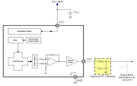 Hall Effect Sensor
Now the conductor plane is partitioned in two ways.
One side acts as positively charged and the other as negatively charged.
Because of this difference in the potential, the voltage gets generated.
This is referred to as the Hall voltage.
Until the balance is obtained, the charge carriers tend to move from one side to another.
This changes the value of the magnetic flux.
Once the separation in the conductor stops the density value of the magnetic flux is obtained. In this way, the Hall Effect sensor works.
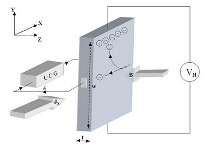 Hall Effect in Conductor
The equation that determines the hall voltage is
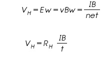 Where 'I' is current, 'B' represents the magnetic field and 't' denotes the thickness of the material.

 Here R H represents the coefficient of the Hall voltage.
Procedure
Establish the connection between the current source which is constant with the solenoids.
The set of four probes is provided the connection with the gaussmeter and kept in between the solenoids.
Switch ON the meter and the current source.
Varying the current present in the solenoids with a certain fixed amount of intervals of current through certain values.
With the gaussmeter, the readings are noted.
Then OFF the switch of the meter and the source of the current.
Then knob is turned towards the minimum value of the current.
Hall probe is fixed on the stand of wood.
Then pair of wires that are available in green color are connected to CCG.
The remaining pair of red wires are connected to the voltmeter in the apparatus of the Hall.
Replace the probes with the apparatus probes.
Keep the material required to be identified between the terminals of the solenoids.
Then switch on the respective connected devices.
Increase the value of the current from CCG.
To the present magnetic field measure the different values of the Hall Voltage.
The thickness of the placed sample can be measured by the apparatus called screw-gauge.
Then calculate the coefficient of the hall and the concentration of the carrier.
Results
To determine the value of the Hall Voltage = ________.
Coefficient of the Hall of the placed material = _________.
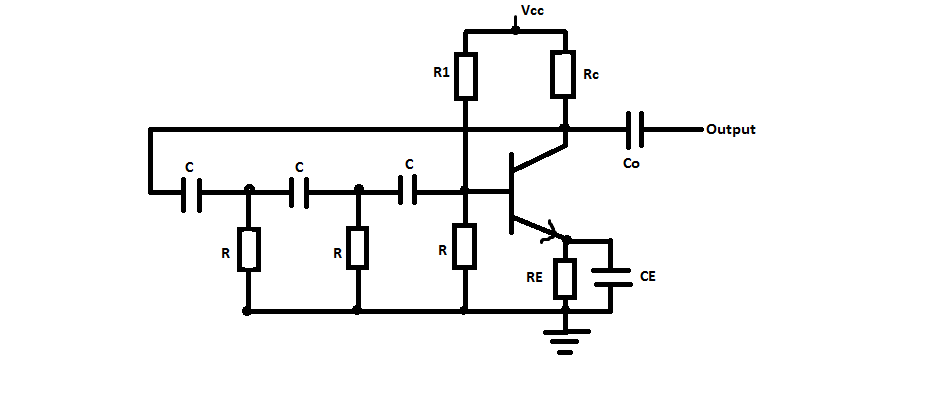 RC Phase Shift Oscillator using BJT
The active region of the transistor has been established by the resistors R1, R2, RC, RE, and the supply voltage Vcc.
The bypass capacitor used in the circuit is CE.
All the three RC sections are identical.
The resistance produced in the last section of the circuit is R'=R-hie.
Here, 'hie' is the input resistance which is added to R' so that the net resistance of the circuit becomes R.
The biasing resistors like R1 and R2 have a very large value and hence have no effect on the AC operation.
Also, the RE-CE combination offers negligible impedance to the circuit and it also has no effect on the AC operations.
When the power supply is given to the circuit, the noise voltage will start the oscillations.
The base current is capable of producing a current which has a phase shift of 180 degrees.
When this signal is again given as a feedback to the input terminal of the amplifier, then the signal will again be phase-shifted by 180 degrees.
When the loop game becomes unity, then sustained oscillations will be produced in the circuit.
The frequency of oscillations is given by:
f = 1/ (2 p R C v ((4Rc / R) + 6))
If Rc/R << 1, then
f= 1/ (2 p R C v 6)
For sustained oscillations, the condition is:
hfe (min) = (4 Rc/ R) + 23 + (29 R/Rc)
In case of a phase shift oscillator which has R = Rc, the value of 'hfe' must be 56 in order to attain sustained oscillations.
From the above equations, we can see that if we wish to change the frequency of oscillations, the value of 'R' and 'C' will have to be changed.
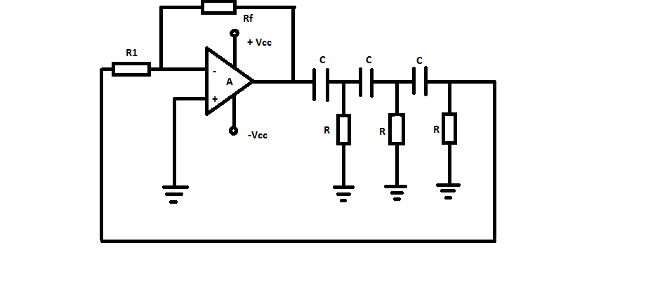 RC Oscillator using Op-amp
The operational amplifier is used in the inverting mode and the output signal is phase-shifted by 180 degrees to the input signal.
An additional 180 degrees phase shift is obtained because of the RC feedback network.
Hence, all the conditions are satisfied and oscillation is produced.
The gain of the op-amp can be adjusted with the help of R1 and R2 resistors.
In order to achieve the required oscillations, we will have to adjust the gain in such a way that the product of gain of feedback and om-amp gain is always slightly greater than 1.
The frequency of oscillations is given by:
1/ (2 p R C v 6)
The condition of oscillations: A = 29.
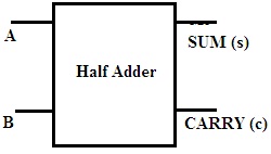 Half Adder
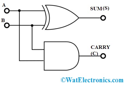 Half Adder
The circuit of this adder comprises of two gates.
They are AND and XOR gates.
The applied inputs are the same for both the gates present in the circuit.
But the output is taken from each gate.
The output of the XOR gate is referred to as SUM and the output of AND is known CARRY.
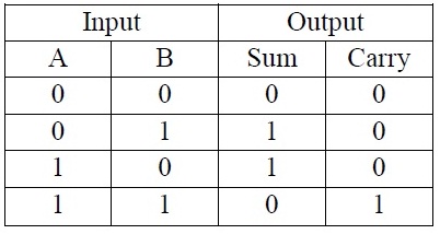 Half Adder Truth Table
From the above truth table the points are evident as follows:
If A=0, B=0 that is both the inputs applied are 0.
Then both the outputs SUM and CARRY are 0.
Among two inputs applied if anyone the input is 1 then the SUM will b e1 but the CARRY is 0.
If both the inputs are 1 then the SUM will be equal to 0 and the CARRY will be equal to 1.
Based on the inputs applied the half adder proceeds with the operation of addition.
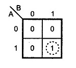 K-Map AND Gate
The output equation of CARRY is obtained from the AND gate.
C=A.B
The Boolean Expression for the SUM is realized by the SOP form.
Hence the K-map for the SUM is
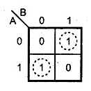 K-Map for Sum (XOR)
The equation determined is
S= A
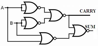 Half Adder using NOR gates
4.
How to Implement Half Adder using NAND Gate?
The NAND gate is one of the kinds of universal gates.
It indicates that any kind of circuit designing is possible by the use of NAND gates.
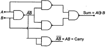 Half Adder
From the above circuit, the carry output can be generated by applying the output of one NAND gate to the input as other NAND gate.
That is nothing but familiar to the output obtained from AND gate.
The output equation of SUM can be generated by applying the output of the initial NAND gate along with the individual inputs of A and B to further NAND gates.
Finally, the outputs obtained by those NAND gates are applied to the gate again.
Hence the output for the SUM is generated.
Therefore the basic adder in the digital circuit can be designed by using various logic gates. But the multiple bits addition gets complicated and considered to be the limitation of the half adder.
Can you describe which IC is used for the increment operation in any practical counters?
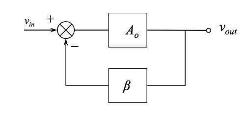 Block Diagram of Feedback Amplifier
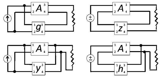 Topologies of Feedback Amplifier
In this way, the topologies of the feedback amplifiers for voltage or the current signals have been classified above.
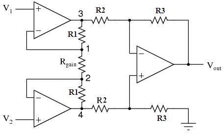 instrumentation-amplifier-circuit
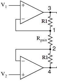 input-stage-of-the-instrumentation-amplifier
From the input stage, it is clear that due to the concept of virtual nodes, the voltage at node 1 is V 1.
Similarly, the voltage at the node in the above circuit is V2.
Initially, the current through the op-amps considered zero.
Hence no current can flow through the resistors.
At node 3 and node 4, the equations of current can be obtained by the application of the ohms law.
Therefore the equations are
I = (V1-V2)/(R1+Rgain+R1)….(1)
I= (V1-V2)/(2R1+Rgain)….(2)
As considered there is no current flowing through resistors at the input.
The equations at node 1 and 2 are
I = (V1-V2)/Rgain
On equating both the current equations
(V1-V2)/(2R1+Rgain) = (V1-V2)/Rgain…….(3)
The output equation of the differential amplifier can be given as
Vout = (R3/R2)(V1-V2)
(V1-V2) = (R3/R2) Vout
On substituting the above equation in (3)
(R2/R3)Vout/(2R1=Rgain) = (V1-V2)/Rgain
(R2/R3)Vout= (2R1=Rgain) (V1-V2)/Rgain
Vout = (R2/R3)[(2R1=Rgain) (V1-V2)/Rgain]
In this way, this output voltage equation of this amplifier can be derived.
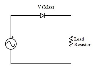 half-wave-rectifier
The operational analysis of the half-wave rectifier circuit can be done based on the above circuit that is a basic half-wave rectifier it consists of semiconductor diode in series with the input AC supply as well as the load is connected in series to the diode.
The half-wave rectification is done either based on the positive cycle of the supply or the negative side of the supply as it cannot consider booth at a single duration.
Once the positive side of the cycle considered as per the diode functionality it will be in forwarding bias that results in the establishment of the path for the flow of current and rectification process takes place.
If the negative side of the cycle is considered in that case the diode-connected must be reconnected by altering its direction.
Once the diode direction is reversed and necessary changes are made the diode gets interacted to the negative supply of the cycle provided.
As per that diode, conduction takes place and the rectification process is further carried out.
In the case of positive cycle consideration, the negative cycle is blocked and during the negative cycle consideration, the positive cycle is blocked.
 output waveforms of a half-wave rectifier
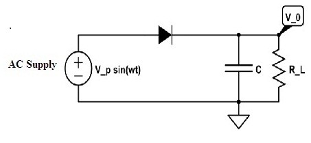 half-wave rectifier with capacitor filter
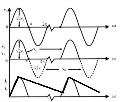 output waveforms of the half-wave rectifier with capacitor filter
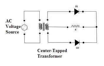 Full Wave Rectifier (Center-Tapped)
This circuit consists of two diodes and the resistive load connected parallel to each other.
In addition to it, a center-tapped transformer is present that is a general transformer that has a wire at the center of the secondary winding.
But this type of transformer makes the circuitry costliest.
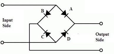 full-wave bridge rectifier basic model
Hence another type of full-wave rectifier is designed that consists of four diodes connected in a bridge topology.
So it is referred to as the Bridge rectifier.
In this, the diodes are connected in a diagonal manner.
The oppositely faced diodes are acting towards the same bias whereas the remaining two are reversed biased.
Hence this is the technique behind the bridge rectifier.
 output waveforms of the full-wave rectifier
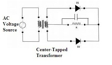 Full Wave Rectifier (Center-Tapped) with capacitor filter
As the capacitor is connected across the load one can see the further changes in the output as follows.
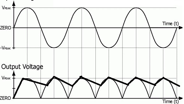 output waveforms of the full-wave rectifier with capacitor filter
Hence the analysis is obtained for the capacitor connected across the half-wave and full-wave rectifiers and then the purpose of the connecting capacitor is proven beneficial because it can remove unnecessary ripples from the generated output.
After analyzing the purpose of the capacitor is there any other type of filter that exists or preferred so that it can improve the purity of output?
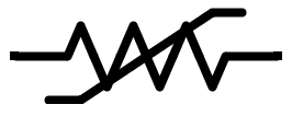 IEEE-symbol
The ICE symbol of this is shown below.
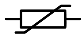 ice-symbol
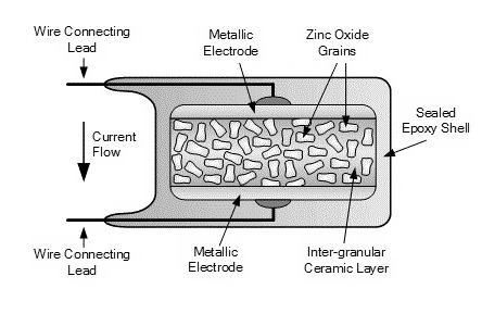 varistor-construction
The metal oxide layer basically contains 90% of zinc oxide and 10% of other metals.
The metal oxide layer is sandwiched between two metal electrodes.
The matrix acts as a binding agent so that the zinc oxide granules can be kept intact between the two metal electrodes.
The boundary surface behaves like a junction of a semiconductor diode.
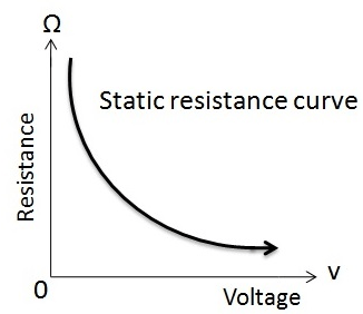 resistance-of-varistor
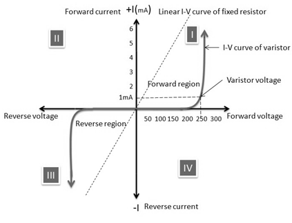 v-i-characteristics
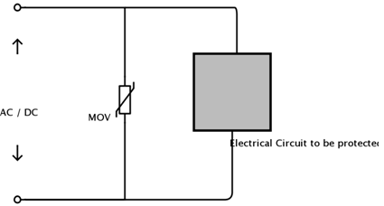 metal-oxide
2).
The devices connected in an electronic circuit are extremely sensitive to change in voltage.
So we use this component in the circuit to protect the different components of the electric circuit.
Here, we can see how this can be used to protect a transistor in the circuit.
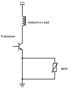 varistor-to-protect-transistor
3).
It can also be used to provide surge protection in AC and DC motors.
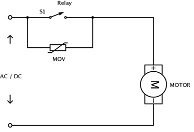 varistor-in-ac-dc-motors
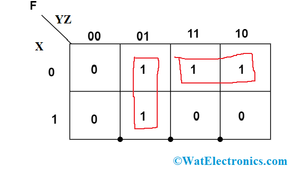 minimal SOP
So, the main benefit of minimal SOP form is it requires only 2 AND gates and one OR gate rather than 3 AND gates and 1 OR gate.
These are three types of SOP expression redundant forms.
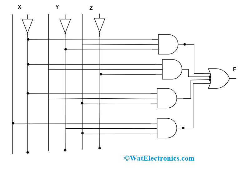 schematic canonical form SOP
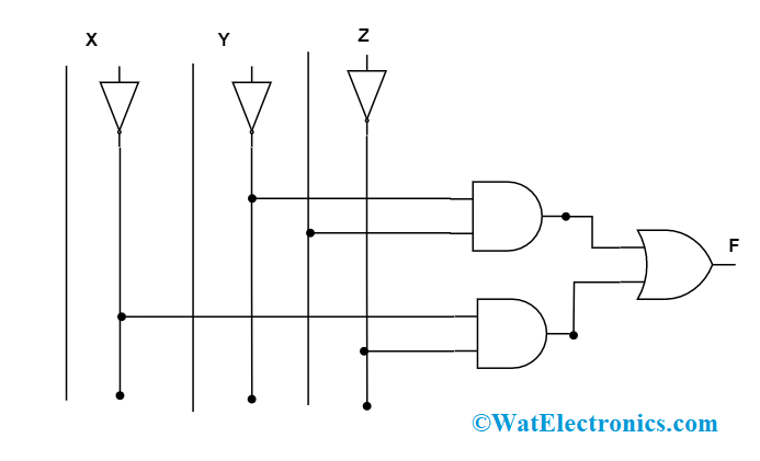 schematic minimal form SOP
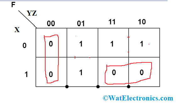 minimal POS
F = (Y+Z)(X' + Y')
So, the main benefit of minimal POS form is it requires only 2 OR gates and one AND gate rather than 4 OR gates and 1 AND gate.
These are three types of POS expression redundant forms.
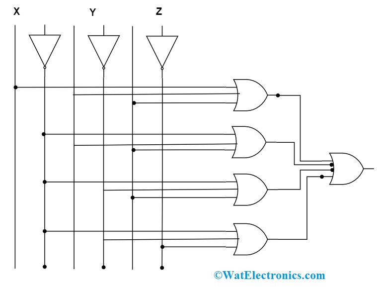 schematic canonical POS
The below diagram represents the schematic diagram of POS minimal forms.
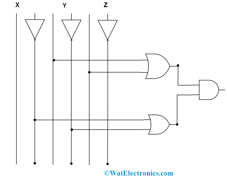 schematic minimal POS
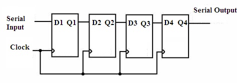 Shift Register (SISO)
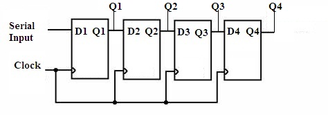 Shift Register (SIPO)
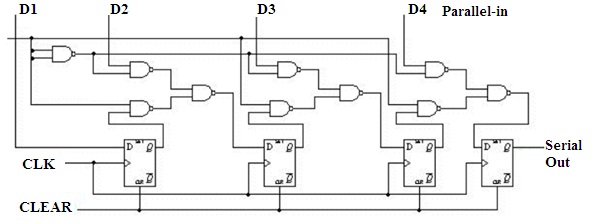 Shift Register (PISO)
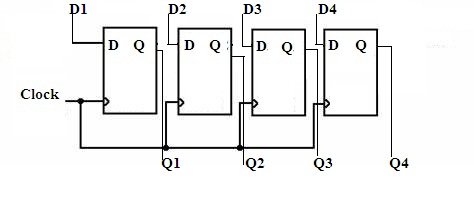 Shift Register (PIPO)
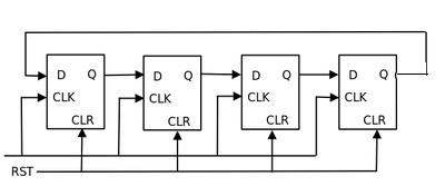 Shift Register (Ring Counter)
Johnson Counter
The realization of this counter is similar to the ring counter.
A similar process of arrangement of flip-flops which is followed in the ring counter is followed.
The only difference is the inverted output obtained at the final stage is fed back to the input at the first stage.
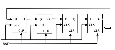 Shift Register (Johnson Counter)
But both the counters can suffer from a condition called 'Lock-out'.
This difficulty can be overcome by using an additional gate.
Further, there are various applications of shift registers.
Some of them are listed as follows:
The chain of Flip-flops connected together acts as a memory element.
These are used in 'Finite Memory Machines'.
To generate Delays in the circuit these are preferred.
To convert data from serial to parallel and parallel to serial.
These registers are preferred.
The above are some of the applications of shift registers.
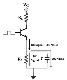 bypass-capacitor
Here in the diagram, we can see that the capacitor conducts AC and the AC is regularly removed from an AC/DC combination.
After that, the DC can freely pass through the bypassed components.
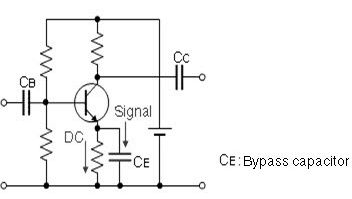 emitter-bypass-capacitor
 cathode-bypass-capacitor
If the capacitor used is sufficiently large, it is capable of acting as a short circuit for audio frequencies.
It can then eliminate the negative feedback.
It can also act as an open circuit for direct current.
In this way, it can maintain the DC grid bias.
We can also introduce a treble boost in the circuit.
This can be done by lowering the capacitor value of the capacitor which acts as a short circuit.
This operation is mainly done in the preamp's bright channel.
If an extra gain is achieved, then we can eliminate the capacitor completely from the circuit.
 Surge Protector
This type of circuit protects the circuit from the permanent damages of the components.
Surges reduces the life span of the devices.
The surge protectors have the capability of handling the spikes about kilovolts range. For a short duration of time, these protection circuits can withstand the spikes.
In the building or the offices, the surge protection is installed in a place where all the devices are provided with the power supply.
Hence all the appliances can be protected from the surge.
This type of circuit approach is known as Universal Surge Protection.
In case each appliance has its protection circuits then there is no need for such a universal approach.
 FM signal
The initial one is the message signal which holds certain information, while the second signal has no information and is called the carrier signal.
The modulation of these waves results in an FM modulated wave.
The FM modulated wave is more crucial as the frequency of this moves up and down based on the amplitude of the message signal and this change in frequency is represented in the form of kilohertz.
For example, when the frequency deviation is 3 kHz up and down, then it is represented as ±3 kHz.
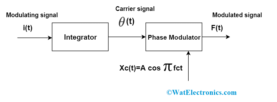 FM block diagram
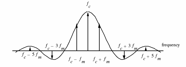 FM bandwidth
ß =
 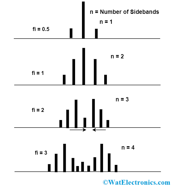 FM spectrum
The initial bands will contain maximum power (nearly 80%) and so these are considered to be significant sidebands.
As per the rule of Carson's, approximately 98% of the modulated signal power exists where the bandwidth is equal to the frequency variation and twice the frequency of the message signal.
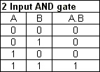 AND Gate Truth Table
If the inputs applied are A, B.
Then the output 'Z' generated can be expressed as Z= AB.
The symbol for AND Gate is
 AND Gate Symbol
The realization of AND gates is also done by using Transistors and the Diodes. When the two diodes are connected along with a resistor and based on the supply provided the output is generated.
 AND Gate Realization using Diodes
when both A and B are applied with +5 Volts.
The diodes remain OFF.
Hence there is no chance of occurrence of Voltage Drop across the resistor.
Therefore the output obtained is high. When both the input values are provided with 0 Volts the circuit will be short-circuited.
Practically o volts are not possible it refers to 0.6 or 0.5 volts.
The circuit of AND can also be realized by using transistors.
When both the inputs or even any one of the output is o then the base current drives the Q3 to ON.
Therefore, the output obtained because of Q3 is 0 volts.
 AND Gate (Using Transistors)
When both the inputs are +5Volts both Q1 and Q2 are ON.
Hence no base current can drive the transistor Q3.
Therefore Q3 is OFF and the output obtained is +5Volts.
 OR Logic Gate
The Truth table of OR clearly states that the value of output remains high even if the single output is high. If the inputs applied are A and B and the output obtained is denoted by Z.
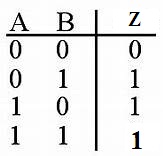 OR Truth Table
The same circuit realization can be done based on diodes.
To the applied inputs the diode behaves accordingly.
When both the applied inputs are 0 volts then diodes remain OFF.
Then no chance of current flow through the circuit.
Hence there is no voltage drop crossover the resistor.
Therefore the output generated is 0 volts.
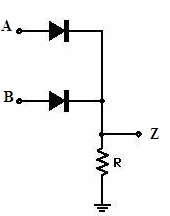 Logic Gate OR
If anyone of the input or both the inputs applied are high.
Then both the diodes or either of the diode is high the current flows through the circuit.
The output generated due to this is high.
Similarly, the same operation of OR is realized using transistors in the circuit.
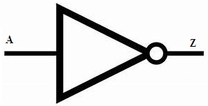 Logic Gate NOT
The Truth Table for the NOT gate is
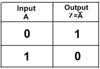 Truth Table Not Gate
 NAND Gate Symbol
The Truth Tabe of the NAND gate is
 Truth Table of NAND Gate
When both the inputs applied are 1 the output obtained is 0.
The operation of the NAND gate can be understood based on the circuit diagram and the applied inputs.
 Logic Circuit Diagram (NAND Gate)
As per the above circuit connection between diodes and an NPN transistor the circuit for NAND gate is designed.
It is the combination of AND gate followed by an inverter.
If both the inputs that are A and B applied with 1 both the diodes are reverse biased.
Then the overall supply reaches the base of the transistor Q1.
This turns the transistor ON and the voltage gets short-circuited to ground.
Hence the output obtained becomes zero.
Similarly, the diodes are forward biased for the other applied inputs and the transistor is in OFF mode.
Therefore the outputs obtained in such cases are high.
 Logic Symbol of NOR Gate
The Truth table for this gate is
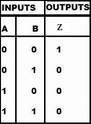 NOR Gate Truth Table
This type of gate generates output as high when both the inputs are 0 volts.
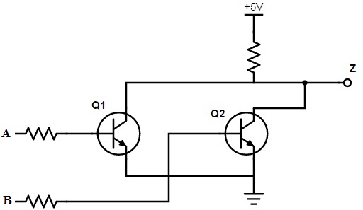 Logic Circuit Diagram of NOR Gate
When both the inputs applied are of 0 volts both the transistors Q1 and Q2 are OFF.
Hence there is no voltage drop developed across the resistor.
The final output generated is of +5 volts.
For the other applied input, either one of the transistors will be ON or both the transistors are ON.
In this situation, a certain voltage drop is generated.
This produces low levels of output.
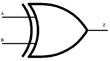 Logic Gate XOR
The Truth Tabe for this XOR gate is
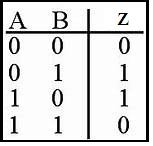 Truth Table of XOR Gate
From the truth table, it can be intelligibly stated that for the applied odd inputs of 1 the resultant will be logic 1.
If more than two inputs are considered then the behavior of this gate is decided based on its implementation. The operation performed by XOR is excluding the carry bit.
This is the reason for defining this gate as an Exclusive OR gate.
The Boolean Expression to define the operation of the XOR gate is
Z= A
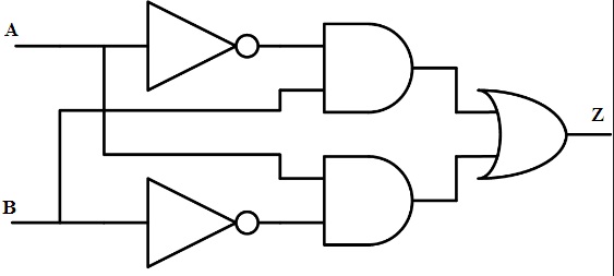 Logic Circuit Diagram of XOR Gate
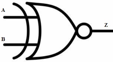 Logic Symbol (X NOR Gate)
The reverse operation of XOR is performed in X NOR.
When both the inputs are o or if both the inputs are 1 the resultant is logic 1 otherwise logic 0 for further inputs.
The truth table for the gate is
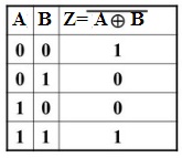 Truth Table of X NOR Gate
The logic circuit diagram for this kind of operation is
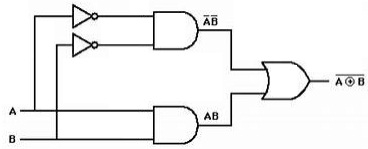 Logic Circuit Diagram of X NOR Gate
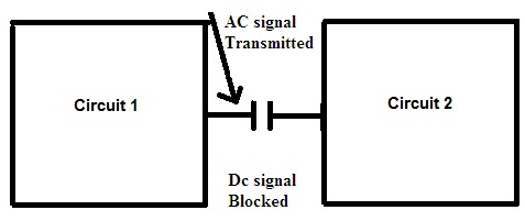 Coupling capacitor General Representation
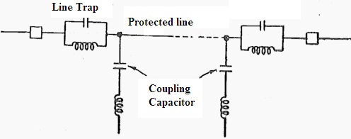 Coupling Capacitor PLCC
The carrier equipment and the respective transmission line are coupled via the coupling capacitor.
It allows the carrier frequency to enter into the respective carrier equipment.
It offers the value of impedance low to the carrier frequency and the high impedance for the respective power frequency.
BJT
In BJT, it is utilized in the circuits of amplification it requires multiple-stage involvement for this purpose.
During multiple stages, a capacitor is connected between the two stages.
So that output of one stage can be coupled as the input to the next stage. In this coupling capacitors are utilized in the BJT's.
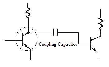 Coupling Capacitor in BJT
From the above description it can be known that the coupling capacitor is mostly part and parcel of any circuit and. Can you calculate how much capacitance should be preferred in substations?
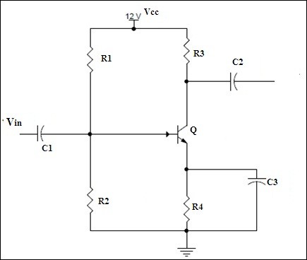 Single Stage RC Coupled Amplifier
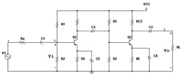 Two stage RC Coupled Amplifier
After the processing of the signal in the first stage the output of the first stage, the amplifier is connected to the second stage as the input.
This made possible with the coupling capacitor present at the output of the first stage of the amplifier.
One can observe after processing occurs at the second stage the output signal obtained has the increased gain factor in it and it is in phase with the input signal.
In this way, the two stages RC coupled amplifier works.
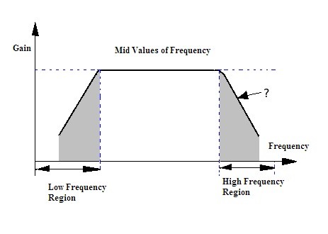 Frequency Response of the RC Coupled Amplifier
 SMD Capacitors- Electrolytic Codes
On some specific capacitor, the three-digit code is present.
In which the last digit is treated as the multiplier.
The units are measured in terms of farads.
As discussed earlier that these capacitors manufactured don't consist of leads.
Hence the design of it is compact in size.
By adopting various latest techniques the size is even minimized and made comfortable for the design criterion of various modern pieces of equipment.
 SMD Capacitor-Tantalum
Let us consider the above example of the SMD tantalum capacitor.
On it, one can notice the value of capacitance printed.
Therefore, the various values of the capacitors are identified based on the standard followed by it. Sometimes it is printed as 33.6 where the value of the capacitance can be determined as 33 micro farads and the number after the decimal point indicates the value of the working voltage.
 Capacitors Connected in Series
Usually, the capacitors are connected in a 'daisy chain' configuration.
In such kinds of circuits, the flow of current for charging will be equal.
This is because of the path establish is the same.
Total Current = Current at C1 = Current at C2
Instead of capacitance, the charge in each capacitor is the same.
Because the plates of each capacitor are connected in an adjacent manner.
Total Charge = Charge at C1= Charge at C2
When the capacitors follow the series connection and more than three capacitors are connected.
The C1 is provided with the supply and the C3 will be connected at the output end.
Whereas the C2 in the middle is isolated from the direct interaction of voltage supply(DC).
Due to this, the voltage drops across each capacitor are different.
It depends upon the individual capacitances of each capacitor.
Generally, the charge, capacitance and the drop of voltage are related as
Q=CV
The formula can be rewritten as
C=Q/V
The voltage across capacitors can be calculated as
Total Voltage = Voltage at C1 + voltage at C2
Total Voltage (Q/C) = Q1/C1 + Q2/C2
In Series, the charge will be equal that is Q1=Q2
Finally, on dividing the equation with Q on both sides
1/C = 1/C1 +1/C2
Hence the above equation is to calculate the capacitance for the series connection of capacitors.
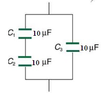 Capacitors in Series and Parallel Combination
Solution:
Given the above circuit consists of C1, C2, and C3 Capacitors.
From the circuit analysis the capacitors C1 and C2 are in series combination.
The C1 and C2 equivalence capacitance can be calculated by using the formula
1/C = 1/C1 +1/C2
1/C= 1/10 + 1/ 10
1/C= 2/10
Finally, C= 10/2 = 5 microfarads.
Further, this C is connected in parallel with the capacitor C3.
The Equivalence capacitance of the circuit can be found by
C (Total) = C+ C3 = 5 + 10 = 15 microfarads
Hence the value of the capacitance can be realized based on the series and parallel analysis. It is noticed as the value of the capacitance is decreases in terms of series combinations.
In the parallel combination, the value of capacitance is increased.
But in case of resistance, it is the opposite. From the above analysis can you determine if you have to store a huge amount of energy then which combination of connection is preferred?
 ferromagnetic material magnetization
In the scope of electrical engineering, it seems to completely suffice to categorize the magnetic materials as ferromagnetic and non-ferromagnetic.
Ferromagnetic materials have the property of permeability more than one whereas non-ferromagnetic has permeability equals one.
Ferromagnetic materials are categorized as
Soft Type of Materials
Hard Type of Materials
Ferrites
 ferromagnetic material magnetization
 ferromagnetic material hysteresis
 basic sequential circuit
As every digital and memory circuit is built based on the finite state machines, sequential circuits are implemented for the construction of these machines.
So, these circuits hold more prominence in digital and electronics technology.
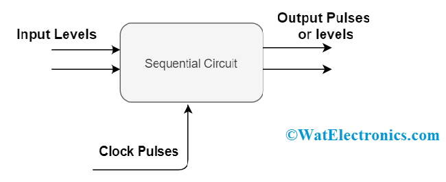 synchronous sequential circuit
Again, synchronous circuits are of two types clocked and unclocked.
 clocked sequential circuit
 unclocked sequential circuit
Applications
Synchronous sequential circuits are implemented in the design of flip-flops, counters and to develop MOORE-MEALY state-controlled machines.
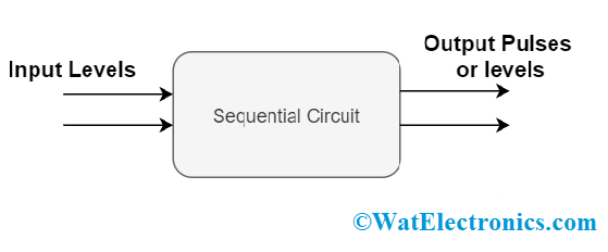 asynchronous sequential circuit
Applications
Asynchronous sequential circuits are cost-effective to be used in small independent systems that need only a few elements.
The communication between two elements, each hold its own independent clock, and this will be achieved by these circuits.
 S-R flip flop
Circuit Diagram
S-R flip flop works in perfect condition when the circuit is connected as below
S-R flip flop
Circuit Diagram
S-R flip flop works in perfect condition when the circuit is connected as below
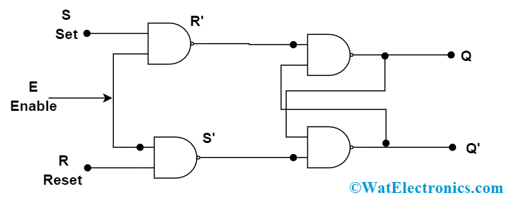 S-R circuit diagram
Truth Table
The output is clearly described in the below truth table
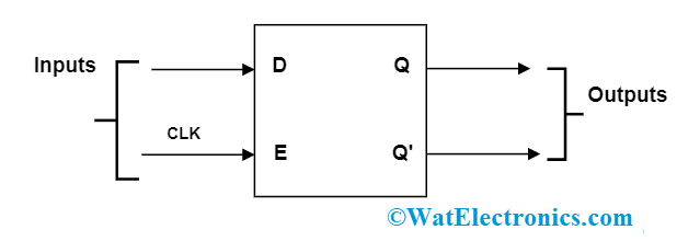 master-slave JK FF
Truth Table
The output is clearly described in the below truth table
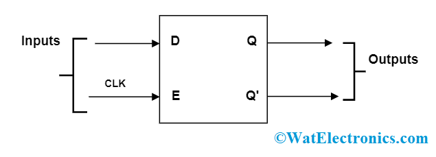 Delay FF block diagram
Circuit Diagram
Delay Flip Flop works in perfect condition when the circuit is connected as below
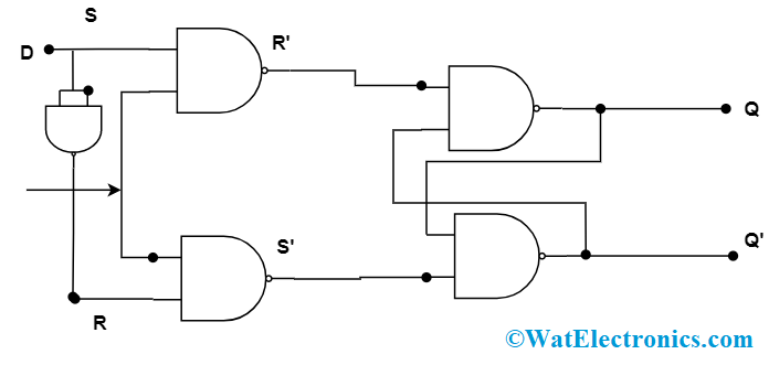 Delay FF circuit diagram
Truth Table
The output is clearly described in the below truth table
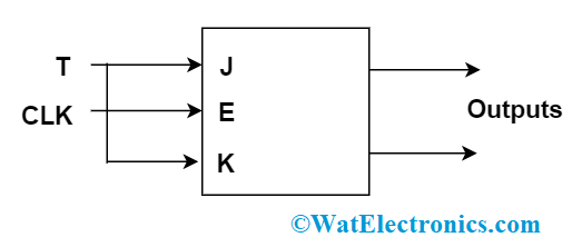 Toggle FF block diagram
Truth Table
The output is clearly described in the below truth table
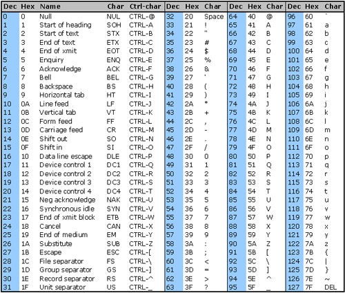 ASCII to Hex Conversion Table
 basic circuit result
 schematic diagram
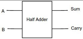 Half Adder Block Diagram
The circuit with logic gates and the truth table of this circuit is as follows;
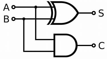 Half Adder Circuit
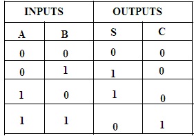 Half Adder Truth Table
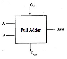 Full Adder Block Diagram
The circuit diagram and the truth table of this circuit are as follows:
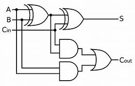 Full Adder Circuit Diagram
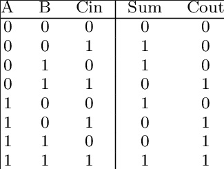 Full Adder Truth Table
 Half Subtractor Block Diagram
The circuit diagram for the half subtractors and the truth table is
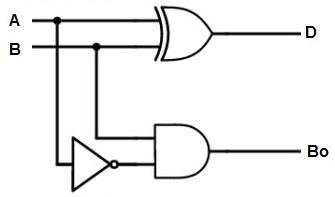 Half Subtractor Circuit
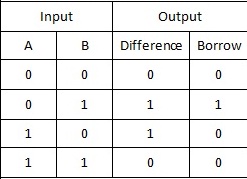 Half Subtractor Truth Table
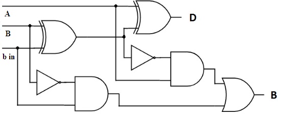 Full Subtractor Circuit
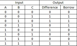 Full Subtractor Truth Table
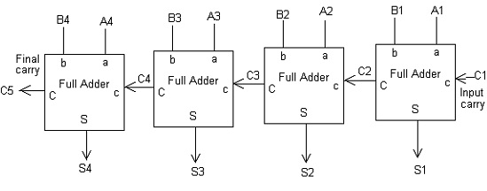 Parallel Adder
These circuits of adders are enclosed in the form of IC's.
These are designed such that it must have terminals of four augends and terminals for the adding the bits.
The two numbers can be added simultaneously in these circuits.
But there is no value of carrying at the least position.
In these adders, the primary block is half adder followed by full adders.
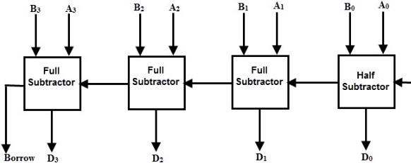 Parallel Subtractor
The bit values 'A3A2A1A0' known as Minuends in the circuits are subtracted by the Subtrahend of 'B3B2B1B0'.
The borrow generated can be connected further as the input value for the preceding subtraction unit.
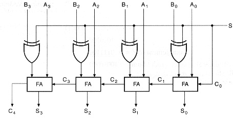 Binary Adder or Subtractor
Each of the XOR gate used in the circuit consists of two input connections.
Among those two inputs, one is for M and the other is for B.
as the S value is maintained 0 B XOR of 0= B.
Then the circuit performs the task of addition. When S =1 the circuit produces B XOR of 0 = Complement of B.
Then the value that is complemented is added to A. This kind of operation is also referred to as two's complement.
Hence the two arithmetic operations are performed in a single circuit.
Practically in the process of addition and subtraction can be performed by these circuits in computers, the devices where the micro controller is the basic units and the digital calculators.
These are also preferred in networking as well as the Digital Processing of the Signals.
We have discussed the parallel adder above.
In that process, the carry has been forwarded to the next stage. If in certain stage carry is not generated the circuit generates time delay.
To overcome another adder circuitry is designed.
Can you identify which circuit can overcome the delay in the addition operations?
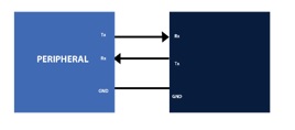 UART-communication-interface
In UART, possibilities to exchange data between the transmitter and receiver can be divided into three modes, namely simplex, half-duplex systems and full-duplex system. Whether UART functions as a half-duplex or full duplex systems it depends on the processor in which it integrated.
Some microcontrollers support half-duplex and some support full duplex systems.
Almost most of the latest microcontrolers support full duplex systems.
Simplex Systems: In this type of communication, the data bits are transmitted only from a single end (i.e., source device).
Half Duplex Systems: Data transmission can be achieved from either direction, but only one user can transmit data at a time.
Since the hardware structure shares the same data bus and control buffer, users are allowed to either receive or transmit data at that particular instant.
Full Duplex Systems: Data transmission can happen in either direction, both the devices which are communicating through this system can receive and transmitt data at the same time and they also have individual data buffers for Tx and Rx.
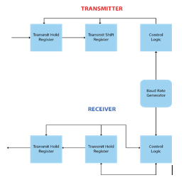 UART-transmitter-and-receiver-module
As shown in Fig.
2, the transmitter section is further categorized into three stages namely
1).
Transmitter holding register: This block holds the control of outgoing information and from the UART buffer signal before processing to the next step.
2).
Transmitter shift register: Once the data is processed from holding register, this block shifts the data by moving bits from left to right or vice versa until the final bit is transmitted or received.
It also converts the input strings from parallel to serial data combinations and transfers the data in the form of bit by bit operation.
3).
Control Logic: As the name suggests, it controls the data flow between transmitter and receiver, and avoids sending blank/error data during transmission.
Similarly, the receiver block encompasses receive hold register, shift register, and control logic.
The functionality is similar to that of the transmitter block, where the collected data is initially processed through a receiver shift register to convert into parallel mode.
The receiver holding the converter dispatches the data to the user. Control logic is used to initiate read and write operations.
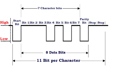 UART-data-frame-structure
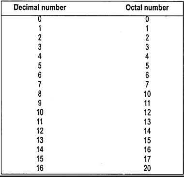 Decimal and Octal Numbering System
Hence the conversion of octal number into decimal and vice versa is very simple. Even there are various programs in different languages like C, Java,python, php that convert one form of code into another format. There are also encoding and the decoding circuits which are used in circuits for hardcore conversions. The Encoders are placed at the inputs of the circuits.
However, the conversion must be handled with care while the mixed decimals are provided.
Can you convert the value of octal 4057.07 into a decimal?
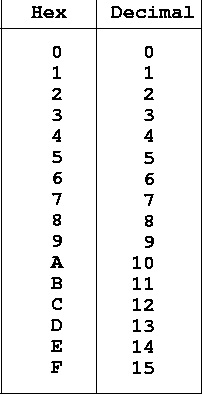 Decimal Numbering to Hexadecimal Numbering System Conversion Table
Let us consider the example of 20.
20 is greater than 15.
It doesn't have any alphabetic representation.
This further simplified by dividing with radix value of the required numbering system.
The resultant is 14 when the Hexadecimal system is considered.
Where 1 is used for carrying and increment the previous value.
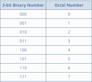 Octal Numbering System Conversion Table
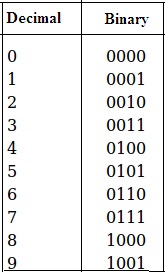 Decimal Numbering System to Binary Numbering System table
 Tantalum Capacitor Symbol
The above figure represents the symbol of tantalum capacitor.
When positive voltage is applied to the anode terminal a oxide layer forms on the anode, which acts as the dielectric. The dielectric which forms in this capacitor is generally a thin layer around 1.7nm/v. The size of the dielectric depends on the amount of the voltage applied. Then after the formation of an oxide layer it is then dipped into an electrolyte solution which acts as the cathode .
That's how a Tantalum capacitor is constructed.
As we know a sintered anode terminal will increase the capacitance of the capacitor.
Similarly in tantalum capacitor also the anode terminal is sintered by which the electrode area increase and so its capacitance also.
The Tantalum capacitors work on the principle of 'Electrolytic Capacitors'.
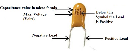 Tantalum Electrolyte Capacitor
 Tantalum Capacitor SMD Sizes

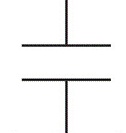
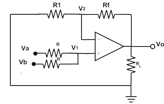 Non-Inverting Summing Amplifier
To design these amplifier circuits firstly it is designed based on the required gain.
Once it is done then the necessary resistors are arranged based on it. If the resistors considered are equal then in such case the output value of the voltage will be given as
V o= V a +V b
From the above equation, the value of the output voltage can be calculated.
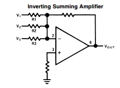 Inverting Summing Amplifier
The output voltage Vout value can find out for the summing amplifier with the help of the equation shown below
V OUT=- {(Rf / R in 1) V in 1 + (Rf / R in 2) V in 2 + (Rf / R in 3) V in 3}
If the values of the resistors are not equal in such case the amplifier is known as scaling amplifier which is type of summing amplifier.
But here we are considering the summing circuit with equal resistance values.
Then, in that case, the equation can be written as
V OUT=- {(Rf / R in 1)} { V in 1 + V in 2 + V in 3}
Hence the above equation is useful while calculating the value of the output voltage for the summing amplifier with the three applied input signals.
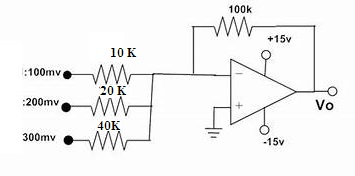 Voltage Adder Example
A 1= - (Rf / R1) = -100/10 = -10
A 2 = - (Rf / R2) = -100/20 = -5
A 3= - (Rf / R 3) = -100/40 = -2.5
The value of the output value of the summing amplifier can be given as
V OUT= - (A 1 V 1+ A 2 V 2 +A 3 V 3)
V OUT= - (10*100 m V +5* 200 m V+2.5* 300 m V)
V OUT= -2750/1000 Volts
V OUT= - 2.75 Volts
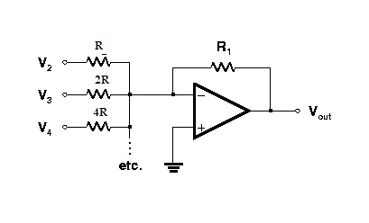 Digital to Analog Converter
In these cases of the converters, the resistors are present to the respective branches of the applied input signals.
But the values of the resistors are chosen in such a way that the one branch resistor value considered must be double in comparison to the previous value of the resistor.
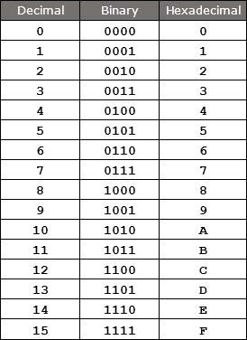 Hexadecimal and Binary Number System Representation
 Binary Numbering System to Hexadecimal Conversion Table
By looking at the conversion table we can easily find the numbers.
0001 is represented as '1' in the hexadecimal numbering system.
1100 is represented as C in the hexadecimal numbering system.
Therefore the hexadecimal number for the given binary string is '#11C'.
Based on this conversion table or by following the 8421 coding technique many conversions can be done conveniently.
The only thing to be noted during these conversions is that digit representation must be of four bits.
For example, if the binary string is 000111 then to convert it into hex grouping is required.
That is 00 0111.
In this case, the second group doesn't have four bits.
This must be overcome by adding zeroes in that group.
Further, the string becomes 0000 0111.
Now the conversion is possible.
This can be represented as '07' in hexadecimal. These are the various techniques utilized during the conversions.
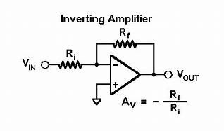 Inverting Amplifier as Op-Amp
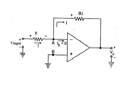 Inverting Amplifier Circuit Diagram
The output signal that is generated due to this amplifier is that will be of angle 180 degrees out-of-phase in comparison to the applied input signal.
The voltage that is applied at the inverting terminal its potential value will be the same as that of the potential at the non-inverting terminal.
The behavior of this amplifier resembles the differential amplifier.
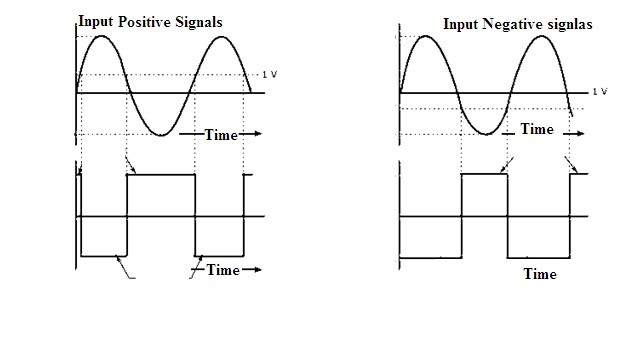 Inverting Amplifier Wave forms
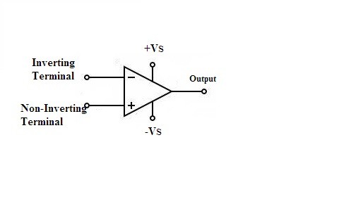 Symbol of Op-amp
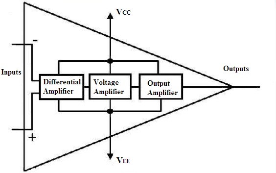 Block Diagram of Op-amp
Hence this makes the op-amp dual input and the single output amplifier.
Then the outcome of the first stage is forwarded to the intermediate stage.
The required gain of the voltage is introduced at this stage of the amplifier.
As well as at this stage the direct coupling is present.
It means that the output of the intermediate stage has the value of the voltage that must be above the ground potential.
Hence this paves the way to make the voltage that is DC to shift down it to zero.
For this reason, the third stage with a level shifter is introduced.
In this stage, the circuit of emitter follower transistor is present along with the source of current that is maintained at constant. Further, the output of the level shifting stage is given to the final stage in which there exists the amplifier of the type push-pull which increments the swing in the voltage that is generated at the output.
In this way, the four stages describe the basic structure of an operational amplifier.
 Super Capacitor
 Super Capacitor Charging Circuit
Super Capacitor vs Battery
Let us consider the battery made up of lithium.
The comparison between this capacitor and the battery is as follows.
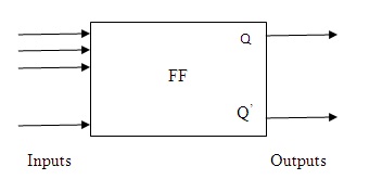 Generalized Symbol of Flip-Flops
Where Q represents normal output and Q' represents inverted output.
There can be 'n' inputs to a flip-flop that is responsible for the simultaneous changes in their states.
These signals are known as “excitation's”.
Some flip-flops are termed as latches.
The only difference aroused between a latch and a flip-flop is the clock signal.
Latches are known for their non-clocked behavior.
The flip-flop because of its states is classified into four basic types:
S-R flip-flop (set-reset)
D flip-flop (delay)
J-K flip-flop
T flip-flop
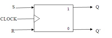 S-R Flip-Flop Block Diagram
As the s-r flip-flop is a result of cross-coupled NOR and NAND gates their excitations based on the behavior of the gates based on the applied inputs.
When the inputs applied are at 0 then the change in the states left undetermined.
When both are at 1 there is no chance of change in the results.
The problem aroused because of NAND and NOR gates is its excitation becomes invalid.
This condition to an extent is modified by using two AND gates at the input side by providing a synchronizing clock.
In order to provide proper functioning one can restrict the clock pulse length and its frequency.
Block diagram
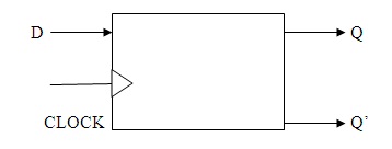 D-Flip-Flop Block Diagram
The functionality is completely based on the edge of the clock applied at the input.
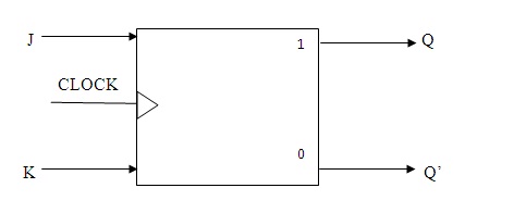 J-K Flip-Flop Block Diagram
J and K are like the set and clear inputs.
In this when both J and K values are equal to 1 this combination leads the flip-flop to act like a trigger resulting it to complement state.
There exists a toggle condition in J-K flip-flop.
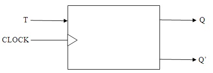 T-Flip-Flop Block Diagram
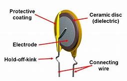 Ceramic Disc Capacitor
Multi-layer Ceramic Capacitor (MLCC)
In this design “Multiple Layers of Ceramic Material” acts as Dielectric.
The electrodes for this are adjusted in between the layers.
These layers and the electrodes are arranged in contact with the terminals.
The size and the number of layers determines the capacitivity of this capacitor.
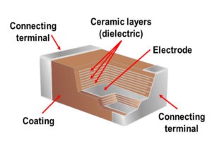 Ceramic Capacitor (MLCC)
 Ceramic Capacitor symbol
 Ceramic Capacitor 104
In this, the first initial two digits represent its value in the capacitance of pico-farads.
The last digit printed is 4 it indicates that it is a multiplier of the value (10^4).
Finally, the value of the capacitance can be generated as, 10*10^4= 10*10000 = 100000 picofarads.
If there is no last number present in that case the initial two numbers represent the overall value of capacitance without any Multiplier in it.
 Capacitor Codes Based on EIA
 Electrolytic Capacitor Symbol
 Aluminum Electrolyte Capacitor
These two capacitors are used in different applications.
The plain one is preferred in providing the smoothening effect in Power Supply Circuits.
The other one is preferred in the BYPASS circuits.
The range of this capacitor is from 1 micro farad to 47000 micro farads.
The maximum voltage range is up to 500 volts.
 Tantalum Electrolyte Capacitor
In comparison to aluminum capacitors, these are considered to be more stable.
The Capacitance range is from 47 nano farads to 470 micro farads.
The maximum range of voltage is about 50 Volts.
These capacitors are more costly in comparison to the Aluminum Capacitors.
 Niobium Electrolyte Capacitor
The above three discussed are the types of Electrolytic Capacitors.
 Paper Capacitor with Paper Sheet
But the possibility is that the electric field is allowed to pass through it.
Therefore the barrier between the electrodes is the sheet of paper.
These sheets further are rolled in the form of a cylinder and the wire heads are attached.
Finally, these are coated using wax or any plastic resin so that these acts as protectants from the environment moisture that is present in the air.
In this way, this type of capacitor with a sheet of paper is constructed.
 Metalized Paper Capacitor
In this way, the capacitor with the metalized layer is constructed.
 Various Symbols of Capacitors
 Capacitor working
The important point to be considered is that in the capacitors when the applied or the supply of the voltage is equal to the voltage at charging.
Even though the battery is provided it stops getting charged. Due to this even if the battery is removed the charge that is present in the capacitor is stored. But If we replace a battery with a load the capacitor gets discharged.
Instead of DC if the capacitor is provided with the AC supply in this case both the halves of the cycles are present.
Due to this reason, the capacitor faces both the phenomenon of charging and the discharging.
Because positive half of the supply makes the capacitor to get charged and negative half makes the capacitor gets discharged.
In the case where AC supply is provided the Charging and the Discharging are dependent upon the frequency of the source signal.
This is the basic principle involved in the functioning capacitor.
 Where “C” is the capacitance denoted in terms of farads.
 Film Capacitor symbol
 Film Capacitor-Mylar
The markings of this capacitor are made in the center of it.
683 indicates the value of the 'capacitance' in picofarads.
The third digit acts as the 'Multiplier'.
That is the value of this capacitor is 68,000 picofarads.
In this type of capacitor, there exists 'Three Exceptions' for the usage of 'The last Digit'.
'7' cannot be used.
If the last digit is '8'.
Then the further digits that are leading are multiplied by the value '0.01'.
If the last digit is '9'.
In this case, the capacitance value is multiplied by '0.1'.
The above are the exceptions for it.
Other than this the marking is done such that it indicates the value of 'Breakdown Voltage'.
For the above example considered '100 volts' is the breakdown value.
As noticed on the capacitor consists of 'no indication' represents that Film Capacitors are non-polarized.
 Variable Capacitor Symbol
 Tuning Capacitor
The range of the values of capacitance provided by these capacitors is from certain 'pico farads' to 'tens of picofarads'.
In the receivers used in Radios which possess 'LC circuits' these types of capacitors are preferred.
These types of capacitors are also known as “Tuning Condensers”.
That's how the Tuning Capacitors works and utilized based on preferred requirements.
 Trimmer Capacitor
Among two plates one of the plates is considered to be fixed and the other is considered to be in movement or movable.
The Dielectric present in this capacitor is 'Fixed'.
The movable plate is moved in the opposite towards the area in between the fixed and the movable electrodes.
In this way, the capacitance of the capacitor can be altered.
The capacitance value and the area are proportional to each other.
If the area between the electrodes tends to increase the value of capacitance increases.
and that's how a Trimmer Capacitor works.
 Symbol of Variable Capacitor
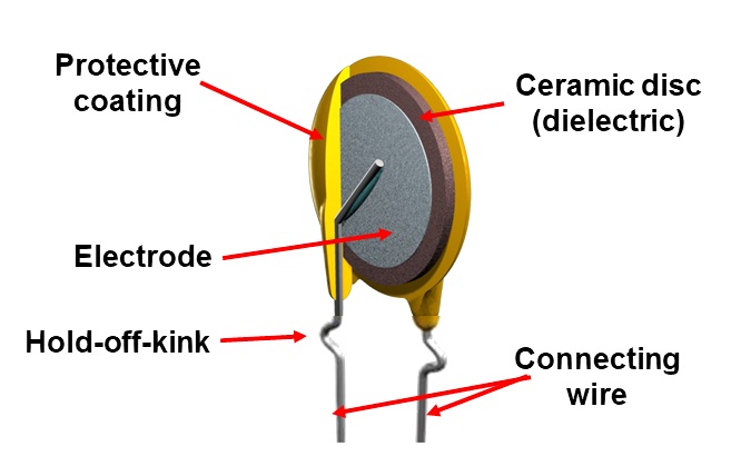 Ceramic Type Capacitor
These capacitors possess three digits of code on it.
Where the first two of the digits present on it represents the value of that particular capacitor and the last digit on it resembles the zeroes added on it.
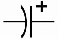 Symbol of Electrolytic Capacitor
In this way there exist various Capacitor Types.
All the types or the classification of the capacitors are based on the type of dielectric layer present between the plates. Each capacitor is chosen based on the requirements.
Can you give the best example of electrolytic capacitors?
 Polarized Capacitor Symbol
The above symbolic representation is also known as Capacitor Polarity Schematic.
 Ceramic Capacitor
Hence this doesn't possess any polarity.
It provides the flexibility of connecting this capacitor in the circuit.
 Film Capacitor
 Capacitor Polarity Indication
The 'plus sign' indication near the terminal indicates that the respective terminal is positive.
So, it is considered as Anode.
The other terminal has to be treated as Cathode.
Capacitor polarity can be identified based on arrow representation.
 Capacitor Polarity Based on Arrow
The arrow pointing towards the terminal is considered to be negative.
This is the process followed in 'Capacitor Polarity Identification' that can be done. But there must be some identification for the Non-polarized Capacitors.
In case of Non-polarized capacitors it is marked as NP on the capacitor for example NPA or NPR where NP stands for Non-polarized,A stand for axial and R stands for Radial.
Hence there exists various ways of determining the capacitor polarity.
There may be certain indications marked on it during the manufacturing time.
Certain capacitors are even marked with the bar on it.
Still, the care must be taken while fixations of it in the circuitry.
Which of the above capacitors do you prefer for high voltage applications polarized or non-polarized ones?
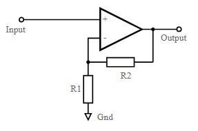 Non-Inverting Operational Amplifier Circuit
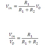 But the gain is the ratio between the ratios of the output values to input values of the applied signals.
Therefore,
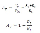 Where;
Av represents the overall gain obtained in the circuit.
R1 represents the resistance connected to the ground.
R2 represents the resistor connected to the feedback.
The resistance considered in the above equation is in ohms.
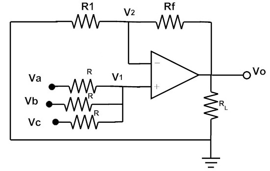 Non-Inverting Summing Amplifier
If the used resistors in the circuit are considered to be equal in terms of resistance.
In that case, the equation for the output can be determined as

 Output Wave form of the Non-Inverting Amplifier
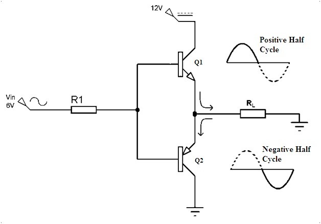 Push-Pull Amplifier Circuit Diagram
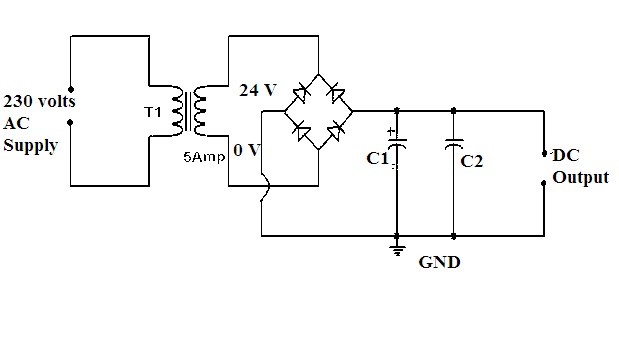 Power Amplifier Circuit Diagram
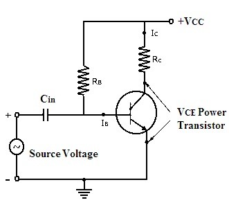 Class A Power Amplifier Circuit
The drawback of this circuit is that the transistor present in this circuit remains always on as it conducts in both positive and negative cycle of the input signal.
Since the transistor is active for both the half cycles it dissipates lots of heat and this results in the decrease in the overall efficiency of the circuit.
It also requires a heat sink to absorb the heat dissipated by the circuit.
The angle of conduction for this class of amplifier is considered to be 360 degrees.
The distortion in this type of amplifier is said to be minimum which results in better performance.
 Class B Power Amplifier Circuit
In this way, the efficiency compared to the class A amplifier is improved to 70 percent (theoretically).
These are mostly preferred for the devices that operate with the help of batteries.
But here the two transistors follow superposition that leads to the distortion over the cross-region.
These kinds of distortions was taken care in the design of class AB amplifiers.
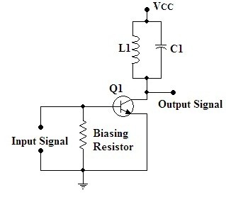 Class C Power Amplifier Circuit
As the signal generated from this circuit is of maximum distortion it cannot be preferred for the amplification of the audio signals.
It is preferred in the oscillators that have frequency consisting high in range.
It consists of the tuning load through which the input signals are filtered and amplified.
Other than the considered frequency rest of the frequency signals are suppressed.
This type is used for frequency modulation of the signals which are required for FM transmissions.
In this way, the various classes of the amplifiers are designed and discussed.
There are other classes such as class D, Class E, class F, etc… where the pulse width modulated signals are amplified.
These classes are generally preferred during switching applications or digital logic operations.
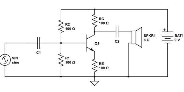 Audio Amplifier Circuit
 Nx Audio Amplifiers
In this way, one can describe that it is an amplifier that relates to sound amplification with various parameters of sound like power varying, impedance varying in it.
Lm386 Audio Amplifier
This is a kind of operational amplifier that is designed to perform certain tasks like if the input signal applied to the amplifier then it gets modulated ten times, a hundred times and even better. It is a basic amplifier in the form of a chip that consists of 8 pins.
The starting pin that is 1 and the pin, at last, that is 8 denote the gain values of that particular amplifier.
This gain value can be adjusted by connecting a capacitor to the circuit.
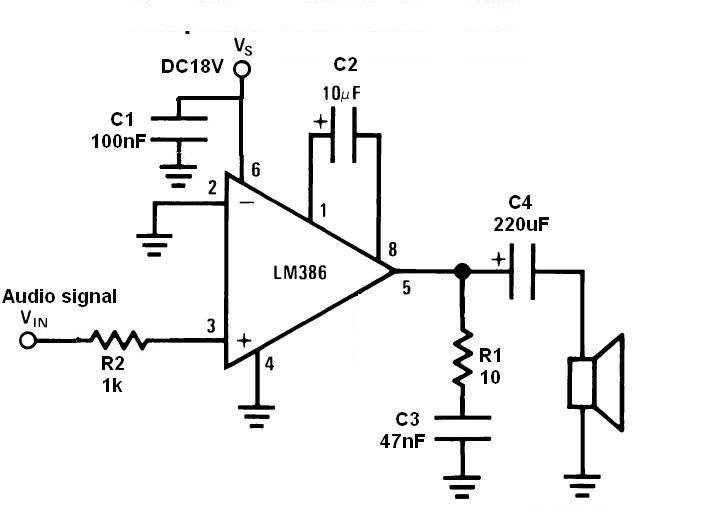 Lm386 Audio Amplifier
A potentiometer is connected to it so that one can control the volume of the amplifier.
In this kind of amplifiers, the distortion of the amplified signal will be low.
This kind of audio amplifier chip operates on the battery.
As the pins that are used in this chip can alter and manage the gains of the amplifier this can act as a flexible amplifier.
Hence Lm386 can be used in various applications of portable amplifiers of audio, ultrasonic sensors, and the power converters, etc…
Audio amplifiers are the basic power amplifiers that can be of various types like it is designed in various versions.
There are various parameters technically and even the parameters related to infrastructure also affect the audio amplification.
The audio amplifiers are designed in the form of chips and various sizes.
Many manufacturing companies designs this set of amplifiers based on the criteria provided by the client.
The best practical example of the audio amplifier is the siren that has the capability of increasing the strength of the applied signal and give an output with the maximum strength of the signal.
Now can you give another practical example where lively you can notice the application of the audio amplifier?
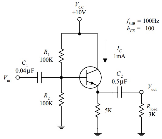 Common Emitter Amplifier Circuit
In the above circuit, common emitter configuration has been chosen in the design of the amplifier.
The circuit consists of potential divider circuitry that consists of resistors at the input side for the applied input signal to pass through this circuit.
The input signal is applied across the emitter and the base junction.
The output is taken across the terminal called the collector.
Here emitter is the common terminal present in both the input and the output sides.
 Symbol of N-Channel JFET
(2) P-Channel JFET
 Symbol for P-Channel JFET
These are the symbols that define the difference in their functionalities based on their arrow indication.
The arrow indication determines the flow of current when the gate and source terminal is forward biased.
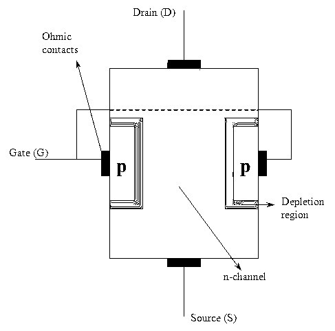 N-Channel JFET Representation
This is the major reason due to which the flow of the majority concentration of carriers can be evident from the terminal drain to the lower potential applied terminal called source.
These majority charge carriers flow is noted in a linear manner.
As the value of the differences in potential increases between the terminals of drain and the source, the flow of the currents tends to be in continuous.
But the at a particular voltage at the drain and the source, the transistor reaches the condition of voltage known as the pinch-off voltage.
Here current flow reaches the saturation level at the transistor.
In this case, the transistor is referred to as the resistor that is controlled by the voltage.
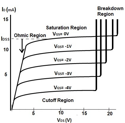 N-Channel JFET Characteristics
 The p-channel formed in between the two P-type substrate can be either due to the induced voltages or it might already exists in prior.
Based on this the p-channel MOSFET's are classified as
(1) P-channel with the Enhancement MOSFET
(2) P-channel with the Depletion MOSFET
 Symbol of Zener Diode
 Zener Diode Circuit
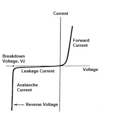 Zener Diode V-I Characteristics Curve
As per the above analysis, it is evident that during forwarding bias Zener diode characteristics will remain the same as that of the normal diode.
Whereas after the applied voltage crosses the value of Zener voltage (Vz ) the Zener breakdown takes place.
After the breakdown, the flow of the current in the circuit tends to increase immediately.
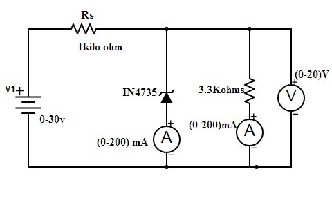 Zener Diode Experiment
The list of the components of equipment required to perform this experiment mainly include Zener diode, Milliammeter, Voltmeter, and DC supply(variable), and Resistors
Firstly the connections are made as per the circuit diagram.
To the circuit, the reverse voltage applied varies slowly.
Then simultaneously note down the voltmeter and ammeter readings.
There are two ammeters present in the circuit.
One is connected in series to the diode whereas other is connected in series to the resistor.
As the minimum voltage applied to the circuit exceeds one can observe sudden spikes in ammeter connected to the diode.
At this time note down the readings for both ammeters and voltmeter.
Even further application of voltage values can see that current values increase in the circuit but the voltage remains constant across the diode.
This has been done by connecting the diode in reverse bias voltage and current readings are tabulated.
Similarly, experiment by keeping the diode in forwarding bias and tabulate the readings.
Once the values are noted the plot of characteristics curves between voltage and current is plotted.
From the plot at which point of voltage the spike in current is noticed that voltage value is referred to as Zener breakdown voltage.
Based on the requirement of the voltage for the particular device the diode with that particular breakdown voltage has been chosen.
Hence in this way, the experiment is performed so that the breakdown voltage value can be found.
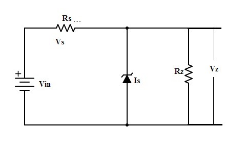 Shunt Regulator
Once the voltage limit has been crossed there is no increment in the voltage after it but in the current, we can see the increment.
The range of breakdown/zener voltage lies is from 12v to 1200 v based on its typical application.
The voltage that is to be regulated is across the resistor Rz.
To it, a diode is connected.
Whatever the voltage has been selected to be regulated it must not cross the limit value that is Vz.
Based on it a diode with certain breakdown voltage has been selected so that it satisfies the above criteria.
Zener diode is connected in reverse bias, so once the Zener voltage exceeds then the current flows through the diode but there is an unnoticeable voltage drop.
Hence in this way the voltage is limited across the load.
In this way, it is used as a voltage regulator.
This is considered as the basic application of Zener diode.
 I-V Characteristic of N-Channel MOSFET
 The symbol for N-Channel MOSFET Working as a Switch
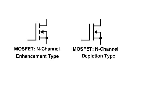 Symbols for N-channel Depletion and Enhancement Types
These n-channel MOSFETs are further classified as
N-Channel with Enhancement MOSFET and
N-Channel with Depletion MOSFET
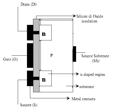 N-Channel Enhancement MOSFET
The device body that is formed due to p-type and the terminal source are connected to a common ground.
A positive polarity of the voltage is applied to the terminal gate.
Because of this positivism, it corresponds to an effect of the capacitor.
Hence in the p substrate, the minority carriers that are free electrons get attracted and move towards the terminal gate.
Due to this a layer that is because of uncovered ions is formed bellow the layer of dielectric where the combinations of the holes with electrons occur.
As the positive voltage applied gradually increases and crosses the minimum threshold the electrons which are minority carriers would be able to overcome the recombination with the holes and they form the channel between the two p type material .
Further application of the positive voltage value at the drain leads to the flow of current through the transistor.
The concentrations of the electrons are dependent on the potential applied.
These concentrations of the electrons are responsible for the formation of the channel and the application of the voltage at gate enhances the flow of the current.
Hence it is termed as N- channel MOSFET of enhancement type.
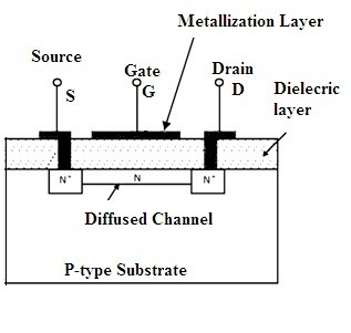 N-Channel Depletion MOSFET
A voltage value with the negative polarity is applied at the gate.
The electrons present in it get repelled and settles down at the dielectric layer.
This is the reason due to which the depletion of the charge carriers occurs and results in the reduction of the overall conductance.
At this situation after applying the same value of the voltage at the terminal drain still, the current value gets reduced.
By making the variations at the depletion charge carriers the flow of current at drain can be controlled.
This is the reason it is defined as depletion MOSFET.
Here the potential value at the drain is positive and the gate has negative polarity and the terminal source remains at the potential value of zero.
The difference of the values of potential is more at the terminals drain and the gate in comparison to the terminals of the source, and the gate.
The depletion width will be evident more at the drain in comparison with the source.
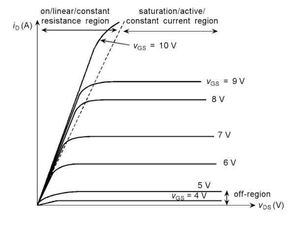 I-V Characteristic of N-Channel MOSFET
After the discussion on the basis of n-channel MOSFET can you tell the importance of n-channel enhancement over depletion type?
 Symbols for N-channel Depletion and Enhancement Types
 P-Channel Enhancement MOSFET
 P-Channel Depletion MOSFET
The variation in the width of the regions impacts the conductivity of the transistor.
This is the reason it is known as the depletion type of p-channel MOSFET.
 N-Channel Enhancement MOSFET
 N-Channel Depletion MOSFET
The enhancement mode is known for its characteristics based on the applied voltage whereas depletion is based on the variation of its width of the depletion region.
 I-V Characteristic of N-Channel MOSFET
 Symbol of N-Channel JFET
 Symbol for P-Channel JFET
Based on the channel it is known as n-channel JFET or the p-channel JFET.
For the n-channel JFET, the positive side is connected to the source terminal.
The drain terminal receives the highest potential in comparison with the gate in this n-channel JFET.
The junction formed due to the interaction of the drain and the gate terminal will be in reverse bias.
Due to this reason, the width of the depletion region that is present near to the drain is greater in comparison with the source.
Because of this condition, the majority of the charge carriers that are electrons flow can be seen from the terminals drain to the source.
As this potential at drain tends to increase the flow of carriers increases the flow of current also increases.
But certain increment at the voltages at drain and source the flow of current is stopped.
The JFET is generally known for the characteristics of controlling the current by the application of the input voltages.
The value of the input impedance is at a peak in this transistor.
When the JFET is in its ideal mode there is no current evidence at the gate terminal.
That how a n-channel JFET works.
Only the variation at the polarities of the supplies makes the FET work as p-channel JFET.
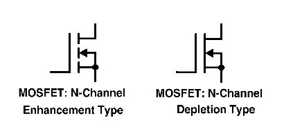 MOSFET
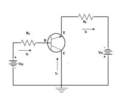 Common Collector Circuit Diagram
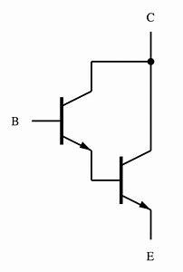 Symbol of Darlington Transistor Pair Configuration of Common Collector Configuration
This connection makes the output current generated at the emitter terminal of the first transistor as the input current of the second transistor for the base terminal.
Hence the overall gain of the current is the product of the individual transistor gains.
This makes the gain of the configuration to become high because of the Darlington pair configuration.
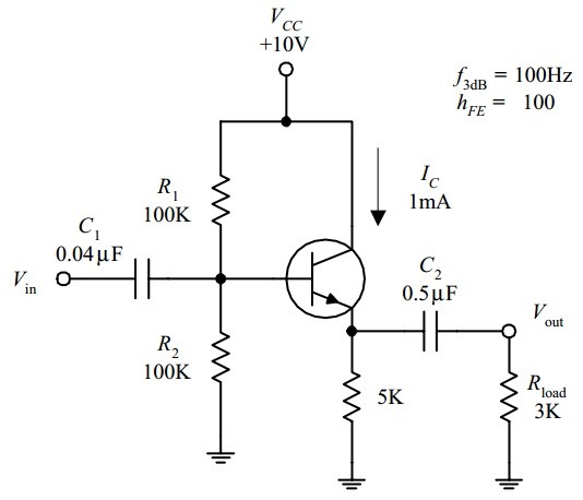 Circuit for Common Emitter Amplifier
Other than this there are various electronic components are to be included in this circuit.
One is the resistor R1 that is the one to make the transistor to function in the forward biasing mode.
The R2 is responsible to make the biasing possible.
There is the load resistor and the resistor that is connected at the emitter so that it controls the stability related to thermal issue. The resistors R1 and R2 connected across the terminal base as it is the input side.
The load resistor is connected at the output side that is across the collector terminal.
There are capacitors as well in the circuit.
The capacitor C1 is at the input side and the capacitor C2 is connected across the emitter resistor.
The C1 capacitor is responsible to separate the value of the AC signals from that of DC signals.
There exists the inverse relation between the R1 resistor and the biasing.
As R2 tends to increase the biasing tends to increase and vice-versa.
Hence to the smaller or the weaker signals that are applied to the base gets amplified at the obtained output signals.
Hence this is the reason it is known as CE amplifier.
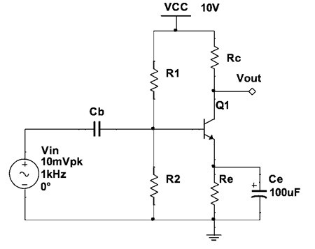 Transistor as Amplifier Circuit
Even the DC voltage can be applied to the circuit.
In this way, the low value of the signal is applied at the input because of the internal circuitry design the output signal generated possesses the strength of the output signal as high.
Overall the circuit designed here acts as an amplifier.
In order to satisfy the parameters and the design considerations generally, the configuration of the common-emitter is utilized in the amplifier applications.
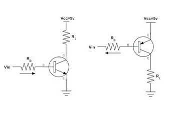 Transistor as Switch
By the application of bias to the base of the transistor both the types in the bipolar junction transistor can be used as switches.
The areas at which the operation of the switch is preferred is either it should be completely in the region called saturation or the cut-off operating region.
The main theme behind using these regions is that switch mode should be completely ON or OFF.
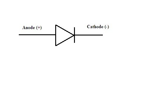 Symbol of P-N Junction Diode
These are utilized where the applications are preferred for low currents such as signal diodes.
one of the basic application of this as the rectifiers.
 Zener Diode
When the diode is in reverse bias mode after it reaches the minimum Zener voltage there we can see the increment in the values of current but the voltage remains constant after that point.
This makes it applicable to making use of it in the regulation of voltages.
The specialty of the diode lies when it starts conducting during reverse bias.
The more zen voltage of this type of diode is fixed by the manufacturers.
Because of this reason, more zen diodes with various more zen voltages can be manufactured
 Schottky Diode
The applications of this type of diodes can be seen as evident in clamping circuits that are fast enough.
This type of diodes can be seen operating in the range of gigahertz.
That is it can be preferred during high-frequency applications.
 The symbol for Shockley Diode
If the voltage applied to this is less than the basic trigger value it cannot switch because it remains in high resistance mode.
As the applied voltage exceeds the basic trigger value the low resistance path will be established.
In this way, the Shockley diodes operate.
 The symbol for Varicap Diode
The applied value of the reverse voltage can affect the junction width.
These are directly proportional to each other.
But these are inversely related with capacitance at the junction.
This is the main reason that makes them applicable in the oscillators.
The change in the value of capacitance makes the circuit to work as a tuner.
 Gunn Diode
These are also utilized in military areas.
The basic tachometers consist of this diode in it.
Nowadays in the monitoring systems for opening the doors sensors are required this can be made possible by the Gunn diodes.
In the intruder alarms circuitry also this diode is preferred.
 Light Emitting Diode
These include various types in LED.
Namely blinking one that can act as on and off for a certain amount of time.
They can be tricolor leads more than two colors get emitted based on the amount of received a positive amount of voltage.
Further, there are LED's that emits infrared light.
The practical application of it can be seen in remote controls.
The above discussed are some of the types present in LED.
 LASER Diode
As the response time is faster in this type of diodes these are used as optical storage devices as well as in CD players.
Nowadays one can see bar code scanners these are one of the applications of LASER diode.
These are also seen in the printers of LASER's, Fax machines, etc…
 Photo Diode
The current value and the value of the intensity of the light are directly proportional to each other.
These also have the response times that are fast enough that is in nanoseconds.
This type of diodes can also have the capacity of generating electricity.
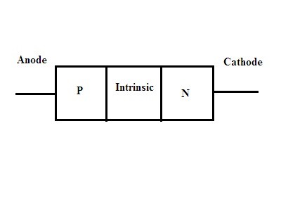 The symbol for PiN Diode
This region is helpful during applications like switching.
 Tunnel Diode
In the range of ultra-high-speed, these tunnel diodes have used switches.
The switching time will be in nano or picoseconds.
Because of the concept of negative resistance involved in it, this is used in the terminology of relaxation oscillator circuitry.
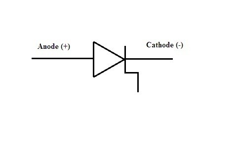 Symbol of Step Recovery Diode
Hence the various types of diodes along with there applications are discussed above.
Each diode is unique in its way of representation as well as application.
The above we discussed various types in a diode with respect to its applications.
Can you describe the functionality of the various types of diodes?
 The encoders and decoders play an essential role in digital electronics projects; encoders & decoders are used to convert data from one form to another form.
These are frequently used in communication system such as telecommunication, networking, etc..to transfer data from one end to the other end.
Similarly, in the digital domain, for easy transmission of data, it is often encrypted or placed within codes, and then transmitted.
At the receiver, the coded data is decrypted or gathered from the code and is processed in order to be displayed or given to the load accordingly.
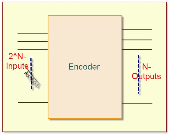 Encoder
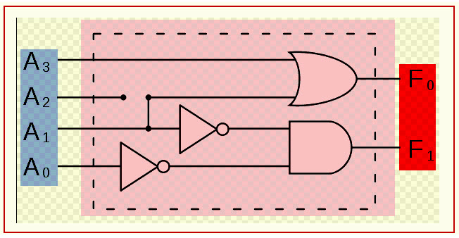 Simple Encoder
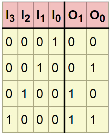 Encoder Truth Table
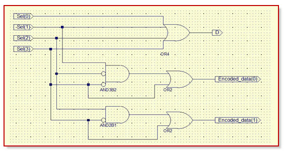 Priority Encoder
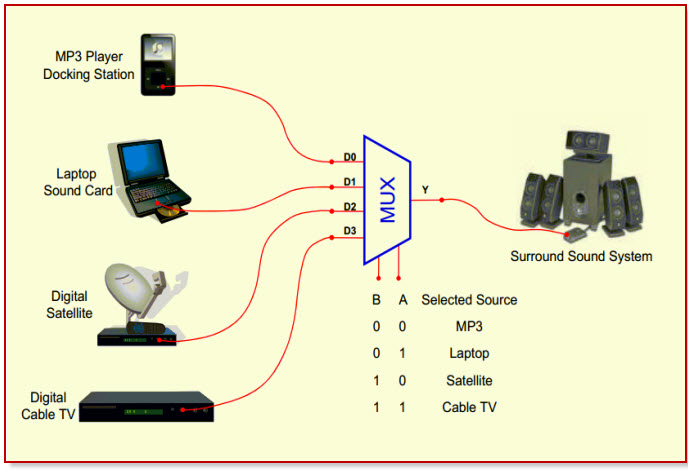 Multiplexer
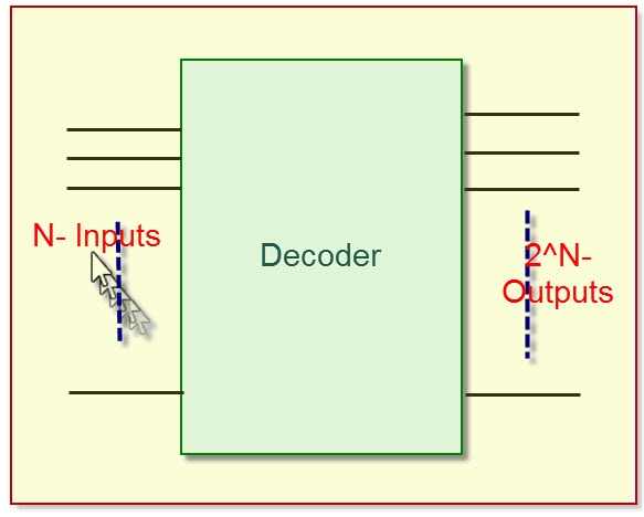 Decoder
 Decoder Circuit
 Decoder Truth T
2-to-4 line Decoder
In this type of encoders and decoders, decoders contain two inputs A0, A1, and four outputs represented by D0, D1, D2, and D3.
As you can see in the truth table - for each input combination, one output line is activated.
 2-to-4 Decoder
In this example, you can notice that, each output of the decoder is actually a minterm, resulting from a certain inputs combination, that is:
D0 =A1 A0, ( minterm m0) which corresponds to input 00
D1 =A1 A0, ( minterm m1) which corresponds to input 01
D2 =A1 A0, ( minterm m2) which corresponds to input 10
D3 =A1 A0, ( minterm m3) which corresponds to input 11
The circuit is implemented with AND gates, as shown in the figure.
In this circuit, the logic equation for D0 is A1/A0, and so on.
Thus, each output of the decoder will be generated to the input combination.
 3-to-8 Decoder
In this example, you can notice that, each output of the decoder is actually a minterm, resulting from a certain inputs combination, that is;
D0 =A2 A1 A0, ( minterm m0) which corresponds to input 000
D1 = A2 A1 A0, ( minterm m1) which corresponds to input 001
D2 = A2 A1 A0, ( minterm m2) which corresponds to input 010
D3 = A2 A1 A0, ( minterm m3) which corresponds to input 011
D4 = A2 A1 A0, ( minterm m0) which corresponds to input 100
D5 = A2 A1 A0, ( minterm m1) which corresponds to input 101
D6 = A2 A1 A0, ( minterm m2) which corresponds to input 110
D7 = A2 A1 A0, ( minterm m3) which corresponds to input 111
The circuit is implemented with AND gates, as shown in the figure.
In this circuit, the logic equation for D0 is A2/A1/A0/, and so on.
Thus, each output of the decoder will be generated to the input combination.
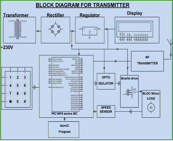 Speed Synchronization of Multiple Motors in Industries
In this system, one motor output is given as the reference speed for the other motors to follow same speed.
The proposed system consists of two blocks: transmitter and receiver blocks, which are built with encoder and decoder.
A particular speed is sent by the transmitter with the help of the decoder.
The receiver receives the data and converts the digital format to send the receiver system, and maintains same speed as it has received.
Thus, if a particular speed is set by the transmitter, then other motors run with the same speed by utilizing radio-frequency communication.
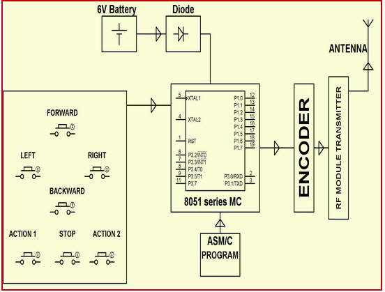 War Field Flying Robort with NJight Vision Flying Camera
In the transmitting end push buttons are used; commands are sent to the controller for controlling the movement of the robot either in forward, backward, left, right, directions.
The RF transmitter acts as a RF remote control that has the advantage of adequate range (up to 200 meters) with proper antenna, while the receiver decodes before feeding it to another microcontroller to drive DC motors via motor-driver IC for necessary work.
A wireless camera is mounted on the robot body for spying purposes, even in complete darkness by using infrared lighting.
The basic schematic diagram is shown above.
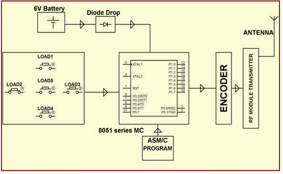 Robotic Vehicle with Metal Detector
The RF transmitter acts as a RF remote control that has the advantage of adequate range (up to 200 meters) with proper antenna, while the receiver decodes before feeding it to another microcontroller to drive DC motors via motor driver IC for necessary work.
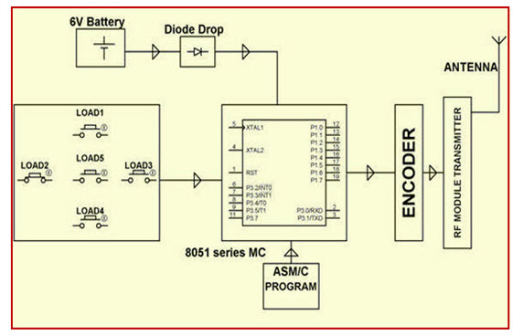 RF based Home Automation System
Presently, conventional wall switches located in different parts of the house make it difficult for the user to approach them for operations.
Furthermore, it becomes more & more difficult for the elderly or physically handicapped people to do so.
Remote controlled home automation system provides a simpler solution with RF technology.
 Automatic Wireless Health Monitoring System in Hospitals for Patients Block Diagram
 Secret Code Enabled Secure Communication using RF Technology Block Diagram
This is all about encoder & decoder, types of encoder and decoder and its applications in communication based projects.
we believe that, you might have got a better idea about this concept, furthermore, any doubts regarding this article please give your valuable suggestions by commenting in the comment section below.
 NMOS Fabrication Process
There are a huge number and assortment of fundamental fabrication steps utilized as a part of the generation of present-day MOS ICs.
A similar procedure can be utilized for the planned of NMOS or PMOS or CMOS devices.
The most commonly used material could be either metal or poly-silicon.
The most regularly utilized substrate is mass silicon or silicon-on-sapphire (SOS).
In order to keep a strategic distance from the nearness of parasitic transistors, varieties are acquired the systems that are utilized to isolate the devices in the wafer.
The NMOS fabrication steps are as per the following.
 Step2:
A SiO2 (silicon dioxide) layer normally 1 micrometer broad is grown all above the exterior of the wafer to guard the surface, performs as a barrier to the dopant through processing, and offers a generally protecting substrate on to which extra layers may be deposited and decorative.
 Step 4:
The photoresist coating is then uncovered to ultraviolet (UV) light through masking which describes those areas into which transmission is to take place as one with transistor channels.
Suppose, for example, that those areas uncovered to UV radiations are polymerized, but that the areas necessary for diffusion are protected by the cover and remain unchanged.
 Step 5:
These regions are consequently readily fixed away together with the original silicon-di-oxide so that the surface of the wafer is uncovered in the window defined by the mask.
 Step 6:
A thin layer of SiO2 (0.1 micro m typical) is grown over the chip surface after removing the remains of photoresist.
Further, a gate structure is created by depositing polysilicon on the top of it.
Factors like precise control of thickness, impurity concentration, and resistivity are necessary for the fabrication of fine pattern devices.
 Step 7:
Further, the photoresist coating and masking allows the polysilicon to be patterned.
After this, the thin oxide is removed to expose the areas.
These areas are defused with n-type impurities by heating the wafer to a high temperature and passing the gas of desired n-type impurities to form the source and the drain.
 Note: The polysilicon has an underlying thin oxide which acts as a mask during diffusion.
This is called self-aligning.
Step 8:
Again a thick oxide of SiO2 is grown over and then masked with photoresist.
Now it is etched to expose selected areas of the polysilicon gate, drain and the source where connections are to be made.
 Step 9:
Now the whole chip has the deposits of the metal (aluminum) over its surface, typically to a thickness of 1micro m.
This metal layer is masked and then etched to form the required interconnection pattern.
 The above fabrication steps let only the arrangement of nMOS enhancement type transistors on a chip.
But, if depletion type transistors are also to be created, one extra step is required for the arrangement of n-diffusions in the channel sections where depletion transistors are to be shaped.
It engages one extra step that is, requires one extra mask to describe channel regions following a diffusion procedure using the ion implantation technique.
For detailed information regarding the NMOS fabrication process.
We hope that you have got a better understanding of this concept.
Furthermore any queries regarding this concept or to implement any electronic projects please post your ideas and queries by commenting on the comment section below.
 Ohmmeter
While testing, repairing or troubleshooting electronic equipment, you use different meters and different types of test equipment to test proper circuit currents, resistances, voltages and to decide whether the wiring is faulty.
Without knowing the operation of the Ohmmeter, it is not possible to connect this instrument to a circuit to test the component.
However, to be a competent technician, we need to be competent to do more than merely read a test instrument.
For that we need a basic knowledge of how test instruments operate.
It is an electronic device used to measure electrical resistance of a circuit element.
Electrical resistance is a measure of how much an object opposes allowing an electrical current to pass through it.
Ohmmeters come with different levels of sensitivity.
Some Ohmmeters are designed to measure low-resistance materials, and some are used for measuring high-resistance materials.
This article discusses the operating principles of an Ohmmeter that you use in equipment's troubleshooting.
Ohmmeter
While testing, repairing or troubleshooting electronic equipment, you use different meters and different types of test equipment to test proper circuit currents, resistances, voltages and to decide whether the wiring is faulty.
Without knowing the operation of the Ohmmeter, it is not possible to connect this instrument to a circuit to test the component.
However, to be a competent technician, we need to be competent to do more than merely read a test instrument.
For that we need a basic knowledge of how test instruments operate.
It is an electronic device used to measure electrical resistance of a circuit element.
Electrical resistance is a measure of how much an object opposes allowing an electrical current to pass through it.
Ohmmeters come with different levels of sensitivity.
Some Ohmmeters are designed to measure low-resistance materials, and some are used for measuring high-resistance materials.
This article discusses the operating principles of an Ohmmeter that you use in equipment's troubleshooting.
 Series Type Ohmmeter
If A&B terminals are connected together the resistors R1 and R2, the battery, the meter form a simple series circuit.
The Resistor R2 is adjusted to get full-scale current through the movement, then the Current I=Ifsd.
The needle drives back to the maximum position on the scale.
So, the current reading on the full scale is marked as 0 Ohms.
If A & B terminals are open circuited, no current will flow and the needle will not move.
So, the zero current reading on full scale will be marked as infinite to indicate an infinite resistance.
 Shunt Type Ohmmeter
When the A and B terminals are closed, then the unknown resistor Rx is short circuited, the needle reads zero because full current flows through the resistor Rx, and I=0 through the meter.
Therefore, zero current reading is marked as 0 Ohms.
When the A and B terminals are opened, then the unknown resistor RX is open circuited, no current flows through the RX and full-scale current flows through the meter as the resistor R1 is adjusted.
So, maximum current reading is marked 8 Ohms.
 Ohmmeter Scale
 A simple ohmmeter circuit
When the leads are shorted, the meter is adjusted for proper operation on the selected range and the needle drives back to the maximum position on the Ohms scale and the meter current is max.
After using an Ohmmeter, the test leads should be removed.
If the test leads remain connected to the Ohmmeter, then the battery of the meter gets discharged.
When the rheostat is adjusted properly, with the test leads shorted, the needle of the meter comes to zero position, and this specifies a zero resistance between the test leads.
 Circuit working with an ohmmeter
If the current limiting resistor R1 or zero adjusts resistor R2 or both are replaced with a larger value resistor, then the current flow and the deflection in the moving coil of the meter will be decreased.
Thus, this article concludes with a brief discussion about the Ohmmeter and its working principle with a circuit diagram which works based on Ohms law principle.
For more information regarding the same or phase sequence meters please post your queries by commenting below.
Photo Credits:
Ohmmeter by iofferphoto
Series Type Ohmmeter by avstop
Shunt Type Ohmmeter by avstop
Ohmmeter scale by avstop
A simple ohmmeter circuit by tpub
Circuit Working with an Ohmmeterby earth2
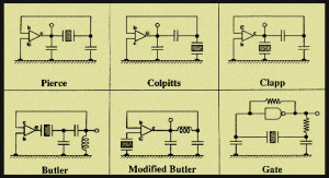 An electronic circuit or electronic device that is used to generate periodically oscillating electronic signal is called as an electronic oscillator.
The electronic signal produced by an oscillator is typically a sine wave or square wave.
An electronic oscillator converts the direct current signal into an alternating current signal.
The radio and television transmitters are broad casted using the signals generated by oscillators.
The electronic beep sounds and video game sounds are generated by the oscillator signals.
These oscillators generate signals using the principle of oscillation.
There are different types of oscillator electronic circuits such as Linear oscillators - Hartley oscillator, Phase-shift oscillator, Armstrong oscillator, Clapp oscillator, Colpitts oscillator, and so on, Relaxation oscillators - Royer oscillator, Ring oscillator, Multivibrator, and so on, and Voltage Controlled Oscillator (VCO).
In this article, let us discuss in detail about Crystal oscillator like what is crystal oscillator, a crystal oscillator circuit, working, and use of crystal oscillator in electronic circuits.
 Quartz Crystal Oscillator
An electronic circuit that is used to generate an electrical signal of precise frequency by utilizing the vibrating crystal's mechanical resonance made of piezoelectric material.
There are different types of piezoelectric resonators, but typically, quartz crystal is used in these types of oscillators.
Hence, these oscillator electronic circuits are named as crystal oscillators.
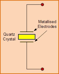 Electronic Symbol for Piezoelectric Crystal Resonator
The above diagram represents the electronic symbol for a piezoelectric crystal resonator which consists of two metalized electrodes and quartz crystal.
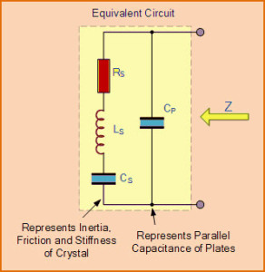 Equivalent Circuit Diagram of Quartz Crystal
The above figure shows the equivalent circuit diagram of quartz crystal in an electronic oscillator that consists of resistor, inductor, and capacitors which are connected as shown in the figure.
 High Frequency-Rectangular Plate Crystals and Low Frequency-Tuning Fork Crystals
Crystal oscillator circuit works on the principle of the inverse piezoelectric effect, i.e., a mechanical deformation is produced by applying an electric field across certain materials.
Thus, it utilizes the vibrating crystal's mechanical resonance which is made of a piezoelectric material for generating an electrical signal of a specific frequency.
These quartz crystal oscillators are highly stable, consists of good quality factor, they are small in size, and are very economical.
Hence, quartz crystal oscillator circuits are superior compared to other resonators such as LC circuits, turning forks, and so on.
Generally, 8MHz crystal oscillator is used in microprocessors and microcontrollers.
The equivalent electrical circuit also represents the crystal action of the crystal.
The basic components used in the circuit, inductance L1 represent crystal mass, capacitance C1 represents compliance, resistance R1 represents the crystal's internal structure friction, and C0 is used to represent the capacitance that is formed because of crystal's mechanical moulding.
The quartz crystal oscillator circuit diagram consists of series resonance and parallel resonance, i.e., two resonant frequencies.
If the reactance produced by capacitance C1 is equal and opposite to the reactance produced by inductance L1, then the series resonance occurs.
The series and parallel resonant frequencies are represented by fs and fp respectively, and the values of fs and fp can be determined by using the following equations shown in the figure below.
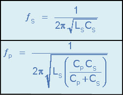 Series Resonant Frequency and Parallel Resonant Frequency
Thus, the impedance is approximately equal to the resistance R1 during this condition.
If the series resonant leg reactance is equal to the reactance caused due to capacitance C0, then parallel resonance occurs.
Thus, the external circuit if offered a very high impedance by the crystal during this condition.
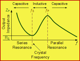 Impedance vs Frequency Graph
The above figure shows the graph between impedance and frequency of the quartz crystal oscillator circuit.
Typically, crystal oscillators are having a frequency range from 32KHz to 200MHz.
 Once the load is connected in parallel in such a way that in order to maintain the same amount of the voltage at the resistor as well as the diode.
In order to make the voltage stabilize first of all the current passing through the diode must be limited to the minimum value.
Then only the stabilization of the voltage becomes more effective.
The maximum limit for the current is determined by the rating that is provided.
But the only problem for this kind of circuits is that they tend to generate noise as the DC supply is provided.
But this kind of noise doesn't affect the operation of stabilizing.
The capacitor is also connected across the diode so that the output generated gets smoothed because the capacitor acts as a filter.
 Overall the connection of resistor in parallel form and the design of the Zener diode is to limit the flow of the value of the voltage so that changes in the current doesn't affect the device.
Hence it is preferred in the protection circuitry so that high currents and the fluctuation in the current should not affect the functionality of the device.
The Zener diode behaves ideally during forwarding bias and the conduction possibility in reverse bias.
Now can you list other than voltage regulation where the Zener diode is been utilized?
 Arduino Uno Board
Arduino is a single-board microcontroller meant to make the application more accessible which are interactive objects and its surroundings.
The hardware features with an open-source hardware board designed around an 8-bit Atmel AVR microcontroller or a 32-bit Atmel ARM.
Current models consists a USB interface, 6 analog input pins and 14 digital I/O pins that allows the user to attach various extension boards.
The Arduino Uno board is a microcontroller based on the ATmega328.
It has 14 digital input/output pins in which 6 can be used as PWM outputs, a 16 MHz ceramic resonator, an ICSP header, a USB connection, 6 analog inputs, a power jack and a reset button.
This contains all the required support needed for microcontroller.
In order to get started, they are simply connected to a computer with a USB cable or with a AC-to-DC adapter or battery.
Arduino Uno Board varies from all other boards and they will not use the FTDI USB-to-serial driver chip in them.
It is featured by the Atmega16U2 (Atmega8U2 up to version R2) programmed as a USB-to-serial converter.
Arduino Uno Board
Arduino is a single-board microcontroller meant to make the application more accessible which are interactive objects and its surroundings.
The hardware features with an open-source hardware board designed around an 8-bit Atmel AVR microcontroller or a 32-bit Atmel ARM.
Current models consists a USB interface, 6 analog input pins and 14 digital I/O pins that allows the user to attach various extension boards.
The Arduino Uno board is a microcontroller based on the ATmega328.
It has 14 digital input/output pins in which 6 can be used as PWM outputs, a 16 MHz ceramic resonator, an ICSP header, a USB connection, 6 analog inputs, a power jack and a reset button.
This contains all the required support needed for microcontroller.
In order to get started, they are simply connected to a computer with a USB cable or with a AC-to-DC adapter or battery.
Arduino Uno Board varies from all other boards and they will not use the FTDI USB-to-serial driver chip in them.
It is featured by the Atmega16U2 (Atmega8U2 up to version R2) programmed as a USB-to-serial converter.
 Arduino Uno with Digital Input/Output
There are various types of Arduino boards in which many of them were third-party compatible versions.
The most official versions available are the Arduino Uno R3 and the Arduino Nano V3.
Both of these run a 16MHz Atmel ATmega328P 8-bit microcontroller with 32KB of flash RAM 14 digital I/O and six analogue I/O and the 32KB will not sound like as if running Windows.
Arduino projects can be stand-alone or they can communicate with software on running on a computer.
For e.g.
Flash, Processing, Max/MSP).
The board is clocked by a 16 MHz ceramic resonator and has a USB connection for power and communication.
You can easily add micro SD/SD card storage for bigger tasks.
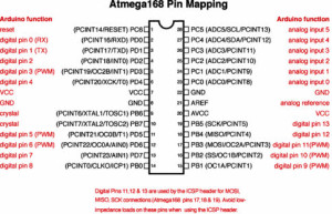 ATmega168-328Arduino Pin Mapping
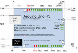 Pin Diagram of Arduino Uno
The ATmega16U2/8U2 is loaded with a DFU bootloader, which can be activated by:
On Rev1 boards: connecting the solder jumper on the back of the board (near the map of Italy) and then resetting the 8U2.
On Rev2 or later boards: there is a resistor that pulling the 8U2/16U2 HWB line to ground, making it easier to put into DFU mode.
You can then use Atmel's FLIP software (Windows) or the DFU programmer (Mac OS X and Linux) to load a new firmware.
Or you can use the ISP header with an external programmer (overwriting the DFU bootloader).
 Arduino Uno Starter Kit
Microcontroller ATmega328
Operating Voltage 5V
Input Voltage (recommended) 7-12V
Input Voltage (limits) 6-20V
Digital I/O Pins 14 (of which 6 provide PWM output)
Analog Input Pins 6
DC Current per I/O Pin 40 Ma
DC Current for 3.3V Pin 50 Ma
Flash Memory 32 KB (ATmega328) of which 0.5 KB used by bootloader
SRAM 2 KB (ATmega328)
EEPROM 1 KB (ATmega328)
Clock Speed 16 MHz
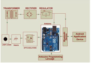 Arduino Based Home Automation
In order to achieve this, a Bluetooth module is interfaced to the Arduino Uno board at the receiver end while on the transmitter end, a Graphical User Interface application on the cell phone sends ON/OFF commands to the receiver where loads are connected.
By touching the identified location on the Graphical User Interface, lamps are used as loads in this project can be turned ON/OFF remotely by using this technology.
The loads are operated by using Arduino Uno board through thyristors using triacs and OPTO-Isolators.
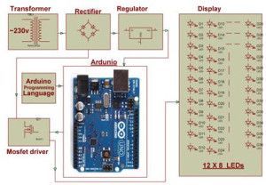 Arduino Based Auto Intensity Control
Thus, this system overcomes this problem by controlling the intensity of LED lights on street by gradually reducing intensity by controlling the voltage applied to these lamps.
This system uses arduino board to produce PWM pulses and it is programmed in such a way that it decreases the voltage applied to these lamps gradually till late nights and completely shutdowns at morning.
Thus, Arduino development board can sense the environment by receiving input from different sensors and affects its surroundings by controlling motors, lights and other actuators.
The microcontroller on the board is programmed using the Arduino programming language.
Thanks for your attention to this article and clarify doubts about Arduino projects by commenting below.
Photo Credits:
Arduino Uno Board by adafruit
Arduino Uno with Digital Input/Output by cprogramming
ATmega168/328-Arduino Pin Mapping by arduino
Pin Diagram of Arduino Uno by cmb
Arduino starter kit by generationrobots
 PIC Microcontroller
PIC microcontroller was developed in the year 1993 by microchip technology.
The term PIC stands for Peripheral Interface Controller.
Initially this was developed for supporting PDP computers to control its peripheral devices, and therefore, named as a peripheral interface device.
These microcontrollers are very fast and easy to execute a program compared with other microcontrollers.
PIC Microcontroller architecture is based on Harvard architecture.
PIC microcontrollers are very popular due to their ease of programming, wide availability, easy to interfacing with other peripherals, low cost, large user base and serial programming capability (reprogramming with flash memory), etc.
We know that the microcontroller is an integrated chip which consists of CPU, RAM, ROM, timers, and counters, etc.
In the same way, PIC microcontroller architecture consists of RAM, ROM, CPU, timers, counters and supports the protocols such as SPI, CAN, and UART for interfacing with other peripherals.
At present PIC microcontrollers are extensively used for industrial purpose due to low power consumption, high performance ability and easy of availability of its supporting hardware and software tools like compilers, debuggers and simulators.
PIC Microcontroller
PIC microcontroller was developed in the year 1993 by microchip technology.
The term PIC stands for Peripheral Interface Controller.
Initially this was developed for supporting PDP computers to control its peripheral devices, and therefore, named as a peripheral interface device.
These microcontrollers are very fast and easy to execute a program compared with other microcontrollers.
PIC Microcontroller architecture is based on Harvard architecture.
PIC microcontrollers are very popular due to their ease of programming, wide availability, easy to interfacing with other peripherals, low cost, large user base and serial programming capability (reprogramming with flash memory), etc.
We know that the microcontroller is an integrated chip which consists of CPU, RAM, ROM, timers, and counters, etc.
In the same way, PIC microcontroller architecture consists of RAM, ROM, CPU, timers, counters and supports the protocols such as SPI, CAN, and UART for interfacing with other peripherals.
At present PIC microcontrollers are extensively used for industrial purpose due to low power consumption, high performance ability and easy of availability of its supporting hardware and software tools like compilers, debuggers and simulators.
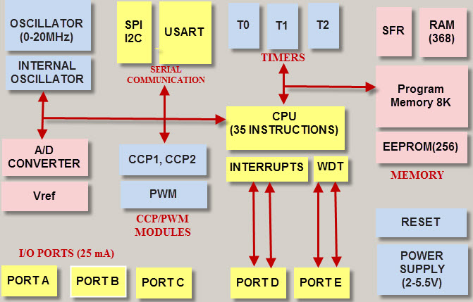 Architecture of PIC Microcontroller
 Memory Organization
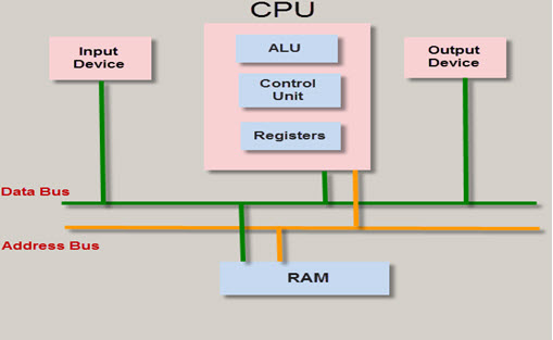 BUS
BUS
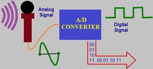 A/D CONVERTER
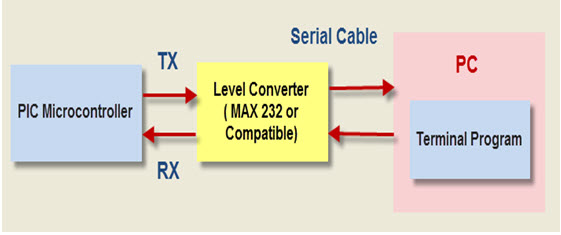 Serial Communication
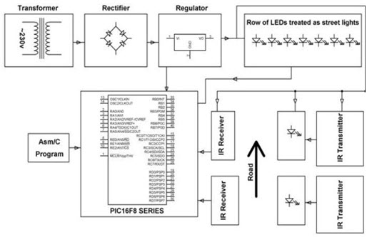 Street Light that Glows on Detecting Vehicle Movement by Edgefxkits.com
The power supply gives the power to the total circuit by stepping down, rectifying, filtering and regulating AC mains supply.
When there are no vehicles on highway, then all lights will turn OFF so that the power can be conserved.
The IR sensors are placed on the road to sense the vehicle movement.
When there are vehicles on highway, then the IR sensor senses the vehicle movement immediately, it sends the commands to the PIC microcontroller to switch ON/OFF the LEDs.
A bunch of LEDS will be turned on when a vehicle come near to the sensor and once the vehicle passes away from the sensor the intensity will become lower than the LEDs will turn OFF
 CMOS Fabrication
In early 1960's the semiconductor manufacturing process was initiated from Texas and in 1963 CMOS or complementary metal oxide semiconductor was patented by Frank Wanlass. Integrated circuits are manufactured by utilizing the semiconductor device fabrication process.
These ICs are major components of every electrical and electronic devices which we use in our daily life.
Many complex and simple electronic circuits are being designed on a wafer made of semiconductor compounds and mostly silicon by using different fabrication steps.
The complementary of the Commodore Semiconductor Group (CSG) or Metal Oxide Semiconductor (MOS) is called as CMOS technology.
This technology is used in developing the microprocessors, microcontrollers, digital logic circuits and many other integrated circuits.
It facilitates low- power dissipation and high-packing density with very less noise margin.
It is mostly used to build digital circuitry.
 Step2: Oxidation
The oxidation process is done by using high-purity oxygen and hydrogen, which are exposed in an oxidation furnace approximately at 1000 degree centigrade.
 Step3: Photoresist
A light-sensitive polymer that softens whenever exposed to light is called as Photoresist layer.
It is formed.
 Step4: MaskingThe photoresist is exposed to UV rays through the N-well mask
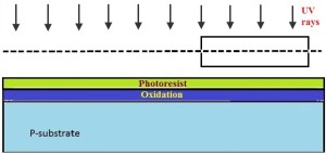 Step5: Photoresist removalA part of the photoresist layer is removed by treating the wafer with the basic or acidic solution.
 Step6: Removal of SiO2 using acid etching
The SiO2 oxidation layer is removed through the open area made by the removal of photoresist using hydrofluoric acid.
 Step7: Removal of photoresist
The entire photoresist layer is stripped off, as shown in the below figure.
 Step8: Formation of the N-wellBy using ion implantation or diffusion process N-well is formed.
 Step9: Removal of SiO2Using the hydrofluoric acid, the remaining SiO2 is removed.
 Step10: Deposition of polysiliconChemical Vapor Deposition (CVD) process is used to deposit a very thin layer of gate oxide.
 Step11: Removing the layer barring a small area for the GatesExcept the two small regions required for forming the Gates of NMOS and PMOS, the remaining layer is stripped off.
 Step12: Oxidation process
Next, an oxidation layer is formed on this layer with two small regions for the formation of the gate terminals of NMOS and PMOS.
 Step13: Masking and N-diffusionBy using the masking process small gaps are made for the purpose of N-diffusion.
 The n-type (n+) dopants are diffused or ion implanted, and the three n+ are formed for the formation of the terminals of NMOS.
 Step14: Oxide strippingThe remaining oxidation layer is stripped off.img class=”aligncenter size-medium wp-image-1062
 Step16: Thick field oxide
A thick-field oxide is formed in all regions except the terminals of the PMOS and NMOS.
 Step17: MetallizationAluminum is sputtered on the whole wafer.
 Step18: Removal of excess metal
The excess metal is removed from the wafer layer.
 Step19: Terminals
The terminals of the PMOS and NMOS are made from respective gaps.
 Step20: Assigning the names of the terminals of the NMOS and PMOS
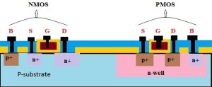
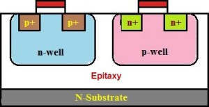 In this process, separate optimization of the n-type and p-type transistors will be provided.
The independent optimization of Vt, body effect and gain of the P-devices, N-devices can be made possible with this process.
Different steps of the fabrication of the CMOS using the twintub process are as follows:
Lightly doped n+ or p+ substrate is taken and, to protect the latch up, epitaxial layer is used.
The high-purity controlled thickness of the layers of silicon are grown with exact dopant concentrations.
The dopant and its concentration in Silicon are used to determine electrical properties.
Formation of the tub
Thin oxide construction
Implantation of the source and drain
Cuts for making contacts
Metallization
By using the above steps we can fabricate CMOS using twintub process method.
 The P-type and N-type transistors are called as fundamental building blocks of CMOS circuits.
If the input voltage is low, then P-type MOSFET acts as closed switch and, if the input voltage is high, then the P-type MOSFET acts as open switch.
If the input voltage is high, then the N-type MOSFET acts as a closed switch and, if input the voltage is low, then the N-type MOSFET acts as an open switch.
Combining the P-type and N-type MOSFETs without any conduction path between the supply voltage and the ground is the basic idea behind developing the CMOS technology.
With this combination, very little energy is consumed by the CMOS circuits.
 Similarly, if the input voltage is high (5V), then the transistor (N-type) T2 conducts (switch close) while the transistor T1 doesn't conduct (switch open).
Hence, the output of the circuit will be low (0V).
The above truth table shows the function of the CMOS inverter circuit and, from the table, we can observe that the output of the circuit is the inverse of the input.
Everytime whether the input is low or high, one of the two transistors conducts such that no current flows from the supply to ground.
For detailed information regarding the fabrication process of CMOS, which includes P-type and twintub processes and also advanced-fabrication process such as combination of Bipolar and CMOS ( BiCMOS fabrication), please post your ideas and queries by commenting below.
 symbol of diode
The basic symbol of a diode that consists of both anode and cathode in it is sufficient enough to represent it as a diode.
The alignment of this diode can be done in such a way that it becomes application-oriented.
In general terms, it can work as a rectifier.
The structure of the arrowhead in the above representation indicated the flow of the conventional current.
 Unbiased-Rectifier Diode
 forward bias
When positive supply is provided to the p-type and negative supply to the n-type the majority carriers tends to repel each other because the polarity of the voltage and charge on the majority carriers is similar.
Hence the process of drift occurs.
Once the electrons in n-type tend to drift there is the generation of drift current.
Hence in n-type, the current is due to electrons and in p-type it is due to holes.
So drift current is due to the drifting of the majority carriers.
This type of current is referred to as forward current and the direction will be from the positive terminal to the negative terminal of the source and opposite to the direction of the flow of electrons.
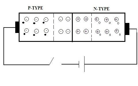 Reverse Bias
As per the connections of the diode in reverse bias, there is no forward current evident here except the reverse saturation current.
As there is the presence of depletion region but its width tends to increase.
However, there is no flow can be seen in majority carriers but due to minority carrier's effect, some current is generated referred to as reverse saturation current.
If the reverse saturation current tends to increase in the diode then a point comes where the width of the depletion region is completely eliminated resulting in a large amount of flow of reverse current in the diode resulting in the breakdown of the diode.
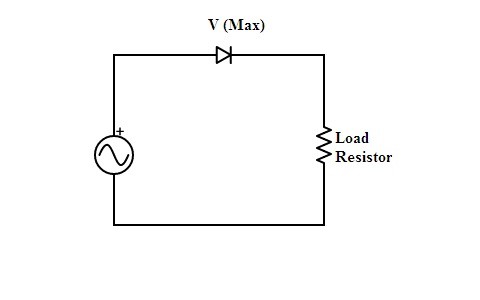 half wave rectifier
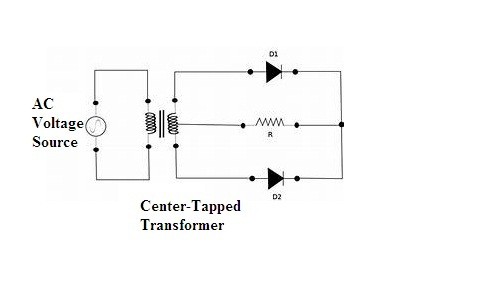 Full Wave Rectifier (Center-Tapped)
For the positive cycle, D1 conducts and for the negative cycle D2 conducts.
However, both the cycles are utilized and the loss of power is minimized and also the ripple factor by increasing efficiency of the circuit.
The only drawback is that the transformer utilized here is costly enough.
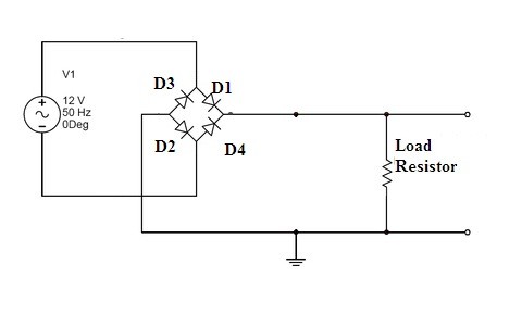 full-wave rectifier (bridge)
Once the circuit is provided with the sufficient supply for the positive duration of the cycle D1 and D2 will be in forward bias and the path has been established for the flow of current.
Whereas D3 and D4 will remain in reverse bias condition.
For the negative half of the cycle, D3 and D4 will be in conduction mode whereas D1 and D2 in the blocked state.
Hence both the cycles are utilized in this process making circuit efficient enough.
Compared to the center-tapped, a diode bridge rectifier is of less cost.
It is simple to analyze and consists of minimum ripple factor value providing maximum efficiency comparable to that of a half-wave rectifier.
However, the output generated consists of ripples in it indicating that the output is not in its purest form.
For the effect of smoothening of the output generated capacitors are connected across the load so that they can function as filters.
Hence the part of rectification is completely dependent on the component used referred to a diode.
Based on the number of diodes required cycles rectification can take place.
Because of the biasing conditions of the diode, it is suitable in various applications.
As per the above realizations is there any existence of current when the diode is in unbiased mode?
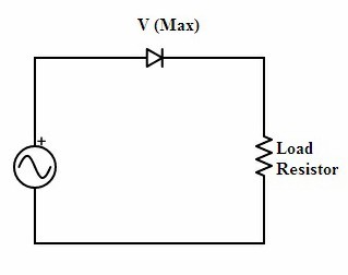 half wave rectifier
If the cycle considered is positive then in that case as per the basic functionality of the diode it will be in forward bias and it allows the path for the flow of current in the circuit.
It blocks the negative cycle.
This is referred to as a positive half-wave rectifier.
The only change made if the negative cycle is to be considered is that change in the direction of the diode-connected.
Then the remaining process remains the same.
Now it is referred to as negative half-wave rectifier.
However, the output generated consists of ripples.
This can be eliminated by connecting a capacitor across the load.
This capacitor functions as the filter and smoothens the output obtained from the rectifier.
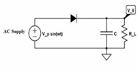 half wave rectifier with capacitor filter
Once the circuit is connected to the supply if the positive cycle is supplied then capacitor gets enough charged and it holds the voltage of the diode at its peak value and after that capacitor tends to degrade at the load slowly because of reverse bias condition in the diode.
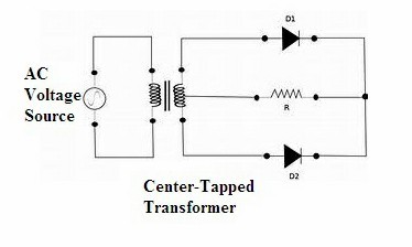 Full Wave Rectifier (Center-Tapped)
If the negative cycle is considered in that case one diode acts in forward and the other in reverse.
But the transformer utilized here is costly.
Hence the other model of full-wave rectifier has been designed.
 full wave rectifier (bridge)
However, the output generated will consist of some ripples in the output.
This can be made more effective by connecting a capacitor across the load for the filtering of the rectified output.
Ripple Factor of Full Wave Rectifier (Similar for Both Centres- Tapped as Well As Bridge)
Here the ripple factor is given by
r=Vrrms/VDC
The Vrrms is the ripple factor of the peak to peak is
Vrrms=vVrms2- VDC2
Vrms is the RMS value of the voltage it is given by
Vrms=Vm/v2
The output DC value can be given as
VDC= (2Vm)/p
On substituting and solving results in the value of the ripple factor of the full-wave rectifier as r= 0.483
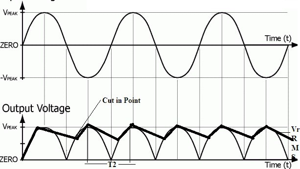 output waveforms of full-wave rectifier with capacitor filter
The charge of the capacitor acquired is referred to as
Vrrms*C
Charge lost on it is given as
Idc*T2
However, both the equations of acquired and lost are equated
Vrrms*C = Idc*T2
If the considered capacitor or the resistor of the filter is large enough then
T2 = T/2 = 1/2f
Then,
Vrrms = Idc/2fC
As per the assumptions based consider that ripple factor waveform in the shape of a triangle
Vr rms=Vrrms/(2v3)
On substituting the known value of Vrrms the above equation can be rewritten as
Vrrms=Idc/(4v3 fC)
Therefore by the concept of ohms law;
Idc=Vdc/RL
Then,
Vrrms=Vdc/(4v3 fCRL )
(Vrrms)/Vdc =1/(4v3 fCRL )
From the above equation, it is clearly evident that the value of the ripple factor in the output signal is inversely related to the value of the capacitor and the resistor.
Hence from the above analysis, the necessity of the filtering circuit after the rectification of the output is clearly evident.
The importance of the capacitor filter is analyzed here.
Similarly, can you compare the capacitor filter with the inductor filter and decide which one is well suited?

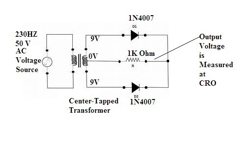
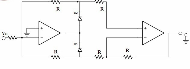 In the precision full-wave rectifiers, it considers both positive and the negative halves of the cycle.
But either the output generated is completely inverted or non-inverted.
When the operation is performed on the precision rectifier the output generated as considered positive full-wave rectifier can be given as
Vo = |Vi|
The output generated for the negative full-wave rectifier can be given as
Vo = -|Vi|
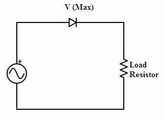 Half-wave rectification is carried out during the positive side of the supply.
Because as per p-n junction diode concept it is evident that diode conducts during forwarding bias.
But in reverse bias condition leakage current is generated due to which there is no possibility of conduction.
In order to consider the operation for negative supply, the diode connected in the positive supply case must be changed its direction and reversely connected.
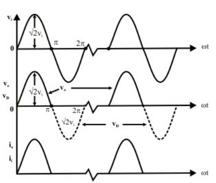 output waveforms of a half-wave rectifier
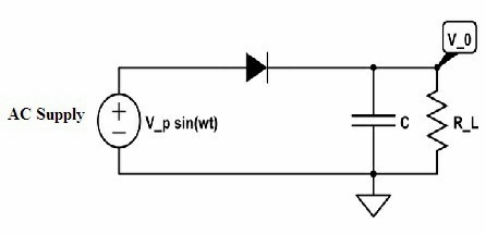 Here the capacitor filter is used for this purpose.
The capacitor filter is connected across the load resistor and suppresses the ripples so that obtained output gets smoothened and the ripples are eliminated.
In this, the output from pulsating DC is converted to its purest form in DC.
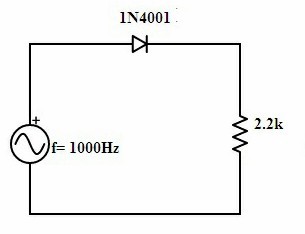
 The purpose of half -wave rectifier is to consider half of the cycle.
In this way, it is further divided into two types
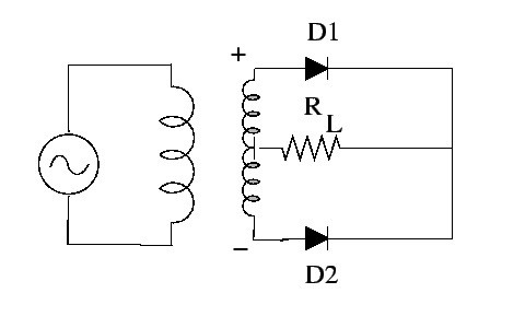
 As the positive part of the AC, supply is provided diode D1 and D2 acts like they follow forward bias condition and diode D3 and D4 remain in reverse bias condition.
Similarly, when the negative part of the supply is provided the diode D1 and D2 will be in reverse bias and diode D3 and D4 will be in forward bias.
In this way, the circuit responds for both positive and negative side of the AC supply.
 general diagram of power supply
The waveform of AC is not constant it is a variant of time.
As it reaches the positive peak value it tends to degrade the same will be followed for the negative value after reaching zero again it will come back to zero lines.
Now let us begin the working of rectifier by applying AC as the input.
For the positive half of the cycle, the diode acts in forward bias mode.
Hence the path is established for the movement of charge carriers.
Once the negative part of the cycle is applied to the diode it blocks the value of the current because the movement of minority charge carriers in it can be neglected.
Simply one can define the working of the diode as conducting in forward bias and blocking in reverse bias to the flow of current.
Hence the flow of current is evident during the positive part of the cycle applied to the diode.
The output obtained it must be converted from AC into DC.
In this way the basic diode functions as a rectifier.
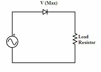 half-wave rectifier
Rectifier Equations of Half Wave Rectifier
The average value of voltage,
Vavg= Vm/p
The average value of the current can be given as
Iavg=Im/p
The value of RMS voltage can be given as
Vrms=Vm/2
The value of RMS current can be given as
Irms=Im/2
The ripple factor value of half-wave rectifier is
Ripple Factor=1.21
The efficiency value of the rectifier is given as
maximum efficiency=40.6%
The form factor value is
form factor=1.57
The above are some of the rectifier equations that relate to the half-wave rectifier.
 full-wave rectifier center-tapped
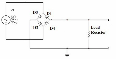 full-wave rectifier (bridge)
Diodes D1 and D2 acts for one part of the cycle and D2 and D3 responds to the other part of the cycle so that it can utilize both the halves of the cycles and makes the circuit less costly by using a normal transformer.
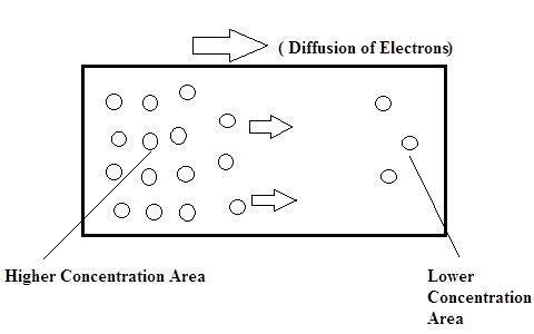 If it is n-type electrons move from higher concentration to lower concentration and in case if it is p-type holes tends to move from higher concentration area to lower concentration area.
Drift and diffusion both the process occur in semiconductors but diffusion mainly occurs without the interference of external voltage.
 (2) The equation for diffusion current density and concentration gradient of the p-type semiconductor
 Here represents the density with respect to electrons and represents the density with respect to holes.
 Similarly, the diffusion density because of the carrier concentration of holes can be written as
 Here stands for the diffusion coefficient with respect to electrons and stands for the diffusion coefficient with respect to holes.
The above equation is for the densities of diffusion densities with respect to electrons and holes but the overall density of the current of respective holes or electrons can be given by the sum of the diffusion current and the drift current.
The overall diffusion density with respect to electrons can be given as
 The overall diffusion density with respect to holes can be given by the equations for the individual densities of electrons as well as holes.
Therefore the overall current density can be given by
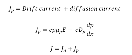 In this way, the equations for the diffusion current densities are described for holes as well as electrons.
The diffusion current in the semiconductor has occurred before the application of external supply.
It is also termed as the process of recombination in order to achieve uniformity.
But have you ever thought why the diffusion doesn't take place in conductors?
 Symbol of P-N-P Transistor
 P-N-P Transistor Construction as a Switch
All these regions are formed in the transistors.
In order to make the transistor to work as a switch only two transistors are preferred either both the junctions must be completely ON that is saturation mode or the junctions must be completely OFF that is in cut-off mode.
This process of operation is referred to as a switch. But the active region is not used for this purpose because the q-point in this region lies at the center.
 Symbol of Darlington Transistor Pair Configuration of N-P-N
 Sziklai Pair Configuration
These transistor pairs are used in various push-pull types of amplifiers and the audio amplifiers of the class AB at the stages of output these transistor pairs have been used.
In this way initially the pair of same type of transistors is interfaced so that a Darlington pair has been formed.
But due to the drawbacks in it Sziklai pair based on the interconnection of the complementary transistors has been formed.
But can you tell which one is preferred during amplification and switching of the devices.
Which is the better one among Darlington and Sziklai pair configurations?
 The only difference between P-N-P and the N-P-N transistors are that the movement of the current based on which the arrows are indicated.
 P-N-P Transistor Equivalent Circuit Representation (BJT)
Hence the circuit of BJT can be represented by the two diodes with the junction P-N.
This represents the equivalent circuit of BJT.
![]() What is a Zener Diode?
What is a Zener Diode?
 The conduction or the flow of the current can be seen from collector as well as emitter and it is controlled by base terminal.
Basics of FET
It also belongs to the category of transistor that in which the current flow is controlled by the electric field. The operation here is based on one single carrier.
However there are two types of charge carriers exist they are electrons and holes.
But in the FETs the operation conduction is based on either holes or electrons.
Hence these transistors are also referred to as UNIPOLAR transistors.
This transistor also consists of three terminals.
They are
Source
Drain
Gate
 From the terminal source the charges gets involved into the channel.
Drain is considered as the terminal for leaving the charges from the channel.
Gate is responsible for the channels conductivity modulation.
Comparison between BJT and FET
The basic comparison between BJT and FET are made as follows
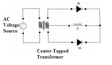 Full Wave Center Tapped Rectifier Circuit Diagram
Hence the connections as per the above circuit diagram as made in order to form a center tapped full wave rectifier circuitry.
The wire at the center separates the respective cycles for both the diodes functioning during respective halves.
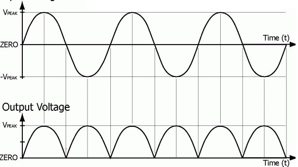 Center Tapped Rectifier Output Waveforms
It is evident that there is the presence of output for both the positive and the negative halves of the cycle.
Hence no loss of cycle here and there is any loss in the output power as well.
But finally generated outputs across the load will not be in its purest form of DC.
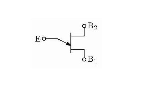 Symbol of UJT
The construction of the UJT is simple as it has one junction.
The construction resembles diode. The difference in between the UJT and the diode is that it consists of three terminals in comparison with the diode.
The higher resistance value is present at the bar that is of n-type.
The maximum value for the resistance is formed in between the terminals of the base 1 and the emitter in comparison with the resistance value of the terminals base2 and the emitter.
The reason for this is that the positioning of the emitter is nearer or closer to the base 2 rather than base 1.
The above connections makes a basic circuit diagram of UJT.
This transistor is operated by making the junction of the terminal in the forward biasing mode.
The operation of this UJT is unique but it doesn't amplify the signals but capable enough of handling and controlling the larger vale of the power applied in terms of AC. It also exhibits the resistance in terms of negative polarity.
This makes the UJT to utilize it as an oscillator circuit.
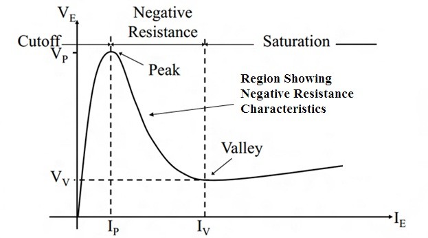 UJT Characteristics Curve
As the current in the UJT tends to increase there can be evident drop in voltage value. Hence this transistor shows the negative characteristics of resistance.
This paves the way to make the UJT to work as a relaxation oscillator.
The basic functional unit of this oscillator consists of resistor and the capacitor with UJT as the active unit for the oscillator to perform operation.
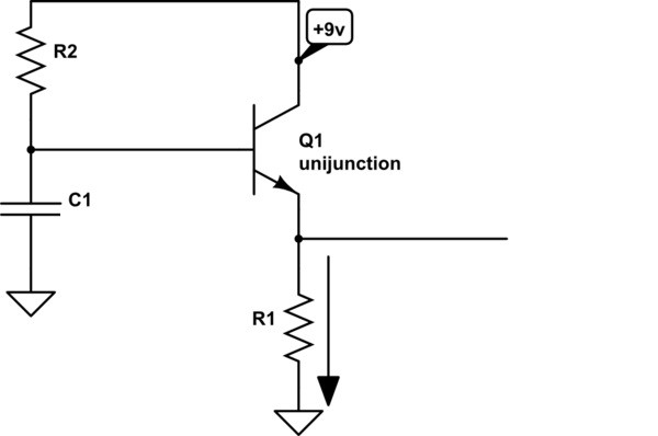 UJT as Relaxation Oscillator
By making the capacitor to get discharged because the resistor R1 is of low ohmic value.
The discharge value of the capacitor is lesser than that of the charging value of the capacitor.
Once the voltage across the capacitor tends to decrease more than that of the time of holding the device tends to get turned OFF. Based on the voltage applied as input dependent o it the device is managed to be turned ON or OFF.
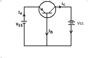 Common Base Configuration
The value of the current gain in this case is either equal or considered to be less than the unit value.
The signals of the input and the output that are generated will remain in-phase.
This kind of configuration has the highest value of the impedance rather than output. The characteristics of the output signals are showcase the similarities as of diode working in forward biased manner.
 Common Base Input Characteristics
 Common Base Output Characteristics
 Common Collector Configuration
The input value of the impedance is high.
Hence these are applicable during the matching of the impedance techniques.
The considered input signals are applied in between the terminals of the collector and the base.
The output is to be taken or considered in between the terminals of the collector and the emitter.
The generated input and the output signals remains in-phase.
The input parameters are the voltage between terminals base and the collector and the current at the terminal base.
The output parameters are the collector current and the voltage at the terminals emitter and the collector.
 Common Collector Input Characteristics
By maintaining voltage at the collector and the emitter at the constant values the graph is plotted between the parameters of the base current and the voltage value at the collector and the base terminals.
 Common Collector Output Characteristics
The graph is plotted between the emitter current and the voltage at the terminals of the collector and the emitter by maintaining the value at the base current at constant.
 Common Emitter Configuration
The parameters of the input for this type of configuration are the voltage at the base and the emitter and the current at the base terminal.
The parameters based on which the output signals characterized are the voltage at the terminals of the collector and the emitter as well as the current at the terminal collector.
It is the most widely utilized configurations in comparison with the other configurations in the amplifier circuitry.
The value of the current at the terminal emitter is the sum of the individual currents at the base and the collector. The impedance at the input as well as the output are of minimum value.
This makes the configuration more efficient.
The gain between the ratio of current at the collector terminal and the emitter terminal is measured in terms of alpha.
The gain for the ratio between the currents of the collector terminal and the base is measured in terms of beta.
The generated output signal has the shifting in phase about 180 degrees that represents the input and the output signals are inversely related in terms of phases.
Input characteristics
The graph is plotted between the current at the base and the voltage value at the terminals of base and the emitter.
 Common Emitter Input Characteristics
Output Characteristics
The graph is plotted between the values of the collector current and the voltage value of the terminals of collector and the emitter.
 Common Emitter Output Characteristics
 Basic Transistor Symbols Along with its Terminals
 Symbol of N-P-N Transistor
 N-P-N Transistor Circuit
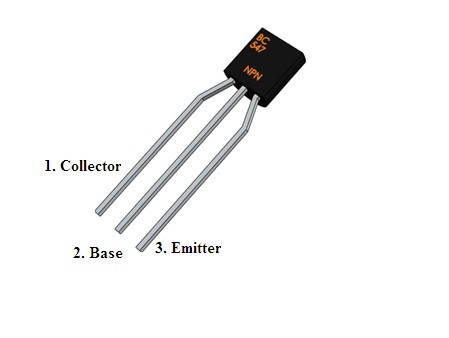 N-P-N Transistor Pin Out
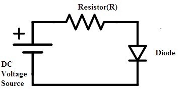 diode-operating-in-forward-bias-for-the-analysis-of-dc-load
Once the Kirchhoff's voltage law is applied to the circuit an equation is obtained for voltages and currents in the circuit.
VDD = VD + IDR
VD = IDR-VDD
Where VDD, is the applied dc source voltage and VD is the voltage across the diode.
Hence the above can be considered as the equation for the diode.
The voltage and current characteristics of the diode in forward bias condition can be drawn.
By our previous analysis on the condition of the diode in forward bias applied a voltage and the generated current in the circuit are exponentially related to each other.
After a certain cut-off voltage, the diode starts operating in forward bias condition.
To this slope, the technique is considered and a straight line on the v-i characteristics is drawn.
The slope here for the above general circuit for the diode is VDD/R.
Then the intersection of the lines results in the formation of diode operating point as already discussed.
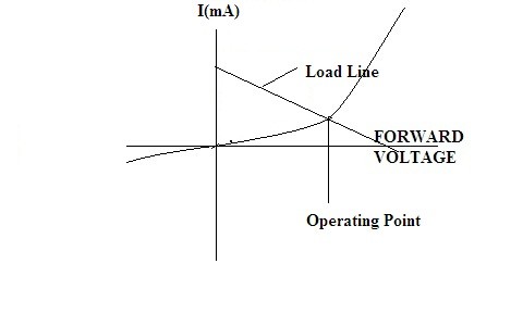 dc-load-line-and-the-formation-of-operating-point
In this way, the analysis for the dc-load line is done for the non-linear device like a diode.
Depending on the type of non-linear device some part of the analysis differs but the technique remains the same.
This type of method comes under the graphical analysis because here the characteristics curve is considered for the formation of the dc-load line.
Once the characteristics curve is formed the slope is identified then with respect to that line is drawn.
Everything is graphical here.
In this way, the analysis for this is done in the above article.
The main purpose of the analysis of the dc load line is that operating point is formed that is accurate in all terms and helpful for the further processing of the circuit.
But for the overall analysis of the circuit Kirchhoff's laws play a major role.
This is for the diode but transistor is also a non-linear device then based on its configurations the operating point is formed.
Then what must be the reason so that to operate BJT the operating point mostly should remain in the active region and why the active region is preferred above the remaining other regions?
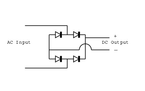 Single Phase Supply Circuit
 Three Phase Supply Circuit
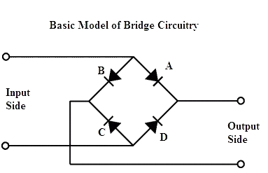 Basic Circuit Representing Uncontrolled Rectifier
 Bridge Rectifier Circuit Representing Controlled Rectifiers
The above are the types of bridge rectifiers that are classified based on the supply provided as well as further classified based on the output power has been controlled or varied.
Based on the necessity the type of rectifier is chosen preferably.
 Bridge Full Wave Rectifier Circuit
The above is the bridge rectifier circuit that consists of the initial AC supply as well the four diodes connected in a bridge topology and a load resistor connected to it.
At the initial stage, the power is supplied using a step- down transformer.
Based on the characteristics are concerned for the requirements in a rectifier it can be the ratings of current or peak inverse voltage and so on the respective diodes have been chosen.
After the processing of input signals done at the diode bridge another stage for the rectifier will be its load.
Here the load is taken as the resistor.
Once rectification is done as the input AC is converted into pulsating DC but the requirement will be of pure DC.
In that case, another component called a capacitor or inductor is added across the load.
So that it can remove the ripples from the circuit and make the output smooth.
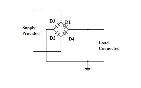 Bridge Wave Rectifier Operation Analysis
Let us consider the above basic circuit in order to analyze the bridge rectifier.
The four are connected in such a diagonal manner that it looks like a diode bridge.
Assume that the circuit is powered on indicating the first positive cycle will enter the circuit.
As the positive cycle gets into the circuitry diode D1 and diode D2 will get into the forward bias condition and allows the path for the flow of current.
Whereas diode D3 and diode D4 will remain in reverse bias condition.
Hence D3 and D4 will not conduct.
As soon as the negative cycle gets into the circuitry D3 and D4 will be in conducting mode. D1 and D2 will remain in reverse bias condition.
This results in the utilization of both positive and the negative halves of the cycle.
One can observe whether it is a positive cycle or negative cycle applied results to the flow of current in the same single direction in order to satisfy the property of the diode. Hence the circuit becomes more efficient.
However after rectification there exist some ripples in the generated output that can be smoothened by the filtering technique.
The ripple factor value is less in this type of rectifier compare to that of a half-wave rectifier.
 diffusion-voltage
Because of the potential across the junction, a barrier is formed so that further movement of the carriers can be noticed.
This movement in the depletion region is dependent on the applied voltage.
This reflects the width of the depletion region.
Poisson's equation determines the relation of the width of the depletion region and the bias voltage.
 poisson's-equation
Here V represents the biasing voltage and e represents the permittivity of the given semiconductor.
Once the voltage applied there is some amount of current generated in the circuit.
It is represented as
 generated-current
Here in the above equation, I_s represents the saturation current, where V is the biasing voltage and I the total current generated.
Whereas k is the Boltzmann constant e is the charge on the electron and T is the temperature in the Kelvin scale.
Here the biasing voltage, width of the depletion region based on biasing and the current generated in the circuit are related to the general characteristics of the pn junction diode.
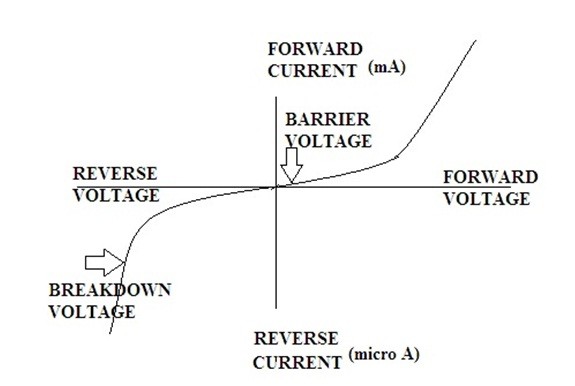 V-I Characteristics of P-N Junction Diode
The above are the basics of the p-n junction diode.
The voltage and current characteristics are well suited for the explanation of the functioning of the circuit.
The circuit can be analyzed better and analysis becomes simpler.
The functioning is evident but have you ever given a thought what are the devices that only functions either in forward bias or in reverse bias?
 P-N Junction Diode Symbol
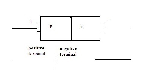 P-N Junction Diode Working in Forward Bias
 P-N Junction Diode Working in Reverse Bias
 Current Equation
Here Is represents the saturation current; VT is the volt-equivalent temperature, and n is the emission coefficient.
V-I under Reverse Bias
Generally, in the reverse bias, the p-n junction will be offering the highest resistance to the flow of current.
Still, some amount of leakage current flows through the junction.
When the reverse voltage applied is of maximum value then the junction gets overheated due to which the breakdown condition occurs and a maximum flow of current is recognized in the circuit.
There is a very tiny amount of current is flowing through the junction as it is in reverse bias.
Hence the equation for it is given as
 Equation for Tiny Amount of Current
Whereas Is represents the saturation current; VT is the volt-equivalent temperature, and n is the emission coefficient.
 Experimental Analysis of P-N Junction Diode
The biasing conditions of p-n junction's diode clearly state that during forward bias the diode is in conducting mode acting like a closed circuit.
Whereas during reverse bias the diode is in non-conducting or acting as an open circuit.
This paved the way the diode to act as a switch.
The switch is on during forward bias that is conducting and during reverse bias the switch will be off indicating that it is in non-conducting mode.
 Energy Band of Unbiased Diode
 Energy Band of Reverse Biased Diode
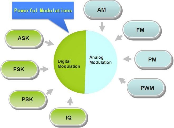 Types of Modulation
Communication is the basic attraction of mankind as it gives the knowledge of what is going on around us.
In our daily life, we communicate with many people and use the entertainment media like television, radio, internet and newspaper to get ourselves involved.
These entertainment media act as a source of communication. Electronic communication comprises TV, radio, internet, etc. When we want to transmit a signal from one location to another, we have to strengthen the signal.
After undergoing strenghthening process the signal travels to a long distance.
This is called as modulation, and this article gives an overview of the modulation and types of modulation techniques.
Communication is nothing but, the process of exchanging (two way communication) or passing (one way communication) information from one person to another.
The basic electronic communication system consists of these components: transmitter, receiver and communication channel.
 Communication System
A transmitter is a group of electronic circuits designed to convert the information into a signal for transmission over a given communication medium.
A receiver is a group of electronic circuits designed to convert the signal back to the original information.
The communication channel is the medium which is designed to transmit the electronic signal from one place to another.
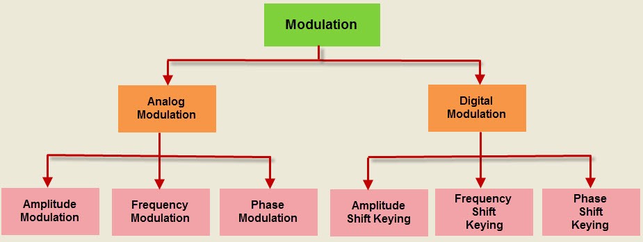 Modulation Techniques
Analog Modulation
Digital Modulation
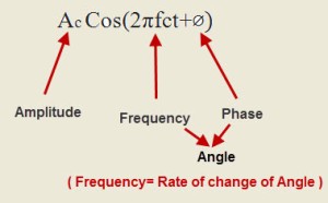 Analog Modulation
Amplitude Modulation (AM)
Frequency Modulation (FM)
Phase Modulation (PM)
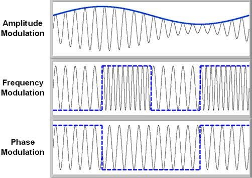 Types of Analog Modulation
Therefore, Analog modulation includes AM, FM and PM and these are more sensitive to noise.
If noise enters into a system, it persists and gets carried up to the end receiver.
So, this drawback can be overcome by the digital modulation technique.
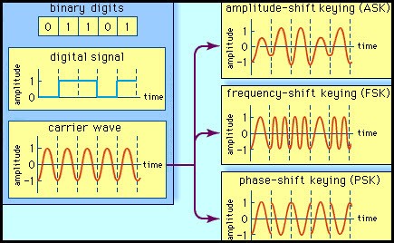 Digital Modulation
The carrier wave is switched on and off to create pulses such that the signal is modulated.
Similar to the analog, in this system, the type of the digital modulation is decided by the variation of the carrier wave parameters like amplitude, phase and frequency.
The most important digital modulation techniques are based on keying such as
Amplitude Shift Keying, Frequency Shift Keying, Phase Shift Keying, Differential Phase Shift Keying, Quadrature Phase Shift Keying, Minimum Shift Keying, Gaussian Minimum Shift Keying, Orthogonal Frequency Division Multiplexing, etc., as shown in the figure.
In an Amplitude shift keying, the amplitude of the carrier wave changes based on the message signal or on the base-band signal, which is in digital format.
It is sensitive to noise and used for low-band requirements.
In frequency shift keying, the frequency of the carrier wave is varied for each symbol in the digital data.
It needs larger bandwidths as shown in the figure.
Similarly, the phase shift keying changes the phase of the carrier for each symbol and it is less sensitive to noise.
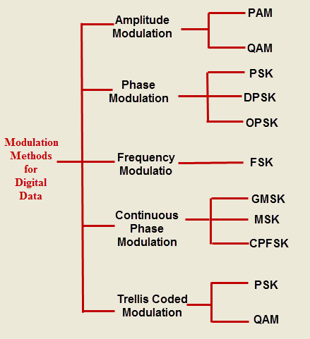 Types of Digital Modulation
 MOSFET Vs IGBT
In today's world there are wide varieties of solid-state, switch-mode, power-supply transistors to perform switching operations in power-electronic systems.
All these have their own specifications in terms of current, voltage, switching speed, load, driver circuitry and temperature.
Each one has its limitations and advantages as well, but its usage depends on the requirements of the application.
In most of the switching applications Metal-Oxide Semiconductor Filed Effect Transistor (MOSFET) and Insulated Gate Bipolar Transistors (IGBTs) are predominant than the other switching devices due to their superior characteristics.
These applications include Uninterruptable Power Supplies (UPS), Solar Inverters and Converters, various motor driver systems, Pulse Width Modulation (PWM) technique based applications, Switch Mode Power Supplies (SMPS), etc.
Let us see the prominent differences that make these switching devices suitable for appropriate applications.
In this regard, the description of the following two switching devices is pertinent.
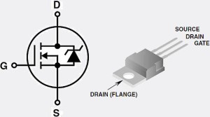 Power MOSFET
MOSFET is a most commonly used switching device, which is voltage-controlled power device unlike the BJT, which is a current controlled device.
MOSFET is a low-current, low-voltage and high-frequency switching device.
It consists of three terminals: gate, drain and source.
It comes with two different modes: enhancement and depletion modes and the MOSFETs can be P-channel or N-channel MOSFETs.
MOSFETs vary depending on the voltage level of the gate terminal.
In a depletion mode, maximum conductance takes place between the source and the drain if there is no voltage at the gate terminal, whereas a positive or negative voltage at the gate decreases the conductivity.
In an enhancement mode, the MOSFET doesn't conduct if there is no voltage at the gate terminal, and if the voltage is more, conduction takes place.
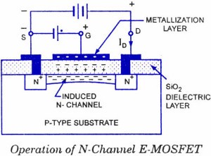 If the positive voltage is more than the threshold level applied between the gate and the source, then it creates a conduction layer by accumulating electrons.
This layer is formed between the oxide layer and the P-substrate layer by pushing away the holes from the P-substrate and attracting the electrons in the N-layer.
With the increase in the gate to source voltage, the size of this conduction layer increases resulting in the flow of more current from the source to the drain.
In this way, MOSFET comes into conduction mode by the application of voltage across the gate and source.
MOSFET can be turned off by decreasing the gate to source voltage to below the threshold level of it.
Sometimes a BJT current is required to trigger it though the MOSFET is a voltage controlled switch.
It also has a body-drain diode useful in dealing with freewheeling current applications.
Because its on-state resistance is low, on-state losses are also lower.
MOSFETs can operate at high frequencies and low voltages and are perfectly suitable for faster switching operations with low-voltage drops.
But these are restricted to be used at higher operating voltages in the range of around 500V.
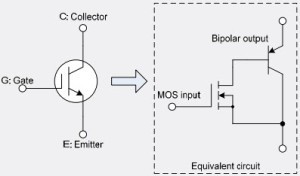 Insulated Gate Bipolar Transistor
It has three terminals: Emitter, Collector and Gate.
The Gate is a control terminal, whereas the collector and emitter terminals are associated for conduction path.
IGBT is a four-layer structure P-N-P-N same as that of thyristors.
The below figure shows different layers of IGBT, wherein the flow of electrons through the drift region and the channel draw more holes into the drift region towards the emitter.
Because the current flow is composed of the holes and electrons, the current is of bipolar nature.
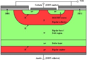 IGBT Structure
Similar to the MOSFET, when the positive gate bias is applied, it allows the inversion of P-base region under the gate and creates N-channel.
During this state, the resistance of n- layer is reduced rapidly when the positive holes are injected from the p+ layer to the n- layer.
This makes the IGBT to handle more currents than the MOSFET due to lower conduction losses.
For turning it off - the negative bias at the gate or lowering the gate voltage to a threshold level makes it off due to no injection of holes to the N region.
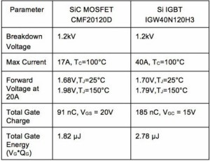 Difference between IGBT and MOSFET
In the above diagram, you can observe some comparisons of IGBT and MOSFET based on their model with ratings.
Therefore, for choosing switching devices, especially IGBT and MOSFET devices there are larger parameters to be considered for the corresponding applications in power electronic field.
For any application-based projects on these devices, you can contact us by commenting below.
Photo Credits:
Power MOSFET by nlvocables
MOSFET Structure by circuitstoday
Insulated Gate Bipolar Transistor by cloudfront
IGBT Structure by lchu
Difference between IGBT and MOSFET by powersystemsdesign
Difference between IGBT and MOSFET
In the above diagram, you can observe some comparisons of IGBT and MOSFET based on their model with ratings.
Therefore, for choosing switching devices, especially IGBT and MOSFET devices there are larger parameters to be considered for the corresponding applications in power electronic field.
For any application-based projects on these devices, you can contact us by commenting below.
Photo Credits:
Power MOSFET by nlvocables
MOSFET Structure by circuitstoday
Insulated Gate Bipolar Transistor by cloudfront
IGBT Structure by lchu
Difference between IGBT and MOSFET by powersystemsdesign
 Insulated-Gate-Bipolar-Transistor
The term IGBT is a short form of insulated gate bipolar transistor, it is a three-terminal semiconductor device with huge bipolar current-carrying capability.
Many designers think that IGBT has a CMOS i/p and bipolar o/p characteristic voltage controlled bipolar device.
So, this device is designed to make use of the benefits of both BJT and MOSFET devices in the form of monolithic.
It combines the best qualities of both to attain the characteristics of an optimal device.
This device is apt for several applications such as used in power electronics, particularly in PWM(Pulse Width Modulated), UPS (Un interruptible Power Supplies), SMPS (Switched-Mode Power Supplies), and other power circuits.
It increases the efficiency, dynamic performance and reduces the level of the audible noise.
It is similarly fitted in the of resonant mode converter circuits.
Optimized IGBT is accessible for both low switching loss and low conduction loss.
 IGBT Symbol
For a MOSFET (metal oxide semiconductor field effect transistor), there is no i/p current as the gate terminal is isolated from the main current-carrying channel.
Thus, the gain of the field effect transistor equals to the an FET's gain is equal to the ratio of o/p current change to i/p v change, Then the IGBT can be treated as a power BJT and the base current of this transistor is provided by an MOSFET.The IGBT is mainly used in small-signal amplifier circuits like BJT or MOSFET When the transistor combines the lower conduction loss of a BJT and MOSFET, then an ideal solid state switch occurs which is perfect for in various applications of power electronics.
An IGBT is simply switched “ON” and “OFF” by triggering and disabling its Gate terminal.
A constant +Ve voltage i/p signal across the 'G' and the 'E' will retain the device in its “ON” state, while deduction of the i/p signal will cause it to turn “OFF” like BJT or MOSFET.
 Basic Structure of N-Channel IGBT
IGBT takes a parasitic thyristor includes the 4-layer NPN structures.
There are some IGBs that are fabricated without the N+ buffer layer is called as NPT IGBTS non punch through), whereas some IGBTs are fabricated with the N+ buffer layer called as PT IGBTs (punch through).
The performance of the device can considerably increase by existing the buffer layer.
The operation of an IGBT is faster to that of power BJT than a power MOSFET.
 Circuit Diagram of an IGBT
The JFET transistor signifies the construction of current b/n any two adjacent IGBT cells.
It allows the MOSFET and supports most of the voltage.
A circuit symbol for the IGBT is shown below, that consists of three terminals namely emitter, gate and collector.Switching Behavior of IGBT
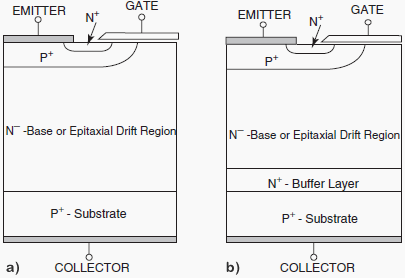 NPT-IGBT and PT-IGBT
The basics of NPT-IGBT, IXYS Corporation 4 IXAN0063 and Abdus Sattar have equal breakdown voltage and these are applicable for AC applications.
The PT-IGBTs have less breakdown voltage and these are relevant for DC circuits where these devices are not essential to support voltage in the reverse direction.
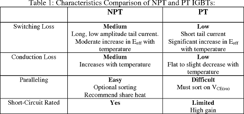 Difference between NPT-IGBT and PT-IGBT
The principle of the BJTs is very similar to the N-channel MOSFET.
The main difference is, the current existing by the conducting channel when current supplies through the device in its ON state is very small in the IGBT, due to this reason, the ratings of the currents are high when matched with an MOSFET.
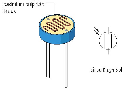 Majority of street lights, outdoor lights, and a number of indoor home appliances are typically operated and maintained manually in many occasions.
This is not only risky, however additionally it leads to wastage of power with the negligence of personnel or uncommon circumstances in controlling these electrical appliances ON and OFF.
Hence, we can utilize the light sensor circuit for automatic switch OFF the loads based on daylight's intensity by employing a light sensor.
This article discusses in brief about what is a light dependent resistor, how to make a light dependent resistor circuit and its applications.
 Working Principle of LDR
These devices depend on the light, when light falls on the LDR then the resistance decreases, and increases in the dark.When a LDR is kept in the dark place, its resistance is high and, when the LDR is kept in the light its resistance will decrease.
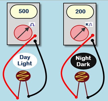 Variation of LDR Resistance with Variation in Light Intensity
If a constant “V' is applied to the LDR, the intensity of the light increased and current increases.
The figure below shows the curve between resistance Vs illumination curve for a particular light dependent resistor.
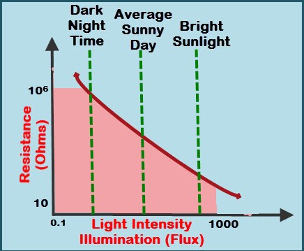 Light Intensity vs LDR Resistance
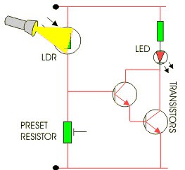 Light Dependent Resistor Circuit
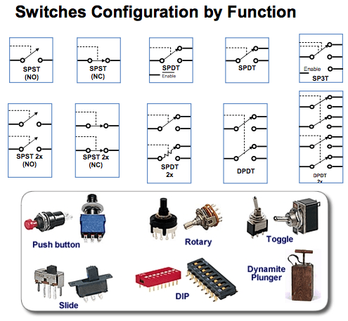
 The application of SPST switch is light switch given below and it is also called as a toggle switch.
This type of switch has one input and one output.
This light switch circuit controls one wire and makes one connection.
This is an ON/OFF switch, when the switch in the below circuit is ON or closed, then the current flows through the two terminals and the bulb in the circuit will blink.
When the switch is OFF or open, then the current doesn't flow through the two terminals.
 The application of SPDT switch is mainly involved in a three-way circuit to turn ON/OFF a light from two locations like from the top & bottom of a stairway.
In the circuit below, when the switch A is closed, then the current flows through the terminals, but only light A will glow and light B will OFF.
When the switch B is closed, then the current flows through the terminals and only light B will glow and light 'A' will OFF.
Her two circuits will be controlled through one source or one way.
 This switch is used to turn two circuits ON/OFF and it consists of four terminals namely two inputs and two o/ps.
The main purpose of this switch is to regulate a 240V appliance, where both supply voltages must be ON whereas the unbiased wire may be always connected.
When this switch is ON then the current starts flowing through two circuits and when it is turned OFF then it is turned OFF.
 When it is in ON-ON mode or ON-OFF-ON mode they work like two discrete SPDT switches worked by the similar actuator.
At a time only two loads can be ON.
A DPDT switch can be used in any application that needs an open & closed wiring system.
 The best example of this is, modeling of the railroad, that makes use of small scaled railways and trains, cars and bridges.
The closed permits for the system to be switched at all times, whereas open permits for extra piece to be switched ON or triggered through the relay.
From the following circuit, A, B and C connections from one pole of the switch and D, E and F connections from the other pole of the switch.
Connections B and E are mutual in each of the poles.
If the +Vs enters at connection B & the switch is fixed to the top most position, then the connection A becomes +ve and the motor will rotate in one direction.
If the switch is set to the lowest position, the power supply is inverted and connection D becomes +ve then the motor will rotate in the opposite direction.
In the middle position, the power supply is not linked to the motor and it does not rotate.
This kind of switch is mainly used in several motor controllers where speed of that motor is to be inverted.
 The voltage sources are connected to a PNP transistor, which is shown in the figure.
The emitter is connected to the Vcc with the RL, this resistor limits the max current flowing through the device, which is connected to the collector terminal.
The base voltage VB is connected to the base resistor RB, which is biased negative with respect to the emitter.
To cause the base current to flow during a PNP transistor, the base terminal must be more negative than the emitter terminal by approx.
0.7volts or a Si device.
The fundamental difference between a PNP and a PN transistor is the proper biasing of the transistor junctions; the current directions and the voltage polarities are always opposite to each other.
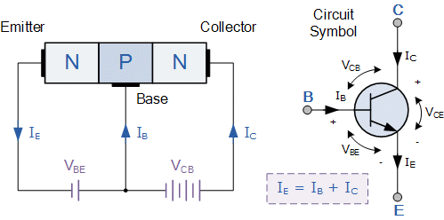 Generally, this transistor is used because it is so easy to produce.
For an NPN transistor to work properly, it needs to be formed from a semiconductor material, which carries some electric current, but not the maximum amount as very conductive materials like metal.
“Si” is one of the most commonly used semiconductor, and NPN transistors are the easiest transistors to make out of silicon.
The application of an NPN transistor is on a computer circuit board.
Computers need all their information to be translated into binary code, and this process is accomplished through a plethora of small switches flipping on and off on the computers circuit boards.
NPN transistors can be used for these switches.
A powerful electric signal turns the switch on, whereas a lack of a signal turns the switch off.
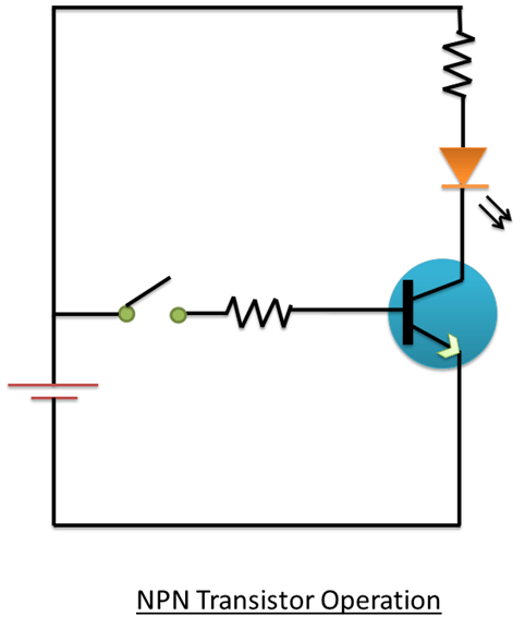 The transistor is a current operated device.
When the transistor is switched on, the large current IC flows between the collector and emitter within the transistor.
However, this only happens when a small biasing current Ib flows through the base terminal of the transistor.
It is a bipolar NPN transistor; the current is the ratio of these two currents (Ic/Ib), called the DC current gain of the device and it is denoted with the symbol “hfe” or nowadays beta.
The value of beta can be large up to 200 for standard transistors, and it is this ratio between Ic and Ib, which makes the transistor a useful amplifier.
When this transistor is used in an active region, then Ib provides the input and Ic provides the output.
Beta has no units as it is a ratio.
The current gain of the transistor from the collector to the emitter is called alpha that is, Ic/Ie, and it is a function of the transistor itself.
As the emitter current Ie is the sum of a small base current and large collector current, the value of the alpha is very close to unity, and for a typical low power signal transistor this value ranges from about 0.950 to 0.999.
 Symbol of N-P-N Transistor
4).
The symbolic representation of p-n-p transistor is
 Symbol of P-N-P Transistor
5).
In the n-p-n transistor the flow of current is evident from the collector to the emitter terminals.
5).
In the p-n-p transistor the flow of current can be seen from the terminals of the emitter to the collector.
6).
In this transistor the arrow is pointing out.
6).
In this transistor the indication of arrow is always pointing in.
The arrows in the transistors both n-p-n and p-n-p shows the main differences between the transistors.
The arrow in n-p-n is pointed towards the emitter whereas for p-n-p the arrow is in the reverse direction.
In both the cases the arrow indicates the direction of the flow of current.
Hence the construction of n-p-n and the p-n-p is simple.
The operating will be same but its polarities of biasing differ.
Now after discussing regarding the basics of n-p-n and the p-n-p can you tell which one is preferred during amplification and why?
Photo Credits:
NPN and PNP Transistor by ggpht
PNP Transistor by wikimedia
Making of PNP Transistor by electronics-tutorials
 resistors
Ohms law V=IR from this equation, we can get I=V/R
Where 'V' is the Potential difference of the conductor, 'I' is the current through the conductor and 'R' is the resistance of the conductor.
 capacitor
The stored electrical charge is Q=CV
Where “C” is the capacitive reactance and 'V' is the applied voltage.
Thus, the current flow through a capacitor is I= C dv/dt
When a DC current is applied across a capacitor, a positive (+) and negative (-) charge builds on a set of terminals.
The charge stays until the capacitor is discharged.
When an AC current is applied across a capacitor, a positive and negative charge forms on a set of plates during the part of the cycle when the voltage is positive.
When the voltage goes negative (-) in the second half of the cycle, then the capacitor releases before the charged current, and then charge the opposite way.
 microcontroller
 inductor
Inductor with symbol
L== (µ.K.N2.S)/I.
Where,
'L' is an inductance
'K' is a Nagaoka coefficient
'µ' is a Magnetic permeability
'N' is the number of turns of the coils
'S' is the Cross-section area of the coil
'I' is the length of the coil in an axial direction
 transformer
In a step-up transformer, a secondary coil contains more winding than the primary coil.
Coming to a step-down transformer, it has more windings in the primary coil than the secondary coil.
These are one of the main reasons we use AC current in our homes and not DC.
DC voltages cannot be changed using transformers.
Transformers are available in many sizes in the market today, ranging from small ones to large one.
 battery
 fuse
Where, 'I' is the peak value of the current interrupted.
't' is the time taken to clear the fault.
Every type of fuse is designed for an accurate amount of current.
A standard fuse comprises main components such as a set of contacts, metal-fuse elements, connection, and support body.
A fuse element is made of Zinc, copper, silver, aluminum or alloys to afford predictable characteristics.
That may be enclosed by air or material.
 light-emitting-diode
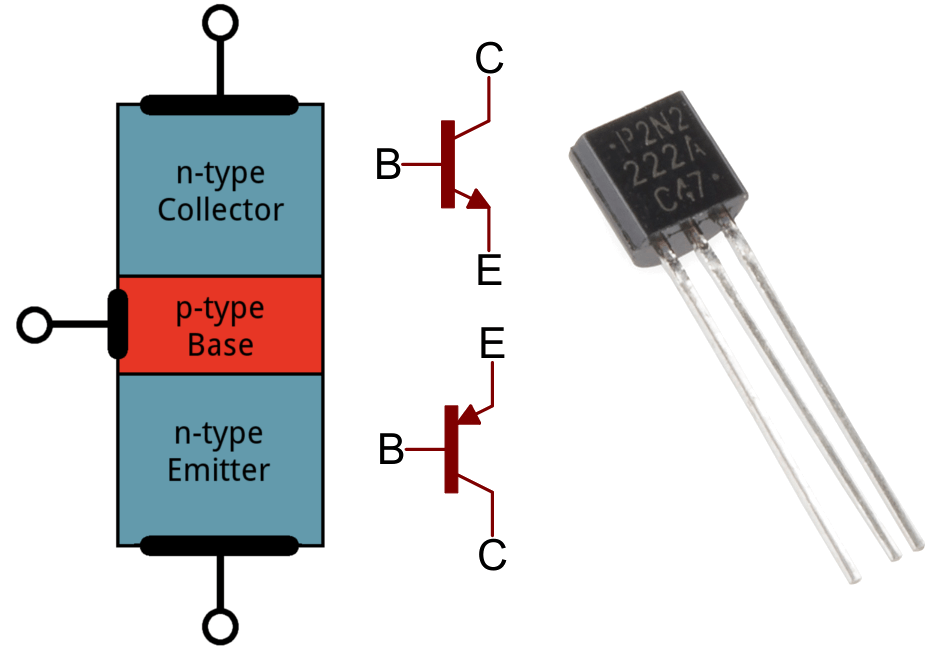 transistors
 integrated-circuit
 relays
 switches
 motors
 circuit-breaker
 Energy Band Diagram of P-Type Semiconductor
Once the impurity is inserted in the pure semiconductor numerous amounts of holes are formed in the valence band.
There are thermal excitation's also in the semiconductors because of this same amount of electrons are also present in the conduction band.
As always majority wins, more amount of hole compared to electrons makes p- types majority carriers as holes.
As the energy band diagram suggests there is less number of electrons in conduction band in p-type compare to that of n-type making the state of conductivity of n-type double than that of p-type.
The reason behind this is the excitation's will release a tremendous amount of energy and also enhances the flow of current making to mold it purposefully based on requirements.
As the doping concept introduced in extrinsic and made it p-type and n-type.
The formation of these types made changes in the development of modern electronics.
For example, it can be LASER, LED or a BJT everything is interlinked to each other.
In what ways do you think p-type is preferred over n-type?
 general-representation-of-p-n-junction
Rather than using the same material if we use different semiconductors for the formation of the PN Junction there will be a phenomenon of scattering that inhibits the flow of charge carriers.
Because of this reason single crystal with doping concept is preferred.
 charge-representation-of-p-type-and-n-type
As the charges flow from higher concentration to lower concentration and the process impacts in such a way that some charge has been imposed at the center on the impure ions.
These carriers form a layer that is static and adjacent towards the junction.
Then this static layer becomes so strong in terms of electric charge that towards n-type electrons lied statically while p-type has holes for that purpose.
However, the concentration will be on the major part but there will be some minority carriers in each region showing the impact of their presence.
As p-type has minority carriers as electrons it tends to move and crosses the PN Junction and gets combined in n-type region.
A similar concept is also applied for n-type minority carriers.
As a result, the regions tend to attain the condition of neutrality.
This makes the junction to attain a state of equilibrium.
In this state, the donor tends to oppose holes and the acceptors repel the electrons.
This phenomenon leads to the formation of a zone called “potential barrier”.
The barrier doesn't have any free carriers left it means that all the free electrons are combined by respective holes in it.
 interaction-of-n-type-and-p-type
In the formation of depletion layer n-type loosen its free electrons while p-type has lost free holes.
Both the sides have some ions and its nature is impure.
This results in the existence of an electric field in it.
The problem is, in order to overcome the barrier it requires some extra charge.
Hence the electric field generated due to the process of diffusion without any application of power supply is can be given as
Here ND represents the donor impurity concentration; NA represents the acceptor's impurity concentration.
Where ni refers to the intrinsic concentration.
Once the barrier is formed at the center there is the existence of the other two processes.
Firstly, the concentration of the carriers is different and when the holes tend to diffuse from p-type to n-type there some current has been generated at the junction termed as diffusion current.
Secondly, because of this depletion, there is some movement in minority carriers in such a way that electric field is imposed because of this electron from p-side tends to flow towards n-side resulting in drift current.
Diffusion current is possible only by the movement of majority carriers whereas drift is possible by the influence of minority carriers.
After the formation of a barrier if charges require movement then it is possible by applying it with suitable voltages.
This concept is termed as biasing.
Without any power supply, there is the presence of some potential in the semiconductor based on its relevance.
If it is silicon then it has 0.6-0.7 volts as the basic potential across the depletion region.
In case germanium is used then it has 0.3-0.35 volts.
As it is referred to potential barrier it opposes the flow of charge carriers on both sides of the junction.
The PN Junction barrier is formed during the process of manufacturing itself compared to germanium silicon has the highest barrier potential.
This potential is highly sensitive to the variations in the temperature, the element or material utilized in its fabrication as well as the concentration of doping required based on the type and the factors.
The most major factor of inbuilt potential inside the interfaced PN Junction is responsible for repelling the flow of electrons and holes once the barrier has formed.
The flow of charged particle in such interfacing will always be in a unified direction.
This is a huge application
These PN Junction devices are considered as the fundamental units for any type of transistors, a few modifications in it can be used for various purposes based on requirements.
Now, these are the basics that made p-n junction more popular in all the aspects termed for modern electronics.
Have you ever thought of how and when these types of p or n-types are replaced and utilized in any other respective equipment?
 The General Structure of Atom
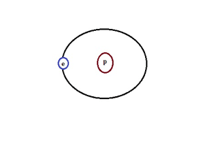 Hydrogen Isotope-Protium
(b) Deuterium: It has one proton and one neutron.
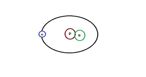 Hydrogen Isotope-Deuterium
(c) Tritium: It possesses two neutrons and a proton it.
Naturally, this condition is not possible one has to make it based on requirement.
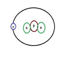 Hydrogen Isotope-Tritium
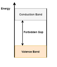 Figure 2 (a).
Energy band diagram Figure
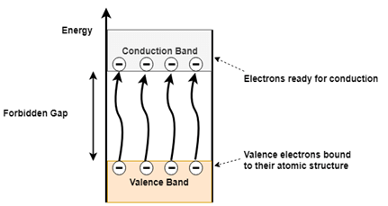 Figure 2(b).
Conduction and Valence band electrons in a semiconductor
When a semiconductor material is subjected to heat or applied voltage few of the covalent bonds break, which generates free electrons as shown in figure 2 (b).
These free electrons get excited and gain energy to overcome the forbidden gap and enter the conduction band from the valence band.
As the electron leaves valence band, it leaves behind a hole in the valence band.
In an intrinsic semiconductor always an equal number of electrons and holes will be created and hence it exhibits electrical neutrality.
Both the electrons and holes are responsible for conduction of current in the intrinsic semiconductor.
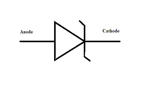 What is a Zener Diode?
