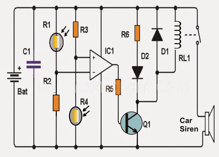
Simple Shadow Sensor Alarm Circuit
This shadow detector circuit operates using two LDRs and effectively detects the difference between the light levels and triggers a loud audible warning siren. In circuits which uses a single LDR (photoresist), the detection may not be as sharp as with two LDRs discussed here.Operational details of the shadow detector circuit may be studied as follows: The key elements of this circuit are the two LDRs and the active operational amplifier, which functions as a comparator.Circuit Operation
As may be seen in the diagram, the inputs of the opamp are carefully balanced using alternately positioned LDRs across the corresponding supply rails in conjunction with the respective resistors. The two resistors may be possibly replaced with presets for getting a fine adjustment option and for ensuring an optimum balance and a perfect zero logic at the output of the opamp. In normal light situations that is with no shadow detected (no shade) the two LDRs are able to receive the same amount of light across the sensing input of the opamp which renders a low logic level at the output of the IC. In an event when one of the LDRs (for instance R1) experiences a shadow or less light than the other (R4), causes the voltage at the inverting input of opamp to go lower than in the non-inverting counterpart, causing the logic at the output of IC to switch to a high logic. The above action activates transistor Q1, which in turn activates the LED and the relay. The LED allows to acquire a visual warning while the relay activates a siren device. Preferably you may want to place a semiconductor diode (D1) in parallel with the relay, as shown in the diagram, to protect the transistor Q1 from the relay reverse EMFs.Circuit Diagram
 Things to be notes:
- The circuit is powered by 9 volt lead acid battery or any similar SMF battery.
- The LDRs should be placed with a separation of about 3cm.
for an optimal response and to avoid incorrect triggering.
Parts list for the proposed shadow detector circuit
- 1 Operational amplifier: LM741 (IC1)
- 2 LDRs (photoresistor / LDR) (R1, R2)
- 1 NPN transistor 2N2222 or similar (Q1)
- 1 1N4007 diode (D1)
- 1 red LED diode (D2)
- 9 volt relay (RL1)
- Two 10K resistors (R3 and R4)
- 1 1K resistor (R5)
- 1 resistors 470 (R6)
- 1 100 nF capacitor (C1)
Things to be notes:
- The circuit is powered by 9 volt lead acid battery or any similar SMF battery.
- The LDRs should be placed with a separation of about 3cm.
for an optimal response and to avoid incorrect triggering.
Parts list for the proposed shadow detector circuit
- 1 Operational amplifier: LM741 (IC1)
- 2 LDRs (photoresistor / LDR) (R1, R2)
- 1 NPN transistor 2N2222 or similar (Q1)
- 1 1N4007 diode (D1)
- 1 red LED diode (D2)
- 9 volt relay (RL1)
- Two 10K resistors (R3 and R4)
- 1 1K resistor (R5)
- 1 resistors 470 (R6)
- 1 100 nF capacitor (C1)
Simple Greenhouse Temperature Regulator Circuit
The post discusses a simple electronic temperature regulator circuit which could be specifically used for regulating greenhouse temperatures. The idea was requested by Mr. Leo.Technical Specifications
I am looking for a guide to build a basic temp regulator circuit. I have a solar charger bought from lidl,(SLS 2200 A1) which has outputs for 5, 7.5 & 9.5v DC 0.5A. it will be used for soil heating in a greenhouse. My idea is to use black drip irrigation pipe as a 'solar panel' to heat the water and with a low volume pump regulate the temp under a propagation tray. Any advise is greatly appreciated. I have seen similar setups for egg incubators , fridge temp controls, etc. but need it at an allotment, so only power source is small panel. also if possible would it be possible to increase capacity of internal battery and have a heating element added. Thank once again. LeoIntroduction
Before getting into the main circuit concept, it would be interesting to learn regarding a few of the parameters expressed in the above request, as given below:What is "black" drip irrigation:
We all probably have heard a lot about drip irrigation, a method in which water is fed to the crops across the entire allotted field through a network of narrow pipe lines wherein water is allowed to drip directly at the bottom of the stem of the crop for a sustained period of time. The method helps to save water and allows the water to reach the crucial areas such as the roots of the crop resulting in a better growth and efficiency. Here an identical approach is implemented but the conventional pipes are replaced with black coiled PVC pipes. The back coiled pipe helps to absorb the heat from the sun rays naturally and allow the water passing through it to become warm naturally without depending on costly artificial utility electricity. The warm water ultimately helps to heat up the soil deep inside for acquiring the intended greenhouse effects.What's a Propagation Tray:
These could be arrays of plastic plantation pots arranged in a large tray like fashion for allowing deeper soil content to the seedlings over minimal spaces, it's specifically designed for optimizing indoor plantations.What's Allotment:
It may refer to a small garden or a plot of land as explained here: https://en.wikipedia.org/wiki/Allotment_%28gardening%29 The Solar Panel: The specified solar panel is a self contained unit which includes a solar panel with outputs at 5, 7.5 & 9.5v DC (0.5A). It also includes a 4-step charge indicator circuit and most interestingly it includes a built-in 2200mAH Li-ion battery so that you don't have to bother about external battery integrations, rather would be able to use the existing facility under overcast conditions.
Basic Requirement for the Green House Effect
Now let's return to the actual requirement of the proposed greenhouse temperature regulator circuit, the idea here is to sustain a raised temperature of the soil by 10 to 20 degrees Celsius above the atmospheric temperature for boosting or enhancing seed germination. Because seeds normally germinate faster in soils that are warmer than the atmosphere, which in turn results in an initial stronger root development instead of bigger leaf development. Generally, heat mats are used below the propagation trays for heating the soil but in the present application the drip water is itself heated and used for generating the same results, which looks much impressive, since heat mats could at times get messy causing sparks, fire or over heating of the soil (if the attached thermostat fails). Nevertheless, the electronic temperature controller circuit discussed below could be used with any heating system, including heat mats. In the proposed design, the natural heating of the water within the black pipes is aided by an external heating element until the temperature of the water reaches the optimal point. As soon as this threshold is sensed the heater is switched off by the regulator circuit and held at that position until the temperature falls back to a relatively cooler level.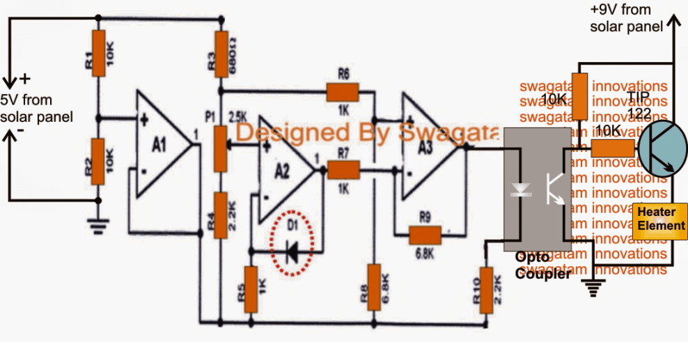 Parts List
D1 = 1N4148,
A1---A3 = 3/4 LM324,
Opto = 4n35
Parts List
D1 = 1N4148,
A1---A3 = 3/4 LM324,
Opto = 4n35
Circuit Operation
Referring to the diagram above which is actually a simple temperature controller circuit, could well be used for regulating the soil temperature in the proposed greenhouse application. Here the temperature sensor D1 is our very own "garden" diode (no pun intended ) 1N4148 which translates every one degree (C) rise in the ambient temperature into a 2mV drop across itself. The opamp A2 is specifically arranged to detect this change in voltage across D1 and feed the difference to A3 such that the result illuminates the LED inside the attached opto coupler IC. The threshold at which the above action takes place could be preset with the help of P1. The output of the opto is connected with a NPN driver stage which is responsible for switching off the heater as soon as the above threshold is reached. The sensor and the heater may be placed across any desired position, as per the user preference. For example the heater could be positioned below the propagation tray, or inside the water tank from where the water is being supplied to the black pipes. On same grounds the sensor may be placed anywhere around, could be below the propagation trays, inside the soil, inside the pipe or simply inside the water tank. The capacity of the unit could be upgraded as per the application, simply by employing a heavier rated solar panel and by replacing the TIP122 with a higher rated mosfet. The heater may also be upgraded as per the requirements.Simple Walkie Talkie Circuit
The article explains a simple walkie talkie circuit that can be easily built by any hobbyist and used for communicating between rooms or floors or simply for having some fun across neighbors and friends. The range of this system is around 30 meters. Awalkie-talkie, also commonly referred to as handheld transceiver is a small, portable hand-held two-way radiotransceiver, which enables voice communication across a specified radial distance without using physical wire connections across the devices. The initial research on walkie talkie concept during the 2nd world war era, has been variously credited toDonald L. Hings, Alfred J. Gross, and engineering experts atMotorola. Walkie talkies were first supplied for infantry use, and soon it also became indispensable among field artillery and tank units. Due to their outstanding wireless communication ability, these units quickly became popular among the masses and became a commercial product for the various manufacturers.Circuit Operation
The figure shows a four stage transistorized circuit which behaves both like a transmitter and a receiver unit, making the design very economical and versatile. An ordinary ��4-pole double throw�� switch serves the purpose well for transforming the unit either to a transmitter or a receiver while communicating with another identical transmitter/receiver set. As can be seen in the diagram three transistors are directly coupled for making an audio amplifier stage set to operate at a significantly high gain. The first transistor functions as a pre-amplifier which pulls the minute voice signals to some higher level and feeds to the next high gain Darlington stage which further amplifies the received audio frequencies and dumps it across the primary of a driver transformer.How Driver Transformer Works
The driver transformer steps up the level of the signals such that it becomes clearly audible over the connected loudspeaker. The speaker may be salvaged from an old small transistor radio or from a landline phone (earpice). The speaker in the shown design is configured in an interesting manner. Depending upon the position of the walkie talkie switch, the speaker works like a sound reproducer when it��s in the receiver mode and like a super dynamic microphone when the switch is toggled in the transmitter mode. While the speaker is being used as a sound reproducer or simply in the receiver mode, the first transistor acts like a signal receiver, picking up the audio across the 4k7 load resistor through the 0.47uF capacitor. The signals then has to pass through a connected volume control stage to finally reach the three transistor amplifier stage discussed above. However while the proposed walkie talkie circuit is flipped in the transmitter mode, the speaker gets rigged right at the input of the amplifier stage such that the spoken voice hits the speaker diaphragm and gets amplified by the same transistor stage. This amplified voice signal is now applied in the form of supply voltage for the circuit in the transmitter mode. The switch also makes sure that the 27 MHz crystal gets connected with the first stage while the transistor gain is uplifted by eliminating the 390 ohm resistor and using a 59 ohm resistor at the emitter of the transistor. In the transmitter mode the speaker transformer secondary now has no connection with the voltage step-up function rather simply acts like a series inductor for coupling the output of the audio amplifier with the supply rail and for sending the signal across the winding to the transmitter stage in the form of a fluctuating supply voltage. As the above signal witnesses a rise and fall in response to the spoken voice, the gain of the first transistor stage is forced to change correspondingly which in turn results in a varying amplitude for the carrier waves transmitted by this stage over the attached antenna. Thus the spoken voice now gets converted to an amplitude modulated (AM) RF 27MHz signal which may be picked by another identical unit placed in the vicinity for the same reason.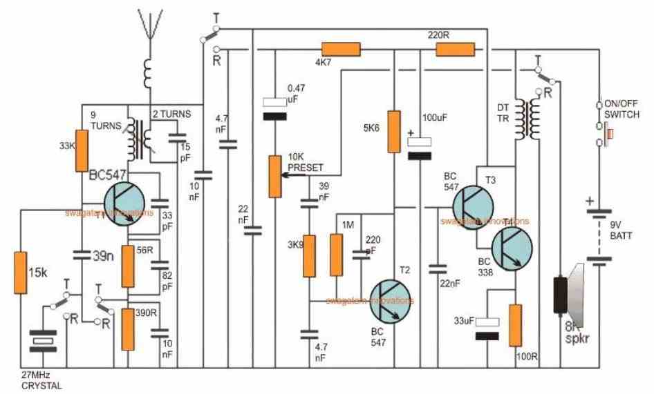
Parts List
All resistors are 1/4 watt 5% CFR 100 ohm - 1 220 ohm - 1 5.6K - 1 4.7K - 1 3.9K - 1 1M - 1 15K - 1 33K - 1 56 ohms - 1 390 ohms - 1 10 k preset - 1 Capacitors Electrolytic 33uF/25V 100uF/25V Capacitors ceramic disc 0.47uF - 1 22nF -2 220pF- 1 4.7nF - 2 10nF - 2 82pF - 1 33pF - 1 15pF - 1 39nF - 1 Transistors BC547 - 2 BC338 - 1 Miscellaneous Crystal 27MHz - 1 TPTT 3 pole triple throw switch - 1 Audio transformer - 1 small speaker 8 ohm 1 watt - 1 9V battery - 1 Inductor as explained belowHow to Wind the Antenna Coil
The coil associated with T1 (BC547) collector is the antenna coil. It is constructed over a ready made variable inductor slug (see image below) having an approximate 3mm diameter and around 7 to 10mm height.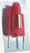 The wire used is a 0.3 to 0.5mm super enameled copper.
Start with the primary 9 turns first, directly on this wind the secondary 2 turns.
The coil in series with the antenna is s simple air core coil made by winding 5 turns of 0.3mm with 5mm diameter.
The wire used is a 0.3 to 0.5mm super enameled copper.
Start with the primary 9 turns first, directly on this wind the secondary 2 turns.
The coil in series with the antenna is s simple air core coil made by winding 5 turns of 0.3mm with 5mm diameter.
How to Wind the speaker coil
You may use a small audio transformer for the shown speaker transformer, or alternatively build it by winding around 70 turns for the primary (left side), and 500 turns at the secondary (speaker side). The wire may be a 0.2mm super enameled copper wire wound over a 3 inch long iron screw.How to Set up the Circuit
After you have built the above explained walkie talkie circuit it's time to check its response by powering it with a 9V PP3 battery. Initially let the switch contacts be positioned for activating the transmitter stage. For knowing whether the transmitter is generating the required 27MHz frequencies or not you will first need to make an RF sniffer circuit as explained HERE Switch ON both the circuits, position the above RF detector circuit about 10 inches away from the walkie talkie antenna, and begin adjusting its variable inductor slug gently using an insulated screw driver which are typically used for adjusting FM radio GANG trimmers. If every thing's done correctly you'll hopefully see the RF detector LED glowing brightly at some point of the adjustment process. Seal and glue the variable inductor at this position, and you can assume your walkie talkie to be all set for having some great time with your friends. However you would need to build another identical set for exchanging the conversations with the other guy, otherwise a single unit wouldn't have much of an importance.What's the Range of this Walkie Talkie
The range of this 27 MHz walkie Talkie can be around 1 Km, provided the trimmers are correctly adjusted and the antenna is long enough for the wide radial transmission.Simple Automatic Plant Watering Circuit for Monitoring Soil Moisture
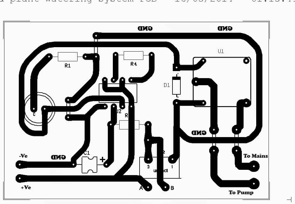
This automatic plant watering circuit can be used for automatically sensing soil humidity and triggering a water pump when the ground gets parched below a predetermined level (adjustable).Circuit Operation
The circuit is rather straightforward and uses a single IC 555 as the main active component.Referring to the automatic plant irrigation circuit shown below we can see the IC 555 is wired in a completely unique and in the quickest possible mode. Here it's configured as a comparator, and works better than an opamp because the IC 555 has built in opamps which are at par with any single opamp and also the output of a 555 IC is able to sink sufficient current in order to drive a relay without a transistor driver stage. The above features particularly makes the above design very simple, low cost and yet too effective with its functions. The pin#2 here becomes the sensing pinout of the IC, and is held at ground level via R2 which must be calculated as per the desired soil humidity triggering threshold. The points A and B can be seen fixed inside the soil which needs to be monitored for the intended automatic watering from the water pump. As long as the points A and B senses some level of humidity corresponding to a resistance value which may be lower than R2, the IC 555 output is held low, which in turn keeps the relay deactivated. However as the soil tends to get dryer, the resistance across the probes starts getting higher and at some moment of time it becomes higher than R2, creating a potential below 1/3rd supply voltage at pin#2 of IC555. The above situation instantly prompts pin#3 of the IC to become high, triggering the connected relay. The relay activation switches ON the water pump which now starts pumping water to the particular area of the soil via a distributing water channel. As this happen, the soil gradually gets wetter and as soon as the predetermined level is reached, the probes immediately sense the lower resistance and revert the IC ouput pin#3 to a low again switching OFF the relay and the water pump consequently. C1 ensures a slight hysteresis in the operations ensuring that the relay triggering is not sudden or abrupt, rather it switches only after sensing a genuine response from the soil conditions.Circuit Diagram
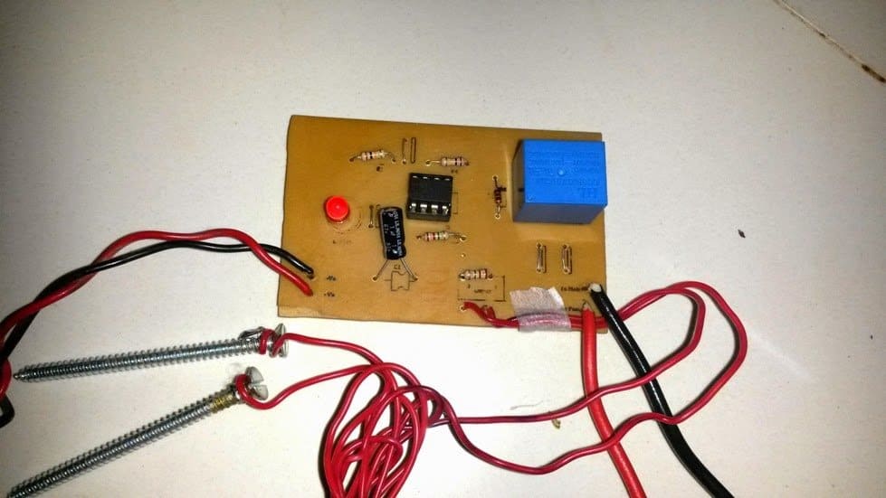
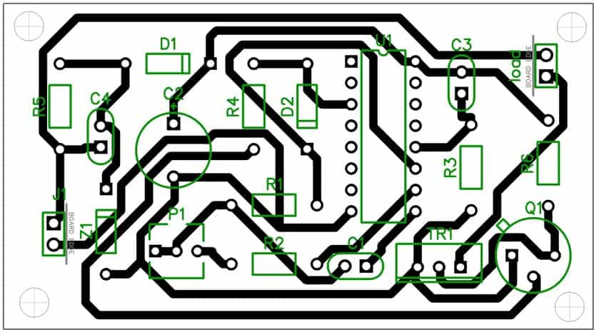
 The above explained automatic plant irrigation circuit was successfully built and tested by Mr.
Ajay Dussa.
The following images show the prototype unit and the PCB design built by Mr.
Ajay.
The above explained automatic plant irrigation circuit was successfully built and tested by Mr.
Ajay Dussa.
The following images show the prototype unit and the PCB design built by Mr.
Ajay.
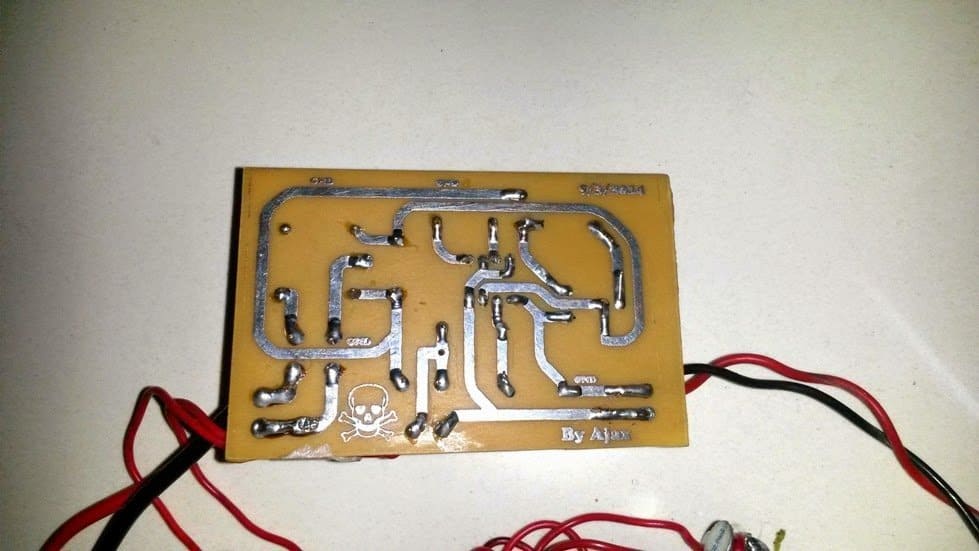 PCB Design
 FOR A 741 OP AMP BASED CIRCUIT, YOU CAN REFER TO THIS ARTICLE.
Parts List
All resistors are 1/4 watt 5% CFR R1 = 10K R3 = 2M2 R4 = 100K R2 = 1M preset or cermet C1 = 1uF/25V optional for creating delay effect on the relay Relay = 12V, 400 ohm SPDT Supply input = 12V/500mA DC Another version of the PCB design is shown below. It was designed an contributed by: Alireza Ghasemi
Soil Moisture Sensor with Automatic Water Sprayer
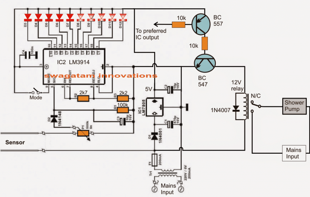
The next article explains a 10 stage soil moisture sensor circuit with an integrated automatic water sprayer mechanism for restoring the critical condition of the soil. The idea was requested by Mr. Remy. I come today asking for help making an automatic watering circuit to water my tomatoes for me. I am requesting the use of a soil moisture sensor (cheap eBay style) to sense the moisture of the soil. Then the moisture value is compared to a set value from a potentiometer maybe. If level is too low then a relay is turned on for a settable amount of time. After a shower the soil is measured again. Rise repeat. The ability to daisy chain many together would be a great help. For wow factor I was thinking that having a few(3) leds light up as a scale to indicate the current moisture level would work well. Thank you for your time and experience. I have learned much from you and hope to add this to my knowledge. RemyCircuit Diagram
The Design
Referring to the given schematic we see a simple yet highly accurate soil moisture sensor circuit with an automatic preset water shower system for restoring the soil moisture level to optimum points. The design is based on a single voltage sensor/LED driver IC LM3914 or a LM3915. The shown sensor pins which are basically two brass rods are configured as voltage sensors across the critical soil area where it may be inserted. The voltage across these pins depend upon the level of moisture present across that particular soil area. This sensed voltage proportionate to the soil moisture level is applied across pin5 of the IC for the required comparison with an in-built reference voltage level. The threshold level at which the shower pump is supposed to be switched ON is set by P1. Depending upon this setting, the IC internal circuitry senses the soil moisture and produces a shifting sequential low logic across the shown 10 outputs starting from pin1 to pin10. This sensed output across the relevant IC outputs are indicated by 10 respective LEDs which light up in sequence in response to the rising or depleting soil moisture levels.Selecting Bar Mode and Dot Mode
The LED illumination sequencing style could be selected to simulate a bar mode or a dot mode by appropriately positioning the pin9 switch of the IC to either ON or OFF. The stage comprising BC547 and BC557 constitute the relay driver stage for controlling the motor pump switching as per the user preference. The base of the PNP transistor is appropriately integrated with any of the output pins of the IC depending at what moisture threshold the user wants the motor to be started or stopped. For example suppose pin15 determines a particular moisture threshold level of the soil and the user feels it to be the unsafe level at which the motor needs to be started in order to restore the soil moisture, then this pinout could be chosen and hooked up with the base of the BC557 transistor for the discussed motor switching. Once the motor is switched ON the soil is showered until its moisture level is restored to the desired level and this prompts the IC to revert its sequence from pin15 to pin14 and toward pin10, switching OFF the motor and the shower. The above process keeps repeating making sure that the soil moisture level never goes down below the undesired parched condition.Simple Transistorized Soil Watering System
Here's another automatic soil watering system that you can build. Its working mode is mainly the nonstop checking of soil moisture, and then responding to a drop beneath a preadjusted degree to set off the plant watering action. This design consists of a straightforward trigger circuit, that switches ON the relay RL for a degree of moisture in the soil and its conductivity which may be beneath the fixed level as adjusted by the 5 k preset.Simple TV Transmitter Circuit
The TV transmitter circuit presented in this post incorporates the European standard FM frequency for audio and Videoup-links. Referring to the circuit below, Q1 is configured as a preamplifier for amplifying the audio input to be modulated.Circuit Description
Q2 is fundamentally responsible for conducting a couple of important functions: It amplifies the carrier frequency generated by the tank circuit, and also modulates the input over this carrier waves. The preamplified audio signals from the Q1 stage is fed to the Q2 stage at its base for the intended modulation actions. As we know all transmitter circuits require a conventional "tank" circuit involving an inductor and few capacitors for generating carrier waves.Here too a tank circuit becomes imperative and is formed by the insertion of C5, L1. This network essentially generates the crucial carrier waves. The video signal which needs to be superimposed with the audio signal is applied to the emitter of Q2 through the variable resistor R7 for implementing the intended modulation process. The composite signal (audio/video) after modulation via the Q2 and the tank circuit stages is further applied to the connected antenna A1 for the final transmission into the atmosphere so that it can be received by a particular TV set in the vicinity. The proposed TV transmitter circuit requires a well regulated stabilized 12V supply for operating. Preferably a 12v battery would give better results due to a muchcleanerDC free from all possible ripples and noises.Circuit Diagrams
Some Important Points:
Things you need to consider while building this TV transmitter circuit at home: Preferably use a well designed glass epoxy PCB for this project. For the inductor L1 use a super enameled copper wire of 24SWG and wind 4 turns with 6mm diameter over any non conducting former such as paper or plastic. T1 may be replaced with any standard audio transformer the type which were commonly used in olden transistor sets and radios at the output amplifier stage. The antenna is not much critical, can be any good conductor of electricity, around a foot long, such as a copper wire. You may try different lengths until you get the optimal response from the TV transmitter circuit. The operating frequency of this unit could be within 50 and 210MHz.Thecompatibilityof this circuit is well with PAL B/C systems. You may have some fun with C8 which may be tweaked a bit for acquiring extreme accuracy with the performance of the circuit.Simple Adjustable Industrial Timer Circuit
The post discusses a simple and effective industrial timer circuit which can be universally used for most industrial and home timer based applications. The idea was requested by Mr. Vasilis K.Technical Specifications
I have a question regarding the 4060 ic wired as "one shot timer." If it can power on the two monostables from the pellet burner circuit, output will be taken from pin #3 which is the last to count to the C1 stage, will that work? When power is applied to the circuit, the first 2 stages should stay low until the time has elapsed. Pin #3 should be set to activate the cycle, so when I leave home in the morning, I will be starting the timer via the thermostat. Then when I get home, the burner should be running. To be more precise, as per the circuit design there are 2 monostable circuits (Stage 1&2) when power is applied via a room thermostat it activates the cycle (Stage 1&2), My request is when power is applied after the predetermined time of the 4060 has elapsed, is to activate the cycle (Stage 1&2), as there is no need for the burner to run when no one is around, plus this would be ideal as it takes about an hour for the water temperature to reach at 75 Celsius.The Design
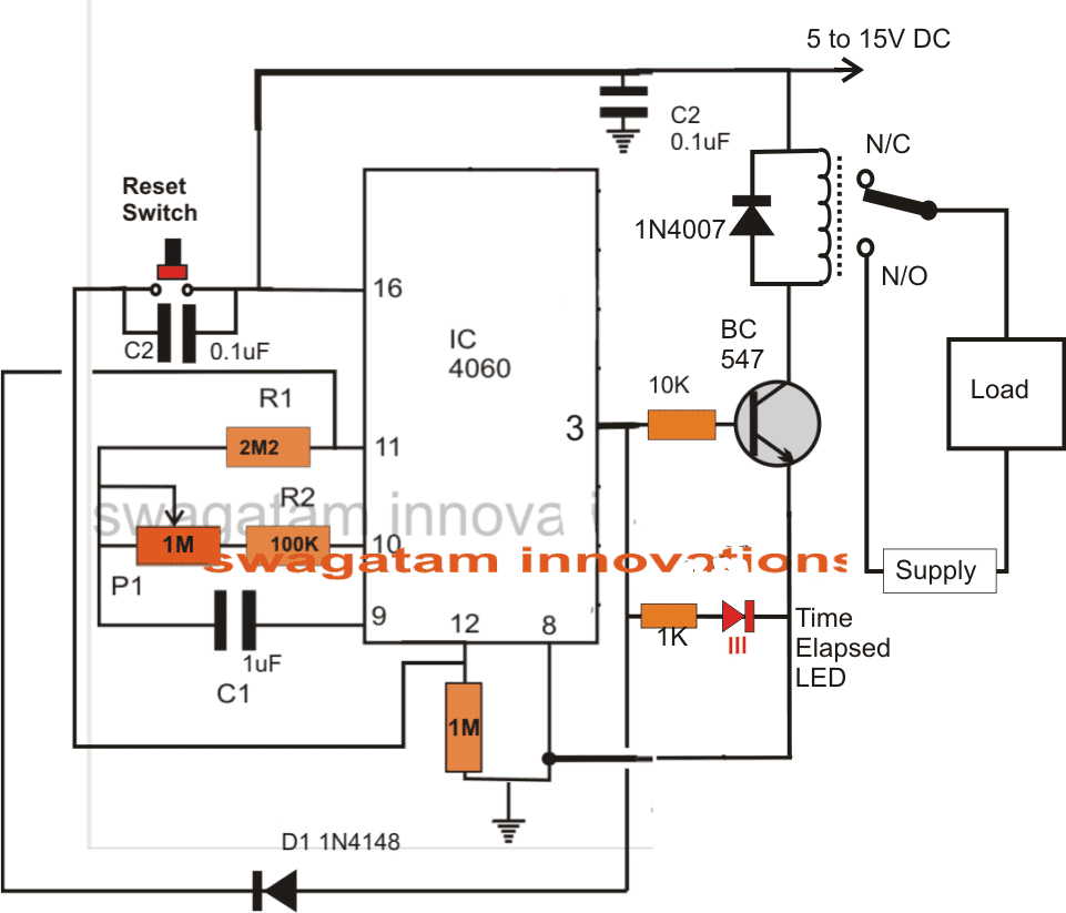
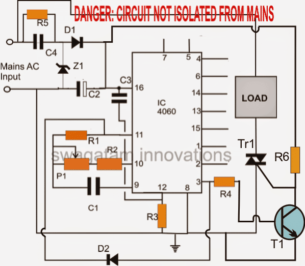
The IC 4060 is an excellent option when it comes to any timer based industrial or home project. This chip being a CMOS device is highly accurate, and is able to generate time delay periods of as high as upto 10 hours with reasonably good accuracy, after this limit the accuracy tends to drift a bit. Although the IC 4060 generates a fixed 50% duty cycle astable type of oscillations at its various outputs, it can be configured as a one shot timer, as explained in the present article. Referring to the shown simple industrial adjustable timer circuit, we can see the IC being the central main component of the whole design. When power is applied or switched ON, C2 momentarily pulses pin#12 of the IC and resets the timing so that the internal oscillator begins counting from zero, moreover the IC can be reset at any moment during the counting period by pressing the given reset switch. While the IC counts, the output which is being used (pin#3 here) is held at a low logic level or a zero voltage, which keeps the TIP122 switched OFF Now as per the setting or selection of R2, P1 and C1, as soon as the set timing elapses, pin#3 goes high, switching ON the transistor and allowing the power to pass to the connected circuit, which now activates. The feedback diode from pin#3 to pin#11 instantly locks the internal oscillator and latches the circuit so that the circuit freezes in that position until the reset switch is pressed for initiating a new cycle.Circuit Diagram
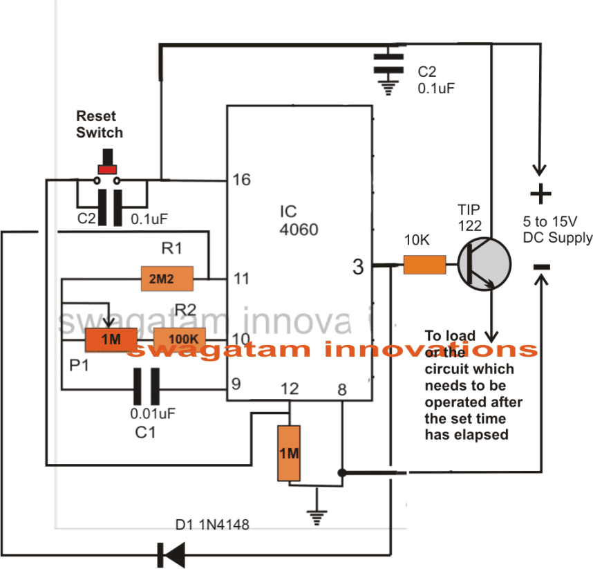 For heavier loads, the above circuit may be upgraded with a relay for identical results but with much higher load current handling capabilities.
 Feedback from Mr.
Vasilis:
Feedback from Mr.
Vasilis:
 Vasilis Karastergios
Hello swagatam!
TESTED & WORKING, really happy with the outcome, i used the 2nd circuit with the relay as i didn't have that specific transistor, that would be my last request for you, i hope i wasn't that much of a pain, again really thankful for all the help and effort, god bless you!!
Regards
Vasilis K.
Vasilis Karastergios
Hello swagatam!
TESTED & WORKING, really happy with the outcome, i used the 2nd circuit with the relay as i didn't have that specific transistor, that would be my last request for you, i hope i wasn't that much of a pain, again really thankful for all the help and effort, god bless you!!
Regards
Vasilis K.
Simple Triac Timer Circuit
Here's a simple triac timer circuit which can be used for switching ON a particular device after a predetermined time, set through the given pot or the variable resistor. The shown circuit diagram of a simple triac timer can be understood by referring to the following explanation:How it Works
The left hand side section comprising the IC 4060 becomes the basic delay generator stage.As we all know, the IC 4060 is an extremely versatile time delay generator chip which has a built in oscillator for the required fundamental timing clocks. The components connected at the pin#9,10 and 11 form the time delay determining parts of the IC. Precisely, the resistor at pin#10 and the capacitor at pin#9 are responsible for fixing the delay period and may be adjusted for acquiring the required predetermined switching output. This IC has 10 discrete outputs which produce delays or oscillation periods which are twice to the previous pinout in the order. Here pin#3 produces the largest delay, followed by pin#2 and then pin#1 and so on as per the specified pinout order. So suppose pin#3 produces delay interval of 1 minute, then pin#2 would produce the same at an interval of 30 seconds, pin#1 at 15 seconds and so on. Since pin#3 is specified with the highest time interval, we use this pinout as the output. Therefore suppose we set the RC at pin#9 and 10 with a maximum delay of 2 hours, pin#3 would be assigned to generate alternately changing ON/OFF pulses, having equal delay intervals of 2 hours, meaning initially the output would be OFF for 2 hours, then ON for next 2 hours and so on as long as its powered. The above explains the IC 4060 configuration, now let's learn about the triac configuration. As we can see, the output pin#3 is directly connected to the gate of the triac, while the triac A1 and A2 are terminated with the load and the other specified parameters. When power is first switched ON, C3 at pin#12 of the IC4060 makes sure that the timing count initiates right from zero by resetting pin#12 with a short pulse. The output pin#3 now initiates with a logic zero output while the IC internal timer starts counting. Due to the logic zero, the triac stays switched OFF initially along with the load. Once the predetermined delay interval lapses, pin#3 instantly becomes high, triggering the triac and the load. The diode connected across pin#3 and pin#11 plays an important function of latching the IC counting process. If this diode is removed, the counting process will continue and after 2 hours the triac will be again become switched OFF, and this procedure will go on repeating every after 2 hours. The diode shuts off this operation, and lathes the IC to the ON position permanently. The above situation provides us with another interesting application of the proposed circuit, by removing the diode we can convert the above circuit into an AC lamp flasher circuit, the flashing rate being set by the RC components. Also note that irrespective of the RC parts you have the option of selecting/connecting the remaining outputs of the IC with the triac gate for getting a diverse range of time delays.Circuit Diagram for Delay ON Timer
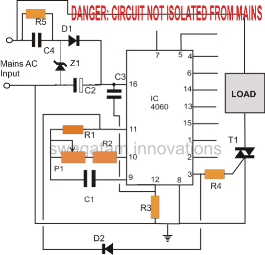 The above triac controlled timer circuit becomes suitable for applications which requires a delay switch ON.
For applications which require a delayswitchOFF meaning in cases where a load needs to beswitched off after a predetermined time interval, the above circuit can be modified as given below:
The above triac controlled timer circuit becomes suitable for applications which requires a delay switch ON.
For applications which require a delayswitchOFF meaning in cases where a load needs to beswitched off after a predetermined time interval, the above circuit can be modified as given below:
Circuit Diagram for Delay OFF Timer
PCB Layout
Parts list for the above simple triac timer circuit
R1 = 2M2 R3 = 100K R2, R4, R6 = 1K R5 = 1M C1 = 1uF/25V (must be non-polar, use more in parallel for higher delays) C3 = 0.1uF disc C2 = 100uF/25V C4 = 0.33uF/400V Z1 = 15V 1watt zener Tr1 = BT136 T1 = BC547 D1, D2 = 1N4007 P1 = 1M potUsing a Transformer DC Supply
The above simple timer circuit can be also built using a transformer DC supply, as shown below: All diodes are 1N4007, and the relay is 12V/400 ohm, 10 amp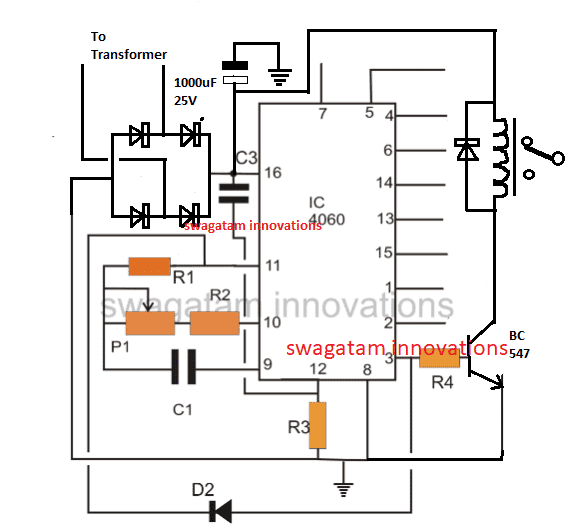
Simple School Bell Timer Circuit using IC 4060
The post explains a very simple 10 stage long duration programmable timer circuit which can be used as a school bell timer circuit. All the 10 stages can be individually programmed from zero to 5 hours. The circuit can be modified in many different ways to suit other specific related applications. You may be also interested in a IC 4017 based School Bell systemThe Circuit Concept
Normally in most of the schools even today the period bells are rung manually by the concerned staff or the peon. Although the job is quite traditional and is carried out without much difficulty and reasonably accurately, the concerned person has to be always on a stand by position for implementing the actions. However with the help of a simple electronic circuit the above implementations could be made fully automatic, eliminating human intervention, thus saving a lot of inconvenience and time. The functioning of the proposed automatic school bell period timer circuit may be understood with the following points:Circuit Operation
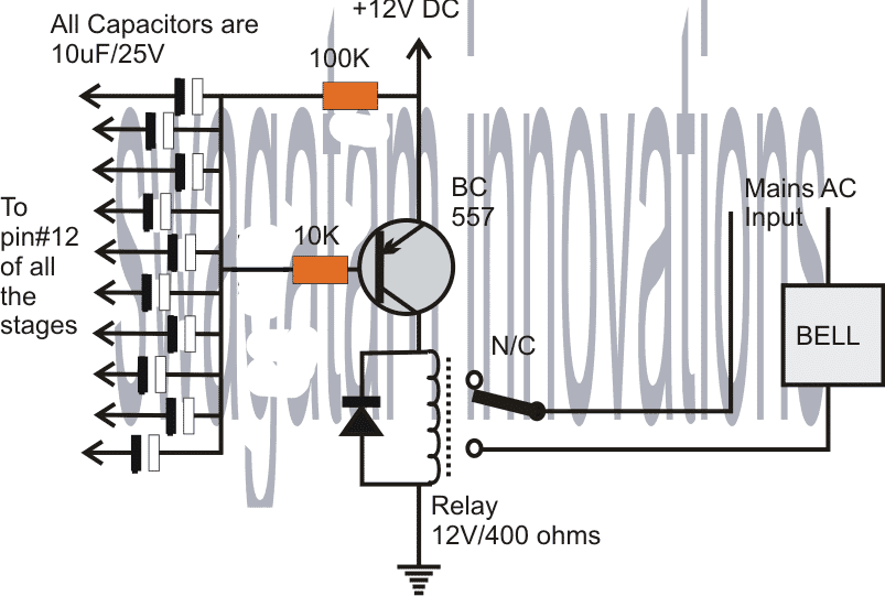
At the first glance the circuit might look quite complex, but seeing it closely shows that actually it's very simple, just a repetition of identical stages for the required number of times. We'll try to understand the top left stage and that will clarify the entire circuit within no time. The circuit is based on the timer/oscillator chip 4060. It's wired in its usual timer/counter mode with the help of the resistors and capacitors fixed over its pin#9, 10,11. Rx determines the time period for which the IC counts until its pin#3 becomes high. The value of this resistor may be determined through trial and error for acquiring the required time intervals for all the relevant subsequent stages. The design is repeated for all the stages. However the top left stage being the first power switch ON stage is rigged with additional components. When the push button P is pressed, the SCR latches, grounding pin#12 of the IC. This initiates the counting procedure within the IC. After the predetermined time lapses, pin#3 of the IC goes high and also the stage gets latched via the diode connected to pin#11. With pin#3 high, the associated transistor pulls pin12 of the next stage to ground, which in turn initiates the counting of the second stage. The procedure is repeated exactly the same way for the second stage also, and consequently all the corresponding stages get activated serially one after the other as per the set time for the individual stages. When the the time period for the last stage is elapsed (bottom left), the transistor at pin#3 momentarily grounds the anode of the SCR via the 1uF capacitor switching off the SCR and the entire circuit. The situation resets the whole circuit to its original state, until the push button is pressed the next morning for initiating yet another cycle. The second circuit shows the driver stage which is responsible for ringing the AC bell in response to the triggering of each subsequent stages in the given order. The diode ends are connected to pin#12 of the different stages. The moment these pins are pulled to ground by the BC547 transistors, sends a momentary biasing to the BC557 transistor which in turn activates the connected relay and the load for a brief period of time depending upon the values of the transistor base resistor and the capacitor (chosen arbitrarily here)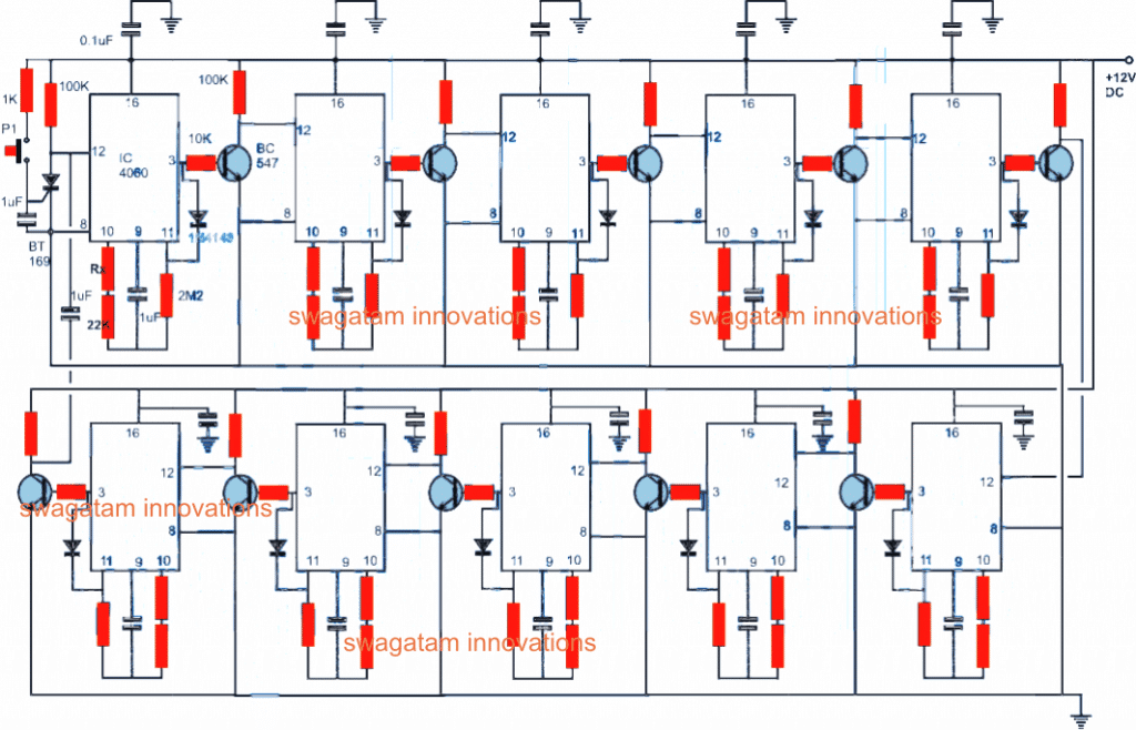
Simplest One Transistor Regulated Power Supply Circuit
The article explains a simple variable regulated voltage power supply circuit which utilizes just a single transistor. The design can be very handy for the new electronic hobbyistMain Features
The explained power supply includes an adjustable voltage feature which is an essential feature for every electronic enthusiast. However making one such power supply within minutes using a handful of components might look difficult. The circuit of a simple variable voltage power supply using just a single transistor referred here shows us how to build one such unit quickly using common parts from your junk box. This single BJT regulated Power Supply is easy to construct. It takes less than an hour on a piece of copper-laminate. All the components can be mounted as show in the aforesaid diagram, cutting the strips for placement. Moreover the board also acts as a heat-sink. Enamelled wires are used to connect the components and the transistor gets bolted to the board, acting as a cooling agent.Circuit Operation
The circuit is designed for use with old C," "D", and even lantern batteries. That��s the reason for no diodes or electrolytic. Get some old batteries and connect together to receive 12v �C 14v, at least. The power for this output is controlled by a 10v zener, made by following the characteristic of zener voltage of 8.2v in between the base-emitter leads of a BC547 transistor, in a reversed bias, and 1.7v approx. across one Red LED. The circuit is designed to deliver 0v-9v at 500mA. However the deliverance depends upon the life of the cells being used. The 10k pot works to adjust the output voltage and thereby the LED circuit goes in ON state. A good part is that the circuit is well designed to fetch the last leg of energy from old cells. Submitted By: Dhrubajyoti BiswasCircuit Diagram
Simple Solar Garden Light Circuit �C With Automatic Cut Off
A very simple automatic solar light system for illuminating your garden passages can be built using some LEDs, a rechargeable battery and a small solar panel. The system automatically switches ON the lamps at dusk and switches them OFF at dawn.How it Works
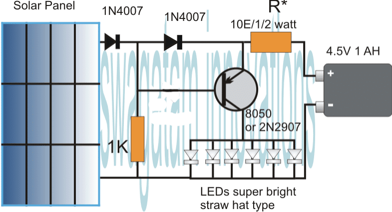
The circuit design is extremely straightforward and may be understood with the following points: As can be seen in the given circuit diagram, the design basically consists of a solar panel, a PNP transistor, few LEDs, a battery and a few resistors. The transistor is the only active component which is positioned as a switch for preventing the battery voltage from reaching the connected LEDs during day time. During broad day light, the solar panel produces the required amount of voltage which is applied across the rechargeable battery via the 1N4007 diode and the resistor R*. This voltage charges the battery gradually from dawn to dusk.Selecting the Current Limiter Resistor
The resistor R* value should be adjusted as per the specs of the battery for limiting excessive current to it. The resistor also serves as the current limiting resistor for the connected LEDs when the transistor is switched ON. Here it hasbeencalculated as 10 Ohms. As long as the solar panel generates the optimal amount of power, the positive potential at the base of the transistor keeps it switched OFF. However when dusk sets in the solar voltage begins to drop, and when it drops below the zener diode rating, the transistor slowly starts conducting, illuminating the LEds gradually. With complete absence of sun light or when its completely dark, the transistor conductsfullywith the help of the 1K resistor, and produces full brightness over the LEDs. The next morning, thecyclerepeats all over again. The circuit can be modified in many different ways.Circuit Diagram
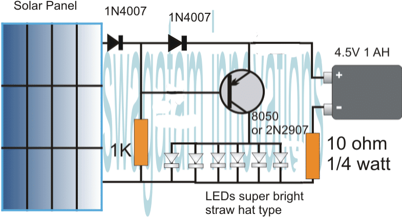
 The above diagram may also be built in the following manner.
It looks more sensible now as the resistor is removed from the emitter for facilitating efficienttriggering of the transistor.
The above diagram may also be built in the following manner.
It looks more sensible now as the resistor is removed from the emitter for facilitating efficienttriggering of the transistor.
PCB Design
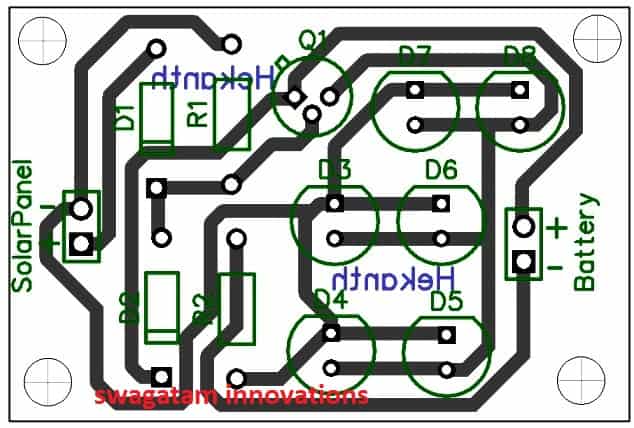 Pictorial Diagram
Parts List
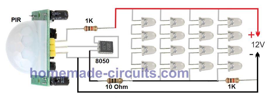
The diagram shows an incorrect transistor number (8050), use 8550 instead.
Recommended Solar Panel Specs
6 to 8V/2 watt
Voltage - 6V
Current - 330 mA
Pictorial Diagram
Parts List
The diagram shows an incorrect transistor number (8050), use 8550 instead.
Recommended Solar Panel Specs
6 to 8V/2 watt
Voltage - 6V
Current - 330 mA

Using a 9 V Battery and High Bright White LED
The next shows an elaborate yet simple solar garden light diagram in pictorial form R2 is the LED current limiting resistor which can be calculated using the following formula: R2 = Battery Voltage - LED Fwd Voltage / LED Current R3 is the charging current limiter resistor for the battery, and it can be calculated using the following formula: R3 = Solar Panel Voltage - Battery Voltage / 10% of Battery mAH Rating The battery voltage must be at least 3 V higher than LED voltage. The panel voltage must be at least 3 V higher than the battery voltage.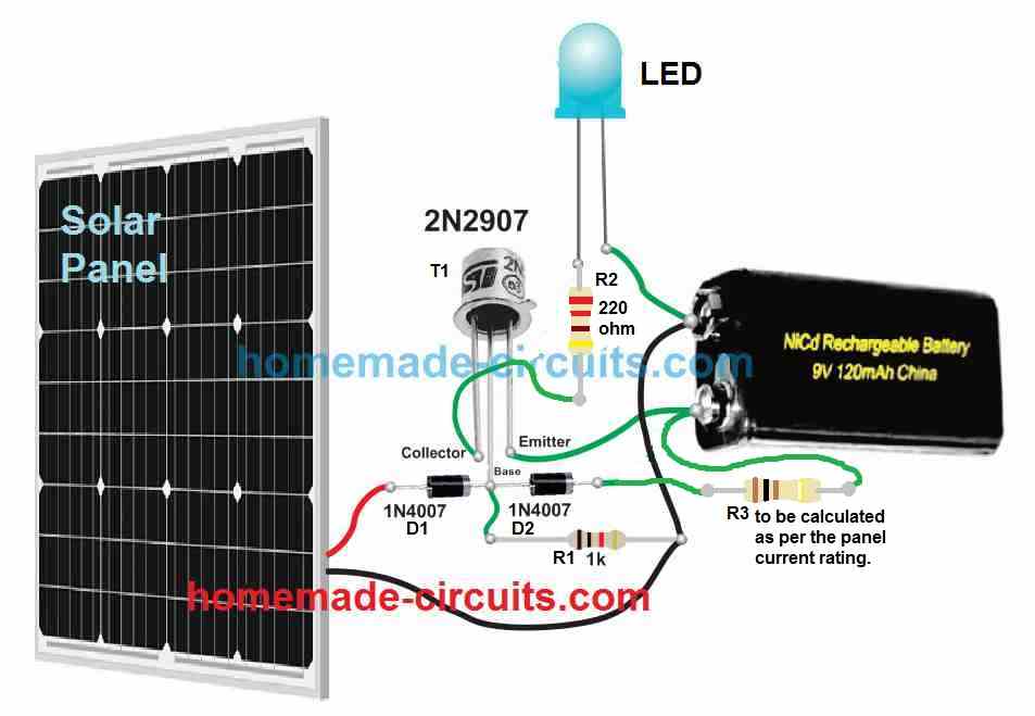
Using NPN Transistors
The above explained designs can be also replicated using two NPN transistors as shown in the following diagram:
Solar Pathway Light Circuit with Constant Voltage
If a Li-Ion battery is intended to be used for the above explained circuit, a constant voltage feature becomes crucial for safeguarding battery life and prolonging it. The following circuit show how this may be done by adding a simple voltage follower regulator circuit: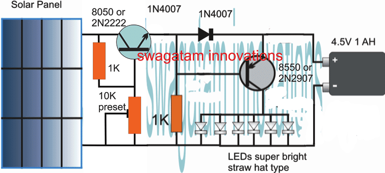 If a 3.7V Li-Ion battery is used, make sure to adjust the 10K preset to achieve precisely 4V across the output points where the battery is supposed to be connected, do this adjustment without connecting the battery.
The 4V level ensures that the battery is never overcharged (at 4.2V) and this also allows the circuit charge the battery without a constant current supply.
If a 3.7V Li-Ion battery is used, make sure to adjust the 10K preset to achieve precisely 4V across the output points where the battery is supposed to be connected, do this adjustment without connecting the battery.
The 4V level ensures that the battery is never overcharged (at 4.2V) and this also allows the circuit charge the battery without a constant current supply.
1.5V Solar Garden Light with Enhanced Features
The following solar powered garden light was designed by Mr. Guido which includes additional features such over charge and low charge cut off for the battery and with a Schmidt trigger. This ensures that the connected battery is never allowed to charge or discharge beyond unsafe levels. The main attraction of the circuit is the use of a single rechargeable AAA penlight cell, which is able to light up a 3.3V high bright LED through an attached Joule thief circuit.
5 Simple Alarm Circuits for Protecting your Home/Office from Theft
The following article discusses a few very simple intrusion detector circuits, or ant-theft alarms. The presented designs are easy to build yet extremely effective with the functions.How the Circuits Works
An intruder alarm basically consists of a sensor and a trigger stages, which work together to produce the requireddetection. The sensor detects the presence of an intruder while the triggering stage responds to the sensor detection by instantly raising the alarm. The triggering stage may consist of a voltage/current amplifier stage rigged with a relay driver stage along with a timer stage for keeping the triggering switched ON even after the threat is eliminated, for increased safety. The sensor pat is generally more sophisticated because it's the main section responsible for detecting the threat. Generally infrared sensorswhichwork bydetectingbody warmth are incorporated in most hi-end types of anti-theft alarms, however here we'll try to implement reasonably similar results yet use ordinary arrangements for the sensor stage in the proposed circuits. You may also want to build this PIR burglar Alarm CircuitIntruder Alarm Using an Ordinary Conductor as the Sensor
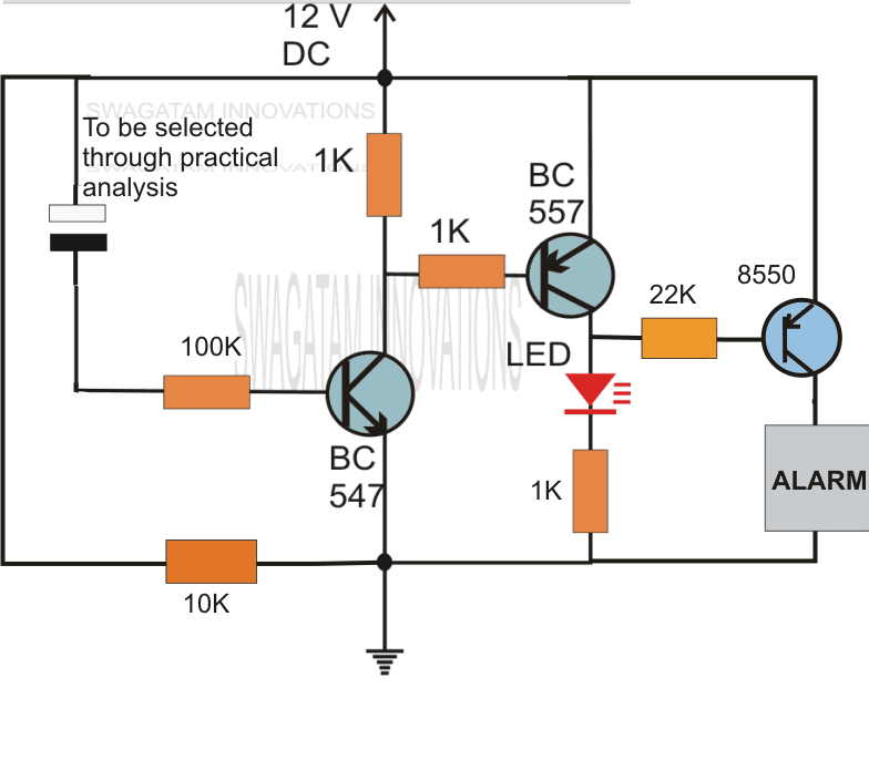
This is probably the simplest one among all. As shown in the circuit diagram, the sensor is an ordinary thin wire conductor which is laid across therestrictedarea in such a way that anybody intruding the place gets caught up against the conductor and in the course breaks it up. Once the wire breaks, the transistor is allowed to receive the required base drive, ringing the attached alarm.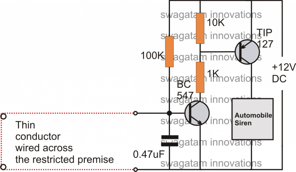
Intruder Alarm Using a Piezo Electric Sound Sensor
This circuit is based on a sound detection through an inexpensive piezo element. Theentiresystem may be fixed over the door or therestrictedentrance. If an intruder tries to break in, the door would be disturbed instantly activating the connected piezo sensor, and theprecedingalarm circuit.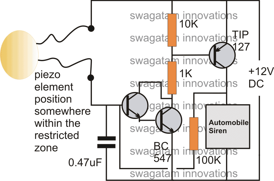
Intruder Alarm Using a Laser Beam.
Today toy laser beam generator devices are pretty popular, and can be easily procured ready made from the market. This toy laser beam can be effectively implemented as an alarm sensor. As shown in the figure, the restricted area may be swarmed by laser beams reflectedacrossthe area via accurately angled mirrors. The final reflection gets directed toward an LDR trigger circuit. In case an intruder tries to trespass the premise, the person would block at least one of the reflections, interrupting the laser passage over the LDR. This would result in an instant triggering of the connected driver circuits.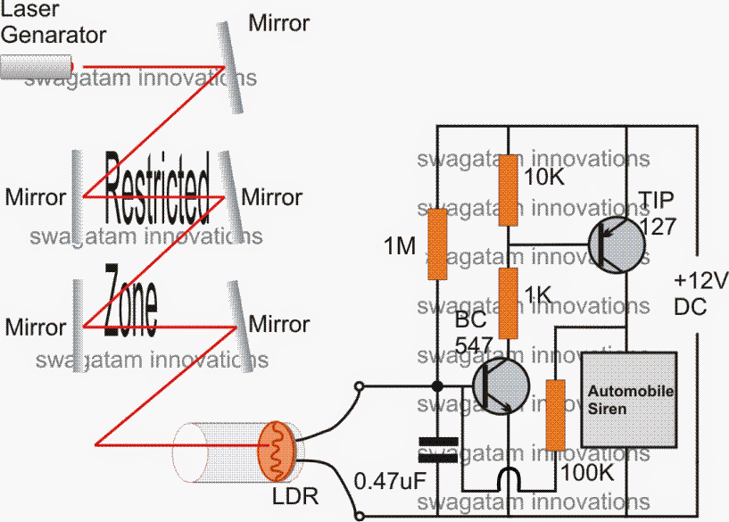
Intruder Alarm with Push Button OFF Feature
The above design of a latching laser activated alarm can be modified with a push button OFF feature. The following diagram shows how it's implemented using a single SCR, while the LDR, and the laser set up remains the same. The idea was requested by Mr. Kuldeep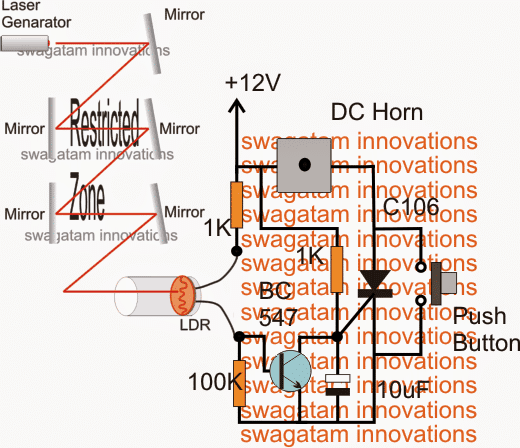 The 12V input power should be switched ON only after the laser point is set on the LDR.
Simple PIR LED Lamp Circuit
The following PIR LED lamp circuit wasdesignedby me for one of the followers of this blog Mr.Deepak upon his request. The circuit is a LED driver which responds to ambient lightas wellas to the presence of a human, person or intruder, and varies its illumination accordingly, let's know more. "I was looking to drive 20 LEDs of 0.06 watts. So total Output voltage is 12-17 volts and total current is 0.08 amps to drive 4 strings of 5 LEDs each each led is 3.4 volts and 20 mA. Can you help with this? Also I would like to have an ambient sensor to switch on and off and a proximity sensor to switch to full brightness if some one approaches and to switch to half or 30% brightness after 30 seconds. I need this for commercial use. I need asimplecost effective circuit. I have been following the blog and am sure that you know the subject. Please get back to me."Simple PIR Controlled LED Lamp Circuit
Before solving the above request, let's first see how we can build the design in its simplest form using a PIR module and some LEDs. PIR Module Datasheet The following circuit shows a simple PIR sensor which activates the connected LEDs in response to the presence of humans within the specified area.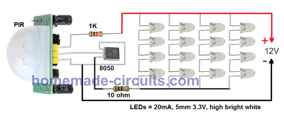 As you can see I have not used any voltage regulator here, since the 1K at the positive works good to limit the current and the voltage to the PIR.
This also avoids the base resistor for the transistor.
I have used 16 LEDs, however upto 64 EDs can be used.
For the power supply you can use any cheap 12V 1 amp SMPS
As you can see I have not used any voltage regulator here, since the 1K at the positive works good to limit the current and the voltage to the PIR.
This also avoids the base resistor for the transistor.
I have used 16 LEDs, however upto 64 EDs can be used.
For the power supply you can use any cheap 12V 1 amp SMPS
Parts List for the above circuit:
PIR Module - 1 1K 1/4 watt - 1 Transistor 8050 - 1 LEDs 5 mA, 20 mA, 3.3V - 16nos, or upto 64 nos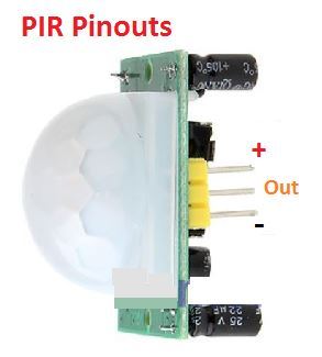
Video Demo
Design# 2
The next two PIR based sensor LED light circuits is similar but has an added feature of detecting the ambient light conditions also. Therefore the circuits will respond based on whether the atmospheric light is sufficiently dark or not and also whether the premise is occupied by a human.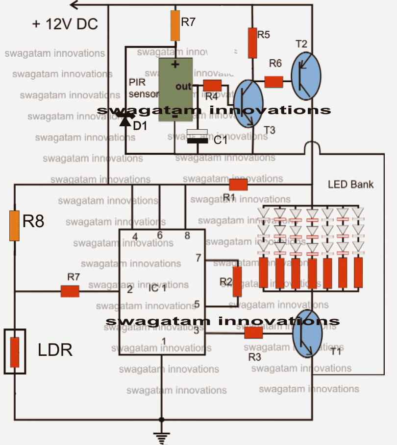 Let's try to understand the PIR based LED lamp circuit functioning from the following points:
The IC 555 isconfigured asa comparator, the LDR and R8 values are compared for generating anappropriateoutput.
As long as there's enough light over the LDR, pin#2 of the IC remains high and this keeps the output pin#3 of the IC high as well.
The highoutputat pin#3 keeps the transistor and the LED switched ON, until the ambient light falls below a predeterminedvalue setby P1.
This means during night or in the absence of light the LEDs too get switched OFF.
The uppersectionis aproximitysensor circuit.
The transistors T2 and T3 are configured as high gainamplifierand is able to sense even minute voltages from the PIR sensor.
In the presence of any human or animal in the specified vicinity, the PIR becomes active and triggers T3, which in turn switches ON T2.
T2 instantly shorts R1, such that the supply voltage reaches the LEDs directly instead of via R1.
This situation brightens up the LED illumination, indicating the presence of a passer by (as stated in the request).
The capacitor C1, ensures the LED brightness stays alive for many seconds, even after the PIR is deactivated.
Let's try to understand the PIR based LED lamp circuit functioning from the following points:
The IC 555 isconfigured asa comparator, the LDR and R8 values are compared for generating anappropriateoutput.
As long as there's enough light over the LDR, pin#2 of the IC remains high and this keeps the output pin#3 of the IC high as well.
The highoutputat pin#3 keeps the transistor and the LED switched ON, until the ambient light falls below a predeterminedvalue setby P1.
This means during night or in the absence of light the LEDs too get switched OFF.
The uppersectionis aproximitysensor circuit.
The transistors T2 and T3 are configured as high gainamplifierand is able to sense even minute voltages from the PIR sensor.
In the presence of any human or animal in the specified vicinity, the PIR becomes active and triggers T3, which in turn switches ON T2.
T2 instantly shorts R1, such that the supply voltage reaches the LEDs directly instead of via R1.
This situation brightens up the LED illumination, indicating the presence of a passer by (as stated in the request).
The capacitor C1, ensures the LED brightness stays alive for many seconds, even after the PIR is deactivated.
Parts List
R1 = 100 Ohms, R2,R4 = 100K, R3,R5, R6 = 10K, R7 (at IC 555 pin2) = 2M2, R7 at PIR positive = 10K R8 = 2M2, C1 = 470uF/25V LED resistors = 100 Ohms each, T1, T3 = BC547, T2 = BC557, D1 = 4.7V zener LDR = any standard type. PIR sensor = any standard type. IC1 = 555Darkness Activated PIR Circuit
The following circuit can be used for automatically detecting human presence, and activating the lights during night time.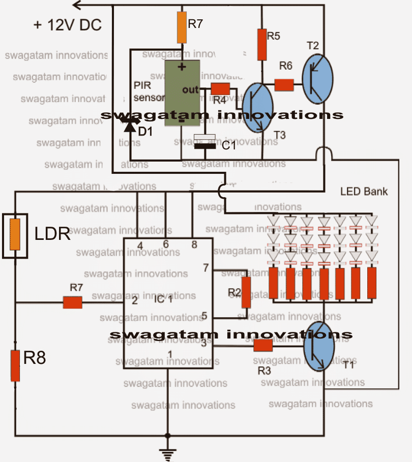
Simple Delay Timer Circuits Explained
In this post we discuss the making of simple delay timers using very ordinary components like transistors, capacitors and diodes. All these circuits will produce delay ON or delay OFF time intervals at the output for a predetermined period, from a few seconds to many minutes. All the designs are fully adjustable.Importance of Delay Timers
In many electronic circuit applications a delay of a few seconds or minutes becomes a crucial requirement for ensuring correct operation of the circuit. Without the specified delay the circuit could malfunction or even get damaged. Let's analyze the various configurations in details. You may also want to read about IC 555 based delay timers. Recommended for you!Using a Single Transistor and Push Button
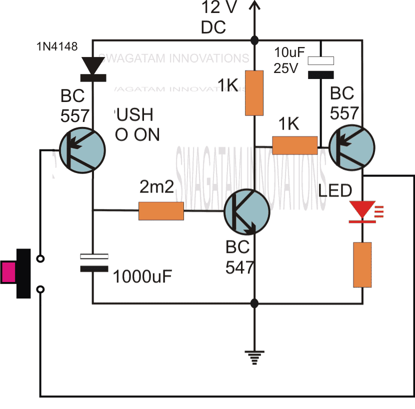
The first circuit diagram shows how a transistors and a few other passive components may be connected for acquiring the intended delay timing outputs. The transistor has been provided with the usual base resistor for the current limiting functions. A LED which is used here just indication purposes behaves like the collector load of the circuit. A capacitor, which is the crucial part of the circuit gets the specific position in the circuit, we can see that it's been placed at the other end of the base resistor and not directly to the base of the transistor. A push button is used to initiate the circuit. On depressing the button momentarily, a positive voltage from the supply line enters the base resistor and switches ON the transistor and subsequently the LED. However in the course of the above action, the capacitor also gets charged fully. On releasing the push button, though the power to the base gets disconnected, the transistor continues to conduct with the aid of the stored energy in the capacitor which now starts discharging its stored charge via the transistor. The LED also stays switched ON until the capacitor gets fully discharged. Te value of the capacitor determines the time delay or for how long the transistor stays in the conducting mode. Along with the capacitor, the value of the base resistor also plays an important role in determining the timing for which the transistor remains switched ON after the push button is released. However the circuit using just one transistor will be able to produce time delays which may range only for a few seconds. By adding one more transistor stage (next figure) the above time delay range can be increased significantly. The addition of another transistor stage increases the sensitivity of the circuit, which enables the use of larger values of the timing resistor thereby enhancing the time delay range of the circuit.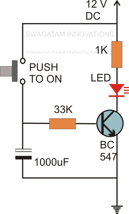 PCB Design
 Video Demonstration
Using a Triac:
The following image shows how the above delay timer circuit may be integrated with a triac and used for toggling a mains AC operated load The above could be further modified with a self contained power transformerless power supply as shown below:
Without a Push-Button
If the above design is intended to be used without a push button, the same may be implemented as indicated in the following diagram: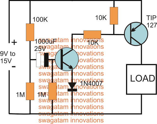 The above delay OFF effect without a push button can be further improved by using two NPN transistor, and by using the capacitor across base/ground of the left NPN
 The following circuit shows how the associated push button may be rendered inactive as soon as it's pressed and while the delay timer is in the activated state.
During this time any further pressing of the push button has no impact on the timer as long as the output is active or until the timer has finished its delay operation.
The following circuit shows how the associated push button may be rendered inactive as soon as it's pressed and while the delay timer is in the activated state.
During this time any further pressing of the push button has no impact on the timer as long as the output is active or until the timer has finished its delay operation.
Delay from an External Trigger
Problem asked by Mr. Glen (one of the dedicated readers of this blog): I have a situation where I have a pulse of 12V that lasts about 4 seconds (from a rotary switch being turned by a slow motor) but I only want about half a second pulse (to trigger a mechanical bell/chime). Is there any way to take a long pulse into a circuit and send a much shorter pulse out? The solution to the above problem is provided in the following schematic:Two Step Sequential Timer
The above circuit can be modified to produce a two step sequential delay generator. This circuit was requested by one of the avid readers of this blog, Mr.Marco. A simple delay OFF alarm circuit is shown in the following diagram.
The circuit was requested by Dmats.
A simple delay OFF alarm circuit is shown in the following diagram.
The circuit was requested by Dmats.
 The following circuit was requested by Fastshack3
Delay Timer with Relay
"I am looking to build a circuit that would control an output relay. This would be done in 12V and the sequence will be initiated by a manual switch. I will need an adjustable time delay (possibly displayed time) after the switch is released, then the output would go on for an adjustable time (also possibly displayed) before shutting off. The sequence would not restart until the button was pressed and released again. The time after the button release would be from 250 milliseconds to 5 seconds. The "on" time for the output to turn on the relay would be from 500 milliseconds to 30 seconds. Let me know if you can offer any insight. Thanks!"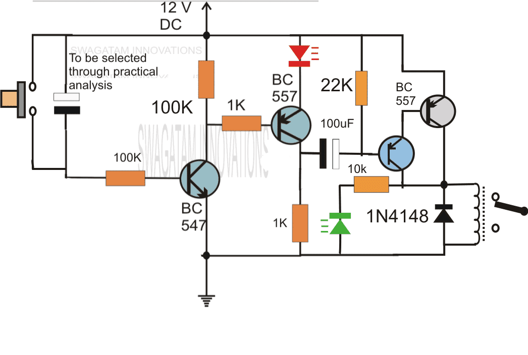 So far we have learned how to make simple delay OFF timers now let us see how we can build a simple delay ON timer circuit which allows the connected load at the output to be switched ON with some predetermined delay after power switch ON.
The explained circuit can be used for all applications which calls for an initial delay ON feature for the connected load after the mains power is switched ON.
So far we have learned how to make simple delay OFF timers now let us see how we can build a simple delay ON timer circuit which allows the connected load at the output to be switched ON with some predetermined delay after power switch ON.
The explained circuit can be used for all applications which calls for an initial delay ON feature for the connected load after the mains power is switched ON.
Delay ON Timer Circuit Working Details
The shown diagram is pretty straightforward yet provides the necessary actions very impressively, moreover the delay period is variable making the set up extremely useful for the proposed applications. The functioning can be understood with the following points: Assuming the load which requires the delay ON action being connected across the relay contacts, when power is switched ON, the 12V DC passes via R2 but is unable to reach the base of T1 because initially, C2 acts as a short across ground. The voltage thus passes through R2, gets dropped torelevantlimits andstartscharging C2. Once C2 charges up to a level which develops a potential of 0.3 to 0.6V (+zener voltage) at the base of T1, T1 is instantly switched ON, toggling T2, and the relaysubsequently....finally the load gets switched ON too. The above process induces the required delay for switching ON the load. The delay period may be set byappropriatelyselecting the values of R2 and C2. R1 ensures that C2 quickly discharges through it so that the circuit attains the stand by position as soon as possible. D3 blocks the charge from reaching the base of T1.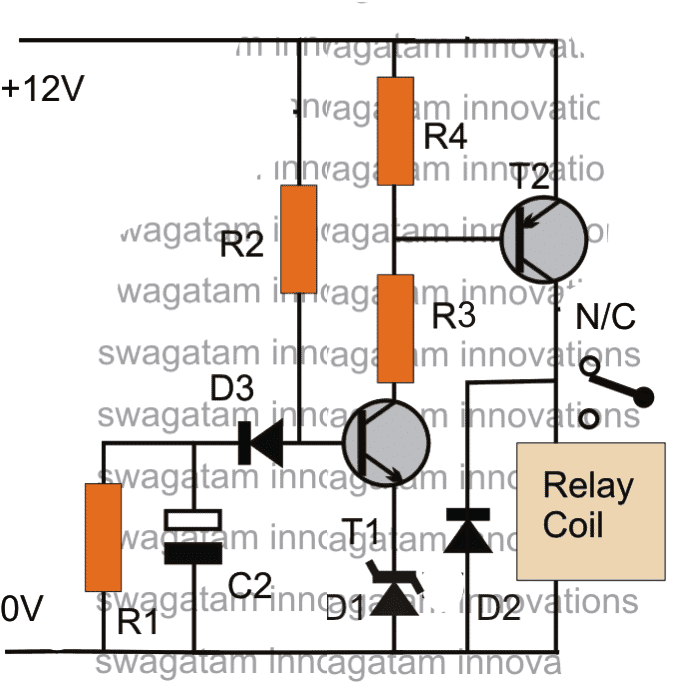
Parts List
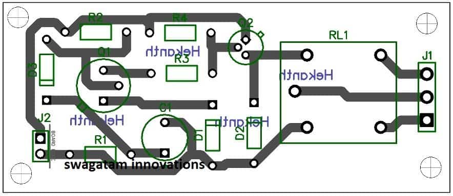
R1 = 1o0K (Resistor for Discharging C2 when circuit is switched OFF)) R2 = 330K (Timing Resistor) R3= 10K R4 = 10K D1 = 3V zener diode (Optional, could be replaced with a wire link) D2 = 1N4007 D3 = 1N4148 T1 = BC547 T2 = BC557 C2 = 33uF/25V (Timing Capacitor) Relay = SPDT, 12V/400 OhmsPCB Design
Application Note
Let's learn how the above delay ON timer circuit becomes applicable for solving the following presented issue by one of the keen followers of this blog, Mr. Nishant.Circuit Problem:
Hello Sir, I have a 1KVA automatic voltage stabilizer.It has one defect that when it is switched on, very high voltage is outputted for about 1.5s (therefore cfls and bulb got fused frequently) after that the voltage becomes OK. I have opened the stabilizer it consist of an auto-transformer,4 24V relay each relay connected to aseparatecircuit(each consisting of 10K preset,BC547,zener diode,BDX53BFP npn darlington pair transistor IC,220uF/63v capacitor,100uF/40V capacitor ,4 diodes and some resistors). These circuits are powered by a step down transformer and output of these circuit are taken across corresponding 100uF/40V capacitor and fed to corresponding relay.What to do in order to tackle the problem.please help me.Hand drawn circuit diagram is attached.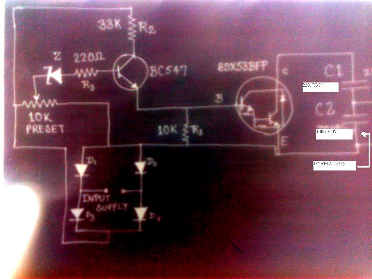
Solving the Circuit Problem
The problem in the above circuit might be due to two reasons: one of the relays is switching ON momentarily connecting the wrong contacts with the output, or one of the responsible relays is settling down with the correct voltages a little while after power switch ON. Since there are more than one relay, tracing out the fault and correcting it can be a bit tedious......the circuit of a delay ON timer explained in the above article could be actually very effective for the discussed purpose. The connections are rather simple. Using a 7812 IC, the delay timer can be powered from the existing 24V supply of the stabilizer. Next, the delay relay N/O contacts may be wired in series with the stabilizer output socket wiring. The above wiring would instantly take care of the issues as now the output would switch after some time during power witch ONs, allowing enough time for the internal relays to settle down with the correct voltages across their output contacts.Feedback from Mr. Bill
Hi Swagatam, I stumbled across your page doing research on the web to make my delay more consistent.Some back ground information first. I am a bracket drag racer and launch the car on first sight of the 3rd amber bulb as the christmas tree is coming down. I use a transbrake switch that is depressed to lock the automatic transmission in forward and reverse at the same time. This allows you to rev up the engine to build power for launch. When the button is released the transmission comes out of reverse and moves the car forward under high rpm. This is like popping the clutch on a manual transmission car, anyway my car reacts to quickly and the result is a redlight, leaving to early, and you lose the race. In dragracing your reaction time on the launch is everything and it is a game of hundreths-thousanths with the big boys, so I have put the transbrake switch on a relay and put a 1100uf cap combo across the relay to delay its release. Because of the car electronics I don't believe there is a precise voltage charging this cap every time I activate this circuit and precision is key so I bought a power stabilizer off of Ebay that takes 8-15 volts in and gives a consistent 12volts out. This turned my season around but i believe this circuit could be made to be more precise and to vary the delay time in an easier way rather than swap cap combos. Also should I run a diode in front of the relay, not currently because all that is there is the on off switch- where will the current go? I am not an electrical engineer by any means but do have some knowledge from trouble shooting high end audio for many years. Would love your thoughts- thankyou Bill KoreckyAnalyzing and Solving the Circuit
Hi Bill, I have attached the schematic of an adjustable delay circuit, please check it out. You can use it for the mentioned purpose. The 100K preset can used and adjusted for acquiring precise short delay periods as per your specifications. However, please note that, the supply voltage will need to be minimum 11V, for the 12V relay to operate correctly, if this is not fulfilled then the circuit might malfunction. Regards.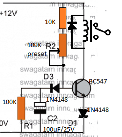
Simple 5 to 20 Minute Delay Timer
The following section discusses a simple 5 to 20 minute delay timer circuit for a specific industrial application. The idea was requested by Mr. Jonathan.Technical Requirements
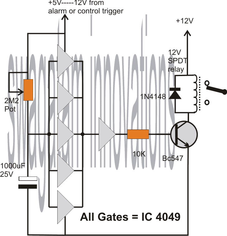
While trying to figure out a solution to my problem on google, I came across your above posting. I'm trying to figure out how to build a better Sous Vide controller. The main problem is that my water bath has a very high hysteresis, and when heating from colder temperatures will overshoot about 7 degrees from the temperature at which power is terminated. It is also very well insulated, with a gap between the inner and outer vessel which makes it act like a thermos jar, because of this it takes a very long time to decline from any excess temperature. My PID controller has an SSR control output and a relay alarm output. The alarm can be programmed as a below limit alarm with an offset from the set-point. I can use a five volt supply I already have for my circulation motor to run through the alarm relay and drive the same SSR the control output is driving. To be on the safe side and protect the PID controller I'll add a diode to both the alarm voltage and the control voltage to prevent one output from feeding back into the other. I'll then set the alarm to stay on until the temperature rises above the set-point minus 7 degrees. This will allow the PID tuning to be adjusted without having to account for the initial temperature ramp-up. Because I know that last few degrees will be achieved without any power input, I'd really like a way to delay any recognition of the control signal for about five minutes after the alarm shuts off, as it will still be calling for heat. This is the part I've yet to figure out the circuitry for. I��m thinking of a normally closed relay in series with the control output, which is held open by the alarm signal. When the alarm signal is terminated, I need a delay on the order of five minutes before the relay returns to its ��off�� normally closed state. I would appreciate help with the delayed off portion of the relay circuit. I like the simplicity of the initial designs on the page, but I get the impression they wouldn��t handle anywhere near five minutes. Thank you, Jonathan LundquistThe Circuit Design
The following circuit design of a simple 5 to 20 minute delay timer circuit can be suitably applied for the above specified application. The circuit employs the IC4049 for the required NOT gates which are configured as voltage comparators. The 5 gates in parallel form the sensing section and provides the required time delay trigger to the subsequent buffer and the relay driver stages. The control input is acquired from the alarm output as indicated in the above description. This input becomes the switching voltage for the proposed timer circuit. On receiving this trigger, the input of the 5 NOT gates are initially held at logic zero because the capacitor grounds the initial trigger via the 2m2 pot. Depending upon the 2m2 setting, the capacitor starts charging up and the moment the voltage across the capacitor reaches a recognizable value, the NOT gates revert their output to logic low, which is translated as a logic high at the output of the right single NOT gate. This instantly triggers the connected transistor and the relay for the required delay output across the relay contacts. The 2M2 pot may be adjusted for determining the required delays.Circuit Diagram
Simple LDR Motion Detector Alarm Circuit
Here we learn how to build a simple LDR based motion detector sensor circuit using ordinary parts such as LDRs and opamps, reasonably accurately.What are Motion Detectors
Motion detector or sensor alarm is a device which detects the presence of a motion or movement within a certain fixed range and raises an alarm on doing so. You might find many electronic circuits related to motion sensing but most of them incorporate shadow detection through a single LDR, which does not work very effectively. Because a shadow might not always be very sharp enough and at times the circuit may just fail to interpret it. The present motion detector/sensor circuit is also based on similar principles but it detects a motion by differentiating the light level using two LDRs, this makes the system more sensitive and works irrespective of the shadow intensity.Circuit Operation
The circuit diagram shows a simple configuration consisting of a couple of opamps from the IC LM324. The two opamps are arranged in a differential mode and as comparators. Both the comparators consists of their own discrete light sensing components in the form of LDRs. The presets provided with the opamps decide at what point the outputs of the both the opamps remain on the same level, that is at zero potential. Also the above condition is met when the light level over both the LDRs are approximately at the same levels. However the moment the light level (or the shade level) on the LDRs differ even slightly, the comparators instantly detects this and one of the relevant opamp outputs goes high. The transistor at the output immediately triggers and activates the relay and the connected alarm mechanism. The LDRs must be positioned at least a feet apart for proper optimization of the detection level. Also the LDRs and the nit itself must be positioned in such a way that the ambient light directly become incident over the sensors.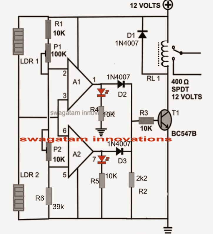
How to Set Up the Circuit.
You will require a lot of dexterity for setting up the circuit accurately. It may be done as follows: Let a constant source of light fall on the LDRs with uniform intensity. Now without letting any of your body part disturbing the light source, gently and skilfully adjust the two presets such that both the LEDs just shut off. That's it, your circuit is now all set and ready to detect even the slightest of motions across any of the LDRs. However it must be ensured that the light source intensities on the LDRs does not change, or else the set up could get rattled.Simple Programmable Timer Circuit
This programmable timer can be used for switching a load ON and OFF with two sets of time delays, which are programmable from 2 seconds to 24 hours independently. The delay timings are adjustable according to the users personal specs. The ON time delay and the OFF time delay are independently settable and this facility becomes the most important feature of a programmable timer circuit.Using Versatile IC 4060
In this page we will discuss a very simple yet reasonably useful timer circuit diagram whose ON time and OFF time settings are independently adjustable through ordinary pots. The idea becomes so easily configurable due to the versatile IC 4060 which require minimal number of component for getting the unit running. Looking at the CIRCUIT DIAGRAM below we can see that two inexpensive IC 4060 have been wired up as two independent timer modes. However though the timing settings are independent for the two sections, these are coupled with other such that their initialization become very much interconnected. Basically both the configurations are similar and have been rigged in the standard counting modes of the IC 4060 devices. You may also want to make this Arduino based programmable timer circuitHow the Circuit Functions
The output of the upper IC is coupled to the reset input of the lower IC via a transistor in such a way that once the upper IC's output goes high, it triggers the lower timer into operation. The lower IC then starts counting and when its output goes high, it halts the upper ICs counting and resets it to its original state and the process is initiated back from the start. It simply means that as long as the upper ICs timing does not lapse the lower IC remains idle, however once the upper ICs timing lapses and its output becomes high, it switches the output load as well as the lower ICs operation. The pot associated with the upper IC can be used for determining after how long the load will be switched ON, while the pot associated with the lower IC is used for determining how long the load remains in the switched ON position or simply after what time it should be switched OFF. Update: The LED positions have been changed in the following updated designs, because the earlier LED positions were conflicting with the relay operations, and therefore the positions have been relocated for ensuring foolproof operations.Circuit Diagram of a Versatile Programmable Timer
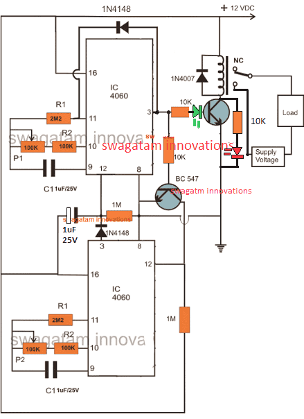
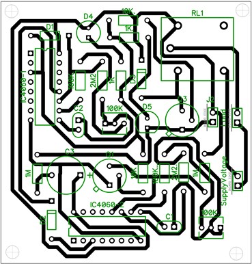
PCB Layout
 Video showing the proposed 2-stage programmable timer circuit with LEDs
Using a Start Push-Button
The above design could be upgraded with a push-button to facilitate a push button start. This further ensures that the timer shuts off completely in case a power failure occurs while the circuit is operational, which in turn ensures that crucial loads like heater, or geyser are completely turned OFF during such situations.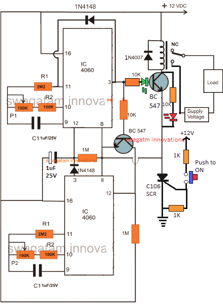
Calculating RCTiming Components
It can be done through a formula, but the manual way is much simpler and accurate. It can be done as explained below: Connect any arbitrarily selected resistor above 100K in place of P1/R2 in the upper circuit. Switch ON and carefully note down after how much time pin#3 of upper IC 4060 becomes HIGH. This will be your "sample delay". Once this is noted, the other desired time delays could be calculated using the following simple cross multiplication: Sample Delay / Desired Delay = Selected Resistor / Unknown Resistor For example if you find the pin3 becoming high after 300 seconds, this becomes your sample delay value. Now, we have the sample delay and the resistor value responsible for this delay. Therefore if we assume the desired delay to be 1 hour or 3600 seconds, we can calculate it by substituting the values in the previous equation: Sample Delay / Desired Delay = Selected Resistor / Unknown Resistor 300 / 3600 = 100 / x (unknown resistor) 300x = 360000 x = 1200 k or 1.2 Meg This shows that 1.2 Meg in place of the P1/R2 will produce the required delay of 1 hour at pin3 of a IC 4060 Please note that the above calculation is only an example and the values do not indicate the actual results.Customizing the Above Concept
This circuit of a flexible programmable timer circuit explained in this article was designed by me in response to a request by Mr.Amit. Let's know more about the request and the circuit details. "I need a circuit for my auquarium where it should do the followingit should switch off the lights at 10:00 pm and start at 7:00 am daily + switch off the light at 12:00 pm daily and switch up at 6:00 pm back.
this will help to make my fishes live longer.
Thanks in advance.
Amit desai"
The Design
So here's the circuit that I came up with. As the name suggest, the timer is pretty flexible and may be adjusted to produce any desired time periods, according to the above requested format. The circuit consists of four identical stages, made up of the IC 4060 timer configuration. Te timer sequence begins from the IC at the top left corner. When power is switched ON this IC starts counting. Depending upon the setting of its pot, the IC triggers after a certain period og time interval. This switches ON the relay and the driver transistor BC547 which consequently switches OFF the connected lamp. The stage gets latched with the help of the diode connected across its pin 3 and pin 11. The above triggering also switches another BC547 transistor which connects the reset pin of the next IC 4060 to ground which initiates this stage also. After a predetermined time, this IC also triggers its output at pin3 and gets latched by the corresponding diode, however this actionsends a feedback signal to the relay driver transistor, instantly switching it off and restoring power back to the lamp so that it lights up again. Just as the above actions, the sequence further proceeds and switches ON the third IC 4060 in the line which counts the set time interval and pulls the relay back to OFFpositionvia the diode connected to the collector of its bc547 transistor, such that the lamp again gets switched OFF. Assoonas the above triggering happens the last section at the bottom right corner switches into action and counts as per the setting of the respective pot, until the ICs output becomes high, this high reset the the first IC and switches ON the lamp once again so thattheprocess may berestartthe cycle all over again. The pots may be increased to 3m3 for generating higher time interval periods, so is true with the respective capacitors.Circuit Diagram
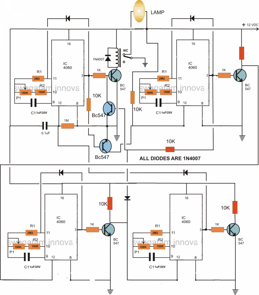
How to Adjust and Set Up
The timer may be adjusted as per the sent request, in the following manner: If we consider the first timing sequence to begin at 7am and end at 12pm, means the upper left timer's P1 needs to be adjusted such that it activates the relay and switches off the relay after exactly 5 hours. Forkeepingthe lamp switched OFF in the above position and switch it ON back at 6 pm we now adjust P1 of the upper right timer section such that its output triggers after another 5 hours. This switches ON the lamp again. The above situation needs to be kept intact until night 10pm, which is about 4 hours of period, therefore we adjust the lower right timer's P1 to get ittriggeredafter 4 hours of time interval. Finally, for initiating the above procedure back again the next morning at 7am, P1 of the last timer at the lower right is adjusted such that it resets the first timer after 9 hours..... and the cycle repeats. For making the circuit work according to the above specified timing pattern, after adjusting the respective hours, the unit should be powered or switched ON exactly at 7 clock in the morning....rest will automatically follow.Simple 12V, 1A SMPS Circuit
The following content explains two simple 12V, 1 Amp switch mode power supply (SMPS) circuit using the very reliable VIPerXX IC from ST microelectronics. With the advent of modern ICs and circuits, the age old iron transformer type of power supply are surely becoming obsolete. Today power supplies are much compact, smaller and efficient with their functioning. Here we discuss one outstanding switch mode power supply circuit which can be easilybuiltat home for deriving clean, ripple free 12 V DC. Thanks to ST Microelectronics IC, the VIPer22A, which has made the construction of truly efficient and compact SMPS powersupplyunit possible that too by using a very few number of electronic parts. As can be seen in the picture, the circuit is indeed very small, compared to the power that is available from it. It's just 50 by 40 mm in its dimensions. The circuit diagram is very easy to understand, let's study it with the following points:1) SMPS using VIPer22A
Looking at the figure we can easily see that theconfigurationdoes not involve too many stages or parts. The input mains AC, as usual is first rectified using ordinary 1N4007 diodes which is fixed in the bridge network mode. The rectified high voltage DC is filtered using the high voltage capacitor. The next stage is the crucial one which incorporates the outstanding chip VIPer22A manufactured by ST Microelectronics. The IC alone functions as theoscillatorand induces a frequency of around 100 KHz into the primary winding of the ferrite E core transformer. The IC isabsolutelyrugged and is internallyprotectedfrom sudden voltage in rush and other voltage relatedcomponenthazards. The IC also incorporates built in over heat protection which makes the IC virtually indestructible. The voltage induced at the input is effectively stepped down at the output winding, due to low eddycurrentlosses, about 1 amp current becomes available from arelativelytiny ferrite transformer. With the coil specs shown the voltage is around 12 and the current is around 1amp. A special feedback circuitry is alsoincludedin the circuit for maintaining high degree of protection and power saving features. The feedback loop is implemented via an opto-coupler which becomes active during abnormal circuit conditions. When the output voltage tends to rise beyond the set threshold the feed back loop becomes operative and feeds an error signal to the IC FB input. The IC instantly comes into an corrective mode and switches off the input to theprimarywinding until the output returns to the normal range. You may also want to read this:24watt, 12V, 2 amp SMPS using a single ICMost recommended for you.Circuit Diagram
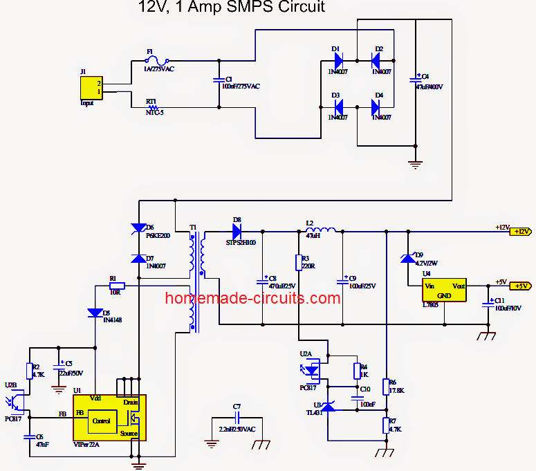
PCB Layout
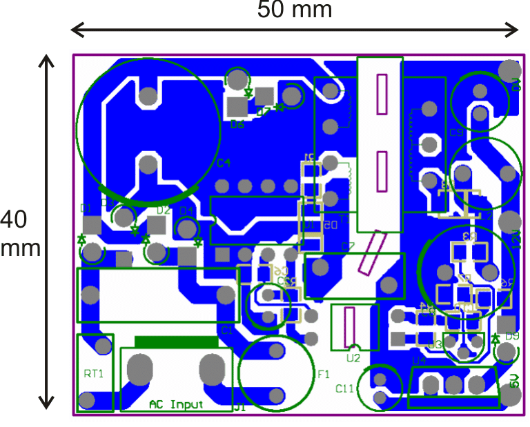
Transformer Winding Data

2) Another 12V 1 amp simple SMPS using IC TNY267

How it Works
The simple smps circuit shown above uses the popular tiny switch IC TNY267. It is a tiny mosfet based 120V to 220V switching oscillator IC which only requires configuring with a ferrite transformer and a stepped down Vdd operating voltage. The design is so simple that a mere visualization of the schematic is enough to tell us the functioning details quickly. The stepped down start voltage is acquired from stabilizing network using a 180V zener diodes and the fast recovery diode BA159 after rectifying the mains 220V through a 1N4007 diodes and the 10uF/400V filter capacitor. As soon as this voltage is applied to the IC, it begins oscillating and its internal mosfet begins switching the ferrite transformer primary at the predetermined oscillating frequency. Being a flyback design, the secondary also starts conducting during the OFF cycles of the primary through mutual induction and generates the required 12V voltage at the output side. This voltage may not be stabilized, therefore an opto-coupler based feedback is used and the link is configured with the exclusive shut down pinout 4 of the IC. This ensures that the output never exceeds, and remains fixed at 12V 1 amp proportion.Transformer Winding Data
The transformer winding is actually quite straightforward, and may be done in the following manner. Keep in mind that the black dots indicate the start points of the winding which is very important, and must be strictly followed while winding the transformer. The primary wound using 36 SWK super enameled copper wire upto 150 turns, while the secondary is wound using 26 SWG wire upto around 12 to 15 turns. The core can be a standardE19type ferrite core having a bobbin with central core cross section area of approximately 4.5mm by 4.5mm.How to Make Simple Solar Cooker at Home
If you are fed-up of ordinary inefficient solar cooker designs and wondering how to make a solar cooker that works in a truly effective way, then probably you have reached the right destination. A low cost solar cooker design that heats up instantly and actually cooks your food in minutes has been meticulously discussed here. When it comes to making of solar cookers, harnessing solar energy most efficiently becomes one big criteria. The idea presented here is perhaps one of the fastest heating solar cooker designs.Making a Super Efficient Solar Cooker
You must have read and studied many different solar cooker designs, but do they really work effectively? Precisely speaking most of them work only under cent percent ideal conditions. Moreover, cooking over many of these cookers look pretty impractical and cumbersome. The main criteria for achieving optimum results with solar heat lies in efficient collection and concentration of sun rays. Solar rays falling straight over a surface may produce just ordinary heating; however collecting them inside an air proof enclosure covered with glass may help enhancing the accumulated heat to more than 50%. This happens because the usual sun rays which are normally made up of long waves make their way successfully through the glass cover into the box but the reflected rays from the container surface are converted to short waves which by the virtue of their property get trapped inside the box and are unable to escape from the glass cover resulting in the increase in temperature of the enclosed area. However, acquiring temperatures up to levels that would actually be suitable for cooking purposes looks a big ask as far as getting it from the natural resources is concerned. Solar cookers made from multilayered boxes with glass covers definitely generate high temperatures inside them, but can never reach temperatures that would cook vegetables or meat optimally. These cookers are good only for heating water or food that��s already cooked, furthermore as already discussed placing and withdrawing food containers over them doesn��t appear clean enough and may cause a lot of discomfort The present content will not only answer the question ��how to make a solar cooker,�� but also a perfect solution to effective cooking using solar power. Let��s peek into the proposed design and see how it works. The design produced here is not new and has been exploited over and over again. As discussed in the previous section the main criteria of effective and maximum concentration of the solar rays over a tight spot is the basis of this design.
How to make a simple solar cooker at home:
Referring to the figure, we see that the main component responsible for generating the intense heating effect is the large dish type cone.The cone may be preferably built using an appropriately sized tin sheet.Cut and turn the tin sheet to make a cone of approximately 4 feet in diameter. Make sure that the conical point produces a small hole or opening for the central pole to pass through it. Secure the edge of the cone with nuts and bolts to make a rigid structure.Fix the cone using clamps over a flat open ground as shown at the site where it is to be installed (where plenty of sunshine is accessible.)A hollow metallic pipe is fixed into the ground through the central opening of the cone. An appropriately sized bowl painted black over its bottom round is fixed through welding at the top end of the pipe as shown in the diagram.This almost completes the simple installation procedure of this super efficient solar cooker system. As the sun rises, the rays incident over the cone��s inner polished surface gets reflected at a certain angle and get concentrated around the top end of the pole where the welded bowl is positioned. The pole will need further adjustments until the concentrated rays perfectly strike the bottom of the bowl.You will find that within minutes the bowl gets heated to appreciable limits and sprinkling water over it sizzles.A super efficient solar cooker is at your disposal, any food you desire may be cooked simply by placing it over the central bowl. Now you know all the tricks regarding how to make a solar cooker that truly works.How to Make a Simple Metal Detector Using IC CS209A
The principle of operation of the proposed metal detector circuit is quite basic yet very interesting. The detecting function is triggered by sensing the decrease in the Q level of the LC network associated with the circuit in the presence of a metal at a specified proximity level.Introduction
Basically the built-in oscillator of the IC CS209 is made functional with the inclusion of a parallel resonant LC tuned network in conjunction with a feedback resistor wired up with the OSC and RF pin outs. The impedance of the tuned resonant network may be expected at the maximum level as long as the driving source frequency is equal to the resonant frequency of the LC circuit network. On detecting the presence of a metallic object at a close proximity to the inductor sensor, the voltage amplitude of the LC network gradually begins to fall corresponding to the closeness of the metal to the inductor. Due to the above factor when the oscillation frame of the chip drops and reaches a certain threshold level, triggers the position of the complementary outputs such that they change states. The precise technical the operations may be understood as follows:
Referring to the figure, as soon as a metal object is detected at the inductor input, the capacitor connected to the DEMOD gets charged through an in built current source of 30 uA.
However during the detection process the above current gets deviated away from the capacitor proportionately with the generated negative bias on the LC network.
Therefore the charge from the capacitor is removed attached to DEMOD with every negative cycle generated across the LC network.
The DC voltage with ripple over the capacitor of the DEMOD is then directly referenced with an internal fixed 1.44 voltage level.
When the procedure forces the internal comparator to trip, it switches the transistor which introduces a 23.6 K Ohms in parallel to the given 4K8 resistor.
This resulting reference level then equals near about 1.2 volts which introduces some sort hysteresis in the circuit, and becomes ideally suited for preventing wrong or false triggering.
The feedback pot connected across the OSC and the RF is used for setting the detection range of the circuit.
Increasing the resistance of the pot, in course increases the range of detection and subsequently the tripping point of the outputs.
However the detection and the trip points may also be dependant on the LC configuration and the Q of the LC network.
The precise technical the operations may be understood as follows:
Referring to the figure, as soon as a metal object is detected at the inductor input, the capacitor connected to the DEMOD gets charged through an in built current source of 30 uA.
However during the detection process the above current gets deviated away from the capacitor proportionately with the generated negative bias on the LC network.
Therefore the charge from the capacitor is removed attached to DEMOD with every negative cycle generated across the LC network.
The DC voltage with ripple over the capacitor of the DEMOD is then directly referenced with an internal fixed 1.44 voltage level.
When the procedure forces the internal comparator to trip, it switches the transistor which introduces a 23.6 K Ohms in parallel to the given 4K8 resistor.
This resulting reference level then equals near about 1.2 volts which introduces some sort hysteresis in the circuit, and becomes ideally suited for preventing wrong or false triggering.
The feedback pot connected across the OSC and the RF is used for setting the detection range of the circuit.
Increasing the resistance of the pot, in course increases the range of detection and subsequently the tripping point of the outputs.
However the detection and the trip points may also be dependant on the LC configuration and the Q of the LC network.
How to Set up the Metal Detector Circuit
The proposed metal detector circuit may be set up initially by following the below described steps: Position a metal object at relatively larger distance away from the inductor, assuming the Q of the LC to be at the maximum sensitivity and the distance to be within the allowable range provided by the Q factor of the inductor. With this set up adjust the pot such that the outputs just shift states indicating the detection of the metal object. Repeat the adjustment procedure by gradually increasing the distance until a suitable maximum sensitivity of the circuit is optimized. Removing or displacing the metal manually should make the output of the circuit to revert states, confirming the perfect working of the circuit. Though the circuit is able to detect metals within a range of 0.3 inches, the range may be suitably increased by increasing the Q of the inductor. The Q factor is directly proportional with the sensitivity of the circuit and the degree of detection.Metal Detector using Ordinary Components
This metal detector simply employs all of the common components, as shown below. It utilizes a 2N2222 transistor and a couple of 741 ICs. Even the detector coil is as simple as it can be! You just need to wind 8 turns of 22 SWG super enameled copper wire over a 9 inch diameter former. After finishing the winding, secure the coil using strapping or a strong adhesive and gently pull it off and remove from the former.
Transistor Q1 works like the main component of a Colpitts oscillator.
Diode D1 rectifies the frequency from the Colpitts oscillator to a certain varying DC.
Op amp U1 works like as a differential amplifier to zero the varying DC, and U2 is used to boost the signal over a 200 ��A meter.
To use the simple metal detector circuit, fine-tune the potentiometer until the meter M1 reaches at the midscaleof the dial.
As soon as a metal object such as gold, tooth fillings, etc come to a close proximity of the coil's field of view, small alterations in the amplitude of the frequency waves trigger changes on the meter reading.
Switch S1 works like an attenuation or sensitivity selection switch.
After finishing the winding, secure the coil using strapping or a strong adhesive and gently pull it off and remove from the former.
Transistor Q1 works like the main component of a Colpitts oscillator.
Diode D1 rectifies the frequency from the Colpitts oscillator to a certain varying DC.
Op amp U1 works like as a differential amplifier to zero the varying DC, and U2 is used to boost the signal over a 200 ��A meter.
To use the simple metal detector circuit, fine-tune the potentiometer until the meter M1 reaches at the midscaleof the dial.
As soon as a metal object such as gold, tooth fillings, etc come to a close proximity of the coil's field of view, small alterations in the amplitude of the frequency waves trigger changes on the meter reading.
Switch S1 works like an attenuation or sensitivity selection switch.
2 Simple Frequency Counter Circuits
A couple of very simple frequency counter circuits are shown below and can be easily built by any electronic enthusiast for the intended purpose. The circuit diagram was provided by Mr.Kapital through an order in Fiverr.com, I was asked to explain the functioning by him.1) Frequency Counter Using IC 74LS47
The first circuit can be understood with the following points: 1. The IC 555 is configured in an astable mutivibrator mode (AMV).
2. AMV is a configuration in which the IC555 generates alternate high and low pulses at its pin number 3.
3. These pulses are simply the generation of positive voltages in succession at a certain rate; say for example 20 positive and negative alternate voltage peaks in one minute.
The capacitor and resistor values can be adjusted for adjusting the generated pulse rate.
4. In the circuit the 74LS90and 74LS47 are used for counting the above pulses from the IC555.
5. The IC74LS90 accepts the pulses from the IC555 at its input pin no.14.
6. Its internal circuit converts these pulses in the form of special codes (binary) and fed in a certain sequence to the decoder IC 74LS47 through its output pin no.12,9,8,11.
7. The above codes are accepted by the decoder IC 74LS47 at its input pin nos.7,1,2,6 in the same above sequence.
8. The IC74LS47 now decodes this binary information and illuminates the LED display bars in such a way that it starts displaying the numbers 1 to 9 in response to the pulses generated by the IC555, meaning, the first pulse from the IC555 displays a no.1 over the right hand side display, the next pulse makes it display the number 2, then 3 and so on until the display reaches the number 9.
9. During the above procedure the left hand side display continues to show the number zero.
10. However the moment the right hand side display reaches the number 9, the next pulse overflows from pin 11 of the right IC74LS90 and becomes available to pin 14 of the left IC 74LS90 which now repeats the above procedure.
11. So now the left hand side begins continuing the counting by displaying the numbers 1 to 9 and we witness the ongoing counting with the displays modules together showing the number 11 until the number 99.
12. That's the maximum number of digits the shown counter design can display at the maximum.
13. For making the counter a three digit counter or a four digit counter, simply the above stages may be added in the same pin out sequence as the two modules are connected in the given diagram.
14. The input at the pin 14 of the first module can be replaced with any type of pulse that needs to be monitored or which needs to be counted.
The pins of the ICs which are connected to the positive and the negative points of the power supply are the supply input pins of the respective ICs which require precisely 5 volts for operating.
The resistors R1 to R7 on each display are connected for limiting current to the display LEDs so that a constant illumination is maintained and also for safeguarding the display LEDs from getting damaged.
1. The IC 555 is configured in an astable mutivibrator mode (AMV).
2. AMV is a configuration in which the IC555 generates alternate high and low pulses at its pin number 3.
3. These pulses are simply the generation of positive voltages in succession at a certain rate; say for example 20 positive and negative alternate voltage peaks in one minute.
The capacitor and resistor values can be adjusted for adjusting the generated pulse rate.
4. In the circuit the 74LS90and 74LS47 are used for counting the above pulses from the IC555.
5. The IC74LS90 accepts the pulses from the IC555 at its input pin no.14.
6. Its internal circuit converts these pulses in the form of special codes (binary) and fed in a certain sequence to the decoder IC 74LS47 through its output pin no.12,9,8,11.
7. The above codes are accepted by the decoder IC 74LS47 at its input pin nos.7,1,2,6 in the same above sequence.
8. The IC74LS47 now decodes this binary information and illuminates the LED display bars in such a way that it starts displaying the numbers 1 to 9 in response to the pulses generated by the IC555, meaning, the first pulse from the IC555 displays a no.1 over the right hand side display, the next pulse makes it display the number 2, then 3 and so on until the display reaches the number 9.
9. During the above procedure the left hand side display continues to show the number zero.
10. However the moment the right hand side display reaches the number 9, the next pulse overflows from pin 11 of the right IC74LS90 and becomes available to pin 14 of the left IC 74LS90 which now repeats the above procedure.
11. So now the left hand side begins continuing the counting by displaying the numbers 1 to 9 and we witness the ongoing counting with the displays modules together showing the number 11 until the number 99.
12. That's the maximum number of digits the shown counter design can display at the maximum.
13. For making the counter a three digit counter or a four digit counter, simply the above stages may be added in the same pin out sequence as the two modules are connected in the given diagram.
14. The input at the pin 14 of the first module can be replaced with any type of pulse that needs to be monitored or which needs to be counted.
The pins of the ICs which are connected to the positive and the negative points of the power supply are the supply input pins of the respective ICs which require precisely 5 volts for operating.
The resistors R1 to R7 on each display are connected for limiting current to the display LEDs so that a constant illumination is maintained and also for safeguarding the display LEDs from getting damaged.
2) Frequency Counter Circuit Using a Single IC 4033
The next circuit shown below can be used for measuring or counting frequency or Hz. The IC is very simple to make andutilizesjust a single IC 4033 and a common cathode display as the mainingredients.Introduction
If higher frequencies in the the order of two or threedigitsare required to be measured, then simple the number of modules can be connected in series as described.The simple frequency counter circuit shown below will effectively convert any pulse at its input into a display over the 7- segment cathode block.The IC has an internal BCd to 7 segment translator which directly converts the pulses at its input to readable numerical bars at the connected display block.Circuit Operation
A single IC 4033 is able to handle only one common cathode display block and therefore the shown circuit is able to show numbers from 0 to 9 in response to the relevant clocks applied at its input. The IC may be easily reset at any point. For example suppose 6 clocks were applied at the input and the the display now reads 6, it can be reverted to zero simply by pressing the shown push button, if needed. Pin #1 is the input where the clock or the pulses are applied for counting. In order to make the counter able to count to two digit or 3 digit or 4 digit etc. just include integrate the relevant number of modules as shown in the diagram and connect their outputs in the following manner: Connect pin #5 of the first module to the clock input of the next module and connect pin #5 of the second module to clock input of the third module and so on. Make the reset pins common, so that a single push button can be used for resetting all the modules at once. Supply terminals will also need to be made into common rails. A capacitor of 0.1uF should be connected close to the supply rail for decoupling purpose.Circuit Diagram
Cellphone Detector Circuit
A cellphone or mobile phone detector is actually a high gain op amp amplifier which detects slightest of RF disturbance from a mobile phone, and illuminates an LED. NOTE: This concept was first developed by me and later on the idea was COPIED by many reputed website. Mobile phones today being the major generator of RF interference is easily picked up by this circuit and can be seen through an LED illumination at the output of the circuit.Working Concept
The concept behind the working of this mobile phone detector is a highly sensitive comparator circuit which is unstable at its input due to high sensitivity, such that it turns ON even with the minutest electrical interference in the atmosphere around it. Since it is designed to detect mobile phone signals one may misinterpret it to be detecting the GHz signals, actually it's not, and it simply can't. Even if the mobile phone signals may be oscillating at GHz levels, the signal is still a radio frequency (RF), having the properties of electrical interference. It is this electrical interference that is picked up by the op amp input, and converted into a DC output, for illuminating the LEDCircuit Description
The circuit is basically a simple high gain inverting amplifier, built around the IC LM 324. Only two of its op amps may be incorporated, however for making the circuit extremely sensitive, all four of its opamps have been rigged in series. Looking at the figure we see actually the the circuit is a repetition of four identical circuits in series. So we would only want to study the basic concept of the any one of the stages consisting just one op amp. NOTE: Using 4 op amp stages can make the design extremely sensitive and the circuit may start sensing all sorts of RF signal that may be present in the atmosphere.
Therefore I recommend using only 3 op amp stages in series for this project.
NOTE: Using 4 op amp stages can make the design extremely sensitive and the circuit may start sensing all sorts of RF signal that may be present in the atmosphere.
Therefore I recommend using only 3 op amp stages in series for this project.
Parts List
All R1 = 100K 1/4 watt All R2 = 2.2 Meg or any value between 1 Meg and 10 Meg (1/4 watt) All C1 = 0.01uF, or 103 ceramic disc or PPC, any type will do. A1 --- A4 = LM324 IC IC LM324 Pinouts
As mentioned in the earlier part of this article, the op amp is configured as a high gain non inverting amplifier, where the input is received at the pin #2 which is the inverting input of the op amp.
The RF disturbances in the air is received by the antenna and fed to the inverting input of the op amp which is amplified by the circuit to some specified level depending on the value of the feed back resistor across the output and the inverting input of the op amp.
Increasing the value of this resistor increases the sensitivity of the circuit, however too much sensitivity can make the circuit unstable and induce oscillations.
The amplified signal is fed to the input of the next stage which is just a replica of the previous stage.
IC LM324 Pinouts
As mentioned in the earlier part of this article, the op amp is configured as a high gain non inverting amplifier, where the input is received at the pin #2 which is the inverting input of the op amp.
The RF disturbances in the air is received by the antenna and fed to the inverting input of the op amp which is amplified by the circuit to some specified level depending on the value of the feed back resistor across the output and the inverting input of the op amp.
Increasing the value of this resistor increases the sensitivity of the circuit, however too much sensitivity can make the circuit unstable and induce oscillations.
The amplified signal is fed to the input of the next stage which is just a replica of the previous stage.
Why it is so Sensitive
It's due to the 4 series op amp stages which helps to make the circuit highly sensitive an this can pick up cellphone RF from a distance of 10 meters. Here the relatively weaker signals from the first stage is further enhanced and made stronger so that now it may be fed to the third stage for repeating the actions that is for further amplification until the last stage whose output illuminate an LED, displaying the presence of even the minutest possible RF disturbance in the air. UPDATE: After a lot of experimentation I finally realized that creating a long range cell phone detector wasn't feasible. It's because the modern phones have a high grade RF shielding, which allows only very little RF to leak out from the phone. Therefore the RF do not reach too far in the atmosphere making it impossible to detect them beyond a few inches from the phone. To improve the distance I tried making the circuit more sensitive by adding more stages in series, but that didn't work. Because higher sensitivity meant the circuit started detecting many different existing RF disturbances in the air, which kept the LED flickering all the time.Video Demo
The Finalized Circuit
The finalized tested design can be seen below, it is exactly similar to a WiFi detector circuit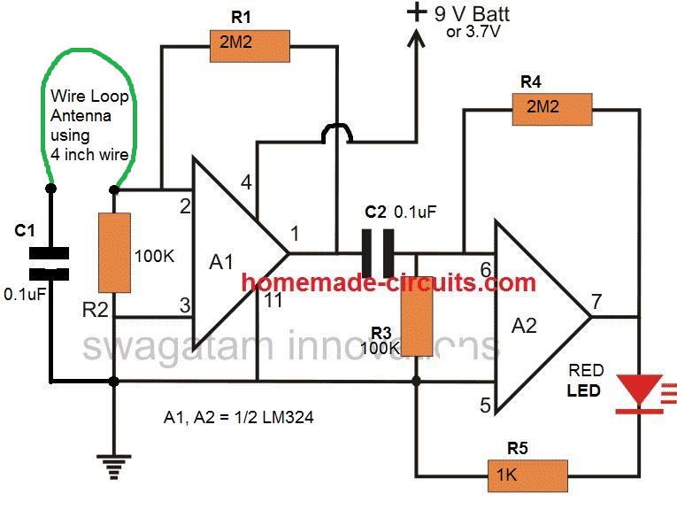
How to Assemble the Circuit
The discussed circuit of cell phone RF signal detector, sensor is very easy to build and requires minimal knowledge of electronic for going about with the procedures. It is built with the following instruction: After procuring the given components, fix them over the piece of general PCB in the following manner: Take the IC first, and carefully insert its legs inside the PCB holes through proper alignment. Solder the leads of the IC. Now as per the diagram start connecting the resistors and capacitors one by one to the pin outs of the IC, remember that from the component side of the PCB, the pin out will be just the opposite to what it is from the track side, so be careful with the pin out designations and connections.How to Test
Once it is assembled, it��s all about connecting the board to a 9 volt battery and confirming the results. For this you may make a call from your cell phone or just call to know your balance report, the LED in the circuit should hopefully start responding to the cell phones generated RF signals. Alternatively, you may try clicking your kitchen gas lighter very close to the antenna of the circuit; the LED could be seen flashing with the clickings of the gas lighter. Another way of checking the circuit would be to take it near your mains electric board, the LED should light up when brought even withing a feet near to the board indicating the presence of the mains field and confirming the working of the circuit. Note: The coil L1 can be made from any gauge wire, just a few turns of any diameter between 5 to 9mm will do.RF Sniffer using a Single Op Amp
While the RF mobile detector circuit was primarily meant to indicate the existence of RF emissions, this circuit is implemented for several different functions, such as testing car security keys and as a bug detector. The RF sniffer circuit is so sensitive that it can pick up fields as low as to 1 mW at 1 m distance and from around 100 kHz to 500 MHz signals.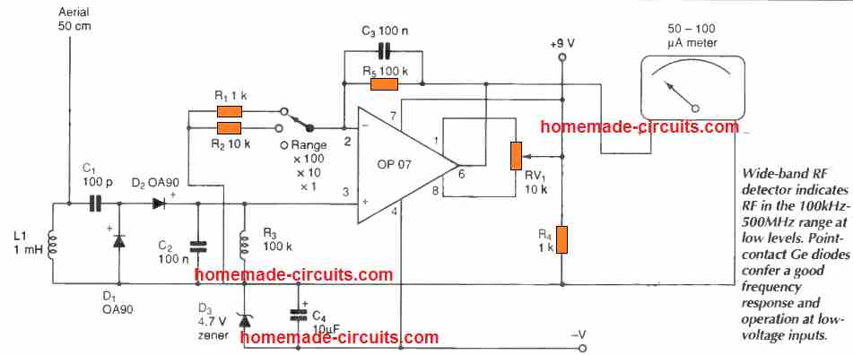 Essentially, it is just a broad -band input circuit, a rectifier and meter, nevertheless for achieving required sensitivity an amplifier is necessary and the diodes should be accurately selected.
Germanium diodes are able to operate even at lower forward voltages compared to the silicon types, and frequency response is bigger using point contact devices, therefore point -contact, germanium 0A90 diodes happen to be the best alternative.
A 1 mH inductor over the input minimizes LF sensitivity, as does the feedback capacitor.
Adjusting the meter offset is not important, nonetheless it will enable the nulling of unwanted frequencies.
The meter might require series resistance to fine-tune sensitivity.
The display reading may not be linear and will only help to indicate the presence of RF and the relative power of the RF.
Essentially, it is just a broad -band input circuit, a rectifier and meter, nevertheless for achieving required sensitivity an amplifier is necessary and the diodes should be accurately selected.
Germanium diodes are able to operate even at lower forward voltages compared to the silicon types, and frequency response is bigger using point contact devices, therefore point -contact, germanium 0A90 diodes happen to be the best alternative.
A 1 mH inductor over the input minimizes LF sensitivity, as does the feedback capacitor.
Adjusting the meter offset is not important, nonetheless it will enable the nulling of unwanted frequencies.
The meter might require series resistance to fine-tune sensitivity.
The display reading may not be linear and will only help to indicate the presence of RF and the relative power of the RF.
Simple Analogue Weighing Scale Machine
Learn a super simple procedure to make a weighing scale device useful for measuring smaller magnitudes of weight.The Concept
The concept is very simple, a light beam is allowed to pass through a linearly colored ribbon and fall over an LDR. The color shade of the ribbon positioned in front of the light source at any instant will depend on the weight placed over a spring loaded mechanism. The corresponding change in the light level is converted into a corresponding difference in the resistance of the LDR which is ultimately read over an Ohmmeter and the equivalent weight is determined. A digital weighing scale is an indispensable device as far as determining smaller magnitude of weights is concerned. However these gadgets can be too sophisticated and expensive to procure. A simple design idea of a weighing scale presented here promises to be equally accurate yet very cheap. We all have seen this machine very commonly used with most of the shopkeeper and retailers. It is used for determining the weights of the various materials being sold to the customers so that the items may be correctly rated as per the displayed weight over the machine. This incredible device is able to detect even the minutest magnitude of weight placed over it and accurately displays it over a digital scale. Yes we are discussing weighing scales normally used for weighing smaller weights ranging from probably mgs up to a few kgs.Simple Weighing Sale Design vs Commercial Design
The commercially available weighing scales are rather too sophisticated, accurate and therefore very costly too. The design of a simple electronic analogue weighing scale presented here has been devised by me and is pretty accurate, very low cost and can be constructed even by a layman. The idea is simple �C a linearly colored semi-transparent ribbon is made to move or dip in response to the pressing weight, a light beam from a light source is allowed to pass through this ribbon and fall over an LDR. The LDR is connected across an Ohm meter, so, as the weight pushes the ribbon, it slides down and settles at a particular point and offers a particular corresponding shade in front of the light source. The light intensity is optimized according to the darkness or lightness of this shade and the LDR reads the proportionate light intensity level and directs it to the meter so that it may be directly read over its calibrated dial.How the Weighing Scale Circuit is Designed to Work
Let��s try to understand the actual functioning of the designed prototype: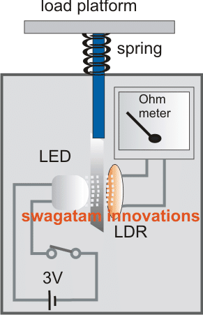 Referring to the homemade weighing scale circuit above, we see that the arrangement is pretty straight forward.
A central pillar or shaft which forms the main and the sole moving part of the system passes through an appropriately sized hole made over the top surface of the cabinet.
The external end of this rod terminates into a flat platform which forms the base for keeping the weights under question.
The rod and the platform are held in a rigid posture by a spring positioned in between the platform and the cabinet top surface.
The shaft actually passes through this spring.
The spring is required so that the weights are properly optimized and the level of the platform returns to its original position once the weight is removed.
A linearly colored or darkened translucent ribbon which forms the heart of the entire mechanism is connected to the inner end of the above movable shaft.
Also a white LED (used as a light source) and an LDR (light receiving component) are positioned exactly opposite, facing each other and partitioned by the ribbon.
An analogue moving coil type meter configured as an Ohm meter or a resistance meter is integrated with the LDR.
The LED is powered through a cell and is switched ON when in use.
The light beam produced from the LED passes through the ribbon and falls over the LDR and a corresponding value is displayed over the meter depending upon the opacity of the ribbon.
When there��s no weight placed over the platform, the spring mechanism keeps the shaft in a position that produces the darkest shade from the ribbon in the path of the LED beam and therefore the meter also reads a minimum or zero value over its calibration.
The moment a weight on this weighing scale is placed, the shaft dips proportionately and the ribbon slides down to produce a linearly changing shade in front of the LED light beam and finally settles down to a corresponding lighter shade level.
The operation is instantly translated over the meter to provide the equivalent value of the weight being measured.
Referring to the homemade weighing scale circuit above, we see that the arrangement is pretty straight forward.
A central pillar or shaft which forms the main and the sole moving part of the system passes through an appropriately sized hole made over the top surface of the cabinet.
The external end of this rod terminates into a flat platform which forms the base for keeping the weights under question.
The rod and the platform are held in a rigid posture by a spring positioned in between the platform and the cabinet top surface.
The shaft actually passes through this spring.
The spring is required so that the weights are properly optimized and the level of the platform returns to its original position once the weight is removed.
A linearly colored or darkened translucent ribbon which forms the heart of the entire mechanism is connected to the inner end of the above movable shaft.
Also a white LED (used as a light source) and an LDR (light receiving component) are positioned exactly opposite, facing each other and partitioned by the ribbon.
An analogue moving coil type meter configured as an Ohm meter or a resistance meter is integrated with the LDR.
The LED is powered through a cell and is switched ON when in use.
The light beam produced from the LED passes through the ribbon and falls over the LDR and a corresponding value is displayed over the meter depending upon the opacity of the ribbon.
When there��s no weight placed over the platform, the spring mechanism keeps the shaft in a position that produces the darkest shade from the ribbon in the path of the LED beam and therefore the meter also reads a minimum or zero value over its calibration.
The moment a weight on this weighing scale is placed, the shaft dips proportionately and the ribbon slides down to produce a linearly changing shade in front of the LED light beam and finally settles down to a corresponding lighter shade level.
The operation is instantly translated over the meter to provide the equivalent value of the weight being measured.
Simplifying the Weighing Machine even Further
In the above example it is clearly evident that the main weighing scale element is the spring, and a spring can be considered pretty accurate and long lasting compared to any other form of compression based sensor. Therefore if a good quality spring is used we can assume the output to be extremely accurate and consistent throughout its life. Based on the above confederation we can go a step ahead and make the above LDR LED based design even more simpler, as shown below.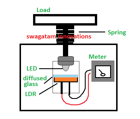 In the figure above, we can see a spring mechanism system fixed over a box, the weighing surface fixed over the spring, and the central spindle of the load surface going inside the box, and terminating into a LED point.
The LED may be powered with an external 3V supply from a DC power supply source connected through flexible wires.
Under the LED we can see an LDR positioned such that the LED can move closer or farther away from this LDR depending on the spring tension or the variation levels on the spring causes by the load.
The LDR wires are interfaced with a suitably calibrated Ohmmeter.
In the figure above, we can see a spring mechanism system fixed over a box, the weighing surface fixed over the spring, and the central spindle of the load surface going inside the box, and terminating into a LED point.
The LED may be powered with an external 3V supply from a DC power supply source connected through flexible wires.
Under the LED we can see an LDR positioned such that the LED can move closer or farther away from this LDR depending on the spring tension or the variation levels on the spring causes by the load.
The LDR wires are interfaced with a suitably calibrated Ohmmeter.
How this Weighing Scale Works
The concept looks pretty obvious and clear, and is quite self explanatory. With no load on the weighing surface, the spring pulls the LED upwards away from the LDR at a maximum possible distance, which causes minimum incident light on the LDR surface. This low light level is shown as almost zero on the Ohm meter. Once a load is kept on the weighing surface, depending on the weight of the load the spring is depressed downward causing the LED to move closer to the LDR at a specified positioned. This causes the LDR to change its resistance proportionately, which can be identified on the ohm meter and calculated as a direct equivalent reading for the load's weight.Simple Solar Tracker System �C Mechanism and Working
The circuit and the mechanism explained in this article may be considered as the easiest and perfect dual axis solar tracker system.How the Dual Axis Solar Tracker Concept Works
The device is able to track the daytime motion of the sun precisely and shift in the vertical axis accordingly. The device also effectively tracks the seasonal displacement of the sun and moves the entire mechanism in the horizontal plane or in a lateral motion such that the orientation of the solar panel is always kept in a straight axis to the sun so that it complements the vertical actionsof the tracker appropriately.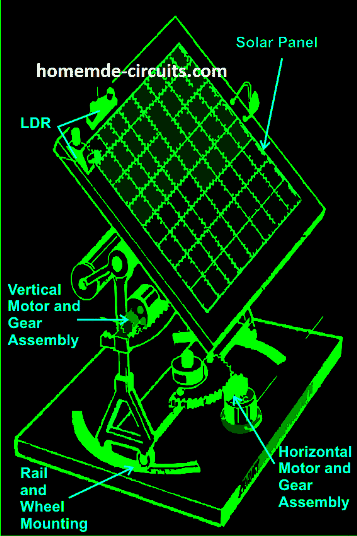 As shown in the figure, a relatively easy mechanism can be witnessed here.
The solar tracker is basically mounted over a couple of stand with a central movable axis.
The pivotal arrangement allows the panel mounts to move on a circular axis over almost 360 degrees.
A motor gear mechanism as shown in the diagram is fitted just at the corner of the pivotal axis in such a way that when the motor rotates the entire solar panel shifts proportionately about its central pivot, either anticlockwise or clockwise, depending upon the motion of the motor which in turn depends on the position of the sun.
As shown in the figure, a relatively easy mechanism can be witnessed here.
The solar tracker is basically mounted over a couple of stand with a central movable axis.
The pivotal arrangement allows the panel mounts to move on a circular axis over almost 360 degrees.
A motor gear mechanism as shown in the diagram is fitted just at the corner of the pivotal axis in such a way that when the motor rotates the entire solar panel shifts proportionately about its central pivot, either anticlockwise or clockwise, depending upon the motion of the motor which in turn depends on the position of the sun.
How the LDR Circuit Works
The position of the LDRs are critical here and the set of LDR which corresponds to this vertical plane movement is so positioned that it senses the sun light accurately and tries to keep the panel perpendicular to the sun rays by moving the motor in the appropriate direction through a definite number of stepped rotations. The LDR sensing is actually accurately received and interpreted by an electronic circuit which commands the motor for the above explained actions. Another mechanism which is quite similar to the above vertical setting, but moves the panel through a lateral motion or rather it moves the whole solar panel mount in circular motion over the horizontal plane. This motion takes place in response to the position of the sun during the seasonal changes, therefore in contrast to the vertical movements; this operation is very gradual and cannot be experienced on a daily basis. Again the above motion is in response to the command given to the motor by the electronic circuit which operates in response to the sensing done by the LDRs. For the above procedure a different set of LDRs are used and are mounted horizontally over the panel, at a specific position as shown in the diagram.How the Solar Tracker OpAmp Control Circuit Functions
A careful investigation of the circuit shown in the diagram reveals that the whole configuration is actually very simple and straightforward. Here a single IC 324 is utilized and only two of its opampsare employed for the required operations.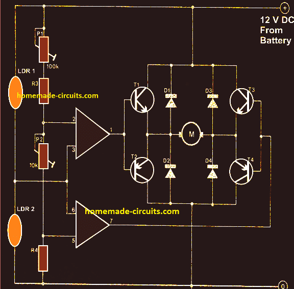 The opamps are primarily wired to form a kind of window comparator, responsible for activating their outputs whenever their inputs waver or drift out of the predetermined window, set by the relevant pots.
Two LDRs are connected to the inputs of the opamps for sensing the light levels.
As long as as the lights over the two LDRs are uniform, the outputs of the opamp remain deactivated.
However the moment one of the LDRs senses a different magnitude of light over it (which may happen due to the changing position of the sun) the balance over the input of the opamp shift toward one direction, immediately making the relevant opamps output go high.
This high output instantly activates the full bridge transistor network, which in turn rotates the connected motor in a set direction, such that the panel rotates and adjusts its alignment with the sun rays until uniform amount of light is restored over the relevant set of LDRs.
Once the light level over the relevant LDR sets is restored, the opamps again become dormant and switch off their outputs and also the motor.
The above sequence keeps on happening for the whole day, in steps, as the sun alters its position and the above mechanism keeps shifting in accordance to the suns position.
It should be noted that two sets of the above explained circuit assemblies will be required for controlling the dual actions or simply to make the above discussed dual tracker solar system mechanism.
Parts List
R3 = 15K,
R4 = 39K,
P1 = 100K,
P2 = 22K,
LDR = Normal type with a resistance of around 10 K to 40K in daylight under shade and infinite resistance in complete darkness.
Op-ampsare from IC 324 or separately two 741 ICs may also be incorporated.
T1, T3 = TIP31C,
T2,T4 = TIP32C,
All diodes are 1N4007
Motor = As per the load and size of the solar panel
Courtesy - Elector Electroniks India
The opamps are primarily wired to form a kind of window comparator, responsible for activating their outputs whenever their inputs waver or drift out of the predetermined window, set by the relevant pots.
Two LDRs are connected to the inputs of the opamps for sensing the light levels.
As long as as the lights over the two LDRs are uniform, the outputs of the opamp remain deactivated.
However the moment one of the LDRs senses a different magnitude of light over it (which may happen due to the changing position of the sun) the balance over the input of the opamp shift toward one direction, immediately making the relevant opamps output go high.
This high output instantly activates the full bridge transistor network, which in turn rotates the connected motor in a set direction, such that the panel rotates and adjusts its alignment with the sun rays until uniform amount of light is restored over the relevant set of LDRs.
Once the light level over the relevant LDR sets is restored, the opamps again become dormant and switch off their outputs and also the motor.
The above sequence keeps on happening for the whole day, in steps, as the sun alters its position and the above mechanism keeps shifting in accordance to the suns position.
It should be noted that two sets of the above explained circuit assemblies will be required for controlling the dual actions or simply to make the above discussed dual tracker solar system mechanism.
Parts List
R3 = 15K,
R4 = 39K,
P1 = 100K,
P2 = 22K,
LDR = Normal type with a resistance of around 10 K to 40K in daylight under shade and infinite resistance in complete darkness.
Op-ampsare from IC 324 or separately two 741 ICs may also be incorporated.
T1, T3 = TIP31C,
T2,T4 = TIP32C,
All diodes are 1N4007
Motor = As per the load and size of the solar panel
Courtesy - Elector Electroniks India
How to Add a Set/Reset Facility in the Above Circuit
At the first glance it might appear that the above circuit does not incorporate an automatic resetting feature. However a closer investigation will show that actually this circuit will reset automatically whendawn setsin or in themorningdaylight. This might be true due to the fact that the LDRs are positioned inside enclosures which arespecfiiallydesigned in a "V" shape for facilitating this action. From the reflection of of the rising sun light, during morning hours the sky gets more illuminated than the ground. Since the LDRs are positioned in "V" manner, the LDR which faces more toward the sky receives more light than the LDR which faces toward the ground.This situation activates the motor in the opposite direction, such that it forces the panel to revert in the early morning hours. As the panel reverts towards the east, the relevant LDR begins getting exposed to even more ambient light from the rising sunlight, this pushes the panel even harder toward the east until both LDR are almost proportionately exposed toward the east rising sunlight, this completely resets the panel so that the process begins all over again.Set Reset Function
In case a set reset feature becomes imperative, thefollowingdesign may be incorporated. The set switch is placed at the "sun-set" end of the tracker, such that it gets depressed when the panel finishes it's days tracking. As can be seen in the below given figure, the supply to the tracker circuit is been given from the N/C points of the DPDT relay, it means when the 'SET" switch is pushed, the relay activates and disconnects the supply to the circuit so that the entire circuit shown in the above article now gets disconnected and does not interfere. At the same time, the motor receives the reversing voltage via the N/O contacts so that it can initiate the reversing process of the panel to its original position. Once the panel finishes its reversing process toward the "sun-rise" end, it pushes the reset switch placed suitably somewhere at that end, this actiondeactivatesthe relay again resetting the entire system for the next cycle.Make a Simplest Temperature Indicator Circuit
A very simple temperature indicator circuit can be built by interconnecting a single transistor, a diode and a few other passive components.Using Transistor as a Heat Sensor
As we know that all semiconductors have this "bad habit�� of changing its basic characteristics in response to ambient temperature changes. Especially basic electronic components like transistors and diodes are very much prone to their case temperature variations. The change with their characteristics with these devices is typically in terms of the passage of voltage through them, which is directly proportional with the magnitude of the temperature difference surrounding them.Using a Transistor (BJT) as the Temperature Sensor
In the present design a diode and a transistor are configured in the form of a bridge network.
 As both these active parts have identical properties as far as ambient temperature changes are concerned, they both complement each other.
Using Diode for Creating a Reference Voltage
The diode is place as the reference device while the transistor is connected to perform the function of a temperature sensor. Obviously since the diode is placed as the reference, it has to be placed in an environment with relatively consistent temperature conditions, otherwise the diode will also start changing its reference level causing error in the indication process. A LED is used here at the collector of the transistor, which directly interprets the transistor conditions and therefore helps to show how much temperature difference is taking place around the transistor.LED Indicates the Temperature Change
The LED is used to get a direct indication of the temperature level sensed by the transistor. In this design the diode is placed at the ambient temperature or at the room temperature which the transistor is placed or attached to the heat source which needs to be measured. The base emitter voltage of the transistor is effectively compared with the reference voltage level produced by the diode at the junction of D1 and R1. This voltage level is taken as the reference and the transistor remains switched OF as long as its base emitter voltage remains below this level. Alternatively this level may be varied by the preset P1. Now as the heat over the transistor starts rising it base emitter starts rising due to the altering characteristic of the transistor. If the temperature crosses the preset value, the base emitter voltage of the transistor exceeds the limit and the transistor starts conducting. The LEDs gradually begins to illuminate and its intensity becomes directly proportional to the temperature over the transistor sensor.Caution
Caution must be maintained, not to exceed the temperature over the transistor above 120 degree Celsius, other wise the device may get burnt and damaged permanently. The proposed simple temperature indicator circuit can be further modified for making it switch an external appliance ON or OFF in response to the sensed temperature levels.How to Calculate the Temperature Thresholds
I will discuss it in my forth coming articles. The resistor values of the configuration is calculated using the following formula: R1 = (Ub - 0.6)/0.005 R2 = (Ub - 1.5)/0.015 Here Ub is the input supply voltage, 0.6 is the forward voltage drop of the BJT, 0.005 is the standard operating current for the BJT. Similarly, 1.5 is the forward voltage drop for the selected RED LED, 0.015 is the standard current for illuminating the LED optimally. The calculated results will be in Ohms. The value of P1 may be anywhere between 150 to 300 OhmsVideo Clip
2 Simple Earth Leakage Circuit Breaker (ELCB) Explained
The discussed Earth leakage circuit breaker diagrams will monitor the leakage current level of the earthing line of your house electrical sockets and will trip the appliances as soon a fault is detected. Here we will learn 2 designs, first using transistors only and the second using IC LM324.Introduction
If anything goes wrong with them it will instantly switch off the mains and stop any further associated loss. A simple ELCB circuit is discussed here. A simple circuit of an Earth leakage circuit breaker also called ground fault circuit interrupter is discussed in this article. The circuit once built and installed will silently monitor the ��health�� of the earth connection of your house and the connected appliance. The circuit will immediately switch off the mains on detecting a missing earth connection or a current leakage through the appliance body.Why You Need an ELCB
A leaking current through earth terminal is probably more dangerous than a short circuit in a domestic wiring. A short circuit hazard is visible and mostly tackled through a fuse or a circuit breaker unit. But earth current leakages may remain hidden for years, eating up your precious electricity and also weakening or deteriorating the wiring conditions and also the appliances. Moreover if the earth connection is not properly grounded due to improper conduction or breakage, the leakage may turn into a lethal shock over the body of the appliance.Cons of Commercial ELCB Units
Commercially available earth leakage circuit breaker units are very costly and bulky, involving complicated installation procedure. I have designed a simple circuit which is low in cost and yet handles the situation handsomely. The device will detect any current exceeding above 5mA through the earth passage and switch off the mains. The connected appliance will then need a diagnose or a total elimination. A leaking appliance not only wastes your electricity but also can be dangerous fatally. Circuit diagram using Transistors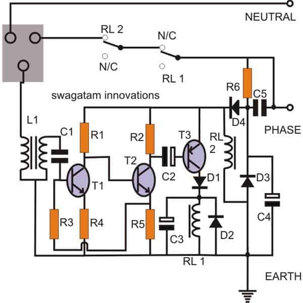
Circuit Operation
The proposed ground fault circuit interrupter or ELCB utilizes a simple principle of detecting the AC signal rather the applied or the leaking voltage. Here, the leaking AC may be too small to be detected as a potential difference using simple voltage detection configuration, therefore the leakage is effectively sensed as a frequency, using a simple audio amplifier stage. As shown in the diagram, a simple bootstrapped amplifier network forms the main sensing stage of the unit. Transistors T1 and T2 along with the associated passive components are wired up into a small two stage amplifier. The introduction of R3 becomes very crucial as it provides a positive feed back to the input making the circuit more stable and respond to minutest input signals. The inductor L1 basically has two windings, the primary which is connected to the earth point of the socket has less number of turns, the secondary winding has six times more number of turns and is integrated to the input of the circuit via C1. The role of L1 is to amplify any AC induced into its primary winding which can only happen in case of a leakage through the body of an appliance connected to the socket. The above amplified leakage voltage is further amplified to a level enough to activate RL1, instantly disabling the input to the appliance and indicating the earth leakage fault. Capacitor C5 along with D3 and C4 forms a standard transformerless power supply to power the circuit. D3 performs a dual function of rectification and surge suppression. Interestingly the main earth connection itself becomes the negative of the circuit instead of the neutral line. Also since RL2 is directly connected to the supply across the positive of the circuit and the earthing, simply means that if the earthing becomes weak or disconnected, the relay will deactivate, cutting off the AC mains to the appliance, so it effectively indicates the health of the earthing and safeguards the house from faulty or missing earth connections.ELCB Circuit Parts List.
R1 = 22K, R2 = 4K7, R3 = 100K, R4 = 220E, R5 = 1K, R6 = 1M, C1 = 0.22/50V, C2 = 47UF/25V, C4 = 10uF/250V, C5 = 2UF/400V PPC, T1, T2 = BC 547B, T3 = BC 557B, Relays = 12V, 400 Ohm, SPDT, All Diodes are = 1N4007, L1 = Coil wound over a bobbin used normally with E-cores (smallest size,) begin winding 50 turns of 25 SWG wire first, tie it up and solder it to produce the primary terminals at one side of the bobbin. Now using 32 SWG copper wire, wind 300 turns over the primary winding, as before tie the ends to the other side of the bobbin by soldering. Insert and fix the coil within the E-cores. Secure it tightly using PVC tapeHow to Make a Homemade Earth Leakage Breaker (ELCB) Unit Using IC 324
An earth leakage circuit breaker is a safety electrical device used for monitoring current leakages through the ��earthing�� terminal and switching OFF the mains when this leakage exceeds a certain dangerous level.Introduction
Normally electromechanical concepts are employed for making these devices, however here we will see how an ELCB can be made by using ordinary electronic components; we will also see why an electronic counterpart is more efficient than the commercial electromechanical units. There are three versions through an electronic ELCB can be made, the first uses a relay for the switching actions, the second idea incorporate a Triac and the third concept employs a SSR or a solid state relay for the required implementations. For all the above concepts, the triggering feature remains the same, through an input inductor stage.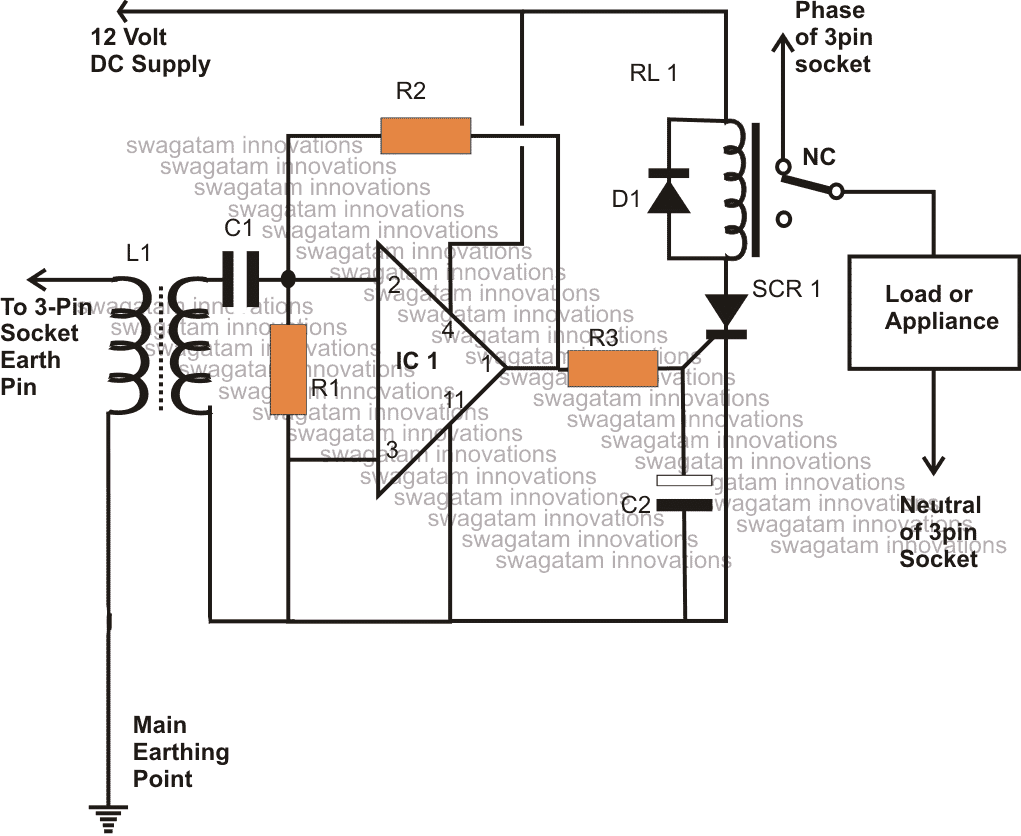
ELCB Circuit Using Relay
Looking at the figure we can see that the entire circuit is concentrated around a single Opamp from the IC 324. The opamp is configured as a high gain inverting amplifier. The opamp is configured as a high gain AC amplifier and its sensitivity can be adjusted by varying the value of R2, increasing its value increase the sensitivity of the circuit. Any minute AC signal that may be present at the inverting input #2 of the IC is picked via the coupling capacitor C1 and instantly amplified by the IC. A small inductor transformer is wired across the above input of the IC. The primary of the inductor is connected to the wire which finally terminates to the earthing terminal or the pin of the various 3-pin sockets in the premise. The transformer can be an ordinary output transformer used in small radio receiver��s output amplifier stage. In case of a leakage, the leaking current passes through the primary winding of the inductor and gets stepped up at the secondary winding. The stepped up induced AC is immediately sensed by the IC input and further amplified to the desired levels, so that the SCR switches in response to the triggering. The SCR, due to its inherent property instantly latches and pulls the relay into conduction. The relay conducts and switches OFF the mains power to the three pin sockets, switching of the appliances and thus eliminating earth leakage conditions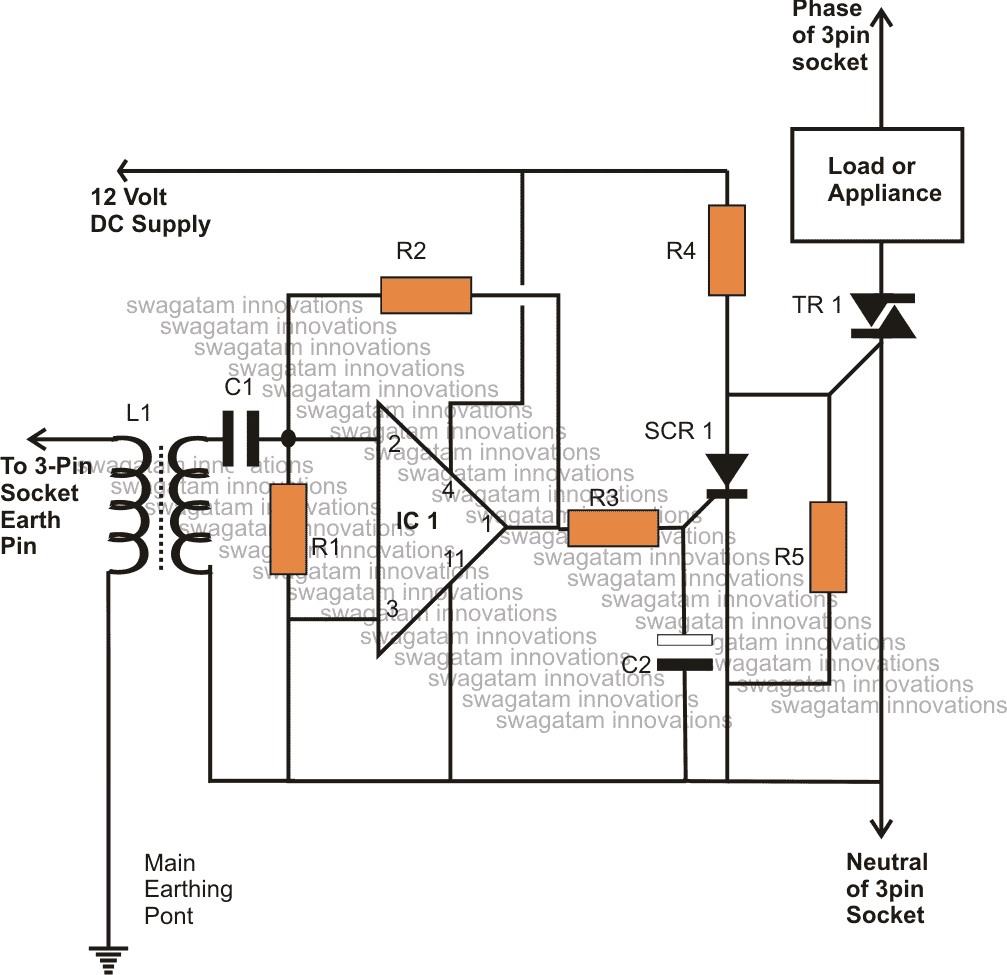
ELCB Circuit Using a Triac
The above circuit can also be implemented using a Triac, everything remains the same, except the relay stage, which now gets replaced by a Triac. During normal conditions the IC output remains switched OFF and the triac is allowed to conduct and operate the load. However the moment a leakage is sensed, the IC output goes high, which triggers the SCR and latches its anode to ground. This inhibits the gate current to the triac which instantly stops conducting, switching OFF the load and rectifying the unfavorable conditions.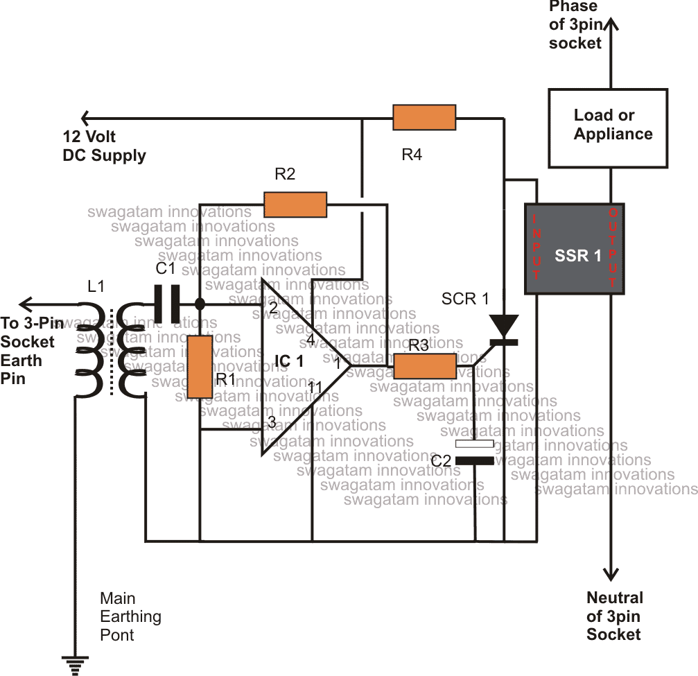
ELCB Circuit Using an SSR or SolidState Relay
Mians operated SSR devices are nowadays being effectively employed for switching mains operated loads more efficiently than relays and since these are electrically isolated and solid state in nature, becomes more desirable than the conventional switching devices like triacs and relays. Here, as long as the conditions are normal, the SSR is able to derive the required input triggering voltage from the circuit, however the moment a leakage is anticipated, the circuit triggers the SCR which in turn chokes the SSR input trigger to ground. The SSR instantly stops conducting, implementing the intended actions by tripping the load and prevents any possible hazard.Parts List
R1 = 100K, R2 = 1M, R3, R4, R5 = 1K, C1 = 0.01uF C2 = 100uF/25V L1 = ordinary small output transformer as used in transistor radios. SCR = BT169 Triac = BT 136 or higher current type Op amp = IC324 SSR = As per user specs. Relay = 12V, SPDT Warning: I have not tested these circuits practically, therefore it needs a thorough testing before a practical implementation. All the circuits involve mains AC which can be lethal if touched in an uncovered and switched ON condition.5 Simple Water Level Controller Circuits
An automatic water level controller is a device which senses undesired low and high water levels in a tank, and switches a water pump ON or OFF accordingly to maintain an optimal water content in the tank. The article explains 5 simple automatic water level controller circuits which can be used for effectively controlling the water level of a water tank by switching the pump motor ON and OFF. The controller responds depending upon the relevant levels of water in the tank and the position of the immersed sensor points. I received the following simple transistorized circuit contribution from Mr.Vineesh, who is one of the keen readers and followers of this blog. He is also an active hobbyist who likes to invent and make new electronic circuits. Let's learn more about his new circuit which was sent to me via email.1) Simple Automatic Water Level Controller Using Transistors
Please find the attached circuit for a very simple and cheap water level controller. This design is only a basic portion of my own marketed product having unsafe voltage cutoff, dry run cut off and LED & alarm indications and overall protection. Anyway, the given concept includes automatic water level control and high /low voltage cut off. It is not a new design since we can find 100s of circuits for over flow controller in many sites and books. But This ckt is simplified with least no: of cheap components. water level sensing and high voltage sensing is doing with same transistor. I used to put all my ckts in observation for a few months and found this ckt OK. but recently some problems highlighted by some customer,which i will definitely write down the end of this mail.CIRCUIT DESCRIPTION
When the water level in over head tank is sufficient , points B & C are closed through water and keeps T2 in ON condition , so T3 will be off , resulting the motor in off condition. When water level lowers below B &C, T2 gets off and T3 on, which switches the relay and pump ON (pump connections not shown in ckt). Pump get off only when water rises and touch the point A only , because point C becomes neutral condition when T3 get ON. The pump switches on again only when the water level comes down below B & C . Presets VR2 is to be set to a high voltage cut off, say 250V when the voltage rises above 250V during pump ON condition, T2 gets ON, and relay off. Preset VR1 is to be set to a low voltage cut off say 170V. T1 will be ON until zener z1 loses its breakdown voltage when voltage lowers to 170V, Z1 will not conduct and T1 stays OFF, which delivers a base voltage to T2 , resulting relay off. T2 is handling the major role in this ckt. (high voltage cut off boards available in market can be easily integrated to this ckt) Electronic components in this circuit worked very fine, but recently some problems were observed: 1) Minor deposits on sensor wire due to electrolysis in water, needed to be cleaned in 2-3 months( this problem is minimized now by applying ac voltage to sensor wire by means of additional circuit, which will be send to you later) 2) Due to relay contact terminal sparks, generated every time during initial current pull of pump, contacts get worn out gradually. This tends to heat the pump because off in-sufficient current flow to pump (observed, new pumps works fine. older pumps heats up more) .For avoiding this problem, additional motor starter must be used, so that relay's function is limited to control the motor starter only, and pump never heats up.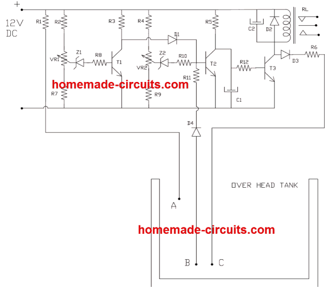 PART LIST
R1,R11 = 100K
R2,R4,R7,R9,= 1.2K
R3 -10KR5 = 4.7K
R6 = 47K
R8,R10 = 10E
R12 = 100E
C1 = 4.7uF/16V
C2 = 220uF/25 V
D1,D2,D3,D4 = 1N 4007
T1,T2 = BC 547
T3 = BC 639( try 187 )
Z1,Z2 = Zener 6.3 V,VR1,
VR2 = 10K PRESET
RL = Relay 12V 200E, > 5 AMP CONT ( According to pump HP)
PART LIST
R1,R11 = 100K
R2,R4,R7,R9,= 1.2K
R3 -10KR5 = 4.7K
R6 = 47K
R8,R10 = 10E
R12 = 100E
C1 = 4.7uF/16V
C2 = 220uF/25 V
D1,D2,D3,D4 = 1N 4007
T1,T2 = BC 547
T3 = BC 639( try 187 )
Z1,Z2 = Zener 6.3 V,VR1,
VR2 = 10K PRESET
RL = Relay 12V 200E, > 5 AMP CONT ( According to pump HP)
2) IC 555 Based Automatic water Level Controller Circuit
The next design incorporates the versatile work horse IC 555 for implementing the intended water level control function in rather very simple and yet effective manner.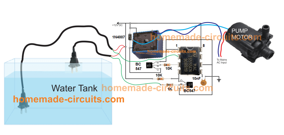 Referring to the above pictorial schematic, the IC 555 working can be understood with the following points:
We know that when the voltage at pin#2 of the IC 555 drops below 1/3rd Vcc, the output pin#3 is rendered high or active with the supply voltage.
We can also observe that pin#2 is held at the bottom of the tank to sense the lower threshold of the water level.
As long as the 2-pin plug remains submerged in water, the pin#2 is held at the Vcc supply level, which ensures that pin#3 stays low.
However as soon as the water drops below the lower 2-pin plug position, the Vcc from pin#2 disappears, causing a lower voltage than 1/3rd Vcc to generate at pin#2.
This instantly activates pin#3 of the IC switching ON the transistor relay driver stage.
The relay in turn switches ON the water pump motor which now begins filling the water tank.
Now as the water starts filing, after some moments the water again immerses the lower two pin plug, however this does not revert the IC 555 situation due to the internal hysteresis of the IC.
The water keeps climbing until it reaches the upper 2-pin plug, bridging water between its two pins.
This immediately switches ON the BC547 attached with pin#4 of the IC, and it grounds the pin#4 with the negative line.
When this happens the IC 555 is quickly reset causing pin#3 to goes low and consequently switching OFF the transistor relay driver and also the water pump.
The circuit now reverts to its original condition and waits for the water to reach the lower threshold to begin the cycle.
Referring to the above pictorial schematic, the IC 555 working can be understood with the following points:
We know that when the voltage at pin#2 of the IC 555 drops below 1/3rd Vcc, the output pin#3 is rendered high or active with the supply voltage.
We can also observe that pin#2 is held at the bottom of the tank to sense the lower threshold of the water level.
As long as the 2-pin plug remains submerged in water, the pin#2 is held at the Vcc supply level, which ensures that pin#3 stays low.
However as soon as the water drops below the lower 2-pin plug position, the Vcc from pin#2 disappears, causing a lower voltage than 1/3rd Vcc to generate at pin#2.
This instantly activates pin#3 of the IC switching ON the transistor relay driver stage.
The relay in turn switches ON the water pump motor which now begins filling the water tank.
Now as the water starts filing, after some moments the water again immerses the lower two pin plug, however this does not revert the IC 555 situation due to the internal hysteresis of the IC.
The water keeps climbing until it reaches the upper 2-pin plug, bridging water between its two pins.
This immediately switches ON the BC547 attached with pin#4 of the IC, and it grounds the pin#4 with the negative line.
When this happens the IC 555 is quickly reset causing pin#3 to goes low and consequently switching OFF the transistor relay driver and also the water pump.
The circuit now reverts to its original condition and waits for the water to reach the lower threshold to begin the cycle.
3) Fluid Level Control Using IC 4093
In this circuit we employ a logic IC 4093. As we all know water (in it��s impure form) that we get in our homes through our house water supply system, has a low resistance to electrical energy. In simple words, water conducts electricity albeit very minutely. Normally the resistance of tap water might be in the range of 100 K to 200 K. This resistance value is quite enough for electronic for exploiting it for the project described in this article that is for a simple water level controller circuit. We have used four NAND Gates here for the required sensing, the whole operation may be understood with the below given points: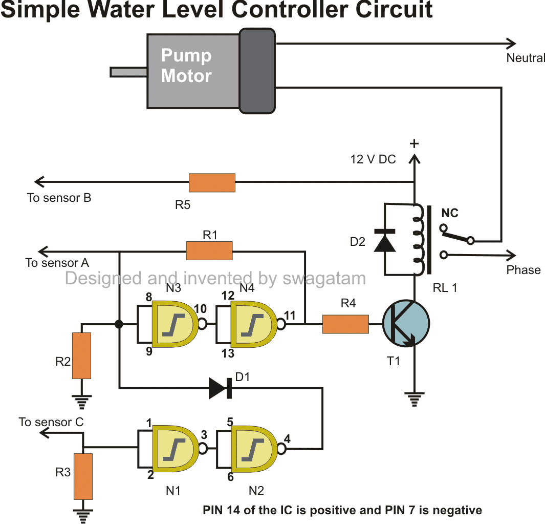
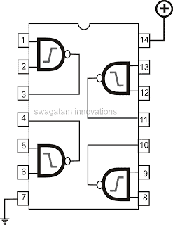 IC 4093 Pinouts
How the Sensors are Positioned
Referring to the above diagram, we see that point B which is at the positive potential is placed somewhere at the bottom section of the tank. Point C is placed at the bottom of the tank, while point A is pinned at the top most section of the tank. As long as water remains under point B, potentials at point A and point C remain at negative or ground level. It also means that the inputs of the relevant NAND gates are also clamped at logic low levels because of the 2M2 resistors.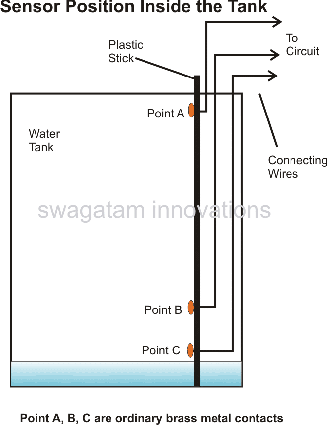 The outputs from N2 and N4 also remain at low logic, keeping the relay and motor switched OFF.
Now suppose the water inside the tank starts filling and reaches point B, it connects point C and B, input of gate N1 becomes high making the otput of N2 also high.
However due to the presence of D1, the positive from the output of N2 does not make any difference to the preceding circuit.
Now when the water reaches point A, input of N3 becomes high and so does the output of N4.
N3 and N4 gets latched due to the feedback resistor across the output of N4 and input of N3. The high output from N4 switches ON the relay and the pump starts emptying the tank.
As the tank gets vacated, the position of water at some point of time goes below point A, however this does not affect N3 and N4 as they are latched, and the motor keeps running.
However once the water level reaches below point B, point C and the input of N1 reverts to logic low, output of N2 also becomes low.
Here the diode gets forward biased and pulls the input of N3 also to logic low, which in turn makes the output of N4 low, subsequently switching OFF the relay and the pump motor.
Parts List
R1 = 100K,
R2, R3 = 2M2,
R4, R5= 1K,
T1 = BC547,
D1, D2 = 1N4148,
RELAY = 12V, 400 OHMS,
SPDT Switch
N1, N2, N3, N4 = 4093
The outputs from N2 and N4 also remain at low logic, keeping the relay and motor switched OFF.
Now suppose the water inside the tank starts filling and reaches point B, it connects point C and B, input of gate N1 becomes high making the otput of N2 also high.
However due to the presence of D1, the positive from the output of N2 does not make any difference to the preceding circuit.
Now when the water reaches point A, input of N3 becomes high and so does the output of N4.
N3 and N4 gets latched due to the feedback resistor across the output of N4 and input of N3. The high output from N4 switches ON the relay and the pump starts emptying the tank.
As the tank gets vacated, the position of water at some point of time goes below point A, however this does not affect N3 and N4 as they are latched, and the motor keeps running.
However once the water level reaches below point B, point C and the input of N1 reverts to logic low, output of N2 also becomes low.
Here the diode gets forward biased and pulls the input of N3 also to logic low, which in turn makes the output of N4 low, subsequently switching OFF the relay and the pump motor.
Parts List
R1 = 100K,
R2, R3 = 2M2,
R4, R5= 1K,
T1 = BC547,
D1, D2 = 1N4148,
RELAY = 12V, 400 OHMS,
SPDT Switch
N1, N2, N3, N4 = 4093
Prototype Images
The above discussed circuit was successfully built and tested by Mr. Ajay Dussa, the following images sent by Mr. Ajay confirm the procedures.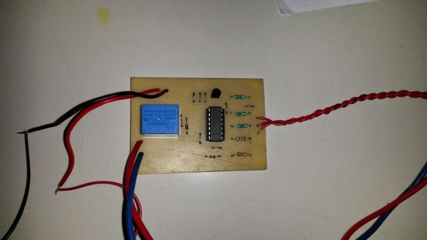
4) Automatic Water Level Controller Using IC 4017
The concept explained above can be also designed using the IC 4017 and a few NOT gates as shown below. The working idea of this 4rth circuit was requested by Mr. Ian Clarke Here's the Circuit Requirement: "I have just discovered this site with these circuits and wonder if you possibly can guide me��.. I have a very similar necessity. I want a circuit to avert a submersible bore pump (1100W) functioning dry, ie exhausting its water supply. I need the pump to shut off when the water level reaches approximately 1M above the pump intake, and start up again as soon as it reaches about 3M above the intake. The pump body at earth potential would likely impart the typical reference. The probes and associated wiring to the surface area had been in place at those ranges. Any assistance you can render would be much acknowledged. I will be able to put up circuits but hardly possess the understanding to figure the specific circuitry out. Many thanks in eager expectation."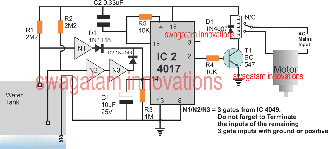 Video Clipping:
Circuit Operation
Let's assume the setup is exactly as shown in the above figure, In fact this circuit needs to be initiated in the existing position that's shown in the figure. Here we can see three probes, one having common ground potential attached at the bottom of the tank and is always in contact with water. The second probe is around 1 meter above the tank bottom level. The uppermost probe above 3 meters above the bottom of the tank level. In the shown position, both the probes are at the positive potentials via the respective 2M2 resistors, which renders the output of N3 positive, and the output of N1 negative. Both these outputs are connected with pin#14 of the IC 4017 which is used as a sequential logic generator for this application. However during first power switch ON the initial N3 positive output does not have any effect on the IC 4017 sequencing, because at switch ON the IC gets reset through C2 and the logic is unable to shift from its initial pin#3 of the IC. Now let's imagine water beginning to fill the tank and reaching the first probe, and this causes the output of N3 to go negative, which again has no impact on the output of IC 4017. As the water fills and finally reaches the uppermost probe, this causes the output of N1 to go positive. Now this impacts the IC 4017 which shifts its logic from pin#3 to pin#2. Pin#2 being connected with a relay driver stage, activates it and subsequently activates the motor pump. The motor pump now starts drawing water out of the tank and keeps emptying it until a time when the tank level begins receding and goes below the upper probe. This reverts the output of N1 at zero, which does not impact the IC 4017 output, and the motor keeps running and emptying the tank, until finally the water goes below the lower probe. When this happens, the N3 output turns positive, and this impacts the IC 4017 output which shifts from pin#2 to pin#4 where it is reset through pin#15 back to pin#3. The motor stops here permanently... until the time when the water again starts filling the tank and its level yet again rises and reaches the uppermost level.5) Water Level Controller Using IC 4049
Another simple water level controller circuit which is 5th in our list for controlling tank overflow can be built using a single IC 4049 and used for the intended purpose. The circuit provided below performs a dual function, it includes an overhead water level control features and also indicates the different levels of water while the water fills the tank.Circuit Diagram
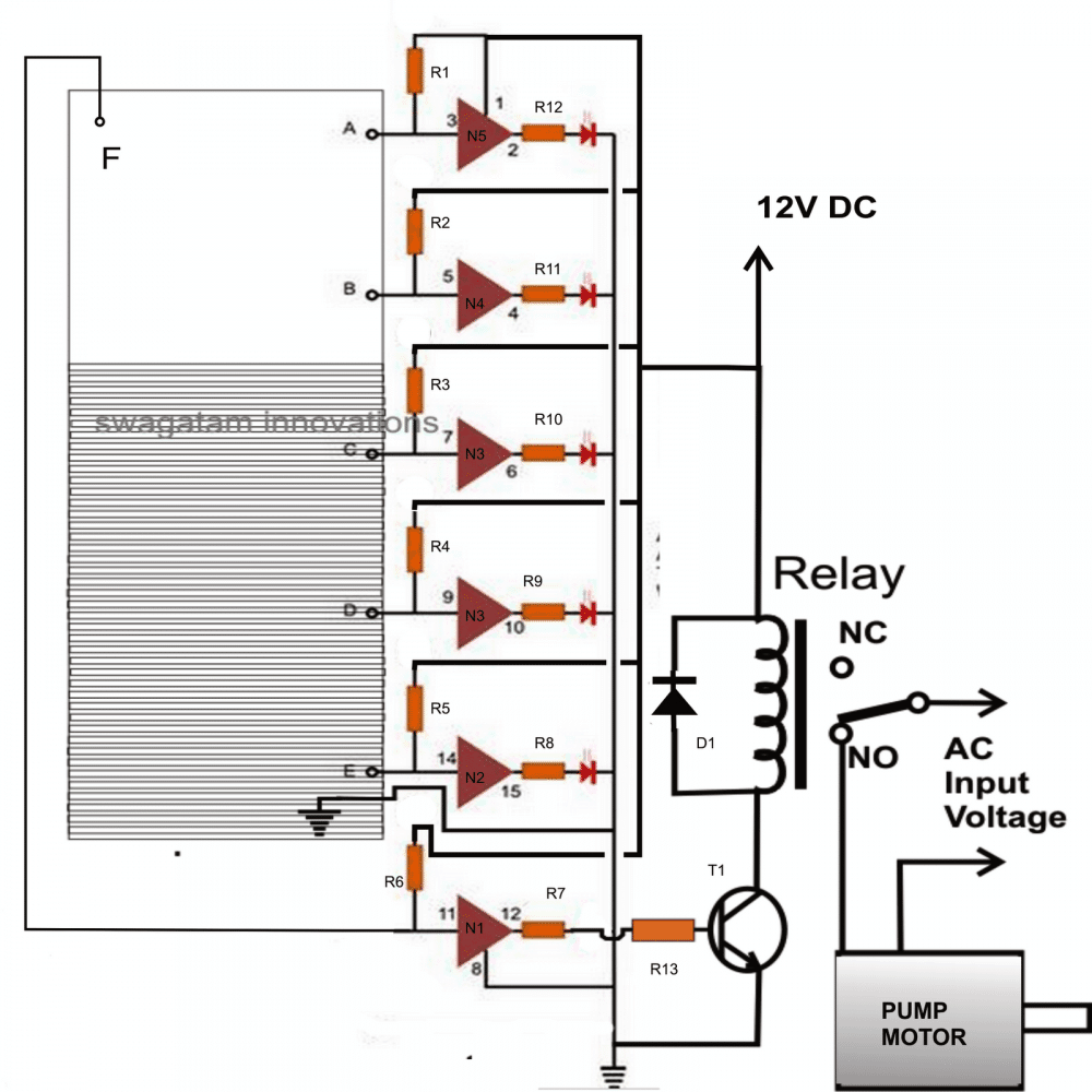
How the Circuit Functions
As soon as the water reaches the uppermost level of the tank, the last sensor positioned at the relevant point triggers a relay which in turn switches the pump motor for initiating the required water evacuating action. The circuit is as simple as it could be. Use of just one IC makes the entire configuration very easy to build, install and maintain. The fact that impure water which happens to be the tap water that we receive in our homes offers a relatively low resistance to electricity has been effectively exploited for implementing the intended purpose. Here a single CMOS IC 4049 has been employed for the necessary sensing and executing the control function. Another interesting associated fact that��s associated with CMOS ICs has helped in making the present concept very easy to implement. It is the high input resistance and sensitivity of the CMOS gates which actually makes the functioning completely straightforward and hassle free. As shown in the above figure, we see that the six NOT gates inside the IC 4049 are arranged in line with their inputs directly introduced inside the tank for the required sensing of the water levels. The ground or the negative terminal of the power supply is introduced right at the bottom of the tank, so that it becomes the first terminal to come in contact with water inside the tank. It also means that the preceding sensors placed inside the tank, or rather the inputs of the NOT gates sequentially come in contact or bridges themselves with the negative potential as the water gradually rises inside the tank. We know that NOT gates are simple potential or logic inverters, meaning their output produces exactly the opposite potential to the one that��s applied to their input. Here it means as the negative potential from the water bottom comes in contact with the inputs of the NOT gates through the resistance offered by the water, the output of those relevant NOT gates sequentially start producing opposite response, that is their outputs start becoming logic high or become at the positive potential. This action immediately lights up the LEDs at the outputs of the relevant gates, indicating the proportionate levels of the water inside the tank. Another point that��s to be noted is, all the inputs of the gates are clamped to the positive supply through a high value resistance. This is important so that the gates inputs are initially fixed at the high logic level and subsequently their outputs generate a logic low level keeping all the LEDs switched off when there��s no water present inside the tank. The last gate which is responsible for initiating the motor pump has its input positioned right at the brim of the tank. It means when the water reaches t the top of the tank and bridges the negative supply to this input, the gate output becomes positive and riggers the transistor T1, which in turn switches the power to the motor pump through the wired relay contacts. The motor pump stats and begin evacuating or releasing the water from the tank to some other destination. This helps the water tank from overfilling and spilling, the other relevant LEDs which monitors the level of the water as it climbs also provides important indication and information regarding the instantaneous levels of the rising water inside the tank. Parts List R1 to R6 = 2M2, R7 to R12 = 1K, All LEDs = Red 5mm, D1 = 1N4148, Relay = 12 V, SPDT, T1 = BC547B N1 to N5 = IC 4049 All the sensor points are ordinary brass screw terminals fitted over a plastic stick at the required measured distance apart and connected to the circuit through flexible conducting insulated wires (14/36).Upgrading the Relay Circuit
The above discussed circuit appears to have one serious drawback. Here the relay operation might continuously keep switching the motor ON/OFF as soon the water level reaches the overflowing threshold, and also immediately when the upper level reduces slightly below the topmost sensor point. This action may not be desirable for any user. The drawback can be eliminated by upgrading the circuit with an SCR and transistor circuit as shown below: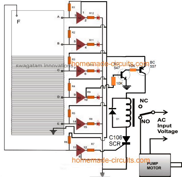
How it Works
The above intelligent modification ensures that the motor is switched ON as soon as the water level touches the point "F", and hereafter the motor keeps running and pumping the water out even while the water level drops below the point "F" .... until it finally reaches below the point "D". Initially when the water level goes above the point "D" the transistors BC547 and BC557 are turned ON, however the relay is still inhibited from switching ON because the SCR is switched OFF during this time. AS the tank fills and the water level rises upto the point "F" output of gate N1 turn positive latching ON the SCR, and subsequently the relay and the motor also switch ON. The water pump begins pumping water out from the tank which results in emptying the tank gradually. The water level now drops below the point "F" switching OFF N1, but the SCR keeps conducting being in the latched situation. The pump keeps running causing the water level to drop continuously until it reduces below the point "D". This instantly switches OFF the BC547/BC557 network, depriving the positive supply to the relay, and eventually switching OFF the relay, the SCR and the pump motor. The circuit returns to its original situation.ULN2003 Water Level Controller Circuit
ULN2003 is a 7-step Darlington transistor array network inside a single IC chip. The Darlingtons are reasonably rated to handle current up to 500 mA and voltages up to 50 V. The ULN2003 can be effectively used for making a full fledged automatic 7 stage water level controller with indicator as shown below: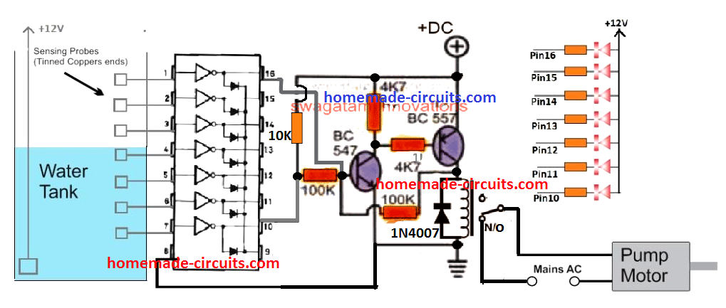 1) PLEASE ADD A 1uF/25V CAPACITOR ACROSS BASE/EMITTER OF THE BC547, OTHERWISE THE CIRCUIT WILL AUTO LATCH ON POWER SWITCH ON.
2) PLEASE DO NOT USE LEDS ON PIN 10 AND PIN 16, OTHERWISE THE VOLTAGE FROM THE LEDS MAY INTERFERE AND CAUSE PERMANENT LATCHING OF THE RELAY
1) PLEASE ADD A 1uF/25V CAPACITOR ACROSS BASE/EMITTER OF THE BC547, OTHERWISE THE CIRCUIT WILL AUTO LATCH ON POWER SWITCH ON.
2) PLEASE DO NOT USE LEDS ON PIN 10 AND PIN 16, OTHERWISE THE VOLTAGE FROM THE LEDS MAY INTERFERE AND CAUSE PERMANENT LATCHING OF THE RELAY
How it Works
The transistor stage associated with the ULN2003 is basically a set reset circuit which is attached with the lowermost and the uppermost pins of the IC for the required set reset actions of the relay and the pump motor. Assuming, the water level is below pin7 probe, the output pin10 remains deactivated, which in turn allows the positive supply to reach the base of the BC547 via the 10K resistor. This immediately switches ON the PNP BC557, which instantly latches the two transistors via the 100K feedback across the collector of BC557 and the base of BC547. The action also latches the relay switching ON the motor pump. The pump water starts filling the tank, and the water gradually climbs above the pin7 probe level. Pin7 tries grounding the 10K biasing for the BC547 but this does not affect the relay switching, since the BC547/BC557 are latched through the 100K resistor. As the water fills and climbs the tank, it finally reaches the uppermost pin1 probe level of the ULN2003. Once this happens the corresponding pin16 goes low, and this grounds the feedback latch bias of the BC547 base, which in turn switches OFF the relay and the motor pump.Making a Customized Water Level Controller
This customized ideal tank overflow controller circuit idea was proposed and requested to me by Mr. Bilal Inamdar. The designed circuit attempts to enhance the above simple circuit into a more personalized form. The circuit is exclusively designed and drawn by me.Objective of the circuit
Well simply I want add a acrylic sheet bellow my tank which will contain tube lights. In short acrylic ceiling. The tank level can't be observed because of the sheet. This is Also needed for terrace tank 1500 Ltrs to observe level indoors without going outside.How it will help
It will help in many scenarios like to observe terrace tank level, to observe and operate overhead tank level and to observe underground tank water level and operate the motor. Also it will save precious water from wasting due to overflow (go green). And release the tension caused due to human error ( forgetting to turn the pump on &filling the water also turn off the motor)Application area :-
Overhead tank Size - height = 12" width = 36" length = 45" the tank is used for drinking, washing & bath. The tank is 7 foot above the flooring. The tank is kept in the bathroom. Material of the tank is plastic (or PVC or fiber whatever non conductive) The tank have three connection Inlet 1/2", outlet 1/2" and whirlpool (overflow) 1". The water fills from inlet. The water comes from outlet for use. The overflow connection prevent water overflowing on the tank and channelized it to drainage. The hole of outlet is lower and the overflow and inlet is higher on the tank (ref height)Scenario :-
The tank probes and level |_A probe (overflow) |__ok level |_D probe (Medium) |__low level |_B probe |__very low level |_C common probe As per the scenario I will now explain how the circuit should workCircuit notes:-
1) Input of the circuit 6v AC/DC (for backup) to 12 AC/DC (for backup) 2) The circuit should mainly work on AC ( my mains is 220-240vac) with use of transformer or adaptor this will avoid probe rusting which occurs due to positive negative stuff. 3) The dc will drives from 9v battery easily available or from aa or aaa battery. 4) We have lots of power cut so please consider backup dc solution. 5) the probe used are aluminum wire 6mm. 6) The resistance of water changes as per location so the circuit must be universal. 7) There must be a sound which is musical as well as different for very high and very low. It can go bad so next sound is preferable. A buzzer is not suitable for big room 2000 sqft. 8) The reset switch must be a normal door bell switch which can be put in existing electric board. 9) There must be at least 6 led Very high, very low, ok, low, mid, motor on/off. The mid must be considered for future expansions. 10) The circuit should indicate led of light gone when there is no AC current. And switch to dc back. or add two led for indication On AC and On battery.Circuit functions.
1) Probe B - if the water goes below this a indication led of very low must glow. The motor should start. The alarm should sound. The sound must be unique for very low level. 2) if the reset switch is pressed than the sound must go off everything else remains the same ( circuit armed, led glowing, motor) 3) if the water touch probe B the sound must be killed automatically. The very low indication led turn off the Low indication led turn on nothing else 4) Probe D - if the water touch probe The low indicator turn off. The ok level led turns on 5) Probe A - if the water touches this probe the then the motor turns off. The ok level led goes off and the very high level led glows. The bell/ speaker turns on with different tune for very high. Also if the reset button is pressed in this case than also there must be no other effect rather than killing the sound. Last but not least the circuit diagram should be expandable to E,F,G etc for very big tank (like mine on terrace) One more thing I m not able to know how the mid level should be indicated. Too tired to write more sorry. Name of the project (just a suggestion) Perfect Water Tank level automation or perfect tank water level controller.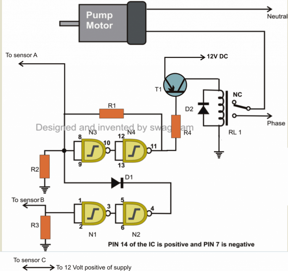 Parts List
R1 = 10K,
R2 = 10M,
R3 = 10M,
R4 = 1K,
T1 = BC557,
Diode = 1N4148
Relay = 12 volt, contacts as per pump current rating.
All Nand gates are from IC 4093
Parts List
R1 = 10K,
R2 = 10M,
R3 = 10M,
R4 = 1K,
T1 = BC557,
Diode = 1N4148
Relay = 12 volt, contacts as per pump current rating.
All Nand gates are from IC 4093
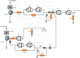
Circuit functioning of the above configuration
Assuming the water content to be at point A, the positive potential from point "C" in the tank reaches the input of N1 through water, making the output of N2 go high. This triggers N3, N4, transistor/relay and horn#2. As the water comes down, below point "A" the gates N3, N4 maintain the situation due to the latching action (feedback from its output to input). Therefore horn#2 remains switched ON. However if the upper reset switch is pressed, the latch is reversed and maintained to negative, switching OFF the horn. In the meantime, since point "B" is also at positive potential, keeps the output of the middle single gate low, keeping the relevant transistor/relay and horn#1 switched OFF. The output of the lower two gates is high but has no effect on the transistor/relay and horn#1 because of the diode at the base of the transistor. Now suppose, the level of the water falls below point "B", the positive from point"C" is inhibited and this point now goes logic low via the 10M resistor (correction required in the diagram which is showing 1M). The output of the middle single gate immediately becomes high and switches ON the transistor/relay and horn#1. This situation is maintained as long as the water threshold is below point B. Howeverhorn#1 can be switched OFF by pressing the lower PB, which reverts the latch made from the lower couple of gates N5, N6. The output of the lower two gates becomes low, pulling the base of the transistor to ground via the diode. The transistor relay switches OFF and hence horn#1. The situation is maintained until the water level again rises above point B. Parts List for the above circuit is given in the diagram.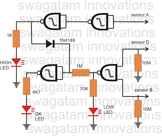
Circuit functioning of the above configuration
Assuming the water level to be at point A, the following things can beobserved: The relevant input pins of the gates are at high logic due to the positive from point "C" coming via the water. This produces a logic low at the output of the upper right gate, which in turn makes the output of the upper left gate high, switching ON the LED (bright glow, showing the tank is full) The input pins of the lower right gate is also high, which makes its output low and therefore the LED marked LOW is switched OFF. However this would have made the lower left gateoutputhigh, switching ON the LED marked OK, but due to the diode 1N4148 itkeepsits output low so that the "OK" LED remains OFF. Now suppose the water level fallsbelowpoint A, the upper two gates reverts theirpositionswitching OFF the LED marked HIGH. No voltageflowsthrough 1N4148 and so the lower left gate switches ON the LED marked "OK" As the water falls below the point D, the OK LED still glows because the lower right gate still remains unaffected andcontinueswith a low output. However the moment water goes below point B, the lower right gate reverts its output because now both its inputs are at logic low. This switches ON the LED marked LOW and switches OFF the LED marked OK. Parts List for the above circuit is given in the diagramIC 4093 PIN-OUT Diagram
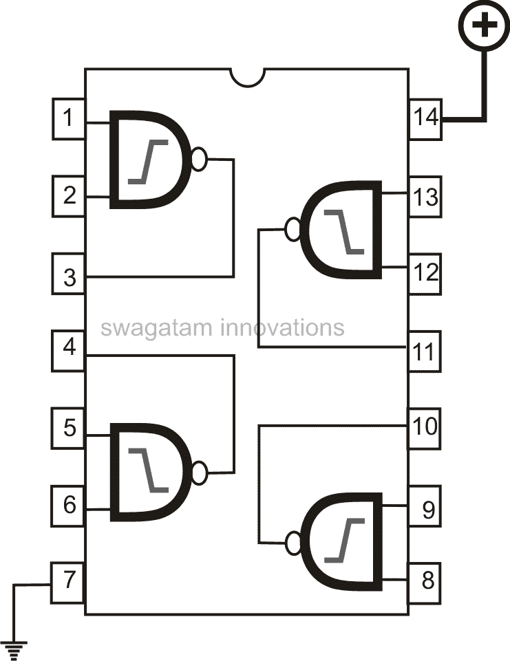 Note:
Please remember to ground the input pin of the remaining three gates which are not used.
In all three ICs would be required constituting 16 gates, only 13 will be used and 3 will remain unused, the above precaution must be followed with these unused gates.
All the relevant sensor points coming out from different circuits must be joined together and terminated to the appropriate tank sensor points.
Wrapping it up
This concludes our articles regarding the 5 best automatic water level controllers which can be customized for switching ON/OFF a pump motor automatically in response to the upper and lower water thresholds.
If you have any other ideas or doubts please feel free to share them through the comment box below
Note:
Please remember to ground the input pin of the remaining three gates which are not used.
In all three ICs would be required constituting 16 gates, only 13 will be used and 3 will remain unused, the above precaution must be followed with these unused gates.
All the relevant sensor points coming out from different circuits must be joined together and terminated to the appropriate tank sensor points.
Wrapping it up
This concludes our articles regarding the 5 best automatic water level controllers which can be customized for switching ON/OFF a pump motor automatically in response to the upper and lower water thresholds.
If you have any other ideas or doubts please feel free to share them through the comment box below
Single LM317 based MPPT Simulator Circuit
To make this simple MPPT circuit we first modify a standard LM317 power supply circuit into a buck converter then configure it with a solar panel for implementing an MPPT function.Modifying a LM317 Power Supply into an MPPT Solar Optimizer
In our previous article we learned how a standard LM317 power supply could be transformed into an inductor based efficient variable buck converter power supply circuit. In this article we analyze how the same circuit design could be enhanced into an effective MPPT circuit by a adding an LDR/LED optocoupler and an opamp voltage follower circuit stages. The complete circuit diagram of the proposed MPPT circuit using LM317 buck converter can be witnessed in the following image:
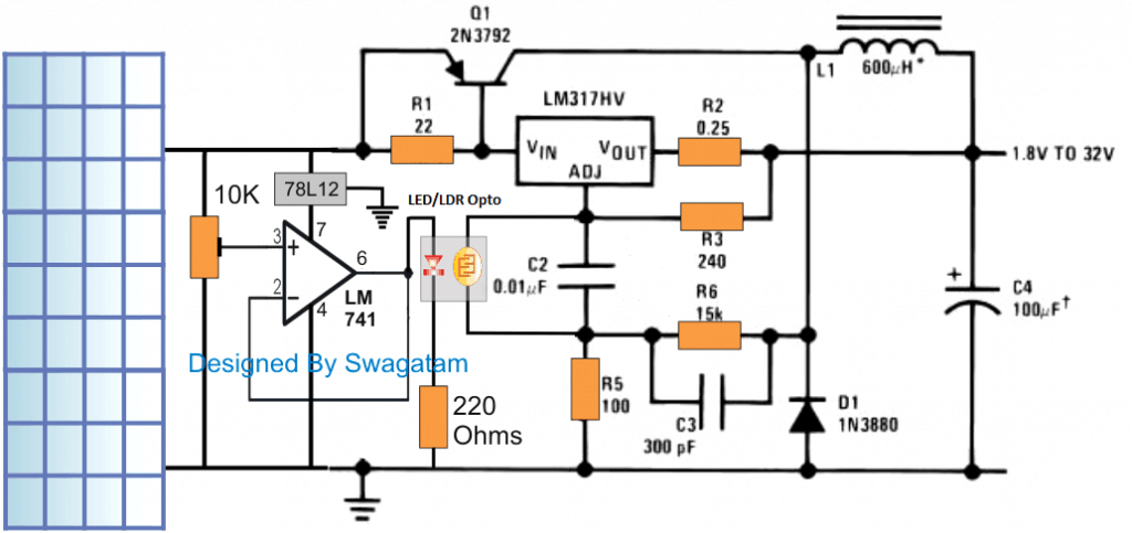 The figure illustrates the discussed MPPT circuit, the LM317 and its associated components form a basic buck converter circuit whose output can be varied by simply varying a resistor across C2.
In our previous power supply design we saw a pot being positioned in parallel with C2 for enabling the variable output voltage feature, however since the present design is supposed to perform an automaticMPPT, this pot could be seen replaced with an LDR/LED opto coupler.
The figure illustrates the discussed MPPT circuit, the LM317 and its associated components form a basic buck converter circuit whose output can be varied by simply varying a resistor across C2.
In our previous power supply design we saw a pot being positioned in parallel with C2 for enabling the variable output voltage feature, however since the present design is supposed to perform an automaticMPPT, this pot could be seen replaced with an LDR/LED opto coupler.
How the Circuits Works
The LED LDR opto coupler is a simple homemade device wherein a red LED and LDR are sealed face to face inside a tiny light proof enclosure. The LDR leads here can be seen connected in parallel with C2,while the LED is integrated with the output of an opamp voltage follower circuit stage. The input of the opamp can be seen hooked up with the solar panel through a 10k preset. The idea here is to make sure that as the solar panel voltage increases, the opto LED intensity also increases, which in turn causes the resistance of the LDR to drop. The dropping resistance causes the buck PWM is narrow its pulses thereby preventing the output voltage to rise, but nevertheless ensuring a proportionate rise in current for the connected load. In one of my earlier postwe understood that in any buck converter design the output from the converter depends on the PWM and the input voltage. That implies if the solar voltage tends to increase, the buck output could get affected and begin increasing proportionately. This could in turn cause overloading of the panel and degrade the efficiency of the panel. The present LM317 MPPT design takes care of this situation through the LED/LDR device and the LM317 variable resistor feature, and combines the two features in conjunction with an opamp voltage follower to develop an effective self adjusting PWM based MPPT circuit. The adjustment of the opamp 10k preset appears to be quite simple.How to Adjust the LM317 MPPT Preset
At optimal sunlight, the 10k preset is adjusted such that the output from the buck converter produces a voltage on par with the load voltage specification. For example suppose the load is a 12v battery, in that case the 10K preset is adjusted to produce around 14.4V. Once this is done, from here on the output could be assumed to self adjust in response to the sun shine...meaning now as the sun shine increases the LM317 buck converter self adjusts and narrows the PWM at the base of Q1 inhibiting any rise in voltage, but in the process the inductor L1 and C4 makes sure that the excess sunshine is transformed into a proportionate amount of extra current for the battery to enable a faster charging. Conversely if the sun shine deteriorates, the PWM tends to widen, causing the voltage for the battery to self adjust automatically maintaining the 14,4V level...... albeit with a proportionate amount of reduction in the current. The self optimizing functionality is carried out throughout the day ensuring the most effective outcome from the panel for the connected load. WARNING: THE ABOVE EXPLAINED SIMPLE MPPT CIRCUIT USING LM317 IS BASED ON THE AUTHOR'S ASSUMPTION AND SIMULATION, VIEWERS ARE ADVISED TO ASSESS THE CONCEPT THOROUGHLY BEFORE ATTEMPTING IT PRACTICALLY.Connecting MPPT with Solar Inverter
The small discussion presented in this article explains whether or not it is advisable to Connect parallel MPPTs with Solar inverters for increasing the net current value of the MPPTs. The question was raised by Mr. Ahmed Qaid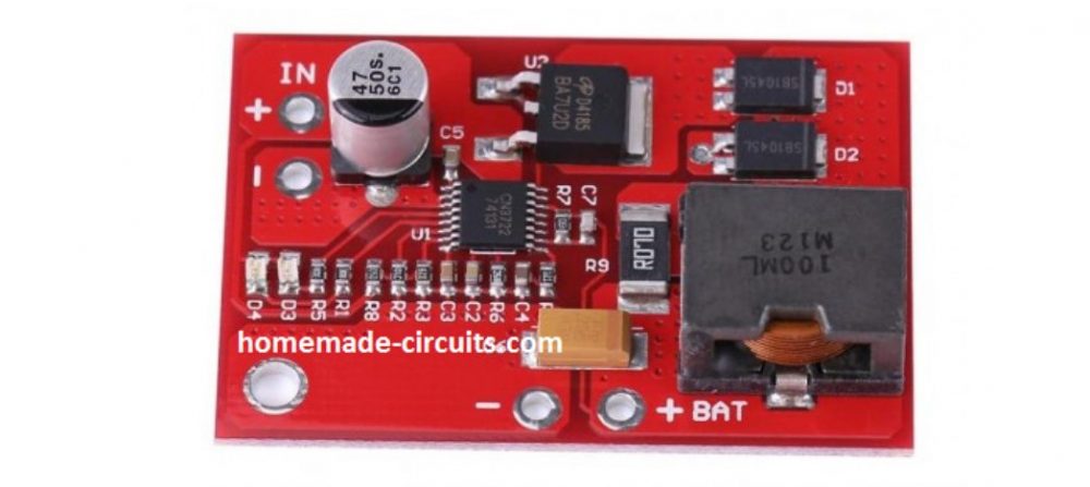
Want to Convert Home Inverter to Solar
hello sir, I have many questions and I hope you to answer them because I'm really in need of your advice 1) If I want to convert any inverter into solar, many products are available in Indian market: a) SU-KAM solarcon b) Luminous solar retrofit charge controller c) Amberroot REhub PWM which one is better for an inverter of 12V battery system? 2) my friend bought Amberroot REhub MPPT and he has an inverter with 24v battery system this solar charge controller charges the battery with 15 amp but if he wants to add 24 batteries in parallel to the system the charging current must increase too so can he use mppt solar charge controller with 400wp to get another 15 amp to make the charging current upto 30 amp? and Is it safe for the system? 3) I'm planning to buy an air cooler, all I know is that ---- is a good company in air conditioners field but in air cooler I don't have any idea, I searched ----- website and I think their products are overpriced so which company is good in air cooler?MPPT will only Convert Excess Volt to Current
Hello Ahmed, The dealer will know better about those products than me, so it's better to consult them. 2) An MPPT circuit will only convert the excess voltage from the panel to an equivalent amount of current if the load operating voltage is lower than the panel output voltage....MPPT will never manufacture current by itself....in short the V x I of the MPPT at any instant can never exceed the Panel's V x I value. so you can measure the existing MPPT output and check it as per the above fact...if it agrees with it then no additional MPPT would be required neither would it work. If you find the V x I of the MPPT is much lower than the solar panel's V x I during the given instant, then you may think of replacing the "Amberroot" with some other higher rated MPPT, or you can connect another MPPT in parallel I can only discus about electronic concepts, I'll never want to recommend or endorse a particular product.More on MPPT Converters:
Unlike solar trackers, MPPT function may be limited only to ensure that the recommended wattage from the panel is fully delivered to the load without losses. This limitation becomes true because the MPPTs have access only to the solar panel's output, and not the sun rays, therefore whatever processing and optimization it may do is limited upto the solar panel specs. On the contrary solar trackers are much efficient since they are able to track the sunlight at every instant and make sure that every bit from the sunlight is delivered to the load. Having said this, a solar tracker may be helpless and waste precious power if the load is not correctly matched with the panel's, specs. For example if the panel voltage is 24V then the load voltage must be close to this value, may be at around 20V, otherwise there could significant losses and the tracker efficiency may get seriously hampered, and the purpose of the solar tracker may fail. A better idea is always to use an MPPT in conjunction with a solar tracker, which produces a double impact and makes sure that the high tracking efficiency of the solar tracker is met with the high processing efficiency of the MPPT and these together could finally help to achieve the most favorable response from the available sunlight.Best 3 MPPT Solar Charge Controller Circuits for Efficient Battery Charging
An MPPT as we all know refers to maximum power point tracking which is typically associated with solar panels for optimizing their outputs with maximum efficiency. In this post we learn the 3 best MPPT controller circuits for efficiently harnessing solar power and charging a battery in the most efficient manner.Where an MPPT is Used
The optimized output from MPPT circuits is primarily used for charging batteries with maximum efficiency from the available sunshine. New hobbyists normally find the concept to difficult and get confused with the many parameters associated with MPPT, such as the maximum power point, "knee" of the I/V graph etc. Actually there's nothing so complex about this concept, because a solar panel is nothing but just a form of power supply. Optimizing this power supply becomes necessary because typically solar panels lack current, but posses excess voltage, this abnormal specs of a solar panel tends to get incompatible with standard loads such as 6V, 12V batteries which carry higher AH rating and lower voltage rating compared to the panel specs, and furthermore the ever-varying sunshine makes the device extremely inconsistent with its V and I parameters. And that's why we require an intermediate device such as an MPPT which can "understand" these variations and churn out the most desirable output from a connected solar panel. You might have already studied this simple IC 555 based MPPT circuit which is exclusively researched and designed by me and provides an excellent example of a working MPPT circuit.Why MPPT
The basic idea behind all MPPTs is to drop or trim down the excess voltage from the panel according to the load specs making sure that the deducted amount of voltage is converted into an equivalent amount of current, thus balancing the I x V magnitude across the input and the output always up to the mark...we cannot expect anything more than this from this useful gadget, do we? The above automatic tracking and appropriately converting the parameters efficiently is implemented using a PWM tracker stage and a buck converter stage, or sometimes a buck-boost converter stage, although a solitary buck converter gives better results and is simpler to implement.Design#1: MPPT using PIC16F88 with 3-Level Charging
In this post we study an MPPT circuit which is quite similar to the IC 555 design, the only difference being the use of a microcontroller PIC16F88 and an enhanced 3-level charging circuit.
Step wise Working Details
The basic function of the various stages can be understood with the help of the following description: 1) The panel output is tracked by extracting a couple of information from it through the associated potential divider networks. 2) One opamp from IC2 is configured as a voltage follower and it tracks the instantaneous voltage output from the panel through a potential divider at its pin3, and feeds the info to the relevant sensing pin of the PIC. 3) The second opamp from IC2 becomes responsible for tracking and monitoring the varying current from the panel and feeds the same to another sensing input of the PIC. 4) These two inputs are processed internally by the MCU for developing a correspondingly tailored PWM for the buck converter stage associated with its pin#9. 5) The PWM out from the PIC is buffered by Q2, Q3 for triggering the switching P-mosfet safely. The associated diode protects the mosfet gate from overvolatges. 6) The mosfet switches in accordance with the switching PWMs and modulates the buck converter stage formed by the inductor L1 and D2. 7) The above procedures produce the most appropriate output from the buck converter which is lower in voltage as per the battery, but rich in current. 8) The output from the buck is constantly tweaked and appropriately adjusted by the IC with reference to the sent info from the two opamps associated with the solar panel. 9) In addition to the above MPPT regulation, the PIC is also programmed to monitor the battery charging through 3 discrete levels, which are normally specified as the bulk mode, absorption mode, an the float mode. 10) The MCU "keeps an eye" on the rising battery voltage and adjusts the buck current accordingly maintaining the correct Ampere levels during the 3 levels of charging procedure. This is done in conjunction with the MPPT control, that's like handling two situations at a time for delivering the most favorable results for the battery. 11) The PIC itself is supplied with a precision regulated voltage at its Vdd pinout through the IC TL499, any other suitable voltage regulator could be replaced here for rendering the same. 12) A thermistor can be also seen in the design this may be optional but can be effectively configured for monitoring the battery temperature and feeding the info to the PIC, which effortlessly processes this third information for tailoring the buck output making sure that the battery temperature never rises above unsafe levels. 13) The LED indicators associated with the PIC indicate the various charging states for the battery which allows the user to get an up-to-date information regarding the charging condition of the battery throughout the day. 14) The proposed MPPT Circuit using PIC16F88 with 3-Level Charging supports 12V battery charging as well as 24V battery charging without any change in the circuit, except the values shown in parenthesis and VR3 setting which needs to be adjusted to allow the output to be 14.4V at the onset for a 12V battery and 29V for a 24V battery. Programming code can be Downloaded hereDesign#2:Synchronous Switch-Mode MPPT Battery Controller
The second design is based on the device bq24650 which includes an advanced built-in MPPT Synchronous Switch-Mode Battery Charge Controller. It offers a high level of input voltage regulation, which prevents the charging current to the battery each time input voltage drops below a specified amount. Learn More: Whenever the input is attached with a a solar panel, the supply stabilization loop pulls down the charging amp to ensure that the solar panel is enabled to produce maximum power output.How the IC BQ24650 Functions
The bq24650 promises to provide a constant-frequency synchronous PWIVI controller with optimal level of accuracy with current and voltage stabilization, charge preconditioning, charge cut-off, and charging level checking. The chip charges the battery in 3 discrete levels: pre-conditioning, constant current, and constant voltage. Charging is is cut-off as soon as the amp level nears the 1/10 of the rapid charging rate. The pre-charge timer is set to be at 30 minutes. The bq2465O without a manual intervention restarts the charging procedure in case the battery voltage reverts below an internally set limit or reaches a minimum quiescent amp sleep mode while the input voltage goes below the battery voltage. The device is designed to charge a battery from 2.1V to 26V with VFB internally fixed to a 2.1V feedback point. The charging amp spec is preset internally by fixing a well matched sensing resistor. The bq24650 can be procured with a 16 pin, 3.5 x 3.5 mm^2 thin QFN option.Circuit Diagram
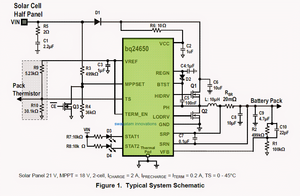 Datasheet bq24650
BATTERY VOLTAGE REGULATION
The bq24650 employs an extremely accurate voltage regulator for the deciding on the charging voltage. The charging voltage is preset by means of a a resistor divider from the battery to ground, with the midpoint hooked up the VFB pin. The voltage at the VFB pin is clamped to 2.1 V reference. This reference value is used in the following formula for determining the desired level of regulated voltage: V(batt) = 2.1V x [1 + R2/R1] where R2 is linked from VFB to the battery and R1 is connected from VFB to GND. Li-Ion, LiFePO4, as well as SMF lead acid batteries are ideally supported battery chemistries. A majority of over the shelf Li-ion cells can now be effectively charged up to 4.2V/cell. A LiFePO4 battery supports the process of a substantially higher charge and discharge cycles, but the down side is that the the energy density is not too good. The recognized cell voltage is 3.6V. The charge profile of the two cells Li-Ion and LiFePO4 is preconditioning, constant current, and constant voltage. For an effective charge/discharge life, the end-of-charge voltage limit may possibly be cut down to 4.1V/cell however it��s energy density could become a lot lower compared to the Li-based chemical specification, lead acid continues to be much preferred battery because of its reduced production expenses as well as rapid discharge cycles. The common voltage threshold is from 2.3V to 2.45V. After the battery is seen to be completely topped up, a float or trickle charge becomes mandatory in order make up for the self-discharge. The trickle charge threshold is 100mV-200mV below the constant voltage point.INPUT VOLTAGE REGULATION
A solar panel may have an exclusive level on the V-I or V-P curve, popularly known as the Maximum Power Point (MPP), wherein the complete photovoltaic (PV) system relies with optimum efficiency and generates the required maximum output power. The constant voltage algorithm is the most easy Maximum Power Point Tracking (MPPT) option available. The bq2465O automatically shuts down the charging amp such that the maximum power point is is enabled for producing maximum efficiency.Switch ON Condition
The chip bq2465O incorporates a "SLEEP" comparator to identify the means of supply voltage on the VCC pin, because of the fact that VCC may be terminated both from a battery or an external AC/DC adapter unit. If the VCC voltage is more significant the SRN voltage, and the additional criteria are fulfilled for the charging procedures, the bq2465O subsequently begins making an attempt to charge a connected battery (please see the Enabling and Disabling Charging section). lf SRN voltage is higher with respect to the VCC, symbolizing that a battery is the source from where the power is being acquired, the bq2465O is enabled for a lower quiescent current ( <15uA) SLEEP mode to prevent amperage leakage from the battery. lf VCC is below the UVLO limit, the IC is cut-off, after which VREF LDO is switched off.ENABLE AND DISABLE CHARGING
The following concerned aspects need to be ensured before the charging process of the proposed MPPT Synchronous Switch-Mode Battery Charge Controller Circuit is initialized: Charging process is enabled (MPPSET > 175mV) The unit is not in Under-Voltage-Lock-Out (UVLO) functionality and VCC is above the VCCLOWV limit The IC is not in SLEEP functionality (i.e. VCC > SRN) VCC voltage is below the AC over-voltage limit (VCC < VACOV) 30ms time lapse is fulfilled after the first power-up REGN LDO and VREF LDO voltages are fixed at the specified junctures Thermal Shut (TSHUT) is not initialized - TS bad is not identified Any one of the following technical issues may inhibit the proceeding charging of the battery: Charging is is deactivated (MPPSET < 75mV) Adapter input is disconnected, provoking the IC to get into a VCCLOWV or SLEEP functionality Adapter input voltage is below the 100mV above battery mark Adapter is rated at higher voltage REGN or VREF LDO voltage is not as per the specs TSHUT IC warmth limit is identified TS voltage happens to move out of the specified range which may indicate that the battery temperature is extremely hot or alternatively much cooler Self-Triggered In-built SOFT-START CHARGER CURRENT The charger by irself soft-starts the charger power regulation current each time the charger moves into the fast-charge to establish that there is absolutely no overshoot or stressful conditions on the externally connected capacitors or the power converter. The soft-start is featured with of stepping-up the chaging stabilization amp into eight uniformly executed operational steps next to the prefixed charging current level. All the assigned steps carry on for around 1.6ms, for a specified Up period of 13ms. Not a single external parts are called for enabling the discussed operational function.CONVERTER OPERATION
The synchronous buck PWM converter employs a predetermined frequency voltage mode with feed-forvvard control strategy. A version III compensation configuration let's the system to incorporate ceramic capacitors at the output stage of the converter. The compensation input stage is associated internally between the feedback output (FBO) along with an error amplifier input (EAI). The feedback compensation stage is rigged between the error amplifier input (EAI) and error amplifier output (EAO). The LC output filter stage needs to be determined to enable a resonant frequency of around 12 kHz - 17 kHz for the device, for which the resonant frequency, fo, is formulated as: fo = 1 / 2 �� ��LoCo An integrated saw-tooth ramp is allowed to compare the internal EAO error control input to alter the duty-cycle of the converter. The ramp amplitude is 7% of the input adapter voltage enabling it to be permanently and completely proportional to the input supply of the adapter voltage. This cancels away any sort of loop gain alterations on account of a variation in the input voltage and simplifies the loop compensation procedures. The ramp is balanced out by 300mV so that a zero percent duty-cycIe is achieved when the EAO signal is below the ramp. The EAO signal is likewise qualified to outnumber the saw-tooth ramp signal with a purpose to achieve a 100% duty cycIe PWM demand. Built in gate drive logic makes it possible accomplishing 99.98% duty-cycle at the same time confirming the N-channel upper device consistently carries as much as necessary voltage to always be 100 % on. In the event the BTST pin to PH pin voltage reduces below 4.2V for longer than three intervals, in that case the high-side n-channeI power MOSFET is switched off while the low-side n-channe| power MOSFET is triggered to draw the PH node down and charge-up the BTST capacitor. After that the high-side driver normalizes to 100% duty-cycle procedure until the (BTST-PH) voltage is observed to decline low yet again, on account of outflow current depleting the BTST capacitor below 4.2 V, as well as reset pulse is reissued. The predetermined frequency oscillator maintains rigid command over the switching frequency under most circumstances of input voltage, battery voltage, charge current, and temperature, simplifying output filter layout and retaining it away from the audible disturbances state.Design#3: Fast MPPT Charger Circuit
The third best MPPT design in our list explains a simple MPPT charger circuit using the IC bq2031 from TEXAS INSTRUMENTS,which is best suited for charging high Ah lead acid batteries quickly and with a relatively fast rateAbstract
This practical application article is for the individuals who may be developing an MPPT-based lead acid battery charger with the aid of bq2031 battery charger. This article includes a structural format for charging a 12-A-hr lead acid battery employing MPPT (maximum power point tracking) for improving charging efficiency for photovoltaic applications.Introduction
The easiest procedure for charging a battery from a solar panel systems could be to hook up the battery straight to the solar panel, however this may not the most effective technique. Presume a solar panel bears a rating of 75 W and generates a current of 4.65 A with a voltage of 16 V at normal test environment of 25 �� C temperature and 1000 W/m2 of insolation. The lead acid battery is rated with a voltage of 12 V; directly hooking up the solar panel to this battery would decrease the panel voltage to 12 V and only 55.8 W (12 V and 4.65 A) could be produced from the panel for charging. A DC/DC converter may be most suitably needed for economical charging here. This practical application document explains a model, making use of the bq2031 for effective charging.I-V Characteristics of Solar Panel
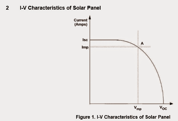 Figure 1 displays the standard aspects of a solar panel systems.
Isc is a short-circuit current that streams through the panel in case the solar panel is short circuited.
It happens to be the optimum current that may be extracted from the solar panel.
Voc is the open-circuit voltage at the terminals of the solar panel.
Vmp and Imp are the voltage and current levels where maximum power can be purchased from the solar panel.
While the sunshine decreases the optimum current (Isc) which may be attained, the highest current from the solar panel also suppresses.
Figure 2 indicates variation of I-V characteristics with sun light.
The blue curve links the details of the maximum power at various values of insolation
Figure 1 displays the standard aspects of a solar panel systems.
Isc is a short-circuit current that streams through the panel in case the solar panel is short circuited.
It happens to be the optimum current that may be extracted from the solar panel.
Voc is the open-circuit voltage at the terminals of the solar panel.
Vmp and Imp are the voltage and current levels where maximum power can be purchased from the solar panel.
While the sunshine decreases the optimum current (Isc) which may be attained, the highest current from the solar panel also suppresses.
Figure 2 indicates variation of I-V characteristics with sun light.
The blue curve links the details of the maximum power at various values of insolation
 The reason for the MPPT circuit is to try to sustain the working level of the solar panel at the maximum power point in several sunshine conditions.
As observed from Figure 2, the voltage where maximum power is delivered does not alter greatly with sunshine.
The circuit constructed with the bq2031 makes use of this character to put into practice MPPT.
An additional current control loop is included with decrease the charge current as the daylight decreases as well as to sustain solar panel voltage around the maximum power point voltage.
The reason for the MPPT circuit is to try to sustain the working level of the solar panel at the maximum power point in several sunshine conditions.
As observed from Figure 2, the voltage where maximum power is delivered does not alter greatly with sunshine.
The circuit constructed with the bq2031 makes use of this character to put into practice MPPT.
An additional current control loop is included with decrease the charge current as the daylight decreases as well as to sustain solar panel voltage around the maximum power point voltage.
bq2031-Based MPPT Charger
Datasheet BQ2031 Figure 3 displays the schematic of a DV2031S2 board with an added current control loop added to carry out the MPPT making use of the operational amplifier TLC27L2. The bq2031 keeps the charging current by retaining a voltage of 250 mV at sense resistance R 20. A reference voltage of 1.565 V is created by using 5 V from U2. The input voltage is compared with the reference voltage to produce an error voltage that could be implemented at the SNS pin of bq2031 to decrease the charge current. The voltage (V mp) where maximum power can be acquired from the solar panel is conditioned employing resistors R26 and R27. V mp = 1.565(R 26 +R 27)/R 27. With R 27 = 1 k �� and R 26 = 9.2 k ��, V mp = 16 V is achieved. TLC27L2 is internally adjusted with a bandwidth of 6 kHz at V dd = 5 V. Mainly because the bandwidth of TLC27L2 is significantly below the switching frequency of bq2031, the added current control loop continues to be constant. The bq2031 in the earlier circuit (Figure 3) offers an optimum current of 1 A. In case the solar power panel can furnish adequate power to charge the battery at 1 A, the outer control loop does not proceed into action. However if the insulation reduces and the solar power panel struggles to deliver sufficient energy to charge the battery at 1 A, the outer control loop decreases the charge current to preserve input voltage at V mp. The outcomes demonstrated in Table 1 confirm the functioning of the circuit. The voltage readings in bold type signify the issue whenever the secondary control loop is minimizing the charge current to preserve input at V mp References: Texas Instruments MPPT Synchronous Switch-Mode Battery Charge Controller CircuitMPPT vs Solar Tracker �C Differences Explored
The post investigates two popular solar harnessing counterparts the MPPT and the solar tracker, and figures out the major differences between these two outstanding free energy spinning devices. It's true that our planet is blessed with many free energy sources such as wind energy, hydro energy, sun or solar energy etc but unless these are harnessed and captured optimally the resources could simply get wasted.Introduction
Considering this fact, two major systems were developed in the form of MPPT circuits, and mechanical solar trackers for harnessing solar energy most effectively and wisely. However a layman in the field always tends to get confused regarding the difference between these two systems and sometimes get ill-informed through many myths and incorrect data. This post is specially written for clarifying the many pros and cons of these two prominent solar harnessing machines, namely the MPPT and the Solar Tracker. Let's learn which gadget wins the race quality and efficiency wise through the following discussion:MPPT vs Solar tracker
MPPT is the acronym for Maximum Power Point Tracker, as the name suggests this device is designed to extract maximum feasible VxI or wattage from the panel and deliver it to the load. An MPPT will basically try to execute two main actions while in use: Firstly, it will track the solar panel maximum available power (V x I) and try to deliver the most of it across the output or the connected load. Secondly, it will monitor that the load does not attempt to hog the panel by extracting illegitimate or unfeasible amount of watts either due to a short circuit or shunting of the output leads of the MPPT. If such a condition is detected the MPPT's "shut down" feature instantly triggers in order to correct this unusual or incorrect load situation.How an MPPT functions
Suppose we have a solar panel with the following specs attached with an MPPT for charging a 12V battery: Volts: 24V Curent: 2.5amps wattage: 24 x 2.5 = 60 watts at optimum sunshine conditions. Optimum or peak sunshine refers to a period during the day when the sun rays are almost perpendicular to the surface of the solar panel, as this condition is compromized with the sun's changing position the output from the panel also suffers and is reduced proportionately. During optimum sunshine, the MPPT will try to deliver, and charge the battery with 12V @ 60/12 = 5 amps. You can see that here the current to the battery is boosted and has been doubled in order to keep the net input to output wattage ratio constant and efficient. Thus the system ensures that the battery which even though has a much lower voltage specs than the panel continues to get optimum power from the panel, that is at the rate of 12 x 5 amps = 60 watts. This is the most interesting and valuable feature of MPPT chargers compared to other forms of ordinary chargers. However when sun light begins diminishing as the day proceeds to dusk, the panel wattage also begins to deteriorate proportionately, so what does the MPPT do now? Does it continue to offer the same amount of power that it was delivering during the peak sunshine? The answer is no, the MPPT simply keeps tracking the maximum available power from the panel and reproduces the same at its output load, meaning if the panel voltage and wattage reduces to say, 20V @30 watts, then the 12V battery only succeeds in getting 12V at 30/12 = 1.5amps charging rate. Although the MPpT is still trying to keep the input/output ratio to unity by rendering the same amount power to the battery that's being provided by the panel, but it's unable to restore sun ray's angle of incidence. This is one big disadvantage with MPPT trackers, whose power producing ability is restricted to the angle of sun rays on the panel, and it becomes "helpless" as sun begins receding. Thus an MPPT will not be able to take the advantage of the sunlight throughout the day. So if we analyze the efficiency of the MPPT with respect to the sun's actual delivering power, we may find it to be around just 50% or even less.Pros and Cons of an MPPT
The positive aspects of MPPT circuits are: These are compact, solid state, more efficient than other forms of chargers and does not employ bulky mechanical assemblies for the implementations, however the huge downside is that these are unable to track the rays of the sun and therefore fail to take the full advantage of the sun's vast energy output.How Solar Trackers Function
Solar trackers are electro-mechanaical systems designed to track the sun rays practically, meaning the solar panel will keep changing it's surface orientation in response to the sun's shifting positions such that it maintains a perpendicular angle with the sun rays throughout the day. The above movement is executed using motors and an LDR sensor circuit. The LDR sensor circuit constantly monitors the incidence of sun rays and commands the motor to turn the panel accordingly such that the panel keeps tilting from east to west fraction by fraction. A solar tracker also has the ability to analyze an overcast condition and adjust the panel for obtaining the most advantageous or optimal angle of the sun rays.Solar Tracker Mechanism Details
MPPT with a Solar Tracker
Therefore if a 24V solar tracker system is directly connected with a 12V battery, although the panel would keep tracking the sun and generate optimum power throughout the day, the battery will not be favored with a doubled current, meaning with the above discussed specs the solar panel which has the ability to produce 2.5V amps at 24V will continue to provide 2.5 amps to the battery contrary to the the boosted 5 amps as produced by the MPPT. Here the MPPT proves its metal since its above ability becomes imperative and significant and cannot be ignored. Therefore it shows that an MPPT cannot be ignored even if a solar tracker is being used, and it should be additionally used with a solar tracker in order to make the combination deadly potent and almost 100% efficient under all circumstances. This combination would ensure that the user is able achieve the maximum from the available solar panel and the sunshine, although this would mean some heavy investments initially, the costs could well be covered within a few seasons of use of the system.Conclusion
In the end comparing the two counterparts we can contemplate and conclude that the distinct winner is the solar tracker system. That said, an MPPT also becomes extremely essential for achieving outstanding results from a solar panel system and also when a fixed solar panel is selected by an user.I/V Tracker Circuit for Solar MPPT Applications
Optimizing power by tracking is the key feature which makes solar MPPT concept so unique and efficient, where the complex and non-linear I/V curve of the solar panel is tracked and switched for creating maximum optimal conditions for the connected load.The Circuit Concept
I have been trying hard to design something that would in true sense track the I/V curve or the power curve of the panel, and correct it automatically whenever it drifts from the optimal points.The proposed design is based on the same grounds, but here I have included only the I (current) tracking stage in order to keep things simple. Actually it's the current that really matters and is directly proportional to power of the panel so I thought keeping this parameter in control could fulfill the job. Let's try to understand the design with the following observations:How the Circuit Functions
Looking at the proposed solar MPPT I/V curve tracker circuit diagram, the BC547 at the extreme right along with the 10k resistor and 1uF capacitor forms a linear ramp generator. The central stage comprising the two 555 ICs form a variable PWM controlled output generator, while the IC 741 stage becomes the actual current tracker stage. When the voltage from the solar panel connects across the BC547 collector and ground, due to the presence of the base 10k/1uf network, the emitter follower provides a gently rising voltage to the 555 PWM generator stage. The ramp activates IC2 and forces it to generate a correspondingly risingPWM output at its pin#3 which goes to the gate of the driver mosfet. The mosfet responds to these pulses and gradually increases its conduction and provides current to the battery in the same incremental order. As soon as the current intake across the battery begins rising, an equivalent voltage level is translated across the current sensing resistor Rx which gets applied a pin#3 of the 741 IC. The above potential also hits pin#2 of 741 via the dropping 1N4148 diode so that pin#2 follows this potential in tandem with pin#3 but lags behind by about 0.6V due to the presence of the series diode. The above condition allows the opamp to begin with a high output which keeps the diodes at its pin#6 reverse biased. As long as the current keeps climbing with the ramp, opamp pin#3 continues to be higher than pin#2, thus keeping the output higher. However at some point of time, which might be after the I/V curve has just crossed, the current output from the panel starts dropping or rather drops abruptly across Rx. This is sensed by pin#3 immediately, however due to the presence of the 33u capacitor, pin#2 is unable to sense and follow this drop in potential. The above situation instantly forces the pin#3 voltage to become lower than pin#2, which in turn reverts the output of the IC to zero, forward biasing the connected diode. The base of the ramp generator BC547 is dragged to zero forcing it to switch OFF, and reset the whole procedure back to the original state. The process now begins afresh. The above procedure continues and ensures that the current is never allowed to fall or cross the inefficient region of the I/V curve. This is just an assumption, a concept which I have tried to implement, it might require a lot many tweaking and alignments before it can become truly result oriented. The output from the mosfet may be integrated with an SMPS based converter for even higher efficiency.
Understanding MPPT Solar Charger
Here we try to understand the actual circuit concept of MPPt type of solar charger controllers and learn how do these devices work.What's MPPT
MPPT stands for Maximum Power Point Tracking, a charger concept specifically intended and designed for acquiring highly efficient solar power harnessing. Solar panels are excellent devices since they allow us to harness free electrical energy from sun, however the present devices are not very efficient with their outputs. As we all know output from solar panel directly depends the incident rays of the sun, as long as its near perpendicular on it offers good efficiency, which keeps on deteriorating with slanting rays or dipping sun position. The above also gets affected with overcast conditions. Moreover a solar panel output is associated with inconsistent voltage levels which needs proper regulation in order to operate the load which is normally a lead acid battery. Lead acid batteries or any kind of chargeable battery will require a properly rated input so that it doesn't get damaged and it gets charged optimally. For this we normally involve a charger controller in between the solar panel and the battery. As a solar panel voltage is never constant and drops with dropping sun light, the current from the solar panel also gets weaker as the sun light intensity gets weaker. With the above conditions if the solar panel undergoes any kind of loading directly, it's current would further go down producing inefficient outputs. In other words the efficiency of a panel is maximum when its voltage is near the rated specified value. Therefore, as an example a 18V solar panel will operate with maximum efficiency when it's operated at 18V. And in case the sun light gets weaker and the above voltage drops to say 16V, yet still we could operate it with maximum efficiency if we could keep the 16V volts intact and derive the output without affecting or dropping this voltage. The below given graph suggests why and how a solar panel produces maximum efficiency when it's allowed to operate at it's maximum circumstantial voltage output.What's Maximum Power Point or Knee point
 Ordinary solar charger controllers only regulate the solar panel voltage and make it appropriate for charging the connected battery, however these do not carry out the panel regulation correctly.
Conventional charger regulator which employ linear ICs for the regulations are unable to keep the solar panel from getting loaded directly by the connected battery or the inverter or whatsoever may be connected as the load.
The above situation tends to drop the solar panel voltage accordingly making its usage inefficient because now the panel is restricted from producing the rated amount of current to the load.
So why does these linear or PWM regulator chargers are unable to avoid loading of the solar panel despite being extremely advanced, accurate and correct with their operations? How do actual MPPT chargers work?
The answer to the above issues is nowhere addressed comprehensively on the net, therefore I thought it necessary to provide with an in-depth explanation regarding the difference between ordinary charger controllers and actual MPPT.
Coming back to the above question, the answer lies in the fact that in linear regulator chargers the load is directly connected with the panel, with no intermediate buffer stage, causing inefficient power transfer and dissipation.
Whereas in MPPT drivers, the load is connected through an intermediate Buck Boost converter which efficiently alters the power conditions to the load depending upon the sunlight power on the panel, ensuring minimum loading of the panel and maximum power delivery to the load.
Basically MPPTs were developed to ensure that the net input wattage was consistently delivered to the output load regardless of the load compatibility with the panel.
Ordinary solar charger controllers only regulate the solar panel voltage and make it appropriate for charging the connected battery, however these do not carry out the panel regulation correctly.
Conventional charger regulator which employ linear ICs for the regulations are unable to keep the solar panel from getting loaded directly by the connected battery or the inverter or whatsoever may be connected as the load.
The above situation tends to drop the solar panel voltage accordingly making its usage inefficient because now the panel is restricted from producing the rated amount of current to the load.
So why does these linear or PWM regulator chargers are unable to avoid loading of the solar panel despite being extremely advanced, accurate and correct with their operations? How do actual MPPT chargers work?
The answer to the above issues is nowhere addressed comprehensively on the net, therefore I thought it necessary to provide with an in-depth explanation regarding the difference between ordinary charger controllers and actual MPPT.
Coming back to the above question, the answer lies in the fact that in linear regulator chargers the load is directly connected with the panel, with no intermediate buffer stage, causing inefficient power transfer and dissipation.
Whereas in MPPT drivers, the load is connected through an intermediate Buck Boost converter which efficiently alters the power conditions to the load depending upon the sunlight power on the panel, ensuring minimum loading of the panel and maximum power delivery to the load.
Basically MPPTs were developed to ensure that the net input wattage was consistently delivered to the output load regardless of the load compatibility with the panel.
How Buck Boost Topology Help MPPT Controllers to maximize Efficiency
This is primarily achieved with the help of a tracking SMPS buck boost technology. Therefore we can say that it's the SMPS buck boost technology that forms the back bone of all MPPT designs and has provided with an extremely efficient option of configuring power regulation and supplying devices. In MPPT charger controllers, the solar panel voltage is first converted into a high frequency equivalent pulsating voltage. This voltage is applied into the primary of a well dimensioned compact ferrite transformer, which generates the required level of current at its secondary winding, matching the specified charging rate of the battery. The voltage however may not be matching the battery charging voltage, therefore here an ordinary linear regulator is incorporated for fixing the voltage level correctly. With the above set up the battery stays completely isolated from the solar panel, and gets efficiently charged even under bad weather conditions, since now the solar panel is allowed to operate without affecting or dropping its available instantaneous voltage under any given condition. This helps to implement the intended maximum power point tracking effect, which is nothing but allowing the panel to operate under minimal loading yet making sure that the connected load gets the complete power required for its optimal performance. It would be interesting to know how an SMPS prevents the panel or any source from getting loaded directly by the load. The secret lies behind the use of the ferrite technology. Ferrite transformers are extremely efficient magnetic devices which saturate effectively to generate an efficient conversion from input to output. Take the example of an ordinary 2 amp iron core transformer power supply and a 2amp SMPS. If you load the two counterparts with full current that is with 2amps, you will find the iron core voltage dropping substantially whereas the SMPS voltage dropping only marginally or rather negligibly....so this is the secret behind the effectiveness of an SMPS based MPPT compared to a linear IC based MPPT charger controller.CMOS Astable, Bistable, Monostable Circuits Explained
In this article we discuss how to use the low-cost CD4001 and CD4011 quad 2-input gate CMOS integrated circuits in bistable, astable, and monostable multivibrator applications through forty different manners. We also learn how to enhance and modify these configurations to produce highly improved outputs from these multivibrators. When CMOS logic gates are configured with an RC network to generate a continuous ON/OFF switching output, it is called CMOS astable circuit. The output ON/OFF period is determined by the values of the RC network. When CMOS gates are configured with external switching signals, generally through push buttons to create alternately latching ON/OFF outputs, it is called CMOS bistable circuit. It is also known as SET/RESET latch circuit. When CMOS gates are configured with RC network to produce a single momentary output ON/OFF pulse, in response to an input trigger, it is called CMOS monostable circuit. The momentary switch ON output period is determined by the values of the RC network. When using 'B' series CMOS, all of the circuits illustrated can function over the full five to fifteen volt supply range.The CD4001 and C04011 ICs
The layouts and pin connections of the CD4001 and CD4011 integrated circuits are shown in Figures 1 and 2. These two integrated circuits consist of quad 2 input gates. NOR gate operations are delivered by the CD4001, whereas NAND gate functions are handled by the CD4011. The truth tables of each of the CD4001's four NOR gates are demonstratedin Fig. 1.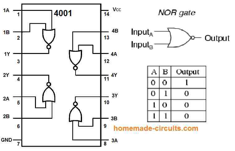 Remember that if both inputs are low, the output is high, but if either one of themor both inputs are high, the output turnslow.
The truth tables of each of the CD4011's four NAND gates are shown in Fig.
2 below.
The output is typically high, and only when both inputs are high does it become low.
Remember that if both inputs are low, the output is high, but if either one of themor both inputs are high, the output turnslow.
The truth tables of each of the CD4011's four NAND gates are shown in Fig.
2 below.
The output is typically high, and only when both inputs are high does it become low.
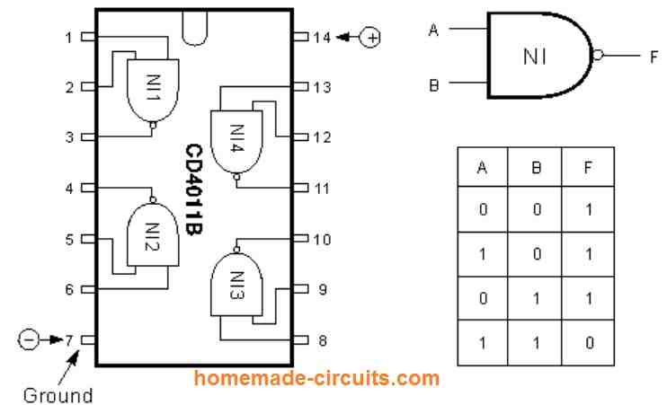 The CD4001 and CD401 1 are low-cost integrated circuits.
They are very cost-effective devices that may be implemented in a wide range of practical twin-gate CMOS multivibrator applications.
The CD4001 and CD401 1 are low-cost integrated circuits.
They are very cost-effective devices that may be implemented in a wide range of practical twin-gate CMOS multivibrator applications.
Bistable Multivibrator Circuits
Both the CD4001 and CD4011 may be utilized in two-gate R-S (Reset-Set) bistable multivibrator circuits, although their input triggering requirements are considerably different. The circuit and waveforms of a pulse-triggered NOR variant of the bistable are indicatedin Figure 3. A normal output from ICa and an inverted output from IC1b make up the circuit's outputs.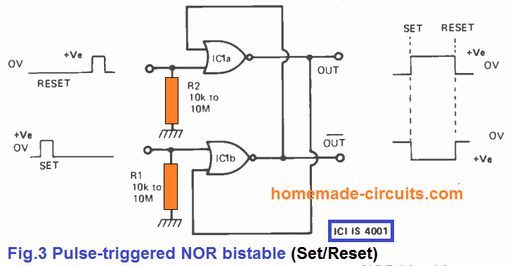 As soon asa positive-edged trigger pulse with a range of about zero to full supply is supplied to the IC1b input, the normal "set" output is turnedhigh and itremains in that conditionregardless of any subsequent signals at the 1C1 b input.
In this situation, it is possible toreset the outputlow onlyby applying a positive-going pulse to IC1a's input, after which the output turnslow and does not get affectedto any successive trigger pulses at the IC1a input.
Note that R1 and R2 are used to connect the input terminals of IC1a and IC1b to ground (the zero-volts line): these resistors could haveany useful value between 10k and 10M.
R1 and R2 can be removed from the circuit if the inputs to IC1a and IC1 b are direct-coupled from previous logic stages.
As soon asa positive-edged trigger pulse with a range of about zero to full supply is supplied to the IC1b input, the normal "set" output is turnedhigh and itremains in that conditionregardless of any subsequent signals at the 1C1 b input.
In this situation, it is possible toreset the outputlow onlyby applying a positive-going pulse to IC1a's input, after which the output turnslow and does not get affectedto any successive trigger pulses at the IC1a input.
Note that R1 and R2 are used to connect the input terminals of IC1a and IC1b to ground (the zero-volts line): these resistors could haveany useful value between 10k and 10M.
R1 and R2 can be removed from the circuit if the inputs to IC1a and IC1 b are direct-coupled from previous logic stages.
Manual NOR Gate
A manually triggered equivalent of the NOR gate circuit in Fig. 3 is shown in Fig. 4. Because the output of this circuit is not affectedby the contact bounce, etc. of its two control switches, it is typically called a 'noiseless' switch.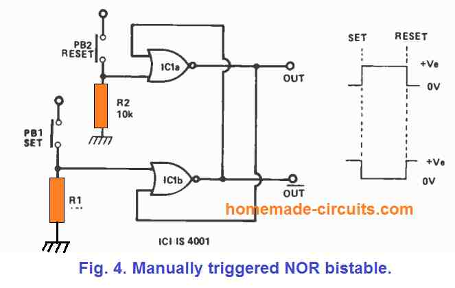
Bistable NAND
The CD4011 NAND gate variant of the bistable circuit is shown in Fig. 5.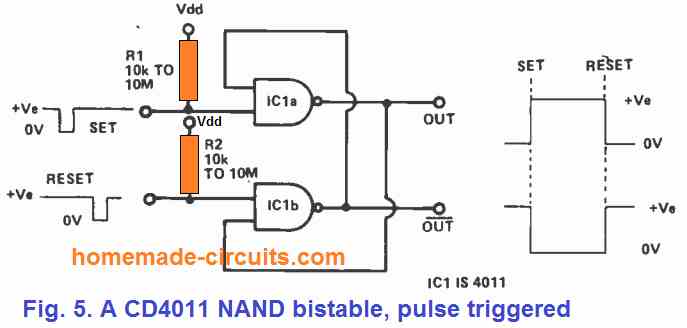 Except for the placement of R1 and R2, this circuit is essentially similarto that in Fig.
3. Note, however, that the NOR gate circuit requires apositive-edgedtrigger pulses, whereas the NAND gate circuit requires negative-edgedpulses, and that the set pulse in the NOR circuit is applied to IC1b, whereas the set pulse in the NAND circuit is applied to IC1a.
Except for the placement of R1 and R2, this circuit is essentially similarto that in Fig.
3. Note, however, that the NOR gate circuit requires apositive-edgedtrigger pulses, whereas the NAND gate circuit requires negative-edgedpulses, and that the set pulse in the NOR circuit is applied to IC1b, whereas the set pulse in the NAND circuit is applied to IC1a.
Manually Triggered NAND Bistable.
The manually-triggered variant of the NAND-type bistable is shown in Figure 6. Although R1 and R2 are depicted as having values of 10k, they can actually have resistance values ranging from a few thousand ohms to roughly 10M, depending on the specifications of the application.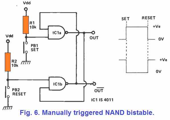
Touch-triggered NAND bistable
Because of this adaptability, the touch-triggered NAND bistable circuit of Fig. 7 was developed, wherein R1 and R2 have values of 10M and the circuit may be initiated by putting any resistance having a valueless than 10M (or examplefinger resistance) between the touch contacts.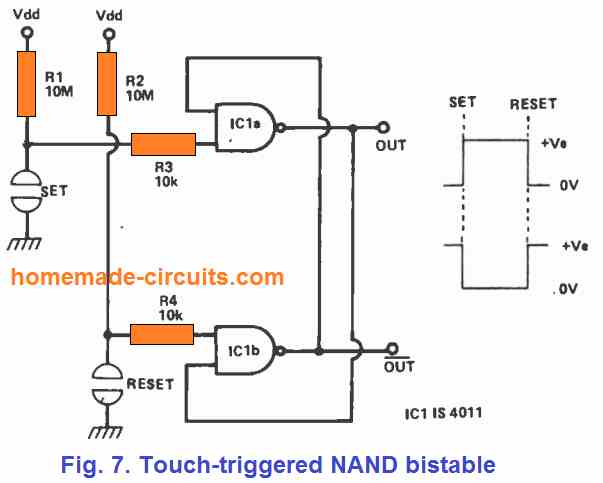 The inputs of the two gates are stabilized by the resistorsR3 and R4 in this circuit.
All of the bistable circuits we've seen so far employ trigger signals with identicalpolarity (either both positive or both negative).
In some applications, however, using reverse-polarity signals to activate the bistable is essential or convenient, and this sort of action may be achieved by connecting an inverter stage to one or both of the conventional bistable input terminals.
Figures 8 and 9 illustrate two different types of this circuit.
The inputs of the two gates are stabilized by the resistorsR3 and R4 in this circuit.
All of the bistable circuits we've seen so far employ trigger signals with identicalpolarity (either both positive or both negative).
In some applications, however, using reverse-polarity signals to activate the bistable is essential or convenient, and this sort of action may be achieved by connecting an inverter stage to one or both of the conventional bistable input terminals.
Figures 8 and 9 illustrate two different types of this circuit.
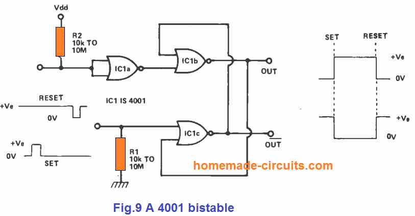 Different methods of connecting a 2-input NAND or NOR gate to serve as a basic pulse inverter stage are shown in Fig.
10. These circuits have a wide range of uses.
Different methods of connecting a 2-input NAND or NOR gate to serve as a basic pulse inverter stage are shown in Fig.
10. These circuits have a wide range of uses.
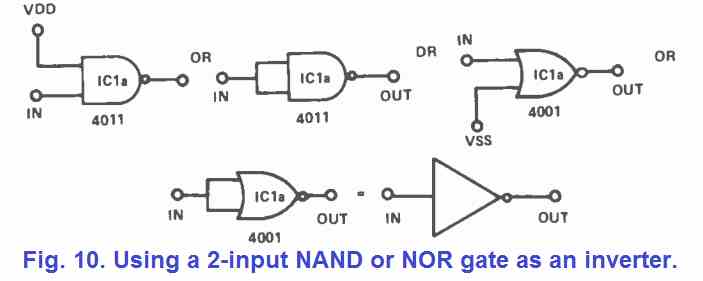
Basic 2-Gate Astable Circuits
The CD4001 and CD4011 are both 2-gate astable multivibrator circuits that may be implemented in a number of applications. Because the gates are linked as ordinary inverters in these circuits, both thetypes of IC provide similar results. Figure 11 depicts the most simple and practical 2-gate CMOS astable circuit.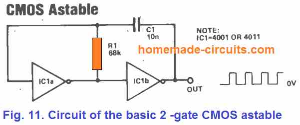 With the comfort parameters provided, this circuit offers a good square wave output, has great thermal stability, and runs at around 1 kHz.
Because the frequency is inversely proportional to the C-R time constant, it may be increased by reducing either C1 or R1.
Make sure that C1a non-polarized capacitor in practice, and its value can range from sometens of picofarads to a few microfarads.
The CD4001 and CD4011 are both 2-gate astable multivibrator circuits that may be implemented in a number of applications.
Because the gates are wired as ordinary inverters in these circuits, both thetypes of IC provide similar results.
R1 might be anything between 4k7 and 10M.
In the R1 slot, connect a fixed resistor and a pot/presetin series for variable frequency operation.
The output of the Fig.
11 astable circuit swings almost completely between the zero and positive supply voltage limits(using a lighter load).
However, the built-in clamping diodes at the input of IC1a prohibit the junction of R1 and C1 from swinging below zero or over the positive rail levels.
As a result of this aspect, the circuit's operational frequency is impacted by supply rail voltages to some extent.
As an approximaterule of thumb, for every 1% increase in supply voltage, the frequency drops by roughly 0.08 percent.
When this astable's frequency getsnormalized using a 10 volt supply, the frequency reduces by 4% at 15 volts and increases by 8% at 5 volts.
Furthermore, the working frequency of the Fig.
11 circuit is affected by the value of thetransfer voltage specs of the particular gate utilized, and can alterby up to 10% across different ICs.
The waveform's output symmetry is also determined by the IC's transfer voltage specs, and in most situations, the circuit will produce an asymmetrical output.
The shortcomings of the basic astable circuit tends to beof little practical importance in the large number of 'hobby' and other non-precision applications.
With the comfort parameters provided, this circuit offers a good square wave output, has great thermal stability, and runs at around 1 kHz.
Because the frequency is inversely proportional to the C-R time constant, it may be increased by reducing either C1 or R1.
Make sure that C1a non-polarized capacitor in practice, and its value can range from sometens of picofarads to a few microfarads.
The CD4001 and CD4011 are both 2-gate astable multivibrator circuits that may be implemented in a number of applications.
Because the gates are wired as ordinary inverters in these circuits, both thetypes of IC provide similar results.
R1 might be anything between 4k7 and 10M.
In the R1 slot, connect a fixed resistor and a pot/presetin series for variable frequency operation.
The output of the Fig.
11 astable circuit swings almost completely between the zero and positive supply voltage limits(using a lighter load).
However, the built-in clamping diodes at the input of IC1a prohibit the junction of R1 and C1 from swinging below zero or over the positive rail levels.
As a result of this aspect, the circuit's operational frequency is impacted by supply rail voltages to some extent.
As an approximaterule of thumb, for every 1% increase in supply voltage, the frequency drops by roughly 0.08 percent.
When this astable's frequency getsnormalized using a 10 volt supply, the frequency reduces by 4% at 15 volts and increases by 8% at 5 volts.
Furthermore, the working frequency of the Fig.
11 circuit is affected by the value of thetransfer voltage specs of the particular gate utilized, and can alterby up to 10% across different ICs.
The waveform's output symmetry is also determined by the IC's transfer voltage specs, and in most situations, the circuit will produce an asymmetrical output.
The shortcomings of the basic astable circuit tends to beof little practical importance in the large number of 'hobby' and other non-precision applications.
Compensated or Optimized Astable
The 'optimized' astable circuit of Fig.12, in which resistor R2 is connected in series with the input of IC1a, can eliminate some of these shortcomings.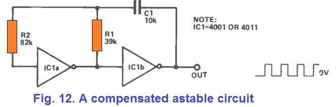 The key objective of the resistor R2, which may be any value between two and ten times that of R1, is to permit the R1-C1 line to swing smoothly between zero and positive supply rail voltages during the switching operation, minimizing the circuit working frequency's reliance on the supply voltage.
When R2 is ten times higher than R1, withthe supply voltage varyingbetween 5 and 15 volts, the frequency fluctuates by only approximately 0.5 percent.
Figures 11 and 12 show conventional and the optimizedastable circuits that can be constructed with a number of detailed modifications.
Figures 13 through 18 depict a few of these designs.
C1 charges and discharges via R1in the basic astable circuit, as anexample.
The key objective of the resistor R2, which may be any value between two and ten times that of R1, is to permit the R1-C1 line to swing smoothly between zero and positive supply rail voltages during the switching operation, minimizing the circuit working frequency's reliance on the supply voltage.
When R2 is ten times higher than R1, withthe supply voltage varyingbetween 5 and 15 volts, the frequency fluctuates by only approximately 0.5 percent.
Figures 11 and 12 show conventional and the optimizedastable circuits that can be constructed with a number of detailed modifications.
Figures 13 through 18 depict a few of these designs.
C1 charges and discharges via R1in the basic astable circuit, as anexample.
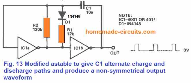 The basic circuit may be changed to provide different C1 charge and discharge channels, as shown in Figures 13 to 15. One method of altering the stable state of the circuitto produce a non-symmetrical output waveform is shown in Fig.
13. C1 charges through onedirection via R1 and R2 in tandem, resulting in a high output, however discharges in the other way via R2 individually, resulting in a low output.
The basic circuit may be changed to provide different C1 charge and discharge channels, as shown in Figures 13 to 15. One method of altering the stable state of the circuitto produce a non-symmetrical output waveform is shown in Fig.
13. C1 charges through onedirection via R1 and R2 in tandem, resulting in a high output, however discharges in the other way via R2 individually, resulting in a low output.
On/Off Control
Figure 14 depicts how the circuit may be enhanced by providing a diode in series with R2, allowing R1 to control the ON time of the output while R2 controls the OFF time. By substituting one or both of the timing resistors with a fixed resistorand a potentiometer in series, boththese circuits could be modified to produce adjustable outputs.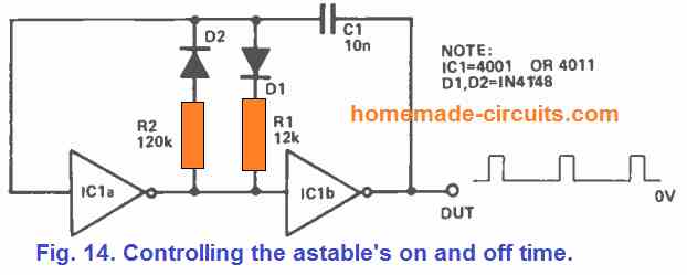
Variable Duty Cycle (PWM)
Figure 15 explains how to modify the astable to provide an adjustablePWM or mark/spaceratio output while the frequency is heldclose to constant.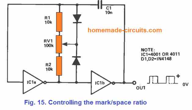 C1is charged in this circuit throughone particular directionvia D1-R2 and through 50%of RV1, and in the other direction through D2-R1 and the remaining50%of RV1. RV1 allows you to change the PWM mark/spaceratio between 1:10 and 10:1.
A multi-tone push-button operated astable's circuit can be seen in Fig.
16.
C1is charged in this circuit throughone particular directionvia D1-R2 and through 50%of RV1, and in the other direction through D2-R1 and the remaining50%of RV1. RV1 allows you to change the PWM mark/spaceratio between 1:10 and 10:1.
A multi-tone push-button operated astable's circuit can be seen in Fig.
16.
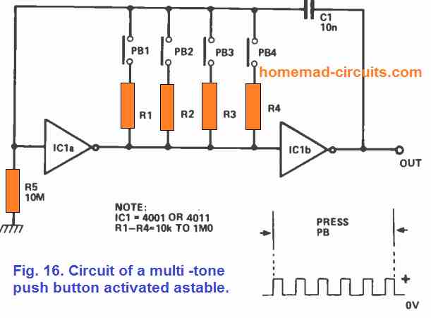 R5 normally keeps the input of IC1a (and consequently the output of IC1b) low while all push-button switches are open.
In case any of the push-button switches is closed, the circuit works likea standard astable,because the values of resistors R1 to R4 are all low in comparison to R5.
This circuit may be implemented in multi-tone musical devices, electronic organs, and other applications, and it has the benefit of using very tiny amount ofcurrent while in thesleep mode.
The number of push-button switches that may be employed with the circuit is unlimited.
R5 normally keeps the input of IC1a (and consequently the output of IC1b) low while all push-button switches are open.
In case any of the push-button switches is closed, the circuit works likea standard astable,because the values of resistors R1 to R4 are all low in comparison to R5.
This circuit may be implemented in multi-tone musical devices, electronic organs, and other applications, and it has the benefit of using very tiny amount ofcurrent while in thesleep mode.
The number of push-button switches that may be employed with the circuit is unlimited.
Frequency Modulation
Fig. 17 illustrates the method through whichthe astable could be integratedwith afrequency modulation or voltage control of frequency input,simply by connectingan externalvoltagesignal to the input of IC1a through a resistance that is significantlylarger than R1.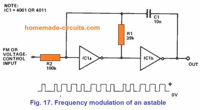 Fig.
18 indicates a simple method through which the circuit could be further enhanced to operate like a specialized voltage-controlled oscillator which is instantly switched OFF as soon as the input voltage drops below.
Fig.
18 indicates a simple method through which the circuit could be further enhanced to operate like a specialized voltage-controlled oscillator which is instantly switched OFF as soon as the input voltage drops below.
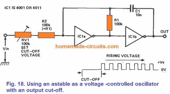 By simply replacing the IC1a inverter position with a two-input NAND or NOR gate, and assigning the input control signal to one of the gate input pin, each of theastable circuits in Figs.
11 to 15 could be customized for gated operation.
This arrangementallowsthem to be switchedon and off through an external signal.
By simply replacing the IC1a inverter position with a two-input NAND or NOR gate, and assigning the input control signal to one of the gate input pin, each of theastable circuits in Figs.
11 to 15 could be customized for gated operation.
This arrangementallowsthem to be switchedon and off through an external signal.
Gated Astable Circuits
The CD4001 and CD4011 ICs may also be utilized in this application, however their gate control and output functioning can besignificantly different. The two fundamental configurations of the gated astable circuit could be seen in Figures 19 and 20.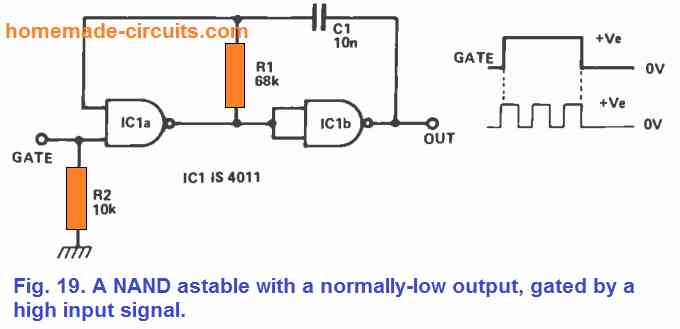 The NAND astable circuit in Fig.
19 consists ofa typically low output which is gated througha high input signal, whereas the NOR astable circuit in Fig.
20 has a usually high output which is gated througha low input signal.
The NAND astable circuit in Fig.
19 consists ofa typically low output which is gated througha high input signal, whereas the NOR astable circuit in Fig.
20 has a usually high output which is gated througha low input signal.
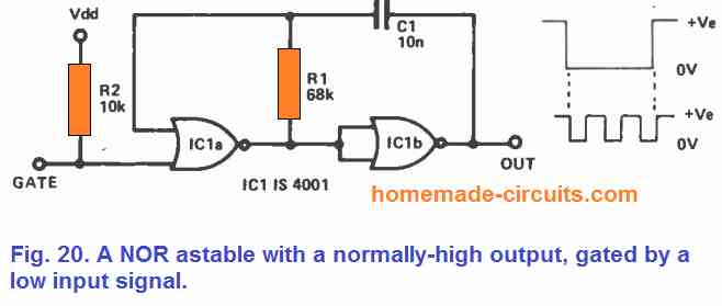 Also, while R2 is depicted in the picture witha value of 10k, R2 may actually have any value between 10k and 10M, or it can be removed entirely in casethe signal to thegate is fed viaa preceding logic state.
Eliminating Noise Interference
In the circuits shown in Figures 19 and 20, the output signal stops as soon as the input gate signal is disconnected. As a result, any noise interference existing at these circuitgate inputs likewise emerges at their outputs. Figures 21 and 22 below illustrate how to modify the circuits to correct this flaw.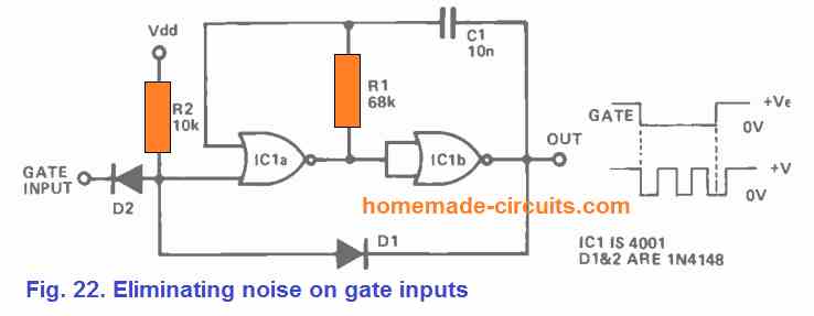 The gate signal of IC1ais obtained through diode OR gate D1-D2-R2 from both externallyand the output of IC1b.
When the circuit is gated externallyby D2, the output of IC1b causesthe gating to be strongervia D1 for eachhalf astable cycle, thus removing the impacts of interference in theexternal signal.
The circuitsoutputs are in the form of fullhalf-cycles.
Observe that R2 is an important component in these circuits.
The circuits from Figs.
21 and 22 are shown asmanual-triggered configurationsin Figs.
23 and 24. When push buttonPB1 is quickly pressed, they create a single crisp clock pulse; while PB1 is pushed down, they create five perfect clock pulses eachsecond.
With fast-acting counting and division circuits, the 2-gate astable circuittypically maynot beappropriate for direct implementationas a clock generator.
The gate signal of IC1ais obtained through diode OR gate D1-D2-R2 from both externallyand the output of IC1b.
When the circuit is gated externallyby D2, the output of IC1b causesthe gating to be strongervia D1 for eachhalf astable cycle, thus removing the impacts of interference in theexternal signal.
The circuitsoutputs are in the form of fullhalf-cycles.
Observe that R2 is an important component in these circuits.
The circuits from Figs.
21 and 22 are shown asmanual-triggered configurationsin Figs.
23 and 24. When push buttonPB1 is quickly pressed, they create a single crisp clock pulse; while PB1 is pushed down, they create five perfect clock pulses eachsecond.
With fast-acting counting and division circuits, the 2-gate astable circuittypically maynot beappropriate for direct implementationas a clock generator.
Generating Cleaner Clocks
Precise clock signals having sharprise and fall times are essential in thesecircuits. The issue is that 2-gate astables based on "A" series or non-buffered CMOS generate clock outputs havingsluggishrise and fall times, whilst 2-gate astables based on buffered-output 'B' series CMOS are designed to generateoutputs with excellent rise and fall times, however these may generate"dirty" clocking if their power supply lines happen to have eventhe slightest levelof noise. Thankfully, allthese issues may be readily solved by connecting a fewinverter-connected gate stages in seriesto the astable circuit's output, as illustrated in Figure 25.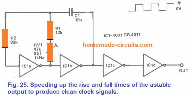 These inverter stages reduce or eliminate the noise impactson the clock circuit by speeding up the rise and fall periods of the astable output waveform, thusproducing excellent level shifting between the astable output and the clock input pinof a given externalsource.
3-Gate Astable for Improved Output Clocks
The "3-gate" astable circuit shown in Fig. 26 is another way to implement a clock generator. The locations of R1 and C1 are swapped in this design, and the inverting input stage (1C1a) in the Fig. 11 circuit is essentially substitutedby an ultra-high-gain non-inverting stage (consisting ofIC1a and IC1b in series) in Fig. 2. The Fig. 26 '3-gate' circuit offers an excellent clean output waveform with anexceptional rise and fall timings. Therefore, itis highly suited for use as a clock generator due to the extremelyhigh gain of its combined input stages.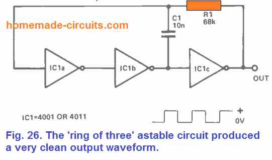 The complete fundamental design modifications described for the two-gate astable may be also applied to the '3-gate' astable circuit.
For example, in the Fig.
11 circuit, C1 alternately charges and discharges through R1, allowing the circuit to be exposed to all of the modifications indicated in Figs.
13 to 15.
It can be built in the standard or 'compensated' forms, for example.
Since it may be gated on and off through either its IC1b or IC1c stages, the '3-gate' astable circuit provides fascinating capabilities when implemented in the gated mode.
The complete fundamental design modifications described for the two-gate astable may be also applied to the '3-gate' astable circuit.
For example, in the Fig.
11 circuit, C1 alternately charges and discharges through R1, allowing the circuit to be exposed to all of the modifications indicated in Figs.
13 to 15.
It can be built in the standard or 'compensated' forms, for example.
Since it may be gated on and off through either its IC1b or IC1c stages, the '3-gate' astable circuit provides fascinating capabilities when implemented in the gated mode.
Controlling NOR Gates with an External Signal
Figures 27 to 30 depict four different interpretations on the topic. Alternative configurations of the gated NOR-type '3-gate' circuit can be seen in Figures 27 and 28. To turn the astable on, both circuits require a 'low' signal.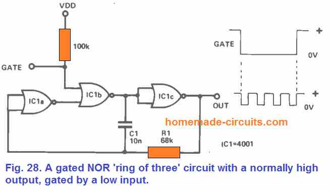 It should be noted that the circuit's output is typically low when IC1c is applied with a gate signal, and typically high when the IC1b is subjected to a gate signal.
Identical differences may be observed in the gated '3-gate' NAND design, as indicatedin Figs.
29 and 30.
It should be noted that the circuit's output is typically low when IC1c is applied with a gate signal, and typically high when the IC1b is subjected to a gate signal.
Identical differences may be observed in the gated '3-gate' NAND design, as indicatedin Figs.
29 and 30.
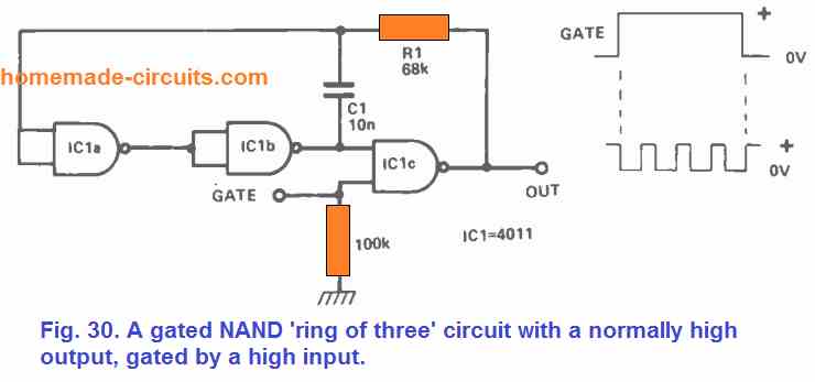 These circuits require a 'high' signal to turn on, and exhibita typically low output when the gate signalis appliedto IC1b or a normally high output with an application ofthe gate signal to IC1c.
CMOS Monostables
Both the CD4001 and CD4011 may be utilized to build a very useful 2-gate monostable multivibrator or pulse generator circuit. Figures 31 and 32 illustrate a couple ofbasic variants of this circuit. The length of the output pulse in these circuits is governed by the R1 and C1 values, whichis about one second per microfarad of C1,when R1 is 1M5.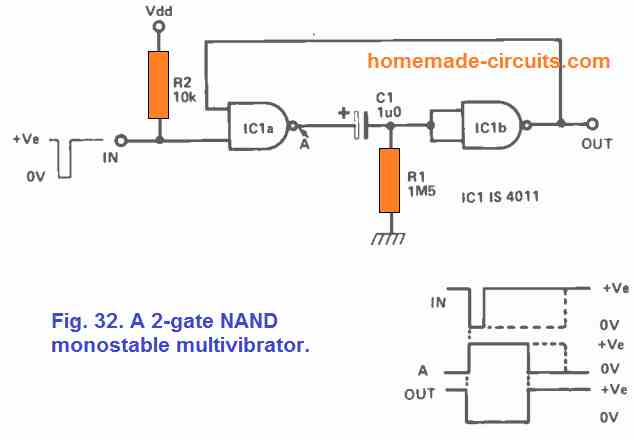 In reality, C1 could use any value between 100p and severalthousand uF, while R1 could have any magnitudebetween 4k7 and 10M.
One distinguishing property of these circuits is that the input trigger signal could be directly linked and therefore has no discernible influence on the duration of the circuit's output pulse: The length of the trigger pulse might be shorter or greater than the length of the output pulse.
The NOR type exhibitsa typically low output and is activated by a positive-edgedinput pulse, whereas the NAND type CMOS gate producea normally high output and is driven by a negative-edgedinput pulse.
The pulse signal arriving at point "A" has the same duration as either the output pulse or the input trigger pulse, determined by the signalwhich is the larger of the two.
This function is useful for creating pulse-length comparators and over-speed monitors, among other things.
There are just two substantial imperfections in the circuits shown in Figures 31 and 32. One of them is that the pulse length is influenced by the transfer voltage specificationsof the particular IC in the circuit.
The second defectis that the pulse duration is affected by the level of thesupply voltage employed in the circuit, in the same way asthe operating frequency of a simple two-gate CMOS astable is affected by the supply voltage variations.
However, in the majority of implementations, these flaws tend to beinsignificant.
An inverter stage must be inserted between the outputs and inputs of consecutive monostables to execute the rightpolarity trigger signals in caseseveral ofthe Fig.
31 and 32 circuits are to be coupled for generatingcascaded delays (as in a delayed-pulse generator, for instance).
The fundamental mechanism block diagram can be seen in Figure 33.
In reality, C1 could use any value between 100p and severalthousand uF, while R1 could have any magnitudebetween 4k7 and 10M.
One distinguishing property of these circuits is that the input trigger signal could be directly linked and therefore has no discernible influence on the duration of the circuit's output pulse: The length of the trigger pulse might be shorter or greater than the length of the output pulse.
The NOR type exhibitsa typically low output and is activated by a positive-edgedinput pulse, whereas the NAND type CMOS gate producea normally high output and is driven by a negative-edgedinput pulse.
The pulse signal arriving at point "A" has the same duration as either the output pulse or the input trigger pulse, determined by the signalwhich is the larger of the two.
This function is useful for creating pulse-length comparators and over-speed monitors, among other things.
There are just two substantial imperfections in the circuits shown in Figures 31 and 32. One of them is that the pulse length is influenced by the transfer voltage specificationsof the particular IC in the circuit.
The second defectis that the pulse duration is affected by the level of thesupply voltage employed in the circuit, in the same way asthe operating frequency of a simple two-gate CMOS astable is affected by the supply voltage variations.
However, in the majority of implementations, these flaws tend to beinsignificant.
An inverter stage must be inserted between the outputs and inputs of consecutive monostables to execute the rightpolarity trigger signals in caseseveral ofthe Fig.
31 and 32 circuits are to be coupled for generatingcascaded delays (as in a delayed-pulse generator, for instance).
The fundamental mechanism block diagram can be seen in Figure 33.
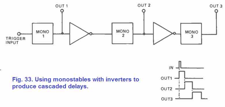
Sound Generator Alarm Call Circuits
A CD4001 or CD4011 IC with one or more transistors may be implementedto create a range of highly effective sound alarm system designs. Some experimental circuits of this kind are presented in Figs. 34 to 41. The circuits can be operated in all situations through any source usingthe 5V to 15V range and may be employed with any3R to 100R speakers. Depending on the speaker impedance and the supplyvoltages chosen, the output power mayrangefrom manyhundreds of milliwatts which could beincreased simply to 10 watts by includingextra power boosting transistorstages. Two variants of a monotone latching signal generator are displayed in Figure 34 and 35. IC1a and IC1 b are interconnected and the 1C1c-IC1d-1 kHz astable tones are connected to the IC1a-IC1b bistable automatic latchesand switches. By temporarily shutting PB1, the circuit could be reset to the OFF mode.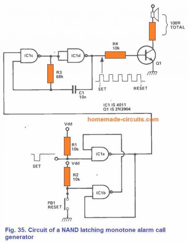 The auto-turn-off monotone alarm generator implementations can be seen in Figs.
36 and 37. IC1a and IC1b can be seenconnected as a monostable multivibrator and wheneverthe IC1c-IC1d areactivated, it switches on theastable for approximately 10 seconds.
The auto-turn-off monotone alarm generator implementations can be seen in Figs.
36 and 37. IC1a and IC1b can be seenconnected as a monostable multivibrator and wheneverthe IC1c-IC1d areactivated, it switches on theastable for approximately 10 seconds.
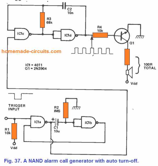 When a proper control signal is provided to the inputof IC1a, the circuits in Figures 38 and 39 create a pulsed-tone signal which allowsa 1 kHz astable (IC1c and IC1d) to begated on and off througha 6 Hz astable (IC1a and IC1b).
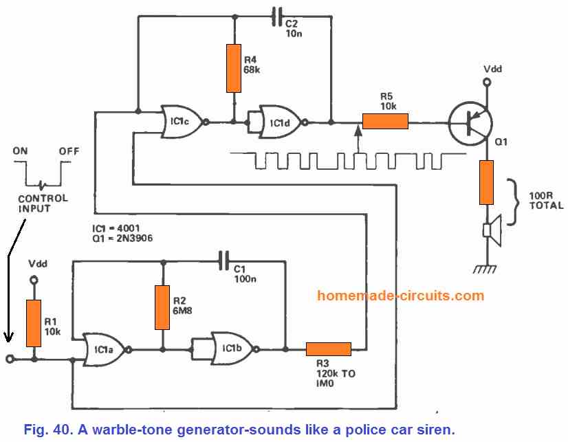 This results in the generation ofa pulsed tone signal.
Lastly, Fig.
40 illustrates a warble tone generator that creates a sound comparable to a British police car siren by switching across a 2-tone cycle during each second, in response toan appropriate control signal introduced to the inputs of IC1a and IC1c.
R3, that can be selected to haveany value in the approximate range of 120k to 1M, determines the intensity of thecircuit's frequency fluctuation.
This results in the generation ofa pulsed tone signal.
Lastly, Fig.
40 illustrates a warble tone generator that creates a sound comparable to a British police car siren by switching across a 2-tone cycle during each second, in response toan appropriate control signal introduced to the inputs of IC1a and IC1c.
R3, that can be selected to haveany value in the approximate range of 120k to 1M, determines the intensity of thecircuit's frequency fluctuation.
IC 4047 Astable, Monostable Circuits
In an IC 4047 astable oscillator circuit, the output of the IC continuously generates a switching ON/OFF signal. Since the output is never in a stable state and constantly switches between and low and high, it is called an astable multivibrator. The astable ON/OFF switching frequency is adjustable and can be varied by changing the values of the RC network of the circuit. In a 4047 monostable configuration, the output of the IC generates a single momentary switch ON pulse in response to a brief trigger pulse at the input pin. The momentary ON output pulse is adjustable and can be varied by modifying the values of the RC network of the circuit. The 4047 CMOS IC is specifically designed to be used as an astable or monostable multivibrator. We will first learn the working of an astable mode using this IC, and later on understand the different monostable operating modes and their configurations.4047 Astable
The first figure below demonstrates the IC 4047 rigged in the true gating astable mode, where the circuit begins oscillating as soon as a high gate signal input is detected, whereas the oscillation quickly ceases when this input signal is rendered low. When the IC is required to run in a free running astable mode, the very same standard 4047 astable circuit becomes applicable, although in this case the pin#5 of the IC 4047 must be hooked up to the positive supply line.
In this mode the IC 4047 is able to generate an anti-phase oscillating outputs across its Q and "not Q" pinouts.
This feature turns the IC into a handy device for applications in which a pair of anti-phase clock signal outputs are mandatory.
When the input gated supply turns low or switches OFF, causes the Q output of the IC to go low while the not Q output of the IC is turned high.
There also exists a third output in the form of pin#13 of the IC 4047 and from this pinout we get an output signal whose frequency is two times (2f) more than the frequencies generated across the primary Q and "not Q" pinouts.
The waveform across all the above three outputs of 4047 is a an ideal squarewave.
Each single output waveform cycle can be calculated through the equation
T = 4.4RC seconds.
The output frequency of the IC can be determined using the equation
f = 1/4.4RC Hz
Timing components R1 and C1 of the IC, are configured discretely using an external resistor and capacitor.
R1 can be selected to have any value between 10k to 1M, while the capacitor Cl can have any value above 100pF.
However, make sure that capacitor C1 is not a polarized capacitor, and its maximum value is recommended to be below 2.2uF.
When the IC is required to run in a free running astable mode, the very same standard 4047 astable circuit becomes applicable, although in this case the pin#5 of the IC 4047 must be hooked up to the positive supply line.
In this mode the IC 4047 is able to generate an anti-phase oscillating outputs across its Q and "not Q" pinouts.
This feature turns the IC into a handy device for applications in which a pair of anti-phase clock signal outputs are mandatory.
When the input gated supply turns low or switches OFF, causes the Q output of the IC to go low while the not Q output of the IC is turned high.
There also exists a third output in the form of pin#13 of the IC 4047 and from this pinout we get an output signal whose frequency is two times (2f) more than the frequencies generated across the primary Q and "not Q" pinouts.
The waveform across all the above three outputs of 4047 is a an ideal squarewave.
Each single output waveform cycle can be calculated through the equation
T = 4.4RC seconds.
The output frequency of the IC can be determined using the equation
f = 1/4.4RC Hz
Timing components R1 and C1 of the IC, are configured discretely using an external resistor and capacitor.
R1 can be selected to have any value between 10k to 1M, while the capacitor Cl can have any value above 100pF.
However, make sure that capacitor C1 is not a polarized capacitor, and its maximum value is recommended to be below 2.2uF.
Complement Gating
The 4047 can also work as an astable multivibrator with a complement gating. In this configuration the circuit is disabled by applying a high gate signal and it is enabled as soon as the gate signal is turned low. The IC 4047 complement gating astable circuit can be witnessed in the following figure.
4047 Monostable
The 4047 CMOS IC works extremely well in the monostable multivibrator configuration and also in the astable mode. There can be 3 monostable configurations in which IC 4047 can be used: positive triggered, negative triggered, and retriggerable. In the positive triggered method, the triggering is executed through a low logic turning into a high logic.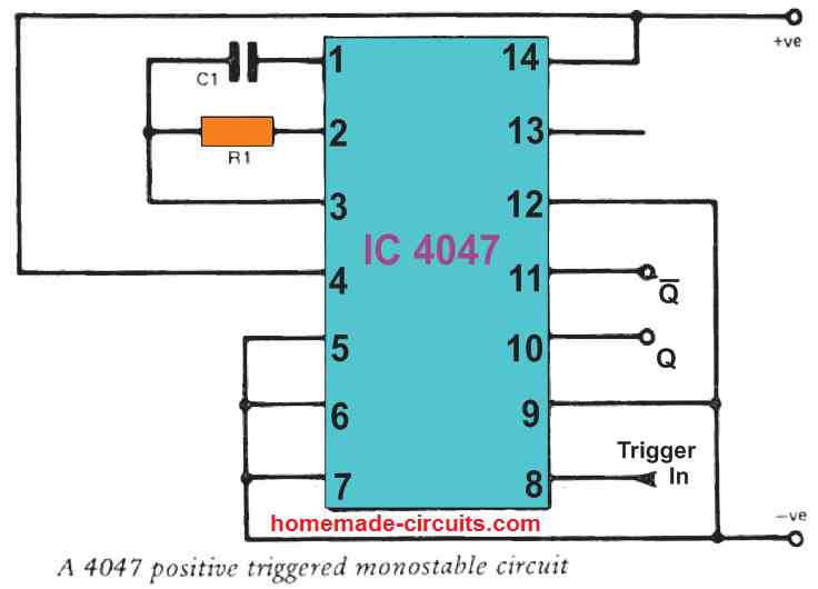 The negative triggering is implemented in the opposite way by applying an input logic that starts from a high state to a low state.
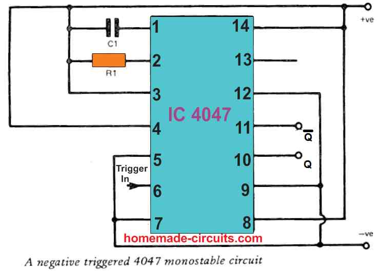 In both the above modes, the output pulse shuts off after the specified time interval lapses, regardless of whether the input is still in the triggering state or not.
The retriggerable type differs in terms of this action from the previous two modes, and similar to a 555 monostable, the output pulse in the retriggerable mode does not shut off as long as the input trigger pulse persists.
In both the above modes, the output pulse shuts off after the specified time interval lapses, regardless of whether the input is still in the triggering state or not.
The retriggerable type differs in terms of this action from the previous two modes, and similar to a 555 monostable, the output pulse in the retriggerable mode does not shut off as long as the input trigger pulse persists.
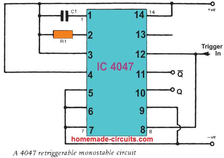 The 4047 retriggerable monostable circuit is triggered with a positive edge pulse, to be precise.
In all the above three configurations the output pulse duration is at a level determined by 2.48 RC seconds, where R1 is recommended to be between 10k and IM.
Timing capacitor C1 for the monostable circuits can be of any value higher than 1nF, but it should be strictly a polarized type.
In all the three variants the Q output is initially at low logic and it turns high to generate a positive output pulse, while the "not Q" output is initially high and provides a negative output pulse.
The 4047 retriggerable monostable circuit is triggered with a positive edge pulse, to be precise.
In all the above three configurations the output pulse duration is at a level determined by 2.48 RC seconds, where R1 is recommended to be between 10k and IM.
Timing capacitor C1 for the monostable circuits can be of any value higher than 1nF, but it should be strictly a polarized type.
In all the three variants the Q output is initially at low logic and it turns high to generate a positive output pulse, while the "not Q" output is initially high and provides a negative output pulse.
5 Simple Sine Wave Generator Circuits Explored
A sine wave generator is actually a sine wave oscillator circuit which generates an exponentially rising and falling sinusoidal waveform. The 5 simple sine wave generator circuits presented in the following article are easy to build, since they incorporate a small number of ordinary electronic components, and can be used for generating an exponentially varying waveform with a specified frequency. The frequency is determined by an RC feedback network between the input and output of the circuits. The kind of sine waveform that can be achieved from the following circuits can be witnessed in the following diagram:
1) High Quality Sine Wave Oscillator
The below indicated sine wave generator circuit is not only easy to build, it also provides an exceptionally pure output having a total noise and distortion level that is effectively under 0.1%. The design is a simple Wien Bridge oscillator configured around an operational amplifier.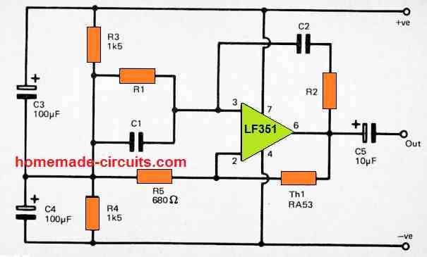 However, the circuit consists of thermistor Th2used for stabilizing the closed loop gain of the circuit with a magnitude which can generate a very good quality output sine wave signal with an amplitude of around 2 volts peak to peak.
The one downside of this circuit is the presence of RA53 thermistor which has a useful property of self heating.
This type of thermistor can be much costlier compared to the normal thermistors.
Nevertheless, the easy design of this sine wave generator and the an excellent sine wave output from this stabilization technique probably justifies the high cost.
Alternatively, you can replace the thermistor with a small 6 V incandescent bulb for getting the same effect
Capacitors C1, C2 and resistors R1, R2 are used for fixing the operating frequency of the output sine wave.
Here, the resistor R1 value can be same as R2, and likewise C1 and C2 can also have the identical values.
The frequency of sine wave could be determined through the following formula
Frequency = 1/2��CR
This implies that, if the operating frequency is approximately 1 kHz, then C1 and C2 could be around 4n7, and R1 and R2 could be set at 33k.
Modifying either the resistors or the capacitors allows an oppositely proportional variation in the frequency value.
It is recommended to have the values of the two resistors between a few kilohms and many Megohms.
For the capacitors any value in the range of a few pFs or higher can be just fine.
Having said that, you cannot use polarized type of capacitors like electrolytic or tantalum elements, and practically speaking this condition restricts the value of the capacitor to around 2.2uF maximum.
It is possible to make the output frequency of the sine wave adjustable by replacing the R1 and R2 with fixed resistors and by putting a potentiometer in series, and it is certainly essential to utilize a twin gang potentiometer to ensure that R1 and R2 series values could be altered in a combined way.
The circuit works with a least supply voltage of around 6 volts, and the the circuit can tolerate a absolute maximum 36 volts.
This simple sine wave generator circuit can be efficiently driven through a dual balanced power supply using the center tapped 0V supply being generated by the resistors R3, and R4.
If the circuit is powered through genuine dual supplies, then obviously, R3 + R4 tend to be unnecessary and could be eliminated.
However, the circuit consists of thermistor Th2used for stabilizing the closed loop gain of the circuit with a magnitude which can generate a very good quality output sine wave signal with an amplitude of around 2 volts peak to peak.
The one downside of this circuit is the presence of RA53 thermistor which has a useful property of self heating.
This type of thermistor can be much costlier compared to the normal thermistors.
Nevertheless, the easy design of this sine wave generator and the an excellent sine wave output from this stabilization technique probably justifies the high cost.
Alternatively, you can replace the thermistor with a small 6 V incandescent bulb for getting the same effect
Capacitors C1, C2 and resistors R1, R2 are used for fixing the operating frequency of the output sine wave.
Here, the resistor R1 value can be same as R2, and likewise C1 and C2 can also have the identical values.
The frequency of sine wave could be determined through the following formula
Frequency = 1/2��CR
This implies that, if the operating frequency is approximately 1 kHz, then C1 and C2 could be around 4n7, and R1 and R2 could be set at 33k.
Modifying either the resistors or the capacitors allows an oppositely proportional variation in the frequency value.
It is recommended to have the values of the two resistors between a few kilohms and many Megohms.
For the capacitors any value in the range of a few pFs or higher can be just fine.
Having said that, you cannot use polarized type of capacitors like electrolytic or tantalum elements, and practically speaking this condition restricts the value of the capacitor to around 2.2uF maximum.
It is possible to make the output frequency of the sine wave adjustable by replacing the R1 and R2 with fixed resistors and by putting a potentiometer in series, and it is certainly essential to utilize a twin gang potentiometer to ensure that R1 and R2 series values could be altered in a combined way.
The circuit works with a least supply voltage of around 6 volts, and the the circuit can tolerate a absolute maximum 36 volts.
This simple sine wave generator circuit can be efficiently driven through a dual balanced power supply using the center tapped 0V supply being generated by the resistors R3, and R4.
If the circuit is powered through genuine dual supplies, then obviously, R3 + R4 tend to be unnecessary and could be eliminated.
2) Simplified Sine wave Generator
The next figure below shows the circuit design of another sine wave generator that is essentially exactly like the previous design. However it works with a technique of gain stabilization which does not depend on an expensive thermistor.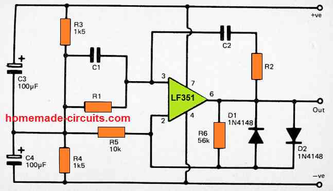 Diodes D1 and D2 are employed to minimize the closed loop gain of the amplifier as soon as the output voltage becomes higher than around +/-0.5 volts, which effectively prevents the circuit from going into a erratic oscillating mode.
This in turn avoids the possibility of high clipping and distortion on the output signal.
However, you may find a substantial level of distortion on the output sine wave output signal, which may not be acceptable for applications in which high quality sine wave is expected.
The output level of the sine wave signal is around 500mV RMS.
Diodes D1 and D2 are employed to minimize the closed loop gain of the amplifier as soon as the output voltage becomes higher than around +/-0.5 volts, which effectively prevents the circuit from going into a erratic oscillating mode.
This in turn avoids the possibility of high clipping and distortion on the output signal.
However, you may find a substantial level of distortion on the output sine wave output signal, which may not be acceptable for applications in which high quality sine wave is expected.
The output level of the sine wave signal is around 500mV RMS.
3) Using Audio Amplifier LM380
The circuit is built around an audio power amplifier device (IC1) utilized in a phase shift oscillator circuit. A three-section phase shift circuit is used to provide feedback between the output and the inverting () input of IC1. R2 - C1, R3 - C2, and R4 - C3 constitute the three parts, each of which provides 60 degrees of phase shift at a specific frequency. As a result, at this frequency, the three parts have a total phase shift of 180 degrees. With the provided settings, the circuit oscillates at roughly 1k5 Hz. A circuit of this nature should typically generate a sinewave output since a clean audiotone is pleasant to listen to for extended periods of time.
Here, this sine tone replicatesthe waveform generated by a real CW (Morse) communication when it is processed by a receiver.
If the gain of the amplifier just marginallycompensates morefor inefficiencies in the feed-back circuit, this circuit will produce a relatively pure sinewave.
This is accomplished by changing R1 to provide the desired loss level via the feed-back channel.
Due to the absence of feedback, it is backed off near the point where oscillation ends.
C4 and a break connection on the output jacksocket provide the output signal to the speakers.
If a plug is pushedinto the outputsocket, itimmediately turns off the speaker.
The unit has an output power of around 100 mW rms and a current usage of roughly 20mA when the key is depressed.
A circuit of this nature should typically generate a sinewave output since a clean audiotone is pleasant to listen to for extended periods of time.
Here, this sine tone replicatesthe waveform generated by a real CW (Morse) communication when it is processed by a receiver.
If the gain of the amplifier just marginallycompensates morefor inefficiencies in the feed-back circuit, this circuit will produce a relatively pure sinewave.
This is accomplished by changing R1 to provide the desired loss level via the feed-back channel.
Due to the absence of feedback, it is backed off near the point where oscillation ends.
C4 and a break connection on the output jacksocket provide the output signal to the speakers.
If a plug is pushedinto the outputsocket, itimmediately turns off the speaker.
The unit has an output power of around 100 mW rms and a current usage of roughly 20mA when the key is depressed.
4) Single Transistor Sine Wave Generator
A transistorized phase shift oscillator is a very easy to build circuit which can be used for generating a sine wave output signal. Having said that, until some kind of gain stabilization is employed it may generate an output with extreme distortion levels. The working frequency of this transistor sine wave generator is governed by 3 resistors and 3 capacitors. Due to the involvement of 3 frequency regulating components it may not be possible to apply this design in applications requiring a variable or an adjustable frequency capability. Another issue with this design is that it can be difficult to obtain gain stabilization satisfactorily. For this reason it may be advisable to use this phase shift oscillator only in those circuits where a fixed frequency and an inferior quality sine wave signal are acceptable.5) Another One Transistor Sine wave Oscillator
A basic phase shift oscillator may be built using a single transistor. The output is a sinewave with something like a 'lump,' indicating that the distortion percentage is somewhat significant, around 10%. This isn't always an issue; when creating audio tones, a largeharmonic content produces a much more intriguing sound. By inserting a potentiometer (25 ohms) into Q1's emitter lead, the sine wave perfection may be improved.Variable Sine Wave Generator Circuit
The circuit presented here generates a high-quality sinewave output across three continuously variable ranges (Range 1, lower than20Hz to over 200Hz; Range 2, lower than200Hz to over 2kHz; and Range 3, lower than2kHz to over 20kHz), which span more than the full audio frequency spectrum. The Wien Bridge type circuit is used, which comprises of an amplifier with frequency selective positive feedback given by a C-R network. This network's capacitive elements can be whatever isswitched by thetwo capacitors SW1. R6, R7, and RV1 are the resistive components, with the latter allowing the sine wave outputto be adjusted throughout the above mentioned ranges.
This network offers positive feedback over the FET-based operational amplifier IC1, which has low noise and distortion.
The non-inverting input of IC1 is likewise biased by RV1a and R6 to a central tapping on the supply generated by R1, R2, and C2. If satisfactory waveformsare to be achieved, the closed loop gain of IC1 should be kept at exactly the right amount.
To ensure steady operating parameters and a consistent sine output level, an automated gain control (AGC) circuit is utilized.
A negative feedback network is formed by R5, R4, and Q1's drain to source resistance, that regulates the closed loop gain of IC1. Q1 is first forward biassed through R3 in order to provide adequategain for powerful oscillation.
R8 and C10 link a little of IC1's output to a rectifier and smoothing network made up of D1, D2, and C3. This results in a positive bias, which attempts to turn off Q1, resulting in lower circuit gain.
The higher the bias and the smaller the gain, the harder the circuit oscillates.
The output may be variedfrom zero to roughly 1V5 rms using the adjustable attenuator RV2. The circuit's current usage is around 7 milliamperes.
R6, R7, and RV1 are the resistive components, with the latter allowing the sine wave outputto be adjusted throughout the above mentioned ranges.
This network offers positive feedback over the FET-based operational amplifier IC1, which has low noise and distortion.
The non-inverting input of IC1 is likewise biased by RV1a and R6 to a central tapping on the supply generated by R1, R2, and C2. If satisfactory waveformsare to be achieved, the closed loop gain of IC1 should be kept at exactly the right amount.
To ensure steady operating parameters and a consistent sine output level, an automated gain control (AGC) circuit is utilized.
A negative feedback network is formed by R5, R4, and Q1's drain to source resistance, that regulates the closed loop gain of IC1. Q1 is first forward biassed through R3 in order to provide adequategain for powerful oscillation.
R8 and C10 link a little of IC1's output to a rectifier and smoothing network made up of D1, D2, and C3. This results in a positive bias, which attempts to turn off Q1, resulting in lower circuit gain.
The higher the bias and the smaller the gain, the harder the circuit oscillates.
The output may be variedfrom zero to roughly 1V5 rms using the adjustable attenuator RV2. The circuit's current usage is around 7 milliamperes.
White Noise and Pink Noise Generator Circuit
In this post we discuss how to build a simple white noise generator circuit which can be subsequently filtered to generate the pink noise output. If you hear to the white noise or pink noise, you will find it exactly similar to the noise that we hear in FM radios in the absence of a radio station, or in TV sets showing only raster, in the no signal condition. More information about pink noise can be studied in the following article: https://en.wikipedia.org/wiki/Pink_noise
What is Noise
A noise is normally an unwanted element that can worsen the efficiency of any measuring instrument. Hence it may appear weird that any user would require the generation of such noise, however you may find this to be quite normal. Noise generators are quite frequently accustomed to introduce noise in radio-frequency amplifiers so that it enables the user to diagnose the amplifier's low signal efficiency. Noise generation are also found useful for checking sound systems, and like a random signal generator while introducing wind-like sound effects in music outputs. You will find a couple of widely used noise generator characteristics, which are 'pink noise' and 'white noise'.What is White Noise
White noise is called by this name because it possesses identical noise strength in equivalent bandwidths within the entire frequency range in question. Therefore, for instance, a white noise source might possess equal energy inside the 100 to 200 Hz frequency bands upto the band of 5000 to 5100 Hz. When the white noise goes through a filtration process or a modification, it is referred to as colored noise or, usually to be more precise it is referred to as the 'pink' or 'grey' noise.What is Pink Noise
The definition of pink noise is usually restricted to the noise characteristic which includes identical energy per percentage change in bandwidth. For instance when a genuine pink noise is considered, the energy between 100 Hz and 200 Hz must be identical to that between 5000 Hz and 10,000 Hz (a change of 100% in each of the scenarios). Pink noise as a result seems to possess a high degree of bass frequency compared to what the white noise may have. Hearing the pink noise might appear a lot more consistent and stable, during the testing process. In order to convert white noise to pink noise, it needs to go through a filtering process which causes its output level to decrease by 3 dB per octave or by 10 dB per decade, as the frequency is increased.How the Circuit Works
 Referring to the pink noise generator circuit above, the transistor Q1 can be actually seen configured like a zener diode.
The typical base-emitter junction wiring can be seen reverse-biased which gets into a zener break down situation at approximately 7 to 8 volts.
The Q1 zener noise current passes to the Q2 base, causing the generation of around 150 millivolts white noise at the output .
This `zener' configuration, no only works like a noise source, but also does the job of biasing Q2 effectively, and the Q2 noise output is applied straight to the White Noise output.
To be able to transform the white noise to pink it would need to go through a filtering process, that gives a 3 dB cut per octave as the frequency is raised.
A normal RC network may not be appropriate for implementing like a individual RC stage for getting a cut of 6 dB per octave.
For this reason a unique resistor Rs and capacitor Cs circuitry becomes necessary for approximating the intended 3 dB-per-octave slope.
Because this kind of a filter is able to produce a high level of attenuation of the noise, an amplifier become necessary in order to restore the output level.
For this exact reason the transistor Q3 is wired like an amplifier with the pink noise filter linked as a feedback network across the collector and base.
This enables you to get the necessary quality through the control of the gain-versus-frequency characteristics of the transistor.
In this way we are able to get the required pink noise from the output of transistor Q3, which is then supplied to the indicated output socket of the circuit.
Referring to the pink noise generator circuit above, the transistor Q1 can be actually seen configured like a zener diode.
The typical base-emitter junction wiring can be seen reverse-biased which gets into a zener break down situation at approximately 7 to 8 volts.
The Q1 zener noise current passes to the Q2 base, causing the generation of around 150 millivolts white noise at the output .
This `zener' configuration, no only works like a noise source, but also does the job of biasing Q2 effectively, and the Q2 noise output is applied straight to the White Noise output.
To be able to transform the white noise to pink it would need to go through a filtering process, that gives a 3 dB cut per octave as the frequency is raised.
A normal RC network may not be appropriate for implementing like a individual RC stage for getting a cut of 6 dB per octave.
For this reason a unique resistor Rs and capacitor Cs circuitry becomes necessary for approximating the intended 3 dB-per-octave slope.
Because this kind of a filter is able to produce a high level of attenuation of the noise, an amplifier become necessary in order to restore the output level.
For this exact reason the transistor Q3 is wired like an amplifier with the pink noise filter linked as a feedback network across the collector and base.
This enables you to get the necessary quality through the control of the gain-versus-frequency characteristics of the transistor.
In this way we are able to get the required pink noise from the output of transistor Q3, which is then supplied to the indicated output socket of the circuit.
Using a Single Transistor
A simple white and pink noise generator could be constructed with the help of a single transistor and a Zener diode. The 10 volt Zener serves like the noise source and it furthermore stabilizes the operating level of the transistor. Putting a capacitor C2 at the indicated position will convert the output from 'white' noise to 'pink' noise.
Using the specified components and the supply input, the white noise level of output voltage will be around 15V, and the pink noise level of output voltage around 14.5 V.
The transistor could be a BC547 or any other similar small signal transistors can also work fine.
Putting a capacitor C2 at the indicated position will convert the output from 'white' noise to 'pink' noise.
Using the specified components and the supply input, the white noise level of output voltage will be around 15V, and the pink noise level of output voltage around 14.5 V.
The transistor could be a BC547 or any other similar small signal transistors can also work fine.
10 Easy Op amp Oscillator Circuits Explained
In an op amp oscillator circuit, an op amp is configured with a resistor-capacitor feedback loop or a inductor-capacitor feedback loop, which triggers the op amp to go into an oscillating mode, generating a switching ON/OFF pulses from its output pin. The high-gain and wide passband of operational amplifier (op amp) ICs makes it possible for these units to work like an oscillator within a wide range of frequency. The op amp oscillates immediately as soon as a feedback is employed across its noninverting input and tweaked to the appropriate amplitude. The IC becomes particularly important in resistance-capacitance-tuned oscillators, because its total gain becomes perfectly suitable to offset the attenuation of the RC network. Additionally, the double input of the differential IC enables not only positive feedback (for oscillation), but additionally allows the negative feedback in a few circuits (for enhancing the output waveform).1) Basic Working
A square-wave output can be easily generated by forcing an op amp to oscillate. The below indicated circuit combines a Schmitt trigger and an integrator. Consider the following scenario: the output is high, and C1 is charged through R3. Because of the resistor divider circuit R1, R2, the voltage at position 'A' is +0.9 V. As soon as the voltage at B gets higher than this, the op amp's output becomes negative (low).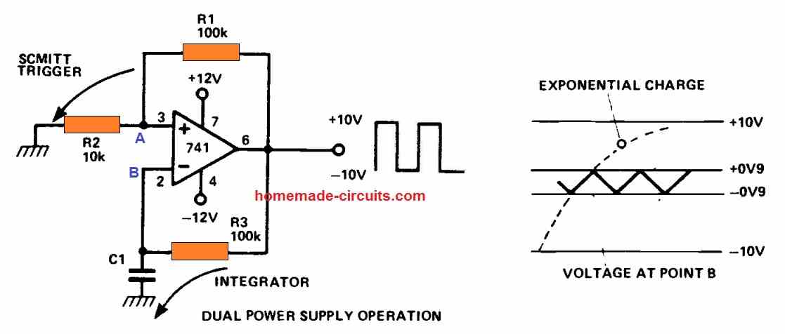 As a result, R3 discharges C1. Once the voltage on C1 falls below -0.9 V, the process is reversed, and the op amp output returns to its high state.
As a result, the circuit oscillates, creating a square wave with a voltage range of +10V to -10y.
The voltage fluctuations on C1 can be used to determine the workingfrequency of the op amp oscillator.
This is the collapsed portion of an exponential charge/discharge waveform, but we'll disregard it and pretend it's linear (which it almost is).
The frequency may be calculated using the following formula:
F = I / ��V x C
where I represents the charging current (about 100 A), ��V represents the charge over C1 (3.6 V), and C represents the capacitance in Farads.
The above design uses a dual supply for the operation, for a single supply operation, we can apply the following configuration:
As a result, R3 discharges C1. Once the voltage on C1 falls below -0.9 V, the process is reversed, and the op amp output returns to its high state.
As a result, the circuit oscillates, creating a square wave with a voltage range of +10V to -10y.
The voltage fluctuations on C1 can be used to determine the workingfrequency of the op amp oscillator.
This is the collapsed portion of an exponential charge/discharge waveform, but we'll disregard it and pretend it's linear (which it almost is).
The frequency may be calculated using the following formula:
F = I / ��V x C
where I represents the charging current (about 100 A), ��V represents the charge over C1 (3.6 V), and C represents the capacitance in Farads.
The above design uses a dual supply for the operation, for a single supply operation, we can apply the following configuration:
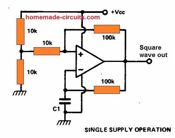 In the following paragraphs we will further learn about seven op amp IC oscillators, with three RC configurations, three LC configurations, and one crystal set up.
These are very common op amp oscillator circuits which could be applied with pretty much any high-gain operational-amplifier IC.
Since any op amp can be used in these configurations, the precise pin numbers aren't specified, except from the standard pins like the inverting input, noninverting input, input ground (common), and output.
The voltage supply pinouts are not indicated, considering that these (Vcc and Vee pinouts) can change with the specific IC.
Wherever feasible, the maximum functional working details is provided for all these basic configurations.
In the following paragraphs we will further learn about seven op amp IC oscillators, with three RC configurations, three LC configurations, and one crystal set up.
These are very common op amp oscillator circuits which could be applied with pretty much any high-gain operational-amplifier IC.
Since any op amp can be used in these configurations, the precise pin numbers aren't specified, except from the standard pins like the inverting input, noninverting input, input ground (common), and output.
The voltage supply pinouts are not indicated, considering that these (Vcc and Vee pinouts) can change with the specific IC.
Wherever feasible, the maximum functional working details is provided for all these basic configurations.
2) TWIN-T RC AF OSCILLATOR
The first figure below illustrates the a resistance-capacitance tuned AF op amp oscillator twin-T null network. This is implemented through the RC network of C1-C2-C3-R2-R3-R4, which decides the frequency level of the output.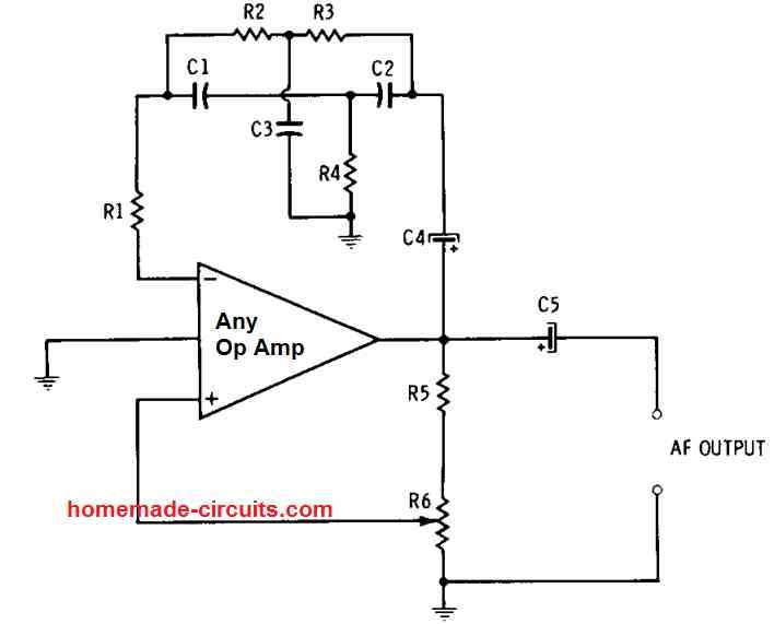 The op amp IC needs to have a voltage gain of 60 dB.
This set up is basically an intensely tuned af amplifier on which a positive feedback is introduced so that it begins oscillating.
The twin-T network is introduced in the negative-feedback loop, and since it works like a null network it helps in eliminating a particular frequency (fr) through the negative feedback.
The IC gain gets terminated appropriately at all other frequencies, while fr is conveniently transmitted forward.
In this oscillator network, the following formulas can be used for the calculations:
C1 = C2 = 1/2 C3
R2 = R3 = 2R4
fr = 1 / (2��R2C1)
In the above formula,
C's will be in farads,
R's will be in ohms,
and the unit of fr will be in hertz.
Coupling capacitor C4 blocks the DC current, and offers a high capacitance with respect to the capacitors C1, C2, and C3. It consequently doesn't have an effect on fr.
Resistor R1 offers a high resistance, based on the IC's input impedance, and helps to decrease loading of the twin-T network through the IC input circuit.
The inclusion of positive feedback, by means of the signal divider R5-R6, results in this very sharply tuned amplifier to oscillate with the frequency fr.
When the potentiometer R6 is adjusted to the level where the circuit merely starts to oscillate, output-signal distortion is found to be minimal.
The op amp oscillator circuit could be made to work like a continuously tunable oscillator (e.g., from 20 Hz to 20 kHz) simply by replacing the resistors R2, R3, R4 with a 3-ganged potentiometer, and selecting capacitors C1, C2, and C3 in trios to adjust the bands.
Output control could be accomplished through a potentiometer which may be configured either to the output or introduced between stages of the IC.
The op amp IC needs to have a voltage gain of 60 dB.
This set up is basically an intensely tuned af amplifier on which a positive feedback is introduced so that it begins oscillating.
The twin-T network is introduced in the negative-feedback loop, and since it works like a null network it helps in eliminating a particular frequency (fr) through the negative feedback.
The IC gain gets terminated appropriately at all other frequencies, while fr is conveniently transmitted forward.
In this oscillator network, the following formulas can be used for the calculations:
C1 = C2 = 1/2 C3
R2 = R3 = 2R4
fr = 1 / (2��R2C1)
In the above formula,
C's will be in farads,
R's will be in ohms,
and the unit of fr will be in hertz.
Coupling capacitor C4 blocks the DC current, and offers a high capacitance with respect to the capacitors C1, C2, and C3. It consequently doesn't have an effect on fr.
Resistor R1 offers a high resistance, based on the IC's input impedance, and helps to decrease loading of the twin-T network through the IC input circuit.
The inclusion of positive feedback, by means of the signal divider R5-R6, results in this very sharply tuned amplifier to oscillate with the frequency fr.
When the potentiometer R6 is adjusted to the level where the circuit merely starts to oscillate, output-signal distortion is found to be minimal.
The op amp oscillator circuit could be made to work like a continuously tunable oscillator (e.g., from 20 Hz to 20 kHz) simply by replacing the resistors R2, R3, R4 with a 3-ganged potentiometer, and selecting capacitors C1, C2, and C3 in trios to adjust the bands.
Output control could be accomplished through a potentiometer which may be configured either to the output or introduced between stages of the IC.
3) PHASE-SHIFT RC AF OSCILLATOR
The phase-shift form of tuned resistance-capacitance audio frequency oscillator are popular for their extremely low harmonic distortion. In this form of oscillator, RC tuning is achieved through a 180-degree phase-shift network configured within the feedback loop of an inverting amplifier.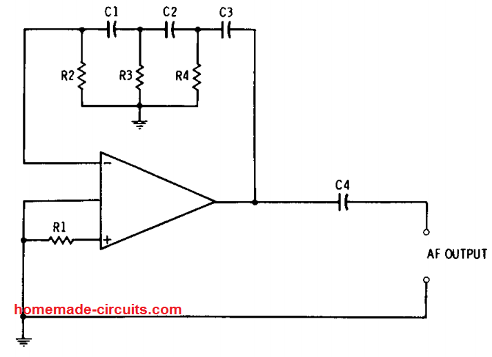 The network consequently generates the precise signal phase rotation for the oscillation.
Fig.
2 above demonstrates the configuration for a phase-shift-type IC oscillator.
In this set up, the phase shift network includes 3 RC legs in cascade pattern which are identical to each other: C1-R2, C2-R3, and C3-R4.
In this network , C1 = C2 = C3, and R2 = R3 = R4. All of these legs brings about a 60 degrees of phase shift.
The frequency level where the entire shift gets to 180 degrees can be determined through the below given formula:
fr= 1/ (10.88R2C1)
To be able to offset the built in attenuation of the RC system, the op amp's gain must be around 40 dB.
The op amp's noninverting input isn't utilized in this configuration, as it is delivered back to the ground by means of the resistor R1 ( which can be around 1000 ohms).
This op amp oscillator circuit could be turned into a continuously tunable type in the range of 20 Hz to 20 kHz, simply by replacing resistors R2, R3, R4, with a 3-gang potentiometer, and by switching the capacitors C1, C2, and C3 in trios, in order to select the bands.
But, the circuit's attenuation increases as the values of the resistances is reduced, and this situation could lead to the output-signal amplitude going down very fast with frequency, and oscillation may simply stop if R2, R3, and R4 are adjusted to lower values with the high frequencies.
Output control could be provided through a potentiometer which could be either connected to the output of the op amp oscillator circuit or introduced between the stages of the op amp.
The network consequently generates the precise signal phase rotation for the oscillation.
Fig.
2 above demonstrates the configuration for a phase-shift-type IC oscillator.
In this set up, the phase shift network includes 3 RC legs in cascade pattern which are identical to each other: C1-R2, C2-R3, and C3-R4.
In this network , C1 = C2 = C3, and R2 = R3 = R4. All of these legs brings about a 60 degrees of phase shift.
The frequency level where the entire shift gets to 180 degrees can be determined through the below given formula:
fr= 1/ (10.88R2C1)
To be able to offset the built in attenuation of the RC system, the op amp's gain must be around 40 dB.
The op amp's noninverting input isn't utilized in this configuration, as it is delivered back to the ground by means of the resistor R1 ( which can be around 1000 ohms).
This op amp oscillator circuit could be turned into a continuously tunable type in the range of 20 Hz to 20 kHz, simply by replacing resistors R2, R3, R4, with a 3-gang potentiometer, and by switching the capacitors C1, C2, and C3 in trios, in order to select the bands.
But, the circuit's attenuation increases as the values of the resistances is reduced, and this situation could lead to the output-signal amplitude going down very fast with frequency, and oscillation may simply stop if R2, R3, and R4 are adjusted to lower values with the high frequencies.
Output control could be provided through a potentiometer which could be either connected to the output of the op amp oscillator circuit or introduced between the stages of the op amp.
4) WIEN-BRIDGE RC AF OSCILLATOR
We have so far learned that the resistance-capacitance-tuned audio frequency oscillators involve 3 resistances and 3 capacitances for the tuning process. However, the op amp oscillator circuit displayed in Fig. 3 below requires just a couple of resistances (R1 and R2) and a pair of capacitances (C1 and C2) for the same tuning facility.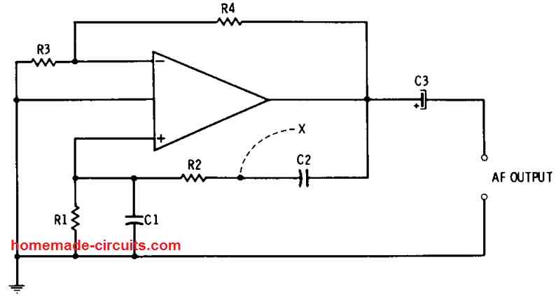 The C1-C2-R1-R2 network forms the 50 % of a Wien bridge network which, just like the twin-T network in Fig.
3-1, is sensitive to the frequency.
The RC configuration is attached inside the positive-feedback link (on the noninverting input terminal).
In this configuration, C1= C2, R1 = R2, and the frequency response can be determined using the below given equation:
fr = 1 / (2��R1C1)
In the above equation,
fr will be in hertz,
R1 will be in ohms,
C1 will be in farads
The resistors R3, and R4 does the job of providing the negative feedback (that works like a a signal voltage divider) to the inverting input terminal.
This negative feedback helps to reduce the output-signal distortion; but, it should be implemented with the right proportion (by appropriately adjusting R3 and R4).
This is important to ensure that it doesn't terminate the positive feedback leading to the elimination of the oscillation.
This form of op amp oscillator circuits could be easily turned into a continuously tunable oscillator in the range of 20 Hz to 1 MHz, simply by replacing the resistors R1, and R2 with a dual-gang potentiometer, and by ensuring that the capacitors C1 and C2 are switched in pairs in order to adjust frequency bands.
The tuning of the oscillator circuit can be implemented over a large frequency range, but, its output-signal amplitude might show a varying tendency with response to the frequency.
Nevertheless this varying tendency of the amplitude could be decreased using an appropriately dimensioned nonlinear resistor, for instance a thermistor, varistor, or double-ended zener diode, hooked up in between point "X" and ground.
Controlling the output of the oscillator can be executed through a potentiometer which may be either incorporated into the output or placed between the stages of the IC.
The C1-C2-R1-R2 network forms the 50 % of a Wien bridge network which, just like the twin-T network in Fig.
3-1, is sensitive to the frequency.
The RC configuration is attached inside the positive-feedback link (on the noninverting input terminal).
In this configuration, C1= C2, R1 = R2, and the frequency response can be determined using the below given equation:
fr = 1 / (2��R1C1)
In the above equation,
fr will be in hertz,
R1 will be in ohms,
C1 will be in farads
The resistors R3, and R4 does the job of providing the negative feedback (that works like a a signal voltage divider) to the inverting input terminal.
This negative feedback helps to reduce the output-signal distortion; but, it should be implemented with the right proportion (by appropriately adjusting R3 and R4).
This is important to ensure that it doesn't terminate the positive feedback leading to the elimination of the oscillation.
This form of op amp oscillator circuits could be easily turned into a continuously tunable oscillator in the range of 20 Hz to 1 MHz, simply by replacing the resistors R1, and R2 with a dual-gang potentiometer, and by ensuring that the capacitors C1 and C2 are switched in pairs in order to adjust frequency bands.
The tuning of the oscillator circuit can be implemented over a large frequency range, but, its output-signal amplitude might show a varying tendency with response to the frequency.
Nevertheless this varying tendency of the amplitude could be decreased using an appropriately dimensioned nonlinear resistor, for instance a thermistor, varistor, or double-ended zener diode, hooked up in between point "X" and ground.
Controlling the output of the oscillator can be executed through a potentiometer which may be either incorporated into the output or placed between the stages of the IC.
5) TRANSFORMER-FEEDBACK AF OSCILLATOR
Fig. 4 below displays the a basic af oscillator configuration where a small audio transformer (T1) is used for providing both the feedback and the tuning which forces the op amp to work like an oscillator. Any low-gain op amp IC could work effectively in this configuration.6) TRANSFORMER-FEEDBACK RF OSCILLATOR
The radio-frequency or the RF oscillator circuit indicated below in Fig. 5 is identical to the transformer-feedback af oscillator explained in the previous section, except that in this particular rf oscillator, positive feedback for the oscillation and tuning are supplied through an air-core transformer, L1-L2. Any low-gain IC could work effectively in this circuit.7) USING AF/RF OSCILLATOR TOGETHER
The Fig. 6 shown below exhibits an oscillator configuration that, which uses plug-in type inductors and capacitors, for producing both audio-frequency or radio-frequency signals through a diverse range of frequency.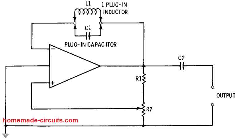 In this op amp oscillator set up, the positive and negative feedback are used both together.
The tuned circuit built using the L1, C1 parts connected in the negative-feedback loop decides the oscillation frequency of the circuit.
Since the L1, C1 works like a wavetrap, this tuned stage of the circuit eliminates its resonant frequency, fr, from the feedback loop.
The op amp consequently behaves like a sharply tuned amplifier, becomes responsible for transmitting the frequency fr.
However, its gain gets terminated at all other frequencies.
The positive feedback, provided by the resistors R1 and R2 which are configured like a signal voltage divider, subsequently enables the op amp to oscillate at frequency fr.
The parameters in this circuit can be calculated using the following given formulas:
In this op amp oscillator set up, the positive and negative feedback are used both together.
The tuned circuit built using the L1, C1 parts connected in the negative-feedback loop decides the oscillation frequency of the circuit.
Since the L1, C1 works like a wavetrap, this tuned stage of the circuit eliminates its resonant frequency, fr, from the feedback loop.
The op amp consequently behaves like a sharply tuned amplifier, becomes responsible for transmitting the frequency fr.
However, its gain gets terminated at all other frequencies.
The positive feedback, provided by the resistors R1 and R2 which are configured like a signal voltage divider, subsequently enables the op amp to oscillate at frequency fr.
The parameters in this circuit can be calculated using the following given formulas:
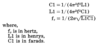 Using a high value capacitance and inductance together enables the generation of audio frequencies, whereas using lower values of capacitance and inductance enables the production of radio frequencies.
The strength at which the oscillation takes place is determined by the the adjustment of positive-feedback potentiometer R2. Therefore the R2 allows controlling the level of output-signal amplitude.
The circuit can work using a number of different op amps.
Considering that output-coupling capacitor C2 is required to generate both low and high frequencies, its value must be suitably adjusted to some intermediate value, for example it can be 0.01 ��F, unless of course the user is prepared to change this capacitor in addition to L1 and C1.
Using a high value capacitance and inductance together enables the generation of audio frequencies, whereas using lower values of capacitance and inductance enables the production of radio frequencies.
The strength at which the oscillation takes place is determined by the the adjustment of positive-feedback potentiometer R2. Therefore the R2 allows controlling the level of output-signal amplitude.
The circuit can work using a number of different op amps.
Considering that output-coupling capacitor C2 is required to generate both low and high frequencies, its value must be suitably adjusted to some intermediate value, for example it can be 0.01 ��F, unless of course the user is prepared to change this capacitor in addition to L1 and C1.
8) CRYSTAL-CONTROLLED RF OSCILLATOR
The below given Fig. 7 demonstrates an op amp based a crystal-controlled RF oscillator circuit that can work without the need of any tuning. This configuration can operate with multistage op amp circuits with various sensitivity levels. Having said that,it is advised to make use of medium and high-gain op amps.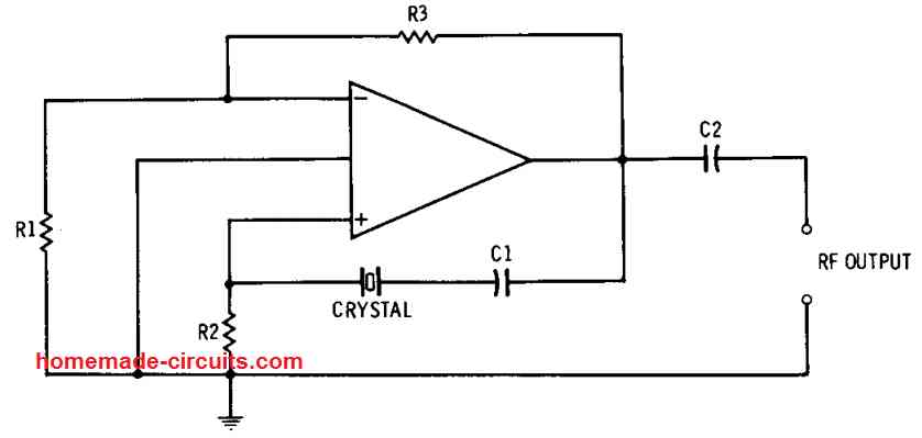 In this configuration, the crystal (XTAL) works like an exceptionally high-Q bandpass filter within the op amps's positive-feedback loop.
The positive-feedback current transferred through the crystal, builds up a voltage drop around resistor R2, which is utilized on the op amp's noninverting input pin of the IC.
This finally forces the circuity to oscillate with the crystal frequency.
Capacitor C1 is utilized simply for blocking the DC content, through a capacitance whose value specifically selected for low reactance at the crystal frequency.
The input ground of the op amp which is common ground is connected directly to the circuit ground, as indicated in the diagram.
The circuit can be also seen having a negative-feedback loop, created using the resistors R1 and R3, which constitues a signal voltage divider network.
Negative-feedback current flowing by means of this resistive divider causes a voltage drop to appear across resistor R1, which is supplied to the op amp's inverting input pin.
It may be important to adjust the amplitude of this voltage by appropriately setting up the values of the resistors R1 and R3. This ensures that the positive feedback does not gets terminated, eventually killing the oscillation.
The use of the negative feedback helps to enhance stability of this op amp oscillator circuit and also helps to minimize the output-signal distortion.
Nevertheless, this could be totally furnished only when a high harmonic output is needed, for example, in many of the transmitter type circuit applications.
In this configuration, the crystal (XTAL) works like an exceptionally high-Q bandpass filter within the op amps's positive-feedback loop.
The positive-feedback current transferred through the crystal, builds up a voltage drop around resistor R2, which is utilized on the op amp's noninverting input pin of the IC.
This finally forces the circuity to oscillate with the crystal frequency.
Capacitor C1 is utilized simply for blocking the DC content, through a capacitance whose value specifically selected for low reactance at the crystal frequency.
The input ground of the op amp which is common ground is connected directly to the circuit ground, as indicated in the diagram.
The circuit can be also seen having a negative-feedback loop, created using the resistors R1 and R3, which constitues a signal voltage divider network.
Negative-feedback current flowing by means of this resistive divider causes a voltage drop to appear across resistor R1, which is supplied to the op amp's inverting input pin.
It may be important to adjust the amplitude of this voltage by appropriately setting up the values of the resistors R1 and R3. This ensures that the positive feedback does not gets terminated, eventually killing the oscillation.
The use of the negative feedback helps to enhance stability of this op amp oscillator circuit and also helps to minimize the output-signal distortion.
Nevertheless, this could be totally furnished only when a high harmonic output is needed, for example, in many of the transmitter type circuit applications.
9) Using MOS Op Amp
A MOSFET op amp is configured asIC1. As a result, its input bias current is really very low, generally 10pA against 100nA for a 741. This enables the creation of circuitdesigns that use extremely little current. An integrator (IC1) and a Schmitt trigger are shown in the circuit (IC2). Assume that the Schmitt's output is high (+10V). R4, R5 have a voltage of around +1V at their junction. This sends a 1uA current via R1, which enables thecharging ofC1.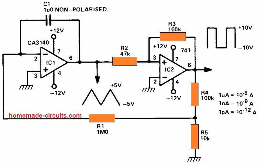 As a result, C1 (IC1's output) slopes down at the speed of 1/C, which in this example is 1V/sec.
The Schmitt trigger switches to its low logicstate when this voltage hits -5V.
(-10y).
The current subsequently travels in the opposite direction via R1, and the output of IC1 ratchets up at 1V/sec.
This process repeats until the voltage hits +5V.
(the upper hysteresis magnitudeof the Schmitt).
The Schmitt trigger then leaps to its highest output, repeating the period procedure.
A square wave (10V) and a triangle (5V) are generated by the circuit.
The time intervalis 20 using the parts indicated.
Set R1 = 10M for 200 seconds, and R1 = 10M, R5 = 1R for 2000 seconds.
As a result, C1 (IC1's output) slopes down at the speed of 1/C, which in this example is 1V/sec.
The Schmitt trigger switches to its low logicstate when this voltage hits -5V.
(-10y).
The current subsequently travels in the opposite direction via R1, and the output of IC1 ratchets up at 1V/sec.
This process repeats until the voltage hits +5V.
(the upper hysteresis magnitudeof the Schmitt).
The Schmitt trigger then leaps to its highest output, repeating the period procedure.
A square wave (10V) and a triangle (5V) are generated by the circuit.
The time intervalis 20 using the parts indicated.
Set R1 = 10M for 200 seconds, and R1 = 10M, R5 = 1R for 2000 seconds.
10) Low Frequency IC 741 Oscillator
Using only a 741 operational amplifier as a comparator, this circuit generates a low-frequency square wave.The frequency may be changed by altering the values of C1 (10u) and R4 (10k). A decrease in C1 or R4 raises the frequency, whereas an increase in value lowers it.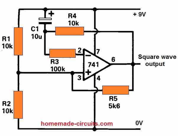 Imagine that the 741's output is low initially,to demonstrate how the circuit works.
The inverting input would be at a supply level that is less than half.
Assuming that C1 is also uncharged.
Due to the current flowing via R4, the bottomend of C1 will begin to drop in voltage until it reaches the value at pin 3. In this situation, t he output of the 741 (which compares voltages at pins 2 and 3) will turn positive.
C1 will repeat the processwhen the voltage at pin 3 rises to the other side of half supply, forcing the 741 output to follow and generatea squarewave.
Imagine that the 741's output is low initially,to demonstrate how the circuit works.
The inverting input would be at a supply level that is less than half.
Assuming that C1 is also uncharged.
Due to the current flowing via R4, the bottomend of C1 will begin to drop in voltage until it reaches the value at pin 3. In this situation, t he output of the 741 (which compares voltages at pins 2 and 3) will turn positive.
C1 will repeat the processwhen the voltage at pin 3 rises to the other side of half supply, forcing the 741 output to follow and generatea squarewave.
Op amp Oscillator, Formulas, and Design Considerations
An oscillator build using an op amp as the active element is called an op amp oscillator. In the following paragraphs we learn how to design op amp based oscillators, and regarding the many critical factors required for generating a stable oscillator design. Op amp based oscillators are normally used to generate precise, periodic waveforms like square, sawtooth, triangular, and sinusoidal. Generally they operate using a single active device, or a lamp, or a crystal, and associated by a few passive devices like resistors, capacitors, and inductors, to generate the output.Op-amp Oscillator Categories
You will find a couple of primary groups of oscillators: relaxation and sinusoidal. Relaxation oscillators produce the triangular, sawtooth and other nonsinuoidal waveforms. Sinusoidal oscillators incorporate op-amps using additional parts accustomed to create oscillation, or crystals which have in-built oscillation generators. Sine wave oscillators are employed as sources or test waveforms in numerous circuit applications. A pure sinusoidal oscillator features solely an individual or basic frequency: ideally without any harmonics. As a result, a sinusoidal wave could be the input to a circuit, using calculated output harmonics to fix the level of distortion. The waveforms in relaxation oscillators are produced through sinusoidal waves which are summed to deliver the stipulated shape. Oscillators are helpful for producing consistent impulses which are used as a reference in applications like audio, function generators, digital systems, and communication systems.Sine Wave Oscillators
Sinusoidal oscillators comprise op-amps using RC or LC circuits that contain adjustable oscillation frequencies, or crystals that possess a predetermined oscillation frequency. The frequency and amplitude of oscillation are established by the selection of passive and active parts hooked up with the central op-amp. Op-amp based oscillators are circuits created to be unstable. Not the type which are at times unexpectedly developed or designed in the lab, rather types that are deliberately built to be in an unstable or oscillatory condition. Op-amp oscillators are tied to the bottom end of the frequency range due to the fact op amps lack the necessary bandwidth for implementing the low phase shift at high frequencies. Voltage-feedback op amps are restricted to a low kHz range since their principal, open-loop pole is often as small as 10 Hz. The modern current-feedback opamps are designed with significantly broader bandwidth, but these are incredibly difficult to implement in oscillator circuits as they are sensitive to feedback capacitance. Crystal oscillators are recommended in high-frequency applications in the range of hundreds of MHz range. Basic Requirements In the most basic type, also called the canonical type a negative feedback method is used. This becomes the prerequisite for initiating the oscillation as shown in Figure 1. Here we see the block diagram for such a method wherein VIN is fixed as the input voltage. Vout signifies the output from the block A. �� denotes the signal, also called the feedback factor, which is supplied back to the summing junction. E signifies the error element equivalent to the sum of the feedback factor and the input voltage.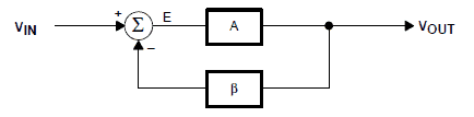 The resulting equations for an oscillator circuit can be seen below.
The first equation is the important one which defines the output voltage.
Equation 2 gives the error factor.
Vout = E x A------------------------------(1)
E = Vin + ��Vout--------------------------(2)
Eliminating the error factor E from the above equations gives
Vout / A = Vin - ��Vout----------------- (3)
Extracting the elements in Vout gives
Vin = Vout (1/A + ��)---------------------(4)
Reorganizing the terms in the above equation provides us the following classical feedback formula through equation #5
Vout / Vin = A / (1+A��)----------------(5)
Oscillators are able to work without the help of an external signal.
Rather, a portion of the output pulse is utilized as the input through a feeedback network.
An oscillation is initiated when the feedback fails to achieve a stable steady state.
This happens because the transfer action does not get fulfilled.
This unstability occurs when the denominator of equation #5 becomes zero, as shown below:
1 + A�� = 0, or A�� = -1.
The crucial thing while designing an oscillator circuit is to ensure A�� = -1. This condition is called theBarkhausen criterion.
To satisfy this condition, it becomes essential that the loop gain value remains at unity through a corresponding 180 degrees phase shift.
This is comprehended by the negative sign in the equation.
The above results can be alternatively expressed as shown below using symbols from complex Algebra:
A�� = 1��-180��
While designing a positive feedback oscillator the above equation can be written as:
A�� = 1��0��which makes the term A�� in equation #5 negative.
When A�� = -1 the feedback output tends to move towards an infinite voltage.
When this approaches the maximum + or - supply levels, the gain level active devices in the circuits changes.
This causes the value of A to become A�� �� -1, slowing down the feedback infinite voltage approach, eventually putting it to a halt.
Here.we may find one of the three possibilities happening:
Non-linear saturation or cut-off causing the oscillator to stabilize and lock.
The initial charge forcing the system to saturate for a much long period before it again becomes linear and begins approaching the opposite supply rail.
The system continues to be in the linear region, and reverts towards the opposite supply rail.
In case of the second possibility, we get an immensely distorted oscillations, generally in the form of quasi square waves.
What's Phase shift in oscillators
The 180�� phase shift in the equation A�� = 1��-180�� is created through the active and passive components.
Just like any correctly designed feedback circuit, oscillators are built based on the phase shift of the passive components.
This is because the results from passive parts are precise and practically drift-free.
The phase shift acquired from active components is mostly inaccurate due to many factors.
It may drift with temperature changes, may show wide initial tolerance, and also the results could be dependent on the device characteristic.
Op amps are chosen in order to ensure that they bring about minimum phase shift to the frequency of the oscillation.
A single pole RL (resistor-inductor) or RC (resistor-caapcitor) circuit brings about approximately 90�� phase shift per pole.
Since 180�� is necessary for oscillation, a minimum of two poles are employed while designing an oscillator.
An LC circuit possesses 2 poles; therefore, it provides around 180�� phase shift for each pole pair.
However we won't be discussing LC based designs here due to the involvemenet of low frequency inductors that can be expensive, bulky, and undesirable.
LC oscillators are intended for high-frequency applications, that may be over and above the frequency range of opamps based on voltage feedback principle.
Here you may find the inductor size, weight, and cost are not of much importance.
Phase shift ascertains the frequency of oscillation since the circuit pulses at the frequency that fetches a phase shift of 180 degress.
The df/dt or the rate at which the phase shift changes with frequency, decides frequency stability.
When cascaded buffered RC sections are used in the form of opamps, offering highinput and low-output impedance, the phase shift multiplies by the number of sections,n(see Figure below).
The resulting equations for an oscillator circuit can be seen below.
The first equation is the important one which defines the output voltage.
Equation 2 gives the error factor.
Vout = E x A------------------------------(1)
E = Vin + ��Vout--------------------------(2)
Eliminating the error factor E from the above equations gives
Vout / A = Vin - ��Vout----------------- (3)
Extracting the elements in Vout gives
Vin = Vout (1/A + ��)---------------------(4)
Reorganizing the terms in the above equation provides us the following classical feedback formula through equation #5
Vout / Vin = A / (1+A��)----------------(5)
Oscillators are able to work without the help of an external signal.
Rather, a portion of the output pulse is utilized as the input through a feeedback network.
An oscillation is initiated when the feedback fails to achieve a stable steady state.
This happens because the transfer action does not get fulfilled.
This unstability occurs when the denominator of equation #5 becomes zero, as shown below:
1 + A�� = 0, or A�� = -1.
The crucial thing while designing an oscillator circuit is to ensure A�� = -1. This condition is called theBarkhausen criterion.
To satisfy this condition, it becomes essential that the loop gain value remains at unity through a corresponding 180 degrees phase shift.
This is comprehended by the negative sign in the equation.
The above results can be alternatively expressed as shown below using symbols from complex Algebra:
A�� = 1��-180��
While designing a positive feedback oscillator the above equation can be written as:
A�� = 1��0��which makes the term A�� in equation #5 negative.
When A�� = -1 the feedback output tends to move towards an infinite voltage.
When this approaches the maximum + or - supply levels, the gain level active devices in the circuits changes.
This causes the value of A to become A�� �� -1, slowing down the feedback infinite voltage approach, eventually putting it to a halt.
Here.we may find one of the three possibilities happening:
Non-linear saturation or cut-off causing the oscillator to stabilize and lock.
The initial charge forcing the system to saturate for a much long period before it again becomes linear and begins approaching the opposite supply rail.
The system continues to be in the linear region, and reverts towards the opposite supply rail.
In case of the second possibility, we get an immensely distorted oscillations, generally in the form of quasi square waves.
What's Phase shift in oscillators
The 180�� phase shift in the equation A�� = 1��-180�� is created through the active and passive components.
Just like any correctly designed feedback circuit, oscillators are built based on the phase shift of the passive components.
This is because the results from passive parts are precise and practically drift-free.
The phase shift acquired from active components is mostly inaccurate due to many factors.
It may drift with temperature changes, may show wide initial tolerance, and also the results could be dependent on the device characteristic.
Op amps are chosen in order to ensure that they bring about minimum phase shift to the frequency of the oscillation.
A single pole RL (resistor-inductor) or RC (resistor-caapcitor) circuit brings about approximately 90�� phase shift per pole.
Since 180�� is necessary for oscillation, a minimum of two poles are employed while designing an oscillator.
An LC circuit possesses 2 poles; therefore, it provides around 180�� phase shift for each pole pair.
However we won't be discussing LC based designs here due to the involvemenet of low frequency inductors that can be expensive, bulky, and undesirable.
LC oscillators are intended for high-frequency applications, that may be over and above the frequency range of opamps based on voltage feedback principle.
Here you may find the inductor size, weight, and cost are not of much importance.
Phase shift ascertains the frequency of oscillation since the circuit pulses at the frequency that fetches a phase shift of 180 degress.
The df/dt or the rate at which the phase shift changes with frequency, decides frequency stability.
When cascaded buffered RC sections are used in the form of opamps, offering highinput and low-output impedance, the phase shift multiplies by the number of sections,n(see Figure below).
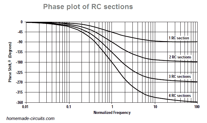 Despite the fact that two cascaded RC sections present 180�� phase shift, you may find d��/dt to be minimal at the oscillator frequency.
As a result oscillators constructed using two cascaded RC sections offerinadequatefrequency stability.
Three identical cascaded RC filter sections provide an increased d��/dt, enabling the oscillator with an enhanced frequency stability.
However, introducing a fourth RC section creates an oscillator with anoutstandingd��/dt.
Hence this becomes an extremely stable oscillator setup.
Four sections happen to be the preferred range mainly because opamps are available in quad packages.
Also, the four-section oscillator produces 4 sine waves which are 45�� phase shifted with reference to one another, which means this oscillator enables you to get hold of sine/cosine or quadrature sine waves.
Despite the fact that two cascaded RC sections present 180�� phase shift, you may find d��/dt to be minimal at the oscillator frequency.
As a result oscillators constructed using two cascaded RC sections offerinadequatefrequency stability.
Three identical cascaded RC filter sections provide an increased d��/dt, enabling the oscillator with an enhanced frequency stability.
However, introducing a fourth RC section creates an oscillator with anoutstandingd��/dt.
Hence this becomes an extremely stable oscillator setup.
Four sections happen to be the preferred range mainly because opamps are available in quad packages.
Also, the four-section oscillator produces 4 sine waves which are 45�� phase shifted with reference to one another, which means this oscillator enables you to get hold of sine/cosine or quadrature sine waves.
Using Crystals and Ceramic Resonators
Crystal or ceramic resonators provide us with the most stable oscillators. This is because resonators come with an incredibly high d��/dt as a result of their nonlinear properties. Resonators are applied in high-frequency oscillators, however, low-frequency oscillators usually do not work with resonators due to size, weight, and cost constraints. You will find that op-amps are not utilized with ceramic resonator oscillators mainly because opamps include a reduced bandwidth. Studies show that it is less expensive to construct a high-frequency crystal oscillator and trim down the output to acquire a low frequency instead of incorporating a low-frequency resonator.Gain in oscillators
The gain of an oscillator must matchoneat the oscillation frequency. The design gets steady once the gain is greater than 1 and oscillations halt. As soon as the gain reaches over 1 along with a phase shift of �C180��, the non linear property of the active device(opamp) drops the gain to 1. When non-linearity occurs the opamp swings near the either (+/-) supply levels due to the reduction in the cut-off or saturation of the the active device (transistor) gain. One strange thing is that the badly designed circuits actually demand marginal gains in excess of 1 during their production. On the other hand, higher gain leads to greater amount of distortion for the output sine wave. In cases where gain is minimal, oscillations cease under extreme unfavorable circumstances. When the gain is very high, the output waveform appears to be much more similar to a square wave instead of a sine wave. Distortion is usually an immediate consequence of too much gain over-driving the amplifier. Therefore, gain should be cautiously governed for for achieving low distortion oscillators. Phase-shift oscillators can show distortions, however they may have the ability to attain a low-distortion output voltages using buffered cascaded RC sections. This is because cascaded RC sections behave as distortion filters. Furthermore, buffered phase-shift oscillators experience low distortion since the gain is managed and uniformly balanced between the buffers. Conclusion From the above discussion we learned the basic working principle of opamp oscillators and understood regarding the fundamental criteria for achieving sustained oscillations. In the next post we'll learn aboutWien-bridge oscillators.How to Make Pierce Oscillator, Hartley Oscillator Circuits
In this post we learn how to build simple oscillator circuits like the pierce oscillator and hartley oscillator using a single CMOS gate. Both the oscillators are types of oscillators that utilize minimum number of components yet are able to generate very stable and reliable frequency outputs.Pierce Oscillator
You can easily build a pierce oscillator circuit, based on a crystal oscillator design, using a single CMOS gate, as shown in the following figure.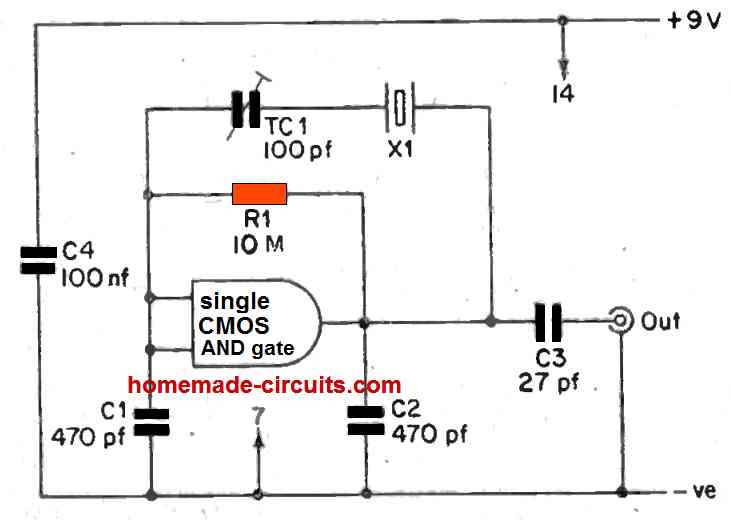 The single CMOS inverter is biased to form a linear amplifier by means of R1. A crystal can be seen connected between the input and the output of the pierce circuit through the trimmer capacitor TCI.
This proposed circuit is designed to operate with the series resonant frequency of the crystal.
Needless to say, a positive feedback hasn't been used here between the output and input of the circuit.
This is because, the CMOS amplifier's input and output work in the antiphase mode.
With series resonance it might look as if the crystal is supplying the negative feedback to the amplifier.
However, this might not be true in reality, because C1 and C2 create a capactive centre tap around the crystal, where the centre tap can be seen grounded.
The crystal as a result behaves like a form of transformer working in the series resonance mode, using its a pair of connections operating in antiphase.
Consequently, we may find a 180 degree phase shift by means of the two amplifier and the crystal, and also with a positive feedback.
TC1 is included to tailor the circuit's oscillation frequency to match the crystal's nominal frequency, but anyway, this specific function could be omitted in case it is not required.
TC1 can now be removed and the crystal can be hooked up directly across R1.
Capacitors C1 and C2 can be seen having the values of 470 pF each in this pierce circuit design.
With these values the circuit must oscillate without any problems within a extensive range of frequencies.
If the frequency is just a few MHz then you may want to decrease the value of C1 and C2 relatively so that you can sustain the oscillation correctly.
Alternatively, when the frequencies is lower than a few 100 kHz you can select C1 and C2 values a little bit larger.
An AND CMOS gate is indicated in the diagram, it is also possible to use a buffer CMOS gate, such as from the IC 4050.
The single CMOS inverter is biased to form a linear amplifier by means of R1. A crystal can be seen connected between the input and the output of the pierce circuit through the trimmer capacitor TCI.
This proposed circuit is designed to operate with the series resonant frequency of the crystal.
Needless to say, a positive feedback hasn't been used here between the output and input of the circuit.
This is because, the CMOS amplifier's input and output work in the antiphase mode.
With series resonance it might look as if the crystal is supplying the negative feedback to the amplifier.
However, this might not be true in reality, because C1 and C2 create a capactive centre tap around the crystal, where the centre tap can be seen grounded.
The crystal as a result behaves like a form of transformer working in the series resonance mode, using its a pair of connections operating in antiphase.
Consequently, we may find a 180 degree phase shift by means of the two amplifier and the crystal, and also with a positive feedback.
TC1 is included to tailor the circuit's oscillation frequency to match the crystal's nominal frequency, but anyway, this specific function could be omitted in case it is not required.
TC1 can now be removed and the crystal can be hooked up directly across R1.
Capacitors C1 and C2 can be seen having the values of 470 pF each in this pierce circuit design.
With these values the circuit must oscillate without any problems within a extensive range of frequencies.
If the frequency is just a few MHz then you may want to decrease the value of C1 and C2 relatively so that you can sustain the oscillation correctly.
Alternatively, when the frequencies is lower than a few 100 kHz you can select C1 and C2 values a little bit larger.
An AND CMOS gate is indicated in the diagram, it is also possible to use a buffer CMOS gate, such as from the IC 4050.
Using an FET
A benefit of the Pierce crystal oscillator circuit is that it does not require any tuning adjustments. The following figure demonstrates how to build a Pierce oscillator circuit using a single 2N3823 (or 2N3821, 2N3822) field-effect transistor.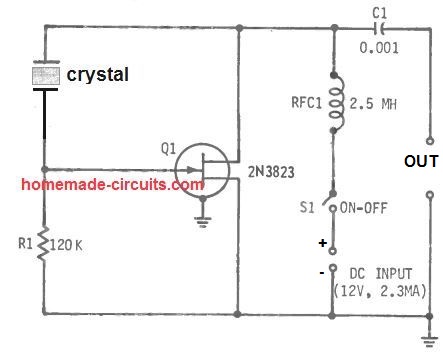 In this set up, the quartz crystal (XTAL) is driven between the FET's drain/output and gate/input stages.
The 2.5-mh RF choke (RFC1) doesn't typically tune the circuit, however it assists just to keep the RF energy away from the DC supply.
The circuit starts oscillating the moment switch S1 is switched ON.
Capacitive output coupling is supplied by means of the capacitor C1, which ensures that that the external load impedance be high enough so that it does not overload the circuit and destroy the oscillations.
During the time the pierce oscillator circuit oscillates at the crystal frequency, it comsumes around 2.3 ma current from the 12 V DC supply.
At this time, without any load the RF output signal amplitude is 6.2v RMS (in the shown circuit this was implemented at 7 MHz frequency).
The Pierce circuit is designed to oscillate at the fundamental frequency of the crystal.
Hence, in case there is a harmonic-type crystal, oscillation will happen in the primary frequency of the crystal, not necessarily in the specified (harmonic) frequency.
Additionally, the Pierce oscillator requires an extremely active crystal.
In this set up, the quartz crystal (XTAL) is driven between the FET's drain/output and gate/input stages.
The 2.5-mh RF choke (RFC1) doesn't typically tune the circuit, however it assists just to keep the RF energy away from the DC supply.
The circuit starts oscillating the moment switch S1 is switched ON.
Capacitive output coupling is supplied by means of the capacitor C1, which ensures that that the external load impedance be high enough so that it does not overload the circuit and destroy the oscillations.
During the time the pierce oscillator circuit oscillates at the crystal frequency, it comsumes around 2.3 ma current from the 12 V DC supply.
At this time, without any load the RF output signal amplitude is 6.2v RMS (in the shown circuit this was implemented at 7 MHz frequency).
The Pierce circuit is designed to oscillate at the fundamental frequency of the crystal.
Hence, in case there is a harmonic-type crystal, oscillation will happen in the primary frequency of the crystal, not necessarily in the specified (harmonic) frequency.
Additionally, the Pierce oscillator requires an extremely active crystal.
Hartley Oscillator
The Hartley oscillator is a type of frequency generator circuit in which the oscillation frequency depends upon a tuned circuit which involves capacitors and inductors, meaning, it is simply a type of an LC oscillator. A single CMOS inverter can be also used to build the popular Hartley type oscillator. This type of Hartley oscillator circuit is more advantageous than normal LC oscillators, since here just just one winding is necessary for the coil. Even so, the coil needs to be a center tapped winding. The CMOS Hartley oscillator circuit diagram can be visualized in the following figure.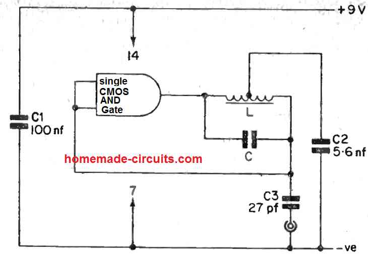 The working of the ahrtley oscillator is quite similar to the pierce oscillator, except the use of the a center tapped LC stage which is used instead of the capactively center tapped crystal.
The inductor L supplies a D.C.
route between the CMOS inverter's input and output which ensures that the circuit can work without the need of a bias resistor.
The circuit can work with with a frequency range of a several 100 kHz but below a maximum of 10 MHz.
These frequencies will depend on the values of the L and C which must appropriately selected to match the specified operating frequency range.
You can make the capacitor C variable, in case you want the Hartley circuit to work like a variable frequency oscillator.
Remember that the indicated tapping on the coil L doesn't need to be at exactly at the middle of the winding, which means for example, the circuit may run without any issues even with the primary of an I.F.
transformer used in place of L.
The coil L can be experimented by using different number of turns over a ferrite core, and testing the results over a frequency meter.
An AND CMOS gate has been used in the hartley diagram, you can also likewise use a buffer CMOS gate, such as from the IC 4050.
The working of the ahrtley oscillator is quite similar to the pierce oscillator, except the use of the a center tapped LC stage which is used instead of the capactively center tapped crystal.
The inductor L supplies a D.C.
route between the CMOS inverter's input and output which ensures that the circuit can work without the need of a bias resistor.
The circuit can work with with a frequency range of a several 100 kHz but below a maximum of 10 MHz.
These frequencies will depend on the values of the L and C which must appropriately selected to match the specified operating frequency range.
You can make the capacitor C variable, in case you want the Hartley circuit to work like a variable frequency oscillator.
Remember that the indicated tapping on the coil L doesn't need to be at exactly at the middle of the winding, which means for example, the circuit may run without any issues even with the primary of an I.F.
transformer used in place of L.
The coil L can be experimented by using different number of turns over a ferrite core, and testing the results over a frequency meter.
An AND CMOS gate has been used in the hartley diagram, you can also likewise use a buffer CMOS gate, such as from the IC 4050.
Using a single Transistor
A type of oscillator single transistor circuit that is tuned with a transformer and generates a sine wave AF, can be witnessed in the following figure. This is actually a Hartley type oscillator circuit, where the tuning and feedback features are achieved through just one center-tapped winding of the transformer; the other winding of the transformer subsequently works like as an output coupling coil.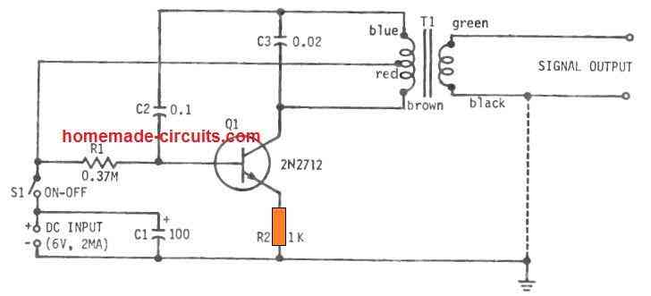 To build this Hartley circuit, you must first procure the small transformer T1 which is a 500 ohm to 30 ohm center tapped transformer.
Meaning the circuit winding has 500 ohm and the output side winding has 30 ohm approximately.
The upper half section of the center-tapped primary winding of L1 acts like the base-input coil while the bottom half of the primary side of L1 act s like the collector output coil.
Capacitor C3 solely becomes responsible for tuning the oscillation on the primary side of the transformer.
The frequency of the Hartley circuit is mainly established by capacitor C3 and the inductance of the total primary winding.
As indicated in the diagram if C3 value is 0.02 mfd, then the frequency will be roughly around 2 kHz.
In order to raise the frequency, you may try lowering the C3 capacitance; to decrease the frequency simply increase the C3 capacitance.
To ensure that the circuit oscillates perfectly, the transformer winding should be correctly polarized as provided in the specs of the transformer by color dots.
Capacitor C2 does not have any role in the tuned circuit, yet it is positioned to prohibit the collector DC voltage appearing from the base of the transistor.
The circuit provides an amplitude of 0.8v RMS when the output is not loaded.
The current consumption is 2 ma when a 6V Dc supply is used for the circuit
To build this Hartley circuit, you must first procure the small transformer T1 which is a 500 ohm to 30 ohm center tapped transformer.
Meaning the circuit winding has 500 ohm and the output side winding has 30 ohm approximately.
The upper half section of the center-tapped primary winding of L1 acts like the base-input coil while the bottom half of the primary side of L1 act s like the collector output coil.
Capacitor C3 solely becomes responsible for tuning the oscillation on the primary side of the transformer.
The frequency of the Hartley circuit is mainly established by capacitor C3 and the inductance of the total primary winding.
As indicated in the diagram if C3 value is 0.02 mfd, then the frequency will be roughly around 2 kHz.
In order to raise the frequency, you may try lowering the C3 capacitance; to decrease the frequency simply increase the C3 capacitance.
To ensure that the circuit oscillates perfectly, the transformer winding should be correctly polarized as provided in the specs of the transformer by color dots.
Capacitor C2 does not have any role in the tuned circuit, yet it is positioned to prohibit the collector DC voltage appearing from the base of the transistor.
The circuit provides an amplitude of 0.8v RMS when the output is not loaded.
The current consumption is 2 ma when a 6V Dc supply is used for the circuit
Square Wave Oscillator Circuits
In this article we comprehensively discuss how to build accurate RC square wave oscillator circuits with 50% duty cycle, by appropriately configuring the gates from various CMOS ICs such as 4001, 4011, 4093, 4046, 4047, 4016, 4060 etc. and also using op ampsDefinition
The square wave oscillators included in this article can be defined as circuits built using CMOS gates or op amps for generating accurate frequency outputs, having perfect square waveform with 50:50 duty cycle, or symmetrical ON/OFF pulses. It means, the waveform from these RC oscillator will have a perfectly square in shape with equal ON and OFF time periods. Moreover, being from CMOS ICs, these frequencies are digital in nature, and therefore can be expected to be more reliable and accurate than the BJT based analogue type of square wave oscillator designs.CMOS Oscillator
CMOS devices give you a wide range of opportunity to design of R-C oscillators. RC oscillators can be built equally using standard gates and with ICs created specifically for oscillator circuits. Having inputs which work with around 1 / 2 the supply voltage and outputs which could switch right across positive and negative supply voltage, CMOS gates are perfectly suitable for stable oscillator design. Circuits employing these tend to be less complicated plus more efficient compared to identical models designed with discrete units like transistors. Their minimal power necessity and wider operating voltage range between 3 to 15 volts additionally make them perfect for use in battery-powered circuits. You may find a few issues though, which needs to be recognized and these are going to be thoroughly discussed in this article. The fundamental prerequisite for the majority of R-C oscillator circuits can be a set of inverting gates attached in series as displayed in the following Figure 2.1. Let's assume that the input is to gate G1, both inverted and noninverted outputs are together accessible, through G1 and G2 respectively.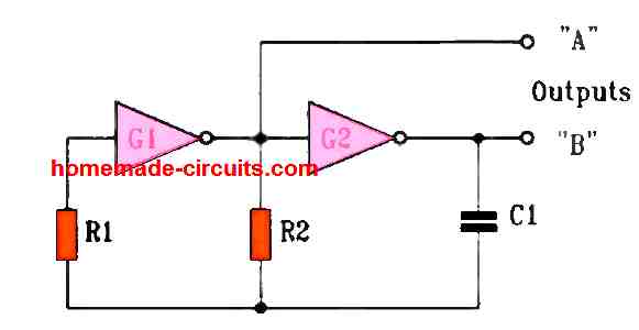 Figure 2.1a: NOT Gate RC Oscillator
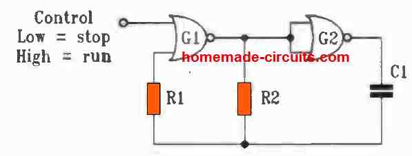 Figure 2.1b: NOR Gate Oscillator
The working of the square wave oscillator using a couple of NOT gates, let's say from the IC 4049 is straightforward to understand.
Figure 2.1b: NOR Gate Oscillator
The working of the square wave oscillator using a couple of NOT gates, let's say from the IC 4049 is straightforward to understand.
Circuit Description
Assuming the output from G1 at the instantaneous positive changeover, the resulting positive input to G2 can cause its output to become negative and this negative signal will move via capacitor C1 and resistor R1 and return to the input of G1, speeding up the activity until a total transformation of state for both the gates has transpired. The positive output from G1 can subsequently begin charging C1, slowly increasing the voltage at G1 input. As soon as it extends to 1 / 2 the supply voltage G1's output will yet again start to change state, on this occasion to negative, and the entire cycle will keep repeating.Frequency Formula
The time period necessary for each half-cycle will be 1.1 x R x C, therefore the frequency can be presented as: f = 1 / 2.2 RC where R is R2 and C is C1 in the circuit. Appropriate values for R2 resistor can be between 10 k and higher, and for capacitor C1 the value can be between 100 pF and higher. The voltage polarity across C2 will keep reversing, therefore C2 cannot be a polarized capacitor like an electrolytic, nevertheless any other non-polar will do. For improved stability polystyrene and polyester capacitors are advised. Two outputs can be found, a single from each gate. Either one or both of them could be utilized. Their working is opposite with their polarity, a characteristic which can be typically helpful in many of the circuit designs.How to Adjust Frequency
The frequency could be altered through a variable resistor for R2, as well as the duty cycle could be tweaked by means of diodes and resistors. Yet again, it is the period of time which is governed by this resistor, therefore the frequency output results is going to be non-linear. Even though it is straightforward and trustworthy, you will find certain possible drawbacks with this circuit that consumers should know about. First of all, the output duty cycle is hardly ever uniform. To get a proper 50:50 ratio or a extremely small frequency, please refer to the next circuit idea which incorporates a divider IC. Secondly, for approximately 10 kHz the output frequency usually adheres to the above equation, however beyond this value it starts getting less and less consistent, normally it is less than what the equation gives. The frequency is additionally dependent on the supply voltage variations, usually the frequency will show an increase as the voltage is increased, and yet again this impact may start getting more visible at higher frequencies.CMOS Oscillators Require Less Current
CMOS gates are widely recognized for their minimal supply current specifications however this applies specifically when their inputs are being operated mostly near to the supply limits. While working with intermediate input voltages CMOS output stages can run with partial conduction causing higher current draw. Also, gradually increasing potential at CMOS gate input may result in instability and "glitches", or spikes, close to the switching points. The issue can be generally hidden unless of course checked using a fast oscilloscope. Such glitches can cause the IC to behave unpredictably and cause errors if the signal is employed, for instance, to operate a counter. This issue could be generally remedied by simply introducing a 10k resistor in series with the load or the the counter in our example. Together with the counter's input capacitance, this 10k can form a low-pass filter that is normally quite enough to correct the issue.Schmitt Trigger Oscillator
An alternate strategy could be the utilization of "Schmitt" gates, for example the gates from the IC 4093B quad Schmitt NAND. However the hysteresis of such ICs can have an affect on the frequency measurements and an increased frequency deviations, along with disparities in supply voltage. The use of Schmitt gates is not going to stop the higher current consumption issue either. All these aspects must not dissuade hobbyists from using these square wave oscillators though, since CMOS oscillators are straightforward, inexpensive and dependable and in the majority of applications it works with no issues. As long as the possible stumbling blocks are recognized, the reason for unforeseen side effects could generally be quickly identified and removed.How it Works
The function of resistor R1 is crucial. At the time when the G2 output begins chnaging state, let's imagine to positive, the side C1 pin conected with the G1 input is at 1 / 2 the supply voltage. As G2's output toggles, the G1 input gets higher at first to logic 1 and a 1 / 2 the value of the supply voltage. Exactly the same thing takes place for negative output which also changes, only in the reverse direction with the G1 input falling to 1 / 2 the supply voltage below negative supply line value. Many B-series CMOS ICs include internal protection circuitry which safeguard their own inputs from these voltages to avoid static discharge destruction. This safety feature may be available in different forms according to the supplier, although typically includes diode networks organized to switch ON whenever voltages over or under the input supply are linked to them. In the R-C oscillator circuit this could cause fast early discharge of C1 when its voltage go beyond the supply input ranges. This could negatively impact efficiency and stability therefore R1 is introduced to limit the current flow to the protection, significantly minimizing the bad consequence. This resistor value must be fairly high compared to R2, usually a ratio of 4 to 1 or higher may be enough. Despite the fact that Figure 2.1a displays a circuit employing a couple of simple inverter gates, it could be designed with NOR or NAND gates as indicated in Figure 2.1b and 2.1c, that make use of gates from a IC 4001B and IC 4011B respectively. Extra inputs could be linked with each other, or to positive/ground supply line, or these may be used as shown for manipulating the oscillator. In circuits where a four-gate IC is employed the left over gates could be utilized for other preferable or desired requirements. A pair of square wave oscillator circuits could be constructed using 4 NAND Gates from the IC 4011. One oscillator can be used for audio frequency generation, while the second one for running at 1 or 2 hertz frequency. Integrating the two with each other would provide a, interesting pulsating audio output as given below.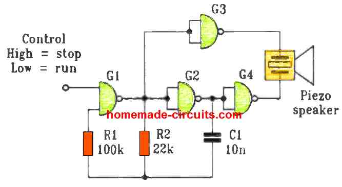 Figure 2.1c: NAND Gate two tone RC oscillator circuit
The extra gates could possibly be utilized as buffers to protect against loading of the oscillator circuit.
A practical advice is to try using these for operating a piezo transducer unit, utilizing the 2 gates like buffers with opposite output polarities to make a "bridge" driver circuit.
This design is demonstrated in Fig.2.1c having G3 and G4 configured as buffers.
The majority of of the inverting CMOS gates may be applied for making this kind of RC square wave oscillator circuits.
A few ideal varieties can be visualized in the below given listing:
4000B Dual 3-input NOR gate plus inverter
4001B Quad 2-input NOR gate
4002B Dual 4-input NOR gate
4011B Quad 2-input NAND gate
4012B Dual 4-input NAND gate
4023B Triple 3-input NAND gate
4025B Triple 3-input NOR gate
4093B Quad 2-input Schmitt NAND gate.
It might be feasible to apply the 4070B quad EX-OR and 4077B quad EX-NOR ICs, because these 2-input gates can be utilized as inverter gates if either of the inputs are hooked up to the proper supply voltage line.
Using the 4070B this can be positive, for the 4077B it may be negative.
Yet again, this gives an alternative facility to manage the oscillation using these inputs.
Figure 2.1c: NAND Gate two tone RC oscillator circuit
The extra gates could possibly be utilized as buffers to protect against loading of the oscillator circuit.
A practical advice is to try using these for operating a piezo transducer unit, utilizing the 2 gates like buffers with opposite output polarities to make a "bridge" driver circuit.
This design is demonstrated in Fig.2.1c having G3 and G4 configured as buffers.
The majority of of the inverting CMOS gates may be applied for making this kind of RC square wave oscillator circuits.
A few ideal varieties can be visualized in the below given listing:
4000B Dual 3-input NOR gate plus inverter
4001B Quad 2-input NOR gate
4002B Dual 4-input NOR gate
4011B Quad 2-input NAND gate
4012B Dual 4-input NAND gate
4023B Triple 3-input NAND gate
4025B Triple 3-input NOR gate
4093B Quad 2-input Schmitt NAND gate.
It might be feasible to apply the 4070B quad EX-OR and 4077B quad EX-NOR ICs, because these 2-input gates can be utilized as inverter gates if either of the inputs are hooked up to the proper supply voltage line.
Using the 4070B this can be positive, for the 4077B it may be negative.
Yet again, this gives an alternative facility to manage the oscillation using these inputs.
CMOS 4060B 14-stage Ripple Counter with Internal Oscillator
An effective variant of the simple RC oscillator could be obtained from the CMOS IC 4060B oscillator ,and divider IC. This is basically a 14-stage binary counter-divider, but as opposed to the some other ripple counters, a set of inverter gates can be seen readily configured as an oscillator, and internally attached with pins 9, 10 and 11 of the IC.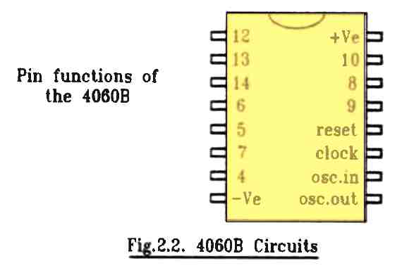
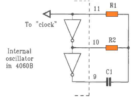 This setup could be applied in a variety of applications, the standard being as a RC oscillator as demonstrated in Figure 2.2c below.
All of the earlier features pertaining to this sort of twin gate RC square wave oscillator is applicable to this 4060 design too, such as the operating frequency that can be determined using the formula:
This setup could be applied in a variety of applications, the standard being as a RC oscillator as demonstrated in Figure 2.2c below.
All of the earlier features pertaining to this sort of twin gate RC square wave oscillator is applicable to this 4060 design too, such as the operating frequency that can be determined using the formula:
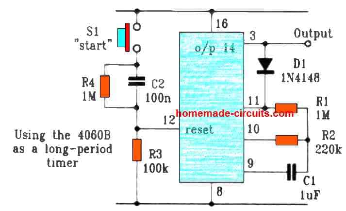 f = 1/(2.2 x R2 x C1).
R1 executes exactly the same functionality as earlier and you can find comparable restrictions around the maximum reliable frequency.
The input for the 2 gates, which is pin 11, is likewise internally attached to the "clock" input of the divider, offering a number of handy possibilities.
The output could be extracted from one of the divider outputs.
The outputs of the IC 4060 are multiple figures of one full RC oscillator cycle, and all outputs feature the exact 50:50 ratio duty cycles.
The outputs are all buffered, therefore it is not possible to cause loading with these outputs.
These could even be utilized for directly driving low-current LEDs, which can be at times great for building cost effective counters or timer circuits.
The divide/by approach causes this IC to be particularly appropriate for the development of extremely low frequency oscillators using standard value resistors and capacitors.
Unfortunately, the 1st three outputs are generally not accessible to the consumer.
The first externally obtainable is the output 4, at pin 7, that works with 1/16th of the clock frequency.
Yet another drawback is the missing output 11, which represents the clock divided by 2048.
This missing output sequence can be frequently cause a hassle because the IC could normally be excellent for creating very basic binary "addresses".
The "Reset" input, to pin 12, must be attached to negative supply line for normal functioning.
In case it is connected to the the positive supply each of the outputs goes low and continue to be in this state as long as the reset is not switched to the low state.
The RC oscillator configurable outputs at pins 9 and 10 can also be driven at the low state as long as the reset pin12 is held high with a positive link.
Thus, the pin12 could be used for controlling the oscillator functioning of the IC.
Just like any other CMOS inputs, the reset pin12 must never be kept unconnected as it may give rise to unusual and unstable consequences.
f = 1/(2.2 x R2 x C1).
R1 executes exactly the same functionality as earlier and you can find comparable restrictions around the maximum reliable frequency.
The input for the 2 gates, which is pin 11, is likewise internally attached to the "clock" input of the divider, offering a number of handy possibilities.
The output could be extracted from one of the divider outputs.
The outputs of the IC 4060 are multiple figures of one full RC oscillator cycle, and all outputs feature the exact 50:50 ratio duty cycles.
The outputs are all buffered, therefore it is not possible to cause loading with these outputs.
These could even be utilized for directly driving low-current LEDs, which can be at times great for building cost effective counters or timer circuits.
The divide/by approach causes this IC to be particularly appropriate for the development of extremely low frequency oscillators using standard value resistors and capacitors.
Unfortunately, the 1st three outputs are generally not accessible to the consumer.
The first externally obtainable is the output 4, at pin 7, that works with 1/16th of the clock frequency.
Yet another drawback is the missing output 11, which represents the clock divided by 2048.
This missing output sequence can be frequently cause a hassle because the IC could normally be excellent for creating very basic binary "addresses".
The "Reset" input, to pin 12, must be attached to negative supply line for normal functioning.
In case it is connected to the the positive supply each of the outputs goes low and continue to be in this state as long as the reset is not switched to the low state.
The RC oscillator configurable outputs at pins 9 and 10 can also be driven at the low state as long as the reset pin12 is held high with a positive link.
Thus, the pin12 could be used for controlling the oscillator functioning of the IC.
Just like any other CMOS inputs, the reset pin12 must never be kept unconnected as it may give rise to unusual and unstable consequences.
CMOS 4016B Electronic Switch Gate Oscillator
One more CMOS device which you can use to construct a twin-gate RC square wave oscillator is the 4016B quad "analogue switch". This chip consists of four electronic "switches", all of which can be "closed" through the implementation of a positive control voltage. When a couple of of these switches are configured like inverters, they work like just every other inverting gates forming a CMOS RC oscillator stage. Figure 2.3a below exhibits the connections of the pins for this IC.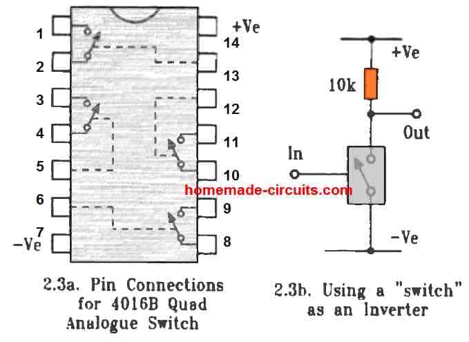 Be aware that, just like various other CMOS ICs, unconnected or extra inputs of the IC must be always terminated to either positive or negative supply, line and should never be left "hanging".
Figure 2.3b above demonstrates the way a solitary switch could be organized like an inverter.
One end of the switch is linked to ground line whilst the other is attached to the positive supply line via a 10 k resistor.
Although the control input, marked as "in" in the schematic, is attached to a negative voltage line, the connection of the switch and resistor, marked as "out", becomes "high" in response to a positive voltage through the resistor.
As soon as the input pin is subjected to a positive source, the switch activates and drags the junction between the switch and resistor "low", to the negative supply level.
Considering that the resistor value is sufficiently less compared to the load which the "gate" is going to be operating, the set up offers an efficiency just like any other type of inverting gate.
In case it is used like an oscillator, a couple of these "inverting gates" are built through four pairs of switches from IC1, and all the standard oscillator ingredients are included in the circuit, as displayed in Figure 2.4a below.
Be aware that, just like various other CMOS ICs, unconnected or extra inputs of the IC must be always terminated to either positive or negative supply, line and should never be left "hanging".
Figure 2.3b above demonstrates the way a solitary switch could be organized like an inverter.
One end of the switch is linked to ground line whilst the other is attached to the positive supply line via a 10 k resistor.
Although the control input, marked as "in" in the schematic, is attached to a negative voltage line, the connection of the switch and resistor, marked as "out", becomes "high" in response to a positive voltage through the resistor.
As soon as the input pin is subjected to a positive source, the switch activates and drags the junction between the switch and resistor "low", to the negative supply level.
Considering that the resistor value is sufficiently less compared to the load which the "gate" is going to be operating, the set up offers an efficiency just like any other type of inverting gate.
In case it is used like an oscillator, a couple of these "inverting gates" are built through four pairs of switches from IC1, and all the standard oscillator ingredients are included in the circuit, as displayed in Figure 2.4a below.
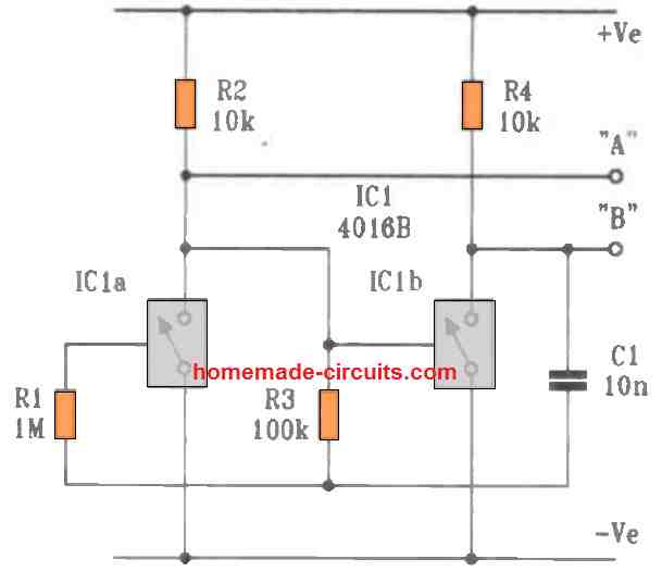 Figure 2.4a: IC 4016 RC oscillator circuit
A couple of outputs are offered, indicated with "A" and "B".
Frequency from these outputs, when scanned with an oscilloscope, look quite "untidy", with snags and instability across the switching regions, as well as the frequency which could be accomplished with this circuit is pretty small, although completely sufficient for acoustic applications.
Figure 2.4a: IC 4016 RC oscillator circuit
A couple of outputs are offered, indicated with "A" and "B".
Frequency from these outputs, when scanned with an oscilloscope, look quite "untidy", with snags and instability across the switching regions, as well as the frequency which could be accomplished with this circuit is pretty small, although completely sufficient for acoustic applications.
Current Drain Issues
A minor problem with the circuit is that one or other gates is usually in the "on" state, therefore you will see a non-stop current drain by means of the connected load resistor. Just like the other CMOS RC oscillators, the frequency of this circuit could be determined using the formula f = 1/(2.2 x R x C). The actual results can deviate from the value of the formula, more consistently as we go on increasing the frequency rate. This means that the formula should be used just like a guideline prior to practical experimentation while designing such CMOS based square wave oscillators, and the real frequency should be confirmed only through an oscilloscope or a frequency meter.Stability Issues
The circuits's frequency is actually pretty stable to variations in source voltage and ambient temperature. The duty-cycle is also fairly close to a 50:50 ratio. Just like with many of the other 2 gate CMOS oscillator circuits, it is possible to change its output frequency by upgrading R3 through a diode and resistor networks. However the response of this circuit is sluggish, and calls for a couple of additional resistors leading to a little higher current consumption. Therefore why must anybody take the trouble of building an oscillator using switches available from this IC 4016? The reason is just like the majority of the other CMOS oscillators explained in this article, this specific oscillator circuit works with a solitary low-cost IC, however here the "unused gates" are a actually a couple of extra analogue switches, featuring a pair of opposite-phase outputs readily available, which could be implemented through various innovative techniques, such as as a two-way switch etc. When CMOS gates from these electronic switches are used for making a square wave oscillator, they efficiently eliminate the spikes and transients or other glitches normally present around the logic switching thresholds, to provide much cleaner results, and moreover along with digital signals these switches can also be configured to control the DC voltages and analogue signals well.CMOS Analogue Signal Control
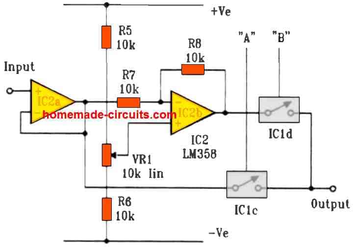 The circuit displayed in Figure 2.4b utilizes a double op-amp, having an amplifier IC2a applied as an input buffer to enable the control signal from a low impedance source, and the second amplifier IC2b, is configured to operate like a unity-gain inverter that produces a complementary signal to IC2a.
Both these voltage outputs are subsequently hooked up to a "2-way switch" created using the rest of the two 4016B electronic switches IC1c and IC1d, to ensure that an varying audio signal amplitude but constant average DC value can be obtained from its output.
The circuit displayed in Figure 2.4b utilizes a double op-amp, having an amplifier IC2a applied as an input buffer to enable the control signal from a low impedance source, and the second amplifier IC2b, is configured to operate like a unity-gain inverter that produces a complementary signal to IC2a.
Both these voltage outputs are subsequently hooked up to a "2-way switch" created using the rest of the two 4016B electronic switches IC1c and IC1d, to ensure that an varying audio signal amplitude but constant average DC value can be obtained from its output.
Main Features
The majority of dual op-amps must be well suited for this simple circuit, however the one tried in this article incorporated the common and cheap LM358. Despite of being simple this circuit offers outstanding efficiency and has unlimited application range depending on the user's imagination. For the beginners, you can try this circuit in the form of an output stage that detects "null" or zero crossing in a DC bridge circuit. The pot VR1 indicated in the circuit enables you to offset any sort of quiescent voltage to ensure that any difference in the DC input, positive or negative, can be instantly audible. Because our ear carries a logarithmic sensitivity to sound, an extremely big dynamic range can be covered, together with great sensitivity at lower levels.CMOS 4047B Astable Oscillator
This IC 4047 is actually slightly distinct from the previously discussed CMOS ICs due to the fact that its basic objective is to work like a flexible timer and oscillator. Therefore, this IC is effective at working most efficiently at increased frequencies. Although oscillators in many cases are created using a couple of free gates from CMOS ICs configured for implementing other primary functions, if the designer intends to make a very basic square wave oscillator or requires enhanced functionality this IC 4047 can prove to be extremely handy. Different pin connections enable the IC to be applied in a variety of different ways, like an astable oscillator with two output modes, complementary outputs and reset, or like an monostable timer with positive or negative triggering.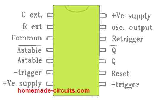 The pin characteristics for the 4047B can be understood through Figure 2.5 above, configured using the standard attributes of a CMOS RC oscillator.
The circuit can be seen working with just one capacitor and a single resistor, and is all that is required to set the frequency.
This frequency value, as earlier can be found out using the formula f = 1/(2.2 x R x C).
Where R may have just about any value from 10k to as high as 1M, while capacitor C ought to be higher than 100pF and should not be a polarized capacitor.
The pin characteristics for the 4047B can be understood through Figure 2.5 above, configured using the standard attributes of a CMOS RC oscillator.
The circuit can be seen working with just one capacitor and a single resistor, and is all that is required to set the frequency.
This frequency value, as earlier can be found out using the formula f = 1/(2.2 x R x C).
Where R may have just about any value from 10k to as high as 1M, while capacitor C ought to be higher than 100pF and should not be a polarized capacitor.
Getting 3 Oscillator Outputs
When an oscillator circuit is configured using the IC 4047, you get 3 oscillating outputs from the IC. The first one is the "Osc out" at pin13, which is a buffered output and working with the fundamental oscillator frequency. This may not be confirmed to give you an ideal 50:50 duty cycle, however practically it is usually a lot superior to the earlier explained two-gate type CMOS oscillator circuit set ups, particularly at lower frequencies. The other a couple of outputs that we get from the IC 4047 are "Q" and "Q_", from pins 10 and 11 respectively. We get these outputs from an internal single-stage divider circuit ensuring that they have accurate 50:50 duty cycles. However they operate at 50 % rate of the principal oscillator frequency which is available at pin13. These outputs are buffered internally, and work complementary to each other. Meaning, when one of the two pins is positive the other is negative and vice versa.Main Applications
This IC 4047 can be used for various different applications, you can use is as a piezo sounder device connected across the complementary pin 10 pin 11 so that the piezo is driven from a bridged output with increased volume. This kind of piezo driver functions wonderfully, generating a significantly loud sound even from your 5-volt supply.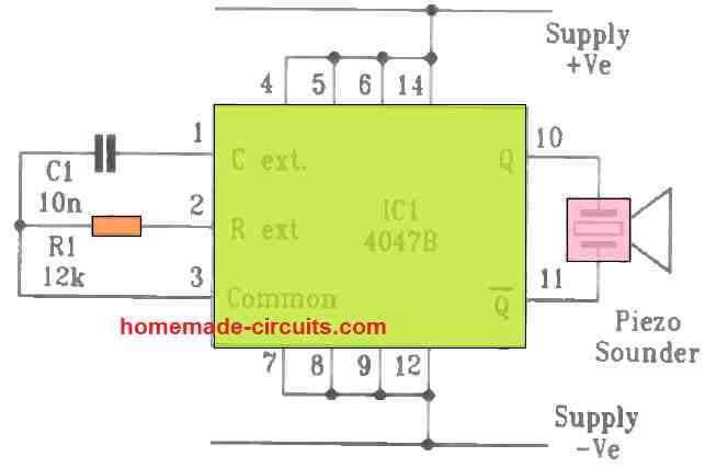 The configuration for this design can be witnessed in Figure 2.5 above, which provides an output frequency of around 1.9 kHz, an appropriate frequency for the majority of piezo sounders.
This square wave oscillator frequency can be calculated using the formula:
f = 1 / 2.2 x R x C
However it must be recalled that only the output from pin 13 of IC 4047 runs with the above rate.
The outputs from pins 10 and 11 operate at one half this frequency, therefore this could be determined using the formula:
f = 1 / 4.4 x R x C
The configuration for this design can be witnessed in Figure 2.5 above, which provides an output frequency of around 1.9 kHz, an appropriate frequency for the majority of piezo sounders.
This square wave oscillator frequency can be calculated using the formula:
f = 1 / 2.2 x R x C
However it must be recalled that only the output from pin 13 of IC 4047 runs with the above rate.
The outputs from pins 10 and 11 operate at one half this frequency, therefore this could be determined using the formula:
f = 1 / 4.4 x R x C
Main Features
The working efficiency of the IC 4047 is normally a lot improved compared to either basic two-gate circuits or the internal oscillator such as the 4060B. With excessive frequencies the output frequency value resembles a lot more tightly to the formula results. A test circuit using 100pF and 22k, designed to get a calculated output of 206kHz, in fact generated 173kHz using a 10 V supply voltage, that appeared much closer than the oscillator using 4060B that could reach only as near as 100kHz using the identical scenarios. Deviations for the input supply voltage is much less also, at 5 volts the 4047 oscillator circuit continued to maintain to operate at 155 kHz. In case a realistically stable RC oscillator running at around 100 kHz is intended, then this 4047 IC is possibly the best option.CMOS 4046B Voltage-Controlled Oscillator
A totally different kind of square wave oscillator circuit might be discovered inside the 4046B "phase-locked loop" IC. This extremely versatile chip offers an important feature, for creating very simply voltage-controlled oscillators. Regrettably explanations for this are often hard to understand for the newcomers, specifically because it provides a couple of independent external frequency control wiring. But in reality it is fairly simple to operate, which we can learn from the following sections.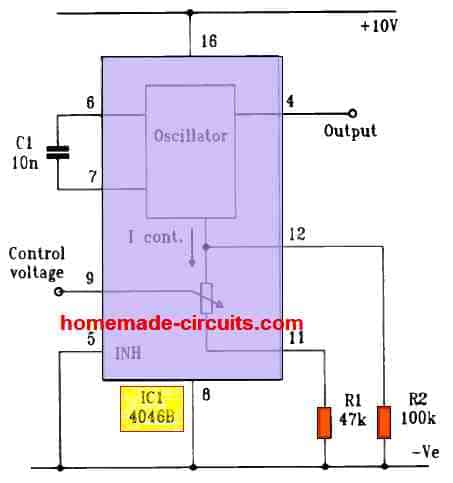 Fig.
2.6. 4046B Voltage-Controlled Oscillator
The fundamental wiring diagram for the CMOS 4046 oscillator can be visualized in Figure 2.6, that features a tremendously simplified model of its internal framework.
Fig.
2.6. 4046B Voltage-Controlled Oscillator
The fundamental wiring diagram for the CMOS 4046 oscillator can be visualized in Figure 2.6, that features a tremendously simplified model of its internal framework.
How it Works
The frequency is defined through an external capacitor C1 hooked up across pins 6 and 7 which is current controlled, the value for which can be fixed externally through the wiring across pins 9, 11 and 12. The timing capacitor could have any value from 50pF and higher, however this should not be an electrolytic type or a polarized type since the attached circuitry inside the IC is designed to operate by alternately reversing the polarity while charging and discharging the capacitor. Using the indicated component values in the diagram, the circuit will generate an output frequency of approximately 2 to 61 kHz. You can find a couple of distinct routes by which the circuit designer may be able to fix the oscillator control current, and it may not be important to work with both of them. Typically the primary one is set by means of pin 11. Control current runs through the oscillator to this pin via an in-built voltage controlled resistor, which has a value adjusted by an external control voltage put on pin 9. Pin 11 is generally linked to the ground line through a resistor, which is indicated as R1 in the schematic. The control voltage may extend from zero to the full supply voltage. When the control voltage is zero, the internal resistor attains an infinity value which means no current can pass through pin 11, and when the pin 12 is not connected, that will stop the oscillator. As the control voltage is increased the internal resistor gets more and more conductive, hence more current passes through it causing the oscillator frequency to increase. As soon as the control voltage extends to the positive supply limit, the pin 11 current is restricted primarily by resistor R1, and therefore this resistor is generally known as the maximum frequency setting resistor. Current may also be allowed to pass via a resistor from pin 12 to ground, indicated as R2. This current can be constant, irrespective of the control voltage, and this resistor is usually known as the minimum frequency setting resistor. Having said that, since this resistor is used to produce a constant frequency increase, right across the control range, it may be preferable to visualize this like a positive frequency "offset" resistor. For example, if the circuit had been setup to work through the range between 0 to 20 kHz with R1 and C1, then incorporating a resistor between pin 12 to get a lowest 51 kHz may modify the range to 5 to 25kHz. Once we understand the current-controlled nature of this IC 4046 CMOS square wave oscillator, through a couple of independent controlled current pathways, it might be much convenient to use this IC. This offers a very easy solution to control frequency using a voltage input, and the range covered might effortlessly end up being 1000:1 or higher, or this could be decreased to some very small fraction using an appropriate value of R2. The voltage control input of the IC offers a extremely large impedance, therefore it may be applied with high impedance signal inputs with no need for any buffer stages. The output offers a fantastic 50:50 duty cycle, plus the optimum frequency could be set up quickly from lower frequencies to as high as 2 or 3MHz. The output frequency is fairly linear with the control voltage, even though there exists little bit of shifting at around less than 20% of the supply. Additionally, it allows you to stop and start the frequency, simply with the aid of pin 5, which works like the "inhibit" input pin. Although this pin must generally be wired with the negative supply rail, connecting this pin with the positive line will cause the oscillator to halt.Drawbacks
Sadly there exists a drawback with this particular IC, as it has a few major difficulties associated with stability and varying characteristics across devices. These disadvantages causes the IC to be excluded from many applications for which it could initially look perfect. Undoubtedly the main concern seems to be the lack of stability in response to changes in supply voltage. As an example, a demo circuit put together to operate at 10 kHz using a supply of 15 V slipped down to 6.8 kHz at 10 V and dropped further to 2.1 kHz at 5 volts. This means that while using practically, this IC might always require a regulated supply voltage where its efficiency may be the lowest at 5 volts. One possible thing could be to regulate an available 5 V supply and then employ a voltage doubler circuit to raise to a stable 10 V level for the CMOS oscillator, however this hassle would mean the circuit would no longer be simple as in its original form. A randomly collected 6nos of 4046B's were experimented with within the same circuit configuration, which produced frequencies through 9.9 kHz to 12.7 kHz, indicating that numerous applications would require "select-on-test" manipulation for the right functioning. You may also find the IC 4046 having a minor sensitivity to variations in temperature. The large deviation of frequency due to changes in the voltage level makes it hard to present a formula for selecting R and C accurately.Calculating Frequency
However using a supply input of 10 volts a reasonably accurate result could be achieved through the formula: f = 2 / C x R The above formula is applicable to the two pins 11 and 12, when it comes to pin 11 the formula takes into account the full positive supply voltage at pin 9. When the supply voltage is half, the frequency may be approximately half the formula value. The resistors connected across pins 11 and 12 to the ground or the negative line must not exceed the values between 10 k to 1 M. Even though it is normal to run this IC using a resistor across pin 11 as being the key frequency-setting element, it is rather feasible to keep this pin unconnected and unused, and employ just a single resistor across pin 12 to establish a constant square wave frequency. As a result, it may be possible to employ a significantly larger resistor between pin 11 to ground in order to present a smaller voltage controlled range of adjustment. This feature isn't usually apparent in explanations on this IC, however it may be worth trying this, since it can uncover several helpful applications for this CMOS IC 4046.High Power CMOS Oscillator
This high-power audio oscillator generates a powerful audible frequency through a piezoelectric transducer. All 4 gates available from the 4093 lC are utilized in this assignment to operate the transducer through an excellent audio signal. The circuit may be used in wireless house alarms, toys and games, as a separate project to instruct regarding square wave oscillators.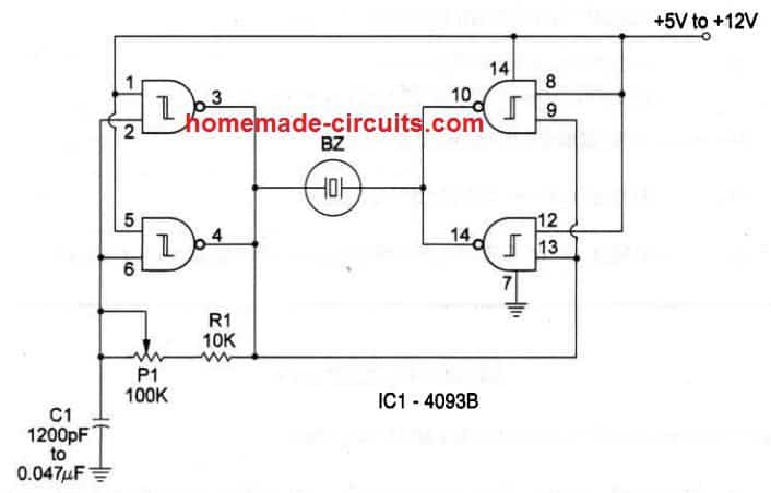 The proposed piezoelectric transducer produces highest output power between 700 and 3,000 Hz, however it may likewise run in different square wave frequencies with less power.
Power supply voltage range can be between 5 and 12 volts.
Current usage is determined the power supply voltage, varying from 10 to 50 mA typically.
P1 changes the tone frequency.
C1 could be re-structured with a a lot of different values as suggested in the schematic diagram.
The proposed piezoelectric transducer produces highest output power between 700 and 3,000 Hz, however it may likewise run in different square wave frequencies with less power.
Power supply voltage range can be between 5 and 12 volts.
Current usage is determined the power supply voltage, varying from 10 to 50 mA typically.
P1 changes the tone frequency.
C1 could be re-structured with a a lot of different values as suggested in the schematic diagram.
More Square wave Generator Circuits

Square wave Oscillator using Op Amp
Figure below exhibits the circuit diagram of a basic square wave oscillator using a single operational amplifier. The indicated values provide an running frequency of roughly 1kHz, however this could be modified by altering the R1 or C1 value.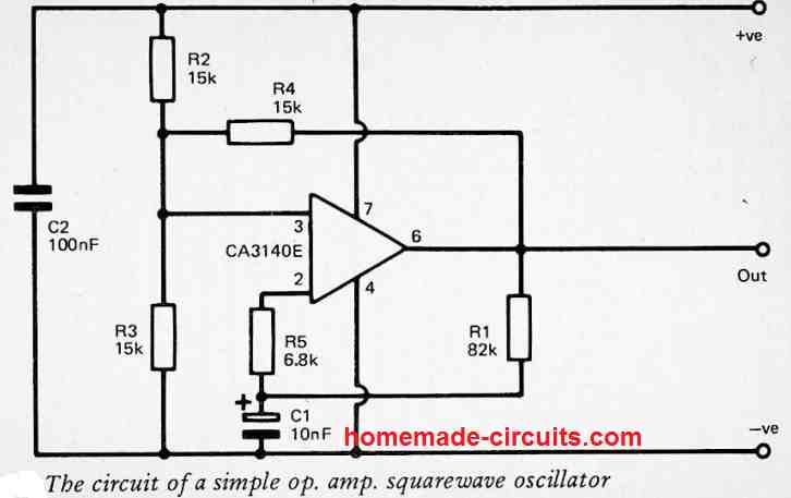 Tweaking these values would provide an inversely proportionate variation in the output frequency.
The equation shown below facilitates determining the rough value for the output frequency:
Frequency = 0.82/R1C1
R1 could be any value between couple of kilohms to many Megohms, and C1 can be selected to have a value between a few tens of pF and higher.
The diagram indicates the appropriate polarity for C1 in case a polarized type for example an electrolytic or a tantalum capacitor is employed here.
The highest operating frequency can be 100 kHz or higher, however with extremely high frequencies the output waveform may show some degradation because of the restrictions added to the circuit through the slew rate of the IC CA3140E.
An operational amplifier has no high current output stage, and with no extra output amplification you possibly can obtain an optimum output current of just a few milliamps.
Similar to 555 astables, this circuit is pretty stable in terms of output frequency, and supply voltage fluctuations will not generate major frequency alterations.
The circuit can work nicely using a supply DC as low as 6 volts, and the overall high supply Dc up to 36 volts (which is the highest the CA3140E operational amplifier can tolerate).
The circuit can work with other operational amplifiers, for example LF351, TL081CP, etc., however remember that several of these offer a reduced peak to peak output voltage compared to CA3140E (which allows an output voltage swing of almost equal to the supply DC with a low output load conditions), and a downside of this can be a minor upsurge in the output frequency which may be normally close to 10%.
This op amp square wave oscillator circuit is advantageous in applications where an adjustable frequency square wave oscillator is necessary since the working frequency could be adjusted using a solitary resistance, which is basically needs to substitute the resistor R1 with a fixed resistor and a potentiometer attached in series.
Obviously, the 555 astable circuits explained in one of the earlier posts may also be used like an adjustable frequency oscillators when one of the timing resistances is swapped out with a fixed resistor and a pot connected in series.
However, this arrangement might result in an alteration in the output waveform as the pot is turned for varying the output frequency.
This situation may possibly be unfavorable in a few applications.
Tweaking these values would provide an inversely proportionate variation in the output frequency.
The equation shown below facilitates determining the rough value for the output frequency:
Frequency = 0.82/R1C1
R1 could be any value between couple of kilohms to many Megohms, and C1 can be selected to have a value between a few tens of pF and higher.
The diagram indicates the appropriate polarity for C1 in case a polarized type for example an electrolytic or a tantalum capacitor is employed here.
The highest operating frequency can be 100 kHz or higher, however with extremely high frequencies the output waveform may show some degradation because of the restrictions added to the circuit through the slew rate of the IC CA3140E.
An operational amplifier has no high current output stage, and with no extra output amplification you possibly can obtain an optimum output current of just a few milliamps.
Similar to 555 astables, this circuit is pretty stable in terms of output frequency, and supply voltage fluctuations will not generate major frequency alterations.
The circuit can work nicely using a supply DC as low as 6 volts, and the overall high supply Dc up to 36 volts (which is the highest the CA3140E operational amplifier can tolerate).
The circuit can work with other operational amplifiers, for example LF351, TL081CP, etc., however remember that several of these offer a reduced peak to peak output voltage compared to CA3140E (which allows an output voltage swing of almost equal to the supply DC with a low output load conditions), and a downside of this can be a minor upsurge in the output frequency which may be normally close to 10%.
This op amp square wave oscillator circuit is advantageous in applications where an adjustable frequency square wave oscillator is necessary since the working frequency could be adjusted using a solitary resistance, which is basically needs to substitute the resistor R1 with a fixed resistor and a potentiometer attached in series.
Obviously, the 555 astable circuits explained in one of the earlier posts may also be used like an adjustable frequency oscillators when one of the timing resistances is swapped out with a fixed resistor and a pot connected in series.
However, this arrangement might result in an alteration in the output waveform as the pot is turned for varying the output frequency.
This situation may possibly be unfavorable in a few applications.
Square Wave Pulse Generator Circuit
The above op amp square wave circuit can be easily customized to generate a pulsed output waveform. The following figure illustrates the required alterations. This actually includes just a a couple of timing resistors (R1 and R2) along with two driver diodes D1 and D2. The configuration ensures that C1 charges through R2 and discharges by means of R1.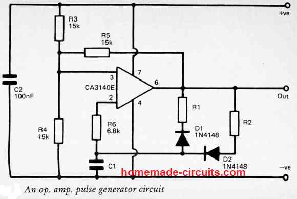 Therefore R1 fixes the low switch OFF output period and R2 determines the high switch ON output period, along with the mark-space duty cycle ratio equivalent to the ratio of R1 to R2. The working frequency of this square wave PWM pulse generator could be determined through the formula as given below:
Frequency = 0.82/[(R1 + R2)/2]C1
Therefore R1 fixes the low switch OFF output period and R2 determines the high switch ON output period, along with the mark-space duty cycle ratio equivalent to the ratio of R1 to R2. The working frequency of this square wave PWM pulse generator could be determined through the formula as given below:
Frequency = 0.82/[(R1 + R2)/2]C1
Digital Step Sine wave Generator Circuit
In this post we learn how to build a simple yet accurate digital sine wave generator circuit, which is basically an oscillator circuit, enhanced to generate square waves through incrementing steps, which ultimately appears like a stepped sine waveform. By Ron Mackenzy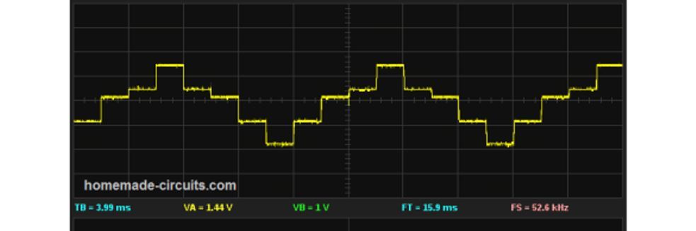 The difference between analogue sine wave generator and digital sine wave generator is that, in analogue design mainly op amps are utilized to shape a smooth exponentially increasing pure sine waveform, while in a digital mode, the waveform is also exponentially increasing but it is with a staggered shape, or in a stepped manner.
Advantage
The main advantage of digital sinewave compared to the analogue counterpart is that, analogue sine wave cannot be used to switch MOSFETs or power transistors for a given applications such as sine wave inverters, converters, motor control etc, while digital sine waveform becomes perfectly suitable for such applications, without causing heating up of the devices. This is because, transistors do not "like" to conduct with analogue signals, or with smoothly rising/falling exponential waveforms, instead the internal characteristics of these devices allow them to be more suitable to logic waveforms, triggered with high and low logic signals.How the Circuit Works
The circuit is made up of a couple of stages, each of which might have several valuable applications by itself: an oscillator built using a set of EX(clusive) OR gates along with a divide-by-three circuit created through a pair of common flipflops. The basic oscillator consists of a noninverting gate (N1) and an inverting gate (N2). If simply inverting gates was utilized, a minimum of about three might have been required for this oscillator, however, a non-inverting gate could be constructed through a couple of inverting gates hooked up in series.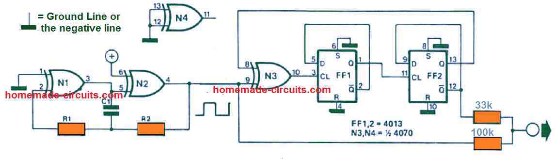 The circuit functions like this: We will suppose that, at the start, the input of N1 (pin 2) is low.
Therefore the output of N1 will be also low causing the output of N2 to be high.
Capacitor C1 will subsequently be charged through resistor R2. After a brief moment, the N1 input should go high through R1 and the entire process is going to be reversed.
The divide-by-three section includes a couple of flip-flops that each divide by 2. Put simply, it would be anticipated that collectively these might divide by four.
Having said that, an additional EXOR gate (N3) can be seen incorporated between the output of FF2 and the input of FF1. This efficiently inverts the clock input signal whenever the output of FF2 flips its polarity.
In case N3 hadn't been used the flipflop's output state wouldn't switch before the ongoing clock interval ended.
With the help of N3, the clock signal gets inverted and its positive-going edge activates the flipflop once every half time period.
As a result, the dividing element in the process is three, never four.
The sinewave signal is created by using a couple of resistors (R3 and R4).
As soon as the input on the two resistors is low (logic zero) no output voltage will be seen.
Once the input to the two resistors becomes high (logic one) the output voltage turns high.
If one of the inputs applied to the resistors is low while the other input is high, causes the output voltage to be either 1/4th or 3/4th of the supply (high) level.
The circuit functions like this: We will suppose that, at the start, the input of N1 (pin 2) is low.
Therefore the output of N1 will be also low causing the output of N2 to be high.
Capacitor C1 will subsequently be charged through resistor R2. After a brief moment, the N1 input should go high through R1 and the entire process is going to be reversed.
The divide-by-three section includes a couple of flip-flops that each divide by 2. Put simply, it would be anticipated that collectively these might divide by four.
Having said that, an additional EXOR gate (N3) can be seen incorporated between the output of FF2 and the input of FF1. This efficiently inverts the clock input signal whenever the output of FF2 flips its polarity.
In case N3 hadn't been used the flipflop's output state wouldn't switch before the ongoing clock interval ended.
With the help of N3, the clock signal gets inverted and its positive-going edge activates the flipflop once every half time period.
As a result, the dividing element in the process is three, never four.
The sinewave signal is created by using a couple of resistors (R3 and R4).
As soon as the input on the two resistors is low (logic zero) no output voltage will be seen.
Once the input to the two resistors becomes high (logic one) the output voltage turns high.
If one of the inputs applied to the resistors is low while the other input is high, causes the output voltage to be either 1/4th or 3/4th of the supply (high) level.
Waveform
Surely, the above situation could be confirmed through formulas, but a less complicated technique is to describe this by analyzing just one sinewave interval through a waveform diagram.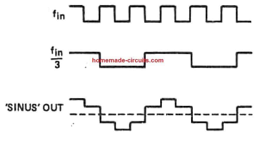 A small rectangle could be used at the center of the sinewave to symbolize a logic 1 level.
A pair of additional rectangles of the identical dimension then can be sketched on each side of the first.
The region within the sinewave of the final a couple of rectangles is going to be half that of the first.
The digital simulation method produces a signal using the exact same regions like the above.
While building this particular digital sine wave generator circuit, it has to be taken into account that CMOS inputs must never be kept 'floating'.
This means that, pins 12 and 13 of the EXOR chip (N4) must be attached to ground (0V).
A small rectangle could be used at the center of the sinewave to symbolize a logic 1 level.
A pair of additional rectangles of the identical dimension then can be sketched on each side of the first.
The region within the sinewave of the final a couple of rectangles is going to be half that of the first.
The digital simulation method produces a signal using the exact same regions like the above.
While building this particular digital sine wave generator circuit, it has to be taken into account that CMOS inputs must never be kept 'floating'.
This means that, pins 12 and 13 of the EXOR chip (N4) must be attached to ground (0V).
Stepped Sinewave Voltage Generator Using IC 4046
A stepped sinewave voltage generator is an electronic circuit designed to generate a sequentially stepped voltage waveform, which resembles a sinusoidal appearance, but has a stepped voltage pattern ascending sequentially upwards towards the peak and then descending sequentially downward with identical steps towards the 0V line to complete a cycle of the waveform.How the Circuit Works
The figure below exhibits a useful application of the IC 4066 quad bilateral switch. In this circuit, the 4066 (U1) is configured to carry out sequential switching, in order to generate a uniform stepped waveform; as indicated in the next figure. As demonstrated, the generator's waveform consists of 3-up and 3- down steps through 1V increments.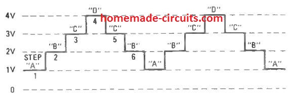 The triggering for the 4066 internal switches is governed by a4017 decade counter/divider(U2); a567 tone decoderset up like a squarewave generator provides the required clock pulses for the IC 4017.
The 4017 is rigged to count from 0 to 5 (0-1-2-3-4-5) sequentially and reset on the rising edge of the seventh step by coupling pin 5 (output 6) of U2 to pin 15 (reset).
As soon as output 6 (pin 5 of U2) becomes high, the reset terminal of U2 pushes output 0 (pin 3) to flip from low to high, starting the pattern afresh.
The high pin-3 output (output 0) of U2 is given to the control pin of the 1st U1 switch, switching it on and consequently connecting the intersection of R4 and R5 with the output bus.
This sets up step one with a one-volt level.
With the following clock pulse from the 567, the 4017 generates a high output at pin 2, which is applied via D4 to another switch control at pin 5, switching it on.
This links the R3, R4 with the output bus.
The 2nd step constitutes a 2-volt output.
For the subsequent pulse obtained via U3, pin 4 of U2 turns high, evoking the 3rd switch (in U1) to activate, which respond to generate a 3- volt output intended for step 3.
The 4th pulse coming from U3 results in pin 7 to become high, switching on the very last switch, and thus creating a 4-volt output for step 4.
The fifth pulse feeds a high to pin 10 of U2, which moves by means of D4 to the control input of the 3rd switch, switching it on (for a second occasion) and providing a 3-volt output to the 5th step.
For the subsequent clock pulses, the switch attached to pin 6 of U1 is yet again activated, generating a 2-volt output for step 6. Soon after step six is accomplished, the counter resets and commences back from the start by switching on the 1st switch for step 1.
Each waveform step can be arranged for any voltage right from zero to 100 % supply voltage through the use of specific voltage dividers for each step.
Additionally, the generator's output could be buffered to deliver adequate voltage and current outputs to provide rising voltage or current supply for a semiconductor curve tracer.
The triggering for the 4066 internal switches is governed by a4017 decade counter/divider(U2); a567 tone decoderset up like a squarewave generator provides the required clock pulses for the IC 4017.
The 4017 is rigged to count from 0 to 5 (0-1-2-3-4-5) sequentially and reset on the rising edge of the seventh step by coupling pin 5 (output 6) of U2 to pin 15 (reset).
As soon as output 6 (pin 5 of U2) becomes high, the reset terminal of U2 pushes output 0 (pin 3) to flip from low to high, starting the pattern afresh.
The high pin-3 output (output 0) of U2 is given to the control pin of the 1st U1 switch, switching it on and consequently connecting the intersection of R4 and R5 with the output bus.
This sets up step one with a one-volt level.
With the following clock pulse from the 567, the 4017 generates a high output at pin 2, which is applied via D4 to another switch control at pin 5, switching it on.
This links the R3, R4 with the output bus.
The 2nd step constitutes a 2-volt output.
For the subsequent pulse obtained via U3, pin 4 of U2 turns high, evoking the 3rd switch (in U1) to activate, which respond to generate a 3- volt output intended for step 3.
The 4th pulse coming from U3 results in pin 7 to become high, switching on the very last switch, and thus creating a 4-volt output for step 4.
The fifth pulse feeds a high to pin 10 of U2, which moves by means of D4 to the control input of the 3rd switch, switching it on (for a second occasion) and providing a 3-volt output to the 5th step.
For the subsequent clock pulses, the switch attached to pin 6 of U1 is yet again activated, generating a 2-volt output for step 6. Soon after step six is accomplished, the counter resets and commences back from the start by switching on the 1st switch for step 1.
Each waveform step can be arranged for any voltage right from zero to 100 % supply voltage through the use of specific voltage dividers for each step.
Additionally, the generator's output could be buffered to deliver adequate voltage and current outputs to provide rising voltage or current supply for a semiconductor curve tracer.
Another Simple Stepped sine wave Voltage Generator using IC 4017
The next design below is even simpler to build as it employs just a couple ICs for the required stepped waveform creation.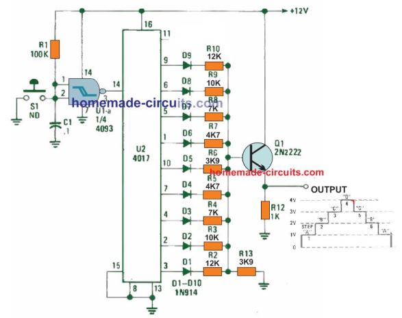 However, the stepped sine wave generator design is implemented in a manual mode, wherein the sequential steps of the waveform are developed by tapping the push button S1 at a specific timed rate.
Each pressing causes the output of the IC 4017 to shift from pin3 upwards, towards pin11.
In the process, the common ends of the resistors happen to develop a sequentially ascending and descending stepped voltage due to the effect of the varying potential divider formed by the interaction of the shifting IC 4017 logics across the resistors R2---R10 and the ground resistor R13.
Since the common joined ends of the resistors are together fed to the base of a common-emitter BJT stage, the stepped voltage is replicated at the emitter of the2N2222 transistorwith a higher current level, which can be integrated with any suitable external circuit stage for a desired execution.
The manually controlled switch can be replaced with an automatic oscillator stage as indicated in the following example, which shows the implementation of the above stepped voltage generator in a police lamp effect simulator circuit.
However, the stepped sine wave generator design is implemented in a manual mode, wherein the sequential steps of the waveform are developed by tapping the push button S1 at a specific timed rate.
Each pressing causes the output of the IC 4017 to shift from pin3 upwards, towards pin11.
In the process, the common ends of the resistors happen to develop a sequentially ascending and descending stepped voltage due to the effect of the varying potential divider formed by the interaction of the shifting IC 4017 logics across the resistors R2---R10 and the ground resistor R13.
Since the common joined ends of the resistors are together fed to the base of a common-emitter BJT stage, the stepped voltage is replicated at the emitter of the2N2222 transistorwith a higher current level, which can be integrated with any suitable external circuit stage for a desired execution.
The manually controlled switch can be replaced with an automatic oscillator stage as indicated in the following example, which shows the implementation of the above stepped voltage generator in a police lamp effect simulator circuit.
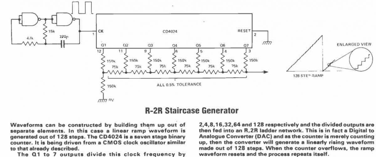
Applications
You will find a variety of applications for this circuit. The stepping sine waveform generator could be implemented to produce numerous progressive voltages for examining the on/off switching point of many CMOS units. It can be effectively used for making efficient sine waveinvertersand converters.Application Circuit
A stepped waveform can be very effectively used for making a sine wave inverter as shown in the following example: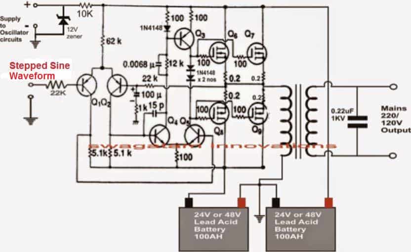
6 Useful Voltage Controlled Oscillator Circuit Explored
In this post we learn how to build 6 useful voltage controlled oscillator circuits, using various op amps and integrated circuits. As the name suggests, a voltage controlled oscillator or a VCO circuit is an oscillator circuit whose output frequency can be controlled or varied through an adjustable control voltage input. This means, if the input control voltage is increased, the output frequency will increase proportionately, and vice versa. If the control voltage varies continuously up and down, then the output frequency will also correspondingly increase and decrease, in response to the varying amplitude of the control voltage levels. Just like any other VCO circuit, in the discussed circuit below, the output frequency is determined by the level of the control voltage applied.1) Main Features (Using IC LM558)
The main advantage of this VCO design is that it comes with a wide control voltage range, which extends right from 0 V up to the maximum positive supply voltage limit. The power supply level could be anything from +3V to +25 V. Additionally this voltage controlled oscillator (VCO) is designed to generate both triangular as well as a square wave output signals.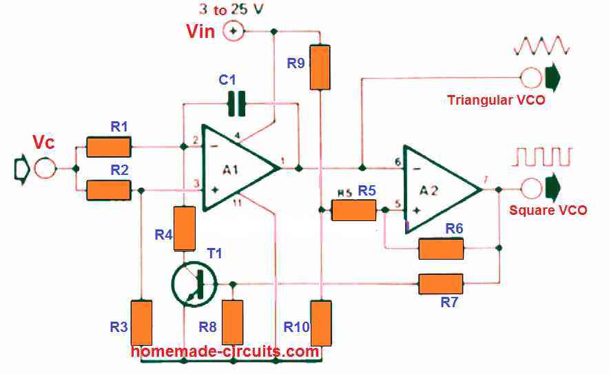 Only the large black dots indicate a connection across the intersecting lines
Parts List
R1, R5, R6 = 100K R2, R3, R4 = 47K R7, R8, R9, R10 = 10K C1 = 47 nF T1 = BC547 A1, A2 = LM358 Having said that, the user has to be careful while working with low voltage inputs, and ensure that the highest input voltage level is at least 1.5 V lower than the supply voltage.How the Circuit Works
The circuit functions by using the 'integrator/comparator' theory. Capacitor C1 forms the part of the integrator (designed around opamp A1), and it is charged using a constant current source as determined by the instantaneous level of the applied control voltage. As a result, the A1 output voltage falls linearly. The comparator output (built using A2) changes state and transistor T1 begins conducting as soon as the comparator's bottom switching threshold is attained. Capacitor C1 at this point is discharged, triggering the A1 output to increase (again, this rising voltage is linear in nature). The action repeats, and the moment the A1 output extends to the comparator's upper switching limit, it switches OFF T1. The duty cycle of the output voltage controlled frequency is going to be FIFTY PERCENT if the R2 and R3 values are identical (R2 = R3), and when the value of R1 is two times than that of R4 (R1 = 2 x R4). The relationship between the R9 and R10 values becomes responsible for the level of the triangular DC output voltage. With respect to the R9/R10 values shown in the schematic, the triangular DC level will likely be 1 / 2 the supply voltage. The peak-to-peak output level, can be determined by solving the following equation: (Vpp) = R5 / (R5 + R6) x VinControl Voltage, Supply Voltage Relationship
The characteristics of the proposed voltage controlled oscillator or the VCO using a pair of (common) supply voltages can be witnessed in the following graph.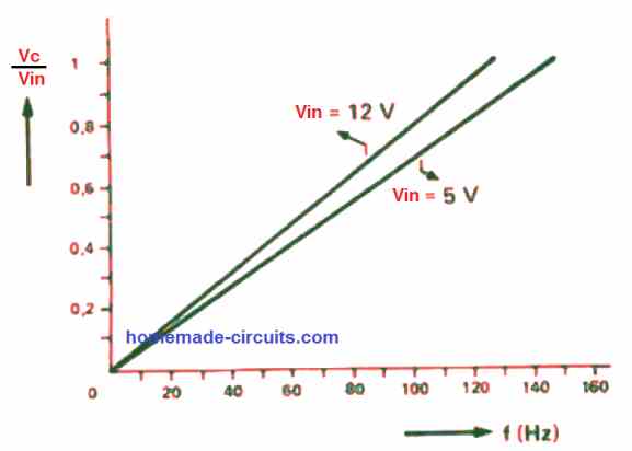 When both the supply inputs are equal (Vin = Vc) in magnitude the maximum frequency that can be achieved from the circuit could be increased or decreased by correspondingly selecting the C1 value lower or higher.
With regards to the opamp's slew rate, the vertical angle of the squarewave signal may decline for the higher frequencies.
When both the supply inputs are equal (Vin = Vc) in magnitude the maximum frequency that can be achieved from the circuit could be increased or decreased by correspondingly selecting the C1 value lower or higher.
With regards to the opamp's slew rate, the vertical angle of the squarewave signal may decline for the higher frequencies.
2) VCO using IC 7555
A neat little voltage controlled oscillator can also be built using the resolute IC 555 and a few other assisting components, as shown below: The discharge process of capacitor C1 is voltage controlled.
This is implemented by the quick charging pulses controlled by the internal discharge transistor of IC2.
To understand the working, imagine the pin3 output of timer IC2 is initially low and the discharge transistor pin 7 is switch ON, pulling current through R6 to activate transistor TR3. This particular transistor maintains the transistor TR2 base at the positive supply voltage.
This guarantees that it is switched off.
The capacitor C1 may consequently start discharging via R4 with a rate as decided by the TR1 collector current.
As the voltage across C1 drops to around 1/3rd supply voltage level, the IC555 output turns high.
Simultaneously the discharge transistor along with TR3 also switch OFF, which means that current through R3 now activates TR2, which begins charging C1 via R4.
As soon as the voltage across C1 gets to 2/3rd of the supply voltage, IC2 yet again changes state and the cycle keeps repeating.
A functioning property of transistors is such that practically all the current going to the emitter side, runs out back from the collector.
A tiny amount of current passes out from the base, however normally, this is very small to be considered.
Due to the fact that the emitter voltage follows the applied base voltage, deducting the base/emitter forward drop of around 0.6 volts, this voltage output enables you to control the voltage over the emitter resistor R2 with this circuit.
The transistor base voltage as a result controls the collector current, giving rise to a voltage controlled current source.
The control voltage could be applied directly on the transistor TR1 base in order to control the frequency output in this circuit.
The discharge process of capacitor C1 is voltage controlled.
This is implemented by the quick charging pulses controlled by the internal discharge transistor of IC2.
To understand the working, imagine the pin3 output of timer IC2 is initially low and the discharge transistor pin 7 is switch ON, pulling current through R6 to activate transistor TR3. This particular transistor maintains the transistor TR2 base at the positive supply voltage.
This guarantees that it is switched off.
The capacitor C1 may consequently start discharging via R4 with a rate as decided by the TR1 collector current.
As the voltage across C1 drops to around 1/3rd supply voltage level, the IC555 output turns high.
Simultaneously the discharge transistor along with TR3 also switch OFF, which means that current through R3 now activates TR2, which begins charging C1 via R4.
As soon as the voltage across C1 gets to 2/3rd of the supply voltage, IC2 yet again changes state and the cycle keeps repeating.
A functioning property of transistors is such that practically all the current going to the emitter side, runs out back from the collector.
A tiny amount of current passes out from the base, however normally, this is very small to be considered.
Due to the fact that the emitter voltage follows the applied base voltage, deducting the base/emitter forward drop of around 0.6 volts, this voltage output enables you to control the voltage over the emitter resistor R2 with this circuit.
The transistor base voltage as a result controls the collector current, giving rise to a voltage controlled current source.
The control voltage could be applied directly on the transistor TR1 base in order to control the frequency output in this circuit.
3) Using Op amp with IC 555
In another situation, if an op-amp is employed with the transistor as displayed in the next diagram below, then the voltage across R2 may follow accurately the input voltage, and the the op-amp would automatically begin compensating for the emitter-base voltage drop as well as disparities due to temperature changes. The resulting output frequency control range can then begin from zero rather than 0.6 volts. Calculations required for designing this IC555 based VCO circuit can be as easy as for the simple fixed-frequency circuits, which means just a couple of rules must be followed.
Resistor R4 has to be relatively low in values compared to the value of R2.
There should always be sufficient voltage across TR 1 for it to work, therefore the input must in no way cross 1 V value below 1/3rd supply voltage.
This particular voltage controlled oscillator circuit is vulnerable to variations in the supply voltage, therefore the supply should be strictly regulated.
Once the maximum control voltage range is fixed, the period for the discharge element of every single cycle could be worked out using the formula:
t = (C x R x E) / V
Here C represents the timing capacitor C1, R stands for the emitter resistor R2, E indicates 1/3rd of the supply level and V represents the voltage across R2.
To th result from the above expression, we have to add the time taken for the charging portion of the cycle:
t = 0.7 x C1 x R4
The two elements collectively provide the full period for each cycle hence, as a common practice, their inverse provides the equivalent frequency.
With the part values indicated with a 9 V supply input, the circuit produces a frequency response from 0 Hz to approximately 1 kHz in response to an input control voltage between 0 to 2 volts.
The output frequency is composed of positive pulses of 100 us width, excellent for generating a wide range of noise over a small loudspeaker using the most basic of output buffer stages, maybe just one BJT stage.
Using C1 as a 1 nF capacitor it delivers approximately 9 kHz for exactly the same input voltage range, using proportionately shorter output pulses.
Calculations required for designing this IC555 based VCO circuit can be as easy as for the simple fixed-frequency circuits, which means just a couple of rules must be followed.
Resistor R4 has to be relatively low in values compared to the value of R2.
There should always be sufficient voltage across TR 1 for it to work, therefore the input must in no way cross 1 V value below 1/3rd supply voltage.
This particular voltage controlled oscillator circuit is vulnerable to variations in the supply voltage, therefore the supply should be strictly regulated.
Once the maximum control voltage range is fixed, the period for the discharge element of every single cycle could be worked out using the formula:
t = (C x R x E) / V
Here C represents the timing capacitor C1, R stands for the emitter resistor R2, E indicates 1/3rd of the supply level and V represents the voltage across R2.
To th result from the above expression, we have to add the time taken for the charging portion of the cycle:
t = 0.7 x C1 x R4
The two elements collectively provide the full period for each cycle hence, as a common practice, their inverse provides the equivalent frequency.
With the part values indicated with a 9 V supply input, the circuit produces a frequency response from 0 Hz to approximately 1 kHz in response to an input control voltage between 0 to 2 volts.
The output frequency is composed of positive pulses of 100 us width, excellent for generating a wide range of noise over a small loudspeaker using the most basic of output buffer stages, maybe just one BJT stage.
Using C1 as a 1 nF capacitor it delivers approximately 9 kHz for exactly the same input voltage range, using proportionately shorter output pulses.
Which Opamps are Suitable
Remember that in case an op-amp is employed as indicated in the above VCO circuit diagram, it has to be of a kind having input and output rated to work right down to the negative supply voltage. The IC CA3140 as indicated is acceptable, some other possible variants could be the CA3130, or one of the op amps from the IC CA3240, LM358 or LM324. Various other transistors may also work very well instead of the one shown in the diagram, as long as these are assembled with the proper polarity. The practical use of this IC 555 voltage controlled oscillator circuit may not be extensive, and may be restricted to generally with audio related work, but the design is very cheap, straightforward and pretty stable with its specifications.4) Using IC 7556
In the previousvoltage controlled oscillator circuit, transistors were employed to provide a steady current and to reverse the discharge signal from a timer IC. To show what's possible, here's a VCO design that uses an op-amp integrator instead of a timing capacitor and current source, plus an IC7556 dual timer for inversion. An op-amp integrator includes a couple ofinputs: one that is non-inverting and generally linked to a reference voltage, and the otherthat is inverting and coupled to an input voltage via a resistor,with anegative feedback from the output,provided by a capacitor. The op-amp utilizes feedback to maintain the voltage at the inverting input same asthe voltage at the non-inverting input,within the limits of the supply voltage.
If a constant voltage is given to the input resistor, the voltage across it will equal the difference between this and the reference voltage, resulting in a constant current flowing into the input.
This current charges the feedback capacitor.
As a result, the op amp output voltage varies at a stable rate to maintain the inverting input voltage constant.
This may be implementedto make an oscillator by changing the input voltage polarity when the output goes over the timer IC's input limits.
One small snag is that the integrator output is reversed, with positive inputs dropping and negative inputs rising.
There has to be a polarity inversion at a certain point in order to build a working oscillator with the inverting IC7556. A dual op-amp, with the latter inverting the output of the first, is one way of achieving this.
Nevertheless, this necessitates the addition of a minimum oftwo extra resistors, which can compromise the circuit's frequency.
A better solution is to utilize two timers, with the second oneserving as an inverter for the first's output.
Figure 1.5 depicts a circuit that works in this manner.
IC1 is the integrator, having resistors R3 and R4 providing a reference voltage of roughly 1/3of the supply voltage to its non-inverting input pin3.
A voltage larger than the reference supplied to resistor R1 while the discharge transistor of the second timer, pin 13, is switchedoff would make the output of IC1 to drop at a rate specified by the input voltage and the values of Rt, R2, and capacitor C1. The first timer switchesstate as soon asit approaches 1/3of the supply voltage, with output pin 5 becoming high.
Because this is linked to the second timer's inputs, pins 8 and 12, the output of this is now becomeslow, and the discharge transistor, pin 13, is turned on.
The integrator's output beginsincreasing,sinceit has an apparent negative input of roughly a 1/3 of the supply linked to R2. The two timers swap states again the momentit reaches 2/3of the supply voltage, and the process continues.
The time for the first part of the cycle is calculated as follows:
t = C x R x V / E
Where Crepresents C1, R1represents R1+ R2, V represents 1/3 of the voltage supply, and E represents the supplied input voltage.
A similar equationmay be used to compute the time for the second portion of the cycle in this situation.
Because R is R2 by itself and V and E are almost identical in value, the time may be calculated as follows:
t = C1 x R2
The op-amp utilizes feedback to maintain the voltage at the inverting input same asthe voltage at the non-inverting input,within the limits of the supply voltage.
If a constant voltage is given to the input resistor, the voltage across it will equal the difference between this and the reference voltage, resulting in a constant current flowing into the input.
This current charges the feedback capacitor.
As a result, the op amp output voltage varies at a stable rate to maintain the inverting input voltage constant.
This may be implementedto make an oscillator by changing the input voltage polarity when the output goes over the timer IC's input limits.
One small snag is that the integrator output is reversed, with positive inputs dropping and negative inputs rising.
There has to be a polarity inversion at a certain point in order to build a working oscillator with the inverting IC7556. A dual op-amp, with the latter inverting the output of the first, is one way of achieving this.
Nevertheless, this necessitates the addition of a minimum oftwo extra resistors, which can compromise the circuit's frequency.
A better solution is to utilize two timers, with the second oneserving as an inverter for the first's output.
Figure 1.5 depicts a circuit that works in this manner.
IC1 is the integrator, having resistors R3 and R4 providing a reference voltage of roughly 1/3of the supply voltage to its non-inverting input pin3.
A voltage larger than the reference supplied to resistor R1 while the discharge transistor of the second timer, pin 13, is switchedoff would make the output of IC1 to drop at a rate specified by the input voltage and the values of Rt, R2, and capacitor C1. The first timer switchesstate as soon asit approaches 1/3of the supply voltage, with output pin 5 becoming high.
Because this is linked to the second timer's inputs, pins 8 and 12, the output of this is now becomeslow, and the discharge transistor, pin 13, is turned on.
The integrator's output beginsincreasing,sinceit has an apparent negative input of roughly a 1/3 of the supply linked to R2. The two timers swap states again the momentit reaches 2/3of the supply voltage, and the process continues.
The time for the first part of the cycle is calculated as follows:
t = C x R x V / E
Where Crepresents C1, R1represents R1+ R2, V represents 1/3 of the voltage supply, and E represents the supplied input voltage.
A similar equationmay be used to compute the time for the second portion of the cycle in this situation.
Because R is R2 by itself and V and E are almost identical in value, the time may be calculated as follows:
t = C1 x R2
5) VCO using IC CA3130
Even though this Voltage Controlled Oscillator works by using just a couple of CA3130 op amps, it is still able to exhibit a voltage/frequency linearity transfer characteristic far better than 0.5%, while its temperature coefficient remains lower than 0.01%/��C. The working of the circuit can be understood wit the following points: IC1 operates like a voltage controlled multivibrator. Supposing that the IC1 output voltage is +15 V at the start, C1 begins charging through D3, R4 and P1 by means of a time constant components (R4 + P1) C1. C1 keeps charging until the potential across the IC1 inverting input surpasses the potential on the non-inverting input. Ignoring the diodes D1 and D2 momentarily, we get around 10 V, fixed by the resistive divider network R1, R3 and R2. The IC1 output now instantly switches down to 0 V, and the potential at the non-inverting input of the IC drops to approximately 5 V as a result of the hysteresis presented by R3.
Next, capacitor C1 begins discharging through IC2 output at a rate depending on the value of the resistor R7 and via the output voltage of IC2. This continues until the potential at the IC1 inverting input drops under 5 V.
As soon as this happens, the IC1 output instantly turns up to +15 V once again and this cycle goes on repeating.
The waveform generated at the output of IC1 therefore exhibits a train of positive pulses with a time interval (T2) which is constant and whose pulse width (T1) determined by the IC2 output voltage.
The resistor R6 and capacitor become responsible for filtering the the IC1 output voltage providing a DC voltage (V2) that's equivalent to the average value of the IC1 waveform, which can be expressed by the formula:
V2 = 15 x T2/T1
Given that T2 is constant, V2 will be proportional to 1/T1, meaning this will be proportional to the output frequency generated from IC1. The control voltage V1 is fed on the inverting input of IC2, which is wired like an integrating comparator.
While V1 is lower than V2, causes the IC2 output to generate a positive ramp.
This in turn causes C1 to discharge with a sluggish rate, resulting in the T1 time interval to be longer, and V2 to decrease.
When V1 goes higher than V2 causes the IC2 output to generate a negative ramp (i.e.
in direction of zero) forcing C1 to discharge faster and a decrease in T1.
If V1 and V2 are identical, the voltage from IC2 stays constant.
The VCO circuit thus always tends to acquire an equilibrium whenever V1 = V2.
That said, considering that V2 and the output frequency of IC1 are proportional, that means the IC1 output frequency will also be proportional to the input voltage V1, given that V1 and V2 are identical.
Some minor improvements are included to enhance the temperature stability of the voltage controlled oscillator.
The temperature coefficients of D3 and D4 might possibly cause glitches by altering the charge and discharge periods of C1, therefore their effects are adjusted by incorporating diodes with similar characteristics in series with the resistor R3 to enable an equivalent counter deviation in the reference voltage at the non-inverting input of IC1.
Preset P2 can be used to adjust the offset voltage of IC2 to zero.
The preset P1 allows minute adjustment of the conversion ratio, which through the indicated values can be approximately 1 kHz/volt
The IC1 output now instantly switches down to 0 V, and the potential at the non-inverting input of the IC drops to approximately 5 V as a result of the hysteresis presented by R3.
Next, capacitor C1 begins discharging through IC2 output at a rate depending on the value of the resistor R7 and via the output voltage of IC2. This continues until the potential at the IC1 inverting input drops under 5 V.
As soon as this happens, the IC1 output instantly turns up to +15 V once again and this cycle goes on repeating.
The waveform generated at the output of IC1 therefore exhibits a train of positive pulses with a time interval (T2) which is constant and whose pulse width (T1) determined by the IC2 output voltage.
The resistor R6 and capacitor become responsible for filtering the the IC1 output voltage providing a DC voltage (V2) that's equivalent to the average value of the IC1 waveform, which can be expressed by the formula:
V2 = 15 x T2/T1
Given that T2 is constant, V2 will be proportional to 1/T1, meaning this will be proportional to the output frequency generated from IC1. The control voltage V1 is fed on the inverting input of IC2, which is wired like an integrating comparator.
While V1 is lower than V2, causes the IC2 output to generate a positive ramp.
This in turn causes C1 to discharge with a sluggish rate, resulting in the T1 time interval to be longer, and V2 to decrease.
When V1 goes higher than V2 causes the IC2 output to generate a negative ramp (i.e.
in direction of zero) forcing C1 to discharge faster and a decrease in T1.
If V1 and V2 are identical, the voltage from IC2 stays constant.
The VCO circuit thus always tends to acquire an equilibrium whenever V1 = V2.
That said, considering that V2 and the output frequency of IC1 are proportional, that means the IC1 output frequency will also be proportional to the input voltage V1, given that V1 and V2 are identical.
Some minor improvements are included to enhance the temperature stability of the voltage controlled oscillator.
The temperature coefficients of D3 and D4 might possibly cause glitches by altering the charge and discharge periods of C1, therefore their effects are adjusted by incorporating diodes with similar characteristics in series with the resistor R3 to enable an equivalent counter deviation in the reference voltage at the non-inverting input of IC1.
Preset P2 can be used to adjust the offset voltage of IC2 to zero.
The preset P1 allows minute adjustment of the conversion ratio, which through the indicated values can be approximately 1 kHz/volt
6) Precision VCO Circuit

7) Simple Linear VCO Circuit
The next figure depicts yet another simple linear VCO. A couple of buffered outputs, a triangle and a square wave, can be seen in the design. Likewise, the oscillation frequency is determined by the Schmitt trigger's output voltage variation, IC2. When a stabilized power source is provided, then, this circuit performs admirably. Q1 can be replaced with a switching FET for improved workingperformance. The degradationtriggeredby saturation voltage and storage time are consequentlyeliminated. High-frequency performance can be also benefited from high speed FET op amps.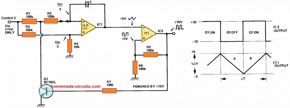
VCO Application: Audio Tone based Voltmeter
The following concepts explains how a VCO can be used for making an audio tone based voltmeter circuit. The tone voltmeter circuit is depicted schematically in the picture below.
The circuit is constructed around a CD4046B phase-locked loop (PLL) integrated circuit with a built-in voltage-controlled oscillator (VCO).
The voltage levelat pin 9, value ofcapacitor C1between pins 6 and 7, potentiometer R1 settingat pin 11, and potentiometer R2 at pin 12 control the frequency of the VCO.
The VCO output (pin 4) is usually routed back into the comparator input (pin 3).
In this circuit, although, the VCO output powers a loudspeaker directly.
Once the inhibit line (INH) at pin 5 is logic low, the VCO activates, and it switches off when INH is logic high.
When the tone voltmeteris not beingused, a touch switch made up of two Schmitt-trigger inverters (IC2 -a and -b) switches the circuit on and off to save power.
If necessary, the touch switch could be substituted with a conventional SPST switch.
Assuming you don't have a Schmitt-trigger inverter and don't want to buy one, this is indeed a good option.
If a logic low is appears at pin9, the circuit generates a low frequencytone.
As the voltage input at pin9grows, so does the pitch of thetone, until the input voltage hits a logic high.
Conversely, the tone pitch lowers as the voltage input at pin9decreases.
The tone voltmeter circuit is depicted schematically in the picture below.
The circuit is constructed around a CD4046B phase-locked loop (PLL) integrated circuit with a built-in voltage-controlled oscillator (VCO).
The voltage levelat pin 9, value ofcapacitor C1between pins 6 and 7, potentiometer R1 settingat pin 11, and potentiometer R2 at pin 12 control the frequency of the VCO.
The VCO output (pin 4) is usually routed back into the comparator input (pin 3).
In this circuit, although, the VCO output powers a loudspeaker directly.
Once the inhibit line (INH) at pin 5 is logic low, the VCO activates, and it switches off when INH is logic high.
When the tone voltmeteris not beingused, a touch switch made up of two Schmitt-trigger inverters (IC2 -a and -b) switches the circuit on and off to save power.
If necessary, the touch switch could be substituted with a conventional SPST switch.
Assuming you don't have a Schmitt-trigger inverter and don't want to buy one, this is indeed a good option.
If a logic low is appears at pin9, the circuit generates a low frequencytone.
As the voltage input at pin9grows, so does the pitch of thetone, until the input voltage hits a logic high.
Conversely, the tone pitch lowers as the voltage input at pin9decreases.
Sine-Cosine Waveform Generator Circuit
The circuit discussed below is designed to generate precision sine and cosine waveforms, which are perfectly identical with their dimensions, but are 90�� out of phase. There are a variety of applications which often demand a couple of sinewave frequencies which are of the identical frequency, but 90�� out of phase. Simply put, a sine signal and a cosine signal together from a single package. This kind of signals are widely-used in SSB and quadrature modulation, electronic systems of circles and ellipses and conversions involving rectilinear and polar coordinates. Sine and cosine signals could be acquired from a quadrature oscillator that includes a couple of integrators configured as demonstrated in the diagram. In the shown diagram, A1 is wired like a non-inverting integrator, while A2 is rigged in the form of an inverting integrator.How the Circuit Works
The reason why this circuit would generate a sine and cosine signal might not be quickly evident, nevertheless can be easily described. At output B shows up a signal that is a function of time, f(t).
Since this is, minus the integral of the signal at A, it is very clear that the signal at A is, minus the differential of the signal at B, that is - df / dt.
In the same manner, the input signal at the integrator A, that is - d2 f / dt2
However, we also find that the signal at the input of A1 is also the output signal of A2.
Therefore, - d2 f / dt2 = f(t)
These conditions are fulfilled through the sine-cosine signals, because if
f(t) = sin �� t (output B)
d(sin �� t) /dt = cos �� t (output A)
d(cos �� t) /dt = d2(sin �� t) / dt2 = -sin �� t = -f(t)
Output A as a result generates a cosine signal and output B a sine signal.
P1 can be used to alter the loop gain of the circuit to ensure that it oscillates without any issues or errors.
In case, may be on account of part tolerances, the circuit fails to oscillate at a set adjustment of P1, you may need to to increase its value to 10 k.
D1, D2 and R4 to R7 are used to stabilize the amplitude of the signal.
The sine-cosine frequency rate could be modified by replacing other desired values of capacitor for C1 to C3, by evaluating them through the explained formulas.
At output B shows up a signal that is a function of time, f(t).
Since this is, minus the integral of the signal at A, it is very clear that the signal at A is, minus the differential of the signal at B, that is - df / dt.
In the same manner, the input signal at the integrator A, that is - d2 f / dt2
However, we also find that the signal at the input of A1 is also the output signal of A2.
Therefore, - d2 f / dt2 = f(t)
These conditions are fulfilled through the sine-cosine signals, because if
f(t) = sin �� t (output B)
d(sin �� t) /dt = cos �� t (output A)
d(cos �� t) /dt = d2(sin �� t) / dt2 = -sin �� t = -f(t)
Output A as a result generates a cosine signal and output B a sine signal.
P1 can be used to alter the loop gain of the circuit to ensure that it oscillates without any issues or errors.
In case, may be on account of part tolerances, the circuit fails to oscillate at a set adjustment of P1, you may need to to increase its value to 10 k.
D1, D2 and R4 to R7 are used to stabilize the amplitude of the signal.
The sine-cosine frequency rate could be modified by replacing other desired values of capacitor for C1 to C3, by evaluating them through the explained formulas.
Understanding Crystal Oscillator Circuits
An oscillator is a circuit which produces a certain frequency and holds this frequency within limits. An inductance-capacitance (LC) oscillator is dependent upon the resonant interchange of electrical energy between a capacitor and inductor for its working. A transistor amplifier provides electrical pulses having the appropriate phase and value to sustain the oscillations. When utilized in oscillator circuits, BJTs act like converters which transform DC electrical energy from the collector power supply of the transistor into AC energy in the output circuit. The amplifying attribute of the BJTs helps them to preserve the oscillation frequency of the circuit. Basic solid state crystal oscillator circuit configurations are today more developed, almost all circuits being modifications of the widely recognized vacuum tube systems like the Pierce, Hartley, Clapp and Butler oscillator and work with both bipolar and FET devices. Although all these circuits fundamentally meet their designed objective, there are plenty of applications that call for something completely different or where functionality requires to be accurately described. Listed below are a range of circuits, for a variety of applications right from LF through the VHF range, which are not typically seen in existing amateur usage or books. Basic solid state crystal oscillator circuit techniques are by now well established, most circuits being adaptations of the well-known vacuum tube technology such as the Pierce, Hartley, Clapp and Butler oscillator and use both bipolar and FET devices. Whilst these circuits basically fulfill their intended purpose, there are many applications which require something different or where performance needs to be reliably characterized. Presented here are a variety of circuits, for a range of applications from LF through the VHF range, that are not commonly found in current amateur use or literature.MODES OF OPERATION
A point rarely valued, or simply overlooked, is the fact that quartz crystals can oscillate in a parallel resonant mode and a series resonant mode. The two frequencies are split up with a minor difference, usually 2-15 kHz over the frequency range. The series resonant frequency is smaller in frequency compared to parallel. A specific crystal designed for use in the parallel mode might be appropriately applied in a series resonant circuit should a capacitor equivalent in magnitude to its exact load capacitance (typically 20,30, 50 or 100 pF) is attached in series with the crystal. Unfortunately, it isn't possible to invert the task for series resonant crystal in parallel mode circuits. The series mode crystal will probably oscillate beyond its calibrated frequency in its situation and might not be feasible to capacitively load it down enough. Overtone crystals run in the series mode generally on the third, fifth or seventh overtone, and the manufacturer usually calibrates the crystal in the overtone frequency.
Running a crystal in the parallel mode and multiplying the frequency 3 or 5 times generates rather a new outcome by operating precisely the same crystal in the series mode upon its 3rd or 5th overtone.
While buying overtone crystals stay away from dilemma and identify the frequency you would like, instead of the apparent fundamental frequency.
Fundamental crystals within the range 500 kHz to 20 MHz are generally built for parallel mode functioning however series mode operation could be asked for.
For low frequency crystals up to 1 MHz, either mode could be chosen.
Overtone crystals normally cover the range 15 MHz to 150 MHz.
Overtone crystals run in the series mode generally on the third, fifth or seventh overtone, and the manufacturer usually calibrates the crystal in the overtone frequency.
Running a crystal in the parallel mode and multiplying the frequency 3 or 5 times generates rather a new outcome by operating precisely the same crystal in the series mode upon its 3rd or 5th overtone.
While buying overtone crystals stay away from dilemma and identify the frequency you would like, instead of the apparent fundamental frequency.
Fundamental crystals within the range 500 kHz to 20 MHz are generally built for parallel mode functioning however series mode operation could be asked for.
For low frequency crystals up to 1 MHz, either mode could be chosen.
Overtone crystals normally cover the range 15 MHz to 150 MHz.
WIDE RANGE or APERIODIC OSCILLATORS
Oscillators that never make use of tuned circuits are often very useful, whether as ��crystal checkers�� or any different reason. Especially for LF crystals, tuned circuits could be rather huge. On the other hand, they usually are not without their own traps. A few crystals are susceptible to oscillation on undesirable modes, specially the DT and CT cut crystals intended for LF quartz oscillators. It truly is a good idea to make sure that the output is on the proper frequency and no "mode instability" is apparent. Minimizing feedback at the higher frequencies commonly solves this. In special cases, the above theory can be forgotten and an oscillator possessing a tuned circuit applied as an alternative, (LF crystal oscillators are reviewed afterwards).Crystal Circuits
The first circuit below is an emitter-coupled oscillator, a variation of the Butler circuit. The output of the circuit in Fig. 1 is basically sine wave; decreasing the emitter resistor of Q2 boosts the harmonic output. As a result, a 100 kHz crystal generates excellent harmonics via 30 MHz. It is a series mode circuit. A range of transistors can be employed. For crystals above 3 MHz, transistors having a high gain-bandwidth product are advised. For crystals within the 50 kHz to 500 kHz assortment, transistors with high LF gain, like the 2N3565 are preferred. Additionally, for crystals within this selection, allowable dissipation is normally lower than 100 microwatts and amplitude constraining might be essential. Reduced supply voltage, in step with efficient starting up, is suggested. Altering the circuit through the inclusion of diodes as shown in Fig. 3 is a more beneficial technique, and starting efficiency is enhanced. The circuit is going to oscillate at as high as 10 MHz using suitable transistors and emitter resistor values. An emitter follower or source follower buffer is usually recommended. Identical comments to the above connect with Fig. 2. An emitter follower buffer is incorporated within this circuit. The two circuits are somewhat sensitive to frequency and to power voltage variations and load specs. A load of 1 k or higher is recommended. TTL lC could be combined with crystal oscillator circuits although numerous published circuits possess terrible starting efficiency or experience non-repeatability due to vast parameters in lC's,.
The circuit in Fig.
4. has been experimented with by the author on the range 1 MHz to 18MHz and will be encouraged.
This is a series mode oscillator and compliments AT-cut crystals.
TTL lC could be combined with crystal oscillator circuits although numerous published circuits possess terrible starting efficiency or experience non-repeatability due to vast parameters in lC's,.
The circuit in Fig.
4. has been experimented with by the author on the range 1 MHz to 18MHz and will be encouraged.
This is a series mode oscillator and compliments AT-cut crystals.
 The output is around 3 V peak to peak, square wave up to about 5 MHz above which this turns into more similar to half-sine pulses.
Starting efficiency is superb, which appears to be mostly a critical factor with TTL oscillators.
The output is around 3 V peak to peak, square wave up to about 5 MHz above which this turns into more similar to half-sine pulses.
Starting efficiency is superb, which appears to be mostly a critical factor with TTL oscillators.
LOW FREQUENCY CRYSTAL OSCILLATORS
Crystals within the range 50 kHz to 500 kHz demand distinctive factors not spotted in the more prevalent AT or BT cut HF crystals. The similar series resistance is a lot bigger and their allowable dissipation is restricted to under 100 microwatts, ideally 50 microwatts or lower. The circuit in Fig. 5 is a series mode oscillator. It offers the benefit of not needing a tuned circuit, and features a choice of sine or square wave output. For crystals within the spectrum of 50-150 kHz, 2N3565 transistors are advised even though publisher finds BC107's reasonable. Both the variety may be adequate for crystals within the range 150 kHz to 500 kHz. If you think the crystal includes a big equivalent series resistance, then you can increase the value of R1 to 270 ohms and R2 to 3.3 k. For square wave operations, C1 is 1 uF (or perhaps a magnitude alongside, or bigger than it).
For sine wave output, C1 is not in circuit.
Amplitude control is needless.
Sine wave output is approximately 1 V rms, square waive output around 4 V peak to peak.
The circuit in Fig.
6 is actually a revised type of the Colpitts oscillator, with the inclusion of resistor Rf to regulate feedback.
Capacitors C1 and C2 must be minimized through calculated magnitudes as the frequency is increased.
At 500 kHz, values for C1 and C2 must be approximately 100 pF and 1500 pF correspondingly.
The circuit as proven offers sine wave output using the second harmonic around 40 dB lower (or higher).
This is often minimized through mindful tweaking of Rf and C1. Remember that, at the decreased amount a feedback is essential to accomplish this, it requires around 20 seconds for the oscillator to attain full output.
Output is around 2 to 3 volts peak to peak.
When you need an output loaded with harmonics, the easy inclusion of a 0.1 uF capacitor over the emitter resistor will accomplish that.
Output subsequently increases to around 5 V peak to peak.
Power supply voltage could be decreased in such cases to reduce crystal dissipation.
Other transistors may be used, although bias and feedback might have to be tweaked.
For cantankerous crystals designed to oscillate in modes besides those you would like, the circuit of Fig.7 strongly suggested
For square wave operations, C1 is 1 uF (or perhaps a magnitude alongside, or bigger than it).
For sine wave output, C1 is not in circuit.
Amplitude control is needless.
Sine wave output is approximately 1 V rms, square waive output around 4 V peak to peak.
The circuit in Fig.
6 is actually a revised type of the Colpitts oscillator, with the inclusion of resistor Rf to regulate feedback.
Capacitors C1 and C2 must be minimized through calculated magnitudes as the frequency is increased.
At 500 kHz, values for C1 and C2 must be approximately 100 pF and 1500 pF correspondingly.
The circuit as proven offers sine wave output using the second harmonic around 40 dB lower (or higher).
This is often minimized through mindful tweaking of Rf and C1. Remember that, at the decreased amount a feedback is essential to accomplish this, it requires around 20 seconds for the oscillator to attain full output.
Output is around 2 to 3 volts peak to peak.
When you need an output loaded with harmonics, the easy inclusion of a 0.1 uF capacitor over the emitter resistor will accomplish that.
Output subsequently increases to around 5 V peak to peak.
Power supply voltage could be decreased in such cases to reduce crystal dissipation.
Other transistors may be used, although bias and feedback might have to be tweaked.
For cantankerous crystals designed to oscillate in modes besides those you would like, the circuit of Fig.7 strongly suggested
 Feedback is governed by a tap along the collector load of Q1. Amplitude confining is important to maintain the crystal dissipation inside boundaries.
For 50 kHz crystals the coil needs to be 2 mH and its resonating capacitor 0.01 uF.
Output is approximately 0.5 V rms, fundamentally a sine wave.
The utilization of an emitter follower or source follower buffer highly recommended.
In case a parallel mode crystal is utilized the 1000 pF capacitor indicated in series with the crystal must be changed to the crystal's selected load capacitance (typically 30, 50 to 100 pF for these types of crystals).
Feedback is governed by a tap along the collector load of Q1. Amplitude confining is important to maintain the crystal dissipation inside boundaries.
For 50 kHz crystals the coil needs to be 2 mH and its resonating capacitor 0.01 uF.
Output is approximately 0.5 V rms, fundamentally a sine wave.
The utilization of an emitter follower or source follower buffer highly recommended.
In case a parallel mode crystal is utilized the 1000 pF capacitor indicated in series with the crystal must be changed to the crystal's selected load capacitance (typically 30, 50 to 100 pF for these types of crystals).
HF CRYSTAL OSCILLATOR CIRCUITS
Solid state designs for the well-known AT-cut HF crystals tend to be legion. But, results not necessarily what you might expect to have. The majority of essential crystals up to 20 MHZ are typically chosen for parallel mode functioning. Nevertheless, this kind of crystals may be used in series mode oscillators by positioning the desired load capacitance in series with the crystal as stated earlier. The two types of circuit are discussed below. A good oscillator for 3 to 10 MHz range that doesn't demand a tuned circuit is presented in Fig. 8 (a). It is naturally, the same circuit as Fig.6. The circuit works extremely well down to 1 MHz when C1 and C2 are higher than 470 pF and 820 pF respectively. It may be utilized to 15 MHz in the event C1 and C2 are decreased to 120 pF and 330 pF. respectively. This circuit is advised for noncritical purposes in which large harmonic output is desired, or not an option.
The inclusion of a tuned circuit as in 8b minimizes harmonic output significantly.
A tuned circuit having a substantial Q is usually recommended.
In a 6 MHz oscillator, We have attained the below results.
Having a coil Q of 50 the 2nd harmonic was 35 dB all the way down.
Having a Q of 160, it had been -50 dB! Resistor Rf could be altered (increase a bit) to enhance this.
The output is additionally raised using a high Q coil.
As formerly observed, with decreased feedback it requires several tens of seconds to achieve 100 % output from turn on, even so, frequency stableness is fantastic.
Functioning at different frequencies can be achieved by adjusting the capacitors and coil effectively.
This circuit (Fig.
8) could also be changed into an extremely useful VXO.
A tiny inductance is defined in series with the crystal and one of the capacitors within the feedback circuit is used as a variable type.
A common two-gang 10-415 pF transmitter tuning capacitor will perform the task perfectly.
Each gangs are conected in parallel.
This circuit is advised for noncritical purposes in which large harmonic output is desired, or not an option.
The inclusion of a tuned circuit as in 8b minimizes harmonic output significantly.
A tuned circuit having a substantial Q is usually recommended.
In a 6 MHz oscillator, We have attained the below results.
Having a coil Q of 50 the 2nd harmonic was 35 dB all the way down.
Having a Q of 160, it had been -50 dB! Resistor Rf could be altered (increase a bit) to enhance this.
The output is additionally raised using a high Q coil.
As formerly observed, with decreased feedback it requires several tens of seconds to achieve 100 % output from turn on, even so, frequency stableness is fantastic.
Functioning at different frequencies can be achieved by adjusting the capacitors and coil effectively.
This circuit (Fig.
8) could also be changed into an extremely useful VXO.
A tiny inductance is defined in series with the crystal and one of the capacitors within the feedback circuit is used as a variable type.
A common two-gang 10-415 pF transmitter tuning capacitor will perform the task perfectly.
Each gangs are conected in parallel.
 The tuning range is determined by the crystal, the inductance of L1 and the frequency.
A larger range is generally accessible using the higher frequency crystals.
Stability is extremely good, getting close to that of the crystal.
The tuning range is determined by the crystal, the inductance of L1 and the frequency.
A larger range is generally accessible using the higher frequency crystals.
Stability is extremely good, getting close to that of the crystal.
A VHF OSCILLATOR-MULTIPLIER
The circuit in Fig.10 is a modified version of the ��impedance inverting�� overtone oscillator. Typically, applying the impedance inverting circuit the collector is either untuned or grounded for RF. The collector could be tuned to two times or 3 times the crystal frequency in order to minimize the output at the crystal frequency, a 2x tuned circuit is proposed.
YOU SHOULD NEVER tune the collector to the crystal frequency, or else the circuit may oscillate with a frequency which may be out of the control of the crystal.
You need to maintain the collector lead very small and one on one as much as you can.
End results using this type of circuit were great.
Just about all outputs besides the desired output had been at -60 dB or higher.
Noise production reaches at least 70 dB under the desired output.
This creates an outstanding conversion oscillator for VHF/UHF converters.
Practically 2 V of RF can be obtained on the hot terminal of L3 (author's original at 30 MHz).
A Zener regulated supply strongly recommended.
As pointed out within the diagram, various circuit values are essential for various transistors.
Strays in specific structure could also require modifications.
L1 may be used to move the crystal on frequency.
Minor modifications in frequency (about 1 ppm) take place while adjusting L2 and L3 as well as using load variations.
Having said that, in real testing, these things could be insignificant.
The collector could be tuned to two times or 3 times the crystal frequency in order to minimize the output at the crystal frequency, a 2x tuned circuit is proposed.
YOU SHOULD NEVER tune the collector to the crystal frequency, or else the circuit may oscillate with a frequency which may be out of the control of the crystal.
You need to maintain the collector lead very small and one on one as much as you can.
End results using this type of circuit were great.
Just about all outputs besides the desired output had been at -60 dB or higher.
Noise production reaches at least 70 dB under the desired output.
This creates an outstanding conversion oscillator for VHF/UHF converters.
Practically 2 V of RF can be obtained on the hot terminal of L3 (author's original at 30 MHz).
A Zener regulated supply strongly recommended.
As pointed out within the diagram, various circuit values are essential for various transistors.
Strays in specific structure could also require modifications.
L1 may be used to move the crystal on frequency.
Minor modifications in frequency (about 1 ppm) take place while adjusting L2 and L3 as well as using load variations.
Having said that, in real testing, these things could be insignificant.
Phase Shift Oscillator Circuits �C Wien-Bridge, Buffered, Quadrature, Bubba
A phase-shift oscillator is an oscillator circuit designed to generate a sinewave output. It operates with a single active element such as a BJT or an op amp configured in an inverting amplifier mode. The circuit arrangement creates a feedback from the output to the input through using an RC (resistor/capacitor) circuit arranged in a ladder type network. The introduction of this feedback causes a positive 'shift' in the phase of the output from the amplifier by 180 degrees at the oscillator frequency. The magnitude of phase shift created by the RC network is frequency dependent. Higher oscillator frequencies creates greater amount of phase shift. The following comprehensive explanations will help us to learn the concept in greater details. In the previous post we learned about the critical considerations required while designing an op-amp based phase shift oscillator circuits. In this post we will take it further ahead and know more regarding the types of phase shift oscillators and how to calculate the involved parameters through formulas.Wien-bridge circuit
The below given diagram shows the Wien-bridge circuit setup. Here, we can break the loop at the positive input of the opamp and calculate the returning signal using the following Equation 2:
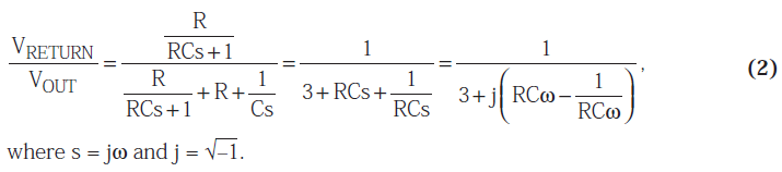 When = 2��pf = 1/RC, the feedback is in phase (positive feedback), having a gain of 1/3.
Therefore the oscillations needs the opamp circuit to have a gain of 3.
When RF = 2RG, the amplifier gain is 3 and oscillation initiates at f = 1/2��RC.
In our experiment the circuit oscillated at 1.65 kHz instead of 1.59 kHz using the indicated part values in Figure 3, but with an apparent distortion.
The next figure below demonstrates a Wien-bridge circuit having non-linear feedback.
When = 2��pf = 1/RC, the feedback is in phase (positive feedback), having a gain of 1/3.
Therefore the oscillations needs the opamp circuit to have a gain of 3.
When RF = 2RG, the amplifier gain is 3 and oscillation initiates at f = 1/2��RC.
In our experiment the circuit oscillated at 1.65 kHz instead of 1.59 kHz using the indicated part values in Figure 3, but with an apparent distortion.
The next figure below demonstrates a Wien-bridge circuit having non-linear feedback.
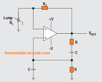 We can see a lamp RL whose filament resistance is selected very low, about 50 % of the feedback resistance value of RF, since the lamp current is defined by RF and RL.
The relationship between the lamp current and lamp resistance being nonlinear, helps to keep the output voltage variations at the minimum level.
You may also find many circuits incorporating diode instead of the above explained nonlinear feedback element concept.
The use of a diode helps decrease the distortion level by offering a gentle output voltage control.
However if the above methods are not favorable to you then you must go for AGC methods, which identically helps to get a reduced distortion.
A common Wien-bridge oscillator using an AGC circuit is displayed in the following figure.
Here, it samples the negative sine wave by means of D1, and the sample is stored inside C1.
We can see a lamp RL whose filament resistance is selected very low, about 50 % of the feedback resistance value of RF, since the lamp current is defined by RF and RL.
The relationship between the lamp current and lamp resistance being nonlinear, helps to keep the output voltage variations at the minimum level.
You may also find many circuits incorporating diode instead of the above explained nonlinear feedback element concept.
The use of a diode helps decrease the distortion level by offering a gentle output voltage control.
However if the above methods are not favorable to you then you must go for AGC methods, which identically helps to get a reduced distortion.
A common Wien-bridge oscillator using an AGC circuit is displayed in the following figure.
Here, it samples the negative sine wave by means of D1, and the sample is stored inside C1.
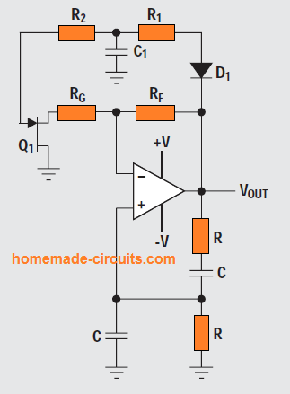 R1 and R2 are calculated such that it centers the bias on Q1 to ensure that (RG + RQ1) equals RF/2 with the expected output voltage.
If the output voltage tends to get higher, resistance of Q1 rises, consequently lowering the gain.
In the first Wien bridge oscillator circuit, the 0.833-volt supply can be seen applied on the positive opamp input pin.
This was done in order to centeralize the output quiescent voltage at VCC/2 = 2.5 V.
R1 and R2 are calculated such that it centers the bias on Q1 to ensure that (RG + RQ1) equals RF/2 with the expected output voltage.
If the output voltage tends to get higher, resistance of Q1 rises, consequently lowering the gain.
In the first Wien bridge oscillator circuit, the 0.833-volt supply can be seen applied on the positive opamp input pin.
This was done in order to centeralize the output quiescent voltage at VCC/2 = 2.5 V.
Phase-shift oscillator (one opamp)
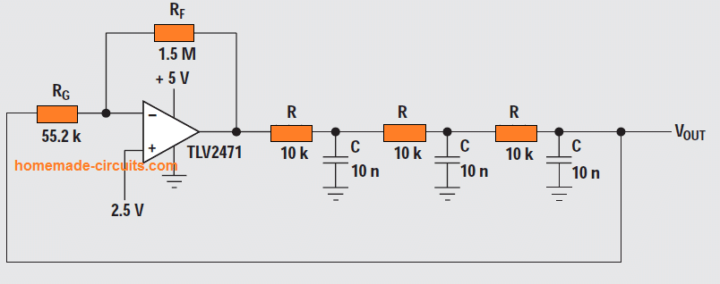 A phase-shift oscillator circuit can be also constructed using just a single opamp as shown above.
The conventional thinking is that in phase-shift circuits the stages are isolated and self-governing of one another.
This gives us the following equation:
A phase-shift oscillator circuit can be also constructed using just a single opamp as shown above.
The conventional thinking is that in phase-shift circuits the stages are isolated and self-governing of one another.
This gives us the following equation:
 When the phase shift of individual section is �C60�� the loop phase shift is = �C180��.
This happens when = 2��pf = 1.732/RC since the tangent 60�� = 1.73.
The value of �� at this moment happens to be (1/2)3, which means that the gain, A, has to be with a level of 8 for the system gain to be with a level at 1.
In this diagram the frequency of oscillation for the indicated part values was found to be 3.76 kHz, and not as per the calculated oscillation frequency of 2.76 kHz.
Moreover, the gain necessary to initiate oscillation was measured to be 26 and not as per the calculated gain of 8.
These kinds of inaccuracies are to some extent due to component imperfections.
However the most significant affecting aspect is due to the wrong predictions that the RC stages never impact one another.
This single opamp circuit setup used to be quite well-known at times when active components were bulky and high priced.
Nowadays op-amps are economical and compact and are available with four numbers within a single package, therefore the single opamp phase-shift oscillator has eventually lost its recognition.
When the phase shift of individual section is �C60�� the loop phase shift is = �C180��.
This happens when = 2��pf = 1.732/RC since the tangent 60�� = 1.73.
The value of �� at this moment happens to be (1/2)3, which means that the gain, A, has to be with a level of 8 for the system gain to be with a level at 1.
In this diagram the frequency of oscillation for the indicated part values was found to be 3.76 kHz, and not as per the calculated oscillation frequency of 2.76 kHz.
Moreover, the gain necessary to initiate oscillation was measured to be 26 and not as per the calculated gain of 8.
These kinds of inaccuracies are to some extent due to component imperfections.
However the most significant affecting aspect is due to the wrong predictions that the RC stages never impact one another.
This single opamp circuit setup used to be quite well-known at times when active components were bulky and high priced.
Nowadays op-amps are economical and compact and are available with four numbers within a single package, therefore the single opamp phase-shift oscillator has eventually lost its recognition.
Buffered phase-shift oscillator
 We can see a buffered phase-shift oscillator circuit in the above figure, pulsating at 2.9 kHz instead of the expected ideal frequency of 2.76 kHz, and with a gain of 8.33 as opposed to an ideal gain of 8.
The buffers prohibit the RC sections from affecting each other, and therefore the buffered phase-shift oscillators are able to operate closer to the calculated frequency and gain.
The resistor RG responsible for the gain setting, loads the third RC section, allowing the 4th opamp in a quad opamp to act as a buffer for this RC section.
This causes the efficiency level to reach an ideal value.
We can extract a low-distortion sine wave from any of the phase-shift oscillator stages, but the most natural sine wave can be derived from the output of the last RC section.
This is usually a high-impedance low current junction, therefore a circuit having a high-impedance input stage must be used here to avoid loading and frequency deviations in response to load variations.
We can see a buffered phase-shift oscillator circuit in the above figure, pulsating at 2.9 kHz instead of the expected ideal frequency of 2.76 kHz, and with a gain of 8.33 as opposed to an ideal gain of 8.
The buffers prohibit the RC sections from affecting each other, and therefore the buffered phase-shift oscillators are able to operate closer to the calculated frequency and gain.
The resistor RG responsible for the gain setting, loads the third RC section, allowing the 4th opamp in a quad opamp to act as a buffer for this RC section.
This causes the efficiency level to reach an ideal value.
We can extract a low-distortion sine wave from any of the phase-shift oscillator stages, but the most natural sine wave can be derived from the output of the last RC section.
This is usually a high-impedance low current junction, therefore a circuit having a high-impedance input stage must be used here to avoid loading and frequency deviations in response to load variations.
Quadrature oscillator
The quadrature oscillator is another version of phase-shift oscillator circuit, however the three RC stages are put together in a way that every section adds up 90�� of phase shift. The outputs are named sine and cosine (quadrature) simply because there exists a 90�� phase shift among opamp outputs.
The loop gain is determined through the Equation 4.
The outputs are named sine and cosine (quadrature) simply because there exists a 90�� phase shift among opamp outputs.
The loop gain is determined through the Equation 4.
 With = 1/RC , Equation 5 simplifies to 1�̨C180��, leading to oscillations at = 2��pf= 1/RC.
The experimented circuit pulsed at 1.65 kHz as opposed to the calculated value of 1.59 kHz, and the difference is mainly due to part value variations.
With = 1/RC , Equation 5 simplifies to 1�̨C180��, leading to oscillations at = 2��pf= 1/RC.
The experimented circuit pulsed at 1.65 kHz as opposed to the calculated value of 1.59 kHz, and the difference is mainly due to part value variations.
Bubba oscillator
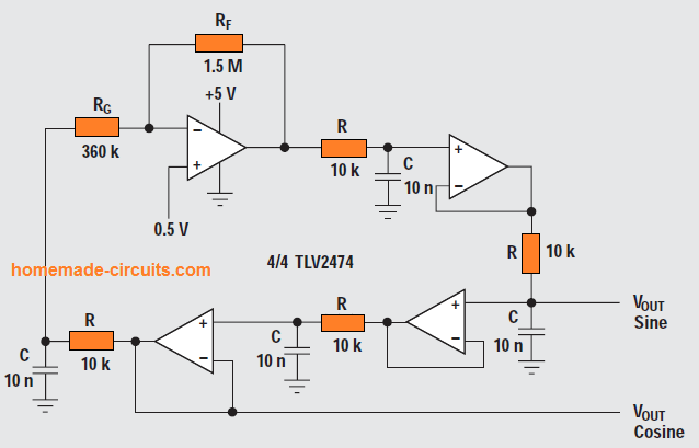 The Bubba oscillator circuit shown above is yet another variant of phase-shift oscillator, but it enjoys the benefit from the quad op-amp package to produce a few distinctive features.
Four RC sections call for 45�� phase shift for each section, which means this oscillator comes with an outstanding d��/dt to reduce frequency deviations.
Each of the RC sections generates 45�� phase shift.
Meaning, because we have outputs from alternate sections assures low-impedance quadrature outputs.
Whenever an output is extracted from each opamp, the circuit produces four 45�� phase-shifted sine waves.
The loop equation can be written as:
The Bubba oscillator circuit shown above is yet another variant of phase-shift oscillator, but it enjoys the benefit from the quad op-amp package to produce a few distinctive features.
Four RC sections call for 45�� phase shift for each section, which means this oscillator comes with an outstanding d��/dt to reduce frequency deviations.
Each of the RC sections generates 45�� phase shift.
Meaning, because we have outputs from alternate sections assures low-impedance quadrature outputs.
Whenever an output is extracted from each opamp, the circuit produces four 45�� phase-shifted sine waves.
The loop equation can be written as:
 When = 1/RCs, the above equations shrinks into the following Equations 7 and 8.
 The gain, A, should reach the value of 4 to initiate an oscillation.
The analysis circuit oscillated at 1.76 kHz as opposed to the ideal frequency 1.72 kHz while the gain seemed to be 4.17 instead of the ideal gain of 4.
Due to a reduced gain A and low bias current op-amps, the resistor RG responsible for fixing the gain doesn't load the final RC section.
This guarantees the most accurate oscillator frequency output.
Extremely low-distortion sine waves could be acquired from the junction of R and RG.
Whenever low-distortion sine waves are needed across all the outputs, the gain actually should be distributed equally among all the opamps.
The non-inverting input of the gain op-amp is biased at 0.5 V to create the quiescent output voltage at 2.5 V.
Gain distribution necessitates biasing of the other opamps, but it surely does not have any impact on the frequency of oscillation.
The gain, A, should reach the value of 4 to initiate an oscillation.
The analysis circuit oscillated at 1.76 kHz as opposed to the ideal frequency 1.72 kHz while the gain seemed to be 4.17 instead of the ideal gain of 4.
Due to a reduced gain A and low bias current op-amps, the resistor RG responsible for fixing the gain doesn't load the final RC section.
This guarantees the most accurate oscillator frequency output.
Extremely low-distortion sine waves could be acquired from the junction of R and RG.
Whenever low-distortion sine waves are needed across all the outputs, the gain actually should be distributed equally among all the opamps.
The non-inverting input of the gain op-amp is biased at 0.5 V to create the quiescent output voltage at 2.5 V.
Gain distribution necessitates biasing of the other opamps, but it surely does not have any impact on the frequency of oscillation.
Conclusions
In the above discussion we understood that Op amp phase shift oscillator circuits are constrained to the lower end of the frequency band. This is due to the fact that op-amps don��t have the essential bandwidth for implementing low phase shift at higher frequencies. Applying the modern current-feedback op-amps in oscillator circuits look difficult since these are very sensitive to feedback capacitance. Voltage feedback op-amps are restricted to just a few 100 kHz since they build up excessive phase shift. The Wien-bridge oscillator works using a small number of parts, and its frequency stability is very acceptable. But, toning down the distortion in a Wien-bridge oscillator circuit is less easier than initiating the oscillation process itself. The quadrature oscillator surely runs using a couple of op-amps, but it includes much higher distortion. However, phase-shift oscillators, like the Bubba oscillator exhibit much lower distortion along with some decent frequency stability. Having said this, the enhanced functionality of this type of phase-shift oscillator circuit does not come cheap due to higher costs of the parts involved across the various stages of the circuit. Related Web sites www.ti.com/sc/amplifiers www.ti.com/sc/docs/products/analog/tlv2471.html www.ti.com/sc/docs/products/analog/tlv2472.html www.ti.com/sc/docs/products/analog/tlv2474.htmlLC Oscillator Working and Circuit Diagram Details
In this post we are going to understand how LC oscillator circuits functions and we will be constructing one of the popular LC based oscillator - Colpitts oscillator.What are Oscillators
Electronic oscillators are used in most of our daily used electronic gadgets ranging from digital clock to high end core i7 processor. Oscillators are heart of all digital circuits but, not only digital circuit employee oscillators but also analogue circuits uses oscillatory circuits. For instant AM, FM radio, where the high frequency oscillation is used as carrier signal to transport message signal. There are many different kinds of oscillators such as RC, LC, crystal etc. Each one of them has their own advantages and disadvantages. So there is nothing called best or ideal oscillator, we have to analyse the circumstance of our circuit and choose the best one which suit, that��s why we find wide range of oscillators in every day used gadgets.LC Oscillators
Let��s dive into the explanation of LC oscillator. The LC oscillator consists of an inductor and a capacitor as shown in figure below.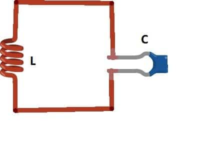 The value of the capacitor and resistor determines the output oscillation.
So how do they generate oscillation?
Well, we need to apply external energy between L and C i.e.
voltage.
When we apply the voltage, the capacitor gets charged-up.
When the supply is cut-off, the stored energy from capacitor flows to inductor and inductor starts building magnetic field around it until the capacitor completely gets discharged.
When the capacitor is fully discharged, the magnetic field around inductor collapse and induces voltage and charge-up the capacitor with opposite polarity and the cycle repeats.
The charge and discharge between L and C produces oscillation and this oscillation is called resonance frequency.
However the frequency generation won��t last forever due to parasitic resistance which dissipates the energy in the oscillatory circuit in the form of heat.
To maintain the oscillation and use the oscillation with reasonable output strength, we need an amplifier with zero degree phase shift and feedback.
The feedback feed small amount of output from amplifier back to LC network to compensate the loss due to parasitic resistance and maintain the oscillation.
Thus we can generate steady sine wave output.
The value of the capacitor and resistor determines the output oscillation.
So how do they generate oscillation?
Well, we need to apply external energy between L and C i.e.
voltage.
When we apply the voltage, the capacitor gets charged-up.
When the supply is cut-off, the stored energy from capacitor flows to inductor and inductor starts building magnetic field around it until the capacitor completely gets discharged.
When the capacitor is fully discharged, the magnetic field around inductor collapse and induces voltage and charge-up the capacitor with opposite polarity and the cycle repeats.
The charge and discharge between L and C produces oscillation and this oscillation is called resonance frequency.
However the frequency generation won��t last forever due to parasitic resistance which dissipates the energy in the oscillatory circuit in the form of heat.
To maintain the oscillation and use the oscillation with reasonable output strength, we need an amplifier with zero degree phase shift and feedback.
The feedback feed small amount of output from amplifier back to LC network to compensate the loss due to parasitic resistance and maintain the oscillation.
Thus we can generate steady sine wave output.
Application circuit:
Here is a colpitts oscillator circuit which can generate around 30Mhz signal.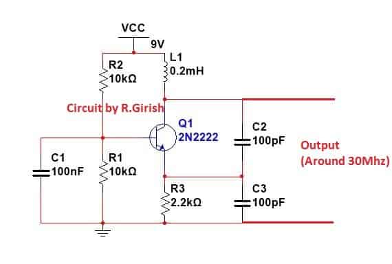 A couple of factors are essential to maintain oscillations in transistorized LC resonant crystal oscillator circuits.
First, the feedback voltage arriving from the transistor collector has to be in phase with the actual input excitation voltage which is initially applied on the base of the transistor.
In other words the feedback link of the circuit should be positive or regenerative in nature.
Second, the quantity of the feedback energy to the base network should be adequately strong to compensate for the energy losses encountered in the base circuit.
It can be necessary to evaluate the theory of Q prior to talking about oscillator functioning.
Q is described as a magnitude of caliber in a resonant circuit.
Equivalent to the reactance divided by the resistance, the Q factor symbolizes the capability of the circuit to maintain oscillations using bare minimum feedback.
To put it briefly, the larger the Q the greater the efficiency of the resonance stage of the circuit.
The inherent Q of quartz can be 10 million at 1 MHz frequency.
Even though Q mgnitude for a attached resonator crystal is diminished to ranges of 20,000 to more than a million, it is still well over the figures that's much superior to the top LC resonator or LC tank circuit.
A couple of factors are essential to maintain oscillations in transistorized LC resonant crystal oscillator circuits.
First, the feedback voltage arriving from the transistor collector has to be in phase with the actual input excitation voltage which is initially applied on the base of the transistor.
In other words the feedback link of the circuit should be positive or regenerative in nature.
Second, the quantity of the feedback energy to the base network should be adequately strong to compensate for the energy losses encountered in the base circuit.
It can be necessary to evaluate the theory of Q prior to talking about oscillator functioning.
Q is described as a magnitude of caliber in a resonant circuit.
Equivalent to the reactance divided by the resistance, the Q factor symbolizes the capability of the circuit to maintain oscillations using bare minimum feedback.
To put it briefly, the larger the Q the greater the efficiency of the resonance stage of the circuit.
The inherent Q of quartz can be 10 million at 1 MHz frequency.
Even though Q mgnitude for a attached resonator crystal is diminished to ranges of 20,000 to more than a million, it is still well over the figures that's much superior to the top LC resonator or LC tank circuit.
LC oscillator with Crystal
The extremely large Q of the crystal oscillator substantially minimizes frequency drift triggered by temperature and the DC voltage fluctuations. Furthermore, crystal-controlled oscillators generate a reduced amount of noise compared to traditional LC tank based oscillator circuits, and hence produce a healthier output signal. The easiest crystal oscillator is made up of solitary BJT using a basic feedback network. Figure 1-a displays a block diagram of a universal crystal oscillator. In this concept , an NPN BJT based amplifier can be seen configured with three feedback circuits. Suitable DC bias is presumed to be present although not revealed in the diagram. Figure 1-b is an comparative circuit built using the parts L1 and C1, and C2 as shown. Each and every crystal oscillator circuit discussed below are designed to work with exactly the same fundamental topology, by using a minimum of two capacitors and an inductor. The crystal could be seen as an element of the feedback circuit.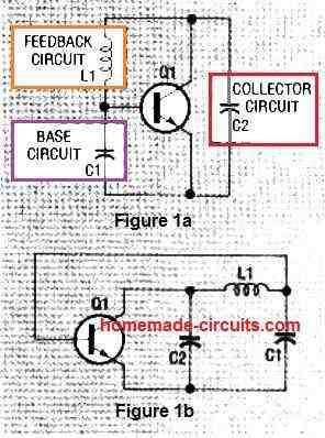 Capacitors C1 and C2 consist of residual transistor and junction capacitance.
Capacitor C2 is similar to a parallel network of an inductor and a capacitor.
This LC pair works like the crystal's third overtone selector since it exihibits capacitive nature only at the crystal's overtone frequency, and inductive property at its fundamental frequency.
Therefore, an inductor positioned at C2 inhibits oscillation at the crystal's fundamental frequency.
Along with amplification and feedback, an oscillator circuit additionally needs a limiting factor, that occurs when a rise in the input signal no more results in a rise in the output signal.
Because of this, the oscillator's output attains a boundary and continues to be in this boundary.
The typical Colpitts crystal-controlled oscillator possesses a stringent load and tuning specifications, while the a pair of semi-isolated models are much less demanding, and are proposed as far better options for general-purpose applications.
In case you are looking for a very accurate output frequency, the Pierce crystal oscillator is the one you must opt for.
On the other hand, if you just want to try things out with oscillators, you may realize that the Butler circuit is able to oscillate without depending on a crystal, and you could test the results using a crystal in or out.
Capacitors C1 and C2 consist of residual transistor and junction capacitance.
Capacitor C2 is similar to a parallel network of an inductor and a capacitor.
This LC pair works like the crystal's third overtone selector since it exihibits capacitive nature only at the crystal's overtone frequency, and inductive property at its fundamental frequency.
Therefore, an inductor positioned at C2 inhibits oscillation at the crystal's fundamental frequency.
Along with amplification and feedback, an oscillator circuit additionally needs a limiting factor, that occurs when a rise in the input signal no more results in a rise in the output signal.
Because of this, the oscillator's output attains a boundary and continues to be in this boundary.
The typical Colpitts crystal-controlled oscillator possesses a stringent load and tuning specifications, while the a pair of semi-isolated models are much less demanding, and are proposed as far better options for general-purpose applications.
In case you are looking for a very accurate output frequency, the Pierce crystal oscillator is the one you must opt for.
On the other hand, if you just want to try things out with oscillators, you may realize that the Butler circuit is able to oscillate without depending on a crystal, and you could test the results using a crystal in or out.
General Colpitts oscillators
A couple of variations of the Colpitts crystal-controlled oscillator are introduced in this article: the standard and the semi-isolated. The standard circuit, demonstrated in Fig. 2, is dependent on the specifications of both, the crystal and load resistance. Additionally, its output power is restricted to less than 50 % of the crystal's power dissipation. However, it is yet considered to be one of the favorites.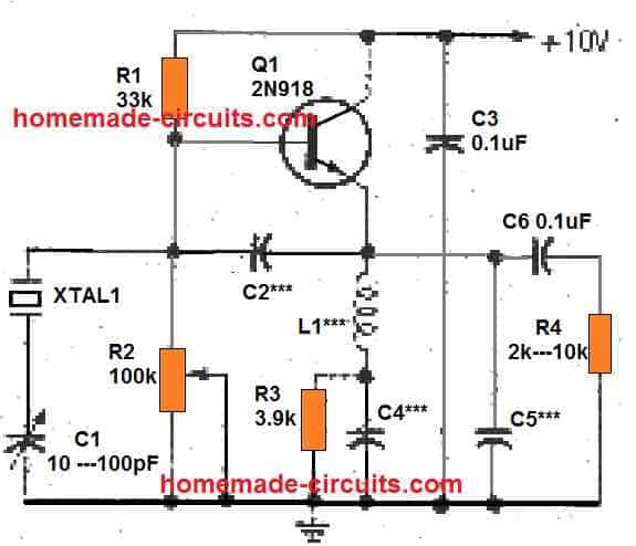 Note that, with a fundamental crystal, we get the frequencies from 1 MHz to 30 MHz are, and we get frequencies from 35 to 60 MHz when a third-overtone crystal is used.
The values for C2, C4, and C5 should be in picofarads, and the values for L1 should be in microhenries.
Resistors R1, R2, and R3 provide the DC bias to the transistor Q1. Potentiometer R2 is used to enable up to around 1.5 milliamperes of emitter current.
Capacitors C3, C4, and C6 work like a bypass elements for the radio frequency at XTAL1's working frequency (fundamental or overtone).
Capacitor C2 operates like the feedback base circuit, equivalent to the capacitor C1 as explained in in Fig.1. When the circuit is working at the XTAL1's operating frequency, L1 and C5 exhibit a net capacitive reactance, and therefore function as the collector circuit feedback capacitor, just like C2 in Figure1.
When overtone crystals are utilized, L1 and C5 behave just like an overtone selector, blocking oscillation at the crystal's fundamental frequency.
Capacitor C1 which is an adjustable trimmer, tweaks the feedback component L1. As the C1 value is reduced, the oscillator's output frequency increases.
Note that, with a fundamental crystal, we get the frequencies from 1 MHz to 30 MHz are, and we get frequencies from 35 to 60 MHz when a third-overtone crystal is used.
The values for C2, C4, and C5 should be in picofarads, and the values for L1 should be in microhenries.
Resistors R1, R2, and R3 provide the DC bias to the transistor Q1. Potentiometer R2 is used to enable up to around 1.5 milliamperes of emitter current.
Capacitors C3, C4, and C6 work like a bypass elements for the radio frequency at XTAL1's working frequency (fundamental or overtone).
Capacitor C2 operates like the feedback base circuit, equivalent to the capacitor C1 as explained in in Fig.1. When the circuit is working at the XTAL1's operating frequency, L1 and C5 exhibit a net capacitive reactance, and therefore function as the collector circuit feedback capacitor, just like C2 in Figure1.
When overtone crystals are utilized, L1 and C5 behave just like an overtone selector, blocking oscillation at the crystal's fundamental frequency.
Capacitor C1 which is an adjustable trimmer, tweaks the feedback component L1. As the C1 value is reduced, the oscillator's output frequency increases.
Simple RC Oscillator Circuit
An oscillator can be also built using just a resistor, capacitor network along with a transistor. Here the transistor base terminal is kept unconnected, only the emitter and collector are used. The complete circuit diagram for this RC oscillator can be seen in the following image: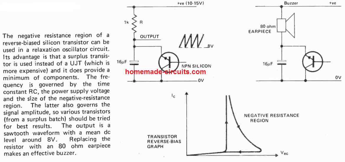
Simple LC RF Oscillator
The circuit presented in the following figure is a simple LC RF oscillator that can work nicely between around 100kHz to 50MHz or higher. Transistor TR1 is configured like a source follower, and the tiny coupling via the T1 inductor winding on is implemented to generate a positive feedback and for stepping up the voltage required for sustaining the oscillation.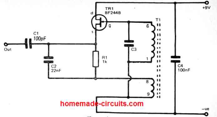 The primary winding of T1 along with C3 form the LC tuned circuit.
This establishes the operating frequency of the LC oscillator circuit.
R1 works like the source load for TR1 at the supplied DC, however TR1 gets bypassed with an AC through C2 causing the coupling winding of T1 to form the real source load for Tr1.
The output signal of the oscillator is derived through the TR1 source via the DC blocking capacitor C1. Capacitor C4 is simply works like a supply decoupling capacitor.
In case an adjustable tuning oscillator is expected, C3 could be easily be replaced with a variable capacitor, or a collaboration of fixed and variable capacitors to enable the required tuning range.
For medium and high frequency LC oscillator, many hobbyists employ ready-made coils nowadays, and these usually offer improved and much more predictable frequency outputs, than the basic home-wound coils.
To build T1 at home, just wind two sets of coils (6 to 1, and 8 to 9) one above the other over a small ferrite rod.
The number of turns can be experimented for getting different frequency outputs.
The key thing to remember is that the phasing of the smaller coupling winding has to be properly connected, otherwise the circuit will not oscillate.
However, the best technique of connecting the smaller coil can be implemented by only through some trial and error.
The primary winding of T1 along with C3 form the LC tuned circuit.
This establishes the operating frequency of the LC oscillator circuit.
R1 works like the source load for TR1 at the supplied DC, however TR1 gets bypassed with an AC through C2 causing the coupling winding of T1 to form the real source load for Tr1.
The output signal of the oscillator is derived through the TR1 source via the DC blocking capacitor C1. Capacitor C4 is simply works like a supply decoupling capacitor.
In case an adjustable tuning oscillator is expected, C3 could be easily be replaced with a variable capacitor, or a collaboration of fixed and variable capacitors to enable the required tuning range.
For medium and high frequency LC oscillator, many hobbyists employ ready-made coils nowadays, and these usually offer improved and much more predictable frequency outputs, than the basic home-wound coils.
To build T1 at home, just wind two sets of coils (6 to 1, and 8 to 9) one above the other over a small ferrite rod.
The number of turns can be experimented for getting different frequency outputs.
The key thing to remember is that the phasing of the smaller coupling winding has to be properly connected, otherwise the circuit will not oscillate.
However, the best technique of connecting the smaller coil can be implemented by only through some trial and error.
How Blocking Oscillator Works
A blocking oscillator is one of the simplest form of oscillators which is able to produce self sustaining oscillations through the use of just a few passive and a single active component. The name "blocking" is applied due to fact that the switching of the main device in the form of a BJT is blocked (cut-of) more often than it's allowed to conduct during the course of the oscillations, and hence the name blocking oscillator.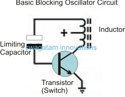
Where a Blocking Oscillator is Typically Used
This oscillator will generate a square wave output which can be effectively applied for making SMPS circuits or any similar switching circuits, but cannot be used for operating sensitive electronic equipment. The tone notes generated with this oscillator become perfectly suitable for alarms, morse code practice devices, wireless battery chargers etc. The circuit also becomes applicable as strobe light in cameras, which can be often seen just before clicking the flash, this feature helps in reducing the infamous red eye effect. Due to its simple configuration, this oscillator circuit is widely used in experimental kits, and the students find it much easier and interesting to grasp it details quickly.How a Blocking Oscillator Works

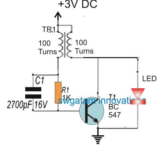 For making a blocking oscillator, the selection of the components become quite critical so that it is able to work with optimal effects.
The concept of a blocking oscillator is actually very flexible, and the outcome from it can be extensively varied, simply by varying the characteristics of the involved components such as the resistors, the transformer.
The transformer here specifically becomes a crucial part and the output waveform heavily depends on the type or the make of this transformer.
For example when a pulse transformer is used in a blocking oscillator circuit, the waveform attains the shape of rectangular waves consisting of rapid rise and fall periods.
The oscillating output from this design become effectively compatible with lamps, loudspeakers, and even relays.
A single resistor can be seen controlling the frequency of a blocking oscillator, and therefore if this resistor is replaced with a pot, the frequency becomes manually variable and can be tweaked as per the users requirement.
However care should be taken not to reduce the value below a specified limit which could otherwise damage the transistor and create unusually unstable output waveform characteristics.
It is always recommended to position a safe minimum value fixed resistor in series with the pot to prevent this situation.
For making a blocking oscillator, the selection of the components become quite critical so that it is able to work with optimal effects.
The concept of a blocking oscillator is actually very flexible, and the outcome from it can be extensively varied, simply by varying the characteristics of the involved components such as the resistors, the transformer.
The transformer here specifically becomes a crucial part and the output waveform heavily depends on the type or the make of this transformer.
For example when a pulse transformer is used in a blocking oscillator circuit, the waveform attains the shape of rectangular waves consisting of rapid rise and fall periods.
The oscillating output from this design become effectively compatible with lamps, loudspeakers, and even relays.
A single resistor can be seen controlling the frequency of a blocking oscillator, and therefore if this resistor is replaced with a pot, the frequency becomes manually variable and can be tweaked as per the users requirement.
However care should be taken not to reduce the value below a specified limit which could otherwise damage the transistor and create unusually unstable output waveform characteristics.
It is always recommended to position a safe minimum value fixed resistor in series with the pot to prevent this situation.
Circuit operation
The circuit works with the help of positive feedbacks across the transformer by associating two switching time periods viz, the time Tclosed when the switch or the transistor is closed, and the time Topen when the transistor is open (not conducting). The following abbreviations are used in the analysis: t, time, one of the variables Tclosed: instant at the end of the closed cycle, initialization of the open cycle. Also a magnitude of the time duration when the switch is closed. Topen: instant at the every end of the open cycle, or the beginning of closed cycle. Same as T=0. Also a magnitude of the time duration whenever the switch is open. Vb, supply voltage e.g. Vbattery Vp, voltage within the primary winding. An ideal switching transistor will allow a supply voltage Vb across the primary, therefore in an ideal situation Vp will be = Vb. Vs, voltage across the secondary winding Vz, fixed load voltage resulting due to for e.g. by the opposite voltage of a Zener diode or the forward voltage of a connected (LED). Im, magnetizing current across the primary Ipeak,m, highest or the "peak" magnetizing current on the primary side of the trafo. Takes place just before Topen. Np, the number of primary turns Ns, the number of secondary turns N, the ratio of winding also defined as Ns/Np, . For an perfectly configured transformer working with ideal conditions, we have Is = Ip/N, Vs = N��Vp. Lp, primary self-inductance, a value calculated by the number of primary turns Np squared, and an "inductance factor" AL. Self-inductance is frequently expressed with the formula Lp = AL��Np2��109 henries. R, combined switch (transistor) and the primary resistance Up, energy accumulated within the flux of the magnetic field across the windings, as expressed by the magnetizing current Im.Operation during Tclosed (time when the switch is closed)
The moment the switching transistor activates or triggers it applies the source voltage Vb over the transformer primary winding. The action generates a magnetizing current Im on the transformer as Im = Vprimary��t/Lp; where t (time) may be a changing with time and initiates at 0. The specified magnetizing current Im now "rides upon" any reverse generated secondary current Is which may happen to induce into the load on the secondary winding (for instance into the control terminal (base) of the switch (transistor) and subsequently reverted to secondary current in primary = Is/N). This altering current at the primary in turn generates an altering magnetic flux within the transformer's windings; which enables quite a stabilized voltage Vs = N��Vb across the secondary winding. In many of the configurations the secondary side voltage Vs may add up with the supply voltage Vb; due to the fact that the voltage on the primary side is approximately Vb, Vs = (N+1)��Vb while the switch (transistor) is in the conducting mode. Thus, the switching procedure may have the tendency to acquire a portion of its control voltage or current directly from Vb while the remaining through Vs. This implies that the switch-control voltage or the current would be "in phase" However in a situation of an absence of a primary resistance and negligible resistance on the transistor switching, might result in a rise in the magnetizing current Im with a "linear ramp" which may be expressed by the formula as given first paragraph. Conversely suppose there is a significant magnitude of primary resistance for the transistor or both (combined resistance R, e.g. primary-coil resistance along with a resistor attached with the emitter, FET channel resistance), then the Lp/R time constant could result in a rising magnetizing current curve with consistently dropping slope. In both the scenarios the magnetizing current Im will have a commanding effect through the combined primary and the transistor current Ip. This also implies that if a limiting resistor is not included the effect could increase infinitely. However, as studied above during the first case (low resistance), the transistor might ultimately fail to handle the excess current, or simply put, its resistance might tend to rise to an extent where the voltage drop across the device might become equal to the supply voltage; causing complete saturation of the device (which may be evaluated from a transistor's gain hfe or "beta" specs). In the second situation (e.g. inclusion of a significant primary and/or emitter resistance) the (dropping) slope of the current might reach a point where the induced voltage over the secondary winding is simply not sufficient to keep the transistor in the conducting position. In the third scenario, the core used for the transformer might reach the saturation point and collapse which int turn would stop it from supporting any further magnetization, and prohibit the primary to secondary induction process. Thus, we can conclude that during all the three situations as discussed above, the rate at which the primary current rises or the rate of rise of the flux in the core of the trafo in the third case, might show a dropping tendency towards zero. Having said this, in the first two scenarios, we find that despite of the fact the primary current seems to continue its supply, its value touches a constant level which might be just equal to the supply value given by Vb divided by the sum of the resistances R at the primary side. In such a "current-limited" condition the transformer's flux might tend to show a steady state. Except the changing flux, which might keep inducing voltage across the secondary side of the trafo, this implies that a steady flux is indicative towards a failure of induction process across the winding resulting in the secondary voltage dropping to zero. This causes the switch (transistor) to open. The above comprehensive explanation clearly explains how a blocking oscillator works and how this highly versatile and flexible oscillator circuit may be used for any specified application and fine tuned to the desired level, as the user may prefer to implement.Metal Detector Circuit �C Using Beat Frequency Oscillator (BFO)
The post explains a simple metal detector circuit using the beat frequency oscillator (BFO) concept, the BFO technique is considered to be the most accurate and reliable methods of detecting metals.How it Works
The circuit functioning may be understood with the following points: The proposed metal detector uses a 4093 quad Schmitt NAND IC and a search coil along with a switch and batteries for power. A lead from IC1d pin 11 connects to MW radio aerial, or another process would be to warp around the radio. The BFO switch if present in the radio must be turned on. The resistance of rapid change in voltage �C known as reactance, delays the logic level at ICI pin 10 back to its input pins 1 and 2, and is further delayed through propagation delays within 4093 IC. This entire process results into rapid oscillations of around 2 MHz, is picked up by a Medium Wave radio. 2 MHz is out of range for Medium Waves, but a MV radio can accept the harmonics of 2 MHz frequency. The process of winding of the coil is not complicated.Coil Winding Specifications
The prototype uses 50 turns of 22 awg/30 swg (0.315 mm) enameled copper wire, wounded on a 4.7"/120 mm former, and then wrapped in an insulation tape. The coil is then connected to 0V.A Faraday shield which is a tin foil acting as a wrapper around the coil. This process leaves a small gap and care should be taken so that the foil does not wrap the entire circumference of the coil. An insulation tape is again used to wrap the Faraday shield. A connection can be established to the Faraday shield with a piece of stiff wire wrapper around the shield, before adding the tape. An ideal scenario would be to wire the circuit with twin-core or microphone cable, and connect the screen to the Faraday shield.How to Set up the Circuit
Setting up the metal detector involves switching on the MW radio to pick up a whistle on a harmonic of 2 MHz. However to note, not all harmonic works best, only the one which suits need to be used. With a suitable harmonic and the metal will alter the tone of a whistle. A metal detector detects a large coin at 80 to 90 mm, which is quote good for a BFO detector. It can even identify discrimination between ferrous and non-ferrous metals with the rise or fall in tone. Submitted By: DhrubaJyoti BiswasCircuit Diagram
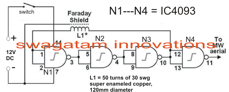
IC 4093 pinouts
Metal Detector using Magnetic Absorption
Behind the detection technology of this metal detector is a sensor that identifies the existence of ferrous and non-ferrous metals by absorbing the magnetic energy. This magnetic field is produced by an inductor which a part of a modified oscillator circuit. The moment a metal object is approached to the magnetic field, sufficient magnetic energy is absorbed to halt the oscillator. Figure below depicts the Colpitt��s oscillator that fires around 70 kHz. Inductor L1 functions as a sensor due to the emitter resistor��s (R1) large value and eventually, the oscillator just works.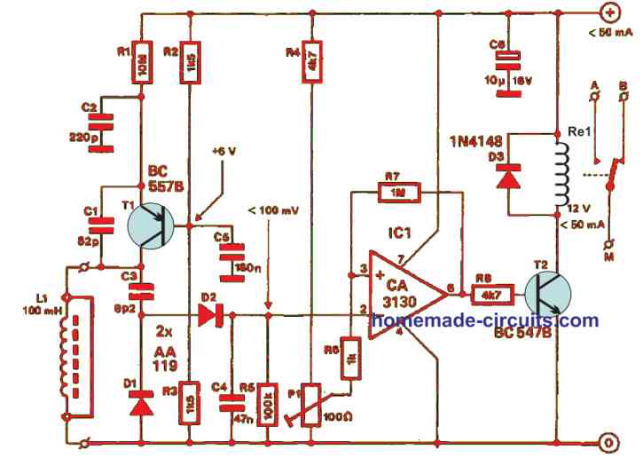 This is favourable because alternatively the losses in the regulated circuit will be reloaded by the transistor.
D1 and D2 will rectify the oscillating output and the subsequent direct voltage is directly applied to the inverting input of Schmitt trigger IC1.
Once the voltage dips below the value at pin 3 which is represented by P1, the output will switch to a high, energizing the relay.
We recommend constructing the detector on a PCB as shown in the figure below.
The actual purpose of inductor L1 was not to mount in on the PCB.
In case the oscillator does not immediately start at whatever setting the P1 was engaged, you must bring down the value of R1.
Alternatively, if the oscillator continues detecting even when a metal object is held close to L1, the R1 value must be increased.
You need to start with the wiper of P1 to earth and control the preset so the relay does not operate at all.
When you need a little more sensitivity, increase the wiper a tad more.
The energising of the relay principally dictates the current consumption and for most cases, it is not more than 50 mA.
This is favourable because alternatively the losses in the regulated circuit will be reloaded by the transistor.
D1 and D2 will rectify the oscillating output and the subsequent direct voltage is directly applied to the inverting input of Schmitt trigger IC1.
Once the voltage dips below the value at pin 3 which is represented by P1, the output will switch to a high, energizing the relay.
We recommend constructing the detector on a PCB as shown in the figure below.
The actual purpose of inductor L1 was not to mount in on the PCB.
In case the oscillator does not immediately start at whatever setting the P1 was engaged, you must bring down the value of R1.
Alternatively, if the oscillator continues detecting even when a metal object is held close to L1, the R1 value must be increased.
You need to start with the wiper of P1 to earth and control the preset so the relay does not operate at all.
When you need a little more sensitivity, increase the wiper a tad more.
The energising of the relay principally dictates the current consumption and for most cases, it is not more than 50 mA.
LC Tuned Metal Detector
Unlike the metal detectors discussed above, this one works under the rule that the frequency of an LC oscillator varies when there is modified inductance. To make that happen, the inductor is approached with any type of metal detector. The frequency change rate depends on the properties of the metal and on the frequency itself. If the latter is too high, a metal component will act like a shorted turn that brings down the inductance so that the frequency elevates. In the event the frequency is substantially low for eddy-current losses to be neglected, we can then differentiate between ferrous and non-ferrous metals. It will be quite challenging to make an oscillator frequency below 200 Hz. Due to that, the oscillator in the current circuit operates around 300 kHz. To make its inductance is quite simple and all you need is a single turn of a coaxial cable a depicted in the following figure.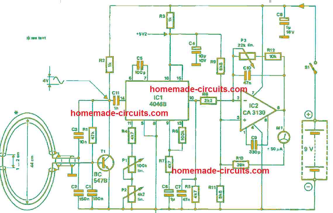
How it Works
The LC tuned metal detector circuit is made up of an oscillator T1, a frequency-to-voltage converter IC1 and a BiMOS operational amplifier IC2. By employing a detector coil diameter of 400 mm, the values of capacitors C1 and C2 guarantee an oscillator frequency of 300 kHz. When smaller diameter coils are used, you will need more turns. To supply the 4046B adequately, the oscillator signal strength must be around 400 mV�Ц�. The phase comparator warrants that the internal phase-locked loop always locks at that level. At pin 10, the source follower input is supplied to a CA3130 where it is sufficiently amplified.How to Set up
Conveniently, P1 sets the centre frequency of the phase-locked loop and the zero of the centre-zero microammeter. Using P2, you can make fine adjustments if the sensitivity of the opamp is high. Moreover, P3 sets the sensitivity in the discussion which is attached in a negative feedback loop to the inverting input. Notice there is a positive feedback through the microammeter and R10 to the non-inverting input. When you choose a different resistance, it is important to modify the values of R9, R10 and R11 appropriately.DC to DC Converter Circuits using SG3524 [Buck, Boost Designs]
A DC to DC converter is basically a switch-mode power supply, designed to work either as a boost-converter to step-up a low voltage DC to a higher voltage DC, or as a buck-converter to step-down a higher voltage DC to a lower voltage DC. The switched mode conversion ensures that the power transfer in the process involves minimum losses, and the efficiency rate is high, typically over 90%. The high efficiency rate in terms of power transfer is the main advantage of using SMPS (switch mode power supply) converters, as opposed to linear regulators which can dissipate and waste huge amounts of power during the DC to DC conversion process.
The main component in an SMPS that enables the efficient power conversion is the inductor or a ferrite transformer based coil, controlled or switched by PWM.
The pulse width modulation or the PWM plays an important role for switching the inductor through a power transistor with calculated duty cycle so that the inductor is able to implement the DC to DC conversion with maximum efficiency.
Since the PWM becomes the crucial factor in an SMPS, an ideal PWM generator/controller IC such as SG3524 or LM3524 becomes extremely suitable for making these types of buck and boost converter designs.
In this post we will elaborately discuss regarding how to design and construct DC to DC converters using the IC SG3525.
In one of our earlier posts we comprehensively learned the main features and the working of this versatile PWM IC SG3524.
In the following paragraphs we will see how those features could be practically exploited through simple smps converter designs.
The high efficiency rate in terms of power transfer is the main advantage of using SMPS (switch mode power supply) converters, as opposed to linear regulators which can dissipate and waste huge amounts of power during the DC to DC conversion process.
The main component in an SMPS that enables the efficient power conversion is the inductor or a ferrite transformer based coil, controlled or switched by PWM.
The pulse width modulation or the PWM plays an important role for switching the inductor through a power transistor with calculated duty cycle so that the inductor is able to implement the DC to DC conversion with maximum efficiency.
Since the PWM becomes the crucial factor in an SMPS, an ideal PWM generator/controller IC such as SG3524 or LM3524 becomes extremely suitable for making these types of buck and boost converter designs.
In this post we will elaborately discuss regarding how to design and construct DC to DC converters using the IC SG3525.
In one of our earlier posts we comprehensively learned the main features and the working of this versatile PWM IC SG3524.
In the following paragraphs we will see how those features could be practically exploited through simple smps converter designs.
Low Current Boost Converter Circuit using LM3524 IC
The first design below shows a straightforward low power boost converter circuit which uses the internal BJTs of the IC SG3524 for the switching, and therefore the maximum current is limited to 80 mA. This circuit can be used for converting any low voltage (above 5 V) to a desired higher level, across VO and GND.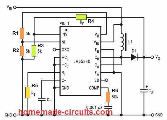 D1 can be any high speed diode such as FR107, Input supply current must not exceed 80 mA
In the above simple SG3524 boost converter design we can see the collectors of the internal driver BJTs CA and CB are joined together for enforcing the ON/OFF switching of the inductor L1 through an appropriately calculated PWM rate.
The PWM rate is set by configuring the SG3524 error amp inputs INV and NI, which is internally set as a comparator, and whose output controls the output PWM.
D1 can be any high speed diode such as FR107, Input supply current must not exceed 80 mA
In the above simple SG3524 boost converter design we can see the collectors of the internal driver BJTs CA and CB are joined together for enforcing the ON/OFF switching of the inductor L1 through an appropriately calculated PWM rate.
The PWM rate is set by configuring the SG3524 error amp inputs INV and NI, which is internally set as a comparator, and whose output controls the output PWM.
Setting up the Error Amp for PWM Control
Configuring the error amp is basically implemented by calculating the potential dividers at the INV input through the feedback RF resistor and associated 5 k divider resistor (R3 and R4 shown in green). This feedback potential at the INV input determines the output pulse cut-off threshold, and the PWM duty cycle. This threshold limit is fixed with reference to the sample voltage set at the NI input of the error amp through the two 5 k resistors (R1, R2 shown in orange).Calculating the Feedback Resistor
RF = 5k [(VO / 2.5) -1] = 5000 [(VO / 2.5) -1] this equation sets up the feedback resistor for the PWM control, using the parameters VO = output step-up voltage, and R3 = 5 k.Calculating Oscillator Frequency
fOSC = 1 / RT * CT this equation sets up the frequency of the converter, which must be anywhere around 30 to 100 kHz. Higher frequencies will mean small L1 inductor.Calculating the Inductor
L1 = 2.5VIN2 (VO - VIN) / fOSC * IO* VO2 this equation help us to determine the inductance rating for the L1 inductor, using the parameters VIN = input supply voltage, the VO = output voltage, f OSC = frequency, and the IO = output currentCalculating the Output Capacitor
CO = IO(VO - VIN) / fOSC * ��VO * VO this equation helps us to calculate the output filter capacitor CO, using the parameters IO = output current, VO = output boosted voltage, VIN = input supply voltage, fOSC = frequency, ��VO = peak-to-peak output ripple.High Current Step Up Converter
In the above DC to DC step-up converter circuit, we learned how the SG3524 could be configured as a low current step up current without involving external power transistors. The next diagram below shows how the same concept could be upgraded to a high current DC to DC boost converter circuit using the very same SG3524 circuit, except the output stage where high power transistors are used for facilitating the required current amplification. This circuit can be used for stepping up or boosting any low voltage (above 5 V) to a desired higher level, without any limitations in the current level. The calculations will be the same as the previous concept.
R9 will depend on the output current spec of the converter, and could be calculated using the formula:
R9 = (VIN - 0.7) * hFE / Max VO
The calculations will be the same as the previous concept.
R9 will depend on the output current spec of the converter, and could be calculated using the formula:
R9 = (VIN - 0.7) * hFE / Max VO
Step-Down Buck Converter using SG3524
The next DC to DC converter circuit using SG3524 discussed below is a step down buck converter which will allow you to convert any higher level DC voltage (below 40 V) into a desired lower DC output voltage, but with an input current not exceeding 80 mA. Meaning, suppose you are trying to make a 48 V inverter, in which the oscillator circuit can work only with a regulated 15 V DC. In such a situation you can effectively apply this buck converter concept for stepping down 48 V to 15 V DC for powering the oscillator circuit safely and allowing the 48 V to be used by the inverter power devices and the transformer. In this configuration we find the IC SG3524 pinout features are configured in the following manner:
The emitters EA and EB of the ICs output transistors are joined together for driving the inductor L1, while the collectors CA and CB are joined together with the input supply Vin for supplying the current to the L1 via the emitters.
The feedback resistor RF (R4) along with the associated 5 k divider resistor R3 is configured as before with the error amplifier, while the reference to the error amp is rigged using R1, R2 via the +5 V supply from the VR (VREF) pin of the IC.
This takes care of the PWM control.
In this configuration we find the IC SG3524 pinout features are configured in the following manner:
The emitters EA and EB of the ICs output transistors are joined together for driving the inductor L1, while the collectors CA and CB are joined together with the input supply Vin for supplying the current to the L1 via the emitters.
The feedback resistor RF (R4) along with the associated 5 k divider resistor R3 is configured as before with the error amplifier, while the reference to the error amp is rigged using R1, R2 via the +5 V supply from the VR (VREF) pin of the IC.
This takes care of the PWM control.
High Current Step-Down Converter
In the above example we learned the low current version of the SG3524 DC step-down converter, without involving external power devices. For higher current levels, an external power switching transistors could be added, along with other upgraded components such as the L1 inductor and diode. Meaning, this design can be used for converting any voltage below 40 V to a desired lower level, without any restrictions on the output current level. An example design for this can be witnessed in the following diagram:
Calculations
The various equations and calculations involved in this SG3524 buck converter circuit can be learned as given below:Calculating the Feedback Resistor
RF = 5 k [(VO/2.5) - 1] 5000 [(VO/2.5) - 1], this equation is used for fixing the feedback resistor RF(R4) which controls the output PWMCalculating the Current Sensing Resistor
RCL = Current Limit Voltage / IO(MAX), this equation is used for evaluating the current sensing resistor RCL or the R7, with respect to the maximum desired output current limit IO(MAX) . The current limit voltage refers to the desired voltage drop that needs to be developed across RCL when IO(MAX) is reached. This current limit voltage could be anywhere between 0.3 V to 1 V, the smaller the better to ensure a smaller RCLCalculating the Oscillator Frequency
fOSC = 1 / RT*CT this equation allows us to set up the oscillator frequency of the converter, and this can be anywhere between 30 kHz and 100 kHz. Higher frequencies will cause the L1 to be smaller and vice versa.Calculating the Inductor
L1 = 2.5VO (VIN - VO) / IO*VIN*fOSC this equation can be used for determining the inductor L1 value which becomes the crucial element of the step down converter. In this equation, VO is the desired stepped down output voltage, VIN is the input supply voltage, IO is the maximum output current, fOSC is the oscillator frequency. The 2.5 value is acquired from the reference voltage formed by the resistive divider using the two 5 k resistors R1, R2 at the NI input of the SG3524 IC error amp.Calculating the Output Capacitor
CO = (VIN - VO) VO* T2 / 8 *��VO *VIN*L1, this equation facilitates determining the output filter capacitor CO, using the available data such as the input supply VIN, output stepped down voltage VO, output peak to peak ripple voltage ��VO, the inductance of L1, and the period T2 where T = 1 / fOSCCurrent Control
In this buck converter we additionally see that current sensing pinouts +CL and -CL of the SG3524 are configured for implementing output current limiting, or for delivering a constant current output for the converter. The +CL and -CL current limit op amp provides a quick facility to configure the current limiting feature, which overrides all other control feature in the SG3524 IC. Meaning, if the current control feature detects an over current situation, it will override all other features and try to shut down the output of the IC.Why Over-current shut down is Important in Buck Converter
We already know that the efficiency of this SG3524 buck converter will be very high, may be around 95%. This implies that if the output voltage is stepped down, will result in the output current to rise proportionately. As an example, suppose we have VIN = 35 V, and we want the output to be VO = 5 V. If we assume the input current to be 80 mA for the above design, will mean an input wattage = 2.8 watts. This also means that ideally the output current should be then 2.8 / 5 = 560 mA. Considering the 95 % efficiency, this current still will be in the vicinity of 532 mA, which is a whopping 7 times higher than the input current. Due to this current boost, a current limiting or current control feature becomes crucial in these step down DC to DC converter designs.Application
The main application of an SG3524 or LM3524 DC to DC converters can be found in the field of solar controllers. Solar panels are mostly available with high voltage, low current specs, while batteries are mostly manufactured with lower voltage, higher current (Ah) specifications. A step-down buck converter becomes highly suitable for integrating a high voltage, low current solar panels with a high Ah, low voltage battery, and ensures a highly efficient and convenient way of implementing solar battery charging. Courtesy: Texas InstrumentsHow Transformers Work
According to the definition given in Wikipedia an electrical transformer is a stationary equipment that exchanges electrical power across a couple of closely wound coils, through magnetic induction. A constantly altering current in one winding of the transformer generates a varying magnetic flux, which, consequently, induces a varying electromotive force over a second coil built over the same core.Basic Working Principle
Transformers basically work by transferring electrical power in between a pair of coils through mutual induction, without depending on any form direct contact between the two winding. This process of transfer of electricity through induction was first proved by Faraday's law of induction, in the year 1831. According to this law the induced voltage across two coils is created due to a varying magnetic flux surrounding the coil. The fundamental function of a transformer is to step up or step down an alternating voltage/current, at different proportions as per the requirement of the application. The proportions are decided by the number of turns and turn ratio of the winding.Analyzing an Ideal Transformer
We can imagine an ideal transformer to be a hypothetical design that may be virtually without any form of losses. Moreover, this ideal design may have its primary and secondary winding perfectly coupled with each other. Meaning the magnetic bonding between the two winding is through a core whose magnetic permeability is infinite, and with winding inductances at an overall zero magnetomotive force. We know that in a transformer, the applied alternating current in the primary winding tries to enforce a varying magnetic flux within the core of the transformer, which also includes the secondary winding encircled around it. Due to this varying flux, an electromotive force (EMF) is induced on the secondary winding through electromagnetic induction. This results in the generation of flux on the secondary winding with a magnitude that's opposite but equal to the primary winding flux, according to Lenz'z law. Since the core carries an infinite magnetic permeability, the entire (100%) magnetic flux is able to get transferred across the two winding. This implies that, when the primary is subjected to an AC source, and a load is connected to the secondary winding terminals, current flows through the respective winding in directions as indicated in the following diagram. In this condition the core magnetomotive force is neutralized to zero.
Test Video Verifying the Linear Relationship between Primary/Secondary Turn Ratio.
TURNS AND VOLTAGE RATIOS
Let's try to understand the turn ratio calculations in detail: The net magnitude of voltage induced from the primary to secondary winding is simply determined by the ratio of the number of turns wound over the primary and the secondary sections. However, this rule only applies if the transformer is close to an ideal transformer. An ideal transformer is that transformer which has negligible losses in the form of skin effect or eddy current. Let's take the Example of the figure 1 below (for an ideal transformer). Suppose the primary winding consists of around 10 turns, while the secondary with just a single turn winding. Due to electromagnetic induction, the lines of flux generated across the primary winding in response to the input AC, alternately expand and collapse, cutting through the 10 turns of the primary winding. This results in a precisely proportionate amount of voltage been induced across the secondary winding depending on the turn ratio.Example #2
Now let's visualize the figure 2 below, it shows a similar type of configuration as in figure1. expect the secondary which now has 1 additional turn, that is 2 numbers of turns.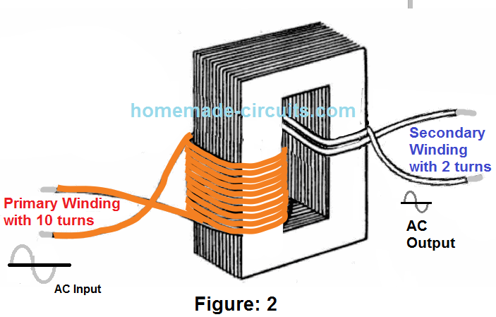 Needless to say, that now the secondary would be going through twice as many lines of flux compared to the figure 1 condition which had just a single turn.
So here the secondary winding would read around 12/10 x 2 = 2.4V because the two turns would be influenced by a magnitude of counter EMF that may be equivalent across the two winding on the primary side of the trafo.
Therefore from the above discussion in general we can conclude that in a transformer the relation between the voltage and number of turns across the primary and the secondary are quite linear and proportional.
Needless to say, that now the secondary would be going through twice as many lines of flux compared to the figure 1 condition which had just a single turn.
So here the secondary winding would read around 12/10 x 2 = 2.4V because the two turns would be influenced by a magnitude of counter EMF that may be equivalent across the two winding on the primary side of the trafo.
Therefore from the above discussion in general we can conclude that in a transformer the relation between the voltage and number of turns across the primary and the secondary are quite linear and proportional.
Transformer Turn Numbers
Thus, the derived formula for calculating the number of turns for any transformer can be expressed as: Es/Ep = Ns/Np where, Es = Secondary Voltage, Ep = Primary Voltage, Ns = Number of secondary turns, Np = Number of Primary turns.Primary Secondary Turn Ratio
It would be interesting to note that the above formula indicates a straightforward relation between the ratio of the secondary to primary voltage and secondary to primary number of turns, which are indicated to be proportionate and equal. Therefore the above equation can be also expressed as: Ep x Ns = Es x Np Further on, we can derive the above formula for solving the Es and Ep as shown below: Es = (Ep x Ns)/Np similarly, Ep = (Es x Np)/Ns The above equation shows that if any 3 magnitudes are available, the fourth magnitude could be easily determined by solving the formula.Solving Practical Transformer Winding Problems
Case in point #1: A transformer possesses 200 number of turns in the primary section, 50 number of turns in the secondary, and 120 volts connected across the primary (Ep). What could be the voltage across the secondary (E s)? Given: Np = 200 turns Ns = 50 turns Ep = 120 volts Es = ? volts Answer: Es = EpNs/Np Substituting: Es = (120V x 50 turns)/200 turns Es = 30 volts Case in point #2: Suppose we have 400 number of turns of wire in an iron-core coil. Assuming coil is required to be employed as the primary winding of a transformer, Calculate the number of turns that needs to be wound on the coil to acquire the secondary winding of the transformer to ensure a secondary voltage of one volt with a situation where the primary voltage is 5 volts? Given: Np = 400 turns Ep = 5 volts Es = 1 volts Ns = ? turns Answer: EpNs = EsNp Transposing for Ns: Ns = EsNp/Ep Substituting: Ns = (1V x 400 turns)/ 5 volts Ns = 80 turns Bear in mind: The ratio of the voltage (5:1) is equivalent to the winding ratio (400:80). Occasionally, as a substitute for particular values, you find yourself assigned with a turn or voltage ratio. In cases like this, you could simply assume any arbitrary number for one of the voltages (or winding) and work out the other alternative value from the ratio. As an illustration, suppose a winding ratio is assigned as 6:1, you could imagine a quantity of turn for the primary section and figure out the equivalent secondary number of turns, using similar proportions like 60:10, 36:6, 30:5, etc. The transformer in all of the above examples carries a lesser number of turns in the secondary section compared to the primary section. For that reason, you can find a smaller amount of voltage across the secondary of the trafo rather than across the primary side.What are Step-up and Step-Down Transformers
A transformer having the secondary side voltage rating lower than the the primary side voltage rating is referred to as a STEP-DOWN transformer. Or, alternatively if the AC input is applied to the winding which has higher number of turns then the transformer acts like a step-down transformer. The ratio of a four-to-one step-down transformer is inscribed as 4:1. A transformer which includes lesser number of turns in the primary side compared to the secondary side will generate a higher voltage across the secondary side compared to the voltage connected across the primary side. A transformer which has a secondary side rated above the voltage across the primary side is referred to as a STEP-UP transformer. Or, alternatively, if the AC input is applied to a winding which has lower number of turns then the transformer acts like a step-up transformer. The ratio of a one-to-four step-up transformer needs to be inscribed as 1:4. As you can see in the two ratios that the magnitude of the primary side winding is consistently mentioned in the beginning.Can we Use a Step-down Transformer as a Step-up transformer and Vice Versa?
Yes definitely! All transformers work with the same fundamental principle as described above. Using a step-up transformer as a step-down transformer simply means swapping the input voltages across their primary/secondary winding. For example, if you have an ordinary power supply step-up transformer which provides you with a 12-0-12V output from a 220V input AC, you can use the same transformer as a step up transformer for producing 220V output from a 12V AC input. A classic example is an inverter circuit, where the transformers have nothing special in them. They all work using the ordinary step-down transformers connected in the opposite way.Impact Of Load
Whenever a load or an electrical device is hooked up across the secondary winding of a transformer, current or amps runs across the secondary side of the winding along with the load. The magnetic flux generated by the current in the secondary winding interacts with the magnetic lines of flux generated by the amps in the primary side. This conflict between the two lines of fluxes is generated as a result of the shared inductance between the primary and secondary winding.Mutual Flux
The absolute flux in the core material of the transformer is prevalent to both the primary and secondary windings. It is additionally a way through which electrical power is able to migrate from the primary winding to the secondary winding. Due to the fact that this flux unites both the windings, the phenomenon generally known as MUTUAL FLUX. Also, the inductance which generates this flux is prevalent to both windings and is termed mutual inductance. Figure (2) below exhibits the flux created by the currents in the primary and secondary winding of a transformer each time supply current is switched ON in the primary winding. Figure (2)
Whenever the load resistance is connected into the secondary winding, the voltage stimulated into the secondary winding triggers current to circulate in the secondary winding.
This current produces a flux rings around the secondary winding (indicated as dotted lines) that may be as an alternative to the flux field around the primary (Lenz's law).
Consequently, the flux around the secondary winding cancels most of the flux around the primary winding.
With a smaller amount of flux encircling the primary winding, the reverse emf is cut down and more amp is sucked from the supply.
The supplementary current in the primary winding releases additional lines of flux, pretty much reestablishing the initial amount of absolute flux lines.
Figure (2)
Whenever the load resistance is connected into the secondary winding, the voltage stimulated into the secondary winding triggers current to circulate in the secondary winding.
This current produces a flux rings around the secondary winding (indicated as dotted lines) that may be as an alternative to the flux field around the primary (Lenz's law).
Consequently, the flux around the secondary winding cancels most of the flux around the primary winding.
With a smaller amount of flux encircling the primary winding, the reverse emf is cut down and more amp is sucked from the supply.
The supplementary current in the primary winding releases additional lines of flux, pretty much reestablishing the initial amount of absolute flux lines.
TURNS AND CURRENT RATIOS
The quantity of flux lines produced in a trafo core is proportional to the magnetizing force (IN AMPERE-TURNS) of the primary and secondary windings. The ampere-turn (I x N) is indicative of magneto motive force; it can be understood to be the magnetomotive force produced by one ampere of current running in a coil of 1 turn. The flux which is available in the core of a transformer surrounds together the primary and secondary windings. Given that the flux is identical for each windings, the ampere-turns in each, primary and secondary winding should always be the very same. For that reason: IpNp = IsNs Where: IpNp = ampere/turns in the primary winding IsNs - ampere/turns in the secondary winding By dividing both sides of the expression by Ip, we get: Np/Ns = Is/Ip since: Es/Ep = Ns/Np Then: Ep/Es = Np/Ns Also: Ep/Es = Is/Ip where Ep = voltage applied across primary in volts Es = voltage across the secondary in volts Ip = current in the primary in Amp Is = current in the secondary in Amps Observe that the equations indicate the ampere ratio to be the inverse of the winding or the turn ratio as well as the voltage ratio. This implies, a transformer possessing fewer number of turns in the secondary side compared to the primary may step down the voltage, but it would step-up the current. For instance: A transformer suppose has a 6:1 voltage ratio. Try to find the current or amps in the secondary side if the current or amp in the primary side is 200 milliamperes. Suppose Ep = 6V (as an example) Es = 1V Ip = 200mA or 0.2Amps Is = ? Answer: Ep/Es = Is/Ip Transposing for Is: Is = EpIp/Es Substituting: Is = (6V x 0.2A)/1V Is = 1.2A The above scenario addresses that despite the fact that the voltage across the secondary winding is one-sixth the voltage across the primary winding, the amps in the secondary winding is 6 times the amps in the primary winding. The above equations could very well be viewed from an alternative perspective. The winding ratio signifies the sum through which the transformer enhances or boosts or reduces the voltage connected to the primary side. Just to illustrate, suppose if the secondary winding of a transformer has double as much number of turns as the primary winding, the voltage stimulated into the secondary side will probably be twice the voltage across the primary winding. In case the secondary winding carries one-half the number of turns the primary side, the voltage across the secondary side is going to be one-half the voltage across the primary winding. Having said that, the winding ratio along with the amp ratio of a transformer comprise an inverse association. As a result, a 1:2 step-up transformer could have one-half the amp in the secondary side compared to the primary side. A 2:1 step-down transformer can have two times the amp in the secondary winding in relation to the primary side. Illustration: A transformer with a winding ratio of 1:12 possesses 3 amperes of current in the secondary side. Find out the magnitude of amps in the primary winding? Given: Np = 1 turn (for instance) Ns = 12 turns Is = 3Amp Lp = ? Answer: Np/Ns = Is/Ip Substituting: Ip = (12 turns x 3 Amp)/1 turn Ip = 36ACalculating Mutual Inductance
Mutual induction is a process in which one winding goes through an EMF induction due to rate of change current of the adjacent winding leading to an inductive coupling between the winding. In other words Mutual Inductance is the ratio of the induced emf across one winding to the rate of change of current on the other winding, as expressed in the following formula: M = emf / di(t) / dtPhasing in Transformers:
Normally, when we examine transformers, most of us believe that the primary and secondary winding voltage and currents are in phase with each other. However, this may not be always true. In transformers, the relation between the voltage, current phase angle across primary and secondary relies on how these winding are turned around the core. It depends on whether they are both in anticlockwise direction, or clockwise direction or may be one winding is turned clockwise while the other winding anticlockwise. Let's refer to the following diagrams to understand how the winding orientation affects the phase angle:Dot Notation and Dot Convention
In order to avoid confusions, Dot notation or Dot convention is employed to represent the winding orientation of a transformer. This enables the user to understand the input and output phase angle specifications, whether the primary and secondary winding are in phase or out of phase. Dot convention is implemented by dot marks across the winding start point, indicating whether the winding are in phase or out of phase with the each other. The following transformer schematic carries a dot convention denotation, and it signifies that the primary and the secondary of the transformer are in phase with each other.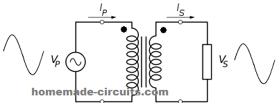 Dot notation used in the illustration below shows the DOTs placed across the opposite points of the primary and the secondary winding.
This indicates that the winding orientation of the two sides are not the same and therefore the phase angle across the two winding will be 180 degrees out of phase when an AC input is applied on one of the winding.
Dot notation used in the illustration below shows the DOTs placed across the opposite points of the primary and the secondary winding.
This indicates that the winding orientation of the two sides are not the same and therefore the phase angle across the two winding will be 180 degrees out of phase when an AC input is applied on one of the winding.
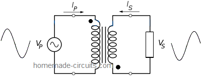
Losses in a Real Transformer
The calculations and formulas considered in the above paragraphs were based on an ideal transformer. However in real world, and for a real transformer, the scenario may be a lot different. You will find that in an ideal design the following fundamental linear factors of real transformers will be ignored: (a) Many types of Core losses, together known as magnetizing current losses, that may include the following types of losses: Hysteresislosses: this is caused due to nonlinear influences of the magnetic flux on the core of the transformer. Eddy currentlosses: This loss is generated due the phenomenon called joule heating in the transformer core. It is proportional to the square of the voltage applied to the primary of the transformer. (b) In contrast to the the ideal transformer, the resistance of the winding in a real transformer can never have a zero resistance. Meaning the winding will eventually have some resistance and inductances associated with them. Joule losses:As explained above, The resistance generated across the winding terminals gives rise to Joule losses. Leakage flux: We know that transformers heavily depend on magnetic induction across their winding. However, since the winding are built on a common single core, magnetic flux show a tendency of leaking across the winding via the core. This gives rise to an impedance called primary/secondary reactive impedance, which contributes to the losses of the transformer. (c) Since a transformer is also a kind of inductor, it is also affected by phenomenon such as parasitic capacitance and self-resonance, on account of electric field distribution. These parasitic capacitance usually can be in 3 different forms as given below: Capacitance generated between the turns one above the other inside a single layer; Capacitance generated across two or more adjoining layers; Capacitance created between the transformer core and the winding layer(s) lying adjacent to the core;Conclusion
From the above discussion, we can understand that in practical applications calculating a transformer, especially an iron core transformer may not be as simple as an ideal transformer would be. To get the most accurate results for the winding data we may have to consider many factors such as: flux density, core area, core size, tongue width, window area, core material type etc. You can learn more about all these calculations under this post:How to Repair a Switch-Mode-Power-Supply (SMPS)
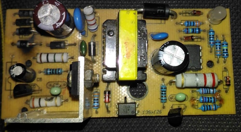 In this post we try to diagnose a burnt SMPS circuit and try to troubleshoot and repair the circuit.
The shown unit is a cheap readymade Chinese make SMPS circuit.
This article is written as per the request made by Mr.
Kesava.
In this post we try to diagnose a burnt SMPS circuit and try to troubleshoot and repair the circuit.
The shown unit is a cheap readymade Chinese make SMPS circuit.
This article is written as per the request made by Mr.
Kesava.
My SMPS got Burnt
The below attachment is 12v 1.3 amps SMPS for charging Agriculture Sprayer..If charge full the green led will glow...If charge low the red led will glow... But now this charge not working...And i check inside , The AC input bridge rectifier IN4007 1diode got damaged...i replace it with new one diode..Now the new diode also damaged....Pls guide me sir.... In our area shop..this type of chargers are not available sir...But my aim is not to buy new one..i itself want to rectify with u r guidance sir....Pls help me sir.... Sorry for bad english.I'm not good sir... Thanks & Regards N.KesavarajTroubleshooting the Problem
Hi Kesava, It's most probably due to a burnt mosfet, the one which can be seen on a heatsink. You can try replacing it with a new one, and also make sure to change the adjoining 10 ohm resistor which also looks like it is burnt. Regards.
Repairing the SMPS Circuit
Referring to the images above, the primary side of the unit appears to be the popular 1 amp 12V SMPS adaptor using a mosfet based switching design, and includes an opamp based auto cut off charger section at its secondary section of the board From the first two images we can clearly see that one of the diodes being completely blown apart, and responsible for shutting down the entire circuit board. A bridge rectifier can be normally seen at the beginning ofany SMPS circuitand is introduced primarily for rectifying the mains AC to a full wave DC, which is further filtered using a filter capacitor and applied to the mosfet/inductor stage for the intended flyback primary side switching operation. This primary side switching causes an equivalent low voltage pulsating DC to be induced at the secondary side of the transformer, which is then smoothed using a large value filter capacitor at the the secondary side for acquiring the final stepped down SMPS DC output. From the image it appears that the entire design is based on a mosfet, inductor switching topology wherein the mosfet becomes the main switching element in the circuit. The diodes in the bridge rectifier appears to be the normal 1N4007 diodes which are capable of handling not more than 1 amp current, therefore if this 1 amp value exceeds the diodes can get ripped through and damaged. The diode might have burnt due to a high current passage which in turn might have happened due to a stalled mofet inductor operation. Which means that the mosfet might have stopped osculating causing a short circuit through itself, allowing the entire AC to go through the components within the input supply line.How to Repair the SMPS Circuit.
The shown burnt SMPS can be repaired with the following simple steps. 1) Remove the mosfet from the PCB and check it with a multimeter 2) Without any doubt you will find the mosfet being the faulty component, so you can quickly go for a replacement of the same using a correctly matched mosfet 3) After changing the mosfet make sure to change the burnt rectifier diode also, and ideally change all the 4 diodes in the bridge, to ensure no weakened diodes are present in the network. 4) You may also want to check if there are any other parts such as resistors or thermistor that may look suspicious and if any replace them with new ones. 5) Once all the doubtful elements are replaced it is time to switch ON the SMPS for the final verification. However this must be done with a series protection load in the form of a series incandescent bulb to make sure that the circuit does not blow of due to some other hidden fault. A 25 watt bulb will be just good for safeguarding the unit from any catastrophic circumstances. 6) On switching on the SMPS, if the the bulb does not glow, it would probably indicate all's well and the unit has been repaired successfully. Now you can feel free to check the output voltage of the SMPS with a meter and confirm that it is producing the right readings. 7) Finally without removing the bulb connect an appropriately rated DC load and check whether it is working correctly or not. 8) If everything seems to be working normally you can remove the series bulb, and repeat the testing process, but make sure to include a small fuse in series with the input supply permanently. 9) However in case the bulb shows a bright glow, would indicate a serious problem persisting in the SMPS circuit and will need to be investigated afresh, this may be done by first switching off the unit and then checking each and every component in the primary side of the trafanformer. 10) The components which needing a recheck will be fundamentally the ones which are prone to high voltage and current damage, such as small BJTs, diodes and low value resistors. 11) The components which can be left unchecked are the ones which are adequately rated and are able to protect itself from from high voltage and current inrush. These may include high value resistors above 50K, or low value wirewound resistors above 1K. Similarly, capacitors which may be rated above 200V can be left unchecked unless one of these look somewhat damaged externally.Testing for a Burnt Inductor Transformer
Every SMPS circuit will essentially include a small ferrite transformer, which this part can also possibly become the cause of a burnt SMPS circuit, although the chances of a damaged transformer can be too remote. This is because the wires inside the inductor might require some time to burn, and before this can transpire the other more vulnerable parts such as diodes and transistors would be forced to blow off ,preventing any further damage to the inductor. So basically you can be rest assured that the transformer is the one element which might be the safest and the undamaged part in a given faulty SMPS circuit. If in a rare event the inductor burns, this would be distinctly visible from the burnt insulation tape which may be also melted and stuck with the winding. An SMPS with a burnt transformer could be virtually irreparable, because a burnt transformer would mean most of the elements burnt out, along with PCB tracks uprooted. Time to buy a new SMPS unit. The secondary side mostly will not require any checking as it is isolated from the primary and can be expected to be aloof from the dangers. Well, this concludes this article explaining tips to repair an SMPS circuit, if you think I have missed some crucial points, or if you have something important to add in the list, please tell us through your valuable comments.110V, 14V, 5V SMPS Circuit �C Detailed Diagrams with Illustrations
In this post we learn how to apply the IC L6565 for making a compact multi purpose 110V, 14V, 5V SMPS circuit using minimum number of external components.Implementingquasi-resonant ZVS flyback
The IC L6565 from ST Microelectronics is designed as a current-mode primary controller chip, to specifically suit quasi-resonant ZVS flyback converter applications. The quasi-resonant implementation is accomplished through demagnetization of a transformer sensing input, which is used for switching ON an attached power mosfet. During the operations of this IC in a converter, the variations in the power capacity of the converter becomes compensated by a line feed forward stage acquired through the line voltage.Circuit Diagram
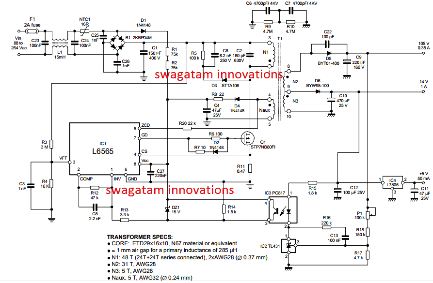 Whenever the connected load is minimal or absent, the IC displays a unique feature which automatically brings down the operating frequency of the converter, and yet ensuring the operation at as far as possible around the ZVS level.
Converters using IC L6565 not only enables low consumption of the design through a low start up current, and a sustained low quiescent current, the system makes sure that it perfectly complies with Blue Angel and Energy Star SMPS guidelines.
In addition to the above explained features, the chip also includes an configurable auto disable function, an in-built current sense and shut down function, and also an accurate reference voltage input for executing basic regulation functions, and an ideal two stage overload protection.
Whenever the connected load is minimal or absent, the IC displays a unique feature which automatically brings down the operating frequency of the converter, and yet ensuring the operation at as far as possible around the ZVS level.
Converters using IC L6565 not only enables low consumption of the design through a low start up current, and a sustained low quiescent current, the system makes sure that it perfectly complies with Blue Angel and Energy Star SMPS guidelines.
In addition to the above explained features, the chip also includes an configurable auto disable function, an in-built current sense and shut down function, and also an accurate reference voltage input for executing basic regulation functions, and an ideal two stage overload protection.
How this 110V/14V/5VSMPS works:
In quasi-resonant SMPS circuits, the operation is implemented by synchronizing the mosfet's switch ON frequency with the demagnetization frequency of the transformer, which is generally accomplished by sensing the falling edge or the negative edge of the transformer's relevant winding voltage. The above procedure is very simply executed by the IC L6565 through an exclusively designated pinout and using just a single resistor. This operation enables the voltage, current variable frequency operation feature (in response to a varying input voltage current situations). The circuit is designed to run approximately within theDCM (Discontinuous Conduction Mode) and CCM (Continuous Conduction Mode) operational mode of the transformer, which can be compared quite like a ringing self-oscillating choke converter or RCC converter. The pin#8 which is the Vcc of the IC acquires an operating supply voltage from an external regulator network, which sets a 7V rail internally, and this voltage helps to run the entire functionality of the IC and for all the specified executions, associated with its remaining pinouts. The IC includes an in-built bandgap circuit which enables the generation of an accurate 2.5V reference voltage for ensuring an improved regulation to the control loop used with primary feedback functionality. You will also find an under-voltage lockout or UVLO comparator with hysteresis featured in the design, which allows the chip to shut down in case the Vcc drops below a specified voltage limit. A zero current detection stage which is integrated within the IC becomes responsible or switching the external power mosfet in response to every negative edged pulse below the 1.6V level that's fed to this relevant pinout marked as ZCD (pin#5). However keeping the noise immunity factor in mind and to control it effectively, the associated triggering block must get activated before pin#5 is allowed to fall below 1.6V, by enabling a+2.1V on this pinout. This process helps the detection of the transformer demagnetization required for the quasi-resonanat operation, in which the transformer's auxiliary winding provides the required signal to the ZCD input, in addition to the IC supply. In an alternate method where the mosfets may be intended to run in the PWM mode rather than quasi-resonanat mode, the above process can be employed for synchronizing the mosfet switch ON in response to negative pulses from an external source.Shut Down Option
In such cases the triggering block is forced to go through momentary shut down as soon as the mosfet is switched OFF. This helps to achive a couple of objectives: 1) To ensure that the negative edged pulses following the leakage inductance demagnetization does not accidentally triggers the ZCD circuit stage, and 2) To acknowledge the functioning termed as frequency foldback. To initiate the external mosfet at the start up, an internal starter stages i used, which enable the driver stage to execute a triggering pulse to the mosfet gate, this becomes necessary due to the absence of an initializing signal to the mosfet from the ZCD pin. In order to keep the external component to minimum associated with auxiliary winding or a possible external clock, the voltage at the ZCD pin is enabled with a double clamping. The upper clamp voltage is fixed at 5.2V while the lower clamping potential is rendered at one VBE over the ground level. This enable the interface to be configured using a just one external resistor for limiting the sourced current which is furthermore shunted by the relevant pinout as per the specified values set for the internal clamping voltages. For more info regarding the additional internal stages of this 110V, 14V and 5V rated SMPS circuit, you can refer to the original datasheet of L6565 st.com/content/ccc/resource/technical/document/datasheet/b9/c5/7a/59/60/8e/42/14/CD00002330.pdf/files/CD00002330.pdf/jcr:content/translations/en.CD00002330.pdfPower Factor Correction (PFC) Circuit �C Tutorial
The post details the different methods of configuring a power factor correction circuit or a PFC circuit in SMPS designs, and explains the best practice options for these topologies so that it complies with the modern PFC restriction guidelines. Designing efficient power supply circuits have never been easy, however in the course of time researchers have been able to solve most of the concerning issues, and quite in the same lines the modern SMPS designs are also being optimized with the best possible outcomes, thanks to the emerging regulatory standards which played an important role in implementing stricter quality parameters for the modern power supply units.PFC Guidelines
The modern power supply quality restrictions are quite aggressively laid down, collectively by efforts of the manufacturers, suppliers and other concerned governing bodies. Among the many quality parameters laid down for the modern power supply designs, power factor correction correction (PFC) which is actually in the form of harmonic cancellation has been declared as a mandatory requirement by the the IEC 61000-3-2 rules. Due to this designers are forced to face tougher challenges in designing power factor correction stages in their power supply designs in order to meet these stringent modern laws, and with power supplies getting more and more formidable with its specs and application range, structuring proper PFC circuits is not getting any easier for the many manufacturer in the arena. The presented tutorials are specially dedicated for all those associations and professionals who are into the manufacturing or designing of flyback SMPS for facilitating them with the most ideal PFC designs and calculations as per their individual requirements. The discussions included in these tutorials will help you to design PFC circuits even for significantly large units in the range of upto 400 watts, 0.75 amps. The readers will also get the opportunity to learn about selecting single-stage isolated converters which also includes LED drivers.The step by step design tutorial and instructions along with system level comparisons, the many designers actively involved in the power electronics field will be enlightened to go about with the most optimal approach for their specific application needsPower Factor Correction Objective
Power factor correction circuit optimization within the modern SMPS (switch mode power supply) units could evolve in the recent past due to the advent of a number of advanced relevant integrated circuits (ICs), which has made possible to lay down different PFC designs having specific modes of operation and with individual challenge handling capability. With the increase in the range of SMPS topologies the complexity in PFC designing and implementation has also aggravated in the present days. In the first tutorial we will learn regarding the operational details of the design which is mostly preferred by the any professionals the corrections. Basically, power factor correction helps to optimize the input current within off-line power supplies so that these are able to enhance the real power from the available mains input. As per the normal requirement a given electrical appliance must emulate itself as a load having a pure resistivity, so that it enables it to have a zero reactive power consumption. This condition results in the generation of almost zero input harmonic currents, in other words it allows the consumed current to be perfectly in line in phase with the input supply voltage which is normally in the form of a sine wave. This achievement facilitates the appliance to consume the ��real power�� from the mains at the most optimal and efficient levels, which in turn results in minimizing wastage of electricity and increase its efficiency. This effective use of electricity not only helps the appliance to present itself in the most efficient way but also for the utility companies and the involved capital equipment for the process. The above feature furthermore enables the power lines to be free from harmonics and the resultant interference across the devices within the network. Apart from the above mentioned advantages, including a PFC in modern power supply units is also for complying with the regulatory requirements as set in Europe and Japan with the IEC61000-3-2 which all electrical equipment should qualify. The above mentioned condition has been regulated for most of the electronic appliances which may be rated at above 75 watt under Class D equipment standards or which are even higher, specifying the highest amplitude of the line-frequency harmonics ranging up to 39th harmonic. Apart from these standards PFC is also employed for ensuring other efficiencies such as Energy Star 5.0 vital for computers, and Energy Star 2.0 for Power Supplies systems and TV sets since 2008.Definition of Power Factor
PFC or Power factor Correction may be defined as the ratio of real power to apparent power, and expressed as: PF = Real Power / Apparent Power, where Real Power is expressed in Watts, while Apparent Power isexpressed in VA. In this expression the real power is determined as the average of the instantaneous product of current and voltage across a phase or cycle, while the apparent power is deemed as the RMS value of current times the voltage. This suggests that whenever current and voltage counterparts are sinusoidal and in phase with each other, the resultant power factor is 1.0. However, in a condition when the current, voltage parameters are sinusoidal but not in phase, gives rise to a power factor that��s cosine of the phase angle. The power factor conditions described above applies in cases where the voltage and current both are pure sine waves, in conjunction with a situation where the accompanying load is made up of resistive, inductive and capacitive components which may be all non-linear in nature, that is not adjusting with input current and voltage parameters. SMPS topologies typically introduce non-linear impedance into the mains line due to the above explained natre of its circuitry.How SMPS Works
An SMPS circuit basically includes a rectifier stage at the input which could be a half wave or a full wave rectifier and a complementing filter capacitor for holding the rectified voltage across it to the peak level of the input supply sine wave until the time the next peak sine wave appears and repeats the charging cycle of this capacitor, resulting in the required peak constant voltage across it. This process of charging the capacitor on each peak cycle of the AC demands that the input must be equipped with enough current for fulfilling the load consumption of the SMPS, in between these peak intervals. The cycle is implemented by dumping a large current into the capacitor quickly, which is applied to the load by through discharging until the next peak cycle arrives. For this uneven charge and discharge pattern it��s a recommended that the pulse current from the capacitor is rated 15% higher than the average requirement of the load.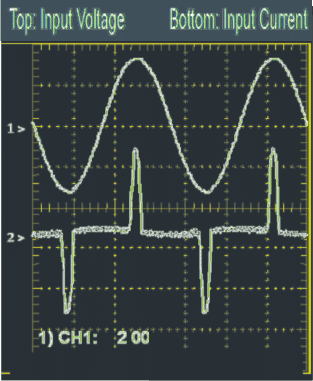 We can see in the above figure that despite of the significant amount of distortion the voltage and the current parameters are apparently in phase with each other.
However if we apply the ��phase angle cosine�� term to the above would give rise to an incorrect inference regarding the power supply being having a power factor of 1.0
The upper and the lower waveforms indicate the amount of harmonic content of the current.
Here the ��fundamental harmonic content�� is indicated in comparison with an amplitude of 100%, while the higher harmonics are presented as the supplementary percentages of the fundamental amplitude.
However since the real power is determined only by the fundamental component, while the other supplementary harmonics only represent the apparent power, the actual power factor may be quite under 1.0.
We call this deviation by the term distortion factor which is fundamentally responsible for giving rise to a non-unity power factor in SMPS units.
We can see in the above figure that despite of the significant amount of distortion the voltage and the current parameters are apparently in phase with each other.
However if we apply the ��phase angle cosine�� term to the above would give rise to an incorrect inference regarding the power supply being having a power factor of 1.0
The upper and the lower waveforms indicate the amount of harmonic content of the current.
Here the ��fundamental harmonic content�� is indicated in comparison with an amplitude of 100%, while the higher harmonics are presented as the supplementary percentages of the fundamental amplitude.
However since the real power is determined only by the fundamental component, while the other supplementary harmonics only represent the apparent power, the actual power factor may be quite under 1.0.
We call this deviation by the term distortion factor which is fundamentally responsible for giving rise to a non-unity power factor in SMPS units.
Expression for Real and Apparent Power
A general expression which addresses the connection between the real and the apparent power may be given as follows: Where cos�� forms the displacement factor emerging from the phase angle �� between the current/voltage waveforms and cos�� signifies the distortion factor.
 Referring to the diagram below, we can witness a situation which shows a perfect powerfactor correction.
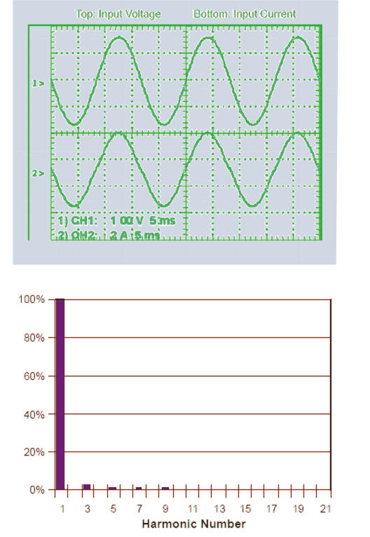 We can see that here the current waveform quite ideally replicates the voltage waveform as both are apparently running in phase and in sync with each other.
Therefore here the input current harmonics could be assumed to be almost zero.
We can see that here the current waveform quite ideally replicates the voltage waveform as both are apparently running in phase and in sync with each other.
Therefore here the input current harmonics could be assumed to be almost zero.
Power Factor Correction Vs Harmonic Reduction
Looking at the earlier illustrations it��s evident that power factor and low harmonics work in sync with each other. It is generally perceived that if limits for the respective harmonics are outlined might help to restrict the input current contamination in power lines by the way of eliminating interfering current disturbances with the other appliances in the vicinity. Therefore while the processing of input current may be termed as ��power factor correction�� the output magnitude of refinement thought this processing is understood as harmonic content a per the international guidelines. For SMPS topologies, it��s normally the displacement element which is approximately at unity, giving rise to the following relationships between power factor and harmonic distortion.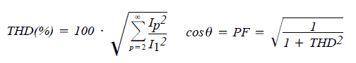 In the expression the THD represents the Total Harmonic Distortion as the quadratic sum of the harmful harmonics over the fundamental content, expressing the relative weight of the associated harmonic content with reference to the fundamental counterpart.The other equation associates the absolute figure of the THD and not in the % proportion, expressing that THD needs to be essentially zero in order to create a unity PF.
Types of Power Factor Correction
The input waveform characteristic in the above figure demonstrates a typical ��active�� type of power factor correction for an SMPS device introduced in between an input rectifier configuration and a filter capacitor, and through a PFC integrated circuit controlling the proceedings along with the associated circuitry for ensuring that the input current cohesively follows the input voltage waveform. This type of processing may be considered as the most prevalent type of PFC employed in the modern SMPS circuits, as may be witnessed in the figure below. Having said this, it is by no means mandatory that only ��active�� versions using ICs, and semiconductors be used for the proposed PFC, ll other form of design which may guarantee a reasonable amount PFC below the set regulations is normally welcomed. It is been noticed that in fact a single inductor replacing the position of the ��active�� counterpart is able to quite satisfactorily reject the harmonics by controlling the peaks and by distributing the current uniformly in sync with the input voltage quite efficiently.Passive PFC Design
However this form of passive PFC control could demand a significantly bulky iron cored inductor and therefore can be used for applications in which compactness is not the a crucial requirement. (page 12) A passive single inductor could seem to be a quick solution for PFC but for high wattage application the size could begin getting uninteresting due to it��s impracticably large dimensions. In the graph below we are able to witness the input characteristics of three numbers of 250 watt PC SMPS variants, each representing a current waveform at an equivalent scale factor. We can easily see that the result obtained from a passive inductor based PFC is 33% higher current peaks, than with active PFC filter counterpart. Even though this may be able to pass the IEC61000-3-2 standards, it will definitely not be on par with the recent more stringent 0.9PF requirement rule, and would fail the QC acceptance level, set as per this new standards.Basic Block Diagram
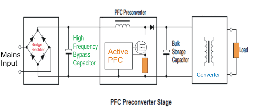 Due to the ongoing electronic market trend where we can see copper costs on the rise along with the rise in the magnetic cores process and the introduction of modern, much cheaper semiconductor materials, it won��t be a surprise if we notice the active PFC approach getting exceedingly popular than the passive counterpart.
And this trend could be perceived to grow even stronger in the coming future, presenting more and more advanced and enhanced PFC solutions for the many SMPS designers and manufacturers.
Due to the ongoing electronic market trend where we can see copper costs on the rise along with the rise in the magnetic cores process and the introduction of modern, much cheaper semiconductor materials, it won��t be a surprise if we notice the active PFC approach getting exceedingly popular than the passive counterpart.
And this trend could be perceived to grow even stronger in the coming future, presenting more and more advanced and enhanced PFC solutions for the many SMPS designers and manufacturers.
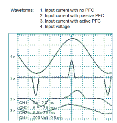
Comparing Input Line Harmonics to IEC610003-2 Standards
In Figure below we are able to see traces of three separate 250 watt PC SMPS results with reference to the IEC6000-3-2 restrictions. The indicated restriction is valid for all class D gadgets such as PCs, TVs, and their monitors. The shown harmonic content limit are fixed in accordance to the input power of the devices. For products related to lights such LED lights, CFL lights, class C restrictions are normally followed, which are identically on par with their input wattage limits. Other non-conventional electronic products find their PFC limit set in proportion to a minimum 600 watt input power. If we look at the passive PFC trace we find it to be hardly in conformity with the set restriction limit, just a touch and go kind of situation (at harmonic no3)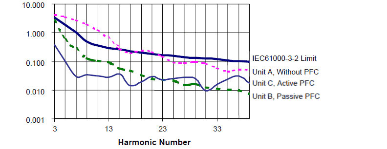
Analyzing Passive PFC Features
In the following figure we can see a classic example of passive PFC circuit designed for a traditional PC power supply. The notable thing here is the connection of center tap of the PFC inductor with the input line input voltage. While in the 220V selection mode (switch open), the entire two sections of the inductor are applied with the rectifier network working like a full bridge rectifier circuit. However in the 110V mode (switch close), just 50% or one half of the coil is utilized through the left side section of the coil being implemented whereas the rectifier section is now transformed into a half wave rectifier doubler circuit. Since the 220V selection is bound to generate around 330V after full wave rectification, this forms the bus input for the SMPS and possesses the possibility of fluctuating significantly in accordance with the input line voltage.Example Circuit Diagram
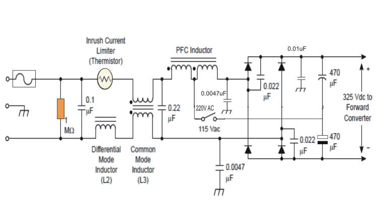 Although this passive PFC design might look quite simple and impressive with its performance it might exhibit a few notable drawbacks.
Along with the bulky nature of the PFC, two other things that affect its performance are first, the inclusion of a mechanical switch which makes the system vulnerable to a possible human error while operating the unit, and also the associated wear and tear issues.
Second, the line voltage being not stabilized results in relative inefficiencies in the fronts of cost effectiveness and DC to DC power conversion accuracy linked with the PFC output.
Although this passive PFC design might look quite simple and impressive with its performance it might exhibit a few notable drawbacks.
Along with the bulky nature of the PFC, two other things that affect its performance are first, the inclusion of a mechanical switch which makes the system vulnerable to a possible human error while operating the unit, and also the associated wear and tear issues.
Second, the line voltage being not stabilized results in relative inefficiencies in the fronts of cost effectiveness and DC to DC power conversion accuracy linked with the PFC output.
Critical Conduction Mode (CrM) Controllers
Controller stage called critical conduction mode which is also termed as transitional mode or borderline conduction mode (BCM) controller are circuits configurations which can be found effectively employed in lighting electronics applications. Although being hassle free with its usability, these controller are relatively expensive. The following diagram 1-8 demonstrates a regular CrM controller circuit design.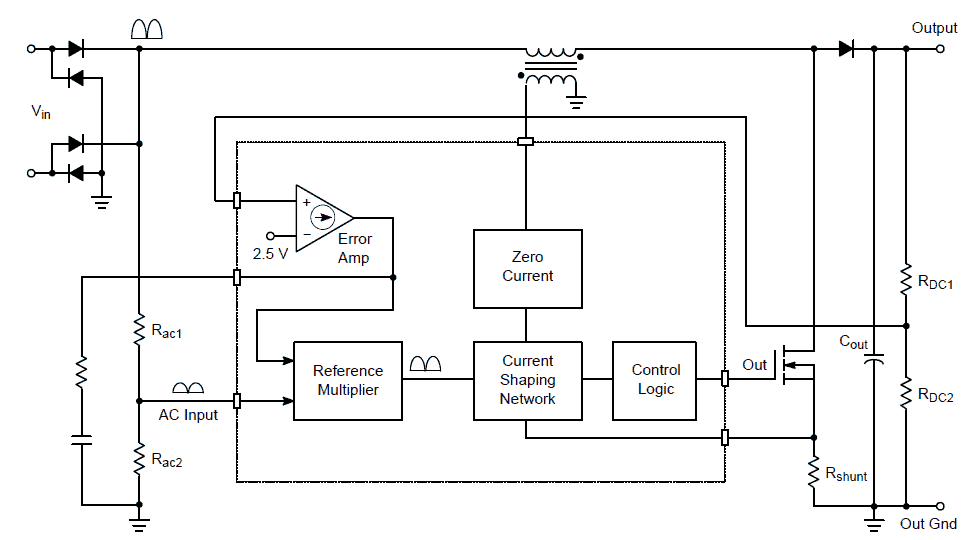 Typically a CrM controller PFC will possess the above shown kind of circuitry, which can be understood with the help of the following points:
An input of a reference multiplier stage receives an appropriately dimensioned signal from an associated error amplifier output having a low frequency pole.
The other input of the multiplier can be seen referenced with a stabilized DC clamped voltage extracted from a rectified AC line input.
Thus, the resultant output from the multiplier is the product of relative DC from the error amp output and the referenced signal in the form of full wave AC sine pulses from the AC input.
This output from the multiplier stage can be seen also in the form of full wave sine wave pulses but appropriately scaled down in proportion with the applied error signal (gain factor) use as the reference for the input voltage.
The signal amplitude of this source is appropriately tweaked in order to implement the right specified average power and to ensure a proper regulated output voltage.
The stage which is responsible for processing the current amplitude causes the current to flow in accordance with the output waveform from the multiplier, however the line frequency current signal amplitude (after smoothing) may be expected to be half that of this reference from the multiplier stage.
Here, the operations by current shaping circuitry may be understood as follows:
Typically a CrM controller PFC will possess the above shown kind of circuitry, which can be understood with the help of the following points:
An input of a reference multiplier stage receives an appropriately dimensioned signal from an associated error amplifier output having a low frequency pole.
The other input of the multiplier can be seen referenced with a stabilized DC clamped voltage extracted from a rectified AC line input.
Thus, the resultant output from the multiplier is the product of relative DC from the error amp output and the referenced signal in the form of full wave AC sine pulses from the AC input.
This output from the multiplier stage can be seen also in the form of full wave sine wave pulses but appropriately scaled down in proportion with the applied error signal (gain factor) use as the reference for the input voltage.
The signal amplitude of this source is appropriately tweaked in order to implement the right specified average power and to ensure a proper regulated output voltage.
The stage which is responsible for processing the current amplitude causes the current to flow in accordance with the output waveform from the multiplier, however the line frequency current signal amplitude (after smoothing) may be expected to be half that of this reference from the multiplier stage.
Here, the operations by current shaping circuitry may be understood as follows:
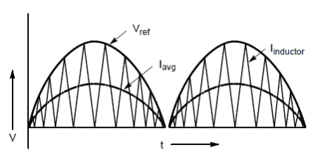 Referring to the diagram above, Vref stands for the signal out from the multiplier stage, which is further fed to one of the opamps of a comparator whose second input is referenced with the current waveform signal.
On power switch, the current across the inductor slowly increases until the signal across the shunt has reached the Vref level.
This forces the comparator to change its output from On to OFF switching OFF the power to the circuit.
As soon as this happens the voltage which was gradually ramping across the inductor begins to drop slowly towards zero and once it touches zero, the opamp output reverts and switches ON again, and the cycle goes on repeating.
As the name of the above characteristic signifies, the control pattern of the system never allows the inductor current to shoot above the predetermined limit across the continues and discontinuous switching modes.
This arrangement helps to predict and calculate the relationship between the average peak current level of the resultant output from the opamp.
Since the response is in the form of triangular waves, the average of the waveform signifies precisely 50% of the actual peaks of the triangle waveforms.
This implies that the resultant average value of the current signal of the triangle waves would be = Inductor current x R sense or simply put half of the preset reference level (Vref) of the opamp.
The frequency of a regulators using the above principle will be dependent on the line voltage and the load current.
The frequency could be much higher at higher line voltages and could vary as the line input varies.
Referring to the diagram above, Vref stands for the signal out from the multiplier stage, which is further fed to one of the opamps of a comparator whose second input is referenced with the current waveform signal.
On power switch, the current across the inductor slowly increases until the signal across the shunt has reached the Vref level.
This forces the comparator to change its output from On to OFF switching OFF the power to the circuit.
As soon as this happens the voltage which was gradually ramping across the inductor begins to drop slowly towards zero and once it touches zero, the opamp output reverts and switches ON again, and the cycle goes on repeating.
As the name of the above characteristic signifies, the control pattern of the system never allows the inductor current to shoot above the predetermined limit across the continues and discontinuous switching modes.
This arrangement helps to predict and calculate the relationship between the average peak current level of the resultant output from the opamp.
Since the response is in the form of triangular waves, the average of the waveform signifies precisely 50% of the actual peaks of the triangle waveforms.
This implies that the resultant average value of the current signal of the triangle waves would be = Inductor current x R sense or simply put half of the preset reference level (Vref) of the opamp.
The frequency of a regulators using the above principle will be dependent on the line voltage and the load current.
The frequency could be much higher at higher line voltages and could vary as the line input varies.
Frequency Clamped Critical Conduction Mode (FCCrM)
Despite of its popularity in various industrial power supply PFC control applications, the above explained CrM controller involves some inherent drawbacks. The main flaw of this type of active PFC control is its frequency instability with respect to line and load conditions, which shows an increase in frequency with lighter loads and higher line voltages, and also while each time the input sinewave approaches the zero crossings. If an attempt is made to rectify this issue by adding a frequency clamp, results in an output with a distorted current waveform, which seems inevitable due to the fact that ��Ton�� remains unadjusted for this procedure.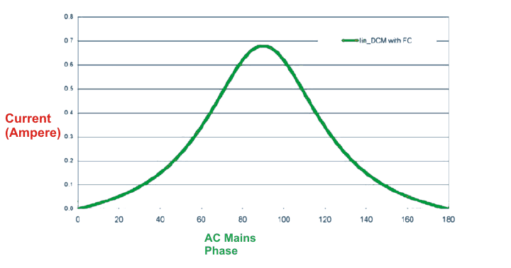 However the development of an alternative technique helps to achieve a true power factor correction even in the discontinuous mode (DCM).
The principle of operation can be studied in Figure below and with the attached equations.
However the development of an alternative technique helps to achieve a true power factor correction even in the discontinuous mode (DCM).
The principle of operation can be studied in Figure below and with the attached equations.
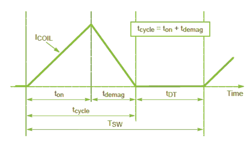 Referring to the diagram above, the coil peak current can beevaluated by solving:
 The average coil current with reference to the switching cycle (which is additionally assumed as the instantaneous line current for the given switching cycle, owing to the fact that switching frequency is usually higher than the line frequency on which the variations of the line voltage takes place), is expressed with the formula:
 Combining the above relationship and simplification of theterms gives the following:
 The above expression clearly indicates and implies that in case a method is implemented wherein an algorithm takes care to maintain ton.tcycle / Tsw at a constant level, it would enable us to achieve a sinewave line current having a unity power factor even in the discontinuous mode of operation.
Although the above considerations reveals some distinct benefits for the proposed DCM controller technique, it��s doesn��t seem to be the ideal choice because of the associated high peak current levels, as demonstrated in the following table:
The above expression clearly indicates and implies that in case a method is implemented wherein an algorithm takes care to maintain ton.tcycle / Tsw at a constant level, it would enable us to achieve a sinewave line current having a unity power factor even in the discontinuous mode of operation.
Although the above considerations reveals some distinct benefits for the proposed DCM controller technique, it��s doesn��t seem to be the ideal choice because of the associated high peak current levels, as demonstrated in the following table:
 In order to achieve an ideal PFC conditions, a sensible approach would be to implement a condition where the DCM and the Crm modes of operations are merged for milking out the best out of these two counterparts.
Therefore when the load conditions are not heavy and the CrM runs at a high frequency, the circuit goes for a DCM mode of operation, and in case when the load current is high, the Crm condition is allowed to persist so that the current peaks do not tend to cross the undesirable high limits.
This kind of optimization across the two suggested control modes can be best visualized in the following figure where the benefits of the two control modes are merged for achieving the most desirable solutions.
In order to achieve an ideal PFC conditions, a sensible approach would be to implement a condition where the DCM and the Crm modes of operations are merged for milking out the best out of these two counterparts.
Therefore when the load conditions are not heavy and the CrM runs at a high frequency, the circuit goes for a DCM mode of operation, and in case when the load current is high, the Crm condition is allowed to persist so that the current peaks do not tend to cross the undesirable high limits.
This kind of optimization across the two suggested control modes can be best visualized in the following figure where the benefits of the two control modes are merged for achieving the most desirable solutions.
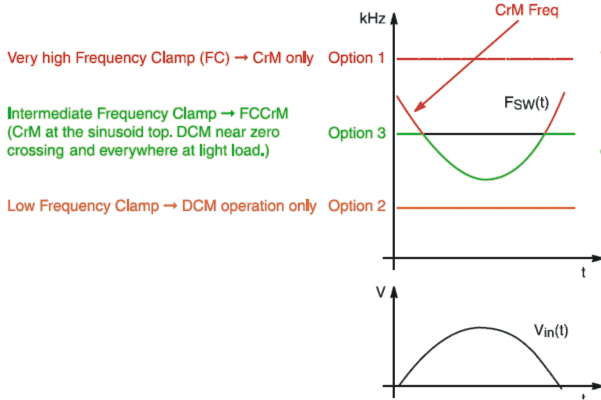
Continues Conduction Mode
The continuous conduction mode of PFC could become quite popular in SMPS designs due to their their flexible application feature and range and the associated several advantages. In this mode the current peak stress is maintained at a lower level resulting in minimized switching losses within the relevant components, and furthermore the input ripple is rendered at a minimal level with a relatively constant frequency, which in turn enables the smoothing process much simpler for the same. The following attributes associated with CCM type of PFC needs to be discussed a bit more elaborately.Vrms2 Control
One of the vital attributes with most PFC design universally applied is the reference signal which needs to be a steppe down imitation of the rectified input volage. This minimized rectified equivalent of the input voltage is finally applied in the circuit for shaping the correct waveform for the output current. As discussed above, a multiplier circuit stage is normally employed for this operation, but as we know that a multiplier circuit stage could be relatively less cost effective than a traditional twn-input multiplier system. A classic example layout an be witnessed in Figure below which demonstrates a continuous mode PFC approach. As can be seen, here the boost converter is triggered with the aid of an average current-mode PWM, which becomes responsible for dimensioning the inductor current (input current for the converter), with reference to the command current signal, V(i), which may be seen as the scaled down equivalent of the input voltage V(in) to a proportion of VDIV. This is is implemented by dividing the error voltage signal with the square of the input voltage signal (smoothed by the capacitor Cf, in order to create a simplified scaling factor with reference to the input voltage level).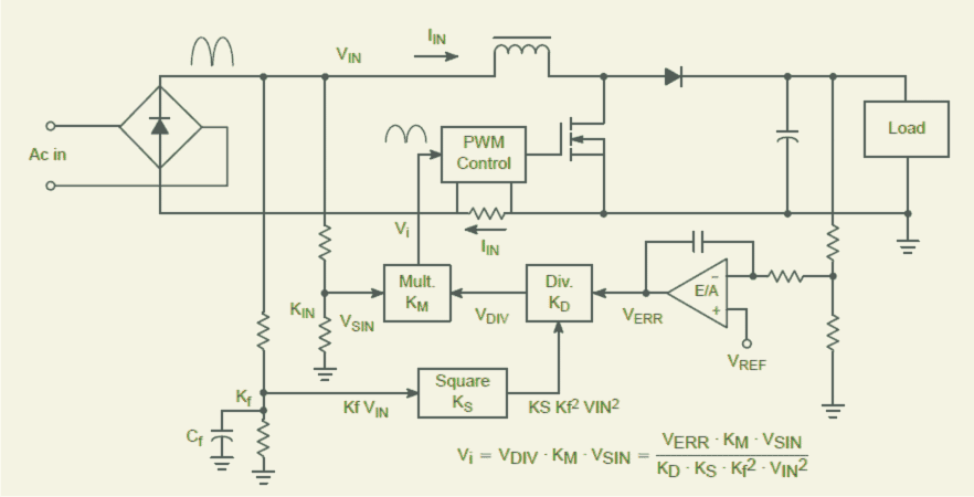 Although you may find it a bit awkward to see the error signal being divided by the square of the input voltage, the reason behind this measure is to create a loop gain (or a transient dependent response) which may not be based on the input voltage triggering.
The squaring of the voltage at the denominator neutralizes with the value of Vsin along with the transfer function of the PWM control (the proportionality of the current graph slope of the inducror with the input voltage).
However one downside of this form of PFC is the flexibility of the multiplier, which compels this stage to be a bit overdesigned especially the power handling sections of the circuit, so that it sustains even the worst-case power dissipation scenarios.
Although you may find it a bit awkward to see the error signal being divided by the square of the input voltage, the reason behind this measure is to create a loop gain (or a transient dependent response) which may not be based on the input voltage triggering.
The squaring of the voltage at the denominator neutralizes with the value of Vsin along with the transfer function of the PWM control (the proportionality of the current graph slope of the inducror with the input voltage).
However one downside of this form of PFC is the flexibility of the multiplier, which compels this stage to be a bit overdesigned especially the power handling sections of the circuit, so that it sustains even the worst-case power dissipation scenarios.
Average Current Mode Control
In the above figure we can see how the reference signal produced from the multiplier V(i) signifies the shape of the waveform, and the scaling range of the PFC input current . The indicated PWM stage becomes responsible of ensuring an average input current to be on par with the reference value. The procedure is executed through an average current mode controller stage, as can be seen in the figure given below.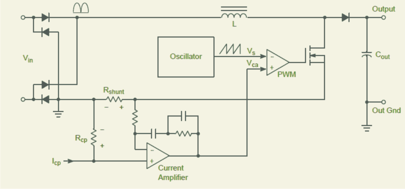 The average current mode control is basically configured to regulate the average current (input/output) with reference to the control signal Icp, which in turn is created by employing a low frequency DC loop through an error amplifier circuit stage, and this is nothing but the equivalent current corresponding to the signal Vi which is shown in the earlier figure to this.
The stage current amplifier functions as an current integrator as well as a error amplifier, in order to regulate the shape of the waveform, whereas the Icp signal which is generated across Rcp becomes responsible for executing the DC input voltage control.
In order to ensure a linear response from the current amplifier, its input is required to be similar, which means the potential difference generated across R(shunt) needs to be similar to the voltage generated around Rcp, because we cannot have a DC through the nono-inverting resistor input of the current amplifier.
The output generated by the current amplifier is supposed to be a ��low frequency�� error signal depending o the shunt��s average current, as well as the signal from the Isp.
Now a oscillator generates a sawtooth signal which is used for comparing the above signal with it, just as done with the voltage mode control design.
This results in the creation of PWMs determined by comparing the above mentioned two signals.
The average current mode control is basically configured to regulate the average current (input/output) with reference to the control signal Icp, which in turn is created by employing a low frequency DC loop through an error amplifier circuit stage, and this is nothing but the equivalent current corresponding to the signal Vi which is shown in the earlier figure to this.
The stage current amplifier functions as an current integrator as well as a error amplifier, in order to regulate the shape of the waveform, whereas the Icp signal which is generated across Rcp becomes responsible for executing the DC input voltage control.
In order to ensure a linear response from the current amplifier, its input is required to be similar, which means the potential difference generated across R(shunt) needs to be similar to the voltage generated around Rcp, because we cannot have a DC through the nono-inverting resistor input of the current amplifier.
The output generated by the current amplifier is supposed to be a ��low frequency�� error signal depending o the shunt��s average current, as well as the signal from the Isp.
Now a oscillator generates a sawtooth signal which is used for comparing the above signal with it, just as done with the voltage mode control design.
This results in the creation of PWMs determined by comparing the above mentioned two signals.
Advanced PFC Solutions
The various methods of PFC controls as discussed above (CrM, CCM, DCM) and their variants provide the designers with varied options of configuring PFC circuits. However despite these options, the consistent search for achieving better and more advanced modules in terms of efficiency has made the it possible for more sophisticated designs to be diagnosed for these applications. We'll discuss more on this as this article is updated with the latest on the subject.Ferrite Core Material Selection Guide for SMPS
In this post we learn how to select ferrite core material with the correct specifications for ensuring proper compatibility with a given SMPS circuit designWhy Ferrite Core
Ferrite is a wonderful core substance for transformers, inverters and inductors in the frequency spectrum 20 kHz to 3 MHz, owing to the benefits of reduced core expense and minimal core losses. Ferrite is an effective stuff for high frequency (20 kHz to 3 MHz) inverter power supplies. Ferrites should be employed in the saturating approach for low power, low frequency functioning ( <50 watts and 10 kHz). For high power functionality a 2 transformer layout, employing a tape wrapped core as the saturating core and a ferrite core as the output transformer, delivers optimum execution. The 2 transformer model provides extraordinary efficiency fantastic frequency durability, and minimal switching drawdowns. Ferrite cores is commonly used in fly-back transformer versions, that provide minimal core cost, reduced circuit expense and top voltage efficiency. Powder cores (MPP, High Flux, Kool M��) produce softer saturation, greater Bmax and more advantageous temperature constancy and is often the preferred option in a number of flyback usages or inductors. High frequency power supplies, either inverters and converters, propose cheaper price, and reduced weight and structure compared to traditional 60 hertz and 400 hertz power options. Several cores in this specific segment are typical designs frequently used in the profession.CORE MATERIALS
F, P, and R materials, facilitating the minimal core disadvantages and maximum saturation flux density, are recommended for high power/high temperature functionality. P material core deficits drop with temperature up to 70��C; R material losses decline to as much as 100��C. J and W materials provide you with superior impedance for wide transformers, which makes them also recommended for low-level power transformers.
CORE GEOMETRIES
1) POT CORES
Pot Cores, are manufactured to pretty much encircle the wound bobbin. This facilitates safeguarding the coil from picking of of EMI from outside alternatives. The pot core proportions pretty much all stick to IEC specifications to ensure that there exists interchangeability between companies. Both the plain and printed circuit bobbins are on the market, as are mounting and assembly hardware. Due to its layout, the pot core is usually a more high-priced core compared to different formats of a analogous size. Pot cores for substantial power purposes are not easily accessible.2) DOUBLE SLAB AND RM CORES
Slab-sided solid center post cores are similar to pot cores, but yet possess a segment minimize off on either part of the skirt. Substantial entrances make it possible for bigger wires to be lodged and contributes to eliminating heat from the setup. RM coresare similar to pot cores, however are fashioned to curtail pcb area, supplying a minimum of a 40% reductions in installation space. Printed circuit or plain bobbins are obtainable. Straightforward 1 unit clamps enable hassle-free construction. Lower outline is achievable. The sturdy middle piece delivers less core loss which in turn eliminates heat accumulation.3) EP CORES
EP Cores are circular center-post cubical designs which surround the coil thoroughly with the exception of the printed circuit board terminals. The specific appearance eliminates the influence of air flow crevices established at mating walls in the magnetic track and gives you a more significant volume ratio to absolute area used. Safeguarding from RFs is pretty much great.4) PQ CORES
PQ cores are intended distinctively for switched mode power supplies. The layout allows for an maximized ratio of bulk to winding region and surface area. Therefore, both optimum inductance and winding surface are achievable with the absolute minimum core dimension. The cores as a result afford optimum power output with the very least assembled transformer mass and dimension, along with occupying a bare minimum level of space on the printed circuit board. Setting up with printed circuit bobbins and one bit clamps is made easy. This economical model assures much more homogeneous cross-sectional section; consequently cores often work with with a smaller amount of hot positions compared to with different layouts.5) E CORES
E cores are cheaper than pot cores, while having the aspects of straightforward bobbin winding and uncomplicated assemblage. Gang winding is achievable for the bobbins put to use using these cores. E cores never, all the same, present self-shielding. Lamination size E layouts are designed for accommodate commercially accessible bobbins in past times meant to conform the strip stampings of customary lamination measurements. Metric and DIN sizes can also be found. E cores are typically embedded to various consistency, furnishing a variety of cross-sectional areas. Bobbins for these various cross sectional areas tend to be accessible commercially. E cores are typically installed in unique orientations, in case preferred, grant a lowprofile. Printed circuit bobbins can be found for low-profile fixing. E cores are well-known designs on account of their more affordable rate, convenience of assembly and winding, and the organized prevalence of an assortment of hardware.6) PLANAR E CORES
Planar E cores can be found in virtually all of the IEC conventional measurements, along with several of supplementary capacities. Magnetics R material is flawlessly matched to planar shapes owing to its reduced AC core losses and minimal losses at 100��C. Planar layouts in most cases have low turn numbers and agreeable thermal dissipation as opposed to standard ferrite transformers, and for that reason the ideal designs for space and effectiveness lead to increased flux densities. In those variations, the overall performance advantage of R material is principally quite notable. The leg span and window elevation (B and D proportions) are flexible for individual purposes without new tooling. This makes it possible for the developer to fine-tune the finalized core specs to accurately fit with the planar conductor stack elevation, lacking any expended space. Clips and clip slots are offered in numerous instances, that could be specifically effective for prototyping. I-cores are furthermore proposed standard, which allows even more adaptability in layout. E-I planar patterns come in handy to enable effective face blending in high bulk production, as well as for creating gapped inductor cores whereby fringing drawdowns needs to be thoroughly regarded on account of the planar structure.7) EC, ETD, EER AND ER CORES
These types of patterns are a mix between E cores and pot cores. Like E cores, they deliver an enormous gap on both sides. This enables satisfactory room for the bigger size wires necessary for reduced output voltage switched mode power supplies. Aside from that it guarantees a circulation of air which maintains the construction colder. The middle piece is circular, very similar to that of the pot core. One of the positive aspects of the circular central pillar is that the winding bears a smaller course period around it (11% faster) compared to the wire around a square type central pillar with an very same cross sectional area. This cuts down on the losses of the windings by 11% and also makes it possible for the core to cope with an improved output ability. The circular central pillar additionally minimizes the spiked fold in the copper that transpires with winding on a square type central pillar.8) TOROIDS
Toroids are cost-effective to produce; consequently, these are least expensive of most relevant core designs. Because no bobbin becomes necessary, accessory and setting up charges are negligible. Winding is completed on toroidal winding equipment. Shielding attribute is pretty sound. Overview Ferrite geometries provide you with a huge choice in sizes and styles. When picking a core for power supply utilizations, specifications displayed in Table 1 ought to be assessed.
TRANSFORMER CORE SIZE SELECTION
The power processing capability on a transformer core is usually contingent on its WaAc product, in which Wa is the offered core window space, and Ac is the useful core cross-sectional space.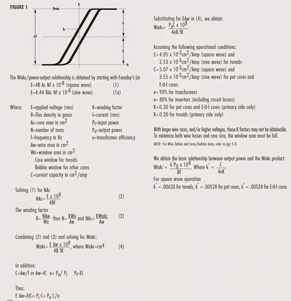 While the equation above enables WaAc to be modified depending on particular core geometry, the Pressman technique takes advantage of topology as the fundamental factor and enables the maker to designate current density.
GENERAL INFORMATION
A perfect transformer is but one that promises minimal core decline while demanding the very least volume of room. The core loss in a particular core is specifically affected by the flux denseness along with the frequency. Frequency is the crucial factor regarding a transformer. Faraday��s Law indicates that as frequency speeds up, the flux density reduces correspondingly. Core losing trades reduce a lot more in case the flux density falls compared to when frequency increases. As an illustration, when a transformer is operated at 250 kHz and 2 kG on R material at 100��C, the core failures would probably be around 400 mW/cm3. If the frequency was made twice and most other limitations unscathed, as a result of Faraday��s law, the flux density would likely turn out to be 1kG and the resultant core drawdowns would be roughly be 300mW/cm3. Standard ferrite power transformers are core loss restricted ranging from 50- 200mW/cm3. Planar models could be operated a lot more assertively, up to 600 mW/cm3, on account of more advantageous power dissipation and significantly less copper in the windings.CIRCUIT Categories
A number of basic feedback on the several circuits are: The push-pull circuit is effective since the device causes bi-directional usage of a transformer core, presenting an output with reduced ripple. In spite of this, circuitry is extra sophisticated, and the transformer core saturation can result in transistor breakdown when power transistors carry unequal switching properties. Feed forward circuits are cheaper in cost, applying just one transistor. Ripple is minimal because of the fact that apparently stable state current streams in the transformer no matter whether the transistor is ON or OFF. The flyback circuit is straightforward and affordable. In addition, EMI issues are considerably less. In spite of this, the transformer is bigger and ripple is more significant.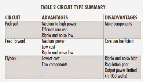
PUSH-PULL CIRCUIT
A conventional push-pull circuit is presented in Figure 2A. The feed voltage is the output of an IC network, or clock, which oscillates the transistors alternately ON and OFF. High frequency square waves on the transistor output are eventually refined, generating dc.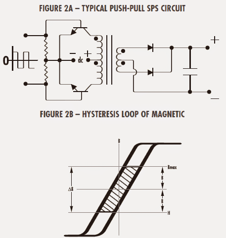
CORE IN PUSH-PULL CIRCUIT
For ferrite transformers, at 20 kHz, it is usually well-known process to employ equation (4) with a flux density (B) level of ��2 kG max. This can be drawn out by the coloured section of the Hysteresis Loop in Figure 2B. This B degree is selected mainly because the restricting aspect of selecting a core with this frequency is core loss. At 20 kHz, if the transformer is ideal for a flux density around saturation (as carried out for smaller frequency layouts), the core is going to acquire an uncontrolled temperature surge. For that reason, the smaller operating flux density of 2 kG will in most cases confine the core losses, consequently helping an affordable temperature increase in the core. Above 20 kHz, core losses maximize. To execute the SPS at raised frequencies, it is important to execute the core flux rates lesser than ��2 kg. Figure 3 exhibits the decline in flux levels for MAGNETICS ��P�� ferrite material vital for contributing constant 100mW/cm3 core losses at numerous frequencies, with a optimum temperature surge of 25��C.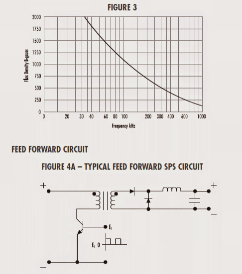 In the feed forward circuit laid out in Figure 4A, the transformer executes in the 1st quadrant of the Hysteresis Loop.
(Fig 4B).
Unipolar pulses implemented to the semiconductor device bring about the transformer core to be powered from its BR value near saturation.
As the pulses are downsized to zero, the core reverts to its BR rate.
To be able to keep up a superior efficiency, the primary inductance is maintained high to help reduce magnetizing current and lessen wire drawdowns.
This implies the core needs to have a zero or a bare minimum of air flow opening.
In the feed forward circuit laid out in Figure 4A, the transformer executes in the 1st quadrant of the Hysteresis Loop.
(Fig 4B).
Unipolar pulses implemented to the semiconductor device bring about the transformer core to be powered from its BR value near saturation.
As the pulses are downsized to zero, the core reverts to its BR rate.
To be able to keep up a superior efficiency, the primary inductance is maintained high to help reduce magnetizing current and lessen wire drawdowns.
This implies the core needs to have a zero or a bare minimum of air flow opening.
LCD Monitor SMPS Circuit
This power supply functions with a broad input voltage range from 90 to 265 V AC and produces a dual output in the form of 5 V / 2.5 A, and 14.5 V / 1 A.The Circuit Layout
The great aspect of this source is its minimal power consumption, optimized power consumption in idle mode and high efficiency at full load conditions. There are additional built in security protections, which includes hysteretic output overvoltage protection, hysteretic output protection against short circuit and thermal protection against overheating with a large hysteresis. Part of the below given explanation is a comprehensive power supply specifications, schematic overview and components used, along with manufacturing documentation and proposal transformer circuit boards and a summary of performance data. The power supply circuit uses the TOPSwitch-JX TOP266EG (U1), which directly hooks up in its housing and also with the high voltage switching MOSFET and driver flyback configuration.EMI Filter
Capacitors C1, C2 and C3 in conjunction with the inductance L1 forms an EMI filter, which works both in the common mode and differential mode EMI filtering. It is followed by the subsequent classic diode bridge D10, which rectifies the input AC voltage, and the resulting power is further filtered by capacitor C4. A diode bridge was selected in the form of D10 in order to execute a reliable operation even at lower input potentials such that it compensates and operates at full load.Using the IC TOP266EG
TOP266EG circuit (U1) TOPSwitch-JX Series shakes hand with oscillator circuit driver switching element, trigger and protection circuitry and MOSFET power supply - all within a single monolithic IC. One of the terminals of the primary winding of the power transformer T1 can be seen joined to the positive side of the filter capacitor C4 and the other line gets hooked up directly with the output pin of U1. When the attached MOSFET turns off, the leakage inductance of the transformer peaks up to induce voltage. The specified amplitude is restricted by the clamping stage, consisting of D5, R4, VR1, R3 and C5. A big portion of the excess energy becomes avaialble across VR1 and R4 is a series combination of R3 and C5 (parallel with R4 and VR1), which further contributes to minimize the magnitude of high frequency surges. The value of the resistor R4 fixes the magnitude of the difference between the two channels. This framework was implemented for minimizing switching losses and internal consumption while it may be running on without any load.Circuit Diagram
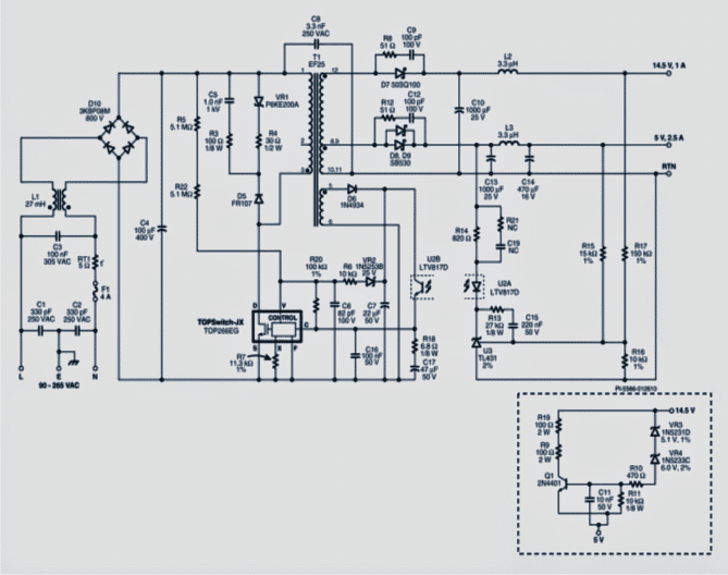 Another design using Fairchild's FPS switch:
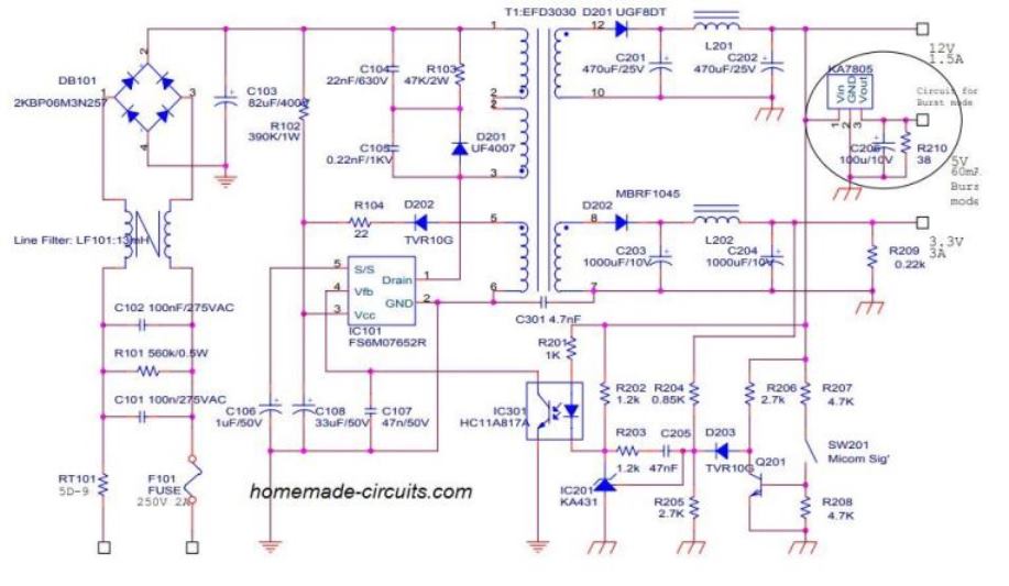 FOR COMPLETE DETAILS REFER TO THIS ARTICLE
Adjustable 0-100V 50 Amp SMPS Circuit
The high power adjustable switching power supply is perfect for the purpose of laboratory work. The topology used to design the system is switching topology �C half controlled bridge. Written and Submitted by: Dhrubajyoti BiswasUsing IC UC3845 as the Main Controller
The switching supply is powered with IGBT transmitters and is further controlled by UC3845 circuit. The mains voltage goes straight through the EMC filter which is further checked and filtered on C4 capacitor. As the capacity is high (50 amps), the inflow in the limiting circuit with Re1 switch and also on R2. The relay coil and fan, taken from AT or ATX power supply is powered from 12V. The power is obtained via the resistor from 17V auxiliary supply. It is ideal to select R1 so that the voltage at the fan and the relay coil limits to 12V. The auxiliary supply on the other hand uses TNY267 circuit and R27 facilitates protection from under-voltage of auxiliary power. The power will not turn on if the current is less than 230V. The UC3845 control circuit results to 47% duty cycle (Max.) with the output frequency of 50 kHz. The circuit is further powered with the help of the zener diode, which actually helps to reduce the supply voltage and even helps to shift the UVLO threshold of lower 7.9V and upper 8.5V to 13.5V and 14.1V respectively. The source initiates the power and starts working on 14.1V. It never goes below 13.5V and further helps to protect IGBT from desaturation. However, the original threshold of UC3845 should to set as low as possible. The MOSFET T2 circuit controls, which helps to make Tr2 transformer work offers floating drive and galvanic isolation for the upper IGBT. It is through the forming circuits of T3 and T4 that it helps to drive T5 and T6 of IGBT and the switch further rectifies line voltage to Tr1 power transformer. As the output is rectified and reaches an average, it is smoothed by L1 coil and C17 capacitors. The voltage feedback is further connected from output to the pin 2 and IO1. Furthermore, you can also set the output voltage of power supply with P1 potentiometer. There is no need for galvanic isolation of feedback. It is because the control circuit of this adjustable SMPS is connected with the secondary SMPS and leaves no connection with the network. The current feedback is passed through the current transformer TR3 right onto 3 pin IO1 and the overcurrent protection threshold can be set using P2. 12V input supply may be acquired from an ATX power supply The Controller Stage Schematic
The IGBT Switching Stage
 +U1 and -U1 may be derived from mains 220V input after appropriate rectification and filtration
Using Heatsink for the Semiconductors
Also, please remember to place diodes D5, D5 ', D6, D6', D7, D7 ', transistors T5 and T6 on heat sink along with the bridge. Care should be taken to place snubbers R22 + D8 + C14, capacitors C15 and diodes D7 close to IGBT. The LED1 signals the operation of the supply and LED2 signals the error or the current mode. The LED glows when the supply has ceased to work in voltage mode. When in voltage mode, the IO1 pin 1 is set to 2.5V else it usually has6V. LED light is an option and you may exclude the same during making.How to Make the Inductor Transformer
Inductance: For power transformer TR1, the transformation ratio is around 3:2 and 4:3 in primary and secondary. There is also air gap in the ferrite core which is EE shaped. If you are looking for to wind all by yourself, use a core as it is in an inverter which should size around 6.4 cm2. The primary is of 20 turns with 20 wires with each having diameter measuring 0.5mm to 0.6mm. The secondary 14 turns with 28 diameters is also of the same measurement like that of primary. Moreover, it is also possible to create windings of copper strips. It is important to note that application of single thick wire is not a possible idea because of the skin effect. Now since the winding is not required, you may wind the primary one first followed by secondary. Tr2 forward gate driver transformer possesses three windings having 16 turns each. It is by using three twisted insulated bell wires that all windings has to be wounded at once leaving any air gap at the wound of the ferrite core. Next, taking the main power supply from AT or ATX power supply unit of a computer with the core section of around 80 to 120mm2. The current Tr3 transformer is of 1 to 68 turn on ferrite ring and the number of turns or size is not critical here. However, the process to orient the winding of transformers must be followed. Also you need to use double choke EMI filter. The output coil L1 has two parallel inductors of 54uH on iron powder rings. The total inductance is finally 27uH and the coils are wounded by two magnetic copper wires of 1.7mm in diameter, which makes the total L1 cross section to approx. 9 mm2. The output coil L1 is attached to a negative branch which results no RF voltage in the cathode of diode. This facilitates mounting the same in heat sink without any insulation.Selecting the IGBT Specs
The max input power of the switched power supply is around 2600W and the resultant efficiency is above 90%. In switching power supply, you can use STGW30NC60W IGBT type or you can also use other variants like STGW30NC60WD, IRG4PC50U, IRG4PC50W or IRG4PC40W. You can also use a fast output diode having adequate current rating. In the worst case scenario, the upper diode gets an average current of 20A while the lower diode in similar situation gets 40A. Thus it is better to use upper diode half-current than the lower one. For upper diode, you can use, either HFA50PA60C, STTH6010W or DSEI60-06A else two DSEI30-06A and HFA25PB60. For lower or bottom diode you can use two HFA50PA60C, STTH6010W or DSEI60-06A else four DSEI30-06A and HFA25PB60. It is important that the diode of the heat sink must lose 60W (approx.) and loss in IGBT may account to 50W. However, it is quite hard to ascertain the loss of D7 since it is dependent on Tr1 property. Moreover, the bridge loss may account to 25W. The S1 switch enables shutdown in standby mode primarily because of the frequent mains switching may not be proper, specifically when using it for laboratory. In the standby state, the consumption is around 1W and S1 can be skipped. If you are looking to construct a fixed voltage source of supply, it is also feasible but for the same it is better to apply transformer ratio of Tr1 for maximum efficiency, for instance, in the primary use 20 turns and in secondary use 1 turn for 3.5V �C 4V.SMPS 50 watt LED Street Light Driver Circuit
The post presents an SMPS based LED street lamp driver circuit which can be used for driving any LED lamp design right from 10 watts to 50 watts plus.Using the IC L6565
The proposed 50 watt (and higher) LED street light driver circuit uses the IC L6565 as the main control device, which is basically a current mode primary controller chip especially built for quasi-resonant ZVS fly-back converters. ZVS stands for zero voltage switching. The chip implements the said quasi-resonant function by sensing the demagnetization of the transformer and by subsequently switching the mosfet for further actions.The Feed Forward Feature
A feed forward feature enables the IC to compensate for the variations of the mains voltage which in turn takes care of the converters power handling capability. In case the connected load is lower than the specified magnitude, the device correspondingly adjusts and compensates the operating frequency without affecting the ZVS feature by much. In addition to the above features the IC also includes a built-in current sensor, an error amplifier with accurate reference voltage and a versatile two step protection against overcurrent load conditions. More details regarding the IC L6565 can be found in its datasheet. The remaining configuration of the converter is standard and may be understood as follows:Circuit Operation
The mains 120/220V AC is fed to the bridge rectifier B1 via an EMI filter L1. The rectified voltage is filtered by C1 and applied to the primary section of the converter which comprises the IC L6565 along with the ferrite transformer primary winding and the switching mosfet. The IC instantly triggers itself and the mosfet, implementing the featured ZVS operations and switching the mosfet at the specified compensated rate, depending upon the mains input level. The output of the transformer responds to this and generates the required voltages across the respective winding. The outputs are appropriately rectified and filtered by the connected fast recovery diodes and high voltage filter capacitors. N2 can be seen specified with an output of 105V at 350mA. Other auxiliary winding which are included produce 14V (@1amp) and 5V (@50mA) which may be used for other relevant applications such as charging a battery or illuminating a pilot lamp. The opto IC3 is as usual included for ensuring a constant output in terms of voltage, current and for providing the relevant output information to the chip so that the necessary protective actions can be enforced by the chip during adverse situations.Transformer winding Details
The transformer winding details for the proposed 50 watt street light driver circuit is furnished in the diagram itself.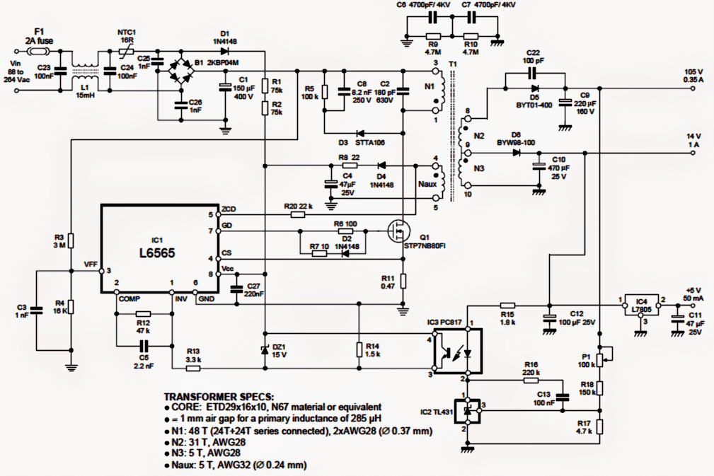 In the above sections we learned an SMPS design which can be used for driving a 50 watt LED lamp made from 50 numbers of 1 watt LEds.
Here we try to understand the connection details of the LEDs with the driver circuit.
In the above sections we learned an SMPS design which can be used for driving a 50 watt LED lamp made from 50 numbers of 1 watt LEds.
Here we try to understand the connection details of the LEDs with the driver circuit.
LED Configuration
Assuming we want to use 1 watt LEDs (recommended) for the proposed 50 watt street light, we would require 50 numbers of these LEDs to be configured with the circuit. Referring to the above descriptions, we see that one of the outputs is specified with 105V at 350mA. This particular output becomes the preferable one for driving 50 numbers of 1 watt LEds, although it could be implemented only after through some serious calculations. If we connect all the 50 LEDs in parallel would call for an output equal to 50 x 3.3 = 165V, but since this output doesn't seem to be available, we could opt for a more feasible series/parallel connection with the LeDs. So we can make two strings of LEDs, each consisting of 25 nos of LEDs, and connect these two strings in parallel. However, involving two strings would mean that the LEDs would now require 3.3 x 25 = 82.5V@ 700mA The above values once again seem to be not matching the driver output specs. No issues, the above values can be matched by doing a few simple tweaks with the relevant output winding of the driver transformer.Current Level Adjustment
The current (amps) can be increased by replacing the N2 winding with a bifilar winding consisting of two 28AWG wires wound simultaneously. This will take care of the required 700mA current since now we have used two wires in parallel for N2 instead of the recommended single wire. Next, for reducing the voltage from 105v to 82.5V, we simply need the above winding to bemade into 24 turns instead of the indicated 31 turns. That's it, once the above couple of simple tweaks are done, the driver now becomes perfectly suitable for driving the proposed 50 watt LED lamp module.The LED connection details can be witnessed in the following schematic diagram:
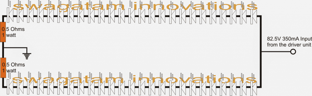
220V SMPS Cell Phone Charger Circuit
The post explains how to make a simple, cheap yet extremely reliable smps based 220V/120V mains operated cell phone charger circuit.Why TNYxxx Tiny Switch is Used
The TNY series of tiny switch ICs provide us with an option of making perhaps the smallest possible smps circuits with high reliability. The tiny switch series includes the following ICs: TNY267P, TNY263, TNY264, TNY265, TNY266, TNY267, TNY268, TNY280. The above ICs have an integrated in-built mosfet switching control circuit, protection against over current and thermal overshoot, along with rugged voltage and current specifications. The IC comes in a DIP8 package that's exactly how a 555 is enclosed. The maximum tolerable voltage limit of the TNY series ICs is a massive 700V, a margin that's way beyond our normal household AC specs. The operating frequency is at about 132kHz. The IC is specifically designed and built for implementing compact and reliable 120/220V mains operated SMPS flyback converters. Although the application of the proposed simplest SMPS design could be huge, it could be best used as a mains operated 5V cell phone charger circuit. The proposed cell phone charger design using the IC TY 267 can be visualized in the below shown diagram.How the SMPS Circuit Works
The circuit can be understood as follows: The mains input which could be anywhere between 100 and 280V is half wave rectified and filtered through shown 1N4007 diode and 10uF/400V input rectifier stage. The 10 ohm/1watt resistor is included to provide some sort of restrictionagainst the surge current inrush during power switch ONs and also forms like a fuse in case of a catastrophic situation. The switching voltage is acquired via the BA159 diode at pin5 of the IC. The IC instantly locks into the specified 132kHz switching frequency when switched ON across the input winding of the switching ferrite transformer. The 180V zener diode safeguards the IC from peak switching voltages. The above switching generates the calculated stepped down low voltage across the output winding of the transformer. The BA159 diode at the output rectifies the 132kz pulsed DC while the 220uF capacitor filters the high frequency ripples to produce a clean DC. The optocoupler acts like a feedback link between the output and the IC in order to ensure that the output never exceeds a certain predetermined voltage level. This feedback limit is decided by the adjoining 4.7V zener diode, which ensures that the output stays well within the 5 V range just suitable for charging any attached cell phone.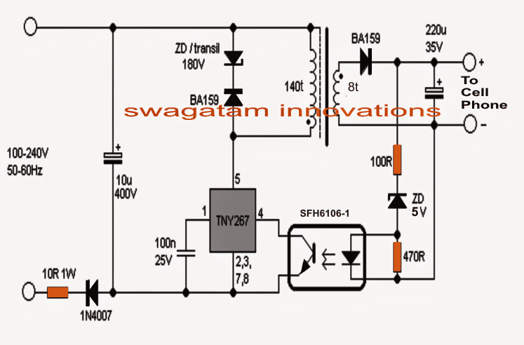
How to wind the ferrite transformer
The shown ferrite transformer along with the IC forms the heart of the circuit, however due to its simple configuration winding this transformer is much easier compared to other mains operated cell phone charger circuit topologies. The input primary winding consists of around 140 turns of 36 SWG, while the output secondary winding is made up of 8 turns of 27SWG super enameled copper wire turns. The core used can be a small E19type ferrite core with bobbin having a central core area section measuring 4.5 by 4.5mm. The primary is wound first. After winding it, it must be covered with a layer of insulation before winding the 8 number of secondary turns on top of the primary layer. A copper or aluminum tape layer should be preferably included in between the primary and the secondary winding and a wire connected with this tape with the "cold" end of the primary winding (see the trafo in the figure), this provides guaranteed isolation between the winding as well as guards against interference issues.220V Mobile Charger Circuit using Viper22E IC
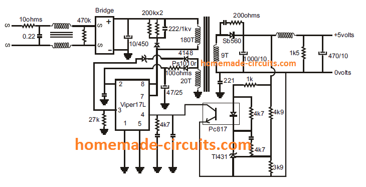 DATASHEET
How Buck-Boost Circuits Work
We all have heard a lot about buck and boost circuits and know that basically these circuits are used in SMPS designs for stepping up or stepping down a given voltage at the input. The interesting thing about this technology is that it allows the above functions with negligible heat generation which results in a extremely efficient conversions.What is Buck-Boost, How it Works
Let's learn the concept in the first section without involving much technicalities so that it becomes easier to understand what's exactly buck boost concept even to a newbie. Among the three fundamental topologies named buck, boost, and buck-boost, the third one is more popular since it allows both the functions (buck boost) to be used through a single configuration just by altering the input pulses. In the buck-boost topology we primarily have an electronic switching component which can be in the form of a transistor or a mosfet. This component is switched via a pulsating signal from an integrated oscillator circuit. Apart from the above switching component, the circuit has an inductor, a diode and a capacitor as the main ingredients. All these parts are arranged in the form that may be witnessed in the following diagram: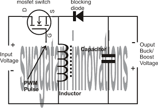 Referring to the above buck boost diagram, the mosfet is the part which receives the pulses which forces it to operate under two conditions: ON state and OFF state.
During ON state the input current gets a clear path through the mosfet and instantly tries to make it's way across the inductor since the diode is positioned in the reversed biased state.
The inductor on account of its inherent property tries to restrict the sudden infliction of current and in an compensating response stores some quantity of current in it.
Now as soon as the mosfet is switched OFF it goes under the OFF state blocking any passage of the input current.
Again the inductor is unable to cope with this sudden change of current from a given magnitude to zero, and in a response to compensate this, it kick backs its stored current via the diode across the output of the circuit.
In the process the current also gets stored in the capacitor.
During the next ON state of the mosfet, the cycle is repeated as above however with no current available from the inductor, the capacitor discharges the stored energy into the output which helps in keeping the output stable to the optimized degree.
You may be wondering what factor decides the BUCK or the BOOST results at the output? It's quite simple, it depends on how long the mosfet is allowed to stay in the ON state or in the OFF state.
With an increase in the mosfets ON time, the circuit starts getting transformed into a Boost converter while with the mosfets OFF time exceeding its ON time results in the circuit behaving like a Buck converter.
Thus the input to the mosfet can be made through an optimized PWM circuit for getting the required transitions across the same circuit.
Referring to the above buck boost diagram, the mosfet is the part which receives the pulses which forces it to operate under two conditions: ON state and OFF state.
During ON state the input current gets a clear path through the mosfet and instantly tries to make it's way across the inductor since the diode is positioned in the reversed biased state.
The inductor on account of its inherent property tries to restrict the sudden infliction of current and in an compensating response stores some quantity of current in it.
Now as soon as the mosfet is switched OFF it goes under the OFF state blocking any passage of the input current.
Again the inductor is unable to cope with this sudden change of current from a given magnitude to zero, and in a response to compensate this, it kick backs its stored current via the diode across the output of the circuit.
In the process the current also gets stored in the capacitor.
During the next ON state of the mosfet, the cycle is repeated as above however with no current available from the inductor, the capacitor discharges the stored energy into the output which helps in keeping the output stable to the optimized degree.
You may be wondering what factor decides the BUCK or the BOOST results at the output? It's quite simple, it depends on how long the mosfet is allowed to stay in the ON state or in the OFF state.
With an increase in the mosfets ON time, the circuit starts getting transformed into a Boost converter while with the mosfets OFF time exceeding its ON time results in the circuit behaving like a Buck converter.
Thus the input to the mosfet can be made through an optimized PWM circuit for getting the required transitions across the same circuit.
ExploringBuck/Boost Topology in SMPS Circuits More Technically:
As discussed in the above section the three fundamental topologies which are popularly used with switch mode power supplies are the buck, boost, and the buck boosts. These are basically non-isolated in which the input power stage shares a common base with the output power section. Of course we could also find isolated versions although pretty rare. The above expressed three topologies can be distinguished uniquely depending upon their exclusive properties.The properties may be identified as the steady state voltage conversion ratios, the nature of the input and output currents and the character of the output voltage ripple as well. Additionally the frequency response of the duty cycle to the output voltage execution can be considered as one of the important properties. Among the above referred three topologies, buck-boost topology is the most preferred one because it allows the output to work voltages less than the input voltage (buck mode) and also to produce voltages above the input voltage (boost mode). However the output voltage can be acquired always with the opposite polarity from the input, which doesn't create any issues whatsoever. The applied input current to a buck boost converter is the form of a pulsating current due to the switching of the associated power switch (Q1). Here the current switches from zero to l during every pulse cycle.The same is true for the output also and we get a pulsating current because of the associated diode which conducts only in one direction, causing an ON and OFF pulsating situation during the switching cycle. The capacitor is responsible for providing the compensating current when the diode is in the switched OFF or reverse biased state during the switching cycles. This article explains steady state functionality of the buck-boost converter in continuous-mode and discontinuous-mode operation with exemplary waveforms presented. The duty-cycle-to-output voltage exchange functionality is presented after an introduction of the PWM switch design. Figure 1 a simplistic schematic of the buck-boost power stage with a drive circuit block added. The power switch, Q1, is an n-channel MOSFET. The output diode is CR1. The inductor, L, and capacitor, C, constitute the efficient output filtering. The capacitor ESR, RC, (equivalent series resistance) and the inductor DC resistance, RL, are all analyzed in this article . The resistor, R, corresponds to the load as indicated by the power stage output.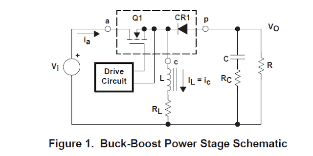 In the course of regular functionality of the buck-boost power stage, Q1 is constantly turned on and off with the on- and off-times governed by the control circuit.
This switching behavior results in a chain of pulses at the junction of Q1, CR1, and L.
Even though the inductor, L, is linked to the output capacitor, C, if only CR1 conducts, a successful L/C output filter is established.
It cleans the succession of pulses to result in a DC output voltage.
In the course of regular functionality of the buck-boost power stage, Q1 is constantly turned on and off with the on- and off-times governed by the control circuit.
This switching behavior results in a chain of pulses at the junction of Q1, CR1, and L.
Even though the inductor, L, is linked to the output capacitor, C, if only CR1 conducts, a successful L/C output filter is established.
It cleans the succession of pulses to result in a DC output voltage.
Buck-Boost Stage Steady-State Analysis
A power stage may function in continuous or discontinuous inductor current setting. Continuous inductor current mode is identified by current continuously in the inductor over the switching sequence in steady-state process. Discontinuous inductor current mode is identified by the inductor current staying zero for a section of the switching cycle. It begins at zero, extends to a maximum value, and comes back to zero in the course of every switching pattern. The two distinct methods are mentioned in much larger detail afterwards and model suggestions for the inductor value to sustain a selected mode of functionality as the ability of rated load are presented. It is rather favorable for a converter to be in a single format only over its predicted functioning circumstances since the power stage frequency response alters substantially between the two distinct techniques of operation. With this assessment, an n-channel power MOSFET is employed and a positive voltage, VGS(ON), is supplied from the Gate to the Source terminals of Q1 by the control circuit to switch on the FET. The benefit of employing an n-channel FET is its lower RDS(on) however the contro circuit tricky because a suspended drive becomes necessary. For the identical package dimensions, a p-channel FET possesses a higher RDS(on) nonetheless typically may not necessitate a floating drive circuit. The transistor Q1 and diode CR1 are illustrated inside a dashed-line outline with terminals tagged a, p, and c. It is discussed thoroughly in the Buck-Boost Power Stage Modeling portion.Buck-Boost Steady-State Continuous Conduction Mode Analysis
The following is a description of buck boost working in the steady-state operation in continuous conduction method. The primary objective of this segment would be to present a derivation of the voltage transformation relationship for the continuous conduction mode buck-boost power stage. This will be significant since it indicates the way the output voltage is determined by duty cycle and input voltage or on the contrary, how the duty cycle could be determined depending on input voltage and output voltage. Steady-state means that the input voltage, output voltage, output load current, and duty-cycle are constant as opposed to varying. Capital letters are usually provided to variable labels to suggest a steady-state magnitude. In continuous conduction mode, the buck-boost converter takes a couple of states per switching cycle. The ON State is each time Q1 is ON and CR1 is OFF. The OFF State is every time Q1 is OFF and CR1 is ON. An easy linear circuit could symbolize each of the two states in which the switches in the circuit are substituted by their matching circuit in the course of each state. The circuit diagram for each of the two conditions is presented in Figure 2.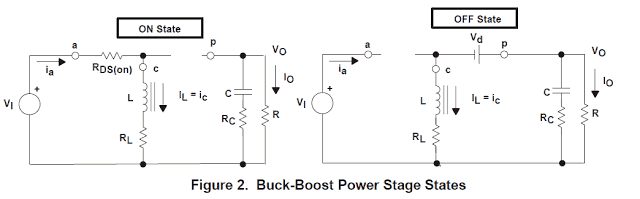 The period of the ON condition is D �� TS = TON in which D is the duty cycle, fixed by the drive circuit, depicted in form of a ratio of the switch ON period to the period of a single full switching sequence, Ts.
The length of the OFF state is known as TOFF.
Because one can find just a couple of conditions per switching cycle for continuous conduction mode, TOFF is equal to (1D) �� TS.
The magnitude (1D) is occasionally called D��.
These periods are presented together with the waveforms in Figure 3.
The period of the ON condition is D �� TS = TON in which D is the duty cycle, fixed by the drive circuit, depicted in form of a ratio of the switch ON period to the period of a single full switching sequence, Ts.
The length of the OFF state is known as TOFF.
Because one can find just a couple of conditions per switching cycle for continuous conduction mode, TOFF is equal to (1D) �� TS.
The magnitude (1D) is occasionally called D��.
These periods are presented together with the waveforms in Figure 3.
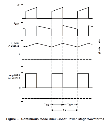 Looking at Figure 2, in the course of the ON state, Q1 offers a reduced resistance, RDS(on), from its drain to source and manifests a smaller voltage drop of VDS=IL �� RDS(on).
Additionally there is a little voltage drop across the dc resistance of the inductor equal to IL �� RL.
Thereby, the input voltage, VI, minus deficits, (VDS + IL �� RL), is put on across the inductor, L.
CR1 is OFF within this period as it would be reverse biased.
The inductor current, IL, passes from the input supply, VI, by way of Q1 and to ground.
In the course of the ON state, the voltage put on across the inductor is constant and the same as VI VDS IL �� RL.
Following the polarity norm for the current IL presented in Figure 2, the inductor current boosts due to the executed voltage.
Furthermore, because the applied voltage is fundamentally consistent, the inductor current rises linearly.
This boost in inductor current in the course of TON is drawn out in Figure 3.
The level by which the inductor current boosts is generally determined by utilizing a form of the well-known formula:
Looking at Figure 2, in the course of the ON state, Q1 offers a reduced resistance, RDS(on), from its drain to source and manifests a smaller voltage drop of VDS=IL �� RDS(on).
Additionally there is a little voltage drop across the dc resistance of the inductor equal to IL �� RL.
Thereby, the input voltage, VI, minus deficits, (VDS + IL �� RL), is put on across the inductor, L.
CR1 is OFF within this period as it would be reverse biased.
The inductor current, IL, passes from the input supply, VI, by way of Q1 and to ground.
In the course of the ON state, the voltage put on across the inductor is constant and the same as VI VDS IL �� RL.
Following the polarity norm for the current IL presented in Figure 2, the inductor current boosts due to the executed voltage.
Furthermore, because the applied voltage is fundamentally consistent, the inductor current rises linearly.
This boost in inductor current in the course of TON is drawn out in Figure 3.
The level by which the inductor current boosts is generally determined by utilizing a form of the well-known formula:
 The inductor current rise in the course of the ON status is presented as:
 This magnitude, ��IL(+), is termed the inductor ripple current.
Furthermore observe that through this interval, every bit of the output load current comes in by the output capacitor, C.
With reference to Figure 2, while Q1 is OFF, it offers an increased impedance from its drain to source.
Consequently, because the current running in the inductor L is unable to adjust instantly, the current switches from Q1 to CR1. As a result of the reducing inductor current, the voltage across the inductor reverses polarity until rectifier CR1 turns into forward biased and flips ON.
The voltage connected across L turns into (VO Vd IL �� RL) in which the magnitude, Vd, is the forward voltage drop of CR1. The inductor current, IL, at this point passes from the output capacitor and load resistor arrangement via CR1 and to the negative line.
Observe that the alignment of CR1 and the path of current circulation in the inductor signifies that the current running in the output capacitor and load resistor grouping leads to VO to be a minus voltage.
In the course of the OFF state, the voltage connected across the inductor is stable and the same as (VO Vd IL �� RL).
Preserving our likewise polarity convention, this connected voltage is minus (or reverse in polarity from the connected voltage in the course of the ON time), due to the fact that the output voltage VO is negative.
Therefore, the inductor current lowers throughout the OFF time.
Furthermore, because the connected voltage is basically steady, the inductor current reduces linearly.
This reduction in inductor current in the course of TOFF is outlined in Figure 3.
The inductor current reduction through the OFF situation is provided by:
This magnitude, ��IL(+), is termed the inductor ripple current.
Furthermore observe that through this interval, every bit of the output load current comes in by the output capacitor, C.
With reference to Figure 2, while Q1 is OFF, it offers an increased impedance from its drain to source.
Consequently, because the current running in the inductor L is unable to adjust instantly, the current switches from Q1 to CR1. As a result of the reducing inductor current, the voltage across the inductor reverses polarity until rectifier CR1 turns into forward biased and flips ON.
The voltage connected across L turns into (VO Vd IL �� RL) in which the magnitude, Vd, is the forward voltage drop of CR1. The inductor current, IL, at this point passes from the output capacitor and load resistor arrangement via CR1 and to the negative line.
Observe that the alignment of CR1 and the path of current circulation in the inductor signifies that the current running in the output capacitor and load resistor grouping leads to VO to be a minus voltage.
In the course of the OFF state, the voltage connected across the inductor is stable and the same as (VO Vd IL �� RL).
Preserving our likewise polarity convention, this connected voltage is minus (or reverse in polarity from the connected voltage in the course of the ON time), due to the fact that the output voltage VO is negative.
Therefore, the inductor current lowers throughout the OFF time.
Furthermore, because the connected voltage is basically steady, the inductor current reduces linearly.
This reduction in inductor current in the course of TOFF is outlined in Figure 3.
The inductor current reduction through the OFF situation is provided by:
 This magnitude, ��IL(), can be termed the inductor ripple current.
In stable state situations, the current rise, ��IL(+), in the course of the ON time and the current reduction through the OFF time, ��IL(), has to be identical.
Or else, the inductor current could offer an overall boost or reduction from cycle to cycle that would not be a stable condition circumstance.
Thus, both of these equations may be equated and worked out for VO to acquire the continuous conduction form buck-boost voltage change-over affiliation:
Determining for VO:
This magnitude, ��IL(), can be termed the inductor ripple current.
In stable state situations, the current rise, ��IL(+), in the course of the ON time and the current reduction through the OFF time, ��IL(), has to be identical.
Or else, the inductor current could offer an overall boost or reduction from cycle to cycle that would not be a stable condition circumstance.
Thus, both of these equations may be equated and worked out for VO to acquire the continuous conduction form buck-boost voltage change-over affiliation:
Determining for VO:
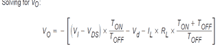 As well as, substituting TS for TON + TOFF, and employing D = TON/TS and (1D) = TOFF/TS, the steady-state equation for VO is:
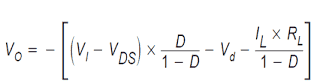 Observe that in simplifying the above, TON + TOFF is supposed to be similar to TS.
This can be genuine only for continuous conduction mode as we are going to discover in the discontinuous conduction mode evaluation.
An essential scrutiny ought to be made at this point:
Fixing the two values of ��IL on par with each other is exactly equal to leveling out the volt-seconds on the inductor.
The volt-seconds employed on the inductor is the product of the voltage employed and the period that the voltage is applied for.
This can be the most effective way to estimate unidentified magnitudes for example VO or D with regards to common circuit parameters, and this approach is going to be used frequently within this article.
Volt-second stabilize on the inductor is a natural requirement and ought to be perceived at least additionally as Ohms Law.
In the above equations for ��IL(+) and ��IL(), the output voltage was implicitly supposed to be consistent without any AC ripple voltage throughout the ON time and the OFF period.
This is an accepted simplification and entails a couple of individual outcomes.
First, the output capacitor is believed to be sizable adequately that its voltage conversion is minimal.
Second, the voltage the capacitor ESR is in addition deemed to be minimal.
Such assumptions are legitimate since the AC ripple voltage will definitely be significantly lower than the DC portion of the output voltage.
The above voltage alteration for VO demonstrates the truth that VO could be tweaked by fine-tuning the duty cycle, D.
This connection draws near zero as D arrives near zero and rises without destined as D draws near 1. A typical simplification consider VDS, Vd, and RL are tiny enough to neglect.
Establishing VDS, Vd, and RL to zero, the above formula simplifies noticeably to:
Observe that in simplifying the above, TON + TOFF is supposed to be similar to TS.
This can be genuine only for continuous conduction mode as we are going to discover in the discontinuous conduction mode evaluation.
An essential scrutiny ought to be made at this point:
Fixing the two values of ��IL on par with each other is exactly equal to leveling out the volt-seconds on the inductor.
The volt-seconds employed on the inductor is the product of the voltage employed and the period that the voltage is applied for.
This can be the most effective way to estimate unidentified magnitudes for example VO or D with regards to common circuit parameters, and this approach is going to be used frequently within this article.
Volt-second stabilize on the inductor is a natural requirement and ought to be perceived at least additionally as Ohms Law.
In the above equations for ��IL(+) and ��IL(), the output voltage was implicitly supposed to be consistent without any AC ripple voltage throughout the ON time and the OFF period.
This is an accepted simplification and entails a couple of individual outcomes.
First, the output capacitor is believed to be sizable adequately that its voltage conversion is minimal.
Second, the voltage the capacitor ESR is in addition deemed to be minimal.
Such assumptions are legitimate since the AC ripple voltage will definitely be significantly lower than the DC portion of the output voltage.
The above voltage alteration for VO demonstrates the truth that VO could be tweaked by fine-tuning the duty cycle, D.
This connection draws near zero as D arrives near zero and rises without destined as D draws near 1. A typical simplification consider VDS, Vd, and RL are tiny enough to neglect.
Establishing VDS, Vd, and RL to zero, the above formula simplifies noticeably to:
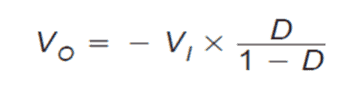 A less complicated, qualitative method to picture the circuit operation would be to contemplate the inductor as a power storage part.
Each time Q1 is on, energy is poured over the inductor.
While Q1 is off, the inductor supplies back part of its energy to the output capacitor and load.
The output voltage is regulated by establishing the on-time of Q1. For instance, by raising the on-time of Q1, the quantity of power sent to the inductor is amplified.
Additional energy is subsequently sent to the output in the course of the off-time of Q1 causing an increase in the output voltage.
In contrast to the buck power stage, the typical magnitude of the inductor current is not the same as the output current.
To associate the inductor current to the output current, looking at Figures 2 and 3, observe that the inductor current to the output solely while in the off state of the power stage.
This current averaged over a whole switching sequence is the same as the output current since the approximate current in the output capacitor ought to be equivalent to zero.
The connection between the average inductor current and the output current for the continuous mode buck-boost power stage is provided by:
A less complicated, qualitative method to picture the circuit operation would be to contemplate the inductor as a power storage part.
Each time Q1 is on, energy is poured over the inductor.
While Q1 is off, the inductor supplies back part of its energy to the output capacitor and load.
The output voltage is regulated by establishing the on-time of Q1. For instance, by raising the on-time of Q1, the quantity of power sent to the inductor is amplified.
Additional energy is subsequently sent to the output in the course of the off-time of Q1 causing an increase in the output voltage.
In contrast to the buck power stage, the typical magnitude of the inductor current is not the same as the output current.
To associate the inductor current to the output current, looking at Figures 2 and 3, observe that the inductor current to the output solely while in the off state of the power stage.
This current averaged over a whole switching sequence is the same as the output current since the approximate current in the output capacitor ought to be equivalent to zero.
The connection between the average inductor current and the output current for the continuous mode buck-boost power stage is provided by:
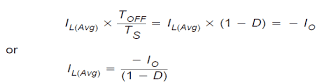 Another significant viewpoint is the fact the typical inductor current is proportional to the output current, and because the inductor ripple current, ��IL, is unrelated of output load current, the minimal and the highest values of the inductor current follow the average inductor current precisely.
As an example, if the average inductor current declines by 2A owing to a load current reduction, in that case the lowest and highest values of the inductor current reduce by 2A (considering continuous conduction mode is preserved).
The forgoing evaluation was for the buck-boost power stage functionality in continuous inductor current mode.
The following segment is a explanation of steady-state functionality in discontinuous conduction mode.
The primary outcome is a derivation of the voltage conversion relationship for the discontinuous conduction mode buck-boost power stage.
Another significant viewpoint is the fact the typical inductor current is proportional to the output current, and because the inductor ripple current, ��IL, is unrelated of output load current, the minimal and the highest values of the inductor current follow the average inductor current precisely.
As an example, if the average inductor current declines by 2A owing to a load current reduction, in that case the lowest and highest values of the inductor current reduce by 2A (considering continuous conduction mode is preserved).
The forgoing evaluation was for the buck-boost power stage functionality in continuous inductor current mode.
The following segment is a explanation of steady-state functionality in discontinuous conduction mode.
The primary outcome is a derivation of the voltage conversion relationship for the discontinuous conduction mode buck-boost power stage.
Buck-Boost Steady-State Discontinuous Conduction Mode Evaluation
We at this point examine what occurs where the load current is reduced and the conduction mode shifts from continuous to discontinuous. Remember for continuous conduction mode, the average inductor current trails the output current, i.e. in case the output current reduces, in that case so will the average inductor current. Besides, the lowest and highest peaks of the inductor current pursue the average inductor current accurately. In case the output load current is decreased below the fundamental current level, the inductor current would be zero for a part of the switching sequence. This would be apparent from the waveforms presented in Figure 3, because the peak to peak level of the ripple current is unable to alter with output load current. In a buck-boost power stage, if the inductor current tries to below zero, it simply halts at zero (because of the unidirectional current movement in CR1) and continues there until the outset of the subsequent switching action. This working mode is known as discontinuous conduction mode. A power stage working of buck boost circuit in discontinuous conduction format possesses three distinctive states through every switching cycle in contrast to 2 states for continuous conduction format. The inductor current state in which the power stage is at the periphery between continuous and discontinuous setting is presented in Figure 4. In this the inductor current simply collapses to zero while the following switching cycle commences just after the current attains zero. Observe that the values of IO and IO(Crit) are laid out in Figure 4 since IO and IL include opposing polarities.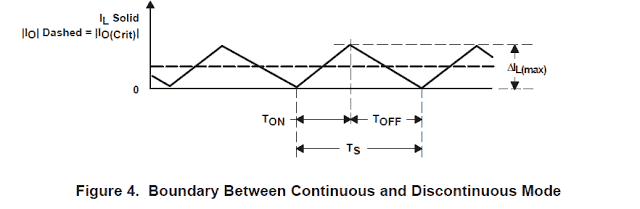 Farther lowering of output load current sets the power stage into discontinuous conduction pattern.
This condition is drawn in Figure 5.
The discontinuous mode power stage frequency response is pretty dissimilar from the continuous mode frequency response which is presented in the Buck-Boost Power Stage Modeling segment.
Additionally, the input to output connection is fairly diverse as presented down this page derivation:
Farther lowering of output load current sets the power stage into discontinuous conduction pattern.
This condition is drawn in Figure 5.
The discontinuous mode power stage frequency response is pretty dissimilar from the continuous mode frequency response which is presented in the Buck-Boost Power Stage Modeling segment.
Additionally, the input to output connection is fairly diverse as presented down this page derivation:
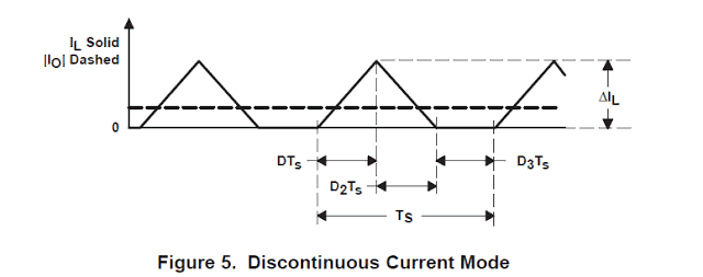 To start the derivation of the discontinuous conduction mode buck-boost power stage voltage change-over ratio, recollect that you have three distinctive states that the converter considers through discontinuous conduction mode functionality.
The ON State is when Q1 is ON and CR1 is OFF.
The OFF State is when Q1 is OFF and CR1 is ON.
The IDLE condition is when each Q1 and CR1 are OFF.
The initial two conditions are very much like the continuous mode situation and the circuits of Figure 2 are relevant apart from that TOFF �� (1D) �� TS.
The rest of the switching sequence is the IDLE state.
Additionally, the DC resistance of the output inductor, the output diode forward voltage drop, as well as the power MOSFET ON-state voltage drop are usually supposed to be minute enough to overlook.
The time period of the ON state is TON = D �� TS where D is the duty cycle, fixed by the control circuit, indicated as a ratio of the turn on time to the time of one full switching sequence, Ts.
The length of the OFF state is TOFF = D2 �� TS.
The IDLE period is the rest of the switching pattern which is presented as TS TON TOFF = D3 �� TS.
These periods are put up with the waveforms in Figure 6.
Without checking the comprehensive description, the equations for the inductor current rise and drop are enumerated below.
The inductor current rise in the course of the ON state is issued by:
To start the derivation of the discontinuous conduction mode buck-boost power stage voltage change-over ratio, recollect that you have three distinctive states that the converter considers through discontinuous conduction mode functionality.
The ON State is when Q1 is ON and CR1 is OFF.
The OFF State is when Q1 is OFF and CR1 is ON.
The IDLE condition is when each Q1 and CR1 are OFF.
The initial two conditions are very much like the continuous mode situation and the circuits of Figure 2 are relevant apart from that TOFF �� (1D) �� TS.
The rest of the switching sequence is the IDLE state.
Additionally, the DC resistance of the output inductor, the output diode forward voltage drop, as well as the power MOSFET ON-state voltage drop are usually supposed to be minute enough to overlook.
The time period of the ON state is TON = D �� TS where D is the duty cycle, fixed by the control circuit, indicated as a ratio of the turn on time to the time of one full switching sequence, Ts.
The length of the OFF state is TOFF = D2 �� TS.
The IDLE period is the rest of the switching pattern which is presented as TS TON TOFF = D3 �� TS.
These periods are put up with the waveforms in Figure 6.
Without checking the comprehensive description, the equations for the inductor current rise and drop are enumerated below.
The inductor current rise in the course of the ON state is issued by:
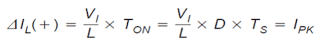 The ripple current quantity, ��IL(+), is likewise the peak inductor current, Ipk since in discontinuous mode, the current begins at 0 every cycle.The inductor current reduction in the course of the OFF state is presented by:
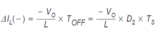 Just like the continuous conduction mode situation, the current rise, ��IL(+), in the course of the ON time and the current reduction while in the OFF time, ��IL(), are identical.
Thus, both of these equations could be equated and addressed for VO to acquire the initial of two equations to be utilized to solve for the voltage conversion ratio:
Just like the continuous conduction mode situation, the current rise, ��IL(+), in the course of the ON time and the current reduction while in the OFF time, ��IL(), are identical.
Thus, both of these equations could be equated and addressed for VO to acquire the initial of two equations to be utilized to solve for the voltage conversion ratio:
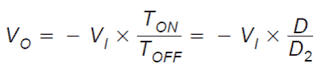 Next we determine the output current (the output voltage VO divided by the output load R).
It is the average over one switching sequence of the inductor current at that time when CR1 becomes conductive (D2 �� TS).
Next we determine the output current (the output voltage VO divided by the output load R).
It is the average over one switching sequence of the inductor current at that time when CR1 becomes conductive (D2 �� TS).
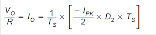 Here, replace the connection for IPK (��IL(+)) into the above equation to acquire:
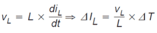 Therefore we have two equations, the one for the output current (VO divided by R) just derived and the one for the output voltage, both of them with regards to VI, D, and D2. We at this point unravel each formula for D2 as well as fix the two equations on par with one another.
Utilizing the resultant equation, an illustration for the output voltage, VO, could be procured.
The discontinuous conduction mode buck-boost voltage transformation affiliation is written by:
Therefore we have two equations, the one for the output current (VO divided by R) just derived and the one for the output voltage, both of them with regards to VI, D, and D2. We at this point unravel each formula for D2 as well as fix the two equations on par with one another.
Utilizing the resultant equation, an illustration for the output voltage, VO, could be procured.
The discontinuous conduction mode buck-boost voltage transformation affiliation is written by:
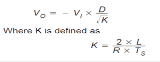 The above connection displays one of the main dissimilarities between the two conduction modes.
For discontinuous conduction mode, the voltage change relationship is a function of the input voltage, duty cycle, power stage inductance, the switching frequency, and the output load resistance.
For continuous conduction mode, the voltage change-over connection is just influenced by the input voltage and duty cycle.
In traditional applications, the buck-boost power stage is run in a choice between continuous conduction mode or discontinuous conduction mode.
For a specific usage, one conduction mode is chosen while the power stage was made to sustain the identical mode.
The above connection displays one of the main dissimilarities between the two conduction modes.
For discontinuous conduction mode, the voltage change relationship is a function of the input voltage, duty cycle, power stage inductance, the switching frequency, and the output load resistance.
For continuous conduction mode, the voltage change-over connection is just influenced by the input voltage and duty cycle.
In traditional applications, the buck-boost power stage is run in a choice between continuous conduction mode or discontinuous conduction mode.
For a specific usage, one conduction mode is chosen while the power stage was made to sustain the identical mode.
How to Convert 12V DC to 220V AC
The article explains a very simple method of acquiring 220V AC from a 12v DC source. The idea utilizes inductor/oscillator based boost topology with the help of the IC 555. We are quite familiar about inverters which convert a DC potential to higher AC potentials at mains levels. However these units involve complex and expensive configurations for acquiring the required outputs. A much simpler approach of achieving the above results is by employing a oscillator mosfet boost converter circuit. If the waveforms are not critical for your applications this method can be a lot simpler and cheaper to implement.Circuit Operation
Referring to the circuit diagram below, we see that the entire idea is based upon the versatile, evergreen IC 555. Here it's configured in its standard astable multivibrator mode for generating the required pulses at a frequency determined by the resistors 4k7, 1k and the capacitor 680pF. The duty cycle may be appropriately adjusted byexperimentingthe 1K resistor. The output is received at pin#3 of the IC, which is fed to the gate of an N-channel mosfet. When power is switched ON, the positive pulses emanating from pin#3 switch ON the mosfet into full conduction. During the above periods the 12V high current potential is pulled to ground via the coil by the mosfet. As we all know inductors always try to oppose instant changes in current polarity through it, therefore during the negative pulses when the mosfet remains switched OFF, forces the coil to dump the stored potential in it in the form of high voltage EMF pulse into the output. This voltage may be equal to 220V and gives rise to the required potential at the shown outlet of the circuit. The above straightforward operation is repeated continuously at the given frequency providing a sustained 220VAC at the output. The BC547 and its base network is introduced for limiting the output voltage to the required degree. For example if the required output is 220V, the 47K preset may beadjustedsuch that the220V mark never exceeds, irrespective of the coil back emf rate or the input voltage fluctuations. The mosfet can be any 30V, 50 amp type, for example aNTD4302 may be used. The coil wire should be thick enough to hold up to 30 or more amps.Circuit Diagram
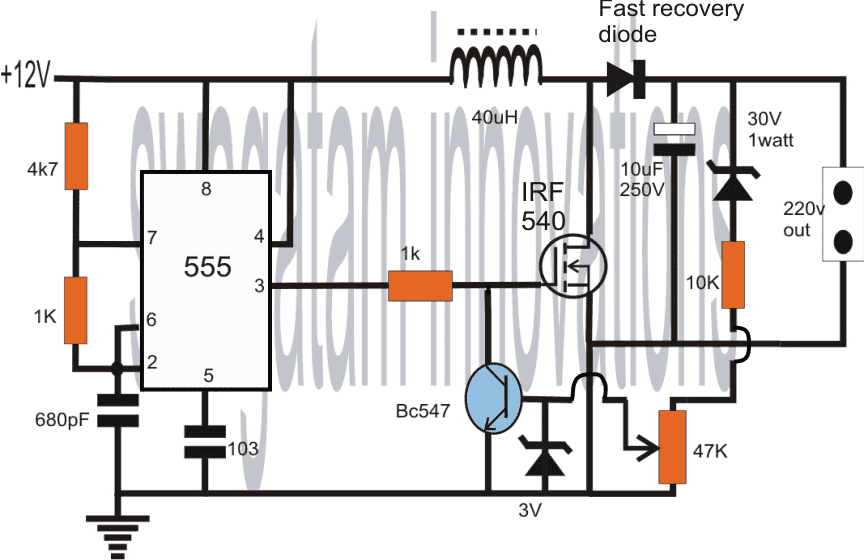
IC 555 Pinout Details
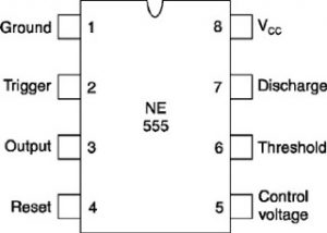
Mosfet IRF 540 Pinout Details
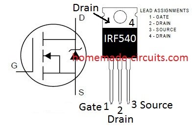
5V, 12V Buck Converter Circuit SMPS 220V
This step down buck converter will convert a 220V AC input from mains supply to 5V or 12V or 24V DC with 90% efficiency. The proposed buck converter is an SMPS circuit using the IC VIPer12A fromSTMicroelectronics. The circuit uses negligible number of externalcomponentsyet is able to operate directly from mains AC input.
The Buck Converter Design
Looking at the given circuit diagram we see that the input stage incorporates a surge limiting resistor which quite acts like a fuse, a diode for rectifying the AC, and an LC filter network for further filtration of the DC riples. The LC filter employed here ensures better DC stabilization and enhanced EMI response. The capacitor Cin1 may be introduced for furtherreinforcingthe EMI functionality. The IC VIPer12A becomes the main PWM processor device which single handedly performs the entire buck conversion in the circuit.Main Features
The main specifications of the configuration may be understood as follows: AC input voltage Vinac 80 - 285Vac Output current Iout 30mA Output current Iout 250mA Output voltage Vout1 +24��10%V Output voltage Vout2 +5V��5% Switching frequency 60 kHz Output Power ~ 1WHow it Works
The circuit facilitates two outputs, rhe 24V output is achieved through a buck converter configuration while the 5V output via fly back mode. The feedback voltage to the IC is acquired from Vout1 for the required regulation of the output, this supply is also applied to the IC Vdd pin. The above wiring becomes possible by using a single high voltage diode and just one capacitor, to be precise D1 and C3, making the connections and costing much simpler. The employed inductor L consists of two windings which are coupled across with each other over a common ferrite core. The winding are done through appropriate turn ratios, where N1 = 200 turns and N2 = 60 turns. Both these are wound over a PANASONIC ELC10D152E ferrite core material.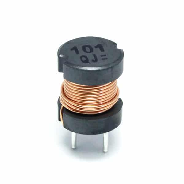 Zener diodes z1 and z2 are installed in order to safeguard the outputs against over voltages.
A dummy load resistor is fixed across Vout1 so that appropriate regulation can be executed over both the outputs during open load situations.
Though the addition of the above resistor affects the efficiency a bit, it superbly improves voltage regulation response of the circuit.
The rectifier diodes fixed at the output are fast response fast recovery types.
D1 is a high voltage diode as it might be subjected to high reverse voltages delivered by the DC bus voltage......
D2 is a normal diode.
Zener diodes z1 and z2 are installed in order to safeguard the outputs against over voltages.
A dummy load resistor is fixed across Vout1 so that appropriate regulation can be executed over both the outputs during open load situations.
Though the addition of the above resistor affects the efficiency a bit, it superbly improves voltage regulation response of the circuit.
The rectifier diodes fixed at the output are fast response fast recovery types.
D1 is a high voltage diode as it might be subjected to high reverse voltages delivered by the DC bus voltage......
D2 is a normal diode.
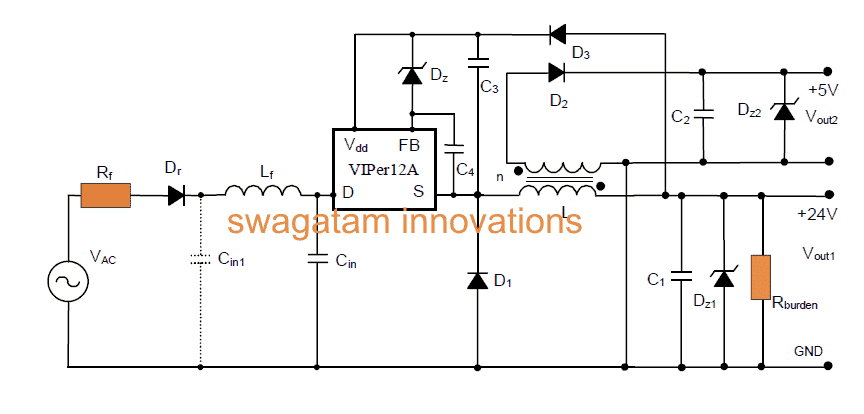
Parts List for the proposed simple SMPS buck converter circuit:
Rr = 10W 1/2W Rf = 10KW 1/4W R(load) = 4.7kW 1/4W Cin = 4.7 ��F, 450V Electrolytic Capacitor C1 = 33 ��F, 50V Electrolytic Capacitor C2 = 100 ��F, 16V Electrolytic Capacitor C3 = 1 ��F, 25V Electrolytic Capacitor C4 = 22 nF Ceramic capacitor Dr = Diode 1N4007 D1 = Diode BA159 (fast) D2 = Diode 1N4148 (fast) D3 = Diode 1N4004 Dz = 22V Zener Dz1 = 27V Zener Dz2 = 5.6V Zener L 1 = 0.5 mH Lf = 470 ��H Inductor IC1 = STMicroelectronics VIPer12ADIP PCB Design and Component Layout of the above explained SMPS buck converter circuit using IC VIPer12A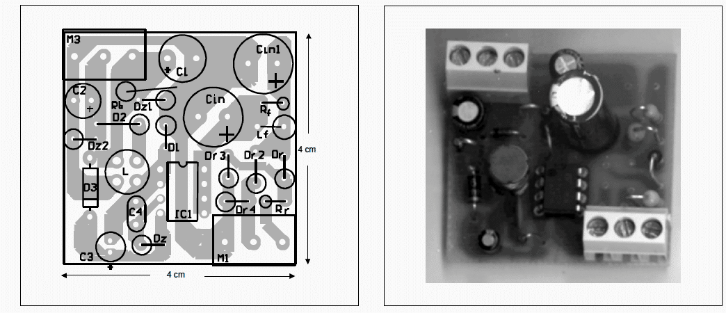 Complete Article can be foundhere
How Switch Mode Power Supply (SMPS) Circuits Work
SMPS is the acronym of the word Switch Mode Power Supply. The name clearly suggests that the concept has something or entirely to do with pulses or switching of the employed devices. Let's learn how SMPS adapters work for converting mains voltage to a lower DC voltage.Advantage of SMPS Topology
In SMPS adapters the idea is to switch the mains input voltage into theprimarywinding of a transformer so that a lower value DC voltage may be obtained at the secondary winding of the transformer. However the question is, the same can be done with an ordinary transformer, so what is the need of such complicatedconfigurationwhen the functioning can be simply implemented though ordinary transformers? Well, the concept was developed precisely for eliminating the use of heavy and bulky transformers with much efficient versions of SMPSpowersupply circuits. Though the principle of operation is quite the similar, the results are hugely different. Our mainsvoltageis also a pulsating voltage or an AC which is normally fed into the ordinary transformer for the required conversions, but we cannot make the transformer smaller in size even with currentas lowas 500 mA. The reason behind this is the very low frequency involved with our AC mains inputs. At 50 Hz or 60Hz, the value is tremendously low for implementing them into high DC currents outputsusingsmaller transformers. This is because as the frequencydecrease, the eddy current losses with the transformermagnetizationincreases, which results in huge lose of current through heat and subsequently the whole process becomes very inefficient. To compensate the above loss, relatively larger transformer cores are involved with relevant degree of wire thickness, making the entire unit heavy andcumbersome. A switch mode power supply circuit tackles this issue very cleverly. If lower frequencyincreaseseddycurrent losses, means anincreasein the frequency would do just the opposite. Meaning if the frequency isincreased, thetransformercould be made muchsmalleryet would provide higher current attheiroutputs.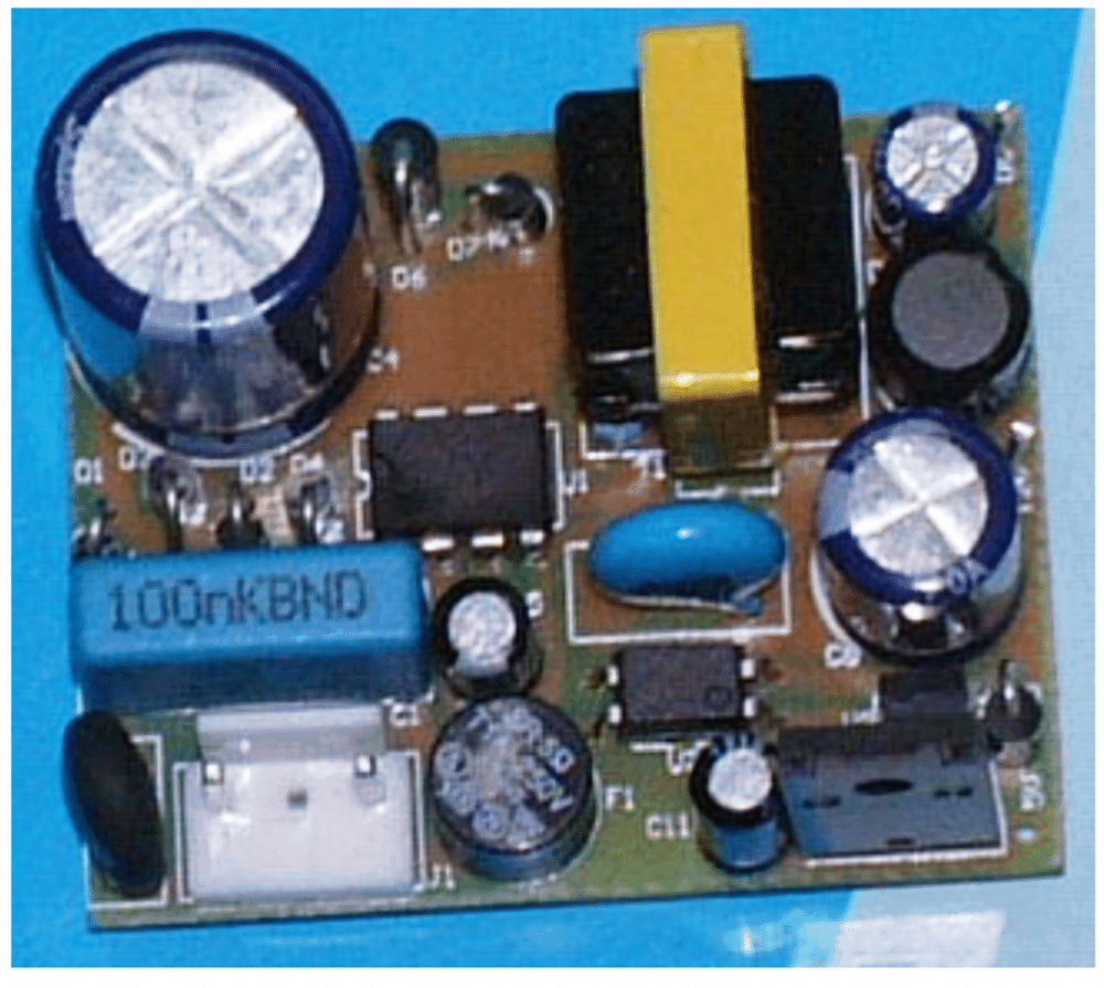 That's exactly what we do with an SMPS circuit.
Let's understand thefunctioningwith the following points:
That's exactly what we do with an SMPS circuit.
Let's understand thefunctioningwith the following points:
How SMPS adapters work
In a switch mode power supply circuit diagram, the input AC is first rectified and filtered to produce relevant magnitude of DC. The above DC is applied to an oscillator configuration comprising a high voltage transistor or a mosfet,riggedto a well dimensioned small ferrite transformer primary winding. The circuit becomes a self oscillating type of configuration which starts oscillating at some predetermined frequency set by other passive components like capacitors and resistors. The frequency is usually above 50 Khz. This frequencyinducesan equivalentvoltageand current at the secondary winding of the transformer,determinedby the number ofturnsand the SWG of the wire. Due the involvement of high frequencies, eddy current losses become negligibly small and high current DC output becomes derivable through smaller ferrite cored transformers and relatively thinner wire winding. However the secondary voltage will also be at the primary frequency, therefore it is once again rectified and filtered using a fast recovery diode and a high value capacitor. The result at the output is a perfectly filtered low DC, which can be used effectively for operating any electronic circuit. Inmodernversions of SMPS, hi-end ICs are employed instead of transistors at the input. The ICs are equipped with abuiltin high voltage mosfet for sustaining high frequency oscillations and many other protection features.What Built-in Protections do SMPS Have
These ICs have adequate built in protection circuitry like avalanche protection, over heat protection and output over voltage protection and also a burst mode feature. Avalanche protection ensures that the IC does not get damaged during power switch ON current in rush. The over heat protection ensures that the IC is automaticallyshutsoff if the transformer is not wound correctly and draws more current from the IC making it dangerously hot. The burst mode is an interesting feature included with the modern SMPS units. Here, the output DC is fed back to asensinginput of the IC. If due to some reason, normally due to wrong secondary winding or selection of resistors the output voltage rises above a certain predetermined value, the IC shuts off the input switching and skips the switching into intermittent bursts. This helps tocontrolthe voltage at the output and also the current at the output. The feature also ensures that if the the output voltage is adjusted to some high point and the outputisnot loaded, the IC switches to burst mode making sure that the unit is operated intermittently until the output getsadequatelyloaded, this saves power of the unit when in standby conditions or when the outputisnotoperative. The feedback from the output section to the IC is implemented via an opto-coupler so that the output remains well aloof from the input high voltage mains AC, avoiding dangerous shocks.2 Easy Voltage Doubler Circuits Discussed
In this article we learn how to make a couple of simple DC to DC voltage doubler circuits using a single IC 4049 and IC 555 along with a few other passive components. If you are wondering how a simple IC 555 can be used for making a powerful voltage doubler circuit, then this article will help you to understand the details and construct the design at home.What's a Voltage Doubler
A voltage doubler is a circuit that uses only diodes and capacitors for raising an input voltage into a higher voltage output, twice the magnitude of the input. If you are new to voltage doubler concept and desire to learn the concept in-depth, we have a good elaborate article in this website explaining different voltage multiplier circuits for your reference. Voltage multiplier concept was first discovered and used practically byBritish and Irish physicistsJohn Douglas CockcroftandErnest Thomas Sinton Walton, hence it is also called theCockcroft�CWalton (CW) generator. A good example of a voltage multiplier design can be studied through this article which exploits the concept for generating ionized air for purifying air in homes. A voltage doubler circuit is also a form of voltage multiplier where the diode/capacitor stage is restricted to a couple of stages only, so that the output is allowed to produce a voltage that may be twice of the supply voltage. Since all voltage multiplier circuits mandatorily require an AC input or a pulsating input, an oscillator circuit becomes essential for accomplishing the results.IC 555 Pinout Details

Circuit Diagram of Voltage Doubler using IC 555
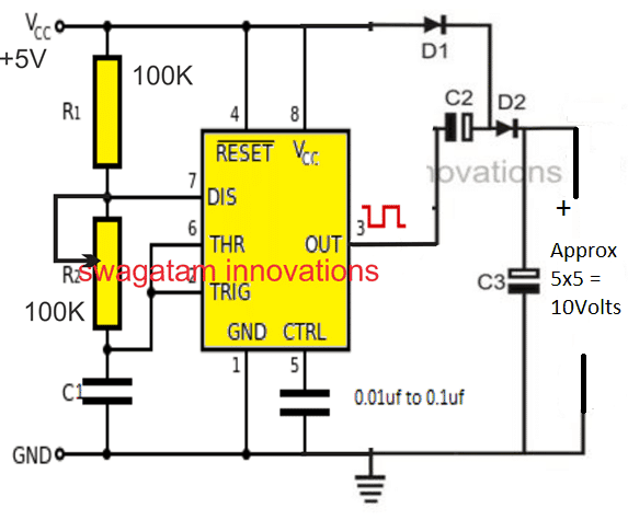 Referring to the above example, we can see an IC 555 circuit configured as an astable multivibrator stage, which is actually a form of oscillator, and is designed to produce a pulsating DC (ON/OFF) at its output pin#3.
If you recall, we had discussed an LED torch circuit in this website, which quite identically uses a voltage doubler circuit, albeit the oscillator section is created using an IC 4049 gates.
Basically, you can replace the IC 555 stage with any other oscillator circuit and still get the voltage doubling effect.
However using IC 555 has a slight benefit since this IC is able to generate more current than any other IC based oscillator circuit without using any external current amplifier stage.
Referring to the above example, we can see an IC 555 circuit configured as an astable multivibrator stage, which is actually a form of oscillator, and is designed to produce a pulsating DC (ON/OFF) at its output pin#3.
If you recall, we had discussed an LED torch circuit in this website, which quite identically uses a voltage doubler circuit, albeit the oscillator section is created using an IC 4049 gates.
Basically, you can replace the IC 555 stage with any other oscillator circuit and still get the voltage doubling effect.
However using IC 555 has a slight benefit since this IC is able to generate more current than any other IC based oscillator circuit without using any external current amplifier stage.
How the Voltage Doubler Stage Operates
As can be seen in the above diagram, the actual voltage multiplication is implemented by the D1, D2, C2, C3 stage, which are configured as a half-bridge 2-stage voltage multiplier network. Simulating this stage in response to the IC 555's pin#3 situation can be a little difficult, and I am still struggling to get it running in my brain correctly. As per my mind simulation, the working of the mentioned voltage doubler stage can be explained as given in the following points: When the IC output pin#3 is in its low logic or ground level, D1 is able to charge C2, since it is able to get forward biased through C2 and pin#3's negative potential, also simultaneously C3 is charged via D1, and D2. Now, in the next instant as soon as pin#3 becomes at high logic or at the positive supply potential, things get slightly confusing. Here C2 is unable to discharge via D1, so we have a supply level output from D1, from C2, and from C3 also. Many of the other online sites say that at this point the stored voltage inside C2, and the positive from D1 is supposed to combine with the output of C3 to produce a doubled voltage, however that does not make sense. Because, when voltages combine in parallel, the net voltage does not increase. The voltages must combine in series to cause the desired boosting or the doubling effect. The only logical explanation that can be derived is, when pin#3 becomes high, C2's negative being at the positive level and its positive end also held at the supply level, it is forced to produce a reverse charge pulse which adds up with the C3 charge, causing a instantaneous potential spike having a peak voltage twice that of the supply level. If you have a better or technically more correctexplanation, please do feel fre to explain it through your comments.How much Current?
Pin#3 of the IC is assigned to deliver a maximum of 200mA current, therefore the maximum peak current can be expected to be at this 200mA level, however the peaks will get narrower depending on the C2, C3 values. Higher value capacitors might enable fuller current transfer across the output, therefore make sure the C2, C3 values are optimally selected, around 100uF/25V will be just enoughA Practical Application
Although a voltage doubler circuit can be useful for many electronic circuit applications, a hobby based application could be to illuminate a high voltage LED from a low voltage source, as shown below: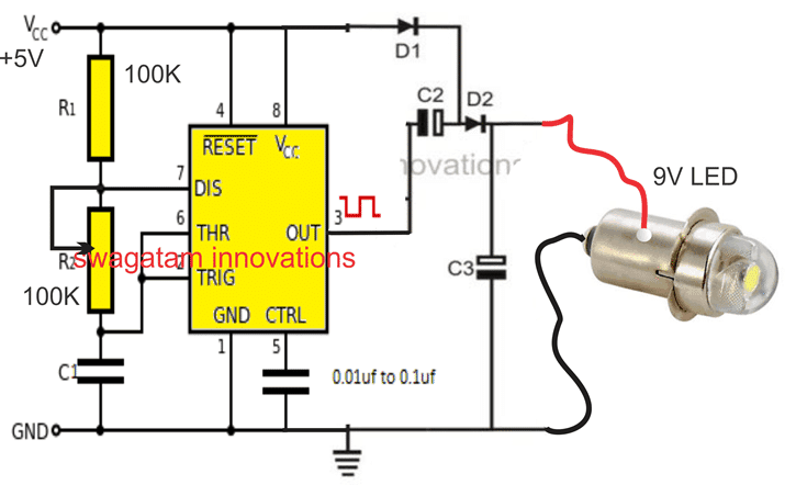 In the above circuit diagram we can see how the circuit is used for illuminating a 9V LED bulb from a 5V supply source, which would normally be impossible if the 5V was directly applied on the LED.
Relation between Frequency, PWM and the Voltage Output Level
The frequency in any voltage doubler circuit is not crucial, however faster frequency will help you to get better results than slower frequencies. Similarly for the PWM range, the duty cycle should be roughly 50%, narrower pulses will cause lower current at the output, whereas too wide pulses will not allow the relevant capacitors to discharge optimally, again resulting in an ineffective output power. In the discussed IC 555 astable circuit, the R1 can be anywhere between 10K and 100K, this resistor along with the C1 decides the frequency. C1 consequently can be anywhere between 50nF to 0.5uF. R2 will fundamentally enable you to control the PWM, therefore this can be made into a variable resistor through a 100K pot.Another 555 Voltage Doubler
The circuit shown below is another IC 555 based DC voltage-doubler, which produces a DC output voltage that is almost double the supply voltage.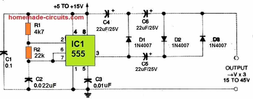 The output of the 555 is connected to a voltage-doubler circuitryconsisting of capacitors C4 and C5, as well as diodes D1 and D2. As long as the output is unloaded, the circuitprovides an output that is about nearly twice the supply voltage.
The exact value of the output is:
Vout = 2 x Vpeak (Vfd1 + Vfd2)
Where Vpeak representsthe squarewave generator's peak output voltage, and Vfd1 and Vfd2 indicatethe multiplier diodes D1 and D2's forward voltage drops (approximately 600 millivolts).
Assoon as the circuit's output is loaded, the output voltage drops.
Any DC source between 5 and 15 volts might operate with the voltage doubler circuit shown above.
This can give voltage outputs across a range of roughly 10 to 30 volts due to its voltage doubling effect.
Applying additional multiplier stages to the circuit will result in a higher voltage.
The output of the 555 is connected to a voltage-doubler circuitryconsisting of capacitors C4 and C5, as well as diodes D1 and D2. As long as the output is unloaded, the circuitprovides an output that is about nearly twice the supply voltage.
The exact value of the output is:
Vout = 2 x Vpeak (Vfd1 + Vfd2)
Where Vpeak representsthe squarewave generator's peak output voltage, and Vfd1 and Vfd2 indicatethe multiplier diodes D1 and D2's forward voltage drops (approximately 600 millivolts).
Assoon as the circuit's output is loaded, the output voltage drops.
Any DC source between 5 and 15 volts might operate with the voltage doubler circuit shown above.
This can give voltage outputs across a range of roughly 10 to 30 volts due to its voltage doubling effect.
Applying additional multiplier stages to the circuit will result in a higher voltage.
Using IC 4049 NOT gates
The following CMOS IC based circuit can be used for doubling any DC source voltage (up to 15 V DC). The presented design will double any voltage between 4 to 15 V DC and will be able to operate loads at current not more then 30 mA. As can be seen in the diagram, this DC voltage doubler circuit employs just a single IC 4049 for achieving the proposed result. IC 4049 Pinouts
Circuit Operation
The IC 4049 has six gates in all which are all effectively for generating the discussed voltage doubling actions. Two of the gates out of the six are configured as an oscillator. The extreme left of the diagram shows the oscillator section. The 100 K resistor and the 0.01 capacitor form the basic frequency determining components. A frequency is imperatively required if a voltage stepping actions needs to be implemented, therefore here too the involvement of an oscillator becomes necessary. These oscillation become useful for initialing the charging and discharging a set of capacitors at the output which amounts to the multiplying of the voltage across the set of capacitors in a such a way that the result becomes twice the applied supply voltage. However the voltage from the oscillator cannot be preferably applied directly to the capacitors, rather its done through a group of gates of the IC arranged in a parallel way. These parallel gates together produce a good buffering to the applied frequency from the generator gates so that the resultant frequency is stronger with respect to current and does not falter with relatively higher loads at the outputs. But still keeping the specifications of a CMOS IC in mind the output current handling capacity cannot be expected to be larger than 40 mA. Higher loads than this will result in the deterioration of the voltage level toward the supply level. The output capacitor values can be increased to 100uF for getting reasonably higher efficiency levels from the circuit. With 12 volts as the supply input to the IC, an output of around 22 volts may be acquired from this IC 4049 based voltage doubler circuit.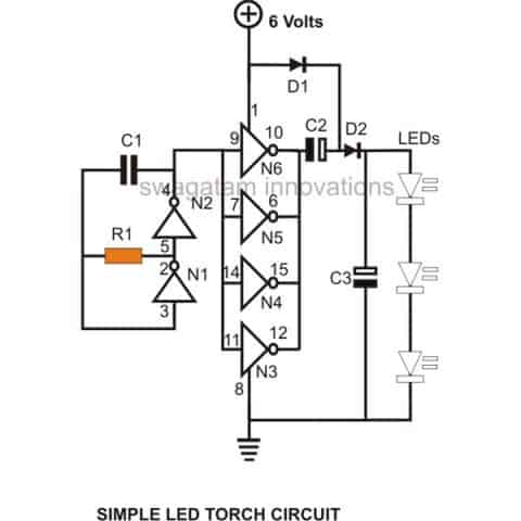 Parts List
R1 = 68K,
C1 = 680pF,
C2, C3 = 100 uF/ 25V,
D1, D2 =1N4148,
N1, N2, N3, N4 = IC 4049,
LEDs White = 3 nos.
Parts List
R1 = 68K,
C1 = 680pF,
C2, C3 = 100 uF/ 25V,
D1, D2 =1N4148,
N1, N2, N3, N4 = IC 4049,
LEDs White = 3 nos.
Dummy Load Circuit for Testing Power Supplies
Suppose you have a 10 amp power supply and you want to confirm the 10 amp output through some sort of dummy load which can absorb 10 amp current. For this, you would have to build a 10 amp current sink using many high watt resistors connected in series and parallel. This arrangement could be hugely cumbersome and bulky. Instead, an adjustable transistorized dummy load circuit could do the job more efficiently by sinking the 10 amp current from the power supply and help the user to confirm that the power supply is actually able to deliver the intended 10 amp current. In this circuit, the high power transistors could be optimized and adjusted to sink or shunt the power supply current at some specific rate, which could be adjusted through a potentiometer, thus making the procedure very smooth and accurate. You can test power supplies and related devices at maximum peak output current without resorting to arrays of power resistors, using this dummy load circuit, which is nothing but a simple transistor current sink circuit. Without the need of costly non-inductive resistors, an adjustable current sink permits the load to be adjusted fast across a large range, irrespective of the voltage source. And thus removes the need to fiddle with power resistors each time the voltage and/or output current characteristicsof the powersupplies or devices under test are changed, for example during the testing ofpower supplies.How the Circuit Works
The current load is shared by transistors QL1 and QL2, which are balanced by their emitter resistors R1 and R2, whose quantities should be in the.2 ohm to.1 ohm range. Therefore, simply byconnecting power transistors QL1 and QL2, we may raise the circuit's current-load capacity to whatever we want, restricted by just the transistors' absolute limits. A few common junkbox-type load transistors, like for exampleNPN 2N3055s, may come witha VCE of 60 volts, an Ic at about 15 amps, and power dissipation of 115 watts. Thus, everything else being identical, while assessing low-voltage supplies, power dissipation is the most important characteristic to consider.
For instance, you may be able tohandle 30 volts at 20 amps constantly by connecting four ordinaryjunkbox 2N5885s in parallel with four 0.1 ohm, 5 watt emitter resistors.
2N5885s have similar characteristics to 2N3055s, although with a power dissipation in the 200-watt range, and with a collector current Ic of about 25 amperes.
Furthermore, high-voltage power supply could also be tested if transistors having high VCE specifications are incorporated.
In either circumstances, the bases of the load transistors (QL1 and QL2) are governed by a predetermined "adjust" current througha battery or DC power.
This preset current regulates the current flowing via Q1, that controls the base current of load transistors QL1 and QL2.
PRESET ADJ., potentiometer R3, controls the highest allowable current draw, whereas CURRENT ADJ., potentiometer R4, sets the current range.
Transistor Q1 is a typical TIP35A, an NPN silicon power transistor that may withstand voltages up to 350 and also has a rated collector current of one amp.
In this dummy load circuit, any NPN silicon power transistors featuringa hfe of 50-150 would suffice.
2N5682 is yet another possibility for Q1.
Thus, everything else being identical, while assessing low-voltage supplies, power dissipation is the most important characteristic to consider.
For instance, you may be able tohandle 30 volts at 20 amps constantly by connecting four ordinaryjunkbox 2N5885s in parallel with four 0.1 ohm, 5 watt emitter resistors.
2N5885s have similar characteristics to 2N3055s, although with a power dissipation in the 200-watt range, and with a collector current Ic of about 25 amperes.
Furthermore, high-voltage power supply could also be tested if transistors having high VCE specifications are incorporated.
In either circumstances, the bases of the load transistors (QL1 and QL2) are governed by a predetermined "adjust" current througha battery or DC power.
This preset current regulates the current flowing via Q1, that controls the base current of load transistors QL1 and QL2.
PRESET ADJ., potentiometer R3, controls the highest allowable current draw, whereas CURRENT ADJ., potentiometer R4, sets the current range.
Transistor Q1 is a typical TIP35A, an NPN silicon power transistor that may withstand voltages up to 350 and also has a rated collector current of one amp.
In this dummy load circuit, any NPN silicon power transistors featuringa hfe of 50-150 would suffice.
2N5682 is yet another possibility for Q1.
How to Setup
The setting levelof the PRESET potentiometer, R3, is defined by the beta of the transistors employed, and the higher-load threshold is decided by the load transistors. The maximum load is adjusted by potentiometer R3, and the current level isreadily adjusted if an optional ammeter or external ammeter is installed. To begin with, tweakthe current PRESET potentiometer R3 to maximum and the CURRENT ADJ. potentiometer R4 to the lowest resistance. Next, measure the currentconsumed from an appropriate power source hooked upto this active dummy load and adjust the current-preset to achievethe maximum load you intend to implement; and that's all there is to it! The maximum power dissipation required is determined by the number and kind of load transistors employed. Therefore, if you drivea lot of voltage at an excessivecurrent for an extended length of time, don't exceedtheir maximum power dissipation otherwise you mightfry your load transistors. Alternatively , if you allow your load transistor temperatureto normalizefor a short amount of time, it might perhaps allow you to exceed theircontinuous power dissipation limit. Try implementinga moderate duty cycle which does not gobeyond their optimal working temperature. This project does not provide a components list since doing so would undermine the objective of the project, which is to be made from junk box parts. A 9-volt transistor battery was selected sinceit works likeanoptimum control power source which is electrically isolated-while lowering expenses to a bare minimum.IC 7805 Variable Power Supply Circuit [5V to 15V]
Although, a 7805 IC is mostly used as a fixed 5 V voltage regulator, it is possible to configure a 7805 IC to produce a variable output from 5 V and higher, depending up the input DC supply. In this post we discuss a simple circuit network which can be used for getting an adjustable output voltage between 5 V and 15 V through the IC 7805. The following figure shows the circuit diagram of the variable IC 7805 power supply. The simple design provides you a range of voltages (which can be adjusted as desired by the user). The circuit can also generate up to 1 amp output current which is a much bigger than most small AC adapters are rated to produce.
How the Circuit Works
As indicated in the diagram, the output voltage is ranged between 5 V and 15 V DC. As soon as power button S1 is switched on, the mains AC is applied to the transformer T1. This transformer steps down the voltage around 18 VAC, which is subsequently full-wave rectified through a bridge-rectifier BR1. The capacitor C1 is employed to clean up and smooth the 100 Hz ripple generated by the bridge rectifier, and the charge stored in C1 is delivered to the voltage regulator. The remaining capacitors, C2 and C3, behave like bypass capacitors which further condition the voltage delivered to the IC 1 which is a 7805 voltage regulator. In general the majority of the circuits working with a 7805 regulators apply them for generating a fixed 5 volts. However, in circuit design explained here, enables the output from the IC 7805 to be adjusted roughly between 5 V and 15 V (although, as mentioned, 15 volts. The following description helps us to understand how the proposed IC 7805 variable power supply works: Typically, an input supply voltage greater than 5 V is fed to the input pin of the IC. The ground pin of the 7805 can be normally seen as connected to the ground line so that it is able to regulate the OUT pin to 5 volts level which is 5 V higher than voltage level at the ground pin held at 0 V. However , when ground pin of the 7805 is lifted by a certain voltage over the ground level, this lifted potential will add up with the 5 V and cause the output to increase by a level which is lifted at the ground pin of the IC. In this IC 7805 adjustable power supply circuit, the center ground pin of the IC is fixed through a resistive divider created from a resistor R1 along with R2 which is a variable resistor or through one of the selectable resistors ranging from R4 to R9. Each of these six resistors configures the output to a certain precise voltage level as determined by the values of the resistors. When the potentiometer R2 is employed it enables an entirely adjustable output from 5 V and the maximum 15 V. Let's imagine that switch S2 is selected to use the potentiometer R2 in the voltage divider network. Here, as the 7805 IC1 attempts to keep up precisely 5 volts at its output, the voltage at center ground pin of the IC could be adjusted by varying the resistance of the lower half of the resistive divider via R2. Consequently, the output voltage is consistently switched to 5 V plus the voltage developed by the R1/ R2 divider network at the center pin of the IC1. As the process causes the output of the IC1 7805's to increase, this also causes the voltage at the resistive divider junction to increase, which in turn forces the output voltage to increase, and and process keeps going on and on, until the input voltage "exhausts". This is exactly how the 7805 regulator gets converted from a fixed 5 V regulator into a variable output regulator. When you toggle the button S2 so that it hooks up with the center GND pin of the IC1 and the rotary switch S3, and S3 is used to select one of the resistors from R4 to R9, these resistors now take the position as the bottom half of the resistive divider. The values of these resistors between R4 and R9 can be selected in a manner that the output can be fixed to generate precise voltages from 5 V, 6 V, 7.5V, 9 V, 12 V, or 15 V DC. The following table can be used for selecting the fixed resistors to obtain the respective variable outputs from the IC 7805
5 V to 13 V Using 7805 and Op Amp
The next variable 7805 circuit is similar to the above design, but it is more reliable due to the involvement of an op amp. The voltage is obtained through R2 and RV1, that are wired across the stabilized output to ensure that regulation efficiency is not considerably reduced. This voltage seems to be too large in impedance to operate pin 3 of IC1, therefore a basic buffer amplifier based on IC2 is used to bridge the two. R1 represents a ballast resistor. The CA3140 device was selected for the IC2 slot because its output is able to go down to within a few millivolts of the negative supply voltage.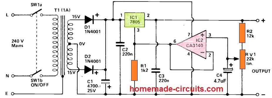 C1 polarity is mistakenly shown in the reversed direction...
In contrast, several options, including the 741C device, providea minimum voltage of no less than 2V, resulting in the lowest output voltage of 7V from the 7805, which becomes inappropriate for use with TTL and several other forms of circuits.
A traditional push-pull type step-down, rectifier, and filteringcircuit provides the input voltage for the regulator circuit.
C2 and C3 contribute to the circuit's reliability and therefore should be placed as near to the regulator IC as feasible.
C4 smooths the voltage at the RV1 wiperand contributes to the circuit's low output noise level of around a millivolt.
The output drops by only 70mV between zero load and maximum power, indicating excellent regulation.
The 7805 IC includes current limiting functionality that prohibits output currents over 1A from flowing.
C1 polarity is mistakenly shown in the reversed direction...
In contrast, several options, including the 741C device, providea minimum voltage of no less than 2V, resulting in the lowest output voltage of 7V from the 7805, which becomes inappropriate for use with TTL and several other forms of circuits.
A traditional push-pull type step-down, rectifier, and filteringcircuit provides the input voltage for the regulator circuit.
C2 and C3 contribute to the circuit's reliability and therefore should be placed as near to the regulator IC as feasible.
C4 smooths the voltage at the RV1 wiperand contributes to the circuit's low output noise level of around a millivolt.
The output drops by only 70mV between zero load and maximum power, indicating excellent regulation.
The 7805 IC includes current limiting functionality that prohibits output currents over 1A from flowing.
SCR Voltage Regulator Circuit
In this post we will discuss how to build a highly efficient voltage regulator circuit using an SCR and some other external components. This SCR voltage regulator circuit being a switching kind of regulator is more efficient than the normal 3 pin voltage regulators, or the transistor zener based series pass regulators circuits.How the Circuit Works
The following figure exhibits the circuit of an SCR based regulated power supply. The only parts necessary for the regulation process are the SCR, R1, and the zener. When power is first switched on, the filter capacitor C1 is in the discharged condition such that its cathode is at 0 V potential.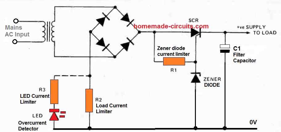 The positive half cycle waveform going out from the bridge rectifier causes the gate current for the SCR to pass through the resistor R1, which triggers ON the SCR.
As soon as the SCR switched ON it starts charging the C1 filter capacitor.
When the positive half - cycle ends the SCR quickly turns OFF.
As soon as the next positive half cycle arrives from the bridge, the same process repeats, charging the filter capacitor C1 until the voltage has almost reached the zener breakover voltage.
As we can clearly understand, the maximum positive voltage that can arise at the gate of the SCR gate is established by the zener value.
Therefore, it means, during the above process a time comes when C1 is able to charge only up to the zener level beyond which the SCR gate is unable derive anymore positive potential, with reference to its cathode.
At this specific stage the SCR is unable to sustain its firing anymore and C1 cannot charge any further.
The filter capacitor C1 discharges through the load, using the amount of power supplied from the transformer.
The moment the next positive cycle arrives the SCR gate turns yet again positive, and fires, charging the C1 filter capacitor.
A couple of half cycles from the bridge are enough to lift the C1 voltage adequately to stop additional firing of the SCR.
As a result the SCR triggers as essential to maintain the C1 capacitor in the "topped up" condition.
How many times the SCR has to trigger specifically depends on the current rating of the load which is being consumed from the input supply.
The positive half cycle waveform going out from the bridge rectifier causes the gate current for the SCR to pass through the resistor R1, which triggers ON the SCR.
As soon as the SCR switched ON it starts charging the C1 filter capacitor.
When the positive half - cycle ends the SCR quickly turns OFF.
As soon as the next positive half cycle arrives from the bridge, the same process repeats, charging the filter capacitor C1 until the voltage has almost reached the zener breakover voltage.
As we can clearly understand, the maximum positive voltage that can arise at the gate of the SCR gate is established by the zener value.
Therefore, it means, during the above process a time comes when C1 is able to charge only up to the zener level beyond which the SCR gate is unable derive anymore positive potential, with reference to its cathode.
At this specific stage the SCR is unable to sustain its firing anymore and C1 cannot charge any further.
The filter capacitor C1 discharges through the load, using the amount of power supplied from the transformer.
The moment the next positive cycle arrives the SCR gate turns yet again positive, and fires, charging the C1 filter capacitor.
A couple of half cycles from the bridge are enough to lift the C1 voltage adequately to stop additional firing of the SCR.
As a result the SCR triggers as essential to maintain the C1 capacitor in the "topped up" condition.
How many times the SCR has to trigger specifically depends on the current rating of the load which is being consumed from the input supply.
High Efficiency Output
You will find a couple of notably interesting characteristics of this type SCR based voltage regulator circuits. Firstly the circuit provides a high degree of efficiency due to minimal power loss that are commonly found in either the series or the shunt type regulators. The second great feature is that you are able to get a quick indication of the current that's being consumed by the load. The second feature could be implemented by hooking up a LED in series with a limiter resistor R3 across the resistor R2, which acts like the load current limiter. The LED will start blinking whenever the SCR triggers and therefore the blinking rate of the LED will directly correspond with the load current and indicate if the load has exceeded the current limit.Parts List for 1 Amp SCR Power Supply
Transformer = 0-12V/1 amp Bridge Rectifier = 1N5402 x 4 diodes SCR = C106 (on heatsink) Zener Diode = As per the required output voltage R1, R2 = 1 K 1/4 W R2 = 3 Ohm 3 wattHow to Design a Bench Power Supply Circuit
In this post we discuss how an effective and efficient, yet very cheap, and stabilized bench power supply can be designed by any electronic hobbyist for safely testing all types electronic projects and prototypes.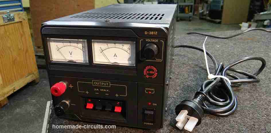 The main features that a bench power supply must have are:
Should be built with cheap and easily available components
Should be flexible with its voltage and current ranges, or simply must include the facility of a variable voltage and variable current outputs.
Should be over-current and over-load protected.
Should be easily reparable, in case a problem arises.
Should be reasonably efficient with its power output.
Should facilitate easily customization as per a desired specification.
The main features that a bench power supply must have are:
Should be built with cheap and easily available components
Should be flexible with its voltage and current ranges, or simply must include the facility of a variable voltage and variable current outputs.
Should be over-current and over-load protected.
Should be easily reparable, in case a problem arises.
Should be reasonably efficient with its power output.
Should facilitate easily customization as per a desired specification.
General Description
The majority of the power supply designs thus far incorporate a linear series stabilizer. This bench power supply design uses a pass transistor which works like a variable resistor, regulated by a Zener diode. The series power supply system is the more popular, possibly due to the fact that it is a lot more efficient. Except of some minor loss in the Zener and feed resistor, noticeable loss only happens in the series pass transistor during the period it is supplying current to the load. However, one disadvantage of the series power supply system is that these do not provide any kind of output load short-circuit. Meaning, during output fault conditions the pass transistor may allow a large current to flow through it, eventually destroying itself and possibly the connected load also. That said, adding a short circuit protection to a series pass bench power supply can be quickly implemented through another transistors configured as a current controller stage. The variable voltage controller is achieved through a simple transistor, potentiometer feedback. The above two additions enables a series pass power supply to be highly versatile, rugged, cheap, universal, and virtually indestructible. In the following paragraphs we will briefly learn the designing of the various stages involved in a standard stabilized bench power supply.Easiest Transistor Voltage Regulator
A quick way of getting an adjustable output voltage is to hook up the base of the pass transistor with a potentiometer and Zener diode as shown in the figure below.Using a Feedback Loop
Although the above design is easy to build and very cheap, this type of approach doesn't offer great regulation of power at the the lower voltage levels. This is exactly why a feedback type control is normally employed to get an improved regulation throughout the entire voltage range, as demonstrated in the figure below.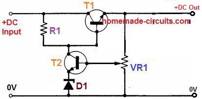 In this configuration, the base voltage of T1, and therefore output voltage, is controlled by the voltage drop across R1, mainly due to the current pulled by T2.
When the slider arm of the pot VR1 is at the ground side extreme end, T2 becomes cut off since now its base becomes grounded, allowing the only only voltage drop across R1 caused by the base current of T1. In this situation the output voltage at the T1 emitter is going to be almost same as the collector voltage, and can be given as:
VE = Vin - 0.7, here VE is the emitter side voltage of T1, and 0.7 is the standard forward voltage drop value for BJT T1 base/emitter leads.
So if the input supply is 15 V, the output can be expected to be:
VE = 15 - 0.7 = 14.3 V
Now, when the pot VR1 slider arm is moved to the upper positive end, will cause T2 to access the whole emitter side voltage of T1, which will cause T2 to conduct very hard.
This action will directly connect the zener diode D1 with R1. Meaning, now the base voltage VB of the T1 will be simply equal to the zener voltage Vz.
So the output will be:
VE = Vz - 0.7
Therefore, if the D1 value is 6 V, the output voltage can be expected to be just:
VE = 6 - 0.7 = 5.3 V, so the zener voltage decides the minimum possible output voltage that could be obtained from this series pass power supply when the pot is rotated at its lowest setting.
Although the above is easy and effective for making a bench power supply, it has a major disadvantage of not being short circuit proof.
That means, if the output terminals of the circuit is accidentally short circuited, or an over load current is applied, the T1 will quickly heat up and burn.
To avoid this situation, this circuit could be a simply upgraded by adding a current control feature as explained in the following section.
In this configuration, the base voltage of T1, and therefore output voltage, is controlled by the voltage drop across R1, mainly due to the current pulled by T2.
When the slider arm of the pot VR1 is at the ground side extreme end, T2 becomes cut off since now its base becomes grounded, allowing the only only voltage drop across R1 caused by the base current of T1. In this situation the output voltage at the T1 emitter is going to be almost same as the collector voltage, and can be given as:
VE = Vin - 0.7, here VE is the emitter side voltage of T1, and 0.7 is the standard forward voltage drop value for BJT T1 base/emitter leads.
So if the input supply is 15 V, the output can be expected to be:
VE = 15 - 0.7 = 14.3 V
Now, when the pot VR1 slider arm is moved to the upper positive end, will cause T2 to access the whole emitter side voltage of T1, which will cause T2 to conduct very hard.
This action will directly connect the zener diode D1 with R1. Meaning, now the base voltage VB of the T1 will be simply equal to the zener voltage Vz.
So the output will be:
VE = Vz - 0.7
Therefore, if the D1 value is 6 V, the output voltage can be expected to be just:
VE = 6 - 0.7 = 5.3 V, so the zener voltage decides the minimum possible output voltage that could be obtained from this series pass power supply when the pot is rotated at its lowest setting.
Although the above is easy and effective for making a bench power supply, it has a major disadvantage of not being short circuit proof.
That means, if the output terminals of the circuit is accidentally short circuited, or an over load current is applied, the T1 will quickly heat up and burn.
To avoid this situation, this circuit could be a simply upgraded by adding a current control feature as explained in the following section.
Adding Overload Short Circuit Protection
A simple inclusion of T3 and R2 enables the bench power supply circuit design to be 100% short-circuit proof and current controlled. With this design even an intentional shorting at the output will not cause any harm to the T1.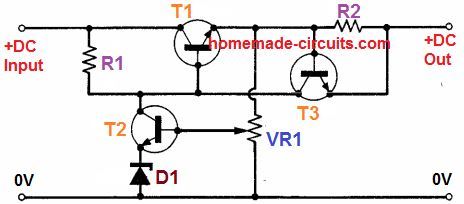 The working of this stage could be understood as follows:
As soon as the output current tends to go beyond the set safe value, a proportional amount of potential difference across R2 is developed, enough to switch ON transistor T3 hard.
With T3 switched ON causes T1 base to be joined with its emitter line, which instantly disables the T1 conduction, and this situation is maintained until the output short or overload is removed.
In this way T1 is safeguarded from any undesired output situation.
The working of this stage could be understood as follows:
As soon as the output current tends to go beyond the set safe value, a proportional amount of potential difference across R2 is developed, enough to switch ON transistor T3 hard.
With T3 switched ON causes T1 base to be joined with its emitter line, which instantly disables the T1 conduction, and this situation is maintained until the output short or overload is removed.
In this way T1 is safeguarded from any undesired output situation.
Adding a Variable Current Feature
In the above design, the current sensor resistor R2 can be a fixed value if the output is required to be a constant current output. However, a good bench power supply is supposed to have a variable range for both voltage and current. Considering this demand, the current limiter could be made adjustable simply by adding a variable resistor with the base of T3, as shown below: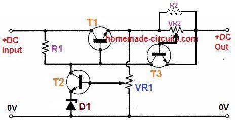 VR2 divides the voltage drop across R2 and thus allows the T3 to switch ON at a specific desired output current.
Calculating the Part Values
Let's start with the resistors, R1 can be calculated with the following formula: R1 = (Vin - MaxVE)hFE / Output Current Here, since MaxVE = Vin - 0.7 Therefore, we an simplify the first equation as R1 = 0.7hFE / Output Current VR1 can be a 10 k pot for voltages up to 60 V Current limiter R2 can be calculated as given below: R2 = 0.7 / Max Output Current Max output current should be selected 5 times lower than T1 maximum Id, if T1 is required to work without an heatsink. With a large heatsink installed on T1, the output current can be 3/4th of T1 Id. VR2 can be simply a 1k pot or preset. T1 should be selected as per the output current requirement. T1 Id rating should be 5 times more than the required output current, if it is to be operated without a heatsink. With a large heatsink installed, the T1 Id rating should be at least 1.33 times more than the required output current. The maximum collector/emitter or VCE for T1 should be ideally twice the value of the maximum output voltage specification. The value of zener diode D1 can be selected depending on the lowest or the minimum voltage output requirement from the bench power supply. The T2 rating will depend on the R1 value. Since the voltage at collector of T2 will be always equal to Vin, the VCE of T2 should be higher than the Vin or the input supply. The Id of T2 should be such it is able to handle the base current of T1, as determined by the value of R1 The same rules apply for T3 also. In general T2, and T3 can be any small signal general purpose transistor such as BC547 or maybe a 2N2222.Practical Design
Having understood all the parameters for designing a customized bench power supply, it's time to implement the data in a practical prototype, as shown below: You may find a few additional components introduced in the design, which are simply for enhancing the regulation capability of the circuit.
C2 is introduced to clean any residual ripple at the T1, T2 bases.
The T2 along with T1 forms a Darlington pair to increase the current gain of the output.
R3 is added to improve the zener diode conduction and therefore to ensure better overall regulation.
R8 and R9 are added to enable the output voltage to be regulated across fixed range, which are not critical.
The R7 sets the maximum current that can accessed at the output, which is:
I = 0.7 / 0.47 = 1.5 amps, and this appears quite low compared to the rating of the 2N3055 transistor.
Although this might keep the transistor super cool, it may possible to increase this value up to 8 amps if the 2N3055 is mounted over a large heatsink.
You may find a few additional components introduced in the design, which are simply for enhancing the regulation capability of the circuit.
C2 is introduced to clean any residual ripple at the T1, T2 bases.
The T2 along with T1 forms a Darlington pair to increase the current gain of the output.
R3 is added to improve the zener diode conduction and therefore to ensure better overall regulation.
R8 and R9 are added to enable the output voltage to be regulated across fixed range, which are not critical.
The R7 sets the maximum current that can accessed at the output, which is:
I = 0.7 / 0.47 = 1.5 amps, and this appears quite low compared to the rating of the 2N3055 transistor.
Although this might keep the transistor super cool, it may possible to increase this value up to 8 amps if the 2N3055 is mounted over a large heatsink.
Decreasing Dissipation to Increase Efficiency
The biggest disadvantage with any series transistor based linear regulator is the high amount transistor dissipation. And this happens when the input/output differential is high. Meaning, when the voltage is adjusted towards lower output voltage, the transistor has to work hard to control the excess voltage, which is then released as heat from the transistor. For example if the load is a 3.3 V LED, and input supply to the bench power supply is 15 V, then the output voltage has to be lowered to 3.3 V which is 15 - 3.3 = 11.7 V less. And this difference is converted to heat by the transistor, which could mean a efficiency loss of more than 70%. However, this problem can be simply solved by using a transformer with tapped voltage output winding. For example the transformer may have taps of 5 V, 7.5 V, 10 V, 12 V, and so on. Depending on the load the taps could be selected for feeding the regulator circuit. After this, the voltage adjustment pot of the circuit could be used for further adjusting the output level precisely to the desired value. This technique would increase the efficiency to a very high level, allowing the heatsink to the transistor to be smaller and compact.Op Amp Controlled Precision Bench Power Supply
The working procedure of the opamp controlled bench power supply circuit is fairly basic uncomplicated, since regulated power supplies can be simply as particular forms of feedback amplifier. In this concept, the R1 and R2 generate a refernce sample signal from the output supply, which is by another reference voltage created by D2. The resulting correction signal is supplied back through the 741 on the series pass transistor Q1. Observe that the circuit stability has been enhanced by providing the reference source R3 -D2 through the stabilized output rather than from the unstabilised input as is usually done inother bench power supplies.
To ensure that the circuit initiates as soon as switched on, a leakage resistance R4 is placed in parallel with the series pass device.
This means that the feedback loop begins to run as soon as power is switched ON.
Absolutely no regulation is sacrificed because of R4, since it is the general output which is sampled by R1 -R2, therefore, the impact of the ripple current moving through R4 gets adjusted through the feedback.
Observe that the circuit stability has been enhanced by providing the reference source R3 -D2 through the stabilized output rather than from the unstabilised input as is usually done inother bench power supplies.
To ensure that the circuit initiates as soon as switched on, a leakage resistance R4 is placed in parallel with the series pass device.
This means that the feedback loop begins to run as soon as power is switched ON.
Absolutely no regulation is sacrificed because of R4, since it is the general output which is sampled by R1 -R2, therefore, the impact of the ripple current moving through R4 gets adjusted through the feedback.
Making the Output Adjustable
The output may well be made adjustable by changing R1-R2 with a potentiometer, however in its existing layout, the circuit can't be forced to regulate under the zener voltage value of D2. When uninterrupted adjustment of the output voltage is necessary, the reference source R3-D2 should be furnished through the unregulated input, with accompanying minor lack of stability. The quantity of power the circuit is able to offer will be limited primarily by the current handling capacity of Q1 and the maximum power capacity of the unregulated supply.More Elaborate Bench Power Supply Circuit
A regulated bench Power supply are normally a useful gadget for any hobbyists or engineer. Despite the truth that IC based voltage regulators have become very easily accessible, a circuit only employing ordinary discrete components can be appealing. In order to save power, and to restrict the dissipation across the series regulator, the entire 0-30 V control range is further divided into 3 scaled-down voltage ranges. All the 3 ranges matches with a suitable secondary supply voltage (determined by the position of S1a) and a proper reference voltage (determined by S1b). So that you can get a consistent control of the output voltage to a minimum of0 V, a negative auxiliary supply needs to be added.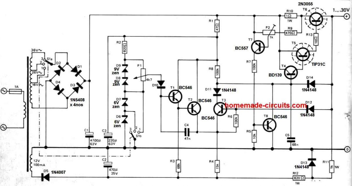 In this bench power supply circuit, this is extracted (by means of D5 and C2) via a different 12 V winding over the mains transformer.
A different option could be to incorporate an additional separate mains transformer.
The final results tested on the bench prototype are pretty decent: ��35 V mains voltage swing induced just ��25 mV swing of the output voltage, with full load 1 amp load attached to the output.
The A.C.
ripples of the output (hum) had been lower than 15 mV.
In this bench power supply circuit, this is extracted (by means of D5 and C2) via a different 12 V winding over the mains transformer.
A different option could be to incorporate an additional separate mains transformer.
The final results tested on the bench prototype are pretty decent: ��35 V mains voltage swing induced just ��25 mV swing of the output voltage, with full load 1 amp load attached to the output.
The A.C.
ripples of the output (hum) had been lower than 15 mV.
How it Works
The circuit functions in the following manner. A reference voltage, extracted through the zener diode(s) D6 -D9 and fixed using pot P1, is directed to the transistor T2 base by means of D10 and TI. T2 and T3 work like a differential amplifier; wherein the base of T3 receives the output voltage by means of DI2. This differential amplifier's output is applied, through D11, on the base of the combined series regulator made up of transistors T4, T5 and T6. Although the configuration might look a bit complex, it works like a typical regulator circuit; it maintains the output voltage virtually fixed over an extensive range of output currents. Transistors T7 and T8 along with connected parts form the current limiter stage. As soon as the voltage over R10 gets to a particular value (as fixed by P2) T7 begins conducting. This, consequently, causes transistor T8 to get biased and starts conducting; which reduces the base drive to transistor T4, and the situation decreases the output voltage hence the output current continues to be inside the predetermined boundary. When S1 is selected at position 1, that compares to an output range of 0-10 V, setting at 2 allows 10-20 V and adjusting at position 3 provides an output range of 20-30 V. P1 is used for tweaking the range as fixed by S1. The highest amount of output current can be established using pot P2. This P2 pot could be either pre-programmed to supply a highest output current of 1 A or employed like a variable output current control.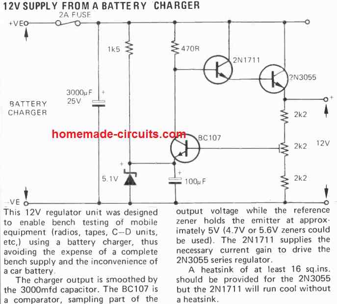
ATX Bench Power Supply
The following ATX bench power supply schematic image and prototype images were submitted by one of the avid readers of this blog, Mr. V.
How an Autotransformer Works �C How to Make
An autotransformer is an electrical transformer which consists of only a single, continuous, non-isolated winding, with tapped terminals across various points of the winding. The winding section between the taps that correspond to the mains AC is applied with the mains AC supply, while the remaining taps are used for getting the desired output voltages, in accordance with their winding ratios.Difference between Auto-transformer and the Step-Down Transformer
Typically in any standard step-down transformer we find two completely separate winding coils in the form of primary winding and secondary winding which are electrically isolated, but magnetically coupled to each other, as shown below.How to Make an Autotransformer
An autotransformer can be built using the same calculations as done for a normal step down transformer, except the secondary side. In fact making an autotransformer is much easier than the standard transformer, since here we can eliminate the secondary side winding, and use a single primary 300 V or 400 V continuous winding. So basically, follow all the steps explained in the following article, just skip the secondary side calculations, and implement only the primary 220 V side calculations. Winding Details Use 400 V for the primary volts, and 1 amp for the current. Once wound, you can attach taps across various intervals of the winding for acquiring the desired stepped up or stepped down voltages.Advantage and Disadvantage of an Auto-Transformer
In an autotransformer winding we normally have a minimum of 3 taps that are electrically terminated as outputs. Due to the fact that a single winding functions both as primary and secondary, autotransformers have better advantage of being smaller sized, lighter in weight, and more affordable than typical double-winding conventional step-down transformers. However, the disadvantage of an auto-tramsformer arises from the fact that none of its winding outputs are electrically isolated from AC mains, and may inflict a lethal shock when touched in swithed ON condition. Among the other advantages of autotransformers are its reduced leakage reactance, reduced losses, lower excitation current, and enhanced VA rating for any existing dimension and bulk.Application
A good example of an auto-transformer application is the tourist's voltage converter, that enables the traveler to connect 230 V appliances on 120 volt supply sources, or the opposite. An autotransformer having several output taps could be utilized to adapt the voltage at the end of an extended distribution circuit to counter any surplus voltage drop. The same situation could be automatically controlled through an electronic switching circuit. This is normally implemented through an AVR or an automatic voltage regulator, that automatically switches the various taps of the autotransformer through relays or triacs, for compensating the output in response to the changes in the line voltage.How it Works
As discussed above an autotransformer includes just one winding with 2 end terminals. There may be one or more terminals in between as tap points for getting the stepped up/down voltages across the tap points. In an auto-transformer we find the primary (input) and secondary (output) section of coils have their turns in common. This the part of the winding shared by the two primary and secondary is usually, known as the "Common Section". Whereas, the part of the winding extending away from this "common section" or the section that is not shared the primary and secondary is usually, known as the "Series Section".How to Calculate Voltage and Turns
Since the parameters voltage, current, and number of turns are proportionate in nature, the formula for calculating the ampere, voltage, and number of turns is governed by the simple universal formula given below: N1/N2 = V1/V2 = I1/I2 Let's check out the following example. It is essential to have at least two parameters in hand, to determine the remaining parameters while calculating an autotramsformer. Here, we have the number of turns and the voltage for the primary or the input side of the autotransformer, but we don't know the parameters on the output side or the load side.How to Calculate Current Rating
For calculating the current rating of the output side of an autotransformer, we must likewise know the current rating of the 220 V side winding. Let's say this is 2 amp, then the current across the N7 winding could be calculated using the following basic power formula: V1 x I1 = V7 x I7 220 x 2 = 300 x I7 I7 = 220 x 2 / 300 = 440 / 300 = 1.46 amps. This shows that in an auto transformer, or any type of transformer, the output wattage is ideally, almost equal to the input wattage.How to Convert a Regular Transformer to an Autotransformer
As discussed in the previous paragraphs of this article, a regular transformer incorporates two separate winding which are electrically isolated, forming the respective primary and the secondary sides. Since the two winding sides are electrically isolated, it becomes impossible to generate customized stepped up and stepped down AC mains voltages from these transformers, unlike an autotransformer. However, with a small modification in the unit, a regular transformer could be to a quite an extent be converted into an autotransformer. For this we simply need to interconnect the primary side wires with the secondary side wires in s format as shown in the following diagram:How IC LM337 Works: Datasheet, Application Circuits
In this post we will talk about the function of an interesting voltage regulator device: The LM337, which is basically the negative complementary device for the popular LM317 IC. Built with an adjustable 3-terminal negative voltage, this regulator can conveniently supply around 1.5 A with an output voltage range of -1.2 V to -37 V. It is incredibly easy to use and only needs two external resistors to configure the output voltage. Other cool features like internal current limiting, thermal shutdown and safe area compensation make the LM337 exceptionally robust. This device caters to the various application including local and on-the-board voltage regulation. Further, the LM337 can be employed to construct a programmable output regulator. If you attach a permanent resistor between the adjustment and the output, the electronic component is transformed into a precision current regulator. Being a complementary device for the IC LM317, which is a positive voltage regulator, the two are often used for making highly versatile dual voltage regulator power supplies.Main Features
Some of the main features of the IC LM337 are: An additional 1.5 A output current Variable output voltage in the range of -1.2 V and -37 V. Built-in thermal overload guard Built-in short circuit, over current-limiting and over heat protection. Output transistor safe-area return An unrestricted operation for high-voltage applications Alleviates stocking of permanent voltages Available in surface mount D2PAK and typical 3-Lead transistor pack Lead-free and RoHS compliantLM337 Variable Voltage Circuit Diagram
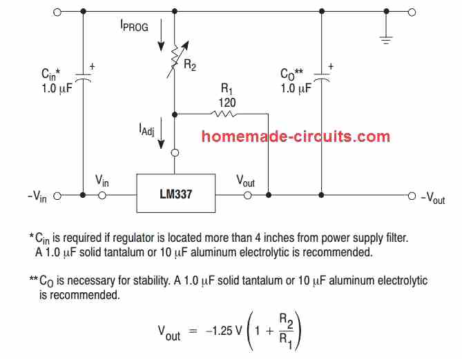
Pinout Details and Working
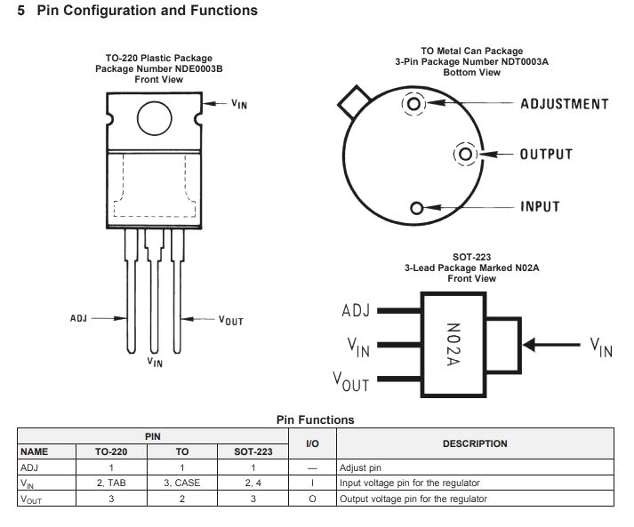
LM337 Absolute Maximum Rating
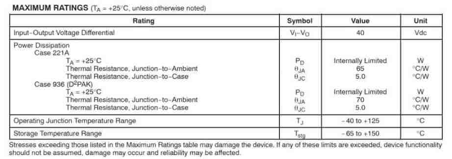
LM337 Electrical Characteristics
 In the Electrical Characteristics for the listed test scenarios, the product parametric performance is shown, unless otherwise described.
There are a few exceptions where product performance may not be displayed in the Electrical Characteristics, as given below.
Tlow to Thigh = 0�� to 125��C, for LM337T, D2T.
Tlow to Thigh = -40�� to +125��C, for LM337BT, BD2T.
Imax = 1.5 A, Pmax = 20 W
The load and line regulation are noted at a constant junction temperature.
There may be a change in VO due to the heating implications which is described under the Thermal Regulation specification.
Here, a low duty cycle pulse testing is used.
Cadj-, if applied, is linked between the adjustment pin and ground.
A temperature curve on the die is generated if there is power dissipation inside an IC voltage regulator.
This affects the separate IC components on the die and its effects can be mitigated by good circuit design and layout methods.
The effect of these temperature curves on the output voltage is given under Thermal Regulation, as the percentage of output change per watt of power change within a specified interval.
Because Long Term Stability cannot be quantified on every component before shipment, this specification serves as a rough estimate of average stability.
In the Electrical Characteristics for the listed test scenarios, the product parametric performance is shown, unless otherwise described.
There are a few exceptions where product performance may not be displayed in the Electrical Characteristics, as given below.
Tlow to Thigh = 0�� to 125��C, for LM337T, D2T.
Tlow to Thigh = -40�� to +125��C, for LM337BT, BD2T.
Imax = 1.5 A, Pmax = 20 W
The load and line regulation are noted at a constant junction temperature.
There may be a change in VO due to the heating implications which is described under the Thermal Regulation specification.
Here, a low duty cycle pulse testing is used.
Cadj-, if applied, is linked between the adjustment pin and ground.
A temperature curve on the die is generated if there is power dissipation inside an IC voltage regulator.
This affects the separate IC components on the die and its effects can be mitigated by good circuit design and layout methods.
The effect of these temperature curves on the output voltage is given under Thermal Regulation, as the percentage of output change per watt of power change within a specified interval.
Because Long Term Stability cannot be quantified on every component before shipment, this specification serves as a rough estimate of average stability.
Basic Circuit Operation and Working
The LM337 is a floating regulator with three terminals. It basically works by generating a precise -1.25 V reference (Vref) between its output and the regulation terminals. This reference voltage is transformed to a programming current (IPROG) by R, as shown in Figure 17. As a result, this constant current travels via R2 from the ground. The equation below describes the regulated output voltage: Vout = Vref ( 1 + R2/R1) + IAdj- R2 The LM337 can be used to regulate the adjustment terminal (IAdj-) to lower than 100 ��A and hold it constant, due to the fact that the current flowing into IAdj pin signifies an error term in the above formula.
In order to implement this, all idle state operating current is sent back to the output terminal.
This forces the need for a minimum load current.
As soon as the load current is at a lower level than this minimum, the output voltage will increase.
Moreover, because the LM337 works like a floating regulator, the most important characteristic that needs to perform is the voltage differential across the circuit.
Additionally, it is also crucial that operation at high voltages relative to ground is achievable.
The LM337 can be used to regulate the adjustment terminal (IAdj-) to lower than 100 ��A and hold it constant, due to the fact that the current flowing into IAdj pin signifies an error term in the above formula.
In order to implement this, all idle state operating current is sent back to the output terminal.
This forces the need for a minimum load current.
As soon as the load current is at a lower level than this minimum, the output voltage will increase.
Moreover, because the LM337 works like a floating regulator, the most important characteristic that needs to perform is the voltage differential across the circuit.
Additionally, it is also crucial that operation at high voltages relative to ground is achievable.
Load Regulation
The IC LM337 is versatile and will deliver an excellent load regulation, provided certain preventive measures are ensured for obtained best performance. One example is that the programming resistor (R1) must be attached as near as possible to the regulator chip, to reduce line voltage drops which can easily join in series with the reference potential, seriously affecting the regulation efficiency. The ground terminal of the R2 can be returned near the load ground to enable remote ground sensing and enhance load regulation.External Capacitors
We recommend employing a 1.0 ��F tantalum input bypass capacitor (Cin-) to minimize the sensitivity to the input line impedance. You can bypass the adjustment terminal to ground to enhance ripple rejection. This capacitor (Cadj) limits ripple from being boosted as the output voltage is adjusted towards higher levels. Using a 10 ��F capacitor can improve ripple rejection about 15 dB at 120 Hz when working with a 10 V application. An output capacitance (CO) is supplied by a tantalum or 10 ��F aluminium electrolytic capacitor is compulsory for stability. Choosing either one of them with non-reduced ESR (Equivalent Series Resistance) value is also a must. Low-ESR or capacitor rated with low ESR value and ceramic capacitors may lead to instability or permanent oscillations in the application.Protection Diodes
If you are using external capacitors with any regulator IC, you might want to heavily consider including protection diodes to avoid the capacitors from discharging via low current points into the regulator. As shown in Figure above, the LM337 with some suggested protection diodes for output voltages more than -25 V or high capacitance values (CO > 25 ��F, CAdj > 10 ��F).
Diode D1 stops CO from discharging through the IC in the event of an input short circuit.
Diode D2 safeguards capacitor CAdj discharging through the IC when an output short circuit occurs.
The combination of diodes D1 and D2 avoids CAdj from discharging via the IC if at all an input short circuit happens.
Reference: Datasheet
As shown in Figure above, the LM337 with some suggested protection diodes for output voltages more than -25 V or high capacitance values (CO > 25 ��F, CAdj > 10 ��F).
Diode D1 stops CO from discharging through the IC in the event of an input short circuit.
Diode D2 safeguards capacitor CAdj discharging through the IC when an output short circuit occurs.
The combination of diodes D1 and D2 avoids CAdj from discharging via the IC if at all an input short circuit happens.
Reference: Datasheet
Adjustable Switching Power Supply Circuit �C 50 V, 2.5 Amps
The explained variable switching power supply circuit is designed around the integrated switch mode power supply controller device Type L4960 from SGS. The main features of this switching regulator can be summarized from the following data:Main Features
Input voltage range: 9-50 VDC Output voltage variable from 5 to 40 V. Maximum accessible output current is: 2.5 Amps. Highest possible output power is: 100 Watts. Integrated soft-start circuitry. Stabilized internal reference level with ��4% margin Works with handful of external parts. Duty factor: 0-1. High efficiency, having �� up to 90%. Has an internal thermal overload protection. Includes an internal current limiter which ensures complete shortcircuit protection.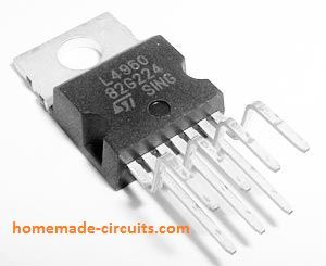 The pin specifications of the chip is shown in the following figure.
The L4964 is encased within a exclusive 15-pin package, designed to handle up to 4 A.
The pin specifications of the chip is shown in the following figure.
The L4964 is encased within a exclusive 15-pin package, designed to handle up to 4 A.
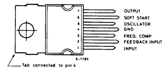 The working of the in-built soft start circuitry, and the current limiter, is highlighted through the below shown waveform drawings, respectively.
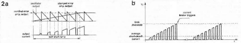 The over temperature shut off circuit in the L4960 is triggered as soon as the IC case temperature goes higher than 125 ��C.
For safety concerns , the suggested switch mode power supply circuit is recommended with transformer based layout.
The AC input voltage to the PCB is acquired from the mains transformer secondary winding, which means that the DC to the IC is at minimum 3 V above the necessary output voltage with the highest possible output current.
It's understandable that the transformer is essentially a toroidal model.
The over temperature shut off circuit in the L4960 is triggered as soon as the IC case temperature goes higher than 125 ��C.
For safety concerns , the suggested switch mode power supply circuit is recommended with transformer based layout.
The AC input voltage to the PCB is acquired from the mains transformer secondary winding, which means that the DC to the IC is at minimum 3 V above the necessary output voltage with the highest possible output current.
It's understandable that the transformer is essentially a toroidal model.
Circuit description
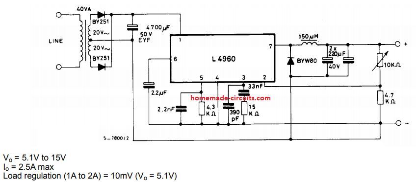 Simplified Schematic
The circuit diagrams above exhibit the mains transformer AC section design, and the DC switching power supply, correspondingly.
The AC voltage from the secondary side is goes to the individual inputs over the supply board, while the center tap is hooked up to ground line.
The unregulated input voltage, Ui for the IC comes through a full-wave rectifier circuit made up of a pair of 3 A diodes 1N5404, D1-D2, along with a filter capacitor, Ct.
Circuit consisting of R1-C3-C4 highlights the closed regulation loop gain.
Another circuit stage using C2 -R2, is configured to generate oscillator frequency of approximately 100 kHz.
The C5 capacitor C5 actually has two functions: this specifies the time of the soft start ramp as shown in the above waveform image, and also the average short-circuit current.
The feedback input of the L4962 is coupled to the output voltage divider R3 -R4 junction.
The output voltage, Uo, of the L4960 is determined using the following calculations
Uo =5.1[(R 3 + R4)/R3] given that Ui - Uo �� 3 V.
Note that the lowest value of Ui has to be 9 V.
we are able to get a fixed output voltage of 5.1 V (��4%) as soon as R3 is removed, and R4 changed with a short link.
If R3 is selected with a fixed value of 5K6, R4 individually decides the output voltage:
Uo =9 V: R4 = 4K3
Uo =12 V: R4 = 7K6
Uo =15 V: R4 = 10K
Uo =18 V: R4 = 14K
Uo =24 V: R4 = 20K
The design can be converted a variable switch mode power supply by using R3 = 6K8 and upgrading R3 with a 25K potentiometer.
Diode D3 is incorporated for protection of the IC.
This fast rectifier restricts the negative spikes at the inductor input side to a harmless 0.6 to 1 V for every switch off periods of the ICs internal output transistor.
If D3 was not there it would cause pin 7 potential of the IC to rise hazardously to many volts below the ground potential.
Inductor L1 along with the diode D3 and the capacitor C6 C7, acts like a buck converter for regulating the output in a switched mode, thereby causing much lower heat dissipation compared any other linear IC circuit such as LM338.
Simplified Schematic
The circuit diagrams above exhibit the mains transformer AC section design, and the DC switching power supply, correspondingly.
The AC voltage from the secondary side is goes to the individual inputs over the supply board, while the center tap is hooked up to ground line.
The unregulated input voltage, Ui for the IC comes through a full-wave rectifier circuit made up of a pair of 3 A diodes 1N5404, D1-D2, along with a filter capacitor, Ct.
Circuit consisting of R1-C3-C4 highlights the closed regulation loop gain.
Another circuit stage using C2 -R2, is configured to generate oscillator frequency of approximately 100 kHz.
The C5 capacitor C5 actually has two functions: this specifies the time of the soft start ramp as shown in the above waveform image, and also the average short-circuit current.
The feedback input of the L4962 is coupled to the output voltage divider R3 -R4 junction.
The output voltage, Uo, of the L4960 is determined using the following calculations
Uo =5.1[(R 3 + R4)/R3] given that Ui - Uo �� 3 V.
Note that the lowest value of Ui has to be 9 V.
we are able to get a fixed output voltage of 5.1 V (��4%) as soon as R3 is removed, and R4 changed with a short link.
If R3 is selected with a fixed value of 5K6, R4 individually decides the output voltage:
Uo =9 V: R4 = 4K3
Uo =12 V: R4 = 7K6
Uo =15 V: R4 = 10K
Uo =18 V: R4 = 14K
Uo =24 V: R4 = 20K
The design can be converted a variable switch mode power supply by using R3 = 6K8 and upgrading R3 with a 25K potentiometer.
Diode D3 is incorporated for protection of the IC.
This fast rectifier restricts the negative spikes at the inductor input side to a harmless 0.6 to 1 V for every switch off periods of the ICs internal output transistor.
If D3 was not there it would cause pin 7 potential of the IC to rise hazardously to many volts below the ground potential.
Inductor L1 along with the diode D3 and the capacitor C6 C7, acts like a buck converter for regulating the output in a switched mode, thereby causing much lower heat dissipation compared any other linear IC circuit such as LM338.
Construction
The compact PCB track and component layout can be visualized in the following image.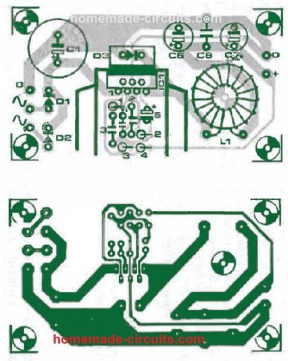 Assembling the board is actually very easy.
Begin by choosing resistors R3 and R4 as previously mentioned.
First assemble the parts that are around the center of the pcb like the, R1�� R4 inclusive as well as C2 C5.
Before you start soldering the parts, make sure that the regulator IC1 and power diode D1 are clamped through screw/nut back to back over a single common heatsink as proven on the image of the component overlay.
Do remember to maintain the heatsink electrically well insulated from the IC metal tab using a thicker mica washer and a plastic material bush.
You possibly can make use of the Type BYV28 for the diode D3..
Whichever diode type is selected, make sure that the mic insulation with a continuity tester!
Press the ICI and D3 pins into their particular PCB holes right up until the heatsink beds down firmly over the PCB surface.
Now, solder the leads and cut off their remaining unwanted portion of the lleads.
After this, install the rest of the parts, L1, CI, C6, C7, Cs, D1 and D2.
Make sure to watch diode and the electrolytic capacitors pin orientation and polarity correctly.
Excessive attention must be exercised to prevent any kind of chance of a short-circuit across choke core winding with the IC heatsink.
It is advised to secure L1 using a central nylon bolt and nut assembly.
Assembling the board is actually very easy.
Begin by choosing resistors R3 and R4 as previously mentioned.
First assemble the parts that are around the center of the pcb like the, R1�� R4 inclusive as well as C2 C5.
Before you start soldering the parts, make sure that the regulator IC1 and power diode D1 are clamped through screw/nut back to back over a single common heatsink as proven on the image of the component overlay.
Do remember to maintain the heatsink electrically well insulated from the IC metal tab using a thicker mica washer and a plastic material bush.
You possibly can make use of the Type BYV28 for the diode D3..
Whichever diode type is selected, make sure that the mic insulation with a continuity tester!
Press the ICI and D3 pins into their particular PCB holes right up until the heatsink beds down firmly over the PCB surface.
Now, solder the leads and cut off their remaining unwanted portion of the lleads.
After this, install the rest of the parts, L1, CI, C6, C7, Cs, D1 and D2.
Make sure to watch diode and the electrolytic capacitors pin orientation and polarity correctly.
Excessive attention must be exercised to prevent any kind of chance of a short-circuit across choke core winding with the IC heatsink.
It is advised to secure L1 using a central nylon bolt and nut assembly.
Testing and Efficiency
Begin the testing procedure by checking the placement, insulation and direction of each and every components on the PCB before you connect the board to the transformer secondary side wires. It must be noted that this adjustable switching power supply needs a load connected at the output constantly in order to work optimally. When the SMPS is supplied with 30 VAC, and a 2 A load attached to an output voltage of 5 V, the heatsink temperature must not exceed around 60 ��C at room temperature. The efficiency of the circuit under such circumstances can be expected to be around 68%. The efficiency boosts to 80% when Uo=10 V, 85% at Uo =15 V, to 87% at at Uo=25 V, all with load rated at 2 Amps. DatasheetLaboratory Power Supply Circuit
Although a variety of laboratory power supplies have appeared in recent times, only handful of these will provide you with the efficiency, versatility, and low cost of the design detailed in this article. This post explains a highly regulated, DIY, laboratory grade power supply with dual 0-50 volt. The voltage and current ranges are independently variable from 0 to 50 V, and 0 to 5 amps respectively.. Having said that, because of the DIY layout, you can customize the settings as needed, which can witnessed in the following specification table.. Number of Supplies = 2 (Fully Floating) Voltage Range = 0 to 50V Current Range = 0 to 5 amps Coarse control and Fine Control ratio for both current and voltage = 1:10 Voltage Regulation = 0.01% line, and 0.1% load Current Limiter = 0.5% You Will Also Like: How to Design a Bench Power Supply CircuitCircuit description
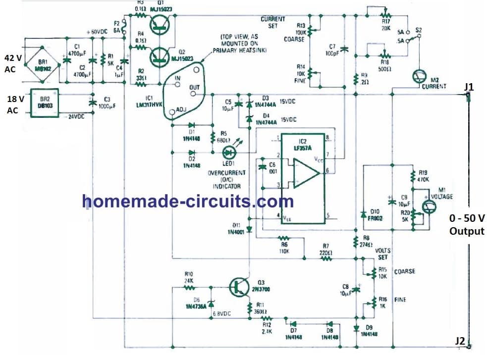 Figure 1 above shows the circuit diagram of the laboratory power supply.
The specifications of the layout is centered around IC1, an LM317HVK adjustable regulator, for wide-ranging functionality.
The "HVK" suffix suggests the high-voltage edition of the regulator.
The remaining portion of the circuit enables voltage setting and current limiting capabilities.
The input to IC1 originates from the output of BR1, which is filtered by C1 and C2 to around + 60 volts DC, and the input for current-sense comparator IC2 develops from bridge rectifier BR2, which furthermore works like a negative bias supply to get regulation to ground level.
The function of IC1 is to keep the OUT terminal at 1.25 volts DC over the ADJ terminal.
The current drain at the ADJ pin is extremely minimal (as low as 25 ��A) and, therefore, R15 and R16 (the crude and refined voltage manipulations) and R8 form a voltage divider, with 1.25 volts showing up around R8.
The lower terminal of R16 attaches to a -1.3 reference volt developed by D7 and D8, permitting the R8 - R15 resistive divider fix the output voltage right down to ground level any time R15 + R16 becomes 0 ohms.
Figure 1 above shows the circuit diagram of the laboratory power supply.
The specifications of the layout is centered around IC1, an LM317HVK adjustable regulator, for wide-ranging functionality.
The "HVK" suffix suggests the high-voltage edition of the regulator.
The remaining portion of the circuit enables voltage setting and current limiting capabilities.
The input to IC1 originates from the output of BR1, which is filtered by C1 and C2 to around + 60 volts DC, and the input for current-sense comparator IC2 develops from bridge rectifier BR2, which furthermore works like a negative bias supply to get regulation to ground level.
The function of IC1 is to keep the OUT terminal at 1.25 volts DC over the ADJ terminal.
The current drain at the ADJ pin is extremely minimal (as low as 25 ��A) and, therefore, R15 and R16 (the crude and refined voltage manipulations) and R8 form a voltage divider, with 1.25 volts showing up around R8.
The lower terminal of R16 attaches to a -1.3 reference volt developed by D7 and D8, permitting the R8 - R15 resistive divider fix the output voltage right down to ground level any time R15 + R16 becomes 0 ohms.
Calculating the Output Voltage
Generally speaking, the output voltage depends upon, the following results: (VouT - 1.25 + 1.3) / (R15 + R16) = 1.25 / R8. Thus, the highest magnitude of voltage value available from each variable supply board can be: VOUT= (1.25 / R8) x (R15 + R16) = 50.18 volts DC. Potentiometers R15 and R16 is used for controlling the output voltage, which enables the VouT to vary from 0-50 volts DC.How Current Control Works
When the DC load current increases, the voltage drop across R2 also rises, and at around 0.65 volts (that is relative to around 20 mA), Q1 and Q2 switch on, becoming the primary course of the current. Additionally, R3 and R4 guarantee that Q1 and Q2 handle the load uniformly. IC2 works like a Current limiter stage. Its non-inverting input makes use of the output voltage like a reference, while its inverting input is attached to the voltage divider developed by R6 and the current control pots R13 and R14. The voltage drop across R6 is about 1.25 volts, the reference voltage stated above is determined by the difference across the IC1 terminals OUT and ADJ. Current passing across Q1 and Q2 moves via R9, building a voltage drop across R13 + R14. As a result, IC2 is forced to switched OFF as soon as the voltage drop around R9 generates current by means of R13 and R14, causing the non-inverting input voltage to go beyond VouT. This fixes the current limiting threshold at: (IouT x 0.2)/(R13 + R14) = 1.25/100K; low = 0 to 5 amps. This provides a corresponding a range of around 0-5 amps. When the current limit threshold is reached, output of IC2 becomes low, driving the ADJ pin down by way of D2 and resulting in the illumination of LED1. Extra current for D5 is delivered by R5. As the ADJ pin is driven low, the output follows, until the output current falls to a point equivalent to the setting of R13 and R14. Considering that the output voltage could be between 0-50 volts, the supply voltage for IC2 should follow this range working with D3, D4, and Q3. Then, D9 ascertains that the output voltage won't increase once the supply input is turned off, while D10 safeguards against a reverse supply voltage. Lastly, the meters M1 displays the voltage reading and M2 displays the current reading.Parts List
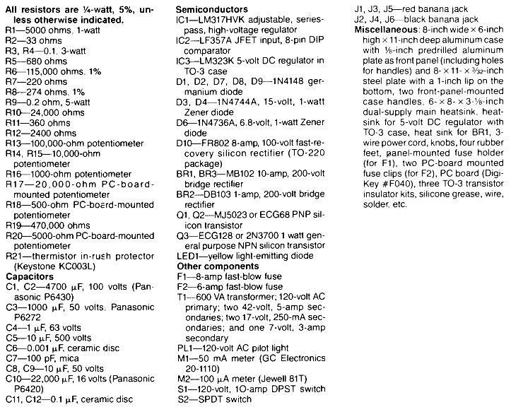
PCB Layout Design
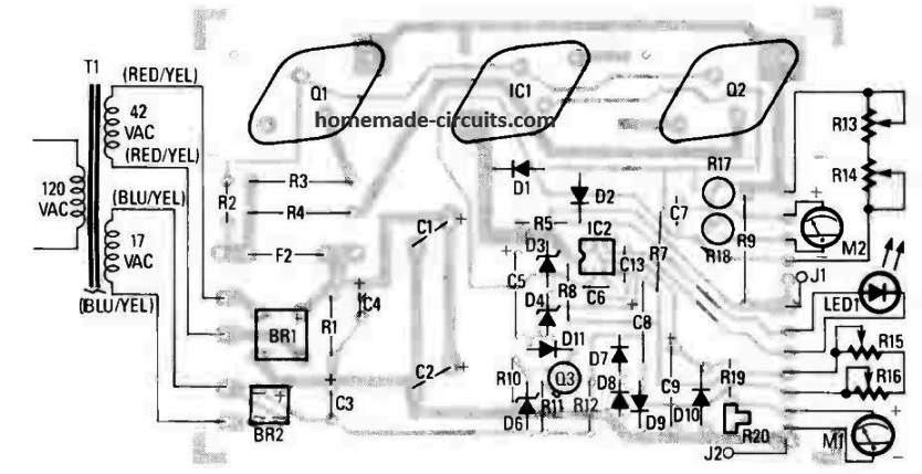
Another Simple Laboratory Power Supply Circuit using LM324 IC
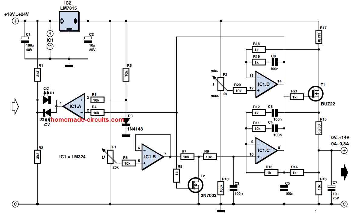 To obtain an intermediate supply voltage the regulator IC LM7815 has been used here.
Its output travels by means of R17, that reads the output current, for th MOSFET T1.
This MOSFET is operated through the opamp IC1, configured like a voltage regulator.
In this laboratory power supply circuit R11 and C4 establish the control loop's bandwidth, which enables the elimination of oscillation at increased frequencies.
Resistor R15 guarantees that capacitive loads having reduced effective resistance will not cause the control loop to become unstable.
The AC content's negative feedback of the current through R12 and C5 enables the circuit to be perfectly reliable even while a large capacitor is employed at its output of the power supply.
The DC content's negative feedback through the low-pass filter is established by resistor R14 and capacitor C6. This configuration guarantees that the voltage drop developed across the resistor R15 is effectively compensated for.
The output capacitor C7 delivers a low impedance source for high-frequency loads.
The resistor R16 helps the discharge of the capacitor C17 whenever the set voltage is decreased in the absence of an output load.
The IC1D section works like a current regulator.
Once again in order to make sure the lab power supply works with perfect stability, the feedback loop's bandwidth is restrained by the resistor R19 and the capacitor C8.
In case the voltage drop developed across the resistor R17 becomes higher than the value as adjusted by the preset P2, the current limiting feature of the circuit kicks in and the transistor T2 is triggered ON.
This action subsequently cuts down the input voltage to the voltage regulation circuit stage until the specified amount of output current is arrived at.
Resistors R7, R9 and capacitor C3 guarantee that proper regulation of current does not produce overshoots of the output voltage and also ensures that there's no generation of resonance effect whenever an inductive load is connected at the output.
To obtain an intermediate supply voltage the regulator IC LM7815 has been used here.
Its output travels by means of R17, that reads the output current, for th MOSFET T1.
This MOSFET is operated through the opamp IC1, configured like a voltage regulator.
In this laboratory power supply circuit R11 and C4 establish the control loop's bandwidth, which enables the elimination of oscillation at increased frequencies.
Resistor R15 guarantees that capacitive loads having reduced effective resistance will not cause the control loop to become unstable.
The AC content's negative feedback of the current through R12 and C5 enables the circuit to be perfectly reliable even while a large capacitor is employed at its output of the power supply.
The DC content's negative feedback through the low-pass filter is established by resistor R14 and capacitor C6. This configuration guarantees that the voltage drop developed across the resistor R15 is effectively compensated for.
The output capacitor C7 delivers a low impedance source for high-frequency loads.
The resistor R16 helps the discharge of the capacitor C17 whenever the set voltage is decreased in the absence of an output load.
The IC1D section works like a current regulator.
Once again in order to make sure the lab power supply works with perfect stability, the feedback loop's bandwidth is restrained by the resistor R19 and the capacitor C8.
In case the voltage drop developed across the resistor R17 becomes higher than the value as adjusted by the preset P2, the current limiting feature of the circuit kicks in and the transistor T2 is triggered ON.
This action subsequently cuts down the input voltage to the voltage regulation circuit stage until the specified amount of output current is arrived at.
Resistors R7, R9 and capacitor C3 guarantee that proper regulation of current does not produce overshoots of the output voltage and also ensures that there's no generation of resonance effect whenever an inductive load is connected at the output.
Using IC 723
The next design shows a simple yet extremely useful laboratory power supply using the IC LM723: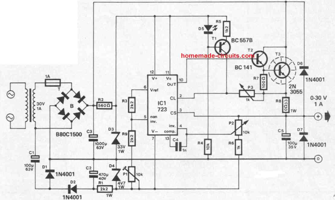
5 V to 10 V Converter for TTL Circuits
The post explains a simple 5 V to 10 V converter circuit which can be used in TTL circuits where only 5 V is available and converting this 5 V to 10 V can be extremely useful for operating an adjacent circuit which may require a supply of around 9 V or 12 V. This voltage doubler circuit can be very handy in circuits which are designed to work with only a 5 V supply voltage, and where a larger voltage is necessary for a different circuit stage.Circuit Description
Figure exhibits the fundamental design, that makes use of 3 gates from the IC 7437 quad two-input NAND buffer IC. Gates N1 and N2 are joined to form a 20 kHz astable multivibrator, and the N2 output runs N3, which behaves like a buffer between the astable and the voltage doubler stages.
Once the N3 output is low C1 starts charging up via D1 and N3 to around + 4.4 V.
As soon as the N3 output turns high the voltage over the C1 positive pin becomes 9 V, causing C1 to discharge by means of D2 into C2. In case no current is pulled from C2 it will continue to charge until the voltage across it reaches +8.5 V.
On the other hand, in case any considerable current is utilized by a load, might cause the output voltage to drop rapidly.
Gates N1 and N2 are joined to form a 20 kHz astable multivibrator, and the N2 output runs N3, which behaves like a buffer between the astable and the voltage doubler stages.
Once the N3 output is low C1 starts charging up via D1 and N3 to around + 4.4 V.
As soon as the N3 output turns high the voltage over the C1 positive pin becomes 9 V, causing C1 to discharge by means of D2 into C2. In case no current is pulled from C2 it will continue to charge until the voltage across it reaches +8.5 V.
On the other hand, in case any considerable current is utilized by a load, might cause the output voltage to drop rapidly.
Improving Voltage Regulation
A much improved output voltage regulation, could be achieved by incorporating a push-pull design as shown in the following figure. This improved 5 V to 10 V converter circuit is driven by a suitable astable square wave source such as from the output of N3 in our previous diagram.
When the N1 output turns low and C1 is in the charging mode, the N2 output becomes high and C2 begins discharging into C3, and vice versa.
Given that C3 is subjected to a continuous charging we find the output voltage regulation much enhanced and stronger than any ordinary voltage doubler variant.
This improved 5 V to 10 V converter circuit is driven by a suitable astable square wave source such as from the output of N3 in our previous diagram.
When the N1 output turns low and C1 is in the charging mode, the N2 output becomes high and C2 begins discharging into C3, and vice versa.
Given that C3 is subjected to a continuous charging we find the output voltage regulation much enhanced and stronger than any ordinary voltage doubler variant.
IC 7437 pinout
The following image shows the internal details and pinout configuration of the IC 7437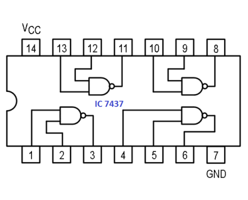
How to Make Step Down Transformers
A step down transformer is a device which reduces a higher AC potential to a lower AC potential as per its winding ratio and specifications. In this article we are going to discuss how to design and construct a basic step down transformer which are typically applied in mains-operated power supplies.Introduction
This will likely help electronic hobbyists to develop and build their very own transformers based on their particular demands. Within the next pages, a simplified layout method is presented in order to achieve satisfactorily developed transformers. On the other hand, the design process may be a subject of some experimentation. The tables presented in this article trim computations short which help the designer to find the appropriate size of wire or even core lamination. Exclusively pertinent data and calculations are supplied here to ensure that the designer is absolutely not baffled by unwanted details. Here we will specifically discuss about transformers which possesses 2 or more winding of insulated copper wire around an iron core. These are: one primary winding and one or maybe more secondary winding. Each winding is electrically isolated from the other however are magnetically connected by using a laminated iron core. Small transformers possess a shell style structure, i.e. the winding are encircled by the core as demonstrated in Fig. 1. The power supplied by the secondary is in fact transmitted from the primary, although at a voltage level dependent on the winding ratio of the a pair of winding. Video Interpretation
Basic Transformer Design
As the initial phase towards the design of a transformer, the primary and secondary voltage evaluations and the secondary ampere rating has to be distinctly expressed. After that determine the core content to be employed: ordinary steel stamping or cold rolled grain oriented (CRGO) stamping. CRGO features a greater allowable flux density and reduced losses. The best possible cross-sectional part of the core is roughly assigned by: Core Area: 1.152 x��(output voltage x output current) sq cm. With regard to transformers having several secondaries, the sum of the the output volt-amp product of each winding needs to be considered. The quantity of turns on the primary and secondary winding is determined using the formula for turns per volt ratio as: Turns per volt = 1/ (4.44 x 10⁻⁴frequency x core area x flux density) Here, the frequency is usually 50Hz for Indian household mains source. The flux density could be considered as approximately 1.0 Weber/ sq. m. intended for ordinary steel stamping and approximately 1.3 Weber/ sq. m. for CRGO stamping.Calculating Primary Winding
The current in the primary'winding is presented by the formula: Primary Current = Sum of o/p Volt and o/p Amp divided by Primary Volts x efficiency The efficiency of small transformers can deviate between 0.8 to 0.��6. A value of 0.87 works extremely well for regular transformers. The appropriate wire size needs to be determined for the winding. The wire diameter is dependent upon the current rated for the winding and also the permitted current density of the wire. The current density could be as tall as 233 amps/ sq. cm. in small transformers and as minimal as 155 amps/ sq. cm. in big ones.Winding Data
 Typically, a value of 200 amps/ sq.
cm.
may be considered, according to which Table#1 is created.
The amount of turns in the primary winding is presented by the formula:
PrimaryTurns = Turns per Volt x Primary Volts
The room consumed by the winding is determined by the insulation density, technique of winding and the wire diameter.
Table#1 provides the estimated values of the turns per square cm.
through which we are able to calculate the window area consumed by the primary winding.
Primary winding Area = Primary turns / Turns per sq.
cm from Table#1
Typically, a value of 200 amps/ sq.
cm.
may be considered, according to which Table#1 is created.
The amount of turns in the primary winding is presented by the formula:
PrimaryTurns = Turns per Volt x Primary Volts
The room consumed by the winding is determined by the insulation density, technique of winding and the wire diameter.
Table#1 provides the estimated values of the turns per square cm.
through which we are able to calculate the window area consumed by the primary winding.
Primary winding Area = Primary turns / Turns per sq.
cm from Table#1
Calculating Secondary Winding
Considering that we have the assumed secondary current rating, we are able to determine the wire size for the secondary winding simply by going through Table#1 directly. The quantity of turns on the secondary is calculated in the identical method when it comes to primary, but around 3% excess turns should be included to reimburse for the internal drop of secondary winding voltage of the transformer, upon loading. Hence, Secondary turns = 1.03 (turns per volt x secondary volts) The window area necessary for secondary winding is identified from Table#2 as Secondary window area = Secondary turns / Turns per sq. cm. (from Table#2 below)Calculating Core size
The principal qualifying measure in picking the core could be the total window area of winding space accessible. Total window area = Primary window area + sum of secondary window areas + space for former & insulation. A little extra space is necessary to support the former and insulation in between winding. The specific quantity of extra area may differ, even though 30% could be considered to begin with although this may need to be customized later on.Table Dimension of Transformer Stamping
 The perfect core sizes possessing a more substantial window space are generally determined from Table#2 taking into consideration the gap between lamination while stacking them (the core stacking element may be taken as 0.9), we now have
Gross core area = Core Area / 0.9 sq cm.
In general, a square central limb is preferred.
For this, the width of the tongue of lamination is
Tongue width = ��Gross core area (sq.cm)
Now refer to Table#2 once again and as a final point find the appropriate core size, having adequate window area and a nearby value of the tongue width as calculated.
Modify thel stack height as needed to acquire the intended core section.
Stack Height = Gross Core Area / Actual Tongue Width
The stack must not be a lot under the tongue width rather should be more.
However, it must not be greater than 11/2 times the tongue width.
The perfect core sizes possessing a more substantial window space are generally determined from Table#2 taking into consideration the gap between lamination while stacking them (the core stacking element may be taken as 0.9), we now have
Gross core area = Core Area / 0.9 sq cm.
In general, a square central limb is preferred.
For this, the width of the tongue of lamination is
Tongue width = ��Gross core area (sq.cm)
Now refer to Table#2 once again and as a final point find the appropriate core size, having adequate window area and a nearby value of the tongue width as calculated.
Modify thel stack height as needed to acquire the intended core section.
Stack Height = Gross Core Area / Actual Tongue Width
The stack must not be a lot under the tongue width rather should be more.
However, it must not be greater than 11/2 times the tongue width.
Core Assembly Diagram

How to Assemble the Transformer
The winding are done over an insulating former or bobbin that fits on the middle pillar of the core lamination. The primary is generally wound first, and next it is the secondary, keeping an insulation between the two layers of the winding. One last insulating layer is applied on top of the winding to safeguard all of them from mechanical and vibration deterioration. Whenever thin wires are employed, their particular ends needs to be soldered to heavier wires in order to bring the terminals outside the former. The lamination are usually put together on the former by alternate lamination reversed in set up. The lamination has to be tightly bound together through an appropriate clamping framework or by using nuts and bolts (in case through holes are supplied within the lamination assembly).How to Apply Shielding
This can be a wise idea to utilize an electrostatic shielding between the primary and secondary winding to circumvent electrical interference from moving across to the secondary from the primary. The shield for step down transformers can be constructed from a copper foil which can be wound between the two winding for somewhat more than a tum. Insulation has to be presented across the entire foil and proper care taken in order that the two ends of the foil never come in contact with each other. Additionally a wire could be soldered with this shielding field and connected with the ground line of the circuit or with the lamination of the transformer which may be clamped with the ground line of the circuit.For Torroidal Transformer designing, you can refer to the following pdf document:
https://www.homemade-circuits.com/wp-content/uploads/2021/04/torroidal-transformer_compressed.pdf2 Compact 12V 2 Amp SMPS Circuit for LED Driver
In this post we comprehensively discuss a 2 simple 12V 2 amp SMPS circuit using the IC UC2842. We study a 2 amp flyback design by evaluating various formulas, which provides the exact selection details for the transformer winding and the parts specifications.Design#1: Introduction
The first design is based on the versatile ICVIPer53-E. The VIPer53-E is built with an improved current mode PWM controller which has a high voltage MDMesh Power MOSFET within the very same package. The VIPer53-E can be found in a couple of distinct packages, DIP8 and PowerSO-10.The benchmark board is undoubtedly an offline wide range power supply which includes the VIPer53-E designed for secondary regulation by operating the PWM controller via an opto-coupler. The switching frequency is 100 kHz and the overall output power is 24 W. Below given are a few of the the main features of the IC: SMPS based general purpose power supply Current mode control along with variable limiting facility Efficiency around a good 75% Output is safeguarded with a short-circuit and overload protection Over temperature is also controlled through a in-built Thermal shutdown protection Complies with EN55022 Class B EMI specification and Blue Angel standards. The circuit diagram of the proposed 12V 2 amp circuit using VIPer53-E could be witnessed in the below shown image: DOWNLOAD COMPLETE PCB AND PARTS LIST
Main Operating Conditions can be studied through the following image:
DOWNLOAD COMPLETE PCB AND PARTS LIST
Main Operating Conditions can be studied through the following image:
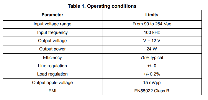
Transformer Details:
The ferrite core transformer winding details for the above SMPS circuit could be analyzed as per the data furnished in the following figure:Design#2: Introduction
The next design is based on the IC UC2842 from Texas Instruments, which can be also used for building a high grade, solid state, very reliable SMPS circuit rated at 12V, and with a current output @ 2 amp to 4 amps. The complete circuit diagram of this design can be sen in the following figure: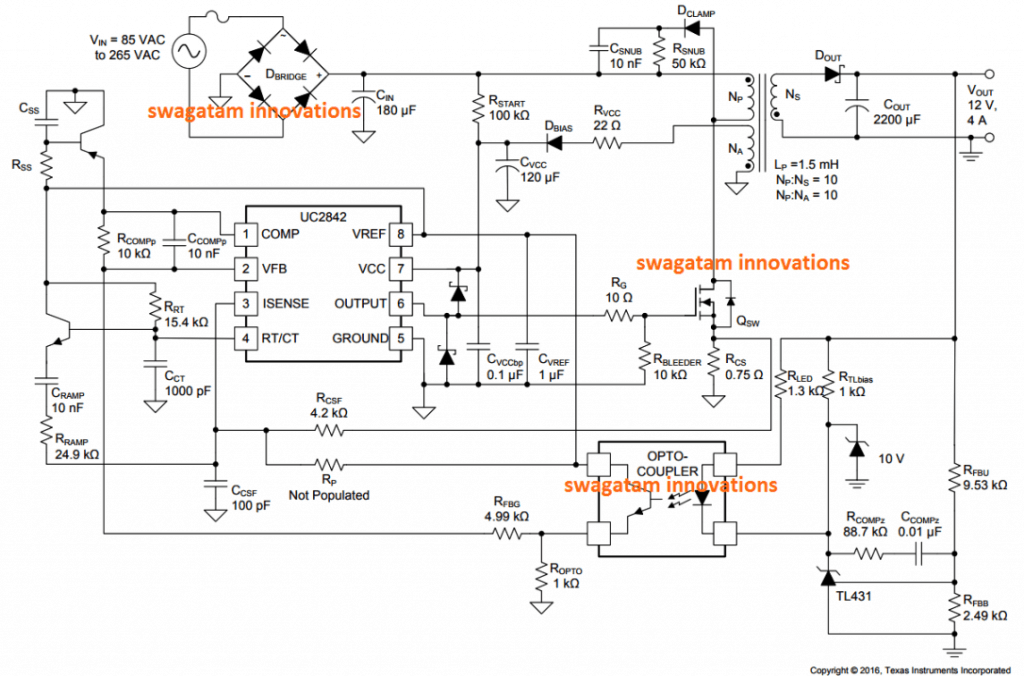 Let��s try to understand the functions and criticalities of a few of the main components used in this 12V 2 amp SMPS circuit:
Cin Input Bulk capacitor and minimum bulk voltage:
The shown bulk capacitor Cin may be incorporated using a single or a few capacitors in parallel, possibly by using an inductor across them to eliminate noise generated due to differential-mode conduction. The value of this capacitor decides the level of minimum bulk voltage. If a lower value Cin is used to reduce minimum bulk voltage, might result in raised primary peak current overloading the switching mosfets and also the transformer. On the contrary keeping the value larger might result in higher peak current on the mosfet and the trafo, which is also not acceptable, therefore a reasonable value as indicated in the diagram should be chosen. It may be done by using the following formula: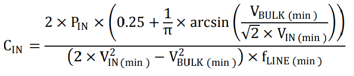 Here Vin(min) indicate the RMS value of the minimum AC input voltage which is around 85 V RMS.
fLINE(min)denotes the frequency of the above RMS value which may be assumed to be 47Hz.
With reference to the above equation, in order to achieve a minimum of 75V bulk voltage value, at 85% efficiency, the Cin value will need to be around 126uF, in our prototype 180uF was found to be just fine.
Here Vin(min) indicate the RMS value of the minimum AC input voltage which is around 85 V RMS.
fLINE(min)denotes the frequency of the above RMS value which may be assumed to be 47Hz.
With reference to the above equation, in order to achieve a minimum of 75V bulk voltage value, at 85% efficiency, the Cin value will need to be around 126uF, in our prototype 180uF was found to be just fine.
Calculating the Tansformer turn ratios:
To begin with the transformer turn calculation, the most favorable switching frequency needs to be found out. Although the IC UC2842 is specified to produce a maximum frequency of 500kHz, considering all the feasible and efficiency related parameters it was decided to select and set the device at around 110kHz. This allowed the design to be reasonably well balanced in terms of the transformer size, EMI filter dimensionand still keep the operations within the tolerable losses. The term Nps refers to the primary of the transformer and this may be determined depending upon the rating of the driver mosfet used along with the rating of the secondary rectifier diode specifications. For an optimal mosfet rating we first need to calculate the peak bulk voltage with reference to the maximum RMS voltage value which is 265V input AC in our case. Therefore we have: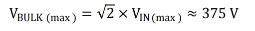 For the sake of simplicity and cost effectiveness, a 650V rated mosfet IRFB9N65A was selected for this 12V 2 amp smps circuit prototype.
If we consider the maximum voltage stress on the mosfet drain to be around 80% of its specifications, and taking 30% as the permissible voltage spike from the maximum bulk input supply, the resultant reflected output voltage can be expected to be lower than 130V as expressed in the following equation:
For the sake of simplicity and cost effectiveness, a 650V rated mosfet IRFB9N65A was selected for this 12V 2 amp smps circuit prototype.
If we consider the maximum voltage stress on the mosfet drain to be around 80% of its specifications, and taking 30% as the permissible voltage spike from the maximum bulk input supply, the resultant reflected output voltage can be expected to be lower than 130V as expressed in the following equation:
 Therefore for a 12V output the maximum primary/secondary transformer turn ratio or the NPS may be calculated as indicated in the following equation:
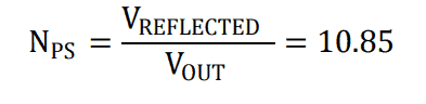 In our design a turn ratio of Nps = 10 has been incorporated.
This winding must calculated in such a way that it is able to produce a voltage that may be a little higher than the minimum Vcc specification of the IC, so that the IC is able to operate under optimal conditions and stability is maintained throughout the circuit.
The auxiliary winding Npa can be calculated as shown in the following formula:
In our design a turn ratio of Nps = 10 has been incorporated.
This winding must calculated in such a way that it is able to produce a voltage that may be a little higher than the minimum Vcc specification of the IC, so that the IC is able to operate under optimal conditions and stability is maintained throughout the circuit.
The auxiliary winding Npa can be calculated as shown in the following formula:
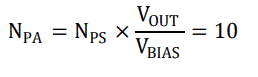 The auxiliary winding in the transformer is used for biasing and providing the operating supply to the IC.
Now for the output diode, the voltage stress on it may be equivalent to the output voltage and the reflected input supply, as given below:
The auxiliary winding in the transformer is used for biasing and providing the operating supply to the IC.
Now for the output diode, the voltage stress on it may be equivalent to the output voltage and the reflected input supply, as given below:
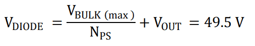 In order to counter the voltage spikes due to ��ringing�� phenomenon, a Schottky diode rated with a blocking voltage of 60V or higher was felt necessary and employed in this design.
Also to keep away high voltage current spike factor, this flyback converter is designed to work with a continuous conduction mode (CCM).
In order to counter the voltage spikes due to ��ringing�� phenomenon, a Schottky diode rated with a blocking voltage of 60V or higher was felt necessary and employed in this design.
Also to keep away high voltage current spike factor, this flyback converter is designed to work with a continuous conduction mode (CCM).
Calculating the Maximum Duty Cycle:
As discussed in the above paragraph, once we calculate the NPS of the transformer, the required maximum duty cycle Dmax can be calculated through the transfer function as allocated for CCM based converters, the details can eb witnessed below: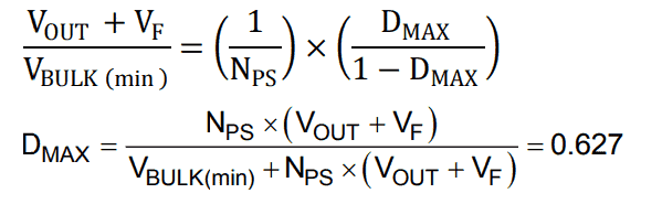
Transformer Inductance and Peak Current
In our discussed 12V 2 amp smps circuit the transformer magnetizing inductance Lp was determined as per the CCM parameters. In this example the inductance was chosen such that the converter is able to get into the CCM working zone with around 10% load and using minimum bulk voltage in order to keep the output ripple to the lowest. For more details regarding the various technical specifications and formulas you can study the original datasheet here
0-40V Adjustable Power Supply Circuit �C Construction Tutorial
This multipurpose general purpose supply generates as much as 2.5 amps from zero to 20 volts or up to 1.25 amps from 0-40 volts. Current limiting is variable within the entire range for either output options. By Trupti Patil
Power Supply Main Specifications:
 AN IDEAL POWER SUPPLY must provide a voltage that is variable within a broad range, and that stays in the set voltage irrespective of line voltage or load disparities.
The supply must also be safe from a short circuit throughout its output and be able to restricting the load current to ensure that devices are not damaged by failing circumstances.
This particular project explains a power supply designed to deliver 2.5 amperes at up to 18 volts (up to 20 volts at lower currents).
At the same time a few basic modifications will make the supply offer as much as 40 volts at 1.25 amperes.
The supply voltage is adjustable between zero and�� the highest available, and current limiting can also be adjusted across the stipulated full range.
The mode of operation of the power supply is indicated by means of two LEDs.
The one near the voltage control knob shows if the unit is in normal voltage-regulation setting and the one near the current limit knob shows if the unit is in current limit mode.
Furthermore a large meter shows the current or voltage output as selected by a switch.
AN IDEAL POWER SUPPLY must provide a voltage that is variable within a broad range, and that stays in the set voltage irrespective of line voltage or load disparities.
The supply must also be safe from a short circuit throughout its output and be able to restricting the load current to ensure that devices are not damaged by failing circumstances.
This particular project explains a power supply designed to deliver 2.5 amperes at up to 18 volts (up to 20 volts at lower currents).
At the same time a few basic modifications will make the supply offer as much as 40 volts at 1.25 amperes.
The supply voltage is adjustable between zero and�� the highest available, and current limiting can also be adjusted across the stipulated full range.
The mode of operation of the power supply is indicated by means of two LEDs.
The one near the voltage control knob shows if the unit is in normal voltage-regulation setting and the one near the current limit knob shows if the unit is in current limit mode.
Furthermore a large meter shows the current or voltage output as selected by a switch.
DESIGN FEATURES
While in our preliminary design stages we researched different types of regulator and the positive aspects and drawbacks of each to be able to pick the one which gives the top cost-effective functionality. The specific strategies and their features could be summarized as follows.The shunt regulator:
This layout would work primarily for low power supplies around 10 to_15 watts. It offers excellent regulation and is internally short-circuit resistant however dissipates the full volume of power it is equipped to handle under no-load conditions.The series regulator.
This regulator fits medium-power supplies approximately about 50 watts. It may and is intended for higher power supplies, although heat dissipation could be a issue particularly at very high current with low output voltages. Regulation great, generally there is minor output noise and the cost is comparatively minimal.SRC regulator:
Ideal for medium to high power purposes, this regulator provides low power dissipation, though the output ripple and response time are not nearly as good as the ones from a series regulator.SCR pre-regulator and series regulator.
The very best features of the SCR and series regulators are put together with this kind of power supply circuit employed for medium to high-power applications. An SCR pre-regulator is employed to secure an roughly regulated supply around five volts greater than recommended, accompanied by a suitable series regulator. This lessens power loss in the series regulator. However, it is a lot more costly to construct.Switching regulator.
Also applied for medium to high-power applications, this technique provides affordable regulation and low power dissipation in the regulator nevertheless is pricey to construct and possesses a high frequency ripple on the output.Switched-mode power supply.
The most successful technique of all, this regulator rectifies the mains to operate an inverter at 20 kHz or even more. To lower or boost the voltage a low cost ferrite transformer is commonly employed, the output from which is rectified and filtered to get the preferred DC output. Line regulation is very good but it surely has the downside that it is not able to conveniently be applied as a variable source since it is just adaptable over a relatively smaller range.OUR OWN DESIGN

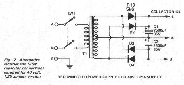 Our initial design principle had been for a power supply of around 20 volts at 5 to 10 amps output.
Having said that, in the light of the varieties of regulator readily available, as well as the costs, it was opted to limit the current to about 2.5 amps.
This approach helped us to employ a series regulator, the most cost-effective model.
Good regulation was necessary, along with adjustable current limiting feature, plus it was additionally chosen that the power supply could well be workable right down to practically zero volts.
To get the final qualification a negative supply rail or a comparator that may run using its inputs at zero volts is essential.
As opposed to using a negative supply rail we made a decision to work with a CA3l30 IC operational amplifier as the comparator.
The CA3l 30 needs a single supply (maximum of 15 volts) and, in the beginning we made use of a resistor and l 2 volt zener to get a 12 volt supply.
The reference voltage had been then created from this zener supply by one more resistor and a 5 volt zener.
It was believed this would have presented adequate regulation for the reference voltage however practically the output from the rectifier was identified to alter from 21to 29 volts plus some of the ripple and voltage switching which took place over the 12 volt zener, as a result, ended up being mirrored into the 5 volt zener reference.
Due to this reason the 12 volt zener has been substituted by an lC regulator that remedied the issue.
With all series regulators the series-output transistor from the characteristics of the layout, ought to dissipate plenty of power particularly in low output voltage and high current.
For this factor a respectable heatsink is an important portion of the structure.
Industrial heatsinks are incredibly expensive and frequently challenging to attach.
We as a result created our very own heatsink that was not only more affordable yet functioned a lot better than the commercial variation we had been thinking about - being simpler to attach.
Nevertheless at full load the heatsink continue to operate warm as will the transformer.
and within high-current low-voltage circumstances the transistor could even become far too sizzling to touch.
This is fairly normal since the transistor within these situations remains to be functioning within its selected temperature range.
Together with any extremely regulated supply, steadiness could be a difficulty.
For this motive the voltage-regulation mode of operations, capacitors C5 and C7 are included to minimize the loop gain in high frequencies and therefore avoid the supply from oscillating.
The value of C5 has been picked for ideally skimp on between stability and reaction period.
When the value of C5 is too low the rate of reaction is increased.
However there exists a greater possibility of lack of stability.
lf excessive reaction time is unduly increased.
In the current-limit mode the identical functionality is completed by C4 and the exact same opinions implement as for the voltage scenario.
As the power supply has the ability to of relatively high current output there may be undoubtedly some voltage drop over the wiring to the output terminals.This is compensated by sensing the voltage on the output terminals through a independent set of leads.
Although the supply was principally made for 20 volts at 2.5 amps it ended up being recommended that the exact same supply may be accustomed to supply 40 volts at 1.25 amps and that this may be of more appropriate to many end users.
This could be accomplished by modifying the settings of the rectifier and by altering a few components.
Some idea was handed to creating the supply switchable however the additional complexities and price were in a way that it was disregarded to be advantageous.
Therefore you need to basically choose configuration that matches your demand and build the supply as necessary.
The maximum regulated voltage accessible is restricted possibly by the input voltage to the regulator being too reduced (with more than 18 volts and 2.5 amps) or perhaps from the ratio of R14/R15 and by the value of the reference voltage.
(Output = R14+R15/R15 )V ref
Because of the tolerance of ZD1 the complete 20 volts (or 40 volts) is probably not accessible.
If it is identified like a situation R14 must be increased to the subsequent favored value.
Single turn potentiometers have been given for the voltage and current controls due to the fact that they are affordable.
Nevertheless if accurate setability of voltage or current control is needed ten-turn potentiometers ought to be applied as a substitute.
Our initial design principle had been for a power supply of around 20 volts at 5 to 10 amps output.
Having said that, in the light of the varieties of regulator readily available, as well as the costs, it was opted to limit the current to about 2.5 amps.
This approach helped us to employ a series regulator, the most cost-effective model.
Good regulation was necessary, along with adjustable current limiting feature, plus it was additionally chosen that the power supply could well be workable right down to practically zero volts.
To get the final qualification a negative supply rail or a comparator that may run using its inputs at zero volts is essential.
As opposed to using a negative supply rail we made a decision to work with a CA3l30 IC operational amplifier as the comparator.
The CA3l 30 needs a single supply (maximum of 15 volts) and, in the beginning we made use of a resistor and l 2 volt zener to get a 12 volt supply.
The reference voltage had been then created from this zener supply by one more resistor and a 5 volt zener.
It was believed this would have presented adequate regulation for the reference voltage however practically the output from the rectifier was identified to alter from 21to 29 volts plus some of the ripple and voltage switching which took place over the 12 volt zener, as a result, ended up being mirrored into the 5 volt zener reference.
Due to this reason the 12 volt zener has been substituted by an lC regulator that remedied the issue.
With all series regulators the series-output transistor from the characteristics of the layout, ought to dissipate plenty of power particularly in low output voltage and high current.
For this factor a respectable heatsink is an important portion of the structure.
Industrial heatsinks are incredibly expensive and frequently challenging to attach.
We as a result created our very own heatsink that was not only more affordable yet functioned a lot better than the commercial variation we had been thinking about - being simpler to attach.
Nevertheless at full load the heatsink continue to operate warm as will the transformer.
and within high-current low-voltage circumstances the transistor could even become far too sizzling to touch.
This is fairly normal since the transistor within these situations remains to be functioning within its selected temperature range.
Together with any extremely regulated supply, steadiness could be a difficulty.
For this motive the voltage-regulation mode of operations, capacitors C5 and C7 are included to minimize the loop gain in high frequencies and therefore avoid the supply from oscillating.
The value of C5 has been picked for ideally skimp on between stability and reaction period.
When the value of C5 is too low the rate of reaction is increased.
However there exists a greater possibility of lack of stability.
lf excessive reaction time is unduly increased.
In the current-limit mode the identical functionality is completed by C4 and the exact same opinions implement as for the voltage scenario.
As the power supply has the ability to of relatively high current output there may be undoubtedly some voltage drop over the wiring to the output terminals.This is compensated by sensing the voltage on the output terminals through a independent set of leads.
Although the supply was principally made for 20 volts at 2.5 amps it ended up being recommended that the exact same supply may be accustomed to supply 40 volts at 1.25 amps and that this may be of more appropriate to many end users.
This could be accomplished by modifying the settings of the rectifier and by altering a few components.
Some idea was handed to creating the supply switchable however the additional complexities and price were in a way that it was disregarded to be advantageous.
Therefore you need to basically choose configuration that matches your demand and build the supply as necessary.
The maximum regulated voltage accessible is restricted possibly by the input voltage to the regulator being too reduced (with more than 18 volts and 2.5 amps) or perhaps from the ratio of R14/R15 and by the value of the reference voltage.
(Output = R14+R15/R15 )V ref
Because of the tolerance of ZD1 the complete 20 volts (or 40 volts) is probably not accessible.
If it is identified like a situation R14 must be increased to the subsequent favored value.
Single turn potentiometers have been given for the voltage and current controls due to the fact that they are affordable.
Nevertheless if accurate setability of voltage or current control is needed ten-turn potentiometers ought to be applied as a substitute.
HOW IT WORKS
The 240 volt mains is stepped-down to 40 Vac through the transformer and, based on which supply has been developed, rectified to either 25 or 5 Vdc. This voltage is actually moderate since the actual voltage will be different between 29 volts (58 volts) on no-load to 21 volts (42 volts) on full load. The identical filter capacitors are employed in both situation. These are attached in parallel for your 25 volt variant (5000uF) and in series intended for the 50 volt model (1250uF). ln the 50 volt model the centre tap of the transformer will be coupled to the centre tap of the capacitors hence guaranteeing accurate voltage. sharing amongst the capacitors. This set up additionally offers a 25 volt supply to the regulator lC. The voltage regulator is essentially a series type in which the impedance of the series transistor is governed in such a method that this voltage throughout the load is kept constant at the predetermined value. The transistor Q4 dissipates a great deal of power particularly at low output voltages and high current and it is hence installed on the heatsink within the backside of the product. Transistor Q3 brings current gain to Q4,the collaboration performing like a high-power, high-gain, PNP transistor. The 25 volts is decreased to 12 volts through the integrated-circuit regulator ICI. This voltage is commonly employed as the supply voltage for the CA3130 lCs and it is additionally lowered to 5.1 volts by zener diode ZDI to use as the reference voltage. The voltage regulation is conducted by lC3 that examines the voltage as determined by RV3 (O to 5.1" volts) with the output voltage as divided by R14 and R15. The divider provides a division of 4.2 (O to 21 volts) or eight (0 to 40 volts). On the other hand in the high end the obtainable voltage is restricted to the point that the regulator manages to lose control at high current as the voltage through the filter capacitor reaches the output voltage plus some 100 Hz ripple may also be found. The output of IC3 regulates transistor Q2 that subsequently controls the output transistor in a way that the output voltage continues to be consistent irrespective of line and load disparities. The 5.1 volt reference is offered to the emitter of Q2 through Q1. This transistor is actually a buffer stage to counteract the 5.1 volt line from becoming loaded. Current control is conducted by IC2 that analyzes the voltage determined by -RV1 (O to 0.55 volts) using the voltage created around R7 by the load current. If say 0.25 volts is defined on RV1 and the current taken from the supply is small, the output of IC2 is going to be near 12 volts. This leads to LED 2 being lit up since the emitter of Q1 is at 5.7 volts. This LED consequently signifies that this supply is functioning within the voltage regulator mode. lf however the current driven is elevated in a way that the voltage around R7 is little over 0.25 volts (in our illustration) the output of IC2 may drop. Once the output of IC2 drops below around 4 volts Q2 begins switch off through LED 3 and D5. The result of this would be to minimize the output voltage in order that the voltage throughout R7 is unable to surge more. While this takes place the voltage comparator IC3 attempts to counter for the problem and its output soars to 12 volts. IC2 then consumes more current to make up and this current brings about LED 3 to lumination, implying that the supply is working in the current-limit mode. To make sure precise regulation the voltage sensing terminals are delivered to the output points Independently from those transporting the load current. The meter includes a one milliamp movement and reads the output voltage (immediately along the output terminals) or current (by ��measuring the voltage around R7) as chosen from the front panel switch SV2PCB Layout for the 40V power supply circuit

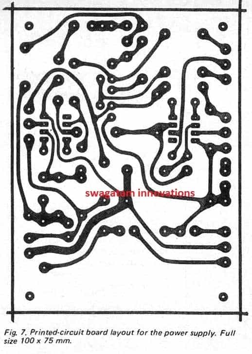

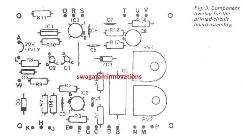
CONSTRUCTION
The suggested PCB layout for this 0-40V variable power supply circuit must be utilized since construction is in so doing tremendously simplied. The components must be put together onto the board ensuring that the polarities of diodes, transistors, lCs and electrolytics are proper. The BDl40 (Q3) must be installed in a way that the side using the metal surface confronts in the direction of lCl . A small heatsink must be bolted onto the transistor as demonstrated in the picture. If the metalwork as detailed is used pursuing assembly arrangement must be employed.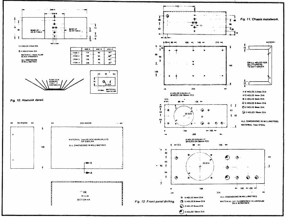

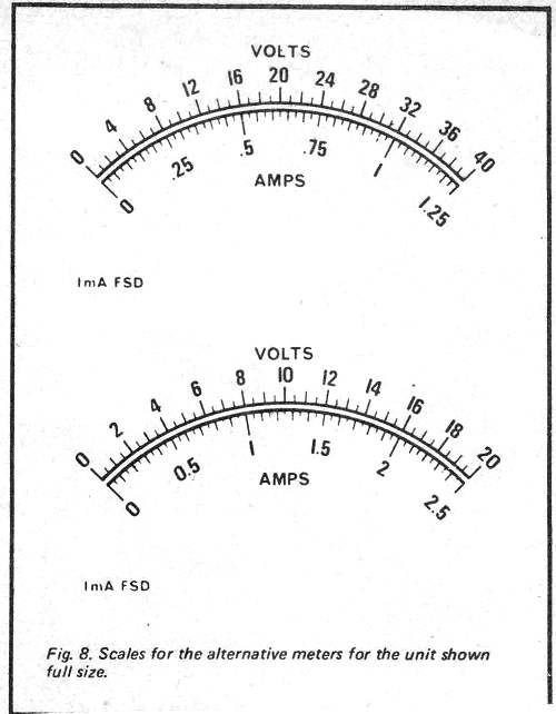 a) Join the front panel into the front of the framework and bolt them with each other by fitting the meter.
b) Fix the output terminals, potentiometers and meter-switch onto the front panel.
c) The cathodes of the LEDs (which we applied) had been designated by a notch within the body that could not possible be noticed while the LEDs were fitted onto the front panel.
If this sounds the situation with yours, reduce the cathode terminals slightly smaller to recognize them after which install the LEDs into place.
d) Solder lengths of wire (around 180 mm long) to the 240 volt terminals of the transformer, insulate the terminals using tape after which attach the transformer into place inside the framework.
f) Mount the mains cord and the cord-clip.
wire the power switch, insulate the terminals and after that attach the switch on the front panel.
g) Fix the heatsink and screw it onto the back of the framework by using a couple of bolts - after that install the power transistor utilizing insulation washers and silicon grease.
h) Install the assembled PCB on the framework utilizing 10 mm spacers.
i) Wire the transformer secondary, rectifier diodes and filter capacitors.
The diode leads are rigid enough not really to want any extra support.
j) The wiring involving the board and the switches may possibly now come in by hook up points with matching letters in the front panel diagram and component overlay diagrams.
The only establishing needed would be to calibrate the meter.
Hook up an genuine voltmeter to the output control of the power supply so that the external meter deciphers 1 5 volts (or 30 volts on the alternative set up).
a) Join the front panel into the front of the framework and bolt them with each other by fitting the meter.
b) Fix the output terminals, potentiometers and meter-switch onto the front panel.
c) The cathodes of the LEDs (which we applied) had been designated by a notch within the body that could not possible be noticed while the LEDs were fitted onto the front panel.
If this sounds the situation with yours, reduce the cathode terminals slightly smaller to recognize them after which install the LEDs into place.
d) Solder lengths of wire (around 180 mm long) to the 240 volt terminals of the transformer, insulate the terminals using tape after which attach the transformer into place inside the framework.
f) Mount the mains cord and the cord-clip.
wire the power switch, insulate the terminals and after that attach the switch on the front panel.
g) Fix the heatsink and screw it onto the back of the framework by using a couple of bolts - after that install the power transistor utilizing insulation washers and silicon grease.
h) Install the assembled PCB on the framework utilizing 10 mm spacers.
i) Wire the transformer secondary, rectifier diodes and filter capacitors.
The diode leads are rigid enough not really to want any extra support.
j) The wiring involving the board and the switches may possibly now come in by hook up points with matching letters in the front panel diagram and component overlay diagrams.
The only establishing needed would be to calibrate the meter.
Hook up an genuine voltmeter to the output control of the power supply so that the external meter deciphers 1 5 volts (or 30 volts on the alternative set up).
Parts List for the proposed 40V 2 amp power supply circuit
Low Dropout (LDO) Voltage Regulator IC KA378R12C �C Pinout and Working Specs
The article explains the pinout functions, and datasheet of a versatile low dropout (LDO) voltage regulator IC KA378R12, and also presents a circuit diagram showing how to use the IC in practical applications. A related question was asked by Mr. Jon, which inspired me to update this post. The question can be seen in the following paragraph:Technical Specification
The reason I emailed you is about a Low Drop Out 12vdc voltage regulator. What I'm working on is a LED brake light assembly were the input voltage needs to be 11.5-12.5 vdc. With a regular 12v regulator the drop out voltage is too high. It works ok when the vehicle is running producing 14.5 volts. With vehicle engine turned off the output voltagefrom these regulator IC drops to low. I was looking at the KA378R12CTU from Fairchild I included the data sheet. Do you have any other suggestions? Thank You Jon RicheyCircuit Analysis
Hi Jon, I think it's the perfect option that you have selected for fulfilling your requirement, please go ahead and use it for the application.The Design
Coming back to our proposed low voltage dropout regulator IC KA378R12, it is quite similar to our ordinary 12V fixed regulator, such as 7812, or the 12V/5amp regulator versionexcept the difference that this device is able to produce a 12V output with an impressive low dropout of 0.5V. The IC is a 12V voltage regulator capable of producing a fixed 12V output at a maximum 3 amp current, with a dropout of hardly 0.5V across its input and output terminals, meaning, even with a 12.5V as the input you can expect the output to produce a consistent and fixed 12V. We can see that this IC has 4 pinouts instead of 3 which we usually find in other traditional regulator ICs, the functions of these pinouts can be understood from the following points:Pinout Details
 Pin#1 is the input pinout of the IC.
A maximum of 35V DC can be applied on this pin.
Pin#2 is the output pinout of the IC.
A 12V fixed low dropout output can be achieved across this pinout.
Pin#3 is the common ground pinout.
The above discussed input and output voltages are referenced to this common ground pinout, meaning it forms the negative line for the input as well as the output voltages, and also the load
Pin#4 has the function of "output disable".
This pin should be fed with a minimum of 2V to keep the output enabled and functioning, not exceeding 35V or the input supply level.
However a zero volt trigger or a ground connection on this pin will instantly render the output zero volt by disabling the IC.
Pin#1 is the input pinout of the IC.
A maximum of 35V DC can be applied on this pin.
Pin#2 is the output pinout of the IC.
A 12V fixed low dropout output can be achieved across this pinout.
Pin#3 is the common ground pinout.
The above discussed input and output voltages are referenced to this common ground pinout, meaning it forms the negative line for the input as well as the output voltages, and also the load
Pin#4 has the function of "output disable".
This pin should be fed with a minimum of 2V to keep the output enabled and functioning, not exceeding 35V or the input supply level.
However a zero volt trigger or a ground connection on this pin will instantly render the output zero volt by disabling the IC.
Application Circuit Diagram
The basic circuit diagram using the above explained low drop 12V regulator KA378R12 can be witnessed in the following image: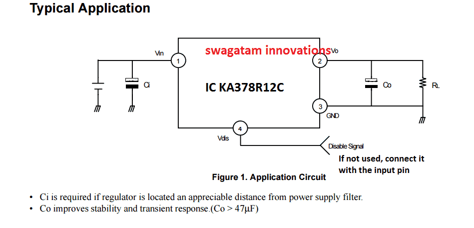
Built-in Protections
Apart from the low dropout feature the IC also comes with a few outstanding and useful protection capabilities such as peak current protection, thermal shut-down, input over voltage protection, and output disable feature (already discussed previously). Feedback from Mr. Jon Hi Swagatam, I'm using this regulator we discussed. But It's a fixed voltage regulator that's a tiny bit to high in voltage. My LED board is 12volts with a total amp draw of 1.50 amps. At 12.3v it creates to much heat. At 11.9v its perfect. Any suggestions on how to bring voltage down? Could I use a resistor to ground draw it down? Or would a switching regulator be a better alternative? If so could you point me in the direction of a schematic. Thank You Jon Richey My Reply Hi jon, the IC is rated to handle 3 amps, therefore 1.5 amps should not be a problem for the mentioned IC You can add a large heatsink to it for controlling the heat. I can suggest you a switching regulator but that may involve complexities and many adjustments.1.5V Power Supply Circuit for Wall Clock
The post presents a simple transformerless 1.5V DC power supply circuit which can be used for powering wall clocks directly from mains, and also keep a stand by back-up cell fully charged for enabling an uninterrupted operation of the clock even during mains failures. The idea was requested by Cheekin Warning: This circuit is not isolated from mains AC and therefore is extremely dangerous to touch in powered condition, users are advised to apply extreme caution while handling it or testing in an uncovered position.The Design
The figure shows a simple 1.5V transformerless power supply circuit for wall clocks that would never allow the clock to stop due to a depleted battery as it would keep running from the mains and also be reinforced with a battery power to ensure that the clock does not stop even during a mains failure. The below shown design is a simple transformerless power supply using a 0.33uF capacitor as the input current limiter component in order to restrict the mains current to a modest 16mA.Circuit Diagram

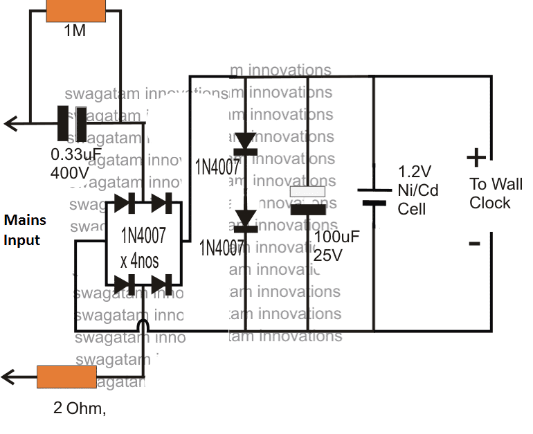 Hopefully this current will keep the clock ticking satisfactorily and also keep the attached Ni/Cd cell trickle charged and ready for an emergency back up.
If the 0.33uF does not provide adequate current for the operations, you can increase it to a higher value which just satisfies the application needs.
The indicated 1.5V transformeless power supply for a wall clock is able to develop the required 1.5V DC at the output with the aid of the two forward biased 1N4007 rectifier diodes across the (+), (-) terminals of the supply, which effectively shunts the massive 330V mains (@ 20mA) to a nominal 1.5V DC.
The inclusion of the two shunting diodes also ensures an entirely surge free supply for the clock and the charging cell, and therefore the design is relieved from other conventional forms of surge protection devices.
Hopefully this current will keep the clock ticking satisfactorily and also keep the attached Ni/Cd cell trickle charged and ready for an emergency back up.
If the 0.33uF does not provide adequate current for the operations, you can increase it to a higher value which just satisfies the application needs.
The indicated 1.5V transformeless power supply for a wall clock is able to develop the required 1.5V DC at the output with the aid of the two forward biased 1N4007 rectifier diodes across the (+), (-) terminals of the supply, which effectively shunts the massive 330V mains (@ 20mA) to a nominal 1.5V DC.
The inclusion of the two shunting diodes also ensures an entirely surge free supply for the clock and the charging cell, and therefore the design is relieved from other conventional forms of surge protection devices.
How it Works
Briefly the 1.5V transformerless supply circuit for clocks can be explained as follows The mains input current is dropped to a lower 20mA by the 0.33uF/400V capacitor. The bridge rectifier converts the above low current input to a low current DC variant, which is further acted upon by the two 1N4007 diodes which shunts the DC to a fixed 1.5V approximately. This 1.5V / 20 mA DC is finally used for operating the desired wall clock, and also for charging a connected 1.2V Ni/Cd cell which reverts its DC each time mains fails, ensuring a failproof uninterrupted supply for the clock so that the unit never stops due to any adverse reasons.LM317 Variable Switch Mode Power Supply (SMPS)
So far in this website we have studied LM317 based linear power supply circuits, here we will learn how an LM317 can be executed as a variable switch mode power or SMPS with zero loss.LM317 as Linear Regulator
We all know that an LM317 IC is internally designed to work as a linear voltage regulator IC, which has a serious drawback of power dissipation through heating. Moreover such topology also requires the input to be minimum 3V higher than the desired output, adding further restrictions to the given regulator configuration. Here we discuss how the same IC could be simply implemented as a 0-40V variable power supply using SMPS topology and therefore eliminating the losses mentioned in the above paragraph.Modifying LM317 Circuit into a PWM Switching Regulator Circuit
The LM317 variable SMPS circuit explained here effortlessly converts an ordinary LM317 IC into an inductor based switching regulator power supply counterpart, as exhibited in the following diagram:Circuit Diagram
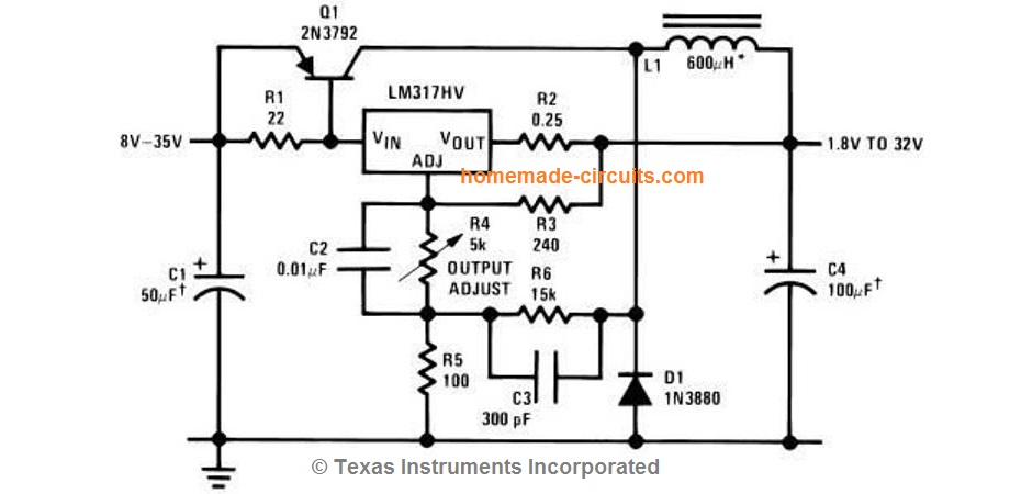 Referring to the above shown diagram we can see that the LM317 is configured in its usual variable regulator mode but with some additional parts in the form of R6, C3, and D1.
We can also see an inductor attached with D1 and an associated power BJT Q1.
Referring to the above shown diagram we can see that the LM317 is configured in its usual variable regulator mode but with some additional parts in the form of R6, C3, and D1.
We can also see an inductor attached with D1 and an associated power BJT Q1.
How it Works
Here the LM317 IC performs two tasks together. It varies the output voltage through the indicated pot R4, and in turn causes a PWM to initiate for the base of Q1. Basically, the introduction of R6/C3 transforms the LM317 regulator circuit into a high frequency oscillator circuit, forcing the output of the LM317 to switch ON/OFF rapidly with a varying PWM, which is dependent on the setting of R4. The BJT Q1 along with the inductor L1 and D1 forms a standard buck converter circuit which is controlled by the above explained PWM generated by the LM317 circuit. This implies that while the pot R4 is varied, the voltage pulse width developed across R1 also varies proportionately causing Q1 to switch L1 in accordance with the varying PWMs. Higher pulse widths enable the inductor to produce higher voltages and vice versa. Capacitor C4 makes sure that the fluctuating output from L1 at the output is adequately smoothed and eliminated, this consequently enhances the ripple current into a stable DC. In the proposed LM317 switch mode power supply circuit since the IC LM317 is not directly involved with the handling of the load current, it's restricted from dissipating current, and thus ensures an efficient regulation of the high input voltage into the desired low output voltage levels. The design also allows the user to upgrade the circuit into a high current SMPS circuit simply by changing the Q1, L1, D1 rating as per the required output current specifications. L1 can be built by winding bifilar enameled copper wire over any suitable ferrite core. Although this LM317 SMPS circuit promises a near zero loss output, Q1 must be mounted on a heatsink and some degree of dissipation may be expected from it. Interesting Feedback from one of the Avid Readers:Mr. Swagatam: I am a retired EE, but continue to have an interest in various areas. Happened to come across your website when I was researching power supplies using LM317. Saw the interesting switch mode power supplyschematic using the LM317. As it turns out, the exact circuit shows upin the 1978 National Semiconductor Voltage Regulator Handbook, withadditional verbiage to explain its behavior. However, I found it evenmore helpful to simulate the circuit using LTSpiceVII (which is free todownload and use) to get a better idea of how the circuit operates withcomponent value changes. Anyway, I decided to scan the two pages fromthe 1978 Handbook and email to you in the event you care to post themwith the schematic for others who might be interested in a little moredetail. Regards, Denton Conrad Raleigh, NC

SCR Shunt Circuit for Protecting LED Drivers
The post presents an effective method for protecting capacitive LED driver circuits through an SCR shunt regulator circuit and explains how it can prevent filter capacitors from blowing of and LEDs from getting destroyed. The remedy was requested by Mr. Max Payne.Protecting High Watt LEDs
Pleasesuggest regarding 3W, 5W LED bulb circuit design fault. the LED bulb running very cool. The electrolyte capacitor (47uf to 100uf , 50v rated) keeps explode. without any reason. and wasting all LED's but smd resistor (474 & 560), MB10S, 105j400v has no problem, This is the problem pcb of the cheapest 3W, 5W LED set. How can i solve the problem permanently or Pls suggest me few cost effective designs ... I noted that these explosion happening when i operate induction cook-top.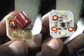
The Design
A filter capacitor in a capacitive power supply will mostly blow-of due to an insurge of voltage higher than its rated value. For example if the filter capacitor breakdown voltage is 50V, and if the surge voltage exceeds this limit could instantly cause the capacitor to explode or gas. A rather simple solution to protect the vulnerable parts in a capacitive transformerless power supply such as the capacitors and the LEDs is to introduce a shunt regulator circuit as indicated in the following diagram:Circuit Diagram
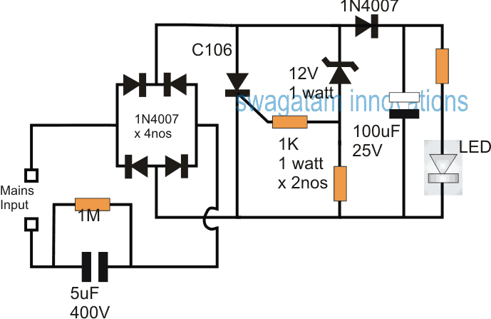 Here the SCR forms the main element for curbing the initial high voltage, high current surge and to ensure a regulated constant supply regardless of the input fluctuations.
If we recall, this concept has been already discussed in one of my earlier posts titled how to make a high current transformerless power supply circuit
Here the SCR forms the main element for curbing the initial high voltage, high current surge and to ensure a regulated constant supply regardless of the input fluctuations.
If we recall, this concept has been already discussed in one of my earlier posts titled how to make a high current transformerless power supply circuit
Circuit Operation
The idea here is to switch ON the SCR or a triac as soon as the input supply tries to surpass the stipulated safe voltage limit of the circuit, which in turn depends on the indicated zener diode voltage. Referring to the above SCR shunt circuit for protecting capacitive LED drivers, whenever the input from the mains capacitor tends to go above 12V, the zener diode conducts fully, triggering the SCR, and causing its anode cathode leads to short circuit the supply instantaneously. This response becomes enough to stop the voltage to rise any further and ensure that it's limited within the assigned 12V range. The stage comprising the SCR, the zener and the 1K resistors act like a high current zener diode and is employed here since the input current is much higher and beyond the capacity of a normal 1 watt zener diode, however for low current transformerless power supply circuits the SCR and the 2nos 1K resistors may be eliminated and only the 12V zener could be used for the intended regulation.Using High Voltage Transistor
Another effective shunt regulator could be built using a high voltage transistor and a variable zener diode, as shown below: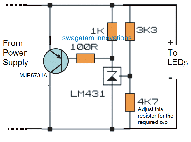
Make this 3.3V, 5V, 9V SMPS Circuit
Here we learn about a simple switch mode power supply (SMPS) circuit which is capable of delivering 3.3V, 5V, 9V at around 800mA from a Mains input range of 100V to 285V, with a complete isolation. The functioning of the proposed 3.3V, 5V, 9V flyback SMPS Circuit may be understood by going through the following detailed circuit explanation:Input EMI Filtering
The capacitor C10, together with C13 form the main capacitors. In conjunction with L4, they constitute the EMI filter stage. Tiny Switch's integrated frequency jitter facilitates to accomplish a reduced EMI even with a rather uncomplicated EMI filter configuration.Primary Clamp Snubber Stage
D3, R1, R2, along with C1 build up the primary side clamp-snubber to fix the voltage peak at the Drain pin as soon as its turned-off. D3 is a 1N4007G, a glass-passivated model of the typical 1N4007, with regulated back EMF restoration. Its positioned, in conjunction with R2, to enhance EMI and the intended 3.3V, 5V, 9V outputs. In a situation where a specific fast recovery diode is difficult to obtain, any other alternative fast diode can be incorporated without an issue.Output voltage filtering
C3, C5, and C7 become responsible as the bulk output capacitors. C4, C6, and C8, in conjunction with the inductors L1, L2, and L3, constitute second-stage output filters.Output Feedback Loop
Sensing resistors R4 and R5 detect and identify a probable difference in the amplitude of the 3.3V and 5V output voltage limits. Such difference in the voltage, could be as a result of differences in the output connected load or perhaps input voltage, are fed as a reference to the input pin of the TL431 shunt regulator. The shunt regulator identifies these and compares the same with its in-built voltage reference level to trigger a feedback signal in the form of a current impulse trough U1 B proportional to the to the identified difference detected by R4 and R5. Opto-coupler U1 immediately shuts down the control loop of the supply voltage by sending the feedback signal current to the output of the ENUV pin on the primary section of the circuit. The following diagram represents the complete schematic of the 3.3V, 5V, 9V SMPS CircuitCircuit Diagram
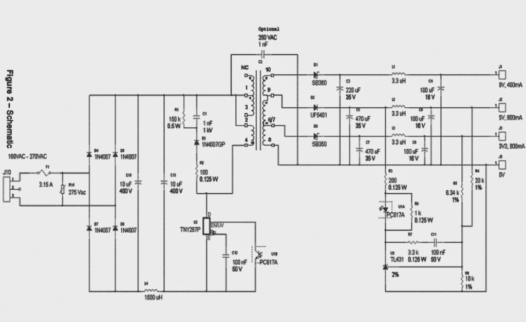
PCB Layout for the proposed multiple voltage output SMPS circuit
 Transformer winding drawing for the above explained multiple voltage output SMPS circuit
Transformer Winding Details
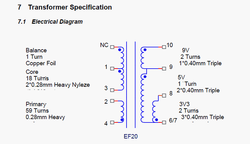 The following gives the transformer specifications for assisting the winding of the turns correctly
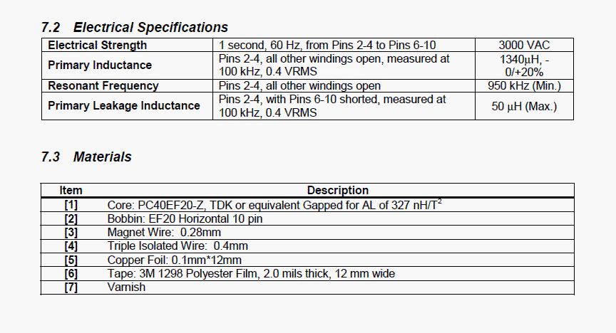
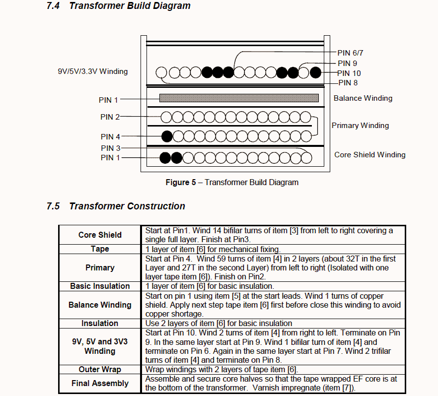
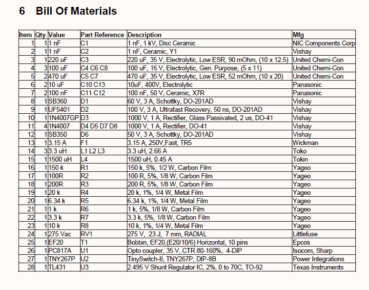 Courtesy:https://ac-dc.power.com/system/files_force/PDFFiles/der55.pdf
Making 3.3V, 5V Voltage Regulator Circuit with Diodes and Transistors
In this post we learn to make 3.3V, 5V voltage regulator circuits from higher voltage sources, such as 12V or a 24V source without ICs.Linear ICs
Normally a step down voltage from a higher voltage source is obtained by using a linear IC such as a 78XX series voltage regulator IC or a buck converter. Both the above options can be costly and/or complex options for getting a particular desired voltage quickly for a particular application.Zener Diodes
Zener diodes also become useful when it comes to achieving a lower voltage from a higher source, however you cannot get sufficient current from a zener diode voltage clamp. This happens because zener diodes normally involve a high value resistor for protecting itself from high currents, which restricts the passage of higher current to the output to just milliamps, which mostly becomes insufficient for an associated load. A quick and a clean way to derive a 3.3V or 5V regulation or any other desired value from a given higher voltage source is to use series diodes as shown in the following diagram.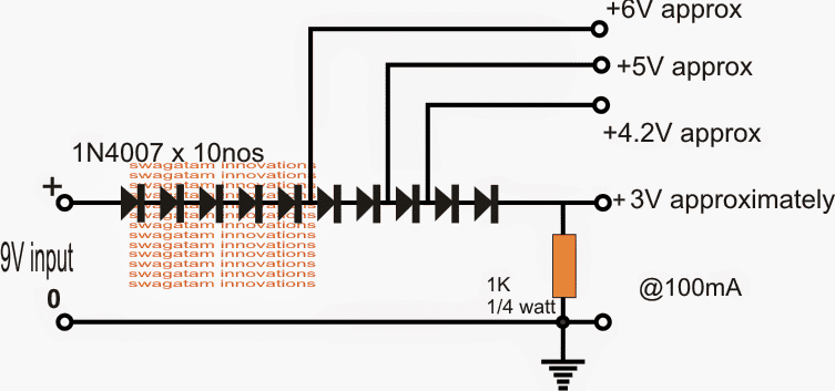
Using Rectifier Diodes for Dropping Voltage
In the above diagram we can see about 10 diodes being used for acquiring a 3V output at the extreme end, while other corresponding values can also be seen in the form of 4.2v, 5v and 6V levels across the relevant dropping diodes. We know that typically a rectifier diode is characterized to drop around 0.6V across itself, meaning any potential fed at a diode's anode will generate an output at its cathode which would be normally approximately 0.6V less than the input at its anode. We take the advantage of the above feature in order to achieve the indicated lower voltage potentials from a given higher supply.Using 1N4007 Diode for 1 Amp Current
In the diagram 1N4007 diodes are shown which might yield not more than 100mA, although 1N4007 diodes are rated to handle upto 1amp, it needs to be ensured that the diodes do not begin warming up, otherwise that would result in higher voltages being allowed to pass. Because as the diode heats up the rated drop across it begins receding towards zero, that's why not more than a 100mA max should be expected from the above design for preventing over heating and enabling an optimal response from the design. For higher currents one may opt for higher rated diodes such as 1N5408 (0.5amp max) or 6A4(2amp max) etc. The drawback of the above design is that it does not produce accurate potential values at the output and therefore might not be suitable for applications where customized voltage references may be needed or for applications where the load parameter could be crucial in terms of its voltage specs. For such applications the following configuration could become very desirable and useful: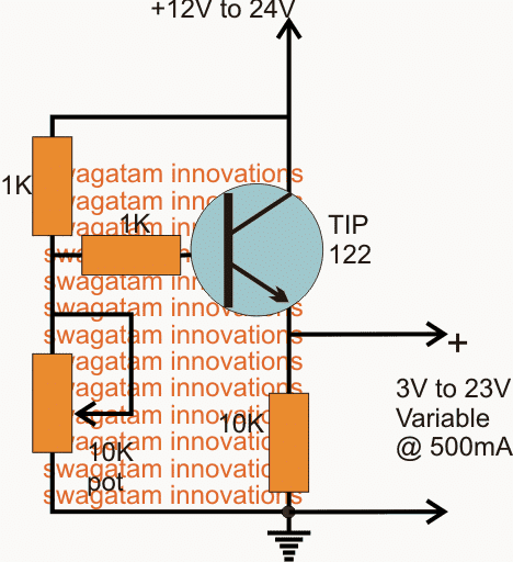
Using an Emitter Follower BJT
The diagram above shows a simple emitter follower configuration using a BJT and a few resistors. The idea is self explanatory, here the pot is used for adjusting the output to any desired level right from 3V or lower to the maximum fed input level, although the maximum available output would be always less than 0.6V than the applied input voltage. The advantage of incorporating a BJT for making 3.3V or 5V regulator circuit is that it enables you to achieve any desired voltage using minimum number of components. It also allows higher current loads to be used at the outputs, moreover the input voltage has no restrictions and may be increased as per the BJT's handling capacity and by some minor tweaks in the resistor values. In the given example, an input of 12V to 24V can be seen, which can be tailored to any desired level such as to 3.3V, 6V, 9V, 12V, 15V, 18V, 20V or to any other intermediate value simply by flicking the knob of the included potentiometer.5V Stabilized Regulator
The working of the 5V transistor regulator circuit is as follows. The 1k resistor attached between the collector/base of transistor BD131 typically means that the BD131 always stays in the conducting mode. However the 4.3 V zener diode ZD1 clamps the base voltage of the transistor 2N697 to approximately 4.3 volts lower than the emitter voltage of the BJT BD131. The 2N697 begins turning ON as soon as its base voltage reaches around 0.6 V positive with respect to its emitter voltage, and at this point the BD131 emitter reaches a potential of around 4.9 V positive.How to Modify SMPS for Adjustable Current and Voltage Output
This article discusses a method through which any ready made SMPS can be converted into a variable current smps circuit using a few external jumper links.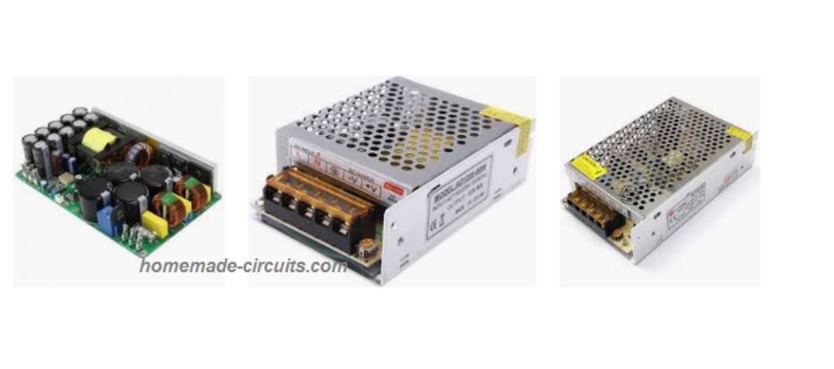 In one of the previous articles we learned how to make a variable voltage SMPS circuit by employing a simple shunt regulators stage, in the present hack also we employ the same circuit stage for implementing a variable current output feature.
What is SMPS
SMPS stands for Switch-Mode-Power-Supply, which uses a high frequency ferrite based switching converter for converting the AC 220V to DC. The use of a high frequency ferrite transformer makes the system highly efficient in terms of compactness, power loss, and cost. The SMPS concept today has almost completely replaced the traditional iron core transformers and have transformed these units into a much compact, light weight and efficient power adaptor alternatives. However since SMPS units are commonly available as fixed voltage modules achieving a preferred voltage as per the users application needs becomes quite difficult. For example for charging a 12V battery one may need an output voltage of around 14.5V, but this value being quite odd and non-standard we may find it extremely difficult to get an SMPS rated with these specs in the market. Although variable SMPS circuits can be found in the market, these may be costlier than the ordinary fixed voltage variants, therefore finding a method of transforming an existing fixed voltage SMPS into a variable type looks more interesting and desirable. By investigating the concept a little I was able to find a very simple method of implementing the same, let's learn how to conduct this modification. You will find one popular 12V 1amp SMPS circuit in my blog which actually has an in built variable voltage feature.The Function of Opto-coupler in SMPS
In the above linked post we discussed how an opto coupler played an important role in providing the crucial constant output feature for any SMPS. The function of the opto coupler may be understood with the following brief explanation: The opto coupler possesses an inbuilt LED/photo-transistor circuitry, this device is integrated with the SMPS outputs stage such that when the output tends to rise above the unsafe threshold, the LED inside the opto lights up forcing the phototransistor to conduct. The photo-transistor in turn is configured across a sensitive "shut down" point of the SMPS driver stage wherein the conduction of the photo-transistor forces the input stage to shut down. The above condition results in the SMPS output to also instantaneously shut down, however the moment this switching initiates, it corrects and restores the output to the safe zone and the LED inside the opto deactivates which once again switches ON the input stage of the SMPS. This operation keeps on cycling rapidly from On to OFF and vice versa ensuring a constant voltage at the output.Adjustable Current SMPS Modification
In order to achieve a current control feature inside any SMPS we yet again seek the help of the opto coupler. We implement a simple modification using a BC547 transistor configuration as shown below: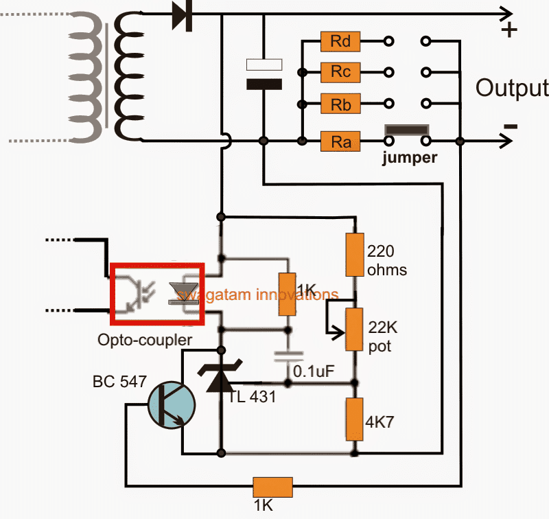 Referring to the above design we get a clear idea regarding how to modify or make a variable current SMPS driver circuit.
The opto coupler (indicated by red square) will be present by default for all SMPS modules, and assuming that the TL431 is not present then we may have to configure the entire configuration associated with opto coupler LED.
If the TL431 stage is already a part of the SMPS circuit, in that case we just have to consider integrating the BC547 stage which becomes solely responsible for the proposed current control of the circuit.
The BC547 can be seen connected with its collector/emitter across the TL431 IC's cathode/anode, and the base of BC547 can be seen connected with the output (-) of the SMPS via a group of selectable resistors Ra, Rb, Rc, Rd.
These resistors being in between the base and emitter of the BC547 transistor begin functioning like current sensors for the circuit.
These are appropriately calculated such that by shifting the jumper connection across the relevant contacts, different current limits are introduced in the line.
When the current tends to increase beyond the set threshold as determined by the values of the corresponding resistors, a potential difference is developed across the base/emitter of the BC547 which becomes sufficient to turn ON the transistor, shorting the TL431 IC between the opto LEd and ground.
The above action instantly lights up the LED of the opto, sending a "fault" signal to the input side of the SMPS via the opto's in-built photo transistor.
The condition immediately tries to execute a shut down across the output side which in turn stops the BC547 from conducting and the situation fluctuates from ON to OFF and ON rapidly ensuring that the current never exceeds the predetermined threshold.
Referring to the above design we get a clear idea regarding how to modify or make a variable current SMPS driver circuit.
The opto coupler (indicated by red square) will be present by default for all SMPS modules, and assuming that the TL431 is not present then we may have to configure the entire configuration associated with opto coupler LED.
If the TL431 stage is already a part of the SMPS circuit, in that case we just have to consider integrating the BC547 stage which becomes solely responsible for the proposed current control of the circuit.
The BC547 can be seen connected with its collector/emitter across the TL431 IC's cathode/anode, and the base of BC547 can be seen connected with the output (-) of the SMPS via a group of selectable resistors Ra, Rb, Rc, Rd.
These resistors being in between the base and emitter of the BC547 transistor begin functioning like current sensors for the circuit.
These are appropriately calculated such that by shifting the jumper connection across the relevant contacts, different current limits are introduced in the line.
When the current tends to increase beyond the set threshold as determined by the values of the corresponding resistors, a potential difference is developed across the base/emitter of the BC547 which becomes sufficient to turn ON the transistor, shorting the TL431 IC between the opto LEd and ground.
The above action instantly lights up the LED of the opto, sending a "fault" signal to the input side of the SMPS via the opto's in-built photo transistor.
The condition immediately tries to execute a shut down across the output side which in turn stops the BC547 from conducting and the situation fluctuates from ON to OFF and ON rapidly ensuring that the current never exceeds the predetermined threshold.
The resistors Ra...Rd may be calculated by using the following formula:
R = 0.7/cut-of current threshold For example if suppose we want to connect an LED at the output having a current rating of 1 amp. We can set the value of the corresponding resistor (selected by the jumper) as: R = 0.7/1 = 0.7 ohm Wattage of the resistor can be simply gotten by multiplying the variants, i.e. 0.7 x 1 = 0.7 watts or simply 1 watt. The calculated resistor ensures that the output current to the LED never crosses the 1 amp mark, thereby safeguarding the LED from damage, other values for the remaining resistors may be appropriately calculated for getting the desired variable current option in the SMPS module.Modifying a Fixed SMPS into Variable Voltage SMPS
This following post tries to determine a method through which any SMPS could be made into a variable power supply for achieving any desired voltage level from 0 to maximum.What is Shunt Regulator
We find that it employs a shunt regulator circuit stage for executing the variable voltage feature in the design. Another interesting aspect is that this shunt regulator device implements the feature by regulating the input of the opto coupler of the circuit. Now since a feedback opto coupler stage is invariably employed in all SMPS circuits, by introducing a shunt regulator one can easily transform a fixed SMPS into a variable counterpart. In fact one can also make a variable SMPS circuit using the same principle as explained above. You may want to learn more about what's a shunt regulator and how it works.Procedures:
Referring to the following example circuit, we are able to find the exact location of the shunt regulator and its configuration details: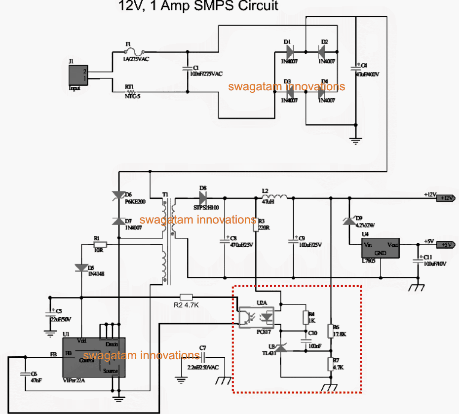 See the bottom right side of the diagram marked with red dotted lines, it shows the variable section of the circuit we are interested in.
This section becomes responsible for the intended voltage regulation actions.
Here the resistor R6 can be replaced with a 22K pot for making the design variable.
Magnifying this section provides a better view of the involved details:
See the bottom right side of the diagram marked with red dotted lines, it shows the variable section of the circuit we are interested in.
This section becomes responsible for the intended voltage regulation actions.
Here the resistor R6 can be replaced with a 22K pot for making the design variable.
Magnifying this section provides a better view of the involved details:
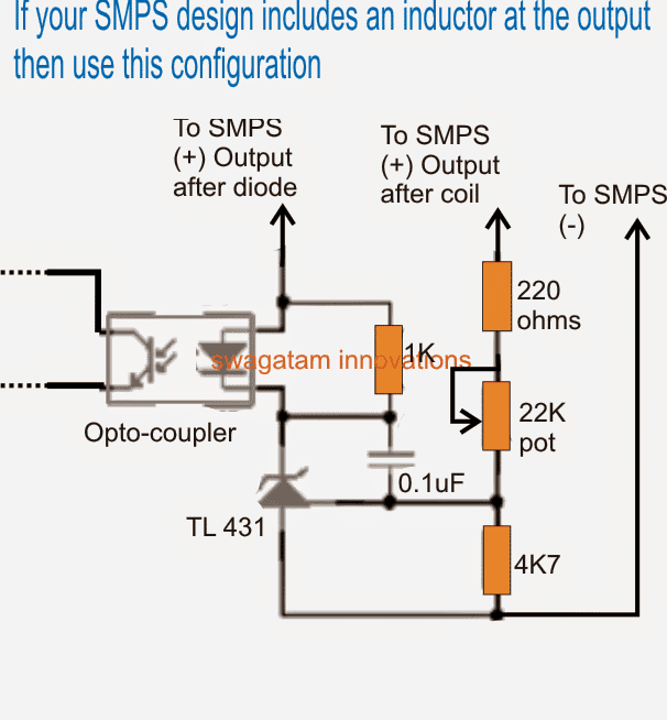
Identifying the Optocoupler
If you have a fixed voltage SMPS circuit, open it and just look out for the optocoupler in the design, it would be mostly located just around the central ferrite transformer, as may be seen in the following image: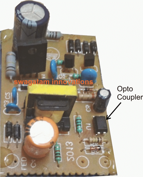 Once you have found the opto-coupler, clean up by removing all the parts associated on the output side of of the opto, meaning across the pins which may be towards the output side of the SMPS PCB.
And connect or integrate these pins of the opto with the assembled circuit using the TL431, shown in the previous diagram.
You can assemble the TL431 section on a small piece of general purpose PCB and glue it on the main SMPS board.
If your SMPS circuit does not have an output filter coil, you can simply short the two positives of the TL431 circuit and join the termination to the cathode of the SMPS output diode.
However suppose your SMPS already includes the TL431 circuit with the opto coupler then simply find the position of the R6 resistor and replace it with a pot (see R6 location in the first diagram above).
Don't forget to add a 220 ohms or 470 ohm resistor in series with the POT otherwise while adjusting the pot to the upper most level could instantly damage the TL431 shunt device.
That's it, now you know exactly how to convert or make a variable voltage SMPS circuit using the above explained steps.
Once you have found the opto-coupler, clean up by removing all the parts associated on the output side of of the opto, meaning across the pins which may be towards the output side of the SMPS PCB.
And connect or integrate these pins of the opto with the assembled circuit using the TL431, shown in the previous diagram.
You can assemble the TL431 section on a small piece of general purpose PCB and glue it on the main SMPS board.
If your SMPS circuit does not have an output filter coil, you can simply short the two positives of the TL431 circuit and join the termination to the cathode of the SMPS output diode.
However suppose your SMPS already includes the TL431 circuit with the opto coupler then simply find the position of the R6 resistor and replace it with a pot (see R6 location in the first diagram above).
Don't forget to add a 220 ohms or 470 ohm resistor in series with the POT otherwise while adjusting the pot to the upper most level could instantly damage the TL431 shunt device.
That's it, now you know exactly how to convert or make a variable voltage SMPS circuit using the above explained steps.
Warning: SMPS circuits are not isolated from AC Mains on the primary side, and can be lethal to touch while in uncovered and switched ON condition.
UPDATE
The following image shows perhaps the easiest way to customize an SMPS circuit for getting a variable voltage and current features. Please see how the pots or presets needs to be configured across the opto-coupler for getting the intended results: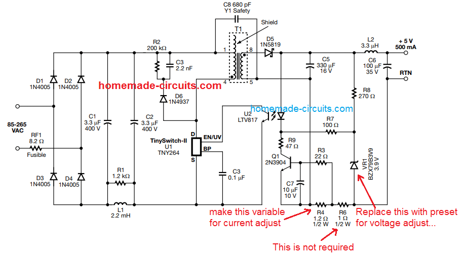 If you have any further doubts regarding the design or the explanation, feel free to express through your comments.
Let's Summarize
In this write up we quickly try to summarize the main points regarding how to modify any SMPS circuit through an easy hack which may help us to get a desired customized output from the unit.What is an SMPS
SMPS stands for switch mode power supply and it's the modern and most compact/efficient way of acquiring low voltage DC from mains AC source. However making an SMPS at home may not be as simple as making power supply units using traditional iron core transformers. Also getting an SMPS with custom specs may not be that easy, in fact impossible if the voltage/current specs are far away from the regular values. So does that mean we have to be satisfied with the SMPS specs which are typically set, and available in the market? For example how do we find an SMPS having an output of say 13 volts or 14 volts or 17 volts which are definitely not the normallyacceptedvoltage ranges?Customizing an SMPS unit
Since making such acustomizedunit may not be an easy task (due to complex layouts and part configurations) it would be a lot better if we could find ways of modifying a readymade one through some simple steps. I have studied a few standard SMPS units and hopefully cracked ways ofmodifying thevoltagesand current as per individual choices. Let's learn it in details. When you open any standard SMPS unit, you will come across the following things over the enclosed assembled card. The populated PCB can be primarily divided into two sections by the presence of the center ferrite transformer. The side of the transformer where the mains chord makes its entry is the input AC section while the other side from where the low voltage DC is derived is the DC section. We are not interested in the AC section because we do not want to modify the input voltage so do not pay any attention there, moreover the AC section is POTENTIALLY VERY DANGEROUS TO TOUCH IN SWITCHED ON CONDITION, THEREFORE KEEPS YOUR HANDS OF IT WHILE TESTING. The DC section will mainly consist of a couple of chokes, a couple of filter capacitors, a diode and a few other components.Look for the Shunt Regulator
Search for a transistor shaped component in this section. If you find a couple of them, one will be actually a transistor, probably for limiting the output current, however the other one will be definitelyTHE PROGRAMMABLE SHUNT REGULATOR. This shunt regulator is the component which fixes the feedback voltage to the AC section mosfet and in turn determines the output voltage. This programmable shunt device is set up through a couple of resistors, changing which will instantly change the output voltage as per ones wish. Try to locate the resistors connected with the leads of this shunt device. One of them can be simply varied for changing the output voltage as per your preferences. Take an external resistor of any value may be a 4k7 1/4 watt, now step-wise go on connecting this resistor across the resistors which are associated with the shunt regulator device.Check and Verify the Output
Verify the output voltage each time you do the above step. The moment you find a change in the output voltage either becoming low or high, you might have just found the one which we are looking for. Now through some trial and error you may find out the exact value of resistor which could be replaced in place of the particular shunt resistor. That's it, it's as simple as that, once you do it, the output voltage would get adjusted to that particular value permanently. But do remember to remove the zener diode if there's any at the output of the power supply before you do the above procedures.100 amp Variable Voltage Power Supply Circuit
The post describes a simple but extremely versatile 100 amp, variable voltage power supply circuit using just a few BJTs in parallel and in a common collector mode. The idea was requested by Mr. Andre.Technical Specifications
Hello Swagatam, I was wondering if you could possibly assist me. on the blogs I have seen some diagrams for simple variable power supplies. Firstly I know very little about electronics, but with a shopping list and a diagram I am sure I would be okay. I would like to build a simple variable power supply with an input of 220/240 volt ac and an output variable voltage of approx. 1.5V to approx. 15V and a variable output current of up to approx. 100A. I have started zinc electroplating as a hobby (have sweaty hands and want to protect all my tools) the chemical company gave me these as a more or less dependant on my zinc plating bath size. At the moment the little 6V 8A Ryobi battery charger works for a few minutes, overheats and cuts out till it cools down again. I would really appreciate any assistance you could give me on this. Many thanks AndreThe Design
A very straightforward circuit design for the proposed 100 amp variable voltage power supply can be witnessed in the following diagram.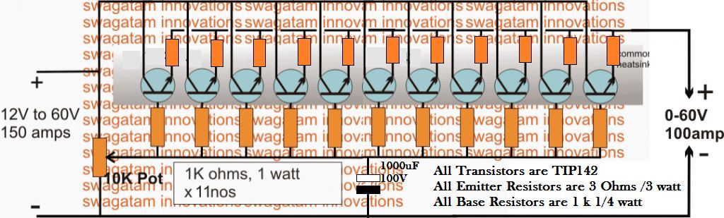 The design basically utilizes a common collector or an emitter follower topology for implementing the operations, by incorporating just a few Darlington power transistors, some resistors and a pot for varying the output voltage.
As can be seen in the diagram, the collectors and the emitters are all joined in common across each other while the bases are made into a common line via individual limiting resistors.
The free ends of these resistors are joined together with a pot across the negative line of the circuit, which determines the voltage regulation at the output of the circuit.
For acquiring more current, more number of transistors may be added in the design, and for reducing the output amps, these may be simply deducted from the configuration.
For inputs above 50V the pot must be upgraded to a high wattage type to sustain the high voltage across its terminals.
All the power devices must be mounted over a common aluminum heatsink without any mica isolation, so that the dissipation is shared uniformly across all the devices and a thermal runaway situation is prevented.
The design basically utilizes a common collector or an emitter follower topology for implementing the operations, by incorporating just a few Darlington power transistors, some resistors and a pot for varying the output voltage.
As can be seen in the diagram, the collectors and the emitters are all joined in common across each other while the bases are made into a common line via individual limiting resistors.
The free ends of these resistors are joined together with a pot across the negative line of the circuit, which determines the voltage regulation at the output of the circuit.
For acquiring more current, more number of transistors may be added in the design, and for reducing the output amps, these may be simply deducted from the configuration.
For inputs above 50V the pot must be upgraded to a high wattage type to sustain the high voltage across its terminals.
All the power devices must be mounted over a common aluminum heatsink without any mica isolation, so that the dissipation is shared uniformly across all the devices and a thermal runaway situation is prevented.
Making a Strong RF Discharge Circuit
In this article we study an RF discharge generation concept also called EMP generator capable of producing an intense RF electrical discharge in the air which may have the potentials of paralyzing and permanently damaging all electronic systems in the close vicinity. The idea was requested by Mr. Nidal.Technical Specifications
I have seen a lot of circuits from you in your blog. I am a great fan of you!!!! If you could help me with a circuit diagram for breaking 2.5 Volt torch bulb (Filament type) when it is switched ON and kept close to a copper pot 6 inches away (distance is between torch and copper pot) with a 12 Volt DC supply. The thing is that, a switched on torch bulb should blow off when it is kept closer to a "copper pot" kept 6 inches apart. I hope a strong magnetic field will give the result. But the problem is how to magnetize a copper pot to that extend?, an alternating supply give to a copper pot may develop magnetic flux around it or will it get short circuited? Is it enough to break lamp filament? Or do I need to wind a copper coil inside that vessel to get that result? Please help me in solving this issue. Many thanks and expecting a reply from you soon. Best regards, Nidal.
The Design
The proposed concept of fusing a bulb filament through a wireless magnetic field doesn't appear to be feasible, however it could be implemented using a very strong RF discharge, such as from a very high voltage capacitor.
The idea may be carried as given in the following explanation:
A high current low voltage is first stepped up to many kilovolts, then stored inside equivalently rated high voltage capacitors and finally discharged by creating a short circuit across the high voltage capacitor leads.
The resulting discharge will generate an awesome amount RF electricity in the zone which may have the potential of fusing the filament of a bulb or illuminating a fluorescent tube momentarily.
Caution: The EMP discharge could produce devastating effects on all electronic equipment placed within the range of the discharge.
Circuit Diagram
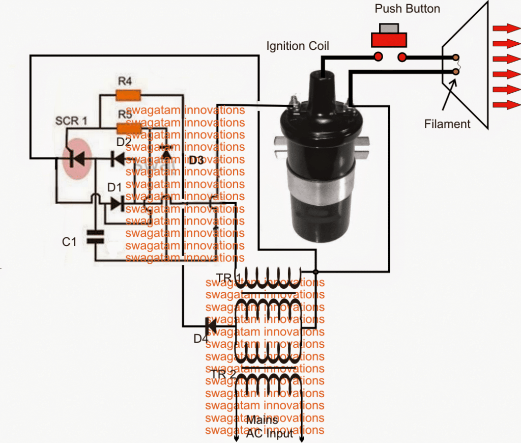
How it Works
Referring to the diagram above, the set up shows a basic capacitive discharge system. The circuit comprising the diodes, C1 and the SCR form a capacitor charge/discharge switching stage which is powered from a boosted AC using a couple of mains transformers.TR1/ and TR2 transformers are coupled together such that the low voltage TR2 winding connects with the TR1's low voltage winding.
When mains is applied to TR2 primary, an equivalent 220V (low current) is induced across the upper winding of TR1.
This voltage is used for charging the high voltage capacitor C1 in the circuit via a switching SCR stage which is triggered through the 50Hz low voltage input from TR2 via D2.
The switched C1 discharge is applied to the primary of a car ignition coil, which steps up this voltage to a staggering 40,000V or higher.
This voltage is kept hanging across a thin filament position within a suitably dimensioned conical shaped aluminum radiator.
When the shown push button is pressed, the high voltage tries to force its path through the filament creating a massive arc and explosion across the points.
This generates an intense RF disturbance in the region which is further magnified and propagated by the cone to the target which is here a small electrical bulb. If the discharge is sufficiently strong may produce a momentary illumination of the bulb filament and then fusing due to the generated RF electricity.
Parts List
R4,R5 = 100 OHMS, 1 WATT D1, D2, D3, D4 = 1N4007 C1 = 100uF/500V, SCR = BT151 TR1/TR2 = 220V/0-12V/1AMP TRANSFORMERS.Making a Regulated 9V Battery Eliminator Circuit
The post presents a regulated 9V battery eliminator circuit which was built and investigated by Mr. Steven Chiverton, an avid reader of this blog and an experienced electronic hobbyist. Let's learn more from him.9 volt battery eliminator circuit tests:
Circuits built 2x each circuit ive made a small modification to it buy adding a low esr 1000uf filetr capacitor between each circuits positive and negative output, latter after construction i decided to test them both but i removed the filer capacitor to note the difference between each 9 volts battery eliminator circuit. First test was with the battery eliminator with the 1000uf low esr filter capacitor, i fed 12 volts dc into it and the output was a9.21 volts dc. Then the battery eliminator without the low esr filter capacitor was tested, i fed it the same 12 volts dc and the output was less at 9.05 volts dc. Test 2 , i then changed the voltage output of my transformer to 9 volts dc , so i fed 9 volts dc into the battery eliminator with the 1000uf low esr filter capacitor and its output was 8.18 volts dc. Then i fed the same 9 volts dc into the battery eliminator without the 1000uf low esr filter capacitor and its output was 7.67 volts dc . Test 3 , then i changed the transformer output voltage to 7.5 volts dc and so i fed that into the battery eliminator with the 1000 low esr capacitor and its output was ,6.75 volts dc. Then i fed the same 7.5 volts dc into the battery eliminator without the 1000 low esr filter capacitor and the output was then 6.2 volts dc . Test 4, i then changed the transformer voltage output to 6 volts dc, and then i fed that into the battery eliminator with the 1000uf low esr filter capacitor and its voltage output was 5.30 volts dc. Then i fed the same voltage into the battery eliminator without the 1000uf low esr filter capacitor and its output was then 4.88 volts dc. Test 5, i then changed the output voltage of the transformer to 4.5 volts dc and then i fed that into the battery eliminator with the 1000uf low esr filter capacitor and the output was then 3.92 volts dc then i fed the same voltage into the battery eliminator without the 1000uf low esr capacitor and its output was then 3.62 volts dc. Last test test 6, i then lowered the transformer output to the last setting on 3 volts dc and fed that into the battery eliminator with the 1000uf low esr filter capacitor and its output voltage was then 2.44 volts dc . So then i fed the same 3 volts dc into the battery eliminator without the 1000uf low esr filter capacitor and its output voltage was then 2.29 volts dc .Conclusion:
So my research tells me that the 1000uf low esr filter capacitor or any 1000uf electrolytic capacitor dose make a difference in providing better voltage output and filtering compared to not using the 1000uf electrolytic capacitor.Circuit Diagram and Prototype
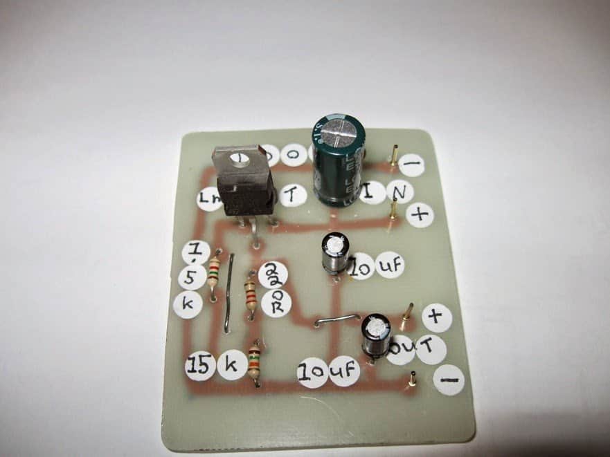
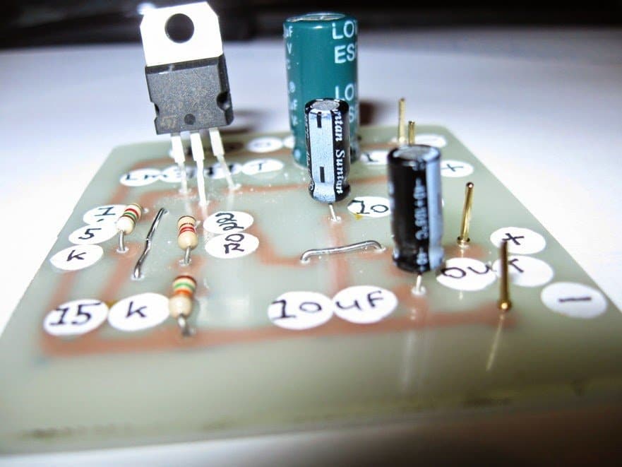
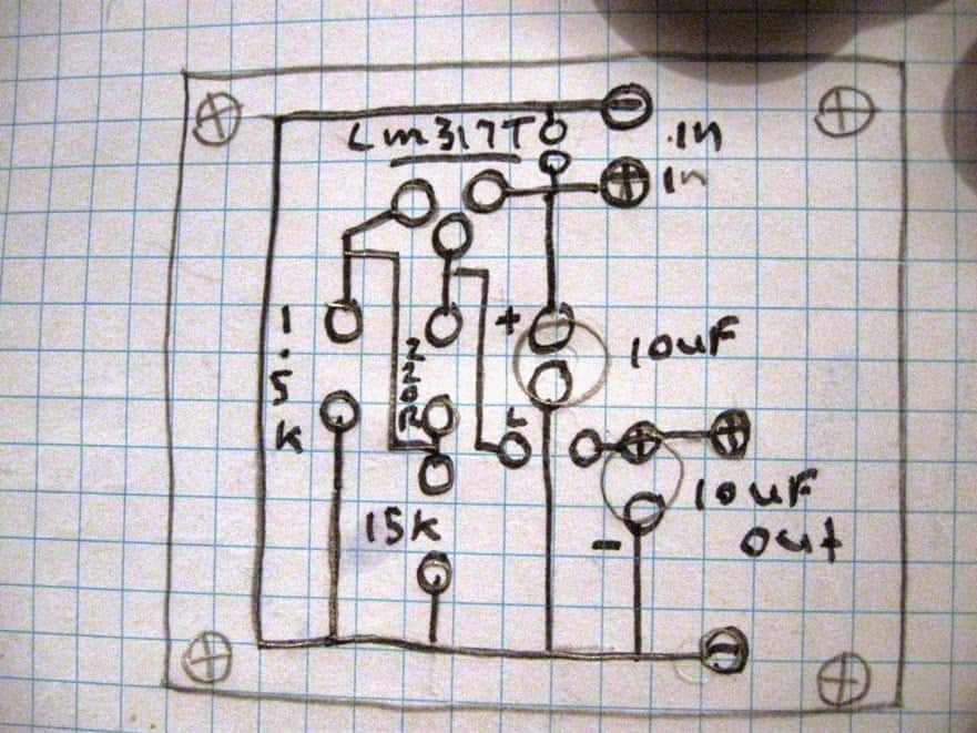
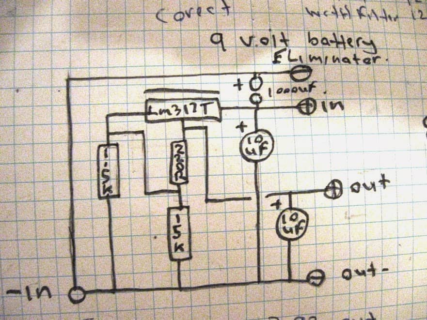
0 to 50V, 0 to 10amp Variable Dual Power Supply Circuit
The post explains a simple yet very useful 0 to 50V dual power supply circuit which will enable a full 0 to maximum dual voltage +/- control of the input power supply DC. It also includes a wide range current control feature right from 0 to 10 amps. The idea was requested by Mr. Tamam.Technical Specifications
It was my long term dream to build a 2 channel power supply for personal use, I have seen a lot of circuits, but those does not fit my criteria. However, please take a look at the following requirements and let me know if its possible or not, if possible I will be the happiest person in the world. 1. Output voltage range: -50V to 0V to +50V ( must be adjustable by individual channel ) 2. Output Current range: 0A to 10A ( must be adjustable by individual channel ) 3. Output would be Duel channel, means total 6 outputs, Channel 1 (Positive, GND, Negative) Channel 2(Positive, GND, Negative) 4. Power Supply Unit should contains 2 Voltmeters and 2 Ammeters (Analogue) for 2 individual channel. 5. Power Supply Unit must have short circuit protection and cooling fan featured and extreme heat protection. 6. I don't want to use any PIC or AVR, so please avoid those. Money is not a matter here, I will spend continuously until above requirement meets. Even If I need any custom transformer I will order and make it from our local area. I have seen many ready made power supply in market but I want to make it by own hand.You just show me the way... please bro, I will be pleased to you for lifetime. Thank you very much !! Best Regards, Tamam For calculating the part values accurately, you can refer to this bench power supply articleCircuit Diagram
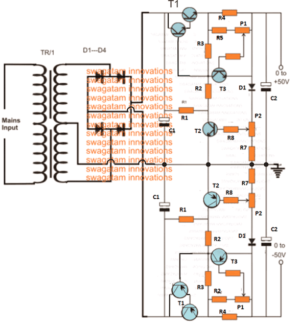
The Design
The basic design of the proposed 0 to 50V variable dual power supply circuit with 0 to 10 amp variable current facility is shown in the above figure. The entire design is transistor (BJT) based and is virtually indestructible. Moreover it's equipped with an over load and over current protection features. The two section included in the design are exactly similar with their configurations, the only difference being the use of PNP devices in the lower configuration while NPN in the upper configuration. The upper NPN design is configured to produce a variable response right from 0.6V to 50V positive while the lower PNP section becomes responsible of producing an oppositely identical response from -0.6V to -50V output.The Transformer Specs
The maximum limit could be suitably changed simply by changing the voltage rating of the transformer. However for higher voltages you may have to appropriately upgrade the BJT voltage ratings accordingly. In both the designs, P2 executes the function of varying the voltage levels as desired by the user, while P1 functions as the current regulator and is used for adjusting or setting the output anywhere from 0 to 10 amp current. Here too the maximum rating depends on the selection of the transformer amp rating and may be changed as per individual preferences. T1s in the both the sections become the fundamental part or the heart of the entire voltage control functioning in the circuit, which becomes possible due to the popular common collector configuration of the devices. The other two active BJTs only help to implement the same just by controlling the base power of the T1s thus making it possible to adjust the thresholds to any desired user defined voltage and current levels, as per the ratings of the transformer or the input supply. You may also like this LM317 based Dual Power Supply CircuitParts list
R1 = 1K, 5 watt wire wound R2 = 120 Ohms, R3 = 330 Ohms, R4 = to be calculated using Ohms law, R = 0.6/Maximum Current Limit, Wattage = 0.6 x Maximum Current Limit R5 = 1K5, R6 = 5K6, R7 = 56 Ohms, R8 = 2K2, P1,P2 = 2k5 presets T1 = 2N6284 + BD139(NPN), 2N6286 + BD140(PNP) T2, T3 = BC546 (NPN) BC556B (PNP) D1, D2, D3, D4 = 6A4, D5 = 1N4007,C1, C2 = 10000uF/100V, Tr1 = 0 �C 40 Volts, 10 AmpOperating Single Rice Bulb Lamp with 220V AC
The post explains a simple 220V mains operated transformerless single rice bulb power supply circuit, which may be used for illuminating electronic rice lamp diyas replacing traditionaloil lamp type diyas during festivals or for decorating sacred idols. The idea was requested by Ms. Rashmi. I want to make a rice light LED bulb with a long wire. I want to change my oil lamp to LED lit. Pls help me make a single rice LED tiny bulb connected to a long wire with a plug in the end. I want to connect it to my 440V power point at home. So what kind of adapter/transformer can I use. How much will it cost me approx!? Any 12V bulb, may it be a rice bulb or other forms can be simply lit through a 12V AC/DC adapter rated as per the specified bulb current requirement. Therefore according to the request a rice bulb too can be powered via a 12V/500mA or 1amp AC/DC adapter. However the current requirement of such bulbs being too small the above type of power supply could look bulky and costly (approx Rs.100/- in India). An alternative suitable, compact mains power supply for illuminating it could be implemented through a capactive type of power supply, the making procedure is explained below.
The Design
A rice bulb could be an LED or in the form of a tiny incandescent lamp rated to operate at 6, 12 or 24V AC/DC, with current consumption of typically 50, 30, 10mA respectively. Here we use a 12V rice bulb which may consume a current at around 25mA. We have seen many exclusively designed transformerless power supply in this blog, one of them has been employed here or driving the proposed single rice bulb diya at 220V or 120V mains supply. Looking at the circuit diagram below, a straightforward half wave capacitive power supply can be seen configured for driving the attached single rice bulb. The 0.33uF capacitor is positioned for dropping the mains 220V current to the desired low value level as per the lamp specs. The 1N4007 diode takes the sting away from the switching initial surge current by grounding one half cycle of the mains and allows only the positive half cycle to proceed toward the lamp. The 15 zener diode further makes sure that only 15V reaches ahead across the lamp, while the resistor helps to keep the current from rising to any higher dangerous levels. The capacitor 0.33uF may be tweaked a bit if the lamp intensity does not produce the desired illumination, other higher values such as 0.47uF. 0.68uF or even 1uF may be tried in place of 0.33uF for the same. Alternatively a 100uF/50V capacitor may be connected across the zener diode for obtaining the above optimization. The entire circuit is directly linked with LETHALmainspotential, and therefore is extremelydangerousto handlewithoutadequateinsulation while switched ON. Due care is advised.Circuit Diagram
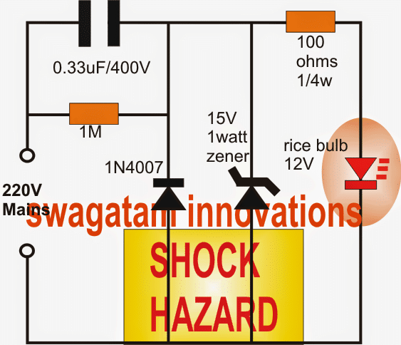
12V, 24V, 1 Amp MOSFET SMPS Circuit
The post investigates a cheap Chinese made 12V, 1 amp MOSFET based smps circuit which can be modified into 24V 1 amp, or 12V 2 amp smps circuits also. The MOSFET used isSTB9NK60Z which is a highly advanced, rugged 600V 7A device specially manufactured for high, unpredictable, voltage environment circuit applications.Reverse Engineering a 12V 1 Amp SMP Adapter Physically
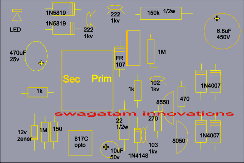
Coil Details:
The proposed 12V, 1 amp MOSFET based smps circuit utilizes a single E-core transformer, the winding details may be understood from the following info: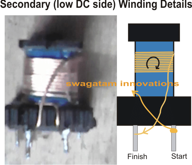 Wire thickness for the above secondary winding = 0.6mm, no.
of turns = 12
Wire thickness for the above secondary winding = 0.6mm, no.
of turns = 12
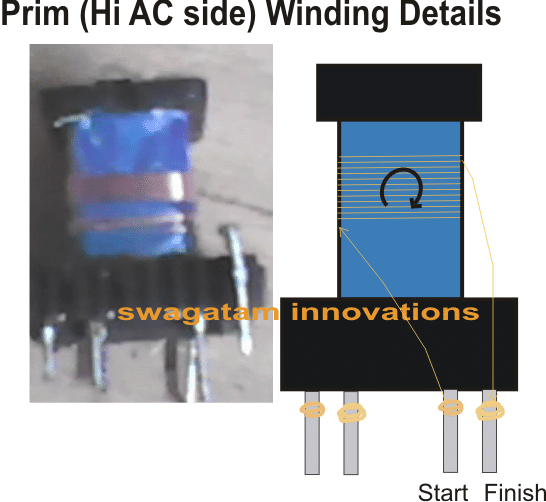 Wire thickness for the above primary winding = 0.25mm, no.
of turns = 12
Wire thickness for the above primary winding = 0.25mm, no.
of turns = 12
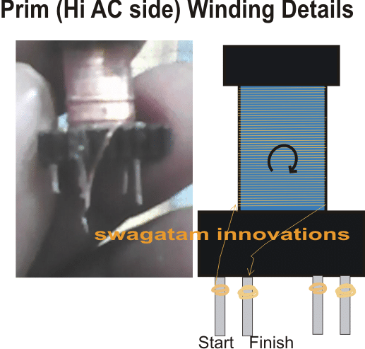 Wire thickness for the above primary winding = 0.25mm, no.
of turns = 170
Feedback from one of the dedicated readers of this blog Mr.Debabrata Mandal:
I bought one today which is exactly the same, well, almost, cost me 100
Tested it @shop for 10 sec& it ran fine, brought home, plugged it in & was just about the test it with multimeter & there was a popping sound, though the indicator led was still glowing
Opened it and found that the electrolytic @ 12v side had blown, another 16v cap was burnt, in this condition I tested the output & found output at around 22-23v
Right now, I cannot check it properly because as soon as I turn it on, within a second the mosfet starts getting burning hot.
Also I can't figure out the transistors s9014 & s8550, what type or how their pins are configured?
There are just 3 components different than the above design
100E/.5w instead of yr 150e/.5w (resistor)220e instead of your 270e (resistor) s9014 instead of your s8050 (transistor)
Without taking anything out of the board, I tested the diodes/zener, they looked fine to me.
So without taking out the transistor/mosfet could you tell me how to check them w/o having to turn the power ON...
because that could melt the mosfet for sure.
Or whatever idea you can share to debug this...
also, how do i tweak the circuit to 14v(13.6~14.4)& 1.1A (>1.05)
Wire thickness for the above primary winding = 0.25mm, no.
of turns = 170
Feedback from one of the dedicated readers of this blog Mr.Debabrata Mandal:
I bought one today which is exactly the same, well, almost, cost me 100
Tested it @shop for 10 sec& it ran fine, brought home, plugged it in & was just about the test it with multimeter & there was a popping sound, though the indicator led was still glowing
Opened it and found that the electrolytic @ 12v side had blown, another 16v cap was burnt, in this condition I tested the output & found output at around 22-23v
Right now, I cannot check it properly because as soon as I turn it on, within a second the mosfet starts getting burning hot.
Also I can't figure out the transistors s9014 & s8550, what type or how their pins are configured?
There are just 3 components different than the above design
100E/.5w instead of yr 150e/.5w (resistor)220e instead of your 270e (resistor) s9014 instead of your s8050 (transistor)
Without taking anything out of the board, I tested the diodes/zener, they looked fine to me.
So without taking out the transistor/mosfet could you tell me how to check them w/o having to turn the power ON...
because that could melt the mosfet for sure.
Or whatever idea you can share to debug this...
also, how do i tweak the circuit to 14v(13.6~14.4)& 1.1A (>1.05)
Possible Solution:
The mosfet should not become hot as long as the output is not loaded or short circuited. If it's getting hot without any load at the output could mean a faulty primary section. Confirm the status by doing the following steps: Cut the PCB tracks of the secondary winding terminals such that it becomes completely isolated from the circuit board, confirm the continuity with a multimeter. Next connect a 25 watt bulb in series with the input AC to the smps and switch ON power. If the 25 watt bulbs glows or if the mosfet shows significant heating would confirm a faulty primary stage. The next step would be to remove the transistors one by one and replace them with new ones and apply the input voltage tocheck the mosfet condition. If the heating persists then finally you can go for amosfet replacement with a new one.After all these procedures are completed and the problem is fixed, we can go ahead to check why the secondary is generating a 24V output. This could be due to a wrong winding data or may be once the primary stage is resolved as above, the output would also settle down withthe correct output. More Inputs from Mr. Debrata OK I already took out the 2 transistors + mosfet + transformer and checked all looked fine, checked the resistors and capacitors, all seem to be fine and then I put them back & started checking the pcb itself... I found a short, after soldering they didn't cutshort that leg & it protruded & touched the copper film, so i cut it short & checked, now the output showed2.3v but still mosfet kept getting Hot. Amazing... finally nothing to do, i replaced the blown cap with 1000u/16v keltron and what? The problem got fixed.Analyzingthe Issue
Wow that's indeedvery interesting., so the problem was in the filter capacitor, once it got fixed, the opto-coupler could receive the feedback input from it and in turn helped to regulate the mosfet conduction..... Anyway all's well that ends well. Thanks for the feedback.Connecting Voltage Regulators 78XX in Parallel for High Current
In this post we investigate how to connect popular voltage regulator ICs such as 7812, 7805 in parallel for acquiring high current output from the ICs. Voltage regulator chips mostly have their maximum current output specs fixed to some predetermined levels. Increasing them to a higher level would normally call for external out board transistors and complicated associated circuitry which might be difficult to configure for the new hobbyists. Connecting a few of them in parallel, possibly solves the problem. The idea was requested by Mr.Raja. Sir, could i use three L 7815 voltage regulator ic in parallel, to get 15volt 4 amps dc current from about 20 volt 5 amp dc source? Sir, as LM 338 and their equivalent ic s ( which gives 5 amps ) arenot available in my town. I planned to use three 7815 in parallel. Ismy idea works? If so please help me. How can i connect them in parallel ? Could i connect input of allthree 7815 ic by a common wire or i should separate mutually by adiode of 2 amp? And what about out put, should i separate them or use a common wire? And i think, i can connect the negative terminal of icwith a common wire. Is it? Please guide me.Solving the Circuit Request
Although notrecommendedby many, the issue can be handled simply by connecting the regulators in parallel, as shown in the following diagram. Here we can see the terminals of the all the three ICs connected in parallel except the output pins which are terminated with individual diodes. However the above connection might face a crucial drawback. Since all the ICs wouldn't have preciselyidenticalcharacteristics and specs could vary with their current limits, and ultimately lead to one of them supplying greater amount of current than the other, and overheating in the course. Although this won't pose a threat to the ICs as these arealwaysthermally protected from inside, it's never a good idea to have a semiconductor device sizzle unnecessarily. The issue can be very easily tackled by connecting the counterparts over a common heatsink, as shown in thediagrambelow. Since the tab for the ICs connect with their identical common leads (ground lead), doesn't need any sort of isolation in the form of mica isolation kit etc. Just make sure to put themover a common aluminium plate, and then you can relax as the heatdissipationacross the plate would result in correct transition of heat enabling each one with an equal share of current at their respective outputs which in return would result in an optimally combined higher current outputs, as required.Circuit Diagram
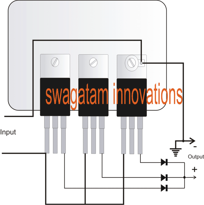
1.5V to 12V DC Converter Circuit for LEDs
The post providesinterestinginformation regarding the making of a 1.5V to 12V converter circuit using a couple of transistors and an inexpensive coil. The idea was requested by Mr. Keith.The CircuitRequest
I found your blog and have searched for an answer to my question but I'm just not finding it.... What I want to do is use 4 x 3v "2032" coin batteries connected in parallel to get long lasting life out of them. Then using a "Joule Thief" circuit up the out-put voltage to 12.5v - 14v to drive a set (3) of color changing LED's or a 12v LED light bulb found on ebay (here is the link to the bulb... Now here is the other part of my problem, I don't want to use a wire wound transformer !!!! I would like the Joule Thief circuit to use transistors or some other easy to get materials because at the end of all of this I am going to encased the whole project in clear resin.. Any help would be great... A wiring schematic with parts labeled would help also. Thanks, KeithSolving the Circuit Request
Hello, Thanks for contacting me! I am afraid without a coil it wouldn't be feasible to create a joule thief effect, because the coil is the maincomponent which enables complete extraction of energy from a depleting source. Regards. Feedaback from Keith I thought that is what you would say. Is there a way to design it with a ferrite core coil that is available "off the shelf" i.e. Radio Shack or Digi-Key, so I don't have to make my own. And could you design it? Also would there be any issues with encasing this project in liquid resin? The resin will cure within 24 hours and I am just wondering is there any issue with the coil not being able to get "fresh air" and getting too hot and eventually burning up. By the way the on/off switch is a mercury switch. Would any of these work? I know that my power requirements maybe more or less than 330uh, I just search for that size because I remember seeing that being used by this project: https://www.instructables(dot)com/id/Joule-Thief-no-IC-and-no-Transformer/ If none of this works can you please send me a wiring schematic with labels for parts that does include a wire coil and I will just build it that way. Thanks again, KeithAnalyzing the Circuit Idea
The 1.5V to 12V converter circuit provided in the above "instructables" link would possibly do the job. The second digikey link coil is the one which exactly suits the design, so you can try it out. Epoxy resin sealing would be fine, it won't do any harm to the inductor. Regards.Circuit Diagram
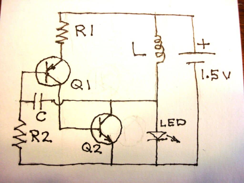
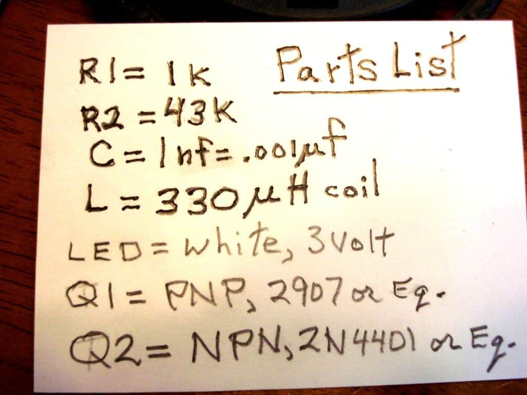 Inductor 300uH or similar (Picture)
0-300V Adjustable MOSFET Transformerless Power Supply Circuit
This simple MOSFET controlled transformerless power supply circuit can be used for delivering a continuously variable 0 to 300V DC output and a current control from 100 mA to 1 Amp. To protect against my high voltage research projects from going up in smoke permanently, I developed an easy circuit which is able to render a variable voltage supply of 0 to 330 Volt. But please be cautioned, the circuit is not isolated from mains potential, and therefore can inflict a lethal shock. The supply is short-circuit proof: the current is restricted to approximately 100mA.Circuit Operation
The design does not require a transformer, rather a 100 watt bulb is introduced at the input in order to provide ultimate safety in case of a short circuit or a component failure. The mains voltage from after passing through the lamp is rectified with bridge D1 (1Amp / 500V) and C1. T1 is configured as a source follower: the source of T1 complies with the voltage of the wiper of R3. D2 is insured to safeguard the gate of T1. T2 and shunt resistor R2 establish the current limiter. Whenever the output current results in being excessive, T2 quickly discharges the gate of T1. This stops the current from increasing any further.The value of R3 was basically identified experimentally; however it actually depends on the Hfe of T2 which means you may need to adjust the value of R2 appropriately. Keep in mind T1 requires a large heatsink: in nastiest situation T1 would probably disperse 330V x 100mA = 33Watt! You may try mosfets such as a BUZ 326 (400V/10.5Amp) or you may likewise use an IRF740 (400V/10Amp). The output impedance of the power supply varies according to the beta of T1, therefore the bigger the MOSFET,the lesser the output impedance!Circuit Diagram
 UPDATE:
The above design could be much simplified as indicated in the following diagram.
The bridge rectifier has been eliminated which drastically reduces the stress level on the MOSFET.
However, the ripple generated due to a half wave rectification may be significantly higher.
The output 10uF filter capacitor helps to reduce this to some extent.
The value of this capacitor could be increased to higher levels for improving the DC quality.
The input series lamp can be added, although this may not be required due to the presence of the current control stage in the design.
However, for better safety a fuse may be added in series with the input line.
UPDATE:
The above design could be much simplified as indicated in the following diagram.
The bridge rectifier has been eliminated which drastically reduces the stress level on the MOSFET.
However, the ripple generated due to a half wave rectification may be significantly higher.
The output 10uF filter capacitor helps to reduce this to some extent.
The value of this capacitor could be increased to higher levels for improving the DC quality.
The input series lamp can be added, although this may not be required due to the presence of the current control stage in the design.
However, for better safety a fuse may be added in series with the input line.
 Video Proof:
This power supply can be used to obtain a regulated power output, variable right from zero to 300 volts maximum.
All the devices should be mounted on heatsinks.
Video Proof:
This power supply can be used to obtain a regulated power output, variable right from zero to 300 volts maximum.
All the devices should be mounted on heatsinks.
Using a Combination of BJT and Mosfets
Circuit Operation The next transformerless 0-300V variable power supply circuit diagram can be understood with the following points:As can be seen in the figure, a high voltage transistor BF458 is used as the main load handling device. Its base bias is controlled by another high voltage transistor BF337 whose emitter is clamped to a stable 24 volts.An FET is used for selecting the base current of the transistor BF337 via a pot of 1M. This setting adjusts the base current for the BF337 which in turn restricts the main transistor BF458s voltage and current flow to the output. The input to the circuit may be derived directly from the mains AC after proper rectification and filtration using a bridge network and a 10u/400V capacitor. The entire circuit is extremely dangerous to touch, due care should be maintained while making and testing this circuit.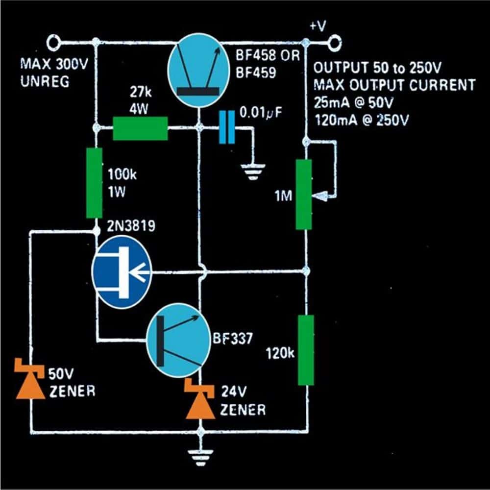 WARNING: THE CIRCUIT CARRIES LETHAL MAINS VOLTAGE AND THEREFORE IS EXTREMELY DANGEROUS.
IT CAN KILL ANYBODY, IF TOUCHED ANYWHERE ON THE CIRCUIT IN POWERED CONDITION.
OBSERVE APPROPRIATE PRECAUTIONS TO AVOID ANY MISHAP.
WARNING: THE CIRCUIT CARRIES LETHAL MAINS VOLTAGE AND THEREFORE IS EXTREMELY DANGEROUS.
IT CAN KILL ANYBODY, IF TOUCHED ANYWHERE ON THE CIRCUIT IN POWERED CONDITION.
OBSERVE APPROPRIATE PRECAUTIONS TO AVOID ANY MISHAP.
MJE13005 Compact 220V Power Supply Circuit
The following article presents a very simple lowcurrent mains operatedtransformerless power circuit using an inexpensive MJE13005 transistor and few other passive electronic components. As can be witnessed in the given circuit diagram, the design is extremely straightforward.How it Works
Transistor T1, which is a high voltage NPN transistor MJE13005 forms the main active component in the circuit. Rest of the components are positioned just for supporting the conduction of T1 and for the required stabilization. The circuit can be understood with the following points: Mains input is fed across D2 and the negative line of the circuit. D2 rectifies the mains AC, while C1 filters to some reasonable levels. R1 drops the current to tolerable limits in order to provide the required base bias for T1. C2 provides further filtration to the voltage generated after R1. D1 clamps the base voltage at the base of T1 to 24V, such that the maximum output voltage can never exceed this limit. A mirror voltage which is always equal to the zener value is generated at the output, however the presence of R2 enables the response to become variable. The adjustments made through R2 effectively varies the zener voltage right from zero to the maximum value, that is up to 24V. Thus the obtained output becomes variable from zero to 24V. However since the voltage is acquired across the emitter/ ground of the transistor, the current gets restricted to very modest levels, at 25mA to be precise. The zener voltage though may be increased to any desired limits. WARNING: THE WHOLE CIRCUIT IS NOTISOLATEDFROM MAINS AC, THEREFORE IS EXTREMELY DANGEROUS TO TOUCH WHILE IT'S UNCOVERED, AND POWERED CONDITIONParts List
R1 = 100k R2 = 10K POT C1 = 4.7uF/300V C2 = 10uF/100v C3,C4 = 100uF/30V D1 = 24V, 1WATT, ZENER DIODE D2 = 1N4007 T1 = MJE13005High Current Transformerless Power Supply Circuit
The simple configuration of a transformerless power supply circuit presented below is able to provide high current at any assigned fixed voltage level. The idea seems to have solved the problem of deriving high current from capacitive power supplies which earlier seemed a difficult proposition. I assume I am the first person to have invented this.Introduction
I have discussed a few transformerless power supply circuits in this blog which are good only with low power applications, and tend to become less effective or useless with high current loads. The above concept utilizes high voltage PP capacitors for dropping the mains voltage to the required level, however it is unable to raise current levels as per any desired particular application. Although, since the current is directly proportional to the reactance of the capacitors, means the current can be lifted just by incorporating more capacitors in parallel. But this puts a risk of high initial surge currents which might destroy the involved electronic circuit instantly.Adding Capacitors to Increase Current
Therefore adding capacitors might help to increase the current specs of such power supplies but the surge factor must be first taken care of for making the circuit feasible for practical usage. The circuit of a high current transformerless power supply explained here hopefully, effectively handles the surge developing from power transients such that the output becomes free from the dangers, and provides the required current supply at the rated voltage levels. Everything in the circuit is kept just as its old counterpart, barring the inclusion of the triac and zener network which actually is a crowbar network, used for grounding anything that goes above the rated voltage. In this circuit the output would hopefully provide a stable voltage of around 12+ volts at around 500 mA of current without the dangers of any accidental voltage or current influx. CAUTION: THE CIRCUIT IS NOT ISOLATED FROM MAINS AND THEREFORE INVOLVES HIGH RISK OF ELECTROCUTION, APPROPRIATE PRECAUTION NEEDS TO BE EXERCISED.Parts List
R1 = 1M, 1/4W R2,R3 = 1K, 1/4 WATT C1----C5 = 2uF/400V PPC, EACH C6 = 100uF/25V All DIODES = 1N4007 Z1 = 15V, 1 watt TRIAC = BT136 A neatly drawn PCB for the above high current transformerless power supply may be seen below, it was designed by Mr. Patrick Bruyn, one of the avid followers of this blog.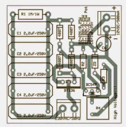
Update
A deeper analysis of the circuit showed that the triac was dumping a significant amount of current while restricting the surge and controlling the current. The approach taken in the above circuit for controlling voltage and the surge is negative in terms of efficiency.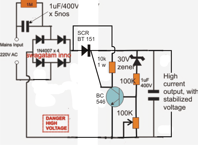 Improving the above design:
In the above SCR based transformerless power supply circuit, the output is surge protected through the SCR, but the BC546 is not protected.
In order to ensure a complete protection for the entire circuit along with the BC546 driver stage, a separate low power triggering stage needs to be added to the B546 stage.
The amended design can be seen below:
Improving the above design:
In the above SCR based transformerless power supply circuit, the output is surge protected through the SCR, but the BC546 is not protected.
In order to ensure a complete protection for the entire circuit along with the BC546 driver stage, a separate low power triggering stage needs to be added to the B546 stage.
The amended design can be seen below:
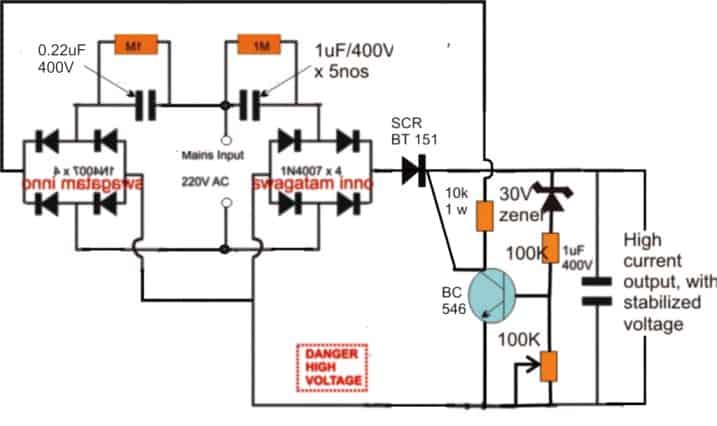 The above design can be further improved by modifying the position of the SCR as shown below:
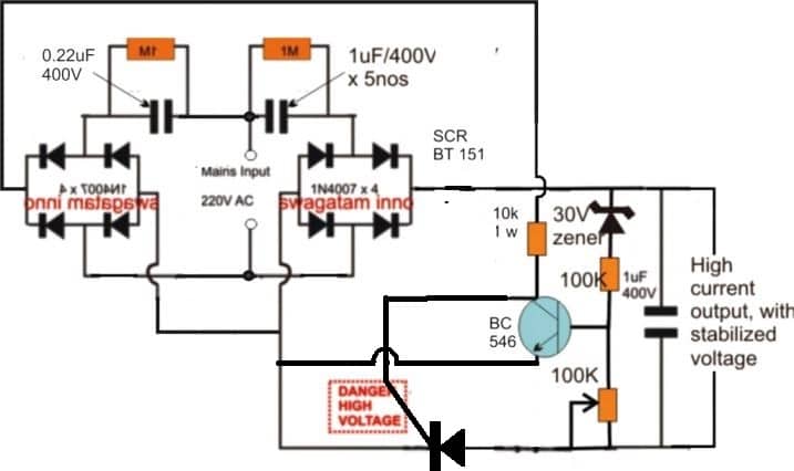 So far we studied a few transformerless power supply designs with high current specs, and also have learned regarding their different modes of configurations.
Below we would go a littlefartherand learn how to make a variable version circuit using an SCR.
The explained design not only provides the option of getting a continuouslyvariableoutput but is also surge protected, andthereforebecome much reliable with its intended functions.
The circuit can be understood from the following description:
So far we studied a few transformerless power supply designs with high current specs, and also have learned regarding their different modes of configurations.
Below we would go a littlefartherand learn how to make a variable version circuit using an SCR.
The explained design not only provides the option of getting a continuouslyvariableoutput but is also surge protected, andthereforebecome much reliable with its intended functions.
The circuit can be understood from the following description:
Circuit Operation
The left side section of the circuit is quite familiar to us, the input capacitor along with the four diodes and the filter capacitor forms the parts of a common, unreliable fixed voltage transformerless power supply circuit. The output from this section will beunstable, prone to surge currents, and relatively dangerous to operate sensitive electronic circuits. The portion of the circuit on the right side of the fuse transforms it into a completely new, sophisticateddesign.The Crowbar Network
It's in fact a crowbar network, introduced for someinterestingfunctions. The zener diode along with R1 and P1 forms a kind of voltage clamp which decides at what voltage level the SCR should fire. P1 effectively varies the zener voltage from zero to its maximum rating, so here it an be assumed to be zero to 24V. Depending upon this adjustment, the firing voltage of the SCR gets set. Supposing P1 sets a 12V range for the SCR gate, as soon as mains power is switched ON, the rectified DC voltage starts developing across D1 and P1. The moment it reaches the 12V mark, the SCR gets sufficient triggering voltage and instantly conducts, short circuiting the output terminals. The short circuiting of the output tends to drop the voltage toward zero, however the moment the voltage drop goes below the set 12V mark, the SCR is inhibited from the required gate voltage and it reverts to it non conducting state.... the situation yet again allows the voltage to rise, and the SCR repeats the process making sure the voltage never goes above the set threshold. The inclusion of the crowbar design also ensures a surge free output since the SCR never allows any surge to pass through to the output under all circumstances, and alsoallowsrelatively higher current operations.Circuit Diagram
Another SCR based Circuit
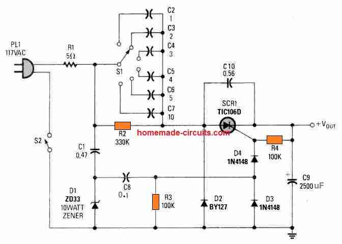 This SCR based high current Transformerless Power Supply consists of rather a few, easily accessible electronic parts.
The output voltage level (and also the level of feasible current as provided in the Table I) is adjustable by rotating the rotary switch S1.
This SCR based high current Transformerless Power Supply consists of rather a few, easily accessible electronic parts.
The output voltage level (and also the level of feasible current as provided in the Table I) is adjustable by rotating the rotary switch S1.
Table#1
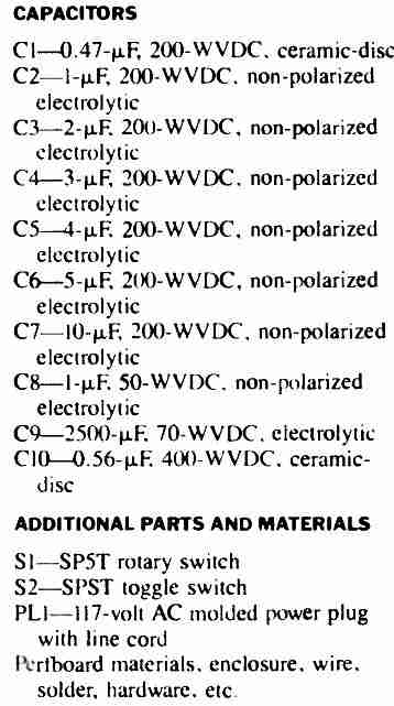
1A Step-Down Voltage Regulator Circuit �C Switched Mode 78XX Alternative
You will be amazed with the features offered by this outstanding voltage regulator IC. As the name refers to, the output from this series of ICs is not only regulated and stabilized but is in the form of switched pulses at very high frequencies.Enhanced Version of the Popular 78XX ICs
These ICs may be considered as an improved SMPS alternative for the conventional linear IC 78XX series regulators which tend to become hot with rising currents at their outputs, but not a problem with the series LM2575 from TEXAS INSTRUMENTS. The switched output with the LM2575 series of ICs especially enables to implement very efficient power transfer to the load even at currents as high 1 Amp. The switched output saves power, keeps the IC cool so that no heatsinks are involved, moreover the switched output makes the IC particularly suitable for a wide application range like in LED drivers, battery chargers etc. These will be discussed elaborately in my coming articles. The LM2575 series from TEXAS INSTRUMENTS provides all the features which particularly becomes very ideal for buck step down regulator applications. These devices are typically capable of producing fixed regulated outputs of 3.3V, 5V, 12V, 15V, and also an adjustable output from one of the devices. The configuration around these ICs require very few number of components for enabling it to function as an effective voltage regulator circuit. The IC necessarily employs an inductor, as we all know that an inductor specifically becomes imperative for all buck/boost type of applications, so even this chip requires one. Though this inductor my be readily procured from the market, may also be hand made using appropriate sized wire and number of calculated turns.Main Technical Specs
The main features of the IC LM2575 may be summarized as follows: Output - 3.3V, 5V, 12V, 15V and also an adjustable version configurable. The adjustable version is able to provide outputs in the range of 1.2V to 35V, 57 volts being the highest. Current - A assured 1 amp of current may be expected from these chips. Input Voltage - A broad DC range upto 40 or even 60 V may be used as inputs for these ICs. Operating Frequency - The ICs output fluctuates at a fixed frequency of 52 kHz, which is set internally. Protections - The chips are all internally safeguarded from over heating and over current. Courtesy of Texas Instruments:ti.com/lit/ds/symlink/lm2575-n.pdf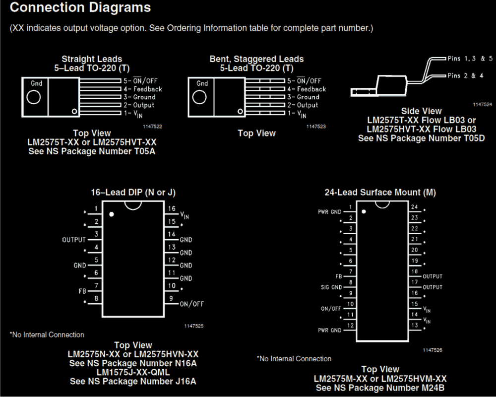
Add this Short Protection Circuit to Your Power Supply
A rather cheap yet reasonably effective short circuit protection circuit is explained below which can be used for safeguarding power supply circuitIntroduction
A power supply unit is an indispensable unit for every electronic enthusiast and engineers working in the relevant field. Though today all of us use hi-tech power supply units having built-in protection, there are folks who still rely on ordinary types of power supply units with no protection facility. The biggest enemy of all power supply units is a possible short circuit that might occur at its output terminals due to an accidental connection or due to the fault with the connected load. There are various electronic circuits that might be employed with a power supply unit for checking this problem, however these circuits sometimes themselves are at risk of getting damaged due to the limitations with many electrical parameters. A very innovative way of rectifying this problem has been shown in this article. A single relay is used for sensing as well as tripping the output from the involved malfunction.Circuit Operation
Referring the circuit diagram, we see that a relay is connected directly to the output of the power supply DC output, however the connection is made through the N/O contacts of the relay. These contacts are also terminated as the output of the unit. N/O means normally open, that means the contacts are open initially, which in turn keeps the output disconnected from the positive of the power supply. Now when the shown push button is momentarily pushed, the N/O contacts are bypassed allowing the current to flow across the relay coil. The relay coil energizes, closing the N/O contacts, which in turn latches and sticks to the position even after the push button is released. The relay latch maintains this latched position as long as the output is used under normal conditions, but in an event of a short circuit across the output terminals, there may be a sharp drop in voltage, the instant this voltage drops below the coilvoltageof the relay, it loses its holding strength and immediately releases the contacts, and trips, cutting OFF the supply to the output and in the course switches OFF the latch preventing the short hazard conditions. This brings the relay to its initial condition and needs resetting in order to restore power at the output. The circuit diagram for the power supply short circuit protection is shown below:
IC 7805, 7812, 7824 Pinout Connection Explained
The post explains how to connect common 78XX voltage regulator ICs such as 7805, 7812, 7824 etc in an electronic circuit for getting the intended fixed regulated output voltages at 5V, 12V, and 24V depending on the selected 78XX specificationImportance of 78XX voltage regulator in circuits
A varying voltage can cause drastic consequences to a sensitive electronic circuit, for example a TTL, LS and HC series of ICs cannot tolerate more than 5 volts and can get immediately damaged. A CMOS IC cannot stand more than 16 to 18 volts. A relay if operated at voltages more than its rating can become hot and waste electricity unnecessarily. There are several other issues which might be faced with electronic circuits if the applied is anunregulatedone. For solving the above issue, many high grade yet verysimpleto configure chips have been designed and are available cheaply and plentifully in our electronicmarkets. The 78XX voltage regulator series for example, comes with most of the standard voltage ratings which can be used in conjunction with an ordinary power supply DC for obtaining high grade, clean voltage controlled outputs.Technical specifications of the 78XX series IC
Output voltage tolerances are around ��2% at Tj = 25C and ��4% Line regulation is around 0.01% of VOUT/V of VIN at 1A load Internal circuitry is thermal and overload protected Internal short-circuit current limit protections are also included Output transistor safe area protection is also one of the features of these ICsIdentifying 7805/7812/7824 ICs Pinouts
A classic example can be seen in this article where a 7805 IC is used as a cell phone charger regulator. Referring to the above circuit diagram These ICs have just three leads, making it very easy to understand and connect. The leads are assigned as input, ground and output respectively. Keeping the printed side toward you, the left side lead is the input, the center one is the ground and the right side lead is the output. The DC from any standard power supply is applied across the input and the ground leads of the IC, the positive goes to the input while the negative is connected to the ground. The output isacquiredacross the output and the ground pins of the IC, the positive being received from the "output" pin and the negative from the common ground line.IC 7805, 7812, 7824 Pinout Specifications
Most of the common voltage regulator ICs beginning with the 78 prefix, such 7805, 7812, 7824 typically have identical pinout assignments as shown below: However, in the above chart, we can also see that except the 78LXX, the other variants have slightly different pinout specifications, and needs to be connected exactly as per the given details otherwise the IC may fail to work and produce unexpected outcomes.
The ICs beginning with 78XX are positive voltage regulators, meaning these will accept a positive input voltage across across their input/Gnd terminals and regulate the same across their output/Gnd terminals with the specified fixed voltage output.
Conversely, the 79XX ICs will accept a negative voltage and produce a negative fixed voltage across their relevant output terminals.
The package of the ICs also signify a vital information.
The ICs with TO220 package are rated to handle and produce a maximum of 1 Amp current whereas the smaller 78LXX version are rated to handle only upto 100mA.
We all very well know regarding the building procedures a DC power supply circuit using a transformer, a bridge rectifier and a filter capacitor.
It just requires connecting four diodes in a bridge configuration and connect it to the secondary of the transformer, the capacitor goes to the output of the bridge terminals.
The output produced across the capacitor is approximately equal to the rated voltage of the transformer, rather a few volts higher than the transformer spec.
However the voltage obtained from the above simple configuration is never regulated and stabilized, meaning the output from it will never be constant and will vary with the varying input mains voltage levels, which we know is never constant.
However, in the above chart, we can also see that except the 78LXX, the other variants have slightly different pinout specifications, and needs to be connected exactly as per the given details otherwise the IC may fail to work and produce unexpected outcomes.
The ICs beginning with 78XX are positive voltage regulators, meaning these will accept a positive input voltage across across their input/Gnd terminals and regulate the same across their output/Gnd terminals with the specified fixed voltage output.
Conversely, the 79XX ICs will accept a negative voltage and produce a negative fixed voltage across their relevant output terminals.
The package of the ICs also signify a vital information.
The ICs with TO220 package are rated to handle and produce a maximum of 1 Amp current whereas the smaller 78LXX version are rated to handle only upto 100mA.
We all very well know regarding the building procedures a DC power supply circuit using a transformer, a bridge rectifier and a filter capacitor.
It just requires connecting four diodes in a bridge configuration and connect it to the secondary of the transformer, the capacitor goes to the output of the bridge terminals.
The output produced across the capacitor is approximately equal to the rated voltage of the transformer, rather a few volts higher than the transformer spec.
However the voltage obtained from the above simple configuration is never regulated and stabilized, meaning the output from it will never be constant and will vary with the varying input mains voltage levels, which we know is never constant.
How to Connect 7805, 7812, 7824 in an Electronic Circuit
In order to regulate an existing supply to a fixed level, we normally use these 78XX ICs, and theses can be very easily connected with any supply source in the following shown manner:Application Circuit
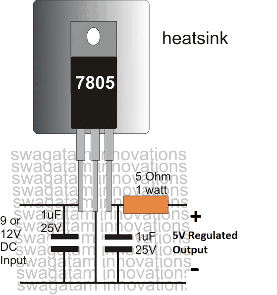 ICs 7812 and 7824 can be also connected exactly in the above shown manner, the only difference being the input/output voltage specifications which will vary as per the IC's ratings.
For example a 7812 will require an input above 13V and will produce a fixed 12V at its output.
Similarly a 7824 will require a input of not less than 26V, and will offer an output voltage fixed at 24V, and so on.
ICs 7812 and 7824 can be also connected exactly in the above shown manner, the only difference being the input/output voltage specifications which will vary as per the IC's ratings.
For example a 7812 will require an input above 13V and will produce a fixed 12V at its output.
Similarly a 7824 will require a input of not less than 26V, and will offer an output voltage fixed at 24V, and so on.
What does the Capacitors do?
We can some capacitors attached across the input and output terminals of the ICs, these are just included to rectify any residual DC spikes and ripples that may exist in the supply line. According to the datasheet of the IC, the input capacitor is required only if the input source is at a significant distance away from the IC, may be at over a meter away. The output capacitor may be included if you want an improved transient regulation, meaning protection from noise spikes. The value of these capacitors is not critical any value between 1 uF and 100 uF can be used for rectifying higher frequency ripples, whereas smaller capacitors in the range of 0.1 uF to 0.47 uF can also be attached in parallel to control any possible high frequency entry along the supply rails.How to Get 10 Amps from 7805 IC
A 7805 IC is designed to deliver 5 V at 1 Amp maximum current. So if you want to get more than 1 amp from this IC it may be impossible to achieve this, directly from the IC. However, the following transistorized circuit not only upgrades the IC 7805 specifications to generates up to 10 Amp current but also allows the user to get a voltage as high as 15 V from the 7805 IC. The following diagram suggests the entire procedure for achieving 10 amps from the IC 7805 and a variable output voltage from 5 V to 15 V.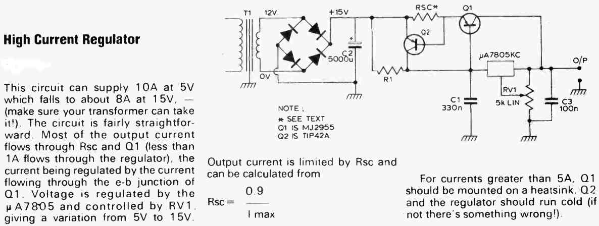 Here's another circuit which can convert an ordinary 7805, or 7812 IC into a high current delivering circuit.
The design presented also has a current control feature which ensures that the output transistor is always safeguarded from short circuit or high current over loads.
Here's another circuit which can convert an ordinary 7805, or 7812 IC into a high current delivering circuit.
The design presented also has a current control feature which ensures that the output transistor is always safeguarded from short circuit or high current over loads.
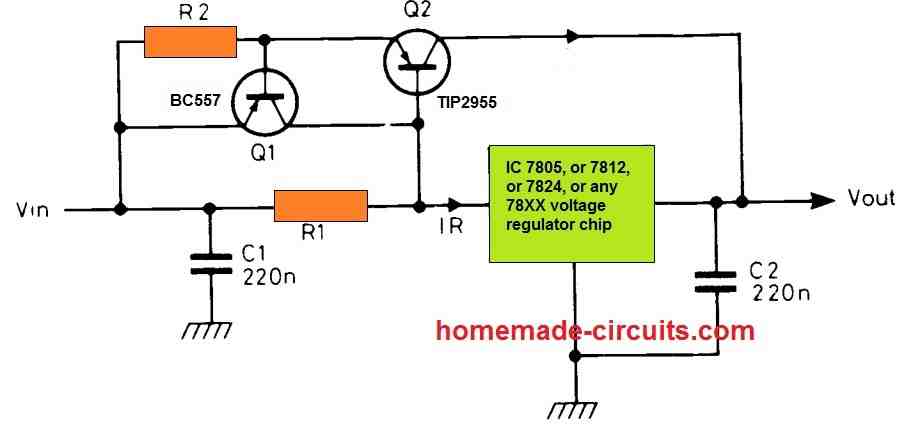
High Current from 7805 and 7812 IC with Short Circuit Protection
The circuit functions in the following way: When the voltage drop across R1 exceeds 0.6 V, Q2 begins conducting and it bypasses the voltage regulator IC to provide the full high current from input supply to the output terminals. Q2 works like a current limiter stage. If the current through Q1 tries to exceed over the maximum tolerable range, the voltage drop across R2 also exceeds 0.6 V turning ON Q2. Q2 collector shorts circuits the Q1 base with the positive supply inhibiting its conduction and thus switching it OFF. In this way the current is controlled strictly to the desired maximum range. R1 and R2 can be calculated using the following formulas: R1 = 0.6 / 0.5 = 1.2 ohms 1/2 watt R2 = 0.6 / maximum current limitVariable Voltage, Current Power Supply Circuit Using Transistor 2N3055
In this post we learn how to make a simple variable power supply circuit using transistor 2N3055 and some other passive components. It includes variable voltage and variable current feature, fully adjustable.Main Specifications
1) Adjustable from 0-30V, 0-60V, and 0-100V, and 500mA to 10 Amp as per user preference 2) Short Circuit Protected when mounted on proper heatsink 3) Ripple free, with less than 1Vpp 4) Output is Stabilized and filtered DC 5) Short circuit LED indicator 6) Overload ProtectedIntroduction
A power supply circuit that does not include the features of a variable voltage and current control can by no means be considered truly versatile. A variable workbench power supply circuit explained in this article is not only specified with a continuously variable voltage control but is also equipped with the feature of overload or continuously variable current control.Circuit Diagram
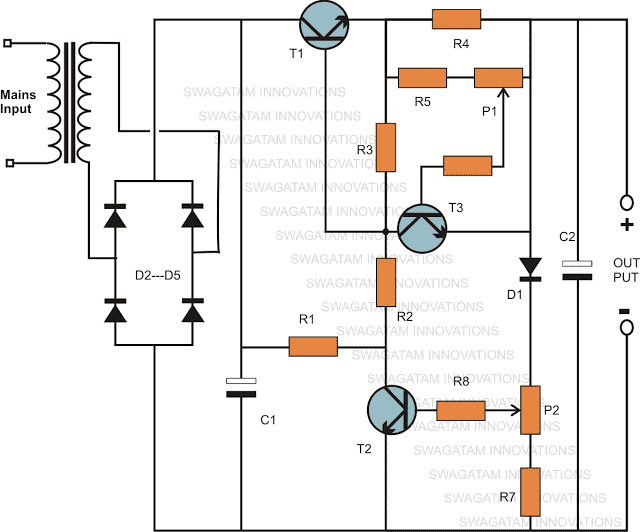
How it Works
A keen look at this 2N3055 based variable voltage current power supply circuit using transistor 2N3055reveals that it��s actually only an ordinary stabilized power supply circuit, however it yet still provides you with the proposed features very efficiently.The voltage variations are made by using the preset P2, through a feedback configuration employing the components D1, R7, T2 and P2. The inclusion of D1 makes it sure that the voltage can be lowered right down to 0.6 volts, which happens to be the forward voltage drop of the diode. If any other specific minimum value is required then the diode can be replaced by zener diode having the required specified value. Therefore in this variable power supply circuit using 2N3055 transistor, the transformer being a 0 �C 40 V, the output becomes variable right from 0.6 to 40 volts maximum, that��s very handy indeed. For implementing the current control feature, T3 along with P1, R5 and R4 are involved. The value of R4 is specifically becomes responsible for defining the maximum allowable output current. P1 is set to choose the maximum range within the value that��s marked or identified by the resistor R4.PCB Design
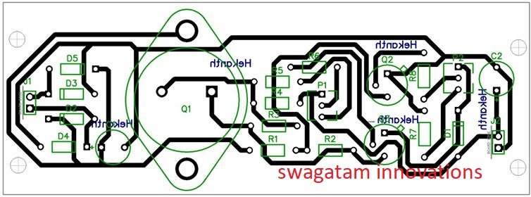
Parts List
R1 = 1K, 5 watt wire wound R2 = 120 Ohms, R3 = 330 Ohms, R4 = to be calculated using Ohms law. R5 = 1K5, R6 = 5K6, R7 = 56 Ohms, R8 = 2K2, P1,P2 = 2k5 presets T1 = 2N3055, T2, T3 = BC547B, D1 = 1N4007, D2, D3, D4, D5 = 1N5402, C1, C2 = 1000uF/50V, Tr1 = 0 �C 40 Volts, 3 Amp2N3055 Pinout Details
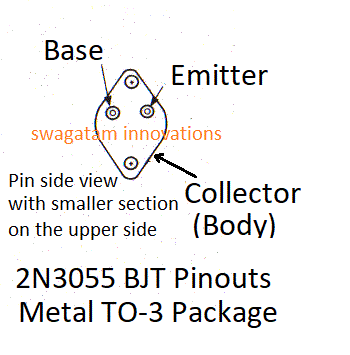 If you have any doubts regarding this variable voltage and current power supply circuit using transistor 2N3055 circuit please do not hesitate to ask then through the comments below.
Original Transistor Power Supply Diagram:
The above design was inspired from the following circuit which was designed and presented in the elektor electronics magazine by the elektor engineers: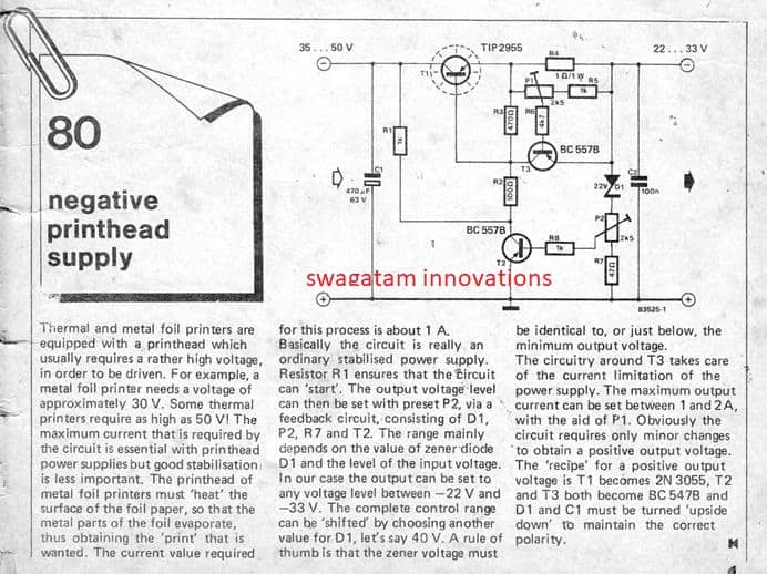
Simplified Variable Power Supply Design using 2N3055 and 2N2222 Transistors
The above designs were assessed and simplified with more effective results by Mr. Nuno. The revised and simplified design can be viewed in the following diagram: The design features an over-current shut down with LED indication.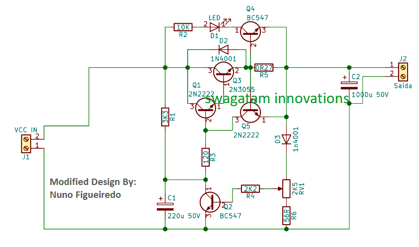 Video clip of the tested prototype:
For PCB Design and other Related Data, you can Download the following ZIP File:
PCB Design for the above Circuit
Another Similar Power Supply Design as Referred by Mr.William C.
Colvinis presented below for the viewer assessment:
Video clip of the tested prototype:
For PCB Design and other Related Data, you can Download the following ZIP File:
PCB Design for the above Circuit
Another Similar Power Supply Design as Referred by Mr.William C.
Colvinis presented below for the viewer assessment:
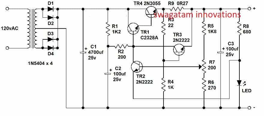
2N3055 Wide Range Variable Voltage Regulator
The key highlights of the circuit are: wide range output: 0.1 to 50 volts excellent load regulation: 0.005% between 0 and 1 amp, decent line regulation: 0.01%, reduced output disturbance: superior to 250 microvolts. The broad output selection is implemented with thehelp of the integrated circuit CA 3130, that is able to work even with a zero volt input/output differential. In addition, higher extension of the output range becomes feasible through the inclusion of T4 between the IC and the series pass transistor. The high gain as a result acquired enables a superior level of regulation, and the T1/T2 Darlington pair offers a adequately large current boosting. T3 works like an output current controller. When P1 is rotated totally anti-clockwise, T3 restricts at 0.6 amps. The limiting circuit becomes inactive when P2 is moved completely clockwise. The regulator circuit specifically operates in the following manner.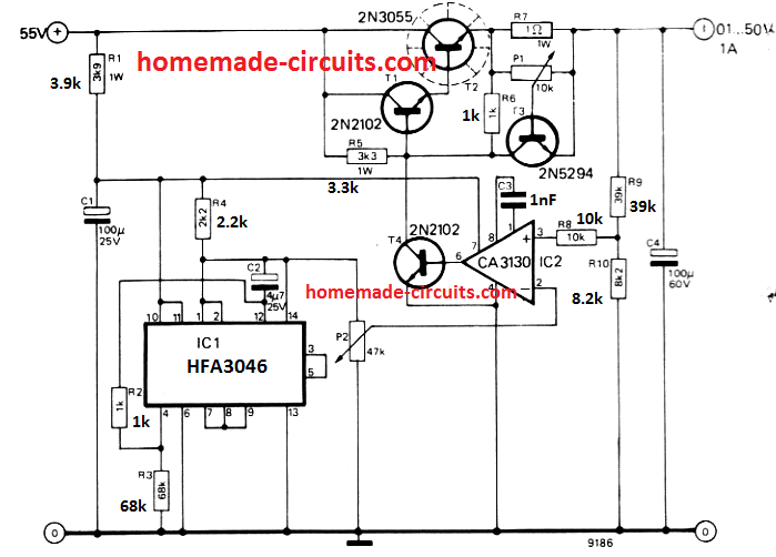 The IC CA 3130 analyzes the output voltage given to the non-inverting input with respect to a reference voltage at the inverting input.
The output voltage of the regulator is reduced with a potential divider to protect against damage to the IC.
The reference voltage is determined by P2, which needs to be a top-notch part, since any kind of noise upon its slider arm will probably be transferred to the regulator output terminals.
A additional IC, HFA3046 , offsets the reference voltage intended for temperature variations.
The IC is made up of 4 transistors applied as diodes or zener and another transistor for cutting down the output impedance of the reference circuit.
The reference IC furthermore provides a stepped down supply voltage for powering CA 3130. This feature necessitates the use of each ICs in the regulator stage; if IC1 is removed can result in the break down of IC2. Each of the transistors shown in the diagram must be rated with a breakdown voltage of a minimum of 55 volts.
The IC CA 3130 analyzes the output voltage given to the non-inverting input with respect to a reference voltage at the inverting input.
The output voltage of the regulator is reduced with a potential divider to protect against damage to the IC.
The reference voltage is determined by P2, which needs to be a top-notch part, since any kind of noise upon its slider arm will probably be transferred to the regulator output terminals.
A additional IC, HFA3046 , offsets the reference voltage intended for temperature variations.
The IC is made up of 4 transistors applied as diodes or zener and another transistor for cutting down the output impedance of the reference circuit.
The reference IC furthermore provides a stepped down supply voltage for powering CA 3130. This feature necessitates the use of each ICs in the regulator stage; if IC1 is removed can result in the break down of IC2. Each of the transistors shown in the diagram must be rated with a breakdown voltage of a minimum of 55 volts.
High Current Variable Power Supply
In this high current linear power supply circuit, we have used a 2N5686 transistor instead of 2N3055, so that the circuit is able to deliver a minimum of 10 amp current, and the preset P3 could be used to adjust a current range of 10 amp. The power supply itself is pretty straightforward to construct. An ICLM329 provides a steady reference voltage of 6.9 V. P4 is a potentiometer, and this pot is utilized to determine the output voltage using a preset potential divider P2-P4-R2. The power stage of the circuit is made up of IC1 and T1, which operate likean operational amplifier when it comes to positive voltages (negative voltagesare not relevanthere, obviously). This non-inverting amplifier is built using an combo of op amp, P1, R5, and R6. This indicates that the voltage at P4's wiper is proportionate to the voltage across the output terminals. P1 is a potentiometer that controls the peak output voltage, while P2 is used for setting the minimum output voltage from the power supply. Preset P3 is used for setting up the maximum current limit of the output.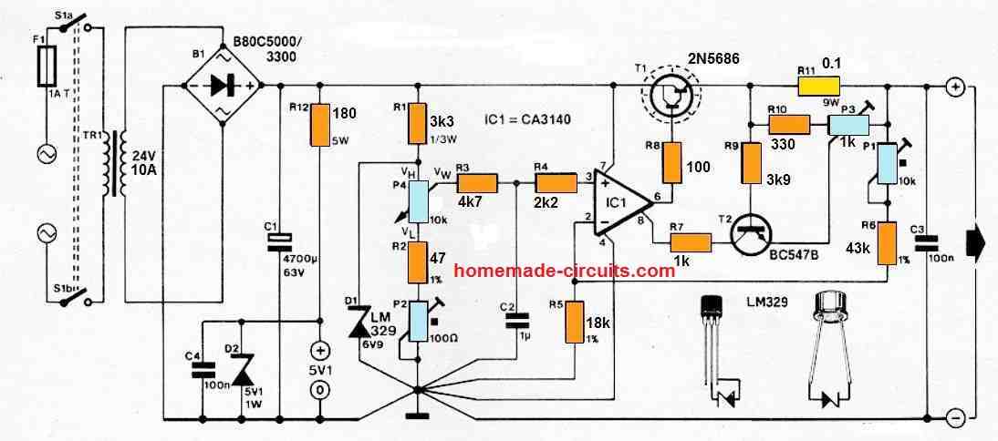 R11 converts the output current to a voltage to accomplish this.
When thisvoltage (controlled by P3) is large enough to turn on T2, the circuit's voltage regulation is superseded by current regulation through IC1's strobe input.
The maximum current that can be adjusted is from 0.8 A to 10A, depending on how the controls are adjusted.
When the output of the power supplyare short-circuited, the current must not increase above 25A to prevent T1from being damaged and due to overdissipation.
The circuit setting upis not complicated.
To begin, adjust P4 to highest possibleresistance and wait about a minute untilZ1and IC1 reachtheir typical working temperatures.
Next, adjust P1to get a 25 V output voltage.
Finally, tweak P2 to provide a 250 mV output voltage by setting P4 to lowest resistance.
The lowest output voltage of 250 mVwas selected on purpose to guarantee that the individual parts always are able to work witha linear regionof their characteristics.
There are a couple ofthings to remember here: the earth lines must be routed exactlyas shown in the schematic, and T1 must be installed on a 1.5 K/ W heat sink.
R11 converts the output current to a voltage to accomplish this.
When thisvoltage (controlled by P3) is large enough to turn on T2, the circuit's voltage regulation is superseded by current regulation through IC1's strobe input.
The maximum current that can be adjusted is from 0.8 A to 10A, depending on how the controls are adjusted.
When the output of the power supplyare short-circuited, the current must not increase above 25A to prevent T1from being damaged and due to overdissipation.
The circuit setting upis not complicated.
To begin, adjust P4 to highest possibleresistance and wait about a minute untilZ1and IC1 reachtheir typical working temperatures.
Next, adjust P1to get a 25 V output voltage.
Finally, tweak P2 to provide a 250 mV output voltage by setting P4 to lowest resistance.
The lowest output voltage of 250 mVwas selected on purpose to guarantee that the individual parts always are able to work witha linear regionof their characteristics.
There are a couple ofthings to remember here: the earth lines must be routed exactlyas shown in the schematic, and T1 must be installed on a 1.5 K/ W heat sink.
Crowbar Circuit for Over-voltage Protection
A very simple DC over voltage protector circuit is shown below. The transistor is set tomonitorthe input voltage applied to it from the left, in case the voltage rises above a specified limit, the transistor conducts,providingthe required current to the SCR, which instantly fires, shorting the output and thus protecting the load from the hazard. It's also called a Crowbar circuit.How it Works
The circuit shown below is very simple to understand and is quite self explanatory.The working may be understood with the following points: The supply DC input voltage is applied from the right hand side o the circuit across the SCR. As long as the input voltage remains under a certainpredeterminedvalue, the transistor isunableto conduct and therefore the SCr also remains shut. The threshold voltage iseffectivelyset by zener diode voltage. As long as the input voltage stays below this threshold everything goes on fine. However in case the inputcrossesthe above threshold level, the zener diode starts conducting so that the base of the transistor starts getting biased. At some point of time the transistor becomes fully biased and pulls the positive voltage to its collector terminal. The voltage at the collector instantly passesthroughthe gate of the SCR. The SCR immediately conducts and shorts the input to ground. This may look a bit dangerous because the situation indicates that the SCR might get damaged as it shorts the voltage directly through it. But the SCR remains absolutely safe because the moment the input voltage drops below the set threshold the transistorstopsconducting and inhibits the SCR from going into damaging extents. The situation is sustained and keeps the voltage under control and prevents it from reaching above thethreshold, in this way the circuit is able to accomplish the DC over protection function.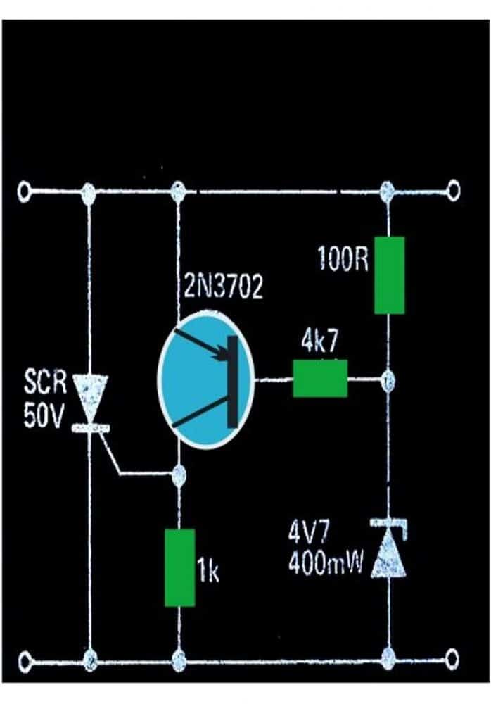
Crowbar using Triac and SSB
The next circuit which can protect your valuable gadget from over voltage situations is shown in the following image, which uses a SSB or a silicon bilateral switch, as the gate driver for the triac. The preset R2 is used for setting the triggering point of the SSB at which the device can fire and trigger ON the triac. This setting is done corresponding to the desired high voltage level at which the crowbar needs to trigger and protect the connected circuit from a possible burn out. As soon as the high voltage situation is reached, as per the R2 setting the SSB detects this over voltage and it switches ON. Once it switch es ON it fires the triac. The triac instantly conducts and shorts circuits the line voltage which in turn causes the fuse to blow. Once the fuse blows, the voltage to the load is cut off and the danger of the over voltage is averted.Crowbar circuit using Triac and Zener Diode
If you do not get an SSB, the same crowbar application as above can be designed using a triac and a zener diodes as shown in the following diagram.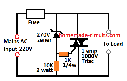 Here, the zener voltage decides the cut off limit of the crowbar circuit.
In the figure it is shown as 270V, therefore as soon as the 270 V mark is reached, the zener starts conducting.
As soon as the zener diode breaks over and conducts, the triac is switched ON.
The triac switches ON and short circuits the line voltage thereby bowing off the fuse the preventing further dangers that may resulted in due to the high voltage.
Here, the zener voltage decides the cut off limit of the crowbar circuit.
In the figure it is shown as 270V, therefore as soon as the 270 V mark is reached, the zener starts conducting.
As soon as the zener diode breaks over and conducts, the triac is switched ON.
The triac switches ON and short circuits the line voltage thereby bowing off the fuse the preventing further dangers that may resulted in due to the high voltage.
Another Simple SCR, Fuse Crowbar Circuit
This is yet another simple SCR transistor crowbar circuit which delivers over-voltage protection in case there is a malfunction of the voltage regulator or high level from an external source. It is supposed to be employed with a supply source that includes some type of short circuit protection, possibly fold-back current limiting or a basic fuse. The best possible application can be a 5V logic supply, because TTL could be quickly destroyed by too much voltage. The values of the parts selected in Fig.1 are with respect to a 5V supply, even though any kind of supply up to about 25V could be protected using this crowbar network, just by picking the right zener diode.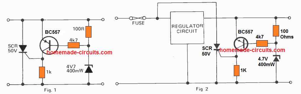 Any time the supply voltage is greater than the zener voltage by +0.7V, the transistor activates and triggers the SCR.
When this happens it short circuits the supply, stopping the voltage from increasing any more.
If it is used in a power supply which only has a fuse protection, it is advisable to attach the SCR right around the unregulated supply as indicated in Fig.2 in order to protect against damage to the regulator circuit as soon as the crowbar triggers ON.
Any time the supply voltage is greater than the zener voltage by +0.7V, the transistor activates and triggers the SCR.
When this happens it short circuits the supply, stopping the voltage from increasing any more.
If it is used in a power supply which only has a fuse protection, it is advisable to attach the SCR right around the unregulated supply as indicated in Fig.2 in order to protect against damage to the regulator circuit as soon as the crowbar triggers ON.
SCR Specifications
The thyristor or the SCR must be rated with a current that may be approximately two times the anticipated short circuit current value and rated with a optimum voltage that must be higher than the input supply voltage. For resetting the circuit in the original condition you can either switch off the supply source, or do it by interrupting the SCR conduction through a push button switch across its cathode/anode terminals.Regulated, High Current Power Supply Circuit
The circuit given here below can be used for applications that requirestringentvoltage regulations and ripple rejectioncriteria. The transistor pair are configured such that all residual ripple factor are perfectly rectified.Circuit Operation
The circuit below shows a simple way of acquiring a perfectly regulated andstabilizedDC voltage output using ordinary transistors.The circuit is very simple to understand, let's study it with the following points: This simple efficient high current 2N3055 based power supply is designed to handle in excess of 3 amp of currents, but must not exceed 5 amps. The voltage that is required to be stabilized can be adjusted through R1 and the value of the zener diode. The diodes at the input are arranged in a bridge network configuration forrectifyingthe voltage applied from thetransformer. C1smoothensthe DC further to feeds the filtered DC to the control circuit made up of Q1 and Q2. R1 is introduced to start up the circuit by providing the required biasing to the transistor pair. C2 makes sure that thetransistorreceive a perfectly smooth DC at their base without any ripples. The zener diode at the base of the Q1 clamps the transistor with a fixed biasing voltage and inhibits any rise at the output voltage, irrespective of the voltage at the input, meaning even if the input voltage from the bridge network rises, the output remains unaffected and produces thevoltagedefined by the setting of R1 and the zenerdiode.
4 Simple Transformerless Power Supply Circuits Explained
In this post we discuss 4 easy to build, compact simple transformerless power supply circuits. All the circuits presented here are built using capacitive reactance theory for stepping down the input AC mains voltage. All the designs presented here work independently without any transformer, or no transformer.The Transformerless Power Supply Concept
As the name defines, a transformerless power supply circuit provides a low DC from the mains high voltage AC, without using any form of transformer or inductor. It works by using a high voltage capacitor to drop the mains AC current to the required lower level which may be suitable for the connected electronic circuit or load. The voltage specification of this capacitor is selected such that it's RMS peak voltage rating is much higher than the peak of the AC mains voltage in order to ensure safe functioning of the capacitor. An example capacitor which is normally used transformerless power supply circuits is shown below: This capacitor is applied in series with one of the mains inputs, preferably the phase line of the AC.
When the mains AC enters this capacitor, depending on the value of the capacitor, the reactance of the capacitor comes into action and restricts the mains AC current from exceeding the given level, as specified by the value of the capacitor.
However, although the current is restricted the voltage isn't, therefore if you measure the rectified output of a transformerless power supply you will find the voltage to be equal to the peak value of the mains AC, that's around 310V, and this could be alarming for any new hobbyist.
But since the current may be sufficiently dropped level by the capacitor, this high peak voltage could be easily tackled and stabilized by using a zener diode at the output of the bridge rectifier.
The zener diode wattage must be appropriately selected according to the permissible current level from the capacitor.
CAUTION:Please read the caution warning message at the end of the post
This capacitor is applied in series with one of the mains inputs, preferably the phase line of the AC.
When the mains AC enters this capacitor, depending on the value of the capacitor, the reactance of the capacitor comes into action and restricts the mains AC current from exceeding the given level, as specified by the value of the capacitor.
However, although the current is restricted the voltage isn't, therefore if you measure the rectified output of a transformerless power supply you will find the voltage to be equal to the peak value of the mains AC, that's around 310V, and this could be alarming for any new hobbyist.
But since the current may be sufficiently dropped level by the capacitor, this high peak voltage could be easily tackled and stabilized by using a zener diode at the output of the bridge rectifier.
The zener diode wattage must be appropriately selected according to the permissible current level from the capacitor.
CAUTION:Please read the caution warning message at the end of the post
Advantages of using a Transformerless Power Supply Circuit
The idea is cheap yet very effective for applications that require low power for their operations. Using a transformer in DC power supplies is probably quite common and we have heard a lot regarding it. However one downside of using a transformer is that you cannot make the unit compact. Even if the current requirement for your circuit application is low, you have to include a heavy and bulky transformer making things really cumbersome and messy. The transformerless power supply circuit described here, very efficiently replaces a usual transformer for applications which require current below 100 mA. Here a high voltage metalized capacitor is used at the input for the required stepping down of the mains power and the preceding circuit is nothing but just simple bridge configurations for converting the stepped down AC voltage to DC. The circuit shown in the diagram above is a classic design may be used as a 12 volts DC power supply source for most electronic circuits. However having discussed the advantages of the above design, it will be worth focusing on a few serious drawback this concept may include.Disadvantages of a Transformerless Power Supply Circuit
First, the circuit is unable to produce high current outputs, but that won��t make an issue for most of the applications. Another drawback that certainly needs some consideration is that the concept does not isolate the circuit from dangerous AC mains potentials. This drawback can have serious impacts for designs which have terminated outputs or metal cabinets, but won��t matter for units which have everything covered up in a non-conducting housing. Therefore, new hobbyists must work with this circuit very carefully to avoid any electrical casualty. The last but not the least, the above circuit allows voltage surges to enter through it, which may cause serious damage to the powered circuit and to the supply circuitry itself. However in the proposed simple transformerless power supply circuit design this drawback has been reasonably tackled by introducing different types of stabilizing stages after the bridge rectifier. This capacitor grounds instantaneous high voltage surges, thus efficiently safeguarding the associated electronics with it.How the Circuit Works
The working of this transformless power supply can be understood with the following points: When mains AC mains input is switched ON, capacitor C1 blocks the entry of the mains current and restricts it to a lower level as determined by the reactance value of C1. Here it may be roughly assumed to be around 50mA. However, the voltage is not restricted, and therefore the full 220V or whatever may be at the input is allowed to reach the subsequent bridge rectifier stage. The bridge rectifier rectifies this 220V C to a higher 310V DC, due to the RMS to peak conversion of the AC waveform. This 310V DC is instantly reduced to a low level DC by the next zener diode stage, which shunts it to the zener value. If a 12V zener is used, this will become 12V and so on. C2 finally filters the 12V DC with ripples, into a relatively clean 12V DC.1) Basic Transformerless Design

Improving the Design
The above transformerless design looks simple, but it has some unavoidable downsides. The resistor R2 is mandatory in the circuit, otherwise the zener diode may burn instantly. However, adding the resistor R2 causes a significant drop in the output current, and there's also some serious dissipation through the resistor R2, making the circuit somewhat inefficient. The idea to make sure that R2 is as low as possible, yet the entire circuit remains completely safe from all possible electrical hazards. For this, we reinforce the zener diode with a high voltage transistor wired in the crowbar format, as shown in the following diagram:Example Circuit for LED Decoration Light Application
The following transformerless or capacitive power supply circuit could be used as an LED lamp circuit for illuminating minor LED circuits safely, such as small LED bulbs or LED string lights. The idea was requested by Mr. Jayesh: Requirement Specifications The string is made up of about 65 to 68 LED of 3 Volt in series approximately at a distance of let us say 2 feet ,,, such 6 strings are roped together to make one string so the bulb placement comes out to be at 4 inches in final rope . so over all 390 - 408 LED bulbs in final rope. So please suggest me best possible driver circuit to operate 1) one string of 65-68 string. or 2) complete rope of 6 strings together. we have another rope of 3 strings.The string is made up of about 65 to 68 LED of 3 Volt in series approximately at a distance of let us say 2 feet , such 3 strings are roped together to make one string so the bulb placement comes out to be at 4 inches in final rope . so over all 195 - 204 LED bulbs in final rope. So please suggest me best possible driver circuit to operate 1) one string of 65-68 string. or 2) complete rope of 3 strings together. Please suggest the best robust circuit with surge protector and advice any additional things to be connected to protect the circuits. and please see that circuit diagrams are with values required for the same as we are not at all technical person in this field. Circuit Design The driver circuit shown below is suitable for driving any LED bulb string having less than 100 LEDs (for 220V input), each LED rated at 20mA, 3.3V 5mm LEDs: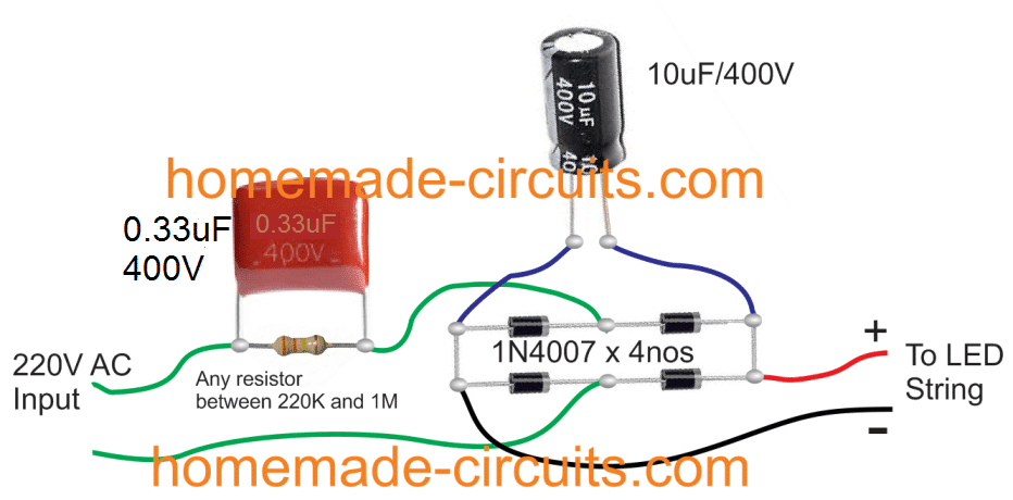 Here the input capacitor 0.33uF/400V decides the amount of current supplied to the LED string.
In this example it will be around 17mA which is just about right for the selected LED string.
If a single driver is used for more number of similar 60/70 LED strings in parallel, then simply the mentioned capacitor value could be proportionately increased for maintaining optimal illumination on the LEDs.
Therefore for 2 strings in parallel, the required value would be 0.68uF/400V, for 3 strings you could replace it with a 1uF/400V.
Similarly for 4 strings this would need to be upgraded to 1.33uF/400V, and so on.
Important: Although I have not shown a limiting resistor in the design, it would be a good idea to include a 33 Ohm 2 watt resistor in series with each LED string for added safety.
This could be inserted anywhere in series with the individual strings.
WARNING: ALL THE CIRCUITS MENTIONED IN THIS ARTICLE ARE NOT ISOLATED FROM MAINS AC, THEREFORE ALL THE SECTIONS IN THE CIRCUIT ARE EXTREMELY DANGEROUS TO TOUCH WHEN CONNECTED TO MAINS AC........
Here the input capacitor 0.33uF/400V decides the amount of current supplied to the LED string.
In this example it will be around 17mA which is just about right for the selected LED string.
If a single driver is used for more number of similar 60/70 LED strings in parallel, then simply the mentioned capacitor value could be proportionately increased for maintaining optimal illumination on the LEDs.
Therefore for 2 strings in parallel, the required value would be 0.68uF/400V, for 3 strings you could replace it with a 1uF/400V.
Similarly for 4 strings this would need to be upgraded to 1.33uF/400V, and so on.
Important: Although I have not shown a limiting resistor in the design, it would be a good idea to include a 33 Ohm 2 watt resistor in series with each LED string for added safety.
This could be inserted anywhere in series with the individual strings.
WARNING: ALL THE CIRCUITS MENTIONED IN THIS ARTICLE ARE NOT ISOLATED FROM MAINS AC, THEREFORE ALL THE SECTIONS IN THE CIRCUIT ARE EXTREMELY DANGEROUS TO TOUCH WHEN CONNECTED TO MAINS AC........
2) Upgrading to Voltage Stabilized Transformerless Power Supply
Now let's see how an ordinary capacitive power supply may be transformed into a surge free voltage stabilized or variable voltage transformerless power supply applicable for almost all standard electronic loads and circuits. The idea was requested by Mr. Chandan Maity.Technical Specifications
If you remember, I communicated you sometime before with comments at your blog. The Transformerless circuits are really good and I tested couple of those and running 20W, 30W LED.Now, I am trying to add some controller, FAN and LED all together , hence, I need a dual supply. The rough specification is: Current rating 300 mAP1= 3.3-5V 300mA ( for controller etc)P2= 12-40V (or higher range), 300mA (for LED) I thought to use your 2nd circuit as mentionedhttps://www.homemade-circuits.com/2012/08/high-current-transformerless-power.html But, I am not able to freeze the way how to get 3.3V without using extra capacitor. 1. Can, a second circuit may be placed from the output of first one?2. Or, a second TRIAC, bridge to be placed in parallel with first one, after capacitor to get 3.3-5V I shall be glad if you kindly help. Thanks,The Design
The function of the various components used across the various stages of the above shown voltage controlled circuit may be understood from the following points: The mains voltage is rectified by the four 1N4007 diodes and filtered by the 10uF/400V capacitor. The output across the 10uF/400V now reaches around 310V which is the peak rectified voltage achieved from the mains. The voltage divider network configured at the base of the TIP122 makes sure that this voltage is reduced to the expected level or as required across the power supply output. You can also use MJE13005 in place of TIP122 for better safety. If a 12V is required the 10K pot may be set to achieve this across the emitter/ground of the TIP122. The 220uF/50V capacitor ensures that during switch ON the base is rendered a momentary zero voltage in order to keep it switched OFF and safe from the initial surge in-rush. The inductor further ensures that during the switch ON period the coil offers a high resistance and stops any inrush current to get inside the circuit, preventing a possible damage to the circuit. For achieving a 5V or any other attached stepped down voltage, a voltage regulator such as the shown 7805 IC may be used for achieving the same.Circuit Diagram
Using MOSFET Control
The above circuit using emitter follower can be further enhanced by applying a MOSFET source follower power supply, along with a supplemental current control stage using BC547 transistor. The complete circuit diagram can be seen below: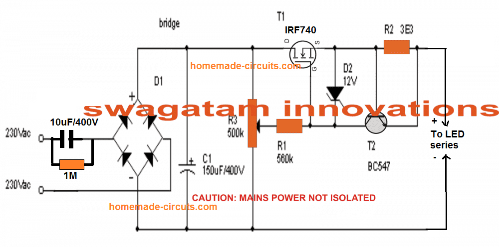
Video Proof of Surge Protection
3) Zero Crossing Transformerless Power Supply Circuit
The third interesting explains the importance of a zero crossing detection in capacitive transformerless power supplies in order to make it completely safe from the mains switch ON inrush surge currents. The idea was proposed by Mr. Francis.Technical Specifications
I have been reading about the transformer less power supply articles on your site with great interest and if I am understanding correctly the main problem is the possible in-rush current in the circuit upon switching-on, and this is caused because switching-on does not always occur when the cycle is at zero volts (zero crossing). I am a novice in electronics and my knowledge and practical experience are very limited, but if the problem can be solved if zero crossing is implemented why not use a zero crossing component to control it such as an Optotriac with zero crossing. The input side of the Optotriac is low power therefore a low power resistor can be used to lower the mains voltage for Optotiac operation. Therefore no capacitor is used at the Optotriac��s input. The capacitor is connected on the output side which will be switched on by the TRIAC which turns on at zero crossing. If this is applicable it will also solve high current requirement problems, since the Optotriac in turn can operate another higher current and/or voltage TRIAC without any difficulty. The DC circuit connected to the capacitor should no longer have the in-rush current problem. It would be nice to know your practical opinion and thank you for reading my mail. Regards, FrancisThe Design
As rightly pointed out in the above suggestion, an AC input without a zero crossing control can be a major cause of a surge current inrush in capacitive transformerless power supplies.About MOCxxxx Opto-couplers
The MOC series triac drivers come in the form of optocouplers and are specialists in this regard and can be used with any triac for controlling AC mains through a zero crossing detection and control. The MOC series triac drivers include MOC3041, MOC3042, MOC3043 etc all these are almost identical with their performance characteristics with only minor differences with their voltage spces, and any of these can be used for the proposed surge control application in capacitive power supplies. The zero crossing detection and execution are all internally processed in these opto driver units and one has to only configure the power triac with it for witnessing the intended zero crossing controlled firing of the integrated triac circuit. Before investigating the surge free triac transformerless power supply circuit using a zero crossing control concept let's first understand briefly regarding what's a zero crossing and its involved features.What is Zero Crossing in AC Mains
We know that an AC mains potential is composed of voltage cycles which rise and fall with changing polarity from zero to maximum and vice versa across the given scale. For example in our 220V mains AC, the voltage switches from 0 to +310V peak) and back to zero, then forwarding downwards from 0 to -310V, and back to zero, this goes on continuously 50 times per second constituting a 50 Hz AC cycle. When the mains voltage is near its instantaneous peak of the cycle, that is near 220V (for a 220V) mains input, it's in the strongest zone in terms of voltage and current, and if a capacitive power supply happens to be switched ON during this instant, the entire 220V can be expected to break through the power supply and the associated vulnerable DC load. The result could be what we normally witness in such power supply units.... that is instant burning of the connected load. The above consequence may be commonly seen only in capacitive transformerless power supplies because, capacitors have the characteristics of behaving like a short for a fraction of a second when subjected to a supply voltage, after which it gets charged and adjusts to its correct specified output level Coming back to the mains zero crossing issue, in a converse situation while the mains is nearing or crossing the zero line of its phase cycle, it can be considered to be in its weakest zone in terms of current and voltage, and any gadget switched ON at this instant can be expected to be entirely safe and free from a surge inrush. Therefore if a capacitive power supply is switched ON in situations when the AC input is passing through its phase zero, we can expect the output from the power supply to be safe and void of a surge current.How it Works
The circuit shown above utilizes a triac optoisolator driver MOC3041, and is configured in such a way that whenever power is switched ON, it fires and initiates the connected triac only during the first zero crossing of the AC phase, and then keeps the AC switched ON normally for rest of the period until power is switched OFF and switched ON again. Referring to the figure we can see how the tiny 6-pin MOC 3041 IC is connected with a triac for executing the procedures. The input to the triac is applied through a high voltage, current limiting capacitor 105/400V, the load can be seen attached to the other end of the supply via a bridge rectifier configuration for achieving a pure DC to the intended load which could an LED.How Surge Current is Controlled
Whenever power is switched ON, initially the triac stays switched OFF (due to an absence of the gate drive) and so does the load connected to the bridge network. A feed voltage derived from the output of the 105/400V capacitor reaches the internal IR LED through the pin1/2 of the opto IC. This input is monitored and processed internally with reference to the LED IR light response.... and as soon the fed AC cycle is detected reaching the zero crossing point, an internal switch instantly toggles and fires the triac and keeps the system switched ON for the rest of the period until the unit is switched OFF and ON yet again. With the above set up, whenever power is switched ON, the MOC opto isolator triac makes sure that the triac is initiated only during that period when the AC mains is crossing the zero line of its phase, which in turn keeps the load perfectly safe and free from the dangerous surge in rush.Improving the above Design
A comprehensive capacitive power supply circuit having a zero crossing detector, a surge suppressor and voltage regulator is discussed here, the idea was was submitted by Mr. Chamy Designing an Improved Capacitive Power Supply Circuit with Zero Crossing Detection Hello Swagatam. This is my zero crossing, surge protected capacitive power supply design with voltage stabilizer,i will try to list all of my doubts. (I know this will be expensive for the capacitors,but this is only for testing purposes) 1-I'm not sure if the BT136 haves to be changed for a BTA06 for accommodating more current.
2-The Q1 (TIP31C) can handle only 100V Max.
Maybe it should be changed for a 200V 2-3A transistor?,like the 2SC4381.
3-R6 (200R 5W),I know this resistor is pretty small and its my
fault,i actually wanted to puta 1k resistor.But with an 200R 5W
resistor it would work?
4-Some resistors have been changed following your recommendations to make it 110V capable.Maybe the 10K one needs to be smaller?
If you know how to make it work correctly,i will be very happy to correct it.If it works i can make a PCB for it and you could publish it in your page (For free of course).
Thank you for taking the time and viewing my full of faults circuit.
Have a nice day.
Chamy
Assessingthe The Design
Hello Chamy,
your circuit looks OK to me.
Here are the answers to your questions:
1) yes BT136 should be replaced with a higher rated triac.
2) TIP31 can be replaced with a 200V Darlington transistor such as BU806 etc otherwise it might not work properly.
3) when a Darlington is used the base resistor could be high in value, may be a 1K/2 watt resistor would be quite OK.
However the design by itself looks like an overkill, a much simpler version can be seen below https://www.homemade-circuits.com/2016/07/scr-shunt-for-protecting-capacitive-led.html
Regards
Swagatam
Reference:
Zero Crossing Circuit
1-I'm not sure if the BT136 haves to be changed for a BTA06 for accommodating more current.
2-The Q1 (TIP31C) can handle only 100V Max.
Maybe it should be changed for a 200V 2-3A transistor?,like the 2SC4381.
3-R6 (200R 5W),I know this resistor is pretty small and its my
fault,i actually wanted to puta 1k resistor.But with an 200R 5W
resistor it would work?
4-Some resistors have been changed following your recommendations to make it 110V capable.Maybe the 10K one needs to be smaller?
If you know how to make it work correctly,i will be very happy to correct it.If it works i can make a PCB for it and you could publish it in your page (For free of course).
Thank you for taking the time and viewing my full of faults circuit.
Have a nice day.
Chamy
Assessingthe The Design
Hello Chamy,
your circuit looks OK to me.
Here are the answers to your questions:
1) yes BT136 should be replaced with a higher rated triac.
2) TIP31 can be replaced with a 200V Darlington transistor such as BU806 etc otherwise it might not work properly.
3) when a Darlington is used the base resistor could be high in value, may be a 1K/2 watt resistor would be quite OK.
However the design by itself looks like an overkill, a much simpler version can be seen below https://www.homemade-circuits.com/2016/07/scr-shunt-for-protecting-capacitive-led.html
Regards
Swagatam
Reference:
Zero Crossing Circuit
4) Switching Transformerless Power Supply using IC 555
This 4rth simple yet smartsolution is implemented here using IC 555 in its monostable mode to control in rush surge in a transfomerless power supply via a zero crossing switchingcircuit concept, wherein the input power from the mains is allowed to enter the circuit only during the zero crossings of the AC signal, thereby eliminating the possibility of surgeinrushes. The idea wassuggestedby one of the avidreadersof this blog.Technical Specifications
Would a zero cross transformerless circuit work to prevent the initial inrush current by not allowing turn on until the 0 point in the 60/50 hertz cycle? Many solid state relays which are cheap, less then INR 10.00 and have this ability built in them.Also I would like to drive 20watt leds with this design but am unsure how much current or how hot capacitors will get I suppose it depends on how the leds are wired series or parallel, but lets say the capacitor is sized for 5 amps or 125uf will the capacitor heat up and blow??? How does one read capacitor specs to determine how much energy they can dissipate. The above request prompted me to look for a related design incorporating a IC 555 based zero crossingswitchingconcept, and came across the following excellent transformerless power supply circuit which could be used for convincingly eliminating all possible chances of surge inrush.
What's a Zero Crossing Switching:
It's important to learn this concept first before investigating the proposed surge free transformerless circuit. We all know how a sine wave of an AC mains signal looks like. We know that this sine signalstartsfrom a zero potential mark, and exponentially or gradually rises to the peak voltage (220 or 120) point, and from there exponentiallyrevertsto the zero potential mark. After this positive cycle, the waveform dips and repeats the above cycle but in the negative direction until it comes back yet again to the zero mark. The above operation happens about 50 to 60 times per second depending upon the mains utility specs. Since this waveform is whatentersthe circuit, any point in the waveform other than the zero, presents a potential danger of a switch ON surge due to the involved high current in the waveform. However the above situation can be avoided if the load confronts the switch ON during the zero crossing, after which the rise being exponential doesn't pose any threat to the load. This is exactly what we have tried to implement in the proposed circuit.Circuit Operation
Referring to the circuit diagram below, the 4 1N4007 diodes form standard bridge rectifiers configuration, the cathode junction produces a 100Hz ripple across the line. The above 100Hz frequency is dropped using a potential divider (47k/20K) and applied to the positive rail of the IC555. Across this line the potential is appropriately regulated and filtered using D1 and C1. The above potential is also applied to the base Q1 via the 100k resistor. The IC 555 is configured as an monostable MV which means its output will go high every time its pin#2 is grounded. For the periods during which the AC mains is above (+)0.6V, Q1 stays switched OFF, but as soon as the AC waveform touches the zero mark, that is reaches below the (+)0.6 V, Q1 switches ON grounding pin#2 of the IC and rendering a positive output of the IC pin#3. The output of the IC switches ON the SCR and the load and keeps it switched ON until the MMV timing elapses, to begin a new cycle. The ON time of the monostable can be set by varying the 1M preset. Greater ON time ensures more current to the load, making it brighter ifit'san LED, and vice versa. The switch ON conditions of this IC 555 based transformerless power supply circuit is thusrestrictedonly when the AC is near zero, which in turn ensures no surge voltage each timethe load or the circuit is switched ON.Circuit Diagram
For LED Driver Application
If you are looking for a transformerless power supply for LED driver application at commercial level, then probably you can try the concepts explained here.Make a Walkie Talkie Circuit using FM Radio
In this post we learn how to make a simple homemade walkie talkie circuit using ordinary FM transmitters and FM radios. It's a perfectly tested design by me. I could talk with my nephew who stays on first floor through a pair of these transmitters with crystal clear transmission.
Overview
In one of my earlier post we comprehensively learned the making of a compact walkie talkie design, however I found that many new hobbyists and school students found the design difficult to adjust and succeed due to its rather complex and the associated strict parameters, In this post we try to design a walkie talkie using discrete transmitter modules and then tune them to different frequencies such that the units are able transmit and exchange the conversation across both the sides without interfering with their own receive modules. For the FM transmitters we select the design which was earlier discussed in our wireless speaker circuit, the main reason being its ability to produce high power output, which enables the circuit to transmit the data over much longer distances compared to the other smaller FM transmitters designs. Want to learn how to build a small transceiver circuit? The following post will walk you through all the details: Mini TransceiverHigh Range Design
As you can see the design is different from the usual single transistor concepts. Here the design incorporates a 3 transistor design along with a center tap antenna coil. This enhances the power output of the transmitter to a great extent, approximately 4 times more than the single transistor version. With this special patented design you can enjoy communicating with your friends in your multistorey apartment, across the highest number of floors. The minimum distance this unit can cover is 50 to 100 meters. The range of a single transistor circuit cannot be over 30 meters. Check it yourself! The main objective here is to get a reasonable distance of wireless communication facility.Circuit Diagram
How the Transmitter Works.
The Transmitters: First you will have to construct two of these identical transmitter circuits as shown below: The operating principle of this powerful little transmitter can be understood from the following points: The MIC converts the voice signals into electrical signals which is further amplified into high amplitude low current signals by T1. This amplified signal is fed to the base of T2 which basically forms a frequency generator stage with the help of L1, C4, C5 and C3. Together this stage forms a regenerative oscillator which resonates in the range of 50 to 200MHz depending on the setting of the relevant LC tank components settings and values. The amplified voice signals from T1 collector gets effectively modulated over the T2 high frequency carriers waves and this modulated signal is applied to the base of T3 for enriching it with high current. T3 basically ensures that the modulated voice signals become significantly powerful with current, and is able to be transmitted to much longer distances with the help of an appropriate antenna. The antenna does not need to be anything special, rather an ordinary 2 feet long flexible wire will be quite enough to enable the transmission to reach over 200 meter distance. Along with these two transmitters you will also need a couple of FM receiver units or simply FM radios, so that the transmitted signals can be received by the respective radios and a conversation over the two sides can be completed. Thus we basically have two sets of transmitter/radio through which two individuals are able to exchange their thoughts by speaking over the respective MIC inputs. Each of the Tx/Rx sets must have mismatched frequency while the opposite side Tx/Rx must have accurately matched frequency response, in other words the opposite side Rx/Tx must be optimally tuned with a given frequency value which must be sufficiently different from the tuned frequency value of the other opposite Tx/Rx pair. For example if one opposite Tx/Rx pair is tuned at 90MHz, the other could be tuned at 100MHz frequency just to make sure that each of the walkie talkie unit doesn't interfere with their own set frequency value.Using an FM Radio as the Walkie Talkie Receiver (Rx)
 The radio could be any type depending on the user's choice, but preferably it must have a convenient frequency adjustment button such as a knob or a up/down keys.
Your smart phone FM radio would also work but the range would be significantly less than conventional radio having a telescopic antenna.
If you intend to operate the units for a room to room conversation then probably your phone would do the job as the receiver,
The radio could be any type depending on the user's choice, but preferably it must have a convenient frequency adjustment button such as a knob or a up/down keys.
Your smart phone FM radio would also work but the range would be significantly less than conventional radio having a telescopic antenna.
If you intend to operate the units for a room to room conversation then probably your phone would do the job as the receiver,
How to Tune and Test The Walkie Talkie Pairs
First make sure that your transmitter is correctly built and is actually transmitting the signals. To do this keep an FM radio at around 2 meters away from the Tx circuit, switch ON the Tx and the radio, and start adjusting the frequency knob of the radio until you suddenly find a "dead" spot on the band. Now tapping lightly on the MIC should generate a thudding sound on the radio speaker, confirming the transmission from the Tx unit. After this, keep increasing the distance between the Tx and the radio and finally try finding the maximum possible distance that the units are able to interact optimally. This may be done by some trial and error and by some skillful fine tuning of the adjustments of the two counterparts. Repeat the same for the other Tx/Radio pair and this will complete your homemade FM walkie talkie circuit. Now it's just about keeping the oppositely tuned units across the two sides from where the conversation needs to be done, and then with some more adjustments you can finally get the conversation going with this simple homemade equipment. If you have any doubts, please feel free to share them through your comments.Parts List for the above shown transmitter
R1 =1M, R2 = 2K2, R3 = 470 Ohms, R4 = 39K, R5 = 470 Ohms, R6 = 4k7 C1 = 0.1 uF, C2 = 4.7 uF, C3, C6 = 0.001uF, C4 = 3.3pF, C5 = 10pF, L1 = It is a 7 turn coil made using 1 mm super enameled copper wire, having 6 mm diameter. The center tap is taken from 1st turn as shown below. T1, T2 = BC547B, T3 = 2N2907B MIC= electret MIC L1 Coil Design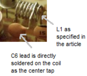 If you are having any confusions regarding the construction of this project contact me immediately, I'll help you through until your project is completed.
PCB Design
The PCB design for the proposed FM radio based walkie talkie circuit can be witnessed below: As you can see, the antenna coil is designed on the PCB itself, through a spirally laid track layout, having the exact required embedded inductance.
Thus the circuit becomes truly compact as it does not depend on the traditional, cumbersome, manually wound copper coil.
The supply being 9V, it works with extra power ensuring that the conversation is distinctly clear even at distances over 150 meters, which other similar transmitter would simply fail to accomplish.
Make sure to use a 1 meter long flexible wire for the antenna, to get a distortion free walkie talkie experience.
As you can see, the antenna coil is designed on the PCB itself, through a spirally laid track layout, having the exact required embedded inductance.
Thus the circuit becomes truly compact as it does not depend on the traditional, cumbersome, manually wound copper coil.
The supply being 9V, it works with extra power ensuring that the conversation is distinctly clear even at distances over 150 meters, which other similar transmitter would simply fail to accomplish.
Make sure to use a 1 meter long flexible wire for the antenna, to get a distortion free walkie talkie experience.
Remote Control Circuit Using FM Radio
In this post we will learn how to build a simple FM remote control circuit for toggling small AC loads such as lamps, fans etc using an ordinary FM transmitter circuit and a modified FM radio circuit. This remote control system enables the user to get an ON/OFF control on any desired appliance, by simply modifying an existing radio into a remote receiver through a relay control circuitry.Introduction
Remote control circuits are not so easy to build as they incorporate critical inductor stages and also, the components are difficult to procure. However a simple homemade FM remote control can be made by modding your existing FM radio as the receiver part. The transmitter can be simply made by assembling a few electronic components. The two sections together can be used for controlling any electrical load remotely from any part of the house.Making the FM Transmitter for the Remote Control Unit:
Using a Music Modulation for Increasing Transmitter range
The section consisting of the IC UM66 and the electrolytic capacitor forms the modulating stage and injects the required modulation signals to the RF stage. This helps to make the transmitted waves much stronger and travel up to longer distances. Once the assembly of the transmitter circuit is done, its working should be confirmed by switching ON the transmitter and by verifying the received signals over the FM radio. The reception should consists the music from the UM66 IC and should be received by the radio, loud and clear even from a distance of over 30 meters. After finishing the construction of the transmitter, you need to assemble the Flip Flop circuit by soldering the electronic components as per the shown diagram. This stage will be later on required to be integrated with the modified FM radio.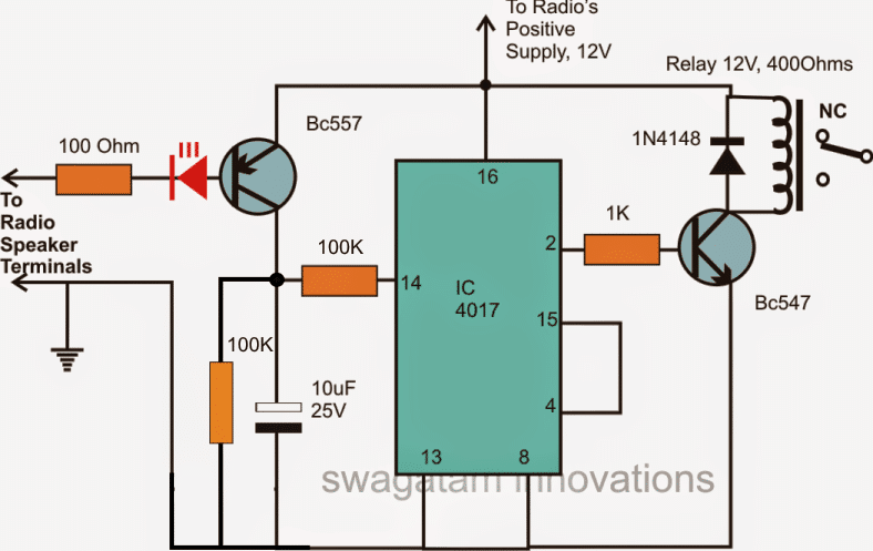
How to Modify a FM Radio as a Remote Control Receiver for Controlling Electrical Gadgets
For this project you will need an ordinary FM radio for making the receiver/controller unit. After procuring a FM radio, you will need to do the following modifications in it. Open the back cover of the FM radio to uncover the circuit of the unit. Now carefully, integrate the flip flop circuit to the speaker terminals of the radio. The connections won��t be difficult as everything��s shown in the diagram very clearly. The idea here is to use the reception audio from the radio speaker terminals and use it to activate our flip flop circuit and the relay. Switch ON the FM radio and tune to some vacant area where there��s no station available, and only the background ��hissing�� noise is audible. Adjust the volume control of the radio toward the maximum and you will find the LED light up, refine the adjustment until the LED just switches OFF. Now tune the radio to some station, without disturbing the volume control. You will find the LED flickering in response to the audio outputs. You will also see the flip flop responding appropriately and the relay switching randomly to the LED illuminations. This concludes the procedures, your setting of the radio or the modifications of the radio is complete.Testing the Remote Control Switching
Now switch ON the transmitter and once again tune the radio to the spot where it receives the transmitter music loud and clear. That��s it, the setting of your home made remote control is complete. Now as many time you click the transmitter switch, it will be received by the radio and the flip flop relay activated alternately. The relay contacts may be wired to any appliance and may be controlled easily by your transmitter through mere clicks of its switch. However the speaker of the radio will also make lot of noise and therefore to eliminate this you may just tear of the cone of the speaker so that it keeps silent, activating only the flip flop.Firecracker Igniter circuit [Remote Controlled with Timer]
In this post we are going to construct a few fireworks ignition circuits which can safely ignite them via IR remote and timer. We have proposed three firecracker igniter circuit designs using ordinary components which we will be exploring them in detail. Before we jump in to the circuit details, we have a word of caution; consumer Fireworks are dangerous and must be enjoyed under adult supervision and adults must have enough precautionary knowledge while igniting one and no fireworks must be ignited with close proximity to you or any flammable / inflammable substances or any living subjects. The proposed project is here to make consumer firecrackers safer by igniting it from safe distance. The proposed circuits operate using rechargeable batteries and can ignite several firecrackers in one charge. Now let��s dive into the first design which is simplest of the three. Firecracker igniter using IR and monostable multivibrator: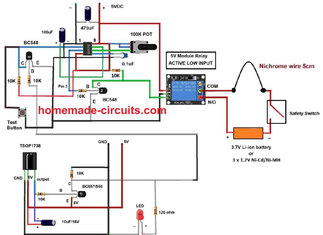 The above circuit consists of two stages: the first one is the IR stage which detects the incoming IR signal from any IR based remote controller.
The second part of the circuit is a monostable multivibrator built using IC 555 which triggers the relay ON for a pre-determined period of time which heats-up the nichrome wire and ignites the fuse of the cracker.
Now let��s explore the two stages in detail and how the circuit functions.
Working explanation and detailed circuit description:
IR stage circuit:
The above circuit consists of two stages: the first one is the IR stage which detects the incoming IR signal from any IR based remote controller.
The second part of the circuit is a monostable multivibrator built using IC 555 which triggers the relay ON for a pre-determined period of time which heats-up the nichrome wire and ignites the fuse of the cracker.
Now let��s explore the two stages in detail and how the circuit functions.
Working explanation and detailed circuit description:
IR stage circuit:
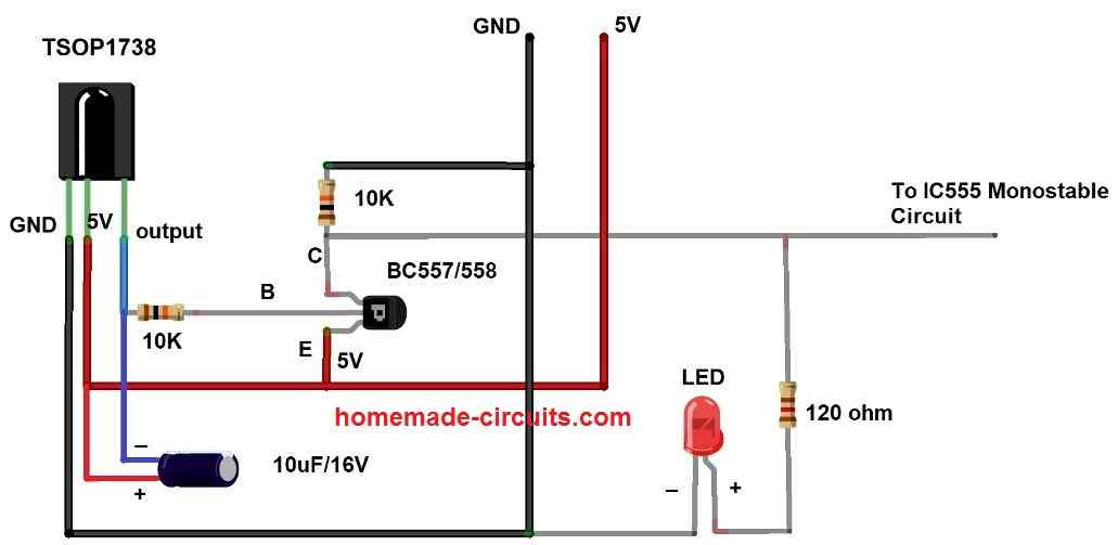 The above circuit is responsible for detecting infrared signal from any IR based remote controller.
The circuit consists of an IR detector TSOP1738 which can detect infrared light with a carrier signal of 38 KHz, which includes most of the IR based remote controllers.
Please note that 38 KHz has nothing to do with the infrared light��s frequency, but the (on/off) switching frequency of the (carrier) signal.
The TSOP1738 operates at 5V and consumes around 5mA.
The output of TSOP1738 during idle state is HIGH and when it detects IR signal from a remote controller the output turns LOW.
IR based remote controllers does not output a steady Infrared light, but flashes, this is because each button on an IR remote has some special purpose and when you press a button the remote emits Infrared light with encoded signal in the form of flashing IR.
At the output terminal of the TSOP1738 we can detect the exact signal from a remote.
However, these encoded signals (with data) are irrelevant for this project and we just need a steady signal to trigger the next stage.
To make the output signal constant we have connected an electrolytic capacitor with a value of 10uF which smooths the pulsating signal from the remote.
The signal after smoothing capacitor is passed to buffer stage which utilizes a low power PNP transistor to strengthen the outgoing signal and also to invert the signal polarity so that the next stage of the circuit receives -Ve signal in idle and +Ve signal when a key is press on the remote.
A 10K pulldown resistor is utilized at collector terminal so that when the circuit is in idle state the output stays at LOW.
A LED is connected to collector terminal with a current limiting resistor which glows when you press a key in a remote.
Monostable multivibrator:
The above circuit is responsible for detecting infrared signal from any IR based remote controller.
The circuit consists of an IR detector TSOP1738 which can detect infrared light with a carrier signal of 38 KHz, which includes most of the IR based remote controllers.
Please note that 38 KHz has nothing to do with the infrared light��s frequency, but the (on/off) switching frequency of the (carrier) signal.
The TSOP1738 operates at 5V and consumes around 5mA.
The output of TSOP1738 during idle state is HIGH and when it detects IR signal from a remote controller the output turns LOW.
IR based remote controllers does not output a steady Infrared light, but flashes, this is because each button on an IR remote has some special purpose and when you press a button the remote emits Infrared light with encoded signal in the form of flashing IR.
At the output terminal of the TSOP1738 we can detect the exact signal from a remote.
However, these encoded signals (with data) are irrelevant for this project and we just need a steady signal to trigger the next stage.
To make the output signal constant we have connected an electrolytic capacitor with a value of 10uF which smooths the pulsating signal from the remote.
The signal after smoothing capacitor is passed to buffer stage which utilizes a low power PNP transistor to strengthen the outgoing signal and also to invert the signal polarity so that the next stage of the circuit receives -Ve signal in idle and +Ve signal when a key is press on the remote.
A 10K pulldown resistor is utilized at collector terminal so that when the circuit is in idle state the output stays at LOW.
A LED is connected to collector terminal with a current limiting resistor which glows when you press a key in a remote.
Monostable multivibrator:
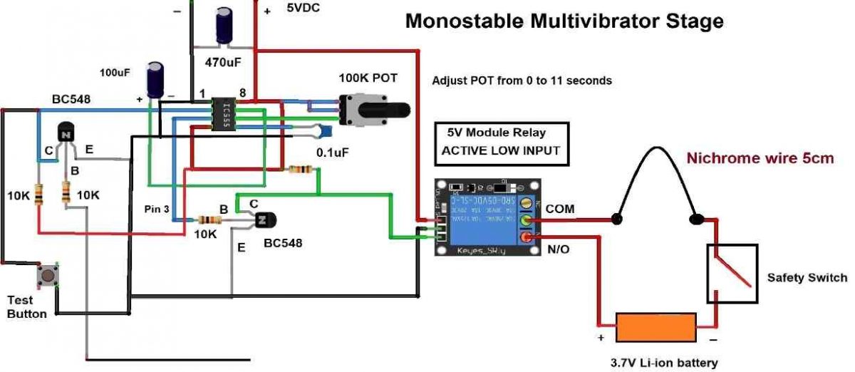 The above circuit is responsible for triggering the relay ON for a pre-determined period of time after a signal from IR stage is received.
When the relay is activated the COM and normally open (N/O) terminals gets connected, this will complete the circuit and heats a piece of nichrome wire which ignites firecracker��s fuse.
The circuit deactivates the relay after reaching the set time.
A 3.7V li-ion cell or Ni-Cd / Ni-Mh battery can be used for heating the nichrome wire.
Please note that when the relay is triggered you can see the nichrome wire glowing red hot.
The monostable multivibrator circuit is build using IC 555. The IC��s output turns HIGH for a pre-determined period of time when a LOW trigger signal is applied at pin number 2. During idle state the pin 2 must be connected to HIGH, to accomplish this a 10K pullup resistor is used at pin 2.
The input HIGH trigger signal is received by a NPN transistor (from IR stage) which invert��s the output as -Ve signal and applies it to pin number 2.
The relay module we are utilizing is a 5V one with a breakout board and the relay activates when you apply a -Ve signal (Active LOW trigger).
At the output terminal (pin number 3) of IC 555 a NPN transistor is used to invert the +Ve signal to -Ve so that the relay can be triggered ON.
A test switch is provided to test / set the timing of the circuit and you can set time from 0 to 11 seconds to heat the nichrome wire by adjusting the provided 100K potentiometer.
The recommended time is 5 seconds after which the relay deactivates.
Note: The fuse of the firecracker must be in contact the nichrome wire properly to start ignition.
Make sure the provided safety switch is in open position when you are setting the firecracker��s fuse with nichrome wire, close the switch and move away to safe a distance immediately and use IR remote to ignite.
Firecracker ignition circuit design 2:
The above circuit is responsible for triggering the relay ON for a pre-determined period of time after a signal from IR stage is received.
When the relay is activated the COM and normally open (N/O) terminals gets connected, this will complete the circuit and heats a piece of nichrome wire which ignites firecracker��s fuse.
The circuit deactivates the relay after reaching the set time.
A 3.7V li-ion cell or Ni-Cd / Ni-Mh battery can be used for heating the nichrome wire.
Please note that when the relay is triggered you can see the nichrome wire glowing red hot.
The monostable multivibrator circuit is build using IC 555. The IC��s output turns HIGH for a pre-determined period of time when a LOW trigger signal is applied at pin number 2. During idle state the pin 2 must be connected to HIGH, to accomplish this a 10K pullup resistor is used at pin 2.
The input HIGH trigger signal is received by a NPN transistor (from IR stage) which invert��s the output as -Ve signal and applies it to pin number 2.
The relay module we are utilizing is a 5V one with a breakout board and the relay activates when you apply a -Ve signal (Active LOW trigger).
At the output terminal (pin number 3) of IC 555 a NPN transistor is used to invert the +Ve signal to -Ve so that the relay can be triggered ON.
A test switch is provided to test / set the timing of the circuit and you can set time from 0 to 11 seconds to heat the nichrome wire by adjusting the provided 100K potentiometer.
The recommended time is 5 seconds after which the relay deactivates.
Note: The fuse of the firecracker must be in contact the nichrome wire properly to start ignition.
Make sure the provided safety switch is in open position when you are setting the firecracker��s fuse with nichrome wire, close the switch and move away to safe a distance immediately and use IR remote to ignite.
Firecracker ignition circuit design 2:
 This design is an enhanced version of the pervious one, the difference between this and previous one is, the former ignites the cracker with single click and this will ignite only after three clicks and this will prevent accidental ignitions and false triggers.
However, this doesn��t mean the previous circuit is a bad design.
Now let��s dive into the details.
The first stage is IR receiver which is same as previous one and works in the same way.
The next stage is a debouncing circuit which will output a signal that is one second long to the next circuit stage.
The debouncing circuit ignores accidental multiple trigger signal from IR circuit stage after a signal is received.
A point worth noting is that the debouncing circuit is also a monostable multivibrator.
This design is an enhanced version of the pervious one, the difference between this and previous one is, the former ignites the cracker with single click and this will ignite only after three clicks and this will prevent accidental ignitions and false triggers.
However, this doesn��t mean the previous circuit is a bad design.
Now let��s dive into the details.
The first stage is IR receiver which is same as previous one and works in the same way.
The next stage is a debouncing circuit which will output a signal that is one second long to the next circuit stage.
The debouncing circuit ignores accidental multiple trigger signal from IR circuit stage after a signal is received.
A point worth noting is that the debouncing circuit is also a monostable multivibrator.
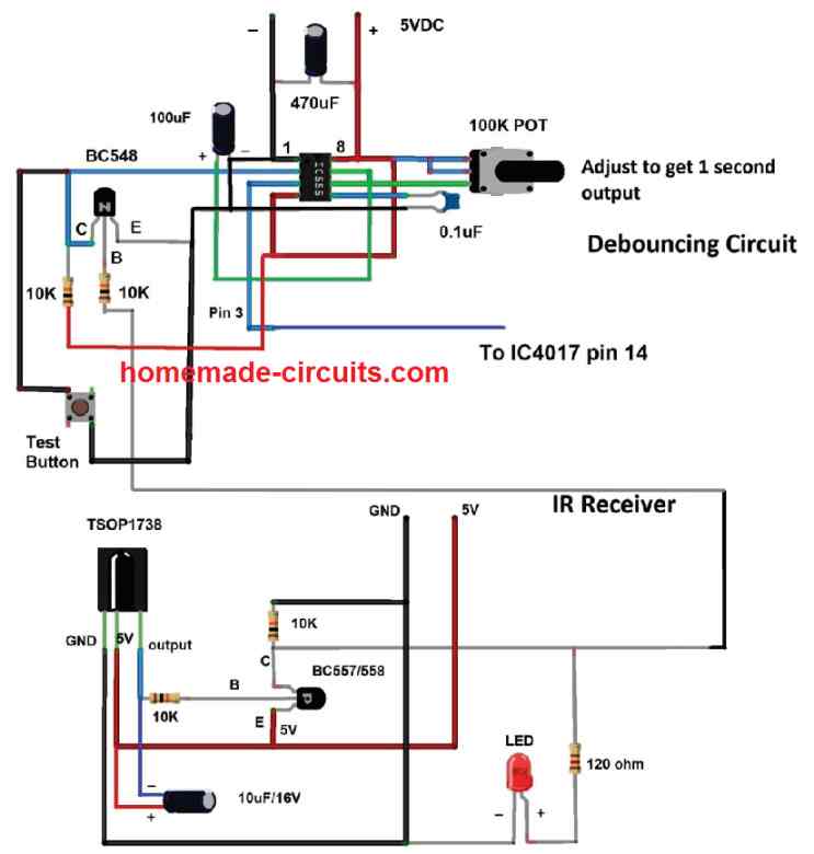 The next stage divides the output by three, this stage is what enabling us to press three clicks for ignition.
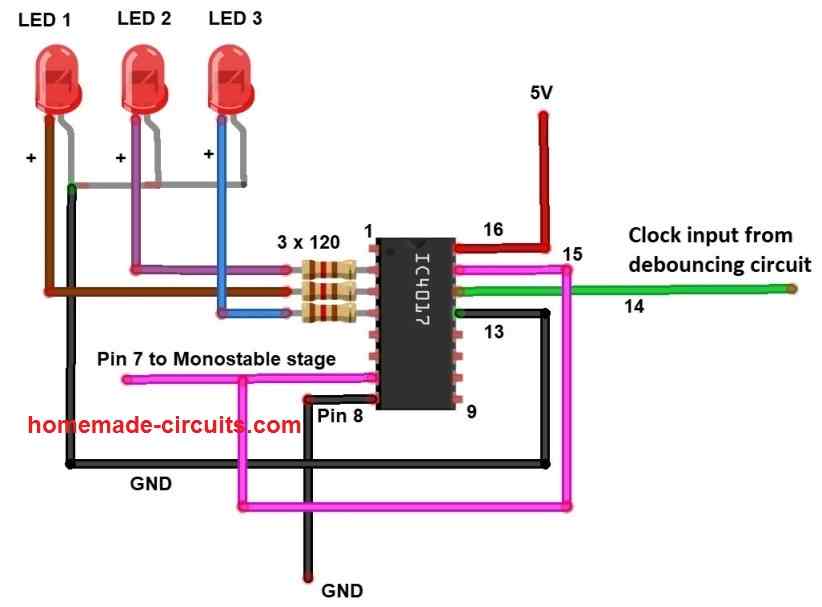 This stage consists of IC 4017 and three LED lights to indicate the how many clicks away from ignition.
The IC 4017 is configured to divide the input signal by three, this is achieved by connecting the 4th output of the IC to reset pin 15.
Initially the LED 1 will glow, when you press a button on IR remote for the first time, the LED 2 will light-up (LED 1 will turn off) and when you press the button again, the LED 3 will light up (LED 2 will turn off) and when you press the remote for the 3rd time the circuit will give a signal to the next stage for ignition.
After pressing three clicks on the remote, the output pin number 7 (4th output) turns high momentarily which is fed to the next stage which is a monostable multivibrator circuit.
This stage consists of IC 4017 and three LED lights to indicate the how many clicks away from ignition.
The IC 4017 is configured to divide the input signal by three, this is achieved by connecting the 4th output of the IC to reset pin 15.
Initially the LED 1 will glow, when you press a button on IR remote for the first time, the LED 2 will light-up (LED 1 will turn off) and when you press the button again, the LED 3 will light up (LED 2 will turn off) and when you press the remote for the 3rd time the circuit will give a signal to the next stage for ignition.
After pressing three clicks on the remote, the output pin number 7 (4th output) turns high momentarily which is fed to the next stage which is a monostable multivibrator circuit.
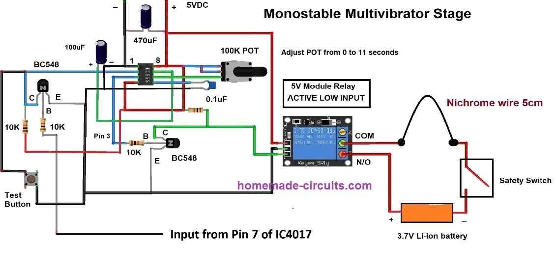 The output of IC 4017 is fed to the above stage and triggers the relay ON for a set period of time that you have set using the provided potentiometer (0 to 11 seconds).
Firecracker ignition circuit design 3:
The output of IC 4017 is fed to the above stage and triggers the relay ON for a set period of time that you have set using the provided potentiometer (0 to 11 seconds).
Firecracker ignition circuit design 3:
 The previous two designs are trigger using IR remote, in this design we have incorporated timer to trigger the ignition.
Here you can select from 10 to 90 seconds to ignite a firecracker.
The first stage is an astable multivibrator circuit using IC 555 which generates clock signal at the rate of 1 Hz.
Adjust the 100K potentiometer to get 1Hz at pin number 3.
The previous two designs are trigger using IR remote, in this design we have incorporated timer to trigger the ignition.
Here you can select from 10 to 90 seconds to ignite a firecracker.
The first stage is an astable multivibrator circuit using IC 555 which generates clock signal at the rate of 1 Hz.
Adjust the 100K potentiometer to get 1Hz at pin number 3.
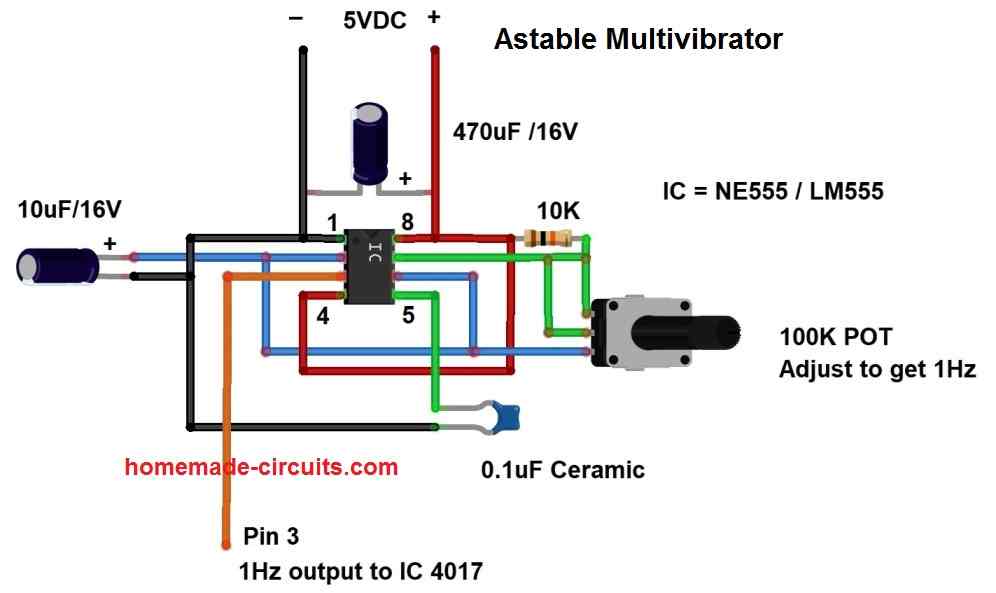 The next stage is clock divider circuit which divides the 1Hz clock to 10 to 90 seconds.
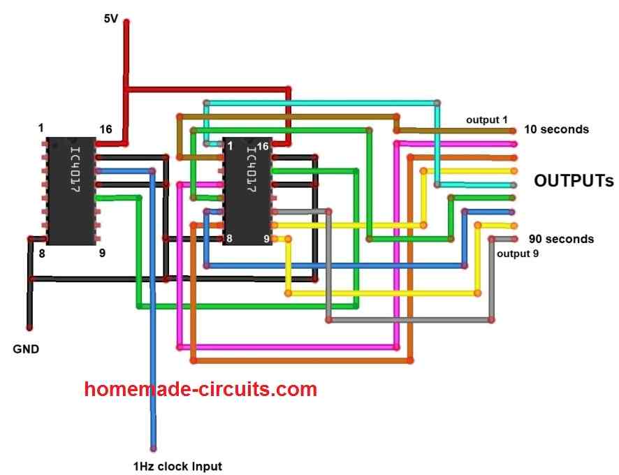 NOTE: There are nine outputs and you can choose an output between 10 and 90 seconds and connect the desired output pin next stage of the circuit.
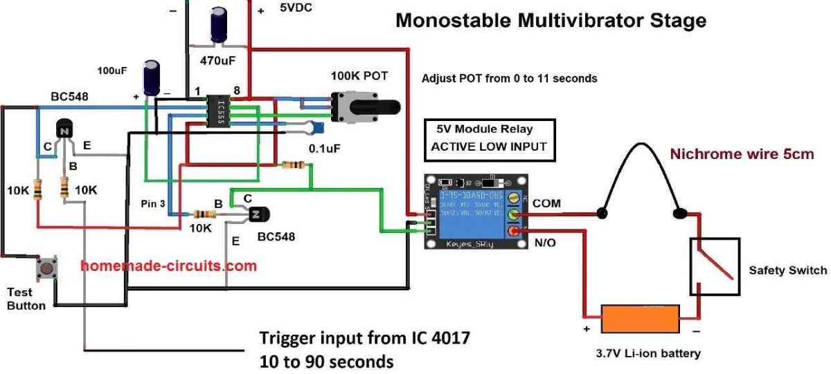 The above stage is a monostable multivibrator circuit which triggers the relay ON for pre-determined period of time, which can be adjusted using the 100K potentiometer.
Power supply:
All the circuit presented in this project are operated using batteries and no AC supply is used.
There are two separate power supplies in all the three proposed circuits, the first one is to heat-up the nichrome wire using 3.7V li-ion cell or three Ni-Cd cells connected in series.
The second power supply is for powering the main circuit using 5V.
The above stage is a monostable multivibrator circuit which triggers the relay ON for pre-determined period of time, which can be adjusted using the 100K potentiometer.
Power supply:
All the circuit presented in this project are operated using batteries and no AC supply is used.
There are two separate power supplies in all the three proposed circuits, the first one is to heat-up the nichrome wire using 3.7V li-ion cell or three Ni-Cd cells connected in series.
The second power supply is for powering the main circuit using 5V.
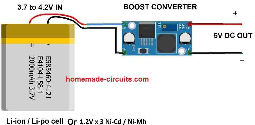 You can use any type of battery and switching buck/boost converters or voltage regulators to get 5Vas output, the above circuit is just an example.
Safety warnings:
You can use any type of battery and switching buck/boost converters or voltage regulators to get 5Vas output, the above circuit is just an example.
Safety warnings:
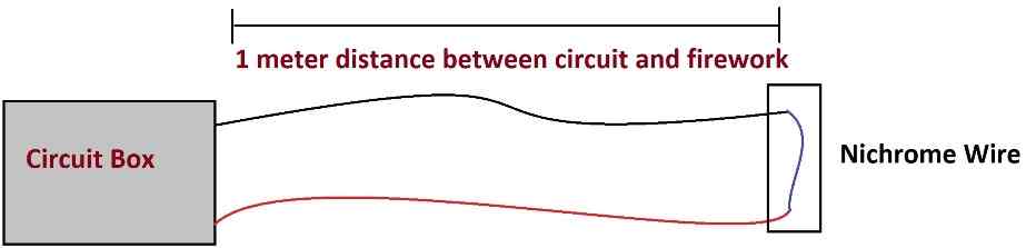 1) Make sure your circuit and batteries are in a safe distance and protected from sparks and flames using a hard plastic box and make sure that the cracker is at least 1 meter away from the circuit as illustrated above.
2) Make sure to open the safety switch mentioned in the circuit before setting up the cracker��s fuse with the nichrome wire.
After closing the safety switch, please move away.
This is to prevent any accidental ignition while setting the cracker��s fuse with the nichrome wire.
3) Make sure the relay is in deactivated state before you setup the cracker with nichrome wire.
You can know whether the relay is ON or OFF by looking at the status LED that comes built-in with the module.
1) Make sure your circuit and batteries are in a safe distance and protected from sparks and flames using a hard plastic box and make sure that the cracker is at least 1 meter away from the circuit as illustrated above.
2) Make sure to open the safety switch mentioned in the circuit before setting up the cracker��s fuse with the nichrome wire.
After closing the safety switch, please move away.
This is to prevent any accidental ignition while setting the cracker��s fuse with the nichrome wire.
3) Make sure the relay is in deactivated state before you setup the cracker with nichrome wire.
You can know whether the relay is ON or OFF by looking at the status LED that comes built-in with the module.
Remote Control using Mains Power Line Communication
The proposed circuit will allow you to remotely control a mains AC operated appliance across rooms of your home through mains power line communication or PLC concept. In PLC technology, an electronic circuit which works as a transmitter is plugged-in to the mains wiring (220 V or 120 V) injects a modulating high frequency data signal into the 50 Hz or 60 Hz mains AC frequency. Another circuit which acts like a receiver and coupled across the same AC mains wiring but in some other location detects this modulated signals via the mains wire and decodes or demodulates the data for the specified end results. Imagine a device which can be plugged in your hall room's mains socket, and toggling its button controls another mains operated gadget in the adjoining room or in your kitchen. This sounds amazing right, yes this is an old concept which allows the user to communicate across rooms using the existing mains wiring of the house, through a coupled transmitter/receiver units. In this article we discuss a couple of simple power line communication (PLC) based remote control circuits, which may be used for controlling devices across rooms through a plugged-in transmitter/receiver pair. The first design below is built using ordinary electronic parts such transistors, resistors, capacitor, diodes etc. Let's first learn regarding the transmitter circuit and its operational details.Power Line Communication Transmitter
The simple transmitter circuit can be witnessed in the following diagram. The PLC transmitter circuit includes an oscillator stage using transistors T5/T6, tuned at at 150 kHz. This oscillator frequency is switched ON through a monostable multivibrator built around T4 transistor BC557. This monostable can be triggered using the ON/OFF switch S1. This 150 kHz frequency is then injected into the mains wiring through the transformer T1 shown at the bottom right. So now, the 150 kHz frequency rides over the mains 50 Hz or 60 z frequency, which can be picked up by a PLC receiver unit coupled with the same wiring at a distant location or in another room.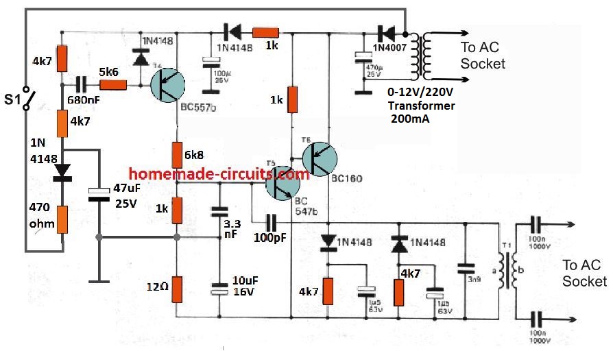
PLC Receiver
The following image depicts the power line communication receiver circuit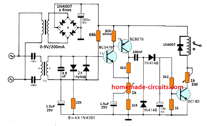 The receiver is configured around a two stage amplifier using transistors T7/T8, a rectifier circuit using two 1N4148 diodes, which has quite a long time constant.
The time delay helps to cancel out momentary interference pulses.
The 150 kHz frequency is extracted through an attached transformer T2, and after suitable filtering stages, the amplifier detects and responds to the 150 kHz frequency and begins oscillating at the same rate.
The rectifier stage using the two 1N4148 and the subsequent 10 uF filter capacitor stabilizes the frequency into a stable DC for toggling ON the next relay driver transistor.
The relay driver stage switches ON the relay and the connected load, and remains ON as long as the transmitter switch S1 remains switched ON, and vice versa.
In case your neighbor might be also having a similar system installed in their house, then to avoid cross interference you may want to adjust the sensitivity of the receiver to a lowest possible setting, which may be just enough to work with your own system.
This sensitivity may be tweaked with the 1 k preset.
The coupling transformers which are used for injecting and extracting the 150 kHz frequency across the mains wiring is built over 20 mm diameter pot core.
The winding "b" which is towards the mains wiring has 20 turns using 31 SWG super enameled copper wire, and the side "a" which towards the circuit side has 40 turns using the same wire.
The above design uses a simple circuit which may perhaps get toggled with some nearby frequency such as 140 kHz or 155 kHz, which may not seem very desirable.
For achieving a pin point accuracy with the frequency response, so that the unit responds precisely to the specific transmitter signals, a PLL based IC may be required as explained below.
The receiver is configured around a two stage amplifier using transistors T7/T8, a rectifier circuit using two 1N4148 diodes, which has quite a long time constant.
The time delay helps to cancel out momentary interference pulses.
The 150 kHz frequency is extracted through an attached transformer T2, and after suitable filtering stages, the amplifier detects and responds to the 150 kHz frequency and begins oscillating at the same rate.
The rectifier stage using the two 1N4148 and the subsequent 10 uF filter capacitor stabilizes the frequency into a stable DC for toggling ON the next relay driver transistor.
The relay driver stage switches ON the relay and the connected load, and remains ON as long as the transmitter switch S1 remains switched ON, and vice versa.
In case your neighbor might be also having a similar system installed in their house, then to avoid cross interference you may want to adjust the sensitivity of the receiver to a lowest possible setting, which may be just enough to work with your own system.
This sensitivity may be tweaked with the 1 k preset.
The coupling transformers which are used for injecting and extracting the 150 kHz frequency across the mains wiring is built over 20 mm diameter pot core.
The winding "b" which is towards the mains wiring has 20 turns using 31 SWG super enameled copper wire, and the side "a" which towards the circuit side has 40 turns using the same wire.
The above design uses a simple circuit which may perhaps get toggled with some nearby frequency such as 140 kHz or 155 kHz, which may not seem very desirable.
For achieving a pin point accuracy with the frequency response, so that the unit responds precisely to the specific transmitter signals, a PLL based IC may be required as explained below.
PLC Circuit using IC LM567
The idea was published in the datasheet of the IC LM567 as one of the application circuits, among the many other outstanding ones.Receiver Schematic
The IC LM 567 is actually a specialized tone decoder using PLL technology which enables the device to detect and respond only to a specific frequency as determined by an external RC network values, and reject all other irrelevant frequency in the spectrum.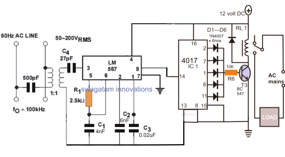 The proposed remote control circuit using power line communication may be witnessed in the above diagram, the circuit functioning details may be learned from the following points:
How it Works
R1, and C1 are the external RC components which decide the sensing frequency of the device, and pin#3 becomes the sensing pinout of the IC. Meaning, pin#3 will detect and acknowledge only that particular frequency which is set using the R1/C1 network. For example if the R1, C1 values are selected to assign a 100kHz frequency, pin#3 will pick only this frequency to activate its output and ignore all that may be different to this range. The above feature enables the IC to single out the specific frequency from the superimposed AC 50 or 60 Hz frequency and trigger the output only in response to this predetermined set frequency. In the figure we can see a small isolation transformer which is included in order to isolate the electronic circuit from the lethal mains current. The mains low AC frequency acts like the carrier frequency, over which the triggering high frequency rides to reach the intended destination across the transmission line. In the above receiver design, the IC is assigned to respond to a 100kHz frequency which is supposed to be injected into the mains line from a nearby location which could be an adjacent room or premise. The 100kHz frequency could be injected through any oscillator circuit such as a IC 555, or IC 4047 circuit or another IC LM567 circuit installed as the transmitter unit. In an event when a signal is injected into the mains from a relevant location, the receiver circuit shown above detects the specific frequency in the attached mains power line, and responds to it by producing a low logic across its pin#8. The pin#8 being connected with the a 4017 flip flop circuit toggles the output relay and the load ON or OFF depending upon the previous situation of the relay.The Transmitter Stage
The transmitter which is supposed to inject the 100kHz or the desired triggering frequency into the power line can be ideally built using a half bridge driver oscillator circuit as shown below:Transmitter Schematic
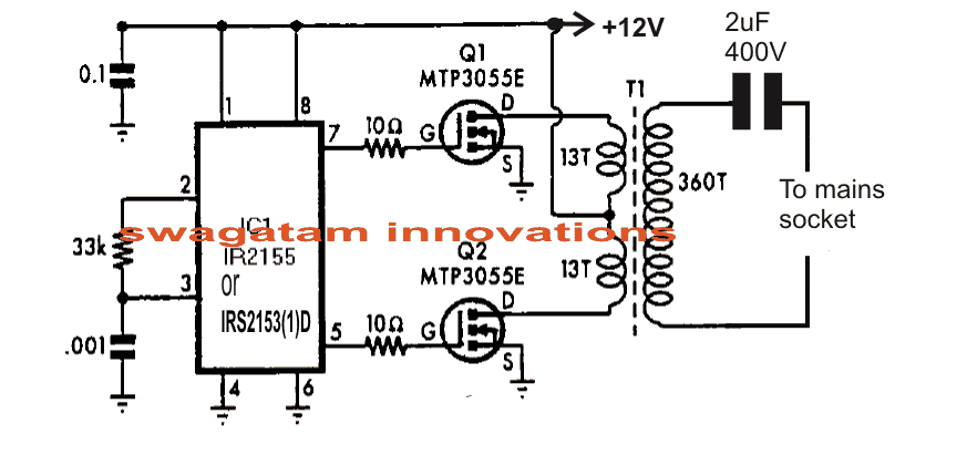 The 12V input to the circuit must be switched through a push button arrangement so that the circuit is triggered only when required in order to switch on the intended appliance through the power line.
The RC component at pin2/3 of the IC are not calculated for generating 100kHz, The following formula can be used for determining the right oscillator frequency:
f = 1/1.453�� Rt x Ct
Ct is in Farads, Rt is in Ohms.
and f in Hz
Alternatively the same can be evaluated using a frequency meter and with some experimentation.
This is an untested circuit designed as per the suggestions presented in the datasheet of the IC LM567.
The 12V input to the circuit must be switched through a push button arrangement so that the circuit is triggered only when required in order to switch on the intended appliance through the power line.
The RC component at pin2/3 of the IC are not calculated for generating 100kHz, The following formula can be used for determining the right oscillator frequency:
f = 1/1.453�� Rt x Ct
Ct is in Farads, Rt is in Ohms.
and f in Hz
Alternatively the same can be evaluated using a frequency meter and with some experimentation.
This is an untested circuit designed as per the suggestions presented in the datasheet of the IC LM567.
How to make a Remote Controlled Game Scoreboard Circuit
The post explains how to build a simple remote controlled game scoreboard circuit with two digits for facilitating the user a hassle free changing of the digits remotely, during a game or a match. The idea was requested by Mr. Richard.Circuit Objectives and Requirements For our co-ed volleyball game we use manual flip cards {simple 00 to 99 (x2) flip cards} This is awkward and time consuming, somebody needs to flip the numbers.
If I had a remote controlled display, no time would be wasted flipping numbers.
This is a recreation league with no BIG $ to spend.
Looking for a 2 digit - seven segment display (x2) with the ability to count up and count down (4 buttons)
Similar to this display -
This is awkward and time consuming, somebody needs to flip the numbers.
If I had a remote controlled display, no time would be wasted flipping numbers.
This is a recreation league with no BIG $ to spend.
Looking for a 2 digit - seven segment display (x2) with the ability to count up and count down (4 buttons)
Similar to this display -
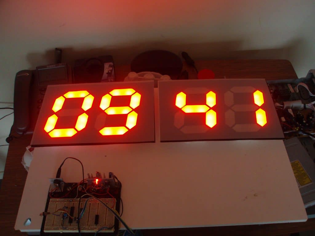
 Can I incorporate a 4 button RF transmitter/receiver
The Design
The following figure shows a simple two digit up/down pulse counter circuit which can be used for the above requested application. The incorporation of the specific digital ICs make the design extremely straightforward to configure and operate for the desired pulse counting display. The IC1 and IC3 form the actual counter chips, whose BCD outputs are appropriately translated into the required 7 segment digital display outputs.Circuit Diagram
 Pin#5 and pin#4 of the 74LS192 are rigged as the UP and DOWN sensing inputs, and the relevant switches when operated allow these pins to get the specified logic zero pulses for displaying the corresponding incrementing or reversing numbers on the associated 7 segment display modules.
The switch at pin#14 of the ICs is used for resetting the displays to zero with a single operation.
Since the proposed digital game scoreboard circuit is supposed to be controlled with a remote control unit, the switches at pin#5, 4 and 14 can be seen replaced with the relay contacts from the remote receiver unit.
Therefore when the compatible or matching buttons on the remote transmitter handset are pressed, the corresponding relay contacts close causing the relevant number to appear on the display board either in the ascending or descending order depending on which button was toggled.
That implies, this remote controlled game scoreboard circuit can be operated using a remote control from anywhere within the stipulated range by any member of the team simply with a press of a button of the transmitter module.
And this can be done while the user enjoys the game on his/her preferred place of the ground.
Pin#5 and pin#4 of the 74LS192 are rigged as the UP and DOWN sensing inputs, and the relevant switches when operated allow these pins to get the specified logic zero pulses for displaying the corresponding incrementing or reversing numbers on the associated 7 segment display modules.
The switch at pin#14 of the ICs is used for resetting the displays to zero with a single operation.
Since the proposed digital game scoreboard circuit is supposed to be controlled with a remote control unit, the switches at pin#5, 4 and 14 can be seen replaced with the relay contacts from the remote receiver unit.
Therefore when the compatible or matching buttons on the remote transmitter handset are pressed, the corresponding relay contacts close causing the relevant number to appear on the display board either in the ascending or descending order depending on which button was toggled.
That implies, this remote controlled game scoreboard circuit can be operated using a remote control from anywhere within the stipulated range by any member of the team simply with a press of a button of the transmitter module.
And this can be done while the user enjoys the game on his/her preferred place of the ground.
The Remote Control Circuit
The remote control circuit for the discussed digital game scoreboard has been already covered in quite many articles from this website, so I won't be discussing it separately here. The following 4 channel RF remote control circuit could be applied for the above explained circuit. Simple RF Remote Control Circuit without Microcontroller A little pondering reveals that the relays can be actually avoided and the output pins of the receiver RF module could be directly configured with the pin#4, 5 of the of the up/down counter IC, and the reset pin through a NPN buffer. Alternatively, the 4 channel remote control module could be purchased ready madefrom the market, and in that case the existing relay contacts in the receiver unit could be wired as already suggested in this article. The colored lines in the proposed remote controlled game scoreboard diagram indicate how two counter modules are cascaded between each other, more digits could be included by simply cascading more such IC stages in similar fashion.433 MHz RF 8 Appliances Remote Control Circuit
The post explains a circuit which can be used for controlling 1 to 8 appliances with a single RF 433MHz remote control handset. Now you can control fans, lights ACs, oven etc within a range of 50 meters with the same remote. In a few of my earlier posts I have comprehensively discussed regarding these versatile and outstanding remote control modules, for reference you may want to go through the following links: Simple RF Remote Control Circuit without Microcontroller ... Make a Hi-End RF Remote Control Circuit | Electronic Circuit Projects RF Remote Control Encoder and Decoder Chip Pinouts Explained ...Main Features of 433MHz RF Remote Module
The main features of these 433MHz remote modules are: 1) These are available with different ranges, from a single channel to as many as 8 channels, which allows the user to use 8 different appliances from a single receiver unit. 2) The technology used for transmitting the RF waves are extremely sophisticated which prevents the transmitted data from getting hacked. 3) The distance of transmission is also diverse, ranging from 50 meters to 5 kms. 4) Fully customizable "address pins" which enables us to use different remote control handsets with a single receiver unit or vice versa Although it provides us with the facility to control 8 appliances from a single RF module, as discussed in the feature no#1 above, this isn't entirely convenient because since all the 8 relays are fixed in the given receiver board could mean a lot of wiring to be done for different appliances situated at different corners of the house. This slight inefficiency accompanied in the system compels us to think of some alternative method which would allow us to employ individual single relay modules with the desired appliances and then toggle these individual modules through a single remote handset. This option looks much hassle-free as no extra wiring is required for the installations. Yes, that's what we would be trying to implement by exploiting feature no#4 by customizing the address pinouts of the transmitter module as well as the associated various receiver modules. Before jumping into the circuit design it would important for us to discuss how these address pins of the transmitter/receiver are related and maybe customized for specific applications.How Address Pins Function
If you notice the decoder chip of the transmitter module and the encoder chip of the receiver module you will find that both these ICs include 10 address pins (A0 to A9). These address pins are directly compatible with each other, meaning configuration of the transmitter and the receiver address pins should be exactly similar in order to make them respond with each other. For example suppose if only A0 address pin of the transmitter circuit is connected with ground then the only A0 of the receiver must be connected to ground for enabling the two counterparts to "talk" with each other. In this proposed article where we are discussing how to control 8 appliances with a single remote control we take the advantage of the above explained "address pin" feature and configure 8 different receiver modules with a single transmitter remote handset. The following example circuit illustrates the address pin configuration of the relevant Tx and Rx modules. Here we have employed a 4 channel remote module, however a single channel module could also be employed for getting the same results, just by modifying the indicated address pins of the units.TheReceiver Circuit
The following image shows the basic configuration of the receiver module. It shows the remote control application set up for one of the 8 appliances. Similarly, 7 more receiver modules need to built for enabling the control of the associated relevant appliances. For all the 8 units only the address pins need to be differently configured by simply changing the pin connections with ground, meaning if A0 is connected to ground for the 1st module, then A1 needs to be connected with ground for the 2nd module, A2 for the third module and so on.Rx Schematic
 The IC 4017 section forms the flip flop circuit which ensures latching up of the load in ON and OFF conditions alternately, in response to the remote button press.
The Transmitter Circuit
The following image shows the single remote control transmitter for the 8 separate receiver units as explained above. Here pressing only the A0 switch activates the above shown receiver unit, since the A0 in the above design is connected with ground, therefore when A0 switch grounds its own A0 pin, both units "shake hands" and the signal is processed for toggling the appliance. Similarly, switches connected across A1 toA7 can be made compatible with the remaining 7 receiver units for enabling the ON/OFF control of the attached 7 appliances located across different premises. The diode network associated with the below shown transmitter unit makes sure that the BC557 activates and simultaneously powers the circuit only whenever the relevant switches are pressed, and otherwise the transmitter circuit remains completely switched OFF...this feature allows the battery to last for a very long time.Tx Schematic
 Please connect pin#13 with ground so that the Tx is able to send signal to the corresponding pin#13 of the Rx unit
If you any further questions regarding how to control 8 appliances or multiple appliance with single remote, please feel free to ask them through your valuable comments.
Please connect pin#13 with ground so that the Tx is able to send signal to the corresponding pin#13 of the Rx unit
If you any further questions regarding how to control 8 appliances or multiple appliance with single remote, please feel free to ask them through your valuable comments.
How to Trigger a Camera Remotely without Physical Presence
The article discusses a simple RF remote control circuit which can be used for activating a digital camera remotely, by a press of a button. The idea was requested by Mr. Pat Circuit Objectives and Requirements I'm Pat, from France. Congratulations for your blog & website about electronic's devices : it's the paradise :o) I'm photographer & i'm looking for a simple remote control for my Nikon D200 in RF. I need a transmitter and receiver in a single radio frequencies with good reach and operate on a 9V battery. the goal is to trigger the camera remotely. The Nikon camera has a 10-pin socket designed for it. Here's a business model but very expensive here :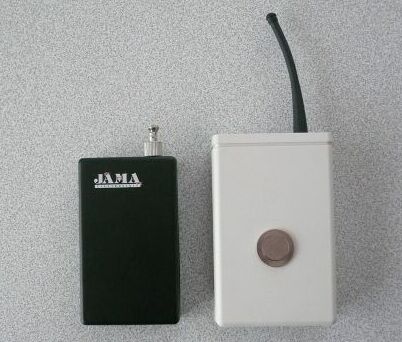 Would you have an assembly to propose? (I tinker with classical electronics as ham radio...
:o)
thanks for your help :o)
Patrick / F5CEY
~90 miles north of Paris
France
Would you have an assembly to propose? (I tinker with classical electronics as ham radio...
:o)
thanks for your help :o)
Patrick / F5CEY
~90 miles north of Paris
France


Analyzingthe Circuit
Hi Pat, I am glad you liked my website. I'll to try post the design as per my analysis soon in my website. In the meantime you can go through the following article which I would be using for the proposed implementation. https://www.homemade-circuits.com/2013/07/simple-100-meter-rf-module-remote.htmlThe Design
I have discussed a simple 433 MHz RF remote control module based circuits which can be used in all kinds of remote switching applications within a range of 100 meters. Other forms of modules can be employed for getting higher ranges of distance. These RF remote control modules can be also effectively used for the discussed remote camera switching application. As per my interpretation, the pinouts from the camera's 10 pin socket which are relevant to the remote switching of the camera (using the proposed RF modules) are as follows: pin#1 = Rx input data (triggering pulse) pin#2 = +5V external input, or from the camera battery pin#7 = power ground to be integrated with the RF module ground or negative. Other pinouts does not look relevant for the intended functions and therefore may be left open. As per the above data, the Rx or receiver module output could be integrated with the camera's existing 10 pin connector in the following shown manner:
 If the camera is intended to be operated with an external power source then an external battery may be utilized for powering the Rx module and the same may be fed to the camera via the pin#2 of its 10 pin socket.
If the internal battery of the camera is used which looks more appropriate then the Rx module could be powered from this source via the pin#2.
The BC557 can be seen configured with one of the output pinouts of the RX module which happens to be pin#10 from the decoder IC of the Rx module, although any of the other output could be used for the same results.
In the Tx module you will also find compatible 4 inputs with switches, each corresponding to the individual 4 outputs of the Rx module, meaning if pin#10 button of the Tx is pressed, this will activate the pin#10 of the Rx module....
and so on.
Therefore in the above case the pin#10 switch of the Tx needs to be pressed for implementing the required remote controlled camera switching.
The press of a button in the Tx handset is supposed to generate a low logic at the relevant pinout of the Rx module (pin#10 in the present case), which causes the BBC557 to activate and send a +5V TTL pulse to pin#1 of the camera, activating the camera shutters.
If the camera is intended to be operated with an external power source then an external battery may be utilized for powering the Rx module and the same may be fed to the camera via the pin#2 of its 10 pin socket.
If the internal battery of the camera is used which looks more appropriate then the Rx module could be powered from this source via the pin#2.
The BC557 can be seen configured with one of the output pinouts of the RX module which happens to be pin#10 from the decoder IC of the Rx module, although any of the other output could be used for the same results.
In the Tx module you will also find compatible 4 inputs with switches, each corresponding to the individual 4 outputs of the Rx module, meaning if pin#10 button of the Tx is pressed, this will activate the pin#10 of the Rx module....
and so on.
Therefore in the above case the pin#10 switch of the Tx needs to be pressed for implementing the required remote controlled camera switching.
The press of a button in the Tx handset is supposed to generate a low logic at the relevant pinout of the Rx module (pin#10 in the present case), which causes the BBC557 to activate and send a +5V TTL pulse to pin#1 of the camera, activating the camera shutters.
The Transmitter circuit for the proposed remote control camera switching circuit
The following circuit depicts the transmitter circuit or the Tx circuit stage which is supposed to be utilized for triggering the camera located in the remote location:
 As can be seen in the above image, the four switches correspond to the respective 4 outputs of the Rx module.
However since pin#10 is employed in the present design, the switch associated with pin#10 should be used which is indicated as SW1 in the above diagram.
The rest of the switches could be ignored.
As can be seen in the above image, the four switches correspond to the respective 4 outputs of the Rx module.
However since pin#10 is employed in the present design, the switch associated with pin#10 should be used which is indicated as SW1 in the above diagram.
The rest of the switches could be ignored.
Remote Controlled Trolley Circuit without Microcontroller
The post explains how to make a cheap yet powerful remote controlled trolley which can be maneuvered left, right, forward and reverse as required, by the user using the given remote handset. The idea does not rely on an microcontroller circuit. In one of my previous posts I discussed about a simple remote controlled toy car circuit, the present idea of a remote controlled trolley is inspired with the same concept but is intended to be used for carrying formidable and much heavier loads.Remote Controlled Trolley for Retail Outlets
This design may be specifically suited and applicable for malls or shopping retail outlets where it may be implemented as a small transport vehicle for transporting material within the compound or the premise with the help of a few presses of the remote Tx unit. The first step in building the proposed remote controlled trolley would be to procure a set of standard Rx/Tx RF modules either from your local electronic dealer or from any online store, I recommend buying from an online store as it would be much easier and convenient, although costlier. The procured units would look as shown below:Using the 433MHz Tx, Rx Modules
 The left side brown color unit is the Tx or the transmitter unit while the adjoining circuit broad is the Rx or the receiver unit.
The Tx unit can be seen with 4 red colored buttons marked as A, B, C, D, and the Rx board may be witnessed having 4 relays (black color boxes).
The four respective buttons of the Tx module are wirelessly coupled for operating the four corresponding relays of the Rx module.
You can see connectors fixed around the edges of the board (green colored), these connectors are appropriately terminated with the (+) (-) supply inputs for the Rx board and also with the relay contacts, for all the 4 relays.
A relay, as we all know consists of 5 basic contacts and their pinouts viz: 2 pins for the coil, one for the pole and one each for the N/C and the N/O.
Since there are 4 relays in the Rx unit, you will be able to find 5 x 4 = 20 outputs associated with the relevant connector points.
It could be a tedious task to separately track down these relay terminations on the connectors, so I recommend soldering wires directly on the relay pinouts in order to save yourself from the above task, this effort will be required later while we engage the unit with the trolley's control circuit.
The left side brown color unit is the Tx or the transmitter unit while the adjoining circuit broad is the Rx or the receiver unit.
The Tx unit can be seen with 4 red colored buttons marked as A, B, C, D, and the Rx board may be witnessed having 4 relays (black color boxes).
The four respective buttons of the Tx module are wirelessly coupled for operating the four corresponding relays of the Rx module.
You can see connectors fixed around the edges of the board (green colored), these connectors are appropriately terminated with the (+) (-) supply inputs for the Rx board and also with the relay contacts, for all the 4 relays.
A relay, as we all know consists of 5 basic contacts and their pinouts viz: 2 pins for the coil, one for the pole and one each for the N/C and the N/O.
Since there are 4 relays in the Rx unit, you will be able to find 5 x 4 = 20 outputs associated with the relevant connector points.
It could be a tedious task to separately track down these relay terminations on the connectors, so I recommend soldering wires directly on the relay pinouts in order to save yourself from the above task, this effort will be required later while we engage the unit with the trolley's control circuit.
Building the relay control circuit for the trolley
For this you will require a handful of relays and diodes. The relays should be correctly rated in order to handle the high power wheel motors of the trolley. I recommend using OEN make relays for this, as shown in the following image: The diodes which will be required in the relay driver circuit can be our standard 1N4007 diodes.
The circuit details for the same may be witnessed in the following diagram:
The diodes which will be required in the relay driver circuit can be our standard 1N4007 diodes.
The circuit details for the same may be witnessed in the following diagram:
Relay Wiring Details and Schematic


How the Remote Trolley Circuit Works
Using the above specified relays and the diodes you will need to finish building the above relay driver circuit board which may be simply done on a piece of veroboard. After this we have a major task at our disposal that is integrating the green wires shown in the above diagram with the remote control Rx board. Before the integration we'll have to insert some mods in the Rx module, as explained below: Using pieces of insulated wires, appropriately stripped and tinned at the ends go on connecting (by soldering) all the pole pins of the relay and link this common joint with the positive line of the Rx board. Now in this situation we can assume that when the relays are not in an activated state (through the remote handset) the pole positive input of each relay will be linked to their respective N/C points, and when activated the positive from the pole will shift and get connected with the relevant N/O points. In short, on activation the N/O contact will receive the positive supply and therefore we are interested in this positive supply from the N/O contacts because these will be initiated only when the relays are activated, which implies that when the Tx (transmitter) buttons are pressed. Therefore all the relevant N/O pinouts must be joined to the green wires of the above indicated relay driver circuit. Once this is done, the Rx will be integrated with the relay driver module for executing all the intended maneuvers of the remote controlled trolley, that is: the forward, reverse, motions and the left, right turns.Powering the relay Driver Board
Since the relays in the relay driver stage would be responsible for moving the heavy motors connected with the trolley wheel,the supply for this would need to be equivalently strong, therefore deep cycle lead acid batteries become ideally suited for this application. Assuming the motors to be rated at 12V, a 40AH lead acid battery would be good enough for enabling the trolley to move even with heavier loads. Configuring the Wheels with the Motors for the Intended maneuvers As may be identified in the following figure, the discussed remote controlled trolley will require 4 wheels for su[porting and rolling the system. However only the front two wheels would be responsible for enabling the intended reverse, forward, right and left maneuvers, and therefore the motors would be required to be clamped with these two front wheels of the trolley, as shown in the following image:
Configuring the Trolley Wheel Connections
The rear wheels are just dummy wheels, fixed only for allowing a free rolling of the trolley, in response to the front wheel commands. As may be observed in the above image, the module marked as PCB assembly is the relay driver board, the remote module signifies the Rx remote receiver board while the battery is the 40 AH 12V battery which we discussed in the previous section of the article. After assembling you may have to tweak and check the motor wire connections with the relay driver board. For a forward and reverse motion both the motors must be in sync with each other, on the other hand for executing a right or a left flip, the motors must go through an opposite rotational movement. If you find the motor not behaving in the above manner, it may be most probably corrected by simply swapping the polarity of one of the motors. This will immediately correct the situation and force the motors to implement the specified maneuvers. Finally the A. B, C, D buttons may be appropriately matched or interchanged for the any of the respective maneuvers by tweaking the green wire links with the Rx module, as per the users personal preference.How to Make Ultrasonic Remote Control Circuit
This ultrasonic remote control circuit can be used to switch and control any appliance ON/OFF through a relay in the receiver circuit. Written by: S.S. KopparthyUsing Ultrasonic Waves
This circuit is a different one that uses ultrasonic sound waves whose frequency ranges from 40 KHz to 50 KHz. These waves can��t be heard by humans as the hearing range of humans limited to roughly 20 KHz only. These waves require air medium to travel unlike infrared waves which are mostly used in remote controls. The proposed ultrasonic remote control circuit uses ultrasonic transducers to produce and receive the ultrasonic signals.
Ultrasonic transducers are used in measuring the distance of an object and various other applications.
In this circuit, we use them for a different purpose of making a remote controlled relay.
Receiver Circuit
The proposed ultrasonic remote control circuit uses ultrasonic transducers to produce and receive the ultrasonic signals.
Ultrasonic transducers are used in measuring the distance of an object and various other applications.
In this circuit, we use them for a different purpose of making a remote controlled relay.
Receiver Circuit
 Transmitter Circuit
The Receiver Circuit
The receiver circuit consists of two important stages for the processing of the ultrasonic waves received by the receiving transducer. The first stage is a rectifier which amplifies the signals with the help of the transistors Q1 and Q2. The rectified and filtered DC is fed to the inverting pin of the operational amplifier CA3140. The inverted output is used to bias the transistor Q3 which energizes the relay and there goes the second stage. The preset resistor R2( in receiver circuit) can be used to adjust the sensitivity of the circuit. You can use a 9v SMPS power supply to power the receiver circuit. The receiver circuit should always remain ON and a push-to-on switch can be used in the transmitting circuit to be used as a remote. Assemble the circuits on general purpose PCB��s. You can enclose the transmitter circuit in a suitable casing and the transducer, push-to-on switch and LED should be outside of the casing. Ultrasonic waves are directional in nature and hence, you should direct the waves straight onto the receiving transducer for the relay to activate.Parts List
Transmitter circuit: R1 �C 18K, R2 �C 10K, R3 �C 5K variable resistor, R4 �C 1K, C1 �C 680pf, C2 �C 0.01��f, C3 �C 100��f, 25v, L1 �C green LED, TR1 �C ultrasonic transmitter, S1 �C push-to-on switch, Receiver circuit: R1 �C 10K, R2 �C 5K variable resistor, R3- 10K, R4 �C 15K, R5 �C 100K, R6 �C 10K, R7 �C 4.7K, R8 �C 15K, R9 �C 10K, R10 �C 12K, R11 �C 390K, R12 �C 470K, R13 �C 27K, R14 �C 1K, C1 �C 0.56��f, C2 �C 0.1��f, C3 �C 0.22��f, C4 �C 10��f, 25v, D1, D2 �C 1N4148, D3 �C 1N4007, Q1, Q2 �C BC 548, Q3 �C BC 558, Q4 �C SL 100, RY1 �C 9v relay, RX1 �C ultrasonic transmitter.Remote Controlled Night Lamp Circuit
The post explains a simple IR based remote controlled night lamp timer circuit. The idea was requested by Mr. Raj Kumar Mukherji.Technical Specifications
Please provide the component values and the modified circuit if: a. the circuit is made to work from 4.5 volts or 5 volts b. the relay is replaced with a 5mm LED c. the circuit is triggered by TSOP1738 d the delay time is set for 2 mins max This is for an old person in my locality. He wants a low cost portable light which he would turn on remotely for a brief period at night and the light would get turned off automatically. He has to get up at night to drink water etc and he does not want a night lamp to be on the whole night or to operate one from the mains power. The best idea that came in my mind is to use the transistorized timer circuit in combination with a TSOP1738 and using 2 or 3 AA cells. Thanks and regards, Raj Kumar Mukherji
The Design
The proposed remote night lamp timer circuit can be visualized in the above diagram and understood with the following points: The IR sensor TSOP1738 responds to an incoming IR signal from a suitable IR handset such as a TV remote or similar, and produces a logic low at its pin labelled as "out". The directed Tx signal could be momentary, probably for a fraction of a second for initiating the triggering response in the circuit. The above action instantly charges the 100uF and also switches ON the BC557. This correspondingly turns on the BC547 and the LED. The stored charge sustains the switched ON position for a certain time period determined via the selected values of the 100uF capacitor and the 1M resistor. These may be altered, experimented for acquiring any desired time delay for the LED illumination period. The 100uF slowly starts discharging via the 1M resistor and the base/emitter of the BC557 until it becomes too low for the transistors to hold the conduction, the LED consequently is also switched OFF as soon the RC determined time is elapsed. The 1K and the 1N4148 diode ensures a complete discharge of the timing capacitor 100uF each time the LED is switched OFF, so that the new cycle is able to begin with a correctly discharged capacitor, for executing consistent time delays, with minimum errors. The above design can be upgraded as shown below for getting improved response: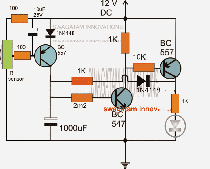
How to Make a Powerful RF Signal Jammer Circuit
The post describes a simple homemade RF signal jammer circuit that can be used for jamming any RF signal within a radial range of 10 meters. The idea was requested by one of the interested readers of this blog.Technical Specifications
I am not a large business interest, but am in need of a circuit which would not only help me, but eventually be welcomed by just about everyone now alive. I am in need of a circuit which will jam RFsignals. I realize jammers are illegal when they disrupt cellphone communication and commercial enterprise. I am only looking to jam (1.) remotely controlled harassment devices and (2.) spyware within the confines of my property. Jamming range limited to around a 25' x 25' area. There is a growing community of victims of electronic harassment. We all experience an invasion of our personal lives/finances and private conversations, and are sometimes physically stalked and attacked. Due to the nature of electronic harassment, it will take time for justice and protection to catch up and solve the problem. As for electronics, some circuits to control the misuse of flux & solder are long overdue in the marketplace. Up until now, most of the interest has been placed on projects of invasion and abuse, such as those contained on many different website I am not overly skilled in electronics, and only come to it in self defense. I am self taught and can follow a schematic and complete a project, and am slowly gaining understanding of the underlying theory. Please advise regarding your interest to help, and your financial requirements. I look forward to hearing from you.Circuit Diagram
Introduction
A simple looking RF signal jammer circuit can be seen in the above diagram, which may be capable of jamming all sorts RF signal within the range of 5 to 10 meters. The circuit can be made suitable with any desired frequency to be jammed by merely using different sets of L1/L2 and by tweaking the 22pF trimmers accordingly. The frequency that could be jammed using this circuit could be well in the range of 50 MHz to 1Ghz, however making it compatible with frequencies above 500 MHz could get much complex and parameters much critical owing to the fact that higher frequencies require shorter interconnections and may involve other stability issues. The present design can be used for jamming FM radio stations situated in the within 40 meters radial distance or even higher. The circuity of the proposed RF signal jammer is basically made of two distinct stages:RF Circuit Stages
The one comprising T1 and the associated parts form the RF oscillator stage while the other stage consisting of T2 and the complementing parts for amplifying and transmitting the low voltage oscillations from T1 into the air. The above strong RF carrier signals transmitted by T2 may be appropriately modulated with any external frequency such as an audio or speech by feeding the signal across the terminal indicated "Test". The circuit is highly stable and doesn't falter with varying input supply voltages due to the presence of the 78L05 voltage regulator at the base of T1 which clamps the base of T1 with a constant biasing current making sure that the oscillations created by the T1 stage stays very stable and consistent. The above feature is perfectly complemented by the T2 stage which accepts the oscillations from the T1 stage and amplifies and transforms the signals with much higher current so that the signals are able to travel across larger radial distances in the air. However in order to implement an optimal transmission of the signals, 50 OHM impedance antenna must be used with the output of the circuit. This could be any ordinary aluminum dipole yagi antenna. A simple flexible wire measuring about a meter would also do but would reduce the transmission strength by about 60 % making the unit much inefficient as far as the transmission range is concerned.How to Peak the Resonance
The performance of the RF jammer could be highly improved by adjusting the presets to produce peak resonance. This can be done with the following points: Connect a 0 - 10V DC voltmeter across the point "test" and the ground line. Adjust the right side 22p trimmer such that the meter reads around a maximum of 3V on the meter. This might disturb the initial frequency of the system that you might have set for the jamming purpose. So go back to the left side 22p trimmer and fine tune it again to set the desired frequency back into place. Your peak resonance for the circuit is set now, and you can expect maximum efficiency from it.RF Jammer Coil Specifications
For making the RF jammer compatible with other frequencies, the coil L1 and L2 must be shortened in terms of their number of turns and/or also the diameter...this will need some experimentation until the right frequency is determined. The adjoining trimmers may also tweaked for getting an optimal response from the jammer circuit or until a perfect jamming is achieved through the circuit. A good quality, well designed PCB is strictly recommended for constructing the RF jammer circuit For jamming standard FM broadcasts within a range of 50 meters, L1 and L2 may be built as indicated in the following images:
PCB Etched RF Coil
The above image shows the construction L2 using a 7 turn, 1mm super enameled copper wire with a diameter of approximately 5 to 6mm (internal)....see how the tap is extracted from the relevant end of the coil. The following image shows how L1 can be designed by etching the tracks on the PCB itself or the same could be built using pieces of diode leads as explained in this FM wireless MIC circuit
Parts List
TR1 = BC547 TR2 = 2N2369 rest are furnished in the diagram.Remote Controlled Pulley Hoist Mechanism Circuit
The post discusses a self locking worm gear mechanism for hoisting heavy loads through an electrical motor. The main feature of the system being its self locking in an event of a motor failure. The idea was requested by Mr. Amit Patkar.Technical Specifications
I love electronics, especially automation, I have been making things using kits from lamington road. but since I have no formal education or background in electronics/ engineering, I get stuck. I love automation may be because I am lazy but I keep getting ideas. While searching for some design that would fit my need on web and thankfully, I landed on your page. I hope you can suggest me some good idea. We stay on the third floor of a old design building, with no lift. If I keep my Cycle and my kids cycles on the ground floor, they are prone to be stolen, and I have back pain and its difficult to carry cycles 3 floors every time anyone of us need to ride. Also it consumes carpet area of the house. Requirement I have a strong Grill where a Pulley mechanism can be fixed. which can be operated using remote. 1) Horizontal movement of rod to put the Pulley 3 ft Away from the Building structure to avoid damage to any window sheds. 2) Vertical movement only on press of remote button. Stop when button released. This will avoid accidental crashing. 3) Rubber based Pick up, can put a rubber jacket on hooks. To avoid damaging the paint. 4) When Vertically pulled up, and horizontally back. It can be set on additional manual hooks, to avoid pressure on the pulley. 5) if Some kind of base is made, it can be used to carry things purchased from Dmart. HaHa. let me know your views. Thanks Amit Ramakant Patkar. Navi Mumbai.The Design
The requested idea looks more mechanical by nature than electronic, so it becomes imperative to discuss the mechanical part elaborately first. The proposed remote controlled bicycle hoist mechanism needs one very important feature to be included in the system, which is obviously necessary for most pulley based hoist mechanisms, it's the self locking feature to prevent reverse unrolling of the pulley in an event of a motor failure.Employing a Worm Gear Mechanism
A very effective way of implementing the self locking feature is by employing a worm gear system, as may be witnessed in the image below. Here we see a horizontal spiral drill bit shaped shaft with its teeth locked within the teeth of a normal circular gear wheel.
Now, as the spiral gear is rotated through a motor its teeth tend to push and roll in the forward motion pushing the teeth of the circular gear in the same direction resulting in a synchronized rotation of the lower circular gear.
The circular gear is the one which is used for lifting or moving the load and in case the motor fails due to power failure or any other malfunction, the spiral gear makes sure that the circular gear teeth get locked across the spiral gear teeth and becomes almost motionless under such situations.
This principle is what makes a worm gear system most desirable for the proposed bicycle hoist mechanism.
The following diagram shows the method in which the above explained worm gear mechanism could be implemented in between parallel supports and with the help of two adjacent rope and pulley assembly.
As per a visual simulation it may be witnessed that when the motor is actuated, the gear assembly starts moving in a certain predetermined direction such that the load is pulled upwards through coiling of the rope around the two adjacent pulleys, the reverse happens when the motor direction is flipped.
The central rod which could be seen supported (pivoted) over firm structures on either side must be enhanced with sealed ball bearing rings in order to facilitate a smooth rotation of the whole system.
Here we see a horizontal spiral drill bit shaped shaft with its teeth locked within the teeth of a normal circular gear wheel.
Now, as the spiral gear is rotated through a motor its teeth tend to push and roll in the forward motion pushing the teeth of the circular gear in the same direction resulting in a synchronized rotation of the lower circular gear.
The circular gear is the one which is used for lifting or moving the load and in case the motor fails due to power failure or any other malfunction, the spiral gear makes sure that the circular gear teeth get locked across the spiral gear teeth and becomes almost motionless under such situations.
This principle is what makes a worm gear system most desirable for the proposed bicycle hoist mechanism.
The following diagram shows the method in which the above explained worm gear mechanism could be implemented in between parallel supports and with the help of two adjacent rope and pulley assembly.
As per a visual simulation it may be witnessed that when the motor is actuated, the gear assembly starts moving in a certain predetermined direction such that the load is pulled upwards through coiling of the rope around the two adjacent pulleys, the reverse happens when the motor direction is flipped.
The central rod which could be seen supported (pivoted) over firm structures on either side must be enhanced with sealed ball bearing rings in order to facilitate a smooth rotation of the whole system.

How to Use RF Remote Control for the Mechanism
The above discussion explained how the pulley hoist mechanism needs to be fixed, next, as per the request the motor is intended to be controlled via a remote control circuit. Nowadays RF remote modules could be procured pretty cheaply and easily from the local electronic shops, so it's recommended to buy one instead of trying to make one. You can read more about it in this POST For hard core enthusiasts who would like to build everything with their own hands, a related circuit design is discussed in this POST In case you have procured ready Rx, Tx modules, you will find the receiver Rx units of these RF modules having integrated relays however these relays could be quite inferior with their load handling capacity and therefore should be reinforced with external relays, especially when the load is a high current type like in the present application. Preferably buy a two-relay RF module because we need just two relays for controlling the reverse forward motions of the motor. A classic example of a two relay module may be seen in the following image. Receiver Rx Module
Transmitter Tx handset Module
The enclosed relays in the Rx PCB will operate in response to the pressing of the corresponding buttons on the Tx transmitter module, so it's all about tracing out the N/O, N/C and the poles of these two relays and wire them up with the external heavy duty relays for enforcing the desired motor reverse forward motions. The following diagram comprehensively details the wiring layout of the relays, once the wiring is completed as per the shown diagram one of the buttons will cause the motor to rotate clockwise while pressing the other would flip the motor direction anticlockwise. When no buttons are operational the motor would stationery.
The motor would wind or unwind the pulley ropes for as long as the relevant buttons of the Tx is held pressed by the user and would halt once released.
Alternatively, you could try playing with the in-built Rx modules "relay operation selector" connections by inserting the plugs appropriately until the required spec is found wherein the relay is allowed to toggle ON/OFF with every alternate press of the Tx buttons and the user don't have to keep the relevant Tx button pressed continuously for executing the intended motor rotations.
When no buttons are operational the motor would stationery.
The motor would wind or unwind the pulley ropes for as long as the relevant buttons of the Tx is held pressed by the user and would halt once released.
Alternatively, you could try playing with the in-built Rx modules "relay operation selector" connections by inserting the plugs appropriately until the required spec is found wherein the relay is allowed to toggle ON/OFF with every alternate press of the Tx buttons and the user don't have to keep the relevant Tx button pressed continuously for executing the intended motor rotations.
Vibrating Cell Phone Remote Control Circuit
In few of my previous articles we discussed a handful of GSM remote control circuits using ordinary cell phones as the modem. All those designs incorporated the ringtone of the cell phone as the triggering signal. In this post we'll learn how the same could be achieved but by using the vibrator feature of the modem cell phone.Using the Vibration Mode as Trigger
In our previous GSM remote control designs we used those cellphones as the modem which had the specific ringtone selection facility for a specific assigned number, here the modem will need to have a vibrating feature for the specific assigned number selected as the triggering number, this is important in order to achieve a fool proof operation of the system. The idea is simple, it's to detect the vibration from the cell phone body, convert it into a toggling signal and control the desired load or gadget ON or OFF. For detecting and using a vibration signal to trigger a relay, we'll need a vibration detector circuit as shown in the following diagram:Circuit Diagram
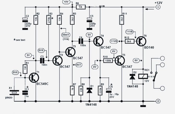
Transistor Amplifier
The circuit is basically a transistorized high gain amplifier where a piezo is used as the vibration sensor. The vibrations from the piezo generates a correspondingly oscillating voltage at the base of T1 which is appropriately amplified by all the following transistor stages consisting of T2, T3, T4, T5, T6 and the associated parts. The amplified DC signal is finally applied across the connected relay which toggles in response to the detected vibrations over the piezo. Since a cell phone vibration could have an inconsistent vibrating rate could result in a corresponding oscillatory response over the relay switching. To avoid this a high value capacitor in the range of 500uF should be connected directly across the base and emitter of T6, this will ensure that T6 sustains its conduction even while the cell phone vibrations are intermittently absent.The Flip Flop Circuit
In the above mode, the relay stays activated only for so long as the vibration signals are produced, in order to translate the reaction into a toggling effect a flip flop circuit becomes imperative. The following simple 4093 IC based design becomes perfectly compatible for the required conversions.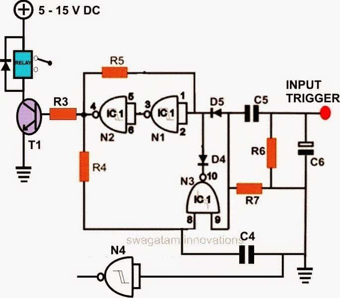 The input trigger may be connected to the pole of the relay, while the N/O of the relay will need to be connected with the positive of the supply.
Alternatively, the relay could be entirely eliminated, and the "input trigger" of the above flip flop circuit directly connected with the collector of T6.
Once this is done the relay would respond with alternate ON/OFF toggling motion each time the modem cellphone is called by the owner or the user.
The relay of the flip flop could be used for switching any desired appliance or in case it's deployed inside a vehicle could be implemented to operate the central locks and the ignition system for achieving a complete cell phone operated security feature.
The input trigger may be connected to the pole of the relay, while the N/O of the relay will need to be connected with the positive of the supply.
Alternatively, the relay could be entirely eliminated, and the "input trigger" of the above flip flop circuit directly connected with the collector of T6.
Once this is done the relay would respond with alternate ON/OFF toggling motion each time the modem cellphone is called by the owner or the user.
The relay of the flip flop could be used for switching any desired appliance or in case it's deployed inside a vehicle could be implemented to operate the central locks and the ignition system for achieving a complete cell phone operated security feature.
Using Piezo as the Sensor
C1 in the first vibration detector circuit could be a 0.22uF capacitor and must be employed only if the piezo is terminated over a longer distance from the circuit, otherwise C1 could be ignored. Preferably the piezo must be situated close with the circuit board. The piezo transducer is a 27mm ordinary device which are normally using in piezo buzzer circuits. It must be appropriately housed inside a plastic enclosure for ensuring an optimal response from it. The entire unit may be further enclosed inside a plastic box with the piezo assembly stuck on inner top surface of the box. The modem cellphone must be directly placed over the above enclosure right on the outer opposite surface of the piezo assembly (see figure below) The modem must be appropriately secured over this position so that the unit does not tumble away from the box while vibrating.
Now your cellphone vibrator based remote control circuit is ready and may be used for any desired GSM based remote control application and may be switched from any part of the world, just with a flick of a button.
Make sure that the vibrator is assigned to turn ON only for the specific numbers and not for the default numbers to ensure a foolproof operation of the unit.
The modem must be appropriately secured over this position so that the unit does not tumble away from the box while vibrating.
Now your cellphone vibrator based remote control circuit is ready and may be used for any desired GSM based remote control application and may be switched from any part of the world, just with a flick of a button.
Make sure that the vibrator is assigned to turn ON only for the specific numbers and not for the default numbers to ensure a foolproof operation of the unit.
Remote Controlled Wireless Water Level Controller Circuit
For multi-storey buildings where water tanks could be at considerable heights over building terraces, monitoring the levels automatically could become a major issue. RF remote control modules have become pretty cheap nowadays which could be effectively used for solving the inconvenience. Let's learn how to make and install a wireless water level controller circuit for the same, requested by Mr. Sriram kp. I am planning to implement this circuit for my home over tank. Because I am in 1st floor and tank is in 5th floor. In the above circuit, Instead of the push switches in the transmitter section, if i arrange the terminals D0-D3 inside the tank means, as the water rises, the one by one D0-D3willget in contact through the water and this will transmit the signal to the receiver. So the output LEDs in the receiver will turn on according to water level. In transmitter, suppose D0 is the tank empty state means there will be no contact to none of the terminals inside the tank, so the LED in the D0 of receiverwillturn off, at this state the motor should turn on. After the water level starts rising, the D3 of the transmitter will get contact , so the D3 LED of receiver will turn on At this state the motor should turn off. Please provide me the circuit for this...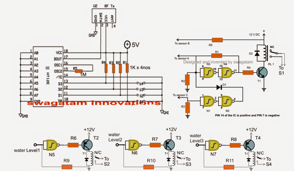
The Design
The circuit may be understood as given under: Here we incorporate two separate stages, one is our automatic water level controller circuit and the other is the RF remote control circuit.Using Tx, Rx 433MHz RF Modules
The remote control has a Tx (transmitter) and and Rx (receiver). The transmitter is triggered through four discrete switches which encode and transmit the signals discretely into the atmosphere. The receiver captures these signals, decodes it and sends it to one of the four outputs relevant to the decoded info. This output responds by becoming high as long as the corresponding Tx switch is kept depressed. The idea of the proposed water level controller through a remote control module is to press the Tx switches via relay contacts actuated by the water level controller circuit in response to the various water level conditions, as configured by the user. The same has been implemented in the discussed design. Referring to the figure, the gates gates N1 to N4 form the automatic water level controller circuit wherein the motor is switched ON when the level reaches a minimum lower threshold, and is switched OFF as soon as the level reaches the brim of the tank. Originally Relay R1 was used for activating the motor by wiring its contacts to the motor and mains. However for the present application, RL1 is rigged to one of the switches of the Tx module (S1) Meaning now the Tx pin10 is engaged with the transmission of the signals as soon as RL1 is energized which happens on detection of an empty water tank. Once this happens, the Rx responds by receiving the signals and triggering its own relay connected with the corresponding pinout. This relay then activates the distant underground or overhead motor for the required water pumping. The circuit diagram also shows three gates N5, N6, N7 which are configured as NOT gates for sensing the different water levels across the tank while the water is being pumped. In the course these gates activate their own relays, which in turn close S2, S3, S4 for the necessary transmissions from the Tx to Rx. The above transmissions are appropriately collected by the Rx, decoded and fed across its relevant outputs for illuminating the connected LEDs. These LEDs provide the user with the info regarding the gradually filling water tank. Thus the remote controlled triggering feature of the water level controller facilitates the owner a wireless and hassle free option of monitoring and controlling a distant situated tank. The following figure shows the wiring details of the Rx or the receiver stage responsible for the toggling of the pump motor and various water level indications, in response to the Tx triggering signals.Receiver Schematic
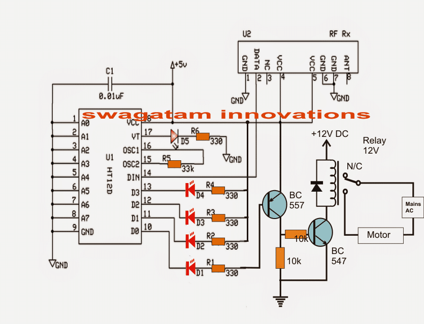 The RF modules can be sutudied in detail below:
https://www.homemade-circuits.com/2013/07/simple-100-meter-rf-module-remote.html
The RF modules can be sutudied in detail below:
https://www.homemade-circuits.com/2013/07/simple-100-meter-rf-module-remote.html
Parts List for the water level controller stage (N1----N4):
R1 = 100K, R2, R3 = 2M2, R4, R5, R6, R7, R8, R9, R10, R11= 10K, T1 = BC547, T2, T3, T4 = BC557 D1, D2 = 1N4148, All RELAYs = 12V, 400 OHMS, SPDT, contact amps as per load specs. N1, N2, N3, N4, N5, N6, N7 = IC 4093 (2nos.) The last unused gate (N8) input must be terminated to ground or (+), output may be kept open. The above wireless water level controller circuit was built and successfully tested by Mr. Sriram kp. The following images exhibit the results of his outstanding efforts: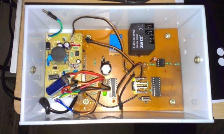
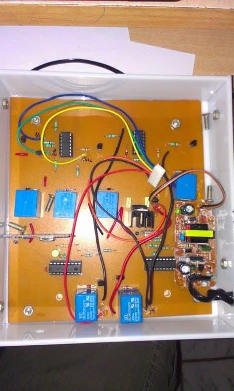

DTMF based FM Remote Control Circuit
The post discusses a DTM based FM remote control circuit which can be used for controlling 4 individual appliances remotely by pressing four corresponding buttons on the DTMF transmitter handset. The idea was requested by Mr. Sunaabh Sarkar. I came across your blog "Homemade The Designs Just for You" quite by chance as I was googling for some circuit and quite frankly I am indeed very impressed by your inputs. I am an architect by profession but when it comes to hobby Its photography after my first choice.. electronics. As a child some 4 decades ago, I used to be fascinated watching my fellow seniors from the Naval NCC class build ships in our electronics lab. The passion has remained in the heart and now when I was forced to take a 'retired back seat' from my active profession due to some unavoidable circumstances, I thought the time to be right to pursue what I had always wanted to do in my heart. Build working model of Ships... well just for the fun. I started with the old worn out RC toys my kids used to play with by "reverse engineering them" to my benefit while building the 5 vessels (all out of household wastes like old ball pens, remote control covers, discarded flexible conduit pipes, plastic bottles and things like those), I have so far built. When there were no more old RC toys around, I would go and buy some new cheap ones and used the electronics to power my models. New or old, the commercially available RC units came with their limitations (like range or performance). The professional ones other modellers use come with their own hitches and which if not for their exorbitant prices, they have remained unavailable for one reason or the other. I wish I had a chance to study electronics as a subject of my higher education, so that I could be designing electronic circuits rather than designing houses ;). However, I had this idea lingering on for quite some time, though I confess its not unique or new... controlling devices using DTMF codes. Ever since Cellphones have taken the front seats, push button land line phones have become vogue and I had been contemplating powering up one of them to generate DTMF codes... then feeding these codes to an audio transmitter in the FM range. The signal transmitted can be received by a FM receiver. The DTMF tones transmitted can then be decoded by a decoding circuit to trigger at least 6 individual circuits driving toy motors. But the moron that I am, I' can only dream. Googling does me little help. There are some circuits available on line, but they require programming too... well at my age I guess by the time I get to know how to write a program and make use of one, there will be little left of my dwindling eyesight to build my dream ship. I was wondering if you could kindly help me by designing/ suggesting/ helping me put together circuits for a simple DTMF interface to easily accomplish my target using simple circuits and passive components. For all the trouble you had had to take to painstakingly go through my mail, and also for your efforts and time to help me, frankly speaking, all the remuneration I can offer you is my good wishes and heartfelt thanks and gratitude. Thanks and regards and TC. God Bless Sunaabh Sarkar (Mistral)The Circuit Design
A couple of DTMF based FM remote control circuits can be seen in the following diagrams based on the proposed request. The first diagram is the dtmf transmitter circuit while the second is the dtmf receiver circuit. We all basically know how a DTMF encoder/decoder circuits function by processing a dual frequency tone uniquely configured for the particular buttons of the enclosed keypad. It's popularly used in the telecommunication field were the keypads of the telephones are assigned with these codes (DTMF) for enabling the corresponding receiver end to identify the pressed buttons and complete the call connection procedures accurately.The DTMF Transmitter Stage
In the first DTMF FM transmitter circuit, the dtmf generator IC 5089 is used and is configured in its standard form. The IC responds to the pressing of the attached keypad buttons by generating the relevant high/low tone combinations at its pinout #16. This DTMF output is fed to a FM transmitter circuit which picks up the audio data and transmits it in the air through its antenna. The shown FM transmitter stage is a bit different from the ordinary ones as it encloses an additional stage in the form of T3 and a centered tapped LC tank network. This modification makes it much powerful than the ordinary single transistor types and enhances it with a higher transmitting range. COMPLETE INFORMATION REGARDING THE TRANSMITTER STAGE CAN BE FOUND HERECircuit Diagram
DTMF Receiver Stage
Since the above explained DTMF transmitter circuit uses an FM topology, the receiver must be an FM based too, for capturing and processing the transmitted data. An ordinary FM radio or a receiving card is all what is needed for collecting the transmitted info from the transmitter unit. The received DTMF audio by the receiver is next forwarded to a standard M8870 DTMF decoder circuit stage which effectively detects and processes the DTMF data received by the FM radio. As per the specifications of the IC, its outputs correspondingly switch ON and OFF in accordance with the DTMF tones generated and transmitted by the transmitter stage. The above switching of the outputs of M8870 IC is integrated to 4 discretely configured IC 4013 based flip flop stages which respond by toggling the attached relay driver stages. The relays can be wired to the relevant loads for achieving the intended switching via the DTMF transmitter handset.Receiver Circuit DTMF
Simple RF Remote Control Circuit without Microcontroller
The article explains how to make a simple RF remote control circuit using ready-made RF 433MHz and 315MHZ RF modules, and without incorporating microcontroler ICs. With the easy availability of RF modules today making an RF remote control has become a childs play. It's all about procuring the RF modules ready made from the market by spending a few bucks and configuring them together for the intended results. Here I'll show you how to make an approximately 100 meter range RF remote control circuit using RF modules, without the help of any microcontroller stage. To begin the assembly you will have to procure the following readymade RF modules and the respective encoder and decoder chips, for the present project we use the HOLTEKs modules:RF 433Mhz Transmitter/Receiver Modules
The following picture shows the Rx (left) and the Tx (right) Modules. The following figure shows the pinout details of the above modules.
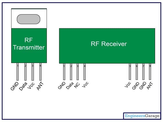
Encoder IC = HT12E
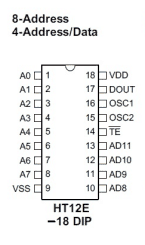
Decoder IC = HT12D
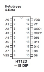 The above encoder and decoder ICs do the jobs exactly as per their assigned names that is encode and decode the bit information for enabling easy interfacing with analogue circuits.
After you have procured the above components it's time to put them together.
The above encoder and decoder ICs do the jobs exactly as per their assigned names that is encode and decode the bit information for enabling easy interfacing with analogue circuits.
After you have procured the above components it's time to put them together.
Assembling the Modules
Configure the transmitter circuit by assembling the Tx (Transmitter) Module with the Encoder IC as given in the following circuit: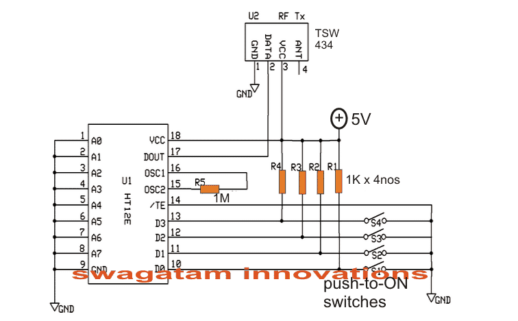 Next, assemble the Rx (Receiver) module with the decoder IC, as per the following diagram:
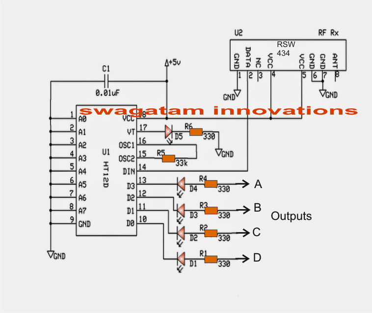 In the above Rx (receiver) circuit we can see that four of its outputs are terminated through LEDsat the points A.B,C,D and another output which is terminated via the VT pinout of the IC.
The four outputs A,B,C,D become high and latched in response to the pressing of the four push buttons shown in the Tx transmitter) circuit.
Pin13 switch of Tx influences the Pin13 output of the Rx and so on....
Suppose when output "A" of the Rx module is activated by the relevant switch of the Tx, it gets latched and this latch breaks only on activating any of the other outputs.
Thus the latch breaks only when a different subsequent output is rendered high through the Tx relevant push buttons.
The output from pin VT "blinks" momentarily every time one of the outputs A,B,C,D get activated.
Meaning VT output can be used in case a flip flop is required to be operated.
The above can be very easily interfaced with a relay driver stage for operating any equipment such as a remote bell, lights, fans, inverters, automatic gates, locks, RC models etc.
In the above Rx (receiver) circuit we can see that four of its outputs are terminated through LEDsat the points A.B,C,D and another output which is terminated via the VT pinout of the IC.
The four outputs A,B,C,D become high and latched in response to the pressing of the four push buttons shown in the Tx transmitter) circuit.
Pin13 switch of Tx influences the Pin13 output of the Rx and so on....
Suppose when output "A" of the Rx module is activated by the relevant switch of the Tx, it gets latched and this latch breaks only on activating any of the other outputs.
Thus the latch breaks only when a different subsequent output is rendered high through the Tx relevant push buttons.
The output from pin VT "blinks" momentarily every time one of the outputs A,B,C,D get activated.
Meaning VT output can be used in case a flip flop is required to be operated.
The above can be very easily interfaced with a relay driver stage for operating any equipment such as a remote bell, lights, fans, inverters, automatic gates, locks, RC models etc.
How to Connect the Address Pins
The pinouts A0-----A7 of the Rx, Tx modules are very interesting. Here we can see them all grounded which creates an impression that these are of no use and are simply terminated to ground. However these pinouts enable a very useful feature. These address pinouts can be used for rendering a particular Rx, Tx pair uniquely. It's simple, let's say for pairing the above modules we ensured that the address pins are identically configured. Alternatively we could make the above pair unique let's say by opening A0 for both the modules. This will make the pair respond only with each other and never with any different module. Similarly if you have more number of such pairs and want to make unique pairs out of them, just assign the pairs in the explained manner. You can do this by either connecting the address pins to ground or by keeping them open. It means by rendering different configurations to the relevant address pinouts between A0 and A7 we can create a huge number of unique combinations. The range of the above explained RF module is around 100 to 150 meters. The above simple RF remote control circuit was successfully tested by Mr. Sriram on a breadboard, the following images of the built prototype were sent by him for reference.Circuit Prototype Images
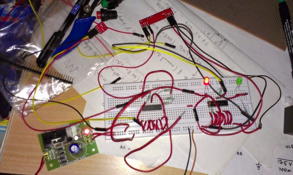
Making a 433 MHz, 315 MHz RF Remote Control with Relay Flip Flop
Building a hi-end remote control device using very few components today looks pretty plausible. The proposed remote control light switch circuit idea provides you with the opportunity of building and owning this amazing device through simple instructions. Moreover the unit provides a 4-bit data to be exchanged between the transmitter and the receiver modules. This Hi-tech remote control light switch enables you to control four individual lights or any electrical appliance for that matter from any corner of your house remotely using a single tiny remote control hand set. Imagine switching a light, a fan, washing machine, computer or similar gadgets from any corner of your room without taking a step! Doesn't that sound great? Controlling a particular gadget remotely through a single flick of your finger definitely feels very amusing and amazing too. It also gives you the comfort of doing an act without moving or getting up from a particular position. The present circuit idea of a remote control light switch enables you controlling not only just a single light but four different electrical gadgets individually using a single remote control hand set. Let��s try to understand its circuit functioning in details of the 433MHz Rx and Tx modules.Transmitter (Tx)Circuit Operation
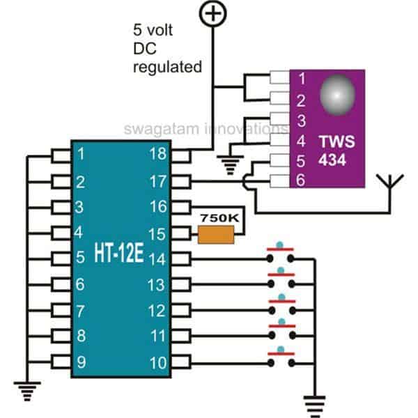 I have already discussed the wireless control modules in the above paragraphs, let��s summarize the entire description yet again and also learn how simply the stages may be configured into the proposed unit.
The first figure shows a standard transmitter module using the RF generator chip TWS-434 and the associated encoder chip the HOLTEK��s HT-12E.
Datahseet HOLTEK12E
The IC TWS-434 basically does the function of manufacturing and transmitting the carrier waves into the atmosphere.
Datasheet TWS-434
However every carrier signal needs modulation for its proper execution, i.e.
it needs to be embedded with a data that becomes the information for the receiving end.
This function is done through its complementing part �C the HT-12E 4-bit encoder chip.
It has got four inputs, which can be triggered discretely by giving them a ground pulse individually.
Each of these inputs produces coding which are distinctly different to each other and become their unique signature definitions.
The encoded pulse from the relevant input is transferred to the IC TWS-434 which carries forward the data and modulates it with the generated carrier waves and finally transmits it into the atmosphere.
The above operations take care of the transmitter unit.
I have already discussed the wireless control modules in the above paragraphs, let��s summarize the entire description yet again and also learn how simply the stages may be configured into the proposed unit.
The first figure shows a standard transmitter module using the RF generator chip TWS-434 and the associated encoder chip the HOLTEK��s HT-12E.
Datahseet HOLTEK12E
The IC TWS-434 basically does the function of manufacturing and transmitting the carrier waves into the atmosphere.
Datasheet TWS-434
However every carrier signal needs modulation for its proper execution, i.e.
it needs to be embedded with a data that becomes the information for the receiving end.
This function is done through its complementing part �C the HT-12E 4-bit encoder chip.
It has got four inputs, which can be triggered discretely by giving them a ground pulse individually.
Each of these inputs produces coding which are distinctly different to each other and become their unique signature definitions.
The encoded pulse from the relevant input is transferred to the IC TWS-434 which carries forward the data and modulates it with the generated carrier waves and finally transmits it into the atmosphere.
The above operations take care of the transmitter unit.
Receiver(Rx)Circuit Operation
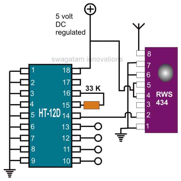 The receiver module does the above operations just in the opposite manner.
Here, the IC RWS-434 forms the receiving part of the module; its antenna anticipates the available encoded pulses from the atmosphere and captures them immediately as they are sensed.
Datasheet RWS-434
The captured signals are relayed forward to the next stage �C the signal decoder stage.
Just like the transmitter module, here too a complementing device the HOLTEK��s HT-12D is employed to revert the received encoded signals.
Datasheet HT-12D
This decoding chip also consists of a 4-bit decoding circuitry and their outputs.
The received data is appropriately analyzed and decoded.
The decoded information gets terminated out through the relevant pin-out of the IC.
This output is in the form of a logic high pulse whose duration depends on the duration of the ground pulse applied to the encoder chip of the transmitter module.
The receiver module does the above operations just in the opposite manner.
Here, the IC RWS-434 forms the receiving part of the module; its antenna anticipates the available encoded pulses from the atmosphere and captures them immediately as they are sensed.
Datasheet RWS-434
The captured signals are relayed forward to the next stage �C the signal decoder stage.
Just like the transmitter module, here too a complementing device the HOLTEK��s HT-12D is employed to revert the received encoded signals.
Datasheet HT-12D
This decoding chip also consists of a 4-bit decoding circuitry and their outputs.
The received data is appropriately analyzed and decoded.
The decoded information gets terminated out through the relevant pin-out of the IC.
This output is in the form of a logic high pulse whose duration depends on the duration of the ground pulse applied to the encoder chip of the transmitter module.
How to use a Flip-Flop Relay Circuit at the Receiver module Output
The above output is fed to a Flip-Flop circuit using the IC 4017, whose output is finally used to switch the output load via a relay driver circuitry. One such flip/flop idea is shown you may construct four of them to access each of the generated 4-bit data discretely and control four gadgets individually. Whether you use it as a remote control light switch or to control many more appliances����the option is all yours.
How to Control Motor with a Cell Phone
The following article describes a very simple circuit idea which can be used for controlling a motor's rotational direction i.e. for moving it either clockwise or anticlockwise through alternate miss calls from your cell phone.The Circuit Concept
I have already discussed a novel cell phone controlled remote switch circuit where the unit can be used for switching an electrical gadget through the users cell phone. The user just has to call the remote system which responds to the blank calls and generates the required alternate switching of the connected gadget. The samecircuithas been used here also, the output is appropriately modified such that now the unit becomes suitable for toggling the rotation of a DC motor. The circuit shown below can be used for controlling a motorrotationaldirection, let's try to understand it's functioning details: The lowersectionof the diagram consisting of T1, T2, T3 and T4 along with the associatedcomponentsforms a simple high gain audio amplifier circuit. This circuit is used for amplifying the ringtone generated by theattachedmodem cell phone unit.How it Works
The modem cell phone handset is an ordinary NOKIA 1280 cellphonewhich is permanently integrated with this circuit. The above modem cell phone uses a prepaid SIM card and thus it becomes a self contained receiver module. When this modem cell phone is called by the owner's cell phone, its ringtone activates and gets amplified by the above explained tone amplifier stage. The amplified signal becomes powerful enough to triggers the relay RL1. This relay holds or remainsactivatedas long as the call stays connected, and breaks when the call is disconnected. RL1's N/O contact is supplied with a 12v trigger to the adjoining stage which is a FLIP/FLOP stage, made by using four NAND gates from the IC 4093. With every alternate missed calls from theowner'scell phone, the modem cell phone signals the tone amplifier, which activates RL1, and RL1 in turn flips or flops the IC1 circuit. The output of the flip flop is connected with a relay driver circuit which is attached with two relays RL2 in parallel. You may use a single DPDT relay also for betterconvenience. The contacts of the relays are configured in such a manner that flipping them produces opposite movements for the motor that'sintegratedto them. The mains supply to therelayand the motor is taken from RL1, which means the motor flips with every subsequent "missed calls" and remainsactivateduntil the call stays connected, and then halts. The circuit can be modified in many different ways as per the usersspecifications. The modem cell phone should be appropriately assigned with a particularcontinuousringtonewhile the default ringtone should be assigned to "empty", tis will make the unit immune to unknownnumbersor wrong numbers, and the owner will be the sole controller of the attached circuit and the motors.
Parts List
All resistors are 1/4w 5% CFR unless otherwise stated. R1 = 22k R2 = 220 OHMS R3,R11,R12 = 100K R4,R6,R7,R9 = 4.7K R5 = 1K, R8 = 2.2M C1,C4,C5 = 0.22uF DISC TYPE C2,C3 = 100uF/25V T1,T2,T4,T5 = BC 547B T3 = BC557 B ALL DIODES = 1N4148 IC1 = 4093 RL1 = RELAY 12V/400 OHMS SPDT RL2 = Relay DPDT 12V/400 ohms L1 = small buzzer coil, small choke or similar. JACK = 3.5mm AUDIO JACK CELL PHONE MODEM = NOKIA 1280Video clip showing the remote control operation of the circuit using a cellphone.
Making a Cell Phone Controlled Remote Bell Circuit
The following circuit of a cell phone controlled remote bell can be used for ringing bells or alarm devices using your personal cell phone. The unit incorporates an attached cheap cell phone as the modem forexecutingthe proposed functions.Circuit Concept
The explained circuit can be used in schools for ringing bells using a cell phone from anywhere irrespective of the distance. Thus the use of this type of cell phone controlled remote bell can eliminate the need of running for the bell switch on every class period intervals. The peon would be able to do his other scheduled work and ring the bell from any position inside the school premise or even from outside, in fact from any corner of the world. Looking at the circuit diagram, we see a pretty straightforward configuration using only transistors.Circuit Operation
Transistors T1 and T2 form a high gain looped audio amplifier. As can be seen the input signal needs to be derived from a modem cell phone's head phone socket. A suitably selected ringtone starts playing on the cell phone when called from the users personal cell phone. The ringtone passes through the headphone connection to the base of T1 via C1, R13. The preamplifier consisting of T1 and T2 amplifies the signal to reasonable levels and feeds it to the T3 via C2 for further amplification. T3 boosts the ringtone level to much higher levels, however this signal is still not powerful enough for driving a relay, therefore it is yetfurtheramplified by T4, until finally the drive becomes just suitable for activating the relay. The relay stays activated only until the incoming cell phone remainsconnected, on disconnecting the call the relay also disconnects. The relaycontactsmay be integrated with a conventional GONG type of bell for the specified actions. The modem cell phone can be of any type, however it must have the feature of assigning unique ringtones to each specific contact names as per the userspreferences. Here the owners number should be first stored/saved in the modem, then this particular contact name inside the modem should be assigned with a particular continuous type of ringtone. Next, the default ringtone should be set to "empty". That's it, the modem cell phone now becomes foolproof and responds to only the ownersassignednumber. More than 1 number can beassigned in fact 99 numbers can be assigned which become the unique members of the modem phone book,such that the modem responds only to these numbers, it won't respond to any other unknown or wrong numbers. Ideally a NOKIA 1280 may be used here as the modem. Designed BY - "SWAGATAM"
Parts List
R1 = 22k R2 = 220 Ohms, R3 = 100K, R4,R6,R7 = 4K7 R5 = 1K R13 = 100 ohms, T1, T2,T4 = BC547 T3 = BC557, C1 = 0.22uF C2,C3 = 100uF/25v L1 = 40 mH coil, example: a piezo buzzer coil will do. diode = 1N4007 Relay = 12V/SPDT Modem = NOKIA 1280 Charger section parts = as given in the diagram.Remote Controlled Toy Car using 433 MHz Remote Modules
This circuit will enable reverse-forward, left-right control of a toy car through 433 MHz RF remote control modules or any similar RF remote modules. The market may be full of these hi-end remote controlled toy cars, but for a hobbyists making one at home can be entirely a different experience. The article belowexplainshow to configure a simple remote controlled toy car using a ready made 4-relay remote control module.Using Readymade 433 MHz/315MHz RF Modules
If you refer one of the previous articles you will find some data regarding buying of ready made, ready to use remote control modules or devices, which just requires to be wired as per the data and you are able to control any electrical device within a range of 100 meters with a press of a button over the remote handset. Here we are using one of these ready made remote control modules for implementing the remote car operations. In this article only the circuit and the wiring part has been discussed, making the car body and fitting of the motors and the wheels will be entirely left on the user, the user may take the help of a carpenter or some fabricator for designing the vehicle body. The remote control module which is being discussed here uses four discrete relays, which can be toggled discretely through the 4 individual switches over the remote handset. The model car is provided with four wheels, two at the front and two at the rear as usual vehicles have. The remote control unit may be procured ready-made, theone discussed here will be just perfect for the present application. Moving back to the proposed project of a simple car remote control, we will need the following components for making the main control units of the system:Required Components
A couple of DC motors. 8 nos. 1N4007 diodes. 4 nos. relays, 12V, SPDT 12V Battery, 4 AH SMF, or as per the motor rating. A general purpose PC boared. 2 nos. 12V DC motors, wattage as per requirement RF Trasmitter/Receiver Relay Modules Once the above things are procured, the motors may be suitably fabricated over a selected piece of metal or wooden base, such that two motrs constitute the two front wheels. Two additional dummy wheel may be fabricated for supporting the front motor wheels.
Wheel Set up
You may also want to learn how to make a heavy duty remote controlled trolley circuit for malls and retail shops After this, the PCB may be populated and wired up with the relays and the diodes with the help of the given figure, this concludes the relay box assembly.Relay Wiring Details
 Next, the four relay outputs from the remote control in-built relays should be connected to the diodes of the above relay box circuit.
The antenna from the remote should be sufficiently terminated using a foot long flexible wire so that the module becomes responsive even from longer distances.
The operation will need battery power, so needless to say a suitable battery will also be required to be placed and integrated with the discussed circuits inside the toy car.
Done!.
Now you may test the unit by pressing the remote handset buttons.
As per theintegrationof the relay serial numbers to the diodes of the relay box, pressing of the buttons A,B,C, and D over the remote handset would produce results in some specific orders, such as: forward, reverse, right and left movements with the car.
The entire PCB along with the remote control module may be suitablyenclosedover the base of the model car such that the system gives an appearance of a well groomed homemade remote controlled car.
Next, the four relay outputs from the remote control in-built relays should be connected to the diodes of the above relay box circuit.
The antenna from the remote should be sufficiently terminated using a foot long flexible wire so that the module becomes responsive even from longer distances.
The operation will need battery power, so needless to say a suitable battery will also be required to be placed and integrated with the discussed circuits inside the toy car.
Done!.
Now you may test the unit by pressing the remote handset buttons.
As per theintegrationof the relay serial numbers to the diodes of the relay box, pressing of the buttons A,B,C, and D over the remote handset would produce results in some specific orders, such as: forward, reverse, right and left movements with the car.
The entire PCB along with the remote control module may be suitablyenclosedover the base of the model car such that the system gives an appearance of a well groomed homemade remote controlled car.
PCB Layout for the Remote Controlled Car (Track Side)
How to Buy and Use RF Remote Control Modules �C Control Any Electrical Gadget Remotely
Remote controls have always been an intriguing device for all of us because of one good reason: It allows us to operate distant gadgets with a flick of a button, without having to move an inch.Introduction
Today with the advancement of technology remote control switches have become accessible very easily from the market and we can buy such units quite cheaply and install them as per our own specific needs. Today you can buy a remote control module from your local dealer or even more easily from an online store at veryreasonablecosts (for about $10). These units willbasicallycome with areceivermodule neatly enclosedinside a small plastic box. Therelaysinside this receiver can be toggled using a small transmitter unitenclosedinsideanothertinyplastic enclosure accompanied with a key chain like attachment. There are many versions of the above system, depending upon ones needs the particular type may be ordered. The most basic one has a single relay which may be controlled through a single button over the given transmitter unit.Common Technical Specifications
Other models come with 2 relays, 4 relays, 8 relays etc. which may individually controlled by pressing the relevant buttons over the associated transmitter key chain arrangement. The transmitter is powered through a small button cell which might take to get exhausted while the receiver module needs to be powered through an external AC/DC 12V 100 mA power supply. The relay outputs are very neatly terminated at the edge of the module using connectors.
You just have to identify the respective pin outs and wire the electrical loads across these connectors as per your own specifications.
The relay outputs are very neatly terminated at the edge of the module using connectors.
You just have to identify the respective pin outs and wire the electrical loads across these connectors as per your own specifications.
Where this Remote Control can be Used
The remote control can be very effectively used for remotely operating shutters, water pump motors, garage doors, apartment gates and doors, it can be also used in cars and vehicles for locking doors and ignition systems. You may also find these gadgets useful for controlling household electrical items like lights, fans, ACs, and other similar gadgets just by a press of the respective buttons.The Code Hopping Feature
Another cool feature with these advanced remote control systems is the code hopping feature which makes the signals generated from the transmitter absolutely fool proof. The codes are automatically changed and made compatible with the transmitter and receiver making it impossible for the hackers and other malicious agents from copying your secret remote transmissions. Ans whats more, in case your transmitter handset is lost, the system also incorporates a "code learning" operation, which enables you to interface any different remote with your existing receiver by pressing a single push button situated inside the receiver module....once the receiver and the new transmitter "shake hands", you can use them together very safely as these both units now become "made for each other".How to Make a Remote Control Circuit from a Remote Bell
The proposed remote control circuit idea can be used for controlling any electrical gadget within a range of 100 meters.How the Circuit is Supposed to Work
Since the idea here is to modify an existing circuit of a remote bell unit, becomes super easy without any complications. However the construction part does require the involvement of electronic assemblies so this project may not be considered entirely a layman��s project. We all have seen and probably used remote bell gadget in our homes. The device is basically a wireless RF receiver and a transmitter set which can be used for producing alarm sounds remotely for calling or indication proposes. These gadgets are pretty effective with their functions and the specified operations are done efficiently across a considerable distance. The Chinese made remote bell units are best suited for the proposed project. Basically, when the transmitter of the remote bell is pressed, it sends a strong RF signal over a radial distance of approximately 100 meters. The receiver unit positioned anywhere within this limit instantly plucks the trigger and switches the in built musical bell, sounding the alarm. The trigger may last for a few moments even after the transmitter is switched OFF. The only feature that we are interested in is the effective transmission and receiving of the RF signals across the said distance. If we are able to mod the receiver part of the unit so that the received trigger can be used to operate a relay instead of the usual alarm, our job is done. However before we indulge into the modification process, it would be necessary to make the Flip Flop circuit first, which would be later on required to be integrated with the receiver set of the remote bell. The flip flop section is a very simple configuration consisting of just a single IC and a few other passive components. The entire circuit may be buikt over a small general purpose board with the help of the shown schematic.Circuit Diagram
Modifying the Receiver (Rx) of the Remote Bell
On opening the cover of the remote bell receiver unit, the following things may be traced out for commencing the modding process: You will find a small speaker connected via a couple of wires which terminate from the circuit board of the unit. Just cut-of the wires from the speaker, remove the entire circuit from its housing and screw it inside a new housing, which should be relatively bigger in size so that it can accommodate the flip flop section, the transformer power supply section and also the relay assembly. After locating the negative wire out of the two speaker wires, integrate them to the flip flop circuit appropriately as shown in the figure. Once the connections are made as per the schematic, check the system by powering the unit and by making a few triggers via the transmitter module. The relay can be seen toggling in response to each subsequent triggers made by the transmitter module. Your RF remote control circuit is ready and may be used for controlling any electrical gadget that you may prefer, wirelessly, across a radial distance of around 100 meters. Parts List for the Circuit Diagram The following listed parts will be required for making the above explained RF remote control circuit's flip flop section:Parts List
R3 = 100 ohms, R2 = 100K, R4 = 4K7, R5 = 10K, C1, C2, C4= 22uF/25V, C6 = 4.7uF/25V, C3 = 0.1, CERAMIC, C5 = 1000uF/25V, T1 = BC557B T2 = BC547B, ALL DIODES ARE = 1N4007, L1 = 50 turns of 30 SWG super enameled copper wire wound over a any ferrite material. IC1 = 4017, IC2 = 7805, TRANSFORMER = 0-12V/500mA,GSM Based Cell Phone Remote Control Switch Circuit
This circuit will allow you to control any electrical gadget from any part of the world through your cellphone remotely, that too without spending a penny for the individual commands.Circuit Concept
Whether it��s you vehicle, your basement door, your mansion gate or simply the air conditioner of your house, everything can now be switched by just a flick of your cell phone button. And yes, it��s completely fool proof, meaning no false triggering is possible through any other cell phone signals, it works only through the owners cell phone commands.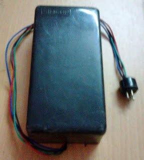 The explained circuit must be employed strictly for operating only the following specified equipment:
All domestic electrical appliances like, lights, fans, motors, TV sets, refrigerators, Air conditioners, washing machine, porch lights, garage door, house gate, basement gate or entrance, car ignition, car doors, water heater etc.
The concept has been already discussed in one of my previous articles �C How to make a GSM car security system, and the going about is unbelievably simple.
However, the above article deals with a system that involves DC control features and therefore is not suited for controlling AC appliances.
The unit discussed here is a universal device and can be used for operating all types of electrical gadgets from any part of the globe, just by making a single blank call to the systems number.
The system will faithfully respond to every call made from your cell phone and will alternately switch the connected load ON and OFF as per your instructions.
The explained circuit must be employed strictly for operating only the following specified equipment:
All domestic electrical appliances like, lights, fans, motors, TV sets, refrigerators, Air conditioners, washing machine, porch lights, garage door, house gate, basement gate or entrance, car ignition, car doors, water heater etc.
The concept has been already discussed in one of my previous articles �C How to make a GSM car security system, and the going about is unbelievably simple.
However, the above article deals with a system that involves DC control features and therefore is not suited for controlling AC appliances.
The unit discussed here is a universal device and can be used for operating all types of electrical gadgets from any part of the globe, just by making a single blank call to the systems number.
The system will faithfully respond to every call made from your cell phone and will alternately switch the connected load ON and OFF as per your instructions.
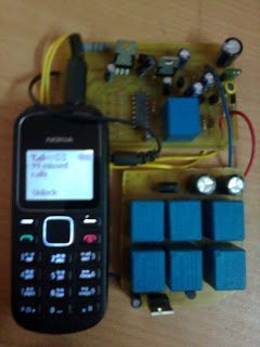 The concept is impeccable, as it has been tested by me thoroughly since last three years with flying results.
Basically the unit employs a very fundamental principle of converting the ringtone of a cell phone into a command output for operating a relay.
This cell phone acts as a modem and is permanently attached with the internal control circuit of the unit.
The modem cell phone is initially made ready by putting a SIM card inside it and by configuring the essential assigned numbers into its phone directory.
These assigned numbers are the only numbers to which this modem responds.
Therefore you would want to assign only those numbers through which you may like to make a call to the ��system��.
For safety reasons more than one number is assigned to the modem so that in case one of your cell phones is out of order or has low battery, you always have the option of using the other cell phone for triggering the system.
The biggest advantage of the GSM cellphone remote control circuit is that, any cheap NOKIA cell phone can be used here as the modem and therefore there��s no fear of the modem becoming obsolete.A simple yet effective cell phone remote control switch details has been discussed here with complete schematics and step by step tutorial.
The concept is impeccable, as it has been tested by me thoroughly since last three years with flying results.
Basically the unit employs a very fundamental principle of converting the ringtone of a cell phone into a command output for operating a relay.
This cell phone acts as a modem and is permanently attached with the internal control circuit of the unit.
The modem cell phone is initially made ready by putting a SIM card inside it and by configuring the essential assigned numbers into its phone directory.
These assigned numbers are the only numbers to which this modem responds.
Therefore you would want to assign only those numbers through which you may like to make a call to the ��system��.
For safety reasons more than one number is assigned to the modem so that in case one of your cell phones is out of order or has low battery, you always have the option of using the other cell phone for triggering the system.
The biggest advantage of the GSM cellphone remote control circuit is that, any cheap NOKIA cell phone can be used here as the modem and therefore there��s no fear of the modem becoming obsolete.A simple yet effective cell phone remote control switch details has been discussed here with complete schematics and step by step tutorial.
UPDATE:
Looking for an advanced solution? Read more below: Advanced Microprocessor Based GSM Remote Controller If you have sufficient prior knowledge of electronics, you should be making this complete unit within a days time. Let's begin the discussion. Basic Concept The idea here is to use an ordinary NOKIA 1280 cell phone as the modem attached permanently with a switching circuit. This entire unit now becomes the receiver unit. The modem cell phone NOKIA1280 is assigned with desired numbers, for example the owners cell number and a few other numbers of the owners family members. When the modem cell phone is called through these assigned numbers, the modem ring tone becomes active and this ring tone is applied to the control circuit and is processed for operating a relay and the connected load. Since the modem cell phone needs to be attached permanently inside the switching unit, it needs to be charged at regular intervals so that it remains functional all the time. For this, a separate cell phone charger module has also been incorporated along with the main circuit which keeps the modem cell phone battery always up to date and fully charged. It is quite obvious that the attached cell phone modem will need a SIM card, which will need to be maintained as we do for normals cell phone operations. Let's learn the building process. You will have first get or procure the following materials or parts for making this unit. I would suggest not to make the Printed board initially, it would better to first test the working over a general board and if thing goes then you would want to transfer it over a well designed P-C-B.Bill of Materials
All resistors are 1/4w 5% CFR unless otherwise stated. R1 = 22k R2 = 220 OHMS R3,R11,R12 = 100K R13 = 100 Ohms R4,R6,R7,R9 = 4.7K R5 = 1K, R8, R10 = 2.2M C1,C4,C5 = 0.22uF DISC TYPE C2,C3 = 100uF/25V T1,T2,T4,T5 = BC 547B T3 = BC557 B ALL DIODES = 1N4148 IC1 = 4093 RL1, RL2 = RELAY 12V/300 OHMS SPDT JACK = 3.5mm AUDIO JACK CELL PHONE MODEM = NOKIA 1280Circuit Diagram
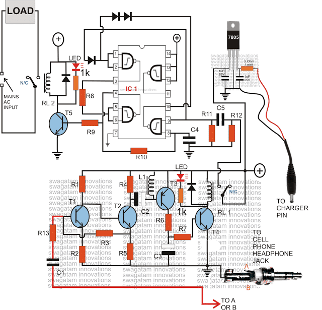
Understanding the Schematic Diagram
The above schematic of the proposed cellphone controlled remote circuit is rather very easy to understand. It may be divided into two main stages, the lower stage consisting of the transistors is a simple audio amplifier, the upper stage consisting of IC is the flip flop triggering stage. When a signal is present at the 3.5mm jack, which might be the input ring-tone from the cell phone modem., T1, T2 amplifier to some greater level, which is further amplifier by T3, T4 to a level is becomes sufficient for triggering the relay RL1. RL1 instantly connects the supply to the input of the flip flop at C5, via its N/O contacts. Note that RL1 will remain switched ON as long as the ring tone is present and will switch OFF the moment the ring tone or the signal over the 3.5mm jack is canceled. C3 makes sure that the relay does not get rattled by any insignificant signals or RFs. L1 has been installed also for the same reason, that is for eliminating unwanted signals and making sure that T3, T4responds only to valid ring-tones. L1 is a buzzer coil, as used in piezo electric buzzers, or may be hand made by winding 1000 turns of 36SWG super enameled wire over a small ferrite core, size and shape does not matter. Image of L1, inside a buzzer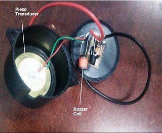 The period for which RL1 remains switched ON will have no consequence on the flip flop operation, the flip flop will switch ON and OFF in response to every subsequent missed call made from the owners cell phone.
The section comprising the IC 7805 is battery charger section, which needs to be connected to the battery charger input of the cell phone.
The charger will keep the cell phone battery always charged so that it remains functional all the time.
The above circuit has been thoroughly tested and confirmed by me, so if you make everything as shown in the above diagram, it should start working immediately.
How to Assign Numbers Inside the MODEM CELL PHONE It's very easy.
Just follow the following steps.
Save the names and the numbers which are important and through which you want the above unit to be operated.
Next select a particular name-->--press scroll right-->--"contact details" will be displayed-->-- press options-->--scroll down-->-- select "assign tone"-->--select a ring tone which has a sustained, non-breaking tune-->-- do OK.
Repeat this for all the desired numbers.
Now go to settings, go to tone settings and select "empty", press OK.
That means now you have switched OFF the default ringtone and no ringtone will be audible for any numbers other than the above assigned ones.
So you can be rest assured that the system will not respond to wrong numbers or any unknown numbers.
It will respond to only the calls made from the assigned numbers.
The period for which RL1 remains switched ON will have no consequence on the flip flop operation, the flip flop will switch ON and OFF in response to every subsequent missed call made from the owners cell phone.
The section comprising the IC 7805 is battery charger section, which needs to be connected to the battery charger input of the cell phone.
The charger will keep the cell phone battery always charged so that it remains functional all the time.
The above circuit has been thoroughly tested and confirmed by me, so if you make everything as shown in the above diagram, it should start working immediately.
How to Assign Numbers Inside the MODEM CELL PHONE It's very easy.
Just follow the following steps.
Save the names and the numbers which are important and through which you want the above unit to be operated.
Next select a particular name-->--press scroll right-->--"contact details" will be displayed-->-- press options-->--scroll down-->-- select "assign tone"-->--select a ring tone which has a sustained, non-breaking tune-->-- do OK.
Repeat this for all the desired numbers.
Now go to settings, go to tone settings and select "empty", press OK.
That means now you have switched OFF the default ringtone and no ringtone will be audible for any numbers other than the above assigned ones.
So you can be rest assured that the system will not respond to wrong numbers or any unknown numbers.
It will respond to only the calls made from the assigned numbers.
How to Power the Unit
The circuit needs to be powered through a DC12V/500mA or 1 Amp SMPS adapter. The load may be any electrical appliance like lights, fans, AC, fridge or anything that you may like to switch using this system.Video Clip showing the circuit functioning of the prototype
WARNING AND DISCLAIMER �C THE PROPOSED DEVICE MUST BE USED FOR OPERATING ONLY THE COMMON HOUSEHOLD ELECTRICAL SYSTEMS AND PARAMETERS. THE PROPOSED CELL PHONE OPERATED SWITCH MUST NEVER BE USED FOR ANY OTHER INTENTIONS OR PURPOSE WHATSOEVER, AND THE AUTHOR TAKES NO RESPONSIBILITY FOR ANY LOSSES THAT MIGHT OCCUR IN CASE THE UNIT IS USED FOR OPERATING ANYTHING ELSE OTHER THAN WHAT'S BEEN SPECIFIED IN THE ABOVE ARTICLE.RF Remote Control Encoder and Decoder Pinouts Explained
In this post we discuss the pinout assignments and functions of the popular 433 MHz RF remote control module from HOLTEK.
RF 315/433 MHz Transmitter-receiver Module for Remote Control Application
Making your own universal remote control systems today is very easy. Such procure the relevant chips, assemble them and here goes, your hi-tech remote control device is working for you. Here we explain a couple of RF 433MHz remote control chips especially designed for the purpose. The IC TWS-434 along with its encoder chip HOLTEK��s HT-12E form a high class transmitter circuit, whereas the chip RWS-434 through its complementing decoder IC HT-12D operates as the receiver module. Both of the above modules are able to exchange 4-bits of discrete data for control four external loads separately. With the easy availability of accurate remote control chips, making your own universal remote control modules is today just a matter of few hours. We discuss a couple of compact RF remote control transmitter and receiver modules here using the chips: HT-12E, HT-12D, TWS-434, RWS-434 Making a hi-end professional remote control system at home is a child��s play now. With the advent of micro remote control encoder and decoders chips, making a RF remote control is today a matter of a few hours or rather minutes. Applications of remote controls made from these chips are countless; you may use it for controlling practically any electrical gadget that you can think of, the best application being for car security systems. A couple of RF remote control chips, the TWS-434 and the RWS-434 both complement each other, the first one being the transmitter and the later one the receiver. The chip TWS-434 is basically a tiny 4-bit transmitter module, which is able to transmit 4 types of coded signals discretely, whereas the RWS-434 exactly complements these signals by receiving them and generating 4 discrete decoded signals at its outputs. However both the above primarily functions just as wireless sender and receiver and therefore require external encoders and decoders to be integrated for the said operations.Understanding the 433MHz RF Transmitter Module Pinouts
A couple of HOLTEK��s encoder and decoder chips HT-12E and HT-12D work in conjunction with TWS-434 and RWS-434 respectively to produce the desired ideal universal remote control operating parameters. Referring to the diagram alongside, we find a straightforward RF transmitter configuration using the chip TWS-434 and HT-12E.Understanding the 433MHz RF Receiver Module Pinouts
Simple Anti-Theft Alarm Circuit to Protect Valuable Items
This easy yet useful security alarm circuit is designed to get triggered in response to even a brief movement of the unit, causing a loud alarm sound to set off. The circuit could be attached or installed on any desired gadget or asset which needs to be protected from theft. As soon as the gadget is displaced or moved with an intention to steal, the device alarm will sound
How the Sensor Works
You can find a variety of sensors that could be tried for S1, however a mercury switch could be the apparent type to go with.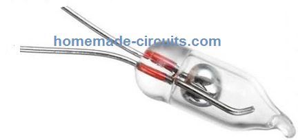 A mercury switch is essentially just a couple of electrodes sealed inside an insulated tube and moderately stuffed with mercury.
In this sensor, a change in its position causes the mercury to shift its contact from the electrodes so that the electrodes are left open.
However, with some other orientation, causes the mercury to roll over and come in contact both the electrodes generating a short between the two electrodes.
In an implementation of this type the sensor switch must be arranged so that it is merely a point away where it just creates an electrical contact across the electrodes, so that any kind of small displacement or vibration even for a brief second triggers the switch and sets off the alarm circuit.
Essentially, the circuit only has to create a latching function in response to a brief triggering from the sensor S1, which is subsequently used to drive an associated alarm device.
In case the unit is required to be powered from a battery, it becomes essential for the circuit to work with minimal stand-by current in order that the unit can remain unattended for long time periods without depleting the battery too much.
A mercury switch is essentially just a couple of electrodes sealed inside an insulated tube and moderately stuffed with mercury.
In this sensor, a change in its position causes the mercury to shift its contact from the electrodes so that the electrodes are left open.
However, with some other orientation, causes the mercury to roll over and come in contact both the electrodes generating a short between the two electrodes.
In an implementation of this type the sensor switch must be arranged so that it is merely a point away where it just creates an electrical contact across the electrodes, so that any kind of small displacement or vibration even for a brief second triggers the switch and sets off the alarm circuit.
Essentially, the circuit only has to create a latching function in response to a brief triggering from the sensor S1, which is subsequently used to drive an associated alarm device.
In case the unit is required to be powered from a battery, it becomes essential for the circuit to work with minimal stand-by current in order that the unit can remain unattended for long time periods without depleting the battery too much.
Circuit Description
In this particular security gadget alarm circuit, as shown in the following diagram, the latching action is implemented through a standard set/reset flip/flop created around IC1a and IC1b. The additional a couple of NOR gates of IC1 are kept unconnected, although their inputs are linked with the negative supply line to ensure protection against static charges, as well as guarantee that the unused gates do not cause any major current usage.
C2 generates the starting 'reset' pulse, to enable the flip/flop stage on the appropriate output condition during the switch-on period, while S1 is poitioned as the mercury switch that enables the output into the high state as soon as it is turned on.
The latch output drives the alarm generator circuit through emitter follower TR1. The alarm generator circuit is created using a pair of 555 IC astable circuits where IC3 is configured for producing the audio tone while IC2 does the job of frequency modulation.
The modulation function is implemented by lightly associating the IC2 output with the control input of IC3 through R8. This configuration allows a straightforward yet powerful two tone 'warbling' alarm noise.
LS1 is an enclosed ceramic resonator that provides large efficiency along with a ear piercing shrill audio output.
In case the best possible volume level is intended, R7 could be substituted with a 1M preset which could be tweaked to the spot where the two frequencies offer the highest output.
The additional a couple of NOR gates of IC1 are kept unconnected, although their inputs are linked with the negative supply line to ensure protection against static charges, as well as guarantee that the unused gates do not cause any major current usage.
C2 generates the starting 'reset' pulse, to enable the flip/flop stage on the appropriate output condition during the switch-on period, while S1 is poitioned as the mercury switch that enables the output into the high state as soon as it is turned on.
The latch output drives the alarm generator circuit through emitter follower TR1. The alarm generator circuit is created using a pair of 555 IC astable circuits where IC3 is configured for producing the audio tone while IC2 does the job of frequency modulation.
The modulation function is implemented by lightly associating the IC2 output with the control input of IC3 through R8. This configuration allows a straightforward yet powerful two tone 'warbling' alarm noise.
LS1 is an enclosed ceramic resonator that provides large efficiency along with a ear piercing shrill audio output.
In case the best possible volume level is intended, R7 could be substituted with a 1M preset which could be tweaked to the spot where the two frequencies offer the highest output.
Applications
This multipurpose anti-theft movement detector alarm circuit could be applied in many different ways. It can be employed like a burglar alarm, attached to a doorway so that the device can be activated as soon as a person moves open the door. This door could be the entrance of a car or a mobile home and not specifically that of a house. The fully furnished and ideal characteristics of the alarm additionally enables it to be well suited to applications like a travel suitcase or tv set alarm, laptops, in which the alarm could be initialized the moment somebody attempts to take away the secured item. The anti-theft device can be built very stream-lined, allowing it to be ideally suitable as a security device for pretty much everything precious that cannot be practically bolted down.Part List
How Laser Microphones or Laser Bugs Work
A laser microphone is a security monitoring gadget in which a laser beam is used for detecting audio vibrations across faraway targets, which are normally walls or glass of homes or offices. These devices could be applied for eavesdropping with virtually no chance of getting identified or cover getting blown. Laser eavesdropping gadgets, it is claimed, are being used by Security and Intelligence agencies in several nations, to detect and read talks in homes and offices from distances as far as 2 miles away. There exists a whole lot controversy and doubts concerning this, nevertheless there isn't any question that this kind of equipment are actually available. Actually, Mr Laisk, a physicist in the Macquarie University (NSW, Australia) along with his 3rd year pupils have developed a laser snooping device and recorded discussions from a room 30 yards far which surely prove the authenticity of such sophisticated snooping gadgets.Main Objective Behind Laser Bugs
The laser bug provides several benefits when compared to other conventional strategies. Probably the foremost advantage is that no special devices, transmitters, or wiring has to be physically installed within the room which needs to be tracked. Another advantage is further crucial than the first - is that the laser bug device to certain level eliminates the need for phone tapping.How Laser Mics Work
The fundamental theory is no rocket science. Any kind of noise or sound produced within a room will result in the windows - and, to some degree, the walls, to vibrate slightly, in accordance with the sound frequency.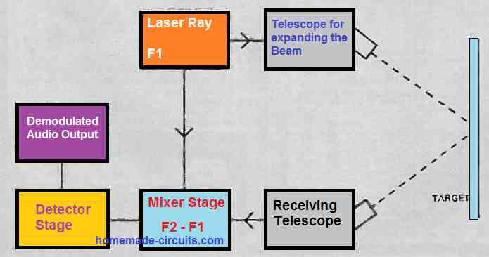 This impact can easily be confirmed by means of one's ear stuck on the wall, or by pressing the ears against the glass door or window.
All audible vibrations inside the room could be listened to pretty distinctly.
A much more remarkable evidence is to increase the volume of a music amplifier within a compact room, when the window panes could generally be seen vibrating.
The laser microphone takes the advantage of this property, where sound inside the room being tracked causes tiny oscillations on the window glass (including the walls).
This impact can easily be confirmed by means of one's ear stuck on the wall, or by pressing the ears against the glass door or window.
All audible vibrations inside the room could be listened to pretty distinctly.
A much more remarkable evidence is to increase the volume of a music amplifier within a compact room, when the window panes could generally be seen vibrating.
The laser microphone takes the advantage of this property, where sound inside the room being tracked causes tiny oscillations on the window glass (including the walls).
Transmitter Function
The laser beam from a laser transmitter is aimed on one of these glass window. The beam strikes upon a section of the glass window that is vibrating at the same frequency of the speech vibrations inside the room. This gives rise to a varying displacement of the glass surface, generating a Doppler shift effect in the laser beam frequency. The reflected beam thus turns into a frequency modulated laser beam through the vibrations of the speech inside the room.Receiver Function
The person monitoring the laser receives the reflected modulated laser. The modulated laser is mixed together with a sample of the original unmodulated sample laser beam, in a PIN photodiode. The result is an output from the diode that includes a varying frequency difference between the original transmitted version and the modulated received version of the signals. This differential signal is subsequently amplified and detected. In Mr. Laisk's circuit, the final detector stage incorporated a special fast recovery diode for the required demodulation of the speech content from the reflected laser beam. In more sophisticated prototypes, a double heterodyne process are often used to obtain additional gain prior to detection and demodulation. At the initial glance it might look important - to receive the reflected beam - the receiving and transmitting devices needs to be set up set up to ensure that the beam is perfectly perpendicular to the window glass surface. However, practically it is found that this may be not necessary. Because when the laser ray hits the glass, the rays get reflected through the normal angle while some laser light get reflected in the diffused manner. Meaning some laser energy get reflected all around. This further means that no matter from which angle the laser hits the target surface, there will always an adequate amount of stray diffused laser energy that will be reflected and captured back for the intended processing and demodulation. And this specific technique is entirely possible even by using rather ordinary detector semiconductor parts like PIN diodes from ranges over 50 metres. If higher range is required, a lot more sensitive detectors will be necessary - perhaps working at extremely low temperatures so as to deliver an improved signal/noise ratio. With reference to a report submitted by Dr Sydenham in his transducer series, commercially obtainable IR detector system could actually be used for sensing the sound vibrations inside a TV tower even across a 70 m of thick fog. Equipment can be obtained from markets which only needs some modifications for applying for such snooping functions. These equipment are called Laser Velocimeters and are being ordered in vast quantities for implementation in commercial control programs. It is obvious that upgraded variations of such devices are being employed for surveillance applications.Modulated Beam has a Wide Bandwidth
The Bandwidth of the modulated reflected laser signal can be pretty broad. With a laser beam running at maybe 1000 mm (i.e. 300 Terahertz), incident on a surface vibrating at just a few microns in a couple of kilohertz, would imply that the receiver is equipped to detect a bandwodth of nearly 1GHz for the detection! Even in this situation, it may be easily feasible using today's technology. The level of sensitivity of such equipment is immensely high. Standard laser interferometers are now able to identify vibrations of one angstrom (10-10 metres) in fact it is documented that detection of 1/100th angstrom movements has been accomplished. Therefore unquestionably, laser snooping is technologically achievable and these devices may be easily available in the local market with the intended features.How to Defeat Laser Bug
As discused above, the laser bug is actually a fairly uncomplicated device. It is pretty much obvious that these are being utilized by a lot of companies - particularly by those operating in 'aggressive marketing research work - or for commercial spying as it really should be known as. The best way to eliminate laser snooping bug is simply to make sure that no private chats ever happen within a area having an exterior wall. However due to the extreme sensitivity of such device it may be necessary that conversing in a room is done at a very low volume. A further advanced strategy would be to set up large double glazed house windows - having the air gap between the glasses which are exposed into the outer surroundings. Additionally, the exterior panes could then be artificially energized through a white noise generator. White noise may be furthermore forced into the air space between the two stage glass or wall layers. In a less critical application - an incredibly successful strategy could be to apply a matt black layer of paint on the exterior of the room walls. This should completely absorb the energy of the laser beam as a result inhibiting the required reflection! Very basic products could be utilized to identify and eliminate such beams - however be aware that although the majority of commercial interferometers work with beams in the visible light spectrum, the laser snooping gadgets function within the infra-red section of the spectrum. This means that they cannot be detected with naked eye. That said, we can still detect the the heat energy emitted from such beams pretty conveniently. Therefore, if you believe you are getting hot under the collar, who knows? Maybe several intrigued organizations could be bugging on you.Touch Alarm Circuit
The touch alarm circuit senses the mains hum signal from an intruder's body and raises the alarm sound. This happens whenever an intruder touches a potential element set as the sensor, such as the door knob, or any object that needs to be protected. If the circuit is linked with the door knob, the circuit stays in the standby condition, regardless of any stray disturbance in the air. As soon as an intruder touches the door know, the circuits activates and raises the alarm. This write-up describes a few alarm systems which employ principles that categorized them as abandoned but not exclusive. Moreover, real-world circuits that comprise type numbers and values are shared. Electronic hobbyists who wish to construct these circuits can do so with just a little effort.Main Advantage
The main advantage of this touch alarm circuit is that, it will detect only the genuine 50 Hz or 60 Hz hum from the human touch, and will ignore all other types stray electrical disturbances. This means, the circuit working is foolproof, and cannot be triggered with atmospheric electrical interference or even thunder lightening. There are many trivial circuits available online which show a touch alarm built using a couple of transistor, but these concepts and completely unreliable. These transistorized systems can be easily triggered through stray electrical noise or interference, causing false triggering of the alarm. Moreover, these ordinary transistor based circuits has to be installed right on the spot of the detection, whereas the proposed circuit can be installed far away at a distance, with only the touch sensor terminated through a cable and installed on the detection area.Mains Hum Sensor
Firstly, we will observe the touch alarm circuit that recognizes the ��mains hum�� which occurs when a metal object is touched by somebody. The transducer can be anything from a cabinet door with valuables inside, or the handle of the door in a room. Modifying the circuit to fit in a huge alarm system is relatively easy albeit it is defined here as independently operational. Figure 1 shows a block diagram that depicts how the unit operates.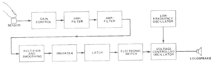 In almost all the buildings, where mains wiring exists, the ��mains hum�� is sensed by any component that is made of a conducting material.
The human body is included because it can capably detect a hum signal due to its substantial size.
In the touch detector circuit, the metal sensor affixed at the input must be little and attached to the remainder of the component using a short wire that is 300 to 500 mm in length, for longer connections use an appropriately shielded wire.
The sensor flows into a gain control, which is a standard volume regulator with a variable attenuator that can be controlled so that the typical atmospheric stray signal from the sensor does not trigger the alarm.
If the sensor is touched by someone, the reasonably huge signal detected by their body is transferred into the sensor, thus resulting in a powerful input signal that triggers the unit.
In almost all the buildings, where mains wiring exists, the ��mains hum�� is sensed by any component that is made of a conducting material.
The human body is included because it can capably detect a hum signal due to its substantial size.
In the touch detector circuit, the metal sensor affixed at the input must be little and attached to the remainder of the component using a short wire that is 300 to 500 mm in length, for longer connections use an appropriately shielded wire.
The sensor flows into a gain control, which is a standard volume regulator with a variable attenuator that can be controlled so that the typical atmospheric stray signal from the sensor does not trigger the alarm.
If the sensor is touched by someone, the reasonably huge signal detected by their body is transferred into the sensor, thus resulting in a powerful input signal that triggers the unit.
Amplification
When the system is switched on based on the condition it is being used, the input signal level will differ. Two stages of amplification which trail the sensor and a strong level of gain are necessary to cater to the diverse input level, which is not that strong. A capacitor in each of the amplifier functions as a lowpass filter. Moreover, strong high-frequency feedback is not required as the input signal is the vital mains frequency at 50 Hz with stable harmonics at a couple of hundred Hertz. The risk of false triggers due to the detection of radio frequency signals can be alleviated by constricting higher frequencies.Rectifier �C Latch
The following section rectifies and smooths the amplified signal so that a positive DC voltage is achieved. When the system is on stand-by mode, the received signal is too weak because of the voltage drop across the diodes in the bridge rectifiers. Often, there would not be any signal at all. Nevertheless, when the unit is triggered, an even more powerful output signal is generated, and the DC voltage climbs to a considerable level. This signal is employed to start an inverter stage which provides some amplification just because a low-impedance output signal of larger magnitude is created. The generated signal operates the input of a latch circuit and consequently, an electronic switch is triggered. The switch links power to an alarm generator circuit that is governed by a voltage-controlled oscillator (VCO) to power up the loudspeaker and a low-frequency oscillator to control the frequency of the VCO. The latter generates a sawtooth output signal which provides control so that the output pitch arches to the top until its peak level and plummets to the minimum pitch before ascending again. This cyclic process warrants an extremely efficient alarm signal. As the latch is included in the unit, the alarm will constantly blare even when the component is not triggered by the sensor anymore.Hum Detector Circuit
Figure 2 describes the complete touch alarm circuit schematic of the Mains body Hum Sensor Alarm.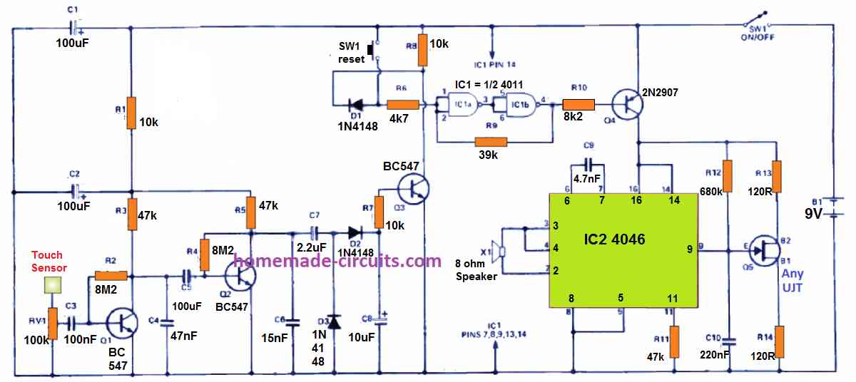 The sensor connects into preset gain control RV1 and afterwards the signal is analysed by two common emitter amplifiers which are constructed around Q1 and Q2. Capacitors C4 and C6 take care of the filtering activity.
Moreover, capacitors C3 and C5 may display low-value characteristics since low frequencies are utilized in this process.
Considering Q1 and Q2 are worked at extremely small collector current values, they possess larger input impedance than the usual common-emitter amplifiers.
As a result, the coupling capacitors are sufficient for practical use.
While diodes D2 and D3 rectify the output from Q2, capacitor C8 smoothens it.
In case an adequately large potential is produced, it forces Q3 to conduct so that its collector current becomes low.
Two NAND gates, IC1a and IC1b of CMOS 4011BE quad 2-input NAND device make up the latch circuit.
However, these two gates are linked in a series connection and function as typical inverters.
The positive return state to trigger the latching operation is supplied by R9. Diode D1 makes sure transistor Q3 can attract the input of the latch low but would fail to push it to the high state.
A workaround is possible by employing reset switch SW1 which is linked to the opposite side of D1.
Once the output of the latch is activated to the low-state, it turns on Q4 which eventually delivers power to the alarm circuit.
This depends on IC2, which is a CMOS 4046BE phase-locked loop but in this operation, the VCO segment and a single-phase comparator are used.
The latter functions as an inverter stage that provides the two-phase output signal.
The output signal operates ceramic resonator X1 compared to a standard coil loudspeaker.
The operator produces a shrieking output from the low-drive current that is offered from IC2 and is considerably noisier than expected.
If required, the output from pin 2 of IC2 can be enhanced and channelled to a typical loudspeaker.
The sawtooth modulation signal is produced by a standard unijunction relaxation oscillator that derives from Q5.
The sensor connects into preset gain control RV1 and afterwards the signal is analysed by two common emitter amplifiers which are constructed around Q1 and Q2. Capacitors C4 and C6 take care of the filtering activity.
Moreover, capacitors C3 and C5 may display low-value characteristics since low frequencies are utilized in this process.
Considering Q1 and Q2 are worked at extremely small collector current values, they possess larger input impedance than the usual common-emitter amplifiers.
As a result, the coupling capacitors are sufficient for practical use.
While diodes D2 and D3 rectify the output from Q2, capacitor C8 smoothens it.
In case an adequately large potential is produced, it forces Q3 to conduct so that its collector current becomes low.
Two NAND gates, IC1a and IC1b of CMOS 4011BE quad 2-input NAND device make up the latch circuit.
However, these two gates are linked in a series connection and function as typical inverters.
The positive return state to trigger the latching operation is supplied by R9. Diode D1 makes sure transistor Q3 can attract the input of the latch low but would fail to push it to the high state.
A workaround is possible by employing reset switch SW1 which is linked to the opposite side of D1.
Once the output of the latch is activated to the low-state, it turns on Q4 which eventually delivers power to the alarm circuit.
This depends on IC2, which is a CMOS 4046BE phase-locked loop but in this operation, the VCO segment and a single-phase comparator are used.
The latter functions as an inverter stage that provides the two-phase output signal.
The output signal operates ceramic resonator X1 compared to a standard coil loudspeaker.
The operator produces a shrieking output from the low-drive current that is offered from IC2 and is considerably noisier than expected.
If required, the output from pin 2 of IC2 can be enhanced and channelled to a typical loudspeaker.
The sawtooth modulation signal is produced by a standard unijunction relaxation oscillator that derives from Q5.
Adjustment
Setting up the touch alarm circuit is not complicated. Begin with RV1 altered for the lowest sensitivity and then increase gradually until the alarm is triggered. Next, retreat a little from this setting and try resetting the alarm. If you find the alarm activating again, turn RV1 a little in reverse more and restart the unit once again through switch SW1.Ultrasonic Fire Alarm Circuit using Air Turbulence Detection
The simple ultrasonic fire alarm circuit explained below detects a fire hazard situation by picking up the variations in the surrounding air waves, or the air turbulence. The high sensitivity of the circuit ensures that even the slightest of air turbulence created by a temperature difference or fire is quickly detected and an attached alarm device is sounded.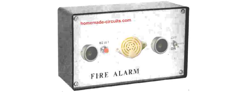 Overview
Conventional fire sensors utilize diverse systems to identify fire, and they come with all sorts of complexities.
An ordinary fire alarm system uses a temperature sensor to sense the unusually high-temperature variance caused by a fire.
It is not fundamental that only an electronic part like a thermistor or a semiconductor temperature device is used, but simple material like a low-temperature fusible link or bimetal temperature switch.
Although the simplicity of such alarm types is preferred, their reliability is questionable because detection occurs only when a fire has already matured.
More complex fire alarm systems exist, for example, smoke detectors that are equipped with a distinct semiconductor part that senses the existence of smoke particles, combustible gas and vapor.
Other than that, there are optoelectronic fire alarm systems which get triggered when the smoke of any form blocks their light beams.
Such type of fire detection system was published on Hobby Electronics.
Overview
Conventional fire sensors utilize diverse systems to identify fire, and they come with all sorts of complexities.
An ordinary fire alarm system uses a temperature sensor to sense the unusually high-temperature variance caused by a fire.
It is not fundamental that only an electronic part like a thermistor or a semiconductor temperature device is used, but simple material like a low-temperature fusible link or bimetal temperature switch.
Although the simplicity of such alarm types is preferred, their reliability is questionable because detection occurs only when a fire has already matured.
More complex fire alarm systems exist, for example, smoke detectors that are equipped with a distinct semiconductor part that senses the existence of smoke particles, combustible gas and vapor.
Other than that, there are optoelectronic fire alarm systems which get triggered when the smoke of any form blocks their light beams.
Such type of fire detection system was published on Hobby Electronics.
Heat Detection Using Doppler Shift
A novel method of fire detection using ultrasonic sound is described in this article. Bearing the same operating principles as the famous Doppler Shift ultrasonic intruder alarms, this fire detection system is tremendously sensitive to turbulence in the air, in addition to solid object��s motion. The heat from an electrical fire produces immense turbulence and triggers the alarm. Often, false alarms are set off because of the turbulence. As a result, this type of fire alarm is perfect for a home even though people living in it would often not appreciate it.How Sound Discrimination Happens
One drawback of using a Doppler Shift burglar alarm as a fire alarm is the massive detection area this unit delivers. Somehow, here this turns out to be a boon because quick detection becomes possible even though a fire starts in a small corner of the detection area. The standard principle of conventional fire alarms is to detect fires while ignoring people who are scrambling around the room. This is crucial as the alarm system is set to run until activated. A typical ultrasonic Doppler Shift alarm fails to differentiate between people and turbulence. Therefore, it makes more sense for a fire alarm system to use a circuit which governs a small area of operation. The alarm unit can be placed in a location in the room where human motion is minimal, but still, be able to swiftly identify the turbulence resulting from a fire.System Working
A basic ultrasonic alarm is equipped with two independent circuits that are connected via the same power supply. The simpler electronic circuit acts a transmitter which emits uniform sound frequencies to the receiver, which is the more complicated circuit. A block diagram of the fire alarm is shown in Figure 1.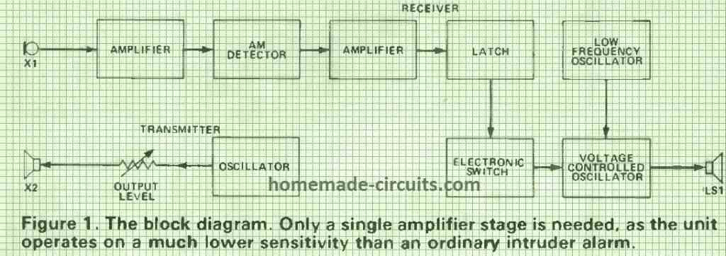 As described, the transmitter circuit works to produce ultrasonic sound using an oscillator and feeds the signal through a loudspeaker.
The electrical signal is converted into sound waves by the speaker, but humans cannot hear them because they are pitched above the hearing range.
Common sound amplifiers do not work well at ultrasonic frequencies because of the Piezoelectric type of transmitting transducer.
Usually, an output level moderator is included so that the sensitivity of the circuit can be attuned to the right level.
As described, the transmitter circuit works to produce ultrasonic sound using an oscillator and feeds the signal through a loudspeaker.
The electrical signal is converted into sound waves by the speaker, but humans cannot hear them because they are pitched above the hearing range.
Common sound amplifiers do not work well at ultrasonic frequencies because of the Piezoelectric type of transmitting transducer.
Usually, an output level moderator is included so that the sensitivity of the circuit can be attuned to the right level.
Receiver
A microphone at the receiver detects the soundwaves from the transmitter and converts them to back to electrical signals. Once more, a specialized Piezoelectric transducer is utilized on the receiving microphone because the normal ones are unsuitable to operate at high, especially ultrasonic frequencies. The extremely maneuvering state of ultrasonic sound causes detection troubles between the microphone and the loudspeaker in case both the devices are installed almost next to each other. In practical situations, the captured signals are reflections from walls or furniture in the room. Moreover, the output from the microphone is relatively low and typically around 1 mV RMS. So, an amplifier is incorporated to enhance the signal to a working level. Normally, two high-gain stages of amplification are used at minimum in an ultrasonic burglar alarm. However, since the discussed fire alarm system requires lesser sensitivity, so a single stage of amplification is more suitable.Detector
The next section of the circuit is an amplitude modulation detector. In a practical situation, the detected signal is a direct 40kHz output wave from the transmitter. This signal is collected using various paths and arbitrarily phased. But, both amplitudes of the signal and its phase relationships are preserved without any alteration. Thus, no output is generated from the amplitude generator under ready situations. Whenever there is motion in front of the detector or the air is turbulent, the whole scenario changes. The famed Doppler Shift takes charge and produces a frequency swing on the signals that are reflected from the object in motion or disorder in the air. A portion of the communicated signal is collected either directly or using motionless items through the air which is resistant to the turbulence. After that, two or more frequencies are channelled into the amplitude demodulator. At this stage, the phase relationship is beyond regulation because the signals have varying frequencies.Ultrasonic Waveforms
When looking at the waveform diagram in Figure 2 below, envision that the upper waveform is the standard 40 kHz signal and the lower waveform is the frequency-altered signal. In the beginning, the signals are in-phase or they increase and decrease homogeneously in scale while maintaining the same polarity. The in-phase signals are summed up inside the demodulator to generate a huge output signal.
Afterwards, during the waveform sequence, they enter the anti-phase zone.
This means the signals still increase and decrease their amplitude uniformly but now have opposite polarities.
As a result, the demodulator produces a weak output signal as the two other signals cancel each other.
But in the end, the signals jump back to be in-phase and release a sturdy output from the demodulator.
The moment the circuit is activated, a changing output level from the demodulator is measured.
The output signal��s frequency is the same as the variance between the double input signals.
This is normally seen on a low-audio frequency or a subsonic frequency.
Without a doubt, the signal from the output is effortlessly captured after the high-gain amplifier enhances it.
The in-phase signals are summed up inside the demodulator to generate a huge output signal.
Afterwards, during the waveform sequence, they enter the anti-phase zone.
This means the signals still increase and decrease their amplitude uniformly but now have opposite polarities.
As a result, the demodulator produces a weak output signal as the two other signals cancel each other.
But in the end, the signals jump back to be in-phase and release a sturdy output from the demodulator.
The moment the circuit is activated, a changing output level from the demodulator is measured.
The output signal��s frequency is the same as the variance between the double input signals.
This is normally seen on a low-audio frequency or a subsonic frequency.
Without a doubt, the signal from the output is effortlessly captured after the high-gain amplifier enhances it.
Alarm Generator
Once the signal is amplified, it is used to control a standard latch circuit that once activated, the alarm continues to blare until the system is reset. The latching operation is governed by a switching transistor that links control voltage to the alarm detection circuit. The alarm generator is built using a Voltage Controlled Oscillator (VCO) moderated by a low-frequency oscillator. A ramp waveform is produced by the low-frequency oscillator and an output from the VCO will gradually increase in frequency until its peak pitch. Then, the signal will revert to the minimum pitch and progressively increase in frequency again. This cyclic process continues and provides an efficient alarm signal.How the Circuit Works
The complete circuit drawing of the ultrasonic fire detection system or the receiver, is depicted in the figure below.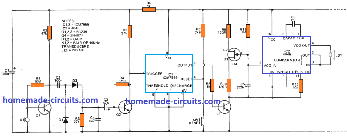
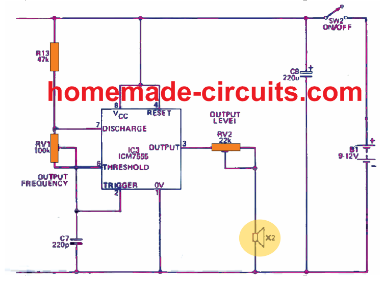 TRANSMITTER CIRCUIT
The transmitter is built using a 7555 timer device, IC1. This CMOS component is the low power type of the 555 timer.
For this type of alarm generator, a 7555 is ideal compared to a 555 because the total power consumption of the circuit is maintained to only around 1mA or less, which contributes to efficient usage of battery power.
Moreover, the 7555 IC is used in a typical oscillating method whereby the timing parts R13, RV1 and C7 are selected specially to generate a frequency of 40 kHz.
The preset is regulated to generate the output frequency that delivers ideal efficiency from the receiving and transmitting circuits.
The preset is identified as RV2 in the circuit schematic.
TRANSMITTER CIRCUIT
The transmitter is built using a 7555 timer device, IC1. This CMOS component is the low power type of the 555 timer.
For this type of alarm generator, a 7555 is ideal compared to a 555 because the total power consumption of the circuit is maintained to only around 1mA or less, which contributes to efficient usage of battery power.
Moreover, the 7555 IC is used in a typical oscillating method whereby the timing parts R13, RV1 and C7 are selected specially to generate a frequency of 40 kHz.
The preset is regulated to generate the output frequency that delivers ideal efficiency from the receiving and transmitting circuits.
The preset is identified as RV2 in the circuit schematic.
Receiver
X1 is the signal-capturing sensor in the receiver circuit, and its output is connected to the input of a common emitter amplifier which is designed around Q1. At this juncture, a low collector current of around 0.1 A is maintained to ensure the power consumption of the whole part is low. Typically, one would think this causes less gain from an amplifier of this sort, but overall, it is more than enough for the existing operation. Capacitor C2 combines the enhanced output from Q1 to a usual AM demodulator by employing D1, D2, R3 and C3. Later, the consequential low-frequency signal is ramped using a second common emitter amplifier located at Q2. Another IC1 timer is utilized as the latch. Contrary to normal practice, the timer IC1 is used in the monostable approach that provides a positive output pulse if pin 2 is reduced by 33% from the supply voltage. Usually, the output pulse width would be regulated by a pair of timing resistor and capacitor, but this circuit is without those components. Instead, pins 6 and 7 of IC1 are linked to the minus supply rail. When activated, the output of IC1 gets switched on and continue being in that state, allowing the latching action. From the collector of transistor Q2, pin 2 of IC1 is connected and regulated to equal half of the supply voltage. Thus, under standby condition, IC1 is not activated. The moment the unit is started, the collector voltage at Q2 oscillates. Moreover, during the negative half-cycles, it becomes lower than the trigger threshold voltage. Using operating switch SW1 and the reset input of IC1 to 0V supply voltage, the complete circuit can be reset. The component that is utilized to channel power to the alarm circuit when the IC1 is activated is transistor Q3. For safety reasons, R8 acts as a current limiting resistor.Alarm signal
IC2 is the last chip, which is a CMOS 4046BE phase-locked loop. However, in this design, only the VCO part is crucial. A phase comparator is aptly utilised but only as an inverter to the alarm circuit. The inversion of the output of the VCO results in a two-phase output which allows ceramic resonator LS1 to receive a peak-to-peak voltage is two times the supply voltage. As a result, a shrieking alarm signal is produced. If needed, the output from pin 4 of IC2 can be enhanced and utilised to energise a standard loudspeaker. Capacitor C6 and resistor R12 function as timing parts for the VCO. The electronic components provide a stable output frequency around 2kHz which is the zone where the ceramic resonator reaches peak efficiency. The modulation signal is produced by a typical unijunction relaxation oscillator from transistor Q4. This delivers a divergent ramp waveform at 4 kHz.How to Set Up
Begin with RV1 in the halfway point and RV2 determined for maximum output which is fully turned in the counterclockwise direction. Using a multimeter (if available), set RV2 to its minimum DC voltage and join it across R3 as the negative probe is attached to the negative supply line. Turn on the power of the unit and place the transducers facing a wall or any smooth surface with around 10 or 20 cm away. When RV1 is actuated, there will be reading or movement on the multimeter, and then RV1 is attuned to reach the maximum reading possible. It is highly recommended to fix a conductor across SW1 when the regulation is done because the alarm generator is silenced, and its output cannot affect the measurements. In the event a multimeter is unavailable, RV1 can be tuned by employing the trial and error approach to discover a value that works for the whole part. Although RV2 is well protected, the alarm unit is still sensitive. The mounting location must be well planned for the unit. A good spot would be slightly above the operator��s workbench where the highest risk of fire is present because of the electrical tools and soldering materials. Another advantage of placing the unit higher is because hot air will rise and makes it easier to trigger the alarm without the risks of false signals created by people running about the room. With a few trials, a suitable position without the consequence from human factors and stable sensitivity can be achieved for the fire alarm generator. To test the effectiveness of the unit��s position, a working soldering iron is placed under and in front of the component. When adequate turbulent air is produced, it should activate the alarm. At switch on, the circuit ill be energised but this can be immediately negated by placing the SW1 on reset. The ultrasonic fire alarm circuit is not designed with on-delay switch but your presence behind the unit must be ensured when operating SW1. There is no risk if you remove your hand after engaging the switch.Parts List
PCB Design and Track Layout
Prototype Image
Loop-Alarm Circuits �C Closed-Loop, Parallel-Loop, Series/Parallel-Loop
The article discusses a few simple loop based security alarm circuits, categorized under closed loop, parallel loop, and series/parallel loop. All these designs could be customized and used for a variety of security alarm applications. Overview In a loop alarm circuit, more than one sensor is used, each one wired with a certain type of detection loop, and inserted across tactical areas, on or around the gadget which is to be guarded. The detection or the sensor circuit (which involves a sensor loop and trigger circuit) controls a burglar alarm device or siren that, when initialized, generates an loud sound, or a visible warning illumination. The sensor device in these type of alarm circuits is generally as basic as an individual strand of thin metal wire, which works like a sensor and is placed around the perimeter of the target to be protected. So long as the cable stays undisturbed, the alarm circuit remains in the alert position. In the event an intruder severs the the wire, the sensor turns ON and sends a signal to the trigger circuit, sounding the alarm. This form of sensor actually comes under the category of one shot non-resetable, system. These security systems necessitate the sensor wire to be changed following each infringement. (These are known as closed-loop circuits.) On the other hand, the majority of alarm circuits apply certain type of magnetically triggered switch, that can be reset and applied repeatedly, like a sensor. The sensor could be sometimes a normally-open or normally closed magnetically triggered switch. Plus, according to the settings of the trigger arrangement, several sensors could be wired up in series or parallel into the circuit.Quiet Alarm
The very first circuit, as shown in Fig. 1 is created using 1/2 of a 4001 CMOS quad 2-input NOR gate, put together like a set/reset latch. When the circuit is in the reset condition (standby mode) and switch S1 open, gate U1a's output stays at logic low. When the key (an LED attached within a mini phone plug, PLI) is connected to jack connector J2, the LED remains shut off, showing that no infringement has happened.
However, as soon as S1 is closed, may be just briefly or entirely the output pin 3 of U1- a goes logic high and continues to be high until the circuit is reset.
When the key is inserted into jack connector J2 following an infringement, the LED lights up.
Putting the key into J1 resets back the circuit.
In the idle condition, the circuit consumes hardly any current, enabling it to maintain a resolute monitoring for several months reliably.
In case the sensor (S1) is set off by an intruder, the circuit records the details in a temporary storage with no additional current draw.
When the key (an LED attached within a mini phone plug, PLI) is connected to jack connector J2, the LED remains shut off, showing that no infringement has happened.
However, as soon as S1 is closed, may be just briefly or entirely the output pin 3 of U1- a goes logic high and continues to be high until the circuit is reset.
When the key is inserted into jack connector J2 following an infringement, the LED lights up.
Putting the key into J1 resets back the circuit.
In the idle condition, the circuit consumes hardly any current, enabling it to maintain a resolute monitoring for several months reliably.
In case the sensor (S1) is set off by an intruder, the circuit records the details in a temporary storage with no additional current draw.
Closed-Loop Alarm Circuit
Our next alarm circuit see Fig. 2, works by using a chain of 3 series-connected normally-closed switches (constituting the closed-loop configuration), wired to an SCR gate.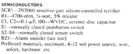 Just about any number of sensors could be attached in series and accustomed to activate the circuit.
In the idle condition, the circuit consumes around 2 mA, however the current drain may possibly increase to all the way to 500 mA if the circuit is activated, depending on the attached alarm device specs.
The circuit's functioning is extremely straightforward.
Having all sensor switches in the closed position and power switched ON, the potential at the SCR's gate becomes close to zero.
The only current depletion is by means of R1 and the closed sensors.
However as soon as any of the sensor switches opens, either briefly or completely, the gate current for the SCR is turned ON via R1.
This activates the SCR, enabling a ground conduction for the alarm horn device, which now begins to wail.
Also, the moment this activation happens, the alarm gets latched and continues to sound for so long as the reset switch (S1) stays activated.
Capacitors C1 and C2 are integrated in the design to stop possible voltage spikes from spuriously initiating the SCR.
Just about any number of sensors could be attached in series and accustomed to activate the circuit.
In the idle condition, the circuit consumes around 2 mA, however the current drain may possibly increase to all the way to 500 mA if the circuit is activated, depending on the attached alarm device specs.
The circuit's functioning is extremely straightforward.
Having all sensor switches in the closed position and power switched ON, the potential at the SCR's gate becomes close to zero.
The only current depletion is by means of R1 and the closed sensors.
However as soon as any of the sensor switches opens, either briefly or completely, the gate current for the SCR is turned ON via R1.
This activates the SCR, enabling a ground conduction for the alarm horn device, which now begins to wail.
Also, the moment this activation happens, the alarm gets latched and continues to sound for so long as the reset switch (S1) stays activated.
Capacitors C1 and C2 are integrated in the design to stop possible voltage spikes from spuriously initiating the SCR.
Parallel-Loop Alarm Circuit
Our next alarm circuit, see Fig. 3, is practically the same as the circuit provided in Fig. 2, with the exception that the sensors are rigged in parallel, which is known as an open loop configuration.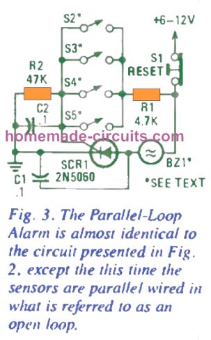 Basically, this schematic makes use of normally-open sensor switches as shown below.
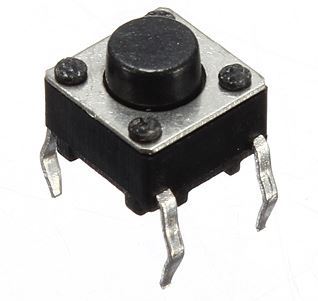 Any desired quantity of normally open switches could be included in parallel and be employed to activate the alarm; these are attached to the SCR as indicated in the schematic.
In the standby mode, the alarm circuit pulls minimal current, which makes it a superb choice as a battery powered unit.
However as soon as any of the input sensors is turned ON, gate current moves via R1 to the SCR, switching it on and triggering the alarm horn.
The horn may continue sounding until the circuit is reset or the power supply or battery depletes off completely.
Any desired quantity of normally open switches could be included in parallel and be employed to activate the alarm; these are attached to the SCR as indicated in the schematic.
In the standby mode, the alarm circuit pulls minimal current, which makes it a superb choice as a battery powered unit.
However as soon as any of the input sensors is turned ON, gate current moves via R1 to the SCR, switching it on and triggering the alarm horn.
The horn may continue sounding until the circuit is reset or the power supply or battery depletes off completely.
A Simpler Parallel Loop Alarm
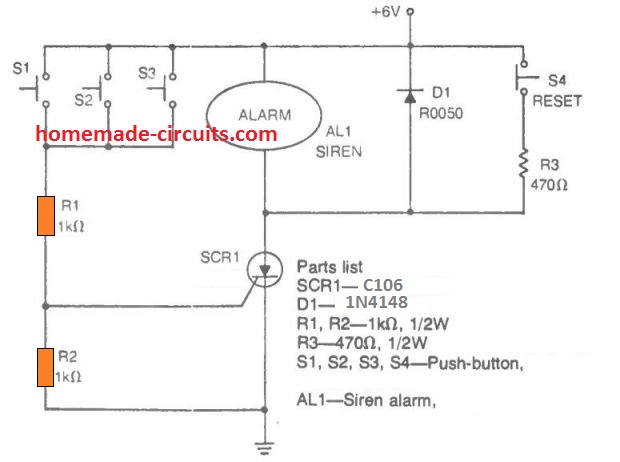 The parallel loop alarm example shown above actually is very much self-explanatory.
The switches S1 through S3 are positioned across various strategical positions within a premise which is to be protected against an intruder.
As soon as an intruder walks across any one of these switches and causes it to get depressed or closed, the voltage is allowed to reach the gate of the SCR via the switch and R1. This instantly switches ON the SCR and latches ON the associated alarm siren.
The system is deactivated only by switching off the supply input.
The parallel loop alarm example shown above actually is very much self-explanatory.
The switches S1 through S3 are positioned across various strategical positions within a premise which is to be protected against an intruder.
As soon as an intruder walks across any one of these switches and causes it to get depressed or closed, the voltage is allowed to reach the gate of the SCR via the switch and R1. This instantly switches ON the SCR and latches ON the associated alarm siren.
The system is deactivated only by switching off the supply input.
Series/Parallel-Loop Alarm Circuit
The following circuit, as given in Fig. 4, integrates the alarm in Fig 2 with the one in Fig. 3 to feature series- and parallel-loop protection together. In this design you could employ both normally-closed and normally-open sensors to activate the same alarm device. It is important to note that the primary difference between the two sensor loops is identified by the manner in which each sensor switch associates with the others within the loop and also the manner in which each loop is hooked up with the circuit.
The loop linked to SCR1 keeps the SCR switched OFF by clamping its gate pin to ground line via the loop sensors.
Opening all of these sensor switches (S2-S4) disconnects the gate ground link, letting the gate current to be applied to SCR1.
This allows the SCR1 to activate and sound the alarm device.
In contrast, SCR2's gate is kept to zero potential through R3. When any one of the associated sensor switches (S5-87) are closed, the gate of the SCR gets attached to the positive supply by means of R2, causing it to start up, and turning ON the alarm.
With one of the sensor switches closed, R2 turns into a gate pull-up resistor.
The moment it's triggered by any of the sensor loops, the circuit goes on to sound the alarm for so long as the S1 switch is not pushed for the reset actions, which can be seen wired in series with the supply voltage input.
Note that cutting off the trigger supply doesn't have any impact on the SCR conduction, until the current through the SCR is not interrupted.
As soon as switch S1 is closed, it causes the current via the SCR's to become minimal, disabling the SCR's.
Capacitors C1-C3 stop the circuit from getting spuriously triggered by voltage spikes.
Another Example of Series/Parallel Loop Alarm
It is important to note that the primary difference between the two sensor loops is identified by the manner in which each sensor switch associates with the others within the loop and also the manner in which each loop is hooked up with the circuit.
The loop linked to SCR1 keeps the SCR switched OFF by clamping its gate pin to ground line via the loop sensors.
Opening all of these sensor switches (S2-S4) disconnects the gate ground link, letting the gate current to be applied to SCR1.
This allows the SCR1 to activate and sound the alarm device.
In contrast, SCR2's gate is kept to zero potential through R3. When any one of the associated sensor switches (S5-87) are closed, the gate of the SCR gets attached to the positive supply by means of R2, causing it to start up, and turning ON the alarm.
With one of the sensor switches closed, R2 turns into a gate pull-up resistor.
The moment it's triggered by any of the sensor loops, the circuit goes on to sound the alarm for so long as the S1 switch is not pushed for the reset actions, which can be seen wired in series with the supply voltage input.
Note that cutting off the trigger supply doesn't have any impact on the SCR conduction, until the current through the SCR is not interrupted.
As soon as switch S1 is closed, it causes the current via the SCR's to become minimal, disabling the SCR's.
Capacitors C1-C3 stop the circuit from getting spuriously triggered by voltage spikes.
Another Example of Series/Parallel Loop Alarm
 If any of the switches S1---S3 is opened, the T1/T2 gets the base biased through R1 and is activated, which in turn latches ON the SCR, and sounds the alarm ON.
Conversely, if any of the switches across S5---S6 is pressed or closed, the SCR gets the gate triggers via R2 and latches ON along sounding the alarm.
If any of the switches S1---S3 is opened, the T1/T2 gets the base biased through R1 and is activated, which in turn latches ON the SCR, and sounds the alarm ON.
Conversely, if any of the switches across S5---S6 is pressed or closed, the SCR gets the gate triggers via R2 and latches ON along sounding the alarm.
High Power Alarm Driver
All the customized alarm circuits talked about so far were simply designed for low to medium power alarm devices because of the low current specifications of the SCR's connected with these. The circuit in Fig.
5 on the other hand, makes use of the SCR driver stages exactly similar to the earlier models, but the SCRs are replaced with higher-power ones, capable of handling much heavier and louder alarm devices.
Both the sensitive-gate SCR's are hooked up in individual sensor/driver circuits.
Similar to the circuit in Fig.
4, SCR1 is set off by the normally closed sensor loop (S2-S4), while SCR2 is activated by the normally open sensor loop (S5-S7).
The output (at the cathode) of each SCR we find the gate of a 400-PIV 6- amp SCR (SCR3) connected through a separate driver diode and a common current-limiting resistor, R5.
In case any of the normally closed switches (S2-S4) opens, gate current begins flowing by means of R3, turning ON the SCR1, which lights up the LED1 revealing that a infringement has happened across one of the normally closed sensors.
Simultaneously, the SCR's cathode voltage climbs up to approximately 80% of the supply voltage, resulting in the current to move via D1 and R5 into the SCR3 gate, switching it on and triggering the alarm horn.
SCR2's normally open sensor loop works in exactly the same fashion.
As soon as any of the normally open sensor switches (S5-57) is pressed down, SCR2 gets activated, illuminating LED2. Also simultaneously, a gate current is delivered to SCR3, triggering the alarm.
The circuit in Fig.
5 on the other hand, makes use of the SCR driver stages exactly similar to the earlier models, but the SCRs are replaced with higher-power ones, capable of handling much heavier and louder alarm devices.
Both the sensitive-gate SCR's are hooked up in individual sensor/driver circuits.
Similar to the circuit in Fig.
4, SCR1 is set off by the normally closed sensor loop (S2-S4), while SCR2 is activated by the normally open sensor loop (S5-S7).
The output (at the cathode) of each SCR we find the gate of a 400-PIV 6- amp SCR (SCR3) connected through a separate driver diode and a common current-limiting resistor, R5.
In case any of the normally closed switches (S2-S4) opens, gate current begins flowing by means of R3, turning ON the SCR1, which lights up the LED1 revealing that a infringement has happened across one of the normally closed sensors.
Simultaneously, the SCR's cathode voltage climbs up to approximately 80% of the supply voltage, resulting in the current to move via D1 and R5 into the SCR3 gate, switching it on and triggering the alarm horn.
SCR2's normally open sensor loop works in exactly the same fashion.
As soon as any of the normally open sensor switches (S5-57) is pressed down, SCR2 gets activated, illuminating LED2. Also simultaneously, a gate current is delivered to SCR3, triggering the alarm.
Multi-Loop Alarm Circuit
The circuit (Fig. 6) explained next is a multi-input alarm having a LED lamp for indicating the status for each sensor. The trigger circuit works nicely as a status indicator when switch S8 is moved to the MONITOR position. With S8 shifted at the MONITOR position, it allows the sensor circuit to be used throughout job hours to monitor door closing and opening and also other typically vulnerable places which are secured only during the non-working periods.
A 6-amp SCR is employed to enable a high-powered alarm device to be controlled using the system.
The circuit's working procedure is very simple.
A 4049 hex inverting buffer is utilized in order to isolate each one of the 6 input sensors.
While S2 is in its normally-closed situation, the input of U1-a at pin 3 is hooked up to the positive supply.
The high input results the U1-a's output to stay low.
With a low output, LED1 is shut off, with no current entering across the diode D1.
When S2 is opened, it drags the input of U1-a low by means of R14, driving its output to move high, causing in LED1 to illuminate, and in the course applying a bias voltage for Q1 base via D1 and S8.
The acion activates Q1, providing adequate gate current for the SCR1 via R20, so that it triggers ON.
This in turn switches ON the alarm horn BZ1.
Each one of the other sensors/ buffers circuits also work in the exact same fashion.
The transistor is wired up in an emitter-follower setup to ensure proper isolation of the buffer outputs and enhance the SCR's gate current so that it turns on optimally.
The circuit can be improved to deliver a series-loop security by replacing a string of sensors (may be 3 or 4) switches for each normally closed switch implemented within the specific loop.
You can furthermore utilize the circuit simply like a status monitor by getting rid of the diodes (D1-D6) as well as the associated circuitry.
Additionally, piezo buzzer could be attached from the diode end of S8 to ground in case an audible output is preferred when the system is used for monitoring purpose only.
When many more unique inputs are expected, it shouldn't be difficult at all by employing an additional 4049 hex inverter into the circuit.
With S8 shifted at the MONITOR position, it allows the sensor circuit to be used throughout job hours to monitor door closing and opening and also other typically vulnerable places which are secured only during the non-working periods.
A 6-amp SCR is employed to enable a high-powered alarm device to be controlled using the system.
The circuit's working procedure is very simple.
A 4049 hex inverting buffer is utilized in order to isolate each one of the 6 input sensors.
While S2 is in its normally-closed situation, the input of U1-a at pin 3 is hooked up to the positive supply.
The high input results the U1-a's output to stay low.
With a low output, LED1 is shut off, with no current entering across the diode D1.
When S2 is opened, it drags the input of U1-a low by means of R14, driving its output to move high, causing in LED1 to illuminate, and in the course applying a bias voltage for Q1 base via D1 and S8.
The acion activates Q1, providing adequate gate current for the SCR1 via R20, so that it triggers ON.
This in turn switches ON the alarm horn BZ1.
Each one of the other sensors/ buffers circuits also work in the exact same fashion.
The transistor is wired up in an emitter-follower setup to ensure proper isolation of the buffer outputs and enhance the SCR's gate current so that it turns on optimally.
The circuit can be improved to deliver a series-loop security by replacing a string of sensors (may be 3 or 4) switches for each normally closed switch implemented within the specific loop.
You can furthermore utilize the circuit simply like a status monitor by getting rid of the diodes (D1-D6) as well as the associated circuitry.
Additionally, piezo buzzer could be attached from the diode end of S8 to ground in case an audible output is preferred when the system is used for monitoring purpose only.
When many more unique inputs are expected, it shouldn't be difficult at all by employing an additional 4049 hex inverter into the circuit.
Touch Operated Code Lock Switch Circuit
This touch operated electronic door lock can be used for locking any entrance through a touch keypad. The lock's touch feature is foolproof and impossible to crack since the touch function is required to be on 3 programmed pads together or simultaneously, otherwise the lock doesn't respond. It is a lot convenient to open a door using a code lock as compared to carrying weighty metal keys with us.
Aside from this, traditional keys can easily get misplaced, but this cannot happen with code locks.
It is a lot convenient to open a door using a code lock as compared to carrying weighty metal keys with us.
Aside from this, traditional keys can easily get misplaced, but this cannot happen with code locks.
Advantage of Touch Operated Code Lock
The circuit diagram below exhibits a code lock that enables it to be opened through an effective three-digit code. But, this specific lock performs this function in a somewhat unconventional and unique technique. In this system, 3 digits has to be touched concurrently, meaning three fingers must touch 3 designated code buttons simultaneously. Any one finger touching the incorrect button would simply not allow the relay to actuate. As the diagram distinctly indicates, it is actually out of the question for an intruder to speculate from the lock's layout exactly how it can be decoded. This particular characteristic, alongside the huge range of combination possibilities, causes it to be extremely hard for an onlooker to crack the lock code. Another advantage is, involving 3 fingers together helps to cover the keyboard and hides the code operation from an onlooker, and the person finds it extremely difficult to understand which 3 pads were tapped by the owner.
How it Works
In all 5 CMOS ICs are used here. All the gates from the IC 4050 are used as buffers whose inputs can be seen connected with the touch keypads. These buffers ensure that the touch operation are effectively converted into logic output signals without any malfunction. Because our finger may have varying resistance levels and pressure causing the output to oscillate and generate fluctuating outputs. The buffers ensure this never happens regardless of the touch variation. The only criterion being the code number which must be touch simultaneously without fail for the lock to open. The output from the buffers are further wired with Hex Inverter IC 7404 and the processor ICs 7430, 7410 which finally execute the relay activation when the code is correctly tapped. An electronic door opener may be configured with the relay contacts for implementing the lock opening and closing operations. The code for the shown circuit illustration is 9-11-4. Any time this program code pads are simultaneously tapped with fingers, the inputs of N2, N3 and N4 turn logic '0'; consequently, the three inputs of N8 and the output of N5 create a logic '1'. Assuming none of the other keypads are tapped except the coded ones, all inputs of gate N7 remain logic '1', which results in the relay to become activated and the LED to illuminate. The relay can be employed to operate an electric door opener mechanism for opening the lock.Gadgets to Protect Women from Assaults and Harassment
Gadgets and devices that are specially designed to repel or deter a potential male offensive can be used by a girl to protect herself from a crime situation, and therefore can be very handy. In this post we discuss a few of these devices which could be either purchased or even developed at home. Despite of all the efforts from the law and the police, it has so far been quite ineffective to control crime against women, which is seeing a constant rise in not only the metro cities but also the rural parts of many developing countries, like India. Physical abuse and molestation are among the main crimes against girls which is rising at an alarming rate, resulting in panic, fear, uncertainty in the minds of young girls and also their family members.Reasons Behind Crime against Women
A few of the fundamental reasons responsible for creating such crimes could be poverty, illiteracy, lack of knowledge and communication, lack of basic amenities of life, adolescence phase, watching illicit content on mobile phone. That said, you may find such crimes happening even from modern guys having good reputation and sophistication, but with hidden, distorted mindset. No matter what, for a girl or a woman it certainly becomes immensely important to make sure that she's always well equipped to tackle any such unpredictable abuse, assault or an offensive attack especially while walking in remote, secluded streets, or lanes, public transport etc. Although many techniques have been suggested for girls self defense, some popular ones appear to be rather incompetent, and with adverse repercussions.Learning Martial Arts and Self Defense Tactics
 There's been a lot of hype and discussions regarding training girls and woman with martial arts, karate etc.
so that they can safeguard themselves against an assault.
However, some thinking reveals that this approach could be quite ineffective, unreliable and dangerous for the girl, unless she's trained at a professional level.
It is because:
Physically, an average man could be 2 to 3 times more stronger than a woman.
A man may easily handle a few blows from a women (unless it is hit on the vital areas), but a single hard blow from a man can cause unconsciousness or even death to a girl.
Moreover, dealing with a real situation can be a lot difficult, and due to nervousness the victim may tend to forget the techniques learned during her training course, due to fear.
Even if she attempts the self defense techniques may result in the assaulter getting angry and dangerously violent.
This situation can put the girl in greater risk of harm and damage.
There's been a lot of hype and discussions regarding training girls and woman with martial arts, karate etc.
so that they can safeguard themselves against an assault.
However, some thinking reveals that this approach could be quite ineffective, unreliable and dangerous for the girl, unless she's trained at a professional level.
It is because:
Physically, an average man could be 2 to 3 times more stronger than a woman.
A man may easily handle a few blows from a women (unless it is hit on the vital areas), but a single hard blow from a man can cause unconsciousness or even death to a girl.
Moreover, dealing with a real situation can be a lot difficult, and due to nervousness the victim may tend to forget the techniques learned during her training course, due to fear.
Even if she attempts the self defense techniques may result in the assaulter getting angry and dangerously violent.
This situation can put the girl in greater risk of harm and damage.
Using a Taser Gun
A taser gun is a gadget that works like a gun, but instead of bullets it releases a pair sharp metallic terminals, intended for hitting the offenders skin. While being shot, the terminals remain wired with the taser gun carrying a high voltage pulse with it. When the terminals hit the target's skin, the high voltage across the terminals inflicts an excruciating pain and even temporary paralysis, incapacitating and preventing the offender from any further actions. But again this unit can be quite unreliable, because the unit is cumbersome, needs proper aiming which can falter, and result in the offender getting more aggressive.
Another disadvantage of a stun gun is that it cannot be used multiple number of time, and the girl has only one chance to use the gun against the offender.
In case there are more than one attacker, the situation can get even worse.
But again this unit can be quite unreliable, because the unit is cumbersome, needs proper aiming which can falter, and result in the offender getting more aggressive.
Another disadvantage of a stun gun is that it cannot be used multiple number of time, and the girl has only one chance to use the gun against the offender.
In case there are more than one attacker, the situation can get even worse.
Ultrasonic Sound Weapon
An ultrasonic sound weapon is an effective looking weapon which generates a sharp ear piercing sound, that may have the potentials to break the ear drums of the target. The sharp sound may also alert the nearby locality which might indirectly help the girl by attracting the attention of the folks in the vicinity. Due to this the offender may be discouraged from his illegal intentions. Although, the devices looks good, it may be slightly bulky due to its cone like speaker enclosure, designed to ensure that the sound focuses specifically toward the target, and the high pitched sound does not affect the user.Dependable Self Defense Strategies
Alternatively, there are a few highly reliable and effective approaches that could be used by any girl, with greater confidence.Pepper Spray
 A pepper spray is perhaps one of the very reliable self defense gadget for women, and may work like an ideal male assault deterrent unit.
The main advantage of a pepper spray unit is that, it can be comfortably gripped and shot at the target from above 2 feet distance.
The spray can be mostly very effective and should succeed in getting into the eyes of the target 99% of the time, unless the target is wearing glasses.
Even then, the spray particles may have the potential to reach the eyes through side gaps of the specs of the unwary target.
Even if the offender succeeds to evade the spray, he will have no other option but to run away, as attempting further assaults could be useless, and dangerous for him.
A pepper spray is perhaps one of the very reliable self defense gadget for women, and may work like an ideal male assault deterrent unit.
The main advantage of a pepper spray unit is that, it can be comfortably gripped and shot at the target from above 2 feet distance.
The spray can be mostly very effective and should succeed in getting into the eyes of the target 99% of the time, unless the target is wearing glasses.
Even then, the spray particles may have the potential to reach the eyes through side gaps of the specs of the unwary target.
Even if the offender succeeds to evade the spray, he will have no other option but to run away, as attempting further assaults could be useless, and dangerous for him.
High Voltage Gloves
This type of gloves could be modified and enhanced with parallel metals foils, and connected with an integrated high voltage source. A girl wearing these gloves can defend herself by grabbing any section of the offenders skin, preferably the face for inflicting a highly painful electric shock and a temporary blackout to the offender. This high voltage gloves may not be available ready made, but could be built at home with some skill, and knowledge of some electronics. You will need the following materials to make this high voltage glove equipment: A high voltage generator module as shown below, rated to generate a 1000 to 4000 voltage from a chargeable 3.7 V Li-Ion battery.
There are plenty of options and varieties available online that you can buy from.
A 1000 V output from 3.7 V should be quite enough although higher voltage ranges may guarantee higher safety and repulsive power.
For the battery, you can use a 18650 type pencil cell
A pair of skin tight rubber gloves, as shown below:
A high voltage generator module as shown below, rated to generate a 1000 to 4000 voltage from a chargeable 3.7 V Li-Ion battery.
There are plenty of options and varieties available online that you can buy from.
A 1000 V output from 3.7 V should be quite enough although higher voltage ranges may guarantee higher safety and repulsive power.
For the battery, you can use a 18650 type pencil cell
A pair of skin tight rubber gloves, as shown below:
 5. Adhesive Copper Tape as demonstrated below:

How to Make an Electrified High Voltage Hand Gloves
Once the above the above ingredients are bought, the high voltage gloves could be created with the help of the following diagram instructions: Cut and stick a couple of copper adhesive tape strips on the inner surface of the gloves, as shown above.
Make sure to use external glue to reinforce the existing adhesive strength of the copper tape.
Once the tape is firmly fixed and dried, you can wire the high voltage generator module, the battery and an ON/OFF switch with the copper tape, as indicated in the above diagram.
Make sure to enclose the module, battery and the switch inside a water proof plastic box, which should be sufficiently compact so that it can be comfortably installed at the base of the gloves.
Now whenever the switch is pressed ON, the two copper will be instantly energized with a high voltage, which could be used to deter a potential offender.
Cut and stick a couple of copper adhesive tape strips on the inner surface of the gloves, as shown above.
Make sure to use external glue to reinforce the existing adhesive strength of the copper tape.
Once the tape is firmly fixed and dried, you can wire the high voltage generator module, the battery and an ON/OFF switch with the copper tape, as indicated in the above diagram.
Make sure to enclose the module, battery and the switch inside a water proof plastic box, which should be sufficiently compact so that it can be comfortably installed at the base of the gloves.
Now whenever the switch is pressed ON, the two copper will be instantly energized with a high voltage, which could be used to deter a potential offender.
Using a Tilt Switch
If you think the manual ON/OFF switch may be bulky and inappropriate in such precarious circumstances, you can replace with a tilt switch device, for enabling an automated switch ON whenever the situation calls for. An example tilt switch unit is shown in the following figure. Here we can see a mercury ball which rolls across the glass tube depending on the orientation of the glass tube.
If the unit is positioned vertically with the two terminals downwards, the mercury ball would roll over the inner two terminals ends causing a short circuit across them, this would switch ON any circuit powered across these terminals.
In the high voltage glove prototype, the tilt switch could be installed in a way that would cause the two terminals to short when the hand is lifted vertically upwards, with fingers pointing upwards (just as we normally do while defending ourselves).
Here we can see a mercury ball which rolls across the glass tube depending on the orientation of the glass tube.
If the unit is positioned vertically with the two terminals downwards, the mercury ball would roll over the inner two terminals ends causing a short circuit across them, this would switch ON any circuit powered across these terminals.
In the high voltage glove prototype, the tilt switch could be installed in a way that would cause the two terminals to short when the hand is lifted vertically upwards, with fingers pointing upwards (just as we normally do while defending ourselves).
A Passive Approach
There are perhaps some passive methods also, which could force all males to ignore the particular girl applying these techniques. One technique is putting artificial get up resembling an old man. For example putting an artificial beard set, wig and an overcoat. The idea might look silly, but actually it can prove to be more effective than many other complex techniques.
Putting Fake Skin or Make Up
Another passive method which can be applied for protecting woman against male offensives, is to use fake skin with a loathsome appearance, as shown in the following example. This approach may be truly repulsive and would certainly repel not only the bad guys, but all, nonetheless the main purpose of safeguarding the girl could be accomplished, no matter what.
Better Safe than Sorry
Although the above discussed gadgets and strategies for protecting woman and girls from an assault may look impressive, it is always good to ensure you never get into such situations on the first place. This can be ensured by avoiding venturing into unknown secluded zones alone. If at all it becomes a necessity, try having a male companion with you, or ask a cop nearby for an escort. You opinion surely maters, so if you have a suggestion please send it through the comment box below.RFID Security Lock Circuit �C Full Program Code and Testing Details
In this article we will see how an Arduino based RFID reader circuit could be used for controlling a relay, which in turn could be used in security door lock applications.Overview
If you haven��t yet checked the previous RFID article, please go ahead check it out, it covered the basics of RFID technology. We are going to identify the authorized tags using UID. In a nutshell UID is the unique identification number of the tag, when you scan your card at your office or anywhere else, it extracts the UID from the card. The UID of the card is saved on the database of your office and it will recognize the card holder and register your attendance. The tag not only transfers UID, but also transfers some other information which is stored in the tag, the tags can generally store from 1KB to 4KB sometimes even more. We won��t be discussing how to store information on the tag but, it will be discussed in a future article. In this post we are going to utilize the UID number to control the relay ON/OFF. The motto of this project is to turn ON/OFF the device, which is connected with the given setup on scanning with authorized RFID tag. The UID of the card is defined in the program and when authorized card is detected, it will turn on the relay on the first scan and scanning it again will deactivate the relay. If any unauthorized card is detected, it will give out error message on serial monitor and relay continue its current task without any interruption. Here when the authorized card is scanned, the relay activates/deactivates, this mechanism can be used anywhere, for example in: door locking system, where authorized card needs to be scanned to open door.How it Works:
 The RFID circuit consist of LED which indicate the status of the relay, BC 548 transistor drives the relay and 1N4007 diode is connected across the relay to arrest the high voltage spike at the instant of switching.
If you want to connect higher voltage rated relay (9V or 12V), you can connect external +Ve supply to relay and �CVe supply to ground of arduino��s GND pin.
Please take at most care while proceeding this step, as you may damage the board if connections are not right.
The next step after completing the hardware setup is to upload the code to find the UID of you tag.
Now upload the below given program to arduino, open serial monitor and scan the tag.
The RFID circuit consist of LED which indicate the status of the relay, BC 548 transistor drives the relay and 1N4007 diode is connected across the relay to arrest the high voltage spike at the instant of switching.
If you want to connect higher voltage rated relay (9V or 12V), you can connect external +Ve supply to relay and �CVe supply to ground of arduino��s GND pin.
Please take at most care while proceeding this step, as you may damage the board if connections are not right.
The next step after completing the hardware setup is to upload the code to find the UID of you tag.
Now upload the below given program to arduino, open serial monitor and scan the tag.
Program to find UID:
#include <SPI.h>
#include <MFRC522.h>
#define SS_PIN 10
#define RST_PIN 9
MFRC522 rfid(SS_PIN, RST_PIN);
MFRC522::MIFARE_Key key;
void setup()
{
Serial.begin(9600);
SPI.begin();
rfid.PCD_Init();
}
void loop() {
if ( ! rfid.PICC_IsNewCardPresent())
return;
if ( ! rfid.PICC_ReadCardSerial())
return;
MFRC522::PICC_Type piccType = rfid.PICC_GetType(rfid.uid.sak);
if(piccType != MFRC522::PICC_TYPE_MIFARE_MINI &&
piccType != MFRC522::PICC_TYPE_MIFARE_1K &&
piccType != MFRC522::PICC_TYPE_MIFARE_4K)
{
Serial.println(F("Your tag is not of type MIFARE Classic, your card/tag can't be read :("));
return;
}
String StrID = "" ;
for (byte i = 0; i <4; i ++) {
StrID +=
(rfid.uid.uidByte[i]<0x10? "0" : "")+
String(rfid.uid.uidByte[i],HEX)+
(i!=3?":" : "" );
}
StrID.toUpperCase();
Serial.print("Your card's UID: ");
Serial.println(StrID);
rfid.PICC_HaltA ();
rfid.PCD_StopCrypto1 ();
}
The output on serial monitor (example):
Your card��s UID is: AA:BB:CC:DD
On the serial monitor, you will see some hexadecimal code, which is the UID of the tag.
Note it down, which will be used in the next program to identify the tag.
After this step is completed, upload the below code on the same setup.
Program to identify the card and control relay:
//---------------Program developed by R.Girish------------//
#include <SPI.h>
#include <MFRC522.h>
#define SS_PIN 10
#define RST_PIN 9
int flag=0;
int op=8;
char UID[] = "XX:XX:XX:XX"; //Place your UID of your tag here.
MFRC522 rfid(SS_PIN, RST_PIN);
MFRC522::MIFARE_Key key;
void setup()
{
Serial.begin(9600);
SPI.begin();
rfid.PCD_Init();
pinMode(op,OUTPUT);
}
void loop()
{
if ( ! rfid.PICC_IsNewCardPresent())
return;
if ( ! rfid.PICC_ReadCardSerial())
return;
MFRC522::PICC_Type piccType = rfid.PICC_GetType(rfid.uid.sak);
if(piccType != MFRC522::PICC_TYPE_MIFARE_MINI &&
piccType != MFRC522::PICC_TYPE_MIFARE_1K &&
piccType != MFRC522::PICC_TYPE_MIFARE_4K) {
Serial.println(F("Your tag is not of type MIFARE Classic, your tag can't be read :("));
return;
}
String StrID = "" ;
for (byte i = 0; i <4; i ++)
{
StrID +=
(rfid.uid.uidByte[i]<0x10? "0" : "")+
String(rfid.uid.uidByte[i],HEX)+
(i!=3?":" : "" );
}
StrID.toUpperCase();
if(StrID!=UID)
{
Serial.println("This is an invalid tag :(");
Serial.println("***************************************");
delay(2000);
}
if (StrID==UID && flag==0)
{
flag=1;
digitalWrite(op,HIGH);
Serial.println("This is a vaild tag :)");
Serial.println("Status: ON");
Serial.println("***************************************");
delay(2000);
}
else if(StrID==UID && flag==1)
{
flag=0;
digitalWrite(op,LOW);
Serial.println("This is a vaild tag :)");
Serial.println("Status: OFF");
Serial.println("***************************************");
delay(2000);
}
rfid.PICC_HaltA ();
rfid.PCD_StopCrypto1 ();
}
//---------------Program developed by R.Girish------------//
char UID[] = "XX:XX:XX:XX"; //Place your UID of your tag here.
Replace XX:XX:XX:XX with your UID.
Author��s prototype which can be effectively used as a foolproof RFID security lock for doors and safes:
 When an authorized card is scanned:
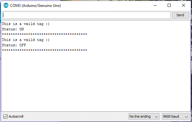 When an unauthorized tag is scanned:
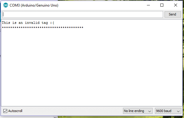 If you have any questions regarding this Arduino RFID security lock circuit, please feel free to ask below in comment section.
Magnetic Door Security Alarm Circuit for Alerting if Door was Opened
The door security alarm circuit discussed in this article alerts the user whenever the door fitted with the circuit is opened or closed or even moved from its original locked position.Using a Reed Relay and Magnet for the Triggering
The idea utilizes the very basic reed relay and magnet concept across the door and the door frame. The magnet is attached with the door edge, while the reed relay and its associated circuit is fixed on the door frame exactly adjacent to the door magnet, such that both are almost touching each other and separated only by the door and frameclearance.
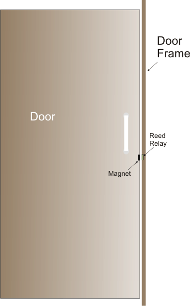 This implies that whenever the door is moved or opened the magnetic influence on the reed relay is inhibited, which causes the associated circuitry to trigger the alarm.
The reed relay is connected with a delay OFF timer circuit, which makes sure that as soon as the door is opened or closed even for a fraction of a second causes the alarm to activate and sound for at least a few 10s of seconds, after which it automatically resets, until the door is moved yet again.
This implies that whenever the door is moved or opened the magnetic influence on the reed relay is inhibited, which causes the associated circuitry to trigger the alarm.
The reed relay is connected with a delay OFF timer circuit, which makes sure that as soon as the door is opened or closed even for a fraction of a second causes the alarm to activate and sound for at least a few 10s of seconds, after which it automatically resets, until the door is moved yet again.

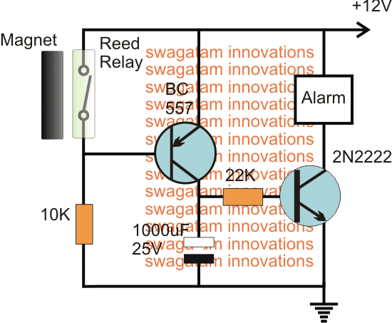
How it Works
The arrangement can be seen in the above diagram which shows how the door open close alarm circuit needs to be configured which appears pretty straightforward. As long as the door remains in the closed position, the magnet enables the reed in the switched ON or "closed" position, which in turn keeps the PNP BC557 switched OFF. With BC557 switched OFF, the 2N2222 is also unable to conduct, and thus the connected alarm module continues to be silent. However in a situation where the door is moved or opened by an intruder, causes the the magnet to shift from its original position, which instantly opens and releases the reed internal contacts. The above action now enables the BC557 to conduct, subsequently enabling the 2N2222 also to trigger and ultimately switch ON the connected alarm unit. The intruder realizes this and tries to close the door in an attempt to shut off the alarm, however due to the presence of the 1000uF capacitor, and the 22K resistor at the base of the 2N2222, the transistor continues to conducts ensuring that the alarm is not switched off even though the door is restored at its initial position....thus the alarm stays latched ON and continues to raise the alarm forcing the intruder to surrender himself, until the 1000uF capacitor has discharged completely. This little inexpensive yet highly efficient door opening alarm circuit can be used for securing any desired entrance from a possible intrusion without the need of a constant monitoring or without a guard in position.How to Make a GHz Microwave Radar Security Alarm Circuit
The post explains a GHz microwave radar security alarm circuit which is designed to detect an intruder within the critical zone only while it's moving, static objects produce no effect for the sensor.Using Doppler Sensor KMY24
In the previous article we learned about a microwave Doppler radar sensor module KMY 24 which is a Hi-end sensor device capable of transmitting a sample signal in the GHz range across the set zone until it's reflected from a moving object back to the sensor for the necessary processing. In the following discussion we will see how this module can be suitably rigged with opamps for enabling the detected signals to be amplified and fed to an appropriate load such as an alarm or a relay driver stage.Circuit Diagram
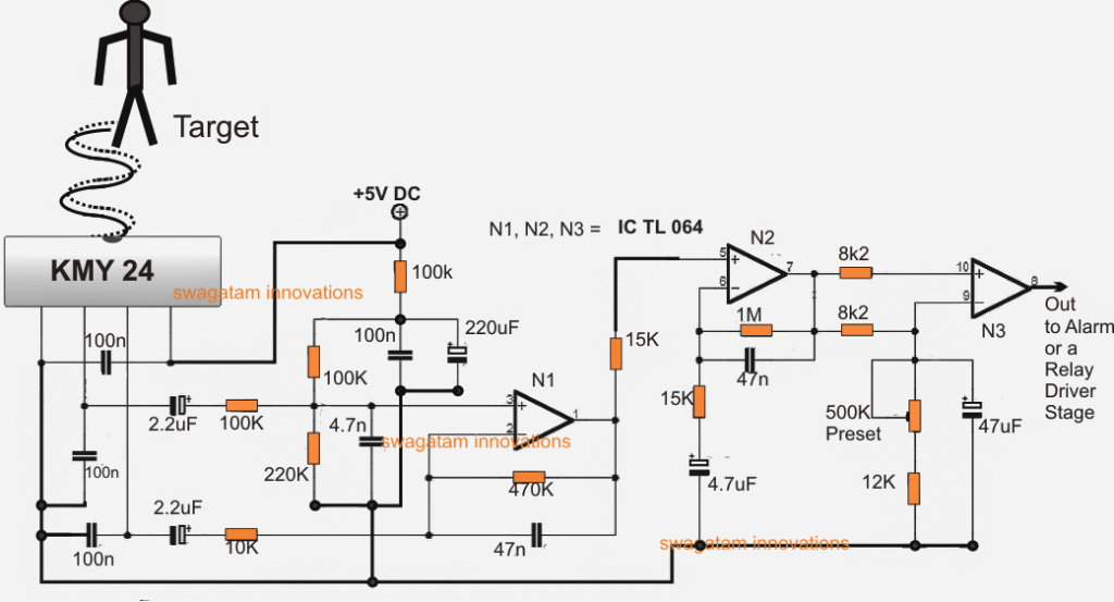 Referring to the above GHz microwave radar security alarm circuit we can see the sensor module KMY 24 configured with the first opamp stage using N1 and the associated components.
Basically N1 is wired up as a differential error amplifier, wherein its two inputs are hooked up with the two differential outputs of the sensor unit.
Referring to the above GHz microwave radar security alarm circuit we can see the sensor module KMY 24 configured with the first opamp stage using N1 and the associated components.
Basically N1 is wired up as a differential error amplifier, wherein its two inputs are hooked up with the two differential outputs of the sensor unit.
Detecting a Moving Object
When a moving object or target is detected in front of the sensor module the reflected GHz signals go through a relative phase shift which is reflected back to the sensor and is processed inside the module producing an equivalent positive or negative response across the center two pinouts of the KMY 24 module. This difference in voltage is fed to the two inputs of A1 which detects this and generates an equivalent amount amplified differential voltage across its output pin#1. A2 is configured as a filter stage which monitors the output from A1 and filters the unwanted spikes that might be induced at its input and feeds a clean amplified differential signal to the next opamp N3 stage. N3 is connected as an impedance matching or transforming stage, which processes the fed differential input from N2 and converts it into a distinctive high or low pulses across its output pin# 8, which becomes compatible to be used with either a DC alarm stage, relay driver stage or even a Microcontroller input. Thus the GHz microwave radar sensor alarm circuit may be used as a security system for detecting even the slightest of movements from an intruder within a 6 meter range from the sensor's emitting point, and convert into an alarm or any desired triggered output.Power Interruption Alarm Circuit for Instant Power Failure Indications
This power interruption alarm circuit will alert you whenever there's a power failure or an interruption in the mains. In some special conditions it becomes imperative to know whether the mains that powers some important system or circuit is absent. By: Manisha PatelHow the power failure alarm works
This proposed circuit is connected to the power mains via the transformer T1. The AC voltage is rectified by the diode D1 and is filtered by C1. As long as there is a voltage level present at the anode of D2 (around 12 volts), transistor Q1 is able to conduct maintaining a negligible voltage at the gate of the SCR (TR1). Thus the SCR is not able to get triggered, ensuring no triggers and no alarm tones. It can be seen that the SCR is permanently attached with a 9 volt PP3 battery. In an event of a mains failure, the voltage from the transformer disappears, the transistor Q1 is instantly cut-off, diode D2 ensures that no current is able to reach Q1 base from the battery power. Also, The battery forward biases diode D3 and a current flows through R2, R3 and R4 resistors. This situation raises the voltage level at the gate of TR1, activating the SCR and the attached buzzer that warns of the situation or the absence of mains voltage. The moment the power returns, the signal error message does not disappear because the thyristor holds itself in latched condition due to its inherent properties (with DC supply SCRs once triggered stay latched permanently), even though its gate now is rendered with a zero voltage. In order to cut of the alarm and restore the condition, it may be only necessary to disconnect the battery supply momentarily via a switch (not shown in the diagram) placed in series with the 9 volt battery or in series with the thyristor anode or cathode. Note: The buzzer may be replaced by a relay for enabling a visual warning or both.Circuit Diagram
Bill Of Materials for the proposed power interruption alarm circuit
- 1 resistor R1 = 12K - 1 resistor R2 = 2.7K - 2 resistors: R3 = R4 = 1K - 1 NPN: BC547 - 1 470 uF/25V - Four semiconductor diodes: D1 = D2 = D3 = D4 = 1N4007 - 1 Thyristor TR1: C106Y1 (NTE5452) - One transformer 120/240 VAC to 9 VAC or more than 500 mA - 1 buzzer 6 or 9 volts - 1 PP3 9 volt battery.Office Call Bell Network Circuit with LED Monitor
The post explains an office call bell network circuit for office complexes which could be used for calling and monitoring office member's attendance and response from the particular intended office chamber. The idea was requested by Mr. Rajib BanerjeeTechnical Specifications
Need a perfect useable circuit idea for Ringing the Bell as different Department of the office from single point. Say, 20 department calling system from a central office. When push the switch for 'x' department then an existing electrical calling bell is ringing till anyone from that department come to attending to the central office and it's time taking to attend because of distance to each other. Now need a circuit which work like when calling the Bell from Central office to any dept, the attendant who attend the central office just push switch from that dept. for the signal that he/she is hearing the bell and just coming. After pushing the switch from Dept a light glow besides the calling switch of Central office. just this which i can incorporate with the existing using one way calling system and give me the alteration as diagram. Thanks Rajib Banerjee kol-110The Design
The proposed office call bell circuit as requested above may be summarized as follows: The central head office needs to be connected to each of the office departments such that pressing the respective push buttons rings the corresponding bell in the desired office chamber. In an event the concerned office member is not in the "called" office, but in some other nearby department and hears the ringing, is able to respond by attending the "answer button" from the other office the member may be situated during that instant. The above response gets stored in the form a glowing LED in the head office allowing the attendant there to check the concerned members exact position. The circuit implementation of the proposed office call bell monitor network can be done by using a group of set/reset flipflops as may be witnessed in the following diagram:Circuit Diagram
 The circuit above illustrates an example wiring for three office rooms which may be extended to any desired numbers simply replicating the stages.
How it Works
As can be seen the upper section comprises three identical stages of transistor set/reset modules, each module being made up of two NPN transistors, one PNP, a couple push buttons and a few resistors. The push button marked as "ON" is used for activating or triggering the latch circuit made up of T1 and T2. The OFF button does the opposite that is deactivates the particular module activation. When activated a positive voltage becomes available at the collector the corresponding PNP transistor which is terminated for triggering the office bell situated at the particular office, in the diagram these are labelled as "Trigger to room#1, room#2, room#3...." When one of these triggers is activated it's conveyed to a relay driver circuit system installed in the intended office chamber where the trigger is fed to the base of the relay driver transistor as shown in the diagram below (labelled as "trigger from head office"). This prompts the relay to get activated and also the connected bell across the relay contacts. The member now presses the green switch in response which is conveyed back to the head office and collected across one of the inputs marked "trigger from room#1, room#2 room#3..." depending upon from where the member may have attended the green button. This action enables an instant switching off of the bell. If it was from the concerned room, say for example room#1 then the corresponding red LED positioned in "room#1"module gets illuminated and latched, if it was from any other room the corresponding red LED is illuminated providing the correct instantaneous location of the member during his/her response to the call made from the head office. The red LED illumination may be reset and restored to its switched OFF position by pressing the reset button at the extreme right corner of the above head office call bell monitor circuit above.The Relay Driver Circuit
Parts list
All R1 = 100 k All R2, R3, R4 = 10 K All diodes = 1N4148 All C1 = 100uF/25V All NPN = BC547 All PNP = BC557Laptop Anti-theft Security Alarm Circuit
The post explains a simple laptop anti-theft alarm circuit which can used with any concerned object such as a laptop which needs to be protected, when an intruder tries to approach the unit or makes an attempt to steal it the connected alarm is instantly raised. The idea was requested by one of the dedicated readers of this blog.Technical Specifications
i have a problem and i hope you will solve this, last month some one stole my laptop in my hostel, i am very angry about this lost i want to make ir transmitter and receiver circuit which operates the relay 12v iam very thankful to you i have also made the transmitter it works but receiver doesn't work i want to request you to make tr.and re very simple and easy work about 5 to 10 feet distance. i have also spend money but all in vain help me sir very soon thank youThe Design
The laptop anti-theft alarm circuit could be possibly implemented by incorporating any of the following circuit concepts" a tilt sensor circuit, a capacitive touch sensor circuit, an IR sensor circuit, a finger touch sensor circuit. Using an IR proximity sensor circuit as shown below, is an effective way of tackling the theft issue, however the circuit could be relatively complex to build, adjust and apply. The entire explanation for the above circuit may be found in this accurate proximity detector circuit article
A much simpler approach could be by employing a capacitive sensor switch circuit as shown below.
The supply will need to be operated from a 6V or a 12V battery.
The unit could be attached with the laptop, anybody coming close or trying to get hold of the object would instantly trigger the alarm.
The concept has been explained comprehensively in this capacitive touch sensor circuit article
The entire explanation for the above circuit may be found in this accurate proximity detector circuit article
A much simpler approach could be by employing a capacitive sensor switch circuit as shown below.
The supply will need to be operated from a 6V or a 12V battery.
The unit could be attached with the laptop, anybody coming close or trying to get hold of the object would instantly trigger the alarm.
The concept has been explained comprehensively in this capacitive touch sensor circuit article
Circuit Diagram
Earth Leakage Indicator Circuit for Detecting Current Leakages in Ground Wires
A simple earth leakage indicator circuit discussed here can be used for getting some very useful results regarding current leakages from an appliance body into the earth pin. The idea was requested by Mr. SS kopparthy. The circuit of the proposed earth leakage indicator is shown in the figure below. Each such unit may be used for individual appliances having earth pins, or a single circuit may be placed near theMCB for detecting a possible common leakage from all the appliances.The circuit may be understood withthe points explained below:Circuit Operation
R2 is positioned as a current sensing resistor which should have a relativelylow value so that the actual earthing feature doesn't get obstructed due to its resistance. T1 here forms a current sensing and a voltage amplifier stage. The detected small voltage across R2 is quickly amplified by T1 and fed to the LED inside an opto coupler. As long as the leakage is not relatively significant (below 20mA) the LED inside the opto does not respond, however the moment this value exceeds the set limit, the LED inside the opto illuminates switching ON the corresponding built-in transistor, which in turn actuates the red LED connected across its collector and positive lead indicating a possible earth leakage. The supply for the entire operation is derived through a small trasformerless power supply using C1, D1, C2 as its main components. The red LED may be replaced with a 12V piezo buzzer for getting an audio indication, or both may be used in parallel for facilitating a dual mode indication. The value of R2 may be calculated using the following formula: R = 0.2/I. where I is allowable current leakage through the earthing cable, assuming this to be 20mA we can calculate it as: R = 0.2/.02 = 10 ohms Since the collector resistance if T1 is quite high, T1 could get triggered with as low as 0.2 across its base/emitter, that's the reason why 0.2 is selected in the above formula. The T2 stage is introduced for monitoring the "health" of the earthing connection, as long as it's at par with the neutral, T2 stays switched off since its base remains grounded via the good earthing, however the moment a weak earthing is formed, T2 base gets enough voltage through R5 to trigger itself and the opto which in turn triggers the connected alarm. The situation of a weak or open earthing is indicated by the red and yellow LEDs together, while the red LED alone indicates an earth leakage. CAUTION: THE CIRCUIT IS NOT ISOLATED FROM MAINS, ALL PARTS COULD CARRY LETHAL ELECTRIC CURRENT, EXERCISE UTMOST CAUTION WHILE HANDLING UNCOVERED.
Parts List
R1 = 1K ohms R2 = see text R3, R4 = 22k R5 = 56K R6 = 1M D1 = 15V 1watt zener diode C2 = 100uF/25V T1, T2 = BC547 C1 = 0.47uF/400V opto = any standard 4-pin type The above circuit could be improved by adding a few more components to it, as shown below: In this circuit we have added a rectifier diode D1 (1N4007) for an improved rectification.
T1 has been enhanced with another BC547 transistor T2 wired as Darlington in order to make the earth leakage detection even more sensitive and allow the use of smaller in-line resistance R2 for better "earthing" experience for the appliances.
C2 (0.22uF) ensures that T1/T2 does not get rattled with unwanted electrical disturbances.
In this circuit we have added a rectifier diode D1 (1N4007) for an improved rectification.
T1 has been enhanced with another BC547 transistor T2 wired as Darlington in order to make the earth leakage detection even more sensitive and allow the use of smaller in-line resistance R2 for better "earthing" experience for the appliances.
C2 (0.22uF) ensures that T1/T2 does not get rattled with unwanted electrical disturbances.
Parts List
R1 = 1K R2 = see text R3, R4 = 22k R5 = 56K R6 = 1M Z1 = 15V 1watt zener diode D1, D2 = 1N4007 C0 = 0.47uF/400V C1 = 100uF/25V C2 = 0.22uF T1, T2, T3 = BC547 C1 = 0.47uF/400V opto = any standard 4-pin typeTest Set-Up for the above circuits:
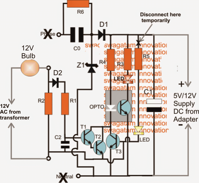
Earth Leakage Indicator
The above diagram shows the test set-up for the proposed earth leakage indicator circuit. It's conducted in the following manner: The circuit powered up using an external 12V AC/dC adapter output, remember do not plug-in the circuit to mains while doing this procedure In the set-up test 12V AC supply is connected across the earth/appliance points via a 12V bulb. R5 link is kept disconnected for the time being. The above implementation should instantly switch ON the red LED indicating a current leakage through R2. Disconnecting the 12V bulb, the red led must also switch OFF, indicating the stoppage of the leakage condition. Now reduce the 12V bulb load to some lower value, could be done by including another 12V bulb in series to it. Even with such lower loads, the red LED should be able to indicate the leakages across R2 confirming the proper working of the circuit. Now removing the above load should instantly switch off the red LED, assuring a correct working of the circuit. Restore the circuit to its original condition and now it's ready for the actual installation near your MCB. The functioning of the yellow LEd can be witnessed after the actual installation and connections are done. If it starts glowing immediately after the installation would indicate a bad or incorrectly wired earthing line.Ultrasonic Weapon (USW) Circuit
The post discusses a simple ultrasonic weapon circuit also called USW, using very ordinary parts such as IC 555 and a few other passive components to generate the required ultrasonic ear piercing sound.Controlling Crime with USW
With rising crime in today's society, especially against woman, carrying some sort of effective weapon has become quite imperative. However keeping weapons like a hand gun can be too risky and dangerous as it can lead to deaths or severe injuries and might instigate legal interventions. A great option which can be as effective in such cases yet won't cross dangerous limits can be in the form of a USW or an ultrasonic weapon.What is a USW
AnUSWis a device or an electronic circuit designed for generating ear piercing, unpleasant frequencies that may be capable of causing intensely disturbing or painful affects for the assailant. when targeted toward the human attacker or an animal. Thissonic devastator will generally work with amplified frequencies of around 10 to 15kHz with a sweeping effect, resembling the sound created when we scratch our nail on a bar of chalk or limestone (amplify it 50 times). Such USW devices are already available in the market but making one at home can be real fun and also useful. A simple version can be witnessed below which incorporates a couple IC 555s for the intended actions. The proposed ultrasonic weapon circuit may be understood as follows: Basically both the ICs are configured as astable multivibrators, but the one at the left is used as a slow rising and falling ramp generator or triangle wave generator.Circuit Operation
The IC 555 at the right is wired up as a high frequency generator determined by the 1.5k resistor, P2 and the 0.01uF capacitor. The slow rising/falling ramp from across the 1uF capacitor of left IC555 is applied to the control input pin#5 of the right hand side astable IC555 stage. The above integration results in an high frequency sweeping voltage at pin#3 of the right hand IC which is fed to the transistor current amplifier stage consisting of the power transistor D40D5 or any other similar NPN equivalent. This amplified current is further fed to a couple of inductors which transform the high current into high voltage frequency suitable for driving high impact piezo transducers or buzzer elements. For the two parallel inductors, here we incorporate the primaries of an ordinary radio audio output driver transformers and the series inductor can be any type having the value of around 1000uH. S4 is the push to ON switch used for triggering the circuit into operation. S1 is for selecting fast or slow sweep effect option, while S3 is the frequency selector switch, to be selected for fixing the optimal frequency range. P2 sets the final frequency to be delivered across the output.Adjusting the Frequency Sweep
P1 is for correcting the desired sweep speeds. The whole circuit operates at 18V, lower voltages upto 12V can also be tried with good results. A battery pack made from chargeable Ni-Cd cells suits good enough for this ultrasonic weapon application. The whole unit must be installed inside a plastic enclosure made by fabricating plastic pipes in such away that it resembles a pistol kind of appearance with S4 positioned at the trigger button position. The piezo must be assembled inside a funnel mouth, and whole assembly to be fixed at the tip of the above fabricated gun barrel.Circuit Diagram ofSonic Devastator

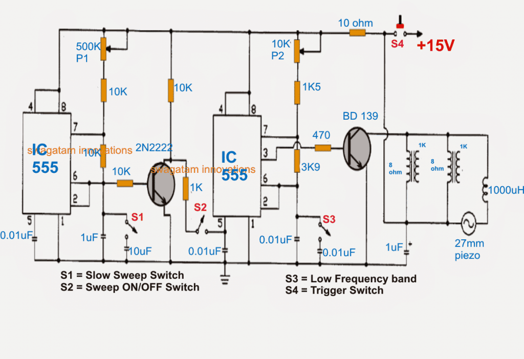
Transducer Driver Coil Details

How to Make a Long Distance USW
The above design could be effectively used for remote long distance control by configuring it with a pair of RF FM transmitter and receiver circuit as shown below:
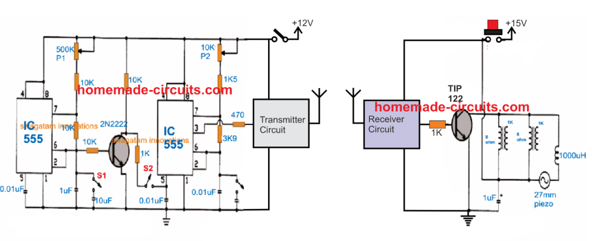
Make this Solar Powered Fence Charger Circuit
A Fence charger or energizer is an equipment which is used for charging(electrifying) a fence or a boundary in order to protect the inside premise from human or animal interventions. Since these boundaries are mostly of large fields and parks, are normally away from the main cities, and powering them through some renewable option becomes more suitable than from utility grids which may become difficult to acquire in such remote areas. The circuit of a solar electric fence charger explained here does not depend on traditional power source for operating, rather gets it 24/7 from a self sustained solar power conversion set up.The circuit is very simple to understand. The fence charger circuit is basically a switching circuit which involves a few diodes and a high voltage capacitor.How the Circuits Works
The diodes are used for rectifying the AC from a small step up transformer so that it gets stored inside the high voltage capacitor. When this voltage reaches a particular threshold, the SCR fires and discharges the entire stored voltage inside the capacitor. The above discharging of the capacitor is done or rather dumped inside the primary section of an automobile ignition coil. The sudden dumping of the above high voltage inside the ignition coils primary, steps up the surge into several thousands of volts into the secondary winding of the ignition coil. This stepped up voltage is used for energizing the fences or the boundaries appropriately. However the above operations requires an AC input at the levels of around 100 to 220volts. This voltage is generated by suitably processing the input DC from a solar panel set up. The voltage from the solar panel is first controlled to a suitable level and then it's used for operating a triggering circuit. The triggering circuit consists of a IC 555 oscillator which switches the voltage obtained from the solar panel controller into the transformers input, so that the output from the transformer generates the required 220V AC for powering the ignition circuit. The solar panel output also charges a small 12V/7AH battery so that the power can be used after dusk, when sun energy is not available.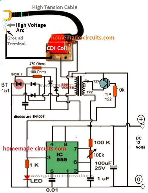 Parts List
10k, 100k, 1k 1/4 watt 5% = 1 each
470 ohms, 100 ohms 1/2 watt 5% = 1 each
preset 100k = 1no
Capacitor 1uF/25V, 100uF/25V electrolytic - 1 each
Capacitpr 0.01uF disc ceramic = 1 no
Capacitor 105/400V PPC = 1no, near the SCR
Semiconductors
1N4007 = 4 nos,
IC 555 = 1no
LED red 5mm = 1no
Transistor TIP122 = 1no
SCR BT151 = 1no
Transformer = 0-12V/220V 1 amp
Ignition Coil from 2-wheeler or 3-wheeler
The above circuit can be powered through the following solar panel current controlled battery charger circuit:
For complete explanation of the circuit please refer this solar voltage regulator circuit.
Parts List
10k, 100k, 1k 1/4 watt 5% = 1 each
470 ohms, 100 ohms 1/2 watt 5% = 1 each
preset 100k = 1no
Capacitor 1uF/25V, 100uF/25V electrolytic - 1 each
Capacitpr 0.01uF disc ceramic = 1 no
Capacitor 105/400V PPC = 1no, near the SCR
Semiconductors
1N4007 = 4 nos,
IC 555 = 1no
LED red 5mm = 1no
Transistor TIP122 = 1no
SCR BT151 = 1no
Transformer = 0-12V/220V 1 amp
Ignition Coil from 2-wheeler or 3-wheeler
The above circuit can be powered through the following solar panel current controlled battery charger circuit:
For complete explanation of the circuit please refer this solar voltage regulator circuit.
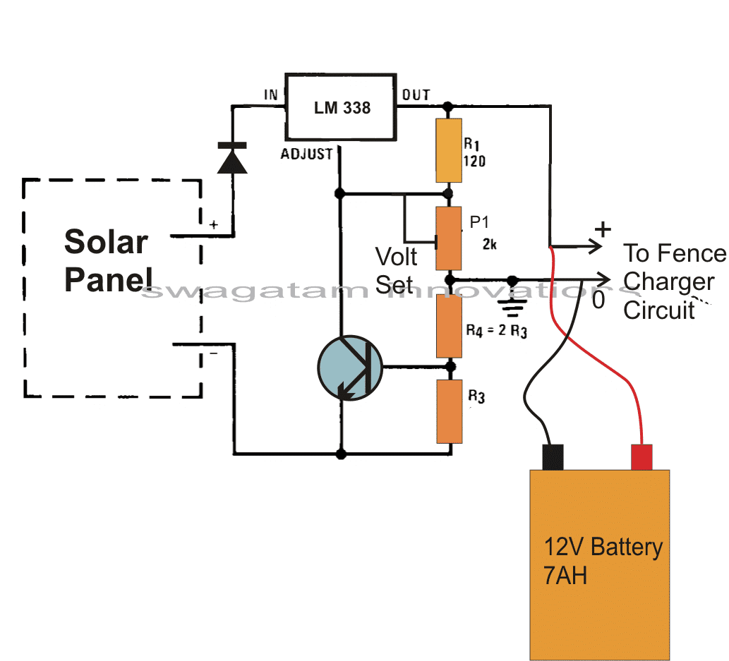
Parts List
R1 = 120 ohms P1 = 10k pot (not 2k) R4 = replace with link R3 = 0.6 ohm 1 watt Transistor BC547 = 1no IC LM338 = 1no Diode 1N5408 = 1no Solar Panel = 16 V / 2 amp Battery 12 V 7 AhFence Charger using a Stand-alone Inverter
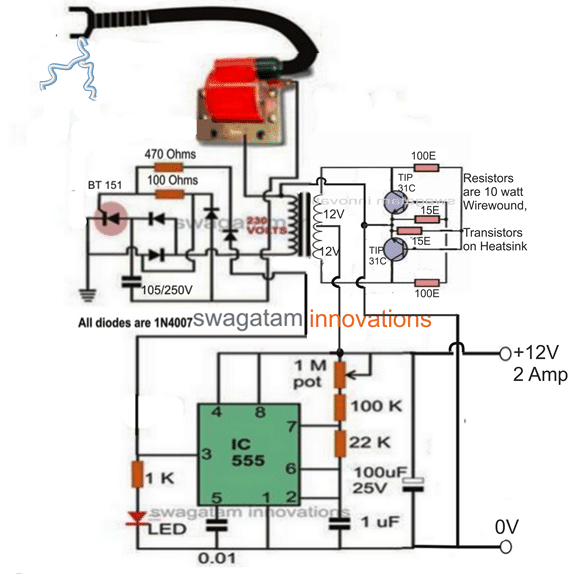 Video clip showing the working details of the fence charger circuit.
The video basically highlights the strength of the sparks generated by the CDI coil and how effectively this can be used when integrated with a farm fence.
Video clip showing the working details of the fence charger circuit.
The video basically highlights the strength of the sparks generated by the CDI coil and how effectively this can be used when integrated with a farm fence.
2 Tone Ringtone Generator Circuit
The IC LS1240A from SGS Thompson is specifically designed for generating a 2 tone ringtone generator circuit. Thus the IC specifically becomes suitable for landline telephones for producing the ringtones when a call is received. However with little modifications the IC can be easily utilized for normal applications, in circuits where a double tone alarm may be required. Basically the IC is a 8-pin DIL chip resembling the IC 555 and has the following specs: Very low current consumption yet good audible response at the output. Internal built-in rectifier stage for rectifying an AC input supply, a filter capacitor is also a built-in feature of the IC. Hardly any external components required for setting up the circuit. The tone of the output musical audio can be adjusted externally through a resistor. If the IC os used inside a landline telephone then the supply to the IC is derived from the line voltage via a 1uF capacitor. The IC is able to drive a piezo electric transducer directly without the need of inductors or amplifiers. The IC is also capable of driving a small loudspeaker directly for generating the musical output. However the speaker must be rated at minimum of 50 Ohms. The following 2 tone ringtone generator circuit shows how to configure the IC LS1240 as a two tone musical signal generator circuit.Pinout Details of the IC LS1240 dual tone generator IC
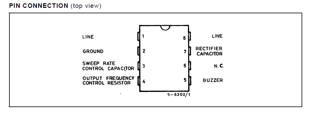
Circuit Diagram of two tone music generator using IC LS1240
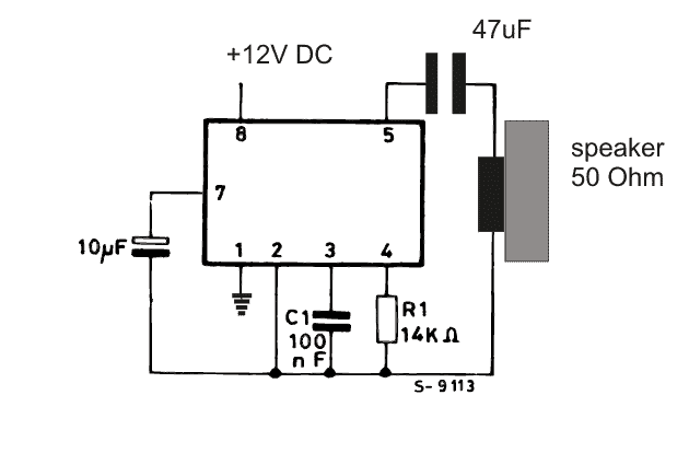
Two Tone Generator using piezo element
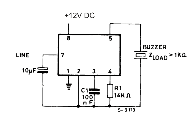 Courtesy:

Earthquake Sensor Circuit [Seismic Sensor]
The article shows an earthquake sensor circuit idea which incorporates an innovative way of detecting the minutest of shocks caused by a possible earthquake tremor. The circuit is so sensitive that it is able to detect tremor of 4 on the Richter scale, yet remains unaffected to loud sounds or irrelevant bangs or noises.Introduction
I have seen a number of different circuits of seismic sensors on the net, however most of these have utilized a piezo transducer as the sensor element, God knows how a piezo would detect earthquake tremors. It simply appears absurd because a piezo transducer would be solely able to sense high frequency vibrations and never a swaying action. An earthquake will never generate a shrill noise rather it produces a gentle swaying pattern, when it hits. Therefore using a piezo element is a flop idea, according to me. Of course a piezo would detect tremors only if it were used in the form of a load-cell, by integrating some kind of load, assembled for implementing an oscillating action during tremors. In the present earthquake sensor circuit, I have used water as the detecting agent. After some experimentation I found that water is an excellent sensor of vibrations as well as a swaying kind of motions. You can test waters behavior by keeping a bowl of water on the table and giving a gentle knock on the table. Even the slightest of legit vibration is enough to create a nice ripples on the surface of the water. I could have used an LED/LDR arrangement for detecting these ripples, however since we are not interested in sensing vibrations rather only swaying actions, I made a little out of the way approach. Through a few of my previous posts I have already discussed water level sensor circuits where the water's conducting property is well exploited for the purpose. The same property has been harnessed for getting the intended results.How the Earthquake Sensor is Designed to Operate
Looking at the circuit diagram we see that the configuration in fact has nothing serious. The electronic part consists of a couple of transistors rigged into a latch circuit. The input to this circuit is achieved from a small half round container filled with water. The positive supply from the circuit is dipped inside the water while the hot end of the input is placed in such a way that it stands just a mm above the water. During a possible earthquake (God Forbid) the water responds to the tremor and starts generating a swaying movement. The moment the water moves, its level gets disturbed and connects the hot end of the circuit with the positive terminal, dipped inside the water.. The positive of the supply immersed in the water instantly makes contact with the HOT end of the circuit via the water, the circuit gets triggered and immediately latches. The connected buzzer sounds, sending an alarm signal. The container can be made by cutting a small children plastic ball into half. After doing the required settings inside this half cut ball, it may be filled with water as shown in the diagram and sealed. The container then should be fixed somewhere such that the level off water inside the ball retains perfectly horizontal position without any deviations.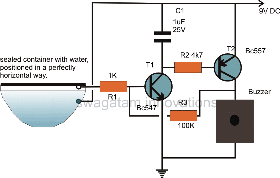
Cell Phone Controlled Door Lock Circuit
Controlling your door lock through your personal cell phone was never this easy. Learn how to build a simple electronic circuit that will help in converting your ordinary door lock into a high security door lock which can be now controlled through your own cell phone. Your ordinary door lock can be now very easily converted into a cell phone controlled high security door lock. Learn the entire building procedure through some simple instructions and circuit schematics.Introduction
A very simple configuration using a low cost cell phone (used as a modem) and an electronic circuit can be build to control remotely a high security door lock. Once the unit is built and attached to a door, by simply assigning your personal cell phone��s number inside the modem cell phone, you can alternately lock and unlock a particular door by sending subsequent ��miss calls�� through your cell phone to it from any part of the world. We use a NOKIA 1202 as the modem cell phone here for the project. Let��s proceed and learn the simple instructions required to complete the project.
How the Circuit Functions?
The basic concept of the project is to detect a particular ringtone from a SIM supporting modem and use it to toggle the electronic circuit and the load (door lock) correspondingly. The very specific and unique ringtone �C ��Beep Once�� or the ��No Tone�� is available with every NOKIA cell phone. And also this ring can be assigned to any particular fed number of the cell phone. So this ringtone becomes specific only to that particular number and will be sounded every time a call is received from the assigned number. This facility has been ideally exploited here. A 5 volt regulated supply is used to trickle charge the modem round the clock so that its battery is never discharged. This supply also goes to the IC 4093 = pin 14 (+) and pin 7(-). An in-built cut-off system inside every NOKIA cell phone ensures a safe charging. The circuit functioning may be easily understood with the following explanation. The FIGURE above shows a simple three transistor amplifier circuit which is basically used as a tone amplifier. On receiving a ��miss call�� from the assigned number (owner��s cell phone), the modem immediately responds and produces the desired ringtone (��Beep Once��). This tone frequency is collected from the modem��s headphone socket and applied to the tone amplifier��s input. The ringtone is suitably amplified and is used to toggle a relay momentarily. This relay connects a 5 volt trigger pulse to the input of CMOS flip flop circuit and also sounds a buzzer. The flip flop toggles in response to the above action and activates the following transistor/relay locking mechanism. A car central lock has been effectively integrated with an ordinary manual locking shaft to form an excellent door dead bolt. The whole system activates in a push pull manner to alternately lock and unlock the door in response to every subsequent ��miss call�� from the owner��s cell phone.Parts List for the proposed cell phone controlled door lock circuit
R1=2K7 R2=10K, R3=10K, R4=2M2, R5=2M2, R6=1K, R7=1M, R8= 180 Ohms R9 = 1K R10=10K R11=22k R12=47K R13=10 Ohm C1,C2=470uF/25V C3,C4,C5=0.22uF C6,C7,C12=10uF/25V C8 = 0.1uF/100V C9,C10=1uF/25V C11=1000uF/25V All NPN Transistors are BC547 and PNP is BC557 IC2=7805 IC1=4093 All Relays=12V/400 OhmDiodes D5- D8=1N5408 Rest all Diodes are 1n4148 Transformer=0-12V/3AmpConstruction Clues and Modem Cell Phone Configuration
Constructing the control circuit is very easy and may be done by just assembling the procured electronic components over a general purpose board by soldering. All the connections should be accurately done with the help of the given circuit schematic. Once the assembly is completed, it��s time to configure the modem cell phone. The attached modem cell phone needs to be set up through the following steps: Go to settings and select set the default ringtone as EMPTY. It means now at this position the modem does not produce any ringtone to any incoming calls. Also, switch off the message tone, keypad tone, start up tone etc. Now feed your personal cell phone numbers (single or many as desired) through which the modem and the lock need to be operated. Assign the required ��beep once�� ringtone to all these numbers. The modem is all set. Integrate it to the control circuit through its headphone socket pin assembly. Also, connect the charging voltage input to it as shown in the diagram. Your high security door lock is fully ready and can be installed over the door which is to be controlled and will lock and unlock it faithfully on receiving the subsequent ��miss calls�� from the assigned numbers.A Homemade Fence Charger, Energizer Circuit
The electric fence charger circuit presented here is basically a high voltage pulse generator. The super high voltage is derived from a commonly used automobile ignition coil. An astable multivibrator is used to generate the required frequency to drive the ignition coil. Another astable is used to control the pulses supplied to the fence.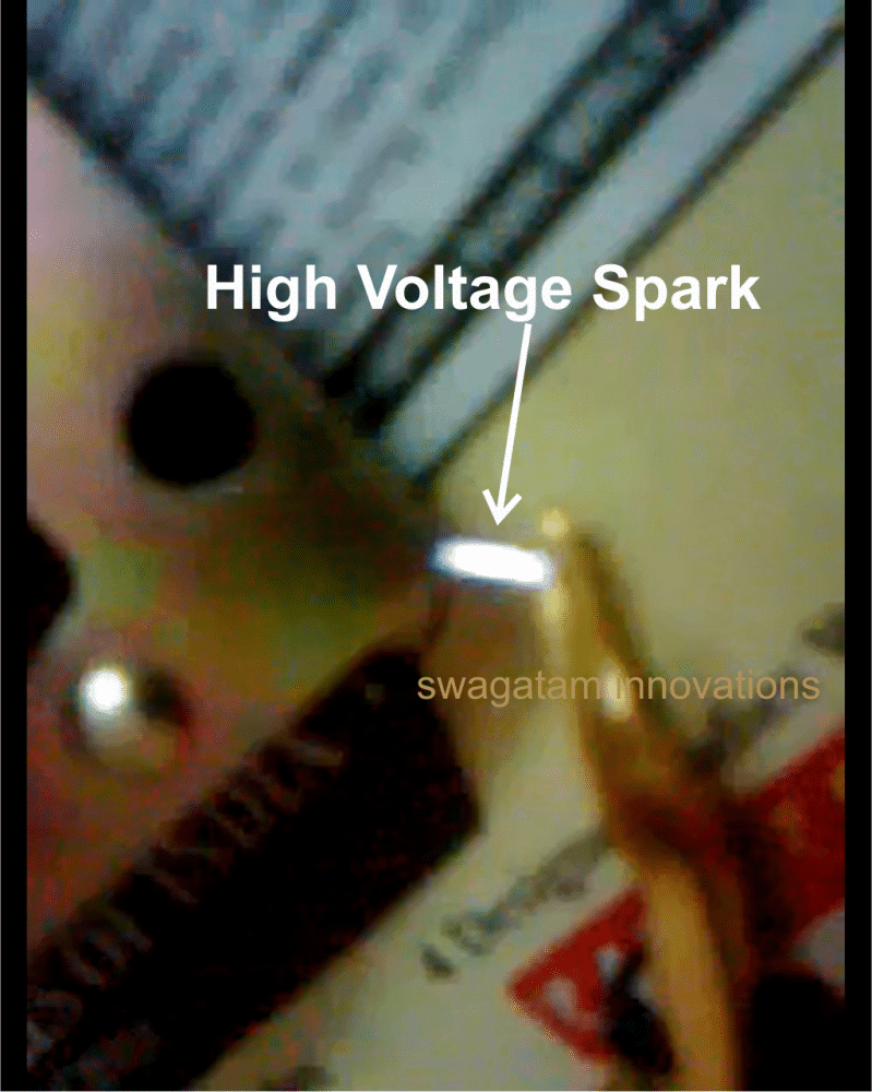
Protecting Crops with Fence Charger
If you have large agricultural fields and desperately need to protect the crops from uninvited guests like animals and possibly humans, then this electric fence charger device is just what you are looking for. Build and install it yourself. An electric fence is an electrified high voltage barrier which produces painful shocks if physically touched or manipulated. Thus such fencing basically function as deterrents for animals as well as human intruders and stop them from crossing the restricted boundary. The present circuit of an electric fence charger is designed and tested by me and has proved sufficiently powerful for the application.20 kV from the Sparks
The fence charger circuit is able to produce voltage pulses up to 20,000 volts, needless to say about the fatality rate involved with it. However the pulses being intermittent, provides the subject with enough time to realize, recover and eject. The generated pulse is so powerful that it can easily arc and fly-off between short distances of around a cm. so the fencing conductor needs to be separated adequately to avoid leakages through arcing and sparking. If not tackled, may drastically reduce the effectiveness of the unit. Here the generation of high voltage is primarily carried out by an automobile ignition coil. The winding ratios of an ignition coil are specifically designed and intended for creating high voltage arc between a two closely spaced conductors inside the ignition chamber to initiate the ignition process in vehicles. Basically it��s just a step-up transformer, which is able to step-up an input applied voltage at its primary winding to monstrous levels at its output or the secondary winding. SOME POINTS OF THE CIRCUIT AND THE IGNITION COIL IS VERY DANGEROUS TO TOUCH WHEN POWERED. ESPECIALLY THE IGNITION COIL OUTPUT IS TOO LETHAL AND MAY EVEN CAUSE PARALYSIS.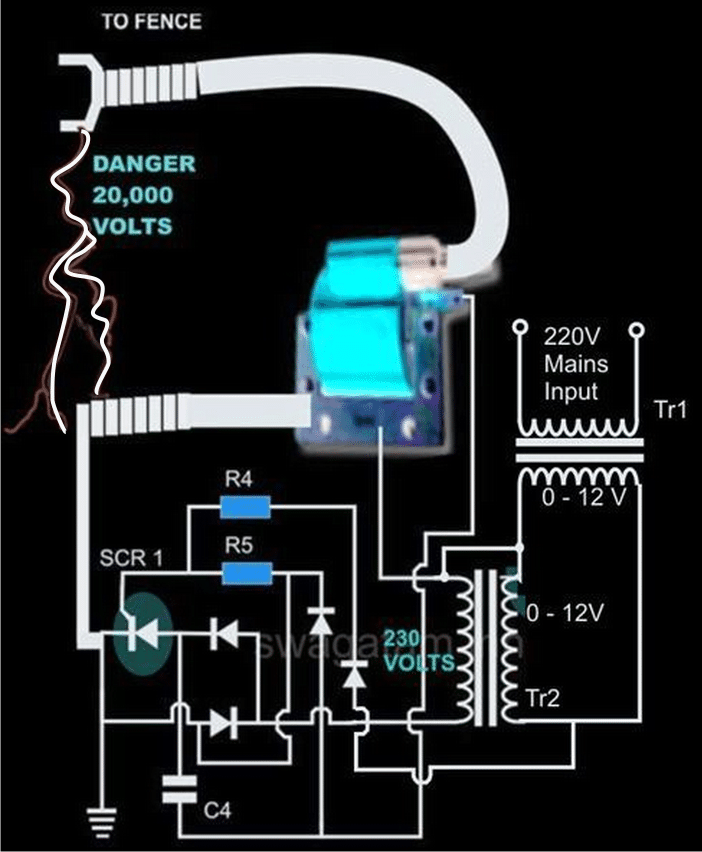
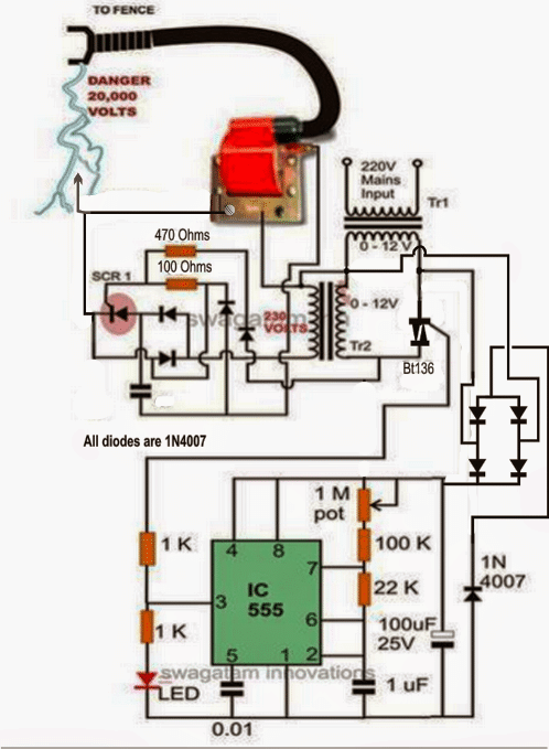 Let��s diagnose the proposed electric fence charger circuit more deeply.
Circuit Operation
In the CIRCUIT DIAGRAM we see that the entire circuit is basically comprised of four stages. A DC oscillator stage, An intermediate 12 to 230 volts step-up stage, The voltage collector and firing stage and the super high voltage-booster stage. TR1 and TR2 are two normal step-down transformers whose secondary windings are connected through SCR2. TR1 input primary winding may be selected as per the country specification. However, TR2 primary should be rated at 230 volts. IC 555 along with the associated components forms a normal astable multivibrator stage. The supply voltage to the circuit is derived from the secondary of TR1 itself. The output from the astable is used to trigger the triac BT136 and the whole system, at a particular fixed intermittent rate as per the settings of P1. During the ON periods, the triac connects the 12 volt AC from TR1 to the secondary of TR2 so that a 230 volt potential instantly becomes available at the other end of TR2. This voltage is fed to the voltage-firing stage consisting of the SCR1 as the main active component along with a few diodes, resistor and the capacitor C4. The fired voltage from SCR1 is dumped into the primary winding of the ignition coil, where it is instantly pulled to a massive 20,000 volts at its secondary winding. This voltage may be suitably terminated into the fencing. The high voltage generated by this electric fence charger will need to be carefully applied across the whole length of the fence. The two poles from the ignition coil connected to the fence wiring should be kept at least 2 inches apart. The pillars of the fence should be ideally made of plastic or similar non conducting material, never use metal and not even wood (wood tend to absorb moisture and may give path to leakages).Parts List for the explained electric fence charger circuit using SCR
R4 = 1K, 1WATT, R5 = 100 OHMS, 1WATT, P1 = 27K PRESET C4 = 105/400V PPC, ALL DIODES ARE 1N4007, IC = 555 TR1 = 0-12V/3Amp (120 or 230V) TR2 = 0-12V/1Amp (120 or 230V) THE SCR IS BT151, THE TRIAC COULD BE ANY 1AMP/400V SUCH AS BT136 TWO WHEELER IGNITION COIL IS SHOWN IN FLUORESCENT BLUE COLOR The above concept can be also implemented using a BJT for the generating the triggering pulses for the transformer, as shown below Please increase the TIP122 base resistor value to 10K for reducing increased dissipation from the transistor.
Adjust the 1M pot such the ON time of the IC 555 is much shorter than the OFF time, for reducing current consumption.
Video showing how an Ignition Coil could be applied for producing high voltage
Please increase the TIP122 base resistor value to 10K for reducing increased dissipation from the transistor.
Adjust the 1M pot such the ON time of the IC 555 is much shorter than the OFF time, for reducing current consumption.
Video showing how an Ignition Coil could be applied for producing high voltage
Mini Fence Charger Circuit
The discussed fence charge above is relatively lager and stronger with its specifications, if you need something smaller, then the following mini fence charger circuit can be quite handy, an may be used for driving away pests like cockroaches, slugs, worms, snails from any desired small premise such a terrace garden, balcony pot plants or simply for guarding food stuffs etc.Circuit Operation
The referred circuit for the mini fence charger is shown below, it may be understood with the help of the following points: The top part of the transformer winding basically delivers a reinforcement to the base of the transistor by means of C2 the T1 keeps being confined on to the conduction status until C2 charges completely, ending the latch and compelling the transistor to commence the conduction sequence afresh. R1 that may be a 1K resistor is installed to restrict the base gain for T1 to secure inhibits whereas VR1 that could be a 22k preset could very well be tweaked for acquiring an effectively pulsating T1 rate. C2 could be additionally fine tuned by attempting supplementary values until the maximum output is accomplished at the trafo outputTransformer Specs
The transformer could possibly be any iron-cored step down transformer (500mA) commonly employed in transformer version AC/DC power supply devices. The output immediately across the transformer output may be at the evaluated secondary level, for instance whether it is a 220V secondary, in that case the output could possibly be anticipated to be with this levels. The above degree could possibly be even more heightened or stepped up by means of the connected diode, capacitor charge pump set-up corresponding to cockroft-walton power generator system. The set-up boosts the 220V level to scores of volts that could be compelled to spark across an accordingly deployed finish terminals of the charge pump circuit. The above end high tension end terminals could be appropriately wired up across the whole length of the area which needs to be guarded from the bugs and for implementing the intended fencing charging operations. The fence charger wires must be separated by some minimum distance so that the sparks do no keep flying of even in the absence of any external intrusion from the insects. The explained mini fence charger circuit concept could be furthermore utilized in mosquito swatter bat purpose by swapping the iron cored transformer with a ferrite core counterpart.Circuit Diagram
Simplest Fence Charge using Just a Couple of Capacitors
If you have an access to a 220V AC or 120V AC mains input within reach, then perhaps the following simple capacitor based AC fence energizer circuit could be used for the purpose without incorporating any kind of complex circuitry. The capacitor may be selected depending on the level of electric shock needed for the application.
Note: Although capacitors are used for dropping the input current to significantly lower levels, still the output from this system may be large enough to kill any living thing if it happens to get stuck or entangled in the fence and is subjected to the current for a longer duration of time.
The capacitor may be selected depending on the level of electric shock needed for the application.
Note: Although capacitors are used for dropping the input current to significantly lower levels, still the output from this system may be large enough to kill any living thing if it happens to get stuck or entangled in the fence and is subjected to the current for a longer duration of time.