In this article we will learn a couple of inverter circuits featuring an automatic feedback control for ensuring that the output does not exceed the normal specified AC output level, and also does not exceed the specified overload conditions.
What is Feedback Control in Inverters
A feedback control in inverter is generally incorporated to control the output voltage and output current and prevent it from exceeding beyond dangerous limits.
In this system, the output AC mains voltage is first dropped to a proportionately lower level, and fed to the shut down pin of the control IC.
The stepped down feedback voltage now follows the output AC and varies up/down accordingly, in a proportionate manner.
The control ICs shut down circuitry comares and monitors this feedback signal with a fixed ference derived from the battery volatge of the inverter.
In an event that the output voltage tends to rise above the predetermined value, and increase beyond the reference level, it activates the error amplifier, which shuts down the inverter output PWM.
Once this happens, the output voltage instantly dips, causing the feedback signal to decrease below the reference value.
This situation prompts the shut down feature of the IC to get disabled, and the IC starts working normally again.
If the output yet again tries to rise beyond the unsafe level, the above process is repeated in the identical manner, and this goes on continuously and rapidly, ensuring that the output voltage is never allowed to surpass the specified unsafe level.
Feedback Control in SG2524/SG3524/SG3525 Inverters
The first example circuit belw shows how an automatic feedback control can be added to a SG2524 inverter circuit.
The same concept can be also applied to all the other inverter versions, using the IC SG3524, and SG3525.
You can refer to the following two datasheets for exactly knowing how the pinouts of the IC SG2524 IC are designed to function:
LM3524 DatasheetSG3525 Pinouts
The feedback control loop is configured in the following can be understood with the following points:
The 220V AC output is first rectified using a 4 diode bridge rectifier circuit.
The rectified high voltage DC is dropped to a lower DC level, at around 5V to 10V through the voltage divider network built using the 220K resistors and the 10K preset.
The 10K preset is used to adjust the feedback voltage until the output voltage is controlled just at the right level.
The feedback is taken from the 10K preset's center arm and fed to the error amplifier's non-inverting input pin#1 of the IC 2524.
This error amplifier is nothing but an opamp set internal to the IC for controlling the PWM of the output pin#11 and Pin#14.
The inverting or the (+) input pin#2 of the op amp is clamped at a fixed reference level of +2.5V through the couple of voltage divider resistors configured around the pin#2 and pin#16 of the IC.
The +5V reference potential is derived from pin#16 of the IC and then dropped to 2.5V using the two voltage divider resisters.
Since the pin#2 of the error amplifier is fixed at 2.5V reference, means that if the pin#1 of the opamp rises above the 2.5V level would instantly trigger the PWM feature of the IC, causing narrowing of the output PWM to the transistors.
The feedback 10k preset is adjusted in a such a way that feedback voltage at pin#1 reaches the 2.6 V mark as soon as the output voltage reaches the specified unsafe high voltage level.
In such situations, when the pin#1 receives a 2.6 V, it will cause the internal error amp to activate, narrowing the output PWMs to the transistors, which will in turn cause the output voltage to reduce to the safe lower levels, appropriately.
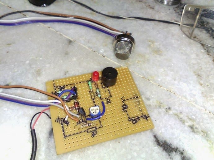
Adding Feedback in IC 555 Inverter
You might have already gone through the post which explains how to build simple 555 based inverters.
Although all these inverters are decently designed and will produce the intended 220 V or 120 V from an easy IC 555 set up, these do not have a built-in feedback system for ensuring a constant output voltage.
The following figure shows how an ordinary IC 555 inverter could be transformed into an enhanced inverter through an easy feedback loop control network.
In this circuit also, we find that the 220V output from the transformer is first rectified to a DC level, and then it is stepped down through a resistive network comprising of a 220K resistor and a 10k preset.
The 10k preset center lead is configured with the NPN transistor BC547, whose collector can be seen connected with the pin#5 of the IC which is control input of the IC.
We know that normally when pin#5 is open, the PWM at the output pin#3 of the IC has a maximum PWM, however, as the potential at pin#5 is reduced, the output PWM also gets reduced proportionately.
Grounding the pin#5 causes the output PWM at pin#3 to become very narrow, with almost zero average voltage at this pinout.
In the IC 555 feedback circuit, when the output voltage tends to rise above the unsafe high voltage threshold, as per the setting of the 10k preset, the base of the BC547 slowly starts getting biased.
When this happens, the BC547 begins conducting and causes the pin#5 of the IC to get gradually grounded.
The grounding of the pin#5 of the IC causes the output PWM at pin#3 to get narrower, which in turns causes the output voltage to drop to the normal levels.
250 Watt Pure Sine Wave Inverter
The cost and quantity of parts necessary to develop the proposed 250 watt sine wave power inverter is actually much less compared to a noisy square wave switching-type inverter circuit.
Only an extra three or four tiny transistors, a some resistors and capacitors, a couple of pots and a small driver transformer are all the additional parts which are required.
A glance at the block diagram will be enough to indicate that the fundamental concept of this sine wave power inverter is extremely basic.
The block diagram matches one of the simple 80 meter CW transmitter circuit.
Essentially, it is only the frequency that is different ; 60 Hz instead of 3.5 MHz.
And producing 250 watts of sine wave ac actually becomes drastically easier with the 500,000 meters (60 Hz) as opposed to the 80 meters (3.5 MHz).
A complete circuit diagram of the 250 watt sine wave inverter is shown below.
The requirements are a sine wave oscillator, a buffer amplifier, and a power amplifier.
The Oscillator
The oscillator could be in fact of any variety, however your best option for sensible reasons can be one particular implementing RC combinations.
Actually an oscillator involving inductor-capacitor combination as for example in the Hartley or Colpitts oscillator circuits could be incorporated at 60 Hz.
However the difficulty of adjusting the frequency to be able to adapt it to 60 Hz happens to be greatly simplified by utilizing an oscillator which has its frequency implemented using an RC network.
The frequency now could be altered by simply adjusting a potentiometer.
Referring to the circuit diagram, here the 10K potentiometer in the oscillator stage permits us to adjust the frequency.
Do not forget that the oscillator stage will create a sine wave.
Several RC oscillator circuits are usually built to generate square waves while some others generate a sawtooth output.
We don 't want to employ these types, simply because we may end up with an inverter which is may be a low quality modified inverter.
The 3.9K potentiometer in the oscillator section is positioned to regulate the level of gain in the feed back loop.
Very high gain setting using this pot might lead to extreme distortion of the sine wave.
Setting the Frequency
How could you set the oscillator frequency to 60 Hz? You can use just about any common methods for computing, just like an audio frequency is measured .
You could possibly evaluate your oscillator's frequency with the mains utility line voltage frequency either by seeing Lissajous statistics with an oscilloscope or by listening to and setting the beat frequency to zero.
Or perhaps for those who have a digital frequency counter, that' the best option you can have, so use it to measure and set the frequency to 60 Hz.
Output Voltage
Besides getting the frequency correct , you should have the output voltage fairly close to the preferred range of 115 - 120 volts (or to 220V depending on the transformer).
As indicated in the circuit diagram the output voltage is dependent on the adjustment of t he 4 K potentiometer which can be seen situated between the oscillator and the buffer amplifier stages.
A simple way to measure and confirm the output volts is by using a standard DMM set to the AC 500 V range and then measure the output voltage while simultaneously adjusting the 4 K pot.
Transformers
In this stage the both the transformers are ordinary 60 Hz step down transformers.
The driver transformer, for instance is actually a tiny power transformer having about three filament windings.
One winding may be employed for the primary , and the remaining two in series might be used for creating the center tapped secondary.
A very common type center-tapped filament transformer could be very much appropriate for the output power transformer.
With a 12 volt battery supply, you might anticipate the power amplifier transistors to generate an ac voltage of around 7-9 volts peak value or 5 to 6.5 volts rms.
It means that a 12 volt center-tapped filament transformer rated at 115 volt secondary winding output must be pretty sufficient.
The dimensions or current rating of the filament transformer depends upon the total power output you would want to generate.
A 25 ampere, 12V transformer is going to be pretty enough for generating power outputs up to 200 to 250 watts.
Picking out the transistor type in the power amplifier stage also will be dependent mainly by simply how much output power you want to generate.
Waveforms
The true waveform that can be acquired from this 250 watt sine wave inverter is slightly different from a true sine wave.
As indicated in the above figure, each power transistor of this power inverter amplifier comes with an operating angle marginally lower than 180¦Ë , that is certainly, near to a Class C type working.
A little deviation in the biasing of the transistors might pull the amplifier back to genuine Class B, however because no noises can be seen developing, this further hard work to improve the bias doesn't appear to be useful.
1.5V, 3V, 6V Inverter Circuit
In this post we discuss a few miniature inverter circuits that can convert 1.5 V to 220 V or 3 V to 220 V or 6 V to 220 V.
All the designs employ a single PNP transistor and transformer, connected in the feedback mode for generating the oscillations.
1.5 V to 220 V Inverter Circuit
The mini inverter circuit demonstrated in the following figure can produce a highest AC output of 220 volts if it is powered through any battery between 1.5 V and 6 V battery.
It employs a TIP2955 power transistor forming a Hartley type oscillator with the transformer.
The center tapped 6.3 v winding of a small iron core transformer (T1) works like a center feedback type of coil for this oscillator.
With a 6 V battery (B1), the highest current drain is around 80 ma.
The 50k 10 watt wirewound potentiometer (R1) adjusts the no-load DC output between 2 V and 220 V volts.
In this inverter design if R1 is substituted by a 200 ohm 10 watt wirewound pot and R2 replaced with a 20 ohm, 1 watt resistor, battery B1 specifications could be minimized to 1.5 V., and then the circuit work like a 1.5 V to 220 V inverter circuit.
The maximum drain from the battery at 1.5 V supply will be roughly around 100 ma.
R1 will alter the DC output between 60 and 80 volts, in the absence of a load.
3 V to 220 V Inverter Circuit
The next 3 V to 220 V inverter circuit is designed to work in a blocking oscillator mode having an operating frequency set at around 400 Hz.
The transistor used can be any PNP power transistor.
The center tap transformer can be any standard step down transformer.
This transformer provides the feedback and the voltage boosting both together.
The connections of the two low voltage windings of T1 must be configured correctly with the transistor, otherwise the inverter may fail to work, and begin heating up.
The 50 K potentiometer is a wirewound variable resistor (R1) which must be appropriately set to get reliable oscillation and the maximum voltage output.
This 3 V to 220 V inverter circuit may draws around 70 ma from the 3 V battery (B1).
Class-D Sinewave Inverter Circuit
A sinewave inverter using class-D amplifier functions by converting a small sinewave input frequency into equivalent sine PWMs, which is finally processed by an H-bridge BJT driver for generating the mains sinewave AC output from a DC battery source.
What is Class-D Amplifier
The working principle of a class-D amplifier is actually simple yet extremely effective.
An input analogue signal such as an audio signal or a sinusoidal waveform from an oscillator is chopped into equivalent PWMs also called SPWM.
These sine equivalent PWMs or SPWMs is fed to a power BJT stage, where these are amplified with high current, and applied to the primary of a step up transformer.
The transformer finally transforms the sine equivalent SPWM into 220V or 120V sine wave AC, whose waveform is exactly in accordance with the input sine wave signal from the oscillator.
Advantages of Class-D Inverter
The main advantage of a class-D inverter is its high efficiency (almost 100%) at a reasonably low cost.
Class-D amplifiers are easy to build and set up, which enables the user to produce efficient, high power sine wave inverters quickly without many technical hassles.
Since the BJTs have to work with PWMs, it allows them to be cooler and more efficient, and this in turn allows them to work with smaller heatsinks.
A Practical Design
A practical class-D inverter circuit design can be witnessed in the following diagram:
The IC 74HC4066 can be replaced with IC 4066, in that case the separate 5V will not be required, and a common 12V can be used for the entire circuit.
The working of the pwm class-D inverter is fairly simple.
The sine wave signal is amplified by the op amp A1 stage to adequate levels for driving the electronic switches ES1---ES4.
The electronic switches ES1---ES4 open and close causing rectangular pulses to be generated across the bases of the transistors T1---T4 bridge alternately.
The PWM or the width of the pulses is modulated by the input sine signal resulting in a sine equivalent PWMs fed to the power transistors,and the transformer, ultimately producing the intended 220V or 120V sine-wave mains AC at the output of the transformer secondary.
The duty factor of a rectangular signal produced from the ES1---ES4 outputs is modulated by the amplitude of the amplified input sine wave signal, which causes an output switching SPWM signal proportional to the sine wave RMS.
Thus the on-time of the output pulse is in accordance with the instantaneous amplitude of the input sine signal.
The switching period interval of the on-time and the off -time together determines the frequency which will be constant.
Consequently, a uniformly dimensioned rectangular signal (square wave) is created in the absence of an input signal.
As a way to achieve fairly good sine wave at the output of the transformer, the frequency of the rectangular wave from ES1 should be at the very least two times as high as the highest frequency in the input sine signal.
Electronic Switches as amplifiers
The standard working of the PWM amplifier is implemented by the 4 electronic switches made around ES1---ES4. Supposing that the input of the op amp input at the zero level, causes the capacitor C7 to charge via R8, until the voltage across C7 attains the level that is sufficient to switch ON ES1.
ES1 now closes and begins discharging C7 until its level drops below the switch ON level of ES1. ES1 now switches OFF initiating the C7 charging again, and the cycle rapidly turns ON/OFF at a rate of 50 kHz, as determined by the values of C7 and R8.
Now, if we consider the presence of a sine wave at the input of the op amp, it effectively causes a forced variation on the charge cycle of C7, causing the ES1 output PWM switching to get modulated as per the rise and fall sequence of the sine wave signal.
The output rectangular waves from the ES1 now produces SPWM whose duty factor now varies in accordance with the input sine signal.
This results in a sine wave equivalent SPWM to be alternately switched across the T1---T4 bridge, which in turn switches the transformer primary to generate the required AC mains from the secondary wires of the transformer.
Since the secondary AC voltage is created in accordance with the primary SPWM switching, the resultant AC is a perfectly equivalent sine wave AC of the input sine signal.
Sine wave Oscillator
As discussed above, the class-D inverter amplifier will need a sine wave signal input from a sine wave geneartor circuit.
The following image shows a very simple single transistor sine wave generator circuit which can be effectively integrated with the PWM inverter.
The frequency of the above sine wave generator is around 250 Hz, but we will need this to be around 50 Hz, which can be changed by altering the values of C1---C3, and R3, R4 appropriately.
Once, the frequency is set, the output of this circuit could be linked with the C1, C2 input of the inverter board.
PCB Design and Transformer Wiring
Parts List
Transformer: 0-9V/220V current, will depend on the transistors wattage and battery Ah rating
Specifications:
The proposed class-D PWM inverter is a small 10 watt test sample prototype.
The 10 watt low output is due to the use of low power transistor for T1---T4.
The power output can be easily upgraded to 100 watts by replacing the transistors with TIP147/TIP142 complementary pairs.
It can increased to even higher levels by using higher BUS DC line for the transistors, anywhere between 12V and 24V
Simple Online UPS Circuit
In this post we learn about the making of a simple online uninterruptible power supply (UPS) which guarantees a seamless transfer of AC mains supply to inverter mains supply for the load, due to the absence of cumbersome transfer switches or relays.
What is an Online UPS
As the name suggests, an online UPS system stays continuously online, and never goes offline even for a split second, since the battery supply to the UPS inverter is held continuously connected, regardless of the mains AC situation.
During the period the mains AC input is available, it is first converted to DC and stepped down to the battery level.
This DC charges the battery and also takes precedence over the battery to simultaneously power the inverter due to its higher power rating than the battery.
The inverter converts this DC back to the mains AC for powering the connected load.
In an event that AC mains fails, the stepped down AC to DC supply gets cut off, and the battery being continuously connected in line, now begins powering the inverter seamlessly, without any interruption of power to the load.
Online UPS vs Offline UPS
The main difference between an online UPS and an offline UPS is that, unlike offline UPS, the online UPS does not depend of mechanical changeover relays or transfer switches for transiting from AC mains to inverter mains AC during an AC mains failure (as shown below).
On the other hand, Offline UPS systems as shown in the below block diagram, rely on mechanical relays for transferring the UPS to the inverter mode, during the absence of mains AC supply.
In these systems when mains AC is available the supply is directly supplied to the load via a set of relay contacts, and the battery is held in the charging mode through another set of relay contacts.
As soon as AC mains fails, the relevant relay contacts deactivate and switch the battery from the charging mode to inverter mode, and the load from grid AC to inverter AC.
This implies that the transfer process tends to involve a slight delay, albeit in milliseconds while changing over from the grid mains to the inverter main.
This delay though small could be critical for sensitive electronic equipment such as computers or micro-controller based systems.
Therefore the online UPS system seems to be more efficient than an offline UPS in terms of speed and smoothness, during the changeover process from grid AC to inverter AC for all types of appliances.
Designing a Simple Online UPS/Inverter Circuit
As discussed in th above sections, making a simple online UPS actually looks quite easy.
We will ignore the EMI filter for simplicity sake and also because the inverter in our design will be a low frequency (50 Hz) iron-core transformer based inverter, and the SMPS would already include built in EMI filters for the necessary rectifications.
We will need the following materials for the basic online UPS design:
A ready made Mains AC to DC 14 V 5 Amp SMPS module.
A battery over charge cut-off system with constant current charger circuitry.
A battery over discharge cut-off circuit stage.
A battery 12 V / 7Ah
Any simple Inverter circuit from this website.
Circuit Diagrams and Stages
The various circuit stages for the proposed online UPS circuit can be learned from the following details:
1) Battery Cut-off Circuits: The circuit below shows the very important battery over-charge cut off circuit, built around a couple of op amp stages.
The left side op amp stage is configured to control the over charging of the battery.
The pin#3 of the op amp is connected with the battery positive for sensing its voltage level.
When this battery voltage at pin#3 exceeds the corresponding pin#2 zener value, the op amp output pin#6 turns high.
This activates the relay via the BC547 driver transistor causing the relay contacts to shift from the N/C to N/O, which cuts off the charging supply to the battery, preventing over charging of the battery.
The feedback hysteresis resistor across pin#6 and pin#3 of the left op amp causes the relay to latch for certain period of time, until the battery voltage drops to a level below the holding threshold of the hysteresis, which causes the pin#3 to go low, and correspondingly pin#6 also goes low, switching off the relay.
The relay contacts now switches back to the N/C, restoring the charging supply to the battery.
Over Discharge Cut OFF Circuit
The right side op amp controls the over discharge limit of the battery or the low battery situation.
As long as the pin#3 voltage of this op amp stays above the pin#2 reference level (as set by the pin#3 preset), the op amp output continues to be high.
This high output at pin#6 enables the attached MOSFET to remain in the conduction mode, which allows the inverter to be switched ON through the negative line.
In an even that the battery is over-drained by the inverter load, the op amp pin#3 level drops below the pin#2 reference voltage, causing pin#6 of the IC to go low, which cuts off the MOSFET and the inverter.
Current Control Stage
The BJT associated with the MOSFET forms a current control circuit for the online UPS, which allows the battery to be charged through a constant current level.
R2 must be calculated to set the maximum current control level for the battery and the inverter.
It may be implemented using the following formula:
R2 = 0.7 / Max Current
2) Inverter Circuit: The inverter circuit for online UPS system, which needs to be connected with the above battery controller circuit is shown below.
We have selected an IC 555 based circuit for simplicity sake and also for ensuring adequate power output range.
This inverter will remain online as long as the charger circuit and the battery remains functional, and the grid AC mains is fed appropriately to the system via a AC to DC SMPS circuit rated at 14V, 5 amp, or as per the particular power rating of the system, which is fully customizable.
The BJT feedback across the gates of the inverter MOSFETs ensures that the output voltage of the inverter never exceeds above the safe level, and is fed in a controlled manner.
This conclude our simple online UPS circuit design, which ensures a continuous uninterruptible online power to any AC load, which needs to be functional without any interruption regardless of the input AC availability.
Easy H-Bridge MOSFET Driver Module for Inverters and Motors
If you are wondering if there's an easy way to implement an H-bridge driver circuit without using the complex bootstrapping stage, the following idea will precisely solve your query.
In this article we learn how to build an universal full-bridge or H-bridge MOSFET driver circuit, using P-channel and N-channel MOSFETs, which can be used for making high efficiency driver circuits for motors, inverters, and many different power converters.
The idea exclusively gets rid of the standard 4 N-channel H-bridge driver topology, which imperatively depends on the complex bootstrapping network.
Advantages and Disadvantages of Standard N-Channel Full Bridge Design
We know that full bridge MOSFET drivers are best achieved by incorporating N-channel MOSFETs for all the 4 devices in the system.
The main advantage being the high degree of efficiency provided by these systems in terms of power transfer, and heat dissipation.
This is due to the fact that N-channel MOSFETs are specified with minimal RDSon resistance across their drain source terminals, ensuring minimum resistance to current, enabling smaller heat dissipation and smaller heatsinks on the devices.
However, implementing the above is not easy, since all the 4 channel devices cannot conduct and operate the central load without having a diode/capacitor bootstrapping network attached with the design.
Bootstrapping network requires some calculations, and tricky placement of the components to ensure that the systems works correctly.
This appears to be the main disadvantage of a 4 channel MOSFET based H-bridge topology, that common users find difficult to configure and implement.
An Alternative Approach
An alternative approach to making an easy and universal H-bridge driver module that promises high efficiency and yet gets rid of the complex bootstrapping is by eliminating the two high side N-channel MOSFETs, and replacing them P-channel counterparts.
One may wonder, if it's so easy and effective then why is it not a standard recommended design? The answer is, although the approach looks simpler there are a few downsides which may cause lower efficiency in this type of full bridge configuration using P and N channel MOSFET combo.
Firstly, the P-channel MOSFETs usually higher RDSon resistance rating compared to N-channel MOSFETs, which may result in uneven heat dissipation on the devices and unpredictable output results.
Second danger may be a shoot-through phenomenon, which can cause an instant damage to the devices.
That said, it is much easier to take care of the above two hurdles than designing a dicey bootstrapping circuit.
The two above issues can be eliminated by:
Selecting P-channels MOSFETs with lowest RDSon specifications, which may be almost equal to the RDSon rating of the complementary N-channel devices.
For example in our proposed design, you can find IRF4905 being used for the P-channel MOSFETs, which are rated with an impressively low RDSon resistance of 0.02 Ohms.
Countering the shoot-through by adding appropriate buffer stages, and by using oscillator signal from a reliable digital source.
An Easy Universal H-Bridge MOSFET Driver
The following image shows the P-channel/N-channel based universal H-bridge MOSFET driver circuit, which seems to be designed to provide maximum efficiency with minimum risks.
How it Works
The working of the above H-bridge design is pretty much basic.
The idea is best suited for inverter applications for efficiently converting a low power DC to mains level AC.
The 12V supply is acquired from any desired power source, such as from a battery or solar panel for an inverter application.
The supply is conditioned appropriately using the 4700 uF filter capacitor and through the 22 ohm current limiting resistor and a 12V zener for added stabilization.
The stabilized DC is used for powering the oscillator circuit, ensuring that its working is not affected by the switching transients from the inverter.
The alternate clock output from the oscillator are fed to the bases of the Q1, Q2 BJTs which are standard small signal BC547 transistor positioned as buffer/inverter stages for driving the main MOSFET stage with precision.
By default, the BC547 transistors are in the switched ON condition, through their respective base resistive divider potentials.
This means that the in the idle condition, without the oscillator signals, the P-channel MOSFETs are always switched ON, while the N-channel MOSFETs are always switched OFF.
In this situation, the load at the center, which is a transformer primary winding gets no power and remains switched OFF.
When clock signals are fed to the indicated points, the negative signals from the clock pulses actually ground the base voltage of the BC547 transistors via the 100 uF capacitor.
This happens alternately, causing the N-channel MOSFET from one of the arms of the H-bridge to turn ON.
Now, since the P-channel MOSFET on the other arm of the bridge is already switched ON, enables one P-channel MOSFET and one N-channel MOSFET across the diagonal sides to get switched ON simultaneously, causing the supply voltage to flow across these MOSFETs and the primary of the transformer in one direction.
For the second alternate clock signal, the same action repeats, but for the other diagonal arm of the bridge causing the supply to flow through the transformer primary in the other direction.
The switching pattern is exactly similar to any standard H-bridge, as depicted in the following figure:
This flip-flop switching of the P and N channel MOSFETs across the left/right diagonal arms keep repeating in response to the alternate clock signal inputs from the oscillator stage.
As a result, the transformer primary is also switched in the same pattern causing a square wave AC 12V to flow across its primary, which is in correspondingly converted into 220 V or 120 V AC square wave across the secondary of the transformer.
The frequency is dependent on the frequency of the oscillator signal input which can be 50 Hz for 220 V output and 60 Hz for 120 V AC output,
Which Oscillator Circuit can be Used
The oscillator signal can be from any digital IC based design, such as from the IC 4047, SG3525, TL494, IC 4017/555, IC 4013 etc.
Even transistorized astable circuit can be used effectively for the oscillator circuit.
The following oscillator circuit example can be ideally used with the above discussed full bridge module.
The oscillator has a fixed at 50 Hz output, through a crystal transducer.
The ground pin of IC2 is mistakenly not shown in the diagram.
Please connect pin#8 of the IC2 with pin#8,12 line of IC1, to ensure that IC2 gets the ground potential.
This ground must be also joined with the ground line of the H-bridge module.
50 Watt Sine Wave UPS Circuit
The UPS detailed in this article can provide a power output of 50 watts consistently, at 110 volts with a frequency of 60 Hz.
The output is fundamentally a sine wave that behaves exactly like standard mains home AC power for the load.
An integrated power supply works like a battery charger.
Even though the UPS could be implemented for numerous different applications, it is mainly designed to power a small computer system and important peripheral, like a disk drive, to ensure that a power outages never causes deletion of data or interruption of the program that may be running at the instant.
This implies that this lead acid powered 50 watt UPS circuit is not going to handle bigger PCs, that usually work with over 60 watts of actual power.
One important feature of this UPS circuit is that it outputs a "clean" sinewave AC power: and flaws like noise, spikes, or low voltage within the grid AC line will never have an affect on the computer's (loads's) functioning.
Power Supply Relay Changeover Stage
The power supply stage is quite distinctive because it takes in power through a remote 12 volt lead acid or SMF battery and also from your AC power line, the battery here becomes the most crucial element for the UPS functioning.
As revealed in Fig.
1 below, when CHARGE-OFF-OPERATE switch S1 is positioned to either the CHARGE or OPERATE setting, relay RY2 is activated and its contacts provide AC power to the primary windings of the power transformers T1 and T2.
The current through the secondary windings is rectified through diodes D1, D2, D3, and D4.
Chokes L1 and L2 restrict the charging current for the battery as well as prohibit the passage of the ripple current.
Diode D5 delivers "crowbar" overload protection; its function is to safeguard the many vulnerable components by triggering fuse F1 to burn out in case the battery is accidentally hooked up with an incorrect polarity.
Op amp IC1 is connected in the form of an inverting voltage comparator whose reference voltage could be adjusted across a range of 11 to 14 volts through potentiometer R3.
Once the battery voltage falls beneath the reference, opto coupler IC2 is activated, that powers relay RY1. Current passing through RY1's contacts begins charging the battery when the load is not too heavy.
On other hand if the UPS is working at or close to its 100 % potential, an external battery charger may be needed to provide adequate current supply, to prevent the battery from getting discharged.
A 10 ampere battery charger is advisable.
Given that the majority of battery chargers donˇŻt have a filtration system, a high value filter capacitor must be included between the charger output and the battery to minimize ripple current.
In order to prevent battery overcharging, the supply from the charger must be switched on only when the UPS is being loaded at its 100 % capacity.
Fuse F2 must be less than 10 amps in order that the primary fuse, F1, may not whack when the 12 volt output is unintentionally shorted.
The Transistor Amplifier Stage
As presented in Fig.
2 below, the UPS AC output is generated from a transformer-coupled Class B amplifier circuit.
The 4 sets of Darlington transistors (Q4-Q8, Q5-Q9, Q6-Q10 and Q7-Q11) work llike emitter-follower networks to deliver voltage to the power transformers T5 and T6 primary windings.
Capacitor C8 cancels out any high frequency ingredients which originate due to high voltage crossover distortion or clipping, and in addition inhibits high frequency self oscillation.
Two of the Darlington sets are powered in parallel through transformer T3; another couple are pushed in parallel by means of T4.
Diodes D11, D12, D13, and D14 produce a constant DC base voltage which biases the output transistors at around the cutoff region.
The Class A driver network formed by the transistors Q2 and Q3, are similarly fully made up of emitter followers.
The essential voltage step-up is implemented by the transformers T3 and T4, which are also typical power transformers configured in the reverse order.
Transistor Q1 drives transistors Q2 and Q3 in parallel.
The Q1 base is directly connected to the IC5-d output (see Fig.
3), which is at 4.5 volts DC.
Reversal of Phase for push-pull drive of the output stage is achieved by appropriately wiring the secondaries of transformer T3 and T4 transformers.
The Sinewave Generator
As revealed in Fig.
3 below, the oscillator stage is configured using IC4, which is a 567 tone detector.
The IC's frequency is set up by resistors R26 and R27, and capacitor C14, and is fixed to a precise 60 Hz.
IC4's square wave output is transformed to a triangle wave by IC5-b, which is further on converted to a sinewave by IC5-c.
Op amp IC5-d's gain is set by potentiometer R35, that is fixed at the AC output voltage.
Op amp IC5-a converts the sinewave from the T2 output to a 60 Hz frequency.
D15 safeguards against damage that may take place in case the op amp inverting input happens to turn negative with reference to ground; the diode is generally reverse biased.
The 60 Hz pulses, that are connected to IC4 via C12 and D16, trigger the oscillator to lock to the grid AC frequency.
Some extent of control on the precise phase synchronization is achievable by fine-tuning potentiometer R20.
Once correctly tweaked, the AC output is going to lock in-phase with the input AC grid line, and this locking/unlocking process during the input power failure and restoration would be soft and favorable, producing almost no interference.
The sine wave generator comes with smooth, ripple-free 9 volt power through IC3, a 7805 IC, 5 V regulator.
Pin 3 of the regulator is kept at 4 volts above ground line with the help of resistive divider R16 and R17 to get a precise 9 volts output.
The Meter Circuit
It may be possible to monitor either the battery voltage or the AC output voltage through a meter circuit as exhibited in Fig.
4 below.
A bridge rectifier consisting of four rectifier diodes converts the AC to DC, while the capacitor C19 smooths to a pure DC.
A DPDT switch hooks up a 15 V DC voltmeter with the 12 V supply or the voltage divider built using resistive divider of R36 and R37.
How to Test the Power Supply Changeover
It may be important to test the power supply section before the amplifier is wired up.
This can be carried out before even the amplifier stage is assembled.
For this you can adjust the R3's slider arm towards the end which is linked to R4.
Do not connect the mains-cord into an electrical outlet yet.
Attach a 12 V lead acid battery to the supply and position S1 to either CHARGE or OPERATE.
Now, the relay RY2 could be seen activated and LED1 illuminated.
At this point you may find around 12 V at pins 2 and 7 of IC1.
Pin 6 should show logic low.
Next, connect the mains cord into an AC outlet.
Lamp LMP1 will now light up.
Relay RY1 should continue to be switched OFF and you would test approximately 14 V at its normally open contacts.
Pin 7 of IC1 should indicate around 14 V and pin 3 around 11 volts.
Pin 6 should indicate a logic low.
Turn R3 to its reverse end to get 14 V at pin 3; RY1 at this moment must activate with LED1 shutting OFF.
The voltage across the battery points should now read 13 V.
Adjust R3 just around the level at which relay RY1 deactivates.
The charger stage must keep switching off and on as the battery voltage goes up and reduces.
The accurate setting of R3 may be at the point, where the charger output switches quite rapidly, and switches off practically the moment it switches on.
The battery voltage should be around at 12.5 V mark in the absence of a charging supply.
When the battery voltage drops, the charger output must begin switching repeatedly unless of course the battery is so terribly discharged that the full current of the charger is not able to restore the voltage back up to 12.5.
Testing the Sine wave Generator
The testing of the sine wave generator stage can be executed separately.
In case you assemble it on the shown PCB without the 9 V regulator IC, then you can use a 9 V PP3 battery or an external equivalent power source for the testing procedure.
Begin by positioning preset R20's slider arm to its ground side.
Using an oscilloscope scope should display a square wave signal at pin 5 of IC4.
By supplying a 60 Hz sinewave frequency to the scope's horizontal sweep, adjust resistor R27 to get a frequency of 60 Hz that will generate a rectangular Lissajous waveform.
The frequency does not have to be precisely accurate.
A gradually altering waveform pattern can be quite satisfactory.
Having the scope set for a standard 60 Hz sweep, make sure the scope indicates a triangle wave on the output of IC5-b and a sinewave at the output of IC5-c.
A sine wave must also be available at the IC5-d output.
And its amplitude should vary in response to the adjustment of R35. In case any of these checks tend to be incorrect, examine the presence of a 4.5 volts DC across all the input and output pins.
Next, connect a 12.6 V AC source to R21, and adjust the R20 until the you find the scope showing the output pulses from IC5-a: The oscillator freqeuncy must lock to the input line frequency.
Now set the scope to display a Lissajous curve as done previously and monitor the IC5-d output.
You must see an oval pattern which is almost closed.
You must be able to possibly fine-tune R20 such that the scope display is almost a sloping straight line, showing that the output signal is in-phase with the grid-line.
Now, if you disconnect the input AC signal by unplugging the mains-cord, the scope pattern must start producing a gradual change to an oval shape display which opens and closes.
Re-allign the potentiometer R27 to reduce the above rate of change.
As soon as the input AC frequency is reconnected back, the scope display must instantly come back to the sloping line pattern.
Testing the Meter Circuit
The testing and calibration of the meter circuit could be implemented by attaching the rectifier to the grid AC line.
Pushing S2 in the AC position, fine-tune R37 to get a meter reading that may be 1/10th of the AC input voltage as measured separately through an standard meter reading.
If you find no measurement appearing, look for around 130 volts DC around C19 to ensure that the rectifier is correctly joined.
A scope here should display a big ripple element due to the low uF value of the C19 capacitor.
Testing the Amplifier
Begin the test by integrating the power transistor amplifier stage with the 12 V power source and the input sinewave waveform generator.
Adjust the R35 center arm towards end associated with the output side of IC5-d, which decides the setting for a zero output signal.
Now shift the S1 to the "OPERATE" position.
You should see a meter reading of 12.5 V at the emitters of Q2, Q3, Q8, Q9, Q10, and Q11.
You may also find these transistors getting a bit warmer, although not hot.
You should be able to see a meter reading of around 11 V at the bases of Q4, Q5, Q6, and Q7, and around 4 V at the Q1 emitter.
While conducting the following testing procedures, be careful while working with the output, since this would be at a lethal mains 117 V level.
Hook up one wire of each of the 120 V windings of the transformer T5 and T6 with each other, leaving the others remain unconnected.
Connect an AC voltmeter with one of the transformer windings and set the meter to a range greater than 110 volts.
After this, little by little turn R35 preset center arm until you see a measurable output voltage.
If you don't find this happening, ensure that phase drive into the output stages are reversed.
The AC voltage from the Q4 or Q6 base to the Q5 or Q7 base must be double the reading to ground.
If you don't see this, try swapping the winding connections of either transformer T3 or T4, but not both.
Next, ensure that the 120 V windings of transformer T5 and T6 are perfectly in-phase and thus connected in the appropriate manner.
Attach the voltmeter across the leads which were left unconnected.
If you find the voltage is two times more than the earlier reading, then the windings are surely connected in series.
Quickly reverse the connection of one of the windings.
If you fail to see any voltage reading on the meter, connect the other two leads with each other.
Link up a 15 W lamp at the output, and set up preset R35 to get a full output.
The lamp must illuminate with optimum brightness and the meter should indicate around 125 volts AC.
How to Use the UPS
While implementing the proposed 50 watt UPS circuit, make sure to set S1 at "OPERATE" before switching ON the load.
Verify the AC output from the UPS to make certain that it is producing a minimum of 120 volts.
This 120 V voltage might decrease a bit as soon as the output is loaded.
If you find the voltage is unstable, it would mean that the oscillator hasn't locked and synchronized with the mains grid power line.
To correct this try readjusting the presets R27 and R20 after sometime, once the circuit has warmed up a bit.
When you tweak the R27/R20 presets appropriately, you will find the oscillator locking with the AC mains frequency during each switch ON periods.
Now, switch ON the system and reconfirm the output voltage conditions.
The output voltage may drop to 110 volts while it is being operated in discontinuous load, say for example a disk drive or a printer, and this may be acceptable.
The back up time from the UPS during a mains outage would depend on the Ah rating of the battery.
When a motorcycle battery is used, it should provide approximately 15 minutes of back up operational time.
Pars List
The complete parts ;list for the above explained 50 watt sinewave UPS circuit is presented in the following image:
How to Construct the L1, L2 filter chokes
If you are unable to obtain the suggested L1, L2 chokes from your part dealer, you can construct the same using the following configuration
Use 1 mm super enameled wire for the coils
500 Watt Inverter Circuit with Battery Charger
In this post we will comprehensively discuss how to build a 500 watt inverter circuit with an integrated automatic battery charger stage.
Further in the article we will also learn how to upgrade the system for higher loads and how to enhance ot into a pure sine wave version.
This 500 watt power inverter will convert a 12 V DC or 24 V DC from a lead acid battery to 220 V or 120 V AC, which can be used for powering all types of loads, right from CFL lights, LED bulbs, fans, heaters, motors, pumps, mixers, computer, and so on.
Basic Design
An inverter can be designed in many different ways, simply by replacing the oscillator stage with another type of oscillator stage, as per user preference.
The oscillator stage is basically an astable multivibrator which could be using ICs or transistors.
Although an astable based oscillator can be designed in various ways, we will use the IC 4047 option here since it is a versatile, accurate and a specialized astable chip designed specifically for applications like inverers.
Using IC 4047
Making any inverter using the IC 4047 is probably the most recommended option due to high accuracy and readability of the IC.
The device is a versatile oscillator IC which provides a dual push pull or flip flop output across its pin10 and pin11, and also a single square wave output at pin13.
BASIC CIRCUIT
A basic 500 watt inverter with a square wave output can be as simple as above to build.
However, to upgrade it with a battery charger we may have to employ a charger transformer rated appropriately as per the battery specifications.
Before learning the charger configuration let's first get acquainted with the battery specification required for this project.
From one of our previous post we know that the more appropriate charging and discharging rate of a lead acid battery should be at 0.1C rate or at a supply current that's 10 time less than the battery Ah rating.
This implies that to get a minimum of 7 hours back up at 500 watt load, the battery Ah could be calculated in the following manner
Operational current required for a 500 watt load from a 12V battery will be 500 / 12 = 41 Amps approximately
This 41 amps needs to last for 7 hours, implies that the battery Ah must be = 41 x 7 = 287 Ah.
However, in real life this will will need to be at least 350 Ah.
For a 24 V battery this may come down to 50% less at 200 Ah.
This is exactly why a higher operational voltage is always advised as the wattage rating of the inverter gets on the higher side.
Using 24 V Battery
In order to keep the battery and the transformer size smaller and cables thinner, you may want to use a 24 V battery for operainf the proposed 500 watt design.
The basic design would remain as is, except a 7812 IC added to the IC 4047 circuit, as shown below:
Schematic Diagram
Battery Charger
To keep the design simple yet effective, I have avoided the use an automatic cut off for the battery charger here, and have also ensured a single common transformer is used for the inverter and the charger operations.
The complete circuit diagram for the proposed 500 watt inverter with battery charger can be seen below:
The same concept has been already elaborately discussed in one of the other related posts, which you can refer to for additional information.
Basically, the inverter uses the same transformer for charging the battery and for converting the battery power to 220 V AC output.
The operation is implemented through a relay changeover network, that alternately changes the transformer winding to charging mode and inverter mode.
How it Works
When grid mains AC is not available, the relay contacts are positioned at their respective N/C points (normally closed).
This connects the drains of the MOSFETs with the transformer primary, and the appliances or the load connect with the secondary of the transformer.
The unit gets into inverter mode and begins generating the required 220V AC or 120 V AC from the battery.
The relay coils are powered from a simple crude transformerless (capacitive) power supply circuit using a 2uF / 400V dropping capacitor.
The supply is not required to be stabilized or well regulated because the load is in the form of the relay coils which are quite heavy duty and will easily withstand the switch ON surge from the 2uF capacitor.
The coil for RL1 relay which controls the mains AC side of the transformer can be seen connected before a blocking diode, while the coil of RL2 which controls the MOSFET side is positioned after the diode and in parallel to a large capacitor.
This is intentionally done to create a small delay effect for RL2, or to ensure RL1 switches ON and OFF prior to RL2. This is for safety concerns, and to ensure that the MOSFETs are never subjected to the reverse charging supply whenever the relay moves from inverter mode to charging mode.
Safety Suggestions
As we know, in any inverter circuit the transformer works like an heavy inductive load.
When such a heavy inductive load is switched with a frequency, it's bound to generate a massive amount current spikes which may be potentially dangerous for the sensitive electronics and the involved ICs.
To ensure proper safety to the electronic stage, it may be important to modify the 7812 section in the following manner:
For a 12V application, you can reduce the above spike protection circuit to the following version:
Battery, MOSFET and Transformer Determine the Wattage
We have discussed this many times through different posts that it is the transformer, the battery, and the MOSFET ratings that actually decide how much power an inverter can produce.
We have already talked about the battery calculations in the previous paragraphs, now let's see how the transformer can be calculated for complementing the required power output.
It is actually very simple.
Since the voltage is supposed to be 24 V, and power 500 watts, dividing 500 with 24 gives 20.83 amps.
Meaning the transformer amp rating must be above 21 amps, preferably up to 25 amps.
However, since we are using the same transformer for both charging and inverter modes, we have to select the voltage in such a way that it suits both the operations optimally.
A 20-0-20 V for the primary side appears to be a good compromise, in fact it is the ideally suited rating for the overall working of the inverter across both the modes.
Since, only one half winding is used for charging the battery, the 20 V RMS rating of the transformer can be used for getting a 20 x 1.41 = 28.2 V peak Dc across the battery with the help of the associated filter capacitor connected across the battery terminals.
This voltage will charge the battery at good rate and at the correct speed.
In the inverter mode, when the battery is at around 26 V, will allow the inverter output to be at 24/26 = 220 / Out
Out = 238 V
This looks a healthy output while th battery is optimally charged, and even when the battery drops to 23 V, the output can be expected to sustain a healthy 210V
Calculating MOSFET: MOSFETs basically work like switches that must not burn while switching rated amount of current, and also must not heat up due to increased resistance to switching currents.
To satisfy the above aspects, we have to make sure that the current handling capacity or the ID spec of the MOSFET is well over 25 amps for our 500 watt inverter.
Also to prevent high dissipation and inefficient switching the MOSFET's RDSon spec must be as low as possible.
The device shown in the diagram is IRF3205, which has an ID of 110 amp and RDSon of 8 milliohms (0.008 Ohms), which actually looks quite impressive and perfectly suitable for this inverter project.
Parts List
To make the above 500 watt inverter with battery charger, you will need the following bill of materials:
IC 4047 = 1
Resistors
56K = 1
10 ohms = 2
Capacitor 0.1uF = 1
Capacitor 4700uF / 50 V = 1 (across the battery terminals)
MOSFETs IRF3205 = 2
Diode 20 amp = 1
Heatsink for the MOSFETs = Large Finned Type
Blocking Diode Across MOSFETs Drain/Source = 1N5402 (Please connect them across drain/source of each MOSFET for added protection against reverse EMF from the transformer primary.
Cathode will go to the drain pin.
Relay DPDT 40 amp = 2 nos
Upgrading to Modified Sinewave Inverter
The square wave version discussed above can be effectively converted into a modified sinewave 500 watt inverter circuit with much improved output waveform.
For this we use the age old IC 555 and IC 741 combination for manufacturing the intended sine waveform.
The complete circuit with battery charger is given below:
The idea is the same which has been applied in a few of the other sinewave inverter designs in this website.
It is to chop the gate of the power MOSFETs with calculated SPWM so that a replicated high current SPWM is oscillated across the push pull winding of the transformer primary.
The IC 741 is used as a comparator which compares two triangle waves across its two inputs.
The slow base triangle wave is acquired from the IC 4047 Ct pin, while the fast triangle wave is derived from an external IC 555 astable stage.
The result is a calculated SPWM at pin6 of the IC 741. This SPWM is chopped at the gates of the power MOSFETs which is switching by the transformer at the same SPWM frequency.
This results in the secondary side with a pure sinewave output (after some filtration).
Full Bridge Design
The full bridge version for the above concept ca be built using the below given configuration:
For sake simplicity, an automatic battery cut off is not included, so it is recommend to switched OFF the supply as soon as the battery voltage reaches the full charge level.
Or alternatively you may add an appropriately filament bulb in series with the charging positive line of the battery, to ensure a safe charging for the battery.
If you have questions or doubts regarding the above concept, the comment box below is all yours.
How to Calculate Ferrite Core Transformers
Calculating ferrite transformer is a process in which engineers evaluate the various winding specifications, and core dimension of the transformer, using ferrite as the core material.
This helps them to create a perfectly optimized transformer for a given application.
The post presents a detailed explanation regarding how to calculate and design customized ferrite core transformers.
The content is easy to understand, and can be very handy for engineers engaged in the field of power electronics, and manufacturing SMPS inverters.
Why Ferrite Core is used in High Frequency Converters
You might have often wondered the reason behind using ferrite cores in all modern switch mode power supplies or SMPS converters.
Right, it is to achieve higher efficiency and compactness compared to iron core power supplies, but it would be interesting to know how ferrite cores allow us to achieve this high degree of efficiency and compactness?
It is because in iron core transformers, the iron material has much inferior magnetic permeability than ferrite material.
In contrast, ferrite cores possess very high magnetic permeability.
Meaning, when subjected to a magnetic field, ferrite material is able to achieve a very high degree of magnetization, better than all other forms of magnetic material.
A higher magnetic permeability means, lower amount of eddy current and lower switching losses.
A magnetic material normally has a tendency to generate eddy current in response to a rising magnetic frequency.
As the frequency is increased, eddy current also increases causing heating of the material and increase in coil impedance, which leads to further switching losses.
Ferrite cores, due to to their high magnetic permeability are able to work more efficiently with higher frequencies, due to lower eddy currents and lower switching losses.
Now you may think, why not use lower frequency as that would conversely help to reduce eddy currents? It appears valid, however, lower frequency would also mean increasing the number of turns for the same transformer.
Since higher frequencies allow proportionately lower number of turns, results in transformer being smaller, lighter and cheaper.
This is why SMPS uses a high frequency.
Inverter Topology
In switch mode inverters, normally two types of topology exits: push-pull, and Full bridge.
The push pull employs a center tap for the primary winding, while the full bridge consists a single winding for both primary and secondary.
Actually, both the topology are push-pull in nature.
In both the forms the winding is applied with a continuously switching reverse-forward alternating current by the MOSFETs, oscillating at the specified high frequency, imitating a push-pull action.
The only fundamental difference between the two is, the primary side of the center tap transformer has 2 times more number of turns than the Full bridge transformer.
How to Calculate Ferrite Core Inverter Transformer
Calculating a ferrite core transformer is actually quite simple, if you have all the specified parameters in hand.
For simplicity, we'll try to solve the formula through an example set up, let's say for a 250 watt transformer.
The power source will be a 12 V battery.
The frequency for switching the transformer will be 50 kHz, a typical figure in most SMPS inverters.
We'll assume the output to be 310 V, which is normally the peak value of a 220V RMS.
Here,the 310 V will be after rectification through a fast recovery bridge rectifier, and LC filters.
We select the core as ETD39.
As we all know, when a 12 V battery is used, it's voltage is never constant.
At full charge the value is around 13 V, which keeps dropping as the inverter load consumes power, until finally the battery discharges to its lowest limit, which is typically 10.5 V.
So for our calculations we will consider 10.5 V as the supply value for Vin(min) .
Primary Turns
The standard formula for calculating the primary number of turns is given below:
N(prim) = Vin(nom) x 108 / 4 x f x Bmax x Ac
Here N(prim) refers to the primary turn numbers.
Since we have selected a center tap push pull topology in our example, the result obtained will be one-half of the total number of turns required.
Vin(nom)= Average Input Voltage.
Since our average battery voltage is 12V, let's, take Vin(nom)= 12.
f = 50 kHz, or 50,000 Hz.
It is the preferred switching frequency, as selected by us.
Bmax= Maximum flux density in Gauss.
In this example, we'll assume Bmaxto be in the range of 1300G to 2000G.
This is the standard value most ferrite based transformer cores.
In this example, letˇŻs settle at 1500G.
So we have Bmax= 1500. Higher values of Bmaxis not recommended as this may result in the transformer reaching saturation point.
Conversely, lower values of Bmaxmay result in the core being underutilized.
Ac= Effective Cross-Sectional Area in cm2.
This information can be collected from the datasheets of the ferrite cores.
You may also find Acbeing presented as Ae.
For the selected core number ETD39, the effective cross-sectional area furnished in the datasheet sheet is 125mm2.
That is equal to 1.25cm2.
Therefore we have, Ac= 1.25 for ETD39.
The above figures give us the values for all the parameters required for calcuating the primary turns of our SMPS inverter transformer.
Therefore, substituting the respective values in the above formula, we get:
N(prim) = Vin(nom) x 108 / 4 x f x Bmax x Ac
N(prim) = 12 x 108 / 4 x 50000 x 1500 x 1.2
N(prim)= 3.2
Since 3.2 is a fractional value and can be difficult to implement practically, we'll round it off to 3 turns.
However, before finalizing this value, we have to investigate whether or not the value of Bmax is still compatible and within the acceptable range for this new rounded off value 3.
Because, decreasing the number of turns will cause a proportionate increase in the Bmax, therefore it becomes imperative to check if the increased Bmax is still within acceptable range for our 3 primary turns.
Counter checking Bmax by substituting the following existing values we get:
Vin(nom)= 12, f = 50000, Npri= 3, Ac= 1.25
Bmax = Vin(nom) x 108 / 4 x f x N(prim) x Ac
Bmax = 12 x 108 / 4 x 50000 x 3 x 1.25
Bmax= 1600
As can be seen the new Bmax value for N(pri) = 3 turns looks fine and is well within the acceptable range.
This also implies that, if anytime you feel like manipulating the number of N(prim) turns, you must make sure it complies with the corresponding new Bmax value.
Oppositely, it may be possible to first determine the Bmax for a desired number of primary turns and then adjust the number of turns to this value by suitably modifying the other variables in the formula.
Secondary Turns
Now we know how to calculate the primary side of an ferrite SMPS inverter transformer, it's time to look into the other side, that is the secondary of the transformer.
Since the peak value has to be 310 V for the secondary, we would want the value to sustain for the entire battery voltage range starting from 13 V to 10.5 V.
No doubt we will have to employ a feedback system for maintaining a constant output voltage level, for countering low battery voltage or rising load current variations.
But for this there has to be some upper margin or headroom for facilitating this automatic control.
A +20 V margin looks good enough, therefore we select the maximum output peak voltage as 310 + 20 = 330 V.
This also means that the transformer must be designed to output 310 V at the lowest 10.5 battery voltage.
For feedback control we normally employ a self adjusting PWM circuit, which widens the pulse width during low battery or high load, and narrows it proportionately during no load or optimal battery conditions.
This means, at low battery conditions the PWM must auto adjust to maximum duty cycle, for maintaining the stipulated 310 V output.
This maximum PWM can be assumed to be 98% of the total duty cycle.
The 2% gap is left for the dead time.
Dead time is the zero voltage gap between each half cycle frequency, during which the MOSFETs or the specific power devices remain completely shut off.
This ensures guaranteed safety and prevents shoot through across the MOSFETs during the transition periods of the push pull cycles.
Hence, input supply will be minimum when the battery voltage reaches at its minimum level, that is when Vin = Vin(min) = 10.5 V.
This will prompt the duty cycle to be at its maximum 98%.
The above data can be used for calculating the average voltage (DC RMS) required for the primary side of the transformer to generate 310 V at the secondary, when battery is at the minimum 10.5 V.
For this we multiply 98% with 10.5, as shown below:
0.98 x 10.5 V = 10.29 V, this the voltage rating our transformer primary is supposed to have.
Now, we know the maximum secondary voltage which is 330 V, and we also know the primary voltage which is 10.29 V.
This allows us to get the ratio of the two sides as: 330 : 10.29 = 32.1.
Since the ratio of the voltage ratings is 32.1, the turn ratio should be also in the same format.
Meaning, x : 3 = 32.1, where x = secondary turns, 3 = primary turns.
Solving this we can quickly get the secondary number of turns
Therefore secondary turns is = 96.3.
The figure 96.3 is the number of secondary turns that we need for the proposed ferrite inverter transformer that we are designing.
As stated earlier since fractional vales are difficult to implement practically, we round it off to 96 turns.
This concludes our calculations and I hope all the readers here must have realized how to simply calculate a ferrite transformer for a specific SMPS inverter circuit.
Calculating Auxiliary Winding
An auxiliary winding is a supplemental winding that a user may require for some external implementation.
Let's say, along with the 330 V at the secondary, you need another winding for getting 33 V for an LED lamp.
We first calculate the secondary : auxiliary turn ratio with respect to the secondary winding 310 V rating.
The formula is:
NA= Vsec/ (Vaux+ Vd)
NA = secondary : auxiliary ratio, Vsec = Secondary regulated rectified voltage, Vaux = auxiliary voltage, Vd = Diode forward drop value for the rectifier diode.
Since we need a high speed diode here we will use a schottky rectifier with a Vd= 0.5V
Solving it gives us:
NA = 310 / (33 + 0.5) = 9.25, let's round it off to 9.
Now let's derive the number of turns required for the auxiliary winding, we get this by applying the formula:
Naux= Nsec/ NA
Where Naux= auxiliary turns, Nsec = secondary turns, NA = auxiliary ratio.
From our previous results we have Nsec= 96, and NA = 9, substituting these in the above formula we get:
Naux= 96/ 9 = 10.66, round it off gives us 11 turns.
So for getting 33 V we will need 11 turns on the secondary side.
So in this way you can dimension an auxiliary winding as per your own preference.
Wrapping up
In this post we learned how to calculate and design ferrite core based inverter transformers, using the following steps:
Calculate primary turns
Calculate secondary turns
Determine and Confirm Bmax
Determine the maximum secondary voltage for PWM feedback control
Find primary secondary turn ratio
Calculate secondary number of turns
Calculate auxiliary winding turns
Using the above mentioned formulas and calculations an interested user can easily design a customized ferrite core based inverter for SMPS application.
For questions and doubts please feel free to use the comment box below, I'll try to solve at an earliest
More Information can be found under this link:
How to Calculate Switching Power Supplies
How to Calculate Modified Sine Waveform
I am sure you might have often wondered how to accomplish the correct way of optimizing and calculating a modified square wave such that it produced almost an identical replication of a sine wave when used in an inverter application.
The calculations discussed in this article will help you to learn the technique through which a modified square wave circuit could be turned into sinewave equivalent.
Let's learn the procedures.
The first criterion to accomplish this is to match the RMS value of the modified square with the sinewave counterpart in a way that the result replicates the sinusoidal waveform as closely as possible.
What is RMS (Root Mean Square)
We know that the RMS of our home AC sinusoidal waveform voltage is determined by solving the following relationship:
Vpeak=ˇĚ2 Vrms
Where Vpeak is the maximum limit or the peak limit of the sine waveform cycle, while the mean magnitude of the each cycle of the waveform is shown as the Vrms
The ˇĚ2 in the formula helps us to find the mean value or the net value of an AC cycle which changes its voltage exponentially with time.
Because the sinusoidal voltage value varies with time and is a function of time, it cannot be calculated by employing the basic average formula, instead we depend on the above formula.
Alternatively, AC RMS could be understood as an equivalent to that value of a direct current (DC) which produces an identical average power dissipation when connected across aresistive load.
OK, so now we know the formula for calculating the RMS of a sinewave cycle with reference to its peak voltage value.
This can be applied for evaluating the peak and the RMS for our home 50 Hz AC too.
By solving this we get the RMS as 220V and peak as 310V for all 220V based mains AC systems.
Calculating Modified Square Wave RMS and Peak
Now let's see how this relationship could be applied in modified square wave inverters for setting up the right waveform cycles for a 220V system, which would correspond to a 220V AC sinusoidal equivalent.
We already know that the AC RMS is equivalent to the average power of a DC waveform.
Which gives us this simple expression:
Vpeak= Vrms
But we also want the peak of the square wave to be at 310V, so it seems the above equation won't hold good and cannot be used for the purpose.
The criteria is to have 310V peak as well as an RMS or average value of 220V for each square wave cycle.
To solve this correctly we take the help of the ON/OFF time of the square waves, or the duty cycle percentage as explained below:
Each half cycle of a 50 Hz AC waveform has a time duration of 10 millisecond (ms).
A modified half wave cycle in its most crude form must look like as shown in the following image:
We can see that the each cycle begins with a zero or blank gap, then shoots up to 310V peak pulse and again ends with a 0V gap, the process then repeats for other half cycle.
In order to achieve the required 220V RMS we have to calculate and optimize the peak and the zero gap sections or the ON/OFF periods of the cycle such that the average value produces the required 220V.
The grey line represents the 50% period of the cycle, which is 10 ms.
Now we need to find out the proportions of the ON/OFF time which will produce an average of 220V.
We do it in this way:
220 / 310 x 100 = 71 % approximately
This shows that the 310V peak in the above modified cycle should occupy 71% of the 10 ms period, while the two zero gaps should be 29% combined, or 14.5% each.
Therefore in a 10 ms length, the first zero section should be 1.4 ms, followed by the 310 V peak for 7 ms, and finally the last zero gap of another 1.4 ms.
Once this is accomplished we can expect the output from the inverter to produce a reasonably good replication of a sine waveform.
Despite of all these you may find that the output is not quite an ideal replication of the sine wave, because the discussed modified square wave is in its most basic form or a crude type.
If we want the output to match the sine wave with maximum precision, then we have to go for an SPWM approach.
I hope the above discussion might have enlightened you regarding how to calculate and optimize a modified square for replicating sinewave output.
For practical verification, the readers can try applying the above technique to this simple modified inverter circuit.
Here's another classic example of an optimized modified waveform for getting a good sine wave at the secondary of the transformer.
Arduino Full-Bridge (H-Bridge) Inverter Circuit
A simple yet useful Microprocessor based Arduino full-bridge inverter circuit can be built by programming an Arduino board with SPWM and by integrating a few mosfets with in H-bridge topology, let's learn the details below:
In one of our earlier articles we comprehensively learned how to build a simple Arduino sine wave inverter, here we will see how the same Arduino project could be applied for building a simple full bridge or an H-bridge inverter circuit.
Using P-Channel and N-Channel Mosfets
To keep things simple we will use the P-channel mosfets for the high side mosfets and N-channel mosfets for the low side mosfets, this will allow us to avoid the complex bootstrap stage and enable direct integration of the Arduino signal with the mosfets.
Usually N-channel mosfets are employed while designing full bridge based inverters, which ensures the most ideal current switching across the mosfets and the load, and ensures a much safer working conditions for the mosfets.
However when a combination of and p and n channel mosfets are used, the risk of a shoot through and other similar factors across the mosfets becomes a serious issue.
Having said that, if the transition phases are appropriately safeguarded with a small dead time, the switching can be perhaps made as safe as possible and blowing of the mosfets could be avoided.
In this design I have specifically used Schmidt trigger NAND gates using IC 4093 which ensures that the switching across the two channels are crisp, and it's not affected by any kind of spurious transients or low signal disturbance.
Gates N1-N4 Logic Operation
When Pin 9 is logic 1, and pin 8 is logic 0
N1 output is 0, Top Left p-MOSFET is ON, N2 output is 1, the Lower Right n-MOSFET is ON.
N3 output is 1, Top Right p-MOSFET is OFF, N4 output 0, Lower Left n-MOSFET is OFF.
The exactly same sequence happens for the other diagonally connected MOSFETs, when pin 9 is logic 0, and pin 8 is logic 1
How it Works
As shown in the above figure, the working of this Arduino based full bridge sinewave inverter can be understood with the help of the following points:
The Arduino is programmed to genearte appropriately formatted SPWM outputs from pin#8 and pin#9.
While one of the pins is generating the SPWMs, the complementary pin is held low.
The respective outputs from the above mentioned pinouts are processed through Schmidt trigger NAND gates (N1---N4) from the IC 4093. The gates are all arranged as inverters with aSchmidt response, and fed to the relevant mosfets of the full bridge driver network.
While pin#9 generates the SPWMs, N1 inverts the SPWMs and ensures the relevant high side mosfets responds and conducts to the high logics of the SPWM, and N2 ensures the low side N-channel mosfet does the same.
During this time pin#8 is held at logic zero (inactive), which is appropriately interpreted by N3 N4 to ensure that the other complementary mosfet pair of the H-bridge remains completely switched OFF.
The above criteria is identically repeated when the SPWM generation transits to the pin#8 from pin#9, and the set conditions are continuously repeated across the Arduino pinouts and the full bridge mosfet pairs.
Battery Specifications
The battery specification selected for the given Arduino full bridge sinewave inverter circuit is 24V/100Ah, however any other desired specification could be selected for the battery as per the user preference.
The transforer primary voltage specs should be slightly lower than the battery voltage to ensure that the SPWM RMS proportionately creates around 220V to 240V at the secondary of the transformer.
The Entire Program Code is Provided in the following article:
Sinewave SPWM Code
4093 IC pinouts
IRF540 pinout Detail (IRF9540 will also have the same pinout config)
An Easier Full-Bridge Alternative
The figure below shows an alternate H-bridge design using P and N channel MOSFETs, which does not depend on ICs, instead uses ordinary BJTs as drivers for isolating the MOSFETs.
The alternate clock signals are supplied from the Arduino board, while the positive and negative outputs from the above circuit is supplied to the Arduino DC input.
1500 watt PWM Sinewave Inverter Circuit
A vey basic yet reasonably efficient 1500W PWM based sinewwave inverter circuit can be studied under this post.
The design utilizes very ordinary parts to accomplish a powerful SPWM type inverter circuit.
Main Specifications
Power Output: Adjustable from 500 watts to 1500 watts
Output Voltage: 120V or 220V as per the transformer specs
Output Frequency: 50Hz or 60Hz as per requirement.
Operating Power: 24V to 48V
Current: Depending on the Mosfet and transformer Ratings
Output Waveform: SPWM (can be filtered to achieve a pure sinewave)
The Design
The proposed 1500 watt PWM sinewave inverter is designed using extremely basic concept through a couple of IC 4017 and a s single IC 555.
In this concept the sequencing logic from the output of the IC 4017 are configured by selecting and skipping subsequent pinouts such that the resultant sequencing produces a decent SPWM like switching on the connected mosfets and the transformer.
The complete schematic could be visualized in the following diagram:
The working of the Inverter can be understood from the following explanation:
Circuit Operation
As can be seen, two IC 4017 are cascaded to form an 18 pin sequencing logic circuit, wherein the each negative pulse or frequency from the IC 555 produces a shifting output sequence across each of the indicated outputs of the two 4017 ICs, starting from pin#9 of the upper IC upto pin#2 of the lower IC, when the sequence is reset to initiate the cycle afresh.
We can see that the output of the IC 4017 are intelligently tapped by skipping and combining sets of output pinouts such that the switching to the mosfets achieves the following kind of waveform:
Acording to the waveform, the start and the end sequences can be seen being skipped by eliminating the relevant pinouts of the IC, similarly, the second and the 6th pinouts are also skipped, while the second, 4rth, 5th, 6th pinouts are joined for accomplishing a decent SPWM like pulse form across the outputs of the two 4017 ICs.
Video Proof (100 watt example)
The Objective behind this Logic Configuration
The above shown waveform is selected so that it is able to replicate the actual sinusoidal or sine waveform as closely as may be possible.
Here we can see the initial blocks are eliminated so that the SPWM waveform can match the actual sinewave's initial lowest RMS value, the next two alternate blocks imitate the average rising RMS within a sinewave, while the center 3 blocks tries to replicate the maximum RMS of an exponentially risingsinewave.
When the above PWM format is applied to the gates of the mosfets, the mosfets alternately execute the switching of the transformer primary with the very same switching format in a push pull manner.
This forces the secondary synchronously to follow the induction pattern with an identical waveform which ultimately results in the creation of the required AC 220V, having the above SPWM waveform pattern.
An appropriately dimensioned LC filter across the output winding of the transformer may finally allow the secondary side to achieve a perfectly carved sinusoidal waveform.
Therefore when the resultant output of this SPWM is filtered should hopefully result in the replication of a sinewave output which could be suitable for operating most electrical appliances.
The Oscillator Stage
An ordinary IC 555 astable is implemented here for creating the required clock pulses for feeding the cascaded 4017 ICs and for enabling the sequencing logic across their output pinouts.
The R1, R2,and C1 associated with the IC 555 must be accurately calculated so that pin#3 is able to generate around a 900Hz frequency at around 50% duty cycle.
A 900 Hz output becomes necessary so that the sequencing across the total 18 pinouts of the 4017 ICs causes the BJTs to trigger at a 50 Hz across the two channels, and at around 150 Hz for chopping the individual 50 Hz blocks.
About the Mosfets and the Transformer
The mosfets and the transformer of the above explained 1500 watt SPWM inverter circuit are the two elements which determine the total power output.
For getting a 1500 watt output make sure the battery supply is not less than 48V, at 500 Ah, while the transformer could be anywhere around 40-0-40V/ 40 amps.
The mosfets can be IRFS4620TRLPBF each if 48V battery is used, a pair of these mosfets would be required in parallel on each channel for ensuring proper delivery of the full 1500 watts at the output
If you have any doubts or personalized queries, please feel free to add them in the comments below for getting quick pertinent replies.
3 Best Transformerless Inverter Circuits
As the name suggests, an inverter circuit that converts a DC input into AC without depending on an inductor or a transformer is called a transformerless inverter.
Since an inductor based transformer is not employed, the input DC is normally equal to the peak value of the AC generated at the output of the inverter.
The post helps us to understand 3 inverter circuits designed to work without using a transformer, and using a full bridge IC network and a SPWM generator circuit.
Transformerless Inverter using IC 4047
Let's begin with an H-Bridge topology that's probably the simplest in its form.
However, technically it's not the ideal one, and not recommended, since It is designed using p/n-channel mosfets.
P-channel mosfets are used as the high side mosfets, and n-channel as the low side.
Since, p-channel mosfets are used on the high side, the bootstrapping becomes unnecessary, and this simplifies the design a lot.
This also means this design does not have to depend on special driver ICs.
Although the design looks cool and enticing, it has a few underlying disadvantages.
And that's exactly why this topology is avoided in professional and commercial units.
That said, if it's built correctly may serve the purpose for low frequency applications.
Here's the complete circuit using IC 4047 as the astable totem pole frequency generator
Parts List
All resistors are 1/4 watt 5%
R1 = 56k
C1 = 0.1uF / PPC
IC pin10/11 resistor = 330 ohms - 2nos
MOSFET gate resistors = 100k - 2nos
Opto-couplers = 4N25 - 2 nos
Upper P-channel MOSFETs = FQP4P40 - 2nos
Lower N-Channel MOSFETs = IRF740 = 2nos
Zener diodes = 12V, 1/2 watt - 2 nos
The next idea is also an h-bridge circuit but this one uses the recommended n-channel mosfets.
The circuit was requested by Mr.Ralph Wiechert
Main Specifications
Greetings from Saint Louis, Missouri.
Would you be willing to collaborate on an inverter project? I would pay you for a design and/or your time, if you'd like.
I have a 2012 & 2013 Prius, and my mother has a 2007 Prius.
The Prius is unique in that it has a 200 VDC (nominal) high-voltage battery pack.
Prius owners in the past have tapped into this battery pack with off-the-shelf inverters to output their native voltages and run tools and appliances.
(Here in the USA, 60 Hz, 120 & 240 VAC, as I'm sure you know).
The problem is those inverters are no-longer made, but the Prius is still is.
Here are a couple inverters that were used in the past for this purpose:
1) PWRI2000S240VDC (See attachment) No longer manufactured!
2)Emerson Liebert Upstation S (This is actually a UPS, but you remove the battery pack, which was 192 VDC nominal.) (See attachment.) No longer manufactured!
Ideally, I'm looking to design a 3000 Watt continuous inverter, pure sine wave, output 60 Hz, 120 VAC (with 240 VAC split phase, if possible), and transformer-less.
Perhaps 4000-5000 Watts peak.
Input: 180-240 VDC.
Quite a wish-list, I know.
I am a mechanical engineer, with some experience building circuits, as well as programming Picaxe micro-controllers.
I just don't have much experience designing circuits from scratch.
I'm willing to try & to fail, if needed!
The Design
In this blog I have already discussed more than 100 inverter designs and concepts, the above request can be easily accomplished by modifying one of my existing designs, and tried for the given application.
For any transformerless design there has to be a couple of basic things included for the implementation: 1) The inverter must be a full bridge inverter using a full bridge driver and 2) the fed input DC supply must be equal to the required output peak voltage level.
Incorporating the above two factors, a basic 3000 watt inverter design can be witnessed in the following diagram, which has a pure sinewave output waveform feature.
The functioning details of the inverter can be understood with the help of the following points:
The basic or the standard full bridge inverter configuration is formed by the full bridge driver IC IRS2453 and the associated mosfet network.
Calculating the Inverter Frequency
The function of this stage is to oscillate the connected load between the mosfets at a given frequency rate as determined by the values of the Rt/Ct network.
The values of these timing RC components can be set by the formula:f = 1/1.453 x Rt x Ct where Rt is in Ohms and Ct in Farads.
It should be set for achieving 60Hz for complementing the specified 120V output, alternatively for 220V specs this could be changed to 50Hz.
This may be also achieved through some practical trial and error, by assessing the frequency range with a digital frequency meter.
For achieving a pure sinewave outcome, the low-side mosfets gates are disconnected from their respective IC feeds, and are applied the same through a BJT buffer stage, configured to operate through an SPWM input.
Generating SPWM
The SPWM which stands for sinewave pulse width modulation is configured around an opamp IC and a single IC 555 PWM geneartor.
Although the IC 555 are configured as PWM, the PWM output from its pin#3 is never used, rather the triangle waves generated across its timing capacitor is utilized for the carving of the SPWMs.
Here one of the triangle wave samples is supposed to be much slower in frequency, and synchronized with the main IC's frequency, while the other needs to be faster triangle waves, whose frequency essentially determines the number of pillars the SPWM may have.
The opamp is configured like a comparator and is fed with triangle wave samples for processing out the required SPWMs.
One triangle wave which is the slower one is extracted from the Ct pinout of the main IC IRS2453
The processing is done by the opamp IC by comparing the two triangle waves at its input pinouts, and the generated SPWM is applied to the bases of the BJT buffer stage.
The BJTs buffers switch according to the SPWM pulses and make sure that the low side mosfets are also switched at the same pattern.
The above switching enables the output AC also to switch with an SPWM pattern for both the cycles of the AC frequecny waveform.
Selecting the mosfets
Since a 3kva transformerless inverter is specified, the mosfets need to be rated appropriately for handling this load.
The mosfet number 2SK 4124 indicated in the diagram will actually not be able to sustain a 3kva load because these are rated to handle a maximum of 2kva.
Some research on the net allows us to find the mosfet:IRFB4137PBF-ND which looks good for operating over 3kva loads, due to its massive power rating at 300V/38amps.
Since it is a transformerless 3kva inverter, the question of selecting transformer is eliminated, however the batteries must be appropriately rated to produce a minimum of 160V while moderately charged, and around 190V when fully charged.
Automatic Voltage Correction.
An automatic correction can be achieved by hooking up a feedback network between the output terminals and the Ct pinout, but this may be actually not required because the IC 555 pots can be effectively used for fixing the RMS of the output voltage, and once set the output voltage can be expected to be absolutely fixed and constant regardless of the load conditions, but only as long as the load does not exceed the maximum power capacity of the inverter.
2) Transformerless Inverter with Battery Charger and Feedback Control
The second circuit diagram of a compact transformeress inverter without incorporating bulky iron transformer is discussed below.
Instead of an heavy iron transformer it uses a ferrite core inductor as shown in the following article.
The schematic is not designed by me, it was provided to me by one of the avid readers of this blog Mr.
Ritesh.
The design is a full fledged configuration with includes most of the features such as ferrite transformer winding details, low voltage indicator stage, output voltage regulation facility etc.
The explanation for the above design hasn't been updated yet, I will try to update it soon, in the meantime you can refer the diagram and get your doubts clarified through comment, if any.
A third design below shows a 200 watt inverter circuit without a transformer (transformerless) using a 310V DC input.
It is a sine wave compatible design.
Introduction
Inverters as we know are devices which convert or rather invert a low voltage DC source to a high voltage AC output.
The produced high voltage AC output is generally in the order of the local mains voltage levels.
However the conversion process from a low voltage to high voltage invariably necessitates the inclusion of hefty and bulky transformers.
Do we have an option to avoid these and make a transformerless inverter circuit?
Yes there is a rather very simple way of implementing a transformerless inverter design.
Basically inverter utilizing low DC voltage battery require to boost them to the intended higher AC voltage which in turn makes the inclusion of a transformer imperative.
That means if we could just replace the input low voltage DC with a DC level equal to the intended output AC level, the need of a transformer could be simply eliminated.
The circuit diagram incorporates a high voltage DC input for operating a simple mosfet inverter circuit and we can clearly see that there's no transformer involved.
Circuit Operation
The high voltage DC equal to the required output AC derived by arranging 18 small, 12 volt batteries in series.
The gate N1 is from the IC 4093, N1 has been configured as the oscillator here.
Since the IC requires a strict operating voltage between 5 and 15 volts,the required input is taken from one of the 12 volt batteries and applied to the relevant IC pin outs.
The entire configuration thus becomes very simple and efficient and completely eliminates the need of a bulky and heavy transformer.
The batteries are all 12 volt, 4 AH rated which are quite small and even when connected together does not seem to cover too much of space.They may stacked tightly to form a compact unit.
The output will be 110 V AC at 200 watts.
The above discussed simple 220V transformerless inverter circuit could be upgraded into a pure or true sinewave inverter simply by replacing the input oscillator with a sine wave generator circuit as shown below:
Parts List for the sinewave oscillator can be found in this post
Transformerless Solar Inverter Circuit
Sun is a major and an unlimited source ofrawpower which isavailableon our planetabsolutelyfree.
This power isfundamentallyin the form of heat, however humans have discovered methods of exploiting the light also from this huge source for manufacturing electrical power.
Overview
Today electricity has become the life line of all cities and even the rural areas.
With depletingfossilfuel, sun light promises to be one of the major renewable source of energy that can be accessed directly from anywhere and under all circumstances on thisplanet, free of cost.
Let's learn one of themethodsof converting solar energy into electricity for our personal benefits.
In one of my previous posts I have discussed a solar inverter circuit which rather had a simple approach and incorporated an ordinary inverter topology using a transformer.
Transformers as we all know are bulky, heavy and may become quiteinconvenientfor some applications.
In the present design I have tried to eliminate the use of a transformer by incorporating high voltage mosfets and bysteppingup the voltage through series connection of solar panels.
Let'sstudythe whole configuration the with the help of the following points:
How it Works
Looking at the below shown solar based transformerless inverter circuit diagram, we can see that it basically consists of three main stages, viz.
the oscillator stage made up of the versatile IC 555, the output stage consisting of a couple of high voltage power mosfets and the power delivering stage which employs the solar panel bank, which is fed at B1 and B2.
Circuit Diagram
Since the IC cannot operate with at voltages more than 15V, it is well guarded through a dropping resistor and a zener diode.
The zener diode limits the high voltage from the solar panel at the connected 15V zener voltage.
However the mosfets are allowed to be operated with the full solar output voltage, which may lie anywhere between 200 to 260 volts.
On overcast conditions the voltage might drop to well below 170V, So probably a voltage stabilizer may be used at the output for regulating the output voltage under such situations.
The mosfets are N and P types which form a pair for implementing the push pull actions and for generating the required AC.
The mosfets arenot specified in the diagram, ideally they must be rated at 450V and 5 amps, you will come across many variants, if you google a bit over the net.
The used solar panels should strictly have an open circuit voltage of around 24V at full sunlight and around 17V during bright dusk periods.
How to Connect the Solar Panels
Parts List
R1 = 6K8
R2 = 140K
C1 = 0.1uF
Diodes = are 1N4148
R3 = 10K, 10 watts,
R4, R5 = 100 Ohms, 1/4 watt
B1 and B2 = from solar panel
Z1 = 5.1V 1 watt
Use these formulas for calculating R1, R2, C1....
Update:
The above 555 IC design may not be so reliable and efficient, a much reliable design can be seen below in the form of a full H-bridge inverter circuit.
This design can be expected of providing much better results than the above 555 IC circuit.
Another advantage of using the above circuit is that you won't require a dual solar panel arrangement, rather a single series connected solar supply would be enough to operate the above circuit for achieving a 220V output.
Inverter Voltage Drop Issue ¨C How to Solve
Whenever PWM is employed in an inverter for enabling a sine wave output, inverter voltage drop becomes a major issue, especially if the parameters are not calculated correctly.
In this website you might have come across many sine wave and pure sine wave inverter concepts using PWM feeds or SPWM integrations.
Although the concept works very nicely and allows the user to get the required sine wave equivalent outputs, they seem to struggle with output voltage drop issues, under load.
In this article we will learn how to correct this through simple understanding and calculations.
First we must realize that output power from an inverter is merely the product of input voltage and current that's being supplied to the transformer.
Therefore here we must make sure that the transformer is correctly rated to process the input supply such that it produces the desired output and is able to sustain the load without any drop.
From the following discussion we'll try to analyze through simple calculations the method to get rid of this issue, by configuring the parameters correctly.
Analyzing Output Voltage in Square Wave Inverters
In a square wave inverter circuit we will typically find the waveform as shown below across the power devices, which deliver the current and voltage to the relevant transformer winding as per the mosfet conduction rate using this square wave:
Here we can see that the peak voltage is 12V, and the dutycycle is 50% (equal ON/OFF time of the waveform).
To proceed with the analysis We first need to find the average voltage induced across the relevant transformer winding.
Supposing we are using a center tap 12-0-12V /5 amp trafo, and assuming 12V@ 50% duty cycle is applied to one of the 12V winding, then the power induced within that winding can be calculated as given below:
12 x 50% = 6V
This becomes the average voltage across the gates of the power devices, which correspondingly operate the trafo winding at this same rate.
For the two halves of the trafo winding we get, 6V+ 6V = 12V (combining both the halves of the center tap trafo.
Multiplying this 12V with the full current capacity 5 amp gives us 60 watt
Now since the transformer actual wattage is also 12 x 5 = 60 watts, implies that the power induced at the primary of the trafo is full, and therefore the output will be also full, allowing the output to run without any drop in voltage under load.
This 60 watt is equal to the actual wattage rating of the transfomer, i.e.
12V x 5 amp = 60 watts.
therefore the output from the trafo works with maximum force and does not drop the output voltage, even when a maximum load of 60 watt is connected.
Analyzing a PWM based Inverter Output Voltage
Now suppose we apply a PWM chopping across the gates of the power mosfets, say at a rate of 50% duty cycle on the gates of the mosfets ( which are already running with a 50% duty cycle from the main oscillator, as discussed above)
This again implies that the previously calculated 6V average is now impacted additionally by this PWM feed with 50% duty cycle, reducing the average voltage value across the mosfet gates to:
6V x 50% = 3V (although the peak is still 12V)
Combining this 3V average for both the halves of the winding we get
3+ 3 = 6V
Multiplying this 6V with 5 amp gives us 30 watts.
Well, this is 50% less than what the transformer is rated to handle.
Therefore when measured at the output, although the output might show a full 310V (due to the 12V peaks), but under load this might quickly drop to 150V, since the average supply at the primary is 50% less than the rated value.
To rectify this issue we have to tackle two parameters simultaneously:
1) We must make sure that the transformer winding matches the average voltage value delivered by the source using the PWM chopping,
2) and the current of the winding must be accordingly specified such that the output AC does not drop under load.
Let's consider our above example where the introduction of a 50% PWM caused the input to the winding to be reduced to 3V, to reinforce and tackle this situation we must ensure that the winding of the trafo must be correspondingly rated at 3V.
Therefore in this situation the transformer must be rated at 3-0-3V
Current Specs for the Transformer
Considering th above 3-0-3V trafo selection, ans considering that the output from the trafo is intended to work with 60 watts load and a sustained 220V, we may need the primary of the trafo to be rated at 60 / 3 = 20 amps, yes that's 20 amps which the trafo will need to be to ensure that the 220V is sustained when a full load of 60 watt is attached to the output.
Remember in such situation if the output voltage is measured without a load, one might see a abnormal increase in the output voltage value which might appear to be exceeding 600V.
This might happen because although the average value induced across the mosfets is 3V, the peak is always 12V.
But there's nothing to be worried about if you happen to see this high voltage without a load, because it would quickly settle down to 220V as soon as a load gets hooked up.
Having said this if users find it rattling to see such increased level of voltages without load, this can be corrected by additionally applying an output voltage regulator circuit which I have already discussed in one of my earlier posts, you may effectively apply the same with this concept also.
Alternatively, the raised voltage display can be neutralized by connecting a 0.45uF/600V capacitor across the output or any similarly rated capacitor, which would also help to filter out the PWMs into a smoothly varying sine waveform.
The High Current Issue
In the above discussed example we saw that the with a 50% PWM chopping, we are forced to employ a 3-0-3V trafo for a 12V supply, forcing the user to go for a 20 amp transformer just to get 60 watts, which looks quite unreasonable.
If 3V calls for 20 amps to get 60 watts, implies that 6V would require 10 amps to generate 60 watts, and this value looks quite manageable.......
or to make it even better a 9V would allow yo to work with a 6.66 amp trafo, which looks even more reasonable.
The above statement tells us that if the average voltage induction on the trafo winding is increased, the current requirement is decreased, and since the average voltage is dependent on the PWM ON time, simply implies that to achieve higher average voltages on the trafo primary, you just have too increase the PWM ON time, that's another alternative and effective way to correctly reinforce the output voltage drop issue in PWM based inverters.
If you have any specified queries or doubts regarding the topic, you can always make use of the comment box below and jot in your opinions.
SG3525 Full Bridge Inverter Circuit
In this post we try to investigate how to design a SG3525 full bridge inverter circuit by applying an external bootstrap circuit in the design.
The idea was requested by Mr.
Mr.
Abdul, and many other avid readers of this website.
Why Full-Bridge Inverter Circuit is not Easy
Whenever we think of a full bridge or an H-bridge inverter circuit, we are able to identify circuits having specialized driver ICs which makes us wonder, isnˇŻt it really possible to design a full bridge inverter using ordinary components?
Although this may look daunting, a little understanding of the concept helps us realize that after all the process may not be that complex.
The crucial hurdle in a full bridge or a H-bridge design is the incorporation of 4 N-channel mosfet full bridge topology, which in turn demands the incorporation of a bootstrap mechanism for the high side mosfets.
What's Bootstrapping
So what's exactly a Bootstrapping Network and how does this become so crucial while developing a Full bridge inverter circuit?
When identical devices or 4 n-channel mosfets are used in a full bridge network, bootstrapping becomes imperative.
It's because initially the load at the source of the high side mosfet presents a high impedance, resulting in a mounting voltage at the source of the mosfet.
This rising potential could be as high as the drain voltage of the high side mosfet.
So basically, unless the gate/source potential of this mosfet is able to exceed the maximum value of this rising source potential by at least 12V, the mosfet won't conduct efficiently.
(If you are having difficulty understanding please let me know through comments.)
In one of my earlier posts I comprehensively explained how emitter follower transistor works, which can be exactly applicable for a mosfet source follower circuit as well.
In this configuration we learned that the base voltage for the transistor must be always 0.6V higher than the emitter voltage at the collector side of the transistor, in order to enable the transistor to conduct across collector to emitter.
If we interpret the above for a mosfet, we find that the gate voltage of an source follower mosfet must be at least 5V, or ideally 10V higher than the supply voltage connected at the drain side of the device.
If you inspect the high side mosfet in a full bridge network, you will find that the high side mosfets are actually arranged as source followers, and therefore demand a gate triggering voltage that needs to be a minimum 10V over the drain supply volts.
Once this is accomplished we can expect an optimal conduction from the high side mosfets via the low side mosfets to complete the one side cycle of the push pull frequency.
Normally this is implemented using a fast recovery diode in conjunction with a high voltage capacitor.
This crucial parameter wherein a capacitor is used for raising the gate voltage of a high-side mosfet to 10V higher than its drain supply voltage is called bootstrapping, and the circuit for accomplishing this is termed as bootstrapping network.
The low side mosfet do not require this critical configuration simply because the source of the low side mosets are directly grounded.
Therefore these are able to operate using the Vcc supply voltage itself and without any enhancements.
How to Make a SG3525 Full Bridge Inverter Circuit
Now since we know how to implement a full bridge network using bootstrapping, letˇŻs try to understand how this could be applied for achieving a full bridge SG3525 inverter circuit, which is by far one of the the most popular and the most sought after ICs for making an inverter.
The following design shows the standard module which may be integrated to any ordinary SG3525 inverter across the output pins of the IC for accomplishing a highly efficient SG3525 full bridge or H-bridge inverter circuit.
Circuit Diagram
Referring to the above diagram, we can identify the four mosfets rigged as an H-bridge or a full bridge network, however the additional BC547 transistor and the associated diode capacitor looks a bit unfamiliar.
To be precise the BC547 stage is positioned for enforcing the bootstrapping condition, and this can be understood with the help of the following explanation:
We know that in any H-bridge the mosfets are configured to conduct diagonally for implementing the intended push pull conduction across the transformer or the connected load.
Therefore letˇŻs assume an instance where the pin#14 of the SG3525 is low, which enables the top right, and the low left mosfets to conduct.
This implies that pin#11 of the IC is high during this instance, which keeps the left side BC547 switch ON.
In this situation the following things happen withing the left side BC547 stage:
1) The 10uF capacitor charges up via the 1N4148 diode and the low side mosfet connected with its negative terminal.
2) This charge is temporarily stored inside the capacitor and may be assumed to be equal to the supply voltage.
3) Now as soon as the logic across the SG3525 reverts with the subsequent oscillating cycle, the pin#11 goes low, which instantly switches OFF the associated BC547.
4) With BC547 switched OFF, the supply voltage at the cathode of the 1N4148 now reaches the gate of the connected mosfet, however this voltage is now reinforced with the stored voltage inside capacitor which is also almost equal to the supply level.
5) This results in a doubling effect and enables a raised 2X voltage at the gate of the relevant mosfet.
6) This condition instantly hard triggers the mosfet into conduction, which pushes the voltage across the corresponding opposite low side mosfet.
7) During this situation the capacitor is forced to discharge quickly and the mosfet is able to conduct only for so long the stored charge of this capacitor is able to sustain.
Therefore it becomes mandatory to ensure that the value of the capacitor is selected such that the capacitor is able to adequately hold the charge for each ON/OFF period of the push pull oscillations.
Otherwise the mosfet will abandon the conduction prematurely causing a relatively lower RMS output.
Well, the above explanation comprehensively explains how a bootstrapping functions in full bridge inverters and how this crucial feature may be implemented for making an efficient SG3525 full bridge inverter circuit.
Now if you have understood how an ordinary SG3525 could be transformed into a full fledged H-bridge inverter, you might also want to investigate how the same can be implemented for other ordinary options such as in IC 4047, or IC 555 based inverter circuits, ˇ..think about it and let us know!
UPDATE: If you find the above H-bridge design too complex to implement, you may try a much easier alternative
SG3525 Inverter Circuit which can be Configured with the the above Discussed Full Bridge Network
The following image shows an example inverter circuit using the IC SG3525, you can observe that the output mosfet stage is missing in the diagram, and only the output open pinouts can be seen in the form of pin#11 and pin#14 terminations.
The ends of these output pinouts simply needs to be connected across the indicated sections of the above explained full bridge network for effectively converting this simple SG3525 design into a full fledged SG3525 full bridge inverter circuit or an 4 N channel mosfet H-bridge circuit.
Feedback from Mr.
Robin, (who is one of the avid readers of this blog, and a passionate electronic enthusiast):
Hi Swagatum
Ok,just to check everything is working I separated the two high side fets from the two low side fets and used the same circuitry as:
(https://www.homemade-circuits.com/2017/03/sg3525-full-bridge-inverter-circuit.html),
connecting the cap negative to the mosfet source then connecting that junction to a 1k resistor and an led to ground on each high side fet.Pin 11 pulsed the one high side fet and pin 14 the other high side fet.
When I switched the SG3525 on both fets lit up momentarily and the oscillated normally thereafter.I think that could be a problem if I connected this situation to the trafo and low side fets?
Then I tested the two low side fets,connecting a 12v supply to a (1k resistor and an led) to the drain of each low side fet and connecting the source's to ground.Pin 11 and 14 was connected to each low side fets gate.
When I switched the SG3525 on the low side fet's would not oscillate until I put a 1k resistor between the pin (11, 14) and the gate.(not sure why that happens).
Circuit diagram attatched below.
My Reply:
Thanks Robin,
I appreciate your efforts, however that doesn't seem to be the best way of checking the IC 's output response...
alternatively you can try a simple method by connecting individual LEDs from pin#11 and pin#14 of the IC to ground with each LED having its own 1K resistor.
This will quickly allow you to understand the IC output response....this could be done either by keeping the full bridge stage isolated from the two IC outputs or without isolating it.
Furthermore you could try attaching a 3V zeners in series between the IC output pins and the respective full bridge inputs...this will ensure that false triggering across the mosfets are avoided as far as possible...
Hope this helps
Best Regards...
Swag
From Robin:
Could you please explain how{ 3V zeners in series between the IC output pins and the respective full bridge inputs...this will ensure that false triggering across the mosfets are avoided as far as possible...
Cheers Robin
Me:
When a zener diode is in series it will pass the full voltage once its specified value is exceeded, therefore a 3V zener diode will not conduct only as long as the 3V mark is not crossed, once this is exceeded, it will allow the entire level of voltage that's been applied across it
So in our case also, since the voltage from the SG 3525 can be assumed to be at the supply level and higher than 3V, nothing would be blocked or restricted and the whole supply level would be able to reach the full bridge stage.
Let me know how it goes with your circuit.
Adding a "Dead Time" to the Low Side Mosfet
Thee following diagram shows how a dead time could be introduced at the low side mosfet such that whenever the BC547 transistor switches causing the upper mosfet to turn ON, the relevant low side mosfet is turned ON after a slight delay (a couple of ms), thus preventing any sort of possible shoot through.
Arduino Modified Sine Wave Inverter Circuit
In this post we are going to construct a modified sine wave inverter using Arduino.
We will explore the methodology of the proposed sine wave inverter and finally, we will take a look at simulated output of this inverter.
By
Difference Between Squarewave and Modified Squarewave Inverter
Inverters saved us from short term power cuts at home, industries and emergency rooms.
The quality of power of delivered by inverters vary depending on what type of inverter is used.
Inverters are classified into three types: square wave, modified sine wave and pure sine wave inverters.
A square wave inverter has poor quality output and contains lot of harmonic noise which may not suitable for many electronic gadgets.
Its wave form goes up and down peak.
But, resistive loads such as incandescent bulbs, heater and some devices which employees SMPS donˇŻt exhibit problem with square wave inverters.
A modified sine wave or modified square wave to be precise can run most of the electronic gadgets without much issue.
The wave form goes peak up and come down to zero volt and stays for some interval and goes negative peak and come back to zero volt and cycle repeats.
It has harmonic noise but not as bad as square wave and can be filtered easily.
This design is used in most of the inexpensive inverters.
A pure sine wave inverter has most sophisticated design and expensive one.
It can run all electronic devices including inductive loads such as motors which have problems in operating with other mentioned designs.
It has no harmonics and wave form is smooth sinusoidal.
By now you know the basic difference between sine, modified sine and square wave inverters.
In this project we are constructing an inverter which can deliver output equivalent to sine wave inverter.
The circuit can be understood better by given block diagram below:
The proposed design consists of an Arduino which generates 50Hz constant square wave.
An IC 555 chopper circuit generates high frequency pulse.
The actual chopping of these two signals is done by IC 7408, which is AND gate.
The mixed signal is fed to gate of MOSFET.
The frequency of IC 555 can be varied for adjusting the output voltage by tuning the variable resistor.
Circuit Diagram:
The constant 50Hz square wave is generated across pin #7 and pin #8 of Arduino.
This flip-flop signal is fed to pin #1 and pin #4 of IC 7408. These two pins are of two different AND gates.
The high frequency chopping signal is fed to pin #2 and #5. The AND gate allows only when two inputs are high, since the Arduino frequency output is lower and IC555 higher, we get chopped signal at the corresponding gate output.
The chopped output is fed to MOSFET with a current limiting resistor for limiting the gate capacitor charging rate.
A 12V 15A or higher rated transformer can be used if you need higher wattage output.
A 400V metal oxide varistor is utilized across the output for suppressing initial high voltage surge while turning on the inverter; it could be several hundreds of volts in magnitude.
A 9V regulator is used for arduino as constant voltage source.
A 1000uF or higher capacitance can be used at battery input for smooth starting and to protect the inverter from sudden voltage fluctuations.
Chopper circuit:
The chopper circuit is simple variable frequency generator, and the circuit is self-explanatory.
Now letˇŻs see how well the frequency from Arduino is chopped by high frequency generator circuit to achieve sine wave equivalent.
The above simulation describes the output from arduino.
ItˇŻs a simple and stable 50Hz signal.
The above simulation shows the wave form after chopping the constant 50Hz signal.
The width of the chopping ratio can be adjusted by tuning the variable resistor and which also determine the output voltage.
The above chopped signal may not look like sine wave.
A real sine wave inverterˇŻs chopped wave form increase and decrease exponentially across x-axis.
But begin a simple design the chopping frequency stay constant and good enough to run most of electronic gadgets.
Program for Arduino:
//-------------Program developed by R.Girish-----------//
int out1 = 8;
int out2 = 7;
void setup()
{
pinMode(out1,OUTPUT);
pinMode(out2,OUTPUT);
}
void loop()
{
digitalWrite(out2,LOW);
digitalWrite(out1,HIGH);
delay(10);
digitalWrite(out1,LOW);
digitalWrite(out2,HIGH);
delay(10);
}
//-------------Program developed by R.Girish----------//
For a Full Bridge version you can refer to this design:https://www.homemade-circuits.com/arduino-full-bridge-h-bridge-sinewave-inverter-circuit/
Automatic Inverter Fan Switch ON while Charging and Inverting Modes
The post explains a simple method of automatically switching ON an inverter fan whenever the unit is operating in the charging mode or inverter mode, in order to ensure optimum cooling of the internal power devices.
The idea was requested by Mr.
Sudip Bepary.
Circuit Objectives and Requirements
I have just bought a new sine wave ups card (850va) (pic16f72)...
It's working good.But, this board does not have cooling fan terminal.
My transformer and Mosfet is getting hot at the condition of inverting and charging.
So, please respond me with proper guide to connect DC cooling in this board to which the fan can on at time of charging and inverting.
Please, please, please help me from this problem.
The Design
The requested idea for an automatic inverter fan switch ON circuit while the inverter is in the inverting mode or charging mode can be implemented using the following explained concept:
As can be seen in the figure, the negative of the battery is connected with a series Rx resistor such that any current whether from the charger or from the inverter passes through this resistor during the irrespective operations.
This implies that during any of the operations the resistor Rx is able to generate a proportionate amount of potential drop across itself enabling the connected sensing circuit to respond to this developed voltage.
A bridge rectifier can also be seen connected across Rx to ensure that it always produces a single polarity voltage regardless of the polarity of the current that may be passing through Rx.
For example while charging the battery the current polarity could be the opposite compared to the inverting mode polarity, however the bridge rectifier corrects both the possibilities and offers a single polarity output for the next stage which is an opto coupler stage.
The optocoupler LED lights up whenever the battery is operated by some method and this is instantly converted into a triggering voltage for the BJT 2N2222 associated with the optocoupler transistor.
The 2N2222 along with the opto transistor is configured in a Darlington mode to ensure a high gain for the BJT pairs which in turn makes sure that the Rx value can be selected to be as small as possible, thereby allowing minimum resistance for the inverter operations.
As soon as the 2N2222 conducts it turn ON the connected fan which begins cooling the vital devices of the inverter and makes sure that they are never hot and vulnerable during the charging process or while the inverter is in the inverting mode.
Calculating the Current Limiter Resistor
The Rx value may be selected with some trial and error.
The LED could be expected to illuminate just slightly at around 0.7V, therefore the formula for calculating Rx can be expressed as
R = V/I = 0.7/I
I (current0) could be selected to be 50% of the calculated charging current, since at this current the power devices could be expected to be just getting warm.
Let's assume if the charging current is 10 amps, then the formula could be handled in the following manner
R = 0.7/5 = 0.14 ohms
Similarly other proportionate values of Rx could be calculated for successfully initiating the proposed automatic inverter fan switch ON during charging and inverting mode of the unit.
3 High Power SG3525 Pure Sinewave Inverter Circuits
The post explains a 3 powerful yet simple sine wave 12V inverter circuits using a single IC SG 3525. The first circuit is equipped with a low battery detection and cut off feature, and an automatic output voltage regulation feature.
This circuit was requested by one of the interested readers of this blog.
Let's learn more about the request and the circuit functioning.
Design#1:Basic Modified Sine
In one of the earlier posts I discussed the pin out functioning of the IC 3525, using the data, I designed the following circuit which is though quite standard in its configuration, includes a low battery shut down feature and also an automatic output regulation enhancement.
The following explanation will walk us through the various stages of the circuit, let's learn them:
As can be witnessed in the given diagram, the IC SG3525 is rigged in its standard PWM generator/oscillator mode where the frequency of oscillation is determined by C1, R2 and P1.
P1 can be adjusted for acquiring accurate frequencies as per the required specs of the application.
The range of P1 is from 100Hz to 500 kHz, here we are interested in the 100 Hz value which ultimately provides a 50Hz across the two outputs at pin#11 and Pin#14.
The above two outputs oscillate alternately in a push pull manner (totem pole), driving the connected mosfets into saturation at the fixed frequency - 50 Hz.
The mosfets in response, "push and Pull the battery voltage/current across the two winding of the transformer which in turn generates the required mains AC at the output winding of the transformer.
The peak voltage generated at the output would be anywhere around 300 Volts which must adjusted to around 220V RMS using a good quality RMS meter and by adjusting P2.
P2 actually adjusts the width of the pulses at pin#11/#14, which helps to provide the required RMS at the output.
This feature facilitatesa PWM controlled modified sine waveform at the output.
Automatic Output Voltage Regulation Feature
Since the IC facilitates a PWM control pin-out this pin-out can be exploited for enabling an automatic output regulation of the system.
Pin#2 is the sensing input of the internal built in error Opamp, normally the voltage at this pin (non inv.) should not increase above the 5.1V mark by default, because the inv pin#1 is fixed at 5.1V internally.
As long as pin#2 is within the specified voltage limit, the PWM correction feature stays inactive, however the moment the voltage at pin#2 tends to rise above 5.1V the output pulses are subsequently narrowed down in anattemptto correct and balance the output voltage accordingly.
A small sensing transformer TR2 is used here foracquiringa sample voltage of the output, this voltage is appropriately rectified and fed to pin#2 of the IC1.
P3 is set such that the fed voltage stays well below the 5.1V limit when the output voltage RMS is around 220V.
This sets up the auto regulation feature of the circuit.
Now if due to any reason the output voltage tends to rise above the set value, the PWM correction feature activates and the voltage gets reduced.
Ideally P3 should be set such that the output voltage RMS is fixed at 250V.
So if the above voltage drops below 250V, the PWM correction will try to pull it upward, and vice versa, this will help to acquire a two way regulation of the output,
A careful investigation will show that the inclusion of R3, R4, P2 are meaningless, these may be removed from the circuit.
P3 may be solely used for getting the intended PWM control at the output.
Low Battery Cut-of Feature
The other handy feature of this circuit is the low battery cut off ability.
Again this introduction becomes possible due to the in built shut down feature of the IC SG3525.
Pin#10 of the IC will respond to a positive signal and will shut down the output untilthe signal is inhibited.
A 741 opamp here functions as the low voltage detector.
P5 should be set such that the output of 741 remains at logic low as long as the battery voltage is above the low voltage threshold, this may be 11.5V.
11V or 10.5 as preferred by the user, ideally it shouldn't be less than 11V.
Once this is set, if the battery voltage tends to go below the low voltage mark, theoutputof the IC instantly becomes high, activating the shut down feature of IC1, inhibiting any further loss of battery voltage.
The feedback resistor R9 and P4 makes sure the position stays latched even if the battery voltage tends to rise back to some higher levels after the shut down operation is activated.
Parts List
All resistors are 1/4 watt 1% MFR.
unless otherwise stated.
R1, R7 = 22 Ohms
R2, R4, R8, R10 = 1K
R3 = 4K7
R5, R6 = 100 Ohms
R9 = 100K
C1 = 0.1uF/50V MKT
C2, C3, C4, C5 = 100nF
C6, C7 = 4.7uF/25V
P1 = 330K preset
P2---P5 = 10K presets
T1, T2 = IRF540N
D1----D6 = 1N4007
IC1 = SG 3525
IC2 = LM741
TR1 = 8-0-8V.....current as per requirement
TR2 = 0-9V/100mA Battery = 12V/25 to 100 AH
The low battery opamp stage in the above shown schematic could be modified for a better response as given in the following diagram:
Here we can see that pin3 of the opamp now has it's own reference network using D6 and R11, and does not depend on the reference voltage from the IC 3525 pin16.
Pin6 of the opamp employs a zener diode in order to stop any leakages that might disturb pin10 of the SG3525 during its normal operations.
R11 = 10K
D6, D7 = zener diodes, 3.3V, 1/2 watt
Another Design with Automatic Output Feedback Correction
Circuit Design#2:
In the above section we learned the basic version of IC SG3525 designed to produce a modified sine wave output when used in an inverter topology, and this basic design cannot be enhanced to produce a pure sinewave waveform in its typical format.
Although the modified squarewave or sinewave output could be OK with its RMS property and reasonably suitable for powering most electronic equipment, it can never match the quality of a pure sinewave inverter output.
Here we are going to learn a simple method which could be used for enhancing any standard SG3525 inverter circuit into a pure sinewave counterpart.
For the proposed enhancement the basic SG3525 inverter could be any standard SG3525 inverter design configured to produce an modified PWM output.
This section is not crucial and any preferred variant could be selected (you can find plenty online with minor differences).
I have discussed a comprehensive article regarding how to convert a square wave inverter to a sinewave inverter in one of my earlier posts, here we apply the same principle for the upgrade.
How the Conversion from Squarewave to Sinewave Happens
You might be curious to know regarding what exactly happens in the process of the conversion which transforms the output into a pure sinewave suitable for all sensitive electronic loads.
It is basically done by optimizing the sharp rising and falling square wave pulses into a gently rising and falling waveform.
This is executed by chopping or breaking the exiting square waves into number of uniform pieces.
In the actual sinewave, the waveform is created through an exponential rise and fall pattern where the sinusoidal wave gradually ascend and descend in the course of its cycles.
In the proposed idea, the waveform is not executed in an exponential, rather the square waves are chopped into pieces which ultimately takes the shape of a sinewave after some filtration.
The "chopping" is done by feeding a calculated PWM to the gates of the FET via a BJT buffer stage.
A typical circuit design for converting the SG3525 waveform into a pure sinewave waveform is shown below.
This design is actually an universal design which may be implemented for upgrading all square wave inverters into sinewave inverters.
Warning: If you are using SPWM as the input, then please replace the lower BC547 with BC557. Emitters will connect with the buffer stage, Collector to Ground, Bases to SPWM Input.
As may be in the above diagram, the lower two BC547 transistors are triggered by a PWM feed or input, which causes them to switch according to the PWM ON/OFF duty cycles.
This in turn rapidly switch the 50Hz pulses of the BC547/BC557 coming from the SG3525 output pins.
The above operation ultimately force the mosfets also to turn ON and OFF number of times for each of the 50/60Hz cycles and consequently produce a similar waveform at the output of the connected transformer.
Preferably, the PWM input frequency should be 4 times more than the base 50 or 60Hz frequency.
so that each 50/60Hz cycles are broken into 4 or 5 pieces and not more than this, which could otherwise give rise to unwanted harmonics and mosfet heating.
PWM Circuit
The PWM input feed for the above explained design can be acquired by using any standard IC 555 astable design as shown below:
This IC 555 based PWM circuit can be used for feeding an optimized PWM to the bases of the BC547 transistors in the first design such that the output from the SG3525 inverter circuit acquires an RMS value close to mains pure sinewave waveform RMS value.
Using an SPWM
Although the above explained concept would greatly improve the square wave modified output of a typical SG3525 inverter circuit, an even better approach could be to go for an SPWM generator circuit.
In this concept the "chopping" of each of the square wave pulses is implemented through a proportionately varying PWM duty cycles rather than a fixed duty cycle.
I have already discussed how to generate SPWM using opamp, the same theory may be used for feeding the driver stage of any square wave inverter.
A simple circuit for generating SPWM can be seen below:
Using IC 741 for Processing SPWM
In this design we see a standard IC 741 opamp whose input pins are configured with a couple of triangle wave sources, one being much faster in frequency than the other.
The triangle waves could be manufactured from a standard IC 556 based circuit, wired as an astable and compactor, as shown below:
THE SLOW TRIANGLE WAVES FREQUENCY MUST BE EQUAL TO THE DESIRED OUTPUT FREQUENCY OF THE INVERTER.
THIS MAY BE 50 Hz OR 60 Hz, AND EQUAL TO PIN#4 FREQUENCY OF SG3525
As can be seen in the above two images, the fast triangle waves are achieved from an ordinary IC 555 astable.
However, the slow triangle waves are acquired through an IC 555 wired like a "square wave to triangle wave generator".
The square waves or the rectangular waves are acquired from pin#4 of SG3525. This is important as it synchronizes the op amp 741 output perfectly with the 50 Hz frequency of the SG3525 circuit.
This in turn creates correctly dimensioned SPWM sets across the two MOSFET channels.
When this optimized PWM is fed to the first circuit design causes the output from the transformer to produce a further improved and gentle sine waveform having properties much identical to a standard AC mains sine waveform.
However even for an SPWM, the RMS value will need to be correctly set initially in order to produce the correct voltage output at the output of the transformer.
Once implemented one can expect a real sinewave equivalent output from any SG3525 inverter design or may be from any square wave inverter model.
If you have more doubts regarding SG3525 pure sinewave inverter circuit you can feel free to express them through your comments.
UPDATE
A basic example design of a SG3525 oscillator stage can be seen below, this design could be integrated with the above explained PWM sinewave BJT/mosfet stage for getting the required enhanced version of the SG3525 design:
Complete circuit diagram and PCB layout for the proposed SG3525 pure sine wave inverter circuit.Courtesy: Ainsworth Lynch
Design#3: 3kva Inverter circuit using the IC SG3525
In the previous paragraphs we have comprehensively discussed regarding how an SG3525 design could be converted into an efficient sinewave design, now let's discuss how a simple 2kva inverter circuit can be constructed using the IC SG3525, which can be easily upgraded to sinewave 10kva by increasing the battery, mosfet and the transformer specs.
The basic circuit is as per the design submitted by Mr.
Anas Ahmad.
The explanation regarding the proposed SG3525 2kva inverter circuit can be understood from the following discussion:
hello swagatam, i constructed the following 3kva 24V inverter modified sine wave (i used 20 mosfet with resistor attached to each, moreover i used center tap transformer and i used SG3525 for oscillator)..
now i want to convert it to pure sine wave, please how can i do that?
Basic Schematic
My Reply:
Hello Anas,
first try the basic set up as explained in this SG3525 inverter article, if everything goes well, after that you can try connecting more mosfets in parallel.....
the inverter shown in the above daigram is a basic square wave design, in order to convert it to sine wave you must follow the steps explained below The mosfet gate/resistor ends must be configured with a BJT stage and the 555 IC PWM should be connected as indicated in the following diagram:
Regarding Connecting parallel mosfets
ok, i have 20 mosfet(10 on lead A, 10 on lead B), so i must attached 2 BJT to each mosfet, that's 40 BJT, and likewise i must connect only 2 BJT coming out from PWM in parallel to the 40 BJT? Sorry am novice just trying to pick up.
Answer:
No, each emitter junction of the respective BJT pair will hold 10 mosfets...therefore you will need only 4 BJTs in all....
Using BJTs as Buffers
1. ok if i may get you right, since you said 4 BJTs, 2 on lead A, 2 on lead B, THEN another 2 BJT from the output of PWM, right?
2. am using 24 volt battery hope no any modification to the BJT collector terminal to the battery?
3. i have to use variable resistor From oscillator to control the input voltage to the mosfet, but i don't know how i will go about the voltage that will go to the base of the BJT in this case, what will i do so that i want end up blow up the BJT?
Yes, NPN/PNP BJTs for the buffer stage, and two NPN with the PWM driver.
24V will not harm the BJT buffers, but make sure to use a 7812 for stepping it down to 12V for the SG3525 and the IC 555 stages.
You can use the IC 555 pot for adjusting the output voltage from the trafo and set it to 220V.
remember your transformer must be rated lower than the battery voltage for getting optimum voltage at the output.
if your battery is 24V you can use an 18-0-18V trafo.
Parts List
IC SG3525 Circuit
all resistors 1/4 watt 5% CFR unless otherwise specified
10K - 6nos
150K - 1no
470 ohm - 1no
presets 22K - 1no
preset 47K - 1no
Capacitors
0.1uF Ceramic - 1no
IC = SG3525
Mosfet/BJT Stage
All mosfets - IRF540 or any equivalent Gate resistors - 10 Ohms 1/4 watt (recommended)
All NPN BJTs are = BC547
All PNP BJTs are = BC557
Base Resistors are all 10K - 4nos
IC 555 PWM Stage
1K = 1no 100K pot - 1no
1N4148 Diode = 2nos
Capacitors 0.1uF Ceramic - 1no
10nF Ceramic - 1no
Miscellaneous IC 7812 - 1no
Battery - 12V 0r 24V 100AH Transformer as per specs.
A Simpler Alternative
How to Design a Solar Inverter Circuit
When a DC to AC inverter is operated through a solar panel, it is called a solar inverter.
The solar panel power is either directly used for operating the inverter or it's used for charging the inverter battery.
In both the case the inverter works without depending on mains utility grid power.
Designing a solar inverter circuit essentially requires two parameters to be configured correctly, namely the inverter circuit and the solar panel specs.
The following tutorial explains the details thoroughly.
Building a Solar Inverter
If you are interested to build your own solar inverter then you ought to have a thorough knowledge of inverter or converter circuits, and regarding how to select solar panels correctly.
There are two options to go about from here: If you think making an inverter is much complex, in that case you could prefer buying a ready made inverter which are plentifully available today in all sorts of shapes, sizes and specs, and then simply learn only about solar panels for the required integration/installation.
The other option is to learn both the counterparts and then enjoy building your own DIY solar inverter step wise.
In either case learning about solar panel becomes the crucial part of the proceedings, so let's first learn about this important device.
Solar Panel Specification
A solar panel is nothing but a form of power supply which produces a pure DC.
Since this DC is dependent on the intensity of the sun rays, the output is normally inconsistent and varies with the sun light position and climatic conditions.
Although solar panel is also a form of power supply, it significantly differs from our usual home power supplies using transformers or SMPS.
The difference being in the current and voltage specs between these two variants.
Our home DC power supplies are rated to produce higher amounts of current, and with voltages perfectly suiting a given load or application.
For example a mobile charger may be equipped to produce 5V at 1 amp for charging a smart phone, here the 1 amp is amply high and the 5V is perfectly compatible, making things extremely efficient for the application need.
Whereas a solar panel may be just the opposite, it usually lacks current and may be rated to produce much higher voltages, which could be hugely unsuitable for general DC loads such as a 12V battery inverter, mobile charger etc.
This aspect makes designing a solar inverter a little difficult and requires some calculations and thinking in order to obtain a technically correct and efficient system.
Selecting the Right Solar Panel
For selecting the right solar panel, the basic thing to consider is that the average solar wattage must not be less than average load wattage consumption.
Let's say a 12V battery needs to be charged at 10amp rate, then the solar panel must be rated to provide a minimum of 12 x 10 = 120 watts at any instant as long as there's a reasonable amount of sun shine.
Since generally it is difficult to find solar panels having lower voltage and higher current specifications, we have to move on with what is readily accessible in the market (with high voltage, low current specs), and then dimesnsion the conditions accordingly.
For example if your load requirement is say 12V, 10 amps, and you are unable to get a solar panel with this specs, you may be forced to opt for an incompatible match such as a 48V, 3 amp solar panel which looks much feasible to procure.
Here the panel provides us with voltage advantage, but current disadvantage.
Therefore, you cannot connect a 48V/3amp panel directly with your 12V 10 amp load (such as a 12V 100 AH battery) because doing this would force the panel voltage to drop to 12V, at 3 amps making things very inefficient.
It would mean paying for a 48 x 3 = 144 watt panel and in return getting 12 x 3 = 36 watt output...that's not good.
In order to ensure an optimal efficiency we would need to exploit the voltage advantage of the panel and convert it into a equivalent current for our "incompatible" load.
This can be very easily done using a buck converter.
You will Need a Buck-Converter for Making a Solar Inverter
A buck converter will effectively convert the excess voltage from your solar panel into an equivalent amount of current (amps) ensuring an optimal output/input = 1 ratio.
There are a few aspects here which needs to be considered.
If you are intending to charge a lower voltage rated battery for later use with an inveter then a buck converter would suit your application.
However if you intend to use the inverter with the solar panel output during daytime simultaneously while its generating power, then a buck converter would not be essential, rather you could connect the inverter directly with the panel.
We will discuss both these options separately.
For the first case where you might need to charge a battery for later use with an inverter especially when the battery voltage is much lower than the panel voltage, then a buck converter could be imperative.
I have already discussed a few buck converter related articles and I have derived the final equations which can be directly implemented while designing a buck conveter for a solar inverter application, you may go through the following two articles for getting an easy understanding of the concept.
How Buck Converters WorkCalculating Voltage, Current in a Buck Inductor
After reading the above posts you might have roughly understood regarding how to implement a buck converter while designing a solar inverter circuit.
If you are not comfortable with formulas and calculations, the following practical approach could be employed for obtaining the most favorable buck converter design output for your solar panel:
Simplest Buck-Converter Circuit
The above diagram shows a simple IC 555 based buck converter circuit.
We can see two pots, the upper pot optimizes the buck frequency, and the lower pot optimizes the PWM, both these adjustments could be tweaked for getting an optimum response across C.
The BC557 transistor and the 0.6 ohm resistor forms a current limiter for safeguarding the TIP127 (driver transistor) from over current during the adjustment process, later this resistance value could be adjusted for higher current outputs along with a higher rated driver transistor.
Selecting the inductor could be tricky.....
1) The frequency may be related to the inductor diameter, lower diameter will call for higher frequency and vice versa,
2) Number of turns will affect the output voltage and also the output current and this parameter would be related to the PWM adjustments.
3) The thickness of the wire would determine the current limit for the output, all these will need to be optimized by some trial and error.
As a rule of thumb, start with a 1/2 inch diameter and number of turns equal to the supply voltage....use ferrite as the core, and after this you can begin the above suggested optimization process.
This takes care of the buck converter which can be used with a given higher voltage / low current solar panel to obtain an equivalently optimized lower voltage / higher current output, as per the load specs, satisfying the equation:
(o/p watt) divided by (i/p watt) = Close to 1
If the above buck converter optimization looks difficult, you could probably go for the following tested PWM solar charger buck converter circuit option:
Here the R8, R9 can be tweaked for adjusting the output voltage, and the R13 for optimizing the current output.
After building and configuring the buck converter with an appropriate solar panel, a perfectly optimized output could be expected for charging a given battery.
Now, since the above converters are not facilitated with a full charge cut off, an external opamp based cut-off circuit might be additionally required for enabling a fully automatic charging feature as shown below.
Adding a Full Charge Cut-off to the Buck Converter Output
The shown simple full charge cut-off circuit could be added with any of the buck converters for ensuring that the battery is never over charged once it reaches the specified full charge level.
The above buck converter design will allow you to get a reasonably efficient and optimal charging for the connected battery.
Although this buck converter would provide good results, the efficiency could deteriorate as the sun went down.
To tackle this, one could think of employing a MPPT charger circuit for acquiring the most optimal output from the buckcircuit.
So a Buck circuit in conjunction with a self optimizing MPPT circuit could help in churning out the maximum from the available sun light.
I have already explained a related post in one of my previous posts, the same could be applied while a solar inverter circuit design
Solar Inverter without a Buck Converter or MPPT
In the previous section we learned to design a solar inverter using a buck converter for inverters with lower battery voltage rating than the panel and which are intended to be operated during night time, using the same battery which was charged during the day time.
This conversely means that if the battery voltage is upgraded somehow to match approximately with that of the panel voltage then a buck converter could be avoided.
This may be also true for an inverter which may be intended to be operated LIVE during daytime, meaning simultaneously while the panel is generating electricity from sunlight.
For simultaneous day time operation, the suitably designed inverter could be directly configured with a calculated solar panel having the correct specifications as shown below.
Again we must make sure that the average wattage of the panel is higher than the maximum required wattage consumption of the inverter load.
Let's say we have an inverter rated to work with a 200 watt load, then the panel must be rated at 250 watts for a consistent response.
Therefore the panel could be a 60V, 5 amp rated, and the inverter could be rated at around 48V, 4amp, as demonstrated in the following diagram:
In this solar inverter, the panel can be seen directly attached with the inverter circuit and the inverter is able to produce the required power as long as the sun rays are optimally incident on the panel.
The inverter would keep running at a reasonably good power output rate for so long as the panel produces voltage above 45V......
that is 60V at the peak and down to 45V probably during afternoon.
From the above shown 48V inverter circuit it is evident that a solar inverter design does not need to be too crucial with its features and specifications.
You can connect any form of inverter with any solar panel for getting the required results.
It implies that you can select any inverter circuit from the list, and configure it with a procured solar panel, and begin reaping free electricity at will.
The only crucial but easy to implement parameters are the voltage and the current specifications of the inverter and the solar panel which must not differ by much, as explained in our earlier discussion.
Sine wave Solar Inverter Circuit
All the designs which are so far discussed are intended to produce a squarewave output, however for some application a square wave could be undesirable and might require an enhanced waveform equivalent to a sine wave, for such requirements a PWM fed circuit could be implemented as shown below:
Note: The SD pin#5 is mistakenly shown connected with Ct, please make sure to connect it with ground line and not with Ct.
The above solar inverter circuit using using PWM sine wave can be studied elaborately in the article titled 1.5 ton AC solar inverter circuit
From the above tutorial it is now clear that designing a solar inverter is after all not so difficult and could be efficiently implemented if you are equipped with some basic knowledge of electronic concepts such as buck converts, solar panel and inverters.
A sinewave version of the above can be seen here:
Still confused? Do not hesitate to use the comment box for expressing your valuable thoughts.
SPDT Relay Switch Circuit using Triac
An efficient solid state single pole double throw or SPDT switch can be built using triacs for replacing a mechanical SPDT.
The post details a simple solid state triac SPDT relay circuit, using an optocoupler and a couple of triacs, which can be used as an effective replacement for mechanical relays.
The idea was requested by "Cypherbuster".
Introduction
In one of the other posts we learned how to make an DPDT SSR using mosfets, however this design could be used only for high current DC loads, and not with AC loads at the mains level.
In this article we will see how a simple mains operated solid-state relay can be made using triacs and an optocoupler.
The working of any relay is specifically intended to operate two different high power loads individually and alternately with the help of an external isolated low power trigger.
In a conventional mechanical type of rely this is done by toggling the loads across its N/O and N/C contacts in response to the activation applied across its coil.
However mechanical relays have their own drawbacks such as higher degree of wear and tear, lower life, generation of RF disturbance due to sparks across the contacts, and the most vital being the delayed switching response which could be crucial in systems like UPS.
Circuit Operation
In our triac SPDT relay circuit the same function is executed through the switching of two triacs via two BJT stages and an isolating optocoupler which ensures that the changeover operation for this relay has no drawbacks as mentioned above.
Referring to the diagram, the left side triac represents the N/O contact while the right side triac operates like the N/C contact.
Circuit Diagram
While the optocoupler is in the non-triggered mode, the BC547 directly associated with the opto goes into the triggered mode, which keeps the second BC547 switched OFF.
This situation enables the right side triac to remain switched ON, and the other triac is held switched OFF.
In this condition any load connected with the right triac becomes operational and stays switched ON.
Now as soon as a trigger is applied to the opto coupler, it switches ON, and in turn switches OFF the connected BC547.
This situation switches ON the second BC547 and consequently the right side triac is switched OFF, ensuring that the left side triac is now switched ON.
The above condition immediately toggles the second load ON and switches OFF the earlier load, effectively fulfilling the required alternate switching of the load with the help of an isolated external DC trigger.
The two LED connected with the bases of the two BJTs indicate which load is in the activated state at any moment while the triac SPDT relay circuit is being operated.
Adding an attached power supply and Delay Effect
The above design could be further enhanced and made fully independent of an external DC power source by upgrading it with its own transformerless power supply, as shown below:
You will find the following changes in this upgraded diagram:
Addition of a 1K at the base of the right BC547 to ensure correct triggering of the left side triac
Addition of R/C network across the gates of the triacs to ensure that the two triacs are never ON together at any given instance or during the changeover periods.
The diodes can be 1N4148, resistors can be 22K or 33K, and the capacitors can be around 100uF/25V.
There's one more thing that seems to be missing in the diagram, and it is a limiting resistor (approximately 22 ohms) between the 12V zener diodes and the 0.33uF capacitor, this may be important to safeguard the zener diode from sudden in rush surge through the capacitor during power switch ON.
Warning: The circuit shown above is not isolated from the mains AC input supply and therefore is extremely dangerous to touch in the switched ON condition.
How to Design an Uninterruptible Power Supply (UPS) Circuit
In this brief tutorial we learn how to design a customized UPS circuit at home using ordinary components such as a few NAND ICs and a some relays.
What is an UPS
UPS which stands for uninterruptible power supply are inverters designed to provide a seamless AC mains power to a connected load without a slightest bit of interruption, regardless of sudden power failures or fluctuation or even a brown-out.
An UPS becomes useful for PCs and other such equipment which involve critical data handling and cannot afford mains power interruption during a vital data processing operation.
For these equipment UPS becomes very handy due to its instantaneous power back-up to the load, and for providing the user with ample time to save computer's crucial data, until actual mains power is restored.
This means that an UPS must be extremely quick with its changeover from mains to inverter (back up mode) and vice versa during a possible mains power malfunction.
In this article we learn how to make a simple UPS with all the bare minimum features, ensuring that it conforms with the above fundamentals and provides the user with a good quality uninterrupted power throughout the course of its operations.
UPS Stages
A basic UPS circuit will have the following fundamental stages:
1) An inverter circuit
2) A Battery
3) A battery charger circuit
4) A changeover circuit stage using relays or other devices such as triacs or SSRs.
Now let's learn how the above circuit stages may be built and integrated together for implementing a reasonably decent UPS system.
Block Diagram
The mentioned functional stages of an uninterruptible power supply unit could be understood in detail through the following block diagram:
Here we can see that the main UPS changeover function is carried out by a couple of DPDT relay stages.
Both the DPDT relays are powered from a 12 V AC to DC power supply or adapter.
The left side DPDT relay can be seen controlling the battery charger.
The battery charger gets powered when AC mains is available through the upper relay contacts, and supplies the charging input to the battery via the lower relay contacts.
When AC mains fails, the relay contacts changeover to the N/C contacts.
The upper relay contacts switches OFF power to the battery charger, while the lower contacts now connects the battery with the inverter to initiate the inverter mode operation.
The right side relay contacts are used for changing over from grid AC mains to the inverter AC mains, and vice versa.
A Practical UPS Design
In the following discussion we will try to understand and design a practical UPS circuit.
1) The Inverter.
Since an UPS has to deal with crucial and sensitive electronic appliances, the involved inverter stage must be reasonably advanced with its waveform, in other words an ordinary square wave inverter may not be recommended for an UPS, and therefore for our design we make sure that this condition is aptly taken care of.
Although I have posted many inverter circuits in this website, including sophisticated PWM sinewave types, here we select a completely new design just to make the article more interesting, and add a new inverter circuit in the list
The UPS design utilizes just a single IC 4093 and yet is able to execute a good PWM modified sine wave functions at the output.
Parts List
N1---N3 NAND gates from IC 4093
Mosfets = IRF540
Transformer = 9-0-9V / 10 amps / 220V or 120V
R3/R4 = 220k pot
C1/C2 = 0.1uF/50V
All resistors are 1K 1/4 watt
Inverter Circuit Operation
The IC 4093 consists of 4 Schmidt type NAND gates, these gates are appropriately configured and arranged in the above shown inverter circuit, for implementing the required specifications.
One of the gates N1 is rigged as an oscillator to produce 200 Hz, while another gate N2 is wired as the second oscillator for generating 50Hz pulses.
The output from N1 is used for driving the attached mosfets at the rate of 200Hz while the the gate N2 along with the additional gates N3/N4, switches the mosfets alternately at the rate of 50Hz.
This is to ensure that the mosfets are never allowed to conduct simultaneously from the output of N1.
The outputs from N3, N4 break the 200Hz from N1 into alternate blocks of pulses which are processed by the transformer to produce a PWM AC at the intended 220V.
This concludes the inverter stage for our UPS making tutorial.
The next stage explains the changeover relay circuit, and how the above inverter needs to be wired with the changeover relays for facilitating the automatic inverter back up and battery charging operations during mains failure, and vice versa.
Relay Changeover Stage and Battery Charger Circuit
The image below shows how the transformer section of the inverter circuit may be configured with a few relays for implementing the automatic changeover for the proposed UPS design.
The figure also shows a simple automatic battery charger circuit using the IC 741 on the left side of the diagram.
First let's learn how the changeover relays are wired and then we can proceed with the battery charger explanation.
In all there are 3 sets of relays which are used in this stage:
1) 2 nos of SPDT relays in the form of RL1 and RL2
2) One DPDT relay as RL3a and RL3b.
RL1 is attached with the battery charger circuit and it controls the high/low cut charge level cut-off for the battery and determines when the battery needs is ready to be used for the inverter and when it needs to be removed.
The SPDT RL2 and the DPDT (RL3a and RL3b) are used for the instant changeover actions during a power failure and restoration.
RL2 contacts are used for connecting or disconnecting the center tap of the transformer with the battery depending on the mains availability or absence.
RL3a and RLb which are the two sets of contacts of the DPDT relay become responsible for switching the load across the inverter mains or the grid mains during power outages or restoration periods.
The coils of RL2 and DPDT RL3a/RL3b are joined with a 14V power supply such that these relays quickly activate and deactivate depending on the input mains status and do the necessary changeover actions.
This 14V supply is also used as the source for charging the inverter battery while the mains power is available.
The coil of the RL1 can be seen connected with the opamp circuit which controls the battery charging of the battery and ensures the supply to the battery from the 14V source is cut-off as soon as it reaches the same value.
It also makes sure that while the battery is in the inverter mode and is consumed by the load, its lower discharge level never goes below 11V, and it cuts off the battery from the inverter when it reaches around this level.
Both these operations are executed by the relay RL1 in response to the opamp commands.
The setting-up procedure for the above UPS battery charger circuit can be learned from this article which discuses how to make a low high cut off battery charger using IC 741
Now it simply needs to integrate all the above stages together for executing a decent looking small UPS, which could be used for providing an uninterruptible power to your PC or any other similar gadget.
That's it, this concludes our tutorial for designing a personal UPS circuit which can be easily done by any new hobbyist by following the above detailed guide.
Convert your Computer UPS to Home UPS
This article explains an interesting topic, how to convert your computer UPS into home UPS.
If you own a desktop computer, you may have a UPS that can power your computer for 10-15 minutes after power failure.
Using an UPS
The purpose of the UPS is to save your work and shutdown your computer properly to avoid potential data loss and hardware loss such as Hard disk of your computer.
Most of us always underestimate the potential of the computer UPS that sitting beside your computer.
The average computer UPS can deliver around 600VA, which is enough to power your low power appliances such as fan, tube light, computer, television, etc.
If you own more powerful UPS such as 1KVA you can power your home appliances more.
So how much can my computer UPS can provide? 600VA means the apparent power, but the real power is 60% of specified value.
In other words it provides 60% of the VA rating.
For example:
If you have 600VA UPS then 600VA x 0.6 = 360W maximum output.
If you have a 1KVA UPS then 1000VA x 0.6 = 600W maximum output.
If my computer UPS can provide this much power, then why computer UPS only power 10-15 min?
This is because most of the computer UPS is only powered by 12V 7AH battery which is sitting inside the UPS.
To increase its backup time we need to connect several numbers of batteries with same specifications in parallel.
The motto of this article is to make a cost effective home UPS from a computer UPS.
The procedure explained in this article is not suitable for beginners in electronics.
Block Diagram:
Circuit Operation
The whole UPS consists of an internal battery and several external batteries, which are crucial part of the UPS.
The internal battery which is charged by internal circuitry of the UPS.
No external battery must be connected to charging circuitry during charging period.
This is because the UPS is only capable of charging single SLA battery.
Exceeding more than one may overload the charging circuit and may lead to physical damage to UPS such as fried circuitry or may even cause fire.
This is exactly opposite during discharge.
All the batteries are connected in parallel including internal battery, injecting the power to UPS.
The external charging circuit consists of voltage regulator LM317 and op-amp comparator circuit for full battery cut-off.
The voltage regulator gives out 13.75v for charging which is healthy amount of voltage for charging all kind of 12V SLA batteries.
When the battery reaches full battery voltage, relay cut-off the batteries from charging circuit and gives float charging to the battery via 150 ohm/5 WATT current limiting resistor.
The relay triggered by op-amp comparator circuit.
There are two transformer one for charging which is 5A or more, the other transformer (500mA) for sensing the presence or absence of mains power.
If the mains are present relays are activated and connected to charger.
If mains are absent relays are deactivated and batteries are connected to UPS.
The 5A charging transformer may be replaced with SMPS.
The 100 ohm/5 watt resistor for quick discharge of 1000uf capacitor, so that relay can be deactivated instantly during power failure.
During power failure all the batteries connect automatically in parallel powering the UPS.
When the batteries are at low state the UPS automatically disconnect its batteries and shutoff itself.
There is always low battery cut-off circuitry in the UPS.
Most of the computer UPS gives out modified sine wave during power failure, and mains sine wave during normal state.
This is suitable for most of home appliances.
WARNINGS:
1) Do not omit the internal battery, this plays an important role in giving uninterrupted power output and UPS circuitry gets unstable without the internal battery.
2) It is not recommended to connect more than 5 external batteries.
3) Do not connect this UPS to mains as what we do when we have genuine manufactured home UPS [IMPORTANT].
4) Use a branded computer UPS to proceed this project.
5) Never overload the UPS during normal/backup state.
6) Make sure that all internal and external batteries are with same capacity (AH) and age.
7) Do not connect any inductive loads other than table fan.
8) Place the whole setup at well ventilated area and donˇŻt allow water to contact the setup.
9) Disconnect the gadgets immediately if you found misbehaving.
AuthorˇŻs prototype
which shows how he could convert his computer UPS to home UPS:
I used two external batteries and charging circuit is embedded inside old DVD player chassis.This is running since 3 years, and absolutely error free.
Solid-State Inverter/Mains AC Changeover Circuits Using Triacs
The post explains 2 simple concepts for making solid-state triac based Inverter/mains AC changeover circuit, the idea was requested by Music girl.
I would like to replace the SPDT relay with 2 scr's.
Would you consider a circuit to replace those changeover relays?
I believe a relay would need to handle 60 amps to be effective for the inverter side...
and a smaller SCR for the Charger side.
Many thanks for the great work you do
The Design #1
The functioning of the above shown triac based solid state inverter mains changeover circuit may be understood with the help of the following points:
Assuming mains grid AC to be present:
1) The battery charger section is in the active state and charging the battery.
2) The DC from the charger supply keeps T2 and the triac TR2 switched ON.
3) TR2 allows the load to get the mains supply voltage from the mains AC source.
4) T2 keeps triac TR1 and T1 switched OFF, disabling the battery supply to the inverter and cutting-off the mains entry from the inverter to the load respectively.
5) In an event when mains AC fails, T2 and TR2 switch OFF giving rise to the following conditions.
6) T1 connects the negative of the battery with the inverter circuit, quickly switching it ON.
7) TR1 makes sure that AC generated by the inverter is instantly allowed to pass to the appliances ensuring an uninterrupted changeover from the AC mains to the inverter mains through the relevant switching of the triacs.
Design #2: Automatic Triac Changeover Circuit for Inverter/Mains
The second circuit belowdiscusses a simple automatic triac changeover circuit from mains to inverter and vice versa for ensuring a well isolated inverter mains transfer for the load.
This is to eliminate the possibility of the grid energy meter recording the inverter supply consumption in the utility bill.
The idea was requested by Mr.
Puneet
Circuit Objectives and Requirements
Its great pleasure to get guided by you.
Thank you so much.
I was looking out for SPDT/DPDT SSR required to work 24*7 with minimal power/heat.
My residence is basically divided into two sections which are powered by two different 230v AC phases.
Lets name them P1 and P2.
Now, the problem starts when a power inverter comes into picture.
The inverter is powered by P1 but powers some electricals in other section which is basically powered by P2.
With new energy meters, which basically calculate the consumption based on difference between incoming phase and outgoing neutral currents, do calculate the load on both energy meters.
I thought of putting a SSR based phase selector (not mechanical one due to wear and tear on 230v AC load).
The SPDT NC would would connect invertor, whereas NO would connect load to P2. P2 would power the trigger i.e.
operate the relay.
So when P2 is available, it would ON the relay and NO would connect powering load with P2, whereas in absence of P2 would switch off relay connecting invertor line to section load.
I am finding it difficult to find some SPDT/DPDT SSR which fulfill my requirement or if any are very costly, so if you can help me with any such circuit.
Assessing the Circuit
Thanks Puneet, basically you want a solid-state SPDT changeover relay which will switch the load from mains to inverter during mains failure and vice-versa when mains returns....this will also prohibit the energy meter from registering the inverter current in its calculation while inverter is running.
I hope I have understood it rightly??
This would also require isolating the neutral so that the energy meter is completely disconnected from the load and the neutral line during mains absence.
Isolating the Neutral
That's perfectly right!
I would beg to differ on the last point - isolation of neutral on mains absence.
The reason being the live wire from invertor is directly connecting in section2 and not from energy meter.
Since mains is off, i believe the energy meter circuit may not be powered to sense the consumption on neutral side.
I may be wrong in my assumption.
So if you feel neutral also needs isolation, please design the circuit accordingly.
That was some confusion i had, thus i always mentioned SPDT/DPDT in my request.
Let me know if any more information required.
Thank you
Puneet
Solution:
I think DPDT could be slightly more complex with a triac based relay, so it's better to stick with an SPDT variant.
I think you could give the last SPDT circuit in the above article a try, with some modifications.
Here you can join the lower leads of the triac together and connect with the load (the other end of the load connected with the neutral), while the upper leads could be separated and joined with the respective phases (mains, and inverter)
for supplying the circuit under both the situations we could use two 0.33uF separately, one connected with the mains, and the other with the inverter phase.
Just for my clear understanding, I am confused with the last statement about 0.33uf capacitors, where exactly should I put them across?
Few queries:
1. do I need to add heat sinks to the triacs? 2. I believe the trigger is 5v dc sourced from mains.
Should I go for transformer supply to drop 230v ac to 5/6v ac and rectify? If you have any specific design for that please guide me.
3. If not dc in above, do I need to take special care for zero crossing for the optocoupler.
I had redrawn the circuit diagram as per your instructions, but could not upload it here.
Hi Puneet, you can send the diagram to my email
the trigger can be 5V or 12V that is not critical.
In the last diagram, the 0.33uF can be see connected with the mains, you can connect a second 0.33uF from the zener side and connect its other end with the inverter mains...this would enable the transistor circuit to operate in both the situations, during absence and presence of mains.
Zero crossing triggering is not required according to me.
Modified Triac Changeover Design
Hello Swagatam,
Please find attached the modified circuit diagram.
I hope i have modified it as per your instructions.
Let me know your valuable feedback.
I would also request you to suggest the best possible option to get the 5v DC signal at trigger end.
should i look out for transformer-less supply or transformer one.
With respect to the 0.33uF capacitors, i doubt if i have made the right connection or should this be coming from the lower ends of the triacs, as here the two phase inputs would collide.
Corrections
Hello Puneet,
the 0.33uF connections are OK, the current on the other side of 0.33uF will be quite low and won't harm each other.
the lower side of the triacs are supposed to be connected only with the load not with the circuit negative, the negative of the circuit should be connected directly with the neutral.
rest all looks OK.
Thank you so much for your quick reply.
I hope this one is correct.
My bad luck i did not see the phases being shorted to ground/neutral at lower triac ends
Would this circuit be capable for handling around 500 watts of load?
Hello Puneet,
Now it looks OK, and hopefully should function as per the expectations.
The trigger to the opto could be extracted from either of the mains supply, that is either from the inverter mains or the grid mains, depending on which one is selected for the activating the triac changeover circuit.
The input of the opto could be connected with these supplies through a 68K 5 watt resistor.
How to Make an ATX UPS Circuit with Charger
The post explains a simple ATX UPS circuit with an automatic charger for enabling an automatic changeover from mains to battery power during mains failures and for ensuring an uninterruptible operation of the ATX load.
Technical Specifications
Iˇäm interested in your site and there are a lot good ideas.
But for my actual idea I canˇät find any solution and itˇäs driving me crazy.
I want to make a ATX power supply with integrated UPS.
The idea is, to put a 230 to 19V power supply, a Li-Ion battery charger, a Li-Ion battery pack and a step-down converter for a picoPSU into a ATX power supply case.
The PicoPSU would be plugged outside of the case into a ATX connector, because the case is modular, also for the cables.
So Iˇäve finished the board for all external connections (see attachment).
So, I need a two way power supply with 19V for the battery charger and 12V for the PicoPSU.
The battery charger should be able to charge 4 or 8 batteries, 4 in a row and as an extension a pack of 4 parallel.
The voltage of the battery pack must be step down to 12V for the PicoPSU.
Between those two 12V sources there must be a UPS function.
Transistor or relay, doesnˇät matter.
The PicoPSU can be a up to 160 watts type.
My problems are the charger and the UPS function.
Maybe youˇäre having an idea for a complete solution.
Thanks a lot
The Design
The requested ATX UPS circuit with charger can be implemented by using the above shown circuit, the details may be understood with the help of the following explanation:
The IC LM321 forms a standard comparator circuit stage and is positioned to monitor the battery voltage level and manage the cut-off actions for the set over-charge and low-charge thresholds appropriately.
The 20V input is obtained from a standard 20V/5amp AC to DC SMPS circuit, and the voltage is used for charging the attached 19V Li-ion battery via the LM321 charger controller circuit.
As long as this input is present, the battery is charged through T1, and when a full charge is reached, the opamp pin3 goes higher than its pin2 reference value (as preset by the pin3 100K resistor), illuminating the green LED and shutting off the red LED.
This prompts the output pin#6 to go high, disabling T1, which in turn cuts off the supply to the battery, preventing over charging of the battery.
Simultaneously.
the 20V DC supply also finds its way to the Pico power supply unit via a dropping 12V regulator using the IC 7812.
The 20V supply input additionally used for keeping T3 disabled so that while the mains input is available, the battery voltage is unable to reach the Pico PSU
Now in an event when mains fails, the 20V input becomes eliminated and T3 is enabled to conduct.
The battery voltage is now instantly replaced for the mains input so that the pico power supply is able to get the supply without an interruption, or in other words, T3 executes the uninterruptible power supply action by quickly changing-over the supply from the mains to battery for the load each time mains power is disrupted.
During the mains failure, battery power is consumed by the load which causes the battery voltage to drop with time, and when it reaches the lower threshold (set by P2), the opamp output reverts to a low or a 0 volt.
This 0 volt also triggers the transistor T2 causing a positive potential is passed through its collector to the base of T3. This instantly disables T3 executing a low voltage cut off action and ensuring that no further power lose is caused for the battery, and a good battery condition is maintained throughout the ATX UPS operations.
No Load Detector and Cut-off Circuit for Inverters
The post discusses a relay cut-off circuit which may be included in inverters to ensures that under a no load at the output the condition is quickly detected and the supply cut off, preventing the inverter from operating unnecessarily.
The idea was requested by Mr.
Rajath.
Technical Specifications
I need to adopt a no load auto cutoff system into my inverter, do you have any suitable design, which could help me.
or else can you give any idea on how to achieve ,as i need to shut down the output of the inverter when ever there is no current drawn from it.
please help me ,here.
Regards Rajath
The Design
In a few of ay previous posts we have learned how to make overload cut off circuit such as:
Low Battery Cut-off and Overload Protection Circuit.Motor over current protector circuit
However, the present concept deals with an opposite situation wherein a no load condition is supposed to be detected and cut off for persisting, that is we discuss a circuit for preventing a no load condition for inverters.
As shown in the above figure, a no load detector and cut of procedure can be initiated by incorporating this design in any inverter circuit.
The operational details may be understood with the following explanation:
The circuit comprises two stage, namely the current amplifier and sensor stage using the T3/T4 Darlington pair, and a simple delay ON stage using T1, T2 and the associated components.
As soon SW1 is switched ON, the delay-ON timer counting is initiated through C1 which begins charging via R2 and D5 keeping T1 switched off in the process.
With T1 switched T2 is switched ON which in turn switches ON the relay.
The relay enables the positive from the battery to get connected with the inverter so that the inverter is able to start and generate the required AC mains to the intended appliances.
With the presence of a load at the output the battery undergoes a proportionate amount current consumption, and in the course Rx experiences a current flow through it.
This current is transformed into a proportionate amount of voltage across Rx which is sensed by the T3/T4 Darlington pair and it is forced to switch ON.
With T3/T4 switched ON, C1 is instantly inhibited from getting charged, which leads to an immediate disabling of the delay ON timer, making sure that the output of the inverter continues to supply the voltage to the load.
However, suppose the output of the inverter is devoid of any load (no load condition), T3/T4 is then unable to switch ON, which allows C1 to get charged gradually until the potential across it becomes sufficient to trigger T1.
Once T1 is triggered, T2 is cut off and so is the relay.
With the relay contacts cut off and shifted from N/O to the N/C contact, the positive to the inverter is also cut off, the system comes to a stand still.
PWM Inverter Using IC TL494 Circuit
A very simple yet highly sophisticated modified sine wave inverter circuit is presented in the following post.
The use of the PWM IC TL494 not only makes the design extremely economical with its parts count but also highly efficient and accurate.
Using TL494 for the Design
The IC TL494 is a specialized PWM IC and is designed ideally to suit all types of circuits which require precise PWM based outputs.
The chip has all the required features in-built for generating accurate PWMs which become customizable as per the users application specs.
Here we discuss a versatile PWM based modified sine wave inverter circuit which incorporates the IC TL494 for the required advanced PWM processing.
Referring to the figure above, the various pinout functions of the IC for implementing the PWM inverter operations may be understood with the following points:
Pinout Function of the IC TL494
Pin#10 and pin#9 are the two outputs of the IC which are arranged to work in tandem or in a totem pole configuration, meaning both the pinouts will never become positive together rather will oscillate alternately from positive to zero voltage, that is when pin#10 is positive, pin#9 will read zero volts and vice versa.
The IC is enabled to produce the above totem pole output by linking pin#13 with pin#14 which is the reference voltage output pin of the IC set at+5V.
Thus as long as pin#13 is rigged with this +5V reference it allows the IC to produce alternately switching outputs, however if pin#13 is grounded the outputs of the IC is forced to switch in a parallel mode (single ended mode), meaning both the outputs pin10/9 will begin switching together and not alternately.
Pin12 of the IC is the supply pin of the IC which can be seen connected to the battery via a dropping 10 ohm resistors which filters out any possible spike or a switch ON surge for the IC.
Pin#7 is the main ground of the IC while pin#4 and pin#16 are grounded for some specified purposes.
Pin#4 is the DTC or the dead time control pinout of the IC which determines the dead time or the gap between the switch ON periods of the two outputs of the IC.
By default it must be connected to ground so that the IC generates a minimum period for the "dead time", however for achieving higher dead time periods, this pinout can be supplied with an external varying voltage from 0 to 3.3V which allows a linearly controllable dead time from 0 to 100%.
Pin#5 and pin#6 are the frequency pinouts of the IC which must be connected with an external Rt, Ct (resistor, capacitor) network for setting up the required frequency across the output pinouts of the IC.
Either of the two can be altered for adjusting the required frequency, in the proposed PWM modified inverter circuit we employ a variable resistor for enabling the same.
It may be adjusted for achieving a 50Hz or 60Hz frequency on pins9/10 of the IC as per the requirements, by the user.
The IC TL 494 features a twin opamp network internally set as error amplifiers, which are positioned to correct and dimension the output switching duty cycles or the PWMs as per the application specs, such that the output produces accurate PWMs and ensures a perfect RMS customization for the output stage.
Error Amplifier Function
The inputs of the error amplifiers are configured across pin15 and pin16 for one of the error amps and pin1 and pin2 for the second error amplifier.
Normally only one error amplifier is used for the featured automatic PWM setting, and the other error amp is kept dormant.
As can be seen in the diagram, the error amp with the inputs at pin15 and pin16 is rendered inactive by grounding the non-inverting pin16 and by connecting the inverting pin15 to +5V with pin14.
So internally the error amp associated with the above pins remain inactive.
However, the error amp having the pin1 and pin2 as the inputs are effectively used here for the PWM correction implementation.
The figure shows that pin1 which is the non-inverting input of the error amp is connected to the 5V reference pin#14, via an adjustable potential divider using a pot.
The inverting input is connected with pin3 (feedback pin) of the IC which is actually the output of the error amps, and enables a feedback loop to form for pin1 of the IC.
The above pin1/2/3 configuration allows the output PWMs to be set accurately by adjusting the pin#1 pot.
This concludes the main pinout implementation n guide for the discussed modified sine wave inverter using the IC TL494.
Output Power Stage of the Inverter
Now for the output power stage we can visualize a couple of mosfets being used, driven by a buffer BJT push pull stage.
The BJT stage ensures ideal switching platform for the mosfets by providing the mosfets with minimum stray inductance issues and quick discharge of the internal capacitance of the fets.
The series gate resistors prevent any transients trying to make its way into the fet thus ensuring the operations to be entirely safe and efficient.
The mosfet drains are connected with a power transformer which could be an ordinary iron cored transformer having a primary configuration of 9-0-9V if the inverter battery is rated at 12V, and the secondary could be 220V or 120V as per the user's country specs.
The power of the inverter is basically determined by the transformer wattage and the battery AH capacity, one can alter these parameters as per individual choice.
Using Ferrite Transformer
For making a compact PWM sine wave inverter, the iron core transformer can be replaced with a ferrite core transformer.
The winding details for the same may be seen below:
By using super enamelled copper wire:
Primary: Wind 5 x 5 turns center tap, using 4 mm (two 2 mm strands wound in parallel)
Secondary: Wind 200 to 300 turns of 0.5 mm
Core: any suitable EE core which would be capable of accommodating these winding comfortably.
TL494 Full Bridge Inverter Circuit
The following design can be used for making full bridge or H-bridge inverter circuit with IC TL 494.
As can be seen, a combination of p channel and n channel mosfets are used for creating the full bridge network, which makes things rather simple and avoids the complex bootstrap capacitor network, which normally become necessary for full bridge inverters having only n channel mosfet.
However incorporating p channel mosfets on the high side and n channel at the low side makes the design prone to shoot-through issue.
To avoid shoot-through a sufficient dead time must be ensured with the IC TL 494, and thus prevent any possibility of this situation.
The IC 4093 gates are use for guaranteeing perfect isolation of the two sides of the full bridge conduction, and correct switching of the transformer primary.
Simulation Results
TL494 Inverter with Feedback
A very simple yet accurate and stable inverter circuit using IC TL494 is shown in the below diagram.
The inverter includes a feedback control system for automatic output voltage correction, applied at the error amplifier pin#1 of the IC.
The 100k preset can be adjusted appropriately for setting up the required constant output voltage limit.
The transformer shown is a ferrite core transformer, and therefore the frequency is set at a very high level from the IC.
Nevertheless, you can easily use an iron core based transformer and reduce the frequency to 50 Hz or 60 Hz for 120 V output.
How to Build a 220V DC Inverter UPS Circuit
The post discuses a simple 220 V to 220V DC online UPS inverter circuit.
The idea was requested by Mr.
Taiye.
Technical Specifications
I intend to build a 1000 watt UPS with a different concept (inverter with high voltage input dc).
I will use a battery bank of 18 to 20 sealed batteries in series each 12 volts/ 7 Ah to give a 220+ volts storage as input to a transformerless inverter.
Can you suggest a simplest possible circuit for this concept which should include a battery charger + protection and auto switching by mains failure.
Later I will include a solar power input too.
The Design
A very simple design can be witnessed in the above diagram for the proposed 220V DC UPS inverter circuit.
Thanks to the IC IRS2153 from International Rectifiers which has everything included inside one package for the required implementation..
Basically, the IC is a specialized half bridge mosfet driver unit having all the required safety parameters built-in, so that we don't have to bother about these while building a customized half-bridge inverter circuit.
As can be seen in the diagram, there's hardly anything complicated, it's just about integrating the mains input and an equivalently rated battery at the other side for implementing a hassle free 220V online UPS circuit which is solid state in design, noiseless, and transformerless.
The Rt and Ct are appropriately selected for achieving the required 50 or 60Hz frequency for the output load.
It may be done by using the following formula:
f = 1/1.453ˇÁ Rt x Ct, where Ct will be in Farads, Rt in Hz, and f in Hz.
L1 may be selected with some experimentation so that the square wave harmonics can be controlled to some favorable extent.
Here, to avoid complication an automatic over charge cut off feature is not included, rather a trickle charge feature is opted for charging the battery.
This may take a relatively longer time for the battery to get charged but the dangers of over charge is eliminated and reduced to safe levels.
The 1K 10 watt resistors determines the charging rate for the battery, optionally the battery could be charged through a suitable external charger circuit.
UPDATE:
Since a half bridge driver IC is used in the above design, the output will be a half wave output, meaning for a 310V DC input the output will be around 130V RMS, although the peaks will be still 310 V
To get get a full wave or a full 220V RMS, please replace the half bridge circuit with a full bridge driver IC circuit
How to Interface Arduino PWM with any Inverter
The post explains how to interface an existing Arduino PWM signal with any inverter to convert it into a sine wave equivalent inverter.
The idea was requested by Mr.
Raju Visshwanath
Technical Specifications
I am in need of following inverter circuit designs:
Single phase DC to AC inverter.
Input 230 VDC.
PWM signals will be sent from Arduino Uno.
Three phase DC to AC inverter.
Input 230 VDC.
PWM signals will be sent from Arduino Uno.
Can you please let me know your estimated service charges, lead time and payment terms?
Thank you,
Raju Visshwanath
As per the request the first diagram below shows a single phase PWM sine wave inverter using an Arduino feed for the PWMs.
The design looks pretty simple, the 4047 IC is configured as a totem pole astable for generating the basic 50 Hz or 60 Hz frequency.
This frequency drives the two power BJ transistor stages alternately at the specified frequency rate.
The transistors could be replaced with IGBTs for getting better efficiency, but mosfets should be avoided as these may require special attention while designing the PCB, and additional buffer BJT stages to prevent heating up of the mosfets from possible hidden stray inductance or harmonics.
Circuit Operation
In the above diagram P1 and C1 determine the frequency of the astable which can be adjusted by suitably setting up P1 using a frequency meter for the intended inverter operating frequency.
T1 and the associated components which stabilize a fixed 9V for the IC 4047 may be eliminated if the selected inverter operating voltage is not over 15V, however higher voltage up to 60V could be tried and is recommended for achieving a compact and a more powerful inverter design.
The PWM from the Arduino is applied across voltage divider networks over the two outputs of the IC via reverse biased diodes which make sure that only the negative pulses of the PWMs interact with the power stages and chop their conduction appropriately.
As a result of these PWM chopping effect, the induced current inside the transformer is also correspondingly shaped for achieving the intended PWM sinewave stepped up mains voltage at the secondary of the transformer.
The PWM frequency from the Arduino must be set at around 200 Hz, if a programmed 50 Hz totem pole is available from the Arduino then the IC4047 can be entirely eliminated and the signals can be integrated directly with R2, R3 left side ends.
SG 3525 Automatic PWM Voltage Regulation Circuit
The post explains a simple configuration which can be added with all SG 3525/3524 inverter circuits for implementing automatic PWM output voltage regulation by the IC.
The solution was requested by Mr.
Felix Anthony.
The Circuit Problem:
Sir, I would need your help on a project about a schematic that I do not understand a particular section.
Our Lecturer gave us the schematic on a printed sheet to build the circuit on our own.
He listed the parts but building the circuit is not easy for me as there is one section I do not really understand what that IC represents.
Can you help me please The section I circled with a pen is the part of the circuit I do not really understand anything about it.
The drawing of the circuit was turned upside down by the computer operators I gave it to.
Thanks so much for your upcoming review.
Solving the Circuit Problem
The section that's circled is a simple bridge rectifier with a potential divider stage in the form of a 100k pot.
It rectifies and sends a sample feedback voltage from the inverter mains output to pin1 of the IC which identifies this feedback and accordingly controls the PWM of the IC and regulates it so that the output from the inverter never exceeds a predetermined limit as set by the 100k preset.
pin1 is the sensing input of the IC which responds and makes the PWMs narrower whenever the fed voltage from the 100k pot exceeds a certain predetermined limit.
Pin1 of IC SG3525/3524 actually forms one of the pinouts of the internal error amplifier opamp.
The term error amplifier itself suggests that the opamp is assigned to sense and check a feedback sample voltage (error signal) from the inverter output and correct the output PWM width accordingly.
This voltage is sensed with reference to the other pin of the IC (pin16) which is internally fixed at a reference voltage of 5.1V.
In case a rising feedback is detected, the potential at pin1 of the IC which is the sensing input of the error amplifier proportionately goes higher than the other complementing pin16 of the opamp creating a high at the output of the internal error opamp.
This high is utilized internally to modify or slim down the PWM frequency which in turn forces the mosfets to conduct with proportionately lower current, thus correcting the output voltage of the inverter automatically with respect to the feedback signal.
Parts list for the above shown SG 3525 inverter circuit with auto PWM voltage control feature
SPDT Solid State DC Relay Circuit using MOSFET
In this post we'll study a simple high current mosfet based SPDT DC relay, which can be used in place conventional bulky SPDT mechanical relays.
The idea was requested by Mr.
Abu-Hafss.
Working Concept
A simple high current SPDT solid state DC relay or a DC SSR can be constructed using a couple of mosfets and an optocoupler, as shown in the digaram above.
The idea looks self explanatory.
In an absence of an external trigger, the lower mosfet stays switched OFF allowing the upper mosfet to conduct through the 10k resistor connected across the positive and the gate of the mosfet.
This enables the N/C contact to get active, and a DC load connected across the supply positive and the N/C gets activated in this situation and vice versa.
Conversely in the presence of an input trigger, the mosfet connected with the opto emitter gets an opportunity to switch ON, switching OFF the upper mosfet.
In this situation a load connected between positive and N/O points gets activated or vice versa.
The Circuit Diagram
The above design can be configured in the following manner, and in fact this appears to be technically more correct, and therefore is the recommended one.
This design will work regardless of the opto input switching voltage, right from 3V to 30V DC.
Upgrading the SPDT Relay to DPDT Version
Creating a DPDT version of the above DC solid state relay is actually not too difficult.
We can do this by adding a couple of more MOSFETs as shown in the following illustration.
Here, although the poles appear to be a single pole, connected with the positive line, it could be simply separated and integrated with the different DC supplies for operating two individual loads, and implementing a DPDT SSR function.
Optimizing Grid, Solar Electricity with Inverter
The post discusses a circuit method which may be used to automatically switch and adjust the stronger counterpart amongst the solar panel, battery and the grid such that the load always gets the optimized power for an interrupted error foroperations.
The idea was requested by Mr.
Raj.
Technical Specifications
Your projects/ circuits onhttps://www.homemade-circuits.com/are truely inspirational and comes handy even to a layman.
I am also an avid fan of circuits and electronics but lacks any professional knowledge.
Here is a case you could help me out:
Suppose I have three sources of power to my home : i) From Grid ii) From solar panels and iii) Battery via inverter.
The main source of power is from Solar panel whereas other two are subsidiaries.
Now the challenge is that my circuit should sense the load and in case more power is required than the supplied power of solar panels, it can take the deficient power from Grid, whereas if its vice versa, say more solar power is available then the remaining power is used to charge the batteries or given to Mains ( grid).
Also there is a condition that when NO Grid power or solar power is available the load is taken up by the inverter.
Assume that normal household consumes 6 KWH of power daily can be taken as standard calculation for designing the circuit.
Looking forward to a positive reply at your end.
Regards.
Raj
The Design
6 KWH means approximately 300 to 600 watts per hour, implies that the solar panel, the inverter, the charge controller all should be optimally rated for handling the above mentioned load conditions.
Now as far as dividing and optimizing current from the solar panel directly and/or battery is concerned, it may not require sophisticated circuitry rather may be implemented using appropriately rated series diodes with each of the sources.
The source which produces higher current and relatively lesser voltage drop will be allowed to conduct by the particular diode in series while the other diodes remain shut off.....as soon as the existing source begins depleting and goes below any of the other source's power levels the relevant diode will now override the previous source and takeover by enabling its power source to conduct towards the load.
We may learn the entire procedure with the help of the following diagram and discussion:
Referring to the above grid, solar panel optimizer circuit, we can see two basic identical stages using two opamps.
The two stages are exactly identical and form two parallel connected zero drop solar charge controller stages.
The upper stage1 includes a constant current feature due to the presence of the BJT BC547 and Rx.
Rx may be selected using the following formula:
0.7x10/Battery AH
The above feature ensures a correct charging rate for the connected battery.
The lower solar charge controller is without a current controller and feeds the inverter (GTI) directly through a series diode, the battery also connects with the inverter through another individual series diode.
Both the solar charge controller circuits are designed to generate the maximum fixed charging voltage for the battery as well as for the inverter.
As long as the solar panel is able to receive peak sun light it overrides the battery voltage and allows the inverter to use current directly from the panel.
The procedures also allows the battery to get charged from the upper solar charge controller stage.
However as the sun light begins depleting the battery overrides the solar panel input and supplies the inverter with its power for carrying out the operations.
The inverter is a GTI which is tied with the grid mains and contributes in sync with the grid.
As long as the grid is stronger the GTI is allowed to be sedentary which proportionately prevents the battery from getting drained, however in case the grid voltage drops and becomes insufficient for powering the connected appliances, the GTI takes over and begins fulfilling the deficit through the conneced battery power.
Parts list for the above solar, grid optimizer circuit
R1 = 10 ohms
R2 = 100k
R3/R4 = see text
Z1,Z2 = 4.7V zener
C1 = 100uF/25V
C2 = 0.22uF
D1 = high amp diodes
D2 = 1N4148
T1 = BC547
IC1 = IC 741
R3/R4 should be selected such that its junction geneartes a volatge which may be just higher than the fixed refernce at pin2 of IC1 when the input supply is just over the optimal charging level of rthe connected battery.
For example suppose the charging voltage is 14.3V, then at this voltage R3/R4 junction must be just higher than pin2 of the IC which may 4.7V due to the given zener value.
The above must be set using an aritificial 14.3 V external supply, the level may be changed appropriately as per the selected battery voltage
Simple 48V Inverter Circuit
The post explains a simple 48V inverter circuit which may be rated at as high as 2 KVA.
The entire design is configured around a single IC 4047 and a few power transistors.
Technical Specifications
I am a big fan of u....i am a wisp.
i need an inverter design with 48volt DC input and 230volt output supply and output power in the range up to 500w.
This inverter will be running 24*7*365 days continuously and should not have charging facility.
will u please design the circuit and transformer running on 48v.
Thanks & Regards
Circuit Diagram
The Design
Referring to the shown 48V inverter circuit, the IC 4047 forms the main oscillator stage responsible of producing a totem pole outputs for the connected output stage.
The output stage is made by configuring a 4 individual high gain high power transistors modules, two of them on each channel of the push pull output stage.
The TIP122 are themselves internally configured as Darlingtons which are further attached with TIP35 transistor in the Darlington for generating exceptionally powerful current gain across each of the modules.
Setting up the Oscillator Frequency
C1 and R1 must be appropriately set for achieving the desired frequency as per the required specifications...could be 50 Hz or 60 Hz.
The shown 48 V inverter configuration is designed to generate a massive 2 kva of output power provided the devices are mounted on sufficiently large heatsinks and the battery rated at 48 V, 100 AH, also the transformer rated at 36-0-36V, 1 kva
For lower outputs, one of the modules could be eliminated from each of the channels.
The BJT BC546 is positioned to provide a reasonably fixed 9 V to the IC in order to keep the IC safe from the high battery voltage and within its specified working voltage limit.
Troubleshooting Inverter Output Voltage Drop Issue
The post presents a discussion regarding the troubleshooting of a 4047 IC based inverter output voltage drop problem on connecting a load.
The solution was requested by Mr.
Isaac Johnson.
The Issue
Good day sir, I am a reader of your blog and an electronics hobbyist.
I constructed a square wave inverter with a filter capacitor(ceiling fan capacitor 2.2uf 400v) at the transformer out.
I noticed on no load, i sometimes get 200-215v but when i connect a 200w bulb the output Voltage drops to 186v.
I used a 12v 7A battery.
Pls is the FET not conducting fully? I get around 2.5v at pin 10 and 11 of my oscillator.
Even same at emitter load resistor feeding the Gates of my fets (is the volt too small to cause the fets to switch fully?).
Pls check my Circuit, and Advice me.
Also is the 8v regulator necessary? If no, wont the battery current damage the cd4047 (oscillator) and c1815 (driver) directly? My transformer is gotten from a old 2kv ups so it cant be having regulation issue or been small.
Pls assist me.
Isaac Johnson.
Solutions:
The battery Ah is way too insufficient for handling a 200 watt load.
In order to achieve 200 watts of power without dropping the output voltage, a minimum 40 AH would be required from the battery.
The FEts are conducting correctly and fully, the 2.5V is roughly the 50% of the supply since the outputs are switching at 50% duty cycle, the peak voltage would be close to the supply DC of the IC.
The voltage regulator shouldn't be removed as it's presence will not harm the circuit in anyway, but should be replaced with a 12V (7812) regulator for a better response.
The 1K at the collector can be removed (shorted), and the emitter resistor should be replaced with a 1 K.
The transformer primary must be rated at slightly lower than the battery voltage for optimal performance, for example with 12V battery it could be a 9-0-9V rated.
This will ensure a normal output voltage within the required range even while the battery voltage drops to a relatively lower level.
Feedback from Mr.
Isaac
Thanks alot for that urgent response and eye-opener.
I am cleared.
Pls, in a Circuit such as the inverter oscillator section Where i used a 8v regulator, what would be the effect if i were to connect the circuit directly to a battery say 12v 100A?
Will the circuit draws only her required current (mA) needed to function or will the battery (high Amps) damage the i.c's?
From my little basic knowledge of electronics, it should be ok having it connected directly to the battery irrespective of the Amps provided the i.c's rated Voltage is not exceeded.
Pls correct me if i am wrong.
Am having doubts in that regard.
Thanks so much.
Isaac Johnson
My Reply:
Since the IC4047 is specified to work with higher voltages than 12V, it won't affect its performance even if no regulator is used, but a regulator is always recommended for better safety.
Amp of the battery becomes immaterial as long as the IC maximum voltage rating is not exceeded.
5kva Ferrite Core Inverter Circuit ¨C Full Working Diagram with Calculation Details
In this post we discuss the construction of a 5000 watt inverter circuit which incorporates a ferrite core transformer and therefore is hugely compact than the conventional iron core counterparts.
Block Diagram
Please note you can convert this ferrite core inverter to any desired wattage, right from 100 watt to 5 kva or as per your own preference.
Understanding the above block diagram is quite simple:
The input DC which could be through a 12V, 24V or 48V battery or solar panel is applied to a ferrite based inverter, which converts it into a high frequency 220V AC output, at around 50 kHz.
But since 50 kHz frequency may not be suitable for our home appliances, we need to convert this high frequency AC into the required 50 Hz / 220V, or 120V AC / 60Hz.
This is implemented through an H-bridge inverter stage, which converts this high frequency into output into the desired 220V AC.
However, for this the H-bridge stage would need a peak value of the 220V RMS, which is around 310V DC.
This is achieved using a bridge rectifier stage, which converts the high frequency 220V into 310 V DC.
Finally, this 310 V DC bus voltage is converted back into 220 V 50 Hz using the H-bridge.
We can also see a 50 Hz oscillator stage powered by the same DC source.
This oscillator is actually optional and may be required for H-bridge circuits which do not have its own oscillator.
For example if we use a transistor based H-bridge then we may need this oscillator stage to operate the High and low side mosfets accordingly.
UPDATE: You may want to jump directly to the new updated "SIMPLIFIED DESIGN", near the bottom of this article, which explains a one-step technique for obtaining a transformerless 5 kva sine wave output instead of going through a complex two-step process as discussed in the concepts below:
A Simple Ferrite Cote Inverter Design
Before we learn the 5kva version here's a simpler circuit design for the newcomers.
This circuit does not employ any specialized driver IC, rather works with only n-channel MOSFETS, and a bootstrapping stage.
The complete circuit diagram can be witnessed below:
400V, 10 amp MOSFET IRF740 Specifications
In the above simple 12V to 220V AC ferrite inverter circuit we can see a ready made 12V to 310V DC converter module being used.
This means you don't have to make a complex ferrite core based transformer.
For the new users this design may be very beneficial as they can quickly build this inverter without depending on any complex calculations, and ferrite core selections.
5 kva Design Prerequisites
First you need to find 60V DC power supply for powering the proposed 5kVA inverter circuit.
The intention is to design a switching inverter which will convert the DC voltage of 60V to a higher 310V at a lowered current.
The topology followed in this scenario is the push-pull topology which uses transformer on the ratio of 5:18. For voltage regulation which you may need, and the current limit ¨C they are all powered by an input voltage source.
Also at the same rate, the inverter expedites the current allowed.
When it comes to an input source of 20A it is possible to get 2 ¨C 5A.
However, the peak output voltage of this 5kva inverter is around 310V.
Ferrite Transformer and Mosfet Specifications
In regard to the architecture, Tr1 transformer has 5+5 primary turns and 18 for secondary.
For switching, it is possible to use 4+4 MOSFET (IXFH50N20 type (50A, 200V, 45mR, Cg = 4400pF).
You are also free to use MOSFET of any voltage with Uds 200V (150V) along with least conductive resistance.
The gate resistance used and its efficiency in speed and capacity must be excellent.
The Tr1 ferrite section is constructed around 15x15 mm ferrite c.
The L1 inductor is designed using five iron powder rings that may be wound as wires.
For inductor core and other associated parts, you can always get it from old inverters (56v/5V) and within their snubber stages.
Using a Full Bridge IC
For integrated circuit the IC IR2153 can be deployed.
The outputs of the ICs could be seen buffered with BJT stages.
Moreover, due to the large gate capacitance involved it is important to use the buffers in the form of power amplifier complementary pairs, a couple of of BD139 and BD140 NPN / PNP transistors do the job well.
Alternate IC can be SG3525
You may also try to use other control circuits like SG3525.
Also, you can alter the voltage of the input and work in direct connection with the mains for testing purpose.
The topology used in this circuit has the facility of galvanic isolation and operating frequency is around 40 kHz.
In case if you have planned to use the inverter for a small operation, you donˇŻt cooling, but for longer operation be sure to add a cooling agent using fans or large heatsinks.
Most of the power is lost at the output diodes and the Schottky voltage goes low around 0.5V.
The input 60V could be acquired by putting 5 nos of 12V batteries in series, the Ah rating of each battery must be rated at 100 Ah.
DATASHEET IR2153
Please do not use BD139/BD140, instead use BC547/BC557, for the driver stage above.
High Frequency 330V Stage
The 220V obtained at the output of TR1 in the above 5 kva inverter circuit still cannot be used for operating normal appliances since the AC content would be oscillating at the input 40 kHz frequency.For converting the above 40 kHz 220V AC into 220V 50 Hz or a 120V 60Hz AC, further stages would be required as stated below:
First the 220V 40kHz will need to be rectified/filtered through a bridge rectifier made up of fast recovery diodes rated at around 25 amps 300V and 10uF/400V capacitors.
Converting 330 V DC into 50 Hz 220 V AC
Next, this rectified voltage which would now mount up to around 310V would need to be pulsed at the required 50 or 60 Hz through another full bridge inverter circuit as shown below:
The terminals marked "load" could be now directly used as the final output for operating the desired load.
Here the mosfets could be IRF840 or any equivalent type will do.
How to Wind the Ferrite Transformer TR1
The transformer TR1 is the main device which is responsible for stepping up the voltage to 220V at 5kva, being ferrite cored based it's constructed over a couple of ferrite EE cores as detailed below:
Since the power involved is massive at around 5kvs, the E cores needs to be formidable in size, an E80 type ferrite E-core could be tried.
Remember you may have to incorporate more than 1 E core, may be 2 or 3 E-cores together, placed side by side for accomplishing the massive 5KVA power output from the assembly.
Use the largest one that may be available and wind the 5+5 turns using 10 numbers of 20 SWG super enameled copper wire, in parallel.
After 5 turns, stop the primary winding insulate the layer with an insulating tape and begin the secondary 18 turns over this 5 primary turns.
Use 5 strands of 25 SWG super enameled copper in parallel for winding the secondary turns.
Once the 18 turns are complete, terminate it across the output leads of the bobbin, insulate with tape and wind the remaining 5 primary turns over it to complete the ferrite cored TR1 construction.
Don't forget to join the end of the first 5 turns with the start of the top 5 turn primary winding.
E-Core Assembly Method
The following diagram gives an idea regarding how more than 1 E-core may be used for implementing the above discussed 5 KVA ferrite inverter transformer design:
E80 Ferrite core
Feedback from Mr.
Sherwin Baptista
Dear All,
In the above project for the transformer, i did not use any spacers between the core pieces, the circuit worked well with the trafo cool while in operation.
I always preferred an EI core.
I always rewound the trafos as per my calculated data and then used them.
All the more the trafo being an EI core, separating the ferrite pieces were rather easy than doing away with an EE core.
I also tried opening EE core trafos but alas; i ended up breaking the core while separating it.
I never could open an EE core without breaking the core.
As per my findings, few things i would say in conclusion:
---Those power supplies with non-gaped core trafos worked best.
(i am describing the trafo from an old atx pc power supply since i used those only.
The pc power supplies do not fail that easily unless its a blown capacitor or something else.)---
---Those supplies that had trafos with thin spacers often were discolored and failed quiet early.(This i got to know by experience since till date i bought many second hand power supplies just to study them)---
---The much cheaper power supplies with brands like; CC 12v 5a, 12v 3a ACC12v 3a RPQ 12v 5a all
Such types ferrite trafos had thicker paper pieces between the cores and all failed poorly!!!---
In FINAL the EI35 core trafo worked the best(without keeping air gap) in the above project.
5kva ferrite core inverter circuit preparation details:
Step 1:
Using 5 Sealed Lead Acid batteries of 12v 10Ah
Total voltage = 60v Actual voltage
= 66v fullcharge(13.2v each batt)voltage
= 69v Trickle level charge voltage.
Step 2:
After calculation of battery voltage we have 66volts at 10 amps when full charged.
Next comes the supply power to ic2153.
The 2153 has a maximum of 15.6v ZENER clamp betwen Vcc and Gnd.
So we use the famous LM317 to supply 13v regulated power to the ic.
Step 3:
The lm317 regulator has the following packages;
LM317LZ --- 1.2-37v 100ma to-92
LM317T --- 1.2-37v 1.5amp to-218
LM317AHV --- 1.2-57v 1.5amp to-220
We use the lm317ahv in which 'A' is the suffix code and 'HV' is the high volt package,
since the above regulator ic can support input voltage of upto 60v and output votage of 57 volts.
Step 4:
We cannot supply the 66v directly to the lm317ahv package sice its input is maximum of 60v.
So we employ DIODES to drop the battery voltage to a safe voltage to power the regulator.
We need to drop about 10v safely from the maximum input of the regulator which is 60v.
Therefore, 60v-10v=50v
Now the safe maximum input to the regulator from the diodes should be 50 volts.
Step 5:
We use the regular 1n4007 diode to drop the battery voltage to 50v,
Since being a silicon diode the voltage drop of each is about 0.7 volts.
Now we calculate the required number of diodes we need which would buck the battery voltage to 50 volts.
battery voltage = 66v
calc.max input voltage to regulator chip = 50v
So, 66-50=16v
Now, 0.7 * ? = 16v
We divide 16 by 0.7 which is 22.8 i.e., 23.
So we need to incorporate about 23 diodes since the total drop from these amounts to 16.1v
Now, the calculated safe input voltage to the regulator is 66v - 16.1v which is 49.9v appxm.
50v
Step 6:
We supply the 50v to the regulator chip and adjust the output to 13v.
For more protection, we use ferrite beads to cancel out any unwanted noise on the output voltage.
The regulator should be mounted on an appopriate sized heatsink in order to keep it cool.
The tantalum capacitor connected to the 2153 is an important capacitor that makes sure ic gets a smooth dc from the regulator.
Its value can be reduced from 47uf to 1uf 25v safely.
Step 7:
Rest of the circuit gets 66volts and the high current carrying points in the circuit should be wired with heavy guage wires.
For the transformer its primary should be 5+5 turns and secondary 20 turns.
The frequency of the 2153 should be set at 60KHz.
Step 8:
The High frequency ac to low frequency ac converter circuit using the irs2453d chip should be wired appropriately as shown in the diagram.
Finally completed.
Making a PWM Version
The following posting discusses another version of a 5kva PWM sinewave inverter circuit using compact ferrite core transformer.
The idea was requested by Mr.
Javeed.
Technical Specifications
Dear sir, would you please modify its output with PWM source and facilitate to make use such an inexpensive and economical design to World wide needy people like us? Hope You will consider my request.
Thanking you.Your affectionate reader.
The Design
In the earlier post I introduced a ferrite core based 5kva inverter circuit, but since it is a square wave inverter it cannot be used with the various electronic equipment, and therefore its application may be restricted to only with the resistive loads.
However, the same design could be converted into a PWM equivalent sine wave inverter by injecting a PWM feed into the low side mosfets as shown in the following diagram:
The SD pin of IC IRS2153 is mistakenly shown connected with Ct, please be sure to connect it with the ground line.
Suggestion: the IRS2153 stage could be easily replaced with IC 4047 stage, in case the IRS2153 seems difficult to obtain.
As we can see in the above PWM based 5kva Inverter circuit, the design is exactly similar to our earlier original 5kva inverter circuit, except the indicated PWM buffer feed stage with the low side mosfets of the H-bridge driver stage.
The PWM feed insertion could be acquired through any standard PWM generator circuit using IC 555 or by using transistorized astable multivibrator.
For more accurate PWM replication, one can also opt for a Bubba oscilator PWM generator for sourcing the PWM with the above shown 5kva sinewave inverter design.
The construction procedures for the above design is not different to the original design, the only difference being the integration of the BC547/BC557 BJT buffer stages with the low side mosfets of the full bridge IC stage and the PWM feed into it.
Another Compact Design
A little inspection proves that actually the upper stage does not need to be so complex.
The 310V DC generator circuit could be build using any other alternate oscillator based circuit.
An example design is shown below where a half bridge IC IR2155 is employed as the oscillator in a push pull manner.
Again, there's no specific design that may be necessary for the 310V generator stage, you can try any other alternative as per your preference, some common examples being, IC 4047, IC 555, TL494, LM567 etc.
Inductor Details for the above 310V to 220V Ferrite Transformer
Simplified Design
In the above designs so far we have discussed a rather complex transformerless inverter which involved two elaborate steps for getting the final AC mains output.
In these steps the battery DC is first needed to be transformed into a 310 V DC through a ferrite core inverter, and then the 310 VDC has to be switched back to 220 V RMS through a 50 Hz full bridge network.
As suggested by one of the avid readers in the comment section (Mr.
Ankur), the two-step process is an overkill and is simply not required.
Instead, the ferrite core section can itself be modified suitably for getting the required 220 V AC sine wave, and the full bridge MOSFET section can eb eliminated.
The following image shows a simple set up for executing the above explained technique:
NOTE: The transformer is a ferrite core transformer which must be appropriately calculated
In the above design, the right side IC 555 is wired to generate a 50 Hz basic oscillatory signals for the MOSFET switching.
We can also see an op amp stage, in which this signal is extracted from the ICs RC timing network in the form of 50 Hz triangle waves and fed to one of its inputs to compare the signal with a fast triangle wave signals from another IC 555 astable circuit.
This fast triangle waves can have a frequency of anywhere between 50 kHz to 100 kHz.
The op amp compares the two signals to generate a sine wave equivalent modulated SPWM frequency.
This modulated SPWM is fed to the bases of the driver BJTs for switching the MOSFETs at 50 kHz SPWM rate, modulated at 50 Hz.
The MOSFEts in turn, switch the attached ferrite core transformer with the same SPWM modulated frequency to generate the intended pure sinewave output at the secondary of the transformer.
Due to the high frequency switching, this sine wave may be full of unwanted harmonics, which is filtered and smoothed through a 3 uF/400 V capacitor to obtain a reasonably clean AC sine wave output with the desired wattage, depending on the transformer and the battery power specs.
The right side IC 555 which generates the 50 Hz carrier signals can be replaced by any other favorable oscillator IC such as IC 4047 etc
Ferrite Core Inverter Design using Transistor Astable Circuit
The following concept shows how a simple ferrite cored inverter could be built using a couple of ordinary transistor based astable circuit, and a ferrite transformer.
This idea was requested by a few of the dedicated followers of this blog, namely Mr.
Rashid, Mr, Sandeep and also by a few more readers.
Circuit Concept
Initially I could not figure out the theory behind these compact inverters which completely eliminated the bulky iron core transformers.
However after somethinkingit seems I have succeeded in discovering the very simpleprincipleassociated with the functioning of such inverters.
Lately theChinesecompact type inverters have become pretty famous just because of their compact and sleek sizes which make them outstandingly light weight and yet hugely efficient with their power output specs.
Initially I thought the concept to beunfeasible, because according to me the use of tiny ferrite transformers for low frequency inverter application appeared highly impossible.
Inverters for domesticuse requires50/60 Hz and for implementing ferritetransformerwe would require very high frequencies, so the idea looked highlycomplicated.
After some thinking I was amazed and happy to discover a simple idea for implementing the design.
Its all about converting the battery voltage to 220 or 120 mains voltage at very high frequency, and switching the output to 50/60 HZ using an push-pull mosfet stage.
How it Works
Looking at the figure we can simply witness and figure out the whole idea.
Here the battery voltage is firstconvertedto high frequency PWM pulses.
These pulses are dumped into a step up ferrite transformer having the required appropriate rating.
The pulses are applied using a mosfet so that the battery current can be utilized optimally.
The ferrite transformer steps up the voltage to 220V at it output.
However since this voltage has a frequency of around 60 to 100kHz, cannot be directly used for operating the domestic appliances and therefore needs further processing.
In the next step this voltage is rectified, filtered and converted to 220V DC.
This high voltage DC is finally switched to 50 Hz frequency so that it may be used for operating the household appliances.
Kindly note that though the circuit has been exclusively designed by me, it hasn'tbeen tested practically, make it at your own risk and on;y if you have sufficient confidence over the given explanations.
Circuit Diagram
Parts List for 12V DC to 220V AC compact ferrite core inverter circuit.
R3---R6 = 470 Ohms
R9, R10 = 10K,
R1,R2,C1,C2 = calculate to generate 100kHz freq.
R7,R8 = 27K
C3, C4 = 0.47uF
T1----T4 = BC547,
T5 = any 30V 20Amp N-channel mosfet,
T6, T7 = any, 400V, 3 amp mosfet.
Diodes = fast recovery, high speed type.
TR1 = primary, 13V, 10amp, secondary = 250-0-250, 3amp.
E-core ferrite transformer....ask an expert winder and transformer designer for help.
Animprovedversion of the above design is shown below.
The output stage here is optimized forbetterresponse and more power.
Improved Version
Dual A/C Relay Changeover Circuit
The post explains a simple relay changeover circuit which may be used for switching a couple of A/Cs or any similar load alternately in order to avoid misuse and save power.
Technical Specifications
Here is the situation:
State: California.
Facility: Church.
The electric rate is greatly influenced by peak usage in any 10 or 15 minute period during the month.
So if usage exceeds the threashold value once in the month, the rate for every KWH in the month goes way up.
Concern: We have 2 large airconditioning units.
If both are run at the same time we will exceed the threashold power consumption, and trigger the high rate for the entire month.
People keep turning on both units whenever they feel too warm with no regard for costs.
Need: A (24V) circuit that works with the A/C thermostats such that: A/C unit 1 turns of/on based on its own (programmable) thermostat; and A/C unit 2 only comes on if 2 conditions are met: a) unit 1 is not running, and b) the thermostat for unit 2 is calling for cooling.
Can you design a simple relay circuit that would disable unit 2 if/when unit 1 is running?
- Lyndon
The Designed and Drawn by: Abu-Hafss
The Design
According to the request:
A/C unit2 ON/OFF switch should stay disabled while or as long as A/C1 is running and in a switched ON position.
The second condition may be ignored since the thermostat of A/C 2 would itself keep the system switched OFF irrespective of A/C1 condition or the relevant ON/OFF switches.
The above circuit which was designed by one of the dedicated readers of this blog Mr.
Abu-Hafss fits the situation perfectly and satisfies the requested need
As can be seen, the design consists of a simple relay circuit which enables toggling of A/C1 and A/C2 in an alternate fashion, and never allows both to be activated at the same time.
In the circuit we have a transformer based full bridge rectifier power supply circuit with a "changeover" relay configured with its output potential.
The power supply input is hooked up with the A/C power switch such that the relay activates whenever A/C 1 is switched ON.
The relay assembly has its contacts wired up with A/C 2 in such a way that as long as the relay is deactivated, A/C2 is allowed to get the switch-ON power through the relay's N/C contacts.
However the moment the relay toggles from its N/C contact to N/O, the power line for A/C2 is cut-off, fulfilling the intended purpose as discussed in the above sections.
How to Convert an Inverter to an UPS
An inverter is an equipment which will convert a battery voltage or any DC (normally a high current) into a higher mains equivalent voltage (120V, or 220V), however unlike an UPS inverters may lack one feature, that is these may not be able to switch from mains battery charging mode to inverter mode and vice versa during grid power failure and restoration situations.
Converting an Inverter to UPS
An inverter can be easily converted to an UPS with a few simple modifications or rather additions with their existing circuitry.
The lacking or missing changeover feature in an inverter can be upgraded by including a few number of relay stages within its circuit, as explained in the following sections:
Referring to the figure below, we see that the above requirement is implemented by using 4 SPDT relays whose coils are wired up in parallel and joined with a mains operated DC source, which could very well be the battery charger DC output.
It means during the presence of mains input the relays would be energized such that their N/O contacts get connected with the individual relay poles and the respective electrical gadgets which could be seen connected with the poles..
The left two relays can be seen with their N/O contacts connected with the mains AC input, while the N/Cs are terminated with the inverter mains output.
The relays at the right side have their N/O contacts rigged with battery charger (+)/(-) inputs, and the N/Cs are integrated to the inverter DC input.
The above data ensures the following actions during mains presence and failure situations:
When mains AC is present, the appliances get connected to the available mains power via the left pair of relay poles, while the battery is able to get the required charging voltage through the right hand relay poles.
This also ensures that the inverter is cut-off via the N/C points from the battery and is no longer able to operate.
In a situation when mains AC fails, the relay contacts revert to their N/C contacts, giving rise to the following actions:
The battery instantly gets connected with the inverter DC input via the right hand side relay N/C contacts, such that the inverter becomes operative and its output starts producing the required mains back up voltage.
At the same instant the above inverter mains voltage now gets switched to the appliances via the left hand side relay N/C contacts ensuring that the appliances do not experience an interruption while the positions revert in the course of the above actions.
Selecting the Relays
The relays must selected with low coil resistance type so that they operate under higher switching currents, and therefore are able to "hammer" the contacts much harder and quicker compared to the lower resistance coil relays.
This will ensure the changeover time to be rapid within milliseconds which happens to be the most crucial factor with UPSs and inverters needing to be converted into UPS systems.
In the above diagram if an automatic battery charger is used, the supply would be cut off once the battery is fully charged, which would also cut off the supply to the relays forcing the inverter to switch ON even while the mains is present.
To avoid this issue, the relays must be powered through a separate power supply as shown in the following diagram.
A capacitive type of power supply circuit could be seen here, which makes the design much compact.
Note: Please connect a 1K resistor across the filter capacitor associated with the bridge rectifier, this is to ensure its quick discharging during a mains failure, and an instant switching of the relevant relays.
Grid-tie Inverter (GTI) Circuit Using SCR
Grid-tie inverter concepts may appear to be complex due to the many criticalities involved with them, however with some intelligent thinking it could be actually implemented using primitive technologies.
One of the ideas has been explored here.
Introduction
The discussed idea of a simple grid-tie inverter circuit was suggested by one of the interested readers of this blog, Mr.
RTO.
The images sent by him are shown below.
In the first image we find the simple circuit diagram comprising a step down transformer for translating the grid data, a mosfet triggering circuit which accepts the grid data and a corresponding inverter transformer which is used to amplify the DC conversion of the grid data from the mosfet network.
A Smart Looking GTI Circuit
The idea looks pretty simple, and indeed very smart:
The left side step down transformer feedsthe half wave rectified voltage to the corresponding mosfets which begin conducting in-sync with the grid input and convert the DC source into a corresponding AC across the inverter transformer at the right hand side.
The output from the inverter transformer which is now a grid synchronized AC feeds the grid with the intended GTIresults.
The idea has been tested by Mr RTO, but he complains about lower efficiency from the unit.
This could be because of one major issue in the design, that is the absence of a "neutral" wire across the output of the inverter transformer.
With the shown set-up, the output would respond with a push-pull action across the secondary of the right hand transformer, meaning both the ends would become "HOT" or "LIVE" alternately during the operations.
The grid will take this as a "short" for every inverted half cycle from the transformer, because the grid voltage always has one wire as the neutral which is never a "LIVE" terminal.
We don't want this to happen.
Using a Center Transformer
A simple solution is to use a center tap winding for the secondary of the inverter transformer.
This would render the center as the "dead" or "neutral" wire relative to the outer taps of the trafo.
The upper tap may be configured with the grid while the lower tap to a balancing load or more effectively fed back to the primary side for charging the battery or reinforcing the DC source itself.
The test set-up of the above design can be witnessed here:
Another issue which could remotely transpire is the conduction from the mosfet which wouldn't be exponential, rather an "awkward" and unrecognizable sinewave.
The mosfets could be replaced with SCRs, as shown below.
This would allow a perfect sine wave to be induced across the inverter transformer and the grid.
Using SCRs for the GTI
A much improved grid-tie inverter circuit using the above concept and SCRs is shown below.
The idea looks greatly simplified, and quite impressive.
The output of the right and transformer could be seen converted to a center tap topology, wherein one half winding is integrated with the grid, while the other half is subjected to a balancing load so that the center tap is appropriately conditioned to be the neutral for the system.
The balancing load could be replaced with a charger circuit for charging the inverter battery itself, this would reinforce the input with additional power and more backup time.
SCRs will not Latch
At first glance it appears that the SCRs would get latched since a DC is being used across its anode/cathode, however according to me it won't happen, because the gate of the SCR is subjected with an alternately reversing AC which would prevent the SCR from getting latched every time the gate AC feed changes its polarity
Simplest Full Bridge Inverter Circuit
Among the different existing inverter topologies, the full bridge or the H-bridge inverter topology is considered to be the most efficient and effective.
Configuring a full bridge topology could involve too many criticality, however with the advent of full bridge driver ICs these have now become one of the simplest inverters one can build.
What's a Full-Bridge Topology
A full bridge inverter also called an H-bridge inverter, is the most efficient inverter topology which work two wire transformers for delivering the required push-pull oscillating current into the primary.
This avoids the use of a 3-wire center tapped transformer which are not very efficient due to their twice the amount of primary winding than a 2-wire transformer
This feature allows the use of smaller transformers and get more power outputs at the same time.Today due to the easy availability of full bridge driver ICs things have become utterly simple and making a full bridge inverter circuit at home has become a kids play.
Here we discuss a full bridge inverter circuit using the full bridge driver IC IRS2453(1)D from International Rectifiers.
The mentioned chip is an outstanding full bridge driver IC as it single handedly takes care of all the major criticality involved with H-bridge topologies through its advanced in-built circuitry.
The assembler simply needs to connect a few handful of components externally for achieving a full fledged, working H-bridge inverter.
The simplicity of the design is evident from the diagram shown below:
Circuit Operation
Pin14 and pin10 are the high side floating supply voltage pinouts of the IC.
The 1uF capacitors effectively keep these crucial pinouts a shade higher than the drain voltages of the corresponding mosfets ensuring that the mosfet source potential stays lower than the gate potentialfor the required conduction of the mosfets.
The gate resistors suppress drain/source surge possibility by preventing sudden conduction of the mosfets.
The diodes across the gate resistors are introduced for quick discharging of the internal gate/drain capacitors during their non-conduction periods for ensuring optimal response from the devices.
The IC IRS2453(1)D is also featured with an in-built oscillator, meaning no external oscillator stage would be required with this chip.
Just a couple of external passive components take care of the frequency for driving the inverter.
Rt and Ct can be calculated for getting the intending 50Hz or 60 Hz frequency outputs over the mosfets.
Calculating Frequency Determining Components
The following formula can be used for calculating the values of Rt/Ct:
f = 1/1.453 x Rt x Ct
where Rt is in Ohms and Ct in Farads.
High Voltage Feature
Another interesting feature of this IC is its ability to handle very high voltages upto 600V making it perfectly applicable for transformeless inverters or compact ferrite inverter circuits.
As can be seen in the given diagram, if an externally accessible 330V DC is applied across the "+/- AC rectified lines", the configuration instantly becomes a transformerless inverter wherein any intended load can be connected directly across the points marked as "load".
Alternatively if an ordinary step-down transformer is used, the primary winding can be connected across the points marked as "load".
In this case the "+AC rectified line" can be joined with pin#1 of the IC and terminated commonly to the battery (+) of the inverter.
If a battery higher than 15V is used, the "+AC rectified line" should be connected directly with the battery positive while pin#1 should be applied with a stepped down regulated 12V from the battery source using IC 7812.
Although the below shown design looks too easy to construct, the layout requires some strict guidelines to be followed, you may refer to the post for ensuring correct protection measures for proposed simple full bridge inverter circuit.
NOTE: Please join the SD pin of the IC with the ground line, if it is not used for the shut down operation.
Circuit Diagram
Simple H-Bridge or Full Bridge Inverter using two Half-Bridge IC IR2110
The diagram above shows how to implement an effective full bridge square wave inverter design using a couple of half bridge ICs IR2110.
The ICs are full fledged half bridge drivers equipped with the required bootstrapping capacitor network for driving the high side mosfets, and a dead-time feature to ensure 100% safety for the mosfet conduction.
The ICs work by alternately switching the Q1/Q2 and Q3/Q4 mosfets in tandem, such that at any occasion when Q1 is ON, Q2 and Q3 are completely switched OF and vice versa.
The IC is able to create the above precise switching in response to the timed signals at their HIN and LIN inputs.
These four inputs needs to be triggered to ensure that at any instant HIN1 and LIN2 are switched ON simultaneously while HIN2 and LIN1 are switched OFF, and vice versa.
This is done at twice the rate of the inverter output frequency.
Meaning if the inverter output is required to be 50Hz, the HIN/LIN inputs should be oscillated at 100Hz rate and so on.
Oscillator Circuit
This is an oscillator circuit which is optimized for triggering the HIN/LIN inputs of the above explained full-bridge inverter circuit.
A single 4049 IC is used for generating the required frequency and also for isolating the alternating input feeds for the inverter ICs.
C1 and R1 determine the frequency required for oscillating the half bridge devices and could be calculated using the following formula:
f = 1 /1.2RC
Alternatively, the values could be achieved through some trial and error.
Discrete Full Bridge Inverter using Transistor
So far we have studied a full bridge inverter topologies using specialized ICs, however the same could be built using discrete parts such transistors and capacitors, and without depending on ICs.
A simple diagram can be seen below:
2 Simple Automatic Transfer Switch (ATS) Circuits
In this article we investigate an ATS circuit for initiating an automatic changeover from mains supply to generator supply through many intermediate transfer stages which involves activating the fuel valve, choke valve and the generator starter.
The circuit was requested by Mr.
Hari, and another dedicated reader from this blog.
Requirement for 5kva LPG Generator
I'm Hari, from Indonesia.
Thank you for your circuit ideas, i made a battery charger based on your design.
Right now, i'm looking for Automatic Transfer Switch (ATS) for my portable generator.
It's 5000VA LPG powered generator with electric starter.
Buy ready to use ATS is very expensive, i want to make it myself.
Can you help me design the ATS? Right now, i need to shut off the LPG valve manually to turn off my generator.
I have plan to add LPG solenoid valve so i can close/open the LPG supply electrically.
And add mechanic solenoid (push-pull, normally pull) to automate the choke.
The ATS system feature i need are:
detect main supply, during normal condition (when main supply on), the ATS close the main to
load connection and open the generator to load connection
when main supply off, the ATS open the main supply to load connection, but keep the generator to load connection open.
then, the system will activate LPG solenoid valve (normally closed) to open LPG supply to the engine and activate mechanical solenoid (normally pulled) to push the choke grip to START position
after that, the ATS will send signal to the generator starter and start to crank the generator automatically maximum for 5 seconds.
If the engine fails to start within 5 seconds, the system will stop for at least 5 second before attempting to start the engine again.
When 3rd trial fails, the system activate an alarm (it could be flashing light or sound).
if the starter succeeds, and the generator runs, the system will wait for 10 seconds then the system will:
deactivate mechanical solenoid so that it pulls the choke grip back to CLOSE position.
after this, finally the system will close the connection between generator to load.
if the main power back, the ATS will open the generator to load connection, and keep the generator run without load for 2 minutes and turn the generator off by deactivate LPG solenoid valve.
several seconds later, the system will open the generator to load connection, it close the connection between main to load connection
Second Request
Sir in my area, we have problem of load-shading.
i want a circuit (system) to automatically turn ON a self start gas generator (6 KVAR) when Light (Grid Supply) goes OFF and load should shift to generator by itself.
And when Light (Grid Supply) is back, automatically turns OFF generator and load should be connected to gird Supply..
I know a system using automatic change over and a relay.
it is only to automatically turn off generator and shift to Grid..automatic change over is used to shift from generator to Grid and relay is used only to turn off generator..
Sir, please tell me a system so that we can make our task easy to turn on and turn off generator.
I think there may be a system such that when light goes off load automatically connects to generator, and we use remote or cell phone to turn on generator.
And to turn off there is already an automatic system...
Design#1: Operational Details
The ATS circuit or automatic relay changeover for generator/ mains circuit as shown below can be understood as follows:
For so long as home mains is present T1 base receives the rectified low voltage DC and keeps T2 base grounded.
With T2 base grounded REL1 is held switched OFF along with REL2, REL3 and REL4, the whole circuit thus stays switched OFF.
With REL4 deactivated, the DPDTholds the home mains supply with the load and the load gets powered via its N/C contacts.
Now in a situation when home mains fails, T1 is inhibited from its base drive and it instantly stops conducting.
With T1 OFF, T2 now activates, switching ON REL1, which in turn activates the LPG solenoid valve for allowing the fuel to reach generator combustion chamber.
After a few seconds delay T3/REL2 also activate pushing ON the choke solenoid into start position.
The delay may be fixed by the tweaking the values of R7, C3.
REL2 activation switches ON the 555 astable which starts counting upto 5 seconds and triggers T4/REL3 so that the generator starter motor begins cranking the gen.
The astable allows this to happen for 5 seconds, if the generator starts, a 12V supply from a 12V adapter connected at the output of the generator feeds T6 base and disables the 555 astable.
The above 12V from the gen also activates the 4060 timer/latch which counts for about 10 seconds after which its pin#3 goes high.
The pin#3 high pulse latches the IC and also feeds T5 which deactivates REL2 so that the choke solenoid is pulled back to "close" position.
The 4060 output also simultaneously activates T7/REL4 making sure that the load now gets connected to the generator AC via N/O contacts of REL4.
Now suppose due to some fault, the cranking of the generator starter fails to initiate the generator, the astable makes three attempts with 5 seconds interval between each try.
Since the above pulses also reach IC4017 counter, after three pulses the IC4017 output sequence reaches its pin#10 which instantly latches itself due to a high at pin#13, and also disables the 555 astable by grounding its reset pin#4 via T6.
REL3 now stops feeding the crank mechanism.
An additional transistor driver/RELAY may be configured with pin#10 of IC 4017. The N/O contacts of this relay then could be wired with an alarm for the required warning in case the cranking attempts fails to start the generator.
When mains AC returns, T1 receievs the atached 12VDC at its base, however due to the presence of R2, D3, C5, T1 is restricted from the base voltage for a few seconds, until C5 charges.
In the meantime T7 is disabled and REL4 reverted to home mains position by T8, this happens as soon as mains returns, so that the generator gets immediately unloaded from the connected appliances.
Parts list for the above automatic transfer switch or ATS circuit
R1, R4, R5, R6, R7, R8, R9, R10, R11 = 10K
R2, R3 = 100K
C4 = 0.1uF
C1----C5 = timing capacitors, can be between 10uF to 100uF
All transistors are BC547
All rectifier diodes are = 1N4007
All zener diodes (D6, D10, D12) are = 3V, 1/2 watt
REL1---REL3 = 12V/10 amps/400 ohms
REL4 = 12V/40amps or as per load specs
IC 555 Astable Configuration
IC 555 Astable Frequency Formula
f = 1.45 / (R1 + 2R2)C
The following formula can be used for calculating the high time and low time periods or the ON/OFF time of the IC 555 astable:
On Time T1 = 0.7(R1 + R2)C
OFF Time T2 = 0.7R1C
IC 4060 Timer Calculation and Formula
or you can also use the following formula:
f(osc) = 1 / 2.3 x Rt x Ct
2.3 is a constant term which will not need any change.
The oscillator section inside the IC will be able to give stable output only if the following criteria is maintained:
Rt << R2 and R2 x C2 << Rt x Ct.
Updated ATS Circuit Diagram with complete IC 4060 and IC 555 wiring details
Design#2
The following article explains an enhanced Automatic Transfer Switch (ATS) Circuit, which includes several customized sequential changeover relay stages making the system truly smart!
Designed and written by: Abu-Hafss.
Main Features
The circuit presented here is an ATS with following features:
a) Battery Voltage Monitor - The system will not operate when the battery drops to a certain preset level.
b) In the event of power failure, the generator engine will be cranked after 5 sec.
The cranking cycle will be 2 minutes in which there will be 12 cranks of 5 sec.
each with an interval of 5 sec.
c) As soon as the engine is started, the cranking will be stopped.
d) Initially the generator will start on PETROL and will shift to GAS after 10 seconds.
e) When Grid Mains is restored the load will be shifted to Mains immediately but the generator will be switched off after 10 sec.
Circuit Diagram
CIRCUIT DESCRIPTION:
1) The circuit enclosed in the green box makes up the battery monitor and it working may be understoodhere.
If the generator is equipped with battery charging setup then this circuit might not be required because the battery will remain in good health.
In that case, the entire circuit may be omitted and point X may be connected to the +(ve) of the battery.
2) When the Grid Mains goes off, the generator will be supplied with 12V via relay RLY1 for ignition i.e.
RLY1 acts as an ignition switch and RLY2 shifts the LOAD to Generator 220V (which is not yet generated).
The absence of grid Mains will switch off Q4 and as a result BATT 12V will be supplied to the rest of the circuit.
IC2, which is configured as "Power-on delay Timer" causes a delay of 5 sec and then resets IC3. IC3 is configured as self-triggering monostable having ON period of about 2 minutes.
IC3 resets IC4 which is configured as an astable vibrator (about 5 sec ON and 5 sec OFF).
During 2 minutes, IC4 cranks the generator (via R20/Q7/RLY3) 12 times for 5 sec with an interval of 5 sec.
If the engine does not starts within 2 minutes, LED2 will glow to indicate engine fault and the entire system will come to halt until the Grid Mains is restored.
If required, the cranking procedure can be restarted by pressing the (Push-to-Off) reset button SW1.
3) Now, assuming that the engine has started during cranking, the generator will start producing electricity hence, 12V from generator adapter will be available.
This will switch on Q6 hence, IC3 and IC4 will be powered off which ultimately stops the cranking cycle.
4) The 12V from generator will also power on IC5 and IC6. Both are configured as "Power-on Delay Timer" for about 10 sec and 20 sec respectively.
For the initial 10 sec Q8 will conduct and the solenoid valve for PETROL will be opened to supply petrol to the generator.
After 10 sec Q8 will stop conducting thereby stopping the petrol supply.
The engine will continue to run on petrol which present in the fuel lines.
After about 10 sec the output of IC6 will become high and Q9 will start conducting.
This will switch on the solenoid valve for GAS hence, the engine will now continue to run on gas.
5) Now, assuming the grid mains is restored, the 12V from mains adapter will switch on relay RLY2 which will switch the load immediately to the grid mains.
The mains 12V will also switch on Q4 hence, IC2, IC3 and IC4 will be disconnected from the battery 12V.
The 12V mains will also power on IC7 which is configured as "Power-on Delay Timer".
The output of IC7 will become high after about 5 sec which will switch off Q5 and de-energize RLY1, ultimately the 12V for generator will be switched off and the generator will be stopped.
Pure Sine Wave Inverter Circuit Using IC 4047
A very effective pure sine wave inverter circuit can be made using the IC 4047 and a couple IC 555 together with a few other passive components.
Let's learn the details below.
The Circuit Concept
In the previous post we discussed the main specifications and datasheet of the IC 4047 where we learned how the IC couldbe configured into a simple inverter circuit without involving any external oscillator circuit.
In this article we carry on the design a little ahead and learn how it can be enhanced into a pure sine wave inverter circuit using a couple of additional ICs 555 along with the existing IC 4047.
The IC 4047 section remains basically the same and is configured in its normal free running multivibrator mode with its output extended with the mosfet/transformer stage for the required 12V to the AC mains conversion.
How the IC 4047 Functions
The IC 4047 generates the usual square waves to the connected mosfets creating a mains output at the secondary of the transformer which is also in the form of square wave AC.
The integration of the two 555 IC to the above stage completely transforms the output into a pure sine wave AC.
The following explanation reveals the secret behind the IC555 functioning for the above.
Referring to the below shown IC 4047 pure sine wave inverer circuit (designed by me), we can see two identical IC 555 stages, wherein the left section functions as a current controlled sawtooth generator while the right hand side section as a current controlled PWM generator.
The triggering of both the 555 ICs are derived from the oscillator output readily available across pin#13 of IC 4047. This frequency would be 100Hz if the inverter is intended for 50Hz operations, and 120Hz for 60Hz applications.
Using IC 555 for the PWM Generation
The left 555 section generates a constant sawtooth wave across its capacitor which is fed to the modulating input of the IC2 555 where this sawtooth signal is compared with the high frequency signal from pin3 of IC1 555 creating the required pure sine wave equivalent PWM at pin#3 of 555 IC2.
The above PWM is directly applied to the gates of the mosfets.
so that the square pulses here generated through pin10/11 of IC4047 gets chopped and "carved" as per the applied PWMs.
The resulting output to the transformer also causes a pure sine wave to be stepped up at the mains AC secondary output of the transformer.
The formula for calculating R1, C1 is given in this article which also tells us about the pinout details of the IC 4047
For the NE555 stage C may be selected near 1uF and R as 1K.
Assumed output waveform
More info on how to use IC 555 for generating PWM
An RMS adjustment could be added to the above design by introducing a pot voltage divider network across pin5 and the triangle source input, as shown below, the design also includes buffer transistors for improving mosfet behavior
The above pure sine wave inverter design was successfully tested by Mr.
Arun Dev, who is one of the avid readers of this blog and an intense electronic hobbyist.
The following images sent by him prove his efforts for the same.
More Feedback
Inspiring response received from Mr.
Arun regarding the above IC 4047 inverter results:
After completing this circuit, the result was amazing.
I got full wattage by the 100 W bulb.
Couldn't believe my eyes.
The only difference i had made in this design was replacing the 180 K in the second 555 with a 220 K pot to adjust the frequencies accurately.
This time the result was fruitful in all respects...
On adjusting the pot, i could get a non disturbing non flickering full wattage glow in the bulb, also the 230/15 V transformer connected as the load gave a frequency in between 50 and 60 ( say 52 Hz ).
The pot was adjusted gently to get a high frequency ( say 2 Khz ) output from pin#3 of second ic 555. The CD4047 section better calibrated to get 52 Hz at the two output terminals....
Also I am facing a simple problem.
I have used IRF3205 mosfets at the output stage.
I forgot to connect the safety diodes across the drain terminals of each mosfets...
So when I had tried connecting an another load ( say table fan ) in parallel to the given load ( 100 W bulb ), the glow of the bulb also the speed of the fan was reduced a little and one of the MOSFET was blown due to the absence of the diode.
The above 4047 sine wave inverter circuit was also tried successfully by Mr.
Daniel Adusie (biannz), who is a regular visitor of this blog, and a hardworking electronic enthusiast.
Here are the images sent by him verifying the results:
Sawtooth Waveform Oscilloscope Output
Illuminating a 100 Watt Test Bulb
The following images show the modified waveforms at the output of the transformer as captured by Mr.
Daniel Adusie after connecting a 0.22uF/400V capacitor and a suitable load.
The waveforms are somewhat trapezoidal and are far better than a square wave which clearly shows the impressive effects of the PWM processing created by the IC555 stages.
The waveforms could be probably even further smoothened by adding an inductor along with the capacitor.
Showing an near Sinewave Oscilloscope Trace after PWM Filtration
Intersting feedback received from Mr.
Johnson Isaac who is one of the dedicated readers of this blog:
Good day
In your post, Pure Sine Wave Inverter using 4047, in the second I.c stage (ic.1) you used 100 ohms resistor in between pin 7 and 6.,
Is that correct? I use to think an astable multivibrator using 555 pin configuration should have the 100 ohms between pin 7 and 6. Also, the 180k variable between pin 8(+) and pin 7. Pls check the pin connection and correct me pls.
Because it oscillate sometimes and it doesn't sometimes also.
Thanks,
Isaac Johnson
Solving the Circuit Issue:
In my opinion, for a better response you can try connecting an additional 1k resistor across the 100 ohm outer end and pin6/2 of IC1
Johnson:
Thank you very much for your response.
I actually constructed the inverter you gave in your blog and it worked.
Though I don't have an oscilloscope to observe the output waveform BUT I bet readers its a good one cos it operated a fluorescent tube lamp in which any modified or pwm inverter can't power on.
See the picture sir.
But my challenge now is when I add load, the output flickers sometimes.
But am happy its a sine wave.
A Simpler Looking Options
The following concept discuses a rather simpler method of modifying an ordinary square wave inverter using IC 4047 into a sine wave inverter through PWM technology.
The idea was requested by Mr.
Philip
Technical Specifications
I hope that i am not going to be a bother, but I need some advice with a PWM-controlled modified sine wave inverter I am designing so I want to seek your expert opinion.
This simple design is tentative, I haven't implemented it yet but I would like you to take a look at it and tell me what you think.
Also I want you to help answer some questions which I have not been able to find answers to.
I have taken the liberty of attaching an image of a quasi-block diagram of my tentative design for your consideration.
Please help me out.
In the diagram, the IC CD4047 in the inverter is responsible for generating square wave pulses at 50Hz which will be used to alternately switch on MOSFETS Q1 and Q2.
The PWM circuit will be based on IC NE555 and its output will be applied to the gate of Q3 so that Q3 will provide the PWM.
Besides this, I have two questions.
First, can I use square waves for the PWM pulses? Second, what is the relationship between PWM frequency and supply frequency? What PWM frequency should I use for a 50Hz inverter output?
I hope that this design is feasible, I think it is feasible, but I want your expert opinion before I commit scarce resources to implement the design.
Looking forward to hearing from you sir!
Sincerely, Philip
Solving the Circuit Request
The configuration shown in the second figure would work but only if the center tap PWM mosfet is replaced with a p-channel mosfet.
The PWM section should be built as explained in this article:
The PWM transforms the flat square waves into a modified square wave by chopping them into smaller calculated sections such that the overall RMS of the waveform becomes as close as possible to an actual sine counterpart, yet maintaining the peak level equal to the actual square wave input.
The concept may be learned in details here:
However the above transformation does not help to eliminate the harmonics.
The PWM frequency will be always in the form of chopped square waves.
The PWM frequency is immaterial and may be of any high value, preferably in kHz.
Homemade 100VA to 1000VA Grid-tie Inverter Circuit
The following concept describes a simple yet viable solar grid tie inverter circuit which can be modified appropriately for generating wattage from 100 to 1000 VA and above.
What's a grid tie inverter
It's an inverter system designed to work just like an ordinary inverter using a DC input power with an exception that the output is fed back to the utility grid.
This added power to the grid may be intended for contributing to the ever increasing power demands and also for generating a passive income from the utility company in accordance with their terms (applicable in limited countries only).
For implementing the above process, it's ensured that the output from the inverter is perfectly synchronized with grid power in terms of RMS, waveform, frequency and polarity, for preventing unnatural behavior and issues.
The proposed concept designed by me, is yet another grid tie inverter circuit (not verified) which is even simpler and reasonable than the previous design.
The circuit may be understood with the help of the following points:
How the GTI Circuit Works
AC mains from the grid system is applied to TR1 which is a stepped down transformer.
TR1 drops the mains input to 12V and rectifies it with the help of the bridge network formed by the four 1N4148 diodes.
The rectified voltage is used for powering the ICs via the individual 1N4148 diodes connected across the relevant pinouts of the ICs, while the associated 100uF capacitors make sure that the voltage is appropriately filtered.
The rectified voltage acquired just after the bridge is also used as the processing inputs for the two ICs.
Since the above signal (see the waveform image #1) is unfiltered it consists of a frequency of 100Hz and becomes the sample signal for processing and enabling the required synchronization.
First it's fed to pin#2 of IC555 where it's frequency is used for comparing with the sawtooth waves (see waveform #2) across pin#6/7 obtained from the collector of the transistor BC557.
The above comparison enables the IC to create the intended PWM output in sync with the frequency of the grid mains.
The signal from the bridge is also fed to pin#5 which fixes the RMS value of the output PWM precisely matching with the grid waveform (see waveform #3).
However at this point the output from the 555 is a low in power and needs to be boosted and also processed such that it replicates and generates both the halves of the AC signal.
For executing the above, the 4017 and the mosfet stage is incorporated.
The 100Hz/120Hz from the bridge is also received by the 4017 at its pin#14 which means now it's output would sequence and repeat from pin#3 back to pin#3 such that the mosfets are switched in tandem and exactly at the frequency of 50Hz, meaning each mosfet would conduct 50 times per second, alternately.
The mosfets respond to the above actions from the IC4017 and generate the corresponding push pull effect over the connected transformer which in turn produces the required AC mains voltage at its secondary winding.
This may be implemented by supplying a DC input to the mosftes from a renewable source or a battery.
However the above voltage would be an ordinary square wave, not corresponding to the grid waveform, until and unless we include the network comprising the two 1N4148 diodes connected across the gates of the mosfets and pin#3 of IC555.
The above network chops the square waves at the gates of the mosftes accurately with respect to the PWM pattern or in other words it carves the square waves exactly matching the grid AC waveform, albeit in PWM form (see waveform #4).
The above output now is fed back to the grid conforming the grid specs and patterns accurately.
The power output can be altered right from 100 watts to 1000 watts or even more by appropriately dimensioning the input DC, the mosfets and the transformer ratings.
The discussed solar grid tie inverter circuit remains operative only so long as the grid power is present, the moment utility mains fails, TR1 switches OFF the input signals and the entire circuit comes to a halt, a situation that's strictly imperative for grid-tie inverter circuit systems.
Circuit Diagram
Assumed Waveform Images
Something's not right in the above design
According to Mr.
Selim Yavuz the above design had a few things which looked doubtful and needed correction, let's hear what he had to say:
Hi Swag,
hope you're well.
I tried your circuit on a bread board.
It seems to work except pwm part.
For some reason, I get a double hump but no real pwm.
Could you please help me understand how 555 does pwm? I noticed that 2.2k and 1u create a ramp of 10ms.
I believe the ramp should be much faster than that as the half wave is 10ms.
May be I missed a few things.
Also, 4017 does a clean job switching happily back and forth.
When you power up, the 100 hz clock makes the counter always start from 0. How can we assure that it always in phase with the grid?
Appreciate your help and ideas.
Regards,
Selim
Solving the Circuit Issue
Hi Selim,
Thanks for the update.
You are absolutely correct, the triangle waves should be much higher in frequency compared to the modulation input at pin#5.
For this we could go for a separate 300Hz (approximately) 555 IC astable for feeding pin2 of the pwm IC 555.
This will solve all the issues according to me.
The 4017 should be clocked via 100Hz received from bridge rectifier and its pin3, pin2 should be used for driving the gates and pin4 connected to pin15. This will ensure perfect synchronization with the mains frequency.
Regards.
Finalized Design as per the above conversation
The above diagram has been redrawn below with distinct part numbers and jumper notations
WARNING: THE IDEA IS BASED SOLELY ONIMAGINATIVESIMULATION, VIEWER DISCRETION IS STRICTLY ADVISED.
A major issue with the above design faced by many of the constructors was the heating up of one of the mosfets during the GTI operations.
A possible cause and remedy as suggested by Mr.
Hsen is presented below.
The proposed correction in the mosfet stage as recommended by Mr.
Hsen is also enclosed here under, hopefully the said modifications will help control the issue permanently:
Hello mr.
Swagatam:
I watched again your diagram and I am firmly convinced that the gates of the MOSFETs will reach a modulating signal (HF PWM) and not a simple signal 50 cs.
Therefore I insist, a more powerful driver the CD4017 must be incorporated, and the series resistance should be of a much lower value.
Another thing to consider is that at the junction of the resistor and the gate should not be another added element, and in this case I see going to the diodes 555.
Because this may be the reason why one of the heats MOFETs because it can self oscillate.
So I think that the mosfet heats because it is oscillating and not because of the output transformer.
Excuse me, but my concern is that your project succeed because I feel very good and it is not my intention to criticize.
Yours affectionately, hsen
Improved Mosfet Driver
As per the suggestions from Mr Hsen, the following BJT buffer could be employed for ensuring that the mosfets are able to work with better safety and control.
How to Charge a Cell Phone from a 1.5V Battery
The post explains a very simple charging a cell phone from a 1.5v battery utilizing merely a 1.5V as the input source.
The source can be any 1.5V cell rated at minimum 1000 mAH.
Circuit Operation
The circuit description is provided below, let's try to understand the working principle of the proposed cell phone charger circuit using a 1.5V source.
The circuit of a phone charger bears a simple design, with two surface-mount transistors, an inductor, diode, resistor and LED.
However, it should be noted that, one transistor acts as a controller while the other as FET.
As the controller gets power from the output (5v) of the circuit, and detecting no-load; the same shuts down.
Moreover it requires very less current.
Connecting the 1v5 battery, the controller initiates using less than 1v5 because of the Schottkey diode, charging the 1uF capacitor with the use of FET and flyback effect of the inductor; thus producing high voltage.
With the voltage of output set to 5v, the controller goes in ˇ®OffˇŻ state, and the only load managed by the 1uF is the controller.
As the voltage falls across the capacitor, the controller turns on in bursts, thereby charging the 1uF to 5v.
The method of charging a cell phone from a 1.5v battery is very cheap and can be made at as low as $3, and it also comes with 4 adapter leads.
Submitted By: Dhrubajyoti Biswas
Circuit Diagram
Grid Mains to Generator Changeover Relay Circuit
The post explains a simple configuration which can be used as a automatic changeover circuit for switching AC grid mains to generator mains, during power failures or outages.
Theexplainedcircuitwill effectively switch the connected appliances to the generator mains during power failure however it won't be able to switch start the generator automatically, this will need to be done manually, because most generators involve adifficultmechanical actuation procedure.
How it Works
Referring to the givendiagram we can see a simple circuit comprising of a TP relay (triple pole relay) as shown below, and a transformerlesspower supplycircuit.
The input of the transformerless power supply circuit is connected to the mains 220V or 120V input.
When mains power is present, theconnected relayactivates with this power and switches ON the load or the appliances via its N/O contacts.
Conversely when mains power fails, the relaydeactivatesand connects with the N/C contacts which may be wired up with the generator mains.
Now as soon as thegeneratoris pulled started, the mains finds its way through the connected N/O contacts of the relay tothe appliances.
The third set of contacts is used for enabling and disabling of the CDI unit of the generator so that when mains is restored, the generator is automatically halted.
Simple yet effective.....
Circuit Diagram
3 Phase Grid to Generator Changeover Circuit
The following diagram shows how a 3 phase grid to generator changeover can be implemented using a couple of 3 phase contactors.
How the Circuit Works
Let's assume mains AC is not available, and generator is switched ON by the left side relay.
In this situation the center relay will be deactivated, and its pole will be connected with its N/C contact, so that the +12V DC from the generator passes through the N/C contact and actuates the bottom/right 3 phase generator contactor.
The top/right grid mains contactor remains switched OFF due to the absence of a +12V DC.
Therefore, the generator AC flows through this bottom/right contactor and operates the connected appliances or load.
Now, suppose the mains grid AC restores.
The left side relay activates and turns OFF the generator.
Also, simultaneously the center relay switches ON through the +12V from the grid mains.
The center relay pole now shifts from N/C to N/O, so that the +12V from the mains grid AC passes through the N/O contacts and actuates the top/right contactor.
The bottom/right generator contactor is simultaneously switched OFF.
With the top/right contactor switched ON, the grid AC now becomes available to the load.
Again, if the mains AC fails, the left side relay deactivates, switching ON the generator procedures, the center relay connects with its N/C contacts, turning on the generator 3 phase contactors and turning OFF the grid contactors.
If you are unable to get the above 12V electromechanical relay/contactor, you can go for a 3 phase SSR contactor instead, as shown below.
Automatic Micro UPS Circuit
The following article discusses a simple automatic micro UPS circuit which can be used with modems for acquiring uninterrupted power from a DC source, and battery during mains power failures.
The circuit also incorporates an automatic over charge cut off, and a low battery indication feature.
The circuit was requested by Mr.
Kapil Goel.
Hi Swagatam, How are you, and was really happy to read your blog as I was scrolling through circuit sites for my requirement.If you can help me out for that, I have a requirement:
This is exactly what my requirement is https://www.mini-box.com/picoUPS-100-12V-DC-micro-UPS-system-battery-backup-systemI have a 12volt operated device, it consumes approx 35 watts right now I power it up using a 12volt adapter, but when main power fails its get rebooted..
I wanted to use 12volt 2200mh Li-ion battery pack so that whenever thereˇŻs a power cut it will automatically shift to battery Also, the circuit should have over charge protection, and low battery indicatorAt last I am not asking this circuit for free, as I am ready to pay for it.
Many thanks in advance
Regards, Kapil Goel
How it Works
The design was actually presented in one of my earlier posts also, however it does not include an automatic overchargecut off feature.The present design has similar functions, but has an added protection feature in the form of an automatic battery over charge cut off and also an under voltage indicator.
The proposed circuit diagram of an automatic micro UPS may be understood with the following points:
The input supply is acquired from any standard AC/DCadapterrated anywhere within 15 and 19V DC, current at anything above 1.5 amps.
The above supply is regulated via a 7812 IC whose ground pin iselevatedto about 2.4V so that the output from the IC gets raised to about 14.4V rather than the normal 12V.
This is required because theattached12V battery needs to be supplied with aslightlyhigher potential than its rated value.
How the IC 741 is Configured
The 741IC stage is configured as a comparator.
Its pin#2 is clamped to a fixedreferencevoltage of 4.7V using a suitably rated zener diode.
Pin#3 is rigged as the sensing input if the IC via an adjustable preset.
The preset is adjusted such that the potential at pin#3 just exceeds the potential at pin#2 when the battery voltage crosses the 13.5V mark.
As long as the above situation is not sensed, the output of the IC at pin#6 sticks to it initial zero voltage level which in turn keeps the BC547transistorswitched OFF.
With BC547beingswitched OFF, the TIP122 gets achanceto conduct via the 1K resistor and charges the connected battery.
The battery terminals are directly connected with the modem which is being used for some application.
This allows the modem to remain powered via the external AC/DCadapterwhile the battery gets chargedsimultaneously.
The battery is allowed to charge freely until it reaches the over charge threshold when the output at pin#6 of the IC goes high, switching ON theconnectedBC547 transistor.
The above switching cuts off the base bias to the TIP122 transistor and stops the battery from gettingfurthercharged.This does not affect the modem as it continues to acquire power from the external powersupply.
During mains failure, the supply from the external adapter gets inhibited, and the modem starts receiving back-up supply from the battery.
Since no relays areusedthetransitionis within micro seconds which keeps the supply to the modem interrupted during power failures or even under heavy powerfluctuations.
If the mainsstaysabsent for long, and the battery reaches its over discharge threshold, the situation is immediately indicated with the green LED, which can be also replaced with a buzzer.
The modem should be switched OFF then, to stop damage to the battery due to over discharge.
The adjustment of the 100K preset determines the low voltage threshold mark or the lower indication.
level.
Once the green LED is lit, it will remain lit until the battery isfullycharged, similarly once the red LED illuminates, it will stay illuminated until the green LED lights up or when the battery voltage level falls below the set lower threshold.
Using a PNP BJT for the above Charger Circuit
The above circuit can be also configured in the following manner, here the LED indications get reversed, meaning red LED shows low voltage while the green LED indicates high voltage threshold.
The following circuit also incorporates a current limiting facility which can be used for providing a current controlled charging to the connected battery.
FEEDBACK from Mr.
Kapil
Hi Swagat,
Thanks for the circuit..
I really appreciated your swift and kind response..
I have couple of questions on the same.
1) What will be the max current it will support, my device requires atleast 5 amps 12 volts, will this be able to handle that.
2)As per the circuit, I can see, you have directly connected the modem to the battery, but if I am not wrong, this means that modem will keep on taking the power from battery, and battery will not get charged?
Please I clear out this confusion.
Also I am using a li-ion battery, which has a voltage of 12.6 volts on full charge and 11 when discharged.
Also my input volt is also 12volts, I cannot use a higher volt rated adapter..
will it be able to charge my battery at fullest.
Regards,
Kapil Goel
My Reply
Hi Kapil,
Presently the above shown circuit is rated at 3 amps maximum, so I may have to amend the design to suit your requirements, however the input voltage will need to be above 13V otherwise the battery will never get optimally charged.
The direct connection of the battery with the modem will not affect the battery charging as long as the input source power is active....both outputs will be simultaneously taken care of.Regards.
The modified 5 AMP micro UPS circuit design:
H-Bridge Inverter Circuit Using 4 N-channel Mosfets
The following post describes an H-bridge modified sine wave inverter circuit using four n-channel mosfets.
Let's learn more about the circuit functioning.
The H-Bridge Concept
We all know that amongthe different invertertypologies, the H-bridge is the most efficient one, since it does notnecessitatethe use of center tap transformers, and allows the use oftransformerswith two wires.
The results become even better when four N-channel mosfets are involved.
With a two wire transformer connected to an H-bridge means the associated winding is allowed to go through the push pull oscillations in a reverseforward manner.
This provides better efficiency as the attainable current gain here becomes higher than the ordinary center taptype topologies.
However better things are never easy to get or implement.
When identical type mosfets areinvolvedin an H-bridge network, driving them efficiently becomes a big problem.
It is primarily due to the following facts:
As we know an H-bridge topology incorporates four mosfets for the specified operations.
With all four of them being N-channel types, driving the upper mosfets or the high side mosfets becomes an issue.
This is because during conduction the upper mosfets experience almost the same level of potential at their source terminal as the supply voltage, due to the presence of the load resistance at the source terminal.
Thatmeansthe upper mosfets come across similar voltage levels at their gate and source while operating.
Since as per the specs, the source voltage must be close to the ground potential for efficientconduction, the situation instantly inhibits the particular mosfet from conducting, and the entire circuit stalls.
In order to switch the upper mosfetsefficiently they must be applied with a gate voltage at least 6V higher than the available supply voltage.
Meaning if the supply voltage is 12V, we would require at least 18-20V at the gate of the high side mosfets.
Using 4 N-Channel Mosfets for the Inverter
The proposed H-bridge inverter circuit having 4 n channel mosfets tries to overcome this problem by introducing a higher voltage bootstrapping network for operating the high side mosfets.
N1, N2, N3, N4 NOT gates from the IC 4049 are arranged as a voltage doubler circuit, which generates about 20 volts from the available 12V supply.
This voltage is applied to the high side mosfets via a couple NPN transistors.
The low side mosfets receive the gate voltages directly from the respective sources.
The oscillating (totem pole) frequency is derived from a standard decade counter IC, the IC 4017.
We know that the IC 4017 generates sequencing high outputs across its specified 10 output pins.
The sequencing logic shuts subsquently as it jumps from one pin to the other.
Here all the 10 outputs are used so that the IC never gets a chance ofproducingincorrect switching of its output pins.
The groups of three outputs fed to the mosfets keep the pulse width to reasonable dimensions.
The feature also provides the user the facility of tweaking the pulse width that's being fed to the mosfets.
By reducing the number of outputs to the respective mosfets, the pulse width can be effectively reduced and vice versa.
This means the RMS is tweakable here to some extents, and renders the circuit a modified sine wave circuit ability.
The clocks to the IC 4017 is taken from the bootstrapping oscillator network itself.
The oscillating frequency of the bootstrapping circuit is intentionally fixed at 1kHz, so that it becomes applicable for driving the IC4017 also, which ultimately provides about 50 Hz output to the connected 4 N-channel H bridge inverter circuit.
The proposed design can be much simplified as given here:
https://www.homemade-circuits.com/2013/05/full-bridge-1-kva-inverter-circuit.html
The next simple full bridge or half-bridge modified sine wave inverter was also developed by me.
The idea does not incorporates 2 P channel, and 2 n channel mosfets for the H-bridge configuration and effectively implements all the necessary functionsflawlessly.
IC 4049 pinouts
How the Inverter Circuit is Configured Stage-wise
The circuit may be basically divided into three stages, viz.
The oscillator stage, the driver stage and the full bridge mosfet output stage.
Looking at the shown circuit diagram, the idea can be explained with the following points:
IC1 which is the IC555 is wired in its standard astable mode, and is responsible for generating the required pulses or the oscillations.
The values of P1 and C1 determines the frequency and the duty cycle of the generated oscillations.
IC2 which is a decade counter/divider IC4017, performs twofunctions: optimization of the waveform and providing a safe triggering for the full bridge stage.
Providinga safe triggering for the mosfets is the most important function which is performed by IC2. Let's learn how it's implemented.
How the IC 4017 is Designed to Work
As we all know the the output of IC4017 sequences in response to each rising edge clock applied at its input pin#14.
The pulses from IC1 initiates the sequencing process such that the pulses jump from one pin out to the other in the following order: 3-2-4-7-1. Meaning, in response to the fed each input pulse the output of the IC4017 will become high from pin#3 to pin#1 and the cycle willrepeatas long as the input at Pin#14 persists.
Once the output reaches pin#1 it's reset via pin#15, so that the cycle can repeat back from pin#3.
At the instant when pin#3 is high, nothing conducts at the output.
The moment the above pulse jumps to pin#2 it becomes high which switches ON T4 (N-channel mosfet responds to positive signal),simultaneouslytransistor T1 also conducts, it's collector goes low which at the same instant switches ON T5, which being a P-channel mosfetrespondsto the low signal at T1's collector.
With T4 and T5 ON, current passes from the positive terminal through the involved transformer winding TR1 across to the ground terminal.
This pushes the current through TR1 in one direction (from right to left).
At the next instant, the pulse jumps from pin#2 to pin#4, since this pinout is blank, once again nothing conducts.
However when the sequence jumps from pin#4 to pin#7, T2 conducts and repeats the functions of T1 but in the reverse direction.
That is, this time T3 and T6 conduct switching the current across TR1 in the opposite direction (from left to right).
The cycle completes the H-bridge functioning successfully.
Finally, the pulse jumps from the above pin to pin#1 where it's reset back to pin#3 and the cycle keeps repeating.
The blank space at pin#4 is the most crucial, as it keeps the mosfets entirely safe from any possible "shoot through" and ensures a 100% flawless functioning of the full bridge avoiding the need andinvolvementof complicated mosfet drivers.
The blank pinout also helps to implement the required typical, crudemodifiedsine wave-form,as shownin the diagram.
The transfer of the pulse across the IC4017 from its pin#3 to pin#1 constitutes one cycle, which must repeat 50 or 60 times in order to generate the required 50 Hz or 60 Hz cycles at the output of TR1.
Thereforemultiplyingthe number of pinouts by 50 gives 4 x 50 = 200 Hz.
This is thefrequencythat must be set at the input of IC2 or at the output of IC1.
The frequency may be easily set with the help of P1.
The proposed full bridge modified sine wave inverter circuit design may be modified in numerous different ways as per individual preferences.
Does the mark space ratio of IC1 have any effect on the pulsefeatures?....thing to ponder about.
Circuit Diagram
Parts List
R2, R3, R4, R5 = 1K
R1, P1, C2 = needs to be calculated at 50Hz using this 555 IC calculator
C2 = 10nF
T1, T2 = BC547
T3, T5 = IRF9540
T4, T6 = IRF540
IC1 = IC 555
IC2 = 4017
Assumed Waveform
Convert a Square Wave Inverter into a Sine Wave Inverter
The post explains a fewcircuitconcepts which can be employed for converting or modifying any ordinary square wave inverter to asophisticatedsine wave inverter design.
Before studying the various designs explained in this article, it would be interesting to know the factors which typically makes a sine wave inverter more desirable than a square wave design.
How Frequency Works in Inverters
Inverters basically involve frequency or oscillations for implementing the boost and inversion actions.
The frequency as we know is generation of pulses at some uniform and calculated pattern, for example a typical inverter frequency may be rated at 50Hz or 50 positive pulses per second.
The fundamental frequency waveform of an inverter is in the form of square wave pulses.
As we all know a square wave is never suitable for operating sophisticated electronic equipment such as TV, music players, computers etc.
The AC (alternating current) mains that we acquire at our domestic mains outlet also consists of pulsating current frequency, but these are in the form of sinusoidal wavesorsine waves.
It's normally at 50Hz or 60Hz depending uponthe particularcountry utility specs.
The above mentioned sine curve ofour home AC waveform refers to the exponentially rising voltage peaks which constitute the 50 cycles of the frequency.
Since our domestic AC is generated through magnetic turbines, the wave form isinherentlya sine wave, so doesn't require anyprocessingfurther and becomes directly usable in homes for all types of appliances.
Conversely in inverters, the fundamentalwaveformare in theshapeof square waves which needs thoroughprocessingin order tomakethe unit compatible with all types of equipment.
Difference between Square Wave and Sine Wave
As shown in the figure, a square wave and sine wave may have identical peak voltagelevels but the RMS value or the root mean squarevalue maynot be identical.
This aspect is what that makes a square wave particularly different from a sine wave even though the peak value may be the same.
Therefore a square wave inverter working with 12V DC would generate an output equivalent to say 330V just like a sine wave inverter operating with the samebattery but if you measure the output RMS of both the inverters, it woulddiffer significantly (330V and 220V).
The image incorrectly shows 220V as the peak, actually it should be 330V
In the above diagram, the green colored waveform is the sine waveform, while the orange depicts the square waveform.
Theshadedportion is the excess RMS whichneedsto beleveledof in order to make both the RMS values as close as possible.
Converting asquarewave inverter into a sine wave equivalent thus basically means allowing the square wave inverer to produce the required peak value of say 330V yet having an RMS just about equal to its sine wave counterpart.
How to Convert/Modify a Square Waveform to Sine Waveform Equivalent
This can be done either by carving a square wave sample into a sine wave form, or simply by chopping a sample square waveform into well calculated smaller pieces such that its RMS becomes very close to a standard mains AC RMS value.
For carving a square wave to a perfect sine wave, we canemploya wien bridge oscillator or morepreciselya "bubba oscillator" and feed it to a sine wave processor stage.
This method would be too complex and is therefore not arecommendedidea for implementing an existing square wave inverter to a sine wave inverter.
The more feasible idea would be to chop theassociatedsquare wave at the base of the output devices to the required RMS degree.
One classic example is shown below:
The first diagram shows an square wave inverter circuit.
By adding a simple AMV chopper we can break down the pulses at the base of the relevant mosfets to the required degree.
Modified square wave to sine wave equivalent inverter version of the above circuit.
Here the lower AMV generate pulses at high frequency whose mark/space ratio can be suitably altered with the help of preset VR1. This PWM controlled output is applied to thegates ofthe mosfets in order to tailor theirconductionintothe stipulatedRMS value.
Expected typical waveform pattern from theabovemodification:
Waveform at the mosfet gates:
Waveform at the output of transformer:
Waveform after proper filtration using inductors and capacitors at the output of the transformer:
The above explained conversion or modification will provide around 70% of efficiency with the achieved RMS matching.
If you are interested in getting better and precise matching then probably a an IC 556 PWM waveform processor would be required.
You would want to refer to this article which shows the principle behind modifying a square waveform into a sine waveform using a couple of IC555.
The output from the above mentioned circuit can be similarly fed to the gate or the base of the relevant power devices which are present in the existing square inverter unit.
A more comprehensive approach may be witnessed in the this article where an IC 556 is used for extracting precise PWM based modified sine wave equivalents from a square wave sample source.
This waveform is integrated with the existing output devices for implementing the intended modifications.
The above examples teach us the simpler methods through which any existing ordinary square wave inverter may be modified into a sine wave inverter designs.
Converting into an SPWM
In the above article we learned how the waveform of a square wave inverter could be optimized for getting a sine wave kind of waveform by chopping the square wave into smaller sections.
However a deeper analysis shows that unless the chopped waveform is not dimensioned in the form of SPWMs, achieving a proper sinewave equivalent may not be possible.
To satisfy this condition an SPWM converter circuit becomes essential for carving out the most ideal sinewaveform from the inverter.
The basic idea is to chop the output power devices with sine wave pulse width modulation, so that the power devices force the transformer winding to also oscillate in the SPWM mode and ultimately generate an optimized pure sine wave at the secondary side.
The magnetic induction of the pulsed SPWM across the transformer winding finally gets the shape of a pure sine wave due to the inductive filtration of the transformer winding.
The following diagram shows how this could be effectively implemented with the concept discussed above.
Through one of my earlier articles we understood how an opamp could be used for creating SPWMs, the same theory could be seen applied in the above concept.
Two triangle wave generators are used here, one accepting the fast square wave from the lower astable, while the other accepting slow square waves from the upper astable and processing them into corresponding fast and slow triangle wave outputs, respectively.
These processed triangle wave are fed across the two inputs of an opamp, which finally converts them into SPWMs or sine wave pulse widths.
These SPWMs are used for chopping the signals at the gate of the mosfets which ultimately switch the waveform over the connected transformer winding for creating an exact replica of a pure sine waveform at the secondary side of the transformer through magnetic induction.
3 Simple DC UPS Circuits for Modem/Router
In the following article we discuss 3 useful DC to DC uninterruptible power supply circuits or DC UPS circuits for low DC to DC uninterruptible power applications
Thefirst idea below presents a DC UPS circuit can be used for providing back up power to modems or routers during mains failures, so that the broadband/WiFi connection never gets interrupted.
The idea was requested by Mr.
Galive.
I need a circuit like,
I have two 12v dc adapter(600mA and 2A).
When input Mains is present, with the 600ma adapter i want to charge the battery(7.5AH) and with the 2A adapter i want to use my wifi router.
when the AC mains fails the battery will backup my wifi router without interruption.like UPS.
MY modem is rated as 12V 2.0A.
That is why i want to use two 12v dc adapter.
The Design
Two adapters actually are not required for the proposed application.
A single adapter, probably the one which is being used for charging the laptop battery may be used for charging the external battery also.
Looking at the given DC modem UPS circuit diagram we can see a simple yet interesting configuration involving a couple of diodes D1, D2, and resistor R1.
Normally a laptop charger is specified with 18V, so for charging a 12V battery this needs to be lowered to 14V.
This is easily done using a transistor zener stage.
When mains is present, the voltage at D1 cathode is more positive than D2, which keeps D2 reverse biassed.
This allows only D1 to conduct, supplying the voltage from the adapter to the modem.
D2 being switched OFF, the connected battery starts receiving the required charging voltage via R1 and begins getting charged in the process.
In an event AC mains fails, D1 gets switched OFF, and therefore allows D2 to conduct, enabling the battery voltage to instantly reach the modem without causing any interruptions to the network.
R1 must be selected depending upon the charging current rate of the attached battery.
A much better and improved version of the above is shown in the following diagram:
2) 6V to 220V Boost UPS Circuit
The second circuit explains a simple boost converter UPS circuit for supplying an uninterruptible power to satellite TV set top boxes so that the offline recording is never allowed to fail during power outages.
The idea was requested by Mr.
Aniruddha Mukherji.
Technical Specifications
I am an enthusiast electronic hobbyist person.
Though I know only the basics, I am sure you must be getting 100's of emails daily and I am completely betting on my luck if this one gets to your "eyes"
My requirement:
16 volt 1 amp DC backup for my apartment Tata sky centralized distribution panel.
Issue: My apartment maintenance peopledo not runbackup (generator) during day time, Ihave a Tata sky DVR which fails to record since there is signal loss due to power failure.
Resolution:
I had thought of a small back up system,I had purchased a small 6 volt 11 watt CFL Ballast circuit thinking as cheap alternate solution, but the same failed to work.
Why I am looking for AC supply instead of DC?I do not want to tamper with their system and get penalized for whatsoever failures which may come to it due to natural course of operation.
Could you please help me with a very simple cost effective circuit that will give me 220 volt 20 watts power from 6 volt 5ah battery.
To be precise 220volts from 6 volt battery, as I have purchased a 6 volt 5 ah batteryrecently.
The output wattage requirement is less than 20 watts, the
adapter ratings are :
Output - 16 volt 1 amp
Input - 240 volt .06 amp
I know you have lot of work, but if you could spare some time and help me with this it would be of great help.
thank you
Thanks,
Aniruddha
The Design
Since today all electronic systems employ an SMPS power supply, the input does not necessarily need to be an AC for powering these equipment, rather an equivalent DC or pulsed DC also become useful and works as good.
Referring to the diagram above, a couple of sections can be seen, the IC1 configuration enables a 6V DC to be boosted to a much higher 220V pulsed DC through a boost converter topology using the IC 555 in its astable form.
The extreme left side battery section ensures an changeover from mains to battery back up every time a power failure is sensed by the circuit.
The idea is pretty simple and does not require much of an elaboration.
How the Circuit Functions
IC1 is configured as an astable oscillator, which drives T1 and consequently L1 at the same frequency.
T1 induces the entire battery current across L1, causing a proportionately boosted voltage to appear across it during the OFF periods of the T1 (induced back EMF from L1).
L1 must be appropriately calculated such that it generates the required magnitude of voltage across the shown terminals.
The indicated 200 turns is tentatively figured out and might need much tweaking for achieving the intended 220V from the input 6V battery source.
T2 is introduced for regulating the output voltage to the desired safe levels, which is 220V here.
Z1 should be therefore a 220V zener, which conducts only when this limit is exceeded, which forces T2 to conduct and ground pin5 of the IC, stalling the frequency at pin3 to a zero voltage.
The above process continuously readjusts itself rapidly ensuring a constant 220V at the output.
The adapter which can be seen at the extreme left is employed for two reasons, first to ensure that IC1 works continuously and produces the required 220V for the connected load regardless of the mains presence (just as we have in online UPS systems), and also to ensure a charging current for the battery when mains voltage is present.
The associated TIP122 transistor is positioned to generate a regulated 7V DC for the battery and also to restrict over charging of the battery .
Using Op Amp Cut OFF
If you want a precise circuit which will accurately monitor the DC UPS battery and implement the required over charge and low discharge cut OFFs, the following design may prove useful.
3) Redundant DC UPS Circuit
In this third concept below we learn a couple of straightforward redundant UPS circuits for providing a secured uninterruptible power to crucial gadgets such as computer ATX or modems etc.
The idea was requested by Mr.
Shayan Firoozi.
Circuit Objectives and Requirements
There are many products which has 2 input for different power supply,for example one for normal mains,one for generator or other mains,like servers,routers,and some critical equipment,we call it redundant power supplies
I have an equipment which consumes 3 ampere in 12 volt dc,if I use 2 transfer with 12 volt,3 amp output which one take responsibility and which one is waiting for first loss?? Both are same on voltage and amperage,I don,t want them to work together,
I want second power supply to be standby
Just a simple question: What would happens if I replace battery with another 12 volt power supply ?? Will it work as a redundant or standby power supply ??
Thanks for your answer in advanced And if it's possible tell us about model of diode and other components for 12 volt 3 ampere
The Design
As per the request, the circuit discussed in the above link can be modified to work with another DC power supply by eliminating the battery and associated stages as shown in the following form of redundant UPS circuit:
Using Two Power Supply Inputs
As we can see, the circuit is intended to work with a couple of power supplies having identical specs, such that whenever the primary power supply fails, the relay instantly changes over to the secondary power supply source ensuring an uninterruptible power supply to the connected load.
The diode D1 makes sure that while the primary power source is active and the relay in the deactivated position, it connects in series with D3 creating a greater forward drop than the primary supply diode D4...thus allowing the primary voltage to be in command and powering the load.
However as soon as the primary source goes through an outage, D4 is disabled, and for that split second D1 and D4 takes over powering the load, until the relay has changed over bypassing D1 and enabling the full rated power to the load.
The next diagram shows a method which allows a battery to be included within the proposed redundant UPS circuit, and the primary power source replaced with a solar panel, making the system a 3 way protected UPS circuit
Using Power Supply with Battery
Referring to the diagram, as long as the solar energy is available, the relay stays activated keeping the mains derived 14v supply cut off from the system.
The solar power in the meantime charges the battery and also the connected load via D1.
The battery power being slightly subdued than the solar panel power keeps D2 deactivated such that only D1 is allowed to carry the solar energy to the attached load at the output.
Using TIP122 for CV Battery Charging
The TIP122 ensures a regulated and safe over charging protected supply for the battery which charges solely through the panel voltage during day time.
As night sets in, the relay deactivates at some of time when the solar supply gets too weak to hold the relay activated.
The above changeover instantly switches the mains operated 14V into the system enabling the load to switch to the mains derived voltage without an interruption.
The battery power makes sure that while the relay is transferring over from the solar to the mains adapter supply, it compensates the split second changeover lapse in power by supplying its own power to the load, and inhibiting even a microsecond break of supply for the load.
The battery also forms the third "line of defense" in case both the primary and the secondary power happens to fail together, and is always positioned in the standby mode for the recommended redundant uninterruptible power supply circuit operation.
The first redundant UPS circuit incorporating two power sources can be better modified in the manner shown below, here the relay N/C can be seen directly connected with the load, thus enabling zero drop in the supply line:
Modem UPS using TP4056 Li-IOn Charger
If you are interested to make a 5 V DC UPS for your router using high end chargers such as TP4056 and boost converter modules, the following design could help:
The above design could be also built without a relay as given below:
How to Design an Inverter ¨C Theory and Tutorial
The post explains the fundamental tips and theories which may be useful for the newcomers while designing or dealing with basic inverter concepts.
Let's learn more.
What's an Inverter
It's a device which converts or inverts a low voltage, high DC potential into a low current high alternating voltage such as from a 12V automotive battery source to 220V AC output.
Basic Principle behind the above Conversion
The basic principle behind converting a low voltage DC to a high voltage AC is to use the stored high current inside a DC source (normally a battery) and step it up to a high voltage AC.
This is basically achieved by using an inductor, which is primarily a transformer having two sets of winding namely primary (input) and secondary (output).
The primary winding is meant for receiving the direct high current input while the secondary is for inverting this input into the corresponding high voltage low current alternating output.
What is Alternating Voltage or Current
By alternating voltage we mean a voltage which switches its polarity from positive to negative and vice versa many times a second depending upon the set frequency at the input of the transformer.
Generally this frequency is a 50Hz or 60 Hz depending upon the particularcountry'sutility specs.
An artificially generated frequency is used at the above rates for feeding the output stages which may consist of power transistors or mosfets or GBTs integrated with the power transformer.
The power devices respond to the fed pulses and drive the connected transformer winding with the corresponding frequency at the given battery current and voltage.
The above action induces an equivalent high voltage across the transformer secondary winding which ultimately outputs the required 220V or 120V AC.
A Simple Manual Simulation
The following manual simulation shows the basic operating principle of a center tap transformer based push pull inverter circuit.
When the primary winding is switched alternately with a battery current, an equivalent amount of voltage and current is induced across the secondary winding through flyback mode, which illuminates the connected bulb.
In a circuit operated inverters the same operation is implemented but through power devices and an oscillator circuit which switches the winding at a much faster pace, usually at the rate of 50Hz or 60Hz.
Thus, in an inverter the same action due to fast switching would cause the load to appear always ON, although in reality the load would be switched ON/OFF at 50Hz or 60Hz rate.
How the Transformer Converts a given Input
As discussed above, the transformer usually will have two winding, one primary and the other secondary.
The two winding react in such a way that a when a switching current is applied at the primary winding would cause a proportionately relevant power to be transferred across the secondary winding through electromagnetic induction.
Therefore suppose, if the primary is rated at 12V and the secondary at 220V, an oscillating or pulsating 12V DC input to the primary side would induce and generate a 220V AC across the secondary terminals.
However, the input to the primary cannot be a direct current, meaning though the source may be a DC, itmustbe applied in a pulsed form or intermittently across the primary, or in the form of a frequency at the specified level, we have discussed this in the previous section.
This is required so that the inherent attributes of an inductor can be implemented, according to which an inductor restricts a fluctuating current and tries to balance it by throwing an equivalent current into the system during the absence of the input pulse, also known as flyback phenomenon.
Therefore when the DC is applied, the primary stores this current, and when the DC is disconnected from the winding, allows the winding to kick back the stored current across its terminals.
However since the terminals are disconnected, this back emf gets induced into the secondary winding, constituting the required AC across the secondary output terminals.
The above explanation thus shows that a pulser circuit or more simply put, an oscillator circuit becomes imperative while designing an inverter.
Fundamental Circuit Stages of an Inverter
To build a basic functional inverter with reasonably good performance, you will need the following basic elements:
Transformer
Power Devices, such as N-channel MOSFETs or NPN Biploar Power Transistors
Lead Acid Battery
Block Diagram
Here's the block diagram which illustrates how to implement the above elements with a simple configuration (center tap push-pull).
How to Design an Oscillator Circuit for an Inverter
An oscillator circuit is the crucial circuit stage in any inverter, as this stage becomes responsible for switching the Dc into the primary winding of the transformer.
An oscillator stage is perhaps the simplest part in an inverter circuit.
It's basically an astable multivibrator configuration which can be made through many different ways.
You can use NAND gates, NOR gates, devices with built-in oscillators such as IC 4060, IC LM567 or just utterly a 555 IC.
Another option is the use of transistors and capacitors in standard astable mode.
The following images show the different oscillator configurations which can be effectively employed for achieving the basic oscillations for any proposed inverter design.
In the following diagrams we see a few popular oscillator circuit designs, the outputs are square wave which are actually positive pulses, the high square blocks indicate positive potentials, the height of the square blocks indicate the voltage level, which is normally equal to the applied supply voltage to the IC, and the width of the square blocks indicate the time span for which this voltage stays alive.
The Role of an Oscillator in an Inverter Circuit
As discussed in the previous section, an oscillator stage is required for generating basic voltage pulses for feeding the subsequent power stages.
However the pulses from these stages can be too low with their current outputs, and therefore it cannot be fed directly to the transformer or to the power transistors in the output stage.
In order to push the oscillation current to the required levels, an intermediate driver stage is normally employed, which might consist of a couple of high gain medium power transistors or even something more complex.
However today with the advent of sophisticated mosfets, a driver stage may be completely eliminated.
This is because mosfets are voltagedependent devices and does not rely on current magnitudes for operating.
With the presence of a potential above 5V across their gate and source, most mosfets would saturate and conduct fully across their drain and source, even if the current is as low as 1mA
This makes conditions hugely suitable, and easy for applying them for inverter applications.
We can see that in the above oscillator circuits, the output is a single source, however in all inverter topologies we require an alternately or oppositely polarized pulsing outputs from two sources.
This can be simply achieved by adding an inverter gate stage(for inverting the voltage)to the existing output from the oscillators, see the figures below.
Configuring Oscillator Stage to Design Small Inverter Circuits
Now let's try to understand the easy methods through which the the above explained with oscillator stages can be attached with a power stage for creating effective inverter designs quickly.
Designing an Inverter Circuit using NOT Gate Oscillator
The following figure shows how a small inverter can be configured using a NOT gate oscillator such as from the IC 4049.
Here basically N1/N2 forms the oscillator stage which create the required 50Hz or 60Hz clocks or oscillations required for the inverter operation.
N3 is used for inverting these clocks because we need to apply oppositely polarized clocks for the power transformer stage.
However we can also see N4, N5 N6 gates, which are configured across the input line and output line of N3.
Actually N4, N5, N6 are simply included for accommodating the 3 extra gates available inside the IC 4049, otherwise only the first N1, N2, N3 could be alone used for the operations, without any issues.
The 3 extra gates act like buffers and also make sure that these gates are not left unconnected, which can otherwise create adverse effect on the IC in the long run.
The oppositely polarized clocks across the outputs of N4, and N5/N6 are applied to the bases of power BJT stage using TIP142 power BJTs, which are capable of handling a good 10 amp current.
The transformer can be seen configured across the collectors of the BJTs.
You will find that no intermediate amplifier or driver stages are used in the above design because the TIP142 itself has an internal BJT Darlington stage for the required in-built amplification and therefore are able to comfortably amplify the low current clocks from the NOT gates into high current oscillations across the connected transformer winding.
More IC 4049 inverter designs can found below:
Homemade 2000 VA Power Inverter CircuitSimplest Uninterrupted Power Supply (UPS) Circuit
Designing an Inverter Circuit using Schmidt Trigger NAND gate Oscillator
The following figure shows how an oscillator circuit using IC 4093 can be integrated with a similar BJT power stage for creating a useful inverter design.
The figure demonstrates a small inverter design using IC 4093 Schmidt trigger NAND gates.
Quite identically here too the N4 could have been avoided and the BJT bases could have been directly connected across the inputs and the outputs N3. But again, N4 is included to accommodate the one extra gate inside the IC 4093 and to ensure that its input pin not left unconnected.
More similar IC 4093 Inverter designs can be referred from the following links:
Best Modified Inverter CircuitsHow to Make a Solar Inverter CircuitHow to Build a 400 Watt High Power Inverter Circuit with Built in ChargerHow to Design an UPS Circuit ¨C Tutorial
Pinout diagrams for the IC 4093 and IC 4049
NOTE: The Vcc, and Vss supply pins of the IC are not shown in the inverter diagrams, these must be appropriately connected with the 12V battery supply, for 12V inverters.
For higher voltage inverters this supply must be appropriately stepped down to 12V for the IC supply pins.
Designing a Mini Inverter Circuit using IC 555 Oscillator
From the above examples, it becomes quite evident that the most basic forms of inverters could be designed by simply coupling a BJT + transformer power stage with an oscillator stage.
Following the same principle an IC 555 oscillator can be also used for designing a small inverter as shown below:
The above circuit is self explanatory, and perhaps does not require any further explanation.
More such IC 555 inverter circuit can be found below:
Simple IC 555 Inverter Circuit
In the above sections we learned about the oscillator stages, and also the fact that the pulsed voltage from the oscillator goesstraightto the preceding power output stage.
There are primarily three ways through which an output stage of an inverter may be designed.
By Using a:
Push Pull Stage (with Center Tap Transformer) as explained in the above examples
Push Pull Half-Bridge Stage
Push Pull Full-Bridge or H-Bridge Stage
The push pull stage using a center tap transformer is the most popular design because it involves simpler implementations and produces guaranteed results.
However it requires bulkier transformers and output is lower in efficiency.
A couple of inverter designs can be seen below which employs a center tap transformer:
In this configuration, basically a center-tap transformer is used with its outer taps connected to the hot ends of the output devices (transistors or mosfets) while the center tap either goes to the negative of the battery or to the positive of the battery depending upon the type of devices used (N type or P type).
Half-Bridge Topology
A half bridge stage does not make use of a center tap transformer.
A half bridge configuration is better than a center tap push pull type of circuit in terms ofcompactnessand efficiency, however it requires large value capacitors for implementing the above functions.
A full bridge or an H-bridge inverter is similar to a half bridge network since it also incorporates an ordinary two tap transformer and does not require a center tap transformer.
The only difference being the elimination of the capacitors and the inclusion of two more power devices.
Full-Bridge Topology
A full bridge inverter circuit consists of four transistors or mosfets arranged in a configuration resembling the letter "H".
All the four devices may be N channel type or with two N channel and two P channeldependingupon the external driver oscillator stage that's being used.
Just like a half bridge, a full bridge also requires separate, isolated alternately oscillating outputs for triggering the devices.
The result is the same, the connected transformer primary is subjected to a reverse forward kind of switching of the battery current through it.
This generates the required induced stepped up voltage across the output secondary winding of the transformer.
Efficiency is highest with this design.
H-Bridge Transistor Logic Details
The following diagram shows a typical H-bridge configuration, the switching are made as under:
A HIGH, D HIGH - forward push
B HIGH, C HIGH - reverse pull
A HIGH, B HIGH - dangerous (prohibited)
C HIGH, D HIGH - dangerous(prohibited)
The above explanation provides the basic information regarding how to design an inverter, and may be incorporated only for designing a ordinary inverter circuits, typically the square wave types.
However there are many further concepts that may be associated with inverter designs like making a sine wave inverter, PWM based inverter, output controlled inverter, these are just additional stages which may be added in the above explained basic designs for implementing the said functions.
We will discuss them some other time or may be through your valuable comments.
300 Watts PWM Controlled Pure Sine Wave Inverter Circuit
The following article which discusses a 300 watt pure sine wave inverter circuit with automatic output voltage correction, is a modified version of one of mypreviousposts, and was submitted to me by Mr.
Marcelin.
Let's learn more about the converter implementations.
The Design
The idea was inspired by the design presented in this article by me, however Mr.Marcelinhas refined it considerably for better efficiency and reliability.
To me, the modifications and theimplementationsdone look great and feasible.
Let's understand the design elaborately with the following points:
IC2 and IC3 are specifically configured as the PWM generator stage.
IC2 forms the high frequency generator required for pulsing the PWM waveform which is processed by IC3.
For processing the IC2 pulses, IC3 needs to be fed with a sine wave equivalent information at its pin#5, or the control input.
Since creating sine waveform is a bit complex than a triangular waves, the later was preferred as its easier to make yet performs as good as a sine waveform counterpart.
IC1 is wired up as the triangular wave generator, whose output is finally fed to pin#5 of IC3 for the generating the required RMS sine equivalent at its pin#3.
However the above processed PWM signals needs to be modulated over a push-pull kind of arrangement so that the waveforms are able to load the transformer with alternately conducting current.
This is necessary for achieving an output mains consisting of both positive and the negative half cycles.
Circuit Operation
The IC 4017 is introduced just for implementing this action.
The IC generates asequentiallyrunningoutput from its pin#2 to pin#4, to pin #7, to pin#3 and back again to pin#2, in response to every rising pulse edge atpin #14.
This pulse is derived from the output of IC2, whichis set to 200 Hz strictly so that the outputs of IC4017 results in a 50 Hz across the sequencing from the above discussed pin outs.
Pin#4 and pin#3 are purposely skipped, for generating a dead time across the gates triggers of the respective transistors/mosfetsconnectedto the relevant outputs of IC4017.
This dead time makes sure that the devices never conducttogethereven for a nano second attransitionzones, and thussafeguardthe health of the devices.
The sequencing positive outputs at pin#2 and 7 trigger the respective devices which in turn force the transformer to saturate with the alternating battery power induced in the respective winding.
This results in the generation of around 330+ V AC at the output of the transformer.
However this voltage would be a square wave with high RMS if it wouldn't be processed with the PWM from IC3.
Transistor T1 along with its collector diode is fed with the PWM pulses such that T1 now conducts and grounds the base trigger voltages of the outputs devices in accordance with the PWM content.
This results in an output that's an exact replica of the the fed PWM optimized input.....
creating a perfectly carved pure sine wave AC equivalent.
The circuit has additional features suchas a manual output voltagecorrectioncircuit.
The two BC108 transistors are stationed for controlling the gate drive voltage levels of the mosfets, the base current of these transistors are derived from asmallsensing winding on the transformer which provides the required output voltage level information to the transistors.
If the output voltage goes beyond the expected safe level, the basecurrentof the above transistors may be adjusted and reduced by varying the 5K preset, this in turn brings down the conduction of the mosfets, ultimately correcting the output AC to the required limits.
The BD135 transistoralongwith its base zener provides a stabilized voltage to the associated electronics for sustaining constant PWM output from the relevant ICs.
With IRF1404 as the mosfets, the inverter would be able togenerate anywher around 300 to 5000 watts of pure sine wave output.
Many drawbacks and flaws were detected while assessing the above circuit details.
The finalized circuit (hopefully) is presented below.
The above circuit may be further enhanced with an automatic load correction feature as shown below.
It is implemented by the inclusion of the LED/LDR opto-coupler stage.
For the final verified design of the above circuit please refer to the following post:https://www.homemade-circuits.com/2013/10/modified-sine-wave-inverter-circuit.html
IC 556 Pure Sine Wave Inverter Circuit
The following article explains a pure sine wave inverter circuit using the IC 556 which forms the main sine wave processor device in the circuit.
How it Works
The presented design actually produces a modified sine wave output, but the waveform is highly processed and constitutes an exact equivalent of a sinusoidal waveform.
A single IC 556 forms the heart of the circuit and is responsible formanufacturingthe required PWM controlled modified sine output waveform.
One half of the IC on the left is configured as a 200Hz frequency generator, this frequency is used for providing the required square wave clocks to the preceding monostable which is formed by wiring up the other half of the 556 IC.
The clocks are received from pin#5 and applied to pin#8 of the IC.
The right hand side section of the IC does the actual processing of the above square wave by comparing it to thetriangularwaves applied at its pin#11.
The result is an output at pin#9 which is a PWM, varying inaccordancewith the amplitude of thetriangularwaveform.
Ideally the triangular waves can be replaced with a sinewaveform, however since triangular waves are easier to generate, and also appropriately replaces the sine counterpart, its been employed here.
R1, R2, C1 should beappropriatelyselected so that pin#5 produces a 50% duty cycle, 200 Hz frequency.
The 200 Hz is not critical here, however it becomes critical for the IC 4017 stage and that's why it's beenselectedto that value.
The modified sine wave PWM generated by the IC556 is next applied to the switching stage comprising the IC 4017 and the relevant output mosfet devices.
Let's see how it's done.
Parts List
IC1 = 556
R1,R2,C1 = select to generate 50% duty cycle
R3 = 1K
C2 = 10pF.
The output stage
The diagram given below shows the output stage configuration where the IC 4017 takes the center stage.
Basically its function is to switch the driver transistors alternately so that the connected mosfets also conduct in tandem for inducing the required mains AC output into the transformer.
The IC receives the clock pulses from the above explained 556 circuit (pin#5/8) and its outputs sequence across the connected transistors alternately as discussed above.
Until herethecircuit behaves like an ordinary square wave inverter, however the introduction of D1/D2 with the pin#9 of the 556 transforms the circuit into a full fledged pure sine wave inverter.
As can be seen, the common cathodes of D1/D2 are integrated with the processed PWM pulses from the above 556 stage, this forces D/D2 to conduct only during the negative pulses from the generatedPWM blocks.
It simply means that when D1/D2 are forward biased,T1 and T2 are inhibited from conducting since their gates become grounded through D1/D2 into pin#9 of the IC 556, which make the mosfets respond exactly to the PWM pattern.
The above process generates an output across the transformer secondary that's perfectly chopped and processed and equivalent to a sine waveform.
Parts List
IC2 = 4017
all resistors are 1K
D1,D2 = 1N4148
T1,T2 = IRF540n
Transformer should be alsoappropriatelyrated as per the requirement.
The Triangular Wave Generator Circuit
The entire modified sine PWM waveform construction and implementation isdependenton the fed triangular waves at pin#11 of the IC556, therefore a triangle wave generator circuit becomes crucial and imperative.
However there are many types circuits that will provide you with the required waveform inputs, the following is one of them which incorporates yet another IC555 and is pretty simple to configure.
The output from the below given circuit must be fed to pin#11 of the IC556 for enabling the proposed sine wave inverter functioning.
DESIGNED BY "SWAGATAM"
A simpler alternative to the above design is shown below, the configuration would produce same results as explained above:
Designing a Grid-Tie Inverter Circuit
A grid tie inverter works quite like a conventional inverter, however the power output from such inverter is fed and tied with the AC mains from the utility grid supply.
As long as the mains AC supply is present, the inverter contributes its power to the existing grid mains supply, and stops the process when the grid supply fails.
The Concept
The concept is indeed very intriguing as it allows each of us to become an utility power contributor.
Imagine each house getting involved in this project to generate overwhelming amounts of power to the grid, which in turn provides a passive income source to the contributing residences.
Since the input is derived from the renewable sources, the income becomesabsolutelyfree of cost.
Making a grid tie inverter at home is considered to be very difficult as the concept involves some strict criteria to be observed, not following may lead to hazardous situations.
The main few things that must be observed are:
The output from the inverter must be perfectly synchronized with the grid AC.
The output voltage amplitude and frequency as mentioned above must allcorrespondwith the grid AC parameters.
The inverter should switch OFF instantly in case the grid voltage fails.
In this post I have tried to present a simple grid-tie inverter circuit which according to me takes care of all the above requirements and delivers the generated AC into the grid safely without creating any hazardous situations.
Circuit Operation
Let's try to understand the proposed design (exclusively developed by me) with the help of the following points:
Again, as usual our best friend, the IC555 takes the center stage in the entire application.
In fact only because of this IC the configuration could become apparently so very simple.
Referringto the circuit diagram, the IC1 and IC2 are basically wired up as a voltage synthesizer or in a more familiar terms a pulse position modulators.
A step down transformer TR1 is used here for supplying the required operating voltage to the IC circuit, and as well as for supplying the synchronization data to the IC, so that it can process the output in accordance with the grid parameters.
Pin#2 and pin#5 of the both the ICs are connected to the point after D1, and via T3 respectively, which provides the frequency count and amplitude data of the grid AC to the ICs respectively.
The above two information provided to the ICs prompts the ICs to modify their outputs at the respective pins in accordance with these information.
The result from the output translates this data into well optimized PWM voltage that's very much synchronized with the grid voltage.
IC1 is used for generating positive PWM, while IC2 produce negative PWMs, both work in tandem creating the required push pull effect over the mosfets.
The above voltages are fed to the respective mosfets, which effectivelyconvertsthe above pattern into a high current fluctuating DC across the involved step up transformerinputwinding.
The output of the transformer converts the input into a perfectly synchronized AC, compatible with the existing grid AC.
While connecting the TR2 output with the grid, connect a 100 watt bulb in series with one of the wires.
If the bulb glows, means the ACs are out of phase, reverse the connections immediately and now the bulb should stop glowing ensuring proper synchronization of the ACs.
You would also want to see thissimplified Grid tie circuit design
Assumed PWM Waveform (bottom trace) at the Outputs of the ICs
Parts List
All resistors = 2K2
C1 = 1000uF/25V
C2,C4 = 0.47uF
D1,D2 = 1N4007,
D3 = 10AMP,
IC1,2 = 555
MOSFETS = AS PER APPLICATION SPECS.
TR1 = 0-12V, 100mA
TR2 = AS PER APPLICATION SPECS
T3 = BC547
INPUT DC = AS PER APPLICATION SPECS.
WARNING: THE IDEA IS BASED SOLELY ONIMAGINATIVESIMULATION, VIEWER DISCRETION IS STRICTLY ADVISED.
After receiving a corrective suggestion from one of the readers of this blog Mr.
Darren and somecontemplation,it revealed that the above circuit had many flaws and it wouldn't actually work practically.
The Revised Design
The revised design is shown below, which looks muchbetterand a feasible idea.
Here a single IC 556 has been incorporated for creating the PWM pulses.
One half of the IC has been configured as the high frequency generator for feeding the other half IC which is rigged as a pulse width modulator.
The sample modulating frequency is derived from TR1 which provides the exact frequency data to the IC so that the PWM are perfectly dimensioned in accordance with the mains frequency.
The high frequency makes sure the output is able to chop the above modulation information to precision and provide the mosfets with an exact RMS equivalent of the grid mains.
Finally, the two transistors make sure that the mosfets never conduct together rather only one at a time, as per the mains 50 or 60 Hz oscillations.
Parts List
R1,R2,C1 = select to create around 1 kHz frequency
R3, R4,R5,R6 = 1K
C2 = 1nF
C3 = 100uF/25V
D1 = 10 amp diode
D2, D3, D4, D5 = 1N4007
T1, T2 = as per requirement
T3, T4 = BC547
IC1 = IC 556
TR1, TR2 = as suggested in the previous section design
The above circuit was analyzed by Mr.
Selim and he found some interesting flaws in the circuit.
The main flaw being themissingnegative PWM pulses of the AC half cycles.
The second fault was detected with the transistors which did not seem to isolate the switching of the two mosfets as per the fed 50 Hz rate.
The above idea was modified by Mr.
Selim, here are the waveform details after the modifications.
modifications:
Waveform Image:
CTRL is the 100 Hz signal after the rectifier, OUT is from PWM from both halve waves, Vgs are the gate voltages of the FETs, Vd is the pickup on the secondary winding, which in sync with CTRL/2.
Disregard the frequencies as they are incorrect due low sampling speeds (else it gets too slow on the ipad).
At higher sampling freqs (20Mhz) the PWM looks quite impressing.
To fix the duty cycle to 50% at around 9kHz, I had to put a diode in.
Regards,
Selim
Modifications
For enabling the detection of the negative half cycles, the control input of the IC must be fed with both the half cycles of the AC, this can be achieved by employing a bridgerectifierconfiguration.
Here's how the finalyzed circuit should look according to me.
The transistor base is now connected with a zener diode so that would hopefully enable the transistors to isolatethe mosfet conduction such that they conductalternately in response to the 50 Hzpulsesat the base T4.
Recent Updates from Mr.
Selim
Hello Swag,
I keep reading your blogs and continue experimenting on the breadboard.
I have tried the zener-diode approach (no-luck), CMOS gates and, much better, op-amps worked best.
I've got 90VAC out of 5VDC and 170VAC from 9VDC at 50Hz, I believe it's in sync with the grid ( can't confirm as no oscilloscope).
Btw the noise goes if you clamp it with a 0.15u cap.
on the secondary coil.
As soon as I put a load on the secondary coil, it's voltage drops to 0VAC with only a slight increase in input DC amps.
The Mosfets don't even try to draw more amps.
Perhaps some mosfet drivers like IR2113 (see below) could help?
Although in high spirits, I feel that PWM might not be as straight forward as hoped.
It definitely is good to control torque on dc motors at low pwm freqs.
However when the 50 Hz signal gets chopped at higher freq, it for some reason looses power or the PWMd mosfet can't deliver the needed high amps on the primary coil to keep the 220VAC going under load.
I've found another schematic which is very closely related to yours, except PWM.
You might have seen this one before.
The link is on https://www(dot)electro-tech-online(dot)com/alternative-energy/105324-grid-tie-inverter-schematic-2-0-a.html
The power handling circuit is an H drive with IGBTs (we could use mosfets instead).
It looks like it can deliver the power across.
It looks complicated but actually is not too bad, what do you think? I will try to simulate the control circuit and let you how it looks.
Regards,
Selim
Sent from my iPad
Further Modifications
Some very interesting modifications and information were provided by Miss Nuvem, one of the dedicated readers of this blog, let's learn them below:
Hello Mr.
Swagatam,
I am Miss Nuvem and I'm working in a group that is building some of your circuits during an event about sustentable living in Brazil and Catalonia.
You have to visit some day.
I've been simulating your Grid-Tie Inverter Circuit, and I'd like to suggest a couple of modifications to the last design that you had on your post.
First, I was having problems where the PWM out signal (IC1 pin 9) would just blank out and stop oscillating.
This was happening whenever the Control voltage at pin 11 would go higher than the Vcc voltage due to the drop across D4. My solution was to add two 1n4007 diodes in series between the rectifier and the control voltage.
You might be able to get away with just one diode, but I am using two just to be safe.
Another problem I was having was with the Vgs for T1 and T2 not being very symmetric.
T1 was fine, but T2 was not oscillating all the way up to Vcc values because whenever T3 was on, it was putting 0.7V across T4 instead of letting R6 pull up the voltage.
I fixed this by putting a 4.7kohm resistor between T3 and T4. I think any value higher than that works, but I used 4.7kohm.
I hope this makes sense.
I am attaching an image of the circuit with these modifications and the simulation results that I am getting with LTspice.
We'll be working on this and other circuits for the next week.
We will keep you updated.
Warm regards.
Miss Nuvem
Waveform Images
3 Simple Solar Panel/Mains Changeover Circuits
The discussed automatic change over relay circuit was requested by Mr.Karimulla Baig.
The circuit normally charges the connected battery at constant current through the power received from the solar panel, andrevertsto DC power from an AC/DC adapter in the absence of solar energy (during night time).
Let's the read the request in more details:
Please help me in designing the change over circuit for my battery charger.
where i want to charge my 6V 4.5Ah battery from solar and AC mains when ever there is no power from solar i need to charge my battery from AC mains.
i have made the both chargers of both AC mains charger and solar Charger and i need a change over for this kindly help me in designing the change over circuit.
The problem what I'm facing is there will be always voltage across the panel even though no current, I'm facing the problem to change it to mains.
Regards, Karimulla Baig"
How the Circuit is Designed to Work
Looking at the proposed circuit diagram, we see three basic stages, on the left an IC 741 circuit, at the center a voltage regulator stage using IC LM317, while on the top an AC/DC adapter circuit.
The AC/DC adapter circuit is a simple rectified transformer power supply, designed for providing 7V DC as long as there's mains power available.
The IC317 circuit is a regulator circuit, configured for generating aconstantcurrent, 7 volts output to the 6V battery which is connected at the given points.
The pot with the LM317 IC may be adjusted to produce the required charging output for the particular battery.
The most important part of the circuit is the IC 741 stage, which is set up as a high voltage trigger circuit.
The associated preset is adjusted such that the relay activates when the solar panel voltage is above 7 volts.
The activation of the relay means the regulator circuit and the battery receive the voltage from the solar panel via the N/O contacts of the relay.
However, the moment the panel voltage drops below 7 volts, the relay switches OFF, connecting the DC adapter power with the regulator circuit, and now the batterystartsgetting charged through the AC/DC adapter voltage source.
Theaboveresults confirmperfectfunctioningof the entire circuit just as required by Mr.
Baig.
R1 = Reference voltage/charging current = 1.25/Chg.Current
Solar Panel/Battery/Mains Changeover Relay Circuit
The post discusses a simple relay changeover circuit for managing a sustained power to the connected battery via a solar panel, and a mains operated SMPS power supply.
The idea was requested by Ms Rina.
I would like to know how the circuit looks like for the problem that you have explained previously.
But the application is little bit different.
There are three parameters:
The solar panel, The battery, And the AC/DC adapter.
During day time the solar panel charges the battery and also stays connected to a 1hp air conditioner, pendaflour tube and a computer so that it can be lit through solar panel.
At night, all 3 appliances gets automatically connected to the battery.
And during overcast conditions or in absence of sunlight, if the battery voltage drops, the battery gets connected to the adapter so that it is able to get charged from the AC/DC source....
Thank you in advance Sir.
Rina
The Desi3n
The proposed solar panel, battery and mains relay changeover circuit as shown above may be understood with the help of the following explanation:
Referring to the figure, we can see that the solar panel power is fed to a charger controller, preferably an MPPT circuit, and also to an SPDT relay coil (via a 78L12 voltage regulator)
This relay remains activated as long as the solar panel voltage is persistent during the day, and as soon as darkness falls, the relay contacts change over and switch the mains adapter voltage with the charger controller unit.
An inverter battery can be seen connected across the output of the charger controller, which is continuously charged through the controller either through the panel voltage or the Mains SMPS voltage, depending upon the day/night or overcast conditions.
The battery can also be seen directly and permanently connected to an associated inverter which is able to receive the battery power throughout the day and also during the night time.
However since the battery is consistently kept in the charging mode via the solar panel or the SMPS, its lower discharge level is never reached and the battery finds itself always in topped-up condition, and supplying a 24/7 power to the connected loads via the inverter output mains.
Solar Battery Charger, AC/DC Adapter Changeover
The enclosed circuit of an solar battery controller, AC/DC adapter automatic changeover circuit was requested by Mr.Juan.
Let's learn more about the request and the circuit from the below given discussions:
Discussing How to Build Solar Panel, DC Adapter Changeover Circuit
Hi Swagatam,
Your information and circuits are great.
But I want to ask for a special circuit.
I've a little solar panel with a solar/battery controller and a battery.
My load is connect to the load-pins of the controller, so when the battery voltage drops, the controller cuts off the output in load-pins immediately (from 11V-14V to 0V)
As hobby, I want to solar power from this system to a 12V led strip in my kitchen.
But in case the light is on and the battery falls off, I want to autoswitch to a 220AC/12DC adapter that I have.
So if my light is on, I will notice a little flick but nothing more, the light will be on all the time I want.
I don't want to "auto charge" battery with de AC/DC adapter in that case, because the main utility of my project is to use solar power.
I want to ask you several questions/circuits
1. I think I can't put together my controller ground and my AC/DC adapter ground, so I need a DPDT LATCH RELAY ("latch" in order not to waste lots of power from de battery system).
And because of I can't put them together, I can't use the AC main switch of the kitchen to control all the system (I mean, the AC main switch of the kitchen will control the light, while the battery/controller powers the light either the AC/DC adapter)
2. What I want is that when my controller's load-pins output goes to 0V, the RELAY will turn to AC/DC power adapter.
And when that output returns to 11-14V, the RELAY will turn to battery/controller system in order to waste "solar power" in my lights.
3. It doesn't mind if the relay is a single o dual coil, but the circuit has to be ultra low power consumption.
4. The ultra low power consumption is the reason for use a latch relay.
It will only drain power when it has to activate o deactivate.
I expect it not to activate never, so means that my solar system has a good battery capacity.
5. How can I control the light only with the AC main switch of the kitchen ?
Do I explain correctly ?
Before I knew about not to join grounds of the to systems (AC/DC adapter and controller output) I design this circuit with a simple SPDT normal relay.
I have attached to you as a guide to understand this long post.
but I suposse I can't do this way.
Hi Juan,
I am little confused, I couldn't understand the procedure correctly.
There are three parameters:
The solar panel,
The battery,
And the AC/DC adapter.
I couldn't understand how you want to integrate these together.
According to me it should be like this:
During day time the solar panel charges the battery and also stays connected to the LED strip, so that it can be lit through solar panel.
At night, the LED strip gets automatically connected to the battery and uses the battery power for illumination.
And during overcast conditions or in absence of sunlight, if the battery voltage drops below 11v, the battery gets connected to the adapter so that it is able to get charged from the AC/DC source....
Is it that way you want??
First of all, thanks for your help.
Excuse me for my English.
The led strip is NOT always ON.
It's a secondary light in my kitchen.
The solar panel is connected to a solar/charger/battery controller (it has 2 inputs and 1 output: solar panel, battery, and load).
The battery is also connected to the controller.
The load attached to the controller is the led strip.
What I want to do is give 2 power supplies to my led strip.
The main supply is the one that comes from the controller (it's using solar power or a battery charged with solar power).
The secondary supply is the one that comes from the AC/DC source.
I don't want to charge my battery with the AC/DC source (I've found some circuits for that).
I want to use the solar-battery-controller group to supply my led strip, but, just in case the controller cuts off the output (to protect the battery because of 3 or 4 four cloudy days or whatever), the led strip will be supplied by the AC/DC adapter.
Then, the next sunny day, the battery will be charged again with solar power (solar-battery-controller group).
I've to check the output of the controller, and when that output is 0V, I have to change to the AC/DC adapter.
The battery remains "untouched".
There's also a handicap, the switch on the wall has to "control" the led strip (either supplied by controller, or by the ac/dc adaptor).(You will understand my previous post's pdf, the coil was energized by the AC/DC source, in order not to energized it if the wall switch is open)
NOTE: In future, I will also get a USB female in order to charge mobiles, and similar.
(I've already get circuits to step down 12 V to 5 V).
May be this USB female connector will have the same "AC/DC source as emergency" or not).
but this doesn't matter now.
I got it now, the circuit will be very simple, I'll draw it and publish it in this blog as a new post, with the above discussions included....I'll inform you when it's posted....soon.
Thanks a lot,
Remember that is very important to drain a very "ultra low" power from the battery to make the circuit/relay/or whatever work.
The solar system is little, so I can't have a constant drain of 30-50 mA, 24 hours per day.
(that is because my first try was power the relay's coil directly with ac/dc source).
I will be using transistors instead of a relay, so the consumption will be negligible....
Done...here's the circuit requested by Mr.Juan, designed by me:
The following circuit goes in response to the added comment by Juan.
How the above circuits function:
In the upper circuit the transistor remains switched OFF by the +V from the solar panel during day, and switch ON during night via a the 1K resistor illuminating the LEDs.
The diodes keep the voltages from the two sources isolated for correct functioning of the circuit
In the lower diagram, the left transistor conducts due to the presence of the solar voltage which grounds the base of the right transistor switching it off....during night the opposite takes place illuminating the LEds.
The relay diode is a freewheeling diodes in order to protect the transistor from relay coil back emf.
the resistors are all 1/4 watt rated
For operating an AC load, the following design could be incorporated using a triac
2 Cool 50 Watt Inverter Circuits for Students and Hobbyists
A 50 watt inverter circuit might look quite trivial, but it can serve some useful purposes to you.
When outdoors, this small power house can be used for operating small electronic gadgets, soldering iron, table top radios, incandescent lights, fans etc.
LetˇŻs learn 2 homemade 50 watt inverter circuit designs, beginning with a brief description regarding the circuit diagram and its functioning:
Design#1: How it Works
The first 50 W circuit may be understood with the following points:
Referring to the figure, transistors T1 and T2 along with the other R1, R2, R3 R4, C1 and C2 together form a simple astable multivibrator (AMV) circuit.
A transistor multivibrator circuit basically is composed of two symmetrical half stages, here its formed by the left and the right hand side transistor stages which conduct in tandem or in simple words the left and the right stages conduct alternately in a kind of a perpetual ˇ°motionˇ±, generating a continuous flip flop action.
The above action is responsible of creating the required oscillations for our inverter circuit.
The frequency of the oscillation is directly proportional to the values of the capacitors or/and the resistors at the base of each transistor.
Lowering the values of the capacitors increases the frequency while increasing the values of the resistors decreases the frequency and vice versa.
Here the values are chosen so as to produce a stable frequency of 50 Hz.
Readers, who wish to alter the frequency to 60 Hz, may easily do it by just changing the capacitor values appropriately.
Transistors T3 and T4 are placed at the two output arms of the AMV circuit.
These are high gain; high current Darlington paired transistors, used as the output devices for the present configuration.
The frequency from the AMV is fed to the base of T3 and T4 alternately which in turn switch the transformer secondary winding, dumping the entire battery power in the transformer winding.
This results in a fast magnetic induction switching across the transformer windings, resulting the required the mains voltage at the output of the transformer.
Parts Required
You will require the following components for making this 50 watt homemade inverter circuit:
R1, R2 = 100K,
R3, R4 = 330 Ohms,
R5, R6 = 470 Ohms, 2 Watt,
R7, R8 = 22 Ohms, 5 Watt
C1, C2 = 0.22 uF, Ceramic Disc,
D1, D2 = 1N5402 or 1N5408
T1, T2 = 8050,
T3, T4 = TIP142,
General purpose PCB = cut into the desired size, approximately 5 by 4 inches should suffice.
Battery: 12 volts, Current not less than 10 AH.
Transformer = 9 ¨C 0 ¨C 9 volts, 5 Amps, Output winding may be 220 V or 120 volts as per your country specifications
Sundries: Metallic box, fuse holder, connecting cords, sockets etc
Testing and Setting Up the Circuit
After you finish making the above explained simple inverter circuit, you may do the testing of the unit in the following manner:
Initially do not connect the transformer or battery to the circuit.
Using a small DC power supply power the circuit.
If everything is done rightly, the circuit should start oscillating at the rated frequency of 50 Hz.
You can check this by connecting the prods of a frequency meter across T3ˇŻs or T4ˇŻs collector and the ground.
The positive of the prod should go to the collector of the transistor.
If you donˇŻt own a frequency meter, never mind, you do a rough checking by connecting a headphone pin across the above explained terminals of the circuit.
If you hear a loud humming sound, will prove that your circuit is generating the required frequency output.
Now itˇŻs time to integrate the battery and the transformer to the above circuit.
Connect everything as shown in the figure.
Connect a 40 watt incandescent lamp at the output of the transformer.
And switch ON the battery to the circuit.
The bulb will immediately come ON brightlyˇ..your homemade 50 watt inverrer is ready and may be used as desired by for powering many small appliances whenever required.
Design#2: 50 Watt Mosfet Inverter Circuit
The circuit explained above involved power transistors now let's see how the same concept may be utilized with mosfets making the configuration much easier and straightforward, yet more robust and powerful.
Rest of the stages are pretty much the same, in the earlier circuit we saw the involvement of a transistor based astable multivibrator for the generation of the required 50 Hz oscillations, here too we have incorporated a transitor operated AMV.
The earlier circuit had a couple of 2N3055 transistors at the output and as we all know driving power transistors efficiently requires proportionate amount of base drive, relative to the load current, because transistors depend on current drive rather than voltage drive, in contrast to mosfets.
Meaning, as the proposed load becomes higher, the base resistance of the relevant output transistor also gets dimensioned accordingly for enabling optimal amount of current to the base of the transistors,
Due to this obligation, in the previous design a additional driver stage had to be incorporated for facilitating better drive current to the 2N3055transistors.
However when it comes to mosfets, this necessity becomes completely insignificant.
As can be seen in the given diagram, the AMV stage is instantly preceded by the relevant gates of the mosfets, because mosfets have very high input resistance, which means the AMV transistors wouldn't beunnecessarilyloaded and therefore the frequency from the AMVwouldn't be distorted due to the integration of the power devices.
The mosfets are alternately switched, which in turn switches the battery voltage/current inside the secondary winding of the transformer.
The output of the transformer gets saturated delivering the expected 220V to the connected loads.
Parts List
R1, R2 = 27K,
R3, R4 = 220 Ohms,
C1,C2 = 0.47uF/100V metallized
T1, T2 = BC547,
T3, T4 = any 30V, 10amp mosfet, N-channel, or a couple of IRF540
Diodes = 1N5402, or any 3 amp rectifier diode
Mosfet: IRF540
Transformer = 9-0-9V, 8 amp
Battery = 12V,10AH
Video showing the Testing process of the 50 watt inverter circuit:
2 Easy Automatic Inverter/Mains AC Changeover Circuits
I have been put forth with this question many times in this blog, how do we add a changeover selector switch for automatically toggling of an inverter when AC mains is present and vice versa.
And also the system must enable automatic switching of the battery charger such that when AC mains is present the inverter battery gets charged and when AC mains fails, the battery gets connected with the inverter for supplying AC to the load.
Circuit Objective
The configuration should be such that everything takes place automatically and the appliances are never switched OFF, just reverted from inverter AC to Mains AC and vice versa during mains powerfailuresand restorations.
So here I am with a couple of simple yet very efficient little relay assembly module which will do all the above functions without letting you know about the implementations, everything is done automatically, silently and with great fluency.
1) Inverter Battery Changeover
Looking at the diagram we can see that the unit requirestworelays, however one of them is a DPDT relay while the other one is an ordinary SPDT relay.
The shown position of the relays are in the N/C directions, meaning the relays are not powered, which will obviously be in the absence of the mains AC input.
At this position if we look at the DPDT relay, we find it to be connecting the inverter AC output to the appliances through its N/C contacts.
The lower SPDT relay is also in a deactivated position and is shown to be connecting the battery with the inverter so that the inverter remains operative.
Now let's assume that AC mains is restored, this will instantly power the battery charger which now becomes operative and supplies power to the relay coil.
The relays instantly become active and switch from N/C to N/O, which initiates the following actions:
The battery charger gets connected with the battery and the battery starts charging.
The battery gets cut OFF from the inverter and therefore the inverter becomes inactive and stops functioning.
The connected appliances are instantly diverted from the inverter AC to the mains AC within a split second such that the appliances doesn't even blink, giving an impression that nothing had happened and the are kept operative continuously without any interruptions.
A comprehensive version of the above can be witnessed below:
2) 10KVA Solar-Grid Inverter Changeover Circuit with Low Battery Protection
In the second concept below we learn how to build a 10kva solar grid inverter changeover circuit which also includes a low battery protection feature.
The idea was requested by Mr.
Chandan Parashar.
Circuit Objectives and Requirements
I have a solar panel system with 24 Panels of 24V and 250W connected to generate a output of 192V, 6000W and 24A.
It is connected to 10KVA, 180V inverter which delivers the output to drive my appliances during daytime.
During night the appliances and inverter run on grid supply.
I request you to kindly design a circuit which will change the inverter input from grid to solar power once panel start generating the power and should again revert the input from solar to grid once darkness falls and solar power generation falls.
Kindly design another circuit which will sense the batter.
I request you to kindly make a circuit which will sense that battery is getting discharged below certain threshold value say 180V (esp during rainy season) and should switch the input from solar to grid even though some amount of solar power is being generated.
Designing the Circuit
The 10kva solar/grid automatic inverter changeover circuit with low battery protection which is requested above can be built using the concept presented in the following figure:
In this design which may be slightly different to the requested one, we can see a battery being charged by a solar panel though an MPPT controller circuit.
The solar MPPT controller charges the battery and also operates a connected inverter through an SPDT relay for facilitating the user with a free electricity supply during day time.
This SPDT relay shown at the extreme right side monitors the over-discharge condition or the low voltage situation of the battery and disconnects the inverter and the load from the battery whenever it reaches the lower threshold.
The low voltage situation could mostly take place during night when there's no solar supply available, and therefore N/C of the SPDT relay is linked with a AC/DC adapter supply source so that in an event of a low battery during night the battery could be charged for the time being through the mains supply.
A DPDT relay can be also witnessed attached with the solar panel, and this relay takes care of the mains supply changeover for the appliances.
During day time when the solar supply is present, the DPDT activates and connects the appliances with the inverter supply, while at night it reverts the supply to grid supply in order to save the battery for a mains failure back up situation.
UPS Relay Changeover Circuit
The next concept makes an attempt to create a simple relay changeover circuit with zero crossing detector which may be used in inverter or UPS changeover applications.
This could be used for switching-over the output from AC mains to inverter mains during inappropriate voltage conditions.
The idea was requested by Mr.
Deepak.
I am looking for circuit comprising of the comparator (LM 324) to drive a relay.
The objective of this circuit is to:
1. Sense AC supply and switch relay 'ON' when voltage is in between 180-250V.
2. Relay should turned 'ON' after 5 seconds
3. Relay should turned 'ON' after zero voltage detection of supplied AC (Zero voltage detector).
This is to minimize arching in the relay contacts.
4. Finally and most importantly, the relay switchover time should be less than 5 ms as a normal off-line UPS does.
5. LED indicator to indicate the state of relay.
The above functionality can be found in UPS circuit which is bit complex to understanding since UPS has many other functional circuit beside this.
So am looking for a separate simpler circuit which only works as mentioned above.
Kindly help me to build the circuit.
Component available and other details:
AC mains = 220V
Battery = 12 V
Comparator = LM 324 or something similar
Transistor = BC 548 or BC 547
All type of Zener are available
All types of resistor are available
Thanks and Best regards,
Deepak
The Design
Referring to the simple UPS relay changeover circuit, the functioning of the various stages may be understood as follows:
T1 forms the sole zero detector component and triggers only when the AC mains half cycles are near to crossover points that's either below 0.6V or above -0.6V.
The AC half cycles are basically extracted from the bridge output and applied to the base of T1.
A1 and A2 are arranged as comparators for detecting the lower mains voltage threshold and the higher mains threshold respectively.
Under normal voltage conditions the outputs of A1 and A2 produce a low logic keeping T2 switched Off and T3 switched ON.
This allows the relay to remain switched ON powering the connected appliances through mains voltage.
P1 is set such that voltage at the inverting input of A1 becomes just lower that the non-inverting input set by R2/R3, in case the mains voltage falls below the specified 180V.
When this happens, the output of A1 reverts from low to high triggering the relay driver stage and switching off the relay for the intended changeover from mains to inverter mode.
However this becomes possible only when the R2/R3 network receives the required positive potential from T1 which in turn takes place only during the zero crossings of the AC signals.
R4 makes sure that A1 does not stutter at the threshold point when the mains voltage goes below 180V or the set mark.
A2 is identically configured as A1, but it's positioned for detecting the higher cut-of limit of the mains voltage which is 250V.
Again the relay switch over implementation is executed only during the zero crossings of the mains AC with the help of T1.
Here R8 does the momentary latching job for ensuring a smooth transition of the switching.
C2 and C3 provides the required time lag before T2 can conduct fully and switch ON the relay.
The values may be appropriately selected for achieving the desired delay lengths.
Circuit Diagram
Parts list for the zero crossing UPS relay changeover circuit
Low Battery and Overload Protection Circuit for Inverters
A very simple low battery cut-off and overload protection circuit has been explained here.
The figure shows a very simple circuit set up which performs the function of an overload sensor and also as an under voltage detector.
In both the cases the circuit trips the relay for protecting the output under the above conditions.
How it Works
Transistor T1 is wired as a current sensor, where the resistor R1 forms the current to voltage converter.
The battery voltage has to pass through R1 before reaching the load at the output and therefore the current passing through it is proportionately transformed into voltage across it.
This voltage when crosses the 0.6V mark, triggers T1 into conduction.
The conduction of T1 grounds the base of T2 which gets immediately switched Off.
The relay is also consequently switched OFF and so is the load.
T1 thus takes care of the over load and short circuit conditions.
Transistor T2 has been introduced for responding to T1's actions and also for detecting low voltage conditions.
When the battery voltage falls beyond a certain low voltage threshold, the base current of T2 becomes sufficiently low such that it's no longer able to hold the relay into conduction and switches it OFF and also the load.
The"LOAD" terminals in the above diagram is supposed to be connected with the inverter +/- supply terminals.
This implies that the battery current from the right side has to pass through R1 before reaching the inverter, enabling the sensing circuit around R1 to sense a possible over current or overload situation.
CORRECTION:
The above shown circuit will not initiate unless the relay is actuated manually through a push switch as shown below:
Parts List
R1 = 0.6/Trip Current
R2 = 100 Ohms,
R3 =10k
R4 = 100K,
P1 = 10K PRESET
C1 = 100uF/25V
T1, T2 = BC547,
Diodes = 1N4148
Relay = As per the specs of the requirement.
Inverter Overload Cut-OFF using Opamp
In the above paragraphs we discussed a very simple concept of inverter overload cut-off using only transistors.
However a cut off system using only transistors cannot be very accurate and sharp.
In order to get a percison inverter overload and short circuit cut off circuit the use of an opamp based design becomes imperative.
The following diagram shows a simple battery overload controller circuit using a single opamp 741 and a relay driver stage.
How it Works
The opamp is configured as a simple comparator circuit.
he inverting input of the opamp is clamped at a fixed 0.6 V using a 1N4148 diode.
The non-inverting input of the op amp is connected with the negative line of the cirucit through a over-current sensor resistor Rx.
Due to inverter overload or short circuit or over current conditions, a voltage drop develops across the resistor Rx which can exceed the 0.6V as per the calculated value of the RX, and cause the non-inverting input of the opamp potential to go higher then its inverter 0.6V potential.
This causes the op amp output to turn high activating the transistors and tripping the relay.
When power is first switched ON, and assuming the inverter is working normally without an overload, the volateg developed across RX is minimal, which keeps the pin3 potential of the opamp the opamp lower than the pin2 potential.
This allows the output of the opamp to be low ensuring that the transistor is switched OFF, and relay contacts stays at the N/C point.
Due to this the 12V is able to reach the inverter and operate it normally.
However, as soon as an overload or over current happens at the inverter side, a large amount of current passes through the RX resistor, causing a voltage drop to develop across pin3 of the IC.
When this voltage drop exceeds the 0.6V reference level of the pin2 of the IC, the output of the op amp goes high, causing the transistor to switch ON and trigger the relay.
The relay contacts now shift from N/C to N/O switching of power to the inverter and thereby averting the short circuit or overload conditions.
The N/O contact can be seen attached with the base of the relay driver transistor, which ensures that as soon as the an overload is detected the relay contact quickly latches the transistor, switching the power permanently off for the inverter.
The power can be restored only by disconnecting the 12 V battery input, but before that it must be ensured that the short circuit or the over load condition is appropriately removed from the inverter side.
Make This 1KVA (1000 watts) Pure Sine Wave Inverter Circuit
A relatively simple 1000 watt pure sine wave inverter circuit is explained here using a signal amplifier and a power transformer.
As can be seen in the first diagram below, the configuration is a simple mosfet based designed for amplifying current at +/-60 volts such that the connected transformer corresponds to generate the required 1kva output.
Circuit Operation
Q1, Q2 forms the initial differential amplifier stage which appropriately raises the 1vpp sine signal at its input to a level which becomes suitable for initiating the driver stage made up of Q3, Q4, Q5.
This stage further raises the voltage such that it becomes sufficient for driving the mosfets.
The mosfets are also formed in the push pull format, which effectively shuffles the entire 60 volts across the transformer windings 50 times per second such that the output of the transformer generates the intended 1000 watts AC at the mains level.
Each pair is responsible for handling 100 watts of output, together all the 10 pairs dump 1000 watts into the transformer.
For acquiring the intended pure sine wave output, a suitable sine input is required which is fulfilled with the help of a simple sine wave generator circuit.
It is made up of a couple of opamps and a few other passive parts.
It must be operated with voltages between 5 and 12. This voltage should be suitably derived from one of the batteries which are being incorporated for driving the inverter circuit.
The inverter is driven with voltages of +/-60 volts that amounts to 120 V DC.
This huge voltage level is obtained by putting 10 nos.
of 12 volt batteries in series.
The Sinewave Generator Circuit
The below given diagram shows a simple sine wave generator circuit which may be used for driving the above inverter circuit, however since the output from this generator is exponential by nature, might cause a lot of heating of the mosfets.
A better option would be to incorporate a PWM based circuit which would supply the above circuit with appropriately optimized PWM pulses equivalent to a standard sine signal.
The PWM circuit utilizing the IC555 has also been referred in the next diagram, which may be used for triggering the above 1000 watt inverter circuit.
Parts List for the sine generator circuit
All resistors are 1/8 watts, 1%, MFR
R1 = 14K3 (12K1 for 60Hz),
R2, R3, R4, R7, R8 = 1K,
R5, R6 = 2K2 (1K9 for 60Hz),
R9 = 20K
C1, C2 = 1¦ĚF, TANT.
C3 = 2¦ĚF, TANT (TWO 1¦ĚF IN PARALLEL)
C4, C6, C7 = 2¦Ě2/25V,
C5 = 100¦Ě/50v,
C8 = 22¦ĚF/25V
A1, A2 = TL 072
Part List for Inverter
Q1, Q2 = BC556
Q3 = BD140
Q4, Q5 = BD139
All N-channel mosfet are = K1058
All P-channel mosfets are = J162
Transformer = 0-60V/1000 watts/output 110/220volts 50Hz/60Hz
The proposed 1 kva inverter discussed in the above sections can be much streamlined and reduced in size as given in the following design:
How to Connect Batteries
The diagram also shows the method of connecting the battery, and the supply connections for the sine wave or the PWM oscillator stages.
Here just four mosfets have been used which could be IRF4905 for the p-channel, and IRF2907 for n-channel.
Complete 1 kva inverter circuit design with 50 Hz sine oscillator
In the above section we have learned a full bridge design in which two batteries are involved for accomplishing the required 1kva output.
Now let's investigate how a full bridge design could be constructed using 4 N channel mosfet and using a single battery.
The following section shows how a full-bridge 1 KVA inverter circuit can be built using, without incorporating complicated high side driver networks or chips.
Using Arduino
The above explained 1kva sinewave inverter circuit can be also driven through an Arduino for achieving almost a prefect sinewave output.
The complete Arduino based circuit diagram can be seen below:
Program Code is given below:
//code modified for improvement from http://forum.arduino.cc/index.php?topic=8563.0
//connect pin 9 -> 10k Ohm + (series with)100nF ceramic cap -> GND, tap the sinewave signal from the point at between the resistor and cap.
float wav1[3];//0 frequency, 1 unscaled amplitude, 2 is final amplitude
int average;
const int Pin = 9;
float time;
float percentage;
float templitude;
float offset = 2.5; // default value 2.5 volt as operating range voltage is 0~5V
float minOutputScale = 0.0;
float maxOutputScale = 5.0;
const int resolution = 1; //this determines the update speed.
A lower number means a higher refresh rate.
const float pi = 3.14159;
void setup() {
wav1[0] = 50; //frequency of the sine wave
wav1[1] = 2.5; // 0V - 2.5V amplitude (Max amplitude + offset) value must not exceed the "maxOutputScale"
TCCR1B = TCCR1B & 0b11111000 | 1;//set timer 1B (pin 9) to 31250khz
pinMode(Pin, OUTPUT);
//Serial.begin(115200);//this is for debugging
}
void loop() {
time = micros()% 1000000;
percentage = time / 1000000;
templitude = sin(((percentage) * wav1[0]) * 2 * pi);
wav1[2] = (templitude * wav1[1]) + offset; //shift the origin of sinewave with offset.
average = mapf(wav1[2],minOutputScale,maxOutputScale,0,255);
analogWrite(9, average);//set output "voltage"
delayMicroseconds(resolution);//this is to give the micro time to set the "voltage"
}
// function to map float number with integer scale - courtesy of other developers.
long mapf(float x, float in_min, float in_max, long out_min, long out_max)
{
return (x - in_min) * (out_max - out_min) / (in_max - in_min) + out_min;
}
The Full-Bridge Inverter Concept
Driving a full bridge mosfet network having 4 N-channel mosfets is never easy, rather itcallsfor reasonably complex circuitry involving complex high side driver networks.
If you study the following circuit which has been developed by me, you will discover that after all it's not that difficult to design such networks and can be done even with ordinary components.
We will study the concept with the help of the shown circuit diagram which is in the form of a modified 1 kva inverter circuit employing 4 N-channel mosfets.
As we all know, when 4 N-channel mosfets are involved in an H-bridge network, a bootstrapping network becomes imperative for driving the high side or the upper two mosfets whose drains are connected to the high side or the battery (+) or the positive of the given supply.
In the proposed design, the bootstrapping network is formed with the help of six NOT gates and a few other passive components.
The output of the NOT gates which are configured as buffers generate voltage twice that of the supply range, meaning if the supply is 12V, the NOT gate outputs generate around 22V.
This stepped up voltage is applied to the gates of the high side mosfets via the emitterpinouts of two respective NPN transistors.
Since these transistors must be switched in such a way that diagonally opposite mosfets conduct at a time while the the diagonally paired mosfets at the two arms of the bridge conduct alternately.
This function is effectively handled by the sequential output high generator IC 4017, which is technically calledJohnsondivide by 10 counter/divider IC.
The Bootstrapping Network
The drivingfrequencyfor the above IC is derived from thebootstrappingnetwork itself just to avoid the need of an external oscillator stage.
The frequency of the bootstrapping network should be adjusted such that the output frequency of the transformer gets optimized to the required degree of 50 or 60 Hz, as per the required specs.
While sequencing, the outputs of the IC 4017 trigger theconnectedmosfets appropriately producing the required push-pull effect on the attached transformer winding which activates the inverter functioning.
The PNP transistor which can bewitnessedattached with the NPN transistors make sure that the gate capacitance of the mosfets are effectively discharged in the course of the action for enabling efficient functioning of the entire system.
The pinout connections to the mosfets can be altered and changed as per individual preferences, this might also require theinvolvementof the reset pin#15 connection.
Waveform Images
The above design was tested and verified by Mr.
Robin Peter one of the avid hobbyists and contributor to this blog, the following waveform images were recorded by him during the testing process.
Transformerless UPS Circuit for Computers (CPU)
In this post we discuss how to build a simple UPS circuit for backing up computers or PCs during sudden power failures or brownouts.
Introduction
Normally when we talk about uninterruptible power supplies (UPS) we imagine large inverter units with complex features, where it imperatively needs to be a pure sine wave type.
Such inverters occupy enormous spaces, require bigger batteries and are immensely expensive.
A little innovative thinking shows that the above cumbersome design can be replaced by just batteries and a small circuit for implementing all the necessary actions of an efficient compact transformerless UPS circuit.
However the design also a few downsides.
It is specifically intended for CPU type computers only and cannot be used for other applications.
The installations procedures are complicated and time consuming and requires expertise in the field of electronics as well as computers.
Having said these, once installed the unit will provide some very useful services for a very long perid of time.
Moreover the efficiency of the system will be far better than the conventional UPS systems.
Looking at the circuit we see that its all about switching the motherboard of the CPU with a set of matched outputs from a battery source which exactly corresponds to the voltages that's obtained from the power supply of the CPU.
Using the Versatile LM338 ICs
The circuit is made up of two ICs LM338, which are set for producing exact 3.3V and 5V outputs which are appropriately bifurcated into many outputs via diodes.
The 12V outputs are taken directly from the battery, while a minus 12V output is derived by employing an extra battery.
One battery feds the LM338 circuit while the other battery generates the required -12V output for the CPU.
The switching action is implemented by a relay when power fails.
The relay simply selects the appropriate grounds while doing the reverting actions.
As long as power is available from the mains, the relay keeps the backup ground disconnected from the CPU ground, and keeps the power supply ground connected to the CPU ground via the N/C contacts.
The relay is powered by an external AC mains power supply source, which is also used for charging the batteries.
Actually it can be an automatic battery charger unit, attached to the system for the required actions.
The moment AC fails, the relay disconnects the power supply ground from the CPU and connects the back up circuit ground with the CPU ground, so that the CPU now gets the required back up from the relevant outputs of the transformerless inverter circuit.
The reverting actions is done within a few ms, providing an interruptible power during power failures or brownouts.
All the outputs shown in the circuit should be carefully soldered to the relevant wires of the power supply by slightly stripping the wire insulation and then taping them.
The voltages must be thoroughly confirmed before integrating the two systems together.
Part List
IC1, IC2 = LM338
R1, R2 = 240 Ohms,
P1, P2 = 4K7 presets
All diodes are 6 amp rated
Relay = 24V, SPDT
Battery as shown
Automatic Inverter Output Voltage Correction Circuit
The common problem with many low cost inverters is their incapability of adjusting the output voltage with respect to the load conditions.
With such inverters the output voltage tends to increase with lower loads and falls with increasing loads.
The circuit ideas explained here can be added to any ordinary inverter for compensating and regulating their varying output voltage conditions in response to varying loads.
Design#1: Automatic RMS Correction using PWM
The first circuit below can be considered perhaps an ideal approach of implementing a load independent auto output correction using PWM from a IC 555.
The circuit shown above can be effectively used as an automatic load triggered RMS converter and could be applied in any ordinary inverter for the intended purpose.
The IC 741 works like a voltage follower and acts like a buffer between the inverter output feedback voltage and the PWM controller circuit.
The resistors connected with pin#3of the IC 741 is configured like a voltage divider, which appropriately scales down the high AC output from the mains into a proportionately lower potential varying between 6 and 12V depending upon the output status of the inverter.
The two IC 555 circuit are configured to work like modulated PWM controller.
The modulated input is applied at pin#5 of the IC2, which compares the signal with the triangle waves at its pin#6.
This results in the generation of the PWM output at its pin#3 which varies its duty cycle in response to the modulating signal at the pin#5 of the IC.
A rising potential at this pin#5 results in the generation wide PWMs or PWMs with higher duty cycles, and vice versa.
This implies that when the opamp 741 responds with a rising potential due to a rising output from the inverter causes the output of IC2 555 to widen its PWM pulses, while when the inverter output drops, the PWM proportionately narrows at pin#3 of IC2.
Configuring the PWM with Mosfets.
When the above auto correcting PWMs is integrated with the mosfet gates of any inverter will enable the inverter to control its RMS value automatically in response to the load conditions.
If the load exceeds the PWM the inverter output wil tend to go low, causing the PWMs to widen which will in turn cause the mosfet to turn ON harder and drive the transformer with more current, thereby compensating the excess current draw from the load
Design#2: Using opamp and Transistor
The next idea discusses an opamp version which can added with ordinary inverters for achieving an automatic output voltage regulation in response to varying loads or battery voltage.
The idea is simple, as soon as the output voltage crosses a predetermined danger threshold, a corresponding circuit is triggered which in turn switches OFF the inverter power devices in a consistent manner thereby resulting a controlled output voltage within that particular threshold.
The drawback behind using a transistor could be the involved hysteresis issue which could make the switching fairly over a wider cross section resulting in a not so accurate voltage regulation.
Opamps on the other hand can be immensely accurate as these would switch the output regulation within a very narrow margin keeping the correction level tight and accurate.
The simple inverter automatic load voltage correction circuit presented below could be effectively used for the proposed application and for regulating the output of an inverter within any desired limit.
The proposed inverter voltage correction circuit can be understood with the help of the following points:
A single opamp performs the function of a comparator and a voltage level detector.
Circuit Operation
The high voltage AC from the transformer output is stepped down using a potential divider network to about 14V.
This voltage becomes the operating voltage as well as the sensing voltage for the circuit.
The stepped down voltage using a potential divider corresponds proportionately in response to the varying voltage at the output.
Pin3 of the opamp is set to an equivalent DC voltage corresponding to the limit which needs to be controlled.
This is done by feeding the desired maximum limit voltage to the circuit and then adjusting 10k preset until the output just goes high and triggers the NPN transistor.
Once the above setting is done the circuit becomes ready to be integrated with the inverter for the intended corrections.
As can be see the collector of the NPN needs to be connected with the gates of the mosfets of the inverter which are responsible for powering the inverter transformer.
This integration ensures that whenever the output voltage tends to cross the set limit, the NPN triggers grounding the gates of the mosfets and thereby restricting any further rise in the voltage, the ON/OFF triggering continues infinitely as long as the output voltage hovers around the danger zone.
It must be noted that the NPN integration would be compatible only with N-channel mosfets, if the inverter carries P-channel mosfets, the circuit configuration would need a complete reversal of the transistor and the input pinouts of the opamp.
Also the circuit ground should be made common with the battery negative of the inverter.
Design#3: Introduction
This circuit was requested to me by one of my friends Mr.Sam, whose constant reminders prompted me to design this very useful concept for inverter applications.
The load independent/output corrected or output compensated inverter circuit explained here is quite on a concept level only and has not been practically tested by me, however the idea looks feasible because of its simple design.
Circuit Operation
If we look at the figure we see that the entire design is basically a simple PWM generator circuit built around the IC 555.
We know that in this standard 555 PWM design, the PWM pulses can be optimized by changing the ratio of R1/R2.
This fact has been appropriately exploited here for the load voltage correction application of an inverter.
An opto-coupler made by sealing an LED/LDR arrangement has been used, where the LDR of the opto- becomes one of the resistors in the PWM "arm" of the circuit.
The LED of the opto coupler is illuminated through the voltage from the inverter output or the load connections.
The mains voltage is suitably dropped using C3 and the associated components for feeding the opto LED.
After integrating the circuit to an inverter, when the system is powered (with suitable load connected), the RMS value may be measured at the output and the preset P1 may be adjusted to make the output voltage just suitable enough for the load.
How to Set Up
This setting is probably all that would be needed.
Now suppose if the load is increased, the voltage will tend to fall at the output which in turn will make the opto LED intensity decrease.
The decrease in the intensity of the LED will prompt the IC to optimize its PWM pulses such that the RMS of the output voltage rises, making the voltage level also rise up to the required mark, this initiation will also affect the intensity of the LED which will now go bright and thus finally reach an automatically optimized level which will correctly balance the system load voltage conditions at the output.
Here the mark ratio is primarily intended for controlling the required parameter, therefore the opto should be placed appropriately either to the left or the right arm of the shown PWM control section of the IC.
The circuit can be tried with the inverter design shown in this 500 watt inverter circuit
Parts List
R1 = 330K
R2 = 100K
R3, R4 = 100 Ohms
D1, D2 = 1N4148,
D3, D4 = 1N4007,
P1 = 22K
C1, C2 = 0.01uF
C3 = 0.33uF/400V
OptoCoupler = Homemade, by sealing an LED/LDR face to face inside a light proof container.
CAUTION: THE PROPOSED DESIGN IS NOT ISOLATED FROM INVERTER MAINS VOLTAGE, EXERCISE EXTREME CAUTION DURING THE TESTING AND SETTING UP PROCEDURES.
Homemade 2000 VA Power Inverter Circuit
Making a power inverter circuit rated above 2000 VA is always difficult, mainly because of the involved transformer dimension which becomes quite huge,unmanageableand difficult to configure correctly.
Introduction
Power inverters in the range of KVA, requires huge currenttransferringcapabilities for implementing the required operations as per the desired specs of the unit.
Transformerbeing the main power cranking component of such an inverter, requires high current handling secondarywindingif the used battery voltage is at the lower side, for example 12 or 24 volts.
In order to optimize the transformer at lower currents, the voltage needs to be pushed at higher levels which again becomes a problematic issue, because higher voltage means puttingbatteriesin series.
The above problems can definitely demoralize any new electronic hobbyists or anybody who might be planning to make a rather big inverter design, may be forcontrollingthewhole houseelectrical.
Aninnovativeapproach for make things simpler even with huge power inverter designs has been discussed in this article which uses smaller discrete transformers with individual drivers for implementing a 2000 VA inverter circuit.
How it Works
Let's study the circuit diagram and it's operations with thefollowingpoints:
Basically the idea is to divide thepower intomanydifferentsmaller transformers whose outputs can be fed to individual sockets for operating the relevant electrical appliances.
This method helps us to avoid the need ofheftyand complicated transformers, and the proposed design becomesfeasibleeven for an electronic novice to understand and construct.
Four IC4049s have been employed in this design.
A single 4049 consists of 6 NOT gates or inverters, so in all 24 of them have been used here.
Two of gates are wired up for generating the basic required square wave pulses and the rest of the gates are simply held as buffers for driving the next relevant stages.
Each transformer utilizes a couple of gates and therespectivehigh current Darlington transistors which function as the driver transistors.
Theassociatedgates conduct alternately and drive the transistors in accordance.
The mosfets which are connected to the drivertransistorsrespond to the above high current signals andstartpumping the battery voltage directly into the winding of the respective transformers.
Due to this an induced high voltage AC starts flowing through the complementary output winding of all the involved transformers, generating the required AC 220 V or 120 V at the respective outputs.
These voltage become available in small pockets, so only the relevant magnitude of power can be expected from each of the transformers.
The 555 section takes care of the square wave output generated from the oscillator stage such that these are broken into sections and optimized for replicating a modified sine wave output.
All the parts after POINT X should be repeated for acquiring discretepower output sections, the common input of all these stages must be joined to POINT X.
Each of the transformer may be rated at 200 VA, so together, 11 stages (after pointX) would provide roughlyoutputsup to 2000 VA.
Though using many transformers instead of a single might look like a small drawback, the actual need of deriving 2000 VA using ordinary parts and concepts finally becomes achievable from the above design very easily.
How to Make a Simple Solar Inverter Circuit
In this article we will try to understand the basic concept of a solar inverter and also how to make a simple yet powerful solar inverter circuit.
Solar power is abundantly available to us and is free to use, moreover itˇŻs an unlimited, unending natural source of energy, easily accessible to all of us.
What's so Crucial about Solar Inverters?
The fact is, there's nothing crucial about solar inverters.
You can use any normal inverter circuit, hook it up with a solar panel and get the required DC to AC output from the inverter.
Having said that, you may have to select andconfigure the specificationscorrectly, otherwise you may run the risk of damaging your inverter or causing an inefficient power conversion.
Why Solar Inverter
We have already discussed how to use solar panels for generating electricity from solar or sun power, in this article we are going to discuss a simple arrangement which will enable us to use solar energy for operating our household appliances.
A solar panel is able to convert sun rays into direct current at lower potential levels.
For example a solar panel may be specified for delivering 36 volts at 8 amps under optimal conditions.
However we cannot use this magnitude of power for operating our domestic appliances, because these appliances can work only at mains potentials or at voltages in the ranges of 120 to 230 V.
Further more the current should be an AC and not DC as normally received from a solar panel.
We have come across a number of inverter circuits posted in this blog and we have studied how they work.
Inverters are used for converting and stepping up low voltage battery power to high voltage AC mains levels.
Therefore inverters can be effectively used for converting the DC from a solar panel into mains outputs that would suitably power our domestic equipment.
Basically in inverters, the conversion from a low potential to a stepped up high mains level becomes feasible because of the high current thatˇŻs normally available from the DC inputs such as a battery or a solar panel.
The overall wattage remains the same.
Understanding Voltage Current Specifications
For example if we supply an input of 36 volts @ 8 amps to an inverter and get an output of 220 V @ 1.2 Amps would mean that we just modified an input power of 36 ˇÁ 8 = 288 watts into 220 ˇÁ 1.2 = 264 watts.
Therefore we can see that itˇŻs no magic, just modifications of the respective parameters.
If the solar panel is able to generate enough current and voltage, its output may be used for directly operating an inverter and the connected household appliances and also simultaneously for charging a battery.
The charged battery may be used for powering the loads via the inverter, during night times when solar energy is not present.
However if the solar panel is smaller in size and unable to generate sufficient power, it may be used just for charging the battery, and becomes useful for operating the inverter only after sunset.
Circuit Operation
Referring to the circuit diagram, we are able to witness a simple set up using a solar panel, an inverter and a battery.
The three units are connected through a solar regulator circuit that distributes the power to the respective units after appropriate regulations of the received power from the solar panel.
Assuming the voltage to be 36 and the current to be 10 amps from the solar panel, the inverter is selected with an input operating voltage of 24 volts @ 6 amps, providing a total power of about 120 watts.
A fraction of the solar panels amp which amounts to about 3 amps is spared for charging a battery, intended to be used after sunset.
We also assume that the solar panel is mounted over a solar tracker so that it is able to deliver the specified requirements as long as the sun is visible over the skies.
The input power of 36 volts is applied to the input of a regulator which trims it down to 24 volts.
The load connected to the output of the inverter is selected such that it does not force the inverter more than 6 amps from the solar panel.
From the remaining 4 amps, 2 amps is supplied to the battery for charging it.
The remaining 2 amps are not used for the sake of maintaining better efficiency of the whole system.
The circuits are all those which have been already discussed in my blogs, we can see how these are intelligently configured to each other for implementing the required operations.
For complete tutorial please refer to this article: Solar Inverter Tutorial
Parts List for the LM338 charger section
All resistors are 1/4 watt 5% CFR unless specified.
R1 = 120 ohms
P1 = 10K pot (2K is mistkanly shown)
R4 = replace iit with a link
R3 = 0.6 x 10 / Battery AH
Transistor = BC547 (not BC557, it's mistakenly shown)
Regulator IC = LM338
Parts List for the inverter section
All parts are 1/4 watt unless specified
R1 = 100k pot
R2 = 10K
R3 = 100K
R4, R5 = 1K
T1, T2 = mosfer IRF540
N1---N4 = IC 4093
Remaining few of the parts does not need to be specified and can be copied as shown in the diagram.
For Charging Batteries up to 250 Ah
The charger section in the above circuit may be suitably upgraded for enabling the charging of high current batteries in the order of 100 AH to 250 Ah.
For 100Ah battery you can simply replace the LM338 with LM196 which is a 10 amp version of the LM338.
An outboard transistor TIP36 is appropriately integrated across the IC 338 for facilitating the required high current charging.
The emitter resistor of TIP36 must be calculated appropriately otherwise the transistor might just blow off, do it by trial and error method, start with 1 ohm initially, then gradually go on reducing it until the required amount of current becomes achievable at the output.
Adding a PWM Feature
For ensuring a fixed 220V or 120V output a PWM control could added to the above designs as shown in the following diagram.
As can be seen the gate N1 which is basically configured as a 50 or 60Hz oscillator, is enhanced with diodes and a pot for enabling a variable duty cycle option.
By adjusting this pot we can force the oscillator to create frequencies with different ON/OFF periods which will in turn enable the mosfets to turn ON and OFF with the the same rate.
By adjusting the mosfet ON/OFF timing we can proportionately vary the current induction in the transformer, which will eventually allow us to adjust the output RMS voltage of the inverter.
Once the output RMS is fixed, the inverter will be able to produce a constant output regardless f the solar voltage variations, until of course the voltage drops below the voltage specification of the transformer primary winding.
Solar Inverter Using IC 4047
As described earlier, you can attach any desired inverter with a solar regulator for implementing an easy solar inverter function.
The following diagram shows how a simple IC 4047 inverter can be used with the same solar regulator for getting 220 V AC or 120 V AC from the solar panel.
Solar Inverter using IC 555
Quite similarly if you are interested to build a small solar inverter using IC 555, you can very well do so, by integrating an IC 555 inverter with solar panel for getting the required 220V AC.
Solar Inverter using 2N3055 Transistor
The 2N3055 transistors are very popular among all electronic enthusiasts.
And this amazing BJT allows you to build pretty powerful inverters with minimum number of parts.
If you are one of those enthusiasts who have a few of these devices in your junk box, and are interested to create a cool little solar inverter using them, then the the following simple design can help you to fulfill your dream.
Simple Solar Inverter without a Charger Controller
For users who are not too keen on including the LM338 charger controller, for simplicity sake, the following simplest PV inverter design looks good.
Even though the battey can eb seen without a regulator, the battery will still get charged optimally, provided the solar panel gets the required adequate amount of direct sunshine.
The simplicity of the design also indicates the fact that lead acid batteries are not so difficult to charge after all.
Remember, a fully discharged battery (below 11V) may require at least 8 hours to 10 hours of charging until the inverter can be switched ON for the required 12V to 220V AC conversion.
Simple Solar to AC Main Changeover
If you want your solar inverter system to have the facility of an automatic changeover from solar panel to mains grid AC, you can add the following relay modification to the LM338/LM196 regulator input:
The 12V adapter should be rated to suit the battery voltage and the Ah specs.
For example if the battery is rated at 12 V 50 Ah, then the 12V adapter can be rated at 15V to 20 V and 5 amp
Solar Inverter using Buck Converter
In the above discussion we learned how to make simple solar inverter with battery charger using linear ICs like LM338, LM196, which are great when the solar panel voltage and current are same as the inverter's requirement.
In such cases the wattage of the inverter is small and restricted.
For inverters loads with significantly higher wattage, the solar panel output power will also need to be large and on par with the requirements.
In this scenario, the solar panel current will need to be significantly high.
But since solar panel are available with high current, low voltage making high wattage solar inverter in the order of 200 watt to 1 kva does not look easily feasible.
However, high voltage, low current solar panels are easily available.
And since wattage is W = V x I, solar panels with higher voltages can easily contribute to a higher wattage solar panel.
That said, these high voltage solar panels cannot be used for low voltage, high wattage inverter applications, since the voltages may not be compatible.
For example, if we have a 60 V, 5 Amp solar panel, and a 12 V 300 watt inverter, although the wattage rating of the two counterparts may be similar, they cannot be hooked up due to voltage/current dissimilarities.
This is where a buck converter comes very handy and can be applied for converting the excess solar panel voltage to excess current, and lowering the excess voltage, as per the inverter requirements.
Making a 300 Watt Solar Inverter Circuit
Let's say we have want to make a 300 watt 12 V inverter circuit from a solar panel rated with 32 V, 15 Amps.
For this we will need an output current of 300/12 = 25 Amps from the buck converter.
The following simple buck converter from ti.com looks extremely efficient in providing the required power for our 300 watt solar inverter.
We fix the important parameters of the buck converter as given in the following calculations:
Design Requirements
Solar Panel Voltage VI = 32 V
Buck Converter Output VO = 12 V
Buck Converter Output IO = 25 A
Buck Converter Operating Frequency fOSC = 20-kHz switching frequency
VR = 20-mV peak-to-peak (VRIPPLE)
¦¤IL = 1.5-A inductor current change
d = duty cycle = VO/VI = 12 V/32 V = 0.375
f = 20 kHz (design objective)
ton = time on (S1 closed) = (1/f) ˇÁ d = 7.8 ¦Ěs
toff = time off (S1 open) = (1/f) ¨C ton = 42.2 ¦Ěs
L (VI ¨C VO ) ˇÁ ton/¦¤IL
[(32 V ¨C 12 V) ˇÁ 7.8 ¦Ěs]/1.5 A
104 ¦ĚH
This provides us the specifications of the buck converter inductor.
The wire SWG can be optimized through some trial and error.
A 16 SWG super enameled copper wire should be good enough to handle 25 Amps current.
Calculating the Output Filter Capacitor for the Buck Converter
After the output buck inductor is determined, the value of the output filter capacitor can be worked out to match the output ripple specifications.
An electrolytic capacitor could be imagined like a series relationship of an inductance, a resistance, and a capacitance.
To offer decent ripple filtering, the ripple frequency has to be much lower than the frequencies where the series inductance becomes critical.
Therefore, both the crucial elements are the capacitance and the effective series resistance (ESR).
highest ESR is calculated in line with the relationship between the chosen peak-to-peak ripple voltage and the peak-to-peak ripple current.
ESR = ¦¤Vo(ripple) / ¦¤IL = V/1.5 = 0.067 Ohms
The lowest C capacitance value recommended to take care of the VO ripple voltage at smaller than the 100-mV design requirement is expressed in the following calculations.
C = ¦¤IL / 8f¦¤Vo = 1.5 / 8 x 20 x 103 x 0.1 V = 94 uF, although higher than this will only help to improve the output ripple response of the buck converter.
Setting up the Buck Output for the Solar Inverter
To precisely set up the output 12 V, 25 Amps we need to calculate the resistors R8, R9, and R13.
R8/R9 decides the output voltage which could be tweaked by randomly using a 10K for R8, and a 10k pot for R9. Next, adjust the 10K pot for getting the exact output voltage for the inverter.
R13 becomes the current sensing resistor for the buck converter and it ensures that the inverter is never able to draw over 25 Amp current from the panel, and is shut down in such a scenario.
Resistors R1 and R2 establish the reference of roughly 1 V for the inverting input of the TL404 internal current-limiting op amp.
Resistor R13, which is connected in series with the load, delivers 1 V to the non-inverting terminal of the current-limiting error op amp as soon as the inverter current extends to 25 A.
The PWM for the BJTs thus is restricted appropriately to control further intake of current.
The R13 value is calculated as given under:
R13 = 1 V / 25 A = 0.04 Ohms
Wattage = 1 x 25 = 25 watts
Once the above buck converter is built and tested for the required conversion of excess panel voltage to excess output current, it's time to connect any good quality 300 watt inverter with the buck converter, with the help of the following block diagram:
Solar Inverter/Charger for Science Project
The next article belowexplainsa simple solar inverter circuit for the newbies or school students.
Here the battery is connected directly with the panel for simplicity sake, and an automatic changeover relay system for switching the battery to the inverter in the absence of solar energy.
The circuit was requested by Ms.
Swati Ojha.
The Circuit Stages
The circuit mainly consists of two stages viz: a simple inverter, and the automatic relay changeover.
During day time for so long the sun light remains reasonably strong, the panel voltage is used for charging the battery and also for powering the inverter via the relay changeover contacts.
The automatic changeover circuit preset is set such that the associated relay trips OFF when the panel voltage falls below 13 volts.
The above action disconnects the solar panel from the inverter and connects the charged battery with the inverter so that the output loads continue to run using the battery power.
Circuit Operation:
ResistorsR1, R2, R3, R4alongwith T1, T2 and the transformer forms the inverter section.
12 volts applied across the center tap and the ground starts the inverter immediately, however here we do not connect the batterydirectlyat these points, rather through a relay changeover stage.
The transistor T3 with the associated components and the relay forms the relay change overstage The LDR is kept outside the house or at a position where it can sense the day light.
The P1 preset is adjusted such that T3 just stops conducting and cuts off the relay in case the ambient light falls below a certain level, or simply when the voltage goes below 13 volts.
This obviouslyhappenswhen the sun light becomes too weak and is no longer able to sustain the specified voltage levels.
However as long as sun light remains bright, the relay stays triggered, connecting the solar panel voltage directly to the inverter (transformer center tap) via the N/O contacts.
Thus the inverter becomes usable through the solar panel during day time.
The solar panel is also simultaneously used for charging the battery via D2duringday time so that it charges up fully by the time it gets dusk.
The solar panel is selected such that it never generates more than 15 volts even at peak sun light levels.
The maximum power from this inverter will not be more than 60 watts.
Parts List for the proposed solar inverter with charger circuit intended for science projects.
R1,R2 = 100 OHMS, 5 WATTS
R3, R4 = 15 OHMS, 5 WATTS
T1, T2 = 2N3055, MOUNTED ON SUITABLE HEATSINK
TRANSFORMER = 9-0-9V, 3 TO 10 AMPS
R5 = 10K
R6 = 0.1 OHMS 1 WATT
P1 = 100K PRESET LINEAR
D1, D2 = 6A4
D3 = 1N4148
T3 = BC547
C1 = 100uF/25V
RELAY = 9V, SPDT
LDR = ANY STANDARD TYPE
SOLAR PANEL = 17 VOLTS OPEN CIRCUIT, 5 AMPS SHORT CIRCUIT CURRENT.
BATTERY = 12 V, 25 Ah
How to Design Your Own Inverter Transformer
Designing an inverter transformer can be a complex affair.
However, using the various formulas and by taking the help of one practical example shown here, the operations involved finally become very easy.
The present article explains through a practical example the process of applying the various formulas for making an inverter transformer.The various formulas required for designing a transformer has been already discussed in one my previous articles.
Update: A detailed explanation can be also studied in this article:How to Make Transformers
Designing an Inverter Transformer
An inverter is your personal power house, which is able to transform any high current DC source into readily usable AC power, quite similar to the power received from your house AC outlets.
Although inverters are extensively available in the market today, but designing your own customized inverter unit can make you overwhelmingly satisfied and moreover it's great fun.
At Bright Hub I have already published many inverter circuit diagram, ranging from simple to sophisticated sine wave and modified sine wave designs.
However folks keep on asking me regarding formulas that can be easily used for designing a inverter transformer.
The popular demand inspired me to publish one such article dealing comprehensively with transformer design calculations.
Although the explanation and the content was up to the mark, quite disappointingly many of you just failed to grasp the procedure.
This prompted me to write this article which includes one example thoroughly illustrating how to use and apply the various steps and formulas while designing your own transformer.
LetˇŻs quickly study the following attached example:Suppose you want to design an inverter transformer for a 120 VA inverter using a 12 Volt automobile battery as the input and need 230 Volts as the output.
Now, simply dividing 120 by 12 gives 10 Amps, this becomes the required secondary current.
Want to learn how to design basic inverter circuits?
In the following explanation the Primary Side is referred to as the Transformer side which may be connected at the DC Battery side, while the Secondary side signifies the Output AC 220V side.
The data in hand are:
Secondary Voltage = 230 Volts,
Primary Current (Output Current) = 10 Amps.
Primary Voltage (Output Voltage) = 12-0-12 volts, that is equal to 24 volts.
Output Frequency = 50 Hz
Calculating Inverter Transformer Voltage, Current, Number of Turns
Step#1: First we need to find the core area CA = 1.152 ˇÁˇĚ 24 ˇÁ 10 = 18 sq.cm where 1.152 is a constant.
We select CRGO as the core material.
Step#2: Calculating Turns per Volt TPV = 1 / (4.44 ˇÁ 10¨C4ˇÁ18 ˇÁ 1.3 ˇÁ 50) = 1.96, except 18 and 50 all are constants.
Step#3: Calculating Secondary Current = 24 ˇÁ 10 / 230 ˇÁ 0.9 (assumed efficiency) = 1.15 Amps,
By matching the above current in Table A we get the approximate Secondary copper wire thickness = 21 SWG.
Therefore the Number of Turns for the Secondary winding is calculated as = 1.96 ˇÁ 230 = 450
Step#4: Next, Secondary Winding Area becomes = 450 / 137 (from Table A) = 3.27 sq.cm.
Now, the required Primary current is 10 Amps, therefore from Table A we match an equivalent thickness of copper wire = 12 SWG.
Step#5: Calculating Primary Number of Turns = 1.04 (1.96 ˇÁ 24) = 49. The value 1.04 is included to ensure that a few extra turns are added to the total, to compensate for the winding losses.
Step#6: Calculating Primary Winding Area = 49 / 12.8 (From Table A) = 3.8 Sq.cm.
Therefore, the Total Winding Area Comes to = (3.27 + 3.8) ˇÁ 1.3 (insulation area added 30%) = 9 sq.cm.
Step#7: Calculating Gross Area we get = 18 / 0.9 = 20 sq.cm.
Step#8: Next, the Tongue Width becomes = ˇĚ20 = 4.47 cm.
Consulting Table B yet again through the above value we finalize the core type to be 6 (E/I) approximately.
Step#9: Finally the Stack is calculated as = 20 / 4.47 = 4.47 cm
The circuit provided in this article shows you a simple way of building a useful liitle inverter that's easy to build and yet provides the features of a pure sine wave inverter.
The circuit can be easily modified for getting higher outputs.
Introduction
LetˇŻs begin the discussion about how to build a 120 Volt, 100 watt sine wave inverter, by first learning itˇŻs circuit functioning details:
The circuit can be basically divided in to two stages viz: the oscillator stage and the power output stage.
Oscillator Stage:
Please refer the detailed explanation about this stage in this pure sine wave article.
The power output stage:
Looking at the circuit diagram we can see that the entire configuration is fundamentally made up of three sections.
The input stage consisting of T1 and T2 form a discrete differential amplifier, responsible for boosting the low amplitude input signal from the sine generator.
The driver stage consists of T4 as the main component whose collector is connected to the emitter of T3.
The configuration quite replicates an adjustable zener diode and is used for settling the quiescent current of the circuit.
A full fledged output stage comprising Darlington transistors T7 and T8 forms the final stage of the circuit after the driver stage.
The above three stages are integrated with each other to form a perfect high power sine wave inverter circuit.
The best feature of the circuit is its high input impedance, around 100K which helps to keep the input sine waveform shape intact and distortion free.
The design is pretty straightforward and will not pose any problems if built correctly as per the circuit diagram and the provided instructions.
Battery Power
As we all know that the biggest drawback with sine wave inverters is its RED HOT output devices, which drastically reduces the over all efficiency of the system.
This can be avoided by increasing the input battery voltage up to the maximum possible tolerable limits of the devices.
This will help to reduce the current requirements of the circuit and thus help to keep the devices cooler.
The approach will also help to increase the efficiency of the system.
Here, the voltage can be increased up to 48 volts plus/minus by connecting eight small sized 12 volt batteries in series as shown in the figure.
The batteries can be 12 V, 7 AH type each and may be tied in series for getting the required supply for the inverter circuit.
The TRANSFORMER is a made to order type, with an input winding of 48 ¨C 0 ¨C 48 V, 3 Amps, output is 120V, 1 Amp.
Once this is done, you can rest assured of a clean, hassle free pure sine wave output that may be used for powering ANY electrical gadget, even your computer.
Adjusting the Preset
The preset P1 may be used to optimize the sine waveform at the output and also to increase the output power to optimal levels.
Another power output stage is shown below using MOSFETs, which may be used in conjunction with the above discussed sine generator circuit for making a 150 watts high power pure sine wave inverter.
How to Make a Simple 200 VA, Homemade Power Inverter Circuit ¨C Square Wave Concept
An efficiency of around 85 % and a power output of more than 200 watts is what you will get from the present design of a power inverter (home built).
Complete circuit schematic and building procedure explained herein.
Introduction
You might have come across many articles regarding power inverters, however you might be still confused about making a power inverter? The present content provides a complete building tutorial of a home built power inverter.
If you are planning to make your own low cost and simple home built power inverter then probably you wonˇŻt find a better circuit than the present one.
This heavy duty, easy to build design includes very few numbers of components which can be found readily available in any electronic retailer shop.
The output of the inverter will be obviously a square wave and also load dependent.
But these drawbacks wonˇŻt matter much as long as sophisticated electronic equipment are not operated with it and the output is not over loaded.
The big benefit of the present design is its simplicity, very low cost, high power output, 12 volt operation and low maintenance.
Besides, once it is built, an instant start is pretty assured.
If at all any problem is encountered, troubleshooting wonˇŻt be a headache and may be traced within minutes.
The efficiency of the system is also pretty high, in the vicinity of around 85% and the output power is above 200 watts.
A simple two transistor astable multivibrator forms the main square wave generator.
The signal is suitably amplified by two current amplifier medium power Darlington transistors.
This amplified square wave signal is further fed to the output stage comprising of parallel connected high power transistors.
These transistors convert this signal into high current alternating pulses which is dumped into the secondary windings of the power transformer.
The induced voltage from the secondary to the primary winding, results a massive 230 or 120 volts conversion, as per transformer specifications.
LetˇŻs study in details how the circuit functions.
Circuit Operation
The circuit diagram description of this home built power inverter may be simply understood through the following points:
Transistor T1 and T2 along with C1 and C2 and the other associated parts forms the required astable multivibrator and heart of the circuit.
The relatively weak square wave signals generated at the collector of T1 and T2 is applied to the base of the driver transistors T2 and T3 respectively.
These are specified as Darlington pairs and thus very effectively amplify the signals to suitable levels so that they may be fed to the high power output transistor configuration.
On receiving the signal from T2 and T3, all parallel output transistors saturate well enough according to the varying signal and create a huge push pull effect in the secondary windings on the power transformer.
This alternate switching of the entire battery voltage through the windings induce massive step up power into the primary windings of the transformer producing the desired AC output.
The resistors placed at the emitter of the 2N3055 transistors are all 1 Ohm, 5 Watts and has been introduced to avoid thermal runaway situations with any of the transistors.
PARTS LIST
RESISTORS WATT, CFR
R1, R4 = 470 ¦¸,
R2, R3 = 39 K,
RESISTORS, 10 WATT, WIRE WOUND
R5, R6 = 100 ¦¸,
R7-----R14 = 15 ¦¸,
R15 ----R22 = 0.22 Ohms, 5 watt (can be connected directly if all the parallel transistors are mounted on a common heatsink, separate for each channel)
Capacitors
C1, C2 = 0.33 ¦ĚF, 50 VOLTS, TANTALLUM,
Semiconductors
D1, D2 = 1N5408,
T1, T2 = BC547B,
T3, T4 = TIP 127,
T5-----T12 = 2N 3055 POWER TRANSISTORS,
Misc.
TRANSFORMER = 10 to 20 AMPS, 9 ¨C 0 ¨C 9 VOLTS,
HEATSINKS = LARGE FINNED TYPE,
BATTERY = 12 VOLT, 100 AH
Inverter Building Tutorial
The below given discussion should provide you with a detailed step wise explanation regarding how to build your own power inverter:
WARNING: The present circuit involves dangerous Alternating Currents, extreme Caution is advised.
The only part of the circuit which is probably difficult to procure is the transformer, because a 10 Amp rated transformer is not easily available in the market.
In that case you can get two 5 Amp rated transformers (easily available) and connect their secondary taps in parallel.
Do not connect their primary in parallel; rather divide them as two separate outputs (See Image and Click to Enlarge).
Next difficult stage in the building procedure is the making of the heat sinks.
I wonˇŻt recommend you to fabricate them by yourself as the task can be quite a tedious one and time consuming too.
It would be rather a better idea to get them ready made.
You will find variety of them, in different sizes in the market.
2N3055 Pinout Diagram
Select the suitable ones; make sure that the holes are appropriately drilled for the TO-3 package as shown in the figure.
TO-3 is the code to recognize typically the dimensions of power transistors which are categorized in the type used in the present circuit i.e.
for 2N3055.
Fix T5----T8 firmly over the heat sinks using 1/8 *1/2 screws, nuts and spring washers.
You may use two separate heat sinks for the two sets of transistors or one single large heat sink.
Do not forget to isolate the transistors from the heat sink with the help of mica isolation kit.
TIP127 Pinout Diagram
Constructing the PCB is just a matter of putting all the components in place and interconnecting their leads as per the given circuit schematic.
It can be done simply over a piece of general PCB.
Transistors T3 and T4 also need heat sinks; a ˇ°Cˇ± channel type aluminum heat sink will do the job perfectly.
This is can also be procured ready made as per the given size.
Now we can connect the relevant points from the assembled board to the power transistors fitted over the heat sinks.
Take care of its base, emitter and the collector, a wrong connection would mean an instant damage of the particular device.
Once all the wires are connected appropriately to the required points, lift the whole assembly gently and place it on the base of a strong and sturdy metallic box.
The size of the box should such that the assembly does not get crammed.
It goes without saying that the outputs and the inputs of circuit should be terminated into proper socket type of outlets, to make the external connections easy.
The external fittings should also include a fuse holder, LEDs and a toggle switch.
How to Test
Testing this home built inverter is very simple.
It may be done in the following ways:
Insert the specified fuse into the fuse holder.
Connect a 120/230 volt 100 Watt incandescent lamp in the output socket,
Now take a fully charged 12V/100Ah lead acid battery and connect its poles to the inverter supply terminals.
If everything is connected as per the given schematic, the inverter should instantly start functioning illuminating the bulb very brightly.
For your satisfaction you may check the current consumption of the unit through following the simple steps:
Take a digital multimeter (DMM), select 20A current range in it.
Remove the inverter fuse from its fuse holder,
Clip the DMMˇŻs prods into the fuse terminals such that the DMMˇŻs positive prod links with the battery positive.
Switch on the inverter, the consumed current will be instantly displayed over the DMM.
If you multiply this current with the battery voltage i.e.
by 12, the result will give you the consumed input power.
Similarly, you may find the output consumed power through the above procedure (DMM set in the AC range).
Here you will have to multiply the output current with the output voltage (120 or 230)
By dividing output power by the input power and multiplying the result by 100, will immediately give you the efficiency of the inverter.
If you have any questions regarding how to build your own power inverter, feel free to comment (comments need moderation, may take time to appear).
How to Build a 400 Watt High Power Inverter Circuit
Interested to make your own power inverter with built in charger? A simple 400 watt inverter circuit with charger that can be very easily built and optimized has been provided in this article.
Read the complete discussion through neat illustrations.
Introduction
A massive 400 watts power inverter with built in charger circuit has been thoroughly explained in this article through circuit schematics.
A simple calculation to evaluate the transistor base resistors has also been discussed.
I have discussed the construction of a fewgood inverter circuits through some of my previous articles and am truly excited by the overwhelming response that I am receiving from the readers.
Inspired by the popular demand I have designed yet another interesting, more powerful circuit of a power inverter with built in charger.
The present circuit though similar in operation, is more interesting and advanced due to the fact that it has got a built-in battery charger and that too fully automatic.
As the name suggests the proposed circuit will produce a massive 400 watts (50 Hz) of power output from a 24 volt truck battery, with an efficiency as high as 78%.
As itˇŻs fully automatic, the unit may be permanently connected to the AC mains.
As long as the input AC is available, the inverter battery is continuously charged so that it is always kept in a topped up, standby position.
As soon as the battery becomes fully charged an internal relay toggles automatically and shifts the battery into the inverter mode and the connected output load is instantly powered through the inverter.
The moment the battery voltage falls below the preset level, the relay toggles and shifts the battery into the charging mode, and the cycle repeats.
Without wasting anymore time letˇŻs straightaway move into the construction procedure.
Parts List for the circuit diagram
You will require the following parts for the construction of the inverter circuit:
All resistors are watt, CFR 5%, unless otherwise stated.
R1----R6 = To be calculated - Read at the end of the article
R7 = 100K (50Hz), 82K (60Hz)
R8 = 4K7,
R9 = 10K,
P1 = 10K,
C1 = 1000¦Ě/50V,
C2 = 10¦Ě/50V,
C3 = 103, CERAMIC,
C4, C5 = 47¦Ě/50V,
T1, 2, 5, 6 = BDY29,
T3, 4 = TIP 127,
T8 = BC547B
D1-----D6 = 1N 5408,
D7, D8 = 1N4007,
RELAY = 24 VOLT, SPDT
IC1 - N1, N2, N3, N4 = 4093,
IC2 = 7812,
INVERTER TRANSFORMER = 20 ¨C 0 ¨C 20 V, 20 AMPS.
OUTPUT = 120V (60Hz) OR 230V (50Hz),
CHARGING TRNASFORMER = 0 ¨C 24V, 5 AMPS.
INPUT = 120V (60Hz) OR 230V (50Hz) MAINS AC
Circuit Functioning
We already know that an inverter basically consists of an oscillator which drives the subsequent power transistors which in turn switches the secondary of a power transformer alternately from zero to the maximum supply voltage, thus producing a powerful stepped up AC at the primary output of the transformer.
In this circuit IC 4093 forms the main oscillating component.
One of its gates N1 is configured as an oscillator, while the other three gates N2, N3, N4 are all connected as buffers.
The oscillating outputs from the buffers are fed to the base of the current amplifier transistors T3 and T4. These are internally configured as Darlington pairs and increase the current to a suitable level.
This current is used to drive the output stage made up of power transistors T1, 2, 5 and 6.
These transistors in response to its alternating base voltage are able to switch the entire supply power into the secondary winding of the transformer to generate an equivalent level of AC output.
The circuit also incorporates a separate automatic battery charger section.
How to Build?
The construction part of this project is pretty straightforward and may be completed through the following easy steps:
Begin the construction by fabricating the heat sinks.
Cut two pieces of 12 by 5 inches of aluminum sheets, having a thickness of cm each.
Bend them to form two compact ˇ°Cˇ± channels.
Drill accurately a pair of TO-3 sized holes on each heat sink; fit the power transistors T3---T6 tightly over the heat sinks using screws, nuts and spring washers.
Now you may proceed for the construction of the circuit board with the help of the given circuit schematic.
Insert all the components along with the relays, interconnect their leads and solder them together.
Keep transistors T1 and T2 little aloof from the other components so that you may find sufficient space to mount the TO-220 type of heat sinks over them.
Next go on to interconnect the base and emitter of the T3, 4, 5 and T6 to the appropriate points on the circuit board.
Also connect the collector of these transistors to the transformer secondary winding using thick gauge copper wires (15 SWG) as per the shown circuit diagram.
Clamp and fix the whole assembly inside a well ventilated strong metallic cabinet.
Make the fittings absolutely firm using nuts and bolts.
Finish the unit by fitting the external switches, mains cord, output sockets, battery terminals, fuse etc.
over the cabinet.
This concludes the construction of this power inverter with built in charger unit.
How to Calculate Transistor Base Resistor for Inverters
The value of the base resistor for a particular transistor will largely depend on its collector load and the base voltage.
The following expression provides a straightforward solution to calculate accurately the base resistor of a transistor.
R1= (Ub - 0.6)*Hfe / ILOAD
Here Ub = source voltage to R1,
Hfe = Forward current gain (for TIP 127 itˇŻs more or less 1000, for BDY29 its around 12)
ILOAD = Current required to activate fully the collector load.
So, now calculating the base resistor of the various transistors involved in the present circuit becomes pretty easy.
It is best done with the following points.
We start first by calculating the base resistors for the BDY29 transistors.
As per the formula, for this we will need to know ILOAD, which here happens to be the transformer secondary one half winding.
Using a digital multimeter, measure the resistance of this portion of the transformer.
Next, with the help of Ohms law, find the current (I) that will pass through this winding (Here U = 24 volts).
R = U/I or I = U/R = 24/R
Divide the answer with two, because the current of each half winding gets divided through the two BDY29s in parallel.
As we know that the supply voltage received from the collector of TIP127 will be 24 volts, we get the base source voltage for BDY29 transistors.
Using all the above data we can now very easily calculate the value of the base resistors for the transistors BDY29.
Once you find the value of the base resistance of BDY29, it will obviously become the collector load for TIP 127 transistor.
Next as above using Ohms law, find the current passing through the above resistor.
Once you get it, you may go on to find the value of the base resistor for the TIP 127 transistor simply by using the formula presented at the beginning of the article.
The above explained simple transistor calculation formula may be used to find the value of the base resistor of any transistor involved in any circuit
Designing a Simple Mosfet Based 400 Watt Inverter
Now let's study yet another design which is perhaps the easiest 400 watt sine wave equivalent inverter circuit.
It works with lowest number ofcomponents and is able to produce optimum results.
The circuit was requested by one of the activeparticipantsof this blog.
The circuit is not actually a sine wave in true sense, however it's the digital version and is almost as efficient as its sinusoidal counterpart.
How it Works
From the circuit diagram we are able to witness the many obvious stages of an inverter topology.
The gates N1 and N2 form the oscillator stage and is responsible for generating the basic 50 or 60 Hz pulses, here it has been dimensioned for generating around 50 Hz output.
The gates are from the IC 4049 which consists of 6 NOT gates, two have been used in the oscillator stage while the remaining four areconfiguredas buffers and inverters (for flipping the square wave pulses, N4, N5)
Until here, the stages behave as an ordinary square wave inverter, but the introduction of the IC 555 stage transforms the entire configuration into a digitally controlled sine wave inverter circuit.
The IC 555 section has been wired up as an astable MV, the 100K pot is used for optimizing the PWM effect from pin#3 of the IC.
The negative going pulses from the IC 555 are only utilized here for trimming the square wave pulses at the gates of the respective MOSFETs, via the corresponding diodes.
The MOSFETs used may be any type able to handle 50V at 30 amps.
The 24batteriesneed to be made out of two 12V 40 AH batteries in series.
The supply to the ICs must beprovidedfrom any of the batteries,because the ICs will get damaged at 24Volts.
The 100K pot should be adjusted using an RMS meter for making the RMS value at the output as close as possible to an original sine wave signal at the relevant voltage.
The circuit has been exclusively developed and designed by me.
Feedback from Mr.
Rudi regarding the waveform issue obtained from the above 400 watt inverter circuit
hi sir,
i need your help sir.
i just finished this circuit.
but the result is not as what i expected, please refer to my pictures below.
This is the wave measure from the gate side (also from the 555 and 4049 ic): it look just nice.
freq and duty cycle almost at desire value.
this is the wave measure from mosfet drain side.
everything is mess up.
freq and duty cycle are changes.
this is i measure from output of my transformer (for testing purpose i used 2A 12v 0 12v - 220v CT).
how to get the transformer output wave just like a gate one? i have a ups at home.
i try to measuring the gate, drain, and transformer output.
the waveform is almost the same on that small ups (modified sinewave).
how do i achieve that result in my circuit?
please kindly help, thanks sir.
Solving the Waveform Issue
Hi Rudi,
it's probably happening due to transformer inductive spikes, please try the following:
first increase the 555 frequency a bit more so that the "pillars" across each square wave cycles look uniform and well distributed..may be a 4 pillar cycle would look better and more atable than the present waveform pattern.
connect a large capacitor, may be a 6800uF/35V right across the battery terminals.
connect 12V zener diodes across gate/source of each of the mosfets.
and connect a 0.22uF/400V capacitor across the transformer output winding....and check the response again.
4 Simple Uninterruptible Power Supply (UPS) Circuits Explored
Under this post we investigate 4 simple 220V Mains Uninterruptible power supply (UPS) designs using 12V battery, which can be understood and constructed by any new enthusiast.
These circuits can be used for operating an appropriately selected appliance or load, let's explore the circuits.
Design#1: Simple UPS using a Single IC
A simple idea presented here can be built at home using most ordinary components to produce reasonable outputs.
It may be used to power not only the usual electrical appliances but also sophisticated gadgets like computers.
Its inverter circuit utilizes a modified sine wave design.
An uninterruptible power supply with elaborate features may not be critically required for the operation of even the sophisticated gadgets.
A compromised design of an UPS system presented here may well suffice the needs.
It also includes a built-in universal smart battery charger.
Difference Between UPS and an Inverter
What's the difference between an uninterruptible power supply (UPS) and an inverter? Well, broadly speaking both are intended to perform the fundamental function of converting battery voltage to AC which may be used to operate the various electrical gadgets in the absence of our domestic AC power.
However, in most cases an inverter may not be equipped with many automatic changeover functions and safety measures normally associated with an UPS.
Moreover, inverters mostly donˇŻt carry a built in battery charger whereas all UPSs have a built in automatic battery charger with them to facilitate instant charging of the concerned battery when mains AC is present and revert the battery power in inverter mode the moment input power fails.
Also UPSs are all designed to produce an AC having a sine waveform or at least a modified square wave resembling quite like its sine wave counterpart.
This perhaps becomes the most important feature with UPSs.
With so many features in hand, thereˇŻs no doubt these amazing devices ought to become expensive and therefore many of us in the middle class category are unable to lay their hands on them.
I have tried to make a UPS design though not comparable with the professional ones but once built, definitely will be able to replace mains failures quite reliably and also since the output is a modified square wave, is suitable for operating all sophisticated electronic gadgets, even computers.
All the designs here are offline type, you may also want to try this simple online UPS circuit
Understanding the circuit Design
The figure alongside shows a simple modified square inverter design, which is easily understandable, yet incorporates crucial features.
The IC SN74LVC1G132 has a single NAND gate (Schmitt Trigger) encapsulated in a small package.
It basically forms the heart of the oscillator stage and requires just a single capacitor and a resistor for the required oscillations.
The value of these two passive components determines the frequency of the oscillator.
Here itˇŻs dimensioned to around 250 Hz.
The above frequency is applied to the next stage consisting of a single JohnsonˇŻs decade counter/divider IC 4017. The IC is configured so that its outputs produce and repeat a set of five sequential logic high outputs.
Since the input Is a square wave the outputs are also generated as square waves.
Parts list for the UPS Inverter
R1=20K
R2,R3=1K
R4,R5 = 220 Ohms
C1=0.095Uf
C2,C3,C4=10UF/25V
T0 = BC557B
T1,T2=8050
T3,T4=BDY29
IC1= SN74LVC1G132 or a single gate from IC4093
IC2=4017
IC3=7805
TRANSFORMER=12-0-12V/10AMP/230V
Battery Charger Section
The base leads of two sets of Darlington paired high gain, hi-power transistors are configured to the IC such that it receives and conducts to the alternate outputs.
The transistors conduct (in tandem) in response to these switching and a corresponding high current alternating potential is pulled through the two halves of the connected transformer windings.
Since the base voltages to the transistors from the IC are skipped alternately, the resultant square impulse from the transformer carries only half the average value compared to the other ordinary inverters.
This dimensioned RMS average value of the generated square waves very much resembles the average value of the mains AC that is normally available at our home power sockets and thus becomes suitable and favorable to most sophisticated electronic gadgets.
The present uninterruptible power supply design is fully automatic and will revert to the inverter mode the moment input power fails.
This is done through a couple of relays RL1 and RL2; RL2 has a dual set of contacts for reversing both the output lines.
As explained above an UPS should also incorporate a built-in universal smart battery charger which also should be voltage and current controlled.
The next figure which is an integral part of the system shows a smart little automatic battery charger circuit.
The circuit is not only voltage controlled but is also includes an over current protection configuration.
Transistor T1 and T2 basically form an accurate voltage sensor and never allows the charging voltage upper limit to exceed the set limit.
This limit is fixed by setting the preset P1 appropriately.
Transistor T3 and T4 together keep an ˇ°eyeˇ± over the rising current intake by the battery and never allows it to reach levels which may be considered dangerous to battery life.
In case the current starts drifting beyond the set level, the voltage across R6 crosses over ¨C 0.6 volts, enough to trigger T3, which in turn chokes the base voltage of T4, thus restricting any further rise in the drawn current.
The value of R6 may be found using the formula:
R = 0.6 / I, where I is the charging current rate.
Transistor T5 performs the function of a voltage monitor and switches (deactivates) the relays into action, the moment mains AC fails.
Parts list for the Charger
R1,R2,R3,R4,R7=1K
P1=4K7 PRESET, LINEAR
R6=SEE TEXT
T1,T2,=BC547
T3=8550
T4=TIP32C
T5=8050
RL1=12V/400 OHM, SPDT
RL2=12V/400 OHM, SPDT, D1ˇŞD4=1N5408
D5,D6=1N4007
TR1=0-12V, CURRENT 1/10 OF THE BATTERY AH
C1=2200UF/25V
C2 = 1uF/25V
Design#2: Single Transformer UPS for Inverter and Battery Charging
The next article details a simple transistor based UPS circuit with a built-in battery charger circuit, which can be used for getting an uninterruptible mains power output cheaply, in your homes and office, shops etc.
The circuit can be upgraded to any desired higher wattage level.
The idea was developed by Mr.
Syed Xaidi.
The main advantage of this circuit is that it uses a single transformer for charging the battery as well as for operating the inverter.
Meaning you don't have to incorporate a separate transformer for charging the battery in this circuit
The following data was provided by Mr.
Syed through email:
I saw that people are getting educated by your post.
So, i think you should explain people about this schematic.
This circuit has astable mutivibrator based on transistors as you did.
The capacitors c1 and c2 are the 0.47 for getting output frequency about 51.xx Hz as i measured but it is not constant in all cases.
The MOSFET has reverse high power diode that is used to charge the battery there is no need to add a special diode to the circuit.
I've shown the switching principle with relays in the schematic.
RL3 must be used with a cutt off circuit.
This circuit is very simple and i've tested it already.
I am going to test another design of mine will share with you as soon as test is done.
It controls output voltage and stabilize that using PWM.
Also in that design i am using transformer 140v winding for charging and BTA16 for controlling the charging amperes.
Lets hope for the Good.
You're doing best.
Never Quit, Have a wonderful day.
Design#3: IC 555 Based UPS Circuit
The 3rd design explained below is simple UPS circuit using PWM, and therfeore becomes perfectly safe for operating sophisticated electronic equipment like computers, music system etc.
The entire unit will cost you around $3. A built in charger is also included in the design for keeping the battery always in a topped up condition and in a stand by mode.
LetˇŻs study the whole concept and the circuit.
The circuit concept is quite basic, itˇŻs all about making the output devices switch according to the applied well optimized PWM pulses, which in turn switches the transformer to generate an equivalent induced AC mains voltage having identical parameters to a standard AC Sine wave-form.
Circuit Operation:
The circuit diagram can be understood with the help of the following points:
The PWM circuit utilizes the very popular IC 555 for the required generation of the PWM pulses.
The presets P1 and P2 can be set precisely as required for feeding the output devices.
The output devices will respond exactly to the applied PWM pulses from the 555 circuit, therefore a carefull optimization of the presets should result in almost an ideal PWM ratio that can be considered quite equivalent to a standard AC waveform.
However since the above discussed pWM pulses are applied to the bases of the both the transistors positioned for switching two separate chennels would mean a total mess, as we will never want to switch both the windings of the transformer together.
Using NOT gates for Inducing the 50Hz Switching
Therefore another stage consisting a few NOT gates from the IC 4049 has been introduced, which ensures that the devices conduct or switch alternately and never all at a time.
The oscillator made from N1 and N2; execute perfect square wave pulses, which are further buffered by N3---N6.
The diodes D3 and D4 also plays an important role by making the devices respond only to the negative pulses from the NOT gates.
These pulses switch OFF the devices alternately, allowing only one channel to conduct at any particular instant.
The preset associated with N1 and N2 is used to set the output AC frequency of the UPS.
For 220 volts, it must be set at 50 Hz and for 120 volts, it must be set at 60 Hz.
If itˇŻs an UPS, the inclusion of a battery charger circuit becomes imperative.
Keeping the low cost and simplicity of the design in mind, a very simple yet reasonably accurate battery charger design has been incorporated in this uninterruptible power supply circuit.
Looking at the figure we can simple witness how easy the configuration is.
You can get the entire explanation in this battery charger circuit article The two relays RL1 and RL2 are positioned to make the circuit completely automatic.When mains power is available, the relays energize and switch the AC mains directly to the load via there N/O contacts.
In the meantime, the battery also gets charged through the charger circuit.The moment AC power fails, the relays revert and disconnect the mains line and replaces it with the inverter transformer so that now the inverter takes charge of supplying the mains voltage to the load, within milliseconds.
Another relay RL4 is introduced to flip its contacts during power failure, so that the battery which was kept in the charging mode is shifted to the inverter mode for the required generation of the back up AC power.
The last design but by far the most powerful discusses a 1000 watt UPS circuit powered with a +/-220V input, using 40 nos of 12V/4 AH batteries in series.
The high voltage operation renders the system relatively less complex and transformerless.
The idea was requested by Aquarius.
Technical Specifications
I am yourfan & have built many projects for my personal use with success & had a lot of pleasure.
God bless you.
Now I intend to build a 1000 watt UPS with a different concept (inverter with high voltage input dc).
I will use a battery bank of 18 to 20 sealed batteries in series each 12 volts/ 7 Ah to give a 220+ volts storage as input to a transformerless inverter.
Can you suggest a simplest possible circuit for this concept which should include a battery charger + protection and auto switching by mains failure.
Later I will include a solar power input too.
The Design
The proposed 1000 watt UPS circuit can be built by using the following two circuits where the first one is the inverter section with the required automatic changeover relays.
The second design provides the automatic battery charger stage.
The first circuit which depicts the 1000 watt inverter consists of three basic stages.
T1, T2 along with the associated components form the input differential amplifier stage which amplifies the input PWM signals from a PWM generator which could be a sine generator.
R5 becomes the current source for providing optimal current to the differential stage and to the subsequent driver stage.
The section after the differential stage is the driver stage which effectively raises the amplified PWM from the differential stage to sufficient levels for triggering the subsequent power mosfet stage.
The mosfets are aligned in a push pull manner across the two 220V battery banks and therefore switch the voltages across their drain/source terminals to produce the required AC 220V output without incorporating a transformer.
The above output is terminated to the load via a relay changeover stage consisting of a 12V 10amp DPDT relay whose triggering input is derived from the utility mains via a 12V ac/DC adapter.
This triggering voltage is applied to the coils of all the 12V relays that's used in the circuit for the intended mains to inverter changeover actions.
Parts List for the above 1000 watt UPS circuit
All resistor CFR 2 watt rated unless stated.
R1, R3,R10,R11,R8 = 4k7
R2,R4, R5= 68k
R6, R7 = 4k7
R9 = 10k
R13, R14 = 0.22 ohms 2 watt
R12,R15 = 1K, 5 watt
C1 = 470pF
C2 = 47uF/100V
C3 = 0.1uF/100V
C4, C5 = 100pF
D1, D2 = 1N4148
T1, T2 = BC556
T5, T6 = MJE350
T3, T4 = MJE340
Q1 = IRF840
Q2 = FQP3P50
relay = DPDT, 12V/10amp contacts, 400 ohm coil
Battery charger circuit for charging the 220V DC battery banks.
Although ideally the involved 12V batteries should be charged individually via a 14V supply, keeping simplicity into account a universal single 220V charger was finally found to be more desirable and easy to build.
As shown in the diagram below, since the required charging voltage is within the vicinity of 260V, the mains 220V output could be seen directly used for the purpose.
However applying the mains directly could be dangerous for the batteries due to the massive amount of current it involves, a simple solution using a 200 watt series bulb is included in the design.
The mains input is applied via a single 1N4007 diode and through a 200 watt incandescent bulb which passes through a switching relay contacts.
Initially the half wave rectified voltage is unable to reach the batteries due to the relay being in the switched OFF mode.
On pressing the PB1, the supply is momentarily allowed to reach the batteries.
This prompts a corresponding level of voltage to be generated across the 200 watt bulb and is sensed by the opto LED.
The opto instantly responds and triggers the accompanied relay which instantly activates and latches ON and sustains it even after PB1 is released.
The 200 watt bulb could be seen glowing slightly whose intensity would depend on the charged condition of the battery bank.
As the batteries begin charging, the voltage across the 200 watt bulb begins dropping until the relay is switched OFF as soon as the battery full charge level is reached.
This could be adjusted by setting up the 4k7 preset.
The output from the above charger is fed to the battery bank through a couple of SPDT relays as shown in the following diagram.
The relays make sure that the batteries are put into the charging mode as long as the mains input is available and is reverted to inverter mode when mains input fails.
Visitor Counter Circuit Using IC 555 and IC 4026
A visitor counter is a machine that counts the of number people who visited a place.
Visitor counters are usually installed at the entrance and exit points of commercial buildings such as shopping malls, theme parks, museums, Airports, schools, departmental shops and other business etc.
The registered counts on the machine are used for business purposes for example, auditing or to maintain records of number of people who visited a place on a given day or a given month or annually.
These data are useful for businesses who are concerned about the number of visitors visiting their place and may try to bring more people compare to previous day or previous month or previous year to improve their businesses.
In this post we are going to construct a visitor counter circuit using IC 555, IC 4026 and laser (for contactless triggering) which can count up to 9999 visitors and showcases it on four 7 segment displays.
In this post we will see the following:
Block diagram and explanation.
IC 555 monostable multivibrator and laser trigger circuit.
IC 4026 counter stage and 7 segment display connections.
Simulation of the proposed project.
Block diagram:
The above image illustrates the block diagram of the proposed visitor counter project.
LetˇŻs try to understand each of the blocks.
In this project we are utilizing one IC 555 and four IC 4026s along with other active and passive components such as resistors, capacitors, transistors and trim potentiometers.
The first block is a laser source which emits a reasonably bright laser beam which is visible even during day time.
We recommend a 5mW laser module which is easily found on e-commerce sites.
The second block is a trigger circuit which is activated optically.
When the laser beam gets interrupted by a person, the circuit generates a negative pulse momentarily.
The next block is a monostable multivibrator stage which utilizes IC 555 for debouncing the output pulse i.e., the circuit generates a clean clock pulse for IC 4026 counting stage.
The next 4 blocks consist of four IC 4026s which drives four 7 segment common cathode displays to showcase the number of visitors passed since the circuit turned ON.
A reset button is connected to four IC 4026s to reset the display to zero manually.
Laser trigger circuit and monostable multivibrator stage:
The above circuit consists two circuit stages the laser trigger circuit and the monostable multivibrator.
LetˇŻs try to understand the laser trigger stage first.
Laser trigger circuit:
The laser trigger circuit consists of a NPN transistor configured to operate at saturation mode and cut-off i.e., transistor acts like a switch (either fully ON or full OFF).
When the laser beam hits the LDR its resistance drops significantly thus creating a low resistance path for ground signal to enter via base terminal of the transistor.
Now the transistor is OFF and no current passes between emitter and collector terminals and since a pull-up resistor is connected at the collector, there will be +Ve signal at pin number 2 of IC 555. A constant +Ve signal will not trigger the IC 555.
When the laser beam gets interrupted by a person the LDRˇŻs resistance increases significantly, almost like an open circuit.
Now the +Vcc signal passes through the base of the transistor via the 10K potentiometer (which can be used for adjusting the sensitivity of LDR).
Now, the transistor has turned ON and conducts current from emitter to collector and a negative signal will be available at collector terminal which triggers the IC 555 to output a pulse to the next stage.
The laser beam hits the LDR again and the transistor goes back to the previous state once the person unblocks the laser beam.
Note: The 470-ohm resistor is here to prevent short-circuit when you set the potentiometer to minimum position and when the LDR is at a lower resistance.
Monostable multivibrator:
Debounce: In electrical and electronic terms, debouncing is a circuit that prevents producing irregular signals generated at the instant of mechanical switching and gives out a clean output.
The purpose of the monostable multivibrator in this project is to debounce the input signal from the laser trigger circuit and to provide a clean signal to the next stage.
When a person blocks the laser beam the transistor could produce more than one pulse at the collector terminal due to the jerky moments of a person and when you couple this directly to the next stage (without monostable multivibrator) the circuit will register incorrect counts.
When we utilize a debouncing circuit the output signal stays constant until the person passes the sensor point, basically you are introducing a delay to the circuit after the detection.
The debouncing length can be adjusted using the provided potentiometer from 0 to 5 seconds.
We recommend you to set one second as debouncing delay.
A LED and 5V DC buzzer is employed to indicate a person has interrupted the laser and a count has been registered.
The length of LED and buzzer duration depends on debouncing length that you have set, so until the buzzer deactivates no new count will be registered on the machine.
How to mount the LDR and laser setup:
Counter circuit:
Note: Display connections are not shown in the first diagram for drawing convinces.
The second diagram shows the display connection with 220-ohm current limiting resistors.
This proposed stage is responsible for counting the number of visitors and also driving the 7 segment displays.
Before we dive into the explanation of the above circuit, it is important to know about the pin diagram of IC 4026 and what each of the pin does, at the same time you will also understand the above circuit stage.
Pin diagram of IC 4026:
Pin 1: Clock input, receives clock signal from an external source.
Pin 2: Clock inhibit, when this pin is connected to +Vcc, the IC ignores the clock input, when this pin is connected to GND, IC accepts input clock pulses.
Pin 3: Display enable / disable pin.
When this pin is connected to +Vcc the 7 segment pins are enabled (A to G) and when connect to GND display pins are disabled.
Pin 5: This pin performs divided by 10 operation or carry-out.
This pin turns high for every 10th input pulse.
This is used for cascading multiple IC 4026s to work with 2 or more digits.
Pins 6, 7, 9, 10, 11, 12,13 are output pins for common cathode 7 segment display (A to G).
Pins 16 and 8 are +Vcc and GND respectively.
Pin 15: Reset, when this pin is turned high the count resets to zero, during normal operation this pin must be grounded.
Circuit explanation:
Cascading IC 4026s is done by connecting the clock input pin number 1 of one IC 4026 to pin number 5 of another IC 4026.
The right most IC 4026 will receive the clock signal when a person interrupts the laser beam.
When the laser beam gets interrupted 10 times (when the IC receives 10 clock pulses), the right most IC gives out a pulse to next IC (left hand side) and it will display 1 and the right most IC turns zero, now the display will show 0010 (for 10 people), similar process takes place for next two IC stages at higher counts.
A 470uF capacitor is connected to suppress switching noise that could occur while turning ON the circuit.
A reset button is provided to reset the display to zero (0000) and also can used to clear any ˇ°garbage valueˇ± that may appear on the display at the instant of switching ON.
The reset pins of all IC 4026s are connected to ground via 10K resistors, this is because during the normal operation the pin 15 must stay LOW and when you press the reset button the reset pins must go HIGH.
If the 10K resistors are absent, it could make a short-circuit.
Simulation:
We developed a simulation using proteus software of the proposed project.
You can download the given file and test the project on your computer.
When you press the button (on the left-hand side at the base terminal of the transistor) it emulates laser beam interruption and increments a count on the display.
A potentiometer connected to IC 555 can be adjusted for testing debouncing delay.
The reset button is provided at the bottom of the circuit to reset the displays to zero.
Download the visitor counter simulation files here.
The post discusses a a simple yet versatile foolproof laser security alarm circuit which can be used for securing any concerned premise with extreme accuracy.
The idea was requested by GPS.
Circuit Objectives and Requirements
Your circuits were very useful to me.
Thanks for all your posts, but i wanted something different now.
I made Transistor Latch Circuit and it worked fine and i am adding dark activated circuit to it.
I used it for laser security system.
So now suppose i used this circuit to cover a room using small mirrors, once the beam is displaced the whole system will be activated but if some one points another laser to the ldr and replace it with the original one the system will not response because ldr will not even know that the beam was replaced.
So i want a circuit that should be activated if anyone points another laser or light because adding two laser will increase little amount of output from the ldr, so my circuit must be activated if beam is broken or if the amount of light is increased.
Please help me out to make our area secure from the persons that comes at night without invitation.
The Design
The proposed foolproof laser security circuit can be witnessed in the following diagram:
In the earlier article we saw a rather simple Laser controlled burglar alarm circuit where the alarm is sounded whenever the laser beam incident on the LDR is interrupted.
However as requested above, this could be possibly overridden and disabled by focusing a dummy laser beam at the sensor by a smart intruder.
In order to counter this the design shown above can be effectively utilized which makes sure that only a specific amount of light controls and keeps the alarm deactivated, and varying this spec even minutely triggers the alarm.
Basically the design is implemented through a window comparator stage made by using a couple opamp comparator circuits.
Circuit Operation
As can be seen in the figure, the lower opamp monitors the laser light interruption or any form of decrease in the laser intensity and triggers its output, while the upper opamp monitors the brightness level of the laser and triggers its output in case the laser intensity increases due to any reason.
This keeps the circuit at a sharp edge, wherein any alteration in the laser beam causes the alarm to get activated.
Since both the opamp can have a zero logic only in the perfectly normal laser condition, the attached optocoupler stays inactive under this condition.
However in case the light is disturbed either on the higher or on the lower side, the relevant opamp output goes high, enabling the opto to activate the relay driver stage.
This instantly actuates the relay and the connected alarm across its contacts.
How to Set up the above discussed fool proof laser security alarm circuit.
It is very easy.
Keep the correct laser intensity focused on the LDR and adjust the lower opamp preset such that the lower opamp output just becomes low or zero.
Similarly, also adjust the upper opamp preset such that the upper opamp's output just becomes low or zero.
That's all, the circuit is now set and ready for sensing any form of tampering of the laser beam and to activate the alarm.
Laser Communicator Circuit ¨C Send, Receive Data with Laser
The article discusses how to make a simple laser communicator circuit for sending and receiving data through laser beam.
Laser has been a boon since its invention.
Laser is used in wide variety of applications, from Blu-ray driver to high powered cutting torch.
There are also many classifications of laser technologies.
Here we use them for communication and receive an audio signal at the receiver.
Laser technology is used in satellite communication system, optic fiber communication system etc.
The principle behind laser communication is series of pluses applied at transmitter and decoding the pulses at receiver end.
This article explains how to make one at your hobby lab.
The Transmitter Circuit
The Receiver Circuit
The Design:
The setup consists of two parts, a transmitter and a receiver.
The transmitter converts the audio signal to pulsating light with respect to input.
The receiver is an amplifier paired with a solar cell as photo detector.
Due to pulsating light input to the receiver the voltage across the solar cell varies with respect to audio input.
However we wonˇŻt see pulsating light, we only see static illumination of laser beam.
This faint signal is picked up by an amplifier.
The receiver consists of single transistor amplifier with laser module.
C1 is DC current blocking capacitor, R1 and R2 gives necessary bias for the transistor.
R3 is current limiting resistor; you may adjust the value of this resistor to get right amount of current flow and brightness for your laser.
Checking Laser Diode Specifications
If you purchase a laser module from online or retail store or anywhere, please check the data sheet or specification for your laser module.
If you violate those specifications you may damage your laser module.
Please adjust R3 and input voltage according to the specifications.
Don't use laser modules from DVD writer or any laser rated class 3B.
They shoot high power laser beam which could damage your solar cell and not safe for your eyes and skin.
You may use toy laser or laser pointer that has 3 button cells.
These lasers are commonly available at stationary stores.
You may use any amplifier lying around your house which has good sensitivity.
It is not mandatory to use the same amplifier illustrated here.
The audio source may be from your Smartphone, MP3 player, iPod etc.
To test this simple laser communicator circuit go to a room where electrical lights are switch off, if you donˇŻt you will hear humming noise on your amplifier.
Power up both the transmitter and receiver, input the audio signal to transmitter and direct the laser beam to solar cell, you will hear clear sound at speaker.
You may use active high pass filter to filter out the humming noise at receiver.
This circuit is capable of carrying transmitted signal around 100 meters depending how powerful your laser beam is.
Laser Diode Driver Circuit
The current controlled circuit of a laser pointer power supply explained in the following post was requested by Mr.
Steven Chiverton (stevenchiverton@hotmail.com), who himself is an intense electronichobbyist andresearcher.
Dear swagatam,
I'm emailing you to ask you for your expertise, and you being one of India's finest electronics engineers I thought you be the best man in the world to know, bear with me my friend its a bit of a long story.
I brought some 10 milliwats laser diodes from xxxx electronics here, the data on them isn't much but maybe enough to go by, they are 2.4 volts and the threshold current is 24 milliamps and the maximum current is 40 milliamps
Now I've looked all over the net for a power supply circuit using the lm317 regulator for this diode but there's circuits for other diodes only but there voltage and currents are different
So trying to find a simple lm317 regulator circuit that will deliver 2.4 volts dc at up to or near 40 milliamps is hard .
so I used an lm317 regulator calculator for voltage and
I breadboarded it only to find out the voltage output was no where near the output of 2.4 volts I wanted , despite what the lm317 regulator calculator says
I wanted 40 milliamps or to be safe just under it so I used the lm317 current regulator calculator and the resistor I entered got me 40 milliamps
But when I bread boarded it I got no where near it .
so the best way to go is may be to modify an already existing laser power supply for a laser diode
I know nothing about to try get the 2.4 volts at near 40 milliamps so ill include one here can you modify the circuit to deliver 2.4 volts dc at near 40 milliamps for me and powered from a nine volts battery .
Thank you swagatam I hope you can get it right where I've failed .
The Design
The required laser pointer driver circuit was actually very easy to design, thanks to the versatile 317 IC, you can do almost anything with this chip.
As shown in the figure, a single LM317 is used for acquiring the required precise 2.4V output at 24mA current.
It's a standard 317 variable power supply design.
The preset P1 is used for setting up the 2.4V output.
Or alternatively P1 may be replaced with afixed resistorof 110 Ohms, which would yield exactly 2.4 volts at the output
R3 is adjusted for getting the 24mA threshold current limit.
As per the formula, the current control resistor R3 may be calculated in the following manner:
R3 = 0.7/0.024 = 29 ohms.
Feedback
Thank you very much swagatam ill give that circuit a go to just have to round up the resistors I need out of a draw full of them and the 110 ohms isn't an easy one
But resistors are never the exact values these days that's why they have the gold tolerance bands they are either above or below there values ,
And also due to the various calibrations of digital meters they don't all read the same values so anyhow 110 ohms is close to 120 ohms is a try and electronic calculators and theory circuits don't calculate values using the gold tolerance bands
So the actual results are not known till the actual circuit build is done or the resistors are measured to the present calibration of the meter you use to test them with ,
Thanks swagatam pal ill get back to you soon hopefully the red 10milliwats laser diodes hold up ok and at just over 6 dollars each I have 2 only so ill try them soon.
More Feedbacks from Mr.
Steven
Here's a copy of the modified laser driver circuit you once emailed my back can you modify it again to be adjustable up to 1.2 amps max and minimum of as low as you can get it , as I want to build another but with a higher adjustable current.
DDL Laser Circuit
Here's a new printed circuit version I made from a schematic from the laser pointer site this is for the ddl laser driver circuit , its a test load circuit for that so you can adjust the ddl laser diode driver and use the next circuit the test load circuit for that to tune this ddl laser diode driver I think its for 2.8 volts laser diode or near that
Improving the Laser Circuit Further
Here's the latest swagatam,
I've made a printed circuit of another ddl laser diode driver from the laser pointer forum
So I've added a new feature to it to solve the laser diode damage problem caused by an undischarged electrolytic capacitor in the circuit near the output to the laser diode
Even though I got the same thing when I blew my test laser diode when I forgot all about the 10 uf 16 volts electrolytic that caused it .
Here is my solution , look at the picture and next to the electrolytic capacitor is a plain dc input socket and I've used just 2 out of its 3 pins so it bridges the capacitor and forms a short to discharge it
To unshort it just put any plug into it and it opens the short so the capacitor can charge during use of the driver and when you finish pull the plug out to shorten the capacitor again fail to do so would result in the charge left in the capacitor being dumped into the laser diode and thus over volting it and blowing it
Laser Beam Light Activated Remote Control Circuit
The following post illustrates a simple light toggled/operated remote control circuit, which can be activated by an ordinary flashlight or more effectively through a laser beam unit (key chain type).
The circuit idea may be understood with the below mentioned points:
How the Circuit Functions
Transistor T3 alnog with the associated parts and the LDR forms a simple light sensor stage.
The LDR is connected across the base of thetransistor and the negative supply such that when light falls over the LDR, BC557 receives the required base bias and conducts.
When BC557 conducts, the high potential at pin 14 of IC1 is pulled to logic high, and the output of the IC changes state activating or deactivating the relay.
The above condition persists until the LDR is illuminated again with a flashlight or with a laser beam.
The above operationalternatelytoggles the output ON and OFF providing the required toggling actions to the connected load.
The LDR must be covered inside an opaque pipe, about an inch long so that the ambient light stays obstructed from the LDR.
The angle of the pipe should be kept in a such a way that it facilitates easyfocusingof the light beam toward the LDR.
C6 ensures that the system does not respond to accidental spurious light beams in case it finds its way inside the pipe, and over the LDR.
Video Test Proof
Circuit Diagram
NOTE: T3 IS INCORRECTLY SHOWN AS BC547, IT IS ACTUALLY A BC557 PNP TRANSISTOR.
Parts List for the above light operated remote control circuit
3 Solid-State Single IC 220V Adjustable Power Supply Circuits
These AC to DC power supplies use a single chip to convert mains 220 V or 120 V input AC into 12 V or 5 V DC without depending on a transformer.
Three simple yet efficient 220V single chip based solid state transformerless adjustable solid-state power supply circuits are discussed here.
The first one works using a single IC SR087. The design does not depend on high value capacitors or inductors and yet is capable of delivering 100mA current to the attache load.
1) Main Features and Board Layout
The Main features of this power supply using the IC SR087 are:
High efficiency without incorporating inductors.
Does not require high voltage capacitors for mains current dropping.
Can be used with 120V AC as well as 220V AC inputs Output adjustable from 9V to 50VDC Has an internal soft stat circuitry Stand by consumption is less than 200mW
The Supertex SR087 is an transformerless switching regulator chip specially designed to operate directly from a rectified 220V or 120V AC line.
The principle of operation is to switch ON a pass transistor each time the rectified AC reaches under the set output level, and switch it OFF as soon as the output level is sustained at the set level.
A internally set 5V linear regulator offers an additional 5V fixed output from the IC for operating devices requiring strict 5V inputs.
The IC also facilitates an external logic input triggered "disable" feature, which can be used for disabling the circuit when not in usee and keep the system in the standby mode.
WARNING! Galvanic isolation is not included in the design.
Life threatening voltages and shocks may be floating when switched ON to the AC line.
The designer employing the SR087 must ensure proper safety measures are employed to protect the end user from fatality.
The circuits described here are not guaranteed to fulfill surge and EMI conduction requirements.
The working of these circuits might differ depending on a given application.
The designer is advised to implement tests to verify compliance with the laid down world standards and regulations.
Circuit Diagram
Parts List
Pinout Description
VIN - Should be connected across a 120/230VAC line.
The AC input stgae of the circuit is safeguarded from surge currents by a 275V metal oxide varistor (MOV) and also a 1.25A
slow-blow fuse.
Never use a transformer at the input line.
The high inductance might generate an inductive back EMF, overloading the
MOV and destroying it.
Please note that the proposed 50V adjustable transformerless power supply is not design to operate through the supply input from a square wave uninterruptible which are also usually referred to as ˇ°modified sine waveˇ±.
GND - This is the circuit common line.
And because the circuit does not offer a galvanic isolation from mains 220V or 120V, connecting this common line to an earth-grounded equipment,
(such as an oscilloscope), could cause a short circuited the AC line, leading to an instant damage to the circuit or even the equipment in use.
You may also want to note that GND may be at a raised voltage level with respect
to earth ground, even while the AC input is switched off.
Be cautioned about this!
VOUT - This refers to the main output of the circuit stage.
The SR087 IC is designed to regulate the peak output voltage, and not the average value, therefore the
average voltage will show a tendency to decline when a load is attached.
VOUT can be adjusted from 9.0 to 50V by changing the value of R1 as per the formula given in the circuit diagram
VREG - It is the fixed 5V regulated output, from the IC.
Since this output is derived from the 50V line any load on VREG might cause an equivalent current drop across VOUT.
VREG will require at least 4.0V of headroom
to generate the 5V, that is a minimum of 9V at VOUT.
Since the IC is typically a linear regulator, the SR087 will dissipate
power as curent on VREG output or VOUT goes up to around 460mW at 60mA.
ENABLE - If a logic low (<0.2V) is applied on this pinout it enables Q1
switching and the VOUT switched ON.
However a logic
high (>0.75 VREG) on this pinout quickly disables Q1
, shutting the VOUT supply and also the VREG output.
However, if an external voltage exists across VOUT terminals in the disabled state, VREG will continue to function allow a 5.0V to be generated across the specified terminals.
The ENABLE input is equipped with 20k¦¸ pull-down resistor.
In case it's not required or unused, it could be simply left unconnected or connected to ground.
2) 12V, 5V Solid-State Power Supply Using IC LR645
In the following second single IC based solid-state design we study how the mains voltage is controlled to 12V and 5V using just a single IC LR645G and some other supportive ordinary active semiconductors.
In one of my earlier posts I provided a similar circuit but it utilized a high voltage capacitor for dropping the mains voltage to lower usable levels.
Thanks to Supertex ic.forproviding us with this wonderful little chip LR645G, which single handedly controls any voltage between 24 and 270 V AC and produces DC voltages below 15 volts at the output, which becomes ideally suitable for operating sensitive, compact electronic circuits.
The best part of the circuit is that it does not incorporate any bulky of heavy components like a transformer or non polar high voltage capacitors.
Though we all know the simple way of constructing transformerless power supply units usinghighvoltage capacitors, these high voltage capacitors have one big drawback.
At switch ON, these caps allow high surge inputs to pass through them and also intermediate transients become unstoppable with these devices.
Thedrawbackcan cause havoc with any electronic circuit that may be connected to such powersupplyconfigurations.
How LR645G Works
Using LR645G the above threat becomesabsolutelynullified.
The maximum currentavailablefrom this device is quite low, around 3 mA, however that's never a problem, because the current can be shot up to 150 mA, through a simple addition of an fet DN2540N5in the circuit.
The figure shown above is a classic solid-state circuit set up of a 12V and 5V transformerless powersupplycircuit which can provide outputs of 15 volts and 5 volts.
15 volts isavailablejust at the junction of the output of LR645 and the input of Ic 7805.
If the 5 volt option is not required, the configuration around the 5 volt regulator can be just eliminated, which makes the circuit yet simpler and compact.
Description
In short the circuit diagram may be understood in the following manner:
The high voltage AC mains is rectified by the bridge configuration using four diodes at the input.
The rectified voltage is smoothed by the filtercapacitorintroduced just after the bridge network.
The rectified, filtered high voltage is fed to the IC LR645LG, which effectively reduces the voltage to 15 volts at 3 mA.
The FET pulls the 3 mA current output to 150 mA and feds it to the next stage which incorporates the 5 volt regulator stage.
However one big drawback of not incorporating a transformer is the DANGER of high voltage shock that actively hangs with all the naked points of the circuit.
Therefore extreme caution must be exercised while building and testing this circuit and other attached circuits.
Parts List
Diodes - 1N4007
Input Capacitor - 4.7uF/400V,
Output Capacitors are 1uF/25V
ICs are LR645LG and 7805,
FET - DN2540N5
3) Single Chip 0-400V Power Supply Circuit
A cool 0-400V variable transformerless power supply circuit can be built using just a single chip LR8, and a few resistors.
The IC features a built in current control stage which makes the design extremely safe even for critical electronic circuits.
How LR8 IC is Designed to Work
The IC LR8 is quite similar to our very own LM317 or LM338 ICs except their maximum input voltage and the current delivering capacity specs which are wide apart, rest of the attributes are exactly similar.
Since the IC LR8 is designed to work with huge voltages upto 430V, its current handling capacity is consequently much lower at 20mA maximum, but nevertheless, at 400V this current could appear significantly useful.
Since the proposed 0-400V transformerless power supply circuit is rated to work with over 400V AC, implies that this circuit could be simply plugged in with our mains socket directly without having to worry about surge inrushes, or other related catastrophic situations.
How it Works
Referring to the circuit design of the 0-400V transformerless power supply above, we can see that it is exactly identical to the LM317 type voltage regulators, where R1 is used for setting up the reference voltage for the ADJ pin, while R2 is positioned for determining the intended output voltage across C2.
In the diagram the 18K resistor is supposed to produce a precise 5V at the output as long as the input voltage is 12V above the output value....meaning for acquiring 5V the minimum input supply voltage should be 17V.
Similarly for ensuring a minimum 1.25V at the output, the input source will need to be around 13.2V.
In short the differential voltage needs to be +12V over the desired output value.
For acquiring a smooth variable 0-400V or 0-300V DC output from a 220V mains rectified input source, the R2 could be replaced with a 100K pot.
For other fixed values the specified formula could be utilized as suggested in the diagram.
The pinout diagram for the LR8 IC can be learned from the following image:
Now since you know how to build a 0-400V transformerless power supply circuit, how do you plan to use it for your specific need?....think, and share if possible through the comment box.
0-60V LM317HV Variable Power Supply Circuit
The high voltage LM317HV series of ICs will allow to go beyond the traditional voltage limits of an LM317 IC and enable controlling supplies that may be as high as 60V.
0-60V Regulation with a Single IC LM317
Therefore now you can build a universal 0-60V regulated power supply circuit loaded with all the essential features of a work bench test power supply circuit.
Normally a standard LM317 IC power supply is designed to work with inputs not exceeding over 40V, which implies that you cannot enjoy the features of this wonderful linear device for inputs that may be higher than this limit.
Probably the developers noticed this drawback of the device and decided to upgrade the same with its improved version LM317 HV which is specifically designed to handle voltages upto 60V, meaning now you can exploit all the special features of an LM317 IC even with inputs higher than its earlier specifications.
This makes the IC extremely versatile, flexible and a true friend of all electronic hobbyists who are always looking for an easy to build yet rugged and powerful workbench power supply circuit.
Let's learn how this high voltage LM317 HV design is created for the proposed 0-60V variable power supply circuit operations.
Pinout Configuration of LM317HV
The following diagram shows the pinout diagram of the device LM317HV
Image Courtesy:http://www.ti.com/lit/ds/symlink/lm117hv.pdf
LM317HV 0-60V Regulated Adjustable Variable Power Supply The Design
The next diagram shows the standard LM317HV 0-60V variable regulated power supply circuit, in fact this configuration may be universally applicable to all LM317/LM117, LM338, and LM396 IC family.
Referring to the design taken from its datasheet we can see that the variable resistor or the potentiometer is specified as a 5K pot, but actually this should be much higher than this value, may be around 22K for achieving a complete 0 to max adjustable output.
The input shows a 48V but we can go a bit higher than this and use upto 56V DC as the input, but please do not stretch it to full 60V as that would mean operating the device at the verge of its breakdown limit and this could make the IC vulnerable to damage.
In case you operate it with a 60V input or slightly above this, then short circuiting the output terminals accidentally could cause an instant damage to the IC, that's why it is not recommended to force the IC to work at its full throttle.
Below this limit, the internal short circuit protection feature could be expected to work normally and safeguard the IC from any possible short circuiting at the output.
C1 may be included only if the shown circuit stage is over 6 inches away from the bridge rectifier and the associated filter capacitor network
C2 is optional and may be included only to improve performance which would help eliminating all possible spikes or transients in the DC line.
For achieving a fixed regulated voltage, R2 could be replaced with a fixed resistor with respect to R1, this may be calculated using the following formula:
Vout = 1.25(1 + R2/R1),
where 1.25 is the fixed reference voltage value generated by the ICs internal circuitry.
You can also use the following software for calculating the same:
LM317 LM338 Calculator
Adding Protection Diodes and Bypass Capacitor
The next diagram shows how a couple of diodes may be added to the basic voltage regulator design for reinforcing the circuit with extra protection, although this may not be too crucial.
Here D1 protects the IC from the discharge of C1 due to an accidental short circuit of Vin with the ground line, while D2 does the same against C2 discharge.
The role of C1 is already explained in the previous paragraph, C2 is used as a bypass capacitor.
C2 may be included to further improve the output DC regulation as it would help to eliminate all sorts of ripple voltages that might appear across the output.
Adding a Simple Current Limiter Stage
Although the LM317HV is internally restricted to produce not more than 1.5 amps at the output, in case the output current is required to be strictly below this limit or any other desired limit below 1.5 amp, then this feature could be achieved by adding a straightforward BC547 stage as shown below:
The diagram also shows the complete LM317HV high voltage 0-60V variable regulated power supply circuit in a pictorial format.
Here R1 refers to 240 ohm, R2 could be a 22k pot, and Rc may be calculated using the following formula for achieving the required current control feature:
Rc = 0.6/Max current limit value.
For example if the maximum value is selected to be 1 amp, then the above formula could be calculated as:
Rc = 0.6/1 = 0.6 ohms
the wattage of the resistor could be calculated as given under:
0.6 x 1= 0.6 watts
The diode in the bridge rectifier should be preferably 1N5408 diodes for ensuring a smooth rectification with no heating issues.
C1 may be anything above 2200uF/100V, although lower values will also do for lower current loads and for non critical loads which do not mind slight ripple factor in the line.
The transformer could be a 0 - 42V/220V/2amp.
The 0 - 42V is recommended because after rectification and smoothing this final DC could exceed a little over 55V.
The next article we might possibly discuss regarding the various application circuits using the LM317HV high voltage regulator IC.
PCB Layout (with reference to the second diagram)
LM317 with Outboard Current Boost Circuit
The popular LM317 voltage regulator IC is designed to deliver not more than 1.5 amps, however by adding an outboard current boost transistor to the circuit it becomes possible to upgrade the regulator circuit to handle much higher currents, and upto any desired levels.
You might have already come across the 78XX fixed voltage regulator circuit which are upgraded to handle higher currents by adding an outboard power transistor to it, the IC LM317 is no exception and the same can be applied for this versatile variable voltage regulator circuit in order to upgrade its specs for handling massive amounts of current.
The Standard LM317 Circuit
The following image shows standard IC LM317 variable voltage regulator circuit, using a bare minimum of components in the form of a single fixed resistor, and a 10K pot.
This set up is supposed to offer a variable range of zero to 24V with an input supply of 30V.
However if we consider the current range, it's not more than 1.5 amps regardless of the input supply current, since the chip is internally equipped to allow only up to 1.5 amps and inhibit anything that may be demanding above this limit.
The above shown design which is limited with a 1.5 amp max current can be upgraded with an outboard PNP transistor in order to boost the current on par with the input supply current, meaning once this upgrade is implemented the above circuit will retain its variable voltage regulation feature yet will be able to offer the full supply input current to the load, bypassing the IC's internal current limiting feature.
Calculating the Output Voltage
For calculating the output voltage of a LM317 power supply circuit the following formula could be used
VO= VREF(1 + R2 / R1) + (IADJˇÁ R2)
where is = VREF = 1.25
Current ADJ can be actually ignored since it is usually around 50 ¦ĚA and therefore too negligible.
Adding an Outboard Mosfet Booster
This current boost upgrade can be implemented by adding an outboard PNP transistor which may be in the form of a power BJT or a P-channel mosfet, as shown below, here we use a mosfet keeping things compact and allow a huge current upgrade in the specs.
In the above design, Rx becomes responsible for providing the gate trigger for the mosfet so that it's able to conduct in tandem with the LM317 IC and reinforce the device with the extra amount of current as specified by the input supply.
Initially when power input is fed to the circuit, the connected load which could be rated at much higher than 1.5 amps tries to acquire this current through the LM317 IC, and in the process a proportionate amount of negative voltage is developed across RX, causing the mosfet to respond and switch ON.
As soon as the mosfet is triggered the entire input supply tends to flow across the load with the surplus current, but since the voltage also begins to increase beyond the LM317 pot setting, causes the LM317 to get reverse biased.
This action for the moment switches OFF the LM317 which in turn shuts off the voltage across Rx and the gate supply for the mosfet.
Therefore the mosfet too tends to switch OFF for the instant until the cycle perpetuates yet again allowing the process to sustain infinitely with the intended voltage regulation and high current specs.
Calculating Mosfet Gate Resistor
Rx may be calculated as given under:
Rx = 10/1A,
where 10 is the optimal mosfet triggering voltage, and 1 amp is the optimal current through the IC before Rx develops this voltage.
Therefore Rx could be a 10 ohm resistor, with a wattage rating of 10 x 1 = 10 watt
If a power BJT is used, the figure 10 can be replaced with 0.7V
Although the above current boost application using the mosfet looks interesting, it has a serious drawback, as the feature completely strips off the IC from its current limiting feature, which can cause the mosfet to blow-of or get burnt in case the output is short circuited.
To counter this over-current or short-circuit vulnerability, another resistor in the form of Ry may be introduced with the source terminal of the mosfet as indicated in the following diagram.
The resistor Ry is supposed to develop a counter voltage across itself whenever the output current is exceeded above a given maximum limit such that the counter voltage at the source of the mosfet inhibits the gate triggering voltage of the mosfet forcing a complete shut off for the mosfet, and thus preventing the mosfet from getting burnt.
This modification looks pretty simple, however calculating Ry could be little confusing and I do not wish to investigate it deeper since I have a more decent and a reliable idea which can be also expected to execute a complete current control for the discussed LM317 outboard boost transistor application circuit.
Using a BJT for Current Control
The design for making the above design equipped with a boost current and also a short circuit and overload protection can be seen below:
An couple of resistors, and a BC547 BJT is all that may be required for inserting the desired short circuit protection to the modified current boost circuit for the LM317 IC.
Now calculating Ry becomes extremely easy, and may be evaluated with the following formula:
Ry = 0.7/current limit.
Here, 0.7 is the triggering voltage of the BC547 and the "current limit" is the maximum valid current that may specified for a safe operation of the mosfet, let's say this limit is specified to be 10amps, then Ry can be calculated as:
Ry = 0.7/10 = 0.07 ohms.
watts = 0.7 x 10 = 7 watts.
So now whenever the current tends to cross the above limit, the BC547 conducts, grounding the ADJ pin of the IC and shutting off the Vout for the LM317
Using BJTs for the Current Boost
If you are not too keen on using mosfet, in that case you could probably apply BJTs for the required current boosting as shown in the following diagram:
Courtesy:Texas Instruments
Adjustable Voltage/Current LM317 High Current Regulator
The following circuit shows a highly regulated LM317 based high current power supply, which will provide an output current of over 5 amps, and a variable voltage from 1.2 V to 30 V.
In the figure above we can see that the voltage regulation is implemented in the standard LM317 configuration through R6 pot which is connected with the ADJ pin of the LM317.
However, the op amp configuration is specifically included to feature the useful a full scale high current adjustment ranging from the minimum to the maximum 5 Amp control.
The 5 amp high current boost available from this design can be further increased to 10 amps by suitably upgrading the MJ4502 PNP outboard transistor.
The inverting input pin#2 of the op amp is used as reference input which is set by the pot R2. The other non-inverting input is used as the current sensor.
The voltage developed across R6 through the current limiter resistor R3 is compared with the R2 reference which allows the output of the op amp to become low as soon the maximum set current is exceeded.
The low output from the op amp grounds the ADJ pin of the LM317 shutting it off and also the output supply, which in turn quickly reduces the output current and restores the LM317 working.
The continuous ON/OFF operation ensures that the current is never allowed to reach above the set threshold adjusted by R2.
The maximum current level can be also modified by tweaking the value of the current limit resistor R3.
Another High Current LM317 circuit with Adjustable Current Circuit
The following design also depicts an LM317 device configured with an external outboard transistor for achieving an enhanced high current output.
However, this circuit includes an improved current control feature, which is fully adjustable through a preset.
The idea is actually simple.
Resistor R2 is rigged as the current sensor resistor.
When the output current exceeds the desired maximum limit, a proportionately increased potential is developed across the resistor R2.
This current is applied to the base T2, depending on the setting of the preset P1.
When this happens, T2 conducts and supplies the required base bias to the attached BC547 transistor.
The BC547 now begins conducting thereby grounding the ADJ pin of the LM317.
This causes the LM317 to shut down, and prevent the output current from exceeding any further.
Adjustable 3V, 5V, 6V, 9V,12V,15V Dual Power Supply Circuit
The purpose of this paper is to detail a variable dual lab power supply circuit which has an adjustable range from 3V, 5V, 6V, 9V, 12V, and 15V or even more at an output current rate of 1 amp.
Written By: Dhrubajyoti Biswas
The Dual Power Supply Concept
In regard to positive volt it is preferable to use IC LM317 [-3V,-5V,-6V,-9V,-12V,-15V at 1A] and use LM337 as the negative volt.
The voltage can further be controlled by S2 [+Vout] and S3 [-Vout].
The size of the transformer is set to 2A and furthermore the IC enables holding the heat sink.
However, for this development we would like to develop a dual positive power supply, ground and negative so as to experiment it in different circuits.
In addition, we can also experiment OP-amp IC ¨C LM741, which uses the power supply voltage of +9 volts and -9 Volts.
Even when we use tone control circuits or preamplifier circuit, they will use voltage supply of +15 volts and -15 volts.
Nevertheless, the circuit that we design here will be useful because a) The circuit has the capacity to enable positive voltage and even negative voltage [at 3 volts, 5 volts, 6 volts, 9 volts, 12 volts, 15 volts respectively keeping the output of the current under 1.5 amps; b)
The circuit is best to use with rotating selector switch, which will give the freedom to select the level voltage.
Moreover, you wonˇŻt require any voltsmeter to measure the voltage of the output; c) The circuit is simple and the IC used for it LM317 and LM337 are cheap and can be easily procured from the market.
Circuit Diagram
How the circuit works
In this dual variable power supply circuit IN4001 ¨C D3 and D4 diode acts as the full-wave rectifier.
The waveform is then filtered to ease the capacitor C1 (2, 200uF).
Then the input of LM317T (ICI) acts to regulate the IC in a positive mode.
Furthermore, it also adjusts the voltage of 1.2-37 volts and enable provision of maximum current output of 1.5 amps.
Point to Note
- The output of the voltage can alter because of the value of change in Resistor R2 and further alters R3 to R8. This is accomplished by S2 selector switch and you can choose the resistance as per your need, in order to gain the voltage level from 3, 5, 6, 9, 12 and 15 volts.
- The C2 (22uF) measured with high impedance and further reduces to transient on the output of ICI-LM317T.
- The C3 (0.1uF) capacitor is used when IC1 is installed keeping distance from C1.
- The C5 (22uF) capacitor, before being amplified and as the output of the voltage goes up acts as ripple signal.
- The C9 capacitor is used to low down the ripple in the output.
- The D5 and D7 diode (IN4001) in the circuit is used to protect IC1 from the discharge of C7 and C5, in situation when the input is in short circuit.
- With regard to the negative mode, it follows similar principle like that of the positive mode.
Here, D1, D2 are the rectifier diodes in a model where the rectifier is in full wave.
The IC IC2-LM337T is regulated by negative DC.
Aforesaid is the process to develop an adjustable dual power supply.
However, if you need the voltage to be variable in nature [for instance, 4.5V,7.5V,13V et al], simply add the VR1 in IC1-LM317 and IC2- LM337 pin.
If a rotary switch is used instead of a potentiometer, as shown in the diagram, make sure to use a rotary switch having a "make before break " feature which will ensure that while operating the rotary switch, the output does not swing to the maximum voltage level during the split second transitional disconnection of the switch contacts.
The "make before break" feature is specially designed to prevent such situations from occurring.
Calculating the Resistor Values:
The values of the various fixed resistors could be calculated either through this calculator software or using the following formula:
VO= VREF(1 + R2 / R1) + (IADJˇÁ R2)
Where R1 = 270 ohms as given in the diagram, R2 = the individual resistors connected with the rotary switch, and VREF= 1.25
For most applicationsIADJ could be simply ignored since it's value will be too small.
Another LM317 Simple Dual Power Supply Circuit
The diagram above shows how a simple yet higher versatile, adjustable dual power supply circuit could be built through just a couple of LM317 ICs.
The circuit will produce an adjustable dual supply of 12V, 5V, and 9V
It means, an effective variable dual supply output could be achieved by using readily available IC like LM317, which is very easily accessible in any electronic market.
The design employs a couple of identical LM317 variable regulator circuits driven through separate bridge rectifiers and AC inputs from the transformers.
This allows us to join the + and - of the two supplies to create a dual supply of our own choice as per specific requirements.
Considering that it should be achievable to adjust the output voltage to 3 variable ranges, the voltage regulator applied is a kind whose output could be fixed using a handful of resistors, as shown in the circuit diagram.
The output voltage is determined using the formula
Uout = 1.25(1+R2/R1) + IadjR2, in which 1.25 signifies the reference voltage of the IC, and ladj indicates the current moving through the 'ADJ(ust)' pin of the device towards ground.
The IC LM317 has internal compartaors, which constantly analyzes portion of the output voltage, fixed by resistive divider R1/R2, with the reference voltage.
In the event that Uout is required to be higher; the comparator output is switched high which forces, the internal transistors to conduct harder.
This action decreases the collector-emitter resistance, causing a boost in the Uout.
This set up guarantees a practically constant Uout.
Practically , the value of Iadj falls between 50 ¦ĚA and 100 ¦ĚA.
Due to this lower value, the factor Iadj R2, could typically be removed from the formula.
Therefore, the refined formula
Uout = 1.25[1+(1270+1280)280] = 12.19 V.
Precision Dual Voltage Power Supply
This circuit has the benefit over the standard 2-resistor voltage divider where the voltage ration V:V does not rely on the current flowing from it.
The ratio of resistances R:R1 determines the voltage ratio.
The OP-AMP identifies any change in this ratio via Rf and quickly executes the correction.
The actual voltages utilized will be limited by the upper and lower operating voltages of the OP AMP.
The circuit shown was developed to deliver +15 V, -15V dual supply, specifically for the operational amplifiers.
Balanced Power Supply using LM324
This stream-lined balanced power supply utilizes the 4 opamps from one LM324 IC.
These are employed to stabilize the output voltage and also to control the output current.
The current limiter circuit is defined at 60 mA and consists of lowest number of parts.
It has to be taken into account that under certain situations it might appear that the (input) power supply of only ˇŔ16 V is actually very low.
However, the highest output voltage is determined by the specifications of the IC employed.
It is far from safe to raise the input supply voltage; any kind of rise in the voltage could destroy the IC, depending on its maximum input voltage tolerating specifications.
A 5.6 V zener diode is employed for fixing the reference voltage.
The zener value is not really crucial; if it is small, the output voltage is going to be a bit lower.
P1 works like the voltage adjustment pot simultaneously for controlling both the +15 and -15 supplies.
Using P1, the reference voltage gets broken down and is given to the + input pinout of the (upper) opamp.
This particular opamp manages the positive output voltage by governing the base current of the series regulating transistor (BC140).
The stabilization of the output voltage is influenced through a negative feedback loop through a voltage divider network composed of the 22 k and 10 k resistors.
The regulation of the negative voltage tends to be relatively more complex.
The + input pinout of the lower opamp is coupled to the zero voltage '0', by means of a 6k8 resistor.
The reference voltage is employed through control pot P1 along with various other parts with the - input pinout.
The negative output voltage is well balanced with respect to the positive reference voltage using the voltage divider `see -saw' network established through the 33 k and 10 k resistors (that are bridged together through a trimming circuitry).
Trimming preset controller P2 cancels out the impact of small tolerances in the circuit elements, and P2 can be tweaked to balance the positive and negative output voltages.
Over Current safety is achieved by the a couple of leftover opamps in the IC.
In case the voltage difference across one of the 10 ohm resistors becomes greater than 0.6 V, the reference voltage is going to decrease to zero and, as a result, the output voltages also reduces along with it.
Simultaneously the LED's illuminate to show that the protection feature of the circuit is working.
Another Simple 3V to +15V, -15V Dual Power Supply Circuit
The following figure shows another simple dual power supply circuit which can be customized to get any dual voltage between 3V and 15V.
THe
By appropriately changing the values of the resistors R2, and R4 resistors it may be possible to alter the output from anywhere between 3V, 4.5V, 6V, 9V, 12V, 15V dual supplies.
For a fixed dual power supply you can use the following configuration.
Here we can see that, for the positive supply the IC 7812 is used, and for the negative supply, the IC 7912 has been used:
Dual Power supply circuit using IC 7815 and IC 7915
15V 10 Amp Voltage Regulator Circuit Using IC LM196
The following article explains a linear voltage regulator power supply circuit using the IC LM196 which is capable of handling up to 10 amps of current and is able to provide a variable voltage right from 1.25V to 15V DC.
About the IC LM196 or LM396
The IC LM 196 is single chip versatile, high performance regulator device which can beconfiguredto provide an adjustable voltage output of 1.25V to 15V or even further at currents in excess of 10 amps.
It is a single chip solution for all electronic circuit applications which involve or require regulated DC up to 10 amps.
That means now you can carry on heavy duty voltage operations as per your personal preference using this easy to build single chip circuit
Many of my earlier posts have discussed circuitsinvolvinga similar IC, the LM338, which is also capable of providing similar features, but cannot handle above 5 amps, the LM196 on the other hand overcomes this limitation of LM338 and goes further by adding 5 amps more to the specs.
Main Specifications
The main features of this adjustable 15V 10 amp voltage regulator IC may be summarized as follows:
Output custom tailored at+/-0.8V
Minutely adjustable voltage right from 1.25V to 15V DC
Guaranteed output current that's not below 10 amps
Verified with P+ product enhancement testing
Maximum power dissipation not exceeding 70 watts even at full load.
Output internally protected against over load and short circuit
Device internally protected against thermal run away or thermal break down situations.
Output voltage supply guaranteed even under worst case scenarios such as adjustment pin disconnected.
NOTE: Although the IC is specified to produce between 1.25 V and 15 V, the datasheet also says that getting higher output voltages than 15 V is possible, as long as the input/output differential is not exceeded.
The input/output differential is specified at 20 V.
This implies that the IC can be adjusted to generate higher voltages at the output as long as the 20 V input/output difference is not exceeded.
Pin out details of LM196
As given in the following diagram, from bottom with the larger area of the metal downward, the pin outs of the IC LM196 may be identified as follows:
Right pin = Adjustment pin
Left Pin = Output pin.
Case or Body = Input
10 Amp Power Supply Circuit Using IC LM196 or LM396
The standard 10 amp voltage regulator circuit diagram using the IC LM196 can be witnessed in the following figure.
Thecalculationsof the resistors are similar to that of IC LM338 or LM317. R2 may be adjusted to get the required regulated voltage at the output.
All the ground terminals involved in the circuit must be fixed with the main input ground which will be obviously the negative point of the bridge rectifier (not shown here).
Similarly, the positive to the load must bedirectlyacquired from the relevant lead of the IC.
The ground and the positive is taken from the main nodes due to theinvolvementof highcurrentswith the circuit.
As current increases, the conductor proportionately offers more resistance to the flow of the current which results in voltage drops at the output and hence unnecessarylengths of tracks should be avoided.
9 Simple Solar Battery Charger Circuits
Simple solar charger are small devices which allow you to charge a battery quickly and cheaply, through solar energy.
A simple solar charger must have 3 basic features built-in:
It should be low cost.
Layman friendly, and easy to build.
Must be efficient enough to satisfy the fundamental battery charging needs.
The post comprehensively explains nine best yet simple solar battery charger circuits using the IC LM338, transistors, MOSFET, buck converter, etc which can be built and installed even by a layman for charging all types of batteries and operating other related equipment
Overview
Solar panels are not new to us and today it's being employed extensively in all sectors.
The main property of this device to convert solar energy to electrical energy has made it very popular and now it's being strongly considered as the future solution for all electrical power crisis or shortages.
Solar energy may be used directly for powering an electrical equipment or simply stored in an appropriate storage device for later use.
Normally there's only one efficient way of storing electrical power, and it's by using rechargeable batteries.
Rechargeable batteries are probably the best and the most efficient way of collecting or storing electrical energy for later usage.
The energy from a solar cell or a solar panel can also be effectively stored so that it can be used as per ones own preference, normally after the sun has set or when it's dark and when the stored power becomes much needed for operating the lights.
Though it might look quite simple, charging a battery from a solar panel is never easy, because of two reasons:
The voltage from a solar panel can vary hugely, depending upon the incident sun rays, and
The current also varies due to the same above reasons.
The above two reason can make the charging parameters of a typical rechargeable battery very unpredictable and dangerous.
UPDATE:
Before delving into the following concepts you can probably try this super easy solar battery charger which will ensure safe and guaranteed charging of a small 12V 7 Ah battery through a small solar panel:
Parts Required
Solar Panel - 20V, 1 amp
IC 7812 - 1no
1N4007 Diodes - 3nos
2k2 1/4 watt resistor - 1no
That looks cool isn't it.
In fact the IC and the diodes could already resting in your electronic junk box, so need of buying them.
Now let's see how these can be configured for the final outcome.
Estimated time taken to charge the battery from 11V to 14V is around 8 hours.
As we know the IC 7812 will produce a fixed 12V at the output which cannot be used for charging a 12V battery.
The 3 diodes connected at its ground (GND) terminals is introduced specifically to counter this problem, and to upgrade the IC output to about 12 + 0.7 + 0.7 + 0.7 V = 14.1 V, which is exactly what is required for charging a 12 V battery fully.
The drop of 0.7 V across each diodes raises the grounding threshold of the IC by stipulated level forcing the IC to regulate the output at 14.1 V instead of 12 V.
The 2k2 resistor is used to activate or bias the diodes so that it can conduct and enforce the intended 2.1 V total drop.
Making it Even Simpler
If you are looking for an even simpler solar charger, then probably there cannot be anything more straightforward than connecting an appropriately rated solar panel directly with the matching battery via a blocking diode, as shown below:
Although, the above design does not incorporate a regulator, it will still work since the panel current output is nominal, and this value will only show a deterioration as the sun changes its position.
However, for a battery that is not fully discharged, the above simple set up may cause some harm to the battery, since the battery will tend to get charged quickly, and will continue to get charged to unsafe levels and for longer periods of time.
1) Using LM338 as Solar Controller
But thanks to the modern highly versatile chips like the LM 338 and LM 317, which can handle the above situations very effectively, making the charging process of all rechargeable batteries through a solar panel very safe and desirable.
The circuit of a simple LM338 solar battery charger is shown below, using the IC LM338:
The circuit diagram shows a simple set up using the IC LM 338 which has been configured in its standard regulated power supply mode.
Using a Current Control Feature
The specialty of the design is that it incorporates a current control feature also.
It means that, if the current tends to increase at the input, which might normally take place when the sun ray intensity increases proportionately, the voltage of the charger drops proportionately, pulling down the current back to the specified rating.
As we can see in the diagram, the collector/emitter of the transistor BC547 is connected across the ADJ and the ground, it becomes responsible for initiating the current control actions.
As the input current rises, the battery starts drawing more current, this build up a voltage across R3 which is translated into a corresponding base drive for the transistor.
The transistor conducts and corrects the voltage via the C LM338, so that the current rate gets adjusted as per the safe requirements of the battery.
R3 may be calculated with the following formula
R3 = 0.7/ Max Current Limit
PCB Design for the above explained simple solar battery charger circuit is given below:
The meter and the input diode are not included in the PCB.
2) $1 Solar Battery Charger Circuit
The second design explains a cheap yet effective, less than $1 cheap yet effective solar charger circuit, which can be built even by a layman for harnessing efficient solar battery charging.
You will need just a solar panel panel, a selector switch and some diodes for getting a reasonably effective solar charger set up.
What is Maximum Power Point Solar Tracking?
For a layman this would be something too complex and sophisticated to grasp and a system involving extreme electronics.
In a way it may be true and surely MPPTs are sophisticated high end devices which are meant for optimizing the charging of the battery without altering the solar panel V/I curve.
In simple words an MPPT tracks the instantaneous maximum available voltage from the solar panel and adjusts the charging rate of the battery such that the panel voltage remains unaffected or away from loading.
Put simply, a solar panel would work most efficiently if its maximum instantaneous voltage is not dragged down close to the connected battery voltage, which is being charged.
For example, if the open circuit voltage of your solar panel is 20V and the battery to be charged is rated at 12V, and if you connect the two directly would cause the panel voltage to drop to the battery voltage, which would make things too inefficient.
Conversely if you could keep the panel voltage unaltered yet extract the best possible charging option from it, would make the system work with MPPT principle.
So it's all about charging the battery optimally without affecting or dropping the panel voltage.
There's one simple and zero cost method of implementing the above conditions.
Choose a solar panel whose open circuit voltage matches the battery charging voltage.
Meaning for a 12V battery you may choose a panel with 15V and that would produce maximum optimization of both the parameters.
However practically the above conditions could be difficult to achieve because solar panels never produce constant outputs, and tend to generate deteriorating power levels in response to varying sun ray positions.
That's why always a much higher rated solar panel is recommended so that even under worse day time conditions it keeps the battery charging.
Having said that, by no means it is necessary to go for expensive MPPT systems, you can get similar results by spending a few bucks for it.
The following discussion will make the procedures clear.
How theCircuitWorks
As discussed above, in order to avoid unnecessary loading of the panel we need to have conditions ideally matching the PV voltage with the battery voltage.
This can be done by using a few diodes, a cheap voltmeter or your existing multimeter and a rotary switch.
Ofcourse at around $1 you cannot expect it to be automatic, you may have to work with the switch quite a few times each day.
We know that a rectifier diode's forward voltage drop is around 0.6 volts, so by adding many diodes in series it can be possible to isolate the panel from getting dragged to the connected battery voltage.
Referring to the circuit digaram given below, a cool little MPPT charger can be arranged using the shown cheap components.
Let's assume in the diagram, the panel open circuit voltage to be 20V and the battery to be rated at 12V.
Connecting them directly would drag the panel voltage to the battery level making things inappropriate.
By adding 9 diodes in series we effectively isolate the panel from getting loaded and dragged to the battery voltage and yet extract the Maximum charging current from it.
The total forward drop of the combined diodes would be around 5V, plus battery charging voltage 14.4V gives around 20V, meaning once connected with all the diodes in series during peak sunshine, the panel voltage would drop marginally to may be around 19V resulting an efficient charging of the battery.
Now suppose the sun begins dipping, causing the panel voltage to drop below the rated voltage, this can be monitored across the connected voltmeter, and a few diodes skipped until the battery is restored with receiving optimal power.
The arrow symbol shown connected with the panel voltage positive can be replaced with a rotary switched for the recommended selection of the diodes in series.
With the above situation implemented, a clear MPPT charging conditions can be simulated effectively without employing costly devices.
You can do this for all types of panels and batteries just by including more number of diodes in series.
3) Solar Charger and Driver Circuit for 10W/20W/30W/50W White High Power SMD LED
The 3rd idea teaches us how to build a simple solar LED with battery charger circuit for illuminating high power LED (SMD) lights in the order of 10 watt to 50 watt.
The SMD LEDs are fully safeguarded thermally and from over current using an inexpensive LM 338 current limiter stage.
The idea was requested by Mr.
Sarfraz Ahmad.
Basically I am a certified mechanical engineer from Germany 35 years ago and worked overseas for many years and left many years ago due to personal problems back home.
Sorry to bother you but I know about your capabilities and expertise in electronics and sincerity to help and guide the beginnings like me.I have seen this circuit some where for 12 vdc.
I have attached to SMD ,12v 10 watt, cap 1000uf,16 volt and a bridge rectifier you can see the part number on that.When I turn the lights on the rectifier starts to heat up and the both SMDs as well.
I am afraid if these lights are left on for a long time it may damage the SMDs and rectifier.
I don not know where the problem is.
You may help me.
I have a light in car porch which turns on at disk and off at dawn.
Unfortunately due to load shedding when there is no electricity this light remains off till the electricity is back.
I want to install at least two SMD (12 volt) with LDR so as soon the light turns off the SMD lights will turn on.
I want to additional two similar light elsewhere in the car porch to keep the entire are lighted.I think that if I connect all these four SMD lights with 12 volt power supply which will get the power from UPS circuit.
Of course it will put additional load on UPS battery which is hardly fully charged due to frequent load shedding.The other best solution is to install 12 volt solar panel and attach all these four SMD lights with it.
It will charge the battery and will turn the lights On/OFF.
This solar panel should be capable to keeps these lights all the night and will turn OFF at dawn.Please also help me and give details about this circuit/project.
You may take your time to figure out how to do that.I am writing to you as unfortunately no electronics or solar product seller in our local market is willing to give me any help, None of them seems to be technical qualified and they just want to sell their parts.
Sarfraz Ahmad
Rawalpindi, Pakistan
The Design
In the shown 10 watt to 50 watt SMD solar LED light circuit with automatic charger above, we see the following stages:
A solar panel
A couple of current controlled LM338 regulator circuits
A changeover relay
A rechargeable battery
and a 40 watt LED SMD module
The above stages are integrated in the following explained manner:
The two LM 338 stages are configured in standard current regulator modes with using the respective current sensing resistances for ensuring a current controlled output for the relevant connected load.
The load for the left LM338 is the battery which is charged from this LM338 stage and a solar panel input source.
The resistor Rx is calculated such that the battery receives the stipulated amount of current and is not over driven or over charged.
The right side LM 338 is loaded with the LED module and here too the Ry makes sure that module is supplied with the correct specified amount of current in order to safeguard the devices from a thermal runaway situation.
The solar panel voltage specs may be anywhere between 18V and 24V.
A relay is introduced in the circuit and is wired with the LED module such that it's switched ON only during the night or when it's dark below threshold for the solar panel to generate the required any power.
As long as the solar voltage is available, the relay stays energized isolating the LED module from the battery and ensuring that the 40 watt LED module remains shut off during day time and while the battery is being charged.
After dusk, when the solar voltage becomes sufficiently low, the relay is no longer able to hold its N/O position and flips to the N/C changeover, connecting the battery with the LED module, and illuminating the array through the available fully charged battery power.
The LED module can be seen attached with a heatsink which must be sufficiently large in order to achieve an optimal outcome from the module and for ensuring longer life and brightness from the device.
Calculating the Resistor Values
The indicated limiting resistors may be calculated from the given formulas:
Rx = 1.25/battery charging current
Ry = 1.25/LED current rating.
Assuming the battery to be a 40 AH lead acid battery, the preferred charging current should be 4 amps.
therefore Rx = 1.25/4 = 0.31 ohms
wattage = 1.25 x 4 = 5 watts
The LED current can be found by dividing its total wattage by the voltage rating, that is 40/12 = 3.3amps
therefore Ry = 1.25/3 = 0.4 ohms
wattage = 1.25 x 3 = 3.75 watts or 4 watts.
Limiting resistors are not employed for the 10 watt LEDs since the input voltage from the battery is on par with the specified 12V limit of the LED module and therefore cannot exceed the safe limits.
The above explanation reveals how the IC LM338 can be simply used for making an useful solar LED light circuit with an automatic charger.
4) Automatic Solar Light Circuit using a Relay
In our 4rth automatic solar light circuit we incorporate a single relay as a switch for charging a battery during day time or as long as the solar panel is generating electricity, and for illuminating a connected LED while the panel is not active.
Upgrading to a Relay Changeover
In one of my previous article which explained a simple solar garden light circuit, we employed a single transistor for the switching operation.
One disadvantage of the earlier circuit is, it does not provide a regulated charging for the battery, although it not might be strictly essential since the battery is never charged to its full potential, this aspect might require an improvement.
Another associated disadvantage of the earlier circuit is its low power spec which restricts it from using high power batteries and LEDs.
The following circuit effectively solves both the above two issues, with the help of a relay and a emitter follower transistor stage.
Circuit Diagram
How it Works
During optimal sun shine, the relay gets sufficient power from the panel and remains switched ON with its N/O contacts activated.
This enables the battery to get the charging voltage through a transistor emitter follower voltage regulator.
The emitter follower design is configured using a TIP122, a resistor and a zener diode.
The resistor provides the necessary biasing for the transistor to conduct, while the zener diode value clamps the emitter voltage is controlled at just below the zener voltage value.
The zener value is therefore appropriately chosen to match the charging voltage of the connected battery.
For a 6V battery the zener voltage could be selected as 7.5V, for 12V battery the zener voltage could be around 15V and so on.
The emitter follower also makes sure that the battery is never allowed to get overcharged above the allocated charging limit.
During evening, when a substantial drop in sunlight is detected, the relay is inhibited from the required minimum holding voltage, causing it to shift from its N/O to N/C contact.
The above relay changeover instantly reverts the battery from charging mode to the LED mode, illuminating the LED through the battery voltage.
Parts list for a 6V/4AH automatic solar light circuit using a relay changeover
5) Transistorized Solar Charger Controller Circuit
The fifth idea presented below details a simple solar charger circuit with automatic cut-off using transistors only.
The idea was requested by Mr.
Mubarak Idris.
Circuit Objectives and Requirements
Please sir can you make me a 12v, 28.8AH lithium ion battery,automatic charge controller using solar panel as a supply, which is 17v at 4.5A at max sun light.
The charge controller should be able to have over charge protection and low battery cut off and the circuit should be simple to do for beginner without ic or micro controller.
The circuit should use relay or bjt transistors as a switch and zener for voltage reference thanks sir hope to hear from you soon!
The Design
PCB Design (Component Side)
Referring to the above simple solar charger circuit using transistors, the automatic cut off for the full charge charge level and the lower level is done through a couple of BJTs configured as comparators.
Recall the earlier low battery indicator circuit using transistors, where the low battery level was indicated using just two transistors and a few other passive components.
Here we employ an identical design for the sensing of the battery levels and for enforcing the required switching of the battery across the solar panel and the connected load.
Let's assume initially we have a partially discharged battery which causes the first BC547 from left to stop conducting (this is set by adjusting the base preset to this threshold limit), and allows the next BC547 to conduct.
When this BC547 conducts it enable the TIP127 to switch ON, which in turn allows the solar panel voltage to reach the battery and begin charging it.
The above situation conversely keeps the TIP122 switched OFF so that the load is unable to operate.
As the battery begins getting charged, the voltage across the supply rails also begin rising until a point where the left side BC547 is just able to conduct, causing the right side BC547 to stop conducting any further.
As soon as this happens, the TIP127 is inhibited from the negative base signals and it gradually stops conducting such that the battery gradually gets cut off from the solar panel voltage.
However, the above situation permits the TIP122 to slowly receive a base biasing trigger and it begins conducting....which ensures that the load now is able to get the required supply for its operations.
The above explained solar charger circuit using transistors and with auto cut-offs can be used for any small scale solar controller applications such as for charging cellphone batteries or other forms of Li-ion batteries safely.
For getting a Regulated Charging Supply
The following design shows how to convert or upgrade the above circuit diagram into a regulated charger, so that the battery is supplied with a fixed and a stabilized output regardless of a rising voltage from the solar panel.
The above designs can be further simplified, as shown in the following over-charge, over-discharge solar battery controller circuit:
The lower NPN transistor is BC547 (not shown in the diagram)
Here, the zener ZX decides the full charge battery cut off, and can be calculated using the following formula:
ZX = Battery full charge value + 0.6
For example, if the full-charge battery level is 14.2V, then the ZX can be 14 + 0.6 = 14.6V zener which can be built by adding a few zener diodes in series, along with a few 1N4148 diodes, if required.
The zener diode ZY decides the battery over-discharge cut off point, and can be simply equal to the value of the desired low battery value.
For example if the minimum low battery level is 11V, then the ZY can be selected to be a 11V zener.
6) Solar Pocket LED Light Circuit
The sixth design here explains a simple low cost solar pocket LED light circuit which could be used by the needy and, underprivileged section of the society for illuminating their houses at night cheaply.
The idea was requested by Mr.
R.K.
Rao
Circuit Objectives and Requirements
I want to make a SOLAR pocket LED light using a 9cm x 5cm x 3cm transparent plastic box [available in the market for Rs.3/-] using a one watt LED/20mA LEDS powered by a 4v 1A rechargeable sealed lead-acid battery [SUNCA/VICTARI] & also with a provision for charging with a cell phone charger [where grid current is available].
The battery should be replaceable when dead after use for 2/3 years/prescribed life by the rural/tribal user.
This is meant for use by tribal/rural children to light up a book; there are better led lights in the market for around Rs.500 [d.light],for Rs.200 [Thrive].
These lights are good except that they have a mini solar panel and a bright LED with a life of ten years if not more ,but with a rechargeable battery without a provision for its replacement when dead after two or three years of use.It is a waste of resource and unethical.
The project i am envisaging is one in which the battery can be replaced , be locally available at low cost.
The price of the light should not exceed Rs.100/150.
It will be marketed on not for profit basis through NGOs in tribal areas and ultimately supply kits to tribal/rural youth to make them in the village.
I along with a colleague have made some lights with 7V EW high power batteries and 2x20mA pirahna Leds and tested them-they lasted for over 30 hours of continuous lighting adequate to light up a book from half-meter distance; and another with a 4v sunce battery and 1watt 350A LED giving enough light for cooking in a hut.
Can you suggest a circuit with a one AA/AAA rechargeable battery,mini solar panel to fit on the box cover of 9x5cm and a DC-DC booster and 20mA leds.
If you want me to come over to your place for discussions i can.
You can see the lights we have made in google photos at https://goo.gl/photos/QyYU1v5Kaag8T1WWA Thanking you,
The Design
As per the request the solar pocket LED light circuits needs to be compact, work with a single 1.5AAA cell using a DC-DC converter and equipped with a self regulating solar charger circuit.
The circuit diagram shown below probably satisfies all the above specifications and yet stays within the affordable limit.
Circuit Diagram
The design is a basic joule thief circuit using a single penlight cell, a BJT and an inductor for powering any standard 3.3V LED.
In the design a 1 watt LeD is shown although a smaller 30mA high bright LED could be used.
The solar LED circuit is capable squeezing out the last drop of "joule" or the charge from the cell and hence the name joule thief, which also implies that the LED would keep illuminated until there's virtually nothing left inside the cell.
However the cell here being a rechargeable type is not recommended to be discharged below 1V.
The 1.5V battery charger in the design is built using another low power BJT configured in its emitter follower configuration, which allows it to produce an emitter voltage output that's exactly equal to the potential at its base, set by the 1K preset.
This must be precisely set such that the emitter produces not more than 1.8V with a DC input of above 3V.
The DC input source is a solar panel which may be capable of producing an excess of 3V during optimal sunlight, and allow the charger to charge the battery with a maximum of 1.8V output.
Once this level is reached the emitter follower simply inhibits any further charging of the cell thus preventing any possibility of an over charge.
The inductor for the pocket solar LED light circuit consists of a small ferrite ring transformer having 20:20 turns which could be appropriately altered and optimized for enabling the most favorable voltage for the connected LED which may last even until the voltage has fallen below 1.2V.
7) Simple Solar Charger for Street Lights
The seventh solar charger discussed here is best suited as a solar LED street light system is specifically designed for the new hobbyist who can build it simply by referring to the pictorial schematic presented here.
Due to its straightforward and relatively cheaper design the system can be suitably used for village street lighting or in other similar remote areas, nonetheless this by no means restricts it from being used in cities also.
Main Features of this system are:
1) Voltage controlled Charging
2) Current Controlled LED Operation
3) No Relays used, all Solid-State Design
4) Low Critical Voltage Load Cut-off
5) Low Voltage and Critical Voltage Indicators
6) Full Charge cut-off is not included for simplicity sake and because the charging is restricted to a controlled level which will never allow the battery to over-charge.
7) Use of popular ICs like LM338 and transistors like BC547 ensure hassle free procurement
8) Day night sensing stage ensuring automatic switch OFF at dusk and switch ON at dawn.
The entire circuit design of the proposed simple LED street light system is illustrated below:
Circuit Diagram
The circuit stage comprising T1, T2, and P1 are configured into a simple low battery sensor, indicator circuit
An exactly identical stage can also be seen just below, using T3, T4 and the associated parts, which form another low voltage detector stage.
The T1, T2 stage detects the battery voltage when it drops to 13V by illuminating the attached LED at the collector of T2, while the T3, T4 stage detects the battery voltage when it reaches below 11V, and indicates the situation by illuminating the LED associated with the collector of T4.
P1 is used for adjusting the T1/T2 stage such that the T2 LED just illuminates at 12V, similarly P2 is adjusted to make the T4 LED begin illuminating at voltages below 11V.
IC1 LM338 is configured as a simple regulated voltage power supply for regulating the solar panel voltage to a precise 14V, this is done by adjusting the preset P3 appropriately.
This output from IC1 is used for charging the street lamp battery during day time and peak sunshine.
IC2 is another LM338 IC, wired in a current controller mode, its input pin is connected with the battery positive while the output is connected with the LED module.
IC2 restricts the current level from the battery and supplies the right amount of current to the LED module so that it is able operate safely during night time back up mode.
T5 is a power transistor which acts like a switch and is triggered by the critical low battery stage, whenever the battery voltage tends to reach the critical level.
Whenever this happens the base of T5 is instantly grounded by T4, shutting it off instantly.
With T5 shut off, the LED module is enable to illuminate and therefore it is also shut off.
This condition prevents and safeguards the battery from getting overly discharged and damaged.
In such situations the battery might need an external charging from mains using a 24V, power supply applied across the solar panel supply lines, across the cathode of D1 and ground.
The current from this supply could be specified at around 20% of battery AH, and the battery may be charged until both the LEDs stop glowing.
The T6 transistor along with its base resistors is positioned to detect the supply from the solar panel and ensure that the LED module remains disabled as long as a reasonable amount of supply is available from the panel, or in other words T6 keeps the LED module shut off until its dark enough for the LED module and then is switched ON.
The opposite happen at dawn when the LED module is automatically switched OFF.
R12, R13 should be carefully adjusted or selected to determine the desired thresholds for the LED module's ON/OFF cycles
How to Build
To complete this simple street light system successfully, the explained stages must be built separately and verified separately before integrating them together.
First assemble the T1, T2 stage along with R1, R2, R3, R4, P1 and the LED.
Next, using a variable power supply, apply a precise 13V to this T1, T2 stage, and adjust P1 such that the LED just illuminates, increase the supply a bit to say 13.5V and the LED should shut off.
This test will confirm the correct working of this low voltage indicator stage.
Identically make the T3/T4 stage and set P2 in a similar fashion to enable the LED to glow at 11V which becomes the critical level setting for the stage.
After this you can go ahead with the IC1 stage, and adjust the voltage across its "body" and ground to 14V by adjusting P3 to the correct extent.
This should be again done by feeding a 20V or 24V supply across its input pin and ground line.
The IC2 stage can be built as shown and will not require any setting up procedure except the selection of R11 which may be done using the formula as expressed in this universal current limiter article
Parts List
R1, R2, R3 R4, R5, R6, R7 R8, R9, R12 = 10k, 1/4 WATT
P1, P2, P3 = 10K PRESETS
R10 = 240 OHMS 1/4 WATT
R13 = 22K
D1, D3 = 6A4 DIODE
D2, D4 = 1N4007
T1, T2, T3, T4 = BC547
T5 = TIP142
R11 = SEE TEXT
IC1, IC2 = LM338 IC TO3 package
LED Module = Made by connecting 24nos 1 WATT LEDs in series and parallel connections
Battery = 12V SMF, 40 AH
Solar Panel = 20/24V, 7 Amp
Making th 24 watt LED Module
The 24 watt LED module for the above simple solar street light system could be built simply by joining 24 nos 1 watt LEDs as shown in the following image:
8) Solar Panel Buck Converter Circuit with Over Load Protection
The 8th solar concept discussed below talks about a simple solar panel buck converter circuit which can be used to obtain any desired low bucked voltage from 40 to 60V inputs.
The circuit ensures a very efficient voltage conversions.
The idea was requested by Mr.
Deepak.
I am looking for DC - DC buck converter with following features.
1. Input voltage = 40 to 60 VDC
2. Output voltage = Regulated 12, 18 and 24 VDC (multiple output from the same circuit is not required.
Separate circuit for each o/p voltage is also fine)
3. Output current capacity = 5-10A
4. Protection at output = Over current, short circuits etc.
5. Small LED indicator for unit operation would be an advantage.
Appreciate if you could help me designing the circuit.
Best regards,
Deepak
The Design
The proposed 60V to 12V, 24V buck converter circuit is shown in the figure below, the details may be understood as explained below:
The configuration could be divided into stages, viz.
the astable multivibrator stage and the mosfet controlled buck converter stage.
BJT T1, T2 along with its associated parts forms a standard AMV circuit wired to generate a frequency at the rate of about 20 to 50kHz.
Mosfet Q1 along with L1 and D1 forms a standard buck converter topology for implementing the required buck voltage across C4.
The AMV is operated by the input 40V and the generated frequency is fed to the gate of the attached mosfet which instantly begins oscillating at the available current from the input driving L1, D1 network.
The above action generates the required bucked voltage across C4,
D2 makes sure that this voltage never exceeds the rated mark which may be fixed 30V.
This 30V max limit bucked voltage is further fed to a LM396 voltage regulator which may be set for getting the final desired voltage at the output at the rate of 10amps maximum.
The output may be used for charging the intended battery.
Circuit Diagram
Parts List for the above 60V input, 12V, 24V output buck converter solar for the panels.
R1---R5 = 10K
R6 = 240 OHMS
R7 = 10K POT
C1, C2 = 2nF
C3 = 100uF/100V
C4 = 100uF/50V
Q1 = ANY 100V, 20AMP P-channel MOSFET
T1,T2 = BC546
D1 = ANY 10AMP FAST RECOVERY DIODE
D2 = 30V ZENER 1 WATT
D3 = 1N4007
L1 = 30 turns of 21 SWG super enameled copper wire wound over a 10mm dia ferrite rod.
9) Home Solar Electricity Set up for an Off-the-grid Living
The ninth unique design explained here illustrates a simple calculated configuration which may be used for implementing any desired sized solar panel electricity set up for remotely located houses or for achieving an off the grid electricity system from solar panels.
I am very sure you must have this kind of circuit diagram ready.
While going through your blog I got lost and could not really choose one best fitting to my requirements.
I am just trying to put my requirement here and make sure I understood it correctly.
(This is a pilot project for me to venture into this field.
You can count me to be a big zero in electrical knowledge.
)
My basic goal is to maximize use of Solar power and reduce my electrical bill to minimum.
( I stay at Thane.
So, you can imagine electricity bills.
) So you can consider as if I am completely making a solar powered lighting system for my home.
1. Whenever there is enough sunlight, I do not need any artificial light.2. Whenever intensity of sunlight drops below acceptable norms, I wish my lights will turn on automatically.
I would like to switch them off during bedtime, though.3. My current lighting system (which I wish to illuminate) consists of two regular bright light Tube lights ( 36W/880 8000K ) and four 8W CFLs.
Would like to replicate the whole setup with Solar-powered LED based lighting.
As I said, I am a big zero in field of electricity.
So, please help me with the expected setup cost also.
The Design
36 watts x 2 plus 8 watt gives a total of around 80 watts which is the total required consumption level here.
Now since the lights are specified to work at mains voltage levels which is 220 V in India, an inverter becomes necessary for converting the solar panel voltage to the required specs for the lights to illuminate.
Also since the inverter needs a battery to operate which can be assumed to be a 12 V battery, all the parameters essential for the set up may be calculated in the following manner:
Total intended consumption is = 80 watts.
The above power may be consumed from 6 am to 6 pm which becomes the maximum period one can estimate, and that's approximately 12 hours.
Multiplying 80 by 12 gives = 960 watt hour.
It implies that the solar panel will need to produce this much watt hour for the desired period of 12 hours during the entire day.
However since we don't expect to receive optimum sunlight through the year, we can assume the average period of optimum daylight to be around 8 hours.
Dividing 960 by 8 gives = 120 watts, meaning the required solar panel will need to be at least 120 watt rated.
If the panel voltage is selected to be around 18 V, the current specs would be 120/18 = 6.66 amps or simply 7 amps.
Now let's calculate the battery size which may be employed for the inverter and which may be required to be charged with the above solar panel.
Again since the total watt hour fr the entire day is calculated to be around 960 watts, dividing this with the battery voltage (which is assumed to be 12 V) we get 960/12 = 80, that's around 80 or simply 100 AH, therefore the required battery needs to be rated at 12 V, 100 AH for getting an an optimal performance throughout the day (12 hours period).
We'll also need a solar charge controller for charging the battery, and since the battery would be charged for the period of around 8 hours, the charging rate will need to be around 8% of the rated AH, that amounts to 80 x 8% = 6.4 amps, therefore the charge controller will need to be specified to handle at least 7 amp comfortably for the required safe charging of the battery.
That concludes the entire solar panel, battery, inverter calculations which could be successfully implemented for any similar kind of set up intended for an off the grid living purpose in rural areas or other remote area.
For other V, I specs, the figures may be changed in the above explained calculation for achieving the appropriate results.
In case the battery is felt unnecessary and the solar panel could also be directly used for operating inverter.
A simple solar panel voltage regulator circuit may be witnessed in the following diagram, the given switch may be used for selecting a battery charging option or directly driving the inverter through the panel.
In the above case, the regulator needs to produce around 7 to 10amps of current therefore an LM396 or LM196 must be used in the charger stage.
The above solar panel regulator may be configured with the following simple inverter circuit which will be quite adequate for powering the requested lamps through the connected solar panel or the battery.
Parts list for the above inverter circuit: R1, R2 = 100 ohm, 10 watt
R3, R4 = 15 ohm 10 watt
T1, T2 = TIP35 on heatsinks
The last line in the request suggests an LED version to be designed for replacing and upgrading the existing CFL fluorescent lamps.
The same may be implemented by simply eliminating the battery and the inverter and integrating theLEDs with the solar regulator output, as shown below:
The negative of the adapter must be connected and made common with the negative of the solar panel
Final Thoughts
So friends these were 9 basic solar battery charger designs, which were hand picked from this website.
You will find many more such enhanced solar based designs in the blog for further reading.
And yes, if you have any additional idea you may definitely submit it to me, I'll make sure to introduce it here for the reading pleasure of our viewers.
Feedback from one of the Avid Readers
Hi Swagatam,
I have come across your site and find your work very inspiring.
I am currently working on a Science, Technology, Engineering and Math (STEM) program for year 4-5 students in Australia.
The project focuses on increasing childrenˇŻs curiosity about science and how it connects to real-world applications.
The program also introduces empathy in the engineering design process where young learners are introduced to a real project (context) and engages with their fellow school peers to solve a worldly problem.
For the next three years, our focus is on introducing children to the science behind electricity and the real-world application of electrical engineering.
An introduction to how engineers solve real-world problems for the greater good of society.
I am currently working on online content for the program, which will focus on young learners(Grade 4-6) learning the basics of electricity, in particular, renewable energy, i.e.
solar in this instance.
Through a self-directed learning program, children learn and explore about electricity and energy, as they are introduced to a real-world project, i.e.
providing lighting to children sheltered in the refugee camps around the world.
On completion of a five-week program, children are grouped in teams to construct solar lights, which are then sent to the disadvantaged children around the world.
As a not 4 profit educational foundation we are seeking your assistance to layout a simple circuit diagram, which could be used for the construction of a 1 watt solar light as practical activity in class.
We have also procured 800 solar light kits from a manufacturer, which the children will assemble, however, we need someone to simplify the circuit diagram of these light kits, which will be used for simple lessons on electricity, circuits, and calculation of power, volts, current and conversion of solar energy to electrical energy.
I look forward to hearing from you and keep on with your inspiring work.
Solving the Request
I appreciate your interest and your sincerely efforts to enlighten the new generation regarding solar energy.
I have attached the most simple yet efficient LED driver circuit which can be used for illuminating a 1 watt LED from a solar panel safely with minimum parts.
Make sure to attach a heatsink on the LED, otherwise it may burn quickly due to overheating.
The circuit is voltage controlled and current controlled for ensuring optimum safety to the LED.
Let me know if you have any further doubts.
Designing Simple Power Supply Circuits
The post details how to design and build a simple power supply circuit right from the basic design to the reasonably sophisticated power supply having extended features.
Power Supply is Indispensable
Whether it's an electronic noob or an expert engineer, all require thisindispensablepieceof equipment called the powersupplyunit.
This is because no electronics can run without power, to be precise a low voltage DC power, and a power supply unit is a device which is specifically meant for fulfilling this purpose.
If this equipment is so important, it becomes imperative for all in the field to learn all the nitty-gritties of this important member of the electronic family.
Let's begin and learn how to design a power supply circuit, a simplest one first , probably for the noobs who would find this information extremely useful.
A basic power supply circuit will fundamentally require three main components for providing the intended results.
A transformer, a diode and a capacitor.The transformer is the device which has two sets of windings, one primary and the other one is the secondary.
Mains 220v or 120v is fed to the primary winding which is transferred to the secondary winding to produce a lower induced voltage there.
The low stepped down voltage available at the secondary of the transformer is used for the intended application in electronic circuits, however before this secondary voltage can be used, it needs to be first rectified, meaning the voltage needs to be made into a DC first.
For example if the transfornmer secondary is rated at 12 volts then the acquired 12 volts from the transformer secondary will be a 12 volt AC acros the relevant wires.
Electronic circuit can never work with ACs and therefore this voltage should be transformed into a DC.
A diode is one device which effectively converts an AC to DC, there are three configurations through which basic power supply designs may be configured.
You may also want to learn how to design a bench power supply
Using a single diode:
The most basic and crude form of power supply design is the one which uses a single diode and a capacitor.
Since a single diode will rectify only one half cycle of the AC signal, this type ofconfigurationrequires a large output filter capacitor for compensating the above limitation.
Afiltercapacitor makes sure that after rectification, at the falling or decreasing sections of the resultant DC pattern, where the voltage tends to dip, these sections are filled and topped by the stored energy inside the capacitor.
The above compensation act done by the capacitors stored energy helps to maintain a clean and ripple free DC output which wouldn't be possible just by the diodes alone.
For a single diode power supply design, the transformer's secondary winding just needs to have a single winding with two ends.
However the above configuration cannot be considered an efficient power supply design due to its crude half wave rectification and limited output conditioning capabilities.
Using Two Diodes:
Using a couple of diodes for making a power supply requires a transformer having a center tapped secondary winding.
The diagram shows how the diodes are connected to the transformer.
Though, the two diodes work in tandem and tackle both the halves of the AC signal and produce a full wave rectification, the employed method is not efficient, because at any instant only one half winding of the transformer is utilized.
This results in poor core saturation and unnecessary heating of the transformer, making this type of power supplyconfigurationless efficient and an ordinary design.
Using Four Diodes:
It's the best and universally accepted form of power supply configuration as far as the rectification process is concerned.
The clever use of four diodes makes things very simple, only a single secondary winding is all that is required, the core saturation is perfectly optimized resulting in an efficient AC to DC conversion.
The figure shows how a full wave rectified power supply is made using four diodes and a relatively low value filter capacitor.
This type of diode configuration is popularly know as the bridge network, you may want to know how to construct a bridge rectifier.
All the above power supply designs provide outputs with ordinary regulation and therefore cannot be considered perfect,these fail to provide ideal DC outputs, and therefore are not desirable for many sophisticated electronic circuits.
Moreover theseconfigurationsdoes not include a variable voltage and current control features.
However the above features may be simply integrated to the above designs, rather with the last full wave powersupplyconfigurationthrough the introduction of a single IC and a few other passive components.
Full Bridge Unregulated Power Supply with Formulas
The diagram below depicts a single rail power supply.
The fuse is installed in the live wire path to the transformer for safety.
The live wire is also attached to the transformer's 240V terminal; this section of the primary winding is quite far away from the secondary, increasing the unit's safety.
The earth should be linked to any uncovered metal and, if applicable, to the transformer shielding.
The voltages mentioned are in volts rms and are AC voltages.
On load, the transformer's output is 6V rms.
When the transformer is not in use, the voltage might rise by up to 25%.
The output ripple can be calculated using the following formula:
Vrip Iload / C [ 7 x 10⁻³ ]
Using the IC LM317 or LM338:
The IC LM 317 is a highly versatile device which is normally incorporated with power supplies for obtaining wellregulatedand variable voltage/current outputs.
A few power supply example circuits using this IC
Since the above IC can only support a maximum of 1.5 amps, forgreatercurrent outputs another similar device but with higher ratings may be used.
The IC LM 338 works exactly like the LM 317 but is capable of handling up to 5 amps of current.
A simple design is shown below.
For obtaining fixed voltage levels, 78XX series ICs may be employed with the above explained power supply circuits.
The 78XX ICs are comprehensively explained for your refernce
Nowadays transformerless SMPS powersuppliesarebecomingthe favorites among the users, due totheirhigh efficiency, high power delivering features at amazingly compact sizes.
Though building an SMPS power supply circuit at home is surely not for the novices in the field, engineers andenthusiastswith comprehensive knowledge about the subject can go about building such circuits at home.
You can also learn about a neat little switch mode power supply design.
There are a few other forms of power supplies which can be rather built by even the newelectronichobbyists and does not require transformers.
Though very cheap and easy to build, these types of power supply circuits cannot support heavy current and are normally limited to 200 mA or so.
Feedback from One of the Dedicated Readers of this Blog
Dear Swagatam Majumdar,
I wish to make a psu for a micro-controller and its dependent components...
I want to get a stable +5V out and +3.3V out from the psu, I'm not sure of the amp-age but I think a 5A total should be enough, there will also be 5V Mouse and 5V Keyboard and 3 x SN74HC595 IC's too and 2 x 512Kb SRAM ...
So I really dont know the amp-age to aim for....
I guess 5Amp is enough?....
My MAIN question is which TRANSFORMER to use and which DIODES to use? I have chosen The transformer after reading somewhere online that the bridge rectifier cause a VOLT DROP of 1.4V in general and in your blog above you state the bridge recitfier will cause the voltage to go up?...
SO I am unsure (I am unsure anyway being new to electronics) .....
The FIRST transformer I chose was this one.
Please advise me which one is BEST for my needs and which DIODES to use too....
I would like to use the PSU for a board very similar to this....
Please help and guide me the best way to make a suitable MAINS 220/240V PSU which gives me STABLE 5V and 3.3V for use with my design.
Thank You In Advance.
How to Get Constant 5V, and 3V from Power Supply Circuit
Hello, you can achieve that simply through a 7805 IC for getting the 5V and by adding a couple 1N4007 diodes to this 5V for getting approximately 3.3V.
5 amp looks too high and I don't think you would require this much high current unless you are also using this supply with an external driver stage carrying higher loads such as a high watt LED or a motor etc.
So I am sure that your requirement can be easily fulfilled through the above mentioned procedures.
for powering MCU through the above procedure you can use a 0-9V or a 0-12V trafo with 1amp current, diodes could be 1N4007 x 4nos
The diodes will drop 1.4V when the input is a DC but when it's an AC like from a trafo then the output will be raised by a factor of 1.21.
make sure to use a 2200uF / 25V cap after the bridge for the filtration
I hope the info will enlighten you and answer your queries.
The image above shows how to get 5V and 3.3V constant from a given power supply circuit.
How to Get 9 V Variable Voltage from IC 7805
Normally, the IC 7805 is considered as a fixed 5 V voltage regulator device.
However, with a basic workaround, the IC could be turned into a 5 V to 9 V variable regulator circuit, as shown above.
Here, we can see that a 500 ohm preset is added with the central ground pin of the IC, which allows the IC to produce a lifted output value up to 9 V, with a current of 850 mA.
The preset could be adjusted o get outputs in the range of 5 V to 9 V.
For getting an increased voltage output from a 7812 IC, you can refer to this post!
Making a Fixed 12V Regulator Circuit
In the above diagram we can see how an ordinary 7805 regulator IC could be used for creating a fixed 5V regulated output.
In case you wanted to achieve a fixed 12V regulated power supply, the same configuration could be applied for getting the required results, as shown below:
12V, 5V Regulated Power supply
Now suppose you had circuit applications which needed a dual supply in the range of 12V fixed and also 5V fixedregulated supplies.
For such applications the above discussed design could be simply modified by using a 7812 IC and then subsequently a 7805 IC for getting the required 12V and 5V regulated power supply output together, as indicated below:
Designing a Simple Dual Power Supply
In many of the circuit applications, especially the ones using op amps, a dual power supply becomes mandatory for enabling the +/- and ground supplies to the circuit.
Designing a simple dual power supply actually involves a just a center tap power supply and a bridge rectifier along with a couple of high value filter capacitors as shown below:
However, for achieving a regulated dual power supply with the desired level of dual voltage at the output is something which normally requires a complex design using costly ICs.
The following design shows how simply and discretely a dual power supply could be configured using a few BJTs, and a few resistors.
Here Q1 and Q3 are rigged as emitter follower pass transistors, which decide the amount of current that is allowed to pass across the respective +/- outputs.
Here, it is around 2 amps
The output voltage across the relevant dual supply rails is determined by the transistors Q2 and Q4 along with their base resistive divider network.
The output voltage levels could be appropriately adjusted and tweaked by adjusting the values of the potential dividers formed by the resistors R2, R3 and R5, R6.
Dual Supply with a Single Opamp
If you an extra opamp left in your circuit that demands a dual supply from a single supply, then perhaps the following simple dual power supply from a single opamp configuration can be tried.
The resistors R1 and R2 work like a high impedance, and consequently economical voltage divider network.
The opamp ensures that the artificial ground potential is always identical to the potential bteween the junction of R1 and R2. The connection between R1 and R2 establishes the relationship between the a couple of output voltages; if R1 and R2 possess the identical value, exactly the same will be ensured for both the output voltages which would be perfectly symmetrical.
This allows us to get the most desirable feature of the circuit, it is that the R1/R2 partnership doesn't rely on the battery voltage! An additional benefit of this active potential divider is that (as opposed to a basic resistor divider chain) it adjusts itself nicely to varying load currents moving to and from the earth supply line, especially with regards to unsymmetrical load current situations.
You can probably think of using different variants of opamps for this circuit.
The 3140 and 324 tend to be fantastic choices, despite having a battery voltage as low as 4.5 V.
Keep in mind that the highest voltage that can be tolerated by these ICs is not more than 30 V, and the maximum load current that can be tolerated by the opamp will also depend on the type of the opamp.
Designing an LM317 Power Supply with Fixed Resistors
An extremely straightforward LM317T-based voltage/ current supply, that could be employed for charging Nickel-Cadmium cells or any time a practical power supply is necessary, is demonstrated below.
It is an uncomplicated venture for the newbie to construct, and is meant to be utilized with a plug-in mains adaptor providing an unregulated d.c.
output.
IC1 is actually a adjustable regulator type LM317T.
The rotary switch S1 chooses the setting (constant current or constant voltage) along with the current or voltage value.
The regulated voltage can be obtained at SK3 and the current is in SK4.
Observe that a adjustable setting (position 12) is incorporated that enables a variable voltage to be tailored through potentiometer VR1.
The resistor values must be manufactured from the closest obtainable fixed values, positioned in series as necessary.
Resistor R6 is rated at 1W and R7 at 2W although the remaining could be 0.25W.
Voltage regulator IC1 317 must he installed to some heatsink the size of which is determined by the input and output voltages and currents necessary.
How to Use LM317 for Making a Variable Power Supply Circuit
In this post we will elaborately discuss how to build a simple LM317 based adjustable power supply circuit using minimum number of external components.
As the name suggests a variable power supply circuit provides the user with a range of linearly varying output voltages through a manually controlled potentiometer rotation.
A LM317 is a versatile device which helps an electronic hobbyist to build a variable voltage power supply quickly, cheaply and very efficiently.
Introduction
Whether itˇŻs an electronic noob or an expert professional, an adjustable power supply unit is required by everybody in the field.
It is the basic source of power that may be required for various electronic procedures, right from powering intricate electronic circuits to the robust electromechanical devices like motors, relays etc.
A variable power supply unit is a must for every electrical and electronic work bench and itˇŻs available in a variety of shapes and sizes in the market and also in the form of schematics to us.
These may be built using discrete components like transistors, resistors etc.
or incorporating a single chip for the active functions.
No matter what the type may be, a power supply unit should incorporate the following features to become a universal and reliable with its nature:
Essential Features
It should be fully and continuously adjustable with its voltage and current outputs.
Variable current feature can be taken as an optional feature because itˇŻs not an absolute requirement with a power supply, unless the usage is in the range of critical evaluations.
The voltage producedshouldbe perfectly regulated.
With the advent of chips or ICs like LM317, L200, LM338, LM723, configuring power supply circuits with variable voltage output with the above exceptional qualities has become very easy nowadays.
How to Use LM317 for Producing a Variable Output
Here weˇŻll try to understand how to construct a simplest power supply circuit using the IC LM317. This IC is normally available in TO-220 package and has three pin outs.
The pin outs are very easy to understand, since it consists of an input, an output and an adjustment pins that just needs to be wired up with the relevant connections.
The input pin is applied with a rectified DC input, preferably with the maximum tolerable input, thatˇŻs 24 volts as per the specs of the IC.
The output is received from the ˇ°outˇ± pin of the IC while the voltage setting components are connected around the adjustment pin.
How to Connect LM317 in a Adjustable Voltage Power Supply Design
As can be seen the diagram, the assembly needs hardly any components and is in fact a childˇŻs play to get everything in place.
Adjusting the pot produces a linearly varying voltage at the output that may be right from 1.25 volts to the maximum level supplied at the input of the Ic.
Though the shown design is the simplest one and therefore includes only a voltage control feature, a current control feature can also be included with the IC.
Adding a Current Control Feature
The figure above shows, how the IC LM317 can be effectively used for producing variable voltages and currents, as desired by the user.
The 5K pot is used for adjusting the voltage, whereas the 1 Ohm current sensing resistor is selectedappropriatelyto acquire the desired current limit.
Enhancing with High Current Output Facility
The IC can be further enhanced for producing currents higher than its rated values.
The diagram below shows how the IC 317 can be used for producing more than 3 amps of current.
LM317 Variable Voltage, Current Regulator
Our versatile IC LM317/338/396 may be used as an adjustable voltage and current regulator through simple configurations.
The idea was built and tested by one of the avid readers of this blog Mr.
Steven Chiverton and used for driving special laser diodes which are known to have stringent operating specifications, and could be driven only through specialized driver circuits.
The discussed LM317 configuration is so accurate that it becomes ideally suitable for all such specialist current and voltage regulated applications.
Circuit Operation
Referring to the shown circuit diagram, the configuration looks pretty straightforward, two LM317 IC s can be seen, one configured in its standard voltage regulator mode and the other in a current control mode.
To be precise the upper LM317 forms the current regulator stage while the lower acts like a voltage controller stage.
The input supply source is connected across the Vin and ground of the upper current regulator circuit, the output from this stage goes to the input of the lower LM317 variable voltage regulator stage.
Basically both the stages are connected in series for implementing a complete foolproof voltage and current regulation for the connected load which is a laser diode in the present case.
R2 is selected to acquire a range of around 1.25A max current limit, the minimum allowable being 5mA when the full 250 ohms is set in the path, meaning the current to the laser may be set as desired, anywhere between 5mA to 1 amp.
Calculating the Output Voltage
The output voltage of a LM317 power supply circuit could be determined with the following formula:
VO= VREF(1 + R2 / R1) + (IADJˇÁ R2)
where is = VREF = 1.25
Current ADJ is usually around 50 ¦ĚA and therefore too negligible in most applications.
You can ignore this.
Calculating Current Limit
The above is calculated by using the following formula:
R = 1.25/max allowable current
The current controlled voltage acquired from the upper stage is next applied to the lower LM317 voltage regulator circuit, which enables the desired voltage to be set anywhere from 1.25V to 30V, here the max range being 9V since the source is a 9V battery.
This is achieved by adjusting R4.
The discussed circuit is assigned to handle not more than 1.5amps, if higher current is required, both the ICs may be replaced with LM338 for obtaining a max 5amp current or LM396 for a max of 10amp current.
The following lovely pictures were sent by Mr.
Steven Chiverton, after the circuit was built and verified successfully by him.
Prototype Images
Upgrading LM317 with Push Button Voltage Control
So far we have learned how to configure an LM317 for producing adjustable output using a pot, now let's understand how push buttons may be used for enabling digitally controlled voltage selection.
We eliminate the use of mechanical pot and replace it with a couple of push buttons for the up/down selection of the desired voltage levels.
The innovation converts the traditional LM317 power supply design into a digital power supply design, by eliminating the low tech potentiometer which might be prone to wear and tear in the long run resulting in erratic operations and incorrect voltage outputs.
The modified LM317 design which would be allow it to respond to the push button selections can be seen in the following diagram:
The R2 resistors associated need to be calculated with respect to R1 (240 ohms) for setting up the intended push button selected voltage outputs.
High Current LM317 Bench Power Suuply
This high current LM317 power supply can be used universally for any application that requires a high quality regulated high current DC supply, such as car sub woofer amplifiers, battery charges etc.
This power supply is designed to be as versatile as feasible, while also ensuring that the parts count stays low and affordable.
This simple LM317 fixed os adjustable voltage supply satisfies the conditions superbly and is capable of delivering up to 10 amps.
The voltage output is governed by the circuit stage containing R4, R5 and S3; observe that switch S3 is a part of R4.
For getting a fixed voltage output, R4 must be determined for getting zero ohms (fully counter-clockwise).
In this situation, switch S3 should be in the open position.
The preset R5 should in that case be tweaked so that the circuit generates a 12 volt output (or anything your personal application requires).
To have an variable output, R4 can be flipped clockwise, with S3 in the closed position, and getting rid of R5 from the circuit.
The output voltage can now be operated by the R4 resistor solely.
When the position of SPDT switch S2 is in 1, the highest output current can be accomplished having the two halves of T1 supplying current to the filter stage, in order to increase the overall current output 2 times more.
Having said that, the highest output voltage will be reduced by 50% in this position.
It really is a much productive setting considering that the power transistor does not have to drop a significant amount of potential.
In position 2, the maximum voltage practically equals the power specifications of T1. Here, we employed a 24 volt center-tapped transformer for T1. Lastly, D1 and D2 had been incorporated to safeguard the LM317 IC in case power was switched off with an inductive load at the output
References:http://www.ti.com/lit/ds/symlink/lm317.pdf
https://en.wikipedia.org/wiki/LM317
Alcohol Detector Meter Circuit using MQ-3 Sensor Module
An alcohol detector is a sensitive device which is able to detect the presence of alcohol molecules or any similar volatile inflammable element in the air and convert it into equivalent level of electrical output.
The simple alcohol detector circuit discussed here will accurately sense the emanation of alcohol gas from a selected source, such as from the mouth of a drunkard, when used as abreathalyzer.
It's cheap and a useful device which can be used by all authorized personnel such as a cops or traffic police for nabbing drunken drivers or miscreants.
Initially I thought of using an Arduino for the experiment, I uploaded the code in my Arduino Uno, but then realized it was simply not necessary since it could be effectively implemented with a simple LM3915 circuit, and therefore dropped the Arduino idea and proceeded with the design as described below.
Main Modules
The main circuit modules required for the proposed alcohol tester circuit are an LM3915 based LED bar graph circuit and an MQ-3 sensor module.
For my experiment I purchased the entire MQ module, but actually only the sensor is enough, and would do the job efficiently.
Regarding MQ-3 Module
A standard MQ-3 Alcohol Sensor module will basically consist of an orange MQ-3 sensor, and an LM393 based comparator circuit as shown below.
The operation of the module is pretty simple.
When the sensor is brought near an alcohol or ethanol source, the voltage level at the input pin#2 of the comparator goes above the reference pin#3, causing the output to go low.
The green LED Illuminates to confirm the results.
Module Pinouts
The following image elaborately shows the specs and the working details of a standard sensor module pinouts:
LM3915 LED Bar Graph Indicator
In the present design we use the popular LM3915 bar graph LED circuit for detecting the alcohol level from the MQ-3 sensor.
The basic signal detector circuit diagram can be seen below:
Now let's see how the MQ-3 sensor could be integrated with the above LED indicator circuit for implementing the proposed alcohol meter circuit.
How the Circuit Works
The working of the alcohol/ethanol detector meter is very straightforward.
When the MQ-3 sensor detects the presence of alcohol molecules, the voltage at its output pin begins rising.
Depending on the concentration of the alcohol or ethanol, the output voltage keeps rising and stabilizes at the highest detected level.
This rise in potential is captured by the input pin#5 of the LM3915 circuit and is appropriately interpreted by sequentially illuminating the attached 10 LED bar-graph meter.
Any Initial Setups
No setting up procedures are required for the sensor except the 10K preset in the LM3915 circuit.
Without the sensor connected, adjust the preset such that only the green LED illuminates, which will be indicating zero level of alcohol in the finalized circuit.
The Entire Module or Just the Sensor
If you are wondering whether the entire MQ-3 module is required or simply the sensor block can be used, the answer is either will do.
However the entire module being costlier, just the orange colored MQ sensor is all that could be needed for the purpose.
The pinout details of the sensor can be visualized below:
How to Identify the MQ-3 pins
If you are having difficulty in identifying the pinouts of a naked MQ-3 sensor, the following image will provide a clear idea regarding its details.
If you have any further questions please feel free to ask them through the comment box.
Video Demonstration
Electronic Load Controller (ELC) Circuit
The post explains a simple electronic load controller or governor circuit which automatically regulates and controls the rotational speed of a hydro-electric generator system by adding or deducting an array of dummy loads.
The procedure ensures a stabilized voltage and frequency output for the user.
The idea was requested by Mr.
Aponso
Technical Specifications:
Thanks for reply and I was out of country for two weeks.
Thanks for info and timer circuit is working very fine now.
Case II , I need electronic Load Controller(ELC)My hydro power plant is 5 kw single phase 220V and 50Hz and need to control excess power using ELC.
Please give reliable circuit for my requirement
Aponso
The Design
If you are one of those lucky people who have a free flowing creek, river stream or even an active small water fall near your backyard, you can very well think of converting it into free electricity simply by installing a mini hydro generator in path of the water flow, and access free electricity for lifetime.
However the main problem with such systems is the speed of the generator which directly affects its voltage and frequency specs.
Here, the rotational speed of the generator depends on two factors, the power of the water flow and the load connected with the generator.
If any of these alter, the speed of the generator too alters causing an equivalent decrease or increase in its output voltage and frequency.
As we all know that for many appliances are such as refrigerators, ACs, motors, drill machines, etc voltage and frequency can be crucial and may be directly related to their efficiency, thus any change in these parameters cannot be taken lightly.
In order to tackle the above situation so that the voltage and the frequency both are maintained within tolerable limits, an ELC or electronic load controller is normally employed with all hydro power systems.
Since controlling water flow cannot be a feasible option, controlling load in a calculated manner becomes the only way out for the above discussed issue.
This is in fact rather straightforward, it's all about employing a circuit which monitors the voltage of the generator and switches ON or OFF a few dummy loads which in turn control and compensate for the increase or decrease in the speed of the generator.
Two simple electronic load controller (ELC) circuits are discussed below (designed by me) which can be easily built at home and used for the proposed regulation of any mini hydro power station.
Let's learn their operations with the following points:
ELC Circuit using IC LM3915
The first circuit which uses a couple of cascaded LM3914 or LM3915 ICs are basically configured as a 20 step voltage detector driver circuit.
A varying 0 to 2.5V DC input at its pin#5 produces an equivalent sequential response across the 20 outputs of the two ICs, starting from LED#1 to LED#20, meaning at 0.125V, the first LED lights up.
while as the input reaches 2.5V, the 20th LED lights up (all LEDs lit up).
Anything in between results in toggling of the corresponding intermediate LED outputs.
Let's assume the generator to be with 220V/50Hz specs, means the lowering its speed would result in lowering of the specified voltage as well as the frequency, and vice versa.
In the proposed first ELC circuit, we reduce the 220V to the required low potential DC via a resistor divider network and feed pin#5 of the IC such that the first 10 LEDs (LED#1 and rest of the blue points) just illuminate.
Now these LED pinouts (from LED#2 to LED#20) are also attached with individual dummy loads via individual mosfet drivers, in addition to the domestic load.
The domestic useful loads are connected via a relay on LED#1 output.
In the above condition it assures that at 220V while all the domestic loads are in use, 9 additional dummy loads also illuminate, and compensate to produce the required 220V@50Hz.
Now suppose the speed of the generator tends to rise above the 220V mark, this would influence pin#5 of the IC which would correspondingly switch the LEDs marked with red dots (from LED#11 and upwards).
As these LEDs are switched ON, the corresponding dummy loads get added to the fray thereby squeezing the speed of the generator such that it gets restored to its normal specs, as this happens the dummy loads are again switched OFF in back sequence, this goes on self-adjusting such that the speed of the motor never exceeds the normal ratings.
Next, suppose the motor speed tends to decreases due to lower water flow power, LEDs marked with blue start shutting off sequentially (starting from LED#10 and downward), this reduces the dummy loads and in turn relieves the motor from excess load thereby restoring its speed toward the original point, in the process the loads tend to switch ON/OFF sequentially in order to maintain the exact recommended speed of the generator motor.
The dummy loads may be selected as per user preference, and conditional specs.
An increment of 200 watts on each LED output would probably be most favorable.
The dummy loads must be resistive in nature, such as 200 watt incandescent lamps or heater coils.
Circuit Diagram
ELC Circuit using PWM
The second option is rather very interesting and even more simpler.
As can be seen in the given diagram, a couple of 555 ICs are used as a PWM generator which alters its mark/space ration in response to the correspondingly varying voltage level fed at pin#5 of IC2.
A well calculated high wattage dummy load is attached with a sole mosfet controller stage at pin#3 of IC#2.
As discussed in the above section, here too a lower sample DC voltage corresponding to 220V is applied at pin#5 of IC2 such that the dummy loads illuminations adjust with the domestic loads to hold the generator output within the 220V range.
Now suppose the rotational speed of the generator drifts towards the higher side, would create an equivalent rise in potential at pin#5 of IC2 which in turn would give rise to higher mark ratio to the mosfet, allowing it to conduct more current to the load.
With increase in the load current, the motor would find it harder to rotate thus settling down back to its original speed.
Exactly the opposite happens when the speed tends to drift toward lower levels, when the dummy load is weakened in order to pull up the speed of the motor to its normal specs.
A constant "tug-of-war" continues so that the speed of the motor never shifts too much from its required specifications.
The above ELC circuits can be used with all types of microhydro systems, watermill systems and also wind mill systems.
Now let's see how we can employ a similar ELC circuit for regulating the speed and frequency of a windmillgeneratorunit.
The idea was requested by Mr.
Nilesh Patil.
I am Great fan of your Electronic circuits and Hobby to create it.
Basically i'm from rural area where 15 hours power cut off problem we facing every year
Even if i go for to buy inverter that is also not get charged due to power failure.
I have created wind mill generator (In Very Cheap Cost ) from that will support to charge 12 v battery.
For the same i m looking to buy wind mill charge turbine Controller that is too costly.
So planned to create our own if have suitable design from you
Generator Capacity : 0 - 230 AC Volt
input 0 - 230 v AC (Vary depends on wind speed)
output : 12 V DC (sufficient boost up current).
Overload / Discharge / Dummy Load handling
Can you please suggest or help me to develop it and required component & PCB from you
I May required many same circuit once succeed.
The Design
The design requested above can beimplemented simplyby using a step down transformer and a LM338 regulatorasalreadydiscussed in many of my posts earlier.
The circuit design explained below is not relevant to the above request, rather addresses a much complex issue in situations where a windmill generator is used for operating AC loadsassignedwith mains50Hz or 60Hz frequency specifications.
How an ELC Works
An electronic load controller is a device which frees or chokes up the speed of an associated electricity generator motor by adjusting the switching of a group of dummy or dump loads connected parallel with the actual usable loads.
The above operations become necessary because the concerned generator may be driven by an irregular, varying source such as a flowing water from a creek, river, waterfall or through wind.
Since the above forces could vary significantly depending upon the associated parameters governing their magnitudes, the generator could also be forced to increase or decrease its speed accordingly.
An increase in speed would mean an increase in voltage and frequency which in turn could besubjected to the connected loads, causing undesirable effects and damage to the loads.
Adding Dump Loads
By adding or deducting external loads (dump loads) across the generator, its speed could be effectively countered against the forced source energy such that the generator speed is maintained approximately to the specified levels of frequency and voltage.
I have already discussed a simple and effective electronic load controller circuit in one of my previous posts, the present idea is inspired from it and is quite similar to that design.
The figure below shows how the proposed ELC may be configured.
The heart of the circuit is the IC LM3915 which is basically a dot/bar LED driver used for displaying variations in the fed analogue voltage input through sequential LED illuminations.
The above function of the IC has been exploited here for implementing the ELC functions.
The generator 220V is first stepped down to 12V DC through a step down transformer and is used for powering the electronic circuit consisting the IC LM3915 and the associated network.
This rectified voltage is also fed to pin#5 of the IC which is the sensing input of the IC.
Generating Proportionate Sensing Voltages
If we assume the 12V from the transformer to be proportionate with 240V from the generator, implies that if the generator voltage rises to 250V would increase the 12V from the transformer proportionately to:
12/x = 240/250
x = 12.5V
Similarly if the generator voltage drops to 220V would proportionately drop the transformer voltage to:
12/x = 240/220
x = 11V
and so on.
The above calculations clearly show that the RPM, frequency and voltage of the generator are extremely linear and proportionate to each other.
In the proposed electronic load controller circuit design below, the rectified voltage fed to pin#5 of the IC is adjusted such that with all the usable loads switched ON, only three dummy loads: lamp#1, lamp#2 and lamp#3 are allowed to remain switched ON.
This becomes a reasonably controlled set up for the load controller, of course the adjustment variations range could be set up and adjusted to different magnitudes depending upon the users preferences and specifications.
This may be done by randomly adjusting the given preset at pin#5 of the IC or by using different sets of loads across the 10 outputs of the IC.
Setting up the ELC
Now with the above mentioned set-up let's assume the generator to be running at 240V/50Hz with the first three lamps in the IC sequence switched ON, and also all the external usable loads (appliances) switched ON.
Under this situation if a few of the appliances are switched OFF would relieve the generator from some load resulting in an increase in its speed, however the increase in the speed would also create an proportionate increase in voltage at pin#5 of the IC.
This will prompt the IC to switch ON its subsequent pinouts in the order thereby switching ON may be lamp#4,5,6 and so on until the speed of the generator is choked up in order to sustain the desired assigned speed and frequency.
Conversely, suppose if the generator speed tends to sow down due to degrading source energy conditions would prompt the IC to switch OFF lamp#1,2,3 one by one or a few of them in order to prevent the voltage from falling below the set, correct specifications.
The dummy loads are all terminated sequentially via PNP buffer transistor stages and the subsequent NPN power transistor stages.
All the PNP transistors are 2N2907 while the NPN are TIP152, which could be replaced with N-mosfets such as IRF840.
Since the above mentioned devices work only with DC, the generator output is suitably converted to DC via 10amp diode bridge for the required switching.
The lamps could be 200 watt rated, 500 watt rated or as preferred by the user, and the generator specs.
Circuit Diagram
So far we learned an effective electronic load controller circuit using a sequential multiple dummy load switcher concept, here we discuss a much simpler design of the same using a triac dimmer concept and with a single load.
What's a Dimmer Switch
A dimmer switch device is something we all are familiar with and can see them installed in our homes, offices, shops, malls etc.
A dimmer switch is a mains operated electronic device which can be used for controlling an attached load such as lights and fans simply by varying an associated variable resistance called a pot.
The control is basically done by a triac which is forced to switch with an induced time delay frequency such that it remains ON only during a fraction of the AC half cycles.
This switching delay is proportionate with the adjusted pot resistance and changes as the pot resistance is varied.
Thus if the pot resistance is made low, the triac is allowed to conduct for a longer time interval across the phase cycles which allows more current to pass through the load, and this in turn allows the load to activate with more power.
Conversely if the pot resistance is reduced, the triac is restricted to conduct proportionately for a much smaller section of the phase cycle, making the load weaker with its activation.
In the proposed electronic load controller circuit the same concept is applied, however here the pot is replaced with an opto coupler made by concealing an LED/LDR assembly inside a light proof sealed enclosure.
Using Dimmer Switch as ELC
The concept is actually pretty simple:
The LED inside the opto is driven by a proportionately dropped voltage derived from the generator output, meaning the LED brightness now is dependent on the voltage variations of the generator.
The resistance which is responsible for influencing the triac conduction is substituted by the LDR inside the opto assembly, meaning the LED brightness levels now becomes responsible for adjusting the triac conduction levels.
Initially, the ELC circuit is applied with a voltage from the generator running at 20% more speed than itscorrect specified rate.
A reasonably calculateddummy load is attached in series with the ELC, and P1 is adjusted such that the dummy load slightly illuminates and adjusts the generator speed and frequency to the correct level as per the required specs.
This is executed with all the external appliances in a switched ON position, that may be associated with the generator power.
The above implementation sets up the controller optimally for tackling any discrepancycreated in the speed of the generator.
Now suppose, if a few of the appliances are switched OFF, this would create a low pressure on the generator forcing it to spin faster and generate more electricity.
However this would also force the LED inside the opto to grow proportionately brighter, which in turn would decrease the LDR resistance, thereby forcing the triac to conduct more and drain the excess voltage through the dummy load proportionately.
The dummy load which is obviously an incandescent lamp could be seen glowing relatively brighter in this situation, draining the extra power generated by the generator and restoring the generator speed to its original RPM.
Circuit Diagram
Parts List for the single dummy load, electronic load controller circuit
The post explains a simple yet accurate spectrum analyzer circuit which can be easily made at home and used for analyzing the audio from a music system or simply as a decorative musical device.
What is a Spectrum Analyzer
A spectrum analyzer is basically a device which is technically used for assessing a frequency source with respect to its strength.
Usually this type of circuit will be quite complicated, however here we are interested in getting a visual display for fun and pleasure therefore accuracy may not be so important.
Here we'll discuss only one channel of the spectrum analyzer circuit, any number of such channels can be built and put together for getting the required results.
As can be seen in the figure, the circuit of the proposed audio spectrum analyzer consists of two main stages.
Circuit Operation
The left stage can be witnessed to be an active tone control stage while the right side IC LM3915 stage is a 10 stage dot/bar LED display stage.
The tone control stage is a simple bass/treble boost circuit which can be set for acquiring the intended magnitude of signal for a particular fed frequency.
This can be done with the help of the two pots.
P1 may be set for controlling the bass or the low frequency band, while P2 can be adjusted for achieving the high frequency content from the input.
The led driver stage basically responds to a DC level applied to its pin#5.
This response is converted into a sequencing to and fro movement of the LED connected at its outputs.
For example, at voltage levels around 0 and 2, the first three or four LEDs would respond creating a up/down dancing movement, the subsequent LEDs would respond in similar fashion as the input voltage rises at pin#5 of the IC.
How to Set the Controls
The active tone settings decide which frequency level is allowed to get past to the output or amplified to the output of C3.
Suppose if you adjust P1 such that only frequencies within 200 Hz are allowed to pass, the LEDs will produce maximum rise and fall only for these frequencies, and if the music content lacks these frequencies will result in a lower rise or fall in the sequencing.
Similarly you can adjust different frequency ranges for the additional channels in order to achieve the intended fluctuations over the connected LED driver output.
You can make 3 of these or may be 30 of these, just arrange them serially, adjust the pots as per the required specs and see the LED bars dazzle in a up/down motion producing a stunning audio spectrum graphic analysis.
Circuit Diagram
Parts List for the op amp stage
R1, R2, R3, R6 = 10k 1/4 watt 5%
C1 = 100uF/25V
C2 = 4.7uF/25V
C3, C4 = 33nF/50V
C5, C6 = 3.3 nF/50V
C7 = 22uF/25V
C8 = 4.7uF/25V
IC 741
Parts List for the LM3915 stage
1M, 1k, 1/4 watt 5% = 1 each
2.2uF/25V = 1no
LEDs 5mm 20mA, color as per specifications = 10 nos
IC LM3915
Simple Battery Voltage Monitor Circuits
The post describes simple battery charge monitor circuits or battery status circuits.
The first design is a 4 LED voltage monitor circuit using the versatile IC LM324. The idea was requested by Ms.
Piyali.
I've a project, if you could help me out:
1. basically its a battery voltage detector cum indicator circuit.
2. the output from a transformer is 6V, 12V, 24V resp., depending on the supplied input.
O/p is A.C.
3. by converting it into D.C.
I've to design a circuit which will detect and indicate the voltage o/p by colored LED lamps.
Such as,
Blue LED - 6V
Green LED - 12V
Red LED - 24V
4. Circuit should be compact in nature as much as possible.
.
Query:
1. should we be using comparator circuit ?
2. how to detect the diff.
voltage levels ?
3. Is relay required ?
.
Please consider at earliest.
1) The Design
The proposed battery voltage status monitor circuit using 4 LEDs makes use of comparators in the form of opamps from the IC LM324.
This IC is much versatile than the other opamp counterparts due to its higher voltage tolerance level and due to the quad opamps in one package.
In the proposed LED battery voltage monitor/indicator circuit all the four opamps have been used, although a few of them may be eliminated in case they are not required or depending on the specs of the individual users.
As can be seen the circuit diagram, the configuration is simple yet the outcome too effective.
Here the inverting pins of all the four opamps are clamped to a fixed reference level determined by the value of the zener diode which is not critical and can be any value close to the suggested one in the parts list.
The non-inverting pins of the oipamps are configured as the sensing inputs and are terminated with variable resistors or the presets.
How to Adjust the Thresholds
The preset should be adjusted in the following manner:
Initially keep all the presets slider arm shifted toward the ground end so that the potential at the non inverting pins become zero.
Using a regulated variable power supply apply the first voltage to be monitored starting from the lowest value to the circuit.
Adjust P1 such that at the above level the white LED just lights up.
Fix P1 with some glue.
Next apply the second higher voltage or increase the voltage to the next level which is to be monitored and adjust P2 such that the yellow LEDs just switches ON.
This should instantly shut OFF the white LED.
Similarly proceed with P3 and P4. Seal of all the presets after they are set.
The shown battery indicator circuit is configured in the "dot" mode meaning only one LED glows at any instant indicating the relevant voltage level.
If you want to make it respond in a "bar graph" mode, simply disconnect the cathodes of all the LEDs from the existing points and connected them all with the ground or the negative line.
Circuit Diagram
Parts List for the battery status monitor circuit
R1---R4 = 6K8
R5 = 10K
P1---P4 = 10k presets
A1----A4 = LM 324
z1 = 3.3V zener diode
LEDs = 5mm, color as per individual preference.
The above circuit can be also configured in the following manner:
How it Works
The LEDvoltmeter discussed is generally used to track the charging and discharging of a vehicle battery.
Because of its tiny size, it may be placed almost anywhere on the dashboard.
The device is based on a low-cost quad opamp Type LM324, which may be powered directly from the automobile battery.
A comparison of the battery voltage and a reference voltage from each of the four opamp inputs generates the voltage readout.
The reference voltage is generated using a zener diode connected to a bias resistor R1 and allowing a current of roughly 6 mA.
5V6 was chosen as the zener voltage because zener diodes running between 5 and 6 V have the highest thermal stability.
ALL THE LED CATHODES ARE SUPPOSED TO BE CONNECTED TO THE GROUND LINE.
2) Modifying the above 4 status Battery Indicator with Flashing LEDs
The above explained 4 LED battery status indicator can be modified appropriately for enabling it with flashing LED indicators, as shown in the following diagram:
R1 = 2k2
R2 = 100 ohms
LED = 20mA 5mm type
C1 = 100uF to 470uF depending on flashing rate preference
The article shows a simple method of using the IC LM3915 for monitoring battery voltages right from 1.5V to 24V in 10 discrete steps using 10 LED indicators.
3) Using a LM3915 IC for the 10 Step Function
The third circuit explained below allows you to visualize precisely what voltage your battery has at any particular instance while it's being charged.
The LM3915 is basically a 10 stage dot/bar mode LED driver circuit which provides a sequential 10 step LED display corresponding to the varying voltage levels set at its signal input pinout#5.
This input can be set with any voltage level right from 1 to 35V for acquiring a correspondingly sequencing readout of the voltages fed on that pin.
In the proposed 10 step battery charging indicator and monitor circuit we assume the battery to be a 12V which is to be monitored, the circuit functioning may be understood as follows for the aforesaid condition:
The transistor at the right end is configured as an emitter follower replicating a high current, constant voltage zener diode, fixed at 3V.
This is required so that the LEDs are restricted from drawing excessive current, unnecessarily making the IC warm.
The battery voltage is also fed to pin#5 via a voltage divider network made from a 10K resistor and a 10K preset.
The outputs of the IC are all connected with 10 individual LEds for producing the required 10 step indications.
The color of the LEDs can be as per your preference.
How to Set up the above explained battery status indicator Circuit.
It's pretty simple.
Apply the full-charge voltage level across the point indicated "to battery positive" and ground.
Now adjust the preset such that the last LED just illuminates at that voltage level.
Done! Your circuit is all set now.
For calibrating, simply divide the above mentioned full charge level with 10.
For the present case, let's assume the full charge level to be 15V, then 15/10 = 1.5V, meaning each LED would stand for an increment of 1.5V.
For example with the 8th LED just ON would indicate 1.5 x 7 = 10.5V, 8th LED = 12V, 9th LED = 13.5V and so on.
Similarly, the circuit can be used with any battery and just needs to be set as per the above guidelines for achieving the proposed 10 step battery level monitoring.
Circuit Diagram
Car Battery Voltage Monitor Circuit
The first concept above can be also modified as a 4 LED car voltmeter which will allow us to monitor the voltage level of the battery of our car at any instant, continuously.
Main Features
To achieve the above feature it must be placed somewhere in the dash of the car so that the group of 4 LEDs remain protruded, each with a label indicating the battery voltage having at that instant.The circuit is designed for executing the following:
- 1st LED lights with 11V battery
- 1st and 2nd LEDs light with battery 12V
- 1st, 2nd and 3rd LEDs light with battery 13V
- 1st, 2nd, 3rd and 4th (all) LEDs light with battery 14V
Operational Details
When the battery voltage drops to 11 or 12 volts, it may need charging.
If its around 13 volts it is in acceptable condition.
At 14 volts it is fully charged.
The colors of the LEDs indicate these status.
The main components of the circuit are just a few operational amplifiers used as comparators.
The inverting inputs of these operational are set at fixed reference voltages using resistor R1, and a zener diode D1 that may be rated at 3.3V or more, but below 6V.
The non-inverting inputs of the op amps are adjusted using the resistors R2, R3, R4, R5, R6. These may be calculated fixed resistors, or these may be replaced with 1 K presets so that the desired adjustment can be implemented for turning ON the LED at the respective battery voltages.
The battery voltage is delivered to non-inverting inputs of the opamps through the shown voltage divider networks formed by R4 and R6 terminals.
Depending on the battery voltage, the voltage at the non-inverting terminal will vary and will put a high voltage level at the output of the comparator, activating the corresponding LED for the required indications.
Circuit Diagram
Parts list for the circuit
- IC1: LM324 integrated (quad opamps in a single integrated) Circuit
- D1: 3.3V zener diode, 1/4 watt
- D2 = D3 = D4 = D5: Diodes LED (2 red, 1 yellow or amber, 1 green)
- R1 = 1K
- R2.....R6: all 1K preset
+12V: is the car battery whose voltage is to be sensed
Another simple 4 LED battery monitor circuit is shown in the following image, using the IC LM324:
Homemade Solar MPPT Circuit ¨C Poor ManˇŻs Maximum Power Point Tracker
MPPT stands for maximum power point tracker, which is anelectronicsystem designed for optimizing the varying power output from a solar panel module such that the connected battery exploits the maximum available power from the solar panel.
Introduction
NOTE: The discussed MPPT circuits in this post do not employ the conventional control methods like "Perturb and observe", "Incremental conductance, "Current sweep", "Constant voltage"......etc etc...Rather here we concentrate and try implementing a couple of basic things:
To make sure that the input "wattage" from the solar panel is always equal to the output "wattage" reaching the load.
The "knee voltage" is never disturbed by the load and the panel's MPPT zone is efficiently maintained.
What's Knee Voltage and Current of a Panel:
Put simply, the knee voltage is the "open circuit voltage" level of the panel, while the knee current is the "short circuit current" measure of the panel at any given instant.
If the above two are maintained as far as possible, the load could be assumed to be getting the MPPT power throughout its operation.
Before we Delve into the Proposed Designs, let's first get acquainted with some of the basic facts regarding solar battery charging
We know that the output from a solar panel is directly proportional to the degree of the incident sunlight, and also the ambient temperature.
When the sun rays are perpendicular to the solar panel, it generates the maximum amount of voltage, and deteriorates as the angle shifts away from 90degrees The atmospheric temperature around the panel also affects the efficiency of the panel, which falls with increase in the temperature.
Therefore we may conclude that when the sun rays are near to 90degreesover the panel and when thetemperatureis around 30 degrees, the efficiency of the panel is toward maximum, the ratedecreasesas the above two parameters drift away from their rated values.
The above voltage is generally used for charging a battery, a lead acid battery, which in turn is used for operating an inverter.
However just as the solar panel has its own operating criteria, the battery too is no less andofferssome strict conditions for getting optimally charged.
The conditions are, the battery must be charged at relatively higher currentinitiallywhich must be gradually decreased to almost zero when the battery attains a voltage 15% higher than its normal rating.
Assuming a fully discharged 12V battery, with a voltage anywhere around 11.5V, may be charged at around C/2 rate initially (C=AH of the battery), this will start filling the battery relatively quickly and will pull its voltage to may be around 13V within a couple of hours.
At this point the current should be automatically reduced to say C/5 rate, this will again help to keep the fast charging pacewithoutdamaging the battery and raise itsvoltageto around 13.5V within the next 1 hour.
Following the above steps, now the current may be further reduced to C/10 rate which makes sure the charging rate and the pace does not slow down.
Finally when the battery voltage reaches around 14.3V, the process may be reduced to a C/50 rate which almost stops the charging process yet restricts the charge from falling to lower levels.
Theentireprocess charges a deepdischargedbattery within a span of 6 hours without affecting the life of the battery.
An MPPT is employed exactly for ensuring that the above procedure is extracted optimally from a particular solar panel.
A solar panel may be unable to provide high current outputs but it definitely is able to provide with higher voltages.
The trick would be to convert the higher voltage levels to higher current levels through appropriate optimization of the solar panel output.
Now since the conversions of a higher voltage to higher current and vice versa can be implemented only through buck boost converters, an innovative method (although a bit bulky) would be to use a variable inductor circuit wherein the inductor would have many switchable taps, these taps may be toggled by a switching circuit in response to the varying sunlight so that the output to the load always remains constant regardless of the sun sunshine.
The concept may be understood by referring to the following diagram:
Circuit Diagram
Using LM3915 as the Main Processor IC
The main processor in the above diagram is the IC LM3915 which switches its output pinout sequentially from the top to the bottom in response to the diminishing sun light
These outputs can be seen configured with switching power transistors which are in turn connected with the various taps of a ferrite single long inductor coil.
The lower most end of the inductor can be seen attached with a NPN power transistor which is switched at around 100kHz frequency from an externally configured oscillator circuit.
The power transistors connected with the outputs of the IC switch in response to the sequencing IC outputs, connecting the appropriate taps of the inductor with the panel voltage and the 100kHz frequency.
This inductor turns are appropriately calculated such that its various taps become compatible with the panel voltage as these are switched by the IC output driver stages.
Thus the proceedings make sure that while the sun intensity and the voltage drops, it's appropriately linked with the relevant tap of the inductor maintaining almost a constant voltage across all the given taps, as per their calculated ratings.
Let's understand the functioning with the help of the following scenario:
Suppose the coil is selected to be compatible with a 30V solar panel, therefore at peak sunshine let's assume that the upper most power transistor is switched ON by the IC which subjects the entire coil to oscillate, this allows the entire 30V to be available across the extreme ends of the coil.
Now suppose the sunlight drops by 3V and reduces its output to 27V, this is quickly sensed by the IC such that the first transistor from the top now switches OFF and the second transistor in the sequence switches ON.
The above action selects the second tap (27V tap) of the inductor from top executing a matching inductor tap to voltage response making sure that the coil oscillates optimally with the reduced voltage...similarly, now as the sunlight voltage drops further the respective transistors "shake hands" with the relevant inductor taps ensuring a perfect matching and efficient switching of the inductor, corresponding to the available solar voltages.
Due to the above matched response between the solar panel and the switching buck/boost inductor...the tap voltages over the relevant points can be assumed to maintain a constant voltage through out the day regardless of the sunlight situation....
For example suppose if the inductor is designed to produce 30V at the topmost tap followed by 27V, 24V, 21V, 18V, 15V, 12V, 9V, 6V, 3V, 0V across the subsequent taps, then all these voltages could be assumed to be constant over these taps regardless of the sunlight levels.
Also please remember that these voltage can be altered as per user specs for achieving higher or lower voltages than the panel voltage.
The above circuit can also be configured in the flyback topoogy as shown below:
In both the above configurations, the output is supposed to remain constant and stable in terms of voltage and wattage regardless of the solar output.
Using I/V Tracking Method
The following circuit concept ensures that the MPPT level of the panel is never disturbed drastically by the load.
The circuit tracks the MPPT "knee" level of the panel and makes sure that the load is not allowed to consume anything more which might cause a dropping in this knee level of the panel.
Let's learn how this can can done using a simple single opamp I/V tracking circuit.
Please note that the designs which are without a buck converter will never be able to optimize the excess voltage into equivalent current for the load, and might fail in this regard, which is considered as the crucial feature of any MPPT design.
A very simple yet effective MPPT type device can be made by employing a LM338 IC and an opamps.
In this concept which is designed by me, the op amp is configured in such a way that it keeps recording the instantaneous MPP data of the panel and compares it with the instantaneous load consumption.
If it finds the load consumption exceeding this stored data, it cuts off the load...
The IC 741 stage is the solar tracker section and forms the heart of the entire design.
The solar panel voltage is fed to the inverting pin2 of the IC, while the the same is applied to the non-inverting pin3 with a drop of around 2 V using three 1N4148 diodes in series.
The above situation consistently keeps the pin3 of the IC a shade lower than pin2 ensuring a zero voltage across the output pin6 of the IC.
However in an event of an inefficient overload, such as a mismatched battery or a high current battery, the solar panel voltage tends to get pulled down by the load.
When this happens pin2 voltage also begins dropping, however due to the presence of the 10uF capacitor at pin3, its potential stays solid and does not respond to the above drop.
The situation instantly forces pin3 to go high than pin2, which in turn toggles pin6 high, switching ON the BJT BC547.
BC547 now immediately disables LM338 cutting off the voltage to the battery, the cycle keeps switching at a rapid pace depending upon the IC's rated speed.
The above operations make sure that the solar panel voltage never drops or gets pulled down by the load, maintaining an MPPT like condition throughout.
Since a linear IC LM338 is used, the circuit could be yet again a bit inefficient....the remedy is to replace the LM338 stage with a buck converter...that would make the design extremely versatile and comparable to a true MPPT.
Below shown is an MPPT circuit using a buck converter topology, now the design makes a lot of sense and looks much closer to a true MPPT
48V MPPT Circuit
The above simple MPPT circuits can be also modified for implementing high voltage battery charging, such as the following 48V battery MPPT charger circuit.
The ideas are all exclusively developed by me.
How to Make a Vibration Meter Circuit for Detecting Vibration Strength
The article discusses a couple of simple vibration detector meter circuits using transistors and also with an IC for getting a bar graph LED sequence for the level indications.
The bar graph LED could be calibrated and used for measuring the strength of the vibration.
Introduction
Whether it's truck throttling over the highway, or an airplane roaring about the sky, or whether it's a knock on the door or a purring of the cat or simply your heartbeats, the vibration level detector circuit explained here will sense them all and convert into beautiful sequencing LED light bar graph indications.
The number of LEDs lit in the bar graph at any particular instant indicates the magnitude of the vibration force at that particular instant.
What is Vibration
Vibration is nothing but the ruffling of the air due a corresponding force generated from an external medium.
For example when we speak, our vocal chords vibrate and generate the corresponding patterns of disturbance in the surrounding air.
When these air vibrations enter our ear, our eardrum also vibrate at the same frequency making it audible to our respective sensory organs.
Stronger vibrations make stronger impact on our senses and therefore we hear them louder in comparison to other sound levels.
The pitch of a vibration also becomes a major factor in determining their nature and strength.
Pitch and frequency are probably the two factors which make a particular vibrating information more distinct with their technical specs.
As an example, a whistling sound may be shrill and might reach longer distances, but the grumbling sound from a mixer grinder even being much stronger won't reach across longer distances.
Though our ear is equipped with pretty impressive detecting capabilities, these organs cannot tell you the exact magnitude of a particular vibration force.
Using Transistors Only
The diagram shown above works very efficiently as a simple transistorized vibration sensor.
It will sense even the slightest sound from the surrounding or the surface over which it is installed.
C2 allows a delay period for the relay so that the relay remains triggered ON for sometime on each detection.
The value of C2 could be tweaked for getting the desired delay OFF on the relay operation.
The relay could be attached with an alarm system if the circuit is intended to be used like a vibration operated alarm or a door alarm etc.
Parts List
R1 = 4k7
R2 = 33k
R3 = 2M2
R4 = 22K
R5 = 470 OHMS
R6 = 4k7
C1 = 0.1uF
C2 = 4.7uF/25V
T1, T2 = BC547
T3 = BC557
D1 = 1N4007
Relay = coil voltage as per the supply voltage, and contact rating as per the load specs
Mic = electret condenser MIC.
Vibration Detector Circuit Working with LM3915
Another cool design can be built using IC LM3915 for detecting the strength of a particular vibration that might be emitted from some relevant source.
The circuit is basically a fun project, that may be built by a school kid and displayed in the school science fair exhibition.
The circuit diagram below shows a rather simple configuration using the versatile IC LM3915 from TEXAS INSTRUMENTS, which alone performs the function of sensing as well as displaying the vibration levels.
Pin #5 of the IC is the input which detects the variations in the induced sound via a electret microphone element.
A piezo transducer can be also tried instead of a mic.
A piezo transducer element is a simple device used in piezo buzzers for emitting a sharp sound when connected to a frequency generator circuit.
However its being used for an opposite response here, that is for detecting a frequency rather than emitting it.
Sound vibration noise striking the MIC generate tiny electrical pulses inside the device, or rather the device converts all vibrations hitting its surface into small electrical signals varying in amplitude which corresponds to the strength of the striking vibrations.
These tiny electrical pulses from the MIC is effectively amplified and processed inside the IC LM3915 and the relevant sequencing LED display is generated across the outputs of the IC.
The LEDs connected at the outputs illuminate in randomly running patterns from the start point to the end point of the array, displaying the relevant information about the captured vibration signals.
This vibration detector or meter circuit can be further modified for more serious applications by including an alarm stage or a relay driver stage for triggering them in case a threatening level of vibrating force is detected.
The application may be user specified and therefore the present circuit might be configured or optimized in numerous different ways.
The IC needs negligible current and therefore a 9V PP3 battery would provide sufficient life to sustain the circuit, almost forever and also this makes the unit very portable and can be installed at any desired crevice or location.
Although the above proposed vibration meter/detector circuit was taken from the original datasheet, it has many flaws and won't produce satisfying results until some serious mods are done.
Recently when I tested it myself realized the drawbacks it possessed.
The tested and modified diagram can be seen below:
Video Clip demonstrating the Vibration meter working
Parts List
R1 = 5k6
R2, R9 = 1K
R3 = 3M3
R4 = 33K
R5 = 330 OHMS
R6 = 2K2
R7 = 10K
R8 = 10K preset
C1 = 0.1uF
C2 = 100uF/25V
C3, C4 = 1uF/25V
T1, T2 = BC547
T3 = BC557
LEDs = RED 5mm type 20mA
Mic = electret condenser MIC.
Simple VU Meter Circuits Explained
VU meter or a volume unit meter circuit is a device used for indicating the music volume output from an amplifier or a loudspeaker system.
It may be also considered as a device for displaying the PMPO of the amplifier at a particular volume setting.
It is also called music level indicator circuit since the music fed to the circuit is displayed through an incrementing LED bar graph illumination, where the number of LED illuminated is directly proportional to the level of the music volume or music power.
Introduction
Though the unit looks quite technical, which is applied as a measuring device of audio power, in real terms these are more like decorative ornaments of an amplifier.
Without such devices attached, an amplifier system would look quite dull and without any juice.
The varying response from a VU meter certainly gives a whole new dimension to a sound system making it more dynamic with its features.
Prior to the days when LEDs were not so popular, moving coil meter type of displays were commonly incorporated as VU meters and surely these units with there back lights ON produced a distinctive visual effect as their needles deflected from left to right displaying the varying pitch of the connected audio system.
With the advent of the LEDs, the moving coil displays slowly got replaced with the ones which incorporated LEDs.
With color effect at its disposal, LEDs became the HOT favorites as far as VU meter were concerned, even today amplifiers employ a LED VU graph for displaying the music power in an amplifier.
For electronic hobbyists who are rather more interested in building a particular required gagdet right at home instead of buying a commercial piece, this cool VU meter circuit will interest them if they are intending to make one for their music system.
20 LED VU Meter
The circuit of a simple LED VU meter explained here uses the outstanding chip LM3915 from TEXAS Instruments.
The circuit diagram shows a very simple configuration employing two of the above ICs in the cascaded form for producing a good 20 LED sequencing bar type indication.
The music input is applied across pin #5 and ground of the IC.
The music input can be directly derived from the speaker terminals of the music system.
R3 has been stationed for adjusting the typical dB levels between the LEDs for enabling visually more enhanced sequencing pattern in response to the fed music input.
The diagram shows a separate power supply being used for the circuit, however if the amplifier supports a 12 volt stabilized power supply, can be used for powering the circuit as well, this would help to get rid of the extra bulk involving the transformer and the associated rectification circuitry.
The color of the LEDs may be selected as indicated in the diagram or may be altered as desired by the user.
Everything is pretty straight forward and can be simply built over a general purpose board.
Assemble the IC first and then go on fixing the rest of the components and connect then to the relevant pin outs of the IC.
The LEDs should be soldered at the end, such that all of them are arranged in a straight line, preferably at the edge of the PCB.
An external enclosure may be used for housing the assembled circuit or possibly the circuit may be installed in the amplifier dashboard itself, if situation permits the required drilling and fittings.
10 LED VU Meter
This easy maximum music level detector VU meter circuit employs 6 LEDs to display six signal levels from -14, -8, -3, 0, +3, and +6dB, or some other quantities keeping the identical spacing.
Approximately 24 mV peak to peak is necessary to be able to illuminate the last 10th LED, thus the circuit is actually highly sensitive and perfectly suitable with any standard product of sound systems.
The circuit is configured around the IC LM3914N bargraph display driver device (IC1), which is wired to drive the attached 10 LEDs.
The configuration ensures that with 0.12 V music input only the first LED indicator lights.
When the music input rises to 0.24 V the second LED lights up; with a 0.36 V music supply enables three LEDs to light up and so on until an input signal of 1V2 or more is reached which causes all the ten LEDs to be illuminated.
The input signal is applied to a preset for allowing the sensitivity adjustment of the circuit to the appropriate degree.
The trimmed audio signal from the preset fed to a low gain common emitter amplifier constructed around the BJT Q1 which enhances a 10 times higher sensitivity for the circuit.
Capacitor C2 takes the output signal from Q1 to the input of IC1.
Resistor R5 works like the input bias resistor for IC1, and diode D7 safeguards IC1 from extreme negative input voltage.
Resistor R6 controls the current to every single LED and restricts it at around 12 mA.
However, because IC1 can work with only the positive half cycles of the music signal, the LEDs are able to turn on for a only 50% of time.
This allows an overall current of 6 mA for each of the LEDs.
The quiescent current consumption of the VU meter is not more than 8mA, which may increase to an utmost maximum of 44 mA while all the 10 LEDs are switched ON.
Simplified Circuit
If you are not interested to have a 20 LED VU meter circuit rather satisfied with a 10 LED VU meter, then the following design using LM3915 can be very handy.
VU Meter using DC Voltmeter
The next VU meter will also show the music level but will indicate it through an ordinary moving coil voltmeter, as shown in the following diagram.
The VU meter circuit indicated in the above diagram consists of a 2-stage voltage amplifier which operates a connected a level meter.
The inpu music AC signal is first amplified, and then rectified, and finally the resulting DC potential equivalent to the music level is displayed on the connected voltmeter.
The VU circuit using a voltmeter can be used with any amplifier, music system, audio mixer etc and must be connected from an early stage of the pre-amp.
The current intake of the circuit in the absence of an input signal is around 2.8mA.
The 12K preset can be used for adjusting the sensitivity of the circuit.
The meter can M be any general purpose moving coil voltmeter.
Simple IC Tester Circuit [Test Digital and Analogue ICs]
The IC Tester is simple to use.
You don't have any switches to configure or lengthy test processes to complete.
The universal IC Tester is a static tester, which means this does not dynamically test the IC's operation.
All ICs with up to 20 pins can be tested by this unit.
ICs with more than 20 pins can also be tested, however the testing will need to beperformed off-board.
Basic Workingtheory
This tester designlooks for PN junction errors in integrated circuits.
Every integrated circuit is made up of diodes and transistors coupled in a variety of ways.
The PN connection on every pin, on the other hand, is shared by all ICs.
When an IC malfunctions, one or more PN junctions tend to fail.
An integrated circuit's normal workingcan be disrupted or halted even if asingle pnjunction fails.
Every integrated circuit has its veryown semiconductive "signature," similar to how each human has a unique fingerprint.
The basic IC Tester shows a visual display of thisfingerprint.
When the "fingerprint"of the ICunder test matches those of a knownidentical working IC, the IC may be consideredto be in agood condition.
If the indicatedfingerprints don't really match, the IC is deemed faulty.
In most situations, the IC Tester will provide a fairly precise diagnosis of the chip being examined.
Twin rows of 10 LEDs reveal the IC markings.
Each LED correlates to a separate IC pin.
An IC's PN junctions are checked by first providing a positive voltage to the ground and/or +V pins.
This positive voltage subsequently activates the IC's forward biased PN connections.
Using buffered circuitry, this forward current then turns ON thedifferent LEDs on the pinout display.
The intensity of the LEDs is determined by the number of PN connections and resistances in the current path of the integrated circuit.
Descriptionofthecircuit
The universal IC Tester is depicted schematically in the figure below.
Each IC socket (SO1) pin is attached to a transistor buffer stage, which powers an indicator LED.
Each pin connection in SO1 has 20 LEDs (LED1 to LED20).
Buffering is provided by transistors Q1 to Q20, while current limiting, voltage division, and biasing are provided by resistors R1 to R20 and R21 to R40.
Initial Testing
It is essential to construct or acquire a 12-inch long test cable with a normal banana connector across one end and a microcrocodileclipon the other end,to initiatethe IC tester operations.
Although just one red wire is needed for regular tests, having a combination of one red and one black test cables is a betteroption.
Push the red cable's banana connector to BP1 connector, which is the red binding post.
When the TEST pushbutton S1is depressed, + 5-volts DC is applied to the small crocodile clip.
Touch the end of the microcrocodile(metal hook) to each contact of the ZIF socket sequentially,whilekeeping S1 depressed.
In response to the above procedure, each of the corresponding LEDs associated with the SO1 pins will light up in succession, indicating that the tester is working correctly.
Now it is ready to test ICs.
How to Test ICs
Push a known good IC into the ZIF socket to start the testing.
Although it isn'timportant inwhich position you put theIC into the socket, you can utilize the pin orientation instructions on the frontpanel.
After the IC is installed into the socket, press the latch on the ZIF socket to secure the IC in place once it's in line.
Now connect the alligator clip to the IC's ground or -V pin.
If you don't remember the IC supply pins, you mayhave to look this up in a datasheet of the IC.
Press the TEST switchwith the alligator clip in place and look at the ICsfingerprint on the LED display panel.
If the IC is a digital chip, all of the LEDs must be illuminated witha certain level of brightness.
TTL and CMOS digital ICs may, in practice, illuminate all of theLEDs.
We haven't found any exceptions yet, but you might.
Of course, pins marked as "not connected"(NC) have no effect on the LEDfunctioning.
If an attached pin on a digital IC somehow doesn't illuminate the associated LED, the IC may be defective and therefore should be scrapped or labelled appropriately.
The rules may vary slightly in casethe IC under test is a linear IC.
A good device's LEDs may or may not be illuminated.
You may even find variations in fingerprints from various manufacturers on the same IC.
When comparing schematic designs of the 555 timer IC from different manufacturers, you'll find that they're not all the same.
The fingerprint of the device may vary as a result of these variations.
Two tests may berequired for analogue or linear ICs.
Press the TEST button after attaching the alligator clip to the V pin.
Keep track of which LEDs are turned on, off, or dimmed.
Then, with the test-lead alligator clipremoved, connect it to the +V pin of the IC.
Press the TEST button to see which LEDs are illuminated, dimmed, or unlit once again.
Both of these tests should be performed with reference toa known and healthy sample IC.
As mentioned above, make a note of the manufacturer, part number, and LED states.
When evaluating any dubious equipment, compare the aforementioned records to the test results of the IC under test.
If the LEDs for the same IC exhibit a different pattern, the IC must be deemed faulty and scrapped.
In most situations, if the LED pattern matches, the device may be consideredOK.
The second test is generally the most helpful while testing linear ICs.
A faulty ICwill frequently clear the first test but fail the second test.
When evaluating linear or analogue ICs, certain general rules are useful.
They are as follows:
Good ICsusually willhave illuminated LEDs on their output pins.
Faulty IC'soutput pins mightindicatevery dimly litor switched OFF LEDs.
Input pins may showLEDs in the switched ON or OFFdepending on the specific IC.
Dual, triple, quad, and other function ICs should have exactly equal input and output pins.
(For example, if one input pin of a dual op-amp showsanilluminated LED, the other input pin should be illuminated as well.)
Keeping track of your results througha reference library can bea wonderful idea.
You'll have to depend less on obtaining a known good IC for comparative testing as your library dataincreases.
Instead, look up forthe specific ICin your library and take note of what the output LEDdisplay should look like if the IC is working properly.
You can make note of your findings in any way you want,as long as you're consistent!
There's more You can do
There are many other thingsthat canbe tested with this multifunctional IC tester.
You may use it to test diodes, transistors, inductors, and capacitors, among other things.
Diode Testing:
Connect the diode leads to any two SO1 contacts.
Hook upthe anode lead to the positive alligatorclip.
Initiate the system by pressing the TEST button.
If the diode is working properly, both LEDs must light up.
Connectthe cathode pinto the alligatorclip.
Start testing by pressing the TEST button.
Now, only the cathode LED must illuminate if indeed the diode is okay.
How to Test an NPN Transistors:
Connect the transistor pins to any three of SO1's connections.
Secure the alligatorclip to thebase pin of the transistor.
If the device is working properly, the base, emitter, and collector LEDs should all be illuminated.
Connect the emitter pinto the alligatorclip.
Now as you press the TEST button, the collector and base leads must NOT illuminate.
Connect the collector lead to the alligator clip.
Start testingby pressing the TEST button.
If the NPNis working properly, the base and emitter LEDs must not illuminate.
Putting PNP Transistors to the Test:
Connect the transistor pinsto any three of SO1's ports.
Secure the alligator clip to the transistorbase pin.
Initiate the system by pressing the TEST button.
The LEDs in the emitter and collector must not be turned on.
Hookup the collector pinto the alligator clip.
When the TEST button is pressed, the emitter LED must not light up.
Connect the emitter pinto the alligator clip.
Perform testing by pressing the TEST button.
The collector LED must be turned off.
Testing Inductors
Connect the terminals of theinductor to any two SO1 connections.
Connect any lead with an alligator clip.
Start the system by pressing the TEST button.
Both LEDs must turn on, with one of them perhaps being brighter than the other.
The inductor may beopen or might be withan extraordinarily high resistance if one of the LEDs is not illuminated.
Capacitor Testing:
This testing is only good for determining the general state of a capacitor, and it performs better with values higher than 1uF.
Thoroughly discharge the capacitor.
Connect the capacitor pins toany two SO1 connections.
In casethe capacitor is polarized, connect an alligator clip to the positive pin of the capacitor.
Push the TEST button while keeping a close watch on the LED on the negative lead.
The LED shouldblink justonce for capacitors having minimal values.
For bigger values, as the capacitor charges up, the LED will illuminate brightly first, then gradually fade away.
The LED would not blink or illuminate if the capacitor is open.
The LED will remain illuminatedas long as the TEST button remains depressed if somehow the capacitor is shorted internally.
Wrapping up
For mosttechnicians andenthusiasts, this universal IC tester circuit may be a very handy device.
Despite the fact that its indications are not always precise, this should correctly determine the state of numerous electronicparts.
The IC Tester is simple to operate and needs hardly any learning.
How to Make a Shunt Resistor
A shunt resistor is a very low value, high wattage resistor which is connected in parallel to a low range meter, so that it helps the meter to substantially increase its measuring capacity.
Quite often youmight find ithard to measure largecurrents with a contemporary multimeter.
If you've ever considered buying an industrial shunt to address the issue, you're aware of how costly these can be.
While industrial shunts are quite accurate, they typically cost more than the circuit they may be monitoring!
However, there is a simpler and less expensive option that could perform equally well in the majority of cases: You can construct your homemade shunts with a few pennies worth of wire and just a little technical expertise.
It simply takes a few minutes and can be a lot of fun!
What is A Shunt?
A shunt is just an extremely low-value resistor (often less than anohm) which is used to assist in the measurement of current.
As seen in Fig.1, a shunt resistor RSH is connected in parallel with a meterto reduce its sensitivity by a set value.
The shunt does this by bypassing or "shunting" the bulk of the current flowing past the meter.
As a result, the shunt resistor allows you to convert any cheap conventional meter, such as a 0 -1 milliammeter, into, perhaps, a robust 0 to 20-amp meter.
Selecting the Shunt Meter
Before trying to make yourownshunt, you must first procure an appropriate shunt meter.
When choosing a meter, look for one that is in good working health and has an appropriately calibrated scale on the front.
For instance, if you require the meterto measure 10 amps full scale, choose a meterwith a scale ranging from 0 to 1.
Choose one with a 0 to 3 graduation if you want a full scale measurement of 30 amps.
Shunt Meter Resistance
To construct a shunt, you'll have to know your meter's internal resistance.
As a result, choose a device which has its internal resistance labeled on it.
Most often this will bein small characters on the meterfrontor aroundthe terminals on the backside.
Assuming you already have a meterbut don't know what its internal resistance is, there's a quick method to find out.
Take your digital multimeter (DMM)and setto its maximum resistance range.
Connect the red (positive) lead of the DMMto the positive terminal of theanalogue meterand the black (common) lead to negativeterminal of the analogue meter.
By sending a tiny amount of current through the equipment under test, digital multimeters can determine theirinternal coil resistance.
This type ofmeasurement should not be attempted with an analogue multimeter.
These anaoguemultimeters test resistance with a lot greater current, which might possibly harm some of these.
Now, keep testing through the lower DMM's resistance ranges (remember, you started withthe maximum) until you seethe analogue meter's needle reachinga full-scale reading.
Take a note of the value on your DMM and jot down with a marker pen on the back of the meter.
Be cautious, and do this procedure carefully.
It's easy to destroy the mA meter if you move too fast and unintentionally pin it.
How to Build the Shunt Resistor
A small piece of copper wire is used to create the shunt.
Because any wire willshow someresistance, we can utilize this feature to build a shunt resistor.
To construct the shunt, you must first calculate the amount of current that could travel through it.
If your meteris capable of measuring 20 amps full scale, for example, the shunt wire should be capable of securely carrying this magnitudeof current.
Let's assume you want to construct a 20-amp shunt out of a surplus analogue 0-1 milliammmeter with a 0-1 graded faceplate.
Select the most suitable gauge wire from any copper-wire chart on the internet.
It's important to remember that the lower the wire gauge, the bigger the diameter and the more current it is able tosafely handle.
250 circular mils per amp is more than enough for most amateur applications.
Divide the circular mils for the chosen wire (available in the copper wire chart) by the maximum current you decide to use through the wire, to determinethe circular mils per amp valuefor the shunt wire:
Circular Mils per amp = (circular mils for wire) /(current through the wire)
A 12 -gauge wire has a cross-sectional area of 6530 round mils, according to the copper wire chart.
We obtain 326 circular mils/amp by dividing this by 20 amps, which should be sufficient.
Wire in the 12-gauge range is widely available and may be found at most hardware stores.
Next, you can usethe following formula to get the shunt's resistance:
RSH =RM /(n -1)
Where RSH shows the shunt resistance, RM represents the resistance of the analogue meter, and n signifies the shunt's multiplication factor.
In our set up, because a 0-1 milliammeter is being employed and 1 milliamp = 0.001 amps, n = 20 amps /0.001 amps, or 20,000.
Now, let's assume that the internal resistance of your analogue meter was determined to be 81 ohms.
Inserting this resistance value and n = 20,0000 into the above Equation gives:
RSH = 81¦¸/(20,000-1) = 0.00405¦¸
Thatresistance looks quite small isn't it? A shunt with such resistance is suitable for the passage of approximately 20amps through it.
And for a full-scale deflection, this will enable0.001 amps (1 mA) toflowthrough the meter.
The length of our shunt must now be calculated.
Remember that 12-gauge wire provides a resistance of 1.619 ohms/1000 ft, as indicated in the copper-wire chart.
As a result, the length of the shunt wire (LS) may be calculated as follows:
LS = RSH/( x ¦¸/1000 ft) = 0.00405/(1.619¦¸/1000 ff.) = 2.5 ft
Witha 0-1 mA meteremployed, havingan internal resistance of 81 ohms to measure 20 amps full scale, the 12-gauge shunt wireshould be 2 feet 6 inches long.
Now thecontact resistance of the meter can create issues with ashunt wire ofthis length.
Considering the very shunt resistance of 0.00405 ohm, even a solid solder connection may exhibita lot of resistance.
A couple of sensing wires are needed to ensure that the circuit's contact resistance is not included in the shunt resistance.
On the shunt wire, these sensing wires are placed LS apart, as illustrated in Fig.
2.
The sensing wires can be made of any type of wire; which is not crucial.
This little effort can considerably improve your shunt's precision.
We're all set to make our shunt now.
Cut a three-foot piece of 12-gauge solid copper wire.
With a pocket knife, peel the insulation off the wire, ensuringnot to break it.
Next take a 2 inch measurement through one end and solder one sensing wire there.
Measure 2 ft 6 in from this sense wire and solder the other sense wire in place.
As illustrated in Fig.
2, hook upthe shunt to the desiredammeterand you're ready to readcurrent! If you wish to make the shunt a bit smaller, wound it around the handle ofan insulated screwdriver or some such identical object, for examplea wooden splinter.
How to Calibrate the Shunt
This technique can produce highly precise shunts.
But higher precision could be obtained,by calibrating the shunt to a reference sample, such as a calibrated meter.
To do this, construct the circuit seen in Fig.
3. Confirm that the load resistance, RL, is capable of securely handling the power.
The author discovered that car tail lamp bulbs can be applied asan excellent load for the circuit.
Connect one sensing wire into position as stated above to calibrate the shunt.
Switch ON power tothe circuit and shift the right side sensing wire up and down acrossthe shunt wire until the meter connected across the shunt wireindicatesthe exactsame current as the calibrated meter on the left.
Turn off the power to the circuit and connect the second sensing wire exactlyat that spot.
Reference: https://www.learningelectronics.net/VA3AVR/gadgets/shunts/shunts.html
Microamp Meter Circuit
A microamp meter or microammeter is a device that allows the user to measure extremely small current levels, in microamps, which is normally not possible to measure using conventional multimeters.
A conventional panel meter or multimeter will not be able to properly measure currents of a few microamps or less.
It is required to utilize an active circuit, such as the one illustrated below, to perform meaningful tests.
It can be employed as a stand-alone device or as part of a larger device that requires a very sensitive current meter.
How the Circuit Works
The sensitivity is in 6 ranges, ranging from 100 nA to 10 mA, with the higher levels provided to enable calibration and as most multimeters have hardly any low current ranges.
R10 and R11 are used for implementinga 1V FSD voltmeter with themeterM1. The latter is tweaked to get the meter'ssensitivity exactly right.
IC1 is an op amp with a DC voltage gain of roughly 100 times and is wired in the non-inverting configuration (using thefeedback network R8-R1).
In order to increase stability and immunity to stray interferencepick-up, C2 is used whichminimizes the AC gain to around unity.
SW1 selects one of the range resistors betweenR2 andR7to bias the non-inverting input of IC1 to the 0V rail.
In principle, this results in zero output voltage and no meterdisplacement, although in real life testing, tiny offset voltages must still be compensated byutilising offset null control, RV1.
When the microamp meter circuit receives an input current, a voltage is generated across the specified range resistor, which is amplified to create a positive meterdeflection.
As an example, when R2 is toggled into the circuit, 10 mA is required to achieve full scale deflection since 10 mA causes 10 mV to be generated across R2. IC1 will amplify this one hundred times, yielding one volt at the output.
The range resistor is increased by a factor of ten for creating most useful ranges, lowering the necessary currentat the input,to produce 10 mV and achieve full scale deflection on meterM1.
This arrangement demands a high input impedance in order for the amplifier to not waste any significant amount of input current, which is done by employing a FET input op amp having a standard input resistance of 1.5 million meg ohms.
D1 and D2 limit the output voltage of IC1 from reaching around 1.3 volts, therefore protecting M1 from over-loads.
How to Set up
To set up the microamp metre circuit, begin adjusting RV1's slider near the pin 5 side of its rotation(you might find a substantial deflection of M1), and then pull it off just far enough to bringthe meter needle to the zero mark, but no farther than that.
Picoammeter Circuit
The next circuit below can measure current even lower than microamps, down to picoamps.
CA3160 and CA3140 BiMOS op amps are used in this circuit to generate a full-scale metre readingat current levels that's as low as3 pA.
The CA3140 acts as an x100 gain stage, providing the metre and feedback circuit with the needed positive and negative output range.
The CA3160's terminals 2 and 4 are at zero voltage, therefore its input is in "protected condition."
Simple Crystal Tester Circuit
In this post we discuss how to build a simple crystal tester circuit using ordinary parts like transistors, resistors, diodes and capacitors.
What is a Crystal
A crystal can be used for making an electronic oscillator circuit by using the mechanical resonance of a piezoelectric vibrating crystal to generate an electrical frequency having a fixed, and a constant frequency.
This frequency can be typically employed to monitor time, such as in quartz watches.
Crystals are also popularly used for getting a constant, reliable clock signal for electronic ICs, and to ensure stable frequencies for radio transmitters and receivers.
The commonest form of piezoelectric resonator utilized is the quartz crystal.
Therefore, oscillator circuits depending on quartz for stabilizing the frequency, became popular as crystal oscillators.
However various other forms of piezoelectric components such as polycrystalline ceramics can be also found in related circuits.
A crystal oscillator begins oscillating due to the small alteration in its shape when it is subjected to an electric field, a characteristics known as electrostriction or inverse piezoelectricity.
When a crystal is subjected to an potential difference, it results in a change in its shape; and as soon as the potential is removed, the crystal produces a tiny voltage since it flexibly restores to its initial condition.
The quartz can oscillate with a constant resonant frequency, working in the same way an RLC circuit would, except with a much increased Q factor (minimal loss of energy during each cycle of the frequency).
After a quartz crystal is fine-tuned to a certain frequency (which can be dependent on the the mass of electrodes mounted on the crystal, the positioning of the crystal, ambient temperature and various other related factors), it successfully sustains this frequency with an enhanced stability.
Making a Crystal Tester Circuit
Crystals cannot be tested directly with a meter.
There's no way these components can be verified using ordinary methods that is normally used for measuring parts like resistors, capacitors, or transistors.
However, the following simple crystal tester circuit works extremely well to detect if a connected crystal is faulty or working without any issues.
The above circuit will provide you with a direct indication whether the connected crystal is good or a bad one.
The configuration around the transistor Q1 and its associated RC network work like a Colpitt's oscillator.
As soon the the crystal is hooked up into the indicated slots, the Q1 circuit starts oscillating at the crystal frequency.
This oscillating frequency is applied to the 1000 pF capacitor through which it reaches the two diode stage wired like a rectifier circuit.
The oscillating frequency is appropriately rectified using the diode network and fed to the next transistor Q2 stage.
The rectified DC from the diodes provide the necessary biasing to the Q2 transistor base, so that it turns ON illuminating the attached LED.
The switched ON LED confirms that the crystal under test is a good crystal, and the circuit is correctly oscillating with the help of the crystal.
If a bad crystal is inserted into the slot, the Q1 fails to oscillate which does not allow any frequency to enter the 1000 pF capacitor causing the Q2 stage to remain switched OFF.
The LED consequently also remains switched OFF, indicating that the connected crystal is a faulty one.
The Q1, Q2 can be any general purpose transistors such as the BC547.
Measure Low Resistances below 1 Ohm with this Circuit
The low resistance meausring circuit explained below can be used for measuring all resistances below 1 ohm with extreme accuracy.
The resistance to be measured can be as low as 0.01 ohm.
The output of the circuit converts the resistance value to exactly equivalent volts, which means the output of the circuit could be hooked up with DMM voltmeter range for getting the low resistance values in terms of voltage with extreme precision.
Accuracy and Resolution
The majority of digital multimeters might correctly measure resistance values as low as five ohms only.
Below 5 ohms, you immediately start facing the digital multimeter resolution issues and start seeing resistance values that are rubbish.
We say rubbish, because of the following reason: Normally, when we try measuring a 0.1 ohm resistance value on a digital multimeter, we need to rotate the selector switch to the meter's lowest range (which can be usually the 200 ohm range).
For almost all standard DMM's, the resolution specs is provided as ˇŔ1 digit.
Put simply, when the meter display shows 0.1 ohm, the true resistance value may be anywhere from 0 to 0.3 ohm.
This equals to an accuracy of ˇŔ100%, which is not really very helpful for the majority of applications.
Likewise, in case you try measuring a 1 ohm resistor over a 200 ohm range of a DMM, the most accurate results that you may anticipate is a measurement display of 1.0 ˇŔ1 digit; That means, the most effective accuracy is ˇŔ10%.
Therefore, the meter resolution significantly decreases the reliability of the measurement, although you may find most DMM's are accurate within ˇŔ1% only if we measure any parameter that may be higher than lowest available meter range.
However you will find numerous scenarios where measuring low-ohm resistance precisely becomes crucial.
These may include evaluating meter shunt resistances, building loudspeaker crossover networks and amplifier output stages, and testing or repairing power supplies or any some other circuitry which involve serious use of low value resistors.
The circuit for measuring low value resistance below 1 ohms presented below eliminates the resolution limitations of the standard DMMs.
You are able to plug in the circuit directly to the probe slots of the DMM and measure small value resistances as low as 0.01 Ohms.
However, the low resistance measuring circuit has one limitation.
As the resistance value to be measured decreases below 0.01 Ohms, issues due to contact resistance of the probes, and connecting wire resistances wires starts developing causing discrepancies in the end result.
Circuit Description
The low ohm measuring circuit as indicated in diagram below includes a 5 volt regulator stage, a constant-current source stage using diodes D, D2, and transistor Q1, and an op amp gain control stage (U1).
The circuit is powered from a 9 V PP3 battery.
This 9 V output is regulated to +5 volts (DC) by a 78L05 regulator.
The regulation enables a stabilized power supply for the constant current source stage and the opamp.
The balance of the circuit only gets linked with the battery as soon as test-switch S1 is pressed.
The current is used from the battery only during the time the resistance measurement is being tested, which ensures a prolonged battery life.
Constant-current source stage is built using the parts D1, D2, and transistor Q1 along with a 1k resistor R1.
Transistor Q1 is configured in the form of an emitter-follower stage.
Its emitter side terminal follows the voltage applied to its base, with a reduction of around 0.6 volt due to the inherent base-emitter voltage drop.
The Series diodes D1 and D2 maintain the Q1 base at a constant 1.2 volts below the +5 V DC supply line.
This ensures that the Q1 emitter is constantly 0.6 volt lower than the + 5 DC line.
Resistor R1 fixes the current at 5 mA via the two diodes D1 and D2.
This 0.6 V DC generated across one of the multi-turn trimmer potentiometers, R2 or R3, as per the selection by the switch S2-a.
The 0.6 V fixes the current by means of Q1 and the resistor under test, Rx.
In case R2 is selected, the test current becomes 1 mA; with the selection of R3, the test current turns into 10 mA.
Across the a pair of ranges (x 1 and 10) at the bottom, the voltage across the resistance under test, Rx, is executed right to the DMM terminals through the banana plugs.
On thecouple of ranges from the top, the op-amp gain stage (U1) gets switched ON enabling the DMM to read the voltage across the opamp output (pin 6) and provide the measured date for the test resistor, Rx.
The op amp U1, is configured in the form of a non-inverting op amp stage having a constant gain of 1 + 10,000/100 = 101. Since we would like to have a gain of exactly 100, we determine the voltage between the op amp output and the voltage across Rx.
Therefore, if switch S2 is moved to the position 3 (x 100), the current established through the constant-current source turns 1 mA; the multiplying element for Rx will be x100. When S2 is turned to the position 4 (x1000), the current will be 10 mA and the multiplying aspect will be 100 x 10 = 1000. Multi-turn trimmer-potentiometer R6 modifies the offset parameter of the op-amp to ensure that, when there's zero voltage across Rx (meaning, when the measurement probes are short circuited), the output also turns to zero.
Enclosure
The complete circuit low Ohms Adapter circuit can be enclosed inside a tiny plastic box.
On the box's front panel can be a couple of multi-way binding post terminals fixed, on which the resistor to be measured (Rx) could be hooked up.
Additionally there will be a rotary switch with 4-way range (x1, x10, x100, and x1000) as well as a TEST push-button.
A pair of banana plugs may be used protruding out at a right angle from the backside of the box; which may be positioned some distance apart so that it allows the entire low resistance circuit to be easily plugged-in into practically any standard digital multimeter or DMM terminal holes.
The low resistance measuring circuit's output generates a voltage which is directly equivalent to the low resistance that is measured.
Practically, the circuit is calibrated to ensure that 1 ohm generates an output of 1 millivolt multiplied by the calibration provided on the the range-switch setting.
For instance, on the x1000 range, 1 ohm would be corresponding to 1 mV x 1000 = 1 volt.
On the x10 range, 1 ohm would be similar to 10 mV, and so on.
How to Calibrate
Switch on power supply by pushing button S1. Verify that the regulator (U2) produces the required +5V at its output, and about 3.8 V DC is produced across the 1K resistor (R1) in series with diodes D1 and D2.
Next, hook up your DMM across the Rx test terminals and set it to the DC 2mA scale.
Adjust the switch S2 to the x1 position and set R2 for getting a display of 1 mA.
Once these are accomplished, adjust the DMM to the DC 20 mA scale, set up S2 to the x10 position and adjust R3 to get a reading display of 10mA.
After these steps the calibration could be accomplished by fine-tuning the offset voltage.
To get this done, remove the meter from the above discussed position, and set it up to the DC 200 mV range.
After doing this, adjust S2 switch of the circuit to the x100 position, short circuit the Rx terminals with a copper wire, and next push the banana plugs of our Low Ohms measuring circuit into the COM and VDC terminal inputs of your DMM.
Start rotating the potentiometer R6 for ensuring a starting reading of slightly above 0 mV on the DMM displayˇ.immediately after this rotate the R6 back to get a reading of exactly 0 mV on the DMM display.
This finishes the calibration procedure.
PCB Design
Parts List
Test Static Electricity with this Electrometer Circuit
Since modern electronics involves a lot a CMOS ICs and power devices like MOSFETs, static electricity can be a reason of some concern.
Because a static charge can easily kill or destroy CMOS ICs or MOSFETs quickly without providing any prior warnings.
Static electricity is actually an asymmetry of electric charges inside or on the exterior of a substance.
The electric charge sticks around the surface until it it is eliminated or pushed away through an application of electric current or another opposite electrical discharge.
Static electricity are static in nature and therefore is named oppositely to "current" electricity, that can run via electrical wires or other conductors and transfers power.
Best example of static electricity is when we touch a plastic or synthetic material, and feel our hairs getting pulled towards that plastic or synthetic material.
The results of static electricity are well known to many folks since we all have experienced, heard, as well as noticed sparking whenever an high voltage discharge is caused due to a large electrical ground conductor getting close to the high voltage source.
Making an Electrometer
The device which can detect static charge is called an electrometer and is fairly sensitive to static charges.
I always use this meter before working with CMOS ICs or sensitive MOSFETs on PCBs to ensure there are no static electricity hanging around on my work bench, PCB, or on my hands, which could otherwise easily destroy these sensitive device almost instantly.
This electrometer is an electrical device that detects and shows the intensity of an electric charge or electrical potential difference.
The circuit can be powered with a 9V battery, and when the probe is brought near a possible electrostatic charged surface, the meter needle will deflect, indicating the presence of the static charge.
The volume of static charge is indicated over an ammeter and the JFET could be a 2N3814 or similar.
The meter can be a 0-1 mA device; in case you find this type of meter is not adequately sensitive to suit your needs, it is possible to replace it with a more sensitive low current meter.
The potentiometer is tweaked in order that the needle indicates 1 mA in the absence of a static charge around the probe.
As soon as the probe is introduced sufficiently near to a charge, the meter needle must decrease towards 0 mA.
To examine whether or not your CMOS device storage box may be devoid of static charge, touch the electrometer probe directly into box.
If you find the meter needle unmoved from the full scale 1 mA level, you can be assured that the box is free from static electricity.
Using IC 555 for Detecting Static Charge
A strong static electricity could destroy your IC RAM or other static-sensitive devices such as MOSFETs.
The next circuit is really straightforward.
This makes use of just 7 parts, along with a 555 oscillator/timer.
Additionally, it works with a FET rigged like a "vision" to identify static-charge deposits.
As soon as the antenna is held alongside a high-voltage source, it decreases the 555's pulse frequency and you could in fact observe that the equivalent results through the flashing ON/OFF rate of the two LED's.
I simply do not advise the use of a CMOS 555, since in that case it itself would be vulnerable to the static field and die quickly.
To verify if your IC 555 static charge detector actually works, try bringing the antenna very near to a television screen and you may quickly start seeing the LED flashing slowing down.
In order to reset the circuit, just short the antenna wire of the circuit to any ground wire of the circuit or a large metal plate, a few instances.
This must get the LED flash rate back to fast rate, which is the normal rate in the absence of a static charge.
You can use this LED electrometer with a multi-meter for higher precision readings.
The circuit really is easy, it is extremely sensitive to excessive voltages, it can easily help you save a ton of money, all the elements are accessible at the local Radio Shack store.
The current consumption is so small that the circuit can easily work for a few hours without showing any abnormal effects.
Universal BJT, JFET, MOSFET Tester Circuit
This useful transistor tester allows the user to quickly check the functionality of an NPN/PNP transistor, JFET or (V)MOSFET as well as determine the orientation of their terminals, or the pins appropriately.
A three-pin BJT or FET provides an overall 6 feasible correlated configurations, however just a single will likely be the right one.
This universal transistor tester circuit offers a easy and foolproof recognition of the appropriate transistor configuration as well as creates a practical examination of the transistor simultaneously.
How the Circuit Works
The tester circuit on its own includes a transistor that collectively with the transistor-under-test (TUT) forms an astable multivibrator circuit.
The tester features 5 testing slots in close proximity with each other, determined by their respective labeling:
E/S - B/G - C/D - E/S - B/G
This arrangement makes it possible for the below shown devices to be examined through the mentioned configurations:
Bipolar Transistors: EBC / BCE / CEB, and reversed: BEC / ECB / CBE.
Unipolar Transistors (FETs): SGD / GDS / DSG, and reversed: GSD / SDG / DGS.
The astable multivibrator stage of the circuit oscillates and blinks a bright white LED (Figure 1) whenever the transistor under test is connected the right way.
The LED could also flash if the E and C pins of the transistor are swapped, however the blinking speed is going to be faster.
This demonstrates the truth that a few varieties of BJTs can function even when their emitter and collector leads interchanged although with a performance characteristics that may be lower than in the normal configuration.
Testing JFETs
While testing JFETs having a symmetrical source and drain structure, it may be only feasible to distinguish the gate pin with any level of assurance, and the source and drain pins could be interchanged.
The load resistance of the transistor-under-test is constructed like a potential divider circuit with half the supply voltage by using resistors R3/R4. This enables an ordinary switch (S1) to swap from N(PN) to P(NP).
Using an LED Indicator
A flashing LED reveals proper positioning of the device under test! If the LED remains shut off or remains ON constantly indicates an incorrect configuration or dead, blown BJT.
This situation can additionally indicate that the unit being tested may be simply not a transistor.
The item could possibly, for instance, be a 3-pin voltage regulator, an SCR or a triac and so on.
Using a Buzzer Indicator
The next variant of the universal transistor tester exhibited in the figure below employs a piezo buzzer instead of the LED indicator.
The frequency determining capacitor value in this design can be seen much reduced compared to the LED version in order to increase the oscillation frequency and make it audible.
A low volume buzzing sound from the buzzer signifies that the transistor is rightly inserted and is perfectly doing the job.
If there's no sound from the buzzer indicates that the BJT or the FET under test is either inserted incorrectly or it may be completely dead.
The push button allows you to switch the circuit on and check the transistor simultaneously as soon as it is hooked up.
The entire circuit can without any difficulty accommodate over a tiny piece of veroboard.
Power supply can be obtained from a standard 9 V PP3 battery.
3-Digit LED Capacitance Meter Circuit
This project is yet another test equipment that can be extremely handy to any electronic hobbyist, and building this unit can be a lot of fun.
A capacitance meter is a very useful test equipment as it allows the user to check a desired capacitor and confirm its relaibility.
Ordinary or standard digital meters mostly do not have a capacitance meter facilty, and therefore an electronic enthusiast has to depend on costly meters to get this facility.
The circuit discussed in the following article, explains an advanced yet cheap 3-digit LED capacitance meter, which provides a reasonably accurate measurement for a range of capacitors that are commonly used in all contemporary electronic circuits.
Capacitance Ranges
The proposed capacitance meter circuit design provides a 3 digit LED display, and it measures the values with five ranges, as indicated below:
Range#1 = 0 to 9.99nF
Range#2 = 0 to 99.9nF
Range#3 = 0 to 999nF
Range#4 = 0 to 9.99¦ĚF
Range#5 = 0 to 99.99¦ĚF
The above ranges include most of the standard values, however the design is unable to determine extremely low values of a few picofarads, or high value electrolytic capacitors.
Practically this limitation may not be too much concern since extremely low value capacitors are seldom used in present day electronic circuits, while the large capacitors could be tested utilizing a couple of series connected capacitors, as is going to be described in-depth later on in the following paragraphs.
How it Works
An overflow warning LED is incorporated in order that inaccurate readings are prevented in case an inappropriate range is chosen.
The device is driven through a 9 volt battery, and hence it is absolutely portable.
Figure 2 exhibits the circuit diagram for the clock oscillator, an low Hz oscillator, logic controller, and monostable multivibrator stages of the LED capacitance meter circuit.
The counter/driver and overflow circuit stages are shown in the next Figure above.
Looking at the Figure 2, IC5 is a 5 volt fixed voltage regulator that provides a nicely regulated 5 volt output from the 9 volt battery source.
The entire circuit uses this regulated 5 volt power for the functioning.
The battery should be of a high mAh rating since the current usage of the circuit is fairly large at around 85 mA.
The current consumption could go beyond 100 mA whenever most of the digits of the 3-display are being illuminated for the displaying.
The low frequency oscillator is built around the IC2a and IC2b that are CMOS NOR gates.
Nevertheless, in this particular circuit these ICs are connected as basic inverters and applied through normal CMOS astable setup.
Observe that the working frequency of the oscillator stage is a lot bigger compared to the frequency with which the readings are provided, because this oscillator has to generate 10 output cycles for enabling the completion of a single reading cycle.
IC3 and IC4a are configured as the control logic stage.
IC3 which is a CMOS 4017 decoder/counter, includes 10 outputs ('0' to '9').
Each of these outputs go high, in succession, for every single consecutive input clock cycle.
In this particular design output '0' supplies the reset clock to the counters.
Output '1' subsequently becomes high and toggles the monostable which produces the gate pulse for the clock/counter circuit.
Outputs '2' to '8' are unconnected, and the time interval throughout which these 2 outputs turn high enables a little bit of time so that the the gate pulse can complete and to allow the counting to become over.
Output '9' supplies the logic signal which latches the new reading over the LED display, however this logic needs to a negative one.
This is accomplished with IC4a which inverts the signal from output 9 so that it translates into a appropriate pulse.
The monostable multivibrator is a a standard CMOS version using a couple of 2 input NOR gates (IC4b and IC4c).
Despite being a simple monostable design, it offers features that make it perfectly worthy of the current application.
This is a non-retriggerable form, and as a result provides an output pulse which is smaller than the trigger pulse generated from IC3. This function is actually critical, because when a retriggerable type is used the least display reading could be fairly high.
The proposed design's self capacitance is pretty minimal, which is essential since a substantial degree of local capacitance could disturb the circuit linear attribute, resulting in a huge lowest display reading.
While using, the prototype display could be seen with reading '000' across all 5 ranges when there's no capacitor connected across testing slots.
Resistors R5 to R9 function as range selection resistors.
When you decrease the timing resistance across decade steps, the timing capacitance required for a particular reading gets increased in the decade increments.
If we consider that the range resistors are rated with tolerance of at least 1%, this set up can be expected to deliver reliable readings.
This means, it may not be necessary for each range to be calibrated separately.
R1 and S1a are wired to run the decimal point segment on the correct LED display, except for the Range 3 (999nF) in which a decimal point indication is not necessary.
The clock oscillator is actually a common 555 astable configuration.
Pot RV1 is used as the clock frequency controller, for calibrating this LED capacitance meter.
The monostable output is used for controlling the pin 4 of IC 1, and the clock oscillator will be activated only while the gate period is available.
This function eliminates the demand for a independent signal gate.
Now checking the Figure 3, we find that the counter circuit is wired using 3 CMOS 4011 ICs.
These are actually not recognized from the ideal CMOS logic family, nevertheless these are extremely flexible elements that are worthy of frequent consumption.
These are actually configured as up/down counters having individual clock inputs and carry/borrow outputs.
As can be understood, the potential to use in the down counter mode is meaningless here, the down clock input is therefore hooked with the negative supply line.
The three counters are connected in sequence to allow a conventional 3 digit display.
Here, IC9 is wired to generate the least significant digit and IC7 enables the most significant digit.
The 4011 includes a decade counter, a seven segment decoder, and a latch/display driver stages.
Every single IC could for that reason substitute a typical 3 chip TTL style counter/driver/latch option.
The outputs have enough power to directly illuminate any appropriate common cathode seven segment LED display.
Despite of a low voltage supply of 5 volts it is recommended to drive every single LED display segment through a current limiting resistor so that the current consumption of the entire caapcitance meter unit can be kept below an acceptable level.
The IC7's 'carry' output is applied to the IC6 clock input, that is a dual D type divide by two flip/flop.
However in this particular circuit just one portion of the IC is implemented.
The IC6 output will switch state only when there's an overload.
This implies, if the overload is significantly high will result in many output cycles from IC7.
Directly powering the LED indicator LED1 through IC6 could be quite inappropriate, because this output can be momentary and the LED may possibly be able to generate just a couple of short illuminations that could be easily go unnoticed.
In order to avoid this situation the IC7 output is used to drive a basic set/reset bistable circuit created by wiring a pair of normally empty gates of IC2, and subsequently the latch switches the LED indicator LED1. The two IC6 and the latch are reset by IC3 in order that the overflow circuit commences from scratch whenever a new test reading is implemented.
How to Build
Constructing this 3 digit capacitance meter circuit is just about assembling all the parts correctly over the below given PCB layout.
Remember that the IC are all CMOS types and therefore sensitive to static electricity from your hand.
To avoid damage through static electricity use of IC sockets are recommended.
Hold the ICs on their body and push into the sockets, without touching the pins in the process.
Calibration
Before you begin calibrating this finalized 3 digit LED capacitance meter circuit, it may be important to employ a capacitor with a tight tolerance and a magnitude which provides approximately 50 to 100% of the full scale range of the meter.
Let's imagine that C6 has been incorporated in the unit and is applied to calibrate the meter.
Now, adjust the device to range#1 (9.99 nF full scale) and insert a direct link across SK2 and SK4.
Next, very gently adjust RV1 to visualize the appropriate reading of 4.7nF on the display.
Once this is done, you may find the unit showing the correspondingly correct readings across a range of capacitors.
However please do not anticipate the readings to be exactly accurate.
The 3 digit capacitance meter on its own is fairly precise, although, as discussed earlier, it will practically be accompanied with some minor discrepancies for sure.
Why 3 LED Displays are Used
Many capacitors tend to have rather large tolerances, although handful of varieties might include an accuracy rate of higher than 10%.
Practically speaking, the introduction of the 3rd LED display digit may not be justified with respect to the expected precision, nonetheless it is advantageous due to the fact that it efficiently expands the lowest capacitance that the device is able to read through a complete decade.
Testing Old Capacitors
In case an old capacitor is tested with this equipment, you could possibly see that the digital reading on the display is gradually rising.
This may not necessarily signify a faulty capacitor, rather this may be simply as a result of warmth of our fingers causing the capacitor value to go up marginally.
While inserting a capacitor in the SKI and SK2 slots, make sure to hold the capacitor by its body, and not the leads.
Testing Overrange High Value Capacitors
High value capacitors which are not within the range of this LED capacitance meter, could be examined by connecting the high value capacitor in series with a lower value capacitor, and then testing the total series capacitance of the two units.
Let's say , we want to examine a capacitor having a 470 ¦ĚF value printed on it.
This may be implemented by attaching it in series with 100¦ĚF capacitor.
Then the value of the capacitor 470 ¦ĚF could be verified using the following formula:
(C1 x C2)/(C1 + C2) = 82.5 ¦ĚF
The 82.5 ¦ĚF will confirm that the 470 ¦ĚF is fine with its value.
But suppose, if the meter shows some other reading such as 80 ¦ĚF, that would mean the 470 ¦ĚF is not OK, since its actual value then would be:
(X x 100)/(X + 100) = 80
100X / X + 100 = 80
100X = 80X + 8000
100X - 80X = 8000
X = 400 ¦ĚF
The result indicates that the tested 470¦ĚF capacitor's health may not be very good
The two additional sockets (SK3 and SK4) and capacitor C6 can be seen in the diagram.
The intention of SK3 is to make it easy for test elements to be discharged by touching across SK1 and SK3 before plugin them across SKI and SK2 for the measurement.
This is applicable only to those capacitors that may have the tendency to store some residual charge when removed from a circuit just before testing.
High value and high voltage type capacitors are the ones that may be susceptible to this issue.
However, in serious conditions capacitors may need to be gently discharged via a bleed resistor prior to taking out them out from a circuit.
The reason for including SK3 is to allow the capacitor under test to be discharged by connecting across SK1 and SK3 before testing them across SKI and SK2 for the measurement.
C6 is a handy, ready to use, sample capacitor for quick calibration purpose.
In case a capacitor under test shows a some flawed reading, then it could be essential to switch to range 1, and putting a jumper link across SK2 to SK4 so that C6 gets connected as the test capacitor.
Next, you may want to checking ensuring that a legitimate value of 47nF is indicated over the displays.
However, there's one thing that needs to be understood: The meter by itself is fairly accurate within a few % plus/minus, apart from capacitor values almost identical to the calibration value.
An additional issue is that the capacitor readings may be dependent on temperature and a few external parameters.
In case a capacitance reading shows a slight error in excess to its tolerance value, this most likely indicates that the part is absolutely OK, and is no way defective.
Parts List
Match Transistor Pairs Quickly using this Circuit
In many critical circuit applications, like power amplifiers, inverters, etc it becomes necessary to use matched transistor pairs having identical hFE gain.
Not doing this possibly creates unpredictable output results, such as one transistor getting hotter than the other, or asymmetrical output conditions.
By: David Corbill
To eliminate this, matching transistor pairs with their Vbe and hFE specs becomes an important aspect for typical applications.
The circuit idea presented here can be used for comparing two individual BJTs, and thus find out exactly which two are perfectly matched in terms of their gain specifications.
Although this is normally done using digital multi-meters, a simple circuit such as the proposed transistors match tester can be a lot handier, due to come the following specific reasons.
It provides a direct display whether the transistor or the BJT are accurately matched or not.
No cumbersome multi-meters and wires are involved, so there's minimum hassle.
Multi-Meters use battery power which at critical junctures tend to get exhausted, hampering the testing procedure.
This simple circuit can be used for testing and matching transistors in mass production chains, without any hiccups or issues.
Circuit Concept
The discussed concept is a remarkable tool that capably chooses transistor pair from all sort of possibilities in a nick of time.
A pair of transistors will be ˇ°matchedˇ± if the voltage at the base/emitter and current amplification are identical.
The extent of precision may be from ˇ°vaguely sameˇ± to ˇ°exactˇ± and can be tweaked as needed.
We know that how very useful it is to have matching transistors for applications like differential amplifiers or thermistors.
Searching for similar transistors is a detesting and taxing job.
Still, it has to be occasionally done because the paired transistors are frequently utilized in differential amplifiers especially when they are operated as thermistors.
Commonly, a whole lot of transistors are checked using a multimeter and their values are recorded until there is nothing left to inspect.
The LEDs will lit if there is a response from the transistorˇŻs UBE and HFE.
The circuit does the heavy lifting as you just need to connect the transistor pairs and monitor for the lights.
In total, there are three LEDs; the first one lets you know if the BJT No.1 is more efficient than the BJT No.2, the second LED describes the opposite.
The last LED acknowledges that the transistors are indeed an identical match.
How the Circuit Works
Although this looks a bit complicated, it follows a relatively direct rule.
Figure 1 depicts a basic type of circuit for better clarity.
The Transistors Under Test (TUTs) are subjected to a triangular wave-shape.
The discrepancies between their collector voltages are identified by a pair of comparators and indicated by the LEDs.
That is the whole concept.
In practical terms, the two BJTs under test are powered by identical control voltages, as displayed in Figure 1.
However, we find that their collector resistance is fairly dissimilar.
R2a and R2b are somewhat larger in resistance compared to R1, but R2a as a single unit has a smaller value than R1. This is the whole setup of the sampling circuit.
LetˇŻs say the two transistors under test are exactly the same in terms of the UBE and HFE.
The upward moving slope of the input voltage will turn both of them on simultaneously and consequently their collector voltages will fall.
Here, if the above situation is paused, we would observe that the second transistorˇŻs collector voltage is a tad lower than the first transistor because the whole collector resistance is larger.
Because R2a has a lower resistance than R1, the potential at the junction of R2a/R2b will be marginally larger as opposed to the collector of transistor 1.
So, the ˇ°+ˇ± input of comparator 1 will be positively charged against its ˇ°-ˇ± input.
That shows the output of K1 will be ON and LED D1 will not illuminate.
At the same time, the ˇ°+ˇ± input of K2 will be negatively charged against its ˇ°-ˇ± and due to that the output will be OFF and LED D3 will also remain shut off.
When K1ˇŻs output is ON and K2 is OFF, D2 will be switched ON to show both transistors are exactly the same and are matched.
LetˇŻs look if TUT1 has a smaller UBE and/or a larger HFE than TUT2. At the rising edge of the triangular signal, the collector voltage of TUT1 will fall quicker than the collector voltage of TUT2.
Then, comparator K1 will respond the same way and the ˇ°+ˇ± input will be positively charged against the ˇ°-ˇ± input, and consequently, its output will be high.
Because the low collector voltage of TUT1 is linked to the ˇ°-ˇ± input of K2, it will be smaller than the ˇ°+ˇ± input which is attached to the collector of TUT2.
As a result, the output of K2 starts rising.
Due to the two high outputs of comparators, D1 fails to illuminate.
Because D2 is linked like D1 and between two high levels, it will not be lit either.
Both these conditions cause D3 to illuminate and thus conclude that the gain of TUT1 is superior to TUT2.
In the event TUT2 gain is identified as the better of the two transistors, this results in the collector voltage to drop more quickly.
Therefore, the voltages at the collector and the R2a/R2b junction will be smaller compared to the collector voltage of TUT1.
Conclusively, a low signal of the ˇ°+ˇ± inputs of the comparators will switch to low with respect to the ˇ°-ˇ± input allowing the two outputs to be low.
Due to that, LEDs, D2 and D3 will not light up, but only D1 will be illuminated at this point, which signals that TUT2 has a better gain than TUT1.
Circuit Diagram
The whole circuit schematic of the BJT pair tester is depicted in Figure 2. The components found in the circuit are an IC, type TL084 that houses four FET operational amplifiers (opamps).
The Schmitt trigger A1 and an integrator are constructed around A2 to develop a standard triangular wave generator.
As a result, an input voltage is supplied to the transistors under evaluation.
Opamps A3 and A4 operate as comparators and their respective outputs are the ones that regulate the LEDs D1, D2 and D3.
When inspected further at the union of resistors in the collector pins of the two transistors, we understand the reason to use a less complex circuit to investigate the rule.
The ultimate schematic appears to be very complex, as a ganged dual pot (P1) was introduced to default the range where the transistor characteristics are believed to be exactly similar.
When P1 is turned to the extreme left, LED D3 will illuminate which means that the pair of TUTs will be the same with less than 1% difference.
The tolerance may deviate by around 10% for the ˇ°matched pairˇ± when the pot is completely rotated in the clockwise direction.
The upper limit of the accuracy is depended on the values of the resistors R6 and R7, which is a result of counteracting the voltage of TL084 and the tracking precision of P1a and P1b.
Furthermore, the TUTs will respond to alterations in their temperature hence this must be observed.
For instance, if the transistor was handled by people before plugging it to the tester, the results are not 100% accurate due to temperature deviations.
And so, it is recommended to delay the final reading until the transistor has cooled down.
Power Supply
A balanced power supply is necessary for the tester.
Since the amplitude of the supply voltage is irrelevant, the circuit works fine with a ˇŔ9V, ˇŔ7V or even at ˇŔ12V.
A simple pair of 9V batteries can supply power to the circuit because the current draw is as little as 25 mA.
Furthermore, this type of circuits is usually not operated for very long hours.
One advantage of having a battery-powered circuit is that the construction is well-ordered and simple to work.
Printed Circuit Board
Figure 3 displays the tester circuitˇŻs printed circuit board.
Given its small size and very few components, construction of the circuit is pretty straightforward.
All that is required are a standard IC, two transistor mounts for the TUTs, some resistors and three units of LEDs.
It is important to ensure resistors R6 and R7 are the 1% types.
5 Digit Frequency Counter Circuit
This digital frequency counter will provide a direct reading of the frequency applied at its input, through a 5 digit common cathode display module.
The compact frequency counter can be used for accurately counting the frequency or pulse from any intended source.
Main Applications
It can be also used for measuring the RPM of a rotating object by checking the digital frequency reading with a corresponding stop watch.
The reading on the display after 1 minute will provide the user with the RPM value of the source.
Another useful use of this digital pulse counter is for measuring the frequency of an inverter, or for checking the proper working of the oscillator of an inverter.
The project can be also applied in delay timer circuits for measuring the delay ON or delay OFF output pulse, and the time required for the output, to set the timing component values correctly.
About IC 4033
The IC 4033 is composed of a 5 stage Johnson decade counter and an output decoder which is designed to convert the Johnson code to a 7 segment decoded output.
This decoded output is used for driving a single stage of a digital display module.
This IC is especially is extremely well suited in display programs which demand low power consumption and compactness.
A high logic on the RESET pin restores the decade counter to its intial zero display position.
The counter is designed to move by a single count in response to the positive clock freqeuncy input when the CLOCK INHIBIT signal is provided with a low logic supply.
Counter progression by means of the clock rail is prevented and stopped as soon as the CLOCK INHIBIT is applied with a HIGH logic input.
The CLOCK INHIBIT logic input could be applied as a negative-edge clock in case the clock line is applied with logic high.
Antilock gating is offered within the JOHNSON counter, which ensures correct sequencing for the counting process.
The CARRY-OUT (Cout) signal finishes a single cycle every ten CLOCK INPUT cycles and it is implemented to clock the next up decade instantly in a multi-decade counting chain.
The seven decoded outputs (a, b, c, d, e, f, g) light up the appropriate sections in a 7-segment display module intended for addressing the decimal figures 0 to 9.
Circuit Working
The 5 digit frequency counter circuit discussed below is made using five decade-counter IC's (IC1 through IC5) and their complementing 7 segment displays (DIS1 through DIS5).
The ICs used for this project are IC 4033, while the displays are 7-segment common cathode NTE3056 or similar.
The complete schematic of the proposed 5 digit frequency pulse counter is shown below.
The design is basically the identical repetition of 5 pulse counter stages comprising of IC1 and the DIS1 in a sequentially cascaded format.
It must be note that DIS2 is the only display module which has an active decimal point.
This decimal point illuminates as soon as the supply to the circuit is switched ON.
The frequency or the pulse which needs to be counted and displayed over the 7-segment displays is applied to the pin#1 of IC1.
As soon as the frequency is applied, the displays begin showing the number of elapsed pulses of the frequency.
If the frequency input is removed, the count over the display will get latched and remain available until the switch S1 is pressed, or the power is switched OFF and ON again.
PCB Design for the 5 Digit Frequency Counter
The following image shows the track side PCB layout for the 5 digit frequency counter circuit.
10 MHz Digital Frequency Meter
Figure 1 exhibits the circuit diagram of the 10-MHz digital Frequency Counter.
The circuit includes an ICM7208 seven-decade counter (U1), an ICM7207A oscillator controller (U2), and a CA3130 biFET op amp (U3).
IC U1 is used for counting the input signals, and then decode them to 7-segment structure.
It additionally is used for generating the output signals for driving a 7-digit LED display.
IC U2 is wired to supply the timing clocks for U1, while U3 processes the input signal to deliver an appropriate waveform for the U1 input.
The frequency from the 5.24288 MHz crystal is divided by U2 to generate a 1280 MHz multiplexing signal at pin 12 of U2. This signal is applied to the input of U1 at its pin 16 which is utilized to scan the display digits in succession.
The cathodes of each one digit are switched to ground repeatedly every second, triggering any segment of the digits which have their anodes high due to the decoding by U1.
The frequency from the crystal is additionally divided to generate a short "store" pulse on pin 2 of U2, which is followed by a brief "reset" pulse on pin 14 of U2 (after around 0.4 milliseconds).
The pulse frequency is established by the state of the pin 11 of U2.
As soon as U2 pin 11 is switched to ground via S1, the pulses repeat every 2 seconds and result in U2 pin 13 to turn high for a single second.
This inhibits further input signals from getting into U1. This leads to the U1's latched counts in the internal counters to be sent to the display module.
Pin13 of the IC U2 subsequently turns low for a single second, permitting a fresh count to be inserted into the U1's seven decade counters.
That period is repeated, continually changing the display every 2 seconds.
When pin 11 of U2 is switched to the positive voltage ( + 5V), the "store" and "reset" pulses begin to happen at 0.2 second time periods, creating a 0.1 second count time period.
It requires 10 input pulses to be counted to ensure that a '1" comes on the first digit, D1, therefore the frequency which is tested is apparently 10 times bigger than the frequency which is displayed on the 7 segment module.
In this setting, the decimal points are powered by R1 and visually suggest that the 0.- second count period has been applied.
Testing
To quickly test the working of the 10 MHz digital frequency counter circuit, apply a sample frequency which can be under 100 Hz.
Put a momentary jumper to connect U1 pin7, 23, or 27 with the + 5V as advised through the dashed line displayed in the first circuit doagram.
IC U1 after that implements the count for all digits greater than D2. Data for U2 signifies that C1 can be a trimmer or variable capacitor.
Having said that, a 22 pF fixed disc capacitor can work reasonably well for the majority of applications, and offers precision to .005 %.
Begin by setting the range switch to "1 second", implement the multiplexing frequency from U2 pin 12 to the input of U3, and fine-tune the trimmer to get a reading of 1280 Hz.
Measuring Frequency
When S1 is positioned at the 1- second mode, the count range is between 1 Hz to 1 MHz, which will provide a direct reading from the display.
If S1 is moved to the 0.1- second position, the measurement range increases to 10 Hz to 10 MHz.
The figures as a result showing up on the display is 1/10the of the frequency that is being measured (1 kHz appears as 100).
In case you try to measure a new frequency, the first reading will turn into previous frequency which was latched in the counters.
You will have to wait for 2 or higher count intervals for the circuit to stabilize around the newly applied frequency.
Alternatively you can try pressing the RESET switch (S2) until the display shows "00," and then you can release the switch.
Stud Finder Circuit ¨C Find Hidden Metals Inside Walls
A stud finder is an electronic device specially created for scanning concrete walls and locating metallic objects, such as nails, bolts, pipes, hidden beneath the wall.
The following article explains a very simple two-transistor metal detector that you can assemble in an afternoon or two and have fun with using for hours at a stretch.
The circuit shown below possibly will not find you a mine of gold, or any other treasure for example.
Nonetheless, it can help discover cabling and embedded nails in the walls, or metal pipes under the floor, and will cost you hardly anything to construct.
How the Circuit Works
Referring to the schematic below, the transistor Q1 (a 2N3904 NPN device) is configured as a simple LC oscillator circuit.
The values of the components L1, C3, C4, and C9 determine the operating frequency of the circuit.
The oscillator's output is extracted via capacitor C1 and R4 and sent to to a 455-kHz ceramic filter.
455 kHz ceramic filter
As soon as the oscillator gets tuned to the filter's center frequency, the filter starts operating like a parallel tuned circuit and begins generating a high level 455 kHz signal at the junction of R3 and R4.
This tuned 455-kHz signal is then applied to the transistor Q2, set up as an emitter follower.
The signal output from Q2 (acquired from its emitter pin) is subsequently transformed to DC through rectifier diode D1,
After this, the frequency is fed to the indicator meter M1 (a 50- to 100-uA meter).
The oscillator stage being tuned at extremely close to the the filter's center frequency, the meter shows the reading anywhere near mid-way of the scale.
However, as soon as any kind of metal object bigger than a BB (7mm) comes close to the loop, the meter's reading might show either a improvement or reduction, according to the specifications of metal.
The stud finder circuit will identify anything from a penny a couple of inches away or a D-cell battery at around 5 inches on ground surface.
How to Make the Search Coil
The search loop or the coil is wrapped over a small diameter former which is ideal for tracing smaller sized items from close range, however a bigger loop or coil could be made to locate larger metals, hidden deeper.
A plastic end cap for a 4-inch PVC sewer pipe (which is often available at nearly any plumbing supply counter) could be used as the coil bobbin for the search loop.
4-inch pipe end cap
This is constructed by putting 10 tightly wound turns using 26 SWG super enamel copper wire.
This should be wound across the bottom part of the end cap and then fixed firmly using cello tape adhesive in place.
The circuit components could be assembled on a veroboard and should be encased inside a metallic box.
Capacitor C9 could be just about any variable capacitor which you can salvage from and old radio.
Meter Specifications
The indicator meter is an ordinary 50 ¦ĚA ammeter as shown in the following image.
How to Select the Ceramic Filter
Many different 455-kHz ceramic filters had been experimented with in the circuit and almost all did actually perform correctly.
The search coil or loop needs to be positioned a minimum of one foot off from the unit's assembly box.
This separating distance should be implemented using a nonmetallic handle or shaft.
A wooden dowel pole can be a nice option.
The search loop and the circuit inside the box could then be interconnected through a sprained set of two un-shielded wires.
How to Test
If for whatever reason you are unable to obtain a meter deflection while adjusting variable capacitor C9, the issue may be simply due to the oscillator stage which just might not be tuning at the filter's frequency.
To check the issue you could use a frequency meter unit could be and hook it up with the Q1 to determine exactly what signal (if any) may be existing.
Or, in case a frequency meter isn't accessible, you may work with a ordinary AM receiver and tune the circuits oscillator to the second harmonic.
Example, if the circuit's oscillator is running at 500 kHz, adjust your radio to 1 MHz you should be able to listen to the carrier transmission loud and clear.
If the oscillator's frequency tends to get extremely high, put a capacitance parallel to C9.
If you find the frequency transmission is too low, you may reduce the values of C3 and C4. Additionally, In case the meter deflection doesn't rather arrive at the full scale range, you may try decreasing the value of R4.
And, if you see the meter needle banging hard at the full scale range, you can try increasing the value of R4 appropriately.
Through some trial and error, you should be able to soon figure out the most effective way of tuning the stud finder circuit for uncovering any desired size and type of metallic objects.
Adjusting the Sensitivity
The circuit's sensitivity can be enhanced by adjusting the tuning so that the meter settles at around 50 % on the dial in the absence of any metal near the search coil.
The proposed stud finder circuit will dig out ferrous and non-ferrous metals by triggering the meter to maximize in the presence of one and minimize with the other.
3 Useful Logic Probe Circuits Explored
These simple yet versatile 3 LED logic probe circuits can be used to test digital circuit boards such as CMOS, TTL or similar for troubleshooting the logic functions of the ICs and the associated stage.
The logic level indications are shown through 3 LEDs.
A couple of red LEDs are used to indicate either a logic HIGH or logic LOW.
A green LED indicates the presence of a sequential pulse at the test point.
The power for the logic probe circuit is obtained from the circuit which is under test, so no separate battery is involved with the design.
Working Specifications
The performance and characteristics of the probe can be understood from the following date:
1) Circuit Description
The logic probe circuit is built using inverter/buffer gates from a single IC 4049.
3 gates are used for making the main logic high/low detector circuit, while two are employed to form monostable multivibrator circuit.
The probe tip which detects the logic levels is connected with the gate IC1c through resistor R9.
When an input logic high or logic 1 is detected, the IC1c output turns low, causing the LEd2 to light up.
Likewise, when a LOW or logic 0 is detected at the input probe, the series pair IC1 e and IC1f light up LED1 via R4.
For "floating" input levels, meaning when the logic probe is not connected to anything, the resistors R1, R2, R3 make sure that the IC1c and IC1f are together held in the logic HIGH position.
Capacitor C1 attcahed across R2 works like a rapid action capacitor, which ensures that the pulse shape at the input of IC1e is sharp, allowing the probe to assess and track even the high frequency logic inputs over 1 MHz.
The monostable circuit created around IC1a and IC1b boost the pulses that are short (below 500 nsec) to 15 msec (0.7RC) with the aid of C3 and R8.
The input to the monostable is obtained from IC1c, while C2 provides the stage with the required isolation from the DC content.
In normal situations, the parts R7 and D1 enable the IC1b input to stay at a logic HIGH.
However, when a negative edged pulse is detected via C2, the IC1b output is turned HIGH, forcing the IC1a output to become low and switch ON LED3.
Diode D1 makes sure that the IC1b input remains at a low logic level (over 0.7V), onle as long as the IC1a output stays low.
The above action inhibit repetitive pulses from re-triggering the input of IC1b, until the monostable is retriggered due to the discharging of C3 across earth via R8. This enables IC1a output to become logic high, turning OFF LED3.
The capacitors C4, and C5 which are not critical, safeguards the IC supply lines from possible voltage spikes and transients, emanating from the circuit under test.
PCB Design and Component Overlay
Parts List
How to Test
To test the logic probe working, connect it with a 5 V supply source.
The 3 LEDs at this point should remain shut off, with the probe unconnected to any source or floating.
Now, the resistance R2 and R3 will need some tweaking depending on the response of the LED illumination as described below.
If you find LED2 begins glowing or flashing when powered, try increasing the R2 value to may be 820 k, until it stops glowing.
However, LED 2 must glow when the tip is touched with your finger.
Also, try testing by touching the logic probe to the either supply rails which must cause the relevant LEDs to illuminate, and cause the PULSE LED to flash when the probe is touched to the positive DC line.
In this situation the LOW deyction LED must light up, if it doesn't then R2 may be a bit too large.
Try 560k for it and check the corrected response by repeating the above procedure.
Next, try a 15 V supply as the supply source.Just as above, all the 3 LEDs must remain shut off.
The LED for HIGH detection might show a slight dim glow, while the probe tip is unconnected.
However, if you find the glow noticeably high, you may try reducing the R3 value to 470 k, so that the glow is hardly noticeable.
But after this, make sure to check the logic probe circuit with the 5 V supply again, to ensure that the response is not altered in any manner.
2) Simple Logic Level Tester and Indicator Circuit
Here's a simpler logic level tester probe circuit that can be very useful device for those who may want to measure the logic levels of digital circuits frequently.
Being an IC based circuit, it's implemented in CMOS technology, its application is more dedicated to test circuits using the same technology.
By: R.K.
Singh
Circuit Operation
The power for the proposed logic gate tester is obtained from the circuit under test itself.
However care must be taken not to put the power terminals in reverse, so when it is connected make sure to set the colors of each of the connecting wires.For example: Red Color, for the cable that connects with the positive voltage (CN2) and black color to the wire that goes to 0 volts.
(CN3)
Operational details of logic tester probe with IC 4001
The operation is very simple.
The 4001 CMOS integrated circuit has four two-input NOR gates, 3 LEDs and a few passive components used in the design.
Implementation also becomes crucial so that it is comfortable to apply while testing, therefore the printed circuit should be in the elongated in shape preferably.
Looking at the figure we see that the sensing signal is applied to CN1 terminal, which is connected to a NOR gate, whose inputs are in turn connected as a NOT gate or an inverter.
The inverted signal is applied to the 2 LEDs.
The diode is switched depending on the voltage level (logic) at the output of the gate.
If the input is high logic level output of the first gate goes low activating the red LED.
Conversely if the detected is low, the signal is sensed is as a low level, the output of this gate is then rendered at high level illuminating the green LED.
In the event if the input signal is an AC or pulsing (varying voltage level constantly between high and low), both red and green LED light become on.
To acknowledge that a pulsed signal may be sensed, the yellow LED starts flashing here.
This flashing is executed with the use of the second and third NOR gates, C1 and R4 which functions like an oscillator.
The oscillator output logic is applied to a 4th NOR gate connected as inverter gate which is directly responsible for activating the yellow LED via the given resistor.
This oscillator can be seen continuously triggered by the output of the first NOR gate.
Circuit Diagram
Parts List for the above explained logic tester probe circuit
Referring to the next simple 3 LED logic probe circuit below, it is built around 3 comparators from the IC LM339.
The LED indicate 3 different conditions of the input logic voltage levels.
The resistors R1, R2, R3 work like resistive dividers, which help to determine the various voltage levels at the input probe.
A potential higher than 3 V causes the output of IC1 A to go low, switching ON the "HIGH" LED.
When the input logic potential is less than 0.8 V, the IC1 B output becomes low causing the D2 to light up.
In case when the probe level is floating or is not connected to any voltage, causes the "FLOAT" LED to illuminate.
When a frequency is detected at the input, turns on both the "HIGH" and the "LOW" LEDs, which indicate the presence of an oscillating frequency at the input.
From the above explanation we can understand that it is possible to tweak the detection levels of the input logic voltages simply by tweaking the values of R1, R2, or R3, appropriately.
Since the IC LM339 can be work with supply inputs up to 36 V means this logic probe is not restricted to TTL ICs only, rather can be used for testing logic circuits right from 3 V to 36 V.
Simple Frequency Meter Circuits ¨C Analogue Designs
The following simple analogue frequency meter circuits can be used for measuring frequencies which may be either sine wave or square wave.
The input frequency which is to be measured must be at least 25 mV RMS, for optimal detection and measurement.
The design facilitates a relatively wide range of frequency measurement, right from 10 Hz to a maximum of 100 kHz, depending on the setting of the selector switch S1. Each of the 20 k preset settings associated with S1 a can be individually adjusted for getting other ranges of frequency full scale deflection on the meter, as desired.
The overall consumption of this frequency meter circuit is only 10 mA.
The values of R1 and C1 decides the full scale deflection on the relevant meters used, and could be selected depending on the meter employed in the circuit.
The values could be fixed accordingly with the help of the following table:
How the circuit Works
Referring to the circuit diagram of the simple frequency meter, 3 BJTs at the input side work like voltage amplifier for amplifying the low voltage frequency into a 5 V rectangular waves, to feed the input of the IC SN74121
The IC SN74121 is a monostable multivibrator with Schmitt-trigger inputs, which allows the input frequency to be processed into a correctly dimensioned one-shot pulses, whose average value directly depends on the frequency of the input signal.
The diodes and R1, C1 network at the output pin of the IC work like an integrator for converting the vibrating output of the monostable into a reasonably stable DC whose value is directly proportional to the frequency of the input signal.
Hence, as the input frequency rises, the value of the output voltage also rises proportionately, which is interpreted by a corresponding deflection on the meter, and provides a direct reading of the frequency.
The R/C components associated with the S1 selector switch determines the monostable one-shot ON/OFF timing, and this in turn decides the range for which the timing becomes most suitable, to ensure a matching range on the meter and minimum vibration on the meter needle.
Switch Range
a = 10 Hz to 100 Hz
b = 100 Hz to 1 kHz
c = 1 khz to 10 kHz
d = 10 kHz to 100 kHz
Multi-range Accurate Frequency Meter Circuit
An improved version of the first Frequency Meter circuit diagram is displayed in the above figure.
The TR1 input transistor is a junction-gate FET followed by a voltage limiter.
The concept allows the instrument with a large input impedance (of one megohm range) and safety against overload.
Switch bank S1 b simply holds the positive ME1meter terminal "grounded" for the 6 range configurations designated on S1a and thus supplies the discharge path for the corresponding range condenser as outlined in the remarks to Fig.
1. That being said, at seventh place, the meter and a preset resistance, VR1, are switched around the D7 reference diode of Zener.
This preset is tweaked during setting up to provide a meter full scale deflection which is then accurately calibrated for that specific reference level.
This is important since Zener diodes on their own offer a 5% tolerance.
When fixed, this calibration is finally governed from a dashboard panel potentiometer VR2 which provides the control for all frequency ranges.
The highest amplitude of the input frequency placed on the f.e.t.
gate is restricted to approximately ˇŔ 2.7V through the Zener diodes D1 and D2, collectively with resistor R1.
In the event the input signal is higher than this value in both polarity, the respective Zener will grounds the excess voltage stabilizing it to 2.7 V.
Capacitor C1 facilitates certain high frequency compensation.
The FET is configured like a source-follower and the source load R4 works as an in-phase mode of the input frequency.
Transistor TR2 functions like a straightforward squaring amplifier whose output causes the transistor TR3 to switch on and of as per the explanation previously provided.
The charging capacitors for every single 6 frequency ranges are determined with the switch bank S1a.
These capacitors must be extremely stable and high grade such as a tantalum.
Although indicated as solitary capacitors in the diagram, these could be made up using a couple of paralleled parts.
Capacitor C5, for instance, is built using a 39n and an 8n2, a overall capacity of 47n2, while C10 consists of a 100p and a 5-65p trimmer.
PCB Layout
The PCB track design and the component overlay for the above shown frequency meter circuit is shown in the following figures
Simple frequency Meter Using IC 555
The next analogue frequency measuring device is probably the simplest yet features a reasonably accurate frequency reading on the attached meter.
The meter could be the specified moving coil type or a digital meter set on a 5 V DC range
The IC 555 is wired as a standard monostable circuit, whose output ON time is fixed through the R3, C2 components.
For each positive half cycle of the input frequency, the monostable turns ON for the specific amount of time as determined by the R3/C2 elements.
The parts R7, R8, C4, C5 at the output of the IC work like stabilizer or integrator to enable the ON/OFF monostable pulses to be reasonably stable DC for the meter to read it without vibrations.
This also allows the output to produce an average continuous Dc which is directly proportional to the frequency rate of the input pulses fed at the base of T1.
However, the preset R3 must be properly adjusted for different ranges of frequencies such that the meter needle is fairly stable and an increase or decrease of the input frequency causes a proportionate amount of deflection over that specific range.
IC 555 Analogue Frequency Meter
The figure below exhibits the 555 IC arranged like a linear-scale analog frequency meter having a full scale sensitivity of 1 kHz.
The circuit's power is received through a stabilized 6 V supply.
The input signals for this analogue frequency meter can be in the form of pulses or square -wave signals with peak-to-peak limits of 2 volts or higher.
Transistor Q1 amplifies this pulsed input signal sufficiently high to trigger the pin#2 IC 555. The output of the IC at pin#3 is connected with the 1 mA full-scale deflection moving-coil meter M1. Diode D1 works like an offset cancel stage with the help of multiplier resistor R5.
Whenever the IC 555 which is configured as a monostable multivibrator get triggered by an input pulse, it creates a pulse having a fixed duration and amplitude.
When every single pulse includes a peak voltage of 6 volts and a 1ms period, and it triggers the IC pin#2 with a frequency of 500 Hz, a high logic 500 milliseconds is created at pin#3, in each 1000 milliseconds.
Furthermore, the average value of output from the IC 555 assessed over this time interval can be calculated as
500 milliseconds/1000 milliseconds x 6 volts = 3 volts or half of 6 volts.
Likewise, in case the input frequency is 250 Hz, and a high pulse of 250 milliseconds in each 1000 millisecond period is created.
As a result, the avergae output voltage from the IC now equals 250 milliseconds/ 1000 milliseconds x 6 volts = 1.5 volts or one quarter of 6 volts.
This shows that, the circuit's average value of output voltage, tested within a realistic overall quantity of pulses, is directly proportionate to the repeating frequency of the monostable multivibrator.
We can get only mean or average measurements from moving-coil meters.
In the circuit diagram a 1 mA meter can be seen connected in series with multiplier resistor R5. This resistor R5 adjusts meter's sensitivity at approximately 3.4 volts full-scale deflection.
The meter is hooked up to offer the mean output value of the multivibrator and its display is instantly proportional to the input frequency.
Using the part values as indicated in the analogue frequency meter diagram, it is configured to produce full-scale deflection at 1 kHz.
To set up the circuit, at first, a 1 kHz square wave frequency is applied to the indicated output, and full scale-adjust potentiometer R7 (it regulates the pulse length) is adjusted and fixed to provide a full-scale measurement on the meter.
Signal Injector Circuits for Quick Troubleshooting of all Audio Equipment
This simple signal injector circuits explained below can be accurately used for troubleshooting and alignment applications of all kinds of audio and high frequency equipment.
1) Using a Single IC 7400
One of the extremely handy devices for repairing audio and high frequency instruments is without question a equipment that will give you a modulated frequency to allow tracing the path of the signal via the circuit.
This single IC signal injector circuit employs probably the most prevalent TTL integrated circuits, the SN7400N, which is made of four 2-input NAND gates.
Although the overall circuit part number is 40, just about five of these are inside the i.c.
package which ensures that building becomes super easy.
How it Works
By correctly joining the four gates of the IC as shown above, configures a multivibrator square wave generator having a fundamental frequency within the full audio range.
Due to the fact that the the output waveform from this circuit produces extremely short ON/OFF periods, the harmonics generated range in the high frequency UHF band.
Therefore the generator could be used to for troubleshooting all types audio equipment along with VHF, UHF receiver circuits.
How to Test
The completed device could be tested by attaching a pair of headphones between the probe terminal and chassis negative clip of the circuit.
If everything is good a frequency note of approximately 3kHz will be clearly audible.
To test the ultra high frequency (UHF) attributes of the generated tone, hook up the probe to a TV receiver aerial socket, and switch ON power.
You must now be able to hear an audible output from the TV receiver speakers.
The earth clip is actually not necessary for use when the injector is used at radio frequencies, however you may find a much amplified output if it is clipped with the negative of the circuit under test.
Parts list for the above design is given below:
Using IC 4011
This signal injector design provides an output consisting of a 100 kHz fundamental frequency and harmonics ranging as high as 200 MHz.
The circuit also comes with an output impedance of 50 ohms.
The NAND gates N1, N2 and N3 work like an astable multivibrator with a perfectly balanced squarewave output and a frequency that's roughly 100 kHz.
The fourth NAND N4 gate is employed as a buffer stage at the oscillator output.
Because we have a perfectly symmetrical squarewave at the output, it includes only the odd harmonics of the fundamental frequency, wherein the harmonics in the higher order tend to be rather weak.
This is because of the relatively slow rise time of the CMOS ICs used in this circuit.
How the circuit Works
Since it is important for the upper harmonics to be abundantly present, to ensure that the circuit works efficiently at high frequencies, the N4 output can be seen connected to a differentiating network R2/C2.
This network attenuates the fundamental frequency with respect to the harmonics, generating a sharply pointed pulse waveform.
This waveform is then amplified by T1 and T2. This signal includes a high amount of harmonics and, because the waveform has extremely low dutycycle, this stage along with T2 consumes hardly any powerparticularly.
The output frequency from the signal injector circuit could be tweaked through the preset P1.
When a precise output frequency becomes necessary then the signal injector could be fine-tuned by eliminating its 2nd harmonic with the 200 kHz Droitwich broadcast transmitter.
The frequency stability of the signal injector depends on how technically well it is constructed.
To reduce capacitance effects from the user's hand, the device must be encased inside a metallic box which will work like a shielded cover, with only one terminating output in the form of the testing probe.
In case preferred, a 1 k preset could be incorporated in series with P1 to enabling more granular fine-tuning.
Many of the on-market low priced signal injectors generate a squarewave output of around 1 kHz.
Although the squarewave is abundant in harmonics that span out into the Megahertz range, these are helpful to test r.f.
Circuits, and the basic need for audio processing.
The signal generator discussed here is subtly different seeing as how the 1 kHz squarewave is switchedon and off at roughly 0.2 Hz, making the troubleshooting procedure much easier.
Figure 1 displays the entiresignal injecter circuit.
The tracking oscillator is an astable multivibrator constructed across a couple ofCMOS NAND gates N1and N2. It therefore switches T1on and off, driving an LED indicating if the signal is on.
Circuit Description
The 1 kHz squarewave generator also includes an astable multivibrator that uses the two additional NAND gates in the IC 4011 pack .
The astable is gated on and off by the 1stastable.
The 1 kHz oscillator outputis buffered by the T2 and T3 transistors, the output being extractedfrom the T3 collector through a potentiometer P1that is used to tweak the output level.
The peak voltage at the outputis equal to the supply voltage (5.6 V).
Diodes D1and D2 enablesome protection from harmful transients for T2 and T3, and C6 inhibits the circuit of any DC voltage on the circuit which is being tested.
High Voltage Application
In particular, if the signal injector is to be used to troubleshoot high voltage circuits, then C6 operatingvoltagehas to berated at 1000 V.
In thiscase it would be too bulkyto install directly on the PCB, as given in the followinglayout.
Mounting the entire circuit inside a well insulatedboxis also a smart option, particularly when operating on AC LIVE audio equipment.
The specs of D1and D2 should be able to withstand whatever intermittent voltages and currents that may likely occur.
Four 1.4 V mercury batteriespower for the circuit.
The specific battery technology chosen becomes anuserpreference.
10 Useful Function Generator Circuits Explained
In this post we will learn how to build 10 simple yet useful function generator circuits using IC 4049, IC 8038, IC 741, IC 7400, transistors, UJTs etc.
for generating accurate square waves, triangle waves, and sinewaves through easy switch operations.
1) Using IC 4049
Using only one low-cost CMOS IC 4049 and a handful of separate modules, it is easy to create a robust function generator that will provide a range of three waveforms around and beyond the audio spectrum.
The purpose of the article was to create a basic, cost-effective, open source frequency generator that is easy to construct and used by all hobbyists and lab professionals.
This goal has undoubtedly been accomplished, as the circuit provides a variety of sine, square and triangle waveforms and a frequency spectrum from roughly 12 Hz to 70 KHz employs just single CMOS hex inverter IC and a few separate elements.
No doubt, the architecture may not deliver the efficiency of more advanced circuits, especially in terms of waveform consistency at increasedfrequencies, but it is nevertheless an incredibly handyinstrument for audio analysis.
For a Bluetooth Version you Can Read this Article
Block Diagram
The circuit operating basics from the above shown block diagram.
The function generator's main section is a triangle / squarewave generator which consists of an integrator and a Schmit trigger.
Once the output of the Schmitt trigger is high, the voltage feeding back from the Schmitt output to the input of the Integrator allows the output of the Integrator to ramp negative before it exceeds the lower output level of the Schmitt trigger.
At this stage the Schmitt trigger output is slow, so the small voltage fed back to the input of theintegratorallows it to ramp up positively before the Schmitt trigger's upper trigger level is reached.
The Schmitt trigger's output goes high again, and the integrater output spikes negative again, and so forth.
The integrator output's positive and negative sweeps represent a triangular waveform whose amplitude is calculated by the Schmitt trigger's hysteresis (i.e.
the difference between the high and low trigger limits).
The Schmitt trigger production is, naturally a square wave made up of alternating high and low output states.
The triangle output is supplied to a diode shaper through a buffer amplifier, that rounds off the highs and lows of the triangle to create an approximate to a sinewave signal.
Then, each of the 3 waveforms can be chosen by a 3-way selector switch S2 and supplied to an output buffer amplifier.
How the Circuit Works
The full circuit diagram of the CMOS function generator as seen in the figure above.
The integrator is entirely built using a CMOS inverter, Nl, while the Schmitt mechanism incorporates 2 positive feedback inverters.
It's N2 and N3.
The following image shows the pinout details of the IC 4049 for applying into the above schematic
The circuit works this way; considering, for the moment, that the P2 wiper is in its lowest location, with N3 output being high, a current equivalent to:
Ub - U1 / P1 + R1
travels via R1 and p1, where Ub indicates the supply voltage and Ut the N1 threshold voltage.
Because this current is unable to move into the inverter high impedance input, it begins traveling towards C1/C2 depending on which capacitor is toggled in line by the switch S1.
The voltage drop over C1 thus decreases linearly such that the output voltage of N1 rises linearly before the lower threshold voltage of the Schmitt trigger is approached just as the output of the Schmitt trigger becomes low.
Now a current equivalent to -Ut / P1 + R1 flows through both R1 and P1.
This current always flows through C1, such that N1's output voltage increases exponentially until the Schmitt trigger's maximum limit voltage is achieved, the Schmitt trigger's output rises, and the entire cycle begins all over again.
To maintain the triangle wave symmetry (i.e.
the very same slope for both the positive-going and the negative-going parts of the waveform) the condenser's load and discharge currents has to be identical, meaning Uj,-Ui should be identical to Ut.
However, sadly, Ut being decided by the CMOS inverter parameters, is normally 55% ! The source voltage Ub = Ut is approximately 2.7 V with 6 V and Ut approximately at 3.3 V.
This challenge is overcome with P2 which requires modification of the symmetry.
For the moment, consider that thai R-is related to the positive supply line (position A).
Regardless of the setting ofP2, the Schmitt trigger's high output voltage always remains11.
Nevertheless, when N3 output is low, R4 and P2 establish a potential divider such that, based on P2's wiper configuration, a voltage between 0 V to 3 V could be returned back into P1.
This ensures the voltage is no longer -Utand but Up2-Ut.
In case the P2 slider voltage is around 0.6 V then Up2-Ut should be around -2.7 V, therefore the currents of charging and discharging would be identical.
Obviously, due to the tolerance in the value of Ut, the P2 adjustment should be performed to match specific function generator.
In situations in which Ut is less than 50 percent of the input voltage, connecting the top of R4 to ground (position B) mightbe appropriate.
A couple offrequency scales can be found, which will be assigned using S1; 12 Hz-1 kHz and 1 kHz to approximately 70 kHz.
Granular frequency control is given by P1that changes the current of charge and discharge of C1 or C2 and thus the frequency throughwhich the integrator ramps up and down.
The squarewave output from N3 is sent to a buffer amplifier via a waveform selector switch, S2, that comprises of a couple ofinverters biased likea linear amplifier (hooked up in parallel to improve their output current efficiency).
The triangle waveoutput is provided througha buffer amplifier N4 and from there by the selector switch to the buffer amplifier output.
Also, the triangle output from N4 is added to the sine shaper, consisting of R9, R11, C3, Dl, and D2.
D1and D2 pull little current up to around +/- 0.5 volts but their diverse resistance drops beyond this voltage and logarithmically limit the highs and lows of the triangle pulse to create an equivalent to a sinewave.
The sine output is transmitted to the output amplifier via C5 and R10.
P4, which varies the gain of N4 and hence the amplitude of the triangle pulse supplied to the sine shaper, changes the sinus transparency.
Too low a signal level, and the amplitude of the triangle would be below the threshold voltage of the diode, and it will proceed with noalteration,and too high a signal level, the highs and lows would be strongly clipped, thereby providing not well formedsine wave.
The output buffer amplifier input resistors are chosen such that all three waveforms have a nominal peak to minimum output voltage of around 1.2 V.
The level of output could be changed through P3.
Setting Up Procedure
The adjustment method is simply to change the symmetry of the triangle and the purity of the sinewave.
In addition, the triangle symmetry is ideally optimized by examining the squarewave input, since a symmetrical triangle is produced if the squarewave duty cycle is 50% (1-1 mark-space).
To do this, you will have to adjust the preset P2.
In a situation wherethe symmetry increases as the P2 wiper is moveddown towards the N3 output but correct symmetry could not be achieved, the upper part of R4 must be joined in the alternate position.
The purity of the sinewaveis changed by adjusting P4 until the waveform 'looks perfect' or by varyingfor minimal distortion only if there is a distortion meter to check.
As the supply voltage affects the output voltage of the different waveforms, and therefore the purity of the sine, the circuit must be powered from a robust 6 V supply.
When batteries are used as power source batteries they should never be forced to run too muchdownward.
The CMOS ICs used as linear circuits drain higher current than in usual switching mode, and hence the supply voltage must not exceed 6 V, or else the IC can heat up due to heavy thermal dissipation.
Another great way of building a function generator circuit can be through the IC 8038, as explained below
2) Function Generator Circuit using IC 8038
The IC 8038 is a precision waveform generator IC specially designed for creating sine, square and triangular output waveforms, by incorporating least number of electronic components and manipulations.
Its working frequency range could be determined through 8 frequency steps, starting from from 0.001Hz to 300kHz, through the appropriate selection of the attached R-C elements.
The oscillatory frequency is extremely steady regardless of temperature or supply voltage fluctuations over a wide range.
Additionally, the IC 8038 function generator offers a working frequency range up to as large as 1MHz.
All the three fundamental waveform outputs, sinusoidal, triangular and square can be at the same time accessed through individual output ports of the circuit.
The frequency range of the 8038 can be varied through an external voltage feed, although the response may not be very linear.
The proposed function generator also provides like adjustable triangle symmetry, and adjustable sine wave distortion level.
3) Function generator Using IC 741
This IC 741 based function generator circuit delivers increased test versatility compared to the typical sine wave signal generator, giving 1 kHz square and triangle waves together, and it is both low-cost and very simple to construct.
As it appears the output is approximately 3V ptp on square wave, and 2V r.m.s.
in the sine -wave.
A switched attenuator might quickly be included if you want to be gentler to the circuit that's being tested.
How to Assemble
Start stuffing the parts onto the PCB as displayed in the component layout diagram, and make sure to insert the polarity of the zener, electrolytics and ICs correctly.
How to Set up
To set up the simple function generator circuit, just fine-tune RV1 until the sine waveform is slightly under the clipping level.
This provides you with the most effective sinewave through the oscillator.
The square and triangle do not require any specific adjustments or set ups.
How it Works
In this IC 741 function generator circuit, the IC1 is configured in the form of a Wien bridge oscillator, operating at 1 kHz frequency.
Amplitude control is supplied by the diodes D1 and D2. The output from this IC is driven via either to the output socket or to the squaring circuit.
This is connected to SW1a by means of C4 and it is a Schmidt trigger (Q1 -Q2).
The zener ZD1 works like a 'hysterisis-free' trigger.
The IC2, C5 and R10 integrator generates the triangular wave from the input square wave.
4) Simple UJT Function Generator
The unijunction oscillator shown below, is among the easiest sawtooth generators.
The two outputs of this give, namely, a sawtooth waveform and a sequence of trigger pulses.
The wave ratchets up from around 2V (the point of the valley, Vv) to the maximum peak (Vp).
The peak point relies on the power supply Vs and the stand-off BJT ratio, which may range from about 0.56 to 0.75, with 0.6 being a common value.
The period of one oscillation is roughly:
t = - RC x 1n[(1 - ¦Ç) / (1 - Vv/Vs)]
where ˇ®1nˇŻ indicates natural logarithm usage.
Considering standard values, Vs = 6, Vv = 2, and ¦Ç = 0.6, the above equation simplifies to:
t = RC x 1n(0.6)
Since capacitor charging is incremental, the sawtooth 's increasing slope isn't linear.
To many Audio applications, this barely matters.
The Figure (b) demonstrates the charging capacitor via a constant-current circuit.
This enables the slope going straight up.
The capacitor's charge rate is now constant, independent from Vs, although Vs still influences the peak point.
Since the current is dependent on transistor gain, there is no simple formula for frequency measurement.
This circuit is designed to work with low frequencies, and has implementations as a ramp generator.
5) Using LF353 op amps
Two op amps are used to construct a precise square wave and triangle wave generator circuit.
The LF353 set includes two JFET op amps which are best suited for this application.
The output signal frequencies are calculatedby the formulaf=1 / RC.
The circuit showsan extremelywide operating range with hardly any distortion.
R may have any value between 330 Ohm and around 4.7 M; C can be ofany value from around 220pF to 2uF.
Just like the above concept, two op amps are used in the nextsine wave an cosine wave functiongeneratorcircuit.
They generate nearly identical frequency sine wave signals but 90 ˇă out of phase, and therefore output of the second op amp is termedas a cosine wave.
Frequency is affected by the collection of acceptable R and C values.
R is in the 220k to 10 M range; C is between 39pF and 22nF.
The connection between R, C and/or is a bit complex, as it must reflect the values of other resistors and capacitors.
Use R = 220k and C = 18nF as an initial point that provides a frequency of 250Hz.
The Zener diodes can be low power output diodes of 3.9V or 4.7V.
6) Function Generator using TTL IC
A couple of gates of a 7400 quad two-input NAND gate constitutes the actual oscillator circuit for this TTL function generator circuit.
The crystal and a adjustable capacitor works like the feedback system across the input of gate U1-a and the output of gate U1-b.
Gate U1-c functions like a buffer between the oscillator stage and the output stage, U1-d.
Switch S1 acts like a manually switchable gate control to toggle the squarewave output of U1-d at pin 11 ON/OFF.
With S1 open, as indicated, the square-wave is generated at the output, and once closed the equare waveform is switched off.
The switch could be substituted with a logic gate to digitally command the output.
An almost ideal 6- to 8-volt peak-to-peak sine wave is created at the connecting point of of C1 and XTAL1.
The impedance on this junction is very high and is unnable to provide a direct output signal.
Transistor Q1, set up as an emitter-follower amplifier, supplies a high input impedance to the sine-wave signal and a low output impedance to an outside load.
The circuit will crank up almost all types of crystals and will run with crystal frequencies of below 1 MHz to above 10 MHz.
How to Set Up
Setting up this simple TTL function generator circuit can be quickly initiated with the following points.
If there's an oscilloscope available with you, hook it up to the square-wave output of U1-d on pin 11 and position C1 in the center of the range that delivers the most effective output waveform.
Next, observe the sine-wave output and adjust C2 for getting the finest looking waveform.
Return to C1 control knob and fine-tune it to and fro a bit until the most healthy sine-wave output is achieved on the scope screen.
Parts List
RESISTORS
(All resistors are -watt, 5% units.)
RI, R2 = 560-ohm
R3 = 100k
R4 = 1k
Semiconductors
U1 = IC 7400
Q1 = 2N3904 NPN silicon transistor
Capacitors
C1, C2 = 50 pF, trimmer capacitor
C3, C4 = 0.1 uF, ceramic-disc capacitor
Miscellaneous
S1 = SPST toggle switch
XTAL1 = Any Crystal (see text)
7) Crystal Controlled Best Sine waveform Circuit
The following waveform generator, is a two-transistor, crystal oscillator circuit that performs superbly, cheap to build, and requires no coils or chokes.
The price depends primarily on the crystal used, as the overall cost of the other elements must be hardly a few dollars.
Transistor Q1 and the several adjacent parts form the oscillator circuit.
The ground path for the crystal is directed by means of C6, R7, and C4. In the C6 and R7 junction, which is a pretty small impedance position, the RF is applied to an emitter-follower amplifier, Q2.
The waveform shape at the C6/R7 junction is really an almost perfect sine wave.
The output, at the emitter of Q2 ranges in amplitude from around 2- to 6-volts peak-to-peak, based upon on the Q factor of the crystal's and the capacitors C1 and C2 values.
The C1 and C2 values decide the frequency range of the circuit.
For crystal frequencies under 1 MHz, C1 and C2 ought to be 2700 pF (.0027 p,F).
For frequencies between 1 MHz and 5 MHz, these can be 680-pF capacitors; and for 5 MHz and 20 MHz.
you can apply 200-pF capacitors.
You could possibly try testing with values of those capacitors to get the finest looking sine wave output.
Additionally, the adjustment of capacitor C6 can have an effect on the two output level and the overall shape of the waveform.
Parts List
RESISTORS
(All resistors are -watt, 5% units.)
R1-R5-1k
R6-27k
R7-270-ohm
R8-100k
CAPACITORS
C1,C2ˇŞSee text
C3,C5-0.1-p.F, ceramic disc
C6-10 pF to 100 pF, trimmer
SEMICONDUCTORS
Q1, Q2-2N3904
XTAL1ˇŞSee text
Sawtooth Generator Circuit
In the sawtooth generator circuit, the parts Q1, D1-D3, R1, R2, and R7 are configured like a simple constant-current generator circuit which charges capacitor C1 with a constant current.
This constant charging current creates a linear increasing voltage over C1.
Transistors Q2 and Q3 are rigged like a Darlington pair to push the voltage through C1, to the output with no loading or distorting effects.
As soon as the voltage around C1 increases to around 70% of the supply voltage, gate U1-a activates, triggering the U1-b output to go high and briefly switch on Q4; which continues to be ON while capacitor C1 discharges.
This finishes a single cycle and initiates the next.
The circuit's output frequency is governed by R7, which supplies a low-end frequency of approximately 30 Hz and an upper-end frequency of around 3.3 kHz.
The frequency range could be made higher by decreasing the value of C1 and dropped by increasing the C1's value.
To preserve Q4's peak discharge current under control.
C1 should not be bigger than 0.27 uF.
Parts List
8) Function Generator Circuit using a Couple of IC 4011
The foundation of this circuit is actually a Wien -bridge oscillator, which offers a sine wave output.
The square and triangular waveforms are subsequently extracted out of this.
The Wien -bridge oscillator is constructed using a CMOS NAND gates N1 to N4, while the amplitude stabilization is supplied by transistor T1, and diodes D1 and D2.
These diodes possibly, must be matched up set of two, for lowest distortion.
The frequency adjusting potentiometer P1 must also be a high-quality stereo potentiometer with internal resistance tracks paired to inside 5% tolerance.
The preset R3 gives adjusting facility for least distortion and in case matched up parts are employed for D1, D2 and P1 the overall harmonic distortion could be under 0.5%.
The output from the Wien -bridge oscillator is applied to the input of N5, which is biased into its linear region and functions as an amplifier.
NAND gates N5 and N6 collectively enhance and clip the oscillator output to generate a square waveform.
The duty -cycle of the waveform is relatively influenced by the threshold potentials of N5 arid N6, however it is in close proximity to 50%.
The gate N6 output is supplied into an integrator built using the NAND gates N7 and N8, that harmonizes with the square wave to deliver a triangular waveform.
The triangular waveform amplitude is, for sure is dependent on the frequency, and as the integrator is simply not very accurate the linearity additionally deviates with respect to the frequency.
In reality the amplitude variation is actually pretty trivial, considering that the function generator will often be used together with a millivoltmeter or an oscilloscope and the output could be easily checked.
9) Function Generator circuit using LM3900 Norton Op Amp
A extremely handy function generator that will reduce hardware and also the price could be constructed with a single Norton quad amplifier IC LM3900.
If resistor R1 and capacitor C1 are removed out of this circuit, the resulting setup will be the common one for a Norton-amplifier square-wave generator, with the timing current entering capacitor C2. The inclusion of an integrating capacitor C1 to the square-wave generator creates a realistically precise sine wave at the output.
Resistor R1, that facilitates to complement the circuit's time constants, enables you to adjust the output sine wave for lowest distortion.
An identical circuit enables you to put in a sine-wave output to the standard hookup for a square-wave/triangular-wave generator designed with two Norton amplifiers.
As demonstrated in the picture triangular output works like the input for the sine -shaper amplifier.
For the part values provided in this article, the circuit's running frequency is approximately 700 hertz.
Resistor R1 can be used for adjusting lowest sine -wave distortion, and resistor R2 can be used for adjusting the the symmetry of the square and triangular waves.
The 4th amplifier in the Norton quad package could be hooked up as an output buffer for all 3 output waveforms.
10) Function Generator using IC 566
The IC 566 becomes ideally suited for building a test generator with the help of its internal voltage controlled oscillator (VOC).
The circuit is designed supply individual outputs offering triangular and square waves along with a set of positive and negative going spike outputs.
The amplitude of the square wave is 5 V pk-pk, the remaining waveforms are 1.5 V pk-pk.
Frequency depends upon the capacitor value which is attached to pin 7 of the IC.
It is advised to make use of tantalum capacitors instead of electrolytics.
The outputs of this IC 566 function generator are created to handle high impedance loads.
A transistor buffer stage is necessary to complement to low input impedance equipment.
Spot Sine wave Function Generator
The next figure illustrates a circuit that uses an IC 7556 as an integrator.
When the integrator is fed witha square waveinput from the timer, it converts it to a triangular wave.
When the triangle-wave signal is applied into another integrator, it is transformed into a sine wave.
With a very basic circuit, this method may be utilized to create a pretty clean sine wave of a set frequency.
All three fundamental waveforms, square, triangle, and sinewave, are generated with almost identical peak-to-peak voltage amplitudes in this version.
The amplitude of the sinewave, 3 volts peak-to-peak with a 9 Vsupply, is nearly comparable to one volt RMS, which is a useful quantity for audio testing.
The goal of this spot sinewave generator is to make all three outputs with about the identicaloutput voltage so that other circuits may be quickly tested for responsiveness to varied waveforms.
With a peak-to-peak voltage of one-third of the supply, the triangle wave defines the starting value.
The squarewave originally possesses the supply voltage valueas it varies from rail to rail, althoughit is attenuated to nearly the required value by means ofthe two resistors R4 and R5. These two resistors could be removed if they are not necessary.
The input of lC2b, a second integrator, is linked to the triangle wave.
Due to input offset voltages and currents, etc., the output of an integrator mightfinally drift as much as it can towards one of the supply rails unless some form of DC feedback is used.
ThereforelC2b is AC coupled to the input signal via C4 and the largefeedback resistorR8, holds the right DC output level.
The levels of these two components are adequate to prevent signal distortion at the operational frequency.
The settings of R7 and C5 adjust the output amplitude to the desired level of roughly one-third of the supply peak-to-peak.
the frequency is determined.
by the formula:
f = 1 / 1.333 x R6 x C5
This method produces a pretty nice sinewave, with the sole downside being that the frequency cannot be readily changed.
Any change in the input frequency to the second integrator will necessitate a change in the values of RT and C5 in order to keep the right sinewave output amplitude, and there is no quick method to achieve this.
Grid Dip Meter Circuit
A dip meter or a grid dip meter can be considered as a kind of frequency meter whose function is to determine the resonant frequency of an LC circuit.
For this, the circuits don't have to 'radiate' any waves or frequency across each other.
Instead, the procedure is implemented simply by placing the coil of the dip meter close to the external tuned LC stage in question, which causes a deflection in the dip meter, allowing the user to know and optimize the resonance of the external LC network.
Application Areas
A dip meter is normally applied in fields that require precise resonance optimization, such as in radio and transmitters, induction heaters, Ham radio circuits, or in any application intended to work with a tuned inductance and capacitance network or an LC tank circuit.
How the Circuit Works
To find out exactly how this operates we could go right to the circuit diagram.
The components that constitute a dip meter are usually quite similar, they work with an adjustable oscillator stage, a rectifier and a moving coil meter.
The oscillator in the present concept is centered around T1 and T2, and is tuned through capacitor C1 and coil Lx.
L1 is built by winding 10 turns of 0.5 mm super enameled copper wire, without using former or core.
This inductor is fixed outside the metallic enclosure where the circuit needs to be installed, so that whenever felt necessary the coil could be quickly replaced with other coils to allow the meter range to be customized.
Once the dipper is powered ON, the generated oscillating voltage is rectified by D1 and C2 and is then transferred to the meter through preset P1, which is used for tuning the meter display.
Main Working Feature
Nothing looks to be unconventional thus far, however now let's learn about the intriguing feature of this dip meter design.
When inductor Lx is inductively coupled with the tank circuit of another LC circuit, this external coil quickly begins pulling power from the our circuits's oscillator coil.
Due to this the voltage supplied to the meter falls causing the reading on the meter to "dip".
What goes on practically can be understood from the following testing procedure:
When the user brings the coil Lx of the above circuit near any passive LC circuit having an inductor and a capacitor in parallel, this external LC circuit starts sucking energy from Lx, causing the meter needle to dip towards zero.
This basically happens because the frequency generated by our dip meter's Lx coil does not match with the resonance frequency of the external LC tank circuit.
Now, when C1 is adjusted such that the dip meter's frequency matches the LC circuit's resonance frequency, the dip on the meter disappears, and the C1 reading informs the reader about the resonance frequency of the external LC circuit.
How to Set Up a Dip Meter Circuit
Our dipper circuit is powered and set up by adjusting the preset P1 and the coil Lx to ensure that the meter delivers optimum reading display, or just about the highest possible needle deflection.
The inductor or coil in the LC circuit that needs to be tested is positioned in close proximity to Lx and C1 is tweaked to make sure that the meter produces a convincing "DIP".
The frequency at this point could be visualized from the calibrated scale over the variable capacitor C1.
How to Calibrate the Dip Oscillator Capacitor
The oscillator coil Lx is built by winding 2 turns of 1 mm super enameled copper wire over an air core former having a diameter of 15 mm.
This would provide a measurement range of around 50 to 150 MHz resonance frequency.
For lower frequency just go on increasing the number of turns of the coil Lx proportionately.
To make the C1 calibration accurately, you will need a good quality frequency meter.
Once the frequency is known which gives a full scale deflection on the meter, the C1 dial could be calibrated linearly across the whole for that frequency value
A couple of factors that must be remembered regarding this grid dip meter circuit are:
Which Transistor can be used for Higher Frequencies
The BF494 transistors in the diagram can deal with up to 150 MHz only.
In case larger frequencies are required to be measured then the indicated transistors should be substituted with some other suitable variant, for example BFR 91, which could enable approximately 250 MHz range.
Relationship between Capacitor and Frequency
You will find a variety of different options which could be applied instead of the variable capacitor C1.
This might as an example, be the 50 pF capacitor, or a less expensive option would be to utilize a couple of 100 pF mica disc capacitors attached in series.
A different alternative could be to salvage a 4 pin FM gang condenser from any old FM radio and integrate the four portions, each section being approximately 10 to 14 pF, when attached in parallel using the following data.
Converting Dip Meter to Field Strength Meter
Lastly, any dip meter, including the one which is discussed above, could, practically also be implemented like an absorption meter or field strength meter.
To make it work like a field strength meter, eliminate the voltage supply input to the meter and ignore the dip action, just concentrate on the response which produces the highest deflection on the meter towards the full scale range., when the coil is taken near to another LC resonance circuit.
Field Strength Meter
This tiny yet convenient field strength meter circuit enables users of any RF remote controller to validate if their remote-control transmitter is working efficiently.
It evens shows if the trouble is with the receiver or the transmitter unit.
The transistor is the sole active electronic component in the simple circuit.
It is used as a regulated resistance in one of the arms of the metering bridge.
The wire or rod aerial is attached to the base of the transistor.
The rapidly rising high-frequency voltage at the base of the aerial powers the transistor to force the bridge out of equilibrium.
Then, current passes through R2, the ammeter and the collector-emitter junction of the transistor.
As a precautionary step, the meter must be zeroed with P1 before switching on the transmitter.
High Frequency Field Strength Meter
For numerous reasons this the following field strength meter can be extremely sensitive.
To begin with, there can be range of several wave lengths as is possible between this device and the transmitter.
A extremely weak signal will undoubtedly be sufficient while employing this sensitive field strength meter.
Finally, the majority of transmitters just have a weak output Strength (for example, 500 mW).
These are typically three of the major factors why this specific field strength meter comes with an RF amplifier stage comprising a Dual gate MOSFET, T1. The amplification element is defined with P1. Switch S2 allows one of the 3 ranges to be determined: 480 kHz to 2.4 MHz (L1); 2.4 to12 MHz (L2) and 12 to 40 MHz (L3).
A pole of around 30 cm is going to be adequate to act as antenna.
Just like any other RF circuits, proper care throughout the construction process is advised.
Simple Circuit Tester Probe ¨C PCB Fault-Finder
This simple circuit tester can be used for detecting short circuits, abnormal resistance conditions, continuity breaks etc inside an assembled circuit board or a PCB.
The indication will be through an audible buzzer sound or an LED illumination.
The described designs are all extremely safe to use even with PCBs that may have highly sensitive or vulnerable electronic components.
Passive testing of your electronic circuit PCB may appear to be a simple job.
All you require is a Ohm meter.
However, using an Ohm meter for checking boards with semiconductors may not be generally such a wise decision.
The output currents from the meter could possibly harm semiconductor junctions.
The first circuit explained below which is a transistor based tester is very easy to develop, and has the good safety advantage since its probes produce not more than 50 ¦ĚA to the circuit which is being tested.
Therefore it can be safely used for troubleshooting the majority of standard IC's and semiconductor such as MOS-components.
The test result 'indicator' is actually in the form of a little loud- speaker, to ensure that at the time of testing, it isn't essential to keep diverting your eyes towards the testing device, rather than the circuit board.
The transistor T1 and T2 work like a basic voltage-controlled low frequency oscillator, which has a loudspeaker as the load.
The oscillator frequency depends on C1, R1, R4 and the resistance value of the external resistive load across the probes that is being measured.
Resistor R3 becomes the collector resistance of T2; C2 acts like a low frequency decoupling for R3.
As explained previously, the tester will never harm a circuit under test; however, oppositely, it may be important to include diodes D1 and D2 to ensure that the potential from circuit under test doesn't cause harm to the tester unit.
Given that there isn't any power association between the testing probes, the circuit is not going to pull any current.
Battery life as a result may be almost comparable to its shelf life
Using Op Amp
Another highly accurate and safe circuit board tester and fault tracer is described in the following paragraphs.
It is an op amp based design which makes the operation even more accurate than the previous transistorized version.
As already discussed, while testing a circuit connection continuity by using an standard ohmmeter, often there is the risk that resistors, semiconductors etc.
engaged in the testing, may result in giving false readings.
In addition the current or voltage from the meter can on occasion cause destruction of the circuit parts.
Using this op amp based circuit tester concept as shown above, all these drawbacks are safely eliminated.
The tester creates a resistance of no more than 1 ohm across its probes whenever the probes happen to interconnect two points over a circuit board.
Also, since the voltage used by the tetser is hardly 2 mV, implies that no diode, IC or any such vulnerable component get involved in the results during the testing procedure.
The highest magnitude of current that may appear across the test probes on the board which is being tested will be 200 pA, which looks too modest to cause any sort of issues to the PCB under test.
The test result indication is through a LED.
If the unit is build to fit inside a pen like enclosure then it can become extremely handy and the whole unit can be used as the one of the probes, whie the other probes is clipped somewhere else on the board.
One drawback is the requiremenet of two 9V cells as the power supply for the unit.
The shown preset is used for adjusting the output offset of the op amp.
The user will have to adjust the preset P1 such that the LED just lights up when the probes ends are shorted.
Conversely, the LED must instantly shut off when the probes are opened.
This will set up the circuit to illuminate the LED only when the probes encounter an almost short like condition on the PB under test.
A very compact and sleek PCB is designed for this tiny little PCB tester, which can be studied through the following diagrams.
Simple Arduino Digital Ohmmeter Circuit
In this post we are going to construct a simple digital ohmmeter circuit using Arduino and 16x2 LCD display.
We will also be exploring the other possible circuit ideas using the same concept.
Circuit Objective
The motto of this article is not just making an ohm meter to measure the resistance; your multimeter can better do the same.
The main objective of this project is to use the resistance value read by arduino to do some useful projects, for instance, fire alarm, where the change in resistance value of thermistor can be easily detected or automatic irrigation system where, if the resistance of soil goes high the microcontroller can trigger the water pump.
The possibility of projects is up to your imagination.
LetˇŻs see how to make an ohm meter first and then we move to other circuit ideas.
How it Works
The circuit consists of Arduino; you may use your favorite Arduino board, a 16x2 LCD display to showcase the unknown resistor value, a potentiometer to adjust contrast level of LCD display.
Two resistors are used, one of which is known resistor value and other is unknown resistor value.
The resistance is an analogue function, but the value displayed on LCD is digital function.
So, we need to do analogue to digital conversion, fortunately Arduino has built-in 10-bit analogue to digital converter.
The 10-bit ADC can differentiate 1024 discrete voltage levels, 5 volt is applied to 2 resistors and the voltage sample is taken in between the resistors.
Using some mathematical calculations, voltage drop at the node and known resistance value can be interpreted to find the unknown resistance value.
The mathematical equations are written in the program, so no manual calculation need to be done, we can read direct value from LCD display.
AuthorˇŻs prototype:
Program for Ohm meter:
//-------------Program developed by R.Girish--------//
#include <LiquidCrystal.h>
LiquidCrystal lcd(12,11,5,4,3,2);
int analogPin=0;
int x=0;
float Vout=0;
float R=10000; //Known Resistor value in Ohm
float resistor=0;
float buffer=0;
void setup()
{
lcd.begin(16,2);
lcd.setCursor(0,0);
lcd.print("----OHM METER---");
}
void loop()
{
x=analogRead(analogPin);
buffer=x*5;
Vout=(buffer)/1024.0;
buffer=(5/Vout)-1;
resistor=R*buffer;
lcd.setCursor(0,1);
lcd.print("R = ");
lcd.print(resistor);
lcd.print(" Ohm");
delay(3000);
}
//-------------Program developed by R.Girish--------//
NOTE: float R=10000; //Known Resistor value in Ohm
You can change the known resistor value in the circuit, but if you do so please change value in the program also.
Like a conventional multimeter, this Arduino digital ohmmeter circuit too has some ranges to measure the resistance.
If you try to measure a low value resistor in mega ohm range in your multimeter, certainly you get error values.
Likewise, it is true for this ohmmeter too.
If you wish to measure resistance from 1K to 50K ohm, 10K ohm known resistor will be enough, but if you measure Mega ohm range or few ohm range you will get some garbage readings.
So it is necessary to change the value of the known resistor to an appropriate range.
In the next section of this article, we are going to study the LCD display circuit for the ohmmeter; and we will see how to read the sensor value (unknown resistance) in serial monitor.
We will also state the threshold value in the program, once it crosses the pre-determined threshold, Arduino will trigger relay.
Circuit Diagram:
Program Code:
//-------------Program developed by R.Girish--------//
float th=7800; // Set resistance threshold in Ohms
int analogPin=0;
int x=0;
float Vout=0;
float R=10000; //Known value Resistor in Ohm
float resistor=0;
float buffer=0;
int op=7;
void setup()
{
Serial.begin(9600);
pinMode(op,OUTPUT);
digitalWrite(op,LOW);
}
void loop()
{
x=analogRead(analogPin);
buffer=x*5;
Vout=(buffer)/1024.0;
buffer=(5/Vout)-1;
resistor=R*buffer;
Serial.print("R = ");
Serial.print(resistor);
Serial.println(" Ohm");
if(th>resistor) // if resistance cross below threshold value, output is on, if you want opposite result use '<' //
{
digitalWrite(op,HIGH);
Serial.println("Output is ON");
delay(3000);
}
else
{
digitalWrite(op,LOW);
Serial.println("Output is OFF");
delay(3000);
}
}
//-------------Program developed by R.Girish--------//
NOTE:
float th=7800; // Set resistance threshold in Ohms
Replace 7800 ohm with your value.
float R=10000; //Known value Resistor in Ohm
Replace 10000 ohm with your known resistor value.
if(th>resistor)
This line in the program states that, if the sensor resistance goes below threshold value output turns ON and vice versa.
If you want to turn on the relay when sensor reading goes above threshold and vice versa, just replace ˇ°if(th<resistor)ˇ± with ˇ°if(th>resistor)ˇ±
By measuring the resistance of the sensor directly (LDR or thermistor or anything else) and setting a threshold, we can acquire great accuracy of control over relay, LEDs, motor and other peripherals.
It is better than comparators, where we set a reference voltage and set threshold by turning a variable resistor blindly to accomplish similar kind of projects.
Arduino based DC Voltmeter Circuit ¨C Construction Details and Testing
In this post, we are going to construct a DC voltmeter using Arduino where the readings are displayed in 16x2 LCD.
The proposed voltmeter design can read up to 30V with tolerance of +/- 0.5 volt.
We are going to see how this setup functions and explore other possibilities we can accomplish other than measuring voltage.
This project is fairly simple, even beginners can accomplish with ease, but care must be taken while prototyping the circuit as we are going to apply external voltage, any misconnection to Arduino can lead to fatal damage to your board.
Let the warning be a side, letˇŻs explore how it functions.
Here, we are using analogue to digital conversion process.
Voltage from any source is analogue function; the readings displayed on 16x2 LCD is a digital function.
The challenge is converting those analogue functions to digital function.
Fortunately, Arduino has functionality to read analogue functions and convert them to discrete function.
Arduino microcontroller equipped with 10-bit analogue to digital converter (ADC).
This means Arduino can read 2^10=1024 discrete voltage levels.
In other words, the voltage applied to analogue pin of Arduino is sampled 1024 discrete voltage levels with respect to a reference voltage; the sampled value gets displayed in the LCD.
This is the principle behind this voltmeter or almost any digital voltmeter.
However, the applied external voltage is not directly measured by Arduino.
The voltage is step down with help of voltage dividers and some math is done in the program in order to get actual voltage reading.
How it Works
The circuit consists of two resistors, one LCD display and an Arduino which is brain of the digital voltmeter.
The two resistor acts as voltage divider, the node of the divider is connected to analogue pin # A0 of the Arduino, which reads the input voltage.
Ground connection is established between Arduino and external voltage source.
The minimum voltage which can measure by this voltmeter is 0.1V, this threshold is set in the program, so that it reads 0.00 volt after disconnecting the voltage source and does not display readings due to static charge around the measuring probe.
AuthorˇŻs prototype:
DonˇŻt reverse the polarity while measuring the voltage, it wonˇŻt harm the circuit but, it does not read any voltage and displays 0.00 V, until you correct the polarity.
Adjust the contrast of LCD display to optimum level by rotating the potentiometer.
Make sure you donˇŻt apply any voltage source which could spike higher than 30V; it may damage your Arduino board.
Technically you can bump up the maximum measuring voltage of this circuit by changing resistor values and modifying the program, but for the illustrated setup 30V is limit.
For accurate reading, choose fixed resistors with minimum tolerance value, resistors play an important role in calibrating the voltage reading.
Circuit diagram:
The other possibility of this voltmeter is that we can modify the program to automate some tasks.
For instance, detect full battery voltage and disconnect the battery from its charger or disconnect battery if voltage goes below preset voltage level and so on, these task can be accomplished even without LCD display.
However this is subject of another article.
Program:
//--------Program developed by R.Girish---------//
#include <LiquidCrystal.h>
LiquidCrystal lcd(12,11,5,4,3,2);
int analogInput = 0;
float vout = 0.0;
float vin = 0.0;
float R1 = 100000;
float R2 = 10000;
int value = 0;
void setup()
{
pinMode(analogInput, INPUT);
lcd.begin(16, 2);
lcd.print("DC VOLTMETER");
Serial.begin(9600);
}
void loop()
{
value = analogRead(analogInput);
vout = (value * 5.0) / 1024;
vin = vout / (R2/(R1+R2));
if (vin<0.10) {
vin=0.0;
}
lcd.setCursor(0, 1);
lcd.print("INPUT V= ");
lcd.print(vin);
delay(500);
}
//--------Program developed by R.Girish---------//
Please check the readings with a good voltmeter/multimeter.
Make this Digital Temperature, Humidity Meter Circuit using Arduino
In our previous article, we learned how to interface temperature humidity sensor with arduino and read out displayed on serial monitor of arduino IDE.
In this post we are going to learn how to display the reading on a 16x2 LCD display for the proposed digital temperature/humidity meter using Arduino.
Introduction
This project may be used as room thermometer as well as humidity meter, since both the functionality is integrated into one sensor.
If you havenˇŻt read the previous article yet, please check it out.
It covered the basics of DHTxx series sensors.
Now, you know quite a bit about DHTxx sensors.
It is better to use DHT22 sensor for projects which you are going to use for long term.
Prototype Image:
The Design:
The connection between LCD and arduino is standard, where you can find similar connection on other LCD based projects.
The program is written in such a way that, you just need to insert the DHT11 into the right port on the Arduino.
This will reduce wire congestion during prototyping this project.
If you want to sense the ambient temperature around some area/circuit you may extent the wires from the sensor.
So that youˇŻre whole setup may be made inside a junk box and sensor is extended out of the junk box, like a probe.
You can use your favorite Arduino board for this project, but my suggestion is to use ˇ°Arduino pro miniˇ± which is less expensive and small in size, which could easily fit into a small junk box for such simple projects.
There are lots of error detection mechanisms written in the DHT library to inform the user about error.
But to make the program simple I have just added one error detection mechanism which is illustrated below:
Mostly errors are due to faulty connection between sensor and arduino other errors less likely to occur, since tiny amount of data is transferred between arduino and sensor.
This doesnˇŻt mean that other kind of error wonˇŻt occur.
To get an idea about all kind of error associated with this sensor, please check out example code in ˇ°DHTlibˇ±.
Program code for the above explained digital temperature, humidity meter using Arduino :
Program Code
//------------------Program developed by R.Girish-----------------//
#include <LiquidCrystal.h>
#include <dht.h>
dht DHT;
LiquidCrystal lcd(12,11,5,4,3,2);
#define DHTxxPIN A1
int p = A0;
int n = A2;
int ack;
int f;
void setup()
{
lcd.begin(16,2);
pinMode(p,OUTPUT);
pinMode(n,OUTPUT);
}
void loop()
{
digitalWrite(p,1);
digitalWrite(n,0);
ack=0;
int chk = DHT.read11(DHTxxPIN);
switch (chk)
{
case DHTLIB_ERROR_CONNECT:
ack=1;
break;
}
if(ack==0)
{
f=DHT.temperature*1.8+32;
lcd.clear();
lcd.setCursor(0,0);
lcd.print("Temp:");
lcd.print(DHT.temperature);
lcd.print("C/");
lcd.print(f);
lcd.print("F");
lcd.setCursor(0,1);
lcd.print("Humidity:");
lcd.print(DHT.humidity);
lcd.print("%");
delay(500);
}
if(ack==1)
{
lcd.clear();
lcd.setCursor(0,0);
lcd.print("NO DATA, Please");
lcd.setCursor(0,1);
lcd.print("check connection");
delay(500);
}
}
//------------------Program developed by R.Girish-----------------//
Note: The program is compatible only with DHT11 sensor
Testing Alternator Current using Dummy Load
The post explains a method of checking or verifying alternator maximum current delivering capacity using a shunt regulator as the dummy load and an ammeter.
The idea was inquired by Mr.
Joe.
Circuit Question
I need help designing an electronic dummy load that can handle high enough power from motorcycle alternator.
I need to know how much power is available from the alternator because when I first time finished rewound the alternator, it shows me 7A of power from two winding set (my alternator is modified by adding another winding on outer layer of existing winding).
But now it only shows about 4A of power from the two winding set.
Is it best to use electronic dummy load or just simple resistive load as resistive load is only work in certain voltage range (that's what I know) to test the alternator.
Kindly need your help for the circuit design.
Thanks and regards,
Joe
Assessing the The Design
Hi Joe,
did you try using your digital mulltimeter with a shunt regulator.
You can set the meter to the maximum current range, normally this could be at 20Amp AC range and check the results by connecting its prods at the output of the shunt regulator and input of the shunt with the alternator winding output.
This should provide you with the necessary information??
The Design
I have already discussed a simple shunt regulator circuit in one of my earlier posts, we can implement the same shunt regulator circuit as a dummy load for the proposed testing of alternator current, through an ammeter in series with the shunt device.
Although an ammeter can be directly connected with the alternator output for measuring its current capacity, a shunt regulator ensures a controlled measurement of the measurement over a specified voltage limit.
Meaning if the alternator is rated to generate a fluctuating voltage say from12V to 24v, the shunt regulator could be set to dump the excess voltage above 12V and control the alternator voltage at this level.
However for the meter this might have no notable effect except a little stress-free working due to the controlled voltage level.
The following circuit shows how to use a shunt regulator as a dummy load with a ammeter for testing alternator current safely and accurately.
Circuit Diagram
3 Frequency to Voltage Converter Circuits Explained
As the name suggests frequency to voltage converters are devices that convert a varying frequency input into a correspondingly varying output voltage levels.
Here we study three easy yet advanced designs using IC 4151, IC VFC32 and IC LM2907.
1) Using IC 4151
This frequency voltage converter circuit using IC 4151 is characterized by its highly linear conversion ratio.
With the indicated part values the conversion ratio of the circuit can be expected to be around 1 V/kHz.
When a DC voltage is used at the input having 0 Hz frequency, the output generates a corresponding voltage of 0 V.
The conversion ratio at the output is never affected by the duty cycle of the input square ave frequency.
But, if a sine wave frequency is applied at the input, in that situation the signal must be passed through a Schmitt trigger before introducing it to the IC 4151 input.
If you are interested to have a different conversion ratio you may calculate it using the following formula:
V(out) / f(in) = R3 x R7 x C2 / 0.486(R4 + P1) x [V/Hz]
T1 = 1.1 x R3 x C2
The circuit can even be coupled to the output of a voltage to frequency converter and used as a way of sending DC signals across extended cable connection without the issues of cable resistance attenuating the signal.
2) Using the VFC32 Configuration
The previous post explained a simple single chip voltage to frequency converter circuit using the IC VFC32, here we learn how the same IC could be used for achieving an opposite frequency to voltage converter circuit application.
The figure below depicts another standard VFC32 configuration which enables it to work as a frequency to voltage converter circuit.
The input stage formed by the capacitive network of C3, R6 and R7 make the comparator input compatible with all 5V logic triggers.The comparator in turn toggles the associated one-shot stage on every falling edge of the fed frequency input pulses.
Circuit Diagram
The threshold reference input set for the detector comparator is around ¨C0.7V.
In case where the frequency inputs may be lower than 5V, the potential divider network R6/R7 can be appropriately adjusted for changing the reference level and for enabling proper detection of the low level frequency inputs by the opamp.
As shown in the graph in the previous article, the C1 value may be selected depending upon the full scale range of the frequency input triggers.
C2 becomes responsible for filtering and smoothing the output voltage waveform, bigger values of C2 help to achieve better control over voltage ripples across the generated output, but the response is sluggish to rapidly varying input frequencies, whereas smaller values of C2 cause poor filtration but offer quick response and adjustment with the fast changing input frequencies.
R1 value could be tweaked for achieving a customized full scale deflection output voltage range with reference to a given full scale input frequency range.
How the Frequency to Voltage Converter Circuit Works
The basic operation of the proposed frequency to voltage converter circuit is based of a charge-and-balance theory.
The input signal frequency is calculated to be conforming the expression V)(in) / R1, and this value is processed by the relevant IC opamp through integration with the aid of C2. The result of this integration gives rise to a falling ramp integration output voltage.
While the above takes place, the subsequent one-shot stage gets triggered, connecting the 1mA reference current with the integrator input in the course of the one-shot operation.
This in turn flips the output ramp response and causes it to climb upward, this continues while the one-shot is ON, and as soon as its period elapses the ramp yet again is forced to change its direction and causes to revert to the downward falling pattern.
Calculating the Frequency
The above oscillating response process enables a sustained balance of charge (average current) across the input signal current and the reference current, which is solved with the following equation:
I(in) = IR (ave)
V(in) / R1 = fo tos
(1ma)
Where fo is the frequency at the outputt is the one-shot period = 7500 C1 (Frarads)
The values for R1 and C1 are appropriately selected so as to result a 25% duty cycle on full-scale output frequency range.
For FSD which may be above 200kHz, the recommended values would generate around 50% duty cycle.
Application Hints:
The best possible application area for the above explained frequency to voltage converter circuit is where the requirement demands a translation of a frequency data into a voltage data.
For example this circuit can be used in tachometers, and for measuring speeds of motors in voltage ranges.
This circuit can be thus used for making simple speedometers for 2 wheelers including bicycles etc.
The discussed IC can be also used for achieving simple, inexpensive yet accurate frequency meters at home, using voltmeters for reading the output conversion.
3) Using IC LM2917
This is another excellent IC series which can be used for a multitude of different circuit applications.
Basically it's a frequency to voltage converter (tachometer) IC with many interesting features.
Let's learn more.
Main Electrical Specifications
The main features of the IC LM2907 ad LM2917 are underlined as follows:
Input tachometer pin which is referenced to ground can be directly made compatible with all kinds of magnetic pick ups having a varying reluctance.
The output pin is linked with an internally set common collector transistor which is able to sink upto 50mA.
This can operate even a relay or a solenoid directly without external buffer transistors, LEDs and lamps can also be integrated with the output including, and of course can be sourced to CMOS inputs.
The chip can double low ripple frequencies.
The tachometer inputs has built-in hysteresis.
Ground referenced tachometer input is fully protected against input frequency swings exceeding the supply voltage of the IC or negative potential below zero.
The pinouts details of the various available packages of the IC LM2907 and LM2917 can be witnessed in the below given images:
The main application areas of this IC are:
Speed Sensing: It can used for sensing a rotational speed or the rate of a moving element
Frequency Converters: For converting frequency into linearly varying potential difference
Vibration based touch switch sensors
Automotive
The chip becomes specially useful in the automotive field, as given under:
Speedometers: In vehicles for measuring speeds
Breaker Point Dwell Meters: Also a vehicle engine related measuring instrument application.
Handy Tachometer: The chip can be used for making handheld tachometers.
Speed Controllers: The device can be applied in speed control or speed governing instruments
Other interesting applications of LM2907/LM2917 IC incude: cruise control, automotive door lock control, clutch control, horn control.
Absolute maximum ratings
(meaning the ratings which mustn't exceeded, of the IC are)
Supply voltage = 28V
Supply current = 25mA
Internal transistor collector voltage = 28V
Differential tachomter input voltage = 28V
Input voltage range =+/-28V
Power dissipation = 1200 to 1500 mW
Other electrical Parameters
Voltage gain = 200V/mV
Output Sink current = 40 to 50mA
Striking features and advantages of this IC
The output does not respond to zero frequencies, and produces zero voltage at the output as well.
The output volatge can be simply calculated using the formula:VOUT = fIN ˇÁ VCC ˇÁ Rx ˇÁ Cx
A simple RC network decides the frequency doubling feature of the IC.
An on-chip zener clamp produces a regulated and stabilized frequency to voltage or current conversion (only in LM2917s)
A typical connection diagram of the IC LM2907/LM2917 is shown below:
Using IC LM331
Another simple frequency to voltage converter can be seen in the above circuit diagram, using a single IC LM331.
Here the Vout can be calculated using the following calculations:
Vout = fIN x (RL/RS) x (1.9V) x (1.1RtCt)
For more info, you can refer to this article
2 Simple Voltage to Frequency Converter Circuits Explained
A voltage to frequency converter circuit converts a proportionately varying input voltage int a proportionately varying output frequency.
The first design is using the IC VFC32 which is an advanced voltage to frequency converter device from BURR-BROWN specifically designed to produce an extremely proportional frequency response to the fed input voltage for a given voltage to frequency converter circuit application.
How the Device Functions
If the input voltage varies, the output frequency follows this and varies proportionately with a great degree of accuracy.
The output of the IC is in the form of an open collector transistor, which simply needs an external pull up resistor connected with a 5V source to make the output compatible with all standard CMOS, TTL and MCU devices.
The output from this IC could be expected to be highly immune to noise and with superb linearity.
The output conversion full-scale-range is determined with the inclusion of an external resistor and capacitor, which may be dimensioned to acquire a reasonably wide range of response.
Main Features of VFC32
The device VFC32 is also equipped with a feature of working in the opposite manner, that is it may be configured to work like a frequency-to-voltage converter also, with similar accuracy and efficiency.
We will discuss about this in our next article in detail.
The IC may be procured in different packages as may suit your application need.
The first figure below depicts a standard voltage to frequency converter circuit configuration where R1 is used for setting up the detection range of the input voltage.
Enabling a Full Scale Detection
A 40k resistor may be selected for getting a 0 to 10V full scale input detection, other ranges could be achieved by simply solving the following formula:
R1 = Vfs/0.25mA
Preferably R1 must be an MFR type for ensuring an improved stability.
By adjusting the value of R1 one may trim down the available input voltage range.
For achieving an adjustable output FSD range C1 is introduced whose value may be appropriately selected for assigning any desired output frequency conversion range, here in the figure itˇŻs selected to give a scale of 0 to 10 kHz for an input range of 0 to 10V.
However, it must be noted that the quality of C1 may directly affect or influence the output linearity or accuracy, therefore the use of a high quality capacitor is recommended.
A tantalum perhaps becomes a good candidate for this type of application field.
For higher ranges in the order of 200kHz and above, bigger capacitor may be opted for C1, while R1 may be fixed at 20k.
The associated capacitor C2 does not necessarily produce an impact on the functioning of C1, however the value of C2 must not cross a given limit.
The value for C2 as shown in the figure below, should not be lowered, although increasing its value above this might be OK
Frequency Output
The frequency pinout of the IC is internally configured as an open collector transistor, which means that the output stage connected with this pin will experience only a sinking voltage/current (logic low) response for the proposed voltage to frequency conversion.
In order to get an alternating logic response instead of only a ˇ°sinking currentˇ± (logic low) response from this pinout, we need to connect an external pull up resistor with a 5V supply as indicated in the second diagram above.
This ensures an alternately varying logic high/low response at this pinout for the connected external circuit stage.
Possible Applications
The voltage to frequency converter circuit explained may be used for many user specific applications and could be customized for any relevant requirement.
One such application could be for making a digital power meter for recording the electricity consumption for a given load.
The idea is to connect a current sensing resistor in series with the load in question and then integrate the developing current build-up across this resistor with the above explained voltage to frequency converter circuit.
Since the current build up across the sensing resistor would be proportional to the load consumption, this data would be accurately and proportionately converted into frequency by the explained circuit.
The frequency conversion could be further integrated with a IC 4033 frequency counter circuit for getting the digital calibrated readout of the load consumption, and this could be stored for future assessment.
Courtesy:http://www.ti.com/lit/ds/symlink/vfc32.pdf
2) Using IC 4151
The next high performance frequency to voltage converter circuit is built around a few components and an IC based switching circuit.
With the part values indicated in the schematic, the ratio of conversion is achieved with a linear response of approx.
1%.
When an input voltage from 0 V-10 V is applied it gets converted to a proportionate magnitude of 0 to 10 kHz square wave output voltage.
Through the potentiometer P1 , the circuit could be tweaked to ensure that an input voltage of 0 V generates an output frequency of 0 Hz.
The components responsible for fixing the frequency range are resistors R2, R3, R5, P1 along with the capacitor C2.
Applying the formulae demonstrated below, the ratio of voltage to frequency conversion may be transformed in order that the circuit works extremely well for several unique applications.
While determining the product of T = 1.1.R3.C2 you must ensure that this is always below one half of the minimum output period, meaning the positive output pulse should invariably be minimum as long as the negative pulse.
f0/Uin = [0.486 .
(R5 + P1) / R2 .
R3 .
C2 ] .
[kHz/V]
T = 1.1 .
R3 .
C2
How to Measure Gain (¦Â) of a BJT
In this post we'll study a simple opamp circuit design which can be applied for measuring the beta or the forward current gain of a particular BJT in question.
What isbeta (¦Â)
The beta (¦Â) is the forward current gain that every BJT inherently possesses.
It determines the efficiency of the particular device in terms of its ability to amplify current.
These values can be fundamentally found in the datasheets of the particular device through minimum or approximate of the actual (practical) values.
This implies that one may not know the real forward gain value of a BJT until its tested practically in a given circuit.
This may be a tedious looking unless we are able to do it with a simple circuit as explained below:
Note that two transistors with the same name (eg BC547) may have different betas.
The following circuit can obtain the value of a specific transistor beta.
Operational Details
Referring to the circuit diagram, we can see that it consists of a voltage to current converter on the left side of the transistor while a current to voltage converter on the right side.
The voltage to current converter to the left becomes responsible of controlling the emitter current of the transistor just as a current to voltage converter may control the base current of a transistor (BJT).
The latter converter design is implemented easily by using an inverting opamp without including an input resistor.
It can be simulated that when powered the base current flows through the virtual ground (point X), the potential (voltage) is not affected by the current as long as the output VB is proportional to this current (Ib) input of the operational amplifier.
Now the circuitry that controls the emitter current is a current to voltage converter circuit that provides the current to the emitter of the transistor.
The base of transistor to held at zero (0) volts (when virtual ground feeds the inverting and non-inverting terminals of the operational amplifier) such that the voltage on the emitter is maintained at -Vbe.
This ensures that the emitter current is established with an input current to the voltage converter and the resulting base current is obtained by measuring the output voltage of the current-voltage converter.
That is,
= 1 + Ie / Ib.
As Ie = VA / R1 and Ib = VBR2
= 1 + VA / R1 x R2 / VB = 1 + [VA x R2] / [VB x R1]
With R1 = R4 = 1k, R2 = R3 = R5 = 100K, = 1 + [VA x 100K] / [VB x 1K].
Substituting V+ = VA, beta (¦Â) of the transistor is obtained from the formula:
¦Â = 1 + 100 V+ / VB
Circuit Diagram
0 to 99 Digital Pulse Counter Circuit
The proposed 00-99 digital counter becomes very handy in places where you need to keep the people organized in some specified order.
Operating details of the digital counter
As may be referred the circuit employs the popular 555 IC to genearte the pulse clocks.
The pulse counting is done with the help of SW1. A couple of CMOS ICs 4026B respond to these clocks and become directly responsible for running the 7-segment display.
Since the last digit is restricted to 99, the first 4026 activates the second, when it crosses from 9 to 0. (see the pin 10 of the first 4026 that enters the clock input of the second).
When the circuit is first powered, it may not start its count from a zero, so a momentary reset activation becomes necessary and is implemented using the switch (SW2).
Pressing this switch the account resets the circuit and starts the count from zero (00).
It may be interesting to see that a pulse is applied to pin R "RESET" in each integrated circuit.
Circuit Diagram
Parts List for the discussed digital counter circuit
Analogue Water Flow Sensor/Meter Circuit ¨C Check Water Flow Rate
The post explains a simple water flow meter/sensor circuit using hall effect sensor and a pulse counter circuit.
Referring to the diagram shown below, we can see an arrangement consisting of a circular enclosure having a couple of pipes drilled in and a circular turbine shaped wheel installed inside the enclosure.
How it Works
The pipe connections allow water to flow in through one of the inserts and flow out from the other side of the enclosure insert.
The extended turbine propellers or wings are purposely placed in path of the flowing water so that it begins rotating in response to the force exerted by the flowing water on the shafts.
A magnet can be seen attached at the outer end of one of the turbine propellers, and a fixed complementing hall effect magnetic sensor at the outer periphery of the enclosure.
When the turbine rotates in response to the water flow rate or flow pressure, the attached magnet cuts through near the hall effect sensor inducing a triggering voltage into it with each rotation cycle.
Integrating with a Digital Decoder Circuit
This pulsed voltage from the hall effect sensor corresponding to the flow rate of the water is appropriately fed to a cascaded IC 4033, 7 segment decoder circuit for indicating the recorded water consumption at any particular instant.
The image above shows a 3 digit pulse counter, the clock input of the circuit may be integrated with the hall sensor triggers for getting the intended water consumption rate.
Simple ESR Meter Circuit
The post discusses a simple ESR meter circuit which can be used for identifying bad capacitors in an electronic circuit without removing them practically from the circuit board.
The idea was requested by Manual Sofian
Do you have a schematic about ESR meter.
Technicians recommend me to check the electrolytic first every time I come up with a dead circuit, But I don't know how to measure it.
Thank you in advance for your answer.
What is ESR
ESR which stands for Equivalent Series Resistance is a negligibly small resistance value that normally becomes a part of all capacitors and inductors and appear in series with their actual unit values, however in electrolytic capacitors especially, due to aging, the ESR value could go on increasing to abnormal levels adversely affecting the overall quality and response of the involved circuit.
The developing ESR in a particular capacitor may gradually increase from as low as a few milliohms to as high as 10 ohms, affecting the circuit response severely.
However the above explained ESR may not necessarily mean that the capacitor's capacitance would also be affected, in fact the capacitance value could remain intact and good, yet have the capacitor's performance deteriorating.
It is due to this scenario a normal capacitance meter entirely fails to detect a bad capacitor affected with high ESR value and a technician finds the capacitors to be OK in terms of its capacitance value which in turn makes troubleshooting extremely difficult.
Where normal capacitance meters and Ohm meters become totally ineffective in measuring or detecting abnormal ESR in faulty capacitors, an ESR meter becomes extremely handy for identifying such misleading devices.
Difference between ESR and Capacitance
Basically speaking, a capacitor's ESR value (in ohms) indicates how good the capacitor is..
The lower the value, the higher the working performance of the capacitor.
An ESR test provides us an quick warning of capacitor malfunction, and is a lot more helpful when compared to a capacitance test.
In fact several defective electrolytics might exhibit OKAY when examined using a standard capacitance meter.
Lately We have spoken to many individuals who don't support the significance of ESR and in exactly what perception it is unique from capacitance.
Therefore I think it is worth providing a clip from a technological news on a reputed magazine authored by Doug Jones, the President of Independence Electronics Inc.
He addresses the concern of ESR effectively.
"ESR is the active natural resistance of a capacitor against an AC signal.
Higher ESR may lead to time-constant complications, capacitor warming, increase in the circuit loading, overall failure of the system etc.
What Problems can ESR Cause?
A switch-mode power supply with high ESR capacitors may fail to start optimally, or simply not start at all.
A TV screen could be skewed in from the sides/top/bottom due to a high ESR capacitor.
It can also lead to premature diode and transistor failures.
All these and many more issues are usually induced by capacitors with proper capacitance but large ESR, that cannot be detected as a static figure and for that reason cannot be measured through a standard capacitance meter or a DC ohmmeter.
ESR shows up only when an alternating current is connected to a capacitor or when a capacitor's dielectric charge is constantly switching states.
This can be viewed as as the capacitor's total in-phase AC resistance, combined with the DC resistance of the capacitor leads, the DC resistance of the interconnection with the capacitor dielectric, the plate resistance of the capacitor and the dielectric material's in-phase AC resistance in a specific frequency and temperature.
All the elements that causes the formation of ESR could be regarded as a resistor in series with a capacitor.
This resistor doesn't really exist as a physical entity, hence an immediate measurement over the 'ESR resistor' is just not feasible.
If, on the other hand, an approach that helps correcting the results of capacitive reactance is accessible, and contemplating that all resistances are in phase, the ESR could be determined and tested employing the fundamental electronics formula E = I x R!
UPDATING a Simpler Alternative
The op amp based circuit given below looks complex, no doubt, therefore after some thinking I could come up with this simple idea for assessing the ESR of any capacitor quickly.
However for this you will have to first calculate the how much resistance the particular capacitor possesses ideally, using the following formula:
Xc = 1 / [2(pi)fC]
where Xc = reactance (resistance in Ohms),
pi = 22/7
f = frequency (take 100 Hz for this application)
C = capacitor value in Farads
The Xc value will give you the equivalent resistance (ideal value) of the capacitor.
Next, find the current through Ohm's law:
I = V / R, Here V will be 12 x 1.41 = 16.92V, R will be replaced with Xc as achieved from the the above formula.
Once you find the ideal current rating of the capacitor, you can then use the following practical circuit to compare the result with the above calculated value.
For this you will need the following materials:
0-12V/220V transformer
4 diodes 1N4007
0-1 amp FSD moving coil meter, or any standard ammeter
The above circuit will provide a direct reading regarding how much current the capacitor is able to deliver through it.
Note down the current measured from the above set up, and the current achieved from the formula.
Finally, use Ohm's law again, to evaluate the resistances from the two current (I) readings.
R = V / I where voltage V will be 12 x 1.41 = 16.92, "I" will be as per the readings.
Obtaining Ideal Value of a Capacitor Quickly
In the above example if you don't wish to go through the calculations, you can use the following benchmark value for getting the ideal reactance of a capacitor, for the comparison.
As per the formula, the ideal reactance of a 1 uF capacitor is around 1600 Ohms at 100 Hz.
We can take this value as the yardstick, and evaluate the value of any desired capacitor through a simple inverse cross multiplication as shown below.
Suppose we want to get the ideal value of a 10uF capacitor, quite simply it would be:
1/10 = x/1600
x = 1600/10 = 160 ohms
Now we can compare this result, with the result obtained by solving the ammeter current in Ohms law.
The difference will tell us regarding the effective ESR of the capacitor.
NOTE: The voltage and the frequency used in the formula and the practical method must be identical.
Using an Op Amp for Making a Simple ESR Meter
An ESR meter can be used to determine the health of a doubtful capacitor while troubleshooting an old electronic circuit or unit.
Moreover the good thing about these measuring instruments is that it can be used to measure the ESR of a capacitor without the need of removing or isolating the capacitor from the circuit board making things pretty easy for the user.
The following figure shows a simple ESR meter circuit which can be built and used for the proposed measurements.
Circuit Diagram
How it Works
The circuit may be understood in the following manner:
TR1 along with the attached NPN transistor forms a simple feed back triggered blocking oscillator which oscillates at some very high frequency.
The oscillations induce a proportionate magnitude of voltage across the 5 turns secondary of the transformer, and this induced high frequency voltage is applied across the capacitor in question.
An opamp can also be seen attached with the above low voltage high frequency feed and is configured as a current amplifier.
With no ESR or in case of a new good capacitor the meter is set to indicate a full scale deflection indicating a minimum ESR across the capacitor which proportionately comes down toward zero for different capacitors having different amounts of ESR levels.
Lower ESR causes relatively higher current to develop across the inverting sensing input of the opamp which is correspondingly displayed in the meter with a higher degree of deflection and vice versa.
The upper BC547 transistor is introduced as a common collector voltage regulator stage in order to operate the oscillator stage with a lower 1.5 V so that the other electronic device in the circuit board around the capacitor under test is kept under zero stress from the test frequency from the ESR meter.
The calibration process of the meter is easy.
Keeping the test leads shorted together the 100k preset near the uA meter is adjusted until a full scale deflection is achieved on the meter dial.
After this, different capacitors with high ESR values could be verified in the meter with correspondingly lower degrees of deflection as explained in the previous section of this article.
The transformer is built over any ferrite ring, using any thin magnet wire with the shown number of turns.
Another Simple ESR Tester with One LED
The circuit provides a negative resistance to terminate the capacitor's ESR which is under test, creating a continuous series resonance through a fixed inductor.
The figure below exhibits the circuit diagram of the esr meter.
The negative resistance is generated by IC 1b: Cx indicates the capacitor under test and L1 is positioned as the fixed inductor.
Basic Working
Pot VR1 facilitates the negative resistance to be tweaked.
To test, simply keep turning VR1 until oscillation just stops.
Once this is done, the ESR value could be checked from a scale attached behind the VR1 dial.
Circuit Description
In the absence of a negative resistance, L1 and Cx work like a series resonant circuit which is suppressed by L1 's resistance and Cx's ESR.
This ESR circuit will begin oscillating as soon as it is powered through an voltage trigger.
IC1 a functions like an oscillator to generate a squarewave signal output with a some low frequency in Hz.
This particular output is differentiated to create the voltage spikes (impulses) which trigger the attached resonant circuit.
As soon as the capacitor's ESR along with the resistance of R1 tend to be terminated with the negative resistance, the ringing oscillation turns into a constant oscillation.
This subsequently switches on the LED D1. As soon as the oscillation is halted due to the drop in the negative resistance, causes the LED to switch OFF.
Detecting a Shorted Capacitor
In case a short-circuited capacitor is detected at Cx, the LED illuminates with an increased brightness.
During the period the resonant circuit is oscillating, the LED gets turned on solely through the positive edged half cycles of the waveform: which causes it to light up only with 50 % of its total brightness.
IC 1 d supplies a half-supply voltage which is used as the reference for IC1b.
S1 can be used for adjusting the gain of ICIb, which in turn changes the negative resistance for enabling wide ESR measurement ranges, across 0-1, 0-10 and 0-100 ¦¸.
Parts List
L1 Construction
The inductor L1 is made by winding directly around the internal 4 pillars of the enclosure that may be used for screwing the PCB corners.
The number of turns can be 42, using 30 SWG super enameled copper wire.
Create L1 until you have a 3.2 Ohm resistance across the winding ends, or around 90uH inductance value.
The wire thickness is not crucial, but the resistance and inductance values must be as stated above.
Test Results
With the winding details as described above a 1,000uF capacitor tested in the Cx slots should generate a frequency of 70 Hz.
A 1 pF capacitor may cause an increase in this frequency to around 10 kHz.
While examining the circuit I hooked up a crystal earpiece through a 100 nF capacitor at R19 to test the frequency levels.
The clicking of a square wave frequency was nicely audible while VR1 was adjusted a long way away from the location that caused the oscillations to cease.
As the VR1 was being adjusted towards its critical point I could start hearing the pure sound of a low voltage sinewave frequency.
How to Calibrate
Take a high grade 1,000¦ĚF capacitor having a voltage rating of a minimum of 25 V and insert it in the Cx points.
Gradually vary the VR1 until you find the LED completely switched off.
Mark this specific point behind the pot scale dial as 0.1 ¦¸.
Next, attach a known resistor in series with the existing Cx under test which will cause the LED to light up, now again adjust VR1 until the LED is just switched OFF.
At this point mark the VR1 dial scale with the fresh total resistance value.
It may be quite preferable to work with increments of 0.1¦¸ on the 1¦¸ range and suitably bigger increments on the other two ranges.
Interpreting the Results
The graph below demonstrates standard ESR values, according to manufacturers' records and taking into account the fact that ESR calculated at 10 kHz is generally 1 / 3 of that tested at 1 kHz.
The ESR values with 10V standard quality capacitors can be found to be 4 times higher than those with low-ESR 63V types.
Therefore, whenever a low-ESR type capacitor degrades to a level where its ESR is much like that of a typical electrolytic capacitor, its internal warming up conditions will increase 4 times higher!
In the event that you see the tested ESR value is greater than 2 times the value shown in the following figure, you may assume the capacitor no more at its best condition.
ESR values for capacitors having voltage ratings different from those indicated below will be between the applicable lines on the graph.
ESR Meter Using IC 555
Not so typical, yet this simple ESR circuit is extremely accurate and easy to build.
It employs very ordinary components such as a IC 555, a 5V DC source, an few other passive parts.
The circuit is built using a CMOS IC 555, set with a duty factor of 50:50.
The duty cycle could be altered through the resistor R2 and r.
Even a small change in the value of the r which corresponds to the ESR of the capacitor in question, causes a significant variation in the output frequency of the IC.
The output frequency is solved by the formula:
f = 1 / 2CR1n(2 - 3k)
In this formula C represents the capacitance, R is formed by (R1 + R2 + r), r denotes the ESR of capacitor C, while the k is positioned as the factor equal to:
k = (R2 + r)/R.
In order to ensure that the circuit works correctly, the factor k value must not be above 0.333.
If it is increased above this value, the IC 555 will go into an uncontrolled oscillating mode, at an extremely high frequency, which will be solely controlled by the propagation delay of the chip.
You will find an exponential increase in the output frequency of the IC by 10X, in response to an increase in the factor k from 0 to 0.31.
As it is increased even further from 0.31 to 0.33, cause the output frequency to increase by another 10X magnitude.
Assuming R1 = 4k7, R2 = 2k2, a minimal ESR = 0 for the C, the k factor should be around 0.3188.
Now, suppose we have the ESR value of around 100 ohm, would cause the k value to increase by 3% at 0.3286. This now forces the IC 555 to oscillate with a frequency that's 3 times greater compared to the original frequency at r = ESR = 0.
This shows that as the r(ESR) increases causes an exponential rise in the frequecny of the IC output.
How to Test
First you will need to calibrate the circuit response using a high quality capacitor with negligible ESR, and having a capacitance value identical to the one that needs to be tested.
Also you should have an handful of assorted resistors with accurate values ranging from 1 to 150 ohms.
Now, plot a graph of output frequency vs r for the calibration values,
Next, connect the capacitor which needs to be tested for the ESR, and start analyzing its ESR value by comparing the corresponding IC 555 frequency and the corresponding value in the plotted graph.
To ensure an optimal resolution for lower ESR values, for example below 10 ohms, and also to get rid of frequency disparities, it is recommended to add a resistor between 10 ohm and 100 ohm in series with the capacitor under test.
Also, the power supply used must a very good quality power supply with regulated DC.
A 9 V battery with a 7805 IC regulator would be most suitable.
Once the r value is obtained from the graph, you just have subtract the fixed resistor value from this r to get the ESR value.
IC 555 ESR Meter Design#2
The equivalent series resistance (ESR) of a capacitor could be calculated through this circuit and a good ac voltmeter.
IC1 works like a 50 kHz square-wave generator.
It pushes a current waveform of approximately ˇŔ 180 mA inside the capacitor-under-test, by means of R1 and R2. When pot R3 is tweaked for the correct resistance, the potential drop over the "equivalent series resistor" gets accurately terminated by the inverting amplifier ( IC2).
Thus, Vo is the genuine capacitor voltage which is the lowest voltage which is usually created at the output Vo.
In order to obtain an ac voltage reading, you will have to fine-tune R3 until you find a minimum voltage at Vo output.
Next, look at the placement of the potentiometer and multiply it with the value of R2, 10 Ohm in this case.
The multiplied result will be equivalent to the capacitor's ESR.
A 7.5 v is used for biasing the capacitor under test, therefore capacitors with lower voltage than this cannot be tested with this ESR meter circuit.
By modifying the R2 value, we can upgrade the circuit for additional ranges of ESR measurement.
Having said that, for smaller R2 value the amp level must be higher to enable a fair voltage drop across R2. This might call for some form of intermediate buffer stage.
The circuit will work well for capacitors higher than 100 ¦ĚF.
The ripple voltage will get larger for smaller sized capacitors with a decrease in the accuracy level.
LED Brightness and Efficiency Tester Circuit
The post details a simple LDR brightness and efficiency tester circuit set up using an LDR and a digital Ohm meter.
The idea was requested by Mr.
Prashant
Technical Specifications
I want to check brightness and light of 1 watt led.
Can i check it with help of ldr.
Bekoz luminous sensor cost is too high.
How can i measure which led has bright light if i have three quality type 1 watt led.
Plz solve the prob.
Thank you
Prashant sharma
The Design
LEDs are not very complex light emitting devices when operated with DC supplies and the illumination level becomes directly proportional to the current across the LED.
Therefore reading the brightness level under the above condition may not require sophisticated circuitry as we have in lux meters, instead the reading can be simply obtained using an LDR and a cheap ohm meter.
The set up design of an LED brightness indicator may be witnessed below:
We see an LDR enclosed inside a hollow opaque tube.
The LED whose brightness is required to be measured is inserted through the opposite hollow end of the tube such that both the devices are brought face to face inside the tube.
A translucent white material such a roughened acrylic piece could be introduced between the two device inside the pipe in order to make the LED light diffuse over the LDR and produce an uniform distribution of light instead of getting focused over a small inconsistent area of the LDR.
With a DC applied across the enclosed LED leads the shown set up would produce a direct reading in the ohm meter indicating the Ohms of the lowered LDR resistance.
This value may be noted and compared by other LEDs or a standard good quality LED in hand for getting the required information regarding their brightness levels and efficiency.
Circuit Diagram
Simple 1.5 V Inductance Meter Circuit
Here a simplest yet quite accurate inductance meter is presented, which can be built within few minutes.
Furthermore, the circuit can be powered-up with a single 1.5V cell.
However, a frequency meter would be required to work-out the inductance.
Designed and Presented by: Abu-Hafss
Using Cross-Coupled NPN BJTs
The circuit is pretty straight forward wherein, two NPN transistors are cross-coupled to form a flip-flop oscillator.
The values of R1 and R2 could be anything between 47 - 100R.
The frequency of the oscillation is inversely proportional to the inductance and it can be calculated with the following formula:
Frequency (kHz) = 50,000 / Inductance (uH)
CALIBRATION:
Initially the circuit has to be calibrated using a known inductor, as described below:
Suppose, we have an inductor of 100uH.
Putting the value of inductor (100uH) in the above formula, we get 500kHz.
Connect the inductor cross point A & B and power on the circuit.
It will start oscillating.
Connect the frequency meter at point A or B and ground.
Adjust the POT until the meter reads 500kHz.
Now the circuit is calibrated.
INDUCTANCE MEASUREMENT:
Connect an unknown inductor across A & B.
Power on the circuit and read the frequency at point A or B.
The above formula can also be written as:
Inductance (uH) = 50, 000 / Frequency (kHz)
Putting the value of frequency in this formula, the value of the inductor can be found.
Waveform Image:
LM317 IC Tester Circuit ¨C Sort Out Good ICs from Faulty Ones
Here is simple but handy testing circuit for LM317 adjustable voltage regulator IC.
I am sure it can be used to test other similar ICs like LM117, LM158, LM358 etc.
The circuit is pretty straightforward.
The circuit is based on normal configuration of adjustable voltage regulator.
How it Works
For details follow https://www.homemade-circuits.com/2011/12/how-to-build-simplest-variable-power.html
A DPDT switch is used to connect the ADJ pin of the IC to either ground or to the resistor R1. When connected to ground, the output should be at the lowest level around 1.2V and when connected to R1 the output should be the maximum level (around 7.5V for 9V input).
Next, LM741 is used to compare the output with a preset voltage level.
When the DPDT switch is in X position the ADJ pin is connected to ground and the (-)ve input of 741 is connected to R4.
The potential divider R3+R4 gives about 1.37V at (-)ve input of 741 which is compared with the output from the Voltage Regulator IC.
In this case it should be about 1.2V which less than 1.37V hence the output of 741 remains low and the green LED glows.
If for some reason the output from the voltage regulator IC is more than 1.37V the output of 741 goes high and the red LED lights up, indicating malfunction of the v/reg IC.
When the DPDT switch is in XX position the ADJ pin is connected to R1 and the (-)ve input of 741 is connected to R5. The potential divider R3+R5 gives about 8.1V at (-)ve input of 741 which is compared with the output from the Voltage Regulator IC.
In this case it is should be about 7.5V which less than 8.1V hence the output of 741 remains low and the green LED glows.
If for some reason the output from the voltage regulator IC is more than 8.1V the output of 741 goes high and the red LED lights up, indicating malfunction of the v/reg IC.
If none of the LEDs glows, it indicates that input pin and ADJ pin of the voltage regulator IC is short because the +9V are connected to ground via ADJ pin.
An 8-pin IC base or simply a 3-pin female connector may be used to hold the v/reg.
IC for testing.
Designed, Written and Submitted by: Abu-Hafss
Satellite Signal Strength Meter Circuit
Here we learn how to make a simple inexpensive satellite signal strength meter which can be used for aligning dish antennas with local satellites in order to achieve the correct positioning and maximum signal strength from the antenna.
How LNB Works
The LNBs that are used for receiving satellite signals (digital or analogue) are designed to grab the entire group of available transponders from the relevant satellite rather than single specific channels.
Due to the high gain features that modern LNBs possess today, the above procedure is likely to induce a whole lot of RF energy into the connected receiver while the dish antenna is optimally aligned.
The proposed signal meter circuit is configured for measuring the magnitude of RF signals over an extensive frequency range by averaging out the overall energy received from all the transponders at once.
It is not recommended to adjust your Meostat dish through this circuit since the power output from this dish could be too low for the meter to detect anything significant and might create confusions.
Image Credit: https://www.shop4fta.com/images/products/satellite-finder-signal-meter.jpg
Circuit Operation
The circuit of the discussed satellite signal strength meter is very straightforward.The IC 78L10 converts the DC extracted from the LNB itself to 10V regulated output for powering the opamp amplifier used for sensing the RF signal strength.
L1 makes sure that the RF from the LNB is not leaked into the supply lines of the circuit in order to reduce signal loss and unnecessary interferences.
The 39pF capacitors conversely allows the RF signal from the LNB to pass into the circuit but blocks the DC content from entering the input of the sensor stage.
The silicon fast recovery high speed diode network formed by the two 1SS99 Schottky diodes detect and rectify the acquired RF signals into recognizable DC.
It is further filtered by the next 39pF capacitor in line.
L2 and the 1nF capacitors are positioned for filtering any unwanted infiltration that might sneak in along with the actual RF energy to be measured.
Finally the net RF signal is applied to the non-inverting pin of the opamp IC TLC271 which is configured as a high gain, high boost amplifier mode.
The feed back pots included in the opamp circuit are used for aligning and adjusting the gain of the signal meter so that the circuit may be tuned for producing maximum sensitivity and for detecting the minutest possible signal from the LNB.
Subsequently the detected and amplified RF signals is fed to a highly sensitive microammeter unit for translating the signal power into a readable visual output through corresponding needle deflections over the meter.
Circuit Diagram
How to Use the Satellite Signal meter Unit
It may be done by following these guideline steps: Detach the coaxial cable connected across your receiver unit and the LNB (at the LNB end), and simply integrate the signal meterˇŻs input port to the LNB output socket through a small piece of coaxial cable.
After this itˇŻs time to plug in the receiver cable which was disconnected from the LNB to the output port of the signal meter.
The ports provided with this homebuilt signal meter device actually does not have any particular orientation, as it can be witnessed that both the ports are configured in parallel, meaning any of the two ports may be used for the LNB and the receiver, anyway round.
Keep the receiver switched ON so that DC from the receiver is able to reach and power up the signal meter circuit as well as the LNB.
Now direct your dish position approximately toward the satellite zone in the sky, let your favourite tracking program get involved in the set up for determining the compass heading time at occasions when the sun attains identical direction (azimuth) with the satellite.
Optimizing the Control Pots
Next, grab the gain adjustment pot of the signal meter and carefully optimize the setting while you also align the azimuth elevation for getting as significant as possible a deflection on the meter.
Remember, even a variation of as low as a 5 degree from the dish could make the signal vanish instantly forcing you to start the procedure all over again, even worse you may simply tune the dish to receive some vague satellite transmission, therefore do it with great dexterity and with gentle hands.
Once the correct and the most optimal positioning of the dish is achieved, it may be fixed into position by tightening the clamps, After this, the placement of the LNB on the dish rod could also be optimized a bit for enhancing the effects.
1.5 watt Transmitter Circuit
This little transmitter will allow you to communicate, chat, send music transmission on any standard FM Radio tuned within the existing band, across a radial distance of not less than 500 meters or half a kilometers.
Warning: Using this transmitter could be illegal in your country or area, take appropriate permissions before indulging.
How it Works
The circuit of this 1.5 watt transmitter is fundamentally configured for driving a tuned RF amplifier stage by an oscillator stage.
Referring to the diagram we find that the BC547 is rigged in a oscillator mode which resembles a Pierce oscillator circuit.
The base of the BC547 is biased by the 10k resistor, and the crucial RF coil is connected across the collector/positive of the transistor.
As soon as power is switched ON, this coil is resonated by the 20pF capacitor across the transistor collector and emitter.
The 33pF capacitor makes sure that the capacitance does not exceed the maximum specs of the design.
The above capacitor also determines and fixes the working band frequency of the circuit which is within 80 MHz and 110 MHz.
The varicap diode is included in order to convert the fed input voice or music signal into riding electrical pulses over the carrier frequency created by the above discussed oscillator stage.
This modulated signal is fed to the base of the amplifier stage consisting of the BD139 transistor via a bocking 33nF capacitor.
The BD139 picks up the signals and matches it up with the tuned network across its collector terminals formed by the two inductors and a couple of capacitive trimmers.
These trimmers must be adjusted precisely so that the input modulated signal is optimally amplified by this stage and results in a maximum transmission output.
The output is terminated through another inductor which removes unwanted harmonics and feeds a clean amplified RF modulated signal over the connected antenna.
Antenna Specifications
The antenna should be a Yagi antenna as used for old TV sets.
The circuit must be attached very close to the antenna, preferably directly with the connecting points of the antenna.
The power supply can be fed from an external source, or a battery may be used for the same.
All the "earth" symbols must be joined together and terminated over a large copper base positioned right under the PCB...this need be done if a designed PCB is not used.
With a well designed PCB, the "earth" points must be terminated with the inbound large copper tracks which should cover the entire area of the PCB running beside the connecting tracks all across the board.
How to Set the presets
The two 10k pot may be used for optimizing the signal strength or the volume of the fed signal which is to be transmitted.
The BD139 will require a large heatsink attached with its tab.
All the coils used for this 1.5 watt transmitter circuit are 0.6mm super enamelled copper wire wound over an air core having a diameter of 5mm.
Homemade Inductance Meter Circuit
The article discusses a simple yet accurate, wide range inductance meter circuit.
The design utilizes only transistors as the main active components and a handful of inexpensive passive components.
The proposed Inductance meter circuit can measure inductance or coil values accurately over the given ranges and as a bonus the circuit is also capable of measuring the complementary capacitor values as accurately.
Circuit Operation
The circuit functioning may be understood with the following points:
As we all know that inductors are fundamentally related to generating frequencies or in other words with pulsating or AC supplies.
Therefore for measuring such components we need to force them with their specific functions in order to enable extraction of their hidden characteristics or attributes.
Here the coil in question is forced to oscillate at a given frequency, and since this frequency depends on the L value of the particular inductor becomes measurable through an analogue device such as a moving coil meter after suitably converting the frequency into amplified voltage/current.
In the shown inductance meter circuit, T1 along Lo, Lx, Co, Cx together forms a Colpitts oscillator type of self oscillating configuration, whose frequency is directly determined by the above L and C components.
Transistor T2 and the associated parts help amplifying the generated pulses at the collector of T1 to reasonable potentials which is fed to the next stage comprising T4/T5 for further processing.
The T4/T5 stage raise the current and integrate the acquired info to appreciable levels so that it becomes readable over the connected uA meter.
Range Selection Option
Here Cx and Co basically provides the range selection option, many good quality caps with precise values may be positioned in the slot, with a provision of selecting the desired one via a rotary switch.
This will allow an instant selecting facility of any desired range for enabling wider measurement of any particular inductor.
Conversely, correctly measured inductors/capacitor may be positioned at Co, Lo and Lx for getting an equivalent meter deflections for any unknown capacitor at Cx.
P1 and P2 may be used for monitoring and adjusting the zero position of the meter, it also allows fine tuning of the selected range over the meter.
Meter FSD calibration can be achieved by using the formula:
ni = nm(1 ¨C fr)/(1 ¨C fc)
where ni is the number of divisions measured on the scale, nm = total number of division of the scale, fr = relative frequency, fc = the smallest relative frequency measured.
The current consumption would be around 12mA at 12V while an inductor is being measured.
Circuit Diagram
Digital Voltmeter Circuit Using IC L7107
The post explains a very simple digital panel type voltmeter circuit using a single IC L7107 and a few other ordinarycomponents.
The circuit is able to measure voltages right up to 2000 AC/DC V.
About the IC L7107
Making this simple digital panel voltmeter circuit is particularly easy due to the availability of the A/D voltage processor chip in the form of IC L7107.
Thanks to Intersil for providing us with this wonderfullittleIC L7107 which can be easily configured into a wide range digital voltmeter circuit using a few number of common anode seven segment displays.
The IC 7107 is a versatile, low consumption 3 and 1/2 digit A/D converter IC which has in-built processors such as seven segment decoders, driver for displays, set reference levels and clock generators.
The IC not only works with ordinary CA seven segment displays but also with liquid crystal displays (LCDs) and has an in-built multiplexed backplaneilluminator for the connected LCD module.
It ensures auto zero correction for inputs less than 10uV, a zero drift for inputs below 1uV/oC, bias current for inputs of maximum 10pA and cross over error of less than a single count.
The IC can be set with ranges as high as 2000 V AC/DC, and as low as 2mV, the later makes the IC very suitable for measuring low inputs from sensors like load cells, piezo transducers,straingauges and similar bridged transducer networks.
In other words, the chip may be simply configured for making products likedigitalweighing scale, pressure meters, electronic strain gauge, vibration detector, shock alarms and many similar circuits.
Needless to say, the IC L7107 can be also rigged into a simple yet accurate panel digital voltmeter circuit, which is what we are presently interested in.
Circuit Operation
Referring to the circuit diagram below, the unit is a full fledged digital voltmeter circuit which can be used for measuring direct voltages right from zero to 199 volts.
The range can be appropriately widened or shortened simply by altering thevalueof the 1M resistor positioned in series with the input terminal.
With 1M, the range gives a full scale of 199.99V, with 100K in place the range would become 19.99V full scale.
The circuit requires a dual+/-5V supply for operating, here the+5V may be strictly acquired from a standard 7805 IC regulator circuit, the -5V isautomaticallycreated by the IC 7660, and fed to pin#26 of the IC L7106.
The three 1N4148 diodes connected in series with thedisplaysupply line ensures optimal operating voltage to the displays for illuminating them withcorrectintensity, however for brighter illumination, the number of diodes may be experimented, as per personal preferences.
The 10K preset across pin#35/36 is used forcalibratingthe voltmeter correctly and must be set such that exactly 1Vappearsacross pin#35/36. This will set up the circuit for displaying the measured magnitudes accurately as per the given specs, and datasheet of the IC.
Pinout details of IC L7106 for interfacing with a 3 and 1/2 digital LCD display.
Use your PC like an Oscilloscope
As an electronics enthusiast or a hobbyist, you probably yearn for an oscilloscope to check out those elusive waveforms in your amplifier or radio.
However, the cost deters you.
A reasonably good oscilloscope will set you back by several hundred dollars, unless you buy a pre-owned piece or get one at the flea market.
However, there is hope yet.
As you probably own a PC, all the hardware needed to display waveforms is already available to you.
Using PC Like an Oscilloscope
What you now require is software that will enable your PC to work as an oscilloscope; you can purchase this from Zelscope.
If you own a PC with a fast processor, about 1GB RAM, about 1MB of free Hard disk space, and at least one 32-bit sound card, you are set up for converting your PC into an oscilloscope.
You can even use your PC as a Spectrum Analyzer.
Some additional front-end hardware will be required to attach the oscilloscope probes and feed the test signal into the PC.
You can build your own following the instructions on the Zelscope site, or buy the front-end ready-made.
Ordinary RG-58 coaxial cables can be used to make up the probes.
The probe end of the coaxial cable can have crocodile clips, while the end of the coaxial cable that connects to the front-end electronics could be terminated by a BNC.
There is a lot you can do with such a simple arrangement.
You get up to two traces with a bandwidth of 10Hz to 20KHz, a sampling rate of 11KHz to 44KHz and an 8- to 16-bit acquisition (it all depends on your sound card).
The time base is from 5Sec to 10uSec with adjustable triggers, two independent cursors, direct frequency readout and time and voltage difference readouts.
The Zelscope-and-PC combination as a low-cost oscilloscope can help adjust audio circuits, take measurements in physics experiments, tune musical instruments, troubleshoot digital circuits, and do many other things.
One limitation is that you cannot sense or display DC waveforms, since the sound card of the PC is capacitively coupled.
The spectrum analyzer mode can display amplitude and/or phase.
Apart from the display of waveforms, you can save screenshots, copy-paste functions for data files, save visible traces as text files and make printouts.
Your PC can now be used as a data logger as well.
What if you are not satisfied with just an oscilloscope or spectrum analyzer in your arsenal?
Maybe you like to add a waveform generator and a ZRLC meter as well - for which you will need the Visual Analyzer.
For those who are looking for something more professional, and willing to spend, Pico has a plethora of similar gadgets.
RF Signal Meter Circuit
In this article we discuss the circuit details of a couple of very interesting and sensitive RF signal meters, which can be used for measuring the RF strength of the transmitted waves from the RF source without making any physical contacts with the source.
Simple RF Signal Meter using IC 741
A RF signal meter of this form is very helpful for identifying the radiation qualities of directional beam transceiver aerials.
This makes it possible for the person to dimension the antenna correctly to have the best transmitting radiation pattern.
An additional aerial must be placed close by from the primary transmitting antenna.
The signal received by the second antenna is subsequently provided to a resonance circuit created by L1, L2 and the varicap C2. This allows the meter to be precisely tuned to the specific transmitting frequency which needs to be measured.
With the inductance values shown for the coil in the schematic the 'band width' of the meter can be anywhere between 6 and 60 MHz.
The RF signal after this is applied to the diode D1, consisting of a rectifier/demodulation stage.
Lastly the signal is directed to the non-inverting input pin#3 of opamp IC1. The gain of this opamp which decides the sensitivity of the 1 mA meter is fine-tuned by the preset P1.
Performance
The working performance of this RF signal meter circuit was tested to be incredibly sensitive, and tremendously selective.
A set of headphones could be attached to the output of the opamp enabling the original RF transmission to be examined.
The general resistance of the recommended headphone must not be below 2k2 or else that may call for an additional amplification Stage in the design.
Discussing How to to Build a RF Signal Meter
A neat little RF signal meter circuit has been discussed in the following post, which can be used to trace even the minutest RF signals in the ether through an illuminated LED bar graph display.
Courtesy: Steven Chiverton.
Hello swagatam busy getting next subject ready for you but here's a circuit from my collection you may like to play around with signals, like it may be useful as another rf ghost detector .
The below given circuit is one of many i collected off the net this one isn't my design bu as years go by many circuits eventually disappear off the net and are then no longer there to build but the idea is if you find something and experiment enough you can improve the old one and or upgrade it.
Using a Gravity Wave Detector Concept
The gravity wave detectors if you still like the details may become handy in the paranormal field as they are on the hodowanec gravity wave detector site but no printed circuits for them and just part of a circuit so ive built them added the amplifier myself and made the printed circuit myself and upgraded them myself and tested them myself and have notes going back a few years
and ive also come up with some of my own using old no longer circuit data say a mic preamplifier you see them on the net but not this one if your not lucky enough to find this exact one anymore i experimented with it and integrated it into my version gravity wave detector that uses a ceramic mic as what you may like to call a ceramic mic ,
its the reader like an areal so the modified mic preamp i used to feed signals to the audio amp ic another one has the 741 as used in the original gravity wave detector and its surrounding few parts but i whacked the modified mic preamp after it in another similar gravity wave detector and so signal gets amplified by the 741 and then fed into the modified mic preamp to amplify it more then to the 386 audio amp is so the amount of changes and upgrades and improvements and modifications using bits of circuits etc is awesome and there's no limit to what you can get ,
so i make printed circuits from old schematics that don't have printed circuit board designs for them and i test and experiment and upgrade and add new ideas to them.
4 Simple Continuity Tester Circuits
If you are looking for a simple circuit for test continuity of wires and long conductors, the explained 4 circuits are the ones which you can try and might fulfill your requirement.
What is a Continuity Tester
A continuity tester is a device which is used for identifying the correct continuity of a particular conductor in question.
Or in other words the device may be used for tracing faults or breaks in a particular conductor or a wire.
The device is actually a simple LED and a cell circuit, where the LED is made to switch by passing the cell voltage to the LED via the conductor in question.
If the conductor is not broken, the cell voltage circulates through it and reaches the LED to complete the circuit and in the course illuminates the LED, providing the relevant information.
If the conductor is open internally, the cell voltage is unable to complete the circuit and the LED remains shut OFF, indicating the fault.
1) Using One LED and Resistor
The first circuit diagram shows a very simple continuity circuit where only a LED/resistor set up along with a 3 volt source is used.
The prods are connected across the ends of the wires or the conductor which needs to be checked.
The results regarding the status of the wire is achieved as explained above.
However this circuit is quite crude and won't be able to check big cable networks where the fed voltage may drop substantially in the path and might fail to illuminate the LED properly.
For checking complex and large wire or cable bundles, rather a much sensitive circuit may be required.
2) Using Two Transistors
The next circuit shows a configuration which is much rugged and highly sensitive.
Moreover the wire ends may be checked via finger touches, which simply avoids th need of lengthy prods from the continuity tester.
The circuit employs a couple of cheap hi-gain transistors which are coupled together in such a way that the over all gain of the circuit becomes very high.
Even a few milli volts is enough for making the circuit conduct and illuminate the LED.
The connections can be seen in the figure, how through easy finger touch operations, even the staus of big wire bundles may be identified in seconds.
If the wire bundle is without breaks, the LED lights up brightly, and in case the wire is open somewhere, keeps the LED completely shut OFF.
This sensitive circuit can also be used as a line tester, the 3volt point is held with hand, and the 1M end is touched to the point where the LINE presence needs to be tested.
The presence of phase, lights up the LED and vice versa.
Video Demonstration
3) Using LM3909
The following miniature tester is built using just 4 inexpensive components, and operated from a AAA 1.5 V dry cell.
It can be used for testing continuity tests across wiring harnesses and on circuit networks, through appropriate test prods hooked up to points A and B.
After some trial and error effort, you will be able to perfectly judge the contact resistance by comparing the differences in the level of the sound frequency.
Another great application of this unit could be in the form of a mini siren or simply as a morse code practice which can be done by connecting a morse key between A and B.
4) Simple Continuity Tester Circuit using IC 555
In the following second project learn how to make a simple continuity checker circuit using 555 timer.
And what makes this circuit so special is that no transistor is used in it and hence this is indeed the simplest continuity checker.
By Ankit Negi
We all know the importance of 555 TIMER in electronics.
The fact that they are used even today, 45 years after their first appearance in electronics industry makes it a key component of our day to day circuit.
ThereˇŻs hardly anything this 555 timer cannot do for you.
From using it as a clock generator to voltage regulator.
And so here we are, making yet another very useful circuit using this invincible IC.
As we already know a continuity checker is a simple electronic tool that checks the continuity between two terminals of a circuit.
For letˇŻs say you have a wire, which you want to check for continuity.
So you have to just connect its two terminal to the continuity checker and if thereˇŻs no break in the circuit it will indicate it( either by a glowing led or buzzer) and if thereˇŻs break than nothing will happen.
COMPONENTS REQUIRED:
1. A 555 timer
2. One buzzer ( **if you do not have buzzer then use LED)
3. 9v battery
4. One 4.7 k resistor
5. One 47 k resistor
6. One 10uf ceramic capacitor
7. One 0.1 uf ceramic capacitor
8. Two connecting probes( red and black)
Circuit diagram:
There are total 8 pins in 555 timer as shown in circuit diagram make connections as shown and donˇŻt forget to connect capacitors as they are as important as any other components in this circuit.
Connecting probes are connected between trigger terminal (2) and ground.
**If you do not have a buzzer than connect led in series with 1k resistor in place of buzzer**
CIRCUIT WORKING:
Before I explain its working you must know these two points:
A.
If voltage at trigger pin is less than 1/3v of the applied voltage (9v in this case), only than the output will be 1(HIGH).
B.
If voltage at threshold pin is greater than 2/3v of the applied voltage then the capacitor (10 uf) starts discharging through discharge pin (7th) to ground.
As you can see in the above iC 555 based continuity tester circuit, to check continuity you place the circuit between probes (connected to trigger terminal and ground).
Case1ˇŞif there is a break in circuit
If this case arises then that means there is infinite resistance(open circuit) between pin 2 and ground which causes all voltage drop between pin 2 and ground which is obviously greater than 1/3 of 9 volt, hence(from point 1) we get 0 volt as output from pin 3 at which buzzer or led is connected.
Hence buzzer will produce no sound indicating a break in circuit.
Case2ˇŞif there is no break in circuit
If this case arises then that means there is almost 0 volts (short circuit) between pin 2 and ground which causes all voltage drop across 4.7k resistor and thus pin 2 get 0 volt which is obviously less than 1/3 of 9 volt, hence(from point 1) we get 1 volt as output from pin 3 at which buzzer is connected.
Hence buzzer will produce sound indicating continuity in circuit.
Enhanced Continuity Tester Circuit
You might be thinking you are obtaining a perfect reading on the meter and afterward surprised to discover that you had been in fact looking across a coil or low resistance system? The proposed enhanced super continuity tester circuit specifically can be a time saver which handles this type of situations, and can additionally verify resistances as high as around 150k.
How it Works
As shown in the figure, a reference voltage (as determined by the potentiometer R1) is put on the inverting input of the IC (1/4th of an LM339 quad comparator).
Potentiometer R1 could be a trimmer type variable resistor, in case you intend to make use of the device for continuity tests, R1 must be a multi-turn type for simplicity of adjustment.
The relationship to be examined is placed across the test probes and to ground, and across the junction of R2 and R3.
Parts R3 and D1 safeguard against unintentional application of voltage to the circuit.
Considering that the non-inverting input possesses a high impedance, the intersection of R3 is almost just like the non-inverting input so far as proportions are involved.
Once the voltage at the non-inverting input of U1 at pin 5 drops under that at the inverting input, the output becomes low.
This leads to the buzzer becoming active and sounding, showing continuity.
Potentiometer R1 adjusts the limit where the buzzer gets triggered and sounds.
When resistance is detected across the R2 /R3 junction and ground, a voltage divider is created, and this is referenced to the voltage divider established by potentiometer R1.
In case the resistance is very small in comparison to the R1 value adjustment, the buzzer starts making noise.
How to Calibrate
In order to scale and calibrate the tester, you will need a couple of resistors; 100 ohms and 120 ohms.
Hook up the 100 ohm resistor across the test probes and start tweaking R1 until the buzzer starts making noise.
Next, hook up the 120 ohm resistor and ensure the buzzer remains perfetly silent.
The continuity tester is at this point fixed at examine any resistance below 100 ohms.
None of the components values are critical, and neither is the battery voltage because the comparator is configured for voltage ratios only and not specific values.
Smart Continuity Tester
The majority of continuity testers currently available are susceptible to false results.
They won't show wrong results intentionally, yet when they find a smallish resistance, they are going to still show you that there's probably a continuity.
The following continuity tester unit takes a different approach.
In case there is continuity, it is going to inform you about the same.
But during a low resistance via an electronic component, the circuit can confirm that too without fail.
Referring to the figure above, we find the circuit makes use of a couple of 741 opamps.
It provides a short-circuit test current of lower than 200uA.
It picks up resistance values of lower than 10 ohms.
Sweetest of all, it will never malfunction when it comes across PN junction or a diode.
How to Check a MOSFET Using a Digital Multimeter
The post explains how to test mosfets using multimeter through a set of steps, which will show help you to accurately learn the good or faulty condition of a mosfet
Mosfets are Efficient but Complex Devices
MOSFETs are outstanding devices when it comes to amplifying or switching of various kinds of loads.
Though transistors are also largely applied for the above purposes, both the counterparts are hugely different with their characteristics.
The amazing efficiency of mosfets are to a great extent neutralized by one drawback associated with these devices.It is the involved complexity which makes these components difficult to understand and configure.
Even the simplest of operations like testing a good mosfet from a bad one is never an easy task especially for the beginners in the field.
Though mosfets usually require sophisticated equipment for checking their conditions, a simple way using a multimeter is also considered effective most of the time for checking them.
We take the example of two types of N-channel mosfets, the K1058 and the IRFP240 and see how these mosfets can be tested using an ordinary digital multimeter through slightly different procedures.
How to Check N-Channel Mosfets
1) Set the DMM to the diode range.
2) Keep the mosfet on a dry wooden table on its metal tab, with the printed side facing you and leads pointed towards you.
3) With a screwdriver or meter probe, short the gate and drain pins of the mosfet.
This will initially keep the internal capacitance of the device completely discharged.
4) Now Touch the meter black probe to source and the red probe to drain of the device.
5)You should see an "open" circuit indication on the meter.
6) Now keeping the black probe touched to the source, lift the red probe from drain and touch it to the gate of the mosfet momentarily, and bring it back to the drain of the mosfet.
7) This time the meter will show a short circuit (sorry, not short-circuit rather "continuity).
The results from the point 5 and 7 confirms that the mosfet is OK.
Repeat this procedure many times for properconfirmation.
For repeating the above procedure each time, you will need to reset the MOSFET by shorting the gate and the drain leads using meter probe as explained earlier.
How to Check P-Channel Mosfets
For P-channel the testing steps will be as per 1,2,3,4 and 5, but the polarities of the meter will change.
Here's how to do it.
1) Set the DMM to the diode range.
2) Fix the mosfet on a dry wooden table on its metal tab, with the printed side facing you and leads pointed towards you.
3) With a any conductor or meter probe, short the gate and drain pins of the P-mosfet.
This will initially enable the internal capacitance of the device to discharge, which is essential for the testing process.
4) Now Touch the meter RED probe to source and the BLACK probe to drain of the device.
5) You will find an "open" circuit reading on the meter.
6) Next, without moving the RED probe from the source, remove the black probe from drain and touch it to the gate of the mosfet for a second, and bring it back to the drain of the mosfet.
7) This time the meter will show a continuity or a low value on the meter.
That's it, this will confirm your mosfet is alright, and without any problems.
Any other form of reading will indicate a faulty mosfet.
If you any further doubts regarding the procedures please feel free to express your thoughts in the comment section.
How to Test an IRF540 Mosfet
The procedures are exactly similar to the above explained N-channel mosfet testing procedures.
The following video clip shows and proves how it may be implemented using an ordinary multi-meter.
Practical Video Tutorial
Simple Mosfet Tester Jig Circuit
If you are not convenient with the above mentioned testing procedure using a multimeter, then you can quickly construct the following jig for checking any N channel mosfet efficiently.
Once you make this jig, you can plug-in the relevant pins of the mosfet into the given G, D, S sockets.
After this you just have to press the push button for confirming the mosfet condition.
If the LED glows only on pressing of the button, then your mosfet is fine, any other results will indicate a bad or defective mosfet.
The cathode of the LED will go to the drain side or drain socket.
For p-channel mosfet you could simply modify the design as per the following image
How to Make a Digital Voltmeter, Ammeter Module Circuits
In this article we learn how to build a digital voltmeter and a digital ammeter combined circuit module for measuring DC volts and current through different ranges, digitally.
Introduction
Electrical parameters like voltage and current are inherently associated with electronics and with electronic engineers.
Any electronic circuit would be just incomplete without appropriate supply of voltage and current levels.
Our mains AC supply an alternating voltage at the potentials of 220 V, for implementing these voltages in electronic circuits we incorporate DC power adapters which effectively step down the mains AC voltages.
However, most power supplies don't include power monitoring systems in them, meaning the units don't incorporate voltage or current meters for displaying the relevant magnitudes.
Mostly the commercial power supplies use simple ways to display the voltages like a calibrated dial or ordinary moving coil type meters.
These may be OK as long as the involved electronic operations are not critical, but for complex and sensitive electronic operations and troubleshooting, a hi-end monitoring system becomes imperative.
A digital volt meter and an ammeter become very handy for monitoring voltages and current perfectly without compromising safety parameters.
An interesting and accurate digital voltmeter and ammeter circuit has been explained in the present article which can be easily built at home, however the unit will require a well designed PCB for the sake of accuracy and perfection.
Circuit Operation
The circuit employs IC 3161 and 3162 for the required processing of the input voltage and current levels.
The processed info can be directly read over three 7-segment common anode display modules.
The circuit requires a 5 volt well regulated power supply section for operating the circuit and should be included without fail as the IC strictly requires a 5 volt supply for operating correctly.
The displays are powered by individual transistors which make sure that the displays are lit brightly.
The transistors are BC640, however you may try other transistors like 8550 or 187 etc.
The proposed digital voltmeter, ammeter circuit module can be effectively used with a power supply for indicating the voltage and current consumption by the connected load through the attached modules.
Referring to the circuit diagram below, the 3 digit digital display module is build through the ICs CA 3162 which is an analogue to digital converter IC, and the complementary CA 3161 IC which is BCD to 7 segment decoder IC, both these ICs are manufactured by RCA.
How the Displays Work
The 7-segment displays used are common anode type and are connected across the shown T1 to T3 transistor drivers for indicating the relevant readings.
The circuit includes the facility for the decimal point selection as per the load specs and range.
For example in the voltage readouts, when the decimal point illuminates at LD3 signifies a 100mV range.
For the current measurement the selection facility enables you to choose from a couple ranges, that is through a 0 to 9.99, and the other from 0 to 0.999 amps (using the link b).
Which implies that the current sensing resistor is either a 0.1 ohm, or a 1 ohm resistor, as shown in the diagram below:
In order to ensure that R6 has no effect on the output voltage this resistor needs to be positioned prior to the voltage divider network which becomes responsible for controlling the output voltage.
S1 which is a DPDT switch is used for selecting either the voltage or the current reading as per the users preference.
With this switch set for measuring voltage P4 along with R1 provides an attenuation of around 100 for the fed input voltage.
Additionally the point D is enabled at a lower voltage level for allowing the illumination of the decimal point on the LS module, and the figure "V" become brightly illuminated.
With the selection switch held towards the Amp range, the voltage drop acquired across the sensing resistor is applied straight over to the points of the Hi-Low inputs of IC1 which is the DAC module.
The significantly low value of the sensing resistors ensures a negligible effect on the voltage divider outcome.
Adjustment Ranges for the Displays
You will find 4 adjustment ranges supplied in the proposed digital voltmeter ammeter circuit module.
P1: for nulling the current range.
P2: For enabling full scale calibration of the current range.
P3: for nulling the voltage range.
P4: For enabling full scale calibration of the voltage range.
It is recommended that the presets are adjusted in the above order only wherein P1, and P3 appropriately used for correctly nullifying the respective parameters of the module.
P1 helps to compensate the regulator operating quiescent current consumption value, which results in a minor negative deviation across their voltage range, which is in turn effectively compensated by P3.
The voltage/current display module works using the unregulated supply from the supply source without any issues (not to exceed 35V max), note the point E and F in the second figure above.
In that case the bridge rectifier B1 can be eliminated.
The system might be designed like a twofold to acquire concurrent V and I readings.
It ought to be recognized, however, that the current sensing resistor is short-circuited by means of the ground links each time the two devices are provided from the identical source.
There are basically two methods to defeat this disorder.
The first is to hook up the V module from a different source, while the l module from the "host" supply.
The second is a lot more graceful and necessitates hard wiring areas E to the left side of the current sensing resistor.
Be aware, although, that the highest possible V reading in that case turns into 20.0 V (R6 declines l V max.), because the voltage at pin ll usually will not surpass l.2 V.
Bigger voltages tend to be showed by choosing the lower current quality, ` i.e., R6 gets to be 0R1. Instance: R6 falls 0.5V at a current usage of 5 A, to ensure 1.2 - 0.5 = 0.7V continues to be for the voltage reading, whose optimum display is in that case 100 x 0.7: 70 V Just as before, these kinds of complications simply develop whenever a couple of of these units are employed all in one supply.
PCB design for making the above discussed modules
Making a RTD Temperature Meter Circuit
In this post we learn the making of an RTD temperature meter circuit, and also learn about different RTDs and their working principles through formulas.
What's an RTD
A RTD or resistance temperature detector works by detecting the difference or an increase in the resistance of the sensor metal when it's subjected to heat.
This change in the temperature of the element being directly proportional to the heat, provides a direct reading of the applied temperature levels.
The article explains how rtds work and also how to make a simple high temperature sensor circuit using a homemade RTD device.
A direct reading in the form of varying resistance values can be obtained by heating an ordinary "heater coil" or an "iron" element.
The resistance being directly equivalent to the subjected heat, corresponds to the applied heat and becomes measurable over an ordinary digital Ohm meter.
Learn more.
How RTD Temperature Meters Work
All metals have this fundamental property in common, that is they all change their resistance or the degree of conductance in response to heat or rising temperatures.
The resistance of a metal increases as its heated and vice versa.
This property of metals is exploited in RTDs.
The above variation in the resistance of the metal is obviously related to electric current and means that if current is passed through a metal which is subjected to some temperature change will offer corresponding levels of resistance to the applied current.
The current also therefore varies proportionately with the varying resistance of the metal; this variation in the current output is directly read over an appropriately calibrated meter.
This is how basically a RTD temperature meter functions as a thermal sensor or transducer.
RTDs are commonly specified at 100 Ohms , which means that the element should show 100 Ohms resistance at zero degree Celsius.
RTDs are generally made up of the noble metal Platinum due to its excellent metallic characteristics like inertness to chemicals, good linear response to temperature versus resistance gradient, large resistance temperature coefficient, providing wider range of measurements, and stability (ability to hold temperatures and restrict sudden change).
Main Parts of an RTD
The above figure of a simple RTD temperature meter shows the basic design of a standard RTD device.
ItˇŻs a simple type of thermal transducer comprising the following main components:
An outer enclosure, thatˇŻs made up of some heat resistant material such as glass or metal and sealed externally.
The above casing encloses a thin metal wire which is used as the heat detecting element.
The element is terminated through two external flexible wires which acts as the current source for the transducer or the enclosed metal element.
The wire element is precisely set inside the enclosure so that itˇŻs proportionately spread across the whole length of the enclosure.
What is Resistivity
The basic working principle of RTDs is based on the fact that most conductors show a linear variation in their fundamental characteristic (conductance or resistance), when subjected to varying temperatures.
Precisely itˇŻs the resistivity of the metal that changes significantly in response to varying temperatures.
This variation in the resistivity of a metal corresponding to the applied temperature changes is termed as resistance temperature coefficient or alpha and is expressed through the following formula:
alpha=d(rho)/dT = dR/dT ohms/oC (1)
where rho is the resistivity of the element or the wire metal used, R is its resistance in Ohms with a specified configuration.
How to Calculate Resistivity
The above formula can be further applied for determining the temperature of an unknown system through the general expression of R as given in the following equation:
R = R(0) + alpha (0 degree + Tx), where R(0) is the resistance of the sensor at zero degree Celsius and Tx is the temperature of the element.
The above expression can be simplified and written as:
Tx = {R ¨C R(0)}/alphaTherefore, when R = R(0), Tx is = 0 degree Celsius, or when R > R(0), Tx > zero degree Celsius, however at R > R(0), Tx < 0 degree Celsius.
It will be important to note that, to achieve reliable results while using RTDs, the applied temperature must be uniformly distributed over the entire length of the sensing element, failing to do so may result inaccurate and inconsistent readings at the output.
Types of RTDs
The above explained conditions referred to the functioning of a two-wire type basic RTD, however due to many practical constraints a two-wire RTD are never accurate.
To make the devices more accurate additional circuitry in the form of a wheatstone bridge is normally incorporated.
These RTDs can be classified as the 3-wire and the 4-wire types.
Three Wire RTD: The diagram shows a typical 3 ¨Cwire RTD connections.
Here, the measuring current flows through L1 and L3 whilr L3 behaves just as one of the potential leads.
So long as the bridge is in the balanced condition, no current passes across L2, however L1 and L3 being in separate arms of the wheatstone network, the resistances get nullified and assumes a high impedance across Eo, also resistances between L2 and L3 are held at identical values.
The parameter ensures the use of a maximum of 100 meters of wire to be terminated from the sensor up to the receiving circuit and yet keep the accuracy within 5% of tolerance levels.
Four Wire RTD: The four wire RTD is probably the most efficient technique of producing accurate results even when the actual rtd is placed at far away distances from the monitor display.
The method cancels out all lead wire discrepancies to produces extremely accurate readings.
The principle of operation is based on supplying a constant current through the RTD and measuring the voltage across it through a high impedance measuring device.
The method eliminates the inclusion of a bridge network and yet provides much credible outputs.
The figure shows a typical four wire RTD wiring layout; here a precisely dimensioned constant current derived from a suitable source is applied through L1, L4 and the RTD.
A proportional result becomes directly available across the RTD through L2 and L3 and can be measured with a high impedance DVM, irrespective of its distance from the sensing element.
Here, L1, L2, L3, and L4 which are the resistances of the wires, become insignificant values that have no influence on the actual readings.
How to Make a Homemade RTD High Temperature Sensor
A high temperature sensor unit can be designed by using an ordinary "heater element" like a heater coil or an "iron" element.
The principle of operation is based on the above discussions.
The connections are simple and needs just to be constructed as shown in the following DIAGRAM.
Higher Variable Output Voltage from IC 7812
You may have often wondered whether it was feasible to get higher voltages than 12 V from a 7812 IC? In this short post we learn how to configure the IC 7812 with a BJT stage, so that its output can be made variable for achieving any desired voltage higher than 12 V, without compromising the performance of the 7812 IC.
A 7812 IC is a 3 terminal fixed voltage regulator device which is able to produce a constant 12 V output in response to an input Dc between 15 V and 30 V.
It is sometimes essential to set up this type of 3-terminal voltage regulator IC to provide an increased output voltage than the fixed value through the regulator itself.
How the Circuit Works
The standard method of getting a higher voltage output from a 7812 IC is to hook up the ''common'' terminal of the IC to the junction of a resistive divider installed across the regulated output supply positive and ground.
The regulator voltage at this point appears over the upper divider resistor; thus, in case for example identical divider resistors are used, the output voltage becomes two times more than the value managed by the regulator across its common terminal and output terminal.
The issue using this technique is that a lot of IC regulators (eg the 78XX series) include a tiny quiescent current (around 10mA) moving out through their common terminal towards ground.
The value of this current is not tightly governed, and therefore the total output voltage tends to become a little bit erratic because of this extra current streaming within the lower half of the resistor divider.
Low value resistive divider seems to solve the problem, but this may up end up with more complications such as heat dissipation and reduced efficiency.
The circuit above eliminates the challenge through the use of transistor Q1 to crank out a low impedance on the regulator common terminal through its emitter-follower configuration.
The transistor emitter transfers the voltage derived from a relatively high-resistance divider network connected across the base of the transistor.
The value of R3 is not crucial, however should be sufficiently small in order to enable the maximum possible quiescent current from the ground terminal of the 7812 IC, without resulting in Q1 to switch off.
The circuit exhibits a functional 24 Volt supply through a 7812 regulator.
A desired higher output voltage from the IC 7812 can be adjusted by altering the values of R1 and R2 accordingly.
Simple FET Circuits and Projects
The Field-Effect Transistor or the FET is a 3 terminal semiconductor device which is used for switching high power DC loads through negligible power inputs.
The FET comes with some unique features such as a high input impedance (in the megohms) and with almost zero loading on a signal source or the attached preceding stage.
The FET exhibits a high level of transconductance (1000 to 12,000 microohms, dependent on the brand and the manufacturer specs) and maximum operating frequency similarly is large (up to 500 MHz for quite a few variants).
I have already discussed the FET working and characteristic in one of my previous articles which you can go through for a detailed review of the device.
In this article we will discuss some interesting and useful application circuits using field effect transistors.
All these applications circuits presented below exploit the high input impedance characteristics of the FET for creating extremely accurate, sensitive, an wide range electronic circuits and projects.
FET Square wave Oscillator
Field effect transistors or FETs can be easily applied for making astable multivibrator (AMV) circuits.
The output from the AMV from the FET configuration is a square wave which includes an amplitude of almost equal to the power supply voltage, and features a low battery drain.
This FET square wave generator circuit can be operated with a battery supply of 9V.
The Drain current consumption is quite low at around 360¦ĚA.
The waveform exhibits an extremely good symmetry which is normally achieved by matching the FETs through the circuit shown on the left hand side.
The FETs must be matched based on their equivalent drain currents.
The operating frequency is determined by the values of the resistor R3 and the capacitor C1. The values as shown in the diagram would produce a frequency of approximately 15kHz.
Audio Preamplifier
FETs work very nicely for making mini AF amplifiers because it is small, it offers high input impedance, it demands just a tiny amount of DC power, and it offers great frequency response.
FET based AF amplifiers, featuring simple circuits, deliver excellent voltage gain and could be constructed small enough to be accommodated within a mic handle or in an AF test-probe.
These are often introduced into different products between stages in which a transmission boost is required and where prevailing circuitry should not be substantially loaded.
Figure above exhibits the circuit of a single-stage, one-transistor amplifier featuring the many benefits of the FET.
The design is a common-source mode which is comparable with and a common-emitter BJT circuit.
The amp's input impedance is around the 1M introduced by resistor R1. The indicated FET is a low-cost and easily available device.
Voltage gain of the amplifier is 10. The optimum input-signal amplitude just before output-signal peak clipping is around 0.7 volt rms, and the equivalent output-voltage amplitude is 7 volt rms.
At 100 % working specs, the circuit pulls 0.7 mA through the 12-volt DC supply.
Using a single FET the input-signal voltage, output-signal voltage and DC operating current could vary to some extent across the values provided above.
At frequencies between 100 Hz and 25 kHz, the amplifier response is within 1 dB of the 1000 Hz reference.
All resistors can be 1/4 watt type.
Capacitors C2 and C4 are 35-volt electrolytic packages, and capacitors C1 and C3 could be just about any standard low-voltage devices.
A standard battery supply or any suitable DC power supply works extremely; the FET amplifier can also be solar driven by a couple of series attached silicon solar modules.
If desirable, constantly adjustable gain control could be implemented by replacing a 1-megohm potentiometer for resistor R1. This circuit would nicely work as a preamplifier or as a main amplifier in a lot of applications demanding a 20 dB signal boost through the entire music range.
The increased input impedance and moderate output impedance will probably meet the majority of specifications.
For extremely low-noise applications, the indicated FET could be substituted with standard matching FET.
2-stage FET amplifier circuit
The next diagram below exhibits the circuit of a two-stage FET amplifier which involves a couple of similar RC-coupled stages, similar what was discussed in the above segment.
This FET circuit is designed to provide a large boost (40 dB) to any modest AF signal, and could be applied both individually or introduced as a stage in equipment requiring this capability.
The input impedance of the 2-stage FET amplifier circuit is around 1 megohm, determined by the input resistor value R1. All round voltage gain of the design is 100, although this number might deviate relatively up or down-with specific FETs.
The highest input-signal amplitude prior to output-signal peak clipping is 70 mV rms which results in the output-signal amplitude of 7 volts rms.
Under full functional mode, the circuit might consume roughly 1.4 mA through the 12-volt DC source, however this current could change a bit depending on the characteristics of specific FETs.
We did not find any need for including a decoupling filter across stages, since this type of filter could cause a reduction in the current of one stage.
The unit's frequency response was tested flat within ˇŔ 1 dB of the 1 kHz level, from 100 Hz to better than 20 kHz.
Because the input stage extends ˇ°wide open,ˇŻˇŻ there could be a possibility of hum pick up hum, unless this stage and the input terminals are properly shielded.
In persistent situations, R1 could be decreased to 0.47 Meg.
In situations where amplifier needs to create smaller loading of the signal source, R1 could be increased to very large values up to 22 megohms, given the input stage shielded extremely well.
Having said that, resistance above this value might cause the resistance value to become same as the FET junction resistance value.
Untuned Crystal Oscillator
A Pierce-type crystal oscillator circuit, employing a single field-effect transistor, is shown in the following diagram.
A Pierce-type crystal oscillator features the benefit of working without a tuning.
It just needs to be attached with a crystal, then powered with a DC supply, to extract an RF output.
The untuned crystal oscillator is applied in transmitters, clock generators, crystal testers receiver front ends, markers, RF signal generators, signal spotters (secondary frequency standards), and several related systems.
The FET circuit will show a quick start tendency for crystals that are beter suited for the tuning.
The FET untuned oscillator circuit consumes roughly 2 mA from the 6-volt DC source.
With this source voltage, the open-circuit RF Output voltage is around 4% volts rms DC supply voltages as much as 12 volts could be applied, with correspondingly increased RF output.
To find out if the oscillator is functioning, shut switch S1 and hook up an RF voltmeter across the RF Output terminals.
In case an RF meter is not accessible, you can use any high-resistance DC voltmeter appropriately shunted through a general-purpose germanium diode.
If the meter needle vibrates will indicate the working of the circuit and the RF emission.
A different approach could be, to connect the oscillator with the Antenna and Ground terminals of a CW receiver that could be tuned with the crystal frequency in order to determine the RF oscillations.
To avoid flawed functioning, it is strongly recommended that the Pierce oscillator works with the specified frequency range of the crystal when the crystal is a fundamental-frequency cut.
If overtone crystals are employed, the output will not oscillate at the crystals rated frequency, rather with the lower frequency as decided by the crystal proportions.
In order to run the crystal at the rated frequency of an overtone crystal, the oscillator needs to be of the tuned type.
Tuned Crystal Oscillator
Figure A below indicates the circuit of a basic crystal oscillator designed to function with most varieties of crystals.
The circuit is tuned using screwdriver adjustable slug within inductor L1.
This oscillator can be easily customized for applications such as in communications, instrumentation, and control systems.
It could even be applied as a flea-powered transmitter, for communications or RC model control.
As soon as the resonant circuit, L1-C1, is tuned to the crystal frequency, the oscillator starts pulling around 2 mA from the 6-volt DC source.
The associated open-circuit RF output voltage is around 4 volts rms.
The drain current draw will be reduced with frequencies of 100 kHz compared to on other frequencies, because of the inductor resistance utilized for that frequency.
The next Figure (B) illustrates a list of industrial, slug-tuned inductors (L1) which work extremely well with this FET oscillator circuit.
Inductances are selected for the 100 kHz normal frequency, 5 ham radio bands, and the 27 MHz citizens band; nevertheless, a considerable inductance range is taken care of by manipulation of the slug of each inductor, and a broader frequency range than the bands suggested in the table could be acquired with every single inductor.
The oscillator could be tuned to your crystal frequency simply by turning the slug up/down of the inductor (L1) to get optimum deviation of the connected RF voltmeter across the RF Output terminals.
Another method would be, to tune the L1 with a 0 - 5 DC hooked up at point X: Next, fine-tune the L1 slug until an aggressive dip is seen on meter reading.
The slug tuning facility gives you a precisely-tuned function.
In applications in which it becomes essential to tune the oscillator frequently using a resettable calibration, a 100 pF adjustable capacitor should be used instead of C2, and the slug utilized just to fix the maximum frequency of the performance range.
Phase-shift Audio Oscillator
The phase-shift oscillator is actually a easy resistance-capacitance tuned circuit that is liked for its crystal clear output signal (minimum distortion sine wave signal).
The field-effect transistor FET is most favorable for this circuit, because the high input impedance of this FET produces almost no loading of the frequency-determining RC stage.
The figure above exhibits the circuit of a phase-shift AF oscillator working with a solitary FET.
In this particular circuit, the frequency depends upon the 3-pin RC phase-shift circuit (C1-C2-C3-R1-R2-R3) which provides the oscillator its specific name.
For the intended 180ˇă phase shift for oscillation, the values of Q1, R and C in the feedback line are appropriately chosen for generating a 60ˇă shift on each individual pin (R1-C1, R2-C2. and R3-C3) between the drain and gate of FET Q1.
For convenience, the capacitances are selected to be equal in value (C1 = C2 = C3) and the resistances are likewise determined with equal values (R1 = R2 = R3).
The frequency of the network frequency (and for that matter the oscillation frequency of the design) in that case will be f = 1/(10.88 RC).
where f is in hertz, R in ohms, and C in farads.
With the values presented in the circuit diagram, the frequency as a result is 1021 Hz (for precisely 1000 Hz with the 0.05 uF capacitors, R1, R2. and R3 individually should be 1838 ohms).
While playing with a phase-shift oscillator, it might be better to tweak the resistors compared to the capacitors.
For an known capacitance (C), the corresponding resistance (R) to get a desired frequency (f) will be R = 1/(10.88 f C), where R is in ohms, f in hertz, and C in farads.
Therefore, with the 0.05 uF capacitors indicated in figure above, the resistance needed for 400 Hz = 1/(10.88 x 400 X 5 X 10^8 ) = 1/0.0002176 = 4596 ohms.
The 2N3823 FET delivers the large transconductance (6500 /umho) necessary for optimum working of the FET phase-shift oscillator circuit.
The circuit pulls around 0.15 mA through the 18-volt DC source, and the open-circuit AF output is around 6.5 volts rms.
All resistors used in the circuit are or1/4-watt 5% rated.
Capacitors C5 and C6 could be any handy low voltage devices.
Electrolytic capacitor C4 is actually a 25-volt device.
To ensure a stable frequency, capacitors Cl, C2, and C3 should be of best high quality and carefully matched up with capacitance.
Superregenerative Receiver
The next diagram reveals the circuit of a self-quenching form of superregenerative receiver constructed using a 2N3823 VHF field-effect transistor.
Using 4 different coils for L1, the circuit will quickly detect and start receiving the 2, 6, and 10-meter ham band signals and possibly even the 27 MHz spot.
The coil details are indicated below:
For receiving 10-meter band, or 27-MHZ band, use L1 = 3.3 uH to 6.5 uH inductance, over a Ceramic former, Powdered iron core slug.
For receiving 6-meter band use L1 = 0.99 uH to 1.5 uH inductance, 0.04 over a Ceramic form, and iron slug.
For receiving 2-Meter Amateur Band wind L1 with 4 turns No.
14 bare wire air-wound 1/2 inch diameter.
The frequency range enables the receiver specifically for standard communications as well as for radio model control.
All inductors are solitary, 2-terminal packages.
The 27 MHz and 6 and 10-meter inductors are ordinary, slug-tuned units that needs to be installed on two-pin sockets for quick plug-in or replacing (for singleband receivers, these inductors could be soldered permanently over the PCB).
Having said that, the 2-meter coil has to be wound by the user, and also this should be furnished with a push-in type of base socket, apart from in a single-band receiver.
A filter network comprising (RFC1-C5-R3) eliminates the RF ingredient from the receiver output circuit, while an additional filter (R4-C6) attenuates the quench frequency.
An appropriate 2.4 uH inductor for the RF filter.
How to Set Up
To check the superregenerative circuit in the beginning:
1- Connect high-impedance headsets to AF output slots.
2- Adjust the volume-control pot R5 to its highest output level.
3- Adjust regeneration control pot R2 to its lower most limit.
4- Adjust the tuning capacitor C3 to its highest capacitance level.
5- Press the switch S1.
6- Keep moving the potentiometer R2 until you find a loud hissing sound at one specific point on the pot, which indicates the start superregeneration.
The volume of this hiss will be pretty consistent as you adjust the capacitor C3, however it should enhance a bit as R2 is moved up towards the uppermost level.
7-Next Hook up the antenna and the ground connections.
If you find the antenna connection ceases hiss, fine-tune the antenna trimmer capacitor C1 until the hiss sound comes back.
You will need to adjust this trimmer with an insulated screwdriver, only once to enable the range of all frequency bands.
8- Now, tune in signals in each and every station, observing the AGC activity of the receiver and the audio response of the speech processing.
9-The receiver tuning dial, mounted on C3 could be calibrated using an AM signal generator attached to the antenna and ground terminals.
Plug-in high-impedance earphones or AF voltmeter to AF output terminals, with each tweaking of the generator, adjust C3 for getting optimal level of audio peak.
The upper frequencies in the 10-meter, 6-meter, and 27 MHz bands could be positioned at the identical spot over the C3 calibration by altering the screw slugs within the associated coils, using the signal generator fixed at the matching frequency and having C3 fixed at the required point close to minimal capacitance.
The 2-meter coil, nevertheless, is without a slug and has to be tweaked by squeezing or stretching its winding for alignment with the top-band frequency.
The constructor should keep in mind that the superregenerative receiver is actually an aggressive radiator of RF energy and may severely conflict with other local receivers tuned in to the identical frequency.
The antenna coupling trimmer, C1, helps to provide a little bit of attenuation of this RF radiation and this might also result in a drop in the battery voltage to the minimum value which will nevertheless manage decent sensitivity and audio volume.
A radio-frequency amplifier powered in front of the superregenerator is a extremely productive medium for reducing RF emission.
Another simple Single FET regenerative radio circuit
Music Level Meter
C1 creates a buffer barrier between the level meter circuit and the audio signal input.
VR1 is used for fine tuning the input signal to the gate of the FET, so this pot works like a sensitivity control.
Audio power through the FET drain builds up a voltage around R2, and is connected to the full-wave rectifiers by C3. Current from this bridge rectifier configuration flows by means of the meter, to indicate an equivalent reading that is determined by the power of the fed audio signal.
This form of sensitive level meter or VU meter is advantageous for recording music through a calibrated scale that is supplied through VR1. It can be used likewise used to keep track of the level of audio signals commonly.
The loading offered by the network of C1/VR1 is going to be of minimal significance for the majority of medium or reasonably low impedance circuits.
For apparent causes, AF obtained can be from a position right after any gain or volume controls in the sound products.
The location where the signal amount is considerably excessive, a resistor could be positioned in series with C1. The value of this resistor relies on the signal voltage, however could be anticipated to lie between around 470k and 10 megohm
Electronic DC Voltmeter
The following figure displays the circuit of a symmetrical electronic DC voltmeter featuring an input resistance (which includes the 1-megohm resistor in the shielded probe) of 11 megohms.
The unit consumes roughly 1.3 mA from a integrated 9-volt battery, B, thus could be left operational for long periods of time.
This device specializes 0-1000 volts measurement in 8 ranges: 0-0.5, 0-1, 0-5, 0-10, 0-50, 0-100,0-500, andO-1000 volts.
The input voltage divider (range switching), the necessary resistances consist of series-connected stock-value resistors that needs to be determined cautiously for obtaining resistance values as close as possible to the portrayed values.
In case precision instrument-type resistors are obtainable, the quantity of resistors in this thread could be reduced by 50%.
Meaning , for R2 and R3, replace 5 Meg.; for R4 and R5, 4 Meg.; for R6 and R7, 500 K; for R8 and R9, 400 K; for R10 and R11, 50 K; for R12 and R13, 40K; for R14 and R15, 5 K; and for R16 and R17,5 K.
This well balanced DC voltmeter circuit features almost no zero drift; any kind of drift in FET Q1 is countered automatically with a balancing drift in Q2. The internal drain-to-source connections of the FETs, along with resistors R20, R21, and R22, creates a resistance bridge.
Display microammeter M1 works like the detector within this bridge network.
When a zero signal input is applied to the electronic voltmeter circuit, meter M1 is defined to zero by adjusting the balance of this bridge using potentiometer R21.
If a DC voltage hereafter is given to the input terminals, causes unbalancing in the bridge, due to the internal drain-to-source resistance alteration of the FETs, which results in a proportionate amount of deflection on the meter reading.
The RC filter created by R18 and C1 helps to eliminate AC hum and noise detected by the probe and the voltage-switching circuits.
Preliminary Calibration Tips
Applying zero voltage across the input terminals:
1 Switch ON S2 and adjust potentiometer R21 until the meter M1 reads zero on the scale.
You can set the range switch S1 to any spot in this initial step.
2- Position range switch to its 1 V placement.
3- Hook up a precisely measured 1-volt DC supply across input terminals.
4- Fine-tune calibration control resistor R19 to get a precise full-scale deflection on meter M1.
5- Briefly take away the input voltage and check if the meter still remains at the zero spot.
If you don't see it, reset R21.
6- Shuffle between the steps 3, 4, and 5 until you see full scale deflection on the meter in response to a 1 V input supply, and the needle returns to the zero mark as soon as 1 V input is removed.
Rheostat R19 will require no repeat setting up once the above procedures are implemented, unless of course its setting gets somehow displaced.
R21 which is meant for the Zero-setting may demand just infrequent resetting.
In case range resistors R2 to R17 are precision resistors, this single-range calibration is going to be just enough; remaining ranges will automatically get into the calibration range.
An exclusive voltage dial could be sketched for the meter, or the already present 0 -100 uA scale could be marked in volts by imagining the appropriate multiplier across all except the 0 -100 volt range.
High Impedance Voltmeter
A voltmeter with a incredibly high impedance could be built through a field effect transistor amplifier.
Figure below depicts a simple circuit for this function, that can be quickly customized into a further enhanced device.
In the absence of a voltage input, R1 preserves the FET gate at negative potential, and VR1 is defined to ensure that supply current via the meter M is minimal.
As soon as the FET gate is supplied with a positive voltage, meter M indicates the supply current.
Resistor R5 is only positioned like a current limiting resistor, in order to safeguard the meter.
If 1 megohm is used for R1, and 10 megohm resistors for R2, R3 and R4 will enable the meter to measure voltage ranges between roughly 0.5v to 15v.
The VR1 potentiometer can be normally 5k
The loading enforced by the meter on a 15v circuit is going to be a high impedance, more than 30 megohms.
Switch S1 is used for selecting various measuring ranges.
If 100 uA meter is employed, then R5 could be 100 k.
The meter may not provide a linear scale, although specific calibration can be easily created through a pot and voltmeter, which enables the device all the desired voltages to be measured across the test leads.
Direct-reading Capacitance Meter
Measuring capacitance values quickly and effectively, is the main feature of the circuit presented in the circuit diagram below.
This capacitance meter implements this 4 separate ranges 0 to 0.1 uF 0 to 200 uF, 0 to 1000 uF, 0 to 0.01 uF, and 0 to 0.1 uF.
Working procedure of the circuit is quite linear, which allows easy calibration of the 0 - 50 DC microammeter M1 scale in picofarads and microfarads.
An unknown capacitance plugged into slots X-X subsequently could be measured straight through the meter, without the need of any sort of calculations or balancing manipulations.
The circuit requires around 0.2 mA through an in-built 18-volt battery, B.
In this particular capacitance meter circuit, the a couple of FETs (Q1 and Q2) are function in a standard drain-coupled multivibrator mode.
The multivibrator output, obtained from the Q2 drain, is a constant-amplitude square wave with a frequency mainly decided by the values of capacitors C1 to C8 and resistors R2 to R7.
The capacitances on each of the ranges are selected identically, while the very same is done for the resistances selection also.
A 6-pole.
4-position.
rotary switch (S1-S2-S3-S4-S5-S6) picks the appropriate multivibrator capacitors and resistors along with the meter-circuit resistance combination necessary for delivering the test frequency for a selected capacitance range.
The square-wave is applied to the meter circuit through the unknown capacitor (connected across the terminals X-X).
You don't have to worry about any zero meter setting; since the meter needle can eb expected to rest at the zero as long as an unknown capacitor is not plugged into slots X-X.
For a selected square-wave frequency, the meter needle deflection generates a directly proportional reading to the value of the unknown capacitance C, along with a nice and linear response.
Hence, if in the preliminary calibration of the circuit is implemented using a precisely identified 1000 pF capacitor attached to terminals X-X, and the range switch positioned to position B, and calibration pot R11 adjusted to achieve an exact full-scale deflection on the meter M1, then the meter will without any doubt measure the 1000 pF value at its full scale deflection.
Since the proposed capacitance meter circuit provide a linear response to its, the 500 pF can be expected to read at around half scale of the meter dial, 100 pF at 1/10 scale, and so forth.
For the 4 ranges of the capacitance measurement, the multivibrator frequency can be toggled to the following values: 50 kHz (0ˇŞ200 pF), 5 kHz (0-1000 pF), 1000 Hz (0ˇŞ0.01 uF), and 100 Hz (0-0.1 uF).
For this reason, switch segments S2 and S3 swap the multivibrator capacitors with equivalent sets in unison with switch sections S4 and S5 that switch the multivibrator resistors through equivalent pairs.
The frequency-determining capacitors should be capacitance-matched in pairs: C1 = C5. C2 = C6. C3 = C7, and C4 = C8. Similarly, the frequency-determining resistors should be resistance-matched in pairs: R2 = R5. R3 = R6, and R4 = R7.
The load resistors R1 and R8 at the FET drain likewise must be appropriately matched.
The pots R9. R11, R13, and R15 that are used for the calibration should be wirewound types; and because these are adjusted only for the calibration purpose, they could be fitted inside the enclosure of the circuit, and furnished with slotted shafts for enabling adjustment through a screwdriver.
All the fixed resistors (R1 to R8. R10, R12. R14) should be 1-watt rated.
Initial Calibration
To begin the calibration process, you will need four perfectly known, very-low-leakage capacitors, having the values: 0.1 uF, 0.01 uF, 1000 pF, and 200 pF,
1-Keeping the range switch at position D, insert the the 0.1 uF capacitor to terminals X-X.
2-Switch ON S1.
An distinctive meter card can be drawn, or numbers could be written on the existing microammeter background dial to indicate capacitance ranges of 0-200 pF, 0-1000 pF, 0-0.01 uF, and 0-0 1 uF.
As the capacitance meter is used further, you might feel it necessary to attach an unknown capacitor to terminals X-X turn ON S1 to test the capacitance reading on the meter.
For greatest precision, it is advised to incorporate the range which will allow the deflection around the top section of the meter scale.
Field Strength Meter
The FET circuit below is designed to detect the strength of all frequencies within 250 MHz or may be even higher sometimes.
A small metal stick, rod, telescopic aerial detects and receives the radio frequency energy.
The D1 rectifies the signals and supplies a positive voltage to the FET gate, over R1. This FET functions like a DC amplifier.
The ˇ°Set Zeroˇ± pot could be any value between 1k to 10k.
When no RF input signal is present, it adjusts gate/source potential in a way that the meter displays merely a tiny current, which increases proportionately depending on the level of the input RF signal.
To get higher sensitivity, a 100uA meter could be installed.
Otherwise, a low sensitivity meter like 25uA, 500uA or 1mA might also work quite well, and provide the required RF strength measurements.
If the field strength meter is required to test for VHF only, a VHF choke will need to be incorporated, but for normal application around lower frequencies, a short wave choke is essential.
An inductance of approximately 2.5mH is will do the job for up to 1.8 MHz and higher frequencies.
The FET field strength meter circuit could be built inside a compact metal box, with the antenna extended outside the enclosure, vertically.
While operating , the device enables tuning up a transmitter final amplifier and aerial circuits, or the realignment of bias, drive and other variables, to confirm optimum radiated output.
The result of adjustments could be witnessed through the sharp upward deflection or dipping of the meter needle or the reading on the field strength meter.
Moisture Detector
The sensitive FET circuit demonstrated below will recognize the existence of atmospheric moisture.
As long as the sense pad is free of moisture, its resistance will be excessive.
On the other hand the presence of moisture on the pad will lower its resistance, therefore TR1 will allow the conduction of current by means of P2, causing the base of TR2 to become positive.
This action will activate the relay.
VR1 makes it possible for realignment of the level where TR1 switches ON, and therefore decides the sensitivity of the circuit.
This could be fixed to an extremely high level.
The pot VR2 makes it possible for adjusting the collector current, to ensure that current through the relay coil is very small during the periods when the sensing pad is dry.
TR1 can be the 2N3819 or any other common FET, and TR2 can be a BC108 or some other high gain ordinary NPN transistor.
The sense pad is quickly produced from 0.1 in or 0.15 in matrix perforated circuit PCB with conductive foil across the rows of holes.
A board measuring 1 x 3 inches is adequate if the circuit is used as a water level detector, however a more substantial sized board (maybe 3 x 4 inches) is recommended for enabling FET moisture detection, especially during rainy season.
The warning unit can be any desired device such as an indication light, bell, buzzer or sound oscillator, and these could be integrated inside the enclosure, or positioned externally and be hooked up through an extension cable.
Voltage Regulator
The simple FET voltage regulator explained below offers reasonably good efficiency using a least number of parts.
The fundamental circuit is demonstrated below (top).
Any kind of variation in output voltage induced through an alteration in load resistance changes the gate-source voltage of the f.e.t.
via R1, and R2. This leads to a counteracting change in drain current.
The stabilization ratio is fantastic ( ˇÖ 1000) however the output resistance is quite high R0> 1/(YFs > 500¦¸) and the output current is actually minimal.
To defeat these anomalies, the improved bottom voltage regulator circuit can be utilized.
The output resistance is tremendously decreased without compromising the stabilization ratio.
The maximum output current is restricted by the permissible dissipation of the last transistor.
Resistor R3 is selected to create a quiescent current of a couple of mA in TR3. A good test set-up applying the values indicated, caused an alteration of less than 0.1 V even when the load current was varied from 0 to 60 mA at 5 V output.
The impact of temperature on the output voltage was not looked into however it could possibly be kept under control through proper selection of the drain current of the f.e.t.
Audio Mixer
You may sometimes be interested to fade-in or fade-out or mix a couple of audio signals at customized levels.
The circuit presented below can be used for accomplishing this purpose.
One particular input is associated to socket 1, and the second to socket 2. Each one input is designed to accept high or other impedances, and possesses independent volume control VR1 and VR2.
R1 and R2 resistors offer isolation from the pots VR1 and VR2 to ensure that a lowest setting from one of the pots doesn't ground the input signal for the other pot.
Such a set up is appropriate for all standard applications, using microphones, pick-up, tuner, cellphone, etc.
The FET 2N3819 as well as other audio and general purpose FETs will work without any issues.
Output must be a shielded connector, through C4.
Simple Tone Control
Variable music tone controls enable customization of audio and music as per personal preference, or allow certain magnitude of compensation to boost overall frequency response of an audio signal.
These are invaluable for standard equipment which is often combined with crystal or magnetic input units, or for radio and amplifier, etc., and which lack input circuits intended for such music specialization.
Three different passive tone control circuits are demonstrated in Figure below.
These designs can be made to work with a common preamplifier stage as shown in A.
With these passive tone control modules there may be a general loss of audio causing some reduction in the output signal level.
In case the amplifier at A includes sufficient gain, satisfactory volume could still be achieved.
This is dependent upon the amplifier as well as other conditions, and when it is assumed that a preamplifier might reestablish volume.
In stage A, VR1 works like the tone control, higher frequencies is minimized in response to its wiper travelling towards C1.
VR2 is wired to form a gain or volume control.
R3 and C3 offer source bias and by-passing, and R2 function as the drain audio load, while the output is acquired from C4. R1 with C2 are used for decoupling the positive supply line.
The circuits can be powered from a 12v DC supply.
R1 could be modified if required for greater voltages.
In this and related circuits you will find substantial latitude in the selection of magnitudes for positions such as C1.
At circuit B, VR1 works like a top cut control, and VR2 as the volume control.
C2 is coupled to the gate at G, and a 2.2 M resistor offers the DC route through gate to negative line, remaining parts are R1, R2, P3, C2, C3 and C4 as at A.
Typical values for B are:
C1 = 10nF
VR1= 500k linear
C2 = 0.47uF
VR2 = 500k log
Another top cut control is revealed at C.
Here, R1 and R2 are identical to R1 and R2 of A.
C2 of A being incorporated like at A.
Occasionally this type of tone control could be included in a pre-existing stage with virtually no hindrance to the circuit board.
C1 at C can be 47nF, and VR1 25k.
Larger magnitudes could be tried for VR1, however that could result in a large section of the audible range of VR1 consume just a little portion of its rotation.
C1 could be made higher, to provide enhanced top cut.
The results attained with different part values are affected by the impedance of the circuit.
Single Diode FET Radio
The next FET circuit below shows a simple amplified diode radio receiver using a single FET and some passive parts.
VC1 could be a typical size 500 pF or identical GANG tuning capacitor; or a small trimmer in case all proportions need to be compact.
The tuning antenna coil is built using fifty turns of 26 swg to 34 swg wire, over a ferrite rod.
or could be salvaged from any existing medium wave receiver.
The number of winding will enable the reception of all nearby MW bands.
MW TRF Radio Receiver
The next relatively comprehensive TRF MW radio circuit can be built using just a coupe of FETs.
It is designed to provide a decent headphone reception.
For a longer range a longer antenna wire could be attached with the radio, or else it could be utilized with lower sensitivity by depending on the ferrite rod coil only for nearby MW signal pick-up.
TR1 works like the detector, and regeneration is achieved through tapping on the tuning coil.
The application of regeneration significantly enhances selectivity, as well as sensitivity to weaker transmissions.
The potentiometer VR1 permits manual realignment of the drain potential of TR1, and so functions as a regeneration control.
Audio output from TR1 is connected with TR2 by C5.
This FET is an audio amplifier, driving the headphones.
An full headset is more suitable for casual tuning in, although phones of approximately 500 ohms DC resistance, or around 2k impedance, will deliver excellent results for this FET MW radio.
In case a mini earpiece is desired for the listening, this can be a moderate or high impedance magnetic device.
How to make the Antenna Coil
The tuning antenna coil is built using fifty turns of super enameled 26swg wire, over a standard ferrite rod having a length of around 5in x 3/8in.
In case the turns are wrapped over a thin card pipe that facilitates sliding of the coil on the rod, might make it possible for adjusting of band coverage optimally.
The winding will start at A, the tapping for the antenna can be extracted at point B which is at around twenty-five turns.
Point D is the grounded end terminal of the coil.
The most effective placement of the tapping C will depend fairly on the FET selected, the battery voltage, and whether the radio receiver will be combined with an external aerial wire without an antenna.
If the tapping C is too close to end D, then regeneration will cease to initiate, or will be extremely poor, even with VR1 turned for optimum voltage.
However, having a lot many turns between C and D, will lead to oscillation, even with VR1 just a bit rotated, causing the signals to get weakened.
JFET Biasing Circuits
The JFET can be used in digital and also in linear circuits.
When it is used in a low-distortion analog amplifier, the JFET should be controlled in its linear region by enabling a reverse biasing on its gate with respect to its source.
You will find three popular JFET biasing methods: self, offset, and constant-current.
JFET Self Biasing
Self-biasing can be witnessed in figure below.
The JFET's gate can be seen grounded by means of resistor RG, and the source is grounded by the resistor Rs.
Any current passing into Rs will cause the source to be positive relative to its gate, which means the gate will be perfectly reverse-biased.
In case drain current (ID) requires to be fixed at 1 milliampere, and we know that a minimum gate-to-source bias voltage (VGS) of -2.2 volts is necessary, the accurate value of source resistor (Rs) has to be established.
You can get the right bias through a 2k2 ohm resistor.
Using Ohms law, we find that if a 2.2 V develops across the 2k2 resistor, will allow the flow of 1 mA current.
When drain current drops, gate-to-source bias voltage also drops.
Due to this the drain current increases, and balances the original difference.
Therefore, the JFET biasing can be self-regulating using a negative feedback.
The gate-source bias necessary to establish a preferred drain current can differ extensively even between similar JFET's in real circuits.
Hence, the only guaranteed method to fix an exact drain current would be to select a source resistor by experimentation or make use of a potentiometer.
No matter exactly how it is implemented, self-biasing works nicely for the majority of practical applications, and it uses just a couple of external parts for its working.
That is why self-biasing method continues to be the most widely used method, to bias a JFET.
Offset Biasing
The second biasing technique is the offset biasing, which can be seen outlined in the figure below.
It provides a much more improved gate biasing compared to self-biasing.
In this concept, the voltage at the R1 and R2 junction is employed like a fixed positive bias into the gate of the JFET, through a resistor RD.
The voltage available at the source becomes same as this bias voltage minus the negative value of the gate-source bias.
As a result, if the positive gate voltage is big enough with regard to gate-source bias, drain current can be manipulated predominantly through Rs and gate-voltage.
This may not be significantly affected by modifications of gate-source bias between specific JFET's.
Offset biasing enables drain current to be established correctly, eliminating the need of selecting specific resistor for the operation.
Comparable effects could be seen simply by grounding the gate and connecting the lower-end of the source resistor with a high negative voltage, as demonstrated in Fig.
5 -b.
Constant Current Biasing
The 3rd JFET basing idea, which is the constant-current biasing, can be seen below.
Here, the resistor at the source of the JFET is substituted by NPN bipolar transistor Q2, that is arranged like a constant-current source.
As a result it ensures the supply for the drain current.
The constant current is defined by Q2's base voltage, that is fixed through the resistors R1 and R2 voltage divider and emitter resistor R3.
Resistor R2 may likewise be changed with a Zener diode or some other voltage reference.
Therefore, within this bias circuit, drain current is not dependent on the specifications of the JFET, which results in a great stability of the biasing of the device.
However, this specific enhancement is acquired at the cost of extra parts.
In the 3 biasing schemes, resistor RG may have virtually any value approximately upto 10 M.
This restriction is enforced due to the voltage drop over the resistor, caused by gate leakage currents, which could create problems for the biasing conditions of the device.
Source-Followers Circuits
JFET transistors when used in linear amplifiers are generally constructed with either a common-source or common-drain (source-follower) configuration.
These configurations work like a JFET equivalents of the BJT common-emitter and common-collector (emitter-follower) amplifier, respectively.
The source-follower configuration provides extremely high input impedance and close to unity total voltage gain.
(For this reason it's additionally known as voltage follower).
A straightforward source-follower amplifier can be visualized in figure below.
It is a self-biasing type, and drain current could be adjusted through a potentiometer R4. This self-biasing source-follower amplifier works using any voltage ranging from +12 to +20 volt supply.
Potentiometer R4 must be adjusted to ensure the quiescent voltage around R2 is 5.6 volts, that supplies a 1 milliampere drain current.
This set up can provide a voltage gain of approximately 0.95 across input and output.
Due to the voltage division on the intersection of potentiometer R4, the series R1 resistor and resistor R2, a little of bootstrapping develops at R3.
In this configuration, in which the output is obtained from the emitter of the JFET, the output voltage specifically influences the biasing of the device.
In this amplifier, negative output pulses result in a rise in the negative voltage at the input, and positive output leads to a lowering of the negative voltage at the input.
The input is connected between the source and the gate of the JFET.
The bootstrapping in this network increases the net value of R3 with a factor of approximately 5. The design's input impedance is approximately 10 megohms, shunted by the 10 picofarads capacitor.
Consequently, input impedance could be as large as 10 megohms when the frequencies are minimal.
Nevertheless, the value of the resistor may reduce to around 1 megohm with frequencies at 16 kHz, and may still be lowered to approximately 100 K at 160 kHz.
The next figure below, is another form of source-follower amplifier which includes offset biasing.
Resistor manipulation is not really required for this amplifier, and its net voltage gain is approximately 0.95. Electrolytic capacitor C2, which gives bootstrapping, increases the effective R3 gate resistor value to around 20 times.
Having said that, this isn't necessary for the normal functioning of the amplifier.
Having C2 removed from the amplifier, the source-follower's input impedance becomes 2.2 megohms, shunted by 10 picofarads.
Having C2 in position, input impedance is enhanced to about 44 megohms, likewise shunted by 10 picofarads.
Some other impedance values might be acquired by increasing R3 up to an optimum value of 10 megohms.
MORE FET CIRCUITS CAN BE DOWNLOADED FROM THE FOLLOWING LINK:
LM10 Op Amp Application Circuits ¨C Works with 1.1 V
The LM10 is a pioneering operational amplifier designed to operate from single ended power inputs with voltages as low as 1.1V, and up to as high as 40V.
As can be witnessed in Figure 1, the device consists of an op amp, a precision 200 mV band-gap voltage reference, and a reference amplifier, all encased inside a single 8-pin bundle.
In this post we take a peek at an entire heap of functional application circuits using the device LM 10.
Basic LM10 Configuration
The basic configuration for an LM10 op amp is shown in the following figure:
In the above circuit we can see that the LM10 is connected in a quite an unusual way, which is different from other op amps.
Here, the output is connected with the positive line which means it shunts or shorts the positive line with ground depending on a given input threshold detection.
This also implies that, in this shunt regulator mode, the positive to the op amp must be supplied via a resistor.
The pin3 which is the non-inverting input of the op amp is connected with a fixed reference voltage of 200 mV through the reference pinouts 1 and 8 of the IC.
Thus, pin3 being set at a fixed reference, the pin2 now becomes the detector input of the op amp and can be used for detecting a desired voltage threshold from an external parameter.
All the LM10 application circuits explained below are based on the above explained fundamental shunt mode.
LM10 Op Amp Precision Voltage Regulator Circuits
The LM10, due to it's built-in precision voltage reference and op -amp, becomes best suited for voltage regulator applications.
Figures 2 to 9 exhibit several practical circuits of this variety.
200 mV to 200 V Reference Generator: The IC's built-in reference and amplifier are accustomed to create a 200 mV to 20 volt voltage levels which is applied to the op amp input, set up like a voltage follower and enhances the available output current to around 20 mA.
0 to 20 V 1 Amp Variable Regulator: In Fig 3 the internal reference and amplifier develop a fixed 20 volts, which is applied to pot RV1 .
The op-amp and transistor Q1 are wired like a voltage follower to amplify the output of 0-20 volts to current with magnitudes close to many hundred milliamps.
Fixed 5 V 20 mA Regulator: In Fig 4 the op-amp input is extracted straight from the 200 mV reference, to provide a 5 volt output.
0 to 5 V Regulator: In Fig 5 the op-amp input is acquired setting up an internal 0-200 mV reference, to produce a 0-5 volt output.
50 V to 200 V Variable regulated Supply: Figures 6 and 7 demonstrate the way the LM 10 could be employed in the 'floating' manner, to produce high output voltages.
Be aware in each of these circuits the IC is applied in the 'shunt' mode through load resistor R3, such that just a small amount of volts are created across the LM 10 itself.
Simple Lab Power Supply: The above concepts can be further upgraded to built a full fledged 0 to 50 V adjustable laboratory power supply as shown below.
An output short circuit protected version of the above 250 V regulator can be witnessed in the following diagram
5 V Shunt Regulator Circuit: A straightforward illustration of the LM 10 application in a 5 volt shunt regulator.
The below Fig 9 shows exactly how the IC could be configured to work as a negative voltage regulator.
Figure:9
LM10 Precision Voltage/Current Monitor Circuits
The LM10 also works well in a variety of voltage, current, and resistance dependent error indicator circuits with audible or visual signals.
Figures 10 to 23 exhibit these types of designs.
In Figures 10 to 1 7 circuits, the op amp is employed as a basic voltage comparator, having its output driving either a LED pointer or an audible alarm unit through an appropriate current limiter resistor.
Over Voltage Indicator: In Fig 10 above the IC LM10 is configured as an over-voltage indicator circuit.
The sensing voltage is applied to the non-inverting pin#3 of the op-amp, and the reference voltage at pin8 is generated by the LM10's internal voltage reference and reference amplifier and is supplied to the inverting pin#2 of the op -amp.
The above design could be also configured in the following alternative manner, which will also serve to indicate an over voltage condition
The Fig 11 below shows different strategy is employed in the over-voltage indicator circuit here.
A 200 mV reference is applied to one input pin of the op amp and a resistive divider variation of the test voltage is applied to another.
An Under voltage Indicator circuit shown in the following Fig.
12 works with the same concept, except that the op-amp input pin configuration happen to be swapped with each other.
A characteristic of both these circuits is that the LM10 supply voltage has to be higher than the recommended trigger voltage.
Fig 13 below exhibits a highly accurate under voltage indicator using LED or audible alert.
Input sensitivity 50k /v.
Fig 14 (below): precision LM10 based over voltage indicator using LED or audible alarm unit, The LED will begin indicating if an over voltage situation is present in response to a current trigger at R1/R2 junction.
An accurate low current indicator circuit using op amp LM10 is shown in the following Fig 15 which illuminates an LED or buzzer alert unit whenever the current through R1 drops below a set threshold level.
Universal Heat/Light Sensor Amplifier: Figure 16 exhibits a high precision circuit which can be activated through an external parameter, for example through light or temperature sensors.
These sensors should have a resistive characteristic like LDR or thermistor.
Figure 16
In these designs, the resistive component becomes section of a Wheatstone bridge which is driven through the LM10's voltage reference amplifier, and the bridge output is applied to switch on the op amp rigged as a comparator.
In the illustrations demonstrated, the bridge is powered through a 2V2 supply.
Remote Sensor Modules using LM10
The op amp LM10 can be also effectively used as a precision remote sensing circuit module, that can work like temperature, light, voltage detectors at a remote place far away from the actual measuring device.
The remote signals is transferred through appropriately shielded cables.
High Temperature Remote Sensor
The next figure shows how an LM10 IC could be configured to detect high temperatures in the order of 500 to 800 degrees Celsius.
The circuit could be thus also be employed as a remote fire hazard detector module
*The maximum 800 degrees high temperature detection threshold is achieved by connecting the "balance" pin of the IC with the "reference" pin.
Remote Vibration Detector: The next diagram shows how the IC LM10 could be used for making remote vibration sensor module.
The sensor could be a piezo based transducer or similar.
Remote Bridge Amplifier Sensor
The following diagram shows am LM10 wired a remote resistive bridge amplifier sensor.
In the resistive any one of the resistors could be replaced with a sensor such as an LDR, photo diode, thermistor, piezo transducer, to create a relevant sensor amplifier.
for detecting a over threshold or lower threshold for the detected parameter.
Thermocouple Sensor Amplifier
A thermocouple is a device consists of two dissimilar metals rods or wires joined by twisting at their ends terminals.
Now, when one of the terminals is held at much higher temperature than the other end, current starts flowing through the conductor due to the difference in the temperature at the ends of the dissimilar metals.
In a thermocouple network as explained above, one of the end becomes the reference point, while the other end becomes the sensing point.
However, the current developed in a thermocouple can be extremely small in the order of micro amps.
The following circuit using LM10 op amp can be used to amplify the low current from a thermocouple to measurable levels.
Here, the LM134 generates a precise reference across one end of the thermocouple element, so that an accurate differential temperature can be detected from the other end of the thermocouple, by the op amp.
Miscellaneous Circuits using Op amp LM10
Battery Level Indicator: The battery voltage monitor circuit shown below uses a single LM10 IC to indicate the battery level when it drops below a certain specified limit.
Here, the LED remains illuminated brightly as long as the voltage is above 7V and shuts off when it drops below 6V.
Precision Thermometer Circuit
The next designs shows a precision thermometer circuit using a single LM10 IC.
The LM134 in the circuit works like a temperature sensor, which converts the temperature into proportionate amount of voltage.
It converts every degree change in temperature into 10 mV.
This conversion is directed displayed over a 0-100uA micro-ammeter through the IC LM10 which is configured as a voltage follower/amplifier.
If you have any queries or doubts regarding any of the above explained LM10 op amp application circuits, you may feel free to contact me through comments below.
Meter Amplifier Circuit
LM10 can be also efficiently used for amplifying millivolts and displaying the reading over an appropriate moving coil meter.
The circuit below is one such circuit in which input voltages from 1 mV to 100 mV is amplified 100 times and produced over an milliamp meter, suitably calibrated to read milivolts.
The design also includes a zero adjust facility which allows the user to adjust the meter needle to exact zero so that the final reading is accurate and error free.
The biggest advantage of this circuit is that it works with a single AAA 1.5 V cell.
The above LM10 based meter amplifier circuit could be further enhanced into a 4 range adjustable millivolt meter amplifier circuit as shown in the following diagram.
Reference: LM10
Low-Dropout 5V, 12V Regulator Circuits using Transistors
The transistorized low-dropout voltage regulator circuit ideas explained in the following article can be used for getting stabilized output voltages right from 3 V and above, such as 5 V, 8 V, 9 V, 12 V, etc with an extremely low dropout of 0.1 V.
For example, if you make the proposed 5 V LDO circuit, it will continue to produce an output of a constant 5 V even if the input supply is as low as 5.1 V
Better than the 78XX Regulators
For the standard 7805 regulator we find that they compulsorily need a minimum of 7 V to produce a precise 5 V output, and so on.
Meaning the dropout level is 2 V which looks very high and undesirable for many applications.
The LDO concepts explained below can be considered better than the popular 78XX regulators like 7805, 7812 etc since they do not require the input supply to be 2 V higher than the intended output level, rather can work with outputs within 2% of the input.
In fact, for all linear regulators such as the 78XX or LM317, 338 etc the input supply must be 2 to 3 V higher than the interned stabilized output.
Designing 5 V Low-Dropout Regulator
NOTE: PLEASE ADD A 1K RESISTOR BETWEEN Q1 BASE AND Q2 COLLECTOR
The figure above shows a simple low-dropout 5 V stabilized voltage regulator design that will give you a proper 5 V stabilized even when the input supply has dropped to less than 5.2 V.
The working of the regulator is actually very simple, Q1 and Q2 form a simple high gain common-emitter power switch, which allows the voltage to pass from the input to the output with a low dropout.
Q3 in association with the zener diode and R2 work like a basic feedback network which regulates the output to the value equivalent to the zener diode value (approximately).
This also implies that by changing the zener voltage value, the output voltage could be changed accordingly, as desired.
This is an added advantage of the design since it enables the user to customize even the non-standard output values which are not available from the fixed 78XX ICs
Designing a 12 V Low-Dropout Regulator
NOTE: PLEASE ADD A 1K RESISTOR BETWEEN Q1 BASE AND Q2 COLLECTOR
As explained in the previous section, merely changing the zener values change the output to the required stabilized level.
In the above 12 v LDO circuit, we have replaced the zener diode with a 12 V zener diode to get a 12 V regulated output through inputs of 12.3 V to 20 V.
Current Specifications.
The current output from these LDO designs will depend on the value of R1, and the current handling capacity of Q1, Q2. The indicated value of R1 will allow a maximum of 200 mA, which can be increased to higher amps by appropriately lowering the value of R1.
To ensure optimal performance, make sure that Q1, and Q2 are specified with high hFE, at least 50. Also, along with Q1 transistor, Q2 also must be a power transistor, as it might also get a bit hot in the process.
Short Circuit Protection
One apparent drawback of the explained low drop circuits is the lack of short circuit protection, which is normally a standard built-in feature in most normal fixed regulators.
Nevertheless, the feature can be added by including a current limiting stage using Q4 and Rx as shown below:
NOTE: PLEASE ADD A 1K RESISTOR BETWEEN Q1 BASE AND Q2 COLLECTOR
When the current increases beyond the predetermined limit, the voltage drop across Rx becomes sufficiently high to turn ON Q4, which begins grounding the Q2 base.
This causes Q1, Q2 conduction to become highly restricted, and the output voltage shuts down, until of course the current draw is restored to the normal level.
Low-Drop Transistor Regulator with Soft Start
This high gain voltage regulator using just a couple of transistors includes qualities better than those of the widely used multiple emitter-follower variants.
The circuit had been tried in a 30 watt stereo amplifier that strictly demanded a highly regulated supply and also an output voltage which could climb slowly and gradually through zero volts to maximum, whenever the circuit was initially powered up.
This soft-start plan (around 2 seconds) for the power amplifiers helped the 2000 uF output capacitors to charge without triggering too much collector current within the output transistors.
Normal regulator output impedance is 0.1 ohm.
Output voltage is found by solving the equation by:
VO = VZ - VBE1.
The rise time of the output voltage is evaluated by calculating through the formula:
T = RB.C1(1 -Vz/V ).
A number of digital devices call for a preset switch on sequence for their power supplies.
By establishing proper RB/C1 values, the rise time of the circuit's output could be fixed to deliver this sequence or delay interval.
Adjustable LDO Circuit
As can be in the schematic, the load is attached to the collector pin of the series transistor T4. This indicates that this particular transistor could be turned ON hard into saturation, causing the voltage between emitter and collector to be just an extremely tiny saturation voltage.
This specific voltage level is dependent naturally on current specification and the type of the transistor.
Parts List
R1 = 1.2 Ohms
R2 = 10k
R3 = 470 Ohms
R4 = 1.2 k
R5 = 560 Ohms
R6 = 1.6 Ohms
P1 = preset 500 Ohm
C1 = 10uF/25V
T1, T3 = BC557
T2 = BC547
T4 = BD438
LED = RED 20mA 5mm
In the case of the discussed design considering a optimum current of 0.5 A the voltage drop will probably be hardly 0.2 V.
Combine with this the voltage drop around R6, necessary for current limiting.
With roughly 0.5 V across R6, T3 begins conducting and restricts the output current.
LED D1 possesses a couple of functions, it works as an indicator and also as a voltage reference diode in order to clamp a 1.5 V to 1.6 V refernce level at the emitter of T1.
The base drive current for T1 comes from the voltage divider which involves R4, P1 and R5. With respect to the difference between the reference and output voltage levels, T1 slowly starts conducting.
Exactly the same then happens with T2 which provides more or less base drive to T4. The function of capacitor C1 is to filter the output stage.
You can easily repalcing BD 438 with other popular brands, for example like BD136, BD138 and BD140 etc.
Having said that, these transistors may likely posses a rather increased saturation voltage.
It should be observed that because D1 works like a reference source, it should be be a red-colored LED, other color LEDs may have other voltage drop specifications.
Listen to UHF and SHF (GHz) Bands with this Simple Circuit
This simple two IC circuit can be used for capturing and listening to frequencies in the GHz range.
Receivers designed to cover frequencies as high as several gigahertz (which is many thousand MHz!) are generally difficult to find, specifically for anyone who is looking for cheap versions of these gadgets.
However, it may be possible to develop a GHz receiver which is effective at tuning this kind of high frequencies ranges easily and at low cost.
What is Super High frequency
Super high frequency (SHF) is the ITU certification for radio frequencies (RF) which come in the range of 3 and 30 gigahertz (GHz).
This specific band of frequencies is usually called the centimetre band or centimetre wave since their frequencies include wavelengths in the range from one to ten centimetres.
The SHF range of frequency is applied for almost all radar transmitters, wireless LANs, satellite transmission, microwave radio relay links, and various short range terrestrial data links.
Construction Hints
Even when you might have never constructed an electronic circuit earlier, this specific venture should simply present no significant problem to you.
The components could be procured from any online source, or a retail spare parts store near your home.
Even there isn't a need to solder while building the circuit, either a solderless circuit breadboard (for example the versions obtainable from Radio Shack, Vishay, Mouser, Jameco, etc.
can be used just as good.
That said, soldering the parts over a small veroboard is always the recommended way of building any electronic prototype.
The important thing to keep in mind is to maintain all interconnecting hook up wires across the different components as tiny as possible.
Circuit Description
The working of the GHz receiver circuit is simple, the detected signals are captured by the loop antenna.
The detector diode demodulates and extracts the audio content from the high frequency carrier waves.
The extracted audio signals are fed to the non-inverting input of the IC 741 amplifier circuit.
Since its inverting input is grounded, any signal in few mV is enough for the op amp to amplify it to higher levels.
The amplified SHF audio signals are applied to a high gain LM386 audio amplifier circuit which finally converts the received GHz range signals into audible sound frequency.
All resistors can be 1/4 -watt types, the tolerance is not really important.
The two ICs are normal types, the 741 and LM386.
About the Antenna and Reception
The loop antenna could be a UHF loop antenna (the one which plugs in instantly to the UHF sockets on the backside of a television) .
For most effective final results, test out a number of different varieties of diodes.
Some of those you can try are 1N21, 1N34, 1N54, and 1N78.
As you could envision, this straightforward circuit comes with its own downsides.
The fundamental one is that there is absolutely no way for you to figure out the frequency of a signal you may receive.
Additionally, it is pretty much entirely non-selective.
Probably the most strong signal within the detecting range may simply "overwhelm" the receiver.
Nevertheless, the suggested loop antenna is to some degree directional and may help you to reduce many interfering channels, so that you focus on a specific GHz channel of your choice.
Listening to Satellite and Radar Communication
You may think, what exactly is there to listen to over 1000 MHz? The answer is, different types of radar transmitter signals from ships and airplanes would be the most typical channels, together with radio direction finders, beacons, data and telemetry broadcasts to and from satellites, and HAM radio enthusiasts.
It might be most probably that several different transmission devices unidentified to the DXing community could also be functioning in the specified range of frequency and could hit your receiver speakers.
Why not try your odds at constructing this circuit to check out? Wish you a great snooping in the GHz frequency range, and make sure to review the outcome of your listening to these confidential communications and report them here with your comments.
In the earlier post we learned comprehensively about how a unijunction transistor works, in this post we will discuss a few interesting application circuits using this amazing device called UJT.
The example application circuits using UJT which are explained in the article are:
Pulse generator
Sawtooth generator
Free running multivibrator
Monostable Multivibrator
General purpose oscillator
Simple crystal oscillator
Transmitter RF Strength Detector
Metronome
Doorbell for 4 entrances
LED Flasher
1) Square Wave Pulse Generator
The first design below demonstrates a simple pulse generator circuit made up of a UJT oscillator (such as 2N2420, Q1) and a silicon bipolar output transistor (such as BC547, Q2).
The UJT output voltage, obtained over the 47 ohm resistor R3, switches the bipolar transistor between a couple of thresholds: saturation and cutoff, generating horizontal-topped output pulses.
Depending on the off time (t) of the pulse, the output waveform could be sometimes narrow rectangular pulses or (as indicated across the output terminals in Fig.
7-2) a square wave.
The maximum amplitude of the output signal can be up to the supply level, that is +15 volts.
The frequency, or cycling frequency, is determined by the adjustment of a 50 k pot resistance and the capacitor value of C1. When the resistance is maximum with R1 + R2 = 51.6 k and with C1 = 0.5 ¦ĚF, the frequency f is = 47.2 Hz, and the time off (t) = 21.2 ms.
When resistance setting is at minimum, probably with only R1 at 1.6 k the frequency will be, f = 1522 Hz, and t = 0.66 ms.
To get additional frequency ranges, R1, R2, or C1 or each one of these could be modified and the frequency calculated using the following formula:
t = 0.821 (R1 + R2) C1
Where t is in seconds, R1 and R2 in ohms, and Cl in farads, and f = 1/t
The circuit works with just 20 mA from the 15 Vdc source, although this range could be different for different UJTs and bipolars.
The dc output coupling can be seen in schematic, but ac coupling could be configured by placing a capacitor C2 within the high output lead, as demonstrated through the dotted image.
The capacitance of this unit must be approximately between 0.1¦ĚF and 1¦ĚF, the most effective magnitude might be the one which brings about minimum distortion of the output waveform, when the generator is run through a specific ideal load system.
2) Accurate Sawtooth Generator
A basic sawtooth generator featuring pointed spikes is advantageous in a number of apps involved with timing, synchronizing, sweeping, and so forth.
UJTs produce this kind of waveforms using straightforward and cheap circuits.
The schematic below displays one of these circuits which, even though not a precision piece of equipment, will deliver a decent outcome in small price range labs.
This circuit is primarily a relaxation oscillator, with outputs extracted from the emitter and the two bases.
The 2N2646 UJT is hooked up in the typical oscillator circuit for these types of units.
The frequency, or repetition rate, is determined from the setting up of the frequency control potentiometer, R2. Any time this pot is defined to its highest resistance level, the sum of the series resistance with the timing capacitor C1 becomes the total of the pot resistance and the limiting resistance, R1 (which is, 54.6 k).
This causes a frequency of around 219 Hz.
If R2 is defined to its minimum value, the resulting resistance essentially represents the value of resistor R1, or 5.6 k, producing a frequency of around 2175 Hz.
Additional frequency tanges and tuning thresholds could be implemented simply by altering R1, R2, C1 values, or may be all the three together.
A positive spiked output can be acquired coming from base 1 of the UJT, while a negative spiked output through base 2, and a positive sawtooth waveform through the UJT emitter.
Although dc output coupling is revealed in Fig.
7-3, ac coupling could be determined by applying capacitors C2, C3, and C4 in the output terminals, as demonstrated through the dotted area.
These capacitances will probably be between 0.1 and 10¦ĚF, the value determined being based on the highest capacitance which may be tackled by a specified load device without distorting the output waveform.
The circuit operates using around 1.4 mA through the 9 volt dc supply.
Each of the resistors are rated at 1/2 watt.
3) Free -Running Multivlbrator
The UJT circuit proven in the below shown diagram resembles the relaxation oscillator circuits explained in the a couple of previous segments, apart from that its RC constants happen to be selected to provide quasi-square-wave output similar to that of a standard transistorized astable multivibrator.
The type 2N2646 unijunction transistor works nicely inside this indicated set up.
There are basically two output signals: a negative-going pulse at UJT base 2, and a positive-going pulse at base 1.
The open circuit maximum amplitude of each of these signals is around 0.56 volt, however this could deviate a bit depending on specific UJTs.
The 10 k pot, R2, should be turned for acquiring a perfect tilt or horizontal topped output waveform.
This pot control additionally impacts the range of the frequency, or the duty cycle.
With the magnitudes presented here for R1, R2, and C1, the frequency is around 5 kHz for a flat-topped peak.
For other frequency ranges, you may want to adjust R1 or C1 values accordingly, and use the following formula for the calculations:
f = 1/0.821 RC
where f is in Hz, R in ohms, and C in farads.
The circuit consumes around 2 mA from the 6 V dc power source.
All fixed resistors can be rated at 1/2 -watt.
4) One-Shot Multivibrator
Referring to the following circuit, we find a configuration of a one-shot or a monostable multivibrator.
A 2N2420 number unijunction transistor and a 2N2712 (or BC547) silicon BJT can be seen put together to generate a solitary, fixed amplitude output pulse for every single triggering at the input terminal of the circuit.
In this particular design, the capacitor C1 is charged by the voltage divider established by R2, R3, and the base-to-emitter resistance of transistor Q2, causing its Q2 side negative and its Q1 side positive.
This resistive divider additionally supplies the Q1 emitter with a positive voltage which is slightly smaller than the peak voltage of the 2N2420 (refer to point 2 in the schematic).
In the beginning, Q2 is in switched ON state; which causes a voltage drop across resistor R4, decreasing the voltage at the output terminals drastically to 0. When a 20 V negative pulse is given across the input terminals, Q1 "fires," causing an instant drop of voltage to zero at the emitter side of C1, which in turn biases the Q2 base negative.
Due to this, Q1 gets cut off, and the Q1 collector voltage increases swiftly to +20 volts (notice the pulse indicated across the output terminals in the diagram).
The voltage continues to be around this level for an interval t, equivalent to the discharging time of capacitor C1 via the resistor R3. The output subsequently drops back to zero, and the circuit goes into stand by position until the next pulse is applied.
Time interval t, and the correspondingly the pulse width (time) of the output pulse, rely on the adjustment of the pulse width control with R3. As per the indicated values of R3 and C1, the time interval range can be anywhere between 2 ¦Ěs to 0.1 ms.
Supposing that R3 encompasses the resistance range between 100 to 5000 ohms.
Additional delay ranges could be fixed by appropriately modifying the values of C1, R3, or both, and using the formula: t = R3C1 where t is in seconds, R3 in ohms, and C1 in farads.
The circuit operates using roughly 11 mA through the 22.5 V dc supply.
However this could be likely to change to some extent depending on the UJTs and bipolars types.
All fixed resistors are 1/2 watt.
5) Relaxation Oscillator
A simple relaxation oscillator offers numerous applications widely recognized by most electronics hobbyists.
The unijunction transistor is a remarkably tough and reliable active component applicable in this kind of oscillators.
The schematic below exhibits the fundamental UJT relaxation oscillator circuit, working with a type 2N2646 UJT device.
The output is actually somewhat curved sawtooth wave consisting of peak amplitude roughly corresponding to the supply voltage (which is, 22.5 V here).
In this design, current travelling through the dc source via resistor R1 charges capacitor C1. A potential difference VEE as a result steadily accumulates across C1.
The moment this potential reaches the peak voltage of the 2N2646 (see point 2 in Fig.
7-1 B), the UJT turns ON and "fires." This immediately discharges the capacitor, switching OFF the UJT back again.
Th is causes the capacitor to initiate the recharge process again, and the cycle simply keeps repeating.
Due to this charging and discharging of the capacitor the UJT switches on and off with a frequency established through the values of R1 and C1 (with the values indicated in diagram, the frequency is around f = 312 Hz).
To achieve some other frequency, use the formula: f =1/(0.821 R1 C1)
where f is in Hz, R1 in ohms, and C1 in farads.
A potentiometer with an appropriate resistance could be used in place of the fixed resistor, R1. This will enable the user to achieve a continuously adjustable frequency output.
All resistors are 1/2 watt.
Capacitors C1 and C2 may be rated at 10 V or 16 V; preferably a tantalum.
The circuit consumes roughly 6 mA from the indicated supply range.
6) Spot Frequency Generator
The following configuration indicates a 100 kHz crystal oscillator circuit which could be used in any standard method like a alternative standard frequency or spot frequency generator.
This design produces a deformed output wave which can be highly suitable in a frequency standard so that you can guarantee solid harmonics loaded with the rf spectrum.
The joint working of the unijunction transistor and the 1N914 diode harmonic generator generates the intended distorted waveform.
In this set up, a tiny 100 pF variable capacitor, C1, enables the frequency of the 100 kHz crystal to be adjusted a bit, to deliver an increased harmonic, for example 5 MHz, to zero beat with a WWV/WWVH standard frequency signal.
The output signal is produced over the 1 mH rf choke (RFC1) which is supposed to have a lower dc resistance.
This signal is given to the 1N914 diode (D1) which is dc biased by means of R3 and R4 to achieve a maximum non-linear portion of its forward conduction characteristic, to additionally distort the output waveform from the UJT.
While using this oscillator, the variable waveform pot, R3, is fixed for achieving the most powerful transmission with the proposed harmonic of 100 kHz.
Resistor R3 acts simply like a current limiter to stop direct application of the 9 volt supply across the diode.
The oscillator consumes around 2.5 mA from the 9 Vdc supply, but, this could change relatively depending on specific UJTs.
Capacitor C1 should be a midget air type; the remaining other capacitors are mica or silvered mica.
All fixed resistors are rated at 1 watt.
7) Transmitter RF Detector
The RF detector circuit demonstrated in the following diagram can be powered directly from rf waves of a transmitter which is being measured.
It provides a variable tuned sound frequency into an attached high impedance headphones.
The sound level of this sound output is determined by the energy of the rf, but could be just sufficient even with low powered transmitters.
The output signal is sampled through L1 rf pickup coil, consisting of 2 or 3 winding of insulated hookup wire fitted firmly close to the transmitter's output tank coil.
The rf voltage is converted to DC through a shunt-diode circuit, made up of blocking capacitor C1, diode D1, and filter resistor R1. The resultant rectified dc is utilized to switch the unijunction transistor in a relaxation oscillator circuit.
The output from this oscillator is fed into an attached high impedance headphones via coupling capacitor C3 and output jack J1.
The signal tone as picked up in the headphones could be altered across a decent range through the pot R2. The frequency of the tone will be somewhere around 162 Hz when R2 is adjusted to 15 k.
Alternatively, the frequency will be roughly 2436 Hz when R2 is defined to 1 k.
The audio level could be manipulated by rotating L1 closer to or away from the transmitter LC tank network; typically, a spot will likely be identified that provides reasonable volume for most basic usage.
The circuit can be constructed inside a compact, earthed metallic container.
Usually, this could be positioned at some fair distance from the transmitter, when a decent quality twisted pair or flexible coaxial cable is employed and when L1 is connected to the lower terminal of the tank coil.
All fixed resistors are rated at 1/2 watt.
Capacitor C1 must be graded to tolerate the highest dc voltage which could inadvertently be experienced in the circuit; C2 and C3, on the other hand, could be any practical low voltage devices.
8) Metronome Circuit
The set up given below exhibits a completely electronic metronome using a 2N2646 unijunction transistor.
A metronome is a very handy little device for many music artists and others who look for an evenly timed audible notes during music composition or singing.
Driving a 21/2 inch loudspeaker, this circuit comes with a decent, high in volume, pop like sound.
The metronome could be created pretty compact, the speaker and battery audio outputs are the only its largest sized elements, and, since it's battery powered, and therefore is entirely portable.
The circuit is actually an adjustable frequency relaxation oscillator which is paired through a transformer to the 4 ohm speaker.
The beat rate can be varied from roughly 1 per second (60 per minute) to around 10 per second (600 per minute) using a 10 k wirewound pot, R2.
The sound output level can be modified through a 1 k, 5 watt, wirewound pot, R4. The output transformer T1 is actually a small 125:3.2 ohm unit.
The circuit pulls 4 mA for the minimum beat rate of the metronome and 7 mA during the fastest beat rate, although this could fluctuate depending on specific UJTs.
A 24 V battery will offer excellent service with this reduced current drain.
Electrolytic capacitor C1 is rated at 50 V.
Resistors R1 and R3 are 1/2 watt, and potentiometers R2 and R4 are wirewound types.
9) Tone Based Signalling System
The circuit diagram shown below makes it possible for a independent audio signal to be extracted from each of the indicated channels.
These channels may possibly include unique doors inside a building, various tables within an workplace, various rooms within a house, or any other areas where push buttons could be worked with.
The location which might be signaling the audio could be identified by its specific tone frequency.
But this may be feasible only when a lower number of channels are employed and that the tone frequencies are significantly wide apart (for example, 400 Hz and 1000 Hz) so that they are easily distinguishable by our ear.
The circuit again is based on a simple relaxation oscillator concept, using a type 2N2646 unijunction transistor to generate the audio note and commute a loudspeaker.
The tone frequency is defined through capacitor C1 and one of the 10 k wirewound pots (R1 to Rn).
As soon as the potentiometer is set to 10k ohms, the frequency is around 259 Hz; when the pot is set to 1k, the frequency is roughly 2591 Hz.
The oscillator is connected with the speaker via an output transformer T1, a tiny 125:3.2 ohm unit with primary side center tap unconnected.
The circuit works with somewhere around 9 mA from the 15 V supply.
10) LED Flasher
A very simple LED flasher or LED blinker could be built using an ordinary UJT based relaxation oscillator circuit as shown below.
The working of the LED flasher is very basic.
The blinking rate is determined by the R1, C2 elements.
When power is applied, the capacitor C2 slowly begins charging via the resistor R1.
As soon as the voltage level across the capacitor exceeds the firing threshold of the UJT, it fires and switches ON the LED brightly.
The capacitor C2 is now begins discharging through the LED, until the potential across Cr drops below the holding threshold of the UJT, which shuts off, switching OFF the LED.
This cycle keeps repeating, causing the LED to flash alternately.
The LED brightness level is decided by R2, whose value could be calculated using the following formula:
R2 = Supply V - LED Forward V / LED Current
12 - 3.3 / .02 = 435 Ohms, so 470 ohms seems to be the correct value for the proposed design.
Incandescent Lamp Flasher
Quite similar to the above concept, the following UJT circuit is able to flash a high power incandescent lamp.
It uses SCRs for the operations.
The bulb could be also replaced with high power LEDs
Toy Siren Circuit
This circuit is so small small that it can be easily fitted inside any desired toy.
With a bit of skill by the user, the toy siren circuit can be tailored to sound like the ambulance siren or other form of emergency sirens.
The transducer used is can be an earphone or a piezo transducer.
The circuit works like a relaxation oscillator using a single unijunction transistor (2N2646, MU10, TIS43).
R2 and a capacitor C2 decide the frequency of the siren tone.
When button SW1 is pushed it enables capacitor C1 to charge up causing the R2, C2 junction voltage to rise which induces an upward shooting frequency of oscillation.
Now as soon as the the push-button is released the charge inside C2 begins dropping gradually causing a proportionate slow decrease in the frequency of oscillation.
If the push button is switched ON/OFF, with a time interval of around 2 sec between ON OFF enables the circuit to generate a siren like sound.
1 Hz to 1 MHz Frequency Reference Generator Circuit
This circuit is an universal frequency generator which you can use in numerous frequency and time period testing applications.
It is primarily well suited for a gate pulse generator in frequency counters.
The circuit is capable of generating an entire range of reference frequencies such as 1 Hz, 5 Hz, 10 Hz, 50 Hz, 100 Hz, 500 Hz, 1 kHz, 5 kHz, 10 kHz, 50 kHz, 100 kHz, 500 kHz, 1 MHz
The center of the circuit design is a 1 MHz crystal oscillator configured using a couple of NAND gates.
A 3rd NAND gate acts like a buffer at the output of this oscillator output of this oscillator, dividing down by a number of 7490 decade counters.
These incorporate a divide-by-2 stage accompanied by a divide-by-5 stage, that suggests that along with dividing the reference frequency down to 1 Hz in decades, signals of 500 kHz and lower values up to 5 Hz are likewise obtainable.
All these signals are specifically useful where gate pulses for counting frequency become necessary.
For instance, the 5 Hz output will give you positive pulses of 100 ms width, thus when the frequency of a 10 MHz signal is tested, a gate pulse of this length might allow through 11500,000 cycles of the signal to the counter, presenting a display of 10,00000.
Alternatively, for time calculations the 1 Hz to 1 MHz outputs tend to be more beneficial.
As an example, while computing a single second interval, 1,000,000 cycles of the 1 MHz output could be measured, offering a display of 10001300.
PCB Design
The PCB design and structure is very stream-lined and effectively presented.
The outputs are obtainable across the lower edge of the board layout diagram.
There exists one extra NAND-gate in the bundle intended for the oscillator, which can be employed as the gate in frequency counter applications.
The wiring contacts to this are introduced at the top right corner of the board.
The oscillator frequency could be tweaked to precisely 1 MHz through the trimmer capacitor.
The ideal way of accomplishing this is by using an oscilloscope to examine the 100 kHz output with the 200 kHz Droitwich reception, and applying Lissajous figure.
The trimmer must, naturally, be fine-tuned until the Lissajous number stops rotating.
Crystal Controlled Time base Generator
This precision crystal controlled time base circuit is constructed utilizing common easily available CMOS ICs and a inexpensive crystal.
This circuit provides the user the configurations for obtaining 50 Hz, 100 Hz or 200 Hz.
The 50 Hz reference frequency can be normally applied as a time base for calibrating electronic clocks, frequency meters and many others.
IC1 is made up of an oscillator and a 20 divider.
Assuming that the oscillator loop is accurately calibrated through C2, the output at pin 3 (Q14) will generate a 200 Hz square wave.
By using the two flip-flops from IC2 rge resulting square wave voltage is subsequently divided by 2 and after that by 4 contributing to a couple of additional outputs of 100 Hz and 50 Hz.
How to Calibrate
The 50 Hz being generated from pin 1. Hobbyists possessing a frequency meter can easily calibrate this crystal controlled time base generator circuit by merely hooking up the meter to pin 7 of IC1 (Q4) and fine-tuning C2 until a display of 204.800 Hz is seen on the meter.
As a topic of curiosity, any uer not having a frequency meter probably should not lose heart, because adjusting the trimmer C2 to around at the center point, might be just enough to get adequate precision for the majority of applications.
The 100 Hz output is advantageous for the designing of digital counters.For this particular application we recommend that a 1 : 10 divider IC (like the IC 4518) is attached to the 100 Hz output pin.
The power supply specifications are: between 5 ..
. 15 V and 0.5ˇ 2.5 mA.
Simple Kitchen Timer Circuit ¨C Egg Timer
A kitchen timer is a useful gadget which produces an alarm sound after a predetermined delay, as set by the user for specific time based food recipes that must be cooked only for a certain amount of time for best results.
Written By: Suneeta Dixit
One example is boiled eggs which may be either hard boiled, medium boiled or soft boiled depending upon how long it is allowed to boil.
For such applications, a kitchen timer can be quite handy, and will provide the user with a warning alarm after the stipulated time is elapsed, so that the user can shut off the flame and avoid the food from getting overcooked or for getting the right desired texture and taste on the food.
How it Works
The kitchen timer circuit with alarm or an egg timer explained in this article could be built very cheaply, and it features an adjustable delay time setting between 1 minute and 17 minutes.
Other time ranges may be possible through little alterations.
Initially while the circuit is not powered, capacitor C1 and C2 are uncharged.
As soon as the unit is turned on with switch S (position 1), input A of the flipflop N1 /N2 stays temporarily at '0V', to ensure that output Q of N2 turns into 0 and multivibrator N3/N4 is disabled.
Next, capacitor C1 begins charging through potentiometer P1 and P2.
Once the voltage at point B becomes lower than the flipflop's switching threshold, the flipflop toggles and this initiates the multivibrator action.
This initializes the square wave frequency from the multivibrator which is amplified by the transistors T1 and T2 and the resulting tone output is reproduced through loudspeaker L.
When the kitchen timer is switched OFF (S moved to position 2), capacitor C1 begins discharging swiftly via resistor R1 to ensure that, once the timer switched on again for the next cycle, no left over charge remains in the capacitor which may otherwise cause reducing the timing length.
How to Calibrate
1. Adjust P1 at the center of its journey and adjust P2 to its minimum setting range.
After that readjust P1 to allow a period of 1 minute.
2. Next, set up P2 to its maximum possible range and determine the time interval generated from the circuit.
3. Lastly calibrate the scale of P2 with a linearly increasing scale from a range of 1 minute minimum, and the maximum which was determined practically earlier.
PCB Design and Component overlay
Voltage Regulator Circuits using Transistor and Zener Diode
In this article we will comprehensively discuss how to make customized transistorized voltage regulator circuits in fixed modes and also variable modes.
All linear power supply circuits which are designed to produce a stabilized, constant voltage and current output fundamentally incorporate transistor and zener diode stages for getting the required regulated outputs.
These circuits using discrete parts can be in the form of of permanently fixed or constant voltage, or stabilized adjustable output voltage.
Simplest Voltage Regulator
Probably the simplest type of voltage regulator is the zener shunt stabilizer, which works by using a basic zener diode for the regulation, as demonstrated in Figure below.
The zener diodes have a voltage rating equivalent to the intended output voltage, that may be closely match the desired output value.
As long as the supply voltage is below the rated value of the zener voltage, it exhibits maximum resistance in the range of many megohms, allowing the supply to pass without restrictions.
However, the moment the supply voltage increases over the rated value of 'zener voltage', triggers a significant drop in its resistance, causing the over voltage to get shunted to ground through it, until the supply drops or reaches the zener voltage level.
Due to this sudden shunting the supply voltage drops and reaches the zener value, which causes the zener resistance to increases again.
The cycle then continues rapidly ensuring the supply remains stabilized at the rated zener value and is never allowed to go above this value.
To get the above stabilization, the input supply needs to be a little higher than the required stabilized output voltage.
The excess voltage above the zener value causes the internal "avalanche" characteristics of the zener to trigger, causing an instant shunting effect and dropping of the supply until it reaches the zener rating.
This action continues infinitely ensuring a fixed stabilized output voltage equivalent to the zener rating.
Advantages of Zener Voltage Stabilizer
Zener diodes are very handy where low current, constant voltage regulation is required.
Zener diodes are easy to configure and can be used to get a reasonably accurate stabilized output under all circumstances.
It only requires a single resistor for configuring a zener diode based voltage regulator stage, and can be quickly added to any circuit for the intended results.
Disadvantages of Zener Stabilized Regulators
Although a zener stabilized power supply is a quick, easy and effective method of achieving a stabilized output, it includes a few serious drawbacks.
The output current is low, which may support high current loads at the output.
The stabilization can happen only for low input/output differentials.
Meaning the input supply cannot be too high than the required output voltage.
Otherwise the load resistance may dissipate huge amount of power making the system very inefficient.
Zener diode operation is generally associated with the generation of noise, which may critically affect the performance of sensitive circuits, such as hi-fi amplifier designs, and other similar vulnerable applications.
Using "Amplified Zener Diode"
This is an amplified zener version which makes use of a BJT for creating a variable zener with enhanced power handling capability.
Let's imagine R1 and R2 are of the same value., which would create sufficient biasing level to the BJT base, and allow the BJT to conduct optimally.
Since the minimum base emitter forward voltage requirement is 0.7V, the BJT will conduct and shunt any value that's above 0.7V or at the most 1V depending on the specific characteristics of the BJT used.
So the output will be stabilized at 1 V approximately.
The power output from this "amplified variable zener" will depend on the BJT power rating and the load resistor value.
However this value can be easily changed or adjusted to some other desired level, simply by changing the R2 value.
Or more simply by replacing R2 with a pot.
The range of both the R1 and R2 Pot can be anything between 1K and 47K, to get a smoothly variable output from 1V to the supply level (24V max).
For more accuracy, you can apply the following volatge divider formula:
Output Voltage = 0.65 (R1 + R2)/R2
Drawback of Zener Amplifier
Yet again, the drawback of this design is a high dissipation which increases proportionately as the input and the output difference is increased.
To correctly set the load resistor value depending on the output current and the input supply, the following data can be applied appropriately.
Suppose the required output voltage is 5V, the required current is 20 mA, and the supply input is 12 V.
Then using Ohms law we have:
Load Resistor = (12 - 5) / 0.02 = 350 ohms
wattage = (12 - 5) x 0.02 = 0.14 watts or simply 1/4 watt will do.
Series Transistor Regulator Circuit
Essentially, a series regulator which is also called seriespass transistor is a variable resistance created using a transistor attached in series with one of the supply lines and the load.
The resistance of the transistor to current automatically adjusts depending on the output load, such that the output voltage remains constant at the desired level.
In a series regulator circuit the input current has to be slightly more than the output current.
This small difference is the only magnitude of current that is utilized by the regulator circuit on its own.
Advantages of Series Regulator
The primary advantage of a series regulator circuit compared to a shunt type regulator is its better efficiency.
This results in minimal dissipation of power and wastage through heat.
Because of this great advantage, series transistor regulators are very popular in high power voltage regulator applications.
However, this may be avoided where the power requirement is very low, or where efficiency and heat generation are not among the critical issues.
Basically a series regulator could simply incorporate a zener shunt regulator, loading an emitter follower buffer circuit, as indicated above.
You may find unity voltage gain whenever an emitter follower stage is employed.
This means when a stabilized input is applied to its base, we will generally achieve a stabilized output from the emitter as well.
Because we are able to get a higher current gain from the emitter follower, the output current can be expected to be a lot higher in comparison to the applied base current.
Therefore, even while the base current is around 1 or 2 mA in the zener shunt stage, which also becomes the quiescent current consumption of the design, the output current of 100 mA could be made available at the output.
The input current is add up to the output current together with 1 or 2 mA utilized by the zener stabilizer, and for that reason the efficiency achieved reaches to an outstanding level.
Given that, the input supply to the circuit is sufficiently rated to achieve the expected output voltage, the output may be practically independent of the input supply level, since this is directly regulated by the base potential of Tr1.
The zener diode and decoupling capacitor develop a perfectly clean voltage at the base of the transistor, which is replicated at the output generating a virtually noise free volatge.
This allows this type of circuits with the ability to deliver outputs with surprisingly low ripple and noise without including huge smoothing capacitors, and with a range of current that may be as high as 1 amp or even more.
As far as the output voltage level is concerned, this may not be exactly equal to the connected zener voltage.
This is because there exists a voltage drop of approximately 0.65 volts between the base and emitter leads of the transistor.
This drop consequently needs to be deducted from the zener voltage value to be able to achieve the minimal output voltage of the circuit.
Meaning if the zener value is 12.7V, then the output at the emitter of the transistor could be around 12 V, or conversely, if the desired output voltage is 12 V, then the zener volatge must be seleced to be 12.7 V.
The regulation of this series regulator circuit will never be identical to the regulation of the zener circuit, because the emitter follower simply cannot possess zero output impedance.
And the voltage drop through the stage has to rise marginally in response to increasing output current.
On the other hand, good regulation could be expected when the zener current multiplied by the current gain of the transistor reaches minimum 100 times the expected highest output current.
High Current Series Regulator using Darlington Transistors
To precisely achieve this this often implies that a few transistors, may be 2 or 3 should be used so that we are able to attain satisfactory gain at the output.
A fundamental two transistor circuit applying an emitter follower Darlington pair is indicated in the following figures exhibits the technique of applying 3 BJTs in a Darlington, emitter follower configuration.
Observe that, by incorporating a pair of transistors results in a higher voltage drop at the output of approximately 1.3 volts, through the base of the 1st transistor to the output.
This is due to the fact that roughly 0.65 volts is shaved off from across each of the transistors.
If a three transistor circuit is considered, this could mean a voltage drop of slightly below 2 volts across base of the 1st transistor and the output, and so on.
Common Emitter Voltage Regulator with Negative Feedback
A nice configuration is at times seen in specific designs having a couple of common emitter amplifiers, featuring a 100 percent net negative feedback.
This set up is demonstrated in the following Figure.
Despite the fact that common emitter stages ordinarily have a substantial degree of voltage gain, this may not be the situation in this case.
It is because of the 100% negative feedback that is placed across the output transistor collector and the emitter of the driver transistor.
This facilitates the amplifier to attain a gain of an exact unity.
Advantages of Common Emitter Regulator with Feedback
This configuration works better compared to a Darlington Pair emitter follower based regulators due to its reduced voltage drop across the input/output terminals.
The voltage drop attained from these designs is barely around 0.65 volts, which contributes to greater efficiency, and empowers the circuit to work effectively regardless whether or not the un-stabilized input voltage is only some hundred millivolts above the expected output voltage.
Battery Eliminator using Series Regulator Circuit
The indicated battery eliminator circuit is a functional illustration of a design built using a basic series regulator.
The model is developed for all applications working with 9 volt DC with a maximum current not exceeding 100 mA.
It isn't appropriate for devices that demand a relatively higher amount of current.
T1 is a 12 -0 - 12 volt 100 mA transformer which supplies isolated protection isolation and a voltage step-down, while its center tapped secondary winding operates a basic push-pull rectifier with a filter capacitor.
With no load the output will be around 18 volts DC, which may drop to approximately 12 volts at full load.
The circuit that works like a voltage stabilizer is actually a basic series type design incorporating R1, D3 and C2 in order to get a regulated 10 V nominal output.
The zener current ranges through around 8 mA without load, and down to about 3 mA at full load.
The dissipation generated from R1 and D3 asa result is minimal.
A Darlington pair emitter follower formed by TR1 and TR2 can be seen configured as the output buffer amplifier delivers a current gain of about 30,000 at full output, while the minimum gain being 10,000.
At this gain level whn the unit operates using 3 mA under full load current, and a minimum gain i exhibits almost no deviation in the voltage drop across the amplifier even while the load current fluctuates.
The real voltage drop from the output amplifier is approximately 1.3 volts, and with a moderate 10 volt input this offers an output of roughly 8.7 volts.
This looks almost equal to the specified 9 V, considering the fact that even the real a 9 volt battery may show variations from 9.5 V to 7.5 V during its operational period.
Adding a Current Limit to a Series Regulator
For regulators explained above it normally becomes important to add an output short circuit protection.
This may be necessary so that the design is able to deliver a good regulation along with a low output impedance.
Since the supply source is very low impedance a very high output current can pass in the situation of an accidental output short circuit.
This might cause the output transistor, along with a few of the other parts to get immediately burned.
A typical fuse may simply fail to offer sufficient protection because the harm would likely occur quickly even before the fuse could possibly react and blow.
The easiest way to implement this perhaps by adding a current limiter to the circuit.
This involves supplemental circuitry without any direct impact to the performance of the design under normal working conditions.
However the current limiter might cause the output voltage to drop quickly if the connected load tries to draw substantial amounts of current.
Actually the output voltage lowers so quickly, that despite having a short circuit placed across the output the current available from the circuit is a bit more than its specified maximum rating.
The outcome of a current limiting circuit is proven in the data below which displays the output voltage and current with regard to a progressively lowering load impedance, as attained from the proposed Battery Eliminator unit.
The current limiting circuitry works by using only a couple of elements; R2 and Tr3. Its response is actually so quick that it simply eliminates all possible risks of short circuit at the output thereby providing a fail proof protection to the output devices.
The working of the current limiting can be understood as explained below.
R2 is wired in series with the output, which causes the voltage developed across R2 to be proportionate to the output current.
At output consumptions reaching 100 mA the voltage produced across R2 won't be enough to trigger on Tr3, since it is a silicon transistor requiring a minimum potential of 0.65 V to switch ON.
However when the output load exceeds the 100 mA limit, it geneartes enough potential across T2 to adequately switch ON Tr3 into conduction.
TR3 in turn causes some current fto flow towards Trl across the negative supply rail through the load.
This results in some reduction of the output voltage.
If the load increases further results in a proportionate rise in potential across R2 to rise, forcing Tr3 to switch ON even harder.
This consequently allows higher amounts current being shifted towards Tr1 and the negative line through Tr3 and the load.
This action further leads to a proportionately rising voltage drop of the output voltage.
Even in case of an output short circuit, Tr3 will likely be biased hard into conduction, forcing the output voltage to drop to zero, ensuring that the output current is never allowed to exceed the 100 mA mark.
Variable Regulated Bench Power Supply
Variable voltage stabilized power supplies work with similar principle like the fixed voltage regulator types, but they feature a potentiometer control which facilitates a stabilized output with a variable voltage range.
These circuits are best suited as bench and workshop power supplies, although they can also be used in applications that demand different adjustable inputs for the analysis.
For such jobs the power supply potentiometer acts like a preset control that can be used to tailor the output voltage of the supply to the desired regulated voltage levels.
The figure above shows a classic example of a variable voltage regulator circuit which will provide a continuously variable stabilized output from 0 to 12V.
Main Features
The current range is limited to a maximum of 500 mA, although this can increased to higher levels by suitably upgrading the transistors and the transformer.
The design provides a very good noise and ripple regulation, which may be less than 1 mV.
The maximum difference between the input supply and the regulated output is not more than 0.3 V even at full output loading.
The regulated variable power supply can be ideally used for testing almost all types of electronic projects with require high quality regulated supplies.
How it Works
In this design we can see a potential divider circuit included between the output zener stabilizer stage and the input buffer amplifier.
This potential divider is created by VR1 and R5. This enables the VR1's slider arm to be adjusted from a minimum 1.4 volts when it is near the base of its track, up to 15 V zener level while it is at the highest point of the of its adjustment range.
There exists roughly 2 volts dropped over the output buffer stage, allowing an output voltage range from from 0 V to around 13 V.
Having said that, the upper voltage range is susceptible to part tolerances, like the 5% tolerance on the zener voltage.
Therefore the optimum output voltage might be a shade higher than 12 volts.
A few types of efficient overload protection circuit can be very important for any bench power supply.
This may be essential since the output may be vulnerable to random overloads and short circuits.
We employ a rather straightforward current limiting in the present design, determined by Trl and its linked elements.
When the unit is operated with normal conditions the voltage produced across R1, which is attached in series with the supply uotput, is too little to trigger Trl into conduction.
In this scenario the circuit works normally, besides a small voltage drop genearted by R1. This produces hardly any effect on the regulation efficiency of the unit.
This is because, the R1 stage comes before regulator circuitry.
In an event of an overload situation, the potential induced across R1 shoots up to around 0.65 volts, which forces Tr1 to switch ON, on account of the base current acquired from the potential difference generated across the resistor R2.
This causes R3 and Tr 1 to draw a significant amount of curent, causing the voltage drop across R4 to increase substantially, and the output voltage to be reduced.
This action instantly restricts the output current to a maximum of 550 to 600 mA despite of the short circuit on the output.
Since the current limiting feature restricts the output voltage to practically 0 V.
R6 is rigged like a load resistor which basically prevents the output current from getting too low and the buffer amplifier unable to work normally.
C3 allows the device to achieve an excellent transient response.
Drawbacks
Just like any typical linear regulator, the power dissipation in Tr4 is determined by the output voltage and current and is at a maximum with pot adjusted for lower output voltages and higher output loads.
In most severe circumstance there may be possibly 20 V induced across Tr4, causing a current of around 600 mA to flow through it.
This results in a power dissipation of around 12 watts in the transistor.
To be able to tolerate this for long durations the device must be installed on a rather big heatsink.
VR1 could be installed with a sizeable control knob facilatating a scale calibrated displaying the output voltage markings.
Parts List
Resistors.
(All 1/3 watt 5%).
R1 1.2 ohms
R2 100 ohms
R3 15 ohms
R4 1k
R5 470 ohms
R6 10k
VR1 4.7k linear carbon
Capacitors
C1 2200 ¦ĚF 40V
C2 100 ¦ĚF 25V
C3 330 nF
Semiconductors
Tr1 BC108
Tr2 BC107
Tr3 BFY51
Tr4 TIP33A
DI to D4 1N4002 (4 off)
D5 BZY88C15V (15 volt, 400 mW zener)
Transformer
T1 Standard mains primary, 17 or 18 volt, 1 amp
secondary
Switch
S1 D.P.S.T.
rotary mains or toggle type
Miscellaneous
Case, output sockets, circuit board, mains lead, wire,
solder etc.
How to Stop Transistor Overheating at Higher input/Output Differentials
The pass transistor type regulators as explained above usually encounters the situation of experiencing extremely high dissipation appearing from the series regulator transistor whenever the output voltage is a lot lower than the input supply..
Each time a high output current is driven at low voltage (TTL) it might possibly be crucial to employ a cooling fan on the heatsink.
Possibly an severe illustration may be the scenario of a source unit specified of providing 5 amps through 5 and 50 volts.
This type of unit could have normally a 60 volt unregulated supply.
Imagine this particular device is to source TTL circuits in its entire rated current.
The series element in the circuit will have to in this situation dissipate 275 watts!
The expense of delivering sufficient cooling appears to be realized only by the price of the series transistor.
In case the voltage drop over the regulator transistor could possibly be limited to 5.5 volts, without depending on the preferred output voltage, the dissipation could be substantially decreased in the above illustration this may be 10% of its initial value.
This could be accomplished by employing three semiconductor parts and a couple of resistors (figure 1).
Here's how exactly this works: thyristor Thy is allowed to be conductive normally through R1.
Nevertheless, once the voltage drop across T2 - the series regulator goes beyond 5.5 volts, T1 begins to conduct, resulting in the thyristor to `open' at the subsequent zero-crossing of the bridge rectifier output.
This specific working sequence constantly controls the charge fed across C1 - the filter capacitor - in order that the unregulated supply is fixed at 5.5 volts over the regulated output voltage.
The resistance value necessary for R1 is determined as follows:
R1 = 1.4 x Vsec - (Vmin + 5) / 50 (result will be in k Ohm)
where Vsec indicates the secondary RMS voltage of the transformer and Vmin signifies the minimum value of the regulated output.
The thyristor has to be competent at withstanding the peak ripple current, and its functioning voltage should be a minimum of 1.5 Vsec.
The series regulator transistor should be specified to support the highest output current, Imax, and should be mounted on a heatsink where it may dissipate 5.5 x Isec watts.
Getting Fixed Voltage from Transistor Regulator
Using just a single transistor and few zener diodes, you can get different voltages ranging from 5 V to 10 V from a supply input of 12 V.
The below shown diagram, and the chart shows how the transistor, the zener diode, and the biasing resistor can be configured for implementing the simple transistor regulator circuit.
Conclusion
In this post we learned how to build simple linear voltage regulator circuits using series pass transistor and zener diode.
Linear stabilized power supplies provide us with fairly easy options for creating fixed stabilized outputs using minimum number of components.
In such designs, basically an NPN transistor is configured in series with positive input supply line in a common emitter mode.
The stabilized output is obtained across the emitter of the transistor and the negative supply line.
The base of the transistor is configured with a zener clamp circuit or a adjustable voltage divider which ensures that the emitter side voltage of the transistor closely replicates the base potential at the emitter output of the transistor.
If the load is a high current load, the transistor regulates the voltage to the load by causing an increase in its resistance and thus ensures that the voltage to the load does not exceed the specified fixed value as set by its base configuration.
5V Transistorized Regulator circuit
Easy Two Transistor Projects for School Students
A variety of small school projects can be built using just a couple of transistors.
This ebook includes a collection of practical and fascinating circuit ideas using just a few number of parts.
Any small signal transistor can be used in the proposed two transistor circuit, such as BC547, 2N2222, 2N2907, BC108, BC107, TIP32, TIP31, 188, 8050, 8550, 2N3904 etc.
The transistor type may depend on the output and input specifications of the application.
You may take the help of the chart here.
1) Transistor Multivibrator Circuit
It's basically an oscillator circuit which produces alternate ON OFF pulses across its two transistor collectors.
The diagram above depicts the design of a standard transistor astable multivibrator using just two transistors, which in any manner can be implemented for developing various fun projects.
The output which is produced at TR1 collector C is linked to TR2 base by C1, while TR2 collector is connected to TR1 base via C2.
Resistors R1 and R2 supply collector and base currents for TR1, while R3 and R4 source base and collector currents for TR2.
Transistors TR1 and TR2 switch in an alternately switching sequence.
The cross-coupling between the two transistor stages causes the design to become unstable in either states.
Therefore it begins oscillating continuously as long as it remains powered.
Each BJT sequentially drives one other into conduction, and is also alternately cut-off.
The frequency in which this occurs depends upon the resistance/capacitance or RC time constant value of the circuit.
Meaning through the magnitudes of the resistors, and C2 and C1. With an appropriate selection of magnitudes, the frequency could be specified to be anything between one or two pulses per second (or even lower) and several kilohertz.
Transistor Astable Multivibrator Applications
The circuit could as a result be applied in pulsating and time delay generating applications.
Additionally, the astable can be used for applications such as in tone generators and audio oscillator applications.
C3 works like a coupling capacitor, to acquire the output to subsequent stages.
These applications could include a test probes, headsets, an amp, or perhaps a loudspeaker, based on the specific devices where the multivibrator is employed.
Transistorized astables can work through an extremely low voltages, like from a solitary 1.5V dry cell, and consume a minimal current of just some mAs.
Also these could be enhanced with high collector current transistors variants, for increased output or direct illumination of lamps.
NPN Polarity
Transistor astable can be built with NPB transistors as indicated above.
In such designs the emitters are connected to the negative supply line.
Although BC108s have been utilized in the diagram, a variety of other small signal NPN transistors can be employed within this and other similar circuit designs.
Assuming replacements are of NPN type, the negative polarity for the ˇ°earthˇ± line must be correctly wired.
PNP Polarity
In the same manner these can be built using PNP transistors as well.
To avoid misunderstandings, the exactly same circuit is demonstrated above, but using PNP transistors.
The emitter lead has now turned positive.
Once again, a common sort of transistor is pointed out (AC128) nevertheless various other PNP transistors may well be tried.
This is fairly frequently possible to work with transistors actually available in the junk box, by replacing other kinds than the ones displayed in the diagrams.
However, always take care of the emitter line polarity for the transistor, which must be positive for PNP and negative for NPN transistors.
2) Two Transistor Door Bell Circuit
This circuit will probably upgrade your existing door buzzer or electrical bell.
This circuit works through a low voltage, DC supply.
This can be a lot easily achieved through a battery, that may have a extended life, because the current utilized is actually little, and the operational cycle is not continuous.
The figure above exhibits the design.
The collector of one of the transistors of the astable is hooked up to the speaker via C3. A 15 ohm model is not necessary for this, however a significantly, or high, impedance may lead to a little decrease in volume.
Door Siren Circuit
The circuit below offers identical functions, but it could be organized to provide a louder and high pitched tone.
It could also be quickly designed to present unique sounds in response to subsequent pressing of the button.
The primary of the transformer supplies the collector load, and each transistor turns ON the base circuit of the other, through the capacitors and parallel resistors C1/R1 and C2/R2.
A transformer that are normally used for loudspeaker impedance matching has been employed here.
The ratio of the primary and secondary winding may be around 8:1.
However, this may not be too crucial.
The transformer and loudspeaker directly impact the volume level output of the circuit.
It is advisable to work with a ratio greater than 8:1, or an 8 ohm speaker, instead of adjusting the circuit with a transformer of reduced ratio, having a 2 ohm speaker.
The sound pitch can be adjusted by altering the C3 value.
Bigger magnitudes reduce the tone of the sound.
R1 and R2, and the capacitors C1 and C2, could also be the experimented with for the same results.
If a significantly large speaker is used, it may be possible to attain substantial audio volume output.
An appropriate housing will be important for this project, which may be in the form of a baffle.
The baffle is actually a ordinary wooden panel, consisting of a tiny hole of appropriate size matching the diameter of the speaker cone.
The panel must be at minimum 10 x 12 inches and may even be bigger.
For powering the circuit a PP3 battery will be just enough.
3) Signal Injector Audio Fault Finder
Speedy assessments of audio circuits and faulty amplifiers is often done using an sound oscillator or a signal generators with an injectable frequency output.
You can use this two transistor device to verify speakers and their joints, specific audio stages of an amplifier, or the frequency stages of a radio receiver along with many other similar equipment.
For this you can use a tubular probe which may have the intended oscillator circuit built-in.
For fault finding audio circuits you'd only need to inspect the doubtful areas with the switched ON probe and by touching the various nodes of the audio stage..
The design works with a tiny solitary dry cell, hence all of the elements could be accommodated within a cylindrical tube like housing.
The resistors should be as small as possible, possibly SMD type, while C1 and C2 may be rated at 6.3V again SMD type.
Make sure you use this signal injector for troubleshooting DC low voltage circuits only, and no AC mains directly operated circuits, which can be lethal to touch.
How to Troubleshoot an Amplifier using this Signal Injector
Testing can be done by working in reverse, from the loudspeaker end.
Let's take the example of the following amplifier circuit under test.
When the crocodile clip is hooked up with the negative supply line, while the prod placed on point A, the amplified signal may be audible from the speaker.
This points out that the output stage is functioning correctly.
However if no signal is audible, inspections could be focused more around the output stage specifically.
Suppose the signal is heard on the speaker with the probe injected at point A.
It could then be shifted to B, to inspect TR2. At this point if the the signal shows decrease in its level, may indicate that this stage may be malfunctioning.
Make sure that tyou proceed methodically from the last stage towards the front stages, starting from the speaker.
When the stage where the problem is detected is crossed, you will find the signal level drastically diminishing on the speaker.
In the similar fashion as explained above you can proceed to test the other points as shown in the above example amplifier circuit.
4) Model Mini-Flasher
The muti-purpose multivibrator can be designed such that it operates with an extremely low frequency, with collector current that may be adequate to illuminate a bulb.
One particular application of this form of circuit is demonstrated in the following figure.
The objective of this design would be to replace a mechanical switch based toy lighthouse, toy car signal, or for any identical application in which a repeatedly pulsating light source is desired.
By using a 6V LED lamp, current intake can be kept minimal.
Capacitors C1 and C2 are selected with substantial values, offering a repeated time interval of approximately 1 second on and 1 second off.
The circuit may work using supplies from 3V to 6V however a 6V lamp will probably be necessary for decent illumination of the bulb and attraction.
The working current is probably acquired from an existing battery already employed in the system to commute a motor or some other task.
5) Double lamp Blinker Circuit
This double lamp flasher circuit as shown could be enclosed inside a robust housing to operate a set of two 12 volt 6 watt lamps, which then could be used in ˇ°accident" scenarios, by placing the unit on the roof of the wrecked car at night times.
Another application is generally to alert the speeding drivers while the driver change the wheel of his damaged car.
In this design, a couple of TIP32 transistors are applied, however other variants could be tried, provided they are appropriately rated for the lamp current.
With 12V 6W lamps, the collector currents can be approximately 500 mA.
The illumination of the lamps tend to be most distinctive when they are separated around 1 ft or more apart, possibly next to each other, or one over the other.
6) Metronome Circuit
A metronome is an device which delivers periodical ticking or beating sound, and its function is to establish the proper tempo for any musical performance.
When employed in in this manner, it supplies a consistent beat to ensure that pace of the music is not changed by the musician in the course of training, and in addition it helps an accurate performing speed to be established.
When it comes to speedy and challenging bits, a performer may need to exercise to the appropriate pace.
A piece of audio might have the rate mentioned on it with respect to the amount of notes of specified duration per minute.
Or one of several audio terms articulating the right speed could be identified at the very top or start of the tunes.
These terminology include from slower, to faster speeds, and symbolize a specific quantity of beats per minute.
The ones most typically demanded are given below:
With the part numbers indicated in the diagram, it may be observed that it is possible to adjust the circuit from around 44 beats per minute, and 200. These might be measured through seconds.
As R1 value is decreased you will find an increase in the maximum range of the frequency.
Which in turn may be set through VR1 for minimum resistance.
Likewise, increasing the values of the specified resistances brings about lowering of the periodic frequency.
7) Mini Piano Circuit
The Minano or mini-piano in fact generates an organ-like notes, that are rich in harmonics, and of pretty pleasing to hear.
A musical instrument of this kind could prove to be a lot of fun.
It could possibly create just one tone during a period, which streamlines performing, since there isn't any chords involved or the need of striking several tunes at the same time frame.
The feedback through capacitor C1 across the collector of 2N2222 and base of BC547 is responsible for generating the osculations .
The value of the capacitor decides the frequency of the circuit, which can be changed as desired.
R1 value cannot be changed since it is supposed to be fixed with a minimum required value ensuring the highest frequency note.
To obtain lower frequencies or tunes, several adjustments in the form of A, B, C, D, presets are added in the design.
The frequency will decrease, as the resistance adjustment on the preset is increased.
A calibration of around 2 octaves, based on Middle C, would be quite fine, and will cover frequencies from 128 to 512 Hertz.
You will actually find an assortment of frequency ranges applicable, the popular ones are probably Standard and Concert Pitch.
For these ranges, the resistance value of 100K on the preset will usually be quite enough.
Keyboard
The diagram above depicts the keyboard for the mini piano having a little over one octave.
For practically implementation of the keyboard make sure the keys are at least 25 mm apart from each other, and without sharp edges.
8) Model Train Controller Circuit
This circuit can be used for controlling supply voltage, and thus can be used for dimming DC light bulbs or for speed control such as in model trains.
The figure above displays the essential circuit, which will usually be sufficient for most model train control.
VR1 is attached across the DC supply line, and its adjustment makes it possible for any desired voltage to be set at the base of the first PNP 2N2907.
The two transistors are connected as Darlington pair in order to increase gain of the pair and to minimize the current load on VR1. It ensures that the base current of the first PNP may simply not surpass 0.1mA, while that of the the second PNP TIP32 may be driven over 5mA.
The O
The emitter voltage of this PNP BJT follows its varying base potential, in order that the second transistor's base voltage is controlled in exactly the same manner.
This results in an output that accurately follows the pot variation and replicates a varying output voltage across the collector of the TIP32.
Thus the pot setting determines the output voltage which can be varied from 0 to the supply level, with a drop of 1.2 V which is the standard biasing drop for the two PNPs combined.
9) Variable Power Supply Circuit
An extremely handy little power supply circuit featuring fully adjustable output voltage right from the lowest possible voltage can be seen above.
The transformer steps down the input mains AC to the required low voltage AC which is then rectified by the bridge rectifier into an equivalent DC.
The zener diode ZD1 provides the required regulation for the output.
The biasing for this zener is acquired via D5, and the associated parts.
C3 and C4 are positioned for filtering out the ripples.
VR1 works like a potential divider, which enables the user to apply the desired potential at the base of the TR2 transistor.
Since TR1 and TR2 are connected as emitter follower, any voltage that appears at the base of TR2 is replicated at the collector of TR1.
This means as VR1 is adjusted the TR1 output also adjusts the equivalent amount of voltage across the output terminals.
However, since the minimum emitter drop of a Darlington transistor is around 1.2V, the emitter output will always lag behind with this value of 1.2V and will show a drop at the output by a level of 1.2 V.
C1 and C2 act like electronic smoothing network and helps remove all sorts of interference and hum from the circuit.
Being a purely linear design, the TR1 may show significant amount of heating as the difference between the input and the output is increased.
Meaning if VR1 is adjusted to get 3 V at the output, and the input is 24V from the transformer, then TR1 may dissipate a huge amount of power to compensate the input/output difference.
The switch S1 is introduced to prevent this situation and help control the dissipation to a great extent.
Therefore while working with lower output adjustments, it is recommended to switch S1 to the center tap so the input/output differential is reduced by 50% which also reduces TR1 dissipation by 50%.
10) Simple Lie Detector Circuit
A lie detector gadget can be one that reveals any kind of change in our skin conductivity, hence the user with this lie detector is able to confirm whether or not a lie from the target who is in question.
This design is actually just for experimental purpose, and may not be too reliable for guaranteed results.
There are a couple of important factors behind this.
One, using lie detection device is never considered a valid method by the law.
Second reason is, since the circuit depends on the moisture levels of the accused person's hand, this may sometimes give misleading results as the person may be actually innocent but due to psychological weakness may sweat heavily causing the meter to indicate a wrong lie detection.
The resistance at X, along with R1, effects in a certain magnitude of collector current for the first transistor stage.
This results in a drop in the potential across R2, and correspondingly affects the base potential of the second transistor stage also.
VR1 makes it possible for the emitter voltage of the PNP to be adjusted such that only the desired minimum amount of collector current passes through the meter.
A 1mA, FSD type moving coil meter can be used for this application.
R4 ensures that current to the meter never exceeds beyond unsafe results under any circumstances.
With appropriate tweaking and setting the lie detector can be set up in such way that even a small amount of moisture across the test points may lead to noticeable deflections on the meter.
11) Lie Detector with Audio Output Circuit
This is another lie detector circuit which makes use of a headphone or a small speaker for processing the output results.
It's again a transistor astable circuit configured to generate a specific tone frequency on the connected speaker.
However since this frequency is directly determined by the RC elements at the base collector of the two transistors, it becomes possible to change the output tone by changing the base resistance of one of the transistors.
The skin resistance when placed between the points X converts the skin resistance into a varying tone on the headphone.
Higher skin resistance initiates the output to generate low frequency intermittent click-click pulses on the speaker headphone.
The frequency of this signal goes on increasing as the skin moisture increases, probably due to a lie spoken by the accused.
This allows the user to understand the level of truth spoken by the accused.
12) Automatic Mast Light
This simple automatic mast light circuit will automatically switch OFF a connected lamp everyday at dawn break, and switch it ON when night sets in.
The working principle is simple.
The preset VR1 setting and the LDR resistance develops a potential at the base of the associated BC547.
VR1 is adjusted such that this potential is minimal while sufficient light is present on the LDR during daytime.
This in turn causes the voltage at the base of the other transistor to be significantly low so that it remains OFF and also keeps the relay and the lamp switched OFF.
When appropriate darkness falls, the LDR resistance increases causing the potentials at the bases of the two transistors to increase proportionately until they switch ON the relay and the lamp.
The cycle repeats each day and night accordingly.
Here the lamp is a low voltage lamp used with the transformer low voltage AC, however an AC mains operated lamp could be also used by appropriately wiring the relay contacts and the lamp with the AC mains line.
Light Activated Lamp without Relay
If you do not wish to include a relay and want to use a DC lamp or an LED lamp for the intended automatic day night lamp activation, in that case the following simple configuration could be tried.
The working process is similar to the previous circuit, except the relay which is replaced with the TIP122 transistor and the DC lamp or LED lamp.
13) Simple Intercom Circuit
This intercom circuit delivers 2-way communication across selected locations or rooms, upstairs-to downstairs, or within home by a simple press of a push-button from either end.
Additionally it is can be a fun telephone for school kids.
This circuit can be also useful as a baby-crying listening device.
The design basically consists of a main or master systems, along with a distant system, linked with a double wire extension lead.
S1 and S2 are a DPDT push switch, which consists of contacts as shown in the normal situation.
Switch S3 is the master device on-off switch, and S4 works like the remote unit contacting switch.
To make the working easier, S1/S2 are indicated by the prints ˇ°Press to Call or Talkˇ±.
S3 is marked ˇ°On", and S4 "Press to Call".
During the functioning, when the distant side user chooses to communicate, the person will press S4. This connects the battery negative circuit via the transformer primary T1 so that it generates a feedback and activates an sound tone in the master speaker.
Next, the individual handling the master unit pushes the switch S3 to switch ON the intercom.
In this situation, anything spoken on the remote speaker gets amplified and becomes clearly audible over the master speaker.
To initiate an opposite communication, the individual at the master unit side activates the switches S1/S2, which causes his loudspeaker to work like a microphone.
The amplified voice is subsequently carried to the remote unit to complete the communication.
T1 and T2 are small audio transformers having a ratio of 1:5 meaning if the primary side 100 turns, the secondary side can be 500 turns.
You can also try any small step down transformer.
14) Audio Mixer with Booster Circuit
If you are looking for a circuit that will mix two audio signals and produce a combined signal at the output then the above shown 2 transistor audio mixer circuit will probably do the job for you!
The circuit will not only mix and blend two audio signals but also boost them to a higher level so that it can be readily employed for feeding a power amplifier.
It features a pair of audio inputs, which are amplified by separate single transistor amplifiers configured common emitter amplifiers.
VR1 and VR2 allow the user to select how much signal can be passed across the two inputs for appropriate mixing of the signals.
15) Pre-amplifier Circuit
A simple yet very useful little pre-amplifier circuit can be built by wiring just a couple of transistors.
The unit will easily boost a 1mV signal up to 100mV or even higher.
It is thus very handy for amplifying extremely small signals which cannot be used directly with a power amplifier.
This pre-amplifier offers a very high input impedance.
This is often an essential aspect, while working with any high fidelity product.
The output offers low impedance, and can be compatible with almost all power amplifiers with good enough results.
The amplification achieved is determined by to a certain extent on genuine transistor selections, and also on the supply source level, however you can expect this to be approximately around 30dB.
We can see a pair of feedback loops in the design, one is using R3 and R5 attached to the first transistor base, while the other is implemented through R6 to emitter.
The indicated magnitudes are the recommended values, because they additionally fix the DC operating conditions for the two stages.
A 250k potentiometer is used as the volume control at the input.
In audio circuits it often becomes important to integrate two stages which are incompatible or having different impedance levels.
This may lead to substantial losses if connected directly without a buffers stage.
Earlier we used to have transformers for this purpose, but these have its own drawbacks.
Transformers can attract hum and noise even after proper shielding.
Moreover transformers can be bulky and expensive.
Another quick method of matching impedance is by adding a high value resistor.
But this method can be highly inefficient as this would resist the actual signal, hampering the actual amplification process.
The 2 transistor buffer as shown above triumphs over this kind of complications.
It features a high input impedance, but a low impedance output.
The gain of this buffer circuit is around unity or 1, meaning the output will be almost the same as input, even with an optimal impedance matching.
Needless to say , this circuit must be enclosed and attached to a metal box in order to achieve perfect screening from external stray pickups.
If an AC to DC adapter is used make sure appropriate hum control is included to prevent hum related issue.
17) Power Amplifier Circuit
If you think that building a decent power amplifier using just two small transistors is impossible then you may be wrong.
Just a couple of standard small signal transistors are actually sufficient for making a reasonably loud power amplifier that may reproduce music loud enough to be be heard within a room comfortably.
As indicated in the diagram, the design incorporates two high-gain NPN transistors.
Audio input is by means of C1. The resistor R1 gives the base bias current for this stage, R2 works like the collector load.
C2 connects signals across the output stage.
Base bias for the transistor at the output stage is established using the resistors R3 and R4. This 2N2222 transistor functions being a grounded collector amplifier, wherein the collector is not really joined to the ground line, rather is grounded with respect to the audio signal variations and through the battery negative, that offers minimal impedance.
For general usage, a 15 ohm speaker can be quite reasonable, however it you may probably find that loud speakers of up to about 75 ohms may also work exceptionally well.
Current consumption will be approximately 25 to 30mA when a 15 ohm speaker is adopted, which may drop to 10 or 15mA with a 75 ohm speaker.
This small power amplifier using two transistors circuit may also generally be employed like a headphone amplifier.
Headphones as high as about 1.5k DC resistance may work extremely well, with current dropping to a mere 2 to 3mA.
The simple amplifier discussed above can be also used with the speaker attached to the collector side of the 2N2222. This version may have slight better amplification level than the emitter side counterpart but the 2N2222 may show a slightly more dissipation and might require a heatsink for controlling the dissipation to safe limits.
Water Level Buzzer
Just two transistors may be needed to make this simple audible water level indicator circuit.
When the indicated probes come in contact with water, current flows to the base of the BC547 and triggers it ON.
This in turn switches ON the PNP 2N2907.
Due to this a voltage surge is sent across the speaker.
The speaker being an inductive load responds with a negative spike to the base of BC547 which instantly switches it OFF hard via C1. With BC547 switched OFF, the 2N2907 and the speaker is also switched OFF.
The situation reverts the circuit to its original status, and BC547 yet again gets a chance to switch ON, and the cycle repeats rapidly generating a sharp tone on the speaker.
Two Transistor Latch
The mini latch circuit shown above using a couple of transistors can be very useful in applications that require latching of a relay in response to a momentary trigger.
Here, when a momentary positive trigger is applied at the input the transistors complement and conduct together along with the relay.
At the same time, a feedback voltage reaches via R3 to the base of T1, which latches the network and the relay permanently, even after the input trigger is removed.
R1 and R3 can be 100K, R2, R4 can be 10K, the transistor can be BC547 and BC557 for T1 and T2 respectively.
C1 must be a 10uF/25V, and preferably it must be positioned across the base/emitter of T1.
Small 2-Transistor Inverter
Inverters are recognized as high power units which mostly require sophisticated configurations and parts.
However, surprisingly, a simple inverter with reasonably good power output can be built by configuring just a couple of power transistors as shown above.
The power output can be as high as 120 watts if the battery used is rated at 12 V 30 Ah, and the transformer is accurately rated at 10 amps.
Guitar Fuzz Circuit
This guitar fuzz circuit uses just a couple of transistors and it has been well tested out by several music artists and it has turned out extremely effective.
Transistors Q1 and Q2 are configured like a voltage amplifier containing ample gain for getting 'overdriven' with the help of a fairly reduced input, for instance an electric guitar.
By doing this the Q2 output becomes a 'Squared -Off' variation of the input, supplying the intended fuzz sound effect.
The pot RV1 modifies the level of negative feedback introduced into the circuit through C2, which results in the squaring of the signal.
The role of resistors R3 and R4 is to minimize the output voltage to some appropriate degree, which can be subsequently tweaked as necessary with the aid of the volume control pot VR2.
Hope you Liked Them
So these were a few two transistor circuits which can be used for various useful circuit applications and products.
Transistors may look tiny, vulnerable, and somewhat insignificant when they are alone, but as they are combined they together grow into formidable designs capable of accomplishing huge tasks.
Even just a pair of these are able to combine and enable the user to achieve interesting circuits with huge potentials and versatility.
If you have more clues regarding how to use two transistors for creating something new, the comment box is waiting for your valuable inputs.
Two Transistor Hum Remover Circuit
It is possible to eliminate hum sound from an audio signal significantly, simply by combining an antiphase hum of equivalent amount.
In the hum remover circuit shown above both the transistors could be inexpensive low or high gain varieties.
Preset VR1 can be tweaked, along with the preset VR2 to a low level, until you find the hum is almost gone.
You have then to switch the SW1 in the next step, where the VR2 is further adjusted until the hum is completely removed.
How to Make a Wireless Robotic Arm using Arduino
This robotic arm circuit which can be also implemented like a robotic crane, works using 6 servo motors and can be controlled through a microcontroller remote control, using an Arduino based2.4 GHz communication link.
Main Features
When you are building something as sophisticated as a robotic arm, it must look modern and must include many advanced features, and not just a mere toy like functions.
The proposed full fledged design is relatively easy to build, yet it is attributed with some advanced maneuvering functions, that could be precisely controlled through wireless or remote controlled commands.
The design is even compatible for industrial use, if the motors are suitably upgraded.
The main features of this mechanical crane like robotic arm are:
Continuously adjustable "arm" over 180 degrees vertical axis.
Continuously adjustable "elbow" over a 180 degree vertical axis.
Continuously adjustable "finger pinch" or Grip over a 90 degree vertical axis.
Continuously adjustable "arm" over a 180 degree horizontal plane.
Entire robotic system or the crane arm is movable and maneuvaerable like a remote controlled car.
Rough Working Simulation
The few of the features explained above can be viewed and understood with the help of the following GIF simulation:
Motor Mechanism Positions
The following figure gives us the clear picture regarding the various motor positions and the associated gear mechanisms which needs to be installed for implementing the project:
In this design we make sure to keep things as simple as possible so that even a layman is able to understand regarding the involved motor/gear mechanisms.
and nothing remains hidden behind complex mechanisms.
The working or the function of each motor can be understood with the help of the following points:
Motor#1 controls the "finger pinch" or the gripping system of the robot.
The movable element is directly hinged with the motor's shaft for the movements.
Motor#2 controls the elbow mechanism of the system.
It is configured with a simple edge to egde gear system for implementing the lifting movement.
Motor#3 is responsible for lifting the entire robotic arm system vertically, therefore this motor needs to be more powerful than the above two.
This motor is also integrated using gears mechanism for delivering the required actions.
Motor#4 controls the whole crane mechanism over a full 360 degree horizontal plane, so that the arm is able to pick or lift any object within the full clockwise or anticlockwise radial range.
Motor#5 and 6 act like wheels for the platform which carries the whole system.
These motors can be controlled by moving the system from one place to another effortlessly, and it also facilitates east/west, north/south movement of the system simply by adjusting the speeds of the left/right motors.
This is simply done by reducing or stopping one of the two motors, for example to initiate a right side turn, the right side motor may be halted or stopped until the turn is executed fully or to the desired angle.
Similarly, for initiating a left turn do the same with the left motor.
The rear wheel does not have any motor associated with it, it is hinged to move freely on its central axis and follow the front wheel maneuvers.
The Wireless Receiver Circuit
Since the whole system is designed to work with a remote control, a wireless receiver needs to be configured with the above explained motors.
And this may be done using the following Arduino based circuit.
As you can see, there are 6 servo motors attached with the Arduino outputs and each of this is controlled through the remote controlled signals captured by the attached sensor NRF24L01.
The signals is processed by this sensor and fed to the Arduino which delivers the processing to the relevant motor for the intended speed control operations.
Thsignals are sent from a Transmitter circuit having potentiometers.
The adjustemenst on these potentiometer control the speed levels on the corrsponding motors attached with the above explained receiver circuit.
Now let's see how the transmitter circuit looks like:
Transmitter Module
The transmitter design can be seen having 6 potentiometer attached with its Arduino board and also with another 2.4 GHz communication link device.
Each of the pots are programmed for controlling a corresponding motor associated with the receiver circuit.
Therefore when the user rotates the shaft of a selected potentiometer of the transmitter, the corresponding motor of the robotic arm starts moving and implementing the actions depending upon its specific position on the system.
Controlling Motor overloading
You may wonder how do the motors limit their movement across their movable ranges, since the system does not have any limiting arrangement for preventing the motor from overloading once the respective mechanism movements reach their finish points?
Meaning, for example what happens if the motor is not stopped even after the "grip" has held the object tightly?
The easiest solution to this is to add individualcurrent control modules with each of the motors so that in such situations the motor remains switched ON and locked without burning or overloading.
Due to an active current control the motors do not go through an overload, or over-current conditions, and they keep operating within a specified safe range.
Complete Program Code can be found in this article
Simple Faraday Flashlight ¨C Circuit Diagram and Working
In this article we are going to construct a Faraday flashlight circuit using only a coil/magnet assembly which requires no battery.
ItˇŻs not free energy, but it converts oscillatory motion to electricity, which can power the flashlight for a couple of minutes.
This flashlight will be useful in emergency situations where no access to electricity or batteries.
Construction Details:
The principle used in this flashlight design was first discovered by Michael Faraday, when he proved that when a magnet was moved within a coiled conductor, electricity was generated in the conductor.
The same concept is implemented in this design wherein a magnet is rapidly moved within a copper coil forcing electrons to flow through the wire and generating the required electricity for the LED illumination.
In this design we go a step further and enhance it with a joule thief circuit and a super capacitor to produce higher amount of sustained glow on the LED.
The heart of this enhanced Faraday flashlight circuit is the supercapacitor which can charge and discharge at greater rate than traditional rechargeable batteries.
The power is generated by oscillatory motion by our hand, which will move magnets to and fro, which induces potential on the coil.
Circuit Diagram
The voltage induced in the coil is fed to supercapacitor, charges and illuminates a 0.5 Watt LED for couple of minutes.
A PVC pipe or similar can be used for flashlightˇŻs body, but make sure itˇŻs made of sturdy material and will not wear and tear easily.
A cotton ball or similar soft material should be placed on top and bottom of the flashlight for smooth stopping of the magnet while charging the torch.
The magnets are round neodymium magnets stacked one another which give cylindrical form, around 10 of them are sufficient.
Coil specification:
The coil is vital part of the crank flashlight circuit which charges the supercapacitor.
Try to make neat as possible.
The coil should be enameled copper wire with 0.5mm in diameter.
The coil should be wounded 3 cm across the tube, and make it 0.5 cm thick with multiple layers.
Make sure the coil stays tight and protect it with insulation tape or something similar.
The supercapacitor alone is not enough to light a LED, the voltage may drop soon and remaining energy stored in the capacitor stay unused.
So we are going to utilize joule thief circuit, which boost up the remaining power in the supercapacitor, which gives extra life to LED.
The Design:
The proposed Faraday flashlight circuit consists of generator coil which is static, and generates power for the supercapacitor.
The induced voltage is alternating current due to oscillatory motion; a bridge rectifier is utilized for converting to DC voltage for charging supercapacitor.
This circuit summarizes the charging circuit.
The LED driver circuit is a normal joule thief circuit, which takes low voltage from the supercapacitor and boosts it up for the LED.
For longer LED illumination use couple of standard 0.5mm white LEDs in series instead of one 0.5 Watt led.
Make sure to switch off the flashlight before shaking it (charging).
Do not use supercapacitor with greater than 1.5 Farad as it may take longer charging duration and may be not suitable for this project.
Make sure the voltage rating is around 5.5V, using lower value may overcharge the capacitor.
Parts List
1 no 1/2 watt 3.3 V LED or you can also try a 20 mA 3.3 V high bright LED for lower consumption and high brightness even with slow shaking.
1 no 2.2 k resistor 1/4 watt
Alternator coil shown on the left side is built by winding many layers super enameled copper wire over a 12 mm diameter 30 mm long plastic former, until the total thickness of the wire layers become 5 mm thick over the former.
The wire gauge or thickness can be 0.3 mm.
The right side joule thief coil could be built by winding two separate turns over a small ferrite ring core.
The wire can be super enameled copper wire 0.3 mm thick.
Remember while joining the two winding with the transistor circuit, there could be a polarity issue.
A wrong polarity will prevent the LED from glowing, if this happen, you can simply try swapping the winding connections on the 2k resistor side, and this will immediately solve the problem.
1 no transistor BC548 or BC547
4 nos 1N4148 diodes.
1 no super capacitor, or you can initially try an ordinary 100uF / 10V capacitor also.
1 no Neodymium cylinder magnet, 10mm dia.
x 15mm thick
1 no ON/OFF switch which is optional
Simple Peak Detector to Detect and Hold Peak Voltage Levels
In this article we are going to learn about a peak detector circuit, its working principle and how to implement it in clap operated circuits for illuminating an LED in response to clap sounds.
What is Peak Detector
A peak detector is a circuit which holds maximum amplitude value of a signal.
If a signal varies rapidly and we are unable to measure it, then we go for peak detector.
This circuit holds the maximum amplitude value for short period of time so that we can measure it.
There are many ways to do this and often used in many fields in electronics where rapid measurement is not viable.
For instance, taking heat gun thermometer as example, where the temperature of an object may vary rapidly at some situations, the peak value of temperature and current value of temperature is displayed simultaneously so that user can get an idea about the object.
Similarly, there are many situations in electronics, where we may need to measure peak signals.
How it works?
Here, we are going to see simple peak detector circuit that consists of one diode, one capacitor and one resistor.
The diode permits the current in one direction, which is to charge the capacitor.
When the input drops the capacitor holds the value for a short period which gives some time to measure the peak.
Here the short period could be ranging from a few milliseconds to a few seconds.
The values need to be refreshed time to time so that new values can be stored.
To do this we need to discharge the capacitor.
A bleed resistor is connected parallel to capacitor which discharges.
The capacitor discharge time can be calculated by the following formula:
T = 5 x C x R
Where, T is time in seconds
C is capacitance in Farad
R is resistance in Ohm
Clap Sensor circuit:
Here, we will implement the peak detector in a clap sensor circuit.
This circuit responds to loud busts of sound such as clap.
There are three stages in this circuit, the microphone amplifier, peak detector and op-amp circuit that detects peak.
The sound gets converted to electrical signal by the microphone, gets amplified by op-amp.
The amplified signal enters the peak detector circuit and charges the capacitor.
The peak value stored in the capacitor becomes the peak input minus 0.7V for silicon diodes, since there will be always voltage drop across diode.
The value stored in the capacitor gets recognized by op-amp comparator circuit.
As soon as the peak value goes above reference voltage the LED turns ON.
As soon as the capacitor is discharged below reference voltage the LED turns OFF.
So, what was the role of peak detector in this circuit? Well, it holds the clap signal for few 100 milliseconds which helped the LED to stay illuminated for a few 100 milliseconds.
If you wish LED to light longer, it can be done by incrementing capacitance and resistor values.
2 Simple Light to Frequency Converter Projects for Transforming Light into Pulses
In this article we are going to see what is a light to frequency converter circuit, how it works, how to use it in a project, and its specifications.
No matter which category you belong to, professional, hobbyist, engineer or student, modular components always reduce half of our headache while designing circuits.
They eliminate the need for designing special circuits and reduce cost effectively.
One such modular component is TSL235R light to frequency converter.
What is light to frequency converter (TSL235R)?
This modular component is basically an IC which converts light intensity into frequency with 50% duty cycle.
The light intensity and frequency are proportional.
When ambient or any external light intensity rises, the output frequency increases and vice versa.
TSL235R is three legged device looks pretty much like a transistor with a translucent casing.
It comes in two forms, one is surface mount and other is common PCB mount type.
The main advantage of this IC is that no external component is required to generate frequency; it can be directly interfaced to any microcontroller or microprocessor.
It has tiny bulged lens in front of the module for focusing the light and back side is flat.
It is very sensitive that it detects tiny changes in light.
Specification overview:
TSL235R can be powered from 2.7 V to 5.5 V (5 V nominal).
It has wide range of light response from 320nm to 1050nm which covers from ultraviolet to visible light.
It has working temperature ranging from -25 degree Celsius to +70 degree Celsius.
It has temperature coefficient of 150 ppm per degree Celsius.
The maximum frequency it can deliver is 100 KHz and minimum frequency is in the range of few 100 Hz.
The output duty cycle is strictly calibrated 50%.
It measures 19.4mm in length including terminal and 4.6mm wide.
A capacitor ranging from 0.01 mfd to 0.1 mfd must be connected from its power supply terminal and the capacitor and TLS235R must close as possible.
How it works?
It combines two components, one is a silicon photodiode and the other is current to frequency converter (CFC).
The CFC is a circuitry which converts current parameter to frequency parameter.
The current flow through photodiode is proportional to light intensity.
The current to frequency converter (CFC) measure the amount of current flow through the photodiode.
When the current flow through the photodiode increases; CFC raises it frequency and vice versa is also true.
Thus we get an indirect conversion from light to frequency.
How and where to use it?
You may use TSL235R where you are working with any light based project such as:
ˇ¤ You may use it for measuring ambient light intensity such as lux meter.
ˇ¤ You may couple a LED and TSL235R for feedback circuit in inverter where output need to be stabilized regardless of the connected load.
ˇ¤ It can be used in motion detector, where any change in light intensity can be detected.
ˇ¤ It can be utilized in security system.
ˇ¤ It can be utilized in automatic street light system, where fall in the frequency can be detected by a microcontroller and trigger the output.
Here is an illustration how to interface it with microcontroller
The applications are unlimited when start play with it and understand in right way.
Light to frequency converter using IC 555
A similar circuit can be achieved by using the IC 555 wired in an astable mode with one of its resistor replaced with an LDR, as shown below:
The capacitor C1 can be replaced with other values for obtaining other sets of frequency ranges, as per the application specs.
The pin3 of the IC 555 can be integrated to any desired external load or circuit, in case a TTL compatible output is required make sure to power the IC 555 with a precise 5V.
Simple Ultrasonic Sound Sensor Alarm Circuit using Opamp
This article discusses a simple ultrasonic sound sensor alarm circuit which may be appropriately set for detecting sound pressures well above the normal human listening capacity, that may range from 20 kHz and over.
Ultrasonic Concept
Ultrasound or ultrasonic sound waves was probably invented even before humans existed on this planet by a few of the animal species such as the bats, dolphins, and similar other creatures.
These are basically used for locating distant objects which might be a potential prey for these animals.
The signals are emitted by vibrating special organs present in these animals which are reflected back from a potential prey in front and thus the creature is able to locate the prey by judging its exact location through the reflected waves and is able to hunt them down.
Humans could discover ultrasound quite late, but nevertheless here we will study how a simple ultrasound detector can be made and used for detecting these high frequency signals inaudible to a normal human ear.
Circuit Diagram
The figure above shows a simple IC 741 based ultrasonic sound sensor alarm circuit.
The detecting device used here is an ordinary electret condenser mic.
The mic input is fed to the inverting input of the IC pin#2.
How it Works
Pin#3 of the IC is appropriately clamped to a suitably selected reference voltage with respect to the pin#2 of the IC.
A feed back link can also be seen via the 1M preset across the output and the inverting input of the IC.
This feedback link makes the IC work like a highly sensitive inverting amplifier.
The MIC is thus set to detect ultrasonic pulses that might be naturally emitted from any relevant source such as when an electronic instrument like a TV, DVD player etc is switched ON, or a mobile call in the vicinity is sensed.
A car ignition could also make the circuit trigger with an alarm.
The detection gain or sensitivity range of the circuit can be set by adjusting the shown 1M preset.
When a high frequency sound in the ultrasound range is sensed by the mic, results in a high logic pulse to generate at pin#6 of the IC which is appropriately dimensioned, and rectified by the output configuration consisting of the series 470nF coupling capacitor and the associated diode, resistor, capacitor filter design.
The high logic may be used as an input to a MCU circuit or simply for driving a relay driver stage.
Simple LPG Gas Detector Alarm Circuit
Are you feeling vulnerable or suspecting a possible LPG gas leakage in your house? Then may be this gas leakage alarm circuit might help you.
Written by: Sai Srinivas
The Concept
This circuit is a simple solution for detecting LPG gas leakage in households which causes severe physical and monetary losses if left unattended for a long time!
This circuit uses a MQ-6 gas sensor which is more sensitive to LPG gas than other sensors like MQ-2. The MQ-6 gas sensor consists of a small heater coil and some chemical composition of the compound SnO2(Tin Dioxide).
The heater coil remains heated always as long as the circuit is on and hence, the circuit continues to draw current even when there is no gas leakage.
WORKING PRINCIPLE OF THE CIRCUIT:
First let us understand the pin outs of the sensor MQ-6. This sensor consists of six pins but in this circuit, two pairs of shorted pins are made by shorting twoˇŞtwo pins separately such that two pins together form one pair and another two pins form another pair and the other two left over pins are used normally without any shorting.
Here, we named one pair of shorted pins as XX and other pair as YY so that we could understand the circuit more easily.
Gas Sensor Pin Connections
The pins can be connected either way round, as they does not have polarity.
The heater pins are named as H each.
While the pin XX is connected to Vcc, the pin YY is connected to the base of the transistor BC548. The heater pins can also be interchanged.
The preset resistor is used to set the sensitivity.
The gas leakage alarm circuit uses a BC548 transistor to turn on the buzzer whenever LPG gas is detected by the sensor.
Initially, when the circuit is turned on, the coil inside the sensor starts heating up and the current flow through the coil is controlled by a 33 ohms resistor while the zener diode makes sure that the voltage flow does not exceed 5.1V.
The XX pin is connected to the +ve of the power supply via a resistor while the YY pin is connected to the base of the transistor BC548. The 100K preset resistor is used to set the sensitivity.
When the gas concentration in the air increases, its output goes high and it makes the transistor to trigger the buzzer and a LED.
The buzzer and the LED remain powered until the concentration in the air decreases below the specified level.
SETTING AND TESTING THE CIRCUIT:
Use a general purpose PCB for assembling the circuit and use a ribbon cable to connect the MQ-6 sensor to the circuit.
After completion of the making of circuit, take it near the LPG gas stove and switch on the power supply.
Make sure that there are no flames or electrical devices that could cause sparks in the vicinity of the stove and the circuit.
Now, turn on the gas stove without lighting it and adjust the preset using the screwdriver so that the buzzer rings only when there is reasonable gas concentration in air.
After the adjustment is over, enclose the circuit in a suitable casing and install the sensor nearer to the gas stove.
Make sure not to include any electro-mechanical devices in the circuit as the sparks that might be produced while they are working could cause fire when there is a gas leakage.
While this gas leakage alarm circuit is tested for satisfactory working, it might fail sometimes to give a buzzer indication due to any reason like for example, power failure.
So, please donˇŻt depend entirely on this circuit and keep an eye on the stove always.
I am not responsible for any consequences that you might face while and after making this circuit.
UPDATE
If you intend to use a ready made MQ-135 for making an LPG gas sensor, you could do it as per the instructions given in this post.
The video demo for the same can be seen below:
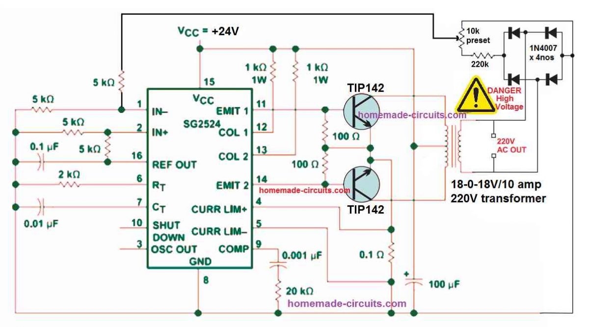 You can refer to the following two datasheets for exactly knowing how the pinouts of the IC SG2524 IC are designed to function:
LM3524 Datasheet
SG3525 Pinouts
The feedback control loop is configured in the following can be understood with the following points:
The 220V AC output is first rectified using a 4 diode bridge rectifier circuit.
The rectified high voltage DC is dropped to a lower DC level, at around 5V to 10V through the voltage divider network built using the 220K resistors and the 10K preset.
The 10K preset is used to adjust the feedback voltage until the output voltage is controlled just at the right level.
The feedback is taken from the 10K preset's center arm and fed to the error amplifier's non-inverting input pin#1 of the IC 2524.
This error amplifier is nothing but an opamp set internal to the IC for controlling the PWM of the output pin#11 and Pin#14.
The inverting or the (+) input pin#2 of the op amp is clamped at a fixed reference level of +2.5V through the couple of voltage divider resistors configured around the pin#2 and pin#16 of the IC.
The +5V reference potential is derived from pin#16 of the IC and then dropped to 2.5V using the two voltage divider resisters.
Since the pin#2 of the error amplifier is fixed at 2.5V reference, means that if the pin#1 of the opamp rises above the 2.5V level would instantly trigger the PWM feature of the IC, causing narrowing of the output PWM to the transistors.
The feedback 10k preset is adjusted in a such a way that feedback voltage at pin#1 reaches the 2.6 V mark as soon as the output voltage reaches the specified unsafe high voltage level.
In such situations, when the pin#1 receives a 2.6 V, it will cause the internal error amp to activate, narrowing the output PWMs to the transistors, which will in turn cause the output voltage to reduce to the safe lower levels, appropriately.
You can refer to the following two datasheets for exactly knowing how the pinouts of the IC SG2524 IC are designed to function:
LM3524 Datasheet
SG3525 Pinouts
The feedback control loop is configured in the following can be understood with the following points:
The 220V AC output is first rectified using a 4 diode bridge rectifier circuit.
The rectified high voltage DC is dropped to a lower DC level, at around 5V to 10V through the voltage divider network built using the 220K resistors and the 10K preset.
The 10K preset is used to adjust the feedback voltage until the output voltage is controlled just at the right level.
The feedback is taken from the 10K preset's center arm and fed to the error amplifier's non-inverting input pin#1 of the IC 2524.
This error amplifier is nothing but an opamp set internal to the IC for controlling the PWM of the output pin#11 and Pin#14.
The inverting or the (+) input pin#2 of the op amp is clamped at a fixed reference level of +2.5V through the couple of voltage divider resistors configured around the pin#2 and pin#16 of the IC.
The +5V reference potential is derived from pin#16 of the IC and then dropped to 2.5V using the two voltage divider resisters.
Since the pin#2 of the error amplifier is fixed at 2.5V reference, means that if the pin#1 of the opamp rises above the 2.5V level would instantly trigger the PWM feature of the IC, causing narrowing of the output PWM to the transistors.
The feedback 10k preset is adjusted in a such a way that feedback voltage at pin#1 reaches the 2.6 V mark as soon as the output voltage reaches the specified unsafe high voltage level.
In such situations, when the pin#1 receives a 2.6 V, it will cause the internal error amp to activate, narrowing the output PWMs to the transistors, which will in turn cause the output voltage to reduce to the safe lower levels, appropriately.
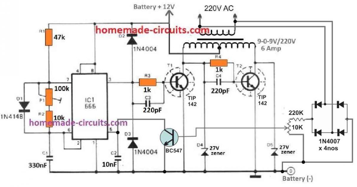 In this circuit also, we find that the 220V output from the transformer is first rectified to a DC level, and then it is stepped down through a resistive network comprising of a 220K resistor and a 10k preset.
The 10k preset center lead is configured with the NPN transistor BC547, whose collector can be seen connected with the pin#5 of the IC which is control input of the IC.
We know that normally when pin#5 is open, the PWM at the output pin#3 of the IC has a maximum PWM, however, as the potential at pin#5 is reduced, the output PWM also gets reduced proportionately.
Grounding the pin#5 causes the output PWM at pin#3 to become very narrow, with almost zero average voltage at this pinout.
In the IC 555 feedback circuit, when the output voltage tends to rise above the unsafe high voltage threshold, as per the setting of the 10k preset, the base of the BC547 slowly starts getting biased.
When this happens, the BC547 begins conducting and causes the pin#5 of the IC to get gradually grounded.
The grounding of the pin#5 of the IC causes the output PWM at pin#3 to get narrower, which in turns causes the output voltage to drop to the normal levels.
In this circuit also, we find that the 220V output from the transformer is first rectified to a DC level, and then it is stepped down through a resistive network comprising of a 220K resistor and a 10k preset.
The 10k preset center lead is configured with the NPN transistor BC547, whose collector can be seen connected with the pin#5 of the IC which is control input of the IC.
We know that normally when pin#5 is open, the PWM at the output pin#3 of the IC has a maximum PWM, however, as the potential at pin#5 is reduced, the output PWM also gets reduced proportionately.
Grounding the pin#5 causes the output PWM at pin#3 to become very narrow, with almost zero average voltage at this pinout.
In the IC 555 feedback circuit, when the output voltage tends to rise above the unsafe high voltage threshold, as per the setting of the 10k preset, the base of the BC547 slowly starts getting biased.
When this happens, the BC547 begins conducting and causes the pin#5 of the IC to get gradually grounded.
The grounding of the pin#5 of the IC causes the output PWM at pin#3 to get narrower, which in turns causes the output voltage to drop to the normal levels.
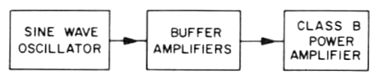 The block diagram matches one of the simple 80 meter CW transmitter circuit.
Essentially, it is only the frequency that is different ; 60 Hz instead of 3.5 MHz.
And producing 250 watts of sine wave ac actually becomes drastically easier with the 500,000 meters (60 Hz) as opposed to the 80 meters (3.5 MHz).
A complete circuit diagram of the 250 watt sine wave inverter is shown below.
The requirements are a sine wave oscillator, a buffer amplifier, and a power amplifier.
The block diagram matches one of the simple 80 meter CW transmitter circuit.
Essentially, it is only the frequency that is different ; 60 Hz instead of 3.5 MHz.
And producing 250 watts of sine wave ac actually becomes drastically easier with the 500,000 meters (60 Hz) as opposed to the 80 meters (3.5 MHz).
A complete circuit diagram of the 250 watt sine wave inverter is shown below.
The requirements are a sine wave oscillator, a buffer amplifier, and a power amplifier.
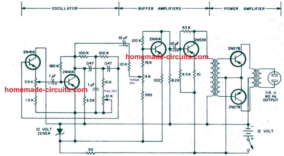
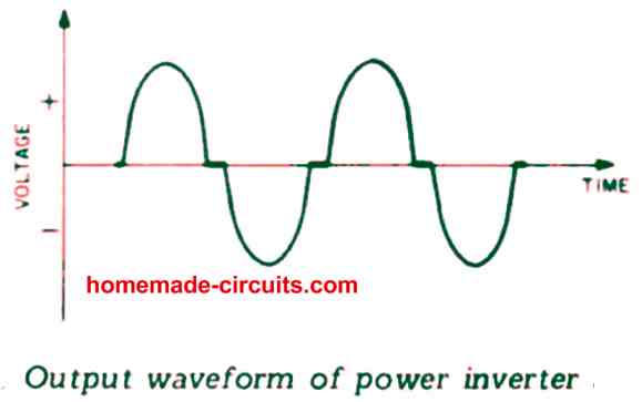 The true waveform that can be acquired from this 250 watt sine wave inverter is slightly different from a true sine wave.
As indicated in the above figure, each power transistor of this power inverter amplifier comes with an operating angle marginally lower than 180¦Ë , that is certainly, near to a Class C type working.
A little deviation in the biasing of the transistors might pull the amplifier back to genuine Class B, however because no noises can be seen developing, this further hard work to improve the bias doesn't appear to be useful.
The true waveform that can be acquired from this 250 watt sine wave inverter is slightly different from a true sine wave.
As indicated in the above figure, each power transistor of this power inverter amplifier comes with an operating angle marginally lower than 180¦Ë , that is certainly, near to a Class C type working.
A little deviation in the biasing of the transistors might pull the amplifier back to genuine Class B, however because no noises can be seen developing, this further hard work to improve the bias doesn't appear to be useful.
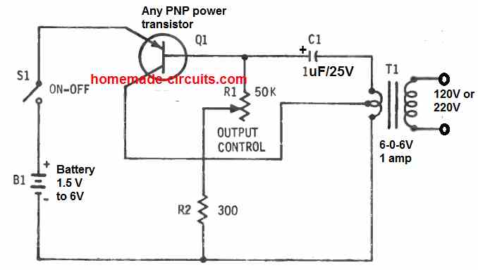 The center tapped 6.3 v winding of a small iron core transformer (T1) works like a center feedback type of coil for this oscillator.
With a 6 V battery (B1), the highest current drain is around 80 ma.
The 50k 10 watt wirewound potentiometer (R1) adjusts the no-load DC output between 2 V and 220 V volts.
In this inverter design if R1 is substituted by a 200 ohm 10 watt wirewound pot and R2 replaced with a 20 ohm, 1 watt resistor, battery B1 specifications could be minimized to 1.5 V., and then the circuit work like a 1.5 V to 220 V inverter circuit.
The maximum drain from the battery at 1.5 V supply will be roughly around 100 ma.
R1 will alter the DC output between 60 and 80 volts, in the absence of a load.
The center tapped 6.3 v winding of a small iron core transformer (T1) works like a center feedback type of coil for this oscillator.
With a 6 V battery (B1), the highest current drain is around 80 ma.
The 50k 10 watt wirewound potentiometer (R1) adjusts the no-load DC output between 2 V and 220 V volts.
In this inverter design if R1 is substituted by a 200 ohm 10 watt wirewound pot and R2 replaced with a 20 ohm, 1 watt resistor, battery B1 specifications could be minimized to 1.5 V., and then the circuit work like a 1.5 V to 220 V inverter circuit.
The maximum drain from the battery at 1.5 V supply will be roughly around 100 ma.
R1 will alter the DC output between 60 and 80 volts, in the absence of a load.
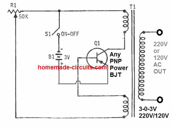 The center tap transformer can be any standard step down transformer.
This transformer provides the feedback and the voltage boosting both together.
The connections of the two low voltage windings of T1 must be configured correctly with the transistor, otherwise the inverter may fail to work, and begin heating up.
The 50 K potentiometer is a wirewound variable resistor (R1) which must be appropriately set to get reliable oscillation and the maximum voltage output.
This 3 V to 220 V inverter circuit may draws around 70 ma from the 3 V battery (B1).
The center tap transformer can be any standard step down transformer.
This transformer provides the feedback and the voltage boosting both together.
The connections of the two low voltage windings of T1 must be configured correctly with the transistor, otherwise the inverter may fail to work, and begin heating up.
The 50 K potentiometer is a wirewound variable resistor (R1) which must be appropriately set to get reliable oscillation and the maximum voltage output.
This 3 V to 220 V inverter circuit may draws around 70 ma from the 3 V battery (B1).
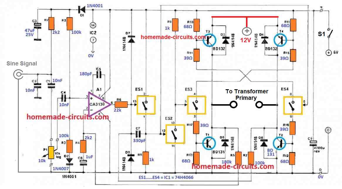 The IC 74HC4066 can be replaced with IC 4066, in that case the separate 5V will not be required, and a common 12V can be used for the entire circuit.
The working of the pwm class-D inverter is fairly simple.
The sine wave signal is amplified by the op amp A1 stage to adequate levels for driving the electronic switches ES1---ES4.
The electronic switches ES1---ES4 open and close causing rectangular pulses to be generated across the bases of the transistors T1---T4 bridge alternately.
The PWM or the width of the pulses is modulated by the input sine signal resulting in a sine equivalent PWMs fed to the power transistors,and the transformer, ultimately producing the intended 220V or 120V sine-wave mains AC at the output of the transformer secondary.
The duty factor of a rectangular signal produced from the ES1---ES4 outputs is modulated by the amplitude of the amplified input sine wave signal, which causes an output switching SPWM signal proportional to the sine wave RMS.
Thus the on-time of the output pulse is in accordance with the instantaneous amplitude of the input sine signal.
The switching period interval of the on-time and the off -time together determines the frequency which will be constant.
Consequently, a uniformly dimensioned rectangular signal (square wave) is created in the absence of an input signal.
As a way to achieve fairly good sine wave at the output of the transformer, the frequency of the rectangular wave from ES1 should be at the very least two times as high as the highest frequency in the input sine signal.
The IC 74HC4066 can be replaced with IC 4066, in that case the separate 5V will not be required, and a common 12V can be used for the entire circuit.
The working of the pwm class-D inverter is fairly simple.
The sine wave signal is amplified by the op amp A1 stage to adequate levels for driving the electronic switches ES1---ES4.
The electronic switches ES1---ES4 open and close causing rectangular pulses to be generated across the bases of the transistors T1---T4 bridge alternately.
The PWM or the width of the pulses is modulated by the input sine signal resulting in a sine equivalent PWMs fed to the power transistors,and the transformer, ultimately producing the intended 220V or 120V sine-wave mains AC at the output of the transformer secondary.
The duty factor of a rectangular signal produced from the ES1---ES4 outputs is modulated by the amplitude of the amplified input sine wave signal, which causes an output switching SPWM signal proportional to the sine wave RMS.
Thus the on-time of the output pulse is in accordance with the instantaneous amplitude of the input sine signal.
The switching period interval of the on-time and the off -time together determines the frequency which will be constant.
Consequently, a uniformly dimensioned rectangular signal (square wave) is created in the absence of an input signal.
As a way to achieve fairly good sine wave at the output of the transformer, the frequency of the rectangular wave from ES1 should be at the very least two times as high as the highest frequency in the input sine signal.
 Transformer: 0-9V/220V current, will depend on the transistors wattage and battery Ah rating
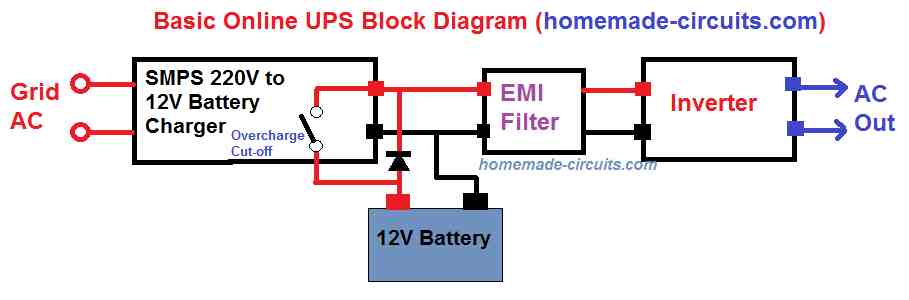 On the other hand, Offline UPS systems as shown in the below block diagram, rely on mechanical relays for transferring the UPS to the inverter mode, during the absence of mains AC supply.
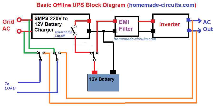 In these systems when mains AC is available the supply is directly supplied to the load via a set of relay contacts, and the battery is held in the charging mode through another set of relay contacts.
As soon as AC mains fails, the relevant relay contacts deactivate and switch the battery from the charging mode to inverter mode, and the load from grid AC to inverter AC.
This implies that the transfer process tends to involve a slight delay, albeit in milliseconds while changing over from the grid mains to the inverter main.
This delay though small could be critical for sensitive electronic equipment such as computers or micro-controller based systems.
Therefore the online UPS system seems to be more efficient than an offline UPS in terms of speed and smoothness, during the changeover process from grid AC to inverter AC for all types of appliances.
In these systems when mains AC is available the supply is directly supplied to the load via a set of relay contacts, and the battery is held in the charging mode through another set of relay contacts.
As soon as AC mains fails, the relevant relay contacts deactivate and switch the battery from the charging mode to inverter mode, and the load from grid AC to inverter AC.
This implies that the transfer process tends to involve a slight delay, albeit in milliseconds while changing over from the grid mains to the inverter main.
This delay though small could be critical for sensitive electronic equipment such as computers or micro-controller based systems.
Therefore the online UPS system seems to be more efficient than an offline UPS in terms of speed and smoothness, during the changeover process from grid AC to inverter AC for all types of appliances.
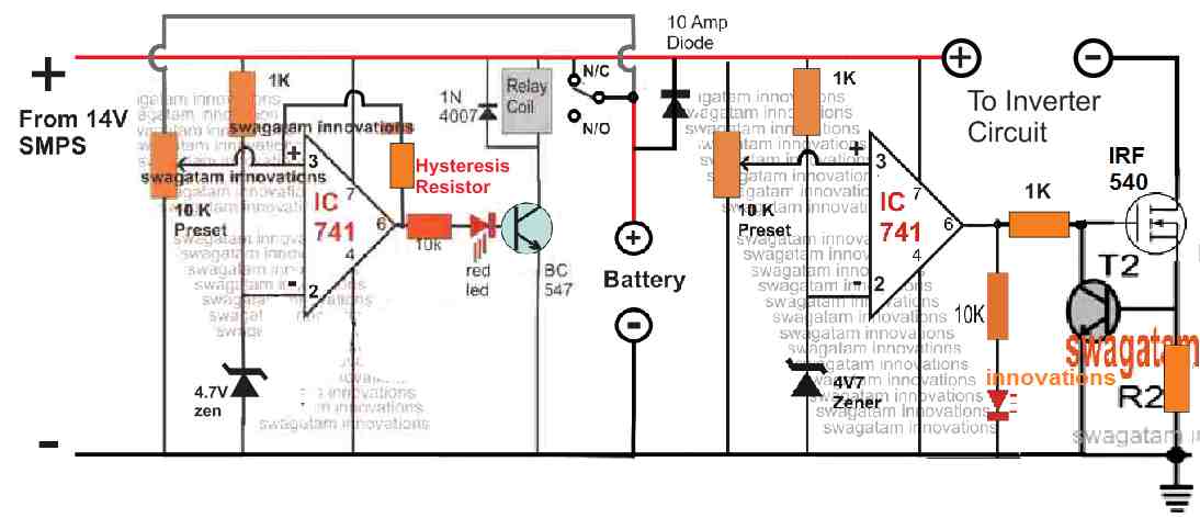 This activates the relay via the BC547 driver transistor causing the relay contacts to shift from the N/C to N/O, which cuts off the charging supply to the battery, preventing over charging of the battery.
The feedback hysteresis resistor across pin#6 and pin#3 of the left op amp causes the relay to latch for certain period of time, until the battery voltage drops to a level below the holding threshold of the hysteresis, which causes the pin#3 to go low, and correspondingly pin#6 also goes low, switching off the relay.
The relay contacts now switches back to the N/C, restoring the charging supply to the battery.
This activates the relay via the BC547 driver transistor causing the relay contacts to shift from the N/C to N/O, which cuts off the charging supply to the battery, preventing over charging of the battery.
The feedback hysteresis resistor across pin#6 and pin#3 of the left op amp causes the relay to latch for certain period of time, until the battery voltage drops to a level below the holding threshold of the hysteresis, which causes the pin#3 to go low, and correspondingly pin#6 also goes low, switching off the relay.
The relay contacts now switches back to the N/C, restoring the charging supply to the battery.
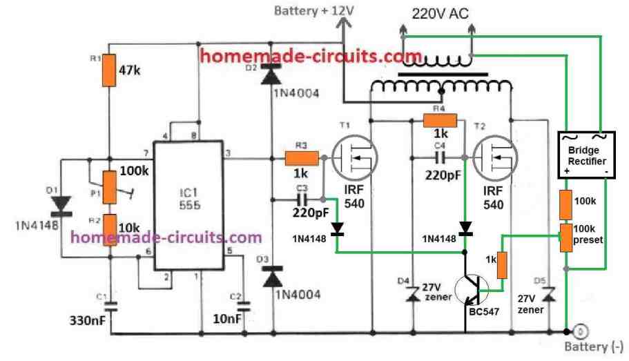 We have selected an IC 555 based circuit for simplicity sake and also for ensuring adequate power output range.
This inverter will remain online as long as the charger circuit and the battery remains functional, and the grid AC mains is fed appropriately to the system via a AC to DC SMPS circuit rated at 14V, 5 amp, or as per the particular power rating of the system, which is fully customizable.
The BJT feedback across the gates of the inverter MOSFETs ensures that the output voltage of the inverter never exceeds above the safe level, and is fed in a controlled manner.
This conclude our simple online UPS circuit design, which ensures a continuous uninterruptible online power to any AC load, which needs to be functional without any interruption regardless of the input AC availability.
We have selected an IC 555 based circuit for simplicity sake and also for ensuring adequate power output range.
This inverter will remain online as long as the charger circuit and the battery remains functional, and the grid AC mains is fed appropriately to the system via a AC to DC SMPS circuit rated at 14V, 5 amp, or as per the particular power rating of the system, which is fully customizable.
The BJT feedback across the gates of the inverter MOSFETs ensures that the output voltage of the inverter never exceeds above the safe level, and is fed in a controlled manner.
This conclude our simple online UPS circuit design, which ensures a continuous uninterruptible online power to any AC load, which needs to be functional without any interruption regardless of the input AC availability.
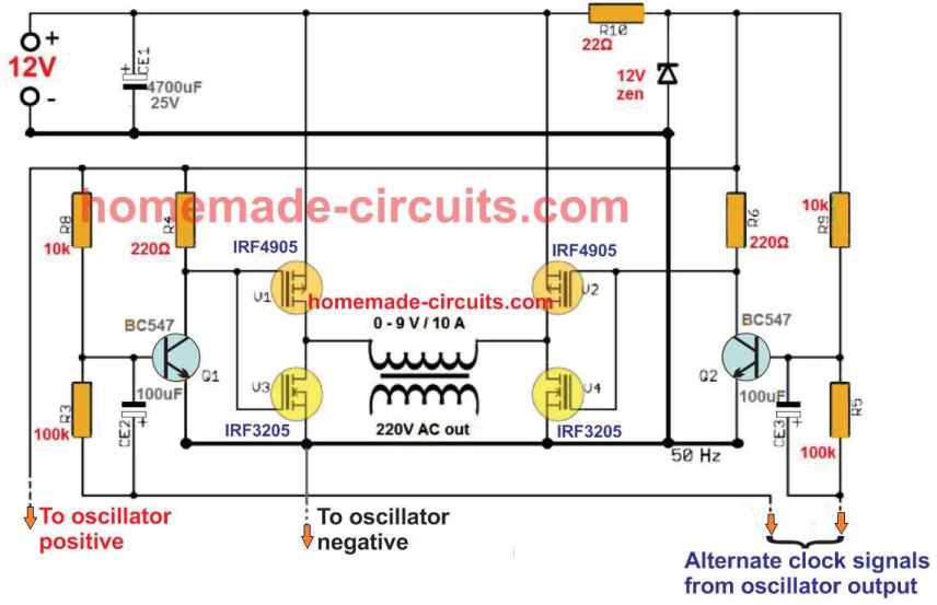
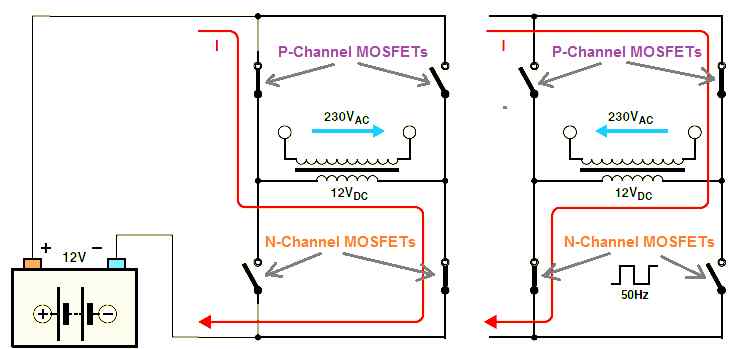 This flip-flop switching of the P and N channel MOSFETs across the left/right diagonal arms keep repeating in response to the alternate clock signal inputs from the oscillator stage.
As a result, the transformer primary is also switched in the same pattern causing a square wave AC 12V to flow across its primary, which is in correspondingly converted into 220 V or 120 V AC square wave across the secondary of the transformer.
The frequency is dependent on the frequency of the oscillator signal input which can be 50 Hz for 220 V output and 60 Hz for 120 V AC output,
This flip-flop switching of the P and N channel MOSFETs across the left/right diagonal arms keep repeating in response to the alternate clock signal inputs from the oscillator stage.
As a result, the transformer primary is also switched in the same pattern causing a square wave AC 12V to flow across its primary, which is in correspondingly converted into 220 V or 120 V AC square wave across the secondary of the transformer.
The frequency is dependent on the frequency of the oscillator signal input which can be 50 Hz for 220 V output and 60 Hz for 120 V AC output,
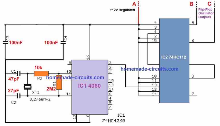 The ground pin of IC2 is mistakenly not shown in the diagram.
Please connect pin#8 of the IC2 with pin#8,12 line of IC1, to ensure that IC2 gets the ground potential.
This ground must be also joined with the ground line of the H-bridge module.
The ground pin of IC2 is mistakenly not shown in the diagram.
Please connect pin#8 of the IC2 with pin#8,12 line of IC1, to ensure that IC2 gets the ground potential.
This ground must be also joined with the ground line of the H-bridge module.
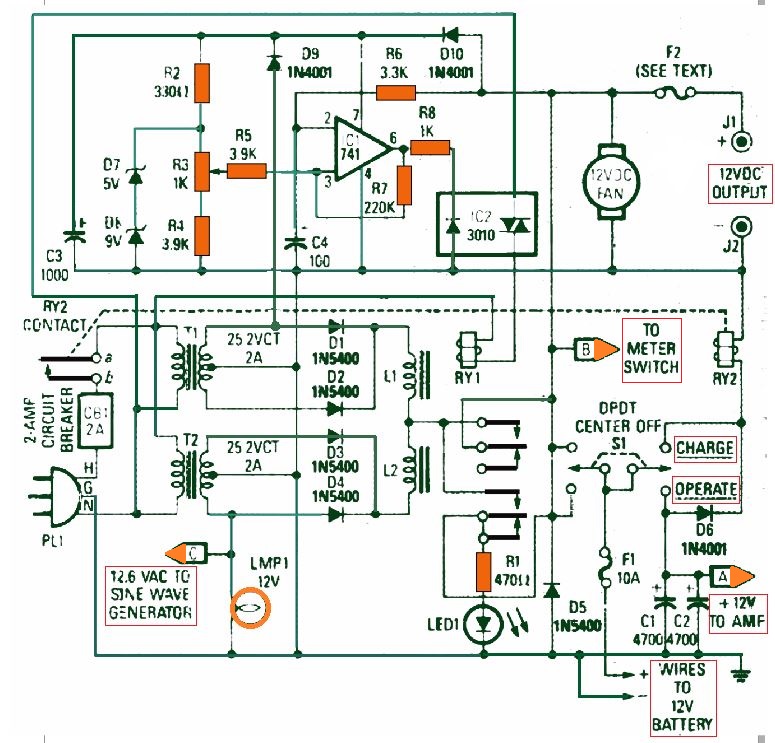 The current through the secondary windings is rectified through diodes D1, D2, D3, and D4.
Chokes L1 and L2 restrict the charging current for the battery as well as prohibit the passage of the ripple current.
Diode D5 delivers "crowbar" overload protection; its function is to safeguard the many vulnerable components by triggering fuse F1 to burn out in case the battery is accidentally hooked up with an incorrect polarity.
Op amp IC1 is connected in the form of an inverting voltage comparator whose reference voltage could be adjusted across a range of 11 to 14 volts through potentiometer R3.
Once the battery voltage falls beneath the reference, opto coupler IC2 is activated, that powers relay RY1. Current passing through RY1's contacts begins charging the battery when the load is not too heavy.
On other hand if the UPS is working at or close to its 100 % potential, an external battery charger may be needed to provide adequate current supply, to prevent the battery from getting discharged.
A 10 ampere battery charger is advisable.
Given that the majority of battery chargers donˇŻt have a filtration system, a high value filter capacitor must be included between the charger output and the battery to minimize ripple current.
In order to prevent battery overcharging, the supply from the charger must be switched on only when the UPS is being loaded at its 100 % capacity.
Fuse F2 must be less than 10 amps in order that the primary fuse, F1, may not whack when the 12 volt output is unintentionally shorted.
The current through the secondary windings is rectified through diodes D1, D2, D3, and D4.
Chokes L1 and L2 restrict the charging current for the battery as well as prohibit the passage of the ripple current.
Diode D5 delivers "crowbar" overload protection; its function is to safeguard the many vulnerable components by triggering fuse F1 to burn out in case the battery is accidentally hooked up with an incorrect polarity.
Op amp IC1 is connected in the form of an inverting voltage comparator whose reference voltage could be adjusted across a range of 11 to 14 volts through potentiometer R3.
Once the battery voltage falls beneath the reference, opto coupler IC2 is activated, that powers relay RY1. Current passing through RY1's contacts begins charging the battery when the load is not too heavy.
On other hand if the UPS is working at or close to its 100 % potential, an external battery charger may be needed to provide adequate current supply, to prevent the battery from getting discharged.
A 10 ampere battery charger is advisable.
Given that the majority of battery chargers donˇŻt have a filtration system, a high value filter capacitor must be included between the charger output and the battery to minimize ripple current.
In order to prevent battery overcharging, the supply from the charger must be switched on only when the UPS is being loaded at its 100 % capacity.
Fuse F2 must be less than 10 amps in order that the primary fuse, F1, may not whack when the 12 volt output is unintentionally shorted.
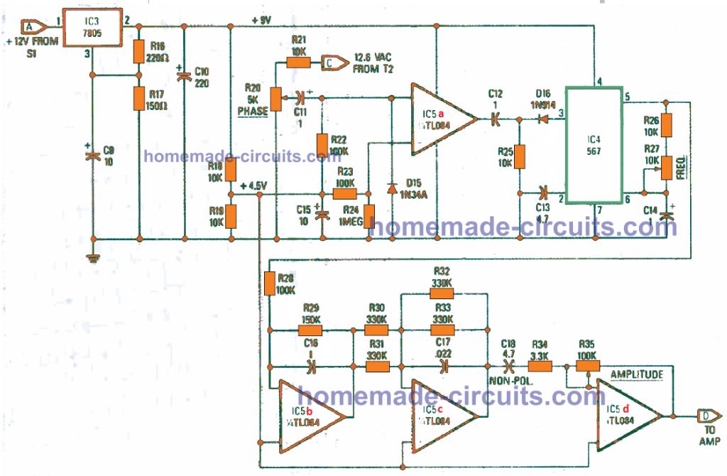 The IC's frequency is set up by resistors R26 and R27, and capacitor C14, and is fixed to a precise 60 Hz.
IC4's square wave output is transformed to a triangle wave by IC5-b, which is further on converted to a sinewave by IC5-c.
Op amp IC5-d's gain is set by potentiometer R35, that is fixed at the AC output voltage.
Op amp IC5-a converts the sinewave from the T2 output to a 60 Hz frequency.
D15 safeguards against damage that may take place in case the op amp inverting input happens to turn negative with reference to ground; the diode is generally reverse biased.
The 60 Hz pulses, that are connected to IC4 via C12 and D16, trigger the oscillator to lock to the grid AC frequency.
Some extent of control on the precise phase synchronization is achievable by fine-tuning potentiometer R20.
Once correctly tweaked, the AC output is going to lock in-phase with the input AC grid line, and this locking/unlocking process during the input power failure and restoration would be soft and favorable, producing almost no interference.
The sine wave generator comes with smooth, ripple-free 9 volt power through IC3, a 7805 IC, 5 V regulator.
Pin 3 of the regulator is kept at 4 volts above ground line with the help of resistive divider R16 and R17 to get a precise 9 volts output.
The IC's frequency is set up by resistors R26 and R27, and capacitor C14, and is fixed to a precise 60 Hz.
IC4's square wave output is transformed to a triangle wave by IC5-b, which is further on converted to a sinewave by IC5-c.
Op amp IC5-d's gain is set by potentiometer R35, that is fixed at the AC output voltage.
Op amp IC5-a converts the sinewave from the T2 output to a 60 Hz frequency.
D15 safeguards against damage that may take place in case the op amp inverting input happens to turn negative with reference to ground; the diode is generally reverse biased.
The 60 Hz pulses, that are connected to IC4 via C12 and D16, trigger the oscillator to lock to the grid AC frequency.
Some extent of control on the precise phase synchronization is achievable by fine-tuning potentiometer R20.
Once correctly tweaked, the AC output is going to lock in-phase with the input AC grid line, and this locking/unlocking process during the input power failure and restoration would be soft and favorable, producing almost no interference.
The sine wave generator comes with smooth, ripple-free 9 volt power through IC3, a 7805 IC, 5 V regulator.
Pin 3 of the regulator is kept at 4 volts above ground line with the help of resistive divider R16 and R17 to get a precise 9 volts output.
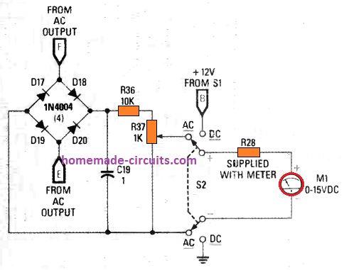 A bridge rectifier consisting of four rectifier diodes converts the AC to DC, while the capacitor C19 smooths to a pure DC.
A DPDT switch hooks up a 15 V DC voltmeter with the 12 V supply or the voltage divider built using resistive divider of R36 and R37.
A bridge rectifier consisting of four rectifier diodes converts the AC to DC, while the capacitor C19 smooths to a pure DC.
A DPDT switch hooks up a 15 V DC voltmeter with the 12 V supply or the voltage divider built using resistive divider of R36 and R37.
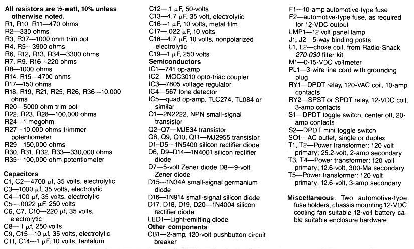 How to Construct the L1, L2 filter chokes
If you are unable to obtain the suggested L1, L2 chokes from your part dealer, you can construct the same using the following configuration
How to Construct the L1, L2 filter chokes
If you are unable to obtain the suggested L1, L2 chokes from your part dealer, you can construct the same using the following configuration
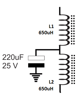 Use 1 mm super enameled wire for the coils
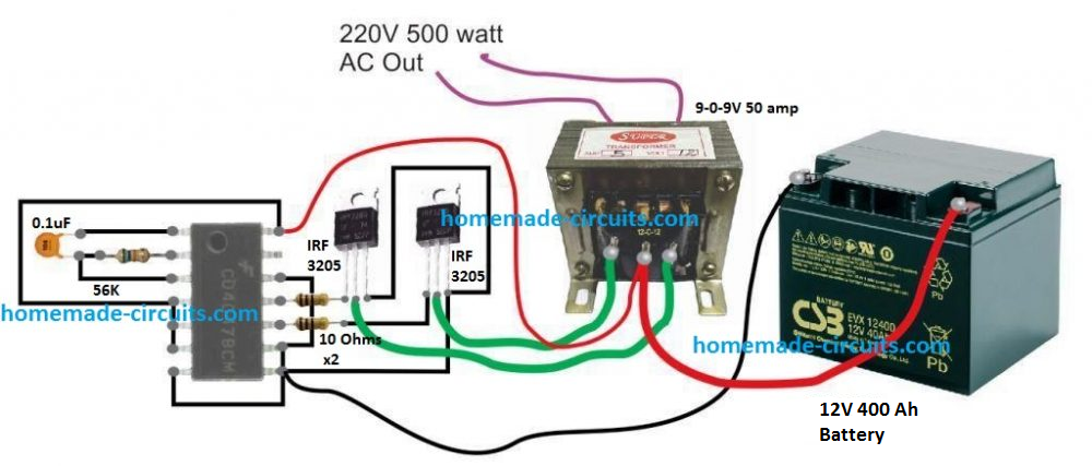 BASIC CIRCUIT
A basic 500 watt inverter with a square wave output can be as simple as above to build.
However, to upgrade it with a battery charger we may have to employ a charger transformer rated appropriately as per the battery specifications.
Before learning the charger configuration let's first get acquainted with the battery specification required for this project.
From one of our previous post we know that the more appropriate charging and discharging rate of a lead acid battery should be at 0.1C rate or at a supply current that's 10 time less than the battery Ah rating.
This implies that to get a minimum of 7 hours back up at 500 watt load, the battery Ah could be calculated in the following manner
Operational current required for a 500 watt load from a 12V battery will be 500 / 12 = 41 Amps approximately
This 41 amps needs to last for 7 hours, implies that the battery Ah must be = 41 x 7 = 287 Ah.
However, in real life this will will need to be at least 350 Ah.
For a 24 V battery this may come down to 50% less at 200 Ah.
This is exactly why a higher operational voltage is always advised as the wattage rating of the inverter gets on the higher side.
BASIC CIRCUIT
A basic 500 watt inverter with a square wave output can be as simple as above to build.
However, to upgrade it with a battery charger we may have to employ a charger transformer rated appropriately as per the battery specifications.
Before learning the charger configuration let's first get acquainted with the battery specification required for this project.
From one of our previous post we know that the more appropriate charging and discharging rate of a lead acid battery should be at 0.1C rate or at a supply current that's 10 time less than the battery Ah rating.
This implies that to get a minimum of 7 hours back up at 500 watt load, the battery Ah could be calculated in the following manner
Operational current required for a 500 watt load from a 12V battery will be 500 / 12 = 41 Amps approximately
This 41 amps needs to last for 7 hours, implies that the battery Ah must be = 41 x 7 = 287 Ah.
However, in real life this will will need to be at least 350 Ah.
For a 24 V battery this may come down to 50% less at 200 Ah.
This is exactly why a higher operational voltage is always advised as the wattage rating of the inverter gets on the higher side.
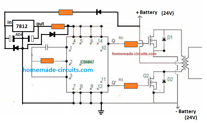
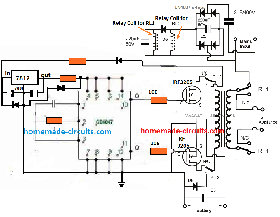 The same concept has been already elaborately discussed in one of the other related posts, which you can refer to for additional information.
Basically, the inverter uses the same transformer for charging the battery and for converting the battery power to 220 V AC output.
The operation is implemented through a relay changeover network, that alternately changes the transformer winding to charging mode and inverter mode.
The same concept has been already elaborately discussed in one of the other related posts, which you can refer to for additional information.
Basically, the inverter uses the same transformer for charging the battery and for converting the battery power to 220 V AC output.
The operation is implemented through a relay changeover network, that alternately changes the transformer winding to charging mode and inverter mode.
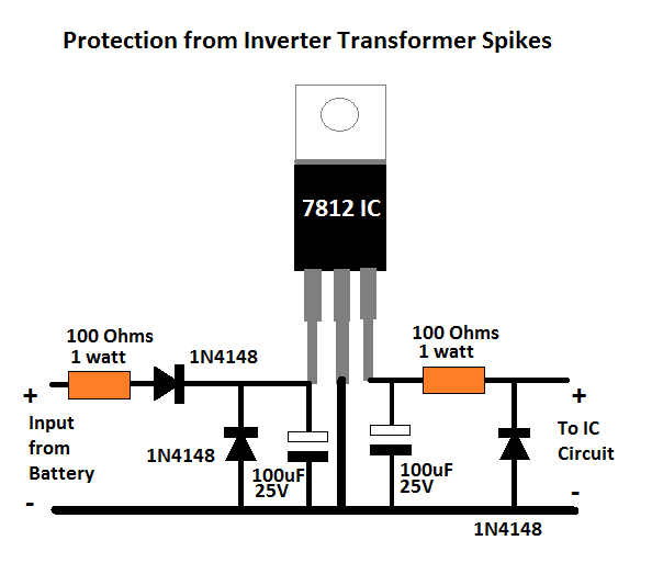 For a 12V application, you can reduce the above spike protection circuit to the following version:
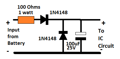
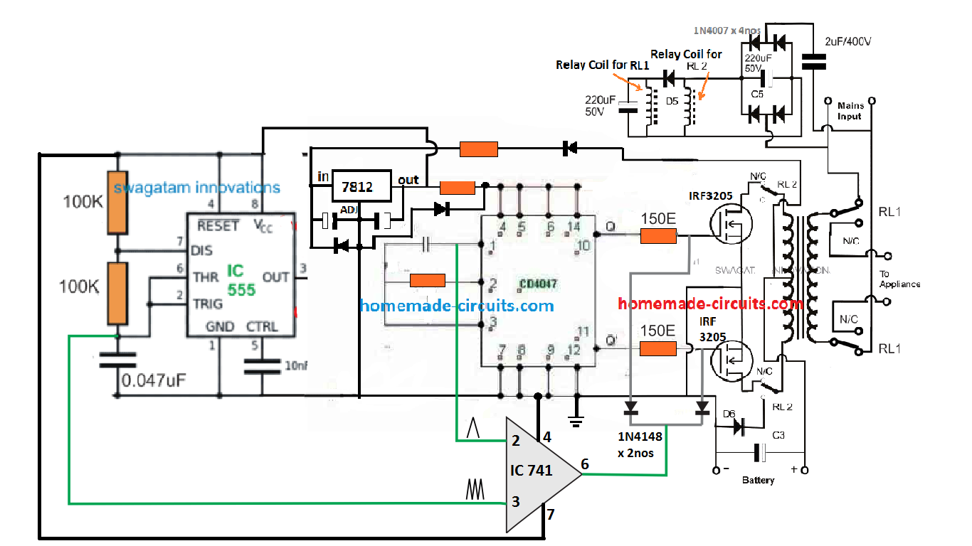 The idea is the same which has been applied in a few of the other sinewave inverter designs in this website.
It is to chop the gate of the power MOSFETs with calculated SPWM so that a replicated high current SPWM is oscillated across the push pull winding of the transformer primary.
The IC 741 is used as a comparator which compares two triangle waves across its two inputs.
The slow base triangle wave is acquired from the IC 4047 Ct pin, while the fast triangle wave is derived from an external IC 555 astable stage.
The result is a calculated SPWM at pin6 of the IC 741. This SPWM is chopped at the gates of the power MOSFETs which is switching by the transformer at the same SPWM frequency.
This results in the secondary side with a pure sinewave output (after some filtration).
The idea is the same which has been applied in a few of the other sinewave inverter designs in this website.
It is to chop the gate of the power MOSFETs with calculated SPWM so that a replicated high current SPWM is oscillated across the push pull winding of the transformer primary.
The IC 741 is used as a comparator which compares two triangle waves across its two inputs.
The slow base triangle wave is acquired from the IC 4047 Ct pin, while the fast triangle wave is derived from an external IC 555 astable stage.
The result is a calculated SPWM at pin6 of the IC 741. This SPWM is chopped at the gates of the power MOSFETs which is switching by the transformer at the same SPWM frequency.
This results in the secondary side with a pure sinewave output (after some filtration).
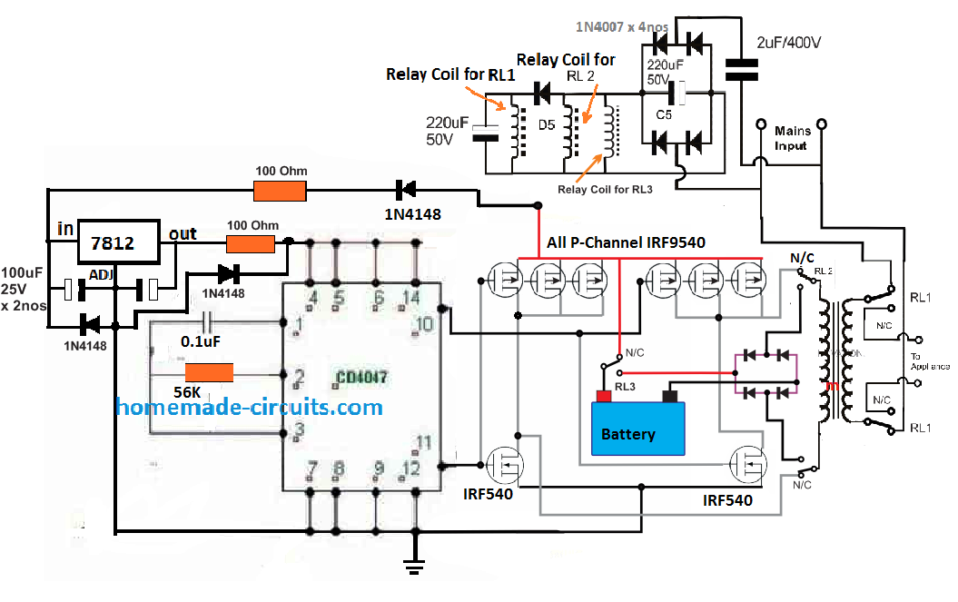 For sake simplicity, an automatic battery cut off is not included, so it is recommend to switched OFF the supply as soon as the battery voltage reaches the full charge level.
Or alternatively you may add an appropriately filament bulb in series with the charging positive line of the battery, to ensure a safe charging for the battery.
If you have questions or doubts regarding the above concept, the comment box below is all yours.
For sake simplicity, an automatic battery cut off is not included, so it is recommend to switched OFF the supply as soon as the battery voltage reaches the full charge level.
Or alternatively you may add an appropriately filament bulb in series with the charging positive line of the battery, to ensure a safe charging for the battery.
If you have questions or doubts regarding the above concept, the comment box below is all yours.

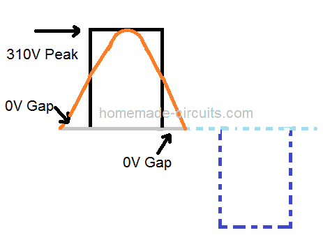 We can see that the each cycle begins with a zero or blank gap, then shoots up to 310V peak pulse and again ends with a 0V gap, the process then repeats for other half cycle.
In order to achieve the required 220V RMS we have to calculate and optimize the peak and the zero gap sections or the ON/OFF periods of the cycle such that the average value produces the required 220V.
The grey line represents the 50% period of the cycle, which is 10 ms.
Now we need to find out the proportions of the ON/OFF time which will produce an average of 220V.
We do it in this way:
220 / 310 x 100 = 71 % approximately
This shows that the 310V peak in the above modified cycle should occupy 71% of the 10 ms period, while the two zero gaps should be 29% combined, or 14.5% each.
Therefore in a 10 ms length, the first zero section should be 1.4 ms, followed by the 310 V peak for 7 ms, and finally the last zero gap of another 1.4 ms.
Once this is accomplished we can expect the output from the inverter to produce a reasonably good replication of a sine waveform.
We can see that the each cycle begins with a zero or blank gap, then shoots up to 310V peak pulse and again ends with a 0V gap, the process then repeats for other half cycle.
In order to achieve the required 220V RMS we have to calculate and optimize the peak and the zero gap sections or the ON/OFF periods of the cycle such that the average value produces the required 220V.
The grey line represents the 50% period of the cycle, which is 10 ms.
Now we need to find out the proportions of the ON/OFF time which will produce an average of 220V.
We do it in this way:
220 / 310 x 100 = 71 % approximately
This shows that the 310V peak in the above modified cycle should occupy 71% of the 10 ms period, while the two zero gaps should be 29% combined, or 14.5% each.
Therefore in a 10 ms length, the first zero section should be 1.4 ms, followed by the 310 V peak for 7 ms, and finally the last zero gap of another 1.4 ms.
Once this is accomplished we can expect the output from the inverter to produce a reasonably good replication of a sine waveform.
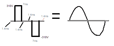 Despite of all these you may find that the output is not quite an ideal replication of the sine wave, because the discussed modified square wave is in its most basic form or a crude type.
If we want the output to match the sine wave with maximum precision, then we have to go for an SPWM approach.
I hope the above discussion might have enlightened you regarding how to calculate and optimize a modified square for replicating sinewave output.
For practical verification, the readers can try applying the above technique to this simple modified inverter circuit.
Here's another classic example of an optimized modified waveform for getting a good sine wave at the secondary of the transformer.
Despite of all these you may find that the output is not quite an ideal replication of the sine wave, because the discussed modified square wave is in its most basic form or a crude type.
If we want the output to match the sine wave with maximum precision, then we have to go for an SPWM approach.
I hope the above discussion might have enlightened you regarding how to calculate and optimize a modified square for replicating sinewave output.
For practical verification, the readers can try applying the above technique to this simple modified inverter circuit.
Here's another classic example of an optimized modified waveform for getting a good sine wave at the secondary of the transformer.
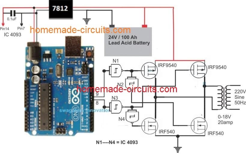
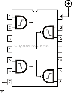
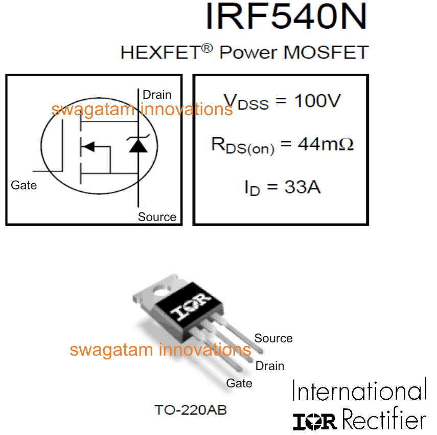
 The working of the Inverter can be understood from the following explanation:
 Acording to the waveform, the start and the end sequences can be seen being skipped by eliminating the relevant pinouts of the IC, similarly, the second and the 6th pinouts are also skipped, while the second, 4rth, 5th, 6th pinouts are joined for accomplishing a decent SPWM like pulse form across the outputs of the two 4017 ICs.
Video Proof (100 watt example)
Acording to the waveform, the start and the end sequences can be seen being skipped by eliminating the relevant pinouts of the IC, similarly, the second and the 6th pinouts are also skipped, while the second, 4rth, 5th, 6th pinouts are joined for accomplishing a decent SPWM like pulse form across the outputs of the two 4017 ICs.
Video Proof (100 watt example)
 The functioning details of the inverter can be understood with the help of the following points:
The basic or the standard full bridge inverter configuration is formed by the full bridge driver IC IRS2453 and the associated mosfet network.
The functioning details of the inverter can be understood with the help of the following points:
The basic or the standard full bridge inverter configuration is formed by the full bridge driver IC IRS2453 and the associated mosfet network.
 Since the IC cannot operate with at voltages more than 15V, it is well guarded through a dropping resistor and a zener diode.
The zener diode limits the high voltage from the solar panel at the connected 15V zener voltage.
However the mosfets are allowed to be operated with the full solar output voltage, which may lie anywhere between 200 to 260 volts.
On overcast conditions the voltage might drop to well below 170V, So probably a voltage stabilizer may be used at the output for regulating the output voltage under such situations.
The mosfets are N and P types which form a pair for implementing the push pull actions and for generating the required AC.
The mosfets arenot specified in the diagram, ideally they must be rated at 450V and 5 amps, you will come across many variants, if you google a bit over the net.
The used solar panels should strictly have an open circuit voltage of around 24V at full sunlight and around 17V during bright dusk periods.
Since the IC cannot operate with at voltages more than 15V, it is well guarded through a dropping resistor and a zener diode.
The zener diode limits the high voltage from the solar panel at the connected 15V zener voltage.
However the mosfets are allowed to be operated with the full solar output voltage, which may lie anywhere between 200 to 260 volts.
On overcast conditions the voltage might drop to well below 170V, So probably a voltage stabilizer may be used at the output for regulating the output voltage under such situations.
The mosfets are N and P types which form a pair for implementing the push pull actions and for generating the required AC.
The mosfets arenot specified in the diagram, ideally they must be rated at 450V and 5 amps, you will come across many variants, if you google a bit over the net.
The used solar panels should strictly have an open circuit voltage of around 24V at full sunlight and around 17V during bright dusk periods.
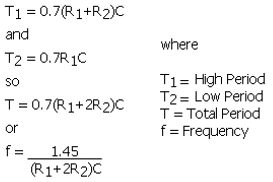 Update:
The above 555 IC design may not be so reliable and efficient, a much reliable design can be seen below in the form of a full H-bridge inverter circuit.
This design can be expected of providing much better results than the above 555 IC circuit.
Update:
The above 555 IC design may not be so reliable and efficient, a much reliable design can be seen below in the form of a full H-bridge inverter circuit.
This design can be expected of providing much better results than the above 555 IC circuit.
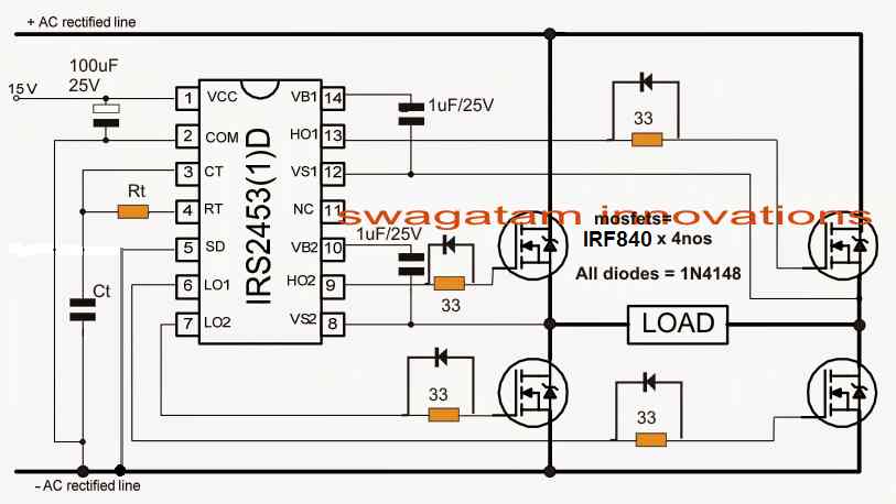 Another advantage of using the above circuit is that you won't require a dual solar panel arrangement, rather a single series connected solar supply would be enough to operate the above circuit for achieving a 220V output.
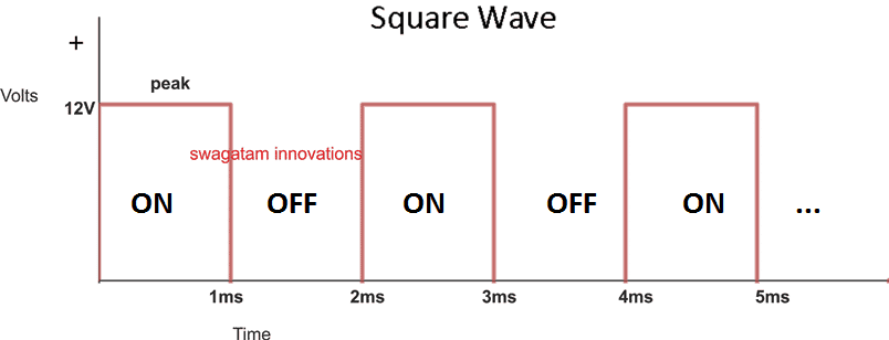 Here we can see that the peak voltage is 12V, and the dutycycle is 50% (equal ON/OFF time of the waveform).
To proceed with the analysis We first need to find the average voltage induced across the relevant transformer winding.
Supposing we are using a center tap 12-0-12V /5 amp trafo, and assuming 12V@ 50% duty cycle is applied to one of the 12V winding, then the power induced within that winding can be calculated as given below:
12 x 50% = 6V
This becomes the average voltage across the gates of the power devices, which correspondingly operate the trafo winding at this same rate.
For the two halves of the trafo winding we get, 6V+ 6V = 12V (combining both the halves of the center tap trafo.
Multiplying this 12V with the full current capacity 5 amp gives us 60 watt
Now since the transformer actual wattage is also 12 x 5 = 60 watts, implies that the power induced at the primary of the trafo is full, and therefore the output will be also full, allowing the output to run without any drop in voltage under load.
This 60 watt is equal to the actual wattage rating of the transfomer, i.e.
12V x 5 amp = 60 watts.
therefore the output from the trafo works with maximum force and does not drop the output voltage, even when a maximum load of 60 watt is connected.
Here we can see that the peak voltage is 12V, and the dutycycle is 50% (equal ON/OFF time of the waveform).
To proceed with the analysis We first need to find the average voltage induced across the relevant transformer winding.
Supposing we are using a center tap 12-0-12V /5 amp trafo, and assuming 12V@ 50% duty cycle is applied to one of the 12V winding, then the power induced within that winding can be calculated as given below:
12 x 50% = 6V
This becomes the average voltage across the gates of the power devices, which correspondingly operate the trafo winding at this same rate.
For the two halves of the trafo winding we get, 6V+ 6V = 12V (combining both the halves of the center tap trafo.
Multiplying this 12V with the full current capacity 5 amp gives us 60 watt
Now since the transformer actual wattage is also 12 x 5 = 60 watts, implies that the power induced at the primary of the trafo is full, and therefore the output will be also full, allowing the output to run without any drop in voltage under load.
This 60 watt is equal to the actual wattage rating of the transfomer, i.e.
12V x 5 amp = 60 watts.
therefore the output from the trafo works with maximum force and does not drop the output voltage, even when a maximum load of 60 watt is connected.
 Now suppose we apply a PWM chopping across the gates of the power mosfets, say at a rate of 50% duty cycle on the gates of the mosfets ( which are already running with a 50% duty cycle from the main oscillator, as discussed above)
This again implies that the previously calculated 6V average is now impacted additionally by this PWM feed with 50% duty cycle, reducing the average voltage value across the mosfet gates to:
6V x 50% = 3V (although the peak is still 12V)
Combining this 3V average for both the halves of the winding we get
3+ 3 = 6V
Multiplying this 6V with 5 amp gives us 30 watts.
Well, this is 50% less than what the transformer is rated to handle.
Therefore when measured at the output, although the output might show a full 310V (due to the 12V peaks), but under load this might quickly drop to 150V, since the average supply at the primary is 50% less than the rated value.
To rectify this issue we have to tackle two parameters simultaneously:
1) We must make sure that the transformer winding matches the average voltage value delivered by the source using the PWM chopping,
2) and the current of the winding must be accordingly specified such that the output AC does not drop under load.
Let's consider our above example where the introduction of a 50% PWM caused the input to the winding to be reduced to 3V, to reinforce and tackle this situation we must ensure that the winding of the trafo must be correspondingly rated at 3V.
Therefore in this situation the transformer must be rated at 3-0-3V
Now suppose we apply a PWM chopping across the gates of the power mosfets, say at a rate of 50% duty cycle on the gates of the mosfets ( which are already running with a 50% duty cycle from the main oscillator, as discussed above)
This again implies that the previously calculated 6V average is now impacted additionally by this PWM feed with 50% duty cycle, reducing the average voltage value across the mosfet gates to:
6V x 50% = 3V (although the peak is still 12V)
Combining this 3V average for both the halves of the winding we get
3+ 3 = 6V
Multiplying this 6V with 5 amp gives us 30 watts.
Well, this is 50% less than what the transformer is rated to handle.
Therefore when measured at the output, although the output might show a full 310V (due to the 12V peaks), but under load this might quickly drop to 150V, since the average supply at the primary is 50% less than the rated value.
To rectify this issue we have to tackle two parameters simultaneously:
1) We must make sure that the transformer winding matches the average voltage value delivered by the source using the PWM chopping,
2) and the current of the winding must be accordingly specified such that the output AC does not drop under load.
Let's consider our above example where the introduction of a 50% PWM caused the input to the winding to be reduced to 3V, to reinforce and tackle this situation we must ensure that the winding of the trafo must be correspondingly rated at 3V.
Therefore in this situation the transformer must be rated at 3-0-3V
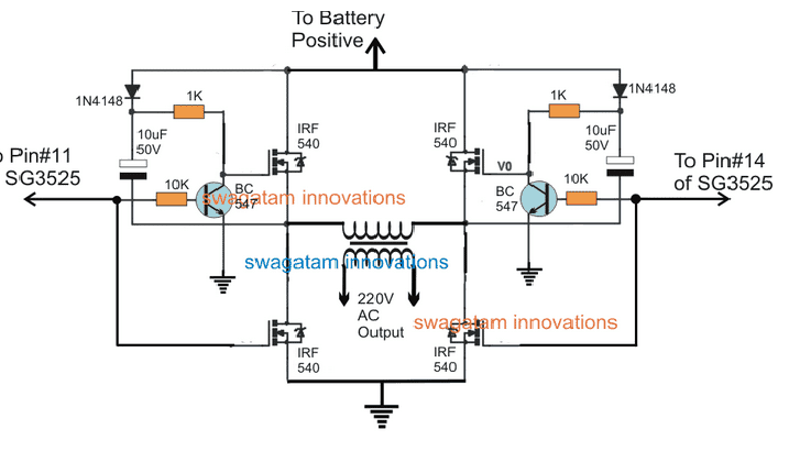 Referring to the above diagram, we can identify the four mosfets rigged as an H-bridge or a full bridge network, however the additional BC547 transistor and the associated diode capacitor looks a bit unfamiliar.
To be precise the BC547 stage is positioned for enforcing the bootstrapping condition, and this can be understood with the help of the following explanation:
We know that in any H-bridge the mosfets are configured to conduct diagonally for implementing the intended push pull conduction across the transformer or the connected load.
Therefore letˇŻs assume an instance where the pin#14 of the SG3525 is low, which enables the top right, and the low left mosfets to conduct.
This implies that pin#11 of the IC is high during this instance, which keeps the left side BC547 switch ON.
In this situation the following things happen withing the left side BC547 stage:
1) The 10uF capacitor charges up via the 1N4148 diode and the low side mosfet connected with its negative terminal.
2) This charge is temporarily stored inside the capacitor and may be assumed to be equal to the supply voltage.
3) Now as soon as the logic across the SG3525 reverts with the subsequent oscillating cycle, the pin#11 goes low, which instantly switches OFF the associated BC547.
4) With BC547 switched OFF, the supply voltage at the cathode of the 1N4148 now reaches the gate of the connected mosfet, however this voltage is now reinforced with the stored voltage inside capacitor which is also almost equal to the supply level.
5) This results in a doubling effect and enables a raised 2X voltage at the gate of the relevant mosfet.
6) This condition instantly hard triggers the mosfet into conduction, which pushes the voltage across the corresponding opposite low side mosfet.
7) During this situation the capacitor is forced to discharge quickly and the mosfet is able to conduct only for so long the stored charge of this capacitor is able to sustain.
Therefore it becomes mandatory to ensure that the value of the capacitor is selected such that the capacitor is able to adequately hold the charge for each ON/OFF period of the push pull oscillations.
Otherwise the mosfet will abandon the conduction prematurely causing a relatively lower RMS output.
Well, the above explanation comprehensively explains how a bootstrapping functions in full bridge inverters and how this crucial feature may be implemented for making an efficient SG3525 full bridge inverter circuit.
Now if you have understood how an ordinary SG3525 could be transformed into a full fledged H-bridge inverter, you might also want to investigate how the same can be implemented for other ordinary options such as in IC 4047, or IC 555 based inverter circuits, ˇ..think about it and let us know!
UPDATE: If you find the above H-bridge design too complex to implement, you may try a much easier alternative
Referring to the above diagram, we can identify the four mosfets rigged as an H-bridge or a full bridge network, however the additional BC547 transistor and the associated diode capacitor looks a bit unfamiliar.
To be precise the BC547 stage is positioned for enforcing the bootstrapping condition, and this can be understood with the help of the following explanation:
We know that in any H-bridge the mosfets are configured to conduct diagonally for implementing the intended push pull conduction across the transformer or the connected load.
Therefore letˇŻs assume an instance where the pin#14 of the SG3525 is low, which enables the top right, and the low left mosfets to conduct.
This implies that pin#11 of the IC is high during this instance, which keeps the left side BC547 switch ON.
In this situation the following things happen withing the left side BC547 stage:
1) The 10uF capacitor charges up via the 1N4148 diode and the low side mosfet connected with its negative terminal.
2) This charge is temporarily stored inside the capacitor and may be assumed to be equal to the supply voltage.
3) Now as soon as the logic across the SG3525 reverts with the subsequent oscillating cycle, the pin#11 goes low, which instantly switches OFF the associated BC547.
4) With BC547 switched OFF, the supply voltage at the cathode of the 1N4148 now reaches the gate of the connected mosfet, however this voltage is now reinforced with the stored voltage inside capacitor which is also almost equal to the supply level.
5) This results in a doubling effect and enables a raised 2X voltage at the gate of the relevant mosfet.
6) This condition instantly hard triggers the mosfet into conduction, which pushes the voltage across the corresponding opposite low side mosfet.
7) During this situation the capacitor is forced to discharge quickly and the mosfet is able to conduct only for so long the stored charge of this capacitor is able to sustain.
Therefore it becomes mandatory to ensure that the value of the capacitor is selected such that the capacitor is able to adequately hold the charge for each ON/OFF period of the push pull oscillations.
Otherwise the mosfet will abandon the conduction prematurely causing a relatively lower RMS output.
Well, the above explanation comprehensively explains how a bootstrapping functions in full bridge inverters and how this crucial feature may be implemented for making an efficient SG3525 full bridge inverter circuit.
Now if you have understood how an ordinary SG3525 could be transformed into a full fledged H-bridge inverter, you might also want to investigate how the same can be implemented for other ordinary options such as in IC 4047, or IC 555 based inverter circuits, ˇ..think about it and let us know!
UPDATE: If you find the above H-bridge design too complex to implement, you may try a much easier alternative
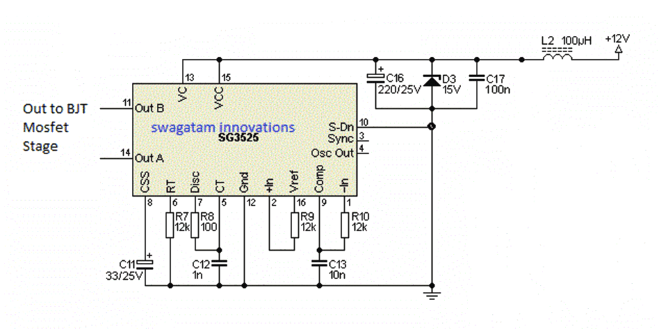 The ends of these output pinouts simply needs to be connected across the indicated sections of the above explained full bridge network for effectively converting this simple SG3525 design into a full fledged SG3525 full bridge inverter circuit or an 4 N channel mosfet H-bridge circuit.
Feedback from Mr.
Robin, (who is one of the avid readers of this blog, and a passionate electronic enthusiast):
Hi Swagatum
Ok,just to check everything is working I separated the two high side fets from the two low side fets and used the same circuitry as:
(https://www.homemade-circuits.com/2017/03/sg3525-full-bridge-inverter-circuit.html),
connecting the cap negative to the mosfet source then connecting that junction to a 1k resistor and an led to ground on each high side fet.Pin 11 pulsed the one high side fet and pin 14 the other high side fet.
When I switched the SG3525 on both fets lit up momentarily and the oscillated normally thereafter.I think that could be a problem if I connected this situation to the trafo and low side fets?
Then I tested the two low side fets,connecting a 12v supply to a (1k resistor and an led) to the drain of each low side fet and connecting the source's to ground.Pin 11 and 14 was connected to each low side fets gate.
When I switched the SG3525 on the low side fet's would not oscillate until I put a 1k resistor between the pin (11, 14) and the gate.(not sure why that happens).
Circuit diagram attatched below.
The ends of these output pinouts simply needs to be connected across the indicated sections of the above explained full bridge network for effectively converting this simple SG3525 design into a full fledged SG3525 full bridge inverter circuit or an 4 N channel mosfet H-bridge circuit.
Feedback from Mr.
Robin, (who is one of the avid readers of this blog, and a passionate electronic enthusiast):
Hi Swagatum
Ok,just to check everything is working I separated the two high side fets from the two low side fets and used the same circuitry as:
(https://www.homemade-circuits.com/2017/03/sg3525-full-bridge-inverter-circuit.html),
connecting the cap negative to the mosfet source then connecting that junction to a 1k resistor and an led to ground on each high side fet.Pin 11 pulsed the one high side fet and pin 14 the other high side fet.
When I switched the SG3525 on both fets lit up momentarily and the oscillated normally thereafter.I think that could be a problem if I connected this situation to the trafo and low side fets?
Then I tested the two low side fets,connecting a 12v supply to a (1k resistor and an led) to the drain of each low side fet and connecting the source's to ground.Pin 11 and 14 was connected to each low side fets gate.
When I switched the SG3525 on the low side fet's would not oscillate until I put a 1k resistor between the pin (11, 14) and the gate.(not sure why that happens).
Circuit diagram attatched below.
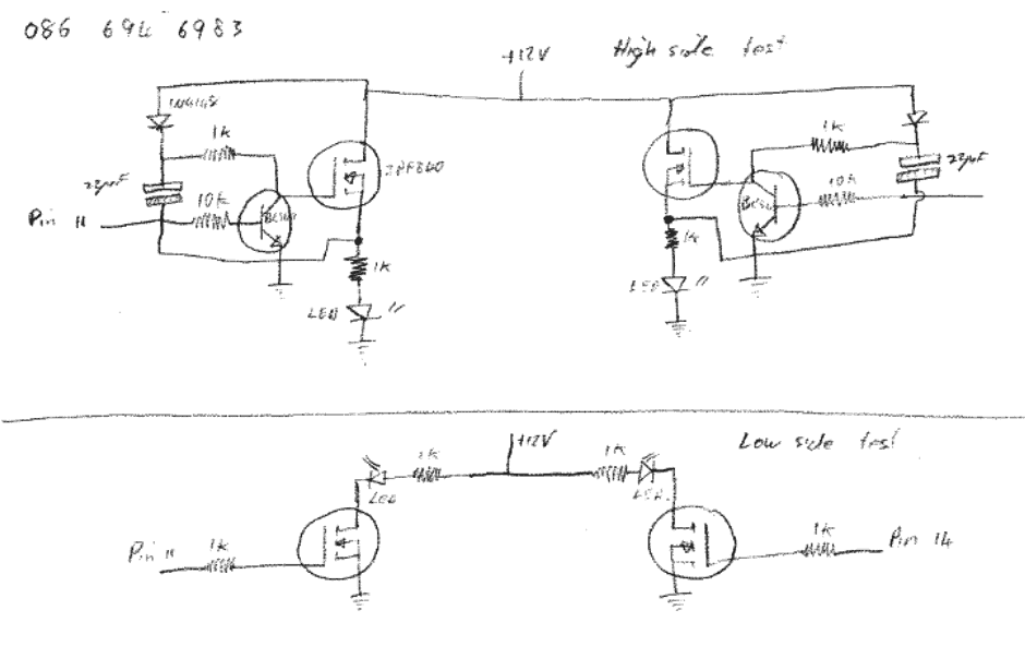 My Reply:
Thanks Robin,
I appreciate your efforts, however that doesn't seem to be the best way of checking the IC 's output response...
alternatively you can try a simple method by connecting individual LEDs from pin#11 and pin#14 of the IC to ground with each LED having its own 1K resistor.
This will quickly allow you to understand the IC output response....this could be done either by keeping the full bridge stage isolated from the two IC outputs or without isolating it.
Furthermore you could try attaching a 3V zeners in series between the IC output pins and the respective full bridge inputs...this will ensure that false triggering across the mosfets are avoided as far as possible...
Hope this helps
Best Regards...
Swag
From Robin:
Could you please explain how{ 3V zeners in series between the IC output pins and the respective full bridge inputs...this will ensure that false triggering across the mosfets are avoided as far as possible...
Cheers Robin
Me:
When a zener diode is in series it will pass the full voltage once its specified value is exceeded, therefore a 3V zener diode will not conduct only as long as the 3V mark is not crossed, once this is exceeded, it will allow the entire level of voltage that's been applied across it
So in our case also, since the voltage from the SG 3525 can be assumed to be at the supply level and higher than 3V, nothing would be blocked or restricted and the whole supply level would be able to reach the full bridge stage.
Let me know how it goes with your circuit.
My Reply:
Thanks Robin,
I appreciate your efforts, however that doesn't seem to be the best way of checking the IC 's output response...
alternatively you can try a simple method by connecting individual LEDs from pin#11 and pin#14 of the IC to ground with each LED having its own 1K resistor.
This will quickly allow you to understand the IC output response....this could be done either by keeping the full bridge stage isolated from the two IC outputs or without isolating it.
Furthermore you could try attaching a 3V zeners in series between the IC output pins and the respective full bridge inputs...this will ensure that false triggering across the mosfets are avoided as far as possible...
Hope this helps
Best Regards...
Swag
From Robin:
Could you please explain how{ 3V zeners in series between the IC output pins and the respective full bridge inputs...this will ensure that false triggering across the mosfets are avoided as far as possible...
Cheers Robin
Me:
When a zener diode is in series it will pass the full voltage once its specified value is exceeded, therefore a 3V zener diode will not conduct only as long as the 3V mark is not crossed, once this is exceeded, it will allow the entire level of voltage that's been applied across it
So in our case also, since the voltage from the SG 3525 can be assumed to be at the supply level and higher than 3V, nothing would be blocked or restricted and the whole supply level would be able to reach the full bridge stage.
Let me know how it goes with your circuit.
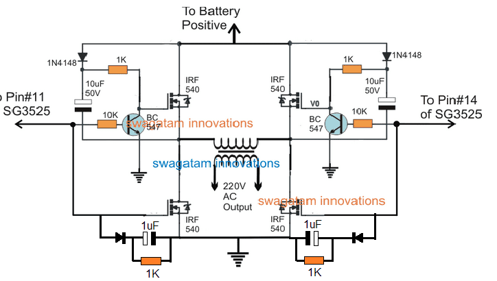
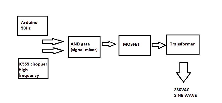 The proposed design consists of an Arduino which generates 50Hz constant square wave.
An IC 555 chopper circuit generates high frequency pulse.
The actual chopping of these two signals is done by IC 7408, which is AND gate.
The mixed signal is fed to gate of MOSFET.
The frequency of IC 555 can be varied for adjusting the output voltage by tuning the variable resistor.
The proposed design consists of an Arduino which generates 50Hz constant square wave.
An IC 555 chopper circuit generates high frequency pulse.
The actual chopping of these two signals is done by IC 7408, which is AND gate.
The mixed signal is fed to gate of MOSFET.
The frequency of IC 555 can be varied for adjusting the output voltage by tuning the variable resistor.
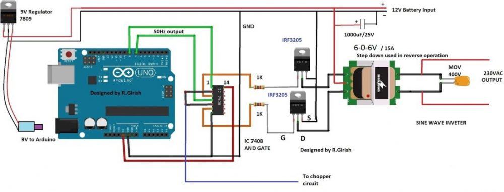 The constant 50Hz square wave is generated across pin #7 and pin #8 of Arduino.
This flip-flop signal is fed to pin #1 and pin #4 of IC 7408. These two pins are of two different AND gates.
The high frequency chopping signal is fed to pin #2 and #5. The AND gate allows only when two inputs are high, since the Arduino frequency output is lower and IC555 higher, we get chopped signal at the corresponding gate output.
The chopped output is fed to MOSFET with a current limiting resistor for limiting the gate capacitor charging rate.
A 12V 15A or higher rated transformer can be used if you need higher wattage output.
A 400V metal oxide varistor is utilized across the output for suppressing initial high voltage surge while turning on the inverter; it could be several hundreds of volts in magnitude.
A 9V regulator is used for arduino as constant voltage source.
A 1000uF or higher capacitance can be used at battery input for smooth starting and to protect the inverter from sudden voltage fluctuations.
The constant 50Hz square wave is generated across pin #7 and pin #8 of Arduino.
This flip-flop signal is fed to pin #1 and pin #4 of IC 7408. These two pins are of two different AND gates.
The high frequency chopping signal is fed to pin #2 and #5. The AND gate allows only when two inputs are high, since the Arduino frequency output is lower and IC555 higher, we get chopped signal at the corresponding gate output.
The chopped output is fed to MOSFET with a current limiting resistor for limiting the gate capacitor charging rate.
A 12V 15A or higher rated transformer can be used if you need higher wattage output.
A 400V metal oxide varistor is utilized across the output for suppressing initial high voltage surge while turning on the inverter; it could be several hundreds of volts in magnitude.
A 9V regulator is used for arduino as constant voltage source.
A 1000uF or higher capacitance can be used at battery input for smooth starting and to protect the inverter from sudden voltage fluctuations.
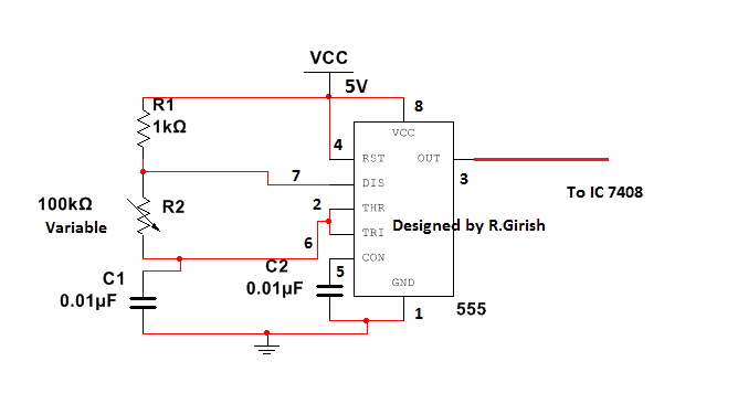 The chopper circuit is simple variable frequency generator, and the circuit is self-explanatory.
Now letˇŻs see how well the frequency from Arduino is chopped by high frequency generator circuit to achieve sine wave equivalent.
The chopper circuit is simple variable frequency generator, and the circuit is self-explanatory.
Now letˇŻs see how well the frequency from Arduino is chopped by high frequency generator circuit to achieve sine wave equivalent.
 The above simulation describes the output from arduino.
ItˇŻs a simple and stable 50Hz signal.
The above simulation describes the output from arduino.
ItˇŻs a simple and stable 50Hz signal.
 The above simulation shows the wave form after chopping the constant 50Hz signal.
The width of the chopping ratio can be adjusted by tuning the variable resistor and which also determine the output voltage.
The above chopped signal may not look like sine wave.
A real sine wave inverterˇŻs chopped wave form increase and decrease exponentially across x-axis.
But begin a simple design the chopping frequency stay constant and good enough to run most of electronic gadgets.
The above simulation shows the wave form after chopping the constant 50Hz signal.
The width of the chopping ratio can be adjusted by tuning the variable resistor and which also determine the output voltage.
The above chopped signal may not look like sine wave.
A real sine wave inverterˇŻs chopped wave form increase and decrease exponentially across x-axis.
But begin a simple design the chopping frequency stay constant and good enough to run most of electronic gadgets.

 As can be seen in the figure, the negative of the battery is connected with a series Rx resistor such that any current whether from the charger or from the inverter passes through this resistor during the irrespective operations.
This implies that during any of the operations the resistor Rx is able to generate a proportionate amount of potential drop across itself enabling the connected sensing circuit to respond to this developed voltage.
A bridge rectifier can also be seen connected across Rx to ensure that it always produces a single polarity voltage regardless of the polarity of the current that may be passing through Rx.
For example while charging the battery the current polarity could be the opposite compared to the inverting mode polarity, however the bridge rectifier corrects both the possibilities and offers a single polarity output for the next stage which is an opto coupler stage.
The optocoupler LED lights up whenever the battery is operated by some method and this is instantly converted into a triggering voltage for the BJT 2N2222 associated with the optocoupler transistor.
The 2N2222 along with the opto transistor is configured in a Darlington mode to ensure a high gain for the BJT pairs which in turn makes sure that the Rx value can be selected to be as small as possible, thereby allowing minimum resistance for the inverter operations.
As soon as the 2N2222 conducts it turn ON the connected fan which begins cooling the vital devices of the inverter and makes sure that they are never hot and vulnerable during the charging process or while the inverter is in the inverting mode.
As can be seen in the figure, the negative of the battery is connected with a series Rx resistor such that any current whether from the charger or from the inverter passes through this resistor during the irrespective operations.
This implies that during any of the operations the resistor Rx is able to generate a proportionate amount of potential drop across itself enabling the connected sensing circuit to respond to this developed voltage.
A bridge rectifier can also be seen connected across Rx to ensure that it always produces a single polarity voltage regardless of the polarity of the current that may be passing through Rx.
For example while charging the battery the current polarity could be the opposite compared to the inverting mode polarity, however the bridge rectifier corrects both the possibilities and offers a single polarity output for the next stage which is an opto coupler stage.
The optocoupler LED lights up whenever the battery is operated by some method and this is instantly converted into a triggering voltage for the BJT 2N2222 associated with the optocoupler transistor.
The 2N2222 along with the opto transistor is configured in a Darlington mode to ensure a high gain for the BJT pairs which in turn makes sure that the Rx value can be selected to be as small as possible, thereby allowing minimum resistance for the inverter operations.
As soon as the 2N2222 conducts it turn ON the connected fan which begins cooling the vital devices of the inverter and makes sure that they are never hot and vulnerable during the charging process or while the inverter is in the inverting mode.
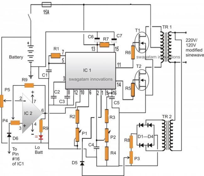
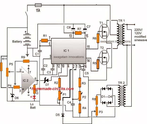 Here we can see that pin3 of the opamp now has it's own reference network using D6 and R11, and does not depend on the reference voltage from the IC 3525 pin16.
Pin6 of the opamp employs a zener diode in order to stop any leakages that might disturb pin10 of the SG3525 during its normal operations.
R11 = 10K
D6, D7 = zener diodes, 3.3V, 1/2 watt
Here we can see that pin3 of the opamp now has it's own reference network using D6 and R11, and does not depend on the reference voltage from the IC 3525 pin16.
Pin6 of the opamp employs a zener diode in order to stop any leakages that might disturb pin10 of the SG3525 during its normal operations.
R11 = 10K
D6, D7 = zener diodes, 3.3V, 1/2 watt
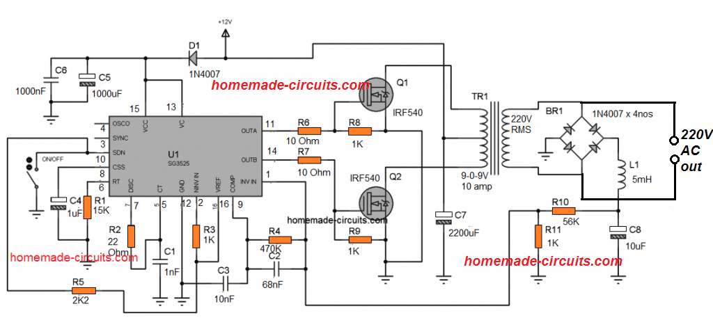
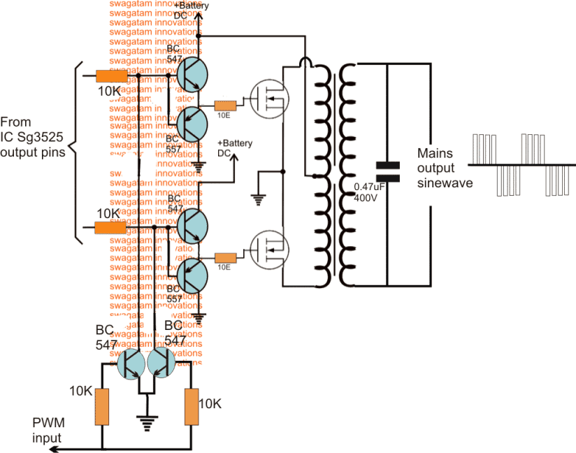 Warning: If you are using SPWM as the input, then please replace the lower BC547 with BC557. Emitters will connect with the buffer stage, Collector to Ground, Bases to SPWM Input.
As may be in the above diagram, the lower two BC547 transistors are triggered by a PWM feed or input, which causes them to switch according to the PWM ON/OFF duty cycles.
This in turn rapidly switch the 50Hz pulses of the BC547/BC557 coming from the SG3525 output pins.
The above operation ultimately force the mosfets also to turn ON and OFF number of times for each of the 50/60Hz cycles and consequently produce a similar waveform at the output of the connected transformer.
Preferably, the PWM input frequency should be 4 times more than the base 50 or 60Hz frequency.
so that each 50/60Hz cycles are broken into 4 or 5 pieces and not more than this, which could otherwise give rise to unwanted harmonics and mosfet heating.
PWM Circuit
The PWM input feed for the above explained design can be acquired by using any standard IC 555 astable design as shown below:
Warning: If you are using SPWM as the input, then please replace the lower BC547 with BC557. Emitters will connect with the buffer stage, Collector to Ground, Bases to SPWM Input.
As may be in the above diagram, the lower two BC547 transistors are triggered by a PWM feed or input, which causes them to switch according to the PWM ON/OFF duty cycles.
This in turn rapidly switch the 50Hz pulses of the BC547/BC557 coming from the SG3525 output pins.
The above operation ultimately force the mosfets also to turn ON and OFF number of times for each of the 50/60Hz cycles and consequently produce a similar waveform at the output of the connected transformer.
Preferably, the PWM input frequency should be 4 times more than the base 50 or 60Hz frequency.
so that each 50/60Hz cycles are broken into 4 or 5 pieces and not more than this, which could otherwise give rise to unwanted harmonics and mosfet heating.
PWM Circuit
The PWM input feed for the above explained design can be acquired by using any standard IC 555 astable design as shown below:
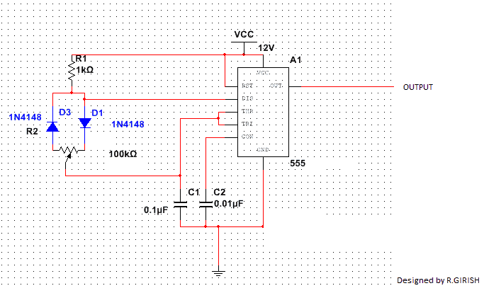 This IC 555 based PWM circuit can be used for feeding an optimized PWM to the bases of the BC547 transistors in the first design such that the output from the SG3525 inverter circuit acquires an RMS value close to mains pure sinewave waveform RMS value.
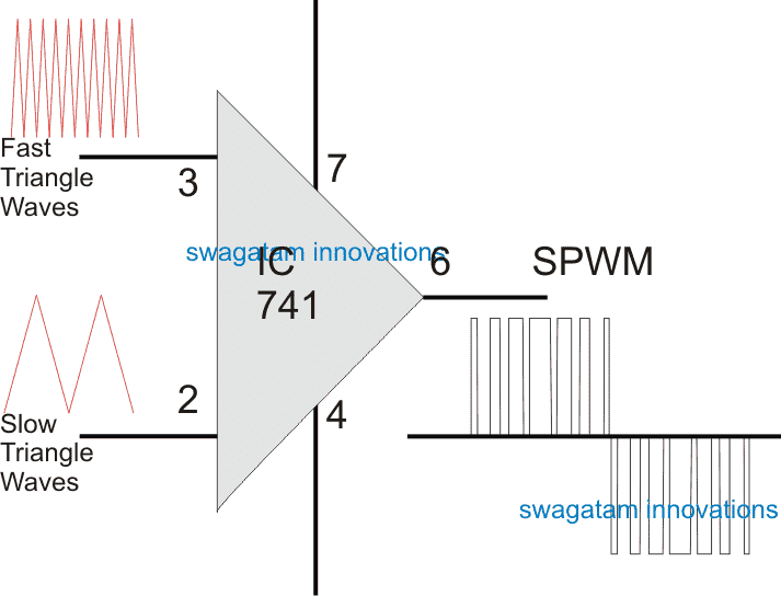
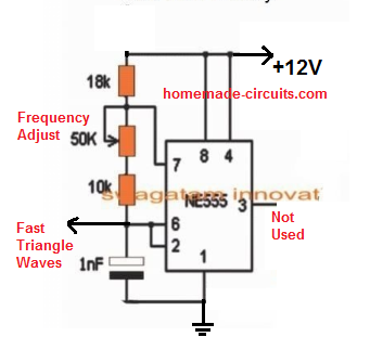
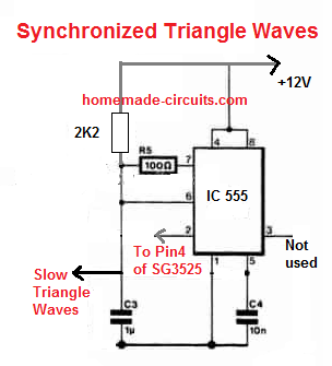 THE SLOW TRIANGLE WAVES FREQUENCY MUST BE EQUAL TO THE DESIRED OUTPUT FREQUENCY OF THE INVERTER.
THIS MAY BE 50 Hz OR 60 Hz, AND EQUAL TO PIN#4 FREQUENCY OF SG3525
As can be seen in the above two images, the fast triangle waves are achieved from an ordinary IC 555 astable.
However, the slow triangle waves are acquired through an IC 555 wired like a "square wave to triangle wave generator".
The square waves or the rectangular waves are acquired from pin#4 of SG3525. This is important as it synchronizes the op amp 741 output perfectly with the 50 Hz frequency of the SG3525 circuit.
This in turn creates correctly dimensioned SPWM sets across the two MOSFET channels.
When this optimized PWM is fed to the first circuit design causes the output from the transformer to produce a further improved and gentle sine waveform having properties much identical to a standard AC mains sine waveform.
However even for an SPWM, the RMS value will need to be correctly set initially in order to produce the correct voltage output at the output of the transformer.
Once implemented one can expect a real sinewave equivalent output from any SG3525 inverter design or may be from any square wave inverter model.
If you have more doubts regarding SG3525 pure sinewave inverter circuit you can feel free to express them through your comments.
UPDATE
A basic example design of a SG3525 oscillator stage can be seen below, this design could be integrated with the above explained PWM sinewave BJT/mosfet stage for getting the required enhanced version of the SG3525 design:
THE SLOW TRIANGLE WAVES FREQUENCY MUST BE EQUAL TO THE DESIRED OUTPUT FREQUENCY OF THE INVERTER.
THIS MAY BE 50 Hz OR 60 Hz, AND EQUAL TO PIN#4 FREQUENCY OF SG3525
As can be seen in the above two images, the fast triangle waves are achieved from an ordinary IC 555 astable.
However, the slow triangle waves are acquired through an IC 555 wired like a "square wave to triangle wave generator".
The square waves or the rectangular waves are acquired from pin#4 of SG3525. This is important as it synchronizes the op amp 741 output perfectly with the 50 Hz frequency of the SG3525 circuit.
This in turn creates correctly dimensioned SPWM sets across the two MOSFET channels.
When this optimized PWM is fed to the first circuit design causes the output from the transformer to produce a further improved and gentle sine waveform having properties much identical to a standard AC mains sine waveform.
However even for an SPWM, the RMS value will need to be correctly set initially in order to produce the correct voltage output at the output of the transformer.
Once implemented one can expect a real sinewave equivalent output from any SG3525 inverter design or may be from any square wave inverter model.
If you have more doubts regarding SG3525 pure sinewave inverter circuit you can feel free to express them through your comments.
UPDATE
A basic example design of a SG3525 oscillator stage can be seen below, this design could be integrated with the above explained PWM sinewave BJT/mosfet stage for getting the required enhanced version of the SG3525 design:
 Complete circuit diagram and PCB layout for the proposed SG3525 pure sine wave inverter circuit.
Courtesy: Ainsworth Lynch
Complete circuit diagram and PCB layout for the proposed SG3525 pure sine wave inverter circuit.
Courtesy: Ainsworth Lynch
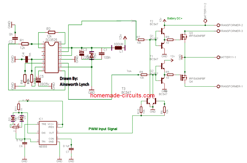
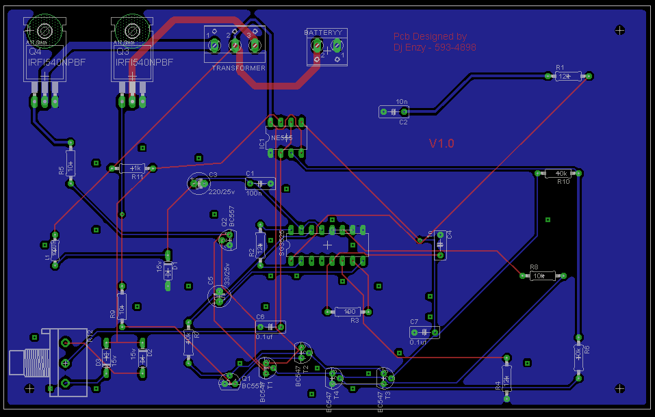
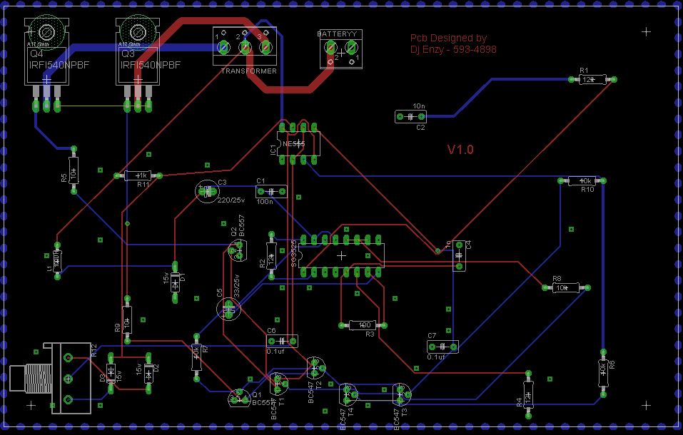
 My Reply:
Hello Anas,
first try the basic set up as explained in this SG3525 inverter article, if everything goes well, after that you can try connecting more mosfets in parallel.....
the inverter shown in the above daigram is a basic square wave design, in order to convert it to sine wave you must follow the steps explained below The mosfet gate/resistor ends must be configured with a BJT stage and the 555 IC PWM should be connected as indicated in the following diagram:
My Reply:
Hello Anas,
first try the basic set up as explained in this SG3525 inverter article, if everything goes well, after that you can try connecting more mosfets in parallel.....
the inverter shown in the above daigram is a basic square wave design, in order to convert it to sine wave you must follow the steps explained below The mosfet gate/resistor ends must be configured with a BJT stage and the 555 IC PWM should be connected as indicated in the following diagram:
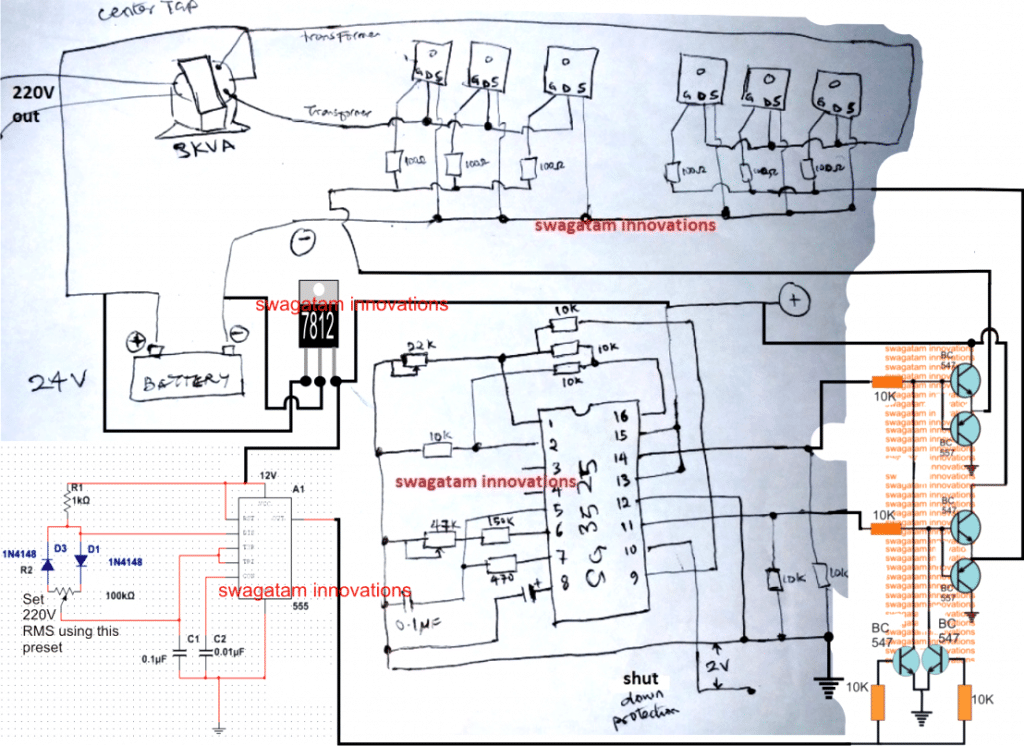

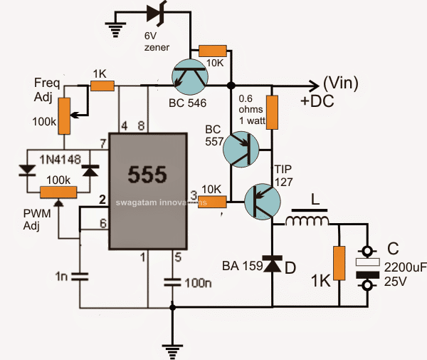 The above diagram shows a simple IC 555 based buck converter circuit.
We can see two pots, the upper pot optimizes the buck frequency, and the lower pot optimizes the PWM, both these adjustments could be tweaked for getting an optimum response across C.
The BC557 transistor and the 0.6 ohm resistor forms a current limiter for safeguarding the TIP127 (driver transistor) from over current during the adjustment process, later this resistance value could be adjusted for higher current outputs along with a higher rated driver transistor.
Selecting the inductor could be tricky.....
1) The frequency may be related to the inductor diameter, lower diameter will call for higher frequency and vice versa,
2) Number of turns will affect the output voltage and also the output current and this parameter would be related to the PWM adjustments.
3) The thickness of the wire would determine the current limit for the output, all these will need to be optimized by some trial and error.
As a rule of thumb, start with a 1/2 inch diameter and number of turns equal to the supply voltage....use ferrite as the core, and after this you can begin the above suggested optimization process.
This takes care of the buck converter which can be used with a given higher voltage / low current solar panel to obtain an equivalently optimized lower voltage / higher current output, as per the load specs, satisfying the equation:
The above diagram shows a simple IC 555 based buck converter circuit.
We can see two pots, the upper pot optimizes the buck frequency, and the lower pot optimizes the PWM, both these adjustments could be tweaked for getting an optimum response across C.
The BC557 transistor and the 0.6 ohm resistor forms a current limiter for safeguarding the TIP127 (driver transistor) from over current during the adjustment process, later this resistance value could be adjusted for higher current outputs along with a higher rated driver transistor.
Selecting the inductor could be tricky.....
1) The frequency may be related to the inductor diameter, lower diameter will call for higher frequency and vice versa,
2) Number of turns will affect the output voltage and also the output current and this parameter would be related to the PWM adjustments.
3) The thickness of the wire would determine the current limit for the output, all these will need to be optimized by some trial and error.
As a rule of thumb, start with a 1/2 inch diameter and number of turns equal to the supply voltage....use ferrite as the core, and after this you can begin the above suggested optimization process.
This takes care of the buck converter which can be used with a given higher voltage / low current solar panel to obtain an equivalently optimized lower voltage / higher current output, as per the load specs, satisfying the equation:
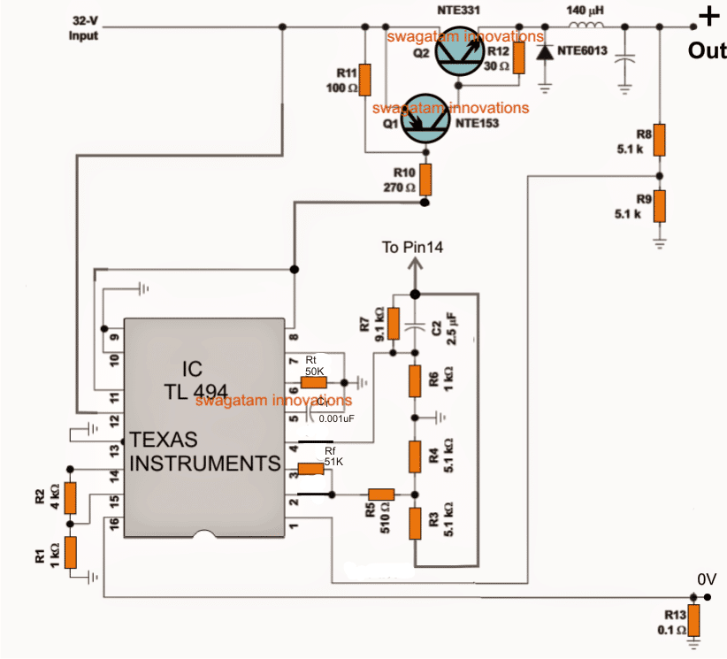 Here the R8, R9 can be tweaked for adjusting the output voltage, and the R13 for optimizing the current output.
After building and configuring the buck converter with an appropriate solar panel, a perfectly optimized output could be expected for charging a given battery.
Now, since the above converters are not facilitated with a full charge cut off, an external opamp based cut-off circuit might be additionally required for enabling a fully automatic charging feature as shown below.
Here the R8, R9 can be tweaked for adjusting the output voltage, and the R13 for optimizing the current output.
After building and configuring the buck converter with an appropriate solar panel, a perfectly optimized output could be expected for charging a given battery.
Now, since the above converters are not facilitated with a full charge cut off, an external opamp based cut-off circuit might be additionally required for enabling a fully automatic charging feature as shown below.
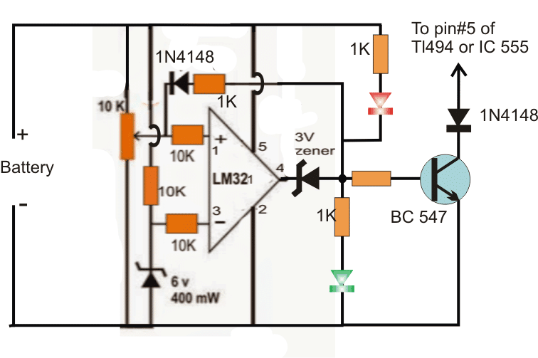 The shown simple full charge cut-off circuit could be added with any of the buck converters for ensuring that the battery is never over charged once it reaches the specified full charge level.
The above buck converter design will allow you to get a reasonably efficient and optimal charging for the connected battery.
Although this buck converter would provide good results, the efficiency could deteriorate as the sun went down.
To tackle this, one could think of employing a MPPT charger circuit for acquiring the most optimal output from the buckcircuit.
So a Buck circuit in conjunction with a self optimizing MPPT circuit could help in churning out the maximum from the available sun light.
I have already explained a related post in one of my previous posts, the same could be applied while a solar inverter circuit design
The shown simple full charge cut-off circuit could be added with any of the buck converters for ensuring that the battery is never over charged once it reaches the specified full charge level.
The above buck converter design will allow you to get a reasonably efficient and optimal charging for the connected battery.
Although this buck converter would provide good results, the efficiency could deteriorate as the sun went down.
To tackle this, one could think of employing a MPPT charger circuit for acquiring the most optimal output from the buckcircuit.
So a Buck circuit in conjunction with a self optimizing MPPT circuit could help in churning out the maximum from the available sun light.
I have already explained a related post in one of my previous posts, the same could be applied while a solar inverter circuit design
 In this solar inverter, the panel can be seen directly attached with the inverter circuit and the inverter is able to produce the required power as long as the sun rays are optimally incident on the panel.
The inverter would keep running at a reasonably good power output rate for so long as the panel produces voltage above 45V......
that is 60V at the peak and down to 45V probably during afternoon.
From the above shown 48V inverter circuit it is evident that a solar inverter design does not need to be too crucial with its features and specifications.
You can connect any form of inverter with any solar panel for getting the required results.
It implies that you can select any inverter circuit from the list, and configure it with a procured solar panel, and begin reaping free electricity at will.
The only crucial but easy to implement parameters are the voltage and the current specifications of the inverter and the solar panel which must not differ by much, as explained in our earlier discussion.
In this solar inverter, the panel can be seen directly attached with the inverter circuit and the inverter is able to produce the required power as long as the sun rays are optimally incident on the panel.
The inverter would keep running at a reasonably good power output rate for so long as the panel produces voltage above 45V......
that is 60V at the peak and down to 45V probably during afternoon.
From the above shown 48V inverter circuit it is evident that a solar inverter design does not need to be too crucial with its features and specifications.
You can connect any form of inverter with any solar panel for getting the required results.
It implies that you can select any inverter circuit from the list, and configure it with a procured solar panel, and begin reaping free electricity at will.
The only crucial but easy to implement parameters are the voltage and the current specifications of the inverter and the solar panel which must not differ by much, as explained in our earlier discussion.
 Note: The SD pin#5 is mistakenly shown connected with Ct, please make sure to connect it with ground line and not with Ct.
The above solar inverter circuit using using PWM sine wave can be studied elaborately in the article titled 1.5 ton AC solar inverter circuit
From the above tutorial it is now clear that designing a solar inverter is after all not so difficult and could be efficiently implemented if you are equipped with some basic knowledge of electronic concepts such as buck converts, solar panel and inverters.
A sinewave version of the above can be seen here:
Note: The SD pin#5 is mistakenly shown connected with Ct, please make sure to connect it with ground line and not with Ct.
The above solar inverter circuit using using PWM sine wave can be studied elaborately in the article titled 1.5 ton AC solar inverter circuit
From the above tutorial it is now clear that designing a solar inverter is after all not so difficult and could be efficiently implemented if you are equipped with some basic knowledge of electronic concepts such as buck converts, solar panel and inverters.
A sinewave version of the above can be seen here:
 While the optocoupler is in the non-triggered mode, the BC547 directly associated with the opto goes into the triggered mode, which keeps the second BC547 switched OFF.
This situation enables the right side triac to remain switched ON, and the other triac is held switched OFF.
In this condition any load connected with the right triac becomes operational and stays switched ON.
Now as soon as a trigger is applied to the opto coupler, it switches ON, and in turn switches OFF the connected BC547.
This situation switches ON the second BC547 and consequently the right side triac is switched OFF, ensuring that the left side triac is now switched ON.
The above condition immediately toggles the second load ON and switches OFF the earlier load, effectively fulfilling the required alternate switching of the load with the help of an isolated external DC trigger.
The two LED connected with the bases of the two BJTs indicate which load is in the activated state at any moment while the triac SPDT relay circuit is being operated.
While the optocoupler is in the non-triggered mode, the BC547 directly associated with the opto goes into the triggered mode, which keeps the second BC547 switched OFF.
This situation enables the right side triac to remain switched ON, and the other triac is held switched OFF.
In this condition any load connected with the right triac becomes operational and stays switched ON.
Now as soon as a trigger is applied to the opto coupler, it switches ON, and in turn switches OFF the connected BC547.
This situation switches ON the second BC547 and consequently the right side triac is switched OFF, ensuring that the left side triac is now switched ON.
The above condition immediately toggles the second load ON and switches OFF the earlier load, effectively fulfilling the required alternate switching of the load with the help of an isolated external DC trigger.
The two LED connected with the bases of the two BJTs indicate which load is in the activated state at any moment while the triac SPDT relay circuit is being operated.
 Warning: The circuit shown above is not isolated from the mains AC input supply and therefore is extremely dangerous to touch in the switched ON condition.
 Here we can see that the main UPS changeover function is carried out by a couple of DPDT relay stages.
Both the DPDT relays are powered from a 12 V AC to DC power supply or adapter.
The left side DPDT relay can be seen controlling the battery charger.
The battery charger gets powered when AC mains is available through the upper relay contacts, and supplies the charging input to the battery via the lower relay contacts.
When AC mains fails, the relay contacts changeover to the N/C contacts.
The upper relay contacts switches OFF power to the battery charger, while the lower contacts now connects the battery with the inverter to initiate the inverter mode operation.
The right side relay contacts are used for changing over from grid AC mains to the inverter AC mains, and vice versa.
Here we can see that the main UPS changeover function is carried out by a couple of DPDT relay stages.
Both the DPDT relays are powered from a 12 V AC to DC power supply or adapter.
The left side DPDT relay can be seen controlling the battery charger.
The battery charger gets powered when AC mains is available through the upper relay contacts, and supplies the charging input to the battery via the lower relay contacts.
When AC mains fails, the relay contacts changeover to the N/C contacts.
The upper relay contacts switches OFF power to the battery charger, while the lower contacts now connects the battery with the inverter to initiate the inverter mode operation.
The right side relay contacts are used for changing over from grid AC mains to the inverter AC mains, and vice versa.
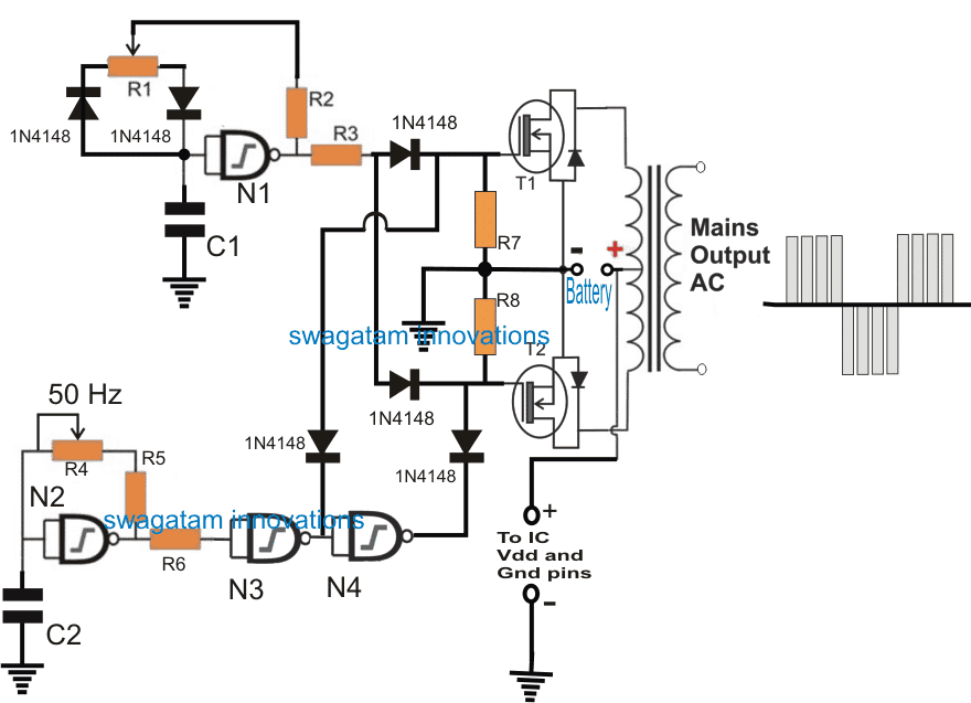 Parts List
N1---N3 NAND gates from IC 4093
Mosfets = IRF540
Transformer = 9-0-9V / 10 amps / 220V or 120V
R3/R4 = 220k pot
C1/C2 = 0.1uF/50V
All resistors are 1K 1/4 watt
Parts List
N1---N3 NAND gates from IC 4093
Mosfets = IRF540
Transformer = 9-0-9V / 10 amps / 220V or 120V
R3/R4 = 220k pot
C1/C2 = 0.1uF/50V
All resistors are 1K 1/4 watt
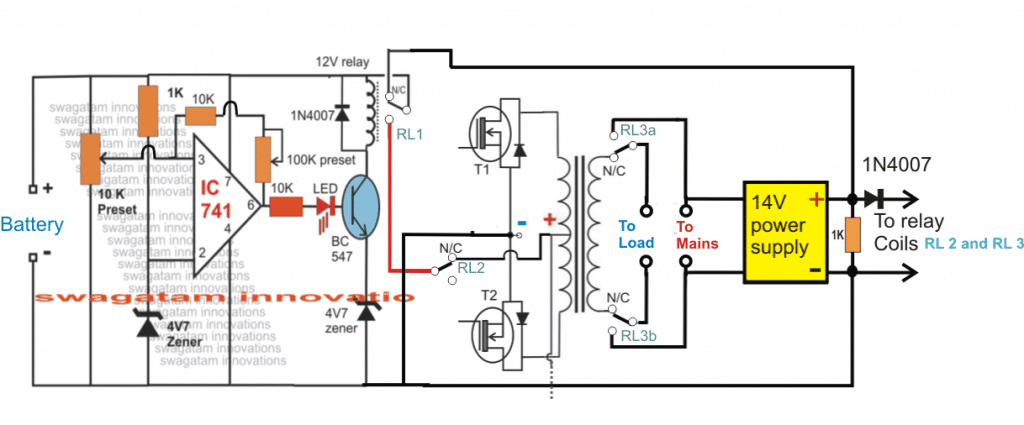 In all there are 3 sets of relays which are used in this stage:
1) 2 nos of SPDT relays in the form of RL1 and RL2
2) One DPDT relay as RL3a and RL3b.
RL1 is attached with the battery charger circuit and it controls the high/low cut charge level cut-off for the battery and determines when the battery needs is ready to be used for the inverter and when it needs to be removed.
The SPDT RL2 and the DPDT (RL3a and RL3b) are used for the instant changeover actions during a power failure and restoration.
RL2 contacts are used for connecting or disconnecting the center tap of the transformer with the battery depending on the mains availability or absence.
RL3a and RLb which are the two sets of contacts of the DPDT relay become responsible for switching the load across the inverter mains or the grid mains during power outages or restoration periods.
The coils of RL2 and DPDT RL3a/RL3b are joined with a 14V power supply such that these relays quickly activate and deactivate depending on the input mains status and do the necessary changeover actions.
This 14V supply is also used as the source for charging the inverter battery while the mains power is available.
The coil of the RL1 can be seen connected with the opamp circuit which controls the battery charging of the battery and ensures the supply to the battery from the 14V source is cut-off as soon as it reaches the same value.
It also makes sure that while the battery is in the inverter mode and is consumed by the load, its lower discharge level never goes below 11V, and it cuts off the battery from the inverter when it reaches around this level.
Both these operations are executed by the relay RL1 in response to the opamp commands.
The setting-up procedure for the above UPS battery charger circuit can be learned from this article which discuses how to make a low high cut off battery charger using IC 741
Now it simply needs to integrate all the above stages together for executing a decent looking small UPS, which could be used for providing an uninterruptible power to your PC or any other similar gadget.
That's it, this concludes our tutorial for designing a personal UPS circuit which can be easily done by any new hobbyist by following the above detailed guide.
In all there are 3 sets of relays which are used in this stage:
1) 2 nos of SPDT relays in the form of RL1 and RL2
2) One DPDT relay as RL3a and RL3b.
RL1 is attached with the battery charger circuit and it controls the high/low cut charge level cut-off for the battery and determines when the battery needs is ready to be used for the inverter and when it needs to be removed.
The SPDT RL2 and the DPDT (RL3a and RL3b) are used for the instant changeover actions during a power failure and restoration.
RL2 contacts are used for connecting or disconnecting the center tap of the transformer with the battery depending on the mains availability or absence.
RL3a and RLb which are the two sets of contacts of the DPDT relay become responsible for switching the load across the inverter mains or the grid mains during power outages or restoration periods.
The coils of RL2 and DPDT RL3a/RL3b are joined with a 14V power supply such that these relays quickly activate and deactivate depending on the input mains status and do the necessary changeover actions.
This 14V supply is also used as the source for charging the inverter battery while the mains power is available.
The coil of the RL1 can be seen connected with the opamp circuit which controls the battery charging of the battery and ensures the supply to the battery from the 14V source is cut-off as soon as it reaches the same value.
It also makes sure that while the battery is in the inverter mode and is consumed by the load, its lower discharge level never goes below 11V, and it cuts off the battery from the inverter when it reaches around this level.
Both these operations are executed by the relay RL1 in response to the opamp commands.
The setting-up procedure for the above UPS battery charger circuit can be learned from this article which discuses how to make a low high cut off battery charger using IC 741
Now it simply needs to integrate all the above stages together for executing a decent looking small UPS, which could be used for providing an uninterruptible power to your PC or any other similar gadget.
That's it, this concludes our tutorial for designing a personal UPS circuit which can be easily done by any new hobbyist by following the above detailed guide.

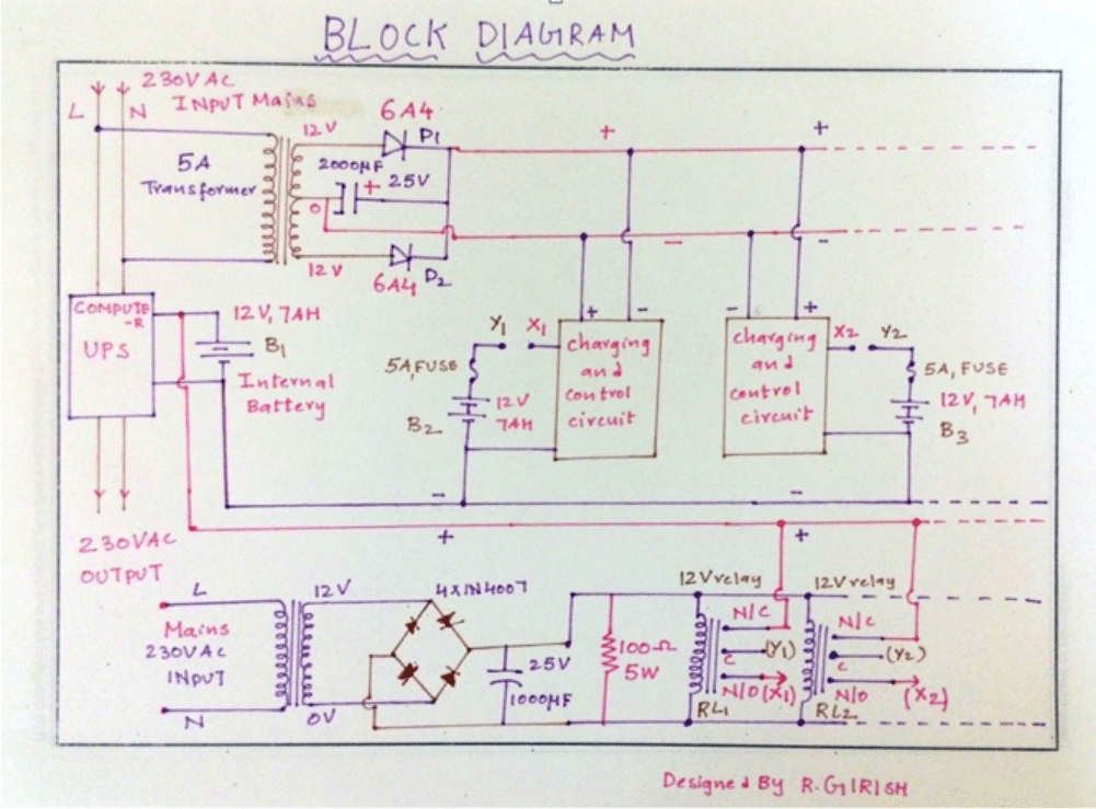

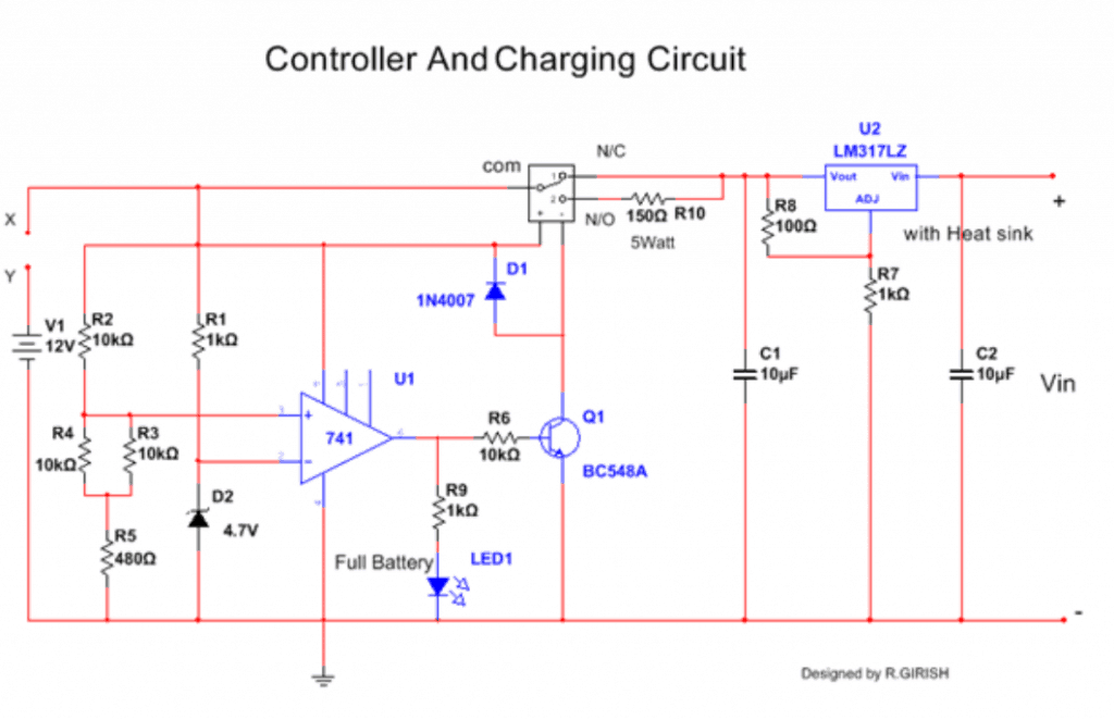 There are two transformer one for charging which is 5A or more, the other transformer (500mA) for sensing the presence or absence of mains power.
If the mains are present relays are activated and connected to charger.
If mains are absent relays are deactivated and batteries are connected to UPS.
The 5A charging transformer may be replaced with SMPS.
The 100 ohm/5 watt resistor for quick discharge of 1000uf capacitor, so that relay can be deactivated instantly during power failure.
During power failure all the batteries connect automatically in parallel powering the UPS.
When the batteries are at low state the UPS automatically disconnect its batteries and shutoff itself.
There is always low battery cut-off circuitry in the UPS.
Most of the computer UPS gives out modified sine wave during power failure, and mains sine wave during normal state.
This is suitable for most of home appliances.
WARNINGS:
1) Do not omit the internal battery, this plays an important role in giving uninterrupted power output and UPS circuitry gets unstable without the internal battery.
2) It is not recommended to connect more than 5 external batteries.
3) Do not connect this UPS to mains as what we do when we have genuine manufactured home UPS [IMPORTANT].
4) Use a branded computer UPS to proceed this project.
5) Never overload the UPS during normal/backup state.
6) Make sure that all internal and external batteries are with same capacity (AH) and age.
7) Do not connect any inductive loads other than table fan.
8) Place the whole setup at well ventilated area and donˇŻt allow water to contact the setup.
9) Disconnect the gadgets immediately if you found misbehaving.
There are two transformer one for charging which is 5A or more, the other transformer (500mA) for sensing the presence or absence of mains power.
If the mains are present relays are activated and connected to charger.
If mains are absent relays are deactivated and batteries are connected to UPS.
The 5A charging transformer may be replaced with SMPS.
The 100 ohm/5 watt resistor for quick discharge of 1000uf capacitor, so that relay can be deactivated instantly during power failure.
During power failure all the batteries connect automatically in parallel powering the UPS.
When the batteries are at low state the UPS automatically disconnect its batteries and shutoff itself.
There is always low battery cut-off circuitry in the UPS.
Most of the computer UPS gives out modified sine wave during power failure, and mains sine wave during normal state.
This is suitable for most of home appliances.
WARNINGS:
1) Do not omit the internal battery, this plays an important role in giving uninterrupted power output and UPS circuitry gets unstable without the internal battery.
2) It is not recommended to connect more than 5 external batteries.
3) Do not connect this UPS to mains as what we do when we have genuine manufactured home UPS [IMPORTANT].
4) Use a branded computer UPS to proceed this project.
5) Never overload the UPS during normal/backup state.
6) Make sure that all internal and external batteries are with same capacity (AH) and age.
7) Do not connect any inductive loads other than table fan.
8) Place the whole setup at well ventilated area and donˇŻt allow water to contact the setup.
9) Disconnect the gadgets immediately if you found misbehaving.

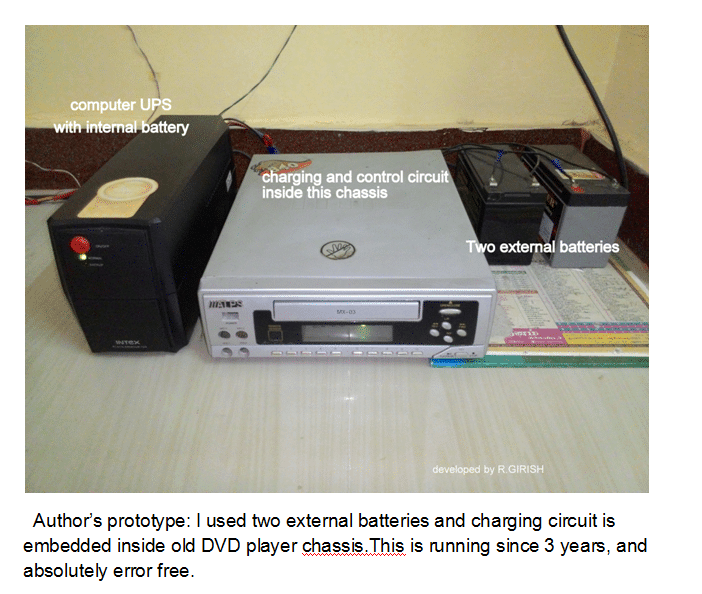 AuthorˇŻs prototype
which shows how he could convert his computer UPS to home UPS:
I used two external batteries and charging circuit is embedded inside old DVD player chassis.This is running since 3 years, and absolutely error free.
AuthorˇŻs prototype
which shows how he could convert his computer UPS to home UPS:
I used two external batteries and charging circuit is embedded inside old DVD player chassis.This is running since 3 years, and absolutely error free.
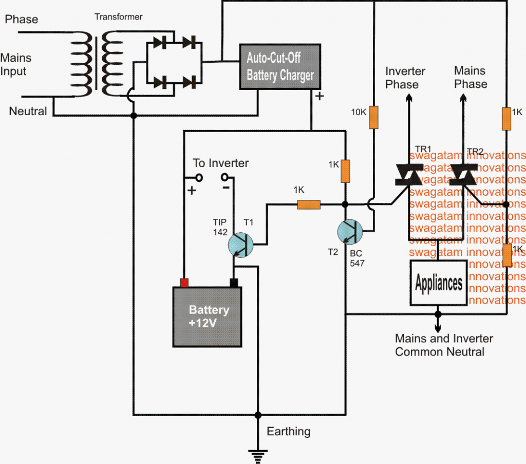
 Hello Puneet,
Now it looks OK, and hopefully should function as per the expectations.
The trigger to the opto could be extracted from either of the mains supply, that is either from the inverter mains or the grid mains, depending on which one is selected for the activating the triac changeover circuit.
The input of the opto could be connected with these supplies through a 68K 5 watt resistor.
Hello Puneet,
Now it looks OK, and hopefully should function as per the expectations.
The trigger to the opto could be extracted from either of the mains supply, that is either from the inverter mains or the grid mains, depending on which one is selected for the activating the triac changeover circuit.
The input of the opto could be connected with these supplies through a 68K 5 watt resistor.
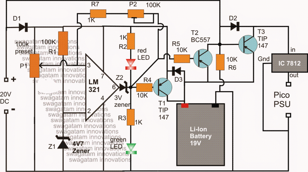
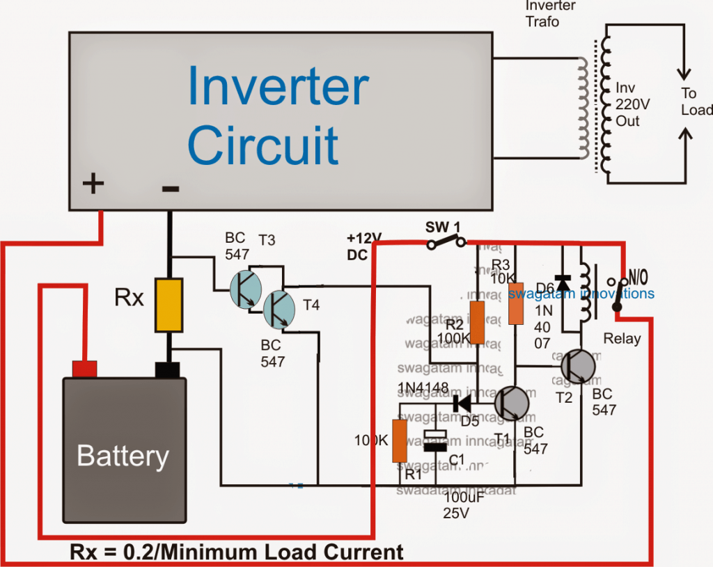 In a few of ay previous posts we have learned how to make overload cut off circuit such as:
Low Battery Cut-off and Overload Protection Circuit.
Motor over current protector circuit
However, the present concept deals with an opposite situation wherein a no load condition is supposed to be detected and cut off for persisting, that is we discuss a circuit for preventing a no load condition for inverters.
As shown in the above figure, a no load detector and cut of procedure can be initiated by incorporating this design in any inverter circuit.
The operational details may be understood with the following explanation:
The circuit comprises two stage, namely the current amplifier and sensor stage using the T3/T4 Darlington pair, and a simple delay ON stage using T1, T2 and the associated components.
As soon SW1 is switched ON, the delay-ON timer counting is initiated through C1 which begins charging via R2 and D5 keeping T1 switched off in the process.
With T1 switched T2 is switched ON which in turn switches ON the relay.
The relay enables the positive from the battery to get connected with the inverter so that the inverter is able to start and generate the required AC mains to the intended appliances.
With the presence of a load at the output the battery undergoes a proportionate amount current consumption, and in the course Rx experiences a current flow through it.
This current is transformed into a proportionate amount of voltage across Rx which is sensed by the T3/T4 Darlington pair and it is forced to switch ON.
With T3/T4 switched ON, C1 is instantly inhibited from getting charged, which leads to an immediate disabling of the delay ON timer, making sure that the output of the inverter continues to supply the voltage to the load.
However, suppose the output of the inverter is devoid of any load (no load condition), T3/T4 is then unable to switch ON, which allows C1 to get charged gradually until the potential across it becomes sufficient to trigger T1.
Once T1 is triggered, T2 is cut off and so is the relay.
With the relay contacts cut off and shifted from N/O to the N/C contact, the positive to the inverter is also cut off, the system comes to a stand still.
In a few of ay previous posts we have learned how to make overload cut off circuit such as:
Low Battery Cut-off and Overload Protection Circuit.
Motor over current protector circuit
However, the present concept deals with an opposite situation wherein a no load condition is supposed to be detected and cut off for persisting, that is we discuss a circuit for preventing a no load condition for inverters.
As shown in the above figure, a no load detector and cut of procedure can be initiated by incorporating this design in any inverter circuit.
The operational details may be understood with the following explanation:
The circuit comprises two stage, namely the current amplifier and sensor stage using the T3/T4 Darlington pair, and a simple delay ON stage using T1, T2 and the associated components.
As soon SW1 is switched ON, the delay-ON timer counting is initiated through C1 which begins charging via R2 and D5 keeping T1 switched off in the process.
With T1 switched T2 is switched ON which in turn switches ON the relay.
The relay enables the positive from the battery to get connected with the inverter so that the inverter is able to start and generate the required AC mains to the intended appliances.
With the presence of a load at the output the battery undergoes a proportionate amount current consumption, and in the course Rx experiences a current flow through it.
This current is transformed into a proportionate amount of voltage across Rx which is sensed by the T3/T4 Darlington pair and it is forced to switch ON.
With T3/T4 switched ON, C1 is instantly inhibited from getting charged, which leads to an immediate disabling of the delay ON timer, making sure that the output of the inverter continues to supply the voltage to the load.
However, suppose the output of the inverter is devoid of any load (no load condition), T3/T4 is then unable to switch ON, which allows C1 to get charged gradually until the potential across it becomes sufficient to trigger T1.
Once T1 is triggered, T2 is cut off and so is the relay.
With the relay contacts cut off and shifted from N/O to the N/C contact, the positive to the inverter is also cut off, the system comes to a stand still.
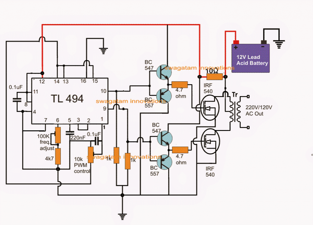 Here we discuss a versatile PWM based modified sine wave inverter circuit which incorporates the IC TL494 for the required advanced PWM processing.
Referring to the figure above, the various pinout functions of the IC for implementing the PWM inverter operations may be understood with the following points:
Here we discuss a versatile PWM based modified sine wave inverter circuit which incorporates the IC TL494 for the required advanced PWM processing.
Referring to the figure above, the various pinout functions of the IC for implementing the PWM inverter operations may be understood with the following points:
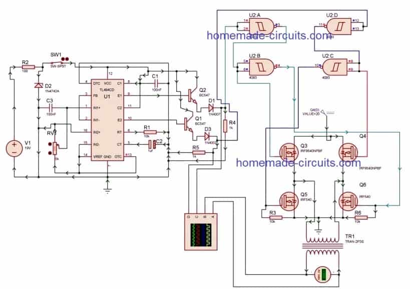 As can be seen, a combination of p channel and n channel mosfets are used for creating the full bridge network, which makes things rather simple and avoids the complex bootstrap capacitor network, which normally become necessary for full bridge inverters having only n channel mosfet.
However incorporating p channel mosfets on the high side and n channel at the low side makes the design prone to shoot-through issue.
To avoid shoot-through a sufficient dead time must be ensured with the IC TL 494, and thus prevent any possibility of this situation.
The IC 4093 gates are use for guaranteeing perfect isolation of the two sides of the full bridge conduction, and correct switching of the transformer primary.
As can be seen, a combination of p channel and n channel mosfets are used for creating the full bridge network, which makes things rather simple and avoids the complex bootstrap capacitor network, which normally become necessary for full bridge inverters having only n channel mosfet.
However incorporating p channel mosfets on the high side and n channel at the low side makes the design prone to shoot-through issue.
To avoid shoot-through a sufficient dead time must be ensured with the IC TL 494, and thus prevent any possibility of this situation.
The IC 4093 gates are use for guaranteeing perfect isolation of the two sides of the full bridge conduction, and correct switching of the transformer primary.

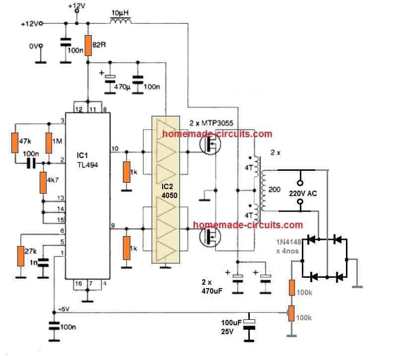 The 100k preset can be adjusted appropriately for setting up the required constant output voltage limit.
The transformer shown is a ferrite core transformer, and therefore the frequency is set at a very high level from the IC.
Nevertheless, you can easily use an iron core based transformer and reduce the frequency to 50 Hz or 60 Hz for 120 V output.
The 100k preset can be adjusted appropriately for setting up the required constant output voltage limit.
The transformer shown is a ferrite core transformer, and therefore the frequency is set at a very high level from the IC.
Nevertheless, you can easily use an iron core based transformer and reduce the frequency to 50 Hz or 60 Hz for 120 V output.
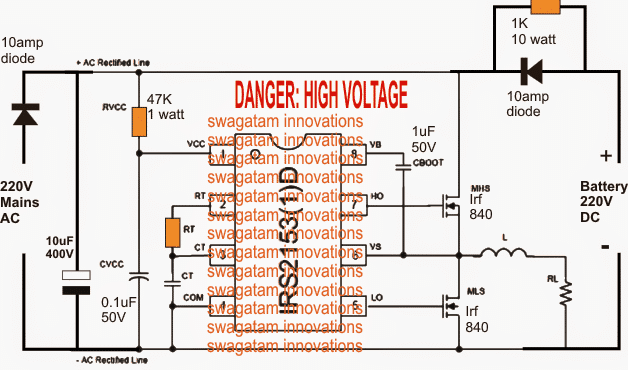
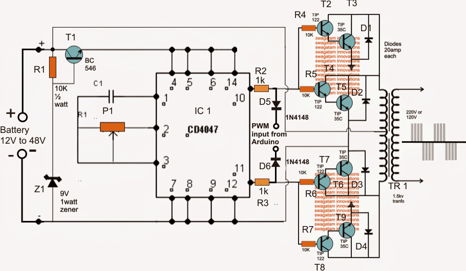
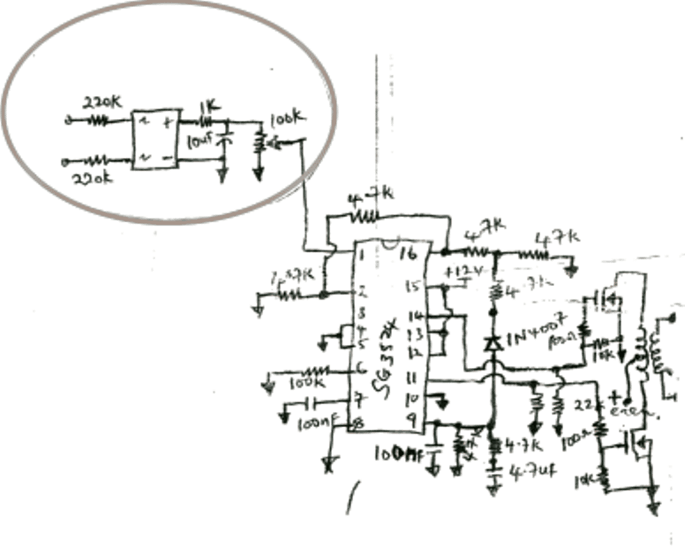
 The above design can be configured in the following manner, and in fact this appears to be technically more correct, and therefore is the recommended one.
This design will work regardless of the opto input switching voltage, right from 3V to 30V DC.
The above design can be configured in the following manner, and in fact this appears to be technically more correct, and therefore is the recommended one.
This design will work regardless of the opto input switching voltage, right from 3V to 30V DC.
 Here, although the poles appear to be a single pole, connected with the positive line, it could be simply separated and integrated with the different DC supplies for operating two individual loads, and implementing a DPDT SSR function.
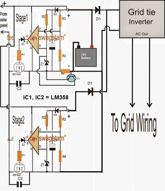 Referring to the above grid, solar panel optimizer circuit, we can see two basic identical stages using two opamps.
The two stages are exactly identical and form two parallel connected zero drop solar charge controller stages.
The upper stage1 includes a constant current feature due to the presence of the BJT BC547 and Rx.
Rx may be selected using the following formula:
0.7x10/Battery AH
The above feature ensures a correct charging rate for the connected battery.
The lower solar charge controller is without a current controller and feeds the inverter (GTI) directly through a series diode, the battery also connects with the inverter through another individual series diode.
Both the solar charge controller circuits are designed to generate the maximum fixed charging voltage for the battery as well as for the inverter.
As long as the solar panel is able to receive peak sun light it overrides the battery voltage and allows the inverter to use current directly from the panel.
The procedures also allows the battery to get charged from the upper solar charge controller stage.
However as the sun light begins depleting the battery overrides the solar panel input and supplies the inverter with its power for carrying out the operations.
The inverter is a GTI which is tied with the grid mains and contributes in sync with the grid.
As long as the grid is stronger the GTI is allowed to be sedentary which proportionately prevents the battery from getting drained, however in case the grid voltage drops and becomes insufficient for powering the connected appliances, the GTI takes over and begins fulfilling the deficit through the conneced battery power.
Referring to the above grid, solar panel optimizer circuit, we can see two basic identical stages using two opamps.
The two stages are exactly identical and form two parallel connected zero drop solar charge controller stages.
The upper stage1 includes a constant current feature due to the presence of the BJT BC547 and Rx.
Rx may be selected using the following formula:
0.7x10/Battery AH
The above feature ensures a correct charging rate for the connected battery.
The lower solar charge controller is without a current controller and feeds the inverter (GTI) directly through a series diode, the battery also connects with the inverter through another individual series diode.
Both the solar charge controller circuits are designed to generate the maximum fixed charging voltage for the battery as well as for the inverter.
As long as the solar panel is able to receive peak sun light it overrides the battery voltage and allows the inverter to use current directly from the panel.
The procedures also allows the battery to get charged from the upper solar charge controller stage.
However as the sun light begins depleting the battery overrides the solar panel input and supplies the inverter with its power for carrying out the operations.
The inverter is a GTI which is tied with the grid mains and contributes in sync with the grid.
As long as the grid is stronger the GTI is allowed to be sedentary which proportionately prevents the battery from getting drained, however in case the grid voltage drops and becomes insufficient for powering the connected appliances, the GTI takes over and begins fulfilling the deficit through the conneced battery power.
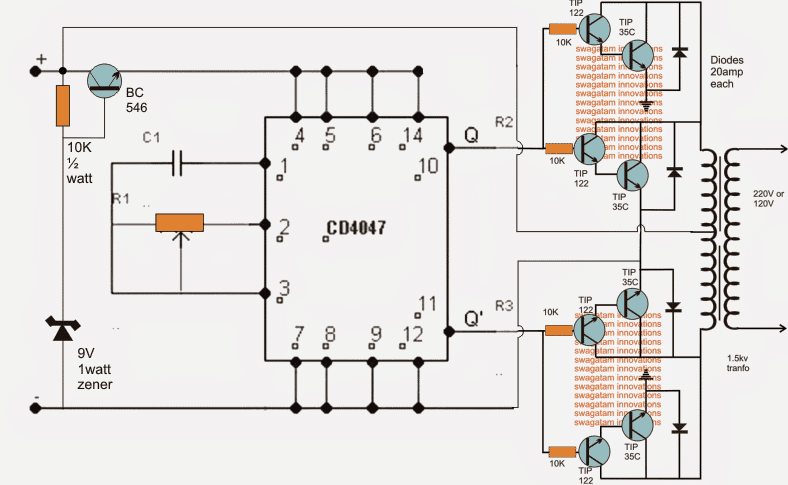
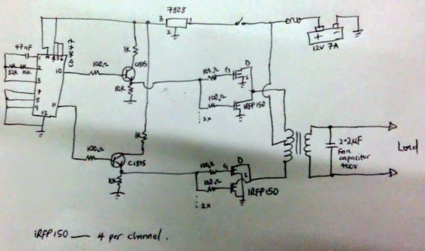
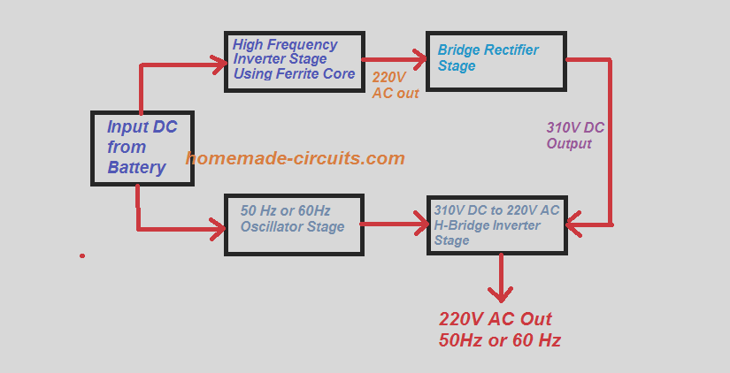 Please note you can convert this ferrite core inverter to any desired wattage, right from 100 watt to 5 kva or as per your own preference.
Understanding the above block diagram is quite simple:
The input DC which could be through a 12V, 24V or 48V battery or solar panel is applied to a ferrite based inverter, which converts it into a high frequency 220V AC output, at around 50 kHz.
But since 50 kHz frequency may not be suitable for our home appliances, we need to convert this high frequency AC into the required 50 Hz / 220V, or 120V AC / 60Hz.
This is implemented through an H-bridge inverter stage, which converts this high frequency into output into the desired 220V AC.
However, for this the H-bridge stage would need a peak value of the 220V RMS, which is around 310V DC.
This is achieved using a bridge rectifier stage, which converts the high frequency 220V into 310 V DC.
Finally, this 310 V DC bus voltage is converted back into 220 V 50 Hz using the H-bridge.
We can also see a 50 Hz oscillator stage powered by the same DC source.
This oscillator is actually optional and may be required for H-bridge circuits which do not have its own oscillator.
For example if we use a transistor based H-bridge then we may need this oscillator stage to operate the High and low side mosfets accordingly.
UPDATE: You may want to jump directly to the new updated "SIMPLIFIED DESIGN", near the bottom of this article, which explains a one-step technique for obtaining a transformerless 5 kva sine wave output instead of going through a complex two-step process as discussed in the concepts below:
Please note you can convert this ferrite core inverter to any desired wattage, right from 100 watt to 5 kva or as per your own preference.
Understanding the above block diagram is quite simple:
The input DC which could be through a 12V, 24V or 48V battery or solar panel is applied to a ferrite based inverter, which converts it into a high frequency 220V AC output, at around 50 kHz.
But since 50 kHz frequency may not be suitable for our home appliances, we need to convert this high frequency AC into the required 50 Hz / 220V, or 120V AC / 60Hz.
This is implemented through an H-bridge inverter stage, which converts this high frequency into output into the desired 220V AC.
However, for this the H-bridge stage would need a peak value of the 220V RMS, which is around 310V DC.
This is achieved using a bridge rectifier stage, which converts the high frequency 220V into 310 V DC.
Finally, this 310 V DC bus voltage is converted back into 220 V 50 Hz using the H-bridge.
We can also see a 50 Hz oscillator stage powered by the same DC source.
This oscillator is actually optional and may be required for H-bridge circuits which do not have its own oscillator.
For example if we use a transistor based H-bridge then we may need this oscillator stage to operate the High and low side mosfets accordingly.
UPDATE: You may want to jump directly to the new updated "SIMPLIFIED DESIGN", near the bottom of this article, which explains a one-step technique for obtaining a transformerless 5 kva sine wave output instead of going through a complex two-step process as discussed in the concepts below:
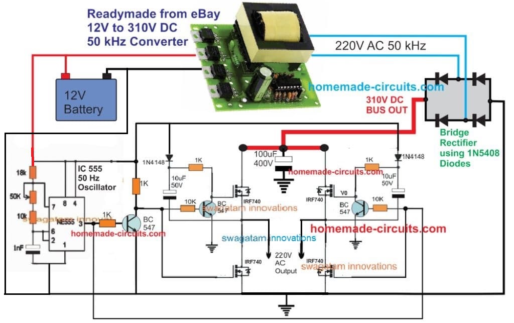
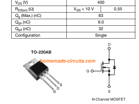 In the above simple 12V to 220V AC ferrite inverter circuit we can see a ready made 12V to 310V DC converter module being used.
This means you don't have to make a complex ferrite core based transformer.
For the new users this design may be very beneficial as they can quickly build this inverter without depending on any complex calculations, and ferrite core selections.
In the above simple 12V to 220V AC ferrite inverter circuit we can see a ready made 12V to 310V DC converter module being used.
This means you don't have to make a complex ferrite core based transformer.
For the new users this design may be very beneficial as they can quickly build this inverter without depending on any complex calculations, and ferrite core selections.
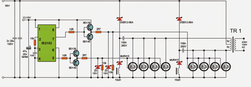 Please do not use BD139/BD140, instead use BC547/BC557, for the driver stage above.
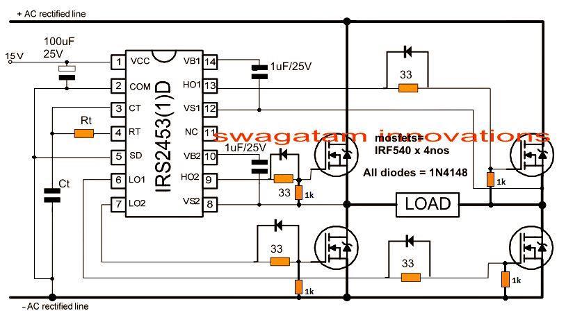 The terminals marked "load" could be now directly used as the final output for operating the desired load.
Here the mosfets could be IRF840 or any equivalent type will do.
The terminals marked "load" could be now directly used as the final output for operating the desired load.
Here the mosfets could be IRF840 or any equivalent type will do.
 E80 Ferrite core

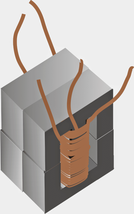
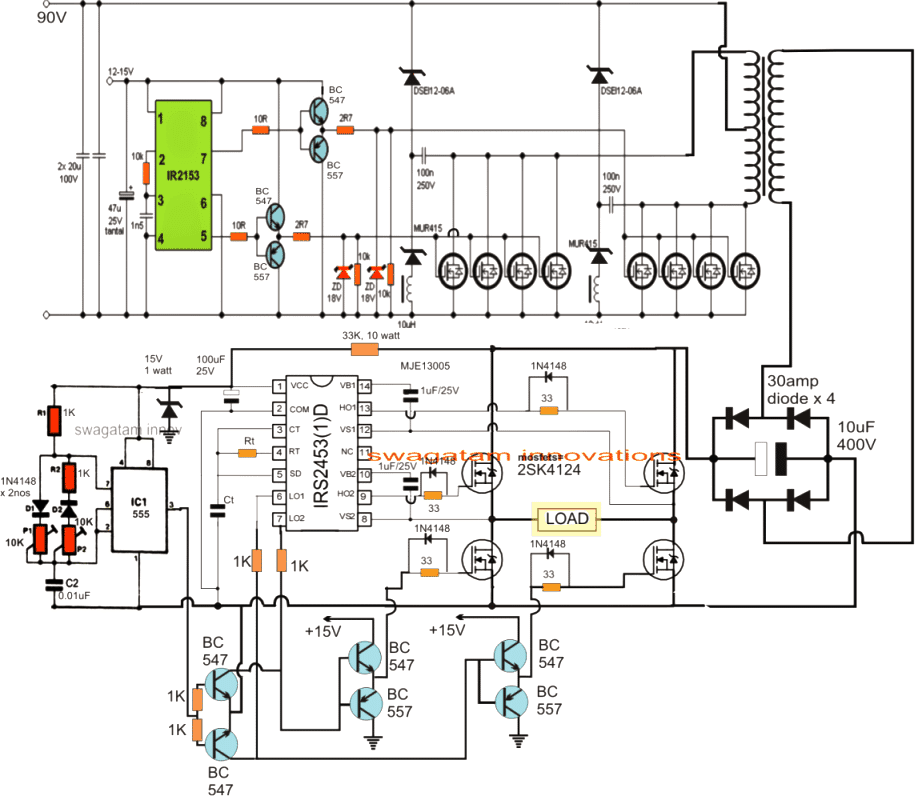 The SD pin of IC IRS2153 is mistakenly shown connected with Ct, please be sure to connect it with the ground line.
Suggestion: the IRS2153 stage could be easily replaced with IC 4047 stage, in case the IRS2153 seems difficult to obtain.
As we can see in the above PWM based 5kva Inverter circuit, the design is exactly similar to our earlier original 5kva inverter circuit, except the indicated PWM buffer feed stage with the low side mosfets of the H-bridge driver stage.
The PWM feed insertion could be acquired through any standard PWM generator circuit using IC 555 or by using transistorized astable multivibrator.
For more accurate PWM replication, one can also opt for a Bubba oscilator PWM generator for sourcing the PWM with the above shown 5kva sinewave inverter design.
The construction procedures for the above design is not different to the original design, the only difference being the integration of the BC547/BC557 BJT buffer stages with the low side mosfets of the full bridge IC stage and the PWM feed into it.
The SD pin of IC IRS2153 is mistakenly shown connected with Ct, please be sure to connect it with the ground line.
Suggestion: the IRS2153 stage could be easily replaced with IC 4047 stage, in case the IRS2153 seems difficult to obtain.
As we can see in the above PWM based 5kva Inverter circuit, the design is exactly similar to our earlier original 5kva inverter circuit, except the indicated PWM buffer feed stage with the low side mosfets of the H-bridge driver stage.
The PWM feed insertion could be acquired through any standard PWM generator circuit using IC 555 or by using transistorized astable multivibrator.
For more accurate PWM replication, one can also opt for a Bubba oscilator PWM generator for sourcing the PWM with the above shown 5kva sinewave inverter design.
The construction procedures for the above design is not different to the original design, the only difference being the integration of the BC547/BC557 BJT buffer stages with the low side mosfets of the full bridge IC stage and the PWM feed into it.
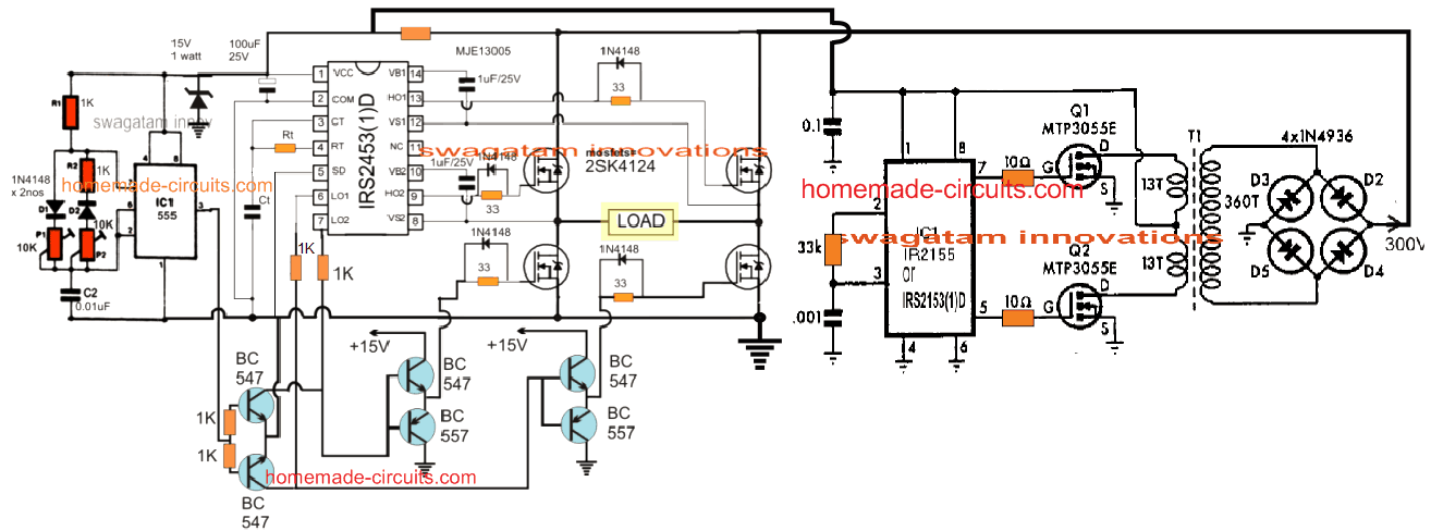 Again, there's no specific design that may be necessary for the 310V generator stage, you can try any other alternative as per your preference, some common examples being, IC 4047, IC 555, TL494, LM567 etc.
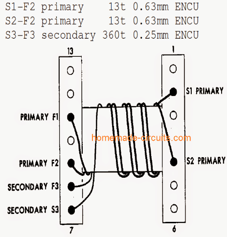
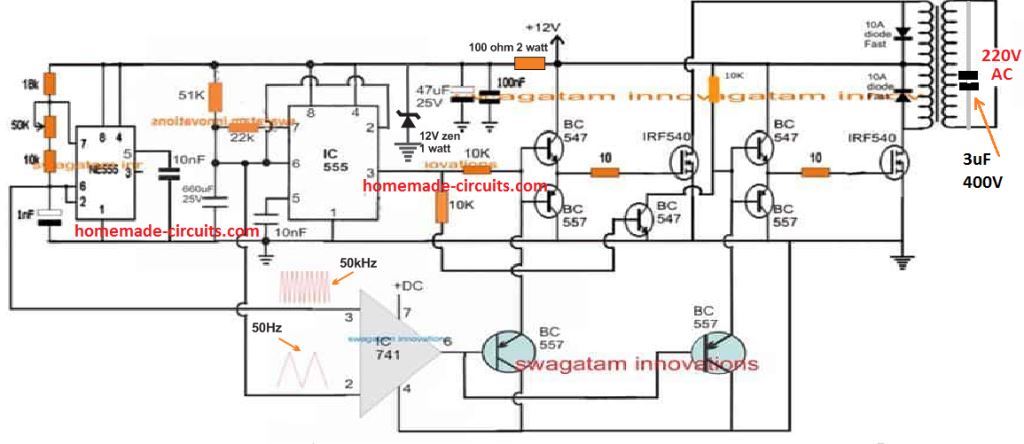 NOTE: The transformer is a ferrite core transformer which must be appropriately calculated
In the above design, the right side IC 555 is wired to generate a 50 Hz basic oscillatory signals for the MOSFET switching.
We can also see an op amp stage, in which this signal is extracted from the ICs RC timing network in the form of 50 Hz triangle waves and fed to one of its inputs to compare the signal with a fast triangle wave signals from another IC 555 astable circuit.
This fast triangle waves can have a frequency of anywhere between 50 kHz to 100 kHz.
The op amp compares the two signals to generate a sine wave equivalent modulated SPWM frequency.
This modulated SPWM is fed to the bases of the driver BJTs for switching the MOSFETs at 50 kHz SPWM rate, modulated at 50 Hz.
The MOSFEts in turn, switch the attached ferrite core transformer with the same SPWM modulated frequency to generate the intended pure sinewave output at the secondary of the transformer.
Due to the high frequency switching, this sine wave may be full of unwanted harmonics, which is filtered and smoothed through a 3 uF/400 V capacitor to obtain a reasonably clean AC sine wave output with the desired wattage, depending on the transformer and the battery power specs.
The right side IC 555 which generates the 50 Hz carrier signals can be replaced by any other favorable oscillator IC such as IC 4047 etc
NOTE: The transformer is a ferrite core transformer which must be appropriately calculated
In the above design, the right side IC 555 is wired to generate a 50 Hz basic oscillatory signals for the MOSFET switching.
We can also see an op amp stage, in which this signal is extracted from the ICs RC timing network in the form of 50 Hz triangle waves and fed to one of its inputs to compare the signal with a fast triangle wave signals from another IC 555 astable circuit.
This fast triangle waves can have a frequency of anywhere between 50 kHz to 100 kHz.
The op amp compares the two signals to generate a sine wave equivalent modulated SPWM frequency.
This modulated SPWM is fed to the bases of the driver BJTs for switching the MOSFETs at 50 kHz SPWM rate, modulated at 50 Hz.
The MOSFEts in turn, switch the attached ferrite core transformer with the same SPWM modulated frequency to generate the intended pure sinewave output at the secondary of the transformer.
Due to the high frequency switching, this sine wave may be full of unwanted harmonics, which is filtered and smoothed through a 3 uF/400 V capacitor to obtain a reasonably clean AC sine wave output with the desired wattage, depending on the transformer and the battery power specs.
The right side IC 555 which generates the 50 Hz carrier signals can be replaced by any other favorable oscillator IC such as IC 4047 etc
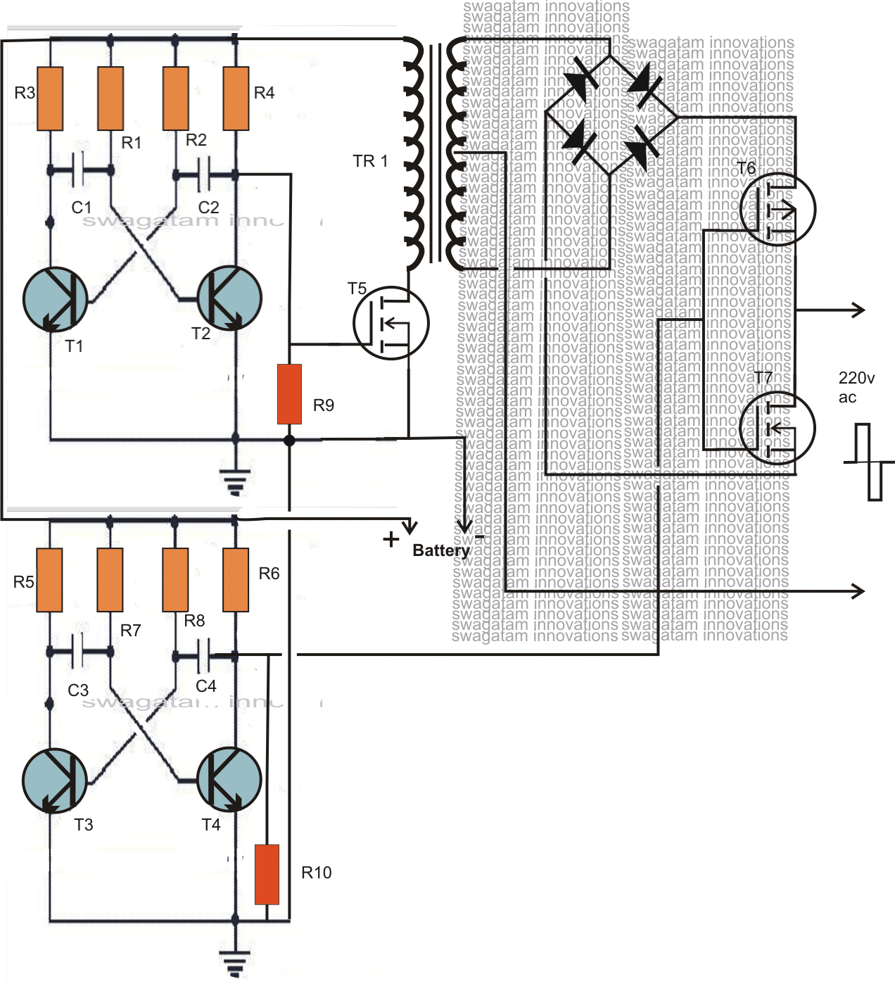
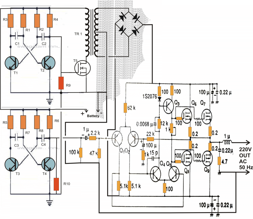
 The Designed and Drawn by: Abu-Hafss
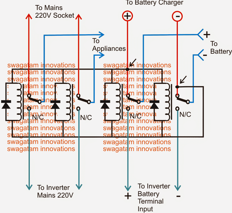 In the above diagram if an automatic battery charger is used, the supply would be cut off once the battery is fully charged, which would also cut off the supply to the relays forcing the inverter to switch ON even while the mains is present.
To avoid this issue, the relays must be powered through a separate power supply as shown in the following diagram.
A capacitive type of power supply circuit could be seen here, which makes the design much compact.
In the above diagram if an automatic battery charger is used, the supply would be cut off once the battery is fully charged, which would also cut off the supply to the relays forcing the inverter to switch ON even while the mains is present.
To avoid this issue, the relays must be powered through a separate power supply as shown in the following diagram.
A capacitive type of power supply circuit could be seen here, which makes the design much compact.
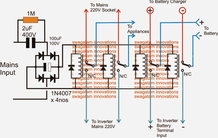 Note: Please connect a 1K resistor across the filter capacitor associated with the bridge rectifier, this is to ensure its quick discharging during a mains failure, and an instant switching of the relevant relays.
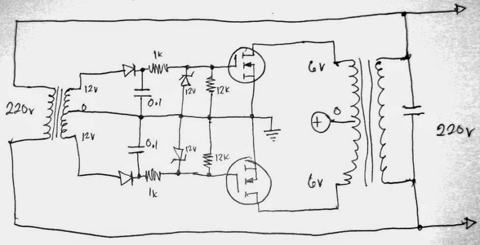 The test set-up of the above design can be witnessed here:
 Another issue which could remotely transpire is the conduction from the mosfet which wouldn't be exponential, rather an "awkward" and unrecognizable sinewave.
The mosfets could be replaced with SCRs, as shown below.
This would allow a perfect sine wave to be induced across the inverter transformer and the grid.
Another issue which could remotely transpire is the conduction from the mosfet which wouldn't be exponential, rather an "awkward" and unrecognizable sinewave.
The mosfets could be replaced with SCRs, as shown below.
This would allow a perfect sine wave to be induced across the inverter transformer and the grid.
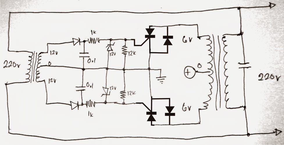
 Simple H-Bridge or Full Bridge Inverter using two Half-Bridge IC IR2110
 The diagram above shows how to implement an effective full bridge square wave inverter design using a couple of half bridge ICs IR2110.
The ICs are full fledged half bridge drivers equipped with the required bootstrapping capacitor network for driving the high side mosfets, and a dead-time feature to ensure 100% safety for the mosfet conduction.
The ICs work by alternately switching the Q1/Q2 and Q3/Q4 mosfets in tandem, such that at any occasion when Q1 is ON, Q2 and Q3 are completely switched OF and vice versa.
The IC is able to create the above precise switching in response to the timed signals at their HIN and LIN inputs.
These four inputs needs to be triggered to ensure that at any instant HIN1 and LIN2 are switched ON simultaneously while HIN2 and LIN1 are switched OFF, and vice versa.
This is done at twice the rate of the inverter output frequency.
Meaning if the inverter output is required to be 50Hz, the HIN/LIN inputs should be oscillated at 100Hz rate and so on.
The diagram above shows how to implement an effective full bridge square wave inverter design using a couple of half bridge ICs IR2110.
The ICs are full fledged half bridge drivers equipped with the required bootstrapping capacitor network for driving the high side mosfets, and a dead-time feature to ensure 100% safety for the mosfet conduction.
The ICs work by alternately switching the Q1/Q2 and Q3/Q4 mosfets in tandem, such that at any occasion when Q1 is ON, Q2 and Q3 are completely switched OF and vice versa.
The IC is able to create the above precise switching in response to the timed signals at their HIN and LIN inputs.
These four inputs needs to be triggered to ensure that at any instant HIN1 and LIN2 are switched ON simultaneously while HIN2 and LIN1 are switched OFF, and vice versa.
This is done at twice the rate of the inverter output frequency.
Meaning if the inverter output is required to be 50Hz, the HIN/LIN inputs should be oscillated at 100Hz rate and so on.
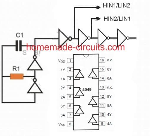 This is an oscillator circuit which is optimized for triggering the HIN/LIN inputs of the above explained full-bridge inverter circuit.
A single 4049 IC is used for generating the required frequency and also for isolating the alternating input feeds for the inverter ICs.
C1 and R1 determine the frequency required for oscillating the half bridge devices and could be calculated using the following formula:
f = 1 /1.2RC
Alternatively, the values could be achieved through some trial and error.
This is an oscillator circuit which is optimized for triggering the HIN/LIN inputs of the above explained full-bridge inverter circuit.
A single 4049 IC is used for generating the required frequency and also for isolating the alternating input feeds for the inverter ICs.
C1 and R1 determine the frequency required for oscillating the half bridge devices and could be calculated using the following formula:
f = 1 /1.2RC
Alternatively, the values could be achieved through some trial and error.
 IC 555 Astable Frequency Formula
f = 1.45 / (R1 + 2R2)C
The following formula can be used for calculating the high time and low time periods or the ON/OFF time of the IC 555 astable:
On Time T1 = 0.7(R1 + R2)C
OFF Time T2 = 0.7R1C
IC 555 Astable Frequency Formula
f = 1.45 / (R1 + 2R2)C
The following formula can be used for calculating the high time and low time periods or the ON/OFF time of the IC 555 astable:
On Time T1 = 0.7(R1 + R2)C
OFF Time T2 = 0.7R1C
 or you can also use the following formula:
f(osc) = 1 / 2.3 x Rt x Ct
2.3 is a constant term which will not need any change.
The oscillator section inside the IC will be able to give stable output only if the following criteria is maintained:
Rt << R2 and R2 x C2 << Rt x Ct.
or you can also use the following formula:
f(osc) = 1 / 2.3 x Rt x Ct
2.3 is a constant term which will not need any change.
The oscillator section inside the IC will be able to give stable output only if the following criteria is maintained:
Rt << R2 and R2 x C2 << Rt x Ct.
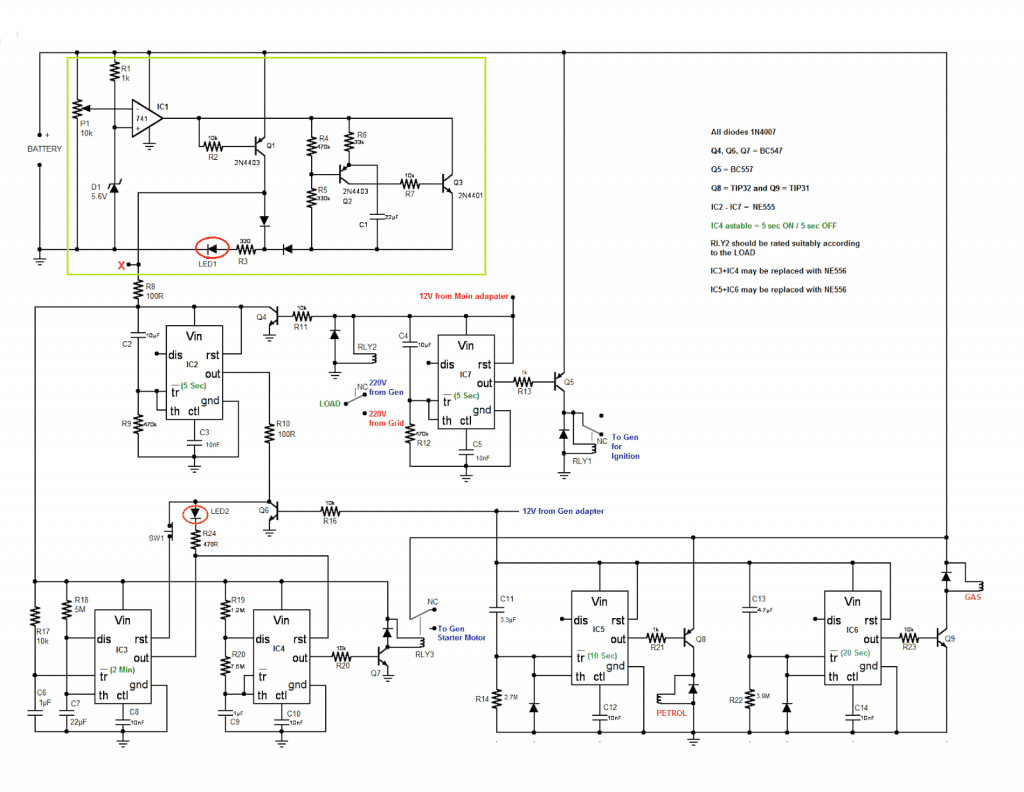
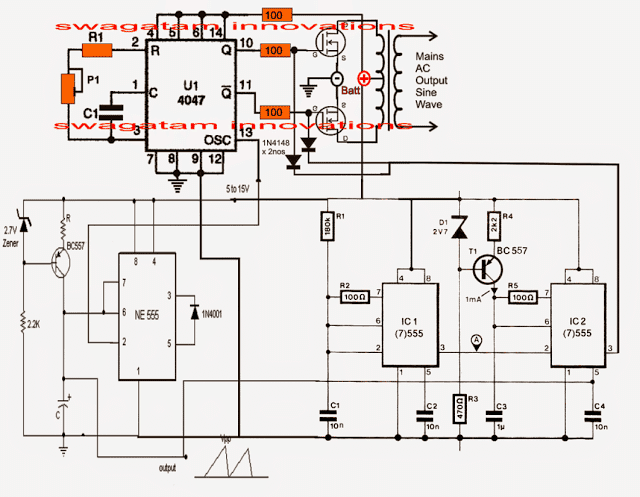
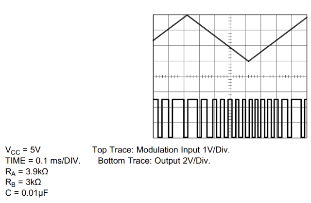 More info on how to use IC 555 for generating PWM
An RMS adjustment could be added to the above design by introducing a pot voltage divider network across pin5 and the triangle source input, as shown below, the design also includes buffer transistors for improving mosfet behavior
More info on how to use IC 555 for generating PWM
An RMS adjustment could be added to the above design by introducing a pot voltage divider network across pin5 and the triangle source input, as shown below, the design also includes buffer transistors for improving mosfet behavior
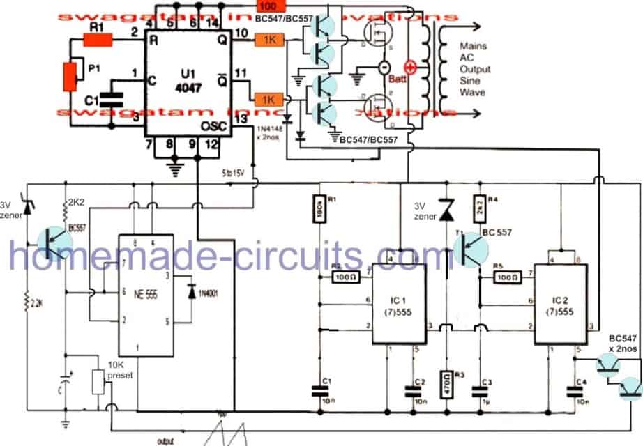 The above pure sine wave inverter design was successfully tested by Mr.
Arun Dev, who is one of the avid readers of this blog and an intense electronic hobbyist.
The following images sent by him prove his efforts for the same.
The above pure sine wave inverter design was successfully tested by Mr.
Arun Dev, who is one of the avid readers of this blog and an intense electronic hobbyist.
The following images sent by him prove his efforts for the same.
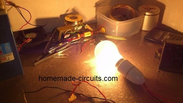
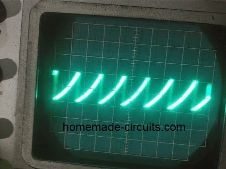
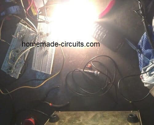 The following images show the modified waveforms at the output of the transformer as captured by Mr.
Daniel Adusie after connecting a 0.22uF/400V capacitor and a suitable load.
The waveforms are somewhat trapezoidal and are far better than a square wave which clearly shows the impressive effects of the PWM processing created by the IC555 stages.
The waveforms could be probably even further smoothened by adding an inductor along with the capacitor.
The following images show the modified waveforms at the output of the transformer as captured by Mr.
Daniel Adusie after connecting a 0.22uF/400V capacitor and a suitable load.
The waveforms are somewhat trapezoidal and are far better than a square wave which clearly shows the impressive effects of the PWM processing created by the IC555 stages.
The waveforms could be probably even further smoothened by adding an inductor along with the capacitor.
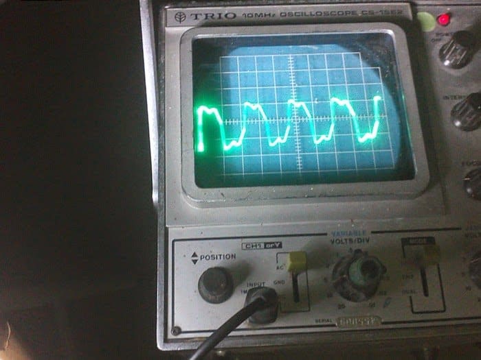
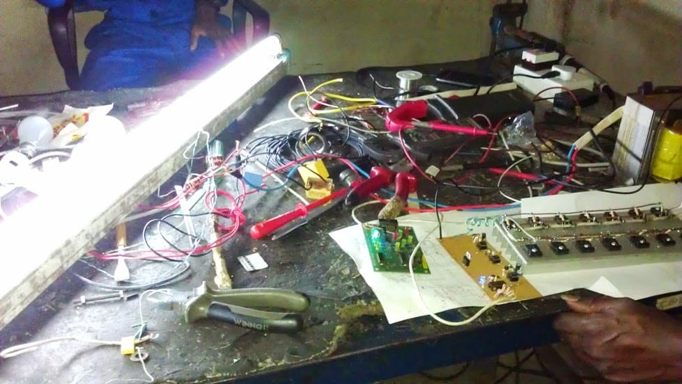
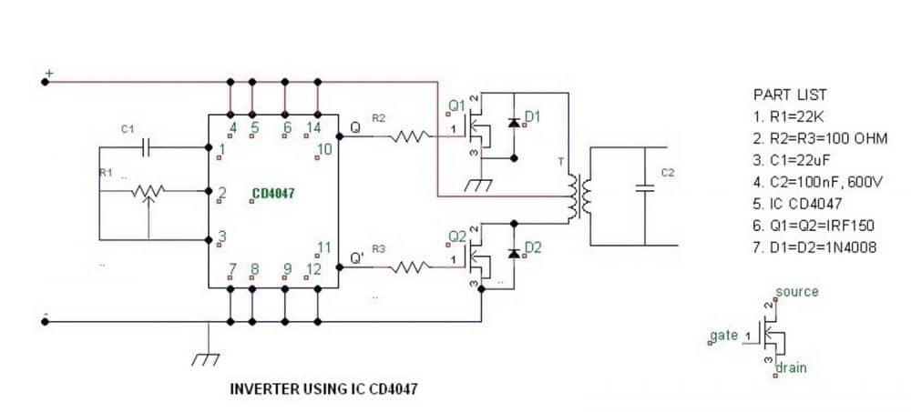
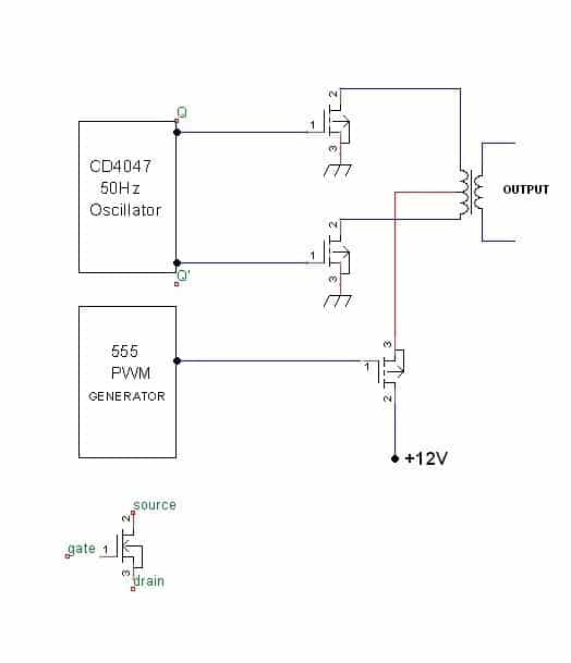
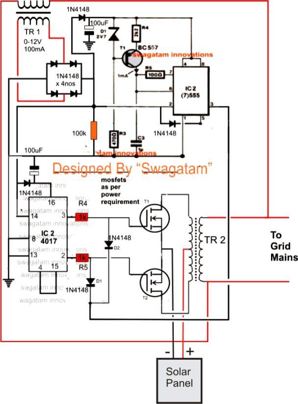
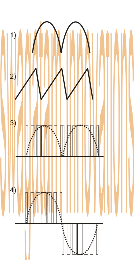 Something's not right in the above design
According to Mr.
Selim Yavuz the above design had a few things which looked doubtful and needed correction, let's hear what he had to say:
Something's not right in the above design
According to Mr.
Selim Yavuz the above design had a few things which looked doubtful and needed correction, let's hear what he had to say:
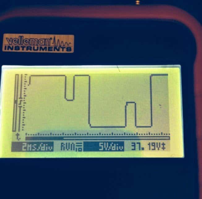
 Hi Swag,
hope you're well.
I tried your circuit on a bread board.
It seems to work except pwm part.
For some reason, I get a double hump but no real pwm.
Could you please help me understand how 555 does pwm? I noticed that 2.2k and 1u create a ramp of 10ms.
I believe the ramp should be much faster than that as the half wave is 10ms.
May be I missed a few things.
Also, 4017 does a clean job switching happily back and forth.
When you power up, the 100 hz clock makes the counter always start from 0. How can we assure that it always in phase with the grid?
Appreciate your help and ideas.
Regards,
Selim
Hi Swag,
hope you're well.
I tried your circuit on a bread board.
It seems to work except pwm part.
For some reason, I get a double hump but no real pwm.
Could you please help me understand how 555 does pwm? I noticed that 2.2k and 1u create a ramp of 10ms.
I believe the ramp should be much faster than that as the half wave is 10ms.
May be I missed a few things.
Also, 4017 does a clean job switching happily back and forth.
When you power up, the 100 hz clock makes the counter always start from 0. How can we assure that it always in phase with the grid?
Appreciate your help and ideas.
Regards,
Selim
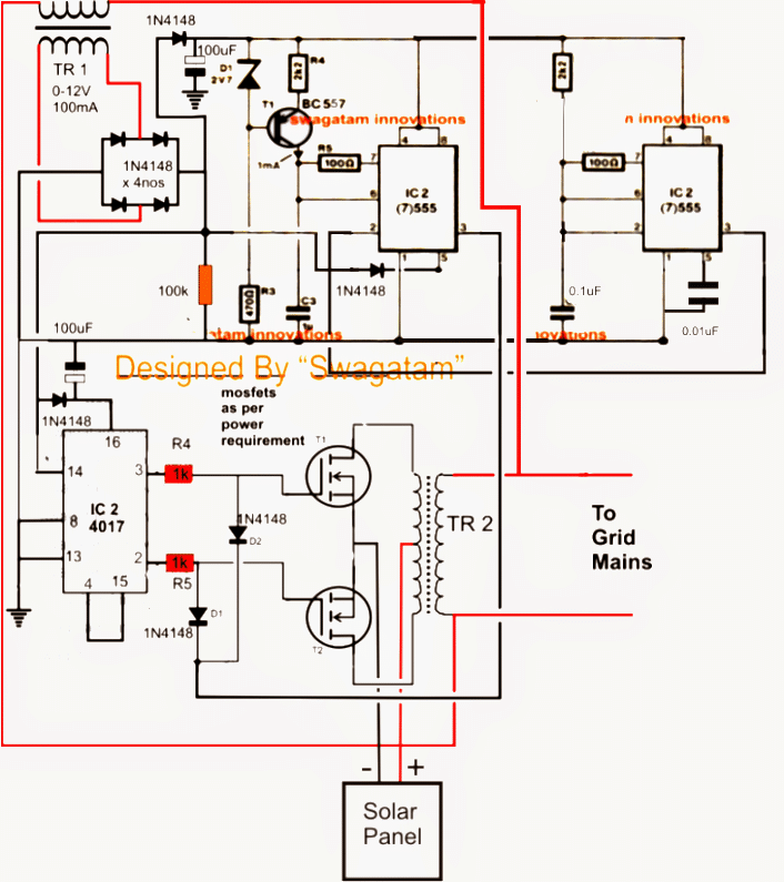 The above diagram has been redrawn below with distinct part numbers and jumper notations
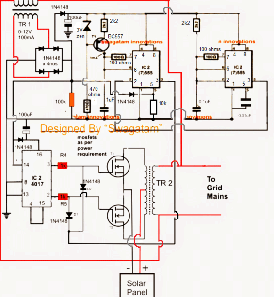 WARNING: THE IDEA IS BASED SOLELY ONIMAGINATIVESIMULATION, VIEWER DISCRETION IS STRICTLY ADVISED.
A major issue with the above design faced by many of the constructors was the heating up of one of the mosfets during the GTI operations.
A possible cause and remedy as suggested by Mr.
Hsen is presented below.
The proposed correction in the mosfet stage as recommended by Mr.
Hsen is also enclosed here under, hopefully the said modifications will help control the issue permanently:
Hello mr.
Swagatam:
I watched again your diagram and I am firmly convinced that the gates of the MOSFETs will reach a modulating signal (HF PWM) and not a simple signal 50 cs.
Therefore I insist, a more powerful driver the CD4017 must be incorporated, and the series resistance should be of a much lower value.
Another thing to consider is that at the junction of the resistor and the gate should not be another added element, and in this case I see going to the diodes 555.
Because this may be the reason why one of the heats MOFETs because it can self oscillate.
So I think that the mosfet heats because it is oscillating and not because of the output transformer.
Excuse me, but my concern is that your project succeed because I feel very good and it is not my intention to criticize.
Yours affectionately, hsen
Improved Mosfet Driver
As per the suggestions from Mr Hsen, the following BJT buffer could be employed for ensuring that the mosfets are able to work with better safety and control.
WARNING: THE IDEA IS BASED SOLELY ONIMAGINATIVESIMULATION, VIEWER DISCRETION IS STRICTLY ADVISED.
A major issue with the above design faced by many of the constructors was the heating up of one of the mosfets during the GTI operations.
A possible cause and remedy as suggested by Mr.
Hsen is presented below.
The proposed correction in the mosfet stage as recommended by Mr.
Hsen is also enclosed here under, hopefully the said modifications will help control the issue permanently:
Hello mr.
Swagatam:
I watched again your diagram and I am firmly convinced that the gates of the MOSFETs will reach a modulating signal (HF PWM) and not a simple signal 50 cs.
Therefore I insist, a more powerful driver the CD4017 must be incorporated, and the series resistance should be of a much lower value.
Another thing to consider is that at the junction of the resistor and the gate should not be another added element, and in this case I see going to the diodes 555.
Because this may be the reason why one of the heats MOFETs because it can self oscillate.
So I think that the mosfet heats because it is oscillating and not because of the output transformer.
Excuse me, but my concern is that your project succeed because I feel very good and it is not my intention to criticize.
Yours affectionately, hsen
Improved Mosfet Driver
As per the suggestions from Mr Hsen, the following BJT buffer could be employed for ensuring that the mosfets are able to work with better safety and control.
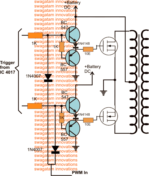
 The input of the transformerless power supply circuit is connected to the mains 220V or 120V input.
When mains power is present, theconnected relayactivates with this power and switches ON the load or the appliances via its N/O contacts.
Conversely when mains power fails, the relaydeactivatesand connects with the N/C contacts which may be wired up with the generator mains.
Now as soon as thegeneratoris pulled started, the mains finds its way through the connected N/O contacts of the relay tothe appliances.
The third set of contacts is used for enabling and disabling of the CDI unit of the generator so that when mains is restored, the generator is automatically halted.
Simple yet effective.....
The input of the transformerless power supply circuit is connected to the mains 220V or 120V input.
When mains power is present, theconnected relayactivates with this power and switches ON the load or the appliances via its N/O contacts.
Conversely when mains power fails, the relaydeactivatesand connects with the N/C contacts which may be wired up with the generator mains.
Now as soon as thegeneratoris pulled started, the mains finds its way through the connected N/O contacts of the relay tothe appliances.
The third set of contacts is used for enabling and disabling of the CDI unit of the generator so that when mains is restored, the generator is automatically halted.
Simple yet effective.....
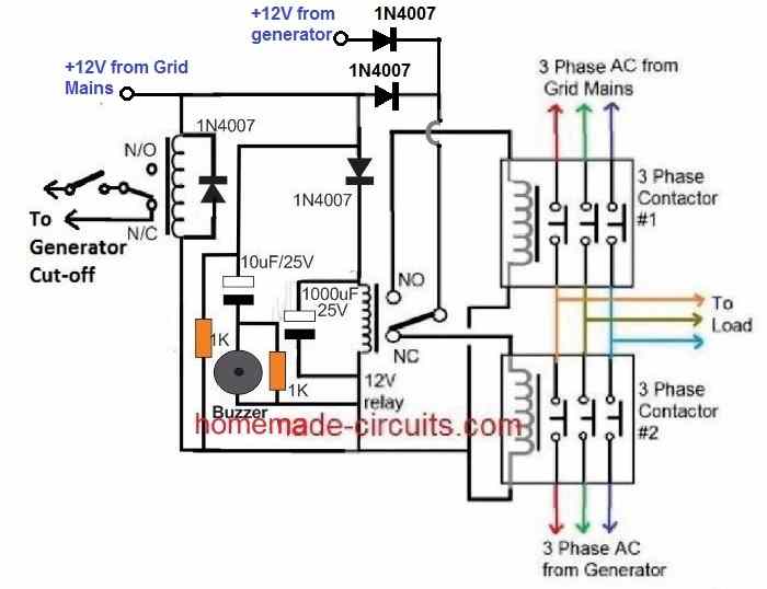
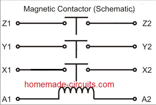 If you are unable to get the above 12V electromechanical relay/contactor, you can go for a 3 phase SSR contactor instead, as shown below.
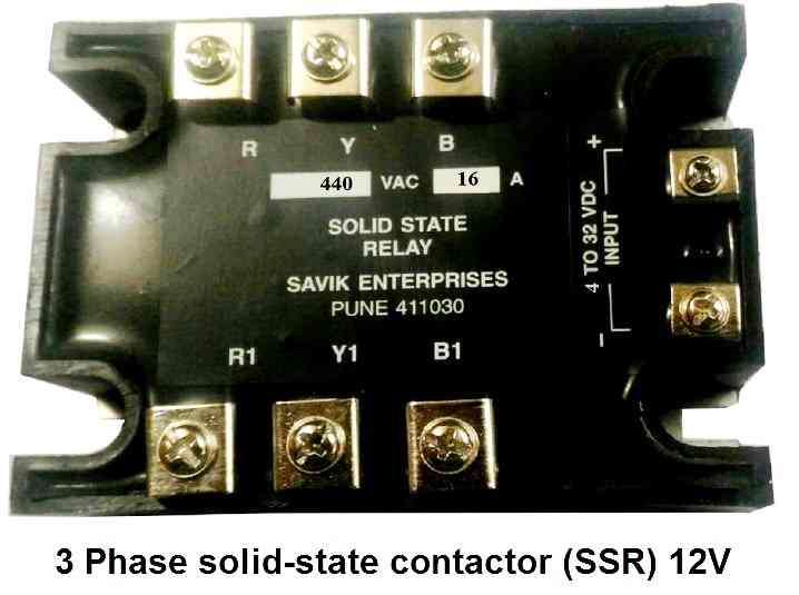
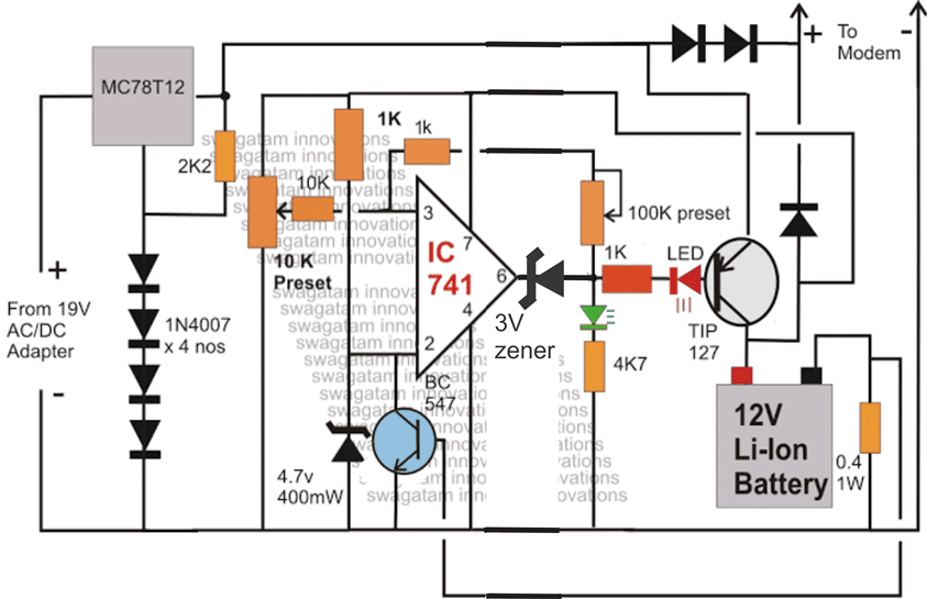
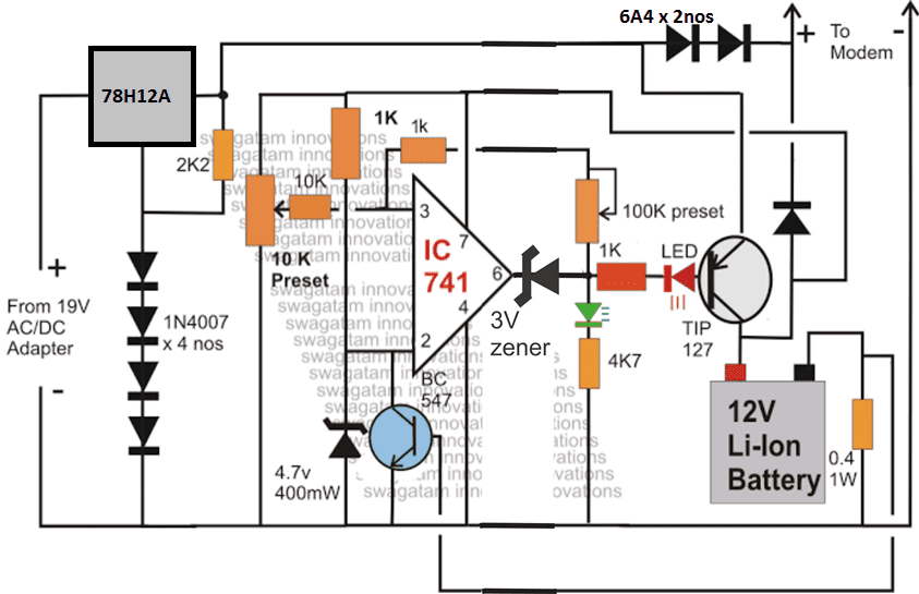
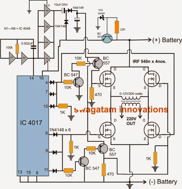
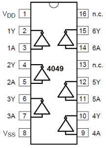

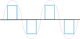
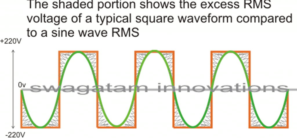 The image incorrectly shows 220V as the peak, actually it should be 330V
In the above diagram, the green colored waveform is the sine waveform, while the orange depicts the square waveform.
Theshadedportion is the excess RMS whichneedsto beleveledof in order to make both the RMS values as close as possible.
Converting asquarewave inverter into a sine wave equivalent thus basically means allowing the square wave inverer to produce the required peak value of say 330V yet having an RMS just about equal to its sine wave counterpart.
The image incorrectly shows 220V as the peak, actually it should be 330V
In the above diagram, the green colored waveform is the sine waveform, while the orange depicts the square waveform.
Theshadedportion is the excess RMS whichneedsto beleveledof in order to make both the RMS values as close as possible.
Converting asquarewave inverter into a sine wave equivalent thus basically means allowing the square wave inverer to produce the required peak value of say 330V yet having an RMS just about equal to its sine wave counterpart.
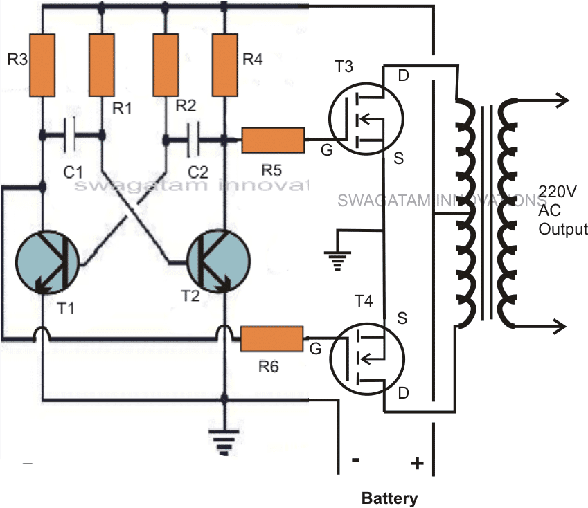 Modified square wave to sine wave equivalent inverter version of the above circuit.
Here the lower AMV generate pulses at high frequency whose mark/space ratio can be suitably altered with the help of preset VR1. This PWM controlled output is applied to thegates ofthe mosfets in order to tailor theirconductionintothe stipulatedRMS value.
Modified square wave to sine wave equivalent inverter version of the above circuit.
Here the lower AMV generate pulses at high frequency whose mark/space ratio can be suitably altered with the help of preset VR1. This PWM controlled output is applied to thegates ofthe mosfets in order to tailor theirconductionintothe stipulatedRMS value.
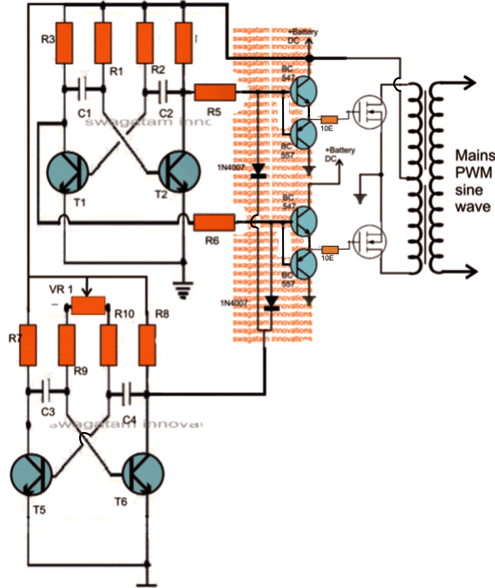 Expected typical waveform pattern from theabovemodification:
Waveform at the mosfet gates:
Expected typical waveform pattern from theabovemodification:
Waveform at the mosfet gates:
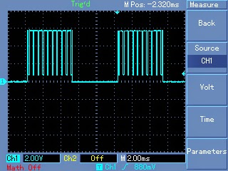 Waveform at the output of transformer:
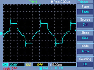 Waveform after proper filtration using inductors and capacitors at the output of the transformer:
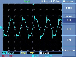
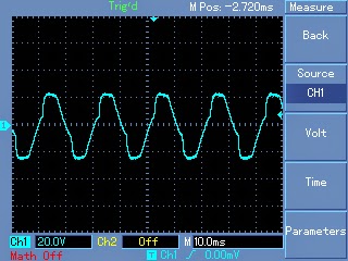
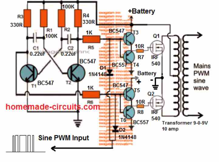 The following diagram shows how this could be effectively implemented with the concept discussed above.
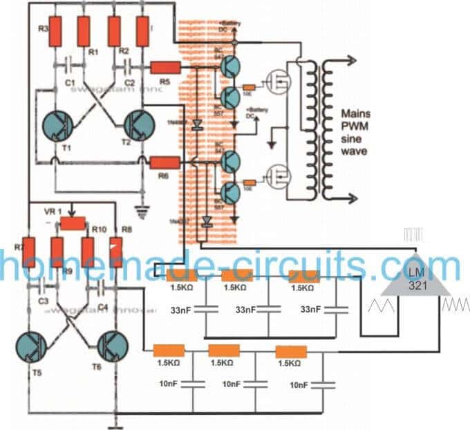 Through one of my earlier articles we understood how an opamp could be used for creating SPWMs, the same theory could be seen applied in the above concept.
Two triangle wave generators are used here, one accepting the fast square wave from the lower astable, while the other accepting slow square waves from the upper astable and processing them into corresponding fast and slow triangle wave outputs, respectively.
These processed triangle wave are fed across the two inputs of an opamp, which finally converts them into SPWMs or sine wave pulse widths.
These SPWMs are used for chopping the signals at the gate of the mosfets which ultimately switch the waveform over the connected transformer winding for creating an exact replica of a pure sine waveform at the secondary side of the transformer through magnetic induction.
Through one of my earlier articles we understood how an opamp could be used for creating SPWMs, the same theory could be seen applied in the above concept.
Two triangle wave generators are used here, one accepting the fast square wave from the lower astable, while the other accepting slow square waves from the upper astable and processing them into corresponding fast and slow triangle wave outputs, respectively.
These processed triangle wave are fed across the two inputs of an opamp, which finally converts them into SPWMs or sine wave pulse widths.
These SPWMs are used for chopping the signals at the gate of the mosfets which ultimately switch the waveform over the connected transformer winding for creating an exact replica of a pure sine waveform at the secondary side of the transformer through magnetic induction.
 Since today all electronic systems employ an SMPS power supply, the input does not necessarily need to be an AC for powering these equipment, rather an equivalent DC or pulsed DC also become useful and works as good.
Referring to the diagram above, a couple of sections can be seen, the IC1 configuration enables a 6V DC to be boosted to a much higher 220V pulsed DC through a boost converter topology using the IC 555 in its astable form.
The extreme left side battery section ensures an changeover from mains to battery back up every time a power failure is sensed by the circuit.
The idea is pretty simple and does not require much of an elaboration.
Since today all electronic systems employ an SMPS power supply, the input does not necessarily need to be an AC for powering these equipment, rather an equivalent DC or pulsed DC also become useful and works as good.
Referring to the diagram above, a couple of sections can be seen, the IC1 configuration enables a 6V DC to be boosted to a much higher 220V pulsed DC through a boost converter topology using the IC 555 in its astable form.
The extreme left side battery section ensures an changeover from mains to battery back up every time a power failure is sensed by the circuit.
The idea is pretty simple and does not require much of an elaboration.
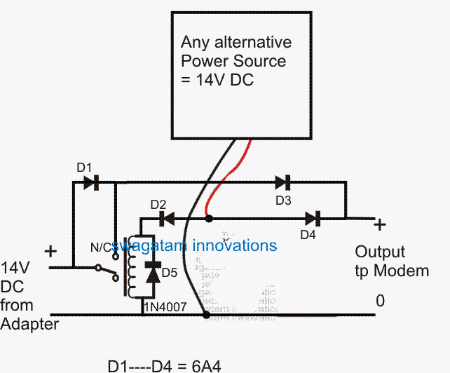
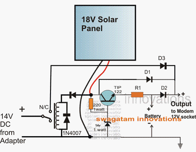
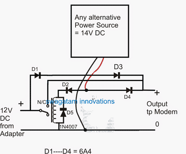
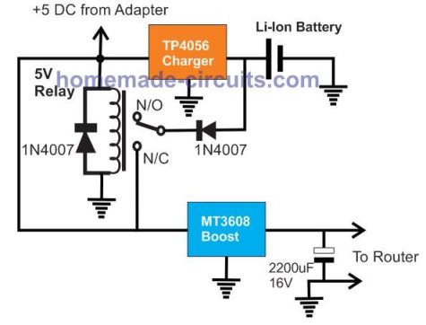 The above design could be also built without a relay as given below:
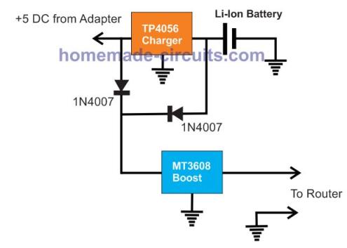


 Here basically N1/N2 forms the oscillator stage which create the required 50Hz or 60Hz clocks or oscillations required for the inverter operation.
N3 is used for inverting these clocks because we need to apply oppositely polarized clocks for the power transformer stage.
However we can also see N4, N5 N6 gates, which are configured across the input line and output line of N3.
Actually N4, N5, N6 are simply included for accommodating the 3 extra gates available inside the IC 4049, otherwise only the first N1, N2, N3 could be alone used for the operations, without any issues.
The 3 extra gates act like buffers and also make sure that these gates are not left unconnected, which can otherwise create adverse effect on the IC in the long run.
The oppositely polarized clocks across the outputs of N4, and N5/N6 are applied to the bases of power BJT stage using TIP142 power BJTs, which are capable of handling a good 10 amp current.
The transformer can be seen configured across the collectors of the BJTs.
You will find that no intermediate amplifier or driver stages are used in the above design because the TIP142 itself has an internal BJT Darlington stage for the required in-built amplification and therefore are able to comfortably amplify the low current clocks from the NOT gates into high current oscillations across the connected transformer winding.
More IC 4049 inverter designs can found below:
Homemade 2000 VA Power Inverter Circuit
Simplest Uninterrupted Power Supply (UPS) Circuit
Here basically N1/N2 forms the oscillator stage which create the required 50Hz or 60Hz clocks or oscillations required for the inverter operation.
N3 is used for inverting these clocks because we need to apply oppositely polarized clocks for the power transformer stage.
However we can also see N4, N5 N6 gates, which are configured across the input line and output line of N3.
Actually N4, N5, N6 are simply included for accommodating the 3 extra gates available inside the IC 4049, otherwise only the first N1, N2, N3 could be alone used for the operations, without any issues.
The 3 extra gates act like buffers and also make sure that these gates are not left unconnected, which can otherwise create adverse effect on the IC in the long run.
The oppositely polarized clocks across the outputs of N4, and N5/N6 are applied to the bases of power BJT stage using TIP142 power BJTs, which are capable of handling a good 10 amp current.
The transformer can be seen configured across the collectors of the BJTs.
You will find that no intermediate amplifier or driver stages are used in the above design because the TIP142 itself has an internal BJT Darlington stage for the required in-built amplification and therefore are able to comfortably amplify the low current clocks from the NOT gates into high current oscillations across the connected transformer winding.
More IC 4049 inverter designs can found below:
Homemade 2000 VA Power Inverter Circuit
Simplest Uninterrupted Power Supply (UPS) Circuit
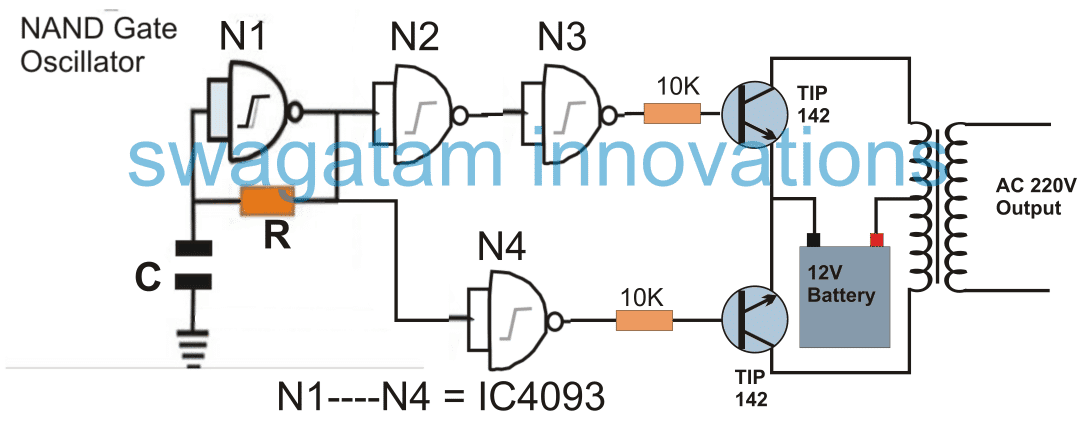 The figure demonstrates a small inverter design using IC 4093 Schmidt trigger NAND gates.
Quite identically here too the N4 could have been avoided and the BJT bases could have been directly connected across the inputs and the outputs N3. But again, N4 is included to accommodate the one extra gate inside the IC 4093 and to ensure that its input pin not left unconnected.
More similar IC 4093 Inverter designs can be referred from the following links:
Best Modified Inverter Circuits
How to Make a Solar Inverter Circuit
How to Build a 400 Watt High Power Inverter Circuit with Built in Charger
How to Design an UPS Circuit ¨C Tutorial
Pinout diagrams for the IC 4093 and IC 4049
The figure demonstrates a small inverter design using IC 4093 Schmidt trigger NAND gates.
Quite identically here too the N4 could have been avoided and the BJT bases could have been directly connected across the inputs and the outputs N3. But again, N4 is included to accommodate the one extra gate inside the IC 4093 and to ensure that its input pin not left unconnected.
More similar IC 4093 Inverter designs can be referred from the following links:
Best Modified Inverter Circuits
How to Make a Solar Inverter Circuit
How to Build a 400 Watt High Power Inverter Circuit with Built in Charger
How to Design an UPS Circuit ¨C Tutorial
Pinout diagrams for the IC 4093 and IC 4049
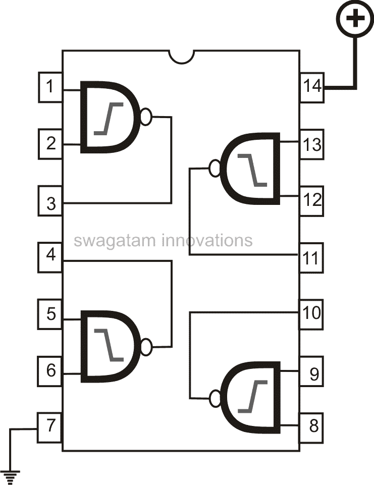 NOTE: The Vcc, and Vss supply pins of the IC are not shown in the inverter diagrams, these must be appropriately connected with the 12V battery supply, for 12V inverters.
For higher voltage inverters this supply must be appropriately stepped down to 12V for the IC supply pins.
NOTE: The Vcc, and Vss supply pins of the IC are not shown in the inverter diagrams, these must be appropriately connected with the 12V battery supply, for 12V inverters.
For higher voltage inverters this supply must be appropriately stepped down to 12V for the IC supply pins.
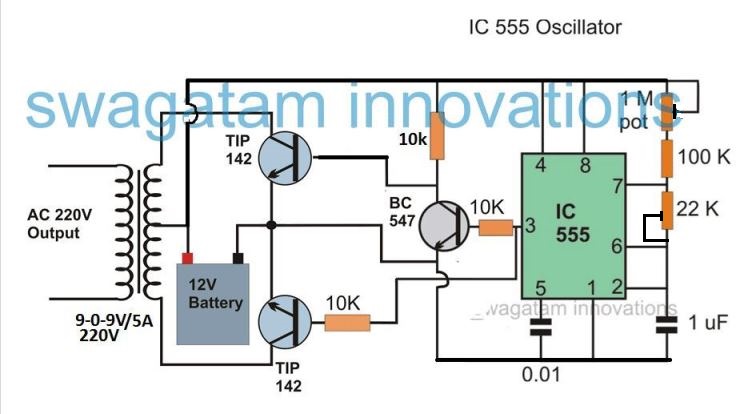 The above circuit is self explanatory, and perhaps does not require any further explanation.
More such IC 555 inverter circuit can be found below:
Simple IC 555 Inverter Circuit
The above circuit is self explanatory, and perhaps does not require any further explanation.
More such IC 555 inverter circuit can be found below:
Simple IC 555 Inverter Circuit
 In this configuration, basically a center-tap transformer is used with its outer taps connected to the hot ends of the output devices (transistors or mosfets) while the center tap either goes to the negative of the battery or to the positive of the battery depending upon the type of devices used (N type or P type).
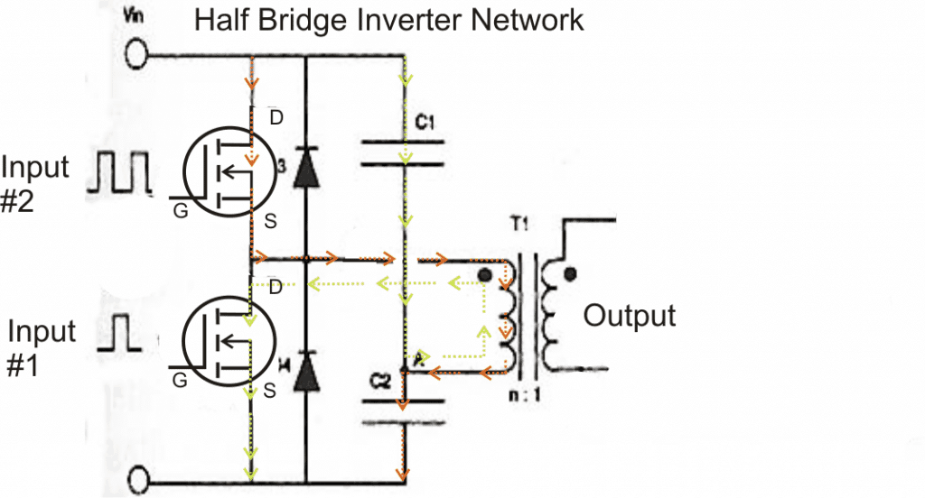 A full bridge or an H-bridge inverter is similar to a half bridge network since it also incorporates an ordinary two tap transformer and does not require a center tap transformer.
The only difference being the elimination of the capacitors and the inclusion of two more power devices.
A full bridge or an H-bridge inverter is similar to a half bridge network since it also incorporates an ordinary two tap transformer and does not require a center tap transformer.
The only difference being the elimination of the capacitors and the inclusion of two more power devices.
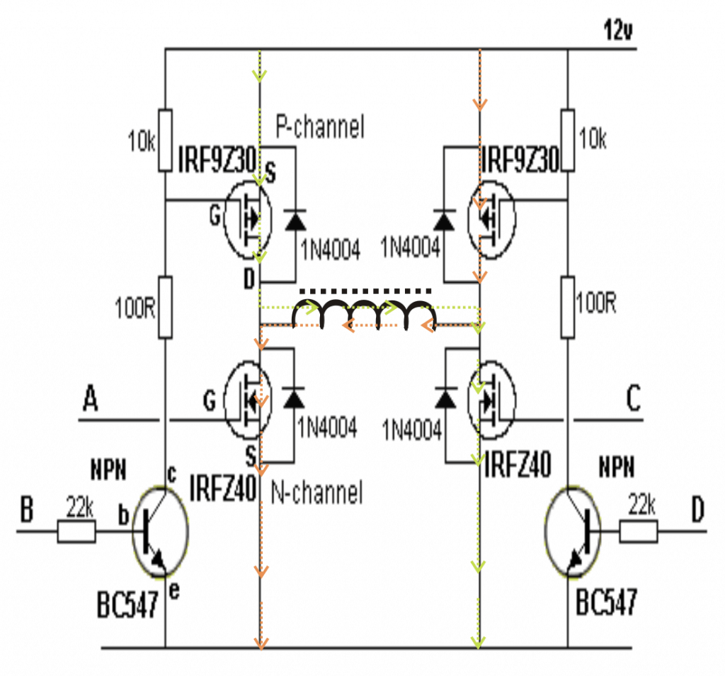 The above explanation provides the basic information regarding how to design an inverter, and may be incorporated only for designing a ordinary inverter circuits, typically the square wave types.
However there are many further concepts that may be associated with inverter designs like making a sine wave inverter, PWM based inverter, output controlled inverter, these are just additional stages which may be added in the above explained basic designs for implementing the said functions.
We will discuss them some other time or may be through your valuable comments.
The above explanation provides the basic information regarding how to design an inverter, and may be incorporated only for designing a ordinary inverter circuits, typically the square wave types.
However there are many further concepts that may be associated with inverter designs like making a sine wave inverter, PWM based inverter, output controlled inverter, these are just additional stages which may be added in the above explained basic designs for implementing the said functions.
We will discuss them some other time or may be through your valuable comments.

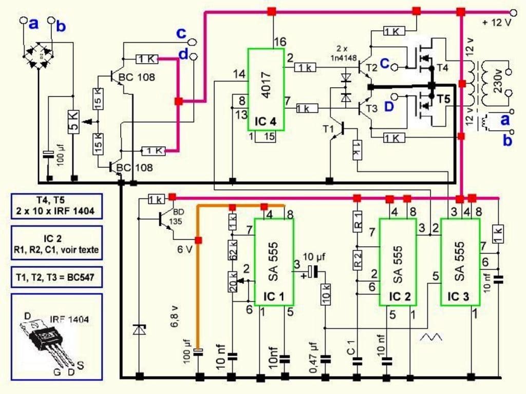 Many drawbacks and flaws were detected while assessing the above circuit details.
The finalized circuit (hopefully) is presented below.
The above circuit may be further enhanced with an automatic load correction feature as shown below.
It is implemented by the inclusion of the LED/LDR opto-coupler stage.
Many drawbacks and flaws were detected while assessing the above circuit details.
The finalized circuit (hopefully) is presented below.
The above circuit may be further enhanced with an automatic load correction feature as shown below.
It is implemented by the inclusion of the LED/LDR opto-coupler stage.

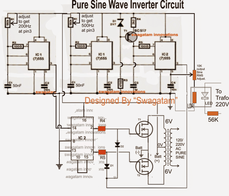 For the final verified design of the above circuit please refer to the following post:https://www.homemade-circuits.com/2013/10/modified-sine-wave-inverter-circuit.html
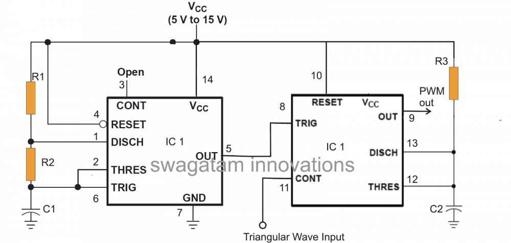 Parts List
IC1 = 556
R1,R2,C1 = select to generate 50% duty cycle
R3 = 1K
C2 = 10pF.
Parts List
IC1 = 556
R1,R2,C1 = select to generate 50% duty cycle
R3 = 1K
C2 = 10pF.
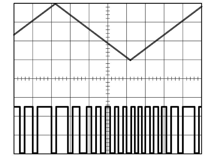
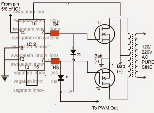 Parts List
IC2 = 4017
all resistors are 1K
D1,D2 = 1N4148
T1,T2 = IRF540n
Transformer should be alsoappropriatelyrated as per the requirement.
Parts List
IC2 = 4017
all resistors are 1K
D1,D2 = 1N4148
T1,T2 = IRF540n
Transformer should be alsoappropriatelyrated as per the requirement.
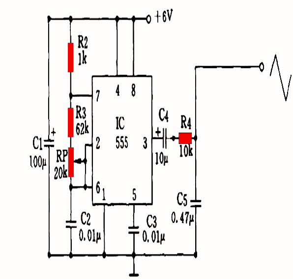 DESIGNED BY "SWAGATAM"
A simpler alternative to the above design is shown below, the configuration would produce same results as explained above:
DESIGNED BY "SWAGATAM"
A simpler alternative to the above design is shown below, the configuration would produce same results as explained above:
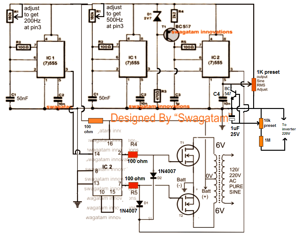
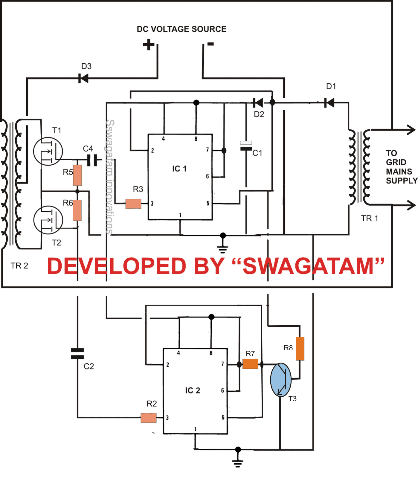 You would also want to see thissimplified Grid tie circuit design
 Parts List
All resistors = 2K2
C1 = 1000uF/25V
C2,C4 = 0.47uF
D1,D2 = 1N4007,
D3 = 10AMP,
IC1,2 = 555
MOSFETS = AS PER APPLICATION SPECS.
TR1 = 0-12V, 100mA
TR2 = AS PER APPLICATION SPECS
T3 = BC547
INPUT DC = AS PER APPLICATION SPECS.
WARNING: THE IDEA IS BASED SOLELY ONIMAGINATIVESIMULATION, VIEWER DISCRETION IS STRICTLY ADVISED.
After receiving a corrective suggestion from one of the readers of this blog Mr.
Darren and somecontemplation,it revealed that the above circuit had many flaws and it wouldn't actually work practically.
Parts List
All resistors = 2K2
C1 = 1000uF/25V
C2,C4 = 0.47uF
D1,D2 = 1N4007,
D3 = 10AMP,
IC1,2 = 555
MOSFETS = AS PER APPLICATION SPECS.
TR1 = 0-12V, 100mA
TR2 = AS PER APPLICATION SPECS
T3 = BC547
INPUT DC = AS PER APPLICATION SPECS.
WARNING: THE IDEA IS BASED SOLELY ONIMAGINATIVESIMULATION, VIEWER DISCRETION IS STRICTLY ADVISED.
After receiving a corrective suggestion from one of the readers of this blog Mr.
Darren and somecontemplation,it revealed that the above circuit had many flaws and it wouldn't actually work practically.
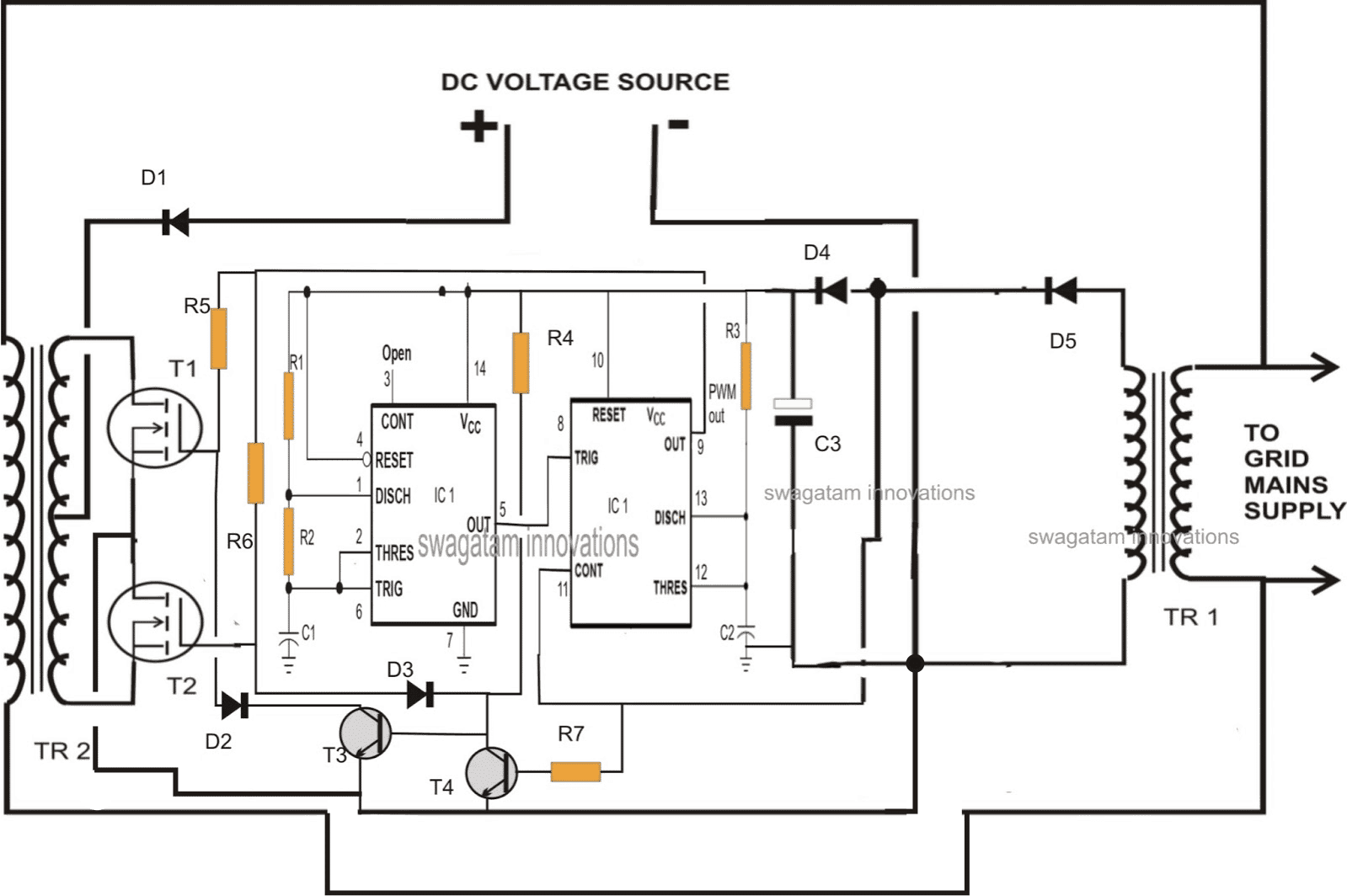
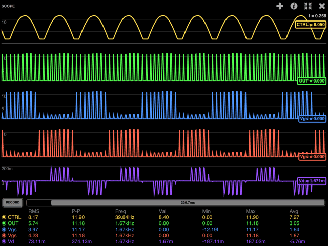 CTRL is the 100 Hz signal after the rectifier, OUT is from PWM from both halve waves, Vgs are the gate voltages of the FETs, Vd is the pickup on the secondary winding, which in sync with CTRL/2.
Disregard the frequencies as they are incorrect due low sampling speeds (else it gets too slow on the ipad).
At higher sampling freqs (20Mhz) the PWM looks quite impressing.
To fix the duty cycle to 50% at around 9kHz, I had to put a diode in.
Regards,
Selim
CTRL is the 100 Hz signal after the rectifier, OUT is from PWM from both halve waves, Vgs are the gate voltages of the FETs, Vd is the pickup on the secondary winding, which in sync with CTRL/2.
Disregard the frequencies as they are incorrect due low sampling speeds (else it gets too slow on the ipad).
At higher sampling freqs (20Mhz) the PWM looks quite impressing.
To fix the duty cycle to 50% at around 9kHz, I had to put a diode in.
Regards,
Selim
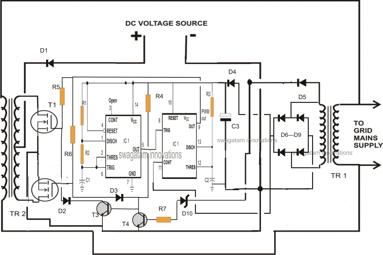
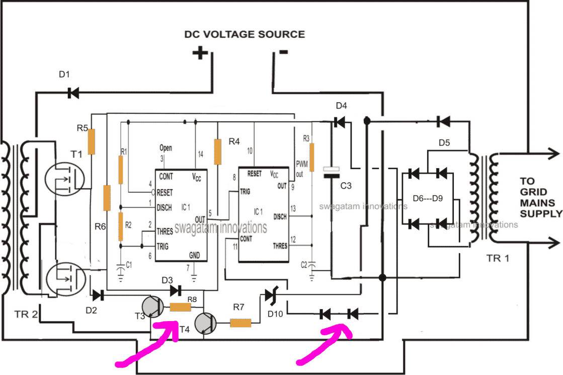
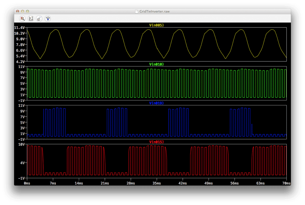

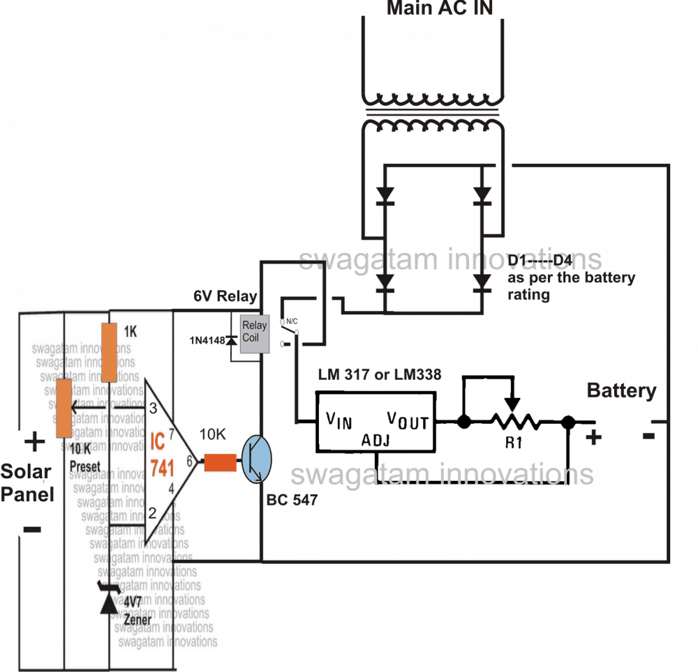
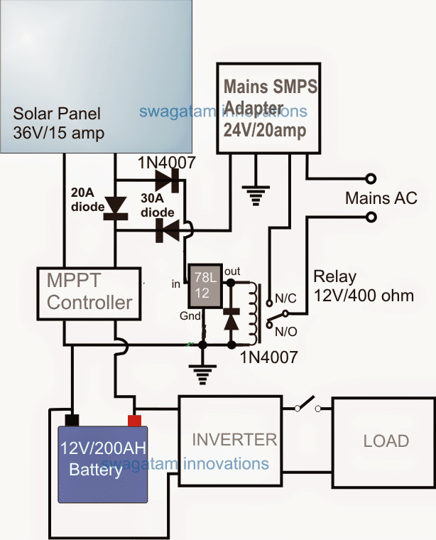
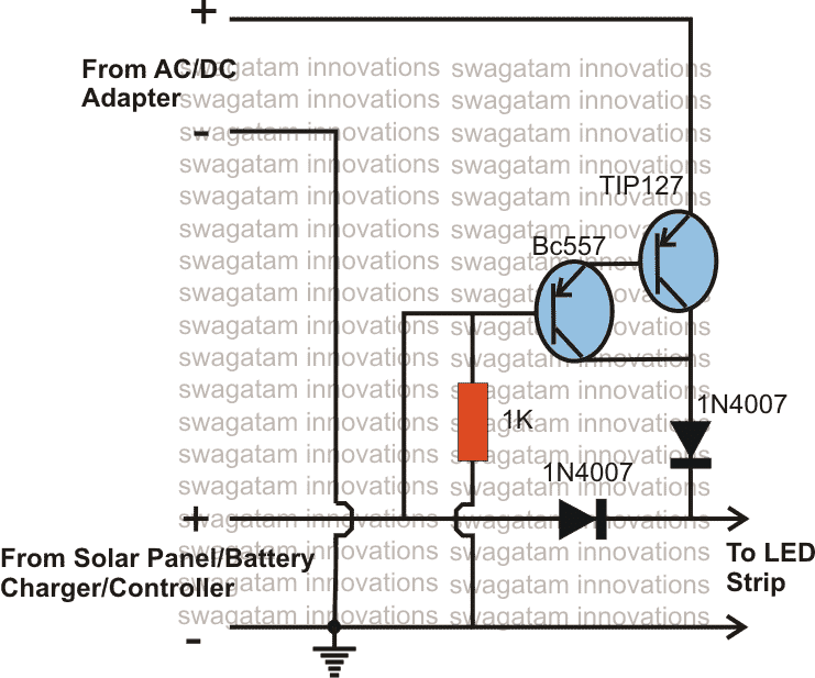
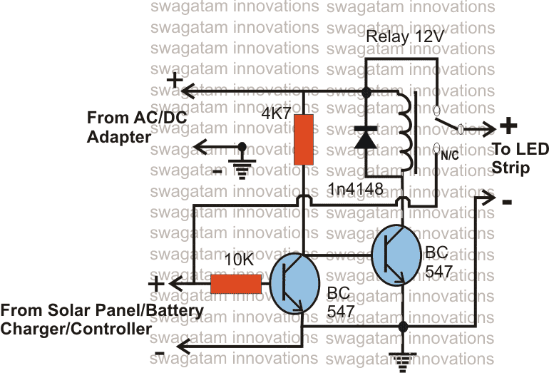
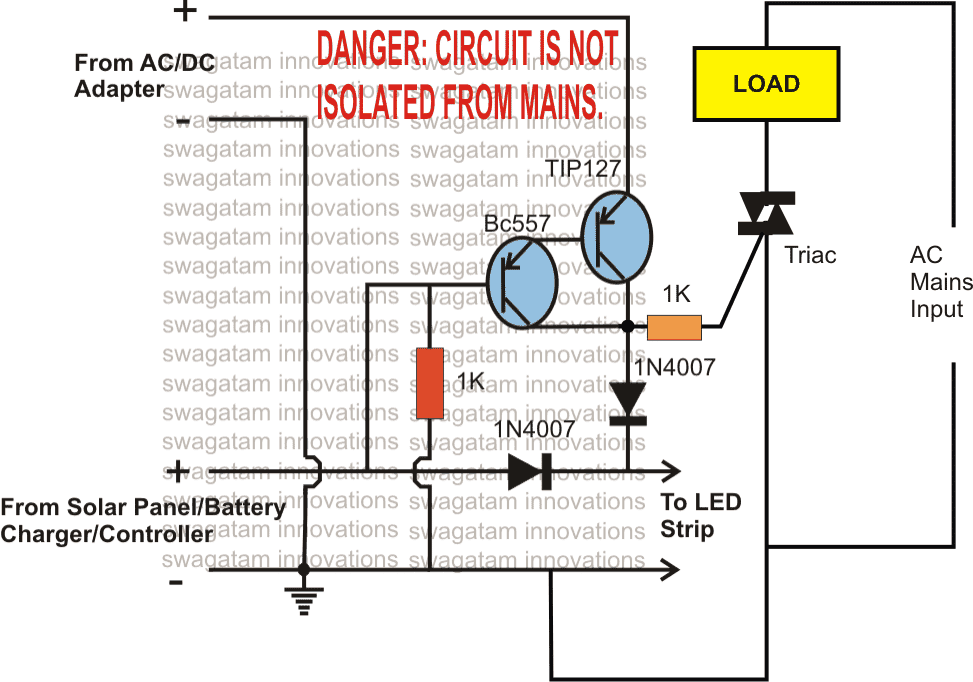
 General purpose PCB = cut into the desired size, approximately 5 by 4 inches should suffice.
Battery: 12 volts, Current not less than 10 AH.
Transformer = 9 ¨C 0 ¨C 9 volts, 5 Amps, Output winding may be 220 V or 120 volts as per your country specifications
Sundries: Metallic box, fuse holder, connecting cords, sockets etc
General purpose PCB = cut into the desired size, approximately 5 by 4 inches should suffice.
Battery: 12 volts, Current not less than 10 AH.
Transformer = 9 ¨C 0 ¨C 9 volts, 5 Amps, Output winding may be 220 V or 120 volts as per your country specifications
Sundries: Metallic box, fuse holder, connecting cords, sockets etc
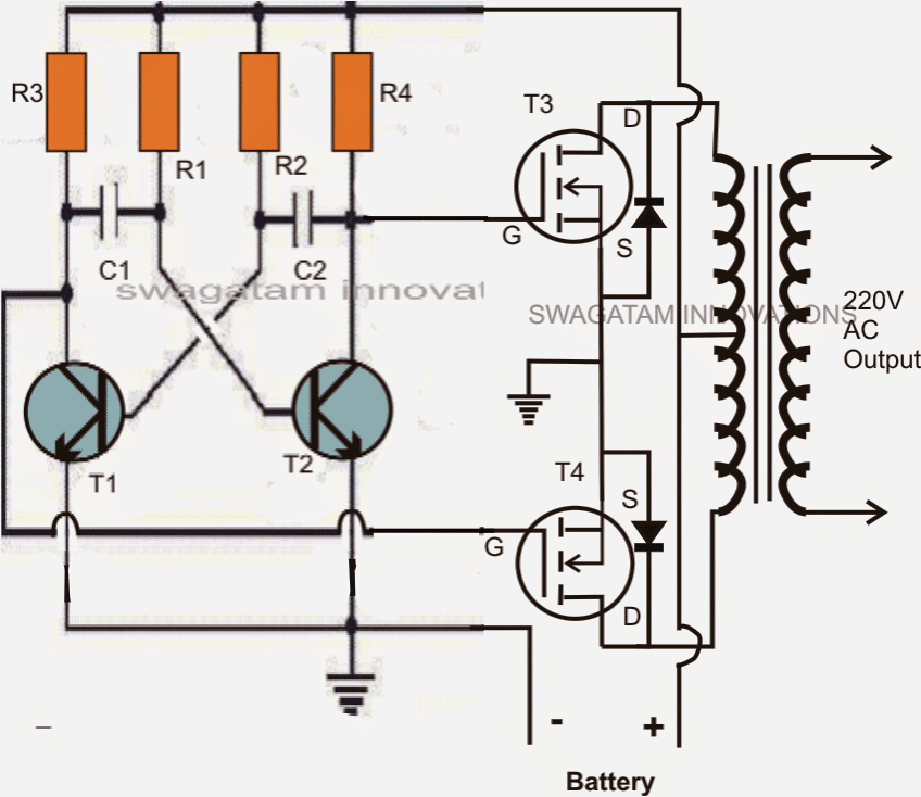
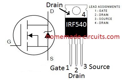
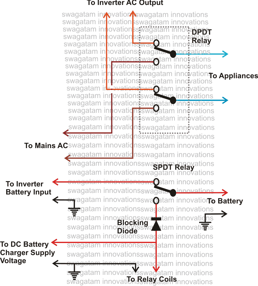 A comprehensive version of the above can be witnessed below:
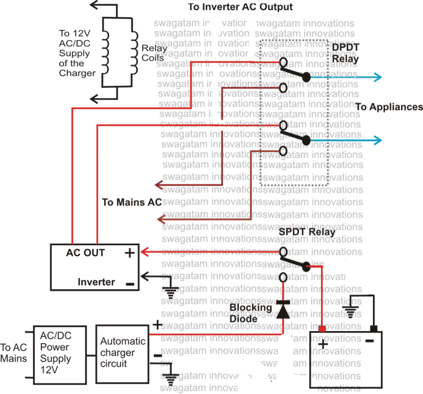
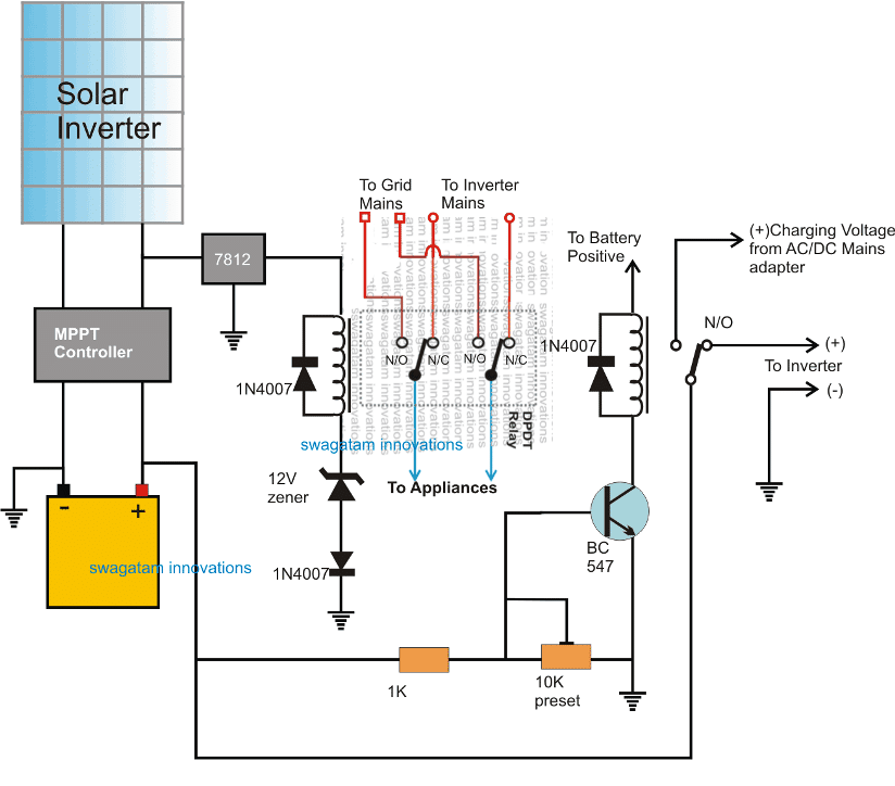 In this design which may be slightly different to the requested one, we can see a battery being charged by a solar panel though an MPPT controller circuit.
The solar MPPT controller charges the battery and also operates a connected inverter through an SPDT relay for facilitating the user with a free electricity supply during day time.
This SPDT relay shown at the extreme right side monitors the over-discharge condition or the low voltage situation of the battery and disconnects the inverter and the load from the battery whenever it reaches the lower threshold.
The low voltage situation could mostly take place during night when there's no solar supply available, and therefore N/C of the SPDT relay is linked with a AC/DC adapter supply source so that in an event of a low battery during night the battery could be charged for the time being through the mains supply.
A DPDT relay can be also witnessed attached with the solar panel, and this relay takes care of the mains supply changeover for the appliances.
During day time when the solar supply is present, the DPDT activates and connects the appliances with the inverter supply, while at night it reverts the supply to grid supply in order to save the battery for a mains failure back up situation.
In this design which may be slightly different to the requested one, we can see a battery being charged by a solar panel though an MPPT controller circuit.
The solar MPPT controller charges the battery and also operates a connected inverter through an SPDT relay for facilitating the user with a free electricity supply during day time.
This SPDT relay shown at the extreme right side monitors the over-discharge condition or the low voltage situation of the battery and disconnects the inverter and the load from the battery whenever it reaches the lower threshold.
The low voltage situation could mostly take place during night when there's no solar supply available, and therefore N/C of the SPDT relay is linked with a AC/DC adapter supply source so that in an event of a low battery during night the battery could be charged for the time being through the mains supply.
A DPDT relay can be also witnessed attached with the solar panel, and this relay takes care of the mains supply changeover for the appliances.
During day time when the solar supply is present, the DPDT activates and connects the appliances with the inverter supply, while at night it reverts the supply to grid supply in order to save the battery for a mains failure back up situation.
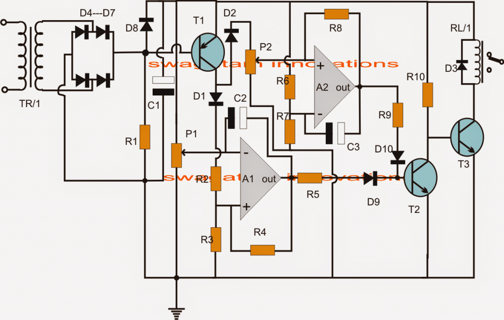
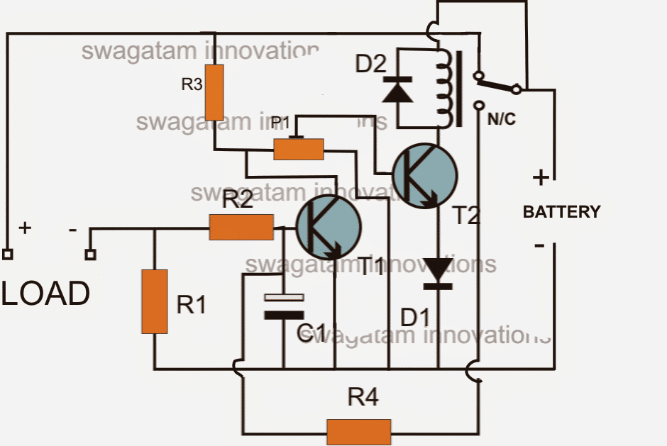 The"LOAD" terminals in the above diagram is supposed to be connected with the inverter +/- supply terminals.
This implies that the battery current from the right side has to pass through R1 before reaching the inverter, enabling the sensing circuit around R1 to sense a possible over current or overload situation.
CORRECTION:
The above shown circuit will not initiate unless the relay is actuated manually through a push switch as shown below:
The"LOAD" terminals in the above diagram is supposed to be connected with the inverter +/- supply terminals.
This implies that the battery current from the right side has to pass through R1 before reaching the inverter, enabling the sensing circuit around R1 to sense a possible over current or overload situation.
CORRECTION:
The above shown circuit will not initiate unless the relay is actuated manually through a push switch as shown below:
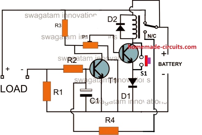
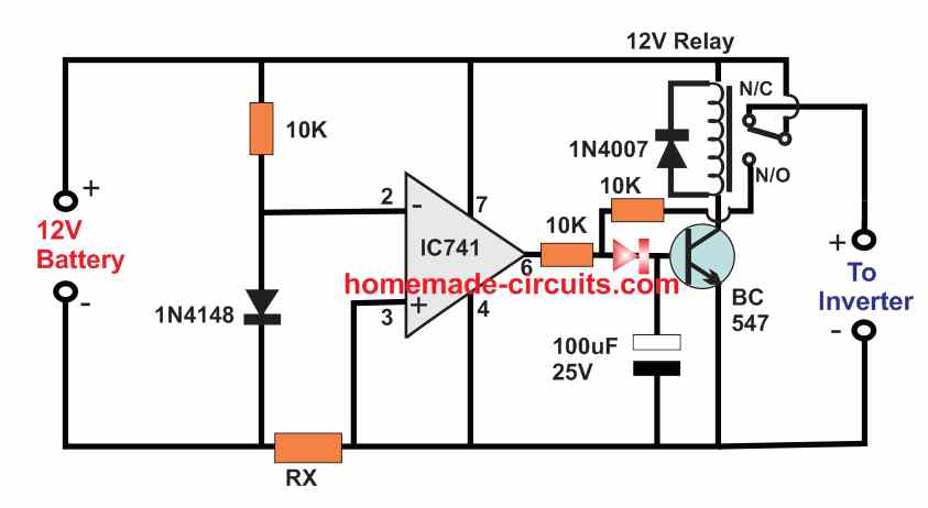

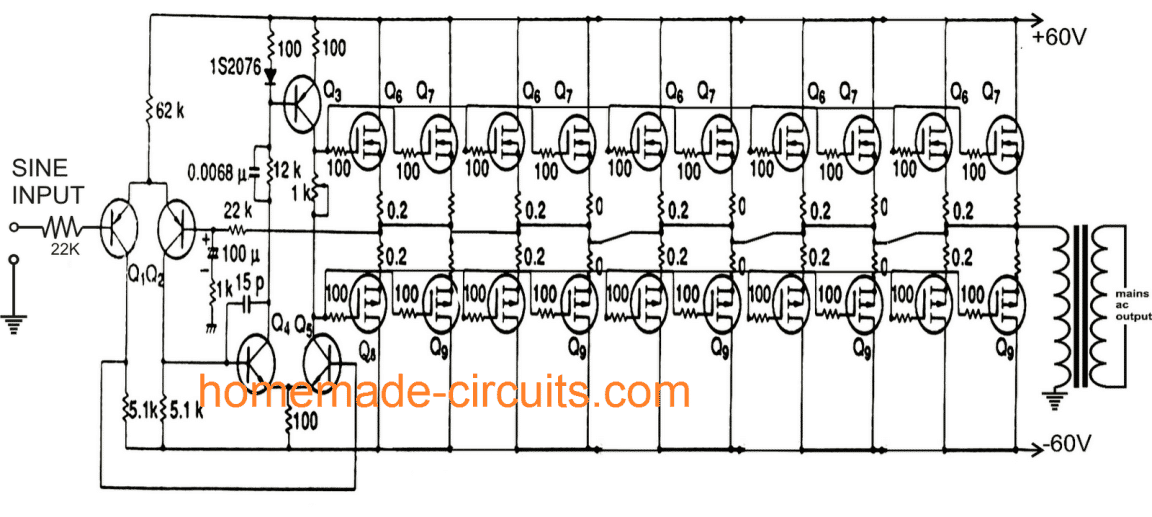
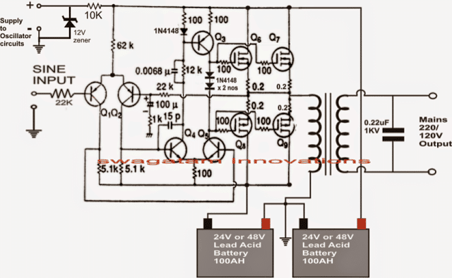
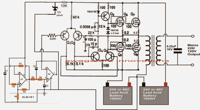 In the above section we have learned a full bridge design in which two batteries are involved for accomplishing the required 1kva output.
Now let's investigate how a full bridge design could be constructed using 4 N channel mosfet and using a single battery.
The following section shows how a full-bridge 1 KVA inverter circuit can be built using, without incorporating complicated high side driver networks or chips.
In the above section we have learned a full bridge design in which two batteries are involved for accomplishing the required 1kva output.
Now let's investigate how a full bridge design could be constructed using 4 N channel mosfet and using a single battery.
The following section shows how a full-bridge 1 KVA inverter circuit can be built using, without incorporating complicated high side driver networks or chips.

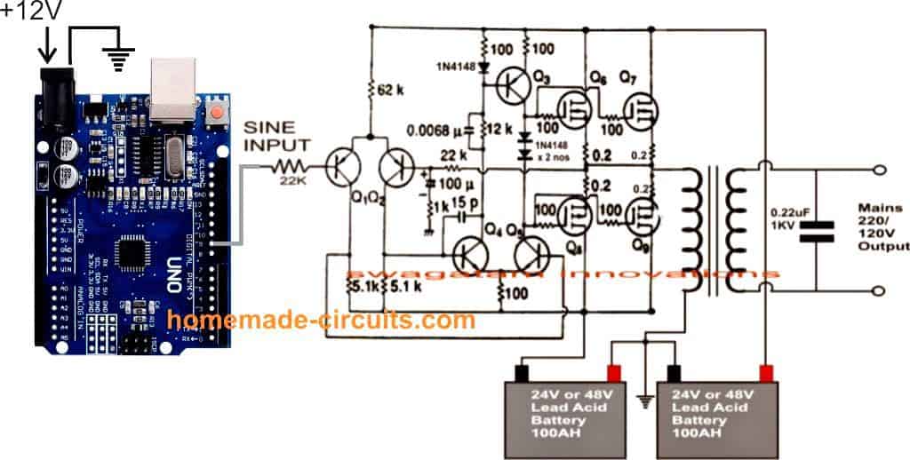 Program Code is given below:
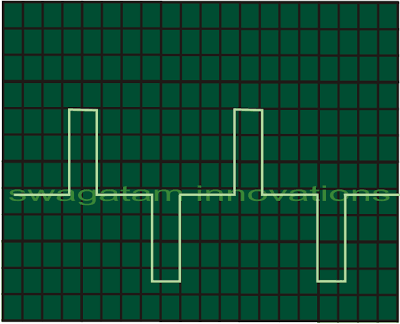
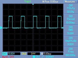


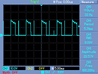
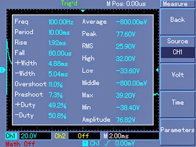
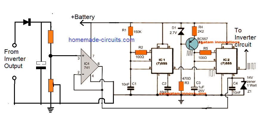 The circuit shown above can be effectively used as an automatic load triggered RMS converter and could be applied in any ordinary inverter for the intended purpose.
The IC 741 works like a voltage follower and acts like a buffer between the inverter output feedback voltage and the PWM controller circuit.
The resistors connected with pin#3of the IC 741 is configured like a voltage divider, which appropriately scales down the high AC output from the mains into a proportionately lower potential varying between 6 and 12V depending upon the output status of the inverter.
The two IC 555 circuit are configured to work like modulated PWM controller.
The modulated input is applied at pin#5 of the IC2, which compares the signal with the triangle waves at its pin#6.
This results in the generation of the PWM output at its pin#3 which varies its duty cycle in response to the modulating signal at the pin#5 of the IC.
A rising potential at this pin#5 results in the generation wide PWMs or PWMs with higher duty cycles, and vice versa.
This implies that when the opamp 741 responds with a rising potential due to a rising output from the inverter causes the output of IC2 555 to widen its PWM pulses, while when the inverter output drops, the PWM proportionately narrows at pin#3 of IC2.
The circuit shown above can be effectively used as an automatic load triggered RMS converter and could be applied in any ordinary inverter for the intended purpose.
The IC 741 works like a voltage follower and acts like a buffer between the inverter output feedback voltage and the PWM controller circuit.
The resistors connected with pin#3of the IC 741 is configured like a voltage divider, which appropriately scales down the high AC output from the mains into a proportionately lower potential varying between 6 and 12V depending upon the output status of the inverter.
The two IC 555 circuit are configured to work like modulated PWM controller.
The modulated input is applied at pin#5 of the IC2, which compares the signal with the triangle waves at its pin#6.
This results in the generation of the PWM output at its pin#3 which varies its duty cycle in response to the modulating signal at the pin#5 of the IC.
A rising potential at this pin#5 results in the generation wide PWMs or PWMs with higher duty cycles, and vice versa.
This implies that when the opamp 741 responds with a rising potential due to a rising output from the inverter causes the output of IC2 555 to widen its PWM pulses, while when the inverter output drops, the PWM proportionately narrows at pin#3 of IC2.
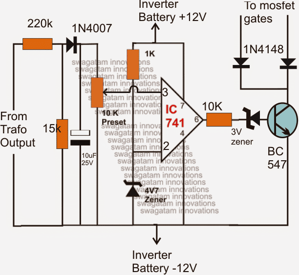
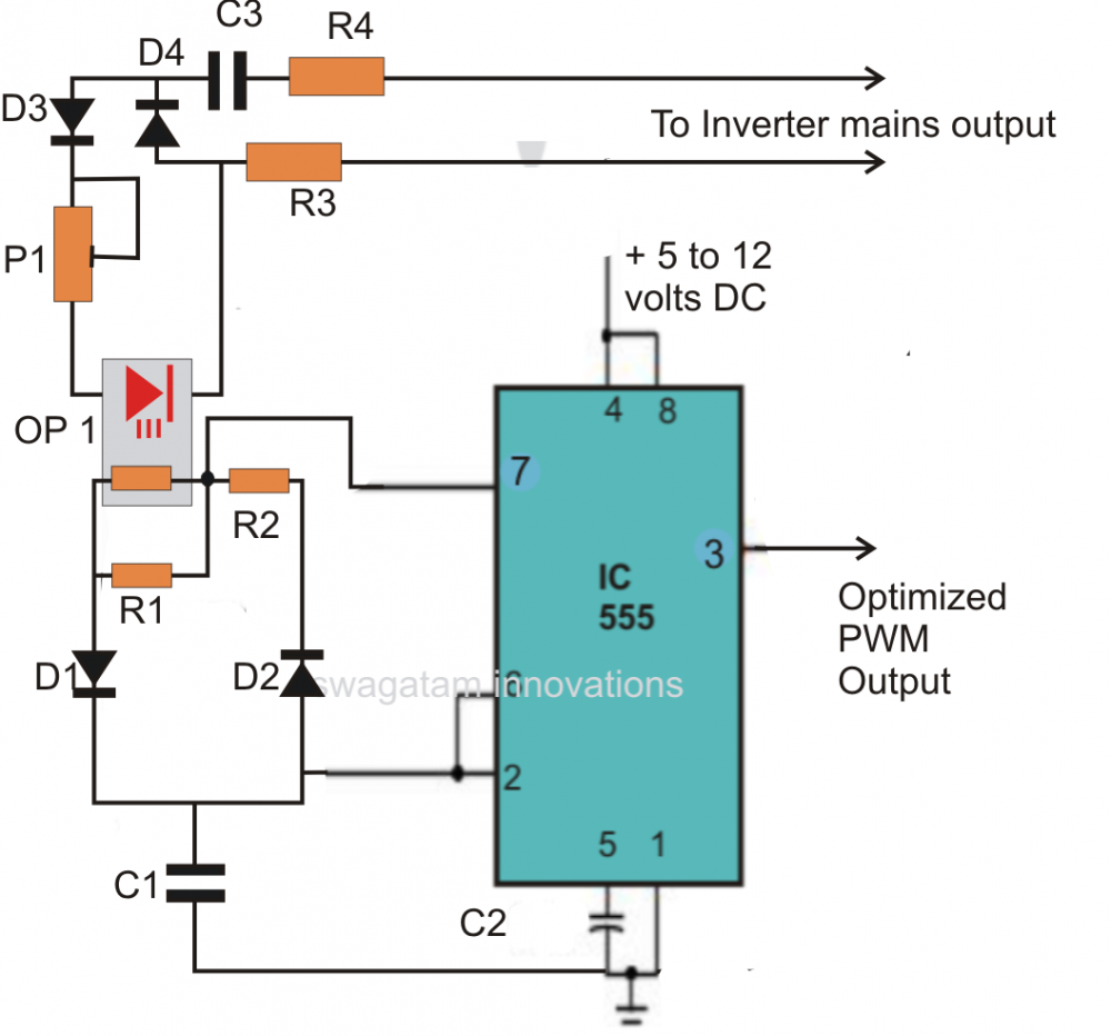
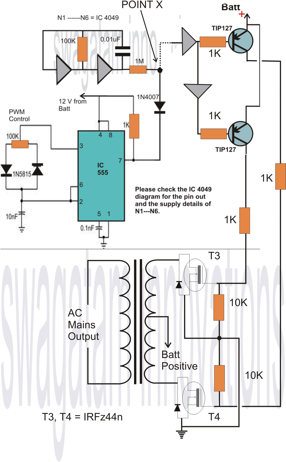

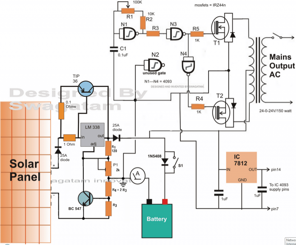
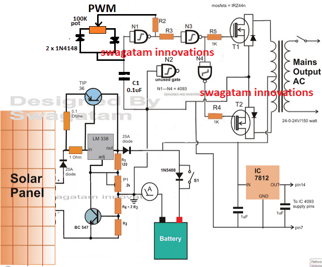 By adjusting this pot we can force the oscillator to create frequencies with different ON/OFF periods which will in turn enable the mosfets to turn ON and OFF with the the same rate.
By adjusting the mosfet ON/OFF timing we can proportionately vary the current induction in the transformer, which will eventually allow us to adjust the output RMS voltage of the inverter.
Once the output RMS is fixed, the inverter will be able to produce a constant output regardless f the solar voltage variations, until of course the voltage drops below the voltage specification of the transformer primary winding.
By adjusting this pot we can force the oscillator to create frequencies with different ON/OFF periods which will in turn enable the mosfets to turn ON and OFF with the the same rate.
By adjusting the mosfet ON/OFF timing we can proportionately vary the current induction in the transformer, which will eventually allow us to adjust the output RMS voltage of the inverter.
Once the output RMS is fixed, the inverter will be able to produce a constant output regardless f the solar voltage variations, until of course the voltage drops below the voltage specification of the transformer primary winding.
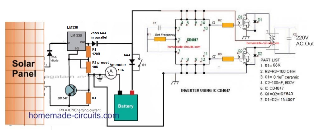

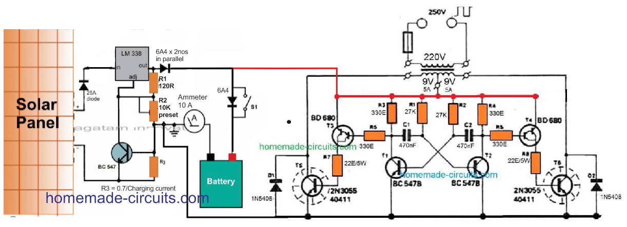
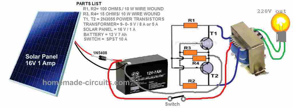 The simplicity of the design also indicates the fact that lead acid batteries are not so difficult to charge after all.
Remember, a fully discharged battery (below 11V) may require at least 8 hours to 10 hours of charging until the inverter can be switched ON for the required 12V to 220V AC conversion.
The simplicity of the design also indicates the fact that lead acid batteries are not so difficult to charge after all.
Remember, a fully discharged battery (below 11V) may require at least 8 hours to 10 hours of charging until the inverter can be switched ON for the required 12V to 220V AC conversion.
 The 12V adapter should be rated to suit the battery voltage and the Ah specs.
For example if the battery is rated at 12 V 50 Ah, then the 12V adapter can be rated at 15V to 20 V and 5 amp
The 12V adapter should be rated to suit the battery voltage and the Ah specs.
For example if the battery is rated at 12 V 50 Ah, then the 12V adapter can be rated at 15V to 20 V and 5 amp
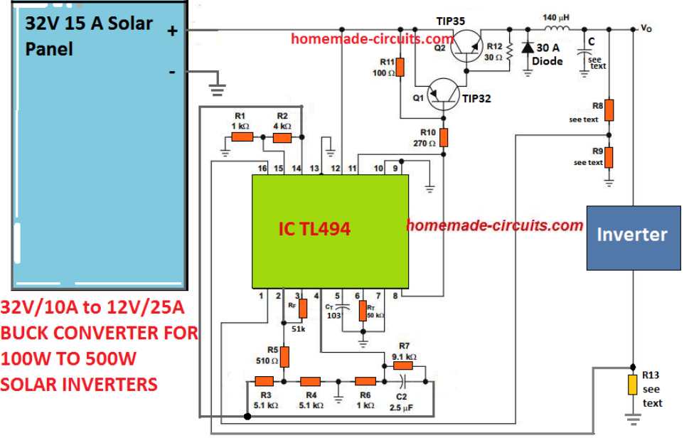 We fix the important parameters of the buck converter as given in the following calculations:
Design Requirements
Solar Panel Voltage VI = 32 V
Buck Converter Output VO = 12 V
Buck Converter Output IO = 25 A
Buck Converter Operating Frequency fOSC = 20-kHz switching frequency
VR = 20-mV peak-to-peak (VRIPPLE)
¦¤IL = 1.5-A inductor current change
d = duty cycle = VO/VI = 12 V/32 V = 0.375
f = 20 kHz (design objective)
ton = time on (S1 closed) = (1/f) ˇÁ d = 7.8 ¦Ěs
toff = time off (S1 open) = (1/f) ¨C ton = 42.2 ¦Ěs
L (VI ¨C VO ) ˇÁ ton/¦¤IL
[(32 V ¨C 12 V) ˇÁ 7.8 ¦Ěs]/1.5 A
104 ¦ĚH
This provides us the specifications of the buck converter inductor.
The wire SWG can be optimized through some trial and error.
A 16 SWG super enameled copper wire should be good enough to handle 25 Amps current.
We fix the important parameters of the buck converter as given in the following calculations:
Design Requirements
Solar Panel Voltage VI = 32 V
Buck Converter Output VO = 12 V
Buck Converter Output IO = 25 A
Buck Converter Operating Frequency fOSC = 20-kHz switching frequency
VR = 20-mV peak-to-peak (VRIPPLE)
¦¤IL = 1.5-A inductor current change
d = duty cycle = VO/VI = 12 V/32 V = 0.375
f = 20 kHz (design objective)
ton = time on (S1 closed) = (1/f) ˇÁ d = 7.8 ¦Ěs
toff = time off (S1 open) = (1/f) ¨C ton = 42.2 ¦Ěs
L (VI ¨C VO ) ˇÁ ton/¦¤IL
[(32 V ¨C 12 V) ˇÁ 7.8 ¦Ěs]/1.5 A
104 ¦ĚH
This provides us the specifications of the buck converter inductor.
The wire SWG can be optimized through some trial and error.
A 16 SWG super enameled copper wire should be good enough to handle 25 Amps current.

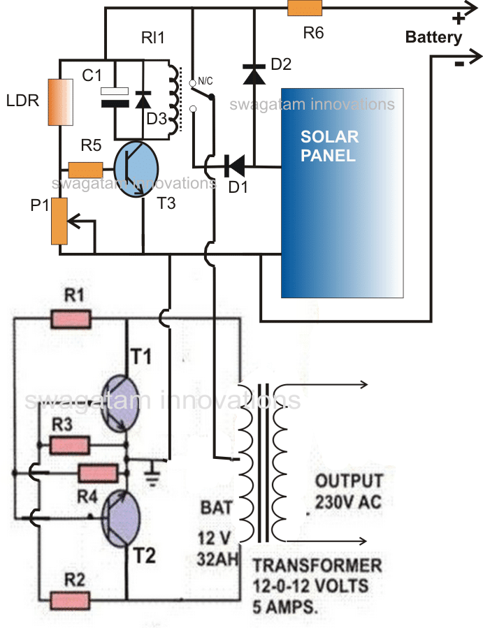
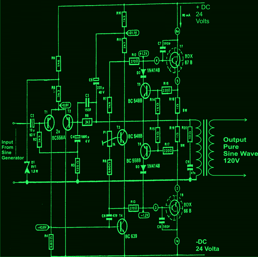 The TRANSFORMER is a made to order type, with an input winding of 48 ¨C 0 ¨C 48 V, 3 Amps, output is 120V, 1 Amp.
Once this is done, you can rest assured of a clean, hassle free pure sine wave output that may be used for powering ANY electrical gadget, even your computer.
The TRANSFORMER is a made to order type, with an input winding of 48 ¨C 0 ¨C 48 V, 3 Amps, output is 120V, 1 Amp.
Once this is done, you can rest assured of a clean, hassle free pure sine wave output that may be used for powering ANY electrical gadget, even your computer.
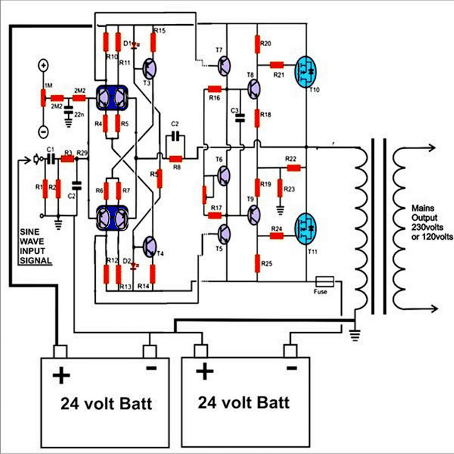
 If you are planning to make your own low cost and simple home built power inverter then probably you wonˇŻt find a better circuit than the present one.
This heavy duty, easy to build design includes very few numbers of components which can be found readily available in any electronic retailer shop.
The output of the inverter will be obviously a square wave and also load dependent.
But these drawbacks wonˇŻt matter much as long as sophisticated electronic equipment are not operated with it and the output is not over loaded.
The big benefit of the present design is its simplicity, very low cost, high power output, 12 volt operation and low maintenance.
Besides, once it is built, an instant start is pretty assured.
If at all any problem is encountered, troubleshooting wonˇŻt be a headache and may be traced within minutes.
The efficiency of the system is also pretty high, in the vicinity of around 85% and the output power is above 200 watts.
A simple two transistor astable multivibrator forms the main square wave generator.
The signal is suitably amplified by two current amplifier medium power Darlington transistors.
This amplified square wave signal is further fed to the output stage comprising of parallel connected high power transistors.
These transistors convert this signal into high current alternating pulses which is dumped into the secondary windings of the power transformer.
The induced voltage from the secondary to the primary winding, results a massive 230 or 120 volts conversion, as per transformer specifications.
LetˇŻs study in details how the circuit functions.
If you are planning to make your own low cost and simple home built power inverter then probably you wonˇŻt find a better circuit than the present one.
This heavy duty, easy to build design includes very few numbers of components which can be found readily available in any electronic retailer shop.
The output of the inverter will be obviously a square wave and also load dependent.
But these drawbacks wonˇŻt matter much as long as sophisticated electronic equipment are not operated with it and the output is not over loaded.
The big benefit of the present design is its simplicity, very low cost, high power output, 12 volt operation and low maintenance.
Besides, once it is built, an instant start is pretty assured.
If at all any problem is encountered, troubleshooting wonˇŻt be a headache and may be traced within minutes.
The efficiency of the system is also pretty high, in the vicinity of around 85% and the output power is above 200 watts.
A simple two transistor astable multivibrator forms the main square wave generator.
The signal is suitably amplified by two current amplifier medium power Darlington transistors.
This amplified square wave signal is further fed to the output stage comprising of parallel connected high power transistors.
These transistors convert this signal into high current alternating pulses which is dumped into the secondary windings of the power transformer.
The induced voltage from the secondary to the primary winding, results a massive 230 or 120 volts conversion, as per transformer specifications.
LetˇŻs study in details how the circuit functions.
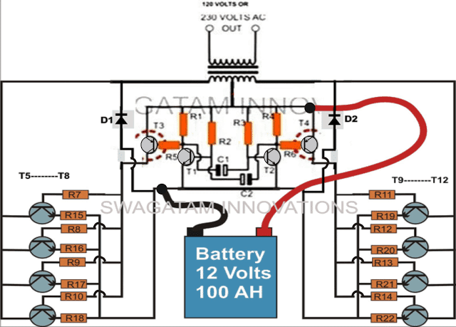 PARTS LIST
RESISTORS WATT, CFR
R1, R4 = 470 ¦¸,
R2, R3 = 39 K,
RESISTORS, 10 WATT, WIRE WOUND
R5, R6 = 100 ¦¸,
R7-----R14 = 15 ¦¸,
R15 ----R22 = 0.22 Ohms, 5 watt (can be connected directly if all the parallel transistors are mounted on a common heatsink, separate for each channel)
Capacitors
C1, C2 = 0.33 ¦ĚF, 50 VOLTS, TANTALLUM,
Semiconductors
D1, D2 = 1N5408,
T1, T2 = BC547B,
T3, T4 = TIP 127,
T5-----T12 = 2N 3055 POWER TRANSISTORS,
Misc.
TRANSFORMER = 10 to 20 AMPS, 9 ¨C 0 ¨C 9 VOLTS,
HEATSINKS = LARGE FINNED TYPE,
BATTERY = 12 VOLT, 100 AH
PARTS LIST
RESISTORS WATT, CFR
R1, R4 = 470 ¦¸,
R2, R3 = 39 K,
RESISTORS, 10 WATT, WIRE WOUND
R5, R6 = 100 ¦¸,
R7-----R14 = 15 ¦¸,
R15 ----R22 = 0.22 Ohms, 5 watt (can be connected directly if all the parallel transistors are mounted on a common heatsink, separate for each channel)
Capacitors
C1, C2 = 0.33 ¦ĚF, 50 VOLTS, TANTALLUM,
Semiconductors
D1, D2 = 1N5408,
T1, T2 = BC547B,
T3, T4 = TIP 127,
T5-----T12 = 2N 3055 POWER TRANSISTORS,
Misc.
TRANSFORMER = 10 to 20 AMPS, 9 ¨C 0 ¨C 9 VOLTS,
HEATSINKS = LARGE FINNED TYPE,
BATTERY = 12 VOLT, 100 AH
 Select the suitable ones; make sure that the holes are appropriately drilled for the TO-3 package as shown in the figure.
TO-3 is the code to recognize typically the dimensions of power transistors which are categorized in the type used in the present circuit i.e.
for 2N3055.
Fix T5----T8 firmly over the heat sinks using 1/8 *1/2 screws, nuts and spring washers.
You may use two separate heat sinks for the two sets of transistors or one single large heat sink.
Do not forget to isolate the transistors from the heat sink with the help of mica isolation kit.
Select the suitable ones; make sure that the holes are appropriately drilled for the TO-3 package as shown in the figure.
TO-3 is the code to recognize typically the dimensions of power transistors which are categorized in the type used in the present circuit i.e.
for 2N3055.
Fix T5----T8 firmly over the heat sinks using 1/8 *1/2 screws, nuts and spring washers.
You may use two separate heat sinks for the two sets of transistors or one single large heat sink.
Do not forget to isolate the transistors from the heat sink with the help of mica isolation kit.
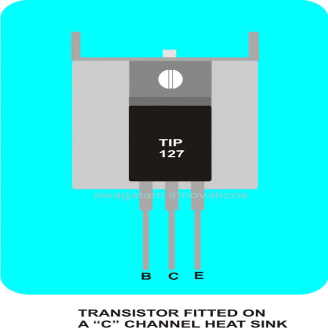 Constructing the PCB is just a matter of putting all the components in place and interconnecting their leads as per the given circuit schematic.
It can be done simply over a piece of general PCB.
Transistors T3 and T4 also need heat sinks; a ˇ°Cˇ± channel type aluminum heat sink will do the job perfectly.
This is can also be procured ready made as per the given size.
Now we can connect the relevant points from the assembled board to the power transistors fitted over the heat sinks.
Take care of its base, emitter and the collector, a wrong connection would mean an instant damage of the particular device.
Once all the wires are connected appropriately to the required points, lift the whole assembly gently and place it on the base of a strong and sturdy metallic box.
The size of the box should such that the assembly does not get crammed.
It goes without saying that the outputs and the inputs of circuit should be terminated into proper socket type of outlets, to make the external connections easy.
The external fittings should also include a fuse holder, LEDs and a toggle switch.
Constructing the PCB is just a matter of putting all the components in place and interconnecting their leads as per the given circuit schematic.
It can be done simply over a piece of general PCB.
Transistors T3 and T4 also need heat sinks; a ˇ°Cˇ± channel type aluminum heat sink will do the job perfectly.
This is can also be procured ready made as per the given size.
Now we can connect the relevant points from the assembled board to the power transistors fitted over the heat sinks.
Take care of its base, emitter and the collector, a wrong connection would mean an instant damage of the particular device.
Once all the wires are connected appropriately to the required points, lift the whole assembly gently and place it on the base of a strong and sturdy metallic box.
The size of the box should such that the assembly does not get crammed.
It goes without saying that the outputs and the inputs of circuit should be terminated into proper socket type of outlets, to make the external connections easy.
The external fittings should also include a fuse holder, LEDs and a toggle switch.
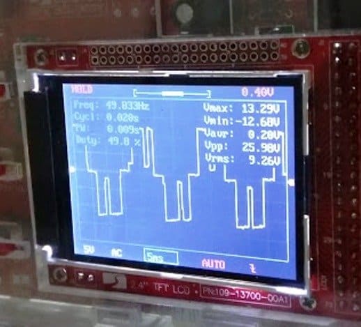 this is the wave measure from mosfet drain side.
everything is mess up.
freq and duty cycle are changes.
this is the wave measure from mosfet drain side.
everything is mess up.
freq and duty cycle are changes.
 this is i measure from output of my transformer (for testing purpose i used 2A 12v 0 12v - 220v CT).
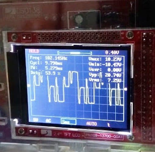 how to get the transformer output wave just like a gate one? i have a ups at home.
i try to measuring the gate, drain, and transformer output.
the waveform is almost the same on that small ups (modified sinewave).
how do i achieve that result in my circuit?
please kindly help, thanks sir.
how to get the transformer output wave just like a gate one? i have a ups at home.
i try to measuring the gate, drain, and transformer output.
the waveform is almost the same on that small ups (modified sinewave).
how do i achieve that result in my circuit?
please kindly help, thanks sir.
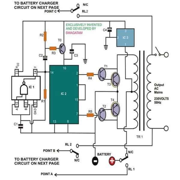
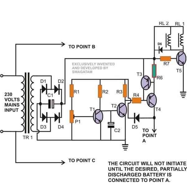 Parts list for the UPS Inverter
R1=20K
R2,R3=1K
R4,R5 = 220 Ohms
C1=0.095Uf
C2,C3,C4=10UF/25V
T0 = BC557B
T1,T2=8050
T3,T4=BDY29
IC1= SN74LVC1G132 or a single gate from IC4093
IC2=4017
IC3=7805
TRANSFORMER=12-0-12V/10AMP/230V
Parts list for the UPS Inverter
R1=20K
R2,R3=1K
R4,R5 = 220 Ohms
C1=0.095Uf
C2,C3,C4=10UF/25V
T0 = BC557B
T1,T2=8050
T3,T4=BDY29
IC1= SN74LVC1G132 or a single gate from IC4093
IC2=4017
IC3=7805
TRANSFORMER=12-0-12V/10AMP/230V
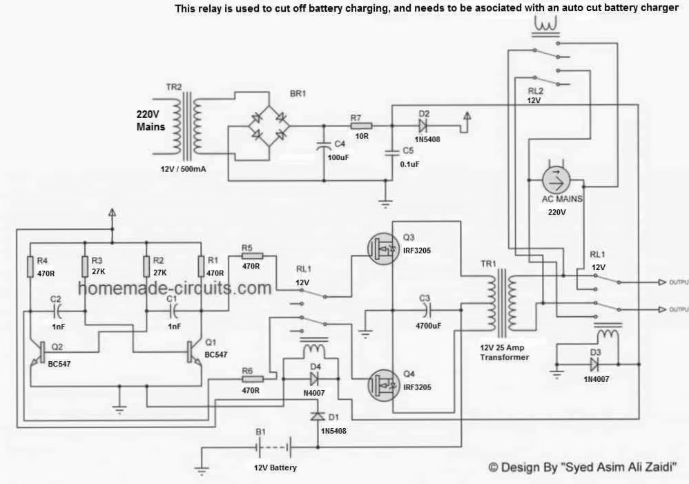
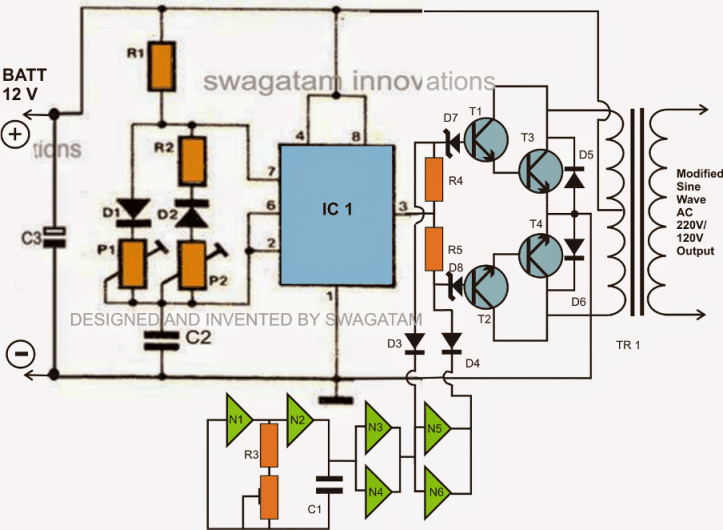
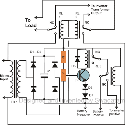
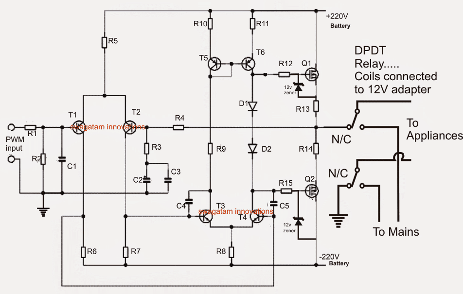 Parts List for the above 1000 watt UPS circuit
All resistor CFR 2 watt rated unless stated.
R1, R3,R10,R11,R8 = 4k7
R2,R4, R5= 68k
R6, R7 = 4k7
R9 = 10k
R13, R14 = 0.22 ohms 2 watt
R12,R15 = 1K, 5 watt
C1 = 470pF
C2 = 47uF/100V
C3 = 0.1uF/100V
C4, C5 = 100pF
D1, D2 = 1N4148
T1, T2 = BC556
T5, T6 = MJE350
T3, T4 = MJE340
Q1 = IRF840
Q2 = FQP3P50
relay = DPDT, 12V/10amp contacts, 400 ohm coil
Parts List for the above 1000 watt UPS circuit
All resistor CFR 2 watt rated unless stated.
R1, R3,R10,R11,R8 = 4k7
R2,R4, R5= 68k
R6, R7 = 4k7
R9 = 10k
R13, R14 = 0.22 ohms 2 watt
R12,R15 = 1K, 5 watt
C1 = 470pF
C2 = 47uF/100V
C3 = 0.1uF/100V
C4, C5 = 100pF
D1, D2 = 1N4148
T1, T2 = BC556
T5, T6 = MJE350
T3, T4 = MJE340
Q1 = IRF840
Q2 = FQP3P50
relay = DPDT, 12V/10amp contacts, 400 ohm coil
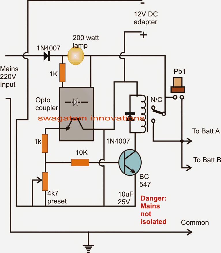 The output from the above charger is fed to the battery bank through a couple of SPDT relays as shown in the following diagram.
The relays make sure that the batteries are put into the charging mode as long as the mains input is available and is reverted to inverter mode when mains input fails.
The output from the above charger is fed to the battery bank through a couple of SPDT relays as shown in the following diagram.
The relays make sure that the batteries are put into the charging mode as long as the mains input is available and is reverted to inverter mode when mains input fails.
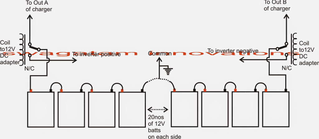
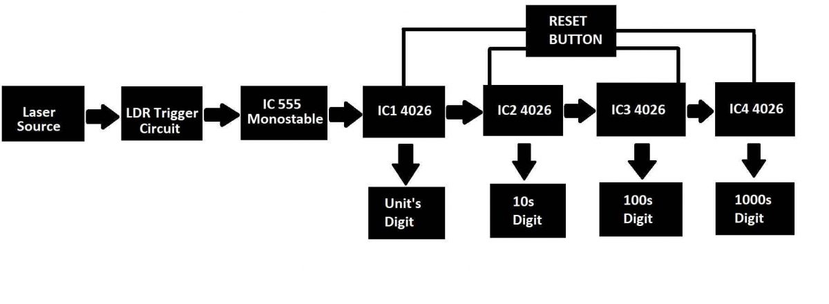 The above image illustrates the block diagram of the proposed visitor counter project.
LetˇŻs try to understand each of the blocks.
In this project we are utilizing one IC 555 and four IC 4026s along with other active and passive components such as resistors, capacitors, transistors and trim potentiometers.
The first block is a laser source which emits a reasonably bright laser beam which is visible even during day time.
We recommend a 5mW laser module which is easily found on e-commerce sites.
The second block is a trigger circuit which is activated optically.
When the laser beam gets interrupted by a person, the circuit generates a negative pulse momentarily.
The next block is a monostable multivibrator stage which utilizes IC 555 for debouncing the output pulse i.e., the circuit generates a clean clock pulse for IC 4026 counting stage.
The next 4 blocks consist of four IC 4026s which drives four 7 segment common cathode displays to showcase the number of visitors passed since the circuit turned ON.
A reset button is connected to four IC 4026s to reset the display to zero manually.
The above image illustrates the block diagram of the proposed visitor counter project.
LetˇŻs try to understand each of the blocks.
In this project we are utilizing one IC 555 and four IC 4026s along with other active and passive components such as resistors, capacitors, transistors and trim potentiometers.
The first block is a laser source which emits a reasonably bright laser beam which is visible even during day time.
We recommend a 5mW laser module which is easily found on e-commerce sites.
The second block is a trigger circuit which is activated optically.
When the laser beam gets interrupted by a person, the circuit generates a negative pulse momentarily.
The next block is a monostable multivibrator stage which utilizes IC 555 for debouncing the output pulse i.e., the circuit generates a clean clock pulse for IC 4026 counting stage.
The next 4 blocks consist of four IC 4026s which drives four 7 segment common cathode displays to showcase the number of visitors passed since the circuit turned ON.
A reset button is connected to four IC 4026s to reset the display to zero manually.
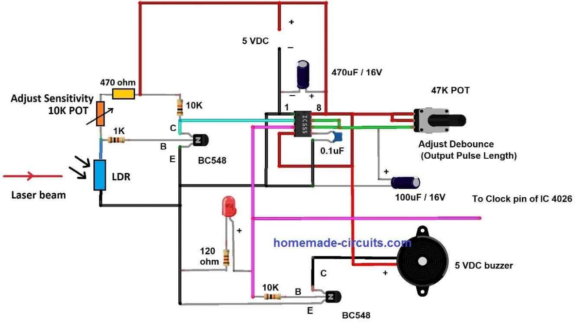 The above circuit consists two circuit stages the laser trigger circuit and the monostable multivibrator.
LetˇŻs try to understand the laser trigger stage first.
The above circuit consists two circuit stages the laser trigger circuit and the monostable multivibrator.
LetˇŻs try to understand the laser trigger stage first.
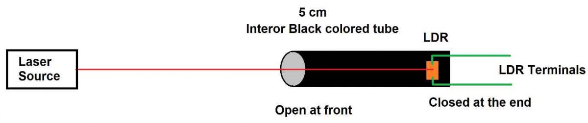 Counter circuit:
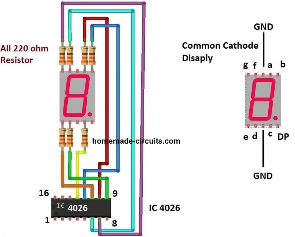 Note: Display connections are not shown in the first diagram for drawing convinces.
The second diagram shows the display connection with 220-ohm current limiting resistors.
This proposed stage is responsible for counting the number of visitors and also driving the 7 segment displays.
Before we dive into the explanation of the above circuit, it is important to know about the pin diagram of IC 4026 and what each of the pin does, at the same time you will also understand the above circuit stage.
Note: Display connections are not shown in the first diagram for drawing convinces.
The second diagram shows the display connection with 220-ohm current limiting resistors.
This proposed stage is responsible for counting the number of visitors and also driving the 7 segment displays.
Before we dive into the explanation of the above circuit, it is important to know about the pin diagram of IC 4026 and what each of the pin does, at the same time you will also understand the above circuit stage.
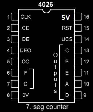 Pin 1: Clock input, receives clock signal from an external source.
Pin 2: Clock inhibit, when this pin is connected to +Vcc, the IC ignores the clock input, when this pin is connected to GND, IC accepts input clock pulses.
Pin 3: Display enable / disable pin.
When this pin is connected to +Vcc the 7 segment pins are enabled (A to G) and when connect to GND display pins are disabled.
Pin 5: This pin performs divided by 10 operation or carry-out.
This pin turns high for every 10th input pulse.
This is used for cascading multiple IC 4026s to work with 2 or more digits.
Pins 6, 7, 9, 10, 11, 12,13 are output pins for common cathode 7 segment display (A to G).
Pins 16 and 8 are +Vcc and GND respectively.
Pin 15: Reset, when this pin is turned high the count resets to zero, during normal operation this pin must be grounded.
Pin 1: Clock input, receives clock signal from an external source.
Pin 2: Clock inhibit, when this pin is connected to +Vcc, the IC ignores the clock input, when this pin is connected to GND, IC accepts input clock pulses.
Pin 3: Display enable / disable pin.
When this pin is connected to +Vcc the 7 segment pins are enabled (A to G) and when connect to GND display pins are disabled.
Pin 5: This pin performs divided by 10 operation or carry-out.
This pin turns high for every 10th input pulse.
This is used for cascading multiple IC 4026s to work with 2 or more digits.
Pins 6, 7, 9, 10, 11, 12,13 are output pins for common cathode 7 segment display (A to G).
Pins 16 and 8 are +Vcc and GND respectively.
Pin 15: Reset, when this pin is turned high the count resets to zero, during normal operation this pin must be grounded.
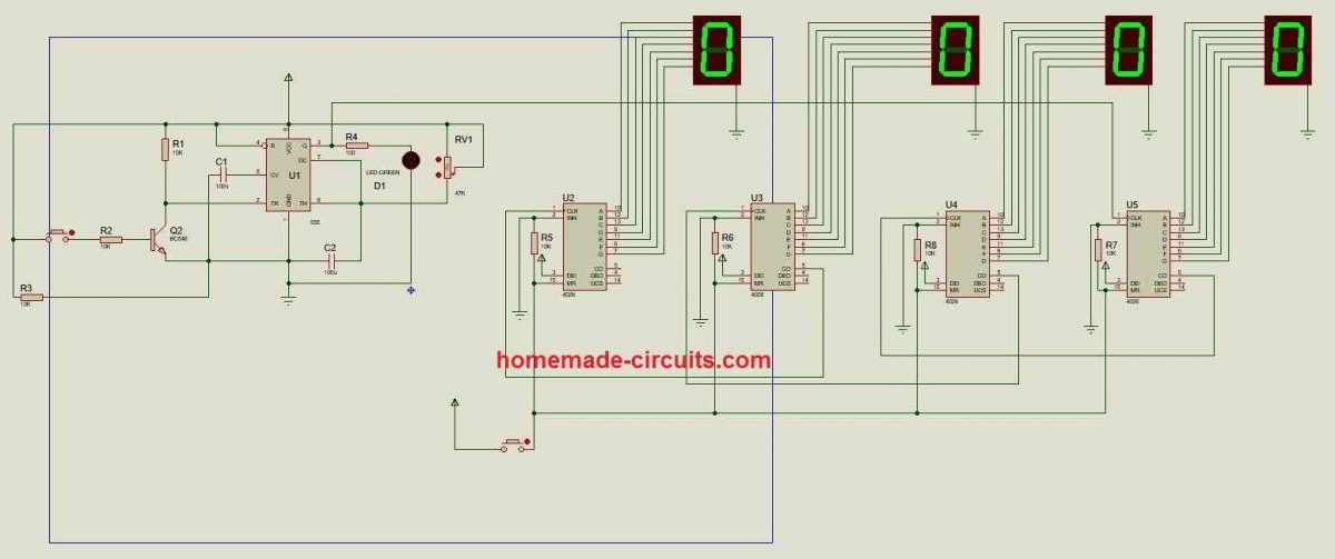 We developed a simulation using proteus software of the proposed project.
You can download the given file and test the project on your computer.
When you press the button (on the left-hand side at the base terminal of the transistor) it emulates laser beam interruption and increments a count on the display.
A potentiometer connected to IC 555 can be adjusted for testing debouncing delay.
The reset button is provided at the bottom of the circuit to reset the displays to zero.
We developed a simulation using proteus software of the proposed project.
You can download the given file and test the project on your computer.
When you press the button (on the left-hand side at the base terminal of the transistor) it emulates laser beam interruption and increments a count on the display.
A potentiometer connected to IC 555 can be adjusted for testing debouncing delay.
The reset button is provided at the bottom of the circuit to reset the displays to zero.

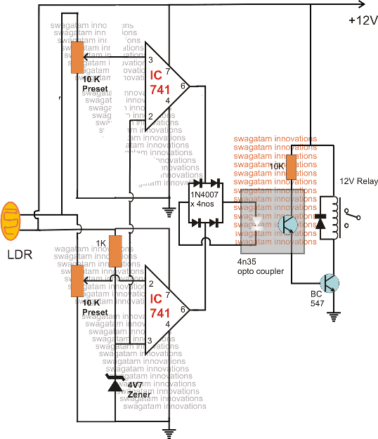 In the earlier article we saw a rather simple Laser controlled burglar alarm circuit where the alarm is sounded whenever the laser beam incident on the LDR is interrupted.
However as requested above, this could be possibly overridden and disabled by focusing a dummy laser beam at the sensor by a smart intruder.
In order to counter this the design shown above can be effectively utilized which makes sure that only a specific amount of light controls and keeps the alarm deactivated, and varying this spec even minutely triggers the alarm.
Basically the design is implemented through a window comparator stage made by using a couple opamp comparator circuits.
In the earlier article we saw a rather simple Laser controlled burglar alarm circuit where the alarm is sounded whenever the laser beam incident on the LDR is interrupted.
However as requested above, this could be possibly overridden and disabled by focusing a dummy laser beam at the sensor by a smart intruder.
In order to counter this the design shown above can be effectively utilized which makes sure that only a specific amount of light controls and keeps the alarm deactivated, and varying this spec even minutely triggers the alarm.
Basically the design is implemented through a window comparator stage made by using a couple opamp comparator circuits.
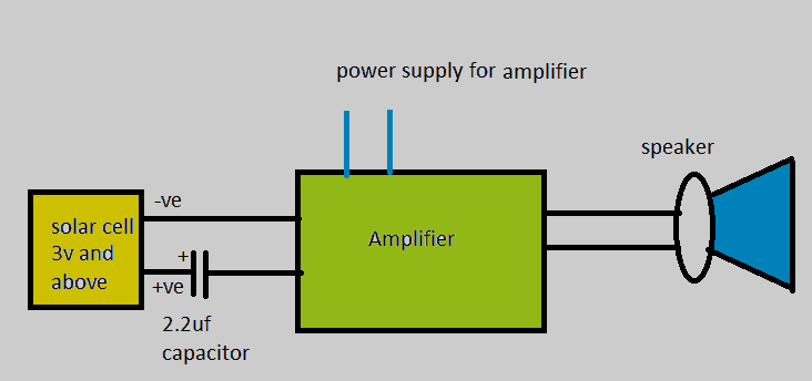
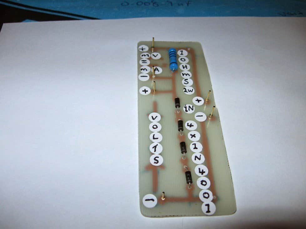
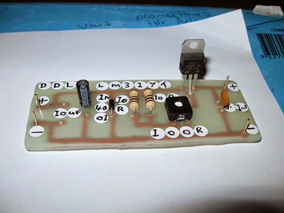
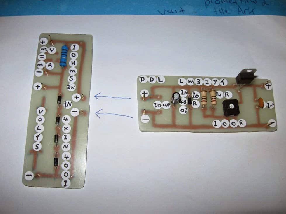
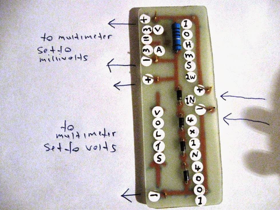
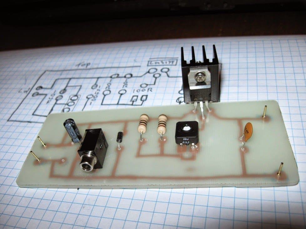
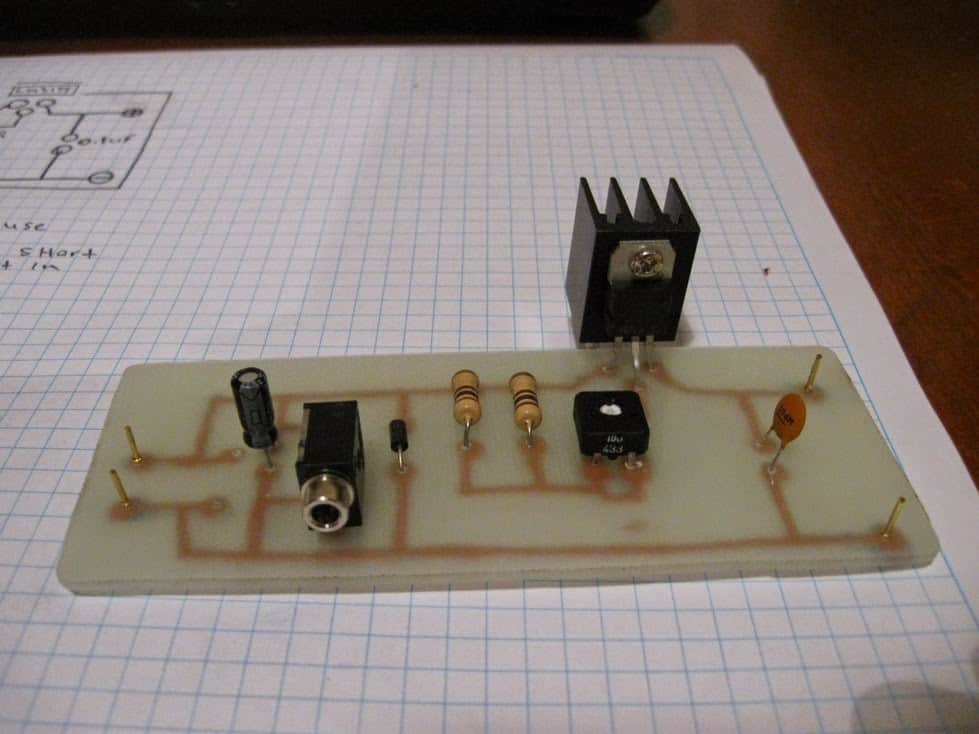
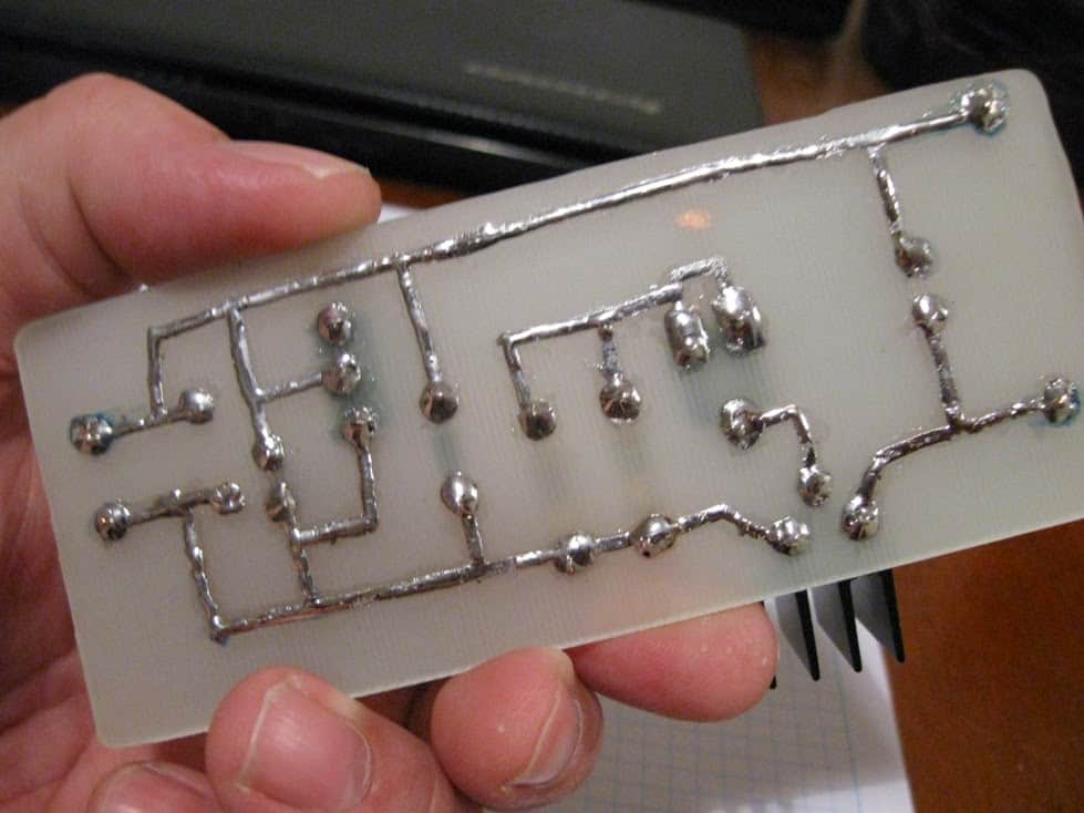
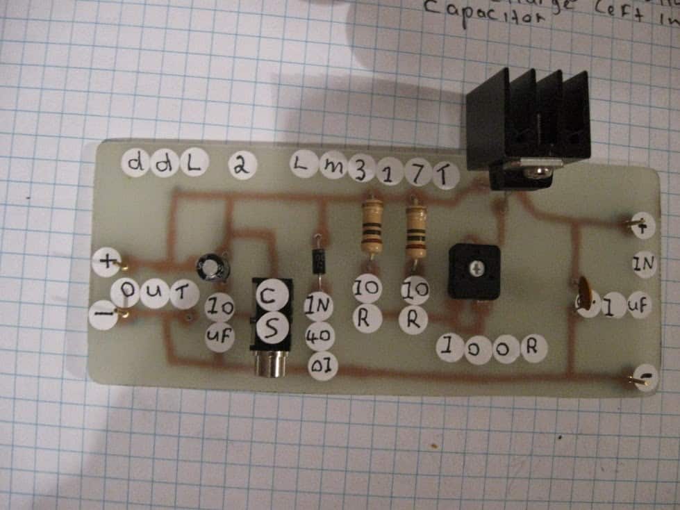
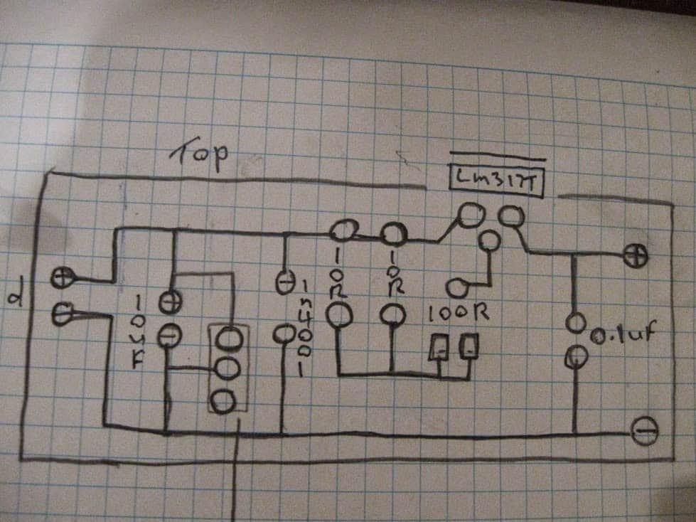

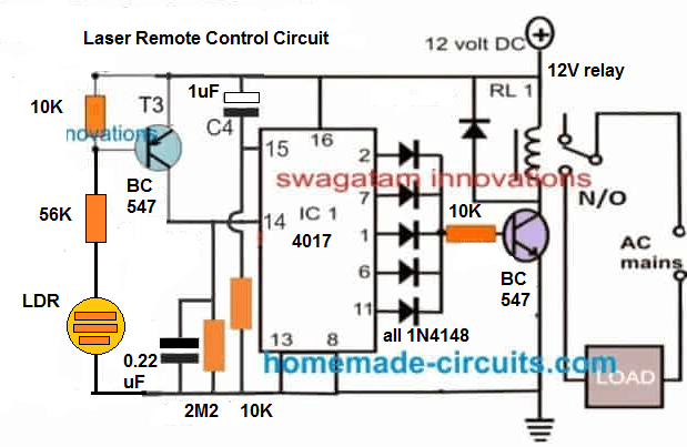 NOTE: T3 IS INCORRECTLY SHOWN AS BC547, IT IS ACTUALLY A BC557 PNP TRANSISTOR.
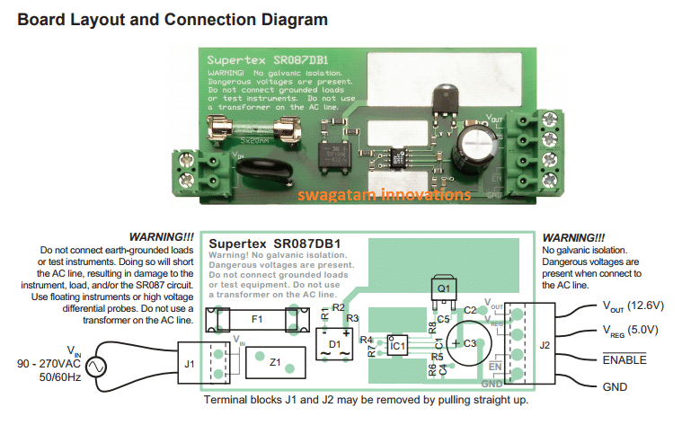 The Main features of this power supply using the IC SR087 are:
High efficiency without incorporating inductors.
Does not require high voltage capacitors for mains current dropping.
Can be used with 120V AC as well as 220V AC inputs Output adjustable from 9V to 50VDC Has an internal soft stat circuitry Stand by consumption is less than 200mW
The Supertex SR087 is an transformerless switching regulator chip specially designed to operate directly from a rectified 220V or 120V AC line.
The principle of operation is to switch ON a pass transistor each time the rectified AC reaches under the set output level, and switch it OFF as soon as the output level is sustained at the set level.
A internally set 5V linear regulator offers an additional 5V fixed output from the IC for operating devices requiring strict 5V inputs.
The IC also facilitates an external logic input triggered "disable" feature, which can be used for disabling the circuit when not in usee and keep the system in the standby mode.
WARNING! Galvanic isolation is not included in the design.
Life threatening voltages and shocks may be floating when switched ON to the AC line.
The designer employing the SR087 must ensure proper safety measures are employed to protect the end user from fatality.
The circuits described here are not guaranteed to fulfill surge and EMI conduction requirements.
The working of these circuits might differ depending on a given application.
The designer is advised to implement tests to verify compliance with the laid down world standards and regulations.
The Main features of this power supply using the IC SR087 are:
High efficiency without incorporating inductors.
Does not require high voltage capacitors for mains current dropping.
Can be used with 120V AC as well as 220V AC inputs Output adjustable from 9V to 50VDC Has an internal soft stat circuitry Stand by consumption is less than 200mW
The Supertex SR087 is an transformerless switching regulator chip specially designed to operate directly from a rectified 220V or 120V AC line.
The principle of operation is to switch ON a pass transistor each time the rectified AC reaches under the set output level, and switch it OFF as soon as the output level is sustained at the set level.
A internally set 5V linear regulator offers an additional 5V fixed output from the IC for operating devices requiring strict 5V inputs.
The IC also facilitates an external logic input triggered "disable" feature, which can be used for disabling the circuit when not in usee and keep the system in the standby mode.
WARNING! Galvanic isolation is not included in the design.
Life threatening voltages and shocks may be floating when switched ON to the AC line.
The designer employing the SR087 must ensure proper safety measures are employed to protect the end user from fatality.
The circuits described here are not guaranteed to fulfill surge and EMI conduction requirements.
The working of these circuits might differ depending on a given application.
The designer is advised to implement tests to verify compliance with the laid down world standards and regulations.
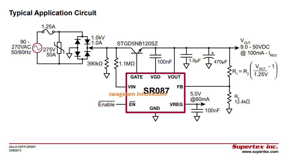
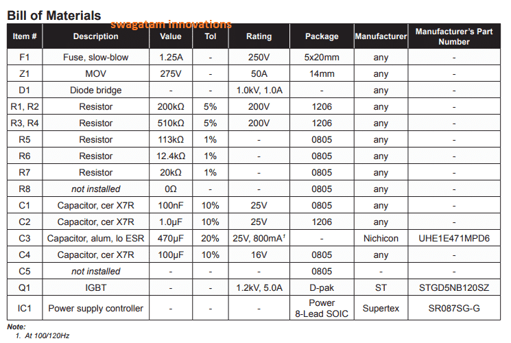
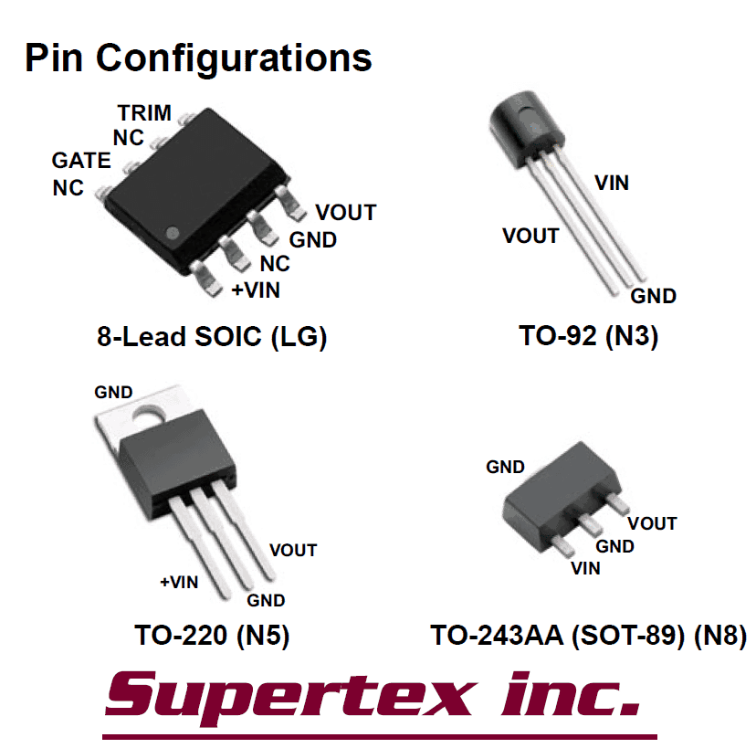
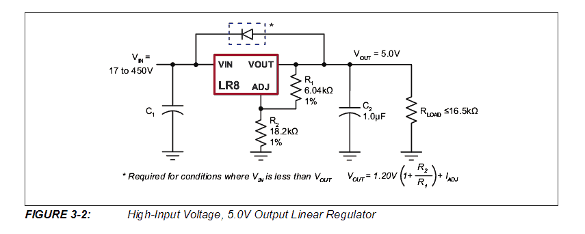
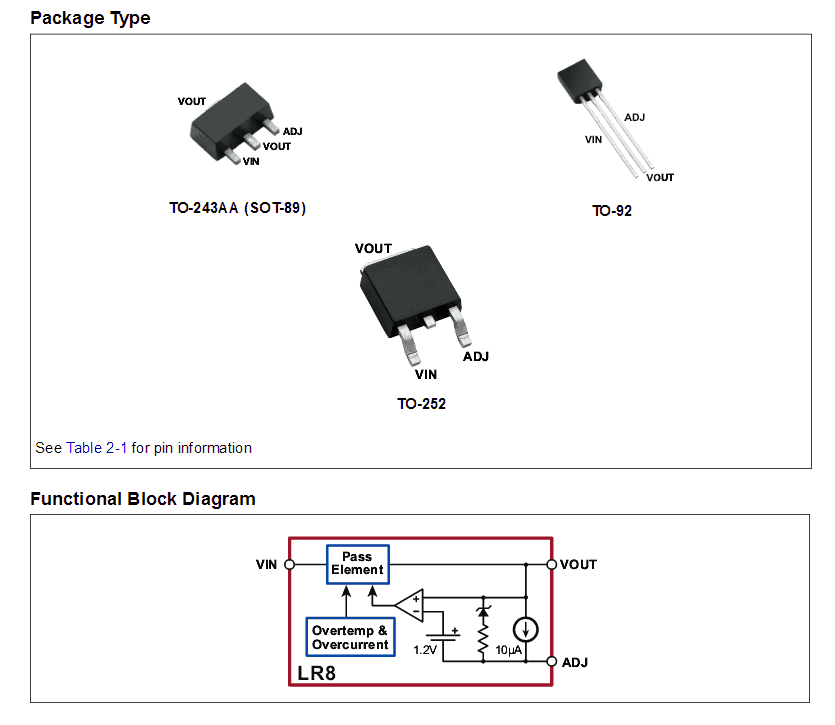 Now since you know how to build a 0-400V transformerless power supply circuit, how do you plan to use it for your specific need?....think, and share if possible through the comment box.
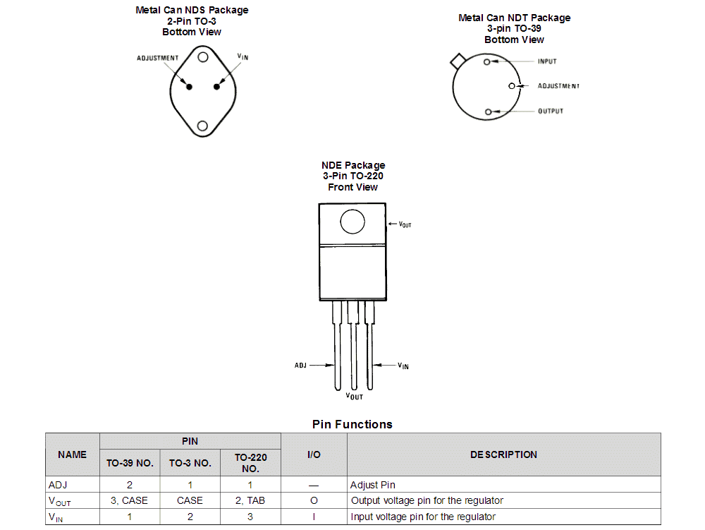 Image Courtesy:http://www.ti.com/lit/ds/symlink/lm117hv.pdf
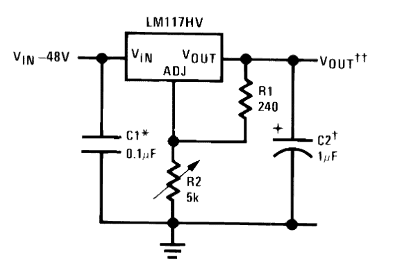 Referring to the design taken from its datasheet we can see that the variable resistor or the potentiometer is specified as a 5K pot, but actually this should be much higher than this value, may be around 22K for achieving a complete 0 to max adjustable output.
The input shows a 48V but we can go a bit higher than this and use upto 56V DC as the input, but please do not stretch it to full 60V as that would mean operating the device at the verge of its breakdown limit and this could make the IC vulnerable to damage.
In case you operate it with a 60V input or slightly above this, then short circuiting the output terminals accidentally could cause an instant damage to the IC, that's why it is not recommended to force the IC to work at its full throttle.
Below this limit, the internal short circuit protection feature could be expected to work normally and safeguard the IC from any possible short circuiting at the output.
C1 may be included only if the shown circuit stage is over 6 inches away from the bridge rectifier and the associated filter capacitor network
C2 is optional and may be included only to improve performance which would help eliminating all possible spikes or transients in the DC line.
For achieving a fixed regulated voltage, R2 could be replaced with a fixed resistor with respect to R1, this may be calculated using the following formula:
Vout = 1.25(1 + R2/R1),
where 1.25 is the fixed reference voltage value generated by the ICs internal circuitry.
You can also use the following software for calculating the same:
LM317 LM338 Calculator
Referring to the design taken from its datasheet we can see that the variable resistor or the potentiometer is specified as a 5K pot, but actually this should be much higher than this value, may be around 22K for achieving a complete 0 to max adjustable output.
The input shows a 48V but we can go a bit higher than this and use upto 56V DC as the input, but please do not stretch it to full 60V as that would mean operating the device at the verge of its breakdown limit and this could make the IC vulnerable to damage.
In case you operate it with a 60V input or slightly above this, then short circuiting the output terminals accidentally could cause an instant damage to the IC, that's why it is not recommended to force the IC to work at its full throttle.
Below this limit, the internal short circuit protection feature could be expected to work normally and safeguard the IC from any possible short circuiting at the output.
C1 may be included only if the shown circuit stage is over 6 inches away from the bridge rectifier and the associated filter capacitor network
C2 is optional and may be included only to improve performance which would help eliminating all possible spikes or transients in the DC line.
For achieving a fixed regulated voltage, R2 could be replaced with a fixed resistor with respect to R1, this may be calculated using the following formula:
Vout = 1.25(1 + R2/R1),
where 1.25 is the fixed reference voltage value generated by the ICs internal circuitry.
You can also use the following software for calculating the same:
LM317 LM338 Calculator
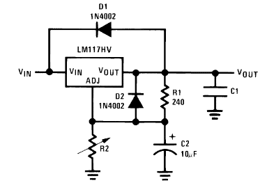 Here D1 protects the IC from the discharge of C1 due to an accidental short circuit of Vin with the ground line, while D2 does the same against C2 discharge.
The role of C1 is already explained in the previous paragraph, C2 is used as a bypass capacitor.
C2 may be included to further improve the output DC regulation as it would help to eliminate all sorts of ripple voltages that might appear across the output.
Here D1 protects the IC from the discharge of C1 due to an accidental short circuit of Vin with the ground line, while D2 does the same against C2 discharge.
The role of C1 is already explained in the previous paragraph, C2 is used as a bypass capacitor.
C2 may be included to further improve the output DC regulation as it would help to eliminate all sorts of ripple voltages that might appear across the output.
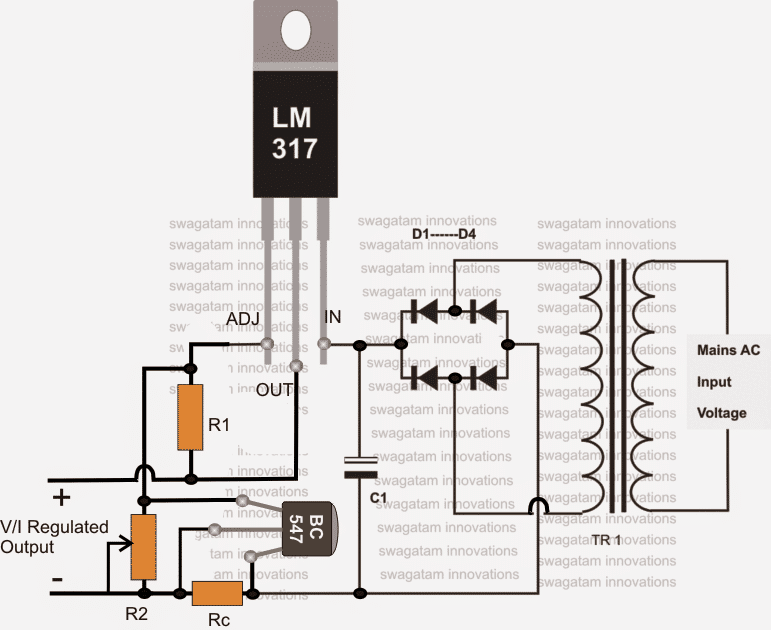 Here R1 refers to 240 ohm, R2 could be a 22k pot, and Rc may be calculated using the following formula for achieving the required current control feature:
Rc = 0.6/Max current limit value.
For example if the maximum value is selected to be 1 amp, then the above formula could be calculated as:
Rc = 0.6/1 = 0.6 ohms
the wattage of the resistor could be calculated as given under:
0.6 x 1= 0.6 watts
The diode in the bridge rectifier should be preferably 1N5408 diodes for ensuring a smooth rectification with no heating issues.
C1 may be anything above 2200uF/100V, although lower values will also do for lower current loads and for non critical loads which do not mind slight ripple factor in the line.
The transformer could be a 0 - 42V/220V/2amp.
The 0 - 42V is recommended because after rectification and smoothing this final DC could exceed a little over 55V.
The next article we might possibly discuss regarding the various application circuits using the LM317HV high voltage regulator IC.
Here R1 refers to 240 ohm, R2 could be a 22k pot, and Rc may be calculated using the following formula for achieving the required current control feature:
Rc = 0.6/Max current limit value.
For example if the maximum value is selected to be 1 amp, then the above formula could be calculated as:
Rc = 0.6/1 = 0.6 ohms
the wattage of the resistor could be calculated as given under:
0.6 x 1= 0.6 watts
The diode in the bridge rectifier should be preferably 1N5408 diodes for ensuring a smooth rectification with no heating issues.
C1 may be anything above 2200uF/100V, although lower values will also do for lower current loads and for non critical loads which do not mind slight ripple factor in the line.
The transformer could be a 0 - 42V/220V/2amp.
The 0 - 42V is recommended because after rectification and smoothing this final DC could exceed a little over 55V.
The next article we might possibly discuss regarding the various application circuits using the LM317HV high voltage regulator IC.
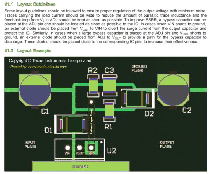
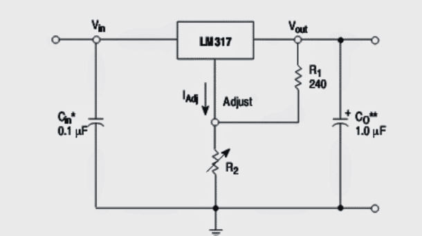 The above shown design which is limited with a 1.5 amp max current can be upgraded with an outboard PNP transistor in order to boost the current on par with the input supply current, meaning once this upgrade is implemented the above circuit will retain its variable voltage regulation feature yet will be able to offer the full supply input current to the load, bypassing the IC's internal current limiting feature.
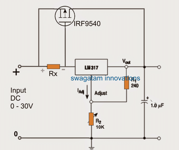 In the above design, Rx becomes responsible for providing the gate trigger for the mosfet so that it's able to conduct in tandem with the LM317 IC and reinforce the device with the extra amount of current as specified by the input supply.
Initially when power input is fed to the circuit, the connected load which could be rated at much higher than 1.5 amps tries to acquire this current through the LM317 IC, and in the process a proportionate amount of negative voltage is developed across RX, causing the mosfet to respond and switch ON.
As soon as the mosfet is triggered the entire input supply tends to flow across the load with the surplus current, but since the voltage also begins to increase beyond the LM317 pot setting, causes the LM317 to get reverse biased.
This action for the moment switches OFF the LM317 which in turn shuts off the voltage across Rx and the gate supply for the mosfet.
Therefore the mosfet too tends to switch OFF for the instant until the cycle perpetuates yet again allowing the process to sustain infinitely with the intended voltage regulation and high current specs.
In the above design, Rx becomes responsible for providing the gate trigger for the mosfet so that it's able to conduct in tandem with the LM317 IC and reinforce the device with the extra amount of current as specified by the input supply.
Initially when power input is fed to the circuit, the connected load which could be rated at much higher than 1.5 amps tries to acquire this current through the LM317 IC, and in the process a proportionate amount of negative voltage is developed across RX, causing the mosfet to respond and switch ON.
As soon as the mosfet is triggered the entire input supply tends to flow across the load with the surplus current, but since the voltage also begins to increase beyond the LM317 pot setting, causes the LM317 to get reverse biased.
This action for the moment switches OFF the LM317 which in turn shuts off the voltage across Rx and the gate supply for the mosfet.
Therefore the mosfet too tends to switch OFF for the instant until the cycle perpetuates yet again allowing the process to sustain infinitely with the intended voltage regulation and high current specs.
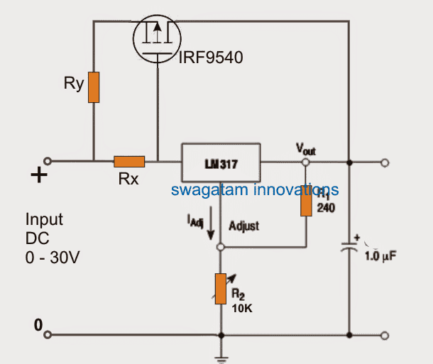 This modification looks pretty simple, however calculating Ry could be little confusing and I do not wish to investigate it deeper since I have a more decent and a reliable idea which can be also expected to execute a complete current control for the discussed LM317 outboard boost transistor application circuit.
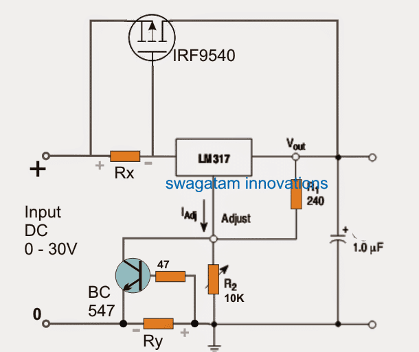 An couple of resistors, and a BC547 BJT is all that may be required for inserting the desired short circuit protection to the modified current boost circuit for the LM317 IC.
Now calculating Ry becomes extremely easy, and may be evaluated with the following formula:
Ry = 0.7/current limit.
Here, 0.7 is the triggering voltage of the BC547 and the "current limit" is the maximum valid current that may specified for a safe operation of the mosfet, let's say this limit is specified to be 10amps, then Ry can be calculated as:
Ry = 0.7/10 = 0.07 ohms.
watts = 0.7 x 10 = 7 watts.
So now whenever the current tends to cross the above limit, the BC547 conducts, grounding the ADJ pin of the IC and shutting off the Vout for the LM317
An couple of resistors, and a BC547 BJT is all that may be required for inserting the desired short circuit protection to the modified current boost circuit for the LM317 IC.
Now calculating Ry becomes extremely easy, and may be evaluated with the following formula:
Ry = 0.7/current limit.
Here, 0.7 is the triggering voltage of the BC547 and the "current limit" is the maximum valid current that may specified for a safe operation of the mosfet, let's say this limit is specified to be 10amps, then Ry can be calculated as:
Ry = 0.7/10 = 0.07 ohms.
watts = 0.7 x 10 = 7 watts.
So now whenever the current tends to cross the above limit, the BC547 conducts, grounding the ADJ pin of the IC and shutting off the Vout for the LM317
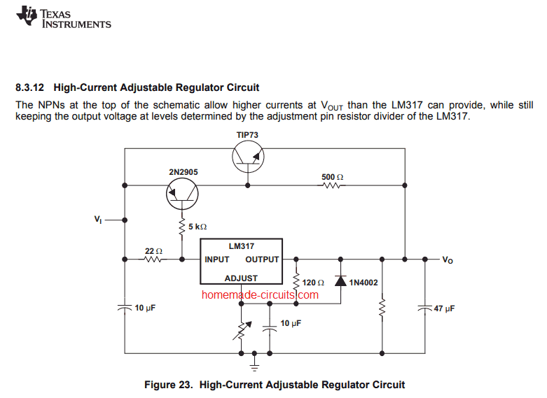 Courtesy:Texas Instruments
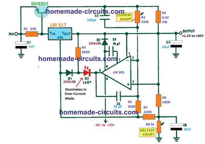 In the figure above we can see that the voltage regulation is implemented in the standard LM317 configuration through R6 pot which is connected with the ADJ pin of the LM317.
However, the op amp configuration is specifically included to feature the useful a full scale high current adjustment ranging from the minimum to the maximum 5 Amp control.
The 5 amp high current boost available from this design can be further increased to 10 amps by suitably upgrading the MJ4502 PNP outboard transistor.
The inverting input pin#2 of the op amp is used as reference input which is set by the pot R2. The other non-inverting input is used as the current sensor.
The voltage developed across R6 through the current limiter resistor R3 is compared with the R2 reference which allows the output of the op amp to become low as soon the maximum set current is exceeded.
The low output from the op amp grounds the ADJ pin of the LM317 shutting it off and also the output supply, which in turn quickly reduces the output current and restores the LM317 working.
The continuous ON/OFF operation ensures that the current is never allowed to reach above the set threshold adjusted by R2.
The maximum current level can be also modified by tweaking the value of the current limit resistor R3.
In the figure above we can see that the voltage regulation is implemented in the standard LM317 configuration through R6 pot which is connected with the ADJ pin of the LM317.
However, the op amp configuration is specifically included to feature the useful a full scale high current adjustment ranging from the minimum to the maximum 5 Amp control.
The 5 amp high current boost available from this design can be further increased to 10 amps by suitably upgrading the MJ4502 PNP outboard transistor.
The inverting input pin#2 of the op amp is used as reference input which is set by the pot R2. The other non-inverting input is used as the current sensor.
The voltage developed across R6 through the current limiter resistor R3 is compared with the R2 reference which allows the output of the op amp to become low as soon the maximum set current is exceeded.
The low output from the op amp grounds the ADJ pin of the LM317 shutting it off and also the output supply, which in turn quickly reduces the output current and restores the LM317 working.
The continuous ON/OFF operation ensures that the current is never allowed to reach above the set threshold adjusted by R2.
The maximum current level can be also modified by tweaking the value of the current limit resistor R3.
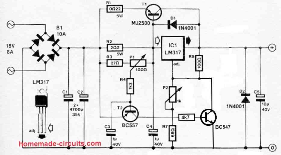
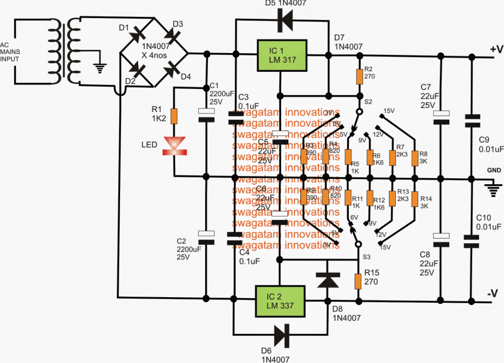
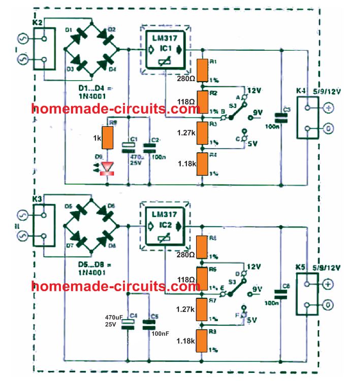 The diagram above shows how a simple yet higher versatile, adjustable dual power supply circuit could be built through just a couple of LM317 ICs.
The circuit will produce an adjustable dual supply of 12V, 5V, and 9V
It means, an effective variable dual supply output could be achieved by using readily available IC like LM317, which is very easily accessible in any electronic market.
The design employs a couple of identical LM317 variable regulator circuits driven through separate bridge rectifiers and AC inputs from the transformers.
This allows us to join the + and - of the two supplies to create a dual supply of our own choice as per specific requirements.
Considering that it should be achievable to adjust the output voltage to 3 variable ranges, the voltage regulator applied is a kind whose output could be fixed using a handful of resistors, as shown in the circuit diagram.
The output voltage is determined using the formula
Uout = 1.25(1+R2/R1) + IadjR2, in which 1.25 signifies the reference voltage of the IC, and ladj indicates the current moving through the 'ADJ(ust)' pin of the device towards ground.
The IC LM317 has internal compartaors, which constantly analyzes portion of the output voltage, fixed by resistive divider R1/R2, with the reference voltage.
In the event that Uout is required to be higher; the comparator output is switched high which forces, the internal transistors to conduct harder.
This action decreases the collector-emitter resistance, causing a boost in the Uout.
This set up guarantees a practically constant Uout.
Practically , the value of Iadj falls between 50 ¦ĚA and 100 ¦ĚA.
Due to this lower value, the factor Iadj R2, could typically be removed from the formula.
Therefore, the refined formula
Uout = 1.25[1+(1270+1280)280] = 12.19 V.
The diagram above shows how a simple yet higher versatile, adjustable dual power supply circuit could be built through just a couple of LM317 ICs.
The circuit will produce an adjustable dual supply of 12V, 5V, and 9V
It means, an effective variable dual supply output could be achieved by using readily available IC like LM317, which is very easily accessible in any electronic market.
The design employs a couple of identical LM317 variable regulator circuits driven through separate bridge rectifiers and AC inputs from the transformers.
This allows us to join the + and - of the two supplies to create a dual supply of our own choice as per specific requirements.
Considering that it should be achievable to adjust the output voltage to 3 variable ranges, the voltage regulator applied is a kind whose output could be fixed using a handful of resistors, as shown in the circuit diagram.
The output voltage is determined using the formula
Uout = 1.25(1+R2/R1) + IadjR2, in which 1.25 signifies the reference voltage of the IC, and ladj indicates the current moving through the 'ADJ(ust)' pin of the device towards ground.
The IC LM317 has internal compartaors, which constantly analyzes portion of the output voltage, fixed by resistive divider R1/R2, with the reference voltage.
In the event that Uout is required to be higher; the comparator output is switched high which forces, the internal transistors to conduct harder.
This action decreases the collector-emitter resistance, causing a boost in the Uout.
This set up guarantees a practically constant Uout.
Practically , the value of Iadj falls between 50 ¦ĚA and 100 ¦ĚA.
Due to this lower value, the factor Iadj R2, could typically be removed from the formula.
Therefore, the refined formula
Uout = 1.25[1+(1270+1280)280] = 12.19 V.
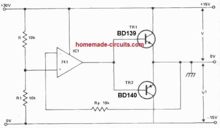 The OP-AMP identifies any change in this ratio via Rf and quickly executes the correction.
The actual voltages utilized will be limited by the upper and lower operating voltages of the OP AMP.
The circuit shown was developed to deliver +15 V, -15V dual supply, specifically for the operational amplifiers.
The OP-AMP identifies any change in this ratio via Rf and quickly executes the correction.
The actual voltages utilized will be limited by the upper and lower operating voltages of the OP AMP.
The circuit shown was developed to deliver +15 V, -15V dual supply, specifically for the operational amplifiers.
 This stream-lined balanced power supply utilizes the 4 opamps from one LM324 IC.
These are employed to stabilize the output voltage and also to control the output current.
The current limiter circuit is defined at 60 mA and consists of lowest number of parts.
It has to be taken into account that under certain situations it might appear that the (input) power supply of only ˇŔ16 V is actually very low.
However, the highest output voltage is determined by the specifications of the IC employed.
It is far from safe to raise the input supply voltage; any kind of rise in the voltage could destroy the IC, depending on its maximum input voltage tolerating specifications.
A 5.6 V zener diode is employed for fixing the reference voltage.
The zener value is not really crucial; if it is small, the output voltage is going to be a bit lower.
P1 works like the voltage adjustment pot simultaneously for controlling both the +15 and -15 supplies.
Using P1, the reference voltage gets broken down and is given to the + input pinout of the (upper) opamp.
This particular opamp manages the positive output voltage by governing the base current of the series regulating transistor (BC140).
The stabilization of the output voltage is influenced through a negative feedback loop through a voltage divider network composed of the 22 k and 10 k resistors.
The regulation of the negative voltage tends to be relatively more complex.
The + input pinout of the lower opamp is coupled to the zero voltage '0', by means of a 6k8 resistor.
The reference voltage is employed through control pot P1 along with various other parts with the - input pinout.
The negative output voltage is well balanced with respect to the positive reference voltage using the voltage divider `see -saw' network established through the 33 k and 10 k resistors (that are bridged together through a trimming circuitry).
Trimming preset controller P2 cancels out the impact of small tolerances in the circuit elements, and P2 can be tweaked to balance the positive and negative output voltages.
Over Current safety is achieved by the a couple of leftover opamps in the IC.
In case the voltage difference across one of the 10 ohm resistors becomes greater than 0.6 V, the reference voltage is going to decrease to zero and, as a result, the output voltages also reduces along with it.
Simultaneously the LED's illuminate to show that the protection feature of the circuit is working.
This stream-lined balanced power supply utilizes the 4 opamps from one LM324 IC.
These are employed to stabilize the output voltage and also to control the output current.
The current limiter circuit is defined at 60 mA and consists of lowest number of parts.
It has to be taken into account that under certain situations it might appear that the (input) power supply of only ˇŔ16 V is actually very low.
However, the highest output voltage is determined by the specifications of the IC employed.
It is far from safe to raise the input supply voltage; any kind of rise in the voltage could destroy the IC, depending on its maximum input voltage tolerating specifications.
A 5.6 V zener diode is employed for fixing the reference voltage.
The zener value is not really crucial; if it is small, the output voltage is going to be a bit lower.
P1 works like the voltage adjustment pot simultaneously for controlling both the +15 and -15 supplies.
Using P1, the reference voltage gets broken down and is given to the + input pinout of the (upper) opamp.
This particular opamp manages the positive output voltage by governing the base current of the series regulating transistor (BC140).
The stabilization of the output voltage is influenced through a negative feedback loop through a voltage divider network composed of the 22 k and 10 k resistors.
The regulation of the negative voltage tends to be relatively more complex.
The + input pinout of the lower opamp is coupled to the zero voltage '0', by means of a 6k8 resistor.
The reference voltage is employed through control pot P1 along with various other parts with the - input pinout.
The negative output voltage is well balanced with respect to the positive reference voltage using the voltage divider `see -saw' network established through the 33 k and 10 k resistors (that are bridged together through a trimming circuitry).
Trimming preset controller P2 cancels out the impact of small tolerances in the circuit elements, and P2 can be tweaked to balance the positive and negative output voltages.
Over Current safety is achieved by the a couple of leftover opamps in the IC.
In case the voltage difference across one of the 10 ohm resistors becomes greater than 0.6 V, the reference voltage is going to decrease to zero and, as a result, the output voltages also reduces along with it.
Simultaneously the LED's illuminate to show that the protection feature of the circuit is working.
 By appropriately changing the values of the resistors R2, and R4 resistors it may be possible to alter the output from anywhere between 3V, 4.5V, 6V, 9V, 12V, 15V dual supplies.
For a fixed dual power supply you can use the following configuration.
Here we can see that, for the positive supply the IC 7812 is used, and for the negative supply, the IC 7912 has been used:
By appropriately changing the values of the resistors R2, and R4 resistors it may be possible to alter the output from anywhere between 3V, 4.5V, 6V, 9V, 12V, 15V dual supplies.
For a fixed dual power supply you can use the following configuration.
Here we can see that, for the positive supply the IC 7812 is used, and for the negative supply, the IC 7912 has been used:
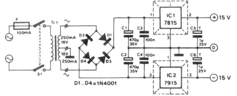

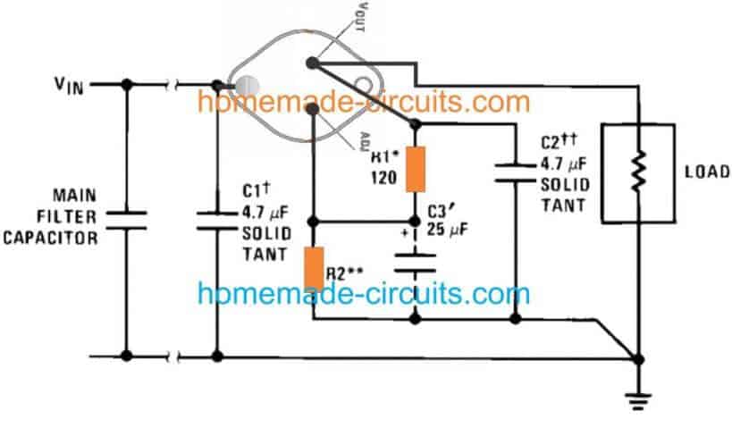
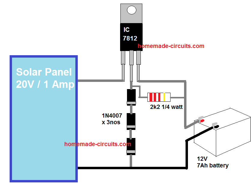 Estimated time taken to charge the battery from 11V to 14V is around 8 hours.
As we know the IC 7812 will produce a fixed 12V at the output which cannot be used for charging a 12V battery.
The 3 diodes connected at its ground (GND) terminals is introduced specifically to counter this problem, and to upgrade the IC output to about 12 + 0.7 + 0.7 + 0.7 V = 14.1 V, which is exactly what is required for charging a 12 V battery fully.
The drop of 0.7 V across each diodes raises the grounding threshold of the IC by stipulated level forcing the IC to regulate the output at 14.1 V instead of 12 V.
The 2k2 resistor is used to activate or bias the diodes so that it can conduct and enforce the intended 2.1 V total drop.
Estimated time taken to charge the battery from 11V to 14V is around 8 hours.
As we know the IC 7812 will produce a fixed 12V at the output which cannot be used for charging a 12V battery.
The 3 diodes connected at its ground (GND) terminals is introduced specifically to counter this problem, and to upgrade the IC output to about 12 + 0.7 + 0.7 + 0.7 V = 14.1 V, which is exactly what is required for charging a 12 V battery fully.
The drop of 0.7 V across each diodes raises the grounding threshold of the IC by stipulated level forcing the IC to regulate the output at 14.1 V instead of 12 V.
The 2k2 resistor is used to activate or bias the diodes so that it can conduct and enforce the intended 2.1 V total drop.
 Although, the above design does not incorporate a regulator, it will still work since the panel current output is nominal, and this value will only show a deterioration as the sun changes its position.
However, for a battery that is not fully discharged, the above simple set up may cause some harm to the battery, since the battery will tend to get charged quickly, and will continue to get charged to unsafe levels and for longer periods of time.
Although, the above design does not incorporate a regulator, it will still work since the panel current output is nominal, and this value will only show a deterioration as the sun changes its position.
However, for a battery that is not fully discharged, the above simple set up may cause some harm to the battery, since the battery will tend to get charged quickly, and will continue to get charged to unsafe levels and for longer periods of time.
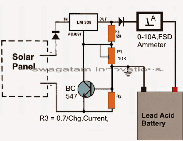 The circuit diagram shows a simple set up using the IC LM 338 which has been configured in its standard regulated power supply mode.
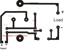 The meter and the input diode are not included in the PCB.


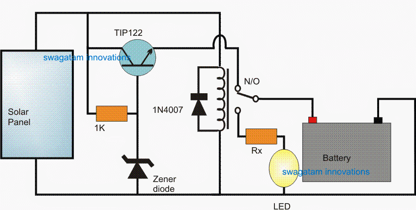
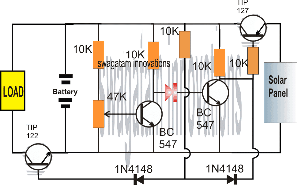
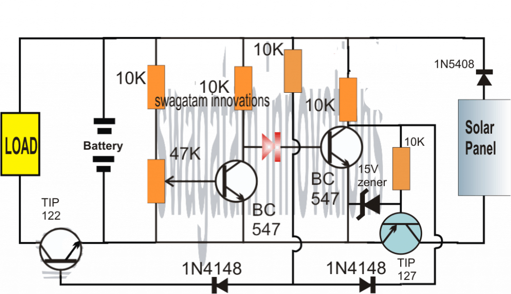 The above designs can be further simplified, as shown in the following over-charge, over-discharge solar battery controller circuit:
 The design is a basic joule thief circuit using a single penlight cell, a BJT and an inductor for powering any standard 3.3V LED.
In the design a 1 watt LeD is shown although a smaller 30mA high bright LED could be used.
The solar LED circuit is capable squeezing out the last drop of "joule" or the charge from the cell and hence the name joule thief, which also implies that the LED would keep illuminated until there's virtually nothing left inside the cell.
However the cell here being a rechargeable type is not recommended to be discharged below 1V.
The 1.5V battery charger in the design is built using another low power BJT configured in its emitter follower configuration, which allows it to produce an emitter voltage output that's exactly equal to the potential at its base, set by the 1K preset.
This must be precisely set such that the emitter produces not more than 1.8V with a DC input of above 3V.
The DC input source is a solar panel which may be capable of producing an excess of 3V during optimal sunlight, and allow the charger to charge the battery with a maximum of 1.8V output.
Once this level is reached the emitter follower simply inhibits any further charging of the cell thus preventing any possibility of an over charge.
The inductor for the pocket solar LED light circuit consists of a small ferrite ring transformer having 20:20 turns which could be appropriately altered and optimized for enabling the most favorable voltage for the connected LED which may last even until the voltage has fallen below 1.2V.
The design is a basic joule thief circuit using a single penlight cell, a BJT and an inductor for powering any standard 3.3V LED.
In the design a 1 watt LeD is shown although a smaller 30mA high bright LED could be used.
The solar LED circuit is capable squeezing out the last drop of "joule" or the charge from the cell and hence the name joule thief, which also implies that the LED would keep illuminated until there's virtually nothing left inside the cell.
However the cell here being a rechargeable type is not recommended to be discharged below 1V.
The 1.5V battery charger in the design is built using another low power BJT configured in its emitter follower configuration, which allows it to produce an emitter voltage output that's exactly equal to the potential at its base, set by the 1K preset.
This must be precisely set such that the emitter produces not more than 1.8V with a DC input of above 3V.
The DC input source is a solar panel which may be capable of producing an excess of 3V during optimal sunlight, and allow the charger to charge the battery with a maximum of 1.8V output.
Once this level is reached the emitter follower simply inhibits any further charging of the cell thus preventing any possibility of an over charge.
The inductor for the pocket solar LED light circuit consists of a small ferrite ring transformer having 20:20 turns which could be appropriately altered and optimized for enabling the most favorable voltage for the connected LED which may last even until the voltage has fallen below 1.2V.
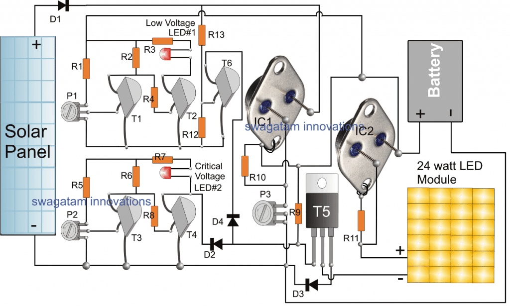 The circuit stage comprising T1, T2, and P1 are configured into a simple low battery sensor, indicator circuit
An exactly identical stage can also be seen just below, using T3, T4 and the associated parts, which form another low voltage detector stage.
The T1, T2 stage detects the battery voltage when it drops to 13V by illuminating the attached LED at the collector of T2, while the T3, T4 stage detects the battery voltage when it reaches below 11V, and indicates the situation by illuminating the LED associated with the collector of T4.
P1 is used for adjusting the T1/T2 stage such that the T2 LED just illuminates at 12V, similarly P2 is adjusted to make the T4 LED begin illuminating at voltages below 11V.
IC1 LM338 is configured as a simple regulated voltage power supply for regulating the solar panel voltage to a precise 14V, this is done by adjusting the preset P3 appropriately.
This output from IC1 is used for charging the street lamp battery during day time and peak sunshine.
IC2 is another LM338 IC, wired in a current controller mode, its input pin is connected with the battery positive while the output is connected with the LED module.
IC2 restricts the current level from the battery and supplies the right amount of current to the LED module so that it is able operate safely during night time back up mode.
T5 is a power transistor which acts like a switch and is triggered by the critical low battery stage, whenever the battery voltage tends to reach the critical level.
Whenever this happens the base of T5 is instantly grounded by T4, shutting it off instantly.
With T5 shut off, the LED module is enable to illuminate and therefore it is also shut off.
This condition prevents and safeguards the battery from getting overly discharged and damaged.
In such situations the battery might need an external charging from mains using a 24V, power supply applied across the solar panel supply lines, across the cathode of D1 and ground.
The current from this supply could be specified at around 20% of battery AH, and the battery may be charged until both the LEDs stop glowing.
The T6 transistor along with its base resistors is positioned to detect the supply from the solar panel and ensure that the LED module remains disabled as long as a reasonable amount of supply is available from the panel, or in other words T6 keeps the LED module shut off until its dark enough for the LED module and then is switched ON.
The opposite happen at dawn when the LED module is automatically switched OFF.
R12, R13 should be carefully adjusted or selected to determine the desired thresholds for the LED module's ON/OFF cycles
The circuit stage comprising T1, T2, and P1 are configured into a simple low battery sensor, indicator circuit
An exactly identical stage can also be seen just below, using T3, T4 and the associated parts, which form another low voltage detector stage.
The T1, T2 stage detects the battery voltage when it drops to 13V by illuminating the attached LED at the collector of T2, while the T3, T4 stage detects the battery voltage when it reaches below 11V, and indicates the situation by illuminating the LED associated with the collector of T4.
P1 is used for adjusting the T1/T2 stage such that the T2 LED just illuminates at 12V, similarly P2 is adjusted to make the T4 LED begin illuminating at voltages below 11V.
IC1 LM338 is configured as a simple regulated voltage power supply for regulating the solar panel voltage to a precise 14V, this is done by adjusting the preset P3 appropriately.
This output from IC1 is used for charging the street lamp battery during day time and peak sunshine.
IC2 is another LM338 IC, wired in a current controller mode, its input pin is connected with the battery positive while the output is connected with the LED module.
IC2 restricts the current level from the battery and supplies the right amount of current to the LED module so that it is able operate safely during night time back up mode.
T5 is a power transistor which acts like a switch and is triggered by the critical low battery stage, whenever the battery voltage tends to reach the critical level.
Whenever this happens the base of T5 is instantly grounded by T4, shutting it off instantly.
With T5 shut off, the LED module is enable to illuminate and therefore it is also shut off.
This condition prevents and safeguards the battery from getting overly discharged and damaged.
In such situations the battery might need an external charging from mains using a 24V, power supply applied across the solar panel supply lines, across the cathode of D1 and ground.
The current from this supply could be specified at around 20% of battery AH, and the battery may be charged until both the LEDs stop glowing.
The T6 transistor along with its base resistors is positioned to detect the supply from the solar panel and ensure that the LED module remains disabled as long as a reasonable amount of supply is available from the panel, or in other words T6 keeps the LED module shut off until its dark enough for the LED module and then is switched ON.
The opposite happen at dawn when the LED module is automatically switched OFF.
R12, R13 should be carefully adjusted or selected to determine the desired thresholds for the LED module's ON/OFF cycles
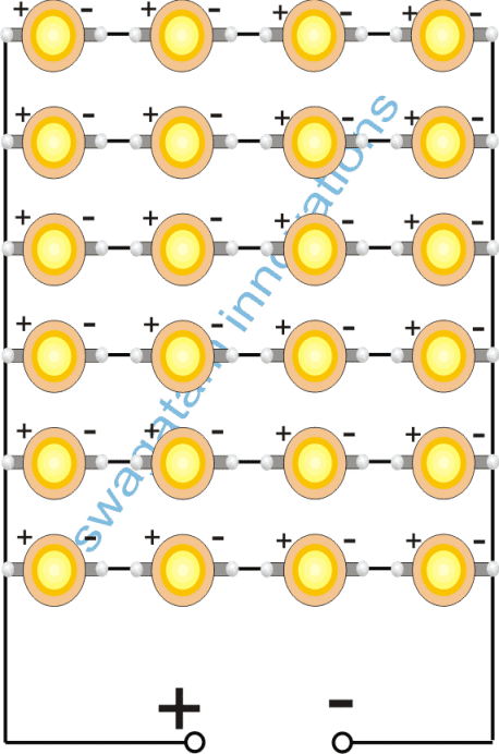
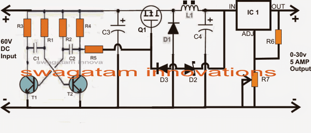
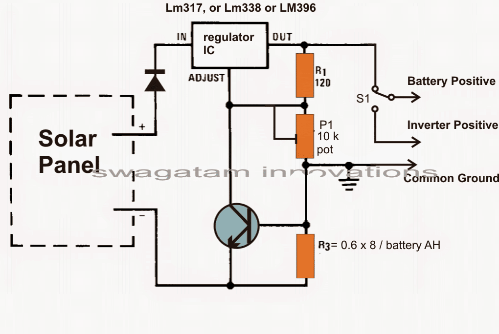 The above solar panel regulator may be configured with the following simple inverter circuit which will be quite adequate for powering the requested lamps through the connected solar panel or the battery.
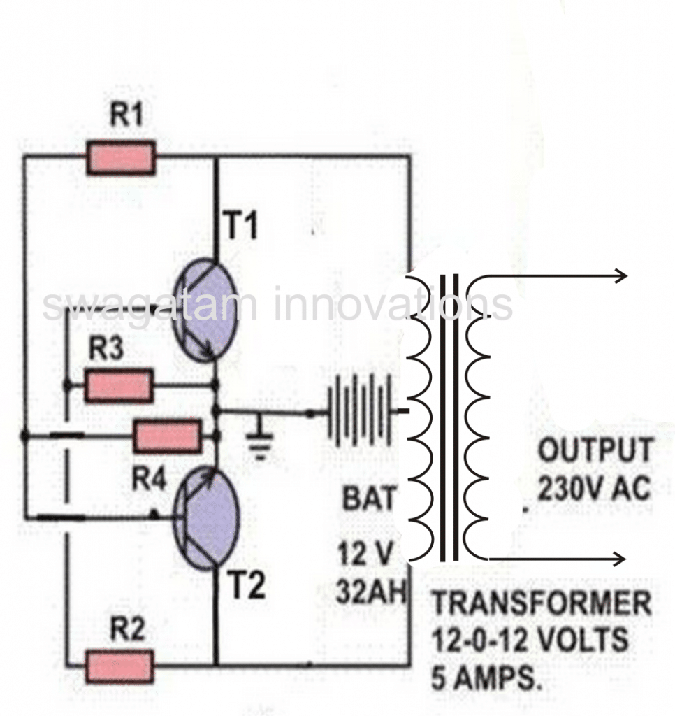
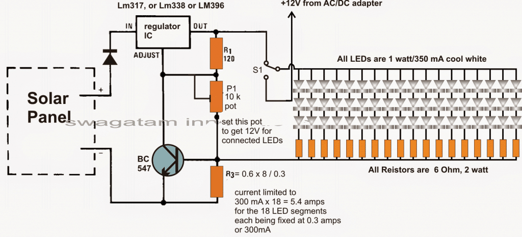 The negative of the adapter must be connected and made common with the negative of the solar panel
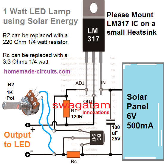
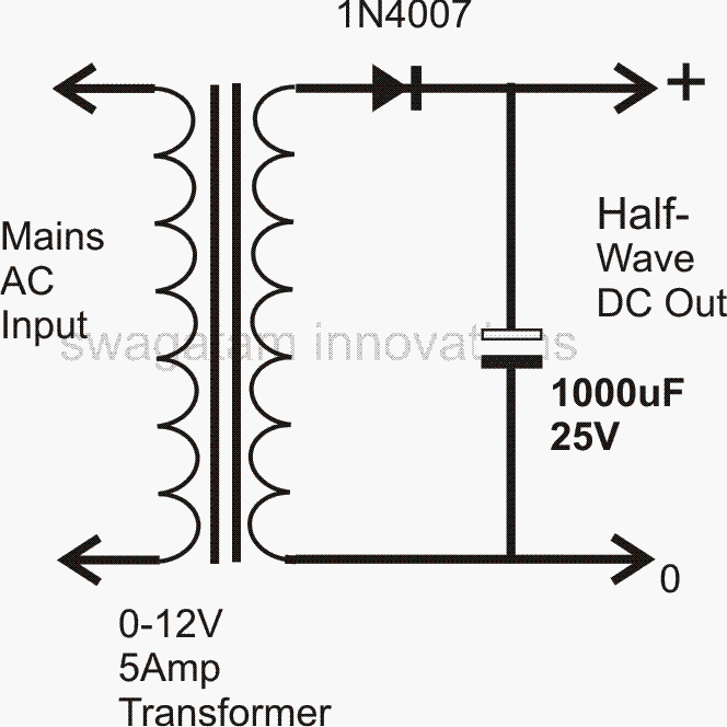 For a single diode power supply design, the transformer's secondary winding just needs to have a single winding with two ends.
However the above configuration cannot be considered an efficient power supply design due to its crude half wave rectification and limited output conditioning capabilities.
For a single diode power supply design, the transformer's secondary winding just needs to have a single winding with two ends.
However the above configuration cannot be considered an efficient power supply design due to its crude half wave rectification and limited output conditioning capabilities.
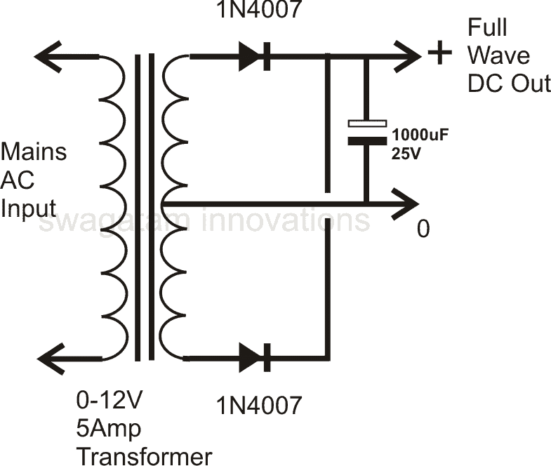 Though, the two diodes work in tandem and tackle both the halves of the AC signal and produce a full wave rectification, the employed method is not efficient, because at any instant only one half winding of the transformer is utilized.
This results in poor core saturation and unnecessary heating of the transformer, making this type of power supplyconfigurationless efficient and an ordinary design.
Though, the two diodes work in tandem and tackle both the halves of the AC signal and produce a full wave rectification, the employed method is not efficient, because at any instant only one half winding of the transformer is utilized.
This results in poor core saturation and unnecessary heating of the transformer, making this type of power supplyconfigurationless efficient and an ordinary design.
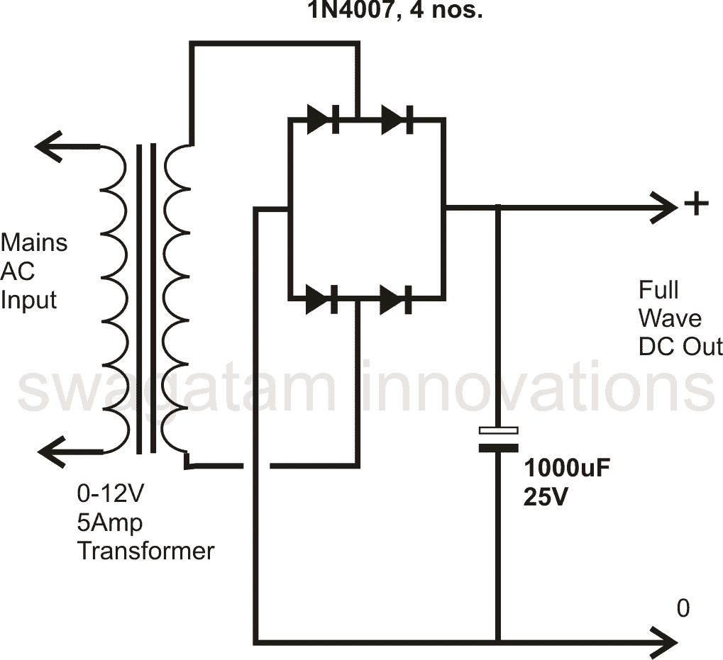 This type of diode configuration is popularly know as the bridge network, you may want to know how to construct a bridge rectifier.
All the above power supply designs provide outputs with ordinary regulation and therefore cannot be considered perfect,these fail to provide ideal DC outputs, and therefore are not desirable for many sophisticated electronic circuits.
Moreover theseconfigurationsdoes not include a variable voltage and current control features.
However the above features may be simply integrated to the above designs, rather with the last full wave powersupplyconfigurationthrough the introduction of a single IC and a few other passive components.
This type of diode configuration is popularly know as the bridge network, you may want to know how to construct a bridge rectifier.
All the above power supply designs provide outputs with ordinary regulation and therefore cannot be considered perfect,these fail to provide ideal DC outputs, and therefore are not desirable for many sophisticated electronic circuits.
Moreover theseconfigurationsdoes not include a variable voltage and current control features.
However the above features may be simply integrated to the above designs, rather with the last full wave powersupplyconfigurationthrough the introduction of a single IC and a few other passive components.
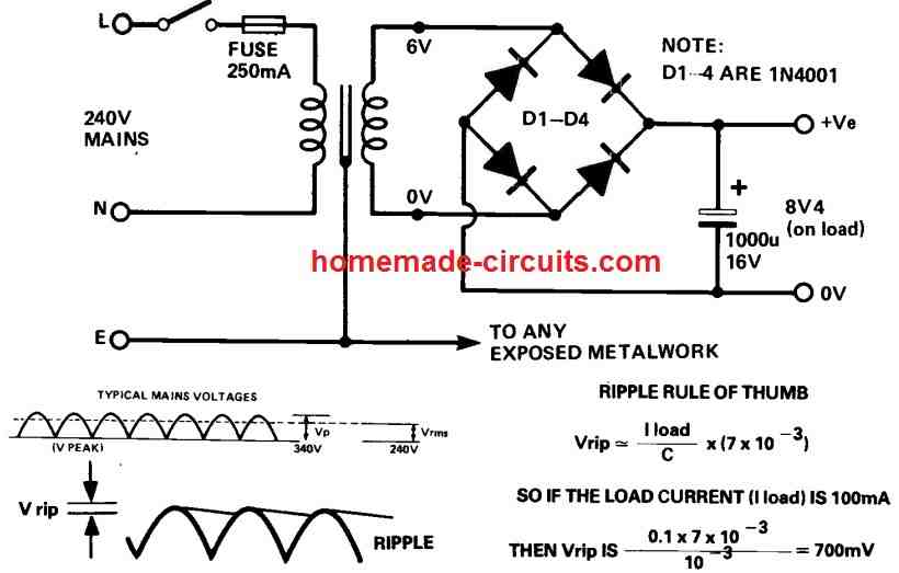 The earth should be linked to any uncovered metal and, if applicable, to the transformer shielding.
The voltages mentioned are in volts rms and are AC voltages.
On load, the transformer's output is 6V rms.
When the transformer is not in use, the voltage might rise by up to 25%.
The output ripple can be calculated using the following formula:
Vrip Iload / C [ 7 x 10⁻³ ]
The earth should be linked to any uncovered metal and, if applicable, to the transformer shielding.
The voltages mentioned are in volts rms and are AC voltages.
On load, the transformer's output is 6V rms.
When the transformer is not in use, the voltage might rise by up to 25%.
The output ripple can be calculated using the following formula:
Vrip Iload / C [ 7 x 10⁻³ ]
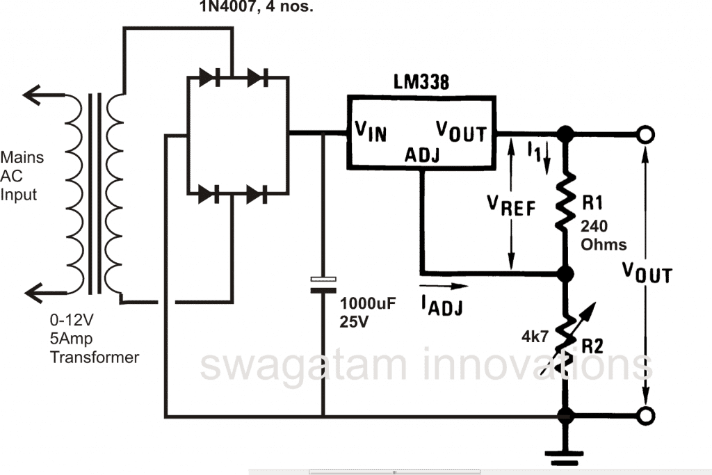 For obtaining fixed voltage levels, 78XX series ICs may be employed with the above explained power supply circuits.
The 78XX ICs are comprehensively explained for your refernce
Nowadays transformerless SMPS powersuppliesarebecomingthe favorites among the users, due totheirhigh efficiency, high power delivering features at amazingly compact sizes.
Though building an SMPS power supply circuit at home is surely not for the novices in the field, engineers andenthusiastswith comprehensive knowledge about the subject can go about building such circuits at home.
You can also learn about a neat little switch mode power supply design.
There are a few other forms of power supplies which can be rather built by even the newelectronichobbyists and does not require transformers.
Though very cheap and easy to build, these types of power supply circuits cannot support heavy current and are normally limited to 200 mA or so.
For obtaining fixed voltage levels, 78XX series ICs may be employed with the above explained power supply circuits.
The 78XX ICs are comprehensively explained for your refernce
Nowadays transformerless SMPS powersuppliesarebecomingthe favorites among the users, due totheirhigh efficiency, high power delivering features at amazingly compact sizes.
Though building an SMPS power supply circuit at home is surely not for the novices in the field, engineers andenthusiastswith comprehensive knowledge about the subject can go about building such circuits at home.
You can also learn about a neat little switch mode power supply design.
There are a few other forms of power supplies which can be rather built by even the newelectronichobbyists and does not require transformers.
Though very cheap and easy to build, these types of power supply circuits cannot support heavy current and are normally limited to 200 mA or so.
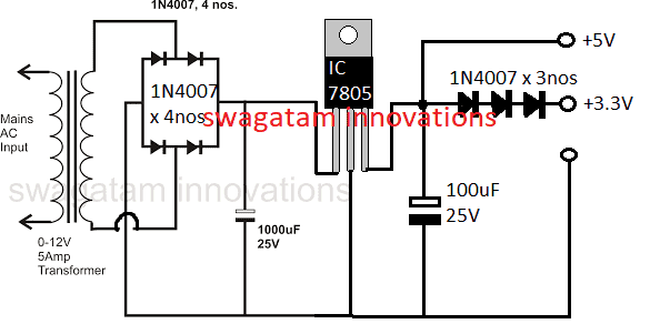 So I am sure that your requirement can be easily fulfilled through the above mentioned procedures.
for powering MCU through the above procedure you can use a 0-9V or a 0-12V trafo with 1amp current, diodes could be 1N4007 x 4nos
The diodes will drop 1.4V when the input is a DC but when it's an AC like from a trafo then the output will be raised by a factor of 1.21.
make sure to use a 2200uF / 25V cap after the bridge for the filtration
I hope the info will enlighten you and answer your queries.
The image above shows how to get 5V and 3.3V constant from a given power supply circuit.
So I am sure that your requirement can be easily fulfilled through the above mentioned procedures.
for powering MCU through the above procedure you can use a 0-9V or a 0-12V trafo with 1amp current, diodes could be 1N4007 x 4nos
The diodes will drop 1.4V when the input is a DC but when it's an AC like from a trafo then the output will be raised by a factor of 1.21.
make sure to use a 2200uF / 25V cap after the bridge for the filtration
I hope the info will enlighten you and answer your queries.
The image above shows how to get 5V and 3.3V constant from a given power supply circuit.
 Here, we can see that a 500 ohm preset is added with the central ground pin of the IC, which allows the IC to produce a lifted output value up to 9 V, with a current of 850 mA.
The preset could be adjusted o get outputs in the range of 5 V to 9 V.
For getting an increased voltage output from a 7812 IC, you can refer to this post!
Here, we can see that a 500 ohm preset is added with the central ground pin of the IC, which allows the IC to produce a lifted output value up to 9 V, with a current of 850 mA.
The preset could be adjusted o get outputs in the range of 5 V to 9 V.
For getting an increased voltage output from a 7812 IC, you can refer to this post!
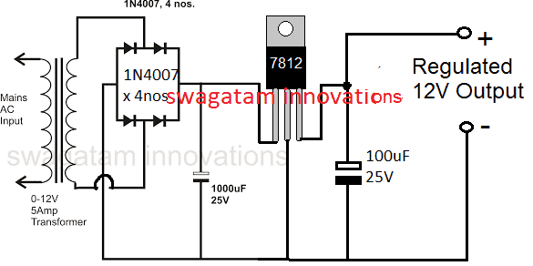
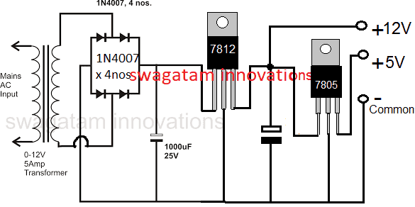
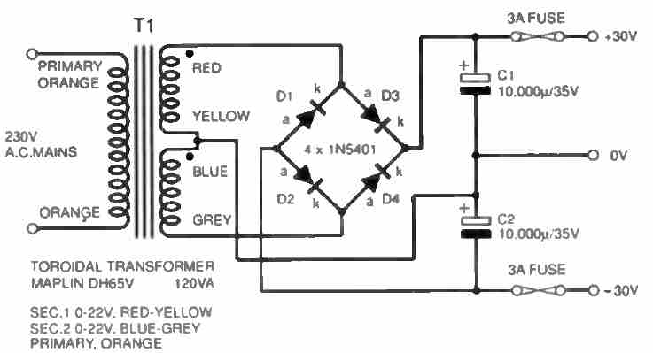 However, for achieving a regulated dual power supply with the desired level of dual voltage at the output is something which normally requires a complex design using costly ICs.
The following design shows how simply and discretely a dual power supply could be configured using a few BJTs, and a few resistors.
However, for achieving a regulated dual power supply with the desired level of dual voltage at the output is something which normally requires a complex design using costly ICs.
The following design shows how simply and discretely a dual power supply could be configured using a few BJTs, and a few resistors.
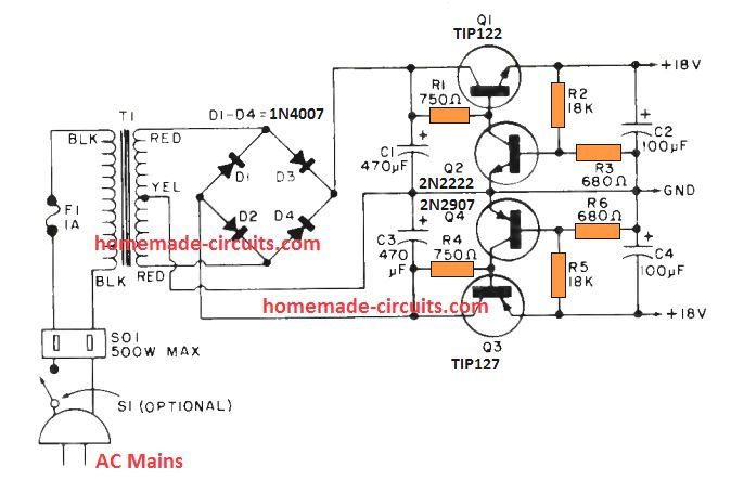 Here Q1 and Q3 are rigged as emitter follower pass transistors, which decide the amount of current that is allowed to pass across the respective +/- outputs.
Here, it is around 2 amps
The output voltage across the relevant dual supply rails is determined by the transistors Q2 and Q4 along with their base resistive divider network.
The output voltage levels could be appropriately adjusted and tweaked by adjusting the values of the potential dividers formed by the resistors R2, R3 and R5, R6.
Here Q1 and Q3 are rigged as emitter follower pass transistors, which decide the amount of current that is allowed to pass across the respective +/- outputs.
Here, it is around 2 amps
The output voltage across the relevant dual supply rails is determined by the transistors Q2 and Q4 along with their base resistive divider network.
The output voltage levels could be appropriately adjusted and tweaked by adjusting the values of the potential dividers formed by the resistors R2, R3 and R5, R6.
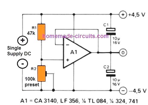 This allows us to get the most desirable feature of the circuit, it is that the R1/R2 partnership doesn't rely on the battery voltage! An additional benefit of this active potential divider is that (as opposed to a basic resistor divider chain) it adjusts itself nicely to varying load currents moving to and from the earth supply line, especially with regards to unsymmetrical load current situations.
You can probably think of using different variants of opamps for this circuit.
The 3140 and 324 tend to be fantastic choices, despite having a battery voltage as low as 4.5 V.
Keep in mind that the highest voltage that can be tolerated by these ICs is not more than 30 V, and the maximum load current that can be tolerated by the opamp will also depend on the type of the opamp.
This allows us to get the most desirable feature of the circuit, it is that the R1/R2 partnership doesn't rely on the battery voltage! An additional benefit of this active potential divider is that (as opposed to a basic resistor divider chain) it adjusts itself nicely to varying load currents moving to and from the earth supply line, especially with regards to unsymmetrical load current situations.
You can probably think of using different variants of opamps for this circuit.
The 3140 and 324 tend to be fantastic choices, despite having a battery voltage as low as 4.5 V.
Keep in mind that the highest voltage that can be tolerated by these ICs is not more than 30 V, and the maximum load current that can be tolerated by the opamp will also depend on the type of the opamp.
 It is an uncomplicated venture for the newbie to construct, and is meant to be utilized with a plug-in mains adaptor providing an unregulated d.c.
output.
IC1 is actually a adjustable regulator type LM317T.
The rotary switch S1 chooses the setting (constant current or constant voltage) along with the current or voltage value.
The regulated voltage can be obtained at SK3 and the current is in SK4.
Observe that a adjustable setting (position 12) is incorporated that enables a variable voltage to be tailored through potentiometer VR1.
The resistor values must be manufactured from the closest obtainable fixed values, positioned in series as necessary.
Resistor R6 is rated at 1W and R7 at 2W although the remaining could be 0.25W.
Voltage regulator IC1 317 must he installed to some heatsink the size of which is determined by the input and output voltages and currents necessary.
It is an uncomplicated venture for the newbie to construct, and is meant to be utilized with a plug-in mains adaptor providing an unregulated d.c.
output.
IC1 is actually a adjustable regulator type LM317T.
The rotary switch S1 chooses the setting (constant current or constant voltage) along with the current or voltage value.
The regulated voltage can be obtained at SK3 and the current is in SK4.
Observe that a adjustable setting (position 12) is incorporated that enables a variable voltage to be tailored through potentiometer VR1.
The resistor values must be manufactured from the closest obtainable fixed values, positioned in series as necessary.
Resistor R6 is rated at 1W and R7 at 2W although the remaining could be 0.25W.
Voltage regulator IC1 317 must he installed to some heatsink the size of which is determined by the input and output voltages and currents necessary.
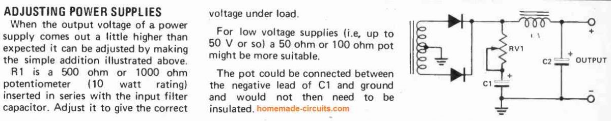
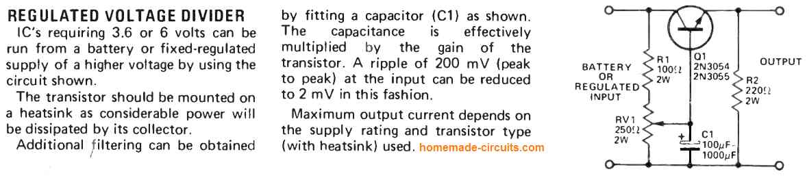
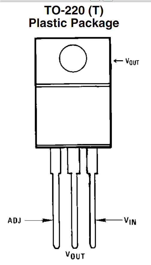 With the advent of chips or ICs like LM317, L200, LM338, LM723, configuring power supply circuits with variable voltage output with the above exceptional qualities has become very easy nowadays.
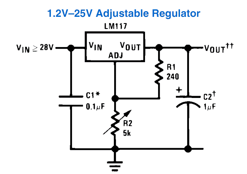 As can be seen the diagram, the assembly needs hardly any components and is in fact a childˇŻs play to get everything in place.
Adjusting the pot produces a linearly varying voltage at the output that may be right from 1.25 volts to the maximum level supplied at the input of the Ic.
Though the shown design is the simplest one and therefore includes only a voltage control feature, a current control feature can also be included with the IC.
As can be seen the diagram, the assembly needs hardly any components and is in fact a childˇŻs play to get everything in place.
Adjusting the pot produces a linearly varying voltage at the output that may be right from 1.25 volts to the maximum level supplied at the input of the Ic.
Though the shown design is the simplest one and therefore includes only a voltage control feature, a current control feature can also be included with the IC.
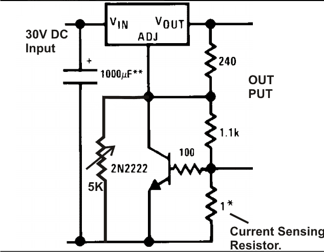 The figure above shows, how the IC LM317 can be effectively used for producing variable voltages and currents, as desired by the user.
The 5K pot is used for adjusting the voltage, whereas the 1 Ohm current sensing resistor is selectedappropriatelyto acquire the desired current limit.
The figure above shows, how the IC LM317 can be effectively used for producing variable voltages and currents, as desired by the user.
The 5K pot is used for adjusting the voltage, whereas the 1 Ohm current sensing resistor is selectedappropriatelyto acquire the desired current limit.
 To be precise the upper LM317 forms the current regulator stage while the lower acts like a voltage controller stage.
The input supply source is connected across the Vin and ground of the upper current regulator circuit, the output from this stage goes to the input of the lower LM317 variable voltage regulator stage.
Basically both the stages are connected in series for implementing a complete foolproof voltage and current regulation for the connected load which is a laser diode in the present case.
R2 is selected to acquire a range of around 1.25A max current limit, the minimum allowable being 5mA when the full 250 ohms is set in the path, meaning the current to the laser may be set as desired, anywhere between 5mA to 1 amp.
To be precise the upper LM317 forms the current regulator stage while the lower acts like a voltage controller stage.
The input supply source is connected across the Vin and ground of the upper current regulator circuit, the output from this stage goes to the input of the lower LM317 variable voltage regulator stage.
Basically both the stages are connected in series for implementing a complete foolproof voltage and current regulation for the connected load which is a laser diode in the present case.
R2 is selected to acquire a range of around 1.25A max current limit, the minimum allowable being 5mA when the full 250 ohms is set in the path, meaning the current to the laser may be set as desired, anywhere between 5mA to 1 amp.
 The R2 resistors associated need to be calculated with respect to R1 (240 ohms) for setting up the intended push button selected voltage outputs.
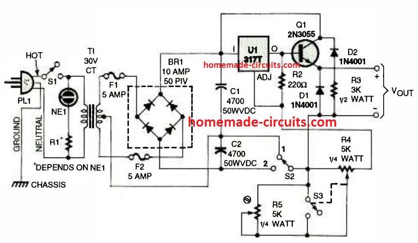 This simple LM317 fixed os adjustable voltage supply satisfies the conditions superbly and is capable of delivering up to 10 amps.
The voltage output is governed by the circuit stage containing R4, R5 and S3; observe that switch S3 is a part of R4.
For getting a fixed voltage output, R4 must be determined for getting zero ohms (fully counter-clockwise).
In this situation, switch S3 should be in the open position.
The preset R5 should in that case be tweaked so that the circuit generates a 12 volt output (or anything your personal application requires).
To have an variable output, R4 can be flipped clockwise, with S3 in the closed position, and getting rid of R5 from the circuit.
The output voltage can now be operated by the R4 resistor solely.
When the position of SPDT switch S2 is in 1, the highest output current can be accomplished having the two halves of T1 supplying current to the filter stage, in order to increase the overall current output 2 times more.
Having said that, the highest output voltage will be reduced by 50% in this position.
It really is a much productive setting considering that the power transistor does not have to drop a significant amount of potential.
In position 2, the maximum voltage practically equals the power specifications of T1. Here, we employed a 24 volt center-tapped transformer for T1. Lastly, D1 and D2 had been incorporated to safeguard the LM317 IC in case power was switched off with an inductive load at the output
References:http://www.ti.com/lit/ds/symlink/lm317.pdf
https://en.wikipedia.org/wiki/LM317
This simple LM317 fixed os adjustable voltage supply satisfies the conditions superbly and is capable of delivering up to 10 amps.
The voltage output is governed by the circuit stage containing R4, R5 and S3; observe that switch S3 is a part of R4.
For getting a fixed voltage output, R4 must be determined for getting zero ohms (fully counter-clockwise).
In this situation, switch S3 should be in the open position.
The preset R5 should in that case be tweaked so that the circuit generates a 12 volt output (or anything your personal application requires).
To have an variable output, R4 can be flipped clockwise, with S3 in the closed position, and getting rid of R5 from the circuit.
The output voltage can now be operated by the R4 resistor solely.
When the position of SPDT switch S2 is in 1, the highest output current can be accomplished having the two halves of T1 supplying current to the filter stage, in order to increase the overall current output 2 times more.
Having said that, the highest output voltage will be reduced by 50% in this position.
It really is a much productive setting considering that the power transistor does not have to drop a significant amount of potential.
In position 2, the maximum voltage practically equals the power specifications of T1. Here, we employed a 24 volt center-tapped transformer for T1. Lastly, D1 and D2 had been incorporated to safeguard the LM317 IC in case power was switched off with an inductive load at the output
References:http://www.ti.com/lit/ds/symlink/lm317.pdf
https://en.wikipedia.org/wiki/LM317

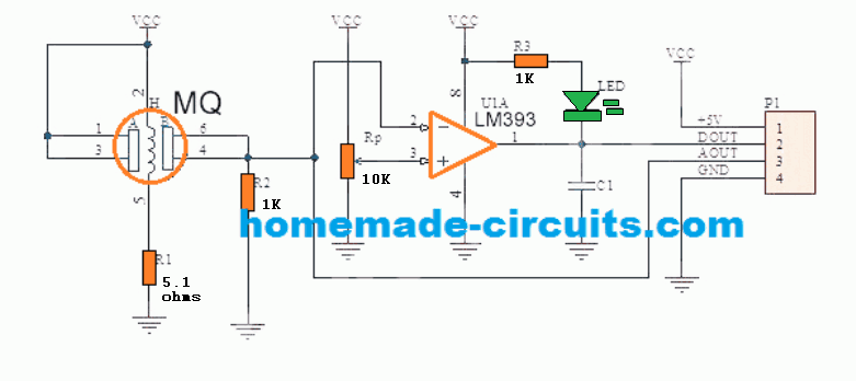 The operation of the module is pretty simple.
When the sensor is brought near an alcohol or ethanol source, the voltage level at the input pin#2 of the comparator goes above the reference pin#3, causing the output to go low.
The green LED Illuminates to confirm the results.
The operation of the module is pretty simple.
When the sensor is brought near an alcohol or ethanol source, the voltage level at the input pin#2 of the comparator goes above the reference pin#3, causing the output to go low.
The green LED Illuminates to confirm the results.
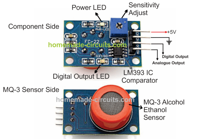
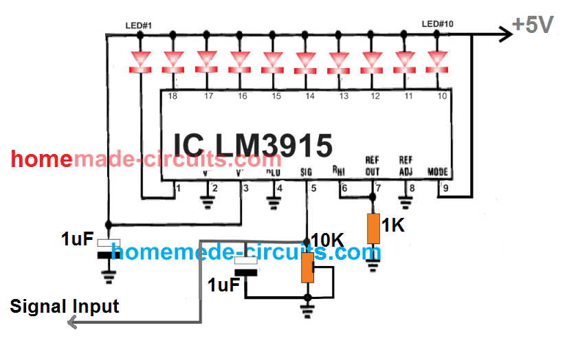 Now let's see how the MQ-3 sensor could be integrated with the above LED indicator circuit for implementing the proposed alcohol meter circuit.
 If you have any further questions please feel free to ask them through the comment box.
Video Demonstration
If you have any further questions please feel free to ask them through the comment box.
Video Demonstration

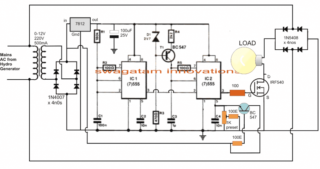 The above ELC circuits can be used with all types of microhydro systems, watermill systems and also wind mill systems.
Now let's see how we can employ a similar ELC circuit for regulating the speed and frequency of a windmillgeneratorunit.
The idea was requested by Mr.
Nilesh Patil.
I am Great fan of your Electronic circuits and Hobby to create it.
Basically i'm from rural area where 15 hours power cut off problem we facing every year
Even if i go for to buy inverter that is also not get charged due to power failure.
I have created wind mill generator (In Very Cheap Cost ) from that will support to charge 12 v battery.
For the same i m looking to buy wind mill charge turbine Controller that is too costly.
So planned to create our own if have suitable design from you
Generator Capacity : 0 - 230 AC Volt
input 0 - 230 v AC (Vary depends on wind speed)
output : 12 V DC (sufficient boost up current).
Overload / Discharge / Dummy Load handling
Can you please suggest or help me to develop it and required component & PCB from you
I May required many same circuit once succeed.
The above ELC circuits can be used with all types of microhydro systems, watermill systems and also wind mill systems.
Now let's see how we can employ a similar ELC circuit for regulating the speed and frequency of a windmillgeneratorunit.
The idea was requested by Mr.
Nilesh Patil.
I am Great fan of your Electronic circuits and Hobby to create it.
Basically i'm from rural area where 15 hours power cut off problem we facing every year
Even if i go for to buy inverter that is also not get charged due to power failure.
I have created wind mill generator (In Very Cheap Cost ) from that will support to charge 12 v battery.
For the same i m looking to buy wind mill charge turbine Controller that is too costly.
So planned to create our own if have suitable design from you
Generator Capacity : 0 - 230 AC Volt
input 0 - 230 v AC (Vary depends on wind speed)
output : 12 V DC (sufficient boost up current).
Overload / Discharge / Dummy Load handling
Can you please suggest or help me to develop it and required component & PCB from you
I May required many same circuit once succeed.
 So far we learned an effective electronic load controller circuit using a sequential multiple dummy load switcher concept, here we discuss a much simpler design of the same using a triac dimmer concept and with a single load.

 Parts List for the op amp stage
R1, R2, R3, R6 = 10k 1/4 watt 5%
C1 = 100uF/25V
C2 = 4.7uF/25V
C3, C4 = 33nF/50V
C5, C6 = 3.3 nF/50V
C7 = 22uF/25V
C8 = 4.7uF/25V
IC 741
Parts List for the LM3915 stage
1M, 1k, 1/4 watt 5% = 1 each
2.2uF/25V = 1no
LEDs 5mm 20mA, color as per specifications = 10 nos
IC LM3915
Parts List for the op amp stage
R1, R2, R3, R6 = 10k 1/4 watt 5%
C1 = 100uF/25V
C2 = 4.7uF/25V
C3, C4 = 33nF/50V
C5, C6 = 3.3 nF/50V
C7 = 22uF/25V
C8 = 4.7uF/25V
IC 741
Parts List for the LM3915 stage
1M, 1k, 1/4 watt 5% = 1 each
2.2uF/25V = 1no
LEDs 5mm 20mA, color as per specifications = 10 nos
IC LM3915
 R1 = 2k2
R2 = 100 ohms
LED = 20mA 5mm type
C1 = 100uF to 470uF depending on flashing rate preference
The article shows a simple method of using the IC LM3915 for monitoring battery voltages right from 1.5V to 24V in 10 discrete steps using 10 LED indicators.
R1 = 2k2
R2 = 100 ohms
LED = 20mA 5mm type
C1 = 100uF to 470uF depending on flashing rate preference
The article shows a simple method of using the IC LM3915 for monitoring battery voltages right from 1.5V to 24V in 10 discrete steps using 10 LED indicators.
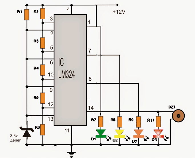

 In both the above configurations, the output is supposed to remain constant and stable in terms of voltage and wattage regardless of the solar output.
 The IC 741 stage is the solar tracker section and forms the heart of the entire design.
The solar panel voltage is fed to the inverting pin2 of the IC, while the the same is applied to the non-inverting pin3 with a drop of around 2 V using three 1N4148 diodes in series.
The above situation consistently keeps the pin3 of the IC a shade lower than pin2 ensuring a zero voltage across the output pin6 of the IC.
However in an event of an inefficient overload, such as a mismatched battery or a high current battery, the solar panel voltage tends to get pulled down by the load.
When this happens pin2 voltage also begins dropping, however due to the presence of the 10uF capacitor at pin3, its potential stays solid and does not respond to the above drop.
The situation instantly forces pin3 to go high than pin2, which in turn toggles pin6 high, switching ON the BJT BC547.
BC547 now immediately disables LM338 cutting off the voltage to the battery, the cycle keeps switching at a rapid pace depending upon the IC's rated speed.
The above operations make sure that the solar panel voltage never drops or gets pulled down by the load, maintaining an MPPT like condition throughout.
Since a linear IC LM338 is used, the circuit could be yet again a bit inefficient....the remedy is to replace the LM338 stage with a buck converter...that would make the design extremely versatile and comparable to a true MPPT.
Below shown is an MPPT circuit using a buck converter topology, now the design makes a lot of sense and looks much closer to a true MPPT
The IC 741 stage is the solar tracker section and forms the heart of the entire design.
The solar panel voltage is fed to the inverting pin2 of the IC, while the the same is applied to the non-inverting pin3 with a drop of around 2 V using three 1N4148 diodes in series.
The above situation consistently keeps the pin3 of the IC a shade lower than pin2 ensuring a zero voltage across the output pin6 of the IC.
However in an event of an inefficient overload, such as a mismatched battery or a high current battery, the solar panel voltage tends to get pulled down by the load.
When this happens pin2 voltage also begins dropping, however due to the presence of the 10uF capacitor at pin3, its potential stays solid and does not respond to the above drop.
The situation instantly forces pin3 to go high than pin2, which in turn toggles pin6 high, switching ON the BJT BC547.
BC547 now immediately disables LM338 cutting off the voltage to the battery, the cycle keeps switching at a rapid pace depending upon the IC's rated speed.
The above operations make sure that the solar panel voltage never drops or gets pulled down by the load, maintaining an MPPT like condition throughout.
Since a linear IC LM338 is used, the circuit could be yet again a bit inefficient....the remedy is to replace the LM338 stage with a buck converter...that would make the design extremely versatile and comparable to a true MPPT.
Below shown is an MPPT circuit using a buck converter topology, now the design makes a lot of sense and looks much closer to a true MPPT
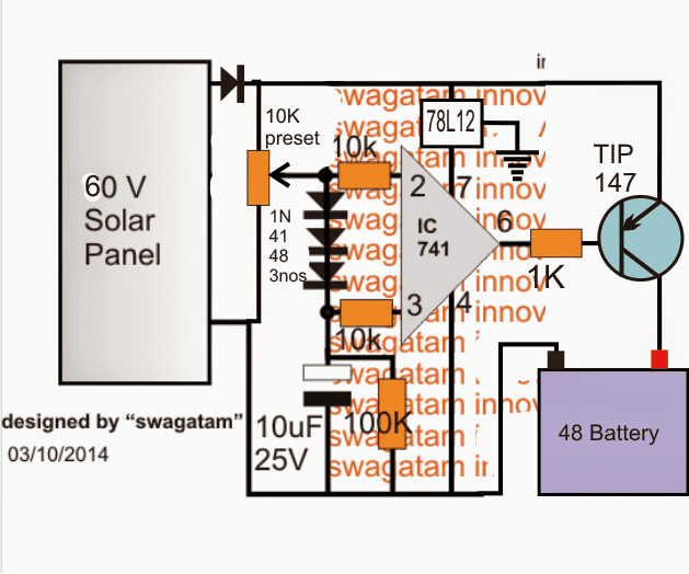 The ideas are all exclusively developed by me.
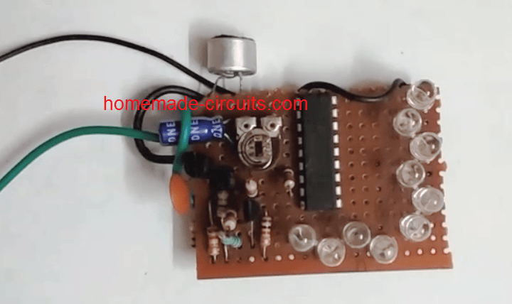
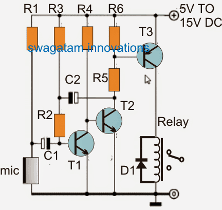 The diagram shown above works very efficiently as a simple transistorized vibration sensor.
It will sense even the slightest sound from the surrounding or the surface over which it is installed.
C2 allows a delay period for the relay so that the relay remains triggered ON for sometime on each detection.
The value of C2 could be tweaked for getting the desired delay OFF on the relay operation.
The relay could be attached with an alarm system if the circuit is intended to be used like a vibration operated alarm or a door alarm etc.
Parts List
R1 = 4k7
R2 = 33k
R3 = 2M2
R4 = 22K
R5 = 470 OHMS
R6 = 4k7
C1 = 0.1uF
C2 = 4.7uF/25V
T1, T2 = BC547
T3 = BC557
D1 = 1N4007
Relay = coil voltage as per the supply voltage, and contact rating as per the load specs
Mic = electret condenser MIC.
The diagram shown above works very efficiently as a simple transistorized vibration sensor.
It will sense even the slightest sound from the surrounding or the surface over which it is installed.
C2 allows a delay period for the relay so that the relay remains triggered ON for sometime on each detection.
The value of C2 could be tweaked for getting the desired delay OFF on the relay operation.
The relay could be attached with an alarm system if the circuit is intended to be used like a vibration operated alarm or a door alarm etc.
Parts List
R1 = 4k7
R2 = 33k
R3 = 2M2
R4 = 22K
R5 = 470 OHMS
R6 = 4k7
C1 = 0.1uF
C2 = 4.7uF/25V
T1, T2 = BC547
T3 = BC557
D1 = 1N4007
Relay = coil voltage as per the supply voltage, and contact rating as per the load specs
Mic = electret condenser MIC.
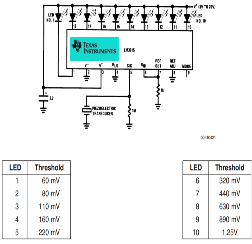 Although the above proposed vibration meter/detector circuit was taken from the original datasheet, it has many flaws and won't produce satisfying results until some serious mods are done.
Recently when I tested it myself realized the drawbacks it possessed.
The tested and modified diagram can be seen below:
Although the above proposed vibration meter/detector circuit was taken from the original datasheet, it has many flaws and won't produce satisfying results until some serious mods are done.
Recently when I tested it myself realized the drawbacks it possessed.
The tested and modified diagram can be seen below:
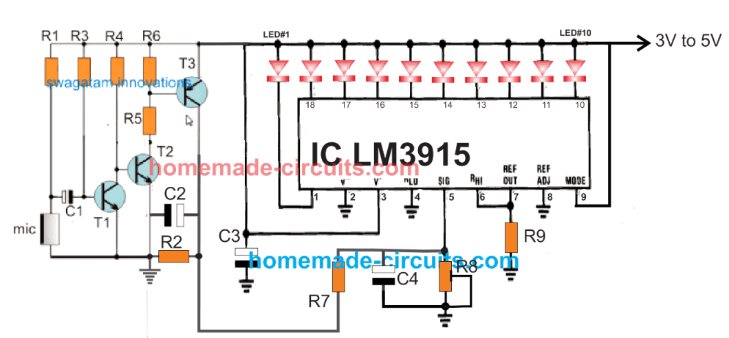 Video Clip demonstrating the Vibration meter working
Parts List
R1 = 5k6
R2, R9 = 1K
R3 = 3M3
R4 = 33K
R5 = 330 OHMS
R6 = 2K2
R7 = 10K
R8 = 10K preset
C1 = 0.1uF
C2 = 100uF/25V
C3, C4 = 1uF/25V
T1, T2 = BC547
T3 = BC557
LEDs = RED 5mm type 20mA
Mic = electret condenser MIC.
Video Clip demonstrating the Vibration meter working
Parts List
R1 = 5k6
R2, R9 = 1K
R3 = 3M3
R4 = 33K
R5 = 330 OHMS
R6 = 2K2
R7 = 10K
R8 = 10K preset
C1 = 0.1uF
C2 = 100uF/25V
C3, C4 = 1uF/25V
T1, T2 = BC547
T3 = BC557
LEDs = RED 5mm type 20mA
Mic = electret condenser MIC.
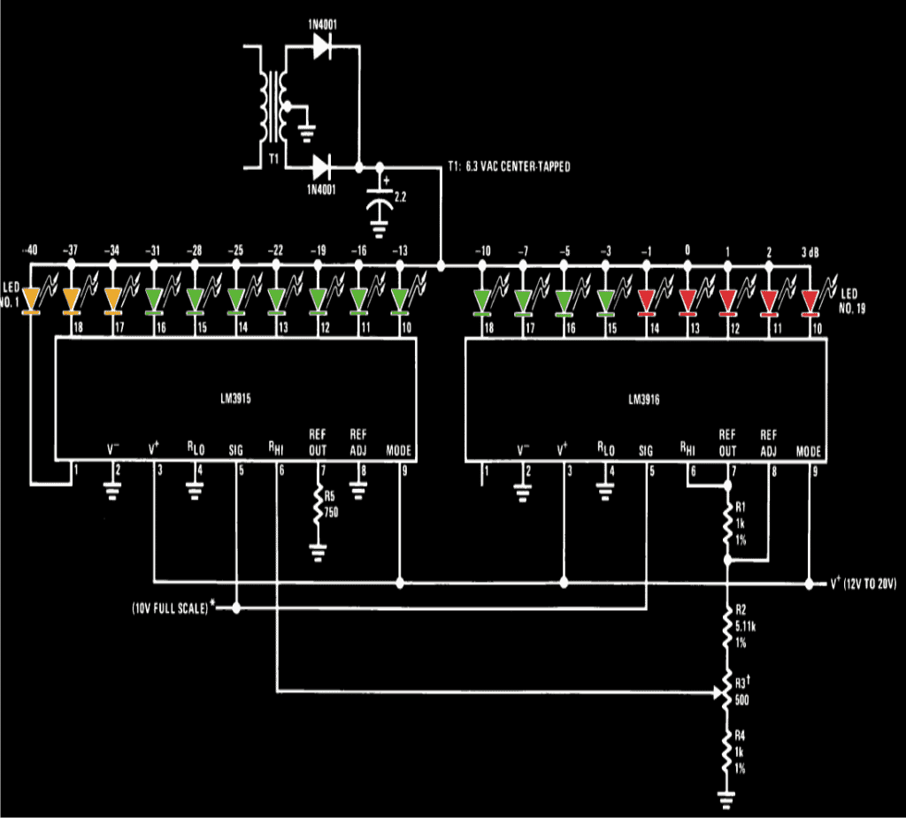
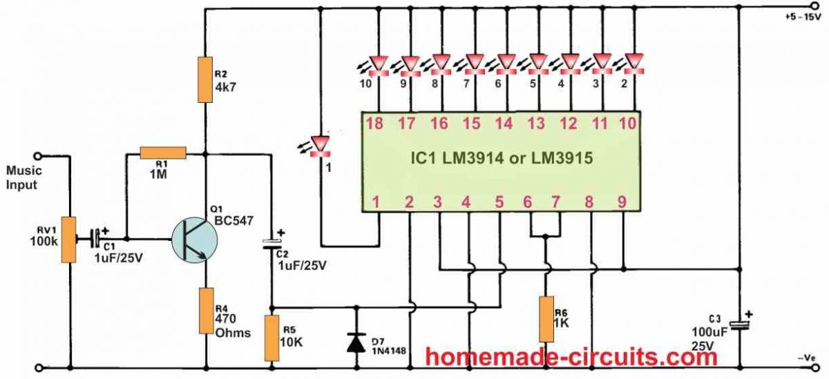 The configuration ensures that with 0.12 V music input only the first LED indicator lights.
When the music input rises to 0.24 V the second LED lights up; with a 0.36 V music supply enables three LEDs to light up and so on until an input signal of 1V2 or more is reached which causes all the ten LEDs to be illuminated.
The input signal is applied to a preset for allowing the sensitivity adjustment of the circuit to the appropriate degree.
The trimmed audio signal from the preset fed to a low gain common emitter amplifier constructed around the BJT Q1 which enhances a 10 times higher sensitivity for the circuit.
Capacitor C2 takes the output signal from Q1 to the input of IC1.
Resistor R5 works like the input bias resistor for IC1, and diode D7 safeguards IC1 from extreme negative input voltage.
Resistor R6 controls the current to every single LED and restricts it at around 12 mA.
However, because IC1 can work with only the positive half cycles of the music signal, the LEDs are able to turn on for a only 50% of time.
This allows an overall current of 6 mA for each of the LEDs.
The quiescent current consumption of the VU meter is not more than 8mA, which may increase to an utmost maximum of 44 mA while all the 10 LEDs are switched ON.
The configuration ensures that with 0.12 V music input only the first LED indicator lights.
When the music input rises to 0.24 V the second LED lights up; with a 0.36 V music supply enables three LEDs to light up and so on until an input signal of 1V2 or more is reached which causes all the ten LEDs to be illuminated.
The input signal is applied to a preset for allowing the sensitivity adjustment of the circuit to the appropriate degree.
The trimmed audio signal from the preset fed to a low gain common emitter amplifier constructed around the BJT Q1 which enhances a 10 times higher sensitivity for the circuit.
Capacitor C2 takes the output signal from Q1 to the input of IC1.
Resistor R5 works like the input bias resistor for IC1, and diode D7 safeguards IC1 from extreme negative input voltage.
Resistor R6 controls the current to every single LED and restricts it at around 12 mA.
However, because IC1 can work with only the positive half cycles of the music signal, the LEDs are able to turn on for a only 50% of time.
This allows an overall current of 6 mA for each of the LEDs.
The quiescent current consumption of the VU meter is not more than 8mA, which may increase to an utmost maximum of 44 mA while all the 10 LEDs are switched ON.
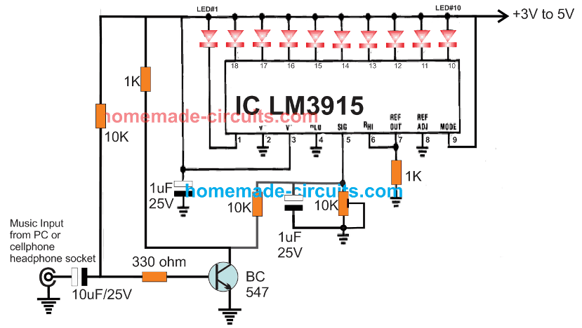
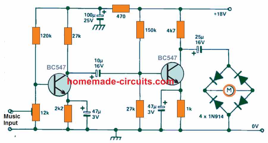 The VU meter circuit indicated in the above diagram consists of a 2-stage voltage amplifier which operates a connected a level meter.
The inpu music AC signal is first amplified, and then rectified, and finally the resulting DC potential equivalent to the music level is displayed on the connected voltmeter.
The VU circuit using a voltmeter can be used with any amplifier, music system, audio mixer etc and must be connected from an early stage of the pre-amp.
The current intake of the circuit in the absence of an input signal is around 2.8mA.
The 12K preset can be used for adjusting the sensitivity of the circuit.
The meter can M be any general purpose moving coil voltmeter.
The VU meter circuit indicated in the above diagram consists of a 2-stage voltage amplifier which operates a connected a level meter.
The inpu music AC signal is first amplified, and then rectified, and finally the resulting DC potential equivalent to the music level is displayed on the connected voltmeter.
The VU circuit using a voltmeter can be used with any amplifier, music system, audio mixer etc and must be connected from an early stage of the pre-amp.
The current intake of the circuit in the absence of an input signal is around 2.8mA.
The 12K preset can be used for adjusting the sensitivity of the circuit.
The meter can M be any general purpose moving coil voltmeter.
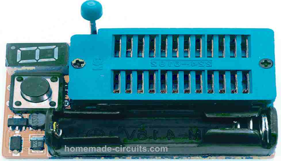
 Buffering is provided by transistors Q1 to Q20, while current limiting, voltage division, and biasing are provided by resistors R1 to R20 and R21 to R40.
 Although just one red wire is needed for regular tests, having a combination of one red and one black test cables is a betteroption.
Push the red cable's banana connector to BP1 connector, which is the red binding post.
When the TEST pushbutton S1is depressed, + 5-volts DC is applied to the small crocodile clip.
Touch the end of the microcrocodile(metal hook) to each contact of the ZIF socket sequentially,whilekeeping S1 depressed.
In response to the above procedure, each of the corresponding LEDs associated with the SO1 pins will light up in succession, indicating that the tester is working correctly.
Now it is ready to test ICs.
Although just one red wire is needed for regular tests, having a combination of one red and one black test cables is a betteroption.
Push the red cable's banana connector to BP1 connector, which is the red binding post.
When the TEST pushbutton S1is depressed, + 5-volts DC is applied to the small crocodile clip.
Touch the end of the microcrocodile(metal hook) to each contact of the ZIF socket sequentially,whilekeeping S1 depressed.
In response to the above procedure, each of the corresponding LEDs associated with the SO1 pins will light up in succession, indicating that the tester is working correctly.
Now it is ready to test ICs.
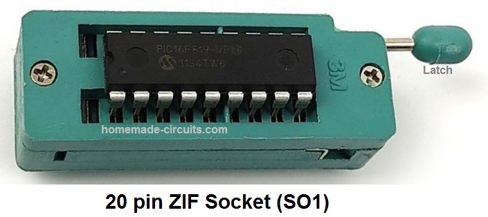 After the IC is installed into the socket, press the latch on the ZIF socket to secure the IC in place once it's in line.
Now connect the alligator clip to the IC's ground or -V pin.
If you don't remember the IC supply pins, you mayhave to look this up in a datasheet of the IC.
Press the TEST switchwith the alligator clip in place and look at the ICsfingerprint on the LED display panel.
If the IC is a digital chip, all of the LEDs must be illuminated witha certain level of brightness.
TTL and CMOS digital ICs may, in practice, illuminate all of theLEDs.
We haven't found any exceptions yet, but you might.
Of course, pins marked as "not connected"(NC) have no effect on the LEDfunctioning.
If an attached pin on a digital IC somehow doesn't illuminate the associated LED, the IC may be defective and therefore should be scrapped or labelled appropriately.
The rules may vary slightly in casethe IC under test is a linear IC.
A good device's LEDs may or may not be illuminated.
You may even find variations in fingerprints from various manufacturers on the same IC.
When comparing schematic designs of the 555 timer IC from different manufacturers, you'll find that they're not all the same.
The fingerprint of the device may vary as a result of these variations.
Two tests may berequired for analogue or linear ICs.
Press the TEST button after attaching the alligator clip to the V pin.
Keep track of which LEDs are turned on, off, or dimmed.
Then, with the test-lead alligator clipremoved, connect it to the +V pin of the IC.
Press the TEST button to see which LEDs are illuminated, dimmed, or unlit once again.
Both of these tests should be performed with reference toa known and healthy sample IC.
As mentioned above, make a note of the manufacturer, part number, and LED states.
When evaluating any dubious equipment, compare the aforementioned records to the test results of the IC under test.
If the LEDs for the same IC exhibit a different pattern, the IC must be deemed faulty and scrapped.
In most situations, if the LED pattern matches, the device may be consideredOK.
The second test is generally the most helpful while testing linear ICs.
A faulty ICwill frequently clear the first test but fail the second test.
When evaluating linear or analogue ICs, certain general rules are useful.
They are as follows:
Good ICsusually willhave illuminated LEDs on their output pins.
Faulty IC'soutput pins mightindicatevery dimly litor switched OFF LEDs.
Input pins may showLEDs in the switched ON or OFFdepending on the specific IC.
Dual, triple, quad, and other function ICs should have exactly equal input and output pins.
(For example, if one input pin of a dual op-amp showsanilluminated LED, the other input pin should be illuminated as well.)
Keeping track of your results througha reference library can bea wonderful idea.
You'll have to depend less on obtaining a known good IC for comparative testing as your library dataincreases.
Instead, look up forthe specific ICin your library and take note of what the output LEDdisplay should look like if the IC is working properly.
You can make note of your findings in any way you want,as long as you're consistent!
After the IC is installed into the socket, press the latch on the ZIF socket to secure the IC in place once it's in line.
Now connect the alligator clip to the IC's ground or -V pin.
If you don't remember the IC supply pins, you mayhave to look this up in a datasheet of the IC.
Press the TEST switchwith the alligator clip in place and look at the ICsfingerprint on the LED display panel.
If the IC is a digital chip, all of the LEDs must be illuminated witha certain level of brightness.
TTL and CMOS digital ICs may, in practice, illuminate all of theLEDs.
We haven't found any exceptions yet, but you might.
Of course, pins marked as "not connected"(NC) have no effect on the LEDfunctioning.
If an attached pin on a digital IC somehow doesn't illuminate the associated LED, the IC may be defective and therefore should be scrapped or labelled appropriately.
The rules may vary slightly in casethe IC under test is a linear IC.
A good device's LEDs may or may not be illuminated.
You may even find variations in fingerprints from various manufacturers on the same IC.
When comparing schematic designs of the 555 timer IC from different manufacturers, you'll find that they're not all the same.
The fingerprint of the device may vary as a result of these variations.
Two tests may berequired for analogue or linear ICs.
Press the TEST button after attaching the alligator clip to the V pin.
Keep track of which LEDs are turned on, off, or dimmed.
Then, with the test-lead alligator clipremoved, connect it to the +V pin of the IC.
Press the TEST button to see which LEDs are illuminated, dimmed, or unlit once again.
Both of these tests should be performed with reference toa known and healthy sample IC.
As mentioned above, make a note of the manufacturer, part number, and LED states.
When evaluating any dubious equipment, compare the aforementioned records to the test results of the IC under test.
If the LEDs for the same IC exhibit a different pattern, the IC must be deemed faulty and scrapped.
In most situations, if the LED pattern matches, the device may be consideredOK.
The second test is generally the most helpful while testing linear ICs.
A faulty ICwill frequently clear the first test but fail the second test.
When evaluating linear or analogue ICs, certain general rules are useful.
They are as follows:
Good ICsusually willhave illuminated LEDs on their output pins.
Faulty IC'soutput pins mightindicatevery dimly litor switched OFF LEDs.
Input pins may showLEDs in the switched ON or OFFdepending on the specific IC.
Dual, triple, quad, and other function ICs should have exactly equal input and output pins.
(For example, if one input pin of a dual op-amp showsanilluminated LED, the other input pin should be illuminated as well.)
Keeping track of your results througha reference library can bea wonderful idea.
You'll have to depend less on obtaining a known good IC for comparative testing as your library dataincreases.
Instead, look up forthe specific ICin your library and take note of what the output LEDdisplay should look like if the IC is working properly.
You can make note of your findings in any way you want,as long as you're consistent!
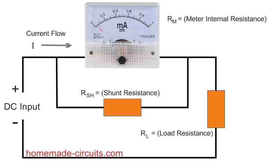 The shunt does this by bypassing or "shunting" the bulk of the current flowing past the meter.
As a result, the shunt resistor allows you to convert any cheap conventional meter, such as a 0 -1 milliammeter, into, perhaps, a robust 0 to 20-amp meter.
The shunt does this by bypassing or "shunting" the bulk of the current flowing past the meter.
As a result, the shunt resistor allows you to convert any cheap conventional meter, such as a 0 -1 milliammeter, into, perhaps, a robust 0 to 20-amp meter.
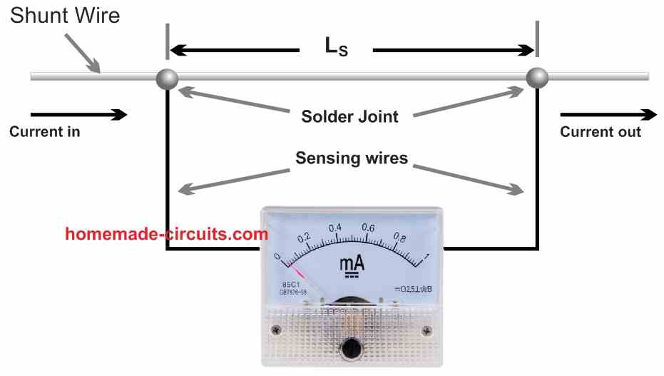 The sensing wires can be made of any type of wire; which is not crucial.
This little effort can considerably improve your shunt's precision.
We're all set to make our shunt now.
Cut a three-foot piece of 12-gauge solid copper wire.
With a pocket knife, peel the insulation off the wire, ensuringnot to break it.
Next take a 2 inch measurement through one end and solder one sensing wire there.
Measure 2 ft 6 in from this sense wire and solder the other sense wire in place.
As illustrated in Fig.
2, hook upthe shunt to the desiredammeterand you're ready to readcurrent! If you wish to make the shunt a bit smaller, wound it around the handle ofan insulated screwdriver or some such identical object, for examplea wooden splinter.
The sensing wires can be made of any type of wire; which is not crucial.
This little effort can considerably improve your shunt's precision.
We're all set to make our shunt now.
Cut a three-foot piece of 12-gauge solid copper wire.
With a pocket knife, peel the insulation off the wire, ensuringnot to break it.
Next take a 2 inch measurement through one end and solder one sensing wire there.
Measure 2 ft 6 in from this sense wire and solder the other sense wire in place.
As illustrated in Fig.
2, hook upthe shunt to the desiredammeterand you're ready to readcurrent! If you wish to make the shunt a bit smaller, wound it around the handle ofan insulated screwdriver or some such identical object, for examplea wooden splinter.
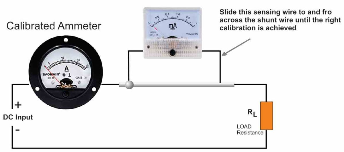 The author discovered that car tail lamp bulbs can be applied asan excellent load for the circuit.
Connect one sensing wire into position as stated above to calibrate the shunt.
Switch ON power tothe circuit and shift the right side sensing wire up and down acrossthe shunt wire until the meter connected across the shunt wireindicatesthe exactsame current as the calibrated meter on the left.
Turn off the power to the circuit and connect the second sensing wire exactlyat that spot.
Reference: https://www.learningelectronics.net/VA3AVR/gadgets/shunts/shunts.html
The author discovered that car tail lamp bulbs can be applied asan excellent load for the circuit.
Connect one sensing wire into position as stated above to calibrate the shunt.
Switch ON power tothe circuit and shift the right side sensing wire up and down acrossthe shunt wire until the meter connected across the shunt wireindicatesthe exactsame current as the calibrated meter on the left.
Turn off the power to the circuit and connect the second sensing wire exactlyat that spot.
Reference: https://www.learningelectronics.net/VA3AVR/gadgets/shunts/shunts.html
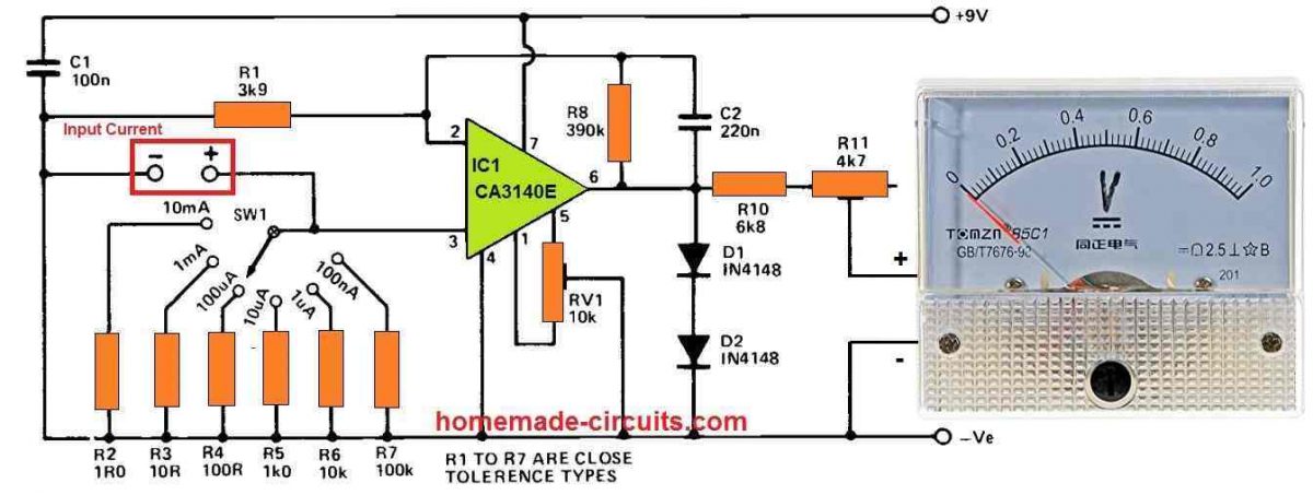 R10 and R11 are used for implementinga 1V FSD voltmeter with themeterM1. The latter is tweaked to get the meter'ssensitivity exactly right.
IC1 is an op amp with a DC voltage gain of roughly 100 times and is wired in the non-inverting configuration (using thefeedback network R8-R1).
In order to increase stability and immunity to stray interferencepick-up, C2 is used whichminimizes the AC gain to around unity.
SW1 selects one of the range resistors betweenR2 andR7to bias the non-inverting input of IC1 to the 0V rail.
In principle, this results in zero output voltage and no meterdisplacement, although in real life testing, tiny offset voltages must still be compensated byutilising offset null control, RV1.
When the microamp meter circuit receives an input current, a voltage is generated across the specified range resistor, which is amplified to create a positive meterdeflection.
As an example, when R2 is toggled into the circuit, 10 mA is required to achieve full scale deflection since 10 mA causes 10 mV to be generated across R2. IC1 will amplify this one hundred times, yielding one volt at the output.
The range resistor is increased by a factor of ten for creating most useful ranges, lowering the necessary currentat the input,to produce 10 mV and achieve full scale deflection on meterM1.
This arrangement demands a high input impedance in order for the amplifier to not waste any significant amount of input current, which is done by employing a FET input op amp having a standard input resistance of 1.5 million meg ohms.
D1 and D2 limit the output voltage of IC1 from reaching around 1.3 volts, therefore protecting M1 from over-loads.
R10 and R11 are used for implementinga 1V FSD voltmeter with themeterM1. The latter is tweaked to get the meter'ssensitivity exactly right.
IC1 is an op amp with a DC voltage gain of roughly 100 times and is wired in the non-inverting configuration (using thefeedback network R8-R1).
In order to increase stability and immunity to stray interferencepick-up, C2 is used whichminimizes the AC gain to around unity.
SW1 selects one of the range resistors betweenR2 andR7to bias the non-inverting input of IC1 to the 0V rail.
In principle, this results in zero output voltage and no meterdisplacement, although in real life testing, tiny offset voltages must still be compensated byutilising offset null control, RV1.
When the microamp meter circuit receives an input current, a voltage is generated across the specified range resistor, which is amplified to create a positive meterdeflection.
As an example, when R2 is toggled into the circuit, 10 mA is required to achieve full scale deflection since 10 mA causes 10 mV to be generated across R2. IC1 will amplify this one hundred times, yielding one volt at the output.
The range resistor is increased by a factor of ten for creating most useful ranges, lowering the necessary currentat the input,to produce 10 mV and achieve full scale deflection on meterM1.
This arrangement demands a high input impedance in order for the amplifier to not waste any significant amount of input current, which is done by employing a FET input op amp having a standard input resistance of 1.5 million meg ohms.
D1 and D2 limit the output voltage of IC1 from reaching around 1.3 volts, therefore protecting M1 from over-loads.
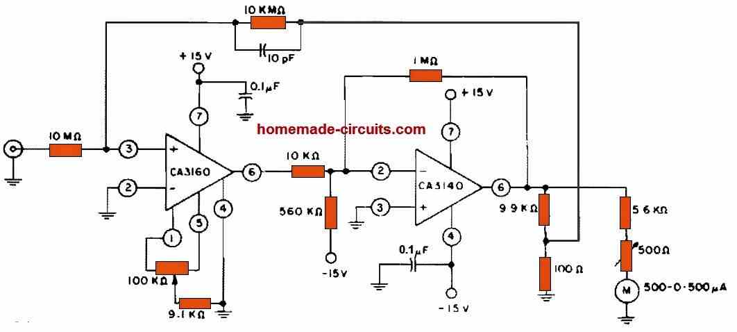 CA3160 and CA3140 BiMOS op amps are used in this circuit to generate a full-scale metre readingat current levels that's as low as3 pA.
The CA3140 acts as an x100 gain stage, providing the metre and feedback circuit with the needed positive and negative output range.
The CA3160's terminals 2 and 4 are at zero voltage, therefore its input is in "protected condition."
CA3160 and CA3140 BiMOS op amps are used in this circuit to generate a full-scale metre readingat current levels that's as low as3 pA.
The CA3140 acts as an x100 gain stage, providing the metre and feedback circuit with the needed positive and negative output range.
The CA3160's terminals 2 and 4 are at zero voltage, therefore its input is in "protected condition."
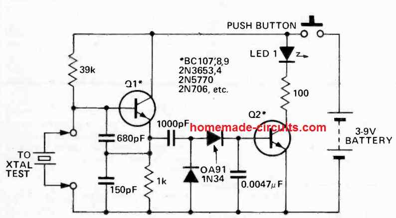 The above circuit will provide you with a direct indication whether the connected crystal is good or a bad one.
The configuration around the transistor Q1 and its associated RC network work like a Colpitt's oscillator.
As soon the the crystal is hooked up into the indicated slots, the Q1 circuit starts oscillating at the crystal frequency.
This oscillating frequency is applied to the 1000 pF capacitor through which it reaches the two diode stage wired like a rectifier circuit.
The oscillating frequency is appropriately rectified using the diode network and fed to the next transistor Q2 stage.
The rectified DC from the diodes provide the necessary biasing to the Q2 transistor base, so that it turns ON illuminating the attached LED.
The switched ON LED confirms that the crystal under test is a good crystal, and the circuit is correctly oscillating with the help of the crystal.
If a bad crystal is inserted into the slot, the Q1 fails to oscillate which does not allow any frequency to enter the 1000 pF capacitor causing the Q2 stage to remain switched OFF.
The LED consequently also remains switched OFF, indicating that the connected crystal is a faulty one.
The Q1, Q2 can be any general purpose transistors such as the BC547.
The above circuit will provide you with a direct indication whether the connected crystal is good or a bad one.
The configuration around the transistor Q1 and its associated RC network work like a Colpitt's oscillator.
As soon the the crystal is hooked up into the indicated slots, the Q1 circuit starts oscillating at the crystal frequency.
This oscillating frequency is applied to the 1000 pF capacitor through which it reaches the two diode stage wired like a rectifier circuit.
The oscillating frequency is appropriately rectified using the diode network and fed to the next transistor Q2 stage.
The rectified DC from the diodes provide the necessary biasing to the Q2 transistor base, so that it turns ON illuminating the attached LED.
The switched ON LED confirms that the crystal under test is a good crystal, and the circuit is correctly oscillating with the help of the crystal.
If a bad crystal is inserted into the slot, the Q1 fails to oscillate which does not allow any frequency to enter the 1000 pF capacitor causing the Q2 stage to remain switched OFF.
The LED consequently also remains switched OFF, indicating that the connected crystal is a faulty one.
The Q1, Q2 can be any general purpose transistors such as the BC547.
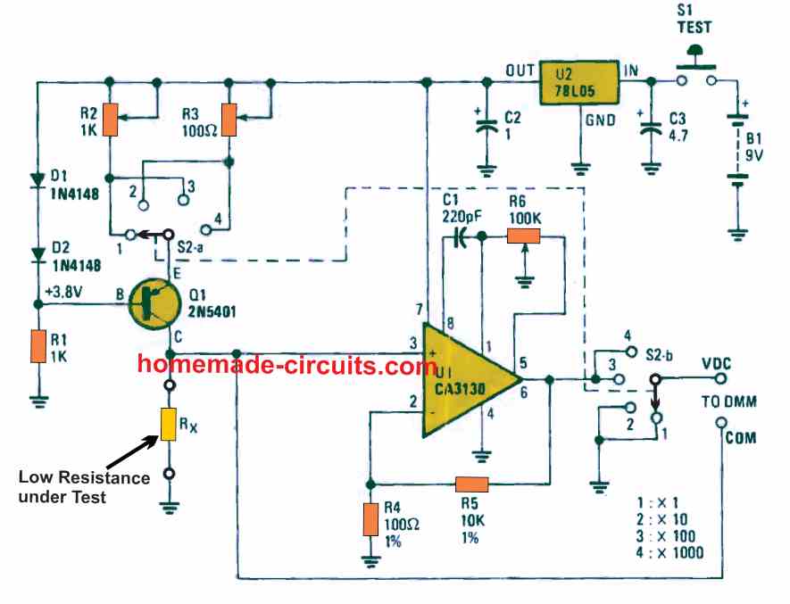 The circuit is powered from a 9 V PP3 battery.
This 9 V output is regulated to +5 volts (DC) by a 78L05 regulator.
The regulation enables a stabilized power supply for the constant current source stage and the opamp.
The balance of the circuit only gets linked with the battery as soon as test-switch S1 is pressed.
The current is used from the battery only during the time the resistance measurement is being tested, which ensures a prolonged battery life.
Constant-current source stage is built using the parts D1, D2, and transistor Q1 along with a 1k resistor R1.
Transistor Q1 is configured in the form of an emitter-follower stage.
Its emitter side terminal follows the voltage applied to its base, with a reduction of around 0.6 volt due to the inherent base-emitter voltage drop.
The Series diodes D1 and D2 maintain the Q1 base at a constant 1.2 volts below the +5 V DC supply line.
This ensures that the Q1 emitter is constantly 0.6 volt lower than the + 5 DC line.
Resistor R1 fixes the current at 5 mA via the two diodes D1 and D2.
This 0.6 V DC generated across one of the multi-turn trimmer potentiometers, R2 or R3, as per the selection by the switch S2-a.
The 0.6 V fixes the current by means of Q1 and the resistor under test, Rx.
In case R2 is selected, the test current becomes 1 mA; with the selection of R3, the test current turns into 10 mA.
Across the a pair of ranges (x 1 and 10) at the bottom, the voltage across the resistance under test, Rx, is executed right to the DMM terminals through the banana plugs.
On thecouple of ranges from the top, the op-amp gain stage (U1) gets switched ON enabling the DMM to read the voltage across the opamp output (pin 6) and provide the measured date for the test resistor, Rx.
The op amp U1, is configured in the form of a non-inverting op amp stage having a constant gain of 1 + 10,000/100 = 101. Since we would like to have a gain of exactly 100, we determine the voltage between the op amp output and the voltage across Rx.
Therefore, if switch S2 is moved to the position 3 (x 100), the current established through the constant-current source turns 1 mA; the multiplying element for Rx will be x100. When S2 is turned to the position 4 (x1000), the current will be 10 mA and the multiplying aspect will be 100 x 10 = 1000. Multi-turn trimmer-potentiometer R6 modifies the offset parameter of the op-amp to ensure that, when there's zero voltage across Rx (meaning, when the measurement probes are short circuited), the output also turns to zero.
The circuit is powered from a 9 V PP3 battery.
This 9 V output is regulated to +5 volts (DC) by a 78L05 regulator.
The regulation enables a stabilized power supply for the constant current source stage and the opamp.
The balance of the circuit only gets linked with the battery as soon as test-switch S1 is pressed.
The current is used from the battery only during the time the resistance measurement is being tested, which ensures a prolonged battery life.
Constant-current source stage is built using the parts D1, D2, and transistor Q1 along with a 1k resistor R1.
Transistor Q1 is configured in the form of an emitter-follower stage.
Its emitter side terminal follows the voltage applied to its base, with a reduction of around 0.6 volt due to the inherent base-emitter voltage drop.
The Series diodes D1 and D2 maintain the Q1 base at a constant 1.2 volts below the +5 V DC supply line.
This ensures that the Q1 emitter is constantly 0.6 volt lower than the + 5 DC line.
Resistor R1 fixes the current at 5 mA via the two diodes D1 and D2.
This 0.6 V DC generated across one of the multi-turn trimmer potentiometers, R2 or R3, as per the selection by the switch S2-a.
The 0.6 V fixes the current by means of Q1 and the resistor under test, Rx.
In case R2 is selected, the test current becomes 1 mA; with the selection of R3, the test current turns into 10 mA.
Across the a pair of ranges (x 1 and 10) at the bottom, the voltage across the resistance under test, Rx, is executed right to the DMM terminals through the banana plugs.
On thecouple of ranges from the top, the op-amp gain stage (U1) gets switched ON enabling the DMM to read the voltage across the opamp output (pin 6) and provide the measured date for the test resistor, Rx.
The op amp U1, is configured in the form of a non-inverting op amp stage having a constant gain of 1 + 10,000/100 = 101. Since we would like to have a gain of exactly 100, we determine the voltage between the op amp output and the voltage across Rx.
Therefore, if switch S2 is moved to the position 3 (x 100), the current established through the constant-current source turns 1 mA; the multiplying element for Rx will be x100. When S2 is turned to the position 4 (x1000), the current will be 10 mA and the multiplying aspect will be 100 x 10 = 1000. Multi-turn trimmer-potentiometer R6 modifies the offset parameter of the op-amp to ensure that, when there's zero voltage across Rx (meaning, when the measurement probes are short circuited), the output also turns to zero.

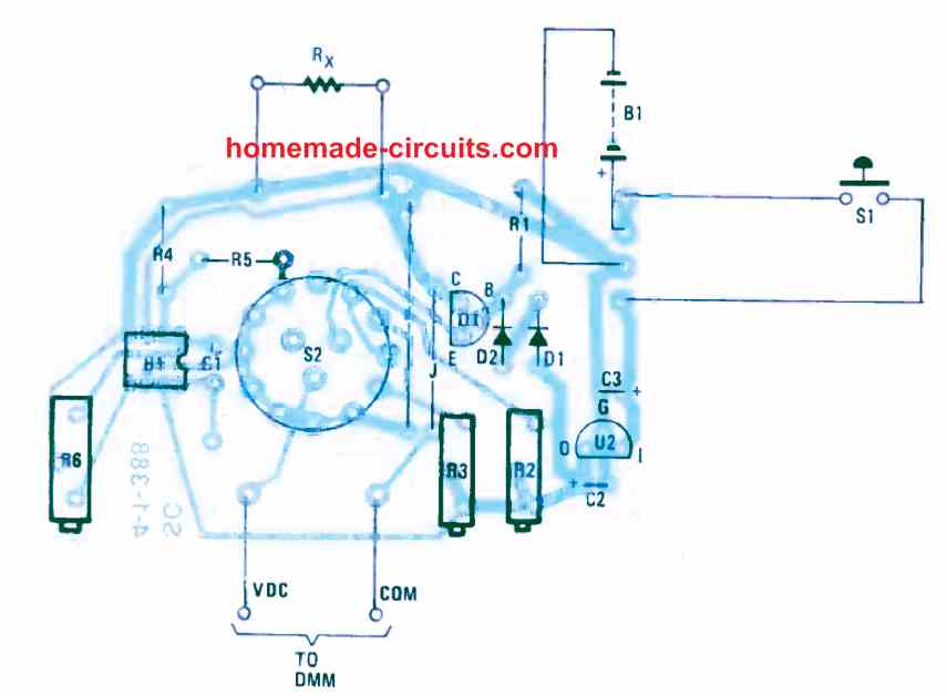
 Best example of static electricity is when we touch a plastic or synthetic material, and feel our hairs getting pulled towards that plastic or synthetic material.
The results of static electricity are well known to many folks since we all have experienced, heard, as well as noticed sparking whenever an high voltage discharge is caused due to a large electrical ground conductor getting close to the high voltage source.
Best example of static electricity is when we touch a plastic or synthetic material, and feel our hairs getting pulled towards that plastic or synthetic material.
The results of static electricity are well known to many folks since we all have experienced, heard, as well as noticed sparking whenever an high voltage discharge is caused due to a large electrical ground conductor getting close to the high voltage source.
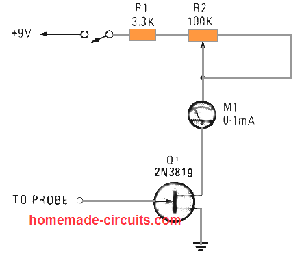 This electrometer is an electrical device that detects and shows the intensity of an electric charge or electrical potential difference.
The circuit can be powered with a 9V battery, and when the probe is brought near a possible electrostatic charged surface, the meter needle will deflect, indicating the presence of the static charge.
The volume of static charge is indicated over an ammeter and the JFET could be a 2N3814 or similar.
The meter can be a 0-1 mA device; in case you find this type of meter is not adequately sensitive to suit your needs, it is possible to replace it with a more sensitive low current meter.
The potentiometer is tweaked in order that the needle indicates 1 mA in the absence of a static charge around the probe.
As soon as the probe is introduced sufficiently near to a charge, the meter needle must decrease towards 0 mA.
To examine whether or not your CMOS device storage box may be devoid of static charge, touch the electrometer probe directly into box.
If you find the meter needle unmoved from the full scale 1 mA level, you can be assured that the box is free from static electricity.
This electrometer is an electrical device that detects and shows the intensity of an electric charge or electrical potential difference.
The circuit can be powered with a 9V battery, and when the probe is brought near a possible electrostatic charged surface, the meter needle will deflect, indicating the presence of the static charge.
The volume of static charge is indicated over an ammeter and the JFET could be a 2N3814 or similar.
The meter can be a 0-1 mA device; in case you find this type of meter is not adequately sensitive to suit your needs, it is possible to replace it with a more sensitive low current meter.
The potentiometer is tweaked in order that the needle indicates 1 mA in the absence of a static charge around the probe.
As soon as the probe is introduced sufficiently near to a charge, the meter needle must decrease towards 0 mA.
To examine whether or not your CMOS device storage box may be devoid of static charge, touch the electrometer probe directly into box.
If you find the meter needle unmoved from the full scale 1 mA level, you can be assured that the box is free from static electricity.
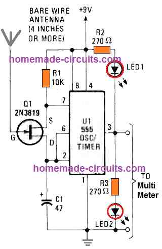 To verify if your IC 555 static charge detector actually works, try bringing the antenna very near to a television screen and you may quickly start seeing the LED flashing slowing down.
In order to reset the circuit, just short the antenna wire of the circuit to any ground wire of the circuit or a large metal plate, a few instances.
This must get the LED flash rate back to fast rate, which is the normal rate in the absence of a static charge.
You can use this LED electrometer with a multi-meter for higher precision readings.
The circuit really is easy, it is extremely sensitive to excessive voltages, it can easily help you save a ton of money, all the elements are accessible at the local Radio Shack store.
The current consumption is so small that the circuit can easily work for a few hours without showing any abnormal effects.
To verify if your IC 555 static charge detector actually works, try bringing the antenna very near to a television screen and you may quickly start seeing the LED flashing slowing down.
In order to reset the circuit, just short the antenna wire of the circuit to any ground wire of the circuit or a large metal plate, a few instances.
This must get the LED flash rate back to fast rate, which is the normal rate in the absence of a static charge.
You can use this LED electrometer with a multi-meter for higher precision readings.
The circuit really is easy, it is extremely sensitive to excessive voltages, it can easily help you save a ton of money, all the elements are accessible at the local Radio Shack store.
The current consumption is so small that the circuit can easily work for a few hours without showing any abnormal effects.
 The tester features 5 testing slots in close proximity with each other, determined by their respective labeling:
E/S - B/G - C/D - E/S - B/G
This arrangement makes it possible for the below shown devices to be examined through the mentioned configurations:
Bipolar Transistors: EBC / BCE / CEB, and reversed: BEC / ECB / CBE.
Unipolar Transistors (FETs): SGD / GDS / DSG, and reversed: GSD / SDG / DGS.
The astable multivibrator stage of the circuit oscillates and blinks a bright white LED (Figure 1) whenever the transistor under test is connected the right way.
The LED could also flash if the E and C pins of the transistor are swapped, however the blinking speed is going to be faster.
This demonstrates the truth that a few varieties of BJTs can function even when their emitter and collector leads interchanged although with a performance characteristics that may be lower than in the normal configuration.
The tester features 5 testing slots in close proximity with each other, determined by their respective labeling:
E/S - B/G - C/D - E/S - B/G
This arrangement makes it possible for the below shown devices to be examined through the mentioned configurations:
Bipolar Transistors: EBC / BCE / CEB, and reversed: BEC / ECB / CBE.
Unipolar Transistors (FETs): SGD / GDS / DSG, and reversed: GSD / SDG / DGS.
The astable multivibrator stage of the circuit oscillates and blinks a bright white LED (Figure 1) whenever the transistor under test is connected the right way.
The LED could also flash if the E and C pins of the transistor are swapped, however the blinking speed is going to be faster.
This demonstrates the truth that a few varieties of BJTs can function even when their emitter and collector leads interchanged although with a performance characteristics that may be lower than in the normal configuration.
 A low volume buzzing sound from the buzzer signifies that the transistor is rightly inserted and is perfectly doing the job.
If there's no sound from the buzzer indicates that the BJT or the FET under test is either inserted incorrectly or it may be completely dead.
The push button allows you to switch the circuit on and check the transistor simultaneously as soon as it is hooked up.
The entire circuit can without any difficulty accommodate over a tiny piece of veroboard.
Power supply can be obtained from a standard 9 V PP3 battery.
A low volume buzzing sound from the buzzer signifies that the transistor is rightly inserted and is perfectly doing the job.
If there's no sound from the buzzer indicates that the BJT or the FET under test is either inserted incorrectly or it may be completely dead.
The push button allows you to switch the circuit on and check the transistor simultaneously as soon as it is hooked up.
The entire circuit can without any difficulty accommodate over a tiny piece of veroboard.
Power supply can be obtained from a standard 9 V PP3 battery.
 Figure 2 exhibits the circuit diagram for the clock oscillator, an low Hz oscillator, logic controller, and monostable multivibrator stages of the LED capacitance meter circuit.
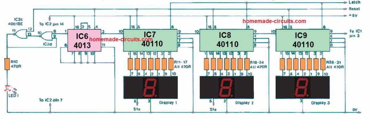 The counter/driver and overflow circuit stages are shown in the next Figure above.
Looking at the Figure 2, IC5 is a 5 volt fixed voltage regulator that provides a nicely regulated 5 volt output from the 9 volt battery source.
The entire circuit uses this regulated 5 volt power for the functioning.
The battery should be of a high mAh rating since the current usage of the circuit is fairly large at around 85 mA.
The current consumption could go beyond 100 mA whenever most of the digits of the 3-display are being illuminated for the displaying.
The low frequency oscillator is built around the IC2a and IC2b that are CMOS NOR gates.
Nevertheless, in this particular circuit these ICs are connected as basic inverters and applied through normal CMOS astable setup.
Observe that the working frequency of the oscillator stage is a lot bigger compared to the frequency with which the readings are provided, because this oscillator has to generate 10 output cycles for enabling the completion of a single reading cycle.
IC3 and IC4a are configured as the control logic stage.
IC3 which is a CMOS 4017 decoder/counter, includes 10 outputs ('0' to '9').
Each of these outputs go high, in succession, for every single consecutive input clock cycle.
In this particular design output '0' supplies the reset clock to the counters.
Output '1' subsequently becomes high and toggles the monostable which produces the gate pulse for the clock/counter circuit.
Outputs '2' to '8' are unconnected, and the time interval throughout which these 2 outputs turn high enables a little bit of time so that the the gate pulse can complete and to allow the counting to become over.
Output '9' supplies the logic signal which latches the new reading over the LED display, however this logic needs to a negative one.
This is accomplished with IC4a which inverts the signal from output 9 so that it translates into a appropriate pulse.
The monostable multivibrator is a a standard CMOS version using a couple of 2 input NOR gates (IC4b and IC4c).
Despite being a simple monostable design, it offers features that make it perfectly worthy of the current application.
This is a non-retriggerable form, and as a result provides an output pulse which is smaller than the trigger pulse generated from IC3. This function is actually critical, because when a retriggerable type is used the least display reading could be fairly high.
The proposed design's self capacitance is pretty minimal, which is essential since a substantial degree of local capacitance could disturb the circuit linear attribute, resulting in a huge lowest display reading.
While using, the prototype display could be seen with reading '000' across all 5 ranges when there's no capacitor connected across testing slots.
Resistors R5 to R9 function as range selection resistors.
When you decrease the timing resistance across decade steps, the timing capacitance required for a particular reading gets increased in the decade increments.
If we consider that the range resistors are rated with tolerance of at least 1%, this set up can be expected to deliver reliable readings.
This means, it may not be necessary for each range to be calibrated separately.
R1 and S1a are wired to run the decimal point segment on the correct LED display, except for the Range 3 (999nF) in which a decimal point indication is not necessary.
The clock oscillator is actually a common 555 astable configuration.
Pot RV1 is used as the clock frequency controller, for calibrating this LED capacitance meter.
The monostable output is used for controlling the pin 4 of IC 1, and the clock oscillator will be activated only while the gate period is available.
This function eliminates the demand for a independent signal gate.
Now checking the Figure 3, we find that the counter circuit is wired using 3 CMOS 4011 ICs.
These are actually not recognized from the ideal CMOS logic family, nevertheless these are extremely flexible elements that are worthy of frequent consumption.
These are actually configured as up/down counters having individual clock inputs and carry/borrow outputs.
As can be understood, the potential to use in the down counter mode is meaningless here, the down clock input is therefore hooked with the negative supply line.
The three counters are connected in sequence to allow a conventional 3 digit display.
Here, IC9 is wired to generate the least significant digit and IC7 enables the most significant digit.
The 4011 includes a decade counter, a seven segment decoder, and a latch/display driver stages.
Every single IC could for that reason substitute a typical 3 chip TTL style counter/driver/latch option.
The outputs have enough power to directly illuminate any appropriate common cathode seven segment LED display.
Despite of a low voltage supply of 5 volts it is recommended to drive every single LED display segment through a current limiting resistor so that the current consumption of the entire caapcitance meter unit can be kept below an acceptable level.
The IC7's 'carry' output is applied to the IC6 clock input, that is a dual D type divide by two flip/flop.
However in this particular circuit just one portion of the IC is implemented.
The IC6 output will switch state only when there's an overload.
This implies, if the overload is significantly high will result in many output cycles from IC7.
Directly powering the LED indicator LED1 through IC6 could be quite inappropriate, because this output can be momentary and the LED may possibly be able to generate just a couple of short illuminations that could be easily go unnoticed.
In order to avoid this situation the IC7 output is used to drive a basic set/reset bistable circuit created by wiring a pair of normally empty gates of IC2, and subsequently the latch switches the LED indicator LED1. The two IC6 and the latch are reset by IC3 in order that the overflow circuit commences from scratch whenever a new test reading is implemented.
The counter/driver and overflow circuit stages are shown in the next Figure above.
Looking at the Figure 2, IC5 is a 5 volt fixed voltage regulator that provides a nicely regulated 5 volt output from the 9 volt battery source.
The entire circuit uses this regulated 5 volt power for the functioning.
The battery should be of a high mAh rating since the current usage of the circuit is fairly large at around 85 mA.
The current consumption could go beyond 100 mA whenever most of the digits of the 3-display are being illuminated for the displaying.
The low frequency oscillator is built around the IC2a and IC2b that are CMOS NOR gates.
Nevertheless, in this particular circuit these ICs are connected as basic inverters and applied through normal CMOS astable setup.
Observe that the working frequency of the oscillator stage is a lot bigger compared to the frequency with which the readings are provided, because this oscillator has to generate 10 output cycles for enabling the completion of a single reading cycle.
IC3 and IC4a are configured as the control logic stage.
IC3 which is a CMOS 4017 decoder/counter, includes 10 outputs ('0' to '9').
Each of these outputs go high, in succession, for every single consecutive input clock cycle.
In this particular design output '0' supplies the reset clock to the counters.
Output '1' subsequently becomes high and toggles the monostable which produces the gate pulse for the clock/counter circuit.
Outputs '2' to '8' are unconnected, and the time interval throughout which these 2 outputs turn high enables a little bit of time so that the the gate pulse can complete and to allow the counting to become over.
Output '9' supplies the logic signal which latches the new reading over the LED display, however this logic needs to a negative one.
This is accomplished with IC4a which inverts the signal from output 9 so that it translates into a appropriate pulse.
The monostable multivibrator is a a standard CMOS version using a couple of 2 input NOR gates (IC4b and IC4c).
Despite being a simple monostable design, it offers features that make it perfectly worthy of the current application.
This is a non-retriggerable form, and as a result provides an output pulse which is smaller than the trigger pulse generated from IC3. This function is actually critical, because when a retriggerable type is used the least display reading could be fairly high.
The proposed design's self capacitance is pretty minimal, which is essential since a substantial degree of local capacitance could disturb the circuit linear attribute, resulting in a huge lowest display reading.
While using, the prototype display could be seen with reading '000' across all 5 ranges when there's no capacitor connected across testing slots.
Resistors R5 to R9 function as range selection resistors.
When you decrease the timing resistance across decade steps, the timing capacitance required for a particular reading gets increased in the decade increments.
If we consider that the range resistors are rated with tolerance of at least 1%, this set up can be expected to deliver reliable readings.
This means, it may not be necessary for each range to be calibrated separately.
R1 and S1a are wired to run the decimal point segment on the correct LED display, except for the Range 3 (999nF) in which a decimal point indication is not necessary.
The clock oscillator is actually a common 555 astable configuration.
Pot RV1 is used as the clock frequency controller, for calibrating this LED capacitance meter.
The monostable output is used for controlling the pin 4 of IC 1, and the clock oscillator will be activated only while the gate period is available.
This function eliminates the demand for a independent signal gate.
Now checking the Figure 3, we find that the counter circuit is wired using 3 CMOS 4011 ICs.
These are actually not recognized from the ideal CMOS logic family, nevertheless these are extremely flexible elements that are worthy of frequent consumption.
These are actually configured as up/down counters having individual clock inputs and carry/borrow outputs.
As can be understood, the potential to use in the down counter mode is meaningless here, the down clock input is therefore hooked with the negative supply line.
The three counters are connected in sequence to allow a conventional 3 digit display.
Here, IC9 is wired to generate the least significant digit and IC7 enables the most significant digit.
The 4011 includes a decade counter, a seven segment decoder, and a latch/display driver stages.
Every single IC could for that reason substitute a typical 3 chip TTL style counter/driver/latch option.
The outputs have enough power to directly illuminate any appropriate common cathode seven segment LED display.
Despite of a low voltage supply of 5 volts it is recommended to drive every single LED display segment through a current limiting resistor so that the current consumption of the entire caapcitance meter unit can be kept below an acceptable level.
The IC7's 'carry' output is applied to the IC6 clock input, that is a dual D type divide by two flip/flop.
However in this particular circuit just one portion of the IC is implemented.
The IC6 output will switch state only when there's an overload.
This implies, if the overload is significantly high will result in many output cycles from IC7.
Directly powering the LED indicator LED1 through IC6 could be quite inappropriate, because this output can be momentary and the LED may possibly be able to generate just a couple of short illuminations that could be easily go unnoticed.
In order to avoid this situation the IC7 output is used to drive a basic set/reset bistable circuit created by wiring a pair of normally empty gates of IC2, and subsequently the latch switches the LED indicator LED1. The two IC6 and the latch are reset by IC3 in order that the overflow circuit commences from scratch whenever a new test reading is implemented.
 The Transistors Under Test (TUTs) are subjected to a triangular wave-shape.
The discrepancies between their collector voltages are identified by a pair of comparators and indicated by the LEDs.
That is the whole concept.
In practical terms, the two BJTs under test are powered by identical control voltages, as displayed in Figure 1.
However, we find that their collector resistance is fairly dissimilar.
R2a and R2b are somewhat larger in resistance compared to R1, but R2a as a single unit has a smaller value than R1. This is the whole setup of the sampling circuit.
LetˇŻs say the two transistors under test are exactly the same in terms of the UBE and HFE.
The upward moving slope of the input voltage will turn both of them on simultaneously and consequently their collector voltages will fall.
Here, if the above situation is paused, we would observe that the second transistorˇŻs collector voltage is a tad lower than the first transistor because the whole collector resistance is larger.
Because R2a has a lower resistance than R1, the potential at the junction of R2a/R2b will be marginally larger as opposed to the collector of transistor 1.
So, the ˇ°+ˇ± input of comparator 1 will be positively charged against its ˇ°-ˇ± input.
That shows the output of K1 will be ON and LED D1 will not illuminate.
At the same time, the ˇ°+ˇ± input of K2 will be negatively charged against its ˇ°-ˇ± and due to that the output will be OFF and LED D3 will also remain shut off.
When K1ˇŻs output is ON and K2 is OFF, D2 will be switched ON to show both transistors are exactly the same and are matched.
LetˇŻs look if TUT1 has a smaller UBE and/or a larger HFE than TUT2. At the rising edge of the triangular signal, the collector voltage of TUT1 will fall quicker than the collector voltage of TUT2.
Then, comparator K1 will respond the same way and the ˇ°+ˇ± input will be positively charged against the ˇ°-ˇ± input, and consequently, its output will be high.
Because the low collector voltage of TUT1 is linked to the ˇ°-ˇ± input of K2, it will be smaller than the ˇ°+ˇ± input which is attached to the collector of TUT2.
As a result, the output of K2 starts rising.
Due to the two high outputs of comparators, D1 fails to illuminate.
Because D2 is linked like D1 and between two high levels, it will not be lit either.
Both these conditions cause D3 to illuminate and thus conclude that the gain of TUT1 is superior to TUT2.
In the event TUT2 gain is identified as the better of the two transistors, this results in the collector voltage to drop more quickly.
Therefore, the voltages at the collector and the R2a/R2b junction will be smaller compared to the collector voltage of TUT1.
Conclusively, a low signal of the ˇ°+ˇ± inputs of the comparators will switch to low with respect to the ˇ°-ˇ± input allowing the two outputs to be low.
Due to that, LEDs, D2 and D3 will not light up, but only D1 will be illuminated at this point, which signals that TUT2 has a better gain than TUT1.
The Transistors Under Test (TUTs) are subjected to a triangular wave-shape.
The discrepancies between their collector voltages are identified by a pair of comparators and indicated by the LEDs.
That is the whole concept.
In practical terms, the two BJTs under test are powered by identical control voltages, as displayed in Figure 1.
However, we find that their collector resistance is fairly dissimilar.
R2a and R2b are somewhat larger in resistance compared to R1, but R2a as a single unit has a smaller value than R1. This is the whole setup of the sampling circuit.
LetˇŻs say the two transistors under test are exactly the same in terms of the UBE and HFE.
The upward moving slope of the input voltage will turn both of them on simultaneously and consequently their collector voltages will fall.
Here, if the above situation is paused, we would observe that the second transistorˇŻs collector voltage is a tad lower than the first transistor because the whole collector resistance is larger.
Because R2a has a lower resistance than R1, the potential at the junction of R2a/R2b will be marginally larger as opposed to the collector of transistor 1.
So, the ˇ°+ˇ± input of comparator 1 will be positively charged against its ˇ°-ˇ± input.
That shows the output of K1 will be ON and LED D1 will not illuminate.
At the same time, the ˇ°+ˇ± input of K2 will be negatively charged against its ˇ°-ˇ± and due to that the output will be OFF and LED D3 will also remain shut off.
When K1ˇŻs output is ON and K2 is OFF, D2 will be switched ON to show both transistors are exactly the same and are matched.
LetˇŻs look if TUT1 has a smaller UBE and/or a larger HFE than TUT2. At the rising edge of the triangular signal, the collector voltage of TUT1 will fall quicker than the collector voltage of TUT2.
Then, comparator K1 will respond the same way and the ˇ°+ˇ± input will be positively charged against the ˇ°-ˇ± input, and consequently, its output will be high.
Because the low collector voltage of TUT1 is linked to the ˇ°-ˇ± input of K2, it will be smaller than the ˇ°+ˇ± input which is attached to the collector of TUT2.
As a result, the output of K2 starts rising.
Due to the two high outputs of comparators, D1 fails to illuminate.
Because D2 is linked like D1 and between two high levels, it will not be lit either.
Both these conditions cause D3 to illuminate and thus conclude that the gain of TUT1 is superior to TUT2.
In the event TUT2 gain is identified as the better of the two transistors, this results in the collector voltage to drop more quickly.
Therefore, the voltages at the collector and the R2a/R2b junction will be smaller compared to the collector voltage of TUT1.
Conclusively, a low signal of the ˇ°+ˇ± inputs of the comparators will switch to low with respect to the ˇ°-ˇ± input allowing the two outputs to be low.
Due to that, LEDs, D2 and D3 will not light up, but only D1 will be illuminated at this point, which signals that TUT2 has a better gain than TUT1.
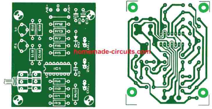
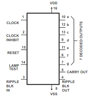 A high logic on the RESET pin restores the decade counter to its intial zero display position.
The counter is designed to move by a single count in response to the positive clock freqeuncy input when the CLOCK INHIBIT signal is provided with a low logic supply.
Counter progression by means of the clock rail is prevented and stopped as soon as the CLOCK INHIBIT is applied with a HIGH logic input.
The CLOCK INHIBIT logic input could be applied as a negative-edge clock in case the clock line is applied with logic high.
Antilock gating is offered within the JOHNSON counter, which ensures correct sequencing for the counting process.
The CARRY-OUT (Cout) signal finishes a single cycle every ten CLOCK INPUT cycles and it is implemented to clock the next up decade instantly in a multi-decade counting chain.
The seven decoded outputs (a, b, c, d, e, f, g) light up the appropriate sections in a 7-segment display module intended for addressing the decimal figures 0 to 9.
A high logic on the RESET pin restores the decade counter to its intial zero display position.
The counter is designed to move by a single count in response to the positive clock freqeuncy input when the CLOCK INHIBIT signal is provided with a low logic supply.
Counter progression by means of the clock rail is prevented and stopped as soon as the CLOCK INHIBIT is applied with a HIGH logic input.
The CLOCK INHIBIT logic input could be applied as a negative-edge clock in case the clock line is applied with logic high.
Antilock gating is offered within the JOHNSON counter, which ensures correct sequencing for the counting process.
The CARRY-OUT (Cout) signal finishes a single cycle every ten CLOCK INPUT cycles and it is implemented to clock the next up decade instantly in a multi-decade counting chain.
The seven decoded outputs (a, b, c, d, e, f, g) light up the appropriate sections in a 7-segment display module intended for addressing the decimal figures 0 to 9.
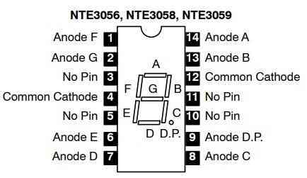
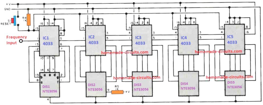 The design is basically the identical repetition of 5 pulse counter stages comprising of IC1 and the DIS1 in a sequentially cascaded format.
It must be note that DIS2 is the only display module which has an active decimal point.
This decimal point illuminates as soon as the supply to the circuit is switched ON.
The frequency or the pulse which needs to be counted and displayed over the 7-segment displays is applied to the pin#1 of IC1.
As soon as the frequency is applied, the displays begin showing the number of elapsed pulses of the frequency.
If the frequency input is removed, the count over the display will get latched and remain available until the switch S1 is pressed, or the power is switched OFF and ON again.
The design is basically the identical repetition of 5 pulse counter stages comprising of IC1 and the DIS1 in a sequentially cascaded format.
It must be note that DIS2 is the only display module which has an active decimal point.
This decimal point illuminates as soon as the supply to the circuit is switched ON.
The frequency or the pulse which needs to be counted and displayed over the 7-segment displays is applied to the pin#1 of IC1.
As soon as the frequency is applied, the displays begin showing the number of elapsed pulses of the frequency.
If the frequency input is removed, the count over the display will get latched and remain available until the switch S1 is pressed, or the power is switched OFF and ON again.
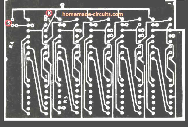
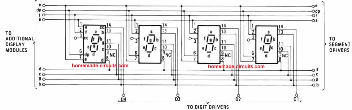 The frequency from the crystal is additionally divided to generate a short "store" pulse on pin 2 of U2, which is followed by a brief "reset" pulse on pin 14 of U2 (after around 0.4 milliseconds).
The pulse frequency is established by the state of the pin 11 of U2.
As soon as U2 pin 11 is switched to ground via S1, the pulses repeat every 2 seconds and result in U2 pin 13 to turn high for a single second.
This inhibits further input signals from getting into U1. This leads to the U1's latched counts in the internal counters to be sent to the display module.
Pin13 of the IC U2 subsequently turns low for a single second, permitting a fresh count to be inserted into the U1's seven decade counters.
That period is repeated, continually changing the display every 2 seconds.
When pin 11 of U2 is switched to the positive voltage ( + 5V), the "store" and "reset" pulses begin to happen at 0.2 second time periods, creating a 0.1 second count time period.
It requires 10 input pulses to be counted to ensure that a '1" comes on the first digit, D1, therefore the frequency which is tested is apparently 10 times bigger than the frequency which is displayed on the 7 segment module.
In this setting, the decimal points are powered by R1 and visually suggest that the 0.- second count period has been applied.
The frequency from the crystal is additionally divided to generate a short "store" pulse on pin 2 of U2, which is followed by a brief "reset" pulse on pin 14 of U2 (after around 0.4 milliseconds).
The pulse frequency is established by the state of the pin 11 of U2.
As soon as U2 pin 11 is switched to ground via S1, the pulses repeat every 2 seconds and result in U2 pin 13 to turn high for a single second.
This inhibits further input signals from getting into U1. This leads to the U1's latched counts in the internal counters to be sent to the display module.
Pin13 of the IC U2 subsequently turns low for a single second, permitting a fresh count to be inserted into the U1's seven decade counters.
That period is repeated, continually changing the display every 2 seconds.
When pin 11 of U2 is switched to the positive voltage ( + 5V), the "store" and "reset" pulses begin to happen at 0.2 second time periods, creating a 0.1 second count time period.
It requires 10 input pulses to be counted to ensure that a '1" comes on the first digit, D1, therefore the frequency which is tested is apparently 10 times bigger than the frequency which is displayed on the 7 segment module.
In this setting, the decimal points are powered by R1 and visually suggest that the 0.- second count period has been applied.
 The following article explains a very simple two-transistor metal detector that you can assemble in an afternoon or two and have fun with using for hours at a stretch.
The circuit shown below possibly will not find you a mine of gold, or any other treasure for example.
Nonetheless, it can help discover cabling and embedded nails in the walls, or metal pipes under the floor, and will cost you hardly anything to construct.
The following article explains a very simple two-transistor metal detector that you can assemble in an afternoon or two and have fun with using for hours at a stretch.
The circuit shown below possibly will not find you a mine of gold, or any other treasure for example.
Nonetheless, it can help discover cabling and embedded nails in the walls, or metal pipes under the floor, and will cost you hardly anything to construct.
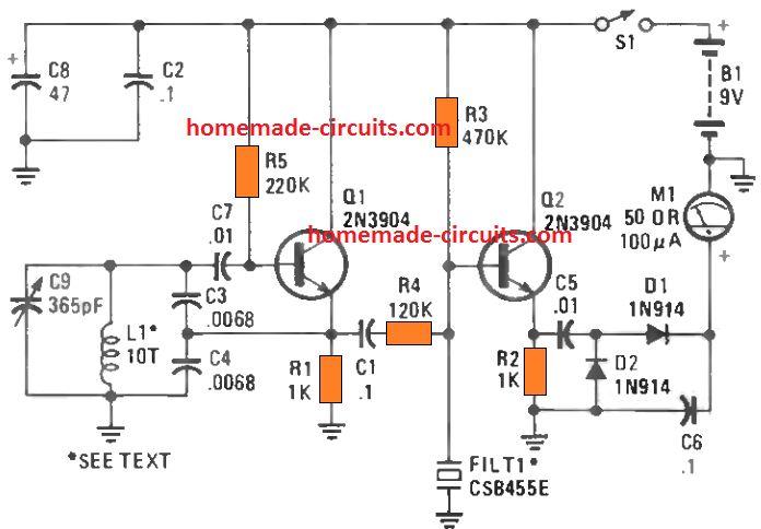 The oscillator's output is extracted via capacitor C1 and R4 and sent to to a 455-kHz ceramic filter.
 455 kHz ceramic filter
As soon as the oscillator gets tuned to the filter's center frequency, the filter starts operating like a parallel tuned circuit and begins generating a high level 455 kHz signal at the junction of R3 and R4.
This tuned 455-kHz signal is then applied to the transistor Q2, set up as an emitter follower.
The signal output from Q2 (acquired from its emitter pin) is subsequently transformed to DC through rectifier diode D1,
After this, the frequency is fed to the indicator meter M1 (a 50- to 100-uA meter).
The oscillator stage being tuned at extremely close to the the filter's center frequency, the meter shows the reading anywhere near mid-way of the scale.
However, as soon as any kind of metal object bigger than a BB (7mm) comes close to the loop, the meter's reading might show either a improvement or reduction, according to the specifications of metal.
The stud finder circuit will identify anything from a penny a couple of inches away or a D-cell battery at around 5 inches on ground surface.
455 kHz ceramic filter
As soon as the oscillator gets tuned to the filter's center frequency, the filter starts operating like a parallel tuned circuit and begins generating a high level 455 kHz signal at the junction of R3 and R4.
This tuned 455-kHz signal is then applied to the transistor Q2, set up as an emitter follower.
The signal output from Q2 (acquired from its emitter pin) is subsequently transformed to DC through rectifier diode D1,
After this, the frequency is fed to the indicator meter M1 (a 50- to 100-uA meter).
The oscillator stage being tuned at extremely close to the the filter's center frequency, the meter shows the reading anywhere near mid-way of the scale.
However, as soon as any kind of metal object bigger than a BB (7mm) comes close to the loop, the meter's reading might show either a improvement or reduction, according to the specifications of metal.
The stud finder circuit will identify anything from a penny a couple of inches away or a D-cell battery at around 5 inches on ground surface.
 4-inch pipe end cap
This is constructed by putting 10 tightly wound turns using 26 SWG super enamel copper wire.
This should be wound across the bottom part of the end cap and then fixed firmly using cello tape adhesive in place.
The circuit components could be assembled on a veroboard and should be encased inside a metallic box.
Capacitor C9 could be just about any variable capacitor which you can salvage from and old radio.
4-inch pipe end cap
This is constructed by putting 10 tightly wound turns using 26 SWG super enamel copper wire.
This should be wound across the bottom part of the end cap and then fixed firmly using cello tape adhesive in place.
The circuit components could be assembled on a veroboard and should be encased inside a metallic box.
Capacitor C9 could be just about any variable capacitor which you can salvage from and old radio.
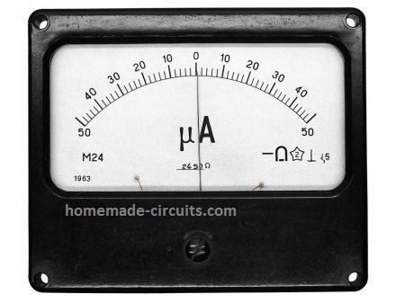
 The logic probe circuit is built using inverter/buffer gates from a single IC 4049.
3 gates are used for making the main logic high/low detector circuit, while two are employed to form monostable multivibrator circuit.
The probe tip which detects the logic levels is connected with the gate IC1c through resistor R9.
When an input logic high or logic 1 is detected, the IC1c output turns low, causing the LEd2 to light up.
Likewise, when a LOW or logic 0 is detected at the input probe, the series pair IC1 e and IC1f light up LED1 via R4.
For "floating" input levels, meaning when the logic probe is not connected to anything, the resistors R1, R2, R3 make sure that the IC1c and IC1f are together held in the logic HIGH position.
Capacitor C1 attcahed across R2 works like a rapid action capacitor, which ensures that the pulse shape at the input of IC1e is sharp, allowing the probe to assess and track even the high frequency logic inputs over 1 MHz.
The monostable circuit created around IC1a and IC1b boost the pulses that are short (below 500 nsec) to 15 msec (0.7RC) with the aid of C3 and R8.
The input to the monostable is obtained from IC1c, while C2 provides the stage with the required isolation from the DC content.
In normal situations, the parts R7 and D1 enable the IC1b input to stay at a logic HIGH.
However, when a negative edged pulse is detected via C2, the IC1b output is turned HIGH, forcing the IC1a output to become low and switch ON LED3.
Diode D1 makes sure that the IC1b input remains at a low logic level (over 0.7V), onle as long as the IC1a output stays low.
The above action inhibit repetitive pulses from re-triggering the input of IC1b, until the monostable is retriggered due to the discharging of C3 across earth via R8. This enables IC1a output to become logic high, turning OFF LED3.
The capacitors C4, and C5 which are not critical, safeguards the IC supply lines from possible voltage spikes and transients, emanating from the circuit under test.
The logic probe circuit is built using inverter/buffer gates from a single IC 4049.
3 gates are used for making the main logic high/low detector circuit, while two are employed to form monostable multivibrator circuit.
The probe tip which detects the logic levels is connected with the gate IC1c through resistor R9.
When an input logic high or logic 1 is detected, the IC1c output turns low, causing the LEd2 to light up.
Likewise, when a LOW or logic 0 is detected at the input probe, the series pair IC1 e and IC1f light up LED1 via R4.
For "floating" input levels, meaning when the logic probe is not connected to anything, the resistors R1, R2, R3 make sure that the IC1c and IC1f are together held in the logic HIGH position.
Capacitor C1 attcahed across R2 works like a rapid action capacitor, which ensures that the pulse shape at the input of IC1e is sharp, allowing the probe to assess and track even the high frequency logic inputs over 1 MHz.
The monostable circuit created around IC1a and IC1b boost the pulses that are short (below 500 nsec) to 15 msec (0.7RC) with the aid of C3 and R8.
The input to the monostable is obtained from IC1c, while C2 provides the stage with the required isolation from the DC content.
In normal situations, the parts R7 and D1 enable the IC1b input to stay at a logic HIGH.
However, when a negative edged pulse is detected via C2, the IC1b output is turned HIGH, forcing the IC1a output to become low and switch ON LED3.
Diode D1 makes sure that the IC1b input remains at a low logic level (over 0.7V), onle as long as the IC1a output stays low.
The above action inhibit repetitive pulses from re-triggering the input of IC1b, until the monostable is retriggered due to the discharging of C3 across earth via R8. This enables IC1a output to become logic high, turning OFF LED3.
The capacitors C4, and C5 which are not critical, safeguards the IC supply lines from possible voltage spikes and transients, emanating from the circuit under test.
 The LED indicate 3 different conditions of the input logic voltage levels.
The resistors R1, R2, R3 work like resistive dividers, which help to determine the various voltage levels at the input probe.
A potential higher than 3 V causes the output of IC1 A to go low, switching ON the "HIGH" LED.
When the input logic potential is less than 0.8 V, the IC1 B output becomes low causing the D2 to light up.
In case when the probe level is floating or is not connected to any voltage, causes the "FLOAT" LED to illuminate.
When a frequency is detected at the input, turns on both the "HIGH" and the "LOW" LEDs, which indicate the presence of an oscillating frequency at the input.
From the above explanation we can understand that it is possible to tweak the detection levels of the input logic voltages simply by tweaking the values of R1, R2, or R3, appropriately.
Since the IC LM339 can be work with supply inputs up to 36 V means this logic probe is not restricted to TTL ICs only, rather can be used for testing logic circuits right from 3 V to 36 V.
The LED indicate 3 different conditions of the input logic voltage levels.
The resistors R1, R2, R3 work like resistive dividers, which help to determine the various voltage levels at the input probe.
A potential higher than 3 V causes the output of IC1 A to go low, switching ON the "HIGH" LED.
When the input logic potential is less than 0.8 V, the IC1 B output becomes low causing the D2 to light up.
In case when the probe level is floating or is not connected to any voltage, causes the "FLOAT" LED to illuminate.
When a frequency is detected at the input, turns on both the "HIGH" and the "LOW" LEDs, which indicate the presence of an oscillating frequency at the input.
From the above explanation we can understand that it is possible to tweak the detection levels of the input logic voltages simply by tweaking the values of R1, R2, or R3, appropriately.
Since the IC LM339 can be work with supply inputs up to 36 V means this logic probe is not restricted to TTL ICs only, rather can be used for testing logic circuits right from 3 V to 36 V.
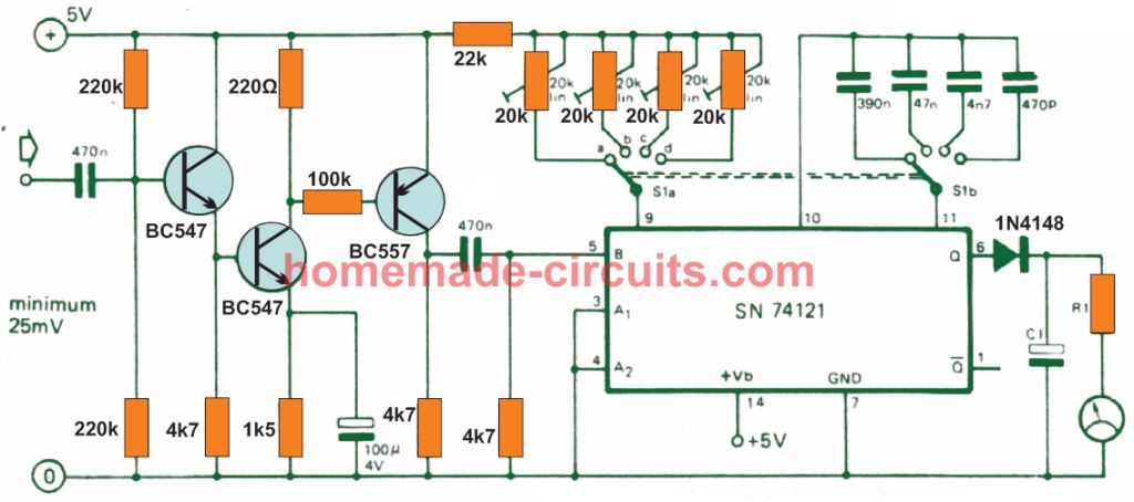 Referring to the circuit diagram of the simple frequency meter, 3 BJTs at the input side work like voltage amplifier for amplifying the low voltage frequency into a 5 V rectangular waves, to feed the input of the IC SN74121
The IC SN74121 is a monostable multivibrator with Schmitt-trigger inputs, which allows the input frequency to be processed into a correctly dimensioned one-shot pulses, whose average value directly depends on the frequency of the input signal.
The diodes and R1, C1 network at the output pin of the IC work like an integrator for converting the vibrating output of the monostable into a reasonably stable DC whose value is directly proportional to the frequency of the input signal.
Hence, as the input frequency rises, the value of the output voltage also rises proportionately, which is interpreted by a corresponding deflection on the meter, and provides a direct reading of the frequency.
The R/C components associated with the S1 selector switch determines the monostable one-shot ON/OFF timing, and this in turn decides the range for which the timing becomes most suitable, to ensure a matching range on the meter and minimum vibration on the meter needle.
Referring to the circuit diagram of the simple frequency meter, 3 BJTs at the input side work like voltage amplifier for amplifying the low voltage frequency into a 5 V rectangular waves, to feed the input of the IC SN74121
The IC SN74121 is a monostable multivibrator with Schmitt-trigger inputs, which allows the input frequency to be processed into a correctly dimensioned one-shot pulses, whose average value directly depends on the frequency of the input signal.
The diodes and R1, C1 network at the output pin of the IC work like an integrator for converting the vibrating output of the monostable into a reasonably stable DC whose value is directly proportional to the frequency of the input signal.
Hence, as the input frequency rises, the value of the output voltage also rises proportionately, which is interpreted by a corresponding deflection on the meter, and provides a direct reading of the frequency.
The R/C components associated with the S1 selector switch determines the monostable one-shot ON/OFF timing, and this in turn decides the range for which the timing becomes most suitable, to ensure a matching range on the meter and minimum vibration on the meter needle.
 An improved version of the first Frequency Meter circuit diagram is displayed in the above figure.
The TR1 input transistor is a junction-gate FET followed by a voltage limiter.
The concept allows the instrument with a large input impedance (of one megohm range) and safety against overload.
Switch bank S1 b simply holds the positive ME1meter terminal "grounded" for the 6 range configurations designated on S1a and thus supplies the discharge path for the corresponding range condenser as outlined in the remarks to Fig.
1. That being said, at seventh place, the meter and a preset resistance, VR1, are switched around the D7 reference diode of Zener.
This preset is tweaked during setting up to provide a meter full scale deflection which is then accurately calibrated for that specific reference level.
This is important since Zener diodes on their own offer a 5% tolerance.
When fixed, this calibration is finally governed from a dashboard panel potentiometer VR2 which provides the control for all frequency ranges.
The highest amplitude of the input frequency placed on the f.e.t.
gate is restricted to approximately ˇŔ 2.7V through the Zener diodes D1 and D2, collectively with resistor R1.
In the event the input signal is higher than this value in both polarity, the respective Zener will grounds the excess voltage stabilizing it to 2.7 V.
Capacitor C1 facilitates certain high frequency compensation.
The FET is configured like a source-follower and the source load R4 works as an in-phase mode of the input frequency.
Transistor TR2 functions like a straightforward squaring amplifier whose output causes the transistor TR3 to switch on and of as per the explanation previously provided.
The charging capacitors for every single 6 frequency ranges are determined with the switch bank S1a.
These capacitors must be extremely stable and high grade such as a tantalum.
Although indicated as solitary capacitors in the diagram, these could be made up using a couple of paralleled parts.
Capacitor C5, for instance, is built using a 39n and an 8n2, a overall capacity of 47n2, while C10 consists of a 100p and a 5-65p trimmer.
An improved version of the first Frequency Meter circuit diagram is displayed in the above figure.
The TR1 input transistor is a junction-gate FET followed by a voltage limiter.
The concept allows the instrument with a large input impedance (of one megohm range) and safety against overload.
Switch bank S1 b simply holds the positive ME1meter terminal "grounded" for the 6 range configurations designated on S1a and thus supplies the discharge path for the corresponding range condenser as outlined in the remarks to Fig.
1. That being said, at seventh place, the meter and a preset resistance, VR1, are switched around the D7 reference diode of Zener.
This preset is tweaked during setting up to provide a meter full scale deflection which is then accurately calibrated for that specific reference level.
This is important since Zener diodes on their own offer a 5% tolerance.
When fixed, this calibration is finally governed from a dashboard panel potentiometer VR2 which provides the control for all frequency ranges.
The highest amplitude of the input frequency placed on the f.e.t.
gate is restricted to approximately ˇŔ 2.7V through the Zener diodes D1 and D2, collectively with resistor R1.
In the event the input signal is higher than this value in both polarity, the respective Zener will grounds the excess voltage stabilizing it to 2.7 V.
Capacitor C1 facilitates certain high frequency compensation.
The FET is configured like a source-follower and the source load R4 works as an in-phase mode of the input frequency.
Transistor TR2 functions like a straightforward squaring amplifier whose output causes the transistor TR3 to switch on and of as per the explanation previously provided.
The charging capacitors for every single 6 frequency ranges are determined with the switch bank S1a.
These capacitors must be extremely stable and high grade such as a tantalum.
Although indicated as solitary capacitors in the diagram, these could be made up using a couple of paralleled parts.
Capacitor C5, for instance, is built using a 39n and an 8n2, a overall capacity of 47n2, while C10 consists of a 100p and a 5-65p trimmer.
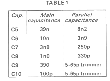
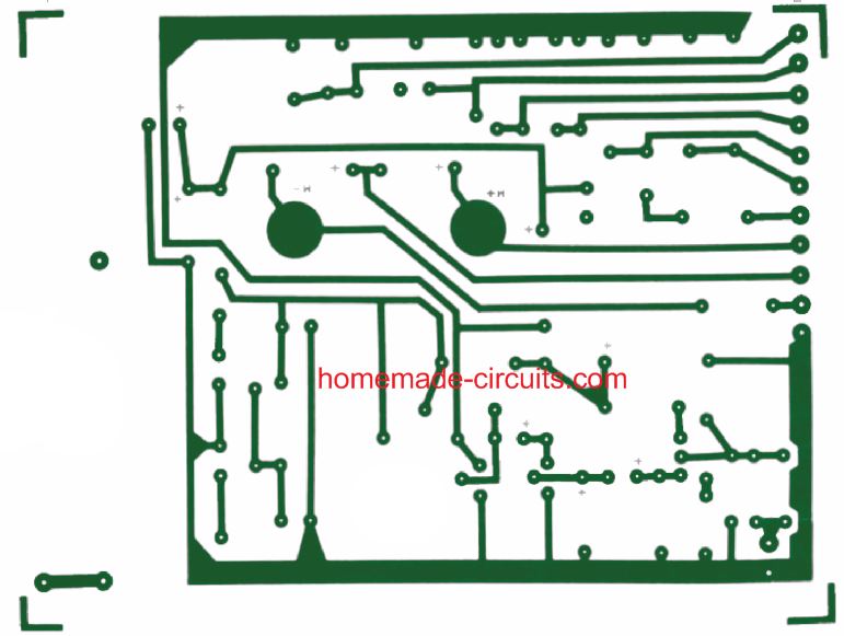
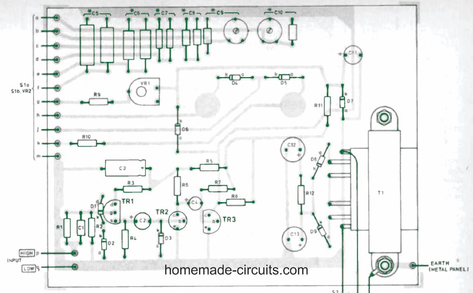
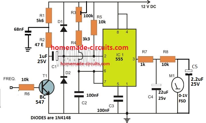 The IC 555 is wired as a standard monostable circuit, whose output ON time is fixed through the R3, C2 components.
For each positive half cycle of the input frequency, the monostable turns ON for the specific amount of time as determined by the R3/C2 elements.
The parts R7, R8, C4, C5 at the output of the IC work like stabilizer or integrator to enable the ON/OFF monostable pulses to be reasonably stable DC for the meter to read it without vibrations.
This also allows the output to produce an average continuous Dc which is directly proportional to the frequency rate of the input pulses fed at the base of T1.
However, the preset R3 must be properly adjusted for different ranges of frequencies such that the meter needle is fairly stable and an increase or decrease of the input frequency causes a proportionate amount of deflection over that specific range.
The IC 555 is wired as a standard monostable circuit, whose output ON time is fixed through the R3, C2 components.
For each positive half cycle of the input frequency, the monostable turns ON for the specific amount of time as determined by the R3/C2 elements.
The parts R7, R8, C4, C5 at the output of the IC work like stabilizer or integrator to enable the ON/OFF monostable pulses to be reasonably stable DC for the meter to read it without vibrations.
This also allows the output to produce an average continuous Dc which is directly proportional to the frequency rate of the input pulses fed at the base of T1.
However, the preset R3 must be properly adjusted for different ranges of frequencies such that the meter needle is fairly stable and an increase or decrease of the input frequency causes a proportionate amount of deflection over that specific range.
 The input signals for this analogue frequency meter can be in the form of pulses or square -wave signals with peak-to-peak limits of 2 volts or higher.
Transistor Q1 amplifies this pulsed input signal sufficiently high to trigger the pin#2 IC 555. The output of the IC at pin#3 is connected with the 1 mA full-scale deflection moving-coil meter M1. Diode D1 works like an offset cancel stage with the help of multiplier resistor R5.
Whenever the IC 555 which is configured as a monostable multivibrator get triggered by an input pulse, it creates a pulse having a fixed duration and amplitude.
When every single pulse includes a peak voltage of 6 volts and a 1ms period, and it triggers the IC pin#2 with a frequency of 500 Hz, a high logic 500 milliseconds is created at pin#3, in each 1000 milliseconds.
Furthermore, the average value of output from the IC 555 assessed over this time interval can be calculated as
500 milliseconds/1000 milliseconds x 6 volts = 3 volts or half of 6 volts.
Likewise, in case the input frequency is 250 Hz, and a high pulse of 250 milliseconds in each 1000 millisecond period is created.
As a result, the avergae output voltage from the IC now equals 250 milliseconds/ 1000 milliseconds x 6 volts = 1.5 volts or one quarter of 6 volts.
This shows that, the circuit's average value of output voltage, tested within a realistic overall quantity of pulses, is directly proportionate to the repeating frequency of the monostable multivibrator.
We can get only mean or average measurements from moving-coil meters.
In the circuit diagram a 1 mA meter can be seen connected in series with multiplier resistor R5. This resistor R5 adjusts meter's sensitivity at approximately 3.4 volts full-scale deflection.
The meter is hooked up to offer the mean output value of the multivibrator and its display is instantly proportional to the input frequency.
Using the part values as indicated in the analogue frequency meter diagram, it is configured to produce full-scale deflection at 1 kHz.
To set up the circuit, at first, a 1 kHz square wave frequency is applied to the indicated output, and full scale-adjust potentiometer R7 (it regulates the pulse length) is adjusted and fixed to provide a full-scale measurement on the meter.
The input signals for this analogue frequency meter can be in the form of pulses or square -wave signals with peak-to-peak limits of 2 volts or higher.
Transistor Q1 amplifies this pulsed input signal sufficiently high to trigger the pin#2 IC 555. The output of the IC at pin#3 is connected with the 1 mA full-scale deflection moving-coil meter M1. Diode D1 works like an offset cancel stage with the help of multiplier resistor R5.
Whenever the IC 555 which is configured as a monostable multivibrator get triggered by an input pulse, it creates a pulse having a fixed duration and amplitude.
When every single pulse includes a peak voltage of 6 volts and a 1ms period, and it triggers the IC pin#2 with a frequency of 500 Hz, a high logic 500 milliseconds is created at pin#3, in each 1000 milliseconds.
Furthermore, the average value of output from the IC 555 assessed over this time interval can be calculated as
500 milliseconds/1000 milliseconds x 6 volts = 3 volts or half of 6 volts.
Likewise, in case the input frequency is 250 Hz, and a high pulse of 250 milliseconds in each 1000 millisecond period is created.
As a result, the avergae output voltage from the IC now equals 250 milliseconds/ 1000 milliseconds x 6 volts = 1.5 volts or one quarter of 6 volts.
This shows that, the circuit's average value of output voltage, tested within a realistic overall quantity of pulses, is directly proportionate to the repeating frequency of the monostable multivibrator.
We can get only mean or average measurements from moving-coil meters.
In the circuit diagram a 1 mA meter can be seen connected in series with multiplier resistor R5. This resistor R5 adjusts meter's sensitivity at approximately 3.4 volts full-scale deflection.
The meter is hooked up to offer the mean output value of the multivibrator and its display is instantly proportional to the input frequency.
Using the part values as indicated in the analogue frequency meter diagram, it is configured to produce full-scale deflection at 1 kHz.
To set up the circuit, at first, a 1 kHz square wave frequency is applied to the indicated output, and full scale-adjust potentiometer R7 (it regulates the pulse length) is adjusted and fixed to provide a full-scale measurement on the meter.
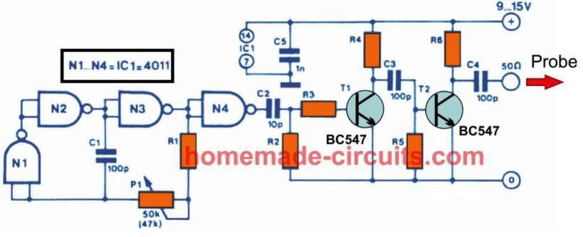
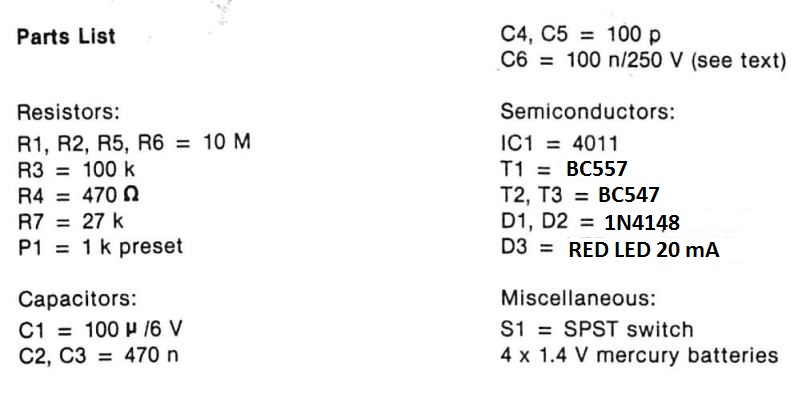 Figure 1 displays the entiresignal injecter circuit.
The tracking oscillator is an astable multivibrator constructed across a couple ofCMOS NAND gates N1and N2. It therefore switches T1on and off, driving an LED indicating if the signal is on.
Figure 1 displays the entiresignal injecter circuit.
The tracking oscillator is an astable multivibrator constructed across a couple ofCMOS NAND gates N1and N2. It therefore switches T1on and off, driving an LED indicating if the signal is on.
 Mounting the entire circuit inside a well insulatedboxis also a smart option, particularly when operating on AC LIVE audio equipment.
The specs of D1and D2 should be able to withstand whatever intermittent voltages and currents that may likely occur.
Four 1.4 V mercury batteriespower for the circuit.
The specific battery technology chosen becomes anuserpreference.
Mounting the entire circuit inside a well insulatedboxis also a smart option, particularly when operating on AC LIVE audio equipment.
The specs of D1and D2 should be able to withstand whatever intermittent voltages and currents that may likely occur.
Four 1.4 V mercury batteriespower for the circuit.
The specific battery technology chosen becomes anuserpreference.

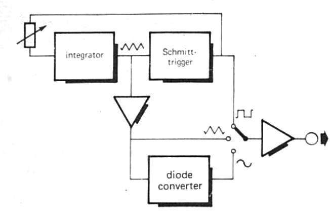 The circuit operating basics from the above shown block diagram.
The function generator's main section is a triangle / squarewave generator which consists of an integrator and a Schmit trigger.
Once the output of the Schmitt trigger is high, the voltage feeding back from the Schmitt output to the input of the Integrator allows the output of the Integrator to ramp negative before it exceeds the lower output level of the Schmitt trigger.
At this stage the Schmitt trigger output is slow, so the small voltage fed back to the input of theintegratorallows it to ramp up positively before the Schmitt trigger's upper trigger level is reached.
The Schmitt trigger's output goes high again, and the integrater output spikes negative again, and so forth.
The integrator output's positive and negative sweeps represent a triangular waveform whose amplitude is calculated by the Schmitt trigger's hysteresis (i.e.
the difference between the high and low trigger limits).
The Schmitt trigger production is, naturally a square wave made up of alternating high and low output states.
The triangle output is supplied to a diode shaper through a buffer amplifier, that rounds off the highs and lows of the triangle to create an approximate to a sinewave signal.
Then, each of the 3 waveforms can be chosen by a 3-way selector switch S2 and supplied to an output buffer amplifier.
The circuit operating basics from the above shown block diagram.
The function generator's main section is a triangle / squarewave generator which consists of an integrator and a Schmit trigger.
Once the output of the Schmitt trigger is high, the voltage feeding back from the Schmitt output to the input of the Integrator allows the output of the Integrator to ramp negative before it exceeds the lower output level of the Schmitt trigger.
At this stage the Schmitt trigger output is slow, so the small voltage fed back to the input of theintegratorallows it to ramp up positively before the Schmitt trigger's upper trigger level is reached.
The Schmitt trigger's output goes high again, and the integrater output spikes negative again, and so forth.
The integrator output's positive and negative sweeps represent a triangular waveform whose amplitude is calculated by the Schmitt trigger's hysteresis (i.e.
the difference between the high and low trigger limits).
The Schmitt trigger production is, naturally a square wave made up of alternating high and low output states.
The triangle output is supplied to a diode shaper through a buffer amplifier, that rounds off the highs and lows of the triangle to create an approximate to a sinewave signal.
Then, each of the 3 waveforms can be chosen by a 3-way selector switch S2 and supplied to an output buffer amplifier.
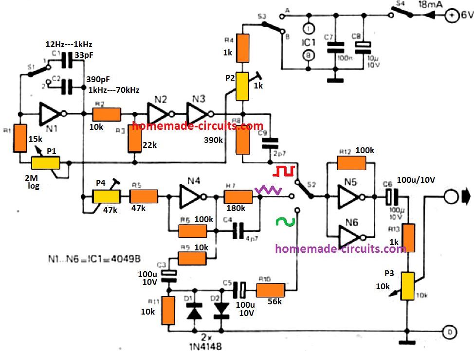 The full circuit diagram of the CMOS function generator as seen in the figure above.
The integrator is entirely built using a CMOS inverter, Nl, while the Schmitt mechanism incorporates 2 positive feedback inverters.
It's N2 and N3.
The following image shows the pinout details of the IC 4049 for applying into the above schematic
The full circuit diagram of the CMOS function generator as seen in the figure above.
The integrator is entirely built using a CMOS inverter, Nl, while the Schmitt mechanism incorporates 2 positive feedback inverters.
It's N2 and N3.
The following image shows the pinout details of the IC 4049 for applying into the above schematic
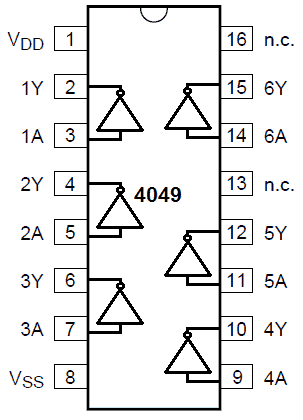 The circuit works this way; considering, for the moment, that the P2 wiper is in its lowest location, with N3 output being high, a current equivalent to:
Ub - U1 / P1 + R1
travels via R1 and p1, where Ub indicates the supply voltage and Ut the N1 threshold voltage.
Because this current is unable to move into the inverter high impedance input, it begins traveling towards C1/C2 depending on which capacitor is toggled in line by the switch S1.
The voltage drop over C1 thus decreases linearly such that the output voltage of N1 rises linearly before the lower threshold voltage of the Schmitt trigger is approached just as the output of the Schmitt trigger becomes low.
Now a current equivalent to -Ut / P1 + R1 flows through both R1 and P1.
This current always flows through C1, such that N1's output voltage increases exponentially until the Schmitt trigger's maximum limit voltage is achieved, the Schmitt trigger's output rises, and the entire cycle begins all over again.
To maintain the triangle wave symmetry (i.e.
the very same slope for both the positive-going and the negative-going parts of the waveform) the condenser's load and discharge currents has to be identical, meaning Uj,-Ui should be identical to Ut.
However, sadly, Ut being decided by the CMOS inverter parameters, is normally 55% ! The source voltage Ub = Ut is approximately 2.7 V with 6 V and Ut approximately at 3.3 V.
This challenge is overcome with P2 which requires modification of the symmetry.
For the moment, consider that thai R-is related to the positive supply line (position A).
Regardless of the setting ofP2, the Schmitt trigger's high output voltage always remains11.
Nevertheless, when N3 output is low, R4 and P2 establish a potential divider such that, based on P2's wiper configuration, a voltage between 0 V to 3 V could be returned back into P1.
This ensures the voltage is no longer -Utand but Up2-Ut.
In case the P2 slider voltage is around 0.6 V then Up2-Ut should be around -2.7 V, therefore the currents of charging and discharging would be identical.
Obviously, due to the tolerance in the value of Ut, the P2 adjustment should be performed to match specific function generator.
In situations in which Ut is less than 50 percent of the input voltage, connecting the top of R4 to ground (position B) mightbe appropriate.
A couple offrequency scales can be found, which will be assigned using S1; 12 Hz-1 kHz and 1 kHz to approximately 70 kHz.
Granular frequency control is given by P1that changes the current of charge and discharge of C1 or C2 and thus the frequency throughwhich the integrator ramps up and down.
The squarewave output from N3 is sent to a buffer amplifier via a waveform selector switch, S2, that comprises of a couple ofinverters biased likea linear amplifier (hooked up in parallel to improve their output current efficiency).
The triangle waveoutput is provided througha buffer amplifier N4 and from there by the selector switch to the buffer amplifier output.
Also, the triangle output from N4 is added to the sine shaper, consisting of R9, R11, C3, Dl, and D2.
D1and D2 pull little current up to around +/- 0.5 volts but their diverse resistance drops beyond this voltage and logarithmically limit the highs and lows of the triangle pulse to create an equivalent to a sinewave.
The sine output is transmitted to the output amplifier via C5 and R10.
P4, which varies the gain of N4 and hence the amplitude of the triangle pulse supplied to the sine shaper, changes the sinus transparency.
Too low a signal level, and the amplitude of the triangle would be below the threshold voltage of the diode, and it will proceed with noalteration,and too high a signal level, the highs and lows would be strongly clipped, thereby providing not well formedsine wave.
The output buffer amplifier input resistors are chosen such that all three waveforms have a nominal peak to minimum output voltage of around 1.2 V.
The level of output could be changed through P3.
The circuit works this way; considering, for the moment, that the P2 wiper is in its lowest location, with N3 output being high, a current equivalent to:
Ub - U1 / P1 + R1
travels via R1 and p1, where Ub indicates the supply voltage and Ut the N1 threshold voltage.
Because this current is unable to move into the inverter high impedance input, it begins traveling towards C1/C2 depending on which capacitor is toggled in line by the switch S1.
The voltage drop over C1 thus decreases linearly such that the output voltage of N1 rises linearly before the lower threshold voltage of the Schmitt trigger is approached just as the output of the Schmitt trigger becomes low.
Now a current equivalent to -Ut / P1 + R1 flows through both R1 and P1.
This current always flows through C1, such that N1's output voltage increases exponentially until the Schmitt trigger's maximum limit voltage is achieved, the Schmitt trigger's output rises, and the entire cycle begins all over again.
To maintain the triangle wave symmetry (i.e.
the very same slope for both the positive-going and the negative-going parts of the waveform) the condenser's load and discharge currents has to be identical, meaning Uj,-Ui should be identical to Ut.
However, sadly, Ut being decided by the CMOS inverter parameters, is normally 55% ! The source voltage Ub = Ut is approximately 2.7 V with 6 V and Ut approximately at 3.3 V.
This challenge is overcome with P2 which requires modification of the symmetry.
For the moment, consider that thai R-is related to the positive supply line (position A).
Regardless of the setting ofP2, the Schmitt trigger's high output voltage always remains11.
Nevertheless, when N3 output is low, R4 and P2 establish a potential divider such that, based on P2's wiper configuration, a voltage between 0 V to 3 V could be returned back into P1.
This ensures the voltage is no longer -Utand but Up2-Ut.
In case the P2 slider voltage is around 0.6 V then Up2-Ut should be around -2.7 V, therefore the currents of charging and discharging would be identical.
Obviously, due to the tolerance in the value of Ut, the P2 adjustment should be performed to match specific function generator.
In situations in which Ut is less than 50 percent of the input voltage, connecting the top of R4 to ground (position B) mightbe appropriate.
A couple offrequency scales can be found, which will be assigned using S1; 12 Hz-1 kHz and 1 kHz to approximately 70 kHz.
Granular frequency control is given by P1that changes the current of charge and discharge of C1 or C2 and thus the frequency throughwhich the integrator ramps up and down.
The squarewave output from N3 is sent to a buffer amplifier via a waveform selector switch, S2, that comprises of a couple ofinverters biased likea linear amplifier (hooked up in parallel to improve their output current efficiency).
The triangle waveoutput is provided througha buffer amplifier N4 and from there by the selector switch to the buffer amplifier output.
Also, the triangle output from N4 is added to the sine shaper, consisting of R9, R11, C3, Dl, and D2.
D1and D2 pull little current up to around +/- 0.5 volts but their diverse resistance drops beyond this voltage and logarithmically limit the highs and lows of the triangle pulse to create an equivalent to a sinewave.
The sine output is transmitted to the output amplifier via C5 and R10.
P4, which varies the gain of N4 and hence the amplitude of the triangle pulse supplied to the sine shaper, changes the sinus transparency.
Too low a signal level, and the amplitude of the triangle would be below the threshold voltage of the diode, and it will proceed with noalteration,and too high a signal level, the highs and lows would be strongly clipped, thereby providing not well formedsine wave.
The output buffer amplifier input resistors are chosen such that all three waveforms have a nominal peak to minimum output voltage of around 1.2 V.
The level of output could be changed through P3.
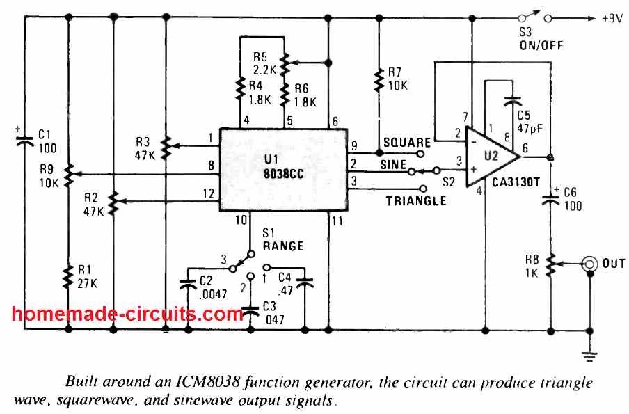 Additionally, the IC 8038 function generator offers a working frequency range up to as large as 1MHz.
All the three fundamental waveform outputs, sinusoidal, triangular and square can be at the same time accessed through individual output ports of the circuit.
The frequency range of the 8038 can be varied through an external voltage feed, although the response may not be very linear.
The proposed function generator also provides like adjustable triangle symmetry, and adjustable sine wave distortion level.
Additionally, the IC 8038 function generator offers a working frequency range up to as large as 1MHz.
All the three fundamental waveform outputs, sinusoidal, triangular and square can be at the same time accessed through individual output ports of the circuit.
The frequency range of the 8038 can be varied through an external voltage feed, although the response may not be very linear.
The proposed function generator also provides like adjustable triangle symmetry, and adjustable sine wave distortion level.
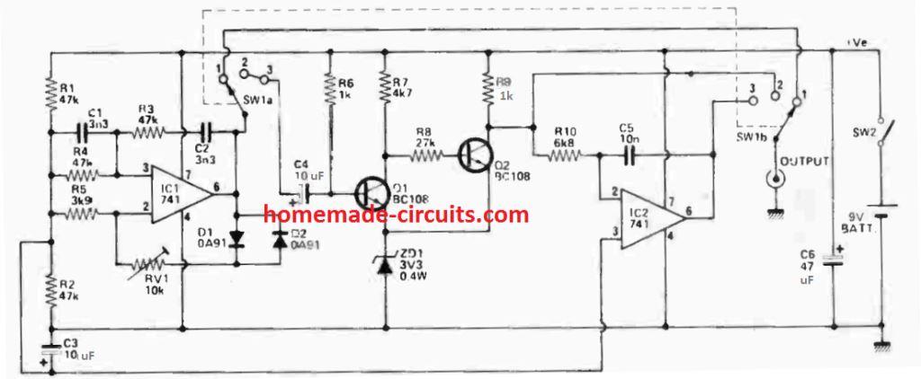
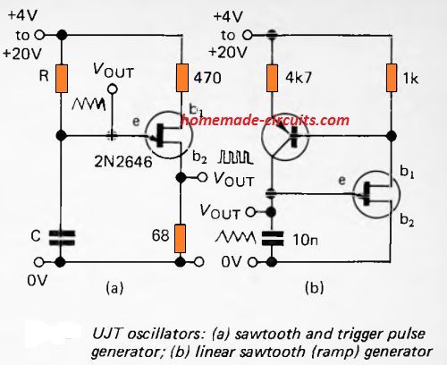 Since capacitor charging is incremental, the sawtooth 's increasing slope isn't linear.
To many Audio applications, this barely matters.
The Figure (b) demonstrates the charging capacitor via a constant-current circuit.
This enables the slope going straight up.
The capacitor's charge rate is now constant, independent from Vs, although Vs still influences the peak point.
Since the current is dependent on transistor gain, there is no simple formula for frequency measurement.
This circuit is designed to work with low frequencies, and has implementations as a ramp generator.
Since capacitor charging is incremental, the sawtooth 's increasing slope isn't linear.
To many Audio applications, this barely matters.
The Figure (b) demonstrates the charging capacitor via a constant-current circuit.
This enables the slope going straight up.
The capacitor's charge rate is now constant, independent from Vs, although Vs still influences the peak point.
Since the current is dependent on transistor gain, there is no simple formula for frequency measurement.
This circuit is designed to work with low frequencies, and has implementations as a ramp generator.
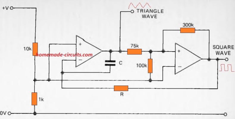 The output signal frequencies are calculatedby the formulaf=1 / RC.
The circuit showsan extremelywide operating range with hardly any distortion.
R may have any value between 330 Ohm and around 4.7 M; C can be ofany value from around 220pF to 2uF.
Just like the above concept, two op amps are used in the nextsine wave an cosine wave functiongeneratorcircuit.
The output signal frequencies are calculatedby the formulaf=1 / RC.
The circuit showsan extremelywide operating range with hardly any distortion.
R may have any value between 330 Ohm and around 4.7 M; C can be ofany value from around 220pF to 2uF.
Just like the above concept, two op amps are used in the nextsine wave an cosine wave functiongeneratorcircuit.
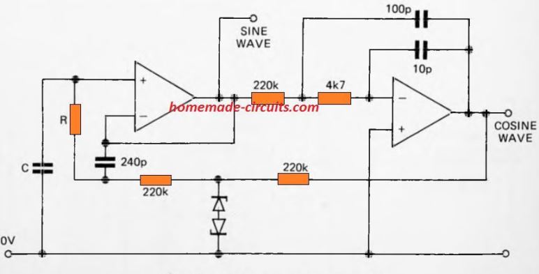 They generate nearly identical frequency sine wave signals but 90 ˇă out of phase, and therefore output of the second op amp is termedas a cosine wave.
Frequency is affected by the collection of acceptable R and C values.
R is in the 220k to 10 M range; C is between 39pF and 22nF.
The connection between R, C and/or is a bit complex, as it must reflect the values of other resistors and capacitors.
Use R = 220k and C = 18nF as an initial point that provides a frequency of 250Hz.
The Zener diodes can be low power output diodes of 3.9V or 4.7V.
They generate nearly identical frequency sine wave signals but 90 ˇă out of phase, and therefore output of the second op amp is termedas a cosine wave.
Frequency is affected by the collection of acceptable R and C values.
R is in the 220k to 10 M range; C is between 39pF and 22nF.
The connection between R, C and/or is a bit complex, as it must reflect the values of other resistors and capacitors.
Use R = 220k and C = 18nF as an initial point that provides a frequency of 250Hz.
The Zener diodes can be low power output diodes of 3.9V or 4.7V.
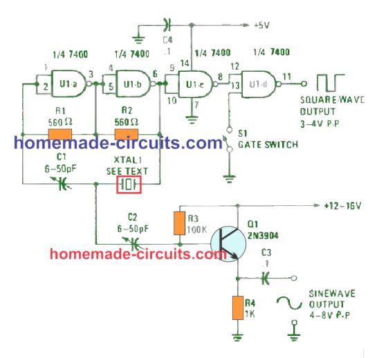 Switch S1 acts like a manually switchable gate control to toggle the squarewave output of U1-d at pin 11 ON/OFF.
With S1 open, as indicated, the square-wave is generated at the output, and once closed the equare waveform is switched off.
The switch could be substituted with a logic gate to digitally command the output.
An almost ideal 6- to 8-volt peak-to-peak sine wave is created at the connecting point of of C1 and XTAL1.
The impedance on this junction is very high and is unnable to provide a direct output signal.
Transistor Q1, set up as an emitter-follower amplifier, supplies a high input impedance to the sine-wave signal and a low output impedance to an outside load.
The circuit will crank up almost all types of crystals and will run with crystal frequencies of below 1 MHz to above 10 MHz.
Switch S1 acts like a manually switchable gate control to toggle the squarewave output of U1-d at pin 11 ON/OFF.
With S1 open, as indicated, the square-wave is generated at the output, and once closed the equare waveform is switched off.
The switch could be substituted with a logic gate to digitally command the output.
An almost ideal 6- to 8-volt peak-to-peak sine wave is created at the connecting point of of C1 and XTAL1.
The impedance on this junction is very high and is unnable to provide a direct output signal.
Transistor Q1, set up as an emitter-follower amplifier, supplies a high input impedance to the sine-wave signal and a low output impedance to an outside load.
The circuit will crank up almost all types of crystals and will run with crystal frequencies of below 1 MHz to above 10 MHz.
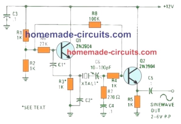 The ground path for the crystal is directed by means of C6, R7, and C4. In the C6 and R7 junction, which is a pretty small impedance position, the RF is applied to an emitter-follower amplifier, Q2.
The waveform shape at the C6/R7 junction is really an almost perfect sine wave.
The output, at the emitter of Q2 ranges in amplitude from around 2- to 6-volts peak-to-peak, based upon on the Q factor of the crystal's and the capacitors C1 and C2 values.
The C1 and C2 values decide the frequency range of the circuit.
For crystal frequencies under 1 MHz, C1 and C2 ought to be 2700 pF (.0027 p,F).
For frequencies between 1 MHz and 5 MHz, these can be 680-pF capacitors; and for 5 MHz and 20 MHz.
you can apply 200-pF capacitors.
You could possibly try testing with values of those capacitors to get the finest looking sine wave output.
Additionally, the adjustment of capacitor C6 can have an effect on the two output level and the overall shape of the waveform.
Parts List
RESISTORS
(All resistors are -watt, 5% units.)
R1-R5-1k
R6-27k
R7-270-ohm
R8-100k
CAPACITORS
C1,C2ˇŞSee text
C3,C5-0.1-p.F, ceramic disc
C6-10 pF to 100 pF, trimmer
SEMICONDUCTORS
Q1, Q2-2N3904
XTAL1ˇŞSee text
The ground path for the crystal is directed by means of C6, R7, and C4. In the C6 and R7 junction, which is a pretty small impedance position, the RF is applied to an emitter-follower amplifier, Q2.
The waveform shape at the C6/R7 junction is really an almost perfect sine wave.
The output, at the emitter of Q2 ranges in amplitude from around 2- to 6-volts peak-to-peak, based upon on the Q factor of the crystal's and the capacitors C1 and C2 values.
The C1 and C2 values decide the frequency range of the circuit.
For crystal frequencies under 1 MHz, C1 and C2 ought to be 2700 pF (.0027 p,F).
For frequencies between 1 MHz and 5 MHz, these can be 680-pF capacitors; and for 5 MHz and 20 MHz.
you can apply 200-pF capacitors.
You could possibly try testing with values of those capacitors to get the finest looking sine wave output.
Additionally, the adjustment of capacitor C6 can have an effect on the two output level and the overall shape of the waveform.
Parts List
RESISTORS
(All resistors are -watt, 5% units.)
R1-R5-1k
R6-27k
R7-270-ohm
R8-100k
CAPACITORS
C1,C2ˇŞSee text
C3,C5-0.1-p.F, ceramic disc
C6-10 pF to 100 pF, trimmer
SEMICONDUCTORS
Q1, Q2-2N3904
XTAL1ˇŞSee text
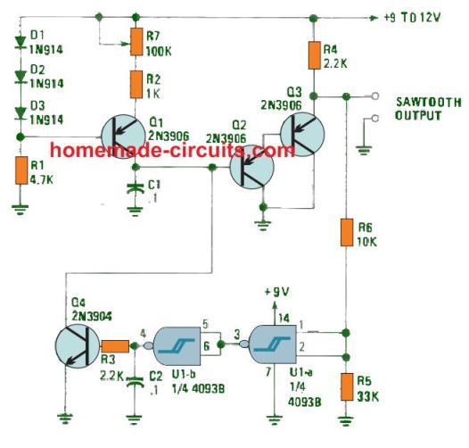 Transistors Q2 and Q3 are rigged like a Darlington pair to push the voltage through C1, to the output with no loading or distorting effects.
As soon as the voltage around C1 increases to around 70% of the supply voltage, gate U1-a activates, triggering the U1-b output to go high and briefly switch on Q4; which continues to be ON while capacitor C1 discharges.
This finishes a single cycle and initiates the next.
The circuit's output frequency is governed by R7, which supplies a low-end frequency of approximately 30 Hz and an upper-end frequency of around 3.3 kHz.
The frequency range could be made higher by decreasing the value of C1 and dropped by increasing the C1's value.
To preserve Q4's peak discharge current under control.
C1 should not be bigger than 0.27 uF.
Parts List
Transistors Q2 and Q3 are rigged like a Darlington pair to push the voltage through C1, to the output with no loading or distorting effects.
As soon as the voltage around C1 increases to around 70% of the supply voltage, gate U1-a activates, triggering the U1-b output to go high and briefly switch on Q4; which continues to be ON while capacitor C1 discharges.
This finishes a single cycle and initiates the next.
The circuit's output frequency is governed by R7, which supplies a low-end frequency of approximately 30 Hz and an upper-end frequency of around 3.3 kHz.
The frequency range could be made higher by decreasing the value of C1 and dropped by increasing the C1's value.
To preserve Q4's peak discharge current under control.
C1 should not be bigger than 0.27 uF.
Parts List
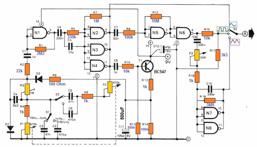 The foundation of this circuit is actually a Wien -bridge oscillator, which offers a sine wave output.
The square and triangular waveforms are subsequently extracted out of this.
The Wien -bridge oscillator is constructed using a CMOS NAND gates N1 to N4, while the amplitude stabilization is supplied by transistor T1, and diodes D1 and D2.
These diodes possibly, must be matched up set of two, for lowest distortion.
The frequency adjusting potentiometer P1 must also be a high-quality stereo potentiometer with internal resistance tracks paired to inside 5% tolerance.
The preset R3 gives adjusting facility for least distortion and in case matched up parts are employed for D1, D2 and P1 the overall harmonic distortion could be under 0.5%.
The output from the Wien -bridge oscillator is applied to the input of N5, which is biased into its linear region and functions as an amplifier.
NAND gates N5 and N6 collectively enhance and clip the oscillator output to generate a square waveform.
The duty -cycle of the waveform is relatively influenced by the threshold potentials of N5 arid N6, however it is in close proximity to 50%.
The gate N6 output is supplied into an integrator built using the NAND gates N7 and N8, that harmonizes with the square wave to deliver a triangular waveform.
The triangular waveform amplitude is, for sure is dependent on the frequency, and as the integrator is simply not very accurate the linearity additionally deviates with respect to the frequency.
In reality the amplitude variation is actually pretty trivial, considering that the function generator will often be used together with a millivoltmeter or an oscilloscope and the output could be easily checked.
The foundation of this circuit is actually a Wien -bridge oscillator, which offers a sine wave output.
The square and triangular waveforms are subsequently extracted out of this.
The Wien -bridge oscillator is constructed using a CMOS NAND gates N1 to N4, while the amplitude stabilization is supplied by transistor T1, and diodes D1 and D2.
These diodes possibly, must be matched up set of two, for lowest distortion.
The frequency adjusting potentiometer P1 must also be a high-quality stereo potentiometer with internal resistance tracks paired to inside 5% tolerance.
The preset R3 gives adjusting facility for least distortion and in case matched up parts are employed for D1, D2 and P1 the overall harmonic distortion could be under 0.5%.
The output from the Wien -bridge oscillator is applied to the input of N5, which is biased into its linear region and functions as an amplifier.
NAND gates N5 and N6 collectively enhance and clip the oscillator output to generate a square waveform.
The duty -cycle of the waveform is relatively influenced by the threshold potentials of N5 arid N6, however it is in close proximity to 50%.
The gate N6 output is supplied into an integrator built using the NAND gates N7 and N8, that harmonizes with the square wave to deliver a triangular waveform.
The triangular waveform amplitude is, for sure is dependent on the frequency, and as the integrator is simply not very accurate the linearity additionally deviates with respect to the frequency.
In reality the amplitude variation is actually pretty trivial, considering that the function generator will often be used together with a millivoltmeter or an oscilloscope and the output could be easily checked.
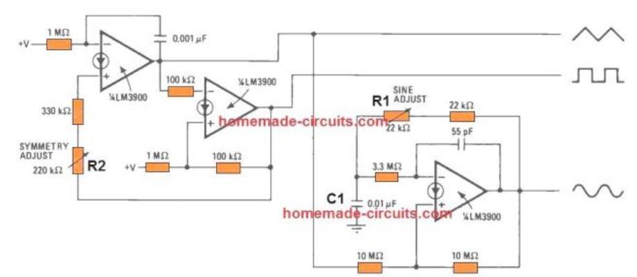 As demonstrated in the picture triangular output works like the input for the sine -shaper amplifier.
For the part values provided in this article, the circuit's running frequency is approximately 700 hertz.
Resistor R1 can be used for adjusting lowest sine -wave distortion, and resistor R2 can be used for adjusting the the symmetry of the square and triangular waves.
The 4th amplifier in the Norton quad package could be hooked up as an output buffer for all 3 output waveforms.
As demonstrated in the picture triangular output works like the input for the sine -shaper amplifier.
For the part values provided in this article, the circuit's running frequency is approximately 700 hertz.
Resistor R1 can be used for adjusting lowest sine -wave distortion, and resistor R2 can be used for adjusting the the symmetry of the square and triangular waves.
The 4th amplifier in the Norton quad package could be hooked up as an output buffer for all 3 output waveforms.
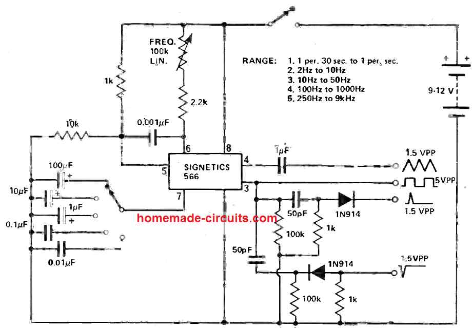
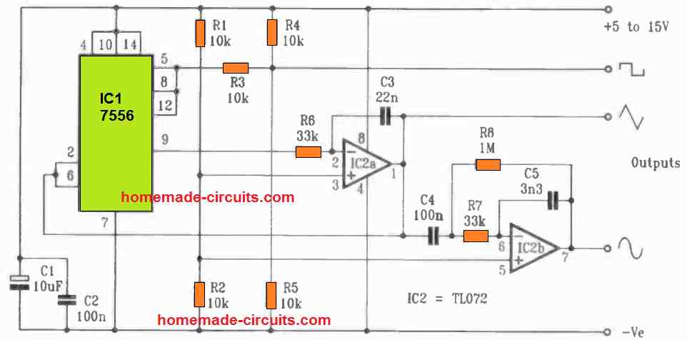 When the integrator is fed witha square waveinput from the timer, it converts it to a triangular wave.
When the triangle-wave signal is applied into another integrator, it is transformed into a sine wave.
With a very basic circuit, this method may be utilized to create a pretty clean sine wave of a set frequency.
All three fundamental waveforms, square, triangle, and sinewave, are generated with almost identical peak-to-peak voltage amplitudes in this version.
The amplitude of the sinewave, 3 volts peak-to-peak with a 9 Vsupply, is nearly comparable to one volt RMS, which is a useful quantity for audio testing.
The goal of this spot sinewave generator is to make all three outputs with about the identicaloutput voltage so that other circuits may be quickly tested for responsiveness to varied waveforms.
With a peak-to-peak voltage of one-third of the supply, the triangle wave defines the starting value.
The squarewave originally possesses the supply voltage valueas it varies from rail to rail, althoughit is attenuated to nearly the required value by means ofthe two resistors R4 and R5. These two resistors could be removed if they are not necessary.
The input of lC2b, a second integrator, is linked to the triangle wave.
Due to input offset voltages and currents, etc., the output of an integrator mightfinally drift as much as it can towards one of the supply rails unless some form of DC feedback is used.
ThereforelC2b is AC coupled to the input signal via C4 and the largefeedback resistorR8, holds the right DC output level.
The levels of these two components are adequate to prevent signal distortion at the operational frequency.
The settings of R7 and C5 adjust the output amplitude to the desired level of roughly one-third of the supply peak-to-peak.
the frequency is determined.
by the formula:
f = 1 / 1.333 x R6 x C5
This method produces a pretty nice sinewave, with the sole downside being that the frequency cannot be readily changed.
Any change in the input frequency to the second integrator will necessitate a change in the values of RT and C5 in order to keep the right sinewave output amplitude, and there is no quick method to achieve this.
When the integrator is fed witha square waveinput from the timer, it converts it to a triangular wave.
When the triangle-wave signal is applied into another integrator, it is transformed into a sine wave.
With a very basic circuit, this method may be utilized to create a pretty clean sine wave of a set frequency.
All three fundamental waveforms, square, triangle, and sinewave, are generated with almost identical peak-to-peak voltage amplitudes in this version.
The amplitude of the sinewave, 3 volts peak-to-peak with a 9 Vsupply, is nearly comparable to one volt RMS, which is a useful quantity for audio testing.
The goal of this spot sinewave generator is to make all three outputs with about the identicaloutput voltage so that other circuits may be quickly tested for responsiveness to varied waveforms.
With a peak-to-peak voltage of one-third of the supply, the triangle wave defines the starting value.
The squarewave originally possesses the supply voltage valueas it varies from rail to rail, althoughit is attenuated to nearly the required value by means ofthe two resistors R4 and R5. These two resistors could be removed if they are not necessary.
The input of lC2b, a second integrator, is linked to the triangle wave.
Due to input offset voltages and currents, etc., the output of an integrator mightfinally drift as much as it can towards one of the supply rails unless some form of DC feedback is used.
ThereforelC2b is AC coupled to the input signal via C4 and the largefeedback resistorR8, holds the right DC output level.
The levels of these two components are adequate to prevent signal distortion at the operational frequency.
The settings of R7 and C5 adjust the output amplitude to the desired level of roughly one-third of the supply peak-to-peak.
the frequency is determined.
by the formula:
f = 1 / 1.333 x R6 x C5
This method produces a pretty nice sinewave, with the sole downside being that the frequency cannot be readily changed.
Any change in the input frequency to the second integrator will necessitate a change in the values of RT and C5 in order to keep the right sinewave output amplitude, and there is no quick method to achieve this.

 This inductor is fixed outside the metallic enclosure where the circuit needs to be installed, so that whenever felt necessary the coil could be quickly replaced with other coils to allow the meter range to be customized.
Once the dipper is powered ON, the generated oscillating voltage is rectified by D1 and C2 and is then transferred to the meter through preset P1, which is used for tuning the meter display.
This inductor is fixed outside the metallic enclosure where the circuit needs to be installed, so that whenever felt necessary the coil could be quickly replaced with other coils to allow the meter range to be customized.
Once the dipper is powered ON, the generated oscillating voltage is rectified by D1 and C2 and is then transferred to the meter through preset P1, which is used for tuning the meter display.
 This tiny yet convenient field strength meter circuit enables users of any RF remote controller to validate if their remote-control transmitter is working efficiently.
It evens shows if the trouble is with the receiver or the transmitter unit.
The transistor is the sole active electronic component in the simple circuit.
It is used as a regulated resistance in one of the arms of the metering bridge.
The wire or rod aerial is attached to the base of the transistor.
The rapidly rising high-frequency voltage at the base of the aerial powers the transistor to force the bridge out of equilibrium.
Then, current passes through R2, the ammeter and the collector-emitter junction of the transistor.
As a precautionary step, the meter must be zeroed with P1 before switching on the transmitter.
This tiny yet convenient field strength meter circuit enables users of any RF remote controller to validate if their remote-control transmitter is working efficiently.
It evens shows if the trouble is with the receiver or the transmitter unit.
The transistor is the sole active electronic component in the simple circuit.
It is used as a regulated resistance in one of the arms of the metering bridge.
The wire or rod aerial is attached to the base of the transistor.
The rapidly rising high-frequency voltage at the base of the aerial powers the transistor to force the bridge out of equilibrium.
Then, current passes through R2, the ammeter and the collector-emitter junction of the transistor.
As a precautionary step, the meter must be zeroed with P1 before switching on the transmitter.
 These are typically three of the major factors why this specific field strength meter comes with an RF amplifier stage comprising a Dual gate MOSFET, T1. The amplification element is defined with P1. Switch S2 allows one of the 3 ranges to be determined: 480 kHz to 2.4 MHz (L1); 2.4 to12 MHz (L2) and 12 to 40 MHz (L3).
A pole of around 30 cm is going to be adequate to act as antenna.
Just like any other RF circuits, proper care throughout the construction process is advised.
These are typically three of the major factors why this specific field strength meter comes with an RF amplifier stage comprising a Dual gate MOSFET, T1. The amplification element is defined with P1. Switch S2 allows one of the 3 ranges to be determined: 480 kHz to 2.4 MHz (L1); 2.4 to12 MHz (L2) and 12 to 40 MHz (L3).
A pole of around 30 cm is going to be adequate to act as antenna.
Just like any other RF circuits, proper care throughout the construction process is advised.
 Therefore it can be safely used for troubleshooting the majority of standard IC's and semiconductor such as MOS-components.
The test result 'indicator' is actually in the form of a little loud- speaker, to ensure that at the time of testing, it isn't essential to keep diverting your eyes towards the testing device, rather than the circuit board.
The transistor T1 and T2 work like a basic voltage-controlled low frequency oscillator, which has a loudspeaker as the load.
The oscillator frequency depends on C1, R1, R4 and the resistance value of the external resistive load across the probes that is being measured.
Resistor R3 becomes the collector resistance of T2; C2 acts like a low frequency decoupling for R3.
As explained previously, the tester will never harm a circuit under test; however, oppositely, it may be important to include diodes D1 and D2 to ensure that the potential from circuit under test doesn't cause harm to the tester unit.
Given that there isn't any power association between the testing probes, the circuit is not going to pull any current.
Battery life as a result may be almost comparable to its shelf life
Therefore it can be safely used for troubleshooting the majority of standard IC's and semiconductor such as MOS-components.
The test result 'indicator' is actually in the form of a little loud- speaker, to ensure that at the time of testing, it isn't essential to keep diverting your eyes towards the testing device, rather than the circuit board.
The transistor T1 and T2 work like a basic voltage-controlled low frequency oscillator, which has a loudspeaker as the load.
The oscillator frequency depends on C1, R1, R4 and the resistance value of the external resistive load across the probes that is being measured.
Resistor R3 becomes the collector resistance of T2; C2 acts like a low frequency decoupling for R3.
As explained previously, the tester will never harm a circuit under test; however, oppositely, it may be important to include diodes D1 and D2 to ensure that the potential from circuit under test doesn't cause harm to the tester unit.
Given that there isn't any power association between the testing probes, the circuit is not going to pull any current.
Battery life as a result may be almost comparable to its shelf life
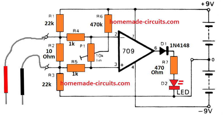 Using this op amp based circuit tester concept as shown above, all these drawbacks are safely eliminated.
The tester creates a resistance of no more than 1 ohm across its probes whenever the probes happen to interconnect two points over a circuit board.
Also, since the voltage used by the tetser is hardly 2 mV, implies that no diode, IC or any such vulnerable component get involved in the results during the testing procedure.
The highest magnitude of current that may appear across the test probes on the board which is being tested will be 200 pA, which looks too modest to cause any sort of issues to the PCB under test.
The test result indication is through a LED.
If the unit is build to fit inside a pen like enclosure then it can become extremely handy and the whole unit can be used as the one of the probes, whie the other probes is clipped somewhere else on the board.
One drawback is the requiremenet of two 9V cells as the power supply for the unit.
The shown preset is used for adjusting the output offset of the op amp.
The user will have to adjust the preset P1 such that the LED just lights up when the probes ends are shorted.
Conversely, the LED must instantly shut off when the probes are opened.
This will set up the circuit to illuminate the LED only when the probes encounter an almost short like condition on the PB under test.
A very compact and sleek PCB is designed for this tiny little PCB tester, which can be studied through the following diagrams.
Using this op amp based circuit tester concept as shown above, all these drawbacks are safely eliminated.
The tester creates a resistance of no more than 1 ohm across its probes whenever the probes happen to interconnect two points over a circuit board.
Also, since the voltage used by the tetser is hardly 2 mV, implies that no diode, IC or any such vulnerable component get involved in the results during the testing procedure.
The highest magnitude of current that may appear across the test probes on the board which is being tested will be 200 pA, which looks too modest to cause any sort of issues to the PCB under test.
The test result indication is through a LED.
If the unit is build to fit inside a pen like enclosure then it can become extremely handy and the whole unit can be used as the one of the probes, whie the other probes is clipped somewhere else on the board.
One drawback is the requiremenet of two 9V cells as the power supply for the unit.
The shown preset is used for adjusting the output offset of the op amp.
The user will have to adjust the preset P1 such that the LED just lights up when the probes ends are shorted.
Conversely, the LED must instantly shut off when the probes are opened.
This will set up the circuit to illuminate the LED only when the probes encounter an almost short like condition on the PB under test.
A very compact and sleek PCB is designed for this tiny little PCB tester, which can be studied through the following diagrams.
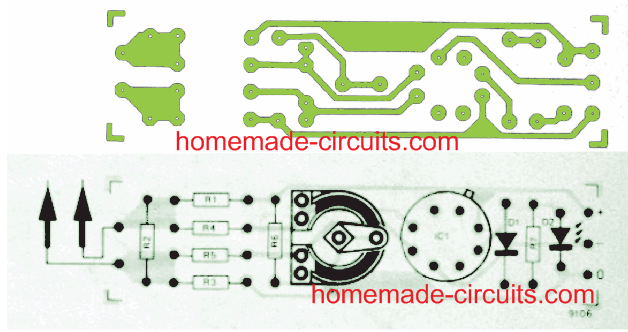

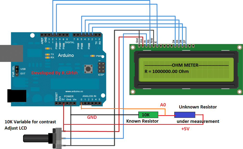 The circuit consists of Arduino; you may use your favorite Arduino board, a 16x2 LCD display to showcase the unknown resistor value, a potentiometer to adjust contrast level of LCD display.
Two resistors are used, one of which is known resistor value and other is unknown resistor value.
The resistance is an analogue function, but the value displayed on LCD is digital function.
So, we need to do analogue to digital conversion, fortunately Arduino has built-in 10-bit analogue to digital converter.
The 10-bit ADC can differentiate 1024 discrete voltage levels, 5 volt is applied to 2 resistors and the voltage sample is taken in between the resistors.
Using some mathematical calculations, voltage drop at the node and known resistance value can be interpreted to find the unknown resistance value.
The mathematical equations are written in the program, so no manual calculation need to be done, we can read direct value from LCD display.
AuthorˇŻs prototype:
The circuit consists of Arduino; you may use your favorite Arduino board, a 16x2 LCD display to showcase the unknown resistor value, a potentiometer to adjust contrast level of LCD display.
Two resistors are used, one of which is known resistor value and other is unknown resistor value.
The resistance is an analogue function, but the value displayed on LCD is digital function.
So, we need to do analogue to digital conversion, fortunately Arduino has built-in 10-bit analogue to digital converter.
The 10-bit ADC can differentiate 1024 discrete voltage levels, 5 volt is applied to 2 resistors and the voltage sample is taken in between the resistors.
Using some mathematical calculations, voltage drop at the node and known resistance value can be interpreted to find the unknown resistance value.
The mathematical equations are written in the program, so no manual calculation need to be done, we can read direct value from LCD display.
AuthorˇŻs prototype:

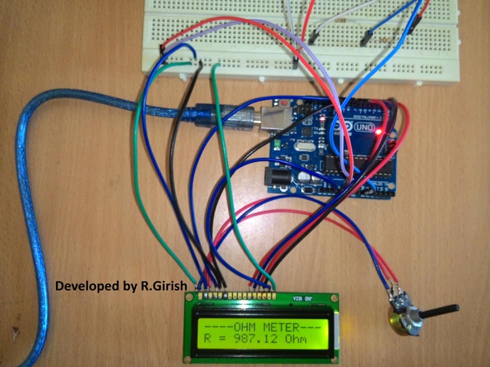
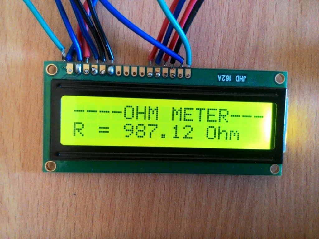
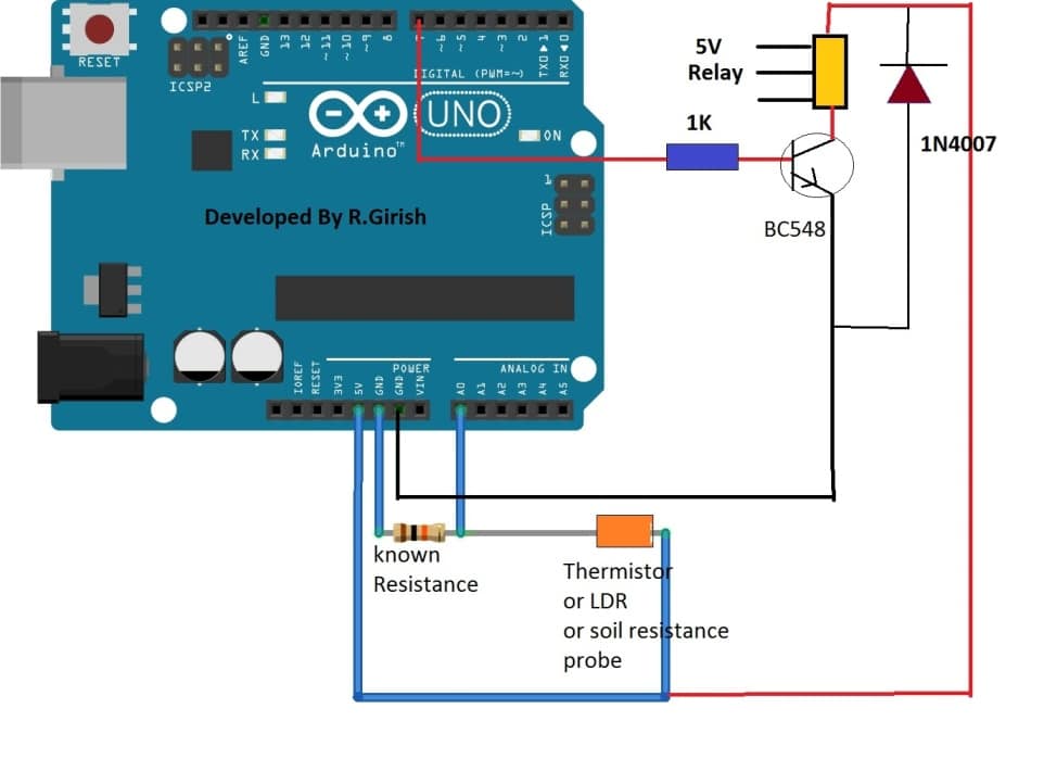
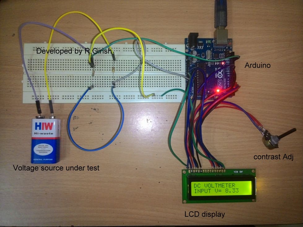 DonˇŻt reverse the polarity while measuring the voltage, it wonˇŻt harm the circuit but, it does not read any voltage and displays 0.00 V, until you correct the polarity.
Adjust the contrast of LCD display to optimum level by rotating the potentiometer.
Make sure you donˇŻt apply any voltage source which could spike higher than 30V; it may damage your Arduino board.
Technically you can bump up the maximum measuring voltage of this circuit by changing resistor values and modifying the program, but for the illustrated setup 30V is limit.
For accurate reading, choose fixed resistors with minimum tolerance value, resistors play an important role in calibrating the voltage reading.
DonˇŻt reverse the polarity while measuring the voltage, it wonˇŻt harm the circuit but, it does not read any voltage and displays 0.00 V, until you correct the polarity.
Adjust the contrast of LCD display to optimum level by rotating the potentiometer.
Make sure you donˇŻt apply any voltage source which could spike higher than 30V; it may damage your Arduino board.
Technically you can bump up the maximum measuring voltage of this circuit by changing resistor values and modifying the program, but for the illustrated setup 30V is limit.
For accurate reading, choose fixed resistors with minimum tolerance value, resistors play an important role in calibrating the voltage reading.

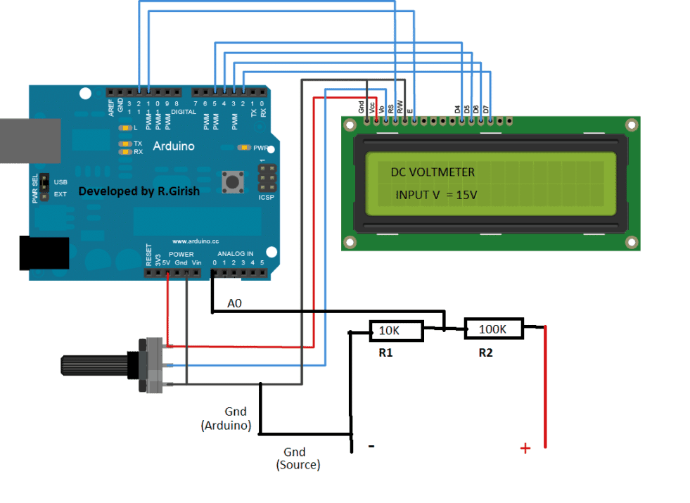 The other possibility of this voltmeter is that we can modify the program to automate some tasks.
For instance, detect full battery voltage and disconnect the battery from its charger or disconnect battery if voltage goes below preset voltage level and so on, these task can be accomplished even without LCD display.
However this is subject of another article.
The other possibility of this voltmeter is that we can modify the program to automate some tasks.
For instance, detect full battery voltage and disconnect the battery from its charger or disconnect battery if voltage goes below preset voltage level and so on, these task can be accomplished even without LCD display.
However this is subject of another article.

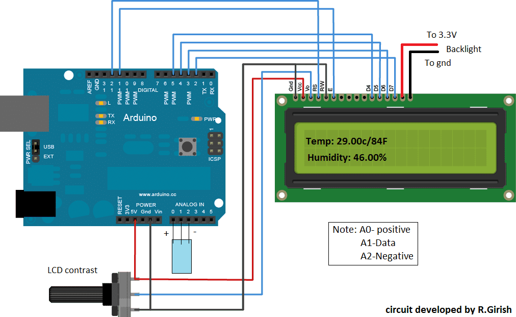 You can use your favorite Arduino board for this project, but my suggestion is to use ˇ°Arduino pro miniˇ± which is less expensive and small in size, which could easily fit into a small junk box for such simple projects.
There are lots of error detection mechanisms written in the DHT library to inform the user about error.
But to make the program simple I have just added one error detection mechanism which is illustrated below:
You can use your favorite Arduino board for this project, but my suggestion is to use ˇ°Arduino pro miniˇ± which is less expensive and small in size, which could easily fit into a small junk box for such simple projects.
There are lots of error detection mechanisms written in the DHT library to inform the user about error.
But to make the program simple I have just added one error detection mechanism which is illustrated below:
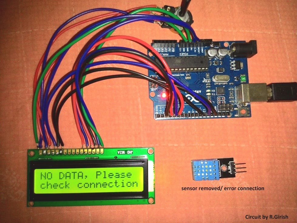 Mostly errors are due to faulty connection between sensor and arduino other errors less likely to occur, since tiny amount of data is transferred between arduino and sensor.
This doesnˇŻt mean that other kind of error wonˇŻt occur.
To get an idea about all kind of error associated with this sensor, please check out example code in ˇ°DHTlibˇ±.
Program code for the above explained digital temperature, humidity meter using Arduino :
Mostly errors are due to faulty connection between sensor and arduino other errors less likely to occur, since tiny amount of data is transferred between arduino and sensor.
This doesnˇŻt mean that other kind of error wonˇŻt occur.
To get an idea about all kind of error associated with this sensor, please check out example code in ˇ°DHTlibˇ±.
Program code for the above explained digital temperature, humidity meter using Arduino :
 This frequency voltage converter circuit using IC 4151 is characterized by its highly linear conversion ratio.
With the indicated part values the conversion ratio of the circuit can be expected to be around 1 V/kHz.
When a DC voltage is used at the input having 0 Hz frequency, the output generates a corresponding voltage of 0 V.
The conversion ratio at the output is never affected by the duty cycle of the input square ave frequency.
But, if a sine wave frequency is applied at the input, in that situation the signal must be passed through a Schmitt trigger before introducing it to the IC 4151 input.
If you are interested to have a different conversion ratio you may calculate it using the following formula:
V(out) / f(in) = R3 x R7 x C2 / 0.486(R4 + P1) x [V/Hz]
T1 = 1.1 x R3 x C2
The circuit can even be coupled to the output of a voltage to frequency converter and used as a way of sending DC signals across extended cable connection without the issues of cable resistance attenuating the signal.
This frequency voltage converter circuit using IC 4151 is characterized by its highly linear conversion ratio.
With the indicated part values the conversion ratio of the circuit can be expected to be around 1 V/kHz.
When a DC voltage is used at the input having 0 Hz frequency, the output generates a corresponding voltage of 0 V.
The conversion ratio at the output is never affected by the duty cycle of the input square ave frequency.
But, if a sine wave frequency is applied at the input, in that situation the signal must be passed through a Schmitt trigger before introducing it to the IC 4151 input.
If you are interested to have a different conversion ratio you may calculate it using the following formula:
V(out) / f(in) = R3 x R7 x C2 / 0.486(R4 + P1) x [V/Hz]
T1 = 1.1 x R3 x C2
The circuit can even be coupled to the output of a voltage to frequency converter and used as a way of sending DC signals across extended cable connection without the issues of cable resistance attenuating the signal.
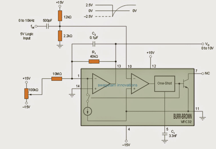 The threshold reference input set for the detector comparator is around ¨C0.7V.
In case where the frequency inputs may be lower than 5V, the potential divider network R6/R7 can be appropriately adjusted for changing the reference level and for enabling proper detection of the low level frequency inputs by the opamp.
As shown in the graph in the previous article, the C1 value may be selected depending upon the full scale range of the frequency input triggers.
C2 becomes responsible for filtering and smoothing the output voltage waveform, bigger values of C2 help to achieve better control over voltage ripples across the generated output, but the response is sluggish to rapidly varying input frequencies, whereas smaller values of C2 cause poor filtration but offer quick response and adjustment with the fast changing input frequencies.
R1 value could be tweaked for achieving a customized full scale deflection output voltage range with reference to a given full scale input frequency range.
The threshold reference input set for the detector comparator is around ¨C0.7V.
In case where the frequency inputs may be lower than 5V, the potential divider network R6/R7 can be appropriately adjusted for changing the reference level and for enabling proper detection of the low level frequency inputs by the opamp.
As shown in the graph in the previous article, the C1 value may be selected depending upon the full scale range of the frequency input triggers.
C2 becomes responsible for filtering and smoothing the output voltage waveform, bigger values of C2 help to achieve better control over voltage ripples across the generated output, but the response is sluggish to rapidly varying input frequencies, whereas smaller values of C2 cause poor filtration but offer quick response and adjustment with the fast changing input frequencies.
R1 value could be tweaked for achieving a customized full scale deflection output voltage range with reference to a given full scale input frequency range.
 The main application areas of this IC are:
Speed Sensing: It can used for sensing a rotational speed or the rate of a moving element
Frequency Converters: For converting frequency into linearly varying potential difference
Vibration based touch switch sensors
The main application areas of this IC are:
Speed Sensing: It can used for sensing a rotational speed or the rate of a moving element
Frequency Converters: For converting frequency into linearly varying potential difference
Vibration based touch switch sensors
 Another simple frequency to voltage converter can be seen in the above circuit diagram, using a single IC LM331.
Here the Vout can be calculated using the following calculations:
Vout = fIN x (RL/RS) x (1.9V) x (1.1RtCt)
For more info, you can refer to this article
Another simple frequency to voltage converter can be seen in the above circuit diagram, using a single IC LM331.
Here the Vout can be calculated using the following calculations:
Vout = fIN x (RL/RS) x (1.9V) x (1.1RtCt)
For more info, you can refer to this article
 The first figure below depicts a standard voltage to frequency converter circuit configuration where R1 is used for setting up the detection range of the input voltage.
 Through the potentiometer P1 , the circuit could be tweaked to ensure that an input voltage of 0 V generates an output frequency of 0 Hz.
The components responsible for fixing the frequency range are resistors R2, R3, R5, P1 along with the capacitor C2.
Applying the formulae demonstrated below, the ratio of voltage to frequency conversion may be transformed in order that the circuit works extremely well for several unique applications.
While determining the product of T = 1.1.R3.C2 you must ensure that this is always below one half of the minimum output period, meaning the positive output pulse should invariably be minimum as long as the negative pulse.
f0/Uin = [0.486 .
(R5 + P1) / R2 .
R3 .
C2 ] .
[kHz/V]
T = 1.1 .
R3 .
C2
Through the potentiometer P1 , the circuit could be tweaked to ensure that an input voltage of 0 V generates an output frequency of 0 Hz.
The components responsible for fixing the frequency range are resistors R2, R3, R5, P1 along with the capacitor C2.
Applying the formulae demonstrated below, the ratio of voltage to frequency conversion may be transformed in order that the circuit works extremely well for several unique applications.
While determining the product of T = 1.1.R3.C2 you must ensure that this is always below one half of the minimum output period, meaning the positive output pulse should invariably be minimum as long as the negative pulse.
f0/Uin = [0.486 .
(R5 + P1) / R2 .
R3 .
C2 ] .
[kHz/V]
T = 1.1 .
R3 .
C2
 The image above shows a 3 digit pulse counter, the clock input of the circuit may be integrated with the hall sensor triggers for getting the intended water consumption rate.
 For this you will need the following materials:
0-12V/220V transformer
4 diodes 1N4007
0-1 amp FSD moving coil meter, or any standard ammeter
The above circuit will provide a direct reading regarding how much current the capacitor is able to deliver through it.
Note down the current measured from the above set up, and the current achieved from the formula.
Finally, use Ohm's law again, to evaluate the resistances from the two current (I) readings.
R = V / I where voltage V will be 12 x 1.41 = 16.92, "I" will be as per the readings.
For this you will need the following materials:
0-12V/220V transformer
4 diodes 1N4007
0-1 amp FSD moving coil meter, or any standard ammeter
The above circuit will provide a direct reading regarding how much current the capacitor is able to deliver through it.
Note down the current measured from the above set up, and the current achieved from the formula.
Finally, use Ohm's law again, to evaluate the resistances from the two current (I) readings.
R = V / I where voltage V will be 12 x 1.41 = 16.92, "I" will be as per the readings.
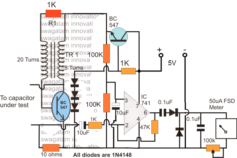
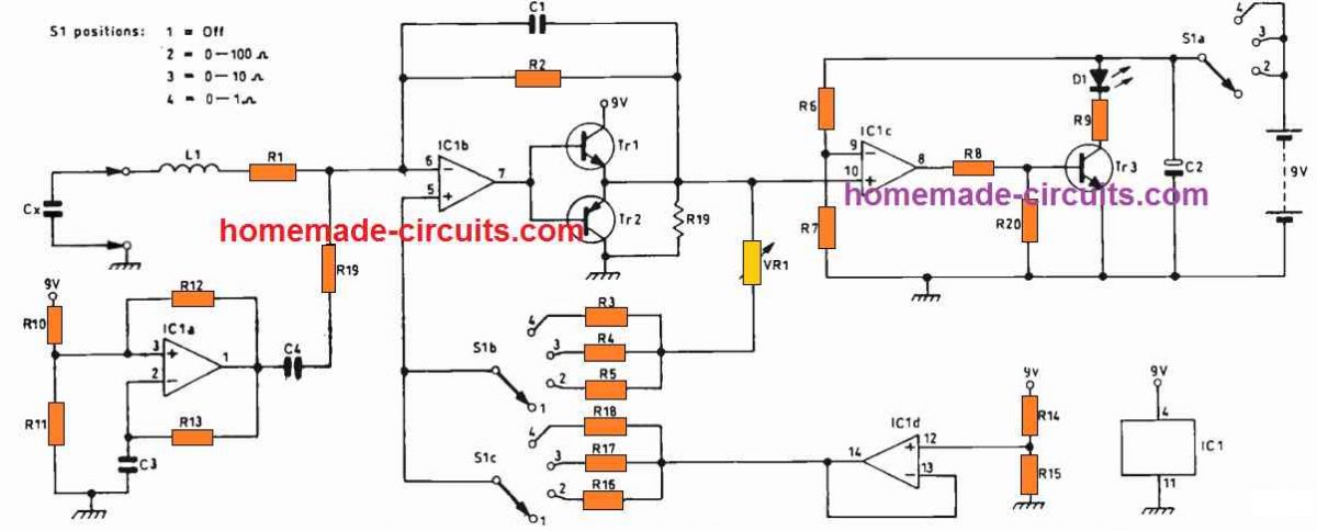
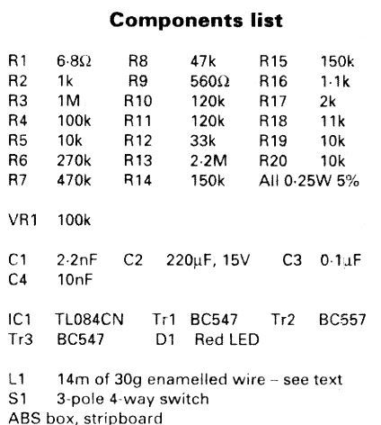
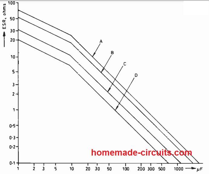
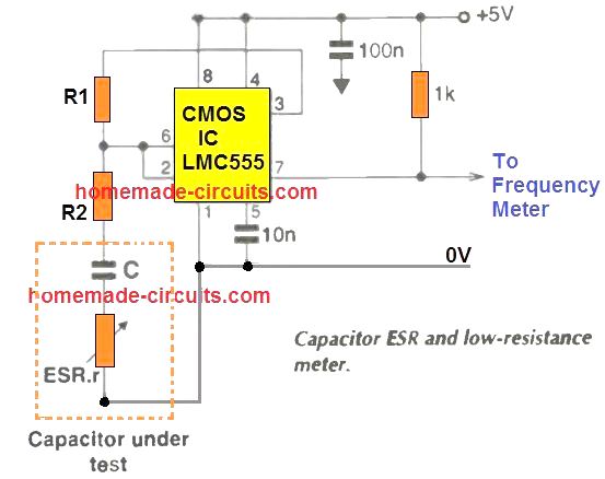 The output frequency is solved by the formula:
f = 1 / 2CR1n(2 - 3k)
In this formula C represents the capacitance, R is formed by (R1 + R2 + r), r denotes the ESR of capacitor C, while the k is positioned as the factor equal to:
k = (R2 + r)/R.
In order to ensure that the circuit works correctly, the factor k value must not be above 0.333.
If it is increased above this value, the IC 555 will go into an uncontrolled oscillating mode, at an extremely high frequency, which will be solely controlled by the propagation delay of the chip.
You will find an exponential increase in the output frequency of the IC by 10X, in response to an increase in the factor k from 0 to 0.31.
As it is increased even further from 0.31 to 0.33, cause the output frequency to increase by another 10X magnitude.
Assuming R1 = 4k7, R2 = 2k2, a minimal ESR = 0 for the C, the k factor should be around 0.3188.
Now, suppose we have the ESR value of around 100 ohm, would cause the k value to increase by 3% at 0.3286. This now forces the IC 555 to oscillate with a frequency that's 3 times greater compared to the original frequency at r = ESR = 0.
This shows that as the r(ESR) increases causes an exponential rise in the frequecny of the IC output.
The output frequency is solved by the formula:
f = 1 / 2CR1n(2 - 3k)
In this formula C represents the capacitance, R is formed by (R1 + R2 + r), r denotes the ESR of capacitor C, while the k is positioned as the factor equal to:
k = (R2 + r)/R.
In order to ensure that the circuit works correctly, the factor k value must not be above 0.333.
If it is increased above this value, the IC 555 will go into an uncontrolled oscillating mode, at an extremely high frequency, which will be solely controlled by the propagation delay of the chip.
You will find an exponential increase in the output frequency of the IC by 10X, in response to an increase in the factor k from 0 to 0.31.
As it is increased even further from 0.31 to 0.33, cause the output frequency to increase by another 10X magnitude.
Assuming R1 = 4k7, R2 = 2k2, a minimal ESR = 0 for the C, the k factor should be around 0.3188.
Now, suppose we have the ESR value of around 100 ohm, would cause the k value to increase by 3% at 0.3286. This now forces the IC 555 to oscillate with a frequency that's 3 times greater compared to the original frequency at r = ESR = 0.
This shows that as the r(ESR) increases causes an exponential rise in the frequecny of the IC output.
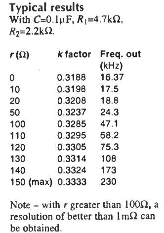
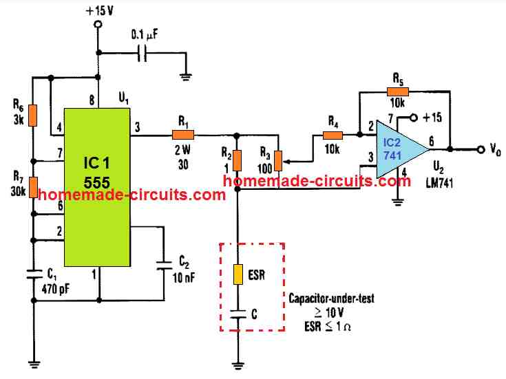 In order to obtain an ac voltage reading, you will have to fine-tune R3 until you find a minimum voltage at Vo output.
Next, look at the placement of the potentiometer and multiply it with the value of R2, 10 Ohm in this case.
The multiplied result will be equivalent to the capacitor's ESR.
A 7.5 v is used for biasing the capacitor under test, therefore capacitors with lower voltage than this cannot be tested with this ESR meter circuit.
By modifying the R2 value, we can upgrade the circuit for additional ranges of ESR measurement.
Having said that, for smaller R2 value the amp level must be higher to enable a fair voltage drop across R2. This might call for some form of intermediate buffer stage.
The circuit will work well for capacitors higher than 100 ¦ĚF.
The ripple voltage will get larger for smaller sized capacitors with a decrease in the accuracy level.
In order to obtain an ac voltage reading, you will have to fine-tune R3 until you find a minimum voltage at Vo output.
Next, look at the placement of the potentiometer and multiply it with the value of R2, 10 Ohm in this case.
The multiplied result will be equivalent to the capacitor's ESR.
A 7.5 v is used for biasing the capacitor under test, therefore capacitors with lower voltage than this cannot be tested with this ESR meter circuit.
By modifying the R2 value, we can upgrade the circuit for additional ranges of ESR measurement.
Having said that, for smaller R2 value the amp level must be higher to enable a fair voltage drop across R2. This might call for some form of intermediate buffer stage.
The circuit will work well for capacitors higher than 100 ¦ĚF.
The ripple voltage will get larger for smaller sized capacitors with a decrease in the accuracy level.
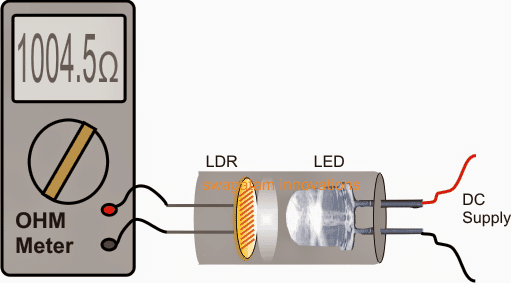
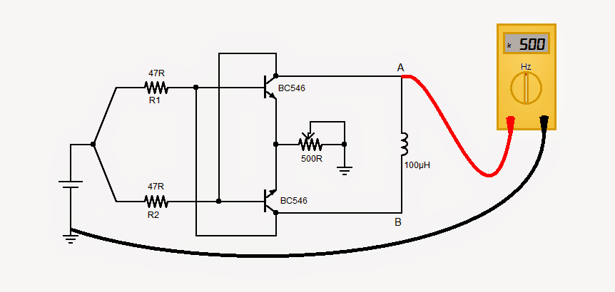

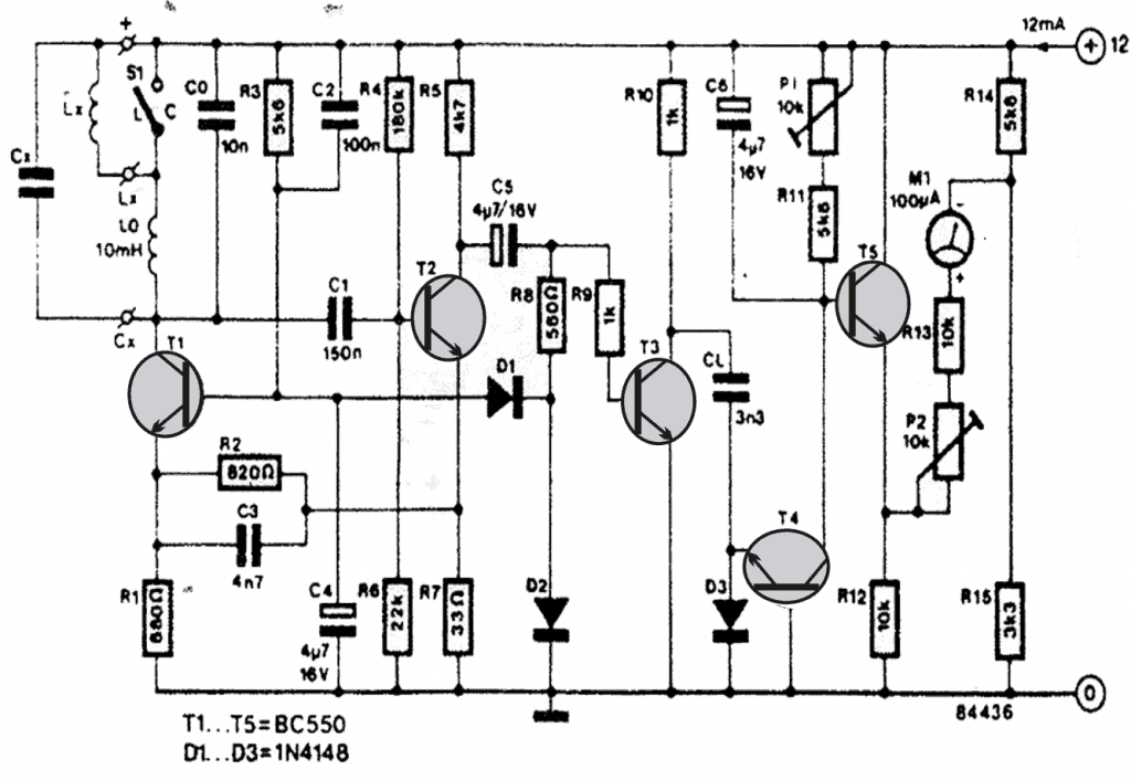


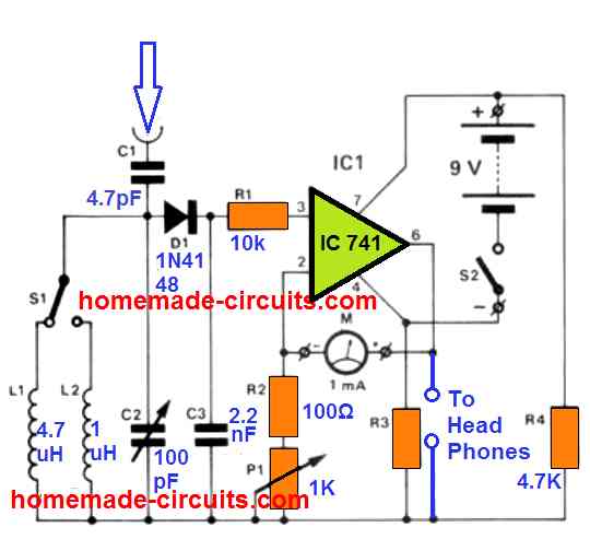 The signal received by the second antenna is subsequently provided to a resonance circuit created by L1, L2 and the varicap C2. This allows the meter to be precisely tuned to the specific transmitting frequency which needs to be measured.
With the inductance values shown for the coil in the schematic the 'band width' of the meter can be anywhere between 6 and 60 MHz.
The RF signal after this is applied to the diode D1, consisting of a rectifier/demodulation stage.
Lastly the signal is directed to the non-inverting input pin#3 of opamp IC1. The gain of this opamp which decides the sensitivity of the 1 mA meter is fine-tuned by the preset P1.
The signal received by the second antenna is subsequently provided to a resonance circuit created by L1, L2 and the varicap C2. This allows the meter to be precisely tuned to the specific transmitting frequency which needs to be measured.
With the inductance values shown for the coil in the schematic the 'band width' of the meter can be anywhere between 6 and 60 MHz.
The RF signal after this is applied to the diode D1, consisting of a rectifier/demodulation stage.
Lastly the signal is directed to the non-inverting input pin#3 of opamp IC1. The gain of this opamp which decides the sensitivity of the 1 mA meter is fine-tuned by the preset P1.
 After some trial and error effort, you will be able to perfectly judge the contact resistance by comparing the differences in the level of the sound frequency.
Another great application of this unit could be in the form of a mini siren or simply as a morse code practice which can be done by connecting a morse key between A and B.
After some trial and error effort, you will be able to perfectly judge the contact resistance by comparing the differences in the level of the sound frequency.
Another great application of this unit could be in the form of a mini siren or simply as a morse code practice which can be done by connecting a morse key between A and B.
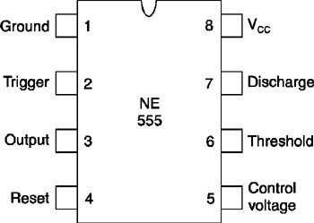 2. One buzzer ( **if you do not have buzzer then use LED)
 3. 9v battery
 4. One 4.7 k resistor
 5. One 47 k resistor
 6. One 10uf ceramic capacitor
 7. One 0.1 uf ceramic capacitor
 8. Two connecting probes( red and black)
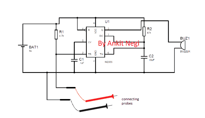 There are total 8 pins in 555 timer as shown in circuit diagram make connections as shown and donˇŻt forget to connect capacitors as they are as important as any other components in this circuit.
Connecting probes are connected between trigger terminal (2) and ground.
**If you do not have a buzzer than connect led in series with 1k resistor in place of buzzer**
There are total 8 pins in 555 timer as shown in circuit diagram make connections as shown and donˇŻt forget to connect capacitors as they are as important as any other components in this circuit.
Connecting probes are connected between trigger terminal (2) and ground.
**If you do not have a buzzer than connect led in series with 1k resistor in place of buzzer**
 Potentiometer R1 could be a trimmer type variable resistor, in case you intend to make use of the device for continuity tests, R1 must be a multi-turn type for simplicity of adjustment.
The relationship to be examined is placed across the test probes and to ground, and across the junction of R2 and R3.
Parts R3 and D1 safeguard against unintentional application of voltage to the circuit.
Considering that the non-inverting input possesses a high impedance, the intersection of R3 is almost just like the non-inverting input so far as proportions are involved.
Once the voltage at the non-inverting input of U1 at pin 5 drops under that at the inverting input, the output becomes low.
This leads to the buzzer becoming active and sounding, showing continuity.
Potentiometer R1 adjusts the limit where the buzzer gets triggered and sounds.
When resistance is detected across the R2 /R3 junction and ground, a voltage divider is created, and this is referenced to the voltage divider established by potentiometer R1.
In case the resistance is very small in comparison to the R1 value adjustment, the buzzer starts making noise.
Potentiometer R1 could be a trimmer type variable resistor, in case you intend to make use of the device for continuity tests, R1 must be a multi-turn type for simplicity of adjustment.
The relationship to be examined is placed across the test probes and to ground, and across the junction of R2 and R3.
Parts R3 and D1 safeguard against unintentional application of voltage to the circuit.
Considering that the non-inverting input possesses a high impedance, the intersection of R3 is almost just like the non-inverting input so far as proportions are involved.
Once the voltage at the non-inverting input of U1 at pin 5 drops under that at the inverting input, the output becomes low.
This leads to the buzzer becoming active and sounding, showing continuity.
Potentiometer R1 adjusts the limit where the buzzer gets triggered and sounds.
When resistance is detected across the R2 /R3 junction and ground, a voltage divider is created, and this is referenced to the voltage divider established by potentiometer R1.
In case the resistance is very small in comparison to the R1 value adjustment, the buzzer starts making noise.
 But during a low resistance via an electronic component, the circuit can confirm that too without fail.
Referring to the figure above, we find the circuit makes use of a couple of 741 opamps.
It provides a short-circuit test current of lower than 200uA.
It picks up resistance values of lower than 10 ohms.
Sweetest of all, it will never malfunction when it comes across PN junction or a diode.
But during a low resistance via an electronic component, the circuit can confirm that too without fail.
Referring to the figure above, we find the circuit makes use of a couple of 741 opamps.
It provides a short-circuit test current of lower than 200uA.
It picks up resistance values of lower than 10 ohms.
Sweetest of all, it will never malfunction when it comes across PN junction or a diode.
 Once you make this jig, you can plug-in the relevant pins of the mosfet into the given G, D, S sockets.
After this you just have to press the push button for confirming the mosfet condition.
If the LED glows only on pressing of the button, then your mosfet is fine, any other results will indicate a bad or defective mosfet.
The cathode of the LED will go to the drain side or drain socket.
For p-channel mosfet you could simply modify the design as per the following image
Once you make this jig, you can plug-in the relevant pins of the mosfet into the given G, D, S sockets.
After this you just have to press the push button for confirming the mosfet condition.
If the LED glows only on pressing of the button, then your mosfet is fine, any other results will indicate a bad or defective mosfet.
The cathode of the LED will go to the drain side or drain socket.
For p-channel mosfet you could simply modify the design as per the following image

 In order to ensure that R6 has no effect on the output voltage this resistor needs to be positioned prior to the voltage divider network which becomes responsible for controlling the output voltage.
S1 which is a DPDT switch is used for selecting either the voltage or the current reading as per the users preference.
With this switch set for measuring voltage P4 along with R1 provides an attenuation of around 100 for the fed input voltage.
Additionally the point D is enabled at a lower voltage level for allowing the illumination of the decimal point on the LS module, and the figure "V" become brightly illuminated.
With the selection switch held towards the Amp range, the voltage drop acquired across the sensing resistor is applied straight over to the points of the Hi-Low inputs of IC1 which is the DAC module.
The significantly low value of the sensing resistors ensures a negligible effect on the voltage divider outcome.
In order to ensure that R6 has no effect on the output voltage this resistor needs to be positioned prior to the voltage divider network which becomes responsible for controlling the output voltage.
S1 which is a DPDT switch is used for selecting either the voltage or the current reading as per the users preference.
With this switch set for measuring voltage P4 along with R1 provides an attenuation of around 100 for the fed input voltage.
Additionally the point D is enabled at a lower voltage level for allowing the illumination of the decimal point on the LS module, and the figure "V" become brightly illuminated.
With the selection switch held towards the Amp range, the voltage drop acquired across the sensing resistor is applied straight over to the points of the Hi-Low inputs of IC1 which is the DAC module.
The significantly low value of the sensing resistors ensures a negligible effect on the voltage divider outcome.
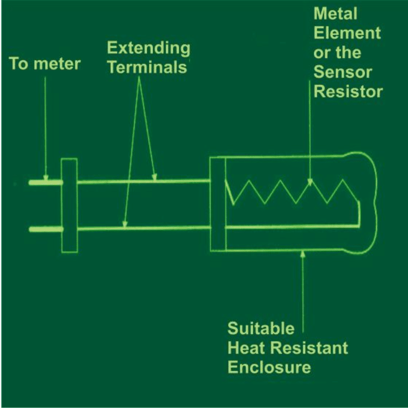
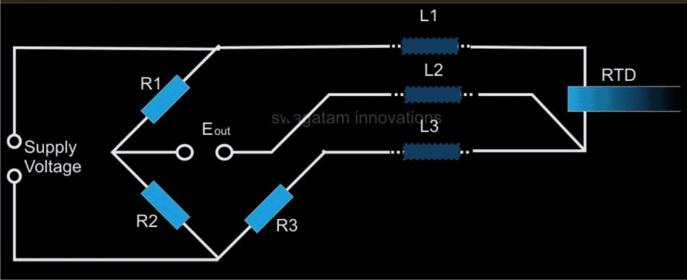 Three Wire RTD: The diagram shows a typical 3 ¨Cwire RTD connections.
Here, the measuring current flows through L1 and L3 whilr L3 behaves just as one of the potential leads.
So long as the bridge is in the balanced condition, no current passes across L2, however L1 and L3 being in separate arms of the wheatstone network, the resistances get nullified and assumes a high impedance across Eo, also resistances between L2 and L3 are held at identical values.
The parameter ensures the use of a maximum of 100 meters of wire to be terminated from the sensor up to the receiving circuit and yet keep the accuracy within 5% of tolerance levels.
Three Wire RTD: The diagram shows a typical 3 ¨Cwire RTD connections.
Here, the measuring current flows through L1 and L3 whilr L3 behaves just as one of the potential leads.
So long as the bridge is in the balanced condition, no current passes across L2, however L1 and L3 being in separate arms of the wheatstone network, the resistances get nullified and assumes a high impedance across Eo, also resistances between L2 and L3 are held at identical values.
The parameter ensures the use of a maximum of 100 meters of wire to be terminated from the sensor up to the receiving circuit and yet keep the accuracy within 5% of tolerance levels.
 Four Wire RTD: The four wire RTD is probably the most efficient technique of producing accurate results even when the actual rtd is placed at far away distances from the monitor display.
The method cancels out all lead wire discrepancies to produces extremely accurate readings.
The principle of operation is based on supplying a constant current through the RTD and measuring the voltage across it through a high impedance measuring device.
The method eliminates the inclusion of a bridge network and yet provides much credible outputs.
The figure shows a typical four wire RTD wiring layout; here a precisely dimensioned constant current derived from a suitable source is applied through L1, L4 and the RTD.
A proportional result becomes directly available across the RTD through L2 and L3 and can be measured with a high impedance DVM, irrespective of its distance from the sensing element.
Here, L1, L2, L3, and L4 which are the resistances of the wires, become insignificant values that have no influence on the actual readings.
How to Make a Homemade RTD High Temperature Sensor
A high temperature sensor unit can be designed by using an ordinary "heater element" like a heater coil or an "iron" element.
The principle of operation is based on the above discussions.
The connections are simple and needs just to be constructed as shown in the following DIAGRAM.
Four Wire RTD: The four wire RTD is probably the most efficient technique of producing accurate results even when the actual rtd is placed at far away distances from the monitor display.
The method cancels out all lead wire discrepancies to produces extremely accurate readings.
The principle of operation is based on supplying a constant current through the RTD and measuring the voltage across it through a high impedance measuring device.
The method eliminates the inclusion of a bridge network and yet provides much credible outputs.
The figure shows a typical four wire RTD wiring layout; here a precisely dimensioned constant current derived from a suitable source is applied through L1, L4 and the RTD.
A proportional result becomes directly available across the RTD through L2 and L3 and can be measured with a high impedance DVM, irrespective of its distance from the sensing element.
Here, L1, L2, L3, and L4 which are the resistances of the wires, become insignificant values that have no influence on the actual readings.
How to Make a Homemade RTD High Temperature Sensor
A high temperature sensor unit can be designed by using an ordinary "heater element" like a heater coil or an "iron" element.
The principle of operation is based on the above discussions.
The connections are simple and needs just to be constructed as shown in the following DIAGRAM.

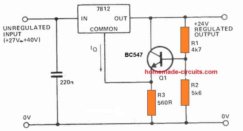 The circuit above eliminates the challenge through the use of transistor Q1 to crank out a low impedance on the regulator common terminal through its emitter-follower configuration.
The transistor emitter transfers the voltage derived from a relatively high-resistance divider network connected across the base of the transistor.
The value of R3 is not crucial, however should be sufficiently small in order to enable the maximum possible quiescent current from the ground terminal of the 7812 IC, without resulting in Q1 to switch off.
The circuit exhibits a functional 24 Volt supply through a 7812 regulator.
A desired higher output voltage from the IC 7812 can be adjusted by altering the values of R1 and R2 accordingly.
The circuit above eliminates the challenge through the use of transistor Q1 to crank out a low impedance on the regulator common terminal through its emitter-follower configuration.
The transistor emitter transfers the voltage derived from a relatively high-resistance divider network connected across the base of the transistor.
The value of R3 is not crucial, however should be sufficiently small in order to enable the maximum possible quiescent current from the ground terminal of the 7812 IC, without resulting in Q1 to switch off.
The circuit exhibits a functional 24 Volt supply through a 7812 regulator.
A desired higher output voltage from the IC 7812 can be adjusted by altering the values of R1 and R2 accordingly.
 In this article we will discuss some interesting and useful application circuits using field effect transistors.
All these applications circuits presented below exploit the high input impedance characteristics of the FET for creating extremely accurate, sensitive, an wide range electronic circuits and projects.
In this article we will discuss some interesting and useful application circuits using field effect transistors.
All these applications circuits presented below exploit the high input impedance characteristics of the FET for creating extremely accurate, sensitive, an wide range electronic circuits and projects.
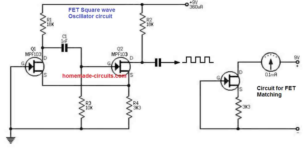 The Drain current consumption is quite low at around 360¦ĚA.
The waveform exhibits an extremely good symmetry which is normally achieved by matching the FETs through the circuit shown on the left hand side.
The FETs must be matched based on their equivalent drain currents.
The operating frequency is determined by the values of the resistor R3 and the capacitor C1. The values as shown in the diagram would produce a frequency of approximately 15kHz.
The Drain current consumption is quite low at around 360¦ĚA.
The waveform exhibits an extremely good symmetry which is normally achieved by matching the FETs through the circuit shown on the left hand side.
The FETs must be matched based on their equivalent drain currents.
The operating frequency is determined by the values of the resistor R3 and the capacitor C1. The values as shown in the diagram would produce a frequency of approximately 15kHz.
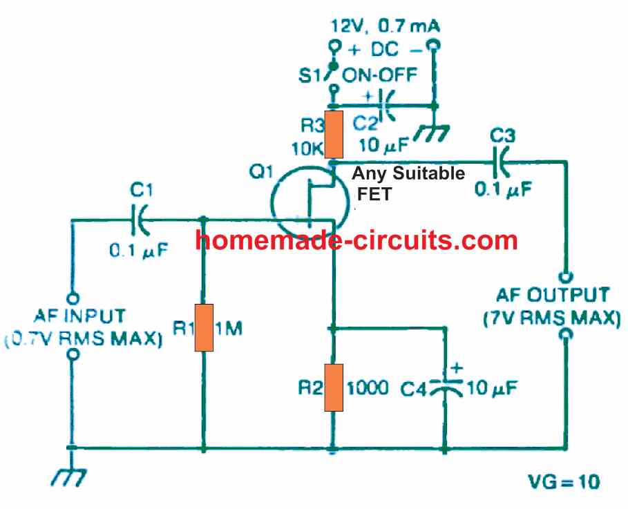 Figure above exhibits the circuit of a single-stage, one-transistor amplifier featuring the many benefits of the FET.
The design is a common-source mode which is comparable with and a common-emitter BJT circuit.
The amp's input impedance is around the 1M introduced by resistor R1. The indicated FET is a low-cost and easily available device.
Voltage gain of the amplifier is 10. The optimum input-signal amplitude just before output-signal peak clipping is around 0.7 volt rms, and the equivalent output-voltage amplitude is 7 volt rms.
At 100 % working specs, the circuit pulls 0.7 mA through the 12-volt DC supply.
Using a single FET the input-signal voltage, output-signal voltage and DC operating current could vary to some extent across the values provided above.
At frequencies between 100 Hz and 25 kHz, the amplifier response is within 1 dB of the 1000 Hz reference.
All resistors can be 1/4 watt type.
Capacitors C2 and C4 are 35-volt electrolytic packages, and capacitors C1 and C3 could be just about any standard low-voltage devices.
A standard battery supply or any suitable DC power supply works extremely; the FET amplifier can also be solar driven by a couple of series attached silicon solar modules.
If desirable, constantly adjustable gain control could be implemented by replacing a 1-megohm potentiometer for resistor R1. This circuit would nicely work as a preamplifier or as a main amplifier in a lot of applications demanding a 20 dB signal boost through the entire music range.
The increased input impedance and moderate output impedance will probably meet the majority of specifications.
For extremely low-noise applications, the indicated FET could be substituted with standard matching FET.
Figure above exhibits the circuit of a single-stage, one-transistor amplifier featuring the many benefits of the FET.
The design is a common-source mode which is comparable with and a common-emitter BJT circuit.
The amp's input impedance is around the 1M introduced by resistor R1. The indicated FET is a low-cost and easily available device.
Voltage gain of the amplifier is 10. The optimum input-signal amplitude just before output-signal peak clipping is around 0.7 volt rms, and the equivalent output-voltage amplitude is 7 volt rms.
At 100 % working specs, the circuit pulls 0.7 mA through the 12-volt DC supply.
Using a single FET the input-signal voltage, output-signal voltage and DC operating current could vary to some extent across the values provided above.
At frequencies between 100 Hz and 25 kHz, the amplifier response is within 1 dB of the 1000 Hz reference.
All resistors can be 1/4 watt type.
Capacitors C2 and C4 are 35-volt electrolytic packages, and capacitors C1 and C3 could be just about any standard low-voltage devices.
A standard battery supply or any suitable DC power supply works extremely; the FET amplifier can also be solar driven by a couple of series attached silicon solar modules.
If desirable, constantly adjustable gain control could be implemented by replacing a 1-megohm potentiometer for resistor R1. This circuit would nicely work as a preamplifier or as a main amplifier in a lot of applications demanding a 20 dB signal boost through the entire music range.
The increased input impedance and moderate output impedance will probably meet the majority of specifications.
For extremely low-noise applications, the indicated FET could be substituted with standard matching FET.
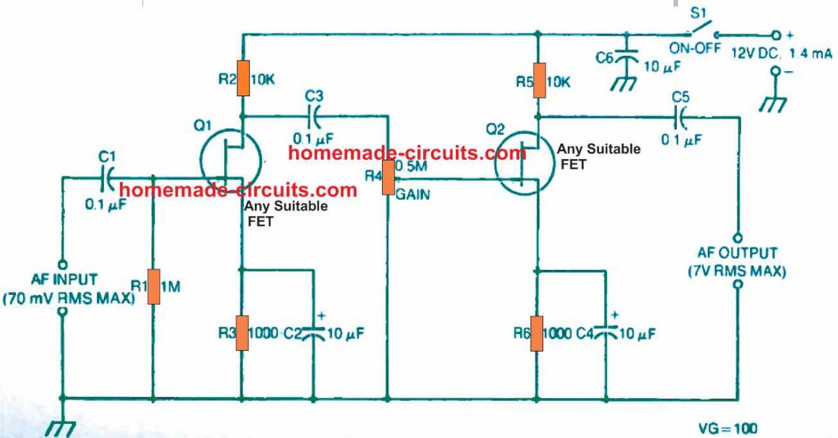 This FET circuit is designed to provide a large boost (40 dB) to any modest AF signal, and could be applied both individually or introduced as a stage in equipment requiring this capability.
The input impedance of the 2-stage FET amplifier circuit is around 1 megohm, determined by the input resistor value R1. All round voltage gain of the design is 100, although this number might deviate relatively up or down-with specific FETs.
The highest input-signal amplitude prior to output-signal peak clipping is 70 mV rms which results in the output-signal amplitude of 7 volts rms.
Under full functional mode, the circuit might consume roughly 1.4 mA through the 12-volt DC source, however this current could change a bit depending on the characteristics of specific FETs.
We did not find any need for including a decoupling filter across stages, since this type of filter could cause a reduction in the current of one stage.
The unit's frequency response was tested flat within ˇŔ 1 dB of the 1 kHz level, from 100 Hz to better than 20 kHz.
Because the input stage extends ˇ°wide open,ˇŻˇŻ there could be a possibility of hum pick up hum, unless this stage and the input terminals are properly shielded.
In persistent situations, R1 could be decreased to 0.47 Meg.
In situations where amplifier needs to create smaller loading of the signal source, R1 could be increased to very large values up to 22 megohms, given the input stage shielded extremely well.
Having said that, resistance above this value might cause the resistance value to become same as the FET junction resistance value.
This FET circuit is designed to provide a large boost (40 dB) to any modest AF signal, and could be applied both individually or introduced as a stage in equipment requiring this capability.
The input impedance of the 2-stage FET amplifier circuit is around 1 megohm, determined by the input resistor value R1. All round voltage gain of the design is 100, although this number might deviate relatively up or down-with specific FETs.
The highest input-signal amplitude prior to output-signal peak clipping is 70 mV rms which results in the output-signal amplitude of 7 volts rms.
Under full functional mode, the circuit might consume roughly 1.4 mA through the 12-volt DC source, however this current could change a bit depending on the characteristics of specific FETs.
We did not find any need for including a decoupling filter across stages, since this type of filter could cause a reduction in the current of one stage.
The unit's frequency response was tested flat within ˇŔ 1 dB of the 1 kHz level, from 100 Hz to better than 20 kHz.
Because the input stage extends ˇ°wide open,ˇŻˇŻ there could be a possibility of hum pick up hum, unless this stage and the input terminals are properly shielded.
In persistent situations, R1 could be decreased to 0.47 Meg.
In situations where amplifier needs to create smaller loading of the signal source, R1 could be increased to very large values up to 22 megohms, given the input stage shielded extremely well.
Having said that, resistance above this value might cause the resistance value to become same as the FET junction resistance value.
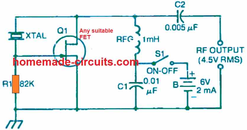 The untuned crystal oscillator is applied in transmitters, clock generators, crystal testers receiver front ends, markers, RF signal generators, signal spotters (secondary frequency standards), and several related systems.
The FET circuit will show a quick start tendency for crystals that are beter suited for the tuning.
The FET untuned oscillator circuit consumes roughly 2 mA from the 6-volt DC source.
With this source voltage, the open-circuit RF Output voltage is around 4% volts rms DC supply voltages as much as 12 volts could be applied, with correspondingly increased RF output.
To find out if the oscillator is functioning, shut switch S1 and hook up an RF voltmeter across the RF Output terminals.
In case an RF meter is not accessible, you can use any high-resistance DC voltmeter appropriately shunted through a general-purpose germanium diode.
If the meter needle vibrates will indicate the working of the circuit and the RF emission.
A different approach could be, to connect the oscillator with the Antenna and Ground terminals of a CW receiver that could be tuned with the crystal frequency in order to determine the RF oscillations.
To avoid flawed functioning, it is strongly recommended that the Pierce oscillator works with the specified frequency range of the crystal when the crystal is a fundamental-frequency cut.
If overtone crystals are employed, the output will not oscillate at the crystals rated frequency, rather with the lower frequency as decided by the crystal proportions.
In order to run the crystal at the rated frequency of an overtone crystal, the oscillator needs to be of the tuned type.
The untuned crystal oscillator is applied in transmitters, clock generators, crystal testers receiver front ends, markers, RF signal generators, signal spotters (secondary frequency standards), and several related systems.
The FET circuit will show a quick start tendency for crystals that are beter suited for the tuning.
The FET untuned oscillator circuit consumes roughly 2 mA from the 6-volt DC source.
With this source voltage, the open-circuit RF Output voltage is around 4% volts rms DC supply voltages as much as 12 volts could be applied, with correspondingly increased RF output.
To find out if the oscillator is functioning, shut switch S1 and hook up an RF voltmeter across the RF Output terminals.
In case an RF meter is not accessible, you can use any high-resistance DC voltmeter appropriately shunted through a general-purpose germanium diode.
If the meter needle vibrates will indicate the working of the circuit and the RF emission.
A different approach could be, to connect the oscillator with the Antenna and Ground terminals of a CW receiver that could be tuned with the crystal frequency in order to determine the RF oscillations.
To avoid flawed functioning, it is strongly recommended that the Pierce oscillator works with the specified frequency range of the crystal when the crystal is a fundamental-frequency cut.
If overtone crystals are employed, the output will not oscillate at the crystals rated frequency, rather with the lower frequency as decided by the crystal proportions.
In order to run the crystal at the rated frequency of an overtone crystal, the oscillator needs to be of the tuned type.
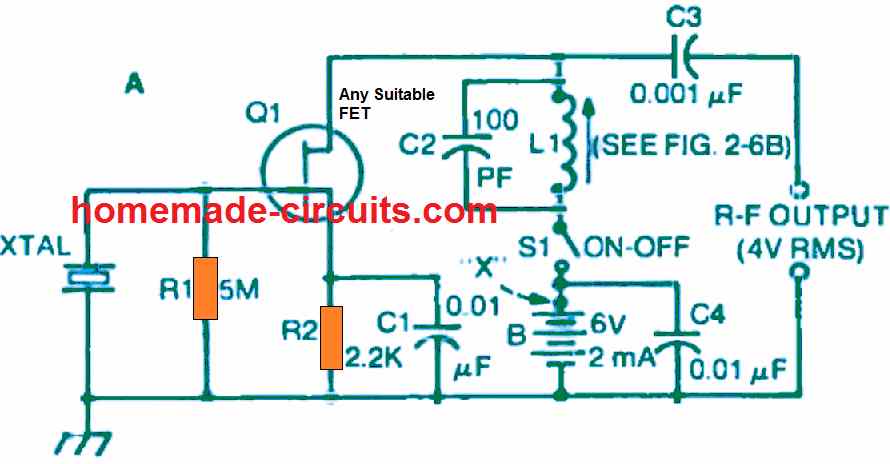 This oscillator can be easily customized for applications such as in communications, instrumentation, and control systems.
It could even be applied as a flea-powered transmitter, for communications or RC model control.
As soon as the resonant circuit, L1-C1, is tuned to the crystal frequency, the oscillator starts pulling around 2 mA from the 6-volt DC source.
The associated open-circuit RF output voltage is around 4 volts rms.
The drain current draw will be reduced with frequencies of 100 kHz compared to on other frequencies, because of the inductor resistance utilized for that frequency.
The next Figure (B) illustrates a list of industrial, slug-tuned inductors (L1) which work extremely well with this FET oscillator circuit.
This oscillator can be easily customized for applications such as in communications, instrumentation, and control systems.
It could even be applied as a flea-powered transmitter, for communications or RC model control.
As soon as the resonant circuit, L1-C1, is tuned to the crystal frequency, the oscillator starts pulling around 2 mA from the 6-volt DC source.
The associated open-circuit RF output voltage is around 4 volts rms.
The drain current draw will be reduced with frequencies of 100 kHz compared to on other frequencies, because of the inductor resistance utilized for that frequency.
The next Figure (B) illustrates a list of industrial, slug-tuned inductors (L1) which work extremely well with this FET oscillator circuit.
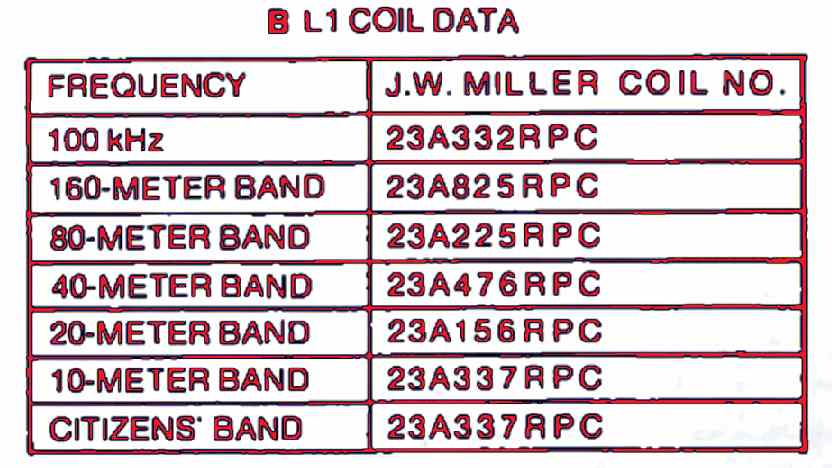 Inductances are selected for the 100 kHz normal frequency, 5 ham radio bands, and the 27 MHz citizens band; nevertheless, a considerable inductance range is taken care of by manipulation of the slug of each inductor, and a broader frequency range than the bands suggested in the table could be acquired with every single inductor.
The oscillator could be tuned to your crystal frequency simply by turning the slug up/down of the inductor (L1) to get optimum deviation of the connected RF voltmeter across the RF Output terminals.
Another method would be, to tune the L1 with a 0 - 5 DC hooked up at point X: Next, fine-tune the L1 slug until an aggressive dip is seen on meter reading.
The slug tuning facility gives you a precisely-tuned function.
In applications in which it becomes essential to tune the oscillator frequently using a resettable calibration, a 100 pF adjustable capacitor should be used instead of C2, and the slug utilized just to fix the maximum frequency of the performance range.
Inductances are selected for the 100 kHz normal frequency, 5 ham radio bands, and the 27 MHz citizens band; nevertheless, a considerable inductance range is taken care of by manipulation of the slug of each inductor, and a broader frequency range than the bands suggested in the table could be acquired with every single inductor.
The oscillator could be tuned to your crystal frequency simply by turning the slug up/down of the inductor (L1) to get optimum deviation of the connected RF voltmeter across the RF Output terminals.
Another method would be, to tune the L1 with a 0 - 5 DC hooked up at point X: Next, fine-tune the L1 slug until an aggressive dip is seen on meter reading.
The slug tuning facility gives you a precisely-tuned function.
In applications in which it becomes essential to tune the oscillator frequently using a resettable calibration, a 100 pF adjustable capacitor should be used instead of C2, and the slug utilized just to fix the maximum frequency of the performance range.
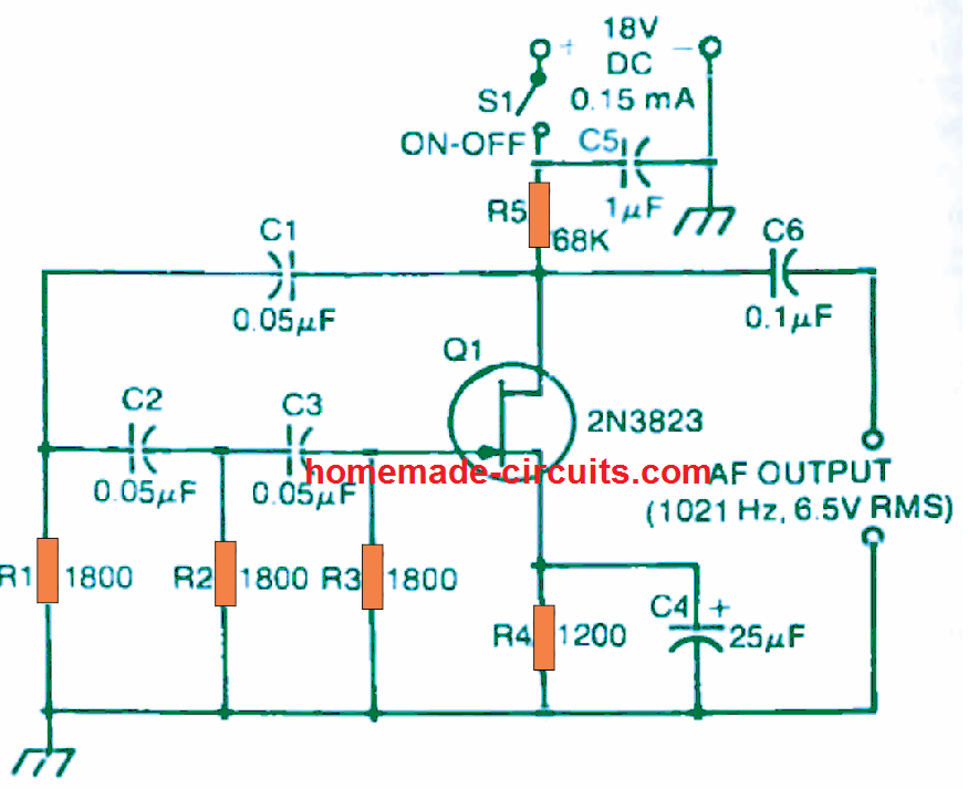 The figure above exhibits the circuit of a phase-shift AF oscillator working with a solitary FET.
In this particular circuit, the frequency depends upon the 3-pin RC phase-shift circuit (C1-C2-C3-R1-R2-R3) which provides the oscillator its specific name.
For the intended 180ˇă phase shift for oscillation, the values of Q1, R and C in the feedback line are appropriately chosen for generating a 60ˇă shift on each individual pin (R1-C1, R2-C2. and R3-C3) between the drain and gate of FET Q1.
For convenience, the capacitances are selected to be equal in value (C1 = C2 = C3) and the resistances are likewise determined with equal values (R1 = R2 = R3).
The frequency of the network frequency (and for that matter the oscillation frequency of the design) in that case will be f = 1/(10.88 RC).
where f is in hertz, R in ohms, and C in farads.
With the values presented in the circuit diagram, the frequency as a result is 1021 Hz (for precisely 1000 Hz with the 0.05 uF capacitors, R1, R2. and R3 individually should be 1838 ohms).
While playing with a phase-shift oscillator, it might be better to tweak the resistors compared to the capacitors.
For an known capacitance (C), the corresponding resistance (R) to get a desired frequency (f) will be R = 1/(10.88 f C), where R is in ohms, f in hertz, and C in farads.
Therefore, with the 0.05 uF capacitors indicated in figure above, the resistance needed for 400 Hz = 1/(10.88 x 400 X 5 X 10^8 ) = 1/0.0002176 = 4596 ohms.
The 2N3823 FET delivers the large transconductance (6500 /umho) necessary for optimum working of the FET phase-shift oscillator circuit.
The circuit pulls around 0.15 mA through the 18-volt DC source, and the open-circuit AF output is around 6.5 volts rms.
All resistors used in the circuit are or1/4-watt 5% rated.
Capacitors C5 and C6 could be any handy low voltage devices.
Electrolytic capacitor C4 is actually a 25-volt device.
To ensure a stable frequency, capacitors Cl, C2, and C3 should be of best high quality and carefully matched up with capacitance.
The figure above exhibits the circuit of a phase-shift AF oscillator working with a solitary FET.
In this particular circuit, the frequency depends upon the 3-pin RC phase-shift circuit (C1-C2-C3-R1-R2-R3) which provides the oscillator its specific name.
For the intended 180ˇă phase shift for oscillation, the values of Q1, R and C in the feedback line are appropriately chosen for generating a 60ˇă shift on each individual pin (R1-C1, R2-C2. and R3-C3) between the drain and gate of FET Q1.
For convenience, the capacitances are selected to be equal in value (C1 = C2 = C3) and the resistances are likewise determined with equal values (R1 = R2 = R3).
The frequency of the network frequency (and for that matter the oscillation frequency of the design) in that case will be f = 1/(10.88 RC).
where f is in hertz, R in ohms, and C in farads.
With the values presented in the circuit diagram, the frequency as a result is 1021 Hz (for precisely 1000 Hz with the 0.05 uF capacitors, R1, R2. and R3 individually should be 1838 ohms).
While playing with a phase-shift oscillator, it might be better to tweak the resistors compared to the capacitors.
For an known capacitance (C), the corresponding resistance (R) to get a desired frequency (f) will be R = 1/(10.88 f C), where R is in ohms, f in hertz, and C in farads.
Therefore, with the 0.05 uF capacitors indicated in figure above, the resistance needed for 400 Hz = 1/(10.88 x 400 X 5 X 10^8 ) = 1/0.0002176 = 4596 ohms.
The 2N3823 FET delivers the large transconductance (6500 /umho) necessary for optimum working of the FET phase-shift oscillator circuit.
The circuit pulls around 0.15 mA through the 18-volt DC source, and the open-circuit AF output is around 6.5 volts rms.
All resistors used in the circuit are or1/4-watt 5% rated.
Capacitors C5 and C6 could be any handy low voltage devices.
Electrolytic capacitor C4 is actually a 25-volt device.
To ensure a stable frequency, capacitors Cl, C2, and C3 should be of best high quality and carefully matched up with capacitance.
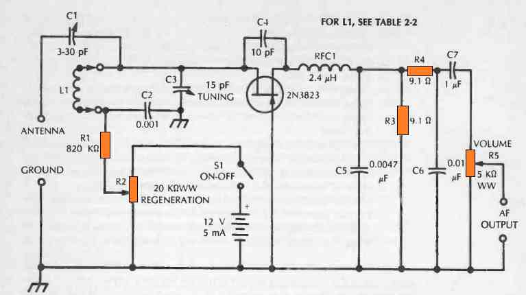 Using 4 different coils for L1, the circuit will quickly detect and start receiving the 2, 6, and 10-meter ham band signals and possibly even the 27 MHz spot.
The coil details are indicated below:
For receiving 10-meter band, or 27-MHZ band, use L1 = 3.3 uH to 6.5 uH inductance, over a Ceramic former, Powdered iron core slug.
For receiving 6-meter band use L1 = 0.99 uH to 1.5 uH inductance, 0.04 over a Ceramic form, and iron slug.
For receiving 2-Meter Amateur Band wind L1 with 4 turns No.
14 bare wire air-wound 1/2 inch diameter.
The frequency range enables the receiver specifically for standard communications as well as for radio model control.
All inductors are solitary, 2-terminal packages.
The 27 MHz and 6 and 10-meter inductors are ordinary, slug-tuned units that needs to be installed on two-pin sockets for quick plug-in or replacing (for singleband receivers, these inductors could be soldered permanently over the PCB).
Having said that, the 2-meter coil has to be wound by the user, and also this should be furnished with a push-in type of base socket, apart from in a single-band receiver.
A filter network comprising (RFC1-C5-R3) eliminates the RF ingredient from the receiver output circuit, while an additional filter (R4-C6) attenuates the quench frequency.
An appropriate 2.4 uH inductor for the RF filter.
Using 4 different coils for L1, the circuit will quickly detect and start receiving the 2, 6, and 10-meter ham band signals and possibly even the 27 MHz spot.
The coil details are indicated below:
For receiving 10-meter band, or 27-MHZ band, use L1 = 3.3 uH to 6.5 uH inductance, over a Ceramic former, Powdered iron core slug.
For receiving 6-meter band use L1 = 0.99 uH to 1.5 uH inductance, 0.04 over a Ceramic form, and iron slug.
For receiving 2-Meter Amateur Band wind L1 with 4 turns No.
14 bare wire air-wound 1/2 inch diameter.
The frequency range enables the receiver specifically for standard communications as well as for radio model control.
All inductors are solitary, 2-terminal packages.
The 27 MHz and 6 and 10-meter inductors are ordinary, slug-tuned units that needs to be installed on two-pin sockets for quick plug-in or replacing (for singleband receivers, these inductors could be soldered permanently over the PCB).
Having said that, the 2-meter coil has to be wound by the user, and also this should be furnished with a push-in type of base socket, apart from in a single-band receiver.
A filter network comprising (RFC1-C5-R3) eliminates the RF ingredient from the receiver output circuit, while an additional filter (R4-C6) attenuates the quench frequency.
An appropriate 2.4 uH inductor for the RF filter.
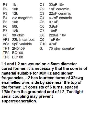
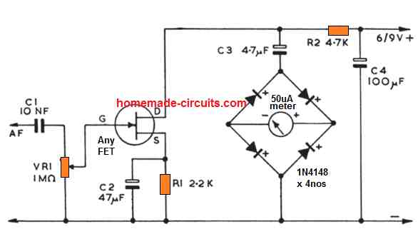 Audio power through the FET drain builds up a voltage around R2, and is connected to the full-wave rectifiers by C3. Current from this bridge rectifier configuration flows by means of the meter, to indicate an equivalent reading that is determined by the power of the fed audio signal.
This form of sensitive level meter or VU meter is advantageous for recording music through a calibrated scale that is supplied through VR1. It can be used likewise used to keep track of the level of audio signals commonly.
The loading offered by the network of C1/VR1 is going to be of minimal significance for the majority of medium or reasonably low impedance circuits.
For apparent causes, AF obtained can be from a position right after any gain or volume controls in the sound products.
The location where the signal amount is considerably excessive, a resistor could be positioned in series with C1. The value of this resistor relies on the signal voltage, however could be anticipated to lie between around 470k and 10 megohm
Audio power through the FET drain builds up a voltage around R2, and is connected to the full-wave rectifiers by C3. Current from this bridge rectifier configuration flows by means of the meter, to indicate an equivalent reading that is determined by the power of the fed audio signal.
This form of sensitive level meter or VU meter is advantageous for recording music through a calibrated scale that is supplied through VR1. It can be used likewise used to keep track of the level of audio signals commonly.
The loading offered by the network of C1/VR1 is going to be of minimal significance for the majority of medium or reasonably low impedance circuits.
For apparent causes, AF obtained can be from a position right after any gain or volume controls in the sound products.
The location where the signal amount is considerably excessive, a resistor could be positioned in series with C1. The value of this resistor relies on the signal voltage, however could be anticipated to lie between around 470k and 10 megohm
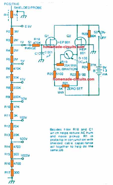 The unit consumes roughly 1.3 mA from a integrated 9-volt battery, B, thus could be left operational for long periods of time.
This device specializes 0-1000 volts measurement in 8 ranges: 0-0.5, 0-1, 0-5, 0-10, 0-50, 0-100,0-500, andO-1000 volts.
The input voltage divider (range switching), the necessary resistances consist of series-connected stock-value resistors that needs to be determined cautiously for obtaining resistance values as close as possible to the portrayed values.
In case precision instrument-type resistors are obtainable, the quantity of resistors in this thread could be reduced by 50%.
Meaning , for R2 and R3, replace 5 Meg.; for R4 and R5, 4 Meg.; for R6 and R7, 500 K; for R8 and R9, 400 K; for R10 and R11, 50 K; for R12 and R13, 40K; for R14 and R15, 5 K; and for R16 and R17,5 K.
This well balanced DC voltmeter circuit features almost no zero drift; any kind of drift in FET Q1 is countered automatically with a balancing drift in Q2. The internal drain-to-source connections of the FETs, along with resistors R20, R21, and R22, creates a resistance bridge.
Display microammeter M1 works like the detector within this bridge network.
When a zero signal input is applied to the electronic voltmeter circuit, meter M1 is defined to zero by adjusting the balance of this bridge using potentiometer R21.
If a DC voltage hereafter is given to the input terminals, causes unbalancing in the bridge, due to the internal drain-to-source resistance alteration of the FETs, which results in a proportionate amount of deflection on the meter reading.
The RC filter created by R18 and C1 helps to eliminate AC hum and noise detected by the probe and the voltage-switching circuits.
The unit consumes roughly 1.3 mA from a integrated 9-volt battery, B, thus could be left operational for long periods of time.
This device specializes 0-1000 volts measurement in 8 ranges: 0-0.5, 0-1, 0-5, 0-10, 0-50, 0-100,0-500, andO-1000 volts.
The input voltage divider (range switching), the necessary resistances consist of series-connected stock-value resistors that needs to be determined cautiously for obtaining resistance values as close as possible to the portrayed values.
In case precision instrument-type resistors are obtainable, the quantity of resistors in this thread could be reduced by 50%.
Meaning , for R2 and R3, replace 5 Meg.; for R4 and R5, 4 Meg.; for R6 and R7, 500 K; for R8 and R9, 400 K; for R10 and R11, 50 K; for R12 and R13, 40K; for R14 and R15, 5 K; and for R16 and R17,5 K.
This well balanced DC voltmeter circuit features almost no zero drift; any kind of drift in FET Q1 is countered automatically with a balancing drift in Q2. The internal drain-to-source connections of the FETs, along with resistors R20, R21, and R22, creates a resistance bridge.
Display microammeter M1 works like the detector within this bridge network.
When a zero signal input is applied to the electronic voltmeter circuit, meter M1 is defined to zero by adjusting the balance of this bridge using potentiometer R21.
If a DC voltage hereafter is given to the input terminals, causes unbalancing in the bridge, due to the internal drain-to-source resistance alteration of the FETs, which results in a proportionate amount of deflection on the meter reading.
The RC filter created by R18 and C1 helps to eliminate AC hum and noise detected by the probe and the voltage-switching circuits.
 In the absence of a voltage input, R1 preserves the FET gate at negative potential, and VR1 is defined to ensure that supply current via the meter M is minimal.
As soon as the FET gate is supplied with a positive voltage, meter M indicates the supply current.
Resistor R5 is only positioned like a current limiting resistor, in order to safeguard the meter.
If 1 megohm is used for R1, and 10 megohm resistors for R2, R3 and R4 will enable the meter to measure voltage ranges between roughly 0.5v to 15v.
The VR1 potentiometer can be normally 5k
The loading enforced by the meter on a 15v circuit is going to be a high impedance, more than 30 megohms.
Switch S1 is used for selecting various measuring ranges.
If 100 uA meter is employed, then R5 could be 100 k.
The meter may not provide a linear scale, although specific calibration can be easily created through a pot and voltmeter, which enables the device all the desired voltages to be measured across the test leads.
In the absence of a voltage input, R1 preserves the FET gate at negative potential, and VR1 is defined to ensure that supply current via the meter M is minimal.
As soon as the FET gate is supplied with a positive voltage, meter M indicates the supply current.
Resistor R5 is only positioned like a current limiting resistor, in order to safeguard the meter.
If 1 megohm is used for R1, and 10 megohm resistors for R2, R3 and R4 will enable the meter to measure voltage ranges between roughly 0.5v to 15v.
The VR1 potentiometer can be normally 5k
The loading enforced by the meter on a 15v circuit is going to be a high impedance, more than 30 megohms.
Switch S1 is used for selecting various measuring ranges.
If 100 uA meter is employed, then R5 could be 100 k.
The meter may not provide a linear scale, although specific calibration can be easily created through a pot and voltmeter, which enables the device all the desired voltages to be measured across the test leads.
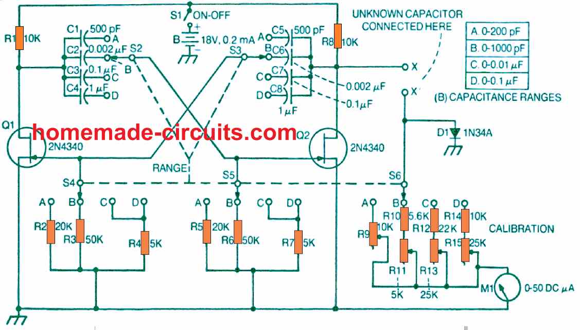 This capacitance meter implements this 4 separate ranges 0 to 0.1 uF 0 to 200 uF, 0 to 1000 uF, 0 to 0.01 uF, and 0 to 0.1 uF.
Working procedure of the circuit is quite linear, which allows easy calibration of the 0 - 50 DC microammeter M1 scale in picofarads and microfarads.
An unknown capacitance plugged into slots X-X subsequently could be measured straight through the meter, without the need of any sort of calculations or balancing manipulations.
The circuit requires around 0.2 mA through an in-built 18-volt battery, B.
In this particular capacitance meter circuit, the a couple of FETs (Q1 and Q2) are function in a standard drain-coupled multivibrator mode.
The multivibrator output, obtained from the Q2 drain, is a constant-amplitude square wave with a frequency mainly decided by the values of capacitors C1 to C8 and resistors R2 to R7.
The capacitances on each of the ranges are selected identically, while the very same is done for the resistances selection also.
A 6-pole.
4-position.
rotary switch (S1-S2-S3-S4-S5-S6) picks the appropriate multivibrator capacitors and resistors along with the meter-circuit resistance combination necessary for delivering the test frequency for a selected capacitance range.
The square-wave is applied to the meter circuit through the unknown capacitor (connected across the terminals X-X).
You don't have to worry about any zero meter setting; since the meter needle can eb expected to rest at the zero as long as an unknown capacitor is not plugged into slots X-X.
For a selected square-wave frequency, the meter needle deflection generates a directly proportional reading to the value of the unknown capacitance C, along with a nice and linear response.
Hence, if in the preliminary calibration of the circuit is implemented using a precisely identified 1000 pF capacitor attached to terminals X-X, and the range switch positioned to position B, and calibration pot R11 adjusted to achieve an exact full-scale deflection on the meter M1, then the meter will without any doubt measure the 1000 pF value at its full scale deflection.
Since the proposed capacitance meter circuit provide a linear response to its, the 500 pF can be expected to read at around half scale of the meter dial, 100 pF at 1/10 scale, and so forth.
For the 4 ranges of the capacitance measurement, the multivibrator frequency can be toggled to the following values: 50 kHz (0ˇŞ200 pF), 5 kHz (0-1000 pF), 1000 Hz (0ˇŞ0.01 uF), and 100 Hz (0-0.1 uF).
For this reason, switch segments S2 and S3 swap the multivibrator capacitors with equivalent sets in unison with switch sections S4 and S5 that switch the multivibrator resistors through equivalent pairs.
The frequency-determining capacitors should be capacitance-matched in pairs: C1 = C5. C2 = C6. C3 = C7, and C4 = C8. Similarly, the frequency-determining resistors should be resistance-matched in pairs: R2 = R5. R3 = R6, and R4 = R7.
The load resistors R1 and R8 at the FET drain likewise must be appropriately matched.
The pots R9. R11, R13, and R15 that are used for the calibration should be wirewound types; and because these are adjusted only for the calibration purpose, they could be fitted inside the enclosure of the circuit, and furnished with slotted shafts for enabling adjustment through a screwdriver.
All the fixed resistors (R1 to R8. R10, R12. R14) should be 1-watt rated.
This capacitance meter implements this 4 separate ranges 0 to 0.1 uF 0 to 200 uF, 0 to 1000 uF, 0 to 0.01 uF, and 0 to 0.1 uF.
Working procedure of the circuit is quite linear, which allows easy calibration of the 0 - 50 DC microammeter M1 scale in picofarads and microfarads.
An unknown capacitance plugged into slots X-X subsequently could be measured straight through the meter, without the need of any sort of calculations or balancing manipulations.
The circuit requires around 0.2 mA through an in-built 18-volt battery, B.
In this particular capacitance meter circuit, the a couple of FETs (Q1 and Q2) are function in a standard drain-coupled multivibrator mode.
The multivibrator output, obtained from the Q2 drain, is a constant-amplitude square wave with a frequency mainly decided by the values of capacitors C1 to C8 and resistors R2 to R7.
The capacitances on each of the ranges are selected identically, while the very same is done for the resistances selection also.
A 6-pole.
4-position.
rotary switch (S1-S2-S3-S4-S5-S6) picks the appropriate multivibrator capacitors and resistors along with the meter-circuit resistance combination necessary for delivering the test frequency for a selected capacitance range.
The square-wave is applied to the meter circuit through the unknown capacitor (connected across the terminals X-X).
You don't have to worry about any zero meter setting; since the meter needle can eb expected to rest at the zero as long as an unknown capacitor is not plugged into slots X-X.
For a selected square-wave frequency, the meter needle deflection generates a directly proportional reading to the value of the unknown capacitance C, along with a nice and linear response.
Hence, if in the preliminary calibration of the circuit is implemented using a precisely identified 1000 pF capacitor attached to terminals X-X, and the range switch positioned to position B, and calibration pot R11 adjusted to achieve an exact full-scale deflection on the meter M1, then the meter will without any doubt measure the 1000 pF value at its full scale deflection.
Since the proposed capacitance meter circuit provide a linear response to its, the 500 pF can be expected to read at around half scale of the meter dial, 100 pF at 1/10 scale, and so forth.
For the 4 ranges of the capacitance measurement, the multivibrator frequency can be toggled to the following values: 50 kHz (0ˇŞ200 pF), 5 kHz (0-1000 pF), 1000 Hz (0ˇŞ0.01 uF), and 100 Hz (0-0.1 uF).
For this reason, switch segments S2 and S3 swap the multivibrator capacitors with equivalent sets in unison with switch sections S4 and S5 that switch the multivibrator resistors through equivalent pairs.
The frequency-determining capacitors should be capacitance-matched in pairs: C1 = C5. C2 = C6. C3 = C7, and C4 = C8. Similarly, the frequency-determining resistors should be resistance-matched in pairs: R2 = R5. R3 = R6, and R4 = R7.
The load resistors R1 and R8 at the FET drain likewise must be appropriately matched.
The pots R9. R11, R13, and R15 that are used for the calibration should be wirewound types; and because these are adjusted only for the calibration purpose, they could be fitted inside the enclosure of the circuit, and furnished with slotted shafts for enabling adjustment through a screwdriver.
All the fixed resistors (R1 to R8. R10, R12. R14) should be 1-watt rated.
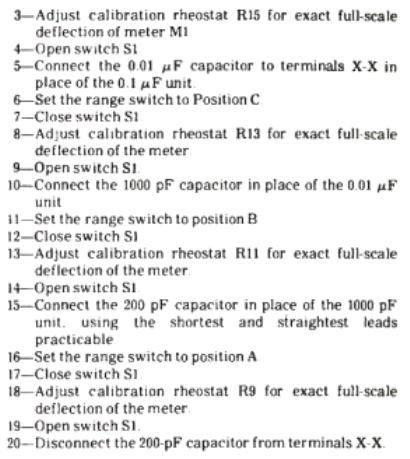 An distinctive meter card can be drawn, or numbers could be written on the existing microammeter background dial to indicate capacitance ranges of 0-200 pF, 0-1000 pF, 0-0.01 uF, and 0-0 1 uF.
As the capacitance meter is used further, you might feel it necessary to attach an unknown capacitor to terminals X-X turn ON S1 to test the capacitance reading on the meter.
For greatest precision, it is advised to incorporate the range which will allow the deflection around the top section of the meter scale.
An distinctive meter card can be drawn, or numbers could be written on the existing microammeter background dial to indicate capacitance ranges of 0-200 pF, 0-1000 pF, 0-0.01 uF, and 0-0 1 uF.
As the capacitance meter is used further, you might feel it necessary to attach an unknown capacitor to terminals X-X turn ON S1 to test the capacitance reading on the meter.
For greatest precision, it is advised to incorporate the range which will allow the deflection around the top section of the meter scale.
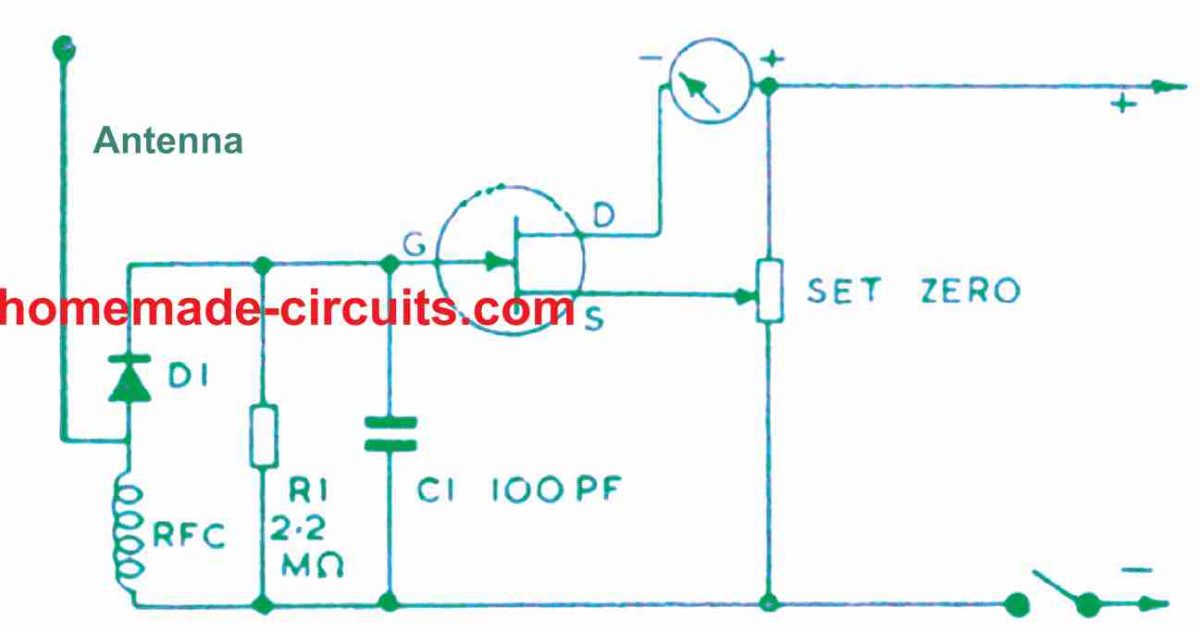 When no RF input signal is present, it adjusts gate/source potential in a way that the meter displays merely a tiny current, which increases proportionately depending on the level of the input RF signal.
To get higher sensitivity, a 100uA meter could be installed.
Otherwise, a low sensitivity meter like 25uA, 500uA or 1mA might also work quite well, and provide the required RF strength measurements.
If the field strength meter is required to test for VHF only, a VHF choke will need to be incorporated, but for normal application around lower frequencies, a short wave choke is essential.
An inductance of approximately 2.5mH is will do the job for up to 1.8 MHz and higher frequencies.
The FET field strength meter circuit could be built inside a compact metal box, with the antenna extended outside the enclosure, vertically.
While operating , the device enables tuning up a transmitter final amplifier and aerial circuits, or the realignment of bias, drive and other variables, to confirm optimum radiated output.
The result of adjustments could be witnessed through the sharp upward deflection or dipping of the meter needle or the reading on the field strength meter.
When no RF input signal is present, it adjusts gate/source potential in a way that the meter displays merely a tiny current, which increases proportionately depending on the level of the input RF signal.
To get higher sensitivity, a 100uA meter could be installed.
Otherwise, a low sensitivity meter like 25uA, 500uA or 1mA might also work quite well, and provide the required RF strength measurements.
If the field strength meter is required to test for VHF only, a VHF choke will need to be incorporated, but for normal application around lower frequencies, a short wave choke is essential.
An inductance of approximately 2.5mH is will do the job for up to 1.8 MHz and higher frequencies.
The FET field strength meter circuit could be built inside a compact metal box, with the antenna extended outside the enclosure, vertically.
While operating , the device enables tuning up a transmitter final amplifier and aerial circuits, or the realignment of bias, drive and other variables, to confirm optimum radiated output.
The result of adjustments could be witnessed through the sharp upward deflection or dipping of the meter needle or the reading on the field strength meter.
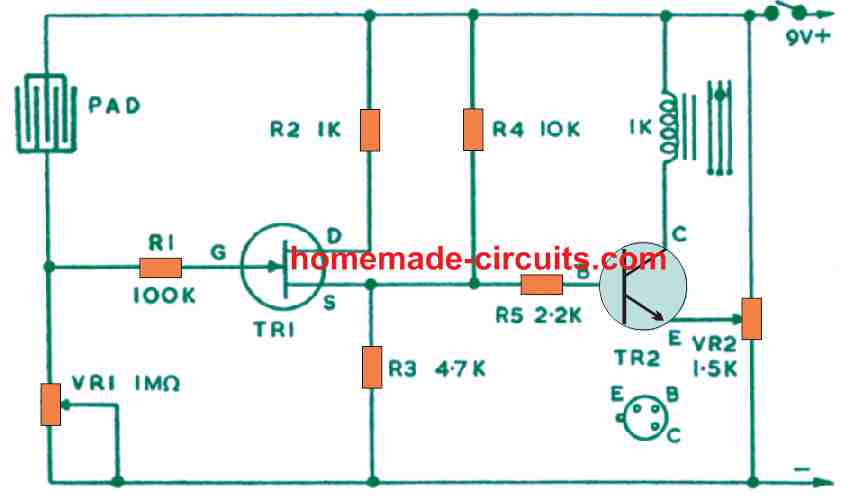 On the other hand the presence of moisture on the pad will lower its resistance, therefore TR1 will allow the conduction of current by means of P2, causing the base of TR2 to become positive.
This action will activate the relay.
VR1 makes it possible for realignment of the level where TR1 switches ON, and therefore decides the sensitivity of the circuit.
This could be fixed to an extremely high level.
The pot VR2 makes it possible for adjusting the collector current, to ensure that current through the relay coil is very small during the periods when the sensing pad is dry.
TR1 can be the 2N3819 or any other common FET, and TR2 can be a BC108 or some other high gain ordinary NPN transistor.
The sense pad is quickly produced from 0.1 in or 0.15 in matrix perforated circuit PCB with conductive foil across the rows of holes.
A board measuring 1 x 3 inches is adequate if the circuit is used as a water level detector, however a more substantial sized board (maybe 3 x 4 inches) is recommended for enabling FET moisture detection, especially during rainy season.
The warning unit can be any desired device such as an indication light, bell, buzzer or sound oscillator, and these could be integrated inside the enclosure, or positioned externally and be hooked up through an extension cable.
On the other hand the presence of moisture on the pad will lower its resistance, therefore TR1 will allow the conduction of current by means of P2, causing the base of TR2 to become positive.
This action will activate the relay.
VR1 makes it possible for realignment of the level where TR1 switches ON, and therefore decides the sensitivity of the circuit.
This could be fixed to an extremely high level.
The pot VR2 makes it possible for adjusting the collector current, to ensure that current through the relay coil is very small during the periods when the sensing pad is dry.
TR1 can be the 2N3819 or any other common FET, and TR2 can be a BC108 or some other high gain ordinary NPN transistor.
The sense pad is quickly produced from 0.1 in or 0.15 in matrix perforated circuit PCB with conductive foil across the rows of holes.
A board measuring 1 x 3 inches is adequate if the circuit is used as a water level detector, however a more substantial sized board (maybe 3 x 4 inches) is recommended for enabling FET moisture detection, especially during rainy season.
The warning unit can be any desired device such as an indication light, bell, buzzer or sound oscillator, and these could be integrated inside the enclosure, or positioned externally and be hooked up through an extension cable.
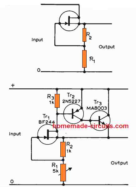 Any kind of variation in output voltage induced through an alteration in load resistance changes the gate-source voltage of the f.e.t.
via R1, and R2. This leads to a counteracting change in drain current.
The stabilization ratio is fantastic ( ˇÖ 1000) however the output resistance is quite high R0> 1/(YFs > 500¦¸) and the output current is actually minimal.
To defeat these anomalies, the improved bottom voltage regulator circuit can be utilized.
The output resistance is tremendously decreased without compromising the stabilization ratio.
The maximum output current is restricted by the permissible dissipation of the last transistor.
Resistor R3 is selected to create a quiescent current of a couple of mA in TR3. A good test set-up applying the values indicated, caused an alteration of less than 0.1 V even when the load current was varied from 0 to 60 mA at 5 V output.
The impact of temperature on the output voltage was not looked into however it could possibly be kept under control through proper selection of the drain current of the f.e.t.
Any kind of variation in output voltage induced through an alteration in load resistance changes the gate-source voltage of the f.e.t.
via R1, and R2. This leads to a counteracting change in drain current.
The stabilization ratio is fantastic ( ˇÖ 1000) however the output resistance is quite high R0> 1/(YFs > 500¦¸) and the output current is actually minimal.
To defeat these anomalies, the improved bottom voltage regulator circuit can be utilized.
The output resistance is tremendously decreased without compromising the stabilization ratio.
The maximum output current is restricted by the permissible dissipation of the last transistor.
Resistor R3 is selected to create a quiescent current of a couple of mA in TR3. A good test set-up applying the values indicated, caused an alteration of less than 0.1 V even when the load current was varied from 0 to 60 mA at 5 V output.
The impact of temperature on the output voltage was not looked into however it could possibly be kept under control through proper selection of the drain current of the f.e.t.
 R1 and R2 resistors offer isolation from the pots VR1 and VR2 to ensure that a lowest setting from one of the pots doesn't ground the input signal for the other pot.
Such a set up is appropriate for all standard applications, using microphones, pick-up, tuner, cellphone, etc.
The FET 2N3819 as well as other audio and general purpose FETs will work without any issues.
Output must be a shielded connector, through C4.
R1 and R2 resistors offer isolation from the pots VR1 and VR2 to ensure that a lowest setting from one of the pots doesn't ground the input signal for the other pot.
Such a set up is appropriate for all standard applications, using microphones, pick-up, tuner, cellphone, etc.
The FET 2N3819 as well as other audio and general purpose FETs will work without any issues.
Output must be a shielded connector, through C4.
 These designs can be made to work with a common preamplifier stage as shown in A.
With these passive tone control modules there may be a general loss of audio causing some reduction in the output signal level.
In case the amplifier at A includes sufficient gain, satisfactory volume could still be achieved.
This is dependent upon the amplifier as well as other conditions, and when it is assumed that a preamplifier might reestablish volume.
In stage A, VR1 works like the tone control, higher frequencies is minimized in response to its wiper travelling towards C1.
VR2 is wired to form a gain or volume control.
R3 and C3 offer source bias and by-passing, and R2 function as the drain audio load, while the output is acquired from C4. R1 with C2 are used for decoupling the positive supply line.
The circuits can be powered from a 12v DC supply.
R1 could be modified if required for greater voltages.
In this and related circuits you will find substantial latitude in the selection of magnitudes for positions such as C1.
At circuit B, VR1 works like a top cut control, and VR2 as the volume control.
C2 is coupled to the gate at G, and a 2.2 M resistor offers the DC route through gate to negative line, remaining parts are R1, R2, P3, C2, C3 and C4 as at A.
Typical values for B are:
C1 = 10nF
VR1= 500k linear
C2 = 0.47uF
VR2 = 500k log
Another top cut control is revealed at C.
Here, R1 and R2 are identical to R1 and R2 of A.
C2 of A being incorporated like at A.
Occasionally this type of tone control could be included in a pre-existing stage with virtually no hindrance to the circuit board.
C1 at C can be 47nF, and VR1 25k.
Larger magnitudes could be tried for VR1, however that could result in a large section of the audible range of VR1 consume just a little portion of its rotation.
C1 could be made higher, to provide enhanced top cut.
The results attained with different part values are affected by the impedance of the circuit.
These designs can be made to work with a common preamplifier stage as shown in A.
With these passive tone control modules there may be a general loss of audio causing some reduction in the output signal level.
In case the amplifier at A includes sufficient gain, satisfactory volume could still be achieved.
This is dependent upon the amplifier as well as other conditions, and when it is assumed that a preamplifier might reestablish volume.
In stage A, VR1 works like the tone control, higher frequencies is minimized in response to its wiper travelling towards C1.
VR2 is wired to form a gain or volume control.
R3 and C3 offer source bias and by-passing, and R2 function as the drain audio load, while the output is acquired from C4. R1 with C2 are used for decoupling the positive supply line.
The circuits can be powered from a 12v DC supply.
R1 could be modified if required for greater voltages.
In this and related circuits you will find substantial latitude in the selection of magnitudes for positions such as C1.
At circuit B, VR1 works like a top cut control, and VR2 as the volume control.
C2 is coupled to the gate at G, and a 2.2 M resistor offers the DC route through gate to negative line, remaining parts are R1, R2, P3, C2, C3 and C4 as at A.
Typical values for B are:
C1 = 10nF
VR1= 500k linear
C2 = 0.47uF
VR2 = 500k log
Another top cut control is revealed at C.
Here, R1 and R2 are identical to R1 and R2 of A.
C2 of A being incorporated like at A.
Occasionally this type of tone control could be included in a pre-existing stage with virtually no hindrance to the circuit board.
C1 at C can be 47nF, and VR1 25k.
Larger magnitudes could be tried for VR1, however that could result in a large section of the audible range of VR1 consume just a little portion of its rotation.
C1 could be made higher, to provide enhanced top cut.
The results attained with different part values are affected by the impedance of the circuit.
 The tuning antenna coil is built using fifty turns of 26 swg to 34 swg wire, over a ferrite rod.
or could be salvaged from any existing medium wave receiver.
The number of winding will enable the reception of all nearby MW bands.
The tuning antenna coil is built using fifty turns of 26 swg to 34 swg wire, over a ferrite rod.
or could be salvaged from any existing medium wave receiver.
The number of winding will enable the reception of all nearby MW bands.
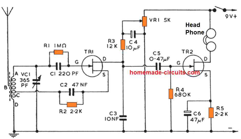 The application of regeneration significantly enhances selectivity, as well as sensitivity to weaker transmissions.
The potentiometer VR1 permits manual realignment of the drain potential of TR1, and so functions as a regeneration control.
Audio output from TR1 is connected with TR2 by C5.
This FET is an audio amplifier, driving the headphones.
An full headset is more suitable for casual tuning in, although phones of approximately 500 ohms DC resistance, or around 2k impedance, will deliver excellent results for this FET MW radio.
In case a mini earpiece is desired for the listening, this can be a moderate or high impedance magnetic device.
The application of regeneration significantly enhances selectivity, as well as sensitivity to weaker transmissions.
The potentiometer VR1 permits manual realignment of the drain potential of TR1, and so functions as a regeneration control.
Audio output from TR1 is connected with TR2 by C5.
This FET is an audio amplifier, driving the headphones.
An full headset is more suitable for casual tuning in, although phones of approximately 500 ohms DC resistance, or around 2k impedance, will deliver excellent results for this FET MW radio.
In case a mini earpiece is desired for the listening, this can be a moderate or high impedance magnetic device.
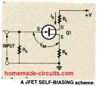 The JFET's gate can be seen grounded by means of resistor RG, and the source is grounded by the resistor Rs.
Any current passing into Rs will cause the source to be positive relative to its gate, which means the gate will be perfectly reverse-biased.
In case drain current (ID) requires to be fixed at 1 milliampere, and we know that a minimum gate-to-source bias voltage (VGS) of -2.2 volts is necessary, the accurate value of source resistor (Rs) has to be established.
You can get the right bias through a 2k2 ohm resistor.
Using Ohms law, we find that if a 2.2 V develops across the 2k2 resistor, will allow the flow of 1 mA current.
When drain current drops, gate-to-source bias voltage also drops.
Due to this the drain current increases, and balances the original difference.
Therefore, the JFET biasing can be self-regulating using a negative feedback.
The gate-source bias necessary to establish a preferred drain current can differ extensively even between similar JFET's in real circuits.
Hence, the only guaranteed method to fix an exact drain current would be to select a source resistor by experimentation or make use of a potentiometer.
No matter exactly how it is implemented, self-biasing works nicely for the majority of practical applications, and it uses just a couple of external parts for its working.
That is why self-biasing method continues to be the most widely used method, to bias a JFET.
The JFET's gate can be seen grounded by means of resistor RG, and the source is grounded by the resistor Rs.
Any current passing into Rs will cause the source to be positive relative to its gate, which means the gate will be perfectly reverse-biased.
In case drain current (ID) requires to be fixed at 1 milliampere, and we know that a minimum gate-to-source bias voltage (VGS) of -2.2 volts is necessary, the accurate value of source resistor (Rs) has to be established.
You can get the right bias through a 2k2 ohm resistor.
Using Ohms law, we find that if a 2.2 V develops across the 2k2 resistor, will allow the flow of 1 mA current.
When drain current drops, gate-to-source bias voltage also drops.
Due to this the drain current increases, and balances the original difference.
Therefore, the JFET biasing can be self-regulating using a negative feedback.
The gate-source bias necessary to establish a preferred drain current can differ extensively even between similar JFET's in real circuits.
Hence, the only guaranteed method to fix an exact drain current would be to select a source resistor by experimentation or make use of a potentiometer.
No matter exactly how it is implemented, self-biasing works nicely for the majority of practical applications, and it uses just a couple of external parts for its working.
That is why self-biasing method continues to be the most widely used method, to bias a JFET.
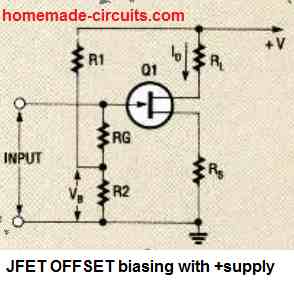
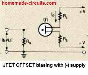 It provides a much more improved gate biasing compared to self-biasing.
In this concept, the voltage at the R1 and R2 junction is employed like a fixed positive bias into the gate of the JFET, through a resistor RD.
The voltage available at the source becomes same as this bias voltage minus the negative value of the gate-source bias.
As a result, if the positive gate voltage is big enough with regard to gate-source bias, drain current can be manipulated predominantly through Rs and gate-voltage.
This may not be significantly affected by modifications of gate-source bias between specific JFET's.
Offset biasing enables drain current to be established correctly, eliminating the need of selecting specific resistor for the operation.
Comparable effects could be seen simply by grounding the gate and connecting the lower-end of the source resistor with a high negative voltage, as demonstrated in Fig.
5 -b.
It provides a much more improved gate biasing compared to self-biasing.
In this concept, the voltage at the R1 and R2 junction is employed like a fixed positive bias into the gate of the JFET, through a resistor RD.
The voltage available at the source becomes same as this bias voltage minus the negative value of the gate-source bias.
As a result, if the positive gate voltage is big enough with regard to gate-source bias, drain current can be manipulated predominantly through Rs and gate-voltage.
This may not be significantly affected by modifications of gate-source bias between specific JFET's.
Offset biasing enables drain current to be established correctly, eliminating the need of selecting specific resistor for the operation.
Comparable effects could be seen simply by grounding the gate and connecting the lower-end of the source resistor with a high negative voltage, as demonstrated in Fig.
5 -b.
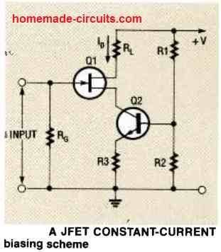 Here, the resistor at the source of the JFET is substituted by NPN bipolar transistor Q2, that is arranged like a constant-current source.
As a result it ensures the supply for the drain current.
The constant current is defined by Q2's base voltage, that is fixed through the resistors R1 and R2 voltage divider and emitter resistor R3.
Resistor R2 may likewise be changed with a Zener diode or some other voltage reference.
Therefore, within this bias circuit, drain current is not dependent on the specifications of the JFET, which results in a great stability of the biasing of the device.
However, this specific enhancement is acquired at the cost of extra parts.
In the 3 biasing schemes, resistor RG may have virtually any value approximately upto 10 M.
This restriction is enforced due to the voltage drop over the resistor, caused by gate leakage currents, which could create problems for the biasing conditions of the device.
Here, the resistor at the source of the JFET is substituted by NPN bipolar transistor Q2, that is arranged like a constant-current source.
As a result it ensures the supply for the drain current.
The constant current is defined by Q2's base voltage, that is fixed through the resistors R1 and R2 voltage divider and emitter resistor R3.
Resistor R2 may likewise be changed with a Zener diode or some other voltage reference.
Therefore, within this bias circuit, drain current is not dependent on the specifications of the JFET, which results in a great stability of the biasing of the device.
However, this specific enhancement is acquired at the cost of extra parts.
In the 3 biasing schemes, resistor RG may have virtually any value approximately upto 10 M.
This restriction is enforced due to the voltage drop over the resistor, caused by gate leakage currents, which could create problems for the biasing conditions of the device.
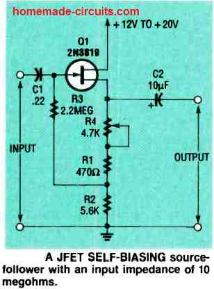 It is a self-biasing type, and drain current could be adjusted through a potentiometer R4. This self-biasing source-follower amplifier works using any voltage ranging from +12 to +20 volt supply.
Potentiometer R4 must be adjusted to ensure the quiescent voltage around R2 is 5.6 volts, that supplies a 1 milliampere drain current.
This set up can provide a voltage gain of approximately 0.95 across input and output.
Due to the voltage division on the intersection of potentiometer R4, the series R1 resistor and resistor R2, a little of bootstrapping develops at R3.
In this configuration, in which the output is obtained from the emitter of the JFET, the output voltage specifically influences the biasing of the device.
In this amplifier, negative output pulses result in a rise in the negative voltage at the input, and positive output leads to a lowering of the negative voltage at the input.
The input is connected between the source and the gate of the JFET.
The bootstrapping in this network increases the net value of R3 with a factor of approximately 5. The design's input impedance is approximately 10 megohms, shunted by the 10 picofarads capacitor.
Consequently, input impedance could be as large as 10 megohms when the frequencies are minimal.
Nevertheless, the value of the resistor may reduce to around 1 megohm with frequencies at 16 kHz, and may still be lowered to approximately 100 K at 160 kHz.
The next figure below, is another form of source-follower amplifier which includes offset biasing.
Resistor manipulation is not really required for this amplifier, and its net voltage gain is approximately 0.95. Electrolytic capacitor C2, which gives bootstrapping, increases the effective R3 gate resistor value to around 20 times.
It is a self-biasing type, and drain current could be adjusted through a potentiometer R4. This self-biasing source-follower amplifier works using any voltage ranging from +12 to +20 volt supply.
Potentiometer R4 must be adjusted to ensure the quiescent voltage around R2 is 5.6 volts, that supplies a 1 milliampere drain current.
This set up can provide a voltage gain of approximately 0.95 across input and output.
Due to the voltage division on the intersection of potentiometer R4, the series R1 resistor and resistor R2, a little of bootstrapping develops at R3.
In this configuration, in which the output is obtained from the emitter of the JFET, the output voltage specifically influences the biasing of the device.
In this amplifier, negative output pulses result in a rise in the negative voltage at the input, and positive output leads to a lowering of the negative voltage at the input.
The input is connected between the source and the gate of the JFET.
The bootstrapping in this network increases the net value of R3 with a factor of approximately 5. The design's input impedance is approximately 10 megohms, shunted by the 10 picofarads capacitor.
Consequently, input impedance could be as large as 10 megohms when the frequencies are minimal.
Nevertheless, the value of the resistor may reduce to around 1 megohm with frequencies at 16 kHz, and may still be lowered to approximately 100 K at 160 kHz.
The next figure below, is another form of source-follower amplifier which includes offset biasing.
Resistor manipulation is not really required for this amplifier, and its net voltage gain is approximately 0.95. Electrolytic capacitor C2, which gives bootstrapping, increases the effective R3 gate resistor value to around 20 times.
 Having said that, this isn't necessary for the normal functioning of the amplifier.
Having C2 removed from the amplifier, the source-follower's input impedance becomes 2.2 megohms, shunted by 10 picofarads.
Having C2 in position, input impedance is enhanced to about 44 megohms, likewise shunted by 10 picofarads.
Some other impedance values might be acquired by increasing R3 up to an optimum value of 10 megohms.
Having said that, this isn't necessary for the normal functioning of the amplifier.
Having C2 removed from the amplifier, the source-follower's input impedance becomes 2.2 megohms, shunted by 10 picofarads.
Having C2 in position, input impedance is enhanced to about 44 megohms, likewise shunted by 10 picofarads.
Some other impedance values might be acquired by increasing R3 up to an optimum value of 10 megohms.
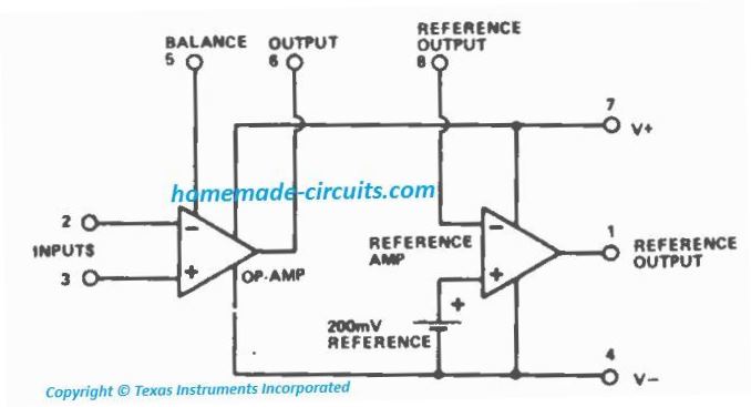 In this post we take a peek at an entire heap of functional application circuits using the device LM 10.
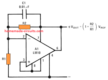 In the above circuit we can see that the LM10 is connected in a quite an unusual way, which is different from other op amps.
Here, the output is connected with the positive line which means it shunts or shorts the positive line with ground depending on a given input threshold detection.
This also implies that, in this shunt regulator mode, the positive to the op amp must be supplied via a resistor.
The pin3 which is the non-inverting input of the op amp is connected with a fixed reference voltage of 200 mV through the reference pinouts 1 and 8 of the IC.
Thus, pin3 being set at a fixed reference, the pin2 now becomes the detector input of the op amp and can be used for detecting a desired voltage threshold from an external parameter.
All the LM10 application circuits explained below are based on the above explained fundamental shunt mode.
In the above circuit we can see that the LM10 is connected in a quite an unusual way, which is different from other op amps.
Here, the output is connected with the positive line which means it shunts or shorts the positive line with ground depending on a given input threshold detection.
This also implies that, in this shunt regulator mode, the positive to the op amp must be supplied via a resistor.
The pin3 which is the non-inverting input of the op amp is connected with a fixed reference voltage of 200 mV through the reference pinouts 1 and 8 of the IC.
Thus, pin3 being set at a fixed reference, the pin2 now becomes the detector input of the op amp and can be used for detecting a desired voltage threshold from an external parameter.
All the LM10 application circuits explained below are based on the above explained fundamental shunt mode.
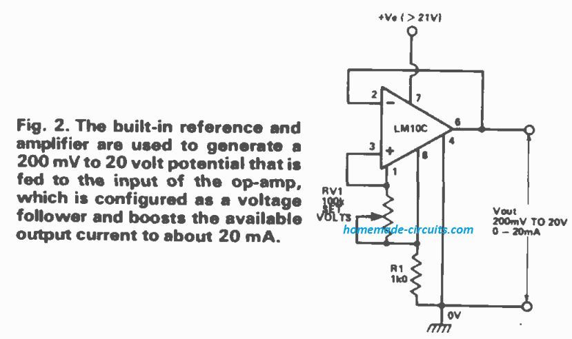 0 to 20 V 1 Amp Variable Regulator: In Fig 3 the internal reference and amplifier develop a fixed 20 volts, which is applied to pot RV1 .
The op-amp and transistor Q1 are wired like a voltage follower to amplify the output of 0-20 volts to current with magnitudes close to many hundred milliamps.
0 to 20 V 1 Amp Variable Regulator: In Fig 3 the internal reference and amplifier develop a fixed 20 volts, which is applied to pot RV1 .
The op-amp and transistor Q1 are wired like a voltage follower to amplify the output of 0-20 volts to current with magnitudes close to many hundred milliamps.
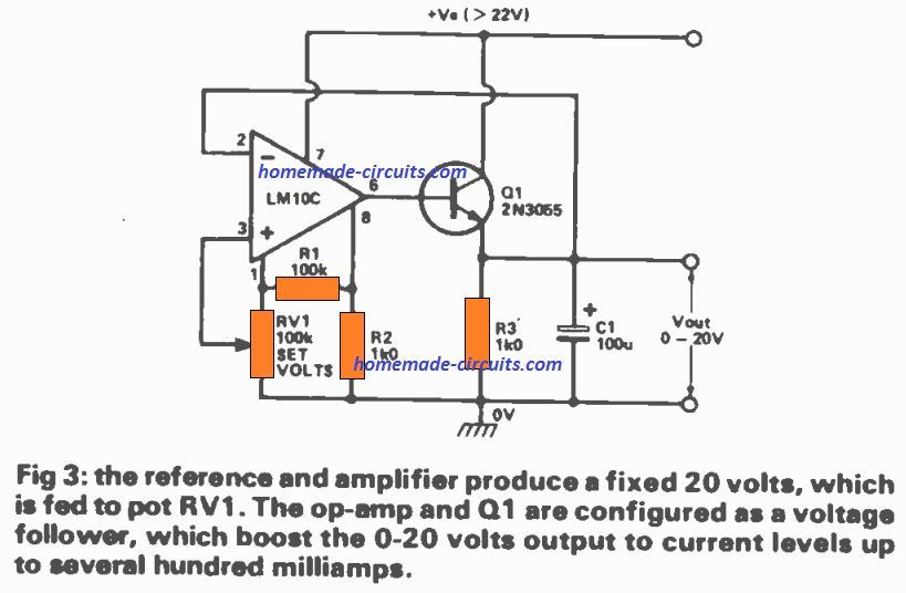 Fixed 5 V 20 mA Regulator: In Fig 4 the op-amp input is extracted straight from the 200 mV reference, to provide a 5 volt output.
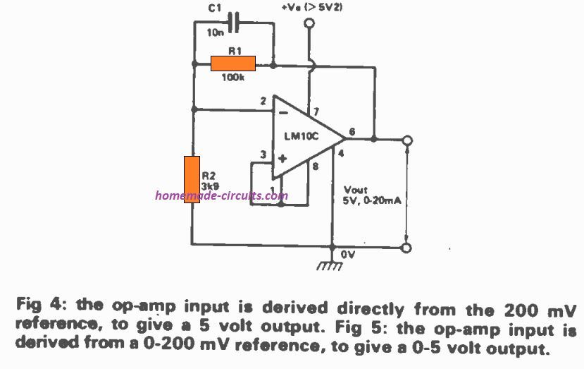 0 to 5 V Regulator: In Fig 5 the op-amp input is acquired setting up an internal 0-200 mV reference, to produce a 0-5 volt output.
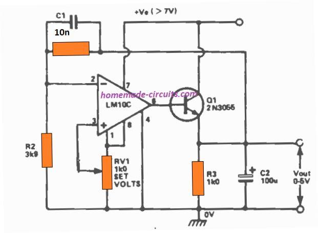 50 V to 200 V Variable regulated Supply: Figures 6 and 7 demonstrate the way the LM 10 could be employed in the 'floating' manner, to produce high output voltages.
Be aware in each of these circuits the IC is applied in the 'shunt' mode through load resistor R3, such that just a small amount of volts are created across the LM 10 itself.
50 V to 200 V Variable regulated Supply: Figures 6 and 7 demonstrate the way the LM 10 could be employed in the 'floating' manner, to produce high output voltages.
Be aware in each of these circuits the IC is applied in the 'shunt' mode through load resistor R3, such that just a small amount of volts are created across the LM 10 itself.
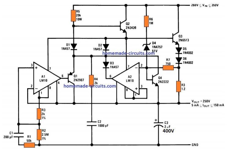 Simple Lab Power Supply: The above concepts can be further upgraded to built a full fledged 0 to 50 V adjustable laboratory power supply as shown below.
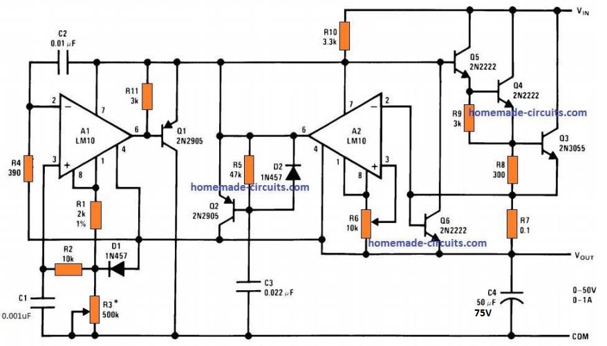 An output short circuit protected version of the above 250 V regulator can be witnessed in the following diagram
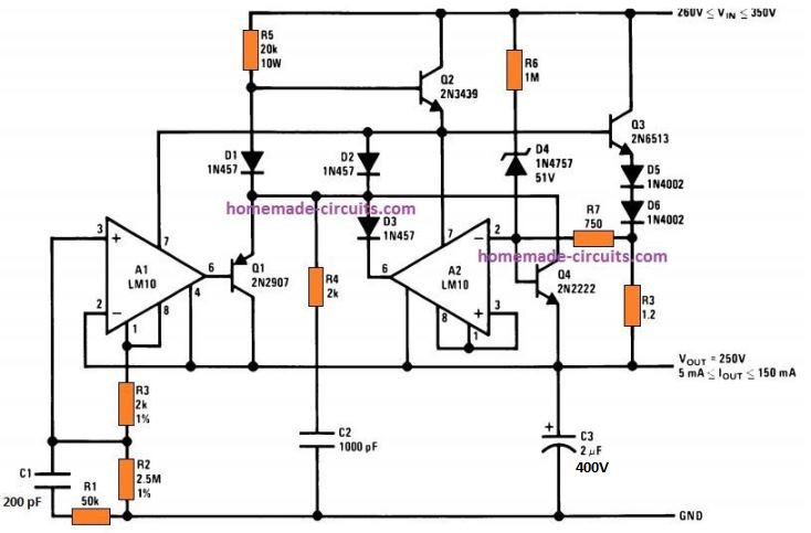 5 V Shunt Regulator Circuit: A straightforward illustration of the LM 10 application in a 5 volt shunt regulator.
 The below Fig 9 shows exactly how the IC could be configured to work as a negative voltage regulator.
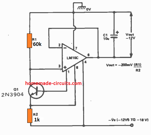 Figure:9
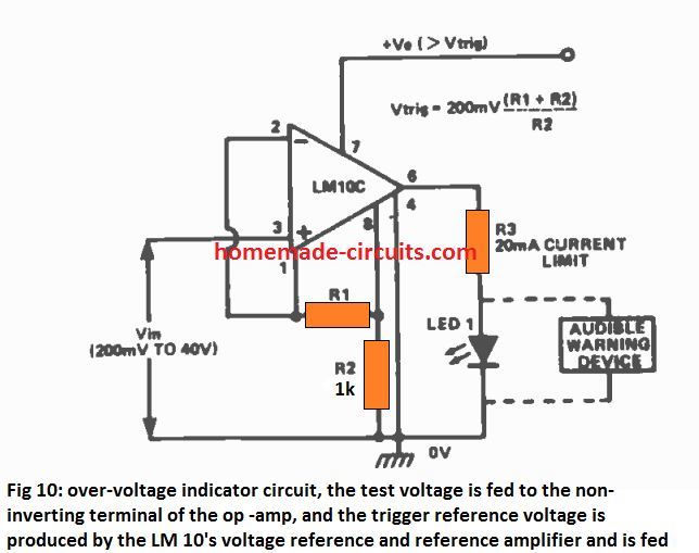 Over Voltage Indicator: In Fig 10 above the IC LM10 is configured as an over-voltage indicator circuit.
The sensing voltage is applied to the non-inverting pin#3 of the op-amp, and the reference voltage at pin8 is generated by the LM10's internal voltage reference and reference amplifier and is supplied to the inverting pin#2 of the op -amp.
The above design could be also configured in the following alternative manner, which will also serve to indicate an over voltage condition
The Fig 11 below shows different strategy is employed in the over-voltage indicator circuit here.
A 200 mV reference is applied to one input pin of the op amp and a resistive divider variation of the test voltage is applied to another.
Over Voltage Indicator: In Fig 10 above the IC LM10 is configured as an over-voltage indicator circuit.
The sensing voltage is applied to the non-inverting pin#3 of the op-amp, and the reference voltage at pin8 is generated by the LM10's internal voltage reference and reference amplifier and is supplied to the inverting pin#2 of the op -amp.
The above design could be also configured in the following alternative manner, which will also serve to indicate an over voltage condition
The Fig 11 below shows different strategy is employed in the over-voltage indicator circuit here.
A 200 mV reference is applied to one input pin of the op amp and a resistive divider variation of the test voltage is applied to another.
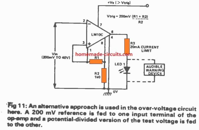 An Under voltage Indicator circuit shown in the following Fig.
12 works with the same concept, except that the op-amp input pin configuration happen to be swapped with each other.
A characteristic of both these circuits is that the LM10 supply voltage has to be higher than the recommended trigger voltage.
An Under voltage Indicator circuit shown in the following Fig.
12 works with the same concept, except that the op-amp input pin configuration happen to be swapped with each other.
A characteristic of both these circuits is that the LM10 supply voltage has to be higher than the recommended trigger voltage.
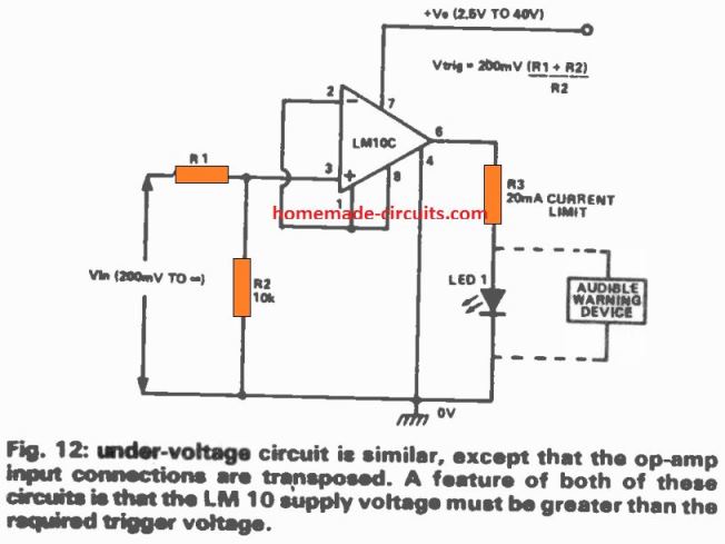 Fig 13 below exhibits a highly accurate under voltage indicator using LED or audible alert.
Input sensitivity 50k /v.
Fig 13 below exhibits a highly accurate under voltage indicator using LED or audible alert.
Input sensitivity 50k /v.
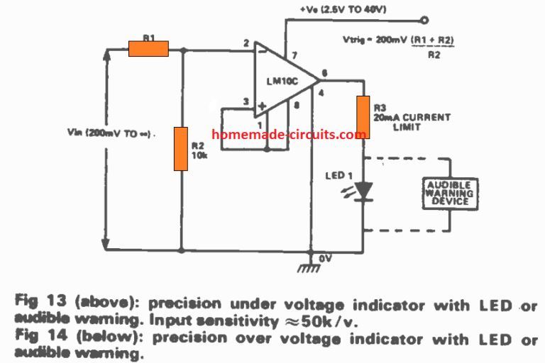 Fig 14 (below): precision LM10 based over voltage indicator using LED or audible alarm unit, The LED will begin indicating if an over voltage situation is present in response to a current trigger at R1/R2 junction.
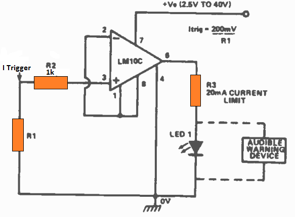 An accurate low current indicator circuit using op amp LM10 is shown in the following Fig 15 which illuminates an LED or buzzer alert unit whenever the current through R1 drops below a set threshold level.
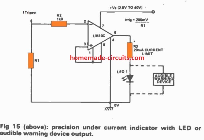 Universal Heat/Light Sensor Amplifier: Figure 16 exhibits a high precision circuit which can be activated through an external parameter, for example through light or temperature sensors.
These sensors should have a resistive characteristic like LDR or thermistor.
Universal Heat/Light Sensor Amplifier: Figure 16 exhibits a high precision circuit which can be activated through an external parameter, for example through light or temperature sensors.
These sensors should have a resistive characteristic like LDR or thermistor.
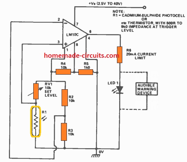 Figure 16
In these designs, the resistive component becomes section of a Wheatstone bridge which is driven through the LM10's voltage reference amplifier, and the bridge output is applied to switch on the op amp rigged as a comparator.
In the illustrations demonstrated, the bridge is powered through a 2V2 supply.
Figure 16
In these designs, the resistive component becomes section of a Wheatstone bridge which is driven through the LM10's voltage reference amplifier, and the bridge output is applied to switch on the op amp rigged as a comparator.
In the illustrations demonstrated, the bridge is powered through a 2V2 supply.
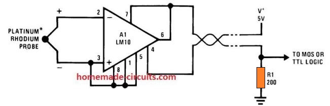 *The maximum 800 degrees high temperature detection threshold is achieved by connecting the "balance" pin of the IC with the "reference" pin.
Remote Vibration Detector: The next diagram shows how the IC LM10 could be used for making remote vibration sensor module.
The sensor could be a piezo based transducer or similar.
*The maximum 800 degrees high temperature detection threshold is achieved by connecting the "balance" pin of the IC with the "reference" pin.
Remote Vibration Detector: The next diagram shows how the IC LM10 could be used for making remote vibration sensor module.
The sensor could be a piezo based transducer or similar.
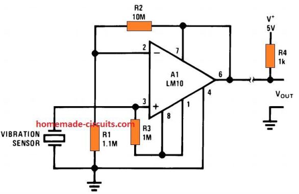
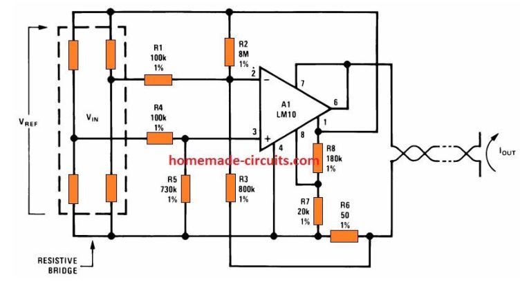 In the resistive any one of the resistors could be replaced with a sensor such as an LDR, photo diode, thermistor, piezo transducer, to create a relevant sensor amplifier.
for detecting a over threshold or lower threshold for the detected parameter.
In the resistive any one of the resistors could be replaced with a sensor such as an LDR, photo diode, thermistor, piezo transducer, to create a relevant sensor amplifier.
for detecting a over threshold or lower threshold for the detected parameter.
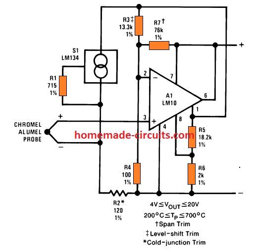 Here, the LM134 generates a precise reference across one end of the thermocouple element, so that an accurate differential temperature can be detected from the other end of the thermocouple, by the op amp.
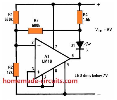
 The LM134 in the circuit works like a temperature sensor, which converts the temperature into proportionate amount of voltage.
It converts every degree change in temperature into 10 mV.
This conversion is directed displayed over a 0-100uA micro-ammeter through the IC LM10 which is configured as a voltage follower/amplifier.
If you have any queries or doubts regarding any of the above explained LM10 op amp application circuits, you may feel free to contact me through comments below.
The LM134 in the circuit works like a temperature sensor, which converts the temperature into proportionate amount of voltage.
It converts every degree change in temperature into 10 mV.
This conversion is directed displayed over a 0-100uA micro-ammeter through the IC LM10 which is configured as a voltage follower/amplifier.
If you have any queries or doubts regarding any of the above explained LM10 op amp application circuits, you may feel free to contact me through comments below.
 The design also includes a zero adjust facility which allows the user to adjust the meter needle to exact zero so that the final reading is accurate and error free.
The biggest advantage of this circuit is that it works with a single AAA 1.5 V cell.
The above LM10 based meter amplifier circuit could be further enhanced into a 4 range adjustable millivolt meter amplifier circuit as shown in the following diagram.
The design also includes a zero adjust facility which allows the user to adjust the meter needle to exact zero so that the final reading is accurate and error free.
The biggest advantage of this circuit is that it works with a single AAA 1.5 V cell.
The above LM10 based meter amplifier circuit could be further enhanced into a 4 range adjustable millivolt meter amplifier circuit as shown in the following diagram.
 Reference: LM10
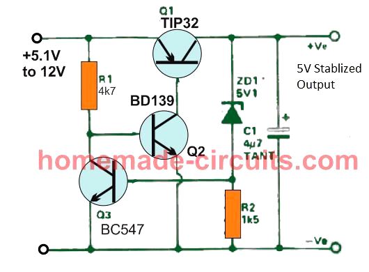 NOTE: PLEASE ADD A 1K RESISTOR BETWEEN Q1 BASE AND Q2 COLLECTOR
The figure above shows a simple low-dropout 5 V stabilized voltage regulator design that will give you a proper 5 V stabilized even when the input supply has dropped to less than 5.2 V.
The working of the regulator is actually very simple, Q1 and Q2 form a simple high gain common-emitter power switch, which allows the voltage to pass from the input to the output with a low dropout.
Q3 in association with the zener diode and R2 work like a basic feedback network which regulates the output to the value equivalent to the zener diode value (approximately).
This also implies that by changing the zener voltage value, the output voltage could be changed accordingly, as desired.
This is an added advantage of the design since it enables the user to customize even the non-standard output values which are not available from the fixed 78XX ICs
NOTE: PLEASE ADD A 1K RESISTOR BETWEEN Q1 BASE AND Q2 COLLECTOR
The figure above shows a simple low-dropout 5 V stabilized voltage regulator design that will give you a proper 5 V stabilized even when the input supply has dropped to less than 5.2 V.
The working of the regulator is actually very simple, Q1 and Q2 form a simple high gain common-emitter power switch, which allows the voltage to pass from the input to the output with a low dropout.
Q3 in association with the zener diode and R2 work like a basic feedback network which regulates the output to the value equivalent to the zener diode value (approximately).
This also implies that by changing the zener voltage value, the output voltage could be changed accordingly, as desired.
This is an added advantage of the design since it enables the user to customize even the non-standard output values which are not available from the fixed 78XX ICs
 NOTE: PLEASE ADD A 1K RESISTOR BETWEEN Q1 BASE AND Q2 COLLECTOR
As explained in the previous section, merely changing the zener values change the output to the required stabilized level.
In the above 12 v LDO circuit, we have replaced the zener diode with a 12 V zener diode to get a 12 V regulated output through inputs of 12.3 V to 20 V.
NOTE: PLEASE ADD A 1K RESISTOR BETWEEN Q1 BASE AND Q2 COLLECTOR
As explained in the previous section, merely changing the zener values change the output to the required stabilized level.
In the above 12 v LDO circuit, we have replaced the zener diode with a 12 V zener diode to get a 12 V regulated output through inputs of 12.3 V to 20 V.
 NOTE: PLEASE ADD A 1K RESISTOR BETWEEN Q1 BASE AND Q2 COLLECTOR
When the current increases beyond the predetermined limit, the voltage drop across Rx becomes sufficiently high to turn ON Q4, which begins grounding the Q2 base.
This causes Q1, Q2 conduction to become highly restricted, and the output voltage shuts down, until of course the current draw is restored to the normal level.
NOTE: PLEASE ADD A 1K RESISTOR BETWEEN Q1 BASE AND Q2 COLLECTOR
When the current increases beyond the predetermined limit, the voltage drop across Rx becomes sufficiently high to turn ON Q4, which begins grounding the Q2 base.
This causes Q1, Q2 conduction to become highly restricted, and the output voltage shuts down, until of course the current draw is restored to the normal level.
 This soft-start plan (around 2 seconds) for the power amplifiers helped the 2000 uF output capacitors to charge without triggering too much collector current within the output transistors.
Normal regulator output impedance is 0.1 ohm.
Output voltage is found by solving the equation by:
VO = VZ - VBE1.
The rise time of the output voltage is evaluated by calculating through the formula:
T = RB.C1(1 -Vz/V ).
A number of digital devices call for a preset switch on sequence for their power supplies.
By establishing proper RB/C1 values, the rise time of the circuit's output could be fixed to deliver this sequence or delay interval.
This soft-start plan (around 2 seconds) for the power amplifiers helped the 2000 uF output capacitors to charge without triggering too much collector current within the output transistors.
Normal regulator output impedance is 0.1 ohm.
Output voltage is found by solving the equation by:
VO = VZ - VBE1.
The rise time of the output voltage is evaluated by calculating through the formula:
T = RB.C1(1 -Vz/V ).
A number of digital devices call for a preset switch on sequence for their power supplies.
By establishing proper RB/C1 values, the rise time of the circuit's output could be fixed to deliver this sequence or delay interval.
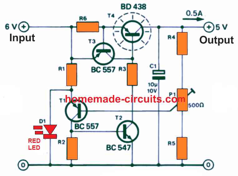
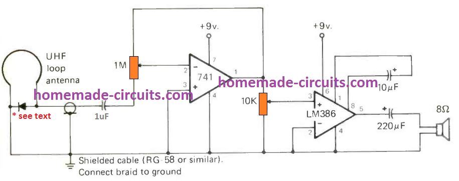 The working of the GHz receiver circuit is simple, the detected signals are captured by the loop antenna.
The detector diode demodulates and extracts the audio content from the high frequency carrier waves.
The extracted audio signals are fed to the non-inverting input of the IC 741 amplifier circuit.
Since its inverting input is grounded, any signal in few mV is enough for the op amp to amplify it to higher levels.
The amplified SHF audio signals are applied to a high gain LM386 audio amplifier circuit which finally converts the received GHz range signals into audible sound frequency.
All resistors can be 1/4 -watt types, the tolerance is not really important.
The two ICs are normal types, the 741 and LM386.
The working of the GHz receiver circuit is simple, the detected signals are captured by the loop antenna.
The detector diode demodulates and extracts the audio content from the high frequency carrier waves.
The extracted audio signals are fed to the non-inverting input of the IC 741 amplifier circuit.
Since its inverting input is grounded, any signal in few mV is enough for the op amp to amplify it to higher levels.
The amplified SHF audio signals are applied to a high gain LM386 audio amplifier circuit which finally converts the received GHz range signals into audible sound frequency.
All resistors can be 1/4 -watt types, the tolerance is not really important.
The two ICs are normal types, the 741 and LM386.
 For most effective final results, test out a number of different varieties of diodes.
Some of those you can try are 1N21, 1N34, 1N54, and 1N78.
As you could envision, this straightforward circuit comes with its own downsides.
The fundamental one is that there is absolutely no way for you to figure out the frequency of a signal you may receive.
Additionally, it is pretty much entirely non-selective.
Probably the most strong signal within the detecting range may simply "overwhelm" the receiver.
Nevertheless, the suggested loop antenna is to some degree directional and may help you to reduce many interfering channels, so that you focus on a specific GHz channel of your choice.
For most effective final results, test out a number of different varieties of diodes.
Some of those you can try are 1N21, 1N34, 1N54, and 1N78.
As you could envision, this straightforward circuit comes with its own downsides.
The fundamental one is that there is absolutely no way for you to figure out the frequency of a signal you may receive.
Additionally, it is pretty much entirely non-selective.
Probably the most strong signal within the detecting range may simply "overwhelm" the receiver.
Nevertheless, the suggested loop antenna is to some degree directional and may help you to reduce many interfering channels, so that you focus on a specific GHz channel of your choice.
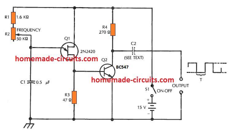 The UJT output voltage, obtained over the 47 ohm resistor R3, switches the bipolar transistor between a couple of thresholds: saturation and cutoff, generating horizontal-topped output pulses.
Depending on the off time (t) of the pulse, the output waveform could be sometimes narrow rectangular pulses or (as indicated across the output terminals in Fig.
7-2) a square wave.
The maximum amplitude of the output signal can be up to the supply level, that is +15 volts.
The frequency, or cycling frequency, is determined by the adjustment of a 50 k pot resistance and the capacitor value of C1. When the resistance is maximum with R1 + R2 = 51.6 k and with C1 = 0.5 ¦ĚF, the frequency f is = 47.2 Hz, and the time off (t) = 21.2 ms.
When resistance setting is at minimum, probably with only R1 at 1.6 k the frequency will be, f = 1522 Hz, and t = 0.66 ms.
To get additional frequency ranges, R1, R2, or C1 or each one of these could be modified and the frequency calculated using the following formula:
t = 0.821 (R1 + R2) C1
Where t is in seconds, R1 and R2 in ohms, and Cl in farads, and f = 1/t
The circuit works with just 20 mA from the 15 Vdc source, although this range could be different for different UJTs and bipolars.
The dc output coupling can be seen in schematic, but ac coupling could be configured by placing a capacitor C2 within the high output lead, as demonstrated through the dotted image.
The capacitance of this unit must be approximately between 0.1¦ĚF and 1¦ĚF, the most effective magnitude might be the one which brings about minimum distortion of the output waveform, when the generator is run through a specific ideal load system.
The UJT output voltage, obtained over the 47 ohm resistor R3, switches the bipolar transistor between a couple of thresholds: saturation and cutoff, generating horizontal-topped output pulses.
Depending on the off time (t) of the pulse, the output waveform could be sometimes narrow rectangular pulses or (as indicated across the output terminals in Fig.
7-2) a square wave.
The maximum amplitude of the output signal can be up to the supply level, that is +15 volts.
The frequency, or cycling frequency, is determined by the adjustment of a 50 k pot resistance and the capacitor value of C1. When the resistance is maximum with R1 + R2 = 51.6 k and with C1 = 0.5 ¦ĚF, the frequency f is = 47.2 Hz, and the time off (t) = 21.2 ms.
When resistance setting is at minimum, probably with only R1 at 1.6 k the frequency will be, f = 1522 Hz, and t = 0.66 ms.
To get additional frequency ranges, R1, R2, or C1 or each one of these could be modified and the frequency calculated using the following formula:
t = 0.821 (R1 + R2) C1
Where t is in seconds, R1 and R2 in ohms, and Cl in farads, and f = 1/t
The circuit works with just 20 mA from the 15 Vdc source, although this range could be different for different UJTs and bipolars.
The dc output coupling can be seen in schematic, but ac coupling could be configured by placing a capacitor C2 within the high output lead, as demonstrated through the dotted image.
The capacitance of this unit must be approximately between 0.1¦ĚF and 1¦ĚF, the most effective magnitude might be the one which brings about minimum distortion of the output waveform, when the generator is run through a specific ideal load system.
 This circuit is primarily a relaxation oscillator, with outputs extracted from the emitter and the two bases.
The 2N2646 UJT is hooked up in the typical oscillator circuit for these types of units.
The frequency, or repetition rate, is determined from the setting up of the frequency control potentiometer, R2. Any time this pot is defined to its highest resistance level, the sum of the series resistance with the timing capacitor C1 becomes the total of the pot resistance and the limiting resistance, R1 (which is, 54.6 k).
This causes a frequency of around 219 Hz.
If R2 is defined to its minimum value, the resulting resistance essentially represents the value of resistor R1, or 5.6 k, producing a frequency of around 2175 Hz.
Additional frequency tanges and tuning thresholds could be implemented simply by altering R1, R2, C1 values, or may be all the three together.
A positive spiked output can be acquired coming from base 1 of the UJT, while a negative spiked output through base 2, and a positive sawtooth waveform through the UJT emitter.
Although dc output coupling is revealed in Fig.
7-3, ac coupling could be determined by applying capacitors C2, C3, and C4 in the output terminals, as demonstrated through the dotted area.
These capacitances will probably be between 0.1 and 10¦ĚF, the value determined being based on the highest capacitance which may be tackled by a specified load device without distorting the output waveform.
The circuit operates using around 1.4 mA through the 9 volt dc supply.
Each of the resistors are rated at 1/2 watt.
This circuit is primarily a relaxation oscillator, with outputs extracted from the emitter and the two bases.
The 2N2646 UJT is hooked up in the typical oscillator circuit for these types of units.
The frequency, or repetition rate, is determined from the setting up of the frequency control potentiometer, R2. Any time this pot is defined to its highest resistance level, the sum of the series resistance with the timing capacitor C1 becomes the total of the pot resistance and the limiting resistance, R1 (which is, 54.6 k).
This causes a frequency of around 219 Hz.
If R2 is defined to its minimum value, the resulting resistance essentially represents the value of resistor R1, or 5.6 k, producing a frequency of around 2175 Hz.
Additional frequency tanges and tuning thresholds could be implemented simply by altering R1, R2, C1 values, or may be all the three together.
A positive spiked output can be acquired coming from base 1 of the UJT, while a negative spiked output through base 2, and a positive sawtooth waveform through the UJT emitter.
Although dc output coupling is revealed in Fig.
7-3, ac coupling could be determined by applying capacitors C2, C3, and C4 in the output terminals, as demonstrated through the dotted area.
These capacitances will probably be between 0.1 and 10¦ĚF, the value determined being based on the highest capacitance which may be tackled by a specified load device without distorting the output waveform.
The circuit operates using around 1.4 mA through the 9 volt dc supply.
Each of the resistors are rated at 1/2 watt.
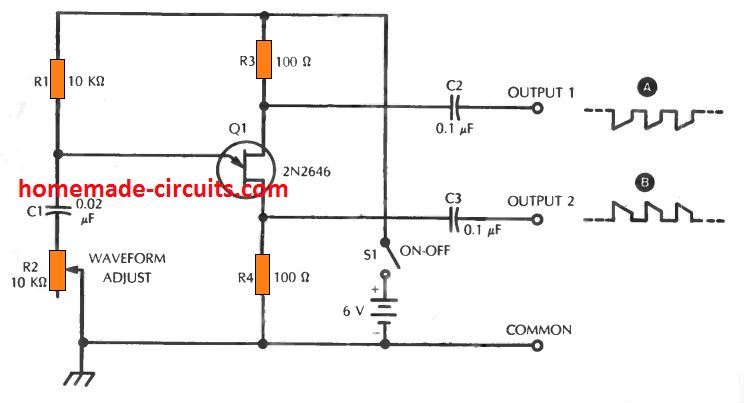 The type 2N2646 unijunction transistor works nicely inside this indicated set up.
There are basically two output signals: a negative-going pulse at UJT base 2, and a positive-going pulse at base 1.
The open circuit maximum amplitude of each of these signals is around 0.56 volt, however this could deviate a bit depending on specific UJTs.
The 10 k pot, R2, should be turned for acquiring a perfect tilt or horizontal topped output waveform.
This pot control additionally impacts the range of the frequency, or the duty cycle.
With the magnitudes presented here for R1, R2, and C1, the frequency is around 5 kHz for a flat-topped peak.
For other frequency ranges, you may want to adjust R1 or C1 values accordingly, and use the following formula for the calculations:
f = 1/0.821 RC
where f is in Hz, R in ohms, and C in farads.
The circuit consumes around 2 mA from the 6 V dc power source.
All fixed resistors can be rated at 1/2 -watt.
The type 2N2646 unijunction transistor works nicely inside this indicated set up.
There are basically two output signals: a negative-going pulse at UJT base 2, and a positive-going pulse at base 1.
The open circuit maximum amplitude of each of these signals is around 0.56 volt, however this could deviate a bit depending on specific UJTs.
The 10 k pot, R2, should be turned for acquiring a perfect tilt or horizontal topped output waveform.
This pot control additionally impacts the range of the frequency, or the duty cycle.
With the magnitudes presented here for R1, R2, and C1, the frequency is around 5 kHz for a flat-topped peak.
For other frequency ranges, you may want to adjust R1 or C1 values accordingly, and use the following formula for the calculations:
f = 1/0.821 RC
where f is in Hz, R in ohms, and C in farads.
The circuit consumes around 2 mA from the 6 V dc power source.
All fixed resistors can be rated at 1/2 -watt.
 In this particular design, the capacitor C1 is charged by the voltage divider established by R2, R3, and the base-to-emitter resistance of transistor Q2, causing its Q2 side negative and its Q1 side positive.
This resistive divider additionally supplies the Q1 emitter with a positive voltage which is slightly smaller than the peak voltage of the 2N2420 (refer to point 2 in the schematic).
In the beginning, Q2 is in switched ON state; which causes a voltage drop across resistor R4, decreasing the voltage at the output terminals drastically to 0. When a 20 V negative pulse is given across the input terminals, Q1 "fires," causing an instant drop of voltage to zero at the emitter side of C1, which in turn biases the Q2 base negative.
Due to this, Q1 gets cut off, and the Q1 collector voltage increases swiftly to +20 volts (notice the pulse indicated across the output terminals in the diagram).
The voltage continues to be around this level for an interval t, equivalent to the discharging time of capacitor C1 via the resistor R3. The output subsequently drops back to zero, and the circuit goes into stand by position until the next pulse is applied.
Time interval t, and the correspondingly the pulse width (time) of the output pulse, rely on the adjustment of the pulse width control with R3. As per the indicated values of R3 and C1, the time interval range can be anywhere between 2 ¦Ěs to 0.1 ms.
Supposing that R3 encompasses the resistance range between 100 to 5000 ohms.
Additional delay ranges could be fixed by appropriately modifying the values of C1, R3, or both, and using the formula: t = R3C1 where t is in seconds, R3 in ohms, and C1 in farads.
The circuit operates using roughly 11 mA through the 22.5 V dc supply.
However this could be likely to change to some extent depending on the UJTs and bipolars types.
All fixed resistors are 1/2 watt.
In this particular design, the capacitor C1 is charged by the voltage divider established by R2, R3, and the base-to-emitter resistance of transistor Q2, causing its Q2 side negative and its Q1 side positive.
This resistive divider additionally supplies the Q1 emitter with a positive voltage which is slightly smaller than the peak voltage of the 2N2420 (refer to point 2 in the schematic).
In the beginning, Q2 is in switched ON state; which causes a voltage drop across resistor R4, decreasing the voltage at the output terminals drastically to 0. When a 20 V negative pulse is given across the input terminals, Q1 "fires," causing an instant drop of voltage to zero at the emitter side of C1, which in turn biases the Q2 base negative.
Due to this, Q1 gets cut off, and the Q1 collector voltage increases swiftly to +20 volts (notice the pulse indicated across the output terminals in the diagram).
The voltage continues to be around this level for an interval t, equivalent to the discharging time of capacitor C1 via the resistor R3. The output subsequently drops back to zero, and the circuit goes into stand by position until the next pulse is applied.
Time interval t, and the correspondingly the pulse width (time) of the output pulse, rely on the adjustment of the pulse width control with R3. As per the indicated values of R3 and C1, the time interval range can be anywhere between 2 ¦Ěs to 0.1 ms.
Supposing that R3 encompasses the resistance range between 100 to 5000 ohms.
Additional delay ranges could be fixed by appropriately modifying the values of C1, R3, or both, and using the formula: t = R3C1 where t is in seconds, R3 in ohms, and C1 in farads.
The circuit operates using roughly 11 mA through the 22.5 V dc supply.
However this could be likely to change to some extent depending on the UJTs and bipolars types.
All fixed resistors are 1/2 watt.
 The output is actually somewhat curved sawtooth wave consisting of peak amplitude roughly corresponding to the supply voltage (which is, 22.5 V here).
In this design, current travelling through the dc source via resistor R1 charges capacitor C1. A potential difference VEE as a result steadily accumulates across C1.
The moment this potential reaches the peak voltage of the 2N2646 (see point 2 in Fig.
7-1 B), the UJT turns ON and "fires." This immediately discharges the capacitor, switching OFF the UJT back again.
Th is causes the capacitor to initiate the recharge process again, and the cycle simply keeps repeating.
Due to this charging and discharging of the capacitor the UJT switches on and off with a frequency established through the values of R1 and C1 (with the values indicated in diagram, the frequency is around f = 312 Hz).
To achieve some other frequency, use the formula: f =1/(0.821 R1 C1)
where f is in Hz, R1 in ohms, and C1 in farads.
A potentiometer with an appropriate resistance could be used in place of the fixed resistor, R1. This will enable the user to achieve a continuously adjustable frequency output.
All resistors are 1/2 watt.
Capacitors C1 and C2 may be rated at 10 V or 16 V; preferably a tantalum.
The circuit consumes roughly 6 mA from the indicated supply range.
The output is actually somewhat curved sawtooth wave consisting of peak amplitude roughly corresponding to the supply voltage (which is, 22.5 V here).
In this design, current travelling through the dc source via resistor R1 charges capacitor C1. A potential difference VEE as a result steadily accumulates across C1.
The moment this potential reaches the peak voltage of the 2N2646 (see point 2 in Fig.
7-1 B), the UJT turns ON and "fires." This immediately discharges the capacitor, switching OFF the UJT back again.
Th is causes the capacitor to initiate the recharge process again, and the cycle simply keeps repeating.
Due to this charging and discharging of the capacitor the UJT switches on and off with a frequency established through the values of R1 and C1 (with the values indicated in diagram, the frequency is around f = 312 Hz).
To achieve some other frequency, use the formula: f =1/(0.821 R1 C1)
where f is in Hz, R1 in ohms, and C1 in farads.
A potentiometer with an appropriate resistance could be used in place of the fixed resistor, R1. This will enable the user to achieve a continuously adjustable frequency output.
All resistors are 1/2 watt.
Capacitors C1 and C2 may be rated at 10 V or 16 V; preferably a tantalum.
The circuit consumes roughly 6 mA from the indicated supply range.
 This design produces a deformed output wave which can be highly suitable in a frequency standard so that you can guarantee solid harmonics loaded with the rf spectrum.
The joint working of the unijunction transistor and the 1N914 diode harmonic generator generates the intended distorted waveform.
In this set up, a tiny 100 pF variable capacitor, C1, enables the frequency of the 100 kHz crystal to be adjusted a bit, to deliver an increased harmonic, for example 5 MHz, to zero beat with a WWV/WWVH standard frequency signal.
The output signal is produced over the 1 mH rf choke (RFC1) which is supposed to have a lower dc resistance.
This signal is given to the 1N914 diode (D1) which is dc biased by means of R3 and R4 to achieve a maximum non-linear portion of its forward conduction characteristic, to additionally distort the output waveform from the UJT.
While using this oscillator, the variable waveform pot, R3, is fixed for achieving the most powerful transmission with the proposed harmonic of 100 kHz.
Resistor R3 acts simply like a current limiter to stop direct application of the 9 volt supply across the diode.
The oscillator consumes around 2.5 mA from the 9 Vdc supply, but, this could change relatively depending on specific UJTs.
Capacitor C1 should be a midget air type; the remaining other capacitors are mica or silvered mica.
All fixed resistors are rated at 1 watt.
This design produces a deformed output wave which can be highly suitable in a frequency standard so that you can guarantee solid harmonics loaded with the rf spectrum.
The joint working of the unijunction transistor and the 1N914 diode harmonic generator generates the intended distorted waveform.
In this set up, a tiny 100 pF variable capacitor, C1, enables the frequency of the 100 kHz crystal to be adjusted a bit, to deliver an increased harmonic, for example 5 MHz, to zero beat with a WWV/WWVH standard frequency signal.
The output signal is produced over the 1 mH rf choke (RFC1) which is supposed to have a lower dc resistance.
This signal is given to the 1N914 diode (D1) which is dc biased by means of R3 and R4 to achieve a maximum non-linear portion of its forward conduction characteristic, to additionally distort the output waveform from the UJT.
While using this oscillator, the variable waveform pot, R3, is fixed for achieving the most powerful transmission with the proposed harmonic of 100 kHz.
Resistor R3 acts simply like a current limiter to stop direct application of the 9 volt supply across the diode.
The oscillator consumes around 2.5 mA from the 9 Vdc supply, but, this could change relatively depending on specific UJTs.
Capacitor C1 should be a midget air type; the remaining other capacitors are mica or silvered mica.
All fixed resistors are rated at 1 watt.
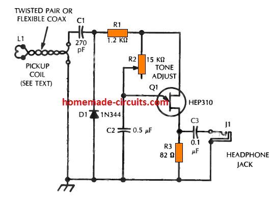 The output signal is sampled through L1 rf pickup coil, consisting of 2 or 3 winding of insulated hookup wire fitted firmly close to the transmitter's output tank coil.
The rf voltage is converted to DC through a shunt-diode circuit, made up of blocking capacitor C1, diode D1, and filter resistor R1. The resultant rectified dc is utilized to switch the unijunction transistor in a relaxation oscillator circuit.
The output from this oscillator is fed into an attached high impedance headphones via coupling capacitor C3 and output jack J1.
The signal tone as picked up in the headphones could be altered across a decent range through the pot R2. The frequency of the tone will be somewhere around 162 Hz when R2 is adjusted to 15 k.
Alternatively, the frequency will be roughly 2436 Hz when R2 is defined to 1 k.
The audio level could be manipulated by rotating L1 closer to or away from the transmitter LC tank network; typically, a spot will likely be identified that provides reasonable volume for most basic usage.
The circuit can be constructed inside a compact, earthed metallic container.
Usually, this could be positioned at some fair distance from the transmitter, when a decent quality twisted pair or flexible coaxial cable is employed and when L1 is connected to the lower terminal of the tank coil.
All fixed resistors are rated at 1/2 watt.
Capacitor C1 must be graded to tolerate the highest dc voltage which could inadvertently be experienced in the circuit; C2 and C3, on the other hand, could be any practical low voltage devices.
The output signal is sampled through L1 rf pickup coil, consisting of 2 or 3 winding of insulated hookup wire fitted firmly close to the transmitter's output tank coil.
The rf voltage is converted to DC through a shunt-diode circuit, made up of blocking capacitor C1, diode D1, and filter resistor R1. The resultant rectified dc is utilized to switch the unijunction transistor in a relaxation oscillator circuit.
The output from this oscillator is fed into an attached high impedance headphones via coupling capacitor C3 and output jack J1.
The signal tone as picked up in the headphones could be altered across a decent range through the pot R2. The frequency of the tone will be somewhere around 162 Hz when R2 is adjusted to 15 k.
Alternatively, the frequency will be roughly 2436 Hz when R2 is defined to 1 k.
The audio level could be manipulated by rotating L1 closer to or away from the transmitter LC tank network; typically, a spot will likely be identified that provides reasonable volume for most basic usage.
The circuit can be constructed inside a compact, earthed metallic container.
Usually, this could be positioned at some fair distance from the transmitter, when a decent quality twisted pair or flexible coaxial cable is employed and when L1 is connected to the lower terminal of the tank coil.
All fixed resistors are rated at 1/2 watt.
Capacitor C1 must be graded to tolerate the highest dc voltage which could inadvertently be experienced in the circuit; C2 and C3, on the other hand, could be any practical low voltage devices.
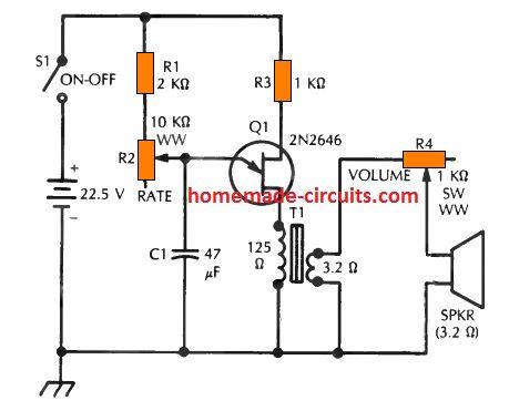 Driving a 21/2 inch loudspeaker, this circuit comes with a decent, high in volume, pop like sound.
The metronome could be created pretty compact, the speaker and battery audio outputs are the only its largest sized elements, and, since it's battery powered, and therefore is entirely portable.
The circuit is actually an adjustable frequency relaxation oscillator which is paired through a transformer to the 4 ohm speaker.
The beat rate can be varied from roughly 1 per second (60 per minute) to around 10 per second (600 per minute) using a 10 k wirewound pot, R2.
The sound output level can be modified through a 1 k, 5 watt, wirewound pot, R4. The output transformer T1 is actually a small 125:3.2 ohm unit.
The circuit pulls 4 mA for the minimum beat rate of the metronome and 7 mA during the fastest beat rate, although this could fluctuate depending on specific UJTs.
A 24 V battery will offer excellent service with this reduced current drain.
Electrolytic capacitor C1 is rated at 50 V.
Resistors R1 and R3 are 1/2 watt, and potentiometers R2 and R4 are wirewound types.
Driving a 21/2 inch loudspeaker, this circuit comes with a decent, high in volume, pop like sound.
The metronome could be created pretty compact, the speaker and battery audio outputs are the only its largest sized elements, and, since it's battery powered, and therefore is entirely portable.
The circuit is actually an adjustable frequency relaxation oscillator which is paired through a transformer to the 4 ohm speaker.
The beat rate can be varied from roughly 1 per second (60 per minute) to around 10 per second (600 per minute) using a 10 k wirewound pot, R2.
The sound output level can be modified through a 1 k, 5 watt, wirewound pot, R4. The output transformer T1 is actually a small 125:3.2 ohm unit.
The circuit pulls 4 mA for the minimum beat rate of the metronome and 7 mA during the fastest beat rate, although this could fluctuate depending on specific UJTs.
A 24 V battery will offer excellent service with this reduced current drain.
Electrolytic capacitor C1 is rated at 50 V.
Resistors R1 and R3 are 1/2 watt, and potentiometers R2 and R4 are wirewound types.
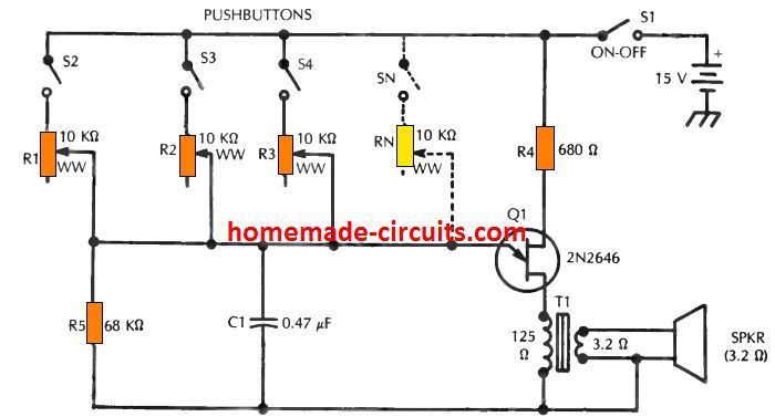 The location which might be signaling the audio could be identified by its specific tone frequency.
But this may be feasible only when a lower number of channels are employed and that the tone frequencies are significantly wide apart (for example, 400 Hz and 1000 Hz) so that they are easily distinguishable by our ear.
The circuit again is based on a simple relaxation oscillator concept, using a type 2N2646 unijunction transistor to generate the audio note and commute a loudspeaker.
The tone frequency is defined through capacitor C1 and one of the 10 k wirewound pots (R1 to Rn).
As soon as the potentiometer is set to 10k ohms, the frequency is around 259 Hz; when the pot is set to 1k, the frequency is roughly 2591 Hz.
The oscillator is connected with the speaker via an output transformer T1, a tiny 125:3.2 ohm unit with primary side center tap unconnected.
The circuit works with somewhere around 9 mA from the 15 V supply.
The location which might be signaling the audio could be identified by its specific tone frequency.
But this may be feasible only when a lower number of channels are employed and that the tone frequencies are significantly wide apart (for example, 400 Hz and 1000 Hz) so that they are easily distinguishable by our ear.
The circuit again is based on a simple relaxation oscillator concept, using a type 2N2646 unijunction transistor to generate the audio note and commute a loudspeaker.
The tone frequency is defined through capacitor C1 and one of the 10 k wirewound pots (R1 to Rn).
As soon as the potentiometer is set to 10k ohms, the frequency is around 259 Hz; when the pot is set to 1k, the frequency is roughly 2591 Hz.
The oscillator is connected with the speaker via an output transformer T1, a tiny 125:3.2 ohm unit with primary side center tap unconnected.
The circuit works with somewhere around 9 mA from the 15 V supply.
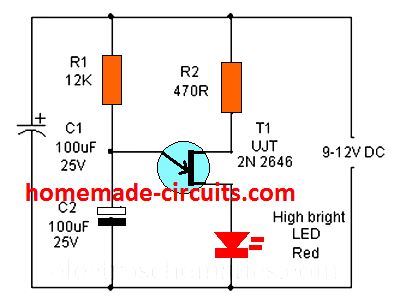 The working of the LED flasher is very basic.
The blinking rate is determined by the R1, C2 elements.
When power is applied, the capacitor C2 slowly begins charging via the resistor R1.
As soon as the voltage level across the capacitor exceeds the firing threshold of the UJT, it fires and switches ON the LED brightly.
The capacitor C2 is now begins discharging through the LED, until the potential across Cr drops below the holding threshold of the UJT, which shuts off, switching OFF the LED.
This cycle keeps repeating, causing the LED to flash alternately.
The LED brightness level is decided by R2, whose value could be calculated using the following formula:
R2 = Supply V - LED Forward V / LED Current
12 - 3.3 / .02 = 435 Ohms, so 470 ohms seems to be the correct value for the proposed design.
The working of the LED flasher is very basic.
The blinking rate is determined by the R1, C2 elements.
When power is applied, the capacitor C2 slowly begins charging via the resistor R1.
As soon as the voltage level across the capacitor exceeds the firing threshold of the UJT, it fires and switches ON the LED brightly.
The capacitor C2 is now begins discharging through the LED, until the potential across Cr drops below the holding threshold of the UJT, which shuts off, switching OFF the LED.
This cycle keeps repeating, causing the LED to flash alternately.
The LED brightness level is decided by R2, whose value could be calculated using the following formula:
R2 = Supply V - LED Forward V / LED Current
12 - 3.3 / .02 = 435 Ohms, so 470 ohms seems to be the correct value for the proposed design.
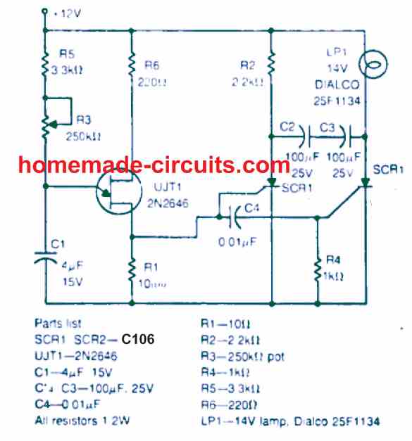 It uses SCRs for the operations.
The bulb could be also replaced with high power LEDs
It uses SCRs for the operations.
The bulb could be also replaced with high power LEDs
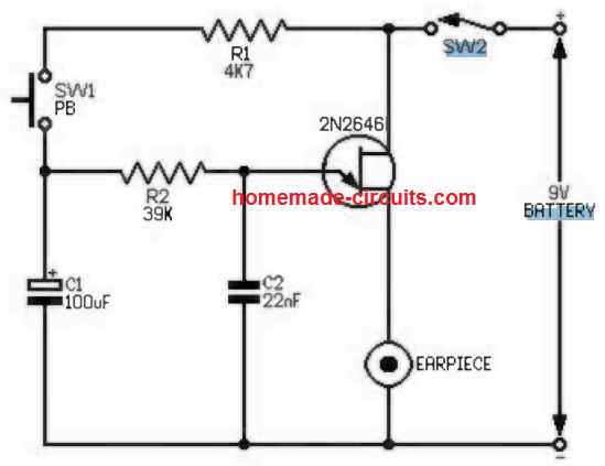 The circuit works like a relaxation oscillator using a single unijunction transistor (2N2646, MU10, TIS43).
R2 and a capacitor C2 decide the frequency of the siren tone.
When button SW1 is pushed it enables capacitor C1 to charge up causing the R2, C2 junction voltage to rise which induces an upward shooting frequency of oscillation.
Now as soon as the the push-button is released the charge inside C2 begins dropping gradually causing a proportionate slow decrease in the frequency of oscillation.
If the push button is switched ON/OFF, with a time interval of around 2 sec between ON OFF enables the circuit to generate a siren like sound.
The circuit works like a relaxation oscillator using a single unijunction transistor (2N2646, MU10, TIS43).
R2 and a capacitor C2 decide the frequency of the siren tone.
When button SW1 is pushed it enables capacitor C1 to charge up causing the R2, C2 junction voltage to rise which induces an upward shooting frequency of oscillation.
Now as soon as the the push-button is released the charge inside C2 begins dropping gradually causing a proportionate slow decrease in the frequency of oscillation.
If the push button is switched ON/OFF, with a time interval of around 2 sec between ON OFF enables the circuit to generate a siren like sound.
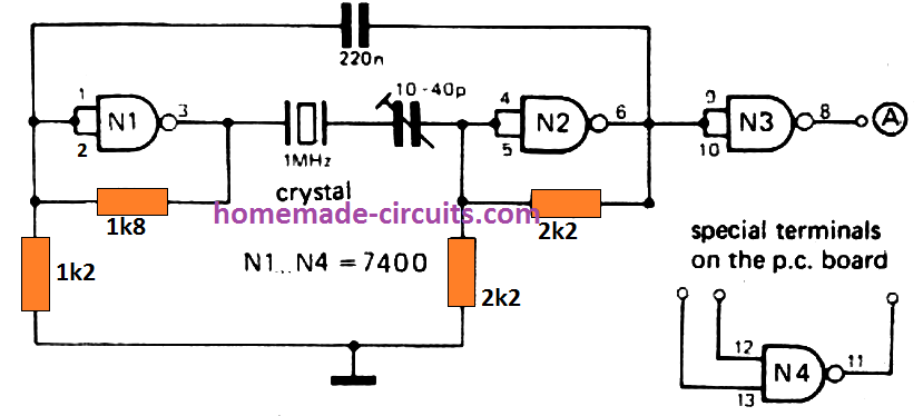 A 3rd NAND gate acts like a buffer at the output of this oscillator output of this oscillator, dividing down by a number of 7490 decade counters.
These incorporate a divide-by-2 stage accompanied by a divide-by-5 stage, that suggests that along with dividing the reference frequency down to 1 Hz in decades, signals of 500 kHz and lower values up to 5 Hz are likewise obtainable.
A 3rd NAND gate acts like a buffer at the output of this oscillator output of this oscillator, dividing down by a number of 7490 decade counters.
These incorporate a divide-by-2 stage accompanied by a divide-by-5 stage, that suggests that along with dividing the reference frequency down to 1 Hz in decades, signals of 500 kHz and lower values up to 5 Hz are likewise obtainable.
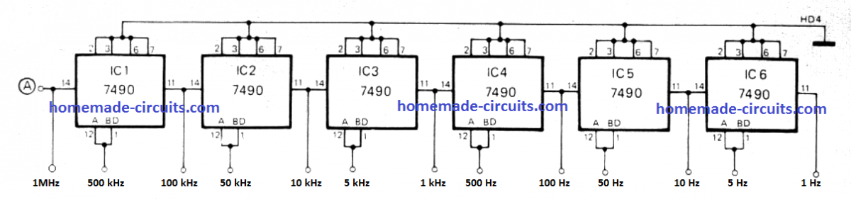 All these signals are specifically useful where gate pulses for counting frequency become necessary.
For instance, the 5 Hz output will give you positive pulses of 100 ms width, thus when the frequency of a 10 MHz signal is tested, a gate pulse of this length might allow through 11500,000 cycles of the signal to the counter, presenting a display of 10,00000.
Alternatively, for time calculations the 1 Hz to 1 MHz outputs tend to be more beneficial.
As an example, while computing a single second interval, 1,000,000 cycles of the 1 MHz output could be measured, offering a display of 10001300.
All these signals are specifically useful where gate pulses for counting frequency become necessary.
For instance, the 5 Hz output will give you positive pulses of 100 ms width, thus when the frequency of a 10 MHz signal is tested, a gate pulse of this length might allow through 11500,000 cycles of the signal to the counter, presenting a display of 10,00000.
Alternatively, for time calculations the 1 Hz to 1 MHz outputs tend to be more beneficial.
As an example, while computing a single second interval, 1,000,000 cycles of the 1 MHz output could be measured, offering a display of 10001300.
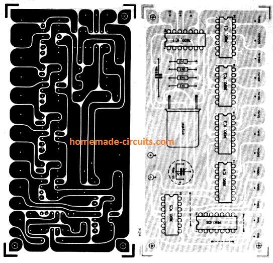 The PCB design and structure is very stream-lined and effectively presented.
The outputs are obtainable across the lower edge of the board layout diagram.
There exists one extra NAND-gate in the bundle intended for the oscillator, which can be employed as the gate in frequency counter applications.
The wiring contacts to this are introduced at the top right corner of the board.
The oscillator frequency could be tweaked to precisely 1 MHz through the trimmer capacitor.
The ideal way of accomplishing this is by using an oscilloscope to examine the 100 kHz output with the 200 kHz Droitwich reception, and applying Lissajous figure.
The trimmer must, naturally, be fine-tuned until the Lissajous number stops rotating.
The PCB design and structure is very stream-lined and effectively presented.
The outputs are obtainable across the lower edge of the board layout diagram.
There exists one extra NAND-gate in the bundle intended for the oscillator, which can be employed as the gate in frequency counter applications.
The wiring contacts to this are introduced at the top right corner of the board.
The oscillator frequency could be tweaked to precisely 1 MHz through the trimmer capacitor.
The ideal way of accomplishing this is by using an oscilloscope to examine the 100 kHz output with the 200 kHz Droitwich reception, and applying Lissajous figure.
The trimmer must, naturally, be fine-tuned until the Lissajous number stops rotating.
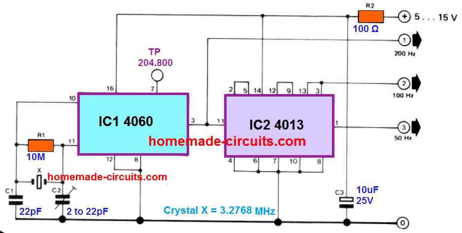 Assuming that the oscillator loop is accurately calibrated through C2, the output at pin 3 (Q14) will generate a 200 Hz square wave.
By using the two flip-flops from IC2 rge resulting square wave voltage is subsequently divided by 2 and after that by 4 contributing to a couple of additional outputs of 100 Hz and 50 Hz.
Assuming that the oscillator loop is accurately calibrated through C2, the output at pin 3 (Q14) will generate a 200 Hz square wave.
By using the two flip-flops from IC2 rge resulting square wave voltage is subsequently divided by 2 and after that by 4 contributing to a couple of additional outputs of 100 Hz and 50 Hz.
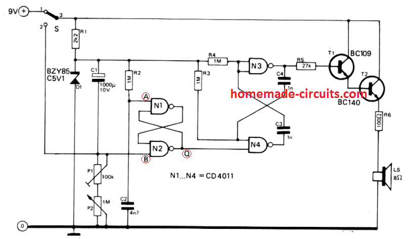
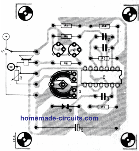
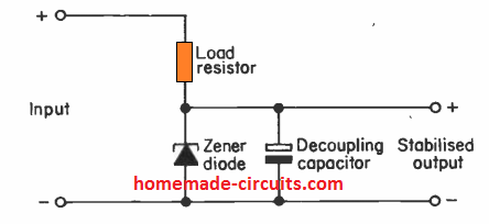 The zener diodes have a voltage rating equivalent to the intended output voltage, that may be closely match the desired output value.
As long as the supply voltage is below the rated value of the zener voltage, it exhibits maximum resistance in the range of many megohms, allowing the supply to pass without restrictions.
However, the moment the supply voltage increases over the rated value of 'zener voltage', triggers a significant drop in its resistance, causing the over voltage to get shunted to ground through it, until the supply drops or reaches the zener voltage level.
Due to this sudden shunting the supply voltage drops and reaches the zener value, which causes the zener resistance to increases again.
The cycle then continues rapidly ensuring the supply remains stabilized at the rated zener value and is never allowed to go above this value.
To get the above stabilization, the input supply needs to be a little higher than the required stabilized output voltage.
The excess voltage above the zener value causes the internal "avalanche" characteristics of the zener to trigger, causing an instant shunting effect and dropping of the supply until it reaches the zener rating.
This action continues infinitely ensuring a fixed stabilized output voltage equivalent to the zener rating.
The zener diodes have a voltage rating equivalent to the intended output voltage, that may be closely match the desired output value.
As long as the supply voltage is below the rated value of the zener voltage, it exhibits maximum resistance in the range of many megohms, allowing the supply to pass without restrictions.
However, the moment the supply voltage increases over the rated value of 'zener voltage', triggers a significant drop in its resistance, causing the over voltage to get shunted to ground through it, until the supply drops or reaches the zener voltage level.
Due to this sudden shunting the supply voltage drops and reaches the zener value, which causes the zener resistance to increases again.
The cycle then continues rapidly ensuring the supply remains stabilized at the rated zener value and is never allowed to go above this value.
To get the above stabilization, the input supply needs to be a little higher than the required stabilized output voltage.
The excess voltage above the zener value causes the internal "avalanche" characteristics of the zener to trigger, causing an instant shunting effect and dropping of the supply until it reaches the zener rating.
This action continues infinitely ensuring a fixed stabilized output voltage equivalent to the zener rating.
 This is an amplified zener version which makes use of a BJT for creating a variable zener with enhanced power handling capability.
Let's imagine R1 and R2 are of the same value., which would create sufficient biasing level to the BJT base, and allow the BJT to conduct optimally.
Since the minimum base emitter forward voltage requirement is 0.7V, the BJT will conduct and shunt any value that's above 0.7V or at the most 1V depending on the specific characteristics of the BJT used.
So the output will be stabilized at 1 V approximately.
The power output from this "amplified variable zener" will depend on the BJT power rating and the load resistor value.
However this value can be easily changed or adjusted to some other desired level, simply by changing the R2 value.
Or more simply by replacing R2 with a pot.
The range of both the R1 and R2 Pot can be anything between 1K and 47K, to get a smoothly variable output from 1V to the supply level (24V max).
For more accuracy, you can apply the following volatge divider formula:
Output Voltage = 0.65 (R1 + R2)/R2
This is an amplified zener version which makes use of a BJT for creating a variable zener with enhanced power handling capability.
Let's imagine R1 and R2 are of the same value., which would create sufficient biasing level to the BJT base, and allow the BJT to conduct optimally.
Since the minimum base emitter forward voltage requirement is 0.7V, the BJT will conduct and shunt any value that's above 0.7V or at the most 1V depending on the specific characteristics of the BJT used.
So the output will be stabilized at 1 V approximately.
The power output from this "amplified variable zener" will depend on the BJT power rating and the load resistor value.
However this value can be easily changed or adjusted to some other desired level, simply by changing the R2 value.
Or more simply by replacing R2 with a pot.
The range of both the R1 and R2 Pot can be anything between 1K and 47K, to get a smoothly variable output from 1V to the supply level (24V max).
For more accuracy, you can apply the following volatge divider formula:
Output Voltage = 0.65 (R1 + R2)/R2
 Basically a series regulator could simply incorporate a zener shunt regulator, loading an emitter follower buffer circuit, as indicated above.
You may find unity voltage gain whenever an emitter follower stage is employed.
This means when a stabilized input is applied to its base, we will generally achieve a stabilized output from the emitter as well.
Because we are able to get a higher current gain from the emitter follower, the output current can be expected to be a lot higher in comparison to the applied base current.
Therefore, even while the base current is around 1 or 2 mA in the zener shunt stage, which also becomes the quiescent current consumption of the design, the output current of 100 mA could be made available at the output.
The input current is add up to the output current together with 1 or 2 mA utilized by the zener stabilizer, and for that reason the efficiency achieved reaches to an outstanding level.
Given that, the input supply to the circuit is sufficiently rated to achieve the expected output voltage, the output may be practically independent of the input supply level, since this is directly regulated by the base potential of Tr1.
The zener diode and decoupling capacitor develop a perfectly clean voltage at the base of the transistor, which is replicated at the output generating a virtually noise free volatge.
This allows this type of circuits with the ability to deliver outputs with surprisingly low ripple and noise without including huge smoothing capacitors, and with a range of current that may be as high as 1 amp or even more.
As far as the output voltage level is concerned, this may not be exactly equal to the connected zener voltage.
This is because there exists a voltage drop of approximately 0.65 volts between the base and emitter leads of the transistor.
This drop consequently needs to be deducted from the zener voltage value to be able to achieve the minimal output voltage of the circuit.
Meaning if the zener value is 12.7V, then the output at the emitter of the transistor could be around 12 V, or conversely, if the desired output voltage is 12 V, then the zener volatge must be seleced to be 12.7 V.
The regulation of this series regulator circuit will never be identical to the regulation of the zener circuit, because the emitter follower simply cannot possess zero output impedance.
And the voltage drop through the stage has to rise marginally in response to increasing output current.
On the other hand, good regulation could be expected when the zener current multiplied by the current gain of the transistor reaches minimum 100 times the expected highest output current.
Basically a series regulator could simply incorporate a zener shunt regulator, loading an emitter follower buffer circuit, as indicated above.
You may find unity voltage gain whenever an emitter follower stage is employed.
This means when a stabilized input is applied to its base, we will generally achieve a stabilized output from the emitter as well.
Because we are able to get a higher current gain from the emitter follower, the output current can be expected to be a lot higher in comparison to the applied base current.
Therefore, even while the base current is around 1 or 2 mA in the zener shunt stage, which also becomes the quiescent current consumption of the design, the output current of 100 mA could be made available at the output.
The input current is add up to the output current together with 1 or 2 mA utilized by the zener stabilizer, and for that reason the efficiency achieved reaches to an outstanding level.
Given that, the input supply to the circuit is sufficiently rated to achieve the expected output voltage, the output may be practically independent of the input supply level, since this is directly regulated by the base potential of Tr1.
The zener diode and decoupling capacitor develop a perfectly clean voltage at the base of the transistor, which is replicated at the output generating a virtually noise free volatge.
This allows this type of circuits with the ability to deliver outputs with surprisingly low ripple and noise without including huge smoothing capacitors, and with a range of current that may be as high as 1 amp or even more.
As far as the output voltage level is concerned, this may not be exactly equal to the connected zener voltage.
This is because there exists a voltage drop of approximately 0.65 volts between the base and emitter leads of the transistor.
This drop consequently needs to be deducted from the zener voltage value to be able to achieve the minimal output voltage of the circuit.
Meaning if the zener value is 12.7V, then the output at the emitter of the transistor could be around 12 V, or conversely, if the desired output voltage is 12 V, then the zener volatge must be seleced to be 12.7 V.
The regulation of this series regulator circuit will never be identical to the regulation of the zener circuit, because the emitter follower simply cannot possess zero output impedance.
And the voltage drop through the stage has to rise marginally in response to increasing output current.
On the other hand, good regulation could be expected when the zener current multiplied by the current gain of the transistor reaches minimum 100 times the expected highest output current.
 Despite the fact that common emitter stages ordinarily have a substantial degree of voltage gain, this may not be the situation in this case.
It is because of the 100% negative feedback that is placed across the output transistor collector and the emitter of the driver transistor.
This facilitates the amplifier to attain a gain of an exact unity.
Despite the fact that common emitter stages ordinarily have a substantial degree of voltage gain, this may not be the situation in this case.
It is because of the 100% negative feedback that is placed across the output transistor collector and the emitter of the driver transistor.
This facilitates the amplifier to attain a gain of an exact unity.
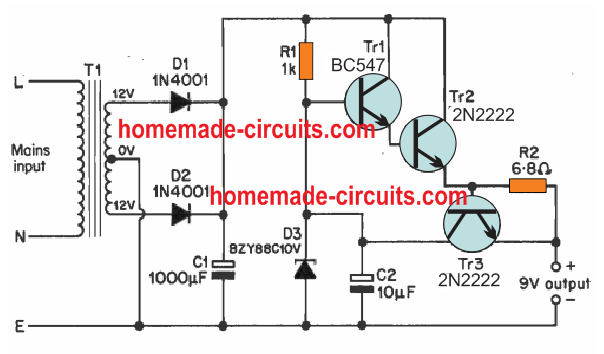 The model is developed for all applications working with 9 volt DC with a maximum current not exceeding 100 mA.
It isn't appropriate for devices that demand a relatively higher amount of current.
T1 is a 12 -0 - 12 volt 100 mA transformer which supplies isolated protection isolation and a voltage step-down, while its center tapped secondary winding operates a basic push-pull rectifier with a filter capacitor.
With no load the output will be around 18 volts DC, which may drop to approximately 12 volts at full load.
The circuit that works like a voltage stabilizer is actually a basic series type design incorporating R1, D3 and C2 in order to get a regulated 10 V nominal output.
The zener current ranges through around 8 mA without load, and down to about 3 mA at full load.
The dissipation generated from R1 and D3 asa result is minimal.
A Darlington pair emitter follower formed by TR1 and TR2 can be seen configured as the output buffer amplifier delivers a current gain of about 30,000 at full output, while the minimum gain being 10,000.
At this gain level whn the unit operates using 3 mA under full load current, and a minimum gain i exhibits almost no deviation in the voltage drop across the amplifier even while the load current fluctuates.
The real voltage drop from the output amplifier is approximately 1.3 volts, and with a moderate 10 volt input this offers an output of roughly 8.7 volts.
This looks almost equal to the specified 9 V, considering the fact that even the real a 9 volt battery may show variations from 9.5 V to 7.5 V during its operational period.
The model is developed for all applications working with 9 volt DC with a maximum current not exceeding 100 mA.
It isn't appropriate for devices that demand a relatively higher amount of current.
T1 is a 12 -0 - 12 volt 100 mA transformer which supplies isolated protection isolation and a voltage step-down, while its center tapped secondary winding operates a basic push-pull rectifier with a filter capacitor.
With no load the output will be around 18 volts DC, which may drop to approximately 12 volts at full load.
The circuit that works like a voltage stabilizer is actually a basic series type design incorporating R1, D3 and C2 in order to get a regulated 10 V nominal output.
The zener current ranges through around 8 mA without load, and down to about 3 mA at full load.
The dissipation generated from R1 and D3 asa result is minimal.
A Darlington pair emitter follower formed by TR1 and TR2 can be seen configured as the output buffer amplifier delivers a current gain of about 30,000 at full output, while the minimum gain being 10,000.
At this gain level whn the unit operates using 3 mA under full load current, and a minimum gain i exhibits almost no deviation in the voltage drop across the amplifier even while the load current fluctuates.
The real voltage drop from the output amplifier is approximately 1.3 volts, and with a moderate 10 volt input this offers an output of roughly 8.7 volts.
This looks almost equal to the specified 9 V, considering the fact that even the real a 9 volt battery may show variations from 9.5 V to 7.5 V during its operational period.
 The current limiting circuitry works by using only a couple of elements; R2 and Tr3. Its response is actually so quick that it simply eliminates all possible risks of short circuit at the output thereby providing a fail proof protection to the output devices.
The working of the current limiting can be understood as explained below.
The current limiting circuitry works by using only a couple of elements; R2 and Tr3. Its response is actually so quick that it simply eliminates all possible risks of short circuit at the output thereby providing a fail proof protection to the output devices.
The working of the current limiting can be understood as explained below.
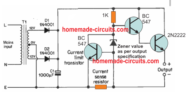 R2 is wired in series with the output, which causes the voltage developed across R2 to be proportionate to the output current.
At output consumptions reaching 100 mA the voltage produced across R2 won't be enough to trigger on Tr3, since it is a silicon transistor requiring a minimum potential of 0.65 V to switch ON.
However when the output load exceeds the 100 mA limit, it geneartes enough potential across T2 to adequately switch ON Tr3 into conduction.
TR3 in turn causes some current fto flow towards Trl across the negative supply rail through the load.
This results in some reduction of the output voltage.
If the load increases further results in a proportionate rise in potential across R2 to rise, forcing Tr3 to switch ON even harder.
This consequently allows higher amounts current being shifted towards Tr1 and the negative line through Tr3 and the load.
This action further leads to a proportionately rising voltage drop of the output voltage.
Even in case of an output short circuit, Tr3 will likely be biased hard into conduction, forcing the output voltage to drop to zero, ensuring that the output current is never allowed to exceed the 100 mA mark.
R2 is wired in series with the output, which causes the voltage developed across R2 to be proportionate to the output current.
At output consumptions reaching 100 mA the voltage produced across R2 won't be enough to trigger on Tr3, since it is a silicon transistor requiring a minimum potential of 0.65 V to switch ON.
However when the output load exceeds the 100 mA limit, it geneartes enough potential across T2 to adequately switch ON Tr3 into conduction.
TR3 in turn causes some current fto flow towards Trl across the negative supply rail through the load.
This results in some reduction of the output voltage.
If the load increases further results in a proportionate rise in potential across R2 to rise, forcing Tr3 to switch ON even harder.
This consequently allows higher amounts current being shifted towards Tr1 and the negative line through Tr3 and the load.
This action further leads to a proportionately rising voltage drop of the output voltage.
Even in case of an output short circuit, Tr3 will likely be biased hard into conduction, forcing the output voltage to drop to zero, ensuring that the output current is never allowed to exceed the 100 mA mark.
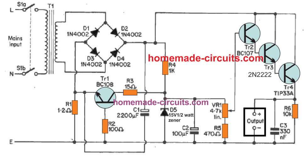 The figure above shows a classic example of a variable voltage regulator circuit which will provide a continuously variable stabilized output from 0 to 12V.
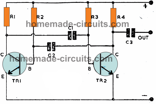
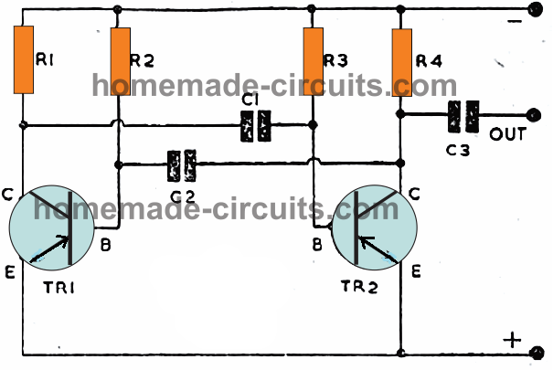 PNP Polarity
In the same manner these can be built using PNP transistors as well.
To avoid misunderstandings, the exactly same circuit is demonstrated above, but using PNP transistors.
The emitter lead has now turned positive.
Once again, a common sort of transistor is pointed out (AC128) nevertheless various other PNP transistors may well be tried.
This is fairly frequently possible to work with transistors actually available in the junk box, by replacing other kinds than the ones displayed in the diagrams.
However, always take care of the emitter line polarity for the transistor, which must be positive for PNP and negative for NPN transistors.
PNP Polarity
In the same manner these can be built using PNP transistors as well.
To avoid misunderstandings, the exactly same circuit is demonstrated above, but using PNP transistors.
The emitter lead has now turned positive.
Once again, a common sort of transistor is pointed out (AC128) nevertheless various other PNP transistors may well be tried.
This is fairly frequently possible to work with transistors actually available in the junk box, by replacing other kinds than the ones displayed in the diagrams.
However, always take care of the emitter line polarity for the transistor, which must be positive for PNP and negative for NPN transistors.
 The circuit below offers identical functions, but it could be organized to provide a louder and high pitched tone.
It could also be quickly designed to present unique sounds in response to subsequent pressing of the button.
The circuit below offers identical functions, but it could be organized to provide a louder and high pitched tone.
It could also be quickly designed to present unique sounds in response to subsequent pressing of the button.
 The primary of the transformer supplies the collector load, and each transistor turns ON the base circuit of the other, through the capacitors and parallel resistors C1/R1 and C2/R2.
A transformer that are normally used for loudspeaker impedance matching has been employed here.
The ratio of the primary and secondary winding may be around 8:1.
However, this may not be too crucial.
The transformer and loudspeaker directly impact the volume level output of the circuit.
It is advisable to work with a ratio greater than 8:1, or an 8 ohm speaker, instead of adjusting the circuit with a transformer of reduced ratio, having a 2 ohm speaker.
The sound pitch can be adjusted by altering the C3 value.
Bigger magnitudes reduce the tone of the sound.
R1 and R2, and the capacitors C1 and C2, could also be the experimented with for the same results.
If a significantly large speaker is used, it may be possible to attain substantial audio volume output.
An appropriate housing will be important for this project, which may be in the form of a baffle.
The baffle is actually a ordinary wooden panel, consisting of a tiny hole of appropriate size matching the diameter of the speaker cone.
The panel must be at minimum 10 x 12 inches and may even be bigger.
For powering the circuit a PP3 battery will be just enough.
The primary of the transformer supplies the collector load, and each transistor turns ON the base circuit of the other, through the capacitors and parallel resistors C1/R1 and C2/R2.
A transformer that are normally used for loudspeaker impedance matching has been employed here.
The ratio of the primary and secondary winding may be around 8:1.
However, this may not be too crucial.
The transformer and loudspeaker directly impact the volume level output of the circuit.
It is advisable to work with a ratio greater than 8:1, or an 8 ohm speaker, instead of adjusting the circuit with a transformer of reduced ratio, having a 2 ohm speaker.
The sound pitch can be adjusted by altering the C3 value.
Bigger magnitudes reduce the tone of the sound.
R1 and R2, and the capacitors C1 and C2, could also be the experimented with for the same results.
If a significantly large speaker is used, it may be possible to attain substantial audio volume output.
An appropriate housing will be important for this project, which may be in the form of a baffle.
The baffle is actually a ordinary wooden panel, consisting of a tiny hole of appropriate size matching the diameter of the speaker cone.
The panel must be at minimum 10 x 12 inches and may even be bigger.
For powering the circuit a PP3 battery will be just enough.
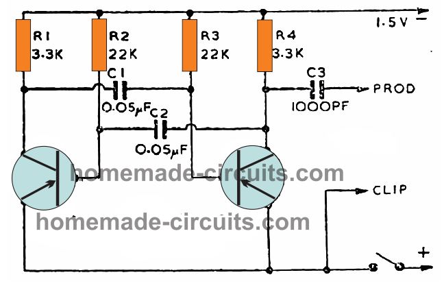 Speedy assessments of audio circuits and faulty amplifiers is often done using an sound oscillator or a signal generators with an injectable frequency output.
You can use this two transistor device to verify speakers and their joints, specific audio stages of an amplifier, or the frequency stages of a radio receiver along with many other similar equipment.
For this you can use a tubular probe which may have the intended oscillator circuit built-in.
For fault finding audio circuits you'd only need to inspect the doubtful areas with the switched ON probe and by touching the various nodes of the audio stage..
The design works with a tiny solitary dry cell, hence all of the elements could be accommodated within a cylindrical tube like housing.
Speedy assessments of audio circuits and faulty amplifiers is often done using an sound oscillator or a signal generators with an injectable frequency output.
You can use this two transistor device to verify speakers and their joints, specific audio stages of an amplifier, or the frequency stages of a radio receiver along with many other similar equipment.
For this you can use a tubular probe which may have the intended oscillator circuit built-in.
For fault finding audio circuits you'd only need to inspect the doubtful areas with the switched ON probe and by touching the various nodes of the audio stage..
The design works with a tiny solitary dry cell, hence all of the elements could be accommodated within a cylindrical tube like housing.
 The resistors should be as small as possible, possibly SMD type, while C1 and C2 may be rated at 6.3V again SMD type.
Make sure you use this signal injector for troubleshooting DC low voltage circuits only, and no AC mains directly operated circuits, which can be lethal to touch.
The resistors should be as small as possible, possibly SMD type, while C1 and C2 may be rated at 6.3V again SMD type.
Make sure you use this signal injector for troubleshooting DC low voltage circuits only, and no AC mains directly operated circuits, which can be lethal to touch.
 When the crocodile clip is hooked up with the negative supply line, while the prod placed on point A, the amplified signal may be audible from the speaker.
This points out that the output stage is functioning correctly.
However if no signal is audible, inspections could be focused more around the output stage specifically.
Suppose the signal is heard on the speaker with the probe injected at point A.
It could then be shifted to B, to inspect TR2. At this point if the the signal shows decrease in its level, may indicate that this stage may be malfunctioning.
Make sure that tyou proceed methodically from the last stage towards the front stages, starting from the speaker.
When the stage where the problem is detected is crossed, you will find the signal level drastically diminishing on the speaker.
In the similar fashion as explained above you can proceed to test the other points as shown in the above example amplifier circuit.
When the crocodile clip is hooked up with the negative supply line, while the prod placed on point A, the amplified signal may be audible from the speaker.
This points out that the output stage is functioning correctly.
However if no signal is audible, inspections could be focused more around the output stage specifically.
Suppose the signal is heard on the speaker with the probe injected at point A.
It could then be shifted to B, to inspect TR2. At this point if the the signal shows decrease in its level, may indicate that this stage may be malfunctioning.
Make sure that tyou proceed methodically from the last stage towards the front stages, starting from the speaker.
When the stage where the problem is detected is crossed, you will find the signal level drastically diminishing on the speaker.
In the similar fashion as explained above you can proceed to test the other points as shown in the above example amplifier circuit.
 The objective of this design would be to replace a mechanical switch based toy lighthouse, toy car signal, or for any identical application in which a repeatedly pulsating light source is desired.
By using a 6V LED lamp, current intake can be kept minimal.
Capacitors C1 and C2 are selected with substantial values, offering a repeated time interval of approximately 1 second on and 1 second off.
The circuit may work using supplies from 3V to 6V however a 6V lamp will probably be necessary for decent illumination of the bulb and attraction.
The working current is probably acquired from an existing battery already employed in the system to commute a motor or some other task.
The objective of this design would be to replace a mechanical switch based toy lighthouse, toy car signal, or for any identical application in which a repeatedly pulsating light source is desired.
By using a 6V LED lamp, current intake can be kept minimal.
Capacitors C1 and C2 are selected with substantial values, offering a repeated time interval of approximately 1 second on and 1 second off.
The circuit may work using supplies from 3V to 6V however a 6V lamp will probably be necessary for decent illumination of the bulb and attraction.
The working current is probably acquired from an existing battery already employed in the system to commute a motor or some other task.
 This double lamp flasher circuit as shown could be enclosed inside a robust housing to operate a set of two 12 volt 6 watt lamps, which then could be used in ˇ°accident" scenarios, by placing the unit on the roof of the wrecked car at night times.
Another application is generally to alert the speeding drivers while the driver change the wheel of his damaged car.
In this design, a couple of TIP32 transistors are applied, however other variants could be tried, provided they are appropriately rated for the lamp current.
With 12V 6W lamps, the collector currents can be approximately 500 mA.
The illumination of the lamps tend to be most distinctive when they are separated around 1 ft or more apart, possibly next to each other, or one over the other.
This double lamp flasher circuit as shown could be enclosed inside a robust housing to operate a set of two 12 volt 6 watt lamps, which then could be used in ˇ°accident" scenarios, by placing the unit on the roof of the wrecked car at night times.
Another application is generally to alert the speeding drivers while the driver change the wheel of his damaged car.
In this design, a couple of TIP32 transistors are applied, however other variants could be tried, provided they are appropriately rated for the lamp current.
With 12V 6W lamps, the collector currents can be approximately 500 mA.
The illumination of the lamps tend to be most distinctive when they are separated around 1 ft or more apart, possibly next to each other, or one over the other.
 A metronome is an device which delivers periodical ticking or beating sound, and its function is to establish the proper tempo for any musical performance.
When employed in in this manner, it supplies a consistent beat to ensure that pace of the music is not changed by the musician in the course of training, and in addition it helps an accurate performing speed to be established.
When it comes to speedy and challenging bits, a performer may need to exercise to the appropriate pace.
A piece of audio might have the rate mentioned on it with respect to the amount of notes of specified duration per minute.
Or one of several audio terms articulating the right speed could be identified at the very top or start of the tunes.
These terminology include from slower, to faster speeds, and symbolize a specific quantity of beats per minute.
The ones most typically demanded are given below:
A metronome is an device which delivers periodical ticking or beating sound, and its function is to establish the proper tempo for any musical performance.
When employed in in this manner, it supplies a consistent beat to ensure that pace of the music is not changed by the musician in the course of training, and in addition it helps an accurate performing speed to be established.
When it comes to speedy and challenging bits, a performer may need to exercise to the appropriate pace.
A piece of audio might have the rate mentioned on it with respect to the amount of notes of specified duration per minute.
Or one of several audio terms articulating the right speed could be identified at the very top or start of the tunes.
These terminology include from slower, to faster speeds, and symbolize a specific quantity of beats per minute.
The ones most typically demanded are given below:
 With the part numbers indicated in the diagram, it may be observed that it is possible to adjust the circuit from around 44 beats per minute, and 200. These might be measured through seconds.
As R1 value is decreased you will find an increase in the maximum range of the frequency.
Which in turn may be set through VR1 for minimum resistance.
Likewise, increasing the values of the specified resistances brings about lowering of the periodic frequency.
With the part numbers indicated in the diagram, it may be observed that it is possible to adjust the circuit from around 44 beats per minute, and 200. These might be measured through seconds.
As R1 value is decreased you will find an increase in the maximum range of the frequency.
Which in turn may be set through VR1 for minimum resistance.
Likewise, increasing the values of the specified resistances brings about lowering of the periodic frequency.
 The Minano or mini-piano in fact generates an organ-like notes, that are rich in harmonics, and of pretty pleasing to hear.
A musical instrument of this kind could prove to be a lot of fun.
It could possibly create just one tone during a period, which streamlines performing, since there isn't any chords involved or the need of striking several tunes at the same time frame.
The feedback through capacitor C1 across the collector of 2N2222 and base of BC547 is responsible for generating the osculations .
The value of the capacitor decides the frequency of the circuit, which can be changed as desired.
R1 value cannot be changed since it is supposed to be fixed with a minimum required value ensuring the highest frequency note.
To obtain lower frequencies or tunes, several adjustments in the form of A, B, C, D, presets are added in the design.
The frequency will decrease, as the resistance adjustment on the preset is increased.
A calibration of around 2 octaves, based on Middle C, would be quite fine, and will cover frequencies from 128 to 512 Hertz.
You will actually find an assortment of frequency ranges applicable, the popular ones are probably Standard and Concert Pitch.
For these ranges, the resistance value of 100K on the preset will usually be quite enough.
The Minano or mini-piano in fact generates an organ-like notes, that are rich in harmonics, and of pretty pleasing to hear.
A musical instrument of this kind could prove to be a lot of fun.
It could possibly create just one tone during a period, which streamlines performing, since there isn't any chords involved or the need of striking several tunes at the same time frame.
The feedback through capacitor C1 across the collector of 2N2222 and base of BC547 is responsible for generating the osculations .
The value of the capacitor decides the frequency of the circuit, which can be changed as desired.
R1 value cannot be changed since it is supposed to be fixed with a minimum required value ensuring the highest frequency note.
To obtain lower frequencies or tunes, several adjustments in the form of A, B, C, D, presets are added in the design.
The frequency will decrease, as the resistance adjustment on the preset is increased.
A calibration of around 2 octaves, based on Middle C, would be quite fine, and will cover frequencies from 128 to 512 Hertz.
You will actually find an assortment of frequency ranges applicable, the popular ones are probably Standard and Concert Pitch.
For these ranges, the resistance value of 100K on the preset will usually be quite enough.
 The diagram above depicts the keyboard for the mini piano having a little over one octave.
For practically implementation of the keyboard make sure the keys are at least 25 mm apart from each other, and without sharp edges.
The diagram above depicts the keyboard for the mini piano having a little over one octave.
For practically implementation of the keyboard make sure the keys are at least 25 mm apart from each other, and without sharp edges.
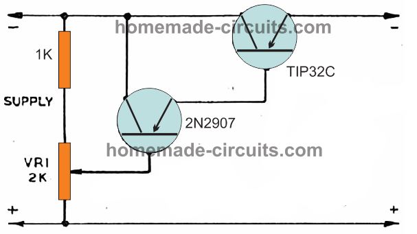 This circuit can be used for controlling supply voltage, and thus can be used for dimming DC light bulbs or for speed control such as in model trains.
The figure above displays the essential circuit, which will usually be sufficient for most model train control.
VR1 is attached across the DC supply line, and its adjustment makes it possible for any desired voltage to be set at the base of the first PNP 2N2907.
The two transistors are connected as Darlington pair in order to increase gain of the pair and to minimize the current load on VR1. It ensures that the base current of the first PNP may simply not surpass 0.1mA, while that of the the second PNP TIP32 may be driven over 5mA.
The O
The emitter voltage of this PNP BJT follows its varying base potential, in order that the second transistor's base voltage is controlled in exactly the same manner.
This results in an output that accurately follows the pot variation and replicates a varying output voltage across the collector of the TIP32.
Thus the pot setting determines the output voltage which can be varied from 0 to the supply level, with a drop of 1.2 V which is the standard biasing drop for the two PNPs combined.
This circuit can be used for controlling supply voltage, and thus can be used for dimming DC light bulbs or for speed control such as in model trains.
The figure above displays the essential circuit, which will usually be sufficient for most model train control.
VR1 is attached across the DC supply line, and its adjustment makes it possible for any desired voltage to be set at the base of the first PNP 2N2907.
The two transistors are connected as Darlington pair in order to increase gain of the pair and to minimize the current load on VR1. It ensures that the base current of the first PNP may simply not surpass 0.1mA, while that of the the second PNP TIP32 may be driven over 5mA.
The O
The emitter voltage of this PNP BJT follows its varying base potential, in order that the second transistor's base voltage is controlled in exactly the same manner.
This results in an output that accurately follows the pot variation and replicates a varying output voltage across the collector of the TIP32.
Thus the pot setting determines the output voltage which can be varied from 0 to the supply level, with a drop of 1.2 V which is the standard biasing drop for the two PNPs combined.
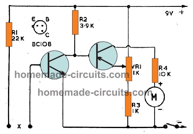 A lie detector gadget can be one that reveals any kind of change in our skin conductivity, hence the user with this lie detector is able to confirm whether or not a lie from the target who is in question.
This design is actually just for experimental purpose, and may not be too reliable for guaranteed results.
There are a couple of important factors behind this.
One, using lie detection device is never considered a valid method by the law.
Second reason is, since the circuit depends on the moisture levels of the accused person's hand, this may sometimes give misleading results as the person may be actually innocent but due to psychological weakness may sweat heavily causing the meter to indicate a wrong lie detection.
The resistance at X, along with R1, effects in a certain magnitude of collector current for the first transistor stage.
This results in a drop in the potential across R2, and correspondingly affects the base potential of the second transistor stage also.
VR1 makes it possible for the emitter voltage of the PNP to be adjusted such that only the desired minimum amount of collector current passes through the meter.
A 1mA, FSD type moving coil meter can be used for this application.
R4 ensures that current to the meter never exceeds beyond unsafe results under any circumstances.
With appropriate tweaking and setting the lie detector can be set up in such way that even a small amount of moisture across the test points may lead to noticeable deflections on the meter.
A lie detector gadget can be one that reveals any kind of change in our skin conductivity, hence the user with this lie detector is able to confirm whether or not a lie from the target who is in question.
This design is actually just for experimental purpose, and may not be too reliable for guaranteed results.
There are a couple of important factors behind this.
One, using lie detection device is never considered a valid method by the law.
Second reason is, since the circuit depends on the moisture levels of the accused person's hand, this may sometimes give misleading results as the person may be actually innocent but due to psychological weakness may sweat heavily causing the meter to indicate a wrong lie detection.
The resistance at X, along with R1, effects in a certain magnitude of collector current for the first transistor stage.
This results in a drop in the potential across R2, and correspondingly affects the base potential of the second transistor stage also.
VR1 makes it possible for the emitter voltage of the PNP to be adjusted such that only the desired minimum amount of collector current passes through the meter.
A 1mA, FSD type moving coil meter can be used for this application.
R4 ensures that current to the meter never exceeds beyond unsafe results under any circumstances.
With appropriate tweaking and setting the lie detector can be set up in such way that even a small amount of moisture across the test points may lead to noticeable deflections on the meter.
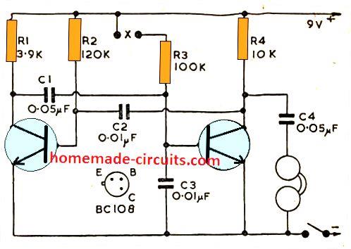 This is another lie detector circuit which makes use of a headphone or a small speaker for processing the output results.
It's again a transistor astable circuit configured to generate a specific tone frequency on the connected speaker.
However since this frequency is directly determined by the RC elements at the base collector of the two transistors, it becomes possible to change the output tone by changing the base resistance of one of the transistors.
The skin resistance when placed between the points X converts the skin resistance into a varying tone on the headphone.
Higher skin resistance initiates the output to generate low frequency intermittent click-click pulses on the speaker headphone.
The frequency of this signal goes on increasing as the skin moisture increases, probably due to a lie spoken by the accused.
This allows the user to understand the level of truth spoken by the accused.
This is another lie detector circuit which makes use of a headphone or a small speaker for processing the output results.
It's again a transistor astable circuit configured to generate a specific tone frequency on the connected speaker.
However since this frequency is directly determined by the RC elements at the base collector of the two transistors, it becomes possible to change the output tone by changing the base resistance of one of the transistors.
The skin resistance when placed between the points X converts the skin resistance into a varying tone on the headphone.
Higher skin resistance initiates the output to generate low frequency intermittent click-click pulses on the speaker headphone.
The frequency of this signal goes on increasing as the skin moisture increases, probably due to a lie spoken by the accused.
This allows the user to understand the level of truth spoken by the accused.
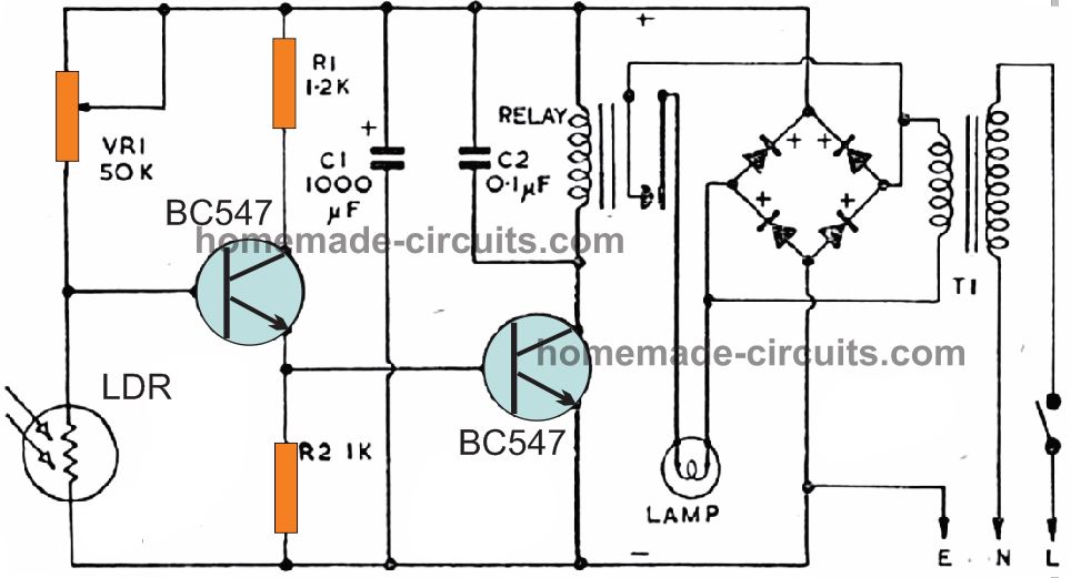 This simple automatic mast light circuit will automatically switch OFF a connected lamp everyday at dawn break, and switch it ON when night sets in.
The working principle is simple.
The preset VR1 setting and the LDR resistance develops a potential at the base of the associated BC547.
VR1 is adjusted such that this potential is minimal while sufficient light is present on the LDR during daytime.
This in turn causes the voltage at the base of the other transistor to be significantly low so that it remains OFF and also keeps the relay and the lamp switched OFF.
When appropriate darkness falls, the LDR resistance increases causing the potentials at the bases of the two transistors to increase proportionately until they switch ON the relay and the lamp.
The cycle repeats each day and night accordingly.
Here the lamp is a low voltage lamp used with the transformer low voltage AC, however an AC mains operated lamp could be also used by appropriately wiring the relay contacts and the lamp with the AC mains line.
Light Activated Lamp without Relay
This simple automatic mast light circuit will automatically switch OFF a connected lamp everyday at dawn break, and switch it ON when night sets in.
The working principle is simple.
The preset VR1 setting and the LDR resistance develops a potential at the base of the associated BC547.
VR1 is adjusted such that this potential is minimal while sufficient light is present on the LDR during daytime.
This in turn causes the voltage at the base of the other transistor to be significantly low so that it remains OFF and also keeps the relay and the lamp switched OFF.
When appropriate darkness falls, the LDR resistance increases causing the potentials at the bases of the two transistors to increase proportionately until they switch ON the relay and the lamp.
The cycle repeats each day and night accordingly.
Here the lamp is a low voltage lamp used with the transformer low voltage AC, however an AC mains operated lamp could be also used by appropriately wiring the relay contacts and the lamp with the AC mains line.
Light Activated Lamp without Relay
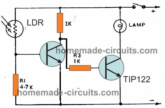 If you do not wish to include a relay and want to use a DC lamp or an LED lamp for the intended automatic day night lamp activation, in that case the following simple configuration could be tried.
The working process is similar to the previous circuit, except the relay which is replaced with the TIP122 transistor and the DC lamp or LED lamp.
If you do not wish to include a relay and want to use a DC lamp or an LED lamp for the intended automatic day night lamp activation, in that case the following simple configuration could be tried.
The working process is similar to the previous circuit, except the relay which is replaced with the TIP122 transistor and the DC lamp or LED lamp.
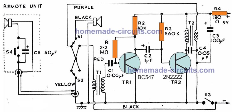 This intercom circuit delivers 2-way communication across selected locations or rooms, upstairs-to downstairs, or within home by a simple press of a push-button from either end.
Additionally it is can be a fun telephone for school kids.
This circuit can be also useful as a baby-crying listening device.
The design basically consists of a main or master systems, along with a distant system, linked with a double wire extension lead.
S1 and S2 are a DPDT push switch, which consists of contacts as shown in the normal situation.
Switch S3 is the master device on-off switch, and S4 works like the remote unit contacting switch.
To make the working easier, S1/S2 are indicated by the prints ˇ°Press to Call or Talkˇ±.
S3 is marked ˇ°On", and S4 "Press to Call".
During the functioning, when the distant side user chooses to communicate, the person will press S4. This connects the battery negative circuit via the transformer primary T1 so that it generates a feedback and activates an sound tone in the master speaker.
Next, the individual handling the master unit pushes the switch S3 to switch ON the intercom.
In this situation, anything spoken on the remote speaker gets amplified and becomes clearly audible over the master speaker.
To initiate an opposite communication, the individual at the master unit side activates the switches S1/S2, which causes his loudspeaker to work like a microphone.
The amplified voice is subsequently carried to the remote unit to complete the communication.
T1 and T2 are small audio transformers having a ratio of 1:5 meaning if the primary side 100 turns, the secondary side can be 500 turns.
You can also try any small step down transformer.
This intercom circuit delivers 2-way communication across selected locations or rooms, upstairs-to downstairs, or within home by a simple press of a push-button from either end.
Additionally it is can be a fun telephone for school kids.
This circuit can be also useful as a baby-crying listening device.
The design basically consists of a main or master systems, along with a distant system, linked with a double wire extension lead.
S1 and S2 are a DPDT push switch, which consists of contacts as shown in the normal situation.
Switch S3 is the master device on-off switch, and S4 works like the remote unit contacting switch.
To make the working easier, S1/S2 are indicated by the prints ˇ°Press to Call or Talkˇ±.
S3 is marked ˇ°On", and S4 "Press to Call".
During the functioning, when the distant side user chooses to communicate, the person will press S4. This connects the battery negative circuit via the transformer primary T1 so that it generates a feedback and activates an sound tone in the master speaker.
Next, the individual handling the master unit pushes the switch S3 to switch ON the intercom.
In this situation, anything spoken on the remote speaker gets amplified and becomes clearly audible over the master speaker.
To initiate an opposite communication, the individual at the master unit side activates the switches S1/S2, which causes his loudspeaker to work like a microphone.
The amplified voice is subsequently carried to the remote unit to complete the communication.
T1 and T2 are small audio transformers having a ratio of 1:5 meaning if the primary side 100 turns, the secondary side can be 500 turns.
You can also try any small step down transformer.
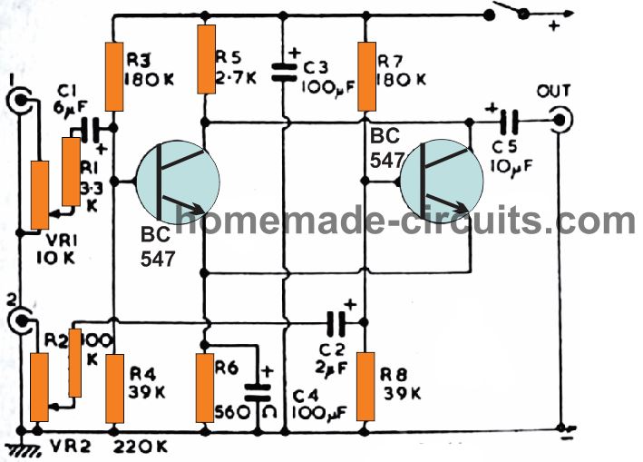 If you are looking for a circuit that will mix two audio signals and produce a combined signal at the output then the above shown 2 transistor audio mixer circuit will probably do the job for you!
The circuit will not only mix and blend two audio signals but also boost them to a higher level so that it can be readily employed for feeding a power amplifier.
It features a pair of audio inputs, which are amplified by separate single transistor amplifiers configured common emitter amplifiers.
VR1 and VR2 allow the user to select how much signal can be passed across the two inputs for appropriate mixing of the signals.
If you are looking for a circuit that will mix two audio signals and produce a combined signal at the output then the above shown 2 transistor audio mixer circuit will probably do the job for you!
The circuit will not only mix and blend two audio signals but also boost them to a higher level so that it can be readily employed for feeding a power amplifier.
It features a pair of audio inputs, which are amplified by separate single transistor amplifiers configured common emitter amplifiers.
VR1 and VR2 allow the user to select how much signal can be passed across the two inputs for appropriate mixing of the signals.
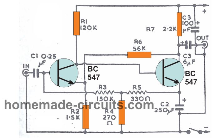 A simple yet very useful little pre-amplifier circuit can be built by wiring just a couple of transistors.
The unit will easily boost a 1mV signal up to 100mV or even higher.
It is thus very handy for amplifying extremely small signals which cannot be used directly with a power amplifier.
This pre-amplifier offers a very high input impedance.
This is often an essential aspect, while working with any high fidelity product.
The output offers low impedance, and can be compatible with almost all power amplifiers with good enough results.
The amplification achieved is determined by to a certain extent on genuine transistor selections, and also on the supply source level, however you can expect this to be approximately around 30dB.
We can see a pair of feedback loops in the design, one is using R3 and R5 attached to the first transistor base, while the other is implemented through R6 to emitter.
The indicated magnitudes are the recommended values, because they additionally fix the DC operating conditions for the two stages.
A 250k potentiometer is used as the volume control at the input.
A simple yet very useful little pre-amplifier circuit can be built by wiring just a couple of transistors.
The unit will easily boost a 1mV signal up to 100mV or even higher.
It is thus very handy for amplifying extremely small signals which cannot be used directly with a power amplifier.
This pre-amplifier offers a very high input impedance.
This is often an essential aspect, while working with any high fidelity product.
The output offers low impedance, and can be compatible with almost all power amplifiers with good enough results.
The amplification achieved is determined by to a certain extent on genuine transistor selections, and also on the supply source level, however you can expect this to be approximately around 30dB.
We can see a pair of feedback loops in the design, one is using R3 and R5 attached to the first transistor base, while the other is implemented through R6 to emitter.
The indicated magnitudes are the recommended values, because they additionally fix the DC operating conditions for the two stages.
A 250k potentiometer is used as the volume control at the input.
 In audio circuits it often becomes important to integrate two stages which are incompatible or having different impedance levels.
This may lead to substantial losses if connected directly without a buffers stage.
Earlier we used to have transformers for this purpose, but these have its own drawbacks.
Transformers can attract hum and noise even after proper shielding.
Moreover transformers can be bulky and expensive.
Another quick method of matching impedance is by adding a high value resistor.
But this method can be highly inefficient as this would resist the actual signal, hampering the actual amplification process.
The 2 transistor buffer as shown above triumphs over this kind of complications.
It features a high input impedance, but a low impedance output.
The gain of this buffer circuit is around unity or 1, meaning the output will be almost the same as input, even with an optimal impedance matching.
Needless to say , this circuit must be enclosed and attached to a metal box in order to achieve perfect screening from external stray pickups.
If an AC to DC adapter is used make sure appropriate hum control is included to prevent hum related issue.
In audio circuits it often becomes important to integrate two stages which are incompatible or having different impedance levels.
This may lead to substantial losses if connected directly without a buffers stage.
Earlier we used to have transformers for this purpose, but these have its own drawbacks.
Transformers can attract hum and noise even after proper shielding.
Moreover transformers can be bulky and expensive.
Another quick method of matching impedance is by adding a high value resistor.
But this method can be highly inefficient as this would resist the actual signal, hampering the actual amplification process.
The 2 transistor buffer as shown above triumphs over this kind of complications.
It features a high input impedance, but a low impedance output.
The gain of this buffer circuit is around unity or 1, meaning the output will be almost the same as input, even with an optimal impedance matching.
Needless to say , this circuit must be enclosed and attached to a metal box in order to achieve perfect screening from external stray pickups.
If an AC to DC adapter is used make sure appropriate hum control is included to prevent hum related issue.
 If you think that building a decent power amplifier using just two small transistors is impossible then you may be wrong.
Just a couple of standard small signal transistors are actually sufficient for making a reasonably loud power amplifier that may reproduce music loud enough to be be heard within a room comfortably.
As indicated in the diagram, the design incorporates two high-gain NPN transistors.
Audio input is by means of C1. The resistor R1 gives the base bias current for this stage, R2 works like the collector load.
C2 connects signals across the output stage.
Base bias for the transistor at the output stage is established using the resistors R3 and R4. This 2N2222 transistor functions being a grounded collector amplifier, wherein the collector is not really joined to the ground line, rather is grounded with respect to the audio signal variations and through the battery negative, that offers minimal impedance.
For general usage, a 15 ohm speaker can be quite reasonable, however it you may probably find that loud speakers of up to about 75 ohms may also work exceptionally well.
Current consumption will be approximately 25 to 30mA when a 15 ohm speaker is adopted, which may drop to 10 or 15mA with a 75 ohm speaker.
This small power amplifier using two transistors circuit may also generally be employed like a headphone amplifier.
Headphones as high as about 1.5k DC resistance may work extremely well, with current dropping to a mere 2 to 3mA.
If you think that building a decent power amplifier using just two small transistors is impossible then you may be wrong.
Just a couple of standard small signal transistors are actually sufficient for making a reasonably loud power amplifier that may reproduce music loud enough to be be heard within a room comfortably.
As indicated in the diagram, the design incorporates two high-gain NPN transistors.
Audio input is by means of C1. The resistor R1 gives the base bias current for this stage, R2 works like the collector load.
C2 connects signals across the output stage.
Base bias for the transistor at the output stage is established using the resistors R3 and R4. This 2N2222 transistor functions being a grounded collector amplifier, wherein the collector is not really joined to the ground line, rather is grounded with respect to the audio signal variations and through the battery negative, that offers minimal impedance.
For general usage, a 15 ohm speaker can be quite reasonable, however it you may probably find that loud speakers of up to about 75 ohms may also work exceptionally well.
Current consumption will be approximately 25 to 30mA when a 15 ohm speaker is adopted, which may drop to 10 or 15mA with a 75 ohm speaker.
This small power amplifier using two transistors circuit may also generally be employed like a headphone amplifier.
Headphones as high as about 1.5k DC resistance may work extremely well, with current dropping to a mere 2 to 3mA.
 The simple amplifier discussed above can be also used with the speaker attached to the collector side of the 2N2222. This version may have slight better amplification level than the emitter side counterpart but the 2N2222 may show a slightly more dissipation and might require a heatsink for controlling the dissipation to safe limits.
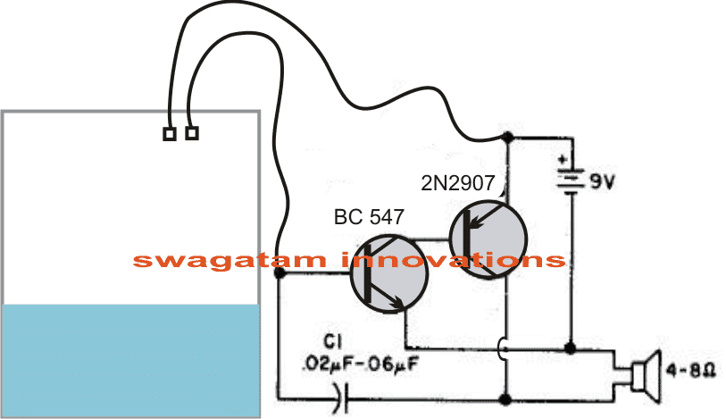 Just two transistors may be needed to make this simple audible water level indicator circuit.
When the indicated probes come in contact with water, current flows to the base of the BC547 and triggers it ON.
This in turn switches ON the PNP 2N2907.
Due to this a voltage surge is sent across the speaker.
The speaker being an inductive load responds with a negative spike to the base of BC547 which instantly switches it OFF hard via C1. With BC547 switched OFF, the 2N2907 and the speaker is also switched OFF.
The situation reverts the circuit to its original status, and BC547 yet again gets a chance to switch ON, and the cycle repeats rapidly generating a sharp tone on the speaker.
Just two transistors may be needed to make this simple audible water level indicator circuit.
When the indicated probes come in contact with water, current flows to the base of the BC547 and triggers it ON.
This in turn switches ON the PNP 2N2907.
Due to this a voltage surge is sent across the speaker.
The speaker being an inductive load responds with a negative spike to the base of BC547 which instantly switches it OFF hard via C1. With BC547 switched OFF, the 2N2907 and the speaker is also switched OFF.
The situation reverts the circuit to its original status, and BC547 yet again gets a chance to switch ON, and the cycle repeats rapidly generating a sharp tone on the speaker.
 The mini latch circuit shown above using a couple of transistors can be very useful in applications that require latching of a relay in response to a momentary trigger.
Here, when a momentary positive trigger is applied at the input the transistors complement and conduct together along with the relay.
At the same time, a feedback voltage reaches via R3 to the base of T1, which latches the network and the relay permanently, even after the input trigger is removed.
R1 and R3 can be 100K, R2, R4 can be 10K, the transistor can be BC547 and BC557 for T1 and T2 respectively.
C1 must be a 10uF/25V, and preferably it must be positioned across the base/emitter of T1.
The mini latch circuit shown above using a couple of transistors can be very useful in applications that require latching of a relay in response to a momentary trigger.
Here, when a momentary positive trigger is applied at the input the transistors complement and conduct together along with the relay.
At the same time, a feedback voltage reaches via R3 to the base of T1, which latches the network and the relay permanently, even after the input trigger is removed.
R1 and R3 can be 100K, R2, R4 can be 10K, the transistor can be BC547 and BC557 for T1 and T2 respectively.
C1 must be a 10uF/25V, and preferably it must be positioned across the base/emitter of T1.
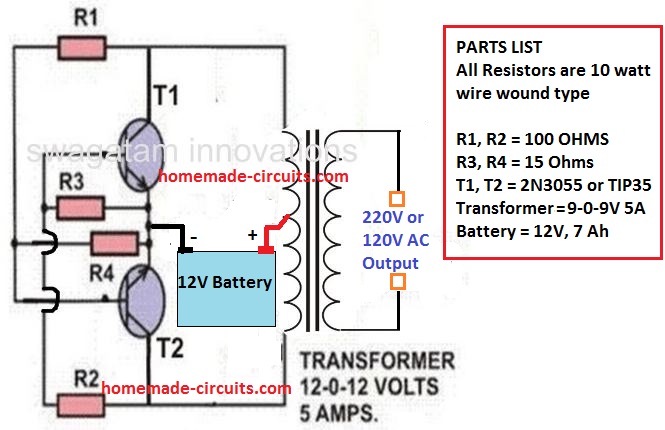 Inverters are recognized as high power units which mostly require sophisticated configurations and parts.
However, surprisingly, a simple inverter with reasonably good power output can be built by configuring just a couple of power transistors as shown above.
The power output can be as high as 120 watts if the battery used is rated at 12 V 30 Ah, and the transformer is accurately rated at 10 amps.
Inverters are recognized as high power units which mostly require sophisticated configurations and parts.
However, surprisingly, a simple inverter with reasonably good power output can be built by configuring just a couple of power transistors as shown above.
The power output can be as high as 120 watts if the battery used is rated at 12 V 30 Ah, and the transformer is accurately rated at 10 amps.
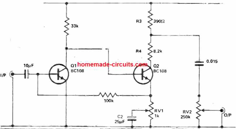 The pot RV1 modifies the level of negative feedback introduced into the circuit through C2, which results in the squaring of the signal.
The role of resistors R3 and R4 is to minimize the output voltage to some appropriate degree, which can be subsequently tweaked as necessary with the aid of the volume control pot VR2.
The pot RV1 modifies the level of negative feedback introduced into the circuit through C2, which results in the squaring of the signal.
The role of resistors R3 and R4 is to minimize the output voltage to some appropriate degree, which can be subsequently tweaked as necessary with the aid of the volume control pot VR2.
 In the hum remover circuit shown above both the transistors could be inexpensive low or high gain varieties.
Preset VR1 can be tweaked, along with the preset VR2 to a low level, until you find the hum is almost gone.
You have then to switch the SW1 in the next step, where the VR2 is further adjusted until the hum is completely removed.
In the hum remover circuit shown above both the transistors could be inexpensive low or high gain varieties.
Preset VR1 can be tweaked, along with the preset VR2 to a low level, until you find the hum is almost gone.
You have then to switch the SW1 in the next step, where the VR2 is further adjusted until the hum is completely removed.

 In this design we make sure to keep things as simple as possible so that even a layman is able to understand regarding the involved motor/gear mechanisms.
and nothing remains hidden behind complex mechanisms.
The working or the function of each motor can be understood with the help of the following points:
Motor#1 controls the "finger pinch" or the gripping system of the robot.
The movable element is directly hinged with the motor's shaft for the movements.
Motor#2 controls the elbow mechanism of the system.
It is configured with a simple edge to egde gear system for implementing the lifting movement.
Motor#3 is responsible for lifting the entire robotic arm system vertically, therefore this motor needs to be more powerful than the above two.
This motor is also integrated using gears mechanism for delivering the required actions.
Motor#4 controls the whole crane mechanism over a full 360 degree horizontal plane, so that the arm is able to pick or lift any object within the full clockwise or anticlockwise radial range.
Motor#5 and 6 act like wheels for the platform which carries the whole system.
These motors can be controlled by moving the system from one place to another effortlessly, and it also facilitates east/west, north/south movement of the system simply by adjusting the speeds of the left/right motors.
This is simply done by reducing or stopping one of the two motors, for example to initiate a right side turn, the right side motor may be halted or stopped until the turn is executed fully or to the desired angle.
Similarly, for initiating a left turn do the same with the left motor.
The rear wheel does not have any motor associated with it, it is hinged to move freely on its central axis and follow the front wheel maneuvers.
In this design we make sure to keep things as simple as possible so that even a layman is able to understand regarding the involved motor/gear mechanisms.
and nothing remains hidden behind complex mechanisms.
The working or the function of each motor can be understood with the help of the following points:
Motor#1 controls the "finger pinch" or the gripping system of the robot.
The movable element is directly hinged with the motor's shaft for the movements.
Motor#2 controls the elbow mechanism of the system.
It is configured with a simple edge to egde gear system for implementing the lifting movement.
Motor#3 is responsible for lifting the entire robotic arm system vertically, therefore this motor needs to be more powerful than the above two.
This motor is also integrated using gears mechanism for delivering the required actions.
Motor#4 controls the whole crane mechanism over a full 360 degree horizontal plane, so that the arm is able to pick or lift any object within the full clockwise or anticlockwise radial range.
Motor#5 and 6 act like wheels for the platform which carries the whole system.
These motors can be controlled by moving the system from one place to another effortlessly, and it also facilitates east/west, north/south movement of the system simply by adjusting the speeds of the left/right motors.
This is simply done by reducing or stopping one of the two motors, for example to initiate a right side turn, the right side motor may be halted or stopped until the turn is executed fully or to the desired angle.
Similarly, for initiating a left turn do the same with the left motor.
The rear wheel does not have any motor associated with it, it is hinged to move freely on its central axis and follow the front wheel maneuvers.
 As you can see, there are 6 servo motors attached with the Arduino outputs and each of this is controlled through the remote controlled signals captured by the attached sensor NRF24L01.
The signals is processed by this sensor and fed to the Arduino which delivers the processing to the relevant motor for the intended speed control operations.
Thsignals are sent from a Transmitter circuit having potentiometers.
The adjustemenst on these potentiometer control the speed levels on the corrsponding motors attached with the above explained receiver circuit.
Now let's see how the transmitter circuit looks like:
As you can see, there are 6 servo motors attached with the Arduino outputs and each of this is controlled through the remote controlled signals captured by the attached sensor NRF24L01.
The signals is processed by this sensor and fed to the Arduino which delivers the processing to the relevant motor for the intended speed control operations.
Thsignals are sent from a Transmitter circuit having potentiometers.
The adjustemenst on these potentiometer control the speed levels on the corrsponding motors attached with the above explained receiver circuit.
Now let's see how the transmitter circuit looks like:
 The voltage induced in the coil is fed to supercapacitor, charges and illuminates a 0.5 Watt LED for couple of minutes.
A PVC pipe or similar can be used for flashlightˇŻs body, but make sure itˇŻs made of sturdy material and will not wear and tear easily.
A cotton ball or similar soft material should be placed on top and bottom of the flashlight for smooth stopping of the magnet while charging the torch.
The magnets are round neodymium magnets stacked one another which give cylindrical form, around 10 of them are sufficient.
Coil specification:
The coil is vital part of the crank flashlight circuit which charges the supercapacitor.
Try to make neat as possible.
The coil should be enameled copper wire with 0.5mm in diameter.
The coil should be wounded 3 cm across the tube, and make it 0.5 cm thick with multiple layers.
Make sure the coil stays tight and protect it with insulation tape or something similar.
The supercapacitor alone is not enough to light a LED, the voltage may drop soon and remaining energy stored in the capacitor stay unused.
So we are going to utilize joule thief circuit, which boost up the remaining power in the supercapacitor, which gives extra life to LED.
The voltage induced in the coil is fed to supercapacitor, charges and illuminates a 0.5 Watt LED for couple of minutes.
A PVC pipe or similar can be used for flashlightˇŻs body, but make sure itˇŻs made of sturdy material and will not wear and tear easily.
A cotton ball or similar soft material should be placed on top and bottom of the flashlight for smooth stopping of the magnet while charging the torch.
The magnets are round neodymium magnets stacked one another which give cylindrical form, around 10 of them are sufficient.
Coil specification:
The coil is vital part of the crank flashlight circuit which charges the supercapacitor.
Try to make neat as possible.
The coil should be enameled copper wire with 0.5mm in diameter.
The coil should be wounded 3 cm across the tube, and make it 0.5 cm thick with multiple layers.
Make sure the coil stays tight and protect it with insulation tape or something similar.
The supercapacitor alone is not enough to light a LED, the voltage may drop soon and remaining energy stored in the capacitor stay unused.
So we are going to utilize joule thief circuit, which boost up the remaining power in the supercapacitor, which gives extra life to LED.
 The LED driver circuit is a normal joule thief circuit, which takes low voltage from the supercapacitor and boosts it up for the LED.
For longer LED illumination use couple of standard 0.5mm white LEDs in series instead of one 0.5 Watt led.
Make sure to switch off the flashlight before shaking it (charging).
Do not use supercapacitor with greater than 1.5 Farad as it may take longer charging duration and may be not suitable for this project.
Make sure the voltage rating is around 5.5V, using lower value may overcharge the capacitor.
The LED driver circuit is a normal joule thief circuit, which takes low voltage from the supercapacitor and boosts it up for the LED.
For longer LED illumination use couple of standard 0.5mm white LEDs in series instead of one 0.5 Watt led.
Make sure to switch off the flashlight before shaking it (charging).
Do not use supercapacitor with greater than 1.5 Farad as it may take longer charging duration and may be not suitable for this project.
Make sure the voltage rating is around 5.5V, using lower value may overcharge the capacitor.
 The capacitor discharge time can be calculated by the following formula:
T = 5 x C x R
Where, T is time in seconds
C is capacitance in Farad
R is resistance in Ohm
The capacitor discharge time can be calculated by the following formula:
T = 5 x C x R
Where, T is time in seconds
C is capacitance in Farad
R is resistance in Ohm
 The value stored in the capacitor gets recognized by op-amp comparator circuit.
As soon as the peak value goes above reference voltage the LED turns ON.
As soon as the capacitor is discharged below reference voltage the LED turns OFF.
So, what was the role of peak detector in this circuit? Well, it holds the clap signal for few 100 milliseconds which helped the LED to stay illuminated for a few 100 milliseconds.
If you wish LED to light longer, it can be done by incrementing capacitance and resistor values.
The value stored in the capacitor gets recognized by op-amp comparator circuit.
As soon as the peak value goes above reference voltage the LED turns ON.
As soon as the capacitor is discharged below reference voltage the LED turns OFF.
So, what was the role of peak detector in this circuit? Well, it holds the clap signal for few 100 milliseconds which helped the LED to stay illuminated for a few 100 milliseconds.
If you wish LED to light longer, it can be done by incrementing capacitance and resistor values.

 It combines two components, one is a silicon photodiode and the other is current to frequency converter (CFC).
The CFC is a circuitry which converts current parameter to frequency parameter.
The current flow through photodiode is proportional to light intensity.
The current to frequency converter (CFC) measure the amount of current flow through the photodiode.
When the current flow through the photodiode increases; CFC raises it frequency and vice versa is also true.
Thus we get an indirect conversion from light to frequency.
It combines two components, one is a silicon photodiode and the other is current to frequency converter (CFC).
The CFC is a circuitry which converts current parameter to frequency parameter.
The current flow through photodiode is proportional to light intensity.
The current to frequency converter (CFC) measure the amount of current flow through the photodiode.
When the current flow through the photodiode increases; CFC raises it frequency and vice versa is also true.
Thus we get an indirect conversion from light to frequency.

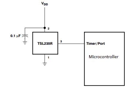 Here is an illustration how to interface it with microcontroller
The applications are unlimited when start play with it and understand in right way.
Here is an illustration how to interface it with microcontroller
The applications are unlimited when start play with it and understand in right way.

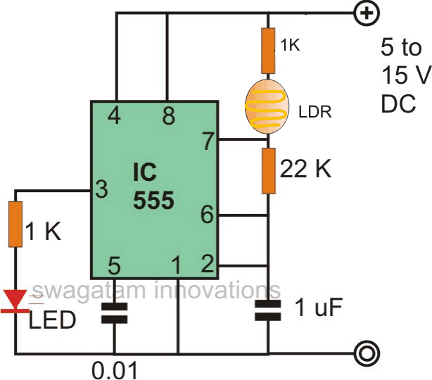 The capacitor C1 can be replaced with other values for obtaining other sets of frequency ranges, as per the application specs.
The pin3 of the IC 555 can be integrated to any desired external load or circuit, in case a TTL compatible output is required make sure to power the IC 555 with a precise 5V.
The capacitor C1 can be replaced with other values for obtaining other sets of frequency ranges, as per the application specs.
The pin3 of the IC 555 can be integrated to any desired external load or circuit, in case a TTL compatible output is required make sure to power the IC 555 with a precise 5V.
 The figure above shows a simple IC 741 based ultrasonic sound sensor alarm circuit.
The detecting device used here is an ordinary electret condenser mic.
The mic input is fed to the inverting input of the IC pin#2.
The figure above shows a simple IC 741 based ultrasonic sound sensor alarm circuit.
The detecting device used here is an ordinary electret condenser mic.
The mic input is fed to the inverting input of the IC pin#2.
 The gas leakage alarm circuit uses a BC548 transistor to turn on the buzzer whenever LPG gas is detected by the sensor.
Initially, when the circuit is turned on, the coil inside the sensor starts heating up and the current flow through the coil is controlled by a 33 ohms resistor while the zener diode makes sure that the voltage flow does not exceed 5.1V.
The XX pin is connected to the +ve of the power supply via a resistor while the YY pin is connected to the base of the transistor BC548. The 100K preset resistor is used to set the sensitivity.
When the gas concentration in the air increases, its output goes high and it makes the transistor to trigger the buzzer and a LED.
The buzzer and the LED remain powered until the concentration in the air decreases below the specified level.
The gas leakage alarm circuit uses a BC548 transistor to turn on the buzzer whenever LPG gas is detected by the sensor.
Initially, when the circuit is turned on, the coil inside the sensor starts heating up and the current flow through the coil is controlled by a 33 ohms resistor while the zener diode makes sure that the voltage flow does not exceed 5.1V.
The XX pin is connected to the +ve of the power supply via a resistor while the YY pin is connected to the base of the transistor BC548. The 100K preset resistor is used to set the sensitivity.
When the gas concentration in the air increases, its output goes high and it makes the transistor to trigger the buzzer and a LED.
The buzzer and the LED remain powered until the concentration in the air decreases below the specified level.