The article discusses a simple method through which large amounts of oxygen and hydrogen could be generated at home using an ordinary electrical setup, and very cheaply.
Before we learn the actual process, it would be important to read the following points related to the experiment:
Warning: The simple concept of generating pure oxygen at home using 220 V or 120 V mains AC presented here may look simple, but since it employs a direct non-isolated mains AC, the set up can be extremely dangerous to touch in an uncovered position.
Therefore, the experiment is absolutely NOT recommended for people who are new to electrical experiments and do not know how to safeguard themselves from electrical hazards.
Advantages
Although the experiment may not be safe for a layman, there are some distinct advantages of this particular concept:
If the whole set up is implemented with appropriate care and caution....
and with appropriate installations, the unit can give you unlimited amounts of oxygen ( and hydrogen) from two most basic elements available at home, which are tap water and mains AC power.
Due to the use of high voltage (220V/310V) the current consumption is less and the output is more which makes the system cheaper than the other concepts.
How to Enhance the Process
Bringing the electrodes nearer will cause aggressive generation of the gases, across the respective electrodes.
Hugely aggressive output generation can also be expected if a drop of H2SO4 is added to the water, although the main objective of using 220 V is to avoid using external catalyst.
Due to the use of 220V, the temperature of water might increase slightly, which may automatically help to enhance the production process, since higher temperature of water is supposed to increase the efficiency rate of the electrolysis process.
Importance of Oxygen and Hydrogen
We all know the potentials of these two gases and how important they are on this planet.
Oxygen is the life sustaining gas without which no living creature on this planet can live.
Hydrogen on other hand has its own merits and can be considered as the future fuel which would ultimately power our vehicles and cook our foods once all the naturally available fossil resources goes out of stock and gets depleted.
What is Electrolysis of Water
In school days we all have learned and witnessed the process called the electrolysis of water, where water which is made up of two main constituents H2O (two parts hydrogen and one part oxygen) is broken down forcibly with the help of electric current.
However in this process, normally a pinch of salt is added or sometime a drop of sulfuric acid is added for enhancing the electrolysis process.
This results in speedy electrolysis process, and we are able to see large and thick amounts of gas bubbles come out across the two electrodes which are connected to a potential difference source or simply to a battery.
However there's an misconception that the above process generates oxygen and hydrogen with ease, in fact that may not be the case and if we carefully assess the process you will find it's not the water but the added chemical which is getting broken in the influence of the electric current.
That means if we add salt to water, the electrolysis process will generate the gas chlorine and sodium deposits over the two electrodes and not oxygen or hydrogen.....you can expect the generation of H and O, but in very negligible volumes.
For generating pure oxygen and hydrogen through the process of breaking down water components we need to implement the process of electrolysis without the addition of any foreign chemical into water.
However, adding a very small quantity of H2SO4 or sulphuric acid could be added to enhance the process to a great extent.
Make sure the quantity is correctly calculated, else it may lead to massive bubbling or even explosions in the water.
Simply put, the procedure must be carried out breaking H2O directly without the help of any catalyst medium.
However if you try to do this, you will find the process to be very lethargic and absolutely impossible, because the bond between the H2O components are so great, it might become impossible to disintegrate them into parts.
But it can be done through brute force, meaning instead of using low power DC, if we use mains AC, and introduce it into a container filled with water, we might just be able to force the liquid to separate into its pure forms.
THIS METHOD OF ELECTROLYSIS OF PURE WATER USING PULSED 220 V WITHOUT ANY CATALYST HAS BEEN DISCOVERED BY ME, I ASSUME SO, BECAUSE IT'S NOT BEEN DISCUSSED ANYWHERE ELSE ON THE NET SO FAR.
Why Use a High Voltage AC instead of Low Voltage DC
Technically, a 1.4 V DC is the ideal power for breaking water molecules into HHO.
Anything above this is considered a waste of energy.
However, using 1.4 V would demand a heck lot of current and the electrodes will need to be placed very close to each to other, making the set up extremely infeasible at home for any lay person.
Using 220 V DC may look highly inefficient in electrical terms, but if you test it practically it turns out to be quite efficient due to the following reasons:
220 V or 120 V is easily accessible in our homes.
Making a bridge rectifier is also very easy.
Bridge rectifier converts AC into 100 Hz or 120 Hz pulses which enhances the electrolysis process significantly, compared to the specified 1. 4 V DC.
The heat dissipation can be easily optimized by decreasing the electrode cross-sectional area, and distance between the electrodes.
Using tap water means high water resistance, which in turn allows less current to be used.
This also means less HHO production but practical results show that the process produces a continuous bubbling across the electrodes, yet the water staying at normal temperatures.
The above factors ensure that a 220 V approach is much efficient in many other ways compared to using a 1. 5 V DC.
Easy set up for Generating Oxygen and hydrogen at Home in Large Quantities
OK, the method is as simple as it can be, while experimenting I found that by converting mains AC to DC, the process aggravates more rapidly and thick fogs of gases can be seen across the respective electrodes.
And it is definitely important to use DC.
otherwise the gases will alternately produced over the two electrodes haphazardly completely ruining the results.
So....it's all about making a bridge rectifier circuit using four diodes, 1n4007 will do.
take four of them and construct the bridge rectifier module and next wire up the system as per the shown diagram.
The glass apparatus will need to be carefully set.
As can be see in the figure, the two glass tubes are inverted inside a container filled with water.
The two tubes should be filled with the water such that both the tubes share the container water among themselves.
A couple of GRAPHITE electrodes are fitted in such a way that they get inside the tubes water content just as shown in the figure.
The electrodes are terminated out through respective wires connections which are further connected to the bridge rectifiers positive and negative outputs.
The bridge rectifier inputs are in turn connected to mains AC.
The moment power is switched ON, thick surfs of bubbles can be seen coming out from the electrodes and exploding into the respective gas forms into the vacant area of the tubes.
No External Catalyst used
Since there's no external chemical involved here, we can be sure that the gas formed and collected inside the tubes to be pure oxygen and hydrogen.
As the process is allowed to continue, you will find the water level gradually coming down and getting transformed into oxygen and hydrogen within the two tubes.
The tubes should have a valve type arrangement at their top termination, so that the accumulated gas can be either transferred to a larger container or directly accessed from the nozzles by releasing the taps or the valve mechanism.
Video Clip show the minimum set up required for the electrolysis process:
Increasing Oxygen Production through Series Connections
Since technically, only 1.4 V is required for an efficient implementation of electrolysis, implies that the 220 V could be divided into a number of series arrangements for multiplying the production rate of oxygen to many folds, as shown in the following example set up.
Here, we find that each glass/electrode set up is able to produce its own share of oxygen and hydrogen, thus making the total production 7 times higher.
Actually, with a 310 v supply (after 220 V rectification), the above setup can be increased to 310 / 1.4 = 221 apparatus's, generating 221 times more oxygen than a single apparatus which was shown in our first example.
That looks awesome, isn't it.
Remember the electrodes are graphite electrodes to avoid corrosion and oxidation.
And, the water is pure tap water, no catalyst in the form of salt, acid, or baking soda must be used, which may otherwise cause false and dangerous outcomes.
Note: Although we all know that electrolysis of water generates oxygen and hydrogen, the gases coming out from the above set up has not been verified practically in a laboratory, so please make sure to test it on a small scale first, to confirm its efficacy.
Increasing the Efficiency Rate by using nano pulse.
The results are not yet confirmed by me, but research has shown that decreasing the pulse width can further increase the efficiency of the electrolysis.
It is called nano pulse electrolysis.
Perhaps the easiest way of implementing a nano pulse could be to put a capacitor in series with the AC input, as shown in the following figure:
What the capacitor does is it allows only a short, narrow, peak pulse to appear across the electrodes, causing the oxygen, hydrogen production to increase to much higher levels compared to any other conventional set up.
Warning
THE WHOLE SYSTEM INVOLVES HIGH AC AND DC POTENTIALS, DEATH CAN COME WITHIN MINUTES IF ANY OF THE PART OF THE SYSTEM IS TOUCHED, EVEN THE WATER IS HIGHLY DANGEROUS TO TOUCH IN SWITCHED ON POSITION.
DO NOT SHORT CIRCUIT THE ELECTRODES, WHICH MAY RESULT IN FIRE AND HUGE EXPLOSIONS.
GREAT CAUTION MUST EXERCISED WHILE HANDLING THIS SET UP.
USE OF A 100 WATT SERIES BULB IS RECOMMENDED TO AVOID AN ACCIDENTAL SHORT CIRCUIT, AND FIRE HAZARD SITUATIONS.
DO THIS AT YOUR OWN RISK.
Room Air Ionizer Circuit �C For Pollution Free Living
In this article we learn how to build a simple room ionizer circuit for getting a clean, pollution free environment right inside our home.
Introduction
Have you ever thought or wondered why atmosphereoverhill stations and other similar places which are far away from modern cities give you a feeling of freshness and good health?
The answer is simple, the air in such places are free from pollutants and harmful chemicals like smoke and gases.
A Must for City Like Delhi
Delhi, the capital of India is today severely struggling with air pollution crises.
The issue has become so serious that it has been entitled as the highest priority among all the other ongoing health issues, and has reached an emergency level.
Although tough efforts are being implemented, still it seems the conditions isn't improving a bit, in fact the situation is getting even grimmer by the day.
A cheap solution like the proposed room air ionizer seems to be a very handy tool which can not only help control Delhi pollution, but also provide individual houses with reasonably pure air.
This equipment can be used in houses, as well as in cars for the intended remedy.
Well, if you are settled in one of thosecitieswhich is engulfed with bad air and if you havecompromisedwith the situations, here's your chance to get rid of thesituationthrough the circuit explained below:
What is an Air Ionizer - How it Works
An air ionizer or as some may refer it as a roomionizeris basically a device or electronic circuit which is designed for generating voltage at the level ofkilo-voltsfor implementing the said ionizing effects.
So what's ionizing after all?
The high voltage that's generated from an ionizer isactuallytuned for generating a negative voltage, at around minus 4 kV.
This high negative voltage is allowed to get terminated over an open ended sharp conductor tip or point that's sharply carved.
When the voltage reaches at this sharp point, it tends to continue itsforwardmotion and gets shot or released into the air in the form of negatively charged ions.
Oncein the air these ions become free to move around and start gettingdispersedacross the room or the premise, as more and more ions are released from the air ionizer device.
Nowas these ions roam freely in the air it comes acrossand startscolliding with the already present pollutants like dust particles, smoke/gas particlesetc in the air.
As per the rules all particles and all materials present around should be positively charged, so what happens, the oppositely charged ions starts collecting thesepollutantsfrom the air by attracting them toward them (opposites attract), just as a magnet bar would do to iron pins.
The pollutants in the air slowly find themselves pulled and firmly stuck over these ions until each of the ions become so much pollutant laden and heavy that they start crashing on the ground or if they find a wall nearby they start gathering on it.
In this way the air in the course of time becomes absolutely clean and free from all impurities.
Circuit Operation
The circuit is quite simple and can be built even by a layman, having just basic knowledge of electronics.
The circuit is fundamentally based onCockroft-Walton Ladder Network, Theconceptmakes use of a network of many diodes and capacitors arranged in such a way that the applied voltage to it gradually becomes stepped up to very high levels, in the order of around 10kV,
However a 10kV range is notsuitablefor the discussed ionizing effects, in fact at this level the effect might produce opposite results.
If we go by calculations the present design would also generate around -10kV, spoiling the intended cause, however practically it is found to be dropping to about -4kV.
This reduction happens due to radiation losses, because in the course of its stepping up, the voltage tends to spark through emissions across the PCB until finally the resultant voltage at the output tip of the device reaches only up to around -4kV which is by God's grace the exact level for achieving the ionizing effect.
Circuit Diagram
The entire circuit may be built over a general purpose board, by soldering the shown number of capacitors and diodes exactly in the way they are arranged in the diagram.
Following the diagram pattern would make the making easier toassembleand would produce guaranteed results without faults.
After the circuit is assembled, check the entire board for any wring connections, this is important because the circuit is very critical with its polarities, a single wrongly connected diode would make the results zero.
After proper confirmation, the soldered side should bethoroughlycleaned with thinner so that no residual flux stays deposited causing loss of voltage and reduction in the desired effects.
The end which is terminated for releasing the ions must be needle shaped, preferably a small pin or needle can be used there for enabling perfectprorogationof the ions.
After all the aboveprecautionsare complete, it's time to power the unit.
Be extremely careful, as the entire circuit is connecteddirectlywith mains AC and can be lifethreateningiftouchedin the powered position.
Verifying the Working of the Circuit
Once the circuit and if hopefully everything is rightly done with the assembly, you would hear a "hissing" noise near the tip of the releasing pin point.
The area near the tip of the pin would giveyoua cooler sensation like a cool breeze flowing out.
The point would also produce a fish like smell.....all the above indications would confirm that the unit is working right and you are already breathing fresh air around your nose and heading toward a healthy life.
THE ABOVE CIRCUIT WASSUCCESSFULLYBUILT ANDTESTEDBY ONE OF THE KEEN FOLLOWERS OF THIS BLOG, MR.
ALI ADNAN.
THE FOLLOWING BEAUTIFUL PICTURES WERE SENT BY HIM.
Prototype Pictures
4 Universal Electronic Thermometer Circuits
Here we learn four best electronic thermometer circuits which can be universally used for measuring body temperatures or atmospheric room temperatures ranging from zero degrees to 50 degrees Celsius.
In the previous post we learned some of the features of the outstanding temperature sensor chip LM35, which gives outputs in varying voltages that's directly equivalent to ambient temperature changes, in Celsius.
This feature in particular makes the construction of the proposed room temperature thermometer circuit very simple.
1) Electronic Thermometer using a Single IC LM35
It just requires a single IC to be connected with a suitable moving coil type of meter, and you start getting the readings almost immediately.
The IC LM35 will show you a 10mv rise in its output volts in response to every degree rise in the temperature of the atmosphere surrounding it.
The circuit diagram shown below explains it all, no need of any complicated circuitry, just connect a 0-1 V FSD moving coil meter across the relevant pins of the IC, set the pot appropriately, and you are ready with your room temperature sensor circuit.
Setting up the unit
After you have assembled the circuit and finished doing the shown connections, you may proceed with the setting of the thermometer as explained below:
Put the preset in the midway range.
Switch ON the power to the circuit.
Take a bowl of melting ice and immerse the IC inside the ice.
Now carefully start adjusting the preset, such that the meter reads a zero volts.
The setting up procedure of this electronic thermometer is done.
Once you remove the sensor from the ice, within seconds it will start displaying the present room temperature over the meter directly in Celsius.
2) Room Temperature Monitor Circuit
The second electronic thermometer design below is another very simple yet highly precise air temperature sensor gauge circuit has been presented here.
The use of the highly versatile and accurate IC LM 308 makes the circuit respond and react superbly to the smallest temperature changes happening over its surrounding atmosphere.
Using the Garden Diode 1N4148 as the Temperature Sensor
Diode 1N4148 (D1) is used as an active ambient temperature sensor here.
The unique drawback of a semiconductor diode such as a 1N4148 which shows forward voltage characteristic change with the influence of ambient temperature change has been effectively exploited here, and this device is used as a efficient, cheap temperature sensor.
The electronic air temperature sensor gauge circuit presented here is very accurate in its function, categorically due to its minimum level of hysteresis.
Complete circuit description and construction clues included herein.
Circuit Operation
The present circuit of an electronic air temperature sensor gauge circuit is outstandingly accurate and can be very effectively used to monitor the atmospheric temperature variations.
Let��s briefly study its circuit functioning:
Here as usual we use the very versatile ��garden diode�� 1N4148 as the sensor due to its typical drawback (or rather an advantage for the present case) of changing its conduction characteristic in the influence of a varying ambient temperature.
The diode 1N4148 is comfortably able to produce a linear and an exponential voltage drop across itself in response to a corresponding increase in the ambient temperature.
This voltage drop is around 2mV for every degree rise in temperature.
This particular feature of 1N4148 is extensively exploited in many low range temperature sensor circuits.
Referring to the proposed room temperature monitor with indicator circuit diagram given below,we see that, IC1 is wired as an inverting amplifier and forms the heart of the circuit.
Its non inverting pin # 3 is held at a particular fixed reference voltage with the help of Z1, R4, P1 and R6.
Transistor T1 and T2 are used as a constant current source and helps in maintaining higher accuracy of the circuit.
The inverting input of the IC is connected to the sensor and monitors even the slightest change in the voltage variation across the sensor diode D1. These voltage variations as explained, is directly proportional to the changes in the ambient temperature.
The sensed temperature variation is instantly amplified into a corresponding voltage level by the IC and is received at its output pin #6.
The relevant readings are directly translated into degree Celsius through a 0-1V FSD moving coil type meter.
Parts List
R1, R4 = 12K,
R2 = 100E,
R3 = 1M,
R5 = 91K,
R6 = 510K,
P1 = 10K PRESET,
P2 = 100K PRESET,
C1 = 33pF,
C2, C3 = 0.0033uF,
T1, T2 = BC 557,
Z1= 4.7V, 400mW,
D1 =1N4148,
IC1 = LM308,
General Purpose Board as per size.
B1 and B2 = 9V PP3 battery.
M1 = 0 �C 1 V, FSD moving coil type voltmeter
Setting Up the Circuit
The procedure is a bit critical and requires special attention.
To complete the procedure you will need two accurately known temperature sources (hot and cold) and an accurate mercury-in-glass thermometer.
The calibration may be completed through the following points:
Initially keep the presets set at their midways.
Connect a voltmeter (1 V FSD) at the output of the circuit.
For the cold temperature source, water at about room temperature is used here.
Dip the sensor and the glass thermometer into the water and record the temperature in the glass thermometer and the equivalent voltage outcome in the voltmeter.
Take a bowl of oil, heat it to about 100 degrees Celsius and wait until its temperature stabilizes down to about 80 degrees Celsius.
As above, immerse the two sensors and compare them with the above result.
The voltage reading should be equal to the temperature change in the glass thermometer times 10 mill volt.
Didn��t get it? Well, let��s read the following example.
Suppose, the cold temperature source water is at 25 degrees Celsius (room temperature), the hot source, as we know is at 80 degrees Celsius.
Thus, the difference or the temperature change between them is equal to 55 degrees Celsius.
Therefore the difference in the voltage readings should be 55 multiplied by 10 = 550 mill volts, or 0.55 volts.
If you don��t quite get the criterion satisfied, adjust P2 and continue to repeat the steps, until finally you achieve it.
Once the above rate of change (10 mV per 1 degree Celsius) is set, just adjust P1 so that the meter shows 0.25 volts at 25 degrees (sensor held in water at room temperature).
This concludes the setting of the circuit.
This air temperature sensor gauge circuit can also be effectively used as an room electronic thermometer unit.
3) Room Thermometer Circuit using LM324 IC
The 3rd design is probably the best one as far as cost, ease of construction and accuracy is concerned.
A single LM324 IC, a 78L05 5V regular IC and a few passive components are all that is needed to make this easiest room Celsius indicator circuit.
Only 3 op amps are used from the 4 op amps of the LM324.
Op amp A1 is wired to create a virtual ground for the circuit, for its effective working.
A2 is configured as a non-inverting amplifier where the feedback resistor is replaced with a 1N4148 diode.
This diode also acts as the temperature sensor, and drops around 2 mV from every single degree rise in the ambient temperature.
This 2 mV drop is detected by the A2 circuit and is converted into a correspondingly varying potential at pin#1.
This potential is further amplified and buffered by A3 inverting amplifier for feeding the attached 0 to 1V volmeter unit.
The voltmeter translates the temperature dependent varying output into a calibrated temperature scale to produce the room temperature data quickly through the relevant deflections.
The entire circuit is powered by a single 9 V PP3.
So folks, these were 3 cool, easy to build room temperature indicator circuits, that any hobbyist can build for monitoring the ambient temperature variations of a premise quickly and cheaply using standard electronic components, and without involving complex Arduino devices.
4) Electronic Thermometer Using IC 723
Just as the above design here too a silicon diode is employed like a temperature sensor.
The junction potential of a silicon diode goes down by approximately 1 millivolt for each degree centigrade, which allows temperature of the diode to be determined by calculating the voltage over it.
When configured as a temperature sensor, a diode offers the benefits of high linearity with a low time constant.
It could additionally be implemented over a broad temperature range, from -50 up to 200 C.
As the diode voltage needs to be assessed quite accurately, a reliable reference supply is necessary.
A decent option is the IC 723 voltage stabilizer.
Even though absolute ti value of the zener voltage within this IC can be different from IC to another, the temperature coefficient is extremely small (typically 0.003% per degree C).
In addition, the 723 is known to stabilize the 12 volt supply throughout the circuit.
Observe that the pin numbers in the circuit diagram are only suitable for the dual -in - line (DIL) variant of the IC 723.
The other IC, the 3900, includes quad amplifiers where just a couple of are utilized.
These op amps are designed to work a little differently; these are configured as current driven units instead of as voltage driven.
An input could best be considered to be the transistor base in a common-emitter configuration.
As a result, the input voltage is often around 0.6 volt.
R1 is coupled to the reference voltage and a constant current hence moves through this resistor.
Due to its large open loop gain, the op amp is able to adapt its very own output in order that the exact same current runs into its inverting input, and the current through the temperature -sensing diode (D1) thus stays constant.
This set up is important due to the fact the diode is, essentially, a voltage source having a specific internal resistance, and any kind of deviation in the current moving via it might as a result create a variation in the voltage which could end up being erroneously translated as a variation in temperature.
The output voltage at pin 4 is hence the same as the voltage at the inverting input as well as the voltage around the diode (the latter changing with temperature).
C3 inhibits oscillation.
Pin 1 of IC 2B is attached to the fixed reference potential and a constant current consequently moves into the non inverting input.
The inverting input of IC 2B is hooked up by means of R2 to the output of IC 2A (pin 4), in order that it is operated by a temperature-dependent current.
IC 2B amplifies the difference between its input currents to a value that the voltage deviation at its output (pin 5) could quickly be read with a 5 to 10 volt f.s.d.
voltmeter.
In case a panel meter is employed, Ohm's law may need to be configured to determine the series resistance.
If a 100-uA f.s.d.
meter with an internal resistance of 1200 is employed, the total resistance for 10 V full-scale deflection has to be as per the calculation:
10/ 100uA = 100K
R5 must as a result be 100 k - 1k2 = 98k8. The closest common value (100 k) will work well.
Calibration can be done as explained below: the zero point is initially fixed by P1 using the temperature sensor immersed in a bowl of melting ice.
Full-scale deflection can after that be fixed with P2; for this the diode can be submerged inside hot water whose temperature is identified (let's say boiling water tested with any standard thermometer to be at 50��).
Using CA3130 IC
This thermometer has a linear scale and provides the temperature range of 0 to 50 degrees Celsius, allowing it to be read straight from a 50uA meter.
By inserting a 100uA meter, a temperature range of 0-100 degrees Celsius may be established.
The temperature sensors in the unit are silicon diodes D1 and D2, which are typically put inside some sort of probe that can be deployed several metres away from the other electronics if required.
C1 eliminates noise detected throughthe connecting cable.
R1 provides a slight forward bias to D1 and D2, such that there is no substantial self heating of the diodes.
The voltage generated between the diodes is theoretically 1V2, but it changes by around 2mV per degree C per diode, or approximately 4mV through both diodes.
This voltage is applied to the input of an operational amplifier inverting amplifier, IC1. RV1 is set for the greatest voltage at IC1's non-inverting input that provides zero output voltage when the probe is at 0 degrees C (which may be obtained by dipping the probe in ice).
This provides the requiredcompensationfor the quiescent voltage across the diodes and results in a 0 V displayon the 1V FSD voltmeter circuit hooked upacross the amplifier's output.
When the diodes become warm up toto 50 degrees Celsius, the voltage across them drops by around 200mV, which is boosted by the amplifier througha factor of 5 to provide around 1V at its output, which resultsnearly afull scale meterdeflection.
Practically, RV2 is utilized to tune the amplifier's gain such that full scale deflection is generated.
RV2 can, obviously, be adjusted to the proper temperature using the probe at any specified temperature that translates to a significant meter deflection.
The circuit demands highlysteady supply of around 5V, which may be achieved with a 5V monolithic regulator and a 9V battery (IC2).
To avoid instabilities, C3 and C4 should mustbe positioned near to IC2.
How to Calculate Heatsinks
Heatsinking is critical for power devices in circuits that are intended to maximize their performance.
When heat from the power devicescannot be moved away very quickly, the power devicesand its operating elements could be damaged.
You may calculate how hot your semiconductors couldbecome whileoperating, using a couple ofeasy formulas.
Using formulas gets rid ofguesswork and the anxiety that comes with it about making a mistake, should you guess incorrectly.
Heatsinks are normally used for absorbing and dissipating excessive heat from electronic power devices such as transistors, SCRs, triacs etc, so that the device temperature can be controlled below their maximum tolerable limit.
The metal aluminum is normally used as the heatsink material due to its excellent heat conductivity, and relatively lower price compared to other metals like copper.
The size of the heatsink determines how quickly and optimally the heat from the devices can be absorbed and dispersed into the air.
If the selected heatsink is too small, it may fail to accomplish the intended cooling, and if it's too large, it can affect the compactness and cost of the electronic circuit.
In order to ensure an optimally sized heatsink for a semiconductor device, it is always recommended to calculate the parameters accurately using formulas, so that a fairly accurate heatsink dimension can be determined.
Convection
Natural convection can be defined asthe heat transfer process through thecirculation ofgas or fluid.
In ourcase this happens viaambient air at room temperature, and thisis the design objective appliedfor cooling semiconductors.
In electronic devices, the convection heat transfer is proportional to the surface area of metal exposed, the forceof air moving acrossthe devicesurface, and the temperature differential between the two.
Whileconsideringheatsinks,thepowersemiconductorisregardedacomponent.
Thus, the heat equivalent in watts generated by the device is equal to the voltage drop across it,multiplied by the current flowingthrough it, multiplied by the time factor (percentage of time it is switched ON, divided by 100).
And this is the absolute temperature that the heatsink should disperse into the atmosphere.
This is a quick calculation for a basiclinear power-supply semiconductor.
The equation for a semiconductor power switching transistor can be a lot more complicated.
In the case of an audio amplifier, we may need to calculate dissipation.
In any scenario, you may want tobe as exact and conservative as possible while calculating the heat to be dissipated equivalent to the heat in watts.
Try looking up the junction-to-case thermal impedance and case-to-sink thermal impedance on the datasheet forthe semiconductor device you'll be mounting on a heatsink.
These impedance magnitudes can be found in��C per watt.
This meansthat for every watt of heat power dissipated by the junction, this will be a certain amount of ��C higher than the case temperature, and vice versa.
If you want to maintain the devicejunction temperatureat or below 100�� C, and its datasheetjunction-to-case thermal impedance valueis 10��C/watt, then a power output of7.5 watts mightcausethe junction temperature to riseto 100�� C.
This might happeneven if the case temperatureis maintained at aconstant 25�� C (possibly by subjecting the devicetoflowing water).
For something like an International Rectifier IRFZ40 MOSFET, common junction-to-case thermal impedances (ZJC) is 1�� C/W, and and this is1.52�� C/W for the BJT2N3055.
The case-to-sink thermal impedance (Zcs) for a TO-220 case is 1�� C/W, and for a TO-3 case this is0.12�� C/W.
Whenever you are unable to access a particulardevice's datasheet, you can tryestimatingthe junction-to-case thermal impedance for your specific semiconductor device using the above mentionedfiguresas a reference.
Heatsink Design Parameters
What is the highest temperature that the junction of a transistor could reach? Several circuit designers fixthe maximum junction temperature of a semiconductor deviceat 80�� C.
This is because,higher temperatures than this canseverely impair the deviceproperties, and can lead to athermal runaway situation,a seriousrisk for bipolar transistors.
Always treat the manufacturer's datasheet comments about maximum watt values and junction temperature with a grain of salt.
These results are only applicable ifthe device is constantly cooled to a comfortable temperature of 25�� C.
Understanding Ambient Temperature and Heatsink Temperature
What does ambient temperature exactly suggest? Remember that the transistor could be enclosed inside a box, in which other heat-dissipatingdevices may beadding to theambient air temperature.
If you are confident that normal room airflow is able tofreely move across the devices, you can anticipate 25�� C to be the ambient temperature value, however you may have to verycautious.
Keep in mind that duringthe summer, the ambienttemperature mayrise to100�� F = 38�� C.
With these data in hand, you could calculate ��T, or the predicted temperature differential between the yet-to-be known heatsink size and the air that would facilitatecooling.
��T = TMaxJ - [Wj x ( Zjc + Zcs)] -TAA
where ZJC represents the junction-to-case thermal impedance, Zcs symbolizes the case-to-sink thermal impedance, TAA denotes the ambient air temperature, TMJ defines the highest junction temperature, and Wj indicates the junction wattage.
Let's assume we wish to use a 2N3055 transistor to drive a motor that draws 3 amps.
You might notice that the transistor drops 1.2 volts at this magnitude ofcurrent, and you might also notice that the highestduty cycle is 50%, or 0.5.
As a result, the power dissipated will be3 x 1.2 x 0.5 = 1.8 watts.
If you go with amaximum junction temperature of 80�� C and a minimum junction temperature of 25�� C,ambient air, then ��T can be calculated as follows:
��T = 80 - [1.8 x (1.52 + 0.12)] - 25
��T = 52�� C
Under such situations, the ��T calculation indicates that the projected heatsink may be at least 52�� C warmer than the air.
Therefore, how big should this heat sink be?
The following formula is used to determine the solution:
A = (WJ x 5630) / ��T5/4
where A indicates the area of the heatsink vertical surface in cm2.
If you want to calculate it with in2, you can use the following formula:
A = (WJ x 872.6) / ��T5/4
Considering the 2N3055 BJT example, and by applying the above in2 equation, we get the following results:
A = (1.8 x 872.6) / 525/4
A = 11.2 in2
The result shows thata heatsink with at least 11.2 square inches of vertical surface area exposed in free air would be necessary to cool the 2N3055transistor.
Heatsink for Parallel Transistors
Now suppose you want to put two or moresemiconductor devices with similar characteristicson the single common heatsink (in parallel),so thatthey consume equivalent currents.
To implement this youmay calculate the thermal power of the pair and divide the thermal impedances by the number of devices, assuming them to bea single device.
Semiconductor devices with dissimilar specificationsshould be placed on separate heatsinks.
MOSFETs in Parallel
Let's consider this example.
In a low-voltage switching power supply, two IRFRZ40 power MOSFETs are wired in parallel.
Currents are expected to reach 40 amps via the two MOSFETs, and duty cycles may exceed 80 percent.
At 80�� C, the IRFZ40's on-resistance (FETconducting) might bearound 0.036 ohm.
Therefore,the parallel pair will have a resistance of 0.018 ohm to the 40 amps, yielding 0.018 x 40 x 0.8 = 23 watts.
Imagining a worst-case temperature of 38�� C, for example the ambient conditionsof a desert, duringsummer, we can estimate the heatsink dimensions as given below:
��T = 80 - [23 x (0.5 + 0.5)] - 38
��T = 19�� C
The above result specifies that the heatsink temperature may be 19�� C more hotter than the ambient temperature
Now, using the above data we can determine the optimum heatsink size using the following calculations:
A= (23 x 872.6) / 195/4
A = 506 square inches.
The 506 square inches result might appear too large, however a normal big heatsink measuring 5 x 4 x 25/8 inches with a surface area of 250 square inches might require an additionalone to effectively dissipate the heat.
Obviously , such large heatsinks may be costly, and if thecost is higherthan the device itself, you mightneed to reconfigure the circuit usingmore number ofparallel transistors.
This method mightreducethe device conductingresistance and thusthe amount of heat that must be dissipated.
Tap Water Induction Heater Circuit
A tap water heater circuit can be simply built by attaching an iron tube on the mouth of the tap or the faucet, and allow the iron pipe to pass through an induction heater coil.
The induction heater will heat up the iron pipe and hence water passing through the the pipe will also heat up and provide a warm water for the user from the other end of the pipe.
Materials Needed
To build this project you will need the following basic materials:
A ready made induction heater circuit that can be powered from a 12V 10 amp SMPS DC power supply.
An appropriately fabricated metal pipe with Bakelite holder at one end which can be clamped to the tap mouth.
An appropriately dimensioned Bakelite box for enclosing the induction heater, the induction coil, and the metal pipe.
The Set Up
The complete set up for the induction tap water heater circuit can be witnessed in the following set up diagram:
In this set up we can see a plated iron pipe or a galvnized iron pipe is clamped to the mouth of the tap via a bakelite adapter cap.
The bakelite cap ensures that the heat from the iron is not able to disperse to the tap metal, and remains instact within the iron pipe.
The iron pipe can be seen encircled by the induction heater coil, or in other words the iron pipe is allowed to pass through the induction heater coil.
The metal pipe diameter must be selected to ensure that the amount of water passing through it is not too large, and the water is able to get warm enough while passing through the pipe.
The water coming out from the pipe must be at least 35 degrees Celsius warm.
How to Enclose the Whole Set up
The above explained induction tap water heater circuit set up will need an appropriate enclosure which must be light, sturdy, water proof, heat proof, and could be attached to the tap system along with the iron pipe.
An example format of the enclosure can be seen in the following image.
The enclosure should have ample ventilation from the bottom side, so that the parts of the induction heater can dissipate the heat comfortably without getting too warm.
The power to the induction heater circuit enclosed inside must be supplied from an external SMPS unit, which may be rated at 12 V 10 amps.
Using the SMPS unit externally provides the user with an advantage of using the SMPS for some other desired purpose, when the heater is not being used.
Cheaper than Commercial Water Heater
If you compare the above induction based tap water heater circuit with commercially available geysers and water heaters you will find that the above set up is much cheaper and cost effective than the commercial units.
The complete set up can be built in less than $20, which is 50% less compared to the commercial units.
Also, the electricity consumption can be 50% less for the above explained concept, compared to the commercial heater units, which depend on heater coils rather than induction heating system.
Moreover, you get a free SMPS device which you can use for lighting LEDs, driving a power amplifier or a subwoofer amplifier, a benefit you can never get with the commercial heater units.
100 ��C to 1000 ��C Thermocouple Temperature Meter Circuit
The post explains a simple op amp based thermocouple temperature meter circuit which can be used for measuring high temperatures in the range of 100 ��C to 1000 ��C, in heaters, furnaces, kilns tec.
What is a Thermocouple
A thermocouple is a simplest and the cheapest form of temperature sensor device, built using a couple of dissimilar metals.
The two dissimilar metal wires are tightly joined or fused at one of their ends, while the opposite open ends are attached to a sensitive milivoltmeter or an op amp circuit.
When the fused end of the wire is heated, current starts flowing through the wire and a potential difference begins building up across the heated end and the opposite side cold ends.
As a result, the meter starts indicating a potential difference, which is directly proportional to the temperature difference between the opposite ends of the wire, or between the hot end and the cold end.
Basic Working of the Project
In this 100 ��C to 1000 ��C thermocouple temperature meter circuit project, a couple of special alloy metals (Chromel/Alumel) are needed with their ends joined or fused together.
For example, one of ends of a CHROME wire and an Aluminum wire could be twisted tightly and the other ends connected to a millivolmeter.
Now If you heat the twisted ends of the wires, you will find a tiny amount of electricity being generated across the free ends of the wires and a deflection appearing on the meter needle.
However, unlike a thermistor, a thermocouple response is not dependent on the amount of heat applied to the fused ends, rather the meter reading will be proportionate to the heat difference between the twisted fused ends of the wires and the ends that are joined to the meter.
The twisted or the fused ends of the thermocouple wire is called the "hot end" and the opposite sides ends are called the "cold ends".
Therefore the electrical potential developing across the cold ends is actually proportionate to the difference between the temperature at the hot end and the cold end of the thermocouple wire assembly.
For example, suppose if we find the meter reading increasing at a rate of 4 mV per 100 ��C applied at the fused ends of the wires, and the temperature at the cold end connected to the meter is 22 ��C, then with the meter reading at 4 mV would indicate that the actual temperature across the fused end is 100 + 22 = 122 ��C.
Circuit Description
The figure of a thermocouple meter circuit shown below is probably the simplest of its kind.
It employs a single IC 741 op amp as the active device, a few resistors and a mA meter for displaying the temperature reading.
The power is applied from a couple of 9 V PP3 batteries.
THe gain of the meter is adjusted and set for all the temperature ranges universally through the preset P1. This setting is done depending on the range and value of the mA meter.
The preset P2 is used for adjusting the offset output voltage from the IC 741 op amp.
It is adjusted until the needle is pushed to exact zero mark, while the system is not detecting any temperature.
The resistive divider created using R3 and the preset P3 enables the ambient temperature correction adjustment for the meter.
This simple thermocouple temperature meter circuit features two handy temperature ranges to select from, one is 0 to 100, and the other is 0 to 1000. This range cn be selected with an quick toggling of the selector switch K1.
The Chromel/Alumel thermocouple sensor input is plugged into the circuit through an ordinary 3.5 mm jack, connected to the selector switch K1.
When the thermocouple (TC) is plugged into K1, it shorts circuits the non-inverting input of the op amp to ground.
Next, if we remove the TC from K1, the (+) input of the op amp is removed from the ground, an at this meter the meter must show zero.
If it doesn't then adjust the offset null preset P2 until the needle reaches the zero point on the meter.
After this connecting the TC to the K1 socket, must keep the meter needle at zero until a temperature difference is created across the two ends of the TC.
In case you find a slight deviation on the meter needle side due to ambient temperature difference across the "hot end" and "cold end" of the TC, this may be corrected by carefully adjusting the P3 preset, until the needle indicates the ambient temperature on the meter.
Now, your thermocouple meter is all set for use.
How to Set Up
In the above paragraph we learned the basic procedure for setting up the 3 presets of the unit.
The following explains the precise method of setting up the thermocouple temperature meter circuit.
Check the mechanical zero of the millivolmeter
Adjust P1 and P2 presets at halfway and adjust the P3 preset at zero (ground)
Remove the TC from the jack plug and switch ON power supply.
Adjust the preset P2, using a screwdriver so that the meter needle settles to the zero mark
Adjust the preset P3 until the meter needle displays or indicates the exact ambient temperature or the room temperature.
Now, insert the TC to the jack socket and immerse the fused tip of the TC in very hot water, at a known temperature between 100 ��C and 1000 ��C
Now very carefully adjust the preset P1 until the meter needle indicates the correct temperature on the calibrated dial.
Parts List
1/4 MFR 1%
R1 = 1 k
R2 = 1.5 k
R3 = 150 ��
R4 = R5 = 2.7 k
P1 = 100k potentiometer
P2 = 10k potentiometer
P3 = 47 �� potentiometer
IC1 = 741 or any other standard op amp
Meter = Can be any 0 to 100 mV meter
K1 = single slide switch
1 Bipolar switch or a double switch (slide or lever)
1 jack socket 3.5 mm
1 jack plug 3.5 mm
2 sockets for small 9 V batteries
2 miniature 9 V batteries PP3
1 printed circuit 66 x 40 mm to be made
8 terminals for printed circuit
1 Chromel/Alumel thermocouple
PCB Design
Wiring Layout
Using Microwave Oven Parts to build a Soldering Iron Heat Controller
In this post we learn how to scavenge discarded microwave oven parts for making a useful soldering iron heat controller circuit which can then be used for maintaining controlled heat over a connected soldering iron tip ensuring safe soldering operations, that may be quite crucial and handy if you are working with SMD parts.
By Henry Bowman
Warning ! This project could expose the experimenter to hazardous voltage from the high voltage capacitor.
Only people with electrical knowledge of ac voltage hazards and high voltage capacitors should attempt this project.
Using Discarded Microwave Oven Parts
Do you have an old microwave oven that no longer works ? Well, don't throw it away.
If the display panel and touch buttons still function, it can be put to good use.
Some cheap microwaves may not have adjustable power levels.
If you are unable to adjust power level to 50%, you won't be able to use this microwave.
Most defective microwaves are the result of bad magnetron tubes, defective high voltage diodes and/or high voltage capacitors.
Soldering iron tips don't have long life, when plugged in for extended periods.
This project will allow you to set various power levels to your iron and automatically disconnect the iron with the time you set.
Look at the functional block diagram of a typical microwave.
How Microwave Oven Circuit Works
The leads marked with red X's show the ac connections to be cut.
The processor controls the amount of time that voltage is applied to the primary winding of the high voltage transformer, depending upon power settings by the user.
If 100% power setting is selected, a relay or triac provides voltage to the transformer for 100% of the cook time selected.
If 50% power setting is selected, the processor provides a 50% on time and 50% off time to the transformer.
Some microwaves can provide as low as 10% power level with 90% off time.
The transformer provides the high voltage to energize the magnetron, which provides the heat to the oven.
For this project, we're only interested in the line cord, fuse, key board, display and processor and power leads to the transformer.
There is no danger of radiation exposure from the magnetron, when the microwave is unplugged from the ac source.
The outer metal cover should be removed from the microwave, being careful not to touch any parts inside until the high voltage capacitor is discharged.
Make a note of the wattage rating of your microwave, before discarding the cover.
Using a metal screwdriver with an insulated handle, locate the high voltage capacitor and place a short across the two terminals of the capacitor.
A momentary spark may occur if the capacitor is still storing a charge.
Extracting Parts from Microwave to Make Soldering Iron Controller
The processor board usually has a ribbon type cable to the key board and lcd panel.
The wires from the processor to the high voltage transformer primary will be large gauge wires that must be cut.
Clip the wires as close as possible to the transformer primary.
The primary is the small coil winding, while the secondary is the large coil.
The ac line cord must have continuity from the ac fuse to the processor panel.
This will require removing interlock switches, thermal switch and any other switch that would prevent ac continuity.
Depending on make and model, the fuse may be located on the processor board, or elsewhere in the enclosure.
You may have to remove a large plastic panel that contains the keyboard and display panel.
This panel can be cut down to size to fit the enclosure you build.
A hacksaw or dremel tool would be the best way to reduce the size of the panel.
Your enclosure for this project should contain the keyboard and display panel, mounted externally, and the processor board and ac fuse internally.
It should also contain the auxiliary a/c outlet for the soldering iron, or other device you wish to control.
The two leads you removed from the primary of the high voltage transformer should be connected to the auxiallary outlet on your enclosure.
The hot side of the ac, from the processor board, (usually black) should connect to the side lugs which connect to the small vertical blades on the outlet.
Twist on type connectors can be used to splice the wires if longer lengths are needed.
Use the same gauge wire as the original wiring.
The neutral wire (white) should connect to the opposite side lugs for the larger vertical blades on the outlet.
The green wire from the ac cord should be spliced and connected to the green lug on the outlet which connects to the small round female holes.
A completed project diagram is shown for your information.
Testing and Troubleshooting
When completed, plug in your line cord and test the panel.
If it doesn't work, verify that you are getting AC mains to the processor board.
You may have left some type of switch in series with the board that must be removed.
Depending on the purpose of the switch or thermal device, you may have to leave it disconnected and leave the wires open, or strap them together at the processor board.
Be sure you understand the purpose of the device that is preventing a/c from getting to your processor.
Be sure that you have included the ac fuse in the circuit and it has not blown.
The auxiliary outlet for the iron should be labeled with the maximum wattage allowed, which you noted earlier.
Once you have the keyboard functioning, plug a table lamp into your auxiliary outlet and set the power rating for 100% and time for 20 seconds.
Press the Start button on the key panel and the light should lamp for the time period selected, then automatically shut off.
Change the power level to 50% on the key pad.
The lamp should retain the same brightness, but flash on and off , with several seconds in between each cycle.
For immediate soldering iron use, plug in the iron and set for 100% power.
Set the amount of time you need for the project, then press start.
If you need to take a short break, reduce the power level to 50%.
When you return, reset the power level to 100% for a quick heat up.
You may decide that your iron may need higher or lower idle time power levels to maintain a warm temperature.
More Applications using Microwave Oven Parts
In the above discussion we learned how to use parts from a discarded or damaged microwave oven to make a heat controller circuit for soldering irons, however you may also find many other applications using discarded microwave oven parts.
A small heating pad could be connected which could be shut off at the time you select.
If your microwave has a power setting of 10% you could connect a table lamp that goes off and on for several hours.
This could convince potential burglars that someone is at home.
You could plug in a small reading lamp by your bed and program it to stay on for the time you need, then turn off automatically.
Remember to observe the maximum watting rating, provided by the manufacturer, when connecting appliances or other electrical objects.
Do not connect ac motors, electric drills or other inductive loads to this outlet.
Induction Heater for Labs and Shops
The post explains how to make small homemade induction heater circuit for laboratories and shops for carrying out small scale heating jobs such as melting ornaments, or boiling small quantity of liquids using electricity or battery The idea was requested by Mr.
Suni and Mr.
naeem
Circuit Objectives and Requirements
Our challenge is to make an induction circuit for use from 12 V to 24 V with a flat spiral that can get half a liter of water to boil in as little time as possible.
The primary goal is to get induction circuit to work but there are other challenges that are described below.
The container in which the water should be boiling is of double-walled stainless steel and is insulated and the distance between the outer and the inner container where the induction works is about 5-7 mm.
We have chosen induction in order to protect the electronic components from the heat of a conventional spiral heater coil which is possible when the tank is insulated.
The outer container has a diameter of 70 mm and the space for the electronic components is 20 mm high, so another challenge is to see if we have space for the components.
In connection with the power supply there is connected a tilt switch which cuts the power to the induction loop in case the container is tilted 15 degrees or more.
When the power to the induction circuit is interrupted this triggers an audio buzzer.
Further, the induction loop is connected to two thermostats.
One thermostat that interrupts power to the induction circuit when the water reaches boiling point and another thermostat that takes over to keep the temperature of the water at about 60 degrees - do not know if this will require a programmable circuit.
I would also like to know if there are any infrared thermostats available.
I know that this is a lot at once, but as mentioned, the primary aim is to get the induction circuit to work.
Is it possible for you to send us a list of the necessary components and a diagram of the circuit.
Looking forwardto hear from you!
Yours sincerelyS��ni Christiansen
hello sir, i need a Induction Heater circuit diagram for our shop we have a silver jewelry shop
so i want to silver melt and sometimes gold but if u send small circuit with transformerless power supply that will be good for me.
I saw on internet very small project for induction heater but i cannot found power supply tansfomerless can you help me if u send both project Induction Heater and his power supply transformerless
The Design
In one of the earlier posts we learned the basic method of designing a customized induction heater circuit by optimizing the resonance of the LC tank circuit, here we are going to apply the same concept and see how the proposed homemade induction heater circuit can be built for using in laboratories and jewellery shops.
The following figure show s standard induction heater design which can be customized as required by the user, as per their individual preferences.
Circuit Diagram
Circuit Operation
The entire circuit is configured around the popular full-bridge IC IRS2453 which indeed makes designing full bridge inverters extremely easy and foolproof.
Here we use this IC for making a DC to DC induction heater inverter circuit.
As can be seen in the design the IC employs nothing more than 4 N-channel mosfets for implementing the full bridge inverter topology, additionally the IC involves an in-built oscillator and a bootstrapping network ensuring an extremely compact design for the inverter circuit.
The oscillator frequency can be adjusted by altering the Ct, and Rt components.
The mosfet H-bridge is loaded by the LC tank circuit using a bifilar coil which forms the induction work coil along with a few parallel capacitors.
The IC also incorporates a shutdown pinout which can be exploited for shutting down the IC and the entire circuit in case of catastrophic circumstances.
Here we have employed a current limiter network using BC547 transistor and configured it with the SD pin of the IC for ensuring a current controlled safe implementation of the circuit.
With this arrangement in place, the user can freely experiment with the circuit without the fear of burning the power devices during the various optimization operations.
As discussed in one of the earlier articles, optimizing the resonance of the work coil becomes the key point for any induction heater circuit, and here too we make sure that the frequency is accurately tweaked in order to enable the most favorable resonance for our induction heater LC circuit.
It doesn't matter whether the work coil is in the shape of a spiral bifilar coil or a cylindrical coiled winding, as long as the resonance is correctly matched the result can be expected to be be optimal from the selected design.
How to Calculate the Resonance Frequency
The resonance frequency for the LC tank circuit can be calculated through the formula:
F = 1 /2�� x ��LCWhere F is the frequency, L is the inductance of the coil (with magnetic load inserted), and C is Capacitor connected parallel to the coil.
Make sure to put the value of L in Henry and C in Farad.Alternatively you can also use this resonance calculator software for determining the values of the various parameters in the design.
The value of F can be selected arbitrarily, say for example we can assume it to be 50kHz, L can then be identified by measuring the inductance of the work coil, and finally the value of C can be found using the formula above, or the referred calculator software.
While measuring the inductance L make sure to keep the ferromagnetic load attached with the work coil, with the capacitors disconnected.
Selecting the CapacitorSince a significant amount of current could be involved with the proposed induction heater for the lab works or for melting ornaments, the capacitor needs to be rated appropriately for the high current frequency.
To tackle this we may have to employ many numbers of capacitors in parallel, and make sure that the final value of the parallel combination is equal to the calculated value.
For example if the calculated value is 0.1uF, and if you have decided to use 10 capacitors in parallel, then the value of each capacitor would need to be around 0.01uF, and so on.
Selecting the Current Limiter Resistor Rx
Rx can be simply calculated by using the formula:
Rx = 0.7/Max CurrentHere, the max current refers to maximum current that may be permissible for the work coil or the load without damaging the mosfets and for optimal heating the load.
For example, if the optimal load heating current is determined to be 10 amps, then Rx could be calculated and dimensioned for restricting anything above this current, and the mosfets must be selected to handle in excess of 15 amps.
All these might require some experimentation, and Rx can be initially kept higher and then gradually lowered until the right efficiency is achieved.
Cooling the Work Coil.
The work coil can be built using a hollow brass tube, or a copper tube, and cooled by pumping tap water through it, or alternatively a cooling fan can be employed just below the coil for sucking out the heat from the coil from the reverse end of the enclosure.
Other suitable methods can also be tried by the user.
Power Supply
The power supply unit required for the above explained induction heater for labs and shops can be built using a 20 amp, 12V transformer and by rectifying the output using a 30 amp bridge rectifier and a 10,000uF/35V capacitor.
Transformerless power supply can be unsuitable for an induction heater since that would require a 20 amp smps circuit which could be extremely costly.
How to Design an Induction Heater Circuit
The article explains a step by step tutorial regarding designing your own homemade basic induction heater circuit, which can be also used as an induction cooktop.
Basic Induction Heater Concept
You might have come across many DIY induction heater circuits online but nobody seem to have addressed the crucial secret behind implementing a perfect and a successful induction heater design.
Before knowing this secret it would be important to know the basic working concept of an induction heater.
An induction heater is actually an extremely "inefficient" form of electrical transformer, and this inefficiency becomes its main advantageous feature.
We know that in an electrical transformer the core needs to be compatible with the induced frequency, and when there's an incompatibility between frequency and the core material in a transformer, it results in the generation of heat.
Fundamentally an iron cored transformer will require a lower range of frequency around 50 to 100Hz, and as this frequency is increased the core may shown a tendency of getting hotter proportionately.
That implies, if the frequency is increased to a much higher level may be over 100kHz would result in the generation of extreme heat within the core.
Yes, this is exactly what happens with an induction heater system where the cooktop acts like the core and therefore is made up of iron material.
And the induction coil is subjected to a high frequency, together this results in the generation of a proportionately intense amount of heat on the vessel.
Since the frequency is optimized at significantly high level ensures a maximum possible heat on the metal.
Now let's proceed and learn the important aspects that may be required for designing a successful and technically correct Induction heater circuit.
The following details will explain this:
For designing an induction cookware, the work coil is supposed to be flat in nature, therefore it must be bifilar type with its configuration, as shown below:
The bifilar coil type designshown above can be effectively implemented for making your homemade induction cookware.
For optimum response and low heat generation within the coil make sure the wire of the bifilar coil is made using many thin strands of copper instead of a single solid wire.
Thus, this becomes the work coil of the cookware, now the ends of this coil simply needs to be integrated with a matching capacitor and a compatible frequency driver network, as shown in the following figure:
Designing the H-Bridge Series Resonant Driver Circuit
So far the information should have enlightened you regarding how to configure a simple induction cookware or an induction cooktop design, however the most critical part of the design is how to resonate the coil capacitor network (the tank circuit) into the most optimal range so that the circuit works at the most efficient level.
Enabling the coil/capacitor tank circuit (LC circuit) to operate at their resonance level requires the inductance of the coil and the capacitance of the capacitor to be matched perfectly.
This can happen only when the reactance of both the counterparts are identical, that is the reactance of the coil (inductor) as well as the capacitor are approximately the same.
Once this is fixed you can expect the tank circuit to operate at its natural frequency and the LC network reaching the resonance point.
This is called a perfectly tuned LC circuit.
This concludes the basic induction heater circuit designing procedures
You may be wondering regarding what is resonance of an LC circuit.?? And how this may be calculated quickly for completing a specific induction heater design? We will comprehensively discuss this in the following sections.
The above paragraphs explained the fundamental secrets behind developing a low cost yet effective induction cooktop at home, in the following descriptions we will see how this can be implemented by specifically calculating its crucial parameters such the resonance of its tuned LC circuit and the correct dimension of the coil wire for ensuring an optimal current handling capacity.
What is Resonance in Induction Heater LC Circuit
When the capacitor within a tuned LC circuit is momentarily charged, the capacitor tries to discharge and dump the accumulated charge over the coil, the coil accepts the charge and stores the charge in the form of magnetic field.
But as soon as the capacitor has discharged in the process, the coil develops an almost equivalent amount of charge in the form of magnetic field and it now tries to force this back inside the capacitor, although with an opposite polarity.
Image courtesy:Wikipedia
The capacitor is again forced to charge but this time in the opposite direction, and as soon as it's fully charged, it yet again tries to empty itself across the coil, and this results in a back and forth sharing of charge in the form of an oscillating current across the LC network.
The frequency of this oscillating current becomes the resonance frequency of the tuned LC circuit.
However due to inherent losses the above oscillations eventually die out in the course of time, and the frequency, the charge all come to an end after sometime.
But if the frequency is allowed to sustain through an external frequency input, tuned at the same resonance level, then that could ensure a permanent resonance effect being induced across the LC circuit.
At resonance frequency we can expect the amplitude of the voltage oscillating across the LC circuit to be at the maximum level, resulting in the most efficient induction.
Therefore we can imply that, to implement a perfect resonance within an LC network for an induction heater design we need to ensure the following crucial parameters:
1) A tuned LC circuit
2) And a matching frequency to sustain the LC circuit resonance.
This can be calculated using the following simple formula:
F = 1��2�� x ��LC
where L is in Henry and C is in Farad
If you don't want to go through the hassles of calculating the resonance of the coil LC tank through formula, a much simpler option could be to use the following software:
LC Resonant Frequency Calculator
Or you may also build this Grid dip meter for identifying and setting the resonance frequency.
Once the resonance frequency is identified, it's time to set the full-bridge IC with this resonance frequency by suitably selecting the Rt, and Ct timing components.
This may be done by some trial and error through practical measurements, or through the following formula:
The following formula can be used for calculating the values of Rt/Ct:
f = 1/1.453 x Rt x Ct where Rt is in Ohms and Ct in Farads.
Using Series Resonance
The induction heater concept discussed in this post uses a series resonant circuit.
When a series resonant LC circuit is employed, we have inductor an (L) and a capacitor (C) connected in series, as shown in the following diagram.
The total voltageV applied across the series LC will be the sum of the voltage across the inductor L and the voltage across the capacitor C.
The current flowing through the system will be equal to the current that's flowing through the L and the C components.
V = VL + VC
I = IL = IC
The frequency of the applied voltage affects the reactances of the inductor and the capacitor.
As frequency is increased from a minimum value to a higher value, the inductive reactance XL of the inductor will proportionately increase, but XC which is the capacitive reactance will decrease.
However, while the frequency is being increased there will be a particular instance or threshold when the magnitudes of the inductive reactance and the capacitive reactance will be just equal.
This instance will be the resonant point of the series LC, and the frequency can be set as the resonant frequency.
Therefore, in a series resonant circuit, the resonance will occur when
XL = XC
or, ��L = 1 / ��C
where �� = angular frequency.
Evaluating the value of �� gives us:
�� = ��o = 1 / �� LC, which is defined as the resonant angular frequency.
Substituting this in the previous equation and also converting the angular frequency (in radians per second) into frequency (Hz), we finally get:
fo = ��o / 2�� = 1 / 2�� LC
fo = 1 / 2�С� LC
Calculating Wire Size for Induction Heater Work Coil
Once you have calculated the optimized values of L and C for the tank circuit of the induction heater and evaluated the exact compatible frequency for the driver circuit, it's time to calculate and fix the current handling capacity of the work coil and the capacitor.
Since the current involved within an induction heater design could be substantially large, this parameter cannot be ignored and must be correctly assigned to the LC circuit.
Using formulas for calculating wire sizes for an Induction wire size may be a little difficult especially for the newcomers, and that's exactly why a special software for the same has been enabled in this site, which any interested hobbyist can use to dimension the right size wire for your induction cooktop circuit.
Arduino Temperature Controlled DC Fan Circuits
In this article we are going to construct a couple of simple Arduino based automatic temperature controlled dc fan circuits which will switch ON a fan or any other gadgets connected to it, when the ambient temperature reaches a pre-determined threshold level.
We are going to utilize DHT11 sensor and arduino for this project.
Overview
The beauty of microcontrollers is that, we get very precise control over the peripherals which are connected to it.
In this project the user just need to input the threshold temperature in the program, the microcontroller will take care of rest of the function.
There are tons of non-microcontroller based automatic temperature controller projects available around the internet, such as using comparator and transistors.
They are very simple and they do work well but, the problem arises while calibrating the threshold level using preset resistor or potentiometer.
We have a blind idea while calibrating it and the user may need to do trial and error method to find the sweet spot.
These problems are overcome by microcontrollers, the user just need to enter the temperature in Celsius in this project, so no need for calibration.
This project can be used where internal temperature of circuit need to be stabilized or saving it from overheating.
In diagram 1, we are connecting a CPU fan as output.
This setup can be used to control the internal ambient temperature of an enclosed circuit.
When the threshold temperature is reached the fan turns on.
When the temperature goes below threshold temperature fan turns off.
So it��s basically an automated process.
In diagram 2, we connected a relay for controlling devices which runs on mains voltage such as table fan.
When the room temperature reaches the threshold temperature the fan turns on and turns off when the room cools down.
This may be the best way for saving power and this can be heaven for lazy people who wish others to switch the fan ON when they feel warm.
Circuit DiagramShowing a DC Fan Control
This setup may be deployed for circuits which are enclosed in a box.
The LED turns ON when the preset threshold level reached and also turns ON the fan.
Connecting a Relay for Controlling Bigger FansThis circuit does the similar function of previous circuit, now the fan is replaced by relay.
This circuit can control a table fan or ceiling fan or any other gadget which can cool down the ambient temperature.
The connected device turns off as soon as the temperature reached below preset threshold level.
The temperature controlled dc fan circuit diagram illustrated here are just few of many possibilities.
You may customize the circuit and program for your own purpose.
NOTE 1: #Pin 7 is output.
NOTE 2: This program is only compatible with DHT11 sensor only.
Program for the above explained automatic temperature regulator circuit using Arduino:
Program Code
//--------------------Program developed by R.Girish---------------------//
#include <dht.h>
dht DHT;
#define DHTxxPIN A1
int p = A0;
int n = A2;
int ack;
int op = 7;
int th = 30; // set thershold tempertaure in Celsius
void setup(){
Serial.begin(9600); // May be removed after testing
pinMode(p,OUTPUT);
pinMode(n,OUTPUT);
pinMode(op,OUTPUT);
digitalWrite(op,LOW);
}
void loop()
{
digitalWrite(p,1);
digitalWrite(n,0);
ack=0;
int chk = DHT.read11(DHTxxPIN);
switch (chk)
{
case DHTLIB_ERROR_CONNECT:
ack=1;
break;
}
if(ack==0)
{
// you may remove these lines after testing, from here
Serial.print("Temperature(��C) = ");
Serial.println(DHT.temperature);
Serial.print("Humidity(%) = ");
Serial.println(DHT.humidity);
Serial.print("\n");
// To here
if (DHT.temperature>=th)
{
delay(3000);
if(DHT.temperature>=th) digitalWrite(op,HIGH);
}
if(DHT.temperature<th)
{
delay(3000);
if(DHT.temperature<th)digitalWrite(op,LOW);
}
}
if(ack==1)
{
// may be removed after testing from here
Serial.print("NO DATA");
Serial.print("\n\n");
// To here
digitalWrite(op,LOW);
delay(500);
}
}
//-------------------------Program developed by R.Girish---------------------//
Note: In the program
int th= 30; // set the threshold temperature in Celsius.
Replace ��30�� with the desired value.
Second Design
The second temperature controlled dc fan circuit project discussed below automatically senses the ambient temperature and adjusts the fan motor speed to keep the surrounding temperature under control.
This automatic processing is done through an Arduino and a temperature sensor IC LM35.
By: Ankit Negi
OUR OBJECTIVE:
1).
As soon as temperature of the surrounding increases beyond 25 degree Celsius (you can change this value in program according to your need, explained in working section) motor starts running.
2).
And with each degree of rise in temperature, speed of motor also increases.
3).
Motor run at its top speed as soon as temperature rises to 40 degree Celsius ( this value can be changed in program).
TEMPERATURE SENSOR LM35:
To achieve the task mentioned above, we are going to use temp.
Sensor LM35 as it is used widely and easily available.
LM35 has 3 pins as you can see in figure.
1. Vin-- this pin is connected to dc power supply between 4 to 20 v.
2. Vout-- this pin gives output in the form of voltage.
3. GND-- this pin is connected to gnd terminal of circuit.
LM35, when connected to power supply senses the temperature of surroundings and sends equivalent voltage in accordance with per degree rise in temperature through its output pin.
LM35 can sense any temp.
between -50 degree to +150 degree Celsius and increases output by 10 millivolts with 1 degree rise in temperature.
Thus maximum voltage it can give as output is 1.5 volts.
WHY ARDUINO FOR THIS DC FAN CONTROLLER PROJECT?
Arduino is required to change the analog value received from output pin of LM35 to digital value and sends the corresponding digital output (PWM) to the base of mosfet.
We will also use arduino commands to print temperature, corresponding analog value and digital output to mosfet on serial monitor of ARDUINO IDE.
WHAT IS THE ROLE OF POWER MOSFET?
This circuit will be of no use if it cannot run high current motor.
Hence to run such motors power mosfet is used.
WHY DIODE IS USED?
Diode is used to protect the mosfet from the back E.M.F generated by motor while running.
PARTS LIST FOR THE PROJECT:
1. LM35
2. ARDUINO
3. POWER MOSFET ( IRF1010E)
4. DIODE (1N4007)
5. FAN (motor)
6. FAN POWER SUPPLY
CIRCUIT DIAGRAM:
Make connections as shown in circuit diagram.
a) Connect vin pin of lm358 to 5v of arduino
b) Connect vout pin of lm358 to A0 of arduino
c) Connect ground pin of lm358 to GND of arduino
d) Connect base of mosfet to PWM pin 10 of arduino
CODE:
float x;// initialise variables
int y;
int z;
void setup()
{
pinMode(A0,INPUT); // initialize analog pin A0 as input pin
Serial.begin(9600); // begin serial communication
pinMode(10,OUTPUT); // initialize digital pin 10 as output pin
}
void loop()
{
x=analogRead(A0) ; // read analog value from sensor's output pin connected to A0 pin
y=(500*x)/1023;// conversion of analog value received from sensor to corresponding degree Celsius (*formula explained in working section)
z=map(x,0,1023,0,255) ; // conversion of analog value to digital value
Serial.print("analog value ");
Serial.print( x) ; // print analog value from sensor's output pin connected to A0 pin on serial monitor( called "analog value")
Serial.print(" temperature ");
Serial.print( y) ; // print the temprature on serial monitor( called "temprature")
Serial.print(" mapped value ");
Serial.print( z*10) ; // multiply mapped value by 10 and print it ( called " mapped value " )
Serial.println();
delay(1000) ; // 1 sec delay between each print.
if(y>25)
{analogWrite(10,z*10) ; // when temp.
rises above 25 deg, multiply digital value by 10 and write it on PWM pin 10 ( ** explained in working section)
}
else
{analogWrite(10,0) ; // in any other case PWM on pin 10 must be 0
}
}
WORKING (understanding code):
A).
VARIABLE X-
This is simply the analog value which is received by pin no.
A0 from the output pin of LM35.
B).
VARIABLE Y-
Because of this variable only, our fan motor runs in accordance with the corresponding temperature.
What this variable does is it changes the analog value i.e.
variable x to corresponding temperature of surroundings.
Y = (500*x)/1023
1. First analog value must be changed to corresponding voltage i.e.
1023: 5v
Hence, (5000 millivolt *x)/1023 V
2. Now we know that for each degree rise in temperature corresponding voltage output increases by 10 mv i.e.
1 degree Celsius: 10 millivolts
Hence, (5000 millivolt *x)/ (1023*10) DEGREE
C).
VARIABLE Z-
z=map(x, 0, 1023, 0,255) ;
this variable changes the analog value to digital value for pwm output on pin 10.
NOTE:: We know that lm35 can provide maximum of 1.5 volt and that too when temp.
Is 150 deg.
which is not practical.
This means for 40 degree Celsius we get 0.40 volts and for 25 degree we get 0.25 volts.
Since these values are very low for proper pwm on mosfet, we need to multiply it by a factor.
Hence we multiply it by 10 and instead give this value as analog output to PWM pin 10 i.e.
** analogWrite(10,z*10)
Now, for .25 volts mosfet gets 0.25*10 = 2.5 volts
For .40 volts mosfet gets 0.40*10 = 4 volts at which motor almost run at its full speed
CASE 1. When temp.
Is less than 25 degree
In this case arduino sends 0 PWM voltage to pin 10 as in the last line of code
** else
{analogWrite(10,0);//in any other case PWM on pin 10 must be 0
} **
Since pwm voltage on base of mosfet is 0, it remains off and motor gets disconnected from the circuit.
See simulated circuit in this case.As you can see temperature is 20 degree hence
Analog value=41
Temperature=20
Mapped value=100
But since temp is less than 25 degree hence mosfet gets 0 volt as show in fig( indicated by blue dot).
CASE 2. When temp.
Is greater than 25 degree
When temperature reaches 25 degree, then as specified in the code pwm signal is sent to the base of mosfet and with each degree rise in temperature this PWM voltage also increases i.e.
if(y>25)
{analogWrite(10,z*10)
} which is z* 10.See simulated circuit in this case.As you can see as temperature increases from 20 degree to all the way to 40 degree , all three value changes and at 40 degree Celsius
Analog value=82
Temperature=40
Mapped value=200
Since temp is greater than 25 degree hence mosfet gets corresponding PWM voltage as show in fig( indicated by red dot).
Hence motor starts running at 25 degree and with corresponding rise in per degree temperature; pwm voltage from pin 10 to base of mosfet also increases.
Hence motor speed increases linearly with the increase in temperature and becomes almost maximum for 40 degree Celsius.
If you have any further queries regarding the above explained automatic temperature controlled dc fan circuit using fan and Arduino, you can always use the comment box below and send your thoughts to us.
We will try to get back at an earliest.
Heater Controller Circuit Using Push-Buttons
Controlling a heavy electrical appliance with push buttons can be extremely convenient since it allows a solid state approach for operating the parameter both ways up and down by mere push of the relevant buttons.
Here we discuss a heat controller circuit using a set of push buttons and PWMs.
Using a Digital Push Button Controller Module
In one of my earlier posts I designed an interesting universal push button controller circuit which could be implemented with any related appliance for achieving a two-way push button control for the particular appliance.We implement the same concept for the present application too.
Let's try to understand the above shown push-button heater controller circuit in detail:
How it Works
The design can be divided into two main stages, the LM3915 stage which becomes responsible for creating an up/down sequentially varying resistances in response to the two push button's pressing, and the transistorized astable multivibrator stage which is positioned to respond to the varying resistances from the LM3915 outputs and generate a correspondingly varying PWMs.
These PWMs are finally utilized for controlling the connected heater appliance.
You may be already knowing that the IC LM3915 is designed for producing a sequentially incrementing output across its pins 1 to 18 to 10, in response to an incrementing voltage level at its pin#5.
We take the advantage of this feature and employ a charging/discharging capacitor at its pin#5 via push buttons for implementing the required forward/reverse sequentially running logic low across the mentioned pinouts.
When SW1 is pushed ON, the 10uF capacitor slowly charges causing a rising potential at pin#5 of the IC which in turn enforces a jumping logic low from pin#1 towards pin#10.
The sequence stops as soon as the push button is released, now to force the sequence backwards SW2 is pressed which now begins discharging the capacitor, causing a reverse jumping of the logic low from pin#10 towards pin#1 of the IC.
The above action is indicated by the chasing red light across the relevant output pins in the same order.
However the actual implementation of the proposed push button controlled heater circuit is carried out by the introduction of the PNP transistor astable PWM generator circuit.
The PWM Generator
This astable circuit generates an approximately 50% duty cycle as long as the resistor capacitor values across the bases of the transistors are at an equilibrium, that is the values are equal and balanced, however if any of these components values are changed, a corresponding amount of change is introduced across the collectors of the devices, and the duty cycle changes at the same proportion.
We exploit this feature of the circuit and integrate one of the bases of the transistor with the sequencing outputs of the LM3915 via an array of calculated resistors which correspondingly change the base resistance of the concerned transistor in response to the pressing of SW1 or SW2.
The above action produces the required varying PWMs or duty cycles across the transistor collectors, which may seen hooked up with a triac and the heater appliance.
The varying PWMs enable the triac and the appliance to conduct or operate under the induced amount ON or OFF switching creating an equivalent amount of increase or decrease in the heat of the appliance.
Simple Thermostat Circuit Using Transistors
The electronic thermostat explained here can be used to control the room temperature by appropriately switching (turning on and off) a heating device.
By: R.K.
Singh
Operational details of electronic thermostat
The circuit employs a thermistor NTC (negative temperature coefficient) as the sensor device.
- As long as the ambient temperature stays higher than the value prefixed by the potentiometer, the relay correspondingly remains inactivate and the red LED may be seen lit.
- In an event of the ambient temperature getting lower than the set value, the relay is activated and the green LED is illuminated.
The potentiometer needs to be carefully adjusted in order to get the desired effects.
To adjust the proposed transistor thermostat circuit, the NTC is enclosed inside a glass tube and its leads are terminated out through long wires so that it can be placed over the desired location for the required sensing.
The circuit is set by placing the thermistor glass tube along with a mercury thermometer inside a container filled with melting ice water, and in the next procedure its placed at ambient temperature and finally close to a gas burner for implementing all the setting levels.
In each of the above mentioned cases, the point at which the green LED just lights up is located by gently manipulating the pot knob toward the maximum and marking it with a line over the knob dial in order to make the relevant temperature calibrations, these markings are then appropriately labelled with the respective temperatures which are recorded simultaneously on the associated thermometer.
The circuit operation is quite straightforward and can be understood by assessing each transistor cut off and triggering states.
For so long as the NTC resistance is very high (when the ambient temperature is low) causes the transistor T1 to go into saturation provided the potentiometer setting permits this.
Considering the above situation is enabled the transistors T1 T2 T3 and T4 saturate and also activate the relay.
The relay employed may be a double contact and each time it is activated two operations are executed, one pair of contacts to switch the LEDs and the other to activate the heater or the desired load.
The capacitor C1 makes sure sudden changes in the value of the NTC.
Circuit Diagram
Bill Of Material for the above transistor thermostat circuit:
Differential Temperature Detector/Controller Circuit
The circuit identifies and detects the temperature difference between two sensors and activates a relay when the temperature is not identical on these differently positioned sensors.
By: Manisha Patel
It'll also enable you to detect a difference in temperature, although the temperature sensing devices can be set are discretely, using a potentiometer.
Operational Details
To implement the sensing abilities a couple of ordinary "garden" diodes are used as temperature sensors (D1 and D2).
As the anodes of both the diodes are attached with the inputs of an opamp it works like a comparator, configured to detect any temperature difference to cause it to output a low voltage.
These diodes should be positioned over two distant desired locations across which the temperatures may be required to be compared.
The sensors are capable of detecting even the slightest amount temperature variation across each other.
- If the diode D1 is placed in a questionable place where the temperature relatively decreases, the opamp gives an output low and activates the relay through the via the transistor Q1. The transistor may be used to activate a heating system or similar with an intention of restoring the decrease in the temperature..
- Identically if the diode D2 is positioned across a susceptible premise to sense an increase in temperature, the opamp gives an output low again activating the relay through the transistor Q1. In this application the transistor/relay may be employed for activating a cooler system or a fan.
In an event when the temperature of the two diodes are restored to equal temperatures, the relay is deactivated.
It must be noted that the inclusion of the potentiometer is to vary the sensing levels of the circuit as per the user preference.
Note: The circuit can be powered by 9V battery.
The relay should also be rated at the same voltage as the supply.
Circuit Diagram
List of components for the above differential temperature detector circuit:
The 4 LED temperature indicator circuit discussed here is very useful for getting a visual information regarding the state of temperature which is to be monitored.
Circuit Operation
In the circuit temperature status is displayed using four LEDs.
- A green LED, indicating that the temperature is in the desirable level
- Two yellow LEDs are included to indicate that the temperature is higher than normal, and the situation is unsafe.
- A red LED warning status tells that the temperature is very high and must be acted upon quickly.
To complement the high temperature red LED warning a buzzer is included in the circuit which emits an audible warning note to alert regarding the emergency.
The circuit is executed using four comparators inside the IC LM324.
This is an outstanding chip which has four operational amplifiers on par with 741 type together in one package.
The first stage of the diagram shows a voltage divider network formed with the help of R2, R3, R4, R5 and R6 resistors.
Here the voltages are fixed referenced at 2.4V, 4.8V, 7.2V, 9.6V.
Each of these voltages is connected directly to the non-inverting pinout (+) of the operational amplifiers which is being used as comparators
The upper lead of the thermistor (R10) connects directly with all inverting (-) terminals of the opamps.
If the subjected temperature varies, the voltage also proportionately varies at the upper pin of the thermistor.
This induced responsive voltage is compared with the opamp comparators across their non-inverting terminals and in response to lesser voltages sends correspondingly high voltage comparator output activating the relevant LED.
As the temperature rises, conditions across the thermistor begins getting lower illuminating the LEDs in sequence.
When the lower most comparator is activated, the red LED lights and activates the "buzzer" giving an audible alert tune that may be considered crucial if the device needs to be safeguarded.
Circuit Diagram
How to Select the Resistors
If you wish to change the LED switching range across a desired input detection range, you may adjust the reference resistor values as per your requirement, as explained below:
As we can understand that the 4 op amps of the LM324 are set up as comparators, wherein the non-inverting pins 3, 5, 10, 12 are clamped to the corresponding fixed reference levels determined by the resistors R2----R6.
The inverting inputs of the 4 op amps are joined in common and connected with another resistive divider formed by R1/Thermistor.
The potential across this resistive divider junction varies depending on the variation in the temperature.
This varying temperature dependent potential across the inverting inputs of the op amps is compared with the relevant reference voltage levels across the non-inverting pins 3,5,10,12.
When the thermistor potential divider on the inverting pins go higher than the corresponding non-inverting pin reference levels, the output of the specific op amp becomes high, illuminating its connected LED.
This implies that by appropriately changing the reference resistor values of R2----R6 we can change the gaps between the LED illumination and thus the change the input detection range suitably across the 4 LEDs, as per a desired specification.
This may be done by using the formula:
Vout = Vin x R1 / (R1 + R2)
Where Vin is supply voltage which must be constant.
Vout becomes the desired reference level on a the given non-inverting pin.
R1 is the total value of the resistor(s) on the positive side of the relevant non-inverting pin
R2 is the total value of the resistor(s) on the ground side of the relevant non-inverting pin.
IC LM324 Pin Diagram
BOM for the proposed 4 LED temperature detector circuit
Resistors (1/4 watt 5% CFR)
R2, R3, R4, R5, R6 = 5K
R1 = 10K,
R7, R8, R9, R11 = 220 Ohms
LEDs: 1 green, 1 yellow, 1 red
Buzzer = 1no
IC LM324 - 1no
R10 = 10K Thermistor (as shown below)
Note: for the thermistor, you must keep the terminals long enough, so that it can be terminated across the place where the temperature is in question.
Submitted by: Shweta sawant
UPDATE from the Admin
The accuracy and reliability of the above 4 LED temperature indicator circuit can be further improved by adding discrete presets to the 4 op amps and by replacing the thermistor with LM35 IC.
The complete circuit is shown below:
Parts List
All presets are 22K (linear)
All resistors are 1K 1/4 watt
ZD1 is 6V 1/4 watt zener diode
LEDs are red, green, yellow, white 5mm 20mA
Op amps are from the IC LM324
Temperature sensor is LM35 IC
Temperature Triggered DC Fan Speed Controller
This fan speed controller works by sensing the temperature of the engine and is accordingly used for the triggering.
As the temperature increases so does the speed of the fan motor and vice versa.
Circuit Operation
Operation of the proposed temperature controlled fan may be understood as follows:
The speed of the DC motor alters as the temperature increases which is converted into a proportionately rising voltage and applied between its terminals.
To measure temperature thermistor (R1) to be placed as close as possible to where you want him to sense temperature is used.
In the diagram, one can see that the thermistor (R1) and the resistor (R2) are employed to form a voltage divider network.
It is recommended that the value of R2 is around approximately one tenth of the value of R1.
As the temperature thermistor value decreases it causes the transistor Q1 to saturate harder proportionately.
Since the collector of Q1 is connected to the base of Q2, the voltage at the base of Q2 also responds to the above and decreases
The voltage decreases at the base of Q2 which becomes saturated harder, causing the collector-emitter voltage (VCE) to lower thus intensifying the voltage on the collector terminal of the motor.
The maximum speed of the motor will be slightly less than its rated specification.
To add to this, it may not be crucially necessary for precise circuit operation, to know the temperature in order to control engine speed an LED may be used as given in the diagram.
This LED will proportionately get brighter as the engine speed increases.
Circuit Diagram
Parts List
R1: 15K thermistor
R2: 1.5K
R3: 1K
R4: 47
R5: 680
VR1: preset 22K
C1: 100uF/25V
Q1: 2N2712 (NPN) or equivalent
Q2: BD140 (PNP) or equivalent
D1 LED
M: Motor DC brushed or brushless
Note: The DC motor can be different from a computer motor.
Make sure that the current rating of the motor does not exceed the rating of the transistor Q2. (maximum current 1.5 amps).
It is recommended not to exceed 1 amp and use sink.
Temperature to Voltage Converter Circuit
The post explains a simple temperature to voltage converter circuit using IC LM317. The idea was requested by one of the dedicated members of this blog.
Technical Specifications
I have eurotherm TS200A temperature controller.this is thyrister based.
This required 0-5V control voltage.
I want one temperature control circuit when temperature is 25deg C the voltage is 0V.
Temperature reduces the control voltage increase from 0-5V.
Please provide the circuit diagram.
Thank you.
The Design
A simple layout for the proposed temperature to voltage converter circuit can be seen in the following diagram.
LM334 which is a precision temperature sensor chip is configured with another precision voltage regulator IC LM317 circuit forming an accurate, linear temperature to voltage converter circuit.
The gain pot and R2 may be tweaked and experimented for achieving the desired temperature to voltage ratio.
As per the request, the voltage needs to be 0 at 25 degree C, this may be done by creating an atmosphere at the specified temperature and then adjust the pot to get a 0V at the output.
The above adjustment would hopefully allow the output to produce 1V increment for every 4.16 degree decrease in the temperature around LM334, this may also need some tweaking.
Solar Powered Induction Heater Circuit
In this post we discuss an induction cooker/heater design which may be powered from a solar panel voltage.
The idea was requested by Mr.
Vamshee
Technical Specifications
My name is Vamshee and i am from hyderabad , India I am a small time entrepreneur looking to promote and sell new age products into the market .
Right now really interested in renewable energy resources .
After reading your blog and being following it from a while I would really appreciate your interest being hired by me if you are interested in the project about induction cooking with solar panel at a very very cheaper cost .( would like to introduce it to the poor ) with the help of govt schemes here in my state .
Specs what i was looking was about
180w solar panel
transformerless inverter ( built inside the induction cooker)
max output of 500W induction stove ( Coil type )
Usage for : heating water,milk , make one time meal in a day .
I am sorry if the specs i gave you might be wrong as i am not from a science background ,but just some calculations reading from the internet .
so i have no idea about this , but just have the concept and can sell the product .
I have gone through 12v cooking pans and stuff like those on google but in vain to find any solutions .
I hope to hear from you soon about this project and make it prospective to talk about a bright future .
Regards
Vamshee
The Design
As per the specifications a 500 watt output is intended to be achieved from a 180 watt solar panel which may not be feasible in the practical world, therefore the correct solar panel parameter for the proposed solar induction heating system should be approximately 600 watt, or two 180 watt panel in parallel can also be tried for optimal results, this won't be cheap, though.
The panel specs could be anywhere from 30 to 44 V and the amp rating between 20 and 10 amps, and will require a buck regulator in order to step down the voltage to the required levels for the induction heater circuit.
A suitable induction heater circuit can seen below which uses a half bridge driver topology, the schematic is pretty straightforward and may be understood as follows:
Circuit Diagram
The circuit is driven from a 24 V DC supply, at current ranging up to 15 amps.
A 7812 voltage regulator drops the input voltage to 12V for the driver IC which is a standard half bridge driver IC IRS2153 or any other similar.
The push pull output from the IC drives a pair of mosfets which in turn forwards the oscillations to the main work coil of the induction heater via a DC blocking capacitor and an impedance matching inductor.
The blocking capacitor prevents excessive current from passing through the work coil and stops damaging the mosfets while the inductor makes sure no disturbing harmonics get into the line and induce inefficiencies into the system.
The 376 nF tank capacitors are used to achieve a resonance with the work coil at about 210 kHz frequency which is set by the R/C network across pin2 and pin3 of the driver IC.
The 33k resistor could be made variable for fine tuning or optimizing the resonance effect.
The Work Coil Size
The work coil dimensions and the resonant capacitor arrangement are provided in the image below:
Buck Converter Specifications
A buck converter for converting the panel high voltage to the required 24 V for the induction heater may be built with the help of the following diagram:
T1, T2 together with C1, C2 and the associated resistors form a classic astable multivibrator (AMV) with a set frequency of around 30 kHz.
The panel volatge is fed to the above AMV and oscillated at the said frequency before feeding it to the buck converter stage made by employing a mosfet and an associated diode, inductor stage.
During the switch OFF periods an equivalent amount voltage is delivered from L1 in the from of back EMFs which is appropriately filtered and supplied to the connected induction heater circuit across the output terminals.
C4 makes sure the converted bucked voltage is free from any ripples and helps in producing a cleaner DC for the induction heater circuit.
The regulated 24 V DC at the outputs may be achieved by roughly winding the correct number of turns for L1 through some trial and error and also by the incorporation of D2 which ultimately stabilizes the output voltage to the required levels.
2 Useful Energy Saver Solder Iron Station Circuits
In this post we learn how to build a energy efficient soldering iron station circuit for achieving maximum power saving from the unit, by ensuring that it is automatically switched OFF when not being used for sometime.
Written and Submitted By: Abu-Hafss
DESIGN#1: OBJECTIVE
To design a circuit for solder iron which would not only save the energy but also avoid the over-heating of solder iron tip.
ANALYSIS & PROCEDURE:
a) Switch ON and warm-up the solder iron for about 1 minute.
b) Check if the solder iron is present in stand or not.
c) If not present, the solder iron gets 100% power, directly from AC mains.
d) If present, the solder iron gets 20% power thru regulated circuit.
e) Go to procedure (b).
Circuit Set up and Schematic
CIRCUIT DESCRIPTION:
a) A 555 timer is configured to delay power on for about minute.
During this period the solder iron is connected to AC mains thru the "NC" contacts of the relay.
The red LED would indicate the initial warm-up of 1 minute after which it goes off and the green LED would light up to indicate that the solder iron is ready to use.
b) IC LM358-A is configured as voltage comparator to check the presence of the solder iron in its stand using a thermistor.
The (-)ve input of the comparator is provided with a reference voltage of 6V using R5/R6 potential divider.
The (+)ve input is also connected to a potential divider formed with R6 and the thermistor TH1.
If the solder iron is not present in its stand the thermistor would acquire the room temperature.
At ambient temperature the resistance of the thermistor would be roughly 10k thus the potential divider R4/Th2would provide 2.8V at the (+)ve input, which is less than 6V at the (-)ve input.
Thus the output of LM358-A remains low and there is no change in the operation; the solder iron continues to get power thru the "NC" contacts of the relay.
c) If the solder iron is present in its stand, the increase in temperature will increase the resistance of the thermistor.
As soon as it crosses 33k, the potential divider R4/Th2provides more than 6V at the (+)ve input hence, the output of LM358-A goes HIGH.
This energizes the coil of the relay via NPN transistor T1 and therefore the solder iron is disconnected from the AC mains.
The HIGH output of LM358-A also powers ON the LM358-B network, which is configured as an astable oscillator with a duty cycle of about 20%.
The duty cycle is controlled thru the potential divider R8/R10. The output is connected to the gate of triac BT136, which conducts and switches on the solder iron for 20% of a cycle, thus 80% of power is saved while the solder iron is at rest.
NOTE:
1) Since the triac (operating AC mains) is directly connected to the rest of the circuit via R12, care should be taken and the circuit should not be touched when powered on.
For protection, opto-isolator like MOC3020 can be incorporated.
2) Any value of thermistor may be used but, the value of the R4 should be selected accordingly such that R4/Th2should provide about 3V at normal temperature.
Moreover, the increase in temperature of the spiral steel wire sleeve due to the presence of solder iron should also be taken into account.
3) The triac cannot be replaced with a relay because of two main disadvantages:
a.
Continuous rattling sound of the relay contacts could be annoying.
b.
The continuous and swift switching of the relay contacts will cause high voltage sparks.
4) The thermistor legs should be covered with heat resistant insulation sleeves and then installed suitably on the iron stand.
5) The 12V DC supply (not shown) may be obtained from AC mains using a step-down 12V transformer, 4 x 1N4007 diodes and a filter capacitor.
For details, read this article https://www.homemade-circuits.com/2012/03/how-to-design-power-supply-simplest-to.html
The above explained circuit of an energy saver soldering iron is appropriately modified and corrected in the following diagram.
Please refer to the comments for a detailed info regarding this modification:
The next concept below discusses another simple automatic soldering iron power shut off timer circuit which ensures that the iron is always switched OFF even if the user forgets to do the same during the course of this routine electronic assembly job work.
The idea was requested by Mr.
Amir
Design#2: Technical Specifications
My name is amir of Argentina ...
and I am repairing technician but I have a problem I always forget the soldering iron on, ested can help me with a circuit for self disconnection time, my idea is ...
after a while the low power soldering iron in half ...
and sounds a beep beep until you press a button and set the counter to zero, but if not pressed after once off.
from already thank you very much.
Circuit Description
Initiallywhen the circuit is powered via mains AC, it staysswitchedOFF due to REL1 contacts being in a deactivated state.As soon as S1 is pressed the IC 4060 momentarily gets powered via TR1, bridge network activating T2.
T2 instantly energizes REL1 coil at its collector which in turn activates the N/O contacts of REL1 wired across S1.
The above activation bypasses S1 and latches the circuit so that now releasing S1 keeps REL1 activated.
This also switches ON the connected soldering iron via REL1 and N/C of REL2.
Now IC 4060 which is wired as a timer beingpoweredbegins counting the timing period set by adjusting P1 as per the requirements.
Suppose P1 is set for 10 minutes, pin3 of the IC is set for becoming high after 10 minutes interval.
However this also means pin2 of the IC would go high after 5 minutes interval.
With pin2 switching ON first after 5 minutes triggers REL2 which now shifts its contacts from N/C to N/O.
Here N/O can be seen connected to iron via a high watt resistor, meaning now the iron gets switched to receive less current making its heat lower than the optimal range.
In the above condition T1 being switched ON, the buzzer at pin7 gets the required ground supply via T1 andstartsbeeping at some frequency indicating the iron being shifted to low heat position.
Now if the user prefers to restore the iron to itsoriginalcondition could press S2 resetting IC timing back to zero.
Conversely if the user is inattentive, the condition persists for another 5 minutes (total 10 minutes) until pin3 oftheICalso goes high switching OFF T1,/REL1 such the whole circuit now shuts down.
Circuit Diagram
Parts List for the proposed automatic soldering iron power saver circuit
R1 = 100K
R2, R3, R4 = 10K
P1 = 1M
C1 = 1uF NON POLAR
C2 = 0.1uF
C3 = 1000uF/25V
R5 = 20 OHMS 10 WATT
ALL DIODES = 1N4007
IC PIN12 RESISTOR = 1M
T1 = BC547
T2 = BC557
REL1, REL2 = RELAY 12V/400 OHMS
TR1 = 12V/500MA TRANSFORMER
S1/S2 = PUSH TO ON SWITCHES
BUZZER = ANY 12V PIEZO BUZZER UNIT
A redrawn version of the above diagram can be seen below, it was suitably improved by Mr.
Mike for helping easier understanding of the wiring details.
Induction Heater Circuit Using IGBT (Tested)
In this post we comprehensively discuss how to build a high power 1000 watt induction heater circuit using IGBTs which are considered to be the most versatile and powerful switching devices, even superior to mosfets.
Induction Heater Working Principle
The principle on which induction heating works is very simple to understand.
A magnetic field of high frequency is produced by the coil present in the induction heater and thus in turn eddy currents are induced over the metal (magnetic) object which is present in the middle of the coil and heats it.
In order to compensate the inductive nature of the coil, a resonance capacity is placed in parallel to the coil.
The resonant frequency is the frequency at which the resonance circuit (also known as coil-capacitor) needs to be driven.
The current flowing through the coil is always much larger than the excitation current.
The IR2153 circuit is used to enable the working of the circuit as a ��double half-bridge�� along with the four controlled IGBT STGW30NC60W.
An equal amount of power is delivered by the double half-bridge as to the full bridge, but the gate driver in the case of the former is simpler.
IGBT STGW30NC60W
Using Anti-Parallel Diodes
The large sized double diodes STTH200L06TV1 (2x 120A) are used in the form of anti-parallel diodes.
Even if the smaller diodes of 30A size will be enough for this.
In case you use the built-in diodes of IGBT such as STGW30NC60WD, then you will not be required to use the smaller diodes or large double diodes.
A potentiometer is used in order to tune the operating frequency into resonance.
One of the best indicators of the resonance is the LED��s highest brightness.
You can certainly build drivers which are more sophisticated depending on your requirement.
You can also use automatic tuning which is one of the best things to do, which is the course adopted in the professional heaters; but there is one drawback that the simplicity of the circuit will be lost in this process.
You can control the frequency which falls in the range of approximately 110 to 210 kHz.
An adapter of little size which can be either transformer type or smps is used to provide 14-15V of auxiliary voltage which is required in the control circuit.
The Isolating Transformer
An isolating transformer and a matching Choke L1 are the electrical equipment which are used to connect the output to the working circuit.
Both these inductors are present in the air-core design.
On one hand where a choke consists of 4 turns on a 23cm diameter, the isolating transformer on the other hand consists of 12 turns on a 14 cm diameter and these turns are made up of double wired cable (as shown in the figure given below).
Even when the output power reaches to a scale of 1600W, you will find that there is still a lot of scope for improvement.
The work coil of the proposed IGBT induction heater is made up of a wire which is 3.3 mm in diameter.
Using Copper for the Coil
A copper wire is considered more suitable to make the work coil as it can be connected easily and effectively to the water cooling.
The coil consists of six turns along with the dimensions of 23 mm height and 24 mm diameter.
The coil can get hot in case it is subjected to prolonged operation.
Resonance capacitor is made up of and consists 23 pieces of capacitors of small size which has a total capacity of 2u3. You can also use capacitors of 100nF in the designs such as Class X2 and 275V MKP polypropylene.
You can use them for this purpose even when they are basically not intended or made for such purposes.
The frequency of resonant is 160 kHz.
EMI filter is always recommended to be used.
A soft start can be used in order to replace the variac.
I would always strongly recommend you to use limiter which is connected in series with the mains such as halogen lamps and heaters of approximately 1 kW when it is being turned on for the first time.
Warning: the induction heating circuit being used is connected to the mains and contains voltage of high level and can be lethal.
In order to avoid any accident due to this you should use a potentiometer which has a plastic shaft.
The electromagnetic fields of high frequency are always harmful and can have a damaging effect on the storage media and the electronic devices.
A significant level of electromagnetic interference is caused by the circuit and this in turn can also cause electric shock, fire, or burns.
Every task or process which you carry out is at your own risk and the responsibility will lie with you and I will not be responsible for any kind of harm which comes by in carrying out of this process.
Circuit Diagram
220V AC to 220V DC Bridge Rectifier Circuit with Safety Lamp
The Choke L1
The design of the choke L1 used in the above full bridge IGBT induction heater circuit can be witnessed in the below given image:
You can make this by coiling 4 turns with 23cm diameter, using any thick single cored cable.
The following image shows the double coiled air cored isolation transformer design:
You can build this by coiling 12 turns with a 14 cm diameter, using any thick doubled wired cable.
The work coil may be build as per the following instruction
Please note that if the coil is tightly wound then only 5 turns may be required.
If six turns are used then you may try stretching the coil slightly for achieving optimal resonance and efficiency.
UPDATE
Adding a Current Limit
The following diagram suggest how a simple current limiting feature can be added to the above explained induction heater design.
TIL111 opto-coupler Pinout Details
Here the resistor near L1 (let's call it Rx) becomes the current sensing resistor, which develops a small voltage across itself to the desired point when the current begins exceeding the safe limits.
This voltage across Rx is used for triggering the LED inside the attached opto-coupler.
The output transistor inside the opto responds to the LED triggering and quickly conducts grounding the Ct, pin#3 of the main driver IC IR2153.
The IC shuts down immediately prohibiting any further rise in current.
When this happens the current drops which in turn eliminates the voltage across Rx, thereby switching OFF the opto LED.
This reverts the situation towards earlier normal situation, and the IC starts oscillating again.
This cycle now repeats rapidly ensuring a constant current consumption for the load, within the predetermined safe limits.
Rx = 2/Current Limit
Feedback from one of the dedicated readers:
Dear Sir- I have successfully made induction heater 1/2 bridge with 4 IGBTs and i want to know that the 1000 watts heater lamp that's been suggested should be permanently connected to the circuit or only upto testing for the 1st time.
Images of the test result are enclosed here under:
Awaiting your reply at the earliest.
Regards - Manish.
Solving the Circuit Query
Dear Manish,
While operating the induction heater do you see any glow on the series lamp?
If yes then probably it cannot be removed, if the lamp is in the non-illuminated state and completely "cold" (feel it by holding it) then it can be removed.
Regards
Feedback from Mr.
Saeed Mahdavi
Dear Swagatam:
At last I was able to make my circuit work again after a lot of more attempts.
And i shot the video with the bolt red hot.
I hope it could be useful for those interested in induction heaters.
Would you please tell me how to increase the heat so that the bolt reaches melting point?
The voltage across the mains is 194 volts and the current consumed by the circuit is just 5 amperes and the wave form on the oscilloscope is quite sine waveform.
In my prototype I added a few turns to the RFC choke to get more voltage on the work coil and consume less amp.
The IGBTs worked quite normally without much heating during the operating period.
Would you please tell me what I should do to get more and heat.
Thanks a lot
Saeed Mahdavi
Video Clip:
2 Simple Induction Heater Circuits �C Hot Plate Cookers
In this post we learn 2 easy to build induction heater circuits which work with high frequency magnetic induction principles for generating substantial magnitude of heat over a small specified radius.
The discussed induction cooker circuits are truly simple and uses just a few active and passive ordinary components for the required actions.
Update:You may also want to learn how to design your own customized induction heater cooktop:
Designing an Induction Heater Circuit - Tutorial
Induction Heater Working Principle
An induction heater is a device that uses a high frequency magnetic field to heat up an iron load or any ferromagnetic metal through eddy current.
During this process electrons inside iron are unable to move as fast as the frequency, and this gives rise to a reverse current in the metal termed as eddy current.
This development of high eddy current ultimately causes the iron to heat up.
The generated heat is proportional to current2 x resistance of the metal.
Since the load metal is supposed to be made up of iron, we consider the resistance R for the metal iron.
Heat = I2x R (Iron)
Resistivity of Iron is:97n����m
The above heat is also directly proportional to the induced frequency and that's why ordinary iron stamped transformers are not used in high frequency switching applications, instead ferrite materials are used as cores.
However here the above drawback is exploited for acquiring heat from high frequency magnetic induction.
Referring to the proposed induction heater circuits below, we find the concept utilizing the ZVS or zero voltage switching technology for the required triggering of the MOSFETs.
The technology ensures minimum heating of the devices making the operation very efficient and effective.
Further to add, the circuit being self resonant by nature automatically gets sets at the resonant frequency of the attached coil and capacitor quite identical to a tank circuit.
Using Royer Oscillator
The circuit fundamentally makes use of a Royer oscillator which is marked by simplicity and self-resonant operating principle.
The functioning of the circuit could be understood with the following points:
When power is switched ON, positive current begins flowing from the two halves of the work coil towards the drains of the mosfets.
At the same the supply voltage also reaches the gates of the mosfets turning them ON.
However due to the fact that no two mosfets or any electronic devices can have exactly similar conducting specifications, both mosfets do not turn on together, rather one of them turns ON first.
Let's imagine T1 turns ON first.
When this happens, due to heavy current flowing through T1, its drain voltage tends to drop to zero, which in turn sucks out the gate voltage of the other mosfet T2 via the attached schottky diode.
Here, it may seem that T1 might continue to conduct and destroy itself.
However, this is the moment when the L1C1 tank circuit comes into action and plays a crucial part.
The sudden conduction of T1 causes a sine pulse to spike and collapse at the drain of T2. When the sine pulse collapses, it dries down the gate voltage of T1, and shuts it down.
This results in a rise in voltage at the drain of T1, which allows a gate voltage to restore for T2. Now, its the turn of T2 to conduct, T2 now conducts, triggering a similar kind of repetition that occurred for T1.
This cycle now continues rapidly causing the circuit to oscillate at the resonant frequency of the LC tank circuit.
The resonance automatically adjusts to an optimal point depending on how well the LC values are matched.
However the main downside of the design is that it employs a center tapped coil as the transformer, which makes the winding implementation a bit trickier.
However the center tap allows an efficient push pull effect over the coil through just a couple of active devices such as mosfets.
As can be seen, there are fast recovery or high speed switching diodes connected across the gate/source of each mosfet.
These diodes perform the important function of discharging the gate capacitance of the respective mosfets during their non-conducting states thereby making the switching operation snappy and quick.
How ZVS Works
As we discussed earlier, this induction heater circuit works using the ZVS technology.
ZVS stands for zero voltage switching, meaning, the mosfets in the circuit switch ON when they have minimum or amount of current or zero current at their drains, we have already learned this from the above explanation.
This actually helps the mosfets to switch ON safely and thus this feature becomes very advantageous for the devices.
This feature could be compared with the zero crossing conduction for triacs in AC mains circuits.
Due to this property the mosfets in ZVS self resonant circuits such as this require much smaller heatsinks and can work even with massive loads upto 1 kva.
Being resonant by nature, the frequency of the circuit is directly dependent on the inductance of the work coil L1 and the capacitor C1.
The Frequency could be calculated using the following formula:
f= 1 / ( 2��*��[L*C])
Where f is the frequency, calculated in Hertz
Lis the inductance of the Main Heating Coil L1, presented in Henries
and Cis the capacitance of the capacitor C1 in Farads
The MOSFETs
You can use IRF540 as the mosfets which are rated at good 110V, 33amps.
Heatsinks could be used for them, although the heat generated is not to any worrying level, yet still it's better to reinforce them on heat absorbing metals.
However any other appropriately rated N channel MOSFETs can be used, there are no specific restrictions for this.
The inductor or inductors associated with the main heater coil (work coil) is a kind of choke that helps eliminating any possible entry of the high frequency content into the power supply and also for restricting the current to safe limits.
The value of this inductor should be much higher compared to the work coil.
A 2mH is generally quite enough for the purpose.
However it must be built using high gauge wires for facilitating a high current range through it safely.
The Tank Circuit
C1 and L1 constitute the tank circuit here for the intended high resonant frequency latching.
Again these too musts be rated to withstand high magnitudes of current and heat.
Here we can see the incorporation of a 330nF/400V metalized PP capacitors.
1) Powerful Induction Heater using a Mazzilli Driver Concept
The first design explained below is a highly efficient ZVS induction concept based on the popular Mazilli driver theory.
It uses a single work coil and a two current limiter coils.
The configuration avoids the need of a center tap from the main work coil thus making the system extremely effective and rapid heating of load with formidable dimensions.
The heating coil heats the load through a full bridge push pull action
The module is actually available online and can be easily bought at a very reasonable cost.
The circuit diagram for this design can be seen below:
The original diagram can be witnessed in the following image:
The working principle is the same ZVS technology, using two high power MOSFETs.
The supply input can be anything between 5V and 12V, and current from 5 amps to 20 amps depending on the load used.
Power Output
The power output from the above design can be as high as 1200 watts, when the input voltage is raised up to 48V, and current up to 25 amps.
At this level the heat generated from the work coil can be high enough to melt a 1 cm thick bolt within a minute.
Work Coil Dimensions
Video Demo
2) Induction Heater using a Center Tap Work Coil
This second concept is also a ZVS induction heater, but uses a center bifurcation for the work coil, which may be slightly less efficient compared to the previous design.
The L1, which is the most crucial element of the whole circuit.
It must be built using extremely thick copper wires so that it sustains the high temperatures during the induction operations.
The capacitor as discussed above must be ideally connected as close as possible to the L1 terminals.
his is important for sustaining the resonant frequency at the specified 200kHz frequency.
Primary Work Coil Specifications
For the induction heater coil L1, many 1mm copper wire may be wound in parallel or in bifilar manner in order to dissipate current more effectively causing lower heat generation in the coil.
Even after this the coil could be subjected to extreme heats, and could get deformed due to it therefore an alternative method of winding it may be tried.
In this method we wind it in the form of two separate coils joined at the center for acquiring the required center tap.
In this method lesser turns may be tried for reducing the impedance of the coil and in turn increase its current handling capability.
The capacitance for this arrangement may be in contrast increased in order to pull down the resonant frequency proportionately.
Tank Capacitors:
In all 330nF x 6 could be used for acquiring a net 2uF capacitance approximately.
How to Attach Capacitor to the Induction Work Coil
The following image shows the precise method of attaching the capacitors in parallel with the end termianals of the copper coil, preferably through a well dimensioned PCB.
Parts list for the above induction heater circuit or induction hot plate circuit
R1, R2 = 330 ohms 1/2 watt
D1, D2 = FR107 or BA159
T1, T2 = IRF540
C1 = 10,000uF/25V
C2 = 2uF/400V made by attaching the below shown 6nos 330nF/400V caps in parallel
D3----D6 = 25 amp diodes
IC1 = 7812
L1 = 2mm brass pipe wound as shown in the following pics, the diameter can be anywhere near 30mm (internal diameter of the coils)
L2 = 2mH choke made by winding 2mm magnet wire on any suitable ferrite rod
TR1 = 0-15V/20amps
POWER SUPPLY: Use regulated 15V 20 amp DC power supply.
Using BC547 transistors in place of high speed diodes
In the above induction heater circuit diagram we can see the MOSFETs gates consisting of fast recovery diodes, which might be difficult to obtain in some parts of the country.
A simple alternative to this may be in the form of BC547 transistors connected instead of the diodes as shown in the following diagarm.
The transistors would perform the same function as the diodes since the BC547 can operate well around 1Mhz frequencies.
Another Simple DIY Design
The following schematic shows another simple design, similar to the above, which can be constructed quickly at home for implementing a personal induction heating system.
Parts List
R1, R4 = 1K 1/4 watt MFR 1%
R2, R3 = 10K 1/4 watt MFR 1%
D1, D2 = BA159 or FR107
Z1, Z2 = 12V, 1/2 watt zener diodes
Q1, Q2 = IRFZ44n mosfet on heatsink
C1 = 0.33uF/400V or 3 nos 0.1uF/400V in parallel
L1, L2, as shown in the following images:
L2 is salvaged from any old ATX computer power supply.
How L2 is Built
Modifying into a Hot Plate Cookware
The above sections helped us to learn a simple induction heater circuit using a spring like coil, however this coil cannot be used for cooking food, and needs some serious modifications.
The following section of the article explains, how the above idea can be modified and used like a simple small induction cookware heater circuit or an induction kadai circuit.
The design is a low tech, low power design, and may not be on par with the conventional units.
I have read ur articleSimple Induction Heater Circuit - Hot Plate Cooker CircuitAnd was very happy to find that there are people ready to help youngsters like us to do something ....
Sir I am trying to understand the working and trying to develop an induction kadai for myself ...
Sir please help me understanding the designing as I m nt so good in electronics
I want to develop an induction to heat up a kadai of dia 20 inch with 10khz frequency at a very low cost !!!
I saw your diagrams and article but was a bit confused about
1. Transformer used
2. How to make L2
3. And any other changes in the circuit for 10 to 20 kHz frequency with 25ams current
Please help me sir as soon as possible ..It will be help full if u could provide with the exact components detail needed ..
PlzzAnd lastly u had mentioned to usePOWER SUPPLY: Use regulated 15V 20 amp DC power supply.Where is it used ....
The Design
The proposed induction kadai circuit design presented here is just for experimental purpose and may not serve like the conventional units.
It may be used for making a cup of tea or cooking an omelet quickly and nothing more should be expected.
The referred circuit was originally designed for heating iron rod like objects such as a bolt head.
a screwdriver metal etc, however with some modification the same circuit can be applied for heating metal pans or vessels with convex base like a "kadai".
For implementing the above, the original circuit wouldn't need any modification, except the main working coil which will need to be tweaked a bit to form a flat spiral instead of the spring like arrangement.
As an example, in order to convert the design into an induction cookware so that it supports vessels having a convex bottom such as a kadai, the coil must be fabricated into a spherical-helical shape as given in the figure below :
The schematic would be the same as explained in my above sevction, which is basically a Royer based design, as shown here:
Designing the Helical Work Coil
L1 is made by using 5 to 6 turns of 8mm copper tube into a spherical-helical shape as shown above in order to accommodate a small steel bowl in the middle.
The coil may be also compressed flat into a spiral form if a small steel pan is intended to be used as the cookware as shown below:
Designing the Current Limiter Coil
L2 may be built by winding a 3mm thick super enameled copper wire over a thick ferrite rod, the number of turns must be experimented until a 2mH value is achieved across its terminals.
TR1 could be a 20V 30amp transformer or an SMPS power supply.
The actual induction heater circuit is quite basic with its design and does not need much of an explanation, the few things that needs to be taken care of are as follows:
The resonance capacitor must be relatively closer to the main working coil L1 and should be made by connecting around 10nos of 0.22uF/400V in parallel.
The capacitors must be strictly non-polar and metalized polyester type.
Although the design may look quite straightforward, finding the center tap within the spirally wound design could pose some headache because a spiral coil would have an unsymmetrical layout making it difficult to locate the exact center tap for the circuit.
It could be done by some trial and error or by using an LC meter.
A wrongly located center tap could force the circuit to function abnormally or producing unequal heating of the mosfets, or the entire circuit may just fail to oscillate under a worst situation.
Reference: Wikipedia
Temperature Controller Circuit for Reptile Racks
Thefollowingarticle discusses a temperature controller circuit which can be used forcontrollingthe temperature inside reptile racks.
The idea was requested by Mr.
Tom.
I'm looking to make a circuit to use to heat my reptile rack, I really like your incubator circuit, but do not have the electronics expertise to change it to suit my needs, this is were this email comes in.
I need to control a 240V 600w heating element, using an external probe.
The temperature control range can be quite small, as I'll only need it to control to 30 degreeCelsiusduring the day and drop to 21 degrees during the night, I have been looking at using twoseparatestats and have one for daytime and one for nighttime, switching them over with a mechanicaltime switch.
but there has to be a better way.
One thing I have been told is because I plan to use it with reptiles I would need it to fail in a safe state, so to avoid any burns etc, if the stat was to short out it would switch the output off rather than being stuck on.
Is there a simple way of doing this?
Basically I would need the temperature to go up in the morning say about 8.00am to 30 degrees, then control at 30 all day until around 6pm and start to drop off so that it reaches 21 degree's at around 20.00pm, then continue controlling all night.
In order to stimulate feeding and breeding there needs to be a slow temperature change more so at night than in the morning, as they are nocturnal.
If it would be possible to increase/decrease the length of the day as well, so in the summer its a 12 hour day then drop down slowly over a few weeks to 8 hour days, it would be better than any stat on the market, but as you say it would become more complex and difficult to set.
This is the part I was thinking if you could use a mechanical timer plug to input when you want day temperatures.
I hope this is clearer
Thanks againTOM
The Design
The above requirement basically involves two stages, the first being the timing stage, and the othertemperaturecontroller stage.
The circuit would thereforeessentiallycomprise of the these two stages, lets learn the functioning with the following points:
The diagrams given belowtogether function as the proposed reptile rack programmable temperature controller circuit.
The first diagram shows a discretelyprogrammabletimer circuit consisting of a couple of 4060 ICs.
Let's learn how it functions
IC1determinesthe OFF time while IC2determinesthe ON time of the connected relay.
The relaycontacts areappropriatelyconnected with thetemperaturecontroller stage such that itselectsbetween the 30 degree and 21 degree temperature options by toggling itself.
P1 is adjusted such that C1 counts for the entire day while itsoutputpin stays low, and becomes high only after the set period elapses.
During this period the N/C contacts of the relay makes sure that the temperature controller is referenced to control at about 30 degree Celsius.
Once the above time lapses, T1switchesON the relay so that it toggles to its N/O state where itselectsthe 21 degree option for the attached temperature controller.
At this point T2 is alsoswitchedON which starts clocking the lower IC 4060 (IC2).
For IC2 P2 is set such that it counts for the entire night until the next morning 10 O clock, when ittogglesIC1 back into action for repeating thecycleafresh.
The second circuit is s simple yet accurate temperature controller circuit, it functions in the following manner:
Here D5 and T1 are bridged such that theircharacteristicsbecomeinterlinked.
Since both these deviceschangetheir conduction property in response to ambienttemperature, they effectively complement each other in the discussed design.
D5 acts and clamps a reference voltage for T1 and this reference varies with the atmospheric temperature.
Depending upon this reference and the setting of VR1, T1 responds to the heat generated from theattachedheating source.
With increase in the source temperature, T1 keeps conducting a little moretherebydecreasing its collector potential.
IC1 which is an opamp 741 is configured as a comparator, its pin#3 isreferencedat 1/2 Vcc which makes the IC functional with a single supplyinsteadof dual.
With T1 potential goingbelowacertainlevel, voltage at pin2 of IC1 driftsbelowthe voltage at pin3, whichinstantlyprompts the IC to change its output state.
The connected relay driver stage instantly switches off itself ad the heater.
The above condition persists until the heater temperature begins falling which at some pointtriggersthe IC back to its previous state, switchingONtheheater, and the process continues.
The above process is controlled in two ranges which must be carefully set by adjusting VR1 and the proximity of T1 to the heat source.
By some trial and error VR1 must be set such that without the timer connected, and point "A" manuallyconnected to B, the temperature is maintained at 30 degrees.
Once the above is set the lower range automatically gets adjusted since the operation is very linear, and R7 is chosen as 1/3rd of R8 (since 20 degrees is 1/3rd less to 30 degree)
To make the response even more precise and adjustable, R4 may be made variable but it might complicate the settings a bit more.
Parts List for the second circuit
R1 = 2k7,
R2, R5, R6 = 1K
R3, R4= 10K,R7 = 470 ohms
R8 = 680 ohms
D1---D4 = 1N4007,
D5, D6 = 1N4148,P1 = 100K,
VR1 = 200 Ohms, 1Watt,
VR2 = 100k potC1 = 1000uF/25V,
T1 = BC547,T2 = BC557,
IC = 741,OPTO = LED/LDR Combo.
Relay = 12 V, 400 Ohm, SPDT.
Pellet Burner Controller Circuit
The following post explains a programmable sequential timer with controller circuit which may be used for automatically controlling a homemade pellet burner/boiler system.
I have used your circuit on my homemade pellet burner that uses a 12V Ac motor for the feeder screw running 8 sec on, 30 sec off , and it works great, my idea for my project was similar to your circuit,
I also have a monostable circuit istalled using the famous 555 ic for the igniter which is a 12V glow plug that stays on for 2-3 min which is enough to ignite the pellets, here is the fun part now,
I run in to some problems during ignition, my idea for this project was for me to use a plc controller for all the action, money is short and i find building the circuit more interesting.
My question is if i can produce a sequence of actions for the ignition process, when power on the circuit 8-10sec on time 30 0ff time for the feeder, at this point glow plug to stay on around 2-3 min, and the fan blower which is a 220Vac to pulsate for the shortest 2-3 sec on 10- 15 off to it's lowest speed if possible,
when fire is detected using a LDR to activate the second circuit ( 8 sec On 30 sec off)and the fan blower to its regular speed via a relay..
I hope i explained everything correct!
Analyzing the Circuit Request
Can you provide your requirement in a step-wise manner because I am finding it difficult to understand the sequence in the above explanation.
If you can provide the circuit operating sequence serially with the relevant timing functions, then I can try working on it.
Pellet Burner Circuit Specifications
There is a room thermostat that I turn on, which gives power to
the circuit.
1) Timer for the pellets- 15 seconds then off
2) Timer for the glow plug - 2-3 minutes then off
3) Timer for the fan - pulsing 2-3 seconds on then 30 seconds off
(this needs to cycle until the photo cell is activated,).
4) Photo cell - when it sees fire, it is to stop the entire cycle.
Then the next cycle begins:
5) Timer for the pellets - 8 seconds on, 30 seconds off until the water
temp reaches 75 degrees C (the boiler will cut the power at this temp).
So every time power in on it should do the steps above, I hope it's clear!
Let me know if you need more info..
The Design
The presented design of a programmable timer controller circuit for homemade pellet burner system looks quite complex, but actually it's not, the design is simply a chain of a few monostable, and astable multivibrator stages configuredsequentially.
The entire circuit can be understood with the following points:
The circuit isinitializedby applying power via a thermostat, as soon as its powered,currentpasses through C1 and triggers the stage#1 monosatble.
T1 activates theconnectedrelay and the relevant load, and also ensures that the reset pin of stage#2 and supply pin#8 of stage#3 gets grounded so that they staydeactivated.
After the set time elapses, T1 releases itself and the connected load, triggering stage#2 into action.
Now T2 activates switching ON the relay and the relevant load, T2 also makes sure that the reset pin of stage#3 is held grounded so that it doesn't activate.
Once the set time of stage 2 gets over, the connected load is switched OFF and stage 3 which is an astable now gets activated.
Stage three toggles the connected load ON/OFF at some specified rate as per the duty cycle set by appropriately selecting the value R16.
The above astable remains ON until the pellets ignite, and the light from its glow activates the comparator associated with stage 4.
With the detection of fire the opamp output goes low grounding the reset pin of stage 3astable, thus deactivating its function.
The opamp triggering in the process also activates another astable at stage 5 which just like stage 3 toggles a connectedload at some specified rate determined by the evaluation of R24.
The last stage is responsible for heating up the boiler water whose temperature is monitored by the thermostat.
Oncethe watertemperaturereachesthe setdegree, the thermostat switches OFF power to the entire circuit so that everything is reset back to the originalstate, ready for commencing a
freshcycle.
Feedback from Mr.
Vasilis K:
Hello swagatam vasilis k here.
I have started putting the circuit together on a breadboard then i realized my mistake at (stage #3) which toggles the fan blower on/off will go off, which is no good as the pellets will go out if there is no air, please is it possible to make an add on to the circuit when (Stage #5) is activated the fan blower should be on steady!Also please can you specify the connections made between P1 , R18, R19, R20 really stuck at this point.
Thanks in advance
Vasilis K
My Reply:
Solving the Feedaback Question
Hi Vasilis,Please do the following modification:
Disconnect D2 connection entirely, it's not required.
That'a all, this will rectify the issue.
The circuit additionally requires a few corrections as suggested below:
1) Put a 10K resistor across pin#4 and ground of strage#5 IC, which is missing in the diagram.2) The LDRs must be connected in parallel for better response and not in series as wrongly indicated in the diagram.
As regards the P1 setting, do it in the following manner:
initially keep the D1, R17 feedback disconnected.
Introduce the LDRs with the required amount of light from the burning pellets, and through some trial and error adjust P1 such that the output pin#6 of IC741 just becomes low or zero volts.
Now removing the light from the LDRs should make the output high or equal to the supply voltage, check this a few times to confirm the results.
That's all, the IC is all set.....now reconnect D1.R17 back in position.
Remember the LDR should not receive light from any external source, otherwise the whole circuit will malfunction.
I hope you got the points,
Prototype of Homemade Pellet Burner Design
The above circuit was designed by me as per the requirements requested by Mr.
Vasilis.
Once it was completed, the unit needed some more refinements/enhancements and customizations for achieving improved optimization.
With the suggestions provided by Mr.
Vasilis, we could together successfully implement the features.
The following discussion between Vasilis and me, and the video explains how things were put into place using a few add-on circuits with the original pellet burner design.
Customizing a Homemade Pellet Burner
Query: I have started putting the circuit together on a breadboard then i realized my mistake at (stage #3) which toggles the fan blower on/off will go off, which is no good as the pellets will go out if there is no air, please is it possible to make an add on to the circuit when (Stage #5) is activated the fan blower should be on steady!Also please can you specify the connections made between P1 , R18, R19, R20 really stuck at this point.
Answer: Please do the following modifications:
Disconnect the reset pin#4 of stage#3 IC from D2 and R13. Connect it to the anodes of two 1N1448 diodes joined together.
Cathode of one diode now goes to collector of the stage#2 transistor and the other to the collector of stage#5 transistor.
Also put a 10K resistor across pin#4 and positive.
D2 and R13 are not required any more.
Put a 10K resistor across pin#4 and ground of strage#5 IC, which is missing in the diagram.
Another point, the LDRs must be connected in parallel for better response and not in series as wrongly indicated in the diagram.
I hope you got the points,
The first modification explained above needs correction.
Only D2 connection needs to be disconnected, rest of the things can be ignored.
R13 is necessary do not remove it
As regards the P1 setting, do it in the following manner:
initially keep the D1, R17 feedback disconnected.
Introduce the LDRs with the required amount of light from the burning pellets, and through some trial and error adjust P1 such that the output pin#6 of IC741 just becomes low or zero volts.
Now removing the light from the LDRs should make the output high or equal to the supply voltage, check this a few times to confirm the results.
That's all, the IC is all set.....now reconnect D1.R17 back in position.
Remember the LDR should not receive light from any external source, otherwise the whole circuit will malfunction.
Feedback: Thank you! Going to work on it this weekend.
I might have messed up something up today, as i had the first 3 stages working perfect with the correct values for the timings on each stage,now i get no response, i am new to this as my job has nothing to do with electronics, i think i might stick with the 3 stages, can you please edit the schematic so i can ask help from a friend of mine, who actually makes a living from this repairing electronics...
Solution: OK Vasilis, in that case you can eliminate stage4 and 5 completely.
Let pin4 of stage3 IC be connected via R13, that's all....no other amendments would be required.
Feedback: I wanted to let know that i am ready to test the circuit on the burner these days, as the first 3 stages work flawlessly with some slight accidental changes, pin 4 from stage 3 is now connected to positive leg of C4 at stage 2 with a 4.7k resistor also pin 8 from stage 3 is now connected to the collector leg of T4, I also removed the two 100K resistors as they preventing switching i guess from one stage to another, really happy with the outcome as it made me more excited to continue building the rest of the circuit, i hope you can guide me from now on with the rest of the circuit when you have some spare time!
I am greatful for all!
Reply: That's great Vasilis, but I think pin#4/8 of stage#3 IC should be connected exactly as I have shown otherwise the system might malfunction.
Removing 100k is OK, alternatively you can replace it with a 1M resistor.
Feel free to question if you have any doubts!
Feedback: I get the same result over and over when i connect the ic the way its shown on the schematic, when power is applied to the circuit first stage gets activated and within the predetermined time second stage gets activated as well, the problem is that both stages stay connected for ever.
Also by changing the 100K resistors with 1M it made a difference the circuit works properly, only when its connected the way i reported it works as it should.
Thanks for your fast reply
have a nice day.
Answer: OK Vasilis, thanks!
Let's see how things work out finally.
Feedback: Well, it didn't work as i thought it was, i have stage 1&2 working properly with the timings and all set, problem is with stage 3, it's connected the way it's shown on the schematic, the problem is when it's switched on to stage 3, when off it's going back to stage 2 continuously this is the kind off problem i had since i started putting the circuit together!
I hope you have a solution for this, also thanks for your patience with me!!
Solution: Stage3 has no connection with stage2 so there's no possibility of the above thing to happen so it's difficult to understand the situation, may be it's producing false triggering of stage2. You can try connecting a 1uF/25V capacitor across base of T1, T3, this might stop from stage two or stage 1 from false triggering.
Feedback: I only have 2.2/50v will they do?Also when pin 8 from stage 3 when it is connected to the positive rail stage 3 comes up momentarily and stops, other than that it switches stages alright without the need of the extra capacitors, this would have worked out fine, running out of patience today as i have the burner all the wiring ready to test it..
Analysis: Stage3 is an astable meaning it will switch ON and OFF (oscillate) at some specific rate determined by its R/C values.
For checking you can connect its pin8 to positive but you should connect it back to where t is connected after checking.
Yes 2.2uF/25V will do.
Feedback: You didn't fully understand , language gap here, when power is applied to the circuit and pin 8 from stage 3 is connected to positive it's gets activated only once along with stage 1, when time elapses from stage 1 and 2 (2-3 min period) then stage 3 gets activated like its suppose to, i hope it's more clear now, i don't wont to bother you again today, i am just looking for a solution to my problem so i can troubleshoot this issue!!
Reply: yes, when power is applied stage3 might only momentarily activate.
But as soon as stage1 relay driver activates, the transistor instantly grounds pin8 of stage3 making it dead.
If you want to avoid this, you can try adding 2.2uF capacitor which you have already have across positive and base of T2 via a 1K resistor.
So now you don't have to connect the cap across the transistors which I had referred before.
Feedback: Thanks for all your help so far, i think i might stick with the first tip, having the two 2,2uf caps connected to base and ground solved the problem, stage 1,2,,3 are connected as shown on the schematic and working like a charm, also i will keep on working with the rest of the circuit as i don't like to quit that easily..
Reply: That's great news Vasilis, surely you will be able to complete it
Feedback: I have tested the other day the burner with the first 3 stages on the breadboard, the circuit so far works like it's suppose to work,i have a question if it's possible, when stage 2 elapses which is the glow plug, stage 3 gets activated.
problem is pellets don't ignite within the predetermined time most off the times, with the result that the burning chamber gets filled with pellets and they go out, so here is my request, how to connect the op-amp to stage 3 so when the ldr's detect light only then to activate stage 3 and completely discard stage 5 which is over kill for my project, this way its more trouble free as it takes time for me to disconnect it from the boiler, take it apart and clean it, so it can start over again.
Analysis: For this to happen you will have to do folowing steps.
Remove D1, D2, R17, R25, R13, T7 these won't be required now.
Connect pin#6 of IC741 directly with pin#4 of stag3 IC.
Connect pin#7 of IC741 to T4 collector.
Use the LDRs in parallel and not in series as wrongy shown in the diagram.
Swap the pin2 and pin3 of IC741 with each other, this is IMPORTANT.
Once you do these, your circuit will respond as you have mentioned.
Make sure the LDRs do not come in contact with any external light.
Feedback: hanks for replying back ,a quick question just to make sure so i don't mess anything up, were do the ldrs and R19 connect now? Along with pin#7 that connects to the collector leg of T4? or to the positive?
Reply: It would be better to connect them to pin#7 so that all get the positive supply from a common point.
Feedback: I hope everything is well, i am having trouble with the op-amp as everything it's connected as you mentioned i don't get the expected results, pin#4 is connected to the output of the ua741 ic, the output is down to 1.9v but it keeps oscilating at power on, whenever i connect pin#4 via a 4K7 resistor to the collector leg of T4 the astable stays grounded, reply to this please when you get some spare time, i hope you have solution to this.
Solution: I would suggest that you isolate the 741 stage and test it separately first for studying it's performance.
You can use artificial light source on the LDR to see how the output of the IC responds.
Connect an LED with series 1K resistor across pin#6 and ground to see the output response.
Please refer to this link to know exactly how you need to configure the stage:
www(dot)technologystudent(dot)com/elec1/opamp3.htm
As shown in the link, you may try adding a transistor stage at the output of 741 for powering the astable.
Feedback: That did it, all 4 stages working like they are suppose to, I can't thank you enough for the time and effort, cold weather is on it's way, I will post a small video of the finished project soon!
Response: Congratulations Vasilis, that's great news!
You are most welcome!
Feedback: Hi Swagatam, I have a question regarding the 4060 ic wired as "one short timer." If it can power on the two monostables from the pellet burner circuit, output will be taken from pin #3 which is the last to count to the C1 stage, will that work?
When power is applied to the circuit, the first 2 stages should stay low until the time has elapsed.
Pin #3 should be set to activate the cycle, so when I leave home in the morning, I will be starting the timer via the thermostat.
Then when I get home, the burner should be running.
Thanks so much for your help.
Analysis: I could not understand this "first two stages should stay low.."can you explain the procedures a bit elaborately.
Feedback: As per the circuit design there are 2 monostable circuits(Stage 1&2) when power is applied via a room thermostat it activates the cycle (Stage 1&2), my request is when power is applied after the predetermined time of the 4060 has elapsed, is to activate the cycle(Stage 1&2), as there is no need for the burner to run when no one is around, plus this would be ideal as it takes about an hour for the water temperature to reach at 75 celsius , I hope this is more clear now!
Reply: Please check out this post:
https://www.homemade-circuits.com/2013/10/simple-adjustable-industrial-timer.htmlTESTED&WORKING, really happy with the outcome, i used the 2nd circuit with the relay as i didn't have that specific transistor, that would be my last request for you, i hope i wasn't that much of a pain, again really thankful for all the help and effort, god bless you!!
I have put both circuits on a pcb board, everything is working like a charm, ready to burn some pellets soon, i am looking for a 220 vac to 12 vdc transformerless power supply for both applications, can you recommend me one?
Thanks in advance!
Vasilis K
Response:
That's great Vasilis!For power supply i think it would be better to go for a ready made 12V/1amp smps adapter for this, because making a capacitive type cheap transformerless power supply could be risky and dangerous for your circuit.
Regards.
Feedback: I think this may be my last question for you regarding the pellet burner circuit.
I was wondering if I can connect a simple latch circuit at the junction of T2 and C4, I want the relay to latch right after the time from the first monostable elapses, is this possible? Thanks.
Vasilis K.
Solution: yes it's possible.
Actually you won't need an additional latch circuit because the first stage itself can be effectively used as a latch.
You just have to integrate another transistor relay driver stage with the collector of the first relay driver transistor.
Do the connection via a 10k resistor and that's it, as long as the first stage stays activated, the added relay driver will remain switched off, as soon as the first stage time lapses and it switches OFF, our second relay stage will latch up for the intended change-over actions.
Final Thoughts and Results
My pellet burner project is finally complete, everything works the way its suppose to work thanks to you.
I have tested it several times with no problems at all.
I have used pins 1&2 from the 4060ic, pin#1 activates the fan blower and pin#2 is responsible for powering the pellet burner circuit.Pin#1 is connected to the fan as a normally open connection.
When it gets activated it runs for about 2min(Cleaning the ash).Then when pin#2 is latched, the fan gets disconnected and the 1st stage is running.
This is the auger feeder, for 30 sec, feeding pellets to the combustion chamber(with no air blowing the pellets away).
When time elapses from the 1st stage, the new relay driver you recommended, activates the fan blower along with stage#2 which is the glow plug(igniting the pellets), it runs about 3min.
Stage#3 is diactivated until fire is detected by the (LDR) which is placed behind the combustion chamber detecting light through a small hole.
I will build another timer with the 4060 ic which will power both circuits for greater time delays!
I made a short video of the burner running, you may see it here!
Homemade pellet burner
Really greatfull for everything!
Thanks again
Vasilis K
Making a Thermocouple or a Pyrometer Circuit
To make a furnace temperature meter, the sensing element is required to be particularly robust so that it is able to withstand the extreme high temperatures generally developed in furnaces and ovens.
What is a Furnace
The circuit of a pyrometer explained here is based on a thermocouple principle which can be used to read high temperatures directly from the furnace or similar high temperature sources.
The article explains a straightforward concept which is being incorporated since very long for measuring high temperatures as in furnaces and ovens.
Circuit design is enclosed herein.
A furnace as we all know is a device or a chamber where temperatures at very high levels are generated.
Furnaces can be of many different types, ranging from the ones which are used in homes to the industrial types which are fundamentally associated with processing of metals, alloys, ores etc.
The furnaces used in houses (also called boilers) are only associated with raising the temperature of the interior to suitable levels and are therefore does not involve critical temperature levels for the required purpose.
However with industrial furnaces, if the temperature level tends to falter might result in serious consequences and cause damage to the processed output.
Therefore, the temperature inside these furnaces needs to be monitored through some suitable means, preferably through electronics.
What is Seebeck Effect
In the year 1821 researcher Thomas Johann Seebeck observed that when two dissimilar metals are merged or joined at their ends to form two opposite junctions and when one of the junctions is heated while the other is cooled, current starts flowing through the system.
This was confirmed by placing a compass near one of the above metals which produced deflections during the process.
The phenomenon was also later on researched and named after the respective scientists as the Peltier and Thomson effect.
How Thermocouple Sensor Works
The following examples will explain how the phenomena takes place:Consider two dissimilar metals, copper and aluminum.
Let the metals be formed into loops and joined at their ends by twisting as shown in the figure.
Now as explained above suppose one of the junctions is heated, keeping the other junction at room temperature, the flow of current can be simply confirmed by introducing a milli ammeter anywhere in series with the ��circuit�� or as shown in the diagram.
However, the ammeter only determines and measures the flow of current and if we want to measure the voltage or the potential difference across the wiring we will have to use a voltmeter or rather a Milli voltmeter and connect it as given in the following diagram.
Here we can see that the second junction of the above circuit has been opened and the resulting terminals are configured with the voltmeter terminals.
The above directions and principles looks pretty straightforward and an easy alternative for measuring high temperatures.
Drawbacks of Thermocouple Sensor
However, the system as one big drawback, since the entire phenomena is working and based on the temperature differences of the respective junctions, means that the introduction of any further junctions would directly affect and interfere with the actual readings of the system.
When we connect the meter terminals to the above explained thermocouple ends, the connections individually act as two more junctions, infusing two more temperature sensing points, which may either add up or deduct the readings from the actual sensing happening at the other end.
But having said that, the conditions can be rectified by keeping the meter connections as short as possible.
It means that if the meter wires are kept absolutely small or in other words if the meter is directly connected across the thermocouple ends can make the differences negligibly small and can be ignored.
Though this principle is usually avoided and the problem is rectified by balancing out the disturbance through a Wheatstone bridge network.
However with our experiment, in order to keep the complications to the minimum, we can make the proposed temperature meter by integrating the thermocouple links directly to the meter termination points.
We employ a rather unusual but very effective method of selecting long bars of the two dissimilar metals, which will help us to isolate the meter from the furnace heat to a safe distance and yet produce reasonably accurate reading of the measured temperature
How to Make a Pyrometer using Thermocouple Sensor
The following explanation will illustrate the whole procedure to you:
You will require the following materials for making the discussed furnace temperature meter:
Copper and Aluminum sticks �C 2 and a half feet long each, half centimeter in diameter.
Ammeter �C 1 mA, FSD, moving coil type meter.
Wooden block with handles, drilled appropriately with through holes for reinforcing the metal rods.
The following procedure explains how to make a thermocouple or a pyrometer Circuit.
Pyrometer Construction Procedure:
Using a sand paper clean of the metal rods gently so that any carbon or corrosion layers are scraped of, and the metals are made shining clean.
Using a pair of nose pliers, carefully bend the metals at certain angle (as illustrated in the diagram) and twist the ends firmly with the pliers.
At this state the rods will be in a quite vulnerable situation and will need to be reinforced at the free ends, so that the junction doesn't disintegrate.
It is done by guiding the rods gently across the holes of a well dimensioned wooden block; the drilling must be selected such that the rods go snugly through them.
The meter now can be appropriately fixed over the wooden block itself and the rod ends also connected to the meter terminals.
Since the attached meter is an ammeter, will require an appropriately calculated resistor across its terminals, so the voltage across it may be translated into a readable potential difference or a voltage corresponding directly to the temperature sensed at the extreme end of the thermocouple.
The meter scale will also need to be calibrated linearly as per the corresponding temperature indications.
Letter Box Open Indicator Circuit
In this post we learn how to build a letter box open indicator circuit, which indicates through an LED if the letter box had been opened either by the postman, or by somebody else!
The idea was requested by Mr.
Bill.
I wonder if you could help me.
I want to make an LED indicator to show whenever my mailbox has beenopened.
What I have in mind is a simple battery circuit with amicroswitch in the letterbox thattriggers the LED and reset button on the outside.
This should be easy but I��m not sure how I can make the LED stay on until I push the reset button?
Any advice orpointing to an existing product would be very helpful.
Letter Box Set up
The following figure shows the set up configuration of the letter box, in which the various electronic units and their placements are depicted.
In this set up we have used a reed switch and magnet arrangement for switching the circuit instead of a micro-switch, for ensuring higher working efficiency, and minimum wear and tear of the system.
Nevertheless, if a microswitvh is preferred, the reed switch could be simply replaced with a microswitch for getting the same operational features.
The magnet can be seen glued to the inner top edge of the letter box lid, while the reed relay is positioned at the top inside portion of the letter box, in such a way that when the lid is closed the magnet comes face to face and at a close proximity to the reed relay.
The reed relay terminals are configured with an electronic latch circuit which includes an LED for the indicating an opened letter box situation.
When the lid of the letter box is closed and the reset button pressed, the magnet keeps the reed relay contacts closed and the circuit goes into a standby mode.
The LED remains shut off in this situation.
Now, if the lid of the letter box is opened, the reed relay contacts release, causing the connected circuit to latch up, and the LED illuminates.
In this position even if the lid is closed again, the LED continues to be in the switched ON condition, indicating the owner regarding an previously opened letter box.
The LED can be shut off only by pressing the reset button, with the letter box lid in the closed position
How the Circuit Works
The following figure shows the part configuration for making the letter box open indicator circuit.
The design is basically a transistor latch circuit using a couple of transistors with a feedback loop for the latching.
The working procedure of the circuit could be understood with the following points:
Basically, since it is a latch circuit, the circuit will switch ON the LED and get latched as soon as power is switches ON.
When power is switched ON, the transistor T1 is triggered ON through R1, which switches ON T2, and the entire system gets latched via the feedback resistor R3.
In this situation, even if the R1 connection is removed, the transistor would still remain latched and the LED will continue to remain illuminated.
For our letter box open indicator application we want the LED to be switched OFF while the lid of the box is in the closed position, and once it is opened only then the LED should go into a permanently ON position regardless of whether the lid is closed back or not.
For this, we have employed a reed switch, or reed relay whose contacts remain open in the absence of a magnetic field and the contacts close when a magnet is brought near the reed switch device.
As depicted in the previous letter box figure, the circuit is initiated by keeping the lid of the letter box closed, which causes the magnet to reach very near to the reed switch so that its contacts now close.
Next, power is switched ON to the circuit.
However, in this situation the latch is unable to operate because the reed switch contacts ground the base of T1. If T1 cannot switch ON, T2 also cannot switch ON, and the entire latching system remains deactivated.
Now, if the letter box is opened, the magnet is pulled away from the reed relay, causing its contacts to open.
When the reed switch contacts open, it removes the grounding of the R1 base current, enabling the switching ON of transistors T1, T2, and the entire system latches ON via R3.
The LED now illuminates indicating that the letter box had been opened by somebody.
In this situation, even if the letter box lid is closed, causing the reed relay contacts to close, and R1 current to become zero, that does not break the latch, since the T1 base keeps getting the biasing current via R3.
The LED now turns permanently ON, until the owner of the letter box presses the hidden reset switch.
The reset switch grounds the feedback latching current via R3 and cuts off the supply to T1 base which ultimately breaks the latch, switching OFF the LED.
However, this resetting must be done with the letter box lid in the closed position (reed relay open).
The resetting function will not work if the lid of the letter box is in the open position.
Using a Microswitch
If you prefer using a microswitch instead of the reed relay, you can simply replace the reed relay with the terminals of the microswitch for enabling the same operations, as discussed in the above paragraphs.
In this case, the magnet will not be required, and the micro-switch can be positioned in such a way that when the lid of the letter box is closed, it presses the micro-switch into a switched ON condition.
How RCCB Works [with Circuit Diagram]
A Residual Current Circuit Breaker (RCCB) or a ground fault circuit interrupter (GFCI), is a form of circuit breaker which will shut down mains AC power as soon as it detects an discrepancy between the incoming current and the outgoing current, through it.
The primary objective of an RCCB device is to cut-off main AC and safeguard people from an electric shock.
An RCCB will trigger and trip instantly, when it detects some current passing through an individual's body due to the body coming in contact with the mains AC line.
The device will also shut down when it detects some kind of an electrical error, for example a short circuit, insulation malfunction, or equipment breakdown.
Difference Between RCCB and MCCB
Common circuit breakers or MCCB (mains current circuit breaker) turn off mains AC power as soon as it detects an over current or an overload, for example over current in the range of 10, 15, or 20 amps.
However, a minuscule current 0.030 amps getting through a human body can be enough to cause a skeletal paralysis of muscles, or trigger a human heart attack.
An RCCB is designed to disconnect or break the circuit the moment it detects an small imbalance even by a magnitude of 0.005 amps (0.030 amps in Australia and some European and Asian countries).
An MCCB or other forms of circuit breaker protects your home wires and equipment from overheating and probable fire hazards.
An RCCB provides protection to people from electric shocks and electrical fatality and can be generally seen fitted in bathrooms or kitchens.
Because these are the places where electrical devices are mostly in direct contact with the people, and chances of an electrical shock through current passing from the device to human body and ground is maximum in such locations.
A RCCB can furthermore protect against fire hazards due to electrical short circuits and other electrical malfunctions that don't usually include humans, for example a low current short in which the current may never extend to the tripping level for a circuit breaker, this may include a live wire dropping in a water bucket or humid soil, allowing the passage of just 0.1 or 0.2 amps of current.
RCCB Basic Operating Principle
RCCB basically operates using the Kirchhoff��s law, according to which an incoming current is always identical to the outgoing current in any form of circuit.
Using this principle, an RCCB compares and analyzes the difference in the magnitudes of the current across the phase and the neutral wires.
Normally, the current passing to the load through the live wire will be always the same to the amount of current returning back through the neutral wire.
When some kind of electrical fault happens due to leakage on the live side wire, the returning current to the neutral line is reduced.
This causes a difference of current between the incoming live wire and the outgoing neutral wire.
This difference of current is called the Residual Current, and is used in RCCB for detecting an electrical fault.
As soon as this Residual Current is detected, the RCCB is instantly activated to trip and break the circuit.
A push button testing facility is provided in all Residual Current devices so that the reliability of the device can be verified by the user anytime it needs to tested.
In this procedure when a test push button is pushed, it bypasses a small amount of current across the live side of the RCCB circuit.
The situation causes an imbalance to trigger on the neutral side of the RCCB device, which in turn forces the RCCB to trip and cut-off the circuit, and in so doing it confirms the working reliability of the device.
How RCCB Device or (RCD) Works
An RCD works by using the principle in which current running through the conductors or winding of its summation current transformer are compared.
As shown in the image below, an RCCB device is made up of a current transformer having 3 types of winding on it, primary winding, secondary winding and the sensing winding:
The main phase line or the LIVE line is supplied to the input of the primary winding, while the neutral line is connected with the input of the secondary winding.
The third winding which is called the sensing coil is wound between the above two winding, and is terminated for connecting with the relay coil.
The relay is a permanent magnet type relay which has a normally closed contacts.
Meaning its contracts are normally closed in the absence of a fault or leakage.
During normal circumstances when there's no phase-to-ground fault, the instantaneous current or the vectorial sum of the current on the sensing winding of the current transformer is almost zero.
However, during an earth leakage or human contact with the LIVE wire, some portion of the current begins flowing away from live line of the winding, that produces an imbalance condition in the sensing current transformer.
Due to this imbalance, a resultant magnetic flux induces an excitation field within the current transformer core, which in turn causes an equivalent current to be generated inside the sensing coil.
This current in the sensing coil eventually actuates the trip relay or the permanent magnet relay (PMR) providing the intended impulse to trip the contacts of the RCD or the RCCB, so that the contacts are instantly released and the mains supply is broken.
Summation Current Transformer or CT
The current transformer (CT) is generally manufactured in the form of a ring-shaped or torroidal transformer.
The magnetic material used for the transformer is usually Permaloy; while many modern variants work with a exclusive magnetic materials using nanocrystalline structure.
How the Trip Relay Works
The relay used in RCCB is mostly a permanent magnet type or PMR type, in which core is made up of a permanent magnet as shown in the figure above.
In quiescent state or during an absence of a residual current fault, the relay armature or the relay shaft is consistently pulled by the magnet and held tightly ON.
The magnetic force keeps the shaft tightly attracted towards it even while the spring force acts on the opposite direction.
This condition causes the external mechanism to keep the mains live line and neutral line switched ON so that the load and rest of the wiring can operate normally.
In case a residual current leakage is detected, maybe due to an electrical shock to a human body, the current from the sensing coil of the transformer causes a repelling or opposing magnetic field to be induced on the PMR coil which leads to a weakening of the permanent magnet attraction over the relay shaft, and this allows the spring force to pull away the relay armature or the relay shaft open, in the original position.
When this happens, the external mechanized contacts or the integrated switching contacts are also opened quickly, which disconnects the mains line breaking the circuit, ensuring safety to the target from the dangerous situation.
Because of its simplicity and confirmed reliability, this form of permanent magnet relays or polarized relays are widely used in most RCD or RCCB applications.
Swithing Mechanism
The switching mechanism of the RCD should be very sensitive as and also should be able to deliver adequate pressure on the contacts.
Efficient functionality has to be guaranteed in every construction assemblies.
Each and every current route to the load should be effective at supplying the minimal required amount of current for the complete lifetime.
The length across circuit breaker contacts should possess risk-free electric insulation and contacts should be shielded against surge currents and short-circuits, with a precalculated short-circuit current.
It is additionally mandatory that for multi-polar types of contacts, the neutral contacts should close before the LIVE line contacts, and the neutral contacts should open after the LIVE line contacts.
The will prevent unnecessary surge voltage spikes in the electrical system.
Test Button
All RCD or RCCB units should be furnished with a testing circuitry which must include a test button T (Test) and a resistance R, depending on on the operating voltage.
The test button should be easily and quickly accessible to the user.
When this test button is pushed, an sample residual current is simulated through the test resistor R, resulting in some low amount of current to move out of the summation transformer, which causes the relay to trip and break the circuit.
RCCB Parameters
Rated residual operating current I��n : It is the amount of residual current as specified by the company.
The value tells us exactly under what specific conditions the RCCB unit must break the circuit.
This value is printed on the circuit breaker body along with the associated working characteristics.
It is the most important parameter of any RCCB, which specifies the conditions related to security against dangerous human contact with electricity.
Residual current I�� (differential current): It is the effective value of instantaneous current values that passes through the main circuit of the RCCB.
I�� can be any amount of current lower or equal to or higher than I��n
.
Residual non-tripping current I��no: It is the amount of residual current, in which (which includes lower values), the RCCB device, under the specified conditions, should not trip or actuate.
This is characterized by the tolerance threshold of 0.5 I��n .
The amount of non-operating and operating residual current thresholds are usually fixed at the manufacturing test lab itself, to around 0.75 I��n
.
Limit non-operation time t��a (time delay): It is the maximum time the circuit breaker may be allowed to keep operating with some elevated value of residual current than the moderate residual current value I��n , without causing an activation of the RCCB.
This residual current value enables RCCB units with a tripping delay time (for type G, the threshold of non-operation time is 10 ms, and for type S it can be around 40 ms).
During the time the RCCB is in the non-operational period, the device remains unresponsive to the residual currents.
Experimental Circuit
Warning: This RCCB experiment is recommended only for the experts, who know how to cautiously handle 220V or 120 V mains voltage based circuit.
The following experiment involves direct mains voltage and is therefore extremely dangerous to touch while experimenting.
An experimental setup to understand the RCCB working is depicted in the following circuit diagram:
The objective of this RCCB circuit experiment is to illuminate an LED as soon as an imbalance is detected within a current transformer.
The current transformer is built by winding the primary, secondary and the sensing winding over a large iron nut,
Make sure the nut is adequately insulated with insulation tape before the winding is implemented.
The 3 winding can be of identical number of turns, maybe 100 turns each, using 0.2 mm or 0.3 mm super enameled copper wire, which can be extracted from any burnt 1 amp transformer secondary winding.
The left side winding acts like the primary winding, the right side winding acts like the secondary winding, while the top center winding works like the sensing coil.
A bridge rectifier is used for rectifying the residual AC from the sensing coil, using 1N4148 diodes, so that the resulting DC can be used for further amplification using an op amp circuit.
A 741 op amp is set up like a differential amplifier.
It is configured to detect the voltage developing from the sensing coil when the test button is pressed.
Once the whole RCCB experimental circuit is built and set up.
Switching ON the mains AC into the current transformer will operate the 200 watt bulb normally and the op amp LED will remain shut off, indicating an absence of any fault, and an equilibrium across the LIVE and the neutral winding currents.
However, when the test button (red push button) is pressed, a small amount of current will start leaking from the load (bulb) to the neutral line, causing an imbalance across the primary and the secondary wining on the nut.
This will generate a resultant error magnetic flux on the nut iron, which will in turn cause an equivalent small AC voltage to be induced on the sensing coil.
This small AC generated across the sensing coil will pass through the bridge rectifier and cause a potential difference to be generated across the 1K resistor inserted between the 1N4148 diode bridge.
This potential difference will be detected by the differential op amp, causing the op amp output to become high.
and illuminate the connected LED.
The illuminated LED will indicate the presence of a leakage current across the line, which may be equivalent to a fault occurring due to a shock current passing through a human body
Push-Button Light Dimmer Circuit
The post explains the construction details of a triac based push-button dimmer circuit which can be used for controlling incandescent, and fluorescent lamp brightness through push-button pressing.
Another feature of this dimmer is its memory, which retains the brightness level even during power outages, and provides the same lamp intensity after power is restored.
By Robert Truce
Introduction
Light dimming circuits are easy to operate, simply assembled and use a rotary type potentiometer for controlling lamp brightness.
Although such circuits are fairly simple, there can be a need for more complex dimming situations.
The appearance of a regular light dimmer circuit is not the best as it has a dull-looking knob with which light intensity is adjusted.
Furthermore, you can only determine the illumination level from the fixed position where the dimmer is installed.
In this project, we are talking about a push-button type dimmer with better aesthetics and more flexible in terms of mounting locations.
Be it on either side of the door or bedside tables, the dimmer discussed in this article is exclusive.
This part equips an on/off toggle switch with a pair of push-buttons �C one to increase the light intensity gradually over 3 seconds and another to do the exact opposite.
While adjusting the knob, the light level can be fixed at the desired level and maintained for 24 hours without any alterations.
This dimmer is suitable for incandescent or fluorescent lights that are rated until 500 VA with a particular heatsink.
When installed a larger heatsink, you can even go up to 1000 VA.
Construction
By referring to tables 1 and 2, prepare the choke and the transformer.
Take extra precaution to ensure sufficient insulation is provided between the primary and secondary windings of the pulse transformers.
The construction will be extremely simple if the following recommended PCB is utilized.
Firstly, place all the electronic components on the PCB by referring to the parts layout.
Be sure to pay attention to the diodes polarity and transistors�� orientation before soldering them.
For the heatsink, grab a tiny piece of aluminium (30 mm x 15 mm) and bend it 90 degrees in the middle of the long side.
Place it under the Triac and your heatsink is ready.
The pulse transformer and the choke are placed using rubber grommets and tightened into position using tinned copper wire around the grommets.
Then, they are soldered into the existing holes.
Check if all the components are soldered and the external wires are linked.
Upon verification, flip the PCB to reveal the underside and use methylated spirits to rinse it.
This process removes any built-up flux residue which could cause leakage.
The PCB must be fixed on washers into a metal box with earthing connections.
After that, you need to place a 1-mm thick insulation material beneath the board to avoid any long component leads from contacting the chassis.
It is recommended that a 6-way terminal block is selected to connect all the external wiring.
Setting up
Ensure that all setup and configurations are made using plastic or thoroughly insulated tools.
This push-button light dimmer circuit will contain the mains voltage when switched on and hence it is extremely important to take the precautionary measures.
Adjust potentiometer RV2 to get the desired minimum light illumination while holding the down button.
Next, tweak potentiometer RV1 to get the maximum light intensity while holding the up push-button.
Do this just until you obtain the maximum level and not more.
Extra precautions are necessary if the lamp loads are of fluorescent type when you are making the adjustments.
Moreover, you must redo the adjustment if the fluorescent loading is altered.
When changing the maximum light illumination on a fluorescent load, gently increase the light level just until the lamps begin to flicker.
At that moment, turn RV1 back until there you see a drop in light intensity.
This elevated setting difficulty is because of the inductive characteristics of the fluorescent loads.
If the needed minimum light level cannot be reached within the range of RV2, you must swap resistor R6 with a bigger value.
This will deliver the lower light level range.
If you use a smaller R6 value, the light level range will be higher.
Table 1: Choke Winding Data
Core
A long piece of 30mm ferrite aerial rod with (3/8�� diameter)
Winding
40 turns 0.63 mm diameter (26 swg) wound as double layers with each having 20 turns.
Close wound utilising the centre 15 mm of only the core.
Insulation
Utilise two layers of plastic insulation tape over complete winding.
Mounting
Utilise a rubber grommet with 3/8�� diameter over each end and attach to the PCB using tinned copper wire in the provided holes.
Table 2: Pulse Transformer Winding Data
T1 Core
A long piece of 30mm ferrite aerial rod with (3/8�� diameter)
Primary
30 turns of 0.4 mm diameter (30 swg) close wound on the centre of the 15 mm of the core.
Insulation
Utilise two layers of plastic insulation tape over primary winding.
Secondary
30 turns 0.4 mm diameter (30 swg) close wound on the centre 15 mm of the core.
Pull the wire out on the opposite side of the core to the primary.
Insulation
Utilise double layers of plastic insulation tape over complete winding.
Mounting
Utilise a rubber grommet with 3/8�� diameter on top of each end and attach to the PCB using tinned copper wire in the provided holes.
How the Circuit Works
We used a phase-controlled triac for power control just like the recent dimmers.
The triac, is switched on by a pulse at a pre-decided point in each half cycle and turns off by itself at the end of each cycle.
Traditionally, dimmer use a standard RC and diac system to produce the trigger pulse.
However, this dimmer works with a voltage-controlled device.
The 240 Vac from the mains is rectified by D1-D4.
The full-wave rectified waveform is trimmed at 12 V by resistor R7 and Zener-diode ZD1.
Because there is no filtering, this 12 V will fall to zero during the last half millisecond of each half-cycle.
To deliver the right timing and the energy needed to drive the triac, a programmable unijunction transistor (PUT) Q3 is used with capacitor C3.
Furthermore, the PUT operates like a switch in the following way.
If the anode (a) voltage is more than the anode-gate voltage (ag), a short-circuit is developed in the anode to cathode (k) path.
The voltage on the anode-gate is determined by RV2 and is usually around 5 to 10 V.
Capacitor C3 is charged through resistor R6 and when the voltage across it increases than the ��ag�� terminal, the PUT begins discharging C3 using the primary side of the pulse transformer T1.
In return, this creates a pulse in the secondary section of T1 which gates on the triac.
When the voltage supply to resistor R6 is not smoothed, the voltage rise on capacitor C3 will experience a scenario called a cosine modified ramp.
This provides a more proportional change in light level versus the control voltage.
The moment capacitor C3 is discharged, the PUT may either stay on or switch off depending on the individual part.
There is a possibility that it might fire again if it turns off because capacitor C3 charges swiftly.
In either situation, the operation of the dimmer remains unaffected.
Moreover, if C3 fails to charge to the PUT��s ��ag�� voltage before the end of the half-cycle, the ��ag�� potential will drop, and the PUT will fire.
This crucial part of the operation ensues synchronization of the timing to the mains voltage.
For this important reason, the 12 V supply is not filtered.
To regulate the charge rate of C3 (and eventually the time it takes to turn on the triac within each half cycle) a secondary timing network of RS and D6 is used.
Since the value of R5 is lower than R6, capacitor C3 will charge faster using this path.
Let��s say we set the input to RS to around 5 V, then C3 will quickly charge up to 4.5 V and slows down due to the value of R6. This type of charging is known as ��ramp and pedestal��.
Because of the initial boost given by RS, the PUT will fire in the beginning and the triac will switch on earlier while distributing more power to the load.
So, by regulating the voltage at the input of R5, we can attempt to control the output power.
Capacitor C2 functions as a memory device.
It can either be discharged by R1 using PB1(up button) or charged with R2 using PB2 (down button).
Since the capacitor C2 is connected from the positive terminal of the 12 V supply, the moment the capacitor is discharged the voltage will shoot up with respect to the zero-volt line.
Diode D5 is there to avoid the voltage from rising beyond the value set by RV1. The capacitor C2 is attached to the input of Q2 using resistor R3.
There is also a Field Effect Transistor (FET) Q2 which holds a high input impedance.
Therefore, the input current is practically zero and the source trails the gate voltage at several levels.
The definite voltage variance depends on the specific FET.
As a result, if there is a change in the gate voltage, there will be also changes in the voltages on C2 and RS.
When either PB1 or PB2 is pressed, the capacitor voltage which triggers the triac firing point and the power delivered to the load may be diverse.
When the push-buttons are released, the capacitor will ��hold�� this voltage for an extended period of time even when the power is turned off!
Elements Affecting Dimmer Memory
However, the memory time relies on several factors as shown outlined below.
You should use a capacitor with a leakage resistance of more than 100,000 megaohms.
Furthermore, choose a decent capacitor with a voltage rating of at least 200 V.
You may choose different brands.
The push-button switch must be rated for 240 Vac operation.
These kinds of switches have better separation and that means greater insulation between the contacts.
You can identify if the push-button is the cause of low memory times by physically dismantling it.
When there is leakage across the PCB board, it is a problem.
You might notice there seems to be a path travelling from the source of Q2 and looks like going nowhere.
This is a guard line that prevents leakage from high voltage components.
If you are adopting a different construction approach, ensure to establish the junctions of R3 and Q2, and R3 and C2 through mid-air joints or by high-quality ceramic standoffs.
By itself, the FET equips a finite input resistance.
Countless FETs were tried and all of them worked.
Still, ensure to check and not overlook the possibility.
You can control the dimmer from multiple stations by simply making parallel connections to the sets of push-buttons.
There is no damage done if both the up and down buttons are pushed simultaneously.
However, bear in mind that increasing the number of control stations may compound the chances of leakage and subsequent loss of memory time.
Always ensure to fix the dimmer and push-button in a dry-dusted position.
At all costs, avoid using this dimmer or push buttons in a bathroom or kitchen because moisture will corrupt the memory of the circuit.
PARTS LIST
RESISTORS (All 1/2W 5% CFR)
R5 = 4k7
R6 = 10k
R4 = 15k
R7 = 47k 1W
R9 = 47k
R3 = 100k
R2 = 1M
R1 = 2M2
R6 = 6M8
RV1,RV2 = 50k trim pot
CAPACITORS
C1 = 0.033uF 630V polyester
C2 = 1 uF 200V polyester
C3 = 0.047uF polyester
SEMICONDUCTORS
D1-D4 = 1N4004
D5,D6,D7 = 1N914
ZD1 = 12V zener diode
Q1 = SC141D,SC146DTriac
Q2 = 2N5458, 2N5459 FET
Q3 = 2N6027PUT
MISCELLANEOUS
L1 = Choke - see table 1
T1 = Pulse Transformer - see table 2
6 -way terminal block (240V), Metal Box, 2 Pushbutton
Switches, Front Plate, Power Switch
Prevent Relay Arcing using RC Snubber Circuits
In this article we discuss the formula and techniques of configuring RC circuit networks for controlling the arcing across relay contacts while switching heavy inductive loads.
Arc suppression
An arc is produced across the contacts when a switch or a relay is opened.
With time, this condition can wear down the contacts.
To overcome this problem, an Resistor/Capacitor or RC circuit is deployed across the contacts and safeguard them.
Once the contacts are open, the applied voltage goes through the capacitor and not the contacts.
During the process, the capacitor charges up faster than the contacts opening time which eventually avoids an arc from forming across the contacts.
Inrush Current Suppression
When the contacts close, the inrush current from the charged capacitor and the supply voltage can be significantly higher than the ratings for the contacts thus causing them to worsen.
To prevent this, a resistor is introduced in series with the capacitor.
It functions as a current limiter by absorbing the inrush current significantly thereby reducing the produced arc and extending the life of the contacts.
C.C Bates developed a formula for calculating the resistance and capacitance value that is required for the RC network: C = I2 /10, and Rc= Vo /[10I{1+(50/Vo)}]
The voltage induced at the contact opening can be determined by
V=IRc= (Rc/RL) Vo
Where VO = Voltage source
I = Load current at contact opening
RC = Resistance of RC Snubber
C = Capacitance of RC Snubber
RL = Load Resistance
In our following examples we talk about the reed relay arcing issues, and try to evaluate the calculations required for designing RC networks across its contacts.
Since the principle of arcing may be the same in bigger relays also, the formulas used in reed relay could be also applied for dimensioning the RC networks for the bigger relays.
How Arcing Happens in Reed Relay Switching
A reed switch or reed sensor can be used for controlling an inductive device like a relay coil, solenoid, transformer, small motor etc.
When the reed switch opens, the charge stored in the inductance in the device will force the switch contacts to a high voltage.
Once the switch opens, the contact gap is tiny in the beginning.
Therefore, arcing between the contact gap can happen almost immediately while the switch is just opening.
The phenomenon can occur in both resistive and inductive loads, but since the latter produce a higher voltage, increased arcing activity is seen thus reducing the switch life.
A diode is normally used by the DC inductive circuits to avoid high voltage.
This type of diode is called the flyback, freewheeling, or catch diode.
Unfortunately, the application of this diode is not possible in AC circuits.
So, we must use a metal-oxide varistor (MOV), a bidirectional transient voltage suppressor (TVS) diode or an RC suppression network, also known as a snubber.
These diverse arc suppression approaches have many pros and cons.
Not using suppression is also an option if the relay contact life isn't affected without it.
The many factors that determines which approach needs to be undertaken, include cost, contact life, packing etc.
The fundamental reason for spark suppression circuit designs is to minimize arcing and the noise generated when engaging relays and switches.
RC Design Considerations
Using DC supply with TVS Suppressor Diode:
The MOV and TVS diodes conduct current when a threshold voltage is surpassed.
Normally, these diodes are parallelly connected to the switch contact.
Even at low voltages like 24 VAC, these devices are capable of working efficiently.
Moreover, they can also function well at higher inductance 120 VAC loads.
Compared to TVS diodes, MOV devices have added capacitance.
Thus, when an MOV device is utilized, you must consider the capacitance to be used.
The Hamlin application note describes this scenario better.
Using Bidirectional TVS Diode
RC suppression had the edge because of limiting the switch contact voltage exactly during switch opening when the contact gap is small.
Furthermore, RC suppression can be implemented to lessen arcing and improve life in resistive loads.
On an RC suppression circuit, a capacitor and resistor network connected in series is mounted across the switch contact in a parallel connection.
Another option is to place the capacitor and resistor across the load.
While attaching the RC snubber across the switch contact is ideal, there is a huge disadvantage because this creates a current path to the load when the switch is open.
If the snubber is installed across the load, it eliminates the current.
However, changes in the connections and source impedance can affect the efficiency of the arc suppression.
Applying RC Snubber Parallel with the Switch Contact
In the snubber, the values of the resistor and the capacitor are dependent on the requirement.
The chosen resistor must have a value high enough to restrict the capacitive discharge current when the contacts of the switch close.
At the same time, it must be small enough to restrict the voltage when the switch contacts open.
If you choose a large capacitor value, it will surely decrease the voltage impact while the switch contacts opens.
But larger capacitor can be expensive and might cause higher capacitive discharge energy during the time the contacts of the switch close.
This type applies to both DC and AC circuits.
Using RC (Snubber) Suppression Paralle with the Load
Ohm��s law is applied to choose the most appropriate resistor value for the arc suppression.
In the Ohm's law R = V/I, we apply the formula R = 0.5 (Vpk/ ISW) and R = 0.3 (Vpk/ ISW), where Vpk is the AC peak voltage (1.414 Vrms) and ISW is the rated switching current of the relay contact).
To decrease the contact degradation due to arcing, we have to make sure the R value is minimum.
On the other hand, the R value must be increased to lessen the relay contact arcing due to the inrush current.
Determining the value of R in between these scenarios is the challenge.
You can begin with C = 0.1��F or 100 nF, when selecting the capacitor because this is standard value and thus cost-friendly.
Depending on the performance examination of this capacitor, you can increase it until the capacitance is sufficient.
There are multiple methods to assess the performance of the chosen snubber values.
Some can be performed just by calculation or simulation.
However, the resistive and inductive features of the load may appear indefinite.
This is largely caused by the inductance of electromechanical loads that fluctuates when the components change positions.
It is a good practice to examine the voltage waveform across the switch contacts via an oscilloscope especially during contact opening.
The snubber system should alleviate or at least minimize the arcing that happens when the contacts open and close.
The increasing voltage should not restart contact arcing.
Furthermore, the maximum voltage across the capacitor in the snubber must not be more than it��s voltage rating.
Yet another way to find out if the snubber is working properly for a reed switch is to look at the switch contact gap and inspect the radiance of the light produced by the arc.
If there��s less light, that means the energy generating the arc is little and therefore warrants longer life.
The final and most precise method of examining the snubber��s performance is to conduct a life test.
Contact life is directly proportional to the number of switching cycles and not to the number of powered and unpowered hours.
It is advised to keep the maximum number of operations per second for life testing of arcing loads is around 5 to 50 operations per second.
This is around 5 to 50 Hz of maximum frequency.
The number of tests you can carry out is reliant on the electrical load and the difference between convenience and precision.
When you need to find out the specifications of the components for the snubber, you must consider a few other things also apart from the described inspection of arc evaluation, highest capacitor voltage and life.
It is fundamental that when a switch contact is opened, current flows through the snubber circuit.
You must ensure that this current does not cause trouble to the snubber��s application.
Moreover, it is essential to confirm that the power dissipation in the snubber��s resistor does not surpass its power rating.
One more thought is that an RC snubber circuit can be utilized in combination with a bidirectional TVS diode of MOV.
An RC snubber can be a highly efficient circuitry in limiting the initial voltage across the opening relay contacts, while the TVS or MOV may be a more efficient alternative for restricting peak surge voltages.
References:
https://www.homemade-circuits.com/wp-content/uploads/2020/10/RC-snubber.pdfhttps://www.homemade-circuits.com/wp-content/uploads/2020/10/spark_suppression_compressed.pdf
https://m.littelfuse.com/~/media/electronics/application_notes/reed_switches/littelfuse_magnetic_sensors_and_reed_switches_inductive_load_arc_suppression_application_note.pdf.pdf
110 V to 310 V Converter Circuit
The discussed circuit is a solid state AC to DC voltage converter that will convert any AC input between 85 V and 250 V into a constant 310 V DC output.
This kind of circuits are normally use in LCD TV sets for operating the system through inputs from 100 V AC to 250 AC.
The good thing about this circuit is that it does not depend on complex inductors and ferrite transformers as we have in SMPS circuits, rather it works with a perfectly solid-state design using only an FET, few diodes and a couple of capacitors.
How the Circuit Works
Referring to the shown circuit diagram, the working of the unit can e understood with the following points:
The device BRT12 remains switched OFF as long as the input AC level is between 180 V and 270 V.
In this situation the bridge rectifier using 4nos 1N4007 diodes causes a full waev rectification of the input into a 300 V DC output, across the shown couple of high voltage filter capacitors.
However if a relatively low level input such as a 110 V DC is applied, the opto-triac BRT12 switches ON, causing a low resistance connection to develp across the bridge rectifier stage and the junction of the two filter capacitors.
This situation causes the bridge rectifier to turn into a voltage doubler, which enables the output to continue to be at around 300 V DC level.
The opto-triac is operated through a basic configuration comprosong of a SIPMOS FET BUZ74. The 22V zener is used for generating a reference voltage, and the netwrok using the 1N4001 diode and the 22 pF capacitor is used like a single phase rectifier stage.
When a low 110 V AC input is used, the BJT BC237 is turned OFF via the potential developed at the junction of the 220 k, 18 k resistive divider network.
This causes the FET to switch ON through a gate potential fixed by the 15 V zener diode.
The 5k6 series resistor ensures that the current through the BRT12 and the FET drain is limited to 2 mA.
This is maintained even at relatively higher input voltages up to 175 V.
When the AC input exceeds this higher level, the base potential of BC237 increases to a level which is enough to switch it ON.
This in turn effectively short-circuits the FET gate to ground, shutting OFF the FET and the current through the BRT12 opto.
Basically, the circuit can operate using AC inputs right from 50 V up to 300 V AC.
The changeover happens at around 165 V input, when the opto-triac device BRT12 becomes non conductive.
This turn OFF is implemented by the BJT BC237 and its base potential determined by the associated resistive divider circuit.
The main components that control the output at 310 V DC are the opto-triac BRT12, the bridge rectifier and the two output capacitors.
The maximum current capacity of this 110 V to 310 V converter circuit is 200 mA with ambient temperature not exceeding 45 ��C.
This current is sufficient for satisfactory working of most electronic gadgets.
Several foreign nations have 110 volts mains supplies.
This is often a trouble in case your electrical appliance is made for working with 220/240 volts specifically.
The above shown simple rectifier voltage doubler enables converting your 110V AC to 220 V DC at low current so that you can operate electrical appliances like heaters, soldering iron, electric shavers, mobile chargers etc through this circuit.
Because the output voltage is 220V dc the particular circuit can be only employed to operate little ac/dc motor or heater based equipment, or mobile chargers.
It should not be utilized, for instance, to operate electronic items like radio sets, TV sets except if these are specifically ac/dc operated types.
Neon Lamps �C Working and Application Circuits
A neon lamp is a glow lamp made up of a glass cover, fixed with a pair of segregated electrodes and containing an inert gas (neon or argon).
The main application of a neon lamp is in the form of indicator lamps or pilot lamps.
When supplied with a low voltage, the resistance between the electrodes is so large that the neon practically behaves like a an open circuit.
However, when the voltage is increased gradually, at a certain specific level where the inert gas inside the neon glass begins ionizing and results in being extremely conductive.
Due to this the gas starts producing a radiant illumination from around the negative electrode.
In case the inert gas happens to be neon, the illumination is orange in color.
For Argon gas which is not very common, the emitted light is blue.
How Neon Lamp Works
The working characteristic of a neon lamp can be witnessed in Fig.
10-1.
The voltage level which triggers the glowing effect in the neon bulb is termed as the initial breakdown voltage.
As soon as this breakdown level is struck, the bulb is triggered into "firing" (glowing) mode, and the voltage drop across the neon terminals stays practically fixed irrespective of any kind of increase in current in the circuit.
In addition, the glowing section inside the bulb increases as the supply current is increased, until a point in which the total area of the negative electrode is filled by the glow.
Any additional escalation in current may then drive the neon into an arcing situation, in which the glow illumination turns into a blue-white colored light over the negative electrode and begins producing rapid degradation of the lamp.
Hence, for you to illuminate a neon lamp efficiently, you must have sufficient voltage for the lamp to "fire," and, and then, ample series resistance in the circuit to be able to restrict the current to a level that will guarantee that the lamp stays running within the typical glowing section.
Since the neon resistance by itself is extremely small soon after it is fired, it needs a series resistor wit one of it supply lines, called a ballast resistor.
Neon Breakdown Voltage
Commonly the firing, or breakdown, voltage of a neon lamp could be anywhere between approximately 60 to 100 volts (or occasionally even greater).
The continuous current rating is fairly minimal, generally between 0.1 and 10 milliamps.
The series resistor value is determined in accordance with the input supply voltage across which the neon may be attached to.
When it comes to neon lamps being controlled with a 220 volt (mains) supply, a 220 k resistor is usually a good value.
With regards to many commercial neon bulbs, the resistor could possibly be included in the body of the construction.
Without any precise info given, it may be supposed that a neon lamp may have simply no resistance while it is illuminated, but may have a drop of around 80 volts across its terminals.
How to Calculate Neon Resistor
A proper value for the neon ballast resistor could be determined by taking this benchmark into account, which is relevant to the precise supply voltage utilized across it, and presuming a "safe" current of, approximately 0.2 milliamps, as an example.
For 220 volt supply, resistor may have to lose 250 - 80 = 170 volts.
Current through series resistor and neon bulb will be 0.2 mA.
Therefore we can use the following Ohm's law formula for calculating the appropriate series resistor for the neon:
R = V/I = 170 / 0.0002 = 850,000 ohms or 850 k
This resistor value would be safe with the majority of commercial neon lamps.
When the neon glow is not quite dazzling, the ballast resistor value could be reduced to drive the lamp higher across the typical glow range.
That said, the resistance must in no way be lowered too much which may cause the whole negative electrode to be engulfed by the hot glow, because this may indicate that the lamp is now inundated and getting close to the arcing mode.
One more issue regarding the power of the neon glow is that it may typically look a lot shiny in ambient light compared to in darkness.
Actually, in total darkness the illumination could be inconsistent and/or call for an increased breakdown voltage to initiate the lamp.
Some neons possess a tiny hint of radioactive gas mixed with the inert gas to promote ionization, in that case this kind of effect may not be visible.
Simple Neon Bulb Circuits
In the above discussion we have elaborately understood the working and characteristic of this lamp.
Now we will have some fun with these devices and learn how to build some simple neon lamp circuits for using in various decorative light effect applications.
Neon Lamp as a Constant Voltage Source
Due to the neon lamp's constant voltage features under standard light conditions, it could be applied as a voltage stabilizing unit.
Therefore, in the circuit displayed above, the output extracted from each side of the lamp might work like an origin of constant voltage, provided that the neon continues to work within the typical glowing region.
This voltage would be then identical to the minimal breakdown voltage of the lamp.
Neon Lamp Flasher Circuit
Using a neon lamp like a light flasher in a relaxation oscillator circuit can be seen in the image below.
This includes a resistor (R) and capacitor (C) attached in series to a supply voltage of a dc voltage.
A neon lamp is attached in parallel with the capacitor.
This neon is applied as a visual indicator to show the functioning of the circuit.
The lamp almost performs like an open circuit until its firing voltage is reached, when it instantly switches current through it quite like a low value resistor and begins glowing.
The voltage supply for this current source therefore needs to be higher than that of the neon's breakdown voltage.
When this circuit is powered, the capacitor begins accumulating a charge with a rate determined by the resistor/capacitor RC time constant.
The neon bulb gets a voltage supply equivalent to the charge developed across the capacitor terminals.
As soon as this voltage reaches the breakdown voltage of the lamp, it switches on and forces the capacitor to discharge via the gas inside the neon bulb, resulting in the neon to glow.
When the capacitor discharges fully, it inhibits any further current to pass through the lamp and thus it shuts down again until the capacitor has gathered another level charge equal to the firing voltage of the neon, and the cycle now keeps repeating.
Put simply, the neon lamp now keeps flashing or blinking at a frequency as decided by the values of the time constant components R and C.
Relaxation Oscillator
A modification in this design is indicated in the above diagram, by using a 1 megohm potentiometer working like a ballast resistor and a couple of 45 volt or four 22.5 volt dry batteries as the voltage input source.
The potentiometer is fine-tuned until the lamp illuminates.
The pot is then rotated in the opposite direction until the neon glow merely fades out.
Allowing the potentiometer to be in this position, the neon must then begin blinking at different flashing rates as determined by the value of the selected capacitor.
Considering the values of the R and C in the diagram, the time constant for the circuit may be evaluated as follows:
T = 5 (megohms) x 0.1 (microfarads) = 0.5 seconds.
This is not specifically the true flashing rate of the neon lamp.
It might require a period of several time constant (or fewer) for the capacitor voltage to accumulate upto the neon firing voltage.
This may be higher in case the turn-on voltage is over 63 % of the supply voltage; and may be smaller if the neon firing voltage spec is lower than 63 % of the supply voltage.
Additionally, it signifies that the blinking rate could be modified by changing the R or C component values, possibly by replacing various values worked out to provide an alternative time constant; or using a parallel attached resistor or capacitor.
Hooking up an identical resistor parallel with R, for instance, would likely make the flashing rate two times more (since adding similar resistors in parallel causes the total resistance to be reduced to half).
Attaching an identical value capacitor in parallel with the existing C would likely cause the flashing rate to become 50% slower.
This type of circuit is referred to as a relaxation oscillator.
Random Multiple Neon Flasher
Replacing R with a variable resistor could enable adjustment for any specific desired flashing rate.
This could also be further enhanced like a novelty light system by attaching an array of capacitor neon circuits, each having its own neon lamp in cascade as shown below.
Each of these RC network will enable a unique time constant.
This may generate a random flashing of the neon across the entire circuit.
Neon Lamp Tone Generator
Another variation of a neon lamp application as an oscillator could be a relaxation oscillator circuit is shown in the figure below.
This can be a genuine signal generator circuit, whose output could be listened through headphones or perhaps a small loudspeaker, by suitably adjusting the variable tone potentiometer.
Neon flashers could be designed to function with random manner or sequentially.
A sequential flasher circuit is displayed in Fig.
10-6.
Additional stages could be included in this circuit, if required, by using the C3 connection to the very last stage.
Astable Neon Lamp Flasher
Lastly, an astable multivibrator circuit is revealed in the figure below, employing a pair of neon lamps.
These neons will blink or flash on/off in sequence at a frequency decided by R1 and R2 (whose values must be identical) and C1.
As a basic instructions on flasher timing, increasing the ballast resistor value or the capacitor value in the relaxation oscillator circuit can reduce the flashing rate or the flashing frequency; and vice versa.
However, in order to protect the working life of a typical neon lamp, the ballast resistor value utilized must not be lower than approximately 100 k; and finest results in very simple relaxation oscillator circuits may often be accomplished by maintaining the capacitor value under 1 microfarad.
More Assorted Neon Circuit
Neon Twinkling Star
The next neon lamp circuit provides a lovely neon glitter shine light outcome.
In the past, I employed this design oftentimes for party decorations.
Because of the dissimilarities in lamp firing limits, the illumination sequence results in essentially random therefore twinkling lights or "tiny blinking stars."
At any moment, a single (or sometimes a couple of) lamps tend to be illuminated allowing the capacitors their charging routes.
When the capacitors charge, this exceeds the firing threshold for another neon, forcing it trigger ON.
Due to a commutation impact, some lamp in the lit up mode subsequently turn off some other lamp which are previously lit up.
These RC and neon networks are basically relaxation oscillators.
For these oscillators to work, the resistors and supply voltage all need to be selected to sit around the negative resistance portion of the NE-2 neon curve.
This often takes place within a somewhat large value range.
Some further experimentation might be required for something additionally extravagant.
Resistors having the value in the range of one to four megohm can be generally a good place to start.
Precisely what is amazing is the fact that I still have no idea how to implement this kind of illumination pattern using LEDs which could turn out to be distantly as easy, as inexpensive, or as low in energy consumption.
Ultrasonic Pest Repellent Circuit
The explained Ultrasonic Pest repeller is a device that generates ultrasound or a very high frequency noise in the range of over 20 kHz which becomes useful for repelling or scaring away animals like stray dogs, cats, mice bats, etc.
This becomes possible since these animals are able to easily detect the frequencies at this range and find it disturbing in their ears, while humans remain unaffected due to lower hearing range.
What is Ultrasound or Ultrasonic Frequency
Animals like dogs, mice, bats have the ability to pick up sound frequencies up to 40 kHz.
There are various types of bugs and pests which are also able to hear or respond o sound frequencies at this level.
Sound frequency at this level are classified as ultrasounds and could be used in a number of trial and error and functional applications.
The unit explained here can be best applied to discourage stray dogs and other undesired animals, in scientific studies, and several other intriguing purposes.
The proposed circuit here generates a non stop sound frequency which may be quite above the capacity of human ear to perceive, that is over a range between 18,000 and 40 kHz.
How the Circuit Works
A single IC 4093 which has quad Schmidt NAND gates is used here for the generation of the required frequency.
Only one gate out of the 4 is used as an oscillator via the RC network, P1, R1 and C1. All these 3 components determine the frequency of the output and can be adjusted for optimizing the output response.
The remaining 3 gates are rigged as buffers for providing sufficient driving current for the transistor.
The indicated piezoelectric transducer includes its optimum output power between 700 and 3,000 Hz, although it may also work at greater frequencies but generating a lesser amount of power.
The recommended power supply is a 9-volt battery.
This project generates ultrasonic frequencies approximately between 18,000 and 40,000 Hz, although it is possible to easily adjust this range by altering C1, within the values of 470 pF and 0.001 uF.
Frequency could be fixed through P1 in the range as determined by C1.
Please note that the maximum range of frequency that can be generated by the IC 4093 is 500 kHz.
The complete circuit diagram of the Ultrasonic Generator can e seen in the below shown figure
Parts List
lC1 - 4093 IC
Q1 - BD135 medium-power NPN silicon transistor
BZ - Piezoelectric transducer
T1 - Transformer: primary 110 VAC; secondary 6Vx100 mA
R1 - 10K, 1/4W, 5% resistor
R2 - 1K, 1/4W, 5% resistor
P1 - 100K trimmer potentiometer
C1 - 4.7nF ceramic or metal film capacitor
C2 - 100 uF/16V
S1 - SPST toggle or slide switch
B1 - 6V or 9V - AA cells or battery - see text
IC 4093 Pinout Image
Piezo Transducer Image
PIEZO TRANSDUCER
Components overlay and the PCB track layout can be seen in the following image.
The entire circuit could be encased inside a compact plastic material container.
The transducer or the piezo element may be installed on the front board.
Be careful with the placement of the parts that carry polarity, for example the transistor, electrolytic capacitor and power supply input.
If the unit is intended to be operated continuously, make sure Q1 is mounted on a proper heatsink.
The transformer specs is not an important factor.
Any transformer having a secondary coil ranging from 100 to 500 mA could be used in this ultrasonic pest repeller project.
Ideas you can Tweak Further
To find out more regarding the circuit or to improve its effectiveness:
You could try replacing the piezoelectric transducer with a tweeter and check the response, whether it improves or not.
Remove T1 and BZ and place the tweeter between positive line and the transistor collector.
You might also try measuring the level of the generated ultrasound power?
The circuit can also be tweaked to generate sound within the human listening range.
This can be done simply by replacing C1 with any other capacitor having value in between 0.02 and 0.1 uF.
Insect Repeller using IC 555
Using an uninterrupted sound frequency to repel or attract insects may actually be possible in real life.
The range of frequency or depth may depend on the implementation and the type of pest, which can be perhaps determined through some trials.
The circuit displayed below produces a nonstop noise frequency you can use to push away (or draw in) several types of insects.
The circuit could be driven by 9V battery packs which may run for a long period of time due to its minimal current consumption.
The center of the circuit is the 7555 lC, a CMOS timer configured as an sound oscillator which operates a piezoelectric transducer.
The parts positioning on a do-it-yourself PCB is revealed in the below given Figure.
Precise location may not be too critical.
Each of the parts and the power supply could be enclosed in a compact plastic-type container.
Transducer BZ can be a crystal earpiece or a piezoelectric transducer.
Location of the polarized items, like c2 and the power supply, should be cautiously wired.
Applying the insect repellent can be quite simple.
You have to fine-tune he trimmer potentiometer P1 to generate a noise having the identical throw, matching the insect's range you would like to repel.
Trial and error has to be done before you uncover the ideal frequency to repel a certain insect.
Parts List
Pressure Cooker Whistle Counter Circuit
This circuit is designed to sense the whistles from a pressure cooker and count the number over a digital display.
The system relieves the user from the stress of constantly monitoring the cooker and from manually counting the whistles.
The idea was requested by Mr.
P.K.
Bajpai
Design Concept
In many of the Asian countries rice is the staple food and to cook rice efficiently a pressure cooker is normally employed.
We all know that a pressure cooker is preferred since it is able to cook food quickly through its high steam pressure inside.
This saves energy and time both for the user.
Another advantage of this special cooking vessel is the facility to adjust the cooking degree or consistency of the food ingredient through an audible alarm in the form of whistles, also created by steam pressure.
The number of whistles allows the user to understand and optimize the texture and the efficiency of the food inside the cooker, and if this is not correctly estimated results in a bad quality food or sometimes even complete destruction of the food.
Electronic Counter for Counting Whistles
As per the request I have designed a simple and cheap whistle counter circuit that will relatively accurately respond to cooker whistles and trigger a digital counter for generating the data over the display.
IC 4033 Pinout Details
How the Circuit Works
Referring the image above, the design is basically built using two stages, a sound sensor circuit comprising T1, T2, T3, and a digital clock counter circuit using IC 4033.
The original circuit of the sound sensor was actually an ordinary MIC based amplifier designed to pick all sorts of sounds, and therefore the same design did not appear desirable for this particular project, since here I needed the device to sense only the high pitched whistles and not any other form of sound disturbances.
To modify the sound sensor into a customized whistle sensor I initially thought of applying LM 567 concept so that it filtered only the specific sound frequency.
However I did not want to make the design too complex, rather wanted to keep it simple and cheap, yet reasonably accurate.
This led me to think of an alternate solution using an opamp based high pass filter, but even this could have made the design complex, therefore ultimately I ended up designing a passive high pass filter using a capacitor and the resistor network for accomplishing the purpose.
You can see this inserted in the form C2/R7. This network makes sure that the only the high pitched, high frequency noise is able to pass through T2 and reach T3 for further amplification.
Other lower frequencies will be simply cut off and not allowed to cross the C2/R7 stage.
Before drawing the schematic I confirmed the result by imitating and creating sharp verbal hissing sounds over the MIC, I was happy to see the connected LED effectively turned ON only to these noises, whereas the other normal loud sounds hardly succeeded to produce any effect.
This confirmed the sound filter stage perfectly.
However the counter is not practically checked by me, but I can assure that it will work, since the design is a standard IC 4033 digital counter application design.
Parts List
R1 = 5k6,
R3 = 3M3,
R4, R8 = 33K,
R5 = 330 OHMS,
R6, R2 = 2K2,
R7 = 470K,
R9 = 10K,
R10 = 1K,
R11 = 470 Ohms,
C1 = 0.1uF,
C2 = 330pF,
C3, C5 = 0.1uF ceramic
T1, T2 = BC547,
T3 = BC557,
IC1 = 4033
Mic = electret condenser MIC.
Display = 7 Segment Common Cathode Type,
Push Button = Push to ON type,
Battery = 9V PP3 with switch
The Circuit was Successfully Tested and Built by Mr.
Pradeep Bajpai.
The images of the built prototypecan be witnessed below:
Video Clip: The working proof of the above whistle sensor can be seen in the video which was also contributed by Mr.
Pradeep Bajpai.
Solid State Contactor Circuit for Motor Pumps
In this article we learn how to design and build a solid state contactor circuit using triacs for operating heavy duty loads like submersible borewell pump motors with high reliability, and without any concerns about wear and tear issue or long term degradation issues of the contactor unit.
What is a Contactor
A contactor is a form of mains operated ON/OFF switch, rated to handle heavy loads at high currents, and high switching spikes in the form arcs across their switching contacts.
It is mostly used for switching high wattage or high current inductive loads such as submersible 3 phase pump motors or other similar type of heavy industrial loads which may also include solenoids.
How a Contactor Works
A basic contactor switch will have the following basic elements in its electrical configuration:
A Push-to-ON Switch
A Push-to-OFF Switch
A Mains operated Relay Meachanism
In a standard mechanical contactor set up, the start switch which is a push-to-ON switch is used for latching the contactor contacts in a switched ON position so that the connected load is also switched ON, while the Stop switch which is a push-to-off switch is used to break this latch arrangement and to switch OFF the connected load.
When the push to ON switch is pressed by the user, an integrated electromagnetic coil is energized, which pulls a set of spring loaded heavy duty contacts and connects them hard with another set of heavy duty contacts.
This joins the two adjoining sets of contacts allowing current to flow from the mains supply source to the load.
The load is thus switched ON with this operation.
The electromagnetic coil and the associated sets of contacts form the relay mechanism of the contactor, which gets latched and switch ON each time the push-to-ON switch is pressed, or the START switch is pressed.
The Push-to-OFF switch acts in the opposite manner, when this switch is pressed, the relay latch is forced to break, which in turn releases and opens the contacts into its original switched OFF position.
This causes the load to get switched OFF.
Problems with Mechanical Contactors
Mechanical contactors work quite efficiently through the above explained procedures, however in the long run they become prone to wear and tear due to heavy electrical arcing across their contacts.
These arcing are generally caused due to the masive initial current draw by the load which are mostly inductive by nature such as motors and solenoids.
The repeated arcing cause burning and corrosion on the contact surfaces which eventually become too degraded to work normally for the required switching of the load.
Designing an Electronic contactor
Finding an easy way to solve the wear and tear issue with the mechanical contactors looks daunting and complex, unless the design is entirely replaced with an electronic counterpart that would do everything as per the specs, yet be foolproof against mechanical degradation regardless how frequently these are operated and how big the load wattage may be.
After some thinking I could come up with the following simple solid state contactor circuit using triacs, SCRs and some other electronic components
Parts List
All SCRs = C106 or BT151
All small triacs = BT136
All large triacs = BTA41/600
All SCR gate Diodes = 1N4007
All Bridge Rectifier Diodes = 1N4007
Circuit Operation
The design looks quite straightforward.
We can see 3 high power triacs being used as switches for activating the 3 lines of the 3-phase input.
The gates of these high power control triacs are triggered by 3 attached low power triacs which are used as buffer stages.
Finally, the gates of these buffer triacs are triggered by 3 individual SCRs configured separately for each of these triac networks.
The SCRs in turn are triggered through separate push-to-ON and push-to-OFF switches to switch them ON and OFF respectively, this allows the triacs to be correspondingly triggered ON and OFF in response to the relevant push switch activation.
When the push-to-ON switch is pressed, all the SCRs become instantly latched, and this allows a gate drive to appear across the gates of all the 3 buffer triacs.
These triacs now start conducting, enabling gate triggering of the main power triacs, which finally begin conducting and allow the 3 phase power to reach the load, and the load is switched ON.
To stop this electronic contactor relay circuit, the push to OFF switch (STOP switch) is pressed by the user, which instantly breaks the latching of the SCRs, inhibiting the gate drive for the triacs and switching them OFF, along with the load.
Simplifying the Circuit
In the above diagram we can see intermediate triac buffer stages being used for relaying the triggering from the SCRs to the mains power triacs.
However a little examination reveals that, may be these buffer triacs could be eliminated, and the SCR output could be directly configured with the mains triacs.
This would simplify the design even further allowing only the SCRs stages to be used for the START and STOP actions and also reduce the overall cost of the unit.
Build this Mosquito Bat without Battery
This simple homemade mosquito swatter bat neither requires a circuit nor a battery for the operation.
The entire design works using a single high voltage capacitor and through quick charging from mains AC socket.
(Designed by me)
Introduction
In a few of my earlier posts I have discussed how to make mosquito zappers using the conventional high voltage circuits, and using chargeable battery for generating the high voltages.
Such swatter bats work great but they have some serious drawbacks.
These units use a fairly complex circuit which require a calculated inductor and a switching circuit.
The second complex thing in the design is the bat mesh which cannot be hand made and require special equipment and tools for the assembly.
Moreover the battery used with these bats being cheap are prone to faults and finally become useless, or require frequent repairing, which usually become difficult for a layman user.
All these complexities finally compel the user to dump the bat in a scrapyard and go for a new one.
The design explained in this post is quite unique, and is free from all the above downsides, and complexities.
The main features of this battery-less mosquito bat can be understood from the following points:
1) The bat mesh uses a PCB and solderable wire assembly which makes it easier to construct by any user having ordinary technical skills.
2) The bat uses a single high voltage capacitor for charging the mesh, and gets rid of the complex switching circuitry.
3) The high capacitor can be charged directly from the AC mains, and therefore the design does not have to depend on costly NiCd or Li-ion battery, and long charging periods.
You might have by now understood the unique features of this bat, let's move ahead and see how simply this mosquiito bat without battery may be constructed by anybody at home.
How the Bat Mesh is Designed
Referring to the figure below, which looks quite self-explanatory, we can understand the details from the following points:
The green base background is actually a PCB, with copper tracks etched on it, shown in orange.
The PCB is elliptical in shape with a large central cut out, and a couple of horizontal ribs to enforce better rigidity to the PCB frame.
The grey lines are tinned copper wires, around 0.5mm in thickness, tightly stretched and soldered end to end across the indicated copper tracks.
The wires are alternately arranged and connected with the respective power line tracks, on either side of the layout.
The wires are also soldered in between across the two central ribs to reinforce them with increased rigidity and firmness.
Designing Swatter Bat without a Battery
That's it, the bat mesh is now ready.
Now let's learn how the stem or the handle of the bat is designed, and the electrical specification details in the following section:
The next image below details the integration of the bat mesh with the handle and the electrical wiring which needs to be done within the internal space of the handle:
From the images above we can identify the following connection and wiring details:
The handle upper and lower assemblies preferably needs to be a push-fit type, with corresponding male/female AC pins, such that when the two sections are push-locked, the pins also get plugged in with each other.
The lower section of the handle can be seen enclosed with a 10uF/400V capacitor (Non-polar), whose terminals are electrically wired with the external plug pins.
This section of the handle plays a twin role, first it allows detachment from the bat and plugging into your home mains socket for a 1 second quick charging, and next, the same plug pins are allowed to be inserted back into the upper bat section for arming the bat mesh net.
The following figure shows how the lower handle section needs to be detached and plugged to an AC socket for charging the internal 10uF capacitor, (for a 1 second charging).
How the Swatter Bat Works without a Circuit or a Battery
Through the above discussion, you might have already understood the concept, where a high value charged capacitor is used for electrifying the bat mesh and electrocuting the bugs or mosquitoes flying between the parallel wires of the bat net.
That looks pretty simple and doesn't need much of an explanation.
Some Technical Necessities
The proposed design uses a single capacitor for the charging the mesh, which implies that the voltage level is significantly reduced across the net wires, as compared to the conventional bat designs.
Therefore in order to make the design effective, it is important to keep the wires soldered on the bat PCB to be not more than 0.8mm away from each other.
Anything above this distance might allow our tiny friends to dodge away the fence, and to safety.
Warning:
Anything that comes easy invariably possesses some hidden drawbacks and dangers.
Here too, although the bat design looks straightforward, the mesh network is held completely exposed to an accidental human touch.
Therefore, once the charged capacitor is hooked-up with the bat mesh, be very cautioned not to allow any of your body part to come in contact with the bat mesh.
Otherwise that could cause a painful memorable jolt to your body.
Since the shock is from a capacitor, it won't be lethal, nevertheless it could be quite nasty.
How Crank Flashlights Work
A crank flashlight basically works by hand cranking a permanent magnet motor, which generates electricity for illuminating the attached LEDs.
Motor Becomes a Generator
Normally, a permanent magnet motor is used for executing a rotational movement by applying a DC potential across its specified supply terminals.
However we also know that the same motor can be easily converted intoan electricity generatorby reversing the operations, meaning when its shaft is applied with a rotational torque through an external mechanical force, causes electricity to be generated across its supply terminals.
The above phenomenon is exploited in crank flashlights where the external mechanical force is achieved through manual hand cranking of a motor via gears suitably enhanced to make the operations most efficient.
So it's just about forcing a permanent magnet type motor to rotate through manual force and witness electricity rolling out from its wire ends, it's as simple as that.
Having said this, the electricity from a hand cranked motor can be very unstabilized and therefore cannot be used for illuminating LEDs without going through proper processing.
Therefore an electronic circuit becomes crucial to ensure that the electricity from the motor is correctly and safely applied to the LEDs.
From the following in-depth study we will try to understand how crank flashlights work and regarding all the necessary parameters involved within these devices for a safe execution of the operations.
Main Parts of a Crank Flashlight
A Crank Flashlight basically requires the following parts:
1) A system involving a gear box and the associated mechanism cranking arrangement.
2) a Bridge rectifier, and filter capacitor.
3) LEDs for the required flashlight illumination
4) Current limiting resistors
5) a rechargeable battery (optional)
When you open a standard crank flashlight device, fundamentally you would be able to see all the above listed materials inside the casing, an example image is shared below for your reference:
In the image above we can clearly see all the items discussed above, the functioning of the entire system can be learned from the following explanation:
How a Crank Flashlight Works
1) When the motor is cranked with manual force (with hand), the motor begins generating electricity which flow through its wires and reaches the bridge rectifier stage.
2) The bridge rectifier ensures that regardless of the motor rotation direction the output is always maintained with a constant polarity, and the outcome is a pure DC.
However this DC is full of ripples at this point
3) The filter capacitor attached with the bridge rectifier smooths the DC filters the ripples and creates a clean stable DC level.
4) This DC level is approximately equal to the motors specified operating voltage and normally this is generally around 3 to 5V.
5) For a 3V motor, the DC output can be assumed to be around 4V to 5V after rectification and filtration.
6) This 4 to 5V is directly applied to a 3.7V rechargeable cell, as indicated in the diagram.
This cell is actually optional, and enables the system to store energy in it each time the mechanism is casually cranked by the user.
This stored energy in the battery becomes available for later usage for illuminating the LED simply by a press of the button switch (shown in RED), additionally this stored energy from the battery also reinforces the illumination with extra cranking by the user, for achieving an increased LED brightness.
7) If the battery is not required, the filter capacitor could be upgraded into a high value capacitor in the order of 4700uF/10V which could be preferably a super capacitor, and this enhancement can be used for replacing the battery entirely.
8) We can also see a few resistors near the LEDs, these are connected in series each LED, to ensure a current controlled supply to the LeDs, the LEDs are normally connected in parallel.
Crank Flashlight Circuit Diagram
The following schematic provides us the detailed configuration of a standard crank flashlight circuit:
From the above explanation you might have got a clear idea regarding how a crank flashlight works using the recommended parts and a motor in the form of a generator, if you have any further doubts, please do use the comment box for expressing your valuable thoughts.
In one of the upcoming articles we will learn how to use a crank flashlight as an ever-ready 24x7 power bank circuit for your smart phones.
BLDC Ceiling Fan Circuit for Power Saving
Within the next few years we may find all conventional capacitor-start type of ceiling fans getting replaced with BLDC ceiling fan circuits, since the concept allows the operation to be extremely efficient and save power by more than 50%.
Replacing Capacitor Start Fan with BLDC Fan
Just as the traditional incandescent lamps today are almost replaced with the much efficient LED lamps, it's now time for the ceiling fans to become smarter and more efficient.
In fact making a BLDC based ceiling fan circuit may be much easier than a capacitor-start type of fan, and could be done by even by an ordinary hobbyist having basic knowledge of electronics.
What you will Need
To achieve this, you may have to acquire or make the following modules:
1) A BLDC controller circuit.
2) An SMPS for powering the BLDC controller circuit
3) An appropriately matched BLDC motor.
4) propeller or blade fitting for the motor.
Main Specifications
The BLDC controller specs can be selected as per the available BLDC motor's specs, for example if you find it comfortable procuring a 220V or 310V BLDC you could probably go for a controller design having matching specs, such as the following circuit which was posted sometime back in this website.
Compact 3-Phase IGBT Driver IC STGIPN3H60
On the other hand if a lower rated BLDCmotor in the range of 12V to 50V looks easier to obtain, one could think of selecting the following alternative design, which was also posted recently in this website:
50V 3-Phase BLDC Motor Driver CircuitSince acquiring a 24V BLDC motor appears to be much easier than a 220V counterpart due to its easy availability in the market, we'll discus the proposed BLDC ceiling fan circuit using a 24V BLDC motor.
Let's assume we select a 24V 2 Amp BLDC for our ceiling fan, as shown in the following example, make sure it includes sensors with it:
To control this motor and apply it like a ceiling fan, we can use the 50V driver circuit link as indicated in the previous paragraph, and modify the attached diagram to suit the ceiling fan control parameters, as indicated below:
Circuit Diagram
The diagram looks pretty straightforward, and you just need to connect the parts as displayed in the diagram, using a well designed PCB.
The 10K pot serves as the speed control knob for the ceiling fan.
Parts List
C1 = 100 ��F
C2 = 100 nF
C3 = 220 nF
CBOOT = 220 nF
COFF = 1 nF
CPUL = 10 nF
CREF1 = 33 nF
CREF2 = 100 nF
CEN = 5.6 nF
CP = 10 nF
D1 = 1N4148
D2 = 1N4148
Opamp = IC 741
R1 = 5.6 K
R2 = 1.8 K
R3 = 4.7 K
R4 = 1 M
RDD = 1 K
REN = 100 K
RP = 100
RSENSE = 0.3
ROFF = 33 K
RPUL = 47 K
RH1, RH2, RH3 = 10 K
Power Supply:
From the above shown BLDC ceiling fan controller circuit, we can understand that the circuit will require a DC power for operating, and this may be fulfilled through any standard SMPS unit, the best example being your laptop charger which can be effectively used for operating the proposed 24V BLDC motor, through the given controller circuit.
In case you decide building the SMPS yourself, you could perhaps try the concept explained in this 12V, 2 amp SMPS circuit.
Here the secondary winding ratio could be suitably doubled for getting the required 24V instead of the specified 12V in the design.
For the 5V supply you can use a 7805 IC based stage, and achieve the 5V requirement for the BLDC controller card.
Conclusion
The main objective of using a BLDC fan is to implement a capacitor less motor (or brushless motor) where the rotor does not carry any winding, which in turn ensures virtually zero friction and therefore extremely high efficiency compared to the normal capacitor type ceiling fan units.
You can use any BLDC for that matter, and power the DC circuit and the motor with an SMPS.
However it must be noted that motors rated with higher voltage will give higher efficiency for this particular application.
This concludes the explanation regarding the making of a simple BLDC ceiling fan circuit, if you have any related doubts let me know through your valuable comments.
Surge Arrestor Circuit with Measuring Facility
In this post we learn about a simple surge voltage protector circuit using a fuse and a triac crowbar circuit and also learn the method to record and measure the last maximum surge that could have destroyed the specified load in case the protection was not introduced.
The idea was requested by Mr.
Akram.
Circuit Objectives and Requirements
I am akram, a university student from sri lanka..
first i would like to thank you for the excellent work of publishing articles and helping out students.
I need to develop a surge arrestormonitoring device which measure surge currents and when it about to reach its maximum capacity, the device should give signal to remote pc.
Basically a surge counter.
Help me with this project sir
Surge Arrestor using a Fuse and a Triac Crowbar Circuit
An ordinary level of surge can be arrested and stopped using the conventional methods such as through MOVs, or NTCs, but a high voltage surge prevention could require costly devices or complex circuitry, therefore instead of employing such a surge controller it's better to use a method that would completely kill the surge and the associated dangers by blowing of a fuse.
Circuit Diagram
Referring to the above simple surge protection circuit, the triac along with the zener diode and the 47K resistor forms a simple crowbar circuit stage.
The value of the zener diode decides at what input surge level the triacs needs to fire.
Here it is shown as 330V which means, in this design the triac is supposed to fire and conduct when the input mains level exceeds the 330V limit, other values can be selected for other surge levels as preferred by the user.
In a situation where the selected zener limit is exceeded by the input mains, the triac is instantly triggered causing an instant short circuit across the mains line by the triac, which causes the fuse to blow of.
The above procedure makes sure that whenever a high voltage surge appears within the mains line, the fuse is blown of in order to prevent the surge from reaching the load and damaging it.
This takes care of the surge aresstor or controller design, now let's learn how this surge level may be recorded for knowing the exact measure of this surge.
Measuring and Monitoring Surge Voltage
In the diagram above we are able to visualize a diode and a capacitor connected at the extreme right side for the design.
The diode is positioned to rectify the surge AC, and this rectified AC peak surge level entering the capacitor is stored inside it permanently, until it is discharged manually by some means.
This stored surge value can be measured by reading it on any standard digital multimeter.
Once the surge is recorded, the fuse can be replaced back for the the next subsequent surge in rush and for storing the data inside the capacitor.
The diode and the capacitor must be rated as per the predicted maximum surge voltage, in order to make sure that it does not burn or get damaged in the process.
How to Build a Simple Cloth Dryer for Rainy Season
The post explains a simple homemade electric cloth dryer circuit using iron heater coil assembly which can be used for drying clothes at home during rainy season or overcast conditions.
The idea was requested by Mr.
Nelson.
Circuit Objectives and Requirements
I have read through some of the topics explained at your website and highly impressed with your in depth knowledge in this area and your willingness to share it with the world.
I feel you are the exact person to approach for advice/help as I have been having an idea to develop something that can dry cloths during rainy season.
It is an equipment which will have heating coils similar to a room heater and dry cloths by blowing hot air (Electrically powered).
Kindly advice how to get a drawing created as I would like make a prototype and study the market to see if I can start selling it.
The Design
A cloth dryer using home electricity can be costly as it would consume a heck lot of electricity and reflect the same in our utility bills.
Therefore the main issue that needs to be observed is the efficiency level of the system through which the most economical output may be achieved.
Using a fan blower and heater coil for drying clothes could make the design highly inefficient since applying breeze would tend to force the heater coil to cool causing higher amount of electricity consumption, therefore this idea could result in an inefficient and a costlier design.
The idea should be to heat the clothes by keeping them at a very close proximity with the heating coil and making sure that the clothes do not directly come in contact with the clothes, an example set up may be seen below:
Circuit Diagram
Here we see a flat platform which has series of heating coil spread across the whole area of the table.
Instead of hanging the clothes, these are spread flat over this table or platform for initiating the drying process.
For the heating coils, we simply use 4 nos of iron coils in series each rated at 1000 watts, and we further add 4 such series assemblies in parallel to make an overall 1000 watt rated series/ parallel heater coil configuration, as shown below:
Wiring the Heater Coils
For making a homemade cloth dryer circuit, we can install the above shown heater coil assembly over a wooden table having a mica sheet covered on its surface.
The Mica sheet should be thick enough and cover the entire area of the coil assembly so that the coils remain perfectly isolated from the wooden table.
On top of this coil we place another similar mica sheet.
But here we make sure that the sheet is punched with holes so that heat is able to dissipate from these holes and enforce the drying process for the clothes which are supposed to be laid down on top of this mica sheet.
Preferably these holes must be smaller in diameter but larger in quantity to ensure proper isolation of the cloth from the heater coil yet maximum exposure to the emanating heat from the coil assembly.
The arrangement may be examined with the following figure:
Using Mica for Insulation and Heat
Using a Blower Fan for Drying Clothes
If you find the above idea inappropriate, and consider the air blower concept as the better option, the same may be implemented by simply hanging the above coil assembly in front of a table fan or fan with a stand, such that the hot air was thrown on the clothes hung on the other side of the coil.
Any other form of heating coil could be tried instead of the above.
However, according to my assessment, the previous idea without a fan blower looks much efficient in terms of electricity consumption and for initiating a rapid drying process for the clothes.
WARNING: THE ABOVE EXPLAINED CLOTH DRYER CIRCUIT INVOLVES LETHAL HIGH CURRENT MAINS AC, THE CONSTRUCTOR OR THE USER IS ADVISED TO EXERCISE EXTREME CAUTION WHILE HANDLING THE DISCUSSED EQUIPMENT.
Triac Phase Control using PWM Time Proportional
A triac phase control using a PWM circuit can be useful only if it's implemented using a time-proportional format, otherwise the response could be haphazard and inefficient.
In a few of of my earlier articles as given below:
Simple Remote Controlled Fan Regulator CircuitPush Button Fan Regulator with Display CircuitDimmer Circuit for LED Bulbs
I discussed regarding using PWM for initiating a triac phase control circuit, however since the designs did not include a time-proportional technology the response from these circuits could be erratic and inefficient.
In this article we learn how to correct the same using time-proportional theory so that the execution is done through a well calculated manner and much efficiently.
What is Time-Proportional Phase Control using Triacs or Thyristors?
It is a system in which the triac is triggered with calculated lengths of PWM pulses allowing the triac to conduct intermittently for specific lengths of the mains 50/60 Hz frequency, as determined by the PWM pulse positions and time periods.
The average conduction period of the triac subsequently determines the average output for which the load may be powered or controlled, and which executes the required load control.
For example, as we know that the mains phase is comprised of 50 cycles per second, therefore if the triac is triggered to conduct intermittently for 25 times with a rate of 1 cycle ON and 1 cycle OFF periods, then the load could be expected to be controlled with 50% power.
Similarly other ON OFF time-proportionals could be implemented for generating corresponding amounts of higher or lower power inputs to the load.
Time-proportional phase control is implemented using two modes, synchronous mode and asynchronous mode, wherein synchronous mode refers to the switching ON of the triac at zero crossings only, while in the asynchronous mode the triac is not specifically switched at zero crossings, rather instantaneous at any random locations, on the respective phase cycles.
In the asynchronous mode, the process may induce a significant levels of RF, while this may be significantly reduced or absent in the synchronous mode due to the zero crossing switching of the triac.
In other words, if the triac is not specifically switched ON at zero crossings, rather at any random peak value then this may give rise to RF noise in the atmosphere, therefore it is always advised to use a zero crossing switching so that RF noise could be eliminated during the triac operations.
How it Works
The following illustration shows how a time proportional phase control may be executed using timed PWMs:
1) The first waveform in the above figure shows a normal 50Hz AC phase signal consisting of a sinusoidal rising and falling 330V peak positive, and negative pulses, with respect to the central zero line.
This central zero line is termed as the zero crossing line for the AC phase signals.
The triac can be expected to conduct the shown signal continuously if its gate DC trigger is continuous without breaks.
2) The second figure shows how a triac can be forced to conduct only during positive half cycles in response to its gate triggers (PWM shown in red) at every alternate positive zero crossings of the phase cycles.This results in a 50% phase control.
3) The third figure shows an identical response wherein the pulses are timed to produce alternately at every negative zero crossing of the AC phase, which also results in a 50% phase control for the triac and the load.
However producing such timed PWMs at different calculated zero crossing nodes can be difficult and complex, therefore an easy approach for acquiring any desired proportion of phase control is to employ timed pulse trains as shown in the 4rth figure above.
4) In this figure bursts of 4 PWMs can be seen after every alternate phase cycle which results in around 30% reduction in the triac operation and the same for the connected load.
It may be interesting to notice that here the middle 3nos of pulses are useless or ineffective pulses because after the first pulse the triac gets latched and therefore the middle 3 pulses have no effect on the triac, and the triac continues to conduct until the next zero crossing where it is triggered by the subsequent 5th (last) pulse enabling the triac to latch ON for the next negative cycle.
After this as soon as the following zero crossing is reached, the absence of any further PWM inhibits the triac from conducting and it's cut OFF, until the next pulse at the next zero crossing which simply repeats the process for the triac and its phase control operations.
In this way other time-proportional PWM pulse trains can be generated for the triac gate so that different measures of phase control can be implemented as per preference.
In one of our next articles we will learn about a practical circuit for achieving the above discussed triac phase control using time proportional PWM circuit
Natural Mosquito Repellent Using High Watt Resistor
As the name suggests, to build this simple natural mosquito repellent circuit you will just require a high watt resistor, a few drops of lemon eucalyptus oil and mains supply input.
Chemical Based Mosquito Repellent are Harmful for Health
You might be already familiar with these popular ready made mosquito repellent units which come in the form of coils, liquids, mats etc, and most of us already use these products for keeping mosquitoes at bay.
Although these methods are effective and help our homes to get rid of dangerous mosquito transmitted diseases like dengue, malaria, hay fever, etc, the chemicals ( mainly DEET) used in these repellents in turn have the potentials to cause many unknown body ailments, which could include lung diseases, severe headache such as migraine etc.
Therefore using these ready made chemical based repellents may not be after all safe either.
An alternative and much safer way of driving away mosquitoes could be by using naturally available options, one of which is available by the name Lemon Eucalyptus Oil.
Using Lemon Eucalyptus Oil as a Safer Alternative
Lemon eucalyptus oil is extracted from the tree lemon eucalyptus and can be easily procured from any nearby chemist shop or may be ordered online.
Normally this oil is required to be applied on the exposed areas of the body in order to protect from mosquito bites, however it may be much cleaner and safe if its fragrance could be dispensed through in the air instead of applying on body.
This could be probably done using a homemade fragrance dispenser circuit
To build the above suggested homemade mosquito liquid dispenser circuit, you would just need a high watt resistor, and a mains input supply.
Mosquito Repellent Circuit Setup
The set up can be seen in the following diagram:
In the shown set up we can see a high watt resistor and an aluminum dish glues over the resistor.
The resistor leads are terminated into a mains 220V or 120V socket.
The aluminum dish is used for placing a piece of cotton wad drenched with lemon eucalyptus oil.
That's all, once this set up is built and plugged in, the high watt resistor could be seen heating up and enabling the aluminum dish to also heat up, causing the heat to evaporate the oil and its fragrance in the air.
This special fragrance which may not be harmful to humans but irritating for the mosquitoes would ultimately help to drive away the creatures away from our homes, naturally and without any health risks.
WARNING: THE SHOWN SET UP IS DEMONSTRATED IN AN UNCOVERED SITUATION AND THEREFORE IS EXTREMELY DANGEROUS TO TOUCH.PRACTICALLY, IT MUST BE ENCLOSED INSIDE AN APPROPRIATE ELECTRICITY/HEAT PROOF CASE IN ORDER TO ENSURE SAFETY FROM LETHAL MAINS CURRENT.
Simple Refrigerator Protector Circuit
This simple refrigerator protector circuit is actually a delay ON timer circuit which makes sure that whenever a power failure occurs or in case abrupt power fluctuations take place, the refrigerator is never allowed to switch ON instantly, rather after a delay of a few moments.
Conventional Protection Features
Today most modern refrigerators are equipped with a protection feature which prevents the fridge from suddenly switching ON or OFF due to sudden power fluctuations or a sudden power restoration.
However, for those fridges which are not equipped with this feature, the following simple delay ON timer circuit can be applied to enable the refrigerator to switch ON after a certain delay, and only when the mains power has become stable.
Until this happens the circuit keeps the fridge switched OFF and monitors until the power has returned to a perfectly normal status.
NOTE: Please use a 50 ohm 1 watt resistor in series with mains input line, otherwise the zener diode may burn during power switch ON.
Circuit Operation
Referring to the above shown refrigerator protection circuit, we are able to witness a two transistor circuit which forms a very basic yet effective delay ON timer circuit, meaning this circuit switches ON its output after some delay, after power is applied to it.
The power supply to the circuit is derived from the mains via a transformerless power supply circuit
which is appropriately stabilized at 12V and fed to the delay circuit.
Whenever power is switched ON, may it be during the first initialization, or during a power failure situation, the associated 1000uF capacitor prevents the BC547 from switching ON at the onset, which in turn keeps the BC557 and the triac switched OFF.
The load is therefore unable to receive power and stays switched OFF too.
However, the 1000uF now gradually begins charging via the 330K resistor and when the potential difference across it reaches the approximate total of transistor's biasing limit plus the emitter zener value (0.6 + 3 = 3.6V), the transistor begins switching ON which prompts the BC557 also to switch ON.
The triac now begins acquiring the required gate voltage and within moments switches ON the fridge.
The 1000uF capacitor stays charged as long as power is available to the circuit, and during power failures the capacitor discharges through the parallel 100k resistor so that it can get into the standby mode for the next delay ON cycle operation.
The time delay period can be accomplished by appropriately selecting the values of the 330K resistor, the 1000uF capacitor and the 3V zener diode, as per the user's preference.
This concludes the explanation for the proposed simple refrigerator protection circuit, for any related query please feel free to use the comment box.
Using Relay
The above design can be used with a relay also as demonstrated below:
PCB Design (Triac)
WARNING: CIRCUIT IS NOT ISOLATED FROM MAINS...
STRICT PRECAUTIONS MUST BE OBSERVED WHILE HANDLING THE DEVICE, WHILE IT'S IN AN UNENCLOSED CONDITION.
Remote Controlled Submersible Pump Circuit
The article discusses a simple remote controlled submersible pump circuit which could be simply configured using any standard 2 channel 433MHz remote control modules.
The idea was requested by Mr.
James Smith
Circuit Objectives and Requirements
I have read a lot of your post and have successfully implemented them several times.
Now I want a design for switching my submersible single phase motor on and off via remote control.
On the starter there a push button for on and push button for off.
The push button is pushed only for 2 seconds and released and the motor is ON.
The same for stop.
The push button is pushed for 2 seconds and the motor is OFF.
Pls help me in doing this as we are having trouble going up and down the staircase from 7 floor to ground floor to just ON and OFF the submersible motor.
If the circuit is ready, I will just connect it to the push buttons.
The Design
We have already witnessed the basic triggering concept of a submersible pump using an automatic "start" and "stop" implementation of the pump contactor switches.
In this remote controlled submersible pump circuit also we follow a similar concept but instead of water sensors, here we do it using a remote controlled modules and subsequent momentary relays switching for initiating the relevant start stop buttons.
For this we can employ a two channel 433 MHz RF remote control modules, which are extremely accurate with their working.
I would recommend buying this unit instead of building one, because these are quite cheap and are easily accessible through online electronic stores.
However if you are interested to make it, you could try it out by procuring the recommended chips for these remote controlled modules which are also available through all standard online electronic retailer.
If you purchase the units readymade, then it's just about configuring the relay contacts with the submersible start, and stop buttons, as shown below.
To be precise, it's the N/O and the pole of the relays which needs to be connected across the submersible buttons.
For identifying the relay contacts of the remote receiver unit one may take the help of one my earlier pasts which explained how to understand and use relays in circuits.
However since the contactor start stop buttons could be specified to work with high switching current, these may require special high current relay driver stages for the individual buttons.
Therefore the triggering supply from the remote receiver relays needs to be further integrated with the above mentioned high power relay driver stages as demonstrated in the following figure:
Circuit Diagram
The relay driver stages shown at the right side of the diagram is made by configuring transistor relay drivers with the respective high power relays.
The bases of the transistors can be seen connected with series high value capacitors, this is to ensure that the relays remain activated only for a couple of seconds, regardless of the switching periods of the remote control module's relays, or regardless of how long the user keeps the remote transmitter handset button pressed.
The shown remote control receiver module consisting of the receiver circuitry and the two relays will need 12V supply from an appropriate DC source, such as a 12V AC DC adapter.
This 12V further needs to be configured with the relay contacts and the relay driver stages also, for enabling the intended remote controlled start/stop switching of the submersible ON/OFF buttons.
Using IC 555 Monostables
The above explained remote controlled submersible start stop operations can be implemented even more accurately by using IC 555 monostable circuits, as shown below:
Ultrasonic Smart Automatic ON/OFF Switch Circuit
In this article we are going to build a smart automatic ON/OFF switch using Arduino, which can turn on or off gadgets automatically by sensing the presence of human nearby through the concept of ultrasonic.
We are going to use ultrasonic module and Arduino to sense the presence of human which activates the gadgets such as table lamp or table fan.
We sometimes forget to turn off the lights or fan while leaving home, at the middle of a trip; we��ll realize that we forgot to turn off ��something��.
This is enough to ruin our joyful trip.
But some don��t even realize it; the energy gets wasted until we return to home.
In this project we are concentrating on gadgets which we use frequently such as table lamps/ table fan and other gadgets, where we sit and move frequently.
Leaving these gadgets on for long period may lead to potential energy and money loss.
The Design:
The heart and brain of this smart automatic ON/OFF switch using Arduino is an ultrasonic module, and arduino respectively.
The ultrasonic module senses the presence of human, but the ultrasonic module can��t differentiate between a human and an obstacle such as chair in front of the table.
Therefore in order to enable this feature we are going to set a threshold distance between the sensor and human.
The distance between the sensor and an object will reduce when new obstacle comes in between them such a human.
If Arduino detects the distance between two object the set level goes below the threshold value and this triggers the relay.
When the person moves out of the threshold range it turns off the relay.
The above diagram illustrates the triggering of the relay in the presence of human, since Arduino detected the distance below the threshold value.
The above diagram illustrates that relay is held switched off in the absence of human, since the arduino continues to detect the distance above threshold value.
The program is written in such a way that it measures the distance between the sensor and obstacle in real time.
The users need to input the threshold value in centimeter before uploading to arduino.
How it Works
The ultrasonic sensor can be directly inserted on analog pins from A0 to A3, sensors facing outward, this may reduce wire congestion while prototyping the circuit.
NOTE: #PIN 7 is the output to relay//--------------------Program developed by R.Girish-------------------//
const int trigger = A1;
const int echo = A2;
int vcc = A0;
int gnd = A3;
int OP = 7;
long Time;
float distanceCM;
float distance = 15; // set threshold distance in cm
float resultCM;
void setup()
{
pinMode(OP,OUTPUT);
pinMode(trigger,OUTPUT);
pinMode(echo,INPUT);
pinMode(vcc,OUTPUT);
pinMode(gnd,OUTPUT);
}
void loop()
{
digitalWrite(vcc,HIGH);
digitalWrite(gnd,LOW);
digitalWrite(trigger,LOW);
delay(1);
digitalWrite(trigger,HIGH);
delayMicroseconds(10);
digitalWrite(trigger,LOW);
Time=pulseIn(echo,HIGH);
distanceCM=Time*0.034;
resultCM=distanceCM/2;
if(resultCM<=distance)
{
digitalWrite(OP,HIGH);
delay(4000);
}
if(resultCM>=distance)
{
digitalWrite(OP,LOW);
}
delay(10);
}
//-----------------Program developed by R.Girish-------------------//NOTE:
In the program replace the value 15 with your distance between the sensor and table��s edge + 7 to 10cm.
float distance = 15; // set threshold distance in cm
For example: if the distance between sensor and table is 100cm, add 7 to 10 cm more and place the value.
The values are in centimeter.
It may take up to 4 seconds to turn off the relay after the person moved away from the sensor��s range.
PWM Controlled Voltage Stabilizer Circuit
The post explains how to make a high power 100V to 220V H-bridge mains voltage stabilizer circuit using automatic PWM control.
The idea was requested by Mr.
Sajjad.
Circuit Objectives and Requirements
I really surprised by your works and intentions to help people, Now allow me to get to my point, I need a voltage regulator with these capabilities as possible 1-focus on low voltage problems rather than high voltages preferably around 100v and up to 250v
I need high capability of stabilizing and sustaining 3.5 ton air conditioner about 30 amps and other design capable of sustaining 5A for lightening.
Avoid big transformer as much as possible, I like ferrite transformers
I found this idea of stabilizer ( https://drive.google.com/file/d/0B5Ct1V0x1 jac19IdzltM3g4N2s/view?usp=sharing ) here is the link I need an schematic with the same idea low input voltage around 100-135v high current to start and sustain 3.5 ton air conditioner and second design for lightening of 6A if you have time
I want third design with a crazy 100A stabilizer for my whole home I have requested design earlier but I Was having no idea this design looks pretty good to my with elegant efficiency
Secondary Features
I like it to has an LCD to display parameters and a custom name,high voltage cut off, over heat protection but drop it if its makes the design more complex.
I know what I have asked for is way too much to accomplish in one cirute so drop the impossibles to sum up I need three designs one is for high current of air conditioner,two the same regulator but with secondary features mentioned and three one for lightening
you may wonder why its that low 100v input required, most of the time in summer we have no public electricity but we have local generator with electricity of 120-170v at home with our ceiling fan barely rotates
Public electricity is grid electricity which has high current but low voltage with supply time at its best of eight hours a day in summer, on the other hand as I said we have big local generators during this time we pay on the basis of ampers (rated current of the circuit breaker for local electricity) for example say you want 50A they will supply you electricity with circuit breaker of 50A and you have to pay for 50A regardless of your usage (they will assume you are using the whole 50A),
so in my house I pay for grid electricity and local generator electricity, local generator is not my home generator, you can imagine it as a second grid electricity but owned by private sector, in both cases we have voltage problem but not current,
lastly I now that the voltage optimizer in boost mode will use more current to produce the required voltage on the
The principle of conservation of energy (V1xI1=V2xI2) assuming 100% efficiency,the current solution I use now is step up transformer which will reduce the usable current may be to 30A of 50A but with good voltage but it is not safe because of lack regulation,on public electricity we have apparently no limits we pay on the basis of KWh,
Before the transformer I have purchased a voltage regulator but it did not work because the minimum of 180V is not met.
The Design
The complete design for the proposed H-bridge mains voltage stabilizer circuit for controlling 100V to 220V can be witnessed in the following figure:
The circuit is functioning is quite similar to one of the earlier discussed posts regarding a solar inverter circuit for a 1.5 ton air conditioner.
However for implementing the intended automatic 100V to 220V stabilization we employ a couple of things here: 1) the 0-400V auto transformer boost coil and the self optimizing PWM circuit.
The above circuit utilizes a full bridge inverter topology using the IC IRS2453 and 4 N-channel mosfets.
The IC is equipped with its own in-built oscillator whose frequency is appropriately set by calculating the indicated Rt, Ct values.
This frequency becomes the recommended operating frequency of the inverter which could be 50Hz (for 220V input) or 60Hz (for 120V input) depending on the country utility specs.
The bus voltage is derived by rectifying the input mains voltage and is applied across the H-bridge mosfet network.
The primary load connected between the mosfets is a boost auto-transformer positioned for reacting with the switching mains DC voltage and for generating a proportionately boosted 400V across its terminals through back EMFs.
However with the introduction of a PWM feed for the low side mosfet this 400V from the coil can be controlled proportionately to any desired lower RMS value.
Thus at max PWM width we can expect the voltage to be 400V and at minimum width this could be optimized close to zero.
The PWM is configured using a couple of IC 555 for generating a varying PWM in response to the varying mains input, however this response is inverted first before feeding the low side mosfets, which implies that as the mains input drops, the PWMs become wider and vice versa.
To correctly set this response the 1K preset shown attached with pin#5 of the IC2 in the PWM circuit is adjusted such that the voltage across the auto-transformer coil is around 200V when the input is around 100V, at this point the PWM could be at the max width level and from here on the PWMs become narrower as the voltage increases, ensuring an almost constant output at around 220V.
Thus, if the mains input goes higher the PWM tries to pull it down by narrowing the pulses and vice versa.
How to make the Boost Transformer.
A ferrite transformer cannot be used for the above discussed 100V to 220V H-bridge mains voltage stabilizer circuit since the base frequency is adjusted to 50 or 60 Hz, therefore a high grade laminated iron core transformer becomes the ideal choice for the application.
It can be made by winding a single end to end coil of around 400 turns over a laminated EI iron core, using 10 strands of 25 SWG wire...this is an approximate value and is not a calculated data...the user may take the help of a professional auto transformer manufacturer or winder for getting the actual required transformer for a given application need.
In the linked pdf document it is written that its proposed design does not require the AC to DC conversion for the circuit, which looks incorrect and is practically not feasible, because if you are using a ferrite boost transformer inverter then the input AC has to be first converted to DC.
This DC is then converted to a high switching frequency for the ferrite transformer whose output is switched back to the specified 50 or 60Hz in order to make it compatible with the appliances.
Mini Welding Machine Circuit for Small Welding Jobs
A small transformerless welding machine circuit can be built using a few high voltage, high value capacitors and a rectifier diode, the following article explains more on it.
The idea was requested by Mr.
Tun.
In one of my earlier posts we came across a full fledged 100 amp SMPS welding inverter circuit for working with reasonably bigger joints and metals.
The Design Concept
Being an SMPS based design and involving high power specs, the above circuit is complex and may be out of the reach of the new hobbyists.
As requested by Mr.Tun a homemade small scale welding machine circuit is what most of the new hobbyists and mechanical engineers would be looking at for solving their occasional work bench metal welding jobs.
A mini welding machine without using complex circuitry could probably be built using a capacitive power supply as shown in the following diagram:
The idea shown above is an ordinary capacitive power supply circuit incorporating extreme capacitors in terms of their values.
Circuit Operation
At the input side we can see a formidable 500uF/400V capacitor, while on the output side also a similar rated capacitor can be seen positioned for reinforcing current.
The most basic parameter essential in a welding system is a high current, so that an extremely high temperature can be formed at the short-circuit junction, over the metal joint in question.
This high current generation can be achieved either by using a high watt transformer or an SMPS version of the same which we discussed in the first paragraph.
A transformer could be too bulky and heavy, while the SMPS circuit too complex for the newcomers, the only alternative way to achieve the high current welding through a relatively simpler design is perhaps by employing the high current capacitive power supply as shown above.
The 500uF/400V capacitor can be expected to generate bursts of current upto as high as 36 amps @ 220V, and reinforced with the complementing output filter capacitor this current can be expected to do some serious welding actions.
You can verify the above mentioned specs by using the following two calculator software:
Reactance CalculatorOhm's Law Calculator
The shown push button enables the user to achieve the welding job through shorts bursts, and not through a continuous arcing, which can be dangerous, and anyway is not recommended in welding operations.
The input 500uF/400V capacitor looks massive and it might not be readily available in the market, therefore this can be built by using 500 numbers of 1uF/400V PPC capacitors wired in parallel, this could occupy some space, but still the method is easily achievable.
Use Non-Polar Capacitors
This capacitor needs to preferably a non-polar capacitor, however since a diode is positioned in series means an electrolyte capacitor could also serve the purpose without issues.
The second capacitor at the output side can be an electrolytic type for sure.
For more current, the values of the caps could be increased to higher limits, that's the only parameter that needs to be focused on.
CAUTION: The mini welding machine circuit explained above is not isolated from mains and has the potentials to kill a person within seconds, therefore extreme caution is advised while handling this equipment in the powered condition.
Automatic Voltage Regulator (AVR) Circuit
An automatic voltage regulator circuit is quite well used where Voltage supply is only 120VAC.
Many gadgets can operate good at 220V Ac that is why Voltage regulation is needed.
By: Mehran Manzoor
For this matter an appropriate voltage Regulator circuit is designed which can operate up to capacity of 1KW and gives Variable voltage at different steps (ranges).
Circuit Operation:
The Mains 120V AC Line and Neutral contains a switch and a fuse up to 10A.
The DPDT Switch is used for Voltage up and Down.
DPDT Switch has a four ends.
The Neutral from mains enters directly in first end of DPDT and the Line/Phase enters the transformer primary winding which is of 220 Turns of 6 layers.
It has seven Secondary Winding of 55 turns and one winding of 60 turns.
These windings are connected to Rotary switch 1 to 8 respectively.
The rotary switch has eight steps which can selected on by one.
The common of rotary switch are connected to second end of DPDT switch.
The third end of DPDT are connected to first secondary winding of transformer.
The last end of DPDT are connected to Common of relay.
The relay in a circuit is used for Auto cut off.
The N/O of Relay becomes the first output Mains AC Supply.
The N/C of relay is connected to first terminal of Red Neon lamp as an indicator to detect the auto cut off.
the other terminal of Red Neon lamp is connected to other terminal of output Supply which is common to circuit.
It directly comes from Line/Phase wire of Input mains 120V AC.
The common of relay is connected to fourth end of DPDT switch and second terminal of 500mA transformer for sensing the voltage.
the relay can operate from Auto cut Circuit as shown in Diagram.
The Voltmeter is connected parallel with Green Neon Lamp to output Supply which indicates the presence of power and voltage across the output terminals
Auto cut Circuit:
The above automatic voltage regulator circuit clearly shows that AC 12V enters through 500mA Transformer to auto cut circuit.
The two Capacitors C1 and C2 adjoining with D1 and D2 produces first terminal to relay and other terminal can be adjusted by preset which are joined to emitter of Transistor Q1.
The output produced by collector becomes another terminal to relay.
the value of the preset can be adjusted as per required.
When the voltage is reached above the adjusted value the circuit automatically cuts off.
In this post we study a simple moisture sensor circuit which enables an evaporative air cooler to automatically restore the wetness level of its evaporative pad by detecting its moisture level and by activating the water pump accordingly.
The idea was requested by Mr.
Ankur shrivastava
sir could you please help me to know the designing a circuit that can control the switching on and off of the water pump according to the wetness of the evaporative pad of the air cooler?
is there any way to measure the amount of the water or the wetness level of the pads?
The Design
Evaporative air coolers depend on water evaporation technique for producing the cooling effect from its fan, and in order to implement this the fan air is forced through a wet evaporating pad, wherein the cooling procedure takes place and a much cooler air than the environment is experienced by the user.
The process of evaporation continuously depletes water from the evaporating pad which results in drying of the pad and consequently lower cooling effect.
This may become inconvenient for the user as the individual has to make sure the wetness of the pad is maintained optimally by pouring water in the water cooler periodically.
The proposed automatic air cooler circuit ensures that the water inside the evaporative pad is always kept at an optimal level by switching ON a water pump and supplying the optimal quantity of water into the evaporative pad whenever a low moisture content is sensed inside the pad.
Circuit Diagram
Referring to the above simple water sensor circuit we can see how the automatic evaporative air cooler operation is implemented with the help of a simple opamp comparator circuit.
How it Works
The opamp 741 is used here for comparing the voltage difference across its input pinouts pin#2 and pin#3.
pin#2 is referenced to fixed 4.7V via a zener clamp, while pin#3 is terminated to a copper etched PCB to ground through a 1M preset.
The etched copper PCB is attached firmly with the evaporative pad such that the water content in the pad comes in direct contact with the etched copper layout of the PCB.
The water content across the PCB allows current to pass through to the ground, and in turn causes the potential level of pin#3 to go below the reference level of pin#2, this can be of course determined by setting the 1M preset appropriately, so that the detection is achieved at the correct wetness level.
Therefore as long as the moisture level on the PCB is detected to be within the optimal range, pin#3 potential continues to be lower than the pin#2 reference potential, which cause a low logic to be held at the output pin#6 of the IC.
This is indicated by the illumination of the green LED, and this also keeps the transistor and the relay in the switched OFF position.
However, the moment a low moisture content is sensed over the PCB layout, pin#3 potential tends to go above the pin#2 potential consequently causing the output pin#6 to go high.
The transistor and the relay responds to this and the pump motor is activated enabling an automatic water filling and drenching of the evaporative pad until its wetness level is optimally restored, which prompts the opamp to switch OFF the relay and the pump until the next cycle.
Smart Emergency Lamp Circuit with Maximum Features
In this post we learn about a simple yet sophisticated automatic emergency light circuit which can be considered "smart" due to the involved advanced features and an inexpensive design.
The idea was requested by Mr.
Lokesh.
Hi sir, I am so glad to see your interest towards electronic circuits.
So eagerly waiting for circuit which will be having following (few or all) feature.
- Low Battery Cut-off
- Overloading protection
- Short Circuit protection
- Reverse current protection
- Reverse polarity protection
- Thunder protection
- Over discharge protection
- Auto battery shut-off at Low voltage detection
- Overcharge protection
- Auto charge stop/ High Volt Detection
- Battery capacity level display(SOC)
Making this circuit for underprivileged location as donation for poor via charity So hope I can have one ckt diagram with some or all features mentioned above or lts link..
Looking for your reply ..
With full excitement
Thank you
Regards
Lokesh
If successful I am in plan to put ur & website name on my device
As part of tribute to you sir
The Design
Amongst the many interesting features requested above only two are not included in the proposed smart LED emergency light circuit which are: 1) Battery Capacity level indicator, and 2) thunder protection.
The battery capacity level indicator is eliminated to keep things simple in the design, and the thunder protector feature is not considered in the circuit since it may be included in the form of an external attachment and cannot be a part of the electronic circuit.
Apart from the above all the remaining features are included in the design making it a truly impressive and a smart.
Let's understand the simple yet advanced design in detail with the help of the following description:
Referring to the above shown smart automatic emergency light circuit, the IC 741 forms the battery level detector and the cut off stage.
How it Works
The 10k preset is adjusted such that the output of the IC goes just positive whenever the "full battery" is reached at the selected level
This is indicated by the illumination of the green LED and the shutting off of the red LED.
When this is detected the IC goes into a latching mode due to the presence of the 100k feedback resistor.
Since this 100k resistor also forms the hysteresis control and becomes responsible of restoring the charging process at the desired low battery level, it must be so selected that it executes this low charge restoration process at the correct preferred low battery level.
During the absence of mains power, when the low level is detected by the opamp, the TIP122 is instantly switched OFF to prevent over discharging of the battery.
The transistor TIP122 becomes the LED driver device, which triggers ON into a standby mode as soon as the battery gets fully charged, and switches ON the LED in case the mains power fails.
Calculating the Current Limiter
The associated BC547 transistor ensures a safe, restricted current to the LED as set by the value of the resistor Rx.
Rx is calculated with the help of the following formula:
Rx = 1.2 / LED max safe current (in amps)
The PNP transistor on top is positioned to supply the charging voltage for the battery.
It is enabled in the switch ON position whenever the battery voltage is detected to be below the lower threshold and while the opamp output is rendered negative or low, on the other hand this PNP transistor is instantly switched OFF when the battery is detected to be fully charged and the opamp output toggled to a high or a positive potential.
The supply voltage at the collector of this transistor may be derived from any standard SMPS AC/DC adapter unit.
The feed back link from the collector of the PNP transistor to the base of the BC547 takes care of the emergency LED changeover action, which ensures an immediate, automatic switch ON of the LED whenever the grid voltage fails and vice versa.
If you have any further questions regarding the design, you may feel free to use the comment box below to jot in your valuable feed backs.
Make this Simple Washing Machine System
In this post we learn how to make a simple washing machine using a single motor and a cam shaft mechanism, cheaply.
The Concept
Washing machines are costly devices which may not be affordable for a section of the population and also to villagers who even might not have an easy access to these equipment.
A homemade version for the same may be learned in this article.
A Simple Washing Machine Mechanism
A rather straightforward approach may be witnessed in the above shown homemade washing machine mechanism, where a motor/camshaft mechanism is used for implementing a slow punching or hammering action over the clothes which needs to be cleaned and washed.
The motor spindle can be seen attached with a camshaft and a vertical rod with a wooden punch.
The wooden punch is supposed to be fixed inside a plastic tub such that the punch diameter is just smaller than the tub inner diameter.
This allows the punch to execute the hammering action smoothly within the specified range.
In order to facilitate an easy introduction of the clothes, the wooden punch has a lid cut-out over its surface, which operates with a hinge and lock.
The clothes are pushed at the bottom of the tub by opening this lid upwards and then inserting the clothes through the opening towards the bottom of the tub.
Next, the required amount of water and detergent is poured through this lid over the clothes.
Once this is done, the lid is closed and locked.
Finally, the motor is switched ON so that the slow punching action is initiated over the clothes.
The wooden punch can be seen having a bunch of holes drilled across it, this allows water to squeeze in and out while the hammering action is being carried out.
The action ensures a better cleansing due to an active exchange and churning of water/detergent over the clothes.
Note: The motor should be integrated with a built-in gear box in order to carry out a relatively slow and gentle rotation (hammering) action over the clothes.
Simulating the Washing Machine Operation
A Rough Simulation to understand how to make a simple washing machine and its mechanism.
Emergency Incubator Heater Circuit with Battery Charger
The post discusses a 12V power supply with battery charger circuit which can be implemented as an uninterruptible emergency heating system for incubator chambers.
The idea was requested by Mr.
Arya.
I've read all your good article, but can you help me to design an Linear PSU that provide 12 vdc 5A output from 220vac, but it must also charge a 60Ah Lead Acid car battery at 5Ah, but when emergency blackout (no 220vac supply) DPDT relay will switch to use battery to light 50watt 12vdc light bulb for incubator heater and it's 12vdc electronic thermostat.
when 220vac supply on again dpdt switch will use PSU to light heater, and the will charge the battery.
this is my available electronic component in my inventory:
1. 1x Big Trafo 220v to 30v 25Amps
2. 1x LM317T IC
3. 2x 7812 IC
4. 4x TIP41C
5. 2x 2N3055
and assorted diodes and resistor and of course i have 2 dpdt relay
i also have few mosfets like IRF540, and 18N50, but i don't know how to use it.
i also have 4 of, 5 watt 0,1 ohm resistor, and the charger that I wanted to build, can it have automatic cut off, so I can leave the battery forever on the unit, and all of that spare parts that I already mentioned before was salvaged material, but has been tested and everything was seems OK,for the small capacitor i can manage to find it, if there are any.
The transformer that i mentioned before already have 25 v 3300uF capacitor, and it's big 30 Amps rectifier( it's look like 4 legged transistor that have a sign look like this - ~ ~ + is that right?, a rectifier?) both of it soldered with cables, near the trafo.
Lights out in Indonesia is often, especially here in eastern Indonesia, in Mollucas Islands.
Thank you before sir.
Arya.
The Design
The idea is intended to ensure an uninterrupted supply of warmth to an incubator chamber regardless of the presence or absence of the mains grid voltage.
Referring to the above design of the proposed emergency incubator lamp with charger circuit, we can see a straightforward layout consisting of a transistorized voltage regulator stage formed by a Darlington paired 2N3055/TIP41 BJTs and an opamp based battery over voltage, lower voltage cut off stage.
The indicated 30V input DC is derived from the mentioned 30V 25amp transformer after appropriately rectifying it via a bridge rectifier and a filter capacitor (3300uF).
The fed input is processed by the Darlington BJT stage and an approximately 14V is achieved across the emitter of the 2N3005 transistor at a particular current level determined by the 1k resistor at the base of the TIP41 transistor.
This resistor may be increased or decreased for proportionately increasing or decreasing the emitter current of the 2N3055.
The above regulated output is used to power the incubator heater lamp and also to charge the associated 12V 60AH battery.
How the Circuit Functions
As long as the battery voltage is below the optimal full charge level, the red LED at pin6 of the opamp 741 remains illuminated and the green LED stays switched OFF.
The above situation keeps the BC547 and the connected relay toggled OFF, which allows the DC voltage from the 2N3055 emitter to pass to the battery via the N/C contact of the relay and via the respective 6amp diode connected at the N/C of the relay.
Once the battery is fully charged, the red LED switches OFF, the green LED is turned ON , so does the BC547 transistor and the relay.
The relay contact now shifts from its N/C to N/O, cutting off the charging supply to the battery, and preventing any chance of over charging for the battery.
The above action also enables the battery voltage to reach the heater lamp via the N/O contact and the series diode at the N/O contact.
However the explained scenario has a problem.....here the changeover action from mains to battery may be inhibited whenever the battery may be in the charging mode.
Because during the charging phase the battery voltage would be somewhere within the full charge and low charge value, maintaining the relay contacts towards the N/C position which in turn would prevent the battery voltage from reaching the heater lamp.
In order to rectify the above issue a BC557 can be seen introduced, which makes sure that each time mains fails and the relay is at the N/C, it's forced to revert to the N/O position and hold this until the battery level falls below the predetermined unsafe low voltage level.
Grid Load Power Monitor Circuit for GTI
The post explains a circuit idea which can be used as a power monitor and control system for ensuring that only the specified amount of watts is allowed to enter into the allocated socket, as per the maximum calculated wattage of the appliances connected across those points.
The idea was requested by Mr.
Bob Rudman.
I have solar panels on my roof that pump 3Kw into the grid in full sunlight, I don��t get the money for what goes�� into the grid, my landlord does, I only get the savings for the energy I use during the hours of daylight.
What I want is a circuit to automatically adjust the power fed into my water heater or night storage heater that would be plugged into a wall socket to match that coming from the solar panels.
The way this would work would be to monitor the energy going into the grid on the mains cable coming into the house, and automatically adjust the power going into the appliance to bring this to a null point I.E.
( nothing coming in and nothing going out ).
I used to have one of those energy monitors that showed how much energy I was using, but I had to stop using it after the solar panels were fitted as it was unable to detect which way the current on the mains was flowing, so this is something which will need to be considered in the design of the circuit.
Hope you can help.
Best regards Bob Rudman
The Design
As far as I have understood, the application requires a system to monitor and allow a specified amount energy to enter the grid which may be equivalent to the intended load wattage rating in use.
The idea actually may be technically incorrect, and might not be feasible, because once the specified solar inverter energy is fed into the grid line, it becomes accessible to all who may be connected with the grid across the area.
However, if the solar AC is fed to the grid line that may be close to the intended appliances then it might be possible to some extent to optimize the energy as per the load specs.
The other loads at distant levels might not be able to access the power due to relatively higher resistance of the wire offered on the path.
The following diagram explains how the concept may possibly be implemented:
Circuit Operation
The idea looks pretty simple now, here the opamp is configured as a comparator.
Initially the triac MT1/MT2 points are shorted temporarily and the input power from solar inverter is switched ON.
The specified range of load is connected right across the grid points where this AC is applied.
The above action develops a certain predetermined level of potential across Rx which becomes just sufficient for triggering the associated BC547 transistor.
The transistor grounds the pin#2 of the IC via the 10K resistor producing a certain level of potential difference at pin#2.
After this, the pin#3 preset is adjusted so that the red LED just lights up, which indicates pin#6 is rendered high and the connected BC547 is now switched ON.
This in turn makes sure that at this point the triac is switched OFF, however it does effect the situation since we have the triac points shorted and the circuit is in the setting up phase.
The procedures sets up the circuit so that now the power is switched OFF and the short across the triac is removed.
The circuit is now fully set for responding and cutting OFF the triac as soon as the connected load wattage exceeds the specified limit, the triac is forced to switch off which in turn switches of the load (for a fraction of a second) until the situation is corrected across the opamp input pins enabling the triac to switch ON again, and the situation keeps switching at a rapid rate making sure that the grid is supplied only the predetermined fixed amount of power as set by the user.
Rx may be set as per the following formula:
Rx = 0.6/max intended grid wattage
The triac current rating may be selected as per the load wattage specifications.
Transformerless Voltage Stabilizer Circuit
The post discusses a simple circuit design which ensures a perfectly stabilized 220 V or 120 V mains voltage across the connected load, without using relays or transformers, rather by the use of accurately dimensioned and self adjusting PWM pulses.
The idea was requested by Mr.
Mathew.
About power optimizer (stabilizer) I need a simple circuit board which can be installed in our power guard ( capacitor bank) with SPD and ELCB for 1ph and 3ph.
At present we are producing it without any electronics circuit in it.
So we are planning to add one circuit board for power optimizer to balance the voltage drop or over voltage.
Our product is in a good demand, So we are planning to introduce our power guard with a voltage stabilizer for our 1ph and 3ph unit.
In this case we need a very simple less cost circuit board for our new models.
I hope you understand what I need exactly.
As I told you in my earlier mail that if you can design the PCB or supply PCB with components will be an advantage because in our country components is very difficult to find.
Our 1ph is 220v/50Hz with 12k and 3ph /415v/50Hz 40k
I look forward your reply soon.
Kindly add me in Skype for any discussion or in viber , whatsup Thanks Mathew
The Design
As requested, the mains voltage stabilizer needs to be compact and preferably a transformerless type.
Therefore a PWM based circuit looked to be the most appropriate option for the proposed application.
Here the mains AC input is first rectified to DC, then converted to a square wave AC, which is finally adjusted to the correct RMS level for obtaining the required stabilized mains output.
So basically the output will be a square wave but controlled at the correct RMS level.
The Rt/Ct of the IRS2453 IC should be appropriately selected in order to obtain a 50 Hz frequency across the H-bridge network.
The shown PWM mains stabilizer circuit basically consists of two isolated stages.
The left hand side circuit is configured around a specialized full wave H-bridge inverter IC, and the associated power mosfets.
To learn more about this simple yet highly sophisticated H-bridge inverter, you may refer to this article named: "Simplest full bridge inverter circuit"
As may be seen the diagram, here the intended load is placed across the left/right arms of the full bridge mosfet.
The right hand side circuit which is made by using a couple of 555 IC stages forms the PWM generator stage, wherein the generated PWM is mains voltage dependent.
Here the IC1 is configured to generate square wave signals at a particular set consistent rate, and feeds the IC2 for transforming these square waves into corresponding triangle waves.
The triangle waves are then compared with the potential at pin#5 of IC2 in order to generate a proportionately matching PWM signal at its pin#3.
That implies, the potential at pin#5 can be adjusted and tweaked for getting any desired PWM rate.
This feature is exploited here by attaching an LDR/LED assembly along with an emitter follower across the pin#5 of IC2.
Inside the LED/LDR assembly, the LED is tied up with the mains input voltage such that its intensity proportionately varies in response to the varying voltage of the mains.
The above action in turn creates a proportionately increasing or decreasing resistance values over the attached LDR.
The LDR resistance influences the base potential of the emitter follower NPN, which accordingly tweaks the pin#5 potential, but in an inverse ratio, meaning as the mains potential tends to increase, the potential at pin#5 of IC 2 is proportionately pulled downwards and vice versa.
As this happens the PWM at pin#3 of the IC is narrowed as the mains potential increases and widened as the mains decreases.
This automatic adjustment of the PWMs is fed at the gates of the low side mosfets of the H-bridge which in turn makes sure that the voltage (RMS) to the load is appropriately adjusted with reference to the mains fluctuations.
Thus, the mains voltage becomes perfectly stabilized and is maintained at a reasonably correct level without using any relays, or transformers.
Note: The rectified DC bus voltage is obtained by appropriately rectifying and filtering the AC mains voltage, so here the voltage could be well around 330V DC
Emergency Generator Circuit Power Distribution
The post explains a twin generator network system to be used for two separate houses during power failure and through automatic changeover.The idea was suggested by Mr.
Ahmad.
The Circuit Idea and Objective
Thank you for posting the new and useful circuits.
I am one of interesting in your website.
This work is great done and a good information with best details explanations.
In either for hobbyists and professionals.
Dear Sir.
I have an idea about the Circuit breaker with different options circuit.
In short words, This circuit will do the following things:
1. It has two different mains inputs : the both for up to 220 volt with one is 3.A Max.
The second is 8.A Max.
2. It has two different mains outputs: the both with same input with limited current to Max is 1.A drain in the outputs.
3. It should be exchange the energy from A Input to B output or from B input to A output .
If suppose that :
A has power main with same time B has an absent or failure of power Then - A gives B the electrify with Limited current to 1 ampere max.
B has power main with same time A has an absent or failure of power Then - B gives A the electrify with Limited current to 1 ampere max.If A or B the current max over to 1 ampere in the drain - the Circuit should break then after while back the electrify again as the rules when A or B has an absent or failure of power.
Now, If both A and B input have electricity then the circuit should give nothing in outputs.
According to the rules I made the part of it using ic 4077, which is gate of XNOR and as my background is Computer Science.
I know the gates so I studied b before on it, However, I am interesting of making this circuits.
My knowledge of electronic is small but I made some working circuits.
I know the components well.
So, here the circuit that I created it through through the Circuit Wizard.
and it working well as it only:
A has power mains with same time B has an absent or failure of power Then - A gives B the electricity.
B has power mains with same time A has an absent or failure of power Then - B gives A the electricity.
If both A and B input have electricity then the circuit should give nothing in outputs.
So, It needs additional things like control of currents to Limited 1 ampere as always as possible.
also it needs to time delay to back turn on the electricity to an absent or failure of power on points of A or B.
the delay could be to up to 1 minute.
Finally,I need some information about how to make it on oversee so could you help me please ? I attached the image of circuit within this email.
In fact this circuit has particular method so it will work as an emergency mains line-status for example of two houses with two own generators.
Whenever either houses have electricity the other house will feed with this too with limited current and limited option.
So, If House No.
1 has a Generator powering by 8A max ...
->
Then B is house No.2 can take some little current of electricity.
That's only if House No.2 has stopped it own generator for take a rest of time after while of working.
If again, House No.2 has Generator powering by 3A max ...-> Then House No.1 can take some little of current of electricity.
That's only If House No.1 has stopped it own generator for a take rest of time after while of working.
In main while, If House No1. gives House No.2 or vice versa ..
it should taken amperage of 1.A as max as possible also in case of overcome then this circuit will take a brake and it back after 1 minute or less.
That's enough for emergency lines with no any affect of origin house's current.
Plus, those Generator may working synchronization but not always.
So, When both working there no need to House No.1 gives House No.2 or vice versa in case both their own generating power working on.
So, in this case it needs to give nothing in the output due fear of short of hazard of two AC mains met.
In addition, this circuit may use it in other various applications, if it haven full control to brake of any met on tow AC mains in same time.
or other thing like an inverter to join it directly with mains with free errors or risk on both house's mains and inverter.
This is maybe work so I just now have an idea and I will try to do that if you help me.
I can provide more information if necessary.
Thank you again and I wish you a great time of day!
I attached circuit diagram for more details.
Best wishes,
Ahmed
A Strange Looking Design
1) The circuit looks incorrect in many ways
2) The emitter of the transistors are connected with the mains line and not the bridge negative.
3) The gate inputs are cross linked so if one of the generators does not have power then the relevant gate will have no defined signal to detect and might hang in an undefined zone.
The IC 4077 has the following truth table, so relating this to the above circuit looks confusing:
To me the circuit looks dangerous.
The Current Limiting Circuit
As requested in the above discussion, the current limit across the two generator outputs can be controlled by adding a small circuit stage as given in the following diagram:
The time delay feature can also be implemented easily by introducing the unused gates from the IC 4077, however unless the point no 3) is corrected or addressed, it won't be a good to assign it in the circuit.
SMPS Voltage Stabilizer Circuit
The article explains a solid state switch-mode mains voltage stabilizer circuit without relays, using a ferrite core boost converter and a couple of half-bridge mosfet driver circuits.
The idea was requested by Mr.
McAnthony Bernard.
Technical Specifications
Of late i started looking at voltage stabilizers use in house hold to regulate utility supply, boosting voltage when utility low and stepping down when utility is high.
It is built around mains transformer(iron core) wound in auto transformer style with many taps of 180v, 200v , 220v , 240v 260v etc..
the control circuit with the help of a relays selects the right tap for output.
i guess you familiar with this device.
I started thinking to implement the function of this device with SMPS .
Which will have the benefit of giving out constant 220vac and stable frequency of 50hz without using relays.
I have attach in this mail the block diagram of the concept.
Please let me know what you think, if it makes any sense going that route.
Will it really work and serve same purpose? .
Also i will need your help in the high voltage DC to DC converter section.
Regards
McAnthony Bernard
The Design
The proposed solid state ferrite core based mains voltage stabilizer circuit without relays may be understood by referring to the following diagram and the subsequent explanation.
RVCC = 1K.1watt, CVCC = 0.1uF/400V, CBOOT = 1uF/400V
The figure above shows the actual configuration for implementing a stabilized 220V or 120V output regardless of the input fluctuations or an over load by using a couple of non-isolated boost converter processor stages.
Here two half bridge driver mosfet ICs become the crucial elements of the whole design.
The ICs involved are the versatile IRS2153 which were designed specifically for driving mosfets in a half bridge mode without the need of complex external circuitry.
We can see two identical half bridge driver stages incorporated, where the left side driver is used as the boost driver stage while the right hand side is configured for processing the boost voltage into a 50Hz or 60Hz sine wave output in conjunction with an external voltage control circuit.
The ICs are internally programmed to produce a fixed 50% duty cycle across the output pinouts through a totem pole topology.
These pinouts are connected with the power mosfets for implementing the intended conversions.
The ICs are also featured with an internal oscillator for enabling the required frequency at the output, the rate of the frequency is determined by an externally connected Rt/Ct network.
Using the Shut Down Feature
The IC also features a shut down facility which can be used to stall the output in an event of an over current, over voltage or any sudden catastrophic situation.
For more info on this half bridge driver ICs, you may refer to this article: Half-Bridge Mosfet Driver IC IRS2153(1)D - Pinouts, Application Notes Explained
The outputs from these ICs are extremely balanced owing to a highly sophisticated internal bootstrapping and dead time processing which ensure a perfect and safe operation of the connected devices.
In the discussed SMPS mains voltage stabilizer circuit, the left side stage is used for generating around 400V from a 310V input derived by rectifying the mains 220V input.
For a 120V input, the stage may be set for generating around 200V through the shown inductor.
The inductor may be wound over any standard EE core/bobbin assembly using 3 parallel (bifilar) strands of 0.3mm super enameled copper wire, and approximately 400 turns.
Selecting the Frequency
The frequency should be set by correctly selecting the values of the Rt/Ct such that a high frequency of about 70kHz is achieved for the left boost converter stage, across the shown inductor.
The right hand side driver IC is positioned to work with the above 400V DC from the boost converter after appropriate rectification and filtration, as may be witnessed in the diagram.
Here the values of the Rt and Ct is selected for acquiring approximately 50Hz or 60Hz (as per the country specs) across the connected mosfets output
However, the output from the right side driver stage could be as high as 550V, and this needs to be regulated to the desired safe levels, at around 220V or 120V
For this a simple opamp error amplifier configuration is included, as depicted in the following diagram.
Over Voltage Correction Circuit
As shown in the above diagram, the voltage correction stage utilizes a simple opamp comparator for the detection of the over voltage condition.
The circuit needs to be set only once in order to enjoy a permanent stabilized voltage at the set level regardless of the input fluctuations or an overload, however these may not be exceeded beyond a specified tolerable limit of the design.
As illustrated the supply to the error amp is derived from the output after appropriate rectification of the AC into a clean low current stabilized 12V DC for the circuit.
pin#2 is designated as the sensor input for the IC while the non-inverting pin#3 is referenced to a fixed 4.7V through a clamping zener diode network.
The sensing input is extracted from an unstabilized point in the circuit, and the output of the IC is hooked up with the Ct pin of the right side driver IC.
This pin functions as the shut down pin for the IC and as soon as it experiences a low below 1/6th of its Vcc, it instantly blanks out the output feeds to the mosfets shutting down the proceedings to a stand still.
The preset associated with pin#2 of the opamp is appropriately adjusted such that the output mains AC settles down to 220V from the available 450V or 500V output, or to 120V from a 250V output.
As long as the pin#2 experiences a higher voltage with reference to pin#3, it continues to keep its output low which in turn commands the driver IC to shut down, however the "shutting down" instantly corrects the opamp input, forcing it to withdraw its output low signal, and the cycle keeps self correcting the output to the precise levels, as determined by the pin#2 preset setting.
The error amp circuit keeps stabilizing this output and since the circuit has the advantage of a significant 100% margin between the input source volatge and the regulated voltage values, even under extremely low voltage conditions the outputs manages to provide the fixed stabilized voltage to the load regardless of the voltage, the same becomes true in a case when an unmatched load or an overload is connected at the output.
Improving the above Design:
A careful investigation shows that the above design can be modified and improved greatly to increase its efficiency and output quality:
The inductor is actually not required and can be removed
The output must be upgraded to a full bridge circuit so that the power is optimal for the load
The output must be a pure sinewave and not a modified one as may be expected in the above design
All these feature have been considered and taken care of in the following upgraded version of the solid state stabilizer circuit:
Circuit Operation
IC1 works like a normal astable multivibrator oscillator circuit, whose frequency can be adjusted by changing the value of R1 appropriately.
This decides the number of "pillars" or "chopping" for the SPWM output.
The frequency from IC 1 at its pin#3 is fed to to pin#2 of IC2 which is wired as a PWM generator.
This frequency is converted into triangle waves at pin#6 of IC2, which is compared by a sample voltage at pin#5 of IC2
Pin#5 of IC2 is applied with sample sinewave at 100 Hz frequency acquired from the bridge rectifier, after appropriately stepping down the mains to 12V.
These sinewave samples are compared with the pin#7 triangle waves of IC2, which results in a proportionately dimesnioned SPWM at pin#3 of IC2.
Now, the pulse width of this SPWM depends on the amplitude of the sample sinewaves from the bridge rectifier.
In other words when the AC mains voltage is higher produces wider SPWMs and when the AC mains voltage is lower, it reduces the SPWM width and makes it narrower proportionately.
The above SPWM in inverted by a BC547 transistor, and applied to the gates of the low side mosfets of a full bridge driver network.
This implies that when the AC mains level will drop the response on the mosfet gates will be in the form of proportionately wider SPWMs, and when the AC mains voltage increases the gates will experience a proportionately deteriorating SPWM.
The above application will result in a proportionate voltage boost across the load connected between the H-bridge network whenever input AC mains drops, and conversely the load will go through a proportionate amount voltage drop if the AC tends to rise above the danger level.
How to Set up the Circuit
Determine the approximate center transition point where the SPWM response may be just identical to mains AC level.
Suppose you select it to be at 220V, then adjust the 1K preset such that the load connected to the H-bridge receives approximately 220V.
That's all, the set up is complete now, and the rest will be taken care of automatically.
Alternatively, you can fix the above setting towards the lower voltage threshold level in the same manner.
Suppose the lower threshold is 170V, in that case feed a 170V to the circuit and adjust the 1K preset until you find approximately 210V across the load or between the H-bridge arms.
These steps concludes the setting up procedure, and the rest will automatically adjust as per the input AC level alterations.
Important: Please connect a high value capacitor in the order of 500uF/400V across the AC rectified line fed to the H-bridge network, so that the rectified DC is able to reach upto 310V DC across the H-bridge BUS lines.
Remote Controlled Ceiling Fan Regulator Circuit
The article discusses a simple infrared controlled fan regulator or dimmer circuit using ordinary parts such as a 4017 IC and a 555 IC.
Circuit Operation
Referring to the shown remote controlled fan dimmer circuit, three main stages may be seen incorporated: the infrared signal sensor stage using the IC TSOP1738, the Johnson's decade counter, sequencer using the IC 4017 and a PWM processor stage using the IC 555.
The various operations involved within the circuit can be understood with the help of the following points:
When an infrared beam is focused at the sensor, the sensor produces a low logic in response to this which in turn causes the PNP BC557 to conduct.
WARNING: THE ENTIRE CIRCUIT IS DIRECTLY LINKED WITH THE MAINS AC, OBSERVE EXTREME CAUTION WHILE TESTING THE CIRCUIT IN POWERED POSITION
Using Sensor TSOP1738
The sensor used here is a TSOP1738, you can learn more about it in this simple IR remote control article
The conduction of the BC557 transistor in response to the IR beam links the positive supply to pin14 of the IC 4017 which is accepted as a clock pulse by the IC.
This clock pulse is translated into a single sequential hop of a high logic from the existing pinout to the next subsequent pinout in the sequence across the shown outputs of the IC 4017.
This sequential transfer or shift of a high logic pulse from one pinout to the next across the entire outputs from pin#3 to pin#10 and back is carried out in response to every momentary beam focused on the IR sensor by the IR remote handset.
Using IC 4017 for Controlling Voltage Divider
We can see that the IC 4017 outputs have a set of precisely calculated resistors whose outer free ends are shorted and connected to ground via a 1K resistor.
The above configuration forms a resistive potential divider which generates a sequential incrementing or dropping potential levels at the node "A" in response to the shifting of the high logics across the outputs as discussed in the above explanation.
This varying potential is terminated at the base of an NPN transistor whose emitter can be seen connected to pin#5 of IC 555 which is configured as a high frequency astable.
Using IC 555 as PWM Generator
The 555 stage basically functions like a PWM generator which varies proportionately as its pin#5 potential is varied.
The varying PWMs are created at its pin#3.
By default pin#5 is connected with a 1K resistor to ground which ensures that when there is no voltage or minimum voltage at pin#5 results in an extremely narrow PWMs at its pin#3 and as the potential or voltage at its pin#5 is increased the PWMs also gain width proportionately.
The width is maximum when the potential at pin#5 reaches 2/3rd of the Vcc of its pin#4/8.
Now apparently, as the outputs from the IC 4017 shifts creating a varying voltage at the base of the NPN, a corresponding amount of varying voltage is transferred over pin#5 of the IC 555 which in turn is converted into an accordingly changing PWMs across pin#3 of the IC.
Since the pin#3 of the IC is connected to the gate of a triac, the conduction of the triac is proportionately influenced from high to low and vice versa in response to the changing PWMs over its gate.
This is effectively converted into a desired speed control or an appropriate regulation of the connected fan across the triac's MT1 and the AC mains input.
Thus the speed of the fan becomes adjustable from fast to slow and vice versa in response to the infrared IR beams toggled on the associated IR sensor of the circuit.
How to Set up the circuit.
It may be done with the help of the following steps:
Initially keep the emitter of the BC547 transistor disconnected with pin#5 of the IC555.
Now the two stages (IC 4017 and IC 555) can be assumed to be isolated from each other.
First check the IC 555 stage in the following manner:
Disconnecting the 1K resistor across pin#5 and ground should increase the speed of the fan to maximum, and connecting it back should decrease it to minimum.
The above will confirm the correct working of the IC 555 PWM stage.
The 50k preset setting is not crucial and may be set to approximately center of the preset range.
However, the capacitor 1nF could be experimented to get the best possible outcomes.
Higher values up to 10uF could be tried and the results monitored to achieve the most favorable fan speed regulation.
Next, we need to check whether the IC 4017 output node at "A" creates a varying voltage from 1V to 10V in response to each pressing of the IR remote beam over the circuit's IR sensor.
If the above condition is met, we can assume the stage to be functioning correctly, and now the emitter of the BC547 can be integrated with pin#5 of the IC555 for the final testing of the fan speed regulation using a IR remote handset.
The remote handset could be any TV remote control which we normally use in our homes.
If the above design does not work smoothly with a connected fan, it may need to go through a slight modification for improving the results as shown below:
The circuit takes the help of a MOC3031 triac driver stage for enforcing a hassle free and clean fan control through the remote handset.
Test Analysis
On testing the above circuit, the results were not quite satisfactory, since the fan could not be controlled upto the lowest limit and it showed some vibration.
Analyzing the design revealed that the application of PWM on triac was causing the issue since triacs do not respond well to DC PWMs, rather show improved reactions to AC phase chopping as used in dimmer switches
Using Phase Control instead of PWM
The circuit discussed in this article eliminates the PWM idea for the fan dimming control, instead employs few low power triacs for sequentially implementing the dimming or speeding effect on the connected fan motor.
The complete design for the proposed remote controlled fan dimmer circuit can be witnessed below:
Circuit Diagram
Note: the 4 SCRs are incorrectly represented as SCR BT169, these must be replaced with triacs, such as BCR1AM-8P triacs, or any other similar triac will also do.
How it Works
Referring to the diagram above we can see two the circuit configured across a couple distinct stages.
The right side of the diagram is configured as a standard light dimmer or fan dimmer circuit, except one change, which can be seen near its usual pot section, where it has been replaced with four triacs having four separate resistor at their MT2, arranged with an incrementing values.
The left side stage comprising the IC 4017 is wired as a 4 step sequential logic generator, triggered by an Infrared sensor unit which forms the IR receiver for receiving the switching triggers from a hand held IR remote control unit.
The alternate remote IR beams from IR transmitter causes the IRS to generate a toggling pulse at pin#14 of the IC 4017, which in turn converts the pulse into a sequentially shifting logic high pulse across its pin#3 to pin#10 after which it's reset back to pin#3 via pin#1/15 interaction.
The above pinouts which are responsible of generating a sequentially traveling logic high pulse are serially connected with the gates A, B, C, D of the indicated triacs.
Since the resistors connected with the anodes of the triacs become the determining components for the fan speed limit, implies that by sequentially switching the triacs to and fro, the speed of the fan can be increased or decreased proportionately, in 4 discrete steps, depending on the values of R4----R8.
Therefore when the remote handset button is pressed, the IC 4017 pinouts trigger the corresponding triac which in turn connects its anode resistor with the dimmer triac/diac configuration, executing the relevant amount of fan speed.
In the proposed remote controlled fan dimmer circuit, 4 triacs are shown for producing a 4-step speed control, however 10 such triacs could be implemented with all the 10 pinouts of the IC 4017 for acquiring a good 10 step discretely controlled fan speed regulation.
Parts List
R1, R3 = 100 ohms,R2 = 100K,R4 = 4K7,R5 = 10K,
C2 = 47uF/25VC1, C4= 22uF/25V,C6 = 4.7uF/25V,
C3 = 0.1, CERAMIC
C5 = 100uF/50V
C10 = 0.22uF/400V
T1 = BC557
IRS = TSOP IR sensor
IC1 = 4017 IC
D1 = 1N4007
D2 = 12V 1watt zener
R9 = 15K
R10 = 330K
R4---R8 = 50K, 100K.
150K, 220K
R11 = 33K
R12 = 100 ohms
Diac = DB-3
TR1 = BT136
L1 = 500 turns of 28SWG over any iron bolt.
C7 = 0.1uF/600V
WARNING: THE ENTIRE CIRCUIT IS DIRECTLY LINKED WITH THE MAINS AC, OBSERVE EXTREME CAUTION WHILE TESTING THE CIRCUIT IN POWERED POSITION
How to Test a MOV (Metal Oxide Varistor) Surge Protector Device
The article discusses a set up for testing MOVs which are special devices specified for absorbing instantaneous high surge currents that may accidentally occur in our mains electrical lines.
The idea was requested by Mr.
Kevin
Technical Specifications
I'm Kevin Montaez, a university Electrical Engineering student here in Cebu, Philippines.
As I told you before, I will get back to you if I have more questions.
I am hoping you'll entertain my query again.
Attached is the surge protection circuit we have decided for our group research/thesis.
This is just one part of our project which is to have a built-in sure protection for wall outlets using 2 diodes with cathodes connected to each other and MOVs.
Although you have recommended before to use NTC thermistor instead of fuse or diodes, but I am concerned that it will cost much than the diodes.
These are my questions:
1. Here in the Philippines, it is not practiced to have grounding in most residential buildings unless residential buildings for rich people of course they have.
Many buildings here are connected line-to-line instead of line-to-ground as practiced abroad.
One of the characteristics of MOV is to absorbed excess voltage, where its resistance will drop, eventually current will flow to it and will be absorb.
The absorbed current will be dissipated to the grounding rod.
My question is, how to dissipate the current in a line-to-line connection?
I am asking this so that by the time we will defend for our thesis, we could test it in front of the panel, sadly the school is not line-to-ground connected, and outlets don't have grounding connection.
2. How to test the varistor (MOV) to know if it really works? If it really absorb the surge voltage/current? Say for example, if a motor will be connected in our proposed outlet, it will require a large starting current.
How to check if the varistor really absorbed it? What instruments do we need to conduct such testing?
3. How to test as well the 2 diodes with cathodes connected to each other?
4. I'm curious as well since you recommended before to use NTC thermistor, what usual rating would it be for the thermistor for this kind of application? How to test if it work?
I'm praying that you will read and respond to this soonest.
I'll attach my email address if you prefer to respond there.
You really are a big help for our thesis and your blog and ideas are a great help as well especially for us students.
Please do help us pass this subject.
Thank you very much for sharing your knowledge in Electrical Engineering! Gob bless you more!!! Best regards,Kevin Montaez
Solving the Circuit Query
An MOV is required to be connected across LINE and NEUTRAL and not LINE and GROUND, so ground may not be required for MOVs, basically it simply needs to be connected across the load mains input terminals.
An MOV is designed to protect against instantaneous high voltage surges that may last for not more than a few nano seconds....for example if there's an instantaneous voltage spike of say 600 V for 3 nano seconds, the MOV will happily neutralize it by short circuiting it across the connected terminals. However if this spike sustains even for a second it could cause the MOV to get destroyed and catch fire.
To demonstrate how to test an MOV you would need a 600 V AC source derived by stepping up the domestic 220 V through an auto transformer, and make the circuit set up as shown in the diagram.
Circuit Setup
The figure shows a bridge network which rectifies the 600 V AC to 700 V DC and this DC is then fired across the MOV circuit carrying a vulnerable 220 V, 10 watt lamp.
This is done through a 2uF/1KV capacitor in order to protect the MOV as it's not designed to handle sustained high surges.
Normally the connected lamp would instantly get burnt when subjected to this massive 700 V, but the experiment will hopefully show how the massive voltage is successfully absorbed and neutralized by the MOV saving the bulb's life.
The diode set up is not recommended, because TVS diodes can act like short circuit if they happen to get destroyed, this would mean the wires catching fire or the fuses blowing of.
An NTC can be selected as per its maximum voltage rating specs, this voltage rating will determine how much instantaneous high voltage the device is rated to restrict.
PIR Ceiling Fan Controller Circuit
The post explains a simple automatic PIR controlled fan circuit for school college use, which responds and switches ON only in the presence of a human (students) in the classroom.
The idea was requested by Mr.
Souren Bhattacharya.
Technical Specifications
I am, souren bhattacharya, a high school teacher in west bengal.
To reduce electricity used in my school classroom can u please make a circuit which can switch offon fans (3/4 ceiling fans) in the classroom as per routine with a facility to manual override.
For example each class has one computer class and one physical education class in a week.
we want to switch off fans when whole class is empty.
If you give ur contact no in my email inbox i can explain in better way in ur idle time.
my email id is sbhattacharya1977@gmail.com.
please help us.
The Design
The design will require some kind of human IR sensor to be included, for example a PIR sensor device which looks to be the most efficient and effective for the proposed application.
Incorporating a PIR sensor makes the design pretty simple since most of the complex circuitry is handled within the unit itself.
The sensor just needs to be integrated with a triggering stage and a correctly rated power supply as shown in the following diagram.
Circuit Diagram
In the given diagram we are able to see a standard preprogrammed PIR module, a 7805 voltage regulator IC stage for supplying the PIR, and a simple 12 V transistor/relay driver stage.
The PIR Module
The PIR module has three terminals, the right one is the ground terminal, center one is the positive +3.3V or +5V, and the left terminal is the responsive output lead of the device.
When the particular assigned (+) and (-) terminals of the PIR device are connected to the specified supply voltages, the device instantly becomes responsive and begins "thinking".
No human presence or motion should be created in front of the unit's lens during this initial switch ON period for about a minute or so, until the device locks ON and puts itself into an alert or a ready stand by position.
The unit now becomes ready and responds to even the slightest human motion or presence in front of its lens by generating a positive supply at its output terminal, this high at its output terminal persists as long as a human presence is detected within a radial range of around 20 meters in front of the PIR device.
Sensing Human Presence
The output turns into a zero voltage as soon as the human presence moves away or is removed.
The above well defined high/low voltage response at the output lead becomes ideally suited or accessible for a transistor relay driver stage as shown in the diagram.
When the PIR output is high due to the presence of a human (children in classroom), the transistor BC547 base receives the +3.3V out from the relevant lead of the device and quickly switches ON the relay.
The relay in turn switches ON the fan and the system stays ON as long as the students occupy the premise.
When the students leave and vacate the premise, the PIR instantly switches OFF its output to a zero voltage level, however the presence of the 470uF/25V capacitor at the output lead of the PIR prevents the BC547 from getting switched off instantly rather keeps it ON for a few seconds more after the PIR has reverted its output to zero.
After this delay the BC547 also gets deactivated, switching OFF the relay and the fan or any other desired load whatsoever that may be wired with the relay.
The above circuit may be effectively modified as given below for operating lights, with a feature making sure that it's implemented only during the night time and not during the daytime when ample daylight is accessible.
The idea was requested by Mr.
Sham.
Simple Water Heater Alarm Circuit
The post explains a simple water heater alarm circuit which may be used as a safety device for getting indications regarding the switched position of a water heater or a geyser through intermittent buzzer actuation.
The idea was requested by Mr.
Mathew.
Technical Specifications
To be frank i am new to your blog https://www.homemade-circuits.com
I was googling on how to make a reminder alarm for my water heater that i forget every time to switch off.
I would be lot grateful if you could give me a circuit diagram through your website on how to make it.
I am sure it would be beneficial for most of the people who gets into trouble with geyser switched on for long periods.
Looking for a piezzo buzzer circuit that sounds every one minute (adjustable) interval for a certain milliseconds or say one second (adjustable preferably again).
Hope your helping hand would guide me.
Regards
Mathew Joy
The Design
The proposed water heater alarm circuit functioning can be studied by referring to the following discussion and the diagram:
A single IC 4093 which is a quad Schmidt NAND gate IC is used here for executing two operations simultaneously viz for generating the timing pulses and the for generating the buzzer frequency.
As may be witnessed in the given diagram, the design can be divided into three basic stages, where U1A forms the PWM timer pulse generator stage, U1B becomes responsible for creating the buzzer frequency while the remaining two gates are used as buffers for delivering the U1B frequency output to the transistor/piezo buzzer network.
When the heater is first switched ON, the circuit also actuates wherein C1 grounds the input of U1A rendering a high at its output which in turn keeps the U1B disabled from making the buzzer frequency.
With the above situation the buzzer stays silent for the moment until C1 charges via R1, D1, RV1 and via the high logic from the output pin3 of the IC.
Delay Period Adjust using PWM
The delay period may be predetermined by suitably adjusting the duty cycle of the stage through RV1 (here it is intended to be 1 minute OFF and 2 sec ON)
A soon as this happens, a logic high appears at the input pin1/2 of the IC which instantly flips the output of U1A, enabling the U1B which now begins generating the required buzzer frequency, but only until C1 yet again discharges completely via R1, D2, RV1 and via the zero logic at pin3, the situation now reverts to the previous situation and continues repeating the procedures infinitely until the geyser is switched OFF.
This frequency is further buffered and transferred via U1D gates to the transistor buzzer driver stage which sounds the connected buzzer/coil assembly generating an ear piercing audible sound, indicating that the heater or the geyser is in the switched ON position and may be needs an attention
Circuit Diagram
PWM Controlled Fan Regulator Circuit
In this article we look into a simple 220V mains PWM controlled fan or light regulator circuit which does not require a microcontroller or costly triac drivers for the intended operations.
Capacitive Phase Chopping
All Ordinary types fan regulator and dimmers which rely on capacitive phase chopping technology have one drawback in common, these generate a lot of RF noise and require bulky inductors for controlling them partially.
Furthermore, the switching or the phase chopping being done using ordinary capacitor diac technology lack accuracy and sharpness.
The proposed mains transformerless PWM controlled fan regulator circuit designed by me is free from all such possible issues normally accompanied with traditional fan or light dimmers since it uses an advanced CMOS IC based circuit and an accurate zero crossing detector stage.
No MCUs Used
The best thing about this circuit is that it does not require microcontrollers and programming, and also a triac driver has been eliminated making the circuit extremely easy to build even for the new hobbyists.
Let's learn the configuration in detail, which is rather too straightforward:
Referring to the circuit, IC1 which is a 4060 timer chip is configured to produce a delayed positive pulse for the triac each time the phase crosses the zero line of its phase angle.
The entire circuit is powered from an ordinary capacitive power supply using C1, D5, Z1 and C3.
IC1 is configured in its standard form for generating a delayed switch ON or a high every time its pin12 goes through a reset action.
Zero Crossing Switching for the Triac
The dimming action or the phase control action is achieved by making the triac to conduct after a predetermined delay each time a zero crossing is detected.
If this delay is short, it means the triac gets an opportunity to conduct for a greater amount of time for the phase angles, causing the connected fan to spin faster or the light to shine to brighter.
As this delay is increased, the triac is forced to conduct for proportionately shorter durations across the phase angles producing a proportionate amount of reduction over the speed or the brightness of the connected fan or the light respectively.
The zero crossing operation is simply enforced by using an ordinary opto coupler, as can be witnessed in the given diagram.
The bridge D1---D4 transforms the alternating phase angle into equivalent 100 Hz positive pulses.
The LEd and the transistor inside the opto coupler responds to these positive 100Hz pulses and stays switched ON only for so long as the pulses are 0.8V above the zero mark and switches OFF instantly as the pulses reach the zero crossing point.
While the opto transistor is in the conducting phase, the IC pin12 is held at ground level allowing a delay or a predetermined negativestarting pulse for the triac gate.
However at the zero crossing levels the opto switches OFF, resetting the pin12 of the IC such that the IC pin3 restarts a fresh or a new delay for the triac to respond for that particular phase angle.
PWM Phase Control
The length or the pulse width of this delay pulse can be varied by suitably adjusting VR1 which also becomes the speed control knob for the discussed PWM controlled fan regulator circuit.
VR1 and C2 must be selected such that the maximum delay produced by these should not exceed the 1/100 = 0.01 second timing in order to ensure a linearly incrementing 0 to full calibration over the given control knob.
The above could be implemented by some trial error or by using the standard formula for IC 4060.
For the above you may also experiment the other outputs of the IC.
Circuit Diagram
Parts List
R1, R5 = 1M
R2, R3, R4 R6 = 10K
VR1, C2 = SEE TEXT
OPTO = 4N35 OR ANY STANDARD
C1 = 0.22uF/400v
C3 = 100uF/25V
D1---D5 = 1N4007
Z1 = 12V
IC1 = 4060
TRIAC = BT136
Waveform Simulation
The delay waveform image below shows how the phase for the fan may be delayed at every zero crossing, for the various settings of VR1 and C2.
Smart PWM Fan Regulator Using IC 555
Almost all light/fan regulator circuits make use of a silicon-controlled rectifier (triac or SCR).
These devices are switched with a predetermined phase angle which subsequently stays in the conduction mode until the following zero crossing of the mains AC cycle.
This process looks easy, however simultaneously it presents difficulties while controlling smaller loads or which are inductive in nature causing hysteresis and flickering.
The reason of these issues depend on the truth that due to smaller load wattage the current delivered to the devices is inadequate to sustain their conduction.
Therefore a region of the control characteristic is not thoroughly implemented.
The outcome further deteriorates for the loads that are inductive.
How the Circuit Works
The proposed AC 220V PWM regulator circuit using IC 555 gives you a simple solution by supplying the triac with a constant gate current, to ensure that loads as nominal as 1 watt is also controlled smoothly.
To have the circuit as compact and straightforward as it can be, we utilize the popular timer IC 555.
The output of the IC 555, which can be typically triggered high, is activated low through a negative potential input.
This negative supply is made available from the stage comprising C1-R3, rectifier D1 -D2, along with stabilizer section D3-C2. BJTs T1 to T3 deliver a initializing pulse on the trigger input pin#2 of the 555 for each of the zero crossings of the mains AC input.
During a PWM period, as decided by the adjustment of P1 and P2, the output of the IC 555 is usually high, and we, therefore, have practically zero voltage difference across pins 3 and pin 8, i.e.
the triac remains switched off.
As soon as the set interval is elapsed, pin 3 becomes low and the triac is activated.
For the rest of the half AC cycle, a gate current keeps running, which allows the the triac to continue to conduct.
The lowest point where, let's say, a light bulb need not just illuminate, is determined by carefully adjusting the pot P1. Filter R7 C5 L1 supplies the necessary decoupling for the triac.
As a final point, remember that the absolute maximum power that could be governed by this IC 555 based smart regulator switch should not exceed 600 watts.
Making a ��Helping Third Hand�� for Aiding Soldering Jobs
The post explains a step by step construction of a "helping third hand" unit for assisting PCB soldering jobs in order to make the job much hassle free.
The gadget could be very handy especially for the new hobbyists.
The project was constructed and submitted by Master Ss kopparthy.
Let's learn the whole procedure.
The Circuit Concept
Dear sir, I am ss kopparthy.
Here I am going to give explanation, making procedure, partsneeded, features, and everything else step by step how to make a HOMEMADE HELPING THIRD HAND.
FOR SOLDERING WITH FUME EXHAUST.
Here's how....MATERIALS NEEDED:
1)Wooden plank, preferably 9 inch length and 5 inch width and thickness 2 centimetres,
2)Drilling machine, drill bits,
3)cutting pliers,
4)Glue gun or any sealing agent like m-seal,
5)Three crocodile clips,
6)Flexible spiral steel tubing, or a strong steel wire will do, 4 metres or as per requirement,
7)Two or more white LED's and a 12VDC cpu exhaust fan,
8)12V dc adapter,9)some connecting wires and10) soldering iron with soldering tools11) Four wooden pieces of dimensions-1cm thick, 2cm length and 2cm height.
CIRCUIT DESCRIPTION:
This helping hand is very easy to make and it includes a feature of sucking away the poisonous fumesthat come while soldering and it has two white Led��s which provide better vision while soldering.
You can even include more LED��s in parallel with existing LED��s using 1k resistors if you want and fix the LED��s to the fan using glue or you can even use separate tubings for LED��s so that you can point those LED��s on the particular place while soldering����
MAKING PROCEDURE:
First, take the wooden plank and drill holes such that they form a triangle when joined.
Next drill ahole in the top left corner of the wooden plank for fixing the exhaust fan��s steel tubing on whose top thefan will be fixed and LED��s.
Now take four wooden pieces of dimensions 1cm thick, 2cm length and 2cm breadth and fix them at the bottom side of plank on the four sides so that the steel tubing that comes out when fixed, does not affect the stability and the entire instrument stands on the four wooden pieces (please let the ��drilling holes" and ��fixing wooden pieces��photos come here while posting in blog).
Now take three steel tubings of equal length and fix the three tubes in their place(i.e., in the three holesthat are drilled previously in the shape of triangle.) using hot glue or m-seal(make sure you fill the entirehole).
Next take another steel tubing whose length should be 4-5cm more than the previously cut tubes.
Fix this tubing in the top left corner hole using hot glue or m-seal ( you can even cut two of such tubingsand fix them at a distance which should be equal to the distance between two adjacent holes of fanso that the fan would be more stable).
Let it dry for 4-5 hours.
After this take three crocodile clips and push the steel tubing into the clip.
And fix it using hot glue and do the same for other two.
Let it dry for some time.
In the meantime, take the exhaust fan and fix the LED��s in the front two holes using glue and connect the LED��s and fan in parallel and use 1k resistors for white LED��s and bring the final wires to the bottom and connect them to the female DC jack.
And next, fix the exhaust fan to the steel tubing that is on the top left corner by pushing steel tubing into one of the holes of fan using hot glue or m-seal(use more glue otherwise the fan would not be stable while on use).
Fixing the DC Jack
Now fix the DC jack beside the exhaust fan��s tubing on the plank using hot glue or glue drops.
Now keep the entire instrument aside for drying.
After drying, you may paint the wooden plank with anycolor as per your liking.
Mains 20 Watt Electronic Ballast Circuit
The post explains a simple 20 watt fluorescent ballast circuit using a single chip FAN7711 from Fairchild semiconductor.
The proposed mains 220V operated, 20 watt fluorescent ballast circuit is built around an LCC resonant tank and a half-bridge network.
Implementing Zero Voltage Switching
The main features and operations may be understood with the following explanation:
In order to execute a zero-voltage switching (ZVS) through the half-bridge inverter circuit, the LCC undergoes a high frequency operation beyond the resonant frequency, fixed by the components L, Cs, Cp and RL where RL is the equivalent to the lamps impedance, and it also crucial with the transfer operation of the LCC resonant tank circuit.
The in-built oscillator stage inside the IC FAN7711 is capable of generating optimal driving pulses in order to implement effective lamp ignition and enhance lamp life.
During the procedures, the oscillation frequency goes through the following transitions:
Preheating frequency > Ignition frequency> normal running frequency.
Initially, the lamp impedance is relatively high, but once it��s ignited the impedance is brought down substantially.
Due to this high initial impedance, the resonant peak could be very high too, owing to this the lamp is fired at a higher frequency than the resonant frequency.
During the operations, the current fundamentally flows via Cp which becomes responsible for linking up the two filaments of the tube and producing ground path for the passing current.
In the course, the passing current preheats the filament for a quick striking.
The amount of amps that may be required for this is adjustable and could be done by setting up the capacitance of Cp.
Calculating Preheating Frequency
The preheating frequency which forms the driving frequency may be expressed as:
fPRE = 1.6 x fOSC
As soon as the above preheating is concluded, the IC pulls down the frequency, increasing the voltage to the lamp for executing the intended ignition of the lamp.
The ignition frequency which is also the function of CPH voltage may be written as:
fIG = [0.3 x (5 �C VCPH) + 1] x fOSC
Where VCPH is the voltage rating of the capacitor used
Once the above operations are implemented, the lamp witnesses a constant frequency drive via an external resistor Rt for the required sustained illumination.
Circuit Diagram
Parts list for the above 20 watt electronic ballast circuit
Single IC Dimmable Ballast Circuit
The post explains a simple 25 to 36 watt ballast circuit which can used for all fluorescent tube applications within the allocated range.
The circuit of the proposed electronic fluorescent ballast may be understood through the following discussion:
The Preheater Stage
The half-bridge stage comprising the two mosfets are triggered by the IC for initiating the required preheating of the tube filaments and for striking the tube into complete illumination.
An instant start is facilitated by the presence of RVCC1 and RVCC2 by providing the required start-up current to the positive line of the circuit.
The Charge Pump Circuit
In the meantime the charge pump section made by CSNUB, DCP1 and DCP2 takes control of the situation while the IC begins oscillating.
LRES and CRES form the resonant tank circuit and are responsible for generating a high voltage for the transition functions useful for the igniting the tube.
It also helps to provide a low-pass filtering intended for the dimmable action of the tube.
You would also witness a DC blocking capacitor CDC intended to keep the lamp current at an AC potential which is important for preventing mercury merger and lamp blackening at the ends as a result.
The feature ensures longer lamp life with great intensities.
LRES:A,B are the secondary winding inside in the resonant coil which are included for optimal preheating of the filaments and also for implementing the featured dimmable actions.
It also allows the use of a single resistor RCS for the required current sensing by extracting an isolated current supply from the filament source.
This current sensed across RCS is applied to the DIM pinout of the IC via a feedback loop made by a resistor, capacitor network: CFB and RFB.
The Dimmer Stage
The dimming network includes a potentiometer control which essentially provides a varying reference voltage to the DIM pin of the IC enabling the dimming of the lamp to any desired level manually.
RLMP1 and RLMP2 are positioned for detecting the presence of the lamp that may be used at the output.
As soon as the lamp connection is detected by this stage the circuit initiates the above discussed functions, instantly illuminating the tube to its optimal intensity.
Ensuring 100% Ignition
In addition to the above, the IC IRS2530D has some outstanding in-built features such as 100% ensured ignition of the connected tube and a sustained constant illumination of the tube even under low voltage conditions from the mains input.
Moreover all these are achieved by using very few number of components.
Thanks to International Rectifier for providing us with the discussed single chip electronic ballast circuit.
Circuit Diagram
Infrared Staircase Lamp Controller Circuit
The article relates a simple automatic infrared controlled staircase lamp circuit which switches ON only during the presence of a passer-by and switches OFF automatically after a predetermined delay once the occupant vacates the corridor .
The idea was requested by Mr.
Sriram.
Technical Specifications
Hai, Recently while i was searching for automatic motor circuit i got ur blog.
U r doing great work.
Now I am following ur blog.
I am planning to fit a automatic staircase light in my house staircase.
But i don't have enough knowledge to make a own circuit.
I am not able to find a circuit according to my need i the internet.
so i need ur help to design a circuit according to my specifications.
Here the specifications :---
The circuit can work at 5v DC.
A single circuit should contain 2 sensors.
One sensor will be fixed at the first staircase, another one at the last staircase.
The circuit should contain a relay to get output of 220v Ac.
So that i can connect a CFL bulb in that circuit.
If i cross any one of the sensor means the bulb should glow for 2 mins and it should switch off.
And another thing is , suppose I crossed any one of the sensor, the bulb is started glowing for 2 mins.
with in that 2 mins if I cross the another sensor means the time should reset for 2 mins and the bulb should glow for 2 mins more and it should switch off.
The bulb should not flicker while the time is reset.
Then a override switch switch should be there to switch on the bulb manually ( like a SPDT switch, up for sensor,centeroff, down means manual switch on the bulb).
I hope u can help me.
The Design
The project is primarily intended to save unnecessary wastage of electricity by using a smart automatic sensor equipped lighting system as explained below:
As shown in the figure below, the proposed circuit idea of an automatic Infrared staircase light is fundamentally made up of two accurate proximity sensor stages coupled with each other for executing the above actions.
Each proximity sensor includes the IC LM567 frequency decoder chips which are rigged with a particular frequency set by the corresponding R3/C2 networks.
Each of the ICs become locked at these set frequencies which also become the transmitting frequencies for the respective ICs.
The above set frequencies drive the relevant Infrared photo diodes which transmit the coded IR waves for detecting an obstacle or human movement across the preferred zone.
On detection of an "obstacle" the IR waves are reflected back from the object and received by another photodiode positioned optimally for the procedures.
Since the received IR waves are set with the correct specified frequency of the IC, the received signals from D2 is readily accepted by the IC which in turn allows its pin8 to go low with the response.
The low response from pin8 of either of the LM567 ICs is fed to the trigger pin2 of a IC 555 monostable multivibrator (MMV) circuit.
The MMV responds to the trigger and activates its output to a high forcing the connected relay to switch ON itself, and the connected load across its contacts.
R9/C5 may be appropriately selected for obtaining the required amount of delay for the relay ON state and the lights.
T3 makes sure that the MMV timing initiates only after the human presence is eliminated, which ensures that the lights never goes off as long as the premise may be in an occupied condition.
The two sensor modules across the left of the corresponding LM567 ICs may be stationed across the ends of the staircase, as proposed, for implementing the desired procedures.
Circuit Diagram
How to Build an Ozone Water/Air Sterilizer Circuit �C Disinfecting Water with Ozone Power
We are all familiar with thundering and lightning during stormy weathers and know how the effect is responsible of producing a lot of ozone and negative ions in the atmosphere.
The same concept has been employed in the proposed water and air sterilizer circuit.
Properties of Ozone
Ozone is a pale blue gas having a pungent order (akin to chlorine) with the chemical formula O3. In the atmosphere ozone may be produced due to the presence of strong UV rays or electrical discharges as during thunder lightnings.
The above mentioned phenomenon produce ozone basically by knocking down the dioxide oxygen molecules (O2) which are present plentifully in the atmosphere, resulting inO2�� 2O.
The resultant free radicals generated as 2O collide around the source forming O3 or Ozone.
The process continues as long as the source (lightning arcs, UV rays) keep their presence.
By nature Ozone is a very strong oxidant even stronger than dioxide.
This property of ozone is helpful in killing germs, parasites and other microorganisms which may be regarded as pests and hence is used as sterilizer for disinfecting water and air.
However, the strong oxidizing property of ozone could be also harmful for humans and animals and could cause respiratory issues if inhaled for longer periods of time inside a non-ventilated premise.
The above discussion shows that ozone can be actually produced very easily either through unsuppressed arcing or through UV rays and used for sterilizing water or air appropriately.
Implementing Unsuppressed Spark Arcing
In the proposed design we incorporate the unsuppressed arcing method since it's more effective and easily implementable.
Producing artificial arcing can be simply done by using a boost circuit topology wherein a high frequency is dumped into a booster coil for generating the required high voltages.
The resultant voltage being in kVs can be forced to arc by bringing the ground terminal close to the high tension terminal from the coil.
The best example of this could be a CDI circuit using the ignition coil as the kV generator, which are normally used in vehicles for generating ignition sparks inside the spark plug.
The following diagram illustrates how a CDI circuit may be used as a ozone generator for sterilizing water, air, food etc.
The lower 555 IC circuit is used for triggering TR2 which is an ordinary stepdown iron core transformer.
It's primary is oscillated at its rated voltage through a frequency set by the 100k pot.
This results in the induction of 220V or whatever may the rating of the secondary high voltage winding of the transformer.
Using a Capacitive Discharge Circuit
This induced 220V is fed to the following CDI or the capacitive discharge ignition stage consisting the scr and the ignition coil as the main components.
The SCR along with the high voltage capacitor and the associated diodes fire at the given frequency forcing the 105/400V capacitor to charge/discharge rapidly,dumping the stored 220V at the same rate into the ignition coil primary.
The result is the generation of around 20,000 volts at the secondary high tension output of the ignition coil.
This output is appropriately terminated close to another terminal derived from the negative of the supply.
Once the above set up is configured, the arcing initiates instantly causing the ozone to be generated around the spark zone.
Since excess generation of the ozone could be harmful for the living beings in the premise, the circuit could be triggered through a programmable timer such that it stays switched ON only for some predetermined period of time and gets switched OFF automatically once the set time elapses.
This would ensure the safe amount of ozone to be produced in the premise.
The arcing may be introduced inside any chamber wherein the intended materials or ingredients may be placed and the unit switched ON for initiating the sterilizing actions through the generated ozone gas.
Circuit Diagram
Parts List
Resistors
100k 1/4 w - 1
10k 1/4 w - 1
1k 1/4 w - 1
470 ohms 1/2 w - 1
100 ohms 1/2 w - 1
Capacitors
1uF/25V electrolytic - 1
100uF/25V electrolytic - 1
10nF ceramic disc - 1
105/400V PPC - 1
Semiconductors
1N4007 - 4nos
IC 555 - 1
TIP122 transistor - 1
SCR BT151 - 1
RED LED 5mm 20mA - 1
Miscellaneous
Transformer 12-0-12v/1 amp /220V - 1
Ignition coil 2 wheeler - 1
Li-ion Emergency Light Circuit
The post presents a simple Li-ion emergency light circuit with over charge and low battery cut off features.
The Circuit was requested by Mr.
Saeed Abu and Y0f4N.
Technical Requirement
Bro thanks for ur reply.
Actually im Pharmacist(M.Pharm) & Electronics is my hobby.
So i go through ur mentioned link & i dont understand ur suggestion to modify that diagram also about ur mentioned cut off transistor.
So would u mind to send me the complete circuit diagram
My requirement is:(1) Circuit is Operated by Nokia standard cell phone charger
(2) Battery nokia 3.7 volt
(3) Auto ac to dc changeover system when ac fail
(4) Battery overcharge protection system(auto battery full charge cutoff) with LED indicator.I have tried many times to develop such type of circuit but i failed.
So Please bro help me urgently.
Please design it simple.
The Design
The proposed Li-ion emergency light circuit with over charge and low battery cut off features functioning may be understood with the the following points:
Transistor T6 is basically configured to automatically sense and shut off the LED during the presence of mains AC and vice versa.
Here a mobile charger is used for powering the T6 circuit.
As long as the mains input is available, the 1 watt LED stays switched OFF due to the presence of a positive potential at the base of T6, T6 starts conducting the moment AC mains fails illuminating the connected LED with the help of the attached Li-ion battery power.
T1 and T2 form the low battery detector stage and does the same when the Li-ion battery voltage falls below a certain predetermined level set by P1.
When this happens, T1 just stops conducting forcing T2, T3 to switch ON hard.
T3 passes the battery voltage to the base of T6 choking its conduction thereby shutting off the LED and inhibiting any further loss of voltage under the situation.
T4 and T5 are configured for the opposite function, that is for detecting the full charge of the li-ion battery.
P2 is appropriately set such that T4 conducts fully at this battery voltage.
With T4 fully ON, the base of T5 is unable to acquire the required negative biasing via R6 and thus is prevented from supplying the charging voltage to the battery, which in turn protects the battery from getting over charged and damaged in due course of time.
The red/green LEDs indicate the relevant states of the battery and the cut off conditions.
The 10 ohm with the negative of the battery may be eliminated, it's not worth with so many existing protections.
For getting a better response from the over-charge cut-off stage, the above circuit could be modified further with an additional transistor stage T5, as shown below:
Referring to the following circuit, we are able to the see a few crucial additions and removals:
IC 7805 has been added, diode at T6 collector is removed, and D1 position changed.
These changes ensure that an exact 4.3V is able to develop across the emitter of T6 and ground, irrespective of the input voltage level.
D5 has been removed in order to provide a better illumination for the LED at the collector of T2.
All high value resistors have now been reduced to 1K for an increased current biasing for the BJTs.
As suggested by one of the avid readers of this blog Mr.
Syed, the above diagram needed some corrections.
The finalized diagram of the Li-ion emergency light circuit with over charge and low battery cut off featurescan be seen below:
2 Mosquito Swatter Bat Circuits Explained
Mosquitoes are a big menace to humankind and these are present in every corner of the world.
A cool way of avenging yourself could by eliminating these "devils" through electrocution.
A mosquito swatter bat is designed just for this.
Let's learn how to build its electronic circuitry.
The idea was requested by Mr.kathiravan d.
Mosquitoes can be Hard to Eliminate
Mosquitoes are tiny in size but they come in big numbers, and no matter how much we try to eliminate them, these micro pests keep growing with their population.
Today you will find plenty of techniques available in the market that provide us with the options of getting rid of these insects, some are in the form of sprays, some are in the form of coils and mats that need to be burned.
Most of these variants are chemical based which either drive away or kill pests due to their toxic nature.
Needless to say if these chemicals have the potentials of harming the pests they would do the same to us in a smaller scale, but nevertheless in the long run they could cause significant health hazards.
Update: Want to know how to build a simple mosquito killer bat without any circuit or battery? Learn More
Using Swatter Bat for Killing Mosquitoes
However there's an innovative method of killing mosquitoes by electrocution which doesn't involve chemicals and also the procedures are clean, without any mess.
Moreover the electrocuting equipment being in the form of a tennis racket makes the swatting playful and provides an opportunity to avenge ourselves from these pests.
The proposed mosquito swatter bat or mosquito zapper circuit can be seen in the diagram given below, the functioning may be understood with the following points:
The shown configuration employs a blocking oscillator concept as used in joule thief circuits, wherein only a single transistor and a center tapped transformer execute sustainable oscillation across the two winding of the transformer.
How the Circuit Functions
R1 along with the preset and the C1 determine the frequency of oscillation.
R1 ensures that the transistor never comes within an unsafe zone while adjusting the preset.
TR1 here is a small ferrite core transformer built using the smallest EE type of ferrite core.
The winding inside the coil is calculated for working with 3V DC supply, meaning the circuit becomes compatible with a 3V battery pack made by putting a couple of AAA cells in series.
When power is applied to the circuit, the transistor and the center tapped transformer instantly start oscillating at the specified high frequency.
This forces the battery current to pass across the TR1 winding in a push pull manner.
The above switching generates a proportional induced high voltage across the secondary winding of TR1.
As per the winding data, this voltage couldbe somewhere around 200V.
To further enhance and lift this voltage to a level which may become suitable for generating aflying spark, a charge pump circuit involving a Crockcroft-Walten ladder network is used at the output of TR1.
This network pulls the 200V from the transformer to about 600V.
This high voltage is rectified and applied across a bridge rectifier where the voltage is appropriately rectified and stepped up by the 2uF/1KV capacitor.
As long as the output terminals across the 2uF capacitor are held at some specified distance, the stored high voltage energy inside the capacitor is unable to discharge, and stays in a standby condition.
If the terminals are bought at a relatively closer distance (about a couple of mm) the potential energy across the 2uF capacitor becomes capable enough to break the air barrier and arc across the terminal gap in the form of a flying spark.
Once this happens, the arcing momentarily stops, until the capacitor charges fully to execute another spark, and the cycle keeps repeating as long as the gap distance is kept within the saturabledistance of the high voltage.
When this circuit is applied as a mosquito swatter, the end terminals of the 2uF capacitor are appropriately tied or connected across the internal and the external bat mesh layers.
These metal mesh layers are woven and positioned tightly over a sturdy plastic frame in such away that these are held apart at some distance.
This distance prevents the high voltage spark from arcing across the meshes while the bat is in a stand by condition.
The moment the bat is swatted over a fly or a mosquito, the insect gets bridged itself between the bat meshes and allows the high voltage to find and easy conducting path through it.
This results in a crackling sound and a spark through the insect, killing it instantly.
Making the Ferrite Core Transformer
The circuit of the mosquito zapper explained here also includes an small transformerless charger circuit which may be connected to mains for charging the 3V rechargeable battery when the bat stops generating sufficient arcing voltage while swatting the mosquitoes.
TR1 winding details can be found in the following image:
Core: EE19/8/5
Interested to know how to Repair Mosquito Rackets?
Commercial Mosquito Zapper Circuit
The following section discusses the construction details of a high voltage generator circuit which are normally used inside all Chinese or commercial mosquito zapper or mosquito racket units.
In one of my earlier posts I discussed a simple mosquito zapper circuit, in this article we study a similar design which is commercially used in all mosquito rackets, or mosquito bat units.
How this electronic mosquito racket circuit works
The article was originally posted in one of the Chinese electronic sites and I found it quite interesting and an easy design, and therefore decided to share it here.
When the power switch SA is pressed, the high-frequency oscillator composed of the transistor VT1 and the step-up transformer T is energized using the 3V DC supply generating a high-frequency alternating current of about 18kHz, boosted by T to about 500V.
This high voltage ranging at 500V is then further stepped up using a ladder network, which is made up of three 1N4007 Diodes, capacitors C1- C3.
This network steps the T output to approximately three times its original value and we get around 1500V which gets stored inside a high voltage PPC capacitor positioned at the extreme end of the ladder network.
This stepped up 1500V is then terminated to the mosquito racket net, which now becomes armed with this high voltage and when ever a mosquito tries to get past the racket net, it instantly gets electrocuted through this high voltage discharge from the PPC capacitor.
An Led can be seen included in the design, it is used for indicating the ON/OFF states of the circuits and also the how much power is left inside the battery.
The series resistor R1 decides the intensity of the LED which can be tweaked as per preference to maximize battery life
Component selection
The oscillator transistor used in this Chinese mosquito zapper circuit is a 2N5609, which is an NPN BJT, having a current handling capacity of around 1 amp, however other similar variants such as 8050, 2N2222, D880 etc can also be tried instead of the original number in the design.
The LED can be any 3mm tiny 20mA type of LED, the diodes can be 1N4007 type although fast recovery would work much better, therefore you can also try replacing them with BA159 or FR107 type of fast diodes.
The resistors could be 1/8 watt rated or even watt can be used without issues.
The capacitors must be strictly PPC types rated not less than 630V.
How to Build the High Voltage Transformer
This is ideally constructed using a 2E19 type ferrite cores and the respective matching plastic bobbin.
L1 consists of ��0.22mm enameled copper wire or magnet wire with around 22 turns
L2 is identically wound using ��0.22mm enameled copper wire or magnet wire with around 8 turns
Finally, L3 which constitutes the secondary winding uses ��0.08mm enameled copper wire and has around 1400 turns.
The above discussed mosquito bat circuit can be also used for killing various kinds of bugs through electrucution using some other suitable format.
For example this design could be integrated with a mesh over a dish having a mosquito/bug bait, which might attract the mosquito/bugs and eventually electrocute them as soon as they try to enter the dish through the electrified mesh.
Warning: The above design is not isolated from mains input voltage and therefore will be floating with lethal mains AC, the user is advised to exercise extreme caution while handling or testing the circuit in open and powered condition.
10/12 watt LED Lamp with 12 V Adapter
The post explains the construction of a homemade 10 watt LED lamp using ready made 12 V SMPS adapter.
The project was successfully built by Mr.
Debabrata Mandal.
In many of previous posts I have discussed the use of 1 watt white LEDs for making high efficiency LED lamps for implementing in homes for high bright, low consumption illumination.
LED Tube without PCB
Here we learn yet another interesting high watt LED lamp project which was constructed by Mr.
Debabrata, using 12nos of high bright 1 watt LEDs fitted over a steel plate.
An ordinary $2 12V/1amp SMPS power supply was used for driving it.
Remember I have already discussed the construction of this SMPS circuit in one my previous posts?
However in the proposed 10 watt LED circuit there are a few serious technical flaws which needs to be rectified for ensuring long life to the lamp and for obtaining optimal results from the unit.
The first issue could be with the use of steel material as the heasink.
As we all know that steel is not an efficient conductor of heat, therefore it's definitely not recommended as a heatsink especially for LEDs which are highly sensitive and vulnerable to heat and current.
The rise in temperature within these LEDs could result in forcing the devices to suck more current which could eventually get transformed into a run away situation and permanent damage to the LEDs or weakeningof their illumination.
Technical Specifications
The following response from Mr.
Debabratasimply highlights the above issue.
Bro, these 1wLEDs produce GINORMOUS amount of heat....
daaaaamn with 12x1w...
this steel plate aint dissipating enough.
Theplate area behind the led bunchis getting so hot tat those plastic glue is semi-melting & alsoheating up the smps board stuck behind
Can u tell mewhere i can get 1 foot aluminium strip? Kinda like a��scale/ruler��...
so i can arrange the LEDs like a tube? ....wider light & more heat dissipation
Using Aluminum Heatsink Base instead of Steel
The above issue can be easily tackled by incorporating an aluminum plate instead of steel or iron.
Size could be a matter of trial and error, it's always better to go for a much larger aluminum surface relative to the LED assembly dimension.
Also make sure the plate is not thicker than 1mm, in fact the thinner the better, but not less than 0.5mm.
The above solution will definitely take care of the heat dissipation of the LEDs, however if the ambient temperature gets warmer, as we commonly experience in tropical countries during summer time, the above solution might not be enough and could start causing problems.
For this a simple yet effective solution is to incorporate a current limiter circuit in between the LED board and the SMP supply.
This will restrict the LEds from drawing current beyond the set safe limit irrespective of the ambient temperature levelconditions.
I have already covered a very useful current limiter design in one y previous posts, so we can incorporate the same for the present design.
In the prototype images shown below we see that the LEDs are arranged in group of 4s, and the power supply used is 12V.
As per the standard formula the arrangement will not require individual resistors, however since each LED would be getting only 12/4 = 3V,the illumination could get slightly lesser, because for optimal power a 3.3V is recommended for these LEDs.
You can again refer to the circuit and the formula presented in the above mentioned LED current controller circuit which shows a configuration using 3 LEDs in the series with individual limiting resistor.
The resistors perform the function of distributing the current equally to the individual strings so that the illumination is uniformly emitted across all the LEDs.
Here's a more comprehensive circuit which shows the correct method of employing high bright 1 watt LEDs for making 10 watt or higher wattage LED lamps for home decor and lighting:
https://www.homemade-circuits.com/making-led-halogen-lamp-for-motorbike/
Home EMF Radiation Protector Neutralizer Circuit
The post investigates a circuit which can be used for negating or neutralizing the everlasting harmful low frequency EMFs created from our mains power line in our homes.
The idea was requested by one of the interested readers of this blog.
I'm trying to find a device or plans to build a device that will generate random EMF noise in the frequencies of 30 Hz - 100 Hz with an adjustable output of about 10 mG to 50 mG.
The purpose is to disrupt the cellular oscillation caused by a constant 60 Hz high EMF in my house.
Anyone have suggestions?
The debated harmful effects produced by the continues presence of various EMF content could range from regularheadacheattacks, uneasiness, insomnia, anemia, and even cancer.
It is said that iftherecould be a way to reveal the magnitude of man made EMF around us, we all would appear like swimming in a pool of EMF curd.
The advent of wireless technology has made our everyday lives so muchdependenton it that now it looks impossible todetachourselves from this harmful invisible enclosure.
The EMF surrounding us can be fundamentallyclassifiedinto high frequency RF or radio waves and extremely low frequency EMF.
Both types are proved to have their own negative impacts on our health, however low frequency EMF being more easily reachable to us is regarded to be potentially much harmful than the RFs.
The main sources of these ELF EMFs could be our mains radiation from our domestic 50/60 Hz line through TV sets, mixer grinders, amplifiers, ovens etc.
As requested above an effective remedy to negate the influence of these radiations is to generate a counter ELF EMF having randomly changing frequency in the atmosphere near us or simply in homes.
The Design
As shown in the below given home EMF protector orneutralizercircuit, we have a configuration which is capable of emitting differentlevelsof low frequency EMFs in the surrounding in a random manner.
These emissions arelikelyto interact with the existing ELF EMFs producing a cancelling or neutralizing effect.
The circuit could be understood with the following points:
The IC 4060 is as usual configured as a free running oscillator.
The outputs from pin#1 to pin#7 produce frequencies varying with a factor of 2x, meaning a particular output could be consisting frequency 2x than the previous pinout or x/2 than the preceding pinout.
All these pinouts with individual frequency outputs are linked with respective common collector transistor configuration.
The bases of these transistors are in turn controlled by the sequential switching output from the IC 4017 which is clocked by the lowest frequency pinout of the IC 4060 itself.
Thus the 8 transistors are switched randomly such that they allow randomly selected frequencies to appear at the base of the power transistor TIP122.
The TIP122 responds to these random frequency switching and oscillates theconnectedinductor accordingly.
Neutralizing the ELF
The coil being subjected to these oscillations at high current levels start emitting the respective random ELF EMFs in the surrounding atmosphere for the intended neutralization effects over of the existing harmful mains radiation.
The power required for operating this proposed EMF neutralizer or protector circuit is 12V at 3 amps.
The inductor used could be a matter of experimentation.
To begin with 500 turns of 30 SWG could be tried over a large laminated iron E-core block.
The 100k pot gives an option of setting the IC 4060 with different ranges of frequencies across all the outputs, as per individual preference or surrounding EMF level conditions.
Circuit Diagram
Transformerless Relay Driver Stage
In this post we discuss an enhanced transformerles power supply circuit design which consists a well stabilized and regulated DC stage along with a relay driver stage which operates through an external pulse.
he idea was suggested by Mr.
Reza.
Reza: Dear Sir, I have a problem with one Circuit regarding converting an Ac 110v power supply to 220v or 250v AC.
But I am unable to do it.
You��re Blog Site and your Circuits make Me crazy, really you are an Electro Man.
My Interest is growing more and more with every visit to your site.
This has inspired me to solve my problem with your help.
So, I need to send you some pictures of that circuit which I want to convert from AC 110v to 220v up 250v AC Main Line.
Sir I am waiting for your response.
Simply should I change the 105-250v Capacitor and two Resistors that are 100k�� and 100�� or something more than that.
But I am confused regarding what is the real one for 220v up to 250v.
For your information I have changed the 200watt Halogen Bulb too.
I have used two square sizes LED (Per Bulb head) and the extra 5volt Mobile Charger Adapter power source for my LEDs, and connected with RL1.
My Response:
Can you specify what exactly are you trying to build?
Reza: I am building nothing.
Trying to convert my 110v motion sensor device to220v AC.
That's all
But I am not sure with the procedures.
That's why i need your help sir, it is transformerless power circuit board.
Circuit Operation:
Before we modify the design for 220V application, let's first understand the functioning of this upgradedtransformerless power supply with relay changeover trigger circuit through the following discussion
Referring the diagram given below, the various parts can be categorized with the following operations:
C1 = High voltage capacitor for stepping down the mains current to tolerable circuit limits.
D3, D5, D6, D7 form the basic bridge rectifier stage.
C2, C4 are for filtering the spikes and the ripples from the DC components.
Q2 forms the emitter follower with its base clamped at 24V by the zener diode D9 and R7.
Being an emitter follower, the voltage at emitter also will be equal to the base voltage, that is 24V and current equal to the combined value of base and collector.
This +24V emitter output is applied to the 24V relay via Q1. When Q1 is triggered from an external positive source via R10 (orange wire), the relay activates.
R8 and D8 connected to the emitter of Q2 forms an additional 5V stabilized output, may be for some specified purpose across the shown RED wire.
R5 is used for included for restricting switch ON surges, while R6 for discharging C1 whenever the system is unplugged from mains.
Modifying the Circuit for 220V Operation
Asrequestedby Mr.
Reza, the circuit needs to be modified so that it can safely operate even with 220V supplies, however a close look reveals that except C1 voltage everything seems to be in order and well suited for voltages right from 110V to 300V.
So, C1 should be changed to 105/400V, and may be R7 should be tweaked a bit or its wattage increased to some higher level and R6 raised to 1M, rest everything looks perfect and well organized.
Circuit Diagram
Making a Parasite Zapper Circuit
An interesting electronic parasite zapper circuit shown below was successfully built and tested by my friend Mr.
Steven.
Let's learn more about the proposed circuit.
The Circuit Idea
Email received from Mr.
Steven:"Hey swagatam did you see the latest pictures I put in my SkyDrive, 4060 integrated circuit type parasite zappers built before but recently installed it into a plastic box enclosure.
The latest one I decided to test on my sore knee, despite having a box full of various ones I built over the years this one I made to pass some free time away and decided to test it out.
I used copper coins for electrodes, each coin was sanded flat on one side with a sharpening stone used for chisel's and knifes, so anyhow the first test I used the coin electrodes on each side of the sore knee joint for a short time.
The next night I decided to try it longer as the pain eased a little the first time, so as I watched TV for about an hour I had the coin electrodes above and below the knee joint, and every few minutes I moved them slightly, during this I noticed a slight pain felt in my knee joint between the coin electrodes, so I thought it odd as I wasn't moving or subjecting any stress to that knee joint.
After a short time the pain went and didn't come back and the next day is the same no pain at all, its all cured and I'm not getting pains trying to stand up or sit down when I bend that knee joint, so that's a great story.
I reckon the small pain may have been a sign that something is working right, now for the back pain I'm getting think it may be a pulled muscle or other."
Parasite zapper circuit using IC 4060:
Circuit Diagram
"New copper coin electrodes for my parasite zapper, these are really neat and can be modified to be able to be secured Velcro strap for parasite zapping this is one of a number of pictures I've uploaded to
SkyDrive..."
"My previous designs were based on transistors and other ICs, here are the pics of those previously built parasite zapper models:
The above is a pulse frequency driver circuit i built from a YouTube video i have made some changes to it i didn't have a bigger size 220uf electro to put into it only small ones so i used the wrong value and put in a 2200uf/35 volts electro, and the 1n4148 diode.
Well it didn't seem to make the led come on even when powering a motor similar to what the fellow on the net used, so i threw in a 1n60 geranium diode and now the led seems to work some times due some unknown factor, but even without the led coming on it stills puts out enough voltage to power a motor.
So when the led is supposed to come on for reasons i don't know yet is a mystery i think, at first i wrote the circuit down from the YouTube video then made it onto a bread board and it worked and the led came on when i powered the electric motor.
I have but when i made the printed circuit version and transferred the parts from the bread board onto it the led wouldn't then come on, when i powered the same motor
so i checked the parts on the printed circuit and they all were OK, so i built another bread board one, and it works again even though the printed circuit versions led doesn't come on when i powered the motor the identical circuit on the other works ok very strange.
So its led comes on too, so i rechecked it on the bread board to find out why it works and not the other, i then found I've mistakenly put in a 1n60 diode so maybe that's why the led comes on when powering a motor.
I changed the 1n4148 diodes on the printed circuit to the same as on the bread board and now the led still doesn't lite up when powering the same motor only some times it blinks when I'm handling the motor due to some unknown factor,
but despite this they still power the motor and put out enough zap onto my tongue to qualify as an experimental parasite zapper, really i built this from a hand drawn circuit on the net to test on my star ship coils.
Here's some new pictures of that multi parasite zapper all installed and also the 2 electrodes made from small whitepvcelbow joiners used,forpvcpipes.
The actual electrodes arecopper2 cent coins filed flat on one side of each coin so as to provide a good contact with your skin , the best way to avoid that brown tarn that forms oncoppersurfaces in this case was to use a smear of aloevera gel,
and you can also use aloevera to help the pulses to conduct better into your skin tothe aloevera gel does dry out quick or absorb into your skin pretty fast, so its just a matter of applying more aloevera gel to the electrodes or the skin.
"
Updates from Steven:
Dear swagatam,
I did an experiment to test this zapper circuit that runs off the 12 volts sla battery, again this time I used my transistor version gravity wave detector to see what else this gravity wave detector can really sense,
and to my surprise I got some baffling results like I once did with another parasite zapper I tested a few years ago and used a gravity wave detector circuit as a receiver for anything it may give off in energy or other.
with the parasite zapper hooked up to my slab battery and the headphones plugged into my gravity wave detector I received a high pitch humming like sound the copper pipe hand hold electrodes of my parasite zapper and the positive puts out a stronger energy than the negative
and I can even tap out morse codes on that positive pipe electrode with my finger and hear it loudly through the headphones as for the negative well its very low sounding
but the strange thing is that the sensitive gravity wave detector sensor ceramic capacitor has to be picking something up coming from the positive electrode and it sounds similar to what I get when I slide that copper pipe electrode up and down behind my right ear while holding the negative electrode so its a bit of a mystery as to what's being given off stronger by just the one copper positive pipe electrode even if the negative is left alone and no contact made to it ,
so with the details of my tests here the parasite zapper is transmitting something that my gravity wave detector can hear and if I cup my hand over near the sensor capacitor the sound is silenced so as if my hand is acting as a shield like it dose in some of my sec exciter experiments where the hand put near the gravity wave detector is shielding it from to much rf ac energy in the air transmitted from the sec excitor coil.
in this case with the parasite zapper its a measured dc output voltage so no ac rf involved so how and why the signal is being received from the positive electrode so strongly on the transistor version gravity wave detector is a mystery .
there's no chokes no coils in the parasite zapper , ill try see if there's any rf wave coming from the parasite zapper by using my high sensitivity long range av plug design and my shortwave receiver and ill try using the ac setting on my meter to see if there's an ac component in it to.
Ultraviolet UV Water Filter/Purifier Circuit at Home
The post describes an easy method of making an ultra violet water purifier circuit using ordinary electronic components.
How UV is Used as Germicidal
Ultravioletgermicidal irradiation (UVGI) is a water treatment method which employs UV or ultraviolet light rays in the range of short wavelength in order toeliminatethe present pathogens and microorganisms.
The technology involves short wavelength UV rays (UV-C) which are effective against all types of germs and microorganisms.
The introduced UV rays target thenucleicacids of the pathogens and cripple them by disorienting their DNA structure.
As a result the germs are unable to carry on with their normal cellular operations and ultimately succumb under the radiation.
Sun is Largest Generator of UV Rays
The sun is the major and strongest source of UV rays which includes UV rays of all wavelengths.
The harmful ones are effectively absorbed by ourplanetsozone layer and that's why life could sustain so faron this planet.
Commercially or rather artificiallygeneratedUV sources include electrically activated devices such as LEDs, neon lamps, black light bulbs or wood's lamp, xenon flash bulbs, welding arcs and similar arc discharges.
Even an ordinary incandescent bulb generates UV rays but in small quantities compared to the other included lightspectrums.
For disinfecting water the most effective artificial sources are perhaps the wood's lamp, and special UV LEds.
However both these devices are special items not easilyavailablein the local market, moreover UV LEds are extremely costly devices.
Using Xenon Bulb
Xenon lampswhich arenormally seen in camera flashes also emit considerable amount of UV rays, although it might include the entire spectrum of the wavelength.
According to me if you want to make ahomemadeUV waterpurifiercircuit, a camera flash xenon tube can be the best option, since these can be easily procured and constructedat home.
You can retrieve an entire flashelectronicsection from your camera for making this project or alternatively make an AC operated xenon tube flasher circuit at home and then use it for the proposed UV water purifier circuit.
A simple xenon flash circuit can be seen in the following diagram:
Circuit Diagram
The explanation for the above circuit diagram can be found HERE
Installing the UV Filter Circuit
After making the above circuit, the lamp may be positioned such that the rays are able to traverse past the water from one end to the other end.
Make sure the water is clear and free from dust particles because suspended impurities will block most of the UV rays making life easy for the germs.
Also remember, the flash bulb should be paced directly face to face with the water surface, if it's placed outside the bottle or the container, the material would block most of the rays making things ineffective.
You may refer to thefollowinglayout example.
Electric Arc as UV Generator
Another potential source of UV light are electric arcs, we all are aware the adverse effects a welding arc introduces to the person using it, simply shows the radiation level generated from these sources.
We can put these devices for disinfecting water tanks or containers by creating electric arcs inside the tanks or smaller householdenclosures.
Ofcourse nobodywouldwant to use welding machine for implementing this, a simpler option would be to use a capacitive discharge circuit as used in motorbikes for generating ignition sparks.
For the above results you may try the following circuit:
The entire explanation can be read HERE
Again as discussed above, the arcs must "see" the water directly and not through a transparent medium or through theenclosure, as shown in the following example:
Automatic Voltage Regulator (AVR) Analyzer
The post below discusses an automatic voltage analyzer circuit which can be used for understanding and verifying the output conditions of an AVR.
The idea was requested by Mr.
Abu-Hafss.
I want to make an analyzer for Automotive Voltage Regulator (AVR).
1. The three wires of the AVR are connected to the corresponding clips of the analyzer.
2. As soon as the analyzer is switched ON, it will apply 5 volts at INPUT and read the polarity at the output, C.
3. If the output is positive the analyzer should light up a green LED.
And the voltage to be monitored across the C and B.
Alternatively:
If the output is negative the analyzer should light up a blue LED.
And the voltage to be monitored across the A and C.
4. Then the analyzer should increase the voltage further at the input until the voltage at output drops to zero.
As soon as the voltage drops to zero, the input voltage should be hold and the analyzer should display that voltage on a DVM.
6. That��s all.
Circuit Analysis In Details
The difference between an IC voltage regulator and an automotive voltage regulator.
The latter is a transistor-based circuit and the former is an IC.
Both have a preset cut-off voltage.
In an IC V/R, e.g.
LM7812 the preset cut-off voltage is 12v.
The output voltage increases with the input voltage as long as the input voltage is below the cut-off voltage.
When the input voltage reaches the cut-off value, the output voltage does not exceed the cut-off voltage.
In an AVR, different models have different cut-off voltage.
In our example, we consider it 14.4v.
When the input voltage reaches/exceeds the cut-off voltage, the output voltage drops to zero volts.
The proposed analyzer has a built-in 30v power supply.
Like an IC V/R, AVR also has three wire ---- INPUT, GROUND and OUTPUT.
These wires are connected to the respective clips of the analyzer.
Initially, the analyzer will supply 5v at the input and read the voltage at the output.
If the voltage at the output is almost same as the input, the analyzer will light-up the green LED indicating that the AVR circuit is PNP based.
The analyzer will increase the supply voltage at the input of AVR and monitor the output voltage across the OUTPUT (C) and GROUND (B).
As soon as the output voltage drops to zero, the supply voltage is not increased further and that fixed voltage is displayed on the DVM.
If the voltage at the output is below 1v, the analyzer should light-up the blue LED indicating that the AVR circuit is NPN based.
The analyzer will increase the supply voltage at the input of AVR and monitor the output voltage across the OUTPUT (C) and GROUND (B).
As soon as the output voltage shoots to 14.4, the supply voltage is not increased further and that fixed voltage is displayed on the DVM.
OR
If the voltage at the output is below 1v, the analyzer should light-up the blue LED indicating that the AVR circuit is NPN based.
The analyzer will increase the supply voltage at the input of AVR and monitor the output voltage across the INPUT (A) and OUTPUT (C).
As soon as the output voltage drops to zero, the supply voltage is not increased further and that fixed voltage is displayed on the DVM.
The Design
The circuit diagram of the proposed automatic voltage regulator (AVR) analyzer circuit is shown below:
When the input 30V power supply is switched ON, the 100uF capacitor slowly starts charging up producing a gradual increase of voltage at the base of the transistor which is configured as an emitter follower.
In response to this ramping voltage, the emitter of the transistor also generates a correspondingly increasing voltage from 0 towards 30V.
This voltage is applied to the connected AVR.
In case the AVR is PNP, it's output produces a positive voltage which triggers the corresponding transistor, which in turn activates the attached relay.
The relay contacts instantly connects the appropriate polarity to the bridge network such that the ramping voltage from the bridge output is able to reach the opamps relevant input.
The above action also illuminates relevant LED for the required indications.
The opamp presets are adjusted such that as long as the output ramp stays slightly below than the input ramp, the opamp output stays at zero potential.
As per the internal setting of the AVR, its output would stops rising above a certain voltage, say at 14.4V, however since the input ramp would continue and tend to rise above this value, the opamp would instantly change its output state to positive.
With the above conditions the positive from the opamp fed to the shown transistor stage grounds the base of the ramp generator transistor, switching it OFF instantly.
However, during the above switching OFF procedure, the opamp quickly reverts to its original state bringing the circuit back to its previous state and the voltage appears to be latched at the AVR constant output.
The DVM must be connected across emitter of the top transistor and the common ground.
The 7812 IC is positioned for providing regulated voltage to the relay and the IC.
Circuit Diagram
Climate Dependent Automatic Fan Speed Controller Circuit
The following circuit of atemperatureor climate controlled automatic fan speed regulator circuit was requested by one of the followers of this blog Mr.Anil Kumar.
Let's learn more about theproposeddesign.
The Design
As can be seen in the given diagram, a very simple concept has been implemented in the proposed design of a climate controlled or temperature controlled fan regulator circuit.
A1, A2, and A3 are the 3 opamps from the IC LM324 which are configured as voltage comparators and amplifier.
The diode D1 which is a common "garden diode" has a very interesting "drawback", it changes its forward voltage drop by 2mV in response to every degree rise in the ambient temperature or the temperature surrounding it.
The above drawback of the device becomes our benefit here, because the feature here is exploited for sensing the ambient temperature of the premise.
The varying voltage across D1, in response to the varying surroundingtemperatureis effectively amplified at the output of A3.
The above amplified response is fed over an LED/LDR opto coupler, where the LED becomes the output load of A3.
Therefore the brightness of the LED varies proportionately in response to the temperaturevariations, it becomes brighter with increasing temperature and vice versa.
The above illumination falls over the built in LDR of the opto, which in turn varies its resistance according to the above information from D1.
Since the LDR is fixed as the gate control resistor of the dimmer circuit consisting of R11, C5, R13, DC1 and the TR1, the voltage across TR1 starts regulating the mains AC in accordance with the fed LED/LDR response.
When the LED is bright (at higher temperatures), the LDR resistance lowers.
allowing the triac to pass more current.
This increases the speed of the fan, and when the LED/LDR response decreases (at lower temperatures), the speed of the fan also decreases.
A compact power supply consisting of C3, C2, Z1 supplies the required filtered DC to the IC LM324 temperature sensor configuration for the intended operations.
Idealy P1 should be adjusted such that the LED just begins glowing at about 24 degree Celsius, initiating the rotation of the fan at the minimum level.
D1 must be kept exposed well outsidethe enclosure so that it is able to sense the fan breeze directly.
Circuit Diagram
WARNING - THE CIRCUIT IS NOT ISOLATED FROMMAINSAC......
BE VERY MUCH CAUTIONED WHILE BUILDING AND TESTING THIS CIRCUIT.
Thermostat Delay Relay Timer Circuit
The circuit given below describes a time delay relay system which is used for keeping a hot air blower working under a specifically programmed timing sequence.
The idea was requested by Mr.Doug Shadix, let's learn more:
Hi Swagatam,
Looks like you know your stuff when it comes to these timer circuits, this one is a little out there but dont believe it is out of your knowledge.
This is a replacement part for an old Bryant furnace 822 relay.
What is needed is a circuit that will get a 24VAC supply when the thermostat kicks in, it will have to have a 45 second delay before triggering a relay that powers the 1/3HP blower motor, the motor needs to run for 45 seconds after the voltage is shut off via the thermostat.
I'm sure that there is a more efficient circuit other than the 822 relay to do the job, especially when you take cost into the equation.
Once the thermostat kicks in it sends 24VAC thru the limit switch(as long as it's not tripped from an overheat), then thru the pilot lights thermo coupler (providing that the pilot is lit)then applies it to the timer/relay.
Once the thermostat kicks out the voltage goes to zero across all components.
Yes, the process would have to repeat each time the thermostat kicks the furnace on.
I was orginaly looking at the 556 timer chip to see if it would be able to serve the dual delay, but looking to you for the best way to get it done.
The Design:
The circuit shown below will respond exactly as per the requested specs.
The entire functioning can be understood with the the following points:
When the thermostat "kicks in", the 24V AC is applied across D1 and ground of the circuit.
The 24VAC gets rectified through D1/C1 and passes through R2 to reach the junction of R3 and D3.
Since initially C2 is in a discharged state the supply gets grounded via D3 and C2.
However as C2 starts charging up, after a predetermined time (45 seconds) set by the values of R2/C2, the voltage across C2 reaches about 1.4V which becomes sufficient to trigger T1.
T1 conducts and so does T2, pulling the relay into action.
The blower connected to the relay contacts initiates.
After some specified time the thermostat switches OFF.
When this happens, the voltage at the cathode of D1 becomes zero which makes D2 forward biased.
such that The instantaneous voltage at the collector of T2 instantly passes via C3, D2 and retains the conduction of T1.
The above situation inhibits the circuit and the relay from switching OFF even after the thermostat has switched OFF.
However now C3 start charging up, and after some predetermined time (45 seconds) set by the value of C3/R6, it gets fully charged and shuts off the base bias to T1.....the circuit and the relay also shut off....until the thermostat "kicks back" again to repeat the procedure.
Parts List for the proposed thermostat timer delay/relay circuit idea
R1 = 100K
R2 = may be replaced with a 1M preset
R3,R4,R5 = 10K
R6 = may be replaced by a 100K preset
D1----D5 = 1N4007
C1,C2 = 100uF/50V
C3 = 220uF/25V
T1 = BC547
T2 = as per the relay coil current
Solving LDR Controlled LED Emergency Lamp Problem
Thefollowingpost discusses the troubleshooting of an automatic LDR controlled emergency lamp circuit which was requested to me via email by one of the keen followers of this blog.
Let's learn about the issue and its solution.
Dear Sir,
I am following you on your website and I thank you for your valuable contributions as I am a electronic enthusiastic from my childhood.
I love to build projects a for my own use.
I seek your help in building a simple but efficient automatic (overcharge cut off) led base emergency light with LDR sensing.
Need to use 12 or more led to light up.
Can you send me a simple and efficient circuit with spare details.
Please help me so that I can build this asap.
Attached one circuit for your reference I tried to build this but failed.
The led is not stopping when light hits also not stopping when mains on.
When light hits led��s just dimming not turning off.
If you can please help me.
Check if there are any errors on this circuit.
Please.
Best Regards
Hariesh
Analyzing the Circuit
Dear Hariesh,
Make the base/ground resistor of the BC548 transistor to 47K and see what happens.
If it still doesn't work, replace the mosfet with a 8050 transistor.
A mosfet is absolutely not required for such a simple application.
The given mosfet is an N-channel but the diagram incorrectly shows it as a P-channel.
Regards.
Dear Sir,
Sorry to bother you again.!!!
Thank you for your prompt response .
can you illustrate the pin connection of 8050 in place of mosfet.?
Best RegardsHariesh
If you hold the transistor with the printed side toward you with its pins down, the center pin will be the base, the right side pin will be collector and the left side will be the emitter.
The pin toward number 8 will be the emitter, the pin at "0" will be collector...
Base will go to the 10K resistor, collector toLEDs and the emitter to ground.
Dear Sir,You are great..!! finally half success now LED turns off in the presence of light.
but not when i plug in mains power.
any thoughts on this.? please.
Check the 1K resistor which is connected from base of BC548 to positive between the diodes.
If it's connected properly the circuit will surely switch off in the presence of AC mains.
Dear Sir,
Thank you so much for your help.
the following changes have led to success as advised by you and it works like a charm.
Replaced MOSFET with 8050.
1k Resistor was not connected properly due to oversight.
Could you kind enough to explain why MOSFET was not working even though I have connected properly.
Just out of curiosity and to learn.
Once again I thank you for your great help.
Regards
Hariesh
Problem Solved
The mosfet should have also worked, there can be many reasons why it didn't work, may be due to some leakage voltage across gate and positive, due to wrong pin connections or simply because the device may be faulty.
Regards.
Automatic Door Lamp Timer Circuit
The article explains a simple automatic doorlighttimer circuit which activatesevery timethe door is opened, and switches OFF after a predetermined time if the door is kept open for too long.
Thecircuitwas requested by one of the avid readers of this blog, Mr.
Juan.
Let's learn more.
Technical Specifications:
I always find your blog very interesting.
I want to know if this would be possible
I have a cabinet in with I put a magnetic switch with normally closed and normally open contacts.
(today, I only use one of them)
Today, when you open the door, the light that is on top turns on
I would change the circuit so that:
1. Open the door once so the circuit is ON, after a given time, the light turns off (although the door hasn't been closed and is opened).
If I ever want to turn on the light, I have to close the door and reopen it.
2. add a LDR to turn on the light ONLY if there isn't sunlight in the room.
With LDR in series with the load is enough?
The system is 12V.
Should I use the famous 555? (all I've seen is with tiggers (push buttons), which is not my case)
Thank you.
The Design
Instead of 555 IC, a 4060 IC has been used here due to it's better accuracy.
The IC 4060 is configured in its standard delay timer mode, where the 1M pot and 0.68uF decides the length of the time delay.
The door switch is set in such a way that it closes when the door opens.
The 10uF capactor at the supply resets pin#16 so that the timerinitiatesthe counting process from zero.
During this period pin#3 stays at logic zero, keeping the first BC547 switched off, which in turn switches ON the relay driver and the lamp.
If the door stays open until the timer delay lapses, pin#3 goes high switching ON the first BC547 and consequently switching OFF the relay driver and the lamp.
Also, at the same time the positive from pin#3 reaches pin#11 of the IC via the connected 1N4148 diode which latches the entire circuit.
This renders the lamppermanentlyON,
In order to switch OFF the lamp, the door will need to be closed now.
An LDR at the base of the first transistor makes sure that this transistor switches ON when there's ample ambient light.
In the above situation the relay driver transistor is held switched OFF, which in turn keeps the lamp switched OFF.
Time Delay Formula
For calculating the output time delay, you can use the following formula:
f(osc) = 1 / 2.3 x Rt x Ct
2.3 is a constant term here.
The oscillator will work with proper results only when the part values are selected as per the following conditions:
Rt << R2 and R2 x C2 << Rt x Ct.
Surge Protected Cheap Transformerless Hi-Watt LED Driver Circuit
The increased number of complaints from the readers regarding burning LEDs associated with my earlier posted transformerless 1 watt LED driver circuit, compelled me to solve the issue once for all.
The power supply section of the circuit discussed here remains exactly identical to the previous configuration, except the inclusion of the "switch ON delay feature" which has been exclusively designed by me and added in the circuit for rectifying the burning LED problem (hopefully).
Suppressing In-rush Surge in Capacitive Power Supplies
The complaints that I kept on receiving were undoubtedly because of the initial switch ON surge which kept destroying the 1 watt LEDs connected at the output of the circuit.
The above problem is pretty common with all capacitive type of power supply, and the problems has created a lot of bad reputation to these types of power supplies.
Therefore normally many hobbyists and even engineers opt for lower values capacitors fearing the above consequence in case larger value capacitors are included.
However as far as I think, capacitive transformerless power supplies are superb cheap and compact AC to DC adapter circuits which requireslittleeffort to build.
If the switch ON surge is tackled appropriately, these circuits would become spotless and could be used without the fear of any damage to the output load, especially an LED.
How Surge is Developed
During switch ONs, the capacitor quite acts like a short for a few microseconds until it gets charged and only then it introduces the required reactance to the connected circuit so that the appropriate amount of current only reaches the circuit.
However the initial few micro second short condition across the capacitor inflicts huge surge to the connected vulnerable circuit and is sometimes enough for destroying the accompanied load.
The above situation can be effectively checked if the connected load is inhibited from responding to the initial switch-ON shock, or in other words we can eliminate the initial surge by keeping the load switched OFF until the safe period is reached.
Using a Delay Feature
This can be very easily achieved by adding a delay feature to the circuit.
And that's exactly what I have included in this proposed surge protected hi-watt LED driver circuit.
The figure shows as usual an input capacitor, followed by a bridge rectifier, until hereeverything'spretty common capacitive power supply.
The next stage which includes the two 10 K resistors, two capacitors, transistor and the zener diode form the parts of the important delay timer circuit.
When power is switched ON, the two resistors and the capacitors restricts the transistor from conducting until both the capacitors get fully charged and allows the biasing voltage to reach the transistor base, illuminating the connected LED after a delay of about 2 seconds.
The zener is also responsible for prolonging the delay for two seconds.
The 1N4007 diode across one of rhe 10K resistors and the100 K resistor across one of the 470uF capacitors helps the capacitors discharge freely once the power is switched OFF so that the cycle can repeat enforcing the surge protection into action on each occasion.
More number of LEDs may be connected in series for increasing the power output, however the number may not exceed 25 nos.
Complaints From the Readers (Resistors burn, transistor becomes hot)
The above concept looks great but is probably not working well with the proposed high voltage capacitor power supply.
The circuit has to be researched a lot before it becomes completely free from troubles.
The resistors in the above circuit are unable to withstand high current requirements, same is true for the transistor which also becomes quite hot in the process.
Finally we can say that that unless the above concept isthoroughlystudied and made compatible with a capacitive transformerless power supply, the circuit cannot be putintopractical use.
A Much Robust and Safe Idea
Even though the above concept failed to work it doesn't mean the high voltage capacitive power supplies are completely hopeless.
There's one novel way oftacklingthe surge issues and making the circuit failproof.
It's by using many 1N4007 diodes in series at the output or in parallel to the connected LEds.
Let's have a look at the circuit:
The above circuit is yet to be tested for many months, so these are still early days, but I don't think the surge from the capacitor will be high enough to blow the 300V, 1 amp rated diodes.
If the diodes remain safe so will the LEDs.
More diodes may be put in series foraccommodatingmore number of LEDs.
Using a Power Mosfet
The first circuit attempt which seemed to be vulnerable itself to surge causalities can be effectively remedied by replacing the power BJT with an 1 amp mosfet as shown in the following diagram.
The mosfet being a voltage controlled device, here the gate current becomes immaterial and therefore a high value 1M resistor works perfectly, the high value makes sure that the resistor does not heat up or burn during the initial power switch ON.
It also facilitates a relatively low value capacitor to be used for the required delay ON surge suppressing feature.
A little investigation revealed that the high voltage transistor in the first diagram is actually not needed, rather it can be replaced with a high current Darlington TIP122 transistor as shown in the following diagram.
The high voltage surge from the capacitor becomes ineffective against the high current specs of the transistor and the LEDs and no damage is caused to them, in fact it forces the high voltage to drop to the specified allowable safe limits of the LEDs and the transistor.
The TIP122 also allows the use of a high value base resistor thereby making it sure that it does not become hot or blow off in the course of time, it also allows the inclusion of a low value capacitor at the base of the transistor for implementing the required delayed switch ON effect.
Using a Power BJT
The above design further improves in terms of safety and surge suppression when used in a common collector mode, as given below:
Mains AC Overload protection Circuit for Voltage Stabilizers
In this article we discuss how to make a cheap yet effective mains operated AC overload and over-current protector circuit using very ordinary discrete components.
Introduction
I have published a few mains voltage stabilizer circuits in this blog, these units are designed and intended for safeguarding the connected appliances at their outputs.
However these equipment lack one protection which is the overload protection.
The Importance of an Overload Protection Circuit
A particular stabilizer unit may be rated for handling a maximum specified limit of power, beyond which it's effects may start diluting or might become inefficient.
Overloading a voltage stabilizer might also result in heating of the transformer and fire hazards.
A simple circuit shown below may be incorporated with a stabilizer circuit or any such protection circuit for reinforcing the safeguarding capabilities of the units.
How it Works
The diagram shows a very simple and straightforward configuration where only a couple of transistors and few other passive parts are used for forming the intending design.
The mains stabilized AC is derived from the stabilizer outputs and allowed to switch through another RL1, via its N/C contacts.
One of the wires of the AC mains connections is added with a series resistor of a calculated value.
As the load across the mains output increases, a proportionate magnitude of voltage starts developing across this resistor.
The value of the resistor is so selected that the voltage across it becomes just enough to light up a connected LED in response to a load that might be considered as dangerous and over the maximum tolerable limit.
When this happens, the LED just lights up, an LDR positioned and enclosed in front of the LED instantly drops its resistance in response to the illumination generated by the LDR.
The sudden reduction in the resistance of the LDR, switches ON T1 which in turn switches ON T2 and the relay, initiating the latching effect of the circuit and the relay.
The load or the appliance at the output is thus immediately switched off when an overload situation is detected.
The whole action takes place within a fraction of a second, giving no chance for any untoward consequence and the whole system is safeguarded by the inclusion of this simple AC mains overload protection circuit.
Formula for Calculating Current limiting Resistor
R1 = 1.5 / I(intended current limit),
For example if I =15 amps, then R1 = 1.5/15 = 0.1 Ohms, and it's wattage will be 1.5 x 15 = 22.5 watts
Parts List
All resistors are 1/4 watt 5% except R1 (see text)
R4 = 56 ohms
R4, R7 = 1K
R5 = 10K
R6 = 47K
P1 = 100K preset
Diodes = All are 1N4007
T1 = BC547
T2 = BC557
C2 = 10uF/25V
LD1 = red LED 20 mA
Relay = 12 V/200mA 30 amps
The LED/LDR device can be assembled manually as per the following example image
Battery Over Charge Protected Emergency Lamp Circuit
The following LED emergency light with battery over charge protection feature circuit was designed by me in response to the request sent by PP.
Main Features
The article describes an LED emergency light circuit with advanced features such as,
over charge battery cut off,
day time auto-disable,
and need less to say that the circuit switches ON the LEDs automatically when AC mains fails and reverts to charging mode when power is restored.
The good thing about this circuit is that it incorporates ordinary, cheap components which can be easily procured from the local market.
Circuit Operation
Let's try tounderstandthe circuit functioning with the help of the following points:
IC1 which is our very own IC555 has been set as a comparator.
During day time, the light over LDR keeps the LDR resistance low such that the potential at pin #2 of the IC is kept well over 1/3Vcc.
This situation ensures that the output of the IC at pin #3 stays at logic high.
The logic high at pin#3 of the IC keeps T1 switched ON, which consequently keeps T2 switched OFF.
With T2 switched OFF, the LED array remains inhibited from the ground connection and therefore the whole white LED array also stays shut off.
Another factor that keeps T1 switched ON and T2 switched OFF, is the voltage from the transformer power supply stage.
This function is implemented via the resistor R9. This also means that as long as mains AC is available, T2 is restricted from conducting and therefore the LEDs cannot light up.
Now suppose the mains power to the transformer fails, and assume that this happens during night or complete darkness, pin#3 of IC555 reverts to zero and also there's no voltage from the power supply, means T1 has absolutely no base bias and therefore has to switch OFF.
This instantly prompts T2 to switch ON and consequently the entire LED array also switches ON, providing the required emergency illumination to the surrounding.
MAKE SURE THAT THE LIGHT FROM THE LED DOES NOT FALL OVER THE LDR, WHICH MIGHT TRIGGER A RAPID UNDESIRABLESWITCHINGOF THE LEDS.
Thebatterycharging section consists of T3, T4 and the associated parts.
P1 is set such that it switches ON T3 when the battery voltage reaches just above 14 volts.
The moment this happens, T4 switches OFF, cutting of the negative supply to the battery and restricting any further charging of the battery.
Diode D2 ensures that the battery receives the negative supply during the charging process only through T4 and also provides a normal negative path to to T2 and the LED array when they conduct.
The left side LED indicates, mains power ON or presence of day light.
The LED at the right side indicates, battery is charging.
Parts List
R1 = 2M2
R2 = 1M
R3, R4, R5, R9, R6, R7, R8 = 4K7
ALL LED RESISTORS = 330 OHMS
D1, D2, D3 = 1N4007
D4----D7 = 1N5402
C1 = 1000uF/25V
C2 = 1uF/25V
T1, T3 = BC547
T4, T2 = BD139
Z1, Z2 = 3V/400mW
P1 = 10K PRESET
IC1 = IC 555
TRANSFORMER = 12V, CURRENT = 1/10 OF BATTERY AH
LEDS = WHITE 5mm, OR AS PER CHOICE.
BATTERY = 12V, AH = AS PER LED POWER AND BACK-UP REQUIREMENTS.
Using a Single PNP BJT
The above circuit can be much simplified by eliminating the IC555, and by using just a single PNP transistor instead of two NPN in the battery auto-battery cut of section.
P1 is used for adjusting the ambient light threshold at which the LEDs stop illuminating.
P2 is set such that at 14.6V (across the battery terminals) the base LED becomes very dim, hardly visible, and at 12.5V it's brightly lit.
Adding a Solar Panel
The above circuit can be also coupled with a solar panel for getting an automatic charging facility from both the sources that is from the panel during day time and from mains after the sun sets.
Parts List
R1,R2,R3, R4, R5 = 1K
P1 = 470K
P2 = 1K
C1 = 1000uF/25V
D1---D5 = 1N4007
T1 = BC547
T2 = 8050
T3 = TIP127
ALL LED RESISTORS = 330 OHMS
LEDS = WHITE, 5MM
LDR = ANY STANDARD TYPE
TRANSFORMER = 0-12/1AMP
SMD LED based Emergency Lamp Circuit
An emergency lamp using SMD LEDs is able to generate illuminations with extreme brightness due to the high efficiency of the SMD type LEDs.
Moreover, SMD LEDs also ensure the unit will be very compact and lightweight.
The following postexplainsa simple circuit diagram of an automatic emergency lamp using 36 nos.
SMD LEDs.
The circuit has been presented in response to the following request sent by Mr.Ali Adnan.
Circuit Request for SMD Emergency Lamp
I've 36 SMD LEDs(Side View Type), I Extracted them from my Broken Laptop's LED LCD screen.
I tested them with multimeter and found all LEDs in working condition.
Now I want to make some useful from them like an emergency LED lite.
I'll remove all 36 LEDs from strip and mount them on a PCB (will be Tough JoB Mounting SMD's) once you will design a circuit for me to drive them.
I don't know much about SMD LEDs so that's why I am bothering you.
I googled for data sheet for that type of LEDs and I think I found right data sheet for this LED, please also compare the pictures of LEDs and data sheet.
I am attaching actual pictures of LEDs that I have and also attaching data sheet, please check and help me with a simple circuit with simple parts.
and just for information I've not found the IC ZXSC310 (that you used in your 1 watt LED circuit) here in Lahore Pakistan and I am too sad for this.
Waiting for your Reply.
Best Regards,
Ali Adnan Khan
"Hi Bro,
What kind of emergency light do you want to make? Automatic AC/Dc operated or just direct on battery?
The datasheet and the pics are OK.
Best Regards,
Swagatam"
"Hi, thanks for your reply bro.
Automatic AC/DC operated with battery backup."
OK, here's an automatic ac/dc emergency light circuit using the proposed 36 SMD LED lights which is easy to build, cheap and yet reliable.
CAUTION - THE CIRCUIT IS NOT ISOLATED FROM AC MAINS, UTMOST CARE MUST BE OBSERVED WHILE TESTING THIS CIRCUIT IN UNCOVERED POSITION.
ALTERNATIVELY YOU MAY INCORPORATE A 12V, 500MA DCADAPTERACROSS THE ZENER DIODE INSTEAD OF THE SHOWN TRANSFORMERLESS POWER SUPPLY FOR AVOIDING THE ABOVE CAUTION.
The Design of a an Automatic SMD based emergency lamp is shown below, as per the above request specification:
This article describes a simple circuit which can be used for pulsing an electromagnet.
The IC 555 once again becomes the central part of the circuit.
Let's learn the making procedure of this simple adjustable electromagnet circuit for varying the magnetic power of an electromagnet.
Introduction
The circuit was requested by Mr.Jason, one of the followers of this blog.
Though I'm not sure of the application needs, the circuit probably can be used for controlling the average magnetic power of an electromagnet or rather the circuit may be considered an adjustable electromagnet circuit.
The circuit involved is quite basic and has been already employed in many applications, explained in my earlier posts.
Here the application is quite similar to the earlier ones, that is controlling the output load through a series of varying pulses or through PWM method.
Circuit Operation
The mark/space ratio can be appropriately adjusted using the shown configuration, which in turn can be used for varying the response of the output load.
Here the output load is an ordinary homemade electromagnet, connected via a power transistor TIP 122.
The power of the electromagnet is at the maximum level when the pot is set for achieving high mark levels than the space levels and vice versa for reducing the magnetic effects of the electromagnet.
The electromagnet may be procured ready made or can be hand made at home using suitable lengths of enameled copper wire wound over a magnetic core, like an iron nail or rod etc.
The diode connected across the electromagnet protects the transistor from back emf fluxes of the electromagnet.
The circuit may be powered with voltages between 5 and 12, but the current must be appropriately rated, otherwise the circuit will fail to operate....
if a battery is used, make sure it's rated at least at around 1 Ah.
Once powered, this adjustable electromagnet circuit will enable smooth adjustments of the attached electromagnet's magnetic field from zero to maximum.
Circuit Diagram
Make this Electronic Mosquito Repeller Circuit
In this post we discuss about a simple electronic high frequency mosquito repellent circuit, which is supposed to drive away mosquitoes through its tuned high frequency pulses.
Introduction
Mosquitoes can be considered as one of the most irritating bugs that not only trouble us a lot but have the potentials of spreading deadly diseases.
These never seem to end, the more we find ways of eliminating them the more they come.
There are plenty of methods that have been developed today for tackling this issue, take for example the electrocuting bat, the mosquito repelling creams, coils, mats etc.
All of these may look effective but have never been the ideal method of termination.
However there is one more method which is though quite controversial may be considered as the most efficient ways of all, provided the results are accurately optimized.
Here we are discussing the method which probably is able to drive away the mosquitoes with the help of frequency generations.
Researchers have found that bugs and insects are typically allergenic to a certain spectrum of frequency level called the ultrasound frequency.
This frequency is beyond the hearing range of the humans, but can cause a lot of uneasiness to the insects and also to animals like dogs and cats.
Though it can be debatable, there have been scientists and many folks around who have found this method pretty useful for controlling mosquitoes.One sample circuit has been presented here which has been specifically devised for generating sound at the ultra frequency levels.
Circuit Operation
The proposed electronic mosquito repeller circuit cannot be considered ��the be all and the end all��, but definitely has plenty of space for experimentation.
If the settings are done impeccably, and hits the ��bull��s eye��, you could be just lucky.
The idea is very simple and involves below ordinary components.
A couple of transistors and a couple of capacitors with some resistors is all you would need.
The circuit is configured as a astable multivibrator, the selected components set the circuit to oscillate at the intended frequency.
The slight imbalance with the symmetry (different capacitor values) of the circuit has been intentionally so that the generated waveform is symmetrical, another aspect that is important for implementing the proposed results successfully.
The frequency is outputted over a piezo electric transducer which is the best interpreters of frequencies, typically at very high levels.
The given pot should be tried at different levels and tested in a mosquito infested area, it may be further optimized until, hopefully some positive and encouraging effects are observed, meaning if you finally see the mosquitoes actually fleeing.
Piezo Transducer
Another Interesting Mosquito Reseller Design
Mosquitoes and other toxic insects appear to only mate at specific periods, and outside of these timesthe sexes are extremely hostile to one another, staying well distant from one another.
It's also been proven that specificallythe female are the onesthatreally stings.
The next thing we really have to understand is that the male mosquito (as well as other bugs) flaps its wings at a somewhat different rate than the female, which is major way thesedistinguish themselves.
It may be deduced from these nuggets of knowledge that if one electronically mimics the noise of a male mosquito wings, the females might flee.
The circuit depicted is a basic audio oscillator whose operating frequency may be adjusted over a large range, to be precisefrom around 500Hz to 10kHz.
This valuecan be assumed tocoverthe frequency range of all typical bugs.
The circuit is a simple multivibrator in which RV1 changes the audio frequency.
This generates a square wave, which is delivered across the tiny crystal earpiece linked to the negative line and the Q2collector.
The impedance of crystal earpieces is quite high, although it has no effect on the circuit's performance.
This basic circuit may utilize almost any transistor, however if PNP types are employed, the battery supply must be inverted.
The capacitor values are not important.
In casealternative capacitors valuesare triedand the frequency range is deemed to be inadequate, R1 may be modified to turn it back into the recommended range.
The current consumption is minimal (2-2mA) and fluctuates somewhat with frequency, however a PP3 battery mightlast a long time; after all, the device needs tobe remainon for extended periods of time.
The device may be constructed in a tiny box to fit inside a coat pocket with the parts placed such that the earpiece becomes external, and all thecomponents need to be as small as possible.
It's a case of trial and error to find the correct frequency that rattles the mosquitos with highest efficieny.
Light Dimmer and Ceiling fan Regulator Circuit
In this post we learn through two examples how to build a simple light dimmer switch circuit for controlling light intensity with pot, using the principle of triac phase chopping.
What are Triac Dimmers
We have already seen in many of my earlier articles how triacs are used in electronic circuits for switching AC loads.
Triacs are basically devices which are able to switch ON a particular connected load in response to an external DC trigger.
Though these may be incorporated for complete switch ON and complete switch OFF procedures of a load, the device is also popularly applied for regulating an AC, such that the output to the load may be reduced to any desired value.
For example triacs are very commonly used dimmer switch applications where the circuit is designed to make the device switch in such a manner that it conducts only for a particular section of the AC sine wave and remains cut OFF during the remaining parts of the sine wave.
This result is an corresponding output AC which has an average RMS value much lower than the actual input AC.
The connected load also responds to this lower value AC and is thus controlled to that particular consumption or resultant output.
This is what exactly happens inside electrical dimmer switches which are normally used for controlling ceiling fan and incandescent lights.
Warning: All the circuits explained below are connected directly with the mains AC, therefore is extremely dangerous to touch while powered ON and in uncovered condition.
Circuit Diagram of a Simple Light Dimmer
Working Video Clip:
Simple Light Dimmer Switch Circuit
The circuit diagram shown above is an classic example of a light dimmer switch, where a triac has been utilized for controlling the intensity of light.
When AC mains is fed to the above circuit, as per the setting of the pot, C2 charges fully after a particular delay providing the necessary firing voltage to the diac.
The diac conducts and triggers the triac into conduction, however this also discharges the capacitor whose charge reduces below the diacs firing voltage.
Due to this the diac stops conducting and so does the triac.
This happens for each cycle of the mains AC sine wave signal, which cuts it into discrete sections, resulting in well tailored lower voltage output.
The setting of the pot sets the charge and the discharge timing of C2 which in turn decides for how long the triac remains in a conducting mode for the AC sine signals.
You might be interested to know why C1 is placed in the circuit, because the circuit would work even without it.
It's true, C1 is actually not required if the connected load is a resistive load like an incandescent lamp etc.
However if the load is an inductive type, the inclusion of C1 becomes very crucial.
Inductive loads have a bad habit of returning a part of the stored energy in the winding, back into the supply rails.
This situation can choke up C2 which then becomes unable to charge properly for initiating the next subsequent triggering.
C1 in this situation helps C2 to maintain is cycle by providing bursts of small voltages even after C2 has completely discharged, and thus maintains the correct switching rate of the triac.
Triac dimmer circuits have the property of generating a lot of RF disturbances in the air while operating and therefore an RC network becomes imperative with these dimmer switches for reducing the RF generations.
The above circuit is shown without the feature and therefore will generate a lot of RF which might disturb sophisticated electronic audio systems.
PCB Layout and Connection
Track Layout Details
Improved Design
The light dimmer switch circuit illustrated below incorporate the necessary precautions for subsiding the above issue.
This enhanced light dimmer circuit also makes it more favorable with high inductive loads such as motors, grinders etc.
this becomes possible due to the inclusion of C2, C3, R3 which allows the diac to be fired with consistent short burst of voltage instead of a abruptly switching pulses, which in turn allows the triac to be fired with smoother transitions, causing minimum transients and spikes.
Modifying into a 5 Step Fan Regulator, Light Dimmer Circuit
The above simple yet highly efficient fan or light dimmer switch circuit can be also modified for getting a stepped regulation of the fan speed or light dimming by replacing the potentiometer with a rotary switch attached with 4 fixed resistors, as shown below:
The resistors could be in a an incrementing order such as: 220K.
150K, 120K, 68K, or other favorable combination could be tried between 22K and 220K.
SCR Light Dimmer
An adjustable RC-type phase-delay circuit is shown below which consists of R2. R3, and C1.
The capacitor C1 fixes the time period where a 2N2646 unijunction transistor (Q2) produces a triggering gate trigger pulse to turn on the 2N3228 SCR (Q1).
By some manipulation of the light-duty control, R3 pot the user is able to change the SCR output across a large range.
In the phase-control circuit, resistor R2 works like a security unit that inhibits rheostat R1 from getting fixed at 100 % anode voltage of the UJT.
This specific rule is applied here to regulate the illumination level of the incandescent lamps, whether as a single lamp or many in parallel as high as to 1000 watts.
In this design, a full-wave bridge rectifier is built using 4nos of 1N4007 silicon power diodes (D1 to D4) that supply rectified power-line voltage for the SCR and the lamp.
Due to the full-wave output from the bridge, it becomes possible for the SCR to take care of both half-cycles of the AC line voltage.
The phase-shift system is sensitive to frequency and has been designed for 60 Hz mains input only.
Therefore the circuit is not going to work with fluorescent lamps and should not be plugged into these.
The 2N3228 SCR 5-amps.
200-volts.
but higher-powered SCRs could be replaced for high current applications, and the UJT 2N2646 section of the schematic could be kept unchanged.
Besides SCR circuit is supposed to be used like a light dimmer, this circuit can be employed likewise as a heater or oven controller.
Light Dimmer circuit and prototype images Submitted by a Dedicated user of this blog
The choke is built using 5 meters of 30 SWG super enameled copper wire over a 1/2 inch diameter and 1 inch long ferrite core
Using Triacs for Controlling Inductive Loads
Here we try to investigate a few enhanced triac based phase controller circuits which can be recommended for controlling or operating inductive loads like transformers and AC motors much safely than earlier traditional triac based circuit dimmer circuits.
Using Triacs for Controlling AC Loads
A Triac is a semiconductor device used for switching AC loads.
Normally it is recommended that the loads that needs to be operated through triacs should be resistive in nature, meaning loads which incorporate coils or capacitors heavily, must be avoided.
Therefore in general loads which convert energy into heat like incandescent bulbs or heaters etc only become suitable with triacs as the switch and devices like transformers, AC motors and electronic circuits are a big NO!
However recent developments and researches have improved things to great extents and today new triacs and the involved improved circuit configurations have made it absolutely safe even for the triacs to be used for switching purely inductive loads.
I won't be discussing the technical areas of the configurations, keeping the new electronic hobbyists in mind and for the sake of simplicity.
Let's analyze a few of the researched designs which boast to support triacs with inductive loads.
Triac Control Circuit Only Suitable with Resistive Loads
The first circuit shows the general way of using a triac and a diac combination for implementing the required controlling of a particular load, however this design is just not suitable with inductive loads.
The circuit incorporates the principle of triggering with synchronization across the triac.
The configuration is the simplest in its form and has the following advantages:
The design is very simple and cheap.
Use of only two end terminal wire and absence of any external power supply.
But one big disadvantage of this design is its incapability of working with highly inductive loads.
Triac Control Circuit Reasonably Suitable for Operating Inductive Loads
However a little contemplation shows that the above circuit can be simply modified into the design shown in the next diagram.
The principle here now gets transformed to triggering of the triac with synchronization by the mains voltage.
The idea to very extent neutralizes the above issue and becomes very much coordinated even with inductive type of loads.
Please note that in the above design very interestingly, the position of the load and the resistor connection has been changed for acquiring the intended results.
The advantages can be assessed as follows:
Again a simple design and also is very low cost.
Better control of even loads which are inductive by nature.
As usual no external power source is required for the functioning.
The disadvantages though are the involvement of 3 terminal wire ends for the intended connections.
The operations become very asymmetrical and therefore the circuit cannot be used for controlling highly inductive loads like transformers.
Triac Control Circuit Ideally Suitable for Highly Inductive Loads like Transformers and AC Motors
An intelligent tweaking of the above circuit makes it very much desirable even with the most tabooed inductive loads like transformers and AC motors.
Here another small sensitive triac is cleverly introduced for rectifying the major issue that's primarily responsible for making triacs so unsuitable with inductive loads.
The second small triac makes sure that the triac is never switched OFF and blocked completely, by generating a pulse train, keeping the triac alive and "kicking" all the time.
The advantages of the above final design may be marked with the following points:
Very simple design,
Superb accuracy while controlling highly inductive loads,
No use of external power supply.
The above circuit was exclusively developed by the SGS-THOMSON Microelectronics applications laboratory and used with success for a wide range of equipment.
COURTESY:
In this write up we will discuss how to make a simple clap operated stairway light switch circuit for enabling a brief switch ON of the lights while the user crosses the lane, and thus save electricity.
Introduction
Stairways, corridors or small indoor passages often tend to be dark throughout the day irrespective of the outdoor ambient light conditions.
Therefore keeping such passages illuminated all the the time becomes imperative, however this leads to unnecessary wastage of electricity.
An innovative way of solving this problem has been discussed in this article, by employing a clap operated momentary light switch circuit.
The circuit diagram may be understood as follows:
How the Circuit Work
The idea is to switch ON the connected lights in the corridor through a clap sound, whenever the involved passage is utilized.
The clap sound triggers the circuit and keeps the connected lights switched ON for a few seconds or until the predetermined time is lapsed, after which the lights are automatically switched OFF.
The configuration is actually a transistor based clap switch, but without a flip flop stage, rather the flip flop is replaced by a delay OFF timer stage for the necessary switching and sustaining of the lights for a fixed predetermined period.
The stage as usual includes a sound sensor stage consisting of a mic and the subsequent transistor amplifier stage using a couple BC547 transistors.
The next stage consists of the PNP transistor BC557 which receives the signals amplified from the first stage via the 47uF capacitor.
The fed signals are further amplified to much greater levels for triggering the final LED driver stage.
The LED driver stage consists of a group of white LEDs which provides enough light for illuminating a small passage premise.
The two 39K resistors and the 220uF capacitors form the basic delay OFF timer and decides for how many seconds the driver stage remains ON with the LEDs lit.
The power to the circuit can be either applied by incorporating a standard transformer/bridge AC/DC adapter or if the circuit needs to be more compact, a transformerless power supply may be included with the below shown circuit.
All the NPN transistors are BC547B and the single PNP transistor is a BC557B, LEDs are ordinary 5mm high efficiency white LEDs.
The coil can be of any type, a 100mH choke will also do, it's introduced in order to keep the circuit stable and for avoiding self oscillations.
Circuit Diagram
Another Clap operated Stairway Switch Circuit
Here's another simpler design that you can try for the proposed clap operated staircase lighting system.
It's a tested design and is more accurate and easier to build than the previous circuit.
How to Make an Incubator Timer Optimizer Circuit
A timer circuit design which could be used for turning the position of the eggs in an incubator between predetermined intervals of time was requested to me by one of the keen readers of this blog, Mr.
Eugene.
The requested circuit has been exclusively designed by me and published here,
Circuit Specifications
Let's hear the whole episode:
I'm raising chickens for derby and I have hen that is laying eggs.
For the hen to continue laying eggs, I need to incubate the eggs.
I have researched incubator designs and parts and I have already assembled a simple one.
I have a digital 220V ac thermostat and in order to protect it, it will only have to drive a 220V relay.
This one already worked well.
Now I have an additional info that the eggs have to be rotated or moved upside down 3 times a day in order for the eggs to hatch well.
I am planning to make a rows of eggs holder chained or builttogether driven by a motor such as electric fan swing motor.
Its strong and moves very slowly and I think its quite enough.
This 220v ac motor will be driven by a 6v dc relay.
Now I need a relay driver circuit and a timer circuit that wil trigger the relay driver more or less every 8 hours for approximately 3 seconds only.
I may not have enough words to reach 300 but I think my intention is clear enough.
But if the blog requires 300 words, I will try to extend my explanation.
Thank yo very much and I hope you can help me.
Eugene"
Designing an Incubator Egg Timer Circuit
The circuit of the proposed incubator egg timer and optimizer is given below:P1 should be adjusted for the long 8 hour duration and P2 for the short 3 seconds duration.
Circuit simulation:
Looking at the circuit diagram we can see that it consists of two identical IC 4060 stages which are coupled across each other for implementing the proposed actions.
The upper timer stage is intended for producing long time intervals and therefore its output is taken from pin #3, while the lower IC generates smaller time intervals and so its pin #15 is chosen as the output.
When power is switched ON the following things happen with the circuit:
The 0.1uF capacitor resets the upper IC so that it can start counting, during this period its pin #3 is at logic low which keeps the relay driver stage switched OFF, also the lower BC547 is kept disabled, which keeps pin #12 of the lower IC at high logic which in turn renders the lower IC inactive.
After the predetermined period is lapsed, pin #3 of the upper IC goes high, this switches ON the relay driver stage and also the lower IC pin #12 gets reset, this toggles the lower IC into counting mode.
After the predetermined period, pin #15 of the lower IC becomes high, which sends a logic high to the reset pin #12 of the upper IC, resetting it back to its original position......the cycle repeats, and goes on repeating as long as power is available.
The lower section can be upgraded for generating higher time intervals at par with the upper section by replacing pin15 with pin3 as already done in the diagram below.
The relay contacts are wired up to the motor for shuffling the egg orientation.
Using Rotary Switch for Adjusting the Time intervals
If you find adjusting the pot difficult and time consuming, you could easily replace them (P1, P2) with rotary switches as shown below.
The involved could be also easily calculated with some quick and experimentation:
How to Make a 25 Amp, 1500 watts Heater Controller Circuit
In this article we will try to understand the making of a 1500 watt simple heater controller circuit at 25 amp current rate using an ordinary triac based dimmer switch circuit
Using Advanced Snubber less Triacs
Controlling heaters rated as high as 1500 watt requires stringent specifications with the controlling unit for safe and effective implementation of the intended operations.
With the advent of advanced snubber-less Triacs and Diacs making heater controllers at massive watt levels has become relatively easier today.
Here we study a simple yet entirely suitable configuration which may be utilized for making a 1500 watts heater controller circuit.
Let's understand the given circuit diagram with the following points:
How the Triac/Diac AC Controller Works
The set up of the circuit is pretty standard as the the wiring is very similar to the ones which are normally employed in ordinary light dimmer switch circuits.
The standard triac and diac set up can be seen for implementing the basic switching of the triac.
The diac is a device which switches current across itself only after a certain specified potential difference is reached across it.
The following network resistors and capacitors associated with the diac are chosen such that they allow the diac to fire only as long as the sine curve remains below a certain voltage level.
As soon as the sine curve crosses the above specified voltage level, the diac stops conducting and the triac is switched OFF.
Since the load or the heater in this case is connected in series with the triac, the load also switches OFF and ON in accordance with the triac.
The above conduction of the triac only for a specified section of the input sine voltage curve, results in an output across the triac which has the AC chopped into smaller sections, making the overall RMS of the resultant drop to a lower value, depending upon the values of the relevant resistors and capacitors around the diac.
The pot which is shown in the figure is used for controlling the heater element which initiates the above explained procedure.
The greater the resistance, the longer it takes or the capacitor to charge and discharge whih in turn prolongs the firing of the diac/triac pair.
This prolongation keeps the triac and the load switched OFF for a longer section of the AC sine curve which results correspondingly lower average voltage to the heater, and the heater temperature remains at the cooler side.
Conversely when the pot is adjusted toward to produce a lower resistance, the capacitor charge and discharge at a faster rate making the above cycle rapid which in turn keeps the average switching period of the triac at the higher side, resulting a higher average voltage to the heater.
The heater now generates more heat due to the increased average voltage developed across it via the triac.
The above simple 220V dimmer switch control can be also effectively implemented using an external Arduino PWM feed through the simple method shown below:
Advanced Heater Controller with Snubber and RFI Elimination
As soon as the voltage around C2 increases over approximately 30 volts (during any phase cycle), the Diac (D1) breaks over and produces a trigger pulse for the gate of the Triac (TR1).
This leads to the Triac switching ON and it appllies the entire AC line voltage to the load hooked up to SO1. Adjusting the potentiometer R2 varies the phase (timing) of the trigger pulses applied to the Triac and therefore modifies the average power level going to the heater load.
Resistor R5 along with the capacitor C3 works like a a snubber network over the Triac to safeguard it from the reverse EMF voltages spikes created by inductive loads every time the Triac is switched OFF.
Inductor L1, which is a 50 ��H choke, and capacitor C4 are configured like an interference suppression filter, that enables the elimination of the RF noise commonly generated by this type of light dimmers or heater controllers.
The preset R3 adjusts the minimum starting range of the heater temperature, and helps the user to ensure that the power to the heater always starts from the minimum power when R2 is moved to the minimum position, and the heater gets maximum power when the R2 is moved to the maximum adjustment point.
PCB Design
1000 watt Light Dimmer
Nearly all light dimmers that you can get from the common electrical products stores can simply manage pretty small electric power.
A few hundred watts is normally the handling capacity.
The straightforward dimmer circuit demonstrated below is designed to control a power as high as 1 kW.
There is nothing much to be explained regarding the details of the circuit.
This high power light dimmer includes one triac, a single diac and an RC network where the period of the charging and discharging of capacitor C2 could be fixed using potentiometer P1. Noise disturbances and transients are kept under control through capacitor C1 and the inductor L1.
How to Set up
Setting up of the circuit requires adjusting the pot P1 so that it reaches its maximum resistance, and then preset P2 must be tweaked until the attached lamp is just at the verge of shutting down.
In case a lamp higher than 100 W is utilized the triac should be attached to a heatsink having a heat transfer specification rate of about 6 ��C/W.
When the circuit is used like a 1000 W dimmer, suppressor coil L1 should be rated to handle a current of 5 A with an inductance value that may be up to 40uH, while fuse F1 must be rated at 6.3 amps.
Heater using Transistors and Resistors
This unique heater circuit which involves transistors and resistors for the heat dissipation instead of a heater coil was designed by Mr.
Norman, but he faced an issue with the circuit.
The problem and solution for the design can be understood from the following discussion:
Problem:
I designed a small heater using LM7812 voltage regulator and Tip31c transistors and resistors.
I tested it over several hours and found a problem.
The last two 56R resistors got extremely hot and burned and scorched the pcb.
I am attaching a schematic.
I couldn't find a similar project on your website, so I am trying to contact you through this contact point.
Thanks!
The Solution:
That looks very strange because the 56 ohm resistors at the emitter of the transistors should force the transistor to dissipate the heat equally among the resistors and the transistors.
The last two 56 ohm resistors getting hotter means that the last two BJTs are conducting more freely than the remaining transistors.
The easiest way to tackle this problem is to mount all the transistors over a common aluminum strip, so that the transistor exchange their body dissipation uniformly with each other and thus all the transistors conduct and dissipate equally.
How to Make a 220V to 110V Converter Circuit
In this post we will unravel a few homemade crude 220V to 110V converter circuits options which will enable to user the user use it for operating small gadgets with a different voltage specs.
UPDATE:
An SMPS circuit is the recommended option for building this converter, so for an SMPS 220V to 110V converter design you can study this concept.
However if you are interested in easier albeit crude 110V converter versions, you may definitely take a tour across the various designs explained below:
Why we Need 220V to 110V Converter
Primarily there are two AC mains voltage levels that are specified by countries across the globe.
These are 110V and 220V.
The USA works with a 110V AC mains domestic line while European countries and many Asian countries supply a 220V AC to their cities.
Folks procuring imported gadgets from a foreign region having a different mains voltage specs find it difficult to operate the equipment with their AC outlets because of the huge difference in the required input levels.
Though there are 220V to 110V converters available for solving the above issue, these are big, cumbersome and immensely costly.
The present article explains s few interesting concepts which can be possibly implemented for making compact, transformerless 220V to 110V converter circuits.
The proposed homemade converters can be customized and dimensioned as per the gadget size so that these may be inserted and accommodated right inside the particular gadget.
This feature helps to get rid of the big and bulky converters and helps to keep away from the unnecessary mess.
CAUTION: ALL THE CIRCUITS DISCUSSED HERE HAVE POTENTIALS OF CAUSING SEVERE LIFE AND FIRE HAZARDS, EXTREME CAUTION IS ADVISED WHILE GETTING INVOLVED WITH THESE CIRCUITS.
All these circuit diagram have been developed by me, let's learn how they can be constructed at home and how the circuit functions:
Using Only Series Diodes
The first circuit will convert a 220V AC input to any desired output level from 100V to 220V, however the output will be a DC, so this circuit may be used for operating a foreign equipment which might be employing an AC/DC SMPS input power supply stage.
The converter will not work with equipment incorporating a transformer at its input.
CAUTION: Diodes will dissipate a lot of heat so make sure they are mounted on a suitable heatsink.
As we all know that a normal diode, like a 1N4007 drops 0.6 to 0.7 volts across it, when a DC is applied, means that many diodes put in series would drop the relevant amount of voltage across them.
In the the proposed design, in all 190 1N4007 diodes have been used and put in series for acquiring the desired level of voltage conversion.
If we multiply 190 by 0.6, it gives around 114, so that's pretty close to the required mark of 110V.
However since these diodes require an input DC, four more diodes are wired up as a bridge network for the initially required 220V DC to the circuit.
The maximum current that can be drawn from this converter is not more than 300 mA, or around 30 watts.
Using a Triac/Diac Circuit
The next option presented here has not been tested by me, but looks good to me, however many will find the concept dangerous and very undesirable.
I designed the following converter circuit only after doing a thorough research regarding the involved issues and have confirmed it to be safe.
The circuit is based on the regular light dimmer switch circuit principle, where the input phase is chopped at the particular voltage marks of the rising AC sine wave.
Thus the circuit can be used for setting the input voltage at the required 100 V level.
The ratio of the resistors R3/R5 in the circuit has been precisely adjusted for obtaining the required 110V at the output terminals across the load L1.
A 100uF / 400V capacitor can be seen introduced in series with the load for extra safety.
Alternatively a simpler version of the circuit can be made, where the main high triac is operated via a cheap light dimmer switch for the intended results.
Using Capacitive Power Supply
The following image suggests how a simple high value capacitor can be used for achieving the intended 220V to 110V output.
It is basically a triac crowbar circuit where the triac shunts the extra 110V to ground allowing only 110V to come out across the output side:
Using an Autotransformer Concept
The last circuit in the order is perhaps the safest from the above because it uses the conventional concept of transfering power through magnetic induction, or in other words here we employ the age old autotransformer concept for making the desired 110V converter.
However here we have the freedom of designing the core of the transformer such that it can be stufed inside the particular gadget enclosure which needs to be operated from this converter.
There will be always some space in gadgets like an amplifier or other simlar systems, which allows us to measure the free spave inside the gadget and customize the core design.
I have shown the use of ordinary steel plates here as the core material which are stacked together and bolted across two of the sets.
The bolting of the two sets of lamination provides some sort of looping effect, generally required for efficient magnetic induction across the core.
The winding a single long winding from start to end, as shown in the figure.
The center tap from the winding will provide the required approximate 110 V AC output.
Using Triac with Transistors
The next circuit has been taken from an old elektor electronic magazine whichdescribesa neat little circuit for converting 220V mains input to 110V AC.
Let's learn more about the circuit details.
Circuit Operation
The shown circuit diagram of a transformerless 220v to 110v converterutilizesa triac and a thyristor arrangement for making the circuit successfully work as a 220v to 110v converter.
The right end of the circuit consists of a triac switching configuration where the triac becomes the main switchingelement.
The resistors and the capacitors around the triac is kept for presenting perfect driving parameters to the triac.
The left section of the diagram shows another switching circuit which is used to control the switching of the right hand side triac and consequently the load.
The transistors at the extreme right of the diagram are simply there to trigger the SCR Th2at the right moment.
The supply to the entire circuit is applied across the terminals K1, via the load RL1 which is in fact a 110V specified load.
Initiallythe half wave DC derived through the bridge networkcompelsthe triac to conduct the full 220V across the load.
Howeverin the course, the bridge starts getting activated causing an appropriate level of voltage to reach therighthand section of the configuration.
The DC thus generated instantly activates the transistors which in turn activates the SCR Th1.
This causes short circuiting of the bridge output, choking the entire trigger voltage to the triac, which finally ceases to conduct, switching off itself and the entire circuit.
The above situation reverts and restores the original state of the circuit and initiates a fresh cycle and the system repeats, resulting in acontrolledvoltage across the load and itself.
The transistors configuration components are so selected that the triac is never allowed to reach above the 110V mark thus keeping the load voltage well within the intended limits.
The shown "REMOTE" points must be kept joined normally.
The circuit isrecommendedfor operating resistive loads only, rated at 110V, below 200 watts.
Circuit Diagram
Simple Hobby Electronic Circuit Projects
A few of the interesting and useful hobby electronic circuit diagrams already published in this blog have been selected and compiled here for quick reference and understanding.
Magnetic Field Detector
The complete circuit schematic for the proposed Magnetic Field Detector presents itself in the following figure.
IC1 is the Hall effect sensor and 1C2 is a precision opamp IC2 rigged to deliver a bit of extra amplification.
The op amp is configured in an inverting mode circuit, that includes resistors R1 and R4 positioned as negative feedback link.
The built-in voltage gain of IC2, or the "open loop" gain as it is actually called, is incredibly large at DC voltages, and lower frequencies.
Actually, it can be more than 100,000 times for any standard opamp.
Applying negative feedback minimizes the design's voltage gain in general into a considerably more workable magnitude, and this "closed loop" gain is equivalent to the value of R4/R1. This breaks down to at slightly above 300 for the present design.
Increased voltage gain might naturally delivers improved sensitivity, however it might as well have its own complications due to noise and deviations.
Opamp 1C2 boosts the voltage difference between the input voltage and the R1 and the voltage at its non-inverting input (pin 3).
This subsequent voltage are adjustable by means of potentiometer VR 1, and practically it can be tweaked to generate a voltage that will have the exact normal output voltage through hall effect IC1 probe.
This generates 1 / 2 the supply voltage on the IC2 output.
The resistive divider created through resistors R5 and R6 in the same way generates an output of 1 / 2 the supply voltage.
Meter ME1 is hooked up across the IC2 output and this particular voltage divider.
Therefore ME1 picks up the voltage difference across the two.
In the standby mode, the two points happen to be with exactly the same voltage levels, displaying 0 voltage over the meter.
When the magnetic field is detected by the hall effet sensor, the IC1 output rises, causing a proportionate decrease across the IC2 output, which in turn generates a negative indication on the meter.
When the IC1 output decreases, the IC2 output increases causing a positive defection on the meter.
Lie Detector Circuit
The simple lie detector circuit will surprise you by its fairly accurate results.
When you press your two fingers across the blue pads, and switch ON power, the speaker starts producing a low frequency sound.
The low frequency indicates that your fingers are not so moist and salty, because your body condition is normal and not in a stressful condition.
In case you happen to be in a lot of stress, or fear, your fingers starts releasing tiny amounts of fluid which is high in minerals and salts.
This situation is quickly detected by the lie detector circuit and the frequency tone from the speaker becomes shriller and sharper, indicating that either the person is in a great amount of stress, or may be the situation is because the person is trying to hide some facts, or simply lieing about the true answers to an asked question.
Electronic Fishing Lure
A very simple yet effective electronic fishing lure circuit can be seen in the following diagram, which is actually a simple piezo buzzer circuit, effectively applied as an electronic fishing lure or a fishing aid circuit
R1 = 68k, R2 = 10k, T1 = BC547, L1= standard buzzer coil, PZ = 27mm piezo element
R1 is used for biasing the transistor T1, while R2 is used as the feedback interrupter which generates a negative feedback pulse from the piezo transducer each time the transistor conducts.
The negative feedback interrupts the biasing of T1 which causes the whole circuit to oscillate at a very high frequency, as determined by the inductor value and the piezo material specification.
The piezo here is a 27 mm standard piezo element.
The must be properly covered with some non-conductive material, and immersed in water where the fishing lure is to be implemented.
The electrical vibrations from the piezo will be transmitted in the water to many meters down, causing the fishes to get attracted to the electrical pulses (imitating a buzzing fly), and accomplishing the fish luring action.
Making a Photo Cell using a Power transistor
This is an old trick I learned many years ago.
Removing the round metal cap from a power transistor, in many cases, will reveal a photocell.
Even those that don't reveal a photocell have a base-emitter region that is sensitive to light when the cover is removed.
As shown in the photo, the metal cap has been removed and the photocell is located acroos the base-emitter pins.
This particular power transistor read 1250 ohms in darkness and 600 ohms under a light bulb.
I removed the cap on a 2N456A and it does not show a photocell inside.
In darknesss, it reads 300 ohms.
Under a light bulb, it reads 25 ohms.
Removing the cover can be difficult.
The best way is to use a dremel tool with a metal cutting disc.
A small hack saw could also be used.
A last resort would be to take a small pair of sharp edge diagonal cutting pliers and pinch the metal at the round edges until the metal is penetrated.
Grab as much metal as possible and twist the pliers and metal upwards to expose the inside.
Be careful not to damage the base-emmitter region.
The amount of resistance change,is going to vary with different types of power transistors.
Making small emergency capacitors
When you need a small size capacitor in an emergency, this is one method of making one.
I made a 22 pf (.022nf) capacitor with pencil and paper as shown in the photo below.
You need a clean sheet of white paper, such as a typing sheet.
You will also need a graphite pencil with a dull end and some scissors.
As the size shown resulted in 22pf of capacitance, you will need a smaller size for smaller pf's and larger for larger pf's.
Your actual capacitance values will depend upon the type of lead pencil you used and the pressure you applied to the paper sheet.
Start on one side and take the side of the pencil lead, making strokes to spread the graphite across the plate area and connection tab on one side.
Take care not to puncture the thin paper.
Also leave a little room at the edges, so the opposite side plate will not short
The connector tabs should only have graphite applied on it's plate side.
Turn the paper over and do the same thing on the opposite side.
The connector tab on the opposite side will be on the opposite end as compared with the front plate.
Use a capacitance meter to test the capicatance.
If it is a smaller value than what you needed, just add more graphite to enlarge the plate area on both sides.
If your tester doesn't identify any capacitance, check with an ohmmeter for a high resistance short.
You may have penetrated the paper and shorted the plates.
Once you have the value required, take the scissors and allow some space from the graphite plates so you want be cutting into the graphite.
Connect pg (gator) type clips to the connector tabs and install it in your circuit.
This is only a temporary fix as the environment, moisture, etc., could gradually change the value.
Simple Touch Sensitive Switch Circuit
We all know about this little versatile chip which finds its way in almost all useful electronic circuits, yes our very own IC 555. The following circuit is no exception, it's a sensitive touch switch circuit using the IC 555.
Here the IC is configured as an monostable multivibrator, in this mode the IC activates its output momentarily by producing a logic high in response to a trigger at its input pin#2.
The momentary activation time period of the output depends on the value of C1 and the setting of VR1.
When the touch switch is touched pin#2 is pulled to a lower logic potential which may be less than 1/3 of Vcc.
This instantly reverts the output situation from low to high activating the connected relay driver stage.
This in turn switches ON the load attached with the relay contacts but only for the time until C1 gets fully discharged.
Simple Bistable Touch Switch
While there are plenty of prototypes for touch switches, creating a design that is easier than previous models is always a challenge.
Whereas most latching touch switches use a couple of wired NAND gates as a flip-flop bistable, this circuit just requires one non-inverting CMOS buffer, one capacitor and one resistor.
As N1 's input is held low by bridging a finger with the lower set of touch points, N1 's output goes low.
The input of N1 is kept low by the output through R1 when the contacts are released, hence the output remains low permanently.
The input of N1 is rendered high when the upper set of contacts are bridged, so that the output goes high.
Once the contacts are released, the input is kept high through R1, and therefore output stays high.
Simple 50 Hz Hum Filter
There are also situations where it is beneficial to be able to remove of unnecessary interference with the mains (50 Hz).
The easiest way of doing that is to use a special filter that only eliminates the 50 Hz signal components while passing unchanged other signal frequencies, i.e.
a highly selective filter.
A typical circuit is illustrated in figure 1 for such an filter.
While a filter with a notch frequency of 50 Hz and a Q of 10 will require nearly 150 Henries inductance, the most easiest answer is To electronically synthesize the intended inductance (see Figure 2).
Together with R2 �� R5, C2 and P1, the two opamps give a rather ideal simulation of a traditional wound inducer located within two pin3 of IC1 and earth.
The resulting inductance value is equal to the sum of the R2, R3 and C2 values ( i.e., L = R2 x R3 x C2).
With P1 this value could be slightly changed for tuning purposes.
The attenuation of 50 Hz signals is 45 to 50 dB when the circuit is calibrated correctly.
The circuit can be used in harmonic distortion as a hum-rejection filter for TV sound signals, meters or as hum filter.
Fluorescent Lamp Dimmer Circuit
It is not possible to control the light level of fluorescent lamps through traditional light dimmers, except if specific modifications are executed.
In the circuit detailed here the heater filaments of the fluorescent lamp are pre-heated using a heater transformer with a pair of individual windings.
The starter is ignored, but the choke (L1) can be allowed to be in the circuit.
The (standard) triac control stage is attached by using the choke with a 33 k/2 W 'bleeder' resistor across the tube and choke to provide current to the dimmer when the tube is shut down.
On the other hand, 3 100 K resistors 1/4 W could be joined in parallel.
Any kind of suppression systems existing in the triac dimmer must be taken off; the large self-inductance of L1 may limit the interference due to the dimmer to a lowest.
When the range of fluorescent light intensity control is found inadequate, you possibly can test out the value of capacitor C1. Regular safety measures must, obviously, be weaned: the circuit should be installed on an insulation box, P1 must have a plastic spindle, and Cl needs to be a 400 V rated.
Simple Triac Dimmer Circuit
The circuit of a simple triac light dimmer shown below can be used for dimming incandescent lamps directly from AC mains.
The circuit is very easy to construct and uses very few components.
The pot is used for controlling the load power or the intensity of the light.
The dimmer circuit can be also used for controlling ceiling fan speeds.
Simple Audio Power Amplifier Circuit
The circuit illustrated here is probably the simplest form of an audio power amplifier.
Though the circuit is very crude by its specs yetis able to amplify an audio input up to a powerful 4 watts in a 8 Ohm speaker.
The transistor used in this amplifier is a 2N3055 is used as a switch for inducing voltages in response to the input signals into one half winding of the transformer.
The back emf generated across the winding of the transformer is effectively dumped over the speaker generating the required amplifications.
The transistor needs to be mounted on a suitable heatsink.
Simple FET Audio Mixer
Low-cost junction-FETs as explained here could typically be used favorably to low frequency circuits.
In a small-scale audio-mixers the application of JFET5 contributes to an excellent saving in parts due to relative ease of the biasing techniques.
The input impedance of each channel is established solely by the magnitude of the potentiometer used.
The quantity of input channels could be significantly extended, in case it is demanded, so long as the common drain load resistor (RI) is appositely selected.
Its value may be the regular value nearest to 22k / n, where n is actually the quantity of input channels
Simple Water Level Alarm Circuit
Just a couple of transistors are enough for implementing a simple water level alarm circuit and used for getting a warning signal when the water level inside a tank nears the overflowing level.
The two transistors are configured as a high gain, high sensitive switch, which also is capable of generating a tone when the shown terminals get bridged through the terminals coming in contact with the water inside the tank.
The water offers just about the right resistance value across the specified points of the circuit for initiating high pitched tone or the desired warning alarm.
Simple Temperature Detector Circuit
A very simple temperature indicator circuit can be built using the circuit shown in the diagram.
A generally purpose small signal transistor is used here as the sensor and another active device in the form of a1N4148 diode is used for providing a reference level to the sensing operation.
The heat source which is to be measured is place in contact with the transistor while the diode is held at a relatively constant ambient temperature level.
As per the setting of the preset P1, if the threshold is crossed by the introduced heat source, the transistor begins to conduct substantially, illuminating the LED and indicating the generation the heat beyond a particular set limit.
Parts List for the above simple transistor hobby circuit
R1 = 1K,
R2 = 2K2,
D1 = 1N4148,
P1 = 300 Ohms,
T1 = BC547
LED = RED 5mm
100 Watt Transistor Based Inverter Circuit
Inverters are devices which have important applications where normal electric supply is not available or difficult to obtain through conventional routes.
The simple 100 watt inverter circuit shown here can be built and used for powering many electrical appliances like, lights, soldering iron, heater, fan etc.
The whole 100 watt inverter circuit mainly involves transistors and therefore becomes easier to construct and implement.
Parts List
R1, R4 = 330 Ohms,
R2, R3 = 39K,
R5, R6 = 100 Ohms, 1watt,
C1, C2 = 0.47uF,
D1, D2 = 1N5402
T1, T2 = BC547,
T3, T4 = TIP127,
T5, T6 = 2N3055,
Transformer = 9-0-9V, 10Amp, 220V or 120V
100 Watt Transistor Power Amplifier Circuit
This circuit of a transistor power amplifier is outstanding with its performance and is able to provide a thumping 100 watts of pure music output.
As can be seen in the diagram it utilizes mainly transistors for making the amplifier and its implementations and a handful of other inexpensive passive components like resistors and capacitors.
The required input is not more than 1 V, which gets amplified 200,000 times at the output.
Simple 10 Watt Amplifier Circuit
This a simple transistorized 10 W power amplifier, mains driven circuit, which will deliver 10 watt into a 4 ohm loudspeaker.
The input sensitivity of the amplifier is 100 mV input sensitivity, input resistance is 10 k.
Before using make sure to optimze thr 100 ohm preset for setting up the quiscent current correctly.
Meaning to ensure that the amplified draws minimum possibe current in the absence of an input signal.
To do this connect a small 10 mA bulb in series with the positive line.
Short the input line with the ground, also short the speaker terminals.
Now switch ON power and adjust the 100 ohm preset until the bulb illumination is almost zero.
The 100 k preset sets the gain of the amplifier.
Simple Automatic Emergency Lamp Circuit
This simple emergency lamp circuit uses very components and yet is able to provide some useful service.
The shown device is able to switch ON automatically when mains power fails, illuminating all the connected LEDs.As soon as power is restored, the LEDs shut off automatically and the connected starts charging through the built in power supply.
The emergency light circuit employs a transformerless power supply for initiating the explained automatic actions and also for trickle charging the connected battery.
Parts List for the above CIRCUIT DIAGRAM
R1 = 220K,
R2 = 10K,
D1, D2, D3 = 1N4007,
Z1 = 15V 1watt, zener diode,
C2 = 100uF/25V
LEDs = white, high bright type.
Automatic Day Night Light Switch Circuit
This simple transistor circuit can be used for monitoring the dawn and dusk conditions and for switching lights in response to the varying conditions.
Thus the day night light switch circuit can be used for switching ON the connected lights when night sets in and switch it OFF during day break.
The threshold tripping point may be set by adjusting the 10K preset.
The capacitors are 100uF/25V, the transistors are ordinary BC547, and the diodes are 1N4007.
Electronic Candle Circuit
R1 = 5k6
R2 = 47k
R3 = 3M3
R4 = 33K
R5, R7 = 330 OHMS
R6, R8 = 2K2
R9 = 22 ohms 1 watt
R10 = 330k
R12 = 1k
C1 = 0.33uF/400V
C2 = 4.7uF/25V
C3 = 0.1uF/25V
C4 = 1uF/25V
T1, T2 = BC547
T3, T4 = BC557
D1 = 1N4007
LED = Amber high bright 3 V, 20 mA
B1 = Ni-Cd Cell
This is a simple hobby project and exhibits all the properties of a conventional wax type candle.
Here the LED is used in place of the candle flame, which illuminates as soon as the mains power fails and shuts off automatically when the power is restored.
So it also performs the function of an emergency lamp.
The connected battery is used for powering the candle��light and it is charged continuously when the unit is not being used and powered through the mains supply.
An interesting ��puff off�� feature is also included so tatthe ��candle�� light may be switched OFF whenever desired through a puff of airinto the attached mic which acts as the air vibration sensor.
Simple Emergency Flashlight Circuit
This circuit may be used as an automatic emergency lamp when there��s no power or when mains power fails during night times.
As shown in the diagram, the circuit utilizes a cheap incandescent flashlight bulb for the required illumination.
As long as the input supply from the mains transformer is present the transistor remains switched OFF and so does the lamp.
However the moment the mains power fails, the transistor conducts and switches ON the battery power to the bulb, instantly illuminating it brightly.
The battery is trickle charged for so long as the mainspower remains connected to the circuit.
Parts List
R1 = 22 Ohms,
R2 = 1K,
D1 = 1N4007,
T1 = 8550,
Lamp = 3V flashlight bulb.
Transformer = 0-3V, 500 mA,
Battery = 3V, penlight 1.5 V cells (2nos.
in series)
Music operated Dancing Light Circuit
This circuit may be used for transforming music into dancing light patterns.
The operation of the music lamp circuit is very simple, the music input is fed to the bases of the shown transistor array, each of them are configured to conduct at a specific voltage level in the incrementing order from the top to the bottom transistor.
Thus the uppermost transistor conducts with the input music is at the minimum volume level and the subsequent transistor starts to conduct in sequence as per the volume or the pitch of the music.
Each transistor is rigged with individual lamps which light up in response to the music levels in a ��chasing�� dancing light pattern.
Parts List
All the base presets are = 10K,
All the collector resistors are 470 Ohms,
All the diodes are = 1N4148,
All NPN transistors are = BC547,
The single PNP transistor is = BC557,
All the triacs are = BT136,
The input capacitor = 0.22uF/25V non polar.
Simple Clap Switch LED Lamp Circuit
R1 = 5k6
R2 = 47k
R3 = 3M3
R4 = 33K
R5, R7 = 330 OHMS
R6 = 2K2
C1 = 0.33uF/400V
C2 = 4.7uF/25V
T1, T2 = BC547
T3 = BC557
D1 = 1N4007
LED = RED LEDs 3 V, 20 mA
The interesting clap switch circuit shown here can be used in stairways and passages for illuminating the premise momentarily through clap sound.
The circuit is basically a sound sensor circuit with an enclosed amplifier stage.
The clap sound or any similar sound is detected by the mic and converted into minute electrical pulses.
These electrical pulses are suitably amplified by the subsequent transistor stage.
The Darlington stage shown at the output is the timer stage which switches in response to the above sound interaction and illuminate the connected LEDs for some period of time defined by the 220K resistor and the two39 K resistors.
After the time lapses the LEDs are switched off automatically and the clap switch circuit returns to its original state until the next clap sound is detected.
The parts list is given in the circuit diagram itself.
A Simple ELCB Circuit
The circuit shown here can be used for detecting earth leakage conditions and for implementing the required shutting off the mains power supply.
Unlike usual configurations, here the ground to the ELCB circuit and the relay is acquired from the earthing line itself.
Also since the input coil is also referenced to the common earthing ground, the entire functioning becomes compatible and accurate.
On sensing a possible current leakage at the input, the transistors come into action and switch the relays appropriately.
The two relay have their individual specific roles to play.
One relay detects and switches OFF when there��s current leakage through an appliances body, while the other relay is wired up to sense the presence of a the earthing line and switches OFF the mains as soon a wrong or weak earthing line is detected.
Parts List
R1 = 33K,
R2 = 4K7,
R3 = 10K,
R4 = 220 Ohms,
R5 = 1K,
R6 = 1M,
C1 = 0.22uF,
C2, C3, C4 = 100uF/25V
C5 = 105/400V
All diodes = 1N4007,
Relay = 12V, 400 Ohms
T1, T2 = BC547,
T3 = BC557,
L1 = output transformer as used in radio push pull amplifierstage
Simple LED Flasher
A very simple LED flasher circuit is illustrated in the diagram.
The transistors and the corresponding parts are connected in the standard astable multivibrator mode, which forces the circuit to oscillate the moment power is applied.
The LEDs connected at the collector of the transistors start flashing alternately in wig wag manner.
The next diagram below shows how the LEDs can be connected in series and parallel, so that many numbers of LEDs can be accommodated in the configuration.
For getting different interesting flashing patterns with the LEDs, you can add separate pots in series with R2 and R3.
Adjusting the pots individually will produce different flashing patterns on the LEDs which can equal across the two channels, or with different flashing rates depending on how the two pots are adjusted.
The pots can be rated at 100k.
If pots are used in series with R2 and R3, then the values of R2 and R3 must be changed to 10K each.
Parts List
R1, R2 = 1K,
P1,P2 = 100K pots,
C1, C2 = 33uF/25V,
T1, T2 = BC547,
Resistors connected with each LED series = 470 Ohms
LEDs are 5mm type, color as per choice.
Simple Wireless Microphone Circuit
Anything spoken into the mic of the presented circuit cab be clearly picked up and reproduced by any standard FM radio, within a range of 30meters of distance.
The circuit is very simple and just requires ther shown components to be assembled and connected with each other as depicted in the diagram.
The coil L1 for this FM transmitter circuit consists of 5 turns of 1mm super enameled copper wire, having a diameter of around 0.6 cm.
Parts List
R1 = 4K7,
R2 = 82K,
R3 = 1K,
C1 = 10pF,
C2, C3 = 27pF,
C4 = 0.001uF,
C5 = 0.22uF,
T1 = BC547
Single IC Transmitter Circuit
In the above section we learned how to build a simple single transistor transmitter circuit, however a low range test transmitter could be also built using a single IC.
Yes, no need of any inductor, no complex tank circuit, no tuning nothing.
Just hook up a few resistors, and an antenna with the NOT gates from the IC 4049, and your tiny little audio transmitter is ready, which can send a sharp frequency signal to nearby AM radio.
However, there's also a possibility to convert this single IC transmitter into a tunable AM transmitter by adding a 10k pot in series with the supply, or by adding a variable gang condenser or a trimmer in series with the antenna, as shown in the following diagrams.
40 LED Emergency Light Circuit
The shown design of a 40 LED emergency light is driven usingan ordinary transistor/transformer inverter circuit.
The transistor and the respective winding of th transformer are configured as a high frequency oscillator stage.
The oscillations induce a high voltage across the winding of the transformer.
The stepped-up voltage at the output is directly used to drive the LED which are all connected in series for getting the desired balance and the illumination.
Parts List
R1 = 470 Ohms,
VR1 = 47K,
C1, C2 = 1uF/25V
TR1 = 0-6V, 500mA,
Battery = 6V, 2AH,
LEDs = high bright white, 40 nos.
Simple Transistor Latch Circuit
If you are looking for a circuit which can be used to latch the output in response to an input signal, then this circuit can be used for the intended purpose very effectively and also very cheaply.
A momentary input trigger is applied to the base of T1,which switches it for a fraction of a second depending upon the length of the applied signal.
The conduction of T1 immediately switches T2 and the connected relay.
However at the very instant a feedback voltage also appears at the base of T1 via R3 from the collector of T2.
This feed back voltage instantly latches the circuit and keeps the relay activated even after the trigger from the input is removed.
Parts List
R1, R3 = 100k,
R2, R4 = 10K,
C1 = 1uF/25V
D1 = 1N4148,
T1 = BC547,
T2 = BC557
Relay = 12V, SPDT
Simple LED Music Light Circuit
In one of the previous sections we studied a simple music light show circuit using mains operated incandescent lamps, the present design incorporate LEDs for similar intended light show generation.
As can be seen in the figure, the transistors are all wired up in sequencing array.
The music signal varying with pitch and amplitude is applied at the base of the buffer amplifier PNP transistor.
The amplified music is then fed across the whole array where the respective transistor receive the inputs with incrementing pitch or the volume levels and go on switching in the corresponding manner from start to finish, producing an interesting LED light sequencing pattern.
This light exactly varies its length according to the pitch or the volume of the fed music signal.
Parts list is provided in the diagram.
A Simple 2-Pin Automobile Indicator Lamp Flasher Circuit with Buzzer
If you want to make a flasher unit for you motorbike then this circuit is just for you.
This simple turn signal flasher circuit can be easily built and installed in any two wheelers for the desired actions.
The automobile flasher circuit employs just two 2-pins instead of 3 as found in other flasher circuits.
Once installed, the circuit will faithfully flash the side indicator lights whenever the intended function is switched ON.
The circuit also incorporates an optional buzzer circuit which can be also included for getting a beeping sound in response to the flashing of the lamps.
Parts List
R1, R2, R3 = 10K
R4= 33K
T1 = D1351,
T2 = BC547,
T3 = BC557,
C1, C2 = 33uF.25V
L1 = Buzzer Coil
Simple Relay Motorbike Flasher Circuit
In the above section we discussed a simple three transistor based flasher circuit; here we study another similar design, however here we incorporate a relay for the switching actions of the lamps.
The circuit looks pretty straightforward and employs hardly anything substantial and yet performs the expected functions wonderfully well.
Just build it and wire it in your mo-bike for witnessing the intended functions...
This circuit is designed to flash a standard incandescent lamp flash at any rate between 2 and about 10 Hz determined by the 100 K pot.
The 1N4004 diode rectifies the mains input AC, which is fed to a variable RC network stage.
The moment the electrolytic capacitor gets fully charged, it reaches the breakdown voltage of the diac ER 900 (or DB-3).
Next, the capacitor begins discharging through the diac, which fires the triac causing the connected lamp to illuminate brightly and shut off.
After some delay as preset by the 100 k pot, the capacitor begins recharging again to the breakdown limit of the diac, causing the lamp to pulse and shut down.
The process continues allowing the lamp to flash at the specified rate.
The 1 k decides at what current threshold the triac is supposed to fire.
Simple Door Bell Timer, with Adjustable Timing Facility
Yes this simple transistor circuit can be used as a home door bell and it��s ON time can be set as preferred by the user, meaning if you wanted that the sound of the bell to remain switched ON for a particular period of time, you could easily do it just by adjusting the given pot.
The actual tune is derived from the IC UM66 and the associated components, while all the included transistors along with the relay are configured for producing the time delay for keeping the music switched ON.
Parts List
R1, R2, R4, R5 = 1K
VR1 = 100K,
D1, D2 = 1N4007,
C1, C2 = 100uF/25
T1, T3 = BC547,
T2 = BC557
Z1 = 3V/400mW
Transformer = 0-12V/500mA,
S1 = Bell Push
IC = UM66
Timer Circuit with Independent On and OFF Delay Adjust Facility
The circuit can be used for generating delays at a desired rate.
The On time of the relay can be controlled by adjusting the Pot VR1 while the pot VR2 may be used to decide after how long the relay responds once theinput trigger is fed by the switch S1.
The parts list is enclosed inside the diagram.
Simple High and Low Mains Voltage Cut Off Circuit
Are you having problems with your input Mains supply? That��s common problem associated with our input mains AC line, where a high and a low voltage conditions are quite frequently encountered by us.
The simple high low voltage controller circuit shown here can be built and installed in you house electrical board for getting a 24/7 safety from the possible dangerous AC voltage conditions.
The circuit keeps the relay and the wired appliances as long as the mains input stays within a safe tolerable level and switches the load OFF the moment a dangerous or unfavorable voltage condition is sensed by the circuit.
Parts List
R1, R2 = 1K,
P1, P2 = 10K Preset,
T1, T2 = BC547B,
C1 = 100uF/25V,
D1 = 1N4007
RL1 = 12V, SPDT,
TR1 = 0-12V, 500mA
This unique work bench circuit utilizes only a few inexpensive transistors and yet delivers some truly useful features.
The feature includes continuously variable voltage from zero to the maximum transformer voltage and current variable from zero to the maximum applied input level.
The output of this power supply is also over load protected.
The pot P1 is used for setting the maximum current while the pot P2 is used for varying the output voltage level up to the desired levels.
Parts List
R1 = 1K2,
R2 = 100 Ohms,
R3 = 470 Ohms,
R4 = Evaluate using Ohms law.
R5 = 1K8,
R6 = 4k7,
R7 = 68 Ohms,
R8 = 1k8,
T1 = 2N3055,
T2, T3 = BC 547B,
D1 = 1N4007,
D2, D3, D4, D5 = 1N5408,
C1, C2 = 2200uF/50V,
Tr1 = 0 �C 35 Volts, 3 Amp
Simple Crystal Tester Circuit
When it comes to frequency generating circuits or rather precise oscillator circuits, crystals become a crucial part, especially because they play an important role for generating and maintaining accurate frequency rates of the particular circuit.
However these devices are prone to many defects and are normally difficult to check through conventional DMM units.
The shown circuit can be used for checking all types of crystals instantly.
The circuit itself is a small transistor oscillator circuit which starts oscillating when a good crystal is introduced across the indicated points in the circuit.
If the crystal is a good one, the bulb lights up showing the relevant results and if there��s any defect in the attached crystal, the bulb remains switched OFF.
Simple Current Limiter Circuit Using two transistors
In many critical applications, circuits are required to maintain a strict controlled magnitude of current through them of at their outputs.
The proposed circuit is exactly meant for carrying out the discussed function.
The lower transistor is the main output transistor which operates the output vulnerable load and by itself is unable to control the current through it.
The introduction of the upper transistor makes it sure that the base of the lower transistor is allowed to conduct as long as the current output is within the specified limits.
In case the current tends to cross the limits, the upper transistor conducts and switches OFF the lower transistor inhibiting any further passage of the exceeded current limit.
The threshold current may be fixed by R which is calculated with the shown formula.
Old Person Monitor Circuit
An aged family member who stays with us sometimes falls down by accident, and often lies on the ground for quite a while in a troubled condition without being in a position to call for help.
Keeping this critical issue in mind, , a straightforward self-sufficient alarm was developed and the completed design is demonstrated below.
Unless of course a "reset" action is employed until a specific period of time has lapsed the alarm will automatically start buzzing.
The working theory of this older person alarm could be tailored as necessary and could motivate some other concepts.
As long as the old individual is resting in bed a pressure button (S1) or a press switch beneath the bed mattress is maintained in closed circuit status.
This allows the 4040 IC2 in its reset condition through transistor TR1 therefore, the piezo sounder WDI remains turned OFF.
Clock pulses of roughly 1 Hz frequency are generated constantly through the 555 timer IC1 (pin 3) towards the counter input of IC2 at pin 10.
However, this action has no effect on the circuit until the individual gets up from the bed (for this action you can also consider a commode or simply, the bathroom door) after which the counter circuit becomes activated and it starts counting.
In the event that the time taken by the elderly person from the bed to the commode or bathroom exceeds a predertermined time (the bathroom can be used for activating microswitch S2 fixed on the bathroom door which resets the timer back to zero) the counter output Q6 (or Q7 perhaps) goes high.
This in turn causes the alarm WD1 to sounds which may be situated in a adjoining area to ensure that anybody can check out and make sure the individual is completely OK.
A hold off between one and two minutes had been chosen to let the aged individual have enough time and also due to the fact in real life the microswitch S2 was not always triggered.
For the present circuit the switch unwraps as soon as the person departs the commode, and thus IC2 begins counting.
When the time person's returning to bed is much too long (which resets the counter) is yet again very long for the alarm to trigger ON, it means that individual is upright, or is going back to bed or might have fallen down.
Considering that an older individual is not likely to keep standing up over (say) 2 minutes and is particularly impossible to take more than 2 minutes to come back to bed, it is most likely that this person has slipped.
The prototype can be powered through a safe 6V battery, that may be standard rechargeable.
Head or Tails Decision Maker
The electronic heads or tails can be used to make important decisions in a perfectly electronic way.
When the button is pressed the 'silicon chip technology' will very efficiently and in a fool proof way provide the 'yes' or 'no' or simply heads or tails answer within a some millisecond.
Gate N1 combined with R1 and C1 works like a square wave generator stage which, by means of N2 controls the flip-flop which involves N3 and N4. Couple of outputs of the flip-flop turn the LEDs D1 and D2 and ON/OFF alternately through transistors T1 and T2. The push button, when pressed, causes the LEDs to blink at very very fast.
As soon as the user releases the push button only one particular LED out of the two remains lit while the other one is completely OFF.
The LEDs can be labelled 'heads' or "tails" and as a result provide the decision which is completely random in nature.
A 3rd LED for 'not sure' had been thought of, however it was terminated because today's professional are eligible to make several decisions for themselves�� On a serious note, the circuit is outstandingly sensible and the output for 'heads and tails' is unquestionably correct and 100 % random!
Well, I am sure there can be countless number of hobby electronic circuits that can be included here, however for the moment I could gather only these many, if you think I might have missed a few you may simply feel free to update the same through your valuable comments....
Neon Sign Driver Circuit
If you are having a 220 V neon sign lamp, and wondering how to illuminate it with a battery, then this simple 555 circuit will solve your problem.
This IC 555 inverter will transformer a 6 V or 12 V battery to 220V low current output for driving or illuminating any neon sign amp or tube.
The transformer T1, can be built on any standard E core ferrite assembly, with 10 turns on the primary side, and the 200 turns on the secondary side.
Simple Surround Sound
THE EASIEST SETUP OF THE HAFLER CIRCUIT.
The left and right backside speakers receive the same L -R signal.
In case their efficiency can be so small that they stop being too much loud on the majority of audio content, R1 may be removed.
Just one rear end speaker is enough to deliver when its impedance is 8 ohms or more.
(This eliminates straining the amplifier.) It must be mounted at the middle rear, ideally facing all the way up or toward the back wall to promote reflecting rebound.
Enhanced Surround Sound Music
THE NEXT CIRCUIT BELOW DELIVERS ENHANCED SURROUND-SOUND EFFECT than the above, and may be more effective with rock than jazz music.
Resistors R1 and R2 must be tweaked concurrently for getting the correct comparative front-to-rear ranges.
The settings of R1 and R2 will correspond, to little extent, on the user's seating position.
Resistor R3 is fine-tuned by listening to the audio, so as to deliver a little bit of blending of the front L and R signals into the backside speakers .
In case preferred, an on/off switch could be fitted at X to get rid of the mixing of the music across the rear channels.
If your amplifier comes with an A-B switch to work with an additional pair of speakers, the rear-speaker circuit, (a) or (b), could be hooked up straight to the positive B terminals.
This can make it possible for easy on-off switching of the rear channels.
Single IC Power Amplifier
Employing a 28 volt supply, this handy amplifier could give an output power of up to around 8 watts rms into an 8 ohm loudspeaker with low distortion (less than 0.1 percent THD).
When utilized with a 4 ohm loudspeaker, the output power rises to around 12 watts rms or so, with distortion approximately quadrupled (althoughstill at thelower end).
The circuit will work with smaller output voltages, such as around9 volts, but the highestoutput power will be reduced.
A TDA2030 integrated circuit is used in the circuit, which is a contemporary device that is faster and easier to operate than most older devices.
DC Over Voltage Protector
Parallel with the 12 V supplylines, a silicon-controlled rectifier is placed and hooked upto a normally-closed 12 V relay, K1.
The applied voltage is sampled using the SCR's gate circuit.
SCR1 stays off and K1's contacts remain closed so long as the applied voltage maintains below a certain amount, delivering current to the load.
Once the source voltage increases over 12 V, enough current is delivered to SCR1's gate forcing it to conduct , and switch ON the relay to shut down the load.
This protects the load from an over voltage situation.
The adjustment of R1 determines the SCR1 trigger point.
K1's contacts open when SCR1 is activated (actuating the relay), preventing current flow to the load.
Closed Loop AC Motor Speed Controller using Back EMF
The article presented here explains a very simple closed loop AC motor speed controller circuit that may be used for controlling single phase AC motor speeds.
The circuit is very cheap and uses ordinary electronic components for the required implementations.
The main feature of the circuit is that it��s a closed loop type, that means the speed or the torque of the motor can never get affected by the load or the speed of the motor in this circuit, on the contrary the torque is indirectly proportional to the magnitude of the speed.
Circuit Operation:
Referring the circuit diagram of the proposed single phase closed loop AC motor controller, the involved operations may be understood through the following points:
For the positive half cycles of the input AC, the capacitor C2 is charged through the resistor R1 and the diode D1.
The charging of C2 persists until the voltage across this capacitor becomes equivalent to the simulating zener voltage of the configuration.
The circuit wired around transistor T1 effectively simulates the operation of a zener diode.
The inclusion of the pot P1 makes it possible to adjust the voltage of this ��zener diode��.
Precisely speaking, the voltage developed across T1 is literally determined by the ratio between resistors R3 and R2 + P1.
The voltage across the resistor R4 is always maintained equal to the 0.6 volts that��s equal to the required conducting voltage of T1��s base emitter voltage.
Therefore it means that the above explained zener voltage should be equal to the value that may be acquired by solving the expression:
(P1 + R2 + R3 / R3) �� 0.6
Parts List for the above closed loop AC motor speed controller circuit
R1 = 39K,
R2 = 12K,
R3 = 22K,
R4 = 68K,
P1 = 220K,
All diodes = 1N4007,
C1 = 0.1/400V,
C2 = 100uF/35V,
T1 = BC547B,
SCR = C106
L1 = 30 turns of 25 SWG wire over a 3mm ferrite rod or 40 uH/5 watt
How the Load is Positioned for a Special Reason
A careful investigation reveals that the motor or the load is not introduced at the usual position; rather it��s wired up just after the SCR, at its cathode.
This causes an interesting feature to be introduced with this circuit.
The above special position of the motor within the circuit makes the firing time of the SCR dependant on the potential difference between the back EMF of the motor and the ��zener voltage�� of the circuit.
That simply means that the more the motor is loaded, the quicker the SCR fires.
The procedure quite simulate a closed loop type of functioning where the feedback s received in the form of back EMF generated by the motor itself.
However the circuit is associated with a slight drawback.
The adoption of an SCR means the circuit can handle only 180 degrees of phase control and the motor cannot be controlled throughout the speed range but only for 50% of it.
Another disadvantage associated due to the inexpensive nature of the circuit is that the motor tends to produce hiccups at lower speeds, however as the speed is increased this issue completely disappears.
The Function of L1 and C1
L1 and C1 are included for checking the high frequency RFs generated due to the rapid phase chopping by the SCR.
Need less to say the device (SCR) must be mounted on a suitable heatsink for optimal results.
Back EMF Drill Speed Controller Circuit
This circuit is mainly used to control the steady speed of smaller series wound motors, as found in several electric hand drills, etc.
The torque and the speed is controlled by P1 potentiometer.
This potentiometer configuration specifies how minutely the triac could be triggered.
When the speed of the motor drops just under the preset value (with load connected), then the motor 's back EMF decreases.
As a result, voltage around through R1, P1, and C5 rises so that the triac is activated earlier and motor speed tends to increase.
A certain proportion of speedstabilityis achieved in this manner.
Mains AC Short Circuit Breaker/Protector �C Electronic MCB
In this post we will try to understand the making of a simple 220 V, 120 V AC mains short circuit breaker using an SCR and a triac combination, (researched and designed by me).
The circuit is an electronic version of the normal main circuit breaker MCB units that we use in our homes.
Note: I did not use a relay for the cut-off, because relay contacts will simply fuse with each other due to heavy current arcing across the contacts during a short circuit condition, and therefore it is highly unreliable.
Why Short Circuit in Homes Can be Hazardous
A short circuit in a house wiring may appear to be something which happens very seldom and folks aren��t too interested to get any relevant precautionary measure installed in their houses and take the hazard very casually.
However once in a while due to some accidental fault, a short circuit in the mains wiring becomes inevitable and it the happening causes a disaster and huge lose.
At times the consequence leads to fire hazards and even lose of life and property.
WARNING - THE PROPOSED CIRCUIT IS NOT ISOLATED FROM MAINS AC, THEREFORE IS EXTREMELY DANGEROUS TO TOUCH IN UNCOVERED POSITION AND WHEN POWERED.
Though many types of short circuit breaker units are available ready made in the market, these are generally very costly.
Moreover an electronic hobbyist will always want to make such an equipment all by him and enjoy its display in the house.
Making a Cheap yet Promising Electronic Circuit Breaker Unit
A short circuit breaker circuit described in this article is indeed a piece cake as far making it is concerned and once installed will provide a life long protection against all short circuit like conditions that might accidentally take place.
The circuit will also safeguard you house wiring against a possible overload conditions.
How it Works
The circuit shown in the schematic looks pretty straightforward and may be verbally simulated as follows:
The sensing stage of the circuit in fact becomes the heart of the whole system and consists of an opto-coupler OP1.
As we all know, an opto-coupler internally consists of an LED and a switching transistor arrangement, the transistor is switched ON in response to the illumination of the built-in LED.
Thus the triggering of the transistor which forms the output of the device takes place without any physical or electrical contact rather through the passage of light rays from the LED.
The LED which becomes the input of the device may be switched through some external agent or a voltage source which required to be kept aloof from the output stage of the opto-coupler.
Why an Optocoupler is Used
In our circuit, the opto coupler LED is powered through a bridge network which obtains it voltage source from the potential generated across resistor R1.
This resistor R1 is connected in such a way that the AC mains current to the house wiring passes through it and therefore any over-load or over-current is subjected over this resistor.
During an over load or short circuit conditions, the resistor instantly develops a potential across it, which is rectified and sent to the opto coupler LED.
The opto LED immediately illuminates, switching ON the corresponding transistor.
Using an SCR for triggering the main Triac Cut out Stage
Referring the circuit we see that the opto transistor��s emitter is connected to the gate of an external SCR, whose anode is further connected to a Triac's gate.
During normal conditions, the triac remains switched ON, allowing the load connected across it to remain operational.
This happens because the SCR remains switched OFF and allows the triac to acquire its gate current through R3.
However in case of an over load or a short circuit, as discussed earlier, the opto-coupler transistor conducts and triggers the SCR.
This instantly pulls the gate potential of the triac to ground, inhibiting it from conducting.
The triac immediately switches OFF, safeguarding the load and the house wiring to which it is configured.
The SCR remains latched, until the problem is rectified and the circuit is restarted.The section comprising C1, Z1, C2 is a simple transformerless power supply circuit, used for powering the SCR and Triac circuit.
Parts List
R1 = iron coiled wire; its resistance is calculated to produce 2 volts across it at the determined critical load conditions.
R2, R3, R4 =100 Ohms
R5 = 1K,
R6 = 1M,
C1, C2 = 474/400V
SCR = C106,
Triac = BTA41/600B
Opto-Coupler = MCT2E,
ZENER = 12V 5W
Diodes = 1N4007
How to Build a Simple Egg Incubator Thermostat Circuit
An electronic incubator thermostat circuit shown in this article is not only simple to build but is also easy to set and acquire exact tripping points at various different set temperature levels.
The setting may be completed through two discrete variable resistors.
How Incubators Work
An Incubator is a system where bird/reptile eggs are hatched through artificial methods by creating a temperature controlled environment.
Here the temperature is precisely optimized to match the natural incubating temperature level of eggs, which becomes the most crucial part of the whole system.
The advantage of artificial incubation is faster and healthier production of the chicks compared to the natural process.
Sensing Range
The sensing range is quite good from 0 to 110 degrees Celsius.
Switching a particular load at different threshold temperature levels doesn��t necessarily need complex configurations to be involved in an electronic circuit.
Here we discuss a simple construction procedure of an electronic incubator thermostat.
This simple electronic incubator thermostat will very faithfully sense and activate the output relay at different set temperature levels from 0 to 110 degree Celsius.
Drawbacks of Electromechanical Thermostats
The conventional electromechanical temperature sensors or thermostats are not very efficient due to the simple reason that they cannot be optimized with accurate trip points.
Normally these types of temperature sensor or thermostats fundamentally use the ubiquitous bimetal strip for the actual tripping operations.
When the temperature to be sensed reaches the threshold point of this metal, it bends and buckles.
Since the electricity to the heating device passes through this metal, it��s buckling causes the contact to break and thus power to the heating element is interrupted - the heater is switched off and the temperature starts falling.
As the temperature cools, the bimetal starts straightening to its original form.
The moment it reaches its previous shape, the electricity supply to the heater is restored through its contacts and the cycle repeats.
However, the transition points between the switching are too long and not consistent and therefore not reliable for accurate operations.
The simple incubator circuit presented here is absolutely free from these drawbacks and will produce comparatively high degree of accuracy as far the upper and the lower tripping operations are concerned.
Parts List
R1 = 2k7,
R2, R5, R6 = 1K
R3, R4 = 10K,
D1---D4 = 1N4007,
D5, D6 = 1N4148,
P1 = 100K,
VR1 = 200 Ohms, 1Watt,
C1 = 1000uF/25V,
T1 = BC547,
T2 = BC557,IC = 741,
OPTO = LED/LDR Combo.
Relay = 12 V, 400 Ohm, SPDT.
Circuit Operation
We know that every semiconductor electronic component changes its electrical conductivity in response to the varying ambient temperature.
This property is exploited here to make the circuit work as a temperature sensor and controller.
Diode D5 and transistor T1 together form a differential temperature sensor and interact greatly with each other with changes in the respective surrounding temperature.
Also since D5 acts as the reference source by staying at the ambient temperature level should be kept as far as possible from T1 and in open air.
Pot VR1 may be used externally to optimize the reference level set naturally by D5.
Now assuming D5 is at a relatively fixed temperature level (ambient), if the temperature in question around T1 starts rising, after a particular threshold level as set by VR1, T1 will begin to saturate and gradually start conducting.
Once it reaches the forward voltage drop of the LED inside the opto-coupler, it will start glowing correspondingly brighter as the above temperature rises.
Interestingly as the LED light reaches a particular level, further set by P1, IC1 picks this up and instantly switches its output.
T2 along with relay also respond to the IC��s command and respectively actuate to trip off the load or the heat source in question.
How to Make an LED/LDR Opto-Coupler?
Making a homemade LED/LDR opto is actually very simple.
Cut a piece of general purpose board about 1 by 1 inch.
Bend the LDR leads near its ��head.�� Also take a green RED LED, bend it just as the LDR (See figure and Click to Enlarge).
Insert them over the PCB so that the LED lens point is touching the LDR sensing surface and are face to face.
Solder their leads at the track side of the PCB; do not cut off the remaining excess lead portion.
Cover the top with an opaque lid and make sure its light proof.
Preferably seal off the edges with some opaque sealing glue.
Let it dry.
Your home made LED/LDR based opto-coupler is ready and may be fixed over the main circuit board with its leads orientations done as per the electronic incubator thermostat circuit schematic.
Update:
After some careful investigation it became evident that the above opto-coupler can be totally avoided from the proposed incubator controllercircuit.
Here are the modifications which needs to be made after eliminating the opto.
R2 now directly connects with the collector of T1.
The junction of pin#2 of IC1 and P1 hooks up with the above R2/T1 junction.
That's it, the simpler version is now all ready, much improved and easier to handle.
Please check-out the much simplified version of the above circuit:
Adding a Hysteresis to the above Incubator Circuit
The following paragraphs describes a simple yet accurate adjustable incubator temperature controller circuit which has a special hysteresis control feature.
The idea was requested by Dodz, let's know more.
Technical Specifications
Hi Sir,
Good day.
I wanna say that your blog is very informative aside from the fact that you are also very helpful blogger.
Thank you very much for such wonderful contributions in this world.
Actually, I have a little request to make and I hope this does not burden you that much.
I have been researching on analog thermostat for my homemade incubator.
I learned that there are probably dozen of ways of doing it using different sensors such as thermistors, bi-metallic strip, transistors, diodes, and so on.
I want to build one using either of these methods but I find the diode method as the best one for me because of the availability of the components.
However I could not find diagrams that I am comfortable experimenting with.
The present circuit is good but could not follow much regarding setting the high and low temp levels and adjusting the hysteresis.
My point is I want to make thermostat with sensor that is diode-based with adjustable hysteresis for a homemade incubator.
This project is for personal use and for our local farmers that venture into duck and poultry hatching.
I am an agriculturist by profession by I studied (vocational very basic course) electronics as a hobby.
I can read diagrams and some components but not very much.
I hope you can make me this circuit.
Lastly, I hope you can make simpler explanations especially on setting the temperature thresholds and the hysteresis.
Thank you very much and more more power to you.
The Design
In one of my previous posts I have already discussed an interesting yet very simple incubator thermostat circuit which uses an inexpensive transistor BC 547 for detecting andmaintainingthe incubation temperature.
The circuit includes another sensor in the form of a 1N4148 diode, however this device is used for generating the reference level for the BC547 sensor.
The 1N4148 diode senses the ambient atmospheric temperature and accordingly "informs" the BC547 sensor to adjust the thresholds appropriately.
Thus during winter, the threshold would be shifted on the higher side such that incubator stays warmer than during summer seasons.
Everything seems to be perfect in the circuit except one issue, that is the hysteresis factor which is completely missing there.
Without an effective hysteresis the circuit would respond fast making the heater lamp switch at rapid frequencies at the threshold levels.
Moreover adding a hysteresis control feature would allow the user to manually set the average temperature of the compartment as per individual preferences.
The following diagram shows the modified design of the previous circuit, here as wecan see, a resistor and a pot has been introduced across pin#2 and pin#6 of the IC.
The pot VR2 can be used for adjusting the OFF time of the relay as per the desired preferences.
The addition almost makes the circuit a perfect incubator design.
Incubator Thermostat using IC LM35 Temperature Sensor
A very simple egg incubator temperature controller thermostat circuit using LM 35 IC is explained in this article.
Let's learn more.
Importance of Temperature Controlled Environment
Anybody involved in this profession will understand the importance of a temperature controller circuit which should be not only reasonably priced but also have features like precise temperature control and manually adjustable ranges, otherwise the incubation could get hugely affected, destroying most the eggs or developing premature offspring.
I have already discussed an easy to build incubator thermostat circuit in one of my earlier posts, here we'll learn a couple of incubator systems having easier and much more user friendly setting up procedures.
The first design shown below uses an opamp and a LM35 IC based thermostat circuit and indeed this looks quite interesting due to its very simple configuration:
The idea presented above looks self explanatory, wherein the IC 741 is configured as a comparator
with its inverting pin#2 input pin is rigged with an adjustable reference potentiometer while the other non-inverting pin#3 is attached with output of temperature sensor IC LM35
The reference pot is used to set the temperature threshold at which the opamp output is supposed to go high.
It implies that as soon as the temperature around the LM35 goes higher than the desired threshold level, its output voltage becomes high enough to cause pin#3 of the opamp to go over the voltage at pin#2 as set by the pot.
This in turn causes the output of the opamp to go high.
The outcome is indicated by the lower RED LED which now illuminates while the green LED shuts off.
Now this outcome can be easily integrated with a transistor relay driver stage for switching the heat source ON/OFF in response to the above triggers for regulating the incubator temperature.
A standard relay driver can be seen below, wherein the base of the transistor may be connected with pin#6 of the opamp 741 for the required incubator temperature control.
The Relay Driver Stage for Switching the Heater Element
Incubator Temperature Controller Thermostat with LED Indicator
In the next design we see another cool incubator temperature controller thermostat circuit using an LED driver IC LM3915
In this design the IC LM3915 is configured as a temperature indicator through 10 sequential LEDs and also the same pinouts are used for initiating the ON/OFF switching of the incubator heater device for the intended incubator temperature control.
Here R2 is installed in the form of a pot and it constitutes the threshold level adjustment control knob and is used for setting up the temperature switching operations as per the desired specifications.
The temperature sensor IC LM35 can seen attached to the input pin#5 of the IC LM3915. With rise in temperature around the IC LM35 the LEDs begin sequencing from pin#1 towards pin#10.
Let's assume, at room temperature the LED#1 illuminates and at the higher cut-off temperature the LED#15 illuminates as the sequence progresses.
It implies that pin#15 may be considered the threshold pinout after which the temperature could be unsafe for the incubation.
The relay cut-off integration is implemented according to the above consideration and we can see that the base of the transistor is able to get its biasing feed only upto pin#15.
Therefore as long as the IC sequence is within pin#15, the relay remains triggered and the heater device is held switched ON, however as soon as the sequence crosses over pin#15 and lands on pin#14, pin#13 etc.
the transistor biasing feed is cut off and the relay is reverted towards the N/C position, subsequently switching OFF the heater.....
until temperature normalizes and the sequence restores back below the pin#15 pinout.
The above sequential up/down drift keeps on repeating in accordance with the surrounding temperature and the heater element is switched ON/OFF maintaining almost a constant incubator temperature as per the given specifications.
Build a 2-Stage Mains Power Stabilizer Circuit �C Whole House
In this article we learn how to make a 2 relay or two stage voltage stabilizer circuit for controlling and regulating 220V or 120V mains voltages through a simple circuit.
Introduction
In this power stabilizer circuit, one relay is wired to select the high or the low tap from the stabilizer transformer at some particular voltage level; whereas the second relay keeps the normal mains voltage switched in, but the moment there��s a voltage fluctuation it toggles and selects the appropriate HOT tap via the first relay contacts.
A simple power stabilizer circuit discussed here is very easy to build and yet is able to provide a 2-stage correction of the input mains.
A simple method of converting a normal transformer into a stabilizer transformer has also been discussed using circuit schematics.
Circuit Operation
As shown in the adjoining figure, the whole circuit operation can be understood with the following points:
Basically the idea here is to make relay #1 switch at two different mains voltage extremes (high and low), which are considered not suitable for the appliances.
This switching enables this relay to select an appropriately conditioned voltage from another relay through its N/C contacts.
How to Wire the Relay Contacts
The contacts of this second relay #2 makes it sure that it selects a appropriate voltages from the stabilizer transformer and keeps it ready for the relay #1 whenever it toggles during dangerous voltage levels.
At normal voltages, relay #1 remains activated and selects the normal voltage through its N/O contacts.
Transistor T1 and T2 are used as voltage sensors.
Relay #1 is connected to this configuration at the collector of T2.
As long as the voltage is normal, T1 stays switched off.
Consequently T2 at this moment remains switched on.
Relay #1 is activated, and its N/O contacts connect the NORMAL AC to the appliance.
If the voltage tends to rise, T1 slowly conducts, and at a certain level (decided by the setting of P1), T1 fully conducts and shuts off T2 and relay #1.
The relay immediately connects the corrected (lowered) voltage supplied by relay #2 through its N/C contacts to the output.
Now, in case of a low voltage T1 and T2 both will stop conducting, producing the same result as above, but this time the supplied voltage from relay #2 to relay #1 will be high, so that the output receives the required corrected level of voltage.
Relay #2 is energized by T3 at a particular voltage level (as per the setting of P3) in between the two voltage extremes.
Its contacts are wired to the stabilizer transformer tapping so that it selects the desired voltage appropriately.
How to Assemble the Circuit
The construction of this circuit is very simple.
It may be done by with the following steps:
Cut a small piece of a general purpose board (about 10 by 5 mm).
Begin the construction by inserting the transistors first, keeping ample space between them so that the other can be accommodated around each of them.
Solder and cut off their leads.
Next, insert the rest of the components and interlink them with each other and the transistors by soldering.
Take the help of the circuit schematic for their proper orientations and placements.
Finally, fix the relays to complete the board assembly.
The next page deals with the construction of the power stabilizer transformer and the testing procedure.
After these procedures are completed, you may integrate the tested circuit assembly to the appropriate transformers.
The whole set up then may be housed inside a tough metal enclosure and installed for the desired operations.
Parts List
R1, R2, R3 = 1K, 1/4W,
P1, P2,P3 = 10K, LINEAR PRESETS,
C1 = 1000uF/25V
Z1, Z2, Z3 = 3V, 400mW ZENER DIODE,
T1, T2,T3 = BC 547B,
RL1, RL2= RELAY 12V,SPDT,400 OHMS,
D1--D4 =1N4007,
TR1 =0-12V, 500mA,
TR2 = 25- 0 - 25 VOLTS, 5 AMPS.
WITH SPLIT CENTER TAP,GENERAL PCB,METALLIC ENCLOSURE, MAINS CORD, SOCKET, FUSE HOLDER ETC
How to Convert an Ordinary Transformer into a Stabilizer Transformer
Stabilizer transformers are normally made to order and are not available ready made in the market.
Since multiple mains AC voltage taps (high and low) outputs are required from them and also since these are specific for a particular application, it becomes much difficult to procure them ready made.
The present circuit also needs a power regulator transformer, but for the ease of construction a simple method may be incorporated to convert an ordinary power supply transformer into a voltage stabilizer transformer.
As shown in the figure, here we require a normal transformer rated at 25-0-25/ 5 Amp.
The centre tap should be split, so that the secondary may consist of two separate windings.
Now it��s just a matter of connecting the primary wires to the two secondary windings as shown in the diagram.
Thus, by following the above procedure, you should be able to successfully convert an ordinary transformer into a stabilizer transformer, very handy for the present application.
How to Set Up the Unit
You will require a variable 0-24V/500mA power supply for the set up procedure.
It may be completed with the following steps:
Since we know that the AC mains voltages fluctuations will always create a proportionate magnitude of the DC voltage fluctuations from a transformer, we may assume that for input voltages of 210, 230 and 250, the correspondingly obtained equivalent DC voltages should be 11.5, 12.5 and 13.5 respectively.
Now the setting of the relevant presets becomes very simple as per the above voltage levels.
Initially keep the both the transformers TR1 and TR2 disconnected from the circuit.
Keep the slider of P1, P2, and P3 at somewhere around midway position.
Connect the external variable power supply to the circuit.
Adjust the voltage to about 12.5.
Now slowly start adjusting P3 until RL2 just activates.
Decrease the supply voltage to about 11.5 volts (RL2 should deactivate in the course), adjust P1 so that RL1 just deactivates.
Gradually increase the supply to about 13.5 �C this should make RL1 and RL2 to energize one after the other, indicating the correctness of the above settings.
Now slowly adjust P2 so that RL1 again deactivates at this voltage (13.5).
Confirm the above settings by varying the input voltage from 11.5 to 13.5 back and forth.
You should get the following results:
RL1 should deactivate at 11.5 and 13.5 voltage levels, but should remain activated in between these voltages.
RL2 should switch ON above 12.5 and switch off below 12 volts.
The setting procedure is now complete.
The final construction of this power regulator unit may be concluded by connecting the tested circuit with the relevant transformers and concealing the whole section inside a well ventilated metallic enclosure as suggested in the previous page.
SCR/Triac Controlled Automatic Voltage Stabilizer Circuit
In this post we will discuss a relatively simple triac controlled automatic mains voltage stabilizer circuit, which uses logic ICs and a few triacs for controlling the mains voltage levels.
Why Solid State
Being solid state in design, the voltage switching transitions are very smooth with minimum wear and tear, resulting in efficient voltage stabilization.
Discover the whole construction procedure of this unique, solid state mains voltage stabilizer.
The proposed circuit of a triac controlled AC voltage stabilizer will provide an excellent 4 step voltage stabilization to any appliance at its output.
With no moving parts involved its efficiency is further enhanced.
Find out more of this silent operator: power guard.
The circuit of an automatic voltage stabilizer discussed in one of my previous articles, though useful, due to its simpler design, does not have the capability of controlling the different levels of varying mains voltages discretely.
The proposed idea though not tested, looks pretty convincing, and if the critical components are properly dimensioned, should work as expected.
The present circuit of triac controlled AC voltage stabilizer is outstanding in its performance and is almost an ideal voltage stabilizer in every respect.
As usual the circuit has been exclusively designed by me.
It is able to control and dimension the input AC mains voltage accurately through 4 independent steps.
The use of triacs make it sure that the changeovers are quick (within 2 mS) and with no sparks or transients usually associated with relay type of stabilizers.
Also since no moving parts are employed, the entire unit becomes completely solid state and almost permanent.
Let��s proceed to see how the circuit functions.
CAUTION:
EACH AND EVERY POINT OF THE CIRCUIT PRESENTED HERE MAY BE AT AC MAINSPOTENTIAL, THEREFORE EXTREMELY DANGEROUS TO TOUCH IN SWITCHED ONPOSITION.
UTMOST CARE AND CAUTION IS ADVISED, USE OF A WOODEN PLANCK UNDER YOURFEET IS STRICTLY RECOMMENDED WHILE WORKING WITH THIS DESIGN ....
NEWBIES PLEASE KEEP AWAY.
Circuit Operation
The functioning of the circuit may be understood through the following points:
Transistors T1 to T4 are all arranged to sense the gradual rise in the input voltage and conduct one after the other in sequence as the voltage rises and vice versa.
Gates N1 to N4 from IC 4093 are configured as buffers.
The outputs from the transistors are fed to the inputs of these gates.
All the gates are interconnected to each other in such away that the output of only a particular gate remains active at a given period of time according to the level of the input voltage.
Thus, as the input voltage rises the gates respond to the transistors and their outputs subsequently become logic hi one after the other making sure that the previous gate��s output is shut OFF and vice versa.
The logic hi from the particular buffer is applied to the gate of the respective SCR which conducts and connects the relevant ��hot�� line from the transformer to the external connected appliance.
As the voltage rises, the relevant triacs subsequently select the appropriate ��hot�� ends of the transformer to increase or decrease the voltage and maintain a relatively stabilized output.
How to Assemble the Circuit
The construction of this triac control AC power guard circuit is simple and just a matter of procuring the required parts and assembling them correctly over a general PCB.
It is pretty obvious that the person who is attempting to make this circuit knows a bit more than just the basics of electronics.
Things may go drastically wrong if there is any error in the final assembly.
You will require an external variable (0 to 12 volts) universal DC power supply for setting up the unit in the following way:
Assuming that an output supply of 12 volts from TR1 corresponds to 225 volts input supply, through calculations we find that it will produce 9 volts at an input of 170 volts, 13 volts will correspond to 245 volts and 14 volts will be equivalent to an input of approximately 260 volts.
How to Set Up and Test the Circuit
Initially keep the points ��AB�� disconnected and make sure the circuit is totally disconnected from the AC mains.
Adjust the external universal power supply to 12 volts and connect its positive to the point ��B�� and negative to the common ground of the circuit.
Now adjust P2 until LD2 is just switched ON.
Reduce the voltage to 9 and adjust P1 to switch ON LD1.
Similarly, adjust P3 and P4 to illuminate the relevant LEDs at voltages 13 and 14 respectively.
The setting procedure is now complete.
Remove the external supply and join points ��AB�� together.
The whole unit may now be connected to the mains AC so that it can start working right away.
You may verify the performance of the system by supplying a varying input AC through an auto transformer and checking the output using a digital multimeter.
This triac controlled AC voltage stabilizer will shut OFF at voltages below 170 and above 300 volts.
IC 4093 Internal Gate Pinout Arrangement
Parts List
You will require the following parts for the construction of this SCR control ac voltage stabilizer:
All resistors are Watt, CFR 5%, unless otherwise stated.
R5, R6, R7, R8 = 1M watt,
All Triacs are 400 volts, 1KV rated,
T1, T2, T3, T4 = BC 547,
All zener diodes are = 3 volts 400 mW,
All Diodes are = 1N4007,
All presets = 10K linear,
R1, 2, 3, 4, 9, 10, 11, 12, 13, 14, 15, 16, 17, 18, 19, 20 = 1K watt,
N1 to N4 = IC 4093,
C1 and C3 = 100Uf/ 25 volts,
C2 = 104, ceramic,
Power Guard Stabilizer Transformer = ��Made to order�� having 170, 225, 240, 260 volts output Taps at 225 volts input supply, or 85, 115, 120, 130 volts taps at 110 AC input supply.
TR1 = Step down transformer, 0 �C 12 volts, 100 mA.
3 Accurate Refrigerator Thermostat Circuits �C Electronic Solid-State
Interested to make an accurate electronic thermostat for your refrigerator? The 3 unique solid state thermostat designs described in this article will surprise you with their ��cool�� performances.
Design#1: Introduction
The unit once built and integrated with any relevant appliance will instantly start exhibiting an improved control of the system saving electricity and also increasing the life of the appliance.
Conventional refrigerator thermostats are expensive and not very accurate.
Moreover these are prone to wear and tear and therefore not permanent.
A simple and much efficient electronic refrigerator thermostat device is discussed here.
What is a Thermostat
A thermostat as we all know is a device which is able to sense a particular set temperature level and trip or switch an external load.
Such devices can be electromechanical types or more sophisticated electronic types.
Thermostats typically are associated with air conditioning, refrigeration and water heating appliances.
For such applications the device becomes a critical part of the system without which the appliance may reach and start operating under extreme conditions and ultimately get damaged.
Adjusting the control switch provided in the above appliances ensures that the thermostat cuts off power to the appliance once the temperature crosses the desired limit and switches back as soon as the temperature returns to the lower threshold.
Thus the temperature inside refrigerators or a room temperature through an Air conditioner is maintained to favorable ranges.
The circuit idea of a refrigerator thermostat presented here can be used externally over a refrigerator or any similar appliance to control its operation.
Controlling their operation can be done by attaching the sensing element of the thermostat to the external heat dissipating grid normally situated behind most cooling devices that use Freon.
The design is more flexible and wide ranged compared to the built-in thermostats and is able to exhibit better efficiency.
The circuit can easily replace the conventional low tech designs and moreover it��s much cheaper compared to them.
Let��s understand how the circuit functions:
Circuit Operation
The diagram alongside shows a simple circuit built around the IC 741, which is basically configured as a voltage comparator.A transformer less power supply is incorporated here to make the circuit compact and solid-state.
A bridge configuration comprising R3, R2, P1 and the NTC R1 at the input forms the main sensing elements of the circuit.
The inverting input of the IC is clamped at half the supply voltage using a voltage divider network of R3 and R4.
This eliminates the need of providing a dual supply to the IC and the circuit is able to produce optimum results even through single pole voltage supply.
The reference voltage to the non-inverting input of the IC is fixed through the preset P1 with respect to the NTC (Negative Temperature Coefficient.)
In case the temperature under check tends to drift above the desired levels, the NTC resistance drops and the potential at non-inverting input of the IC crosses the set reference.
This instantly toggles the output of the IC, which in turn switches the output stage comprising transistor, triac network, switching off the load (heating or the cooling system) until the temperature reaches the lower threshold.
The feedback resistor R5 to some extent helps to induce hysteresis into the circuit, an important parameter without which the circuit may keep flip-flopping quite rapidly in response to the sudden temperature changes.
Once the assembly is completed, setting up the circuit is very simple and is done with the following points:
REMEMBER THE ENTIRE CIRCUIT IS AT AC MAINS POTENTIAL, SO EXTREME CAUTION IS ADVISED WHILE GOING THROUGH THE TESTING AND THE SETTING PROCEDURES.
USE OF A WOODEN PLANK OR ANY OTHER INSULATING MATERIAL UNDER YOUR FEET IS STRICTLY RECOMMENDED; ALSO USE ELECTRICAL TOOLS WHICH ARE THOROUGHLY INSULATED NEAR AND AROUND THE GRIPPING AREA.
How to Setup this Electronic Refrigerator Thermostat Circuit
You will need a sample heat source accurately adjusted to the desired cut-off threshold level of the thermostat circuit.
Switch on the circuit and introduce and attach the above heat source with the NTC.
Now adjust the preset so that the output just toggles (the output LED comes on.)
Remove the heat source away from the NTC, depending upon the hysteresis of the circuit the output should switch off within few seconds.
Repeat the procedure many times to confirm its correct functioning.
This concludes the setting up of this refrigerator thermostat and is ready to be integrated with any refrigerator or similar gadget for an accurate and permanent regulation of its operation.
2) Another simple yet effective electronic fridge thermostat circuit is explained below.
The post is based on the request sent to me by Mr.Andy.
The proposed idea incorporates just a single IC LM 324 as the main active component.
Let'slearnmore.The email which I received from Mr.Andy:
Circuit Objective
I am Andy from Caracas.
I have seen that you have experience with thermostats and other electronic designs, so i hope you can help me.
I need to replace the mechanical fridge thermostat which is not working anymore.
I'm sorry i didn't write directly on the blog.
I think it's too much text.
I decided to build a different schematic.
It is working well, but only for positive temperatures.
I need the schematic to operate from -5 Celsius to +4 Celsius (to use VR1 to set the temperature inside the fridge in the range of -5 Celsius +4 Celsius as the old thermostat knob used to do).
The schematic is using LM35DZ (0 Celsius to 100 Celsius).
I��m using LM35CZ (-55 Celsius to +150 Celsius).
To make the LM35CZ send negative voltage, I put an 18k resistor between pin2 of LM35 and the negative from the power supply (pin4 of LM358).
(as in page 1 or 7(figure7) in the datasheet).
https://www.ti.com/lit/ds/symlink/lm35.pdf
Because i��m using a 5,2v stabilized power supply, i operated the following modifications:1.ZD1, R6 are out.
R5 is 550 ohm.
2.VR1 is 5K instead of 2,2K (i couldn��t find a 2,2K pot)The design is not working at temperatures below 0 Celsius.
What else should i modifiy?I did some measuring.
At 24 Celsius, LM35CZ is giving 244mVAt -2 Celsius, LM35CZ is giving -112mV (at -3 Celsius is -113mV)At -2 Celsius the voltage between TP1 and GND cand be set from VR1 from between 0 to 2,07v Thank you!
Circuit Assessment:
The solution is probably much simpler than it may appear to be.
Basically the circuit is responding only topositivetemperatures because it incorporates a single supply.
For making it respond to negative temperatures.
the circuit or rather the opamps needs to be fed with dualsupplyvoltages.
That will most certainly solve the issuewithoutthe need of modifying anything in the circuit.
Though the above circuit looks superb, new hobbyists may find the ICs LM35 and TL431 quite unfamiliar and difficult to configure.A similar type of circuit of an electronic fridge thermostat can be builtusingjust a single IC LM324 and by an ordinary 1N4148 diode as the sensor.
Thefigurebelow shows the simple wiring done around a quad opamp IC LM324.
A1 produces a virtual ground to the sensing circuit opamps, thuscreatesa dual voltage supply very simply avoiding complicated and bulky wiring.A2 forms the sensing stage which utilizes the "garden diode" 1N4148 for doing all the temperature sensing.
A2 amplifies the differencesgeneratedacross the diode and feeds it to the next stage where A3 is configured as a comparator.
The final result obtained from the output of A4 is finally fed to another comparator stage consisting of A4, and the subsequent relay driver stage.
The relay controls the fridge compressor On/OFF switching as per the settings of the preset P1.
P1 should be set such that the green LED just shuts off at -5 degrees or any other lower temperatures, as per the users demands.Next P2 should be adjusted so that the relay just triggers at the above condition.
R13 should be actually replaced with a 1M preset.
This preset should be adjusted such that the relay justdeactivatesat around 4 degrees Celsius or any other closer values again depending upon the users preferences.
Design#3
3) The third circuit idea explained below was requested to me by one of the keen readers of this blog Mr.Gustavo.
I had published one similar circuit of an automatic refrigerator thermostat, however the circuit was intended to sense higher temperature level available at the rear side grid of refrigerators.
The idea was not quite appreciated by Mr Gustavo and he asked me to design a refrigerator thermostat circuit which could sense the cold temperatures inside the fridge, rather than the hot temperatures at the rear of the fridge.
So with some effort I could discover the present CIRCUIT DIAGRAM of a refrigerator temperature controller, let's learn the idea with the following points:
How the Circuit Functions
The concept is not very new, neither unique, it's the usual comparator concept that has been incorporated here.
The IC 741 has been rigged in its standard comparator mode and also as a non inverting amplifier circuit.
The NTC thermistor becomes the main sensing component and is specifically responsible for sensing cold temperatures.
NTC means negative temperature coefficient, meaning the resistance of the thermistor will rise as the temperature around it falls.
It must be noted that the NTC must be rated as per the given specs otherwise the system will not functions as intended.
The preset P1 is used for setting the tripping point of the IC.
When the temperature inside the fridge falls below the threshold level, the thermistor resistance becomes high enough and reduces the voltage at the inverting pin below the non-inverting pin voltage level.
This instantly makes the output of the IC go high, activating the relay and switching OFF the fridge compressor.
P1 must be set such that the opamp output becomes high at around zero degree Celsius.
A little hysteresis introduced by the circuit comes as a boon or rather a blessing in disguise, because due to this the circuit does not switch rapidly at the threshold levels rather responds only after the temperature has risen to about a couple degrees above the tripping level.
For example suppose if the tripping level is set at zero degrees, the IC will trip the relay at this point and the fridge compressor will be also switched OFF, the temperature inside the fridge now starts rising, but the IC does not switch back immediately but retains its position until the temperature has risen at least upto 3 degrees Celsius above zero.
These were 3 accurate and reliable thermostat designs that can be built and installed in your fridge for the required temperature control.
If you have any further queries, you can express the same through your comments
40 watt Electronic Ballast Circuit
The proposed 40 watt electronic ballast is designed to illuminate any 40 watt fluorescent tube, with high efficiency, and optimal brightness.
The PCB layout of the proposed electronic fluorescent ballast is also provided along with the torroid and the buffer choke winding details.
Introduction
Even the promising and the most talked about LED technology is perhaps unable to produce lights equal to the modern electronic fluorescent ballasts lights.
The circuit of one such electronic tube light is discussed here, with efficiency better than LED lights.
Just a decade ago electronic ballasts were relatively new and due to frequent failures and high costs were not generally preferred by everyone.
But with passing time the device went through some serious improvements and the results were encouraging as they started becoming more reliable and long lasting.
The modern electronic ballasts are more efficient and fail proof.
Difference between Electrical Ballast and Electronic Ballast
So what's the exact advantage of using electronic flourescent ballast compared to the age old electrical ballast? To understand the differences correctly it is important to know how ordinary electrical ballasts work.
Electrical ballast is nothing but a simple high current, mains voltage inductor made by winding number of turns of copper wire over laminated iron core.
Basically, as we all know a fluorescent tube requires a high initial current thrust to ignite and make the electrons flow connect in between its end filaments.
Once this conduction is connected the current consumption to sustain this conduction and the illumination becomes minimal.
Electrical ballasts are used just to ��kick�� this initial current and then control the supply of the current by offering increased impedance once the ignition is completed.
Use of a Starter in Electrical Ballasts
A starter makes it sure that the initial ��kicks�� are applied through intermittent contacts, during which the copper winding��s stored energy is used to produce the required high currents.
The starter stops functioning once the tube gets ignited and now since the ballast is routed via the tube, starts getting a continuous flow of AC through it and due to its natural attributes offers high impedance, controlling the current and helping sustain optimal glow.
However, due to variation in voltages and lack of an ideal calculation, electrical ballasts can become quite inefficient, dissipating and wasting a lot of energy through heat.
If you actually measure you will find that a 40 watt electrical choke fixture may consume as high as 70 watts of power, almost double the required amount.
Also, the initial flickers involved cannot be appreciated.
Electronic Ballasts are More Efficient
Electronic ballasts on the other hand are just the opposite as far as efficiency is concerned.
The one which I built consumed just 0.13 Amps of current @ 230volts and produced light intensity that looked much brighter than normal.
The have been using this circuit since last 3 years without no problems whatsoever (though I had to replace the tube once as it blackened at the ends and started producing lesser light.)
The current reading itself proves how efficient the circuit is, the power consumption being just around 30 watts and an output light equivalent to 50 watts.
How the Electronic Ballast Circuit Works
Its working principle of the proposed electronic flourescent ballast is rather straightforward.
The AC signal is first rectified and filtered using a bridge/capacitor configuration.
The next comprises a simple two transistor cross-coupled oscillator stage.
The rectified DC is applied to this stage which immediately starts oscillating at the required high frequency.
The oscillations are typically square wave which is appropriately buffered via an inductor before it is finally used to ignite and illuminate the connected tube.
The diagram shows a 110 V version which can be easily modified into 230 volt model through simple alterations.
The following illustrations clearly explains how to build a homemade electronic 40 watt electronic fluorescent ballast circuit at home using ordinary parts.
PCB Component Layout
WARNING: PLEASE INCLUDE A MOV AND A THERMISTER AT THE SUPPLY INPUT, OTHERWISE THE CIRCUIT WILL BECOME UNPREDICTABLE AND MIGHT BLOW-OFF AT ANY MOMENT.
ALSO, MOUNT THE TRANSISTORS OVER SEPARATE, 4*1 INCH HEATSINKS, FOR BETTER EFFICIENCY AND LONGER LIFE.
PCB Track Layout
Torroid Inductor
Choke Inductor
Parts List
R1,R2,R5 = 330K MFR 1%
R3,R4,R6,R7=47 Ohm, CFR 5%
R8=2.2 Ohms, 2watts
C1,C2=0.0047/400V PPC for 220V, 0.047uF/400V for 110V AC input
C3,C4=0.033/400V PPC
C5=4.7uF/400V Electrolytic
D1=Diac DB3
D2����D7=1N4007
D10,D13=B159
D8,D9,D11,D12=1N4148
T1,T2=13005 Motorola
Heatsink is required for T1 and T2.
Electronic Ballast Circuit for Twin 40 Watt Fluorescent Tubes
The next concept below explains how to build a simple yet extremely reliable electronic ballast circuit for driving or operating two 40 watt fluorescent tubes, with an active power correction.
Courtesy: https://www.irf.com/technical-info/appnotes/an-995a.pdf
Main Electrical Features of the IC
International Rectifier Control ICs are monolithic power integrated circuits suitable for operating low-side and high-side MOSFETs or lGBTs through logic level, referenced to ground input leads.
They feature balanced out voltage functionality as much as 600 VDC and, contrary to ordinary driver transformers, can bring super-clean wave-forms with virtually any duty-cycle from 0 to 99%.
The IR215X sequence is actually a recently available accessory to the Control IC family and, besides the previously mentioned characteristics, the product employ a top end comparable in performance to the LM 555 timer IC.
These types of driver chips give you the developer with self oscillatory or coordinated vacillation capabilities purely with the help of alternative RT and CT components See figure below
Parts List
Ct/Rt = same as given in the below given diagrams
lower diodes = BA159
Mosfets: as recommended in below diagrams
C1 = 1uF/400V PPC
C2 = 0.01uF/630V PPC
L1 = As recommended in below diagram, may need some experimentation
They likewise have in-built circuitry which offers a moderate 1.2 microsecond dead-time between outputs and switching high side and low side components for driving half-bridge power devices.
Calculating The Oscillator Frequency
Whenever included in the self oscillatory form the frequency of oscillation is calculated simply by:
f = 1/1.4 x (Rt + 75ohm) x Ct
The three accessible self-oscillating devices are IR2151, IR2152 and IR2155. IR2I55 seems to have more substantial output buffers that will turn a 1000 pF capacitive load with tr = 80 ns and tf = 40 ns.
It includes minuscule power start-up and 150 ohm RT supply.
IR2151 possesses tr and tf of 100 ns and 50 ns and performs much like IR2l55. IR2152 will be indistinguishable to IR2151 although with phase cambio from Rt to Lo.
IR2l5l and 2152 include 75 ohm Rt source (Equation l.)
These types of ballast drivers usually are meant to be furnished with the rectified AC input voltage and consequently these are intended for minimal quiescent-current and still have a l5V in-built shunt regulator to ensure that just one limiting resistor works extremely well through the DC rectified bus voltage.
Configuring the Zero Crossing network
Looking yet again to Figure 2, be aware the synchronizing potential of the driver.
Both back-to-back diodes in line together with the lamp circuit are efficiently configured as a zero crossing detector for the lamp current.
Ahead of the lamp strike, the resonant circuit involves L, Cl and C2 all in a string.
Cl is a DC blocking capacitor having a low reactance, in order that the resonant circuit is successfully L and C2. The voltage around C2 is amplified by way of the Q factor of L and C2 at resonance and hits the lamp.
How the Resonant Frequency is Determined
As soon as the lamp strikes, C, is appropriately short circuited by the lamp potential drop, and the frequency of the resonant circuit at this point is determined by L and Cl.
This leads to a change to some lower resonant frequency in the course of standard operations, just as before coordinated through sensing the zero-crossing of the AC current and taking advantage of the resulting voltage to regulate the driver oscillator.
Along with the driver quiescent current, you will find a couple of additional elements on DC supply current which are a functionality of the very application circuit:
Evaluating Current and Charge Discharge Parameters
l) Current as a result of charging the input capacitance of the power FETs
2) current resulting from charging and discharging the junction isolation capacitance of the International Rectifier gate driver devices.
Each components of current arc charge-relatcd and for that reason stick to the rules:
Q = CV
It could conveniently be observed, consequently, that to be able to charge and discharge the power device input capacitances, the expected charge can be a product of the gate drive voltage and the true input capacitances and also the input power recommended will be specifically proportionate to the product of charge and frequency and voltage squared:
Power = QV^2 x F / f
The above mentioned associations propose the below factors when making a real ballast circuit:
1) pick the smallest working frequency according to decreasing inductor dimension;
2) opt for the most compact die volume for the power devices dependable with reduced conduction deficits (that minimizes the charge specifications);
3) DC bus voltage is normally selected, however , if there exists a alternative, make use of the minimum voltage.
NOTE: Charge is simply not a functionality of switching rate.
The charge transmitted is the very same with regard to I0 ns or 10 microsecond transition times.
We will at this point take into account a few useful ballast circuits which can be achievable using the self-oscillating drivers.
Probably the most well-liked fluorescent light fixture may be the so called ��Double 40�� type which often employs a couple of typical Tl2 or TS lamps within a common reflectante.
A pair of recommended ballast circuits are demonstrated in the following figures.
The first is the minimal power factor circuit, along with the other works with a novel diode/capacitor settings to accomplish a power factor > 0.95. The lower power factor circuit proven in figure 3 welcomes 115 VAC or 230 VAC 50/60/400 Hz inputs to generate a moderate DC bus of 320 VDC.
Twin 40 Watt Ballast Circuit Diagram
Considering that the input rectifiers carry out just close to the peaks of the AC input voltage, the input power factor is around 0.6 lagging with a non-sinusoidal current wave-form.
Such type of rectifier is simply not advised for anything at all apart from an assessment circuit or reduced power compact fluorescent and without a doubt could become unwanted as harmonic currents in power supply devices are additionally lessened by power quality restrictions.
The IC uses a Limiting Resistor only to Operate
Observe that the International Rectifier IR2151 Control IC performs directly off thc DC bus by way of a limiting resistor and pivots at close to 45 kHz in conformity with the given relationship:
f = 1/1.4 x (Rt + 75ohm) x Ct
Power for the high side switch gate drive arises from a bootstrap capacitor of 0.1 pF and that is charged to roughly 14V anytime V5 (lead 6) is dragged low within the low side power switch conduction.
The bootstrap diode l IDF4 prevents the DC bus voltage as soon as the high side change conducts.
A fast recovery diode ( <100 ns) is necessary to be certain that the bootstrap capacitor will not be moderately discharged since the diode comes back and obstructs the high voltage bus.
The high frequency output in the half-bridge is actually a square wave with extremely fast changeover periods (around 50 ns).
To avoid abnormal extended noises through the fast wave fronts, a 0.5W snubber of 10 ohm and 0.001 pF is employed to minimize the switch periods to just about 0.5 ps.
Featuring a Built-in Dead Time Facility
Observe that we have a built-in dead time of 1.2 ps in the IR2151 driver to stop shoot-through currents in the half-bridge.
The 40 watt fluorescent lamps are controlled in parallel, each using its own L-C resonant circuit.
Approximately four tube circuits could be operated from a single set of two MOSFETs measured to match the power level.
The reactance valuations for the lamp circuit are picked from L-C reactance tables or through the formula for series resonance:
f = 1/2pi x square-root of LC
The Q of the lamp circuits is pretty small simply because of the advantages of functioning from a fixed rate of recurrence which usually, obviously, may differ due to RT and CT tolerances.
Fluorescent lights tend not to generally need extremely high striking voltages therefore a Q of 2 or 3 is enough.
��Flat Q` curves often originate from bigger inductors and small capacitor ratios in which:
Q = 2pi x fL / R, wherein R is often greater because a lot more turns are employed.
Soft-starting during tube filament pre-heating may be inexpensively contained by utilizing PTC.
thermistors around each lamp.
In this manner, the voltage along the lamp steadily boosts as the RTC.
self-heats right up until eventually the striking voltage together with hot filaments is achieved and the lamp illuminates.
20 Watt Fluorescent Tube Circuit with 12V Battery Operation
This simple 20 watt home tube light circuit will work with any 12V battery and uses very few components yet is able to produce a reasonable amount of white light.
The components used are very common and can be easily procured from the local electronic retailer.
The idea is simple, the secondary winding of Tr1 and T1 along with the associated components forms a high frequency oscillator circuit.
How the Circuits Works
This oscillations forces an AC in the secondary winding of the transformer which is further induced into the primary of the transformer and stepped up to the corresponding rated value ofthe transformer.
The transformer used is an ordinary 12-0-12 volt 1Amp rated, it can be retrieved from any old, junk power supply unit that might be lying in your electronic junk box.
The transistor also is an ordinary type, here a 2N6101 is shown, but any other similar type will do.
You may try a 2N3055 transistor or even a D1351 in place of the specified one.
The 2k5 preset is used for adjusting the frequency of the circuit which in turn affects the brightness of the connected tube.
The preset must be carefully optimized for obtaining maximum brightness on the tube and yet keeping the consumption on the relatively lower side.
The 0.47uF capacitor is also introduced for enhancing the output from the tube light, you may other nearby values for improving the overall brightness.
The battery can be a 12V, 7 AH battery which should last many hours.
However you cannot expect full striking brightness from this circuit.
When I tested this circuit, I could never bring the tube light to its actual specified striking brightness.
The following diagram shows how to make a simple 20 watt fluorescent tube, 12V converter circuit.
Circuit Diagram Diagram
10 Automatic Emergency Light Circuits
The article describes a 10 simple automatic emergency light circuits using high bright LEDs.
This circuit can be used during power failures and outdoors where any other source of power might be unavailable.
What's an Emergency Lamp
An emergency light is a circuit which automatically switches ON a battery operated lamp as soon as the mains AC input is unavailable or during mains power failure and outages.
It prevents the user from being into an inconvenient situation due to sudden darkness, and helps the user to get access to an instant make shift emergency illumination.
The discussed circuits uses LEDs instead of incandescent lamp, thus making the unit very power efficient and brighter with its light output.
Moreover, the circuit employs a very innovative concept especially devised by me which further enhances the economical feature of the unit.
Let��s learn the concept and the circuit more closely:
WARNING - MANY OF THE CIRCUITS PRESENTED BELOW ARE NOT ISOLATED FROM AC MAINS, AND THEREFORE IS EXTREMELY DANGEROUS IN POWERED, UNCOVERED POSITION.
Automatic Emergency Light Theory
As the name suggests, it is a system that automatically switches ON a lamp when regular AC supply fails, and switches it OFF when mains power returns.
An emergency light can be crucial in areas where power outage is frequent, as it can prevent the user from going through an inconvenient situation when suddenly mains power shuts down.
It allows the user to continue with the ongoing task or access a better alternative such as switching ON a generator or an inverter, until mains power is restored..
1) Using a Single PNP Transistor
The concept: We know that LEDs require a certain fixed forward voltage drop to become illuminated and it is at this rating when the LED is at it��s best, that is voltages which is around its forward voltage drop facilitates the device to operate in the most efficient way.
As this voltage is increased, the LED starts drawing more current, rather dissipating extra current by getting heated up itself and also through the resistor which also gets heated up in the process of limiting the extra current.
If we could maintain a voltage around an LED near to its rated forward voltage, we could use it more efficiently.
That��s exactly what I have tried to fix in the circuit.
Since the battery used here is a 6 volt battery, means this source is a bit higher than the forward voltage of the LEDs used here, which amounts to 3.5 volts.
The extra 2.5 volts rise can cause considerable dissipation and loss of power through heat generation.
Therefore I employed a few diodes in series with the supply and made sure that initially when the battery is fully charged; three diodes are effectively switched so as to drop the excess 2.5 volts across the white LEDs (because each diode drop 0.6 volts across itself).
Now as the voltage of the battery drops, the diodes series are reduced to two and subsequently to one making sure only the desired amount of voltage reaches the LED bank.
In this way the proposed simple emergency lamp circuit is made highly efficient with its current consumption, and it provides backup for a much longer period of time than what it would do with ordinary connections
However, you can remove those diodes if you don't want to include them.
Circuit Diagram
How this white LED Emergency Light Circuit Works
Referring to the circuit diagram, we see that the circuit is actually very easy to understand, let��s evaluate it with the following points:
The transformer, bridge and the capacitor forms a standard Power supply for the circuit.
The circuit is basically made up of a single PNP transistor, which is used as a switch here.
We know that PNP devices are referenced to positive potentials and it acts like ground to them.
So connecting a positive supply to the base of a PNP device would mean grounding of its base.
Here, as long as mains power is ON, the positive from the supply reaches the base of the transistor, keeping it switched off.
Therefore the voltage from the battery is not able to reach the LED bank, keeping it switched off.
In the meantime the battery is charged by the power supply voltage and it��s charged through the system of trickle charging.
However, as soon as the mains power disrupts, the positive at the base of the transistor disappears and it gets forward biased through the 10K resistor.
The transistor switches ON, instantly illuminating the LEDs.
Initially all the diodes are included in the voltage path, and are gradually bypassed one by one as the LED gets dimmer.
HAVE ANY DOUBTS? FEEL FREE TO COMMENT AND INTERACT.
Parts List
R1 = 10K,
R2 = 470 ohms
C1 = 100uF/25V,
Bridge diodes and D1, D2 = 1N4007,
D3---D5 = 1N5408,
T1 = BD140
Tr1 = 0-6V, 500mA,
LEDs = white, hi-efficiency, 5mm,
S1 = switch with three changeover contacts.
Using Transformerless power supply
The design presented above can be also made using a transformerless supply as shown below:
Here we will discuss how an emergency lamp can be build without a transformer using a some LEDs and a handful of ordinary components.
The main features of the proposed automatic transformerless emergency light circuit is though very identical to the earlier designs, the elimination of the transformer makes the design pretty handy.
Because now the circuit becomes very compact, low cost and easy to build.
However, the circuit being completely and directly linked with the AC mains is hugely dangerous to touch in an uncovered position, so it is obvious that the constructor implements all the due safety measures while making it.
Circuit Description
Coming back to the circuit idea, transistor T1 being an PNP transistor tends to remains in switched OFF condition as long as AC mains is present across its base emitter.
Actually here the transformer is replaced by the configuration consisting of C1, R1, Z1, D1 and C2.
The above parts constitute a nice little compact transformerless power supply, capable of keeping the transistor switched OFF during mains presence and also trickle charges the associated battery.
The transistor reverts to a biased condition with the help of R2 the moment AC power fails.
The battery power now passes through T1 and lights up the connected LEDs.
The circuit shows a 9 volts battery, however a 6 volt battery may also be incorporated, but then D3 and D4 will need to be completely removed from their positions and replaced by a wire link so that the battery power is able to flow directly through the transistor and the LEDs.
Automatic Emergency Light Circuit Diagram
Video Clip:
The following surge proof emergency lamp circuit employs 7 series diodes connected in forward biased condition across the supply line after the input capacitor.
These 7 diodes drop around 4.9V, and thus produce a perfectly stabilized and surge protected output for charging the connected battery.
Emergency Lamp with Automatic Day Night LDR Activation
In response to the suggestion of one of our avid readers, the above automatic LED emergency light circuit has been modified and improved with a second transistor stage incorporating an LDR trigger system.
The stagerendersthe emergency light actionineffectiveduring day time when ample ambient light is available, thus saving precious battery power by avoidingunnecessaryswitching of the unit.
Circuit modifications for operating 150 LEDs, requested by SATY:
Parts List for the 150 LED emergency light circuit
R1 = 220 Ohms, 1/2 watt
R2 = 100Ohms, 2 watts,
RL = All 22 Ohms, 1/4 watt,
C1 = 100uF/25V,
D1,2,3,4,6,7,8 = 1N5408,
D5 = 1N4007
T1 = AD149, TIP127, TIP2955, TIP32 or similar,
Transformer = 0-6V, 500mA
3) Automatic Emergency Lamp Circuit with Low Battery Cut-off
The following circuit shows how a low voltage cut off circuit can be included in the above design for preventing the battery from getting over discharged.
4) Power Supply Circuit with Emergency Light Application
The 4rth circuit shown below was requested by one of the readers, it is a power supply circuit which trickle charges abatterywhen AC mains is available, and also feeds the output with the required DC powerviaD1.
Now, the moment AC mains fails, the battery instantly backs up and the compensates the output failure with its power via D2.
When input Mains is present, the rectified DC passes through R1 and chargesthebattery with the desired outputcurrent, also, D1 transfers the transformer DC to the output forkeepingthe load switched on simultaneously.
D2 remains reverse biased and is not able to conduct because of higher positive potential produced at the cathode of D1.
However when mains AC fails, the cathode potential of D1 becomes lower and therefore D2 starts conducting and provides the battery DC back up instantly to the load without any interruptions.
Parts List for an emergency light back up circuit
All Diodes = 1N5402 for battery up to 20 AH, 1N4007, two in parallel for 10-20 AH battery, and 1N4007 for below 10 AH.
R1 = Charging Volts - Battery volts / charging current
Transformer Current/Charging current = 1/10 * batt AH
C1 = 100uF/25
5) Using NPN transistors
The first circuit can be also built using NPN transistors, as shown here:
6) Emergency Lamp using Relay
This 6th simple LED relay changeover emergency light circuit using a battery back up which gets charged during mains presence and changes over to LED/battery mode as soon as mains fails.
The idea was requested by one of the members of this blog.
Circuit Objectives and Requirements
The following discussion explains the application details for the proposed LED relay changeover emergency lamp circuit
I am trying to make very simple changeover circuit..
where I am using a 12-0-12 Transformer to charge a 12v Motorcycle battery via mains.
When the mains go off the battery will power a 10w LED.
But, the problem is the relay is not switching off, when the mains goes down.
Any ideas.
Want to keep it really simple..
12VDC Relay / 2200uf-50v cap on Transformer.
My Response:
Hi, make sure that the relay coil is connected with the rectified DC from the 12-0-12 transformer.
The relay contacts should be only wired with the battery and the LED.
Feedback:
Firstly Thanks for the Reply.
1. Yes the Relay Coil is connected with the Rectified DC.
2. If I connect the relay contacts to Battery / LED only, then how will the Battery get charged when Mains is ON?
If i am not missing anything..
The Design
The above circuit is self explanatory and shows the configuration for implementing a simple LED relay changeover emergency lamp circuit.
Using a Relay and without Transformer
This is a new entry, and shows how a single relay can be used for making an emergency lamp with charger.
The relay can be any ordinary 400 ohm 12V relay.
While mains AC is available, the relay is energized using the rectified capacitive power supply, which connects the relay contacts with its N/O terminal.
The battery now gets charged through this contact via the 100 ohm resistor.
The 4V zener makes sure that the 3.7 Cell never reaches an over charged situation.
When mains AC fails, the relay deactivates, and its contact is pulled at its N/C terminals.
The N/C terminals now connects the LEDs with the battery, illuminating it instantly via the 100 ohm resistor.
If you any specific questions, please ask using the comment box.
7) Simple Emergency Lamp Circuit using 1 Watt LEDs
Here we learn a simple 1 watt led emergency lamp circuit using li-ion battery.
The design was requested by one of the keen readers of this blog, Mr.
Haroon Khurshid.
Technical Specifications
Can you help me design a circuit to charge a
nokia 3.7 volt battery by using regular nokia cellphone charger circuit and utilize that battery for lighting 1watt leds connected in parallel there should be light indicator and also automatic on of system in case of power failure kindly you consider my idea and design one
kind Regards,
Haroon khurshid
The Design
The requested 1 watt led emergency lamp circuit using li-ion battery may be easily built with the help of the below given schematic:
Adding a Current Control for the LED
Rx = 0.7 / 0.3 = 2.3 ohm 1/4 watt
The voltage from the cell phone charger power supply is dropped to around 3.9V by adding diodes in the positive path of the supply.
This should be confirmed with a DMM before connecting the cell.
The voltage should be limited to around 4V so that the cell is never allowed to cros the over charge limit.
Although the above voltage will not allow the cell to get charged fully and optimally, it will ensure the cell doesn't get damaged due to over charge.
The PNP transistor is held reversed biased as long as mains AC stays active, while the Li-Ion cell is charged gradually charged.
In case the mains AC fails, the transistor switches ON with the help of the 1K resistor and instantly illuminates the 1 watt LED connected across its collector and ground.
The above design can also be implemented using a transformerless power supply circuit.
Let's the learn the complete design:
Before proceeding with the circuit details it should be noted that the following proposed design is notisolatedfrom mains and therefore is extremely dangerous to touch, and it has not been verified practically.
Build it only if you personally feel sure about the design.
Moving on, the given 1 watt LED emergency light circuit using Li-Ion cell looks quite a straightforward design.
Let's learn the functioning with the following points.
It's basically a regulated transformerless power supply circuit which can also be used as a 1 watt LED driver circuit.
The present design perhaps becomes very reliable owing to the fact that the dangers normally associated with transformerless power supplies are effectively tackled here.
The 2uF capacitor along with the 4 in4007 diodes form a standard mains operated capacitive power supply stage.
Adding an Emitter Follower for Voltage Regulation
The preceding stage which consists of an emitter follower stage and the associated passive parts form a standard variable zener diode.
The main function of this emitter follower network is to restrict the available voltage to precise levels set by the preset.
Here it should be set at around 4.5V, which becomes the charging voltage for the Li-ion cell.
The final voltage that reaches the cell is around 3.9V due to the presence of the series diode 1N4007.
The transistor 8550 acts like a switch which activates only in the absence of power through the capacitive stage, meaning when AC mains is not present.
During the presence of mains power the transistor is held reverse biased due to the direct positive from the bridge network to the base of the transistor.
Since the charging voltage is restricted at 3.9V keeps the battery just under the full charge limit and therefore the danger of over charging it is never reached.
In the absence of mains power, the transistor conducts and connects the cell voltage with the attached 1 watt LED across the collector and ground of the transistor, the 1watt LED illuminates brightly....when mains power restores, the LED is switched OFF immediately.
If you have further doubts or queries regarding the above 1 watt led emergency lamp circuit using li-ion battery, feel free to post them through your comments.
8) Automatic 10 watt to 1000 watt LED Emergency Light Circuit
The following 8th concept explains a very simple yet an outstanding automatic 10 watt to 1000 watt emergency lamp circuit.
The circuit also includes an automatic over voltage and low voltage battery shut off feature.
The entire circuit functioning may be understood with the following points:
Circuit Operation
Referring the below given circuit diagram, the transformer, bridge and the associated 100uF/25V capacitor forms a standard step down AC to DC power supply circuit.
The bottom SPDT relay is directly connected with the above power supply output such that it remainsactivatedwhen mains is connected with the circuit.
In the above situation, the N/O contacts of the relay stay connected which keeps the LED shut OFF (since it's connected with the N/C of the relay).
This takes care of the LED switching, making sure than the LEDs are switched ON only in the absence of mains power.
However, the positive from the battery is not directlyconnectedwith the LED module, rather it comes via another relay N/O contacts (the upper relay).
This relay is integrated with a high/low voltage sensor circuit stationed for detecting the battery voltage conditions.
Supposing the battery is in adischargedcondition, switching ON the mains keeps the relaydeactivatedso that the the rectified DC can reach the battery viatheupper relay N/C contacts initiating the chargingprocessof the connected battery.
When the battery voltages reaches the "full charge" potential, as per the setting of the 10 K preset, the relay trips and joins with the battery through its N/O contacts.
Now in the above situation if the mains fails, the LED module is able to get powered via the above relay and the lower relay N/O contacts and get illuminated.
Since relays are used, the power handling capacity becomes sufficiently high.
The circuit is thus able to support in excess of 1000 watts of power (lamp), providedthe relay contacts are appropriately rated for the preferred load.
The finalized circuit with an added feature can be seen below:
The circuit was drawn by Mr.
Sriram kp, for details please go through the comment discussion between Mr Sriram and me.
9) Emergency Light Circuit Using a Flashlight Bulb
In this 9 idea we discuss the making of a simple emergency lamp using a 3V/6V flashlight bulb.
Though it's the world LEDs today, an ordinary flashlight bulb can also be considered a useful light emitting candidate especially because it's much to configure than an LED.
The shown circuit diagram is quite simple to understand, a PNP transistor is used as the primary switching device.
A straight forward power supply provides the power to the circuit when mains is available.
Circuit Operation
As long as power is present, the transistor T1 remains positively biased and therefore remains switched OFF.
This inhibits battery power from entering the bulb and keeps it switched OFF.
The mains power is also utilized for charging the involved battery via the diode D2 and the current limiting resistor R1.
However, the moment AC mains fails, T1 is instantly forward biased, it conducts and allows the battery power to pass through it, which ultimately turns ON the bulb and the emergency light.
The entire unit may be adjusted inside a standard AC/DC adapter box and plugged IN directly in to an existing socket.
The bulb should be kept protruding outside the box so that the illumination reaches the external surrounding amply.
The 10th awesome design talks abouta simple yet effective 40 watt LED emergency tube light circuit which can be installed at home for acquiring uninterruptibleillumination at the same time saving a lot ofelectricityand money.
Introduction
You might have read one of my earlier articles which explained a 40 watt LED street light system.
The power saving concept is pretty much the same, through a PWM circuit, however thealignmentof the LEDs has been laid in a completely different manner here.
As the name suggest the present idea is of an LED tube light and therefore the LEds have been configured in astraighthorizontal pattern for better and efficient light distribution.
The circuit also features an optional emergency battery back up system which may be employed for getting an uninterruptible illumination from the LEDs even during the absence of normal mains AC.
Due to the PWM circuit the acquired backup can extend up to more than 25 hours on every single recharge of the battery (rated at 12V/25AH).
The PCB would be strictly needed for assembling the LEDs.
The PCB must be an aluminum-back type.
The track layout is shown in the below given picture.
As can be seen the LEDs are spaced at a distance of about 2.5 cm or 25mm from each other for enhancing maximum and optimaldistributionof light.
Either the LEDs may be laid over a single row or over a couple of rows.
A single rowpatternis shown in the below given layout, due to lack of space only two series/parallel connection has beenaccommodated, the pattern is continuedfurtheron the right side of the PCB so that all the 40 LEDs become included.
Normally the proposed 40 watt LED tube light circuit, or in other words the PWM circuit may be powered through any standard 12V/3amp SMPS unit for the sake of compactness and decent looks.
After assembling the above board, the output wires should be connected to the below shown PWM circuit, across the transistor collector and positive.
The supply voltage should be provided from any standard SMPS adapter as mentioned in the above section of the article.
The LED trip will instantly light up illuminating the premise with flood light brightness.
The illumination may be assumed to be equivalent to a 40 watt FTL with power consumption of less than 12 watts, that's a lot of power saved.
EmergencyBattery Operation
If an emergency backup is preferred for the above circuit, it may be simply done by adding the following circuit.
Let's try to understand the design in more details:
The circuit shown above is the PWM controlled 40 watt LED lamp circuit, the circuit has been elaborately explained in this 40 watt street light circuit article.
You can refer it for knowing more about its circuit functioning.
Automatic Battery Charger Circuit
The next figure shown below is an automatic under voltage and over voltage battery charger circuit withautomaticrelaychangeovers.
The whole functioning may be understood with the following points:
The IC 741 has been configured as a low/high battery voltage sensor and itactivatesthe adjoining relay connected to the transistor BC547 appropriately.
Assume the mains to be present and the battery to be partially discharged.
The voltage from the AC/DC SMPS reaches the battery through the N/C contacts of the upper relay which remains in andeactivatedpositionbecause of the battery voltage which may be below the full charge threshold level, let's assume the full charge level to be 14.3V (set by the 10K preset).
Since the lower relay coil is connected to the SMPS voltage, stays activated such that the SMPS supply reaches the PWM 40 watt LED driver via the N/O contacts of the lower relay.
Thus the LEDs remains switched ON by using the DC from the mainsoperatedSMPS adapter, also the battery continues to get charged as explained above.
Once the battery gets fully charged, the output of the IC741 goes high, activating the relay driver stage, the upper relay switches and instantly connects the battery with the N/C of the lower relay, positioning the battery in the standby condition.
However until AC mains is present, the lower relay isunableto deactivate and therefore the above voltage from the charged battery is not able to reach the LED board.
Now if suppose AC mains fails, the lower relay contactshiftsto the N/C point, instantly connects the supply from the battery to the PWM LED circuit, illuminating the 40 watt LEDs brightly.
The LEDs consume battery power until either the battery falls below the low voltage threshold or mains poweris restored.
The lowbatterythresholdsetting is done by adjusting the feedback preset 100K across the pin3 and pin6 of the IC741.
Over to You
So friends these were the 10 simple automatic emergency light circuits, for your building pleasure! If you any suggestions or improvements for the mentioned circuits please tell us using the comment box below.
AC 220V/120V Mains Surge Protector Circuits
Voltage spikes can sometimes be a big nuisance as far as the safety of the various electronic appliances are concerned.
Let's learn how to make a simple AC Mains surge protector circuits at home.
What is a Surge Protector
A surge protector is an electrical device which is designed to neutralize minor electrical spikes and transients that normally keep appearing in the mains utility lines.
These are normally installed in sensitive and vulnerable electronic equipment to prevent them from getting damaged due to these sudden unprecedented surges and voltage fluctuations.
They work by instantaneously short circuiting any excess high voltage that may appear in the mains AC line for a very duration.
This duration is usually lasts in microseconds.
Anything above this period of time may cause the surge suppressor itself to burn or get damaged
What is Voltage In Rush
A sudden voltage spike is basically a sharp rise in the voltage lasting not more than a few milliseconds but enough to cause damage to our precious equipment almost instantly.
It thus becomes imperative to stop or block these from entering vulnerable electronic gadgets like our personal computers.
Commercial spike busters are though available pretty easily and cheaply too, cannot be trusted and moreover have no reliability test arrangement so it becomes just a "assuming" game, until it's all over.
Working Design
The circuit of a Simple AC Mains Surge Protector Devicebelow, which shows how to make a simple homemade AC mains high current protector device is based on very simple principle of "speed breaking" the initial jolt through components who are well equipped in the field.
A simple iron resistor and MOV combination are more than enough to provide the protections we are looking for.
Here R1 and R2 are 5 turns of iron wire (0.2mm thick) over a 1 inch diameter air core each followed by an appropriately rated varistor or an MOV connected across them to become a full fledged spike protector system.
Sudden high AC entering the input of spike are effectively tackled and the "sting" absorbed in the course by the relevant parts and a safe and clean mains is allowed to go through the connected load.
Metal Oxide Varistor (MOV) Calculations and Formulas
The calculation of energy during application of such a pulse is given by the formula:
E = (Vpeak x I peak) x t2 x K
where:
Ipeak = peak current
Vpeak = voltage at peak current
�� = given for I = x Ipeak to Ipeak
K is a constant depending on t2, when t1 is 8 ��s to 10 ��s
A low value of �� corresponds to a low value of Vpeak and then to a low value of E.
Transient Protector Using Inductors and MOV
Question Regarding Surge Prevention in Electronic Ballast
Hi swagtam, I found your email address from your blog.
I really need yr help.
Actually my company has customer in china we make UV lamps and we use electronic ballast for it.
now the problem is in china because of Over Voltage the ballast burn out so i design circuit which is in attachment which dosen't help either?
so i found your Ultimate High/Low Voltage Protector Circuit which i wants to build.
or can you tell me the update if i can do in my circuit that will be great.
sorry if i am bothring you.
but i really really need yr help to save my job thanks Thank You Krishna Shah
Solution
Hi Krishna, According to me the problem may not be with the voltage fluctuations, rather it's because of the sudden voltage surges that's blowing of your ballast circuit.
The diagram shown by you may not prove very effective, because it does not incorporate a resistor or any kind of barrier with the MOVs.
You may try the following circuit, introduce it at the entry point of the ballast circuit.
Hope it works:
Note: The 1 ohm resistors should be dimesioned according to the load current.
The formula for calculating them is R1+R2 = MOV Voltage Rating / Max MOV Current Rating
Using an NTC and MOV
The following image shows how two different sudden high voltage suppressor devices could be tied up with the mains line for achieving a double edged safety.
The NTC here enables an initial switch ON current in rush protection by offering a higher resistance due to its initial lower temperature, but in the course of this action its temperature begins increasing and it begins allowing more current for the appliance until a normal working conditions achieved.
The MOV on the other complements the NTC output and makes sure that in case the NTC is unable to stop the up-surge onslaught correctly, it switches ON itself shorting the residual high transient content to ground and as a result establishing a safest possible supply for the connected load or the appliance.
RFI Line Filter and Surge Suppression Circuit
If you are looking for a mains AC line filter circuit having a combined protection against radio frequency interference (RFI) suppression, along with voltage surge control, then the following design could prove quite handy.
As we can see, the input side is protected with an NTC and MOV.
The MOV grounds any instantaneous over voltage surge, while the NTC limits an over current surge.
The next stage constitutes an RFI line filter, comprising of a small ferrite transformer and a few capacitors.
The transformer arrests and blocks the passage of any incoming or outgoing RFI across the line, while the capacitor network reinforces the effect by grounding the residual high frequency content across the line.
The transformer is built over a small ferrite rod, having two identical winding wrapped one over the other, and one of the winding end connections swapped between the input/output Neutral line.
Simple Peltier Refrigerator Circuit
In this post we learn a straightforward procedure for building a simple refrigerator using Peltier device for generating the required cooling effect inside the fridge.
How Peltier Device Works
We are all familiar with a Peltier device and know how it functions.
A Peltier device is a 2-wire semiconductor device having two surfaces that generate hot and cold temperatures across them in response to electricity supplied on its wire terminals.
Basically it works on the principle of thermo-electric effect (opposite of Seebeck Effect) where a potential difference is used for making or producing hot and cold temperatures over the two ends of a dissimilar metal assembly.
A Peltier device has two terminals in the form of wire ends which requires to be connected across a voltage source rich in current content.
The application of voltage instantly starts transforming one surface of the unit hot and the reverse surface cool very fast.
However, the hot end must be quickly managed so that the heat does not reach higher levels, which can completely hamper the heating and cooling process and ruin the device itself.
Therefore the hot surface must be attached with heavy heatsinking materials like aluminum or copper metal of suitable sizes.
How to Build a Simple Fridge using Peltier Device
The simple construction of a simple peltier refrigerator circuit shown in the figure demonstrates the above discussed set up where two such devices are appropriately fixed with aluminum plates for radiating different degrees of temperatures from their relevant sides.
The plates responsible for generating the cooling effects must be trapped inside a well insulated enclosure made up of thermocole or polyurethane foam etc.
The inside chamber may be used for storing water bottles or water packets as desired.
The hot heatsinked surfaces must be exposed in the outside air for radiations and for controlling the temperatures of "hot" ends of the unit, see figure.
Complete diagram for understandingHow to Make a Simple Peltier Refrigerator at Home.
Automatic Voltage Stabilizer Circuit for TV sets and Refrigerator
Here we will study thedesignof a simple automatic mains AC voltage stabilizer which can be applied for safeguarding appliances like TV and refrigerators from fluctuating voltages.
A voltage stabilizer is a device which is designed to sense inappropriate voltage fluctuations in AC mains supply inputs, and correct them to produce a stabilized voltage for the connected appliances or gadgets.
How the Circuit Functions
Referring to the figure we find that the proposed automatic voltage stabilizer circuit is configured with the single opamp IC 741.
It becomes the control section ofthewhole design.The opamp is wired as a comparator, we all know how well this mode suits the IC 741 and other opamps.
It's two inputs are suitable rigged for the said operations.
Pin #2 of the IC is clamped to areferencelevel,createdby the resistor R1 and the zener diode, while pin #3 is applied with the sample voltage from the transformer or the supply source.
This voltage becomes the sensing voltage for the IC and is directly proportional to the varying AC input of our mains supply.
The preset is used to set the triggering point or the threshold point at which the voltage may be assumed to be dangerous or inappropriate.
We willdiscussthis in thesettingup procedure section.
The pin #6 which is the output of the IC, goes high as soon as pin #3 reaches the set point and activates the transistor/relay stage.
In case the the mains voltage crosses a predetermined threshold, the ICs non inverting detects it and its output immediately goes high, switching ON the transistor and the relay for the desired actions.
The relay, which is a DPDT type of relay, has its contacts wired up to a transformer, which is an ordinary transformer modified to perform the function of a stabilizer transformer.
It��s primary and secondary winding are interconnected in such a manner that through appropriate switching of its taps, the transformer is able to add or deduct a certain magnitude of AC mains voltage and produce the resultant to the output connected load.
The relay contacts are appropriately integrated to the transformer taps for executing the above actions as per the commands given by the opamp output.
So if the input AC voltage tends to increase a set threshold value, the transformer deducts some voltage and tries to stop the voltage from reaching dangerous levels and vice versa during low voltage situations.
Complete Circuit Diagram
Opamp Calculations
If a resistor divider was used instead of a zener at pin#2, the relationship between the reference level at pin#2 of the opamp with the resistor divider and Vcc could be given as:
Vref = (R2 / R1 + R2) x Vcc
Where R2 is the resistor used instead of Z1.
Transformer Relay Wiring Diagram
Parts List
You will require the following components to make this homemade automatic mains voltage stabilizer circuit:
R1, R2 = 10K,
R3 = 470K or 1M, (lower values will enable slower voltage corrections)
C1 = 1000 uF / 25 V
D1, D2, D3 = 1N4007,
T1 = BC547,
TR1 = 0 �C 12 V, 500 mA,
TR2 = 9 �C 0 �C 9 V, 5 Amp,
IC1 = 741,
Z1, Z2 = 4.7V/400mW
Relay = DPDT, 12 V, 200 or more Ohms,Approximate Voltage Outputs for the Given Inputs
Stabilized Output Vs UnStabilized Input Voltage Proportions
The discussed simple automatic voltage stabilizer circuit may be set up with the following steps:
Initially do not connect the transformers to the circuit, also keep R3 disconnected.
Now, using a variable power supply, power the circuit across C1, the positive of the supply goes to the pin#7 line of the opamp while the negative goes to the negative pin#4 line of the opamp.
Set the voltage to about 12.5 voltage and adjust the preset so that the output of the IC just becomes high and triggers the relay.
Remember, here we have assumed that the DC output 12.5V from TR1 corresponds to around 225V AC input from mains....For your circuit be sure to confirm this before doing this set up procedure.
Meaning, if suppose you find that your TR1 DC output corresponds to 13V for an input of 225V, then complete this procedure using 13V....and so on.
Now lowering the voltage to about 12 volts should make the opamp trip the relay to its original state or make it de-energized.
Repeat and check the relay action by altering the voltage from 12 to 13 volts, which should make the relay flip flop correspondingly.
Your setting up procedure is over.
Now you may connect both the transformer to its appropriate positions with the circuit, and also restore the R3 and the relay connections across their original points
Your simple home made mains voltage stabilizer circuit is ready.
When installed, the relay trips whenever the input voltage crosses 230 volts, bringing the output to 218 volts and keeps this distance continuously as the voltage reaches higher levels.
When the voltage drops back to 225, the relay gets de-energized pulling the voltage to 238 volts and maintains the difference as the voltage further goes down.
The above action keeps the output to the appliance well between 200 to 250 volts with fluctuations ranging from 180 to 265 volts.
Warning: A single wrong connection could lead to a fire hazard or explosion, therefore please proceed with caution.
Always use a 100 watt protection bulb in series with the one of the mains line which goes to the stabilizer transformer initially.
Once the operations are confirmed, you can remove this bulb.
2) The entire circuit is not isolated from mains, therefore users are advised to maintain extreme caution while testing the unit in an uncovered position and while powered ON, to avoid lethal electric shocks.
Incubator Reverse Forward Motor Controller Circuit
In this post we learn a reverse forward timer circuit for operating an incubator motor mechanism with a preferred set of movements.
The idea was requested by Mr.
Anwar
Technical Specifications
I am from Indonesia.....
I Need Schematics For Incubator Timer with High Torque Motor (DC Motor Power Window in Car).
I am trying to get a DC motor to run in two direction until it reaches the end position then stop and switch polarity so it will run the other direction when power is reapplied.
Then do the same thing at the other end.
1. timer turns power on for 1min.
(7:00am -7:01am)
2. motor runs in one direction until it hits stop position, say 30sec.
3. power to motor turns off when it hits stop position and delays for the 1min.
timer to end/turn off main power.
also reverses polarity so that.
4. next time the main timer comes on (10:00-10:01) it dose the same thing in reverse direction and repeating continuously
5. 12 VDC Motor Reverse (Just two cable from motor + and -)
6. Need Led Indicator for Rev/Fwd motor
Can you Help me Sir?
Thank you in advance for any help.
This is an important home project that needs to be 100% reliable.
The Design
In the figure above we can visualize a design for implementing the proposed reverse forward motion of an incubator motor after a predetermined set of time interval.
At the instant when power is switched ON we have the following scenario:
The magnetic switch for "set" may be assumed to be in a deactivated state or depressed while the motor or the designed incubator mechanism is in its zero start position.
Please note that preferably the "set"/"reset" switches should be implemented using magnetic reed switches.
With power is switched ON, IC 4060 is reset via C2 so that it initiates it counting process from zero, and pin3 is rendered a zero logic.
This initial zero logic is fed via C3 to the base of T1 which instantly conducts forcing T3 and its associated relay to activate.
R7 in the process makes sure T1/T3 get latched in this mode.
The DPDT relay at this point actuates at its N/O contacts initiating the motor and the mechanism towards an assumed "forward" motion.
As soon the motor begins moving, the "set" button is released such that T4 and the upper SPDT gets an opportunity to actuate, wherein the SPDT relay attains a N/O position changeover rendering the N/C contacts of the DPDT with a standby supply..
The motor and/or the mechanism keeps moving until it has attained the "reset" position which causes T2 to activate and break the T1/T4 latch.
With T4 switched OFF, the DPDT relay changes its position from N/O to N/C and provides an opposite (reverse) movement to the motor mechanism.
The incubator motor mechanism now flips its direction and initiates a reverse motion until it has reached the "set" point which quickly switches OFF the base drive of T4, the SPDT switches OFF cutting power of the DPDT and the entire mechanism comes to a stand still.
In the meantime the IC 4060 continues counting until it has yet again produced a zero logic after going through a high logic at its pin3 (by discharging C3).
The cycle once again gets initiated and repeats the procedure as explained above.
OBD2 Connector Pinout, Datasheet
The DB9 to OBD-II adapter cable is an easy to use adapter that enables the EasySYNC range of CANbus products to fit compatibly with OBD-II interface connectors, typically utilized in automotive diagnostics.
The DB9 pinouts directly fit into the EasySYNC CANPlus modules or any CANbus adapter which complies with the CAN-in-Automation (CiA) DS102-2 pin-out.
The OBD-II end can be directly plugged into any automotive diagnostic port.
The cable specifically works with the CANbus portion of the OBD-II standards.
The Cable comes with a regular DB9 Female connector along with an OBD 16 Pin Male connector for executing the necessary communications across the EasySYNC CANbus products and OBD-II interface.
Understanding the Block Diagram
DB9 Connector (Female)
The DB9 connector is a female 9-way D-sub connector (also known as DE-9S) which can be wired directly fit with the EasySYNC CANPlus products.
The signals transmitted from CANbus also comply with the standards of the CAN-in-Automation (CiA) DS102-2 pin-out.
Cable Length
The OBD-M-DB9-ES cord is 900mm long.
ODB-16P Connector (Male)
The wiring of the ODB-16P connector is designed such that it connects to the CANbus pins in an OBD-II automotive application.
Internal Connection
The following table below indicates how the wiring of the OBD-M-DB9-F-ES is implemented.
Pinout Diagram of OBD-II adapter cable
Safety Definition
The OBD-M-DB9-F-ES is specified within the Limited Power Supply (LPS) device category, designed to operate with voltages below 60VDC.
Environmental Specs
The OBD-M-DB9-F-ES is a lead-free product which conforms to the below given standard environmental guidlines:
RoHS, WEEE, REACH, PFOS and DecaBDE.
Line Laser Controlled Motor Alignment Circuit
The post explains a simple line laser controlled motor driver circuit, which works by responding to a precision horizontal laser line, generated from a line laser level device, and automatically adjusts the alignment of the connected tool or the job work with extreme perfection and accuracy.
What is Line Laser
The line laser equipment is an high precision electronic replacement of the carpenters age old spirit level aligner.
The line laser device is actually an advanced laser emitting equipment which can generate a 360�� high precision illuminated horizontal laser line, for providing a calibrating reference to all industrial or constructional engineering jobs, so that the end result of the job is perfectly straight and aligned without a slightest bit of error.
The circuit was requested by one of the dedicated readers of this blog, Mr.
Rafal.
The detailed discussions regarding the working procedure of the line laser controlled motor can be learned from the following paragraphs:
Design Objective
Mr.
Rafal: I'm very new to this.
I've done some research in the last few weeks and haven't found exactly what I need.
I will be grateful for any help.
I attach a photo of my idea.
I want to control two 12 V DC motors with a laser level.
The line laser level will signal the receivers.
This signal will then have to control the direction of the 12 V DC motor.
The motor rotates the threaded rod back and forth to adjust the height of the tool.
From what I discovered, there would be several photodiodes connected in parallel, one set to detect the laser above zero level and the other below that level.
The null level is just some kind of pause between the photodiodes to keep the system from waking up.
Laser sensor without display.
I only gave a pictorial photo.
I need an H bridge circuit, but all found by me are to be used with an Arduino system.
If necessary, I can purchase a ready-made bridge for a reasonable price of up to $ 30
Ideally this would work with both red and green lasers, but the wavelengths are so different that I doubt it could be done and it wouldn't work across the entire light spectrum.
Initially, I would like to set the level of this beam attached to the engines with the up-down buttons.
I would be delighted if the second motor would then level itself with the gyroscope while setting it up, but without the Arduino it might be very difficult.
I feel what I am trying to do is so simple that I can get away without using Arduino.
And I insist on an analog, due to the difficult conditions at a construction site and it seems to me that the more electronics, the more unreliable the device.
It will only work indoors, and the laser distance is max 10m.
The motor I found at the beginning has a large current consumption of 200mA max 2.19 A, but also a large torque.
Power 18 V DC from a Makita battery.
Thanks in advance for any suggestions.
Greetings from Poland
Rafal
Swag: I have a confusion about the working of the motor shafts.
The threaded screw on both the motors will push the tool, but it cannot pull it back? How does that work out?
Is it possible to implement the same with a single motor?
Mr.
Rafal: Lower leveling straightedges would be perhaps 70 cm, only for small rooms, e.g.
a toilet so that you can enter through a door.
Machine without drive, hand-pulled, only leveling straightedges.
In the video, the two yellow objects on masts are laser detectors rigidly attached to the straightedges.
The laser is standing somewhere further away and it produces a horizontal line.
The motors would be attached to a cart and the threaded screw to leveling straightedges with laser detectors.
There must be two motors to level both sides, but it's a mirror image.
The only common part would be a two-channel H-bridge as if I were doing it from a ready-made module and possibly a gyroscope, but that's a dream :).
It is important that there are button for left and right motors revolutions.
The procedure is this.
I hang the laser for example 2 m above the designated floor level.
I measure out 2 meters from the laser beam to the bottom edge of the straightedges.
I regulate the height pressing buttons the switches right-left so that it is equal to 2 meters to the bottom edge of the straightedges.
I put the detectors on the masts so that the laser beam is at zero level between the photodiode sections.
And the rest will do itself
In the attachment I put a drawing of the detector operation.
Rafal
Circuit Design
Looking at the figure above, two such identical circuit stages will be required for detecting and correcting the associated motor controlled tool with respect to the laser line straightness accuracy.
The two identical stages are mirror images of each other as shown below:
The circuitry is fairly straightforward.
It works with a window comparator which ensures that the drive motors are non-operational so long as the pair of LDRs are exposed with the identical laser line brightness.
One half supply voltage is then generated on the non-inverting input of A1 and to the inverting input of A2.
As soon as a deflection in the laser line is detected (which can happen if the motor controlled tool is not aligned straight), the brightness impacting LDRs R1 and R2 changes.
In this situation, the input voltage to the window comparator drifts away from half the supply voltage.
This situation causes the comparator output to command the motor bridge network to move the motor in the clockwise or anticlockwise directions.
Transistors T1 .
. .
T4 are configured like a bridge network to enable switching of the motor in forward and reverse directions depending on the LDR illumination or the laser line deviation angle.
Diodes D1 .
. .
D4 are positioned to cancel voltage peaks generated during the time the motor is avtive and running.
The function of the Preset potentiometers P1 and P2 is for facilitating the alignment adjustments.
These are fine-tuned to ensure the motor is completely shut off and inactive as long as the relevant LDR pair is exposed to the exact same laser light brightness.
Let's say for example, due to incorrect alignment of the motor controlled tool, the laser line tilt causes the light to reduce on LDR R2 than LDR R1. This will result in the voltage at point A to rise above half the supply voltage.
In this situation, the A1 op amp output becomes high, forcing the transistors T1 and T4 to operate.
This in turn causes the motor to rotate in the relevant direction.
This action automatically shifts the connected tool in a straight line until its horizontal alignment accuracy coincides with the laser line accuracy .
Conversely, if we assume the tool to be tilted with the opposite orientation such that illumination of the LDRs are opposite to the discussed above, causes the voltage at point A to drop below half the supply voltage.
This condition triggers output A2 op amp to go high such that T3 and T2 become operational.
This results in the motor now running in the opposite direction, in an attempt to correct the alignment of the tool in the relevant direction until it becomes perfectly straight coinciding with the laser line horizontal accuracy.
Up/Down Button
The up down buttons for initially presetting the height of the spirit level can be simply implemented by wiring push-button switches in parallel to each of the LDRs.
LDR Installation
For getting the correct response from the LDRs, the left right pairs must be installed inside a tube like enclosure such that they are able to "see" only the laser illumination, and not any other ambient light.
The idea can be witnessed in the following image:
Here, we can see that the LDRs are positioned very close to each other, which ensure that when the laser line is at the exact center, some portion of the both the LDR pairs get illuminated by the laser light uniformly.
The front of the LDR enclosure could be covered with a diffused lens, so that the laser illumination could be diffused inside over the respective LDRs uniformly.
Simple Line Follower Vehicle Circuit
The article explains a simple line follower vehicle circuit, also known as line tracker vehicle, using just a couple of op amps and a few other components, without using complex Arduino or microcontrollers.
What is a Line Follower Vehicle
A line follower vehicle is a form of Automatic Guided Vehicle (AGV) which runs by detecting a white line drawn or embedded on ground.
The signal from the detectors command the motorized wheels to automatically turn and adjust in accordance with the line, giving an impression that the vehicle is following the line.
Hence the name line follower.
Basically the detectors are in the form of photo resistors such as LDRs or semiconductors light detectors such as photo diodes or photo transistors.
A couple of such light detectors are used which detect the reflected light from the white line and switch a transistorized circuit or op amp based comparators, which in turn control the wheel motors of the vehicle to maneuver in accordance with the turns and curves of the white line on the ground.
Using Window Comparators
In the proposed line follower vehicle circuit, we have used a couple of op amp comparators was engaging the motors into the balancing act.
The op amps are rigged as window compartaors.
As the name suggests, a window comparator compares the input signal from the detectors with two extreme voltage references which constitute the "window" thresholds.
As long as the input signal level is within this "window" reference thresholds, the output of both the op amps maintain high logic across their outputs.
However, in an event the input signal tends to cross the reference thresholds, the relevant op amp output turns low, resulting in opposing outputs from the op amps.
This unbalance prompts the output devices to correct the situation by switching of the loads appropriately.
How the Circuit Works
Referring to the circuit diagram of the line follower vehicle below, we can see two op amps configured as window compartaors.
The op amps can be from the IC LM358 or LM324
The upper op amp is wired to control the upper threshold limit, while the lower op amp is connected to control the lower threshold limit.
The inverting input of op amp A1 and non-inverting input of op amp A2 are clamped with fixed reference voltage
The non-inverting input of op amp A1, and the the inverting input of the op amp A2 are tied together and used for sensing the variations in the input signal from the light detectors.
The two Light Dependent Resistors, LDR1 and LDR2 which act like light sensitive devices are positioned as light detectors, such that they receive the reflected light from the white line uniformly on them.
As long as the light on the LDRs are adequately high and uniform, the pin3 of A1 remains higher than its pin2, since LDR1 is attached with the positive line.
This causes its output to go high.
Likewise, pin6 of A2 is held lower than its pin5 due to the LDR2 connection with the ground line, and this enables the output of A2 to stay high.
In other words, when the LDRs are uniformly lit, the non-inverting (+) inputs of the both the op amps are held higher than their inverting (-) inputs causing their outputs to go high.
With both the outputs high, the transistor drivers keep the respective motors running uniformly, which correspondingly allows the vehicle to run smoothly over a straight line.
How the Vehicle Follows the Line
When a curving white line is encountered, one of the LDRs deviates from the line causing a difference in light at point A of the circuit.
This subsequently causes the relevant op amp output to go low and a momentary stoppage of the relevant motor.
In this situation, the other side motor which is still operational forces the vehicle to turn towards the bending angle of the line, which brings the shaded LDR back in the illuminated region of the white line.
When this happens both the motors again become operational enabling the vehicle to run normally.
The above automatic ON/OFF switching across the left/right motors in response to light variations from the bending white lines forces the vehicle to keep adjusting and maneuvering in accordance with the white line.
How to Build the Vehicle
In one of my earlier posts we learned how a simple remote controlled vehicle could be built using just a couple of motors attached to the rear edge of a rectangular board, and pair of dummy wheels at the front edge of the board.
For the proposed line follower vehicle circuit also, we employ a similar construction for the vehicle, as exhibited in the above figure.
The arrangement looks pretty simple, the rear wheels are attached with motors which are controlled by the transistor drivers across the op amp outputs.
When the vehicle deviates from the line, the difference in the light level on the LDRs switches OFF one of the op amps, halting the relevant motor.
This forces the opposite side motor which is operational, to turn towards the side of the halted motor, meaning if the left side motor is braked, the vehicle will be forced to turn toward left, adjusting to the bending line, on the same direction.
This also suggests that the left/right motor integration with the op amp outputs should be appropriately done such that bending direction of the line and the motor which is being stopped are on the same side of the vehicle.
How to Position the LDRs
Since the two LDRs (LDR1 and LDR2) are supposed to sense the reflected light from the white line uniformly, their orientation should be perpendicular to the length of the line, as shown below.
Here, we have assumed the vehicle to be running from right to left, following a laid down line in the same path.
The LDRs total width should fall within the width of the line.
The LDRs and the LED should be installed at the bottom surface of the vehicle, and preferably at the rear side, just under the rear wheel set.
The indicated LED is a white LED with a series 1K resistor.
It must be positioned close to the LDRs and at the center, ensuring that the light from the LDR don't reach the LDRs directly, instead the light should reach the LDRs by reflection from the white line under them.
Motor Specs
The motors can be any permanent magnet brushed type, but it should be equipped with a gear box to ensure the movement of the vehicle is appropriately slow and steady.
The power rating of the motor should be as per the load which the vehicle is supposed to carry.
This can be tested through some practical experimentation.
How to Set Up
To set up this line follower vehicle circuit, you will have to arrange a small strip of white line painted on a flat surface, or a white tape stuck on the flat surface.
Position the system (without wheels) over the line, as indicated in the previous diagram, such that the LDRs and the LED are correctly adjusted inside the width of the line.
Switch ON power, the white LED should illuminate the area under it brightly.
Adjust the two presets until the both the motors are switched ON simultaneously.
Now shift the unit slightly on the right so that the LDR1 moves out of the white line.
The left motor should stop.
If it doesn't then adjust the P1 until the left motor just stops.
Next, move the unit slightly on the left so that the LDR2 moves out of the white line.
This should halt the right side motor.
If it doesn't then adjust the 10k preset until the right side motor just stops.
This will complete the set up procedures and now you can install the wheels on the motors and use this guided vehicle to automatically follow a laid down track on the ground.
White Line vs Black Line
The proposed line follower vehicle system is based on a white line embedded on the ground, instead of a black line.
The advantage of using a white line instead of a black line are as follows:
White line looks more elegant and decent compared to black line.
White line based line follower can work even in total darkness or dim ambient lights.Black light based designs normally require an external illumination to keep the vehicle operational.
A white line based AGV works more accurately regardless of the tile color, except for tiles which are extremely white or equivalent to the color of the white line.
Converting the Vehicle into a Black Line Follower
Despite of the above advantages, if the user prefers the vehicle to follow a black line, then the system could be easily transformed to do so through the a few quick modifications in the proposed design.
The user just to interchange or swap the input pin connections of the op amps with the presets, and remove the LED associated with the LDRs.
Another Simple Line Follower Circuit
The op amp U1a flip flops its output from positive to negative and vice versa, in response to changing light levels across the two LDRs.
This response is amplified by the U1b op amp and fed to the driver op amps U1c, U1d.
When light reflected from the line falling on LDR1 (R1) is high, U1c's, U1d's non-inverting inputs get a positive signal, which causes their outputs to turn positive.
This positive from their outputs causes Q1 to switch ON since it is an NPN, and this turns ON the connected relay, which in turn causes the relevant motor on relay K1 to turn off, so that the vehicle can twist itself momentarily and correct its orientation until a uniform light is received on the LDRs.
On the other hand, if the opposite happens that is if LDR2 (R2) gets more light from the ground due to a disorientation of the vehicle, or maybe due to the line itself making a curve, this results in a negative voltage to be delivered on the non-inverting inputs of the U1c, and U1d, whose outputs now turn negative.
The negative logic is now responded by the PNP transistor but NPN transistor stays unbiased and does not conduct.
The PNP relay conducts and stops the relevant connected motor in order to ensure that the vehicle twists itself and corrects the orientation until both the LDRs have equal light on them.
Another White Line Follower Circuit (Steering Control)
The sensors applied to check the white line is built using a couple of light dependent resistors (LORs) that are targeted at both sides of the line to ensure that each LDR looks at half white half dark sections of the ground.
The white line is lit up by means of a bulb to make sure that the LDRs include a comparatively low resistance.
If the car or the vehicle is shifted off the centre line one of the LDRs will witness higher percentage of 'white' causing its resistance to drop proportionately.
Since both the LDRs are hooked up in series connection across the supply voltage, it implies that the voltage at the junction of the LDRs will change as the vehicle travels while following the twisting white line.
This varying voltage is compared with the setting of the preset RVI through transistors Q1 and Q2. The error signal thus generated adjusts the servo motor rotational direction accordingly which attempts to compensate the error, ensuring the vehicle adjusts itself and follows the white track correctly.
The resistor R10 provides the negative feedback in order to minimize the 'open loop gain', whike the dynamic feedback is supplied by means of the capacitor C1, which is positioned to cut down overshoot.
Remember that the servo motor shown in the above figure is supposed to be configured with a steering mechanism of the vehicle, so that the steering is appropriately adjusted by the motor for keeping the vehicle correctly focused on the white line.
PCB Designs
SCR Applications Circuits
In this article we are going to learn many interesting SCR application circuits and also learn the main features and properties of an SCR also called a thyristor device.
What's an SCR or Thyristor
SCR is the acronym of Silicon Controlled Rectifier, as the name suggests it's a kind of diode or a rectifying agent whose conduction or operation can be controlled through an external trigger.
It means that this device will switch ON or OFF in response to an external small signal or voltage, quite similar to a transistor, yet hugely different with its technical characteristics.
SCR C106 pinouts
Looking at the figure we can see that a SCR has three leads which mat be identified as follows:
Keeping the printed side of the device facing us,
The right end lead is called the "gate".
The center lead is the "Anode", and
The left end lead is the "Cathode"
How to Connect an SCR
The gate is the trigger input of an SCR and requires a DC trigger with a voltage of around 2 volts, the DC should be ideally more than 10mA.
This trigger is applied across the gate and the ground of the circuit, meaning the positive of the DC goes to the gate and the negative to the ground.
The conduction of voltage across the anode and the cathode is switched ON when the gate trigger is applied and vice versa.
The extreme left lead or the cathode of an SCR should always be connected to the ground of the triggering circuit, meaning the ground of the triggering circuit should be made common by connecting to the SCR cathode or else the SCR will never respond to the applied triggers.
The load is always connected across the anode and an AC supply voltage which may be required for activating the load.
SCRs are specifically suited for switching AC loads or pulsed DC loads.
Pure, or clean DC loads will not work with SCRs, since the DC will cause a latching effect on the SCR and will not allow to switch OFF even after the gate trigger is removed.
SCR Application Circuits
In this part, we will look at some of the popular applications of SCR which are in the form of static switch, a phase-control network, SCR battery charger, temperature controller, and a single-source emergency-lighting
system.
Series-Static-Switch
A half-wave series static switch can be witnessed in the following figure.
When the switch is pressed to allow the supply in, current at the gate of the SCR becomes active during the positive cycle of the input signal, switching ON the SCR.
Resistor R1 controls and restricts the amount of gate current.
In the switched ON condition the anode to cathode voltage VF of the SCR decreases to the level of the conduction value of RL.
This causes the gate current to reduce drastically, and minimum loss at the gate circuitry.
During the negative input cycle, the SCR is switched OFF, because of the anode getting more negative than the cathode.
Diode D1 safeguards the SCR from a reversal of the gate current.
The right side section of the above image shows the resulting waveform for the load current and the voltage.
The waveform looks like a half-wave supply across the load.
Closing the switch allows the user to achieve a conduction level lower than 180 degrees at phase displacements happening during the positive period of the input AC signal.
For achieving conduction angles between 90�� and 180��, the following circuit can be used.
This design is similar to the above, except the resistor, which is in the form of the variable resistor here, and the manual switch is eliminated.
The network using R and R1 ensures a properly controlled gate current for the SCR during the positive half cycle of the input AC.
Moving the variable resistor R1 slider arm to maximum, or towards the lower most point, the gate current may become too weak to reach the gate of the SCR, and this will never allow the SCR to switch ON.
On the other hand when it is moved upwards, the gate current will slowly increase until the SCR turn ON magnitude is reached.
Thus, using the variable resistor the user is able to set the level of the turn ON current for the SCR anywhere between 0�� and 90��, as indicated at the right hand side of the above diagram.
For the R1 value, if it's rather low, will cause the SCR to fire quickly, leading to the a similar outcome obtained from the first figure above (180�� conduction).
However, if the R1 value is bigger, a higher positive input voltage will be needed to fire the SCR.
This situation wouldn't allow us to extend the control over 90�� phase displacement, since the input is at its highest level at this point.
If the SCR is unable to fire at this level or for the lower values of the input voltages at the positive slope of the AC cycle, the response will be exactly the same for the negative slopes of the input cycle.
Technically, this type of working of an SCR is called half-wave variable-resistance phase control.
This method can be effectively used in applications requiring RMS current control or load power control.
Battery Charger using SCR
Another very popular application of the SCR is in the form of battery charger controllers.
A basic design of an SCR based battery charger can be seen in the following diagram.
The shaded portion will be our main area of discussion.
The working of the above SCR controlled battery charger can be understood with the following explanation:
The input stepped down AC is full wave rectified through the diodes D1, D2 and supplied across the SCR anode/cathode terminals.
The battery which is under charging can be seen in series with the cathode terminal.
When the battery is in the discharged condition, its voltage is low enough to keep the SCR2 is the switched OFF state.
Due to the open state of SCR2, the SCR1 control circuit behaves exactly like our series static switch discussed in the previous paragraphs.
With the input rectified supply adequately rated, triggers ON the SCR1 with a gate current that's regulated by R1.
This instantly turns ON the SCR and the battery begins charging via the anode/cathode SCR conduction.
In the beginning, due to the low discharged level of the battery, the VR will have a lower potential as set by the R5 preset or potential divider.
At this point the VR level will be too low to turn ON the 11 V zener diode.
In its non-conducting state the zener will be almost like an open circuit, causing the SCR2 to be completely switched OFF, due to virtually zero gate current.
Also, the presence of C1 ensures that the SCR2 is never accidentally turned ON due to voltage transients or spikes.
As the battery charges, its terminal voltage gradually rises, and ultimately when it reaches the set full charge value, VR becomes just sufficient to turn ON the 11 V zener diode, subsequently firing ON the SCR2.
As soon as SCR2 fires, it effectively generates a short circuit, connecting R2 end terminal to ground, and enabling the potential divider created by R1, R2 network at the gate of the SCR1.
The activation of the R1/R2 potential divider at the gate of SCR1 causes an instant drop in the gate current current of SCR1, forcing it to shut off.
This results in the supply to the battery getting cut off, ensuring the battery is not allowed to over charge.
After this, if the battery voltage tends to drop below the preset value, the 11 V zener switches OFF, causing SCR1 to switch ON yet again to repeat the charging cycle.
AC Heater Control using SCR
The above diagram shows a classic heater control application using an SCR.
The circuit is designed to switch ON and OFF the 100 watt heater depending on the thermostat switching.
A mercury-in-glass thermostat is used here, which are supposed to be extremely sensitive to the changes in the temperature levels surrounding it.
To be precise it can sense even a change of a 0.1��C temperatures.
However, since these types of thermostats are normally rated to handle very small magnitudes of current in the range of 1 mA or so, and therefore it is not too popular in temperature control circuits.
In the discussed heater control application, the SCR is used as a current amplifier for amplifying the thermostat current.
Actually, the SCR does not function like a traditional amplifier, rather as a current sensor, which allows the varying thermostat characteristics to control the higher current level switching of the SCR.
We can see that the supply to the SCR is applied through the heater and a full bridge rectifier, which allows a full wave rectified DC supply for the SCR.
During the period, when the thermostat is in the open state, the potential across the 0.1uF capacitor is charged to the firing level of the SCR gate potential via pulses generated by each rectified DC pulse.
The time constant for charging the capacitor is established by the product of the RC elements.
This enables the SCR to conduct during these pulsed DC half cycle triggers, allowing the current to pass through the heater, and allow the required heating process.
As the heater heats up and it temperature rises, at the predetermined point, causes the conductive thermostat to activate and create a short circuit across the 0.1uF capacitor.
This in turn switches OFF the SCR and cuts off power to the heater, causing its temperature to drop gradually, until it drops to a level where the thermostat yet again is disabled and the SCR fires ON.
Emergency Lamp using SCR
The next SCR application talks about a single-source emergency lamp design in which a 6 V battery is kept in a topped up charged condition, so that the connected lamp can be seamlessly switched ON whenever a power failure happens.
When power is available, a full wave rectified DC supply using D1, D2 reaches the connected 6 V lamp.
C1 is allowed to charge to a level that's slightly lower than the difference between the peak DC of the fully rectified supply and the voltage across R2, as determined by the supply input and charge level of the 6 V battery.
Under any circumstances, the cathode potential level of the SCR is help higher than its anode, and also gate to cathode voltage is held negative.
This make sure that the SCR stays in the non-conducting state.
The charging rate of the attached battery is determined by R1, and enabled through the diode D1.
The charging is sustained only as long a the D1 anode remains more positive than its cathode.
While the input power is present, the full wave rectified across the emergency lamp keeps it switched ON.
During power failure situation, the capacitor C1 begins discharging through D1, R1, and R3, until the point where the SCR1 cathode becomes less positive than its cathode.
Also, meanwhile the R2, R3, junction goes positive resulting in an increased gate to cathode voltage for the SCR, turning it ON.
The SCR now fires and allows the battery to get connected with the lamp, instantly illuminating it through battery power.
The lamp is allowed to stay in the illuminated state as if nothing had happened.
When power returns, the capacitors C1 is yet again recharged, causing the SCR to switch OFF, and cutting off the battery power to the lamp, so that the lamp now illuminates through the input DC supply.
Miscellaneous SCR Applications Collected from this Website
Simple Rain Alarm:
The above circuit of a rain alarm can be used for activating a AC load, like a lamp or an automatic folding cover or shade.
The sensor is made by placing to metallic pegs, or screws or similar metal over a plastic body.
The wires from these metals are connected across the base of a triggering transistor stage.
The sensor is the only part of the circuit which is placed outdoors, for sensing a rain fall.
When a rain fall begins, water droplets bridge the metals of the sensor.
Small voltage start leaking across the sensor metals and reach the base of the transistor, the transistor immediately conducts and supplies the required gate current to the SCR.
The SCR also responds and switches ON the connected AC load for pulling an automatic cover or simply an alarm for correcting the situation as desired by the user.
SCR Burglar Alarm
We discussed in the previous section regarding a special property of SCR where it latches in response to DC loads.
The circuit described below exploits the above property of the SCR effectively for triggering an alarm in response to a possible theft.
Here, initially the SCR is held in a switched OFF position as long as its gate stays rigged or screwed with the ground potential which happens to be the body of the asset which is required to be protected.
If an attempt to steal the asset is made by unscrewing the relevant bolt, the ground potential to the SCR is removed and the transistor gets activated through the associated resistor connected across its base and positive.
The SCR also instantly triggers because now it gets its gate voltage from the transistor emitter, and latches sounding the connected DC alarm.
The alarm remains switched ON until its switched OFF manually, hopefully by the actual owner.
Simple Fence Charger, Energizer Circuit
SCRs becomes ideally suited for making fence charger circuits.
Fence chargers primarily require a high voltage generator stage, where a high switching device like an SCR becomes highly imperative.
SCRs thus become specifically suitable for such applications where they are used for generating the required high arcing voltages.
CDI Circuit for Automobiles:
As explained in the above application, SCRs are also widely used in automobiles, in their ignition systems.
Capacitive discharge ignition circuits or CDI systems employ SCRs for generating high voltage switching required for the ignition process or for starting a vehicle ignition.
Bidirectional Switch
In this post we learn about MOSFET bidirectional power switches, which can be used for operating a load across two points bidirectionally.
This is simply done by connecting two N-channel, or P-channel MOSFETs back to back in series with the specified voltage line.
What is a Bidirectional Switch
A bidirectional power switch (BPS) is an active device built using MOSFETs or IGBTs, which allows a two way bidirectional flow of current when powered ON, and blocks a bidirectional flow of voltage when powered OFF.
Since it is able to conduct across both ways, a bidirectional switch can be compared and symbolized as a normal ON/OFF switch as shown below:
Here, we can see a positive voltage is applied at point "A" of the switch and a negative potential is applied at point "B", which allows the current to flow across "A" to "B".
The action can be reversed by simply changing the voltage polarity.
Meaning, the points "A" and "B" of the BPS can be used as interchangeable input/output terminals.
The best application example of a BPS can be seen in all MOSFET based commercial SSR designs.
Characteristics
In Power Electronics, the characteristics of a bidirectional switch (BPS) is defined as a four-quadrant switch having the ability to conduct positive or negative current in the ON-state, and also block positive or negative current in OFF-state.
The four-quadrant ON/OFF diagram for a BPS is shown below.
In the above diagram, the quadrants are indicated in green color which indicates the ON state of the devices regardless of the polarity of the supply current or the waveform.
In the above diagram, the red straight line indicates that the BPS devices are in OFF state and offers absolutely no conduction regardless of the polarity of the voltage or the waveform.
Main Features a BPS Should Have
A bidirectional switch device must be highly adaptable to enable easy and quick power conduction from both sides, that is across A to B and B to A.
When used in DC application, a BPS must exhibit minimum on state resistance (Ron) for improved voltage regulation of the load.
A BPS system must be equipped with proper protection circuitry to withstand sudden in rush current during a polarity change, or at relatively high ambient temperature conditions.
Bidirectional Switch Construction
A bidirectional switch is constructed by connecting MOSFETs or IGBTs back to back in series as shown in the following figures.
Here, we can witness three fundamental methods through which a bidirectional switch can be configured.
In the first diagram, two P-channel MOSFETs are configured with their sources connected back to back with each other.
In the second diagram, two N-channel MOSFETS can be seen connected across their sources for implementing a BPS design.
In the third configuration, two N-channel MOSFETs are shown attached drain to drain for executing the intended bidirectional conduction.
Basic Functioning Details
Let's take the example of the second configuration, in which the MOSFETs are joined with their sources back to back, let's imagine positive voltage is applied from "A", and negative to "B", as shown below:
In this case we can see that when the gate voltage is applied, current from "A" is allowed to flow through left MOSFET, then through the internal forward biased diode D2 of the right side MOSFET, and finally the conduction completes at point "B".
When the voltage polarity is reversed from "B" to "A" the MOSFETs and their internal diodes flip their positions as shown in the following illustration:
In the above situation, the right side MOSFET of the BPS switches ON along with D1 which is the internal body diode of the left side MOSFET, to enable the conduction from "B" to "A".
Making Discrete Bidirectional Switches
Now let's learn how a bidirectional switch can be built using discrete components for an intended two way switching application.
The following diagram shows the basic BPS implementation using P-channel MOSFETs:
Using P-Channel MOSFETS
When point "A" is positive, the left side body diode gets forward biased and conducts, followed by the right side p-MOSFET, to complete the conduction at point "B".
When point "B" is positive, the opposite side respective components become active for the conduction.
The lower N-channel MOSFET is controls the ON/OFF states of the BPS device through appropriate ON/OFF gate commands.
The resistor and the capacitor protect the BPS devices from a possible in rush current surge.
However, using P-channel MOSFET is never the ideal way of implementing a BPS due to their high RDSon.
Therefore these might require bigger and costlier devices to compensate against heat and other related inefficiencies, compared to N-channel based BPS design.
Using N-Channel MOSFETS
In the next design we see an ideal way of implementing a BPS circuit using N-channel MOSFETs.
In this discrete bidirectional switch circuit, back-to-back connected N-chanel MOSFETs are used.
This method demands an external driver circuit for facilitating the two way power conduction from A to B and in reverse.
The Schottky diodes BA159 are used to multiplex the supplies from A and B to activate the charge pump circuit, so that the charge pump is able to generate the necessary amount turn ON voltage for the N-channel MOSFETs.
The charge pump could be built using a standard voltage doubler circuit or a small boost switching circuit.
The 3.3 V is applied for powering the charge pump optimally, while the Schottky diodes derive the gate voltage directly from the respective input (A/B) even if the input supply is as low as 6 V.
This 6 V is then doubled by the charge ump for the MOSFET gates.
The lower N-channel MOSFET is for controlling the ON/OFF switching of the bidirectional switch as per desired specifications.
The only disadvantage of using an N-channel MOSFET compared to the previously discussed P-channel are these extra components that may consume extra space on the PCB.
However, this disadvantage is outweighed by the low R(on) of the MOSFETs and highly efficient conduction, and low cost small sized MOSFETs.
That said, this design also does not provide any effective protection against over heating, and therefore oversized devices may be considered for high power applications.
In this post we study regarding what is corona effect and how to make a corona effect generator circuit at home using a CDI coil and a tesla coil configuration.
Then idea was suggested by Mr.
Sanjoy
Corona Treatment for Paper Coating
Many many thanks for posting the alternate switching timer circuit as requested.
Although I haven't tried yet, but your circuits work mostly.
Here us another request .
In our paper coating lab, we are trying to coat OHP polyester sheets with the same formulation as paper coating.
But the problem we are facing is the low surface tension of the polyester sheets.
The applied coating isn't spreading evenly and forming droplets as well.
To overcome this problem we need a handheld Corona Treatment device.
Which will be able to produce high density concentrated corona along the edge of a 15 inches long ideal discharge line.
It will be better if the circuit can be designed transformer less.
Please advice regarding the design of insulated handle as well.
The device will be turned on and swept lightly and slowly over the surface of the polyester sheet from a very close distance.
This way the corona bombarded surface will have higher level of surface tension and can be coated properly.
SANJOY BHATTACHARJEE
The Design
A corona discharge effect can be generally visualized in darkness around high voltage sources ranging from 2kV and above.
The corona effect is created by the emission of ions from a high voltage source due to the immense voltage pressure from the source.
The high voltage pressure causes charging up of the air atoms around the conductor forming a shining crown like structure, hence the name "corona"
This basically happens due to the absence of a neutral or ground nearby, which causes huge electrical pressure build up around the source forcing the air around it to charge up into ions.
However if a ground or a neutral line becomes available somewhere within the reach of the source could normally cause the high voltage to jump across the gap giving rise to sparks and arcing.
A practical example of corona discharge could be seen around high tension overhead wiring which normally carry many kVs of potential, the same could be also witnessed around flyback transformer cable used in old vacuum tube TV sets.
A small scale model of corona effect generator circuit can be built using any high voltage generator circuit.
I have discussed an air ionizer circuit in one of my earlier posts, the tip of the needle connected with the circuit could be seen with a tiny blue corona discharge in complete darkness, especially when we hold our finger little above the needle point.
A full fledged corona discharge could be probably built using a CDI coil circuit in conjunction with a small tesla coil.
A CDI coil circuit can be built from the many relevant links provided in the website.
Once the CDI coil circuit is built, the output of the CDI coil could be configured with a homemade tesla coil circuit for visualizing a breathtaking corona effect in darkness.
Petrol to LPG ATS Circuit using Solenoid Changeover Valve
The post explains a simple mains to generator automatic transfer switch (ATS) which features an initial petrol start which switches to an LPG gas supply via fuel valve changeover switches.
The idea was requested by Mr.
Junaid.
sir i want to make my generator automatic start on petrol then shift the generator on gas and finally turn on the load and when main supply comes it will auto shift the load to main and turn off the generator..
in short i want to use this circuit with automatic ATS for my generator which is placed on 2nd floor.
i will very thankful to you if you upload the circuit diagram as soon as possible
my generator is already button/self start.i think that relay will do the job (automatic start) but my main purpose is that the generator should start on petrol then after 10 to 15 second automatic shift it to the GAS/LPG..hope you will help me for this.
Parts List
R1, R2, R3, R4, R5 = 10K
C1 = 470uF/25V
T1, T2 = BC557
T3, T4 = BC547
ALL DIODES = 1N4007
RL1---RL3 = 12V/400 ohms
RL4 = 12V DPDT, 30amp
The Design
As per the request, the above shown circuit may be incorporated for implementing the proposed generator automatic transfer or changeover relay circuit from petrol to gas using 12V solenoid valves.
The circuit employs a couple of 2-way normally closed solenoid fuel valves for changing over from petrol to gas fuel.
The circuit may be understood with the help of the following explanation:
As soon as mains grid electricity fails, T1 base gets enabled through R1 and C1 and it triggers the RL1 to initiate the connected generator.
RL1 holds on for a few seconds depending the values of R1 and C1 and then deactivates, once this happen the generator can be assumed to have started.
While the above is carried out, simultaneously T2 also switches ON activating RL2 and opening P1 which is a 2-way fuel solenoid valve connected with the petrol tank.
Petrol is now allowed to pass to the generator ignition chamber.
T2/P1 operates using a chargeable battery supply.
The generator thus is initiated using the petrol from this valve P1 at the onset.
Once the generator starts a 12V adapter connected with the generator output switches ON and sends a 12V supply to the bases of T2 and T3 via D4/D5. This action forces T2 to deactivate shutting of R2 and closing P1 petrol supply...while at the same time T3 switches ON opening G1 gas supply valve by the activation of RL3.
The above execution switches the generator operation from petrol to gas (LPG or CNG)
RL4 makes sure that the load or the appliances are appropriately and automatically transferred from the grid mains to generator mains and vice versa whenever grid mains fails or restores.
In an event when the grid mains returns, T4 disables T3, RL3 and the gas supply to the generator, forcing it to shut off.
The entire system now returns to the original mode and the load begins operating via the grid mains AC.
Improved Version
An improved or an upgraded version of the above ATS can be witnessed in the following sections:
The above diagram shows the "smart" generator starter circuit, which cranks the generator a few number of times and then shuts off.
The shutting off is dependent on three conditions:
1) The generator actuates,
2) The stipulated number of cranking is completed without results, 3) The battery is detected to be low.
IC1 and IC3 are configured as monstables, where IC1 is selected to generate a 1 minute high at its pin#3 when AC mains fails, while IC3 is assigned for generating the cranking sequences for 4 or 5 times with 5 seconds period for each cranking.
The center IC2 is rigged as an astable which supplies the cranking triggers to the IC3.
The IC2 preset must be set such that pin3 of IC 2 generates a duty cycle of 20 seconds ON and 2 seconds OFF.
In order to ensure a delayed start ON or a delayed switch OFF the following delay relay circuit may be employed with the above design.
The post explains a remote controlled automatic transfer switch for enabling an automatic grid to generator changeover action from a specified distance.
The idea was requested by Mr.
odudu johnson.
Project description: Automatic changeover switch with wireless generator control abilities or mechanism.
The generator rating is going to be between 2.2kva up to 2.5kva, and much be an automatic embedded systems generator on its own not the manual gen set...
Single phase generator and the Mains will be single phase too..
Ie 220 volts 50hz.....
The system will be designed to select between two available source of power Giving preference or priority to one out of the two sources of power.
In this case, the selection is between public supply Mains and generator.
The ATS should monitor the Mains supply and check for complete failure or power outage upon which it changes the load over to the generator supply, sends command to the generator wirelessly to start ie ON..
And when the public supply is restored the ATS detects this sends an off command to the generator wirelessly the return the load back to the Mains............
The communication between the ATS and Mains isn't wireless just that of the gen set.....
I'll be expecting something positive
The Design
The entire design of the proposed remote controlled wireless generator automatic transfer switch circuit can be divided into the following explained 4 stages:
1) Low voltage (brownout), Grid failure detector changeover circuit:
The following circuit controls the mains ATS by detecting a possible grid low voltage condition or a complete failure.
The opamp is configured as a comparator, wherein its non-inverting pin is used as the detector input via an adjustable 10k preset.
As long as the grid mains voltage is within the normal range the output of the opamp remains high, keeping the two relay driver stages switched ON.
The first relay changeover stage comprises a DPDT relay and it forms the main ATS grid to generator changeover controller relay, while the other smaller relay becomes responsible for controlling the transmitter circuit.
While the grid mains is active, both the relays stay activated, the DPDT supplies the grid AC to the home appliances through the relevant N/O contacts.
The SPDT relay keeps the transmitter (Tx) circuit switched ON so that a continuous wireless signal is sent in the atmosphere for the Rx (receiver) circuit, which is supposed to be attached with generator system somewhere in the vicinity.
2) The Transmitter (Tx) Circuit:
The following diagram depicts the transmitter (Tx).
The N/O contact connections from the above shown SPDT relay is connected across any one of the 4 switches (as desired).....
that is any one among the shown SW1---SW4 switches
3) The Receiver Circuit (Rx):
The next diagram which may be witnessed below, is the receiver (Rx) circuit, which is positioned near the generator system and is configured to respond to the above shown Tx signals and keep the generator either ON or OFF, depending upon the grid mains availability.
When the grid mains is present, one of the selected switches (SW1----SW4) from the above Tx circuit is toggled ON by the SPDT relay in the first opamp circuit.
The wireless remote signals from the Tx unit is detected by the below shown Rx circuit, resulting in a low logic signal across one of the 4 outputs (A-----D) corresponding to the particular selected input of the Tx circuit (SW1----SW4), as selected.
4) The Relay Driver Stage
The following shown relay driver stage is used to respond to the above discussed Rx circuit output's low logic and activate a connected relay.
As long as the selected output of the receiver (Rx) circuit remains ON, the BC557 from the below given relay driver stage also stays ON, keeping the associated relay activated, this is supposed to happen while the grid mains is available.
As indicated below, the relay stays switched ON across its N/O contacts which in turns keeps the generator switched OFF.
However in an event of possible low grid voltage or a complete failure, the opamps controlled ATS relays reverts to the N/C contacts, toggling the load towards the generator side of the changeover, and simultaneously the transmitter circuit is switched OFF.
With no signal available for the Rx unit, the corresponding relay driver stage and the relay are also switched OFF.
The relay contacts now shift to its N/C contact enabling the generator with a switch ON power.
The generator is thus switched ON and the power to the appliances is supplied and changed over by the generator mains AC, via the ATS DPDT relay contacts from the opamp circuit.
Hen House Automatic Door Controller Circuit
The article discusses an automatic door mechanism circuit that responds to the ambient light conditions by keeping the door open during day time and closed during night.
Here the application is used for operating a hen house door.
The idea was requested by Mr.
Gavin Sweet
Technical Specifications
I have a project that I am starting to investigate and was wondering if you had any ideas
The project is to make an automatic door for a hen house, I would like it to be controlled by dawn/dusk to run a 12v motor to open the door then reaching a limit switch to then reverse motor direction when it is dark returning the door down to a second limit switch placed at the bottom of the door (I was also Hoping to put a delay on the door closure of Upto 30 mins)
There are many designs for a timer version of this circuit but this would mean periodic adjustments to the programmable timer.
I hope you can point me in the right direction
Thanks
Gavin Sweet
The Design
The requested dawn dusk hen house door operator circuit may be witnessed in the above diagram and understood with the help of the following points.
Two 555 IC stages can be seen the proposed design.
The IC1 stage is wired as light activated switch using an LDR as the sensor.
The relay associated with IC1 is held deactivated during day time and vice versa.
IC2 is configured as a set/reset latch flip flop or bistable stage wherein the relay associated with this IC stays activated when SW1 is in the depressed position and deactivated when SW2 is in a pushed ON state.
Let's assume it's day time and the door being fully open, and the door mechanism keeping the SW1 switch pushed ON.
In the above scenario, the IC1 DPDT relay can be assumed to be in the N/C positions, while the IC2 relay in N/O position.
IC2 relay being in the N/O position cuts off the negative supply to the DPDT relay making sure that the motor in this state stays shut off and tightly locked keeping SW1 pressed and ON.
Now, as day light begins to fade and dusk arrives, the LDR senses this and toggles IC1 pin3 low, actuating the DPDT relay whose contacts now change positions towards their respective N/O points.
The above changeover immediately switches ON the motor which starts moving the door mechanism until its fully closed.
In the course it releases SW1 rendering IC2 in a standby position.
When the closing procedure ends, SW2 which is positioned at the the other end of the door mechanism responds to the closing of the door pressure resets the IC2 such that its relay now chnages from N/O to N/C.
This action instantly cuts off the other negative line to the N/O contacts of the DPDT.aking sure that the motor shuts off again and stays in that position until dawn sets in.
The 2200u capacitor and R3 may be appropriately tweaked for getting a delayed response from IC1 after dawn or dusk transitions are sensed by the LDR
Lathe Machine Over Load Protector Circuit
The article discusses a simple overload cut off circuit for safeguarding heavy mains operated machines such as a lathe machine.
The idea was requested by Mr.
Howard Dean.
Technical Specifications
May I first say I have very little knowledge of electronics although I could follow a simple diagram.
I operate a small Chinese lathe for hobby machining (making model steam engines)but occasionally the system is overloadedand a 3 amp fuse blows, I appreciate this fuse is there to protect the motor.
Would it be possible to replace this fuse with a cut-out switch rather like a domestic unit so that I don't have to change fuses.
The problem does not occur often but when it does it is a damned nuisance getting to the fuse as it is situated at the back of the lathewhich I have to haularound.
A bit much at 75.
Any assistance would be appreciated.
Many thanks.
Howard Dean
The Design
I have already discussed one simple overload protector circuit design in one of my previous posts, the same can be utilized for the proposed lathe machine overload cut off application.
Referring to the circuit diagram below, we can identify the following main stages in it:
An opto coupler stage driven by a bridge rectifier
and a latching relay circuit stage coupled with the above opto coupler stage.
Circuit Diagram
The AC mains is supplied at the indicated left side input, which is passed on to the load via a load sensing resistor R1 and the associated cut off relay's N/C contacts, N/C stands for normally closed, meaning the contacts are connected across this point while the relay is in a deactivated state.
R1 is suitably calculated such that a potential difference sufficient enough to trigger the opto LED develops across it whenever an overload exceeding the unsafe zone is reached.
The overload cut off operation is executed in the following manner:
For so long as the load is within the the normal range of consumption, the voltage across R1 stays low, keeping the opto LED disabled.
However in case of a short circuit or an overload at the output, which may be in a lathe machine for the proposed design, the voltage across R1 shoots and becomes sufficiently high so as to switch ON the opto LED instantly.
The opto LED in turn illuminates the associated LDR sealed inside the light proof enclosure causing its resistance to drop significantly.
This drop in the the LDR voltage allows a biasing current to the base of R1 which along with T2 instantly flips into a latching mode switching ON the relay.
The relay contacts respond to this and deliver the required changeover cutting off the AC line to the load or the lathe machine.
The circuit stays latched and frozen until the power to the circuit is switched OFF and switched ON resetting the relay in its initial form.
Alternatively the shown push button may also be pressed for the same.
The green LED indicates the latched mode of the overload protector circuit and also confirms a power off to the output load.
The opto coupler is a homemade device, the construction details may be studied in the following article:
https://www.homemade-circuits.com/2011/12/how-to-build-simple-electronic.html
Using an LED/LDR combination for the opto coupler appears to be much reliable in its operations, however a conventional LED/transistor opto (such as a 4n35 etc) can also be tried instead, and might just work as reliably, it could be a matter of some experimentation.
Using an Opto-coupler
The above design can be also built using an opto-coupler instead of an LED/LDR assembly, as shown below:
Current Limit Formula
R1 may be calculated using the following formula:
R1 = LED forward voltage / overload current (in amps)
P1 s for adjusting the sensitivity of the circuit.
High Power Industrial Mains Surge Suppressor Explored
The post explains a high energy surge suppressor circuit using high capacity industrial MOVs for suppressing high current mains surges in industrial electrical lines.
The Circuit Problem:
I've been reading a lot of your design ideas and I am extremely impressed with your designs.
I don't have anywhere near your level of expertise, but I can follow directions very well.
I read about your household mains surge suppressor and would like to know if it would be possible to build a portable version for my RV.
What we have now, is automatic and will cut the power to the RV, if the input voltage goes too high, or too low.
The unit we have was very expensive and would have to be replaced, if we ever experienced a spike in input voltage.
If your mains design could be converted for portable use, I would love to build myself one.
Like I said, I am very good at following directions and using a wiring diagram.
I would just need a parts list.
Our RV is normally supplied from a double pole 50AMP circuit breaker.
Nothing in the RV uses 240V, so they just split the load between the two 120V inputs.
There are other circuits of yours, that I would like to build.
I just need the parts lists and direction guidance.
I am sorry if I am being a burden, I wish I had the knowledge already.
Thank you,
Gary
Analyzingthe CircuitIssue
Hello Gary,
Thanks very much! Can you please elaborate a bit what an RV is? and also please provide the load specs in terms of voltage and current for operating this equipment.
Sorry about that.
An RV is a recreational vehicle.
When we stay at a campground, we hook into their power pedestal.
It supplies either 30AMPS/120V, or 50/100AMPS 120V.
Nothing in the RV uses 240V power, so power is drawn from either hot leg.
Our 50AMP service uses a NEMA 14-50R receptacle and the 30AMP uses a TT-30 receptacle.
The 50AMP uses both hots from a double pole 50AMP breaker and the 30AMP uses the hot leg from a single pole 30AMP breaker.
I would like to adapt your house mains surge suppressor, for use with my RV.
I would need to make both the 30AMP version and the 50AMP version.
The power I have access to, depends on what is available.
The 30AMP, would be single pole and 3,600watts and the 50AMP would be double pole, with 6,000watts on each pole.
Please let me know if this is enough information for you.
Thank you,
Gary
Solving the Circuit Query
The input high current surge seems to be the main issue in the above discussion, which could be effectively tackled using a High Energy Industrial Metal Oxide Varistor (MOV), the details may be studied in the following image:
The high energy varistor as discussed above should be installed into the power lines as shown in the following diagram:
Circuit Diagram
Automatic PWM Door Open/Close Controller Circuit
The post explains a simple PWM controlled automatic turnstile or door circuit featuring an automatic open/close action via a photo-interrupter stage.
The idea was requested by Mr.
Bruce Clark.
Technical Specifications
Thank you for a really fantastic service you provide.
Would you please be so kind as to help me with a modification of the your circuit at:
I would like to use an arduino PWM to control a 12Vdc gate control motor ( will draw 9amps at startup) using MJ11015G power transistors.
My dilemma lies in the requirements to supply sufficient power to the transistors base and the associated circuit modifications within the limitations of the arduino Uno.
It is my very limited understanding that the inverting gates would not be even nearly sufficient for this application.
I know that the limit of the Arduino is 40mA per output pin.
If I were to apply a PWM output through a 120 Ohm resistor directly to the base of these transistors would I be okay? If not please advise an alternative.
Basically, I wish to use the motor for a turnstile or automatic door and as such need the dead stop and reverse functionality.
A photointerrupter will be used to determine position of door and induce a brief halt and then reversal to initial position where it will be indexed via a sensor.
The door can be rather heavy and space is very limited so I plan to drive the door using the motor mentioned through a reduction gearbox.
Your help would be most sincerely appreciated
Kind regards
Bruce Clark
The Design
A very simple PWM based motor control circuit with high torque and instant stop/reversal feature can be witnessed in the given diagram and may be used for operating the proposed turnstile or automatic door application.
The PWM Schematic
If an Arduino based PWM is intended to be used, the IC stage in the above diagram could be removed and the PWM from the Arduino could be applied directly at the base of the mosfet via a 10 ohm resistor as shown below
The Relay Driver DPDT
Parts List
R1 = 10K
R2 = 47 OHMS
P1 = 100K POT
D1, D2 = 1N4148
D3 = MUR1560
C1,C2 = 0.1uF/100V
Z1 = 15V, 1/2 WATT
Q1 = IRF540
N1---N6 = IC MM74C14
DPDT = DPST SWITCH OR DPDT RELAY
Circuit Operation
The first circuit above, which is not using an Arduino input is configured around 6 hex-inverter Schmidt NOT gates from the IC MM74C14, where N1 forms the fundamental rectangular wave pulse generator, N2 is used for detecting the duty cycle of the pulses generated by N1 via the pot P1, while the remaining gates are wired as buffers.
P1 is used for determining the speed at which the door is supposed to open and close automatically.
The final PWM output achieved from the outputs of the buffers N3 to N6 is applied to a driver mosfet Q1 which becomes responsible for controlling the speed of the attached motor depending upon the fed PWM data.
A DPDT switch can be seen rigged with the motor terminals and the mosfet, this switch is used for acquiring an instant braking and reversal of motor rotation.
The good thing about this circuit is that it does depend on a H-bridge driver configuration for achieving the motor flipping actions, rather the same is implemented by the use of an ordinary DPDT switch.
As per the request, for executing the automatic door opening and closing via photo sensitive device, the DPDT could be replaced with a DPDT relay and the coil of this relay could be in turn controlled through the intended photo sensitive device (photo-interrupter) such as a photo diode or an LDR.
The photo interrupter stage will be updated soon.
PWM Air Blower Controller Circuit for Biomass Cook Stoves
The article details a PWM speed controller circuit for a fan air blower system to be used in Biomass cook stoves.
The circuit also includes an uninterrupted automatic battery back-up supply with an integrated automatic battery charger circuit for the particular application.
The idea was requested by Mr.
Tushar and Sivaranjani.
Technical Specifications
Thanks for your interest and enthusiastic response.
To give you an idea , we are working on Biomass cook stoves which are a replacement to the LPG cylinders and conventional firewood cooking.
Basically the application works by pushing more air in the cook stove combustion system ensuring cleaner combustion and reduce indoor air pollution.
In-order to facilitate more air into the system, these cook stoves have
1) a PMDC motor (Brush) - 12VDC with an RPM of 7000, 40 W,0.53 A
2) An Impeller mounted on the shaft of the motor to send in air through the system
3) There is a 7.2 AH sealed lead acid battery to provide back-up power to run the system.
As mentioned earlier we would need a circuit that would have
1) PWM Speed controller for a 12VDC motor which would in turn regulate the amount of air entering the system
2) A 12 V Lead acid battery charger
3) transformerless Power supply
We would like to share experiences we have faced till date on the circuits and have been really clueless on how to solve them.
1) They are put to maximum misuse by the cooks in the kitchen.
Hence a simple but a rugged system needs to be in place
2) Power supply side
a) Since our main target region is in Tamil Nadu and we have a terrible power crisis, the switching over between step down power supply and the battery power should be automatic and not fluctuate the operational voltage
b) If the battery has not been in use for more than a month, the entire circuit stops working
3) PWM side
a) Fine regulation of motor speed, to give a feel of use similar to that of an LPG stove.
What we observed is that after 16 hours of continuous operations there is no speed variation in the motor.
Haven't been able to pinpoint the reason yet.
4) General Conditions
a) since this circuit will be operating near a furnace and inspite of the fact that it is well ventilated and insulated from the heat, the circuit itself gets heated considerably and many claim that the circuit fails due to this reason.
We would like to come up with a solution with your expertise to tackle these problems and help us in our sustainable livelihoods venture.
Do let us know if you have any queries and how we could take this up further.
Regards,
Sivaranjani
The Design
As per the request the biomass cook stove application requires a 12 V fan for forcing air into the combustion chamber for the desired improved results, this induction of air needs to be variable, meaning the fan speed should have a controllable feature via a PWM control knob, which could be used by the user for setting/selecting the desired air induction and rate of combustion.
A novel 12 V PWM fan speed control circuit is shown below, using a couple of IC 555.
Using Two IC 555 for the PWM Fan Control
IC1 is used for generating a 80 Hz square wave frequency which is applied at pin2 of IC2 arranged as a PWM generator.
IC2 generates a variable PWM at its pin3 by first converting the pin2 square wave input into triangle waves across C3 and then by comparing it with the voltage level applied at its pin5.
The pin5 voltage which is manually selectable or adjustable via pot determines the duty cycle of the PWMs which in turn determines the connected fan speed accordingly.
The variable voltage or the adjustable PWM pot is formed by P1, along with T2 rigged in the common collector mode.
The above explained fan speed controller needs to be powered through an uninterruptible power supply system from a standby well-recharged battery back up stage.
The battery in turn requires an automatic battery charger circuit so that it stays ready for providing an instant uninterrupted power to the fan, ensuring a smooth and a continuous supply to the motor and feed of air to the biomass cook stove.
Using Opmap Based Automatic Battery Charger Circuit
All these conditions are fulfilled in the following circuit diagram which is an opamp based automatic battery charger circuit.
The charger circuit as shown below employs a couple of opamps for the required detection and cut-off during the battery full and battery low level thresholds.
The 10k preset connected at pin3 of the left 741 IC is set such that whenever the battery reaches the full charge level the output of the IC just goes high deactivating the relevant TIP127, cutting off the charging voltage to the battery.
The glowing LED indicates charging ON situation of the battery and vice versa.
The right hand side IC 741 stage is positioned for monitoring the low voltage condition of the battery.
When it reaches the lower threshold, pin2 of the IC becomes lower than the reference pin3, which in turn causes the output of the IC to go high deactivating the attached TIP127.
The load now is inhibited from getting any power from the battery.This threshold cut off is set by adjusting the 10k preset at pin2 of the IC
Here too the base LED indicates the relevant situations, glow indicates battery low, while shut-off indicates battery above the lower threshold.
Why the Two Diodes are Used
The two diodes are connected with a specific purpose, while the mains is present the 14V supply from the SMPS being slightly higher than battery voltage keeps the horizontal diode reverse biased and allows only the SMPS voltage to reach the load or the fan blower via the vertical 1N5402 diode.
In case when mains voltage fails, the horizontal diode connected at the collector of the right hand side TIP127 quickly gets forward biased replacing the dead SMPS supply with the battery supply, ensuring an uninterrupted flow of the supply to the fan.
The 14V transformerless SMPS could be bought ready made from the market or built personally.
A few suitable circuits may be seen in the following links:
12V 1 Amp MOSFET SMPS12 V SMPS using VIPer22A IC12 V SMPS using TNY tiny switch IC
All the above models will need to be tweaked at their output stages for acquiring the required 14 V.
Grid Transformer Fire Hazard Protector Circuit
The post explains a smart mains fire hazard protector circuit which can be used for preventing mains grid transformers from over heating and causing sparks or even burning due to a possible fire.
The idea was requested by Mr.
Ravindra Shedge
I am Ravindra Shedge from Mumbai.
I am looking for a circuit or device which can detect sparks at transformers.
or early detection system which can alarm before the transformer blows.
please suggest some measure, how it can be done.Regards,
Ravindra Shedge.
The Design
A transformer would tend to catch fire or cause sparks if the load connected with it exceeds its maximum tolerable wattage rating.
However before the malfunction is able to initiate, the transformer would probably first heat up to drastic levels causing a possible fire or sparks across the winding.
The proposed transformer fire hazard protector circuit is designed to monitor both of these issues, and switch off the system in case any of these critical conditions can cross the danger threshold.
Let's try to understand how the circuit is intended to operate for the preventing a possible fire inside a transformer.
Referring to the circuit diagram, we see the configuration consisting of three stages, a heat sensor stage consisting the BJT BC547 as the sensing element, a threshold detector stage made around the opamp IC 741 and a current sensing wired around Rx and the connected bridge network using D7---D10.
As discussed above, a transformer would get too hot before any sort of fire hazard, the heat sensor in the circuit is positioned to tackle this issue before it gets too late.
Transistor T1 along with D5, R1, R2, VR1 and OP1 form the heat sensor stage, the circuit functioning may be learned in detaul HERE.
Making LDR/LED OPtocoupler
OP1 is a hand made opto coupler wherein two 5mm red LEDs are sealed along with a tiny LDR face to face inside a light proof enclosure, an example unit using a single LED may be studiedin this article.For the present application two LEDs will need to be enclosed with one LDR inside the opto module.
VR1 is set in such a way that when the heat around BC547 exceeds 90 degrees Celsius, the left hand side LED inside OP1 begins illuminating.
The above illumination of the left hand side LED inside the opto lowers the LDR resistance which causes pin2 of the opamp to become just higher than its pin3 reference voltage.
As soon as the above situation occurs opamp output flips to a low logic from its initial high logic state, switching ON the relay.
The relay contacts which are wired in series with the transformer mains input instantly switches OFF the transformer preventing any further heating up of the system and a possible fire hazard.
The right hand side LED inside the opto is positioned for detecting an overload or an over current situation within the transformer.
In case of an over load, the resulting increased amp level induces a potential rise across the sensing resistor Rx which in turn is translated into a DC for illuminating the right hand side LED of the opto.
Quite identically this condition too lowers the LDR resistance causing a higher potential to develop at pin2 of the opamp than its pin3 forcing the relay to actuate and cut off the supply to the transformer stopping all chances of a possible spark or burning inside the transformer.
Calculating Current Limit
Rx may be calculated using the following formula:
Rx = LED forward drop/maximum amp threshold = 1.2/Amp
Suppose the maximum tolerable amp which should not exceed the output is 30amps, Rx could be figured as:
Rx = 1.2/30 = 0.04 ohms
wattage of the resistor would be 1.2 x 30 = 36 watts
Circuit Diagram
Note: T1 must be positioned as close as possible to the transformer, while D5 must be kept exposed to ambient atmosphere, well aloof from the transformer heat.Parts List
R1 = 2k7,
R2, R5, R6 = 1K
R3 = 100K,
R4 = 1M
D1---D4, D6, D7---D10 = 1N4007,
D5 = 1N4148,
VR1 = 200 Ohms, 1Watt, Potentimeter
C1 = 1000uF/25V,
T1 = BC547,
T2 = 2N2907,
IC = 741,
OPTO = LED/LDR Combo (see text).
Relay = 12 V, SPDT.
amp spec as per transformer rating
SMPS Halogen Lamp Transformer Circuit
One of the best substitutes for traditional light transformer for halogen bulbs is the electronic halogen transformer.
It can also be used with non-halogen bulbs and any other form of resistive loads that does not run on RF current.
Written and Submitted By: Dhrubajyoti Biswas
Halogen Lamp Working Principle
The electronic halogen lamp transformer works on the principle of switching power supply.
It does not run on secondary rectifier like the switching power supply, for which DC voltage is not needed to run the same.
Moreover, it doesn��t have the option of smoothing after network bridge and it is simply due to the absence of electrolyte the application of thermistor does not come in application.
Eliminating Power Factor Issue
The design of the electronic halogen transformer also eliminates the issue with power factor.
Designed with MOSFET as a half-bridge and IR2153 driving circuit, the circuit is equipped with upper MOSFET driver and also has its own RC oscillator.
The transformer circuit runs on a frequency of 50 kHz and the voltage is around 107V at the primary pulse transformer, which is measured as per the following calculation mentioned below:
Uef = (Uvst-2) .
0,5 .
��(t-2.deadtime)/t
[Here Uvst is the input line voltage and the resulting dead-time in IR2153 is set to 1. The value 2us and t is stated as the period and especially in regard to 50 kHz.].
However, upon substituting the value with the formula: U = (230-2) .
0,5 .
��(20-2.1,2)/20 = 106,9V, the voltage gets reduced by 2V at the diode bridge.
It is further subdivided by 2 at the capacitive divider, which is made of 1u/250V capacitors, thus reducing the effective value at dead-time.
Designing the Ferrite Transformer
The Tr1 transformer on the other hand is a pulse transformer placed on ferrite core of either EE or E1 can be lent from SMPS [AT or ATX].
While designing the circuit, it is important to bear in mind that the core should maintain a cross section of 90 �C 140mm2 (approx.).
Furthermore, the number of turns also has to be adjusted with based upon the state of the bulb.
When we try to determine the calculation of transformer rate, we usually take it for consideration that the primary rate is the effective voltage of 107V in case of 230V output line.
The transformer derived from AT or ATX generally gives 40 turns on primary and is further sub-divided into two parts having 20 turns on each primary �C one that lies under the secondary while the other above the same.
In case if you are using 12V, I would recommend using 4 turns and the voltage should be 11.5V.
For your note, the transformation ratio is calculated with a simple division method: 107V / 11.5 V = 9.304. Also in the secondary section, the value is 4t, so the primary value should be: 9.304 .
4t = 37t.
However, since the bottom half of the primary remains in 20z, the best option would be wind the top layer by 37t - 20t = 17t.
And if you can trace out the original number of turns in secondary, things will be far easier for you.
If the secondary is set to 4 turns just unwind 3 turns from the top of the primary to derive the result.
One of the simplest procedures for this experiment is using 24V bulb, albeit the secondary to choose should be 8-10 turns.
The IRF840 or STP9NK50Z MOSFET without the absence of heat sink can be applied to derive the output of 80 �C 100V (approx.).
The other option would be use STP9NC60FP, STP11NK50Z or STP10NK60Z MOSFET model.
In case if you are looking to add more power, do use heat sink or MOSFET with higher power, such as 2SK2837, STB25NM50N-1, STP25NM50N, STW20NK50Z, STP15NK50ZFP, IRFP460LC or IRFP460. Be sure to consider that the voltage should be Uds 500 �C 600V.
Care should also be taken, not to have a long lead to the bulb.
The main reason is, in case of high voltage it may result to drop of voltage and cause interference mainly due to inductance.
One last point to consider you can��t measure the voltage with the help of multimeter.
SMPS Welding Inverter Circuit
If you are looking for an option to replace conventional welding transformer, the welding inverter is the best choice.
Welding inverter is handy and runs on DC current.
The current control is maintained through potentiometer.
By: Dhrubajyoti Biswas
Using Two Switch Topology
When developing a welding inverter, I applied forward inverter with two switches topology.
Here the input line voltage traverses through the EMI filter further smoothing with big capacity.
However, as the switch-on current pulse tends to be high there needs the presence of softstart circuit.
As the switching is ON and the primary filter capacitors charges via resistors, the power is further zeroed by turning the switching ON the relay.
The moment the power is switched, the IGBT transistors gets used and are further applied through TR2 forward gate drive transformer followed by shaping the circuit with the help of IC 7812 regulators.
Using IC UC3844 for PWM Control
The control circuit used in this scenario is UC3844, which is very much similar to UC3842 with pulse-width limit to 50% and working frequency to 42 kHz.
The control circuit draws the power from an auxiliary supply of 17V.
Due to high currents, the current feedback uses Tr3 transformer.
The voltage of 4R7/2W sensing register is more or less equal to the current output.
The output current can be further controlled by P1 potentiometer.
Its function is to measure the feedback��s threshold point and the threshold voltage of pin 3 of UC3844 stands at 1V.
One important aspect of power semiconductor is that it needs cooling and most of the heat generated is pushed out in output diodes.
The upper diode which consists of 2x DSEI60-06A should have the capacity to handle the current at an average of 50A and loss till 80W.
The lower diode i.e.
STTH200L06TV1 also should the average current of 100A and loss till 120W.
On the other hand, the total max loss of the secondary rectifier is 140W.
The L1 output choke is further connected with the negative rail.
This is a good scenario since the heat sink is barred from hi-frequency voltage.
Another option is to use FES16JT or MUR1560 diodes.
However, it is important to consider that the max current flow of the lower diode is twice the current to that of the upper diode.
Calculating IGBT Loss
As a matter of fact, calculating IGBT��s loss is a complex procedure since besides conductive losses switching loss is another factor too.
Also each transistor loses around 50W.
The rectifier bridge also loses power till 30W and it is placed on the same heat sink as IGBT along with UG5JT reset diode.
There is also the option to replace UG5JT with FES16JT or MUR1560. The loss of power of the reset diodes is also dependent upon the way Tr1 is constructed, albeit the loss is lesser compared to the loss of power from IGBT.
The rectifier bridge also accounts to power loss of around 30W.
Furthermore when preparing the system it is important to remember to scale the maximum loading factor of the welding inverter.
Based upon the measurement, you can then be ready to select the correct size of the winding gauge, heat sink etc.
Another good option is to add a fan as this will keep a check on the heat.
Circuit Diagram
Transformer Winding Details
The Tr1 switching transformer is wounded two ferrite EE core and they both have the central column section of 16x20mm.
Therefore, the total cross section calculates to 16x40mm.
Care should be taken to leave no air gap in the in the core area.
A good option would be to use 20 turns primary winding by wounding it with 14 wires of 0.5mm diameter.
The secondary winding on the other hand has six copper strip of 36x0.55mm.
The forward drive transformer Tr2, which is designed on low stray inductance, follows trifillar winding procedure with three twisted insulated wire of 0.3 mm diameter and the windings of 14 turns.
The core section is made of H22 with the middle column diameter of 16mm and leaving no gaps.
The current transformer Tr3 is made of EMI suppression chokes.
While the primary has only 1 turn, the secondary is wounded with 75 turns of 0.4 mm wire.
One important issue is to keep the polarity of the windings.
While L1 has ferrite EE core, the middle column has the cross section of 16x20mm having 11 turns of copper strip of 36x0.5mm.
Furthermore, the total air gap and the magnetic circuit are set to 10mm and its inductance is 12uH cca.
The voltage feedback does not really hamper the welding, but it surely affects the consumption and the loss of heat when in idle mode.
The use of voltage feedback is quite important because of high voltage of around 1000V.
Moreover, the PWM controller is operating at max duty cycle, which increases the power consumption rate and also the heating components.
The 310V DC could be extracted from the grid mains 220V after rectification via a bridge network and filtration through a couple of 10uF/400V electrolytic capacitors.
The 12V supply could be obtained from a ready-made 12V adapter unit or built at home with the help of the info provided here:
Aluminum Welding Circuit
This request was submitted to me by one of the dedicated readers of this blog Mr.
Jose.
Here are the details of the requirement:
My welding machine Fronius-TP1400 is fully functional and I have no interest in changing its configuration.
This machine that has an age is the first generation of inverter machines.
It is a basic device for welding with coated electrode (MMA welding) or tungsten arc gas (TIG welding).
A switch allows the choice.
This device only provides DC current, this is very appropriate for a large number of metals to be welded.
There are a few metals such as aluminum that due to its rapid corrosion in contact with the environment, it is necessary to use pulsating AC current (square wave 100 to 300 Hz) this facilitates the elimination of corrosion in cycles with inverted polarity and turn the melting in the direct polarity cycles.
There is a belief that aluminum does not oxidize, but it is incorrect, what happens is that at the zero moment that it receives contact with air, a thin layer of oxidization is produced, and which from then on preserves it from next subsequent oxidization.
This thin layer complicates the work of welding that's why AC current is used.
My desire is make a device that be connected it betwen the terminals of my DC welding machine and the Torch to obtain that AC current in the Torch.
This is where I have difficulties, at the moment of building that CC to AC converter device.
I am fond of electronics but not expert.
So I understand the theory perfectly, I look at the HIP4080 IC or similar datasheet seeing that it is possible to apply it to my project.
But my great difficulty is that I do not do the necessary calculation of the values of the components.
Maybe there is some scheme that can be applied or be adapted, I not find it on internet and I do not know where to look, that's why I ask for your help.
The Design
In order ensure that the welding process is able to eliminate the oxidized surface of an aluminum and enforce an effective welding joint, the existing welding rod and the aluminum plate could be integrated with a full bridge driver stage, as shown below:
The Rt, Ct could be calculated with some trial and error to get the mosfets oscillating at any frequency between 100 and 500Hz.
For the exact formula you could refer to this article.
Th 15V input could be supplied from any 12V or 15V AC to DC adapter unit.
Simple High voltage Generator Circuit �C Arc Generator
A simple high voltage generator circuit is explained here which can be used to step up any DC level to about 20 times or depending upon the transformer secondary rating.
Circuit Operation
As can be visualized in the shown high voltage arc generator circuit diagram, it employs a standard transistor blocking oscillator configuration for generating the required stepped up voltage across the output winding of the transformer.
The circuit may be understood as follows:
The transistor conducts and drives the associated winding of the transformer via its collector/emitter the moment power is applied to the center of the transformer.
Circuit Diagram
The upper half of the transformer winding simply provides a feedback to the base of the transistor via C2 such the T1 stays locked on to the conduction mode until C2 charges fully, breaking the latch and forcing the transistor to begin the conduction cycle afresh.
R1 which is a 1K resistor is positioned to limit the base drive for T1 to safe limits while VR1 which is a 22k preset may be adjusted for obtaining an efficiently pulsating T1 frequency.
C2 may be also fine tuned by trying other values until the highest possible output is attained at the trafo output
The transformer could be any iron-cored step down transformer (500mA) normally used in transformer type AC/DC adapter units.
The output right across the transformer output would be at the rated secondary level, for example if it is a 220V secondary, then the output could be expected to be at this level.
The above level could be further amplified or stepped up through the attached diode, capacitor charge pump network akin to cockroft-walton generator network.
The network raises the 220V level to many hundreds of volts which may be forced to spark across an appropriately positioned end terminals of the charge pump circuit.
The circuit can be also used in mosquito swatter bat application by replacing the iron cored transformer with a ferrite core counterpart.
High Power 10 kv Generator Circuit
If powered with a 30 V power input, the circuit detailed below can provide a high voltage which range from 0 to 3 kV (type 2 an even provide from 0----10 kV.
NAND gates N1----N3 are wired like an astable multivibrator (AMV), which powers the darlington transistors T1/T2 with a 20kHz souarewave frequency.
Because of the reduced current circulation (decided by R4 via the transistors, they are not able to get saturated, leading to a quick switch-off.
The incredibly rapid switching of the transistors generates a pulsating signal of around 300 V across the primary winding of Tr1.
This voltage is subsequently boosted and stepped-up proportionately as per the turn ratio of the secondary windings.
The 1st variation (type 1) of the circuit employs half-wave rectification.
Version 2 is actually a cascade rectifier salvaged from an old T.V.
set.
Variation 2 provides a voltage 3 times greater than version 1 since the cascade rectifier functions like voltage multiplier (3X).
IC2 controls the output voltage.
The opamp compares the voltage created across the P1 preset with the voltage existing at the voltage dividers R6/R8 or R7/R8 junction.
In the event the output goes higher than the preset voltage level, IC2 may cut down the supply voltage towards the output by using T3. The main section of the circuit is the transformer.
Eventhough it is pretty vital, its design isn't that critical.
A range of E, EI ferrite cores with a diameter of 30 mm might work extremely well pretty effortlessly.
The core must not include any kind of air gap, an AL value of 2000 nH will be just appropriate.
The primary winding includes 25 turns of 0.7 mm 1 mm super enamelled copper wire and the secondary is built using 500 turns of 0.2 �� 0.3 mm super enameled copper wire.
The primary and secondary windings needs to be effectively insulated from one another! Dependent upon the high voltages, the user must be careful about the following points: Capacitor C6 should have the ability to handle a minimum of 3 kV.
R6 in version 1 includes six 10 M resistors connected in series.
R7 is a 10 M resistor, built by using 10nos of 1M in series.
This is implemented to counteract spikes from the output.
Both circuit takes in around 50 mA with no load attached, and 350 mA while ensuring 2 �� 3 W to a load.
Transistors T2 and T3 may demand heatsinks.
Automatic Generator Choke Actuator Circuit
The post explains a simple automatic generator choke actuator circuit using a straightforward delay OFF timer circuit and a solenoid device.
The circuit was requested by Mr.
Bob Perry.
Technical Specifications
I��m in need of a time delay schematic for the following project.
I have an electric generatorthat I can start by means of a control panel from inside my house but need to go outsideto close the carburetor choke before starting.
I��ve devised a way of using a 12V car door actuator/solenoid to pull the choke closed but it would be nice to have a circuit that would trigger the solenoid (to pull and hold) for 15sec then stop.
I have a spring that will pull the choke back open after the 20sec has been reached.
The 12V solenoid has to wires and depending on polarity can be used to make it push or pull.
I would like to utilize a push button that I will attach to the control panel to activate the circuit using the 12V battery on the generator, allowing it to energize the solenoid to pull the choke closed.
(Battery Specs: Cycle Use: 14.5-14.9V Standby use: 13.6 -13.8V Initial Current: Less than 6.8A)
The circuit design must not drain the battery when not in use.
I plan on building a circuit board using your schematic and placing it in a waterproof case.
If you can help, I would appreciate it.
Kindest regards,
Bob Perry
The Design
Using only transistors
As shown in the first diagram, the NPN/PNP transistor network basically forms a simple delay OFF timer circuit.
It may also be considered a transistorized monostable circuit.
The 2M2 resistor and the 1000uF capacitor determine the length of the delay and thus can be suitably tweaked for the required amount of delay.
Preferably only the capacitor may be altered by trial and error for acquiring the desired timing.
As soon as the momentary push button is pressed, the supply voltage is allowed to enter the base of the BC547 via the 2m2 resistor, also simultaneously results in charging the 1000uF capacitor.
The above operations trigger the NPN/PNP setup along with the connected DPDT relay.
The relay activates the solenoid in turn.
The whole operation clickswithin a fraction of a second and holds on even after the switch is released.
This keeps the solenoid switched ON until the time elapses through the discharging of the 1000uF capacitor, wherein the relay and the solenoid switch OFF and revert to their original positions.
It must be noted that here a spring load solenoid may not be required as the use of theDPDT relay and its connections effectively reverses the polarities of the solenoid appropriately for the intended actions.
This choke actuator circuit would consume zero current when not in use and connected to the supply.
Circuit Diagram
Using IC 555
The above circuit can also be made even more accurately by the set up shown below.
Here we see the IC 555 being configured in its standard monosable mode.
The push button is used to momentarily ground pin#2 of the IC such that the connected devices across pin#3 of the IC get activated and hold the position even after the switch is released and until the set time elapses as determined by the values of the resistor/capacior across the pin#6/7 of the IC.
This automatic generator choke actuator circuit would consume around 5mA when it's in a non-operative state.
Feedback from Mr.
Bob
Hi Swag,
Thank you for your time and the schematic.
People such as yourself, make the internet a valuable resource.
Just a couple of questions:
1) Can the 2.2Meg resistor be replaced with a trimmer pot to vary the time or should I only vary
the two 1000uf caps only?
2) Do I connect the positive ends of both capacitors to the positive lead of solenoid and negative
lead of solenoid to ground?
Thanks again,
Bob Perry
Solving the Circuit Query
It's a Pleasure Bob!
1) Yes the 2.2m resistor can be replaced with a preset, the value is not critical you can even try a 1M preset and simultaneously try experimenting with 1000uF cap which is connected with the 2.2M resistor (it's a single capacitor).
Both values together (2.2M and 1000uF) or individually can be tweaked for getting the desired delay.
Make sure you add a 10k resistor in series with the preset (transistor base) to safeguard the transistor.
2) You can either connect the positives of the capacitors "towards" the solenoid or the negatives "towards" the solenoid, no other combination should be tried, basically we are trying to implement a non-polar capacitor here...therefore alternatively you can procure a non-polar 500uF/25V capacitor and connect it in series with any one wire of the solenoid anyway round.
The solenoid wire connections (polarity) becomes crucial only with the relay contacts once the above cap assembly is done, the above cap assembly becomes a part of the solenoid.
The slenoid wire polarity can be confirmed simply by operating the mechanism, if it moves oppositely...
just swap the wire across.
Best Regards.
10 Step Relay Selector Switch Circuit
The post explains a simple yetuseful10 step selector switch circuit which can be operated using a singe push-to-ON switch.
In thefollowingdesign thecircuitis used as a 3 step, single push motor speed controller unit.
The circuit was requested by Mr.Edalcor.
hi sir good day to to you, can you please design me a circuit with only one switch (a push button) to control the speed of my dc motor 1st push low, 2nd push medium and 3rd push high the output will go to my 12 volts relay there are 3 relay for low med and high, and the output of my relay will be going to my dc motor with rheostat to control the speed i want to use it for my car air-con.
thank you and more power to your blog.
Circuit Diagram
How it Works
The IC 4017 is a johnson decade counter IC with 10 decoded output, designed to produce sequential logic high outputs in response to high/low alternate logic switching at its pin#14.
Here pin#14 of the IC is switched or toggled using a push button switch, which generates the shifting high logic pulses across the output pinouts of the IC starting from pin#3 to pin#11.
However in the shown design since only 3 outputs are used for implementing 3 relay based switches, the IC is resets back to the first pinout as soon as the logic sequence reaches pin#7 of the IC.
If you want to implement a 10 relay operation in that case you can configure the transistor relay driver stages across all the 10 output pins of the IC.
Application Circuit:
The above concept can be applied as a 3 step LED brightness controller through a single push button, as shown below:
Infrared (IR) Motor Remote Control Circuit
The article discusses a simple infrared (IR) remote control circuit which is configured for operating a DC motor in response to theswitchingmade from a standard IR remote handset such as a TV remote or a DVD remote.
The connected motor can be moved either ways and also can be made to halt.
The circuit may be understood with the following explanations:
How it Works
As can be seen in the given circuit diagram, the sensor is any standard three pin IR sensor module which would typically respond to any TV IR remote handset.
When an IR (infrared) beam is focused at the sensor, the pin which is designated as the output becomes logic low.
This situation persists as long as the beam remains focused at it.
The transistor T1 which is a PNP responds to this logic low signal and conducts switching the attached relay RL1.
The contacts instantly connect the instantaneous positive potential at the collector of the transistor to pin#14 of the IC1 which is wired as a flip flop circuit.
Assuming the initial logic sequence to be at pin#3 of the IC, the above triggering shifts the sequence to pin#2 of the IC, making it high.
This switches ON T2 and the corresponding relay RL2.
RL2 conducts and connects the particular wire of the motor to negative supply.
Since the other terminal of the motor gets a positive from RL3, it starts moving on the set direction.
Now suppose, the sensor is given a subsequent trigger through the IR remote handset, the above process repeats and the output sequence shifts from pin#2 to pin#4 of IC1, which instantly switches ON T3 while switching OFF T2.
The above action reverts the relay connections forcing the motor to instantly flip its rotational direction .
With another subsequent trigger from the remote handset, the sequence bounces of back to pin#3, which is not connected to anything and results in switching off of the motor completely.
The inclusion of L1, C1 ensures that the circuits does not get influenced with spurious triggering of the sensor.
L1 can be experimented to get the optimal value so that it "grounds" only accidental stray external signals and not the actual IR signals from a remote control handset.
Parts List for the above IR (infra red) remote controlled motor circuit.
In this post we learn a couple simple circuits which when installed will prevent single phase occurrence in a 3 phase system.
Introduction
We all know that foroperatingheavy electrical loads three phase power or AC is required in order to make the functioning efficient and viable.
However thisnecessitatesthe presence of all the three phases at all circumstances.
If any of the phases fail, can causecatastrophicconsequences to the connected systems.
The following artice offers a simple yet effective solution for tacking the above conditions.
As discussed above, a three phase load such as an industrial heavy motor will require the presence of all the three input AC mains phases for reliable and correct operations.
If there's any discrepancy with the presence of the input phases, the motor might startoperatingunder heavily stressful and abnormal conditions.
This might cause huge currentconsumption, heating of the winding and ultimately burning of the motor parts.
Circuit Operation
The circuit of a single phasing preventor shown below can be effectively used for eliminating all kinds of undesirable consequences that might result from an abnormal three phase issues.
In the diagram we can see the use of three transformer/relay driver stages.
The transformers can be the normal step-down types,ratedappropriately for switching the connectedrelays.
One of the input primary terminals of all the transformers are made common and connected with the neutral line.
While the other terminals of each transformer are joined to the respective first, second and the third phases of the input mains.
However the above connections are done cleverly via the relay N/O contacts of the subsequent relay assemblies for implementing the required single phasing prevention.
Initially when the set-up is integrated with the the three phases as per the given connections, the phases are remain cut off from the output load, because the relay contacts are all open.
On pressing the given push button, the particular phase in the line is allowed to reach the second or the middle transformer primary winding.
The middle transformer instantly operates its own relay, whose contacts just like the above relay connects the second respective phase with the primary of the bottom transformer, which finally operates its relay powering the top transformer.
Once this happens the entire system gets latched via the N/O contacts of the relays such that now even if the push button is released the system continues and sustains the voltages across the outputs and to the transformers.
Now suppose if any of the phases become low or fails, the particular transformer in line instantlydeactivates its relay and the whole system of relays break down in sequence, immediately halting and disconnecting the output loads.
Thus the system effectively prevents the loads fromoperatingunder the absence of any of the phases making it sure nothing goes out in fumes.
The circuit was designed exclusively by me, I guess so, if it's already been discoveredkindlyprovide me with the link:
How to Build a Pyro-ignition Circuit �C Electronic Pyro Igniter system
The following conversation was made by Mr.Tom and me regarding the circuit idea of a pyro-iginition system.
I was asked to design the particular circuit idea by Mr.Tom in Fiverr.com.
The discussion explains the details of his requirement and how it was almost fulfilled by me
Hi Swagatam,
I was wondering if you could design me a system for a simple pyrotechnic firing system.
An input trigger would (maybe 5-12v) pulse would switch on que1, another pulse would switch cue2 (binary counter).
A total of 16 channels (cues), each cue would be fired with from mosfet pair.
Ideally control circuit would have independent power supply to power to cues.
It would also be nice to have a timer which could on pulse fire each cue in sequence e.g.
cue1 wait 1 second cue 2 wait 1 second cue3 etc.
Either this of some kind of programmable pic (picaxe etc) so the functionality can be changed.
Kind regards
Tom
Hi Tom,
I can design the control circuit along with the timer, however I'm interested to know what would be connected to the mosfet outputs, because that looks the difficult part if I'm required to set up those.
Thanks
Swagatam
Here's the pyro-ignition control circuit:
Next up is the mosfet output stage:
Hi Swagatam,
I don't seem to be able to get the control circuit to work.
Where does the external trigger connect to, if i connect a ground just before R5 can I use this as the trigger?
Thanks
Tom
Hi Tom,
The circuit starts sequencing the moment power is switched ON, so the "power ON" switch itself acts as the external trigger.
When power is switched OFF, the circuit resets and comes to its original state, so that when power is switched ON again, the cycle can repeats.
Thanks,
Swagatam
Hi Swagatam,
That's not what I asked for.
The external trigger should either start the timing sequence if selected or step through each output on each trigger input.
Referringback to the conversation
"
Function 1
Trigger -> Cue 1 fires (stays on for 100ms to ignite firework)
Trigger -> Cue 2 fires (stays on for 100ms)
Function 2
Trigger -> Fires all Cues in sequence (cue 1,2,3 etc) from a internal modifiable timer
Function 3
The circuit diagram also has continuity test for each cue, this should be a low enough current as not to fire igniter this is to be displayed through an led on each cue.
"
Regards
Tom
Hi Swagatam,
I've attached a circuit diagram of an open source wireless firing system, the files can be found here
http://code.google.com/p/openpyro/downloads/list.
The system will fire these http://www.category4.co.uk/igniters/technical/igniters.php
If you're just using a binary counter I think you might need to double the stages(bits) and pulse the clock after 100ms to turn off the mosfets in case of short circuit.
If you could replicate attached circuit without the wireless this would be fantastic.
I'll pay for extra gigs if needed.
Thanks
Tom
Hi Tom,
From the above description what I understood is that the particular fireworks needs to be ignited in some sequence.
The fuses would be loaded across the relevant mosfets and the triggering timing would be such that the mosfets are switched only for some fraction of a second, just enough to ignite the fireworks and then shut off.
The sequence will go on repeating until the last mosfet is fired...am I correct?
If my interpretation is right then I can go ahead with the circuit and design it using ordinary discrete components, no need of any microcontrollers.
Thanks,
Swagatam
Yes,
Function 1
Trigger -> Cue 1 fires (stays on for 100ms to ignite firework)
Trigger -> Cue 2 fires (stays on for 100ms)
Function 2
Trigger -> Fires all Cues in sequence (cue 1,2,3 etc) from a internal modifiable timer
Function 3
The circuit diagram also has continuity test for each cue, this should be a low enough current as not to fire igniter this is to be displayed through an led on each cue.
Could this led be also lit when the cue is fired.
Tom
OK, function1 refers to a manual triggering option in the circuit? right?
There should be power to the circuit at all times, when a plus trigger is applied to the system it should step.
Hi Tom,
In our circuit this can be done through a simpler modification, kindly view the attachment.
Pressing S1 initiates the sequencing at any instant and releasing it stops the process.
Thanks
Swagatam.
OK let me try an explain again.
The circuit is a stepper, each trigger pulse it receives progresses the binary counter on one.
So trigger +12 v, binary counter increases one.
Trigger again +12v, binary counter increases one again.
The trigger pulse it totally separate from this circuit and comes from another source.
Easy enough, just a binary counter and outputs.
I also want another function to allow the first trigger pulse to start a timer a clock the binary counter on it's own.
This time is variable.
So there would be a switch to allow you to access this mode.
So binary counter output 1 would feed back into the timer circuit if a switch was closed.
Hi Tom,
Just have a look at this modification, I hope this one works as intended.
S2 is a SPDT switch, when positioned toward B, it responds to the pressing of S1 and steps with each trigger from S1.
When S2 is moved toward A, pressing S1 does the following things:
T1 and T2 instantly latches powering the timer IC 4060 via T2 and T3.
IC 4060 starts clocking the IC 4017 for the required actions.
Putting S2 back to point B resets the circuit to its previous mode, that is to the manual mode.
However to reset the IC 4017, it will need to be switched OFF and then switched ON again.
Intruder Alarm Circuit using Photodiodes
The post explains a simple infrared intruder alarm circuit using an IR transmitter and an IR receiver module.
The transmitter and the receiver photo diodes used in the two modules are aligned in line at a distance of around 2 meters within the restricted area.
When an intruder tries to trespass the restricted area, the intruder unknowingly crosses the IR beam cutting of the transmission link between the transmitter and the receiver, which activates the attached relay alarm sound.
The circuit is intended to be fitted inside an existing burglar security system.
For distances of around 2 metres or less, the system is quite simple and does not require any extra lenses or filters.
Such small range is generally enough to cover room doors, corridors, and other areas.
The device is made up of two circuits: one that generates an infrared beam and another that detects it and sounds an alert if the signal is broken.
A pulsed infrared beam is employed, as is the case with many of these technologies of this kind.
A modulated beam may easily be determined against ambient infrared radiation, facilitating the use of a low-power beam.
Intruder Alarm IR Transmitter Circuit
The transmitter is constructed aroundthe well-known 555 timer IC and operates in astable mode.
The timing elements are R1, R2, and C2, which provide a 5.25kHz operational frequency.
The output turnshigh while C2 charges up through the relatively high resistance of R1+R2, and turnslow while C2 discharges through the lowerresistance of R2 and an internal transistor of IC1. Due to this operation, a conventional 555 oscillator doesn't really generate a genuine squarewave output because the output is in the high state for a much longer duration than the low state.
The parameters utilized in this example result in an output that is is able to stayin the low state onlyaround 10% of the time period.
Q1 is switched on throughthe base current it gets via R3 throughout these short negative output bursts.
By means of thecurrent limiting resistor R4, it then transfers a current of around 500 mA to infrared LED1. However, the netcurrent passingthrough LED1 is hardly around50 mA.
Thus, this system produces quite powerful infrared pulses while consuming a relatively modest overall current.
LED1 does not use the visible light spectrum for generating the intended infrared rays.
Intruder Alarm IR Receiver Circuit
Infrared pulses are intercepted by photo-diode LED1 at the receiver end.
This is applied throughthe supply rails via load resistor R1. The leakage current through LED1 increases temporarily as a result of the infrared pulses, producing a sequence of tiny voltage pulses at the intersection of R1 and LED1.
C2 feeds these pulses to the input of a basichigh gain amplifier, which employs Q1 and Q2 in a two-stage directlycoupled configuration.
C2 and C4 are intentionally set to low levels to ensure thatthe circuit getsan inferiorlow-frequency response.
This ensures that 50 Hertz signals generatedby LED1 due to theinfrared radiation leakage fromthemains-powered lights are effectively rejected.
However, at the significantly higher working frequency of the transmitter circuit, the circuit seems to providea largergain.
C5 connects the amplifier's output to a rectifier and smoothing circuit made up of D1, D2, C6, and R6. This circuit's positive bias is supplied into one of the operational amplifier IC1's inputs.
R7 and R8 provide a bias voltage to the other input.
In most cases, the inverting input's fixed bias would be larger than the bias supplied to the non-inverting input.
The IC1 is configured like a comparator, and its output switcheshigh while under situations, activating the relay coil.
The separate buffer stage Q3 is employed to supply the relatively high driving current necessary.
If an intruder briefly disrupts the beam, the charge on C6 rapidly decays, dropping IC1's non-inverting input potentialbelow the inverting input.
The output of IC1 is therefore turned low, causingthe relay toturnoff, which opens thecontacts of relayRLA1, and the central security system is activated.
PIR Burglar Alarm Circuit
The PIR burglar alarm explained here will detect a human intruder within the stipulated range and sound an alarm.
Thus, the system could be effectively use for detecting trespassing, theft, intrusion, burglars, or any form of unlawful entry inside a restricted area or zone.
Basic Principle
The operating principle of the proposed burglar alarm circuit can be understood by referring to the following block diagram.
The design looks very simple, since most of the complex infrared detection is carried out by the advanced PIR module itself.
The PIR module converts the IR radiation from human body into corresponding electrical signal.
These electrical signals are amplified by a single transistor amplifier which also works like a relay driver controller stage.
When a human intrusion from a burglar is detected, the PIR comverts the heat map of the intruders body into tiny electrical pulses.
The transistor receives these pulses and amplifies it sufficiently to drive a relay.
The relay switches ON, and sounds the connected alarm through its contacts.
How the Circuit Works
In the above paragraph we learned about the basic block diagram and the working principle of the burglar alarm using a PIR sensor.
Now let's try to understand the precise details of the circuit configuration.
The design is based on a PIR motion sensor circuit which can be easily built using the following basic set up and applied as a burglar alarm circuit.
Here we can see, the system can be assembled using just 5 fundamental components, which are: 1) The PIR Module 2) A 1 k resistor, 3) An NPN transistor, 4) A Relay, 5) An Alarm Siren unit.
The PIR has 3 terminals labelled as the Vcc, OUT, and the GND or ground.
The Vcc is supplied with a +12V via the 1k resistor, the GND with the 0V from a DC supply which could be from any standard 12 V AC to DC adapter.
Power Supply
Although the PIR is rated to work with a 3.3 V from a 5 V DC supply, for the sake of simplicity a 5 V regulator is avoided.
Instead a 1 k limiting resistor is used for dropping the 12 V supply to the required 3.3 V.
The 3.3 V is achieved through a 3.3 V regulator which is provided inside the PIR module PCB.
Thus, the PIR works safely from a 12 V supply even without external voltage regulator circuitry.
The 1 K resistor also allows the circuit to eliminate the transistor base resistor, which further simplifies the shown PIR burglar alarm circuit concept.
The Relay Driver And Alarm Stage
The base of the relay driver transistor is directly attached with the OUT pin of the PIR for receiving the detected signal from the PIR module.
The transistor acts like a small signal amplifier as well as an effective relay driver stage.
Whenever the PIR detects a human presence which may be from an intrusion from a possible burglar or an attempt of theft, it converts the infrared heat map detection from the human body into corresponding 3.3V electrical pulses.
This DC pulse being higher than the 0.7 V switching bias for the transistor, the transistor instantly switches ON and activates the relay.
The relay contacts move from its initial N/C to N/O position which triggers ON the the connected alarm system.
Using an External Alarm
The burglar alarm system or the siren unit attached with the relay contact can be a homemade alarm circuit, or simply an external ready made siren, depending on the user preference.
Conclusion
The explained simple PIR burglar alarm circuit looks too simple to build yet provides an outstanding protection from all forms of human interventions, or intrusion inside a restricted zone, such as shops, homes, offices, lands, etc.
The system could be wired with a wireless transmission also for sending the detected intrusion to another destination such as police station or the owners residence.
Fiber Optic Circuit �C Transmitter and Receiver
Electronic signals have been quite successfully sent for decades through standard "hard -wire" connections, or by using radio links of different kinds which had many disadvantages.
On the other hand fiber optic links, whether used for audio or video links over long ranges, or to handle small distances, have been offering some distinct advantages compared to the normal wired cables.
How Fiber Optic Works
In fiber optic circuit technology an optical fiber link is used for transferring digital or analogue data in the form light frequency through a cable which has a highly reflective central core.
Internally, the optical fiber consists of a highly reflective central core, which acts like a light guide for transferring light through it by means of continuous to and fro reflections across its reflective walls.
The optical link normally includes an electrical frequency to light frequency converter circuit, which converts digital or audio signals into light frequency.
This light frequency is "injected" to one of the ends of the optical fiber through a powerful LED.
The light is then allowed to travel through the optical cable to the intended destination, where it is received by a photocell and an amplifier circuit which converts the light frequency back to the original digital form or audio frequency form.
Advantages of Fiber Optics
One major advantage of fibre optic circuit links is their perfect immunity to electrical interference and stray pick ups.
Standard "cable" links could be designed to reduce this problem, however it may be a lot challenging to completely eradicate this issue.
On the contrary, the nonelectrical characteristics of a fiber optic cable helps make electrical interference immaterial, apart from some disturbance that could be picked at the receiver end, but this can be also eliminated through an effective shielding of the receiver circuit.
Quite similarly, broadband signals routed across a regular electrical cable often dissipate electrical disturbance causing jamming of radio and television signals close by.
But again, in case of a fiber optic cable it truly can prove to be entirely devoid of electrical emissions, and even though transmitter unit may possibly crank out some radio frequency radiation, it is rather simple to enclose it utilizing basic screening strategies.
Due to this plus point, systems incorporating many optic cables working together one beside another have no complications or issues with cross-talks.
Of course light could possibly leak out from one cable to the next, but fiber optic cables are usually encapsulated in an light proof external sleeving which ideally prevents any form of light leakage.
This strong shielding in fibre optic links ensures a reasonably safe and reliable data transfer.
Another advantage is that fiber optics are free from fire hazard problems since no electricity or high current flow in involved.
We also have a good electrical isolation throughout the link to ensure that complications with earth loops are unable to develop.
Through appropriate transmitting and receiving circuits it becomes well suited for fiber optic links to handle substantial bandwidth ranges.
Wide bandwith links could be created through coaxial power cables also, although modern optic cables typically experience reduced losses compared to coaxial types in wide bandwidth applications.
Optic cables are typically slim and lightweight, and also immune to climatic conditions and several chemical substances.
This frequently allows them to be applied quickly in inhospitable surroundings or unfavorable scenarios where electrical cables, specifically coaxial types simply turn out to be very ineffective.
Disadvantages
Although fiber optics circuit have so many advantages these have a few down sides also.
The apparent disadvantage is that electrical signals cannot be transferred directly into an optical cable, and in several situations the cost and problems encountered with the vital encoder and decoder circuits tend to get quite incompatible.
A crucial thing to remember while working with optical fibers is that they ordinarily have a specified least diameter, and when these are twisted with a sharper curve gives rise to physical damages to the cable at that bend, making it useless.
The "minimum bend" radius as it is normally called in the datasheets, is typically between approximately 50 and 80 millimetres.
The consequence of such bends in a normal wired mains cable could be just nothing, however for a fiber optic cables even small tight bends can hinder the propagation of the light signals leading to drastic losses.
Basic of Fiber Optics
Though it may seem to us that a fiber optic cable simply is made up of glass filament covered within an light proof external sleeving, the situation are in fact a lot more advanced than this.
Nowadays, the glass filament is mostly in the form of a polymer and not actual glass, and the standard set up may be as laid out in the following Figure.
Here we can see a central core having a high refractive index and an outer shielding with reduced refractive index.
Refraction where the inner filament and the outer cladding interact makes it possible for light traverse through the cable by efficiently jumping across wall to wall all the way through the cable.
It is this bouncing of the light across the cable walls that makes it possible for the cable to run like a light guide, carrying the illumination smoothly about corners and the curves.
High Order Mode Light Propagation
The angle at which the light is reflected is determined by the properties of the cable and the input angle of the light.
In the above Figure the light ray can be seen put through a "high order mode" propagation.
Low Order Mode Light Propagation
However, you will find cables with light fed with a shallower angle causing it to bounce between cable walls with a considerably wide angle.
This lower angle allows the light to travel at relatively greater distance through the cable on each bounce.
This form of light transfer is termed "low order mode" propagation.
The practical significance of both of these modes is that light venturing via the cable in the high order mode needs to travel appreciably further as compared to light that is propagated in the low order mode.
This smudges signals delivered down the cable reducing the the frequency range of the application.
However, this is only relevant in extremely wide bandwidth links.
Single Mode Cable
We also have the "Single mode" type cables which are intended simply for enabling a single propagation mode, but it is not really required to utilize a this form of cable with the comparatively narrow bandwidth techniques detailed in this article.
You may further come across an alternate kind of cable named "graded index" cable.
This is in fact pretty similar to the stepped index cable discussed earlier, although there exists a progressive transformation from a high refractive index near the center of the cable to a reduced value near to the outer sleeving.
This causes the light passing deep across the cable in quite similar manner as explained earlier, but with the light having to go through a curved route (as in the following Figure) instead of being propagated through straight lines.
Optic Fiber Dimensions
The typical dimension for optical fiber cables is 2.2 millimetres with an average dimension of the inner fiber being around 1 millimetre.
You can find several connectors accessible for connections across this size of cable, in addition to a number of systems that hook up to equally matching cables.
A normal connector system includes a "plug" that is installed onto the tip of the cable and safeguards it to the "socket" terminal which usually brackets over the circuit board having a slot for accommodating the photocell (which forms the emitter or the detector of the optical system).
Factors Affecting Fiber Optic Circuit Design
One crucial aspect that needs to be remembered in fiber optics is the peak output specifications of the emitter photocell for the light wavelength.
This must be ideally selected to match the transmission frequency with appropriate sensitivity.
The second factor to remember is that the cable will be specified with only a limited bandwidth range, which means the losses must be as minimum as possible.
The optical sensors and transmitters normally used in optical fibers are mostly rated to work at the infrared range with utmost efficiency, while some may be intended to work best with the visible light spectrum.
Fibre optic cabling are frequently delivered with unfinished terminating ends, which could be very unproductive, unless the ends are appropriately trimmed and worked.
Typically, the cable will provide decent effects when it is sliced at right angles with a razor-sharp modelling knife, chopping the cable end cleanly in one action.
A fine file may be used to polish the sliced ends, but if you've only just cut the ends, this may not help to significantly enhance the light efficiency.
It is crucial that cut is sharp, crisp and perpendicular to the cable diameter.
If the cutting has some angle may severely deteriorate the efficiency due to deviation in angle of the light feed.
Designing a Simple Fiber Optic System
A basic way to start for anyone looking to try things out with fiber optic communications would be to create an audio link.
In its most elementary form this may include a simple amplitude modulation circuitry which varies the LED transmitter brightness in accordance with the amplitude of the audio input signal.
This would cause an equivalently modulating current response across the photocell receiver, which would be processed to genearte a correspondingly varying voltage across a calculated load resistor in series with the photocell.
This signal would be amplified to deliver the audio output signal.
In reality this fundamental approach may come with its own downsides, the major one may be simply an insufficient linearity from the photocells.
Absence of linearity affects in the form of a proportionate level of distortion across the optical link that may be subsequently of bad quality.
A method that normally offers significantly better outcomes is a frequency modulation system, which is basically identical to the system used in standard VHF radio broadcasts.
However, in such cases a carrier frequency of around 100 kHz is involved instead of the conventional 100 MHz as used in band 2 radio transmission.
This approach can be pretty simple, as shown in the block diagram below.
It demonstrates the principle set up for a one way link of this form.
The transmitter is actually a voltage controlled oscillator (VCO), and as the title suggests, the output frequency from this design could be adjusted through a control voltage.
This voltage may be the sound input transmission, and as the signal voltage oscillates up and down, so will the VCO's output frequency.
A lowpass filter is incorporated to refine the audio input signal before it is applied to the VCO.
This helps to keep the heterodyne "whistles" away from being produced on account of beat notes between the voltage controlled oscillator and any high frequency input signals.
Typically, the input signal is only going to cover the audio frequency range, but you may find distortion content at higher frequencies, and radio signals getting picked up from the wiring and interacting with the VCO signal or harmonics around the VCO's output signal.
The emitting device which may be simply an LED is driven by the VCO output.
For optimal result this LED is normally a high wattage type of LED.
This necessitates the use of a driver buffer stage for operating the LED power.
This next stage is a monostable multivibrator which must be designed as a non-retriggerable type.
This enables the stage to generate output pulses through intervals as determined by the C/R timing network which is independent of the input pulse duration.
Operational Waveform
This provides an easy yet effective frequency to voltage conversion, having waveform as depicted in the following figure clearly explains its operational pattern.
In Figure (a) the input frequency generates an output from the monostable with a 1 to 3 mark-space ratio, and the output is in the high state for 25% of the time.
The average output voltage (as depicted inside the dotted line) is as a result 1/4 of the output HIGH state.
In Figure (b) above we can see that the input frequency has been increased by two fold, which means we get two times more output pulses for a specified time interval with a mark space ratio of 1:1. This allows us to get an average output voltage that is 50% of HIGH output state, and 2 times more magnitude of the previous example.
In simple terms, the monostable not only helps to convert frequency to voltage, but it additionally enables the conversion to get a linear characteristic.
The output from the monostable alone cannot build an audio frequency signal, unless a lowpass filter is incorporated which ensures that the output is stabilized into a proper audio signal.
The primary problem with this simple method of frequency to voltage conversion is that a higher level attenuation (essentially 80 dB or higher) is required at the minimum output frequency of the VCO to be able to create a stabilized output.
But, this method is really simple and dependable in other considerations, and together with modern circuits it may not be difficult to design an output filter stage having a appropriately precise cut off characteristic.
A tiny level of surplus carrier signal on the output may not be a too critical and could be ignored, because the carrier is generally at frequencies which is not within the the audio range, and any leakage at the output will as a result be inaudible.
Fiber Optic Transmitter Circuit
The entire fiber optic transmitter circuit diagram can be seen below.
You will find many integrated circuits suitable to work like VCO, along with many other configurations built using discrete parts.
But for a low cost technique the widely used NE555 becomes the preferred option, and though it certainly cheap, yet comes with a fairly good performance efficiency.
It may be frequency modulated by integrating the input signal to pin 5 of the IC, that connects with the voltage divider configured to create the 1/3 V+ and 2/3 V+ switching limits for the IC 555.
Essentially, the upper limit is increased and decreased so that the time consumed for the timing capacitor C2 to switch between the two ranges could be correspondingly increased or decreased.
Tr1 is wired like an emitter follower buffer stage which supplies the high drive current required for illuminating the LED (D1) optimally.
Although the NE555 itself features a good 200 mA current for the LED, a separate current controlled driver for the LED allows to establish the desired LED current in a precise way and through a more reliable method.
R1 is positioned to fix the LED current at approximately 40 milliamps, but since the LED is switched ON/OFF at a rate of 50% duty cycle allows the LED to work with only 50% of the actually rating which is about 20 milliamps.
The output current could be increased or decreased by adjusting the R1 value whenever this may be felt necessary.
Components for Fiber Optic Transmitter Resistors (all 1/4 watt, 5%)
R1 = 47R
R2 = 4k7
R3 = 47k
R4 = 10k
R5 = 10k
R6 = 10k
R7 = 100k
R8 = 100k
Capacitors
C1 = 220�� 10V elect
C2 = 390pF ceramic plate
C3 = 1u 63V elect
C4 = 330p ceramic plate
C5 = 4n7 polyester layer
C6 = 3n3 polyester layer
C7 = 470n polyester layer
Semiconductors
IC1 = NE555
IC2 = 1458C
Tr1 = BC141
D1 = see text
Miscellaneous
SK1 3.5mm jack socket
Circuit board, case, battery, etc
Fiber Optic Receiver Circuit
The primary fiber optic receiver circuit diagram can be seen in the upper section of the below diagram, the output filter circuit is drawn just below the receiver circuit.
The output of the receiver can be seen joined with the input of the filter through a grey line.
D1 forms the detector diode, and it works in the reverse bias setting in which its leakage resistance helps to create a kind of light dependent resistor or LDR effect.
R1 works like a load resistor, and C2 creates a link between the detector stage and the input amplifier input.
This forms a two-stage capacitively linked network where the two stages function together in the common emitter mode.
This allows a superior overall voltage gain greater than 80 dB.
given that a fairly powerful input signal is supplied, this offers an adequately high output voltage oscillation at the Tr2 collector pin to push the monostable multivibrator.
The latter is a standard CMOS type built using a couple of 2-input NOR gates (IC1a and IC1b) with C4 and R7 functioning like timing elements.
The other a couple of gates of IC1 are not used, although their inputs can be seen hooked to earth in an effort to stop false switching of these gates due to stray pick up.
Referring to filter stage built around IC2a/b, it is fundamentally a 2/3rd order (18 dB per octave) filter systems with specifications commonly employed in the transmitter circuits.
These are joined in series to establish a total of 6 poles and a general attenuation rate of 36 dB per octave.
This offers approximately 100 dB of attenuation of the carrier signal in its minimum frequency range, and an output signal with a relatively low carrier signal levels.
The Fiber Optic Circuit can deal with input voltages as high as 1 volt RMS approximately with no critical distortion, and help to work with marginally less than unity voltage gain for the system.
Components for Fibre Optic Receiver and Filter
Resistors (all 1/4 watt 5%)
R1 = 22k
R2 = 2M2
R3 = 10k
R4 = 470R
R5 = 1M2
R6 = 4k7
R7 = 22k
R8 = 47k
R9 = 47k
R10 to R15 10k (6 off)
Capacitors
C1 = 100��10V electrolytic
C2 = 2n2 polyester
C3 = 2n2 polyester
C4 = 390p ceramic
C5 = 1�� 63V electrolytic
C6 = 3n3 polyester
C7 = 4n7 polyester
C8 = 330pF ceramic
C9 = 3n3 polyester
C10 = 4n7 polyester
Semiconductors
IC1 = 4001BE
1C2 = 1458C
IC3 = CA3140E
Trl , Tr2 BC549 (2 off)
D1 = See text
Miscellaneous
SK1 = 25 way D connector
Case, circuit board, wire, etc.
4 Simple Motion Detector Circuits using PIR
A PIR motion sensor alarm is a device which detects the infrared radiation from a moving human body and triggers an an audible alarm.
The post discuses 4 simple motion detector circuits using op amp and transistor.
We also discuss the pinout details of the standard passive infrared (PIR) sensor RE200B.
We will Learn:
How to use a PIR sensor device to Detect human body infrared.
How to use a PIR module as a Security Burglar Alarm Circuit
How to use a PIR to switch ON lights when a human presence is detected.
How to apply a PIR to detect an object in industrial applications
The first circuit uses an op amp, while the second design works with a single transistor and relay for detecting the IR radiation from a moving human body and activating the a relay activated alarm.
What is a PIR
PIR is the acronym for Passive Infra Red.
The term "passive" indicates that the sensor does not actively take part in the process, meaning it does not itself emit the referred infra red signals, rather passively detects infrared radiations emanating from warm blooded animal in the vicinity.
The detected radiations are converted into an electrical charge proportional to the detected level of the radiation.
This charge is then further enhanced by the built-in FET and fed to the output pin of the device which becomes applicable to an external circuit for further amplification and for triggering the alarm stages.
PIR Pinout Details
The image shows a typical PIR sensor pinout diagram.
It's quite simple to understand the pinouts and one may easily configure them into a working circuit with the help of the following points:
As indicated in the following diagram, PIN#3 of the sensor should be connected to the ground or the negative rail of the supply.
Pin#1 which corresponds to the "drain" terminal of the dvice should be connected to the positive supply, which must be ideally a 5V DC.
And pin#2 which corresponds to the "source" lead of the sensor must be connected to ground via a 47K or 100K resistor.
This pin also becomes the output pin out of the device and the detected infrared signal is carried forward to an amplifier from pin#2 of the sensor.
1) PIR Human Movement Detector Circuit using Op Amp
In the above section we learned the datasheet and the pinouts of a standard PIR sensor now lets' move on and study a simple application for the same:
The first PIR circuit diagram for sensing moving humans is shown above.
A practical implementation of the explained pin-out details can be witnessed here.
In the presence of a human IR radiation, the sensor detects the radiations and instantly converts it into minute electrical pulses, enough to trigger the transistor into conduction, making its collector go low.
The IC 741 has been set up as a comparator where its pin#3 is assigned as the reference input while pin#2 as the sensing input.
The moment the collector of the transistor goes low, the potential at pin#2 of the 741 IC becomes lower than the potential at pin#3. This instantly makes the output of the IC high, triggering the relay driver stage consisting of the another BC547 transistor and a relay.
The relay activates and switches ON the connected alarm device.
The capacitor 100 uF/25 V makes sure that the relay remains ON even after the PIR is deactivated possibly due the exit of the radiation source.
The PIR device discussed above is actually a core sensor and can be extremely sensitive and difficult to optimize.
In order to stabilize its sensitivity the sensor should be suitably enclosed inside a Fresnel lens cover, this will additionally enhance the radial range of the detection.
If you are unsure about using an uncovered PIR device, you can simply go for a readymade PIR module with a lens and other enhancements, as described below.
2) PIR Motion Detector and Security Alarm Circuit
The following PIR motion sensor circuit can be easily built using the following basic set up and applied as a anti-theft alarm circuit.
As the figure shows, the PIR only requires a single 1K resistor, transistor and a relay to be configured externally.
The siren can be either built at home or purchased ready made.
The 12v supply can be from any ordinary 12V 1 amp SMP circuit.
Video Demo
3) Another Simple PIR Based Alarm Circuit
The third idea below explains a simple PIR motion detector alarm circuit which can be used for activating lights or an alarm signal, only in the presence of a human or an intruder.
How it Works
Here is a simple circuit that activates a relay alarm when a living being (a human) is detected by the PIR sensor.
Here PIR stands for Passive Infrared sensor.
It doesn��t produce any infrared radiations to detect the presence of a living being but on the other hand it detects the infrared radiations released by them.
This circuit uses a HC-SR501 IC which is the heart of the circuit.
Initially when the moving object is detected by the sensor, it produces a small signal voltage(usually 3.3 volts) which is fed to the base of the transistor BC547 through a current control resistor and hence, its output goes high and it switches the relay on.
A more Comprehensive Diagram can be Visualized below:
Relay Wiring
This relay can be configured to be used with a electrical bulb or a tubelight, night lamp or anything else that works on 220VAC.
This circuit is mostly used in gardens, so that at night, when we go for a walk in the garden, the circuit switches on a light automatically and it remains lit until we are in the sensor��s vicinity and it gets turned off when we move away from that place and hence reducing the electricity costs.
Here��s a back view of the sensor HC-SR501��
HC-SR501 Pinouts
PIR Sensor Front View:
The sensor consists of two preset resistors which can be used to control the delay time and sensing range.
The delay potentiometer can be adjusted to decide the time for which light remains on.
The sensor when purchased, it comes with the default mode ��H�� which means that the circuit switches on the light when somebody moves within the zone and it remains on for preset time and after the preset time lapses, if the sensor could still detect motion, it does not switch the light off in the absence of a moving target, it switches off the light.
Here are the technical details of the sensor HC-SR501
Working voltage range: 4.5VDC to 12VDC.
Current Drain: <60uA
Voltage output: 3.3V TTL
Detection distance: 3 to 7 metres(can be adjusted)
Delay time: 5 to 200 seconds(can be adjusted)
One of the disadvantages PIR sensors is that its output goes high even when a rat or a dog or some other animal moves in front of it and it switches on light unnecessarily.
In cold countries, the sensor��s sensing range increases.
Due to low temperature, infrared radiations released by humans travel more distances and hence causing unnecessary switching of lights.
If installed in backyards, there are chances of activating of light when a car passes by because the radiations emitted by hot engine of car fools the sensor.
PARTS LIST:
D1, D2 - 1N4007,
C1- 1000uf, 25V,
Q1 - BC547,
R1 - 10K,
R2 - 1K,
L1 - LED(green)
RY1 - Relay 12V
T1 �C Transformer 0-12V.
After completing the construction of the circuit, enclose it in a suitable casing and use a separate casing for the sensor and connect the sensor to circuit using long wires so that you can place sensor at the place you wish like in a garden and circuit will be inside so that the circuit is protected from weather.
And remember to use a separate PCB for relay.
Also, don��t forget to use a suitable relay with correct current and voltage rating.
You can use a terminal block which connects to the relay��s switching contacts, and arrange it as shown in image so that you can change the electrical device connected to relay contacts easily.
Usage of this sensors save electricity to great extents.
It could reduce your electricity bills too!
��PLEASE SAVE THE POWER FOR THE NEXT HOUR!��
If the above PIR moving human detector design is intended to be used with an alarm and a lamp such that both the loads operate during night but the alarm only during day, then the diagram may be modified in the following manner.
The idea was suggested by Mr.
Manjunath
4) Industrial Application
The post illustrates an industrial motion sensor circuit using a couple of LDRs, an IC and a few other passive components.
The circuit senses the movement of a cylinder illuminating the appropriate LEDs for the required detection.
The idea was requested by Mr.Hasnain.
Technical Specifications
I have sent you request on Google account, i am not sure that you got my messages or not, so i am sending you my problem here again, please help me out i shall be very thankful to you, i hope you will understand my problem and solve it...
sir it is related to motion sensing, and i have no knowledge about sensors, that which type i should use..problem : there are two levels, ( level means height), level A, and level B.
height A > height B.i want to use sensors at these levels, so from now i will say sensor A and sensor B..
i have two indication lights RED and GREEN there is a cylinder that moves from up to down and then down to up and so on..first it will move from up to down and will come in front of sensor A.
( at this time RED light should turn ON and GREEN turn OFF) and moving downward cylinder will come in front of sensor B.
( this should make no difference, i,e RED should remain ON, and GREEN should remain OFF ).
then cylinder will start moving upward, first it will move away from sensor B.
( at this time RED should turn OFF and GREEN turn ON), then moving upward cylinder will move away from sensor A,
( this should make no difference.
i,e RED should remain OFF and GREEN should remain ON)..then again repeat.
The Circuit Design
The proposed idea is quite straightforward and can be understood with the following points:
When power is switched ON, the IC is reset through the 0.1uF capacitor ensuring the green LED illuminates first.
At this position both the sensors sensorA (LDR1) and sensorB (LDR2) are able to receive the lights from the relevant laser beams focused at them.LDR1 switches ON BC547 transistor while LDR2 does the same for BC557 and keeps it triggered.
Due the above actions the transistor BC557 passes the supply voltage to pin#14 of the IC.
However since LDR1 ad BC547 are also conducting this potential gets grounded, and the net potential at pin#14 remains at logic low or zero.
Now as the cylinder lowers and comes in front of LDR1, it blocks the beam making LDR1 resistance high, shutting OFF BC547.
This allows the voltage from the BC557 to hit pin#14 producing a forward sequence at the output of IC which results in illuminating the red LED and shutting off green LED.
The cylinder continues its downward motion and comes in front of LDR2 blocking its beam and lowering its resistance, this stops the transistor from conducting such that the potential at pin#14 of the IC is again switched back to zero, however this action does not effect the IC since it's specified to respond only to positive pulses.
Next, the cylinders reverts and starts moving upwards and in the course unblocks the LDR2 beam allowing the BC557 to conduct, and yet again the positive pulse from the transistor is allowed to hit the IC pin#14 resulting in the restoration of the previous situation i.e.
now green LED illuminates and the RED shuts off.As the cylinder moves past LDR1, BC547 also switches ON, but produces no effect due to the same reasons as explained above.
The above motion detection cycle keeps repeating in response to the specified cylindermovement.
Circuit Diagram
PIR Security Alarm with Delay Effect
When the PIR is triggered, the BC547 switches ON which in turn prompts the TIP127 to switch ON.
However, due to the presence of the 220uF capacitor the base emitter voltage of this PNP transistor is unable to attain the required 0.7V quickly, and the LED does not light up until the 220uF is fully charged.
When the PIR is switched OFF, the 220uF is able to quickly discharge through the 56K resistor, rendering the circuit in a standby position quickly.
The 1N4148 diode ensures that the circuit works only as a delay ON PIR circuit and not as a delay OFF.
PIR Solar Home Lighting Circuit
The post explains a simple circuit using Passive Infrared or PIR for making an automatic solar LED lamp which can be used for illuminating your home automatically at sunset, and only in the presence of a human member in the premise.
BySS Kopparthy
Introduction
Here, in this article, a simple yet useful and improved version of the PIR based automatic home lighting system is discussed.
A previous version of this circuit is already discussed and is available here: https://www.homemade-circuits.com/pir-motion-activated-relay-circuit/ The major improvement is the static detection of human beings and also it works completely on solar energy unless the battery doesn��t get charged on a rainy day or something.
Circuit Working:
The circuit consists of different stages, where each one performs a specific task to keep the circuit working.
The first one is the solar panel, solar charge controller and the battery which together control solar based power supply to the circuit.
The same stage decides whether power is to be fed from the battery or from the mains, depending on the battery charge and voltage.
Circuit Diagram
A 8550 PNP transistor is used here in the solar charge controller to decide it is day or night depending on the voltage form the solar panel.
This is achieved by feeding the solar panel voltage to the base of the transistor hence holding it off during the day time when the voltage is produces by panel.
When the dusk sets in the voltage drops across the transistor and battery voltage gets routed to rest of the circuit.
The next stage is a voltage source switcher that decides whether the circuit should be powered using battery voltage or the AC power source depending on the battery voltage level.
A DPDT relay is configured to take care of this switching.
Hence, the power to the circuit remains uninterrupted.
The next stage consists of the day/night detector that senses whether it is day or night depending on the sunlight incident on the LDR and it triggers the relay correspondingly.
A capacitor C1 is attached at base of the transistor T3 in this stage.
That makes sure that a small delay is introduced in the sensing so that sudden changes in the intensity of light does not false trigger the circuit.
Output of T3 is fed to the next transistor Q1 which actually triggers the relay.
Final stage consists of a PIR sensor HC-SR501 that produces a high output when it detects the presence of a human being in its vicinity which is fed to the base of the transistor Q2 and immediately it fires the relay and the LED��s connected to it gets lit up.
When the human moves away, the light gets turned off automatically using the same mechanism.
Finally, for the circuit to work even when there is static occupancy, the an additional stage consisting of the Hex Schmitt trigger IC and few other components may be used in combination with the existing circuit, but please remember to use a bigger battery and solar panel as per requirement.
The circuit can be found here: https://www.homemade-circuits.com/pir-circuit-for-detecting-static-or/
After completion of thisautomatic PIR based solar home lighting circuit assembly, the unit can be housed inside a suitable casing(plastic) and installed the in a safe position protected from weather.
The solar panel, LDR needs to be located such that sunlight is incident on them directly.
Here is the video of my prototype showing the static occupancy detection, please note that solar panel is not connected to the circuit in the video as the circuit is indoor and also the circuit for PIR sensor motion is powered externally for the time being.
A Simplified Design can been seen below:
Make this IR Remote Control Range Extender Circuit
In this post we will learn how to increase or extend the range of an ordinary infra red or IR remote control through a 433MHz RF remote control system.
IR Range Extender Concept
The idea of this circuit is to feed the IR data from an IR transmitter into the transmitter input of an RF module through an IR sensor, and transmit the data in air so that the distant RF receiver module is able to receive the data.
After receiving the data the RX would decode it and convert it back to IR based data, which could be used for triggering the relevant IR operated distant device.
Block Diagram
Parts You will Need to Build this Circuit
Transmitter Stage
433MHz or 315 MHz RF Encoder Modules, as shown in the following article, and assemble them as show:
How to wire RF Module circuits
All below shown Resistors are 1/4 wat t 5% CFR, unless otherwise specified
1M - 1no, 1 K - 4nos, 100ohms = 2nos,
Transistor BC557 = 1no
Capacitor 10uF/25V = 1no
Receiver Stage
433MHz or 315 MHz RF Decoder Modules, as shown in the above linked article, and to be assembled as show:
1K = 1no, 10K = 1no, 330ohms = 2nos, 33K = 1no
IR photodiode (any type) = 1no
Transistor = BC557
RED LED = 2nos
Capacitor -= 0.01uF
The IR to RF Range Extender Transmitter Circuit
The figure above shows the basic layout for the infrared remote control range extender transmitter circuit, wherein a 433MHz or a 315MHz RF encoder circuit can be seen built around the chips HT12E and TSW434, and we can also see an attached simple IR sensor circuit stage using TSOP730.
The IR sensor can be visualized at the extreme right side of the diagram with pinouts: Vs, Gnd, and O/p.
The output pin is connected with the base of an PNP transistor, whose collector is integrated with one of the 4 input pinouts of the RF encoder IC HT12E.
Now, to enable transmitting of the IR data to a distant location to extend its range, the user has to point the IR rays on the sensor from a IR handset and press the relevant button of the IR handset remote.
As soon as the IR rays hit the TSOP sensor, it converts the data into its respective PWM format and feeds the same to the selected input pinouts of the HT12E encoder.
The encoder IC picks up the converter IR signals, encodes the data and forwards it to the adjoining TSW434 transmitter chip for allowing the transmission of the data into the air.
The signals travels through air until it finds the antenna of the corresponding RF decoder module using 433MHz or 315MHz as the operating frequency.
The Range Extender RF Decoder Receiver Circuit
The circuit diagram shown above represents the IR data receiver circuit which receives the transmitted signal from the transmitter end and reverts the signals back to the IR mode for operating the IR device extended at this remote end.
Here the RF decoder module is built using HT12D IC and the receiverusing RSW434 chip.
The receiver chip picks up the transmitted IR to RF converted data, and sends it to the decoder IC, which completes the process by decoding the RF signals back to IR frequency.
This IR frequency is appropriately fed to an IR photo-diode driver circuit built using a PNP transistor and an IR photo-diode device, as shown at the extreme right side of the circuit.
The decoded RF to IR frequency is oscillated and transmitted by the photo-diode and applied on the device which is to be operated at the remote end.
The device hopefully responds to these RF decoded IR signals and functions as per the expected specification.
This concludes the IR range extender circuit using RF 433MHz modules, if you think I have missed something in the design or in the explanation please feel free to point them out through the comment box below.
4 Simple Proximity Sensor Circuits �C Using IC LM358, IC LM567, IC 555
An IR proximity sensor is a device which detects the presence of an object or a human when it is within a predetermined range from the sensor, through reflected infrared beams.
Three useful proximity sensor concepts are explained here, the first concept is based on an ordinary opamp LM358, the second one using IC LM567 which functions with a phase locked loop principle ensuring very accurate response for the detection.
The third circuit works using the ubiquitous IC 555. Let's learn each one with a step by step explanation.
Overview
There is a long list of sensors that are available in market today.
One such sensor is proximity sensor.
In this post , we are about to unravel how a proximity sensor works and what provide the necessary knowledge to make this project at home.
As the name suggests, the unit detects whether an object is near or far from it.
They can be designed in different ways.
But, the most common method is the one based on INFRARED rays and OPAMP.
Some common uses of this device can be seen in cell phones, automatic flush systems , automatic taps, hand dryers and never-falling robots.
Components Required
1. IR led: Every led emits some form of electromagnetic radiation when powered up.
From our household experience, we have known leds that emit visible light.
But, there are also some special leds that emit infra red rays.
Just as there can be visible led of different colours , IR led also emit rays of different wavelengths.
Infra Red rays can be of varying wavelengths and can take up any value belonging to their waveband.
So , it is very important that the IR photodiode used must be able to detect the particular wavelength of INFRA RED given out by the IR led.
2. IR PHOTODIODE: It is a special type of diode which is connected in reverse bias for IR rays detection.
In the absence of IR radiation , it has a very high resistance and practically zero current passes through it.
But when the IR rays fall on to it ,its resistance decreases and a current proportional to the intensity of the radiation is allowed to pass through it.
This property of photodiode is used to generate an electric signal in proximity sensor on incidence of IR rays.
3. Op-amp (IC LM358): Op-amp or operational amplifier is a multi-purpose ic and is highly revered in the electronics world.
In this project op-amp is used as a comparator.
LM358 IC has two op-amps which means we can make two proximity detectors using just one IC.
The reason to use op-amp in the circuit is to convert analog signal into digital signal.
4. Preset: Preset is basically a resistor having three terminals.
The function of a preset is to divide the total voltage available in a way that the user can access a fraction of it.
We just have to set the middle terminal to an appropriate position.
The preset sets the threshold voltage above which the output voltage should be generated.
It can be manually set to resistance of any value by rotating its head using a suitable screwdriver.
5. Red led : I have used a red led for my project but in general led of any colour can be used.
It acts as a visual signal to show that the obstacle has come close enough.
6. Resistors: Two 220 ohms and one 10k ohm.
7. Power supply: 5 v to 6v.
How it work
The principle lying behind the working of a proximity sensor is fairly simple.
A typical concept has two leds parallel to each other �C IR emitting led and a photodiode.
They act as a transmitter-receiver pair.
When an obstacle comes in front of emitter rays, they are reflected back and intercepted by the receiver.
As per the properties of the photodiode ,the intercepted IR rays decrease the resistance of the photodiode and the resultant electric signal is generated.
This signal in practice is the voltage across the 10k resistor which is directly fed to non-inverting end of op-amp.
The function of the op-amp is to compare the two inputs given to it.
The signal from the photodiode is given to the non-inverting pin (pin 3) and the threshold voltage from potentiometer is given to the inverting pin (pin 2).If the voltage at the non-inverting pin is greater than the voltage at the inverting pin the op-amp output is high otherwise the output is low.
All in all, op-amp converts analog signal into digital signal in this circuit.
OUTPUTS:
The sensor output can be used in two forms: ANALOG and DIGITAL.
Digital output is in the form of either high or low.
Digital output signal of a proximity sensor can be used to stop the motion of an obstacle-avoiding robot.
As soon as, the obstacle comes close enough, signal can be directly fed to the input pins of motor driver to stop the motors.
Analog output is a continuous range of values from zero to some finite value.
Such signal cannot be directly given to motor drivers and other switching devices.
First they need to be processed by the microcontrollers and converted into digital form through ADC and some coding.
This output form requires an additional microcontroller but eliminates the use of op-amp.
Full Circuit Digaram
UPDATE from Admin
The above circuit design could be also built using an ordinary single opamp IC 741, as shown below:
Video Clip
2) Accurate Proximity Detector Circuit (Immune to Sunlight)
The following post explains an accurate infrared (IR) based proximity detector circuit which incorporates the IC LM567 for ensuring reliable, and foolproof operations.
This circuit is immune to sunlight or any other ambient light, and will not get affected, until the tuned reflected signals is received by the sensor.
The design also works as an obstacle detector.
The Circuit Concept
I found this design on the net while searching for an accurate and reliable yet cheap proximity sensor circuit.
The circuit may be understood with the help of the following description:
Referring to the below shown infrared (IR) motion detector circuit, we see the design consisting of two main stages, one involving the IC LM567 while the other with the IC555.
Basically the IC LM567 becomes the heart of the circuit which solely performs the functions of the generating/transmitting the IR frequency and also detecting the same.
Moreover the IC has an internal phase locked loop circuitry which makes it highly reliable with frequency detecting circuit applications.
It means once it reads and latches to a given frequency, its detection feature gets locked to that frequency and therefore any other stray disturbance no matter how strong it may be doesn't influence or rattle its functioning.
Circuit Operation
An internal oscillator frequency determined by R3, C2 feeds the IR diode D274 via a current controlled stage consisting T1, R2. This frequency decides the center frequency of the chip.
With the above conditions the IC gets set and centered at the above frequency generating a constant high at its output pin#8.
Input pin#3 of the IC waits to receive a frequency which may be exactly equal to the above "centered" frequency of the IC.
The IR receiver or the sensor connected across pin#3 of the IC is positioned exactly for this purpose.
As soon the IR beam from the LD274 finds an obstacle, its beam gets reflected and falls on the appropriately positioned detector diode BP104.
The IR frequency from the LD274 now passes to the input pin#3 of the IC, since this frequency will be exactly same to the set center frequency of the IC, the IC recognizes this and instantly switches its output from high to LOW.
The above low trigger at pin#2 of the IC 555 which is configured as a monostable in turn switches its output high,causingthe connected alarm to blow.
The above condition persists for so long as the interruptionfromof the IR sensor/ detector stays and allows the beams to get reflected.
With the inclusion of R9 and C5, the output of IC555 exhibits a certain delay off condition for the connected buzzer even after the motion or the obstacle moves away.
For adjusting the delay-off effect, R9 and C5 may be tweaked as per preference.
The above explained circuit may also be used as a proximity detector circuit and obstacle detector circuit.
Circuit Diagram
Test Circuit
The following test circuit shows how to verify the results from a basic LM567 IR based design.
The schematic can be seen below:
As you can see, only the LM567 stage is incorporated in the design while the IC 555 stage has been eliminated in order to keep the fundamental testing procedures simpler.
Here the red LED at pin#8 of the IC lights up and remains illuminated as long as the IR LEDs are held parallel to each other within a distance of 1 foot.
If you try replacing the Tx infrared red transmitter LED with some other external source having a different frequency, the LM567 is stop detecting the signals and the red LED will stop glowing.
The photo diodes are not crucial, you can use any similar or standard photo diodes for the transmitter and receiver LEDs.
Video clip for the above test set up:
3) Another IC 567 based Proximity Sensor Design
Just as above, the exceptional feature regarding this circuit is that it cannot be activated or rattled by direct IR radiation, rather only reflected IR radiation hitting the detector will trigger the circuit.
In the centre of the circuit is a solitary 567 tone decoder IC (U1) that executes a twin functionality: it runs both as a basic IR-transmitter driver and as a receiver.
Capacitor C1 and resistor R2 are employed to fix U1's internal oscillator frequency to around 1 kHz.
The square-wave output from U1 at pin 5 is applied on the Q1 base.
Transistor Q1 is set up as an emitter-follower amplifier, which connects a 20-mA pulse on the LED2 anode.
Transistor Q3 picks up the IR output from LED2 and directs the transmission on to Q2 for more amplification.
Following amplification by Q2, the signal is applied back to the input of U1 at pin 3, triggering pin 8 to become low, switching ON LED1.
When required, LED1 could be substituted with an optocoupler to toggle virtually any AC-operated load.
Because the circuit is very straightforward, almost any design plan will work.
The IR emitter (LED1) and the phototransistor (03) must be installed approximately inch separated within a side-by-side placement and focused in the exact same track.
It may be required to test out the spacing and installation viewpoint of the a pair of IR devices to figure out the perfect position for any assigned range between the detector and the emitter.
As a rule of thumb, an inch gap between the IR-emitter/detector pair makes it possible for the proximity circuit to discover a target approximately half to 1-inch apart.
Lighter shaded targets reflect much better and can perform at increased distances than those created from deeper elements.
So long as the proximity sensor picks up the tuned IR signals, the controlled circuit continues to be turned on, and as soon as the signal vanishes the output turns off.
4) Proximity Detector Using IC 555 Circuit
In this third design we discus a simple IC 555 based proximity detector circuit which can be used for detecting human trespassing from a distance.
Circuit Operation
An infrared proximity detector can be considered as one of the most valuable and widely used circuits in electronic automation application range.
We can typically see it being used in automatic water dispensers, automatic hand dryer units and some specific variants may be witnessed in the automatic doors of department stores.
Working principle of the proposed proximity detector circuit using IC 555
In the design a generation of rapid bursts of peak voltage pulses from the IC LM555 is implemented at a relatively lower frequency rate, which is transmitted via the infrared LED as jets of IR beams.
These transmitted pulses are focused toward the area which is required to be monitored, and is reflected back when a subject or intruder is detected over a phototransistor diode positioned strategically for receiving these reflected signals..
Once this happens the received signals go through processing in order to enable an attached relay mechanism and subsequently an alarm device to get activated.
To test the above implementation an object may be introduced across the zone of the IR beams and the response may be checked by monitoring the relay operation, such as by moving hand in the focused area, within a distance of about 1 meter.
When the reflected signals hit the phototransistor, it develops a potential difference across the 1M pot (adjustable) and triggers the associated Darlington stage, which in turn activate the right hand side 555 stage configured as a monostable circuit.
The relay gets activated in response to this and stays ON depending on the monostable predetermined time delay set by the 1M and the 10uF capacitor.
Circuit Diagram
Parts List fro the proposed IC 555 based IR proximity detector circuit.
2-- IC LM 555
2-- IC sockets 8 pin
1-- relay 12 V 5 pin
1-- Infrared Phototransistor General Purpose
1-- Infrared Diode General Purpose
3-- BC547
2-- capacitors.
10 uF / 50 V
1-- 1N4148 diode
1-- red led 5mm
1-- 68 H
1-- 1K5
2-- 10K
1-- 100K
1-- 470 R H All 1/2 W
1-- 10k 1/4 w resistor to be connected in between 1M preset center lead and the BC547 pair
IC 555 Pinouts
How to Connect an IR Photodiode Sensor in a Circuit
In this post we learn how to correctly connect an IR photodiode in circuits such as a proximity sensor circuit.
The explanation is presented in the form a discussion between one of the dedicated readers of this blog NVD, and me.
Here's the discussion which explains how to connect a photodiode in an electronic circuit.
Verifying IR Photodiode Connection in a Circuit
Question: Can you please tell me whether following circuit work or not.
I think output of ic is 5v.
I want the output to be connected to a 12v relay instead of buzzer..can you tell what alterations should i make in the circuit..
Analyzing the Circuit
Answer:
(+) is the Anode, and (-) is the Cathode of the Photodiode.
In other words the pin associated with the wider plate inside the photodiode will be be the Cathode, and the pin associated with the thinner plate inside the photodiode will be the Anode
if it's set correctly then it should work..However the diagram above has many mistakes and will never work.
The IR photodiode configuration with the opamp will need some modifications.
For configuring a relay, you can use a BC547/relay stage at the output of the opamp, the base resistor cold be 10K
For a details information regarding the relay driver stage you can refer to the following article: https://www.homemade-circuits.com/2012/01/how-to-make-relay-driver-stage-in.html
Question:
okis there any positive and negative terminal for IR receiver and transmitter like led.
I'm new to to this, that's why asking
Polarity for IR Photodiodes in Transmitters
just like any other diode, IR photo-diodes also have polarity and must be connected accordingly.
Question:
In the circuit, photodiode is connected forward bias.
is it wrong? Please check sir.
Circuit Diagram
IR Photo Polarity for Receiver
The transmitter IR photodiode polarity is correct...receiver polarity is wrong, needs to be inverted for the receiver as shown below.
Question:
sir, firstly i forgot to connect IC pin 3 to receiver resistor then i have given a supply of 12V therefore Led lights up only.
After that I connected pin 3 to resistor and given 9V.
Now led lights when i turn the variable resister to one side.
LED doesn't light up when obstacle is brought in front.
Can an IR Photodiode get Burnt
I connected everything properly still it doesn't work, is there a chance of IC or photodiode getting burnt when i connect to a 12V supply.
Do you have any circuit diagram for IR proximity sensor.
Please help me sir.
Answer
The photodiode will never burn as long as its connected in series with a resistor.
So why is the Receiver Photodiode not Responding
Answer:
In the diagram above the photodiode connected with the opamp will never be able to trigger the opamp in response to a received infrared signal, Why??
The Right way to Connect a Photodiode with an Opamp
The voltage generated by the receiver photodiode in response to the signals from the transmitter photodiode will be hardly in millivolts, may be just a couple of millivolts.
Although opamps may be sensitive to detect even to a couple of millivolts, the 10K resistor across pin#3 and ground will instantly nullify the tiny millivolt signal making it impossible for the opamp to detect it.
Therefore we can assume that it is the 10K resistor that is responsible for not allowing the opamp to detect the photodiodes output signal.
The following diagram shows how to connect a photodiode correctly with an opamp such that it effectively responds to the signals from any IR photodiode transmitter source:
In the above diagram we can see that the earlier 10k resistor at the non-inverting pin of the opamp is replaced with a low value capacitor, and now this allows the opamp to respond to the signals generated from the Rx, Tx photodiodes.
In fact the opamp would still respond without the capacitor, however it is never advisable to keep the inputs of an opamp floating while it is powered, therefore the grounded capacitor makes sure that the concerned input of the opamp never stays floating and prone to stray signals.
You may think that the capacitor could be replaced with a high value resistor, in the order of many Meg Ohms, sorry that might not help either, that would again prohibit the opamp from sensing the signals from the photodiode, and ultimately the low value capacitor results in being the right choice.
Connecting Photodiode for Activating a Relay
The above shown opamp based photodiode detector can be further upgraded to trigger a relay stage by integrating a relay driver stage as shown in the following diagram:
Feedback from Mr.
Norman Kelley (one of the avid readers of this blog):
Hi, Swagatam,
I have been looking for a circuit to alert me when someone enters my courtyard and front deck.
Delivery people leave things on the front deck and do not ring the door bell, so I don't know my packages are on the deck.
Also, at night, I would like to know if someone enters my courtyard.
I designed a circuit with a PIR and a wireless TX/RX to play a message inside my house.
Everything works but there are many false triggers and it drives my wife nuts.
I am assuming that the RF signals are triggering the PIR.
I tried separating them a few inches and it helped, but not enough.
So, I decided to look at IR to detect the person opening the gate to the courtyard and then wirelessly transmitting that trigger.
I wanted to do an IR beam, but it requires more components that I don't have at this time.
So, I decided a proximity IR would work if I placed the sensor at the gate and put a reflector on the gate that would reflect the IR when the gate was opened.
I saw your above circuit "How to connect an IR Photodiode Sensor".
I bread boarded the circuit and it works fine.
The only problem is it uses 50ma in standby mode and 70ma when active.
Remote mounting with battery power supply seems to be out of the question unless there is a way to reduce the power requirements or I will have to run low voltage out to the unit.
Any suggestions or comments? Thanks for your help!
Norman Kelley
My Response:
Hi Norman,
The high consumption could be simply due to the incorrect LED resistor values, try using 1K for transmitter LED and also for the indicator LED, the total consumption should come down to around 6mA
The article discusses a few highly advanced contactles sensors such as infrared sensor, temperature sensor, humidity sensor, light sensor which can be used for crucial and sensitive industrial applications, and manufacturing plants.
Texas Instruments (TI) introduced the growth of its industry-leading sensing integrated circuits with the inclusion of 4 innovative products that may empower technical engineers to precisely detect crucial environmental variables in restricted areas using surprisingly low electric power.
These new releases present alternatives for temperature, humidity, ambient light and capacitive sensing for many crucial industrial and business applications.
Contactless, Infrared Temperature Sensing (Thermopile Sensor)
The TMP007 is a exceptionally integrated, noncontact infrared (IR) temperature sensor, becoming a member of TI��s group of the world��s tiniest thermopile detectors.
This new sensor comes with a built-in math computer, that executes computations on-chip to get immediate reading of the specific target��s temperature, and presents low power utilization of only 675 uJ for each of the reading.
Having dimensions of only 1.9 mm by 1.9 mm by 0.625 mm, the TMP007 makes it possible for developers to keep track of temperature in space-constrained manufacturing applications, such as protection relays and process management equipment, along with other manufacturing and construction automation applications, in addition to enterprise equipment, like laser printers and network servers.
Integrated Humidity and Temperature Sensor
Designers who intend to build control equipment can easily carry out precise, energy-saving environment control in modest areas, whereas developers of household gadgets and client items can simply put moisture sensing features for their items using the HDC1000 integrated humidity and temperature sensor.
TI��s humidity sensor delivers high precision and lower power inside a little, dust-resistant casing.
The HDC1000 makes use of just one.2 uA of average current while calculating relative humidity and temperature at 11-bit resolution, once for every second.
This outstandingly low current helps prolong battery life in remote and distant applications.
The sensor��s 2.0-mm by 1.6-mm wafer grade chip size packet (WLCSP) streamlines panel design and lowers process size.
Additionally, the revolutionary placement of the sensing component in the base of the unit offers prevention to dirt, dirt along with other ecological pollutants.
Accurate Ambient Light Recognition
The OPT3001 is a accurate ambient light sensor internally adjusted to carefully reproduce the human eye��s photopic reaction.
Having its industry-leading spectral effect, the sensor has the ability to supply more than 99 % IR rejection, to produce steady light metering irrespective of the source of light.
Using just a 2.0 mm by 2.0 mm by 0.65 mm space, it works with just 1.6 V at standard operating current of 2 uA, this ambient light sensor could be utilized for numerous sorts battery-powered purposes.
Furthermore, the OPT3001 allows you to work with more than a 23-bit dynamic range, offering developers the substantial resolution necessary for business lighting effects control and construction and factory automation programs.
This newest ambient light sensor works with with TI��s Sensor Hub BoosterPack.
High-end Capacitive Sensing
The four-channel FDC1004 capacitance-to-digital converter brings together distinctive attributes and operates with low power and 16-bit noise performance, spanning a range of +/-15 pF, making it easy for architects to make use of capacitive sensing to improve the intellect and understanding of their devices.
The product includes an offset capacitance up to 100 pF, making it possible for remote sensing in severe situations or in places where normal electronics may have the tendency to fail.
It provides a solid shield driver to enable reduce interference, to enable aim the sensing target accurately and for lowering the effect of temperature disparities on process efficiency.
The FDC1004 can be utilized in numerous programs such as proximity wake-up sensing, material research and liquid level sensing.
You can use it with microcontrollers (MCUs), including the ultra-low-power MSP430 MCUs.
Arduino IR Remote Control Circuit
In this post we are going to construct a customizable Arduino based IR (infrared) based wireless remote control switch, which consists of IR remote and a receiver, you may modify according to your needs.
In the later part of the article we learn about an upgraded foolproof version of an IR remote control which will respond only to an uniquely assigned frequency.
If you are above beginner level you can accomplish it with ease.
The proposed circuit illustrated here just has three controls on remote and 3 relays on receiver end.
You may modify the code and circuit diagram to fulfill your needs.
You��ll need two Arduino boards, which act as remote and another act as receiver.
I would recommend Arduino pro mini for this project, since the sizes of them are pretty small and the overall size of the remote could be shirked.
You may use 3.3V based Arduino pro mini for remote so, that you can be powered with two button cell or two AA size batteries, according to your needs.
The IR transmitter circuit has 3 push to on buttons and an IR LED for sending commands to receiver.
Each button has programmed with unique hexadecimal code, the same hexadecimal code is programmed on receiver side too.
When a button is depressed the IR LED sends out the hexadecimal code to receiver, the receiver will recognize which of the button is pressed and it switches the corresponding relay ON/OFF.
The proposed remote uses RC5 protocol for communicating with receiver; you may change everything by modifying the code.
If you are just beginner in Arduino, you can still accomplish it just follow the diagram and upload the code without modifying.
The circuit and program:
Arduino Remote Transmitter:
The above circuit illustrates how to build the Arduino IR remote transmitter.
The three 10K resistors are pull down resistors, which prevent accidental triggering of the remote due to static charge and a 220ohm current limiting resistor is employed for IR LED.
Program for Remote Transmitter:
//---------Program developed by R.Girish--------//
#include <IRremote.h>
IRsend irsend;
const int button1 = 4;
const int button2 = 5;
const int button3 = 6;
void setup() {
pinMode(button1, INPUT);
pinMode(button2, INPUT);
pinMode(button3, INPUT);
}
void loop()
{
if (digitalRead(button1) == HIGH)
{
delay(50);
irsend.sendRC5(0x80C, 32);
delay(200);
}
if (digitalRead(button2) == HIGH)
{
delay(50);
irsend.sendRC5(0x821, 32);
delay(200);
}
if (digitalRead(button3) == HIGH)
{
delay(50);
irsend.sendRC5(0x820, 32);
delay(200);
}
}
//---------Program developed by R.Girish--------//
Arduino Receiver:
The IR Arduino receiver circuit as shown above consists of TSOP1738 sensor few transistors, current limiting resistors for transistor, relays and diodes for absorbing high voltage spike from relay coils.
The circuit diagram is self explanatory.
Program for Arduino receiver:
//-----------------Program developed by R.Girish-----------//
#include<IRremote.h>
int input = 11;
int op1 = 8;
int op2 = 9;
int op3 = 10;
int intitial1;
int intitial2;
int intitial3;
IRrecv irrecv(input);
decode_results dec;
#define output1 0x80C // code received from button A
#define output2 0x821 // code received from button B
#define output3 0x820 // code received from button C
void setup()
{
irrecv.enableIRIn();
pinMode(op1,1);
pinMode(op2,1);
pinMode(op3,1);
}
void loop() {
if (irrecv.decode(&dec)) {
unsigned int value = dec.value;
switch(value) {
case output1:
if(intitial1 == 1) {
digitalWrite(op1, LOW);
intitial1 = 0;
} else {
digitalWrite(op1, HIGH);
intitial1 = 1;
}
break;
case output2:
if(intitial2 == 1) {
digitalWrite(op2, LOW);
intitial2 = 0;
} else {
digitalWrite(op2, HIGH);
intitial2 = 1;
}
break;
case output3:
if(intitial3 == 1) {
digitalWrite(op3, LOW);
intitial3 = 0;
} else {
digitalWrite(op3, HIGH);
intitial3 = 1;
}
break;
}
irrecv.resume();
}
}
//--------------Program developed by R.Girish-----------//
By following the above explanations you can accomplish three controls, if you want to add more controls and relay, you need to edit the code and circuit diagram.
You can assign output and input for unused pins in the receiver and remote in the program and connect number of transistor and relay for the respective pins in receiver and similarly connect number of switches and pull down resistor in remote.
You can use random hexadecimal code for assigning more number of buttons.
For example: 0xA235, 0xFFFF, 0xBA556 and so on.
And also add the same hexadecimal value in receiver code too.
For example: #define output4 0xA235, #define outout5 0xFFFF and so on.
Making a IR Remote Control with Unique Frequency
In the above sections we learned about a simple IR remote control that will work with any IR remote transmitter.
In the following article we will learn how to make an upgraded version of the above concept for a foolproof control of the home appliances using arduino microcontroller, which will work with a unique frequency and never operate with common IR handset.
Foolproof IR Remote Control
This circuit can turn on/off your gadgets using TV remote��s unused buttons or any other unused remote that may be lying in your junk box for ages.
The motto of this project is to help physically challenged persons, and help them to access the ON/OFF switching of the basic home appliances such as fans or lights independently.
The second objective is to enable the user to control the gadgets ��Like a boss�� without having to move from his or her existing position.
The circuit utilizes traditional IR based communication between transmitter and receiver.
This circuit is cent percent foolproof to other IR remotes, and other IR sources and less susceptible to errors.
The major problem with non-microcontroller based IR remote control circuit, which is found around the internet, is that it could turn ON/OFF with any IR based remote and can only control one device at an instant and also more susceptible to errors.
This circuit overcomes above specified issues, and we can control several gadgets on one remote and assign keys for specific gadgets.
Before proceeding this project you need to download the library files for arduino form this link and follow the instruction given below: github.com/z3t0/Arduino-IRremote
Instructions:
1) Click ��clone or download�� button form the given link and hit ��Download ZIP��.
2) Extract the file and move ��IRremote�� folder to your library folder of Arduino.
3) Delete ��RobotIRremote�� folder from your arduino library.
��RobotIRremote�� has similar definition of ��IRremote�� library which clash and not able to upload the code to Arduino so, deletion/removal is mandatory.
By duplicating the above instruction your Arduino IDE software is ready for any/most of the IR based projects.
Assign keys for remote:
In our TV remote each key has unique hexadecimal code, which is used to recognize which key is pressed for an operation.
Before uploading the final code to Arduino, you need to find what the hexadecimal codes for your keys are.
To do this construct the following circuit in breadboard and follow the instruction.
1) Open Arduino IDE and upload example code ��IRrecv Demo��
2) Open serial monitor and press the key on remote that you want to use.
You��ll see hexadecimal code pop up as soon as you press the key.
That��s the hexadecimal code for that particular key.
3) Do the same for other two keys (3 keys are given in this project for controlling 3 devices)
�� We are going to use these hexadecimal codes in the main program and upload to arduino.
Program:
//-----------------Program developed by R.Girish-----------//
#include<IRremote.h>
int input = 11;
int op1 = 8;
int op2 = 9;
int op3 = 10;
int intitial1;
int intitial2;
int intitial3;
IRrecv irrecv(input);
decode_results dec;
#define output1 0x111 // place your code received from button A
#define output2 0x112 // place your code received from button B
#define output3 0x113 // place your code received from button C
void setup()
{
irrecv.enableIRIn();
pinMode(op1,1);
pinMode(op2,1);
pinMode(op3,1);
}
void loop() {
if (irrecv.decode(&dec)) {
unsigned int value = dec.value;
switch(value) {
case output1:
if(intitial1 == 1) {
digitalWrite(op1, LOW);
intitial1 = 0;
} else {
digitalWrite(op1, HIGH);
intitial1 = 1;
}
break;
case output2:
if(intitial2 == 1) {
digitalWrite(op2, LOW);
intitial2 = 0;
} else {
digitalWrite(op2, HIGH);
intitial2 = 1;
}
break;
case output3:
if(intitial3 == 1) {
digitalWrite(op3, LOW);
intitial3 = 0;
} else {
digitalWrite(op3, HIGH);
intitial3 = 1;
}
break;
}
irrecv.resume();
}
}
//--------------Program developed by R.Girish-----------//
NOTE:
In the program:
#define output1 0x111 // place your code received from button A
#define output2 0x111 // place your code received from button B
#define output3 0x111 // place your code received from button C
�� Place your 3 unique codes from your remote in this place of 111, 112, and 113 and upload the code.
Hexadecimal codes will be from 0 to 9 and A to F, for example: 20156, 26FE789, FFFFFF.
�� Place your code with ��0x�� (zero x).
Circuit diagram:
�� Pressing key trips the relay ON and by pressing again it will turn off the relay.
Make this Touch free Faucet Circuit for Hands-free Tap Control
A very simple touch free faucet circuit or touch free automatic tap circuit can be built using as little as an IC 555 and a few passive components, in order to implement a contact less water supply operation from the attached facet or the tap.
Drinking Water is Precious
Pure drinking water which we normally get in our cities and homes is precious, and we are always advised to conserve drinking water as much as possible by saving unnecessary wastage of water due to carelessness or negligence.
Especially in public places this issue can become quite grim as many irresponsible citizens often forget to close a water tap or partially close it allowing unnecessary wastage of water.
An automatic tap system that would take care of the above condition could be a welcome change in many such places for ensuring the prevention of unnecessary throwing away of our precious drinking water into drainages.
Designing an Automatic Water Cut-off
We have already seen how the IC 555 can be used as an effective capacitive switch circuit wherein this device is able to sense a nearing human hand and activate its output accordingly.
In the present concept we try the same concept to build the proposed touch free faucet circuit.
For higher accuracy and reliability you could also try implementing a specialized precision capacitive proximity sensor circuit for the same, although the installation procedures would remain the same.
The first circuit below shows a 555 IC application, which could be tried for the implementing a non-contact tap faucet design:
Circuit Diagram
image courtesy: elektor electronics
As can be seen in the figure above, the IC 555 is configured as an astable whose pin#2 is used for sensing the proximity or the capacitance of a human hand.
Pin#2 is terminated with a metallic plate (which could be replaced by the faucet body) such that whenever somebody approaches the tap for washing hands, the sensor is triggered activating the connected relay.
The relay finally opens the tap valve for releasing water.
However in the above design the relay is supposed to remain activated only for a short duration of time, which means the individual might require to move his hand to and fro frequently if the washing is required to be for a relatively prolonged period.
Another design which is shown below can be executed for the same:
A Improved Faucet Control Schematic
image courtesy: elektor electronics
The above shown proximity detector circuit is a transistor based design and is designed to sense a human hand when brought at a relatively close proximity to the indicated plate.
Circuit Operation
The T1, and T2 transistors are rigged quite in the manner like a Darlington pairs forming a high gain detector stage.
The capacitive plate attached with the base of T1 sense the minute potential differences due to the variations in the capacitance of the plate in response to the human hand and conducts some current at its emitter lead, which is picked by T2 and amplified to a greater extent across its collector lead.
This preamplified signal is detected by the FET stages, which further amplify it to a level strong enough to cause the relay to toggle.
Since the proposed touch free faucet design is an electrically activated device, the water control mechanism needs to be implemented through a water valve mechanism, such as a 12V solenoid valve system.
A typical 12V solenoid valve system can be witnessed below:
Integrating a 12V Solenoid
The two leads are supposed to be fed with a switchable 12V supply in order to close and open the water passage through the white plastic pipe.
The white plastic pipe needs to be inserted in series with the faucet water transmission line so that the water supply from the faucet is appropriately controlled via the above discussed operations.
The basic connection details of the above mechanism in conjunction with the electronic circuit and the faucet can be seen below, the user can feel free customize the same in other ways as per his or her preference.
Note: If the faucet body does not respond to the hand proximity, the system could be reinforced with a small additional metal plate in order to increase the surface area of the capacitive sensor and thereby ensure a reliable operation of the touch free faucet.
433 MHz Remote Infrared Wireless Alarm
A simple infrared wireless alarm circuit can be built using an 433 MHz RF remote control unit a TSOP based IR sensor, let's learn the procedures in detail.
In a few of the other posts I have discussed regarding these RF remote control modules.
For more info you may go through the following relevant article:
In this article we employ one of the above methods, and implement the proposed infrared wireless alarm circuit as explained below:
The idea is very simple, the infrared circuit is integrated with the Tx (transmitter) module, such that as long as the IR beam is not disturbed by an intruder the Tx switch is kept deactivated, and the moment the IR beam is interrupted by an intruder, the TX switch is triggered which in turn triggers the remote Rx relay and the associated alarm.
The Transmitter Circuit
The above configuration depicts the IR wireless alarm transmitter circuit stage set up, wherein the TSW434 forms the standard RF transmitter chip, while the HT-12E is configured as an RF encoder IC.
A IR generator stage can be also seen which is used for generating and focusing an IR beam on the sensor of the IR encoder/transmitter stage.
This IR beam is positioned and stretched across the premise which needs to be guarded.
In the transmitter stage the encoder IC includes 4 inputs all of which require a ground or negative trigger to activate the encoder IC and prompt the TWS to send a corresponding encoded pulse signal in the air within the range of 50 meters.
Depending on the users requirement, only a single stage may be used or all the four stages may be engaged in order to monitor 4 different critical zones needing protection against a possible intrusion or a break in.
The IR sensor stage incorporates a standard TSOP17XX series sensor IC, which is configured with a PNP BC557 transistor amplifier stgae for amplifying the relatively smaller electrical pulses from the sensor to a 5V output.
As long as the IR beam stays focused and incident on the TSOP sensor, the BC557 is held switched ON which ensures a positive potential over the relevant input pin of the encoder IC.
In an event this IR beam is cut-off due a human passing by across the restricted zone, the BC557 is interrupted for that moment which in turn causes a ground signal to appear at the particular input of the encoder pin.
This action instantly initiates the TWS chip to send out a correspondingly encoded pulse in the air which is supposed to be received by the receiver unit or the decoder receiver unit positioned at some desired remote location within the specified radial range, near the user.
The Receiver Stage
A complementary RF receiver decoder stage can be seen in the above diagram which is configured to receive the signal transmitted by the transmitter stage explained in the previous section.
Here the RSW is positioned to pick up the transmitted signal from the earlier explained TWS IC, and forward the encoded signal to the attached HT-12D decoder IC.
This IC then appropriately decodes the received signals, converting them to a logic based signal across its one of the relevant output pins.
Pins 10 to 13 form the output pins of the decoder IC which produces the corresponding logic outputs for an external driver stage.
Here the driver stage is formed through a PNP BC557 and a relay suitably wired for the toggling the connected load which can be an alarm unit.
As may be seen, all the output pins from the decoder IC are made parallel or tied up together and integrated with the relay driver stage.
This makes sure that the relay driver is able to trigger in response to the activation of any of the transmitter input pins which may be configured with a separate TSOP sensor across different critical locations.
The infrared frequency generator as indicated in the first Tx circuit stage could be built by using a IC 555 wired in its standard astable mode with a frequency set at 38kHz.
The above discussed remote infrared wireless alarm circuit set up can be implemented for monitoring any desired critical location remotely within a radial distance of around 50 meters or more depending on which RF module is employed.
Detecting Static Human with PIR
The post explains a method which can be probably used for enhancing a passive infrared sensor ability to detect even a static or stationery human presence.
This feature is normally not possible with the conventional PIR sensors.
How PIR Detect Human Presence
I have already discussed many PIR based motion detector applications in this website, however all these applications requires the human presence to be constantly in motion in order to keep the PIR detecting their presence, this appears to be a big drawback which prevents these units from sensing a constant or a stationary human occupancy.
However the above explained drawback has a reason behind it.
The conventional PIR sensors work by sensing the IR signals from a human body through a couple of parallel slots on their front lens, and its internal circuitry activates only when the IR signals cross between these sensing slots ("visions").
The crossing of IR signals across the sensing slots enables the PIR circuit to translate the info into two corresponding alternating pulses, which is in turn is rectified to generate the triggering voltage at the out pin of the PIR.
PIR Cannot Detect Stationery Target
This implies that if the IR source is motionless, it won't prompt the PIR module to produce any trigger across its output pin.
It also implies that the IR signal from the source should somehow keep crossing across the given PIR detection slots in order to enable it to sense a given human being within the zone.
It seems there's no direct or simple remedy for this, because the PIR modules cannot be modified internally for this, which cripples the unit from detecting stationary human presence.
However a logical observance tells us that if its a varying IR source that may be required to keep the PIR module activated, then why not force the PIR itself to be in a constant motion instead of the subject.
The concept can be visualized from the following GIF simulation, which shows an oscillating PIR module and a static human being in the detecting zone.
Here we can see how an oscillating PIR adapts to the issue and transforms itself enabling the detection of even static IR subjects.
This becomes possible because through its movement the PIR module transforms the stationary IR source into a continuously changing IR imaging across its two receiving slots.
Although the idea looks complex, it can be actually simply solved using a slow oscillating PwM controlled motor circuit.
We'll learn the entire mechanism and the circuit details in the following sections.
As we already discussed, conventional PIR modules are able to detect only moving living objects and cannot identify a stationary target which makes its application limited as a human motion detector only.
For applications where the detection of motiolesss human occupancy becomes necessary in such scenarios a conventional PIR can become useless, and might require some external arrangement for upgrading itself.
Designing PIR to Detect Motionless Targets
In the above section we learned that instead of needing the target to be in motion, the PIR module can be itself be moved over a given radius for implementing the desired static target detection.
In the following sections we learn regarding a simple circuit mechanism which can be used with a PIR mounted over a small DC motor for the proposed oscillations.
The PWM/Flip Flop Controlled Motor Driver
The system basically requires a PWM controlled speed determination and a flip flop changeover for the motor.
The following diagram shows how these features can be attributed to the PIR motor with the help of a simple circuit:
The shown circuit utilizes a single IC HEF40106 hex inverting schmitt gate IC which includes 6 inverter NOT gates.
Gates N1 and N2 are configured to produce an adjustable PWM output which is fed to the gates N4, N5, N6 forming the buffers.
The common output from these buffer gates is terminated to the gate of a motor driver mosfet.
The PWM content is set with the help of P1, which is finally applied to the connected motor via a set of DPDT relay contacts.
These relay contacts determine the direction of the motor movement (clockwise or anticlockwise).
This flip flop DPDT relay contacts is controlled by an astable timer configured around the gate N3, wherein the capacitor C3/R3 determines at what rate the relay needs to changeover in order to allow the motor to change its rotational direction consistently.
The above design allows the motor to execute the required slow to and fro oscillating movement across a given radial zone.
C3 may be selected to initiate the changeover after every 5 to 6 seconds, and the PWm may be adjusted to enable an extremely sluggish motor movement, because it just needs to ensure that the slots of the PIR cross over the IR signals of the target in a timely manner.
However since the motor operation is slow, the output from the PIR will need to be sustained through a delay OFF timer so that the connected load does not switch OFF and ON while the motor movement alternately cuts through the IR lines from the human occupancy.
The Delay Timer
The following delay timer circuit stage can be used which makes sure that each time the PIR output produces the sensed pulse, the delay from the timer is extended for 5 to 10 seconds and the connected load is never interrupted during the process.
In the above set up we can see the motor which receives its electrical drive supply from the PWM/flip flop stage as discussed in the previous paragraph.
The spindle of the motor can be seen coupled with a horizontal shaft over which the PIR is clamped, such that when the motor moves, the PIR goes through a correspondingly changing radial to and fro motion.
While the above PIR motion is induced, the IR signals from a stationary target in the zone is detected in the form of short alternate pulses, which are generated at the output pin of the PIR indicated with the blue wire.
These pulses are applied across the 1000uF capacitor which charges up with each pulse and makes sure that the BC547 is kept in the conducting mode without an interruption during the process.
The relay driver comprising of the BC557 stage responds to the above stable signal from the BC547 collector and in turn keeps the relay ON, as long as the PIR keeps detecting a human presence.
The relay load thus stays activated continuously due to presence of a stationary human being in the area.
However in case the human occupancy is removed or when the target moves away from the zone, the delay timer stage keeps the relay and the load activated for the stipulated 5 to 10 seconds after which it shuts off permanently, until the zone is yet again captured by a potential IR emanating source.
Parts List
R1, R4 = 10K
R2 = 47 OHMS
P1 = 100K POT
D1, D2 = 1N4148
D3 = MUR1560
C1,C2 = 0.1uF/100V
Z1 = 15V, 1/2 WATT
Q1 = IRF540
Q2 = BC547
N1---N6 = IC MM74C14
DPDT = DPST SWITCH OR DPDT RELAY
R3, C3 to be determined by some trial and error
UPDATE:
The above explained PIR circuit for detecting static human presence can be much simplified by employing a signal chopper circuit as depicted in the following GIF simulation:
A careful inspection shows that actually an oscillatory movement is simply not required, the motor and the chopper blade could be allowed to rotate freely by keeping the motor speed at a lower level.
This would also effectively accomplish the intended static PIR sensing operation.
Video Demo proving the static human detection for a PIR
Automatic Sliding Gate Controller Circuit
In this post we investigate a circuit, designed for implementing an automatic sliding gate or door action, and includes a set of features as specified in the request.
The idea was suggested by Mr.
Andreas.
Can you help me to design a simple sliding gate controller.
How can work its like this...Press a switch and open the gate, after a minute the gate close again.
If during the closing someone passing in front of the gate then the gate opens again(with the help of infrared cell??).
Reaching at the end(Stopping) during opening and closing its made by magnetic or limit switch..
Note this system must work on 24V.
Many thanks,
Andreas Christodolou
The Design
The proposed automatic sliding gate controller circuit may be understood as explained in the following points:
Referring to the circuit below, it can be divided into three stages: the set-reset latch using T1/T2, the monostable timer using IC 4060 and the IR interceptor using T3/T5.
Note:
Please disconnect the 100k below C1 from the ground, and connect it on C1 positive terminal, meaning the 100k should be connected right across C1 terminals and nowhere else.
R6 needs to be calculated for getting a 1 minute delay before the gate initiates a reverse closing motion
Let's assume the gate to be in the "closed" position with Reed#2 actuated by the relevant gate magnet.
This ensures pin#12 of the IC 4060 to be rendered high and the IC stays inactive (pin#3 switched OFF).
In the above scenario, the relay#1 is already OFF, with its N/C position closed (because T1/T2 are OFF), and T4 is also OFF due to the absence of a base drive, which implies relay#2 is OFF and in the N/C position.
With relay#2 in N/C, the motor is switched off due to the absence of a positive link via the relay#2 N/O contact.
The entire circuit is thus in a switched OFF condition.
Now, as requested, the opening of the gate is initiated by pressing SW1 momentarily.
Pressing SW1 instantly latches T1/T2 via R4, toggling relay#1 such that its N/O contacts close, which in turn forces the motor to slide the gate towards the "open" direction.
As soon the gate slides away from its "close" position, reed#2 is released, which instantly enables the IC 4060 and it starts counting, with its pin#3 now with a logic zero.
The gate rolls on until it reaches the extreme end when the other relevant magnet fixed on the gate activates reed#1.
On activation, reed#1 pulls the base of T1 to ground via C1, breaking the latch, which in turn deactivates relay#1 and its contacts return to their N/C points.
However relay#2 still being in a switched OFF condition causes the motor to halt due to the absence of power through relay#2 (N/O) points.
In the meantime, IC 4060 completes its counting allowing a high to appear at its pin#3. (the IC now latches in this position via D2)
This immediately activates relay#2, enabling a reverse activation of the motor.
The motor starts sliding the gate towards the "close "position, and the moment it reaches the "close" end, reed#2 is activated yet again.
At this position, the IC is again reset causing a no signal at its pin#3, deactivating relay#2 and....shutting off the motor.
The circuit reverts to its original standby state.
Calculating the Time Delay
The universal equation for finding the timing component Rt and Ct values is:
f(osc) = 1 / 2.3 x Rt x Ct
2.3 is just a constant with regards to the ICs internal configuration.
Preventing Accidental Entry
As per the request, the circuit needs to respond to an accidental entry of an individual through the gate in the course of its closing process, in order to safeguard the individual and also the gate mechanism.
This is implemented using an infrared transmitter receiver assembly, as shown in the diagram.
D3 is a receiver IR photodiode which is kept switched ON through a perpendicular IR activated transmitter beam, focused on D3, the beam position is supposed to be in a straight line along the gate's sliding action.
As long as D3 stays actuated, T3/T5 are unable to conduct, however in the presence of an individual who may be trying to make a quick entry across the gate while its closing, would in the course obstruct the IR beam, triggering T3/T5 which in turn would conduct and disable T4, and relay#2.
With relay#2 disabled, the door would instantly stop its closing motion and halt on the spot until the individual has completely crossed the restricted line of action.
For the sake of simplicity, a momentary halting of the gate looks more appropriate, instead of enforcing a reverse opening action which might unnecessarily delay the process.
Using a Transistorized Timer Stage
The above could be much simplified by replacing the IC 4060 timer stage with transistorized delay ON timer, and by removing the IR detector stage.
The complete circuit diagram could be witnessed below:
The IR Transmitter Stage
The IR transmitter which is supposed to focus a beam on D3 may be built using the following circuit:
Key Finder or Pet Tracker Circuit
Pets and kids (under 4) have one thing in common, they are curious by nature and love venturing into unknown zones ending up in some sort of mess or trouble.
Pet or kid tracker equipment which are quite similar to a key finder circuit were specifically designed for solving this issue, here we learn how these work and how to build one at home.
The idea was requested by Mr.
Akmar.
Key Finder using 433MHz RF Modules
thank you for posting this article..:) I really like it.
For your information, I want to build an object finder (ex:key finder) similar to this circuit and I will modify it a bit sing 433MHz RF modules..the idea is when the receiver receives signal from the transmitter, it can produce sound if it detects the object..
if possible, can I substitute the load with a buzzer? thank you and I hope you can help me with this.
Akmar
The Design
The requested application of a keyfinder is similar to what we normally do when one of our cell phones become untraceable in our home, we then resort to calling it through another phone so that it rings and identifies its location.
However when it comes to some other equally important item such as a key which has no calling feature to respond, locating it becomes hugely difficult and frustrating.
A simple remedy for this may be to attach some kind of a wireless device to the key chain so that whenever a misplacement of the thing occurs, the owner is able to quickly find it by connecting it through a matching transmitting handset.
The handset transmits the matching frequency forcing the attached key receiver to beep or produce the programmed sound for identifying itself.
The above concept may be also applied for tracking or monitoring purpose, for example on pets or small kids.
Here the transmitting device could be attached to the member so that whenever the member tends to move out of a predetermined safe premise, the owner or the parent is instantly notified about it through an alarm over a nearby or a pocket receiving device
Keeping a continuous watch over these elements may not be always feasible for all and therefore resorting to some kind of hi-fi device becomes a favorite alternative.
Below we see two diagrams which can be tried for the proposed pet finder or tracker and also for monitoring and restricting kids in parks or in building safe premise.
The heart of the circuits are the standard 315MHz RF modules that come in compatible packages as Tx/encoder and Rx/decoder.
The first diagram shows a Tx (transmitter) and its encoder module.
The HT12E is the encoder chip while the upper small chip is the RF transmitter.
The Transmitter Circuit (Tx)
The function of the Tx chip is to generate the 315 MHz carrier signals and modulate it with the applied digital or an analogue data via its relevant pinouts.
This data must first go through a processing phase in order to make the data recognizable to the Tx chip.
The digital or analogue input could be from an external source such as a PC USB, a sensor device or simply from an oscillator as used here.
The data is fed to one of the inputs of the encoder (since we have four inputs/outputs for this model, we may choose any one of these for the intended actions).
The diagram shows D0 being used as the input for the data feed, the data feed here is nothing but an ordinary square wave oscillator using a standard transistorized oscillator circuit consisting of Q1, Q2 and the associated parts.
The frequency from the astable constantly switches the encoder which in turn processes this signal and feeds it to the data input of the Tx.
Tx now makes sure that this data rides over the 315MHz carries and is transmitted into the atmosphere for enabling the Rx module in the vicinity to capture and reprocess these signals into the required tracking info.
An oscillating frequency is used as the trigger instead of a fixed switching to minimize current consumption of the Tx unit and ensure a much longer battery life.
The battery here could be a small 3V button cell, the entire circuit could be built using SMD to make the configuration as small as possible.
Transmitter Schematic
The above system would be rather incomplete if it's not complemented by an Rx (receiver) circuit.
The following circuit highlights the receiver system which works exactly in the same way as its Tx counterpart but in an opposite manner.
Here, the Rx chip is stationed for capturing the data sent by the Tx module.
The captured data is mingled with the 315MHz carrier waves and is in an encoded form, therefore it must go through a reprocessing, which is done by the HT12D chip via its pin14 (data feed).
The Receiver Circuit (Rx)
The processed signal is anticipated across the relevant output pin of the decoder and terminated to produce a high or a low logic signal or as per the original data content.
In the discussed pet finder/tracker or the key finder circuit we have used D0 as the I/O pins for both the modules, therefore in the following Rx module we find D0 being hooked up with an external transistor buzzer driver stage.
The processed square wave output at D0 is now used for triggering the first BC557 transistor, which responds to these signals by staying continuously ON due to the inclusion of the base 330 ohm resistor and the filter capacitor 4.7uF stabilizing components.
As long as the first PNP stays ON, the second PNP is restrained from activating and keeps shut off but only for so long as the Tx module is within the transmitting range.
Once the Tx module which may be fixed on the kid or the pet drifts out of the predetermined safe zone, the RX module is inhibited from the signals.
When this happens the second PNP gets a chance to trigger ON activating the attached buzzer.
The alarm sound instantly notifies the owner or the parent regarding the situation.
Receiver Schematic
In order to use the above circuit as a key finder, the right side BC557 will need to be removed and the buzzer replaced with the shown collector resistor of the left BC557.
Also Tx circuit will now need a switch for the required toggling and detection of a buzzing sound from the above Rx attached key circuit.
Multiple Appliances Remote Control Circuit
The post discusses a simple IR remote control circuit which can be used for controlling many appliances independently through a single transmitter handset.
The idea employs ordinary components like IC LM567, IC 555 and does not incorporate microcontroller devices.
The idea was requested by Mr.
Saeed Abu and also other dedicated readers of this blog.
Technical Specifications
bro thanks for ur reply.
Pls develop a simple Infrared (IR) Remote Transmitter/Receiver Circuit diagram.My requirement is:
1) It must be specified for its transmitter.No interference with Tv/Vcd remote or any other type of remote.
2) It(receiver) should be powered by Ac 220v.
3) It(receiver) can be used for multiple load(Light+Fan+..+..) by one transmitter
4) Please develop it very simple.
The Design
The following design depicts the basic IR receiver module using the IC LM567. The involved stages can be grasped with the help of the following points:
The IC LM567 which is a tone decoder IC or more simply a frequency decoder IC is rigged to produce a particular frequency determined by R3 and C2.
This frequency becomes the bandpass frequency of the circuit such that the circuit now gets locked on this frequency.
The input pin#3 of the IC is attached to a photodiode device for receiving an IR signal which may be tuned to the above set frequency of the IC.
This means that the circuit will now respond whenever D2 detects an IR frequency tuned to the frequency determined by R3/C2 of the configuration.
On detecting a coded frequency from a relevant transmitter the IC M567 output pin8 becomes low and stays in that position until the transmitting signal is prohibited.
Thus this circuit becomes the receiver module and may be triggered by a transmitter circuit tuned at the relevant fixed frequency.
The IC2 which is a Johnsons decoder divider IC is wired as a flip flop circuit, it's integrated to pin8 of the IC LM567
As long as no signal is detected by D2, pin8 of IC1 remains high, the moment a signal is detected, T3 is triggered, which in turn triggers pin14 of IC2.
The above situation prompts IC2 output to change state thereby either activating RL1 and the connected appliance or deactivating them depending uponits initial condition.
For controlling multiple gadgets using a single transmitter handset, many of the above modules may be constructed and integrated with the corresponding appliances for the intended switching.
Circuit Diagram
Controlling multiple appliances using the following single IR transmitter circuit
The following circuit forms the transmitter module of the proposed IR remote control for activating multiplegadgets.
It's a simple IC 555 astable circuit, whose output frequency is determined by the 5 individual capacitors and should be appropriately matched with the particular receiver circuit modules as discussed in the above section.
The capacitors attached with the respective buttons should be calculated and matched such that on pressing the relevant button, the corresponding receiver gets triggered for toggling the corresponding appliance.
R1, R2 may be chosen arbitrarily, but Cz must be selected in accordance with the receiver module frequency determined by R3 of the module.
Multiple Frequency Transmitter Circuit
Make this TV Remote Jammer Circuit
The proposed TV remote jammer circuit can be used for freezing and scrambling all TV remotes under the specified vicinity.
How TV Remote Works
As we all know the fundamental technology used in today��s TV or similar remote controls is Infrared (IR) light.
The IR spectrum of light is invisible to the human eye, but can be identified using a digital camera, video camera and other such relevant gadgets.
Basically the transmitter associated with a IR remote which is also called the handset emits a chain of IR pulses on pressing the particular button over the handset.
The transmitting element inside the handset is normally a light emitting diode fixed at the pointing surface of the handset.
The emitted pulses are assigned with a unique configuration of pulses relevant to the particular button and the sensor circuitry of the receiving unit.
The sensor circuitry inside the receiver, example your TV set is programmed to recognize these unique patterns and trigger the particular requirement over the TV.
Thus the TV remote responds to every different call depending upon the pressing of the particular IR remote handset buttons.
However many remote controls also employ near IR light for controlling the assigned appliance.
Typically a 940nm wavelength is the preferred one.
This wavelength is unidentifiable to human eyes but easily detected by the relevant receiving devices.
In the ��eye�� of a video camera this IR would appear like a purple visible light ray.
The appliances which require just a single button for the controls, the IR carries signal itself becomes the triggering beam for such units.
However for multifunction gadgets such as TVs DvDs, etc.
each IR signal corresponding with the different buttons goes through special processing of the signals before it can reach the receiving gadget sensor.
As an example in TV remote, each button processes the basic carrier IR signal into complex PWM IR beams, this may also be referred to as encoding of the IR beams, so each IR signal relevant to the assigned button of the remote control handset gets encoded with special pulsed information.
When this special encoded IR message reaches the receiving IR sensor, a reverse process is followed inside the receiving circuitry where the signals are decoded and recognized precisely for which function it was assigned.
Thus the coding is ��understood�� by the receiver and the relevant function is instantly implemented, providing the user with the desired output.
The above data provides us with an interesting idea which is a constructive one, and much complicated.
However a destructive idea of always easier to implement than a constructive idea.
As explained in the above section, processing the IR signal for the various TV remote button can be hugely complicated but to spoil them or rather scramble them can be quite simple and would require an external IR modulated with some irrelevant frequency to the handset frequencies.
A TV remote jammer circuit can be much easier to make than the remote control itself.
And this scrambling or the jamming frequency needs to be much stronger than TV remote IR signal strength.
How it Works
The proposed circuit of a TV remote jammer is basically configured around the popular IC 555 which is arranged in a standard astable mode.
The shown diagram is rather self explanatory.
The astable circuit produces a chain of pulses across the IR LEDs which transforms these voltage pulses into strong Infrared radiation all across the ether or the atmosphere.
Any weaker IR wave coming in contact with the above 555 IR wave gets overpowered by it and is scrambled and diffused.
The information stored inside the TV remote signal can be thus jammed or cancelled using this TV remote jammer equipment.
The whole circuit can be built over a small veroboard.
The 22k pot should be adjusted for getting the best or the optimal results from maximum possible distance.
The circuit can be operated with a 9V PP3 battery but due to relatively higher current consumption, the cell won't last for much time so a regulated 9V adapter would be more preferable.
By the way for what purpose would you use this? :p
Circuit Diagram
2 Simple Infrared (IR) Remote Control Circuits
The proposed infrared or IR remote control circuit can be used to operate an appliance ON/OFF through any standard TV remote control handset.
In this write up we discuss a couple of these simple infrared remote control circuits designed for controlling any given electrical appliance through an ordinary or TV remote control unit.
Introduction
Controlling household electrical gadgets or any electrical equipment remotely can be fun.
Controlling gadgets like a TV set or a DVD player through a remote may look pretty common to us and we are very used to with the experience, however for controlling many other domestic equipment like a water pump, lights etc we are compelled to walk around for implementing the switching.
The article is inspired by our usual TV remote concept and has been applied for controlling other house hold electrical appliances remotely.
The circuit facilitates and helps the user to do the operations without moving an inch from his resting place.
The whole circuit of the proposed IR remote control may be understood by studying the following points:
Referring to the figure, we see that the entire layout consists of just a couple of stages viz: the IR sensor stage and the flip flop stage.
Thanks to the highly versatile, miniature IR sensor TSOP1738 which forms the heart of the circuit and directly coverts the received IR waves from the transmitter unit into the relevant logic pulses for feeding the fllip flop stage.
The sensor basically consists of just three leads viz: the input, the output and the biasing voltage input lead.
The involvement of only three leads makes the unit very easy to configure into a practical circuit.
The sensor is specified for operating at 5 volts regulated voltage which makes the inclusion of the 7805 IC stage important.
The 5 voltage supply also becomes useful for the flip flop IC 4017 and is appropriately supplied to the relevant stage.
When a IR signal becomes incident over the sensor lens, the inbuilt feature of the unit activates, triggering a sudden drop in its output voltage.
The PNP transistor T1 responds to the negative trigger pulse from the sensor and quickly pulls the positive potential at its emitter to the collector across the resistor R2.
The potential developed across R2 provides a positive logic high to the IC 4017 input pin #14. The IC instantly flips its output and changes it��s polarity.
The transistor T2 accepts the command and switches the relay according to the relevant input provided to its base.
The relay thus switches the connected load across its contacts alternately in response to the subsequent triggers received from the IR transmitter unit.
For the sake of convenience the user may use the existing TV remote control set unit as the transmitter for operating the above explained control circuit.
The referred sensor is well compatible with all normal TV or DVD remote control handset and thus can be appropriately switched through it.
The entire circuit is powered from an ordinary transformer/bridge network and the entire circuit may be housed inside a small plastic box with the relevant wires coming out of the box for the desired connections.
Circuit Diagram
Video Demonstration
Parts List
The following parts will be required for making the above explained infra red remote control circuit:
R1 = 100 ohms,
R3 = 1K,
R2 = 100K,
R4, R5 = 10K,
C1, C2, C4 = 10uF/25V
C6 = 100uF/25V
C3 = 0.1uF, CERAMIC,
C5 = 1000uF/25V,
T1 = BC557B
T2, T3 = BC547B,
ALL DIODES ARE = 1N4007,
IR SENSOR = TSOP1738 image: Vishay
IC1 = 4017,
IC2 = 7805,
TRANSFORMER = 0-12V/500mA,
TSOP1738 pinout Details
Prototype image courtesy: Raj Mukherji
2) Precision Infrared (IR) Remote Circuit
The second IR remote control circuit discussed below uses a unique frequency and detects only the specified IR frequency from the given remote transmitter unit, making the design entirely failproof, accurate and reliable.
Ordinary IR Remote Drawback
Ordinary IR remote control circuits have one big drawback, they easily get disturbed bystrayexternal frequencies, and thus produce spurioustogglingof the load.
In one of previous posts I have discussed a simple IR remote control circuit which operates quite well, however the circuit is not completely immune to external electrical disturbance generations such as from appliance switching etc.
which results in false operations of the circuit causing lot of annoyance to the user.
The circuit design included here efficiently overcomes this problem without incorporatingcomplexcircuit stages or microcontrollers.
Why LM567 is Used
Thesolutioncomes easily due to the inclusion of the versatile IC LM567.
The IC is a precise tone decoder device which can be configured to detect only a specified band of frequency, known as passband frequency.
Frequencies not falling within this range will have no effect on the detection procedures.
Thus the passband frequency of the IC may be set precisely at the frequency generated by the transmitter IR circuit.
Shown below are the Tx (transmitter) and the Rx (receiver) circuits which are set precisely to complement one another.
T1 ad T2 along with R1, R2 and C1 in the first Tx circuit forms a simple oscillator stage which oscillates with a frequency determined by the values of R1 and C1.
The IR LED1 is forced to oscillate at this frequency by T1 which results in thetransmissionof the required IR waves from LED1
As discussed above, R5 of IC2 in the Rx circuit is adjusted such that its passband frequency precisely matches with that of LED1 transmission output.
Circuit Operation
When the Tx IR waves are allowed to fall over Q3 which is an IR photo transistor, a subsequent order of varying positive pulses is applied to pin#3 of IC, which is basicallyconfigured asa comparator.
The above function generates an amplified output at pin#6 of IC1 which in turn gets induced across the input or the sensing pin out of IC2.
IC2 instantly latches on to theacceptedpassband frequency, and toggles its output at pin#8 to a low logic level, triggering the connected relay, and the preceding load across the relay contacts.
However the load would stay energized only as long as Tx stays switched ON, and would switch OFF thethemomentS1 released.
In order to make the output load latch and toggle alternately, a flip flop circuit will need to be employed at pin#8 of IC2.
Parts List
R1 22K 1/4W Resistor
R2 1 Meg 1/4W Resistor
R3 1K 1/4W Resistor
R4, R5 100K 1/4W Resistor
R6 50K Pot
C1, C2 0.01uF 16V Ceramic Disk Capacitor
C3 100pF 16V Ceramic Disk Capacitor
C4 0.047uF 16V Ceramic Disk Capacitor
C5 0.1uF 16V Ceramic Disk Capacitor
C6 3.3uF 16V Electrolytic Capacitor
C7 1.5uF 16V Electrolytic Capacitor
Q1 2N2222 NPN Silicon or Transistor 2N3904
Q2 2N2907 PNP Silicon Transistor
Q3 NPN Phototransistor
D1 1N914 Silicon Diode
IC1 LM308 Op Amp
ICIC2 LM567 Tone Decoder
LED1 Infa-Red LED
RELAY 6 Volt Relay
S1 SPST Push Button Switch
B1 3 Volt Battery Two 1.5V batteries in series
MISC Board, Sockets For ICs, Knob For R6,
Battery Holder
 Video Clip show the minimum set up required for the electrolysis process:
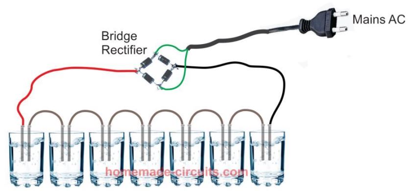 Here, we find that each glass/electrode set up is able to produce its own share of oxygen and hydrogen, thus making the total production 7 times higher.
Actually, with a 310 v supply (after 220 V rectification), the above setup can be increased to 310 / 1.4 = 221 apparatus's, generating 221 times more oxygen than a single apparatus which was shown in our first example.
That looks awesome, isn't it.
Remember the electrodes are graphite electrodes to avoid corrosion and oxidation.
And, the water is pure tap water, no catalyst in the form of salt, acid, or baking soda must be used, which may otherwise cause false and dangerous outcomes.
Here, we find that each glass/electrode set up is able to produce its own share of oxygen and hydrogen, thus making the total production 7 times higher.
Actually, with a 310 v supply (after 220 V rectification), the above setup can be increased to 310 / 1.4 = 221 apparatus's, generating 221 times more oxygen than a single apparatus which was shown in our first example.
That looks awesome, isn't it.
Remember the electrodes are graphite electrodes to avoid corrosion and oxidation.
And, the water is pure tap water, no catalyst in the form of salt, acid, or baking soda must be used, which may otherwise cause false and dangerous outcomes.
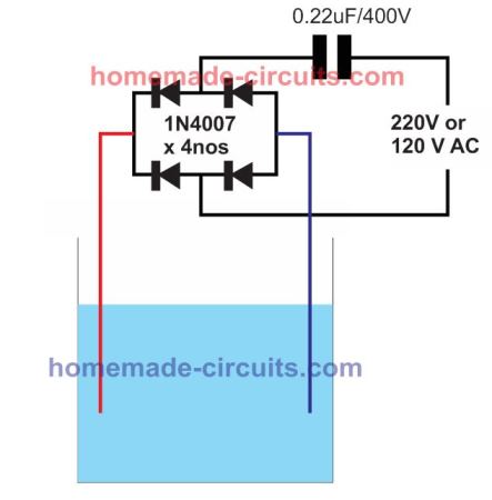
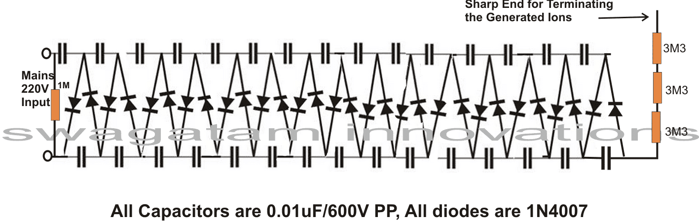 The entire circuit may be built over a general purpose board, by soldering the shown number of capacitors and diodes exactly in the way they are arranged in the diagram.
Following the diagram pattern would make the making easier toassembleand would produce guaranteed results without faults.
After the circuit is assembled, check the entire board for any wring connections, this is important because the circuit is very critical with its polarities, a single wrongly connected diode would make the results zero.
After proper confirmation, the soldered side should bethoroughlycleaned with thinner so that no residual flux stays deposited causing loss of voltage and reduction in the desired effects.
The end which is terminated for releasing the ions must be needle shaped, preferably a small pin or needle can be used there for enabling perfectprorogationof the ions.
After all the aboveprecautionsare complete, it's time to power the unit.
Be extremely careful, as the entire circuit is connecteddirectlywith mains AC and can be lifethreateningiftouchedin the powered position.
The entire circuit may be built over a general purpose board, by soldering the shown number of capacitors and diodes exactly in the way they are arranged in the diagram.
Following the diagram pattern would make the making easier toassembleand would produce guaranteed results without faults.
After the circuit is assembled, check the entire board for any wring connections, this is important because the circuit is very critical with its polarities, a single wrongly connected diode would make the results zero.
After proper confirmation, the soldered side should bethoroughlycleaned with thinner so that no residual flux stays deposited causing loss of voltage and reduction in the desired effects.
The end which is terminated for releasing the ions must be needle shaped, preferably a small pin or needle can be used there for enabling perfectprorogationof the ions.
After all the aboveprecautionsare complete, it's time to power the unit.
Be extremely careful, as the entire circuit is connecteddirectlywith mains AC and can be lifethreateningiftouchedin the powered position.
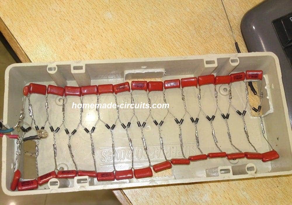
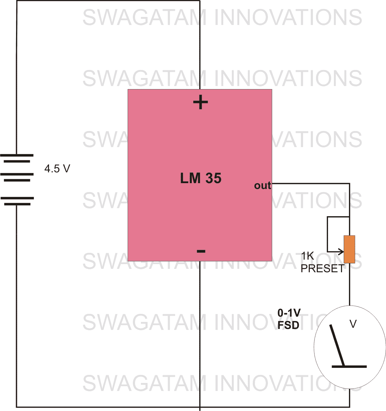
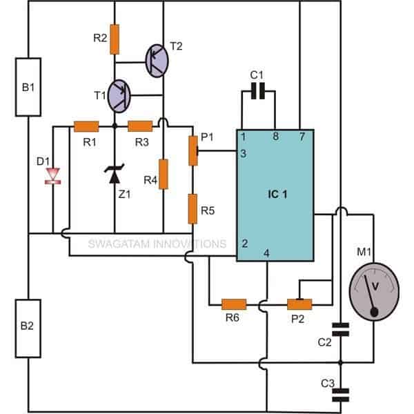 Parts List
R1, R4 = 12K,
R2 = 100E,
R3 = 1M,
R5 = 91K,
R6 = 510K,
P1 = 10K PRESET,
P2 = 100K PRESET,
C1 = 33pF,
C2, C3 = 0.0033uF,
T1, T2 = BC 557,
Z1= 4.7V, 400mW,
D1 =1N4148,
IC1 = LM308,
General Purpose Board as per size.
B1 and B2 = 9V PP3 battery.
M1 = 0 �C 1 V, FSD moving coil type voltmeter
Parts List
R1, R4 = 12K,
R2 = 100E,
R3 = 1M,
R5 = 91K,
R6 = 510K,
P1 = 10K PRESET,
P2 = 100K PRESET,
C1 = 33pF,
C2, C3 = 0.0033uF,
T1, T2 = BC 557,
Z1= 4.7V, 400mW,
D1 =1N4148,
IC1 = LM308,
General Purpose Board as per size.
B1 and B2 = 9V PP3 battery.
M1 = 0 �C 1 V, FSD moving coil type voltmeter
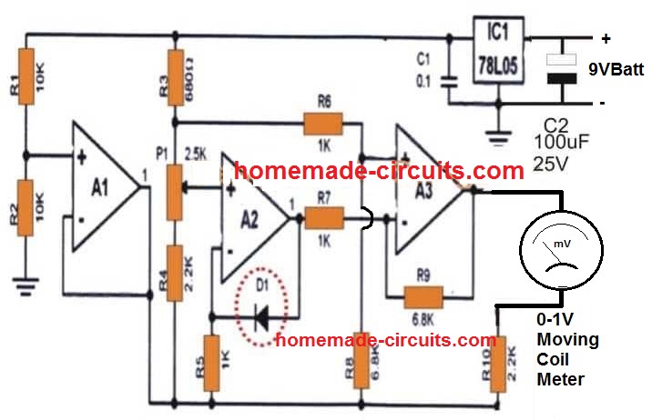 The 3rd design is probably the best one as far as cost, ease of construction and accuracy is concerned.
A single LM324 IC, a 78L05 5V regular IC and a few passive components are all that is needed to make this easiest room Celsius indicator circuit.
Only 3 op amps are used from the 4 op amps of the LM324.
Op amp A1 is wired to create a virtual ground for the circuit, for its effective working.
A2 is configured as a non-inverting amplifier where the feedback resistor is replaced with a 1N4148 diode.
This diode also acts as the temperature sensor, and drops around 2 mV from every single degree rise in the ambient temperature.
This 2 mV drop is detected by the A2 circuit and is converted into a correspondingly varying potential at pin#1.
This potential is further amplified and buffered by A3 inverting amplifier for feeding the attached 0 to 1V volmeter unit.
The voltmeter translates the temperature dependent varying output into a calibrated temperature scale to produce the room temperature data quickly through the relevant deflections.
The entire circuit is powered by a single 9 V PP3.
So folks, these were 3 cool, easy to build room temperature indicator circuits, that any hobbyist can build for monitoring the ambient temperature variations of a premise quickly and cheaply using standard electronic components, and without involving complex Arduino devices.
The 3rd design is probably the best one as far as cost, ease of construction and accuracy is concerned.
A single LM324 IC, a 78L05 5V regular IC and a few passive components are all that is needed to make this easiest room Celsius indicator circuit.
Only 3 op amps are used from the 4 op amps of the LM324.
Op amp A1 is wired to create a virtual ground for the circuit, for its effective working.
A2 is configured as a non-inverting amplifier where the feedback resistor is replaced with a 1N4148 diode.
This diode also acts as the temperature sensor, and drops around 2 mV from every single degree rise in the ambient temperature.
This 2 mV drop is detected by the A2 circuit and is converted into a correspondingly varying potential at pin#1.
This potential is further amplified and buffered by A3 inverting amplifier for feeding the attached 0 to 1V volmeter unit.
The voltmeter translates the temperature dependent varying output into a calibrated temperature scale to produce the room temperature data quickly through the relevant deflections.
The entire circuit is powered by a single 9 V PP3.
So folks, these were 3 cool, easy to build room temperature indicator circuits, that any hobbyist can build for monitoring the ambient temperature variations of a premise quickly and cheaply using standard electronic components, and without involving complex Arduino devices.
 The other IC, the 3900, includes quad amplifiers where just a couple of are utilized.
These op amps are designed to work a little differently; these are configured as current driven units instead of as voltage driven.
An input could best be considered to be the transistor base in a common-emitter configuration.
As a result, the input voltage is often around 0.6 volt.
R1 is coupled to the reference voltage and a constant current hence moves through this resistor.
Due to its large open loop gain, the op amp is able to adapt its very own output in order that the exact same current runs into its inverting input, and the current through the temperature -sensing diode (D1) thus stays constant.
This set up is important due to the fact the diode is, essentially, a voltage source having a specific internal resistance, and any kind of deviation in the current moving via it might as a result create a variation in the voltage which could end up being erroneously translated as a variation in temperature.
The output voltage at pin 4 is hence the same as the voltage at the inverting input as well as the voltage around the diode (the latter changing with temperature).
C3 inhibits oscillation.
Pin 1 of IC 2B is attached to the fixed reference potential and a constant current consequently moves into the non inverting input.
The inverting input of IC 2B is hooked up by means of R2 to the output of IC 2A (pin 4), in order that it is operated by a temperature-dependent current.
IC 2B amplifies the difference between its input currents to a value that the voltage deviation at its output (pin 5) could quickly be read with a 5 to 10 volt f.s.d.
voltmeter.
In case a panel meter is employed, Ohm's law may need to be configured to determine the series resistance.
If a 100-uA f.s.d.
meter with an internal resistance of 1200 is employed, the total resistance for 10 V full-scale deflection has to be as per the calculation:
10/ 100uA = 100K
R5 must as a result be 100 k - 1k2 = 98k8. The closest common value (100 k) will work well.
Calibration can be done as explained below: the zero point is initially fixed by P1 using the temperature sensor immersed in a bowl of melting ice.
Full-scale deflection can after that be fixed with P2; for this the diode can be submerged inside hot water whose temperature is identified (let's say boiling water tested with any standard thermometer to be at 50��).
The other IC, the 3900, includes quad amplifiers where just a couple of are utilized.
These op amps are designed to work a little differently; these are configured as current driven units instead of as voltage driven.
An input could best be considered to be the transistor base in a common-emitter configuration.
As a result, the input voltage is often around 0.6 volt.
R1 is coupled to the reference voltage and a constant current hence moves through this resistor.
Due to its large open loop gain, the op amp is able to adapt its very own output in order that the exact same current runs into its inverting input, and the current through the temperature -sensing diode (D1) thus stays constant.
This set up is important due to the fact the diode is, essentially, a voltage source having a specific internal resistance, and any kind of deviation in the current moving via it might as a result create a variation in the voltage which could end up being erroneously translated as a variation in temperature.
The output voltage at pin 4 is hence the same as the voltage at the inverting input as well as the voltage around the diode (the latter changing with temperature).
C3 inhibits oscillation.
Pin 1 of IC 2B is attached to the fixed reference potential and a constant current consequently moves into the non inverting input.
The inverting input of IC 2B is hooked up by means of R2 to the output of IC 2A (pin 4), in order that it is operated by a temperature-dependent current.
IC 2B amplifies the difference between its input currents to a value that the voltage deviation at its output (pin 5) could quickly be read with a 5 to 10 volt f.s.d.
voltmeter.
In case a panel meter is employed, Ohm's law may need to be configured to determine the series resistance.
If a 100-uA f.s.d.
meter with an internal resistance of 1200 is employed, the total resistance for 10 V full-scale deflection has to be as per the calculation:
10/ 100uA = 100K
R5 must as a result be 100 k - 1k2 = 98k8. The closest common value (100 k) will work well.
Calibration can be done as explained below: the zero point is initially fixed by P1 using the temperature sensor immersed in a bowl of melting ice.
Full-scale deflection can after that be fixed with P2; for this the diode can be submerged inside hot water whose temperature is identified (let's say boiling water tested with any standard thermometer to be at 50��).
 R1 provides a slight forward bias to D1 and D2, such that there is no substantial self heating of the diodes.
The voltage generated between the diodes is theoretically 1V2, but it changes by around 2mV per degree C per diode, or approximately 4mV through both diodes.
This voltage is applied to the input of an operational amplifier inverting amplifier, IC1. RV1 is set for the greatest voltage at IC1's non-inverting input that provides zero output voltage when the probe is at 0 degrees C (which may be obtained by dipping the probe in ice).
This provides the requiredcompensationfor the quiescent voltage across the diodes and results in a 0 V displayon the 1V FSD voltmeter circuit hooked upacross the amplifier's output.
When the diodes become warm up toto 50 degrees Celsius, the voltage across them drops by around 200mV, which is boosted by the amplifier througha factor of 5 to provide around 1V at its output, which resultsnearly afull scale meterdeflection.
Practically, RV2 is utilized to tune the amplifier's gain such that full scale deflection is generated.
RV2 can, obviously, be adjusted to the proper temperature using the probe at any specified temperature that translates to a significant meter deflection.
The circuit demands highlysteady supply of around 5V, which may be achieved with a 5V monolithic regulator and a 9V battery (IC2).
To avoid instabilities, C3 and C4 should mustbe positioned near to IC2.
R1 provides a slight forward bias to D1 and D2, such that there is no substantial self heating of the diodes.
The voltage generated between the diodes is theoretically 1V2, but it changes by around 2mV per degree C per diode, or approximately 4mV through both diodes.
This voltage is applied to the input of an operational amplifier inverting amplifier, IC1. RV1 is set for the greatest voltage at IC1's non-inverting input that provides zero output voltage when the probe is at 0 degrees C (which may be obtained by dipping the probe in ice).
This provides the requiredcompensationfor the quiescent voltage across the diodes and results in a 0 V displayon the 1V FSD voltmeter circuit hooked upacross the amplifier's output.
When the diodes become warm up toto 50 degrees Celsius, the voltage across them drops by around 200mV, which is boosted by the amplifier througha factor of 5 to provide around 1V at its output, which resultsnearly afull scale meterdeflection.
Practically, RV2 is utilized to tune the amplifier's gain such that full scale deflection is generated.
RV2 can, obviously, be adjusted to the proper temperature using the probe at any specified temperature that translates to a significant meter deflection.
The circuit demands highlysteady supply of around 5V, which may be achieved with a 5V monolithic regulator and a 9V battery (IC2).
To avoid instabilities, C3 and C4 should mustbe positioned near to IC2.
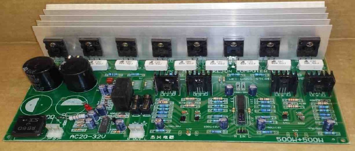

 The power is applied from a couple of 9 V PP3 batteries.
THe gain of the meter is adjusted and set for all the temperature ranges universally through the preset P1. This setting is done depending on the range and value of the mA meter.
The preset P2 is used for adjusting the offset output voltage from the IC 741 op amp.
It is adjusted until the needle is pushed to exact zero mark, while the system is not detecting any temperature.
The resistive divider created using R3 and the preset P3 enables the ambient temperature correction adjustment for the meter.
This simple thermocouple temperature meter circuit features two handy temperature ranges to select from, one is 0 to 100, and the other is 0 to 1000. This range cn be selected with an quick toggling of the selector switch K1.
The Chromel/Alumel thermocouple sensor input is plugged into the circuit through an ordinary 3.5 mm jack, connected to the selector switch K1.
When the thermocouple (TC) is plugged into K1, it shorts circuits the non-inverting input of the op amp to ground.
Next, if we remove the TC from K1, the (+) input of the op amp is removed from the ground, an at this meter the meter must show zero.
If it doesn't then adjust the offset null preset P2 until the needle reaches the zero point on the meter.
After this connecting the TC to the K1 socket, must keep the meter needle at zero until a temperature difference is created across the two ends of the TC.
In case you find a slight deviation on the meter needle side due to ambient temperature difference across the "hot end" and "cold end" of the TC, this may be corrected by carefully adjusting the P3 preset, until the needle indicates the ambient temperature on the meter.
Now, your thermocouple meter is all set for use.
The power is applied from a couple of 9 V PP3 batteries.
THe gain of the meter is adjusted and set for all the temperature ranges universally through the preset P1. This setting is done depending on the range and value of the mA meter.
The preset P2 is used for adjusting the offset output voltage from the IC 741 op amp.
It is adjusted until the needle is pushed to exact zero mark, while the system is not detecting any temperature.
The resistive divider created using R3 and the preset P3 enables the ambient temperature correction adjustment for the meter.
This simple thermocouple temperature meter circuit features two handy temperature ranges to select from, one is 0 to 100, and the other is 0 to 1000. This range cn be selected with an quick toggling of the selector switch K1.
The Chromel/Alumel thermocouple sensor input is plugged into the circuit through an ordinary 3.5 mm jack, connected to the selector switch K1.
When the thermocouple (TC) is plugged into K1, it shorts circuits the non-inverting input of the op amp to ground.
Next, if we remove the TC from K1, the (+) input of the op amp is removed from the ground, an at this meter the meter must show zero.
If it doesn't then adjust the offset null preset P2 until the needle reaches the zero point on the meter.
After this connecting the TC to the K1 socket, must keep the meter needle at zero until a temperature difference is created across the two ends of the TC.
In case you find a slight deviation on the meter needle side due to ambient temperature difference across the "hot end" and "cold end" of the TC, this may be corrected by carefully adjusting the P3 preset, until the needle indicates the ambient temperature on the meter.
Now, your thermocouple meter is all set for use.
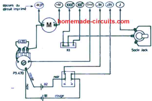


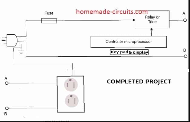

 The bifilar coil type designshown above can be effectively implemented for making your homemade induction cookware.
For optimum response and low heat generation within the coil make sure the wire of the bifilar coil is made using many thin strands of copper instead of a single solid wire.
Thus, this becomes the work coil of the cookware, now the ends of this coil simply needs to be integrated with a matching capacitor and a compatible frequency driver network, as shown in the following figure:
The bifilar coil type designshown above can be effectively implemented for making your homemade induction cookware.
For optimum response and low heat generation within the coil make sure the wire of the bifilar coil is made using many thin strands of copper instead of a single solid wire.
Thus, this becomes the work coil of the cookware, now the ends of this coil simply needs to be integrated with a matching capacitor and a compatible frequency driver network, as shown in the following figure:
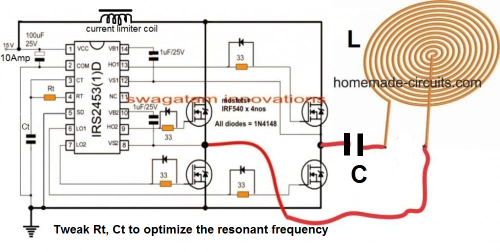
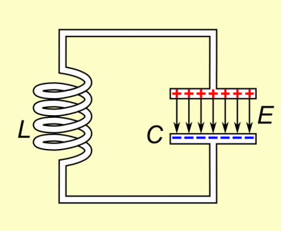 Wikipedia
The capacitor is again forced to charge but this time in the opposite direction, and as soon as it's fully charged, it yet again tries to empty itself across the coil, and this results in a back and forth sharing of charge in the form of an oscillating current across the LC network.
The frequency of this oscillating current becomes the resonance frequency of the tuned LC circuit.
However due to inherent losses the above oscillations eventually die out in the course of time, and the frequency, the charge all come to an end after sometime.
But if the frequency is allowed to sustain through an external frequency input, tuned at the same resonance level, then that could ensure a permanent resonance effect being induced across the LC circuit.
At resonance frequency we can expect the amplitude of the voltage oscillating across the LC circuit to be at the maximum level, resulting in the most efficient induction.
Therefore we can imply that, to implement a perfect resonance within an LC network for an induction heater design we need to ensure the following crucial parameters:
1) A tuned LC circuit
2) And a matching frequency to sustain the LC circuit resonance.
This can be calculated using the following simple formula:
F = 1�� 2�� x ��LC
where L is in Henry and C is in Farad
If you don't want to go through the hassles of calculating the resonance of the coil LC tank through formula, a much simpler option could be to use the following software:
LC Resonant Frequency Calculator
Or you may also build this Grid dip meter for identifying and setting the resonance frequency.
Once the resonance frequency is identified, it's time to set the full-bridge IC with this resonance frequency by suitably selecting the Rt, and Ct timing components.
This may be done by some trial and error through practical measurements, or through the following formula:
The following formula can be used for calculating the values of Rt/Ct:
f = 1/1.453 x Rt x Ct where Rt is in Ohms and Ct in Farads.
Wikipedia
The capacitor is again forced to charge but this time in the opposite direction, and as soon as it's fully charged, it yet again tries to empty itself across the coil, and this results in a back and forth sharing of charge in the form of an oscillating current across the LC network.
The frequency of this oscillating current becomes the resonance frequency of the tuned LC circuit.
However due to inherent losses the above oscillations eventually die out in the course of time, and the frequency, the charge all come to an end after sometime.
But if the frequency is allowed to sustain through an external frequency input, tuned at the same resonance level, then that could ensure a permanent resonance effect being induced across the LC circuit.
At resonance frequency we can expect the amplitude of the voltage oscillating across the LC circuit to be at the maximum level, resulting in the most efficient induction.
Therefore we can imply that, to implement a perfect resonance within an LC network for an induction heater design we need to ensure the following crucial parameters:
1) A tuned LC circuit
2) And a matching frequency to sustain the LC circuit resonance.
This can be calculated using the following simple formula:
F = 1�� 2�� x ��LC
where L is in Henry and C is in Farad
If you don't want to go through the hassles of calculating the resonance of the coil LC tank through formula, a much simpler option could be to use the following software:
LC Resonant Frequency Calculator
Or you may also build this Grid dip meter for identifying and setting the resonance frequency.
Once the resonance frequency is identified, it's time to set the full-bridge IC with this resonance frequency by suitably selecting the Rt, and Ct timing components.
This may be done by some trial and error through practical measurements, or through the following formula:
The following formula can be used for calculating the values of Rt/Ct:
f = 1/1.453 x Rt x Ct where Rt is in Ohms and Ct in Farads.
 The total voltageV applied across the series LC will be the sum of the voltage across the inductor L and the voltage across the capacitor C.
The current flowing through the system will be equal to the current that's flowing through the L and the C components.
V = VL + VC
I = IL = IC
The frequency of the applied voltage affects the reactances of the inductor and the capacitor.
As frequency is increased from a minimum value to a higher value, the inductive reactance XL of the inductor will proportionately increase, but XC which is the capacitive reactance will decrease.
However, while the frequency is being increased there will be a particular instance or threshold when the magnitudes of the inductive reactance and the capacitive reactance will be just equal.
This instance will be the resonant point of the series LC, and the frequency can be set as the resonant frequency.
Therefore, in a series resonant circuit, the resonance will occur when
XL = XC
or, ��L = 1 / ��C
where �� = angular frequency.
Evaluating the value of �� gives us:
�� = ��o = 1 / �� LC, which is defined as the resonant angular frequency.
Substituting this in the previous equation and also converting the angular frequency (in radians per second) into frequency (Hz), we finally get:
fo = ��o / 2�� = 1 / 2�� LC
fo = 1 / 2�С� LC
The total voltageV applied across the series LC will be the sum of the voltage across the inductor L and the voltage across the capacitor C.
The current flowing through the system will be equal to the current that's flowing through the L and the C components.
V = VL + VC
I = IL = IC
The frequency of the applied voltage affects the reactances of the inductor and the capacitor.
As frequency is increased from a minimum value to a higher value, the inductive reactance XL of the inductor will proportionately increase, but XC which is the capacitive reactance will decrease.
However, while the frequency is being increased there will be a particular instance or threshold when the magnitudes of the inductive reactance and the capacitive reactance will be just equal.
This instance will be the resonant point of the series LC, and the frequency can be set as the resonant frequency.
Therefore, in a series resonant circuit, the resonance will occur when
XL = XC
or, ��L = 1 / ��C
where �� = angular frequency.
Evaluating the value of �� gives us:
�� = ��o = 1 / �� LC, which is defined as the resonant angular frequency.
Substituting this in the previous equation and also converting the angular frequency (in radians per second) into frequency (Hz), we finally get:
fo = ��o / 2�� = 1 / 2�� LC
fo = 1 / 2�С� LC
 This setup may be deployed for circuits which are enclosed in a box.
The LED turns ON when the preset threshold level reached and also turns ON the fan.
Connecting a Relay for Controlling Bigger Fans
This setup may be deployed for circuits which are enclosed in a box.
The LED turns ON when the preset threshold level reached and also turns ON the fan.
Connecting a Relay for Controlling Bigger Fans
 This circuit does the similar function of previous circuit, now the fan is replaced by relay.
This circuit can control a table fan or ceiling fan or any other gadget which can cool down the ambient temperature.
The connected device turns off as soon as the temperature reached below preset threshold level.
The temperature controlled dc fan circuit diagram illustrated here are just few of many possibilities.
You may customize the circuit and program for your own purpose.
NOTE 1: #Pin 7 is output.
NOTE 2: This program is only compatible with DHT11 sensor only.
Program for the above explained automatic temperature regulator circuit using Arduino:
This circuit does the similar function of previous circuit, now the fan is replaced by relay.
This circuit can control a table fan or ceiling fan or any other gadget which can cool down the ambient temperature.
The connected device turns off as soon as the temperature reached below preset threshold level.
The temperature controlled dc fan circuit diagram illustrated here are just few of many possibilities.
You may customize the circuit and program for your own purpose.
NOTE 1: #Pin 7 is output.
NOTE 2: This program is only compatible with DHT11 sensor only.
Program for the above explained automatic temperature regulator circuit using Arduino:
 1. Vin-- this pin is connected to dc power supply between 4 to 20 v.
2. Vout-- this pin gives output in the form of voltage.
3. GND-- this pin is connected to gnd terminal of circuit.
LM35, when connected to power supply senses the temperature of surroundings and sends equivalent voltage in accordance with per degree rise in temperature through its output pin.
LM35 can sense any temp.
between -50 degree to +150 degree Celsius and increases output by 10 millivolts with 1 degree rise in temperature.
Thus maximum voltage it can give as output is 1.5 volts.
1. Vin-- this pin is connected to dc power supply between 4 to 20 v.
2. Vout-- this pin gives output in the form of voltage.
3. GND-- this pin is connected to gnd terminal of circuit.
LM35, when connected to power supply senses the temperature of surroundings and sends equivalent voltage in accordance with per degree rise in temperature through its output pin.
LM35 can sense any temp.
between -50 degree to +150 degree Celsius and increases output by 10 millivolts with 1 degree rise in temperature.
Thus maximum voltage it can give as output is 1.5 volts.
 4. DIODE (1N4007)
 5. FAN (motor)
6. FAN POWER SUPPLY
5. FAN (motor)
6. FAN POWER SUPPLY
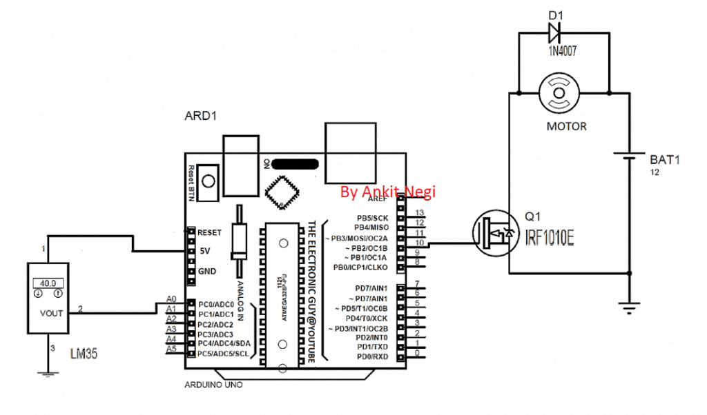 Make connections as shown in circuit diagram.
a) Connect vin pin of lm358 to 5v of arduino
b) Connect vout pin of lm358 to A0 of arduino
c) Connect ground pin of lm358 to GND of arduino
d) Connect base of mosfet to PWM pin 10 of arduino
Make connections as shown in circuit diagram.
a) Connect vin pin of lm358 to 5v of arduino
b) Connect vout pin of lm358 to A0 of arduino
c) Connect ground pin of lm358 to GND of arduino
d) Connect base of mosfet to PWM pin 10 of arduino
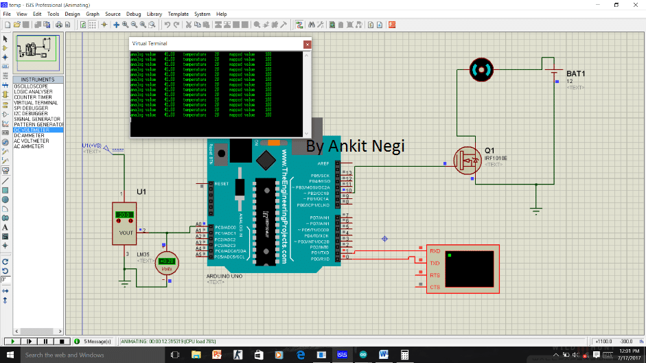 As you can see temperature is 20 degree hence
Analog value=41
Temperature=20
Mapped value=100
But since temp is less than 25 degree hence mosfet gets 0 volt as show in fig( indicated by blue dot).
CASE 2. When temp.
Is greater than 25 degree
When temperature reaches 25 degree, then as specified in the code pwm signal is sent to the base of mosfet and with each degree rise in temperature this PWM voltage also increases i.e.
As you can see temperature is 20 degree hence
Analog value=41
Temperature=20
Mapped value=100
But since temp is less than 25 degree hence mosfet gets 0 volt as show in fig( indicated by blue dot).
CASE 2. When temp.
Is greater than 25 degree
When temperature reaches 25 degree, then as specified in the code pwm signal is sent to the base of mosfet and with each degree rise in temperature this PWM voltage also increases i.e.
 As you can see as temperature increases from 20 degree to all the way to 40 degree , all three value changes and at 40 degree Celsius
Analog value=82
Temperature=40
Mapped value=200
Since temp is greater than 25 degree hence mosfet gets corresponding PWM voltage as show in fig( indicated by red dot).
Hence motor starts running at 25 degree and with corresponding rise in per degree temperature; pwm voltage from pin 10 to base of mosfet also increases.
Hence motor speed increases linearly with the increase in temperature and becomes almost maximum for 40 degree Celsius.
If you have any further queries regarding the above explained automatic temperature controlled dc fan circuit using fan and Arduino, you can always use the comment box below and send your thoughts to us.
We will try to get back at an earliest.
As you can see as temperature increases from 20 degree to all the way to 40 degree , all three value changes and at 40 degree Celsius
Analog value=82
Temperature=40
Mapped value=200
Since temp is greater than 25 degree hence mosfet gets corresponding PWM voltage as show in fig( indicated by red dot).
Hence motor starts running at 25 degree and with corresponding rise in per degree temperature; pwm voltage from pin 10 to base of mosfet also increases.
Hence motor speed increases linearly with the increase in temperature and becomes almost maximum for 40 degree Celsius.
If you have any further queries regarding the above explained automatic temperature controlled dc fan circuit using fan and Arduino, you can always use the comment box below and send your thoughts to us.
We will try to get back at an earliest.
 Let's try to understand the above shown push-button heater controller circuit in detail:
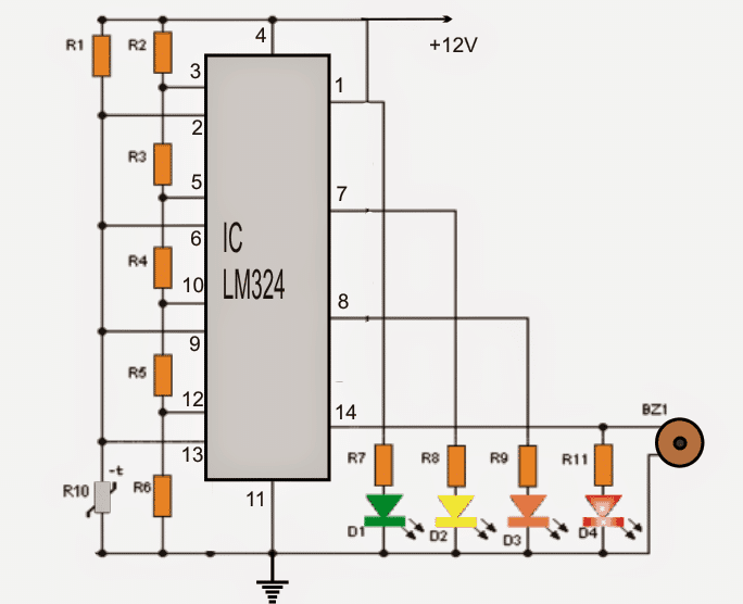
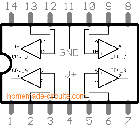
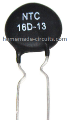 Note: for the thermistor, you must keep the terminals long enough, so that it can be terminated across the place where the temperature is in question.
Submitted by: Shweta sawant
UPDATE from the Admin
The accuracy and reliability of the above 4 LED temperature indicator circuit can be further improved by adding discrete presets to the 4 op amps and by replacing the thermistor with LM35 IC.
The complete circuit is shown below:
Note: for the thermistor, you must keep the terminals long enough, so that it can be terminated across the place where the temperature is in question.
Submitted by: Shweta sawant
UPDATE from the Admin
The accuracy and reliability of the above 4 LED temperature indicator circuit can be further improved by adding discrete presets to the 4 op amps and by replacing the thermistor with LM35 IC.
The complete circuit is shown below:
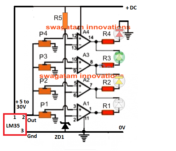 Parts List
All presets are 22K (linear)
All resistors are 1K 1/4 watt
ZD1 is 6V 1/4 watt zener diode
LEDs are red, green, yellow, white 5mm 20mA
Op amps are from the IC LM324
Temperature sensor is LM35 IC
Parts List
All presets are 22K (linear)
All resistors are 1K 1/4 watt
ZD1 is 6V 1/4 watt zener diode
LEDs are red, green, yellow, white 5mm 20mA
Op amps are from the IC LM324
Temperature sensor is LM35 IC
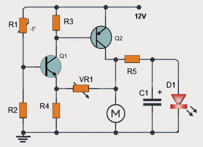
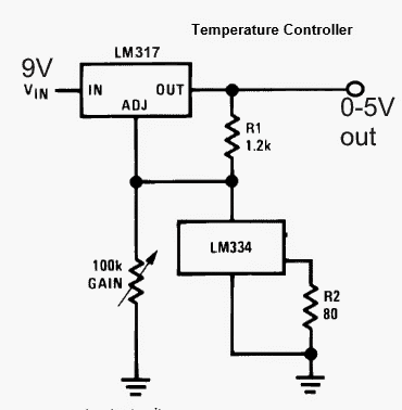 LM334 which is a precision temperature sensor chip is configured with another precision voltage regulator IC LM317 circuit forming an accurate, linear temperature to voltage converter circuit.
The gain pot and R2 may be tweaked and experimented for achieving the desired temperature to voltage ratio.
As per the request, the voltage needs to be 0 at 25 degree C, this may be done by creating an atmosphere at the specified temperature and then adjust the pot to get a 0V at the output.
The above adjustment would hopefully allow the output to produce 1V increment for every 4.16 degree decrease in the temperature around LM334, this may also need some tweaking.
LM334 which is a precision temperature sensor chip is configured with another precision voltage regulator IC LM317 circuit forming an accurate, linear temperature to voltage converter circuit.
The gain pot and R2 may be tweaked and experimented for achieving the desired temperature to voltage ratio.
As per the request, the voltage needs to be 0 at 25 degree C, this may be done by creating an atmosphere at the specified temperature and then adjust the pot to get a 0V at the output.
The above adjustment would hopefully allow the output to produce 1V increment for every 4.16 degree decrease in the temperature around LM334, this may also need some tweaking.
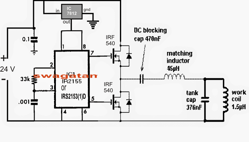 The circuit is driven from a 24 V DC supply, at current ranging up to 15 amps.
A 7812 voltage regulator drops the input voltage to 12V for the driver IC which is a standard half bridge driver IC IRS2153 or any other similar.
The push pull output from the IC drives a pair of mosfets which in turn forwards the oscillations to the main work coil of the induction heater via a DC blocking capacitor and an impedance matching inductor.
The blocking capacitor prevents excessive current from passing through the work coil and stops damaging the mosfets while the inductor makes sure no disturbing harmonics get into the line and induce inefficiencies into the system.
The 376 nF tank capacitors are used to achieve a resonance with the work coil at about 210 kHz frequency which is set by the R/C network across pin2 and pin3 of the driver IC.
The 33k resistor could be made variable for fine tuning or optimizing the resonance effect.
The circuit is driven from a 24 V DC supply, at current ranging up to 15 amps.
A 7812 voltage regulator drops the input voltage to 12V for the driver IC which is a standard half bridge driver IC IRS2153 or any other similar.
The push pull output from the IC drives a pair of mosfets which in turn forwards the oscillations to the main work coil of the induction heater via a DC blocking capacitor and an impedance matching inductor.
The blocking capacitor prevents excessive current from passing through the work coil and stops damaging the mosfets while the inductor makes sure no disturbing harmonics get into the line and induce inefficiencies into the system.
The 376 nF tank capacitors are used to achieve a resonance with the work coil at about 210 kHz frequency which is set by the R/C network across pin2 and pin3 of the driver IC.
The 33k resistor could be made variable for fine tuning or optimizing the resonance effect.

 T1, T2 together with C1, C2 and the associated resistors form a classic astable multivibrator (AMV) with a set frequency of around 30 kHz.
The panel volatge is fed to the above AMV and oscillated at the said frequency before feeding it to the buck converter stage made by employing a mosfet and an associated diode, inductor stage.
During the switch OFF periods an equivalent amount voltage is delivered from L1 in the from of back EMFs which is appropriately filtered and supplied to the connected induction heater circuit across the output terminals.
C4 makes sure the converted bucked voltage is free from any ripples and helps in producing a cleaner DC for the induction heater circuit.
The regulated 24 V DC at the outputs may be achieved by roughly winding the correct number of turns for L1 through some trial and error and also by the incorporation of D2 which ultimately stabilizes the output voltage to the required levels.
T1, T2 together with C1, C2 and the associated resistors form a classic astable multivibrator (AMV) with a set frequency of around 30 kHz.
The panel volatge is fed to the above AMV and oscillated at the said frequency before feeding it to the buck converter stage made by employing a mosfet and an associated diode, inductor stage.
During the switch OFF periods an equivalent amount voltage is delivered from L1 in the from of back EMFs which is appropriately filtered and supplied to the connected induction heater circuit across the output terminals.
C4 makes sure the converted bucked voltage is free from any ripples and helps in producing a cleaner DC for the induction heater circuit.
The regulated 24 V DC at the outputs may be achieved by roughly winding the correct number of turns for L1 through some trial and error and also by the incorporation of D2 which ultimately stabilizes the output voltage to the required levels.
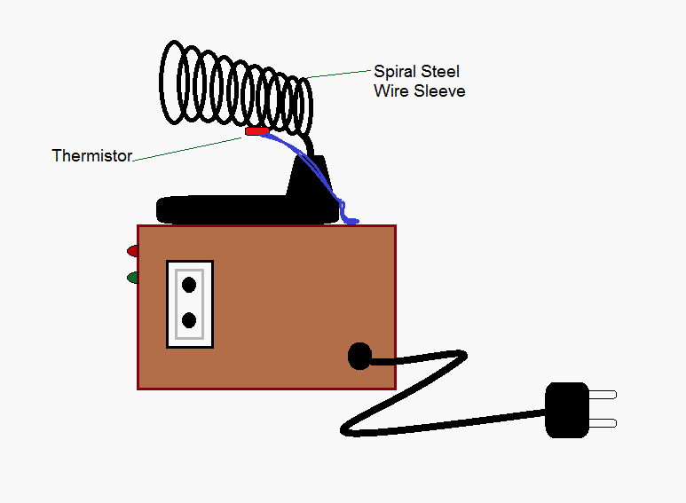
 The next concept below discusses another simple automatic soldering iron power shut off timer circuit which ensures that the iron is always switched OFF even if the user forgets to do the same during the course of this routine electronic assembly job work.
The idea was requested by Mr.
Amir
The next concept below discusses another simple automatic soldering iron power shut off timer circuit which ensures that the iron is always switched OFF even if the user forgets to do the same during the course of this routine electronic assembly job work.
The idea was requested by Mr.
Amir
 Parts List for the proposed automatic soldering iron power saver circuit
R1 = 100K
R2, R3, R4 = 10K
P1 = 1M
C1 = 1uF NON POLAR
C2 = 0.1uF
C3 = 1000uF/25V
R5 = 20 OHMS 10 WATT
ALL DIODES = 1N4007
IC PIN12 RESISTOR = 1M
T1 = BC547
T2 = BC557
REL1, REL2 = RELAY 12V/400 OHMS
TR1 = 12V/500MA TRANSFORMER
S1/S2 = PUSH TO ON SWITCHES
BUZZER = ANY 12V PIEZO BUZZER UNIT
A redrawn version of the above diagram can be seen below, it was suitably improved by Mr.
Mike for helping easier understanding of the wiring details.
Parts List for the proposed automatic soldering iron power saver circuit
R1 = 100K
R2, R3, R4 = 10K
P1 = 1M
C1 = 1uF NON POLAR
C2 = 0.1uF
C3 = 1000uF/25V
R5 = 20 OHMS 10 WATT
ALL DIODES = 1N4007
IC PIN12 RESISTOR = 1M
T1 = BC547
T2 = BC557
REL1, REL2 = RELAY 12V/400 OHMS
TR1 = 12V/500MA TRANSFORMER
S1/S2 = PUSH TO ON SWITCHES
BUZZER = ANY 12V PIEZO BUZZER UNIT
A redrawn version of the above diagram can be seen below, it was suitably improved by Mr.
Mike for helping easier understanding of the wiring details.

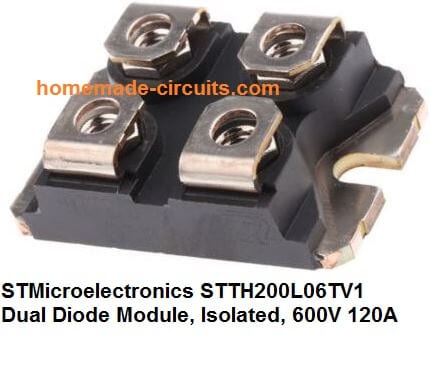 In case you use the built-in diodes of IGBT such as STGW30NC60WD, then you will not be required to use the smaller diodes or large double diodes.
A potentiometer is used in order to tune the operating frequency into resonance.
One of the best indicators of the resonance is the LED��s highest brightness.
You can certainly build drivers which are more sophisticated depending on your requirement.
You can also use automatic tuning which is one of the best things to do, which is the course adopted in the professional heaters; but there is one drawback that the simplicity of the circuit will be lost in this process.
You can control the frequency which falls in the range of approximately 110 to 210 kHz.
An adapter of little size which can be either transformer type or smps is used to provide 14-15V of auxiliary voltage which is required in the control circuit.
In case you use the built-in diodes of IGBT such as STGW30NC60WD, then you will not be required to use the smaller diodes or large double diodes.
A potentiometer is used in order to tune the operating frequency into resonance.
One of the best indicators of the resonance is the LED��s highest brightness.
You can certainly build drivers which are more sophisticated depending on your requirement.
You can also use automatic tuning which is one of the best things to do, which is the course adopted in the professional heaters; but there is one drawback that the simplicity of the circuit will be lost in this process.
You can control the frequency which falls in the range of approximately 110 to 210 kHz.
An adapter of little size which can be either transformer type or smps is used to provide 14-15V of auxiliary voltage which is required in the control circuit.
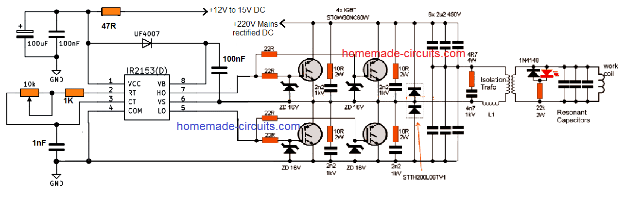
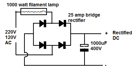
 The following image shows the double coiled air cored isolation transformer design:
You can build this by coiling 12 turns with a 14 cm diameter, using any thick doubled wired cable.
The following image shows the double coiled air cored isolation transformer design:
You can build this by coiling 12 turns with a 14 cm diameter, using any thick doubled wired cable.

 Please note that if the coil is tightly wound then only 5 turns may be required.
If six turns are used then you may try stretching the coil slightly for achieving optimal resonance and efficiency.
UPDATE
Please note that if the coil is tightly wound then only 5 turns may be required.
If six turns are used then you may try stretching the coil slightly for achieving optimal resonance and efficiency.
UPDATE
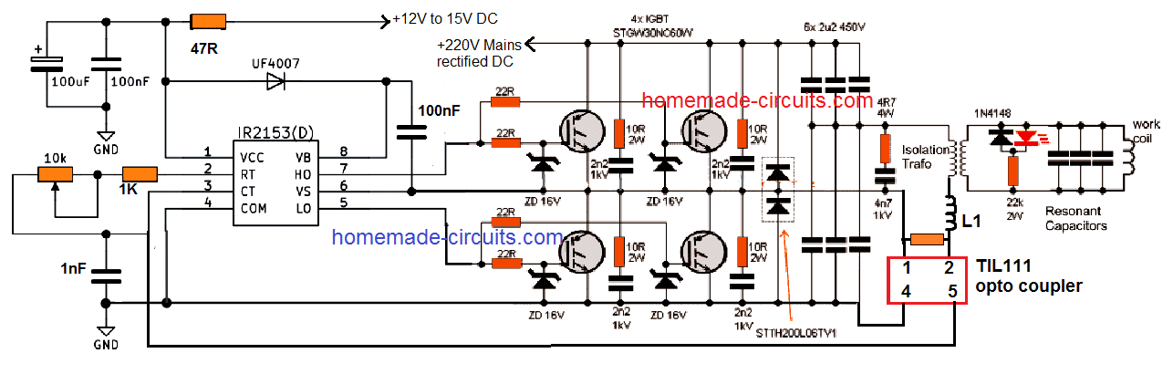
 Here the resistor near L1 (let's call it Rx) becomes the current sensing resistor, which develops a small voltage across itself to the desired point when the current begins exceeding the safe limits.
This voltage across Rx is used for triggering the LED inside the attached opto-coupler.
The output transistor inside the opto responds to the LED triggering and quickly conducts grounding the Ct, pin#3 of the main driver IC IR2153.
The IC shuts down immediately prohibiting any further rise in current.
When this happens the current drops which in turn eliminates the voltage across Rx, thereby switching OFF the opto LED.
This reverts the situation towards earlier normal situation, and the IC starts oscillating again.
This cycle now repeats rapidly ensuring a constant current consumption for the load, within the predetermined safe limits.
Rx = 2/Current Limit
Here the resistor near L1 (let's call it Rx) becomes the current sensing resistor, which develops a small voltage across itself to the desired point when the current begins exceeding the safe limits.
This voltage across Rx is used for triggering the LED inside the attached opto-coupler.
The output transistor inside the opto responds to the LED triggering and quickly conducts grounding the Ct, pin#3 of the main driver IC IR2153.
The IC shuts down immediately prohibiting any further rise in current.
When this happens the current drops which in turn eliminates the voltage across Rx, thereby switching OFF the opto LED.
This reverts the situation towards earlier normal situation, and the IC starts oscillating again.
This cycle now repeats rapidly ensuring a constant current consumption for the load, within the predetermined safe limits.
Rx = 2/Current Limit

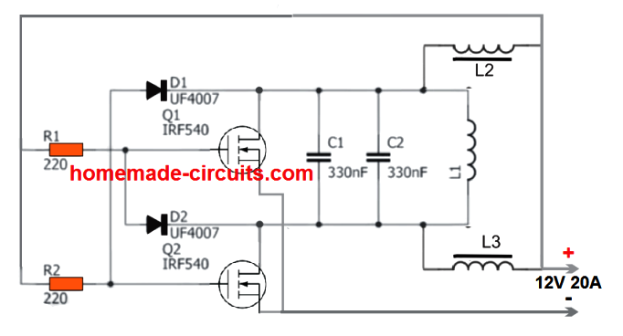 The original diagram can be witnessed in the following image:
 The working principle is the same ZVS technology, using two high power MOSFETs.
The supply input can be anything between 5V and 12V, and current from 5 amps to 20 amps depending on the load used.
The working principle is the same ZVS technology, using two high power MOSFETs.
The supply input can be anything between 5V and 12V, and current from 5 amps to 20 amps depending on the load used.
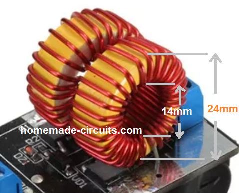 Video Demo
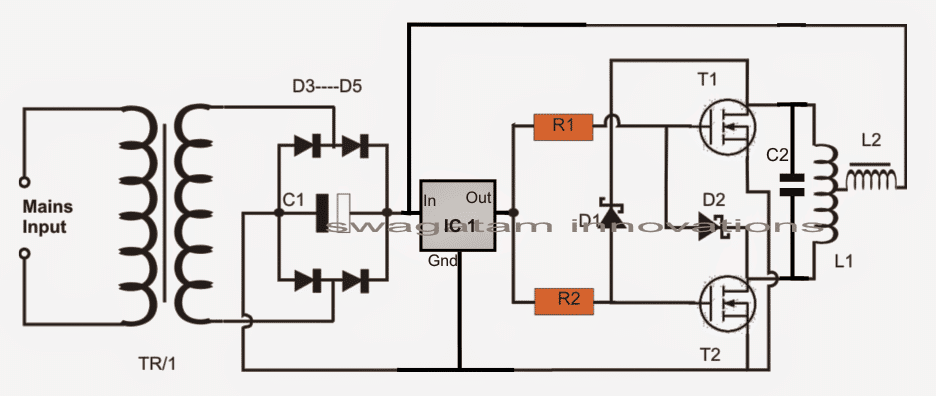 The capacitor as discussed above must be ideally connected as close as possible to the L1 terminals.
his is important for sustaining the resonant frequency at the specified 200kHz frequency.
The capacitor as discussed above must be ideally connected as close as possible to the L1 terminals.
his is important for sustaining the resonant frequency at the specified 200kHz frequency.

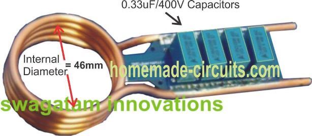 Parts list for the above induction heater circuit or induction hot plate circuit
R1, R2 = 330 ohms 1/2 watt
D1, D2 = FR107 or BA159
Parts list for the above induction heater circuit or induction hot plate circuit
R1, R2 = 330 ohms 1/2 watt
D1, D2 = FR107 or BA159
 T1, T2 = IRF540
C1 = 10,000uF/25V
C2 = 2uF/400V made by attaching the below shown 6nos 330nF/400V caps in parallel
T1, T2 = IRF540
C1 = 10,000uF/25V
C2 = 2uF/400V made by attaching the below shown 6nos 330nF/400V caps in parallel
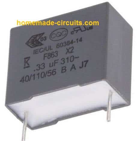 D3----D6 = 25 amp diodes
IC1 = 7812
L1 = 2mm brass pipe wound as shown in the following pics, the diameter can be anywhere near 30mm (internal diameter of the coils)
L2 = 2mH choke made by winding 2mm magnet wire on any suitable ferrite rod
TR1 = 0-15V/20amps
POWER SUPPLY: Use regulated 15V 20 amp DC power supply.
D3----D6 = 25 amp diodes
IC1 = 7812
L1 = 2mm brass pipe wound as shown in the following pics, the diameter can be anywhere near 30mm (internal diameter of the coils)
L2 = 2mH choke made by winding 2mm magnet wire on any suitable ferrite rod
TR1 = 0-15V/20amps
POWER SUPPLY: Use regulated 15V 20 amp DC power supply.
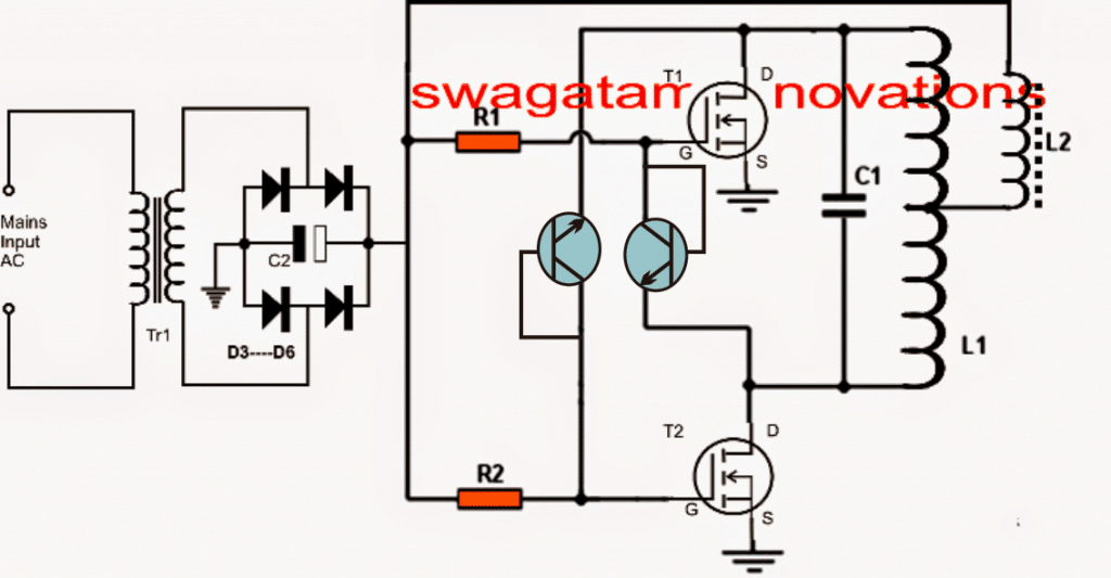
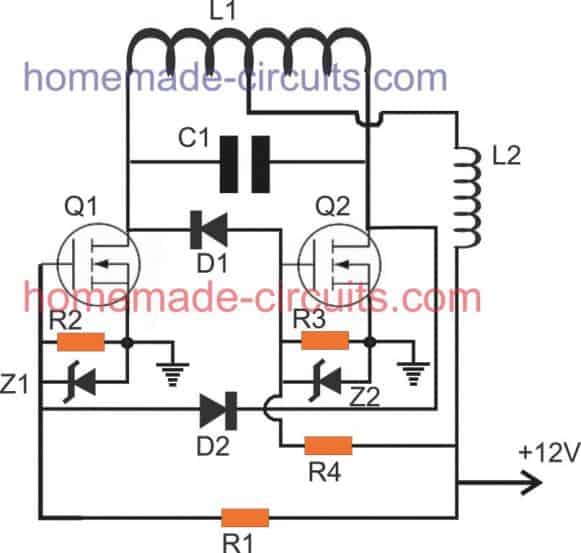
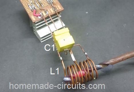
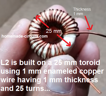
 The schematic would be the same as explained in my above sevction, which is basically a Royer based design, as shown here:


 Parts List for the second circuit
R1 = 2k7,
R2, R5, R6 = 1K
R3, R4= 10K,R7 = 470 ohms
R8 = 680 ohms
D1---D4 = 1N4007,
D5, D6 = 1N4148,P1 = 100K,
VR1 = 200 Ohms, 1Watt,
VR2 = 100k potC1 = 1000uF/25V,
T1 = BC547,T2 = BC557,
IC = 741,OPTO = LED/LDR Combo.
Relay = 12 V, 400 Ohm, SPDT.
Parts List for the second circuit
R1 = 2k7,
R2, R5, R6 = 1K
R3, R4= 10K,R7 = 470 ohms
R8 = 680 ohms
D1---D4 = 1N4007,
D5, D6 = 1N4148,P1 = 100K,
VR1 = 200 Ohms, 1Watt,
VR2 = 100k potC1 = 1000uF/25V,
T1 = BC547,T2 = BC557,
IC = 741,OPTO = LED/LDR Combo.
Relay = 12 V, 400 Ohm, SPDT.
 The above circuit was designed by me as per the requirements requested by Mr.
Vasilis.
Once it was completed, the unit needed some more refinements/enhancements and customizations for achieving improved optimization.
With the suggestions provided by Mr.
Vasilis, we could together successfully implement the features.
The following discussion between Vasilis and me, and the video explains how things were put into place using a few add-on circuits with the original pellet burner design.
The above circuit was designed by me as per the requirements requested by Mr.
Vasilis.
Once it was completed, the unit needed some more refinements/enhancements and customizations for achieving improved optimization.
With the suggestions provided by Mr.
Vasilis, we could together successfully implement the features.
The following discussion between Vasilis and me, and the video explains how things were put into place using a few add-on circuits with the original pellet burner design.
 However, the ammeter only determines and measures the flow of current and if we want to measure the voltage or the potential difference across the wiring we will have to use a voltmeter or rather a Milli voltmeter and connect it as given in the following diagram.
Here we can see that the second junction of the above circuit has been opened and the resulting terminals are configured with the voltmeter terminals.
However, the ammeter only determines and measures the flow of current and if we want to measure the voltage or the potential difference across the wiring we will have to use a voltmeter or rather a Milli voltmeter and connect it as given in the following diagram.
Here we can see that the second junction of the above circuit has been opened and the resulting terminals are configured with the voltmeter terminals.
 The above directions and principles looks pretty straightforward and an easy alternative for measuring high temperatures.
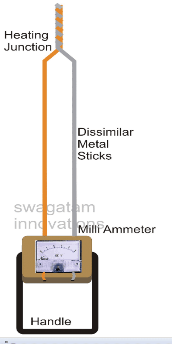
 In this set up we have used a reed switch and magnet arrangement for switching the circuit instead of a micro-switch, for ensuring higher working efficiency, and minimum wear and tear of the system.
Nevertheless, if a microswitvh is preferred, the reed switch could be simply replaced with a microswitch for getting the same operational features.
The magnet can be seen glued to the inner top edge of the letter box lid, while the reed relay is positioned at the top inside portion of the letter box, in such a way that when the lid is closed the magnet comes face to face and at a close proximity to the reed relay.
The reed relay terminals are configured with an electronic latch circuit which includes an LED for the indicating an opened letter box situation.
When the lid of the letter box is closed and the reset button pressed, the magnet keeps the reed relay contacts closed and the circuit goes into a standby mode.
The LED remains shut off in this situation.
Now, if the lid of the letter box is opened, the reed relay contacts release, causing the connected circuit to latch up, and the LED illuminates.
In this position even if the lid is closed again, the LED continues to be in the switched ON condition, indicating the owner regarding an previously opened letter box.
The LED can be shut off only by pressing the reset button, with the letter box lid in the closed position
In this set up we have used a reed switch and magnet arrangement for switching the circuit instead of a micro-switch, for ensuring higher working efficiency, and minimum wear and tear of the system.
Nevertheless, if a microswitvh is preferred, the reed switch could be simply replaced with a microswitch for getting the same operational features.
The magnet can be seen glued to the inner top edge of the letter box lid, while the reed relay is positioned at the top inside portion of the letter box, in such a way that when the lid is closed the magnet comes face to face and at a close proximity to the reed relay.
The reed relay terminals are configured with an electronic latch circuit which includes an LED for the indicating an opened letter box situation.
When the lid of the letter box is closed and the reset button pressed, the magnet keeps the reed relay contacts closed and the circuit goes into a standby mode.
The LED remains shut off in this situation.
Now, if the lid of the letter box is opened, the reed relay contacts release, causing the connected circuit to latch up, and the LED illuminates.
In this position even if the lid is closed again, the LED continues to be in the switched ON condition, indicating the owner regarding an previously opened letter box.
The LED can be shut off only by pressing the reset button, with the letter box lid in the closed position
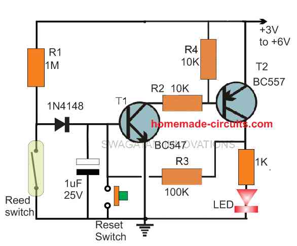 Basically, since it is a latch circuit, the circuit will switch ON the LED and get latched as soon as power is switches ON.
When power is switched ON, the transistor T1 is triggered ON through R1, which switches ON T2, and the entire system gets latched via the feedback resistor R3.
In this situation, even if the R1 connection is removed, the transistor would still remain latched and the LED will continue to remain illuminated.
For our letter box open indicator application we want the LED to be switched OFF while the lid of the box is in the closed position, and once it is opened only then the LED should go into a permanently ON position regardless of whether the lid is closed back or not.
For this, we have employed a reed switch, or reed relay whose contacts remain open in the absence of a magnetic field and the contacts close when a magnet is brought near the reed switch device.
As depicted in the previous letter box figure, the circuit is initiated by keeping the lid of the letter box closed, which causes the magnet to reach very near to the reed switch so that its contacts now close.
Next, power is switched ON to the circuit.
However, in this situation the latch is unable to operate because the reed switch contacts ground the base of T1. If T1 cannot switch ON, T2 also cannot switch ON, and the entire latching system remains deactivated.
Now, if the letter box is opened, the magnet is pulled away from the reed relay, causing its contacts to open.
When the reed switch contacts open, it removes the grounding of the R1 base current, enabling the switching ON of transistors T1, T2, and the entire system latches ON via R3.
The LED now illuminates indicating that the letter box had been opened by somebody.
In this situation, even if the letter box lid is closed, causing the reed relay contacts to close, and R1 current to become zero, that does not break the latch, since the T1 base keeps getting the biasing current via R3.
The LED now turns permanently ON, until the owner of the letter box presses the hidden reset switch.
The reset switch grounds the feedback latching current via R3 and cuts off the supply to T1 base which ultimately breaks the latch, switching OFF the LED.
However, this resetting must be done with the letter box lid in the closed position (reed relay open).
The resetting function will not work if the lid of the letter box is in the open position.
Basically, since it is a latch circuit, the circuit will switch ON the LED and get latched as soon as power is switches ON.
When power is switched ON, the transistor T1 is triggered ON through R1, which switches ON T2, and the entire system gets latched via the feedback resistor R3.
In this situation, even if the R1 connection is removed, the transistor would still remain latched and the LED will continue to remain illuminated.
For our letter box open indicator application we want the LED to be switched OFF while the lid of the box is in the closed position, and once it is opened only then the LED should go into a permanently ON position regardless of whether the lid is closed back or not.
For this, we have employed a reed switch, or reed relay whose contacts remain open in the absence of a magnetic field and the contacts close when a magnet is brought near the reed switch device.
As depicted in the previous letter box figure, the circuit is initiated by keeping the lid of the letter box closed, which causes the magnet to reach very near to the reed switch so that its contacts now close.
Next, power is switched ON to the circuit.
However, in this situation the latch is unable to operate because the reed switch contacts ground the base of T1. If T1 cannot switch ON, T2 also cannot switch ON, and the entire latching system remains deactivated.
Now, if the letter box is opened, the magnet is pulled away from the reed relay, causing its contacts to open.
When the reed switch contacts open, it removes the grounding of the R1 base current, enabling the switching ON of transistors T1, T2, and the entire system latches ON via R3.
The LED now illuminates indicating that the letter box had been opened by somebody.
In this situation, even if the letter box lid is closed, causing the reed relay contacts to close, and R1 current to become zero, that does not break the latch, since the T1 base keeps getting the biasing current via R3.
The LED now turns permanently ON, until the owner of the letter box presses the hidden reset switch.
The reset switch grounds the feedback latching current via R3 and cuts off the supply to T1 base which ultimately breaks the latch, switching OFF the LED.
However, this resetting must be done with the letter box lid in the closed position (reed relay open).
The resetting function will not work if the lid of the letter box is in the open position.
 The primary objective of an RCCB device is to cut-off main AC and safeguard people from an electric shock.
An RCCB will trigger and trip instantly, when it detects some current passing through an individual's body due to the body coming in contact with the mains AC line.
The device will also shut down when it detects some kind of an electrical error, for example a short circuit, insulation malfunction, or equipment breakdown.
The primary objective of an RCCB device is to cut-off main AC and safeguard people from an electric shock.
An RCCB will trigger and trip instantly, when it detects some current passing through an individual's body due to the body coming in contact with the mains AC line.
The device will also shut down when it detects some kind of an electrical error, for example a short circuit, insulation malfunction, or equipment breakdown.
 The main phase line or the LIVE line is supplied to the input of the primary winding, while the neutral line is connected with the input of the secondary winding.
The third winding which is called the sensing coil is wound between the above two winding, and is terminated for connecting with the relay coil.
The relay is a permanent magnet type relay which has a normally closed contacts.
Meaning its contracts are normally closed in the absence of a fault or leakage.
During normal circumstances when there's no phase-to-ground fault, the instantaneous current or the vectorial sum of the current on the sensing winding of the current transformer is almost zero.
However, during an earth leakage or human contact with the LIVE wire, some portion of the current begins flowing away from live line of the winding, that produces an imbalance condition in the sensing current transformer.
Due to this imbalance, a resultant magnetic flux induces an excitation field within the current transformer core, which in turn causes an equivalent current to be generated inside the sensing coil.
This current in the sensing coil eventually actuates the trip relay or the permanent magnet relay (PMR) providing the intended impulse to trip the contacts of the RCD or the RCCB, so that the contacts are instantly released and the mains supply is broken.
The main phase line or the LIVE line is supplied to the input of the primary winding, while the neutral line is connected with the input of the secondary winding.
The third winding which is called the sensing coil is wound between the above two winding, and is terminated for connecting with the relay coil.
The relay is a permanent magnet type relay which has a normally closed contacts.
Meaning its contracts are normally closed in the absence of a fault or leakage.
During normal circumstances when there's no phase-to-ground fault, the instantaneous current or the vectorial sum of the current on the sensing winding of the current transformer is almost zero.
However, during an earth leakage or human contact with the LIVE wire, some portion of the current begins flowing away from live line of the winding, that produces an imbalance condition in the sensing current transformer.
Due to this imbalance, a resultant magnetic flux induces an excitation field within the current transformer core, which in turn causes an equivalent current to be generated inside the sensing coil.
This current in the sensing coil eventually actuates the trip relay or the permanent magnet relay (PMR) providing the intended impulse to trip the contacts of the RCD or the RCCB, so that the contacts are instantly released and the mains supply is broken.
 The magnetic force keeps the shaft tightly attracted towards it even while the spring force acts on the opposite direction.
This condition causes the external mechanism to keep the mains live line and neutral line switched ON so that the load and rest of the wiring can operate normally.
In case a residual current leakage is detected, maybe due to an electrical shock to a human body, the current from the sensing coil of the transformer causes a repelling or opposing magnetic field to be induced on the PMR coil which leads to a weakening of the permanent magnet attraction over the relay shaft, and this allows the spring force to pull away the relay armature or the relay shaft open, in the original position.
When this happens, the external mechanized contacts or the integrated switching contacts are also opened quickly, which disconnects the mains line breaking the circuit, ensuring safety to the target from the dangerous situation.
Because of its simplicity and confirmed reliability, this form of permanent magnet relays or polarized relays are widely used in most RCD or RCCB applications.
The magnetic force keeps the shaft tightly attracted towards it even while the spring force acts on the opposite direction.
This condition causes the external mechanism to keep the mains live line and neutral line switched ON so that the load and rest of the wiring can operate normally.
In case a residual current leakage is detected, maybe due to an electrical shock to a human body, the current from the sensing coil of the transformer causes a repelling or opposing magnetic field to be induced on the PMR coil which leads to a weakening of the permanent magnet attraction over the relay shaft, and this allows the spring force to pull away the relay armature or the relay shaft open, in the original position.
When this happens, the external mechanized contacts or the integrated switching contacts are also opened quickly, which disconnects the mains line breaking the circuit, ensuring safety to the target from the dangerous situation.
Because of its simplicity and confirmed reliability, this form of permanent magnet relays or polarized relays are widely used in most RCD or RCCB applications.
 The objective of this RCCB circuit experiment is to illuminate an LED as soon as an imbalance is detected within a current transformer.
The current transformer is built by winding the primary, secondary and the sensing winding over a large iron nut,
Make sure the nut is adequately insulated with insulation tape before the winding is implemented.
The 3 winding can be of identical number of turns, maybe 100 turns each, using 0.2 mm or 0.3 mm super enameled copper wire, which can be extracted from any burnt 1 amp transformer secondary winding.
The left side winding acts like the primary winding, the right side winding acts like the secondary winding, while the top center winding works like the sensing coil.
A bridge rectifier is used for rectifying the residual AC from the sensing coil, using 1N4148 diodes, so that the resulting DC can be used for further amplification using an op amp circuit.
A 741 op amp is set up like a differential amplifier.
It is configured to detect the voltage developing from the sensing coil when the test button is pressed.
Once the whole RCCB experimental circuit is built and set up.
Switching ON the mains AC into the current transformer will operate the 200 watt bulb normally and the op amp LED will remain shut off, indicating an absence of any fault, and an equilibrium across the LIVE and the neutral winding currents.
However, when the test button (red push button) is pressed, a small amount of current will start leaking from the load (bulb) to the neutral line, causing an imbalance across the primary and the secondary wining on the nut.
This will generate a resultant error magnetic flux on the nut iron, which will in turn cause an equivalent small AC voltage to be induced on the sensing coil.
This small AC generated across the sensing coil will pass through the bridge rectifier and cause a potential difference to be generated across the 1K resistor inserted between the 1N4148 diode bridge.
This potential difference will be detected by the differential op amp, causing the op amp output to become high.
and illuminate the connected LED.
The illuminated LED will indicate the presence of a leakage current across the line, which may be equivalent to a fault occurring due to a shock current passing through a human body
The objective of this RCCB circuit experiment is to illuminate an LED as soon as an imbalance is detected within a current transformer.
The current transformer is built by winding the primary, secondary and the sensing winding over a large iron nut,
Make sure the nut is adequately insulated with insulation tape before the winding is implemented.
The 3 winding can be of identical number of turns, maybe 100 turns each, using 0.2 mm or 0.3 mm super enameled copper wire, which can be extracted from any burnt 1 amp transformer secondary winding.
The left side winding acts like the primary winding, the right side winding acts like the secondary winding, while the top center winding works like the sensing coil.
A bridge rectifier is used for rectifying the residual AC from the sensing coil, using 1N4148 diodes, so that the resulting DC can be used for further amplification using an op amp circuit.
A 741 op amp is set up like a differential amplifier.
It is configured to detect the voltage developing from the sensing coil when the test button is pressed.
Once the whole RCCB experimental circuit is built and set up.
Switching ON the mains AC into the current transformer will operate the 200 watt bulb normally and the op amp LED will remain shut off, indicating an absence of any fault, and an equilibrium across the LIVE and the neutral winding currents.
However, when the test button (red push button) is pressed, a small amount of current will start leaking from the load (bulb) to the neutral line, causing an imbalance across the primary and the secondary wining on the nut.
This will generate a resultant error magnetic flux on the nut iron, which will in turn cause an equivalent small AC voltage to be induced on the sensing coil.
This small AC generated across the sensing coil will pass through the bridge rectifier and cause a potential difference to be generated across the 1K resistor inserted between the 1N4148 diode bridge.
This potential difference will be detected by the differential op amp, causing the op amp output to become high.
and illuminate the connected LED.
The illuminated LED will indicate the presence of a leakage current across the line, which may be equivalent to a fault occurring due to a shock current passing through a human body
 Although such circuits are fairly simple, there can be a need for more complex dimming situations.
The appearance of a regular light dimmer circuit is not the best as it has a dull-looking knob with which light intensity is adjusted.
Furthermore, you can only determine the illumination level from the fixed position where the dimmer is installed.
In this project, we are talking about a push-button type dimmer with better aesthetics and more flexible in terms of mounting locations.
Be it on either side of the door or bedside tables, the dimmer discussed in this article is exclusive.
This part equips an on/off toggle switch with a pair of push-buttons �C one to increase the light intensity gradually over 3 seconds and another to do the exact opposite.
While adjusting the knob, the light level can be fixed at the desired level and maintained for 24 hours without any alterations.
This dimmer is suitable for incandescent or fluorescent lights that are rated until 500 VA with a particular heatsink.
When installed a larger heatsink, you can even go up to 1000 VA.
Although such circuits are fairly simple, there can be a need for more complex dimming situations.
The appearance of a regular light dimmer circuit is not the best as it has a dull-looking knob with which light intensity is adjusted.
Furthermore, you can only determine the illumination level from the fixed position where the dimmer is installed.
In this project, we are talking about a push-button type dimmer with better aesthetics and more flexible in terms of mounting locations.
Be it on either side of the door or bedside tables, the dimmer discussed in this article is exclusive.
This part equips an on/off toggle switch with a pair of push-buttons �C one to increase the light intensity gradually over 3 seconds and another to do the exact opposite.
While adjusting the knob, the light level can be fixed at the desired level and maintained for 24 hours without any alterations.
This dimmer is suitable for incandescent or fluorescent lights that are rated until 500 VA with a particular heatsink.
When installed a larger heatsink, you can even go up to 1000 VA.
 Firstly, place all the electronic components on the PCB by referring to the parts layout.
Be sure to pay attention to the diodes polarity and transistors�� orientation before soldering them.
For the heatsink, grab a tiny piece of aluminium (30 mm x 15 mm) and bend it 90 degrees in the middle of the long side.
Place it under the Triac and your heatsink is ready.
The pulse transformer and the choke are placed using rubber grommets and tightened into position using tinned copper wire around the grommets.
Then, they are soldered into the existing holes.
Check if all the components are soldered and the external wires are linked.
Upon verification, flip the PCB to reveal the underside and use methylated spirits to rinse it.
This process removes any built-up flux residue which could cause leakage.
The PCB must be fixed on washers into a metal box with earthing connections.
After that, you need to place a 1-mm thick insulation material beneath the board to avoid any long component leads from contacting the chassis.
It is recommended that a 6-way terminal block is selected to connect all the external wiring.
Firstly, place all the electronic components on the PCB by referring to the parts layout.
Be sure to pay attention to the diodes polarity and transistors�� orientation before soldering them.
For the heatsink, grab a tiny piece of aluminium (30 mm x 15 mm) and bend it 90 degrees in the middle of the long side.
Place it under the Triac and your heatsink is ready.
The pulse transformer and the choke are placed using rubber grommets and tightened into position using tinned copper wire around the grommets.
Then, they are soldered into the existing holes.
Check if all the components are soldered and the external wires are linked.
Upon verification, flip the PCB to reveal the underside and use methylated spirits to rinse it.
This process removes any built-up flux residue which could cause leakage.
The PCB must be fixed on washers into a metal box with earthing connections.
After that, you need to place a 1-mm thick insulation material beneath the board to avoid any long component leads from contacting the chassis.
It is recommended that a 6-way terminal block is selected to connect all the external wiring.
 We used a phase-controlled triac for power control just like the recent dimmers.
The triac, is switched on by a pulse at a pre-decided point in each half cycle and turns off by itself at the end of each cycle.
Traditionally, dimmer use a standard RC and diac system to produce the trigger pulse.
However, this dimmer works with a voltage-controlled device.
The 240 Vac from the mains is rectified by D1-D4.
The full-wave rectified waveform is trimmed at 12 V by resistor R7 and Zener-diode ZD1.
Because there is no filtering, this 12 V will fall to zero during the last half millisecond of each half-cycle.
To deliver the right timing and the energy needed to drive the triac, a programmable unijunction transistor (PUT) Q3 is used with capacitor C3.
Furthermore, the PUT operates like a switch in the following way.
If the anode (a) voltage is more than the anode-gate voltage (ag), a short-circuit is developed in the anode to cathode (k) path.
The voltage on the anode-gate is determined by RV2 and is usually around 5 to 10 V.
Capacitor C3 is charged through resistor R6 and when the voltage across it increases than the ��ag�� terminal, the PUT begins discharging C3 using the primary side of the pulse transformer T1.
In return, this creates a pulse in the secondary section of T1 which gates on the triac.
When the voltage supply to resistor R6 is not smoothed, the voltage rise on capacitor C3 will experience a scenario called a cosine modified ramp.
This provides a more proportional change in light level versus the control voltage.
The moment capacitor C3 is discharged, the PUT may either stay on or switch off depending on the individual part.
There is a possibility that it might fire again if it turns off because capacitor C3 charges swiftly.
In either situation, the operation of the dimmer remains unaffected.
Moreover, if C3 fails to charge to the PUT��s ��ag�� voltage before the end of the half-cycle, the ��ag�� potential will drop, and the PUT will fire.
This crucial part of the operation ensues synchronization of the timing to the mains voltage.
For this important reason, the 12 V supply is not filtered.
To regulate the charge rate of C3 (and eventually the time it takes to turn on the triac within each half cycle) a secondary timing network of RS and D6 is used.
Since the value of R5 is lower than R6, capacitor C3 will charge faster using this path.
Let��s say we set the input to RS to around 5 V, then C3 will quickly charge up to 4.5 V and slows down due to the value of R6. This type of charging is known as ��ramp and pedestal��.
Because of the initial boost given by RS, the PUT will fire in the beginning and the triac will switch on earlier while distributing more power to the load.
So, by regulating the voltage at the input of R5, we can attempt to control the output power.
Capacitor C2 functions as a memory device.
It can either be discharged by R1 using PB1(up button) or charged with R2 using PB2 (down button).
Since the capacitor C2 is connected from the positive terminal of the 12 V supply, the moment the capacitor is discharged the voltage will shoot up with respect to the zero-volt line.
Diode D5 is there to avoid the voltage from rising beyond the value set by RV1. The capacitor C2 is attached to the input of Q2 using resistor R3.
There is also a Field Effect Transistor (FET) Q2 which holds a high input impedance.
Therefore, the input current is practically zero and the source trails the gate voltage at several levels.
The definite voltage variance depends on the specific FET.
As a result, if there is a change in the gate voltage, there will be also changes in the voltages on C2 and RS.
When either PB1 or PB2 is pressed, the capacitor voltage which triggers the triac firing point and the power delivered to the load may be diverse.
When the push-buttons are released, the capacitor will ��hold�� this voltage for an extended period of time even when the power is turned off!
We used a phase-controlled triac for power control just like the recent dimmers.
The triac, is switched on by a pulse at a pre-decided point in each half cycle and turns off by itself at the end of each cycle.
Traditionally, dimmer use a standard RC and diac system to produce the trigger pulse.
However, this dimmer works with a voltage-controlled device.
The 240 Vac from the mains is rectified by D1-D4.
The full-wave rectified waveform is trimmed at 12 V by resistor R7 and Zener-diode ZD1.
Because there is no filtering, this 12 V will fall to zero during the last half millisecond of each half-cycle.
To deliver the right timing and the energy needed to drive the triac, a programmable unijunction transistor (PUT) Q3 is used with capacitor C3.
Furthermore, the PUT operates like a switch in the following way.
If the anode (a) voltage is more than the anode-gate voltage (ag), a short-circuit is developed in the anode to cathode (k) path.
The voltage on the anode-gate is determined by RV2 and is usually around 5 to 10 V.
Capacitor C3 is charged through resistor R6 and when the voltage across it increases than the ��ag�� terminal, the PUT begins discharging C3 using the primary side of the pulse transformer T1.
In return, this creates a pulse in the secondary section of T1 which gates on the triac.
When the voltage supply to resistor R6 is not smoothed, the voltage rise on capacitor C3 will experience a scenario called a cosine modified ramp.
This provides a more proportional change in light level versus the control voltage.
The moment capacitor C3 is discharged, the PUT may either stay on or switch off depending on the individual part.
There is a possibility that it might fire again if it turns off because capacitor C3 charges swiftly.
In either situation, the operation of the dimmer remains unaffected.
Moreover, if C3 fails to charge to the PUT��s ��ag�� voltage before the end of the half-cycle, the ��ag�� potential will drop, and the PUT will fire.
This crucial part of the operation ensues synchronization of the timing to the mains voltage.
For this important reason, the 12 V supply is not filtered.
To regulate the charge rate of C3 (and eventually the time it takes to turn on the triac within each half cycle) a secondary timing network of RS and D6 is used.
Since the value of R5 is lower than R6, capacitor C3 will charge faster using this path.
Let��s say we set the input to RS to around 5 V, then C3 will quickly charge up to 4.5 V and slows down due to the value of R6. This type of charging is known as ��ramp and pedestal��.
Because of the initial boost given by RS, the PUT will fire in the beginning and the triac will switch on earlier while distributing more power to the load.
So, by regulating the voltage at the input of R5, we can attempt to control the output power.
Capacitor C2 functions as a memory device.
It can either be discharged by R1 using PB1(up button) or charged with R2 using PB2 (down button).
Since the capacitor C2 is connected from the positive terminal of the 12 V supply, the moment the capacitor is discharged the voltage will shoot up with respect to the zero-volt line.
Diode D5 is there to avoid the voltage from rising beyond the value set by RV1. The capacitor C2 is attached to the input of Q2 using resistor R3.
There is also a Field Effect Transistor (FET) Q2 which holds a high input impedance.
Therefore, the input current is practically zero and the source trails the gate voltage at several levels.
The definite voltage variance depends on the specific FET.
As a result, if there is a change in the gate voltage, there will be also changes in the voltages on C2 and RS.
When either PB1 or PB2 is pressed, the capacitor voltage which triggers the triac firing point and the power delivered to the load may be diverse.
When the push-buttons are released, the capacitor will ��hold�� this voltage for an extended period of time even when the power is turned off!
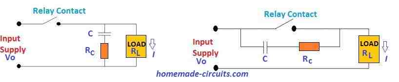 C.C Bates developed a formula for calculating the resistance and capacitance value that is required for the RC network: C = I2 /10, and Rc= Vo /[10I{1+(50/Vo)}]
The voltage induced at the contact opening can be determined by
V=IRc= (Rc/RL) Vo
Where VO = Voltage source
I = Load current at contact opening
RC = Resistance of RC Snubber
C = Capacitance of RC Snubber
RL = Load Resistance
In our following examples we talk about the reed relay arcing issues, and try to evaluate the calculations required for designing RC networks across its contacts.
Since the principle of arcing may be the same in bigger relays also, the formulas used in reed relay could be also applied for dimensioning the RC networks for the bigger relays.
C.C Bates developed a formula for calculating the resistance and capacitance value that is required for the RC network: C = I2 /10, and Rc= Vo /[10I{1+(50/Vo)}]
The voltage induced at the contact opening can be determined by
V=IRc= (Rc/RL) Vo
Where VO = Voltage source
I = Load current at contact opening
RC = Resistance of RC Snubber
C = Capacitance of RC Snubber
RL = Load Resistance
In our following examples we talk about the reed relay arcing issues, and try to evaluate the calculations required for designing RC networks across its contacts.
Since the principle of arcing may be the same in bigger relays also, the formulas used in reed relay could be also applied for dimensioning the RC networks for the bigger relays.
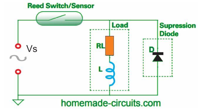 The MOV and TVS diodes conduct current when a threshold voltage is surpassed.
Normally, these diodes are parallelly connected to the switch contact.
Even at low voltages like 24 VAC, these devices are capable of working efficiently.
Moreover, they can also function well at higher inductance 120 VAC loads.
Compared to TVS diodes, MOV devices have added capacitance.
Thus, when an MOV device is utilized, you must consider the capacitance to be used.
The Hamlin application note describes this scenario better.
The MOV and TVS diodes conduct current when a threshold voltage is surpassed.
Normally, these diodes are parallelly connected to the switch contact.
Even at low voltages like 24 VAC, these devices are capable of working efficiently.
Moreover, they can also function well at higher inductance 120 VAC loads.
Compared to TVS diodes, MOV devices have added capacitance.
Thus, when an MOV device is utilized, you must consider the capacitance to be used.
The Hamlin application note describes this scenario better.
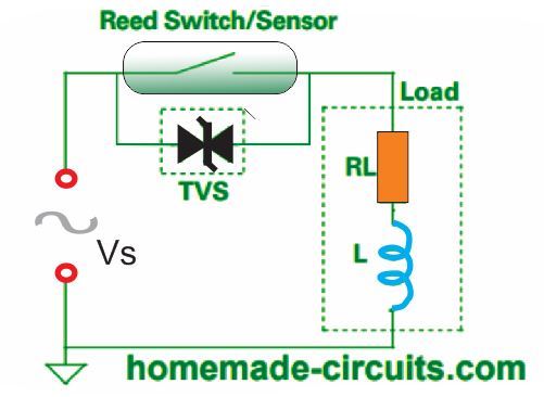 RC suppression had the edge because of limiting the switch contact voltage exactly during switch opening when the contact gap is small.
Furthermore, RC suppression can be implemented to lessen arcing and improve life in resistive loads.
On an RC suppression circuit, a capacitor and resistor network connected in series is mounted across the switch contact in a parallel connection.
Another option is to place the capacitor and resistor across the load.
While attaching the RC snubber across the switch contact is ideal, there is a huge disadvantage because this creates a current path to the load when the switch is open.
If the snubber is installed across the load, it eliminates the current.
However, changes in the connections and source impedance can affect the efficiency of the arc suppression.
RC suppression had the edge because of limiting the switch contact voltage exactly during switch opening when the contact gap is small.
Furthermore, RC suppression can be implemented to lessen arcing and improve life in resistive loads.
On an RC suppression circuit, a capacitor and resistor network connected in series is mounted across the switch contact in a parallel connection.
Another option is to place the capacitor and resistor across the load.
While attaching the RC snubber across the switch contact is ideal, there is a huge disadvantage because this creates a current path to the load when the switch is open.
If the snubber is installed across the load, it eliminates the current.
However, changes in the connections and source impedance can affect the efficiency of the arc suppression.
 In the snubber, the values of the resistor and the capacitor are dependent on the requirement.
The chosen resistor must have a value high enough to restrict the capacitive discharge current when the contacts of the switch close.
At the same time, it must be small enough to restrict the voltage when the switch contacts open.
If you choose a large capacitor value, it will surely decrease the voltage impact while the switch contacts opens.
But larger capacitor can be expensive and might cause higher capacitive discharge energy during the time the contacts of the switch close.
This type applies to both DC and AC circuits.
In the snubber, the values of the resistor and the capacitor are dependent on the requirement.
The chosen resistor must have a value high enough to restrict the capacitive discharge current when the contacts of the switch close.
At the same time, it must be small enough to restrict the voltage when the switch contacts open.
If you choose a large capacitor value, it will surely decrease the voltage impact while the switch contacts opens.
But larger capacitor can be expensive and might cause higher capacitive discharge energy during the time the contacts of the switch close.
This type applies to both DC and AC circuits.
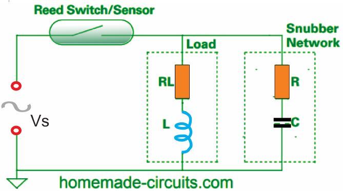 Ohm��s law is applied to choose the most appropriate resistor value for the arc suppression.
In the Ohm's law R = V/I, we apply the formula R = 0.5 (Vpk/ ISW) and R = 0.3 (Vpk/ ISW), where Vpk is the AC peak voltage (1.414 Vrms) and ISW is the rated switching current of the relay contact).
To decrease the contact degradation due to arcing, we have to make sure the R value is minimum.
On the other hand, the R value must be increased to lessen the relay contact arcing due to the inrush current.
Determining the value of R in between these scenarios is the challenge.
You can begin with C = 0.1��F or 100 nF, when selecting the capacitor because this is standard value and thus cost-friendly.
Depending on the performance examination of this capacitor, you can increase it until the capacitance is sufficient.
There are multiple methods to assess the performance of the chosen snubber values.
Some can be performed just by calculation or simulation.
However, the resistive and inductive features of the load may appear indefinite.
This is largely caused by the inductance of electromechanical loads that fluctuates when the components change positions.
It is a good practice to examine the voltage waveform across the switch contacts via an oscilloscope especially during contact opening.
The snubber system should alleviate or at least minimize the arcing that happens when the contacts open and close.
The increasing voltage should not restart contact arcing.
Furthermore, the maximum voltage across the capacitor in the snubber must not be more than it��s voltage rating.
Yet another way to find out if the snubber is working properly for a reed switch is to look at the switch contact gap and inspect the radiance of the light produced by the arc.
If there��s less light, that means the energy generating the arc is little and therefore warrants longer life.
The final and most precise method of examining the snubber��s performance is to conduct a life test.
Contact life is directly proportional to the number of switching cycles and not to the number of powered and unpowered hours.
It is advised to keep the maximum number of operations per second for life testing of arcing loads is around 5 to 50 operations per second.
This is around 5 to 50 Hz of maximum frequency.
The number of tests you can carry out is reliant on the electrical load and the difference between convenience and precision.
When you need to find out the specifications of the components for the snubber, you must consider a few other things also apart from the described inspection of arc evaluation, highest capacitor voltage and life.
It is fundamental that when a switch contact is opened, current flows through the snubber circuit.
You must ensure that this current does not cause trouble to the snubber��s application.
Moreover, it is essential to confirm that the power dissipation in the snubber��s resistor does not surpass its power rating.
One more thought is that an RC snubber circuit can be utilized in combination with a bidirectional TVS diode of MOV.
An RC snubber can be a highly efficient circuitry in limiting the initial voltage across the opening relay contacts, while the TVS or MOV may be a more efficient alternative for restricting peak surge voltages.
References:
https://www.homemade-circuits.com/wp-content/uploads/2020/10/RC-snubber.pdf
https://www.homemade-circuits.com/wp-content/uploads/2020/10/spark_suppression_compressed.pdf
https://m.littelfuse.com/~/media/electronics/application_notes/reed_switches/littelfuse_magnetic_sensors_and_reed_switches_inductive_load_arc_suppression_application_note.pdf.pdf
Ohm��s law is applied to choose the most appropriate resistor value for the arc suppression.
In the Ohm's law R = V/I, we apply the formula R = 0.5 (Vpk/ ISW) and R = 0.3 (Vpk/ ISW), where Vpk is the AC peak voltage (1.414 Vrms) and ISW is the rated switching current of the relay contact).
To decrease the contact degradation due to arcing, we have to make sure the R value is minimum.
On the other hand, the R value must be increased to lessen the relay contact arcing due to the inrush current.
Determining the value of R in between these scenarios is the challenge.
You can begin with C = 0.1��F or 100 nF, when selecting the capacitor because this is standard value and thus cost-friendly.
Depending on the performance examination of this capacitor, you can increase it until the capacitance is sufficient.
There are multiple methods to assess the performance of the chosen snubber values.
Some can be performed just by calculation or simulation.
However, the resistive and inductive features of the load may appear indefinite.
This is largely caused by the inductance of electromechanical loads that fluctuates when the components change positions.
It is a good practice to examine the voltage waveform across the switch contacts via an oscilloscope especially during contact opening.
The snubber system should alleviate or at least minimize the arcing that happens when the contacts open and close.
The increasing voltage should not restart contact arcing.
Furthermore, the maximum voltage across the capacitor in the snubber must not be more than it��s voltage rating.
Yet another way to find out if the snubber is working properly for a reed switch is to look at the switch contact gap and inspect the radiance of the light produced by the arc.
If there��s less light, that means the energy generating the arc is little and therefore warrants longer life.
The final and most precise method of examining the snubber��s performance is to conduct a life test.
Contact life is directly proportional to the number of switching cycles and not to the number of powered and unpowered hours.
It is advised to keep the maximum number of operations per second for life testing of arcing loads is around 5 to 50 operations per second.
This is around 5 to 50 Hz of maximum frequency.
The number of tests you can carry out is reliant on the electrical load and the difference between convenience and precision.
When you need to find out the specifications of the components for the snubber, you must consider a few other things also apart from the described inspection of arc evaluation, highest capacitor voltage and life.
It is fundamental that when a switch contact is opened, current flows through the snubber circuit.
You must ensure that this current does not cause trouble to the snubber��s application.
Moreover, it is essential to confirm that the power dissipation in the snubber��s resistor does not surpass its power rating.
One more thought is that an RC snubber circuit can be utilized in combination with a bidirectional TVS diode of MOV.
An RC snubber can be a highly efficient circuitry in limiting the initial voltage across the opening relay contacts, while the TVS or MOV may be a more efficient alternative for restricting peak surge voltages.
References:
https://www.homemade-circuits.com/wp-content/uploads/2020/10/RC-snubber.pdf
https://www.homemade-circuits.com/wp-content/uploads/2020/10/spark_suppression_compressed.pdf
https://m.littelfuse.com/~/media/electronics/application_notes/reed_switches/littelfuse_magnetic_sensors_and_reed_switches_inductive_load_arc_suppression_application_note.pdf.pdf
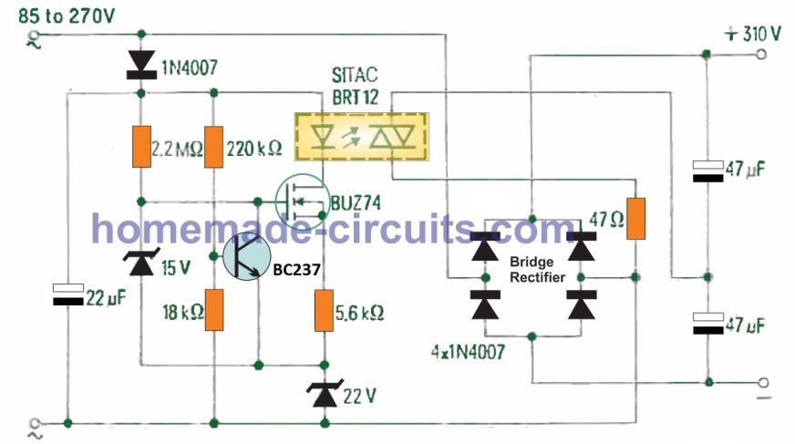
 The above shown simple rectifier voltage doubler enables converting your 110V AC to 220 V DC at low current so that you can operate electrical appliances like heaters, soldering iron, electric shavers, mobile chargers etc through this circuit.
Because the output voltage is 220V dc the particular circuit can be only employed to operate little ac/dc motor or heater based equipment, or mobile chargers.
It should not be utilized, for instance, to operate electronic items like radio sets, TV sets except if these are specifically ac/dc operated types.
The above shown simple rectifier voltage doubler enables converting your 110V AC to 220 V DC at low current so that you can operate electrical appliances like heaters, soldering iron, electric shavers, mobile chargers etc through this circuit.
Because the output voltage is 220V dc the particular circuit can be only employed to operate little ac/dc motor or heater based equipment, or mobile chargers.
It should not be utilized, for instance, to operate electronic items like radio sets, TV sets except if these are specifically ac/dc operated types.
 In case the inert gas happens to be neon, the illumination is orange in color.
For Argon gas which is not very common, the emitted light is blue.
In case the inert gas happens to be neon, the illumination is orange in color.
For Argon gas which is not very common, the emitted light is blue.
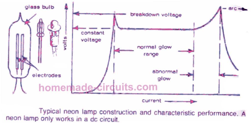 The voltage level which triggers the glowing effect in the neon bulb is termed as the initial breakdown voltage.
As soon as this breakdown level is struck, the bulb is triggered into "firing" (glowing) mode, and the voltage drop across the neon terminals stays practically fixed irrespective of any kind of increase in current in the circuit.
In addition, the glowing section inside the bulb increases as the supply current is increased, until a point in which the total area of the negative electrode is filled by the glow.
Any additional escalation in current may then drive the neon into an arcing situation, in which the glow illumination turns into a blue-white colored light over the negative electrode and begins producing rapid degradation of the lamp.
Hence, for you to illuminate a neon lamp efficiently, you must have sufficient voltage for the lamp to "fire," and, and then, ample series resistance in the circuit to be able to restrict the current to a level that will guarantee that the lamp stays running within the typical glowing section.
Since the neon resistance by itself is extremely small soon after it is fired, it needs a series resistor wit one of it supply lines, called a ballast resistor.
The voltage level which triggers the glowing effect in the neon bulb is termed as the initial breakdown voltage.
As soon as this breakdown level is struck, the bulb is triggered into "firing" (glowing) mode, and the voltage drop across the neon terminals stays practically fixed irrespective of any kind of increase in current in the circuit.
In addition, the glowing section inside the bulb increases as the supply current is increased, until a point in which the total area of the negative electrode is filled by the glow.
Any additional escalation in current may then drive the neon into an arcing situation, in which the glow illumination turns into a blue-white colored light over the negative electrode and begins producing rapid degradation of the lamp.
Hence, for you to illuminate a neon lamp efficiently, you must have sufficient voltage for the lamp to "fire," and, and then, ample series resistance in the circuit to be able to restrict the current to a level that will guarantee that the lamp stays running within the typical glowing section.
Since the neon resistance by itself is extremely small soon after it is fired, it needs a series resistor wit one of it supply lines, called a ballast resistor.
 This resistor value would be safe with the majority of commercial neon lamps.
When the neon glow is not quite dazzling, the ballast resistor value could be reduced to drive the lamp higher across the typical glow range.
That said, the resistance must in no way be lowered too much which may cause the whole negative electrode to be engulfed by the hot glow, because this may indicate that the lamp is now inundated and getting close to the arcing mode.
One more issue regarding the power of the neon glow is that it may typically look a lot shiny in ambient light compared to in darkness.
Actually, in total darkness the illumination could be inconsistent and/or call for an increased breakdown voltage to initiate the lamp.
Some neons possess a tiny hint of radioactive gas mixed with the inert gas to promote ionization, in that case this kind of effect may not be visible.
This resistor value would be safe with the majority of commercial neon lamps.
When the neon glow is not quite dazzling, the ballast resistor value could be reduced to drive the lamp higher across the typical glow range.
That said, the resistance must in no way be lowered too much which may cause the whole negative electrode to be engulfed by the hot glow, because this may indicate that the lamp is now inundated and getting close to the arcing mode.
One more issue regarding the power of the neon glow is that it may typically look a lot shiny in ambient light compared to in darkness.
Actually, in total darkness the illumination could be inconsistent and/or call for an increased breakdown voltage to initiate the lamp.
Some neons possess a tiny hint of radioactive gas mixed with the inert gas to promote ionization, in that case this kind of effect may not be visible.
 Therefore, in the circuit displayed above, the output extracted from each side of the lamp might work like an origin of constant voltage, provided that the neon continues to work within the typical glowing region.
This voltage would be then identical to the minimal breakdown voltage of the lamp.
Therefore, in the circuit displayed above, the output extracted from each side of the lamp might work like an origin of constant voltage, provided that the neon continues to work within the typical glowing region.
This voltage would be then identical to the minimal breakdown voltage of the lamp.
 This includes a resistor (R) and capacitor (C) attached in series to a supply voltage of a dc voltage.
A neon lamp is attached in parallel with the capacitor.
This neon is applied as a visual indicator to show the functioning of the circuit.
The lamp almost performs like an open circuit until its firing voltage is reached, when it instantly switches current through it quite like a low value resistor and begins glowing.
The voltage supply for this current source therefore needs to be higher than that of the neon's breakdown voltage.
When this circuit is powered, the capacitor begins accumulating a charge with a rate determined by the resistor/capacitor RC time constant.
The neon bulb gets a voltage supply equivalent to the charge developed across the capacitor terminals.
As soon as this voltage reaches the breakdown voltage of the lamp, it switches on and forces the capacitor to discharge via the gas inside the neon bulb, resulting in the neon to glow.
When the capacitor discharges fully, it inhibits any further current to pass through the lamp and thus it shuts down again until the capacitor has gathered another level charge equal to the firing voltage of the neon, and the cycle now keeps repeating.
Put simply, the neon lamp now keeps flashing or blinking at a frequency as decided by the values of the time constant components R and C.
This includes a resistor (R) and capacitor (C) attached in series to a supply voltage of a dc voltage.
A neon lamp is attached in parallel with the capacitor.
This neon is applied as a visual indicator to show the functioning of the circuit.
The lamp almost performs like an open circuit until its firing voltage is reached, when it instantly switches current through it quite like a low value resistor and begins glowing.
The voltage supply for this current source therefore needs to be higher than that of the neon's breakdown voltage.
When this circuit is powered, the capacitor begins accumulating a charge with a rate determined by the resistor/capacitor RC time constant.
The neon bulb gets a voltage supply equivalent to the charge developed across the capacitor terminals.
As soon as this voltage reaches the breakdown voltage of the lamp, it switches on and forces the capacitor to discharge via the gas inside the neon bulb, resulting in the neon to glow.
When the capacitor discharges fully, it inhibits any further current to pass through the lamp and thus it shuts down again until the capacitor has gathered another level charge equal to the firing voltage of the neon, and the cycle now keeps repeating.
Put simply, the neon lamp now keeps flashing or blinking at a frequency as decided by the values of the time constant components R and C.
 A modification in this design is indicated in the above diagram, by using a 1 megohm potentiometer working like a ballast resistor and a couple of 45 volt or four 22.5 volt dry batteries as the voltage input source.
The potentiometer is fine-tuned until the lamp illuminates.
The pot is then rotated in the opposite direction until the neon glow merely fades out.
Allowing the potentiometer to be in this position, the neon must then begin blinking at different flashing rates as determined by the value of the selected capacitor.
Considering the values of the R and C in the diagram, the time constant for the circuit may be evaluated as follows:
T = 5 (megohms) x 0.1 (microfarads) = 0.5 seconds.
This is not specifically the true flashing rate of the neon lamp.
It might require a period of several time constant (or fewer) for the capacitor voltage to accumulate upto the neon firing voltage.
This may be higher in case the turn-on voltage is over 63 % of the supply voltage; and may be smaller if the neon firing voltage spec is lower than 63 % of the supply voltage.
Additionally, it signifies that the blinking rate could be modified by changing the R or C component values, possibly by replacing various values worked out to provide an alternative time constant; or using a parallel attached resistor or capacitor.
Hooking up an identical resistor parallel with R, for instance, would likely make the flashing rate two times more (since adding similar resistors in parallel causes the total resistance to be reduced to half).
Attaching an identical value capacitor in parallel with the existing C would likely cause the flashing rate to become 50% slower.
This type of circuit is referred to as a relaxation oscillator.
A modification in this design is indicated in the above diagram, by using a 1 megohm potentiometer working like a ballast resistor and a couple of 45 volt or four 22.5 volt dry batteries as the voltage input source.
The potentiometer is fine-tuned until the lamp illuminates.
The pot is then rotated in the opposite direction until the neon glow merely fades out.
Allowing the potentiometer to be in this position, the neon must then begin blinking at different flashing rates as determined by the value of the selected capacitor.
Considering the values of the R and C in the diagram, the time constant for the circuit may be evaluated as follows:
T = 5 (megohms) x 0.1 (microfarads) = 0.5 seconds.
This is not specifically the true flashing rate of the neon lamp.
It might require a period of several time constant (or fewer) for the capacitor voltage to accumulate upto the neon firing voltage.
This may be higher in case the turn-on voltage is over 63 % of the supply voltage; and may be smaller if the neon firing voltage spec is lower than 63 % of the supply voltage.
Additionally, it signifies that the blinking rate could be modified by changing the R or C component values, possibly by replacing various values worked out to provide an alternative time constant; or using a parallel attached resistor or capacitor.
Hooking up an identical resistor parallel with R, for instance, would likely make the flashing rate two times more (since adding similar resistors in parallel causes the total resistance to be reduced to half).
Attaching an identical value capacitor in parallel with the existing C would likely cause the flashing rate to become 50% slower.
This type of circuit is referred to as a relaxation oscillator.
 Each of these RC network will enable a unique time constant.
This may generate a random flashing of the neon across the entire circuit.
Each of these RC network will enable a unique time constant.
This may generate a random flashing of the neon across the entire circuit.
 This can be a genuine signal generator circuit, whose output could be listened through headphones or perhaps a small loudspeaker, by suitably adjusting the variable tone potentiometer.
Neon flashers could be designed to function with random manner or sequentially.
A sequential flasher circuit is displayed in Fig.
10-6.
This can be a genuine signal generator circuit, whose output could be listened through headphones or perhaps a small loudspeaker, by suitably adjusting the variable tone potentiometer.
Neon flashers could be designed to function with random manner or sequentially.
A sequential flasher circuit is displayed in Fig.
10-6.
 Additional stages could be included in this circuit, if required, by using the C3 connection to the very last stage.
 These neons will blink or flash on/off in sequence at a frequency decided by R1 and R2 (whose values must be identical) and C1.
As a basic instructions on flasher timing, increasing the ballast resistor value or the capacitor value in the relaxation oscillator circuit can reduce the flashing rate or the flashing frequency; and vice versa.
However, in order to protect the working life of a typical neon lamp, the ballast resistor value utilized must not be lower than approximately 100 k; and finest results in very simple relaxation oscillator circuits may often be accomplished by maintaining the capacitor value under 1 microfarad.
These neons will blink or flash on/off in sequence at a frequency decided by R1 and R2 (whose values must be identical) and C1.
As a basic instructions on flasher timing, increasing the ballast resistor value or the capacitor value in the relaxation oscillator circuit can reduce the flashing rate or the flashing frequency; and vice versa.
However, in order to protect the working life of a typical neon lamp, the ballast resistor value utilized must not be lower than approximately 100 k; and finest results in very simple relaxation oscillator circuits may often be accomplished by maintaining the capacitor value under 1 microfarad.
 At any moment, a single (or sometimes a couple of) lamps tend to be illuminated allowing the capacitors their charging routes.
When the capacitors charge, this exceeds the firing threshold for another neon, forcing it trigger ON.
Due to a commutation impact, some lamp in the lit up mode subsequently turn off some other lamp which are previously lit up.
These RC and neon networks are basically relaxation oscillators.
For these oscillators to work, the resistors and supply voltage all need to be selected to sit around the negative resistance portion of the NE-2 neon curve.
This often takes place within a somewhat large value range.
Some further experimentation might be required for something additionally extravagant.
Resistors having the value in the range of one to four megohm can be generally a good place to start.
Precisely what is amazing is the fact that I still have no idea how to implement this kind of illumination pattern using LEDs which could turn out to be distantly as easy, as inexpensive, or as low in energy consumption.
At any moment, a single (or sometimes a couple of) lamps tend to be illuminated allowing the capacitors their charging routes.
When the capacitors charge, this exceeds the firing threshold for another neon, forcing it trigger ON.
Due to a commutation impact, some lamp in the lit up mode subsequently turn off some other lamp which are previously lit up.
These RC and neon networks are basically relaxation oscillators.
For these oscillators to work, the resistors and supply voltage all need to be selected to sit around the negative resistance portion of the NE-2 neon curve.
This often takes place within a somewhat large value range.
Some further experimentation might be required for something additionally extravagant.
Resistors having the value in the range of one to four megohm can be generally a good place to start.
Precisely what is amazing is the fact that I still have no idea how to implement this kind of illumination pattern using LEDs which could turn out to be distantly as easy, as inexpensive, or as low in energy consumption.
 PIEZO TRANSDUCER
Components overlay and the PCB track layout can be seen in the following image.
PIEZO TRANSDUCER
Components overlay and the PCB track layout can be seen in the following image.
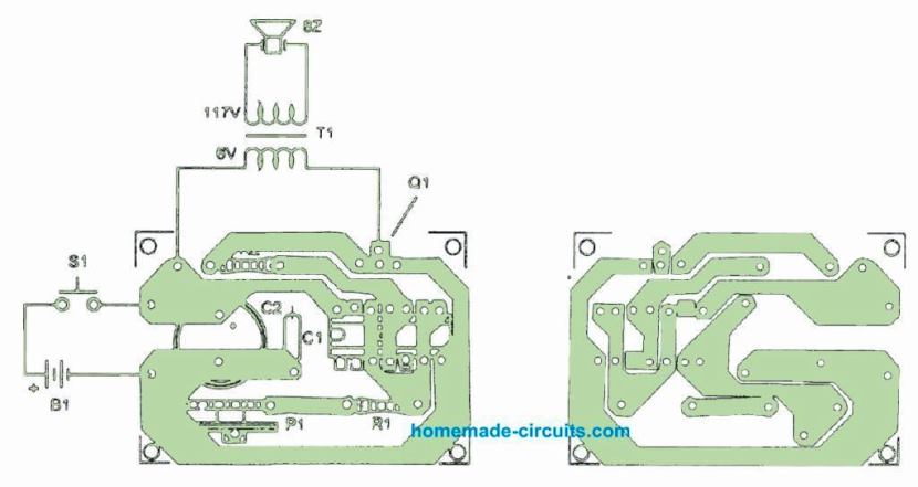 The entire circuit could be encased inside a compact plastic material container.
The transducer or the piezo element may be installed on the front board.
Be careful with the placement of the parts that carry polarity, for example the transistor, electrolytic capacitor and power supply input.
If the unit is intended to be operated continuously, make sure Q1 is mounted on a proper heatsink.
The transformer specs is not an important factor.
Any transformer having a secondary coil ranging from 100 to 500 mA could be used in this ultrasonic pest repeller project.
The entire circuit could be encased inside a compact plastic material container.
The transducer or the piezo element may be installed on the front board.
Be careful with the placement of the parts that carry polarity, for example the transistor, electrolytic capacitor and power supply input.
If the unit is intended to be operated continuously, make sure Q1 is mounted on a proper heatsink.
The transformer specs is not an important factor.
Any transformer having a secondary coil ranging from 100 to 500 mA could be used in this ultrasonic pest repeller project.
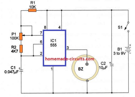 The circuit could be driven by 9V battery packs which may run for a long period of time due to its minimal current consumption.
The center of the circuit is the 7555 lC, a CMOS timer configured as an sound oscillator which operates a piezoelectric transducer.
The parts positioning on a do-it-yourself PCB is revealed in the below given Figure.
The circuit could be driven by 9V battery packs which may run for a long period of time due to its minimal current consumption.
The center of the circuit is the 7555 lC, a CMOS timer configured as an sound oscillator which operates a piezoelectric transducer.
The parts positioning on a do-it-yourself PCB is revealed in the below given Figure.
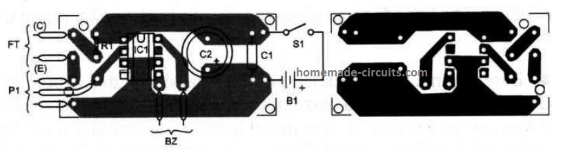 Precise location may not be too critical.
Each of the parts and the power supply could be enclosed in a compact plastic-type container.
Transducer BZ can be a crystal earpiece or a piezoelectric transducer.
Location of the polarized items, like c2 and the power supply, should be cautiously wired.
Applying the insect repellent can be quite simple.
You have to fine-tune he trimmer potentiometer P1 to generate a noise having the identical throw, matching the insect's range you would like to repel.
Trial and error has to be done before you uncover the ideal frequency to repel a certain insect.
Parts List
Precise location may not be too critical.
Each of the parts and the power supply could be enclosed in a compact plastic-type container.
Transducer BZ can be a crystal earpiece or a piezoelectric transducer.
Location of the polarized items, like c2 and the power supply, should be cautiously wired.
Applying the insect repellent can be quite simple.
You have to fine-tune he trimmer potentiometer P1 to generate a noise having the identical throw, matching the insect's range you would like to repel.
Trial and error has to be done before you uncover the ideal frequency to repel a certain insect.
Parts List
 IC 4033 Pinout Details
 Video Clip: The working proof of the above whistle sensor can be seen in the video which was also contributed by Mr.
Pradeep Bajpai.
Video Clip: The working proof of the above whistle sensor can be seen in the video which was also contributed by Mr.
Pradeep Bajpai.

 Parts List
All SCRs = C106 or BT151
All small triacs = BT136
All large triacs = BTA41/600
All SCR gate Diodes = 1N4007
All Bridge Rectifier Diodes = 1N4007
Parts List
All SCRs = C106 or BT151
All small triacs = BT136
All large triacs = BTA41/600
All SCR gate Diodes = 1N4007
All Bridge Rectifier Diodes = 1N4007
 The green base background is actually a PCB, with copper tracks etched on it, shown in orange.
The PCB is elliptical in shape with a large central cut out, and a couple of horizontal ribs to enforce better rigidity to the PCB frame.
The grey lines are tinned copper wires, around 0.5mm in thickness, tightly stretched and soldered end to end across the indicated copper tracks.
The wires are alternately arranged and connected with the respective power line tracks, on either side of the layout.
The wires are also soldered in between across the two central ribs to reinforce them with increased rigidity and firmness.
The green base background is actually a PCB, with copper tracks etched on it, shown in orange.
The PCB is elliptical in shape with a large central cut out, and a couple of horizontal ribs to enforce better rigidity to the PCB frame.
The grey lines are tinned copper wires, around 0.5mm in thickness, tightly stretched and soldered end to end across the indicated copper tracks.
The wires are alternately arranged and connected with the respective power line tracks, on either side of the layout.
The wires are also soldered in between across the two central ribs to reinforce them with increased rigidity and firmness.
 From the images above we can identify the following connection and wiring details:
The handle upper and lower assemblies preferably needs to be a push-fit type, with corresponding male/female AC pins, such that when the two sections are push-locked, the pins also get plugged in with each other.
The lower section of the handle can be seen enclosed with a 10uF/400V capacitor (Non-polar), whose terminals are electrically wired with the external plug pins.
This section of the handle plays a twin role, first it allows detachment from the bat and plugging into your home mains socket for a 1 second quick charging, and next, the same plug pins are allowed to be inserted back into the upper bat section for arming the bat mesh net.
From the images above we can identify the following connection and wiring details:
The handle upper and lower assemblies preferably needs to be a push-fit type, with corresponding male/female AC pins, such that when the two sections are push-locked, the pins also get plugged in with each other.
The lower section of the handle can be seen enclosed with a 10uF/400V capacitor (Non-polar), whose terminals are electrically wired with the external plug pins.
This section of the handle plays a twin role, first it allows detachment from the bat and plugging into your home mains socket for a 1 second quick charging, and next, the same plug pins are allowed to be inserted back into the upper bat section for arming the bat mesh net.
 The following figure shows how the lower handle section needs to be detached and plugged to an AC socket for charging the internal 10uF capacitor, (for a 1 second charging).


 In the image above we can clearly see all the items discussed above, the functioning of the entire system can be learned from the following explanation:
 From the above explanation you might have got a clear idea regarding how a crank flashlight works using the recommended parts and a motor in the form of a generator, if you have any further doubts, please do use the comment box for expressing your valuable thoughts.
In one of the upcoming articles we will learn how to use a crank flashlight as an ever-ready 24x7 power bank circuit for your smart phones.
From the above explanation you might have got a clear idea regarding how a crank flashlight works using the recommended parts and a motor in the form of a generator, if you have any further doubts, please do use the comment box for expressing your valuable thoughts.
In one of the upcoming articles we will learn how to use a crank flashlight as an ever-ready 24x7 power bank circuit for your smart phones.

 The diagram looks pretty straightforward, and you just need to connect the parts as displayed in the diagram, using a well designed PCB.
The 10K pot serves as the speed control knob for the ceiling fan.
The diagram looks pretty straightforward, and you just need to connect the parts as displayed in the diagram, using a well designed PCB.
The 10K pot serves as the speed control knob for the ceiling fan.
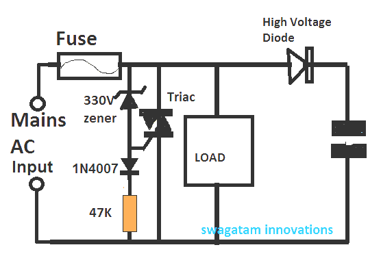 Referring to the above simple surge protection circuit, the triac along with the zener diode and the 47K resistor forms a simple crowbar circuit stage.
The value of the zener diode decides at what input surge level the triacs needs to fire.
Here it is shown as 330V which means, in this design the triac is supposed to fire and conduct when the input mains level exceeds the 330V limit, other values can be selected for other surge levels as preferred by the user.
In a situation where the selected zener limit is exceeded by the input mains, the triac is instantly triggered causing an instant short circuit across the mains line by the triac, which causes the fuse to blow of.
The above procedure makes sure that whenever a high voltage surge appears within the mains line, the fuse is blown of in order to prevent the surge from reaching the load and damaging it.
This takes care of the surge aresstor or controller design, now let's learn how this surge level may be recorded for knowing the exact measure of this surge.
Referring to the above simple surge protection circuit, the triac along with the zener diode and the 47K resistor forms a simple crowbar circuit stage.
The value of the zener diode decides at what input surge level the triacs needs to fire.
Here it is shown as 330V which means, in this design the triac is supposed to fire and conduct when the input mains level exceeds the 330V limit, other values can be selected for other surge levels as preferred by the user.
In a situation where the selected zener limit is exceeded by the input mains, the triac is instantly triggered causing an instant short circuit across the mains line by the triac, which causes the fuse to blow of.
The above procedure makes sure that whenever a high voltage surge appears within the mains line, the fuse is blown of in order to prevent the surge from reaching the load and damaging it.
This takes care of the surge aresstor or controller design, now let's learn how this surge level may be recorded for knowing the exact measure of this surge.

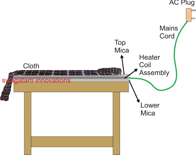 Here we see a flat platform which has series of heating coil spread across the whole area of the table.
Instead of hanging the clothes, these are spread flat over this table or platform for initiating the drying process.
For the heating coils, we simply use 4 nos of iron coils in series each rated at 1000 watts, and we further add 4 such series assemblies in parallel to make an overall 1000 watt rated series/ parallel heater coil configuration, as shown below:
Here we see a flat platform which has series of heating coil spread across the whole area of the table.
Instead of hanging the clothes, these are spread flat over this table or platform for initiating the drying process.
For the heating coils, we simply use 4 nos of iron coils in series each rated at 1000 watts, and we further add 4 such series assemblies in parallel to make an overall 1000 watt rated series/ parallel heater coil configuration, as shown below:

 For making a homemade cloth dryer circuit, we can install the above shown heater coil assembly over a wooden table having a mica sheet covered on its surface.
The Mica sheet should be thick enough and cover the entire area of the coil assembly so that the coils remain perfectly isolated from the wooden table.
On top of this coil we place another similar mica sheet.
But here we make sure that the sheet is punched with holes so that heat is able to dissipate from these holes and enforce the drying process for the clothes which are supposed to be laid down on top of this mica sheet.
Preferably these holes must be smaller in diameter but larger in quantity to ensure proper isolation of the cloth from the heater coil yet maximum exposure to the emanating heat from the coil assembly.
The arrangement may be examined with the following figure:
For making a homemade cloth dryer circuit, we can install the above shown heater coil assembly over a wooden table having a mica sheet covered on its surface.
The Mica sheet should be thick enough and cover the entire area of the coil assembly so that the coils remain perfectly isolated from the wooden table.
On top of this coil we place another similar mica sheet.
But here we make sure that the sheet is punched with holes so that heat is able to dissipate from these holes and enforce the drying process for the clothes which are supposed to be laid down on top of this mica sheet.
Preferably these holes must be smaller in diameter but larger in quantity to ensure proper isolation of the cloth from the heater coil yet maximum exposure to the emanating heat from the coil assembly.
The arrangement may be examined with the following figure:

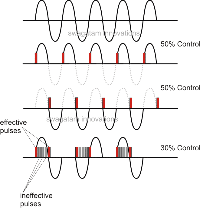 1) The first waveform in the above figure shows a normal 50Hz AC phase signal consisting of a sinusoidal rising and falling 330V peak positive, and negative pulses, with respect to the central zero line.
This central zero line is termed as the zero crossing line for the AC phase signals.
The triac can be expected to conduct the shown signal continuously if its gate DC trigger is continuous without breaks.
2) The second figure shows how a triac can be forced to conduct only during positive half cycles in response to its gate triggers (PWM shown in red) at every alternate positive zero crossings of the phase cycles.This results in a 50% phase control.
3) The third figure shows an identical response wherein the pulses are timed to produce alternately at every negative zero crossing of the AC phase, which also results in a 50% phase control for the triac and the load.
However producing such timed PWMs at different calculated zero crossing nodes can be difficult and complex, therefore an easy approach for acquiring any desired proportion of phase control is to employ timed pulse trains as shown in the 4rth figure above.
4) In this figure bursts of 4 PWMs can be seen after every alternate phase cycle which results in around 30% reduction in the triac operation and the same for the connected load.
It may be interesting to notice that here the middle 3nos of pulses are useless or ineffective pulses because after the first pulse the triac gets latched and therefore the middle 3 pulses have no effect on the triac, and the triac continues to conduct until the next zero crossing where it is triggered by the subsequent 5th (last) pulse enabling the triac to latch ON for the next negative cycle.
After this as soon as the following zero crossing is reached, the absence of any further PWM inhibits the triac from conducting and it's cut OFF, until the next pulse at the next zero crossing which simply repeats the process for the triac and its phase control operations.
In this way other time-proportional PWM pulse trains can be generated for the triac gate so that different measures of phase control can be implemented as per preference.
In one of our next articles we will learn about a practical circuit for achieving the above discussed triac phase control using time proportional PWM circuit
1) The first waveform in the above figure shows a normal 50Hz AC phase signal consisting of a sinusoidal rising and falling 330V peak positive, and negative pulses, with respect to the central zero line.
This central zero line is termed as the zero crossing line for the AC phase signals.
The triac can be expected to conduct the shown signal continuously if its gate DC trigger is continuous without breaks.
2) The second figure shows how a triac can be forced to conduct only during positive half cycles in response to its gate triggers (PWM shown in red) at every alternate positive zero crossings of the phase cycles.This results in a 50% phase control.
3) The third figure shows an identical response wherein the pulses are timed to produce alternately at every negative zero crossing of the AC phase, which also results in a 50% phase control for the triac and the load.
However producing such timed PWMs at different calculated zero crossing nodes can be difficult and complex, therefore an easy approach for acquiring any desired proportion of phase control is to employ timed pulse trains as shown in the 4rth figure above.
4) In this figure bursts of 4 PWMs can be seen after every alternate phase cycle which results in around 30% reduction in the triac operation and the same for the connected load.
It may be interesting to notice that here the middle 3nos of pulses are useless or ineffective pulses because after the first pulse the triac gets latched and therefore the middle 3 pulses have no effect on the triac, and the triac continues to conduct until the next zero crossing where it is triggered by the subsequent 5th (last) pulse enabling the triac to latch ON for the next negative cycle.
After this as soon as the following zero crossing is reached, the absence of any further PWM inhibits the triac from conducting and it's cut OFF, until the next pulse at the next zero crossing which simply repeats the process for the triac and its phase control operations.
In this way other time-proportional PWM pulse trains can be generated for the triac gate so that different measures of phase control can be implemented as per preference.
In one of our next articles we will learn about a practical circuit for achieving the above discussed triac phase control using time proportional PWM circuit

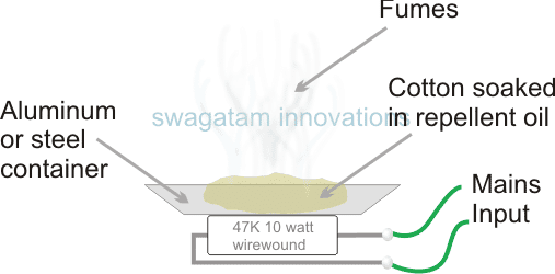 In the shown set up we can see a high watt resistor and an aluminum dish glues over the resistor.
The resistor leads are terminated into a mains 220V or 120V socket.
The aluminum dish is used for placing a piece of cotton wad drenched with lemon eucalyptus oil.
That's all, once this set up is built and plugged in, the high watt resistor could be seen heating up and enabling the aluminum dish to also heat up, causing the heat to evaporate the oil and its fragrance in the air.
This special fragrance which may not be harmful to humans but irritating for the mosquitoes would ultimately help to drive away the creatures away from our homes, naturally and without any health risks.
WARNING: THE SHOWN SET UP IS DEMONSTRATED IN AN UNCOVERED SITUATION AND THEREFORE IS EXTREMELY DANGEROUS TO TOUCH.
PRACTICALLY, IT MUST BE ENCLOSED INSIDE AN APPROPRIATE ELECTRICITY/HEAT PROOF CASE IN ORDER TO ENSURE SAFETY FROM LETHAL MAINS CURRENT.
In the shown set up we can see a high watt resistor and an aluminum dish glues over the resistor.
The resistor leads are terminated into a mains 220V or 120V socket.
The aluminum dish is used for placing a piece of cotton wad drenched with lemon eucalyptus oil.
That's all, once this set up is built and plugged in, the high watt resistor could be seen heating up and enabling the aluminum dish to also heat up, causing the heat to evaporate the oil and its fragrance in the air.
This special fragrance which may not be harmful to humans but irritating for the mosquitoes would ultimately help to drive away the creatures away from our homes, naturally and without any health risks.
WARNING: THE SHOWN SET UP IS DEMONSTRATED IN AN UNCOVERED SITUATION AND THEREFORE IS EXTREMELY DANGEROUS TO TOUCH.
PRACTICALLY, IT MUST BE ENCLOSED INSIDE AN APPROPRIATE ELECTRICITY/HEAT PROOF CASE IN ORDER TO ENSURE SAFETY FROM LETHAL MAINS CURRENT.
 WARNING: CIRCUIT IS NOT ISOLATED FROM MAINS...
STRICT PRECAUTIONS MUST BE OBSERVED WHILE HANDLING THE DEVICE, WHILE IT'S IN AN UNENCLOSED CONDITION.
WARNING: CIRCUIT IS NOT ISOLATED FROM MAINS...
STRICT PRECAUTIONS MUST BE OBSERVED WHILE HANDLING THE DEVICE, WHILE IT'S IN AN UNENCLOSED CONDITION.
 I would recommend buying this unit instead of building one, because these are quite cheap and are easily accessible through online electronic stores.
However if you are interested to make it, you could try it out by procuring the recommended chips for these remote controlled modules which are also available through all standard online electronic retailer.
If you purchase the units readymade, then it's just about configuring the relay contacts with the submersible start, and stop buttons, as shown below.
To be precise, it's the N/O and the pole of the relays which needs to be connected across the submersible buttons.
For identifying the relay contacts of the remote receiver unit one may take the help of one my earlier pasts which explained how to understand and use relays in circuits.
However since the contactor start stop buttons could be specified to work with high switching current, these may require special high current relay driver stages for the individual buttons.
Therefore the triggering supply from the remote receiver relays needs to be further integrated with the above mentioned high power relay driver stages as demonstrated in the following figure:
I would recommend buying this unit instead of building one, because these are quite cheap and are easily accessible through online electronic stores.
However if you are interested to make it, you could try it out by procuring the recommended chips for these remote controlled modules which are also available through all standard online electronic retailer.
If you purchase the units readymade, then it's just about configuring the relay contacts with the submersible start, and stop buttons, as shown below.
To be precise, it's the N/O and the pole of the relays which needs to be connected across the submersible buttons.
For identifying the relay contacts of the remote receiver unit one may take the help of one my earlier pasts which explained how to understand and use relays in circuits.
However since the contactor start stop buttons could be specified to work with high switching current, these may require special high current relay driver stages for the individual buttons.
Therefore the triggering supply from the remote receiver relays needs to be further integrated with the above mentioned high power relay driver stages as demonstrated in the following figure:
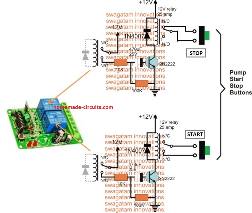 The relay driver stages shown at the right side of the diagram is made by configuring transistor relay drivers with the respective high power relays.
The bases of the transistors can be seen connected with series high value capacitors, this is to ensure that the relays remain activated only for a couple of seconds, regardless of the switching periods of the remote control module's relays, or regardless of how long the user keeps the remote transmitter handset button pressed.
The shown remote control receiver module consisting of the receiver circuitry and the two relays will need 12V supply from an appropriate DC source, such as a 12V AC DC adapter.
This 12V further needs to be configured with the relay contacts and the relay driver stages also, for enabling the intended remote controlled start/stop switching of the submersible ON/OFF buttons.
The relay driver stages shown at the right side of the diagram is made by configuring transistor relay drivers with the respective high power relays.
The bases of the transistors can be seen connected with series high value capacitors, this is to ensure that the relays remain activated only for a couple of seconds, regardless of the switching periods of the remote control module's relays, or regardless of how long the user keeps the remote transmitter handset button pressed.
The shown remote control receiver module consisting of the receiver circuitry and the two relays will need 12V supply from an appropriate DC source, such as a 12V AC DC adapter.
This 12V further needs to be configured with the relay contacts and the relay driver stages also, for enabling the intended remote controlled start/stop switching of the submersible ON/OFF buttons.
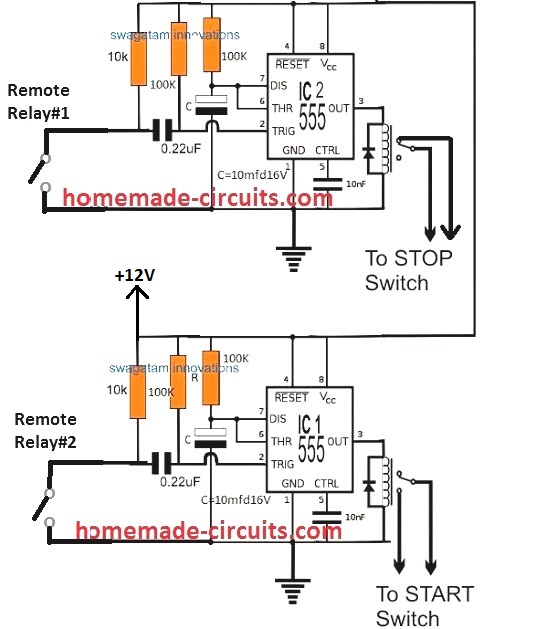
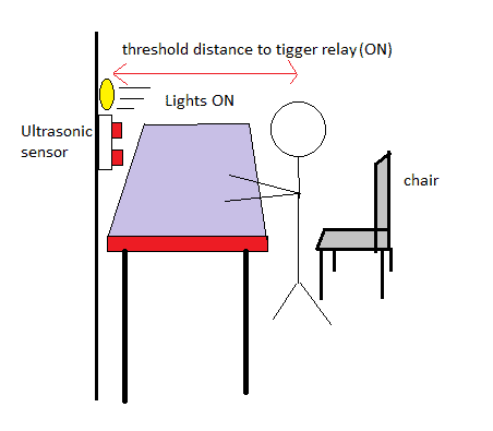 The above diagram illustrates the triggering of the relay in the presence of human, since Arduino detected the distance below the threshold value.
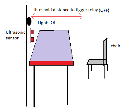 The above diagram illustrates that relay is held switched off in the absence of human, since the arduino continues to detect the distance above threshold value.
The program is written in such a way that it measures the distance between the sensor and obstacle in real time.
The users need to input the threshold value in centimeter before uploading to arduino.
The above diagram illustrates that relay is held switched off in the absence of human, since the arduino continues to detect the distance above threshold value.
The program is written in such a way that it measures the distance between the sensor and obstacle in real time.
The users need to input the threshold value in centimeter before uploading to arduino.
 The ultrasonic sensor can be directly inserted on analog pins from A0 to A3, sensors facing outward, this may reduce wire congestion while prototyping the circuit.
NOTE: #PIN 7 is the output to relay
The ultrasonic sensor can be directly inserted on analog pins from A0 to A3, sensors facing outward, this may reduce wire congestion while prototyping the circuit.
NOTE: #PIN 7 is the output to relay
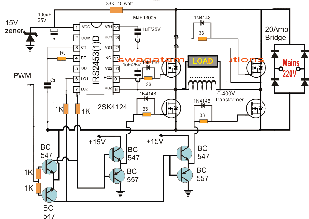 The circuit is functioning is quite similar to one of the earlier discussed posts regarding a solar inverter circuit for a 1.5 ton air conditioner.
However for implementing the intended automatic 100V to 220V stabilization we employ a couple of things here: 1) the 0-400V auto transformer boost coil and the self optimizing PWM circuit.
The above circuit utilizes a full bridge inverter topology using the IC IRS2453 and 4 N-channel mosfets.
The IC is equipped with its own in-built oscillator whose frequency is appropriately set by calculating the indicated Rt, Ct values.
This frequency becomes the recommended operating frequency of the inverter which could be 50Hz (for 220V input) or 60Hz (for 120V input) depending on the country utility specs.
The bus voltage is derived by rectifying the input mains voltage and is applied across the H-bridge mosfet network.
The primary load connected between the mosfets is a boost auto-transformer positioned for reacting with the switching mains DC voltage and for generating a proportionately boosted 400V across its terminals through back EMFs.
The circuit is functioning is quite similar to one of the earlier discussed posts regarding a solar inverter circuit for a 1.5 ton air conditioner.
However for implementing the intended automatic 100V to 220V stabilization we employ a couple of things here: 1) the 0-400V auto transformer boost coil and the self optimizing PWM circuit.
The above circuit utilizes a full bridge inverter topology using the IC IRS2453 and 4 N-channel mosfets.
The IC is equipped with its own in-built oscillator whose frequency is appropriately set by calculating the indicated Rt, Ct values.
This frequency becomes the recommended operating frequency of the inverter which could be 50Hz (for 220V input) or 60Hz (for 120V input) depending on the country utility specs.
The bus voltage is derived by rectifying the input mains voltage and is applied across the H-bridge mosfet network.
The primary load connected between the mosfets is a boost auto-transformer positioned for reacting with the switching mains DC voltage and for generating a proportionately boosted 400V across its terminals through back EMFs.
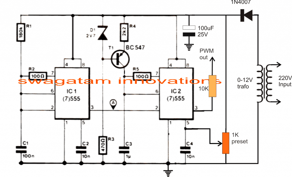 However with the introduction of a PWM feed for the low side mosfet this 400V from the coil can be controlled proportionately to any desired lower RMS value.
Thus at max PWM width we can expect the voltage to be 400V and at minimum width this could be optimized close to zero.
The PWM is configured using a couple of IC 555 for generating a varying PWM in response to the varying mains input, however this response is inverted first before feeding the low side mosfets, which implies that as the mains input drops, the PWMs become wider and vice versa.
To correctly set this response the 1K preset shown attached with pin#5 of the IC2 in the PWM circuit is adjusted such that the voltage across the auto-transformer coil is around 200V when the input is around 100V, at this point the PWM could be at the max width level and from here on the PWMs become narrower as the voltage increases, ensuring an almost constant output at around 220V.
Thus, if the mains input goes higher the PWM tries to pull it down by narrowing the pulses and vice versa.
However with the introduction of a PWM feed for the low side mosfet this 400V from the coil can be controlled proportionately to any desired lower RMS value.
Thus at max PWM width we can expect the voltage to be 400V and at minimum width this could be optimized close to zero.
The PWM is configured using a couple of IC 555 for generating a varying PWM in response to the varying mains input, however this response is inverted first before feeding the low side mosfets, which implies that as the mains input drops, the PWMs become wider and vice versa.
To correctly set this response the 1K preset shown attached with pin#5 of the IC2 in the PWM circuit is adjusted such that the voltage across the auto-transformer coil is around 200V when the input is around 100V, at this point the PWM could be at the max width level and from here on the PWMs become narrower as the voltage increases, ensuring an almost constant output at around 220V.
Thus, if the mains input goes higher the PWM tries to pull it down by narrowing the pulses and vice versa.
 The idea shown above is an ordinary capacitive power supply circuit incorporating extreme capacitors in terms of their values.

 Referring to the above simple water sensor circuit we can see how the automatic evaporative air cooler operation is implemented with the help of a simple opamp comparator circuit.
 Referring to the above shown smart automatic emergency light circuit, the IC 741 forms the battery level detector and the cut off stage.


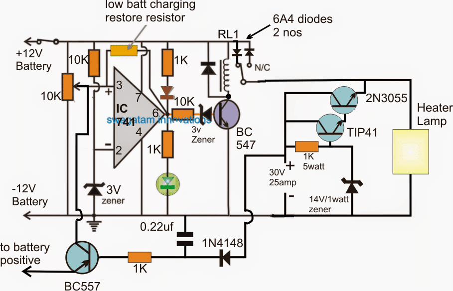
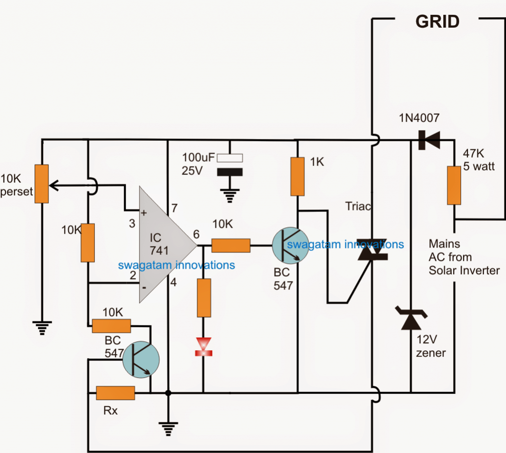

 In fact this circuit has particular method so it will work as an emergency mains line-status for example of two houses with two own generators.
Whenever either houses have electricity the other house will feed with this too with limited current and limited option.
So, If House No.
1 has a Generator powering by 8A max ...
->
Then B is house No.2 can take some little current of electricity.
That's only if House No.2 has stopped it own generator for take a rest of time after while of working.
If again, House No.2 has Generator powering by 3A max ...-> Then House No.1 can take some little of current of electricity.
That's only If House No.1 has stopped it own generator for a take rest of time after while of working.
In main while, If House No1. gives House No.2 or vice versa ..
it should taken amperage of 1.A as max as possible also in case of overcome then this circuit will take a brake and it back after 1 minute or less.
That's enough for emergency lines with no any affect of origin house's current.
Plus, those Generator may working synchronization but not always.
So, When both working there no need to House No.1 gives House No.2 or vice versa in case both their own generating power working on.
So, in this case it needs to give nothing in the output due fear of short of hazard of two AC mains met.
In addition, this circuit may use it in other various applications, if it haven full control to brake of any met on tow AC mains in same time.
or other thing like an inverter to join it directly with mains with free errors or risk on both house's mains and inverter.
This is maybe work so I just now have an idea and I will try to do that if you help me.
I can provide more information if necessary.
Thank you again and I wish you a great time of day!
I attached circuit diagram for more details.
Best wishes,
Ahmed
In fact this circuit has particular method so it will work as an emergency mains line-status for example of two houses with two own generators.
Whenever either houses have electricity the other house will feed with this too with limited current and limited option.
So, If House No.
1 has a Generator powering by 8A max ...
->
Then B is house No.2 can take some little current of electricity.
That's only if House No.2 has stopped it own generator for take a rest of time after while of working.
If again, House No.2 has Generator powering by 3A max ...-> Then House No.1 can take some little of current of electricity.
That's only If House No.1 has stopped it own generator for a take rest of time after while of working.
In main while, If House No1. gives House No.2 or vice versa ..
it should taken amperage of 1.A as max as possible also in case of overcome then this circuit will take a brake and it back after 1 minute or less.
That's enough for emergency lines with no any affect of origin house's current.
Plus, those Generator may working synchronization but not always.
So, When both working there no need to House No.1 gives House No.2 or vice versa in case both their own generating power working on.
So, in this case it needs to give nothing in the output due fear of short of hazard of two AC mains met.
In addition, this circuit may use it in other various applications, if it haven full control to brake of any met on tow AC mains in same time.
or other thing like an inverter to join it directly with mains with free errors or risk on both house's mains and inverter.
This is maybe work so I just now have an idea and I will try to do that if you help me.
I can provide more information if necessary.
Thank you again and I wish you a great time of day!
I attached circuit diagram for more details.
Best wishes,
Ahmed
 To me the circuit looks dangerous.
 The time delay feature can also be implemented easily by introducing the unused gates from the IC 4077, however unless the point no 3) is corrected or addressed, it won't be a good to assign it in the circuit.
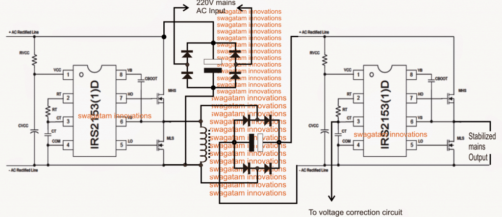 RVCC = 1K.1watt, CVCC = 0.1uF/400V, CBOOT = 1uF/400V
The figure above shows the actual configuration for implementing a stabilized 220V or 120V output regardless of the input fluctuations or an over load by using a couple of non-isolated boost converter processor stages.
Here two half bridge driver mosfet ICs become the crucial elements of the whole design.
The ICs involved are the versatile IRS2153 which were designed specifically for driving mosfets in a half bridge mode without the need of complex external circuitry.
We can see two identical half bridge driver stages incorporated, where the left side driver is used as the boost driver stage while the right hand side is configured for processing the boost voltage into a 50Hz or 60Hz sine wave output in conjunction with an external voltage control circuit.
The ICs are internally programmed to produce a fixed 50% duty cycle across the output pinouts through a totem pole topology.
These pinouts are connected with the power mosfets for implementing the intended conversions.
The ICs are also featured with an internal oscillator for enabling the required frequency at the output, the rate of the frequency is determined by an externally connected Rt/Ct network.
RVCC = 1K.1watt, CVCC = 0.1uF/400V, CBOOT = 1uF/400V
The figure above shows the actual configuration for implementing a stabilized 220V or 120V output regardless of the input fluctuations or an over load by using a couple of non-isolated boost converter processor stages.
Here two half bridge driver mosfet ICs become the crucial elements of the whole design.
The ICs involved are the versatile IRS2153 which were designed specifically for driving mosfets in a half bridge mode without the need of complex external circuitry.
We can see two identical half bridge driver stages incorporated, where the left side driver is used as the boost driver stage while the right hand side is configured for processing the boost voltage into a 50Hz or 60Hz sine wave output in conjunction with an external voltage control circuit.
The ICs are internally programmed to produce a fixed 50% duty cycle across the output pinouts through a totem pole topology.
These pinouts are connected with the power mosfets for implementing the intended conversions.
The ICs are also featured with an internal oscillator for enabling the required frequency at the output, the rate of the frequency is determined by an externally connected Rt/Ct network.
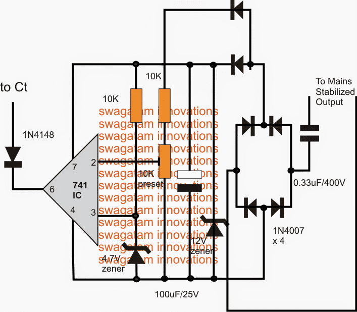
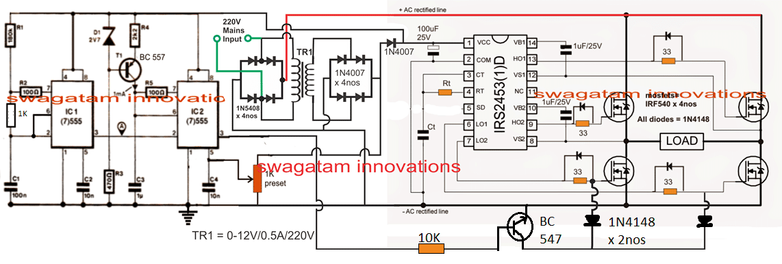
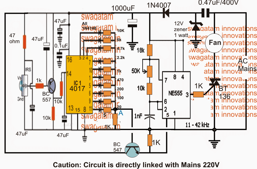 The various operations involved within the circuit can be understood with the help of the following points:
When an infrared beam is focused at the sensor, the sensor produces a low logic in response to this which in turn causes the PNP BC557 to conduct.
WARNING: THE ENTIRE CIRCUIT IS DIRECTLY LINKED WITH THE MAINS AC, OBSERVE EXTREME CAUTION WHILE TESTING THE CIRCUIT IN POWERED POSITION
The various operations involved within the circuit can be understood with the help of the following points:
When an infrared beam is focused at the sensor, the sensor produces a low logic in response to this which in turn causes the PNP BC557 to conduct.
WARNING: THE ENTIRE CIRCUIT IS DIRECTLY LINKED WITH THE MAINS AC, OBSERVE EXTREME CAUTION WHILE TESTING THE CIRCUIT IN POWERED POSITION
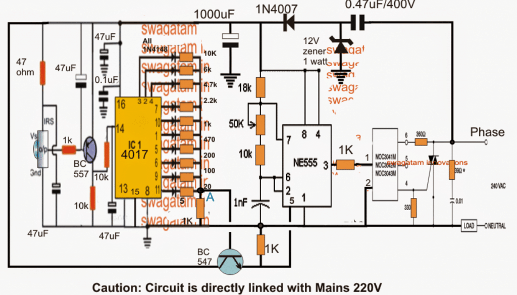 The circuit takes the help of a MOC3031 triac driver stage for enforcing a hassle free and clean fan control through the remote handset.
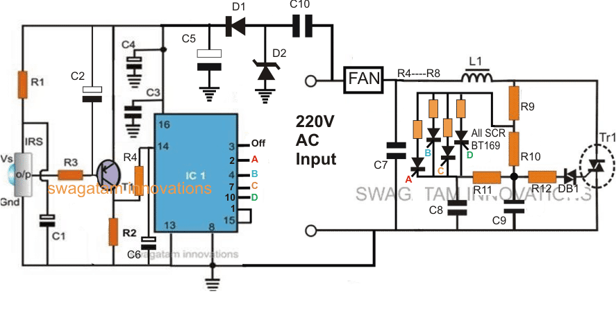 Note: the 4 SCRs are incorrectly represented as SCR BT169, these must be replaced with triacs, such as BCR1AM-8P triacs, or any other similar triac will also do.
 Although you have recommended before to use NTC thermistor instead of fuse or diodes, but I am concerned that it will cost much than the diodes.
These are my questions:
Although you have recommended before to use NTC thermistor instead of fuse or diodes, but I am concerned that it will cost much than the diodes.
These are my questions:
 The figure shows a bridge network which rectifies the 600 V AC to 700 V DC and this DC is then fired across the MOV circuit carrying a vulnerable 220 V, 10 watt lamp.
This is done through a 2uF/1KV capacitor in order to protect the MOV as it's not designed to handle sustained high surges.
Normally the connected lamp would instantly get burnt when subjected to this massive 700 V, but the experiment will hopefully show how the massive voltage is successfully absorbed and neutralized by the MOV saving the bulb's life.
The diode set up is not recommended, because TVS diodes can act like short circuit if they happen to get destroyed, this would mean the wires catching fire or the fuses blowing of.
An NTC can be selected as per its maximum voltage rating specs, this voltage rating will determine how much instantaneous high voltage the device is rated to restrict.
The figure shows a bridge network which rectifies the 600 V AC to 700 V DC and this DC is then fired across the MOV circuit carrying a vulnerable 220 V, 10 watt lamp.
This is done through a 2uF/1KV capacitor in order to protect the MOV as it's not designed to handle sustained high surges.
Normally the connected lamp would instantly get burnt when subjected to this massive 700 V, but the experiment will hopefully show how the massive voltage is successfully absorbed and neutralized by the MOV saving the bulb's life.
The diode set up is not recommended, because TVS diodes can act like short circuit if they happen to get destroyed, this would mean the wires catching fire or the fuses blowing of.
An NTC can be selected as per its maximum voltage rating specs, this voltage rating will determine how much instantaneous high voltage the device is rated to restrict.
 In the given diagram we are able to see a standard preprogrammed PIR module, a 7805 voltage regulator IC stage for supplying the PIR, and a simple 12 V transistor/relay driver stage.
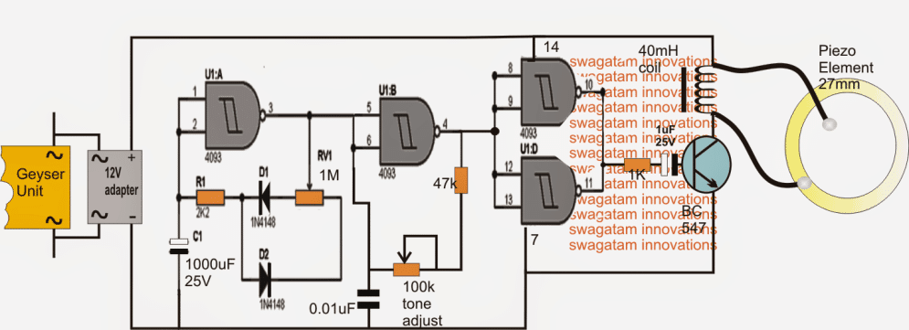
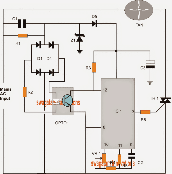
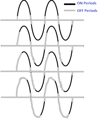
 To have the circuit as compact and straightforward as it can be, we utilize the popular timer IC 555.
The output of the IC 555, which can be typically triggered high, is activated low through a negative potential input.
This negative supply is made available from the stage comprising C1-R3, rectifier D1 -D2, along with stabilizer section D3-C2. BJTs T1 to T3 deliver a initializing pulse on the trigger input pin#2 of the 555 for each of the zero crossings of the mains AC input.
During a PWM period, as decided by the adjustment of P1 and P2, the output of the IC 555 is usually high, and we, therefore, have practically zero voltage difference across pins 3 and pin 8, i.e.
the triac remains switched off.
As soon as the set interval is elapsed, pin 3 becomes low and the triac is activated.
For the rest of the half AC cycle, a gate current keeps running, which allows the the triac to continue to conduct.
The lowest point where, let's say, a light bulb need not just illuminate, is determined by carefully adjusting the pot P1. Filter R7 C5 L1 supplies the necessary decoupling for the triac.
As a final point, remember that the absolute maximum power that could be governed by this IC 555 based smart regulator switch should not exceed 600 watts.
To have the circuit as compact and straightforward as it can be, we utilize the popular timer IC 555.
The output of the IC 555, which can be typically triggered high, is activated low through a negative potential input.
This negative supply is made available from the stage comprising C1-R3, rectifier D1 -D2, along with stabilizer section D3-C2. BJTs T1 to T3 deliver a initializing pulse on the trigger input pin#2 of the 555 for each of the zero crossings of the mains AC input.
During a PWM period, as decided by the adjustment of P1 and P2, the output of the IC 555 is usually high, and we, therefore, have practically zero voltage difference across pins 3 and pin 8, i.e.
the triac remains switched off.
As soon as the set interval is elapsed, pin 3 becomes low and the triac is activated.
For the rest of the half AC cycle, a gate current keeps running, which allows the the triac to continue to conduct.
The lowest point where, let's say, a light bulb need not just illuminate, is determined by carefully adjusting the pot P1. Filter R7 C5 L1 supplies the necessary decoupling for the triac.
As a final point, remember that the absolute maximum power that could be governed by this IC 555 based smart regulator switch should not exceed 600 watts.
 Now take four wooden pieces of dimensions 1cm thick, 2cm length and 2cm breadth and fix them at the bottom side of plank on the four sides so that the steel tubing that comes out when fixed, does not affect the stability and the entire instrument stands on the four wooden pieces (please let the ��drilling holes" and ��fixing wooden pieces��photos come here while posting in blog).
Now take three steel tubings of equal length and fix the three tubes in their place(i.e., in the three holesthat are drilled previously in the shape of triangle.) using hot glue or m-seal(make sure you fill the entirehole).
Now take four wooden pieces of dimensions 1cm thick, 2cm length and 2cm breadth and fix them at the bottom side of plank on the four sides so that the steel tubing that comes out when fixed, does not affect the stability and the entire instrument stands on the four wooden pieces (please let the ��drilling holes" and ��fixing wooden pieces��photos come here while posting in blog).
Now take three steel tubings of equal length and fix the three tubes in their place(i.e., in the three holesthat are drilled previously in the shape of triangle.) using hot glue or m-seal(make sure you fill the entirehole).
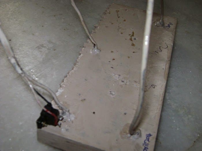 Next take another steel tubing whose length should be 4-5cm more than the previously cut tubes.
Fix this tubing in the top left corner hole using hot glue or m-seal ( you can even cut two of such tubingsand fix them at a distance which should be equal to the distance between two adjacent holes of fanso that the fan would be more stable).
Let it dry for 4-5 hours.
After this take three crocodile clips and push the steel tubing into the clip.
And fix it using hot glue and do the same for other two.
Next take another steel tubing whose length should be 4-5cm more than the previously cut tubes.
Fix this tubing in the top left corner hole using hot glue or m-seal ( you can even cut two of such tubingsand fix them at a distance which should be equal to the distance between two adjacent holes of fanso that the fan would be more stable).
Let it dry for 4-5 hours.
After this take three crocodile clips and push the steel tubing into the clip.
And fix it using hot glue and do the same for other two.
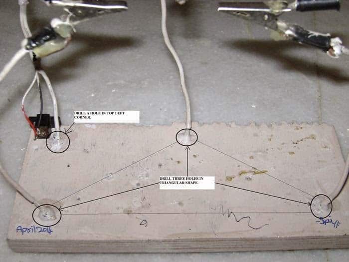 Let it dry for some time.
In the meantime, take the exhaust fan and fix the LED��s in the front two holes using glue and connect the LED��s and fan in parallel and use 1k resistors for white LED��s and bring the final wires to the bottom and connect them to the female DC jack.
Let it dry for some time.
In the meantime, take the exhaust fan and fix the LED��s in the front two holes using glue and connect the LED��s and fan in parallel and use 1k resistors for white LED��s and bring the final wires to the bottom and connect them to the female DC jack.
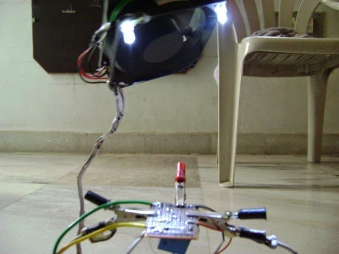 And next, fix the exhaust fan to the steel tubing that is on the top left corner by pushing steel tubing into one of the holes of fan using hot glue or m-seal(use more glue otherwise the fan would not be stable while on use).
 Now keep the entire instrument aside for drying.
After drying, you may paint the wooden plank with anycolor as per your liking.
Now keep the entire instrument aside for drying.
After drying, you may paint the wooden plank with anycolor as per your liking.
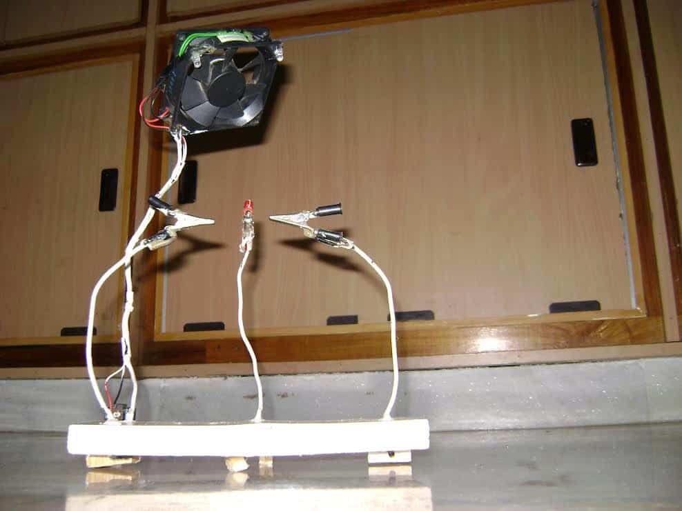

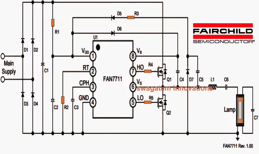

 The circuit of the proposed electronic fluorescent ballast may be understood through the following discussion:
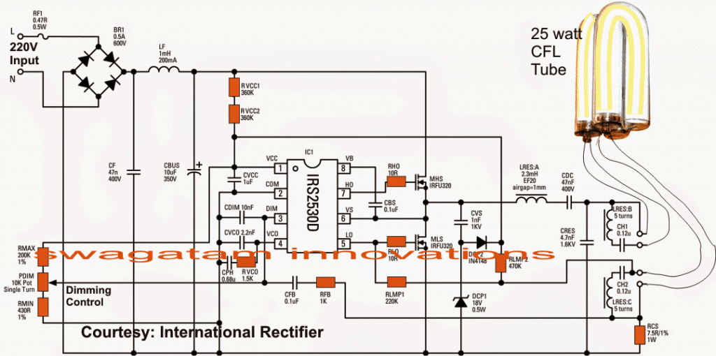
 The 10 ohm with the negative of the battery may be eliminated, it's not worth with so many existing protections.
For getting a better response from the over-charge cut-off stage, the above circuit could be modified further with an additional transistor stage T5, as shown below:
Referring to the following circuit, we are able to the see a few crucial additions and removals:
IC 7805 has been added, diode at T6 collector is removed, and D1 position changed.
These changes ensure that an exact 4.3V is able to develop across the emitter of T6 and ground, irrespective of the input voltage level.
D5 has been removed in order to provide a better illumination for the LED at the collector of T2.
All high value resistors have now been reduced to 1K for an increased current biasing for the BJTs.
The 10 ohm with the negative of the battery may be eliminated, it's not worth with so many existing protections.
For getting a better response from the over-charge cut-off stage, the above circuit could be modified further with an additional transistor stage T5, as shown below:
Referring to the following circuit, we are able to the see a few crucial additions and removals:
IC 7805 has been added, diode at T6 collector is removed, and D1 position changed.
These changes ensure that an exact 4.3V is able to develop across the emitter of T6 and ground, irrespective of the input voltage level.
D5 has been removed in order to provide a better illumination for the LED at the collector of T2.
All high value resistors have now been reduced to 1K for an increased current biasing for the BJTs.
 As suggested by one of the avid readers of this blog Mr.
Syed, the above diagram needed some corrections.
The finalized diagram of the Li-ion emergency light circuit with over charge and low battery cut off featurescan be seen below:
As suggested by one of the avid readers of this blog Mr.
Syed, the above diagram needed some corrections.
The finalized diagram of the Li-ion emergency light circuit with over charge and low battery cut off featurescan be seen below:

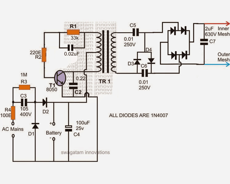
 Core: EE19/8/5
Interested to know how to Repair Mosquito Rackets?
Core: EE19/8/5
Interested to know how to Repair Mosquito Rackets?
 In one of my earlier posts I discussed a simple mosquito zapper circuit, in this article we study a similar design which is commercially used in all mosquito rackets, or mosquito bat units.
 When the power switch SA is pressed, the high-frequency oscillator composed of the transistor VT1 and the step-up transformer T is energized using the 3V DC supply generating a high-frequency alternating current of about 18kHz, boosted by T to about 500V.
This high voltage ranging at 500V is then further stepped up using a ladder network, which is made up of three 1N4007 Diodes, capacitors C1- C3.
This network steps the T output to approximately three times its original value and we get around 1500V which gets stored inside a high voltage PPC capacitor positioned at the extreme end of the ladder network.
This stepped up 1500V is then terminated to the mosquito racket net, which now becomes armed with this high voltage and when ever a mosquito tries to get past the racket net, it instantly gets electrocuted through this high voltage discharge from the PPC capacitor.
An Led can be seen included in the design, it is used for indicating the ON/OFF states of the circuits and also the how much power is left inside the battery.
The series resistor R1 decides the intensity of the LED which can be tweaked as per preference to maximize battery life
When the power switch SA is pressed, the high-frequency oscillator composed of the transistor VT1 and the step-up transformer T is energized using the 3V DC supply generating a high-frequency alternating current of about 18kHz, boosted by T to about 500V.
This high voltage ranging at 500V is then further stepped up using a ladder network, which is made up of three 1N4007 Diodes, capacitors C1- C3.
This network steps the T output to approximately three times its original value and we get around 1500V which gets stored inside a high voltage PPC capacitor positioned at the extreme end of the ladder network.
This stepped up 1500V is then terminated to the mosquito racket net, which now becomes armed with this high voltage and when ever a mosquito tries to get past the racket net, it instantly gets electrocuted through this high voltage discharge from the PPC capacitor.
An Led can be seen included in the design, it is used for indicating the ON/OFF states of the circuits and also the how much power is left inside the battery.
The series resistor R1 decides the intensity of the LED which can be tweaked as per preference to maximize battery life


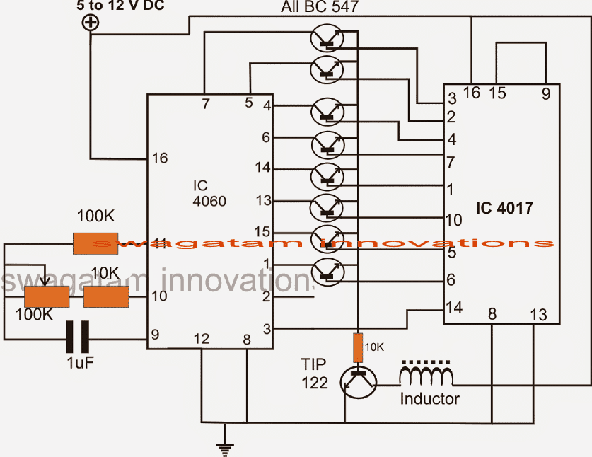
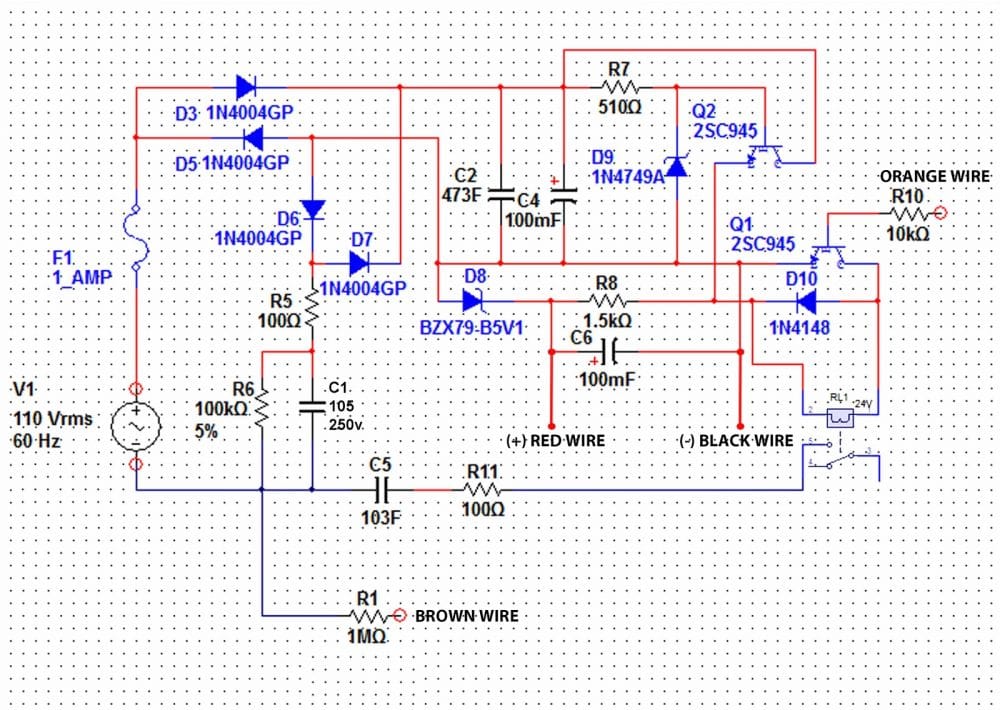
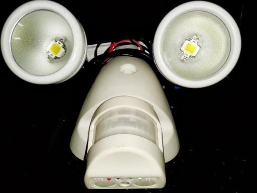
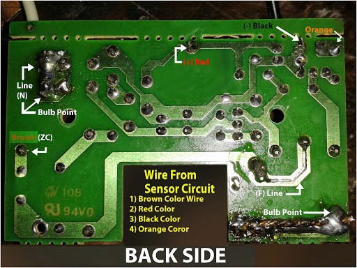
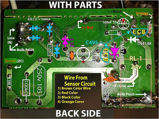

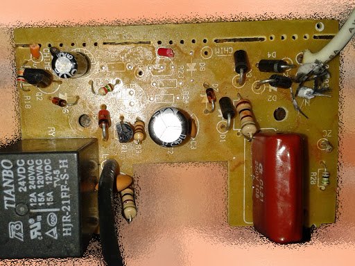
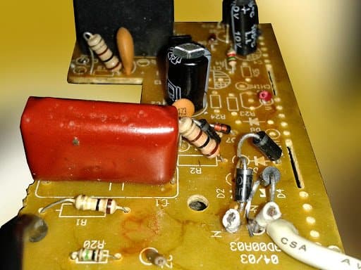
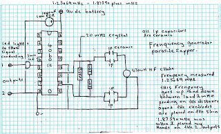
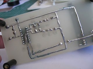
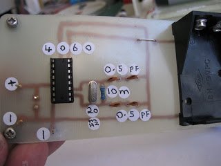
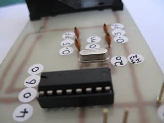 "New copper coin electrodes for my parasite zapper, these are really neat and can be modified to be able to be secured Velcro strap for parasite zapping this is one of a number of pictures I've uploaded to
SkyDrive..."
"New copper coin electrodes for my parasite zapper, these are really neat and can be modified to be able to be secured Velcro strap for parasite zapping this is one of a number of pictures I've uploaded to
SkyDrive..."
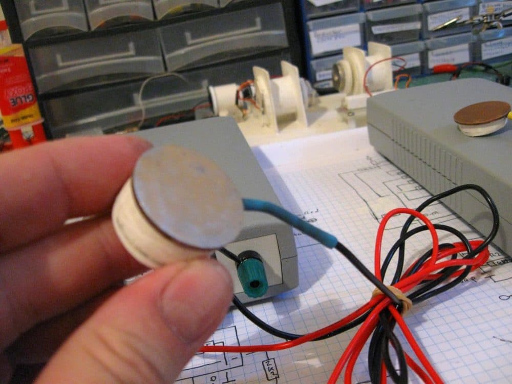 "My previous designs were based on transistors and other ICs, here are the pics of those previously built parasite zapper models:
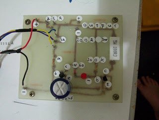
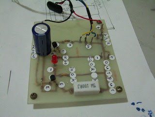
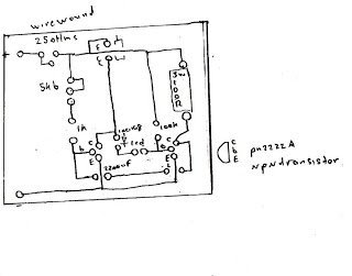 The above is a pulse frequency driver circuit i built from a YouTube video i have made some changes to it i didn't have a bigger size 220uf electro to put into it only small ones so i used the wrong value and put in a 2200uf/35 volts electro, and the 1n4148 diode.
Well it didn't seem to make the led come on even when powering a motor similar to what the fellow on the net used, so i threw in a 1n60 geranium diode and now the led seems to work some times due some unknown factor, but even without the led coming on it stills puts out enough voltage to power a motor.
So when the led is supposed to come on for reasons i don't know yet is a mystery i think, at first i wrote the circuit down from the YouTube video then made it onto a bread board and it worked and the led came on when i powered the electric motor.
I have but when i made the printed circuit version and transferred the parts from the bread board onto it the led wouldn't then come on, when i powered the same motor
so i checked the parts on the printed circuit and they all were OK, so i built another bread board one, and it works again even though the printed circuit versions led doesn't come on when i powered the motor the identical circuit on the other works ok very strange.
So its led comes on too, so i rechecked it on the bread board to find out why it works and not the other, i then found I've mistakenly put in a 1n60 diode so maybe that's why the led comes on when powering a motor.
I changed the 1n4148 diodes on the printed circuit to the same as on the bread board and now the led still doesn't lite up when powering the same motor only some times it blinks when I'm handling the motor due to some unknown factor,
but despite this they still power the motor and put out enough zap onto my tongue to qualify as an experimental parasite zapper, really i built this from a hand drawn circuit on the net to test on my star ship coils.
The above is a pulse frequency driver circuit i built from a YouTube video i have made some changes to it i didn't have a bigger size 220uf electro to put into it only small ones so i used the wrong value and put in a 2200uf/35 volts electro, and the 1n4148 diode.
Well it didn't seem to make the led come on even when powering a motor similar to what the fellow on the net used, so i threw in a 1n60 geranium diode and now the led seems to work some times due some unknown factor, but even without the led coming on it stills puts out enough voltage to power a motor.
So when the led is supposed to come on for reasons i don't know yet is a mystery i think, at first i wrote the circuit down from the YouTube video then made it onto a bread board and it worked and the led came on when i powered the electric motor.
I have but when i made the printed circuit version and transferred the parts from the bread board onto it the led wouldn't then come on, when i powered the same motor
so i checked the parts on the printed circuit and they all were OK, so i built another bread board one, and it works again even though the printed circuit versions led doesn't come on when i powered the motor the identical circuit on the other works ok very strange.
So its led comes on too, so i rechecked it on the bread board to find out why it works and not the other, i then found I've mistakenly put in a 1n60 diode so maybe that's why the led comes on when powering a motor.
I changed the 1n4148 diodes on the printed circuit to the same as on the bread board and now the led still doesn't lite up when powering the same motor only some times it blinks when I'm handling the motor due to some unknown factor,
but despite this they still power the motor and put out enough zap onto my tongue to qualify as an experimental parasite zapper, really i built this from a hand drawn circuit on the net to test on my star ship coils.
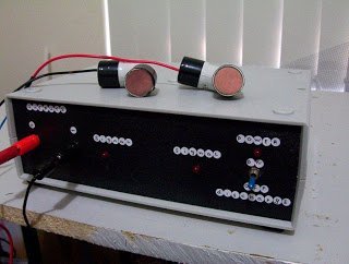
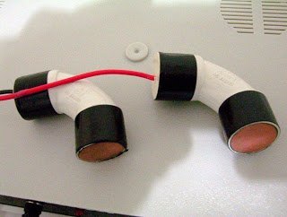
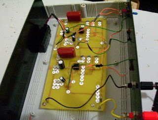
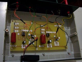 Here's some new pictures of that multi parasite zapper all installed and also the 2 electrodes made from small whitepvcelbow joiners used,forpvcpipes.
The actual electrodes arecopper2 cent coins filed flat on one side of each coin so as to provide a good contact with your skin , the best way to avoid that brown tarn that forms oncoppersurfaces in this case was to use a smear of aloevera gel,
and you can also use aloevera to help the pulses to conduct better into your skin tothe aloevera gel does dry out quick or absorb into your skin pretty fast, so its just a matter of applying more aloevera gel to the electrodes or the skin.
"
Here's some new pictures of that multi parasite zapper all installed and also the 2 electrodes made from small whitepvcelbow joiners used,forpvcpipes.
The actual electrodes arecopper2 cent coins filed flat on one side of each coin so as to provide a good contact with your skin , the best way to avoid that brown tarn that forms oncoppersurfaces in this case was to use a smear of aloevera gel,
and you can also use aloevera to help the pulses to conduct better into your skin tothe aloevera gel does dry out quick or absorb into your skin pretty fast, so its just a matter of applying more aloevera gel to the electrodes or the skin.
"
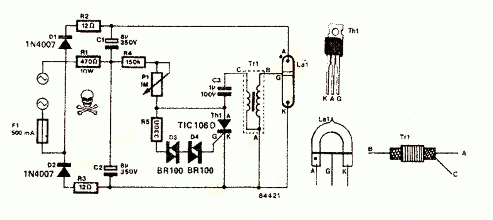 The explanation for the above circuit diagram can be found HERE
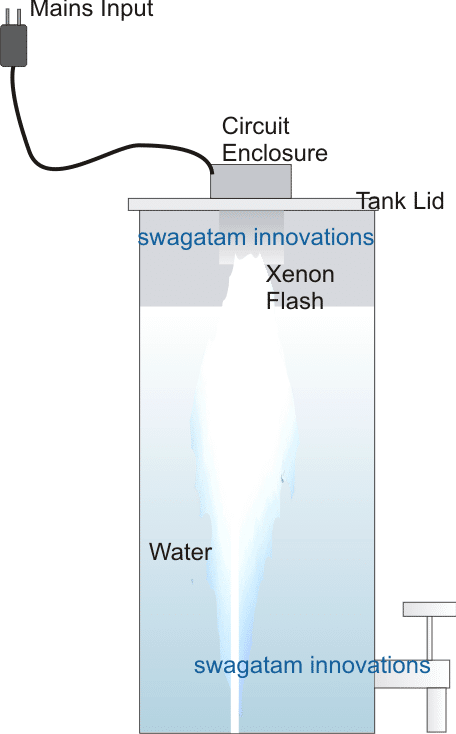
 The entire explanation can be read HERE
 Again as discussed above, the arcs must "see" the water directly and not through a transparent medium or through theenclosure, as shown in the following example:
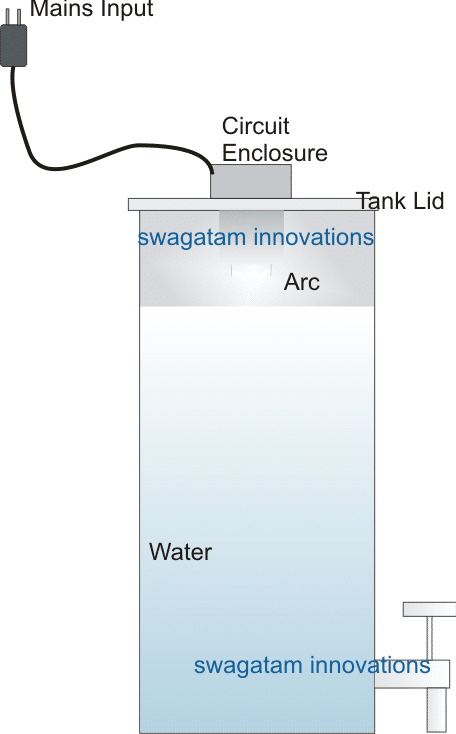
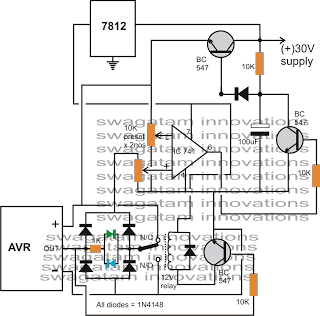
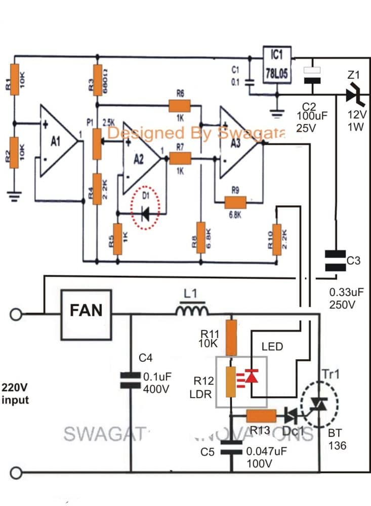 WARNING - THE CIRCUIT IS NOT ISOLATED FROMMAINSAC......
BE VERY MUCH CAUTIONED WHILE BUILDING AND TESTING THIS CIRCUIT.
WARNING - THE CIRCUIT IS NOT ISOLATED FROMMAINSAC......
BE VERY MUCH CAUTIONED WHILE BUILDING AND TESTING THIS CIRCUIT.
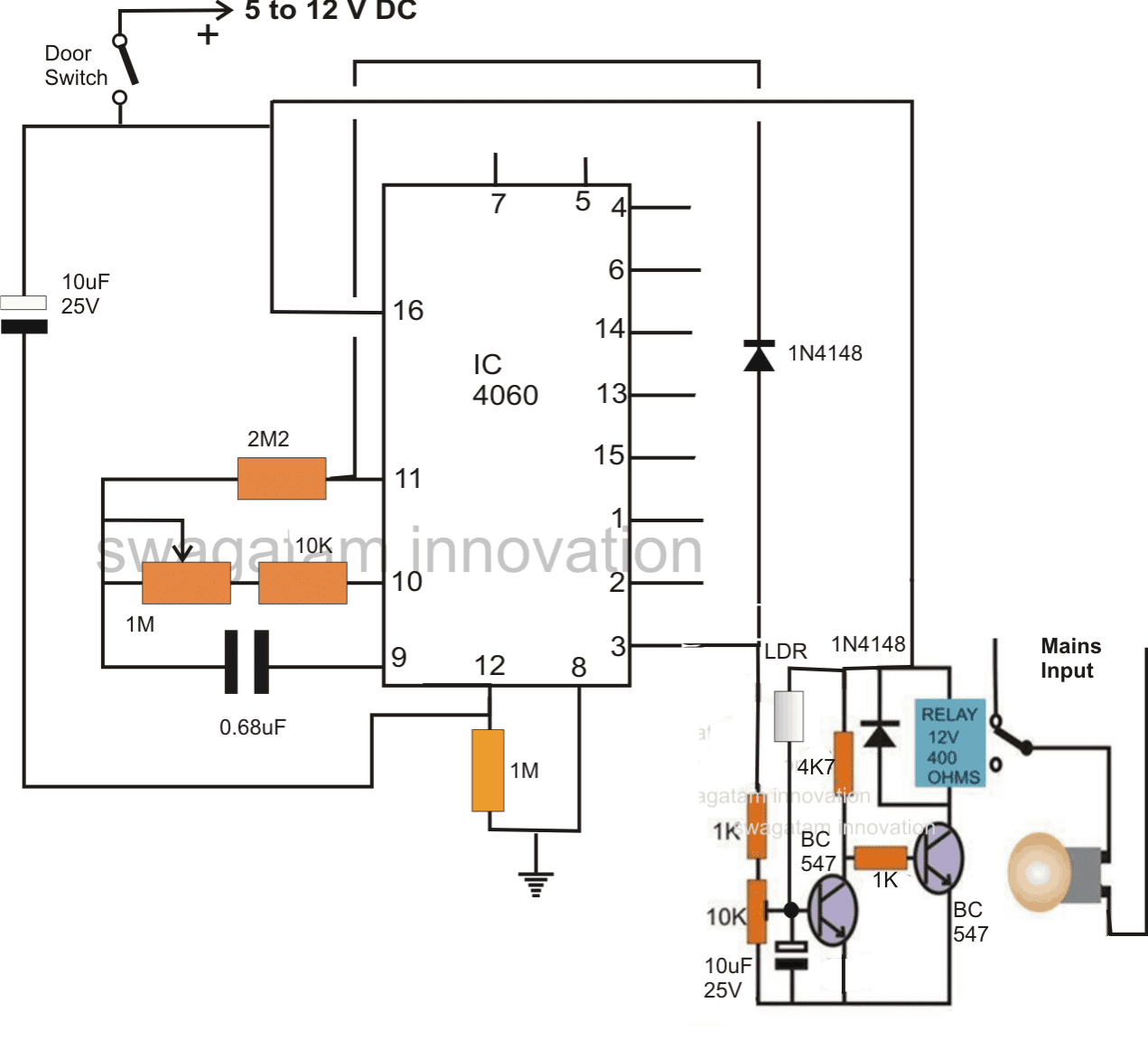
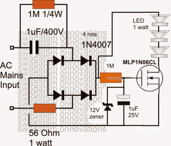 A little investigation revealed that the high voltage transistor in the first diagram is actually not needed, rather it can be replaced with a high current Darlington TIP122 transistor as shown in the following diagram.
The high voltage surge from the capacitor becomes ineffective against the high current specs of the transistor and the LEDs and no damage is caused to them, in fact it forces the high voltage to drop to the specified allowable safe limits of the LEDs and the transistor.
The TIP122 also allows the use of a high value base resistor thereby making it sure that it does not become hot or blow off in the course of time, it also allows the inclusion of a low value capacitor at the base of the transistor for implementing the required delayed switch ON effect.
A little investigation revealed that the high voltage transistor in the first diagram is actually not needed, rather it can be replaced with a high current Darlington TIP122 transistor as shown in the following diagram.
The high voltage surge from the capacitor becomes ineffective against the high current specs of the transistor and the LEDs and no damage is caused to them, in fact it forces the high voltage to drop to the specified allowable safe limits of the LEDs and the transistor.
The TIP122 also allows the use of a high value base resistor thereby making it sure that it does not become hot or blow off in the course of time, it also allows the inclusion of a low value capacitor at the base of the transistor for implementing the required delayed switch ON effect.
 Parts List
All resistors are 1/4 watt 5% except R1 (see text)
R4 = 56 ohms
R4, R7 = 1K
R5 = 10K
R6 = 47K
P1 = 100K preset
Diodes = All are 1N4007
T1 = BC547
T2 = BC557
C2 = 10uF/25V
LD1 = red LED 20 mA
Relay = 12 V/200mA 30 amps
The LED/LDR device can be assembled manually as per the following example image
Parts List
All resistors are 1/4 watt 5% except R1 (see text)
R4 = 56 ohms
R4, R7 = 1K
R5 = 10K
R6 = 47K
P1 = 100K preset
Diodes = All are 1N4007
T1 = BC547
T2 = BC557
C2 = 10uF/25V
LD1 = red LED 20 mA
Relay = 12 V/200mA 30 amps
The LED/LDR device can be assembled manually as per the following example image
 P1 is used for adjusting the ambient light threshold at which the LEDs stop illuminating.
P2 is set such that at 14.6V (across the battery terminals) the base LED becomes very dim, hardly visible, and at 12.5V it's brightly lit.
P1 is used for adjusting the ambient light threshold at which the LEDs stop illuminating.
P2 is set such that at 14.6V (across the battery terminals) the base LED becomes very dim, hardly visible, and at 12.5V it's brightly lit.
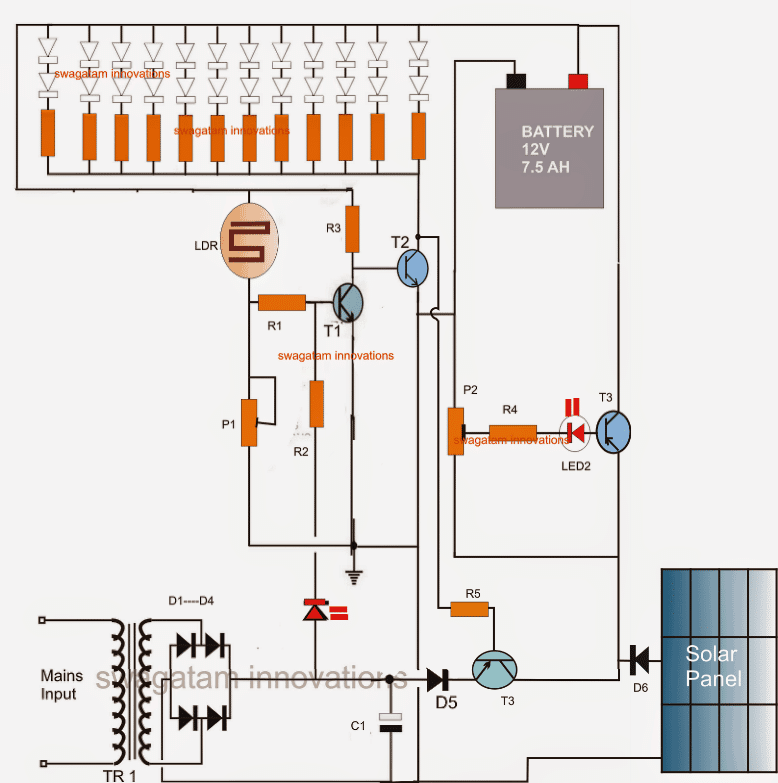

 "Hi Bro,
What kind of emergency light do you want to make? Automatic AC/Dc operated or just direct on battery?
The datasheet and the pics are OK.
Best Regards,
Swagatam"
"Hi, thanks for your reply bro.
Automatic AC/DC operated with battery backup."
OK, here's an automatic ac/dc emergency light circuit using the proposed 36 SMD LED lights which is easy to build, cheap and yet reliable.
CAUTION - THE CIRCUIT IS NOT ISOLATED FROM AC MAINS, UTMOST CARE MUST BE OBSERVED WHILE TESTING THIS CIRCUIT IN UNCOVERED POSITION.
ALTERNATIVELY YOU MAY INCORPORATE A 12V, 500MA DCADAPTERACROSS THE ZENER DIODE INSTEAD OF THE SHOWN TRANSFORMERLESS POWER SUPPLY FOR AVOIDING THE ABOVE CAUTION.
The Design of a an Automatic SMD based emergency lamp is shown below, as per the above request specification:
"Hi Bro,
What kind of emergency light do you want to make? Automatic AC/Dc operated or just direct on battery?
The datasheet and the pics are OK.
Best Regards,
Swagatam"
"Hi, thanks for your reply bro.
Automatic AC/DC operated with battery backup."
OK, here's an automatic ac/dc emergency light circuit using the proposed 36 SMD LED lights which is easy to build, cheap and yet reliable.
CAUTION - THE CIRCUIT IS NOT ISOLATED FROM AC MAINS, UTMOST CARE MUST BE OBSERVED WHILE TESTING THIS CIRCUIT IN UNCOVERED POSITION.
ALTERNATIVELY YOU MAY INCORPORATE A 12V, 500MA DCADAPTERACROSS THE ZENER DIODE INSTEAD OF THE SHOWN TRANSFORMERLESS POWER SUPPLY FOR AVOIDING THE ABOVE CAUTION.
The Design of a an Automatic SMD based emergency lamp is shown below, as per the above request specification:
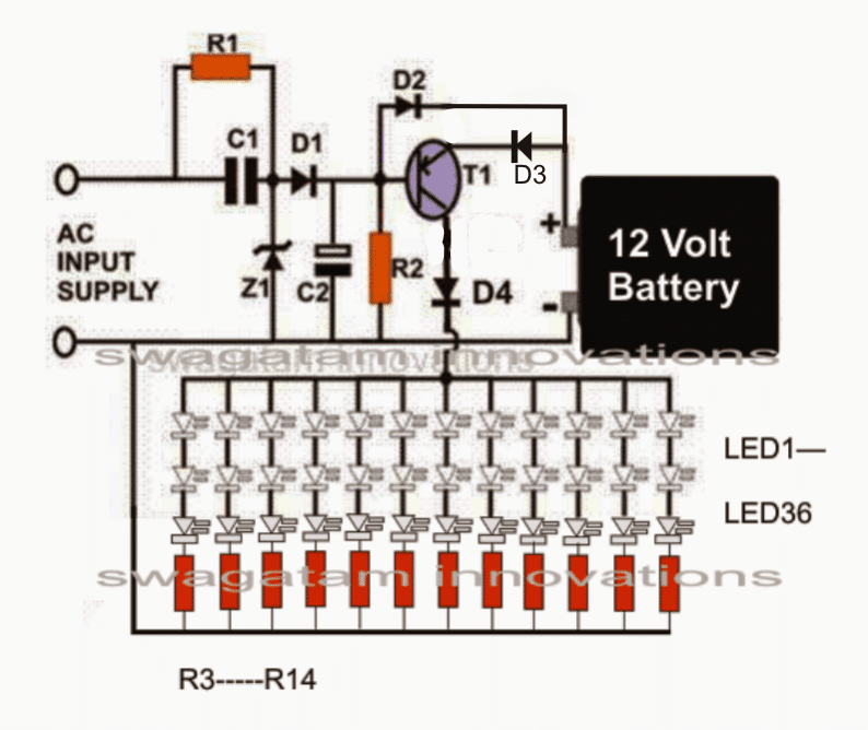
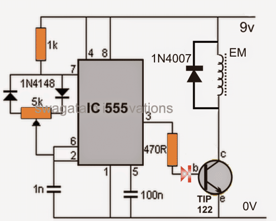
 The circuit depicted is a basic audio oscillator whose operating frequency may be adjusted over a large range, to be precisefrom around 500Hz to 10kHz.
This valuecan be assumed tocoverthe frequency range of all typical bugs.
The circuit is a simple multivibrator in which RV1 changes the audio frequency.
This generates a square wave, which is delivered across the tiny crystal earpiece linked to the negative line and the Q2collector.
The impedance of crystal earpieces is quite high, although it has no effect on the circuit's performance.
This basic circuit may utilize almost any transistor, however if PNP types are employed, the battery supply must be inverted.
The capacitor values are not important.
In casealternative capacitors valuesare triedand the frequency range is deemed to be inadequate, R1 may be modified to turn it back into the recommended range.
The current consumption is minimal (2-2mA) and fluctuates somewhat with frequency, however a PP3 battery mightlast a long time; after all, the device needs tobe remainon for extended periods of time.
The device may be constructed in a tiny box to fit inside a coat pocket with the parts placed such that the earpiece becomes external, and all thecomponents need to be as small as possible.
It's a case of trial and error to find the correct frequency that rattles the mosquitos with highest efficieny.
The circuit depicted is a basic audio oscillator whose operating frequency may be adjusted over a large range, to be precisefrom around 500Hz to 10kHz.
This valuecan be assumed tocoverthe frequency range of all typical bugs.
The circuit is a simple multivibrator in which RV1 changes the audio frequency.
This generates a square wave, which is delivered across the tiny crystal earpiece linked to the negative line and the Q2collector.
The impedance of crystal earpieces is quite high, although it has no effect on the circuit's performance.
This basic circuit may utilize almost any transistor, however if PNP types are employed, the battery supply must be inverted.
The capacitor values are not important.
In casealternative capacitors valuesare triedand the frequency range is deemed to be inadequate, R1 may be modified to turn it back into the recommended range.
The current consumption is minimal (2-2mA) and fluctuates somewhat with frequency, however a PP3 battery mightlast a long time; after all, the device needs tobe remainon for extended periods of time.
The device may be constructed in a tiny box to fit inside a coat pocket with the parts placed such that the earpiece becomes external, and all thecomponents need to be as small as possible.
It's a case of trial and error to find the correct frequency that rattles the mosquitos with highest efficieny.
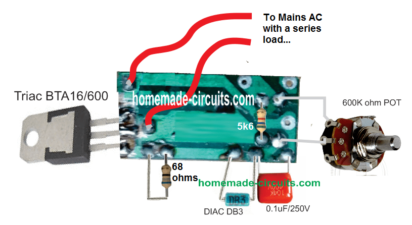 Track Layout Details
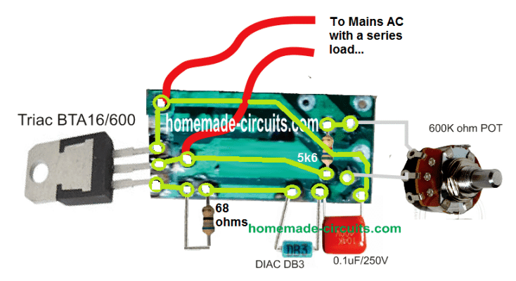
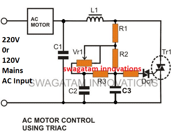
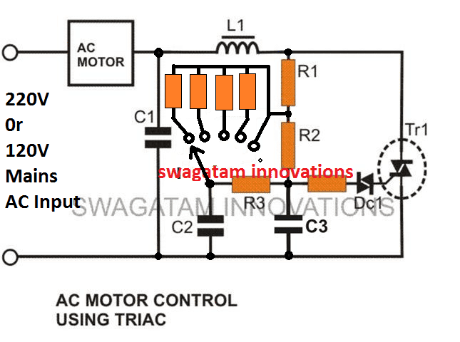
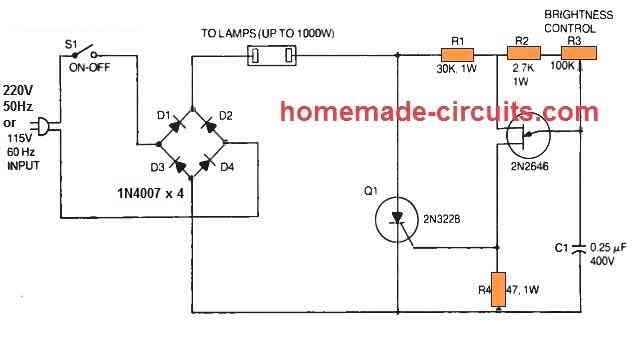 The capacitor C1 fixes the time period where a 2N2646 unijunction transistor (Q2) produces a triggering gate trigger pulse to turn on the 2N3228 SCR (Q1).
By some manipulation of the light-duty control, R3 pot the user is able to change the SCR output across a large range.
In the phase-control circuit, resistor R2 works like a security unit that inhibits rheostat R1 from getting fixed at 100 % anode voltage of the UJT.
This specific rule is applied here to regulate the illumination level of the incandescent lamps, whether as a single lamp or many in parallel as high as to 1000 watts.
In this design, a full-wave bridge rectifier is built using 4nos of 1N4007 silicon power diodes (D1 to D4) that supply rectified power-line voltage for the SCR and the lamp.
Due to the full-wave output from the bridge, it becomes possible for the SCR to take care of both half-cycles of the AC line voltage.
The phase-shift system is sensitive to frequency and has been designed for 60 Hz mains input only.
Therefore the circuit is not going to work with fluorescent lamps and should not be plugged into these.
The 2N3228 SCR 5-amps.
200-volts.
but higher-powered SCRs could be replaced for high current applications, and the UJT 2N2646 section of the schematic could be kept unchanged.
Besides SCR circuit is supposed to be used like a light dimmer, this circuit can be employed likewise as a heater or oven controller.
The capacitor C1 fixes the time period where a 2N2646 unijunction transistor (Q2) produces a triggering gate trigger pulse to turn on the 2N3228 SCR (Q1).
By some manipulation of the light-duty control, R3 pot the user is able to change the SCR output across a large range.
In the phase-control circuit, resistor R2 works like a security unit that inhibits rheostat R1 from getting fixed at 100 % anode voltage of the UJT.
This specific rule is applied here to regulate the illumination level of the incandescent lamps, whether as a single lamp or many in parallel as high as to 1000 watts.
In this design, a full-wave bridge rectifier is built using 4nos of 1N4007 silicon power diodes (D1 to D4) that supply rectified power-line voltage for the SCR and the lamp.
Due to the full-wave output from the bridge, it becomes possible for the SCR to take care of both half-cycles of the AC line voltage.
The phase-shift system is sensitive to frequency and has been designed for 60 Hz mains input only.
Therefore the circuit is not going to work with fluorescent lamps and should not be plugged into these.
The 2N3228 SCR 5-amps.
200-volts.
but higher-powered SCRs could be replaced for high current applications, and the UJT 2N2646 section of the schematic could be kept unchanged.
Besides SCR circuit is supposed to be used like a light dimmer, this circuit can be employed likewise as a heater or oven controller.
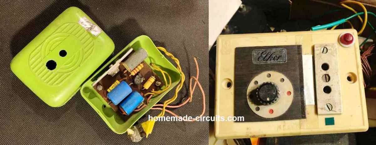 The choke is built using 5 meters of 30 SWG super enameled copper wire over a 1/2 inch diameter and 1 inch long ferrite core
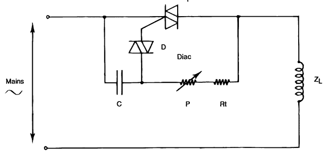 The circuit incorporates the principle of triggering with synchronization across the triac.
The configuration is the simplest in its form and has the following advantages:
The design is very simple and cheap.
Use of only two end terminal wire and absence of any external power supply.
But one big disadvantage of this design is its incapability of working with highly inductive loads.
The circuit incorporates the principle of triggering with synchronization across the triac.
The configuration is the simplest in its form and has the following advantages:
The design is very simple and cheap.
Use of only two end terminal wire and absence of any external power supply.
But one big disadvantage of this design is its incapability of working with highly inductive loads.
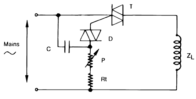 The principle here now gets transformed to triggering of the triac with synchronization by the mains voltage.
The idea to very extent neutralizes the above issue and becomes very much coordinated even with inductive type of loads.
Please note that in the above design very interestingly, the position of the load and the resistor connection has been changed for acquiring the intended results.
The advantages can be assessed as follows:
Again a simple design and also is very low cost.
Better control of even loads which are inductive by nature.
As usual no external power source is required for the functioning.
The disadvantages though are the involvement of 3 terminal wire ends for the intended connections.
The operations become very asymmetrical and therefore the circuit cannot be used for controlling highly inductive loads like transformers.
The principle here now gets transformed to triggering of the triac with synchronization by the mains voltage.
The idea to very extent neutralizes the above issue and becomes very much coordinated even with inductive type of loads.
Please note that in the above design very interestingly, the position of the load and the resistor connection has been changed for acquiring the intended results.
The advantages can be assessed as follows:
Again a simple design and also is very low cost.
Better control of even loads which are inductive by nature.
As usual no external power source is required for the functioning.
The disadvantages though are the involvement of 3 terminal wire ends for the intended connections.
The operations become very asymmetrical and therefore the circuit cannot be used for controlling highly inductive loads like transformers.
 Here another small sensitive triac is cleverly introduced for rectifying the major issue that's primarily responsible for making triacs so unsuitable with inductive loads.
The second small triac makes sure that the triac is never switched OFF and blocked completely, by generating a pulse train, keeping the triac alive and "kicking" all the time.
The advantages of the above final design may be marked with the following points:
Very simple design,
Superb accuracy while controlling highly inductive loads,
No use of external power supply.
The above circuit was exclusively developed by the SGS-THOMSON Microelectronics applications laboratory and used with success for a wide range of equipment.
COURTESY:
Here another small sensitive triac is cleverly introduced for rectifying the major issue that's primarily responsible for making triacs so unsuitable with inductive loads.
The second small triac makes sure that the triac is never switched OFF and blocked completely, by generating a pulse train, keeping the triac alive and "kicking" all the time.
The advantages of the above final design may be marked with the following points:
Very simple design,
Superb accuracy while controlling highly inductive loads,
No use of external power supply.
The above circuit was exclusively developed by the SGS-THOMSON Microelectronics applications laboratory and used with success for a wide range of equipment.
COURTESY:


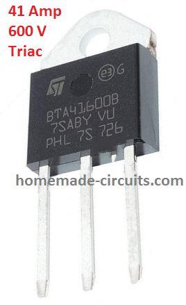 Controlling heaters rated as high as 1500 watt requires stringent specifications with the controlling unit for safe and effective implementation of the intended operations.
With the advent of advanced snubber-less Triacs and Diacs making heater controllers at massive watt levels has become relatively easier today.
Here we study a simple yet entirely suitable configuration which may be utilized for making a 1500 watts heater controller circuit.
Let's understand the given circuit diagram with the following points:
Controlling heaters rated as high as 1500 watt requires stringent specifications with the controlling unit for safe and effective implementation of the intended operations.
With the advent of advanced snubber-less Triacs and Diacs making heater controllers at massive watt levels has become relatively easier today.
Here we study a simple yet entirely suitable configuration which may be utilized for making a 1500 watts heater controller circuit.
Let's understand the given circuit diagram with the following points:
 Resistor R5 along with the capacitor C3 works like a a snubber network over the Triac to safeguard it from the reverse EMF voltages spikes created by inductive loads every time the Triac is switched OFF.
Inductor L1, which is a 50 ��H choke, and capacitor C4 are configured like an interference suppression filter, that enables the elimination of the RF noise commonly generated by this type of light dimmers or heater controllers.
The preset R3 adjusts the minimum starting range of the heater temperature, and helps the user to ensure that the power to the heater always starts from the minimum power when R2 is moved to the minimum position, and the heater gets maximum power when the R2 is moved to the maximum adjustment point.
Resistor R5 along with the capacitor C3 works like a a snubber network over the Triac to safeguard it from the reverse EMF voltages spikes created by inductive loads every time the Triac is switched OFF.
Inductor L1, which is a 50 ��H choke, and capacitor C4 are configured like an interference suppression filter, that enables the elimination of the RF noise commonly generated by this type of light dimmers or heater controllers.
The preset R3 adjusts the minimum starting range of the heater temperature, and helps the user to ensure that the power to the heater always starts from the minimum power when R2 is moved to the minimum position, and the heater gets maximum power when the R2 is moved to the maximum adjustment point.
 This high power light dimmer includes one triac, a single diac and an RC network where the period of the charging and discharging of capacitor C2 could be fixed using potentiometer P1. Noise disturbances and transients are kept under control through capacitor C1 and the inductor L1.
 The Solution:
That looks very strange because the 56 ohm resistors at the emitter of the transistors should force the transistor to dissipate the heat equally among the resistors and the transistors.
The last two 56 ohm resistors getting hotter means that the last two BJTs are conducting more freely than the remaining transistors.
The easiest way to tackle this problem is to mount all the transistors over a common aluminum strip, so that the transistor exchange their body dissipation uniformly with each other and thus all the transistors conduct and dissipate equally.
The Solution:
That looks very strange because the 56 ohm resistors at the emitter of the transistors should force the transistor to dissipate the heat equally among the resistors and the transistors.
The last two 56 ohm resistors getting hotter means that the last two BJTs are conducting more freely than the remaining transistors.
The easiest way to tackle this problem is to mount all the transistors over a common aluminum strip, so that the transistor exchange their body dissipation uniformly with each other and thus all the transistors conduct and dissipate equally.
 CAUTION: Diodes will dissipate a lot of heat so make sure they are mounted on a suitable heatsink.
As we all know that a normal diode, like a 1N4007 drops 0.6 to 0.7 volts across it, when a DC is applied, means that many diodes put in series would drop the relevant amount of voltage across them.
In the the proposed design, in all 190 1N4007 diodes have been used and put in series for acquiring the desired level of voltage conversion.
If we multiply 190 by 0.6, it gives around 114, so that's pretty close to the required mark of 110V.
However since these diodes require an input DC, four more diodes are wired up as a bridge network for the initially required 220V DC to the circuit.
The maximum current that can be drawn from this converter is not more than 300 mA, or around 30 watts.
CAUTION: Diodes will dissipate a lot of heat so make sure they are mounted on a suitable heatsink.
As we all know that a normal diode, like a 1N4007 drops 0.6 to 0.7 volts across it, when a DC is applied, means that many diodes put in series would drop the relevant amount of voltage across them.
In the the proposed design, in all 190 1N4007 diodes have been used and put in series for acquiring the desired level of voltage conversion.
If we multiply 190 by 0.6, it gives around 114, so that's pretty close to the required mark of 110V.
However since these diodes require an input DC, four more diodes are wired up as a bridge network for the initially required 220V DC to the circuit.
The maximum current that can be drawn from this converter is not more than 300 mA, or around 30 watts.
 The circuit is based on the regular light dimmer switch circuit principle, where the input phase is chopped at the particular voltage marks of the rising AC sine wave.
Thus the circuit can be used for setting the input voltage at the required 100 V level.
The ratio of the resistors R3/R5 in the circuit has been precisely adjusted for obtaining the required 110V at the output terminals across the load L1.
A 100uF / 400V capacitor can be seen introduced in series with the load for extra safety.
Alternatively a simpler version of the circuit can be made, where the main high triac is operated via a cheap light dimmer switch for the intended results.
The circuit is based on the regular light dimmer switch circuit principle, where the input phase is chopped at the particular voltage marks of the rising AC sine wave.
Thus the circuit can be used for setting the input voltage at the required 100 V level.
The ratio of the resistors R3/R5 in the circuit has been precisely adjusted for obtaining the required 110V at the output terminals across the load L1.
A 100uF / 400V capacitor can be seen introduced in series with the load for extra safety.
Alternatively a simpler version of the circuit can be made, where the main high triac is operated via a cheap light dimmer switch for the intended results.
 IC1 is the Hall effect sensor and 1C2 is a precision opamp IC2 rigged to deliver a bit of extra amplification.
The op amp is configured in an inverting mode circuit, that includes resistors R1 and R4 positioned as negative feedback link.
The built-in voltage gain of IC2, or the "open loop" gain as it is actually called, is incredibly large at DC voltages, and lower frequencies.
Actually, it can be more than 100,000 times for any standard opamp.
Applying negative feedback minimizes the design's voltage gain in general into a considerably more workable magnitude, and this "closed loop" gain is equivalent to the value of R4/R1. This breaks down to at slightly above 300 for the present design.
Increased voltage gain might naturally delivers improved sensitivity, however it might as well have its own complications due to noise and deviations.
Opamp 1C2 boosts the voltage difference between the input voltage and the R1 and the voltage at its non-inverting input (pin 3).
This subsequent voltage are adjustable by means of potentiometer VR 1, and practically it can be tweaked to generate a voltage that will have the exact normal output voltage through hall effect IC1 probe.
This generates 1 / 2 the supply voltage on the IC2 output.
The resistive divider created through resistors R5 and R6 in the same way generates an output of 1 / 2 the supply voltage.
Meter ME1 is hooked up across the IC2 output and this particular voltage divider.
Therefore ME1 picks up the voltage difference across the two.
In the standby mode, the two points happen to be with exactly the same voltage levels, displaying 0 voltage over the meter.
When the magnetic field is detected by the hall effet sensor, the IC1 output rises, causing a proportionate decrease across the IC2 output, which in turn generates a negative indication on the meter.
When the IC1 output decreases, the IC2 output increases causing a positive defection on the meter.
IC1 is the Hall effect sensor and 1C2 is a precision opamp IC2 rigged to deliver a bit of extra amplification.
The op amp is configured in an inverting mode circuit, that includes resistors R1 and R4 positioned as negative feedback link.
The built-in voltage gain of IC2, or the "open loop" gain as it is actually called, is incredibly large at DC voltages, and lower frequencies.
Actually, it can be more than 100,000 times for any standard opamp.
Applying negative feedback minimizes the design's voltage gain in general into a considerably more workable magnitude, and this "closed loop" gain is equivalent to the value of R4/R1. This breaks down to at slightly above 300 for the present design.
Increased voltage gain might naturally delivers improved sensitivity, however it might as well have its own complications due to noise and deviations.
Opamp 1C2 boosts the voltage difference between the input voltage and the R1 and the voltage at its non-inverting input (pin 3).
This subsequent voltage are adjustable by means of potentiometer VR 1, and practically it can be tweaked to generate a voltage that will have the exact normal output voltage through hall effect IC1 probe.
This generates 1 / 2 the supply voltage on the IC2 output.
The resistive divider created through resistors R5 and R6 in the same way generates an output of 1 / 2 the supply voltage.
Meter ME1 is hooked up across the IC2 output and this particular voltage divider.
Therefore ME1 picks up the voltage difference across the two.
In the standby mode, the two points happen to be with exactly the same voltage levels, displaying 0 voltage over the meter.
When the magnetic field is detected by the hall effet sensor, the IC1 output rises, causing a proportionate decrease across the IC2 output, which in turn generates a negative indication on the meter.
When the IC1 output decreases, the IC2 output increases causing a positive defection on the meter.
 R1 = 68k, R2 = 10k, T1 = BC547, L1= standard buzzer coil, PZ = 27mm piezo element
R1 is used for biasing the transistor T1, while R2 is used as the feedback interrupter which generates a negative feedback pulse from the piezo transducer each time the transistor conducts.
The negative feedback interrupts the biasing of T1 which causes the whole circuit to oscillate at a very high frequency, as determined by the inductor value and the piezo material specification.
The piezo here is a 27 mm standard piezo element.
The must be properly covered with some non-conductive material, and immersed in water where the fishing lure is to be implemented.
The electrical vibrations from the piezo will be transmitted in the water to many meters down, causing the fishes to get attracted to the electrical pulses (imitating a buzzing fly), and accomplishing the fish luring action.
R1 = 68k, R2 = 10k, T1 = BC547, L1= standard buzzer coil, PZ = 27mm piezo element
R1 is used for biasing the transistor T1, while R2 is used as the feedback interrupter which generates a negative feedback pulse from the piezo transducer each time the transistor conducts.
The negative feedback interrupts the biasing of T1 which causes the whole circuit to oscillate at a very high frequency, as determined by the inductor value and the piezo material specification.
The piezo here is a 27 mm standard piezo element.
The must be properly covered with some non-conductive material, and immersed in water where the fishing lure is to be implemented.
The electrical vibrations from the piezo will be transmitted in the water to many meters down, causing the fishes to get attracted to the electrical pulses (imitating a buzzing fly), and accomplishing the fish luring action.
 Your actual capacitance values will depend upon the type of lead pencil you used and the pressure you applied to the paper sheet.
Start on one side and take the side of the pencil lead, making strokes to spread the graphite across the plate area and connection tab on one side.
Take care not to puncture the thin paper.
Also leave a little room at the edges, so the opposite side plate will not short
The connector tabs should only have graphite applied on it's plate side.
Turn the paper over and do the same thing on the opposite side.
The connector tab on the opposite side will be on the opposite end as compared with the front plate.
Use a capacitance meter to test the capicatance.
If it is a smaller value than what you needed, just add more graphite to enlarge the plate area on both sides.
If your tester doesn't identify any capacitance, check with an ohmmeter for a high resistance short.
You may have penetrated the paper and shorted the plates.
Once you have the value required, take the scissors and allow some space from the graphite plates so you want be cutting into the graphite.
Connect pg (gator) type clips to the connector tabs and install it in your circuit.
This is only a temporary fix as the environment, moisture, etc., could gradually change the value.
Your actual capacitance values will depend upon the type of lead pencil you used and the pressure you applied to the paper sheet.
Start on one side and take the side of the pencil lead, making strokes to spread the graphite across the plate area and connection tab on one side.
Take care not to puncture the thin paper.
Also leave a little room at the edges, so the opposite side plate will not short
The connector tabs should only have graphite applied on it's plate side.
Turn the paper over and do the same thing on the opposite side.
The connector tab on the opposite side will be on the opposite end as compared with the front plate.
Use a capacitance meter to test the capicatance.
If it is a smaller value than what you needed, just add more graphite to enlarge the plate area on both sides.
If your tester doesn't identify any capacitance, check with an ohmmeter for a high resistance short.
You may have penetrated the paper and shorted the plates.
Once you have the value required, take the scissors and allow some space from the graphite plates so you want be cutting into the graphite.
Connect pg (gator) type clips to the connector tabs and install it in your circuit.
This is only a temporary fix as the environment, moisture, etc., could gradually change the value.
 Here the IC is configured as an monostable multivibrator, in this mode the IC activates its output momentarily by producing a logic high in response to a trigger at its input pin#2.
The momentary activation time period of the output depends on the value of C1 and the setting of VR1.
When the touch switch is touched pin#2 is pulled to a lower logic potential which may be less than 1/3 of Vcc.
This instantly reverts the output situation from low to high activating the connected relay driver stage.
This in turn switches ON the load attached with the relay contacts but only for the time until C1 gets fully discharged.
Here the IC is configured as an monostable multivibrator, in this mode the IC activates its output momentarily by producing a logic high in response to a trigger at its input pin#2.
The momentary activation time period of the output depends on the value of C1 and the setting of VR1.
When the touch switch is touched pin#2 is pulled to a lower logic potential which may be less than 1/3 of Vcc.
This instantly reverts the output situation from low to high activating the connected relay driver stage.
This in turn switches ON the load attached with the relay contacts but only for the time until C1 gets fully discharged.
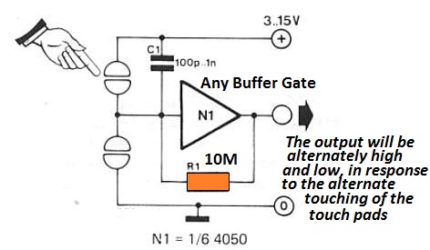 The input of N1 is kept low by the output through R1 when the contacts are released, hence the output remains low permanently.
The input of N1 is rendered high when the upper set of contacts are bridged, so that the output goes high.
Once the contacts are released, the input is kept high through R1, and therefore output stays high.
The input of N1 is kept low by the output through R1 when the contacts are released, hence the output remains low permanently.
The input of N1 is rendered high when the upper set of contacts are bridged, so that the output goes high.
Once the contacts are released, the input is kept high through R1, and therefore output stays high.
 While a filter with a notch frequency of 50 Hz and a Q of 10 will require nearly 150 Henries inductance, the most easiest answer is To electronically synthesize the intended inductance (see Figure 2).
 Together with R2 �� R5, C2 and P1, the two opamps give a rather ideal simulation of a traditional wound inducer located within two pin3 of IC1 and earth.
The resulting inductance value is equal to the sum of the R2, R3 and C2 values ( i.e., L = R2 x R3 x C2).
With P1 this value could be slightly changed for tuning purposes.
The attenuation of 50 Hz signals is 45 to 50 dB when the circuit is calibrated correctly.
The circuit can be used in harmonic distortion as a hum-rejection filter for TV sound signals, meters or as hum filter.
Together with R2 �� R5, C2 and P1, the two opamps give a rather ideal simulation of a traditional wound inducer located within two pin3 of IC1 and earth.
The resulting inductance value is equal to the sum of the R2, R3 and C2 values ( i.e., L = R2 x R3 x C2).
With P1 this value could be slightly changed for tuning purposes.
The attenuation of 50 Hz signals is 45 to 50 dB when the circuit is calibrated correctly.
The circuit can be used in harmonic distortion as a hum-rejection filter for TV sound signals, meters or as hum filter.
 The starter is ignored, but the choke (L1) can be allowed to be in the circuit.
The (standard) triac control stage is attached by using the choke with a 33 k/2 W 'bleeder' resistor across the tube and choke to provide current to the dimmer when the tube is shut down.
On the other hand, 3 100 K resistors 1/4 W could be joined in parallel.
Any kind of suppression systems existing in the triac dimmer must be taken off; the large self-inductance of L1 may limit the interference due to the dimmer to a lowest.
When the range of fluorescent light intensity control is found inadequate, you possibly can test out the value of capacitor C1. Regular safety measures must, obviously, be weaned: the circuit should be installed on an insulation box, P1 must have a plastic spindle, and Cl needs to be a 400 V rated.
The starter is ignored, but the choke (L1) can be allowed to be in the circuit.
The (standard) triac control stage is attached by using the choke with a 33 k/2 W 'bleeder' resistor across the tube and choke to provide current to the dimmer when the tube is shut down.
On the other hand, 3 100 K resistors 1/4 W could be joined in parallel.
Any kind of suppression systems existing in the triac dimmer must be taken off; the large self-inductance of L1 may limit the interference due to the dimmer to a lowest.
When the range of fluorescent light intensity control is found inadequate, you possibly can test out the value of capacitor C1. Regular safety measures must, obviously, be weaned: the circuit should be installed on an insulation box, P1 must have a plastic spindle, and Cl needs to be a 400 V rated.
 The quantity of input channels could be significantly extended, in case it is demanded, so long as the common drain load resistor (RI) is appositely selected.
Its value may be the regular value nearest to 22k / n, where n is actually the quantity of input channels
The quantity of input channels could be significantly extended, in case it is demanded, so long as the common drain load resistor (RI) is appositely selected.
Its value may be the regular value nearest to 22k / n, where n is actually the quantity of input channels
 Parts List for the above simple transistor hobby circuit
R1 = 1K,
R2 = 2K2,
D1 = 1N4148,
P1 = 300 Ohms,
T1 = BC547
LED = RED 5mm
Parts List for the above simple transistor hobby circuit
R1 = 1K,
R2 = 2K2,
D1 = 1N4148,
P1 = 300 Ohms,
T1 = BC547
LED = RED 5mm
 This circuit of a transistor power amplifier is outstanding with its performance and is able to provide a thumping 100 watts of pure music output.
As can be seen in the diagram it utilizes mainly transistors for making the amplifier and its implementations and a handful of other inexpensive passive components like resistors and capacitors.
The required input is not more than 1 V, which gets amplified 200,000 times at the output.
This circuit of a transistor power amplifier is outstanding with its performance and is able to provide a thumping 100 watts of pure music output.
As can be seen in the diagram it utilizes mainly transistors for making the amplifier and its implementations and a handful of other inexpensive passive components like resistors and capacitors.
The required input is not more than 1 V, which gets amplified 200,000 times at the output.
 This a simple transistorized 10 W power amplifier, mains driven circuit, which will deliver 10 watt into a 4 ohm loudspeaker.
The input sensitivity of the amplifier is 100 mV input sensitivity, input resistance is 10 k.
Before using make sure to optimze thr 100 ohm preset for setting up the quiscent current correctly.
Meaning to ensure that the amplified draws minimum possibe current in the absence of an input signal.
To do this connect a small 10 mA bulb in series with the positive line.
Short the input line with the ground, also short the speaker terminals.
Now switch ON power and adjust the 100 ohm preset until the bulb illumination is almost zero.
The 100 k preset sets the gain of the amplifier.
This a simple transistorized 10 W power amplifier, mains driven circuit, which will deliver 10 watt into a 4 ohm loudspeaker.
The input sensitivity of the amplifier is 100 mV input sensitivity, input resistance is 10 k.
Before using make sure to optimze thr 100 ohm preset for setting up the quiscent current correctly.
Meaning to ensure that the amplified draws minimum possibe current in the absence of an input signal.
To do this connect a small 10 mA bulb in series with the positive line.
Short the input line with the ground, also short the speaker terminals.
Now switch ON power and adjust the 100 ohm preset until the bulb illumination is almost zero.
The 100 k preset sets the gain of the amplifier.
 This simple emergency lamp circuit uses very components and yet is able to provide some useful service.
The shown device is able to switch ON automatically when mains power fails, illuminating all the connected LEDs.As soon as power is restored, the LEDs shut off automatically and the connected starts charging through the built in power supply.
The emergency light circuit employs a transformerless power supply for initiating the explained automatic actions and also for trickle charging the connected battery.
Parts List for the above CIRCUIT DIAGRAM
R1 = 220K,
R2 = 10K,
D1, D2, D3 = 1N4007,
Z1 = 15V 1watt, zener diode,
C2 = 100uF/25V
LEDs = white, high bright type.
This simple emergency lamp circuit uses very components and yet is able to provide some useful service.
The shown device is able to switch ON automatically when mains power fails, illuminating all the connected LEDs.As soon as power is restored, the LEDs shut off automatically and the connected starts charging through the built in power supply.
The emergency light circuit employs a transformerless power supply for initiating the explained automatic actions and also for trickle charging the connected battery.
Parts List for the above CIRCUIT DIAGRAM
R1 = 220K,
R2 = 10K,
D1, D2, D3 = 1N4007,
Z1 = 15V 1watt, zener diode,
C2 = 100uF/25V
LEDs = white, high bright type.
 This simple transistor circuit can be used for monitoring the dawn and dusk conditions and for switching lights in response to the varying conditions.
Thus the day night light switch circuit can be used for switching ON the connected lights when night sets in and switch it OFF during day break.
The threshold tripping point may be set by adjusting the 10K preset.
The capacitors are 100uF/25V, the transistors are ordinary BC547, and the diodes are 1N4007.
This simple transistor circuit can be used for monitoring the dawn and dusk conditions and for switching lights in response to the varying conditions.
Thus the day night light switch circuit can be used for switching ON the connected lights when night sets in and switch it OFF during day break.
The threshold tripping point may be set by adjusting the 10K preset.
The capacitors are 100uF/25V, the transistors are ordinary BC547, and the diodes are 1N4007.
 R1 = 5k6
R2 = 47k
R3 = 3M3
R4 = 33K
R5, R7 = 330 OHMS
R6, R8 = 2K2
R9 = 22 ohms 1 watt
R10 = 330k
R12 = 1k
C1 = 0.33uF/400V
C2 = 4.7uF/25V
C3 = 0.1uF/25V
C4 = 1uF/25V
T1, T2 = BC547
T3, T4 = BC557
D1 = 1N4007
LED = Amber high bright 3 V, 20 mA
B1 = Ni-Cd Cell
This is a simple hobby project and exhibits all the properties of a conventional wax type candle.
Here the LED is used in place of the candle flame, which illuminates as soon as the mains power fails and shuts off automatically when the power is restored.
So it also performs the function of an emergency lamp.
The connected battery is used for powering the candle��light and it is charged continuously when the unit is not being used and powered through the mains supply.
An interesting ��puff off�� feature is also included so tatthe ��candle�� light may be switched OFF whenever desired through a puff of airinto the attached mic which acts as the air vibration sensor.
R1 = 5k6
R2 = 47k
R3 = 3M3
R4 = 33K
R5, R7 = 330 OHMS
R6, R8 = 2K2
R9 = 22 ohms 1 watt
R10 = 330k
R12 = 1k
C1 = 0.33uF/400V
C2 = 4.7uF/25V
C3 = 0.1uF/25V
C4 = 1uF/25V
T1, T2 = BC547
T3, T4 = BC557
D1 = 1N4007
LED = Amber high bright 3 V, 20 mA
B1 = Ni-Cd Cell
This is a simple hobby project and exhibits all the properties of a conventional wax type candle.
Here the LED is used in place of the candle flame, which illuminates as soon as the mains power fails and shuts off automatically when the power is restored.
So it also performs the function of an emergency lamp.
The connected battery is used for powering the candle��light and it is charged continuously when the unit is not being used and powered through the mains supply.
An interesting ��puff off�� feature is also included so tatthe ��candle�� light may be switched OFF whenever desired through a puff of airinto the attached mic which acts as the air vibration sensor.
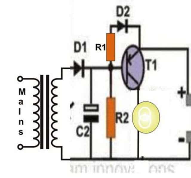 This circuit may be used as an automatic emergency lamp when there��s no power or when mains power fails during night times.
As shown in the diagram, the circuit utilizes a cheap incandescent flashlight bulb for the required illumination.
As long as the input supply from the mains transformer is present the transistor remains switched OFF and so does the lamp.
However the moment the mains power fails, the transistor conducts and switches ON the battery power to the bulb, instantly illuminating it brightly.
The battery is trickle charged for so long as the mainspower remains connected to the circuit.
Parts List
R1 = 22 Ohms,
R2 = 1K,
D1 = 1N4007,
T1 = 8550,
Lamp = 3V flashlight bulb.
Transformer = 0-3V, 500 mA,
Battery = 3V, penlight 1.5 V cells (2nos.
in series)
This circuit may be used as an automatic emergency lamp when there��s no power or when mains power fails during night times.
As shown in the diagram, the circuit utilizes a cheap incandescent flashlight bulb for the required illumination.
As long as the input supply from the mains transformer is present the transistor remains switched OFF and so does the lamp.
However the moment the mains power fails, the transistor conducts and switches ON the battery power to the bulb, instantly illuminating it brightly.
The battery is trickle charged for so long as the mainspower remains connected to the circuit.
Parts List
R1 = 22 Ohms,
R2 = 1K,
D1 = 1N4007,
T1 = 8550,
Lamp = 3V flashlight bulb.
Transformer = 0-3V, 500 mA,
Battery = 3V, penlight 1.5 V cells (2nos.
in series)
 This circuit may be used for transforming music into dancing light patterns.
The operation of the music lamp circuit is very simple, the music input is fed to the bases of the shown transistor array, each of them are configured to conduct at a specific voltage level in the incrementing order from the top to the bottom transistor.
Thus the uppermost transistor conducts with the input music is at the minimum volume level and the subsequent transistor starts to conduct in sequence as per the volume or the pitch of the music.
Each transistor is rigged with individual lamps which light up in response to the music levels in a ��chasing�� dancing light pattern.
Parts List
All the base presets are = 10K,
All the collector resistors are 470 Ohms,
All the diodes are = 1N4148,
All NPN transistors are = BC547,
The single PNP transistor is = BC557,
All the triacs are = BT136,
The input capacitor = 0.22uF/25V non polar.
This circuit may be used for transforming music into dancing light patterns.
The operation of the music lamp circuit is very simple, the music input is fed to the bases of the shown transistor array, each of them are configured to conduct at a specific voltage level in the incrementing order from the top to the bottom transistor.
Thus the uppermost transistor conducts with the input music is at the minimum volume level and the subsequent transistor starts to conduct in sequence as per the volume or the pitch of the music.
Each transistor is rigged with individual lamps which light up in response to the music levels in a ��chasing�� dancing light pattern.
Parts List
All the base presets are = 10K,
All the collector resistors are 470 Ohms,
All the diodes are = 1N4148,
All NPN transistors are = BC547,
The single PNP transistor is = BC557,
All the triacs are = BT136,
The input capacitor = 0.22uF/25V non polar.
 R1 = 5k6
R2 = 47k
R3 = 3M3
R4 = 33K
R5, R7 = 330 OHMS
R6 = 2K2
C1 = 0.33uF/400V
C2 = 4.7uF/25V
T1, T2 = BC547
T3 = BC557
D1 = 1N4007
LED = RED LEDs 3 V, 20 mA
The interesting clap switch circuit shown here can be used in stairways and passages for illuminating the premise momentarily through clap sound.
The circuit is basically a sound sensor circuit with an enclosed amplifier stage.
The clap sound or any similar sound is detected by the mic and converted into minute electrical pulses.
These electrical pulses are suitably amplified by the subsequent transistor stage.
The Darlington stage shown at the output is the timer stage which switches in response to the above sound interaction and illuminate the connected LEDs for some period of time defined by the 220K resistor and the two39 K resistors.
After the time lapses the LEDs are switched off automatically and the clap switch circuit returns to its original state until the next clap sound is detected.
The parts list is given in the circuit diagram itself.
R1 = 5k6
R2 = 47k
R3 = 3M3
R4 = 33K
R5, R7 = 330 OHMS
R6 = 2K2
C1 = 0.33uF/400V
C2 = 4.7uF/25V
T1, T2 = BC547
T3 = BC557
D1 = 1N4007
LED = RED LEDs 3 V, 20 mA
The interesting clap switch circuit shown here can be used in stairways and passages for illuminating the premise momentarily through clap sound.
The circuit is basically a sound sensor circuit with an enclosed amplifier stage.
The clap sound or any similar sound is detected by the mic and converted into minute electrical pulses.
These electrical pulses are suitably amplified by the subsequent transistor stage.
The Darlington stage shown at the output is the timer stage which switches in response to the above sound interaction and illuminate the connected LEDs for some period of time defined by the 220K resistor and the two39 K resistors.
After the time lapses the LEDs are switched off automatically and the clap switch circuit returns to its original state until the next clap sound is detected.
The parts list is given in the circuit diagram itself.
 The circuit shown here can be used for detecting earth leakage conditions and for implementing the required shutting off the mains power supply.
Unlike usual configurations, here the ground to the ELCB circuit and the relay is acquired from the earthing line itself.
Also since the input coil is also referenced to the common earthing ground, the entire functioning becomes compatible and accurate.
On sensing a possible current leakage at the input, the transistors come into action and switch the relays appropriately.
The two relay have their individual specific roles to play.
One relay detects and switches OFF when there��s current leakage through an appliances body, while the other relay is wired up to sense the presence of a the earthing line and switches OFF the mains as soon a wrong or weak earthing line is detected.
The circuit shown here can be used for detecting earth leakage conditions and for implementing the required shutting off the mains power supply.
Unlike usual configurations, here the ground to the ELCB circuit and the relay is acquired from the earthing line itself.
Also since the input coil is also referenced to the common earthing ground, the entire functioning becomes compatible and accurate.
On sensing a possible current leakage at the input, the transistors come into action and switch the relays appropriately.
The two relay have their individual specific roles to play.
One relay detects and switches OFF when there��s current leakage through an appliances body, while the other relay is wired up to sense the presence of a the earthing line and switches OFF the mains as soon a wrong or weak earthing line is detected.
 Parts List
R1, R2 = 1K,
P1,P2 = 100K pots,
C1, C2 = 33uF/25V,
T1, T2 = BC547,
Resistors connected with each LED series = 470 Ohms
LEDs are 5mm type, color as per choice.
Parts List
R1, R2 = 1K,
P1,P2 = 100K pots,
C1, C2 = 33uF/25V,
T1, T2 = BC547,
Resistors connected with each LED series = 470 Ohms
LEDs are 5mm type, color as per choice.
 Anything spoken into the mic of the presented circuit cab be clearly picked up and reproduced by any standard FM radio, within a range of 30meters of distance.
The circuit is very simple and just requires ther shown components to be assembled and connected with each other as depicted in the diagram.
The coil L1 for this FM transmitter circuit consists of 5 turns of 1mm super enameled copper wire, having a diameter of around 0.6 cm.
Parts List
R1 = 4K7,
R2 = 82K,
R3 = 1K,
C1 = 10pF,
C2, C3 = 27pF,
C4 = 0.001uF,
C5 = 0.22uF,
T1 = BC547
Anything spoken into the mic of the presented circuit cab be clearly picked up and reproduced by any standard FM radio, within a range of 30meters of distance.
The circuit is very simple and just requires ther shown components to be assembled and connected with each other as depicted in the diagram.
The coil L1 for this FM transmitter circuit consists of 5 turns of 1mm super enameled copper wire, having a diameter of around 0.6 cm.
Parts List
R1 = 4K7,
R2 = 82K,
R3 = 1K,
C1 = 10pF,
C2, C3 = 27pF,
C4 = 0.001uF,
C5 = 0.22uF,
T1 = BC547
 The shown design of a 40 LED emergency light is driven usingan ordinary transistor/transformer inverter circuit.
The transistor and the respective winding of th transformer are configured as a high frequency oscillator stage.
The oscillations induce a high voltage across the winding of the transformer.
The stepped-up voltage at the output is directly used to drive the LED which are all connected in series for getting the desired balance and the illumination.
Parts List
R1 = 470 Ohms,
VR1 = 47K,
C1, C2 = 1uF/25V
TR1 = 0-6V, 500mA,
Battery = 6V, 2AH,
LEDs = high bright white, 40 nos.
The shown design of a 40 LED emergency light is driven usingan ordinary transistor/transformer inverter circuit.
The transistor and the respective winding of th transformer are configured as a high frequency oscillator stage.
The oscillations induce a high voltage across the winding of the transformer.
The stepped-up voltage at the output is directly used to drive the LED which are all connected in series for getting the desired balance and the illumination.
Parts List
R1 = 470 Ohms,
VR1 = 47K,
C1, C2 = 1uF/25V
TR1 = 0-6V, 500mA,
Battery = 6V, 2AH,
LEDs = high bright white, 40 nos.
 If you are looking for a circuit which can be used to latch the output in response to an input signal, then this circuit can be used for the intended purpose very effectively and also very cheaply.
A momentary input trigger is applied to the base of T1,which switches it for a fraction of a second depending upon the length of the applied signal.
The conduction of T1 immediately switches T2 and the connected relay.
However at the very instant a feedback voltage also appears at the base of T1 via R3 from the collector of T2.
This feed back voltage instantly latches the circuit and keeps the relay activated even after the trigger from the input is removed.
Parts List
R1, R3 = 100k,
R2, R4 = 10K,
C1 = 1uF/25V
D1 = 1N4148,
T1 = BC547,
T2 = BC557
Relay = 12V, SPDT
If you are looking for a circuit which can be used to latch the output in response to an input signal, then this circuit can be used for the intended purpose very effectively and also very cheaply.
A momentary input trigger is applied to the base of T1,which switches it for a fraction of a second depending upon the length of the applied signal.
The conduction of T1 immediately switches T2 and the connected relay.
However at the very instant a feedback voltage also appears at the base of T1 via R3 from the collector of T2.
This feed back voltage instantly latches the circuit and keeps the relay activated even after the trigger from the input is removed.
Parts List
R1, R3 = 100k,
R2, R4 = 10K,
C1 = 1uF/25V
D1 = 1N4148,
T1 = BC547,
T2 = BC557
Relay = 12V, SPDT
 In one of the previous sections we studied a simple music light show circuit using mains operated incandescent lamps, the present design incorporate LEDs for similar intended light show generation.
As can be seen in the figure, the transistors are all wired up in sequencing array.
The music signal varying with pitch and amplitude is applied at the base of the buffer amplifier PNP transistor.
The amplified music is then fed across the whole array where the respective transistor receive the inputs with incrementing pitch or the volume levels and go on switching in the corresponding manner from start to finish, producing an interesting LED light sequencing pattern.
This light exactly varies its length according to the pitch or the volume of the fed music signal.
Parts list is provided in the diagram.
In one of the previous sections we studied a simple music light show circuit using mains operated incandescent lamps, the present design incorporate LEDs for similar intended light show generation.
As can be seen in the figure, the transistors are all wired up in sequencing array.
The music signal varying with pitch and amplitude is applied at the base of the buffer amplifier PNP transistor.
The amplified music is then fed across the whole array where the respective transistor receive the inputs with incrementing pitch or the volume levels and go on switching in the corresponding manner from start to finish, producing an interesting LED light sequencing pattern.
This light exactly varies its length according to the pitch or the volume of the fed music signal.
Parts list is provided in the diagram.
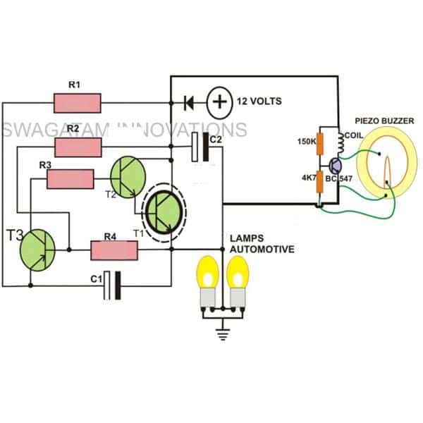 If you want to make a flasher unit for you motorbike then this circuit is just for you.
This simple turn signal flasher circuit can be easily built and installed in any two wheelers for the desired actions.
The automobile flasher circuit employs just two 2-pins instead of 3 as found in other flasher circuits.
Once installed, the circuit will faithfully flash the side indicator lights whenever the intended function is switched ON.
The circuit also incorporates an optional buzzer circuit which can be also included for getting a beeping sound in response to the flashing of the lamps.
Parts List
R1, R2, R3 = 10K
R4= 33K
T1 = D1351,
T2 = BC547,
T3 = BC557,
C1, C2 = 33uF.25V
L1 = Buzzer Coil
If you want to make a flasher unit for you motorbike then this circuit is just for you.
This simple turn signal flasher circuit can be easily built and installed in any two wheelers for the desired actions.
The automobile flasher circuit employs just two 2-pins instead of 3 as found in other flasher circuits.
Once installed, the circuit will faithfully flash the side indicator lights whenever the intended function is switched ON.
The circuit also incorporates an optional buzzer circuit which can be also included for getting a beeping sound in response to the flashing of the lamps.
Parts List
R1, R2, R3 = 10K
R4= 33K
T1 = D1351,
T2 = BC547,
T3 = BC557,
C1, C2 = 33uF.25V
L1 = Buzzer Coil
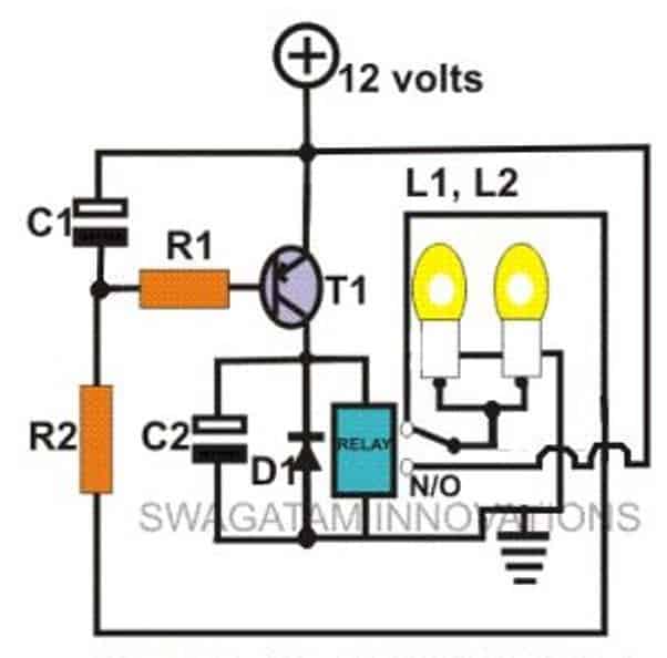 In the above section we discussed a simple three transistor based flasher circuit; here we study another similar design, however here we incorporate a relay for the switching actions of the lamps.
The circuit looks pretty straightforward and employs hardly anything substantial and yet performs the expected functions wonderfully well.
Just build it and wire it in your mo-bike for witnessing the intended functions...
In the above section we discussed a simple three transistor based flasher circuit; here we study another similar design, however here we incorporate a relay for the switching actions of the lamps.
The circuit looks pretty straightforward and employs hardly anything substantial and yet performs the expected functions wonderfully well.
Just build it and wire it in your mo-bike for witnessing the intended functions...
 Next, the capacitor begins discharging through the diac, which fires the triac causing the connected lamp to illuminate brightly and shut off.
After some delay as preset by the 100 k pot, the capacitor begins recharging again to the breakdown limit of the diac, causing the lamp to pulse and shut down.
The process continues allowing the lamp to flash at the specified rate.
The 1 k decides at what current threshold the triac is supposed to fire.
Next, the capacitor begins discharging through the diac, which fires the triac causing the connected lamp to illuminate brightly and shut off.
After some delay as preset by the 100 k pot, the capacitor begins recharging again to the breakdown limit of the diac, causing the lamp to pulse and shut down.
The process continues allowing the lamp to flash at the specified rate.
The 1 k decides at what current threshold the triac is supposed to fire.
 Yes this simple transistor circuit can be used as a home door bell and it��s ON time can be set as preferred by the user, meaning if you wanted that the sound of the bell to remain switched ON for a particular period of time, you could easily do it just by adjusting the given pot.
The actual tune is derived from the IC UM66 and the associated components, while all the included transistors along with the relay are configured for producing the time delay for keeping the music switched ON.
Parts List
R1, R2, R4, R5 = 1K
VR1 = 100K,
D1, D2 = 1N4007,
C1, C2 = 100uF/25
T1, T3 = BC547,
T2 = BC557
Z1 = 3V/400mW
Transformer = 0-12V/500mA,
S1 = Bell Push
IC = UM66
Yes this simple transistor circuit can be used as a home door bell and it��s ON time can be set as preferred by the user, meaning if you wanted that the sound of the bell to remain switched ON for a particular period of time, you could easily do it just by adjusting the given pot.
The actual tune is derived from the IC UM66 and the associated components, while all the included transistors along with the relay are configured for producing the time delay for keeping the music switched ON.
Parts List
R1, R2, R4, R5 = 1K
VR1 = 100K,
D1, D2 = 1N4007,
C1, C2 = 100uF/25
T1, T3 = BC547,
T2 = BC557
Z1 = 3V/400mW
Transformer = 0-12V/500mA,
S1 = Bell Push
IC = UM66
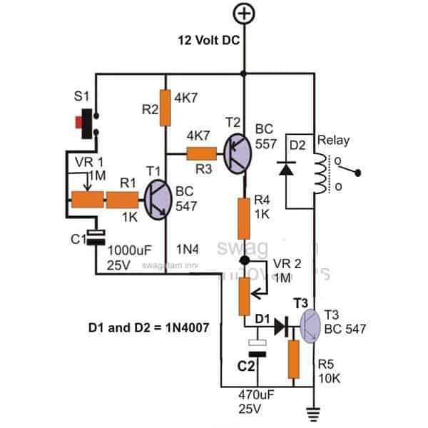 The circuit can be used for generating delays at a desired rate.
The On time of the relay can be controlled by adjusting the Pot VR1 while the pot VR2 may be used to decide after how long the relay responds once theinput trigger is fed by the switch S1.
The parts list is enclosed inside the diagram.
The circuit can be used for generating delays at a desired rate.
The On time of the relay can be controlled by adjusting the Pot VR1 while the pot VR2 may be used to decide after how long the relay responds once theinput trigger is fed by the switch S1.
The parts list is enclosed inside the diagram.
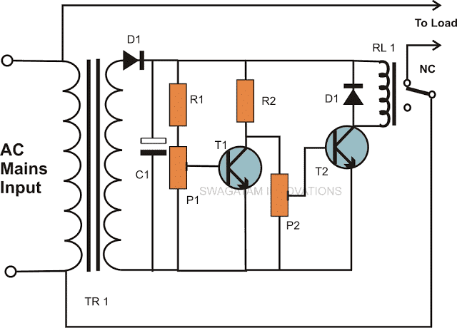 Are you having problems with your input Mains supply? That��s common problem associated with our input mains AC line, where a high and a low voltage conditions are quite frequently encountered by us.
The simple high low voltage controller circuit shown here can be built and installed in you house electrical board for getting a 24/7 safety from the possible dangerous AC voltage conditions.
The circuit keeps the relay and the wired appliances as long as the mains input stays within a safe tolerable level and switches the load OFF the moment a dangerous or unfavorable voltage condition is sensed by the circuit.
Parts List
R1, R2 = 1K,
P1, P2 = 10K Preset,
T1, T2 = BC547B,
C1 = 100uF/25V,
D1 = 1N4007
RL1 = 12V, SPDT,
TR1 = 0-12V, 500mA
Are you having problems with your input Mains supply? That��s common problem associated with our input mains AC line, where a high and a low voltage conditions are quite frequently encountered by us.
The simple high low voltage controller circuit shown here can be built and installed in you house electrical board for getting a 24/7 safety from the possible dangerous AC voltage conditions.
The circuit keeps the relay and the wired appliances as long as the mains input stays within a safe tolerable level and switches the load OFF the moment a dangerous or unfavorable voltage condition is sensed by the circuit.
Parts List
R1, R2 = 1K,
P1, P2 = 10K Preset,
T1, T2 = BC547B,
C1 = 100uF/25V,
D1 = 1N4007
RL1 = 12V, SPDT,
TR1 = 0-12V, 500mA
 This unique work bench circuit utilizes only a few inexpensive transistors and yet delivers some truly useful features.
The feature includes continuously variable voltage from zero to the maximum transformer voltage and current variable from zero to the maximum applied input level.
The output of this power supply is also over load protected.
The pot P1 is used for setting the maximum current while the pot P2 is used for varying the output voltage level up to the desired levels.
Parts List
R1 = 1K2,
R2 = 100 Ohms,
R3 = 470 Ohms,
R4 = Evaluate using Ohms law.
R5 = 1K8,
R6 = 4k7,
R7 = 68 Ohms,
R8 = 1k8,
T1 = 2N3055,
T2, T3 = BC 547B,
D1 = 1N4007,
D2, D3, D4, D5 = 1N5408,
C1, C2 = 2200uF/50V,
Tr1 = 0 �C 35 Volts, 3 Amp
This unique work bench circuit utilizes only a few inexpensive transistors and yet delivers some truly useful features.
The feature includes continuously variable voltage from zero to the maximum transformer voltage and current variable from zero to the maximum applied input level.
The output of this power supply is also over load protected.
The pot P1 is used for setting the maximum current while the pot P2 is used for varying the output voltage level up to the desired levels.
Parts List
R1 = 1K2,
R2 = 100 Ohms,
R3 = 470 Ohms,
R4 = Evaluate using Ohms law.
R5 = 1K8,
R6 = 4k7,
R7 = 68 Ohms,
R8 = 1k8,
T1 = 2N3055,
T2, T3 = BC 547B,
D1 = 1N4007,
D2, D3, D4, D5 = 1N5408,
C1, C2 = 2200uF/50V,
Tr1 = 0 �C 35 Volts, 3 Amp
 When it comes to frequency generating circuits or rather precise oscillator circuits, crystals become a crucial part, especially because they play an important role for generating and maintaining accurate frequency rates of the particular circuit.
However these devices are prone to many defects and are normally difficult to check through conventional DMM units.
The shown circuit can be used for checking all types of crystals instantly.
The circuit itself is a small transistor oscillator circuit which starts oscillating when a good crystal is introduced across the indicated points in the circuit.
If the crystal is a good one, the bulb lights up showing the relevant results and if there��s any defect in the attached crystal, the bulb remains switched OFF.
When it comes to frequency generating circuits or rather precise oscillator circuits, crystals become a crucial part, especially because they play an important role for generating and maintaining accurate frequency rates of the particular circuit.
However these devices are prone to many defects and are normally difficult to check through conventional DMM units.
The shown circuit can be used for checking all types of crystals instantly.
The circuit itself is a small transistor oscillator circuit which starts oscillating when a good crystal is introduced across the indicated points in the circuit.
If the crystal is a good one, the bulb lights up showing the relevant results and if there��s any defect in the attached crystal, the bulb remains switched OFF.
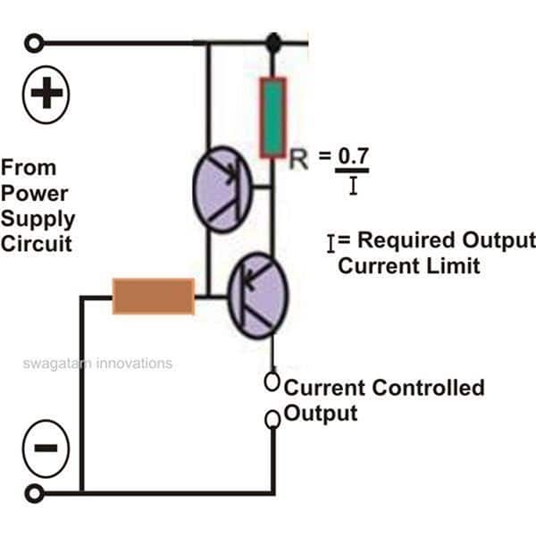 In many critical applications, circuits are required to maintain a strict controlled magnitude of current through them of at their outputs.
The proposed circuit is exactly meant for carrying out the discussed function.
The lower transistor is the main output transistor which operates the output vulnerable load and by itself is unable to control the current through it.
The introduction of the upper transistor makes it sure that the base of the lower transistor is allowed to conduct as long as the current output is within the specified limits.
In case the current tends to cross the limits, the upper transistor conducts and switches OFF the lower transistor inhibiting any further passage of the exceeded current limit.
The threshold current may be fixed by R which is calculated with the shown formula.
In many critical applications, circuits are required to maintain a strict controlled magnitude of current through them of at their outputs.
The proposed circuit is exactly meant for carrying out the discussed function.
The lower transistor is the main output transistor which operates the output vulnerable load and by itself is unable to control the current through it.
The introduction of the upper transistor makes it sure that the base of the lower transistor is allowed to conduct as long as the current output is within the specified limits.
In case the current tends to cross the limits, the upper transistor conducts and switches OFF the lower transistor inhibiting any further passage of the exceeded current limit.
The threshold current may be fixed by R which is calculated with the shown formula.
 Unless of course a "reset" action is employed until a specific period of time has lapsed the alarm will automatically start buzzing.
The working theory of this older person alarm could be tailored as necessary and could motivate some other concepts.
As long as the old individual is resting in bed a pressure button (S1) or a press switch beneath the bed mattress is maintained in closed circuit status.
This allows the 4040 IC2 in its reset condition through transistor TR1 therefore, the piezo sounder WDI remains turned OFF.
Clock pulses of roughly 1 Hz frequency are generated constantly through the 555 timer IC1 (pin 3) towards the counter input of IC2 at pin 10.
However, this action has no effect on the circuit until the individual gets up from the bed (for this action you can also consider a commode or simply, the bathroom door) after which the counter circuit becomes activated and it starts counting.
In the event that the time taken by the elderly person from the bed to the commode or bathroom exceeds a predertermined time (the bathroom can be used for activating microswitch S2 fixed on the bathroom door which resets the timer back to zero) the counter output Q6 (or Q7 perhaps) goes high.
This in turn causes the alarm WD1 to sounds which may be situated in a adjoining area to ensure that anybody can check out and make sure the individual is completely OK.
A hold off between one and two minutes had been chosen to let the aged individual have enough time and also due to the fact in real life the microswitch S2 was not always triggered.
For the present circuit the switch unwraps as soon as the person departs the commode, and thus IC2 begins counting.
When the time person's returning to bed is much too long (which resets the counter) is yet again very long for the alarm to trigger ON, it means that individual is upright, or is going back to bed or might have fallen down.
Considering that an older individual is not likely to keep standing up over (say) 2 minutes and is particularly impossible to take more than 2 minutes to come back to bed, it is most likely that this person has slipped.
The prototype can be powered through a safe 6V battery, that may be standard rechargeable.
Unless of course a "reset" action is employed until a specific period of time has lapsed the alarm will automatically start buzzing.
The working theory of this older person alarm could be tailored as necessary and could motivate some other concepts.
As long as the old individual is resting in bed a pressure button (S1) or a press switch beneath the bed mattress is maintained in closed circuit status.
This allows the 4040 IC2 in its reset condition through transistor TR1 therefore, the piezo sounder WDI remains turned OFF.
Clock pulses of roughly 1 Hz frequency are generated constantly through the 555 timer IC1 (pin 3) towards the counter input of IC2 at pin 10.
However, this action has no effect on the circuit until the individual gets up from the bed (for this action you can also consider a commode or simply, the bathroom door) after which the counter circuit becomes activated and it starts counting.
In the event that the time taken by the elderly person from the bed to the commode or bathroom exceeds a predertermined time (the bathroom can be used for activating microswitch S2 fixed on the bathroom door which resets the timer back to zero) the counter output Q6 (or Q7 perhaps) goes high.
This in turn causes the alarm WD1 to sounds which may be situated in a adjoining area to ensure that anybody can check out and make sure the individual is completely OK.
A hold off between one and two minutes had been chosen to let the aged individual have enough time and also due to the fact in real life the microswitch S2 was not always triggered.
For the present circuit the switch unwraps as soon as the person departs the commode, and thus IC2 begins counting.
When the time person's returning to bed is much too long (which resets the counter) is yet again very long for the alarm to trigger ON, it means that individual is upright, or is going back to bed or might have fallen down.
Considering that an older individual is not likely to keep standing up over (say) 2 minutes and is particularly impossible to take more than 2 minutes to come back to bed, it is most likely that this person has slipped.
The prototype can be powered through a safe 6V battery, that may be standard rechargeable.
 Gate N1 combined with R1 and C1 works like a square wave generator stage which, by means of N2 controls the flip-flop which involves N3 and N4. Couple of outputs of the flip-flop turn the LEDs D1 and D2 and ON/OFF alternately through transistors T1 and T2. The push button, when pressed, causes the LEDs to blink at very very fast.
As soon as the user releases the push button only one particular LED out of the two remains lit while the other one is completely OFF.
The LEDs can be labelled 'heads' or "tails" and as a result provide the decision which is completely random in nature.
A 3rd LED for 'not sure' had been thought of, however it was terminated because today's professional are eligible to make several decisions for themselves�� On a serious note, the circuit is outstandingly sensible and the output for 'heads and tails' is unquestionably correct and 100 % random!
Well, I am sure there can be countless number of hobby electronic circuits that can be included here, however for the moment I could gather only these many, if you think I might have missed a few you may simply feel free to update the same through your valuable comments....
Gate N1 combined with R1 and C1 works like a square wave generator stage which, by means of N2 controls the flip-flop which involves N3 and N4. Couple of outputs of the flip-flop turn the LEDs D1 and D2 and ON/OFF alternately through transistors T1 and T2. The push button, when pressed, causes the LEDs to blink at very very fast.
As soon as the user releases the push button only one particular LED out of the two remains lit while the other one is completely OFF.
The LEDs can be labelled 'heads' or "tails" and as a result provide the decision which is completely random in nature.
A 3rd LED for 'not sure' had been thought of, however it was terminated because today's professional are eligible to make several decisions for themselves�� On a serious note, the circuit is outstandingly sensible and the output for 'heads and tails' is unquestionably correct and 100 % random!
Well, I am sure there can be countless number of hobby electronic circuits that can be included here, however for the moment I could gather only these many, if you think I might have missed a few you may simply feel free to update the same through your valuable comments....
 This IC 555 inverter will transformer a 6 V or 12 V battery to 220V low current output for driving or illuminating any neon sign amp or tube.
The transformer T1, can be built on any standard E core ferrite assembly, with 10 turns on the primary side, and the 200 turns on the secondary side.
This IC 555 inverter will transformer a 6 V or 12 V battery to 220V low current output for driving or illuminating any neon sign amp or tube.
The transformer T1, can be built on any standard E core ferrite assembly, with 10 turns on the primary side, and the 200 turns on the secondary side.
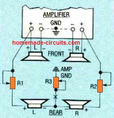 Resistor R3 is fine-tuned by listening to the audio, so as to deliver a little bit of blending of the front L and R signals into the backside speakers .
In case preferred, an on/off switch could be fitted at X to get rid of the mixing of the music across the rear channels.
If your amplifier comes with an A-B switch to work with an additional pair of speakers, the rear-speaker circuit, (a) or (b), could be hooked up straight to the positive B terminals.
This can make it possible for easy on-off switching of the rear channels.
Resistor R3 is fine-tuned by listening to the audio, so as to deliver a little bit of blending of the front L and R signals into the backside speakers .
In case preferred, an on/off switch could be fitted at X to get rid of the mixing of the music across the rear channels.
If your amplifier comes with an A-B switch to work with an additional pair of speakers, the rear-speaker circuit, (a) or (b), could be hooked up straight to the positive B terminals.
This can make it possible for easy on-off switching of the rear channels.
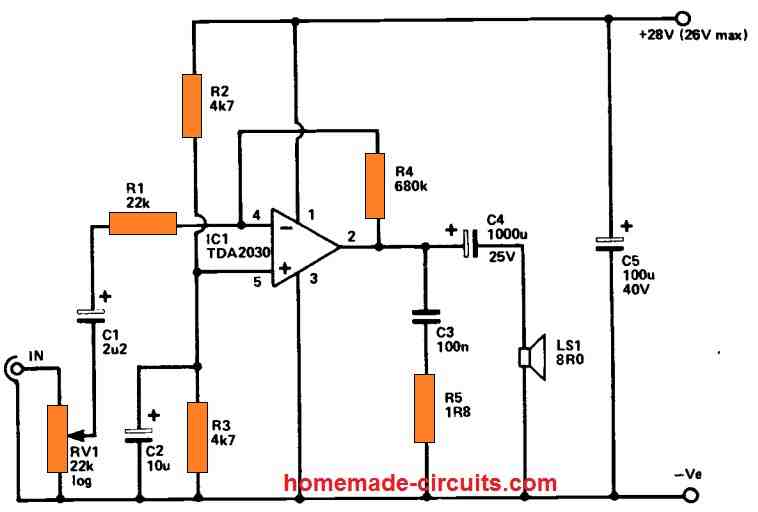
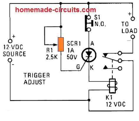 The applied voltage is sampled using the SCR's gate circuit.
SCR1 stays off and K1's contacts remain closed so long as the applied voltage maintains below a certain amount, delivering current to the load.
Once the source voltage increases over 12 V, enough current is delivered to SCR1's gate forcing it to conduct , and switch ON the relay to shut down the load.
This protects the load from an over voltage situation.
The adjustment of R1 determines the SCR1 trigger point.
K1's contacts open when SCR1 is activated (actuating the relay), preventing current flow to the load.
The applied voltage is sampled using the SCR's gate circuit.
SCR1 stays off and K1's contacts remain closed so long as the applied voltage maintains below a certain amount, delivering current to the load.
Once the source voltage increases over 12 V, enough current is delivered to SCR1's gate forcing it to conduct , and switch ON the relay to shut down the load.
This protects the load from an over voltage situation.
The adjustment of R1 determines the SCR1 trigger point.
K1's contacts open when SCR1 is activated (actuating the relay), preventing current flow to the load.
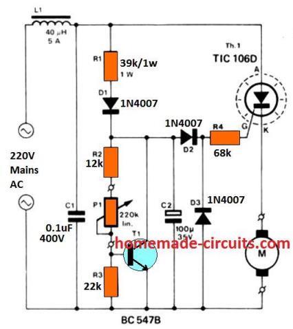 The charging of C2 persists until the voltage across this capacitor becomes equivalent to the simulating zener voltage of the configuration.
The circuit wired around transistor T1 effectively simulates the operation of a zener diode.
The inclusion of the pot P1 makes it possible to adjust the voltage of this ��zener diode��.
Precisely speaking, the voltage developed across T1 is literally determined by the ratio between resistors R3 and R2 + P1.
The voltage across the resistor R4 is always maintained equal to the 0.6 volts that��s equal to the required conducting voltage of T1��s base emitter voltage.
Therefore it means that the above explained zener voltage should be equal to the value that may be acquired by solving the expression:
(P1 + R2 + R3 / R3) �� 0.6
The charging of C2 persists until the voltage across this capacitor becomes equivalent to the simulating zener voltage of the configuration.
The circuit wired around transistor T1 effectively simulates the operation of a zener diode.
The inclusion of the pot P1 makes it possible to adjust the voltage of this ��zener diode��.
Precisely speaking, the voltage developed across T1 is literally determined by the ratio between resistors R3 and R2 + P1.
The voltage across the resistor R4 is always maintained equal to the 0.6 volts that��s equal to the required conducting voltage of T1��s base emitter voltage.
Therefore it means that the above explained zener voltage should be equal to the value that may be acquired by solving the expression:
(P1 + R2 + R3 / R3) �� 0.6
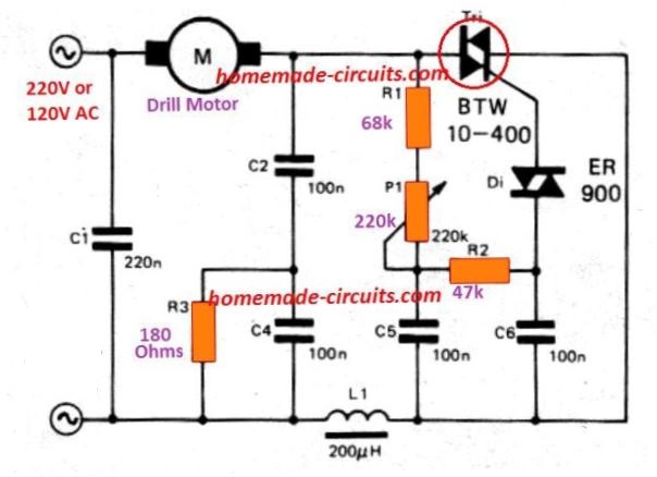 When the speed of the motor drops just under the preset value (with load connected), then the motor 's back EMF decreases.
As a result, voltage around through R1, P1, and C5 rises so that the triac is activated earlier and motor speed tends to increase.
A certain proportion of speedstabilityis achieved in this manner.
When the speed of the motor drops just under the preset value (with load connected), then the motor 's back EMF decreases.
As a result, voltage around through R1, P1, and C5 rises so that the triac is activated earlier and motor speed tends to increase.
A certain proportion of speedstabilityis achieved in this manner.
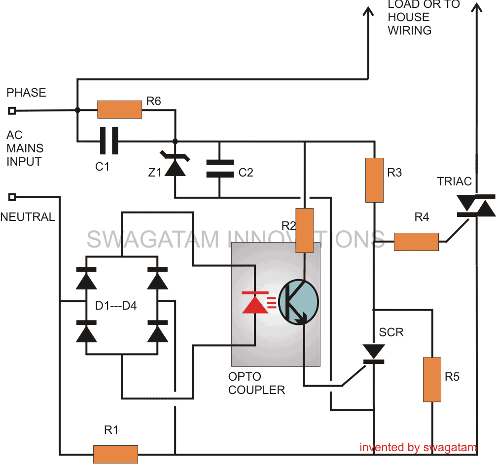
 R2, R3, R4 =100 Ohms
R5 = 1K,
R6 = 1M,
C1, C2 = 474/400V
SCR = C106,
Triac = BTA41/600B
Opto-Coupler = MCT2E,
ZENER = 12V 5W
Diodes = 1N4007
R2, R3, R4 =100 Ohms
R5 = 1K,
R6 = 1M,
C1, C2 = 474/400V
SCR = C106,
Triac = BTA41/600B
Opto-Coupler = MCT2E,
ZENER = 12V 5W
Diodes = 1N4007
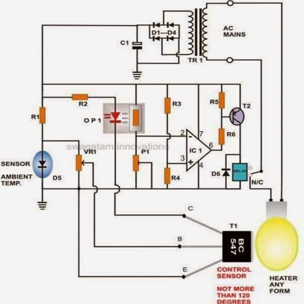 Parts List
R1 = 2k7,
R2, R5, R6 = 1K
R3, R4 = 10K,
D1---D4 = 1N4007,
D5, D6 = 1N4148,
P1 = 100K,
VR1 = 200 Ohms, 1Watt,
C1 = 1000uF/25V,
T1 = BC547,
T2 = BC557,IC = 741,
OPTO = LED/LDR Combo.
Relay = 12 V, 400 Ohm, SPDT.
Parts List
R1 = 2k7,
R2, R5, R6 = 1K
R3, R4 = 10K,
D1---D4 = 1N4007,
D5, D6 = 1N4148,
P1 = 100K,
VR1 = 200 Ohms, 1Watt,
C1 = 1000uF/25V,
T1 = BC547,
T2 = BC557,IC = 741,
OPTO = LED/LDR Combo.
Relay = 12 V, 400 Ohm, SPDT.
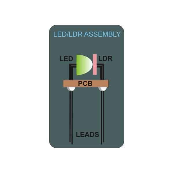 Making a homemade LED/LDR opto is actually very simple.
Cut a piece of general purpose board about 1 by 1 inch.
Bend the LDR leads near its ��head.�� Also take a green RED LED, bend it just as the LDR (See figure and Click to Enlarge).
Insert them over the PCB so that the LED lens point is touching the LDR sensing surface and are face to face.
Solder their leads at the track side of the PCB; do not cut off the remaining excess lead portion.
Cover the top with an opaque lid and make sure its light proof.
Preferably seal off the edges with some opaque sealing glue.
Let it dry.
Your home made LED/LDR based opto-coupler is ready and may be fixed over the main circuit board with its leads orientations done as per the electronic incubator thermostat circuit schematic.
Update:
After some careful investigation it became evident that the above opto-coupler can be totally avoided from the proposed incubator controllercircuit.
Here are the modifications which needs to be made after eliminating the opto.
R2 now directly connects with the collector of T1.
The junction of pin#2 of IC1 and P1 hooks up with the above R2/T1 junction.
That's it, the simpler version is now all ready, much improved and easier to handle.
Please check-out the much simplified version of the above circuit:
Making a homemade LED/LDR opto is actually very simple.
Cut a piece of general purpose board about 1 by 1 inch.
Bend the LDR leads near its ��head.�� Also take a green RED LED, bend it just as the LDR (See figure and Click to Enlarge).
Insert them over the PCB so that the LED lens point is touching the LDR sensing surface and are face to face.
Solder their leads at the track side of the PCB; do not cut off the remaining excess lead portion.
Cover the top with an opaque lid and make sure its light proof.
Preferably seal off the edges with some opaque sealing glue.
Let it dry.
Your home made LED/LDR based opto-coupler is ready and may be fixed over the main circuit board with its leads orientations done as per the electronic incubator thermostat circuit schematic.
Update:
After some careful investigation it became evident that the above opto-coupler can be totally avoided from the proposed incubator controllercircuit.
Here are the modifications which needs to be made after eliminating the opto.
R2 now directly connects with the collector of T1.
The junction of pin#2 of IC1 and P1 hooks up with the above R2/T1 junction.
That's it, the simpler version is now all ready, much improved and easier to handle.
Please check-out the much simplified version of the above circuit:
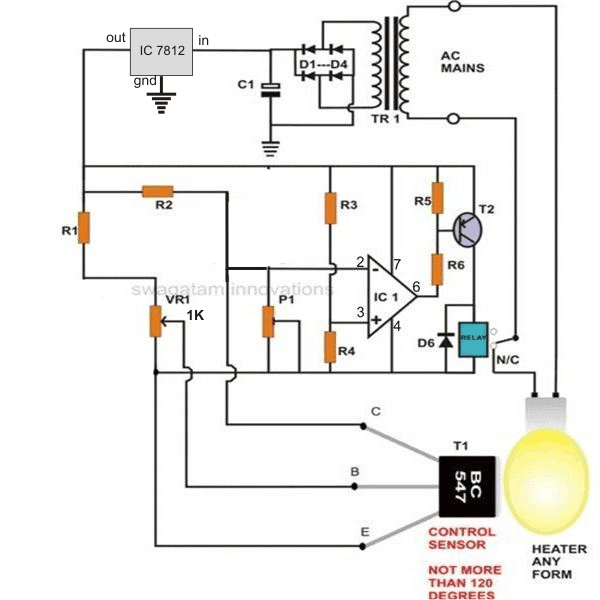
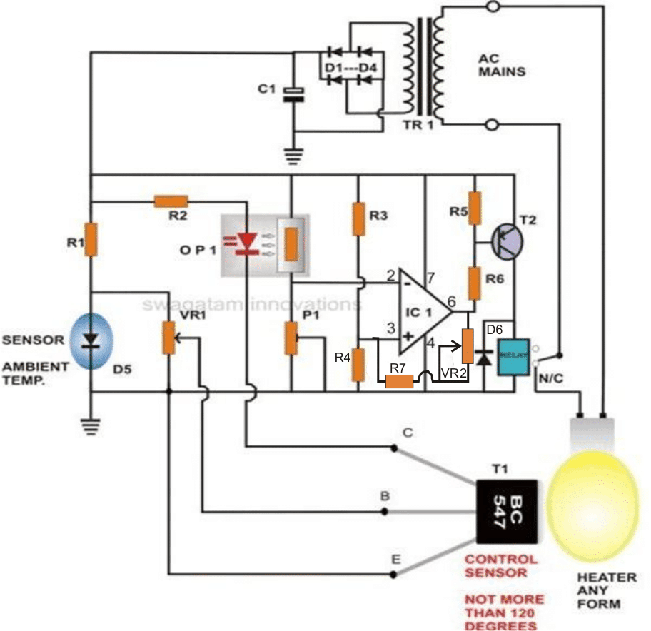
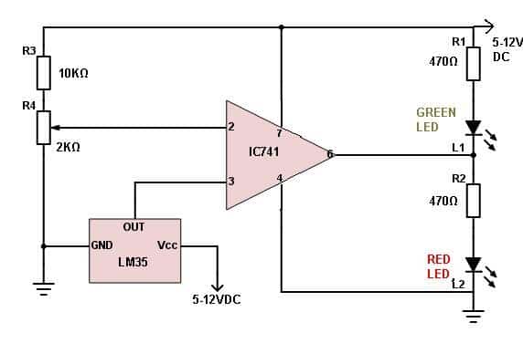 The idea presented above looks self explanatory, wherein the IC 741 is configured as a comparator
with its inverting pin#2 input pin is rigged with an adjustable reference potentiometer while the other non-inverting pin#3 is attached with output of temperature sensor IC LM35
The reference pot is used to set the temperature threshold at which the opamp output is supposed to go high.
It implies that as soon as the temperature around the LM35 goes higher than the desired threshold level, its output voltage becomes high enough to cause pin#3 of the opamp to go over the voltage at pin#2 as set by the pot.
This in turn causes the output of the opamp to go high.
The outcome is indicated by the lower RED LED which now illuminates while the green LED shuts off.
Now this outcome can be easily integrated with a transistor relay driver stage for switching the heat source ON/OFF in response to the above triggers for regulating the incubator temperature.
A standard relay driver can be seen below, wherein the base of the transistor may be connected with pin#6 of the opamp 741 for the required incubator temperature control.
The idea presented above looks self explanatory, wherein the IC 741 is configured as a comparator
with its inverting pin#2 input pin is rigged with an adjustable reference potentiometer while the other non-inverting pin#3 is attached with output of temperature sensor IC LM35
The reference pot is used to set the temperature threshold at which the opamp output is supposed to go high.
It implies that as soon as the temperature around the LM35 goes higher than the desired threshold level, its output voltage becomes high enough to cause pin#3 of the opamp to go over the voltage at pin#2 as set by the pot.
This in turn causes the output of the opamp to go high.
The outcome is indicated by the lower RED LED which now illuminates while the green LED shuts off.
Now this outcome can be easily integrated with a transistor relay driver stage for switching the heat source ON/OFF in response to the above triggers for regulating the incubator temperature.
A standard relay driver can be seen below, wherein the base of the transistor may be connected with pin#6 of the opamp 741 for the required incubator temperature control.
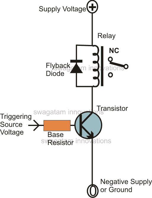
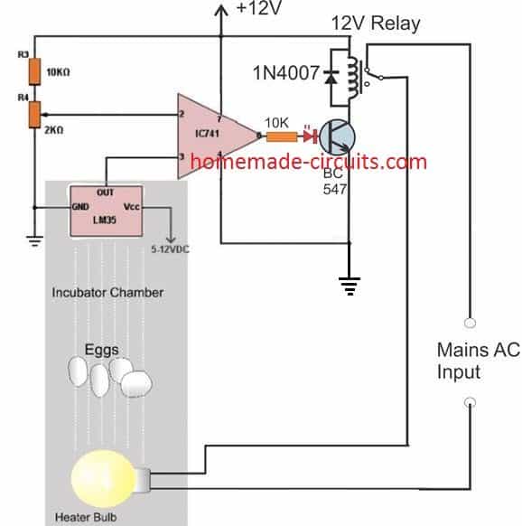
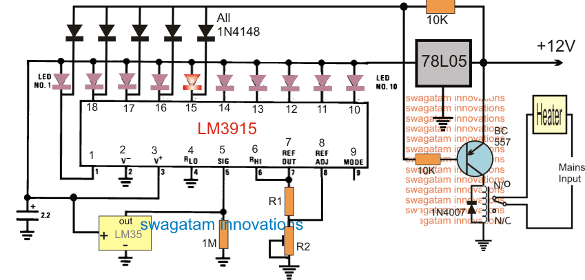 In this design the IC LM3915 is configured as a temperature indicator through 10 sequential LEDs and also the same pinouts are used for initiating the ON/OFF switching of the incubator heater device for the intended incubator temperature control.
Here R2 is installed in the form of a pot and it constitutes the threshold level adjustment control knob and is used for setting up the temperature switching operations as per the desired specifications.
The temperature sensor IC LM35 can seen attached to the input pin#5 of the IC LM3915. With rise in temperature around the IC LM35 the LEDs begin sequencing from pin#1 towards pin#10.
Let's assume, at room temperature the LED#1 illuminates and at the higher cut-off temperature the LED#15 illuminates as the sequence progresses.
It implies that pin#15 may be considered the threshold pinout after which the temperature could be unsafe for the incubation.
The relay cut-off integration is implemented according to the above consideration and we can see that the base of the transistor is able to get its biasing feed only upto pin#15.
Therefore as long as the IC sequence is within pin#15, the relay remains triggered and the heater device is held switched ON, however as soon as the sequence crosses over pin#15 and lands on pin#14, pin#13 etc.
the transistor biasing feed is cut off and the relay is reverted towards the N/C position, subsequently switching OFF the heater.....
until temperature normalizes and the sequence restores back below the pin#15 pinout.
The above sequential up/down drift keeps on repeating in accordance with the surrounding temperature and the heater element is switched ON/OFF maintaining almost a constant incubator temperature as per the given specifications.
In this design the IC LM3915 is configured as a temperature indicator through 10 sequential LEDs and also the same pinouts are used for initiating the ON/OFF switching of the incubator heater device for the intended incubator temperature control.
Here R2 is installed in the form of a pot and it constitutes the threshold level adjustment control knob and is used for setting up the temperature switching operations as per the desired specifications.
The temperature sensor IC LM35 can seen attached to the input pin#5 of the IC LM3915. With rise in temperature around the IC LM35 the LEDs begin sequencing from pin#1 towards pin#10.
Let's assume, at room temperature the LED#1 illuminates and at the higher cut-off temperature the LED#15 illuminates as the sequence progresses.
It implies that pin#15 may be considered the threshold pinout after which the temperature could be unsafe for the incubation.
The relay cut-off integration is implemented according to the above consideration and we can see that the base of the transistor is able to get its biasing feed only upto pin#15.
Therefore as long as the IC sequence is within pin#15, the relay remains triggered and the heater device is held switched ON, however as soon as the sequence crosses over pin#15 and lands on pin#14, pin#13 etc.
the transistor biasing feed is cut off and the relay is reverted towards the N/C position, subsequently switching OFF the heater.....
until temperature normalizes and the sequence restores back below the pin#15 pinout.
The above sequential up/down drift keeps on repeating in accordance with the surrounding temperature and the heater element is switched ON/OFF maintaining almost a constant incubator temperature as per the given specifications.

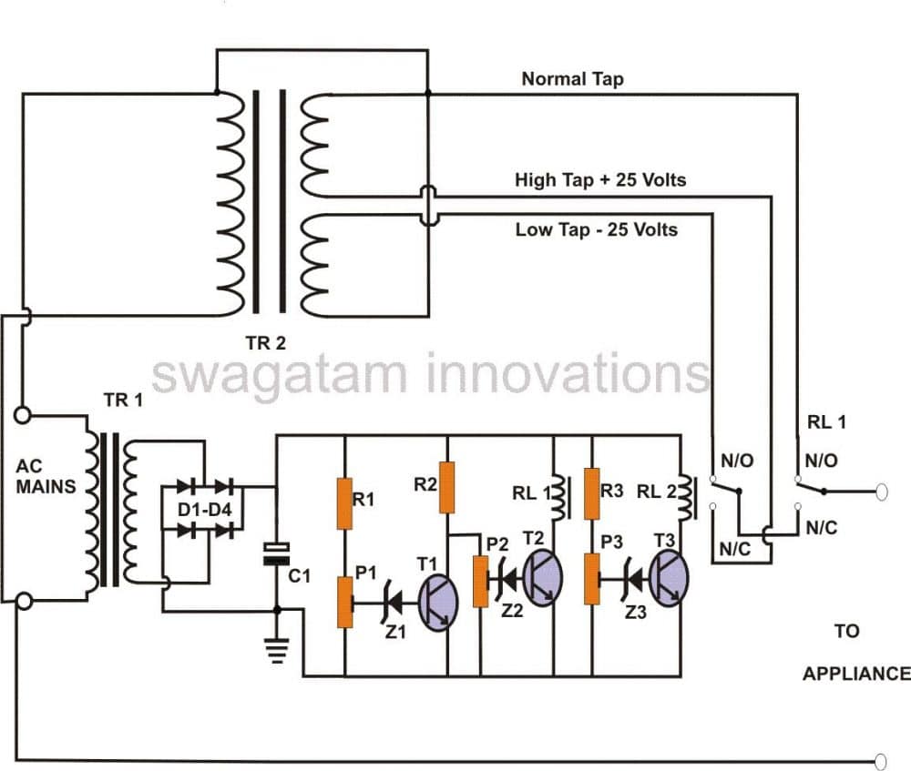 Basically the idea here is to make relay #1 switch at two different mains voltage extremes (high and low), which are considered not suitable for the appliances.
This switching enables this relay to select an appropriately conditioned voltage from another relay through its N/C contacts.
Basically the idea here is to make relay #1 switch at two different mains voltage extremes (high and low), which are considered not suitable for the appliances.
This switching enables this relay to select an appropriately conditioned voltage from another relay through its N/C contacts.

 Stabilizer transformers are normally made to order and are not available ready made in the market.
Since multiple mains AC voltage taps (high and low) outputs are required from them and also since these are specific for a particular application, it becomes much difficult to procure them ready made.
The present circuit also needs a power regulator transformer, but for the ease of construction a simple method may be incorporated to convert an ordinary power supply transformer into a voltage stabilizer transformer.
As shown in the figure, here we require a normal transformer rated at 25-0-25/ 5 Amp.
The centre tap should be split, so that the secondary may consist of two separate windings.
Now it��s just a matter of connecting the primary wires to the two secondary windings as shown in the diagram.
Thus, by following the above procedure, you should be able to successfully convert an ordinary transformer into a stabilizer transformer, very handy for the present application.
Stabilizer transformers are normally made to order and are not available ready made in the market.
Since multiple mains AC voltage taps (high and low) outputs are required from them and also since these are specific for a particular application, it becomes much difficult to procure them ready made.
The present circuit also needs a power regulator transformer, but for the ease of construction a simple method may be incorporated to convert an ordinary power supply transformer into a voltage stabilizer transformer.
As shown in the figure, here we require a normal transformer rated at 25-0-25/ 5 Amp.
The centre tap should be split, so that the secondary may consist of two separate windings.
Now it��s just a matter of connecting the primary wires to the two secondary windings as shown in the diagram.
Thus, by following the above procedure, you should be able to successfully convert an ordinary transformer into a stabilizer transformer, very handy for the present application.
 All the gates are interconnected to each other in such away that the output of only a particular gate remains active at a given period of time according to the level of the input voltage.
Thus, as the input voltage rises the gates respond to the transistors and their outputs subsequently become logic hi one after the other making sure that the previous gate��s output is shut OFF and vice versa.
The logic hi from the particular buffer is applied to the gate of the respective SCR which conducts and connects the relevant ��hot�� line from the transformer to the external connected appliance.
As the voltage rises, the relevant triacs subsequently select the appropriate ��hot�� ends of the transformer to increase or decrease the voltage and maintain a relatively stabilized output.
All the gates are interconnected to each other in such away that the output of only a particular gate remains active at a given period of time according to the level of the input voltage.
Thus, as the input voltage rises the gates respond to the transistors and their outputs subsequently become logic hi one after the other making sure that the previous gate��s output is shut OFF and vice versa.
The logic hi from the particular buffer is applied to the gate of the respective SCR which conducts and connects the relevant ��hot�� line from the transformer to the external connected appliance.
As the voltage rises, the relevant triacs subsequently select the appropriate ��hot�� ends of the transformer to increase or decrease the voltage and maintain a relatively stabilized output.
 Parts List
You will require the following parts for the construction of this SCR control ac voltage stabilizer:
All resistors are Watt, CFR 5%, unless otherwise stated.
R5, R6, R7, R8 = 1M watt,
All Triacs are 400 volts, 1KV rated,
T1, T2, T3, T4 = BC 547,
All zener diodes are = 3 volts 400 mW,
All Diodes are = 1N4007,
All presets = 10K linear,
R1, 2, 3, 4, 9, 10, 11, 12, 13, 14, 15, 16, 17, 18, 19, 20 = 1K watt,
N1 to N4 = IC 4093,
C1 and C3 = 100Uf/ 25 volts,
C2 = 104, ceramic,
Power Guard Stabilizer Transformer = ��Made to order�� having 170, 225, 240, 260 volts output Taps at 225 volts input supply, or 85, 115, 120, 130 volts taps at 110 AC input supply.
TR1 = Step down transformer, 0 �C 12 volts, 100 mA.
Parts List
You will require the following parts for the construction of this SCR control ac voltage stabilizer:
All resistors are Watt, CFR 5%, unless otherwise stated.
R5, R6, R7, R8 = 1M watt,
All Triacs are 400 volts, 1KV rated,
T1, T2, T3, T4 = BC 547,
All zener diodes are = 3 volts 400 mW,
All Diodes are = 1N4007,
All presets = 10K linear,
R1, 2, 3, 4, 9, 10, 11, 12, 13, 14, 15, 16, 17, 18, 19, 20 = 1K watt,
N1 to N4 = IC 4093,
C1 and C3 = 100Uf/ 25 volts,
C2 = 104, ceramic,
Power Guard Stabilizer Transformer = ��Made to order�� having 170, 225, 240, 260 volts output Taps at 225 volts input supply, or 85, 115, 120, 130 volts taps at 110 AC input supply.
TR1 = Step down transformer, 0 �C 12 volts, 100 mA.
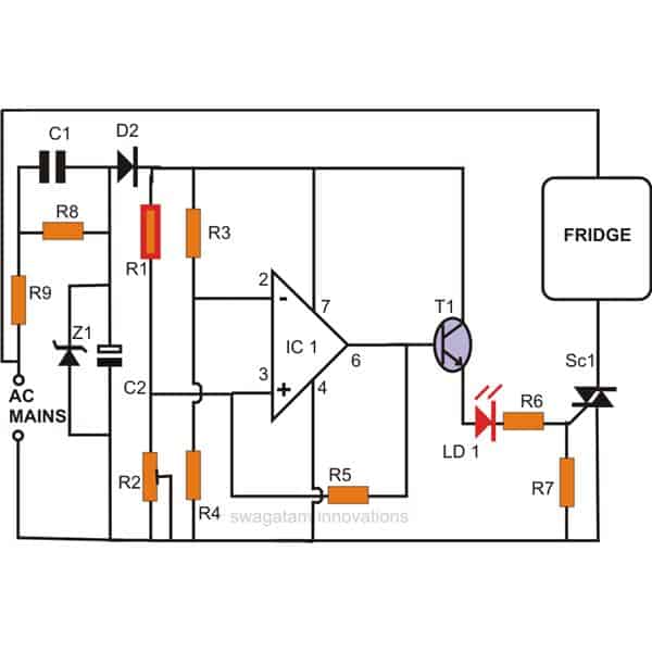 The diagram alongside shows a simple circuit built around the IC 741, which is basically configured as a voltage comparator.A transformer less power supply is incorporated here to make the circuit compact and solid-state.
A bridge configuration comprising R3, R2, P1 and the NTC R1 at the input forms the main sensing elements of the circuit.
The inverting input of the IC is clamped at half the supply voltage using a voltage divider network of R3 and R4.
This eliminates the need of providing a dual supply to the IC and the circuit is able to produce optimum results even through single pole voltage supply.
The reference voltage to the non-inverting input of the IC is fixed through the preset P1 with respect to the NTC (Negative Temperature Coefficient.)
In case the temperature under check tends to drift above the desired levels, the NTC resistance drops and the potential at non-inverting input of the IC crosses the set reference.
This instantly toggles the output of the IC, which in turn switches the output stage comprising transistor, triac network, switching off the load (heating or the cooling system) until the temperature reaches the lower threshold.
The feedback resistor R5 to some extent helps to induce hysteresis into the circuit, an important parameter without which the circuit may keep flip-flopping quite rapidly in response to the sudden temperature changes.
Once the assembly is completed, setting up the circuit is very simple and is done with the following points:
REMEMBER THE ENTIRE CIRCUIT IS AT AC MAINS POTENTIAL, SO EXTREME CAUTION IS ADVISED WHILE GOING THROUGH THE TESTING AND THE SETTING PROCEDURES.
USE OF A WOODEN PLANK OR ANY OTHER INSULATING MATERIAL UNDER YOUR FEET IS STRICTLY RECOMMENDED; ALSO USE ELECTRICAL TOOLS WHICH ARE THOROUGHLY INSULATED NEAR AND AROUND THE GRIPPING AREA.
The diagram alongside shows a simple circuit built around the IC 741, which is basically configured as a voltage comparator.A transformer less power supply is incorporated here to make the circuit compact and solid-state.
A bridge configuration comprising R3, R2, P1 and the NTC R1 at the input forms the main sensing elements of the circuit.
The inverting input of the IC is clamped at half the supply voltage using a voltage divider network of R3 and R4.
This eliminates the need of providing a dual supply to the IC and the circuit is able to produce optimum results even through single pole voltage supply.
The reference voltage to the non-inverting input of the IC is fixed through the preset P1 with respect to the NTC (Negative Temperature Coefficient.)
In case the temperature under check tends to drift above the desired levels, the NTC resistance drops and the potential at non-inverting input of the IC crosses the set reference.
This instantly toggles the output of the IC, which in turn switches the output stage comprising transistor, triac network, switching off the load (heating or the cooling system) until the temperature reaches the lower threshold.
The feedback resistor R5 to some extent helps to induce hysteresis into the circuit, an important parameter without which the circuit may keep flip-flopping quite rapidly in response to the sudden temperature changes.
Once the assembly is completed, setting up the circuit is very simple and is done with the following points:
REMEMBER THE ENTIRE CIRCUIT IS AT AC MAINS POTENTIAL, SO EXTREME CAUTION IS ADVISED WHILE GOING THROUGH THE TESTING AND THE SETTING PROCEDURES.
USE OF A WOODEN PLANK OR ANY OTHER INSULATING MATERIAL UNDER YOUR FEET IS STRICTLY RECOMMENDED; ALSO USE ELECTRICAL TOOLS WHICH ARE THOROUGHLY INSULATED NEAR AND AROUND THE GRIPPING AREA.
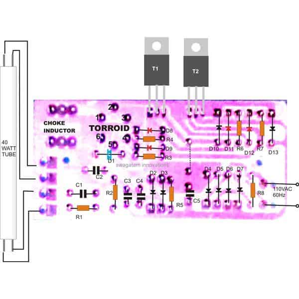
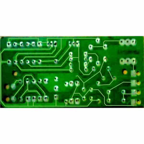
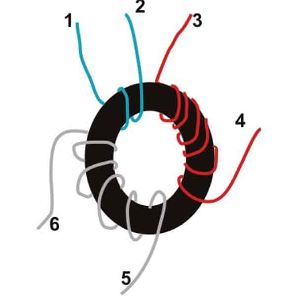

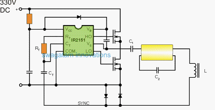 Parts List
Ct/Rt = same as given in the below given diagrams
lower diodes = BA159
Mosfets: as recommended in below diagrams
C1 = 1uF/400V PPC
C2 = 0.01uF/630V PPC
L1 = As recommended in below diagram, may need some experimentation
They likewise have in-built circuitry which offers a moderate 1.2 microsecond dead-time between outputs and switching high side and low side components for driving half-bridge power devices.
Parts List
Ct/Rt = same as given in the below given diagrams
lower diodes = BA159
Mosfets: as recommended in below diagrams
C1 = 1uF/400V PPC
C2 = 0.01uF/630V PPC
L1 = As recommended in below diagram, may need some experimentation
They likewise have in-built circuitry which offers a moderate 1.2 microsecond dead-time between outputs and switching high side and low side components for driving half-bridge power devices.
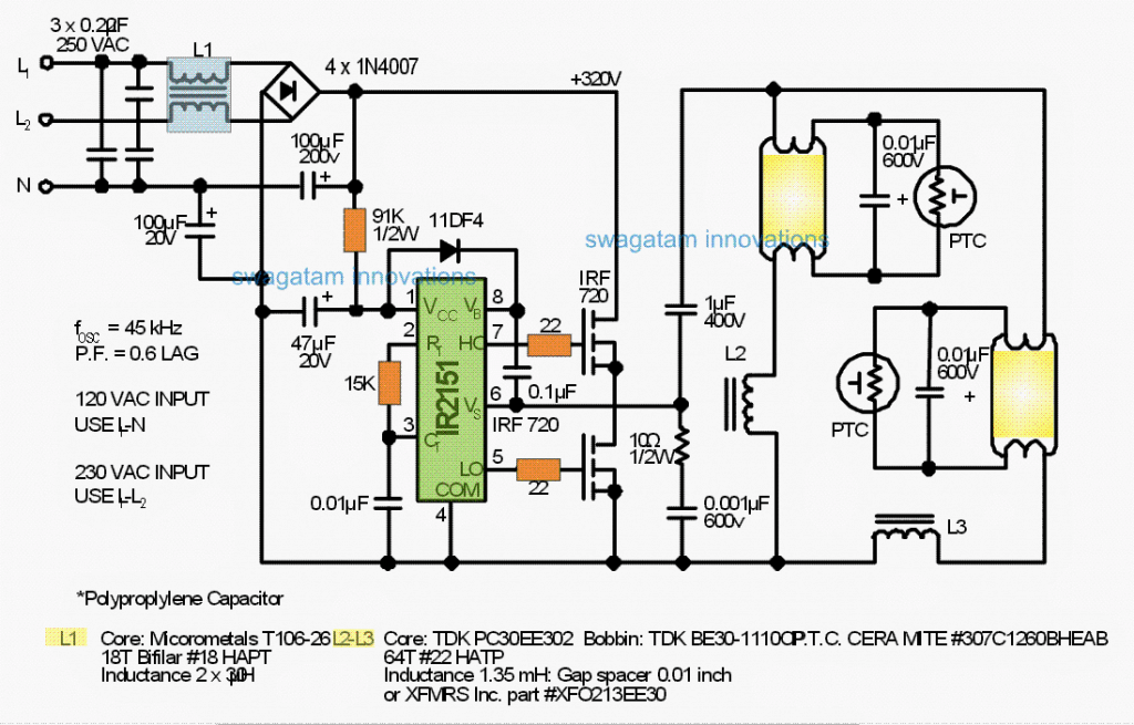
 Considering that the input rectifiers carry out just close to the peaks of the AC input voltage, the input power factor is around 0.6 lagging with a non-sinusoidal current wave-form.
Such type of rectifier is simply not advised for anything at all apart from an assessment circuit or reduced power compact fluorescent and without a doubt could become unwanted as harmonic currents in power supply devices are additionally lessened by power quality restrictions.
Considering that the input rectifiers carry out just close to the peaks of the AC input voltage, the input power factor is around 0.6 lagging with a non-sinusoidal current wave-form.
Such type of rectifier is simply not advised for anything at all apart from an assessment circuit or reduced power compact fluorescent and without a doubt could become unwanted as harmonic currents in power supply devices are additionally lessened by power quality restrictions.
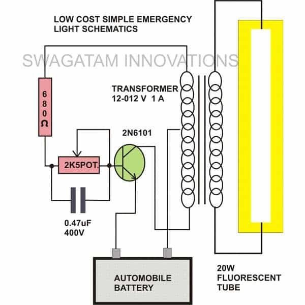
 The concept: We know that LEDs require a certain fixed forward voltage drop to become illuminated and it is at this rating when the LED is at it��s best, that is voltages which is around its forward voltage drop facilitates the device to operate in the most efficient way.
As this voltage is increased, the LED starts drawing more current, rather dissipating extra current by getting heated up itself and also through the resistor which also gets heated up in the process of limiting the extra current.
If we could maintain a voltage around an LED near to its rated forward voltage, we could use it more efficiently.
That��s exactly what I have tried to fix in the circuit.
Since the battery used here is a 6 volt battery, means this source is a bit higher than the forward voltage of the LEDs used here, which amounts to 3.5 volts.
The extra 2.5 volts rise can cause considerable dissipation and loss of power through heat generation.
Therefore I employed a few diodes in series with the supply and made sure that initially when the battery is fully charged; three diodes are effectively switched so as to drop the excess 2.5 volts across the white LEDs (because each diode drop 0.6 volts across itself).
Now as the voltage of the battery drops, the diodes series are reduced to two and subsequently to one making sure only the desired amount of voltage reaches the LED bank.
In this way the proposed simple emergency lamp circuit is made highly efficient with its current consumption, and it provides backup for a much longer period of time than what it would do with ordinary connections
However, you can remove those diodes if you don't want to include them.
Circuit Diagram
The concept: We know that LEDs require a certain fixed forward voltage drop to become illuminated and it is at this rating when the LED is at it��s best, that is voltages which is around its forward voltage drop facilitates the device to operate in the most efficient way.
As this voltage is increased, the LED starts drawing more current, rather dissipating extra current by getting heated up itself and also through the resistor which also gets heated up in the process of limiting the extra current.
If we could maintain a voltage around an LED near to its rated forward voltage, we could use it more efficiently.
That��s exactly what I have tried to fix in the circuit.
Since the battery used here is a 6 volt battery, means this source is a bit higher than the forward voltage of the LEDs used here, which amounts to 3.5 volts.
The extra 2.5 volts rise can cause considerable dissipation and loss of power through heat generation.
Therefore I employed a few diodes in series with the supply and made sure that initially when the battery is fully charged; three diodes are effectively switched so as to drop the excess 2.5 volts across the white LEDs (because each diode drop 0.6 volts across itself).
Now as the voltage of the battery drops, the diodes series are reduced to two and subsequently to one making sure only the desired amount of voltage reaches the LED bank.
In this way the proposed simple emergency lamp circuit is made highly efficient with its current consumption, and it provides backup for a much longer period of time than what it would do with ordinary connections
However, you can remove those diodes if you don't want to include them.
Circuit Diagram
 Video Clip:

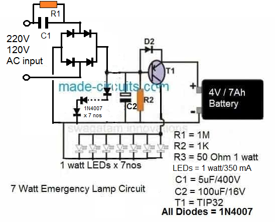
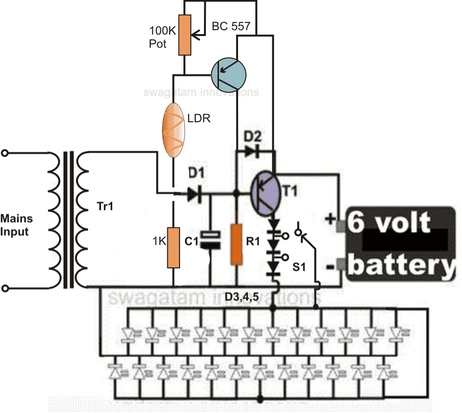
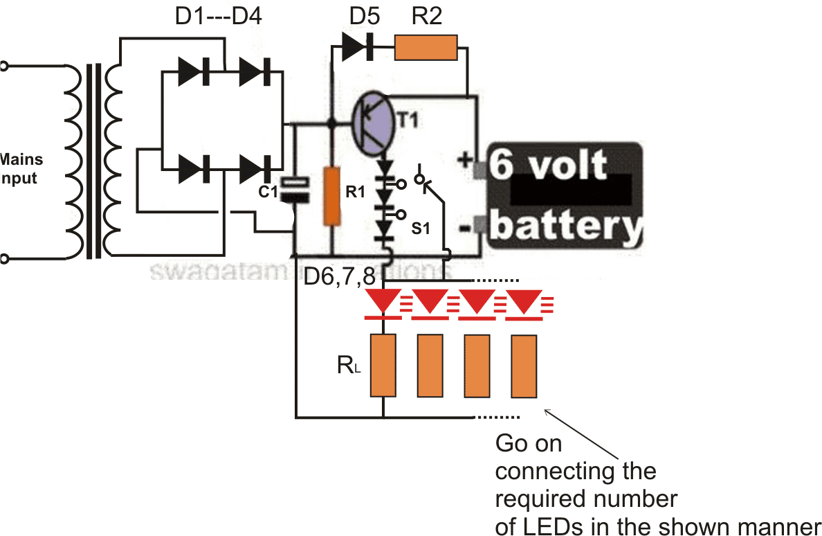 Parts List for the 150 LED emergency light circuit
R1 = 220 Ohms, 1/2 watt
R2 = 100Ohms, 2 watts,
RL = All 22 Ohms, 1/4 watt,
C1 = 100uF/25V,
D1,2,3,4,6,7,8 = 1N5408,
D5 = 1N4007
T1 = AD149, TIP127, TIP2955, TIP32 or similar,
Transformer = 0-6V, 500mA
Parts List for the 150 LED emergency light circuit
R1 = 220 Ohms, 1/2 watt
R2 = 100Ohms, 2 watts,
RL = All 22 Ohms, 1/4 watt,
C1 = 100uF/25V,
D1,2,3,4,6,7,8 = 1N5408,
D5 = 1N4007
T1 = AD149, TIP127, TIP2955, TIP32 or similar,
Transformer = 0-6V, 500mA
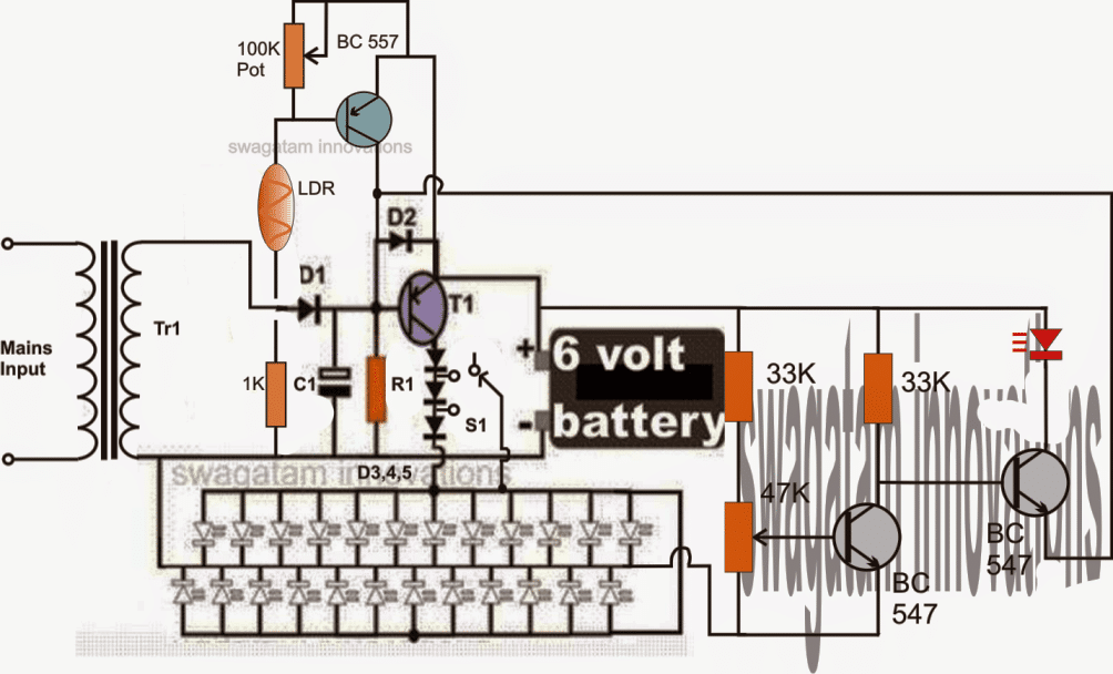
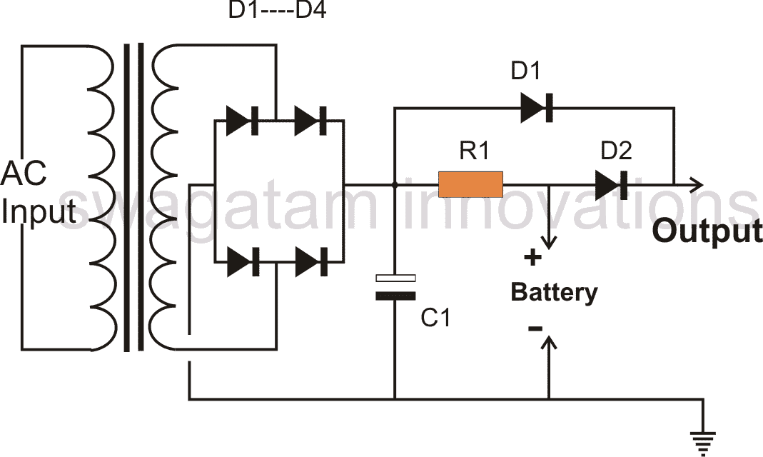
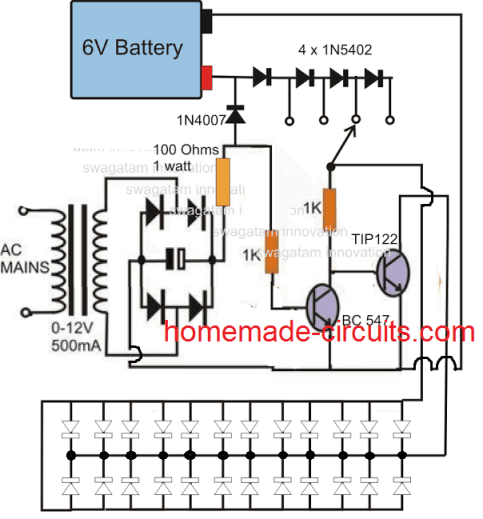
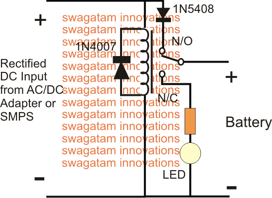 The above circuit is self explanatory and shows the configuration for implementing a simple LED relay changeover emergency lamp circuit.
 The relay can be any ordinary 400 ohm 12V relay.
While mains AC is available, the relay is energized using the rectified capacitive power supply, which connects the relay contacts with its N/O terminal.
The battery now gets charged through this contact via the 100 ohm resistor.
The 4V zener makes sure that the 3.7 Cell never reaches an over charged situation.
When mains AC fails, the relay deactivates, and its contact is pulled at its N/C terminals.
The N/C terminals now connects the LEDs with the battery, illuminating it instantly via the 100 ohm resistor.
If you any specific questions, please ask using the comment box.
The relay can be any ordinary 400 ohm 12V relay.
While mains AC is available, the relay is energized using the rectified capacitive power supply, which connects the relay contacts with its N/O terminal.
The battery now gets charged through this contact via the 100 ohm resistor.
The 4V zener makes sure that the 3.7 Cell never reaches an over charged situation.
When mains AC fails, the relay deactivates, and its contact is pulled at its N/C terminals.
The N/C terminals now connects the LEDs with the battery, illuminating it instantly via the 100 ohm resistor.
If you any specific questions, please ask using the comment box.
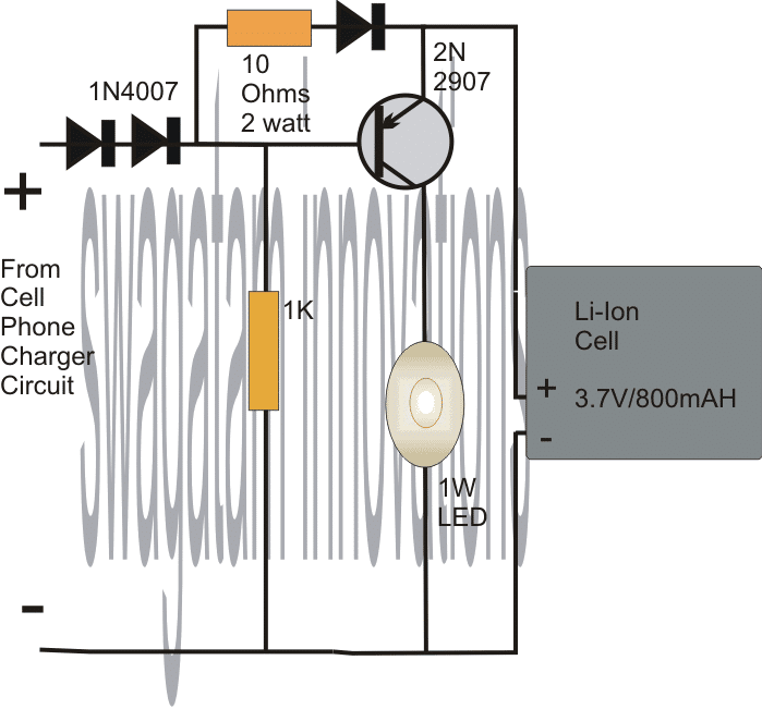 Adding a Current Control for the LED
 Rx = 0.7 / 0.3 = 2.3 ohm 1/4 watt
The voltage from the cell phone charger power supply is dropped to around 3.9V by adding diodes in the positive path of the supply.
This should be confirmed with a DMM before connecting the cell.
The voltage should be limited to around 4V so that the cell is never allowed to cros the over charge limit.
Although the above voltage will not allow the cell to get charged fully and optimally, it will ensure the cell doesn't get damaged due to over charge.
The PNP transistor is held reversed biased as long as mains AC stays active, while the Li-Ion cell is charged gradually charged.
In case the mains AC fails, the transistor switches ON with the help of the 1K resistor and instantly illuminates the 1 watt LED connected across its collector and ground.
The above design can also be implemented using a transformerless power supply circuit.
Let's the learn the complete design:
Before proceeding with the circuit details it should be noted that the following proposed design is notisolatedfrom mains and therefore is extremely dangerous to touch, and it has not been verified practically.
Build it only if you personally feel sure about the design.
Moving on, the given 1 watt LED emergency light circuit using Li-Ion cell looks quite a straightforward design.
Let's learn the functioning with the following points.
It's basically a regulated transformerless power supply circuit which can also be used as a 1 watt LED driver circuit.
The present design perhaps becomes very reliable owing to the fact that the dangers normally associated with transformerless power supplies are effectively tackled here.
The 2uF capacitor along with the 4 in4007 diodes form a standard mains operated capacitive power supply stage.
Rx = 0.7 / 0.3 = 2.3 ohm 1/4 watt
The voltage from the cell phone charger power supply is dropped to around 3.9V by adding diodes in the positive path of the supply.
This should be confirmed with a DMM before connecting the cell.
The voltage should be limited to around 4V so that the cell is never allowed to cros the over charge limit.
Although the above voltage will not allow the cell to get charged fully and optimally, it will ensure the cell doesn't get damaged due to over charge.
The PNP transistor is held reversed biased as long as mains AC stays active, while the Li-Ion cell is charged gradually charged.
In case the mains AC fails, the transistor switches ON with the help of the 1K resistor and instantly illuminates the 1 watt LED connected across its collector and ground.
The above design can also be implemented using a transformerless power supply circuit.
Let's the learn the complete design:
Before proceeding with the circuit details it should be noted that the following proposed design is notisolatedfrom mains and therefore is extremely dangerous to touch, and it has not been verified practically.
Build it only if you personally feel sure about the design.
Moving on, the given 1 watt LED emergency light circuit using Li-Ion cell looks quite a straightforward design.
Let's learn the functioning with the following points.
It's basically a regulated transformerless power supply circuit which can also be used as a 1 watt LED driver circuit.
The present design perhaps becomes very reliable owing to the fact that the dangers normally associated with transformerless power supplies are effectively tackled here.
The 2uF capacitor along with the 4 in4007 diodes form a standard mains operated capacitive power supply stage.
 The finalized circuit with an added feature can be seen below:
 The circuit was drawn by Mr.
Sriram kp, for details please go through the comment discussion between Mr Sriram and me.
The circuit was drawn by Mr.
Sriram kp, for details please go through the comment discussion between Mr Sriram and me.
 Normally the proposed 40 watt LED tube light circuit, or in other words the PWM circuit may be powered through any standard 12V/3amp SMPS unit for the sake of compactness and decent looks.
After assembling the above board, the output wires should be connected to the below shown PWM circuit, across the transistor collector and positive.
The supply voltage should be provided from any standard SMPS adapter as mentioned in the above section of the article.
The LED trip will instantly light up illuminating the premise with flood light brightness.
The illumination may be assumed to be equivalent to a 40 watt FTL with power consumption of less than 12 watts, that's a lot of power saved.
Normally the proposed 40 watt LED tube light circuit, or in other words the PWM circuit may be powered through any standard 12V/3amp SMPS unit for the sake of compactness and decent looks.
After assembling the above board, the output wires should be connected to the below shown PWM circuit, across the transistor collector and positive.
The supply voltage should be provided from any standard SMPS adapter as mentioned in the above section of the article.
The LED trip will instantly light up illuminating the premise with flood light brightness.
The illumination may be assumed to be equivalent to a 40 watt FTL with power consumption of less than 12 watts, that's a lot of power saved.
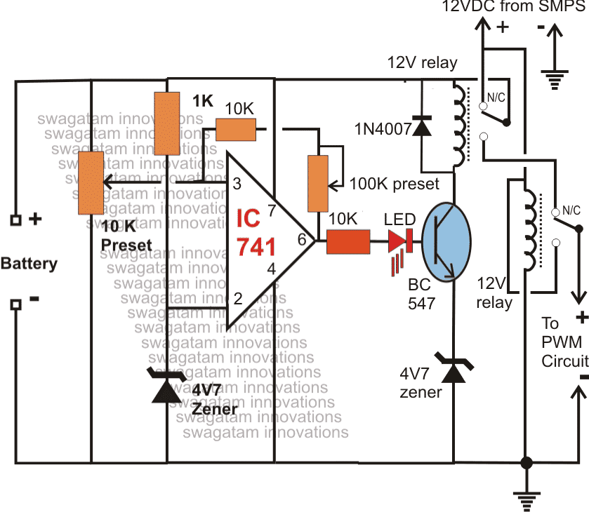 The IC 741 has been configured as a low/high battery voltage sensor and itactivatesthe adjoining relay connected to the transistor BC547 appropriately.
Assume the mains to be present and the battery to be partially discharged.
The voltage from the AC/DC SMPS reaches the battery through the N/C contacts of the upper relay which remains in andeactivatedpositionbecause of the battery voltage which may be below the full charge threshold level, let's assume the full charge level to be 14.3V (set by the 10K preset).
Since the lower relay coil is connected to the SMPS voltage, stays activated such that the SMPS supply reaches the PWM 40 watt LED driver via the N/O contacts of the lower relay.
Thus the LEDs remains switched ON by using the DC from the mainsoperatedSMPS adapter, also the battery continues to get charged as explained above.
Once the battery gets fully charged, the output of the IC741 goes high, activating the relay driver stage, the upper relay switches and instantly connects the battery with the N/C of the lower relay, positioning the battery in the standby condition.
However until AC mains is present, the lower relay isunableto deactivate and therefore the above voltage from the charged battery is not able to reach the LED board.
Now if suppose AC mains fails, the lower relay contactshiftsto the N/C point, instantly connects the supply from the battery to the PWM LED circuit, illuminating the 40 watt LEDs brightly.
The LEDs consume battery power until either the battery falls below the low voltage threshold or mains poweris restored.
The lowbatterythresholdsetting is done by adjusting the feedback preset 100K across the pin3 and pin6 of the IC741.
The IC 741 has been configured as a low/high battery voltage sensor and itactivatesthe adjoining relay connected to the transistor BC547 appropriately.
Assume the mains to be present and the battery to be partially discharged.
The voltage from the AC/DC SMPS reaches the battery through the N/C contacts of the upper relay which remains in andeactivatedpositionbecause of the battery voltage which may be below the full charge threshold level, let's assume the full charge level to be 14.3V (set by the 10K preset).
Since the lower relay coil is connected to the SMPS voltage, stays activated such that the SMPS supply reaches the PWM 40 watt LED driver via the N/O contacts of the lower relay.
Thus the LEDs remains switched ON by using the DC from the mainsoperatedSMPS adapter, also the battery continues to get charged as explained above.
Once the battery gets fully charged, the output of the IC741 goes high, activating the relay driver stage, the upper relay switches and instantly connects the battery with the N/C of the lower relay, positioning the battery in the standby condition.
However until AC mains is present, the lower relay isunableto deactivate and therefore the above voltage from the charged battery is not able to reach the LED board.
Now if suppose AC mains fails, the lower relay contactshiftsto the N/C point, instantly connects the supply from the battery to the PWM LED circuit, illuminating the 40 watt LEDs brightly.
The LEDs consume battery power until either the battery falls below the low voltage threshold or mains poweris restored.
The lowbatterythresholdsetting is done by adjusting the feedback preset 100K across the pin3 and pin6 of the IC741.
 Question Regarding Surge Prevention in Electronic Ballast
Hi swagtam, I found your email address from your blog.
I really need yr help.
Actually my company has customer in china we make UV lamps and we use electronic ballast for it.
now the problem is in china because of Over Voltage the ballast burn out so i design circuit which is in attachment which dosen't help either?
so i found your Ultimate High/Low Voltage Protector Circuit which i wants to build.
or can you tell me the update if i can do in my circuit that will be great.
sorry if i am bothring you.
but i really really need yr help to save my job thanks Thank You Krishna Shah
Solution
Hi Krishna, According to me the problem may not be with the voltage fluctuations, rather it's because of the sudden voltage surges that's blowing of your ballast circuit.
The diagram shown by you may not prove very effective, because it does not incorporate a resistor or any kind of barrier with the MOVs.
You may try the following circuit, introduce it at the entry point of the ballast circuit.
Hope it works:
Question Regarding Surge Prevention in Electronic Ballast
Hi swagtam, I found your email address from your blog.
I really need yr help.
Actually my company has customer in china we make UV lamps and we use electronic ballast for it.
now the problem is in china because of Over Voltage the ballast burn out so i design circuit which is in attachment which dosen't help either?
so i found your Ultimate High/Low Voltage Protector Circuit which i wants to build.
or can you tell me the update if i can do in my circuit that will be great.
sorry if i am bothring you.
but i really really need yr help to save my job thanks Thank You Krishna Shah
Solution
Hi Krishna, According to me the problem may not be with the voltage fluctuations, rather it's because of the sudden voltage surges that's blowing of your ballast circuit.
The diagram shown by you may not prove very effective, because it does not incorporate a resistor or any kind of barrier with the MOVs.
You may try the following circuit, introduce it at the entry point of the ballast circuit.
Hope it works:
 Note: The 1 ohm resistors should be dimesioned according to the load current.
The formula for calculating them is R1+R2 = MOV Voltage Rating / Max MOV Current Rating
Note: The 1 ohm resistors should be dimesioned according to the load current.
The formula for calculating them is R1+R2 = MOV Voltage Rating / Max MOV Current Rating

 As we can see, the input side is protected with an NTC and MOV.
The MOV grounds any instantaneous over voltage surge, while the NTC limits an over current surge.
The next stage constitutes an RFI line filter, comprising of a small ferrite transformer and a few capacitors.
The transformer arrests and blocks the passage of any incoming or outgoing RFI across the line, while the capacitor network reinforces the effect by grounding the residual high frequency content across the line.
The transformer is built over a small ferrite rod, having two identical winding wrapped one over the other, and one of the winding end connections swapped between the input/output Neutral line.
As we can see, the input side is protected with an NTC and MOV.
The MOV grounds any instantaneous over voltage surge, while the NTC limits an over current surge.
The next stage constitutes an RFI line filter, comprising of a small ferrite transformer and a few capacitors.
The transformer arrests and blocks the passage of any incoming or outgoing RFI across the line, while the capacitor network reinforces the effect by grounding the residual high frequency content across the line.
The transformer is built over a small ferrite rod, having two identical winding wrapped one over the other, and one of the winding end connections swapped between the input/output Neutral line.
 Basically it works on the principle of thermo-electric effect (opposite of Seebeck Effect) where a potential difference is used for making or producing hot and cold temperatures over the two ends of a dissimilar metal assembly.
A Peltier device has two terminals in the form of wire ends which requires to be connected across a voltage source rich in current content.
The application of voltage instantly starts transforming one surface of the unit hot and the reverse surface cool very fast.
However, the hot end must be quickly managed so that the heat does not reach higher levels, which can completely hamper the heating and cooling process and ruin the device itself.
Therefore the hot surface must be attached with heavy heatsinking materials like aluminum or copper metal of suitable sizes.
Basically it works on the principle of thermo-electric effect (opposite of Seebeck Effect) where a potential difference is used for making or producing hot and cold temperatures over the two ends of a dissimilar metal assembly.
A Peltier device has two terminals in the form of wire ends which requires to be connected across a voltage source rich in current content.
The application of voltage instantly starts transforming one surface of the unit hot and the reverse surface cool very fast.
However, the hot end must be quickly managed so that the heat does not reach higher levels, which can completely hamper the heating and cooling process and ruin the device itself.
Therefore the hot surface must be attached with heavy heatsinking materials like aluminum or copper metal of suitable sizes.
 Peltier Performance Specifications
Hot Side Temperature (oC) 25oC / 50oC
Qmax (Watts) = 50 / 57
Delta Tmax (oC) = 66 / 75
Imax (Amps) = 6.4 / 6.4
Vmax (Volts) = 14.4 / 16.4
Module Resistance (Ohms) = 1.98 / 2.30
Peltier Performance Specifications
Hot Side Temperature (oC) 25oC / 50oC
Qmax (Watts) = 50 / 57
Delta Tmax (oC) = 66 / 75
Imax (Amps) = 6.4 / 6.4
Vmax (Volts) = 14.4 / 16.4
Module Resistance (Ohms) = 1.98 / 2.30

 In the figure above we can visualize a design for implementing the proposed reverse forward motion of an incubator motor after a predetermined set of time interval.
At the instant when power is switched ON we have the following scenario:
The magnetic switch for "set" may be assumed to be in a deactivated state or depressed while the motor or the designed incubator mechanism is in its zero start position.
Please note that preferably the "set"/"reset" switches should be implemented using magnetic reed switches.
With power is switched ON, IC 4060 is reset via C2 so that it initiates it counting process from zero, and pin3 is rendered a zero logic.
This initial zero logic is fed via C3 to the base of T1 which instantly conducts forcing T3 and its associated relay to activate.
R7 in the process makes sure T1/T3 get latched in this mode.
The DPDT relay at this point actuates at its N/O contacts initiating the motor and the mechanism towards an assumed "forward" motion.
As soon the motor begins moving, the "set" button is released such that T4 and the upper SPDT gets an opportunity to actuate, wherein the SPDT relay attains a N/O position changeover rendering the N/C contacts of the DPDT with a standby supply..
The motor and/or the mechanism keeps moving until it has attained the "reset" position which causes T2 to activate and break the T1/T4 latch.
With T4 switched OFF, the DPDT relay changes its position from N/O to N/C and provides an opposite (reverse) movement to the motor mechanism.
The incubator motor mechanism now flips its direction and initiates a reverse motion until it has reached the "set" point which quickly switches OFF the base drive of T4, the SPDT switches OFF cutting power of the DPDT and the entire mechanism comes to a stand still.
In the meantime the IC 4060 continues counting until it has yet again produced a zero logic after going through a high logic at its pin3 (by discharging C3).
The cycle once again gets initiated and repeats the procedure as explained above.
In the figure above we can visualize a design for implementing the proposed reverse forward motion of an incubator motor after a predetermined set of time interval.
At the instant when power is switched ON we have the following scenario:
The magnetic switch for "set" may be assumed to be in a deactivated state or depressed while the motor or the designed incubator mechanism is in its zero start position.
Please note that preferably the "set"/"reset" switches should be implemented using magnetic reed switches.
With power is switched ON, IC 4060 is reset via C2 so that it initiates it counting process from zero, and pin3 is rendered a zero logic.
This initial zero logic is fed via C3 to the base of T1 which instantly conducts forcing T3 and its associated relay to activate.
R7 in the process makes sure T1/T3 get latched in this mode.
The DPDT relay at this point actuates at its N/O contacts initiating the motor and the mechanism towards an assumed "forward" motion.
As soon the motor begins moving, the "set" button is released such that T4 and the upper SPDT gets an opportunity to actuate, wherein the SPDT relay attains a N/O position changeover rendering the N/C contacts of the DPDT with a standby supply..
The motor and/or the mechanism keeps moving until it has attained the "reset" position which causes T2 to activate and break the T1/T4 latch.
With T4 switched OFF, the DPDT relay changes its position from N/O to N/C and provides an opposite (reverse) movement to the motor mechanism.
The incubator motor mechanism now flips its direction and initiates a reverse motion until it has reached the "set" point which quickly switches OFF the base drive of T4, the SPDT switches OFF cutting power of the DPDT and the entire mechanism comes to a stand still.
In the meantime the IC 4060 continues counting until it has yet again produced a zero logic after going through a high logic at its pin3 (by discharging C3).
The cycle once again gets initiated and repeats the procedure as explained above.
 The OBD-II end can be directly plugged into any automotive diagnostic port.
The cable specifically works with the CANbus portion of the OBD-II standards.
The Cable comes with a regular DB9 Female connector along with an OBD 16 Pin Male connector for executing the necessary communications across the EasySYNC CANbus products and OBD-II interface.
The OBD-II end can be directly plugged into any automotive diagnostic port.
The cable specifically works with the CANbus portion of the OBD-II standards.
The Cable comes with a regular DB9 Female connector along with an OBD 16 Pin Male connector for executing the necessary communications across the EasySYNC CANbus products and OBD-II interface.


 This signal will then have to control the direction of the 12 V DC motor.
The motor rotates the threaded rod back and forth to adjust the height of the tool.
From what I discovered, there would be several photodiodes connected in parallel, one set to detect the laser above zero level and the other below that level.
The null level is just some kind of pause between the photodiodes to keep the system from waking up.
Laser sensor without display.
I only gave a pictorial photo.
I need an H bridge circuit, but all found by me are to be used with an Arduino system.
If necessary, I can purchase a ready-made bridge for a reasonable price of up to $ 30
Ideally this would work with both red and green lasers, but the wavelengths are so different that I doubt it could be done and it wouldn't work across the entire light spectrum.
Initially, I would like to set the level of this beam attached to the engines with the up-down buttons.
I would be delighted if the second motor would then level itself with the gyroscope while setting it up, but without the Arduino it might be very difficult.
I feel what I am trying to do is so simple that I can get away without using Arduino.
And I insist on an analog, due to the difficult conditions at a construction site and it seems to me that the more electronics, the more unreliable the device.
It will only work indoors, and the laser distance is max 10m.
The motor I found at the beginning has a large current consumption of 200mA max 2.19 A, but also a large torque.
Power 18 V DC from a Makita battery.
Thanks in advance for any suggestions.
Greetings from Poland
Rafal
Swag: I have a confusion about the working of the motor shafts.
The threaded screw on both the motors will push the tool, but it cannot pull it back? How does that work out?
Is it possible to implement the same with a single motor?
Mr.
Rafal: Lower leveling straightedges would be perhaps 70 cm, only for small rooms, e.g.
a toilet so that you can enter through a door.
Machine without drive, hand-pulled, only leveling straightedges.
In the video, the two yellow objects on masts are laser detectors rigidly attached to the straightedges.
The laser is standing somewhere further away and it produces a horizontal line.
The motors would be attached to a cart and the threaded screw to leveling straightedges with laser detectors.
There must be two motors to level both sides, but it's a mirror image.
The only common part would be a two-channel H-bridge as if I were doing it from a ready-made module and possibly a gyroscope, but that's a dream :).
It is important that there are button for left and right motors revolutions.
The procedure is this.
I hang the laser for example 2 m above the designated floor level.
I measure out 2 meters from the laser beam to the bottom edge of the straightedges.
I regulate the height pressing buttons the switches right-left so that it is equal to 2 meters to the bottom edge of the straightedges.
I put the detectors on the masts so that the laser beam is at zero level between the photodiode sections.
And the rest will do itself
In the attachment I put a drawing of the detector operation.
Rafal
This signal will then have to control the direction of the 12 V DC motor.
The motor rotates the threaded rod back and forth to adjust the height of the tool.
From what I discovered, there would be several photodiodes connected in parallel, one set to detect the laser above zero level and the other below that level.
The null level is just some kind of pause between the photodiodes to keep the system from waking up.
Laser sensor without display.
I only gave a pictorial photo.
I need an H bridge circuit, but all found by me are to be used with an Arduino system.
If necessary, I can purchase a ready-made bridge for a reasonable price of up to $ 30
Ideally this would work with both red and green lasers, but the wavelengths are so different that I doubt it could be done and it wouldn't work across the entire light spectrum.
Initially, I would like to set the level of this beam attached to the engines with the up-down buttons.
I would be delighted if the second motor would then level itself with the gyroscope while setting it up, but without the Arduino it might be very difficult.
I feel what I am trying to do is so simple that I can get away without using Arduino.
And I insist on an analog, due to the difficult conditions at a construction site and it seems to me that the more electronics, the more unreliable the device.
It will only work indoors, and the laser distance is max 10m.
The motor I found at the beginning has a large current consumption of 200mA max 2.19 A, but also a large torque.
Power 18 V DC from a Makita battery.
Thanks in advance for any suggestions.
Greetings from Poland
Rafal
Swag: I have a confusion about the working of the motor shafts.
The threaded screw on both the motors will push the tool, but it cannot pull it back? How does that work out?
Is it possible to implement the same with a single motor?
Mr.
Rafal: Lower leveling straightedges would be perhaps 70 cm, only for small rooms, e.g.
a toilet so that you can enter through a door.
Machine without drive, hand-pulled, only leveling straightedges.
In the video, the two yellow objects on masts are laser detectors rigidly attached to the straightedges.
The laser is standing somewhere further away and it produces a horizontal line.
The motors would be attached to a cart and the threaded screw to leveling straightedges with laser detectors.
There must be two motors to level both sides, but it's a mirror image.
The only common part would be a two-channel H-bridge as if I were doing it from a ready-made module and possibly a gyroscope, but that's a dream :).
It is important that there are button for left and right motors revolutions.
The procedure is this.
I hang the laser for example 2 m above the designated floor level.
I measure out 2 meters from the laser beam to the bottom edge of the straightedges.
I regulate the height pressing buttons the switches right-left so that it is equal to 2 meters to the bottom edge of the straightedges.
I put the detectors on the masts so that the laser beam is at zero level between the photodiode sections.
And the rest will do itself
In the attachment I put a drawing of the detector operation.
Rafal
 Looking at the figure above, two such identical circuit stages will be required for detecting and correcting the associated motor controlled tool with respect to the laser line straightness accuracy.
The two identical stages are mirror images of each other as shown below:
Looking at the figure above, two such identical circuit stages will be required for detecting and correcting the associated motor controlled tool with respect to the laser line straightness accuracy.
The two identical stages are mirror images of each other as shown below:
 The circuitry is fairly straightforward.
It works with a window comparator which ensures that the drive motors are non-operational so long as the pair of LDRs are exposed with the identical laser line brightness.
One half supply voltage is then generated on the non-inverting input of A1 and to the inverting input of A2.
As soon as a deflection in the laser line is detected (which can happen if the motor controlled tool is not aligned straight), the brightness impacting LDRs R1 and R2 changes.
In this situation, the input voltage to the window comparator drifts away from half the supply voltage.
This situation causes the comparator output to command the motor bridge network to move the motor in the clockwise or anticlockwise directions.
Transistors T1 .
. .
T4 are configured like a bridge network to enable switching of the motor in forward and reverse directions depending on the LDR illumination or the laser line deviation angle.
Diodes D1 .
. .
D4 are positioned to cancel voltage peaks generated during the time the motor is avtive and running.
The function of the Preset potentiometers P1 and P2 is for facilitating the alignment adjustments.
These are fine-tuned to ensure the motor is completely shut off and inactive as long as the relevant LDR pair is exposed to the exact same laser light brightness.
Let's say for example, due to incorrect alignment of the motor controlled tool, the laser line tilt causes the light to reduce on LDR R2 than LDR R1. This will result in the voltage at point A to rise above half the supply voltage.
In this situation, the A1 op amp output becomes high, forcing the transistors T1 and T4 to operate.
This in turn causes the motor to rotate in the relevant direction.
This action automatically shifts the connected tool in a straight line until its horizontal alignment accuracy coincides with the laser line accuracy .
Conversely, if we assume the tool to be tilted with the opposite orientation such that illumination of the LDRs are opposite to the discussed above, causes the voltage at point A to drop below half the supply voltage.
This condition triggers output A2 op amp to go high such that T3 and T2 become operational.
This results in the motor now running in the opposite direction, in an attempt to correct the alignment of the tool in the relevant direction until it becomes perfectly straight coinciding with the laser line horizontal accuracy.
The circuitry is fairly straightforward.
It works with a window comparator which ensures that the drive motors are non-operational so long as the pair of LDRs are exposed with the identical laser line brightness.
One half supply voltage is then generated on the non-inverting input of A1 and to the inverting input of A2.
As soon as a deflection in the laser line is detected (which can happen if the motor controlled tool is not aligned straight), the brightness impacting LDRs R1 and R2 changes.
In this situation, the input voltage to the window comparator drifts away from half the supply voltage.
This situation causes the comparator output to command the motor bridge network to move the motor in the clockwise or anticlockwise directions.
Transistors T1 .
. .
T4 are configured like a bridge network to enable switching of the motor in forward and reverse directions depending on the LDR illumination or the laser line deviation angle.
Diodes D1 .
. .
D4 are positioned to cancel voltage peaks generated during the time the motor is avtive and running.
The function of the Preset potentiometers P1 and P2 is for facilitating the alignment adjustments.
These are fine-tuned to ensure the motor is completely shut off and inactive as long as the relevant LDR pair is exposed to the exact same laser light brightness.
Let's say for example, due to incorrect alignment of the motor controlled tool, the laser line tilt causes the light to reduce on LDR R2 than LDR R1. This will result in the voltage at point A to rise above half the supply voltage.
In this situation, the A1 op amp output becomes high, forcing the transistors T1 and T4 to operate.
This in turn causes the motor to rotate in the relevant direction.
This action automatically shifts the connected tool in a straight line until its horizontal alignment accuracy coincides with the laser line accuracy .
Conversely, if we assume the tool to be tilted with the opposite orientation such that illumination of the LDRs are opposite to the discussed above, causes the voltage at point A to drop below half the supply voltage.
This condition triggers output A2 op amp to go high such that T3 and T2 become operational.
This results in the motor now running in the opposite direction, in an attempt to correct the alignment of the tool in the relevant direction until it becomes perfectly straight coinciding with the laser line horizontal accuracy.
 Here, we can see that the LDRs are positioned very close to each other, which ensure that when the laser line is at the exact center, some portion of the both the LDR pairs get illuminated by the laser light uniformly.
The front of the LDR enclosure could be covered with a diffused lens, so that the laser illumination could be diffused inside over the respective LDRs uniformly.
Here, we can see that the LDRs are positioned very close to each other, which ensure that when the laser line is at the exact center, some portion of the both the LDR pairs get illuminated by the laser light uniformly.
The front of the LDR enclosure could be covered with a diffused lens, so that the laser illumination could be diffused inside over the respective LDRs uniformly.
 The op amps can be from the IC LM358 or LM324
The upper op amp is wired to control the upper threshold limit, while the lower op amp is connected to control the lower threshold limit.
The inverting input of op amp A1 and non-inverting input of op amp A2 are clamped with fixed reference voltage
The non-inverting input of op amp A1, and the the inverting input of the op amp A2 are tied together and used for sensing the variations in the input signal from the light detectors.
The two Light Dependent Resistors, LDR1 and LDR2 which act like light sensitive devices are positioned as light detectors, such that they receive the reflected light from the white line uniformly on them.
As long as the light on the LDRs are adequately high and uniform, the pin3 of A1 remains higher than its pin2, since LDR1 is attached with the positive line.
This causes its output to go high.
Likewise, pin6 of A2 is held lower than its pin5 due to the LDR2 connection with the ground line, and this enables the output of A2 to stay high.
In other words, when the LDRs are uniformly lit, the non-inverting (+) inputs of the both the op amps are held higher than their inverting (-) inputs causing their outputs to go high.
With both the outputs high, the transistor drivers keep the respective motors running uniformly, which correspondingly allows the vehicle to run smoothly over a straight line.
The op amps can be from the IC LM358 or LM324
The upper op amp is wired to control the upper threshold limit, while the lower op amp is connected to control the lower threshold limit.
The inverting input of op amp A1 and non-inverting input of op amp A2 are clamped with fixed reference voltage
The non-inverting input of op amp A1, and the the inverting input of the op amp A2 are tied together and used for sensing the variations in the input signal from the light detectors.
The two Light Dependent Resistors, LDR1 and LDR2 which act like light sensitive devices are positioned as light detectors, such that they receive the reflected light from the white line uniformly on them.
As long as the light on the LDRs are adequately high and uniform, the pin3 of A1 remains higher than its pin2, since LDR1 is attached with the positive line.
This causes its output to go high.
Likewise, pin6 of A2 is held lower than its pin5 due to the LDR2 connection with the ground line, and this enables the output of A2 to stay high.
In other words, when the LDRs are uniformly lit, the non-inverting (+) inputs of the both the op amps are held higher than their inverting (-) inputs causing their outputs to go high.
With both the outputs high, the transistor drivers keep the respective motors running uniformly, which correspondingly allows the vehicle to run smoothly over a straight line.
 For the proposed line follower vehicle circuit also, we employ a similar construction for the vehicle, as exhibited in the above figure.
The arrangement looks pretty simple, the rear wheels are attached with motors which are controlled by the transistor drivers across the op amp outputs.
When the vehicle deviates from the line, the difference in the light level on the LDRs switches OFF one of the op amps, halting the relevant motor.
This forces the opposite side motor which is operational, to turn towards the side of the halted motor, meaning if the left side motor is braked, the vehicle will be forced to turn toward left, adjusting to the bending line, on the same direction.
This also suggests that the left/right motor integration with the op amp outputs should be appropriately done such that bending direction of the line and the motor which is being stopped are on the same side of the vehicle.
For the proposed line follower vehicle circuit also, we employ a similar construction for the vehicle, as exhibited in the above figure.
The arrangement looks pretty simple, the rear wheels are attached with motors which are controlled by the transistor drivers across the op amp outputs.
When the vehicle deviates from the line, the difference in the light level on the LDRs switches OFF one of the op amps, halting the relevant motor.
This forces the opposite side motor which is operational, to turn towards the side of the halted motor, meaning if the left side motor is braked, the vehicle will be forced to turn toward left, adjusting to the bending line, on the same direction.
This also suggests that the left/right motor integration with the op amp outputs should be appropriately done such that bending direction of the line and the motor which is being stopped are on the same side of the vehicle.
 Here, we have assumed the vehicle to be running from right to left, following a laid down line in the same path.
The LDRs total width should fall within the width of the line.
The LDRs and the LED should be installed at the bottom surface of the vehicle, and preferably at the rear side, just under the rear wheel set.
The indicated LED is a white LED with a series 1K resistor.
It must be positioned close to the LDRs and at the center, ensuring that the light from the LDR don't reach the LDRs directly, instead the light should reach the LDRs by reflection from the white line under them.
Here, we have assumed the vehicle to be running from right to left, following a laid down line in the same path.
The LDRs total width should fall within the width of the line.
The LDRs and the LED should be installed at the bottom surface of the vehicle, and preferably at the rear side, just under the rear wheel set.
The indicated LED is a white LED with a series 1K resistor.
It must be positioned close to the LDRs and at the center, ensuring that the light from the LDR don't reach the LDRs directly, instead the light should reach the LDRs by reflection from the white line under them.
 The op amp U1a flip flops its output from positive to negative and vice versa, in response to changing light levels across the two LDRs.
This response is amplified by the U1b op amp and fed to the driver op amps U1c, U1d.
When light reflected from the line falling on LDR1 (R1) is high, U1c's, U1d's non-inverting inputs get a positive signal, which causes their outputs to turn positive.
This positive from their outputs causes Q1 to switch ON since it is an NPN, and this turns ON the connected relay, which in turn causes the relevant motor on relay K1 to turn off, so that the vehicle can twist itself momentarily and correct its orientation until a uniform light is received on the LDRs.
On the other hand, if the opposite happens that is if LDR2 (R2) gets more light from the ground due to a disorientation of the vehicle, or maybe due to the line itself making a curve, this results in a negative voltage to be delivered on the non-inverting inputs of the U1c, and U1d, whose outputs now turn negative.
The negative logic is now responded by the PNP transistor but NPN transistor stays unbiased and does not conduct.
The PNP relay conducts and stops the relevant connected motor in order to ensure that the vehicle twists itself and corrects the orientation until both the LDRs have equal light on them.
The op amp U1a flip flops its output from positive to negative and vice versa, in response to changing light levels across the two LDRs.
This response is amplified by the U1b op amp and fed to the driver op amps U1c, U1d.
When light reflected from the line falling on LDR1 (R1) is high, U1c's, U1d's non-inverting inputs get a positive signal, which causes their outputs to turn positive.
This positive from their outputs causes Q1 to switch ON since it is an NPN, and this turns ON the connected relay, which in turn causes the relevant motor on relay K1 to turn off, so that the vehicle can twist itself momentarily and correct its orientation until a uniform light is received on the LDRs.
On the other hand, if the opposite happens that is if LDR2 (R2) gets more light from the ground due to a disorientation of the vehicle, or maybe due to the line itself making a curve, this results in a negative voltage to be delivered on the non-inverting inputs of the U1c, and U1d, whose outputs now turn negative.
The negative logic is now responded by the PNP transistor but NPN transistor stays unbiased and does not conduct.
The PNP relay conducts and stops the relevant connected motor in order to ensure that the vehicle twists itself and corrects the orientation until both the LDRs have equal light on them.
 If the car or the vehicle is shifted off the centre line one of the LDRs will witness higher percentage of 'white' causing its resistance to drop proportionately.
Since both the LDRs are hooked up in series connection across the supply voltage, it implies that the voltage at the junction of the LDRs will change as the vehicle travels while following the twisting white line.
This varying voltage is compared with the setting of the preset RVI through transistors Q1 and Q2. The error signal thus generated adjusts the servo motor rotational direction accordingly which attempts to compensate the error, ensuring the vehicle adjusts itself and follows the white track correctly.
The resistor R10 provides the negative feedback in order to minimize the 'open loop gain', whike the dynamic feedback is supplied by means of the capacitor C1, which is positioned to cut down overshoot.
Remember that the servo motor shown in the above figure is supposed to be configured with a steering mechanism of the vehicle, so that the steering is appropriately adjusted by the motor for keeping the vehicle correctly focused on the white line.
If the car or the vehicle is shifted off the centre line one of the LDRs will witness higher percentage of 'white' causing its resistance to drop proportionately.
Since both the LDRs are hooked up in series connection across the supply voltage, it implies that the voltage at the junction of the LDRs will change as the vehicle travels while following the twisting white line.
This varying voltage is compared with the setting of the preset RVI through transistors Q1 and Q2. The error signal thus generated adjusts the servo motor rotational direction accordingly which attempts to compensate the error, ensuring the vehicle adjusts itself and follows the white track correctly.
The resistor R10 provides the negative feedback in order to minimize the 'open loop gain', whike the dynamic feedback is supplied by means of the capacitor C1, which is positioned to cut down overshoot.
Remember that the servo motor shown in the above figure is supposed to be configured with a steering mechanism of the vehicle, so that the steering is appropriately adjusted by the motor for keeping the vehicle correctly focused on the white line.
 In the switched ON condition the anode to cathode voltage VF of the SCR decreases to the level of the conduction value of RL.
This causes the gate current to reduce drastically, and minimum loss at the gate circuitry.
During the negative input cycle, the SCR is switched OFF, because of the anode getting more negative than the cathode.
Diode D1 safeguards the SCR from a reversal of the gate current.
The right side section of the above image shows the resulting waveform for the load current and the voltage.
The waveform looks like a half-wave supply across the load.
Closing the switch allows the user to achieve a conduction level lower than 180 degrees at phase displacements happening during the positive period of the input AC signal.
For achieving conduction angles between 90�� and 180��, the following circuit can be used.
This design is similar to the above, except the resistor, which is in the form of the variable resistor here, and the manual switch is eliminated.
In the switched ON condition the anode to cathode voltage VF of the SCR decreases to the level of the conduction value of RL.
This causes the gate current to reduce drastically, and minimum loss at the gate circuitry.
During the negative input cycle, the SCR is switched OFF, because of the anode getting more negative than the cathode.
Diode D1 safeguards the SCR from a reversal of the gate current.
The right side section of the above image shows the resulting waveform for the load current and the voltage.
The waveform looks like a half-wave supply across the load.
Closing the switch allows the user to achieve a conduction level lower than 180 degrees at phase displacements happening during the positive period of the input AC signal.
For achieving conduction angles between 90�� and 180��, the following circuit can be used.
This design is similar to the above, except the resistor, which is in the form of the variable resistor here, and the manual switch is eliminated.
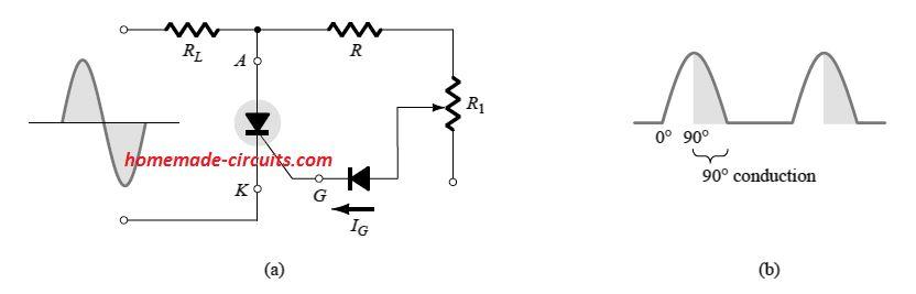 The network using R and R1 ensures a properly controlled gate current for the SCR during the positive half cycle of the input AC.
Moving the variable resistor R1 slider arm to maximum, or towards the lower most point, the gate current may become too weak to reach the gate of the SCR, and this will never allow the SCR to switch ON.
On the other hand when it is moved upwards, the gate current will slowly increase until the SCR turn ON magnitude is reached.
Thus, using the variable resistor the user is able to set the level of the turn ON current for the SCR anywhere between 0�� and 90��, as indicated at the right hand side of the above diagram.
For the R1 value, if it's rather low, will cause the SCR to fire quickly, leading to the a similar outcome obtained from the first figure above (180�� conduction).
However, if the R1 value is bigger, a higher positive input voltage will be needed to fire the SCR.
This situation wouldn't allow us to extend the control over 90�� phase displacement, since the input is at its highest level at this point.
If the SCR is unable to fire at this level or for the lower values of the input voltages at the positive slope of the AC cycle, the response will be exactly the same for the negative slopes of the input cycle.
Technically, this type of working of an SCR is called half-wave variable-resistance phase control.
This method can be effectively used in applications requiring RMS current control or load power control.
The network using R and R1 ensures a properly controlled gate current for the SCR during the positive half cycle of the input AC.
Moving the variable resistor R1 slider arm to maximum, or towards the lower most point, the gate current may become too weak to reach the gate of the SCR, and this will never allow the SCR to switch ON.
On the other hand when it is moved upwards, the gate current will slowly increase until the SCR turn ON magnitude is reached.
Thus, using the variable resistor the user is able to set the level of the turn ON current for the SCR anywhere between 0�� and 90��, as indicated at the right hand side of the above diagram.
For the R1 value, if it's rather low, will cause the SCR to fire quickly, leading to the a similar outcome obtained from the first figure above (180�� conduction).
However, if the R1 value is bigger, a higher positive input voltage will be needed to fire the SCR.
This situation wouldn't allow us to extend the control over 90�� phase displacement, since the input is at its highest level at this point.
If the SCR is unable to fire at this level or for the lower values of the input voltages at the positive slope of the AC cycle, the response will be exactly the same for the negative slopes of the input cycle.
Technically, this type of working of an SCR is called half-wave variable-resistance phase control.
This method can be effectively used in applications requiring RMS current control or load power control.
 The working of the above SCR controlled battery charger can be understood with the following explanation:
The input stepped down AC is full wave rectified through the diodes D1, D2 and supplied across the SCR anode/cathode terminals.
The battery which is under charging can be seen in series with the cathode terminal.
When the battery is in the discharged condition, its voltage is low enough to keep the SCR2 is the switched OFF state.
Due to the open state of SCR2, the SCR1 control circuit behaves exactly like our series static switch discussed in the previous paragraphs.
With the input rectified supply adequately rated, triggers ON the SCR1 with a gate current that's regulated by R1.
This instantly turns ON the SCR and the battery begins charging via the anode/cathode SCR conduction.
In the beginning, due to the low discharged level of the battery, the VR will have a lower potential as set by the R5 preset or potential divider.
At this point the VR level will be too low to turn ON the 11 V zener diode.
In its non-conducting state the zener will be almost like an open circuit, causing the SCR2 to be completely switched OFF, due to virtually zero gate current.
Also, the presence of C1 ensures that the SCR2 is never accidentally turned ON due to voltage transients or spikes.
As the battery charges, its terminal voltage gradually rises, and ultimately when it reaches the set full charge value, VR becomes just sufficient to turn ON the 11 V zener diode, subsequently firing ON the SCR2.
As soon as SCR2 fires, it effectively generates a short circuit, connecting R2 end terminal to ground, and enabling the potential divider created by R1, R2 network at the gate of the SCR1.
The activation of the R1/R2 potential divider at the gate of SCR1 causes an instant drop in the gate current current of SCR1, forcing it to shut off.
This results in the supply to the battery getting cut off, ensuring the battery is not allowed to over charge.
After this, if the battery voltage tends to drop below the preset value, the 11 V zener switches OFF, causing SCR1 to switch ON yet again to repeat the charging cycle.
The working of the above SCR controlled battery charger can be understood with the following explanation:
The input stepped down AC is full wave rectified through the diodes D1, D2 and supplied across the SCR anode/cathode terminals.
The battery which is under charging can be seen in series with the cathode terminal.
When the battery is in the discharged condition, its voltage is low enough to keep the SCR2 is the switched OFF state.
Due to the open state of SCR2, the SCR1 control circuit behaves exactly like our series static switch discussed in the previous paragraphs.
With the input rectified supply adequately rated, triggers ON the SCR1 with a gate current that's regulated by R1.
This instantly turns ON the SCR and the battery begins charging via the anode/cathode SCR conduction.
In the beginning, due to the low discharged level of the battery, the VR will have a lower potential as set by the R5 preset or potential divider.
At this point the VR level will be too low to turn ON the 11 V zener diode.
In its non-conducting state the zener will be almost like an open circuit, causing the SCR2 to be completely switched OFF, due to virtually zero gate current.
Also, the presence of C1 ensures that the SCR2 is never accidentally turned ON due to voltage transients or spikes.
As the battery charges, its terminal voltage gradually rises, and ultimately when it reaches the set full charge value, VR becomes just sufficient to turn ON the 11 V zener diode, subsequently firing ON the SCR2.
As soon as SCR2 fires, it effectively generates a short circuit, connecting R2 end terminal to ground, and enabling the potential divider created by R1, R2 network at the gate of the SCR1.
The activation of the R1/R2 potential divider at the gate of SCR1 causes an instant drop in the gate current current of SCR1, forcing it to shut off.
This results in the supply to the battery getting cut off, ensuring the battery is not allowed to over charge.
After this, if the battery voltage tends to drop below the preset value, the 11 V zener switches OFF, causing SCR1 to switch ON yet again to repeat the charging cycle.
 The above diagram shows a classic heater control application using an SCR.
The circuit is designed to switch ON and OFF the 100 watt heater depending on the thermostat switching.
A mercury-in-glass thermostat is used here, which are supposed to be extremely sensitive to the changes in the temperature levels surrounding it.
To be precise it can sense even a change of a 0.1��C temperatures.
However, since these types of thermostats are normally rated to handle very small magnitudes of current in the range of 1 mA or so, and therefore it is not too popular in temperature control circuits.
In the discussed heater control application, the SCR is used as a current amplifier for amplifying the thermostat current.
Actually, the SCR does not function like a traditional amplifier, rather as a current sensor, which allows the varying thermostat characteristics to control the higher current level switching of the SCR.
We can see that the supply to the SCR is applied through the heater and a full bridge rectifier, which allows a full wave rectified DC supply for the SCR.
During the period, when the thermostat is in the open state, the potential across the 0.1uF capacitor is charged to the firing level of the SCR gate potential via pulses generated by each rectified DC pulse.
The time constant for charging the capacitor is established by the product of the RC elements.
This enables the SCR to conduct during these pulsed DC half cycle triggers, allowing the current to pass through the heater, and allow the required heating process.
As the heater heats up and it temperature rises, at the predetermined point, causes the conductive thermostat to activate and create a short circuit across the 0.1uF capacitor.
This in turn switches OFF the SCR and cuts off power to the heater, causing its temperature to drop gradually, until it drops to a level where the thermostat yet again is disabled and the SCR fires ON.
The above diagram shows a classic heater control application using an SCR.
The circuit is designed to switch ON and OFF the 100 watt heater depending on the thermostat switching.
A mercury-in-glass thermostat is used here, which are supposed to be extremely sensitive to the changes in the temperature levels surrounding it.
To be precise it can sense even a change of a 0.1��C temperatures.
However, since these types of thermostats are normally rated to handle very small magnitudes of current in the range of 1 mA or so, and therefore it is not too popular in temperature control circuits.
In the discussed heater control application, the SCR is used as a current amplifier for amplifying the thermostat current.
Actually, the SCR does not function like a traditional amplifier, rather as a current sensor, which allows the varying thermostat characteristics to control the higher current level switching of the SCR.
We can see that the supply to the SCR is applied through the heater and a full bridge rectifier, which allows a full wave rectified DC supply for the SCR.
During the period, when the thermostat is in the open state, the potential across the 0.1uF capacitor is charged to the firing level of the SCR gate potential via pulses generated by each rectified DC pulse.
The time constant for charging the capacitor is established by the product of the RC elements.
This enables the SCR to conduct during these pulsed DC half cycle triggers, allowing the current to pass through the heater, and allow the required heating process.
As the heater heats up and it temperature rises, at the predetermined point, causes the conductive thermostat to activate and create a short circuit across the 0.1uF capacitor.
This in turn switches OFF the SCR and cuts off power to the heater, causing its temperature to drop gradually, until it drops to a level where the thermostat yet again is disabled and the SCR fires ON.
 The next SCR application talks about a single-source emergency lamp design in which a 6 V battery is kept in a topped up charged condition, so that the connected lamp can be seamlessly switched ON whenever a power failure happens.
When power is available, a full wave rectified DC supply using D1, D2 reaches the connected 6 V lamp.
C1 is allowed to charge to a level that's slightly lower than the difference between the peak DC of the fully rectified supply and the voltage across R2, as determined by the supply input and charge level of the 6 V battery.
Under any circumstances, the cathode potential level of the SCR is help higher than its anode, and also gate to cathode voltage is held negative.
This make sure that the SCR stays in the non-conducting state.
The charging rate of the attached battery is determined by R1, and enabled through the diode D1.
The charging is sustained only as long a the D1 anode remains more positive than its cathode.
While the input power is present, the full wave rectified across the emergency lamp keeps it switched ON.
During power failure situation, the capacitor C1 begins discharging through D1, R1, and R3, until the point where the SCR1 cathode becomes less positive than its cathode.
Also, meanwhile the R2, R3, junction goes positive resulting in an increased gate to cathode voltage for the SCR, turning it ON.
The SCR now fires and allows the battery to get connected with the lamp, instantly illuminating it through battery power.
The lamp is allowed to stay in the illuminated state as if nothing had happened.
When power returns, the capacitors C1 is yet again recharged, causing the SCR to switch OFF, and cutting off the battery power to the lamp, so that the lamp now illuminates through the input DC supply.
The next SCR application talks about a single-source emergency lamp design in which a 6 V battery is kept in a topped up charged condition, so that the connected lamp can be seamlessly switched ON whenever a power failure happens.
When power is available, a full wave rectified DC supply using D1, D2 reaches the connected 6 V lamp.
C1 is allowed to charge to a level that's slightly lower than the difference between the peak DC of the fully rectified supply and the voltage across R2, as determined by the supply input and charge level of the 6 V battery.
Under any circumstances, the cathode potential level of the SCR is help higher than its anode, and also gate to cathode voltage is held negative.
This make sure that the SCR stays in the non-conducting state.
The charging rate of the attached battery is determined by R1, and enabled through the diode D1.
The charging is sustained only as long a the D1 anode remains more positive than its cathode.
While the input power is present, the full wave rectified across the emergency lamp keeps it switched ON.
During power failure situation, the capacitor C1 begins discharging through D1, R1, and R3, until the point where the SCR1 cathode becomes less positive than its cathode.
Also, meanwhile the R2, R3, junction goes positive resulting in an increased gate to cathode voltage for the SCR, turning it ON.
The SCR now fires and allows the battery to get connected with the lamp, instantly illuminating it through battery power.
The lamp is allowed to stay in the illuminated state as if nothing had happened.
When power returns, the capacitors C1 is yet again recharged, causing the SCR to switch OFF, and cutting off the battery power to the lamp, so that the lamp now illuminates through the input DC supply.
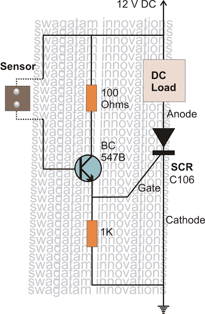 The above circuit of a rain alarm can be used for activating a AC load, like a lamp or an automatic folding cover or shade.
The sensor is made by placing to metallic pegs, or screws or similar metal over a plastic body.
The wires from these metals are connected across the base of a triggering transistor stage.
The sensor is the only part of the circuit which is placed outdoors, for sensing a rain fall.
When a rain fall begins, water droplets bridge the metals of the sensor.
The above circuit of a rain alarm can be used for activating a AC load, like a lamp or an automatic folding cover or shade.
The sensor is made by placing to metallic pegs, or screws or similar metal over a plastic body.
The wires from these metals are connected across the base of a triggering transistor stage.
The sensor is the only part of the circuit which is placed outdoors, for sensing a rain fall.
When a rain fall begins, water droplets bridge the metals of the sensor.
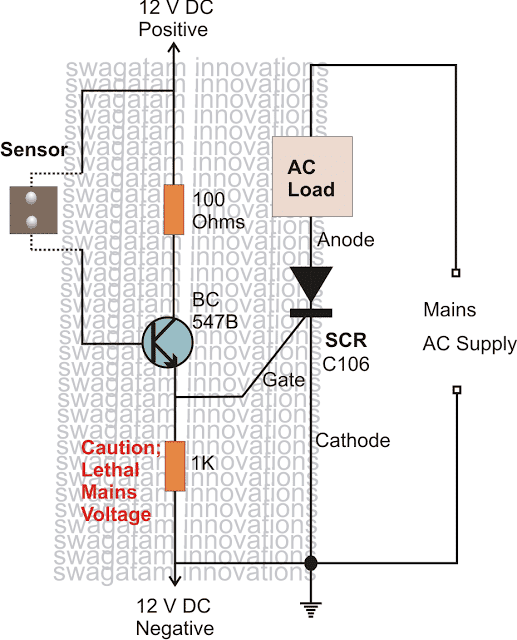 Small voltage start leaking across the sensor metals and reach the base of the transistor, the transistor immediately conducts and supplies the required gate current to the SCR.
The SCR also responds and switches ON the connected AC load for pulling an automatic cover or simply an alarm for correcting the situation as desired by the user.
Small voltage start leaking across the sensor metals and reach the base of the transistor, the transistor immediately conducts and supplies the required gate current to the SCR.
The SCR also responds and switches ON the connected AC load for pulling an automatic cover or simply an alarm for correcting the situation as desired by the user.
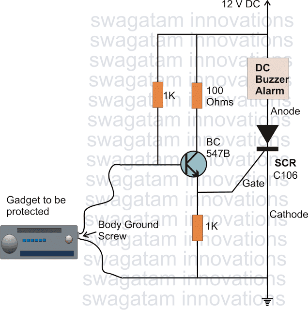 We discussed in the previous section regarding a special property of SCR where it latches in response to DC loads.
The circuit described below exploits the above property of the SCR effectively for triggering an alarm in response to a possible theft.
Here, initially the SCR is held in a switched OFF position as long as its gate stays rigged or screwed with the ground potential which happens to be the body of the asset which is required to be protected.
If an attempt to steal the asset is made by unscrewing the relevant bolt, the ground potential to the SCR is removed and the transistor gets activated through the associated resistor connected across its base and positive.
The SCR also instantly triggers because now it gets its gate voltage from the transistor emitter, and latches sounding the connected DC alarm.
The alarm remains switched ON until its switched OFF manually, hopefully by the actual owner.
We discussed in the previous section regarding a special property of SCR where it latches in response to DC loads.
The circuit described below exploits the above property of the SCR effectively for triggering an alarm in response to a possible theft.
Here, initially the SCR is held in a switched OFF position as long as its gate stays rigged or screwed with the ground potential which happens to be the body of the asset which is required to be protected.
If an attempt to steal the asset is made by unscrewing the relevant bolt, the ground potential to the SCR is removed and the transistor gets activated through the associated resistor connected across its base and positive.
The SCR also instantly triggers because now it gets its gate voltage from the transistor emitter, and latches sounding the connected DC alarm.
The alarm remains switched ON until its switched OFF manually, hopefully by the actual owner.
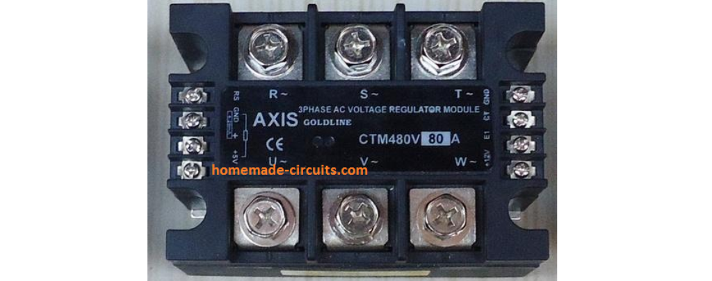
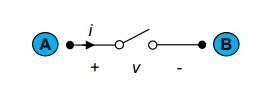 Here, we can see a positive voltage is applied at point "A" of the switch and a negative potential is applied at point "B", which allows the current to flow across "A" to "B".
The action can be reversed by simply changing the voltage polarity.
Meaning, the points "A" and "B" of the BPS can be used as interchangeable input/output terminals.
The best application example of a BPS can be seen in all MOSFET based commercial SSR designs.
Here, we can see a positive voltage is applied at point "A" of the switch and a negative potential is applied at point "B", which allows the current to flow across "A" to "B".
The action can be reversed by simply changing the voltage polarity.
Meaning, the points "A" and "B" of the BPS can be used as interchangeable input/output terminals.
The best application example of a BPS can be seen in all MOSFET based commercial SSR designs.
 In the above diagram, the quadrants are indicated in green color which indicates the ON state of the devices regardless of the polarity of the supply current or the waveform.
 In the above diagram, the red straight line indicates that the BPS devices are in OFF state and offers absolutely no conduction regardless of the polarity of the voltage or the waveform.
 In the first diagram, two P-channel MOSFETs are configured with their sources connected back to back with each other.
In the second diagram, two N-channel MOSFETS can be seen connected across their sources for implementing a BPS design.
In the third configuration, two N-channel MOSFETs are shown attached drain to drain for executing the intended bidirectional conduction.
In the first diagram, two P-channel MOSFETs are configured with their sources connected back to back with each other.
In the second diagram, two N-channel MOSFETS can be seen connected across their sources for implementing a BPS design.
In the third configuration, two N-channel MOSFETs are shown attached drain to drain for executing the intended bidirectional conduction.
 In this case we can see that when the gate voltage is applied, current from "A" is allowed to flow through left MOSFET, then through the internal forward biased diode D2 of the right side MOSFET, and finally the conduction completes at point "B".
When the voltage polarity is reversed from "B" to "A" the MOSFETs and their internal diodes flip their positions as shown in the following illustration:
In this case we can see that when the gate voltage is applied, current from "A" is allowed to flow through left MOSFET, then through the internal forward biased diode D2 of the right side MOSFET, and finally the conduction completes at point "B".
When the voltage polarity is reversed from "B" to "A" the MOSFETs and their internal diodes flip their positions as shown in the following illustration:
 In the above situation, the right side MOSFET of the BPS switches ON along with D1 which is the internal body diode of the left side MOSFET, to enable the conduction from "B" to "A".
 When point "A" is positive, the left side body diode gets forward biased and conducts, followed by the right side p-MOSFET, to complete the conduction at point "B".
When point "B" is positive, the opposite side respective components become active for the conduction.
The lower N-channel MOSFET is controls the ON/OFF states of the BPS device through appropriate ON/OFF gate commands.
The resistor and the capacitor protect the BPS devices from a possible in rush current surge.
However, using P-channel MOSFET is never the ideal way of implementing a BPS due to their high RDSon.
Therefore these might require bigger and costlier devices to compensate against heat and other related inefficiencies, compared to N-channel based BPS design.
When point "A" is positive, the left side body diode gets forward biased and conducts, followed by the right side p-MOSFET, to complete the conduction at point "B".
When point "B" is positive, the opposite side respective components become active for the conduction.
The lower N-channel MOSFET is controls the ON/OFF states of the BPS device through appropriate ON/OFF gate commands.
The resistor and the capacitor protect the BPS devices from a possible in rush current surge.
However, using P-channel MOSFET is never the ideal way of implementing a BPS due to their high RDSon.
Therefore these might require bigger and costlier devices to compensate against heat and other related inefficiencies, compared to N-channel based BPS design.
 The charge pump could be built using a standard voltage doubler circuit or a small boost switching circuit.
The 3.3 V is applied for powering the charge pump optimally, while the Schottky diodes derive the gate voltage directly from the respective input (A/B) even if the input supply is as low as 6 V.
This 6 V is then doubled by the charge ump for the MOSFET gates.
The lower N-channel MOSFET is for controlling the ON/OFF switching of the bidirectional switch as per desired specifications.
The only disadvantage of using an N-channel MOSFET compared to the previously discussed P-channel are these extra components that may consume extra space on the PCB.
However, this disadvantage is outweighed by the low R(on) of the MOSFETs and highly efficient conduction, and low cost small sized MOSFETs.
That said, this design also does not provide any effective protection against over heating, and therefore oversized devices may be considered for high power applications.
The charge pump could be built using a standard voltage doubler circuit or a small boost switching circuit.
The 3.3 V is applied for powering the charge pump optimally, while the Schottky diodes derive the gate voltage directly from the respective input (A/B) even if the input supply is as low as 6 V.
This 6 V is then doubled by the charge ump for the MOSFET gates.
The lower N-channel MOSFET is for controlling the ON/OFF switching of the bidirectional switch as per desired specifications.
The only disadvantage of using an N-channel MOSFET compared to the previously discussed P-channel are these extra components that may consume extra space on the PCB.
However, this disadvantage is outweighed by the low R(on) of the MOSFETs and highly efficient conduction, and low cost small sized MOSFETs.
That said, this design also does not provide any effective protection against over heating, and therefore oversized devices may be considered for high power applications.

 Parts List
R1, R2, R3, R4, R5 = 10K
C1 = 470uF/25V
T1, T2 = BC557
T3, T4 = BC547
ALL DIODES = 1N4007
RL1---RL3 = 12V/400 ohms
RL4 = 12V DPDT, 30amp
Parts List
R1, R2, R3, R4, R5 = 10K
C1 = 470uF/25V
T1, T2 = BC557
T3, T4 = BC547
ALL DIODES = 1N4007
RL1---RL3 = 12V/400 ohms
RL4 = 12V DPDT, 30amp
 The above diagram shows the "smart" generator starter circuit, which cranks the generator a few number of times and then shuts off.
The shutting off is dependent on three conditions:
1) The generator actuates,
2) The stipulated number of cranking is completed without results, 3) The battery is detected to be low.
IC1 and IC3 are configured as monstables, where IC1 is selected to generate a 1 minute high at its pin#3 when AC mains fails, while IC3 is assigned for generating the cranking sequences for 4 or 5 times with 5 seconds period for each cranking.
The center IC2 is rigged as an astable which supplies the cranking triggers to the IC3.
The IC2 preset must be set such that pin3 of IC 2 generates a duty cycle of 20 seconds ON and 2 seconds OFF.
In order to ensure a delayed start ON or a delayed switch OFF the following delay relay circuit may be employed with the above design.
The above diagram shows the "smart" generator starter circuit, which cranks the generator a few number of times and then shuts off.
The shutting off is dependent on three conditions:
1) The generator actuates,
2) The stipulated number of cranking is completed without results, 3) The battery is detected to be low.
IC1 and IC3 are configured as monstables, where IC1 is selected to generate a 1 minute high at its pin#3 when AC mains fails, while IC3 is assigned for generating the cranking sequences for 4 or 5 times with 5 seconds period for each cranking.
The center IC2 is rigged as an astable which supplies the cranking triggers to the IC3.
The IC2 preset must be set such that pin3 of IC 2 generates a duty cycle of 20 seconds ON and 2 seconds OFF.
In order to ensure a delayed start ON or a delayed switch OFF the following delay relay circuit may be employed with the above design.
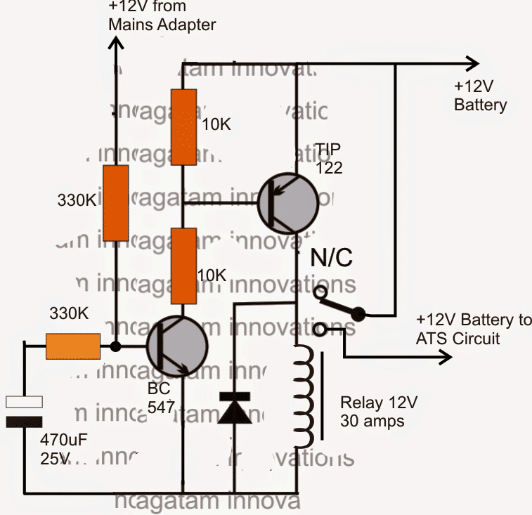
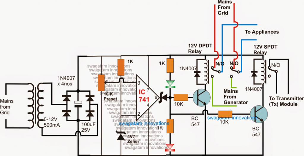

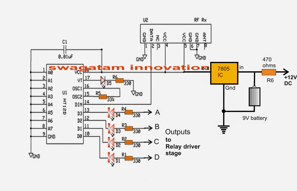
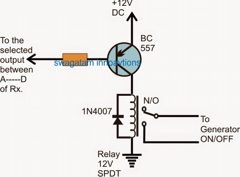
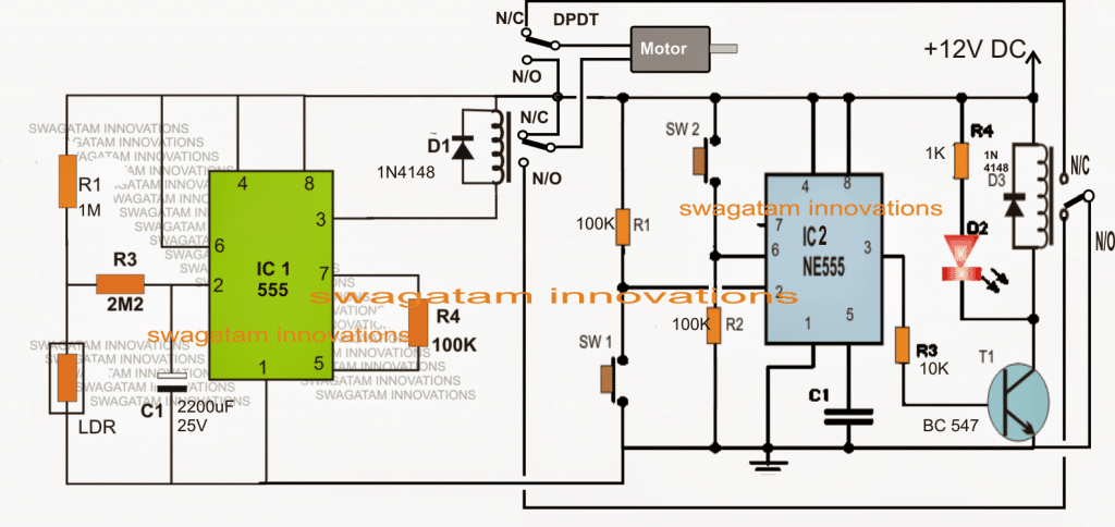
 The AC mains is supplied at the indicated left side input, which is passed on to the load via a load sensing resistor R1 and the associated cut off relay's N/C contacts, N/C stands for normally closed, meaning the contacts are connected across this point while the relay is in a deactivated state.
R1 is suitably calculated such that a potential difference sufficient enough to trigger the opto LED develops across it whenever an overload exceeding the unsafe zone is reached.
The overload cut off operation is executed in the following manner:
For so long as the load is within the the normal range of consumption, the voltage across R1 stays low, keeping the opto LED disabled.
However in case of a short circuit or an overload at the output, which may be in a lathe machine for the proposed design, the voltage across R1 shoots and becomes sufficiently high so as to switch ON the opto LED instantly.
The opto LED in turn illuminates the associated LDR sealed inside the light proof enclosure causing its resistance to drop significantly.
This drop in the the LDR voltage allows a biasing current to the base of R1 which along with T2 instantly flips into a latching mode switching ON the relay.
The relay contacts respond to this and deliver the required changeover cutting off the AC line to the load or the lathe machine.
The circuit stays latched and frozen until the power to the circuit is switched OFF and switched ON resetting the relay in its initial form.
Alternatively the shown push button may also be pressed for the same.
The green LED indicates the latched mode of the overload protector circuit and also confirms a power off to the output load.
The opto coupler is a homemade device, the construction details may be studied in the following article:
https://www.homemade-circuits.com/2011/12/how-to-build-simple-electronic.html
Using an LED/LDR combination for the opto coupler appears to be much reliable in its operations, however a conventional LED/transistor opto (such as a 4n35 etc) can also be tried instead, and might just work as reliably, it could be a matter of some experimentation.
Using an Opto-coupler
The above design can be also built using an opto-coupler instead of an LED/LDR assembly, as shown below:
The AC mains is supplied at the indicated left side input, which is passed on to the load via a load sensing resistor R1 and the associated cut off relay's N/C contacts, N/C stands for normally closed, meaning the contacts are connected across this point while the relay is in a deactivated state.
R1 is suitably calculated such that a potential difference sufficient enough to trigger the opto LED develops across it whenever an overload exceeding the unsafe zone is reached.
The overload cut off operation is executed in the following manner:
For so long as the load is within the the normal range of consumption, the voltage across R1 stays low, keeping the opto LED disabled.
However in case of a short circuit or an overload at the output, which may be in a lathe machine for the proposed design, the voltage across R1 shoots and becomes sufficiently high so as to switch ON the opto LED instantly.
The opto LED in turn illuminates the associated LDR sealed inside the light proof enclosure causing its resistance to drop significantly.
This drop in the the LDR voltage allows a biasing current to the base of R1 which along with T2 instantly flips into a latching mode switching ON the relay.
The relay contacts respond to this and deliver the required changeover cutting off the AC line to the load or the lathe machine.
The circuit stays latched and frozen until the power to the circuit is switched OFF and switched ON resetting the relay in its initial form.
Alternatively the shown push button may also be pressed for the same.
The green LED indicates the latched mode of the overload protector circuit and also confirms a power off to the output load.
The opto coupler is a homemade device, the construction details may be studied in the following article:
https://www.homemade-circuits.com/2011/12/how-to-build-simple-electronic.html
Using an LED/LDR combination for the opto coupler appears to be much reliable in its operations, however a conventional LED/transistor opto (such as a 4n35 etc) can also be tried instead, and might just work as reliably, it could be a matter of some experimentation.
Using an Opto-coupler
The above design can be also built using an opto-coupler instead of an LED/LDR assembly, as shown below:


 The high energy varistor as discussed above should be installed into the power lines as shown in the following diagram:

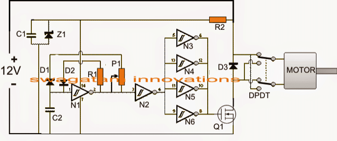 If an Arduino based PWM is intended to be used, the IC stage in the above diagram could be removed and the PWM from the Arduino could be applied directly at the base of the mosfet via a 10 ohm resistor as shown below
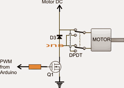 Parts List
R1 = 10K
R2 = 47 OHMS
P1 = 100K POT
D1, D2 = 1N4148
D3 = MUR1560
C1,C2 = 0.1uF/100V
Z1 = 15V, 1/2 WATT
Q1 = IRF540
N1---N6 = IC MM74C14
DPDT = DPST SWITCH OR DPDT RELAY
Parts List
R1 = 10K
R2 = 47 OHMS
P1 = 100K POT
D1, D2 = 1N4148
D3 = MUR1560
C1,C2 = 0.1uF/100V
Z1 = 15V, 1/2 WATT
Q1 = IRF540
N1---N6 = IC MM74C14
DPDT = DPST SWITCH OR DPDT RELAY
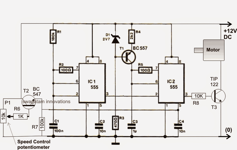 The above explained fan speed controller needs to be powered through an uninterruptible power supply system from a standby well-recharged battery back up stage.
The battery in turn requires an automatic battery charger circuit so that it stays ready for providing an instant uninterrupted power to the fan, ensuring a smooth and a continuous supply to the motor and feed of air to the biomass cook stove.
The above explained fan speed controller needs to be powered through an uninterruptible power supply system from a standby well-recharged battery back up stage.
The battery in turn requires an automatic battery charger circuit so that it stays ready for providing an instant uninterrupted power to the fan, ensuring a smooth and a continuous supply to the motor and feed of air to the biomass cook stove.
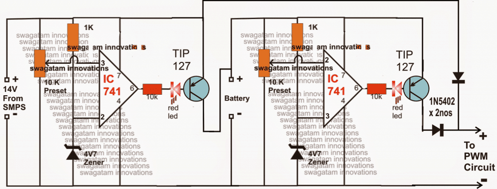

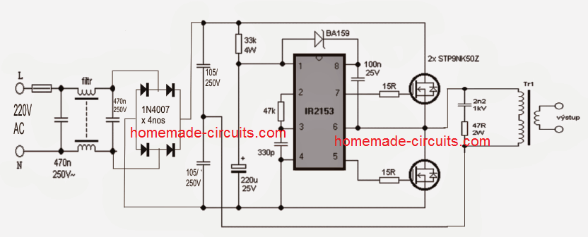
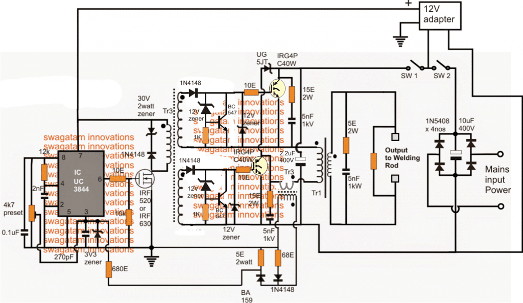
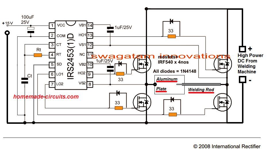 The Rt, Ct could be calculated with some trial and error to get the mosfets oscillating at any frequency between 100 and 500Hz.
For the exact formula you could refer to this article.
Th 15V input could be supplied from any 12V or 15V AC to DC adapter unit.
The Rt, Ct could be calculated with some trial and error to get the mosfets oscillating at any frequency between 100 and 500Hz.
For the exact formula you could refer to this article.
Th 15V input could be supplied from any 12V or 15V AC to DC adapter unit.
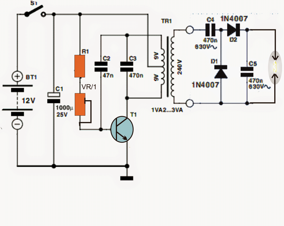 The upper half of the transformer winding simply provides a feedback to the base of the transistor via C2 such the T1 stays locked on to the conduction mode until C2 charges fully, breaking the latch and forcing the transistor to begin the conduction cycle afresh.
R1 which is a 1K resistor is positioned to limit the base drive for T1 to safe limits while VR1 which is a 22k preset may be adjusted for obtaining an efficiently pulsating T1 frequency.
C2 may be also fine tuned by trying other values until the highest possible output is attained at the trafo output
The transformer could be any iron-cored step down transformer (500mA) normally used in transformer type AC/DC adapter units.
The output right across the transformer output would be at the rated secondary level, for example if it is a 220V secondary, then the output could be expected to be at this level.
The above level could be further amplified or stepped up through the attached diode, capacitor charge pump network akin to cockroft-walton generator network.
The network raises the 220V level to many hundreds of volts which may be forced to spark across an appropriately positioned end terminals of the charge pump circuit.
The circuit can be also used in mosquito swatter bat application by replacing the iron cored transformer with a ferrite core counterpart.
The upper half of the transformer winding simply provides a feedback to the base of the transistor via C2 such the T1 stays locked on to the conduction mode until C2 charges fully, breaking the latch and forcing the transistor to begin the conduction cycle afresh.
R1 which is a 1K resistor is positioned to limit the base drive for T1 to safe limits while VR1 which is a 22k preset may be adjusted for obtaining an efficiently pulsating T1 frequency.
C2 may be also fine tuned by trying other values until the highest possible output is attained at the trafo output
The transformer could be any iron-cored step down transformer (500mA) normally used in transformer type AC/DC adapter units.
The output right across the transformer output would be at the rated secondary level, for example if it is a 220V secondary, then the output could be expected to be at this level.
The above level could be further amplified or stepped up through the attached diode, capacitor charge pump network akin to cockroft-walton generator network.
The network raises the 220V level to many hundreds of volts which may be forced to spark across an appropriately positioned end terminals of the charge pump circuit.
The circuit can be also used in mosquito swatter bat application by replacing the iron cored transformer with a ferrite core counterpart.
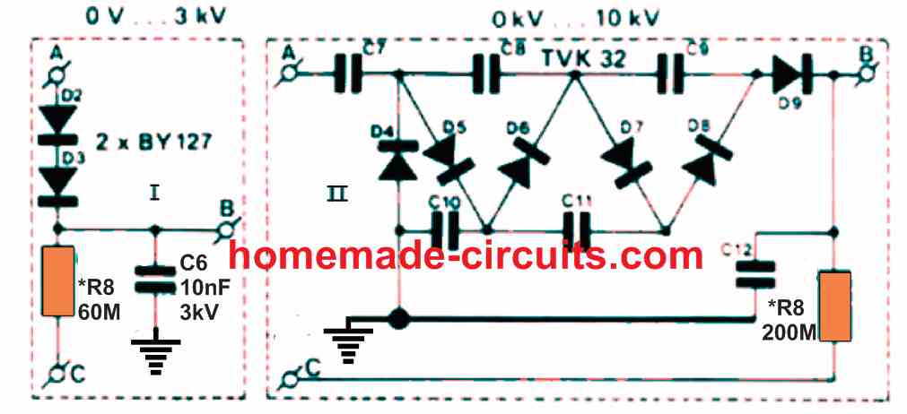 This voltage is subsequently boosted and stepped-up proportionately as per the turn ratio of the secondary windings.
The 1st variation (type 1) of the circuit employs half-wave rectification.
Version 2 is actually a cascade rectifier salvaged from an old T.V.
set.
Variation 2 provides a voltage 3 times greater than version 1 since the cascade rectifier functions like voltage multiplier (3X).
IC2 controls the output voltage.
The opamp compares the voltage created across the P1 preset with the voltage existing at the voltage dividers R6/R8 or R7/R8 junction.
In the event the output goes higher than the preset voltage level, IC2 may cut down the supply voltage towards the output by using T3. The main section of the circuit is the transformer.
Eventhough it is pretty vital, its design isn't that critical.
A range of E, EI ferrite cores with a diameter of 30 mm might work extremely well pretty effortlessly.
The core must not include any kind of air gap, an AL value of 2000 nH will be just appropriate.
The primary winding includes 25 turns of 0.7 mm 1 mm super enamelled copper wire and the secondary is built using 500 turns of 0.2 �� 0.3 mm super enameled copper wire.
The primary and secondary windings needs to be effectively insulated from one another! Dependent upon the high voltages, the user must be careful about the following points: Capacitor C6 should have the ability to handle a minimum of 3 kV.
R6 in version 1 includes six 10 M resistors connected in series.
R7 is a 10 M resistor, built by using 10nos of 1M in series.
This is implemented to counteract spikes from the output.
Both circuit takes in around 50 mA with no load attached, and 350 mA while ensuring 2 �� 3 W to a load.
Transistors T2 and T3 may demand heatsinks.
This voltage is subsequently boosted and stepped-up proportionately as per the turn ratio of the secondary windings.
The 1st variation (type 1) of the circuit employs half-wave rectification.
Version 2 is actually a cascade rectifier salvaged from an old T.V.
set.
Variation 2 provides a voltage 3 times greater than version 1 since the cascade rectifier functions like voltage multiplier (3X).
IC2 controls the output voltage.
The opamp compares the voltage created across the P1 preset with the voltage existing at the voltage dividers R6/R8 or R7/R8 junction.
In the event the output goes higher than the preset voltage level, IC2 may cut down the supply voltage towards the output by using T3. The main section of the circuit is the transformer.
Eventhough it is pretty vital, its design isn't that critical.
A range of E, EI ferrite cores with a diameter of 30 mm might work extremely well pretty effortlessly.
The core must not include any kind of air gap, an AL value of 2000 nH will be just appropriate.
The primary winding includes 25 turns of 0.7 mm 1 mm super enamelled copper wire and the secondary is built using 500 turns of 0.2 �� 0.3 mm super enameled copper wire.
The primary and secondary windings needs to be effectively insulated from one another! Dependent upon the high voltages, the user must be careful about the following points: Capacitor C6 should have the ability to handle a minimum of 3 kV.
R6 in version 1 includes six 10 M resistors connected in series.
R7 is a 10 M resistor, built by using 10nos of 1M in series.
This is implemented to counteract spikes from the output.
Both circuit takes in around 50 mA with no load attached, and 350 mA while ensuring 2 �� 3 W to a load.
Transistors T2 and T3 may demand heatsinks.


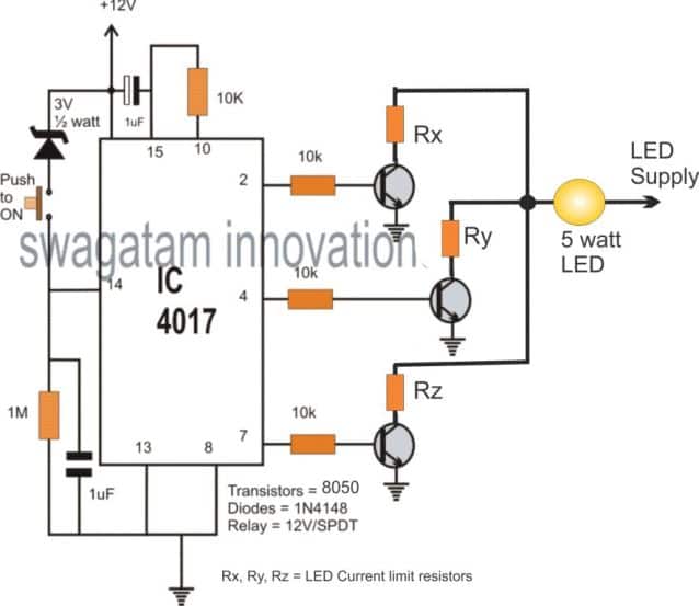
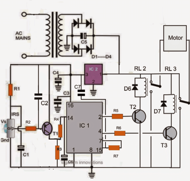
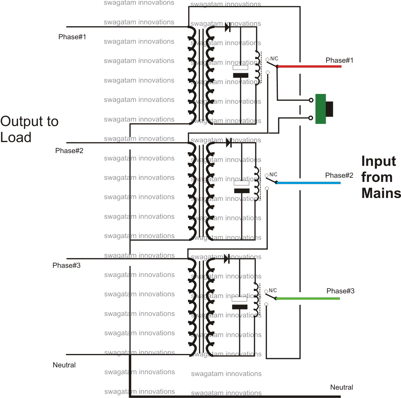
 C2 feeds these pulses to the input of a basichigh gain amplifier, which employs Q1 and Q2 in a two-stage directlycoupled configuration.
C2 and C4 are intentionally set to low levels to ensure thatthe circuit getsan inferiorlow-frequency response.
This ensures that 50 Hertz signals generatedby LED1 due to theinfrared radiation leakage fromthemains-powered lights are effectively rejected.
However, at the significantly higher working frequency of the transmitter circuit, the circuit seems to providea largergain.
C5 connects the amplifier's output to a rectifier and smoothing circuit made up of D1, D2, C6, and R6. This circuit's positive bias is supplied into one of the operational amplifier IC1's inputs.
R7 and R8 provide a bias voltage to the other input.
In most cases, the inverting input's fixed bias would be larger than the bias supplied to the non-inverting input.
The IC1 is configured like a comparator, and its output switcheshigh while under situations, activating the relay coil.
The separate buffer stage Q3 is employed to supply the relatively high driving current necessary.
If an intruder briefly disrupts the beam, the charge on C6 rapidly decays, dropping IC1's non-inverting input potentialbelow the inverting input.
The output of IC1 is therefore turned low, causingthe relay toturnoff, which opens thecontacts of relayRLA1, and the central security system is activated.
C2 feeds these pulses to the input of a basichigh gain amplifier, which employs Q1 and Q2 in a two-stage directlycoupled configuration.
C2 and C4 are intentionally set to low levels to ensure thatthe circuit getsan inferiorlow-frequency response.
This ensures that 50 Hertz signals generatedby LED1 due to theinfrared radiation leakage fromthemains-powered lights are effectively rejected.
However, at the significantly higher working frequency of the transmitter circuit, the circuit seems to providea largergain.
C5 connects the amplifier's output to a rectifier and smoothing circuit made up of D1, D2, C6, and R6. This circuit's positive bias is supplied into one of the operational amplifier IC1's inputs.
R7 and R8 provide a bias voltage to the other input.
In most cases, the inverting input's fixed bias would be larger than the bias supplied to the non-inverting input.
The IC1 is configured like a comparator, and its output switcheshigh while under situations, activating the relay coil.
The separate buffer stage Q3 is employed to supply the relatively high driving current necessary.
If an intruder briefly disrupts the beam, the charge on C6 rapidly decays, dropping IC1's non-inverting input potentialbelow the inverting input.
The output of IC1 is therefore turned low, causingthe relay toturnoff, which opens thecontacts of relayRLA1, and the central security system is activated.
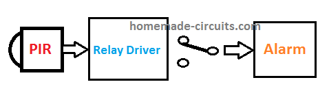
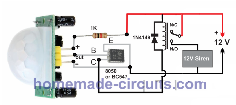 Here we can see, the system can be assembled using just 5 fundamental components, which are: 1) The PIR Module 2) A 1 k resistor, 3) An NPN transistor, 4) A Relay, 5) An Alarm Siren unit.
The PIR has 3 terminals labelled as the Vcc, OUT, and the GND or ground.
The Vcc is supplied with a +12V via the 1k resistor, the GND with the 0V from a DC supply which could be from any standard 12 V AC to DC adapter.
Here we can see, the system can be assembled using just 5 fundamental components, which are: 1) The PIR Module 2) A 1 k resistor, 3) An NPN transistor, 4) A Relay, 5) An Alarm Siren unit.
The PIR has 3 terminals labelled as the Vcc, OUT, and the GND or ground.
The Vcc is supplied with a +12V via the 1k resistor, the GND with the 0V from a DC supply which could be from any standard 12 V AC to DC adapter.
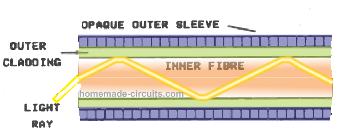 Refraction where the inner filament and the outer cladding interact makes it possible for light traverse through the cable by efficiently jumping across wall to wall all the way through the cable.
It is this bouncing of the light across the cable walls that makes it possible for the cable to run like a light guide, carrying the illumination smoothly about corners and the curves.
Refraction where the inner filament and the outer cladding interact makes it possible for light traverse through the cable by efficiently jumping across wall to wall all the way through the cable.
It is this bouncing of the light across the cable walls that makes it possible for the cable to run like a light guide, carrying the illumination smoothly about corners and the curves.
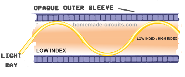
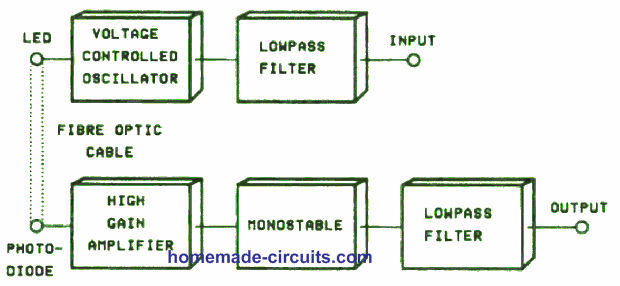 This voltage may be the sound input transmission, and as the signal voltage oscillates up and down, so will the VCO's output frequency.
A lowpass filter is incorporated to refine the audio input signal before it is applied to the VCO.
This helps to keep the heterodyne "whistles" away from being produced on account of beat notes between the voltage controlled oscillator and any high frequency input signals.
Typically, the input signal is only going to cover the audio frequency range, but you may find distortion content at higher frequencies, and radio signals getting picked up from the wiring and interacting with the VCO signal or harmonics around the VCO's output signal.
The emitting device which may be simply an LED is driven by the VCO output.
For optimal result this LED is normally a high wattage type of LED.
This necessitates the use of a driver buffer stage for operating the LED power.
This next stage is a monostable multivibrator which must be designed as a non-retriggerable type.
This enables the stage to generate output pulses through intervals as determined by the C/R timing network which is independent of the input pulse duration.
This voltage may be the sound input transmission, and as the signal voltage oscillates up and down, so will the VCO's output frequency.
A lowpass filter is incorporated to refine the audio input signal before it is applied to the VCO.
This helps to keep the heterodyne "whistles" away from being produced on account of beat notes between the voltage controlled oscillator and any high frequency input signals.
Typically, the input signal is only going to cover the audio frequency range, but you may find distortion content at higher frequencies, and radio signals getting picked up from the wiring and interacting with the VCO signal or harmonics around the VCO's output signal.
The emitting device which may be simply an LED is driven by the VCO output.
For optimal result this LED is normally a high wattage type of LED.
This necessitates the use of a driver buffer stage for operating the LED power.
This next stage is a monostable multivibrator which must be designed as a non-retriggerable type.
This enables the stage to generate output pulses through intervals as determined by the C/R timing network which is independent of the input pulse duration.
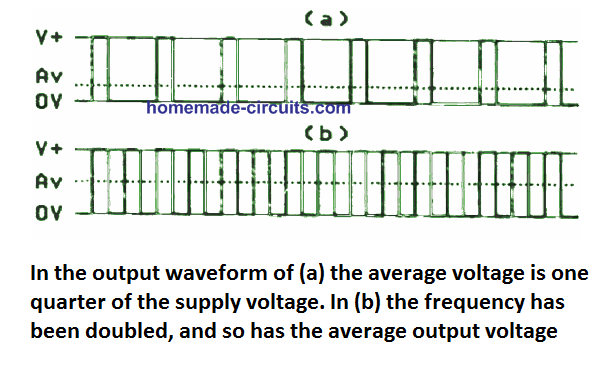 In Figure (a) the input frequency generates an output from the monostable with a 1 to 3 mark-space ratio, and the output is in the high state for 25% of the time.
The average output voltage (as depicted inside the dotted line) is as a result 1/4 of the output HIGH state.
In Figure (b) above we can see that the input frequency has been increased by two fold, which means we get two times more output pulses for a specified time interval with a mark space ratio of 1:1. This allows us to get an average output voltage that is 50% of HIGH output state, and 2 times more magnitude of the previous example.
In simple terms, the monostable not only helps to convert frequency to voltage, but it additionally enables the conversion to get a linear characteristic.
The output from the monostable alone cannot build an audio frequency signal, unless a lowpass filter is incorporated which ensures that the output is stabilized into a proper audio signal.
The primary problem with this simple method of frequency to voltage conversion is that a higher level attenuation (essentially 80 dB or higher) is required at the minimum output frequency of the VCO to be able to create a stabilized output.
But, this method is really simple and dependable in other considerations, and together with modern circuits it may not be difficult to design an output filter stage having a appropriately precise cut off characteristic.
A tiny level of surplus carrier signal on the output may not be a too critical and could be ignored, because the carrier is generally at frequencies which is not within the the audio range, and any leakage at the output will as a result be inaudible.
In Figure (a) the input frequency generates an output from the monostable with a 1 to 3 mark-space ratio, and the output is in the high state for 25% of the time.
The average output voltage (as depicted inside the dotted line) is as a result 1/4 of the output HIGH state.
In Figure (b) above we can see that the input frequency has been increased by two fold, which means we get two times more output pulses for a specified time interval with a mark space ratio of 1:1. This allows us to get an average output voltage that is 50% of HIGH output state, and 2 times more magnitude of the previous example.
In simple terms, the monostable not only helps to convert frequency to voltage, but it additionally enables the conversion to get a linear characteristic.
The output from the monostable alone cannot build an audio frequency signal, unless a lowpass filter is incorporated which ensures that the output is stabilized into a proper audio signal.
The primary problem with this simple method of frequency to voltage conversion is that a higher level attenuation (essentially 80 dB or higher) is required at the minimum output frequency of the VCO to be able to create a stabilized output.
But, this method is really simple and dependable in other considerations, and together with modern circuits it may not be difficult to design an output filter stage having a appropriately precise cut off characteristic.
A tiny level of surplus carrier signal on the output may not be a too critical and could be ignored, because the carrier is generally at frequencies which is not within the the audio range, and any leakage at the output will as a result be inaudible.
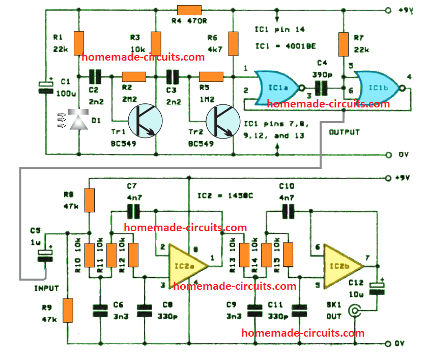 D1 forms the detector diode, and it works in the reverse bias setting in which its leakage resistance helps to create a kind of light dependent resistor or LDR effect.
R1 works like a load resistor, and C2 creates a link between the detector stage and the input amplifier input.
This forms a two-stage capacitively linked network where the two stages function together in the common emitter mode.
This allows a superior overall voltage gain greater than 80 dB.
given that a fairly powerful input signal is supplied, this offers an adequately high output voltage oscillation at the Tr2 collector pin to push the monostable multivibrator.
The latter is a standard CMOS type built using a couple of 2-input NOR gates (IC1a and IC1b) with C4 and R7 functioning like timing elements.
The other a couple of gates of IC1 are not used, although their inputs can be seen hooked to earth in an effort to stop false switching of these gates due to stray pick up.
Referring to filter stage built around IC2a/b, it is fundamentally a 2/3rd order (18 dB per octave) filter systems with specifications commonly employed in the transmitter circuits.
These are joined in series to establish a total of 6 poles and a general attenuation rate of 36 dB per octave.
This offers approximately 100 dB of attenuation of the carrier signal in its minimum frequency range, and an output signal with a relatively low carrier signal levels.
The Fiber Optic Circuit can deal with input voltages as high as 1 volt RMS approximately with no critical distortion, and help to work with marginally less than unity voltage gain for the system.
Components for Fibre Optic Receiver and Filter
Resistors (all 1/4 watt 5%)
R1 = 22k
R2 = 2M2
R3 = 10k
R4 = 470R
R5 = 1M2
R6 = 4k7
R7 = 22k
R8 = 47k
R9 = 47k
R10 to R15 10k (6 off)
Capacitors
C1 = 100��10V electrolytic
C2 = 2n2 polyester
C3 = 2n2 polyester
C4 = 390p ceramic
C5 = 1�� 63V electrolytic
C6 = 3n3 polyester
C7 = 4n7 polyester
C8 = 330pF ceramic
C9 = 3n3 polyester
C10 = 4n7 polyester
Semiconductors
IC1 = 4001BE
1C2 = 1458C
IC3 = CA3140E
Trl , Tr2 BC549 (2 off)
D1 = See text
Miscellaneous
SK1 = 25 way D connector
Case, circuit board, wire, etc.
D1 forms the detector diode, and it works in the reverse bias setting in which its leakage resistance helps to create a kind of light dependent resistor or LDR effect.
R1 works like a load resistor, and C2 creates a link between the detector stage and the input amplifier input.
This forms a two-stage capacitively linked network where the two stages function together in the common emitter mode.
This allows a superior overall voltage gain greater than 80 dB.
given that a fairly powerful input signal is supplied, this offers an adequately high output voltage oscillation at the Tr2 collector pin to push the monostable multivibrator.
The latter is a standard CMOS type built using a couple of 2-input NOR gates (IC1a and IC1b) with C4 and R7 functioning like timing elements.
The other a couple of gates of IC1 are not used, although their inputs can be seen hooked to earth in an effort to stop false switching of these gates due to stray pick up.
Referring to filter stage built around IC2a/b, it is fundamentally a 2/3rd order (18 dB per octave) filter systems with specifications commonly employed in the transmitter circuits.
These are joined in series to establish a total of 6 poles and a general attenuation rate of 36 dB per octave.
This offers approximately 100 dB of attenuation of the carrier signal in its minimum frequency range, and an output signal with a relatively low carrier signal levels.
The Fiber Optic Circuit can deal with input voltages as high as 1 volt RMS approximately with no critical distortion, and help to work with marginally less than unity voltage gain for the system.
Components for Fibre Optic Receiver and Filter
Resistors (all 1/4 watt 5%)
R1 = 22k
R2 = 2M2
R3 = 10k
R4 = 470R
R5 = 1M2
R6 = 4k7
R7 = 22k
R8 = 47k
R9 = 47k
R10 to R15 10k (6 off)
Capacitors
C1 = 100��10V electrolytic
C2 = 2n2 polyester
C3 = 2n2 polyester
C4 = 390p ceramic
C5 = 1�� 63V electrolytic
C6 = 3n3 polyester
C7 = 4n7 polyester
C8 = 330pF ceramic
C9 = 3n3 polyester
C10 = 4n7 polyester
Semiconductors
IC1 = 4001BE
1C2 = 1458C
IC3 = CA3140E
Trl , Tr2 BC549 (2 off)
D1 = See text
Miscellaneous
SK1 = 25 way D connector
Case, circuit board, wire, etc.
 As indicated in the following diagram, PIN#3 of the sensor should be connected to the ground or the negative rail of the supply.
Pin#1 which corresponds to the "drain" terminal of the dvice should be connected to the positive supply, which must be ideally a 5V DC.
And pin#2 which corresponds to the "source" lead of the sensor must be connected to ground via a 47K or 100K resistor.
This pin also becomes the output pin out of the device and the detected infrared signal is carried forward to an amplifier from pin#2 of the sensor.
As indicated in the following diagram, PIN#3 of the sensor should be connected to the ground or the negative rail of the supply.
Pin#1 which corresponds to the "drain" terminal of the dvice should be connected to the positive supply, which must be ideally a 5V DC.
And pin#2 which corresponds to the "source" lead of the sensor must be connected to ground via a 47K or 100K resistor.
This pin also becomes the output pin out of the device and the detected infrared signal is carried forward to an amplifier from pin#2 of the sensor.
 In the above section we learned the datasheet and the pinouts of a standard PIR sensor now lets' move on and study a simple application for the same:
The first PIR circuit diagram for sensing moving humans is shown above.
A practical implementation of the explained pin-out details can be witnessed here.
In the presence of a human IR radiation, the sensor detects the radiations and instantly converts it into minute electrical pulses, enough to trigger the transistor into conduction, making its collector go low.
The IC 741 has been set up as a comparator where its pin#3 is assigned as the reference input while pin#2 as the sensing input.
The moment the collector of the transistor goes low, the potential at pin#2 of the 741 IC becomes lower than the potential at pin#3. This instantly makes the output of the IC high, triggering the relay driver stage consisting of the another BC547 transistor and a relay.
The relay activates and switches ON the connected alarm device.
The capacitor 100 uF/25 V makes sure that the relay remains ON even after the PIR is deactivated possibly due the exit of the radiation source.
The PIR device discussed above is actually a core sensor and can be extremely sensitive and difficult to optimize.
In order to stabilize its sensitivity the sensor should be suitably enclosed inside a Fresnel lens cover, this will additionally enhance the radial range of the detection.
If you are unsure about using an uncovered PIR device, you can simply go for a readymade PIR module with a lens and other enhancements, as described below.
In the above section we learned the datasheet and the pinouts of a standard PIR sensor now lets' move on and study a simple application for the same:
The first PIR circuit diagram for sensing moving humans is shown above.
A practical implementation of the explained pin-out details can be witnessed here.
In the presence of a human IR radiation, the sensor detects the radiations and instantly converts it into minute electrical pulses, enough to trigger the transistor into conduction, making its collector go low.
The IC 741 has been set up as a comparator where its pin#3 is assigned as the reference input while pin#2 as the sensing input.
The moment the collector of the transistor goes low, the potential at pin#2 of the 741 IC becomes lower than the potential at pin#3. This instantly makes the output of the IC high, triggering the relay driver stage consisting of the another BC547 transistor and a relay.
The relay activates and switches ON the connected alarm device.
The capacitor 100 uF/25 V makes sure that the relay remains ON even after the PIR is deactivated possibly due the exit of the radiation source.
The PIR device discussed above is actually a core sensor and can be extremely sensitive and difficult to optimize.
In order to stabilize its sensitivity the sensor should be suitably enclosed inside a Fresnel lens cover, this will additionally enhance the radial range of the detection.
If you are unsure about using an uncovered PIR device, you can simply go for a readymade PIR module with a lens and other enhancements, as described below.
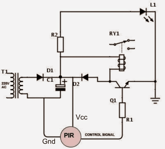 This circuit uses a HC-SR501 IC which is the heart of the circuit.
Initially when the moving object is detected by the sensor, it produces a small signal voltage(usually 3.3 volts) which is fed to the base of the transistor BC547 through a current control resistor and hence, its output goes high and it switches the relay on.
A more Comprehensive Diagram can be Visualized below:
This circuit uses a HC-SR501 IC which is the heart of the circuit.
Initially when the moving object is detected by the sensor, it produces a small signal voltage(usually 3.3 volts) which is fed to the base of the transistor BC547 through a current control resistor and hence, its output goes high and it switches the relay on.
A more Comprehensive Diagram can be Visualized below:

 The sensor consists of two preset resistors which can be used to control the delay time and sensing range.
The delay potentiometer can be adjusted to decide the time for which light remains on.
The sensor when purchased, it comes with the default mode ��H�� which means that the circuit switches on the light when somebody moves within the zone and it remains on for preset time and after the preset time lapses, if the sensor could still detect motion, it does not switch the light off in the absence of a moving target, it switches off the light.
Here are the technical details of the sensor HC-SR501
Working voltage range: 4.5VDC to 12VDC.
Current Drain: <60uA
Voltage output: 3.3V TTL
Detection distance: 3 to 7 metres(can be adjusted)
Delay time: 5 to 200 seconds(can be adjusted)
One of the disadvantages PIR sensors is that its output goes high even when a rat or a dog or some other animal moves in front of it and it switches on light unnecessarily.
In cold countries, the sensor��s sensing range increases.
Due to low temperature, infrared radiations released by humans travel more distances and hence causing unnecessary switching of lights.
If installed in backyards, there are chances of activating of light when a car passes by because the radiations emitted by hot engine of car fools the sensor.
The sensor consists of two preset resistors which can be used to control the delay time and sensing range.
The delay potentiometer can be adjusted to decide the time for which light remains on.
The sensor when purchased, it comes with the default mode ��H�� which means that the circuit switches on the light when somebody moves within the zone and it remains on for preset time and after the preset time lapses, if the sensor could still detect motion, it does not switch the light off in the absence of a moving target, it switches off the light.
Here are the technical details of the sensor HC-SR501
Working voltage range: 4.5VDC to 12VDC.
Current Drain: <60uA
Voltage output: 3.3V TTL
Detection distance: 3 to 7 metres(can be adjusted)
Delay time: 5 to 200 seconds(can be adjusted)
One of the disadvantages PIR sensors is that its output goes high even when a rat or a dog or some other animal moves in front of it and it switches on light unnecessarily.
In cold countries, the sensor��s sensing range increases.
Due to low temperature, infrared radiations released by humans travel more distances and hence causing unnecessary switching of lights.
If installed in backyards, there are chances of activating of light when a car passes by because the radiations emitted by hot engine of car fools the sensor.
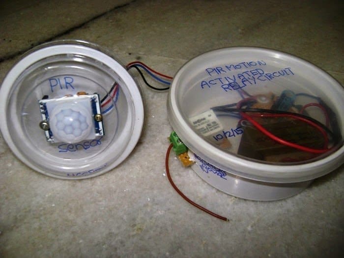 After completing the construction of the circuit, enclose it in a suitable casing and use a separate casing for the sensor and connect the sensor to circuit using long wires so that you can place sensor at the place you wish like in a garden and circuit will be inside so that the circuit is protected from weather.
And remember to use a separate PCB for relay.
Also, don��t forget to use a suitable relay with correct current and voltage rating.
You can use a terminal block which connects to the relay��s switching contacts, and arrange it as shown in image so that you can change the electrical device connected to relay contacts easily.
After completing the construction of the circuit, enclose it in a suitable casing and use a separate casing for the sensor and connect the sensor to circuit using long wires so that you can place sensor at the place you wish like in a garden and circuit will be inside so that the circuit is protected from weather.
And remember to use a separate PCB for relay.
Also, don��t forget to use a suitable relay with correct current and voltage rating.
You can use a terminal block which connects to the relay��s switching contacts, and arrange it as shown in image so that you can change the electrical device connected to relay contacts easily.
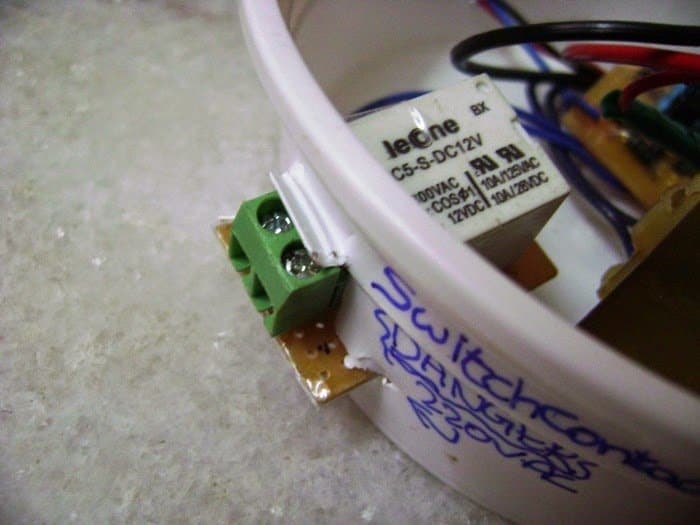 Usage of this sensors save electricity to great extents.
It could reduce your electricity bills too!
��PLEASE SAVE THE POWER FOR THE NEXT HOUR!��
If the above PIR moving human detector design is intended to be used with an alarm and a lamp such that both the loads operate during night but the alarm only during day, then the diagram may be modified in the following manner.
The idea was suggested by Mr.
Manjunath
Usage of this sensors save electricity to great extents.
It could reduce your electricity bills too!
��PLEASE SAVE THE POWER FOR THE NEXT HOUR!��
If the above PIR moving human detector design is intended to be used with an alarm and a lamp such that both the loads operate during night but the alarm only during day, then the diagram may be modified in the following manner.
The idea was suggested by Mr.
Manjunath
 A 8550 PNP transistor is used here in the solar charge controller to decide it is day or night depending on the voltage form the solar panel.
This is achieved by feeding the solar panel voltage to the base of the transistor hence holding it off during the day time when the voltage is produces by panel.
When the dusk sets in the voltage drops across the transistor and battery voltage gets routed to rest of the circuit.
The next stage is a voltage source switcher that decides whether the circuit should be powered using battery voltage or the AC power source depending on the battery voltage level.
A DPDT relay is configured to take care of this switching.
Hence, the power to the circuit remains uninterrupted.
The next stage consists of the day/night detector that senses whether it is day or night depending on the sunlight incident on the LDR and it triggers the relay correspondingly.
A capacitor C1 is attached at base of the transistor T3 in this stage.
That makes sure that a small delay is introduced in the sensing so that sudden changes in the intensity of light does not false trigger the circuit.
Output of T3 is fed to the next transistor Q1 which actually triggers the relay.
Final stage consists of a PIR sensor HC-SR501 that produces a high output when it detects the presence of a human being in its vicinity which is fed to the base of the transistor Q2 and immediately it fires the relay and the LED��s connected to it gets lit up.
When the human moves away, the light gets turned off automatically using the same mechanism.
Finally, for the circuit to work even when there is static occupancy, the an additional stage consisting of the Hex Schmitt trigger IC and few other components may be used in combination with the existing circuit, but please remember to use a bigger battery and solar panel as per requirement.
The circuit can be found here: https://www.homemade-circuits.com/pir-circuit-for-detecting-static-or/
A 8550 PNP transistor is used here in the solar charge controller to decide it is day or night depending on the voltage form the solar panel.
This is achieved by feeding the solar panel voltage to the base of the transistor hence holding it off during the day time when the voltage is produces by panel.
When the dusk sets in the voltage drops across the transistor and battery voltage gets routed to rest of the circuit.
The next stage is a voltage source switcher that decides whether the circuit should be powered using battery voltage or the AC power source depending on the battery voltage level.
A DPDT relay is configured to take care of this switching.
Hence, the power to the circuit remains uninterrupted.
The next stage consists of the day/night detector that senses whether it is day or night depending on the sunlight incident on the LDR and it triggers the relay correspondingly.
A capacitor C1 is attached at base of the transistor T3 in this stage.
That makes sure that a small delay is introduced in the sensing so that sudden changes in the intensity of light does not false trigger the circuit.
Output of T3 is fed to the next transistor Q1 which actually triggers the relay.
Final stage consists of a PIR sensor HC-SR501 that produces a high output when it detects the presence of a human being in its vicinity which is fed to the base of the transistor Q2 and immediately it fires the relay and the LED��s connected to it gets lit up.
When the human moves away, the light gets turned off automatically using the same mechanism.
Finally, for the circuit to work even when there is static occupancy, the an additional stage consisting of the Hex Schmitt trigger IC and few other components may be used in combination with the existing circuit, but please remember to use a bigger battery and solar panel as per requirement.
The circuit can be found here: https://www.homemade-circuits.com/pir-circuit-for-detecting-static-or/
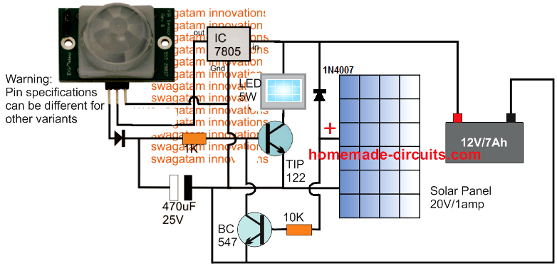
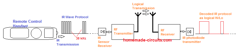
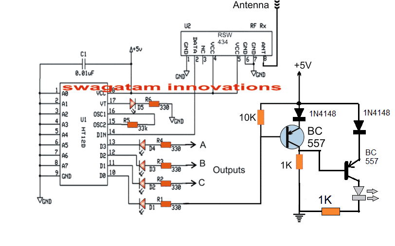 The circuit diagram shown above represents the IR data receiver circuit which receives the transmitted signal from the transmitter end and reverts the signals back to the IR mode for operating the IR device extended at this remote end.
Here the RF decoder module is built using HT12D IC and the receiverusing RSW434 chip.
The receiver chip picks up the transmitted IR to RF converted data, and sends it to the decoder IC, which completes the process by decoding the RF signals back to IR frequency.
This IR frequency is appropriately fed to an IR photo-diode driver circuit built using a PNP transistor and an IR photo-diode device, as shown at the extreme right side of the circuit.
The decoded RF to IR frequency is oscillated and transmitted by the photo-diode and applied on the device which is to be operated at the remote end.
The device hopefully responds to these RF decoded IR signals and functions as per the expected specification.
This concludes the IR range extender circuit using RF 433MHz modules, if you think I have missed something in the design or in the explanation please feel free to point them out through the comment box below.
The circuit diagram shown above represents the IR data receiver circuit which receives the transmitted signal from the transmitter end and reverts the signals back to the IR mode for operating the IR device extended at this remote end.
Here the RF decoder module is built using HT12D IC and the receiverusing RSW434 chip.
The receiver chip picks up the transmitted IR to RF converted data, and sends it to the decoder IC, which completes the process by decoding the RF signals back to IR frequency.
This IR frequency is appropriately fed to an IR photo-diode driver circuit built using a PNP transistor and an IR photo-diode device, as shown at the extreme right side of the circuit.
The decoded RF to IR frequency is oscillated and transmitted by the photo-diode and applied on the device which is to be operated at the remote end.
The device hopefully responds to these RF decoded IR signals and functions as per the expected specification.
This concludes the IR range extender circuit using RF 433MHz modules, if you think I have missed something in the design or in the explanation please feel free to point them out through the comment box below.
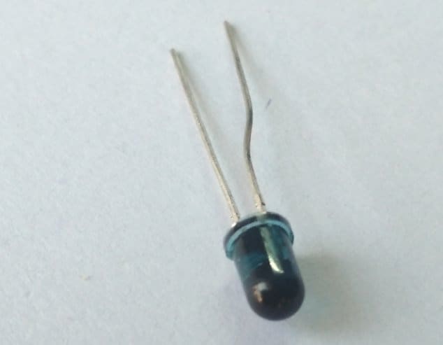 2. IR PHOTODIODE: It is a special type of diode which is connected in reverse bias for IR rays detection.
In the absence of IR radiation , it has a very high resistance and practically zero current passes through it.
But when the IR rays fall on to it ,its resistance decreases and a current proportional to the intensity of the radiation is allowed to pass through it.
This property of photodiode is used to generate an electric signal in proximity sensor on incidence of IR rays.
2. IR PHOTODIODE: It is a special type of diode which is connected in reverse bias for IR rays detection.
In the absence of IR radiation , it has a very high resistance and practically zero current passes through it.
But when the IR rays fall on to it ,its resistance decreases and a current proportional to the intensity of the radiation is allowed to pass through it.
This property of photodiode is used to generate an electric signal in proximity sensor on incidence of IR rays.
 3. Op-amp (IC LM358): Op-amp or operational amplifier is a multi-purpose ic and is highly revered in the electronics world.
In this project op-amp is used as a comparator.
LM358 IC has two op-amps which means we can make two proximity detectors using just one IC.
The reason to use op-amp in the circuit is to convert analog signal into digital signal.
3. Op-amp (IC LM358): Op-amp or operational amplifier is a multi-purpose ic and is highly revered in the electronics world.
In this project op-amp is used as a comparator.
LM358 IC has two op-amps which means we can make two proximity detectors using just one IC.
The reason to use op-amp in the circuit is to convert analog signal into digital signal.
 4. Preset: Preset is basically a resistor having three terminals.
The function of a preset is to divide the total voltage available in a way that the user can access a fraction of it.
We just have to set the middle terminal to an appropriate position.
The preset sets the threshold voltage above which the output voltage should be generated.
It can be manually set to resistance of any value by rotating its head using a suitable screwdriver.
4. Preset: Preset is basically a resistor having three terminals.
The function of a preset is to divide the total voltage available in a way that the user can access a fraction of it.
We just have to set the middle terminal to an appropriate position.
The preset sets the threshold voltage above which the output voltage should be generated.
It can be manually set to resistance of any value by rotating its head using a suitable screwdriver.
 5. Red led : I have used a red led for my project but in general led of any colour can be used.
It acts as a visual signal to show that the obstacle has come close enough.
5. Red led : I have used a red led for my project but in general led of any colour can be used.
It acts as a visual signal to show that the obstacle has come close enough.
 6. Resistors: Two 220 ohms and one 10k ohm.
7. Power supply: 5 v to 6v.
6. Resistors: Two 220 ohms and one 10k ohm.
7. Power supply: 5 v to 6v.
 The function of the op-amp is to compare the two inputs given to it.
The signal from the photodiode is given to the non-inverting pin (pin 3) and the threshold voltage from potentiometer is given to the inverting pin (pin 2).If the voltage at the non-inverting pin is greater than the voltage at the inverting pin the op-amp output is high otherwise the output is low.
All in all, op-amp converts analog signal into digital signal in this circuit.
The function of the op-amp is to compare the two inputs given to it.
The signal from the photodiode is given to the non-inverting pin (pin 3) and the threshold voltage from potentiometer is given to the inverting pin (pin 2).If the voltage at the non-inverting pin is greater than the voltage at the inverting pin the op-amp output is high otherwise the output is low.
All in all, op-amp converts analog signal into digital signal in this circuit.
 UPDATE from Admin
The above circuit design could be also built using an ordinary single opamp IC 741, as shown below:
UPDATE from Admin
The above circuit design could be also built using an ordinary single opamp IC 741, as shown below:
 Video Clip
 As you can see, only the LM567 stage is incorporated in the design while the IC 555 stage has been eliminated in order to keep the fundamental testing procedures simpler.
Here the red LED at pin#8 of the IC lights up and remains illuminated as long as the IR LEDs are held parallel to each other within a distance of 1 foot.
If you try replacing the Tx infrared red transmitter LED with some other external source having a different frequency, the LM567 is stop detecting the signals and the red LED will stop glowing.
The photo diodes are not crucial, you can use any similar or standard photo diodes for the transmitter and receiver LEDs.
Video clip for the above test set up:
As you can see, only the LM567 stage is incorporated in the design while the IC 555 stage has been eliminated in order to keep the fundamental testing procedures simpler.
Here the red LED at pin#8 of the IC lights up and remains illuminated as long as the IR LEDs are held parallel to each other within a distance of 1 foot.
If you try replacing the Tx infrared red transmitter LED with some other external source having a different frequency, the LM567 is stop detecting the signals and the red LED will stop glowing.
The photo diodes are not crucial, you can use any similar or standard photo diodes for the transmitter and receiver LEDs.
Video clip for the above test set up:
 In the centre of the circuit is a solitary 567 tone decoder IC (U1) that executes a twin functionality: it runs both as a basic IR-transmitter driver and as a receiver.
Capacitor C1 and resistor R2 are employed to fix U1's internal oscillator frequency to around 1 kHz.
The square-wave output from U1 at pin 5 is applied on the Q1 base.
Transistor Q1 is set up as an emitter-follower amplifier, which connects a 20-mA pulse on the LED2 anode.
Transistor Q3 picks up the IR output from LED2 and directs the transmission on to Q2 for more amplification.
Following amplification by Q2, the signal is applied back to the input of U1 at pin 3, triggering pin 8 to become low, switching ON LED1.
When required, LED1 could be substituted with an optocoupler to toggle virtually any AC-operated load.
Because the circuit is very straightforward, almost any design plan will work.
The IR emitter (LED1) and the phototransistor (03) must be installed approximately inch separated within a side-by-side placement and focused in the exact same track.
It may be required to test out the spacing and installation viewpoint of the a pair of IR devices to figure out the perfect position for any assigned range between the detector and the emitter.
As a rule of thumb, an inch gap between the IR-emitter/detector pair makes it possible for the proximity circuit to discover a target approximately half to 1-inch apart.
Lighter shaded targets reflect much better and can perform at increased distances than those created from deeper elements.
So long as the proximity sensor picks up the tuned IR signals, the controlled circuit continues to be turned on, and as soon as the signal vanishes the output turns off.
In the centre of the circuit is a solitary 567 tone decoder IC (U1) that executes a twin functionality: it runs both as a basic IR-transmitter driver and as a receiver.
Capacitor C1 and resistor R2 are employed to fix U1's internal oscillator frequency to around 1 kHz.
The square-wave output from U1 at pin 5 is applied on the Q1 base.
Transistor Q1 is set up as an emitter-follower amplifier, which connects a 20-mA pulse on the LED2 anode.
Transistor Q3 picks up the IR output from LED2 and directs the transmission on to Q2 for more amplification.
Following amplification by Q2, the signal is applied back to the input of U1 at pin 3, triggering pin 8 to become low, switching ON LED1.
When required, LED1 could be substituted with an optocoupler to toggle virtually any AC-operated load.
Because the circuit is very straightforward, almost any design plan will work.
The IR emitter (LED1) and the phototransistor (03) must be installed approximately inch separated within a side-by-side placement and focused in the exact same track.
It may be required to test out the spacing and installation viewpoint of the a pair of IR devices to figure out the perfect position for any assigned range between the detector and the emitter.
As a rule of thumb, an inch gap between the IR-emitter/detector pair makes it possible for the proximity circuit to discover a target approximately half to 1-inch apart.
Lighter shaded targets reflect much better and can perform at increased distances than those created from deeper elements.
So long as the proximity sensor picks up the tuned IR signals, the controlled circuit continues to be turned on, and as soon as the signal vanishes the output turns off.


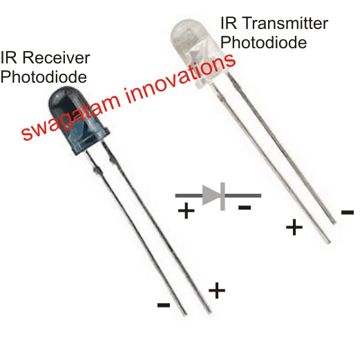
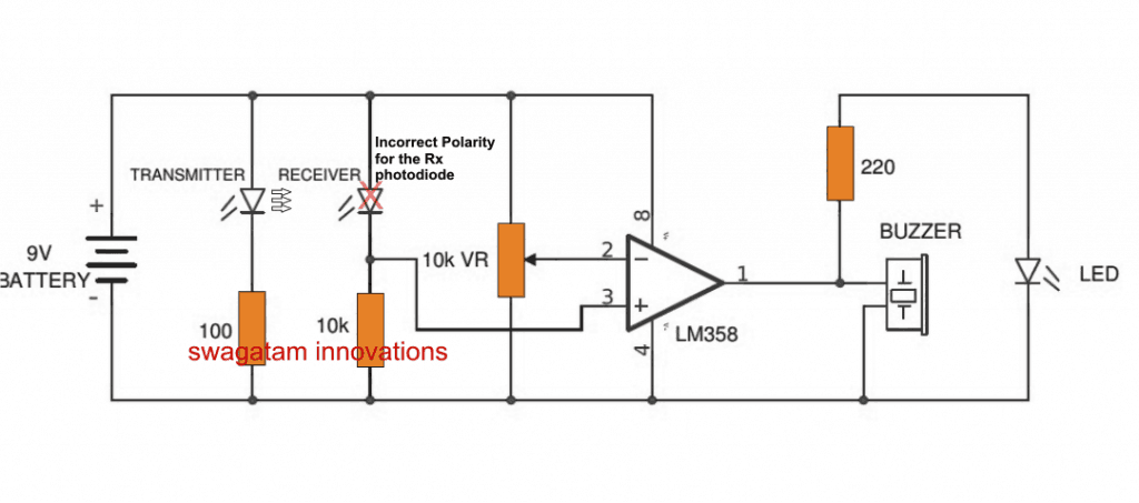
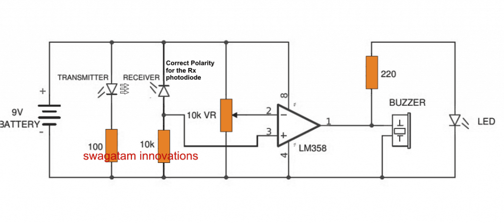 Question:
sir, firstly i forgot to connect IC pin 3 to receiver resistor then i have given a supply of 12V therefore Led lights up only.
After that I connected pin 3 to resistor and given 9V.
Now led lights when i turn the variable resister to one side.
LED doesn't light up when obstacle is brought in front.
Question:
sir, firstly i forgot to connect IC pin 3 to receiver resistor then i have given a supply of 12V therefore Led lights up only.
After that I connected pin 3 to resistor and given 9V.
Now led lights when i turn the variable resister to one side.
LED doesn't light up when obstacle is brought in front.
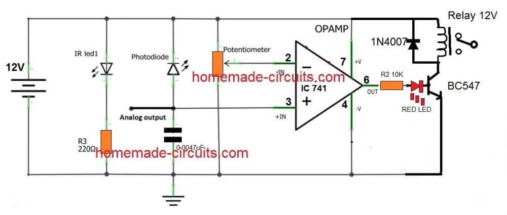 Feedback from Mr.
Norman Kelley (one of the avid readers of this blog):
Hi, Swagatam,
I have been looking for a circuit to alert me when someone enters my courtyard and front deck.
Delivery people leave things on the front deck and do not ring the door bell, so I don't know my packages are on the deck.
Also, at night, I would like to know if someone enters my courtyard.
I designed a circuit with a PIR and a wireless TX/RX to play a message inside my house.
Everything works but there are many false triggers and it drives my wife nuts.
I am assuming that the RF signals are triggering the PIR.
I tried separating them a few inches and it helped, but not enough.
So, I decided to look at IR to detect the person opening the gate to the courtyard and then wirelessly transmitting that trigger.
I wanted to do an IR beam, but it requires more components that I don't have at this time.
So, I decided a proximity IR would work if I placed the sensor at the gate and put a reflector on the gate that would reflect the IR when the gate was opened.
I saw your above circuit "How to connect an IR Photodiode Sensor".
I bread boarded the circuit and it works fine.
The only problem is it uses 50ma in standby mode and 70ma when active.
Remote mounting with battery power supply seems to be out of the question unless there is a way to reduce the power requirements or I will have to run low voltage out to the unit.
Any suggestions or comments? Thanks for your help!
Norman Kelley
My Response:
Hi Norman,
The high consumption could be simply due to the incorrect LED resistor values, try using 1K for transmitter LED and also for the indicator LED, the total consumption should come down to around 6mA
Feedback from Mr.
Norman Kelley (one of the avid readers of this blog):
Hi, Swagatam,
I have been looking for a circuit to alert me when someone enters my courtyard and front deck.
Delivery people leave things on the front deck and do not ring the door bell, so I don't know my packages are on the deck.
Also, at night, I would like to know if someone enters my courtyard.
I designed a circuit with a PIR and a wireless TX/RX to play a message inside my house.
Everything works but there are many false triggers and it drives my wife nuts.
I am assuming that the RF signals are triggering the PIR.
I tried separating them a few inches and it helped, but not enough.
So, I decided to look at IR to detect the person opening the gate to the courtyard and then wirelessly transmitting that trigger.
I wanted to do an IR beam, but it requires more components that I don't have at this time.
So, I decided a proximity IR would work if I placed the sensor at the gate and put a reflector on the gate that would reflect the IR when the gate was opened.
I saw your above circuit "How to connect an IR Photodiode Sensor".
I bread boarded the circuit and it works fine.
The only problem is it uses 50ma in standby mode and 70ma when active.
Remote mounting with battery power supply seems to be out of the question unless there is a way to reduce the power requirements or I will have to run low voltage out to the unit.
Any suggestions or comments? Thanks for your help!
Norman Kelley
My Response:
Hi Norman,
The high consumption could be simply due to the incorrect LED resistor values, try using 1K for transmitter LED and also for the indicator LED, the total consumption should come down to around 6mA
 The TMP007 is a exceptionally integrated, noncontact infrared (IR) temperature sensor, becoming a member of TI��s group of the world��s tiniest thermopile detectors.
This new sensor comes with a built-in math computer, that executes computations on-chip to get immediate reading of the specific target��s temperature, and presents low power utilization of only 675 uJ for each of the reading.
Having dimensions of only 1.9 mm by 1.9 mm by 0.625 mm, the TMP007 makes it possible for developers to keep track of temperature in space-constrained manufacturing applications, such as protection relays and process management equipment, along with other manufacturing and construction automation applications, in addition to enterprise equipment, like laser printers and network servers.
The TMP007 is a exceptionally integrated, noncontact infrared (IR) temperature sensor, becoming a member of TI��s group of the world��s tiniest thermopile detectors.
This new sensor comes with a built-in math computer, that executes computations on-chip to get immediate reading of the specific target��s temperature, and presents low power utilization of only 675 uJ for each of the reading.
Having dimensions of only 1.9 mm by 1.9 mm by 0.625 mm, the TMP007 makes it possible for developers to keep track of temperature in space-constrained manufacturing applications, such as protection relays and process management equipment, along with other manufacturing and construction automation applications, in addition to enterprise equipment, like laser printers and network servers.
 Designers who intend to build control equipment can easily carry out precise, energy-saving environment control in modest areas, whereas developers of household gadgets and client items can simply put moisture sensing features for their items using the HDC1000 integrated humidity and temperature sensor.
TI��s humidity sensor delivers high precision and lower power inside a little, dust-resistant casing.
The HDC1000 makes use of just one.2 uA of average current while calculating relative humidity and temperature at 11-bit resolution, once for every second.
This outstandingly low current helps prolong battery life in remote and distant applications.
The sensor��s 2.0-mm by 1.6-mm wafer grade chip size packet (WLCSP) streamlines panel design and lowers process size.
Additionally, the revolutionary placement of the sensing component in the base of the unit offers prevention to dirt, dirt along with other ecological pollutants.
Designers who intend to build control equipment can easily carry out precise, energy-saving environment control in modest areas, whereas developers of household gadgets and client items can simply put moisture sensing features for their items using the HDC1000 integrated humidity and temperature sensor.
TI��s humidity sensor delivers high precision and lower power inside a little, dust-resistant casing.
The HDC1000 makes use of just one.2 uA of average current while calculating relative humidity and temperature at 11-bit resolution, once for every second.
This outstandingly low current helps prolong battery life in remote and distant applications.
The sensor��s 2.0-mm by 1.6-mm wafer grade chip size packet (WLCSP) streamlines panel design and lowers process size.
Additionally, the revolutionary placement of the sensing component in the base of the unit offers prevention to dirt, dirt along with other ecological pollutants.
 The OPT3001 is a accurate ambient light sensor internally adjusted to carefully reproduce the human eye��s photopic reaction.
Having its industry-leading spectral effect, the sensor has the ability to supply more than 99 % IR rejection, to produce steady light metering irrespective of the source of light.
Using just a 2.0 mm by 2.0 mm by 0.65 mm space, it works with just 1.6 V at standard operating current of 2 uA, this ambient light sensor could be utilized for numerous sorts battery-powered purposes.
Furthermore, the OPT3001 allows you to work with more than a 23-bit dynamic range, offering developers the substantial resolution necessary for business lighting effects control and construction and factory automation programs.
This newest ambient light sensor works with with TI��s Sensor Hub BoosterPack.
The OPT3001 is a accurate ambient light sensor internally adjusted to carefully reproduce the human eye��s photopic reaction.
Having its industry-leading spectral effect, the sensor has the ability to supply more than 99 % IR rejection, to produce steady light metering irrespective of the source of light.
Using just a 2.0 mm by 2.0 mm by 0.65 mm space, it works with just 1.6 V at standard operating current of 2 uA, this ambient light sensor could be utilized for numerous sorts battery-powered purposes.
Furthermore, the OPT3001 allows you to work with more than a 23-bit dynamic range, offering developers the substantial resolution necessary for business lighting effects control and construction and factory automation programs.
This newest ambient light sensor works with with TI��s Sensor Hub BoosterPack.
 The four-channel FDC1004 capacitance-to-digital converter brings together distinctive attributes and operates with low power and 16-bit noise performance, spanning a range of +/-15 pF, making it easy for architects to make use of capacitive sensing to improve the intellect and understanding of their devices.
The product includes an offset capacitance up to 100 pF, making it possible for remote sensing in severe situations or in places where normal electronics may have the tendency to fail.
It provides a solid shield driver to enable reduce interference, to enable aim the sensing target accurately and for lowering the effect of temperature disparities on process efficiency.
The FDC1004 can be utilized in numerous programs such as proximity wake-up sensing, material research and liquid level sensing.
You can use it with microcontrollers (MCUs), including the ultra-low-power MSP430 MCUs.
The four-channel FDC1004 capacitance-to-digital converter brings together distinctive attributes and operates with low power and 16-bit noise performance, spanning a range of +/-15 pF, making it easy for architects to make use of capacitive sensing to improve the intellect and understanding of their devices.
The product includes an offset capacitance up to 100 pF, making it possible for remote sensing in severe situations or in places where normal electronics may have the tendency to fail.
It provides a solid shield driver to enable reduce interference, to enable aim the sensing target accurately and for lowering the effect of temperature disparities on process efficiency.
The FDC1004 can be utilized in numerous programs such as proximity wake-up sensing, material research and liquid level sensing.
You can use it with microcontrollers (MCUs), including the ultra-low-power MSP430 MCUs.


 image courtesy: elektor electronics
As can be seen in the figure above, the IC 555 is configured as an astable whose pin#2 is used for sensing the proximity or the capacitance of a human hand.
Pin#2 is terminated with a metallic plate (which could be replaced by the faucet body) such that whenever somebody approaches the tap for washing hands, the sensor is triggered activating the connected relay.
The relay finally opens the tap valve for releasing water.
However in the above design the relay is supposed to remain activated only for a short duration of time, which means the individual might require to move his hand to and fro frequently if the washing is required to be for a relatively prolonged period.
Another design which is shown below can be executed for the same:
image courtesy: elektor electronics
As can be seen in the figure above, the IC 555 is configured as an astable whose pin#2 is used for sensing the proximity or the capacitance of a human hand.
Pin#2 is terminated with a metallic plate (which could be replaced by the faucet body) such that whenever somebody approaches the tap for washing hands, the sensor is triggered activating the connected relay.
The relay finally opens the tap valve for releasing water.
However in the above design the relay is supposed to remain activated only for a short duration of time, which means the individual might require to move his hand to and fro frequently if the washing is required to be for a relatively prolonged period.
Another design which is shown below can be executed for the same:
 image courtesy: elektor electronics
The above shown proximity detector circuit is a transistor based design and is designed to sense a human hand when brought at a relatively close proximity to the indicated plate.
image courtesy: elektor electronics
The above shown proximity detector circuit is a transistor based design and is designed to sense a human hand when brought at a relatively close proximity to the indicated plate.

 Note: If the faucet body does not respond to the hand proximity, the system could be reinforced with a small additional metal plate in order to increase the surface area of the capacitive sensor and thereby ensure a reliable operation of the touch free faucet.
 The above configuration depicts the IR wireless alarm transmitter circuit stage set up, wherein the TSW434 forms the standard RF transmitter chip, while the HT-12E is configured as an RF encoder IC.
A IR generator stage can be also seen which is used for generating and focusing an IR beam on the sensor of the IR encoder/transmitter stage.
This IR beam is positioned and stretched across the premise which needs to be guarded.
In the transmitter stage the encoder IC includes 4 inputs all of which require a ground or negative trigger to activate the encoder IC and prompt the TWS to send a corresponding encoded pulse signal in the air within the range of 50 meters.
Depending on the users requirement, only a single stage may be used or all the four stages may be engaged in order to monitor 4 different critical zones needing protection against a possible intrusion or a break in.
The IR sensor stage incorporates a standard TSOP17XX series sensor IC, which is configured with a PNP BC557 transistor amplifier stgae for amplifying the relatively smaller electrical pulses from the sensor to a 5V output.
As long as the IR beam stays focused and incident on the TSOP sensor, the BC557 is held switched ON which ensures a positive potential over the relevant input pin of the encoder IC.
In an event this IR beam is cut-off due a human passing by across the restricted zone, the BC557 is interrupted for that moment which in turn causes a ground signal to appear at the particular input of the encoder pin.
This action instantly initiates the TWS chip to send out a correspondingly encoded pulse in the air which is supposed to be received by the receiver unit or the decoder receiver unit positioned at some desired remote location within the specified radial range, near the user.
The above configuration depicts the IR wireless alarm transmitter circuit stage set up, wherein the TSW434 forms the standard RF transmitter chip, while the HT-12E is configured as an RF encoder IC.
A IR generator stage can be also seen which is used for generating and focusing an IR beam on the sensor of the IR encoder/transmitter stage.
This IR beam is positioned and stretched across the premise which needs to be guarded.
In the transmitter stage the encoder IC includes 4 inputs all of which require a ground or negative trigger to activate the encoder IC and prompt the TWS to send a corresponding encoded pulse signal in the air within the range of 50 meters.
Depending on the users requirement, only a single stage may be used or all the four stages may be engaged in order to monitor 4 different critical zones needing protection against a possible intrusion or a break in.
The IR sensor stage incorporates a standard TSOP17XX series sensor IC, which is configured with a PNP BC557 transistor amplifier stgae for amplifying the relatively smaller electrical pulses from the sensor to a 5V output.
As long as the IR beam stays focused and incident on the TSOP sensor, the BC557 is held switched ON which ensures a positive potential over the relevant input pin of the encoder IC.
In an event this IR beam is cut-off due a human passing by across the restricted zone, the BC557 is interrupted for that moment which in turn causes a ground signal to appear at the particular input of the encoder pin.
This action instantly initiates the TWS chip to send out a correspondingly encoded pulse in the air which is supposed to be received by the receiver unit or the decoder receiver unit positioned at some desired remote location within the specified radial range, near the user.
 A complementary RF receiver decoder stage can be seen in the above diagram which is configured to receive the signal transmitted by the transmitter stage explained in the previous section.
Here the RSW is positioned to pick up the transmitted signal from the earlier explained TWS IC, and forward the encoded signal to the attached HT-12D decoder IC.
This IC then appropriately decodes the received signals, converting them to a logic based signal across its one of the relevant output pins.
Pins 10 to 13 form the output pins of the decoder IC which produces the corresponding logic outputs for an external driver stage.
Here the driver stage is formed through a PNP BC557 and a relay suitably wired for the toggling the connected load which can be an alarm unit.
As may be seen, all the output pins from the decoder IC are made parallel or tied up together and integrated with the relay driver stage.
This makes sure that the relay driver is able to trigger in response to the activation of any of the transmitter input pins which may be configured with a separate TSOP sensor across different critical locations.
The infrared frequency generator as indicated in the first Tx circuit stage could be built by using a IC 555 wired in its standard astable mode with a frequency set at 38kHz.
The above discussed remote infrared wireless alarm circuit set up can be implemented for monitoring any desired critical location remotely within a radial distance of around 50 meters or more depending on which RF module is employed.
A complementary RF receiver decoder stage can be seen in the above diagram which is configured to receive the signal transmitted by the transmitter stage explained in the previous section.
Here the RSW is positioned to pick up the transmitted signal from the earlier explained TWS IC, and forward the encoded signal to the attached HT-12D decoder IC.
This IC then appropriately decodes the received signals, converting them to a logic based signal across its one of the relevant output pins.
Pins 10 to 13 form the output pins of the decoder IC which produces the corresponding logic outputs for an external driver stage.
Here the driver stage is formed through a PNP BC557 and a relay suitably wired for the toggling the connected load which can be an alarm unit.
As may be seen, all the output pins from the decoder IC are made parallel or tied up together and integrated with the relay driver stage.
This makes sure that the relay driver is able to trigger in response to the activation of any of the transmitter input pins which may be configured with a separate TSOP sensor across different critical locations.
The infrared frequency generator as indicated in the first Tx circuit stage could be built by using a IC 555 wired in its standard astable mode with a frequency set at 38kHz.
The above discussed remote infrared wireless alarm circuit set up can be implemented for monitoring any desired critical location remotely within a radial distance of around 50 meters or more depending on which RF module is employed.
 Here we can see how an oscillating PIR adapts to the issue and transforms itself enabling the detection of even static IR subjects.
This becomes possible because through its movement the PIR module transforms the stationary IR source into a continuously changing IR imaging across its two receiving slots.
Although the idea looks complex, it can be actually simply solved using a slow oscillating PwM controlled motor circuit.
We'll learn the entire mechanism and the circuit details in the following sections.
As we already discussed, conventional PIR modules are able to detect only moving living objects and cannot identify a stationary target which makes its application limited as a human motion detector only.
For applications where the detection of motiolesss human occupancy becomes necessary in such scenarios a conventional PIR can become useless, and might require some external arrangement for upgrading itself.
Here we can see how an oscillating PIR adapts to the issue and transforms itself enabling the detection of even static IR subjects.
This becomes possible because through its movement the PIR module transforms the stationary IR source into a continuously changing IR imaging across its two receiving slots.
Although the idea looks complex, it can be actually simply solved using a slow oscillating PwM controlled motor circuit.
We'll learn the entire mechanism and the circuit details in the following sections.
As we already discussed, conventional PIR modules are able to detect only moving living objects and cannot identify a stationary target which makes its application limited as a human motion detector only.
For applications where the detection of motiolesss human occupancy becomes necessary in such scenarios a conventional PIR can become useless, and might require some external arrangement for upgrading itself.
 The shown circuit utilizes a single IC HEF40106 hex inverting schmitt gate IC which includes 6 inverter NOT gates.
Gates N1 and N2 are configured to produce an adjustable PWM output which is fed to the gates N4, N5, N6 forming the buffers.
The common output from these buffer gates is terminated to the gate of a motor driver mosfet.
The PWM content is set with the help of P1, which is finally applied to the connected motor via a set of DPDT relay contacts.
These relay contacts determine the direction of the motor movement (clockwise or anticlockwise).
This flip flop DPDT relay contacts is controlled by an astable timer configured around the gate N3, wherein the capacitor C3/R3 determines at what rate the relay needs to changeover in order to allow the motor to change its rotational direction consistently.
The above design allows the motor to execute the required slow to and fro oscillating movement across a given radial zone.
C3 may be selected to initiate the changeover after every 5 to 6 seconds, and the PWm may be adjusted to enable an extremely sluggish motor movement, because it just needs to ensure that the slots of the PIR cross over the IR signals of the target in a timely manner.
However since the motor operation is slow, the output from the PIR will need to be sustained through a delay OFF timer so that the connected load does not switch OFF and ON while the motor movement alternately cuts through the IR lines from the human occupancy.
The shown circuit utilizes a single IC HEF40106 hex inverting schmitt gate IC which includes 6 inverter NOT gates.
Gates N1 and N2 are configured to produce an adjustable PWM output which is fed to the gates N4, N5, N6 forming the buffers.
The common output from these buffer gates is terminated to the gate of a motor driver mosfet.
The PWM content is set with the help of P1, which is finally applied to the connected motor via a set of DPDT relay contacts.
These relay contacts determine the direction of the motor movement (clockwise or anticlockwise).
This flip flop DPDT relay contacts is controlled by an astable timer configured around the gate N3, wherein the capacitor C3/R3 determines at what rate the relay needs to changeover in order to allow the motor to change its rotational direction consistently.
The above design allows the motor to execute the required slow to and fro oscillating movement across a given radial zone.
C3 may be selected to initiate the changeover after every 5 to 6 seconds, and the PWm may be adjusted to enable an extremely sluggish motor movement, because it just needs to ensure that the slots of the PIR cross over the IR signals of the target in a timely manner.
However since the motor operation is slow, the output from the PIR will need to be sustained through a delay OFF timer so that the connected load does not switch OFF and ON while the motor movement alternately cuts through the IR lines from the human occupancy.
 In the above set up we can see the motor which receives its electrical drive supply from the PWM/flip flop stage as discussed in the previous paragraph.
The spindle of the motor can be seen coupled with a horizontal shaft over which the PIR is clamped, such that when the motor moves, the PIR goes through a correspondingly changing radial to and fro motion.
While the above PIR motion is induced, the IR signals from a stationary target in the zone is detected in the form of short alternate pulses, which are generated at the output pin of the PIR indicated with the blue wire.
These pulses are applied across the 1000uF capacitor which charges up with each pulse and makes sure that the BC547 is kept in the conducting mode without an interruption during the process.
The relay driver comprising of the BC557 stage responds to the above stable signal from the BC547 collector and in turn keeps the relay ON, as long as the PIR keeps detecting a human presence.
The relay load thus stays activated continuously due to presence of a stationary human being in the area.
However in case the human occupancy is removed or when the target moves away from the zone, the delay timer stage keeps the relay and the load activated for the stipulated 5 to 10 seconds after which it shuts off permanently, until the zone is yet again captured by a potential IR emanating source.
In the above set up we can see the motor which receives its electrical drive supply from the PWM/flip flop stage as discussed in the previous paragraph.
The spindle of the motor can be seen coupled with a horizontal shaft over which the PIR is clamped, such that when the motor moves, the PIR goes through a correspondingly changing radial to and fro motion.
While the above PIR motion is induced, the IR signals from a stationary target in the zone is detected in the form of short alternate pulses, which are generated at the output pin of the PIR indicated with the blue wire.
These pulses are applied across the 1000uF capacitor which charges up with each pulse and makes sure that the BC547 is kept in the conducting mode without an interruption during the process.
The relay driver comprising of the BC557 stage responds to the above stable signal from the BC547 collector and in turn keeps the relay ON, as long as the PIR keeps detecting a human presence.
The relay load thus stays activated continuously due to presence of a stationary human being in the area.
However in case the human occupancy is removed or when the target moves away from the zone, the delay timer stage keeps the relay and the load activated for the stipulated 5 to 10 seconds after which it shuts off permanently, until the zone is yet again captured by a potential IR emanating source.
 Video Demo proving the static human detection for a PIR
 Note:
Please disconnect the 100k below C1 from the ground, and connect it on C1 positive terminal, meaning the 100k should be connected right across C1 terminals and nowhere else.
R6 needs to be calculated for getting a 1 minute delay before the gate initiates a reverse closing motion
Let's assume the gate to be in the "closed" position with Reed#2 actuated by the relevant gate magnet.
This ensures pin#12 of the IC 4060 to be rendered high and the IC stays inactive (pin#3 switched OFF).
In the above scenario, the relay#1 is already OFF, with its N/C position closed (because T1/T2 are OFF), and T4 is also OFF due to the absence of a base drive, which implies relay#2 is OFF and in the N/C position.
With relay#2 in N/C, the motor is switched off due to the absence of a positive link via the relay#2 N/O contact.
The entire circuit is thus in a switched OFF condition.
Now, as requested, the opening of the gate is initiated by pressing SW1 momentarily.
Pressing SW1 instantly latches T1/T2 via R4, toggling relay#1 such that its N/O contacts close, which in turn forces the motor to slide the gate towards the "open" direction.
As soon the gate slides away from its "close" position, reed#2 is released, which instantly enables the IC 4060 and it starts counting, with its pin#3 now with a logic zero.
The gate rolls on until it reaches the extreme end when the other relevant magnet fixed on the gate activates reed#1.
On activation, reed#1 pulls the base of T1 to ground via C1, breaking the latch, which in turn deactivates relay#1 and its contacts return to their N/C points.
However relay#2 still being in a switched OFF condition causes the motor to halt due to the absence of power through relay#2 (N/O) points.
In the meantime, IC 4060 completes its counting allowing a high to appear at its pin#3. (the IC now latches in this position via D2)
This immediately activates relay#2, enabling a reverse activation of the motor.
The motor starts sliding the gate towards the "close "position, and the moment it reaches the "close" end, reed#2 is activated yet again.
At this position, the IC is again reset causing a no signal at its pin#3, deactivating relay#2 and....shutting off the motor.
The circuit reverts to its original standby state.
Note:
Please disconnect the 100k below C1 from the ground, and connect it on C1 positive terminal, meaning the 100k should be connected right across C1 terminals and nowhere else.
R6 needs to be calculated for getting a 1 minute delay before the gate initiates a reverse closing motion
Let's assume the gate to be in the "closed" position with Reed#2 actuated by the relevant gate magnet.
This ensures pin#12 of the IC 4060 to be rendered high and the IC stays inactive (pin#3 switched OFF).
In the above scenario, the relay#1 is already OFF, with its N/C position closed (because T1/T2 are OFF), and T4 is also OFF due to the absence of a base drive, which implies relay#2 is OFF and in the N/C position.
With relay#2 in N/C, the motor is switched off due to the absence of a positive link via the relay#2 N/O contact.
The entire circuit is thus in a switched OFF condition.
Now, as requested, the opening of the gate is initiated by pressing SW1 momentarily.
Pressing SW1 instantly latches T1/T2 via R4, toggling relay#1 such that its N/O contacts close, which in turn forces the motor to slide the gate towards the "open" direction.
As soon the gate slides away from its "close" position, reed#2 is released, which instantly enables the IC 4060 and it starts counting, with its pin#3 now with a logic zero.
The gate rolls on until it reaches the extreme end when the other relevant magnet fixed on the gate activates reed#1.
On activation, reed#1 pulls the base of T1 to ground via C1, breaking the latch, which in turn deactivates relay#1 and its contacts return to their N/C points.
However relay#2 still being in a switched OFF condition causes the motor to halt due to the absence of power through relay#2 (N/O) points.
In the meantime, IC 4060 completes its counting allowing a high to appear at its pin#3. (the IC now latches in this position via D2)
This immediately activates relay#2, enabling a reverse activation of the motor.
The motor starts sliding the gate towards the "close "position, and the moment it reaches the "close" end, reed#2 is activated yet again.
At this position, the IC is again reset causing a no signal at its pin#3, deactivating relay#2 and....shutting off the motor.
The circuit reverts to its original standby state.

 The above system would be rather incomplete if it's not complemented by an Rx (receiver) circuit.
The following circuit highlights the receiver system which works exactly in the same way as its Tx counterpart but in an opposite manner.
Here, the Rx chip is stationed for capturing the data sent by the Tx module.
The captured data is mingled with the 315MHz carrier waves and is in an encoded form, therefore it must go through a reprocessing, which is done by the HT12D chip via its pin14 (data feed).
The above system would be rather incomplete if it's not complemented by an Rx (receiver) circuit.
The following circuit highlights the receiver system which works exactly in the same way as its Tx counterpart but in an opposite manner.
Here, the Rx chip is stationed for capturing the data sent by the Tx module.
The captured data is mingled with the 315MHz carrier waves and is in an encoded form, therefore it must go through a reprocessing, which is done by the HT12D chip via its pin14 (data feed).
 In order to use the above circuit as a key finder, the right side BC557 will need to be removed and the buzzer replaced with the shown collector resistor of the left BC557.
Also Tx circuit will now need a switch for the required toggling and detection of a buzzing sound from the above Rx attached key circuit.
In order to use the above circuit as a key finder, the right side BC557 will need to be removed and the buzzer replaced with the shown collector resistor of the left BC557.
Also Tx circuit will now need a switch for the required toggling and detection of a buzzing sound from the above Rx attached key circuit.

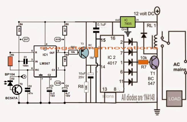 Controlling multiple appliances using the following single IR transmitter circuit
The following circuit forms the transmitter module of the proposed IR remote control for activating multiplegadgets.
It's a simple IC 555 astable circuit, whose output frequency is determined by the 5 individual capacitors and should be appropriately matched with the particular receiver circuit modules as discussed in the above section.
The capacitors attached with the respective buttons should be calculated and matched such that on pressing the relevant button, the corresponding receiver gets triggered for toggling the corresponding appliance.
R1, R2 may be chosen arbitrarily, but Cz must be selected in accordance with the receiver module frequency determined by R3 of the module.
Controlling multiple appliances using the following single IR transmitter circuit
The following circuit forms the transmitter module of the proposed IR remote control for activating multiplegadgets.
It's a simple IC 555 astable circuit, whose output frequency is determined by the 5 individual capacitors and should be appropriately matched with the particular receiver circuit modules as discussed in the above section.
The capacitors attached with the respective buttons should be calculated and matched such that on pressing the relevant button, the corresponding receiver gets triggered for toggling the corresponding appliance.
R1, R2 may be chosen arbitrarily, but Cz must be selected in accordance with the receiver module frequency determined by R3 of the module.
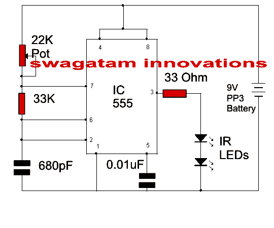
 Video Demonstration
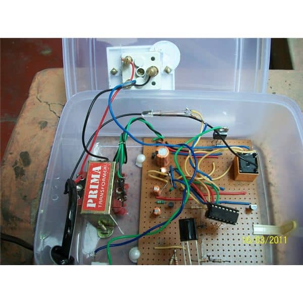 Prototype image courtesy: Raj Mukherji