Understanding MOSFET Avalanche Rating, Testing and Protection
In this post we discuss MOSFET avalanche ratings, and learn how to understand this rating in the datasheet correctly, how the parameter is tested by the manufacturer, and measures to protect MOSFETs from this phenomenon.
The avalanche parameter not only helps to verify the devices ruggedness, it additionally helps filtering out weaker MOSFETs or the ones which are more susceptible or at risk of a breakdown.
What is MOSFET Avalanche Rating
MOSFET avalanche rating is the maximum tolerable energy (millijoule) a MOSFET can withstand, when its drain-source voltage exceeds the maximum breakdown voltage (BVDSS) limit.
This phenomenon normally occurs in MOSFET switching circuits with inductive load across the drain terminal.
During the ON periods of the switching cycles, the inductor charges, and during the OFF periods the inductor releases its stored energy in the form of back EMF across source-drain of the MOSFET.
This reverse voltage finds its way through the MOSFET's body diode, and if its value exceeds the device's maximum tolerable limit, causes intense heat to develop within the device causing harm or a permanent damage to the device.
When was MOSFET Avalanche Introduced
The parameter Avalanche Energy and UIS(unclamped inductive switching) current was in fact not included in MOSFET datasheets before the 1980s.
And that's when it evolved into not only a datasheet specification, but a parameter which many consumers began demanding that the FET be tested before passing the device for production, especially, if the MOSFET is being designed for power supply or switching implementations.
Therefore it was only after 1980s that the avalanche parameter began appearing in the datasheets, and then promotion technicians began understanding that the bigger the avalanche rating was, the more competitive the device appeared to be.
The engineers began determining techniques to experiment with the parameter by tweaking few of its variables, which were used for the testing process.
Generally speaking, the bigger the avalanche energy, the more durable and strong the MOSFET turns into.
Therefore larger avalanche rating, represents stronger MOSFET characteristics.
Most FET datasheets will normally have the avalanche parameter included in their Absolute Maximum Ratings Table, which can be found directly on entry page of the data sheet.
Especially, you can view the parameters here written as Avalanche Current and Avalanche Energy, Eas.
Therefore, in datasheets MOSFET Avalanche Energy is presented as the quantity of energy the MOSFET is able to tolerate while it is being subjected to the avalanche test, or when the MOSFET's maximum breakdown voltage rating is crossed.
Avalanche Current and UIS
This maximum breakdown voltage rating is determined through the Avalanche Current Test, which is accomplished through an Unclamped Inductive Switching test or the UIS test.
Hence when engineers discuss about UIS current, they may be referring to the Avalanche Current.
An Unclamped Inductive Switching test is performed to figure out the current and thereby the avalanche energy that could trigger the MOSFET failure.
As mentioned earlier, these magnitudes or ratings are hugely dependent on testing specifications, particularly, the inductor value applied at the time of the test.
Test Set Up
The following diagram shows a standard UIS test circuit set up.
Thus we see a voltage supply in series with an inductor, L, which is also in series with the MOSFET under test.
We can also see a gate driver for the FET whose output is in series with a FET gate resistor R.
In the below image, we find, the LTC55140 controller device, which is used in Texas Instrument lab to evaluate the UIS characteristics of the FET.
The UIS characteristic subsequently helps not only to find out the FET datasheet rating, but also the value utilized to scan the FET in the final testing procedure.
The tool allows tweaking the load inductor value from 0.2 to 160 millihenries.
It allows the adjustment of the the drain voltage of the MOSFET under test from 10 to 150 volts.
This, as a result makes it possible to screen even those FETs which are rated to handle only 100 volt breakdown voltage.
And, it becomes possible applying drain currents from 0.1 to 200 amps.
And this is the UIS current range which the FET may have to tolerate during the testing procedure.
Additionally the tool allows setting different ranges of the MOSFET case temperatures, from -55 to +150 degrees.
Testing Procedures
The standard UIS test is implemented through 4 stages, as illustrated in the following image:
The first stage consists of the pre-leakage test, in which the supply voltage biases the FET drain.
Fundamentally, the idea here is to try to ensure the FET is performing in the normal expected manner.
Thus, in the first stage the FET is held switched off.
It keeps the supply voltage blocked across the daim-emitter terminals, without experiencing any kind of excessive leakage current flowing through it.
In the second stage, which is known as the Avalanche Current ramp up, the FET is switched ON, which causes its drain voltage to drop.
This results in the current to increase gradually through the inductor with a constant di/dt.
So basically in this stage, the inductor is allowed to charge up.
In the the third stage, the actual avalanche test is carried out, where the FET is practically subjected to the avalanche.
In this stage the FET is turned off by removing its gate bias.
This results in a massive di/dt getting through the inductor, causing the FET drain voltage to shoot high above the breakdown voltage limit of the FET.
This forces the FET to go through the avalanche surge.
In this process, the FET absorbs the whole energy generated by the inductor, and stays shut off, until the 4rth stage is executed, involving the post leakage test
In this 4rth stage the FET is once again subjected to the a repeat avalanche test, just to be sure whether the MOSFET is still behaving normally or not.
If it does, then the FET is deemed to have passed the avalanche test.
Next, the FET has to go through the above test many more times, wherein the UIS voltage level is gradually increased with each test, until the level where the MOSFET is unable to withstand and fails the post-leakage test.
And this current level is noted to be the MOSFET's maximum UIS current withstanding capability.
Calculating MOSFET Avalanche Energy
Once the maximum UIS current handling capacity of the MOSFET is realized, at which the device breaks down, it becomes much easier for the engineers to estimate the quantity of energy that is dissipated through the FET during the avalanche process.
Assuming, the entire energy stored in the inductor was dissipated into the MOSFET during the avalanche, this energy magnitude can be determined using the following formula:
EAS = 1/2L x IAV2
EAS gives us the magnitude of energy stored inside the inductor, which is equal to 50% of the inductance value multiplied by the current squared, flowing through the inductor.
Further on, it was observed that as the inductor value was increased, the amount of current that was responsible for the MOSFET breakdown actually decreased.
However this increase in inductor size in fact offsets this reduction in current in the above energy formula in a way that the energy value literally increases.
Avalanche Energy or Avalanche Current?
These are the two parameters, which can be confuse the consumers, while checking a MOSFET datasheet for avalanche rating.
Copyright Texas Instruments Incorporated
Many of the MOSFET manufacturers intentionally test the MOSFET with larger inductors, so that they are able to boast a larger avalanche energy magnitude, creating an impression that the MOSFET is tested for withstanding huge avalanche energies, and therefore has an increased durability to avalanche.
But the above method of using larger inductor looks misleading, that is exactly why the Texas Instruments engineers test with smaller inductance in the order of 0.1 mH, so that the MOSFET under test are subjected to higher Avalanche current and extreme breakdown stress levels.
So, in datasheets, it is not the Avalanche energy, rather Avalanche current that should be bigger in quantity, which displays better MOSFET ruggedness.
This makes the final testing highly stringent and enables filtering out as many weaker MOSFETs as possible.
This test value is not only used as the final value before the FET layout is passed for the production, but this is also the value which is entered in the datasheet.
In the next step, the above test value is derated by 65%, so that the end user is able to get a wider margin of tolerance for their MOSFETs.
So for example, if the tested avalanche current was 125 Amps, the final value which is entered in the datasheet happens to be 81 Amps, after the derating.
MOSFET Avalanche Current vs Time Spent in Avalanche
Another parameter that is associated with power MOSFET and mentioned in datasheets, especially for the MOSFETs designed for switching applications is the Avalanche Current Capability versus Time Spent in Avalanche.
This parameter is normally shown with respect to the MOSFET's case temperature at 25 degrees.
During the testing the case temperature is increased to 125 degrees.
In this situation the MOSFET's case temperature of the MOSFET gets very close to the actual junction temperature of the MOSFET's silicon die.
In this procedure as the device's junction temperature is increased, you may expect to see a certain amount of degradation which is quite normal? However, if the result shows a high level of degradation , that may indicate the signs of an inherently weak MOSFET device.
Therefore from a design viewpoint, an attempt is made to ensure that the degradation does not exceed over 30% for an increase in case temperature from 25 to 125 degrees.
How to Protect MOSFET from Avalanche Current
As we learned from the above discussions, avalanche in MOSFETs is developed due to high voltage inductive back EMF switching through MOSFET's body diode.
If this back EMF voltage exceeds the maximum rating of the body diode, causes extreme heat generation in the device and subsequent damage.
This implies that if the inductive EMF voltage is allowed to pass through an external suitably rated bypass diode, across the drain-emitter of the FET may help avert the avalanche phenomenon.
The following diagram suggests the standard design of adding an external drain-emitter diode for reinforcing the internal body diode of the MOSFET.
Courtesy: MOSFET Avalanche
What is IGBT: Working, Switching Characteristics, SOA, Gate Resistor, Formulas
IGBT stands for Insulated-gate-Bipolar-Transistor, a power semiconductor which includes the features of a MOSFET's high speed, voltage dependent gate switching, and the minimal ON resistance (low saturation voltage) properties of a BJT.
Figure 1 exhibits IGBT equivalent circuit, where a bipolar transistor works with a MOS gate architect, while the similar IGBT circuit is actually a mixture of a MOS transistor and a bipolar transistor.
IGBTs, promising fast switching speed along with minimal saturation voltage characteristics, are being used in a extensive range, from commercial applications like in solar energy harnessing units and uninterruptible power supply (UPS), to consumer electronic fields, like temperature control for induction heater cooktops, air conditioning equipment PFC, inverters, and digital camera stroboscopes.
Figure 2 below reveals an evaluation between IGBT, bipolar transistor, and MOSFET internal layouts and attributes.
The fundamental framework of the IGBT is same as that of a MOSFET having a p+ layer put into the drain (collector) section, and also an extra pn junction.
Due to this , whenever minority carriers (holes) tend to be inserted through the p+ layer on to the n- layer with conductivity modulation, the n- layer resistance gets reduced dramatically.
Consequently, the IGBT provides a reduced saturation voltage (smaller ON resistance) compared to a MOSFET when coping with huge current, thus enabling minimal conduction losses.
Having said that, considering that for the output flow path of holes, the accumulation of minority carriers at the turn-off periods, is prohibited due to the particular IGBT design.
This situation gives rise to a phenomenon known as tail current, wherein the turn-off is slowed down.
When tail current develops, the switching period gets delayed and late, more than that of a MOSFET, resulting in an increase in the switching time losses, during the IGBT turn-off periods.
Absolute Maximum Ratings
Absolute maximum specifications are the values designated to guarantee safe and sound application of IGBT.
Crossing these specified absolute maximum values even momentarily may result in destruction or break down of the device, therefore please make sure to work with IGBTs inside the maximum tolerable ratings as suggested below.
Application Insights
Even if the recommended application parameters such as working temperature / current / voltage etc are maintained within the absolute maximum ratings, in case the IGBT is frequently subjected to excessive load (extreme temperature, large current/voltage supply, extreme temperature swings etc.), the durability of the device might get severely affected.
Electrical Characteristics
The following data informs us regarding the various terminologies and parameters involved with IGBT, which are normally used for explaining and understanding the working of an IGBT in detail.
Collector current, Collector Dissipation: Figure 3 demonstrates the collector dissipation temperature waveform of the IGBT RBN40H125S1FPQ.
The maximum tolerable collector dissipation is displayed for various different case temperatures.
The below shown formula becomes applicable in situations when the ambient temperature TC = 25 degrees Celsius or more.
Pc = (Tjmax - Tc) / Rth(j - c)
For conditions where the ambient temperature TC is = 25�� or lower, the IGBT collector dissipation is applied in accordance with their absolute maximum rating.
The formula for calculating the collector current of an IGBT is:
Ic = (Tjmax - Tc) / Rth(j c)��VCE(sat)
However the above is the general formula, is simply a temperature dependent computation of the device.
Collector current of IGBTs is determined by their collector/emitter saturation voltage VCE(sat), and also depending on their current and temperature conditions.
Additionally, the collector current (peak) of an IGBT is defined by the amount of current it can handle which is in turn dependent on the way it is installed and its reliability.
For that reason, users are advised never to exceed the maximum tolerable limit of IGBTs while using them in a given circuit application.
On the other hand even if the collector current may be lower than the maximum rating of the device, it could get restricted by the unit's junction temperature or the safe operation area.
Therefore make sure you consider these scenarios while implementing an IGBT.
Both the parameters, collector current and collector dissipation are usually designated as the maximum ratings of the device.
Safe Operating Area
The safe operating area (SOA) is dependent on the factors which ensure that the IGBT working condition (while being switched) is well inside the tolerable range of voltage, current and power magnitudes.
It is important to set up the layout of the circuit to ensure that the switching trajectory of the device during ON and OFF are always within the tolerable SOA (Figure 4).
The SOA of an IGBT consists of a forward bias SOA and a reverse bias SOA, however since the particular range of values could differ in accordance with device specs, users are advised to verify the facts equivalent in the data sheet.
Forward Bias Safe Operating Area
Figure 5 illustrates the forward bias safe operation area (FBSOA) of the IGBT RBN50H65T1FPQ.
The SOA is split into 4 regions depending on particular limitations, as outlined below:
Area restricted by the highest rated collector pulse current IC(peak).
Area restricted by collector dissipation region
Area restricted by the secondary breakdown.
Remember that this kind of malfunction causes the safe operating area of an IGBT to get narrower, except when the device features a secondary breakdown margin.
Area restricted by maximum collector to emitter voltage VCES rating.
Reverse Bias Safe Operating Area
Figure 6 demonstrates the reverse bias safe operation area (RBSOA) of the IGBT RBN50H65T1FPQ.
This particular characteristic works in accordance with the reverse bias SOA of the bipolar transistor.
Whenever a reverse bias, which includes no bias, is supplied across the gate and the emitter of the IGBT during its turn-off period for an inductive load, we find a high voltage being delivered to the IGBT��s collector-emitter.
Simultaneously, a large current constantly moves as a result of residual hole.
Having said that, in this functioning the forward bias SOA cannot be used, while the reverse bias SOA can be utilized.
The reverse bias SOA is divided into 2 restricted areas, as explained in the following points; eventually the area is established by validating the real functioning procedures of the IGBT.
Area restricted by the maximum peak collector current Ic(peak).
Area restricted by the maximum collector-emitter voltage breakdown rating VCES.
Observe that the IGBT may get damaged if a specified VCEIC operation trajectory strays away from the device's SOA specifications.
Hence, while designing an IGBT based circuit, it must be ensured that the dissipation and other performance issues are as per the recommended boundaries, and also the specific characteristics and circuit breakdown constants relevant to breakdown tolerance must be taken care of.
For instance, reverse bias SOA carries a temperature characteristic which dips at extreme temperatures, and the VCE/IC operating locus shifts in accordance with the IGBT's gate resistance Rg and gate voltage VGE.
That is why, it is vital to determine the Rg and VGE parameters with respect to the working ecosystem and lowest gate resistance value during switch off periods.
In addition, a snubber circuit could be helpful for controlling the dv/dt VCE.
Static Characteristics
Figure 7 indicates the output characteristics of IGBT RBN40H125S1FPQ.
The picture represents the collector-emitter voltage while the collector current passes within a random gate voltage situation.
The collector-emitter voltage, that impacts the current handling efficiency and loss during switch ON condition, varies according to the gate voltage and body temperature.
All these parameters needs to be taken into account while designing an IGBT driver circuit.
The current goes up whenever VCE reaches the values of 0.7 to 0.8 V, although this is because of the forward voltage of the PN collector-emitter PN junction.
Figure 8 demonstrates the collector-emitter saturation voltage vs.
gate voltage characteristics of IGBt RBN40H125S1FPQ.
Essentially, VCE (sat) begins dropping as the gate-emitter voltage VGE rises, although the change is nominal while VGE = 15 V or higher.
Therefore, it is advised working with a gate/emitter voltage VGE that's around 15 V, whenever possible.
Figure 9 exhibits the collector current vs.
gate voltage characteristics of IGBT RBN40H125S1FPQ.
The IC/VGE characteristics are based on temperature changes, however the region of low gate voltage towards the intersection point, tend to be negative temperature coefficient, while the high gate voltage region signifies positive temperature coefficients.
Considering that power IGBTs will generate heat while in operation, it is actually more advantageous to pay attention to the positive temperature coefficient region particularly when the devices are operated in parallel.
The recommended gate voltage condition using VGE = 15V exhibits the positive temperature characteristics.
Figures 10 and 11 demonstrate how the performance of the collector-emitter saturation voltage, along with gate threshold voltage
of an IGBT are dependent on temperature.
Due to the fact that the collector-emitter saturation voltage features a positive temperature coefficient characteristics, it is not easy for current to pass while the IGBT operation is dissipating high amount of temperature, which becomes responsible for blocking the effective current during parallel IGBT operation.
On the contrary, the operation of gate-emitter threshold voltage relies on negative temperature characteristics.
During high heat dissipation, the threshold voltage falls downward, causing a higher possibility of malfunctioning of the device resulting from noise generation.
Therefore, mindful testing, centered around the above specified characteristics may be crucial.
Gate Capacitance Characteristics
Charge Characteristics: Figure 12 demonstrates the gate charge characteristics of a stabdard IGBT device.
IGBT gate characteristics are essentially in line with the very same principles applied for power MOSFETs and provide as the variables that decide the device's drive current and drive dissipation.
Figure 13 reveals the characteristic curve, divided into Periods 1 to 3.
The working procedures related with each period are explained below.
Period 1: Gate voltage is raised up to threshold voltage where current just starts to stream.
The section ascending from VGE = 0V is the portion responsible for charging the gate-emitter capacitance Cge.
Period 2: While the transition from the active region to the saturation region transpires, the collector-emitter voltage begins altering and gate-collector capacitance Cgc gets charged.
This particular period comes with a noticeable increase in capacitance because of the mirror effect, which causes VGE to become constant.
On the other hand while an IGBT is entirely in the ON state, the change in the voltage across collector-emitter (VCE) and the mirror effect vanish.
Period 3: In this particular period the IGBT gets into a completely saturated condition and the VCE shows no changes.
Now, the gate-emitter voltage VGE begins increasing with time.
How to Determine Gate Drive Current
The IGBT gate drive current depends upon the internal gate series resistance Rg, signal source resistance Rs of the driver circuit, the rg element which is the internal resistance of the device, and the drive voltage VGE(ON).
The gate drive current is calculated using the following formula.
IG(peak) = VGE(on) / Rg + Rs + rg
Keeping the above in mind, the IGBT the driver output circuit should be created ensuring a current drive potential equivalent to, or bigger than IG(peak).
Typically, the peak current happens to be smaller than the value determined using formula, because of the delay involved in a driver circuit and also the delay in the dIG/dt rise of the gate current.
These may occur on account of aspects such as wiring inductance from the drive circuit to the gate connection point of the IGBT device.
Additionally, the switching properties for each turn-on and turn-off may be hugely dependent on Rg.
This eventually may be impacting switching time and switching deficits.
It is crucial to choose a suitable Rg with respect to the device's characteristics in use.
Drive Loss Calculation
The losses occurring in IGBT driver circuit can be depicted through the below given formula if all of the losses developed from the driver circuit are absorbed by the above discussed resistance factors.
(f indicates the switching frequency).
P(Drive Loss) = VGE(on) �� Qg �� f
Switching Characteristics
Considering that the IGBT is a switching component, its switch ON, switch OFF speed is among the main factors impacting its operating efficiency (loss).
Figure 16 demonstrates the circuit which can be used for measuring the Inductance Load switching of an IGBT.
Because the diode clamp is hooked up in parallel to inductive load L, the delay of the IGBT turn-on (or the turn-on loss) is usually afflicted by the diode��s recovery time characteristics.
Switching Time
The Switching time of an IGBT, as displayed in Figure 17, can be categorized into 4 measurement periods.
Due to the fact that the time changes drastically for every single period with respect to Tj, IC, VCE, VGE, and Rg situations, this period is assessed with the following outlined conditions.
td(on) (turn-on delay time): The point of time from where the gate-emitter voltage extends to 10% of forward bias voltage to a level until the collector current increases to 10%.
tr (rise time): The point of time from where the collector current increases from 10% to 90%.
td(off) (turn-off delay time): The point of time from where gate-emitter voltage attains 90% of forward bias voltage to a level until the collector current drops to 90%.
tf (fall time): The point of time from where the collector current reduces from 90% to 10%.
ttail(tail time): The IGBT turn-off period consists of a tail time (ttail).
This can be defined as the time consumed by the excess carriers leftover on the IGBT's collector side to recede through recombination despite of the IGBT getting shut off and causing the collector-emitter voltage to increase.
Built-in Diode Characteristics
In contrast to power MOSFETs, the IGBT doesn't involve a parasitic diode.
As a result, an integrated IGBT that comes with a pre-installed Fast Recovery Diode (FRD) chip is employed for inductance charge control in motors and identical applications.
In these types of equipment, the working efficiency of both the IGBT and the pre-installed diode significantly impacts the equipment working efficiency and noise interference generation.
Additionally, reverse recovery and forward voltage qualities are crucial parameters related to the in-built diode.
Built-in Diode Reverse Recovery Characteristics
The concentrated minority carriers are discharged during the switching state just when forward current passes via the diode until the reverse element state is attained.
The time needed for these minority carriers to be fully released is known as the reverse recovery time (trr).
The operational current involved throughout this time is termed as reverse recovery current (Irr), and the integral value of both of these intervals is known as the reverse recovery charge (Qrr).
Qrr = 1/2(Irr x trr)
Considering that the trr time period is equivalently short circuited, it involves a huge loss.
Additionally, it restricts the frequency throughout the switching process.
On the whole, fast trr and reduced Irr (Qrris small) is deemed optimal.
These qualities are greatly dependent on the forward bias current IF, diF/dt, and junction temperature Tj of the IGBT.
On the other hand, if trr gets faster, di/dt results in being steeper around the recovery period, as happens with the corresponding collector-emitter voltage dv/dt, which causes an increase in the propensity for noise generation.
Following are the examples which provides the ways through which noise generation can be countered.
Decrease diF/dt (reduce IGBT switch-ON time).
Include a snubber capacitor across the collector and emitter of the device to minimize collector-emitter voltage dv/dt.
Replace the built-in diode with some soft recovery diode.
The reverse recovery property significantly relies on the voltage/current tolerance capacity of the device.
This feature could be enhanced using lifetime management, hefty metallic diffusion, and various other techniques.
Built-in Diode Forward Voltage Characteristics
Figure 19 exhibits the output characteristics of in-built diode of a standard IGBT.
Diode forward voltage VF signifies declining voltage produced when current IF through the diode runs in the direction of the diode's forward voltage drop.
Since this characteristic may result in power loss in the course of back EMF generation (free-wheeling diode) in motor or inductive applications, selecting smaller VF is recommended.
Additionally, as depicted in Figure 19, the positive and negative temperature coefficient characteristics is determined by the diode's forward current magnitude IF.
Thermal Resistance Characteristics
Figure 20 depicts the resistance characteristics of the IGBT against thermal transients and integrated diode.
This characteristic is used for determining junction temperature Tj of the IGBT.
The pulse width (PW) shown over the horizontal axis signifies the switching time, which defines the single one shot pulse and the results of repetitive operations.
For instance, PW = 1ms and D = 0.2 (duty cycle = 20%) signifies that the repetition frequency is 200Hz since the repetition period is T = 5ms.
If we imagine PW = 1ms and D = 0.2, and dissipation power Pd = 60W, it is possible to determine the increase in IGBT junction temperature ��Tj in the following manner:
��Tj = Pd �� ��j - c(t) = 60 �� 0.17 = 10.2
Load Short Circuit Characteristics
Applications that require bridged IGBT switching circuits like inverters, a short circuit (overcurrent) protection circuit becomes imperative for withstanding and protecting against damage during the time until the IGBT gate voltage is switched OFF, even in a situation of an output short circuit of the unit.
Figure 21 and 22 indicate the short circuit bearing time and short circuit current handling capacity of the IGBT RBN40H125S1FPQ.
This short circuit withstanding capacity of an IGBT is commonly expressed with regard to time tSC.
This withstanding capability is determined mainly based on the IGBT's gate-emitter voltage, body temperature, and power supply voltage.
This ought to be looked at while designing a critical H-bridge IGBT circuit design.
Additionally make sure to opt for an optimally rated IGBT device in terms of the following parameters.
Gate-emitter voltage VGE: With an increase in the gate voltage, the short circuit current also rises and the current handling capacity of the device decreases.
Case temperature: With an increase in the case temperature ��Tj of the IGBT, the current withstanding capacity declines, until the device reaches the breaks down situation.
Power supply voltage
VCC: As the input supply voltage to the device increases the short circuit current also increases causing the current withstand capacity of the device to deteriorate.
Furthermore, during the instant when the short circuit or over-load protection circuit senses the short circuit current and shuts down the gate voltage, the short circuit current is actually incredibly large than the standard operational current magnitude of the IGBT.
During the turning off process with this substantial current using standard gate resistance Rg, it might cause the development of big surge voltage, exceeding the IGBT rating.
For this reason, you must appropriately select the IGBT gate resistance suitable for tackling the short circuit conditions, having at least 10-times higher than the normal gate resistance value (yet remain inside the forward bias SOA value).
This is to counteract surge voltage generation across collector-emitter ledas of the IGBT during the periods when short circuit current is cut-off.
Additionally, the short circuit withstand time tSC may cause distribution of the surge across the other associate devices.
Care must be taken to ensure adequate margin of a minimum of 2 times the standard time-frame needed for the short-circuit protection circuit to begin operating.
Maximum Junction Temperature Tjmax for 175��
The absolute maximum rating for most semiconductor device's junction temperature Tj is 150��, but Tjmax = 175�� is set as per the requirement for new generation devices in order to withstand the increased temperature specifications.
.
Table 3 displays a good example of the test conditions for the IGBT RBN40H125S1FPQ which is designed to withstand 175�� while operating at high case tempeatures.
In order to guarantee effective operations at Tjmax = 175��, many of the parameters for the standard consistency test at 150�� had been improved and operational verification performed.
Having said that, testing grounds range with respect to the device specs.
Make sure you validate the reliability data related to the device you might be applying, for added information.
Likewise remember that the Tjmax value isn't just a restriction for constant working, rather also a specification for the regulation which should not be surpassed even for a moment.
Safety against high temperature dissipation, even for a brief moment for an IGBT, during ON/OFF switching must be strictly considered.
Make sure to work with IGBT in an environment which in no way exceeds the max breakdown case temperature of Tj = 175��.
IGBT Losses
Conduction Loss: While powering an inductive load through an IGBT, the incurred losses is basically categorized into conduction loss and switching loss.
The loss happening as soon as the IGBT is completely switched ON is called conduction loss, while the loss taking place during the time of IGBT's switching from ON to OFF or OFF to ON is known as switching loss.
Due to the fact, loss depends upon implementation of voltage and current as demonstrated in the below given formula, loss arises as a result of the impact of collector-emitter saturation voltage VCE(sat), even while the device is conducting.
VCE(sat) should be minimal, since the loss may cause heat generation within the IGBT.
Loss (P) = voltage (V) �� current (I)
Turn-on loss: P(turn ON) = VCE(sat) �� IC
Switching Loss: As IGBT loss can be challenging to estimate using switching time, reference tables are incorporated in the relevant datasheets to assist the circuit designers to determine switching loss.
Figure 24 below demonstrates the switching loss characteristics for the IGBT RBN40H125S1FPQ.
The factors Eon and Eoff are heavily influenced by the collector current, gate resistance, and operating temperature.
Eon (Turn-on energy loss)
The volume of loss developed during the turn-on process of the IGBT for an inductive load, along with the recovery loss at reverse recovery of the diode.
Eon is calculated from the point when gate voltage is powered to the IGBT and the collector current begins travelling, until the point of time when the IGBT is completely transited to the switched ON state
Eoff (Turn-off energy loss
It is the magnitude of loss resulting during the turn-off period for inductive loads, which includes the tail current.
Eoff is measured from the point where the gate current is just cut off and the collector-emitter voltage begins climbing, until the point of time where the IGBT reaches a complete switched OFF state.
Summary
The insulated-gate bipolar transistor (IGTB) device is a type of three-terminal power semiconductor device which are basically used as electronic switch and is also known for providing a combination of extremely fast switching and high efficiency in the more newer devices.
IGBTs for High Current Applications
A range of modern appliances such as VFDs (Vaiable Frequency Drives), VSFs (variable speed refrigerators), trains, stereo systems with switching amplifiers, electric cars, and air conditioners use insulated-gate bipolar transistor for switching the electric power.
Symbol of depletion mode IGBT
In case the amplifiers use insulated-gate bipolar transistor often synthesize waveforms which are complex in nature along with low-pass filters and pulse width modulation; as insulated-gate bipolar transistor are basically design to turn on and off on a fast and rapid pace.
The pulse repetition rates are boasted by the modern devices which consist of switching application and fall well within the ultrasonic range which are the frequencies which are ten times higher than the highest audio frequency handled by the device when the devices is used in the form of an analog audio amplifier.
The MOSFETs consisting of high current and characteristics of a simple gate-drive is combined with the bipolar transistors which has low-saturation-voltage capacity by the IGTB.
IGBTs are a Combination of BJT and Mosfet
A single device is made by IGBT by combining the bipolar power transistor which acts as a switch and an isolated gate FET which acts as the control input.
The insulated-gate bipolar transistor (IGTB) is majorly used in applications which consists of multiple devices which are placed in parallel to each other and most of the times have capacity of handling very high current which are in the range of hundreds of amperes along with a 6000V of blocking voltage, which in turn is equal to hundreds of kilowatts use medium to high power such as induction heating, switched-mode power supplies, and traction motor control.
Insulated-gate bipolar transistors which are large in size.
IGBTs are the Most Advanced Transistors
Insulated-gate bipolar transistor (IGTB) is a new and recent invention of the time.
The first-generation devices which were invented and launched in 1980s and the early years of 1990s were found to have slow switching process relatively and are prone to failure through different modes such as latchup (where the device will continue to be switched on and not turn off till the current keeps on flowing through the device), and secondary breakdown (where when high current flows through the device, a localized hotspot present in the device goes into thermal runaway and as a result burns the device).
There was a lot of improvement observed in the second-generation devices and the most new devices on the block, the third-generation devices are considered even better than the first tow generation devices.
New Mosfets are Competing with IGBTs
The third-generation devices consist of MOSFETs with speed rivaling, and tolerance and ruggedness of excellent level.
The devices of second and third generation consists of pulse rating which are extremely high which make them very useful in order to generate large power pulses in various areas such as plasma physics and particle.
Thus the second and third generation devices have superseded mostly all the older devices such as triggered spark gaps and thyratrons used in these areas of plasma physics and particle.
These devices also hold attraction for the hobbyist of high-voltage due to their properties of high pulse ratings and availability in the market at low prices.
This enables the hobbyist to control huge amounts of power in order to drive devices such as coil-gums and Tesla coils.
Insulated-gate bipolar transistors are available at affordable price range and thus act as an important enabler for hybrid cars and electric vehicles.
Courtesy: Renesas
Diac �C Working and Application Circuits
The diac is a two-terminal device having a combination of parallel-inverse semiconductor layers, which allows the device to be triggered through both directions regardless of the supply polarity.
Diac Characteristics
The characteristics of a typical diac can be seen in the following Figure, which distinctly reveals the presence of a breakover voltage in across both of its terminals.
Since a diac can be switched in both directions or bidirectionally, the feature is effectively exploited in many AC switching circuits.
The next figure below illustrates how the layers are arranged internally, and also shows the graphical symbol of the diac.
It may be interesting to note that both the terminals of the diac are assigned as anodes (anode 1 or electrode 1 and an anode 2 or electrode 2) , and there is no cathode for this device.
When the connected supply across the diac is positive on anode 1 with respect to anode 2, the relevant layers function as p1n2p2 and n3.
When the connected supply is positive on anode 2 with respect to anode 1, the functional layers are as p2n2p1 and n1.
Diac Firing Voltage Level
The breakdown voltage or the firing voltage of diac as indicated in the first diagram above, seems to be quite uniform across both terminals.
However, in an actual device this could vary anywhere from 28 V to 42 V.
The firing value could be achieved by solving the following terms of the equation as available from the datasheet.
VBR1 = VBR2 �� 0.1VBR2
The current specifications (IBR1 and IBR2) across the two terminals also appears to be quite identical.
For the diac which is represented in the diagram
The two current levels (IBR1 and IBR2) for a diac are also very close in magnitude.
In the example characteristics above, these appear to be around
200 uA or 0.2 mA.
Diac Applications Circuits
The following explanation shows us how a diac works in an AC circuit.
We will try to understand this from a simple 110 V AC operated proximity sensor circuit.
Proximity Detector Circuit
The proximity detector circuit using a diac can be witnessed in the following diagram.
Here we can see that an SCR is incorporated in series with the load and the programmable unijunction transistor (PUT) which is joined with the sensing probe directly.
When a human body comes near to the sensing probe, causes an increase in the capacitance across the probe and the ground.
As per the characteristics of a silicon programmable UJT, it will fire when the voltage VA at its anode terminal exceeds its gate voltage by at least 0.7 V.
This causes a short circuit across the anode cathode of the device.
Depending on the setting of the 1M preset, the diac follows the input AC cycle and fires at a specified voltage level.
Due to this continues firing of the diac, the anode voltage VA of the UJT is never allowed to increase its gate potential VG which is always held at almost as high as the input AC.
And this situation keeps the programmable UJT switched OFF.
However, when a human body approaches the sensing probe, it lowers the gate potential VG of the UJT substantially, allowing the anode potential VA of the UJT of the UJT to go higher than VG.
This instantly causes the UJT to fire.
When this happens, the UJTs creates a short across its anode/cathode terminals, providing the necessary gate current for the SCR.
The SCR fires and switches ON the attached load, indicating the presence of a human proximity near the sensor probe.
Automatic Night Lamp
A simple automatic mast light circuit using an LDR, triac and a Diac can be see in the above drawing.
The working of this circuit is pretty simple, and the critical switching job is handled by the diac DB-3. When evening sets in, the light on the LDR starts falling, which causes the voltage at the junction of R1, DB-3 to gradually rise, due to the increasing resistance of the LDR.
When this voltage rises to the break over point of the diac, the diac fires and actuates the triac gate, which in turn switches ON the connected lamp.
During morning, the light on the LDR gradually increases, which causes the potential across the diac to diminish due to grounding of the R1/DB-3 junction potential.
And when the light is sufficiently bright, the LDR resistance causes the diac potential to drop to almost zero, switching off the triac gate current, and hence the lamp is also switched OFF.
The diac here ensures that the triac is switched without much flickering during the twilight transition.
Without the diac, the lamp would have flickered for many minutes before switching completely ON or OFF.
Thus the breakdown triggering feature of the diac is thoroughly exploited in favor of the automatic light design.
Light Dimmer
A light dimmer circuit is perhaps the most popular application using a triac diac combination.
For each cycle of the AC input the diac fires only when the potential across it reaches its breakdown voltage.
The time delay after which the diac fires decides for how much time the triac remains switched ON during each cycle of the phase.
This in turn decides the amount of current and illumination on the lamp.
The time delay in firing the diac is set by the shown 220 k pot adjustment, and the C1 value.
This RC time delay components determine the ON time of the triac through the diac firing which results in chopping of the AC phase over specific sections of the phase depending on the firing delay of the diac.
When the delay is longer, a narrower portion of the phase is allowed to switch the triac and trigger the lamp, causing lower brightness on the lamp.
For quicker time intervals, the triac is allowed to switch for longer periods of the AC phase, and thus the lamp also is switched for longer sections of the AC phase causing higher brightness on it.
Amplitude Triggered Switch
The most basic application of the diac without depending on any other part, is through automatic switching.
For an ac or dc supply the diac behaves like a high resistance (practically an open circuit) so long as the applied voltage is below the critical VBO value.
The diac switches ON as soon as this critical VBO voltage level is achieved or surpassed.
Therefore, this specific 2-terminal device could be turned on just by increasing the amplitude of the attached control voltage, and it could go on conducting, until eventually the voltage is decreased to zero.
Figure below displays a straightforward amplitude-sensitive switch circuit by using a 1N5411 diac or a DB-3 diac.
An voltage of around 35 volts dc or peak ac is applied which switches ON the diac into conduction, due to which a current of around 14 mA begins flowing through the output resistor, R2. Specific diacs may possibly turn on at voltages below 35 volts.
Using 14 mA switching current, the output voltage created across the 1k resistor gets to 14 volts.
In case the supply source includes an inside conductive path within the output circuit, resistor R1 could be ignored and eliminated.
While working with the circuit, try adjusting the supply voltage so that it gradually increases from zero while simultaneously check the output response.
When the supply reaches around 30 volts, you will see small or slight bit of output voltage, due to the extremely low leakage current from the device.
However, at roughly 35 volts, you will find the diac suddenly breaking down and a full output voltage quickly showing up across resistor R2. Now, start reducing the supply input, and observe that the output voltage correspondingly reduces, finally getting at zero when the input voltage is reduced to zero.
At zero volts, the diac is completely "shut off," and goes into a situation which requires it to be triggered again through the 35 volt amplitude level.
Electronic DC Switch
The simple switch detailed in the previous section could be likewise activated through an small increase in the supply voltage.
Therefore, a stable voltage of may be 30 V could be employed consistently to the 1N5411 diac ensuring that the diac is just at the vege of conduction but still switched OFF.
However the moment a potential of approximately 5 volts is added in series, the breakdown voltage of 35 volts is quickly achieved to execute the firing of the diac.
Removing this 5 volt "signal" subsequently has no impact on the turned ON situation of the device, and it continues to remain conducting the 30 volt supply until the voltage is lowered to zero volts.
Figure above demonstrates a switching circuit featuring the theory of incremental voltage switching as explained above.
Within this set up, a 30 volt is supply is given to the 1N5411 diac (D1) (here this supply is shown as a battery source for convenience, nevertheless the 30 volts could be applied through any other constant regulated source dc).
With this voltage level, the diac is unable to turn ON, and no current runs via the connected external load.
However, when the potentimeter is gradually adjusted, the supply voltage slowly increases and finally the diac is turned ON, which enables the current to pass through the load and switch it ON.
Once the diac is switched ON, decreasing the supply voltage through the potentiometer has no effect on the diac.
However, after reducing the voltage through the potentiometer, the reset switch S1 could be used for toggling OFF the diac conduction and reset the circuit in the original switched Off condition.
The shown diac or DB-3 will be able to remain idle at around 30 V, and will not go through a self firing action.
That said, some diacs may require lower voltages than 30 V to keep them in the non-conducing condition.
In the same way specific diacs may require higher than 5 V for the incremental switch ON option.
The value of the potentiometer R1 should not be more than 1 k Ohms,, and should be wire wound type.
The above concept can be used for implementing latching action in low current applications through a simple two terminal diac device instead of depending on complex 3 terminal devices like SCRs.
Electrically Latched Relay
Figure shown above indicates the circuit of a dc relay which is designed to remain latched the moment it is powered through an input signal.
The design is as good as latching mechanical relay.
This circuit makes use of the concept explained in the previous paragraph.
Here also, the diac is held switched off at 30 volts, a voltage level that's typically small for a diac conduction.
However, as soon as a 6 V series potential is given to the diac, the latter begins pushing current which switches ON and latches the relay (the diac after that remains switched ON, even though the 6 volt control voltage no longer exists).
With R1 and R2 optimized correctly, the relay will switch ON efficiently in response to an applied control voltage.
After this the relay will remain latched even without the input voltage.
However, the circuit can be reset back to its previous position by pressing the indicated reset switch.
The relay has to be a low current type, may be with a coil resistance of 1 k.
Latching Sensor Circuit
Many devices, for example intruder alarms and process controllers, demand a triggering signal that stays switched ON once triggered and switches OFF only when power input is reset.
As soon as the circuit is initiated, it enables you to operate circuitry for alarms, recorders, shutoff valves, safety gadgets, and many others.
Figure below exhibits an example design for this type of application.
Here, a HEP R2002 diac works like a switching device.
In this particular set up, the diac stays in the stand-by mode at 30 volts supply through B2.
But, the moment switch S1 is toggled, that could be a "sensor" on a door or window, contributes 6 volts (from B1), to the existing 30 V bias, causing the resultant 35 volts to fire the diac and generate around 1 V output across R2.
DC Overload Circuit Breaker
Figure above demonstrates a circuit that will instantly switch off a load when the dc supply voltage surpasses a fixed level.
The unit then stays turned off until the voltage is lowered and the circuit is reset.
In this particular set up, the diac (D1) is normally switched OFF, and transistor current is not high enough to trigger the relay (RY1).
When the supply input goes beyond a specified level as set by the potentiometer R1, the diac fires, and the DC from the diac output reaches the transistor base.
The transistor now switches ON through potentiometer R2 and activates the relay.
The relay now disconnects the load from the input supply, preventing any damage to the system due to overload.
The diac after that continues to be switched ON keeping the relay turned ON until the circuit is reset switch, by opening the S1, momentarily.
In order to adjust the circuit in the beginning, fine-tune potentiometers R1 and R2 to ensure that the relay just clicks ON once the input voltage actually reaches the desired diac firing threshold.
The relay after that must keep activated until the voltage reduces back to its normal level and the reset switch is momentarily opened.
If the circuit works properly, the diac "firing" voltage input must be around 35 volts (specific diacs could activate with a smaller voltage, although this is often corrected by adjusting of potentiometer R2), as well as the dc voltage at the transistor base must be roughly 0.57 volt (at around 12.5 mA).
The relay is a 1k coil resistance.
Ac Overload Circuit Breaker
The circuit diagram above demonstrates the circuit of an ac overload circuit breaker.
This idea works the identical way as the dc set up explained in the earlier {part.
The ac circuit {differs|varies} from the dc version due to the presence of the capacitors C1 and C2 and diode rectifier D2.
Phase Controlled Triggering Switch
As stated before, the primary use of the diac is to source an activation voltage to some device such as a triac for controlling a desired equipment.
The diac circuit in the following implementation is a phase control process which can find many applications other than triac control, in which a variable phase pulse output may be necessary.
Figure above displays typical diac trigger circuit.
This set up fundamentally regulates the firing angle of the diac, and this is achieved by manipulating the phase control network built around the parts R1 R2 and C1.
The values of the resistance and capacitance provided here are as reference values only.
For a specific frequency (generally the AC mains line frequency), R2 is tweaked in order that the diac break-over voltage is attained at an instant that corresponds to the preferred point in the ac half cycle where the diac is required to switch on and provide the output pulse.
The diac following this may keep repeating this activity throughout each +/- AC half cycle.
Eventually, the phase is decided not just by R1 R2 and C1, but also through the impedance of the ac source and the impedance of the circuit which the diac set up activates.
For the majority of applications, this diac circuit project will likely be beneficial to analyze the phase of the diac resistance and capacitance, to know efficiency of the circuit.
The following Table below, for instance, illustrates the phase angles which may correspond to different settings of the resistance in accordance with the 0.25 ��F capacitance in the figure above.
The information are shown intended for 60 Hz.
Remember, as indicated in the table as the resistance is decreased, the trigger pulse keeps appearing in earlier positions in the supply voltage cycle, which causes the diac to "fire" earlier in the cycle and to remain switched ON that much longer.
Since the RC circuit includes series resistance and shunt capacitance, the phase is, naturally, lagging that signifies that the trigger pulse comes after the supply voltage cycle within time cycle.
Solid State Relay (SSR) Circuit using MOSFETs
SSR or Solid state relays are high power electrical switches that work without involving mechanical contacts, instead they use solid state semiconductors like MOSFETs for switching an electrical load.
SSRs can be used for operating high power loads, through a small input trigger voltage with negligible current.
These devices can be used for operating high power AC loads as well as DC loads.
Solid State Relays are highly efficient compared to the electro-mechanical relays due to a few distinct features.
Main Features and Advantages of SSR
The main features and advantages of solid state relays or SSRs are:
SSRs can be built easily using a minimum number ordinary electronic parts
They work without any form of clicking sound due to the absence of mechanical contacts.
Being solid state also means SSRs can switch at much faster speed than the traditional electro-mechanical types.
SSRs do not depend external supply for switching ON, rather extract the supply from the load itself.
They work using negligible current and therefore do not drain battery in battery operated systems.
This also ensures negligible idle current for the device.
Basic SSR Working Concept using MOSFETs
In one of my earlier posts I explained how a MOSFET based bidirectional switch could be used for operating any desired electrical load, just like a standard mechanical switch , but with exceptional advantages.
The same MOSFET bidirectional switch concept could be applied for making an ideal SSR device.
For a Triac based SSR please refer to this post
Basic SSR Design
In the above shown basic SSR design, we can see a couple of appropriately rated MOSFETs T1 and T2 connected back to back with their source and gate terminals joined in common with each other.
D1 and D2 are the internal body diodes of the respective MOSFETs, which may be reinforced with external parallel diodes, if required.
An input DC supply can also be seen attached across the common gate/source terminals of the two MOSFETs.
This supply is used for triggering the MOSFETs ON or for enabling permanent switch ON for the MOSFETs while the SSR unit is operational.
The AC supply which could be up to grid mains level and the load are connected in series across the two drains of the MOSFETs.
How it Works
The working of the proposed sold state relay can be understood by referring to the following diagram, and the corresponding details:
With the above setup, due to the input gate supply connected, T1 and T2 are both in the switched ON position.
When the load side AC input is switch ON, the left diagram shows how the positive half cycle conducts through the relevant MOSFET/diode pair (T1, D2) and the right side diagram shows how the negative AC cycle conducts through the other complementing MOSFET/diode pair (T2, D1).
In the left diagram we find one of the AC half cycles goes through T1, and D2 (T2 being reverse biased), and finally completes the cycle via the load.
The right side diagram shows how the other half cycle completes the circuit in the opposite direction by conducting through the load, T2, D1 (T1 being reversed biased in this case).
In this way the two MOSFETs T1, T2 along with their respective body diodes D1, D2, allow both the half cycles of the AC to conduct, powering the AC load perfectly, and accomplishing the SSR role efficiently.
Making a Practical SSR Circuit
So far we have learned the theoretical design of an SSR, now let's move ahead and see how a practical solid state relay module could be built, for switching a desired high power AC load, without any external input DC.
The above SSR circuit is configured exactly in the same way as discussed in the earlier basic design.
However, here we find two additional diodes D1, and D2, along with the MOSFET body diodes D3, D4.
The diodes D1, D2 are introduced for a specific purpose such that it forms a bridge rectifier in conjunction with the D3, D4 MOSFET body diodes.
The tiny on OFF switch could be used for turning the SSR ON/OFF.
This switch could be a reed switch or any low current switch.
For high speed switching you can replace the switch with a opto-coupler as shown below.
In essence the circuit now fulfills 3 requirements.
It powers the AC load through the MOSFET/Diode SSR configuration.
The bridge rectifier formed by D1---D4 simultaneously converts the load AC input into rectified and filtered DC, and this DC is used for biasing the gates of the MOSFETs.
This allows the MOSFETs to get appropriately turned ON through the load AC itself, without depending on any external DC.
The rectified DC is further terminated as an auxiliary DC output which could be used for powering any suitable external load.
Circuit Problem
A closer look at the above design suggests that, this SSR design might have problems implementing the intended function efficiently.
This is because, the moment the switching DC arrives at the gate of the MOSFET, it will begin turning ON, causing a bypassing of the current through the drain/source, depleting the gate/source voltage.
Let's consider the MOSFET T1. As soon as the rectified DC begins reaching the gate of T1, it will begin turning ON right from around 4 V onward, causing a bypassing effect of the the supply via its drain/source terminals.
During this moment, the DC will struggle to rise across the zener diode and begin dropping toward zero.
This will in turn cause the MOSFET to turn OFF, and the continuous stale-mate kind of struggle or a tug of war will occur between the MOSFET drain/source and the MOSFET gate/source, preventing the SSR from functioning correctly.
The Solution
The solution to the above issue could be accomplished using the following example circuit concept.
The objective here is, to make sure that the MOSFETs do not conduct until an optimum 15 V is developed across the zener diode, or across the gate/source of the MOSFETs
The op amp ensures that its output fires only once the DC line crosses the 15 V zener diode reference threshold, which allows the MOSFET gates to get an optimal 15 V DC for the conduction.
The red line associated with pin3 of IC 741 can be toggled through an opto coupler for the required switching from an external source.
How it Works: As we can see, the inverting input of the op amp is tied with the 15V zener, which forms a reference level for the op amp pin2. Pin3 which is the non-inverting input of the op amp is connected with the positive line.
This configuration ensures that the output pin6 of the op amp produces a 15V supply only once its pin3 voltage reaches above 15 V mark The action ensures that the MOSFETs conduct only through a valid 15 V optimal gate voltage, enabling a proper working of the SSR.
Isolated Switching
The main feature of any SSR is to enable the user an isolated switching of the device through an external signal.
The above op amp based design could be facilitated with this feature as demonstrated in the following concept:
How the Diodes Work Like Bridge Rectifier
During the positive half cycles, the current moves through D1, 100k, zener, D3 and back to the AC source.
During the other half cycle, the current moves through D2, 100k, zener, D4 and back to the AC source.
Reference: SSR
Calculating Transistor as a Switch
Although transistors (BJTs) are popularly used for making amplifier circuits, these can be also effectively used for switching applications.
A transistor switch is a circuit in which the collector of the transistor is switched ON/OFF with relatively larger current in response to a correspondingly switching low current ON/OFF signal at its base emitter.
As an example, the following BJT configuration can be used as a switch for inverting an input signal for a computer logic circuit.
Here you can find that the output voltage Vc is opposite to the potential applied across the base/emitter of the transistor.
Also, the base is not connected with any fixed DC source, unlike amplifier based circuits.
The collector has a DC source which corresponds to the supply levels of the system, for example 5 V and 0 V in this computer application case.
We will talk about how this voltage inversion could be designed to ensure that the operating point correctly switches from cut off to saturation along the load line as shown in the following figure:
For the present scenario, in the above figure we have assumed that IC = ICEO = 0 mA, when IB = 0 uA (a great approximation with regards to enhancing construction strategies).
Additionally let's assume that VCE = VCE(sat) = 0 V, instead of the usual 0.1 to 0.3 V level.
Now, at Vi = 5 V the BJT will switch ON, and the design consideration must ensure that the configuration is highly saturated, by a magnitude of IB which may be more than the value associated with the IB curve seen close to the saturation level.
As can be witssed in the above figure, this conditions calls for IB to be greater than 50 uA.
Calculating Saturation Levels
The collector saturation level for the shown circuit can be calculated using the formula:
IC(sat) = Vcc / Rc
The magnitude of base current in the active region just prior to the saturation level can be calculated using the formula:
IB(max) IC(sat) / ��dc ----------Equation 1
This implies that, to implement the saturation level, the following condition must be met:
IB > IC(sat) / IC(sat) / ��dc -------- Equation 2
In the graph discussed above, when Vi = 5 V, the resulting IB level can be evaluated in the following method:
If we test the the equation 2 with these results we get:
This appears to be perfectly satisfying the required condition.
No doubt, any value of IB which is higher than 60 uA will be allowed to enter across Q-point over the load line situated extremely closely to the vertical axis.
Now, eferring to the BJT network shown in the first diagram, while Vi = 0 V, IB = 0 uA, and asuming IC = ICEO = 0 mA, the volatge drop occurring across RC will be as per the formula:
VRC = ICRC = 0 V.
This gives us VC = +5 V for the first diagram above.
In addition to computer logoc switching applications, this BJT configuration can be also implemented like a switch using the same extreme points of the load line.
When saturation takes place, the current IC tends to get quite high, which corresponding drops the voltage VCE to a lowest point.
This gives rise to a resistance level across the two terminals as depicted in the following figure and calculated using the following formula:
R(sat) = VCE(sat) / IC(sat) as indicated in the following figure.
If we assume a typical average value for the VCE(sat) such as 0.15 V in the above formula, we get:
This resistance value across the collector emitter terminals looks quite small when compared to a series resistance in kilo Ohms at the collector terminals of the BJT.
Now, when the input Vi = 0 V, the BJT switching will be cut off causing the resistance across the collector emitter to be:
R(cutoff) = Vcc / ICEO = 5 V / 0 mA = �� ��
This gives rise to an open circuit kind of situation across the collector emitter terminals.
If we consider a typical value 10 uA for the ICEO, the value of the cut off resistance will be as given below:
Rcutoff = Vcc / ICEO = 5 V / 10 uA = 500 k ��
This value looks significantly large and an equivalent to an open circuit for most BJT configuration as a switch.
Solving a Practical Example
Calculate the values of RB and RC for a transistor switch configured like an inverter below, given that ICmax = 10mA
The formula for expressing collector saturation is:
ICsat = Vcc / Rc
�� 10 mA = 10 V / Rc
�� Rc = 10 V / 10 mA = 1 k��
Also, at saturation point
IB IC(sat) / ��dc = 10 mA / 250 = 40 ��A
For guaranteed saturation let's select IB = 60 ��A, and by using the formula
IB = Vi - 0.7 V / RB, we get
RB = 10 V - 0.7 V / 60 ��A = 155 k�� ,
Rounding off the above result to 150 k��, and evaluating the above formula again we get:
IB = Vi - 0.7 V / RB
= 10 V - 0.7 V / 150 k�� = 62 ��A,
since IB = 62 ��A > ICsat / ��dc = 40 ��A
This confirms the we have to use RB = 150 k��
Calculating Switching Transistors
You will find special transistors called switching transistors due to their fast rate of switching from one voltage level to another.
The following Figure compares the time periods symbolized as ts, td, tr, and tf with the collector current of the device.
The effect of the time periods on the collector speed response is defined by the collector current response as shown below:
The total time needed for the transistor to switch from the ��off�� to the ��on�� state is symbolized as t(on) and can be established by the formula:
t(on) = tr + td
Here td identifies the delay happening while the input switching signal is changing state and the transistor output is responding to the change.
The time tr indicates the final switching delay from 10% to 90%.
The total time taken by a bJt from a turned ON state to turned OFF state is indicated as t(off), and expressed by the formula:
t(off) = ts + tf
ts determines the storage time, while tf identifies the fall time from 90% to 10% of the original value.
Refferrng to the above graph, for a general purpose BJT, if the collector current Ic = 10 mA, we can see that:
ts = 120 ns, td = 25 ns, tr = 13 ns, tf = 12 ns
which means t(on) = tr + td = 13 ns + 25 ns = 38 ns
t(off) = ts + tf = 120 ns + 12 ns = 132 ns
Photodiode, Phototransistor �C Working and Application Circuits
Photodiodes and phototransistors are semiconductor devices which have their p-n semiconductor junction exposed to light through a transparent cover, so that external light can react and force an electrical conduction through the junction.
How Photodiodes Work
A photodiode is just like a regular semiconductor diode (example 1N4148) consisting of a p-n junction, but it has this junction exposed to light through a transparent body.
Its working can be understood by imagining a standard silicon diode connected in reverse biased fashion across a supply source as shown below.
In this condition, no current flows through the diode except some very small leakage current.
However, suppose we have the same diode with its outer opaque cover scraped of or removed and connected with a reverse bias supply.
This will expose the PN junction of the diode to light, and there will be an instant flow of current through it, in response to the incident light.
This may result in a current as much as 1 mA through the diode, causing a rising voltage to develop across R1.
The photodiode in the above figure can be also connected on the ground side as shown below.
This will produce a opposite response, resulting in a decreasing voltage across R1, when the photodiode is illuminated with external light.
The working of all P-N junction based devices is similar and will exhibit photo-conductivity when exposed to light.
The schematic symbol of a photodiode can be see below.
Compared to cadmium-sulphide or cadmium-selenide photocells like LDRs, photodiodes are generally less sensitive to light, but their response to light changes is much faster.
Due to this reason, photocells like LDRs are generally used in applications that involve visible light, and where the response time does not need to be quick.
On the other hand, photodiodes are specifically selected in applications that require fast detection of lights mostly in the infrared region.
You will find photodiodes in systems such as infrared remote control circuits, beam interruption relays and intruder alarm circuits.
There's another variant of photodiode which uses lead-sulfide (PbS) and there working characteristic is quite similar to LDRs but are designed to respond only to the infrared range lights.
Phototransistors
The following image shows the schematic symbol of a phototransistor
The phototransistor is generally in the form of a bipolar NPN silicon transistor encapsulated in a cover with a transparent opening.
It works by allowing light to reach the PN junction of the device through the transparent opening.
The light reacts with the exposed PN junction of the device, initiating the photoconductivity action.
A phototransistor is mostly configured with its base pin unconnected as shown in the following two circuits.
In the left side figure the connection effectively causes the phototransistor to be in the reverse bias situation, such that it now works like a photodiode.
Here, the current generated due to light across the base collector terminals of the device is directly fed back to the base of the device, resulting in the normal current amplification and the current flowing out as the output from the collector terminal of the device.
This amplified current causes a proportionate amount of voltage to develop across the resistor R1.
Phototransistors may show identical amounts of current at their collector and emitter pins, due to an open base connection, and this prevents the device from a negative feedback.
Due to this feature, if the phototransistor is connected as shown at the right side of the above figure with R1 across emitter and ground, the outcome is exactly identical as it had been for the left side configuration.
Meaning for both the configurations, the voltage developed across R1 due to phototransistor conduction is similar.
Difference between Photodiode and Phototransistor
Although the working principle is similar for the two counterparts, there are a few noticeable differences between them.
A photodiode may be rated to work with much higher frequencies in the range of tens of megahertz, as opposed to a phototransistor which is restricted to only a few hundred kilohertz.
The presence of the base terminal in a phototransistor makes it more advantageous compared to a photodiode.
A phototransistor can be converted to work like a photodiode by connecting its base with ground as shown below, but a photodiode may not have the ability to work like a phototransistor.
Another advantage of the base terminal is that the sensitivity of a phototransistor can be made variable by introducing a potentiometer across base emitter of the device as shown in the following figure.
In the above arrangement the device works like a variable sensitivity phototransistor, but if the pot R2 connections are removed, the device acts like a normal phototransistor, and if R2 is shorted to ground, then the device turns into a photodiode.
Selecting the Biasing Resistor
In all the circuit diagrams shown above the selection of R1 value is usually a balance between voltage gain and bandwidth response of the device.
As the value of R1 is increased the voltage gain increases but the useful operating bandwidth range decreases, and vice versa.
Furthermore, the value of R1 should be such that the devices are forced to work in their linear region.
This can be done with some trial and error.
Practically for operating voltages from 5V and 12V any value between 1K and 10K is usually sufficient as R1.
Darlington phototransistors
These are similar to a normal darlington transistor with their internal structure.
Internally these are built using two transistors coupled with each other as shown in the following schematic symbol.
The sensitivity specifications of a photodarlington transistor may be approximately 10 times higher than that of a normal phototransistor.
However, the working frequency of these units are lower than the normal types, and may be restricted to only some 10s of kilohertz.
Photodiode Phototransistor Applications
The best example of photodiode and phototransistor application may be in field of lightwave signal receivers or detectors in fiber optic transmission lines.
The lightwave passing via an optical fiber can be effectively modulated both through analog or digital techniques.
Photodiodes and phototransistors are also widely used for making detectors stages in optocouplers and infrared light beam interruption devices and intruder alarm gadgets.
The problem while designing these circuits is that, the intensity of light falling on the photo sensitive devices could be very strong or weak, and also these may encounter external disturbances in the form of random visible lights, or infrared interference.
To counter these issues, these application circuits are normally operated with optical links having a specific infrared carrier frequency.
Moreover the input side of the receiver is reinforced with a preamplifier so that even the weakest of the optical linking signals is detected comfortably, enabling the system with a wide range of sensitivity.
The following two applications circuits show how a foolproof implementation can be done using photodiodes through 30 kHz carrier modulation frequency.
These are selective preamplifier based photodiode alarm circuits, and will respond to a specific band of frequency, ensuring a foolproof operation of the system.
In the upper design, L1, C1 and C2 filter out all other frequencies except the intended 30 Hz frequency from an infrared optical link.
As soon this is detected it is further amplified by Q1, and its output becomes active for sounding an alarm system.
Alternatively, the system could be used for activating an alarm when the optical link is cut off.
In this case the transistor may be kept active permanently through a 30 Hz IR focus on the phototransistor Next, the output from the transistor could be inverted using another NPN stage so that, an interruption in the 30 Hz IR beam, turns OFF Q1, and turns ON the second NPN transistor.
This second transistor must integrated through a 10uF capacitor from the collector of Q2 in the upper circuit.
The lower circuit functioning is similar to the transistorized version except the frequency range which is 20 kHz for this application.
It is also a selective preamplifier detection system tuned to detect IR signals having a modulation frequency of 20 kHz.
As long as an IR beam tuned at 20 kHz remains focused on the photodiode, it creates a higher potential on the inverting input pin2 of the op amp which exceeds the potential divider output at the non-inverting pin of the op amp.
This causes the output RMS from the op amp to be near zero.
However, the moment the beam is interrupted, causes a sudden drop of potential at the pin2, and an increase of potential at pin3. This instantly raises the RMS voltage at the output of the op amp activating the connected alarm system.
C1 and R1 are employed to bypass any unwanted signal to ground.
Two photo diodes D1 and D2 are used so that the system activates only when the IR signals are interrupted simultaneously across D1 and D2. The idea can be used in places where only long vertical targets like humans are required to be sensed, while the shorter targets like animals can be allowed to pass freely.
To implement this D1 and D2 must be installed vertically and parallel to each other, wherein D1 may be placed a feet above the ground, and D2 some 3 feet above D1 in a straight line.
Tunnel Diode �C Working and Application Circuit
A tunnel diode is a type of semiconductor diode which features a negative resistance on account of a quantum mechanical effect known as tunneling.
In this post we will learn the basic characteristics and working of tunnel diodes, and also a simple application circuit using this device.
We will see how a tunnel diode could be used for changing heat into electricity, and for charging a small battery.
Image Credit: https://commons.wikimedia.org/wiki/File:GE_1N3716_tunnel_diode.jpg
Overview
After a long disappearance from the semiconductor world, the tunnel diode, has been actually re-launched as a result of the fact that it could be implemented to convert heat energy into electricity.
Tunnel diodes are also known as Esaki diode, named after its Japanese inventor.
In the nineteen fifties and sixties, tunnel diodes were implemented in a lot of applications primarily in RF circuits, in which their extraordinary qualities were taken advantage of for producing extremely fast level sensors, oscillators, mixers, and stuff like that.
How Tunnel Diode Works
In contrast to a standard diode, a tunnel diode works by using a semiconductor substance that has an incredibly large doping level, leading to the depletion layer between the p -n junction to become approximately 1000 times narrower even than the fastest silicon diodes.
Once the tunnel diode is forward biased, a process known as "tunnelling" of the electron flow starts happening throughout the p -n junction.
"Tunnelling" in doped semiconductors is actually a method not easily understandable using conventional atomic hypothesis, and cannot perhaps be covered in this small article.
Relationship between Tunnel Diode Forward Voltage and Current
While testing the relationship between a tunnel diode's forward voltage, UF, and current, IF, we can find that the unit owns a negative resistance characteristic between the peak voltage, Up, and the valley voltage, Uv, as demonstrated in Fig below.
Therefore, when the diode is powered within the shaded area of its IF-UF curve, the forward current comes down as the voltage goes up.
The resistance of the diode is without any doubts negative, and normally presented as -Rd.
The design presented in this article takes the advantage of the above quality of tunnel diodes by implementing a set of serially connected tunnel diode devices to charge a battery through solar heat (not solar panel).
As observed in Figure below, seven or more Gallium-Indium Antimonide (GISp) tunnel diodes are hooked up in series and clamped over on a big heatsink, which helps prevent dissipation of their power (tunnel diodes get cooler as UF goes higher or increased).
Heatsink is used to enable an effective accumulation of solar heat, or any other form of heat that may be applied, whose energy is required to be transformed into a charge current for charging the proposed Ni-Cd battery.
Convert Heat to Electricity using Tunnel Diodes (Thermal Electricity)
The working theory of this special configuration is actually amazingly straightforward.
Imagine an ordinary, natural, resistance, R, is able to discharge a battery through a current I=V/R.
which implies that a negative resistance will be able to initiate a charging process for the same battery, simply because the sign of I gets reversed, that is: -I=V/-R.
In the same way, if a normal resistance allows heat dissipation by P= PR watts, a negative resistance will be able to provide the same amount of wattage into the load: P = -It-R.
Whenever the load is a voltage source on its own with relatively reduced internal resistance, the negative resistance have to, certainly, generate a greater level of voltage for the charge current, Ic, to flow which is given by the formula:
Ic= ��[ ��(Uf) - Ubat] / �� (Rd)+Rbat
Referring to the annotation �� (Rd) it is right away understood that all diodes within the string sequence have to be run inside the -Rd region, mainly because any individual diode with a +Rd characteristic might terminate the objective.
Testing Tunnel Diodes
To make certain that all of diodes present a negative resistance, a straightforward test circuit could be designed as revealed in the following figure.
Observe that the meter should be specified to indicate the polarity of the current, because it could very well happen that a specific diode has a really excessive IP:Iv ratio (tunnel slope) causing the battery to unexpectedly charged on implementing a small forward bias.
The analysis has to be performed at an atmospheric temperature below 7��C (try a cleaned out freezer), and note down the UF-IF curve for every single diode by meticulously increasing the forward bias through the potentiometer, and documenting the resulting magnitudes of IF, as displayed on the meter reading.
Next, bring an FM radio close by to make certain that the diode which are being tested are not oscillating at 94.67284 MHz (Freq , for GISp at doping level 10-7).
If you find this happening , the specific diode may be unsuitable for the present application.
Determine the range of OF that guarantees -Rd for just about all diodes.
Based on the manufacturing threshold of the diodes in the available lot, this range could be as minimal as, say, 180 to 230 mV.
Application circuit
The electricity generated by tunnel diodes from heat can be used for charging a small Ni-Cd battery.
First determine the quantity of diodes necessary for charging the battery through its minimal current: for the above selection of UF, a minimum of Seven diodes will have to be connected in series in order to provide a charging current of approximately 45 mA when they are warmed to a temperature level of:
�� [ -�� (Rd)If][ �� (Rth-j) - R��].��(Td+Ta)��C
Or approximately 35��C when the thermal resistance of the heatsink is no more than 3.5 K/W, and when it is installed under peak sunlight (Ta 26��C).
To have the maximum efficiency out of this NiCd charger, the heatsink has to be dark-colored for the best possible heat exchange to the diodes.
Additionally it must not be magnetic, considering that any kind of outside field, induced or magnetic, will cause unstable stimulation of the charge carriers within the tunnels.
This may consequently bring about the unsuspecting duct effect; electrons may likely be knocked of from the p -n junction over the substrate, and thereby build up around the diode terminals, triggering maybe hazardous voltages depending on metallic housing.
Several tunnel diodes Type BA7891NG are, regrettably, very sensitive to minutest magnetic fields, and tests have proven that these needs to be maintained horizontal with regards to the earth's surface for interdicting this.
Original Prototype Demonstrating Electricity from Solar Heat using Tunnel Diodes
How Varactor (Varicap) Diodes Work
A varactor diode, also called varicap, VVC (voltage-variable capacitance, or tuning diode, is a type of semiconductor diode which features a variable voltage-dependent capacitance on its p-n junction when the device is reversed biased.
Reverse bias basically means when the diode is subjected to an opposite voltage, meaning a positive voltage at the cathode, and negative at the anode.
The way a varactor diode operates depends on the existing capacitance over the p-n junction of the diode while it's in a reversed biased mode.
In this condition we find a region of uncovered charges being established across the p-n sides of the junction, which together result in a depletion region across the junction.
This depletion region establishes the depletion width in the device, symbolized as Wd.
The transition in the capacitance due to the above explained isolated uncovered charges, across the p-n junction can be determined using the formula:
CT = ��.
A/Wd
where �� is the permittivity of the semiconductor materials, A is the p-n junction area, and Wd is the depletion width.
How it Works
The basic working of a varicap or a varactor diode can be understood with the following explanation:
When a varactor or varicap diode is applied with a rising reverse bias potential, results in an increase in the depletion width of the device, which in turn causes its transition capacitance to decrease.
The following image shows the typical characteristics response of a varactor diode.
We can see the steep initial drop in CT in response to the increase reverse bias potential.
Normally, the range for the applied reverse bias voltage VR for a variable voltage capacitance diode is restricted to 20 V.
With regard to the applied reverse bias voltage, the transition capacitance can be approximated using the formula:
CT = K / (VT + VR)n
In this formula, K is a constant as determined by the type of semiconductor material used and its constructional layout.
VT is the knee potential, as described below:
VR is the amount of reverse bias potential applied on the device.
n can have the value 1/2 for varicap diodes using alloy junction, and 1/3 for diodes using diffused junctions.
In the absence of a biasing voltage or at a zero voltage biasing, the capacitance C(0) as the function of VR can be expressed through the following formula.
CT(VR) = C(0) / (1 + |VR/VT|)n
Varicap Equivalent Circuit
The standard symbols (b) and an equivalent approximate circuit (a) of a varicap diode is represented in the following image:
The right side figure provides an approximate simulation circuit for a varicap diode.
Being a diode and in the reverse biased region, the resistance in the equivalent circuit RR is shown significantly large (around 1M Ohms), while the geometric resistance value Rs is quite small.
The value of CT may vary between 2 and 100 pF depending on the type of varicap used.
In order to make sure that the value RR is sufficiently large, so that the leakage current can be minimum, a silicon material is normally selected for a varicap diode.
Since a varicap diode is supposed to be specifically used in extremely high frequency applications, the inductance LS cannot be ignored even though it may look small, in nanohenries.
The effect of this small looking inductance can be a quite significant, and can be proved through the following reactance calculation.
XL = 2��fL, Let's imagine, the frequency to be at 10 GHz, and LS = 1 nH, will generate in an XLS = 2��fL = (6.28)(1010 Hz)( 10-9 F) = 62.8 Ohms.
This looks too big, and no doubt this is why varicap diodes are specified with a strict frequency limit.
If we suppose the frequency range to be appropriate, and the values of RS, XLS to be low compared to the other series elements, the above indicated equivalent circuit could be simply replaced with a variable capacitor.
Understanding Datasheet of a Varicap or Varactor Diode
Complete Datasheet of a typical varicap diode can be studied from the following figure:
The ratio of C3/C25 in the above figure, demonstrates the ratio of the capacitance level when the diode is applied with a reverse bias potential between 3 to 25 V.
The ratio helps us to get a quick reference regarding the level of change in the capacitance with respect to the applied reverse bias potential.
The figure of Merit Q provides the range of consideration for implementing the device for an application, and it is also a rate of the ratio of energy stored by the capacitive device per cycle to the energy lost or dissipated per cycle.
Since the loss of energy is mostly considered as a negative attribute, higher the relative value of the ratio, the better.
Another aspect in the datasheet is the resonant frequency of a varicap diode.
And this is determined by the formula:
fo = 1/2�С�LC
This factor decides the application range of the varicap diode.
Capacitance Temperature Coefficient
Referring to the above graph, the capacitance temperature coefficient of a varicap diode may be evaluated using the following formula:
where ��C signifies the variations in the capacitance of the device due to change in temperature represented by (T1 - T0), for a specific reverse bias potential.
In the above datasheet for example, it shows C0 = 29 pF with VR = 3 V and T0 = 25 degrees Celsius.
Using the above data we can evaluate the change in the capacitance of the varicap diode, simply by substituting the new temperatures T1 value and the TCC from the graph (0.013).
Having the new VR, the TCC value can be expected to vary accordingly.
Referring back to the datasheet, we find that the maximum frequency attained will be 600 MHz.
Using this frequency value, the reactance XL of the varicap can be calculated as:
XL = 2��fL = (6.28)(600 x 1010 Hz)(2.5 x 10⁻⁹ F) = 9.42 Ohms
The result is a magnitude which is relatively small and it's acceptable to ignore it.
Application of Varicap Diode
Few of the high frequency application areas of a varactor or varicap diode determined by low capacitance specs are adjustable bandpass filters, automatic-frequency-control devices, parametric amplifiers, and FM modulators.
The example below shows varicap diode implemented in a tuning circuit.
The circuit consists of a combination of L-C tank circuits, whose resonant frequency is determined by:
fp = 1/2�С�LC'T (a high-Q system) having a C'T level = CT + Cc, established by the applied reverse-bias potential VDD.
The coupling capacitor CC ensures the required protection against the shorting tendency of L2 the applied biasing voltage.
The intended frequencies of the tuned circuit are subsequently allowed to move to the high-input impedance amplifier for the further amplification.
Diode Rectification: Half-Wave, Full-Wave, PIV
In electronics, rectification is a process in which a rectifier diode converts an alternating full cycle AC input signal into a half cycle DC output signal.
A single diode produces half wave rectification, and a network of 4 diodes produces a full wave rectification
In this post we will analyze both half wave and full wave diode rectification processes, and other properties through time-varying functions like sine wave and square wave.
Meaning, through voltages and currents which change their magnitude and polarity with respect to time.
We will consider the diode to be an ideal diode by ignoring whether it's a silicon diode or a Germanium, to minimize complications in the calculations.
We will consider the diode to be a standard rectifier diode with standard rectification abilities.
Half-Wave Rectification
The simplest diagram showing a time-varying signal applied to a diode is shown in the following diagram:
Here we can see an AC waveform, where the period T signifies one full cycle of the waveform, which is the average value or the algebraic sum of the portions or the humps above and below the central axis.
This type of circuit in which a single rectifier diode is applied with a time-varying sinusoidal AC signal input to generate a DC output having a value half of the input is called a half wave rectifier.
The diode is referred to as the rectifier in this circuit.
During the period between t = 0 �� T/2 of the AC waveform, the polarity of the voltage vi creates a "pressure" in the direction as depicted in the diagram below.
This allows the diode to switch ON and conduct with a polarity as indicated just above the diode symbol.
Since the diode is conducting fully, substituting the diode with a short circuit, will produce an output as shown in the above right side image.
No doubt, the generated output appears to be an exact replication of the applied input signal above the central axis of the waveform.
During the period T/2 �� T, the polarity of the input signal vi becomes negative, which causes the diode to turn OFF, resulting in an open circuit equivalent across the diode terminals.
Due to this the charge is unable to flow across the diode path during the period T/2 �� T, causing vo to be:
vo = iR = 0R = 0 V (using Ohm's Law).
The response can be visualized in the following diagram:
In this diagram we can see the DC output Vo from the diode produces a net average positive region above the axis, for the input full cycle, which can be determined by the formula:
Vdc = 0.318 Vm (half-wave)
The input vi and the output vo voltages during the diode half-wave rectification process is presented in the following figure:
From the above diagrams and explanation we can define half-wave rectification as a process in which one-half of the input cycle is eliminated by the diode at its output.
Using a Silicon Diode
When a silicon diode is used as the rectifier diode, since it has a forward voltage drop characteristic of VT = 0.7 V, it generates a forward bias region as shown in the following figure:
The VT = 0.7 V means that now the input signal must be at least 0.7 V to ensure the diode turns ON successfully.
In case the input VT is less than 0.7 V would simply fail to switch ON the diode and the diode will continue to be in its open circuit mode, with Vo = 0 V.
While the diode conducts during the rectification process, it generates a DC output that carries a fixed voltage level for the voltage difference vo - vi, equal to the above discussed forward drop of 0.7 V.
We can express this fixed level with the following formula:
vo = vi - VT
This produces a reduction in the average output voltage above the axis, causing a slight net reduction of the rectified output from the diode.
Referring the above figure, if we consider the Vm (peak signal level) to be adequately high than the VT, such that Vm >> VT, we can evaluate the average DC output value from the diode using the following formula, quite accurately.
Vdc 0.318(Vm - VT)
More precisely, if the input AC peak is sufficiently higher than VT (forward drop) of the diode, then we can simply use the previous formula for estimating the rectified DC output from the diode:
Vdc = 0.318 Vm
Solved Example for Half Bridge Rectifier
Problem:
Evaluate the output vo and find out the DC magnitude of the output for the circuit design shown below:
Solution: For the above circuit network, the diode will turn ON for the negative portion of the input signal, and vo will be as indicated in the following sketch.
For the full period of the input AC cycle, the DC output will be:
Vdc = 0.318Vm = - 0.318(20 V) = - 6.36 V
The negative sign indicates the polarity of the output DC which is opposite to the sign provided in the diagram under the problem.
Problem#2: Solve the above problem considering the diode to be a silicon diode.
In case of a silicon diode, the output waveform would look like this:
And the output DC would can be calculated as explained below:
Vdc - 0.318(Vm - 0.7 V) = - 0.318(19.3 V) - 6.14 V
The drop in the output DC voltage due to the 0.7 V factor is around 0.22V or approximately 3.5%
Full-Wave Rectification
When an AC sinusoidal signal is used as the input for rectification, the DC output can be improved to 100% level using a full-wave rectification process.
The most well known and easy process for achieving this is by employing a 4-diode bridge rectifier network as shown below.
When the positive input cycle progresses through the period t = 0 to T/2, the polarity of the input AC signal across the diode and the output from the diode are as represented below:
Here, we can see that due to the special arrangement of the diode network in the bridge, when D2, D3 conduct, the opposite diodes D1, D4 remain reversed biased and in switched OFF state.
The net output DC generated from this rectification process through D2, D3 can be seen in the above diagram.
Since we have imagined the diodes to be ideal, the output is vo = vin.
Now, likewise for the negative half cycle of the input signal diodes D1, D4 conduct, and diodes D2, D3 go into an OFF state, as illustrated below:
We can clearly see that the output from the bridge rectifier has converted both the positive and the negative half cycles of the input AC into two DC half cycles above the central axis.
Since this region above the axis is now two times more than the region obtained for a half wave rectification, the output DC will also become twice the magnitude, as calculated using the following formula:
Vdc = 2(0.318Vm)
or
Vdc = 0.636Vm (full-wave)
As depicted in the above figure, if instead of ideal diode a silicon diode is used, applying Kirchhoff��s voltage law over the conduction line would give us the following result:
vi - VT - vo - VT = 0, and vo = vi - 2VT,
Therefore, the output voltage peak vo will be:
Vomax = Vm - 2VT
In a situation where V >> 2VT, we can use our earlier equation to get the average value with a reasonably high degree of precision:
Vdc - 0.636(Vm - 2VT),
Yet again, if we have Vm significantly higher than 2VT, the 2VT can be simply ignored, and the equation can be solved as:
Vdc - 0.636(Vm)
PIV (Peak Inverse Voltage)
The peak inverse voltage or the (PIV) rating which is also sometimes called peak reverse voltage (PRV) rating of a diode becomes a crucial parameter while designing rectifier circuits.
It is basically a reverse-bias voltage range of the diode that must not be exceeded, otherwise the diode may breakdown by transiting into a region called zener avalanche region.
If we apply Kirchhoff's voltage law to a half wave rectifier circuit as shown below, it simply explains that the PIV rating of a diode must be higher than the peak value of the supply input used for the rectifier input.
For a full bridge rectifier also, the PIV rating calculation is the same as half wave rectifier, that is:
PIV �� Vm, since Vm is the total voltage that's applied to the connected load as depicted in the following figure.
Solved Examples for Full Bridge Rectifier Network
Determine the output waveform for the following diode network, and also calculate the output DC level and the safe PIV for each diode in the network.
Solution: For the positive half cycle, the circuit would behave as depicted in the following diagram:
We can redraw this in the following manner for better understanding:
Here, vo = 1/2vi = 1/2Vi(max) = 1/2(10 V) = 5 V
For the negative half cycle, the conduction role of the diodes can be interchanged, which will produce an output vo as shown below:
The absence of two diodes in the bridge results in the reduction in the DC output with a magnitude:
Vdc = 0.636(5 V) = 3.18 V
This is quite the same that we would have obtained from a half bridge rectifier with the same input.
The PIV will be equal to the maximum voltage generated across R, which is 5 V, or half of that needed for a half wave rectified with the same input.
Adigital-to-analog converter(DAC,D/A,D2A, orD-to-A) is a circuit designed to convert adigital input signalinto ananalog output signal.
Theanalog-to-digital converter(ADC) works in the opposite way and transforms an analog input signal into a digital output.
In this article we comprehensively discuss how digital to analog, and analog to digital converter circuits work, using diagrams and formulas.
In electronics we may find voltages and currents varying continuously with different ranges and magnitudes.
In digital circuits the voltage signal is in two forms, either as a logic high or logic low logic levels, which represent binary values of 1 or 0.
In a analog to digital converters (ADC), the input analog signal is represented as a digital magnitude, while a digital-analog converter (DAC) converts the digital magnitude back to an analog signal.
How Digital-to-Analog Converters Work
Digital-to-analog conversion process can be carried out through many different techniques.
One well-known method utilizes a network of resistors, known as ladder network.
A ladder network is designed to accept inputs involving binary values typically at 0 V or Vref and delivers an output voltage equivalent to the magnitude of the binary input.
The figure below demonstrates a ladder network using 4 input voltages, that represent 4 bits of digital data and a dc voltage output.
The output voltage is proportionate to the digital input value as expressed by the equation:
Solving the above example we get the following output voltage:
As we see, a digital input of 01102 gets converted to an analog output of 6 V.
The purpose of the ladder network is to change the 16 potential binary magnitudes
through 0000 to 1111 into one of the 16 voltage quantities at intervals of Vref/16.
Therefore, it may be possible to process more binary inputs by including more number of ladder units, and to accomplish higher quantization for each step.
Meaning, suppose if we use a 10 step ladder network, will allow use to increase the voltage step quantity or the resolution to Vref/210 or Vref/1024. In this case, if we used a reference voltage Vref = 10 V would generate output voltage in steps of 10 V / 1024, or at around 10 mV.
Thus, adding more number of ladder stages will give us proportionately higher resolution.
Typically, for n number of ladder steps, this can be represented through the following formula:
Vref / 2n
DAC Block Diagram
The figure below shows the block diagram of a standard DAC using a ladder network, referenced as a R-2R ladder.
This can be seen locked between reference current source and current switches.
The current switches are linked with the binary switches, producing an output current proportional to the input binary value.
The binary inputs toggle the respective legs of the ladder, enabling an output current that's a weighted sum of the current reference.
If required, resistors can be attached with the outputs for interpreting the result as analog output.
How Analog-to-Digital Converters Work
So far we discussed how to convert digital to analog signals, now let's learn how to do the opposite, that is convert an analog signal into a digital signal.
This can be implemented through a well known method called the dual-slope method.
The following figure shows the block diagram for the standard dual slope ADC converter.
Here, an electronic switch is employed to transfer the desired analog input signal to an integrator, also called a ramp generator.
This ramp generator may be in the form of a capacitor charged with a constant current for generating the linear ramp.
This produces the required digital conversion through a counter stage that works for both positive and negative slope intervals of the integrator.
The method may be understood with the following description:
The full measuring range of the counter decides the fixed time interval.
For this interval the input analog voltage applied to the integrator causes the comparator input voltage to rise to some positive level.
Referring to the (b) section of the diagram above, shows that the voltage from the integrator at the end of the fixed time interval is higher than the input voltage that's larger in magnitude.
When the fixed time interval finishes, the count is set to 0, which prompts the electronic switch to connect the integrator to a fixed reference input voltage level.
After this, the output of the integrator which is also the input of the capacitor begins dropping at a constant rate.
During this period, the counter keeps advancing, while the output of the integrator continues to drop at a constant rate, until it goes below the reference voltage of the comparator.
This causes the comparator output to change state and triggers the control logic stage to stop the counting.
The stored digital magnitude inside the counter becomes the digital output of the converter.
The use of a common clock and integrator stage during both the positive and negative slope intervals adds some sort of compensation for controlling the drifting of the clock frequency, and accuracy limit of the integrator.
It may be possible to scale the counter output as per user preference by suitably setting up the reference input value, and the clock rate.
We can have the counter as binary, BCD or in other digital format, if it's required.
Using Ladder Network
The ladder network method using counter and comparator stages is another ideal way to implement analog-to-digital conversion.
In this method, a counter begins counting from zero, which drives a ladder network, generating a stepped incrementing voltage, resembling a staircase (see figure below).
The process allows the voltage to increase with each count step.
A comparator monitors this incrementing staircase voltage and compares it with the analog input voltage.
As soon as the comparator senses the staircase voltage going above the analog input, its output prompts to stop the counting.
The counter value at this point becomes the digital equivalent of the analog signal.
The level of change in the voltage generated by the steps of the staircase signal is determined by the amount of count bits used.
For example a 12 stage counter using 10 V reference will operate a 10 stage ladder network with step voltages of:
Vref/212 = 10 V / 4096 = 2.4 mV
This will create a conversion resolution of 2.4 mV.
The time required for the execution of the conversion is determined by the clock rate of the counter.
If the clock rate of 1 MHz is used for operating a 12 stage counter, the maximum time taken for the conversion would be:
4096 x 1 ��s = 4096 ��s �� 4.1 ms
The least number of conversions that may be possible per second can be found as:
no.
of conversions = 1/4.1 ms �� 244 conversions/second
Factors that Influence the Conversion Process
Considering that some conversion may demand higher and some may require lower count time, typically a conversion time = 4.1ms / 2 = 2.05 ms can be a good value.
This will produce a 2 x 244 = 488 number of conversions on an average.
Slower clock rate would mean less conversions per second.
A converter working with lower number of count stages (low resolution) would have a higher rate of conversion.
The precision of the of converter is determined by the accuracy of the compartaor.
Understanding MOSFET Turn-ON Process
A correctly calculated MOSFET turn-ON process ensures that the device is switched ON with optimal efficiency.
While designing MOSFET based circuits you might have wondered what is the correct way of turning ON a MOSFET? Or simply what is the minimum voltage that should be applied across gate/source of the device to switch it ON perfectly?
Although for many digital systems this might not be an issue, 5V systems such as DSPs, FPGAs, and Arduinos require boosting of their outputs for optimal switching condition for the connected MOSFET.
And in these situations the designer begins looking at the specifications of the MOSFET to get the threshold voltage data.
The designer assumes that the MOSFET would turn ON and change state when this threshold level is crossed.
However this may be not as simple as it may appear to be.
What is Threshold Voltage VGS(th)
First of all we must realize that the threshold voltage, denoted as VGS(th) is not for circuit designers to worry about.
To be precise, it is the gate voltage which causes the drain current of the MOSFET to cross a threshold level of 250 ��A, and this is tested under conditions that might never normally transpire in practical applications.
During certain analysis, a constant 5V is used for the above mentioned testing of the device.
But this test is normally implemented with the gate and the drain of the device connected or shorted with each other.
You can easily get this information in the datasheet itself, so there's nothing mysterious about this test.
The table above indicates the threshold levels and the relevant test conditions for an example MOSFET.
For a desired application the designer might be worried about a dreaded situation known as "induced" gate voltage, which may be a serious issue for example in a low side MOSFET of synchronous buck converter.
As discussed earlier, here too we must understand that crossing the threshold VGS(th) level may not force the device to run into a shoot-through breakdown condition.
This level actually tells the designer regarding the threshold at which the MOSFET just begins turning ON and is not a situation where things just end altogether.
It may be advisable that while the MOSFET is in the switched OFF condition the gate voltage is maintained below the VGS(th) level , to prevent current leakage.
But while turning it ON this parameter may be simply ignored.
Transfer Characteristic Curve
You will find another curve diagram named transfer characteristics in MOSFET datasheets explaining its turn ON behavior in response to increasing gate voltage.
To be precise this may be more related to current variation analysis with respect to gate voltage and device case temperature.
In this analysis the VDS is held at a fixed level but high level, around 15V, which may not be revealed in the datasheet specs.
If we refer to the curve as shown above we realize that for 20 Amp drain current, 3.2 V gate-to-source voltage may not be adequate.
The combination would result in a VDS of 10 V typically with a dissipation of 200 watts.
Transfer curve data can be useful for MOSFETs operated in the linear range, however the curve data may have less significance for MOSFETs in switching applications.
Output Characteristics
The curve which reveals the actual data regarding the fully ON condition of a MOSFET is known as the output curve as shown below:
Here, for the various levels of VGS the forward drop of the MOSFET is measured as a function of current.
Device engineers use this curve data to confirm the optimal level of gate voltage.
For each level of gate voltage that ensures a full switch ON of the MOSFET [RDS(on)], we get a range of voltage drops (VGS) across drain-to-source having strictly linear response with drain current.
The range begins from zero and upwards.
For lower gate voltages (VGS), when the drain current is increased, we find the curve losing the linear response, moving through the "knee" and then going flat.
The above curve details provide us the complete output characteristics for a range of gate voltages from 2.5 V to 3.6 V.
MOSFET users may normally contemplate this as the linear function.
However, in contrast device engineers may prefer to pay more attention towards the gray region of the graph which suggests the current saturation region for applied gate voltage.
It reveals the current data that has touched the saturation point or the saturation limit.
At this point, if the VDS is increased will result in a marginal increase in the current, but a small increase in drain current may lead to a much larger VDS.
For increased gate voltage levels, which enable the MOSFET to turn ON fully, the green shaded area will show us the operating point for the process, indicated as resistive (or Ohmic) region.
Please note that the curves here show the typical values only, and does not include any minimum or maximum boundaries.
While operating at lower ambient temperatures, the device will require higher gate voltage to stay in the resistive region, which may go upward at the rate of 0.3 %/��C.
What is MOSFET RDS(on)
When device engineers have to encounter the output characteristics of the MOSFET, they will essentially want to learn about the RDS (on) of the device with reference to the specific operating conditions.
Generally, this can be a mix of VGS and IDS across the area where the curve has deviated from the straight line into the portion indicated by the gray shade.
Considering the example discussed above, a gate voltage of 3.1 V with an initial current of 10 Amps, the engineers will know that the RDS(on) will tend to be greater than the estimated value.
Having said this, do we expect the MOSFET manufacturer to furnish an approximate data regarding this?
With both the quantities VDS and IDS readily obtainable in the curve it may become too enticing, and is often surrendered into, to divide the two quantities at the resultant RDS(on).
However, sadly we do not have an RDS(on) for the assessment here.
It seems to be unavailable for the mentioned situations since for any section of the load line representing a resistance has to cross through the origin in a linear manner.
That said, it may be possible to simulate the load line in an aggregated form like a non-linear resistance.
At the minimum, this will guarantee that any understanding of practical working is sustained at the origin (0, 0).
Gate Charge Curve Characteristics
It is the gate charge curve data that actually gives us a real hint regarding the turn ON specs of the MOSFET as shown in the figure below:
Although the above curve is a standard inclusion in all MOSFET datasheets, the underlying indications are seldom comprehended by the MOSFET user.
Moreover, the modern advancement in the MOSFET layouts, such as trench and shielded gates, call for a revised addressing of the data.
For example, the specification named "gate-charge" may appear slightly misleading by itself.
The linear and divided sections of the curve do not appear like voltage charging a capacitor, regardless of how much non-linear value it may exhibit.
To be precise, the gate charge curve signifies an associated data of two non parallel capacitors, having dissimilar magnitudes and carrying different voltage levels.
In theory, the functional capacitance as witnessed from MOSFET gate terminal is defined with the equation:
Ciss = Cgs + Cgd
where Ciss = gate capacitance, Cgs = gate source capacitance, Cgd = gate drain capacitance
Although it may appear rather simple to measure this unit and specify in the datasheets, it must be noted that the term Ciss is actually not a real capacitance.
It may be completely wrong to think that a MOSFET is turned ON merely through a voltage applied on the "the gate capacitance Ciss".
As indicated in the above figure, just before a MOFET turns ON, the gate capacitance has no charge, but the capacitance at gate-drain Cgd possesses a negative charge which needs to be eliminated.
Both these capacitance have a non-linear nature and their values largely vary as the applied voltages vary.
Hence, it is important to note that it is the stored charges of the MOSFET that determines its switching characteristics, and not the capacitance value for a specific voltage level.
Since the two capacitance elements constituting Ciss have different physical attributes, they tend to get charged with dissimilar voltage levels, requiring the turn ON process of the MOSFET also to go through two stages.
The precise sequence may be different for resistive and inductive applications, but typically most practical loads being highly inductive, the process could be simulated as depicted in the following figure:
Gate Charge Timing Sequence
The gate charge timing sequences of the MOSFET can be studied from the diagram below:
It may be understood with the following explanation:
T0 - T1: Cgs charges from zero to VGS(th).
VDS or IDS does not go through any changes.
T1-T2, current starts rising in the MOSFET in response to the increasing gate voltage from VGS(th) upto the plateau voltage Vgp.
Here, IDS increases and reaches to full load current from 0 V, although VDS remains unaffected and constant.
The associated charge is formed through the integral of Cgs from 0 V to Vgp, and Qgs given in the datasheets.
T2 - T3: Observe the flat region between T2 and T3, it's called the Miller plateau.
Before the switch ON, Cgd charges and holds up to the supply voltage VIN, until IDS reaches the peak value I(load) at T2.
The time between period T2 and T3, the negative charge (VIN - Vgp) gets converted into positive charge with respect to the plateau voltage Vgp.
This can be also visualized as the falling of the drain voltage from VIN to around almost zero.
The charge involved is equal to around the Cgd integral from 0 to Vin, which is shown as Qgd in datasheets.
During T3 - T4, the gate voltage climbs from Vgp to VGS, and here we find hardly any change for VDS and IDS, but the effectual RDS(on) drops slightly as the gate voltage rises.
At some voltage level above Vgp, provides the manufactures enough confidence to fix the upper limit on the effective RDS(on).
For Inductive Loads
The rise of current in MOSFET channel due to an inductive load needs to be completed before the voltage starts falling.
At the start of the plateau, the MOSFET is in the OFF state, in the presence of a high current and voltage across drain to source.
Between the time T2 and T3, a charge Qgd is applied to the gate of the MOSFET, wherein the MOSFET characteristic transforms from constant current to constant resistance mode at the end.
When the above transition happens, no noticeable change in the gate voltage Vgp takes place.
This is the reason it is never a wise idea to relate a MOSFET turn ON process with any particular level of gate voltage.
The same may be true for the switch OFF process, which demands the same two charges (discussed earlier) to be eliminated from the gate of the MOSFET in the opposite order.
MOSFET Switching Speed
While Qgs plus Qgd together ensures that the MOSFET will switch ON fully, it does not tell us about how quickly this will happen.
How fast the current or voltage will switch is decided by the rate through which the charge elements at the gate are applied or removed.
This is also termed as the gate drive current.
Although a fast rise and fall rate ensures lower switching losses in MOSFETs, these may also give rise to system level complications related to increased peak voltages, oscillations, and electromagnetic interference, especially during the turn off instants of the inductive load.
The linearly falling voltage depicted in the above Fig.7 manages to take a constant value of Cgd, which may hardly happen to MOSFETs in practical applications.
To be precise, the gate-drain charge Cgd for a high voltage super junction MOSFET such as SiHF35N60E exhibits a significantly high linear response, as can be seen the following figure:
The variation range that exists in the value of Crss (reverse transfer) is more than 200:1 within the initial 100 V.
Due to this the actual fall time of voltage against the gate charge curve appears more like the dashed line shown in red color in figure 7.
At higher voltages, the rise and fall times of the charges, along with their equivalent dV/dt values are more reliant on the value of Crss, instead of the integral of the whole curve indicated as Qgd.
When users want to compare MOSFET specs within different design environments, they should realize that MOSFET with half the Qgd value won't necessarily feature two times faster switching rate, or 50% less switching losses.
This is because, according to the Cgd curve and its magnitude at higher voltages, it may be quite possible for a MOSFET to have a low Qgd in datasheet, but without any increase in the switching speed.
Summarizing
In actual implementation, the turning ON of a MOSFET happens through a series of processes, and not with a predetermined parameter.
Circuit designers must stop imagining that VGS(th), or voltage levels could be used as the gate voltage for switching the MOSFET output from high to low RDS(on).
It may be futile to think about having an RDS(on) below or above a specific gate voltage level, since gate voltage level doesn't intrinsically decide the turn ON of a MOSFET.
Rather it's the charges Qgs and Qgd introduced into the MOSFET that execute the job.
You may find the gate voltage rising above VGS(th) and Vgp during the charge/discharge process but these are not so important.
Likewise, how fast todays MOSFET may turn ON or OFF can be a complex function of Qgs or Qgd.
For evaluating MOSFET switching speeds, especially the advanced MOSFETs, the designer must go through a comprehensive study regarding the gate charge curve and the capacitance characteristic of the device.
Reference: https://www.vishay.com/
Transfer Characteristics
In transistors transfer characteristics can be understood as plotting of an output current against an input-controlling magnitude, which consequently exhibits a direct ��transfer�� of variables from input to output in the curve represented in the graph.
We know that for a bipolar junction transistor (BJT), the output collector current IC and the control input base current IB are related by the parameter beta, which is assumed to be constant for an analysis.
Referring to the equation below, we find a linear relationship existing between IC and IB.
If we make the IB level 2x, then IC also doubles proportionately.
But sadly, this convenient linear relationship may not be achievable in JFETs across their input and output magnitudes.
Rather, the relationship between the drain current ID and the gate voltage VGS is defined by Shockley��s equation:
Here, the squared expression becomes responsible for the non-linear response across the ID and VGS, which gives rise to a curve growing exponentially, as the magnitude of VGS is decreased.
Although a mathematical approach would be easier to implement for the dc analysis, the graphical way might require a plotting of the above equation.
This can present the device in question and the plotting of the network equations relating to the identical variables.
We find the solution by looking at the point of intersection of the two curves.
Remember, that when you use the graphical method, the characteristics of the device remains unaffected by the network where the device is implemented.
As the intersection between the two curves changes, it also changes the network equation, but this has no effect on the transfer curve defined by the above Eq, 5.3.
Therefore, in general we can say that:
The transfer characteristic defined by Shockley's Equation is not affected by the network where the device is implemented.
We can get the transfer curve using Shockley's equation, or from the output characteristics as depicted in Fig.5.10
In the figure below, we can see two graphs.
The vertical line measures milliamperes for the two graphs.
One graph plots the drain current ID versus drain-to-source voltage VDS, the second graph plots the drain current versus gate-to-source voltage or ID vs VGS.
With the aid of the drain characteristics shown at the right side of the "y" axis,we are able to draw a horizontal line starting at the saturation region of the curve shown as VGS = 0 V upto the axis shown as ID.
The current levels thus achieved for the two graphs is IDSS.
The point of intersection on the curve of ID vs VGS will be as given below, because the vertical axis is defined as VGS = 0 V
Note that the drain characteristics show the relationship between one drain output magnitude with another drain output magnitude, wherein the two axes are interpreted by variables in the same region of the MOSFET characteristics.
Thus, transfer characteristics can be defined as a plot of a MOSFET drain current versus a quantity or a signal acting as an input control.
This consequently results in a direct "transfer" across input/output variables, when the curve is used at the left of Fig 5.15. If it had been a linear relationship, the plot of ID vs VGS would have been a straight line across IDSS and VP.
However, this results in a parabolic curve due to the vertical spacing between the VGS stepping over the drain characteristics, that decreases to an appreciable extent as VGS gets increasingly negative, in Fig 5.15 .
If we compare the space between VGS = 0 V and VGS = -1V with that of between VS = -3 V and the pinch-off, we see that the difference to be identical, although it's a lot different for the ID value.
We are able to identify another point on the transfer curve by drawing a horizontal line from VGS = -1 V curve until the axis of ID and subsequently extending it to the other axis.
Observe that VGS = - 1V at the bottom axis of the transfer curve when ID = 4.5 mA.
Also note that, in the ID definition at VGS = 0 V and -1 V, the saturation levels of ID are used, while the ohmic region is neglected.
Moving further ahead, with VGS = -2 V and - 3V, we are able to finish the transfer curve plot.
How to Apply Shockley's Equation
You can also directly achieve the Fig 5.15 transfer curve by applying Shockley's Equation (Eq.5.3), provided the values of IDSS and Vp are given.
The IDSS and VP levels define the limits of the curve for the two axes, and necessitates only the plotting of a few intermediate points.
The genuineness of the Shockley��s equation Eq.5.3 as a source of the transfer curve of Fig 5.15 can be perfectly expressed by inspecting certain distinctive levels of a particular variable and then identifying the corresponding level of the other variable, in the following way:
This matches the plot shown in Fig.5.15.
Observe how carefully the negative signs for VGS and VP are managed in the above calculations.
Missing out even a single negative sign could lead to a totally erroneous result.
It is pretty clear from the above discussion, that if we have the values of IDSS and VP (which can be referred from the datasheet), we can quickly determine the value of ID for any magnitude of VGS.
On the other hand, through standard Algebra we can derive an equation (via Eq.5.3), for the resulting VGS level for a given level of ID.
This could be derived quite simply, to get:
Now let us verify the above equation by determining the VGS level that produces a drain current of 4.5 mA for a MOSFET having the characteristics matching Fig 5.15.
The result verifies the equation as it conforms with the Fig.5.15.
Using the Shorthand Method
Since we need to plot the transfer curve quite often, one might find it convenient to get a shorthand technique for plotting the curve.
A desirable method would be that allows the user to plot the curve quickly and efficiently, without compromising on accuracy.
The equation 5.3 that we learned above is designed such that particular VGS levels produces levels of ID that can be remembered for utilizing as plot points while drawing the transfer curve.
If we specify VGS as 1/2 of the pinch-off value VP, the resultant ID level can be determined using Shockley's equation in the following manner:
It must be noted that the above equation is not created for a specific level of VP.
The equation is a general form for all VP levels for so long as VGS = VP/2. The result of the equation suggests that the drain current will be always 1/4th of the saturation level IDSS as long as the gate-to-source voltage has a value that's 50% less than the pinch-off value.
Please note that the level of ID for VGS = VP/2 = -4V/2 = -2V as per the Fig.5.15
Opting ID = IDSS/2 and substituting it into Eq.5.6 we get the following results:
Although further number points can be established, sufficient level of accuracy can be simply achieved by drawing the transfer curve using only 4 plot points, as identified above and also in Table 5.1 below.
In most cases we can employ just the plot point using VGS = VP/2, while the axis intersections at IDSS and VP will give us a curve sufficiently reliable for most of the analysis.
Darlington Transistor Calculations
Darlington transistor is a well known and popular connection using a pair of bipolar transistor junction transistor (BJT), designed for operating like an unified "superbeta" transistor.
The following diagram shows the details of the connection.
Definition
A Darlington transistor can be defined as a connection between two BJTs that allows them to form a single composite BJT acquiring a substantial amount of current gain, which may range beyond thousand typically.
The main advantage of this configuration is that the composite transistor behaves like a single device having an enhanced current gain equivalent to the product of the current gains of the each transistor.
If the Darlington connection comprises of two individual BJTs with current gains ��1 and ��2 the combined current gain can be calculated using the formula:
��D = ��1��2 -------- (12.7)
When matched transistors are used in a Darlington connection such that ��1 = ��2 = �� , the above formula for the current gain gets simplified as:
��D = ��2 -------- (12.8)
Packaged Darlington Transistor
Due to its immense popularity, Darlington transistors are also manufactured and available ready made in a single package which have two BJTs internally wired up as one unit.
The following table provides the datasheet of an example Darlington pair within a single package.
The indicated current gain, is the net gain from the two BJTs.
The unit comes with 3 standard terminals externally, namely base, emitter, collector.
This kind of packaged Darlington transistors have external features similar to a normal transistor but have very high and enhanced current gain output, compared to the normal single transistors.
How to DC Bias a Darlington Transistor Circuit
The following figure shows a common Darlington circuit using transistors with a very high current gain ��D.
Here the base current can be calculated using the formula:
IB = VCC - VBE / RB + ��DRE -------------- (12.9)
Although this may look similar to the equation which is normally applied for any regular BJT, the value ��D in the above equation will be substantially higher, and the VBE will be comparatively larger.
This has been also proven in the sample datasheet presented in the previous paragraph.
Therefore, the emitter current can be calculated as:
IE = (��D + 1)IB �� ��DIB -------------- (12.10)
DC voltage will be:
VE = IE RE -------------- (12.11)
VB = VE + VBE -------------- (12.12)
Solved Example 1
From the data given in the following figure, calculate the bias currents and voltages of the Darlington circuit.
Solution: Applying Eq.12.9 the base current is determined as:
IB = 18 V - 1.6 V / 3.3 M�� + 8000(390��) �� 2.56 ��A
Applying Eq.12.10, the emitter current may be evaluated as:
IE �� 8000(2.56 ��A) �� 20.28 mA �� IC
Emitter DC voltage can be calculated using equation 12.11, as:
VE = 20.48 mA(390��) �� 8 V,
Finally collector voltage can be assessed by applying Eq.
12.12 as given below:
VB = 8 V + 1.6 V = 9.6 V
In this example the supply voltage at the collector of the Darlington will be:
VC = 18 V
AC Equivalent Darlington Circuit
In the figure shown below, we can see a BJT emitter-follower circuit connected in Darlington mode.
The base terminal of the pair is connected to an ac input signal through capacitor C1.
The output ac signal obtained through capacitor C2 is associated with the emitter terminal of the device.
The simulation result of the above configuration is presented in the following figure.
Here the Darlington transistor can be seen replaced with an ac equivalent circuit having an input resistance ri and an output source of current represented as ��DIbThe AC Input Impedance can be calculated as explained below:
Ac base current passing through ri is:
Ib = Vi - Vo / ri ---------- (12.13)
Since
Vo = (Ib + ��DIb)RE ---------- (12.14)
If we apply Eq 12.13 in Eq.
12.14 we get:
Ib ri = Vi - Vo = Vi - Ib (1 + ��D)RE
Solving the above for Vi :
Vi = Ib[ri + (1 + ��D)RE]
Vi / Ib = ri + ��DRE
Now, examining the transistor base, its ac input impedance can be evaluated as:
Zi = RB ri + ��DRE ---------- (12.15)
Solved Example 2
Now let's solve a practical example for the above AC equivalent emitter follower design:
Determine the input impedance of the circuit, given ri = 5 k��
Applying Eq.12.15 we solve the equation as given below:
Zi = 3.3 M�� [5 k�� + (8000)390 ��)] = 1.6 M��
Practical Design
Here's a practical Darlington design by connecting a 2N3055 power transistor with a small signal BC547 transistor.
A 100K resistor is used at the signal input side to reduce the current to a few millamps.
Normally with such low current at the base, the 2N3055 alone can never illuminate a high current load such as a 12V 2 amp bulb.
This is because the current gain of 2N3055 is very low to process the low base current into high collector current.
However as soon as another BJT which is a BC547 here is connected with 2N3055 in a Darlington pair, the unified current gain jumps up into a very high value, and allows the lamp to glow at full brightness.
Th average current gain (hFE) of 2N3055 is around 40, while for BC547 it's 400. When the two are combined as a Darlington pair, the gain shoots up substantially to 40 x 400 = 16000, awesome isn't it.
That's the sort of power we are able to get from a Darlington transistor configuration, and an ordinary looking transistor could be turned into a hugely rated device just with a simple modification.
Field-Effect Transistors (FET)
The field-effect transistor (FET) is an electronic device in which an electric field is used to regulate the flow of current.
To implement this a potential difference is applied across the gate and source terminals of the device, which alters the conductivity between the drain and source terminals causing a controlled current to flow across these terminals.
FETs are calledunipolar transistorsbecause these are designed to operate as single-carrier-type devices.
You will find different types of field effect transistors available.
Symbol
The graphical symbols for the n-channel and p-channel JFETs can be visualized in the following figures.
You can clearly notice that the arrow marks which are pointing inward for the n-channel device to indicate the direction in which IG (gate current) is supposed to flow when the p-n junction were forward-biased.
In case of a p-channel device the conditions are identical except the difference in the direction of the arrow symbol.
Difference between FET and BJT
The field-effect transistor (FET) is a three-terminal device designed for a wide range of circuit applications that complement, to a great level, those of the BJT transistor.
While you will find significant variances between BJTs and JFETs, there are actually several matching characteristics which will be talked about in the following discussions.
The main distinction between these devices is BJT is a current-controlled device as represented in Fig.
5.1a, while the JFET transistor is a voltage-controlled device as indicated in Fig.
5.1b.
Put simply, the current IC in Fig.
5.1a is an immediate function of the level of IB.
For the FET the current I is a function of the voltage VGS given to the input circuit as demonstrated in Fig.
5.1b.
In both the instances the current of the output circuit will be governed by a parameter of the input circuit.
In one situation a current level and in the other an applied voltage.
Just like npn and pnp for bipolar transistors, you will find n-channel and p-channel field-effect transistors.
But, you should remember that the BJT transistor is a bipolar device the prefix bi- indicating that the conduction level is a function of two charge carriers, electrons and holes.
The FET on the other hand is a unipolar device that solely depends on either electron (n-channel) or hole (p-channel) conduction.
The phrase "field-effect" can be explained like this: all of us are aware of the power of a permanent magnet to attract metal filings towards the magnet without any physical contact.
Quite in a similar way inside FET an electric field is created by the existing charges that influence the conduction path of the output circuit without having any direct contact between the controlling and controlled quantities.
Probably one of the most crucial features of the FET is its high input impedance.
Ranging from a magnitude of 1 to many hundred megohms it significantly surpasses the normal input resistance ranges of the BJT configurations, an extremely important attribute while developing linear ac amplifier models.
However, the BJT carries a greater sensitivity to variations in the input signal.
Meaning, the change in output current is commonly significantly more for BJTs than FETs for the same amount of change in their input voltages.
Because of this, standard ac voltage gains for BJT amplifiers can be a much higher compared to FETs.
Generally speaking, FETs are considerably more thermally resilient than BJTs, and also are often smaller sized in structure compared to BJTs, which make them specifically suitable for embedding as integrated-circuit (IC) chips.
The structural characteristics of some FETs, on the other hand, can allow them to be extra sensitive to physical contacts than BJTs.
More BJT/JFET Relationship
For a BJT VBE = 0.7 V is the important factor for starting an analysis of its configuration.
Similarly, the parameter IG = 0 A is commonly the first thing considered for the analysis of a JFET circuit.
For the BJT configuration, IB is often the first factor that becomes necessary to be determined.
Likewise, for the JFET, it is typically the VGS.
In this article we will be focussing on JFETs or junction field effect transistors, in the next article we'll dicuss about metal-oxide-semiconductor field-effcet transistor or MOS-FET.
CONSTRUCTION AND CHARACTERISTICS OF JFETs
As we learned earliet a JFET has 3 leads.
One of them controls the current flow between the other two.
Just like BJTs, in JFETs too the n-channel device is used more prominently than the p-channel counterparts, since n devices tend to more efficient and user friendly compared to the p-device.
In the following figure we can see the basic structure or construction of a n-channel JFET.
We can see that the n-type composition forms the principal channel across the p-type layers.
The upper part of the n-type channel is joined through an Ohmic contact with a termnal named the drain (D), while the lower section of the same channel also connected through a Ohmic contact with another terminal named the source (S).
The couple of p-type materials are together linked with the terminal referred to as the gate (G).
Essentially we find that the drain and source terminals are joined to the ends of the n-type channel.
The gate terminal is joined to a pair of p-channel material.
When there's no voltage applied across a jfet, its two p-n junctions are without any biasing conditions.
In this situation there exists a depletion region on each junction as indicated in the above figure, which looks quite like a diode p-n region under no biasing.
Water Analogy
The working and control operations of a JFET can be understood through the following water analogy.
Here, the water pressure can be compared with the applied voltage magnitude from drain towards source.
The flow of water can be compared with the flow of electrons.
The mouth of the tap imitates the source terminal of the JFET, while the upper portion of the tap where the water is forced in depicts the Drain of the JFET.
The tap knob acts like the Gate of the JFET.
With the help of an input potential it controls the flow of electrons (charge) from drain to source, just as the tap knob controls the flow of water on the mouth opening.
From the JFET structure we can see that the drain and the source terminals are at the opposite ends of the n-channel, and as the term is based of electron flow we can write:
VGS = 0 V, VDS Some Positive Value
In the Fig 5.4 we can see a positive voltage VDS applied across the n-channel.
The gate terminal is directly joined to the source to create a condition VGS = 0V.
This enables the gate and the source terminals to be at an identical potential, and results in a lower end depletion region of each p-material, exactly as we see in the first diagram above with a no-bias condition.
As soon as a voltage VDD ( = VDS) is applied, electrons are pulled towards the drain terminal, generating the conventional flow of current ID, as indicated in Fig 5.4.
The direction of the flow of the charge reveals that the drain and source current are equal in magnitude (ID = IS).
As per the conditions depicted in the Fig 5.4, the flow of the charge looks quite unrestricted, and only affected by the resistance of the n-channel between drain and the source.
You may observe that the depletion region is bigger around the top section of both p-type materials.
This difference in size of the region is ideally explained through the Fig.
5.5. Let's imagine having a uniform resistance in the n-channel, this could be split up to the sections indicated in Fig.
5.5.
The current ID may build the voltage ranges through the channel as pointed out in the same figure.
As a result the upper region of the p-type material is going to be reverse biased by a level of around 1.5 V, with the lower region being merely reverse-biased by 0.5 V.
The point that the p-n junction is reverse-biased along the entire channel gives rise to a gate current with zero amperes as displayed in the same figure.
This characteristic which leads to IG = 0 A is an important characteristic of the JFET.
As VDS potential is increased from 0 to a some volts, the current increases as per Ohm��s law and the plot of ID versus VDS can look as proven in Fig.
5.6.
The comparative straightness of the plotting shows that for the low value regions of VDS, the resistance is basically uniform.
As VDS rises and nears a level known as VP in Fig.
5.6, the depletion regions widens as given in Fig 5.4.
This results in a apparent lowering of the channel width.
The decreased conduction path leads to the increase in resistance giving rise to the curve of Fig.
5.6.
The more horizontal the curve gets, the higher is the resistance, indicating that the resistance is getting towards ��infinite�� ohms in the horizontal region.
When VDS increases to an extent where it would appear that the two depletion regions might ��contact�� as displayed in Fig.
5.7, gives rise to a situation known as pinch-off.
The amount by which VDS develops this situation is called the pinch-off voltage and it is symbolized by VP as presented in Fig.
5.6. In general, the word pinch-off is misleading because it implies the current ID is "pinched off" and falls to 0 A.
As proven in Fig.
5.6, this hardly looks evident in this case.
ID retains a saturation level characterized as IDSS in Fig.
5.6.
The truth is a very little channel continues to exist, with a current of significantly high concentration.
The point that ID does not drop off at pinch-off and preserves the saturation level as indicated in Fig.
5.6 is confirmed with the following proof:
Since there's no drain current eliminates the possibility of diverse potential levels through the n-channel material for determining the changing amounts of reverse bias along the p-n junction.
The end result being loss of the depletion region distribution that triggered pinch-off to start with.
As we increase VDS above VP, the close contact region where the two depletion regions will encounter with each other increase in length along the channel.
However the ID level continues to be essentially unchanged.
Thus the moment VDS is higher than Vp, the JFET acquires the characteristics of current source.
As proven in Fig 5.8 current in a JFET is determined at ID = IDSS, but voltage VDS higher than VP is established by the connected load.
The selection of IDSS notation is based on the fact that it is the Drain to Source current having a short circuited link across gate to source.
Further investigation gives us the following evaluation:
IDSS is the highest drain current for a JFET and is established by the conditions VGS = 0 V and VDS > |VP|.
Notice that in Fig.
5.6 VGS is 0V for the complete stretch of the curve.
In the following sections we will learn how the Fig 5.6 attributes become influenced as the level of VGS is varied.
VGS < 0V
The volatage applied across the gate and source is signified as the VGS, which is responsible for controlling the JFET operations.
If we take the example of a BJT, just as the curves of IC vs VCE are determined for various levels of IB, similarly the curves of ID vs VDS for various levels of VGS can be created for a JFET counterpart.
For this the gate terminal is set at a continued lower potential below the level of the source potential.
Referring to the Fig.5.9 below, a -1V is applied across the gate/source terminals for a reduced VDS level.
The objective of negative potential bias VGS is to develop depletion regions resembling the situation of VGS = 0, but at significantly reduced VDS.
This causes the gate to attain a saturation point with a lower levels of VDS as indicated in Fig.
5.10 (VGS = -1V).
The corresponding saturatio level for ID can be found to be reduced and actually just goes on decreasing as VGS is made more negative.
You can clearly see in Fig.
5.10 how the pinch-off voltage carries on dropping with a parabolic shape as VGS gets more and more negative.
Finally, when VGS = -Vp, it gets sufficiently negative to establish a saturation level which is eventually 0 mA.
At this level, the JFET is completely "turned OFF".
The level of VGS which causes ID to reach 0 mA is characterized by VGS = VP, wherein VP is a negative voltage for n-channel devices and a positive voltage for p-channel JFETs.
Commonly, you may find most JFET datasheets showing pinch-off voltage specified as VGS(off) instead of VP.
The area at the right hand side of the pinch-off locus in the above figure is the place conventionally used in linear amplifiers for achieving distortion free signal.
This region is generally called constant-current, saturation or linear amplification region.
Voltage-controlled Resistor
The area which is on the left side of the pinch-off locus in the same figure, is called the ohmic region or the voltage-controlled resistance region.
In this region the device can be in fact operated as a variable resistor (for example in automatic gain control application), with its resistance controlled through the applied gate/source potential.
You can see that the slope of each of the curves which also signifies the drain/source resistance of the JFET for VDS < VP happens to be a function of the applied VGS potential.
As we make VGS higher with negative potential, the slope of each curve gets more and more horizontal, exhibiting proportionately increasing resistance levels.
We are able to get a good initial approximation to the level of the resistance with respect to the VGS voltage, through the following equation.
p-Channel JFET Working
The internal layout and construction of a p-channel JFET is precisely identical to the n-channel counterpart, except that the p- and n-type materials regions are reversed, as shown below:
The directions of the current flow can be also seen as reversed, along with the actual polarities of voltage VGS and VDS.
In case of a p-channel JFET, the channel will get constrained in response to increasing positive potential across the gate/source .
The notation with a double subscript for the VDS will give rise to negative voltage for VDS, as shown on the characteristics of Fig.5.12. Here, you can find IDSS at 6 mA, while a pinch-off voltage at VGS = +6V.
Please do not get puzzled due to the presence of thee minus sign for the VDS.
It simply indicates that source carries a higher potential than the drain.
You can see that the curves for high VDS levels abruptly rise to values that look unrestricted.
The indicated rise which are vertical symbolize a breakdown situation, which means the current through the channel device is entirely controlled by the external circuitry at this point of time.
Although this is not apparent in Fig.5.10 for n-channel device, it may be a possibility under sufficiently high voltage.
This region can be eliminated if the VDS(max) is noted from the datasheet of the device, and the device is configured such that the actual VDS value is lower than this noted value for any VGS.
How to Troubleshoot Transistor (BJT) Circuits Correctly
Troubleshooting BJT circuits is basically a process of identifying the electrical faults in the network using multimeters across the various nodes in the circuit.
BJT troubleshooting techniques is a huge topic and therefore including 100 % solutions and strategies can be perhaps difficult within a single article.
Basically, the user should know about a handful of fundamental moves and measurements which may enable him to spotlight the location of the problem and help recognize the remedy.
Quite certainly, the initial step in having the ability to troubleshoot a BJT circuit would be to get thoroughly familiar with the tendencies of the network, and to have idea regarding the specified voltage and current ranges.
Checking Base-Emitter Voltage
Remember, for any BJT in the active region, the most crucial measurable dc level is actually its base-to-emitter voltage VBE .
For a BJT that's in a switched ON condition, the voltage across its base and emitter VBE should be in the vicinity of 0.7 V.
The correct relationships for testing VBE can be seen in below shown Figure.
Observe that the positive (red) lead of the digital multimeter is touched to the base terminal for an npn transistor and the negative (black) lead to the emitter terminal.
Any different form of display not matching the approximate 0.7 V, such as 0, 4, or 12 V, or a negative could be an indication of a faulty device, and the network connections might require a deeper analysis during such a situation.
For a pnp transistor, the very same strategy may be used however the meter probe polarity will need to be reversed for getting a similar response.
Checking Collector-Emitter Voltage
While troubleshooting a BJT, another voltage level having equal significance is the collector-to-emitter voltage.
Recollect from the general characteristics of a BJT that values of VCE in the vicinity of 0.3 V indicate that the device is saturated - a situation that must not really exist unless of course if the BJT is working in a switching mode.
Having said that:
For a standard Bipolar Junction Transistor amplifier working in the active region, VCE is normally around 25% to 75% of VCC.
For Example if supply voltage VCC = 20 V, and a display on the meter for collector-emitter current VCE is may be 1 to 2 V or 18 to 20 V then undoubtedly it is an an abnormal outcome.
Unless, otherwise this is intentionally designed the network and connections must be inspected.
This can be witnessed in the below shown image.
Checking BJT Open Loop Connections
If collector-emitter voltage VCE = 20 V (with supply VCC = 20 V) there could be a minimum of two chances that can arise, either the device (BJT) is damaged and has developed the characteristics of an open circuit across collector and emitter pins, or perhaps an interconnection between collector-emitter or base-emitter circuit loop is open.
The situation can be witnessed below, which may create a collector current IC being at 0 mA and VRC = 0 V.
Here we can see the black probe of the voltmeter is attached to the common ground of the source and the red probe to the lower terminal of the resistor.
With collector current not present and a corresponding zero voltage drop around RC may result in a reading of 20 V.
When the meter is joined to the collector terminal of the BJT, the reading will probably be 0 V because the supply VCC is cut off from the active device due to the open circuit.
Checking Incorrect Resistance
Probably the most typical faults in the troubleshooting procedures is the incorporation of incorrect resistance values for any given network.
Think about the effect of utilizing a 680 Ohms resistor for the base resistor RB, instead of the required correct network value of 680 k.
For supply voltage VCC = 20 V and a fixed-bias configuration, the resulting base current would be 28.4 mA, instead of the required 28.4
��A.
A huge difference!!
A base current of 28.4 mA would undoubtedly mean the device is in the saturation region which might result in damaging the device.
Due to the fact real resistor values in many cases are not the same as the minimal color-code value, it might be advisable to confirm the resistor value with a Ohm-meter before applying it in the circuit.
This will ensure that genuine values are closer to assumptive ranges and give the user certain assurance regarding the correct resistance value being exercised.
Troubleshooting Unknown Situations
There may be occasions when disappointment can build up.
You might have inspected the BJT on a curve tracer or some other BJT testing instrument and found it to be absolutely fine.
All resistor levels appear appropriate, the inter-connections look reliable, and proper supply voltage may have been employed - what then?? At this point the troubleshooter should make an effort to achieve a greater level of thinking.
Can it be that the internal network from the wire and the end connection of a lead is bad?
How frequently did you find that simply pressing a BJT at some appropriate places resulted in a ��make and break�� condition across connections?
In another circumstance you may find the supply switched on with the correct voltage but the current-limiting control has been mistakenly positioned at zero point, blocking the specified right amount of current to the circuit.
Naturally, the greater the sophistication of the network, the larger could be the spectrum of possibilities.
Whatever the case, probably the most successful strategies to troubleshooting a BJT network is always to examine the various voltage levels with reference to ground.
This usually is done by connecting the black (negative) probe of a voltmeter to ground and ��touching�� the essential points of the network with the red (positive) probe.
In the figure above, when the red probe is attached directly to supply VCC, it must display the fed VCC voltage level on the meter.
This is simply because the network works with a single common ground for the connected supply and other parameters.
At VC the reading must be less, depending on the voltage drop across RC.
And the voltage VE must be lower than VC by a magnitude equal to VCE or the collector-emitter voltage.
The failure of registering any of these instances would be enough to define a faulty connection or element.
If VRC and VRE carry fair values but VCE shows 0 V, the likelihood may be that the BJT is internally damaged resulting in a short-circuit kind of reading between collector and emitter terminals.
As noted earlier, if VCE registers a level of about 0.3 V as defined by VCE = VC - VE (due to the variation of the two quantities as assessed above), the system may indicate a saturated condition with a BJT that may be defective or perhaps may not be defective.
It must be relatively apparent through the above discussion that the voltmeter whether analogue or digital is pretty crucial in the repairing procedure.
Current (ampere) ranges are often determined through the voltage levels itself, measured across the various resistors, rather than unnecessarily ��breaking�� the network to insert the milliammeter probes of a multimeter.
For checking bigger schematics, precise voltage ranges are supplied in datasheets with reference to ground for effortless testing and recognition of probable troublesome areas.
Solving a Practical Example #1
Referring to the various voltage readings for the following BJT configuration, find out if the design is supposed to work correctly, if not state the cause of it.
Example #2
Referring to the readings shown the diagram, determine whether the transistor is in ��on�� position or not, and if the network is operating properly.
Over to you
I hope the tutorial could enlighten you regrading how to troubleshoot BJT transistor circuits.
The article discussed about an npn device so far.
I will soon try to update the post with more information regarding the troubleshooting techniques for a pnp transistor.
If you have further doubts please use the comment box below for expressing your thoughts.
Transistor Common Collector
A BJT common collector amplifier is a circuit in which the collector and the base of the BJT share a common input supply, hence the name common collector.
In our previous articles we have learned the other two transistor configurations, namely the common-base and the common-emitter.
In this article we discuss the third and the final design which is called the common-collector configuration or alternatively it is also known emitter-follower.
The image of this configuration is shown below using the standard current flow directions and voltage notations:
Main Feature of Common Collector Amplifier
The main feature and the purpose of using a BJT common collector configuration is impedance-matching.
This is due to the fact that this configuration possesses a high input impedance and a low output impedance.
This feature is actually the opposite of the other two counterparts common-base an common-emitter configurations.
How Common Collector Amplifier Works
From the figure above we can see that the load here is attached with the emitter pin of the transistor and the collector is connected to a common reference with respect to the base (input).
Meaning, the collector is common to both the input and the output load.
In other words, the supply coming to the base and the collector both share the common polarity.
Here, the base becomes the input and the emitter becomes the output.
It would be interesting to note that, although the configuration resembles our previous common-emitter configuration, the collector can be seen attached with the "Common Source".
With regards to the design features, we don't have to incorporate the set of common collector characteristics for establishing the circuit parameters.
For all practical implementations, the output characteristics of a common-collector configuration will be exact as attributed for the common-emitter
Therfeore, we can simply design it by using the characteristics employed for the common-emitter network.
For every common-collector configuration, the output characteristics are plotted by applying IE vs VECfortheavailableIBrangeofvalues.
This implies that the both common-emitter and common-collector have identical input current values.
For achieving the horizontal axis for a common-collector, we just need to change the polarity of collector-emitter voltage in a common-emitter characteristics.
Finally, you will see that there's hardly any difference in the vertical scale of a common-emitter IC, if this is interchanged with IE in a common-collector characteristics, (since �� 1 ).
While designing the input side, we can apply the common-emitter base characteristics in order to achieve the essential data.
Limits of Operation
For any BJT the limits of operation refers to the operational region over its characteristics which indicate its maximum tolerable range and the point where the transistor can work with minimum distortions.
The following image shows how this is defined for BJT characteristics.
You will also find these limits of operation on all transistor datasheets.
A few of these limits of operation are easily understandable, for example we know what is maximum collector current (referred to as continuous collector current in datasheets), and maximum collector-to-emitter voltage (typically abbreviated as VCEOindatasheets).
For the example BJT demonstrated in the above graph, we find IC(max) is specified as 50 mA and VCEO as 20 V.
The vertical line drawn indicated as VCE(sat) on the characteristic , exhibits the minimum VCE which can be implemented without crossing the non-linear region, indicated with the name "saturation region".
The VCE(sat) specified for BJTs is normally around 0.3V.
The highest possible dissipation level is calculated using the following formula:
In the above characteristic image, the assumed BJT's collector power dissipation is shown as 300mW.
Now the question is, what is the method through which we can plot the curve for the collector power dissipation, defined by the following specifications:
E
This implies that the product of VCE and IC must be equal to 300mW, at any point on the characteristics.
If suppose IC has a maximum value of 50mA, substituting this in the above equation gives us the following results:
The above results tells us that if IC = 50mA, then VCE will be 6V on the power dissipation curve, as proven in Fig 3.22.
Now if we pick VCE with the highest value of 20V, then the IC level will be as estimated below:
This establishes the second point over the power curve.
Now if we select a level of IC around the mid-way, let's say at 25mA, and apply it on the resultant level of VCE, then we get the following solution:
The same is proven in Fig 3.22 also.
The 3 points explained can be effectively applied for getting an approximate value of the actual curve.
No doubt we can use more number of points for the estimation and get even better accuracy, nevertheless an approximate becomes just enough for most applications.
The area that can be seen below IC = ICEO is called the cut-off region.
This region must not be reached to ensure a distortion free working of the BJT.
Datasheet Reference
You will see many datasheets only providing the ICBO value.
In such situations we can apply the formula
ICEO =��ICBO.Thiswillhelpustogetanapproximateunderstanding regarding the cut-off level in the absence of the characteristic curves.
In cases where you are unable to access the characteristic curves from a given datasheet, it may be imperative for you to confirm that the values of IC, VCE, and their product VCE x IC remain within the range as specified in the following Eq 3.17.
Summary
The common collector is a well known transistor (BJT) configuration among the other three basic ones, and is used whenever a transistor is required to be in the buffer mode, or as a voltage buffer.
How to Connect a Common Collector Amplifier
In this configuration the base of the transistor is wired for receiving the input trigger supply, the emitter lead is connected as the output, and the collector is hooked up with the positive supply, such that the collector becomes a common terminal across the base trigger supply Vbb and the actual Vdd positive supply.
This common connection gives it the name as common collector.
The common collector BJT configuration is also called the emitter follower circuit due to the simple reason that the emitter voltage follows the base voltage with reference to the ground, meaning the emitter lead initiates a voltage only when the base voltage is able to cross the 0.6V mark.
Therefore, if for example the base voltage is 6V, then the emitter voltage will be 5.4V, because the emitter has to provide a 0.6V drop or leverage to the base voltage for enabling the transistor to conduct, and hence the name emitter follower.
In simple terms, the emitter voltage will be always less by a factor of around 0.6V than the base voltage because unless this biasing drop is maintained the transistor will never conduct.
Which in turn means no voltage can appear at the emitter terminal, therefore the emitter voltage constantly follows the base voltage adjusting itself by a difference of around -0.6V.
How Emitter Follower Works
Let's assume we apply 0.6V at the base of a BJT in a common collector circuit.
This will produce zero voltage at the emitter, because the transistor is just not fully in the conducting state.
Now suppose this voltage is slowly increase to 1V, this may allow the emitter lead to produce a voltage that may be around 0.4V, similarly as this base voltage is increased to 1.6V will make the emitter to follow up to around 1V....this shows how the emitter keeps following the base with a difference of around 0.6V, which is the typical or the optimal biasing level of any BJT.
A common collector transistor circuit will exhibit a unity voltage Gain, which means the voltage gain for this config is not too impressive, rather just on par with the input.
Mathematically the above may be expressed as:
PNP version of the emitter follower circuit, all polarities are reversed.
Even the smallest of the voltage deviations at the base of a common collector transistor is duplicated across the emitter lead, which to an extent is dependent on the gain (Hfe) of the transistor and the resistance of the load attached).
The main benefit of this circuit is its high input impedance feature, which allows the circuit to perform efficiently regardless of the input current or the load resistance, meaning even huge loads can be efficiently operated with inputs having minimal current.
That's why a common collector is used as a buffer, meaning a stage which efficiently integrates high load operations from a relatively weak current source (example a TTL or Arduino source)
The high input impedance is expressed with the formula:
and the small output impedance, so it can drive low-resistance loads:
Practically seeing, the emitter resistor could be significantly larger and can therefore be ignored in the above formula, which finally gives us the relationship:
Current Gain
The current gain for a common collector transistor configuration high, because the collector being directly connected with the positive line is able to pass the full required amount of current to the attached load via the emitter lead.
Therefore if you are wondering how much current an emitter follower would be able to provide to the load, rest assured that won't be an issue as the load would be always driven with an optimal current from this configuration.
Example Application Circuits for BJT Common collector
In bipolar junction transistors the factor that determines the sensitivity level of the device to base current, and the amplification level at its collector is called beta or the hFE.
This also determines the gain of the device.
In other words, if the BJT uses relatively higher current to switch its collector load optimally then it has low �� (beta), conversely if it is able to switch the rated collector current optimally using lower base current, then its beta is considered high.
In this article we will discuss regarding beta (��) and what ishFE in BJT configurations.
We will find the similarity between ac and dc betas, and also prove through formulas why the factor beta is so important in BJT circuits.
A BJT circuit in the dc bias mode forms a relationship across its collector and base currents IC and IB through a quantity called beta, and it is identified with the following expression:
��dc = IC / IB ------ (3.10)
where the quantities are established over a specific operating point on the characteristic graph.
In real transistor circuits, the value of beta for a given BJT may typically vary within a range of 50 to 400, where the approximate mid-range being the most common value.
These values provide us an idea regarding the magnitude of the currents between the the collector and base of the BJT.
To be more precise, if a BJT is specified with a beta value of 200, signifies that the capacity of its collector current IC is 200 times more the base current IB.
When you check datasheets you will find that the��dc of a transistor being representedas the hFE.
In this term the letter h is inspired from the word hybrid as in transistor hybrid equivalent ac circuit, we will discuss more on this in our upcoming articles.
The subscripts F in (hFE) is extracted from the phrase forward-current amplification and the term E is taken from the phrase common-emitter in a BJT common-emitter configuration, respectively.
When alternating current or an ac is involved, the beta magnitude is expressed as shown below:
Formally, the term��ac is referred to as common-emitter, forward-current amplification factor.
Since in common-emitter circuits the collector current typically becomes the output of the BJT circuit, and the base current acts like the input, the amplification factor is expressed as shown in the above nomenclature.
The format of equation 3.11 quite resembles the format of��ac asdiscussed in our earlier section 3.4.
In this section we avoided the procedure of determining the value of��ac from the characteristics curves due to the involved complexity of measuring the genuine changes between the IC and IE over the curve.
However, for the equation 3.11 we find it possible to explain it with some clarity, and furthermore it also allows us to find the value of ��acfrom a derivation.
In BJT datasheets, ��acis normally shown as hfe.
Here we can see that the difference is only the in the lettering of the fe, which are in lowercase compared to the uppercase as used for��dc.
Here too the letter h is used for identifying the h as in the phrasehybrid equivalent circuit, and fe is derived from the phrases forward current gain and common-emitter configuration.
Fig 3.14a shows the best method of implementing the Eq.3.11 through a numerical example, with a set of characteristics, and this is produced again in Fig.
3.17.
Now let's see how we can determine��acfor a region of the characteristics identified by an operating point having values IB = 25 ��a and VCE = 7.5 V as shown in Fig 3.17.
The rule that restricts VCE = constant demands the vertical line to be drawn in a way that it cuts through the operating point at VCE = 7.5 V.
This renders the valueVCE = 7.5 V to remain as a constant throughout this vertical line.
The variation in IB (��IB) as apparent in Eq.
3.11 is consequently described by selecting a couple of points on the two sides of the Q-point (operating point) along the vertical axis having approximately uniform distances on either side of the Q-point.
For the indicated situation the curves involving the magnitudes IB = 20 ��A and 30 ��A satisfy the requirements by staying close to the Q-point.
These furthermore establish the levels of IB which are defined without difficulty instead of requiring the need to interpolate the IB level between the curves.
It might be important to note that best results is determined typically by selecting ��IBas small as possible.
We can find out the two magnitudes of IC at the place where the two intersections of IB and the vertical axis intersect by drawing a horizontal line across the vertical axis and by evaluating the resulting values of IC.
The��ac established for the specific region could then be identified by solving the formula:
The values of��ac and��dc can be found reasonably close to each other, and therefore they could be often interchanged.
Meaning if the value of��ac is identified, we may be able to use the same value for assessing��dc also.
However, remember that these values could be vary across BJTs, even if they are from the same batch or lot.
Typically, the similarity in the values of the two betas depends on how small the specification of ICEOis for the particular transistor.
Smaller ICEO will present higher similarity and vice versa.
Since the preference is to have the least ICEO value for a BJT, the similarity dependence of the two betas turns out to be a genuine and acceptable occurrence.
If we had the characteristic appearing as shown in Fig.
3.18, we would had the��ac similar at all the regions of the characteristics,
You can see that the step of IB is set at 10��A and the curves have identical vertical spaces across all the characteristics points,which is 2 mA.
If we evaluate the value of ��acat the indicated Q-point, would produce the result as shown below:
This proves that the values of the ac and dc betas will be identical if the characteristic of the BJT appear like in the Fig.3.18. Specifically, we can notice here that the ICEO = 0��A
In the following analysis, we will be ignoring the ac or dc subscripts for the betas just to keep the symbols simple and clean.
Therefore for any BJT configuration the symbol�� will be considered as the beta for both ac and dc calculations.
We have already discussed regarding alpha in one of our earlier posts.
Let's now see how we can create a relationship between the alpha and beta by applying the fundamental principles learned so far.
Using �� = IC / IB
we get IB = IC /��,
Similarly for the term alpha also, we can deduce the following value:
�� = IC / IE, and IE = IC /��
Therefore substituting and rearranging the terms we find the following relationship:
The above results is as indicated in Fig.
3.14a.
Beta becomes a crucial parameter as it allows us to identify a direct relationship between the magnitudes of currents across the input and output stages for a common-emitter configuration.
This can be acknowledged from the following evaluations:
This concludes our analysis regarding what is beta in BJT configurations.
If you have any suggestions or further information please do share in the comments section.
Understanding Common Base Configuration in BJTs
In this section we are going to analyze BJT common-base configuration, and learn regarding its driving point characteristics, reverse saturation current, base to emitter voltage and evaluate the parameters through a practical solved example.
In the later parts we will also analyze how to configure a common-base amplifier circuit
Introduction
The symbols and annotations utilized for representing transistor common base configuration in most of
the books and guides printed these days can be witnessed in the below shown Fig.
3.6 This may be true for both pnp and npn transistors.
Figure 3.6
3.4 What is Common-Base Configuration
The term "common-base" arises from the fact that here the base is common to both the input and output stages of the arrangement.
Furthermore, the base typically becomes the terminal nearest to, or at, ground potential.
Throughout our conversation here, all current (Ampere) directions will be taken with respect to the conventional (hole) direction of flow and not the electron flow direction.
This selection has been decided chiefly with the concern that the large amount of document offered at academic and commercial organizations implements conventional flow, and the arrows in every electronic representations possess a path identified with this specific convention.
For any bipolar transistor:
The arrow mark in the graphical symbol describes the direction of flow of the emitter current (conventional flow) across the transistor.
Each of the current (Amp) directions showing up in Fig.
3.6 are the genuine directions as characterized by the selection of conventional flow.
Observe in each case that IE = IC + IB.
Notice additionally that the biasing (voltage sources) implemented are specifically to ascertain current in the direction that's specified for each of the channels.
Meaning, compare the direction of IE with the polarity or VEE for each configuration, and also compare the direction of IC with the polarity of VCC.
To comprehensively illustrate the actions of a three-terminal unit, for example the common-base amplifiers in Fig.
3.6, demands 2 sets of properties - one for the driving point or input factors and the other for the output section.
The input set for the common-base amplifier as displayed in Fig.
3.7 applies an input current (IE) to an input
voltage (VBE) for a variety of ranges of output voltage (VCB).
The output set applies an output current (IC) for an output voltage (VCB) for a variety of ranges of input current (IE) as demonstrated in Fig.
3.8. The output, or the group of collector characteristics, possesses 3 fundamental elements of interest, as pointed out in Fig.
3.8: the active, cutoff, and saturation regions.
The active region will be the region typically useful for linear (undistorted) amplifiers.
Specifically:
Within the active region the collector-base junction will be reverse-biased, while the base-emitter junction is forward-biased.
The active region is characterized by the biasing configurations as indicated in Fig.
3.6. On the lower end of the active region the emitter current (IE) will be zero, the collector current is in this situation simply as a result of reverse saturation current ICO, as illustrated in Fig.
3.8.
The current ICO is so negligible (microamperes) in dimension in comparison to the vertical scale of IC (milliamperes) that it presents itself practically on the same horizontal line as IC = 0.
The circuit considerations which are present when IE = 0 for the common-base setup can be seen in Fig.
3.9. The annotation most often applied for ICO on datasheets and spec sheets is as pointed out in Fig.
3.9, ICBO.
On account of superior design methods, the degree of ICBO for general-purpose transistors (particularly silicon) within the low- and midpower ranges is normally so minimal that its influence could be overlooked.
Having said that, for larger power devices ICBO might continue to show up in the microampere range.
Furthermore, remember that ICBO, just likeIs in case of diodes (both are reverse leakage currents) could be vulnerable to changes in temperature.
At increased temperatures the impact of ICBO may result being a crucial aspect because it can rise significantly quickly in response to temperature elevations.
Be aware in Fig.
3.8 as the emitter current rises over zero, the collector current goes up to a level primarily equivalent to that of the emitter current as established by the fundamental transistor-current relationships.
Notice also that there's quite an ineffective influence of VCB on the collector current for the active region.
The curved shapes evidently reveal that an initial estimation to the relationship between IE and IC in the active region can be presented as:
As deduced from its title itself, the cutoff region is understood to be that location where the collector current is 0 A, as disclosed on Fig.
3.8. Furthermore:
In the cut-off region the collector-base and base-emitter junctions of a transistor tend to be in the reverse-biased mode.
The saturation region is identified as that section of the characteristics across the left side of VCB = 0 V.
The horizontal scale in this area has been enlarged to distinctly reveal the remarkable enhancements made on attributes in this region.
Observe the exponential upsurge in collector current in response to the increase in the voltage VCB toward 0 V.
The collector-base and base-emitter junctions can be seen to be forward-biasIn the saturation region.
The input characteristics of Fig.
3.7 show you that for any predetermined magnitudes of collector voltage (VCB), the emitter current increases in such a way that may strongly resemble to that of the diode characteristics.
Actually, the effect of a rising VCB tends to be so minimal on the characteristics that for any preliminary evaluation the difference caused by variations in VCB could be disregarded and the characteristics could be actually represented as demonstrated in Fig.
3.10a below.
If we therefore utilize the piecewise-linear technique, this will produce the characteristics as revealed in Fig.
3.10b.
Taking this one level up, and disregarding the slope of the curve and consequently the resistance generated due to a forward-biased junction will lead to the characteristics as displayed in Fig.
3.10c.
For all the future investigations that would be discussed in this website, the equivalent design of Fig.
3.10c is going to be exercised for all dc evaluations of transistor circuits.
Meaning , whenever a BJT is in the ��conducting�� status, the base-to-emitter voltage is going to be considered as expressed in the following equation: VBE = 0.7 V (3.4).
To put it differently, the influence of the changes in the value of VCB along with the input characteristics slope will tend to be overlooked as we make an effort to evaluate BJT configurations in such a way that may help us to acquire an optimal approximation towards the actual response, without too much involving ourselves with parameter which may be of less significance.
Figure 3.10
We all should actually thoroughly appreciate the assertion expressed in the above characteristics of Fig.
3.10c.
They define that with the transistor in the ��on�� or active condition the voltage moving from base to emitter is going to be 0.7 V for any amount of emitter current as regulated by the associated external circuit network.
To be more precise , for any initial experimentation with a BJT circuit in the dc configuration, the user can now quickly define that the voltage through base to emitter is 0.7 V while the device is in the active region - this can be considered as an extremely crucial bottom line for all our dc analysis which would be discussed in our upcoming articles..
Solving a Practical Example (3.1)
In the above sections we learned what is common-base configuration about the relationship between base current IC and emitter current IE of a BJT in section 3.4. With reference to this article we can now design a configuration which would allow the BJT to amplify current, as represented in Fig 3.12 below common-base amplifier circuit.
But before investigating this, it would be important for us to learn what is alpha(��).
Alpha(��)
In a common-base BJT configuration in the dc mode, due to the effect of the majority carriers, the current IC and IE form a relationship expressed by the quantity alpha, and presented as:
�� dc = IC/ IE -------------------- (3.5)
where IC and IE are the current levels at the point of operation.
Although the above characteristic identifies that �� = 1, in real devices and experiments this quantity could lie anywhere around 0.9 to 0.99, and in most cases this would be approaching towards the maximum value of the range.
Due to the fact that here alpha is specifically defined for the majority carriers, the Eq 3.2 which we had learned in the previous chapters now can be written as:
Referring to the characteristic in graph Fig 3.8, when IE = 0 mA, IC value consequently becomes = ICBO.
However, from our previous discussions we know that the level of ICBO is often minimal, and therefore it becomes almost unidentifiable in the graph of 3.8.
Meaning, whenever IE = 0 mA in the above mentioned graph, IC also turns into 0 mA for the VCB range of values.
When we consider an ac signal, wherein the point of operation travels over the characteristic curve, an ac alpha can be written as:
There are a few formal names given to ac alpha which are: common-base, amplification factor, short-circuit.The reasons for these names will get more apparent in the upcoming chapters while evaluating equivalent circuits of BJTs.
At this point we can find that Eq 3.7 above confirms that a relatively modest variation in the collector current gets divided by the resultant change in IE, while the collector-to-base is at a constant magnitude.
In majority conditions, the quantity of�� ac and�� dc are almost equal allowing an exchange of magnitudes among each other.
Common-Base Amplifier
The dc biasing is not shown in the above figure since our actual intent is to analyze the ac response only.
As we learned in our earlier posts regarding common-base configuration, the input ac resistance as indicated in Fig 3.7 looks quite minimal and varying typically within a range of 10 and 100 ohm.
While in the same chapter we also saw in Fig 3.8 the output resistance in a common-base network looks significantly high, which could vary typically in the range of 50 k to 1 M Ohm.
These differences in resistance values is basically on account of the forward-biased junction appearing on the input side (between base to emitter), and the reverse biased junction appearing at the output side between base and collector.
By applying a typical value of say 20 Ohms (as given in the above figure) for the input resistance, and 200mV for input voltage, we can evaluate the amplification level or range at the output side through the following solved example:
Thus, the voltage amplification at the output can be found by solving the following equation:
This is a typical voltage amplification value for any common-base BJT circuit which could possibly vary between 50 and 300. For such network, the current amplification IC / IE is always less than 1, since IC = alphaIE, and alpha is always less than 1.
In preliminary experiments the fundamental amplifying action was introduced through a transfer of current I across a low to a high-resistance circuit.
The relationship between the two italic phrases in the above sentence actually resulted in the term transistor:
transfer + resistor = transistor.
In the next tutorial we will discuss Common-Emitter Amplifier
Reference:https://en.wikipedia.org/wiki/Common_base
Bipolar Transistor (BJT) �C Construction, and Operational Details
A bipolar transistor or a BJT is a 3 terminal semiconductor device which is able to amplify or switch small signal input voltages and currents to significantly larger output signal voltages and currents.
HowBipolar Junction Transistor BJTs Evolved
During 1904�C1947, the vacuum tube was unquestionably the electronic device of great curiosity and growth.
In 1904, the vacuum-tube diode was launched by J.
A.
Fleming.
Soon afterwards, in 1906, Lee De Forest enhanced the device with a third feature, known as the control grid, producing the first amplifier, and named as the triode.
In the subsequent decades, radio and television induced huge inspiration to the tube business.
Manufacturing went up from around 1 million tubes in 1922 to around 100 million in 1937. In the beginning of 1930s the 4 element tetrode and 5 element pentode acquired popularity in the electron-tube business.
In the years that would follow, the manufacturing sector evolved into one of most important sectors, and speedy improvements were created for these models, in the production methods, in high-power and high-frequency applications, and in the direction of miniaturization.
On December 23, 1947, however, the electronics industry was going witness the arrival of an absolutely brand new "direction of interest" and improvement.
It turned out on the mid-day that Walter H.
Brattain and John Bardeen exhibited and proved the amplifying function of the very first transistor at the Bell Telephone Laboratories.
The very first transistor (which was in the form of a point-contact transistor) is demonstrated in Fig.
3.1.
Image Courtesy:https://commons.wikimedia.org/wiki/File:Replica-of-first-transistor.jpg
The positive aspects of this 3 pin solid-state unit in contrast to the tube were instantly noticeable: It turned out to be much smaller, could work without an "heater" or heating losses, was unbreakable and strong, was more efficient in terms of power usage, could be stored and accessed with ease, didn't require any initial warming start up, and it worked at much lower operating voltages.
TRANSISTOR CONSTRUCTION
A transistor is basically a device built with 3 layer of semiconductor material in which either 2 n- type and a single p- type layer of material is used or2 p- type and a single n- type layer of material is used.
The first type is called an NPN transistor, while the second variant is named as the PNP type of transistor.
Both of these types could be visualized in the figure 3.2 with appropriate DC biasing.
We have already learned how in BJTs DC biasing become essential for establishing the required operational region and for AC amplification.
For this the emitter side layer is doped more significantly compared to the base side which is doped less significantly.
The outer layers are created with layers much greater in thickness compared to the p- or n- type sandwiched materials.
In Fig 3.2 above, we can find that for this type the proportion of the total width in comparison to the central layer is around0.150/0.001 : 150:1. The doping implemented over the sandwiched layer is also relatively lower than the outside layers which ranges typically across 10 : 1 or even lesser.
This kind of reduced doping level lowers the conduction capacity of the material and increases the resistive nature by restricting the quantity of the free moving electrons or the "free" carriers.
In the biasing diagram we can also see that the terminals of the device are shown using capital letters E for emitter, C for collector and B for base, in our future discussion I'll explains the why this importance is rendered to these terminals.
Also, the term BJT is used for abbreviating bipolar transistor and designated to these 3 terminal devices.
The phrase "bipolar" indicate the relevance of the holes and electrons involved during the doping process with respect to an oppositely polarized substance.
TRANSISTOR OPERATION
Let's now understand the fundamental working of a BJT with the help of an PNP version of the Fig 3.2. The operating principle of an NPN counterpart would be exactly similar if the participation of the electrons and the holes are simply interchanged.
As can be seen in Figure 3.3, the PNP transistor has been redrawn, eliminating the base to collector biasing.
We can visualize how the depletion region looks narrowed in width due to the induced biasing, which causes a massive flow of the majority carriers across p- to the n- type materials.
In case the base-to-emitter bias of the pnp transistor is removed as demonstrated in Fig 3.4, the flow of the majority carriers becomes zero, allowing the flow of only minority carriers.
Briefly we can understand that, in a biased situation one p-n junction of a BJT becomes reverse biased while the other junction is forward biased.
In Fig.
3.5 we can see both biasing voltages being applied to a pnp bipolar transistor, which causes the indicatedmajority- and minority-carrier flow.
Here, from the widths of the depletion regions we can clearly visualize which junction has working with a forward-biased condition and which is in reverse-biased.
As shown in the figure a substantial quantity of majority carriers end up being diffused across the forward-biased p-n junction into the n-type material.
This raises a question in our minds, could these carriers play any important roleto promote the base current IB or enable it to flow directly into the p-type material?
Considering that the sandwiched n-type content is incredibly thin and possesses minimal conductivity, an exceptionally few of these carriers is going to take this particular route of high resistance across the base terminal.
The level of the base current is normally around microamperes rather than milliamperes for the emitter and collector currents.
The bigger range of these majority carriers are going to diffuse along the reverse-biased junction into the p type material attached to the collector terminal as pointed out in Fig.
3.5.
The actual cause behind this relative ease with which the majority carriers are allowed to get across the reverse-biased junction is quickly realized by the example of a reverse biased diode where the induced majority carriers turn up as minority carriers in the n-type material.
To put it differently, we find an introduction of minority carriers into the n-type base region material.
With this knowledge and along with the fact that for diodes all the minority carriers in the depletion region get across the reverse-biased junction, results in the flow of electrons, as indicated in Fig.
3.5.
Assuming the transistor in Fig.3.5 to be a single node, we can apply Kirchhoff's current law to get the following equation:
IE = IC + IB
Which shows that the emitter current is equal to the sum of base and collector current.
However, the collector current is made up of a couple of elements, which are namely the majority and the minority carriers as proven in Fig.3.5.
The minority-current carrier element here constitutes the leakage current, and is symbolized as ICO (current IC having an open emitter terminal).
Consequently, the net collector current is established as given in the following equation 3.2:
IC = ICmajority + ICOminority
Collector current IC is measured in mA for all general purpose transistors, while ICO is calculated in uA or nA.
ICO will behave quite like a reverse biased diode and therefore could be vulnerable to temperature changes, and therefore must be appropriately taken care while testing, especially in circuits which are designed to work in widely varying temperature range scenarios, or else the result can be hugely affected due to the temperature factor.
That said, due to the many advanced enhancements in the construction layout of the modern bipolar transistors, the ICO is significantly reduced and can be completely ignored for all today's BJTs.
In the next chapter we will learn how to configure BJTs in the common base mode.
References:https://en.wikipedia.org/wiki/John_Bardeen
Emitter-Stabilized BJT Bias Circuit
A configuration in which a bipolar junction transistor or a BJT is reinforced with an emitter resistor for enhancing its stability with regards to changing ambient temperatures, is called an emitter stabilized bias circuit for BJT.
We have already studied what is DC biasing in transistors, now let's move ahead and learn how an emitter resistor can be used for improving the stability of a BJT DC bias network.
Applying Emitter Stabilized Bias Circuit
The inclusion of the emitter resistor to the dc bias of the BJT delivers superior stability, meaning, the dc bias currents and voltages continue to be more close to where they had been fixed by the circuit considering external parameters, such as variations in temperature, and transistor beta (gain),
The below given figure shows a transistor DC bias network having an emitter resistor for enforcing an emitter-stabilized biasing on the existing fixed bias configuration of the BJT.
Figure 4.17 BJT Bias Circuit with Emitter Resistor
In our discussions we'll begin our analysis of the design by first inspecting the loop around the base-emitter region of the circuit, and then use the results for further investigating the loop around the collector-emitter side of the circuit.
Base-Emitter Loop
We can redraw the above base-emitter loop in the way shown below in Fig 4.18, and if we apply Kirchhoff's voltage lawon this loop in the clockwise direction, helps us to get the following equation:
+Vcc = IBRB - VBE - IERE = 0 -------(4.15)
From our previous discussions we know that: IE = (��+1)IB-------(4.16)
Substituting the value of IE in Eq.(4.15) provides the following result:
Vcc = IBRB- VBE- (��+1)IBRE= 0
Putting the terms in their respective groups yields the following:
If you recall from our previous chapters, the fixed bias equation was derived in the following form:
If we compare this fixed bias equation with the (4.17) equation we find the only difference between the two equation for current IB is the the term(��+1)RE.
When the equation 4.17 is used for drawing a series based configuration we are able to extract an interesting result, which actually is the similar to equation 4.17.
Take the example of the following network in Fig 4.19:
If we solve the system for current IB, results in the same equation obtained in Eq.
4.17. Observe that besides the voltage from base to emitter VBE, the resistor RE could be seen appearing again at the input of the base circuit by a level(��+1).
Meaning, the emitter resistor which forms a part of the collector-emitter loop shows up as(��+1)REin the base-emitter loop.
Assuming that �� could be mostly above 50 for most BJTs, the resistor at the emitter of the transistors could be significantly bigger in the base circuit.
Hence, we are able to derive the following general equation for the Fig.4.20:
Ri=(��+1)RE------(4.18)
You will find this equation quite handy while solving many future networks.
Actually, this equation facilitates memorizing equation 4.17 in an easier way.
As per Ohm's law we know that the current through a network is the voltage divided by the resistance of the circuit.
The voltage for a base-emitter design is = Vcc - VBE
The resistances seen in the 4.17 are RB + RE, which is reflected as(��+1),and the result is what we have in Eq 4.17.
Collector�CEmitter Loop
The figure above shows the collector-emitter loop, applying Kirchhoff's law to the indicated loop in the clockwise direction, we get the following equation:
+IERE +VCE+ ICRC- VCC= 0Solving a practical example for an emitter stabilized bias circuit as given below:
For the emitter bias network as given in the above figure 4.22, evaluate the following:
IBICVCEVCVEVBVBC
Determining Saturation level
The maximum collector current which becomes the collector saturation level for an emitter bias network could be calculated by employing the identical strategy which had been applied for our earlier fixed bias circuit.
It may be implemented by creating a short circuit across the collector and emitter leads of the BJT, as indicated in the above diagram 4.23, and then we can evaluate the resulting collector current using the following formula:
Example problem for solving saturation current in an emitter stabilized BJT circuit:
Load Line Analysis
The load-line analysis of the emitter-bias BJT circuit is quite similar to our earlier discussed fixed-bias configuration.
The only difference being the level of IB [as derived in our Eq.(4.17)] defines the level of IB on the characteristics as shown in the following Fig.
4.24 (indicated as IBQ).
Exploring Current Mirror Circuits with Practical Designs
The Mbius Strip seems to have an intriguing property: it includes just one edge and one side! Wecanillustrate this by drawing a line around the hoop using a pen or pencil.
Extend the line until you reach your initial position, whereyou will find that you have completed the whole strip, covering what seems to be "either" sides.
In essence, you've completed a 720�� round! The unique characteristics of the Mbius Strip are, obviously, owing to the hoop's "twist".
This is referred to as a node or singularity.
In mathematical terms, it is referred to as a high-order pole.
Topologyis the fieldof mathematics whichanalyzes peculiarobjects like this.
"How does topology relate to electronics?" you could wonder.
A singularity addresses numerous design difficulties by evaluating a very fundamentalbuilding block of integrated circuit architecture.
A genuine "topologist" would disagree with our comparison as applied to electronics, but it serves our needs.
Mobius Circuit
Observe that Q1's collector is shorted to its base in the circuit depicted in the following figure.
This is known as a diode-connected transistor.
Q1 is still very much in "active" operating mode because the collector to base voltage is zero.
Furthermore, connecting the bases and emitters of Q1 and Q2 results in their sharing the same base-emitter voltage.
For a silicon transistor, resistor R1 provides a fixed-bias current to Q1, yielding a base-emitter voltage of roughly 0.6 volts.
Q2 is biased into conduction by this voltage.
For amoment, we'll suppose that the base-emitter voltage and gain of both transistors are perfectly matched, and that the current gain is exceptionally high.
Because the base-emitter voltages for Q1 and Q2 are identical, the base and emitter currents are also identical.
When Q2 has a load inside its "compliance" range, the collector currents across both transistors are preciselyidentical, which is the most important aspect of the circuit.
The base currents are insignificant with such a large gain, and the collector current of Q2 matches the current through Q1.
We can assert that the source current from R1 is "mirrored" by Q2 assuming conventional flow of current (flow of electron from a positive terminal to a negative terminal) to explain the circuit response.
Q2 sinks the identicalamount of current at its collector as Q1. As a result, this form of circuit is referred to as a "current mirror".
Transistor Q2's "compliance" range, where its sink current is identical to its source current, could be anywhere between +V and 0.6 volts.
Q2's collector-base junction would have a negative bias if the voltage decreases under 0.6 volts.
For example, shorting Q2's collector to +V,or employing a resistive load of adequatevalue to decrease +V to 0.6 volts at the load (or source) current determined by R1are also feasible options.
R1's value can becalculatedby the formula:
( +V - 0.6V) /Isink
Naturally, the transistors used must be capable of handling the required current.
The base-emitter voltage (0.6 V) that Q1 and Q2 share is a "singularity" on its own, in the fundamental current mirror circuit.
Regardless ofwhat we do to the output circuit at Q2 by using idealparts and matching, the singularity would not alter.
No matter whatever load, it maintains its predicted voltage.
One example is the circuit indicated in the following figure.
In tandem with Q2, transistors Q3 and Q4 have been introduced.
Along with Q2, each of the extra transistors may now sink the identicalamount of current.
We may now sink a current three times the quantityof the input source current by interconnecting the collectors of Q2, Q3, and Q4 as illustrated in the figure below indicated below.
This is because, since the "composite" transistors Q2-Q3-Q4 now have 3 times the silicon area of a single transistor.
Thus, while building integrated circuits, current mirrors employ transistors having variable chip areas to produce varying levelsof current throughout the IC.
This is common in "current- steering" circuits.
The current mirror is an excellent current sink (when used with NPN devices) or source (with PNP units).
Either circuit can be simply built on a monolithic chip.
As you can see, our "Mbius" circuit includessome interesting (and useful) characteristics, although we have gone a little too far in analyzing it with the topological comparison.
It may appear to be an "optimal" circuit at this point, enabling a huge number of paralleled outputs with flawless performance.
In reality, however, this never happens.
As we shall see in the next breadboard tests, parameters including base-emitter voltage and gain matching, temperature monitoring, and output resistance all have varying degrees of influence on circuit efficiency.
In addition, we will demonstrate some circuit adjustments that will greatly enhance our findings.
How to Design Current Mirrors
Standard discrete transistors are the ideal place to begin our explorations.
A tiny solderless breadboard, a basic 9-volt battery, several 1/4-watt resistors, and a couple oftransistors are all that is required.
You're allset to go if you already have a bunch of general-purpose transistors with identical partnumber.
If not, NPN variants like the 2N3904 or 2N2222 can be obtainedcheaply packaged in 10 or 15 piece packs.
Likewise, PNP variants like the 2N3906 and 2N2907 are also easilyavailable in the market.
In our first experiment, we'll try to associate two separate transistors together.
Possibly, from out of ten pieces, you may be able tostrike a great combo! Legitimate results, on the other hand, do not require a good match.
Build the basic current-mirror circuit overa breadboard, utilizing 22-gauge solid-wire jumpers wherever appropriate, as shown below in Fig.
A for NPN devices, and Fig.
B for PNP BJTs.
Starting with an 8200 ohm value for R1, the input reference current would be:
(9.0 volts - 0.6 volts) /8200 ohms or approximately 1 mA.
Apply voltage to the circuit and hook upammeter M1 in series with R1. Take the reading of the current measurement.
Repeat the procedure by changing R1 to 82,000 ohms.
We wouldnow observe a reading of around 100 microamps; make a note of that as well.
Remove M1 from the circuit and reconnect R1. Measure the voltage drop between the base-emitter junctions of Q1 and Q2 with Q2's collector pin in theopen condition, which should be around 0.6 volts.
Q2's collector should be connected to +V (for the NPN type) or ground (for the PNP type).
You might find the base-emitter voltage dropincreased by 10 to 20 mV.
This is due to transistors limited gain and output resistance, that have non-standardspecs in the physical realm.
We'll explain you the effects of such an increase soon.
Attach M2 in series with Q2's collector terminal (obviously, using an ammeter) and record the output current with R1 at 82,000 ohms.
Now, ameasurement in the range of 100 microamps should be seen.
Replace a different transistor for Q2 with identicalnumber.
Take note of the output current once more.
Allow the circuit temperature to normalize after handling any of the transistors, toensure accurate readings.
Connect the previousoriginal transistor to the existing Q2 and record the output current, that should be equivalent to the total of your earlier observations.
Return to one unit for Q2 and repeat the process with another few BJTsto checkif you can locate a transistor which matches Q1. If you are able to achievewithin 10% or 20% of the target, consider yourself lucky!
Modify R1 again to 8200 ohms for a 1 mA reference current as soon asyou've found the "closestmatch."
The reference current is minimally affected by the voltage drop, while the output current is substantially affected!
Touch Q2 with your finger now, and observe the inverse result: the output current increases fast as Q2's effective bias thresholdfalls, but the net base/emitter voltage, as well as the reference current, stay constant.
Implementing discrete BJT devices, temperature monitoring across both transistors becomes obviously a major issue.
Using a common heatsink or even gluing the BJTstogether of course, benefits a lot.
The ideal solution, nevertheless, is to employ components that were manufactured along the same substrate and packaged together.
Afterwards, we'll go over thismethod in further detail.
We'll now try to learnthe implications of finite gain and output resistance employing our "matching" circuit discussed above.
Check the output current once the temperatures of both transistors have settled, and noting that it is around 1 mA.
R2 now could be added to the circuit, as illustrated in the below Fig.
C, which is the NPN form of the circuit.
R2 is introduced in the sameway if you're dealing with the PNP variant of the circuit.
R2 should be set to 1000 ohms.
Take note of the current output.
Next, increase R2's value by roughly 2000 ohms and record the output current once more.
Continue to increase R2's value while measuring the output current until you achieve around 7500 ohms.
At thispresent level, the transistors must be close to their optimum compliance voltage.
With common transistors, the output current drops by 20% or so when the value of R2 is raised across the compliancerange.
The circuit in parallel with R2 has a low output impedance, which causes this.
Ideal Current Source
For a genuine constant-current output, a perfect current source or sink, we need to have an infinite output impedance.
The output impedance of this circuit is generally in the 100,000 ohms region.
To obtain full precision, we'll need to have an impedance value in the high megohm region.
Our "Mbius Circuit," as you can see, is a very basic and effective current generator.
However, in terms of precision, it leaves a room for improvement.
Now we'll look at some modifications to the above circuit that will take us nearer to a "perfect" current mirror.
Temperature Compensation
Temperature monitoring and effective transistor matching are two of the key issues with our current-mirror circuit.
Both issues imply that output reliability and dependability are questionable.
Thankfully, a variety of integrated circuits with matching transistors on the very same substrate are accessible.
An additional temperature-related issue is Q1's temperature coefficient deviation, which changes the base-emitter voltage and hence the reference current.
A few additional number of parts, could be used to rectify this, as shown below.
When a typical red LED is biased at 5 mA, the voltage drop across the diode reaches 1.6 volts.
Because the base-emitter voltage of Q1 is approximately 0.6 volts, 1 volt is seenacross R1.
The output current is proportional to the voltage at the base of the emitter.
The output current reduces by a decade with every 60 mV reduction in voltage.
The output current must be close to 10 microamps when R2 is set to drop 120 mV at 10 microamps.
LED1and Q1 have identical temperature coefficients that subtract from R1's voltage drop; hence, excellent compensation may be achieved.
The reference current is easily determined by dividing the value of R1 by one volt.
The circuit has the extra benefit of allowing considerably lower values for R1 to be employed.
This is highly beneficial in situations when low output current values are required.
Widlar Current Mirror
R1values would typically be fairly high.
Thankfully, there is another way to produce extremely low currents while keeping R1 within a tolerable range.
The circuit indicated below is known as aWidlar current mirror.
Additional resistor, R2, may be seen in Q2's emitter circuit.
Assume the reference current is adjusted to 1 mA and R1is fixed at8200 ohms, and you want an output current of 10 microamps.
Without R2, R1 would require a value of 820,000 ohms to accomplish this.
By adding R2, however, we may lower the base-emitter voltage supplied to Q2.
Try a value of 12,000 ohms for R2 on the breadboard.
With significantly lower resistor values, you might achieve an outputnearto 10 microamps.
Also, examine the output across its compliance range to see whether the accuracy has increased.
The output impedance of the Widlar mirror is greater.
To decrease output resistance and bias issues, some designs employ anadditional transistor to provide the base-current drive for Q1 and Q2.
The extreme speeds possible with current generators are demonstrated in our concluding current mirror example.
Discrete BJT basedcurrent sources or sinks provide a significant benefit over op-amp-based solutions in certain cases.
Gating a Current Mirror
The next figure below illustrates how simple it is to "gate" a current mirror.
R1 is driven directly through any conventional CMOS gate capable of handling the reference current.
The CMOS gate controls the rise and fall timings.
The circuit employs a 2N5117 transistor as an integrator, which is powered by an op-amp and gated at high speed.
The current mirror, as you can see, is a very flexible circuit that could be categorized as a "Mbius" circuit.
If you examine the relevance of the base-emitter voltage, it appears to have a singularity.
Why not include it into your upcomingproject?
Inductor Working and Designing, with Formulas
In this post we learn all the basics of inductors, its working principle, and how to design inductors with the help of formulas and calculations.
Inductors are vastly used from mobile, laptop chargers to high-end communication equipment like mobile base stations to the satellites orbiting the earth.
Let us take a deep dive into the world of inductors.
What is an Inductor?
An inductor is a two-pin passive component that stores energy in the form of a magnetic field when a current flows through it.
It could be a tiny piece of straight copper wire or wire wound into rings called a coil.
An inductor inherently opposes the change of current through it.
It is denoted by the letter L and its SI unit is Henry, H.
Figure 1 depicts the symbol of an inductor.
Figure 1: Symbol of Inductor
Working of Inductor
Let us take a simple circuit as shown in Figure 2, where a battery is connected to an inductor L in parallel, and a switch S in series.
When the switch S is turned on, current starts flowing through the inductor, a magnetic field is produced and the inductor becomes an electromagnet.
This electromagnet has its North Pole, N, and South Pole, S,like a conventional magnet.
And magnetic lines flow from N to S pole.
Now, if we reverse the polarity of the battery, the direction of the current changes, consequently poles of the electromagnet are reversed, and the direction of magnetic lines of force also gets reversed.
The strength of this induced magnetic field is measured in magnetic flux density denoted by the letter B and the SI unit is wb/m2.
Where magnetic flux is the total number of magnetic lines and measured in SI unit Weber.
Figure 2: Inductor Circuit
EMF
Now let us continuously turn on and off the switch S, this is similar to applying alternating current.
Any change in the electric current induced, changes the flux.
This change in flux, induces an electromotive force (EMF) in the inductor which is given by :
��= -Ldl/dt
Where �� is the electromotive force in volt, L is the inductor value in Henry and dl/dt is the rate of change of current with respect to time.
Kindly note that, the negative sign which indicates the EMF is of opposite polarity to the applied voltage.
This is called back EMF or counter EMF.
Inductive Reactance
The opposition, resistance, to the induced current, induced by the magnetic field is called Inductive reactance and given by :
XL= 2��fL
Where XL is inductive reactance in ohms, f is the frequency in Hz, and L is inductance in Henry.
How much is one Henry?
An inductor has an inductance (L) of 1 Henry if the EMF (��) induced in it is 1 Volt when the current is changing at the rate of one ampere per second (dI/dt).
Inductors in Series and Parallel
Like other discrete components resistor and capacitor, we can connect Inductors in series and parallel too.
In series, see Figure 3, total equivalent Inductance will be :
L total =L1+L2+��.Ln
Figure 3: Inductors in Series
In parallel, see Figure 4, total equivalent, Inductance will be:
Ltotal = 1 / (1/L1+1/L2+��1/Ln)
Figure 4: Inductors in parallel
Q Factor of the Inductor
There is no such thing as an ideal inductor in the practical world so every inductor has some resistance, R, in addition to inductance.
The lower the resistance higher the Q or quality factor of the coil.
Q Factor is expressed as:
Q = wL / R = XL / R
Thus, Q is the ratio of inductive reactance of the inductor and its resistance.
As we can see Q is inversely proportional to the R so the lesser the resistance of the inductor better the Q factor it has.
This is also called the efficiency of the coil or inductor.
Types of Inductors
There are different types of inductors available based on their geometrical shape and type of core used.
Air Core
As the name suggests, these have only air in the core of their winding.
Air does not provide the flow of magnetic lines freely, rather opposes the flow of the line.
This is called reluctance R (in H-1).
As air has high reluctance these types of inductors are used in high-frequency RF circuits where a low value of inductance is required.
Iron Core
In this type of inductor, wire is wound on a ferromagnetic material soft iron as its core.
Iron core allows an easy path to the magnetic lines of force.
This property is called permittivity �� (in H/m).
As iron core inductors have a higher value of inductance they are used in low-frequency line filtering and audio equipment.
Ferrite Core
These types of inductors are most widely used.
In this type of inductor, ferrite is used as a core.
They find their application mainly in power conversion, broadband communication, and interference suppression.
Multi-Layer Inductors
In this type of inductor, layers of coils are wound one over the other.
They are used in communication equipment like mobile and Bluetooth devices.
These types of inductors have a high inductance level.
Thin-film Inductors
These types of inductors are made with thin-film coils, shaped like spirals.
They are designed similar to semiconductors.
They are made up of alumina, ferrite, or magnetic material.
They are also called chip inductors.
They find applications in wireless LAN networks, voltage-controlled oscillators, and impedance matching.
Toroidal Inductor
They have a geometrical shape like a donut made with a ferromagnetic core on which coil is wound.
They are widely used in power supplies, inverters, and amplifiers.
Designing an Inductor
Here we learn to design a ferrite core inductor.
There are formulas available on the internet for designing ferrite core inductors based on their geometrical shape.
But for that, one has to make precise measurements like outer diameter, inner diameter, spacing, wire thickness, which would require instruments like Screw Gauge and Vernier Calliper as an overhead, and involve manual error also.
I don��t want to intimidate you, however you may find different versions of formulas that are available for the same shape of inductor design, that could utterly confuse you.
The methodology presented here is very easy to use and reliable also.
Before I begin let me introduce you to a new parameter AL called inductance factor or inductance per turn or permeance.
It is a value of specific inductance (measured with 1 turn) characteristic for a given magnetic core, measured in Henry/turn2.
And it is given by:
AL=L / N2
For designing an inductor, following two parameters must be known:
Inductance required, L (in millhenries)
DC Current, I (in ampere)
Now compute L*I2 for a required inductance of 100 ��Henries when the maximum current is 1A
So , L*I2 = 100 x 10-6 x 1 = 0.1 millijoules
Next, read the corresponding AL value for LI2 by looking at the ferrite core selection chart, depending on which geometrical shape of core you have selected.
We have chosen a PQ-type ferrite core, see figure 5, for our design so we will look at AL vs LI2 in the PQ chart, see figure 6.
This chart data will be supplied by the ferrite vendor or you can search online if you know the exact specifications and part number of the ferrite.
Seeing the chart for PQ type core, , 42016 (part number) we have AL=1200.
Figure 5: PQ Type Core
Now we have the following data with us:
Inductance required = 0.1 milliheneries
current = 1 Ampere
AL = 1200
As we know current is 1A, and looking up the wire sizing table, select SWG22 copper wire size which can carry current up to 1.2A.
Calculate the required number of turns by putting these values in the below equation:
N= 103��L/AL
Calculations:
N= 1030.11200
N = 1000*0.3162/34.6410
N = 9 Turns
Figure 6 : PQ Ferrite Core Chart
Difference Between Op amp and Comparator
In this article we discuss the main differences between op amp and comparator, and try to understand why op amps are not ideally suited to be used like compartaors.
We also learn the main advantages of using compartaor ICs in comparator applications.
Basically, you will find many electronic lectures or publications talking about using an operational amplifier like a comparator.
In this article we take a look on this subject in greater depth, and find out exactly how the idea may usually be a bad idea.
The concept used in designing the comparator is straightforward.
Using Op amp like Comparator
An op amp includes an extremely high open-loop DC gain, meaning that even a small amount of differential input voltage could push the output to one extreme of the supply voltage or to the other extreme.
When the voltage applied at the non-inverting (��+��) input of an op amp is higher than the voltage at the inverting (��-��) input, then the output switches to high (equal to the positive supply level); and in the opposite case the op amp output turns low (equal to zero volts).
To put it differently, a couple of voltage levels are compared across the input pins, causing the output to generate a binary signal indicating which input pin voltage is greater, and which input is lower.
In the above example, the op amp appears like the ideal device to be used like a comparator.
Yet, why do we then have specialized comparator devices available?
Externally Opamps and Comparator ICs Look Similar
Seen externally, opamps and comparators appear to have no difference at all.
Both device have identical power supply connections, both include ��+�� and ��-�� input pinouts and a solitary output pin.
Examining the inner circuit configuration, we find that once again both units look largely the same (although a comparator IC having an open-collector or open-drain output might appear much different to an op amp).
Differences Between Op amps and Comparator ICs
1) Op Amp output works in linear mode, Comparator output works in saturation mode
The significant difference, that is not noticeable until the circuit is examined more carefully, is the op amp output stages which are created for linear functioning, with the basic purpose of amplifying the input signal with as minimum distortion as possible (by introducing little bit of negative feedback).
However when it comes to a comparator the internal output circuit is built to work in saturation mode, meaning, to ensure switching between the upper and lower supply limits of output voltage without depending on an external feedback.
Comparators usually also come with a ground connection besides the normal power supply connections, and deliver digital logic levels on their outputs, although it can also accept symmetrical analogue input signals.
What do these differences actually indicate in practical use?
Comparators have Faster Response time than Op Amps
Comparators are able to respond rapidly to voltage variations on their input pins using small propagation delays and output rise-and fall-times, as specified by the manufacturer.
In comparison, since op amps are generally not supposed to be applied in the above function, manufacturers usually do not provide precise technical specs for propagation delay and rise-and fall times (although the slew rate is generally provided).
All these specifications are usually significantly inferior in opamps compared to comparators.
Considering a serious illustration, a low-power op amp could possess a propagation delay tested in milliseconds, while a comparator may well respond in nanoseconds: which is a million times quicker.
There exists an additional issue with op amps.
Op Amps may Consume High Power in Saturation mode, Comparators don't
Many opamp unit display an increased power consumption during saturated output.
The generated power dissipation due to high power consumption can be enough to damage the opamp.
Furthermore, many of the op amps are generally not competent at switching their outputs near to the supply voltage levels.
For example it may produce a highest possible output voltage of 3 V when a 5 V supply is used.
You may also find their inputs having restricted operating limits.
A few op amps include anti-parallel diodes on their input terminals, in order to stop differential input voltages higher than approximately 0.6 V in contrast to comparators inputs which are usually permitted to vary within the entire supply range.
Undoubtedly , you will find numerous less critical applications in which an op amp may perform flawlessly just like a comparator, but still it may not be recommended to use an opamp instead of a comparator.
Test Results
Folks who don't want to accept these differences can have a quick test of a comparator and an op amp simultaneously.
The testing may be done by supplying each device with a squarewave signal having sharp and fast edges.
Several prospective downfalls could be proven quickly through simulation, for example the probability of an op amp performing at such slow speeds that it simply misses out the narrow pulses.
Op Amps are Less Efficient than Comparators
Using op amp it may not be possible to guarantee circuit efficiency, current consumption, and even whether the device will get damaged or not.
Tests prove that the comparator reacts faster using a lot smaller rise-time.
Its output voltage switching can be right up to +5 V instead of 3 V normally seen in an op amp output.
The same function can be witnessed when the output turns low, and the comparator output can reach a minimum of -5 V.
In such situations the op amp responds very slowly and is able to reach an output voltage of just -3 V instead of the intended -5 V.
In op amps, the original input squarewave is barely the same as the output squarewave.
An op amp may completely be unsuccessful to handle shorter pulses, which usually tend to die out entirely, while the comparator effectively takes care of them quite easily.
Summarizing the Main Differences Between Op amp and Compartaor
Op amps are designed to work efficiently in the linear mode, whereas comparators are designed to work efficiently in the saturation mode.
The main function of op amps is to amplify an analogue input signal.
The main function of comparators is to compare two varying input signals and produce corresponding binary outputs, switching between the supply levels.
Comparators are significantly faster than op amps when it comes to comparing and responding to varying voltage levels at their input pins.
While comparing fast square waves at their inputs, an op amp can miss out and ignore narrow pulses, whereas comparators will never miss even the narrowest of the pulses.
While comparing inputs signals, an op amp output may not switch up to the supply level extremes, but in comparators, the output switching will efficiently reach the extreme levels of the DC supply.
An op amp when saturated may tend to heat up and burn, but a comparator will run smoothly in the saturated mode.
Offset output voltage in op amps is significantly high, whereas in comparators the offset voltage is negligibly low.
6 Simple AC Bridge Circuits Explained
An AC bridge is a circuit which can be used for measuring parameters like capacitance, resistance, Inductance using differential method, by comparing them with known values of similar components, positioned diagonally across a bridge circuit, and through an analogue meter placed at the center of the bridge.
Before we begin talking about the AC bridge circuits using capacitance and/or inductance, it may be important to understand several related terminologies.
The capacitors and inductors that are ideally suited for the application are specified with reactance in an AC circuit, instead of resistance.
Important Parameters
Reactance represents the AC variant of "resistance," which is indicated in ohms.
Impedance is one more relative term which is utilized to express the whole combined result of reactance and resistance in certain section of a circuit, and is indicated in ohms.
In the practical world capacitors and inductors both may consists of resistance and reactance, therefore while talking about them we imagine them also having an impedance and not just only reactance.
Since the AC bridge circuit legs might consist of both reactances and/or resistances, we'll discuss these legs of the bridge with regard to impedance and not resistance.
To be precise , resistance and impedance can be incredibly identical.
The factors for keeping an AC bridge balanced are exactly the same as a DC bridge, we only insert an impedance (symbolized as Z) instead of the resistance.
This provides us with extremely standard equations which can be used with any relevant circuit.
AC bridges work quite well for calculating component values, for example the capacitance.
In case we had a capacitor here under test in an AC bridge circuit, its value could be determined utilizing the values of the components in the bridge whose values are known, along with the value of R3 which may be necessary for implementing the null reading.
1) Measuring Small Capacitance Differences
In case we want to determine small differences in capacitance of a capacitor, we could start using an AC bridge circuit like the one shown in Fig.
1 below.
Considering that a resistor's impedance is strictly resistive and a capacitor's impedance is practically completely reactive, the impedance of the upper branches of the bridge simply cannot can be different to the lower branches.
In this circuit R1/C1 = R2/C2 when the R3 is correctly adjusted for getting a zero or null reading on the voltmeter V.
This indicates that the second set of conditions needed for balancing (ZA = Z3 and Z4 = ZB) cannot be be fulfilled.
The third conditions required for balance the AC circuit cannot be fulfilled either.
Having said that, we can see that the initial conditions (ZA = ZB and Z3 = Z4) could be fulfilled.
The impedance ZA consists of R1 and a part of R3, while the impedance ZB comprises of R2 and a some part of R3. The impedance Z3 is attributed to the capacitor C1, while Z4 is the impedance that is used to represent C2.
Provided that C1 remains equal to C2 and any R1 and R2 difference is tweaked and corrected by R3, then we can achieve a well balanced bridge.
Here the impedance of active components, such as resistors and capacitors is determined by the frequency.
However we find that the Fig.
1 is not dependent on frequency because the C1, C2 reactances could alter together whenever the frequency changes.
An additional variant of the above discussed AC bridge circuit can be seen in Fig.
2. Although this circuit is designed to work well, it isn't one of the favorite AC bridge versions due to the presence of the DC isolation across only one side of the meter (at point B).
In this circuit R1/R2 = C1/C2 when the variable resistor R3 is appropriately adjusted to get a zero or null reading on the meter V.
If a DC content comes through the input source, it could result in much unfavorable effects.
Additionally it could be complicated to bias a meter-input amplifier hooked up at point A without modifying the input signal level at A.
2) Using Only Capacitors
It is possible to create an AC bridge circuit using only capacitors as demonstrated in Fig.
3 below.
In this circuit, C1/C2 = C2/C4, when the variable resistor R1 is carefully adjusted until a zero or null reading is obtained on the meter V
Let's analyze the initial condition (ZA = ZB and Z3 = Z4).
Given that the reactance of the capacitor pairs C1/C2 and C3/C4 can change in the same way in response to the changing frequency, the balanced state of the AC bridge is not dependent on the frequency.
This is likewise true for the 3rd condition (ZA = ZB = Z3 = Z4).
Another alternative could be that C1 and C3 are made identical, and C2 and C4 are made identical.
With these conditions fulfilled and the input frequency fine-tuned to get identical phase shift across points A and B, a perefct balance can be achieved in the bridge circuit.
However, the above conditions prevents the bridge from being independent to the input frequency.
Regardless of what conditions we use for getting the AC bridge circuit properly balanced, if the value of any one of the capacitors is changed will cause the generation of an AC voltage output between points A and B.
Since the points A and B are both kept well isolated from the input AC power source, it is fairly easy to connect this high impedance points to any preferred differential amplifier for further processing of the results.
3) Using Inductance and Capacitance Together
Inductors and capacitors both could be applied in an AC bridge circuit, as indicated in Fig.
4.
In this network, L1/R2 = R1/C1, when R3 is perfectly adjusted to bring a zero or null on the meter V.
So far, the phase shift symbols of active components did not demand consideration.
However, inductors and capacitors both can give rise to phase shift.
Capacitors possess a positive phase shift, and inductors can generate negative phase shift.
Therefore, in case an inductor is connected in one leg of the of the AC bridge, a capacitor must be connected at the other opposite leg (unless you may want to work with an additional inductor hooked up at the adjacent leg of the AC bridge).
These elements will possess equal and opposite phase shift only when they are positioned diagonally across from one another in the AC bridge diagram.
However , the phase shift needs to be identical for the left-hand and the right-hand portions of the circuit together.
This may be only achievable at frequency levels where the reactances of the active components are identical.
Therefore, the L1 and C1 reactances in Fig.
6 should be identical to one another at the operating frequency.
It is possible to balance the shown bridge if an additional condition is implemented.
The rule is, If the L1 reactance of becomes equal to the R1 resistance, and the C1 reactance becomes same as the the R2 resistance at the operating frequency.
This means that R1 should be same as R2.
We can evaluate the reactances of the capacitive and inductive components in an AC bridge circuit by replacing R1 and R2 with variable resistance, or potetiometers.
After this we can measure the resistance, once proper balancing of the pots are accomplished.
4) Using Identical Inductances and Identical Capacitances
A much easier method would be to insert identical inductances and identical capacitances in the AC bridge legs as shown in the following Fig.
5 and then balance the bridge circuit by having inductance and capacitance on the other leg within the same bridge.
In this circuit L1/C1 = L2/C2 when R1 is carefully tweaked to get a zero or null reading on the meter V
In this AC bridge circuit, the phase shift across the two left and right sections are the same for a particular frequency.
A little modification in either the capacitance or inductance within one of the bridge legs will cause the generation of an AC output at points A and B.
This bridge circuit could be balanced by fine-tuning C2 instead of a adjusting the resistor for the balancing.
5) Using Only Inductors
An AC bridge circuit using only inductors can be seen in Fig.
6 below.
In this configuration, L1/L3 = L2/L4 when R2 carefully adjusted to get a zero or null reading on the meter.
R1 is used for fine tuning and ensure that the meter reading comes perfectly to the zero mark
By adding a sensitive voltmeter in series with a variable resistor, it becomes possible to calibrate to any desired output range within bridge's tolerable voltage range.
This bridge can perform very nicely for detecting the inductance value of any type of inductor that may be introduced in the bridge.
6) One Bridge Inside Another
There are also AC bridge circuits that include one bridge inside another bridge.
Such types of circuit can be used for determining the combined results of more than a couple of versions of the circuit, as indicated in the Fig.
7 below.
The bridge network which is near the meter works like a full-wave rectifier that let's us know regarding the DC meter's sensitivity for displaying the changes in the AC voltages.
If necessary it may be possible to include more than one element to the specific legs of the bridge.
While this could make the system quite complex mathematically, the factors required for the balance may not change, meaning, to keep identical voltage difference at the nodes while closely watching and adjusting the phase shift.
Understanding regarding phase shift and exactly what components need to complement with one another in the AC bridge circuit is really important, if you are intending to utilize the circuits to your greatest advantage.
Getting well versed with the fundamentals of the AC bridge circuit could resolve many of your future electronic design complications.
High Stability of Crystals in Oscillator Circuits
The stability of good quality RC oscillators can be expected to be around 0.1%, while normally we can assume the stability of LC oscillators to be up to 0.01%.
When a much higher level of stability is required, we have to use a crystal based oscillator circuit.
The main reason why crystals are so important in oscillator circuits compared to LC networks, is their high degree of stability, which ensure precise oscillation frequencies with virtually no high output amplitudes.
LC resonance vs Crystal Resonance
As opposed to the electro-magnetic resonance associated with an LC circuit, we find an electro-mechanical resonance from the piezo-electric crystal.
The only difference is that crystals could simply be processed through machines to get high precision results in terms of natural frequencies as close as 10 parts per million (ppm).
Which Material is used in Crystals
A number of crystalline materials, of which quartz happens to be a main example, have got the characteristics through which these are able to generate an electric field when exposed to mechanical stress.
On the other hand, a quartze material tend to get physically deformed as soon as these are exposed to an electric field.
This phenomenon is called the piezo-electric effect.
As a result, you are able to cut a crystal to make it physically oscillate at some specified frequency as soon as it is exposed to an AC electric field.
Despite the fact that quartz is one of the most frequently used substances, other materials for example, lithium-tantalate, bismuth-germanium oxide, lithiumniobate, and aluminium-phosphate are also applied in several applications.
Additionally, you will find ceramic elements like the PZT ceramics being used for making crystals, which involves solid solutions of lead, zirconium and titanium.
Yet another piezo-electric category includes polymers like polyvinyl chloride and difluorpolyethylene.
For these materials, the piezo-electric characteristics is determined by how these are processed.
A fine plastic film using the above material is first warmed and then subjected to a powerful electrical field, and subsequently cooled down at room temperature.
This process helps in the polarization of the substance, which subsequently gets the piezo-electric attributes.
Crystal Electronic Modelling
Looking with an electronic perspective, an RLC circuit as shown below could be implemented as a model for simulating the working of the crystal.
The inductor L can be compared to the mass of the quartz piece.
The capacitor C compares to the the rigidity of the quartz piece.
The resistor R corresponds to the energy losses taking place due to the physical distortions happening in the crystal.
The other capacitor, Co, behaves like the capacitance between the conductive electrodes coated on the two sides of the quartz material.
Normally, L can be a extremely large inductance while C is extremely low in value.
For instance, in a crystal which is appropriately cut for vibrating at 200 kHz, L can be 27 H, C can be basically 0.024 pF, R can be 2 k and C0 can be 9 pF.
The magnitudes like these are generally used while modelling the crystal behavior in computer simulations.
The L to C ratio utilized is extremely high which we're able to obtain by making use of genuine electronic parts, providing the crystal an extremely high Q (quality factor).
A crystal often have a Q factor of around 100,000, whereas the Q of a most LC network is only in the range of a few hundred.
Operating Crystals in Series and Parallel Resonance Modes
You can operate crystals in the series resonance mode or in parallel resonance mode.
When applied in the series resonance mode, the crystal behaves like a capacitor and inductance connected in series.
The crystal impedance can be minimal (corresponding to R only).
When utilized in the parallel resonance mode, which can be somewhat larger, the crystal works like an inductor and capacitor hooked up in parallel.
In this mode the crystal's impedance increases to the highest level at the applied resonance frequency.
Crystals are often cut in a way that allows them to operate optimally in either series or the parallel resonance modes.
The cut of the crystal determines how the crystal would oscillate, the manner in which it will vibrate, and the size of the crystal film that will be required for the implementation.
In case, the crystal is excited for a longitudinal vibration function, the resonant frequency can be roughly calculated using the following given formula.
fo = 2.7 x 10³ / L
Here L denotes the size parameter of the crystal, where the unit will be in meter.
The numerical constant in the formula symbolizes the phase velocity of the crystal's vibration.
Therefore, if the required frequency fo is selected to be 100 kHz, then L must be 2.7cm.
In case fo is required to be 10 MHz, L would be 0.27 mm
Crystal Fundamental and Overtone Frequencies
Furthermore, they are often cut in a way that allows them to operate in the fundamental mode or at their harmonic (overtone) modes.
The overtones are the odd harmonics of the fundamental frequency of the crystal, that makes sure that the crystal is able to operate at the fundamental as well at its harmonics.
For example if we have a crystal cut to oscillate at 100 kHz, then it should also oscillate at 300 kHz, 500 kHz, 700 kHz and at other bigger harmonics.
Crystal Limitation
One of the shortcomings that we may find in crystals is that when a crystal is cut to include a large fundamental frequency, may end up being extremely thin in thickness.
Due to this it can easily become vulnerable to physical damage and breakage.
The highest frequency limit for fundamental mode crystals is approximately 70 Hz.
Crystals made for operating at frequencies which may be in the range of many hundred MHz are cut such that they get a somewhat lower fundamental range but can be controlled in harmonic mode.
Through this method it is possible to get a maximum oscillating frequency of around 500 MHz for the crystal.
Thermal Stability in Crystals
Thermal stability is vital in certain oscillator applications.
The temperature coefficient is determined by how a crystal is cut.
As an example, the popular AT-cut provide crystals with a temperature coefficient of around ��0.002% for a temperature range of 55��C to +105��C.
This temperature coefficient range is equivalent to some % of most capacitors.
For getting an increased stability the crystal are often treated in an ��oven��.
In this process the crystal is cut so that it is able to acquire a minimum temperature coefficient at a temperature which may be higher than room temperature.
Here, the oven is maintained at this specified higher than room temperature.
You may find disadvantages in this process due to the involvement of high power used in the oven, the involvement of huge bulky oven, and the amount of time taken by the oven to get heated.
However, the highly improved result that we get is an enhanced thermal stability for the crystal, approximately ��5 parts per ten million.
As high frequency communication channels increase, and as the clock speeds in digital circuits increase, crystals are gradually getting replaced by ceramic resonators.
These ceramic resonators are usually tiny discs of PZT ceramics or similar piezo-electric components which are efficient at working with frequencies in the Gigahertz range.
Crystals in Oscillators
Due to their high stability crystals are employed to substitute or to partially substitute the LC resonant circuit stage in most oscillator circuits.
As an example, the crystal-controlled model of the Colpitts oscillator includes a crystal and a capacitor as opposed to the inductor L1.
When a crystal is installed in place of an inductor, the frequency gets a lot more accurately set.
In this type of oscillator circuit, the crystals are generally controlled in parallel resonance mode, possessing highest possible impedance in the resonant frequency and thus generating an output frequency with very high amplitude.
The Pierce oscillator demonstrated in the following figure is an example which exhibits a crystal working in the series resonance mode.
Feedback is directed by means of the crystal and it attains the maximum level as the crystal resonates in the series mode, using minimum impedance.
Observe that this oscillator can work reliably with the need of a tuned circuit, depending simply on the crystal to decide its oscillating frequency.
Crystal oscillators are not only very accurate with their functioning, they are in addition one of the fastest of the oscillators, typically.
Present day digital circuits demand extremely fast clocks to operate them, with frequencies that may range in hundreds of megahertz.
Surface Acoustic Wave Devices
You will find a few of the fastest oscillators that work with surface acoustic wave (SAW) devices.
They are tiny strips of piezo-electric substance having many electrodes plated towards their ends as shown below.
At one end which can be the input end, when an electrical field is applied between the electrodes, it results in the exterior of the strip to get deformed.
This action produces an vibrational wave which travels along the surface area of the strip.
This behaves like an acoustic wave which is able to move across the strip with very high speeds, as fast as the speed of the sound which is roughly 3000 m/s.
After a fraction of a second, as soon as the wave influx extends to the other end, which can be the output of the strip, the electrical field involved with the wave generates a potential difference across the linked electrodes.
Since the gaps between the electrodes on the two ends ascertains which frequency would be fed more strongly into the SAW and retrieved from the other end, SAWs are generally applied in bandpass filters.
The time required for the wave to travel across the strip provides the filter the characteristics of a delay line unit.
When used as an element of an oscillator, a SAW delay line can be used exactly in the above manner at the RC network of a phase shift filter.
The time taken to create a phase shift of 180�� is incredibly brief, and therefore, the frequency of this kind of oscillators is tremendously high.
Normally, they range up to around 2 GHz.
Oscillators that work with dielectric resonators in the feedback loop can even go beyond the 2 GHz range.
At this level we could be effectively into the microwave spectrum, which possess their own specialized characteristics.
Boolean Algebra in Logic Circuits Made Easy
Boolean algebra is a assortment of basic mathematical techniques applied to signify and communicate the logical procedures that happen within a digital circuit.
Difference Between Boolean Algebra and Common Algebra
Boolean algebra is much like common algebra.
The main distinction is that in contrast to common algebra, in which we have parameters that can be of any magnitude, in Boolean algebra only the values 0 and 1 are accepted.
Apart from this, almost all of the fundamental operating rules that are used in common algebraic expressions are used in Boolean logic also.
Advantages of Boolean Algebra
The best advantage of Boolean algebra is that it gives a solution to express digital-logic procedures mathematically.
Boolean equations could be put forth to accurately explain exactly how a logic circuit works, so that you are able to design this kind of circuits.
Boolean algebra additionally offers a method to reduce the quantity of gates that may be required for a logic circuit and thus simplifies the circuit design a lot.
This enables the users to decrease the all round cost of the logic design, and help minimize power consumption.
Furthermore, the boolean equations are able to quickly demonstrate exactly what is happening in a logic circuit to help you find the possible faults.
Remember not to get afraid of the terms like "Boolean," "equation," "mathematical expression," or "algebra" when you start understanding the vocabulary and also the number of basic principles introduced here.
Even complicated circuits can start appearing simple for you.
Hence, prepare for a digital logic tutorial, after that we are going to enjoy composing the Boolean equations of a circuit and developing a circuit from those equations.
Reviewing Digital-Logic Circuits.
In the past, you might have figured out exactly how fundamental logic circuits work.
You can go through the following articles which have extensively discussed regarding the working of the various logic circuits.
Once you refresh with the logical diagrams, truth tables and the working procedures of the logical gates, you can come back here to leran the boolean algebra principles involved with these gates.
How Logic Gates WorkDigital Circuit
Expressing Logic Mathematically
To start applying Boolean algebra, we must obtain some method to show the basic logic procedures implementing mathematical expressions.
Let's check out the options for conveying inversion, AND, OR , NAND, and NOR functions.
While you understand the fundamental rules, remember that the binary signals that are being processed by the logic circuits are referred to as variables.
Variables are signals that will change value.
Binary variables may have any two of the values, either a 1 or a 0 value.
Variables are generally offered names to differentiate them from each other.
Alphabetical letters are the most popular method used to distinguish between the variables, though several additional alpha or alphanumeric titles can also be applied.
Generally signals are provided some variable name (mnemonic) which is merely a short-cut technique of referring to the signal.
A good example is a binary signal known as "clear," which can be symbolized by the mnemonic CLR.
Frequently you will find binary signals are arranged collectively and related as in a binary number.
For instance, the bits in an 8-bit word could be offered the names A0 through A7. Whatever may be the case, you may come across numerous variations.
Inversion
Inversion is mathematically indicated by putting a bar on top of the variable.
As shown in the Fig.
1, the inverter input is A while the output is B.
Observe that B is portrayed in terms of A.
This expression is stated as B is equal to NOT A.
The NOT bar shows that signal A has become inverted.
Keep in mind that A could be either a binary 0 or a binary 1. NOT A, needless to say, will be the opposite, or complementary to the NOT B.
Considering that it is not easy to write a bar on top of the letter as demonstrated in Fig.
1, some other easier techniques happen to be created for symbolizing inversion.
Occasionally the inverted variable is mentioned by an asterisk or a prime (just like an accent).
Applying the variables in Fig.
1 we get the following equation:
B= A * or B =A'
AND Function
The logical AND functioning is expressed by putting a dot between the two variables to make it ANDed.
This is highlighted in Fig.
2.
The a pair of inputs to the AND gate are A and B and the output is specified as C.
Understand this manifestation for the output:
C =AB
In normal algebra AB might suggest multiply A and B together.
For this reason the output of an AND gate is normally referred to as product of the inputs.
Like in standard algebra, it isn't essential to indicate any symbolic representation between a pair of variables (despite the fact that at times a dot can be used).
As an alternative, the letters are simply put next to one another.
Figure 3 exhibits a four-input AND gate having different input variables.
Frequently you might notice the output equation expressed using certain variables split up by parentheses.
Every input expression presents itself inside a pair of parentheses to help keep these visually segregated in order to avoid confusion.
However given each of these terms are written immediately next to one another, it indicates that the variables are ANDed with each other.
In Fig.
3, we state that the output product is:
TX = (D7)(EB)(CLK)(RST)
OR Function
The logical gate OR is displayed by inserting a + symbol between variables.
This is highlighted using the three-input OR gate as demonstrated in Fig.
4. Commonly you might discover the output of an OR gate being called as the sum of the input variables.
NAND Function
The NAND or NOT-AND functionality is just the inverted product of the input variables.
A good example is demonstrated in Fig.
5. The output term is expressed just as it might be done for an AND gate, except by presenting a NOT to the complete expression.
This may be carried out by inserting a bar on top of the whole expression as found in Fig.
5. For expressing in an alternate way, the ANDed input terms could be placed into parentheses and an asterisk or apostrophe applied to suggest the NOT function.
Observe that the term B includes a NOT bar on top of it.
The NOR Function
In order to create the NOR logic function, we basically invert a fundamental OR output.
Figure 6 exhibits a four-input NOR gate.
The output term is created simply by composing the input variables split up by + signs.
Subsequently, a bar is positioned on top of the whole expression in order to invert it.
Once again remember that one term, DZ, is inverted at the input.
Now, applying those basic (Boolean) expressions for every single logic gates, a lot more complex circuits could be quickly displayed.
Obtaining Boolean Expressions
Understanding the standard rules defined in the last paragraphs, we are now able to obtain a comprehensive Boolean expression for every larger, more advanced logic circuits.
The procedure is actually to get through the different logic gates beginning with the inputs, and creating the equation one step at a time.
A few good illustrations can show you the method.
Looking at the circuit in Fig.
7.
Observe that the input variables are marked.
The output is specified as G.
The task is to produce the expression for G with regards to the input variables.
It's truly much less difficult than it actually appears to be.
To get started, you begin with the variables at the inputs which are all on the left hand side of the circuit.
Write down their expression for each circuit's output.
For instance, the AND-gate 1 output is basically written as AB.
The inverter 2 output is written as NOT C.
The AND-gate 3 output is represented as DEF.
The outputs of gates 1 and 3, and inverter 2, constitute the inputs to OR-gate 4.
To finish the expression, we simply OR each of the inputs together with gate 4.
Subsequently, the output expression G turns into the following:
G = AB +C +DEF
Check out the equation that we derived just above.
You will usually notice an expression like this called a sum of products.
In our case, the products are classified as the ANDed variables AB and DEF.
The sum, naturally, appertains to the ORing together of each of the products.
A little more advanced circuit is demonstrated in Fig.8. Even here the analysis procedure will be the exact same.
Start working out from the circuit across left to right writing the output terms for each gate.
The gate 1 output will be A1(K) as displayed.
We employ parentheses in cases like this to signify the separation amongst the a pair of variables, still they may be written next to each other to denote a product or AND function.
Next, the output of gate1 is ORed with the input of J.
The causes the output from gate 2 to be:
A1(K) +J
This turns into one of the inputs to AND-gate 3. This expression is ANDed with input B to provide the finishing output expression:
M = B(A1(K) +J)
Yet again parentheses are employed here to separate the variables from each other and to guarantee that proper logical operation is depicted.
Examine the illustration in Fig.9. Once again, the method is to build the output expressions of the input gates, and then procedd through from left to right to generate the output.
The output from gate1 will be:
(W +X +Y)
The gate 2 output can be written as:
(W + X)
The a pair of outputs serve as the inputs to AND-gate 3. The final output expression is generated as, Z, simply by ANDing the two expressions with each other.
We get the result as:
Z= (W +X +Y)(W +X)
You may possibly come across this type of expression which is known as a product of sums.
Generating a Circuit From Equations
At this point we will think about the technique of sketching the logic circuit equivalent to a given Boolean expression.
We will begin with the straightforward expression below:
W =XY +Z
The different logic functions suggested in the equation are quite simple to identify.
The X and Y are put next to each other implying that the both signals are ANDed.
To indicate you just have to draw an AND gate using X and Y as being the inputs.
The output of this AND gate XV will be ORed in the next step with an additional input called Z.
The + indication informs us we require an OR gate to accomplish this.
If solely the variable Z is available, an inverter will be required to generate Z.
The circuit drawn accordingly can be witnessed in Fig.
10.
A rather more complicated illustration can be observed in the following equation:
X= (A +B +C)(D +E)(F)
The parenthesis let you know you have 3 distinct groups of variables ANDed together to create the output, X.
The variables inside the groups are ORed with each other.
This could be started by making the circuits for each group of variables.
The + sign within the parenthesis signify that an OR gate needs to be drawn.
To begin with we can draw an OR gate having inputs A, B, and C.
An additional expression comes by ORing the input variables D with E.
Now draw an OR gate having the a pair of variables as its inputs.
The variable F within parenthesis will be ANDed along with the other pair of expressions.
Lastly, to finish the circuit just draw an AND gate having 3 inputs and join these with the outputs of the a pair of OR gates and a signal input F as demonstrated in Fig.
11.
More on Boolean Algebra can be learned from the following pdf document:
https://www.homemade-circuits.com/wp-content/uploads/2021/05/boolean.pdf
Understanding Digital Circuits
In the following paragraphs we will try to understand the most basic foundations of digital electronic circuits: namely gates and flip -flops.
Whether it is a complex and larger digital circuits, or as simple as a BCD counter, for example the 7490, or a large-scale integration (LSI) microprocessor chip, eventually all of these comprise of a many, and several types of digital-logic gates.
Let us explore the features of all those fundamental digital circuits below.
Logic Families
Digital-logic families or integrated circuits are units that are structured or built using the common circuit components like transistors, capacitors, resistors, so that it becomes simple to interface them with each other through direct electrical conductors such as wires or PCB tracks.
The complex interfacing job is therefore eliminated since we don't have to think a lot about matching signal levels and impedance values etc.
The a couple of contemporary digital-logic families include the transistor-to-transistor logic (TTL) and complementary metal-oxide semiconductor (CMOS) devices.
The TTL logic ICs are built using NPN/PNP bipolar transistors or BJTs, whereas CMOS digital ICs are structured around field-effect transistors FETs or MOSFET's).
It is possible to identify a CMOS IC through their "4xxx- series" part numbers (for examplle the IC 4049).
TTL ICs can be recognized by their printed numbers that begin with 74xx (for example IC 7490) or 74xxx (for example the IC 74161).
Military level TTL ICs are occasionally witnessed in amateur components vendors as industrial surplus.
These ICs have the same printed figures like the ordinary hobbyist version, barring the the initial "7" which may be found substituted with a "5." Put simply, these have numbers like IC 5490 which may be equivalent to a 7490.
Digital Vs.
Analog
Digital electronics is different from analog electronics with their characteristics of pulses or the signals that are processed.
In an analog circuit, a signal may have just about any value across a particular range.
As an example, let's assume there's an opamp is connected for analog functioning.
Furthermore, assume that it is possible for the output voltage to move from -12 to + 12 volts DC.
With an analog circuit, the output voltage can usually accept any value from -12 volts to + 12 volts; no supply values are barred.
On the contrary, digital circuits will accept only a single value out of the two permitted values, all the remaining values are prohibited.
Due to the fact that in digital circuits only a pair of signal voltage values are acceptable, we express these circuits to be binary in nature.
Both of these levels are usually known as 1 and 0 (or logical 1 and logical 0), or simply true and false, or they may be also represented as high and low.
In this post, we will be using the terms "high" and "low" to indicate the various states, apart from for a couple of instances where 1 and 0 may appear to be specifically suitable.
There are two logic IC families or the digital devices that work with different voltage levels for high and low.
One example is, the TTL logic IC family that functions using +2.4 to +5 volts for the high logic levels, and voltage or signal levels between 0 volts and + 0.8 volts, for low logic levels.
However, with CMOS logic family, you are able to work with absolutely any voltage or signal levels between -15 to 0 volts for low logic levels, and 0 to +15 volts for high logic levels.
Generally speaking, one of either scenarios are normal in CMOS circuits.
Thus in CMOS ICs either we denote low as zero and high as +5 volts (in situations when interfacing with TTL becomes necessary), or low can be a negative voltage and high can be a positive voltage of the identical value.
The phrases "positive logic" and "negative logic" may at times mix up folks who are just understanding digital electronics.
For logic systems that are positive, a high will be a more positive voltage than a low.
In negative logic systems, a low will be more positive than a high.
Gates
The most standard digital component are the gates.
Just about all digital circuits could be created by configuring just three of these standard gates: the NOT gate, the AND gate, and the OR gate.
Despite the fact that these three gates can fulfill most of the digital functions, we additionally incorporate the other popular gates namely the NOR, NAND, and OR gates amongst the basic ones.
While we talk about each of these gates, we will look at their schematic symbols, an equivalent circuit crafted from switches that switch ON/OFF a lamp, and its truth table (which tells us the conditions that determine 1= high and 0 = low).
Last but not least, we're going discuss about a wavetrain graphical example.
You may want to analyze the wavetrain illustrations so that it helps you to gain an in-depth understanding regarding how these gates work in dynamic circuits.
Inverter Gates
Inverters, which are also referred to as NOT gates.
They are called inverters because they generate an output which is just the opposite of the input.
When the input signal to the NOT gate is HIGH input, the output generates a LOW signal, and vice versa.
The alphabet "A" is used as an expression which symbolizes the input, therefore "A" can be applied with a high or a low.
Similarly, the letter "B" signifies the output, and can be a high or low depending on the logic at "A".
An inverter gate is displayed with a triangle sign, having a tiny circle at the apex of the triangle, which is also the output of the gate (see Fig.
1A).
Whenever we find a circle on any lead (input or output) of a digital circuit that signifies inversion, as we're going to learn the same with a few of the other gates.
Often we are able to obtain better understanding of a circuit functioning by exploring at its basic equivalent circuit.
In Fig.
1B we find a straightforward DC circuit which symbolizes the basic working of an inverter gate.
Switch S1 is positioned to select either a high signal (V +) or a low signal (ground or 0 volts) as being the input to the circuit.
The lamp shows the output condition: a switch ON for a high output and switch off for a low output.
While the switch is in the HIGH position, each sides of the lamp get exactly the same voltage difference, which causes the lamp to remain shut off.
This signifies a low output.
As soon as the switch S1 is selected in the low position, the lamp obtains both ground and V+ therefore the lamp illuminates to demonstrate a high output.
The truth table for the NOT gate can be found in Fig.
1C.
Here we see that the input is A and the output is B, which means that a low input at A delivers a high output at B, and a high input at A delivers a low output at B.
This circuit operation is demonstrated in Fig.
1D.
Here, the A is the input, while the B or A signifies the output.
The line or the bar shown above the input or output in logic notation signifies an opposite signal to whatever the "unbarred" signal may be having.
As an example, if suppose A is high, then A will be low.
This notation allows us to signify the relationship between the input and the output as represented in the following expression:
B = A
This is a manifestation can be found in Boolean algebra, and it represents the mathematics of digital logic.
OR Gates
An OR gate (Fig.
2A) generates a high output when at least one of its inputs is high.
Therefore when, A or B, or both A and B are high, then it gives a high output.
An alternate way to explain this is, to get a low output from an OR gate, it is necessary for both of its inputs to be low.
Figure 2B exhibits a clear-cut equivalent circuit for the OR gate.
Here we see that the lamp (output) is switched ON (high) when either switch A "or" switch B is high.
That is exactly why these gates are known as "OR" gates.
A truth table for the OR gate can be seen in Fig.
2C.
What it affirms is that the output is low as long as all inputs are likewise low, and a high signal on any one of the both inputs generates a high output.
The behavior of the circuit with the above specified rules can be witnessed in a realistic form in Fig.
2D.
Each of the inputs get a series of pulses, and the variations in its output demonstrates how the gate operates in accordance to these input levels.
NOR Gates
The NOR gate can be made by interconnecting an OR gate with an inverter gate or NOT gate.
(Observe the ring around the output pin in Fig.
3A.) The gate could be described as a NOT/OR gate.
The NOR gate generates a low output when any one or both of its inputs are high.
A comparable circuit for the NOR gate using mechanical switch can be seen in Fig.
3B.
So long as each of the switches are in the open condition, the lamp remains switched ON, however if any one of the switch is closed then it causes the lamp to be switched off.
The truth table for this circuit can be witnessed in Fig.
3C, which may be understood in a nutshell through the following guidelines:
You will get a HIGH from a NOR gate output when, and only when, both of its inputs are supplied with low logic (meaning the output will be logic low only if any of its inputs is high.)
Talking about an NOR gates, the same regulations can be understood in a graphical manner as shown in Fig.
3D
AND Gates
The AND gate as indicated in the Fig.
4A will generate a high output in a condition when both its inputs are high.
We can witness a equivalent switch and bulb replicating the AND gate function in Fig.
4B.
The lamp is switched when both its switches A and switch B are turned ON.
As given in Fig 4C we can summarize the truth table in the following manner:
The output of an AND will turn low when both its inputs are is low and its output will be high only when both of its inputs are high).
The very same rules can be described in practical circuits through the graphical diagram as depicted in the Fig.
4D.
NAND Gates
A NAND gate can be seen in the Fig.
5A which is yet another gate built with a combination of an AND gate with a NOT inverter gate.
We can witness an equivalent lamp/switch circuit of the same in Fig.
5B.
In a situation when both the indicated switches are in the open state, the lamp will be switched ON.
The lamp will be turned OFF only in a situation when both the switches are toggled OFF.
The appropriate functional rules for a NAND gate can be witnessed in the truth table as indicated in the fig.
5C.
The same maye be comprehended at a glimpse by reading the following:
The output of a NAND gate will be high when one or both of its inputs are held low.
In other words, the output of a NAND gate will be low only when both of its inputs are held high.
Just like in our previous examples, the same rules can be expressed in a graphical manner as depicted in Fig.
5D.
XOR Gates
This is last in the list of our basic standard gates which is known as the Exclusive-OR (XOR).
That image of the XORR gate can be witnessed in the Fig.
6A which apperaes to be a bit uncommon, however it can be used for a plenty of practical digital circuit applications.
For a pictorial working circuit of this XOR gate you may refer to the Fig.
6B.
The lamp/switch circuit is built using a a couple of SPDT switches interconnected with each other.
From the supplied the truth table as in Fig.
6C we are able to learn a few useful actions: When both the inputs of a XOR gate are low, then it provide a low output.
In case both of its inputs are high, then we get an output that is yet again low.
In a situation when one of its inputs is applied with a high signal, and the other input is applied with a low signal, then the output produces a high signal.
To put it differently, the output will be low only in a situation when both of its inputs are applied with identical signals, meaning when both the input are either high, or both are low.
That working pattern of a XOR gate can be witnessed in the Fig.
6D.
Flip-Flops
A flip-flop can be understood as a one-bit memory device built using a few fundamental gates, however it is hardly given any importance today, due to modern technologies producing chips capable of handling 256KB and 1MB dynamic-memory ranges.
Nevertheless, for specific applications flip-flops continue to be widely used in digital electronics, both in computers related applications or even in circuits which don't have any connection with computers.
Normally, flip-flop configurations possess a two outputs identified as Q and Q-not (or Q).
The Q output works like the primary output, while Q functions like a complimentary for the Q output.
Meaning, if Q generates a high signal, then Q will become low logic, and vice versa.
Additionally, whenever an input supply line on a circuit diagram drawing is indicated with a tiny ring on the body of the flip-flop, then it implies that input will be active when low.
Or else, the input will be active when high.
R-S Flip-Flops
The R-S, flip flops which stand for "Reset-Set," flip -flop can be defined as a configuration which includes a pair of inputs: namely set and reset.
If the reset input is held in the active mode, the Q output is pushed to produce a low (if it has a Q output in that case it will be pushed high).
The set input generates exactly the reverse result: a positive input signal causes the Q output high and the Q output low.
We can normally find two types of R-S flip-flop: NOR-logic and NAND-logic.
The NOR-logic R-S flip-flop configurations are built using a pair of input NOR-gates for example by using the gates from the 7402 ICs.
The NAND-gate configurations are designed by employing Two-input NAND-gates, for example by using gates that are available inside the 7400 ICs.
The NOR-logic flip-flop circuit can be witnessed in Fig.
7A, and the truth table for the same is provided in Fig.
7B.
The NOR logic configuration makes use of active-high inputs.
To put it differently, when a low signal is applied on both of its inputs simultaneously, it causes no change or variations in its output.
However in case, any one of its input is applied with a high logic, with a low logic applied to the other input, then this actions results in a change in its output-state.
What change in the state of the output happens will depend on which of the inputs (the set or reset) had been rendered active.
Applying both the inputs simultaneously with a high signal is prohibited simply because in that case the output results can become unpredictable and unstable.
The NAND logic configuration as depicted in Fig.
8A works by using two-input NAND gates as opposed to NOR gates for creating a flip-flop circuit.
They behave exactly oppositely to the NOR-gate flip-flops (you can compare the truth table results from Fig.
8B with Fig.
7B).
In NAND logic flip flop we find a couple of R-S flip-flop ICs obtained from the CMOS family of ICs.
The IC 4043 is a quad NOR-logic R-S flip -flop ("quad" name is given since it includes four R-S flip -flop's internal to the IC).
Likewise, we have the IC 4044 which is a quad NAND logic R-S flip -flop.
Clocked R-S Flip-Flops
One of the main problems associated with R-S flip-flop configurations is that, any form of noise appearing on its inputs can cause an spurious chnage in the output state.
Additional issues associated with R-S flip -flop is that these are asynchronous or these are not time-dependent and can function simply in the presence of a legitimate input signal.
A remedy to these sorts of challenges can be the implementation of clocked R-S flip -flop configuration as shown in the Fig.
9.
The two gates on the right side constitute a NAND gate logic R-S flip -flop in the identical fashion as done in Fig.
8A.
The control of inputs of this flip-flop are implemented by the outputs of the other two NAND gates.
For so long as the clock input stays at a low logic, the outputs of each of the left gates stay latched in the high logic mode, which means that the R-S flip-flop is unable to operate now.
However, if the clock pulse to the turns high, then the R-S flip flop outputs respond and change the output state either to set or to reset.
Master-Slave Flip-Flop
Another type of flip flop called the "master-slave" flip-flop, which is also known as the load/transfer flip-flop, can be seen in the Fig.
10. This flip flop configuration is built using two clocked R-S flip-flops, A and B as indicated in the diagram.
The configuration is designed in such a way that the left side flip flop's outputs trigger the inputs of the right side flip flop.
The two clock lines are operated with signals that are out of phase with each other but the signals come from a common clock source, called the load/transfer, or the L/T input.
When the L/T line has a high signal, then the clock at the A flip-flop is turned low and the B side flip flop is turned high.
In this situation, B will be active, and A will be inactive.
Whatever logic levels show up on the A outputs are instantly shifted to the B outputs on account of CLK2 being high.
However once the L/T line becomes low, flip flop B gets disabled (although its outputs continue to remain the same) and flip flop A becomes enabled.
Any variations caused on the S and R inputs are reproduced on the Q1/Q outputs of flip flop A.
When the L/T line is applied with a high signal again, these new quantities are shifted to the outputs of flip flop B.
The master-slave flip-flop is used in applications where noise or synchronization can be an issue.
In certain flip-flops we find a differences between the clock triggering.
Figures 11A and 11B indicate the difference between positive and negative level triggering.
With level triggering, the circuit reacts once the level is either high (positive-level triggering) or low (negative-level triggering).
Triggering at the edge of the signal happen when the input signal is just changing over from either low-to-high (referred to as positive-edge triggering), as in Fig.
11C, or high-to-low (referred to as negative-edge triggering), as displayed in Fig.
11D.
Type-D Flip-Flops
The type-D flip-flop, also referred to as one-bit data latch.
As shown in the Fig.
12A it is a digital device designed to send the data on the D input line only in the situation when the clock (CLK) line is active.
In the majority of type-D flip -flop's, the clock is rendered active whenever a high signal is applied to the CLK line.
Therefore the rule can be interpreted as:
The data level on the D input is delivered to the Q output as soon as there's a high signal on the CLK line.
Hence, the type-D flip-flop is known to "latch" the D input data for one clock cycle.
In other words: As long as the CLK line has a high signal, the state of the Q output follows the D input.
All of the transitions or the changeovers taking place at the D input are goes through an inversion (gets inverted) and then it is transferred to the Q output.
Meaning, a high signal at the input delivers a low output, and a low signal at the input generates a high output.
In Figure 12B we are able to witness a graphical picture showing how the type-D flip-flop actually performs.
We find four clock pulses depicted as: A, B, C, and D.
These are exihibited in the form of periodic square-wave string of pulses, but it is not necessary for them to be this much regular.
It is possible to connect the CLK line to an input source which only turns high occasionally.
Suppose the Q output is low at the beginning.
At a time T1 the CLK turns high and the D input is low.
As a result, the Q output will hold low during this period.
But remember, during the time pulse A is still high, the D input will make a sudden changeover to high.
At this stage, the Q output instantly turns high and continues to be in that position after pulse A has terminated at time T2.
In a situation where the D input turns low again, the Q output would follow the sequence.
You can take a look at the the rest of the pulses for understanding the relationship between the output and input levels in response to the the clock signal.
Good examples of typeD flip-flop is the IC 7474 dual edge-triggered TTL flip-flop, and the IC 4013 CMOS device.
The IC 7475 is a TTL quad-latch device, however it includes just a couple of clock-inputs.
Each one clock input is hooked up to a set of two flip-flops.
If the two clock lines are joined with each other the 7475 functions like a four bit data latch.
J-K Flip-Flops
Fig.
13A shows an illustration of J-K Flip-Flop device which could be powered through one of the two methods: direct and clocked.
The truth table logic for the direct mode can be witnessed in Fig.
13B.
While they are held in the low logic positions, the direct inputs of the device (clear and set) remain active.
For implementing direct function the J and K inputs are usually attached to the inactive state.
In this case the inactive state is low logic.
The working of the J-K flip-flop configuration depends on these inputs, and the clock input is unimportant (while held in the "don't-care" condition).
Observe that the figure indicates all four possible combinations of clear-and set-input states.
In a situation when both set and clear are in the low logic, the J-K flip-flop is unable to "understand" what it needs to do, therefore this condition is forbidden.
In this condition the outputs can be erratic, therefore such combination of inputs are no allowed.
In any situation while the clear input is applied with a low logic and the set input is applied with a high logic, in this situation the Q output quickly attains the low logic and the Q output turns high.
However as soon as the set input is applied with a low logic and the clear input with a high, the results turn opposite:
Q now becomes high and Q becomes low.
Now observe how the device behaves when set and clear both the inputs are applied with high logic levels: the J-K flip-flop now gets organized in the clocked operation mode and we have a different set of rules being implemented.
The truth table for the above discussed clocked operation for the J-K flip-flop can be learned from the Fig.
13C.
The J-K flip-flop works with a negative-edge triggered clocks.
Meaning , the output changeover for these devices can only take place during the high-to-low transition at the input clock pinout (CLK).
In case if both J and K inputs of the deviceare applied with are low signals, then it produces absolutely no change in the output condition, even if the clocks are being applied.
However when J is applied with a low logic and K is applied with a high, in this situation during the transition of the input clock causes Q to go low and Q to go high.
In the same way, in a situation when J is applied with a high logic and K is applied with a low, we get the opposite results: now Q turns high and Q turns low.
If we apply high logic signal to both J and K inputs, in this condition Q output will switch to the opposite state during the negative-edge clock changeover of the input clock.
The above situation can we winessed in the Fig.
13D.
Here, it looks like that the input frequency is getting divided by two.
At time T1 the clock happens to be positive-edged, therefore we don not find any switching taking place.
However during time T2, we have a negative-going transition, which leads to the output suddenly changing state from low to high.
During the upcoming negative-going clock transition at time T4, the output line suddenly becomes low again.
The above procedures tells us that supplying a pair of input pulses to the clock lines (A and B) is necessary so that the output pulse is able to generate one full cycle, hence we get the following relationship:
fin = 2foutWhen we configure J -K flip -flops in a cascaded manner, as shown in Fig.
14A, it results in the creation of a binary-division chain.
The figure exhibits a four-bit scenario, where the input clock frequency applied at the input is denoted as f, and the frequency at the Q1 input becomes f /2, at Q2 the frequency turns into f/4, at Q3 = f /8, and at Q4 it becomes f/16.
We can witness the above explained series of clock pulses and the resultant outputs in the example figure 14B.
Simple Triac Phase Control Circuits Explored
In a triac phase control circuit, the triac is triggered ON only for specific portions of the AC half cycles, causing the load to operate only for that period of the AC waveform.
This results in a controlled supply of power to the load.
Triacs are popularly used as a solid-state replacement of relay for switching high power AC loads.
However, there's another very useful feature of triacs which allows them to be used as power controllers, for controlling a given load at a desired specific power levels.
This is basically implemented through a couple of methods: Phase control and zero voltage switching.
Phase control application is normally suitable for loads like light dimmers, electric motors, voltage and current regulation techniques.
Zero voltage switching is more appropriate for restive loads such as incandescent lamps, heaters, soldering irons, geysers, etc.
Although these can be also controlled through phase control method.
How Triac Phase Control Works
A Triac could be triggered into activation across any portion of an applied AC half-cycle, and it will continue to be in the conducting mode just until the AC half cycle has reached the zero crossing line.
That means, when a triac is triggered at the start of each AC half-cycle, the Triac would essentially turn ON just like an ON/OFF switch, toggled on.
However, suppose if this triggering signal is used somewhere at midway of the AC cycle waveform, the Triac would be allowed to conduct simply for the leftover period of that half-cycle.
And because the Triac activates for only half the period, it proportionately cuts down the power being supplied to the load, by approximately 50% (Fig.
1).
Thus, the amount of power to the load could be controlled at any desired level, merely by varying the triac triggering point on the AC phase waveform.
This is how phase control works using a triac.
Light Dimmer Application
A standard light dimmer circuit is presented in Fig.
2 below.
In the course of each AC half-cycle the 0.1��f capacitor gets charged (through the resistance of the control potentiometer) until a voltage level of 30-32 is reached across its pinouts.
Around this level the trigger diode (diac) is forced to fire causing the voltage to pass the trigger the gate of the triac.
A neon lamp may also be employed in place of a diac for the same response.
The time utilized by the 0.1��f capacitor to charge upto the firing threshold of the diac is dependent upon the resistance setting of the control potentiometer.
Now suppose if the potentiometer is adjusted to a zero resistance, will cause the capacitor to charge instantly to the diac's firing level, which will in turn cause the to go into conduction for pretty much the entire AC half-cycle.
On the other hand, when the potentiometer is adjusted at it maximum resistance value might cause the capacitor to charge to the firing level only until half-cycle has almost reached its finishing point.
This will allow the
Triac to conduct only for a very short time while the AC waveform travels across its end of the half cycle.
Although the dimmer circuit demonstrated above really is easy and low-cost to construct includes one significant limitation - it doesn't allow a smooth control of power on the load from zero to maximum.
As we rotate the potentiometer, we may find the load current rising pretty abruptly from zero to some higher levels from where this could only then be operated smoothly in the higher or the lower levels.
In the event the AC supply is briefly cut off and the lamp illumination goes below this 'jump' (hysteresis) level, the lamp remains switched off even after the power is finally restored.
How to Reduce Hysteresis
This hysteresis effect could be substantially lowered by implementing the design as shown in the circuit in Fig 3 below.
Correction: Please replace 100 uF with 100 uH for the RFI coil
This circuit works great as a household light dimmer.
All parts could be fitted at the rear of a wall switch board and in case the load happens to be below 200 watts, the Triac could work without depending on a heatsink.
Practically 100% absence of hysteresis is necessary for light dimmers used in orchestral performances and theaters, to enable consistent illumination control of the lamps.
This feature may be accomplished by working with the circuit revealed in Fig.
4 below.
Correction: Please replace 100 uF with 100 uH for the RFI coil
Selecting the Triac Power
Incandescent bulbs pull incredibly large current during the period the filament reaches its operating temperatures.
This switch ON surge current might surpass the rated current of the triac by around 10 to 12 times.
Luckily household light bulbs are able to reach their operating temperature in just a couple AC cycles, and this brief period of high current is easily absorbed by the Triac without any issues.
However, the situation might not be the same for theatrical lighting scenarios, in which the bigger wattage bulbs require much longer time to attain their working temperature.
For such type of applications the Triac has to be rated at a minimum of 5 times the typical maximum load.
Voltage Fluctuation in Triac Phase Control Circuits
Each of the triac phase control circuits displayed thus far are all voltage dependent - meaning, their output voltage varies in response to the changes in the input supply voltage.
This dependence on voltage could be eliminated employing a a zener diode which is able to stabilize and keep the voltage across the timing capacitor constant (Fig.
4).
This set up helps to sustain virtually a constant output regardless of any significant variations in mains AC input voltage.
It is regularly found in photographic and other applications where a highly stable and fixed level of light becomes essential.
Fluorescent Lamp Control
Referring to all the phase control circuits explained so far, incandescent filament lamps could be manipulated without any additional alterations to the existing home lighting system.
Dimming Fluorescent lamps may be also possible through this kind of triac phase control.
When the outer temperature of halogen lamp falls below 2500 degrees C, the regenerating halogen cycle becomes non-operational.
This may cause the filament Tungsten to be deposited over the wall .of the lamp, decreasing the filament life and also restricting the transmission of illumination through the glass.
An adjustment which is often employed along with some of the circuits reviewed above is demonstrated in Fig.
5
This set up turns ON the lamps as darkness sets in, and turns them off again at dawn.
It is necessary for the photo cell to see the ambient light but be shielded from the lamp which is being controlled.
Motor Speed Control
Triac phase -control also enables you to adjust the speed of electric motors.
The general kind of series-wound motor could be governed through circuits much like those applied for light dimming.
However, to guarantee reliable commutation, a capacitor and series resistance needs to be hooked up in parallel across the Triac (Fig.
6).
Through this set up the motor speed can vary in response to changes in load and the supply voltage,
However, for applications that are not critical (for example fan speed control), in which the load is fixed at any given speed, the circuit won't require any changes.
Motor speed which usually, when pre-programmed, is kept constant even with changes in the load conditions appears to be a helpful characteristic for power tools, laboratory stirrers, watchmakers' lathes potters' wheels, etc.
To achieve this 'load sensing' feature, an SCR is usually included in a half -wave arrangement (Fig.
7).
The circuit operates pretty good within a limited motor speed range although may be vulnerable to low-speed 'hiccups' and the half -wave working rule inhibits stabilized operation very much above the 50% speed range.
A load sensing phase -control circuit where a Triac delivers complete zero to maximum control is displayed in Fig.
8.
Controlling Induction Motor Speed
Induction motors speed could be also controlled using Triacs, although you may come across a few difficulties particularly if split-phase or capacitor start motors are involved.
Normally, induction motors could be controlled between full and half speed, given that these aren't 100% loaded.
The temperature of the motor could be used as a fairly dependable reference.
The temperature should never go beyond the manufacturer's specifications, at any speed.
Yet again, the improved light dimmer circuit indicated in Fig.
6 above could be applied, however the load must be connected at the alternate location as revealed in the dotted lines
Varying Transformer Voltage through Phase Control
The circuit set up explained above could also be used to regulate the voltage within the primary side winding of a transformer thereby acquire a variable rate secondary output.
This design was applied in various microscope lamp controllers.
A variable zero-set has been provided by changing the 47K resistor with a 100k potentiometer.
Controlling Heating Loads
The various Triac phase control circuits discussed until now may be applied to control heater type load applications, although the load temperature being controlled might change with variations in the input AC voltage and the surrounding temperature.
A circuit that compensates for such varying parameters is demonstrated in Fig.
10.
Hypothetically this circuit could keep the temperature stabilized to within 1% of the predetermined point regardless of AC line voltage alterations of +/-10%.
Precise overall performance may be determined by the structure and design of the system where the controller is applied.
This circuit delivers a relative control, which means, total power is given to the heating load as the load is starting to warm up, then at some midway point, the power is lowered through a measure that's proportionate to the difference between the actual temperature of the load and the intended load temperature.
The proportional range is variable through a 'gain' control.
The circuit is straightforward yet effective, however it includes one significant downside which limits its use to basically lighter loads.
This issue is regarding the emission of heavy radio interference, due to triac phase chopping.
Radio Frequency Interference in Phase Control Systems
All triac phase control devices crank out huge amounts of RF disturbances (radio frequency interference or RFI).
This fundamentally happens at lower and moderate frequencies.
Radio frequency emission is picked up strongly by all nearby medium wave radios and even by audio equipment and amplifiers, generating a irritating loud ringing sound.
This RFI could also impact research laboratory equipment, particularly the pH meters, resulting in unpredictable functioning of computers and other similar sensitive electronic devices.
A feasible remedy to reduce RFI is to add an RF inductor in series with the power line (indicated as L1 in the circuits).
An appropriately dimensioned choke could be built by winding 40 to 50 turns of super enameled copper wire over a small ferrite rod or any ferrite core.
This may introduce an inductance of approx.
100 uH suppressing the RFI oscillations to a great extent.
For increased suppression it might be essential to maximize the number of turns to as high as it may be feasible, or inductances up to 5 H.
Disadvantage of RF Choke
The downfall of this type of RF coil based triac phase control circuit is that the load wattage has to be considered according to the choke wire thickness.
For the load is intended to be in kilowatt range then the RF choke wire has to be thick enough causing the size of the coil to increase significantly and bulky.
The RF noise is proportional to the load wattage, thus higher loads may cause higher RF emission demanding more improved suppression circuitry.
This issue may not be as severe for inductive loads like electric motors, since in such cases the load winding itself attenuates the RFI.
Triac Phase control is also involved with an additional issue - that is the load power factor.
The load power factor may be negatively impacted and is an issue that power supply regulators regard quite seriously.
How RC Circuits Work
In an RC circuit, a combination or R (resistor) and C (capacitor) is used in specific configurations in order to regulate the flow of current, for implementing a desired condition.
One of the main uses of a capacitor is in the form of a coupling unit which allows AC to pass but blocks DC.
In almost any practical circuit, you will see a few resistances joined in series with the capacitor.
The resistance restricts the flow of current and causes some delay across the supply voltage fed to the capacitor by causing a charge to build up in the capacitor, proportionate to the fed voltage.
RC Time Constant
The formula for determining the RC time (T) is very straightforward:
T = RC where T = time constant in seconds R = resistance in megohms C = capacitance in microfarads.
(It may be observed that the very same numerical value for T is provided if R is in ohms and C in farads, but in practice megohms and microfarads are often far more easy units.)
In an RC circuit, the RC time constant may be defined as the time taken by the applied voltage across the capacitor to attain 63 % of the applied voltage.
(this 63 % magnitude is actually preferred for ease of calculation).
In real life, the voltage across the capacitor may go on accumulating to practically (but never quite) 100 % of the applied voltage, as indicated in the figure below.
The time constant element signifies the length of time in the form of time factor, for example at 1 time factor of the RC network, 63 % total voltage is accumulated, in a period after 2X time constant, 80% total voltage is built up inside the capacitor; and so forth.
After a time constant of 5 almost (but not quite) 100% voltage may build up across the capacitor.
The discharge factors of a capacitor occur in the same fundamental manner but in the inverse sequence.
Meaning, after an interval of time equal to the time constant 5, the voltage applied to the capacitor will achieve a drop of 100 - 63 = 37 % of the full voltage and so forth.
Capacitors are Never Fully Charged or Discharged
Theoretically, at the very least, a capacitor may in no way charge up to the full applied voltage level; neither can it be completely discharged.
In reality, full charge, or total discharge, may be regarded as being accomplished within a time period corresponding to 5 time constants.
Therefore, in the circuit as shown below, powering switch 1 will cause a "full" charge on the capacitor in 5 x time constant seconds.
Next, when switch 1 is opened, the capacitor may then be in a situation where it will be storing a voltage equal to the actual applied voltage.
And it will hold this charge for an indefinite period of time provided the capacitor has zero internal leakage.
This process of losing charge will be actually extremely sluggish, since in real world no capacitor can be perfect, however for certain significant period of time this stored charge may continue being an effective source of the original "full charge" voltage.
When the capacitor is applied with a high voltage, it can quickly be in a position of delivering an electrical shock in case touched even after the circuit is powered down.
To execute the cycle of charge/discharge as displayed in the second graphical diagram above, when switch 2 is closed, the capacitor begins discharging via the connected resistance, and takes some period of time to accomplish its discharge process.
RC Combination in Relaxation Oscillator
The figure above is a very basic relaxation oscillator circuit operating using the basic charge discharge theory of a capacitor.
It includes a resistor (R) and capacitor (C) wired in series to a dc voltage source.
In order to be able to see the working of the circuit physically, a neon lamp is used in parallel with the capacitor.
The lamp behaves virtually like an open circuit until the voltage reaches its threshold voltage limit, when it instantly switches ON and conducts current quite like a conductor and begins glowing.
The source of supply voltage for this current hence must be higher than that of the neon triggering voltage.
How it Works
When the circuit is powered ON, the capacitor slowly begins charging as determined by the RC time constant.
The lamp begins receiving a rising voltage which is developed across the capacitor.
The moment this charge across the capacitor attains a value which may be equal to the firing voltage of the neon, the neon lamp conducts and begins illuminating.
When this happens the neon creates a discharge path for the capacitor and now the capacitor begins discharging.
This in turn causes a drop in the voltage across the neon and when this level goes below the neon's firing voltage, the lamp switches OFF and shuts down.
The process now continues causing the neon to flash ON OFF.
The flashing rate or frequency depends on the RC time constant value, which could be adjusted to either enable a slow flashing or fast flashing rate.
If we consider the component values as shown in the diagram, the time constant for the circuit T = 5 (megohms) x 0.1 (microfarads) = 0.5 seconds.
This implies that by changing the RC values, the flashing rate of the neon can be accordingly changed, as per individual preference.
RC Configuration in AC Circuits
When an AC is used in an RC configuration, due to the alternating nature of the current, the one half cycle of the AC charges the capacitor effectively, and likewise it is discharged with the next negative half cycle.
This causes the capacitor to alternately charge and discharge in response to the varying polarity of the AC cycle waveform.
Because of this, in effect, AC voltages do not get stored in the capacitor rather is allowed to pass through the capacitor.
However, this passage of current is constrained by an existing RC time constant in the path of the circuit.
The RC components decides by how much percentage of the applied voltage the capacitor is charged and discharged.
Simultaneously, the capacitor can also provide a slight resistance to the passing of the AC by the way of reactance, even though this reactance basically does not consume any power.
Its primary impact is on the frequency response involved in the RC circuit.
RC COUPLING in AC CIRCUITS
Coupling a particular stage of a audio circuit to another stage through a capacitor is a common and widespread implementation.
While the capacitance appears to be used independently, it actually may be involved with an integral series resistance symbolized by the term "load" as shown below.
This resistance, aided by the capacitor, gives rise to an RC combination that may be responsible of generating a certain time constant.
It is crucial that this time constant complements the specification of the input AC signal frequency which is being transferred from one stage to another.
If we assume the example of an audio amplifier circuit, the highest range the input frequency could be approximately around 10 kHz.
The time period cycle of this sort of frequency will be 1/10,000 = 0.1 milliseconds.
That said, in order to allow this frequency, each cycle implements two charge/discharge characteristics with regards to the coupling capacitor function, which are one positive and one negative.
Therefore the period of time for a solitary charge/ discharge functionality will be 0.05 milliseconds.
The RC time constant required to enable this functioning must satisfy the 0.05 milliseconds value in order to reach the 63 % of the fed ac voltage level, and essentially somewhat less to allow the passage of higher than 63 percent of the applied voltage.
Optimizing RC Time Constant
The above statistics provides us with a idea regarding the the best possible value of the coupling capacitor to be utilized.
To illustrate this, let's say the normal input resistance of a low power transistor can be approximately 1 k.
The time constant of a most effective RC coupling might be 0.05 milliseconds (see above), which may be achieved with the following calculations:
0.05 x 10 = 1,000 x C or C = 0.05 x 10⁻⁹ farads = 0.50 pF (or possibly slightly lower, since that would allow higher than 63 % voltage to pass through the capacitor).
Practically speaking, a much larger capacitance value could generally be implemented; which can be as large as 1��F or even more.
This may typically provide improved results, but on the contrary may cause reduction in the efficiency of the AC coupling conduction.
Also, calculations suggest that capacitive coupling gets more and more inefficient as the AC frequency increases, when real capacitors are implemented in coupling circuits.
Using RC network in FILTER CIRCUITS
A standard RC arrangement implemented as a filter circuit is demonstrated in the below figure.
If we look at the input side, we find a resistor attached in series with a capacitive reactance, causing a voltage drop to develop across the two elements.
In case the capacitor reactance (Xc) happens to be higher than R, almost all of the input voltage builds up across the capacitor and therefore the output voltage attains the level equal to the input voltage.
We know that capacitor reactance is inversely proportional to frequency, This implies, if the AC frequency is increased will cause the reactance to decrease, resulting in the output voltage to increase proportionality (but a significant portion of the input voltage will be dropped by the resistor).
What is Critical Frequency
In order to ensure an efficient coupling of AC signal, we have to consider the factor called critical frequency.
At this frequency, the reactance value element tends to get so badly affected that in such condition the coupling capacitor begins blocking the signal instead of efficiently conducting.
In such a situation, the ratio of volts(out) / volts(in) begins declining rapidly.
This is demonstrated below in basic diagrammatic form.
The critical point, called the roll-off point or cut-off frequency (f) is evaluated as:
fc = 1 / 2��RC
where R is in ohms, C is in farads, and �� = 3.1416
But from the previous discussion we know that RC = time constant T, therefore the equation becomes:
fc = 1 / 2��T
where T is the time constant in seconds.
The working efficiency of this type of filter is characterized by their cut-off frequency and by the rate through which the volts(in) / volts(out) ratio begins to drop above the cut-off frequency threshold.
The latter is generally represented as (some) dB per octave (for each frequency doubled), as indicated in the following figure which exhibits the relationship between dB and volts(in) /volts(out) ratio, and also provides an accurate frequency response curve.
RC LOW-PASS FILTERS
As the name suggests, low-pass filters are designed to pass ac signals below the cut-off frequency with minimum loss or attenuation of signal strength.
For signals that are above the cut-off frequency, low pass filter generates an increased attenuation.
It is possible to calculate exact component values for these filters.
As an example, a standard scratch filter normally used in amplifiers could be built to attenuate frequencies over, say, 10 kHz.
This specific value signifies the intended cut-off frequency of the filter.
RC HIGH-PASS FILTERS
High-pass filters are designed to operate the other way around.
They attenuate frequencies which appear below the cut-off frequency, but allow all frequencies at or above the set cut-off frequency with no attenuation.
To accomplish this high pass filter implementation, the RC components in the circuit are simply swapped with each other as indicated below.
A high pass filter is similar to its low pass counterpart.
These are generally employed in amplifiers and audio devices, to get rid of noise or "rumble" generated by the inherent, unwanted low frequencies.
The selected cut-off frequency which is to be eliminated should be low enough so that it doesn't conflict with the "good" bass response.
Therefore, the decided magnitude is normally in the range of 15 to 20 Hz.
Calculating RC Cut-off Frequency
Precisely, the same formula is required to calculate this cut-off frequency, thus, with 20 Hz as the cut off threshold we have:
20 = 1 / 2 x 3.14 x RC
RC = 125.
This indicates that as long as the RC network is selected such that their product is 125 will enable the intended high pass cut-off below 20 Hz signals.
In practical circuits, such filters are typically introduced at the preamplifier stage, or in the amplifier immediately before an existing tone control circuit.
For Hi-Fi devices, these cut off filter circuits are usually far more sophisticated than the ones explained here, to enable the cut off points with higher efficiency and pin point accuracy.
.
Reed Switch �C Working, Application Circuits
In this post we comprehensively learn about reed switch functioning, and how to make simple reed switch circuits.
What is Reed Switch
Reed switch also called reed relay, is a low current magnetic switch with a concealed pair of contacts that close and open in response to magnetic field near it.
The contacts are concealed inside a glass tube and its ends terminated out of the glass tube for external connection.
And with around a billion operation specification, the functional life of these devices also look very impressive.
Moreover, reed switches are cheap and therefore become suitable for all types of electrical, electronic applications.
When was Reed switch Invented
Reed switch was invented way back in the year 1945, by Dr.
W.B.
Ellwood, while being employed at the Western Electric Corporation, in the USA.
The invention appears to be a lot advanced than the period when it was invented.
Its immense application advantages continued to be unnoticed by the electronic engineers, until the recent times when reed switches are becoming a part of many crucial electronic and electrical implementations.
How Reed Switches Work
Fundamentally, a reed switch is a magneto-mechanical relay.
To be more precise a reed switch working is initiated when a magnetic force is brought near it, which results in the required mechanical switching action.
A standard reed relay switch can be witnessed as shown in the above figure.
It is made up a pair of flattened ferromagnetic strips (reeds) which are hermetically sealed in a tiny glass tube.
The reeds are clamped firmly on either ends of the glass tube in such a way that their free ends are slightly overlapped at the center with a separation of approximately 0.1 mm.
During the sealing process the air inside the tube is pumped out and is replaced by dry nitrogen.
This is crucial to ensure that the contacts work in an inert atmosphere which helps to keep the contacts corrosion free, eliminate air resistance, and make it long lasting.
How it Works
The basic working of a reed switch can be understood from the following explanation
When a magnetic field is introduced near a reed switch either from a permanent magnet or from an electromagnet, the reeds being ferromagnetic turn into a part of the magnetic source.
This causes the ends of the reeds to acquire opposite magnetic polarity.
If the magnetic flux is adequately strong, attract the reeds towards each other to an extent which overcomes their clamping rigidity, and their two ends establish an electrical contact at the center of the glass tube.
When the magnetic field is removed, the reeds lose their holding power and the strips spring back to their original position.
Reed Switch Hysteresis
As we know that hysteresis is a phenomenon in which the system is unable to activate and deactivate at a particular fixed point.
As an example, for a 12 V electrical relay, the activation point may be 11 V, but its deactivation point may be somewhere around 8.5 V, this time lag between the activation and deactivation points is known as hysteresis.
Similarly, for a reed switch, the deactivation of its reeds may require the magnet to be moved much farther away from the point at which it was initially activated.
The following image explains the situation clearly
Typically, a reed switch will close when the magnet is brought at a distance of 1 inch from it, but it may need the magnet to be moved around 3 inches away to open the contacts to its original form, due to magnetic hysteresis.
Correcting Hysteresis Effect in Reed Switch
The above hysteresis issue can be reduced to a geat extent by simply introducing another magnet with an inverted N/S poles at the opposite side of the reed switch, a shown below:
Make sure that the left side fixed magnet is not within the pull-in range of the reed switch, rather at some distance away, otherwise the reed will remain closed and will open only when the right side magnet is brought too close to the reed.
Therefore, the distance of the fixed magnet must be experimented with some trial and error until the right differential is achieved, and the reed activates sharply at a fixed point by the moving magnet.
Creating "Normally-Closed" Type Reed Switch
From the above discussions we know that typically the contacts of a reed switch is 'normally open' type.
The reeds close if a magnet is held close to the device body.
But, there may be certain applications in which the reed may be required to be 'normally-closed' or switched ON, and switch OFF in the presence of a magnetic field.
This can easily be achieved either by biasing the device with a complementing nearby magnet as demonstrated below, or by using a 3 terminal SPDT type of reed switch as indicated in the second diagram below.
In the majority of systems in which a reed switch is operated through 'a permanent magnet, the magnet is installed over a moving element, and the reed is installed over a fixed or constant platform.
However, you may find several programs where both the magnet and the reed has to be positioned over a fixed platform.
The ON/OFF operation of the reed in such cases is then achieved by distorting the magnetic field with the help of an external moving ferrous agent, as explained in the following paragraph.
Implementing Fixed Reed/Magnet Operation
In this set up the magnet and the reed are kept significantly close by, which enables the reed contacts to be at normally-closed situation, and it opens as soon as the external distorting ferrous agent moves past between the reed and the magnet.
On the other hand, the same concept can be applied for getting exactly the opposite results.
Here, the magnet is adjusted to a position which is just enough to keep the reed in normally-open position.
As soon the external ferrous agent is moved between the reed and the magnet, the magnetic force gets enhanced and reinforced by the ferrous agent which instantly pulls-in the reed switch and activates it.
Operating Planes of a Reed Switch
The following figure shows different linear planes of operation for a reed switch.
If we move the magnet across any of the planes a-a, b-b, and c-c, will allow the reed to operate normally.
However, selecting the magnet can be rather crucial if the mode of operation is across the b-b plane.
Additionally, you may find spurious or false reed triggering due to negative peaks from the magnet's field pattern curve.
In situations where the negative peaks are high, the reeds may switch ON/OFF several times as the magnet moves past across the end to end length of the reed.
Activation of the reed through a rotational movement can be also implemented successfully.
To achieve this, you can use among the many set ups shown below:
FIGURE A
FIGURE B
FIGURE C
It is also possible to use a rotational motion for triggering a reed switch set up.
In figure A and B, the reed switches are installed in a fixed position, while magnets are attached with the rotating disc which causes the magnets to move past the reed switch on each rotation, switching the reed ON/OFF correspondingly.
In figure C, the magnet and the reed switch both are stationery, while a specially carved magnetic shield cam is rotated between them such that the cam cuts the magnetic field alternately on each rotation causing the reed to open and close in the same sequence
Rotary motion may also be used to actuate a reed switch, In A and B the switches are stationary and the magnets rotate.
In examples C and D both the switches and the magnets are stationary and the switch operates whenever the cutout portion of the magnetic shield is between magnet and switch.
Switching rates can be adjusted one second to well over 2000 per minute simply by changing the rotating disc speed.
Operating Life of Reed Switches
Reed switches are designed to have extremely high working life span which may be range from 100 million to 1000 million open/close operations.
However, this may be true only as long as the current is low, if the switching current through the reed contacts exceed the maximum rated value, then the same reed might fail within a few operations.
Typically, reed switches are rated to work with current within a range of 100 mA to 3 Amps depending on the size of the device.
The maximum tolerable value is specified for purely resistive loads.
If the load is capacitive or inductive, in that case the contacts of the reed switch must either be substantially derated or appropriate snubber protection and reverse EMF protection applied across the reed terminals, as shown below:
Adding Protection against Inductive Spikes
Any of the above four simple methods an e employed for enabling protection to a reed switch from inductive or capacitive current spikes.
For an inductive load such as a relay coil with a DC supply, a simple resistor shunt rated at 8 times more than the relay coil will be just enough to keep the reed relay safe from the relay coil back EMFs, as shown figure A.
Although this may slightly increase the idle current flow in the reed but that won't harm the reed anyway.
The ersistor can be replaced with a capacitor also for enabling a similar kind of protection, as shown in figure B.
Typically, a resistor capacitor protection network is applied as indicated in figure C, in case the supply is an AC.
The resistor can be a 150 ohm 1/4 watt, and the capacitor can be anything between 0.1 uF and 1 uF.
This method has been proved to be the most effective, and has been successful in keeping the reed safe from motor starter switching for over a million operations.
The value R and C can be determined through the following formula
C = I^2 / 10 uF, and R = E / 10I( 1 + 50/E)
Where E is the closed circuit current and E is the open circuit voltage of the network.
In figure C we can see a diode connected across the reed.
This protection works well in DC circuits with inductive load, although the polarity of the diode must be correctly implemented.
High Current Reed Swithcing
In applications which require heavy current switching using a reed switch, a triac circuit is employed for switching the heavy current load and a reed switch is used for controlling the gate switching of the triac as shown below
The gate current being significantly less than the load current, the reed switch will work efficiently and allow the triac to be switched wit the high current load.
Even minute reed switch can be applied here, and will work without issues.
The optional 0.1 uF and the 100 ohm RC is a snubber network is for protecting the triac against high current inductive spikes, if the load is an inductive load.
Advantages of Reed Switch
A great advantage of the reed switch is its capacity to work very efficiently while switching low magnitudes of currents and voltages.
This can be a significant problem when a regular switch is used.
This is because of lack of adequate current to eliminate the resistive surface layer normally associated with standard switch contacts.
On the contrary, a reed switch as a result of its gold-plated contact surfaces and inert atmosphere works successfully for over a billion operations without any issues.
In one of the practical tests in a reputed USA company lab, four reed switches were powered with 120 ON/OFF sequences per second through a load working with 500 micro-volts and 100 microamps, dc.
In the test each of the reeds could complete 50 million closures consistently with not a single occasion showing a switched resistance beyond 5 ohms.
Reed Switch Failures
Although extremely efficient, reed switch may show a tendency to fail if the operated under higher current inputs.
High current causes the contacts to erode which is also commonly seen in regular switches.
This erosion results in tiny particles which are also magnetic to collect near the gap of the contacts and somehow create a bridging across the gap.
This bridging of the gap causes a short circuit and reeds seems to be fused permanently ON.
So actually it is not due to melting of the contacts, rather the shorting due to the collection of the eroded particles that causes the reed contacts to seem like they have melted and fused.
Specifications for a Standard Universal Reed Switch
Maximum voltage = 150 V
Maximum current = 2 amps
Maximum power = 25 watt
Max.
initial resistance = 50 milliohms
Max.
end-of-life resistance = 2 Ohms
Peak breakdown voltage = 500 V
Closure rate = 400 Hz
Insulation resistance = 5000 milliohms
Temperature range = -55 degrees C to +150 degrees C
Contact capacitance = 1.5 pF
Vibration = 10G at 10-55Hz
Shock = 15G mini mu m
Life at rated load = 5 x 10^6 operations
Life at zero load = 500 x 10^6 operations
Applications Areas
Hydraulic brake fluid level indicator, where feasibility fundamentally relies on straightforwardness and ease of use.
Proximity counting, delivering an incredibly simple approach to recording the passing of ferrous objects across a set predetermined point.
Safety interlock switching, offering extraordinary stability and ease-of-use of applications to intricately mechanized designs.
Here, embedded reed switches are used to connect a circuit to light up a cautionary lamp or prompt the next stages of operation.
Sealed switching in inflammable environments, circumvents combustion possibility; also in dust packed atmospheres where standard open switches could be hard to rely on; and particularly in cold weather where regular switches might simply freeze up.
In radioactive surroundings, where magnetic working helps to preserve credibility of shielding.
Some other application circuits published in this website
Float Switch: Reed switches can be used for effective corrosion free float switches water level controllers.
Since reed switches are sealed, water contact is avoided and the system works infinitely without any issues.
Patient Drip Alarm: This circuit uses a reed switch to activate an alarm when the drip package connected to a patient becomes empty.
The alarm enables the nurse to know the situation immediately and replace the empty drip with a new package.
Magnetic Door Alarm: In this application, a reed switch activates or deactivates when an adjacent magnet is moved by the opening or closing of a door.
The alarm alerts the user regarding the operation of the door.
Transformer Winding Counter: Here, the reed switch is operated by a magnet attached on a rotating winder wheel, which allows the counter to get a clock signal for each winding rotation from the reed activation.
Gate Open/Close Controller: Reed switches also work great as solid state limit switches.
In this gate controller circuit, the reed switch limits the gate opening or closing by shutting off the motor whenever the gate reaches its maximum sliding limits.
How to Make PCB at Home
For any electronic enthusiast making PCBs for an electronic project can be a lot of fun.
A printed circuit board or PCB not only helps to build compact circuit projects, it also guarantees the working of the circuit fail proof and more accurate.
In this post we comprehensively learn a step wise process of making small DIY PCBs at home through minimum effort and maximum precision.
DIY Step-wise Procedures
It basically involves the following crucial steps:
Cutting copper clad laminate into proper size.
Punching indentations for drilling holes for the component leads, as per the schematic.
Drawing pads around the indentations with etch resist paint, and linking the pads through tracks using etch resist paint.
Immersing the painted board in ferric chloride solution, until the chemical eats away the exposed copper, leaving the painted layout sections intact.
Drying the board and scrubbing out the etch resist paint from the tracks and the pads.
Drilling holes on the indentations.
Polishing the finished board with fine emery paper.
Using the ready PCB for assembly and soldering the parts.
Now let's discuss the above steps in details.
The first step in PCB production would be to acquire the essential resources and items.
We are going to focus on all those things that are fundamental.
Materials Needed for Making PCB
To start the process we will first gather all the vital ingredients or materials required for the PCB making.
The following fundamental things will be needed for the production
Copper Clad Laminate
Ferric Chloride Solution
Etch Resist Chemical or paint.
Painting brush or Pen
Container for etching the PCB
Drill Machine and Drill Bit.
Etchant Remover
Scouring pad, Kitchen Paper
Copper Clad Laminate
The most basic item will be the copper clad for making the printed circuit board alone, and you will find a variety of these.
The base (insulating) stuff is generally either fibreglass or SRBP (sheet resin bonded paper), and the latter is usually the more affordable option.
However, fibreglass has become the widely used both with commercial and recreational consumers as it is equipped with a couple of positive aspects.
The first is basically that it is tougher and for that reason less susceptible to bending and breaking than SRBP.
The improved durability is additionally very helpful for boards that bear weighty parts for example transformers.
An additional benefit is that fibreglass is translucent and thus typically allows us to view the copper paths through the top (component) area of the board which is often worthwhile when examining and fault-finding.
Having said that, the standard of SRBP boards is more than satisfactory for many requirements.
Marketing campaigns usually make reference to board as 1mm, 1.6mm, etc., and this is actually refering to the thickness of the base material.
Board Thickness
Naturally the thicker (about 1.6 to 2mm) boards tend to be more robust compared to slimmer (about 1mm) models, however the heavier quality boards are only crucial for large PCBs, or where weighty parts will likely be installed on the board.
For the majority of applications the thickness of the board is actually of little consequence.
Occasionally copper laminate board will likely be chosen as one ounce quality, or possibly two ounce quality, which appertains to the weight of the copper on one square foot of board.
Most circuits deal with just quite low currents, and regular one ounce board is just about all that's needed.
In reality one ounce board is frequently satisfactory even for circuits involving formidable currents.
The Etch Resist Paint
The fundamental method by which a printed circuit board is manufactured is usually to cover the regions of copper that are necessary on the completed board through an etch resist, and after that dip the board in etchant that takes away the undesired (uncovered) regions of copper.
The etch resist is subsequently taken off to expose the copper tracks and pads.
Whichever paint that is able to keep the etchant away from the copper layout during the etching process can be employed as the resist.
I personally prefer using nail enamels or nail polish, any cheap brand can be used and will work great as an etch resist.
Properties of Etch Resist
Professionally, probably the most widely used resists are waterproof paints and inks.
Water soluble varieties are definitely not fit for purpose simply because these an get dissolved and washed off in the etching solution.
A paint or ink that dries quickly is more advantageous because it eliminates the need to wait for a long time before the board could be etched.
Even the more basic printed circuit patterns appear to have a large quantity of thin copper tracks within a relatively compact area of board nowadays, and a paint brush competent at creating extremely fine lines becomes necessary.
Drawing the Track Layout
A simple solution would be to utilize an worn-out fibre-tip pen in paint brush manner, which can help develop outstanding final results although it might not look like quite a exquisite means to fix the issue.
An easier way of implementing the resist is to use one of the commercially available etch resist pens which can be easily bought from any electronic part dealer.
Any kind of pen that uses a spirit based ink and a sharp point should be workable with this application.
In case you are uncertain regarding the appropriateness of a pen you can easily pull out a few traces over a discarded copper laminate board then etch the board to verify if the ink maintains the etchant away correctly.
An additional type of resist are the rub-down etch resistant transfers which are available from several component merchants and which often can provide truly outstanding and specialized outcomes as demonstrated in the following example.
Actually you may find that there are lots of chemicals that can be applied as the etchant, but the majority of these are hazardous for some reason or another and are not likely suited to home designed boards.
The Etchant
The etchant is a chemical which reacts with the exposed copper area of the copper laminate and breaks it down from the board.
It is used for taking off the copper regions on the board which are not painted by the etch resist and the areas which do not contribute to the track layouts and pads.
The etchant typically employed for home developed boards is ferric chloride, and while this is less hazardous compared to the majority of the choices, it is nevertheless a chemical that needs to be implemented with caution.
This should hence always be rinsed off quickly with running tap water in case you spill any on your skin.
Make sure you don't store ferric chloride in metallic containers, since this chemical is reactive to metals and make the metal porous and cause leakages.
As ferric chloride is toxic (and in in the course of many uses progressively gets transformed into copper chloride which is likewise extremely poisonous) it must obviously be stored far from foodstuff and utensils etc.
Types of Ferric Chloride
Ferric chloride can be obtained in a range of different forms.
Probably the most handy type to have is a ready to use solution of the chemical.
Many component suppliers market it in such liquid form; typically in 250ml containers and in a concentrated form.
You must dilute it a bit prior to use, as per the given guideline on the bottle.
It may not require a great deal of dilution, and a 250ml bottle normally allows only 500ml or a litre after diluting it with water.
Some companies may provide the ferric chloride as crystals, also known as "Ferric Chloride Rock" sometimes.
This label is very suitable since in this form it certainly looks like pieces of yellow rock rather then tiny nice crystals, which is pretty much rock solid.
In this type ferric chloride is normally available in 500gm packages, which is enough to generate one litre of etching solution.
You can as well get this in bigger packages, but since 500gm is enough to etch a seriously great number of regular size boards and may easily survive even an diligent constructor a very long time it is most likely not rewarding getting bigger than 500gm pack altogether.
How to Create Ferric Chloride Solution
In crystaline condition ferric chloride is not going to dissolve easily in particular, however when it is stirred steadily it may sooner or later break down completely, and with constant mixing it may melt fairly quickly.
Last but not least, ferric chloride can be acquired in anhydrous form, which basically signifies it's genuine ferric chloride with virtually no water material.
It will possess a slight degree of water in its crystalline form as an aside.
What actually causes this type of ferric chloride so hard to work with is the heating effect that is generated when it is mixed with water.
Even if you begin with cooled water it can quickly become quite hot to a level at which the container turns very warm to touch, posing a danger of melting for plastic containers.
One more concern is that of having the chemical to dissolve adequately and create a decent etching formulation.
For whatever reason you may find yourself ending up with a large quantity of chemical that will never break down, and also solution which appears like ferric chloride but has very little if any etching potential.
That is why cool water (ideally refrigerated or with ice) must be employed.
It is additionally possible that there might be a tiny amount of chemical that won't melt, which can either be strained from the liquid, or as it does not appear to impede etching it could simply be left in the solution.
Drill Bit Size
The next important ingredient for manufacturing PCB at home is the drill bit, which is required for drilling holes on the PCB for the component leads.
The typical diameter for component lead holes is 1mm, though a number of components like preset resistors, big electrolytic capacitors, etc.
demand a bit bigger diameter.
A hole diameter of about 1.4mm is appropriate for these kinds of components.
Typically, it is recommended to use a diameter of under 1mm for semiconductors and a number of other components that have thinner leads.
0.7mm or 0.8mm appear to be acceptable diameter for these components.
In case you have access to high quality drill bits they must be pretty tough.
However drill bits of around 0.7mm to 1.4mm in diameter may be quite weak and should be handled relatively carefully.
If they are maintained with downwards straight vertical pressure it may be fine, but if the orientation is not maintained at right angles to the board a proper hole won't be created which is quite possible that the drill bit will break in two.
You have to for that reason take realistic care while drilling holes using such drill bits, and preferably the machine should be used with a adjustable stand as shown below.
We have so far discussed the key things which are necessary while making a printed circuit board, and there may be some other probabilities and ends which might be essential.
These are typically basic domestic objects though, and these will be unveiled as we advance with the etching course of action.
You will find many different methods for manufacturing a printed circuit board.
Despite the fact that all of them are fundamentally the identical and the major dissimilarities are just the sequence through which the different measures along the way are performed.
We are going to hence begin by taking into consideration one approach of manufacturing a board, after which a couple of alternate techniques will be explained.
Getting Started with PCB Making
The very first step would be to check with the book or magazine where the printed circuit is presented in order to get the right dimensions of the board.
You might generally have a circuit schematic, a component overlay diagram, and the printed circuit track pattern reproduced in actual size, as given in the following 3 figures respectively.
The size of the printed circuit should be available in the text or the schematic, however in many instances it will be required to consider the proportions through the real size copper track pattern.
Mark the boundary of the finalized board on the copper side of the laminate board, then pull an additional set of lines approximately 2mm or so on the outer side of the previous marking.
By cautiously cutting between these outlines you should be able to generate a section of board with decent precision and straight edges with minimum issues.
The sides of the board could be smoothed using a small flat file, and with fibre glass board that eliminates the abrasive ends which can be undesirable.
Be aware that the markings should be done on the copper side of the board and sawn from the same side to prevent peeling of the copper while cutting the board.
Therefore, make sure to cut, or drill the board always from the copper side, and not from the laminate side
The next step would be to draw the positions of the holes for the components, and wherever suitable, the fitting holes for the board mounting.
The quick method to get this done is to clamp the schematic drawing over the board on the copper track, by accurately aligning the drawing and the board edges.
Then, with a bradawl or similar pointed tool carefully and accurately marking through the schematic onto the board by punching small indentations in the copper.
It is not necessarily essential to mark the board by punching with a pointed tool, and an alternate way is to simply align and stick the drawing to the board using cello tape, and then drill down through the drawing which now itself acts like drilling markers.
Painting the Tracks with Etch Resist
After the board is trimmed to size and all holes drilled, the next task is to paint the board with the etch resist.
This basically involves cleansing the board as extensively as you can.
Special cleaning blocks can be obtained from the market and these apparently perform quite nicely.
Copper laminate boards may generally show some oxide and corrosion on top of the copper surface, and it is very important to remove this or else this may prevent the board from getting properly etched.
Hence, it is recommended to make use of a reasonably powerful cleaning agent which will perfectly eliminate all oxide, dirt and corrosion from the copper surface.
After the board has been comprehensively washed and the copper layer appears glistening throughout, rinse the board beneath warm water to get rid of any remnants of the cleanser or oily ingredient.
At this point make sure not to touch the copper surface, which might otherwise cause greasy finger marks and slow down the etching process.
Next, take the etch resist paint to pull copper pads round the holes drilled for the components leads.
After the pads are drawn with etch resist, it's time to paint the copper tracks so that they link up the pads as per the circuit design.
Always make sure to keep your hands away from the copper surface while doing this.
Begin from the board one edge and proceed systematically towards the other edge, instead of doing it randomly (which might likely result in mistakes)
For Complex PCB Designs
Several contemporary printed circuit designs can be extremely sophisticated and challenging to replicate.
While designing a board of this kind it is recommended work with a printed circuit resist pen (or a appropriate alternative) with an even finer nib.
In places that may have many narrow, tightly packed parallel tracks, you must take the help of a ruler to allow fine straight lines to be sketched.
If you see the tracks or pads merging with each other, wait for the resist to dry up and then make use of a compass point or other sharp pointed to scratch away the excess overlapping resist.
As soon as the resist has dried out and the PCB is inspected, the next task is to submerge the board in the etchant solution until eventually all the exposed copper has been taken off.
How PCB Etching Happens
Essentially what goes on in the course of etching is that the copper takes the place of the iron in the ferric chloride to form copper chloride, while the iron gets precipitated.
In the beginning etching process happens pretty fast and could take only a few minutes, but as the ferric chloride progressively gets transformed into copper chloride the etching action steadily becomes sluggish, and after several boards are etched it can be observed that the etching time is rather prolonged, or not getting accomplished at all.
In that case the etchant will need to replaced with new batch of ferric chloride solution.
As you will notice that Ferric chloride has a red-yellow color while copper chloride is blue in color, so when you find the etching solution slowly getting towards more greenish, will indicate that the chemical is nearing the finish of its working life.
While etching the board at home in a small dish make sure the copper side of the board is facing up and the process is carried out in a non-metallic dish having adequate size.
You may want to add a decent cover on top and periodically remove the cover to check the outcome until etching is over.
A main problem with this method is that an iron and copper chloride layer tends to develop on top of the board which may significantly prolong the etching time.
This may be countered by carefully rocking the dish from time to time to displace off this layer so that the etching speeds up.
Using Special Containers for Etching
You may actually find it rather easy to set up a container in order to enable the PCB close to a vertical position with the copper side of the board facing downwards.
In this situation etching process happens really fast since iron precipitate is unable to develop a layer and tends to fall downwards away from the board.
This ensures that the etching is not hampered.
Still , periodic agitation of the board and etchant can help to knock off any small suppressing coating that may develop, enabling even faster etching.
Figure above shows a few easy options for accomplishing this.
In Figure (a) a curved dish is employed which ensures that the board is maintained in place through the four corners, and does not come in contact with the dish at any other points.
The technique demonstrated in (b) a good choice for bigger PCBs which may necessitate a rather huge dish to enable the procedure.
The container has to be pretty sizeable, anything similar to a classic instant coffee jar would work.
A great deal of etchant will probably be required so as to practically fill up the jar.
This might look a bit pricey at first, however the etchant will certainly last proportionately more time compared to a smaller quantity.
Alternatively, a lesser amount of etchant can be diluted with higher amount of water, but this could considerably decelerate etching and is not advisable.
For substantially large boards the only functional method of etching the board could be to employ a big flat dish (like a photographic dish) with the copper side facing upwards.
Frequent agitation may be accustomed to speed up the etching time.
Etching will be seen happening faster on areas of where there are smaller regions of open copper, and will take a lot longer on areas of the board where there are relatively wider areas of open copper.
Etching also takes place more quickly round the perimeters of the board.
A method which usually works more effectively and is typically far easier in practice is displayed above.
Here a pair of wooden or plastic rods are put down the entire length of the dish, on opposite sides.
These are relatively longer than the dish to allow them to rest on top.
The board is then hung from the rods supported on a couple of wire pieces, one at each end of the board.
Just a single wire is demonstrated in Figure for better understanding.
If copper wire is used make sure it is a super Enameled copper wire having a thickness of 18 SWG.
The wires are attached to the rods simply by turning the ends round the diameter of the rod once or twice.
After Etching is Over
When etching appears to be complete, you must thoroughly examine the board to make sure that there are no pockets of open copper left, and look for parts of the board where the copper tracks and pads are closely drawn (for example groupings of IC pads).
After you have confirmed that etching is totally accomplished, keep the board vertically over the etching solution for some moments to allow the dripping etchant elope the board, and then wipe the board using a piece of tissue paper or rag.
As an aside, this is a wise decision to maintain a piece of kitchen paper nearby throughout the etching process to ensure that remnants of etching solution could be wiped from the tweezers or gloves whenever needed.
The board must be then carefully washed in water to launder away any final leftover traces of etching solution.
Removing the Resist
Finally at the end, the resist sticking on the copper has to be eliminated, that might otherwise seriously impede the soldering process on the copper pads.
You can acquire any standard resist remover, and this may be in the form of a light spirit that will break down the majority of paints and inks.
It may be also feasible to obtain printed circuit polishing blocks that happen to be likewise well suited for scrubbing of the resist.
One more technique is to try using a scouring pad or powder, and this is basically among the most straightforward activities of printed circuit production which should certainly not present any kind of challenges.
To enable the final assembly of the components on the ready PCB with perfect soldering and absolutely no "dry" joints, the copper tracks and pads must be polished to a glossy finishing before the soldering of the components can be actually commenced.
Over to You
As explained above, apparently making PCB at home looks pretty simple, and it is just a matter of a few hours to create outstanding professional grade PCBs using ready made DIY materials from the market.
That said, the process may require some caution and precision for achieving the desired results, so that the intended circuit project is accomplished successfully.
If you have any doubts regarding the topic, please let us now through the comments below, we'll be most happy to help!
Simple Circuits using IC 7400 NAND Gates
In this article we will discuss many assorted circuit ideas built using NAND gates from ICs such as IC 7400, IC 7413, IC 4011, and IC 4093 etc.
IC 7400, IC 7413 Specifications
The I.C.s 7400 and the 7413 are 14 -pin DIL ICs, or "14 pin Dual In Line Integrated Circuits", where pin 14 is the positive supply V+ and pin 7 is the negative, ground or 0 V pin.
Supply inputs to pins 14 and 7 are not shown in the drawings for simplicity sake, but you are advised not to forget to connect these pins, or else the circuit would simply fail to work!
All the circuits work using a 4.5 V or 6 V DC supply however the typical voltage can be 5 volts.
A mains driven 5 V regulated supply can be obtained through a number of options.
The 4 gates of a 7400 are exactly the same with their specs:
Gate A pins 1, 2 inputs, pin 3 output
Gate B pins 4, 5 inputs, pin 6 output
Gate C pins 10, 9 inputs, pin 8 output
Gate D pins 13, 12 inputs, pin 11 output
You may find a specific circuit indicating an oscillator applying gates A and B, however this also means that the same can be designed using gates A and C, B and C or C and D also, without any problems.
Figure 1 exhibits the logic circuit of your 7400 I.C.
Figure 2 demonstrates the logic symbolic representation for just one gate, every single gate usually a "2 Input NAND Gate".
The internal configuration with an individual gate is displayed in figure 3. The 7400 is a TTL logic I.C., that means it works by using "Transistor-Transistor-Logic".
Every single gate employs Four transistors, every 7400 is made up of 4 x 4= 16 transistors.
The logic gates include a pair of states, depending on the binary system, 1 or "High" typically 4 volts, and 0 (zero) or "Low" typically 0 volts.
In case a gate terminal is not used.
that may correspond to a 1 input.
Meaning an open gate pin is at "high" level.
When a gate input pin is connected with the ground or 0 volts line, the input then becomes 0 or logic low.
A NAND gate is actually a mix of "NOT and AND" gate when both of its inputs (and function) are at logic 1, output is a NOT gate output which is 1.
The output from a NOT gate will be 0V in response to a 1 input signal or + supply input, meaning output will be logic Zero when input is at + supply level.
For a NAND gate when both inputs are logic 0, output turns into logic 1, which is exactly like a NOT gate response.
It might look difficult to comprehend exactly why the output is 1 when inputs held at 0, and vice versa.
It can be explained in this way
For a switching of state an AND function must come about, that is each inputs must transform for the toggling of state.
This solely happens when the two inputs switch through 0 to 1. The 7400 gates are 2 input NAND gates however 3 input NAND gates 7410 I.C., 4 input NAND gates 7420 and also an 8 input NAND gate 7430 can be also procured easily from the market.
Regarding the 7430, its 8 input gate will switch state only when each one of the 8 inputs are either 1 or 0.
When the 8 inputs of the 7430 are 1,1,1,1,1,1,1,0 then the output will continue to be 1. The change of state will not occur as long all 8 inputs do not have the identical logics.
But as soon as the last input changes from 0 to 1 the output changes from 1 to 0. The technique that causes "change of state" is a crucial aspect to understand the functionality of logic circuits.
The number of pins a logic IC may commonly have are 14 or 16. A 7400 consists of four NAND gates, with 2 input pins and 1 output pin for each of the gates, and also a pair of pins for the power supply inputs, pin 14 and pin 7.
IC 7400 Family
The other members of the 7400 family may come with higher number of input pins such as 3 input NAND gates, 4 input NAND gates and the 8 input NAND gate featuring more input combination options for each gate.
As an example the IC 7410 is a variant of 3 input NAND gates or a"Triple 3 input NAND gate".
The IC 7420 is a variant of 4 input NAND gates and is also called "Dual 4 input NAND gate" while the IC 7430 is a member that has 8 inputs and is known as 8 -input NAND gate.
Basic NAND Gate Connections
While the IC 7400 features only NAND gates, it is possible to connect the NAND gates in a number of ways.
This allows us to convert them into other forms of gate like:
(1) an inverter or "NOT" gate
(2) an AND gate
(3) an OR gate
(4) NOR gate.
The IC 7402 resembles the 7400 although is made up of 4 NOR gates.
In the same way as NAND is a combination of "NOT plus AND", NOR is blend of "NOT plus OR".
The 7400 is an extremely adaptable IC as can be found from the range following of circuits in the applications guide.
To help you fully grasp the functionality of a NAND gate, a TRUTH table is demonstrated above for a 2 input NAND gate.
Equivalent truth tables could be evaluated for just about any logic gate.
The truth table for an 8 input gate like the 7430 is somewhat more complex.
How to Test a NAND Gate
In order to check a 7400 IC, you can apply power across pins 14 and 7. Keep pins 1 and 2 connected to positive supply, this will show the output as 0.
Next, without changing pin 2 connection, connect pin 1 to 0 volts.
This will enable the inputs to become 1, 0. This will cause the output to turn 1, illuminating the LED.
Now simply, swap pin 1 and pin 2 connections, so that the Inputs become 0, 1, this will switch the output to logic 1, shutting off the LED.
In the final step, connect both the input pins 1 and 2 to ground or 0 volts so that the Inputs are at logic 0, 0. This will yet again turns output to logic high or 1, switching ON the LED.
The glowing of the LED signifies the logic level 1.
When LED is OFF this suggests logic level 0. The analysis could be repeated for the gates B, C and D.
Note: each of the circuits proven here work with 1/4W 5% resistors - all electrolytic capacitors are generally 25V rated.
If a circuit fails to work, you may look at the connections, the possibility of a faulty IC may be highly unlikely compared to an incorrect connection of the pins.
This connections of a NAND gate shown below may be the most basic and works by using only 1 gate of a 7400.
1) NOT Gate from a NAND Gate
When the input pins a of a NAND gate are shorted with each other the circuit then works like an inverter, meaning the output logic shows always the opposite of the input.
When the shorted input pins of the gate is connected to 0V, the output will turn into 1 and vice versa.
Because the "NOT" configuration provides an opposing response across the input and the output pins, hence the name NOT gate.
This phrase is actually a technically appropriate one.
2) Creating AND Gate from a NAND Gate
Since a NAND gate is also a kind of a "NOT AND" gate, therefore in case a "NOT" gate is introduced after a NAND gate, the circuit turns into a "NOT NOT AND" gate.
A couple of negatives produce a positive (a notion that's popular in math concepts too).
The circuit has now become an "AND" gate as shown above.
3) Making OR Gate from NAND Gates
Inserting a NOT gate before each NAND gate inputs generates an OR gate as demonstrated above.
This is usually a 2 -input OR gate.
4) Making NOR Gate from NAND Gates
In the previous design we created an OR gate from NAND gates.
A NOR gate in fact becomes a NOT OR gate when we add an extra NOT gate just after an OR gate as shown above.
5) Logic Level Tester
This logic level tested circuit can be created through a single 7400 NAND gate as an inverter or NOT gate for indicating logic levels.
A couple of red LEDs are employed to distinguish the logic levels across the LED 1 and LED 2.
The LED pin which is longer becomes the cathode or the negative pin of the LED.
When the input is at logic level 1 or HIGH, LED 1 illuminates naturally.
The pin 3 which is the output pin is the opposite of the input at logic 0 which causes the LED 2 to remain OFF.
When the input gets a logic 0, LED 1 shuts OFF naturally, but LED 2 now glows due to the opposite response of the gate.
6) BISTABLE LATCH (S.R.
FLIP-FLOP)
This circuit makes use of a couple of NAND gates cross-coupled, to make a S-R bistable latch circuit.
The outputs are marked as Q and 0. The line above the Q signifies NOT.
The 2 outputs Q and 0 acts like complements of each other.
Meaning, when Q reaches logic level 1, Q turns 0; when Q is 0, Q turns 1.
The circuit could be activated into both of the 2 stable states through an appropriate input pulse.
Essentially this allows the circuit a "memory" feature and creates this into a super easy 1 bit (one binary digit) data storage chip.
The two inputs are branded S and R or Set and Reset, thus this circuit is usually known as S.R.F.F.
(Set Reset Flip-Flop).
This circuit can be quite useful and it is applied in a number of circuits.
THE S-R FLIP-FLOP RECTANGULAR WAVE GENERATOR
The SR Flip-Flop circuit can be configured to work like a square wave generator.
If the F.F.
is applied with a sine wave, let's say from a 12V AC from a transformer, with minimum 2 volts peak to peak range, the output will respond by generating square waves having peak to peak equivalent to the Vcc voltage.
These square wave can be expected to be perfectly square in shape due to the extremely fast rise and fall times of the IC.
The inverter or NOT gate output feeding the to the R input results in creating complementary ON/OFF inputs across the R and S inputs of the circuit.
8) SWITCH CONTACT BOUNCE ELIMINATOR
In this circuit an S-R FLIP-FLOP can be seen applied as a switch contact bounce eliminator.
Whenever switch contacts are closed it is usually followed by the contacts bouncing rapidly a few times between due to mechanical stress and pressure.
This mostly results in the generation of spurious spikes, which may cause interference and erratic circuit operation.
The above circuit eliminates this possibility.
When the contacts close initially it latches the circuit, and due to this the interference from contact bounce fails to create any effect on the flip-flop.
9) MANUAL CLOCK
This is a another variant of circuit eight.
For experimenting with circuits like half adder or other logic circuits, it really is necessary to be capable of analyzing the circuit since it works with a single pulse at a time.
This could be achieved by the application of a hand operated clocking.
Whenever the switch is toggled a solitary trigger turns up at the output.
The circuit works extremely well with a binary counter.
Whenever the switch is toggled, only a single pulse at a time is allowed to happen due to anti-bounce feature of the circuit, enabling the count to progress one trigger at a time.
10) S-R FLIP-FLOP WITH MEMORY
This circuit is designed using the basic S-R Flip-Flop.
The output is determined by the last input.
D indicates the DATA input.
An "enabling" pulse becomes necessary to activate gates B and C.
Q forms the identical logic level as D, Meaning this assumes the value of D and continues to be in this condition (see picture 14).
The pin numbers aren't given for simplicity sake.
All 5 gates are 2 input NAND, a couple of 7400s are needed.
The diagram above only denotes a logic circuit, yet can be quickly converted into a circuit diagram.
This streamlines diagrams that include huge amounts of logic gates to work with.
The enable signal could be a pulse from the "manual clock circuit" explained previously.
The circuit works whenever a "CLOCK" signal is applied, this is usually a basic principle employed in all computer related applications.
The couple of circuits explained above may be built using just two 7400 ICs wired up with each other.
11) CLOCK CONTROLLED FLIP-FLOP
This is actually another type of SR flip flop with memory.
The data input is governed with a clock signal, the output through the S-R Flip-Flop is likewise regulated by the clock.
This Flip-Flop works well like a storage register.
The clock is actually a master controller for the input and output movement of pulses.
12) HIGH SPEED PULSE INDICATOR AND DETECTOR
This particular circuit is designed using the S-R Flip -Flop and is accustomed to sense and display a specific pulse within a logic circuit.
This pulse latches the circuit, the output is then applied to the inverter input which causes red LED to glow.
The circuit continues to be in this particular state until it is eliminated by toggling the single pole switch, reset switch.
13) "SNAP!" INDICATOR
This circuit shows how to use of the S-R Flip -Flop in another way.
Here, two flip-flops are incorporated through 7 NAND gates.
The fundamental theory in this circuit is the application of S-R flip-flops and the INHIBIT lines.
SI and S2 form the switches that govern the flip-flops.
The moment the flip-flop latches the concerned LED switches ON and the complementary flip-flop is prevented from latching.
When the switches are in the form of push buttons, releasing the button causes resetting of the circuit.
The diodes employed are 0A91 or any other will do such as 1N4148.
Gates A, B, C form the stage for S1 and LED 1.
Gates D, E, F constitute stage for S2 and LED 2.
Gate G confirms that the INHIBIT and INHIBIT lines work like complementary pairs.
14) LOW FREQUENCY AUDIO OSCILLATOR
The circuit uses two NAND gates connected as inverters and cross coupled to form an astable multivibrator.
The frequency can be altered by increasing the value of CI and C2 (lower frequency) or decreasing the value of C1 and C2 (higher frequency).
As electrolytic capacitors make sure the polarity connection is correct.
Circuits fifteen, sixteen and seventeen are also types of low frequency oscillators created from circuit fourteen.
However, in these circuits the output is configured to make the LEDs flash.
We can observe that all these circuit resemble each other quite closely.
However, in this circuit if an LED is used at the output will cause flashing of the LED at a very rapid rate which can be virtually indistinguishable by our eyes due to persistence of vision.
This principle is used in pocket calculators.
15) TWIN LED FLASHER
Here we incorporate a couple of NAND gates for creating a very low frequency oscillator.
The design controls two red LEDs causing the LEDs to flash with alternate ON OFF switching.
The circuit works with two NAND gates, the remaining two gates of the IC could be additionally employed within the same circuit.
Different capacitor values could be used for this second circuit to generate an alternate LED flasher stage.
Higher value capacitors will cause the LEDs to flash slower and vice versa.
16) SIMPLE LED STROBOSCOPE
This specific design is produced out of circuit fifteen which works like a low power stroboscope.
The circuit in fact is a high speed LED flasher.
The red LED twitches fast but the eye struggles to distinguish the specific flashes (due to persistence of vision).
The output light cannot be expected to be too powerful which means that the stroboscope may work better only when it is dark, and not during day time.
The ganged variable resistors is used to vary the frequency of the strobe so that the stroboscope can easily adjusted for any desired strobe rate.
The stroboscope work extremely well at higher frequencies by modifying the timing capacitor value.
The LED actually being a diode is able to support very high frequencies with ease.
We recommend that it could possibly be applied to capture extremely high speed pictures through this circuit.
17) LOW HYSTERESIS SCHMITT TRIGGER
Two NAND gates function may be configured like a Schmitt trigger to create this specific design.
In order to experiment with this circuit you may want to tweak R1 which is positioned for hysteresis effect.
18) FUNDAMENTAL FREQUENCY CRYSTAL OSCILLATOR
This circuit is rigged as a crystal controlled oscillator.
A pair of gates are wired as inverters, the resistors provide the correct amount of biasing for the associated gates.
The 3rd gate is configured like a "buffer" which prevents over loading the oscillator stage.
Remember that when a crystal is employed in this particular circuit, it is going to oscillate at its fundamental frequency, meaning, it won't oscillate at its harmonic or overtone frequency.
In case the circuit operates at a considerably reduced frequency than estimated, would imply that the crystal frequency is operating at an overtone.
In other words, it may be operating with several fundamental frequencies.
19) TWO BIT DECODER
This circuit constitutes a simple two bit decoder.
The inputs are across the line A and B, outputs are across the line 0, 1, 2, 3.
Input A can be as logic 0 or 1. Input B can be as logic 0 or 1. If A and B both are applied with logic 1, this becomes a binary count of 11 which is equal to denary 3 and the output across line 3 is "high".
Likewise, A, 0 B, 0 output line 0. The highest count is based on the amount of inputs.
The greatest counter using 2 inputs is 22 - 1 = 3. It may be possible to extend the circuit further, for example if four inputs were employed A, B, C and D, in that case the highest count will be 24 - 1 = 15 and the outputs are from 0 to 15.
20) PHOTO SENSITIVE LATCHING CIRCUIT
This is a simple photodetector based circuit which employs a couple of NAND gates to trigger a darkness activated latching action.
When the ambient light is higher than the set threshold, the output remains unaffected and at zero logic.
When darkness falls below the set threshold, the potential at the input of the NAND gate toggles it to logic high, which in turn latches the output into a high logic permanently.
Removing the diode removes the latching feature and now the gates operates in tandem with the light responses.
Meaning the output alternately goes High and LOW in response to the light intensities on the photodetector.
21) TWIN TONE AUDIO OSCILLATOR
The next design shows how to build a a two tone oscillator using two pairs of NAND gates.
Two oscillators stages are configured using this NAND gates, one having a high frequency using 0.22 ��F, while the other with a low frequency oscillator 0.47 uF capacitors.
The oscillators coupled with each other together in a way that the low frequency oscillator modulates the high frequency oscillator.
This produces a warbling sound output which sounds more pleasing and interesting than a mono tone produced by a 2 -gate oscillator.
22) CRYSTAL CLOCK OSCILLATOR
This is another crystal based oscillator circuit for use with a L.S.I.
IC clock "chip" for a 50 Hz base.
The output is adjusted at 500 kHz so to get 50 Hz, this output needs to be connected to four 7490 I.C.s in cascade manner.
Each 7490 then divides the subsequent output by 10 enabling a total division of 10,000.
This finally produces an the output equal to 50 Hz (500,000 10 �� 10 �� 10+ 10 = 50).
The 50 Hz reference is normally acquired from the mains line but using this circuit allows the clock to be independent from the mains line and also get an equally precise 50 Hz time base.
23) SWITCHED OSCILLATOR
This circuit is made up of a tone generator and a switching stage.
The tone generator operates non-stop, but without any kind of output on the earpiece.
However, as soon as a logic 0 appears at the input gate A, it inverts gate A to a logic 1. The logic 1 opens gate B and the sound frequency is allowed to reach the earpiece.
Even though a tiny crystal earpiece is employed here, this is still able to generate an amazingly loud sound.
The circuit could possibly be applied like a buzzer featuring along side an electronic alarm clock I.C.
24) ERROR VOLTAGE DETECTOR
This circuit is designed to work as a phase detector through four NAND gates.
The phase detector analyzes two inputs and generates an error voltage which is proportional to the difference between the two input frequencies.
The detector output converts the signal through an RC network comprising of a 4k7 resistor and a 0.47uF capacitor to produce a DC error voltage.
The phase detector circuit works extremely well in a P.L.L.
(phase lock loop) applications.
The above diagram shows a block diagram of a full P.L.L.
network.
The error voltage generated by the phase detector is boosted to regulate the multivibrator frequency of the V.C.O.
(voltage controlled oscillator).
The P.L.L.
is a incredibly useful technique and is very effective in F.M demodulation at 10.7 MHz (radio) or 6 MHz (TV sound) or to reestablish the 38 KHz subcarrier within a stereo multiplex decoder.
25) RF Attenuator
The design incorporates 4 NAND gates and applies them in a chopper mode for controlling the diode bridge.
The diode bridge switches either for enabling the conduction of the RF or for blocking the RF.
How much RF is allowed through the channel is ultimately determined by the gating signal.
The diodes can be any high speed silicon diodes or even our own 1N4148 will work (see diagram 32).
26) REFERENCE FREQUENCY SWITCH
The circuit works with five NAND gates for developing a 2-frequency switch.
Here, a bistable latch circuit is used along with a single pole switch for neutralizing the debouncing effect from the SPDT switch.
The final output could be f1 or f2, depending on the position of the SPDT.
27) TWO BIT DATA CHECK
This circuit works with a computer type concept and can be used to learn the basic logic functions that arise in a computer, leading to errors.
Checking errors is performed with the addition of a supplementary bit (binary digit) in "words" in order that the final amount appearing in a computer "word" is consistently odd or even.
This technique is referred to as a "PARITY CHECK".
The circuit examines odd or even parity for 2 bits.
We can find that the design quite resembles to the phase error detector circuit.
28) BINARY HALF ADDER CIRCUIT
This circuit employs seven NAND gates to create a half adder circuit.
A0, B0 constitute the binary digit inputs.
S0, C0 represent the sum and carry lines.
To be able to learn how these types of circuits function imagine how basic math is educated to kids.
You can refer to the half adder TRUTH Table below.
0 and 0 is 0
I and 0 is I sum 1 carry 0.
0 and 1 is I sum 1 carry 0.
I and I is 10 sum 0 carry 1.
1 0 shouldn't be mistaken as "ten" rather it is pronounced as "one zero" and symbolizes 1 x 2^1 + (0 x 2^0).
Two whole half adder circuits in addition to an "OR" gate gives rise to a full adder circuit.
In the following diagram A1 and B1 are the binary digits, C0 is the carry from the previous stage, S1 becomes the sum, C1 is the carry to the next stage.
29) NOR GATE HALF ADDER
This circuit and next ones below are configured using only NOR gates.
The 7402 IC comes with four 2-input NOR gates.
The half adder operates with the help of five NOR gates as depicted above.
Output lines:
30) NOR GATE FULL ADDER
This design depicts a full adder circuit using a pair of NOR gate half-adders along with a couple of extra NOR gates.
The circuit works with a total of 12 NOR gates and needs in all 3nos of 7402 I.C.s.
The output lines are:
Input lines A, B and K.
K is actually the digit that carries forward from the previous line.
Observe that the output is implemented by means of a couple of NOR gates that are equal to a single OR gate.
The circuit settles back to two half adders in addition to an OR gate.
We can compare this with our previously discussed circuits.
31) SIMPLE SIGNAL INJECTOR
A basic signal injector which can be used for testing audio equipment faults or other frequency related issues, could be created employing two NAND gates.
The unit uses 4.5V volt through 3nos of 1.5V AAA cells in series (see diagram 42).
Another signal injector circuit can be built as shown below using a half 7413 IC.
This is more reliable since it employs a Schmitt trigger as a multivibrator
32) SIMPLE AMPLIFIER
A pair of NAND gates designed as inverters could be wired in series for developing a simple audio amplifier.
The 4k7 resistor is employed to generate a negative feedback in the circuit, although this does not help to eliminate all the distortions.
The amplifier output can be used with any loudspeaker rated at 25 to 80 ohms.
An 8 Ohm loudspeaker can be tried although that could cause the IC to get a lot warmer.
Lower values for the 4k7 could be also tried but that can lead to lower volume at the output.
33) LOW SPEED CLOCK
Here a Schmitt trigger is used in conjunction with a low frequency oscillator, the RC values determine the frequency of the circuit.
The clock frequency is about 1 Hz or 1 pulse per second.
34) NAND Gate Touch Switch Circuit
Just a couple of NAND can be used for making a touch operated relay control switch as shown above.
The basic configuration is the same as the RS flip flip explained previously, which triggers its output in response to the two touch pads at their inputs.
Touching the Touch pad 1 causes the output go high activating the relay driver stage, so that the connected load is switched ON.
When the lower touch pad is touched it resets the output turning it back to logic zero.
This action switches OFF the relay driver and the load.
35) PWM Control using a single NAND Gate
NAND gates can be also used for achieving an efficient PWM controlled output from minimum to maximum.
The NAND gate shown at the left side does two things, it generates the required frequency, and also allows the user to change the ON time and the OFF time of the frequency pulses separately via two diodes which control the charge and discharge timing of the capacitor C1.
The diodes isolate the two parameters and enables the charging and the discharging control of C1 separately via the pot adjustments.
This in turn allows the output PWM to be controlled discretely through the pot adjustments.
This set up could be used for controlling DC motor speed accurately with minimum components.
Voltage Doubler using NAND Gates
NAND gates can be also applied for making efficient voltage doubler circuits as shown above.
Nand N1 is configured as a clock generator or frequency generator.
The frequency is reinforced and buffered through the remaining 3 Nand gates wired in parallel.
The output is then fed to a diode capacitor voltage doubler or multipliers stage to finally accomplish the 2X voltage level change at the output.
Here 5V is doubled to 10V, however other voltage level up to 15V maximum and be also used for getting the required voltage multiplication.
220V Inverter using NAND Gates
If you are thinking NAND gate can be only used for making low voltage circuits, you may be wrong.
A single 4011 IC can be quickly applied for making a powerful 12V to 220V inverter as shown above.
N1 gate along with RC elements form the basic 50 Hz oscillator.
The RC parts must be selected appropriately to get the intended 50 Hz or 60 Hz frequency.
N2 to N4 are arranged as buffers and inverters so that the final output at the bases of the transistors produce alternately switching current for the required push pull action on the transformer via the transistor collectors.
Piezo Buzzer
Since NAND gates can be configured as efficient oscillators, the related applications are vast.
One of these is the piezo buzzer, which can be built using a single 4011 IC.
NAND gate oscillators can be customized for implementing many different circuit ideas.
This post is not yet completed, and will be updated with more NAND gate based designs as time permits.
If you have something interesting related to NAND gate circuits, please let us know your feedback will be greatly appreciated.
How to Wire a MQ-135 Gas Sensor Module Correctly
MQ-135 is a gas sensor designed to sense or detect gaseous substance and generate a corresponding positive output voltage.
In this post we will learn how to connect or wire the pinouts of an MQ-135 module with a relay driver stage correctly.
The MQ-135 module is an enhanced or upgraded package of the basic MQ-6 gas sensor module.
In this module the analogue output from the MQ-6 is converted into a digital output, with an adjustable sensitivity feature.
The conversion of the analogue to digital is done through a comparator IC, usually an LM393.
How The MQ-135 Module Works
As described above the MQ-135 works by converting the analogue signals from the sensor unit into digital output through a comparator.
The module basically features 4 pinouts.
Vcc
Ground
Digital Out
Analogue Out
Sensor side View
Component Side View
The analogue out is directly taken from the MQ-6 sensor pin.
The Vcc works with a +5V DC supply, ground is the negative or the 0V terminal of the module.
The digital output is derived from the output of a differential comparator using the IC LM393.
How to Configure MQ-135 Correctly
Recently I purchased the MQ-135 module and while testing it I was surprised to see my external relay driver not responding at all.
However, since the module's in-built LED was illuminating, I knew the module was OK.
I assumed and expected the output to produce a positive digital signal for every input detection.
However, I simply couldn't get this working.
Then I realized that the IC LM393 has an open collector output, meaning its output pin was associated with an open collector of an internal NPN BJT.
And since my external relay driver NPN BJT was unresponsive meant that the module did not have a pull up resistor with the LM393 output.
I quickly configured a pull-up resistor with the comparator output pin and tried again.
The relay now responded but with an opposite effect.
Meaning, now the relay remained switched ON when powered, and switched OFF as soon as the sensor detected gas.
This was very undesirable, and was due a wrongly configured module.
It seemed the manufacturer missed the fact that the LM393 is not an op amp, and its input pins needs to be wired in a way opposite to an op amp input wiring.
In other words (+) input pin should have been wired with the reference preset and the (-) input with the sensor analogue input.
Anyway, since it was not possible to modify the module PCB and the ICs input configuration, I ultimately decided to change the NPN relay driver with a PNP transistor driver.
And this solved the issue.
Wiring Diagram
Here's the complete wiring diagram of MQ-135 for all the new hobbyists, who may otherwise find it impossible to drive a relay using NPN transistor, for a positive detection.
May be, for the future productions this issue will be addressed by the manufacturer and corrected.
Video Demo
P-Channel MOSFET in H-Bridge Applications
Implementing P-channel MOSFETs in an H-bridge circuit may look easy and enticing, however it may require some stringent calculations and parameters for achieving an optimal response.
P-channel MOSFETs are usually implemented for load ON/OFF switching.
The ease-of-use of P-channel options on the high side allows them to be very convenient for applications like Low-Voltage Drives (H-Bridge Networks) and non-isolated Point of Loads (Buck Converters) and in applications in which space is a critical limitation.
The key benefit of a P-channel MOSFET is the economical gate driving strategy around the high side switch position and generally helps to make the system very cost effective.
In this article we explore the use of P-channel MOSFETs as a high side switch for H-Bridge applications
P-channel versus N-channel Pros and Cons
When used in a high side switch application the source voltage of an N-channel MOSFET happens to be at an increased potential with regard to ground.
Therefore, here operating an N-channel MOSFET necessitates an independent gate driver such as a bootstrapping circuit, or an arrangement involving a pulse transformer stage.
These drivers demand a separate power source, while the transformer load can on occasion go through incompatible circumstances.
On the other hand, this may not be the situation with a P-channel MOSFET.
You can easily drive a P-channel high side switch using an ordinary level shifter circuit (voltage level changer).
Achieving this streamlines the circuit and effectively lessens the all round cost.
Having said that, the point to be taken into consideration here is that it may be extremely hard to attain the identical RDS(on) efficiency for a P-channel MOSFET in contrast to an N-channel using the similar chip dimension.
Due to the fact that the flow of the carriers in an N-channel is around 2 to 3 times greater than that of a P-channel, for the exact same RDS(on) range the P-channel device needs to be 2 to 3 times bigger in size than its N-channel counterpart.
The bigger package size, causes the thermal tolerance of the P-channel device to decrease and also increases its current specifications.
This also impacts its dynamic effectiveness proportionally due to an increased case size.
Therefore, in a low frequency application in which the conduction losses tend to be high, a P-channel MOSFET needs to have a RDS(on) corresponding to that of an N-channel.
In such a situation, the P-channel MOSFET internal region shall be bigger than that of the N-channel.
Furthermore, in high frequency applications where the switching losses are usually high, a P-channel MOSFET should possess a value of gate charges comparable to an N-channel.
In cases like this, a P-channel MOSFET size could on par with N-channel but with a reduced current specification compared to an N-channel alternative.
Hence, an ideal P-channel MOSFET needs to be cautiously picked taking into account the proper RDS(on) and gate charge specifications.
How to Select a P-channel MOSFET for an application
There are numerous switching applications where a P-channel MOSFET can be effectively applied, for example Low-Voltage Drives and non-isolated Point of Loads.
In these types of applications the crucial guidelines governing the MOSFET choice are usually device ON-resistance (RDS(on)) and the Gate Charge (QG).
Any one of these variables results in being of greater importance based on the switching frequency in the application.
For applying in Low-Voltage Drive networks such as full-bridge or B6-bridge (3-phase bridge) configuration the N-channel MOSFETs are commonly employed with motor (Load) and a DC supply.
The compromising factor for the positive aspects presented by N-channel devices is the higher complexity in the gate driver design.
A gate driver of an N-channel high side switch demands a bootstrap circuit that creates a gate voltage greater than the motor voltage supply rail, or alternately an independent power supply to switch it on.
Increased design complexity generally leads to greater design work and higher assembly area.
The Figure below demonstrates the difference between the circuit designed using complementary P and N Channel MOSFETs and the circuit with 4 N-channel MOSFETs only.
Using only 4 N-channel MOSFETS
In this arrangement, if the high side switch is built with a P-channel MOSFET, the driver design simplifies the layout tremendously., as shown below:
Using P and N-channel MOSFETs
The need for a bootstrapped charge pump is eliminated for switching the high side switch.
Here this can simply be driven directly by the input signal and through a level shifter (3V to 5V converter, or 5V to 12V converter stage).
Selecting P-channel MOSFETs for Switching Applications
Typically Low-voltage drive systems work with switching frequencies in the range of 10 to 50kHz.
In these ranges, nearly all of the MOSFET power dissipation occurs by means of conduction losses, because of high current specifications of the motor.
Therefore, in such networks a P-channel MOSFET with appropriate RDS(on) should be chosen to achieve the optimum efficiency.
This could be understood by contemplating an illustration of a 30W Low-Voltage Drive operated with a 12V battery.
For a high side P-channel MOSFET we may have a couple of options in hand - one to have a equivalent RDS(on) comparable with the low side N-channel and the other to have comparable gate charges.
The following table below displays the components applicable for the full bridge Low-Voltage Drive having comparable RDS(on) and with identical gate charges as that of the N-channel MOSFET on the low side.
The table above depicting the MOSFET losses within the particular application reveals that the overall power losses are governed by the conduction losses as proven in the following pie chart.
Additionally it looks like if P-channel MOSFET is preferred having comparable gate charges as that of the N-channel, the switching losses will be identical, but the conduction losses may probably be excessively high.
Therefore, for low switching applications with lower frequencies the high side P-channel MOSFET should madatorily have a comparable RDS(on) like that of the low side N-channel.
Non-isolated Point of Loads (POL)
Non-isolated Point of Loads is a converter topology such as in buck converters where the output is not isolated from the input, unlike the flyback designs where the input and outputs stages are completely isolated.
For such Low power non-isolated Point of Loads having output power lower than 10W, presents one of the greatest design difficulties.
Sizing has to be bare minimum while preserving a satisfactory degree of efficiency.
One popular way to decrease converter size is to use N-channel mosfet as the high side driver, and increase the operating frequency to substantially higher level.
Faster switching allows the use of a much a scaled-down inductor size.
Schottky diodes are often implemented for synchronous rectification in these types of circuits however MOSFETs instead undoubtedly are a better option since the the voltage drop for MOSFETs is usually substantially lower than a diode.
Another space-saving approach would be to substitute the high side N-channel MOSFET with a P-channel.
The P-channel method gets rid of the complex supplemental circuitry to drive the gate, which becomes necessary for an N-channel MOSFET on the high side.
The diagram below demonstrates the fundamental design of a buck converter having a P-channel MOSFET implemented on the high side.
Normally the switching frequencies in non-isolated Point of Load applications will likely be close to 500kHz, or even at times as high as up to 2MHz.
Contradicting the earlier design concepts, the main loss at such frequencies turns out to be the switching losses.
The figure below indicates the loss from a MOSFET in a 3 watt non-isolated Point of Load application running at a switching frequency of 1MHz.
Thus it shows the level of gate charge that must be specified to a P-channel when it is selected for a high side application, with respect to a high side N-channel device.
Conclusion
Applying a P-channel MOSFET no doubt gives you the designers advantages in terms of less complicated, more dependable and an improved configuration.
That said for a given application, the compromise between RDS(on) and QG should be seriously evaluated while selecting a P-channel MOSFET.
This is to ensure that the p-channel is able to offer an optimal performance just like its n-channel variant.
Courtesy: Infineon
How to Repair Mosquito Swatter Bats
Repairing a mosquito bat is a process in which a malfunctioning mosquito bat is checked for faults using meters and restored to its earlier working condition.
This post provides some general tips regarding how to repair a mosquito swatter bat or racket, through quick steps.
Mosquito rackets today have become an indispensable tool in every house, simply because it not only provides us with an effective way of terminating mosquito, the process also creates a sense of fun and satisfaction.
However these devices seem to have one drawback, they get damaged or nonoperational quite quickly.
This is usually due to bad handling or some minor internal technical problems.
Let's discuss some general tips regarding the possible faults with a swatter mosquito bat, and ways to quickly investigate and repair them.
It would be interesting to know that 90% of the time the faults associated with a damaged mosquito swatter bat is due to shorted mesh net, or an exhausted battery.
90% of the time the fault is not associated with the circuit board or its components.
How does a Mosquito racket circuit look like
In the above image we can see a commercial mosquito bat circuit board, populated with many stages and electronic components.
If you find your mosquito bat is no more working (no lights, no sparks), then most probably none of the parts in the circuit may be faulty or damaged.
Do not throw it or submit it into a junk shop because most of the time the fault in a mosquito bat is too basic which can be easily repaired at home using ordinary tools such as soldering iron and a multimeter.
Frequently, it's either the battery that is completely exhausted or may have become unresponsive to the charging cycles.
How to Troubleshoot
For troubleshooting and repairing your mosquito bat you will need a soldering iron, a multimeter and some prior experience with electronic assembly and soldering.
If you are entirely new to this then these operations may not be recommended for you.
Next, follow the steps as given below:
With great care and concentration open the bat enclosure and remove the circuit board.
This is normally done by removing a couple of screws on the bat handle.
Before disconnecting the wires, take a snap shot of the various wire connections in your mobile phone so that you can refer to the pic in case you forget any of the connections.
After this, the first step would be to detach battery from the board by desoldering the soldered points.
Likewise, detach the high voltage wire from the board associated with the racket mesh.
Check the Battery
Next, check the voltage across the detached battery wire through V range of your DMM.
The reading should be around 3V.
A damaged battery might show below 2V indicating that the battery needs a replacement.
If it shows 3V, then connect it back with the PCB and measure the DC side supply lines ON the PCB with the push button pressed.
If the battery has lost its current delivering capacity you may find the voltage dropping drastically, again this may indicate the signs of a damaged battery.
In the above case, remove the battery and connect the circuit board with an external 3V DC from an AC to DC power supply.
Very likely, now the DC supply line of the PCB will show a perfect 3V.
Check Output Arc Voltage
Next, it's time to verify the high voltage side operations, which must be checked cautiously using the DC 1000V range in your DMM.
Be careful, and make sure none of your body part touches this side, which might otherwise inflict a painful electric shock.
Begin, by pressing the relevant switch or the push button and checking the response.
If the meter shows a high voltage, the problem may be deemed solved.
To further confirm the actions, try shorting the high voltage side terminals manually with a piece of flexible wire.
It should respond with a powerful spark confirming the proper working condition of the board.
Since it's assured that the device needs a new battery, get it replaced with the new one.
Get a new battery pack connect the wires across the respective points and reconfirm the procedure.
Once done, you can now fix the wires accordingly and restore the board inside the cabinet and fasten the screws.
You have just repaired your mosquito bat.
Check Loose Connections, or Solder Points
In some cases you may find the battery is OK, and mesh network is also undamaged yet no response from the unit.
In such situations you may want to confirm the various joints and weak solder points.
Touch-up all the possible solder points with your soldering iron and solder wire, so that all the joints are renewed.
If the problem is with a bad solder point or connection, this action might quickly resolve the issue and restore the working condition of your mosquito racket.
Look for Dented Mesh Net
This is another major issue which causes a mosquito bat to stop functioning and deplete battery quickly.
It's a deformed or crushed bat mesh.
Very often while hunting for the mosquito we tend to hit the bat on hard surfaces or uneven surfaces, causing a dent or depression to form on the netting of the bat.
This in turn causes the portion of the mesh to get depressed and come closer to the central net.
When this happens the sparks get an easy path across this "shorted" nearby points.
This situation makes the actual zapping operations ineffective allowing the mosquito to escape unscathed between the net.
A quick way to check the above issue is to carefully observe the bat net in darkness with the push button pressed.
You may immediately witness a shiny arcing near the dent, indicating a leaking spark across the dented area.
Once the spot is located, check the area carefully and correct the fault by gently straightening the crooked mesh section with a screwdriver.
This will quickly render the bat in a working condition, and restore snappy electrocution of the mosquito.
Parts of Mosquito Swatter Racket
Faults in the Circuit Board
Faults in a mosquito swatter bat circuit board can be very rare.
Because the circuit is operated with a 3V battery while most of the parts are rated at much higher levels.
Basically this kind of circuits work using a blocking oscillator for pulsating a high voltage ferrite transformer.
Here, the main active component is a small signal BJT which operates in a push pull manner for creating the required pulses across the transformer winding.
If none of the above mentioned troubleshooting ideas work, you may start checking the circuit board for a possible fault.
As specified earlier, begin by reinforcing all the solder points with fresh soldering touch ups.
Verify whether or not the problem is solved.
If not, remove the transistor and check it with a multimeter.
If you find the reading suspicious simply replace it with an identical transistor or a close equivalent.
Mostly this transistor will be an NPN and any equivalent having
collector/emitter voltage rating around 30V and current 200mA can be used as a replacement.
The range may include transistors like, 8050, BEL188, 2N2222, SL100, BC182, BC338. More equivalents can be found through this image:
Checking the Diodes
If replacing the transistor does not help, check the diodes by removing each one separately.
The secondary side can be especially prone to diodes getting faulty due to high voltage.
So check the secondary diodes carefully, and replace the defective one with a new equivalent.
A Capacitor can be also Defective
The commercial units are notorious for using low quality, cheap components, in order to increase profit margin.
This may lead to one of the high voltage capacitors going faulty.
A faulty capacitor can give rise to two types of problems in a mosquito swatter bat.
On the secondary side this can result in a suppressed or low voltage output, and on the primary side a faulty capacitor may prohibit the battery from charging optimally or completely inhibit the charging process.
At the secondary side, a faulty capacitor may cause the output sparks to get feeble and weak.
If your meter reads the transformer secondary producing a reasonable amount of voltage which may be anywhere between 300V to 700V, but the final terminals generating less, then the fault could be in one of the ladder capacitors.
Assuming you have already checked the diodes or replaced them with new ones, it's time to check the associated capacitors and replace the defective one with a new one.
The checking can be done by removing the capacitor and testing them with a capacitance meter.
Battery not Charging
In the above paragraph the faulty capacitor was on the secondary side which was responsible for a suppressed output voltage.
On the primary side also you may see a high voltage capacitor which is employed for creating a cheap 220V transformerless power supply.
This power supply is primarily intended for enabling a trickle charging for the battery.
If this capacitor goes defective then no voltage will be reach the battery, or the voltage may be insufficient causing inefficient charging of the battery.
Check and replace it with a new one and verify by checking the voltage across the points which leads to the battery terminals.
Remember the above explained transformerless charger is not isolated from mains voltage, therefore is lethal to touch, proceed with great caution while testing this stage.
Miscellaneous Faults
In the above sections we have talked about the major and the most likely faults that can render mosquito bat nonoperational.
However there can be other faults resulting in the swatter bat shutting down completely.
One of the basic reasons could be a malfunctioning or a broken switch.
A mosquito racket will normally have two switches.
One is a selector-switch or the ON/OFF switch.
When this switch is in the ON position, the bat gets into a standby mode.
In this position the second switch which is a push-button becomes enabled and allows the user to press it for activating the bat mesh for the required fly zapping actions.
In the OFF position the selector switch turns off and disables the bat completely, and also simultaneously turns on and enables the charging of the battery when the unit is plugged in to the mains socket.
If any of these switches become defective, the above explained operations of the bat can get hampered.
Repairing a faulty switch in a mosquito bat is actually quite easy.
Disconnect the relevant connecting wires by desoldering them from the switch, and then check the continuity across the switch terminal with a DMM, in the diode range.
A short-circuit reading or loss of continuity on the meter will confirm a damaged switch.
Remove and replace it with a new one to complete the repairing of the mosquito swatter bat.
Over to You
So folks these were a few tips regarding how to quickly and wisely repair a fly zapper or mosquito racket at home using ordinary tools.
If you have any specific questions regarding this topic, please send them through the comments below, I'll try to solve them ASAP.
H-Bridge Bootstrapping
Bootstrapping is a crucial aspect that you will find in all H-bridge or full bridge networks with N-channel mosfets.
It is a process in which the gate/source terminals of the high side mosfets are switched with a voltage that's at least 10V higher than its drain voltage.
Meaning, if the drain voltage is 100V, then the effective gate/source voltage must be 110V in order to enable the full transfer of the 100V from the drain to the source of the high side mosfet.
Without bootstrapping facility an H-bridge topology with identical mosfets simply won't work.
We will try to understand the details through a step by step explanation.
A bootstrapping network becomes necessary only when all the 4 devices in the H-bridge are identical with their polarity.
Commonly these are n-channel mosfets (4 p-channel is never used due to obvious reasons).
The following image shows a standard n-channel H-bridge configuration
The main function of this mosfet topology is to switch the "load" or the transformer primary in this diagram, in a flip-flop manner.
Meaning, to create an alternating push-pull current across the connected transformer winding.
To implement this the diagonally arranged mosfets are switched ON/OFF simultaneously.
And this is cycled alternately for the diagonal pairs.
For instance the pairs Q1/Q4 and Q2/Q3 are together switched ON/OFF, alternately.
When Q1/Q4 is ON, Q2/Q3 is OFF, and vice versa.
The above action forces current to alternately change its polarity across the connected transformer winding.
This in turn causes the induced high voltage across the secondary of the transformer also to change its polarity, producing the intended AC or alternating output on the secondary side of the transformer.
What are High-Side Low-Side Mosfets
The upper Q1/Q2 are called the high side mosfets, and the lower Q3/Q4 are called the low side mosfets.
The low side mosfet have their reference leads (source terminals) appropriately connected with the ground line.
However the high side mosfet have no access to the reference ground line directly, instead are connected to the transformer primary.
We know the "source" terminal of a mosfet or the emitter for a BJT must be connected to the common ground line (or the common reference line) in order to enable it to conduct and switch a load normally.
In an H-bridge since the high side mosfets are unable to access the common ground directly, switching them ON effectively with a normal gate DC (Vgs) become impossible.
This is where the problem arises, and a bootstrapping network becomes crucial.
Why this is a Problem?
We all know that a BJT requires a minimum 0.6V between its base/emitter to conduct fully.
Similarly, a mosfet requires around 6 to 9V across its gate/source to conduct fully.
Here, "fully" means optimal transfer of the mosfet drain voltage or the BJT collector voltage to their respective source/emitter terminals, in response to gate/base voltage input.
In an H-bridge the low side mosfets have no problems with their switching parameters and these can be switched normally and optimally without any special circuitry.
This is because the source pin is always at zero or ground potential allowing the gate to be elevated at the specified 12V or 10V above the source.
This meets the required switching conditions of the mosfet and allows it to pull the drain load to ground level fully.
Now, observe the high side mosfets.
If we apply 12V across its gate/source, the mosfets initially responds well and begins conducting the drain voltage towards the source terminals.
However, while this happens, due to the presence of the load (transformer primary winding) the source pin begins experiencing a rising potential.
When this potential rises over 6V, the mosfet begins stalling, because it has no more "space" to conduct, and by the time the source potential reaches 8V or 10V the mosfet just stops conducting.
Let's understand this with the help of the following simple example.
Here the load can be seen connected at the source of the mosfet, imitating a Hi-side mosfet condition in an H-bridge.
In this example if you measure the voltage across the motor you will find it to be just 7V, although 12V is applied at the drain side.
This is because the 12 - 7 = 5V is the bare minimum gate/source or Vgs that's being utilized by the mosfet to keep the conduction ON.
Since the motor here is a 12V motor it still rotates with the 7V supply.
If suppose we used a 50V motor with 50V supply on the drain and 12V on the gate/source, we may see just 7V on the source, producing absolutely no movement on the 50V motor.
However, if we apply around 62V across the gate/source of the mosfet.
This would instantly turn ON the mosfet, and its source voltage would rapidly start rising until it reaches to the maximum 50V drain level.
But even at 50V source voltage, the gate being 62V would be still 62 - 50 = 12V higher than the source, enabling a full conduction of the mosfet and the motor.
This implies, the gate source terminals in the above example would require something around 50 + 12 = 62V to enable a full speed switchng on the 50V motor.
Because this allows the gate voltage level of the mosfet to be properly elevated at the specified 12V level above the source.
Why doesn't the Mosfet Burn with such high Vgs
It's because as soon as the gate voltage (Vgs) is applied, the drain side high voltage is instantly switched ON and it rushes at the source terminal cancelling the excess gate/source voltage.
Finally, only the effective 12V or 10V is rendered at the gate/source.
Meaning, if 100V is the drain voltage, and 110V is applied on the gate/source, the 100V from drain rushes at the source, nullifying the applied gate/source potential 100V, allowing only the plus 10V to operate the procedures.
Therefore the mosfet is able to operate safely without burning.
What is Bootstrapping
From the above paragraphs we understood why exactly we need around 10V higher than the drain voltage as the Vgs for the high side mosfets in an H-bridge.
The circuit network that accomplishes the above procedure is called a bootstrapping network in an H-bridge circuit.
In standard H-bridge driver IC, the bootstrapping is achieved by adding a diode and a high voltage capacitor with the gate/source of the high side mosfets.
When the low-side mosfet is switched on (high-side FET is off), the HS pin and the switch node are grounded.
The Vdd supply, through the bypass capacitor, charges the bootstrap capacitor through the bootstrap diode and resistor.
When the low-side FET is switched off and the high-side is on, the HS pin of the gate driver and the switch node get connected to the high voltage bus HV; the bootstrap capacitor discharges some of the stored voltage (collected during the charging sequence) to the high-side FET through the HO and HS pins of the gate driver as shown in.
For more info on this you can refer to this article
Implementing a Practical Circuit
After learning the concept above thoroughly, you might be still confused regarding the correct method of implementing an H-Bridge circuit? So here's an application circuit for all of you, with an elaborate description.
The working of the above H-bridge application design can be understood with the following points:
The crucial aspect here is to develop a voltage across the 10uF such that it becomes equal to the "desired load voltage" plus the supply 12V at the gates of the high side MOSFETs, during their ON periods.
The shown configuration executes this very efficiently.
Imagine clock#1 is high, and clock#2 is low (since they are supposed to be alternately clocking).
In this situation the top right mosfet becomes OFF, while the lower left mosfet is switched ON.
The 10uF capacitor quickly charges up to +12V through the 1N4148 diode and lower mosfet drain/source.
In the next instant, as soon as clock#1 becomes low and clock#2 becomes high, the charge across the left 10uF switches ON the top left MOSFET which immediately begins conducting.
In this situation its drain voltage begins rushing towards its source, and simultaneously the voltages starts pushing into the 10uF capacitor in such a way that the existing charge +12V "sits" over this instantaneously pushing voltages from the MOSFET terminal.
This addition of the drain potential into the 10uF capacitor through the source terminal ensures that the two potentials add up and enable the instantaneous potential across gate/source of the MOSFET to be just at around +12V above the drain potential.
For example if the drain voltage is selected to be 100V, then this 100V pushes into the 10uF causing a continuously compensating potential gate voltage which maintains at +12 just above the 100V.
I hope this helped you to understand the basic working of the high side bootstrapping using discrete capacitor diode network.
Conclusion
From the above discussion we understand that bootstrapping is crucial for all H-bridge topologies in order to allow effective switch ON of the high side mosfets.
In this process an appropriately selected capacitor across the gate/emitter of the High side mosfet is charged to 12V higher than the applied drain voltage level.
Only when this happens the high side mosfets are able to switch ON and complete the intended push pull switching of the connected load.
Cathode Ray Oscilloscopes �C Working and Operational Details
In this post we will elaborately discusshow Cathode Ray Oscilloscopes (CRO) work and its internal construction.
We will also learn how to use a CRO using the various controls and understand the graphical representations of the various input signals on the display screen of the scope.
Importance ofCathode Ray Oscilloscopes (CRO)
We know that majority of the electronic circuits strictly involve and work using electronic waveform or digital waveform, which are normally produced as a frequency.
These signals play an important part in such circuits in the form of audio information, computer data, TV signals, oscillators and timing generators (as applied in radars) etc.
Therefore measuring these parameters accurately and correctly becomes very crucial while testing and troubleshooting these types of circuits
The commonly available meters such as digital multimeters or analogue multimeters have limited facilities and are able to measure dc or ac voltages, currents or impedances only.
Some advanced meters are able to measure ac signals but only if the signal is highly refined and in the form of specific undistorted sinusoidal signals.
Hence these meters fail to serve the purpose when it comes to analyzing circuits involving waveform and timed cycles.
In contrast an oscilloscope is a device which are designed for accepting and measuring waveform accurately enabling the user to visualize the shape of the pulse or the waveform practically.
The CRO is one of those high grade oscilloscopes which allows the user to see a visual representation of an applied waveform in question.
It employs a cathode ray tube (CRT) for generating the visual display corresponding to the signal applied at the input as a waveform.
The electron beam inside the CRT goes through deflected movements (sweeps) across the face of the tube (screen) in response to the input signals, creating a visual trace on the screen representing the waveform shape.
These continuous traces then allows the user to examine the waveform and test its characteristics.
The feature of an oscilloscope to produce the actual image of the waveform becomes very helpful compared to digital multimeters which are only able to provide numerical values of the waveform.
As we all know cathode ray oscilloscopes work with electron beams for indicating the various readings on the oscilloscope screen.
For deflecting or processing the beam horizontally an operation called sweep-voltage is incorporated, while the vertical processing is done by the input voltage which is being measured.
CATHODE RAY TUBE �� THEORY AND INTERNAL CONSTRUCTION
Inside a cathode ray oscilloscope (CRO), the Cathode Ray Tube (CRT) becomes the main component of the device.
The CRT becomes responsible for generating the complex waveform imaging on the screen of the scope.
The CRT basically comprises of four parts:
1. An electron gun for generating the electron beam.
2. Focusing and accelerating components for creating accurate beam of electrons.
3. Horizontal and vertical deflecting plates for manipulating the angle of the electron beam.
4. An evacuated glass enclosure coated with phosphorescent screen for creating the required visible glow in response to the striking of the electron beam on its surface
The following figure presents the basic construction details of a CRT
Now let's understand how the CRT works with its basic functions.
How Cathode Ray Oscilloscope (CRO) Work
A hot filament inside the CRT is used for heating the cathode (K) side of the tube consisting of an oxide coating.
This results in an instant release of electrons from the cathode surface.
An element called the control grid (G) controls the quantity of electrons which can pass farther across the tube length.
The level of voltage applied on the grid determines the quantity of electrons are freed from the heated cathode, and how many of them are allowed to move ahead towards the face of the tube.
Once the electrons surpass the control grid, they go through subsequent focusing into a sharp beam and a high speed acceleration with the help of anode acceleration.
This highly accelerated electron beam in the next phase is passed between a couple of sets of deflection plates.
The angle or the orientation of the first plate is held in such a way that it deflects the electron beam vertically up or down.
This in turn is controlled by the voltage polarity applied across these plates.
Also by how much the deflection on the beam is allowed is determined by the amount of voltage applied on the plates.
This controlled deflected beam then goes through more acceleration through extremely high voltages applied on the tube, which finally causes the beam to hit thephosphorescent layer coating of the inside surface of the tube.
This instantly causes the phosphor to glow in response to the striking of the electron beam generating the visible glow on the screen for the user handling the scope.
The CRT is an independent complete unit having appropriate terminals protruded out via a rear base into specific pinouts.
Different forms of CRTs are available in the market in many different dimensions, with distinct phosphor coated tubes and deflection electrode positioning.
Let's now give some thought to the way the CRT is employed in an oscilloscope.
The waveform patterns that we visualize for a given sample signal is executed in this way:
As the sweep voltage moves the electron beam horizontally on the inner face of the CRT screen, the input signal which is being measured simultaneously forces the beam to deflect vertically, generating the required pattern on the screen graph for our analysis.
What is a Single Sweep
Every sweep of the electron beam on the CRT screen is followed with a fractional "blank" interval of time.
During this blank phase the beam is briefly switched OFF until it reaches to the start point or the previous extreme side of the screen.
This cycle of each sweep is called "one sweep of the beam"
To obtain a stable waveform display on the screen the electron beam is supposed to be "sweeped" repeatedly from left to right and vice versa using an identical imaging for each sweep.
To achieve this, an operation called synchronization becomes necessary, which ensures that the beam returns and repeats each sweep from exactly the same point on the screen.
When correctly synchronized, the waveform pattern on the screen appears stable and constant.
However if the syncing is not applied, the waveform appears to be slowly drifting horizontally from one end of the screen toward the other end continuously.
Basic CRO Components
The essential elements of a CRO can be witnessed in Fig.
22.2 below.
We are going to primarily analyze the CRO��s operational details for this basic block diagram.
For achieving a meaningful and recognizable deflection of beam through at least a centimeter to some centimeters, the typical level of voltage utilized on the deflection plates has to be minimum at tens or even hundreds of volts.
Due to the fact that the pulses assessed through a CRO usually at only a few volts in magnitude, or at the most at several millivolts, suitable amplifier circuits become necessary to boost the input signal upto the optimal voltage levels necessary to run the tube.
In fact, amplifier stages are employed which help to deflect the beam on both the horizontal and the vertical planes.
To be able to adapt the input signal level which is being analyzed, each input pulse has to proceed through an attenuator circuit stage, designed to enhance the amplitude of the display.
VOLTAGE SWEEP OPERATION
The voltage sweep operation is implemented in the following manner:
In situations when the vertical input is held at 0V, the electron beam is supposed to be seen at the vertical center of the screen.
If a 0V is identically applied to the horizontal input, the beam is positioned at the center of the screen appearing like a solid and stationery DOT at the center.
Now, this "dot" could be moved anywhere across the screen face, simply by manipulating the horizontal and the vertical control buttons of the oscilloscope.
The position of the dot can be also changed through a specific dc voltage introduced at the input of the oscilloscope.
The following figure shows how exactly the the position of the dot could be controlled through on a CRT screen through a positive horizontal voltage (towards right) and a negative vertical input voltage (downwards from the center).
Horizontal Sweep Signal
For a signal to become visible on the CRT display, it becomes imperative to enable a beam deflection through a horizontal sweep across the screen, such that any corresponding vertical signal input allows the change to be reflected on the screen.
From Fig 22.4 below we can visualize the straight line on the display obtained due to a positive voltage feed to the vertical input through a linear (sawtooth) sweep signal applied to the horizontal channel.
When the electron beam is held over a selected fixed vertical distance, the horizontal voltage is forced to travel from negative to zero to positive, causing the beam to travel from left side of the screen, to the center, and to the right side of the screen.
This movement of the electron beam generates a straight line above the center vertical reference, displaying an appropriate dc voltage in the form of a starlight line.
Instead of producing a single sweep, the sweep voltage is implemented to work like a continuous waveform.
This is essentially to ensure a consistent display to be visible on the screen.
If just a single sweep is used, it wouldn't last and would fade out instantly.
That's why repeated sweeps are generated per second inside the CRT which gives an appearance of a continuous waveform on the screen due to our persistence of vision.
If we reduce the above sweep rate depending on the time-scale provided on the oscilloscope, the real moving impression of the beam could be witnessed on the screen.
If onlya sinusoidal signal is applied to the vertical input without the presence of the horizontal sweep, we would see a vertical straight line as depicted in Fig 22.5.
And if the speed of this sinusoidal vertical input is sufficiently reduced enables us to see the electron beam travelling up down along the path of a straight line.
Using Linear Sawtooth Sweep to Display Vertical Input
If you are interested to examine a sine wave signal, you will have to utilize a sweep signal on the horizontal channel.
This will allow the signal applied on the vertical channel to become visible on the screen of the CRO.
A practical example can be seen in Fig.
22.6 which shows a waveform generated by utilizing a horizontal linear sweep along with a sinusoidal or sine input through the vertical channel.
In order to obtain a single cycle on the screen for the applied input, a synchronization of the input signal and the linear sweep frequencies becomes essential.
Even with a minute difference or incorrect syncing the display may fail to show any movement.
If the sweep frequency is reduced, more number of cycles of the sine input signal could be made visible on the CRO screen.
On the other hand, if we increase the frequency of the sweep would allow lower number of vertical input sine signal cycles to be visible on the display screen.
This would in fact result in generating a magnified portion of the applied input signal on the CRO screen.
Solved Practical Example:
In Fig.22.7 we can see the oscilloscope screen displaying a pulsed signal in response to a pulse like waveform applied to the vertical input with a horizontal sweep
The numbering for each waveform enables the display to follow the variations of the input signal and the sweep voltage for each cycle.
SYNCHRONIZATION AND TRIGGERING
Adjustments in Cathode Ray Oscilloscope is executed by adjusting the speed in terms of frequency, for producing a single cycle of a pulse, many number of cycles, or a portion of a waveform cycle, and this feature becomes one of the CRO is a crucial features of any CRO.
In Fig.22.8 we can see the CRO screen displaying a response for a few number of cycles of the sweep signal.
For each execution of horizontal sawtooth sweep voltage via a linear sweep cycle (having a limit from maximum negative limit of zero to maximum positive), causes the electron beam to travel horizontally across the CRO screen area, starting from left, to center, and then to right of the screen.
After this the sawtooth voltage returns quickly back to the starting negative voltage limit with the electron beam correspondingly moving to the left side of the screen.
During this period of time when the sweep voltage undergoes a swift return to the negative (retrace), the electron goes through a blank phase (wherein the grid voltage inhibits the electrons from striking the face of the tube)
For enabling the display to produce a stable signal image for every sweep of the beam, it becomes essential to initiate the sweep from the exact same point in the input signal cycle.
In Fig.22.9 we can see that a rather low sweep frequency causing the display to produce an appearance of a left side drift of the beam.
When set to a high sweep frequency as proven in Figure 22.10, the display produces a appearance of a right side drift of the beam on the screen.
Needless to say, it can be very difficult or impracticable to adjust the sweep signal frequency exactly equal to the input signal frequency for achieving a steady or constant sweep on the screen.
A more feasible looking solution is to wait for the signal to return back to the starting point of the trace in a cycle.
This type of triggering includes some good features which we'll discuss in the following paragraphs.
Triggering
The standard approach for the synchronization employs a small portion of the input signal for switching the sweep generator, which forces the sweep signal to latch or lock in with the input signal, and this process synchronizes the two signals together.
In Fig 22.11 we are able to see the block diagram illustrating the extraction of a portion of the input signal in a single channel oscilloscope.
This trigger signal is extracted from the mains AC line frequency (50 or 60Hz) for analyzing any external signals which may be associated or concerned with the AC mains, or may be a related signal applied as a vertical input in the CRO.
When the selector switch is toggled towards the "INTERNAL" enables a portion of the input signal to be used by the trigger generator circuit.
Then, the output trigger generator output is used to initiate or start the main sweep of the CRO, which remains visible for a period as set by the time/cm control of the scope.
The initialization of the triggering at several different points across a signal cycle can be visualized in Fig.
22.12. The functioning of the trigger sweep could be also analyzed through the resultant waveform patterns.
The signal which is applied as the input is used for generating a trigger waveform for the sweep signal.
As shown in the Fig 22.13, the sweep is initiated with the input signal cycle and it sustains for a period decided by the sweep length control setting.
Subsequently, the CRO operation waits until the input signal attains an identical point in its cycle before initiating a new sweep operation.
The above explained triggering method enables the synchronization process, while the number of cycles that can be viewed on the display is determined by the length of the sweep signal.
MULTITRACE FUNCTION
Many of the advanced CROs facilitate viewing of more than one, or multiple traces on the display screen simultaneously, which allows the user to easily compare the special or other specific characteristics of multiple waveforms.
This feature is normally implemented using multiple beams from multiple electron guns, which generate individual beam on the CRO screen, however sometimes this is also executed through a single electron beam.
There are a couple of techniques that are employed for generating multiple traces: ALTERNATE and CHOPPED.
In the alternate mode the two signals available at the input, are alternately connected to the deflection circuit stage through an electronic switch.
In this mode beam is swept across the CRO screen no matter how many traces are to be displayed.
After this, the electronic switch alternatively picks the second signal and does the same for this signal too.
This mode of operation can be witnessed in Fig.
22.14a.
Fig 22.14b demonstrates the CHOPPED mode of operation wherein the beam goes through a repetitive switching for selecting between the two input signals for every sweep signal of the beam.
This switching or chopping action stays undetectable for relatively lower frequencies of the signal, and is apparently seen as two individual traces on the CRO screen.
How to Measure Waveform through Calibrated CRO scales
You might have seen that the screen of the CRO display consists of clearly marked calibrated scale.
This is provided for the measurements of amplitudes and time factor for an applied waveform in question.
The marked units are visible as boxes which are divided through 4 centimeters (cm) on either sides of the boxes.
Each of these boxes are additionally divided into intervals of 0.2 cm.
Measuring Amplitudes:
The vertical scale on the screen of the RO can be seen calibrated in either volts/cm (V/cm) or millivolts/cm (mV/cm).
With the help of the settings of the control buttons of the scope, and the markings presented on the face of the display, the user is able to measure or analyze the peak-to-peak amplitudes of a waveform signal or typically an AC signal.
Here's a practical solved example for understanding how amplitude is measured on the screen of the CRO:
Note: This is the advantage of a oscilloscope against multimeters, since multimeters only provide the RMS value of the AC signal, while a scope is able to provide both the value of RMS as well as the peak-to-peak value of the signal.
Measuring Timing (Period) of an AC cycle using Oscilloscope
The horizontal scale provided on the screen of an oscilloscope helps us to determine the timing of an input cycle in seconds, in milliseconds (ms), and inmicroseconds (��s), or even in nanoseconds (ns).
The time interval consumed by a pulse to complete a cycle from start to end is called the period of the pulse.
When this pulse is in the form of a repetitive waveform, its period is called one cycle of the waveform.
Here's a practical solved example showing how to determine period of a waveform using CRO screen calibration:
Measuring Pulse Width
Every waveform is made up of maximum and minimum voltage peaks called as high and low states of the pulse.
The time interval for which the pulse remains at its HIGH or LOW states is called the pulse width.
For pulses whose edges rise and decline very sharply (rapidly), the width of such pulses are measured from the start of the pulse called the leading edge upto the end of the pulse called the trailing edge, this is exhibited in Fig.
22.19a.
For pulses which have rather slower or sluggish rise and fall cycles (exponential type) , their pulse width is measured across their 50% levels in the cycles, as indicated in Fig.
22.19b.
The following solved example helps to understand the above procedure in a better way:
UNDERSTANDING PULSE DELAY
The time interval space between the pulses in a pulse cycle is called pulse delay.
A pulse delay example can be seen in the below given figure 22.21, we can see the delay here is measured between the middle point or the 50% level and the start point of the pulse.
Figure 22.21
Practical solved example showing how to measure pulse delay in CRO
Conclusion:
I have tried to include most of the basic details regarding how Cathode Ray Oscilloscope (CRO) work , and have tried to explain how to use this device for measuring various frequency based signals through its calibrated screen.
However there can be still many more aspects that I might have missed here, nonetheless I'll keep checking from time to time and update more info whenever it is possible.
Reference:https://en.wikipedia.org/wiki/Oscilloscope
How to Connect Transistors (BJT) and MOSFET with Arduino
The interfacing of power devices like BJTs, and MOSFETs with Arduino output is a crucial configuration which allows switching high power loads through low power outputs of an Arduino.
In this article we elaborately discuss the correct methods of using or connecting transistors like BJTs and mosfets with any microcontroller or an Arduino.
Such stages are also referred to as "Level Shifter" because this stage changes the voltage level from a lower point to a higher point for the relevant output parameter.
For example here the level shift is being implemented from Arduino 5V output to MOSFET 12V output for the selected 12V load.
No matter how well programmed or coded your Arduino may be, if it's not correctly integrated with a transistor or an external hardware, could result in inefficient operation of the system or even damage to the components involved in the system.
Therefore, it becomes extremely important to understand and learn the right methods of using external active components like mosfets and BJTs with a microcontroller, so that the final outcome is effective, smooth and efficient.
Before we discuss the interfacing methods of transistors with Arduino, it would be useful to learn the basic characteristics and working of BJTs and mosfets.
Electrical Characteristics of Transistors (Bipolar)
BJT stands for bipolar junction transistor.
The basic function of a BJT is to switch ON an attached load in response to an external voltage trigger.
The load is supposed to be mostly heavier in current compared to the input trigger.
Thus, the basic function of a BJT is to switch ON a higher current load in response to a lower current input trigger.
Technically, this is also called biasing of the transistor, which means using current and voltage to operate a transistor for an intended function, and this biasing has to be done in the most optimal way.
BJTs have 3 leads or 3 pins, namely base, emitter, collector.
The base pin is used for feeding the external input trigger, in the form of small voltage and current.
The emitter pin is always connected to the ground or the negative supply line.
The collector pin is connected to the load via the positive supply.
BJTs can be found with two types of polarities, NPN and PNP.
The basic pin configuration is the same for both NPN and PNP as explained above, except the DC supply polarity which becomes just the opposite.
The pinouts of a BJT could be understood through the following image:
In the image above we can see the basic pinout configuration of an NPN and an PNP transistors (BJTs).
For the NPN the emitter becomes the ground line, and is connected with the negative supply.
Normally when the word "ground" is used in a DC circuit, we assume it to be the negative supply line.
However, for a transistor the ground line associated with the emitter is with reference to its base and the collector voltages, and the emitter "ground" may not necessarily mean the negative supply line.
Yes, for an NPN BJT the ground could be the negative supply line, but for an PNP transistorthe "ground" is always referenced to the positive supply line, as shown in the figure above.
The switching ON/OFF function of both the BJTs is basically the same, but the polarity changes.
Since the emitter of a BJT is the "exit" passage for the current entering through and base and the collector, it has to be "grounded" to a supply line which should be opposite to the voltage used at base/collector inputs.
Otherwise the circuit won't complete.
For a NPN BJT, the base and the collector inputs are associated with a positive trigger or switching voltage, therefore the emitter must be referenced to the negative line.
This ensures that the positive voltages entering the base and collector are able to reach the negative line through the emitter and complete the circuit.
For a PNP BJT, the base and the collector are associated with a negative voltage input, therefore naturally the emitter of a PNP must be referenced to the positive line, so that the positive supply can enter through the emitter and finish its journey from the base and the collector pins.
Note that the flow of current for the NPN is from base/collector towards emitter, while for the PNP, it's from the emitter towards the base/collector.
In both the cases, the objective is to switch ON the collector load through a small voltage input at the base of the BJT, only the polarity changes that's all.
The following simulation shows the basic operation:
In the simulation above, as soon as the button is pressed, the external voltage input enters the base of the BJT and reaches the ground line via the emitter.
While this happens the collector/emitter passage inside the BJT opens up, and allows the positive supply from top to enter the bulb, and pass through the emitter to ground, switching ON the bulb (load).
Both the switching happen almost simultaneously in response to the pressing of the push button.
The emitter pin here becomes the common "exit" pinout for both the input feeds (base and collector).
And the emitter supply line becomes the common ground line for the input supply trigger, and also the load.
Which means that, the supply line connecting with the BJT emitter must be also strictly connected with the ground of the external trigger source, and the load.
Why we use a Resistor at the Base of a BJT
The base of a BJT is designed to work with low power inputs, and this pin cannot take in large current inputs, and therefore we employ a resistor, just to make sure that no large current is allowed to enter the base.
The basic function of the resistor is to limit current to a correct specified value, as per the load specification.
Please Note that, for BJTs this resistor must be dimensioned as per the collector side load current.
Why?
Because BJTs are current dependent "switches".
Meaning, the base current needs to be increased or decreased or adjusted in accordance with the load current specs at the collector side.
But the switching voltage required at the base of a BJT can be as low as 0.6V or 0.7V.
Meaning, BJT collector load could be switched ON with a voltage as low as 1V across base/emitter of a BJT.
Here's the basic formula for calculating the base resistor:
R = (Us - 0.6)Hfe / Load Current,
Where R = base resistor of the transistor,
Us = Source or the trigger voltage to the base resistor,
Hfe = Forward current gain of the transistor (can be found from the datasheet of the BJT).
Although the formula looks neat, it is not absolutely necessary always to configure the base resistor so accurately.
It is simply because, the BJT base specifications has a wide tolerance range, and can easily tolerate wide differences in the resistor values.
For example, to connect a relay having a 30mA coil resistance, the formula may roughly provide a resistor value of 56K for a BC547 at 12V supply input....but I normally prefer using 10K, and it works flawlessly.
However, if you are not following the optimal rules there could be something not good with the results, right?
Technically that makes sense, but again the lose is so small compared to the effort spent for the calculations, it can be neglected.
For example using 10K instead of 56K may force the transistor to work with a slightly more base current, causing it to warm up slightly more, may be a couple degrees higher...
which doesn't matter at all.
How to Connect BJT with Arduino
OK, now let's come to the actual point.
Since we have so far comprehensively learned regarding how a BJT needs to be biased and configured across its 3 pinouts, we can quickly grasp the details regarding its interfacing with any microcontroller such as Arduino.
The main purpose of connecting a BJT with an Arduino is usually to switch ON a load or some parameter at the collector side, in response to a programmed output from one of the Arduino output pins.
Here, the trigger input for the BJT base pin is supposed to come from the Arduino.
This implies the end of the base resistor simply needs to be attached with the relevant output from the Arduino, and the collector of the BJT with the load or any intended external parameter.
Since a BJT requires hardly 0.7V to 1V for an effective switching, 5V from the Arduino output pin becomes perfectly adequate for driving a BJT and operating reasonable loads.
An example configuration can be see the following image:
In this image we can see how a programmed Arduino is used for operating a small load in the form of relay via BJT driver stage.
The relay coil becomes the collector load, while the signal from the selected Arduino output pin acts like the input switching signal for the BJT base.
Although, a relay becomes the best option for operating heavy loads via a transistor driver, when mechanical switching becomes an undesirable factor, upgrading BJTs becomes a better choice for operating high current DC loads, as shown below.
In the above example a Darlington transistor network can be seen, configured for handling the indicated high current 100 watt load without depending on a relay.
This allows seamless switching of the LED with minimum disturbance, ensuring a long working life for all the parameters.
Now let's proceed further, and see how mosfets can be configured with an Arduino
Electrical Characteristics of MOSFET
The purpose of using a mosfet with an Arduino is usually similar to that of BJT as discussed above.
However, since normally MOSFETs are designed to handle higher current specs efficiently compared to BJTs, these are mostly used for switching high power loads.
Before we comprehend the interfacing of a mosfet with Arduino it would interesting to know the basic difference between BJTs and mosfets
In our previous discussion, we understood that BJTs are current dependent devices, because their base switching current is dependent on the collector load current.
Higher load currents will demand higher base current, and vice versa.
For mosfets this is not true, in other words mosfets gate which is equivalent to BJT base, require minimal current to switch ON, regardless of the drain current (drain pin of mosfet is equivalent to collector pin of BJT).
Having said this, although the current is not the deciding factor for switching a mosfet gate, voltage is.
Thereforemosfets are considered asvoltage dependent devices
The minimum voltage required for creating healthy biasing for a mosfet is 5V or 9V, 12v being the most optimal range for switching ON a mosfet fully.
Therefore we can assume that in order to switch ON a mosfet, and a load across its drain, a 10V supply can be used across its gate for an optimal outcome.
Equivalent pins of Mosfets and BJTs
The following image shows the complementing pins of mosfets and BJTs.
Base corresponds to Gate-Collector corresponds to Drain-Emitter corresponds to Source.
What Resistor should be Used for a Mosfet Gate
From our earlier tutorials we understood that the resistor at base of a BJT is crucial, without which the BJT can instantly get damaged.
For a MOSFET this may not be so relevant, because MOSFETs are not affected with current differences at their gates, instead a higher voltage could be considered dangerous.
Typically anything above 20V can be bad for a MOSFET gate, but current may be immaterial.
Due to this, a resistor at the gate is not relevant since resistors are used for limiting current, and mosfet gate is not dependent on current.
That said, MOSFETs are hugely vulnerable to sudden spikes and transients at their gates, compared to BJTs.
For this reason a low value resistor is generally preferred at the gates of MOSFETs, just to ensure no sudden voltage spike is able to go through the MOSFET gate and tear it apart internally.
Typically any resistor between 10 and 50 ohms could be used at MOSFET gates for safeguarding their gates from unexpected voltage spikes.
Interfacing a MOSFET with Arduino
As explained in the above paragraph, a mosfet will need around 10V to 12V for properly switching ON, but since Arduinos work with 5V its output cannot be directly configured with a mosfet.
Since an Arduino runs with 5V supply, and all of its outputs are designed to produce 5V as the logic high supply signal.
Although this 5V may have the ability to switch ON a MOSFET, it may result in an inefficient switching of the devices and heating up issues.
For effective MOSFET switching, and to transform the 5V output from Arduino into a 12V signal, an intermediate buffer stage could be configured as shown in the following image:
In the figure, the MOSFET can be seen configured with a couple of BJT buffer stages which allows the MOSFET to use the 12V from the power supply and switch ON itself and the load effectively.
Two BJTs are used here since a single BJT would cause the MOSFET to conduct oppositely in response to every positive Arduino signals.
Suppose one BJT is used, then the while the BJT is ON with a positive Arduino signal, the mosfet would be switched Off, since its gate would be grounded by the BJT collector, and the load would be switched ON while the Arduino is OFF.
Basically, one BJT would invert the Arduino signal for the mosfet gate resulting in an opposite switching response.
To correct this situation, two BJTs are used, so that the second BJT inverts the response back and allows the mosfet to switch ON for every positive signals only from the Arduino.
Final Thoughts
By now you should have comprehensively understood the correct method of connecting BJTs and mosfets with a microcontroller or an Arduino.
You might have noticed that we have mostly used NPN BJTs and N-channel mosfets for the integrations, and have avoided using the PNP and P-channel devices.
This is because NPN versions work ideally like a switch and is easy to comprehend while configuring.
It's like driving a car normally in the forward direction, rather than looking behind and driving it in the reverse gear.
In both ways the car would operate and move, but driving in the reverse gear is much inefficient and doesn't make sense.
The same analogy applies here, and using NPN or N-channel devices become a better preference compared to PNP or P-channel mosfets.
If you have any doubts, or if you think I may have missed something here, please use the comment box below for further discussion.
Understanding Amplifier Circuits
In general, an amplifier can be defined as a circuit designed to boost an applied low power input signal into a high power output signal, as per the specified rating of the components.
Although, the basic function remains the same, amplifiers could be classified into different categories depending on their design and configurations.
Circuits for Amplifying Logic Inputs
You may have come across single transistor amplifiers which are configured to operate and amplify a low signal logic from an input sensing devices such as LDRs, photodiodes, IR devices.The output from these amplifiers are then used for switching a flip flop or a relay ON/OFF in response to the signals from the sensor devices.
You may have also seen tiny amplifiers which are used for pre-amplifying a music or audio input, or for operating an LED lamp.
All these small amplifiers are categorized as small signal amplifiers.
Types of Amplifiers
Primarily, amplifier circuits are incorporated for amplifying a music frequency such that the fed small music input is amplified into many folds, normally 100 times to 1000 times and reproduced over a loudspeaker.
Depending on their wattage or power rating, such circuits may have designs ranging from small opamp based small signal amplifiers to large signal amplifiers which are also called power amplifiers.These amplifiers are technically classified based on their working principles, circuit stages, and the manner in which they may be configured to process the amplification function.
The following table provides us the classification details of amplifiers based on their technical specifications and operating principle:
In a basic amplifier design we find that it mostly includes a few stages having networks of bipolar transistors or BJTs, field effect transistors (FETs), or operational amplifiers.
Such amplifier blocks or modules could be seen having a couple of terminals for feeding the input signal, and another pair of terminals at the output for acquiring the amplified signal over a connected loudspeaker.
One of the terminals out of these two is the ground terminals and could be seen as a common line across the input and the output stages.
Three Properties of an Amplifier
The three important properties which an ideal amplifier should have are:
Input Resistance (Rin)
Output Resistance (Rout)
Gain (A) which is the amplification range of the amplifier.
Understanding an Ideal Amplifier Working
The difference in the amplified signal between the output and the input is termed as the gain of the amplifier.
It is the magnitude or the amount by which the amplifier is able to amplify the input signal across its output terminals.
Take for example, if an amplifier is rated to process an input signal of 1 volt into an amplified signal of 50 volts, then we would say that the amplifier has a gain of 50, it is as simple as that.
This enhancement of a low input signal to a higher output signal is called the gain of an amplifier.
Alternatively, this may be understood as an increase of the input signal by a factor of 50.
Gain RatioThus, the gain of an amplifier is basically ratio of output and input values of the signal levels, or simply the output power divided by the input power, and is attributed by the letter "A" which also signifies the amplification power of the amplifier.
Types of Amplifier GainsThe different types of amplifier gains may be classified as:
Voltage Gain (Av)Current Gain (Ai)Power Gain (Ap)Example Formulas for Calculating Amplifier GainsDepending upon the above 3 types of gains, the formulas for calculating these could be learned from the following examples:
Voltage Gain (Av) = Output Voltage / Input Voltage = Vout / VinCurrent Gain (Ai) = Output Current / Input Current = Iout/ IinPower Gain (Ap) = Av.x.Ai
For calculating power gain, alternatively you may also use the formula:
Power Gain (Ap) = Output Power / Input Power = Aout/ AinIt would be important to note that the subscript p, v, i used for calculating power are assigned for identifying the specific type of signal gain that's being worked upon.
Expressing Decibels
You will find another method of expressing power gain of an amplifier, which is in Decibels or (dB).
The measure or the quantity Bel(B) is a logarithmic unit (Base 10) that does not have a unit of measurement.
However a Decibel could be too large a unit for practical use, therefore we use the lowered version decibel (dB) for amplifier calculations.
Here are some formulas which can be employed for measuring amplifier gain in decibels:
Voltage Gain in dB: av = 20*log(Av)Current Gain in dB: ai = 20*log(Ai)Power Gain in dB: ap = 10*log(Ap)Some Facts about dB Measurement
It would be important to note that an amplifier's DC power gain is 10 times the common log of its output/input ratio, whereas the gains of current and voltage are 20 times the common log of their ratios.
This implies that because a log scale is involved, a 20dB gain cannot be deemed as twice of 10dB, due to the non-linear measurement characteristic of log scales.
When gain is measured in dB, positive values signify gain of the amplifier while a negative dB value indicates a loss of amplifier's gain.
For example if a +3dB gain is identified it indicates a 2 fold or x2 gain of the particular amplifier output.
Conversely, if the result is -3dB, indicates that the amplifier has a loss of 50% gain or a x0.5 measure of loss in its gain.
This is also referred to as half-power point meaning -3dB lower than the maximum achievable power, with respect to 0dB which is the maximum possible output from the amplifier
Calculating Amplifiers
Calculate the voltage, current and power gain of an amplifier with the following specifications:Input signal = 10mV @ 1mAOutput Signal = 1V @ 10mA.Additionally find out the gain of the amplifier using decibel (dB) values.
Solution:
Applying the formulas learned above, we can evaluate the different types of gains associated with the amplifier as per input output specifications in hand:
Voltage Gain (Av) = Output Voltage / Input Voltage = Vout/ Vin= 1 / 0.01 = 100Current Gain (Ai) = Output Current / Input Current = Iout/ Iin=10 / 1 = 10Power Gain (Ap) = Av.
xAi=100 x 10 = 1000
To get the results in Decibels we apply the corresponding formulas as given below:
av = 20logAv = 20log100 = 40dBai = 20logAi= 20log10 = 20dBap = 10log Ap = 10log1000 = 30dB
Amplifier Subdivisions
Small Signal Amplifiers: With respect to the power and voltage gain specs of an amplifier, it becomes possible for us to sub divide them a couple of diverse categories.
The first type is referred to as the small signal amplifier.
These small signal amplifiers are generally utilized in preamplifier stages, instrumentation amps etc.
These types of amplifiers are created for handling minute signal levels at their inputs, within the range of some micro volts, such as from sensor devices or small audio signals inputs.
Large Signal Amplifiers: The second type of amplifiers are named as large signal amplifiers, and as the name implies these are employed in power amplifier applications for achieving huge amplification ranges.
In these amplifiers the input signal is relatively larger in magnitude so that they could be substantially amplified for reproducing and driving them into powerful loudspeakers.
How Power Amplifiers Work
Since small signal amplifiers are designed to process small input voltages, these are referred to as small signal amplifiers.
However when an amplifier is required to work with high switching current applications at their outputs, like operating a motor or operating sub-woofers, a power amplifier becomes inevitable.
Most popularly, power amplifiers are employed as audio amplifiers for driving large loudspeakers and for achieving huge music level amplifications and volume outputs.
Power amplifier require external DC power for their working, and this DC power is utilized for achieving the intended high power amplification at their output.
The DC power is usually derived through high current high voltage power supplies through transformers or SMPS based units.
Although, power amplifiers are able to boost the lower input signal into high output signals, the procedure is actually not very efficient.
It is because in the process a substantial amount of DC power is wasted in the form of heat dissipation.
We know that an ideal amplifier would produce an output almost equal to the power consumed, resulting in an efficiency of 100%.
However, practically this looks quite remote and may not be feasible, due to inherent DC power losses from the power devices in the form of heat.
Efficiency of an AmplifierFrom the above considerations, we can express efficiency of an amplifier as:
Efficiency = Amplifier Power output / Amplifier DC consumption = Pout / Pin
Ideal Amplifier
With reference to the above discussion, it may be possible for us to outline regarding the main characteristics of an ideal amplifier.
They are specifically as explained below:
The gain (A) of an ideal amplifier should be constant regardless of a varying input signal.
The gain remains constant regardless of the frequency of the input signal, enabling the output amplification to remain unaffected.
Amplifier's output is free from any kind of noise during the amplification process, on the contrary, it incorporates a noise reduction feature cancelling any possible noise introduced through the input source.
It remains unaffected by the changes in the ambient temperature or the atmospheric temperature.
Long time usage has minimal or no effect on the performance of the amplifier, and it stays consistent.
Electronic Amplifier Classification
Whether it's a voltage amplifier or a power amplifier, these are classified based on their input and output signal characteristics.
This is done by analyzing flow of current with respect to the input signal signal and the time required for it to reach the output.
Based on their circuit configuration, power amplifiers can be categorized in an alphabetical order.
They are assigned with different operational classes such as:
Class "A"
Class "B"
Class "C"
Class "AB" and so on.
These may have properties ranging from almost linear output response but rather low efficiency to a non-linear output response with high efficiency.
None of these classes of amplifiers can be distinguished as poorer or better than each other, since each have its own specific application area depending on the requirement.
You may find optimal conversion efficiencies for each of these, and their popularity can be identified in the following order:
Class "A" Amplifiers: Efficiency is lower typically less than 40%, but may show improved linear signal output.
Class "B" Amplifiers: Efficiency rate may be twice that of class A, practically around 70%, due to the fact that only the active devices of the amplifier consume power, causing only 50% usage of power.
Class "AB"Amplifiers: Amplifiers in this category have efficiency level somewhere between that of class A and class B, but the signal reproduction is poorer compared to class A.
Class "C" Amplifiers: These are considered to be exceptionally efficient in terms of power consumption, but the signal reproduction is worst with plenty of distortion, causing very poor replication of the input signal characteristics.
How Class A Amplifiers Work:
Class A amplifiers have a ideally biased transistors within the active region which it makes it possible for the input signal to be accurately amplified at the output.
Due to this perfect biasing feature, the transistor are never allowed to drift towards their cut off or over saturation regions, resulting in the signal amplification being correctly optimized and centered between the specified upper and the lower limitations of the signal, as shown in the following image:
In class A configuration, identical sets of transistors are applied across two halves of the output waveform.
And depending upon the kind of biasing it employs, the output power transistors are always rendered in the switched ON position, regardless of whether the input signal is applied or not.
Because of this, class A amplifiers get an extremely poor efficiency in terms of power consumption, since the actual delivery of power to the output gets hampered due to excess wastage through device dissipation.
With the above explained situation, class amplifiers can be seen always having over heated output power transistors even in the absence of an input signal.
Even while there's no input signal, the DC (Ic) from the power supply is allowed to flow through the power transistors, that may be equal to the current flowing through the loudspeaker when input signal was present.
This gives rise to a continuous "hot" transistors and wastage of power.
Class B Amplifier Operation
In contrast to class A amplifier configuration which depend on single power transistors, class B uses a pair of complementary BJTs across each half sections of the circuit.
These could be in the form of NPN/PNP, or N-channel mosfet/P-channel mosfet).
Here, one of the transistors is allowed to conduct in response to the one half waveform cycle of the input signal, while the other transistor handles the other half cycle of the waveform.
This ensures that each transistor in the pair conducts for half of the time within the active region and half of the time in the cut-off region, thus allowing only 50% involvement in the amplification the signal.
Unlike class A amplifiers, In class B amplifiers the power transistors are not biased with a direct DC, instead the configuration ensures that they conduct only while the input signal goes higher than the base emitter voltage, which could be around 0.6V for silicon BJTs.
This implies that, when there's no input signal, the BJTs remain shut off and the output current is zero.
And due to this only 50% of the input signal is allowed to enter the output at any instance enabling a much better efficiency rate for these amplifiers.
The result can be witnessed in the following diagram:
Since there's no direct involvement of DC for biasing the power transistors in class B amplifiers, in order to initiate the conduction in response to the each half +/- waveform cycles, it becomes imperative for their base/emitter Vbe to acquire a higher potential than 0.6V (standard base biasing value for BJTs)
Due to the above fact, it implies that the while the output waveform is below the 0.6V mark, it cannot be amplified and reproduced.
This gives rise to a distorted region for the output waveform, just during the period when one of the BJTs becomes switched OFF and waits for the other to switch back ON.
This results in a small section of the waveform being subjected to minor distortion during the cross over period or the transition period near the zero crossing, exactly when the changeover from one transistor to the other occurs across complementary pairs.
Class AB Amplifier Operation
The class AB amplifier is built using a blend f characteristics from class A and Class B circuit designs, hence the name Class AB.
Although Class AB design also works with a pair of complementary BJTs, the output stage ensures that the biasing of the power BJTs are controlled close the the cut-off threshold, in the absence of an input signal.
In this situation, as soon as an input signal is sensed, the transistors negin operating normally in their active region thus inhibiting any possibility of a cross over distortion, which is normally prevalent in Class B configurations.
However, there could be a slight amount of collector current conducting across the BJTs, the amount may be considered negligible compared to Class A designs.
Class AB type of amplifier exhibit a much improved efficiency rate and a linear response as opposed to the Class A counterpart.
Class AB Amplifier Output Waveform
Amplifier Class is an important parameter which is depending on how the transistors are biased through the amplitude of the input signal, for implementing the amplification process.
It relies upon how much of the magnitude of the input signal waveform is utilized for the transistors to conduct, and also the efficiency factor, which is determined by the amount of power actually used for delivering the output and/or wasted through dissipation.
With regards to these factors we can finally create a comparison report showing the differences between the various classes of amplifiers, as given in the following table.
Then we can make a comparison between the most common types of amplifier classifications in the following table.
Power Amplifier Classes
Final Thoughts
If an amplifier is not designed correctly, like for example a class A amplifier design, may demand substantial heatsinking on the power devices, along with cooling fans for the operations.
Such designs will also need a larger power supply inputs for compensating the huge amounts of power wasted in heat.
All such drawbacks can render such amplifiers very inefficient which in turn could cause a gradual deterioration of the devices and eventually failures.
Therefore, it may be advisable to go for a Class B amplifier designed with higher efficiency of around 70% as opposed to 40% of a Class A amplifier.
Said that, Class A amplifier may promise a more linear response with its amplification and a wider frequency response, although this comes with a price of substantial power wastage.
Understanding PID Controller
The first successful assessment of PID control theory was practically verified in the field of automatic steering systems for ships, way back around the year 1920. After this it was applied in various industrial automatic process controls requiring optimized and accurate manufacturing output specifications.
For manufacturing units PID was popularly implemented for achieving precise pneumatic control, and ultimately the PID theory was applied in electronic controllers in modern times.
What is PID Controller
The term PID is the acronym for proportional integral derivative controller, which is a feedback loop mechanism, designed to accurately control various industrial control machineries, and many other similar applications which require critical and automated modulation controls.
In order to implement this, a PID controller continuously monitors the system operation, and calculates the induced error element.
It then evaluates this instantaneous error value in the form of difference between the required set-point (SP), and the measured process variable (PV).
With reference to the above, an instantaneous and automatic feedback correction is executed in terms of proportional (P), integral (I), and derivative (D) expressions, and hence the name PID controller.
In simple words a PID controller continuously monitors the working of a given machine system, and keeps correcting its output response depending on the variations caused by external influences, through a specified algorithm.
Thus it ensures that the machine always works within the stipulated ideal conditions.
Understanding PID Block Diagram
A PID controller is considered a versatile control system due to its ability to detect and manage 3 control parameters: proportional, integral and derivative, and apply the intended optimal control on the output with extreme accuracy, with reference to these 3 parameters.
The image below shows the block diagram of the PID.
We can quickly understand the basic principle of working of a PID by referring to this block diagram.
image courtesy:en.wikipedia.org/wiki/File:PID_en.svg
Here we are able to see a set of variables such as e(t) corresponding to the error value, r(t) corresponding to the targeted set point, and y(t) as the measured process variable.
The PID controller throughout its operation monitors the error value e(t) by assessing the difference between the intended setpoint r(t) or SP and measured process value y(t) or PV, and consequently executes a feedback correction or optimization using the parameters namely: proportional, integral, and derivative.
The controller continues making an effort to reduce the error effect throughout, by adjusting the control variable u(t) to fresh values based on the analyzed weighted sum of the control terms (p, I, d).
For example, in the operation of a valve control, its opening and closing may be continuously varied by a PID through complex assessments, as explained above.
In the shown system the various terms can be understood as explained below:
P- Controller:
The term P is proportional to the instantaneous error values e(t) acquired by assessing the result for SP �C PV.
In situation when the error value tends to get large, the control output also gets proportionately larger with reference to the gain factor ��K��.
However in a process requiring compensation such as in temperature control, proportional control solitarily may lead to inaccuracies across the setpoint and the actual process value, since it cannot work satisfactorily without an error feedback to generate the proportional response.
Implies that without an error feedback, proper corrective response may not be possible.
I- Controller:
The term I becomes responsible for the previously evaluated values of SP �C PV errors, and integrates them during its operational period to create the term I.
For instance while the proportional control is being applied if the SP �C PV produces some error, the parameter I gets active and attempts to terminate this residual error.
This actually happens with a control response triggered due to cumulative value of the error recorded at an earlier time.
As soon as this happens the I term stops enhancing any further.
This causes the proportional effect to correspondingly minimize as the error factor deceases, although this also gets compensated as the integral effect develops.
D- Controller:
The term D is a most suitable approximation deduced for the evolving trends for the SP �C PV error, depending on the instantaneous rate of change of the error factor.
If this rate of change enhances rapidly, the feedback control implements more aggressively, and vice versa.
What is PID Tuning
The above discussed parameters may require correct balancing for ensuring optimal control function, and this is achieved through a process called ��loop tuning��.
The involved tuning constants are denoted as ��K�� as shown in the following deductions.
Each of these constants must be individually derived for a selected application, since the constants strictly depend and vary as per the characteristics and influences of the specific external parameters involved in the loop.
These may include the response of the sensors employed for measuring a given parameter, the final throttling element such as a control valve, a possible time elapse in the loop signal and the process itself etc.
It may be acceptable to employ approximated values for the constants at the start of implementation based on the type of application; however this may ultimately require some serious fine tuning and tweaking through practical experimentation, by forcing changes in set points and subsequently observing the response of the system control.
Whether a mathematical model or in practical loop, both can be seen employing a ��direct�� control action for the specified terms.
Meaning when an increase in a positive error is detected, a correspondingly increased positive control is initiated to control the situation for the involved terms summed up.
However this may be required to be reversed in applications where the output parameter may have an oppositely configured characteristic necessitating a reverse corrective measure.
Let��s consider the example of a flow loop wherein the valve opening process is specified to operate using 100% and 0% output, but needs to be controlled with a corresponding 0% and 100% output, in this case a reverse corrective control becomes essential.
To be more precise consider a water cooling system having a protection feature in which its valve is required to be 100% open during a signal loss.
In this case the controller output must be able to change to 0% control in the absence of a signal, so that the valve is able to open at a full 100%, this is termed as ��reverse acting�� control.
Mathematical Model of the Control Function
In this mathematical model, all non-negative constants Kp, Ki, and Kd signify coefficients for the proportional, integral, and derivative terms respectively (on some occasions these are also denoted P, I, and D).
Customizing PID Control Terms
From the above discussions we understood that fundamentally PID control system works with three control parameters, however some smaller applications may prefer using a couple of these terms or even a single term out of the three terms.
The customization is done by rendering the unused term to a zero setting, and incorporating the couple of terms PI, PD or single terms such as P or I.
Among these, PI controller configuration are more common since the term D is usually prone to noise influences and therefore eliminated in most cases, unless strictly mandatory.
Term I is normally included since it ensures the system to achieve the intended optimal target value at the output.
Understanding Pull-Up and Pull-Down Resistors with Diagrams and Formulas
In this post we are going to explore pull-Up resistor and pull-down resistor, why they are commonly used in electronic circuits, what happens to electronic circuits without Pull-Up or Pull-down resistor, and How to calculate Pull-Up and Pull-down resistor values and finally we will see about open collector configuration.
How Logic Inputs and Outputs Work in Digital Circuits
In digital electronics and most microcontroller based circuits the involved digital signals are processed in the form of logic1 or logic0, i.e.
��HIGH�� or ��LOW��.
Digital logic gates become the fundamental units of any digital circuit, and by utilizing ��AND��, ��OR�� and ��NOT�� gate we are able to build complex circuits, however as noted above digital gates can accept only two voltage levels which ��HIGH�� and ��LOW��.
The ��HIGH�� and ��LOW�� are generally in the form of 5V and 0V respectively.
��HIGH�� is also referred as ��1�� or positive signal of the supply and ��LOW�� is also referred as ��0�� or negative signal of the supply.
Problems arise in a logic circuit or a microcontroller when the fed input is somewhere in the undefined region between 2V and 0V.
In such a situation a logic circuits or microcontroller may not recognize the signal properly, and the circuit will make some wrong assumptions and execute.
Generally a logic gate can recognize the signal as ��LOW�� if the input is below 0.8V and can recognize the signal as ��HIGH�� if the input is above 2V.
For microcontrollers this can actually vary a lot.
Undefined Input Logic Levels
The problems arise when the signal is between 0.8V and 2V and varies randomly at the input pins, this issue can be explained with an example circuit using a switch connected to an IC or a microcontroller.
Assume a circuit using a microcontroller or an IC, if we close the circuit, the input pin goes ��LOW�� and the relay turns ��ON��.
If we open the switch, the relay should turn ��OFF�� right? Well not really.
We know that the digital ICs and digital microcontrollers only takes input as either ��HIGH�� or ��LOW��, when we open the switch, the input pin is just open circuited.
It is neither ��HIGH�� nor ��LOW��.
The input pin must be ��HIGH�� in order to turn the relay off, but in the open situation this pin becomes vulnerable to stray pickups, stray static charges, and other electrical noise from surrounding, which can cause the relay to go ON and OFF randomly.
To prevent such random triggers due to stray voltage, in this example it becomes mandatory to tie the shown digital input pin to a ��HIGH�� logic, so that when the switch is flipped off, the pin automatically connects to a defined state ��HIGH�� or the positive supply level of the IC.
To keep the pin ��HIGH�� we can connect the input pin to Vcc.
In the below circuit the input pin is connected to Vcc, which keeps the input ��HIGH�� if we open the switch, which prevents random triggering of the relay.
You may think, now we have the solution worked out.
But no....not yet!
As per the diagram if we close the switch there will be short circuit and shut off and short circuit the whole system.
Your circuit can never have any worst situation than a short circuit.
The short circuit is due to very large current flowing through a low resistance path which burns the PCB traces, blowing of fuse, triggering safety switches and even may cause fatal damage to your circuit.
To prevent such heavy current flow and also to keep the input pin in ��HIGH�� condition, we can utilize a resistor which is connected to Vcc, that is between the "red line".
In this situation the pin will be in a ��HIGH�� state if we open the switch, and on closing the switch there won��t be any short circuit, and also the input pin is allowed to directly connect with the GND, making it ��LOW��.
If we close the switch there will be negligible voltage drop via the pull-Up resistor and rest of the circuit will remain unaffected.
One must choose the Pull-Up / Pull-Down resistor value optimally so that it won��t draw excess through the resistor.
Calculating Pull-Up Resistor value:
To calculate an optimum value, we have to know 3 parameters: 1) Vcc 2) Minimum threshold input voltage which can guarantee to make the output ��HIGH�� 3) High level input current (The required current).
All these data are mentioned in the datasheet.
Let��s take the example of logic NAND gate.
According to its datasheet Vcc is 5V, minimum threshold input voltage (High level Input voltage VIH) is 2V and High level input current (IIH) is 40 uA.
By applying ohm��s law we can find the correct resistor value.
R = Vcc - VIH (MIN) / IIH
Where,
Vcc is the operating voltage,
VIH (MIN) is HIGH Level Input voltage,
IIH is the HIGH Level Input Current.
Now let��s do the matching,
R = 5 - 2 / 40 x 10^-6 = 75K ohm.
We can use a resistor value maximum of 75K ohm.
NOTE:
This value is calculated for ideal conditions, but we don��t live in an ideal world.
For best operation you may connect a resistor slightly lower than calculated value say 70K, 65k or even 50K ohm but don��t reduce the resistance low enough that it will conduct huge current for example 100 ohm, 220 ohm for the above example.
Multiple gate Pull-Up resistors
In the above example, we saw how to pick a Pull-up resistor for one gate.
What If we have 10 gates which all are need to be connected to Pull-Up resistor?
One of the ways is to connect 10 Pull-Up resistors at each of the gate, but this isn��t cost effective and easy solution.
The best solution would be connecting all the input pins together to single Pull-Up resistor.
To calculate the Pull-Up resistor value for the above condition follow the formula below:
R =Vcc - VIH (MIN) / N x IIH
The ��N�� is the number of gates.
You will notice that the above formula is the same as the previous one; the only difference is multiplying the number of gates.
So, let��s do the math again,
R = 5 -2 / 10 x 40 x 10^-6 = 7.5K ohm (maximum)
Now for the 10 NAND gates, we got the resistor value in a way that the current is 10 times higher than one NAND gate (In previous example), so that the resistor can maintain minimum of 2V at peak load, which can guarantee the required output without any error.
You can use the same formula for calculating Pull-Up resistor for any application.
Pull-Down Resistors:
The Pull-Up resistor keeps the pin ��HIGH�� if no input is connected; with Pull-down resistor, it keeps the pin ��LOW�� if no input is connected.
The pull-down resistor is made by connecting the resistor to ground instead of Vcc.
The Pull-Down can be calculated by:
R = VIL (MAX) / IIL
Where,
VIL (MAX) is LOW level input voltage.
IIL is LOW level input current.
All these parameters are mentioned in the datasheet.
R = 0.8 / 1.6 x 10 ^-3 = 0.5K ohm
We can use maximum of 500 ohm resistor for Pull-down.
But again, we should use a resistor value less than 500 ohms.
Open collector output / Open Drain:
We can say a pin is ��open collector output�� when the IC can��t drive the output ��HIGH�� but can only drive its output ��LOW��.
It simply connects the output to the ground or disconnect from ground.
We can see how the open collector configuration is made in an IC.
Since the output is either ground or open circuit, we need to connect an external Pull-Up resistor which can turn the pin ��HIGH�� when the transistor is OFF.
This is same for Open drain; the only difference is that the internal transistor inside the IC is a MOSFET.
Now, you may ask why do we need an open drain configuration? We need to connect a Pull-Up resistor anyway.
Well, the output voltage can be varied by choosing different resistor values at the open collector output, so it gives more flexibility for the load.
We can connect load at output which has higher or lower operating voltage.
If we had a fixed pull-up resistor value we can��t control the voltage at the output.
One disadvantage of this configuration is that, it consumes huge current and may not be battery friendly, it need higher current for its correct operation.
Let��s take example of IC 7401 open drain logic ��NAND�� gate and see how to calculate pull-up resistor value.
We need to know the following parameters:
VOL(MAX) which is the maximum input voltage to IC 7401 which can guarantee to turn the output ��LOW�� (0.4V).
IOL(MAX) which is the Low level input current (16mA).
Vcc is the operating voltage which is 5V.
So, we here we can connect a Pull-Up resistor value around 287 ohm.
Have any questions? Please use the comment box below to express your thoughts, your queries will be replied ASAP
Digital Buffer �C Working, Definition, Truth Table, Double Inversion, Fan-out
A buffer stage basically a reinforced intermediate stage which allows the input current to reach the output without getting affected by the output loading.
In this post we will try to understand what digital buffers are, and we will be taking a look at its definition, symbol, truth table, double inversion using logic ��NOT�� gate, digital buffer fan out fan in, tri-state buffer, tri state buffer switch equivalent, Active ��HIGH�� tri-state buffer, Active ��HIGH�� inverting tri-state buffer, Active ��LOW�� state tri-state buffer, Active ��LOW�� inverting Tri-state buffer, tri-state buffer control, tri-state buffer data bus control and finally we will take an overview on commonly available digital buffer and tri state buffer ICs.
In one of the previous posts we learned about logic ��NOT�� gate which is also called digital inverter.
In a NOT gate output is always complementary to input.
So, if the input is ��HIGH�� the output turns ��LOW��, if the input is ��LOW�� the output turns ��HIGH��, so this is called as inverter.
There could be a situation where the output needs to be separated or isolated from the input, or in cases where the input may be quite weak and needs to drive loads requiring higher current without inverting polarity of the signal using a relay, or transistor etc.
In such situations digital buffers become useful and are effectively applied as buffers between the signal source and the actual load driver stage.
Such logic gates which can deliver signal output same as input and act as intermediate buffer stage is called digital buffer.
A digital buffer does not perform any inversion of the fed signal and it is not a "decision making" device either, like logic ��NOT�� gate, but gives out the same output as input.
Illustration of Digital Buffer:
The above symbol is similar to logic ��NOT�� gate without the ��o�� at the tip of the triangle, which means that it does not perform any inversion.
The Boolean equation for the digital buffer is Y = A.
��Y�� is the input and ��A�� output.
Truth table:
Double Inversion using logic ��NOT�� gates:
A digital buffer can be constructed using two logic ��NOT�� gates in the following manner:
The input signal is first inverted by the first NOT gate on left hand side and the inverted signal is then further inverted by the next ��NOT�� gate on the right hand side, which makes the output same as input.
Why Digital Buffers are Used
Now you might be scratching your head why the digital buffer even exist, it does not do any operation like other logic gates, we could just throw the digital buffer out of a circuit and connect a piece of wire����.correct? Well not really.
Here is the answer: A logic gate does not require a high current to perform any operations.
It just requires a voltage level (5V or 0V) at low current is enough.
All types of logic gates primarily support a built in amplifier so that the output is not dependent on input signals.
If we cascade two logic ��NOT�� gates in series we get same signal polarity as input at the output pin but, with relatively higher current.
In other words digital buffer works like a digital amplifier.
A digital buffer can be used as an isolation stage between signal generator stages and driver stages; also it helps prevent impedance affecting one circuit from another.
A digital buffer can provide higher current capability which can be used for driving switching transistors more efficiently.
The digital buffer provides higher amplification which is also called ��fan-out�� capability.
Digital buffer fan-out capability:
FAN-OUT: The fan-out can be defined as the number of logic gates or digital ICs that can be driven in parallel by a digital buffer (or any digital ICs).
A typical digital buffer has fan-out of 10, which means the digital buffer can drive 10 digital ICs in parallel.
FAN-IN: The fan-in is the number of digital inputs that can be accepted by the digital logic gate or digital IC.
In the above schematic the digital buffer has fan-in of 1, which means one input.
A ��2-input�� logic ��AND�� gate has fan-in of two and so on.
From the above schematic a buffer is connected to the 3 inputs of three different logic gates.
If we just connect a piece of wire in the place of the buffer in the above circuit, the input signal might not be with sufficient current and causes voltage to drop across gates and might not even recognize the signal.
So in conclusion a digital buffer is used for amplifying a digital signal with higher current output.
Tri-state Buffer
Now we know what a digital buffer does and why it exists in electronic circuits.
These buffers have two states ��HIGH�� and ��LOW��.
There is another type of buffer called ��Tri-state buffer��.
This buffer has an additional pin called ��Enable pin��.
Using the enable pin we can connect or disconnect the output from input electronically.
Like a normal buffer, it works as digital amplifier and gives output signal same as the input signal, the only difference is that the output can be electronically connected and disconnected by the enable pin.
So a third state is introduced, in this the output is neither ��HIGH�� nor ��LOW�� but an open circuit state or high impedance at the output and will not respond to the input signals.
This state is referred as ��HIGH-Z�� or ��HI-Z��.
The above is the equivalent circuit of the tri-state buffer.
The enable pin can connect or disconnect the output from the input.
There are four types of Tri-state buffer:
Active ��HIGH�� Tri-state buffer
Active ��LOW�� Tri-state buffer
Active ��HIGH�� Inverting Tri-state buffer
Active ��LOW�� Inverting Tri-state buffer
Let��s look each of them sequentially.
Active ��HIGH�� tri-state buffer
In the Active ��HIGH�� tri-state buffer (for example: 74LS241) the output pin gets connected to input pin when we apply ��HIGH�� or ��1�� or positive signal at the enable pin.
If we apply ��LOW�� or ��0�� or negative signal to the enable pin, the output gets disconnected from input and goes to ��HI-Z�� state where the output will not respond to input and output will be in open circuit state.
Active ��LOW�� tri-state buffer
Here the output will be connected to input when we apply ��LOW�� or ��0�� or negative signal at the enable pin.
If we apply ��HIGH�� or ��1�� or positive signal to enable pin, the output gets disconnected from input and output will be in ��HI-Z�� state / open circuit state.
Truth Table:
Active ��HIGH�� Inverting Tri-state Buffer
In active ��HIGH�� inverting Tri-state buffer (example: 74LS240), the gate act as logic ��NOT�� gate but, with the enable pin.
If we apply ��HIGH�� or ��1�� or positive signal at the enable input the gate gets activated and act like a regular logic ��NOT�� gate where its output is inversion / complementary of input.
If we apply ��LOW�� or ��0�� or negative signal to the enable pin, the output will be in ��HI-Z�� or open circuit state.
Truth table:
Active ��LOW�� Inverting Tri-state buffer:
In active ��LOW�� Inverting Tri-state buffer, the gate acts as logic ��NOT�� gate but, with enable pin.
If we apply ��LOW�� or ��0�� or negative signal to enable pin, the gate activates and work like regular logic ��NOT�� gate.
If we apply ��HIGH�� or ��1�� or positive signal to enable pin, the output pin will be in ��HI-Z�� state / open circuit state.
Truth Table:
Tri-state Buffer Control:
From the above we saw that a buffer can provide digital amplification and tri-state buffers can completely disconnect its output from input and give open circuit state.
In this section we will learn about the application of the tri-state buffer and how it is used in digital circuits for managing data communication efficiently.
In digital circuits we can find a data bus / wires carrying data, they carry all kinds of data in a single bus to reduce wiring congestion / reduce PCB traces and also reducing manufacturing cost.
At the each end of the bus, multiple logic devices, microprocessors and microcontrollers are connected which tries to communicate each other simultaneously which create something called contention.
Contention occurs in a circuit when some devices in a bus drives ��HIGH�� and some devices drives ��LOW�� simultaneously which causes short circuit and causes damage in a circuit.
Tri-state buffer can avoid such contention and properly send and receive data over a bus.
The tri-state buffer is used to isolate logic devices, microprocessors and microcontrollers from one another in a data bus.
A decoder will allows only one set of tri-state buffers to pass data through the bus.
Say if the data set ��A�� is connected to a microcontroller, data set ��B�� to a microprocessor and data set ��C�� to some logic circuits.
In the above schematic all the buffers are active high tri-state buffer.
When the decoder sets the ENA ��HIGH�� the data set ��A�� is enabled, now the microcontroller can send data through the bus.
Rest of the two data sets ��B�� and ��C�� are in ��HI-Z�� or very high impedance state which electrically isolates the microprocessor and logical circuits from the bus, which is presently used by the microcontroller.
When the decoder sets ENB ��HIGH�� the data set ��B�� can send data over the bus and rest of the data sets ��A�� and ��C�� are isolated from the bus in ��HI-Z�� state.
Similarly, for when data set ��C�� is enabled.
The data bus is used by anyone of the data sets ��A�� or ��B�� or ��C�� at a given time to prevent contention.
We can also establish duplex (bi-directional) communication by connecting two tri-state buffers in parallel and in opposite direction.
The enable pins can be used as direction control.
For such kind of applications IC 74245 can be utilized.
Here are the commonly available list of digital buffers and Tri-state buffers:
74LS07 Hex Non-inverting Buffer
74LS17 Hex Buffer/Driver
74LS244 Octal Buffer/Line Driver
74LS245 Octal Bi-directional Buffer
CD4050 Hex Non-inverting Buffer
CD4503 Hex Tri-state Buffer
HEF40244 Tri-state Octal Buffer
This concludes our discussion regarding how digital buffers work, and their various digital configurations, I hope it helped you understand the details well.
If you have any further questions or suggestions, please express your questions in the comment section you may get a quick reply.
How Logic Gates Work
In this post we are going to comprehensively understand regarding what logic gates are and its working.
We will be taking a look at the basic definition, symbol, truth table, Multi input gates, we will be also constructing transistor based gate equivalents and finally we will take an overview on various relevant CMOS ICs.
What are Logic Gates
A logic gate in an electronic circuit can be expressed as a physical unit represented through a Boolean function.
In other words, a logic gate is designed to execute a logical function using single or more binary inputs and to generate a single binary output.
Electronic Logic gates are fundamentally configured and implemented using semiconductor blocks or elements such as diodes or transistors which work like ON/OFF switches having a well-defined switching pattern.
Logic gates facilitate cascading of the gates such that it easily enables composition of Boolean functions, making it possible to create physical models of all Boolean logic.
This further enables algorithms and mathematics writable using Boolean logic.
Logic circuits may employ semiconductor elements in the range of multiplexers, registers, arithmetic logic units (ALUs), and computer memory, and even microprocessors, involving as high as 100s of millions of logic gates.
In today��s implementation, you will find mostly field-effect transistors (FETs), being used for manufacturing logic gates, a good example being a metal�Coxide�Csemiconductor field-effect transistors or MOSFETs.
Let's begin the tutorial with logic AND gates.
What is Logic ��AND�� Gate?
It is an electronic gate, whose output turns ��high�� or ��1�� or ��true�� or gives out a ��positive signal�� when all the inputs of the AND gates are ��high�� or ��1�� or ��true�� or ��positive signal��.
For example: Say in an AND gate with ��n�� number of inputs, if all the inputs are ��high�� the output turns ��high��.
Even if one input is ��LOW�� or ��0�� or ��false�� or ��negative signal��, the output turns ��LOW�� or ��0�� or ��false�� or gives out a ��negative signal��.
Note:
The term ��High��, ��1��, ��positive signal��, ��true�� are essentially the same (Positive signal is the battery��s or power supply��s positive signal).
The term ��LOW��, ��0��, ��negative signal��, ��false�� are essentially the same (Negative signal is the battery��s or power supply��s negative signal).
Illustration of Logic AND gate symbol:
Here the ��A�� and ��B�� are the two inputs and the ��Y�� is output.
The Boolean expression for logic AND gate: The output ��Y�� is multiplication of the two inputs ��A�� and ��B��.
(A.B) = Y.
The Boolean multiplication is denoted by a dot (.)
If ��A�� is ��1�� and ��B�� is ��1�� the output is (A.B) = 1 x 1 = ��1�� or ��high��
If ��A�� is ��0�� and ��B�� is ��1�� the output is (A.B) = 0 x 1 = ��0�� or ��Low��
If ��A�� is ��1�� and ��B�� is ��0�� the output is (A.B) = 1 x 0 = ��0�� or ��Low��
If ��A�� is ��0�� and ��B�� is ��0�� the output is (A.B) = 0 x 0 = ��0�� or ��Low��
The above conditions are simplified in the truth table.
Truth Table (Two Input):
A (Input)
B (INPUT)
Y (Output)
0
0
0
0
1
0
1
0
0
1
1
1
3-Input ��AND�� Gate:
Illustration of 3 input AND gate:
Logic AND gates can have ��n�� number of inputs, which means it can have more than two inputs (Logic AND gates will have at-least two input and always one output).
For a 3 input AND gate the Boolean equation turns like this: (A.B.C) = Y, similarly for 4 input and above.
Truth Table for 3 input logic AND gate:
A (INPUT)
B (INPUT)
C (INPUT)
Y (OUTPUT)
0
0
0
0
0
0
1
0
0
1
0
0
0
1
1
0
1
0
0
0
1
0
1
0
1
1
0
0
1
1
1
1
Multi Input Logic AND Gates:
Commercially available Logic AND gates are only available in 2, 3 and 4 inputs.
If we have more than 4 input then we have to cascade the gates.
We can have six input logic AND gates by cascading the 2 input AND gates as follows:
Now the Boolean equation for the above circuit becomes Y = (A.B).(C.D).(E.F)
Still, all the mentioned logical rules apply to the above circuit.
If you are going to use only 5 inputs from the above 6 inputs AND gates, we can connect a pull-up resistor at any one pin and now it becomes 5 input AND gate.
Transistor Based two input Logic AND gate:
Now we know, how a logic AND gate functions, let��s construct a 2 input AND gate using two NPN transistors.
The logic ICs are constructed in the almost same the same way.
Two Transistor AND gate Schematic:
At the output ��Y�� you can connect a LED; if the output is high the LED will glow (LED +Ve terminal at ��Y�� with 330 ohm resistor and negative to GND).
When we apply high signal to the base of the two transistors, both the transistors turns ON, the +5V signal will be available at the emitter of the T2, thus the output turns high.
If any one of the transistor is OFF, no positive voltage will be available at emitter of T2, but due to the 1K pull down resistor the negative voltage will be available at the output, so the output is referred as low.
Now you know how to construct logic AND gate of your own.
Quad AND gate IC 7408:
If you want to buy logic AND gate from the market, you will get in the above configuration.
It has 14 pins; the pin #7 and pin #14 are GND and Vcc respectively.
It is operated at 5V.
Propagation delay:
Propagation delay is the time taken for the output to change from LOW to HIGH and vice versa.
The propagation delay from LOW to HIGH is 27 nanoseconds.
The propagation delay from HIGH to LOW is 19 nanoseconds.
Other commonly available ��AND�� gate ICs:
74LS08 Quad 2-input
74LS11 Triple 3-input
74LS21 Dual 4-input
CD4081 Quad 2-input
CD4073 Triple 3-input
CD4082 Dual 4-input
You can always refer data sheet for the above ICs for more information.
How Logic ��Exclusive NOR�� Gate Function
In this post we are going to explore about logic ��Ex-NOR�� gate or Exclusive-NOR gate.
We will be taking a look at the basic definition, symbol, truth table, Ex-NOR equivalent circuit, Ex-NOR realization using logic NAND gates and finally, we will be taking overview on quad 2 input Ex-OR gate IC 74266.
What is ��Exclusive NOR�� gate?
It is an electronic gate, whose output turns ��high�� or ��1�� or ��true�� or gives out a ��positive signal�� when the inputs are even number of logic ��1s�� (or ��true�� or ��high�� or ��positive signal��).
For example: Say an Exclusive NOR gate with ��n�� number of inputs, if the inputs are logic ��HIGH�� with 2 or 4 or 6 inputs (even number of input ��1s��) the output turns ��HIGH��.
Even if we apply no logic ��high�� to input pins (i.e.
zero number of logic ��HIGH�� and all logic ��LOW��), still ��zero�� is an even number the output turns ��HIGH��.
If the number of logic ��1s�� applied are ODD then the output turns ��LOW�� (or ��0�� or ��false�� or ��negative signal��).
This is opposite of logic ��Exclusive OR�� gate where its output turns ��HIGH�� when the inputs are ODD number of logic ��1s��.
Note:
The term ��High��, ��1��, ��positive signal��, ��true�� are essentially the same (Positive signal is the battery��s or power supply��s positive signal).
The term ��LOW��, ��0��, ��negative signal��, ��false�� are essentially the same (Negative signal is the battery��s or power supply��s negative signal).
Illustration of Logic ��Exclusive NOR�� gate:
��Exclusive NOR�� gate equivalent Circuit:
The above is the equivalent circuit for logic Ex-NOR, which is basically combination of logic ��Exclusive OR�� gate and logic ��NOT�� gate.
Here the ��A�� and ��B�� are the two inputs and the ��Y�� is output.
The Boolean expression for logic Ex-NOR gate: Y = (AB) + AB.
If ��A�� is ��1�� and ��B�� is ��1�� the output is ((AB) + AB) = 0 + 1 = ��1�� or ��HIGH��
If ��A�� is ��0�� and ��B�� is ��1�� the output is ((AB) + AB) = 0 + 0 = ��0�� or ��LOW��
If ��A�� is ��1�� and ��B�� is ��0�� the output is ((AB) + AB) = 0 + 0 = ��0�� or ��LOW��
If ��A�� is ��0�� and ��B�� is ��0�� the output is ((AB) + AB) = 1 + 1 = ��1�� or ��HIGH��
The above conditions are simplified in the truth table.
Truth Table (Two Input):
A (Input)
B (INPUT)
Y (Output)
0
0
1
0
1
0
1
0
0
1
1
1
3 Input Exclusive NOR Gate:
Illustration of 3 input Ex-NOR gate:
Truth Table for 3 input logic EX-OR gate:
A (INPUT)
B (INPUT)
C (INPUT)
Y (OUTPUT)
0
0
0
1
0
0
1
0
0
1
0
0
0
1
1
1
1
0
0
0
1
0
1
1
1
1
0
1
1
1
1
0
For the 3 input Ex-NOR gate the Boolean equation becomes: A (BC) + ABC + AB C + A BC.
The logic ��Ex-NOR�� gate is not a fundamental logic gate but, combination of different logic gates.
The Ex-NOR gate can be realized using logic ��OR�� gates, logic ��AND�� gate and logic ��NAND�� gate as follows:
Equivalent circuit for ��Exclusive NOR�� gate:
The above design has major drawback, we need 3 different logic gates to make one Ex-NOR gate.
But we can overcome this problem by implementing Ex-NOR gate with only logic ��NAND�� gates, this is also economical to fabricate.
Exclusive NOR gate using NAND gate:
Exclusive NOR gates are used to perform complicated computing tasks such as arithmetic operations, binary adders, binary subtraction, parity checkers and they are used as digital comparators.
Logic Exclusive-NOR Gate IC 74266:
If you want to buy logic Ex-NOR gate from the market, you will get in the above DIP configuration.
It has 14 pins; the pin #7 and pin #14 are GND and Vcc respectively.
It is operated at 5V.
Propagation delay:
Propagation delay is the time taken for the output to change from LOW to HIGH and vice versa after giving input.
The propagation delay from LOW to HIGH is 23 nanoseconds.
The propagation delay from HIGH to LOW is 23 nanoseconds.
Commonly available ��EX-NOR�� gate ICs:
74LS266 Quad 2-input
CD4077 Quad 2-input
How NAND Gate Works
In the below explanation we are going to explore about digital logic NAND gate.
We will be taking a look at the basic definition, symbol, truth table, Multi input NAND gate, we will be constructing transistor based 2 input NAND gate, various logic gates using only NAND gate and finally we will take an overview on the NAND gate IC 7400.
What is Logic ��NAND�� Gate?
It is an electronic gate, whose output turns ��LOW�� or ��0�� or ��false�� or gives out a ��negative signal�� when all the inputs of the NAND gates are ��high�� or ��1�� or ��true�� or ��positive signal��.
For example: Say an NAND gate with ��n�� number of inputs, if all the inputs are ��high�� the output turns ��LOW��.
Even if one input is ��LOW�� or ��0�� or ��false�� or ��negative signal��, the output turns ��HIGH�� or ��1�� or ��true�� or gives out a ��positive signal��.
Note:
The term ��High��, ��1��, ��positive signal��, ��true�� are essentially the same (Positive signal is the battery��s or power supply��s positive signal).
The term ��LOW��, ��0��, ��negative signal��, ��false�� are essentially the same (Negative signal is the battery��s or power supply��s negative signal).
Illustration of Logic NAND gate symbol:
Here the ��A�� and ��B�� are the two inputs and the ��Y�� is output.
This symbol is ��AND�� gate with inversion ��o��.
Logic ��NAND�� Gate Equivalent Circuit:
The logic NAND gate is the combination of logic ��AND�� gate and logic ��NOT�� gate.
The Boolean expression for logic NAND gate: The output ��Y�� is complementary multiplication of the two inputs ��A�� and ��B��.
Y = ((A.B) )
The Boolean multiplication is denoted by a dot (.) and the complementary (inversion) is represented by a bar (-) over a letter.
If ��A�� is ��1�� and ��B�� is ��1�� the output is ((A.B) ) = (1 x 1) = ��0�� or ��LOW��
If ��A�� is ��0�� and ��B�� is ��1�� the output is ((A.B) ) = (0 x 1) = ��1�� or ��HIGH��
If ��A�� is ��1�� and ��B�� is ��0�� the output is ((A.B) ) = (1 x 0) = ��1�� or ��HIGH��
If ��A�� is ��0�� and ��B�� is ��0�� the output is ((A.B) ) = (0 x 0) = ��1�� or ��HIGH��
The above conditions are simplified in the truth table.
Truth Table (Two Input):
A (Input)
B (INPUT)
Y (Output)
0
0
1
0
1
1
1
0
1
1
1
0
3-Input ��NAND�� Gate:
Illustration of 3 input NAND gate:
Logic NAND gates can have ��n�� number of inputs, which means it can have more than two inputs
(Logic NAND gates will have at-least two input and always one output).
For a 3 input NAND gate the Boolean equation turns like this: ((A.B.C) ) = Y, similarly for 4 input and above.
Truth Tablefor 3 input logic NAND gate:
A (INPUT)
B (INPUT)
C (INPUT)
Y (OUTPUT)
0
0
0
1
0
0
1
1
0
1
0
1
0
1
1
1
1
0
0
1
1
0
1
1
1
1
0
1
1
1
1
0
Multi Input Logic NAND Gates:
Commercially available Logic NAND gates are only available in 2, 3 and 4 inputs.
If we have more than 4 input then we have to cascade the gates.
For example, we can have four input logic NAND gate by cascading 5 two input NAND gates as follows:
Now the Boolean equation for the above circuit becomes Y = ((A.B.C.D) )
Still, all the mentioned logical rules apply to the above circuit.
If you are going to use only 3 inputs from the above 4 inputs NAND gate, we can connect a pull-up resistor to any one pin and now it becomes 3 input NAND gate.
Transistor Based two input Logic NAND gate:
Now we know, how a logic NAND gate functions, let��s construct a 2 input NAND gate using two
NPN transistors.
The logic ICs are constructed in the almost same the same way.
Two Transistor NAND gate Schematic:
At the output ��Y�� you can connect a LED; if the output is high, the LED will glow (LED +Ve terminal at ��Y�� with 330 ohm resistor and negative to GND).
When we apply high signal to the base of the two transistors, both the transistors turns ON, the ground signal will be available at the collector of the T1, thus the output turns ��LOW��.
If any one of the transistor is OFF i.e.
applying ��LOW�� signal to base, no ground signal will be available at collector of T1, but due to the 1K pull up resistor the positive signal will be available at the output and the output is turns ��HIGH��.
Now you know how to construct logic NAND gate of your own.
Various Logic Gates Using NAND gate:
The NAND gate is also known as ��universal logic gate�� because we can make any Boolean logic with this single gate.
This is an advantage for fabricating ICs with different logical functions and fabricating a single gate is economical.
In above schematics just 3 types of gates are shown but, we can make any Boolean logic.
Quad NAND gate IC 7400:
If you want to buy a logic NAND gate from the market, you will get in the above DIP configuration.
It has 14 pins; the pin #7 and pin #14 are GND and Vcc respectively.
It is operated at 5V.
Propagation delay:
Propagation delay is the time taken for the output to change from LOW to HIGH and vice versa after giving an input.
The propagation delay from LOW to HIGH is 22 nanoseconds.
The propagation delay from HIGH to LOW is 15 nanoseconds.
There several other NAND gate ICs available:
74LS00 Quad 2-input
74LS10 Triple 3-input
74LS20 Dual 4-input
74LS30 Single 8-input
CD4011 Quad 2-input
CD4023 Triple 3-input
CD4012 Dual 4-input
How NOR Gate Works
Here we are going to explore about digital logic NOR gate.
We will be taking a look at the basic definition, symbol, truth table, Multi input NOR gate, we will be constructing transistor based 2 input NOR gate, various logic gates using only NOR gate and finally we will take an overview on the NOR gate IC 7402.
What is Logic ��NOR�� Gate?
It is an electronic gate, whose output turns ��HIGH�� or ��1�� or ��true�� or gives out a ��positive signal�� when all the inputs of the NOR gates are ��LOW�� or ��0�� or ��false�� or ��negative signal��.
For example: Say an NOR gate with ��n�� number of inputs, if all the inputs are ��LOW�� the output turns ��HIGH��.
Even if one input is ��HIGH�� or ��1�� or ��true�� or ��positive signal��, the output turns ��LOW�� or ��0�� or ��false�� or gives out a ��negative signal��.
Note:
The term ��High��, ��1��, ��positive signal��, ��true�� are essentially the same (Positive signal is the battery��s or power supply��s positive signal).
The term ��LOW��, ��0��, ��negative signal��, ��false�� are essentially the same (Negative signal is the battery��s or power supply��s negative signal).
Illustration of Logic NOR gate symbol:
Here the ��A�� and ��B�� are the two inputs and the ��Y�� is output.
This symbol is ��OR�� gate with inversion ��o��.
Logic ��NOR�� Gate Equivalent Circuit:
The logic NOR gate is the combination of logic ��OR�� gate and logic ��NOT�� gate.
The Boolean expression for logic NOR gate: The output ��Y�� is complementary addition of the two inputs ��A�� and ��B��.
Y = ((A+B) )
The Boolean addition is denoted by (+) and the complementary (inversion) is represented by a bar (-) over a letter.
If ��A�� is ��1�� and ��B�� is ��1�� the output is ((A+B) ) = (1+ 1) = ��0�� or ��LOW��
If ��A�� is ��0�� and ��B�� is ��1�� the output is ((A+B) ) = (0+ 1) = ��0�� or ��LOW��
If ��A�� is ��1�� and ��B�� is ��0�� the output is ((A+B) ) = (1+ 0) = ��0�� or ��LOW��
If ��A�� is ��0�� and ��B�� is ��0�� the output is ((A+B) ) = (0+ 0) = ��1�� or ��HIGH��
The above conditions are simplified in the truth table.
Truth Table (Two Input):
A (Input)
B (INPUT)
Y (Output)
0
0
1
0
1
0
1
0
0
1
1
0
3-Input ��NOR�� Gate:
Illustration of 3 input NOR gate:
Logic NOR gates can have ��n�� number of inputs, which means it can have more than two inputs (Logic NOR gates will have at-least two input and always one output).
For a 3 input NOR gate the Boolean equation turns like this: ((A+B+C) ) = Y, similarly for 4 input and above.
Truth Table for 3 input logic NOR gate:
A (INPUT)
B (INPUT)
C (INPUT)
Y (OUTPUT)
0
0
0
1
0
0
1
0
0
1
0
0
0
1
1
0
1
0
0
0
1
0
1
0
1
1
0
0
1
1
1
0
Multi Input Logic NOR Gates:
Commercially available Logic NOR gates are only available in 2, 3 and 4 inputs.
If we have more than 4 input then we have to cascade the gates.
For example, we can have four input logic NOR gate by cascading 5 two input NOR gates as follows:
Now the Boolean equation for the above circuit becomes Y = ((A+B+C+D) )
Still, all the mentioned logical rules apply to the above circuit.
If you are going to use only 3 inputs from the above 4 inputs NOR gate, we can connect a pull-down resistor to any one of the pin and now it becomes 3 input NOR gate.
Transistor Based two input Logic NOR gate:
Now we know, how a logic NOR gate functions, let��s construct a 2 input NOR gate using two NPN transistors.
The logic ICs are constructed in the almost same the same way.
Two Transistor NOR gate Schematic:
At the output ��Y�� you can connect a LED; if the output is high, the LED will glow (LED +Ve terminal at ��Y�� with 330 ohm resistor and negative to GND).
When we apply ��HIGH�� signal to the base of the two transistors, both the transistors turns ON and the ground signal will be available at the collector of the T1 and T2, thus the output turns ��LOW��.
If we apply ��HIGH�� to any one of the transistor, still the negative signal will be available at the output, making the output go ��LOW��.
If we apply ��LOW�� signal to the base of two transistors, both turns OFF, but due to the pull-up resistor the output turns ��HIGH��.
Now you know how to construct logic NOR gate of your own.
Various Logic Gates Using NOR gate:
NOTE: NAND and NOR are the two gates otherwise known as universal gates.
The NOR gate is also a ��universal logic gate�� because we can make any Boolean logics with this single gate.
This is an advantage for fabricating ICs with different logical functions and fabricating a single gate is economical, this is same for NAND gate too.
In above schematics just 3 types of gates are showcased but, we can make any Boolean logics.
Quad NOR gate IC 7402:
If you want to buy a logic NOR gate from the market, you will get in the above DIP configuration.
It has 14 pins; the pin #7 and pin #14 are GND and Vcc respectively.
It is operated at 5V.
Propagation delay:
Propagation delay is the time taken for the output to change from LOW to HIGH and vice versa after giving an input.
The propagation delay from LOW to HIGH is 22 nanoseconds.
The propagation delay from HIGH to LOW is 15 nanoseconds.
There several other NOR gate ICs available:
74LS02 Quad 2-input
74LS27 Triple 3-input
74LS260 Dual 4-input
CD4001 Quad 2-input
CD4025 Triple 3-input
CD4002 Dual 4-input
Logic NOT Gate
In this post we are going to explore about logic ��NOT�� gate.
We will be learning about its basic definition, symbol, truth table, NAND and NOR gate equivalents, Schmitt inverters, Schmitt NOT gate oscillator, NOT gate using transistor and finally we will be taking a look at logic NOT gate inverter IC 7404.
Before we start looking into the detail of logic NOT gate which is also called as digital inverter, one must not confuse with the ��Power inverters�� that are used in solar or backup power supplies at home or office.
What is Logic ��NOT�� Gate?
It is a single input and single output logic gate whose output is complement to the input.
The above definition states that if the input is ��HIGH�� or ��1�� or ��true�� or ��positive signal�� the output will be ��LOW�� or ��0�� or ��false�� or ��negative signal��.
If the input is ��LOW�� or ��0�� or ��false�� or ��negative signal�� the output will be inverted to ��HIGH�� or ��1�� or ��true�� or ��positive signal��
Note:
The term ��High��, ��1��, ��positive signal��, ��true�� are essentially the same (Positive signal is the battery��s or power supply��s positive signal).
The term ��LOW��, ��0��, ��negative signal��, ��false�� are essentially the same (Negative signal is the battery��s or power supply��s negative signal).
Illustration of Logic NOT Gate:
Let��s assume ��A�� is the input and ��Y�� is the output, the Boolean equation for logic NOT gate is: �� = Y.
The equation states that the output is inversion of the input.
Truth Table for logic NOT gate:
A
(INPUT)
Y
(OUTPUT)
0
1
1
0
The not gates will always have a single input (and always have a single output) it is categorized as decision making devices.
The ��o�� symbol at the tip of the triangle represents complementation or inversion.
This ��o�� symbol is not only limited to the logic ��NOT�� gate, but also can be used by any logic gates or any digital circuit.
If the ��o�� is at the input, this states that the input is active-low.
Active-Low: The output turns active (activating a transistor, a LED or a relay etc.) when ��LOW�� input is given.
NAND and NOR Gates Equivalent:
The ��NOT�� gate can be constructed using logic ��NAND�� and logic ��NOR�� gates by joining all the input pins, this applies to gates with 3, 4 and higher input pins.
Transistor based Logic ��NOT�� gate:
The logic ��NOT�� can be constructed by a NPN transistor and a 1K resistor.
If we apply ��HIGH�� signal to the base of the transistor, the ground gets connected to the collector of the transistor, thus the output turns ��LOW��.
If we apply ��LOW�� signal to the base of the transistor, the transistor remains OFF and will not connected to ground but, the output will be pulled ��HIGH�� by the pull-up resistor connect to Vcc.
Thus we get can make a logic ��NOT�� gate using transistor.
Schmitt Inverters:
We will explore this concept with an automatic battery charger to explain the utilization and functioning of the Schmitt inverters.
Let��s take the example of li-ion battery charging procedure.
The 3.7 V li-ion battery is charged when the battery hits 3 V to 3.2 V; the battery voltage rises gradually while charging and the battery needs to be cut-off at 4.2 V.
After charging, the battery��s open circuit voltage drops around 4.0 V.
A voltage sensor measures the cut-off limit and triggers the relay to stop charging.
But when the voltage drops below 4.2V the charger detects as not charged and begins the charge till 4.2V and cut-off, again the battery voltage falls to 4.0V and begins the charge again and this madness cycles over and over.
This will kill the battery quickly, to overcome this issue we need a lower threshold level or ��LTV�� so that the battery won��t start charge until the battery falls to 3 V to 3.2 V.
The upper threshold voltage or ��UTV�� is 4.2V in this example.
A Schmitt inverter is made to switch its output state when the voltage crosses the upper threshold voltage and it stays same until the input reaches the lower threshold voltage.
Similarly, once the input is crosses lower threshold voltage, the output stays same until the input reaches the upper threshold voltage.
It won��t change its state in between the LTV and UTV.
Now, because of this, the ON / OFF will be much smoother and unwanted oscillation will be removed and also the circuit will more resistant to electrical noise.
Schmitt NOT Gate Oscillator:
The above circuit is an oscillator which produce square wave at 33% duty cycle.
Initially the capacitor is in discharged state and the ground signal will be available at input of NOT gate.
The output turns positive and charges the capacitor via resistor ��R��, the capacitor charges till the upper threshold voltage of the inverter and changes the state, the output turns negative signal and capacitor starts to discharge via the resistor ��R�� until capacitor voltage reaches the lower threshold level and changes the state, the output turns positive and charges the capacitor.
This cycle repeats as long the power supply is given to the circuit.
The frequency of the above oscillator can be calculated: F= 680/RC
Where, F is frequency.
R is resistance in ohms.
C is capacitance in farad.
Square wave converter:
The above circuit will convert sine wave signal to square wave, actually it can convert any analog waves into square wave.
The two resistors R1 and R2 work as voltage divider, this is utilized to get a biasing point and the capacitor blocks any DC signals.
If the input signal goes above Upper threshold level or below lower threshold level the output turns
LOW or HIGH according to the signal, this produces square wave.
IC 7404 NOT gate Inverter:
The IC 7404 is one of the most commonly used logic NOT gate IC.
It has 14 pins, pin #7 is ground and pin #14 is Vcc.
The operating voltage is from 4.5V to 5V.
Propagation delay:
The propagation delay is the time taken by the gate to process the output after giving an input.
In logic ��NOT�� gate takes around 22 nano seconds to change its state from HIGH to LOW and vice versa.
There are several other logic ��NOT gate ICs:
74LS04 Hex Inverting NOT Gate
74LS14 Hex Schmitt Inverting NOT Gate
74LS1004 Hex Inverting Drivers
CD4009 Hex Inverting NOT Gate
CD4069 Hex Inverting NOT Gate
How OR gate Works
Now let's explore about digital logic OR gates.
We will be taking a look at the basic definition, symbol, truth table, Multi input OR gate, we will be constructing transistor based 2 input OR gate and finally we will take an overview on the OR gate IC 7432.
What is Logic ��OR�� Gate?
It is an electronic gate, whose output turns ��LOW�� or ��0�� or ��false�� or gives out a ��negative signal�� when all the inputs of the OR gates are ��LOW�� or ��0�� or ��false�� or ��negative signal��.
For example: Say an OR gate with ��n�� number of inputs, if all the inputs are ��LOW�� the output turns ��LOW��.
Even if one input is ��HIGH�� or ��1�� or ��true�� or ��positive signal��, the output turns ��HIGH�� or ��1�� or ��true�� or gives out a ��positive signal��.
Note:
The term ��High��, ��1��, ��positive signal��, ��true�� are essentially the same (Positive signal is the battery��s or power supply��s positive signal).
The term ��LOW��, ��0��, ��negative signal��, ��false�� are essentially the same (Negative signal is the battery��s or power supply��s negative signal).
Illustration of Logic OR gate symbol:
Here the ��A�� and ��B�� are the two inputs and the ��Y�� is output.
The Boolean expression for logic OR gate: The output ��Y�� is addition of the two inputs ��A�� and ��B��, (A+B) = Y.
The Boolean addition is denoted by (+)
If ��A�� is ��1�� and ��B�� is ��1�� the output is (A + B) = 1 + 1 = ��1�� or ��high��
If ��A�� is ��0�� and ��B�� is ��1�� the output is (A + B) = 0 + 1 = ��1�� or ��high��
If ��A�� is ��1�� and ��B�� is ��0�� the output is (A + B) = 1 + 0 = ��1�� or ��high��
If ��A�� is ��0�� and ��B�� is ��0�� the output is (A + B) = 0 + 0 = ��0�� or ��Low��
The above conditions are simplified in the truth table.
Truth Table (Two Input):
A (Input)
B (INPUT)
Y (Output)
0
0
0
0
1
1
1
0
1
1
1
1
3-Input ��OR�� Gate:
Illustration of 3 input OR gate:
Logic OR gates can have ��n�� number of inputs, which means it can have more than two inputs (Logic OR gates will have at-least two input and always one output).
For a 3 input logic OR gate the Boolean equation turns like this: (A + B + C) = Y, similarly for 4 input and above.
Truth Table for 3 input logic OR gate:
A (INPUT)
B (INPUT)
C (INPUT)
Y (OUTPUT)
0
0
0
0
0
0
1
1
0
1
0
1
0
1
1
1
1
0
0
1
1
0
1
1
1
1
0
1
1
1
1
1
Multi Input Logic OR Gates:
Commercially available Logic OR gates are only available in 2, 3 and 4 inputs.
If we have more than 4 input then we have to cascade the gates.
We can have six input logic OR gate by cascading the 2 input OR gates as follows:
Now the Boolean equation for the above circuit becomes Y = (A+B)+(C+D)+(E+F)
Still, all the mentioned logical rules apply to the above circuit.
If you are going to use only 5 inputs from the above 6 inputs OR gate, we can connect a pull-down resistor at any one pin and now it becomes 5 input OR gate.
Transistor Based two input Logic OR gate:
Now we know, how a logic OR gate functions, let��s construct a 2 input OR gate using two NPN transistors.
The logic ICs are constructed in the almost same the same way.
Two Transistor OR gate Schematic:
At the output ��Y�� you can connect a LED; if the output is high the LED will glow (LED +Ve terminal at ��Y�� with 330 ohm resistor and negative to GND).
When we apply LOW signal to the base of the two transistors, both the transistors turns OFF, the ground signal will be available at the emitter of the T2 / T1 via 1k pull-down resistor, thus the output turns LOW.
If any one of the transistor is ON, positive voltage will be available at emitter of T2 / T1, thus the output turns HIGH.
Now you know how to construct logic OR gate of your own.
Quad OR gate IC 7432:
If you want to buy logic OR gate from the market, you will get in the above configuration.
It has 14 pins; the pin #7 and pin #14 are GND and Vcc respectively.
It is operated at 5V.
Propagation delay:
Propagation delay is the time taken for the output to change from LOW to HIGH and vice versa.
The propagation delay from LOW to HIGH is 7.4 nanoseconds at 25 degree Celsius.
The propagation delay from HIGH to LOW is 7.7 nanoseconds at 25 degree Celsius.
74LS32 Quad 2-input
CD4071 Quad 2-input
CD4075 Triple 3-input
CD4072 Dual 4-input
Logic Exclusive �COR Gate
In this post we are going to explore about logic XOR gate or Exclusive-OR gate.
We will be taking a look at the basic definition, symbol, truth table, XOR equivalent circuit, XOR realization using logic NAND gates and finally, we will be taking overview on quad 2 input Ex-OR gate IC 7486.
In the previous posts, we learned about three fundamental logic gates ��AND��, ��OR�� and ��NOT��.
We also learned that, using these three fundamental gates we can construct two new logic gates ��NAND�� and ��NOR��.
There are two more logic gates although these two are not basic gates but, it is constructed by the combination of the other logic gates and its Boolean equation is so vital and very useful that it is considered as distinct logic gates.
These two logic gates are ��Exclusive OR�� gate and ��Exclusive NOR��.
In this post we are going to only explore about logic Exclusive OR gate.
What is ��Exclusive OR�� gate?
It is an electronic gate, whose output turns ��high�� or ��1�� or ��true�� or gives out a ��positive signal�� when the two logic inputs are different with respect to each other (this is applicable only for two 2 input Ex-OR gate).
For example: Say an Exclusive OR gate with ��two�� inputs, if one of the input pin A is ��HIGH�� and the input pin B is ��LOW�� then the output turns ��HIGH�� or ��1�� or ��true�� or ��positive signal��.
If the both the inputs are same logic level i.e.
both pins ��HIGH�� or both pins ��LOW�� the output turns ��LOW�� or ��0�� or ��false�� or ��negative signal��.
Note:
The term ��High��, ��1��, ��positive signal��, ��true�� are essentially the same (Positive signal is the battery��s or power supply��s positive signal).
The term ��LOW��, ��0��, ��negative signal��, ��false�� are essentially the same (Negative signal is the battery��s or power supply��s negative signal).
Illustration of Logic Exclusive OR gate:
Here the ��A�� and ��B�� are the two inputs and the ��Y�� is output.
The Boolean expression for logic Ex-OR gate: Y = (A.) B+A.B
If ��A�� is ��1�� and ��B�� is ��1�� the output is (A .B+A.B ) = 0 x 1 + 1 x 0 = ��1�� or ��LOW��
If ��A�� is ��0�� and ��B�� is ��1�� the output is (A .B+A.B ) = 1 x 1 + 0 x 0 = ��1�� or ��HIGH��
If ��A�� is ��1�� and ��B�� is ��0�� the output is (A .B+A.B ) = 0 x 0 + 1 x 1= ��1�� or ��HIGH��
If ��A�� is ��0�� and ��B�� is ��0�� the output is (A .B+A.B ) = 1 x 0 + 0 x 1 = ��0�� or ��Low��
The above conditions are simplified in the truth table.
Truth Table (Two Input):
A (Input)
B (INPUT)
Y (Output)
0
0
0
0
1
1
1
0
1
1
1
0
In the above two input logic Ex-OR gate, if the two inputs are different i.e.
��1�� and ��0�� the output turns ��HIGH��.
But with 3 or more input logic Ex-OR or in general the Ex-OR��s output turns ��HIGH�� only when the ODD number of logic ��HIGH�� is applied to the gate.
For example: If we have 3 input Ex-OR gate, if we apply logic ��HIGH�� to only one input (odd number of logic ��1��) the output turns ��HIGH��.
If we apply logic ��HIGH�� to two inputs (this is even number of logic ��1��) the output turns ��LOW�� and so on.
3 Input Exclusive OR Gate:
Illustration of 3 input EX-OR gate:
Truth Table for 3 input logic EX-OR gate:
A (INPUT)
B (INPUT)
C (INPUT)
Y (OUTPUT)
0
0
0
0
0
0
1
1
0
1
0
1
0
1
1
0
1
0
0
1
1
0
1
0
1
1
0
0
1
1
1
1
For the 3 input Ex-OR gate the Boolean equation becomes: A(BC) + A BC + (AB) C + ABC
As we described before, the logic ��Ex-OR�� gate is not a fundamental logic gate but, combination of different logic gates.
The Ex-OR gate can be realized using logic ��OR�� gate, logic ��AND�� gate and logic ��NAND�� gate as follows:
Equivalent circuit for ��Exclusive OR�� gate:
The above design has major drawback, we need 3 different logic gates to make one Ex-OR gate.
But we can overcome this problem by implementing Ex-OR gate with only logic NAND gates, this is also economical to fabricate.
Exclusive OR gate using NAND gate:
Exclusive OR gates are used to perform complicated computing tasks such as arithmetic operations, full adders, half-adders, it can also deliver carry out functionality.
Logic Exclusive OR Gate IC 7486:
If you want to buy logic Ex-OR gate from the market, you will get in the above DIP configuration.
It has 14 pins; the pin #7 and pin #14 are GND and Vcc respectively.
It is operated at 5V.
Propagation delay:
Propagation delay is the time taken for the output to change from LOW to HIGH and vice versa after giving input.
The propagation delay from LOW to HIGH is 23 nanoseconds.
The propagation delay from HIGH to LOW is 17 nanoseconds.
Commonly available ��EX-OR�� gate ICs:
74LS86 Quad 2-input
CD4030 Quad 2-input
I hope the above detailed explanation might have helped you to understand regarding what logic gates are and how logic gates work, if you still have any questions? Please express in the comment section, you may get a quick reply.
What is Constant Current Source �C Facts Explained
In this post we try to analyze what is constant current source and how it affects a load, or how it may be used with a load correctly for achieving the most efficient results.
The following discussion between me and Mr.
Girish will clearly explain what is CC or how constant current operates.
How a Constant Current Source Works.
Question put by Mr.
Girish.
I am trying to build a Arduino based Li-ion charger with a display, but I am with loads of confusions, if possible try to correct my puzzlement.
I have attached a diagram it is similar to which I am working with.
The LM317 in CC and CV mode, I have limited the voltage to 4.20V and current to 800mA (for 2AH battery) with 1.5ohm 1 watt resistor.
I am getting exactly 4.20V at output (open circuit) and short circuit current of exactly 0.80A.
But when I connect a Li-ion battery (with half charge which is old batteries from laptop) the current consumption is just 0.10A, and almost discharged battery not consuming not more than 0.20A.
If charging is done at this rate it might take 10 hrs or more for reaching full battery, which is not feasible.
Is it possible to force the current to flow through the battery at 0.80A rate?
As far as i know the batteries are in good condition.
Will the Current be Forced into the Load
My second question is: Does constant current source pump current into a load or is it just a maximum current limiter?
Answer
If you are supplying 4.2V and 800mA to a 3.7V/800mAH or to a 2AH cell, then everything is correct and nothing should be changed, because your charging specifications are perfect.
If the battery is not charging at the given full rate then the problem has to be with the battery not with the charging procedure.
You can try confirming the results with another meter if possible, to be entirely sure.
By the way a good battery should have accepted the 0.8 mAH charging rate and should have shown an immediate rise in its body temperature...if that is not happening then I guess the problem has to be with the battery.
You can also try another Li-ion battery and check whether it behaves in the same way or not.
or you can try raising the current to full 1.5 amps, and check the response, but make sure to mount the ICs on a good heatsink, otherwise they will shut off.
Constant current source will not pump current, its job is is restricted to not to allow the load to consume current above the CC's specified value at any circumstances.
However ultimately it is the load which decides how much current it is supposed to consume.
Current limiter will only work to stop the consumption if it reaches over the specified rating, and nothing more.
Feedback from Mr.Girish
Exactly, what I discovered too, but in YouTube, I have seen many people saying it "pumps" the current through the load.
They limited the current to 12.6 mA with 100 ohm resistor and I am getting short circuit current of around 12.6 mA, they connected number of LEDs in series and took reading, current flow remains the same 12.6mA.
The input volt is hiked to 24V, but the LED remains without any harm.
link:www.youtube.com/watch?v= iuMngik0GR8
I too replicated the experiment and got the same result.
I think this may look like current "pumping" but obviously not "pumping".
I think this video conclusion cannot be applied to Li-ion batteries, since LEDs are current driven devices.
In case of Li-ion battery, if we connect two in series we have to increase the voltage to 8.4V and not keeping the same voltage or unconditionally higher voltage as LEDs.
I am assuming that my batteries are faulty.
Answer:
In the video the person says a 1amp constant current source will push 1 amp to a 1 ohm and also to a 100 ohms regardless of the resistance value? it implies that it will do the same to a 1K resistor?? that's grossly incorrect...just try it with a 1K resistance.
You can apply Ohm's law and get the results quickly.
Constant current simply means that the source will never allow the load to consume more than the specified rating of the source, this is the ultimate truth for any constant current source.
It is the load that ultimately decides how much current it will consume....
provided the load V specs matches the source V specs.
This is the reason why we use different resistors with different LEDs, because resistors do resist current depending on their values.
It may be any kind of load, whether battery or LED or bulb or SMPS, as long as the V spec matches the source V spec, the current draw will be decided by the load.
The current source can do nothing but wait until the load tries to pull more than the rated value, and here the CC comes into action and stops the load from doing this.
Our mains input has around 50 amp current CC, does that mean it will push this current in our appliance, then we would see our appliances catching fire every now and then...;)
You can pump current by disturbing the voltage, that is by increasing the V beyond the load's V rating, which is technically wrong.
Feedback:
I too agree on this and I think the reason why LEDs able to lit without any harm at 24V because the current is limited to 12.6mA which would also affect the voltage (V and I are proportional and no voltage regulator in it).
since the current is constant, the terminal LED voltage must also stay fairly constant.
I done the same experiment and got 2.5 to 3V across the LED at 17V input.
Reply:
Yes that's another aspect, if the current is below the load's max current specs then the voltage will drop to the load's rated V specs, regardless of the input voltage increase, .....but not if the current is more than the loads rating, then it will burn the load.
That's why when we use a low current capacitive power supply, even though the input conversion produces 310VDC across the LED, it quickly drops to the connected LED's fwd drop value, because the current is limited by the low value capacitor which may be rated lower than the loads's max amp rating.
In the above indicated capacitive power supply, the output from the bridge is around 310V DC, but yet it is quickly dropped at the zener diode's value without burning the zener diode.
This happens because of low constant current from the capacitive supply which is unable to cause any harm to the zener diode, due to the much higher wattage of the zener diode.
Conclusion
From the above discussion we understand the following aspects regarding a constant current source:
Constant Current Supply has only one job to do, stop the connected load from drawing more current than the input's CC rating.
For example, a 7812 IC can be considered as a 1 amp 12V CC/CV regulator IC, because it will never allow the load to consume more than 1 amp and more tha 12V, regardless of the load rating.
Alternatively, as long as the load's voltage rating matches the Constant current supply's Voltage rating, it will consume a current as per its own specification.
Suppose we have a 12V supply with a 50 amp CC, and we connect a load rated at 12V 1 amp, so what will be the consumption of the load.
It will be 1 amp strictly, because the load's V spec is correctly matched with the supply's V specs.
What happens if the supply V increases.
It will be then devastating for the load, as it will be forced to consume dangerous higher levels of current than its 1 amp rating, and finally it will burn.
Simple Constant Current, Constant Voltage Circuit Using Transistors
The following image shows how a simple yet very reliable CC/CV regulator can be built using a couple of transistors or BJTs.
The 10K pot can be used for adjusting the required constant voltage output level, while Rx cab be set for fixing the constant current level at the output.
Rx may be calculated with the help of the following formula:
Rx = 0.7 / the Desired CC Level
In this post we learn how to use a transistor emitter follower configuration in practical electronic circuits, we study this through a few different example application circuits.
An emitter follower is one of the standard transistor configurations which is also referred to as common collector transistor configuration.
Let��s try to first understand what's an emitter follower transistor and why it��s called a common collector transistor circuit.
What's an Emitter Follower Transistor
In a BJT configuration when the emitter terminal is used as the output, the network is called an emitter-follower.
In this configuration the output voltage is always a shade lower than the input base signal due to the inherent base to emitter drop.
In simple terms, in this type of transistor circuit the emitter seems to be following the base voltage of the transistor such that the output at emitter terminal is always equal to the base voltage minus the forward drop of the base-emitter junction.
We know that normally when the emitter of a transistor (BJT) is connected to the ground rail or the zero supply rail, the base typically requires around 0.6V or 0.7 V to enable complete switching of the device across its collector to emitter.
This operational mode of the transistor is called the common emitter mode, and the 0.6V value is termed as forward voltage value of the BJT.
In this most popular form of configuration the load is always found connected with the collector terminal of the device.
This also means that as long as the base voltage of the BJT is 0.6V higher than its emitter voltage, the device becomes forward biased or gets turned ON into conduction, or gets optimally saturated.
Now, in an emitter follower transistor configuration as shown below, the load is connected at the emitter side of the transistor, that is between the emitter and the ground rail.
When this happens the emitter is not able to acquire a 0V potential, and the BJT is unable to turn ON with a regular 0.6V.
Suppose a 0.6V is applied to its base, due to the emitter load, the transistor only just begins conducting which is not enough to trigger the load.
As the base voltage is increased from 0.6V to 1.2V, the emitter begins to conduct and allows a 0.6V to reach its emitter, now suppose the base voltage is further increased to 2V��.this prompts the emitter
voltage to reach around 1.6V.
From the above scenario we find that the emitter of the tramsistor is always 0.6V behind the base voltage and this gives an impression that the emitter is following the base, and hence the name.
The main features of an emitter follower transistor configuration can be studied as explained below:
The emitter voltage is always around 0.6V lower than the base voltage.
The emitter voltage can be varied by varying the base voltage accordingly.
The emitter current is equivalent to the collector current.
This
makes the configuration rich in current if the collector is directly
connected with the supply (+) rail.
The load being attached between the emitter and the ground, the base
is attributed with a high impedance feature, meaning the base being not
vulnerable of getting connected to the ground rail through the emitter,
does not require high resistance to safeguard itself, and is normally
protected from high current.
How Emitter Follower Circuit Works
The voltage gain in an emitter follower circuit is approximated to be Av 1, which is quite good.
In contrast to the collector voltage response, the emitter voltage is in phase with the input base signal Vi.
Meaning both input and the output signals tend to replicate their positive and negative peak levels, simultaneously.
As understood earlier, the output Vo appears to be "following" the input signals levels Vi, through an in-phase relationship, and this represents its name emitter follower.
The emitter-follower configuration is mainly used for impedance-matching applications, due to its high impedance characteristics at the input and a low impedance at the output.
This appears to be the direct opposite of the classic fixed-bias configuration.
The outcome of the circuit is quite similar to as that acquired from a transformer, in which the load is matched to the source impedance for achieving highest levels of power transfer through the network.
re Equivalent Circuit of Emitter Follower
The re equivalent circuit for the above emitter follower diagram is shown below:
Referring to the re circuit:
Zi: The input impedance can be calculated using the formula:
Zo: The output impedance can be best defined by first evaluating the equation for the current Ib:
Ib = Vi / Zb
and subsequently multiplying by (�� +1) to get Ie.
Here's the result:
Ie = (�� +1)Ib = (�� +1)Vi / Zb
Substituting for Zb gives:
Ie = (�� +1)Vi / ��re + (�� +1)RE
Ie = Vi / [��re + (�� +1)] + RE
since (�� +1) is almost equal to �� and ��re / �� +1 is almost equal to ��re / �� = re we get:
Now, if we build a network using the above derived equation, presents us with the following configuration:
Therefore, the output impedance could be determined by setting the input voltage Vi to zero and
Zo = RE||re
Since, RE is normally much bigger than re, the following approximation is mostly taken into account:
Zo re
This gives us the expression for the output impedance of an emitter follower circuit.
How to use an Emitter Follower Transistor in a Circuit (Application Circuits)
An emitter follower configuration gives you the advantage of getting an output that becomes controllable at the base of the transistor.
And therefore this can be implemented in various circuit applications demanding a customized voltage controlled design.
The following few example circuits show how typically an emitter follower circuit can be used in circuits:
Simple Variable Power Supply:
The following simple high variable power supply exploits the emitter follower characteristic and successfully implements a neat 100V, 100 amp variable power supply which can be built and used by any new hobbyist quickly as a handy little bench power supply unit.
Adjustable Zener Diode:
Normally a zener diode comes with a fixed value which cannot be changed or altered as per a given circuit application need.
The following diagram which is actually a simple cell phone charger circuit is designed using an emitter follower circuit configuration.
Here, simply by changing the indicated base zener diode with a 10K pot, the design can be transformed into an effective adjustable zener diode circuit, another cool emitter follower application circuit.
Simple Motor Speed Controller
Connect a brushed motor across the emitter/ground and configure a potentiometer with the base of the transistor, and you have a simple yet very effective 0 to maximum ranged motor speed controller circuit with you.
The design can be seen below:
Hi Fi Power Amplifier:
Even wondered how amplifiers are able to replicate a sample music into an amplified version without disturbing the waveform or the content of the music signal? That becomes possible due to the many emitter follower stages involved within an amplifier circuit.
Here��s a simple 100 watt amplifier circuitwhere the output power devices can be seen configured in an source follower design which is an mosfet equivalent of a BJT emitter follower.
There can be possibly many more such emitter follower application circuits, I have just named the ones which were easily accessible to me from this website, if you have more info on this, please feel free to share through your valuable comments.
How Supercapacitors Work
In this post we are going to understand what a supercapacitor is, how closely similar or different to an ordinary capacitor, where it is used and we will be doing comparison between batteries and super-capacitors to find out which one of them is superior.
Let��s understand the basics of an ordinary capacitor.
How Ordinary Capacitor Works
A capacitor is a passive electronic component which can store small amount of electrostatic energy between the interleaved conductive and dielectric material.
We can charge and discharge the capacitor at rapid rate; due to this property we use them as voltage smoothers in all power supply circuits.
All the capacitors have some specification coated on the body, such as operating temperature, operating voltage, and value of the capacitor which is usually range from few pico-farads to few thousand micro-farads.
The capacitors which we find usually on consumer grade electronics are ceramic, polyester, paper, etc.
These types of capacitor usually have low capacitance in the range of few pico-farads to less than a micro-farad.
The one with higher capacitance are electrolytic type, which has capacitance ranging from 0.1uF to several thousand microfarads.
The electrolytic capacitor increases its charge storage capacity by adding a tissue soaked with some chemical electrolyte as dielectric and either of the side with aluminium foil, as shown in figure.
The stack of aluminium and tissue is rolled into cylinder form and housed into aluminium chassis.
The diameter of the roll, height and thickness of the tissue determines the various parameters of the capacitor.
The electrolytic capacitors are polarized, which means it has anode and cathode terminal and we should not be interchanged the input supply polarity to the capacitor as we do on other type of capacitors.
How Supercapacitors Work
Supercapacitor is also called as Ultracapacitor or double layered capacitor.
The supercapacitor has humongous charge storing capacity and it is usually measured in Farad (without micro or pico or nano prefixes).
A supercapacitor can range from few Farads to few thousand Farads.
Unlike ordinary capacitors, the supercapacitor has lower operating voltage, which is usually between 2.5V to 2.7V.
They are connected in series and parallel configuration to increase the throughput from the capacitor bank.
The supercapacitors are utilized where batteries can��t handle the given task efficiently, for instant regenerative braking in vehicles.
The kinetic energy is converted to electrical energy and stored for a while and reused to accelerate the vehicle.
This mechanism improves overall efficiency of vehicle.
But using batteries alone, the energy capture is not efficient.
Many car manufactures are experimenting with supercapacitor in combination with batteries and reportedly improved overall efficiency of the system.
Supercapacitor has better charge and discharge cycles compare to batteries.
A typical lithium-ion battery found in our smartphones has roughly 1000 charge and discharge cycles, where as a supercapacitor has over 1 million charge and discharge cycles.
Batteries deteriorate its effective capacity when the battery is discharged below certain voltage for prolong time.
A supercapacitor has no such limits; it can go all the way to zero volts.
But leaving any capacitor over prolong period of time like a year or so without charging can also deteriorate its charge holding capacity due to some chemical reaction between plates of the capacitor.
Construction of Supercapacitor:
The construction of supercapacitors are fundamentally same as ordinary capacitor only the difference is the type of material used and some method is utilized to increase the energy storing capacity.
Supercapacitors have conductive plates on either side of the separator soaked in electrolyte and the separator is a very thin dielectric materiel made from plastic or carbon or paper.
The separator is made very thin compare to ordinary capacitor to increase efficiency of ion transfer between plates.
The supercapacitors are sometimes referred as double-layer; this is because when the plates on either sides charge up it produces charge on either side of the separator as shown in figure.
By now you would have an idea about supercapacitor and its fundamental functioning.
Battery vs Supercapacitor:
Let��s compare energy density and weight in batteries and supercaps.
Lithium-ion and lithium-polymer has the highest energy density compare to any other battery technology available commercially.
This is the reason why our smartphones and other portable electronics are built with li-ion/polymer.
The energy density of supercaps is pretty low compare to lithium batteries thus making it ideal only for non-portable devices.
Supercaps are very good at rapid charging and discharging.
This cannot be achieved with battery due to higher internal resistance in all kinds of batteries.
If we try to discharge the battery beyond its safer current limit, we might damage the battery.
This is because the batteries possesses internal resistance and generate heat.
The generated thermal energy is enough to create irreversible damage to battery capacity.
In supercaps, internal resistance is very small, even smaller than internal resistance in some automobile batteries which is designed to provide high current.
The chance of supercapacitor getting damaged due to thermal is pretty low.
The batteries can hold the charge for very long period of time, but for supercaps self-discharge is a problem and not suitable for storing energy for long period of time.
Now its conclusion time,
So which one of them is superior? Probably none of them are superior to each other.
Batteries have great portability but, supercaps have very high charging and discharging rate.
At end of the day it depends on the application what we use and this decides which one of them is most suitable.
Let us know in the comment section, do you think one day supercapacitors will replace batteries due to rapid development in technology.
Calculating Capacitor Charge/Discharge Time using RC Constant
Capacitor charge and discharge periods is usually calculated through an RC constant called tau, expressed as the product of R and C, where C is the capacitance and R is the resistance parameter that may be in series or parallel with the capacitor C.
It may be expressed as shown below:
�� = R C
The RC constant tau may be defined as the period required to charge a given capacitor through an associated series resistor by a difference of approximately 63.2% between its initial charge level and the final charge level.
Conversely, the above expressed RC constant may be defined as the period required to discharge the same capacitor through a parallel resistor until 36.8% of the charge level is left.
The reason behind setting these limits is the extremely sluggish response by the capacitor beyond these limits which causes the charging or discharging processes to almost take an infinite amount of time to reach the respective full charge or full discharge levels, and therefore is ignored in the formula.
The value of tau is derived from the mathematical constant e, or
,and to be more precise this may be expressed as the voltage required for charging the capacitor with respect to the parameter "time", as indicated below:
Charging
V(t) = V0(1e^t/��)
Discharging
V(t) = V0(e^t/��)
Cutoff frequency
The time constant
��
is also typically associated with an alternative parameter, the cutoff frequency fc, and may be expressed by the formula:�� = R C = 1/ 2 �� f c
rearranging the above gives:, f c = 1 / 2 �� R C = 1/ 2 �� ��
where resistance in ohms and capacitance in farads yields the time constant in seconds or the frequency in Hz.
The above expressions may be further understood with short conditional equations, for example:
fc in Hz = 159155 / �� in ��s�� in ��s = 159155 / fc in Hz
Other similar useful equations are represented below which can be used for assessing a typical RC constant behavior:
rise time (20% to 80%)
t r �� 1.4 �� �� 0.22 / f c
rise time (10% to 90%)
t r �� 2.2 �� �� 0.35 / f c
In certain complicated circuits that may accompany in excess of one resistor and/or capacitor, the open-circuit time constant approach happens to offer a way of deriving the cutoff frequency by analyzing and calculating the total of many associated RC time constants.
Transistor Stray pickup False Triggering Problem
The article explains how to make any BJT or mosfet based circuit free from stray signal pickup and false triggering by simply attaching a filter resistor or a capacitor across their base/emitter or gate/source terminals.
The problem was raised by Mr.Henrik.
Solving a Circuit Problem
I have an issue I don��t understand.
please check out the following diagram.
If I connect the Base of a PNP transistor through a 10K resistor to ground the LED lite up.
If I disconnect the Base from ground the LED light up weakly.
I would have expected the LED to be completely off.Can you explain me why this is the case.
I have tried with other transistors also.
If I use a NPN transistor to switch a PNP transistor (Darlington) do I need a resistor from the Base of the PNP to Collector of the NPN transistor?
Thank you,Henrik
The Reason behind the Fault:
The mentioned problem of false transistor triggering while its base was unconnected to a triggering source may be due to stray signal pickup by the transistor base causing the slight illumination on the LED.
Because as we know that when a small current flows through base emitter of a BJT, forces a relatively more stronger current to pass through collector/emitter of the device.
Here too the stray signal at the base of the BJT could be forcing the device to trigger albeit fractionally, but enough to cause a faint illumination on the LED.
The Solution:
The problem could be easily remedied by adding a compensating resistor across the base emitter of the BJT, the value could be anything which allows a 1V across the base emitter when the actual trigger is connected with the base.
This value could be evaluated using a resistor potential divider network calculation.
Or simply a matching value resistor could be included similar to the existing base resistor value, as done below.
Another simple way to eliminate stray pick up while its base was not associated with any form of input logic or trigger is to add a small value capacitor across its base and emitter, which would help the BJT to effectively ground any possible stray input signal and prevent it from causing the device to conduct spuriously.
How to Make a Zero Crossing Detector Circuit
Making a zero crossing detector circuit is actually very easy and it could be effectively applied for protecting sensitive electronic equipment against mains switch ON surges.
A zero crossing detector circuit is mainly used for protecting electronic devices from switch ON surges by ensuring that during power switch ON the mains phase always "enters' the circuit at its first zero crossing point.
Strangely, except "wikipedia" no other top online site has so far addressed this crucial application of a zero crossing detector concept, I hope they will update their articles after reading this post.
What is a zero crossing detector?
We all know that our mains AC phase is made up of alternating sinusoidal voltage phases as shown below:
In this alternating AC, the current can be seen alternating across the central zero line and across the top positive and bottom negative peak levels, through a particular phase angle.
This phase angle can be seen rising and declining exponentially, meaning it is doing so in a gradually rising and gradually falling manner.
The alternating cycle in an AC happens 50 times per second for 220V mains and 60 times per second for 120V mains inputs as set by the standard rules.
This 50 cycle response is called 50 Hz frequency and the 60 Hz is called 60 Hz frequency for these mains outlets in our homes.
Whenever we switch ON an appliance or an electronic device to the mains, it is subjected to a sudden entry of the AC phase, and if this entry point happens to be at the peak of the phase angle could imply maximum current being forced to the device at the switch ON point.
Although, most devices will be ready for this and might be equipped with protection stages using resistors, or NTC or MOV, it is never recommended to subject them to such sudden unpredictable situations.
To tackle such an issue, a zero crossing detector stage is used which ensures that whenever a gadget is switched ON with mains power, the zero crossing circuit waits until the AC phase cycle reaches the zero line, and at this point it switches ON the mains power to the gadget.
How to Design a Zero Crossing Detector
Designing a zero crossing detector is not difficult.
We can make it using an opamp, as shown below, however using a opamp for a simple concept as this looks to be an overkill, so we'll also discuss how to implement the same using an ordinary transistor based design:
Opamp zero crossing detector circuit
Note: Input AC should be from a Bridge Rectifier
The figure above show s simple 741 opamp based zero crossing detector circuit which can be used for all applications requiring a zero crossing based execution.
As can be seen, the 741 is configure as a comparator, wherein its non-inverting pin is connected with ground through a 1N4148 diode, which causes a 0.6V drop potential at this input pin.
The other input pin#2 which is the inverting pin of ther iC is used for the zero crossing detection, and is applied with the preferred AC signal.
As we know that as long as pin#3 potential is lower than pin#2, the output potential at pin#6 will be 0V, and as soon as pin#3 voltage goes above the pin#2, the output voltage will quickly switch to the 12V (supply level).
Therefore within the fed input AC signal during the periods when the phase voltage is well above the zero line, or at least above the 0.6V over the zero line, the opamp output shows a zero potential....but during the periods when the phase is about to enter or cross the zero line, the pin#2 experiences a potential below 0.6V reference as set for pin#3, causing an immediate reversion of the output to 12V.
Thus the output during these points becomes 12v high level, and this sequence goes on triggering each time the phase crosses the zero line of its phase cycle.
The resultant waveform can be seen at the output of the IC which clearly expresses and confirms the zero crossing detection of the IC.
Using a opto-coupler BJT circuit
Although the above discussed opamp zero crossing detector is very efficient, the same can be implemented using an ordinary opto coupler BJT with reasonably good accuracy.
Note: Input AC should be from a Bridge Rectifier
Referring to the image above, the BJT in the form of a phototransistor associated inside an opto coupler can be effectively configured as a simplest zero crossing detector circuit.
The AC mains is fed to the LED of the opamp via a high value resistor.
During its phase cycles as long as the mains voltage is above 2V, the phototransistor stays in the conducting mode and the output response is held at near zero volts, however during times when the phase reaches the zero line of its travel, the LED inside the opto shuts off causing the transistor to also shut off, this response instantly causes a high logic to appear at the indicated output point of the configuration.
Practical Application circuit using zero crossing detection
A practical example circuit using a zero crossing detection can be witnessed below, here the triac is never allowed to be switched at any other phase point except the zero crossing point, whenever power is switched ON.
This makes sure that the circuit is always kept away from the switch ON current surge, and from its relevant dangers.
Note: Input AC should be from a Bridge Rectifier
In the concept above, a triac is fired through a small signal SCR controlled by a PNP BJT.
This PNP BJT is configured to execute a zero crossing sensing for the intended safe switching of the triac and the associated load.
Anytime when power is switched ON, the SCR gets its anode supply from the existing DC trigger source, however its gate voltage is switched ON only at the moment when the input transits through its first zero crossing point.
Once the SCR is triggered at the safe zero crossing point, it fires the triac and the connected load, and in turn becomes latched ensuring a continual gate current for the triac.
This kind of switching at the zero crossing points every time power is switched ON ensures a consistent safe switch-ON for the load eliminating all possible dangers that is normally associated with mains sudden power switch ON.
RF Noise Elimination
Another great application of a zero crossing detector circuit is for eliminating noise in triac switching circuits.
Let's take the example of an electronic light dimmer circuit, we normally find such circuits emitting a lot of RF noise into the atmosphere and also into mains grid causing unnecessary dumping of harmonics.
This happens due to the rapid intersection of the triac conduction across the positive/negative cycles via the zero crossing line...especially around the zero crossing transition where the triac is subjected into a undefined voltage zone causing it to produce rapid current transients which in turn are emitted as RF noise.
A zero crossing detector if added to triac based circuits, eliminates this phenomenon by allowing the triac to fire only when the AC cycle has crossed the zero line perfectly, which ensures a clean switching of the triac, thererby eliminating the RF transients.
Reference:
Zero Crossing Circuit
Capacitive Voltage Divider
In this post we learn how capacitive voltage divider circuits operate in electronic circuits, through formulas and solved examples.
By: Dhrubajyoti Biswas
What is a Voltage Divider Network
Talking about a voltage divider circuit, it is important to note that voltage in divider circuit gets equally distributed among all the existing components associated with the network, although the capacity may vary based upon the constitution of the components.
A voltage divider circuit can be built out of reactive components or even from fixed resistors.
However, when comparing to capacitive voltage dividers, the resistive dividers remain unaffected with the change of frequency in supply.
The purpose of this paper is to provide a detailed understanding of capacitive voltage dividers.
But to gain more insight, it is vital to detail capacitive reactance and its effect on the capacitors at varied frequencies.
A capacitor is made of two conductive plates, placed parallel to each other which are additionally separated with an insulator.
These two plates have one positive (+) and another negative (-) charge.
When a capacitor is charged fully via DC current, the dielectric [popularly referred to insulator] jams the current flow across the plates.
Another important characteristic of a capacitor in comparison to a resistor is: A capacitor stores energy on the conductive plates during charge, which the resistor does not, as it always tends to release out excess energy as heat.
But the energy stored by a capacitor is passed to the circuits that are connected with it during its discharge process.
This feature of a capacitor to store the charge is referred as reactance, and further referred as Capacitive Reactance [Xc] for which Ohm is the standard unit of measurement for reactance.
A discharged capacitor when connected to a DC power supply, the reactance remains low at the initial stage.
A substantial part of the current flows via the capacitor for a short span, which force the conductive plates get charged rapidly, and this eventually inhibits any further passage of current.
How Capacitor Blocks DC?
In a resistor, capacitor series network when the time period reaches a magnitude of 5RC, the conductive plates of the capacitor get fully charged, which signifies the charge received by the capacitor to be equal to the voltage supply, which stops any further current flow.
Furthermore, the reactance of the capacitor in this situation under the influence of the DC voltage reaches to max state [mega-ohms].
Capacitor in AC supply
In regard to using alternate current [AC] to charge a capacitor, wherein the AC current flow is always alternately polarized, the capacitor receiving the flow is subjected to a constant charging and discharging across its plates.
Now if we have constant current flow then we also need to determine the reactance value to restrict the flow.
Factors to determine value of capacitive resistance
If we take a look back on the capacitance we will find that the amount of charge on the conductive plates of a capacitor is proportional to the value of the capacitance and the voltage.
Now when a capacitor gets current flow from an AC input, the voltage supply goes through a constant change in its value, which invariably changes the value of the plates too proportionately.
Now let��s consider a situation where a capacitor contains higher value of capacitance.
In this situation the resistance R consume more time to charge the capacitor �� = RC.
This implies that if the charging current is flowing for a longer span of time the reactance records a smaller value Xc, depending on the specified frequency.
Identically if the capacitance value is smaller in a capacitor, then to charge the capacitor it requires shorter RC time.
This shorter time causes the flow of current for a shorter span of time, which results in comparatively smaller reactance value, Xc.
Therefore, it is evident that with higher currents the value of the reactance remains small and vice versa.
And thus capacitive reactance is always inversely proportional to the capacitor��s capacitance value.
XC �� -1 C.
It is vital to note that capacitance is not the sole factor to analyze capacitive reactance.
With a low frequency of the AC voltage applied, the reactance gets more time develop based upon the allocated RC time constant.
Further, it also blocks the current, indicating higher value of reactance.
Similarly, if the frequency applied is high, the reactance allows lesser time cycle for charging and discharging process to occur.
Moreover, it also receives higher current flow during the process, which leads to lower reactance.
So this proves that the impedance (AC reactance) of a capacitor and its magnitude is dependent on the frequency.
Therefore, higher frequency results in lower reactance and vice versa, and thus it can be concluded that Capacitive Reactance Xc is inversely proportional to the frequency and capacitance.
The said theory of capacitive reactance can be summed up with the following equation:
Xc = 1/2��fC
Where:
�� Xc = Capacitive Reactance in Ohms, (��) �� �� (pi) = a numeric constant of 3.142 (or 22��7) �� = Frequency in Hertz, (Hz) �� C = Capacitance in Farads, (F)
Capacitive Voltage Divider
This section will aim to provide a detailed explanation regarding how the frequency of supply affects two capacitors connected back to back or in series, better termed as capacitive voltage divider circuit.
Capacitive Voltage Divider Circuit
To illustrate a capacitive voltage divider functioning, let us refer to the circuit above.
Here, C1 and C2 are in series and connected to an AC power supply of 10 volts.
Being in series both the capacitors are receiving same charge, Q.
However, the voltage will remain different and it is also dependent on the value of capacitance V = Q/C.
Considering Figure 1.0, the calculation of voltage across the capacitor can be determined through different ways.
One option is to find out the total circuit impedance and circuit current, i.e.
to trace the value of capacitive reactance on each capacitor and then calculate the voltage drop across them.
For instance:
EXAMPLE 1
As per Figure 1.0, with C1 and C2 of 10uF and 20uF respectively, calculate rms voltage drops occurring across the capacitor in a situation of sinusoidal voltage of 10 volts rms @ 80Hz.
C1 10uF Capacitor
Xc1 = 1/2��fC = 1/2�� x 80 x 10uF x 10-6 = 200 Ohm
C2 = 20uF capacitor
Xc1 = 1/2��fC = 1/2�� x 8000 x 22uF x 10-6 = 90
Ohm
Total Capacitive Reactance
Xc(total) = Xc1 + Xc2 = 200�� + 90�� = 290��
Ct = (C1 x C2) / (C1 + C2) = 10uF x 22uF / 10uF + 22uF = 6.88uF
Xc = 1/2��fCt = 1 / 1/2�� x 80 x 6.88uF = 290��
Current in the circuit
I = E / Xc = 10V / 290��
The voltage serially drops for both the capacitor.
Here the capacitive voltage divider is calculated as:
Vc1 = I x Xc1 = 34.5mA x 200�� = 6.9V
Vc2 = I x Xc2 = 34.5mA x 90�� = 3.1V
If the values of the capacitors differ, the smaller value capacitor can then charge to a higher voltage in comparison to the large value one.
In Example 1, the voltage charge recorded is 6.9 & 3.1 for C1 and C2 respectively.
Now since the calculation is based on Kirchoff��s theory of voltage, therefore the total voltage drops for individual capacitor equals to the supply voltage value.
NOTE:
The voltage drop ratio for the two capacitors that is connected to series capacitive voltage divider circuit always remains same even if there is a frequency in supply.
Therefore as per Example 1, 6.9 and 3.1 volts are the same, even if the supply frequency is maximized from 80 to 800Hz.
EXAMPLE 2
How to find the capacitor voltage drop using the same capacitors used in Example 1?
Xc1 = 1/2��fC = 1/2�� x 8000 x 10uF = 2 Ohm
Xc1 = 1/2��fC = 1/2�� x 8000 x 22uF = 0.9 Ohm
I = V/Xc(total) = 10/2.9 = 3.45 Amps
Therefore, Vc1 = I x Xc1 = 3.45A x 2�� = 6.9V
And, Vc2 = I x Xc2 = 3.45A x 0.9 �� = 3.1V
As the voltage ratio remains same for both the capacitors, with increasing supply frequency, its impact is seen in the form of a decrease of combined capacitive reactance, as well as for total circuit impedance.
A reduced impedance causes higher flow of current, for instance, the circuit current at 80Hz is around 34.5mA, whereas at 8kHz there may be a 10 times increase of current supply, that is around 3.45A.
So it can be concluded that the flow of current via capacitive voltage divider is proportional to the frequency, I �� f.
As discussed above, the capacitive dividers which involve series of capacitors connected, they all drop AC voltage.
To find out the correct voltage drop the capacitive dividers take the value of capacitive reactance of a capacitor.
Therefore, it does not work as dividers for DC voltage, since in DC the capacitors arrest and block current, which causes nil current flow.
The dividers can be used in cases where the supply is driven by frequency.
There is a wide range of electronic use of capacitive voltage divider, from finger scanning device to Colpitts Oscillators.
It is also preferred extensively as cheap alternate for mains transformer where capacitive voltage divider are employed to drop high mains current.
How an Accelerometer Works
In this post we will try to understand how an accelerometer works and also learn the specifications of a popular accelerometer ADXL335 in detail.
If you are a tech enthusiast you would have came across the term called ��Accelerometer��.
This piece of technology made our smart phones really smart, many common home appliances, automobile, robotics, image stabilization, and much more gadgets utilizes accelerometer.
In this article we will learn what an accelerometer is and how to use one for a project.
What is an Accelerometer?
An accelerometer is a sensory electronic device that measure acceleration deceleration of a moving body or a vibrating body.
Accelerometer comes in surface mount form, looks pretty much like an IC.
Accelerometers are embedded in our Smartphone which tells orientation of the phone, thus your image on your screen rotates accordingly.
Have you ever wondered how you��re racing car on your Smartphone moves left and right when you tilt your phone from left to right? It��s all possible due to accelerometer.
Triple Axis Accelerometer ADXL33 - Specifications
It measures 4mm x 1.45mm, just around size of a coin.
It can measure in three directions X, Y and Z axis.
It can be powered from 1.8 V to 3.6 V and power consumption is merely 350 micro amperes (uA).
It can survive up to 10,000 G of force (This means it can handle the acceleration of 10,000 times of its own weight).
It has working temperature range of -55 degree Celsius to +125 degree Celsius (absolute maximum).
It has 6-pins, three of which are X, Y and Z axis output, two of them are Vcc and ground and remaining one is ST (self-test).
At the three outputs connecting a 0.1 micro farad capacitors are recommended (on each axis) for ant-aliasing and noise reduction.
How an Accelerometer Works:
The following explanation can be studied to learn how an accelerometer works
An accelerometer is a Micro-electromechanical system or simply (MEMS).
There are moving parts inside an accelerometer which detect changes in acceleration.
Capacitance is the key concept utilized in an accelerometer.
There are dielectric and metallic plates arranged in parallel manner attached with moving mass.
Three such modules are placed orthogonally each other.
All the parallel plates are capable of moving independently.
Each modules measure at one axis.
When accelerometer is tilted, due to moving mass, alignment of capacitor plates changes which alters the capacitance value.
These changes are measured by built in circuitry and outputs an analogue signal.
The signals from accelerometer can be given to a microcontroller or a microprocessor depending on your design and application.
Applications:
There is huge spectrum of application ranging from mobile phone to satellite systems.
Accelerometers are ideally used in Smartphones where it is used to detect the orientation of the phone.
Accelerometer is boon for aerodynamics where airplanes need to be stabilized during flight.
Used in anti-theft devices where walking behavior is unique for all, this data is analyzed and stored, when there is any change in walking behavior, this can be detected.
Accelerometers are used in health equipment such as fitness band, pedometer etc.
It is used in toys such as RC based helicopters and gaming controllers.
Accelerometer is very crucial component in satellite system where it needs to measure the apogee situation.
Electric Match (Ematch) Circuit Firework Ignitor
The post comprehensively explains a simple electric match igniter circuit which can be used for implementing a foolproof ignition of a series of Ematches through a microcontroller based control system.
The idea was requested and explained by Mr.
Jerry Shallis
The details may be understood by reading the following email discussion between Mr.
Jerry and me.
I've just been looking at all the useful stuff on your site, and I'd start by thanking you for putting it all in the public domain.
It's a very useful reference for those of us for whom electronics isn't our primary skill.
I found you had published a circuit for a Ematch fireworks ignitor system.
I think it is close to what I am looking for, to build into my own system, but it is sufficiently different that I can't adapt it myself.
I am building a microcontroller based radio linked distributed firing system.
I work with a professional display crew and have designed the system to offer all the best features of commercial systems, but I hope without the unnecessary features or the high cost.
Having been a software engineer for 30 years, I don't have any problem with the code, and there are nice embedded environments such as Arduino or Raspberry Pi that make the hardware side quite straightforward - even for a software guy!
As a result, I have built a modular firing system that can process ignitor continuity (voltage) information on 24 pins in each module, and can generate a 5V signal on one of 24 output pins.
I now have many modules, all controlled from a central unit.
However, I have a problem with the output circuitry, as this requires a knowledge of analog electronics that is beyond me.
Each module is supposed to detect continuity on, and fire, 24 ignitors.
I have 24 input pins and 24 output pins per module.
Each individual cue therefore uses one input and one output pin.
The input pin can measure (when the software directs it to do so) the voltage relative to Gnd.
The output pin will be raised and held at 5V for a set period before being reduced to 0V, again when the software directs it to do so.
If I were only building a continuity test, with no firing function, I might connect my +5V supply to a 10 ohm resistor, the other end of that resistor to one wire of the ignitor (which has a resistance of 1.5-2.5 ohms) and then from the other end of the ignitor to Gnd.
A line to from the junction between the resistor and the ignoitor, to the input pin would allow me to measure the voltage drop and detect the presence or absence of the ignitor.
There may be other resistors present to ensure that no more than 0.2A could go through the ignitor, which is its maximum no-fire current.
On the other hand, if I were just building a firing circuit, I would take the output pin into the base of a transistor whose collector was connected to +18V and whose emitter was connected to one wire of the ignitor, with the other wire of the ignitor connected to earth.
There may be other components necessary.
I have seen these on firing systems, but don't really understand their roles in the circuit.
There are 4 problems that I have yet to overcome.
1) To be useful, there must be no moving parts on the firing module.
There must be no 'switching' between the continuity sensing function and the firing function.
The 2 wires of the ignitor must be plugged into a fixed connection block on the module, and its internal wiring must allow both continuity and sense functions to take place without either one affecting the other.
In the worst case, if the fire circuit were energized, and at the same time, the continuity test were being performed on the same pin, no more than 5V must be present on the input pin.
And of course the continuity test current must never energize the transistor that will fire the ignitor.
2) The circuits for the 24 individual ignitors must not affect each other.
The circuits should be isolated so that what goes on in one circuit will not cause an impact on another.
For example, when an ignitor fires, and its firing circuit either goes open or shorts, that must not shunt any current into one of the other circuits and risk energising its transistror.
3) To be practical, I hope to build a number of these modules.
With 24 continuity and 24 firing circuits per module, the more of each that can be reduced to ICs or other PCB mounted components, preferably in array packages, the better and of course cheaper will be the final product.
I am happy to commission a custom board and perhaps even assembly if the design can support this.
4) The fourth problem is one that it would be nice to overcome, but isn't essential.
The software will allow multiple output pins, and therefore ignitors, to be fired at once.
On the digital side, this isn't a problem, but it does place a significant load on the firing circuit's power source.
An 18V LiPo battery will probably be able to supply the 0.6-0.9A required to fire many ignitors, but with the internal resistance of the battery, the resistance of the lengths of copper wire involved and the fact that sometimes, we connect more than one eMatch in series to a single firing circuit, it is easy to see that there will be a limit.
To raise this limit as high as possible, a capacitive discharge could be used, with a smaller battery charging one or more capacitors, whose energy can then be fed to the transistors.
I understand this can be much more effective than a simple direct battery energy connection.
So, does this project appeal to you? Are you interested and willing to contribute your expertise to turn this from a bench project, as it is currently, into something that really works?
I will happily supply any further information you may require.
Kindest regards,
Jerry
Designing the Circuit
Hi Jerry,
Please check the attachment, will this set-up work for you?
Working Without a Push-Button
Hi Swag,
Thanks for taking the time to look at this.
Unfortunately, I fear I was not sufficiently clear when I said that there can be no physical switches in the circuit.
The circuit needs to work without a continuity push button.
Instead, there needs to be a constant connection from somewhere in the circuit to the sense (ADC input) pin with a voltage (only ever 0-5V) whose value can be used to assert whether or not a load of 1.5 - 10 ohms is present.
I am also a little worried about the 10 ohm resistor.
It looks to me that even with no trigger voltage, current from the 18V supply will pass through the load and then the 10 ohm resistor to ground, delivering 1.5A to the load, instantly detonating it.
Do you agree that this would happen? Can you come up with any modifications that would address either of these observations?
Many thanks,
Jerry
The 10 Ohm Rsistor Correction
Hi Jerry,
The 10 ohm was indeed a mistake, please check it now and let me know if this electric match (Ematch) firework ignitor circuit would serve the purpose
(see attachment).
The diode and the capacitor is for ensuring that the signal holds even while the transistor is conducting during the triggering period of the load.
The 10k preset could be adjusted for setting up an appropriate voltage for the ADC input.
Thank you very much Swag.
I'm not familiar with the characteristics of the TIP122 or the 4N35 so I will get their datasheets and construct the circuit to test.
This may take longer than would be ideal as I have just broken my arm, so soldering is going to be a challenge!
Nonetheless, I am very grateful for your assistance.
I wonder if you have any thoughts on replacing the 18V supply with a capacitive discharge circuit?
I suspect that this will be much more straightforward and I can no doubt find references on the Internet to standard charge/discharge schematics, but if you have any that you have done before, I would be eager to see?
All the best,
Jerry
Hi Jerry,
I think now I am beginning to understand the configuration completely.
Could you specify the voltage level required for the load to fire?
This would help me to design the finalized circuit along with the capacitive discharge stage.
Best Regards.
Swag
E-Matches are Low Current Devices
Hi Swag.
EMatches are specified to fire on minimum current, rather than voltage.
Different manufacturers give the minimum firing current at between 0.35A and 0.5A though most recommend closer to 0.6A-0.75A to fire with good reliability.
Manufacturers also give different internal resistances for their ignitors, from 1.6 ohms to 2.3 ohms.
If you connect a single 2.3 ohm eMatch to a battery of negligible internal resistance and look for 0.75A it will take only 1.725V to fire it.
However, if the single firing circuit (which we call a 'cue') were to be used to fire 6 ignitors, connected in series, that would demand 10.35V.
In the real world, there are additional resistances present, both from the energy source and the copper wiring between the ignitors.
Consequently, 12-24V is usually taken as the baseline.
Then there is the consideration that there are 24 cues on each module, all sharing the same energy source.
The software will permit all 24 cues to be fired at once.
The cues are themselves effectively in parallel, and at least 0.75A can be drawn by each cue.
So the energy source must be able to supply 18A for this to happen.
When we need to connect multiple ignitors to a single cue, we always do this in series - never in parallel.
We aim for 100% reliability and a series connection will always fail its continuity test if a single ignitor is bad.
In parallel, multiple faulty ignitors can be missed.
Although all this current and voltage is unusual for small circuitry, there are some compensations.
Firstly, the objective is to get the ignitors to burn out, so excess voltage or current is never a problem, as long as the components can handle the power.
Secondly, the ignitors typically burn out in 20-50ms so the draw will only ever be quite short and the components are unlikely to have to dissipate much heat.
The primary consideration has to be whether the power switching transistor can shunt that much power.
The software that fires (raises the firing pin to 5V) each cue will hold it at +5V for only 500ms before dropping it to 0V so there will never be power through the output circuit for more than 500ms even if the ignitor fires but then shorts itself out afterwards (always a risk).
One note on the sensing side of the circuit.
I can see that your design will provide 0V to the ADC if the ignitor is missing or has already blown open.
However, if it is damaged or has been poorly wired and is shorted, I don't think this will be detectable, will it? This isn't a fundamental problem, though I had hoped to use the ADC to detect open circuit, short circuit or sensible resistance in the range 1 to 15 ohms.
Finally, I think the capacitor(s) will need to be charged, and discharged, under software control.
You could assume that there is another pin on the module which will be pulled to +5V when the capacitor should charge, and will drop to 0V when the capacitor should discharge.
A safe shunt into which to discharge the capacitor will be required.
I have a suspicion that this arrangement may require a change to the sensing circuit, since the sense function should operate whether the capacitor is charged or not.
It is important also to ensure that the current through the ignitor is kept to an absolute minimum for sensing purposes.
I have read only today that with a constant current less than the minimum fire (say, 0.25A which is less than the 0.35A min fire) the ignitor will still heat up and may fire after several seconds.
Consequently, it is thought that constant test currents should be less than 10% of the min fire current (which would be 35mA) , and possibly as low as 1% (3.5mA).
I hope this isn't changing things too radically.
Many thanks for your continued interest.
All the best,
Jerry
Using a Low DC
Hi Jerry,
OK that means that the firing voltage is a low voltage DC, I confused it to be a high voltage when you mentioned the term "capacitive discharge"....
so I think I should leave this up you to decide regarding the appropriate figure, since the TIP122 can handle well over 3amps at 100V so there's ample range to play with.
I'll put an opamp comparator at the sensor side that will enable you to select the detection range as per any desired specification.
I'll try to design it soon, and let you know once it's completed
Hi Swag,
Thank you once again for your time on this.
You have so much more expertise in analog electronics than I do and have achieved in a few days what I had spent many months puzzling over.
I totally understand your point about detecting the range of the load - this was only an aspiration and the system will not fail to work without it.
I have taken what you have provided and run it through the EasyEDA circuit simulator where it performs exactly as I had hoped - at least with a single circuit.
It indicates that with the potentiometer at 10%, the ADC will see 0.36V when there is an ignitor present, and 0V when it is open, which is what I will require for this to work.
When the ignitor is energized, this goes up to 1.4V which is perfectly safe.
The sensing current isn't even measurable while the firing current looks like 3.2A which will fire anything.
My next task is to simulate multiple independent circuits, up to the 24 I will have in a module, and look for any evidence of crossover.
I have attached the schematic of the circuit and the simulated currents & voltages.
I have ghad to work with what is supported, which is why the simulation uses a different darlington transistor, but I believe - unless you advise me otherwise - that it illustrates the expected behaviour.
V1 incidentally is a 5V square wave with frequency 1Hz, since this allows for simulation of the 5V firing pin going high.
Can you suggest how much of the circuit can be shared between the 24 cues in a module?
The primary supply voltage will, as will any lower voltage supply required to feed the LM7805, and of course a common ground.
Can a single LM7805 be used to provide the input for all of the 4N35s? I'm guessing that the rest will have to be unique for each cue, which gives me a shopping list, but I would appreciate your thoughts on the construction of a 24 cue module.
Finally, I am still wondering what the options are for adding a capacitive discharge energy source in place of the 18V source?
My understanding is that commercial firing systems will use them because their low internal resistance makes it possible to pass high currents through low resistance ignitors.
Is it correct that a C.D.
source will have lower internal resistance than a battery?
Some firing systems may have quite a high fire voltage but this is probably just a consequence of how capacitive discharge works.
18V is as much as is needed, though more will certainly not hurt.
Is a C.D.
source a straightforward thing to add? Would it be possible to add something that would run off 6 x 1.2V rechargeable AA batteries?
If that were possible then that same 7.2V source will happily power both the LM7805 for the firing circuit and the arduino board too.
I feel that would be a pretty perfect solution.
All best wishes,
Jerry
Presenting the Modified The Design
Hi Jerry,
I have modified the design as per the specs.
The BC547 makes sure that the ADC continues to receive the logic high while the transistor is triggered ON, and thus allows the load to fire fully.
Detecting the range of the load might require a much complex circuitry to be included, so I decided to go without it in the design.
Let me know if you have further doubts.
Hi Swag,
Thank you once again for your time on this.
You have so much more expertise in analog electronics than I do and have achieved in a few days what I had spent many months puzzling over.
I totally understand your point about detecting the range of the load - this was only an aspiration and the system will not fail to work without it.
I have taken what you have provided and run it through the EasyEDA circuit simulator where it performs exactly as I had hoped - at least with a single circuit.
It indicates that with the potentiometer at 10%, the ADC will see 0.36V when there is an ignitor present, and 0V when it is open, which is what I will require for this to work.
When the ignitor is energized, this goes up to 1.4V which is perfectly safe.
The sensing current isn't even measurable while the firing current looks like 3.2A which will fire anything.
My next task is to simulate multiple independent circuits, up to the 24 I will have in a module, and look for any evidence of crossover.
I have attached the schematic of the circuit and the simulated currents & voltages.
I have ghad to work with what is supported, which is why the simulation uses a different darlington transistor, but I believe - unless you advise me otherwise - that it illustrates the expected behaviour.
V1 incidentally is a 5V square wave with frequency 1Hz, since this allows for simulation of the 5V firing pin going high.
Can you suggest how much of the circuit can be shared between the 24 cues in a module?
The primary supply voltage will, as will any lower voltage supply required to feed the LM7805, and of course a common ground.
Can a single LM7805 be used to provide the input for all of the 4N35s?
I'm guessing that the rest will have to be unique for each cue, which gives me a shopping list, but I would appreciate your thoughts on the construction of a 24 cue module.
Finally, I am still wondering what the options are for adding a capacitive discharge energy source in place of the 18V source?
My understanding is that commercial firing systems will use them because their low internal resistance makes it possible to pass high currents through low resistance ignitors.
Is it correct that a C.D.
source will have lower internal resistance than a battery? Some firing systems may have quite a high fire voltage but this is probably just a consequence of how capacitive discharge works.
18V is as much as is needed, though more will certainly not hurt.
Is a C.D.
source a straightforward thing to add? Would it be possible to add something that would run off 6 x 1.2V rechargeable AA batteries?
If that were possible then that same 7.2V source will happily power both the LM7805 for the firing circuit and the arduino board too.
I feel that would be a pretty perfect solution.
All best wishes,
Jerry
Hi Jerry,
Here are the answers,
The transistor can be replaced with any appropriately rated NPN transistor as per your preference, nothing is critical here except the V and the I specs.
A single 7805 would be enough for all the sensing stages, the ADC being a high impedance input, current consumption would be negligible and can be ignored.
However as you rightly mentioned the power ignition stage will need to be unique for each of the 24 cues (Total 24 nos of power transistors with 24 triggering inputs) A 7.2V supply using AAA cells can be tried for powering the entire system, in order to step up the voltage to 18V you can try using the first circuit concept shown in the following article: https://www.homemade-circuits.com/2012/10/1-watt-led-driver-using-joule-thief.html You may replace the 1.5V with your 7.2V source, and replace the LED with a bridge rectifier and an associated 2200uF/25V capacitor.
make sure to connect a 4k7 load across this capacitor.
The transistor could be replaced with a BD139 You may have to tweak the coil turns on both sides a bit to determine the most suitable outcome.
Let me know if you have more queries?
Best Regards.
Swag
Hi Swag,
I've been waiting for the components to arrive.
I have built the circuit and am delighted to be able to confirm that it works.
So once again, my thanks for all your invaluable help - I am most grateful.
When I had built the circuit, I tested it first with a direct 5V signal on the input and the ignitor immediately fired, which was great.
When connected to my Arduino however,I found that putting the digital pins into output mode also fired the ignitor instantly, which was not so great.
Although I thought that the digital output pins were internally pulled low, it seems not to be the case, but I am now setting their state to off before setting the pin mode to output, and that has addressed it quite nicely.
I was also surprised to discover that when the potentiometer reduces the resistance between the ignitor and pin 1 on the opto-coupler, the current through the 1k resistor, the ignitor and the potentiometer can still be low enough to allow for a firing current to go to ground at pin 2.
To my mind, even with the pot providing 0 ohms, that current should be less than 18/1002 or 0.017A.
That shouldn't be enough to fire the ignitor, according to its data sheet.
However, with the pot adding about 5k ohms, the ignitor remains cold.
No doubt this was why you used a potentiometer and not just a pair of fixed resistors.
So I will experiment next with a variety of ignitors from other suppliers and discover the potentiometer setting that will allow all to fire only when they should.
I can then build a full sized unit with fixed resistors here.
So in summary, it all works just as I had hoped and I am extremely grateful that you spared me the time to provide your input.
Please feel free to publish the circuit, and our dialog, along with my thanks and recognition of your skill.
With kindest regards,
Jerry
p.s.
to answer your final question, yes, all 24 ADC inputs are unique and independent, just as are the 24 digital outputs.
I am using the Mux Shield 2 to boost the basic capacity of the ATmega328P.
What's Internal Resistance of Battery
In this post we try to investigate internal resistance of battery and try to learn the critical characteristics involved with this battery parameter.
What's Internal Resistance of Battery
The internal resistance (IR) of a battery is basically the level of opposition to the passage of electrons or current through the battery in a closed loop.
There are basically two factors that influence the internal resistance of a particular battery; viz: electronic resistance and ionic resistance.
The electronic resistance in conjunction with the ionic resistance is conventionally termed as the total effective resistance
The electronic resistance allows access to the resistivity of the practical components which can include the metallic covers and other relevant associated materials; and also, at what level these materials might be in physical contact across one another.
The result of the above parameters related to the generation of the total effective resistance could be quick, and could be witnessed within the initial few fraction of milliseconds after a battery is subjected under a load.
What is Ionic Resistance
Ionic resistance is the resistance to electron passage within the battery as a result of a multitude of electrochemical parameters which might include, electrolyte conductivity, ion streaming and electrode surface cross section.
Such polarization results initiate rather sluggishly compared to the electronic resistance which add up to the total effective resistance, usually taking place some milliseconds after a battery is influenced under load.
A 1000 Hz impedance test evaluation is often implemented in order to indicate internal resistance.
Impedance is referred to as resistance offered to AC passage through a given loop.
As a consequence of the relatively high frequency of a 1000 Hz, some degree of the ionic resistance probably might fail to get entirely recorded.
In most cases, the 1000 Hz impedance significance is going to be below the overall effective resistance value for the relevant battery in question.
An impedance check across a a selected range of frequencies could be tried to enable an accurate display of the internal resistance.
Effect of ionic Resistance
The effect of an electronic and ionic resistance could be identified when the set up is tested with a a double pulse input verification.
This test makes use of a procedure of introducing a battery in question on a subdued background drain so that the discharging is first stabilized before pulsing is initiated with a more significant load, for some 100 milliseconds.
Calculating Effective Resistance
With the help of ��Ohms Law��, the total effective resistance is easily evaluated by dividing the difference in voltage by the difference current.
By referring to the evaluation shown in (fig.
1), with a 5 mA stabilization load in conjunction with a 505 mA pulse, the difference in current is 500 mA.
If the voltage deviates from 1.485 to 1.378, the delta voltage could be witnessed as 0.107 Volts, thereby indicating a total effective resistance of 0.107 Volts / 500mA or 0.214 Ohms.
The characteristic effective resistances of brand new Energizer alkaline cylindrical batteries (through a 5 mA stabilization drain and immediately with a 505 mA, 100 millisecond pulse) could be expected to be around 150 to 300 milliohms, as determined by the relative dimension.
What's Flash Amps
Flash amps is additionally Incorporated to induce an approximation of internal resistance.
Flash amps are understood to be the maximum current a battery may be expected to supply for a significantly shorter time.
This test is sometimes carried out by electrically shorting a battery with a 0.01 ohm resistor for somewhere within 0.2 seconds and recording the closed circuit voltage.
The current circulation via the resistor could be determined by means of Ohms Law and dividing the closed circuit voltage by 0.01 ohms.
The open circuit voltage before the the test is divided by the flash amps to attain an approximation of internal resistance.
Considering Flash Amps could not be easy to perfectly determine and OCV, could be calculated on numerous conditions, this way of measuring needs to only be applied to achieve a generic approximation of internal resistance.
The voltage drop of a battery under load may be relative to total effective resistance along with current drain rate.
General information of initial voltage drop under load are typically estimated by multiplying the total effective resistance by the current drain subjected the battery.
Let's say a battery with an internal resistance of 0.1 ohms is discharged or drained at 1 amp rate.
Then as per Ohms law:
V = I x R = 1 x 0.1 = 0.1 Volts
If we consider the open circuit voltage to be 1.6V, then the expected closed circuit voltage of the battrey could be written as:
1.6 - 0.1 = 1.5V.
How Internal Resistances Increases
Generally speaking, internal resistance is going to increase in the course of discharge caused by the active components within the battery put into use.
Having said that, the rate of variation throughout discharge is not uniform.
Battery chemical composition, intensity of discharge, dissipation rate and the age of the battery may easily all affect the internal resistance in the course of discharge.
Wintry conditions could result in the electrochemical tendencies that materialize within the battery to decelerate resulting in reduction of ion activity in the electrolyte.
Eventually, internal resistance would get higher as surrounding temperatures lowers
The graph (fig.
2) demonstrates the outcome of temperature on the total effective resistance of a brand new Energizer E91 AA alkaline battery.
In general, internal resistance could possibly be determined in accordance with the voltage drop of the battery under a recognized load conditions.
Achievements could be impacted by approach, settings as well as climatic restrictions.
The internal resistance of a battery needs to be deemed as a generic rule of thumb rather than as an accurate magnitude whenever it's applied it to the estimated voltage drop for a given application.
Calculating Inductors in Buck Boost Converters
In this post we try to understand the method of dimensioning or calculating inductors in buck boost converter circuits in order to ensure an optimal performance from these devices.
We take the example of IC 555 boost converter and IC 555 buck converter typologies, and try to understand the optimizing techniques through equations and manual adjustments, for achieving the most optimal output response from these converter designs.
In a few of my earlier posts we comprehensively studied regarding how SMPS buck and boost converters work, and we also deduced a few fundamental formulas for evaluating the important parameters like voltage, current and inductance in these converter circuits.
You may want to summarize the details from the following articles, before embarking on the present article which deals with the inductor designing methods.
How Boost Converters WorkHow Buck Converters Work
Basic Buck Boost Equations
For calculating inductors in buck boost SMPS circuits, we could derive the following two concluding formulas for a buck converter and for a boost converter respectively:
Vo = DVin ---------- For Buck Converter
Vo = Vin / (1 �C D) ---------- For Boost Converter
Here D = Duty Cycle, which is = Transistor ON time / ON + OFF time of each PWM cycle
Vo = Output Voltage from the converter
Vin = Input supply voltage to the converter
From the above derived formulas, we can understand that the 3 basic parameters which can be used for dimensioning the output in an SMPS based circuit are:
Main Parameters Associated with Buck Boost Converter
1) The Duty cycle
2) The Transistor ON/OFF time
3) And the Input Voltage level.
This implies that by appropriately adjusting any one of the above parameters it becomes possible to tailor the output voltage from the converter.
This adjustment could be implemented manually or automatically through a self adjusting PWM circuit.
Although the above formulas clearly explain how to optimize the output voltage from a buck or boost converter, we still do not know how the inductor can be built for getting an optimal response in these circuits.
You may find many elaborate and researched formulas for settling this issue, however no new hobbyist or any electronic enthusiast would be interested to actually struggle with these complex formulas for the required values, which could actually have more possibility of providing erroneous results due to their complexities.
The better and more effective idea is to "calculate" the inductor value with an experimental set up and through some practical trial and error process as explained in the following paragraphs.
Configure a Boost Converter Using IC 555
A simple IC 555 based boost and buck converter designs are shown below which could be used for determining the best possible inductor value for a particular SMPS boost converter circuit.
The inductor L may be initially made arbitrarily.
The rule of the thumb is to use the number of turns slightly higher than the supply voltage, therefore if the supply voltage is 12V, the number of turns could be around 15 turns.
It must be wound over a suitable ferrite core, that could be a ferrite ring or a ferrite rod, or over an EE core assembly.
The thickness of the wire is determined by the amp requirement which initially won't be a relevant parameter, therefore any relatively thin copper enameled wire would work, may be around 25 SWG.
Later on as per the current specs of the intended design, more number of wires could be added in parallel to the inductor while winding it in order to make it compatible with the specified ampere rating.
The diameter of the inductor will depend on the frequency, higher frequency would allow smaller diameters and vice versa.
To be more precise, the inductance offered by the inductor becomes higher as frequency is increased, therefore this parameter will need to be confirmed through a separate test using the same IC 555 set up.
Circuit Diagram Boost Converter
Optimizing the Potentiometer Controls
The above set up shows a basic IC 555 PWM circuit, which is equipped with separate potentiometers for enabling an adjustable frequency, and an adjustable PWM output at its pin#3.
Pin#3 can be seen connected to a standard boost converter configuration using the TIP122 transistor the inductor L, the diode BA159 and a capacitor C.
The transistor BC547 is introduced to limit the current across the TIP122 so that during the adjustment process when the pots are being tweaked the TIP122 is never allowed to cross the breakdown point, thus the BC547 safeguards the TIP122 from excessive current and makes the procedure safe and foolproof for the user.
The output voltage or the boost voltage is monitored across C for a maximum optimal response during the entire testing process.
The IC 555 boost converter could be then manually optimized through the following steps:
Initially, set the PWM pot to produce the narrowest possible PWM at pin#3, and the frequency is adjusted to about 20kHz.
Take a digital multimeter fixed over above 100 V DC range and connect the prods across C with appropriate polarity.
Next, gradually adjust the PWM pot and monitor as long as the voltage across C continues to rise.
The moment you find this voltage dropping, restore the adjustment to the previous position which yielded the highest possible voltage on the pot, and fix this pot/preset position as the optimal point for the selected inductor.
After this, tweak the frequency pot similarly for further optimization of the voltage level across C, and set it to achieve the most effective frequency point, for the selected inductor.
For determining the duty cycle one could possibly check the PWM pot resistance ratio, which would be directly proportional to the mark space ratio of the pin#3 output duty cycle.
The frequency value could be learned through a frequency meter or by using the frequency range across the given DMM if it has the facility, this could be checked at pin#3 of the IC.
Your inductor parameters are now determined and could be used for any boost converter for the best optimal response.
Determining Current for the Inductor
The current spec of the inductor could be increased by simply using many parallel wires while winding it, say for example you could use around 5 nos of 26SWG wires in parallel for empowering the inductor to handle 5amps of current.
and so on.
The next diagram shows the process of optimizing and calculating inductors in SMPS, for a buck converter application.
Circuit Diagram Buck Converter
The same process applies for this set up too, as was done with the above explained boost converter design.
As can be seen the output stage is now altered with a buck converter set up, the transistors are now replaced with PNP types and the positions of the inductor, diode changed appropriately.
Thus, by using the above two methods anybody can determine or calculate inductors in buck boost smps circuits without using complex and unfeasible formulas.
How Boost Converters Work
A boost converter (also called step-up converter) is a DC to DC converter circuit which is designed to convert an input DC voltage into an output DC voltage with a level that may be much higher than the input voltage level.
However the process always conserves the relation P = I x V, which means that as the output of the converter steps up the input voltage, the output proportionately undergoes a reduction in current, which causes the output power to be almost always equal to the input power or less than the input power.
How a Boost Converter Works
A boost converter is a kind of SMPS or switch mode power supply which fundamentally works with two active semiconductors (transistor and diode) and with a minimum of one passive component in the form of a capacitor or an inductor or both for greater efficiency.
The inductor here basically is used for stepping up the voltage and the capacitor is introduced for filtering the switching fluctuations and for reducing current ripples at the output of the converter.
The input power supply which may be required to be boosted or stepped up could be acquired from any suitable DC source such as batteries, solar panels, motor based generators etc.
Operating Principle
The inductor in a boost converter plays the important of stepping up the input voltage.
The crucial aspect which becomes responsible for activating the boost voltage from an inductor is due to its inherent property of resisting or opposing a suddenly induced current across it, and due to its response to this with a creation of magnetic field and subsequently destroying of the magnetic field.
The destroying leads to the releasing of the stored energy.
This above process results in the storing of the current in the inductor and kicking back this stored current across the output in the form of back EMF.
A relay transistor driver circuit can be considered a great example of a boost converter circuit.
The flyback diode connected across the relay is introduced to short circuit the reverse back EMFs from the relay coil and to protect the transistor whenever it switches OFF.
If this diode is removed and a diode capacitor rectifier is connected across the transistor's collector/emitter, the boosted voltage from the relay coil can be collected across this capacitor.
The process in a boost converter design results in an output voltage that��s always higher than the input voltage.
Boost Converter Configuration
Referring to the following figure, we can see a standard boost converter configuration, the working pattern may be understood as given under:
When the shown device (which could be any standard power BJT or a mosfet) is switched ON, current from the input supply enters the inductor and flows clockwise through the transistor to complete the cycle at the negative end of the input supply.
During the above process the inductor experiences a sudden introduction of current across itself and tries to resist the influx, which results in the storing of some amount of the current in it through the generation of a magnetic field.
At the next subsequent sequence, when the transistor is switched OFF, the conduction of current breaks, yet again forcing a sudden change in the current level across the inductor.
The inductor responds to this by kicking back or releasing the stored current.
Since the transistor is in the OFF position, this energy finds its path through the diode D and across the shown output terminals in the form of a back EMF voltage.
The inductor performs this by destroying the magnetic field which was earlier created in it while the transistor was in the switch ON mode.
However, the above process of releasing energy is implemented with an opposite polarity, such that the input supply voltage now becomes in series with the inductor back emf voltage.
And as we all know that when supply sources join in series their net voltage adds up to produce a bigger combined outcome.
The same happens in a boost converter during the inductor discharge mode, producing an output which may be the combined result of the inductor back EMF voltage and the existing supply voltage, as shown the diagram above
This combined voltage results in a boosted output or a stepped up output which finds its path through the diode D and the across capacitor C to ultimately reach the connected load.
The capacitor C plays quite an important role here, during the inductor discharge mode the capacitor C stores the released combined energy in it, and during the next phase when the transistor switches OFF again and the inductor is in the storing mode, the capacitor C tries to maintain the equilibrium by supplying its own stored energy to the load.
See the figure below.
This ensures a relatively steady voltage for the connected load which is able to acquire power during both the ON, and OFF periods of the transistor.
If C is not included then this feature is cancelled resulting in a lower power for the load and lower efficiency rate.
The above explained process continues as the transistor is switched ON/OFF at a given frequency, sustaining the boost conversion effect.
Modes of Operation
A boost converter may be primarily operated in two modes: the continuous mode, and the discontinuous mode.
In continuous mode, the inductor current is never allowed to reach zero during its discharging process (while the transistor is switched OFF).
This happens when the ON/OFF time of the transistor is dimensioned in such a way that the inductor is always connected back quickly with the input supply through the switched ON transistor, before it��s able to get completely discharged across the load and the capacitor C.
This allows the inductor to consistently produce the boost voltage at an efficient rate.
In the discontinuous mode, the transistor switch ON timing may be so wide apart that the inductor may be allowed to get discharged fully and stay inactive in between the switch ON periods of the transistor, creating huge ripple voltages across the load and the capacitor C.
This could make the output less efficient and with more fluctuations.
The best approach is to calculate the ON/OFF time of the transistor which yields maximum stable voltage across the output, meaning we need to make sure that the inductor is optimally switched such that it��s neither switched ON too quickly which might not allow it to discharge optimally, and nor switch it ON very late which might drain it an inefficient point.
Calculating, Inductance, Current, Voltage and Duty Cycle in a Boost Converter
Here we��ll discuss only the continuous mode which is the preferable way to operate a boost converter, let��s evaluate the calculations involved with a boost converter in a continuous mode:
While the transistor is in the switched ON phase, the input source voltage () is applied across the inductor, inducing a current () build up through the inductor for a time period, denoted by (t).
This may be expressed with the following formula:
��IL/��t = Vt/L
By the time the ON state of the transistor is about to get over, and the transistor is about to switch OFF, the current that is supposed to build up in the inductor may be given by the following formula:
��IL(on) = 1/L 0DT
or
Vidt = DT(Vi)/L
Where D is the duty cycle.
For understanding its definition you can refer to our previous buck converter related post
L denotes the inductance value of the inductor in Henry.
Now, while the transistor is in the OFF state, and if we assume the diode to be offering minimum voltage drop across it and the capacitor C large enough to be able to produce almost a constant output voltage, then the output current () can be deduced with the help of the following expression
Vi - Vo = LdI/dt
Also, the current variations () that may occur across the inductor during its discharge period (transistor off state) can be given as:
��IL(off) = 1/L x DTT (Vi - Vo)dt/L = (Vi - Vo) (1 �C D)T / L
Assuming that the converter could be performing with a relatively steady conditions, the magnitude of current or the energy stored inside the inductor throughout the commutation (switching) cycle can be assumed to be steady or at an identical rate, this may be expressed as:
E = L x 2IL
The above also implies that, since the current throughout the commutation period, or at the beginning of the ON state and at the end of the OFF state should be identical, their resultant value of the change in the current level should be a zero, as expressed below:
��IL(on) + ��IL(off) = 0
If we substitute the values of ��IL(on) and ��IL(off) in the above formula from the previous derivations, we get:
��IL(on) - ��IL(off) = Vidt/L + (Vi - Vo) (1 �C D)T / L = 0
Further simplifying this yields the following result:Vo/ Vi = 1 / (1 �C D)
or
Vo = Vi / (1 �C D)
The above expression clearly identifies that the output voltage in a boost converter will be always higher than the input supply voltage (across the entire range of the duty cycle, 0 to 1)
Shuffling the terms across the sides in the above equation we get the equation for determining the duty cycle in a boost converter working cycle.
D = 1 �C Vo/ Vi
The above evaluations give us the various formulas for determining the different parameters involved in boost converter operations, which can be effectively used for calculating and optimizing an accurate boost converter design.
Calculate Boost Converter Power Stage
The following 4 guidelines are necessary to Calculate Boost Converter Power Stage:
1. Input Voltage Range: Vin(min) and Vin(max)
2. Minimal Output Voltage: Vout
3. Highest Output Current: Iout(max)
4. IC Circuit employed to building the boost converter.
This is often mandatory, simply because certain outlines for the computations ought to be taken which may not be mentioned of the data sheet.
In the event that these limitations are familiar the approximation of the power stage normally
takes place.
Evaluating the Highest Switching Current
The primary step to determine the switching current would be to figure out the duty cycle, D, for the minimum input voltage.
A bare minimum input voltage is employed mainly because this results in the highest switch current.
D = 1 - {Vin(min) x n} / Vout---------- (1)
Vin(min) = minimum input voltage
Vout = required output voltage
n = efficiency of the converter, e.g.
anticipated value may be 80%
The efficiency is put into the duty cycle calculation, simply because the converter is required to present the power dissipation also.
This estimation offers a more sensible duty cycle compared to the formula without the efficiency factor.
We need to possibly allow an estimated 80% tolerance (that could be not impractical for a boost
converter worst case efficiency), should be considered or possibly refer to the Conventional Features portion of the picked converter's data sheet
Calculating the Ripple Current
The subsequent action for calculating the highest switching current would be to figure out the inductor ripple current.
In the converter datasheet usually a specific inductor or a variety of inductors are referred to as to work with with the IC.
Therefore we must either use the suggested inductor value to calculate the ripple current, if nothing is presented in the datasheet, the one estimated in the Inductors list.
Selection of this application note to Calculate Boost Converter Power Stage.Delta I(l) = {Vin(min) x D} / f(s) x L ---------- (2)
Vin(min) = smallest input voltage
D = duty cycle measured in Equation 1
f(s) = smallest switching frequency of the converter
L = preferred inductor value
Subsequently it has to be established should the preferred IC may be able to supply the optimum output
current.
Iout(max) = [ I lim(min) - Delta I(l)/2 ] x (1 - D) ---------- (3)
I lim(min) = minimal value of the
current restriction of the involved switch (highlighted in the data
sheet)
Delta I(l) = inductor ripple current measured in earlier equation
D = duty cycle calculated in first equation
In case the estimated value for the optimum output current of the decided on IC, Iout(max), is below the systems expected greatest output current, an alternative IC with a slightly higher switch current control really needs to be employed.
On condition that the measured value for Iout(max) is probably a shade less than the expected one, you possibly can apply the recruited IC with an Inductor with larger inductance whenever it is still in the prescribed series.
A larger inductance lessens the ripple current therefore enhances the maximum output current with the specific IC.
If the established value is above the the best output current of the program, the greatest switch current in the equipment is figured out:
Isw(max) = Delta I(L) / 2 + Iout(max) / (1 - D) --------- (4)
Delta I(L) = inductor ripple current measured in second equation
Iout(max), = optimum output current essential in the utility
D = duty cycle as measured earlier
It is actually the optimum current, the inductor, the enclosed switch(es) in addition to the external diode is required to stand up against.
Inductor Selection
Sometimes data sheets furnish numerous advised inductor values.
If this is the situation, you will want to prefer an inductor with this range.
The larger the inductor value, the increased is the maximum output current mainly because of the decreased ripple current.
The cut down the inductor value, the scaled-down is the solution size.
Be aware that the inductor really should invariably include a better current rating as opposed to the maximum current specified in Equation 4 due to the fact that the current speeds up with lowering inductance.
For elements wherein no inductor range ls handed out, the following picture ls a reliable calculation for the suitable inductor;
L = Vin x ( Vout - Vin) / Delta I(L) x f(s) x Vout --------- (5)
Vin = standard input voltage
Vout = preferred output voltage
f(s) = minimal switching frequency of the converter
Delta I(L) = projected inductor ripple current, observe below:
The inductor ripple current simply cannot be measured with the first equation, just because the inductor ls not recognized.
A sound approximation for the inductor ripple current ls 20% to 40% of the output current.
Delta I(L) = (0.2 to 0.4) x Iout(max) x Vout/Vin ---------- (6)
Delta I(L) = projected inductor ripple current
Iout(max) = optimum output
current required for the application
Rectifier Diode Determination
To bring down losses, Schottky diodes really needs to be considered a good choice.
The forward current rating considered necessary is on par with the maximum output current:
I(f) = Iout(max) ---------- (7)
I(f) = typical
forward current of the rectifier diode
Iout(max) = optimum output current important in the program
Schottky diodes include considerably more peak current rating in comparison with normal rating.
That is why the increased peak current in the program is not a big concern.
The second parameter containing to be monitored is the power dissipation of the diode.
It consists of to handle:
P(d) = I(f) x V(f) ---------- (8)
I(f) = average forward current of the rectifier diode
V(f) = forward voltage of the rectifier diode
Output Voltage Setting
Most of the converters allocate the output voltage with a resistive divider network (that could be in-built
should they be stationary output voltage converters).
With the assigned feedback voltage, V(fb), and feedback bias current, I(fb), the voltage divider tend to be
computed.
The current with the aid of the resistive divider could perhaps be about one hundred times as massive as the feedback bias current:
I(r1/2) > or = 100 x I(fb) ---------- (9)
I(r1/2) = current in the course of the resistive divider to GND
I(fb) = feedback bias current from data sheet
This augments below 1% inaccuracy to the voltage evaluation.
The current is additionally considerably larger.
The main problem with smaller resistor values is an increased power loss in the resistive divider, except the relevancy might be somewhat elevated.
With the above conviction, the resistors are worked out as listed below:
R2 = V(fb) / I(r1/2) ---------- (10)R1 = R2 x [Vout / V(fb) - 1] ---------- (11)
R1, R2 = resistive divider.
V(fb) = feedback voltage from the data sheet
I(r1/2) = current due to the resistive divider to GND, established in Equation 9
Vout = planned output voltage
Input Capacitor Selection
The least value for the input capacitor is typically handed out in the data sheet.
This very least value is vital for steady the input voltage as a result of the peak current prerequisite of a switching power supply.
The most suitable method is to make use of reduced equivalent series resistance (ESR) ceramic capacitors.
The dielectric element needs to be X5R or higher.
Otherwise, the capacitor could drop off most of its capacitance on account of DC bias or temperature (see references 7 and 8).
The value could in fact be raised if perhaps the input voltage is noisy.
Output Capacitor Selection
The best method is to locate small ESR capacitors to lessen the ripple on the output voltage.
Ceramic capacitors are the right types when the dielectric element is of X5R type or more efficient
In the event the converter bears external compensation, any kind of capacitor value above the advocated smallest in the datasheet can be applied, yet somehow the compensation must have to be altered for the selected output capacitance.
With internally compensated converters, the advisable inductor and capacitor values needs to be accustomed, or the information in the datasheet for adapting the output capacitors could be adopted with the ratio of L x C.
With secondary compensation, the following equations can be of help to regulate the output capacitor values for a planned output voltage ripple:
Cout(min) = Iout(max) x D / f(s) x Delta Vout ---------- (12)
Cout(min) = smallest output capacitance
Iout(max) = optimum output current of the usage
D = duty cycle worked out with Equation 1
f(s) = smallest switching frequency of the converter
Delta Vout = ideal output voltage ripple
The ESR of the output capacitor increases a dash more ripple, pre-assigned with the equation:
Delta Vout(ESR) = ESR x [ Iout(max)/1 -D + Delta I(l)/2 ] ---------- (13)
Delta Vout(ESR) = alternative output voltage ripple resulting from capacitors ESR
ESR = equivalent series resistance of the employed output capacitor
Iout(max)= greatest output current of the utilization
D = duty cycle figured out in first equation
Delta I(l) = inductor ripple current from Equation 2 or Equation 6
Equations to Evaluate the Power Stage of a Boost Converter
Maximum Duty Cycle: D = 1 - Vin(min) x n / Vout ---------- (14)
Vin(min) = smallest input voltage
Vout = expected output voltage
n = efficiency of the converter, e.g.
estimated 85%
Inductor Ripple Current:
Delta I(l) = Vin(min) x D / f(s) x L ---------- (15)
Vin(min) = smallest input voltage
D = duty cycle established in Equation 14
f(s) = nominal switching frequency of the converter
L = specified inductor value
Maximum output current of the nominated IC:
Iout(max) = [ Ilim(min) - Delta I(l) ] x (1 - D) ---------- (16)
Ilim(min) = smallest value of the current limit of the integral witch (offered in the data sheet)
Delta I(l) = Inductor ripple current established in Equation 15
D = duty cycle estimated in Equation 14
Application specific max switch current:
Isw(max) = Delta I(l) / 2 + Iout(max) / (1 - D) ---------- (17)
Delta I(l) = inductor ripple current estimated in Equation 15
Iout(max), = highest possible output current required in the utility
D = duty cycle figured out in Equation 14
Inductor Approximation:
L = Vin x ( Vout - Vin) / Delta I(l) x f(s) x Vout ---------- (18)
Vin = common input voltage
Vout = planned output voltage
f(s) = smallest switching frequency of the converter
Delta I(l) = projected inductor ripple current, see Equation 19
Inductor Ripple Current Valuation:
Delta I(l) = (0.2 to 0.4) x Iout(max) x Vout/Vin ---------- (19)
Delta I(l) = projected Inductor ripple current
Iout(max) = highest output current important in the usage
Typical Forward Current of Rectifier Diode:
I(f) = Iout(max) ---------- (20)
Iout(max) = optimal output current appropriate in the utility
Power Dissipation in Rectifier Diode:
P(d) = I(f)
x V(f) ---------- (21)
I(f) = typical forward current of the rectifier diode
V(f) = forward voltage of the rectifier diode
Current By using Resistive Divider Network for Output Voltage Positioning:
I(r1/2) > or = 100 x I(fb) ---------- (22)
I(fb) = feedback bias current from data sheet
Value of Resistor Between FB Pin and GND:
R2 = V(fb) / I(r1/2) ---------- (23)
Value of Resistor Between FB pin and Vout:
R1 = R2 x [Vout/V(fb) - 1 ] ---------- (24)
V(fb) = feedback voltage from the data sheet
I(r1/2) = current
due to the resistive divider to GND, figured out in Equation 22
Vout = sought after output voltage
Smallest Output Capacitance, otherwise pre-assigned in the data sheet:
Cout(min) = Iout(max) x D / f(s) x Delta I(l) ---------- (25)
Iout(max) = highest possible output current of the program
D = duty cycle figured out in Equation 14
f(s) = smallest switching frequency of the converter
Delta Vout = expected output voltage ripple
Excess Output Voltage Ripple owing to ESR:
Delta Vout(esr) = ESR x [ Iout(max) / (1 - D) + Delta I(l) / 2 ---------- (26)
ESR = parallel series resistance of the employed output capacitor
Iout(max) = optimum output current of the usage
D = duty cycle determined in Equation 14
Delta I(l) = inductor ripple current from Equation 15 or Equation 19
Calculating Voltage, Current in a Buck Inductor
In this post we'll try to understand the various parameters required for designing a correct buck converter inductor, such that the required output is able to achieve maximum efficiency.
In our previous post we learned the basics of buck converters and realized the important aspect regarding the transistor's ON time with respect to the periodic time of the PWM which essentially determines the output voltage of the buck converter.
In this post we'll go a little deeper and try to evaluate the relationship between the input voltage, switching time of the transistor, output voltage and the current of the buck inductor, and regarding how to optimize these while designing a buck inductor.
Buck Converter Specifications
Let's first understand the various parameters involved with a buck converter:
Peak inductor current, ( ipk) = It's the maximum amount of current that an inductor can store before getting saturated.
Here the term "saturated" means a situation where the transistor switching time is so long that it continues to be ON even after the inductor has crossed its maximum or peak current storing capacity.
This is an undesirable situation and must be avoided.
Minimum Inductor Current, (io) = It's the minimum amount of current that may be allowed for the inductor to reach while the inductor is discharging by releasing its stored energy in the form of back EMF.
Meaning, in the process when the transistor is switched OFF, the inductor discharges its stored energy to the load and in the course its stored current drops exponentially towards zero, however before it reaches zero the transistor may be supposed to switch ON again, and this point where the transistor may switch ON again is termed as the minimum inductor current.
The above condition is also called the continuous mode for a buck converter design.
If the transistor does not switch ON back before the inductor current has dropped to zero, then the situation may be referred to as the discontinuous mode, which is an undesirable way to operate a buck converter and may lead to an inefficient working of the system.
Ripple Current, (��i = ipk - io) = As may be seen from the adjoining formula, the ripple ��i is the difference between the peak current and minimum current induced in the buck inductor.
A filter capacitor at the output of the buck converter will normally stabilize this ripple current and help to make it relatively constant.
Duty Cycle, (D = Ton/T) = The duty cycle is calculated by dividing the ON time of the transistor by the periodic time.
Periodic time is the total time taken by one PWM cycle to complete, that is the ON time + OFF time of one PWM fed to the transistor.
ON time of the Transistor ( Ton = D/f) = The ON time of the PWM or the "switch ON" time of the transistor may be achieved by dividing the duty cycle by the frequency.
Average output current or the load current, (iave = ��i / 2 = iload) = It's obtained by dividing ripple current by 2. This value is the average of the peak current and the minimum current that may be available across the load of a buck converter output.
RMS value of Triangle wave irms = ��{io2 + (��i)2/ 12} = This expression provides us the RMS or the root mean square value of all or any triangle wave component that may be associated with a buck converter.
OK, so the above were the various parameters and expressions essentially involved with a buck converter which could be utilized while calculating a buck inductor.
Now let's learn how the voltage and current may be related with a buck inductor and how these may be determined correctly, from the following explained data:
Remember here we are assuming the switching of the transistor to be in the continuous mode, that is the transistor always switches ON before the inductor is able to discharge its stored EMF completely and become empty.
This is actually done by appropriately dimensioning the ON time of the transistor or the PWM duty cycle with regard to the inductor capacity (number of turns).
V and I Relationship
The relationship between voltage and current within a buck inductor may be put down as:
V = L di/dt
or
i = 1/L 0tVdt + io
The above formula may be used for calculating the buck output current and it holds good when the PWM is in the form of an exponentially rising and decaying wave, or may be a triangle wave.
However if the PWM is in the form of rectangular waveform or pulses, the above formula can be written as:
i = (Vt/L) + io
Here Vt is the voltage across the winding multiplied by the time for which it's sustained (in micro-secs)
This formula becomes important while calculating the inductance value L for a buck inductor.
The above expression reveals that the current output from a buck inductor is in the form of a linear ramp, or wide triangle waves, when the PWM is in the form of triangular waves.
Now let's see how one may determine the peak current within a buck inductor, the formula for this is:
ipk = (Vin �C Vtrans �C Vout)Ton / L + io
The above expression provides us the peak current while the transistor is switched ON and as the current inside the inductor builds up linearly (within its saturation range*)
Calculating Peak Current
Therefore the above expression can be used for calculating the peak current build-up inside a buck inductor while the transistor is in the switch ON phase.
If the expressioniois shifted to the LHS we get:
ipk - io = (Vin �C Vtrans �C Vout)Ton / L
HereVtransrefers to the voltage drop across the transistor's collector/emitter
Recall that the ripple current is also given by ��i = ipk - io, therefore substituting this in the above formula we get:
��i = (Vin �C Vtrans �C Vout)Ton/ L ------------------------------------- Eq#1
Now let's see the expression for acquiring the current within the inductor during the switch-OFF period of the transistor, it may be determined with the help of the following equation:
io = ipk - (Vout �C VD)Toff / L
Again, by substituting ipk - io by ��i in the above expression we get:
��i = (Vout �C VD)Toff / L ------------------------------------- Eq#2
The Eq#1 and Eq#2 can be used for determining the ripple current values while the transistor is supplying current to the inductor, that is during it's ON time.....
and while the inductor is draining the stored current through the load during the transistor switch OFF periods.
In the above discussion we successfully derived the equation for determining the current (amp) factor in a buck inductor.
Determining Voltage
Now let's try to find a expression which may help us to determine the voltage factor in a buck inductor.
Since the ��i is common in both Eq#1 and Eq#2, we can equate the terms with each other to get:
(Vin �C Vtrans �C Vout)Ton / L = (Vout �C VD)Toff / L
VinTon �C Vtrans �C Vout = VoutToff �C VDToff
VinTon �C Vtrans �C VoutTon = VoutToff - VDToff
VoutTon + VoutToff = VDToff + VinTon �C VtransTon
Vout = (VDToff + VinTon �C VtransTon) / T
Replacing theTon/T expressions by duty cycle D in the above expression, we get
Vout = (Vin �C Vtrans)D + VD(1 �C D)
Processing the above equation further we get:
Vout + VD = (Vin �C Vtrans + VD)D
or
D = Vout - VD / (Vin �C Vtrans �C VD)
HereVDrefers to the voltage drop across the diode.
Calculating Step Down Voltage
If we ignore the voltage drops across the transistor and the diode (since these can be extremely trivial compared to the input voltage), we can trim down the above expression as given below:
Vout = DVin
The above final equation can be used for calculating the step down voltage that may be intended from a particular inductor while designing a buck converter circuit.
The above equation is the same as the one discussed in the solved example of our previous article "how buck converters work.
In the next article we'll learn how to estimate the number of turns in a buck inductor....please stay tuned.
How Buck Converters Work
The article below presents a comprehensive know how regarding how buck converters work.
As the name suggests, a buck converter is designed to oppose or restrict an input current causing an output that may be much lower than the supplied input.
In other words it can be considered a step down converter which could be used for acquiring calculated voltages or currents lower than the input voltage.
Let's learn more regarding the working of buck converters in electronic circuits through the following discussion:
The Buck Converter
Typically you may find a buck converter being used in SMPS and MPPT circuits which specifically require the output voltage to be reduced significantly than the input source power, without affecting or altering the power output, that is the V x I value.
The supply source to a buck converter could be from an AC outlet or from a DC power supply.
A buck converter is used only for those application where an electrical isolation may not be critically required across the input power source and the load, however for applications where the input may be at mains levels then a flyback topology is normally used through an isolating transformer.
The main device which is used as the switching agent in a buck converter could be in the form of a mosfet or a power BJT (such as a 2N3055), which is configured to switch or oscillate at a rapid rate through an integrated oscillator stage with its base or gate.
The second important element in a buck converter is the inductor L, which stores the electricity from the transistor during its ON periods and releases it during its OFF periods maintaining a continuous supply to the load at the specified level.
This stage is also referred to as the "Flywheel" stage since its function resembles a mechanical flywheel which is able to sustain a continuous and steady rotation with the help of regular pushes from an external source.
Input AC or DC?
A buck converter is basically a DC to DC converter circuit that is designed to acquire a supply from a DC source, which may be a battery or a solar panel.
This could also be from an AC to DC adapter output achieved through a bridge rectifier and a filter capacitor.
No matter what may be the source of the input DC to the buck converter, it is invariably converted into a high frequency using a chopper oscillator circuit along with a PWM stage.
This frequency is then fed to the switching device for the required buck converter actions.
Buck Converter Operation
As discussed in the above section regarding how a buck converter works, and as may be seen the following diagram, the buck converter circuit includes a switching transistor and an associated Flywheel circuit which includes the diode D1, the inductor L1 and the capacitor C1.
During the periods when the transistor is ON, the power passes first through the transistor and then through the inductor L1 and finally to the load.
In the process, the inductor due to its inherent property tries to oppose the sudden introduction of current by storing the energy in it.
This opposition by L1 inhibits the current from the applied input to reach the load and reaching the peak value for the initial switching instants.
However in the meantime the transistor enters its switch OFF phase, cutting off the input supply to the inductor.
With the supply switched OFF L1 again faces a sudden change in the current, and to compensate the change it flushes out the stored energy across the connected load
Transistor Switch ��on�� Period
Referring to the above figure, while the transistor is in the switch on phase, it allows the current to reach the load, but during the initial instants of the switch ON the current is heavily restricted due to the inductors opposition to the sudden application of the current through it.
However in the process the inductor responds and compensates the behavior by storing the current in it, and in the course some portion the supply is allowed to reach the load and also to the capacitor C1, which also stores the allowed portion of the supply in it.
It should also be taken into account that while the above happens, D1 cathode experiences a full positive potential which keeps it reverse biased, making it impossible for the L1's stored energy to get a return path across the load via the load.
This situation allows the inductor to keep on storing the energy into it without any leakages.
Transistor Switch ��off�� Period
Now referring to the above figure, when the transistor reverts its switching action, that is as soon as it's turned OFF, the L1 is yet again introduced with a sudden void of current, to which it responds by releasing the stored energy towards the load in the form of an equivalent potential difference.
Now, since the T1 is switched OFF, the cathode of D1 is relieved from the positive potential and it's enabled with a forward based condition.
Due to the forward biased condition of D1, the released L1 energy or the back EMF kicked by the L1 is allowed to complete the cycle through the load, D1 and back to L1.
While the process is being completed the L1 energy goes through an exponential drop due to the load's consumption.
C1 now comes to the rescue and assists or aids the L1 EMF by adding its own stored current to the load, thereby ensuring a reasonably stable instantaneous voltage to the load...until the transistor switches ON again to refresh the cycle back.
The whole procedure enables the execution of the desired buck converter application wherein only a calculated portion of the supply voltage and current is allowed for the load, instead of the relatively bigger peak voltage from the input source.
This may be seen in the form of a smaller ripple waveform instead of the huge square waves from the input source.
In the above section we learned exactly how buck converters work, in the following discussion we'll delve deeper and learn the relevant formula of determining the various parameters related to buck converters.
Formula for Calculating the Buck Voltage in a Buck Converter Circuit
From the above decision we can conclude that the maximum stored current inside L1 depends on the ON time of the transistor, or the back EMF of L1 can be dimensioned by appropriately dimensioning the ON, and OFF time of L, it also implies that the output voltage in a buck converter can be predetermined by calculating the ON time of T1.
The formula for expressing the buck converter output may be witnessed in the below given relationship:
V(out) = {V(in) x t(ON)}/T
where V (in) is the source voltage, t(ON) is the ON time of the transistor,
and T is the "periodic time" or the period of one full cycle of the PWM, that is the time taken for completing one full ON time + one full OFF time.
Solved Example:
Let's try to understand the above formula with a solved example:
Let's assume a situation where a buck converter is operated with V(in) = 24V
T = 2ms+ 2ms (ON time + OFF time)
t(ON) = 1ms
Substituting these in the above formula we get:
V(out) = 24 x 0.001/0.004 = 6V
Therefore V(out) = 6V
Now let's increase the transistor time by making t(ON) = 1.5ms
Therefore, V(out) = 24 x 0.0015/0.004 = 9V
From the above examples it becomes pretty clear that in a buck converter switching time t(ON) of the transistor governs the output voltage or the required Buck voltage, thus any value between 0 and V(in) could be achieved simply by appropriately dimensioning the ON time of the switching transistor.
Buck Converter for Negative Supplies
The buck converter circuit we discussed so far is designed to suit positive supply applications, since the output is able to generate a positive potential with reference to the input ground.
However for applications which might require a negative supply, the design could be slightly modified and made compatible with such applications.
The figure above shows that by simply swapping the positions of the inductor and the diode, the output from the buck converter may be inverted or made negative with respect to the available common ground input.
Sensorless BLDC Motor Driver Circuit
In this post we investigate what's a BLDC motor and subsequently we learn regarding the design of a sensorless BLDC motor driver circuit.
BLDC CPU Fans
Seen those fast moving fans in CPUs, voltage stabilizers, DVD players, and other similar equipment, which work with utmost efficiency, consuming minimum space, current and yet are able to deliver the important operations as stipulated for the particular equipment?
Yes, these are all the modern versions of BLDC fans or the brushless DC motors which are much superior than the old traditional brushed motors.
Image Courtesy: https://en.wikipedia.org/wiki/Computer_fan#/media/File:Geh%C3%A4usel%C3%BCfter.jpg
However a BLDC motor will require a sophisticated driver circuit, and yes all these CPU fans contain these driver modules in-built, although these appear easily operable using an ordinary DC, internally the system is already fitted with a smart circuit.
BLDC Motor Driver
Here we will learn about one such smart BLDC motor driver circuit, using a single chip DRV10963 for driving any small BLDC motor with incredible efficiency, and later on in one of the upcoming articles we will see how this IC circuit may be upgraded for driving even the powerful high current BLDCs such as the ones which are used in quadcopters.
But before this it would be interesting to learn a bit about BLDC motors.
Difference Between Brushed and Brushless DC Motors
The difference between a brushed motor and a brushless motor and the efficiency rate is rather obvious.
Since brushed motors have the wound armature itself moving between magnets, has to employ "brushes" (rubbing contacts) so that the moving coil terminals are able to receive the supply voltage consistently without having to reach the supply source themselves, which would otherwise make the working impossible and jeopardize the operations.
In a brushless motor, the coil or the winding is never moving and is constant, here the rotor carries a set of permanent magnets and rotates in the influence of surrounding winding's magnetic fluxes.
Since the magnet is free from all the hassles, and is able to work without involving terminals to manage or to receive power, it can go about effortlessly, spinning at a rapid speed and virtually at a noiseless level.
But there's a catch here.
In order to make an electromagnet respond to a permanent magnet's fluxes, there needs to be a constant shift of magnetic phase or poles, so that the two counterparts are able to constantly react and go through an opposing force thereby releasing the required torsional force over the rotor and execute the rotation with the resultant torque.
In a brushed motor, this becomes easier due to the self adjusting nature of the armature coil which is able to rotate and create a self sustaining opposing magnetic force and keep rotating without the need of any external pulses or processing.
However in a BLDC this becomes a problem since the magnet rotor remains "clueless" and requires a calculated magnetic command from the winding in order to rotate in a meaningful way and not in a haphazard manner.
That's exactly why all BLDC motors mandatorily require a motor driver circuit for commanding the three distinct sets of winding inside the motor.
Thus all BLDC are essentially 3-phase motors and compulsorily require 3 phases for producing the rotational torque on the rotor.
What Does Sensorless BLDC Drivers Do
The sensor less BLDC driver circuit simply electrifies the 3 sets of winding in a sequential manner such that the magnetic rotor is able to go through a consistent opposing force enabling the motor to accomplish a sustained torque and rotational force.
But this sequential powering of the BLDC winding by the circuit cannot be just randomly set, it has to be in tandem or in response to the rotational position of the rotor magnet, otherwise the implementation could go haywire and we may witness the motor shaft (rotor) rotating haphazardly, that is jerking in between a clockwise and an anticlockwise with no sensible rotation.
Why Sensors are Used in BLDC Motors
Therefore, we introduce sensors positioned inside many BLDC motor variants, these sensors (typically Hall effect sensors) "understand" the changing position of the magnetic poles of the rotor magnet, instruct the attached processor circuit to electrify the corresponding winding and execute a rotational movement with an optimal torque.
Hall effect sensors are effectively employed in most BLDC motors which are relatively larger in size, but for smaller motors such as in CPU fans, CPU drives, DVD players, in small exhaust fans, for motors used in quadcopters, hall effect sensors can become inappropriate and therefore an alternative sensor less approach is implemented.
This involves the exploitation of the winding's inherent back EMF electricity which is taken as the reference source for processing and electrifying the relevant sets of winding and executing the rotational torque.
Simulating a BLDC Rotor Movement
In the above crude simulation we can visualize how the released back EMF is taken as the reference and used for producing the sequencing pulses for the subsequent sets of winding, imposing a rotating torque on the central permanent magnet rotor.
The simulation might not be the exact replication, nevertheless it gives a rough idea of the working principle.
It is interesting to note that the pulse is switched when the N/S of the magnet is exactly at the center of the winding core, which enables the winding to either energize as N or S depending on the pulse polarity and produce an attracting and repelling force on the N/S magnets, thereby generating the required torque at the maximum possible level.
And this in turn becomes possible due to the back EMF released through the switching of of the previous winding.
The above discussion clarifies the working of a sensor less BLDC motor, now let's learn how a specified circuit handles the above complex execution of a 3 phase switching
BLDC Driver DRV10963
After some Googling I found this sensorless BLDC driver circuit using a single chip DRV10963 which employs negligible amount of parts in the configuration and yet is able to implement a sophisticated processing for the intended actions.
The DRV10963 is a state-of-the-art chip which is specifically designed to operate sensor less BLDC motors by merely anticipating the back EMF from the motor winding and delivering a precise command over the winding and accomplishing an optimal rotational torque over the rotor.
Circuit Diagram
The above image shows the simple layout of the circuit which apparently includes nothing but the IC itself.
The various pinouts are allocated for carrying out the specified functions such as PWM speed control of the motor, direction control, etc by simply feeding the relevant pinouts with the specified datas from an external source.
The following image shows the package of the chip, which looks like a 10 pin DIL IC, the various pinout functions of the same may be studied from the data as furnished under the diagram:
Referring to the circuit diagram of the proposed sensorless BLDC driver circuit as presented in the previous article and also the chip image above, the pinouts details may be understood as follows:
IC Pinout Details
FG = It is the motor speed indicator pin (output), which is rigged in an open collector mode with an internal BJT.
Open collector signifies that the output at this pinout will produce the negative PWMs through sinking logics across the open collector and ground, thus to get a valid reading the user will need to connect a pull up resistor across this open collector and the positive supply (5V) for accomplishing the speed indication at this pinout.
FGS = It's the speed indicator selector input, meaning a logic high or low may be introduced here for switching ON/OFF the indicator pin FG.
Vcc = The positive supply to the IC for enabling it to operate, must not exceed 5V.
W, U and V are the 3-phase outputs for the BLDC motor which is supposed to be operated through this IC.
This also acts like inputs for sensing the motor EMF pulses for the required synchronized switching of the motor coils.
GND = Refers to the negative supply pinout of the IC with respect to Vdd pin.
FR = Helps to select or command the direction of the motor and may be dynamically changed anytime once the system is powered, simply by introducing an external logic high or logic low.
PWM = It signifies the PWM control input from an external PWM waveform generator.
This PWM input may be variable for implementing the desired speed control of the connected BLDC motor.
The dotted space at the center of the chip indicates the thermal pad, which may be clamped or pressed with a heatsink in order to sink the possible heat generation on the chip while its being used with a loaded BLDC motor.
The above discussion states the pinout or the connection details of the sensorless BLDC motor driver chip DRV10963, now let's analyze the internal configuration and functioning of the chip in detail with the help of the following points:
Device Description
The DRV10963 is a 3 phase sensorless electric motor operator with built-in power MOSFETs (3-phase H-bridged).
It is tailored for higher productivity, reduced noise and minimal secondary material count motor drive functions.
The exclusive sensorless window-Iess 180�� sinusoidal management scheme delivers noise-free motor commute efficiency.
The DRV10963 made up of an smart lock detect functionality, put together with supplementary in-built security circuits to achieve secured performance.
The DRV10963 can be found in a thermally efficient 10- pin USON packing with an uncovered thermal mat.
How the IC Works
The DRV10963 product is a 3 phase sensorless motor operator with infused power MOSFETs, It is
created specifically for superior performance, reduced resonance and minimum superficial part count motor drive functions.
The principal sensorless window-less 180�� sinusoidal control plan presents noiseless motor functioning by maintaining electrically stimulated torque ripple nominal.
Upon initialization, the DRV10963 device is going to turn the motor in the course specified through the FR input pin.
The DRV10963 chip is going to function a 3 phase BLDC motor making use of a sinusoidal control plan.
The significance of the employed sinusoidal phase voltages depends upon the duty cycle of the PWM pin.
While the motor moves, the DRV10963 IC delivers the velocity data at the FG pin.
The DRV10963 unit consists of a smart lock sense capability.
In the event like that in which the motor is stunted by an extraneous pressure, the program is going to identify the locking problem and will take measures to safeguard on its own along with the motor.
The particular procedure of the lock sense circuit is depicted in detail in Lock Detection.
The DRV10963 IC furthermore includes multiple in-built safety circuits for example over current protection, over voltage protection, under voltage protection, and over temperature protection.
Characteristic Explanation
Speed Input and Control
The DRV10963 presents 3-phase 25-kl-lz PWM outputs which may have a standard percentage of sinusoidal waveforms from phase to phase.
In case any cycle is determined with regards to ground, the waveform detected are likely to be a PWM protected sinusoid combined with 3rd order harmonics as shown in Figure 2.
This coding strategy streamlines the driver specifications for the reason that there will probably often be one phase output that could be on par with zero.
The outcome amplitude varies according to the supply voltage (VCC) and the mandated PWM duty cycle (PWM) as defined in Equation 1 and highlighted in Figure 3. The optimum amplitude is implemented once the instructed PWM duty cycle is 100 PERCENT.
Vphpk = PWMdc > < VCC
The motor speed is regulated not directly through the use of the PWM order to regulate the amplitude of the phase voltages that happen to be used for the motor.
The duty cycle of PWM input is modified into a 9 bit digital quantity (from 0 to 511).
The regulation resolution is 1/512 == 0.2%.
The duty cycle analyzer facilitates an initial order exchange operation amongst the input duty cycle and the 9 bits digital figure.
This is highlighted in Figure 4, in which r=80 ms.
The exchange performance between the PWM ordered duty cycle along with the output maximum amplitude is variable in the DRV10963 device.
The outcome maximum amplitude is discussed by Equation 1 when PWM command > minimum functioning duty cycle.
The lowest operation duty cycle often is established to possibly 13%, 10%, 5% or no restriction by OTP setting (MINOP_DC1:0).
Table 1 demonstrates the recommended configurations for the minimal operation duty cycle.
Whenever the PWM instructed duty cycle is less than lowest functioning duty cycle and more than 1.5%, the output is going to be regulated at the minimal operation duty cycle.
Any time the input duty cycle is under a 1.5%, the DRV10963 device will likely not run the output, and is sent to the standby mode.
This can be illustrated in Figure 6.
Rotational Configurations
DRV10963 will start the motor by means of a technique that is finely detailed in Figure 7.
The motor initialization graph consists of device configurable alternatives for open loop to close loop changeover limit (HOW.), align time (TAHQH), and accelerate rate (RACE).
To line up the rotor to the commutation logic the DRV10963 executes an x% duty cycle on phases V and W at the same time controlling phase U at GND.
This scenario is sustained for TAIign seconds.
The x% significance is identified by the VCC voltage (as shown in Table 2) to keep up ample rotational torque over various different supply voltages.
As the align sequence accomplishes, the motor is forced to speed up by putting on sinusoidal phase voltages with peak levels as illustrated in Table 2 and boosting by means of the commutation range at an expanding rate represented by RACE until the level of commutation grows to Hom., Hz.
AS soon as this limit is arrived at, the DRV��l0963 converts to closed loop mode whereby the commutation drive progression is recognized by the in-built control algorithm while the employed voltage is identified by the PWM mandated duty cycle input.
The open loop to close loop changeover limit (Hom), align time (TAHQH), and the accelerate rate (RACE) are configurable through OTP configurations.
The selection of handoff threshold (HOW,) are typically approved by trial and error assessment.
The objective would be to prefer a handoff tolerance that could be as little as feasible and enables the motor to effortlessly and faithfully changeover between the open loop acceleration and the closed loop acceleration.
Commonly increased speed motors (maximum speed) necessitate a superior handoff tolerance due to the fact elevated speed motors comprise decreased Kt hence more affordable BEMF.
Table 3 demonstrates the configurable preferences for the handoff tolerance.
Highest speed in electrical Hz are proven as a reference to help out with choosing the desirable handoff speed for a specific submission.
The choice of align time (TAHQH) and accelerate rate (RACE) can even be contingent on trial and error examination.
Motors with greater inertia normally demand an extended align time and a more sluggish speed up rate in contrast to motors with low inertia that commonly demand a briefer align time together with a speedier accelerate percentage.
Program tradeoffs needs to be implemented to capitalize on launch stability as opposed to rotate up period.
TI endorses starting with deciding on the less intense configurations (slower RACE and significant Tmign) to compromise the torque up time in support of maximum fulfillment rate.
As soon as the equipment is confirmed to perform conscientiously the extra forceful configurations (greater RACC and lesser TAHQH) may be used to diminish the turn up moment and at the same time cautiously keeping track of the fulfillment rate.
Table 4 exhibits the configurable settings for TA"g,, and RACE.
The remaining part of the explanation regarding this sensorless BLDC IC is furnished in this original datasheet
Please feel free to comment to know more regarding the above discussed sensorless BLDC motor driver circuit details
How Wireless Power Transfer Works
Wireless power transfer is a process in which electrical energy is transferred from one system to another system through electromagnetic waves without using wires or any physical contact.
In this post we discuss regarding how wireless power transfer works or the transfer of electricity through air without using wires.
You might have already come across this technology and might have gone through many related theories on the Internet.
Although the Internet may be full of such articles explaining the concept with examples and videos, the reader mostly fails to understand the core principle governing the technology, and its future prospects.
How Wireless Electricity Transfer Works
In this article we'll roughly try to get an idea regarding how a wireless electricity transfer happens or works or conduction takes place and why the idea is so difficult to implement over large distances.
The most common and classic example of wireless power transfer is our old radio and TV technology which works by sending electrical waves (RF) from one point to the other without cables, for the intended data transfer.
The Difficulty
However the drawback behind this technology is that it is unable to transfer the waves with high current such that the transmitted power becomes meaningful and usable on the receiving side for driving a potential electrical load.
This problem becomes difficult since the resistance of air could be in the range of millions of mega Ohms and thus extremely difficult to cut through.
Another hassle that makes the long distance transfer even more difficult is the focusing feasibility of the power to the destination.
If the transmitted current is allowed to disperse over a wide angle, the destination receiver might not be able to receive the sent power, and could possibly acquire just a fraction of it, making the operation extremely inefficient.
However, transferring electricity over short distances without wires looks much easier and has been successfully implemented by many, simply because for short distances the above discussed constraints never become an issue.
For a short distance wireless power transfer, the air resistance encountered is much smaller, within a range of a few 1000 meg ohm (or even lesser depending on the proximity level), and the transfer becomes feasible rather efficiently with the incorporation of high current and high frequency.
Acquiring Optimal Range
In order to acquire an optimal distance-to-current efficiency, the frequency of transmission becomes the most important parameter in the operation.
Higher frequencies enable larger distances to be covered more effectively, and therefore this is one element that needs to be followed while devising a wireless power transfer apparatus.
Another parameter that helps the transfer easier is the voltage level, higher voltages allow involving lower current, and in keeping the device compact.
Now let's try to grasp the concept through a simple circuit set up:
The Circuit Set up
Parts List
R1 = 10 ohm
L1 = 9-0-9 turns, that is 18 turns with a center tap using a 30 SWG super enameled copper wire.
L2 = 18 turns using 30 SWG super enameled copper wire.
T1 = 2N2222
D1----D4 = 1N4007
C1 = 100uF/25V
3V = 2 AAA 1.5V cells in series
The image above shows a straightforward wireless power transfer circuit consisting of the transmitter stage on the left and the receiver stage on the right side of the design.
Both the stages can be seen separated with a significant air gap for the intended shift of electricity.
How it Works
The power transmitter stage looks like an oscillator circuit made through a feedback network circuit across an NPN transistor and an inductor.
Yes that's right the transmitter indeed is an oscillator stage which works in a push-pull manner for inducing a pulsating high frequency current in the associated coil (L1).
The induced high frequency current develops a corresponding amount of electromagnetic waves around the coil.
Being at a high frequency this electromagnetic field is able to tear apart through the air gap around it and reach out to a distance that be permissible depending upon its current rating.
The receiver stage may be seen consisting of only a complementing inductor L2 quite similar to L1, which has the sole role of accepting the transmitted electromagnetic waves and converting it back to a potential difference or electricity albeit at a lower power level due to the involved transmission losses through the air.
The electromagnetic waves generated from L1 is radiated all around, and L2 being somewhere in the line is hit by these EM waves.
When this happens, the electrons inside the L2 wires are forced to oscillate at the same rate as the EM waves, which finally results in an induced electricity across L2 too.
The electricity is rectified and filtered appropriately by the connected bridge rectifier and C1 constituting an equivalent DC output across the shown output terminals.
Actually, if we carefully see the working principle of wireless power transfer we find it's nothing new but our age old transformer technology that we ordinarily use in our power supplies, SMPS units etc.
The only difference being the absence of the core which we normally find in our regular power supply transformers.
The core helps to maximize (concentrate) the power transfer process, and introduce minimum losses which in turn increases the efficiency to a great extent
Inductor Core Selection
The core also allows the use of relatively lower frequencies for the process, to be precise around 50 to 100 Hz for iron core transformers while within 100kHz for ferrite core transformers.
However in our proposed article regarding how wireless power transfer functions, since the two sections need to be entirely aloof from each other, the use of a core becomes out of question, and the system is compelled to work without the comfort of an assisting core.
Without a core it becomes essential that a relatively higher frequency and also higher current is employed so that the transfer is able to initiate, which may be directly dependent on the distance between the transmitting and the receiving stages.
Summarizing the Concept
To Summarize, from the above discussion we can assume that to implement an optimal power transfer through air, we need to have the following parameters included in the design:
A correctly matched coil ratio with respect to the intended voltage induction.
A high frequency in the order of 200kHz to 500kHz or higher for the transmitter coil.
And a high current for the transmitter coil, depending on how much distance the radiated electromagnetic waves is required to be transferred.
For more info regarding how wireless transfer works, please feel free to comment.
How to Connect a TSOP1738 IR Sensor
TSOP17XX series devices are advanced infrared sensors having a specified center frequency of operation which makes their detection extremely reliable and foolproof.
In this post we learn how to connect a TSOP series infrared sensor and use it for a specified IR remote control operations.
TSOP IR Sensor Specifications
A TSOP series of IR sensor ICs may consist many variants which differ marginally from each other, these may be in the form of TSOP22.., TSOP24.., TSOP48.., TSOP44..
However the most popular and most commonly used is the TSOP1738 IC module which is from the TSOP17XX series.
The other variants from this group are available with the following numbers:
TSOP1733, TSOP1736, TSOP1737, TSOP1740, TSOP1756, TSOP1738CB1, TSOP1738GL1, TSOP1738KA1, TSOP1738KD1, TSOP1738KS1, TSOP1738RF1, TSOP1738SA1, TSOP1738SB1, TSOP1738SE1, TSOP1738SF1, TSOP1738TB1, TSOP1738UU1, TSOP1738WI1, TSOP1738XG1, TSOP1740, TSOP1740CB1, TSOP1740GL1, TSOP1740KA1, TSOP1740KD1, TSOP1740KS1, TSOP1740RF1.
All the above TSOP variants have identical features and characteristics except their center working frequency, which may typically range between 30 kHz to 60 khZ.
How the Connect TSOP1738 sensors
Connecting or wiring a TSOP1738 infrared sensor is actually very easy, once you know how it responds to supply voltage and the IR signals applied across its specified pinouts.
The diagram below shows the a standard TSOP infrared sensor IC, whose pinouts can eb seen marked as (-), (+) and the OUT.
The (+) and the (-) are the supply pins of the IC and are specified to be connected across a 5V typical supply level, to be precise any voltage between 3 and 6V may be aplied here, although 5V works the best, and is recommended since it can be easily tailored using a 5V regulator IC 7805 and allows a wide range of input to be used (between 6V and 24V).
The curved lens which can be seen over the central portion of sensor body is where the infrared signal from a remote control handset is focused for enabling the TSOP to initiate its sensing operations.
Sensor Pinouts
NOTE: The pinout polarity is different for the TSOP1838 IR detector, as shown below.
So please verify the pinout sequence if you are using a different variant of the IC.
How connect Supply Voltage to TSOP1738
The following image shows how the TSOP1738 IC needs to be wired and connected across a given supply voltage and how its output may be terminated to the relay driver circuit for the intended toggling of the relay according to the sensor's response to the IR signal.
The shown wire connections are for indicative purpose only, these could be in practice connected through PCB tracks.
How TSOP1738 Responds to Infrared Signal
Let's learn step wise how a wired TSOP1738 sensor behaves or responds when an IR signal is focused towards its lens.
In the above diagram we see that as long as the supply input is not connected to the TSOP circuit, its output stays dormant or inactive, meaning it's neither positive nor negative.
Video Clip
Initially the Output is a +5V (Supply Level)
As soon as the TSOP is applied with a supply voltage (via a 5V regulator), it responds by making its output pin high or at the positive (+5V) level.
This level is maintained, as long as an input infrared signal is not pointed or is focused towards the lens of the TSOP
When an IR Signal is Applied
In the above diagram we can see IR signal frequency being applied and approaching the lens of the TSOP, until it touches the lens of the sensor.
The moment the IR signal reaches the lens of the TSOP, the output of the TSOP begins responding and oscillating in tandem with the focused infrared signal.
Remember, the input IR frequency focused towards the TSOP sensor must be oscillated at a 38 KHz frequency, otherwise the TSOP sensor will not respond.
This frequency may be slightly different for the different variants of the TSOP sensors.
The Output Waveform of the Sensor
The output waveform indicates how the output of the IC oscillates between a positive (initial status) and negative (sensing status) across its "OUT" pins in an alternating pattern, as long as the input IR is kept focused towards it.
How to configure the above response from the TSOP1738 sensor for driving a relay stage.
A classic example may be seen in the following diagram taken from the article "remote controlled fish feeder", where we can see the TSOP being used for an IR remote control application and for a toggling action in response to an IR input triggering signal.
Basic Connection Details of TSOP1738 in a Circuit
Simplified Design
Application Schematic for TSOP1738 Relay Operation
Parts List
R1, R3 = 100 ohms
R4, R2 = 10K
T1 = BC557
T2 = BC547
Relay 12V, 400 ohms
IC = 7805
D1 = 1N4007
Sensor = TSOP17XX
C1, C2 = 22uF/25V
Here we can see that a PNP transistor is being used for toggling the relay, let's learn why exactly a PNP device is required for toggling a TSOP sensor, why an NPN BJT may not be suitable for the same.
Through the above explanation we understood the fact that while the TSOP is in the standby mode or as long as there's no IR signal focused, the output from the device holds a positive potential.
This implies that if an NPN was used in conjunction with this output then this would force the transistor to remain switched ON in the standby mode, and switch it OFF in the presence of an IR signal....
This is technically incorrect because this would keep the relay switched ON all the time and switched OFF only while an IR signal was triggered...this condition is not recommended and therefore we use a PNP transistor which inverts the response from the TSOP sensor and toggle the relay ON only in response to an IR signal, and keeps the relay switched OFF normally while the sensor is in the standby mode (no IR signal).
Here C2 is used to filter the ripples or the pulsating DC output of the TSOP, so that the transistors activate properly and without causing a chattering effect on the relay
USB Isolator Diagram and Working
The following email discussions were sent to me by Mr John Sweden who is one of the avid readers of this blog, here he explains about an USB isolator device, and how it may be incorporated while using an oscilloscope with a PC, in order to safeguard the oscilloscope and the test circuit from accidental high volatges.
Let's learn more.
Circuit Concept#1
Some time ago I purchased a Digitech 40MHz Dual Channel USB Oscilloscope that i would now like to learn to use with a PC via USB.
I had heard that one must use extreme caution when placing the oscilloscope probe earth of this (and any) oscilloscope on the test circuit if that test circuit is also brought to mains earth potential by plugging it in to a USB port to power it.
A wrong move could zap the test circuit and possibly the oscilloscope A video by Dave of EEV Blog explains the dangers more clearly than I can.
One answer to this problem would be to place a USB Isolator between the usb input of the test circuit and the PC.
An example of such an isolator is shown here:
A less costly alternative to many of the other the eye-wateringly expensive isolators also shown on EBay might be really useful.
Might this be a useful DIY project for the pages of Homemade Circuit Projects?
Thank you, John Waterman
Analyzingthe Circuit Idea
Thanks John,
Yes it's definitely an interesting concept to investigate.
However, tt seems to be a difficult circuit and I don't think I would be able to design this one.
Let me try, I'll let you know if I happen to crack it.
Best Regards.
Circuit Concept#2
Hi Swagatam,
I finally tracked down a schematic of the isolator.
Unfortunately the one given to me was small and not clear.
Tried to sharpen in Photoshop but it is still poor.
It will give you an idea.
Details:
Low Noise USB Digital Isolator Module
Description This module is designed based on ADUM4160, a Full/Low speed 5kV USB isolator.
It's a good choice for appilcations that isolation is needed between PC and peripheral device.
This module features a low noise power that is very suitble for Hifi devices.
In additon, overcurrent protection circuit is included.
When short circuit happens in your device, the power supply will be cut off to protect both your device and this module.
A red LED will light when overcurrent condition occcurs.
Features :
USB 2.0 compatible
Low and full speed data rate: 1.5MBps and 12Mbps, selected by jumper Bidirectional communication On-board LDO regulator for low noise applications Wide power input range: +6V to +24V Downstream port over-current protection ( This function is very useful for protecting your device from damage when short circuit happens)
Circuit Concept#3
Greetings again Swagatam,
A helpful guy in China provided this PDF schematic (attached).
Now you can find your way around it and explore
John
Sine wave PWM (SPWM) Circuit using Opamp
SPWM refers to Sine Wave Pulse Width Modulation which is a pulse width arrangement in which the pulses are narrower at the start, which gradually get broader at the middle, and then narrower again of the end of the arrangement.
This set of pulses when implemented in an inductive application like inverter enables the output to be transformed into an exponential sinewaveform, which may look exactly identical to an conventional grid sine waveform,
Acquiring a sinewave output from an inverter can be the most crucial and the most advantageous feature for rendering maximum efficiency to the unit, in terms of its output quality.
Let's learn how to make sine wave PWM or an SPWM using an opamp.
Simulating a Sine waveform is not Easy
Achieving a sinusoidal wave output could be quite complex and may not be recommended for inverters, because electronic devices normally do not "like" exponentially rising currents or voltages.
Since inverters are essentially made by using solid state electronic devices, a sinusoidal waveform is normally avoided.
Electronic power devices when forced to operate with sinusoidal waves produce inefficient results since the devices tend to get relatively more hot compared to when operated with square wave pulses.
So the next best option for implementing a sine wave from an inverter is by the way of PWM, which stands for Pulse width modulation.
PWM is an advanced way (digital variant) of putting forth an exponential waveform through a proportionately varying square pulse widths whose net value is calculated to exactly match the net value of a selected exponential waveform, here "net" value refers to the RMS value.
Therefore a perfectly calculated PWM with reference to a given sine wave can be used as a perfect equivalent for replicating the given sinewave.
Furthermore, PWMs become ideally compatible with electronic power devices (mosfets, BJTs, IGBTS) and allow these to run with minimal heat dissipation.
However generating or making sinewave PWM waveforms is normally considered complex, and that's because the implementation is not easy to simulate in ones mind.
Even I had to go through some brainstorming before I could correctly simulate the function through some intense thinking and imagining.
What is SPWM
As explained at the beginning of the post, an SPWM is a digital equivalent of an analogue sine waveform.
An analogue sine waveform has a gradually increasing waveform at the start, which grows maximum at the center of its travel, and then it gradually descends downwards towards the zero mark.
In the same way an SPWM has thinner pulses at the start of the waveform, the thickness or the width of the pulses gradually get bigger and maximum at the center of the travel, and then the pulses slowly grow thinner towards the end of the waveform.
When this SPWM consisting of growing and shrinking pulse widths is applied to a transformer, the output from the transformer transforms this SPWM into an analogue equivalent which closely replicates an analogue sine waveform.
The easiest known method of generating a sinewaver PWM (SPWM), is by feeding a couple of exponentially varying signals to the input of an opamp for the required processing.
Among the two input signals one needs to be much higher in its frequency compared to the other.
The IC 555 can also be used effectively for generating sine equivalent PWMs, by incorporating its built-in opamps and an R/C triangle ramp generator circuit.
The following discussion will help you to understand the entire procedure.
New hobbyists and even the professionals will now find it quite easy to understand regarding how sine wave PWMs (SPWM) are implemented by processing a couple of signals by using an opamp, let's figure it out with the help of the following diagram, and simulation.
Using two Input Signals
As mentioned in the previous section, the procedure involves the feeding of two exponentially varying waveforms to the inputs of an opamp.
Here the opamp is configured as a typical comparator, so we can assume that the opamp will instantly start comparing the instantaneous voltage levels of these two superimposed waveforms the moment these appear or are applied to its inputs.
In order to enable the opamp to implement the required sine wave PWMs correctly at its output, it's imperative that one of the signals has a much higher frequency than the other.
The slower frequency here is the one which is supposed to be the sample sine wave which needs to be imitated (replicated) by the PWMs.
Ideally, both the signals should be sinewaves (one with a higher frequency than the other), however the same can be also implemented by incorporating a triangle wave (high frequency) and a sine wave (sample wave with low frequency).
As can be seen in the following images, the high frequency signal is invariably applied to the inverting input (-) of the opamp, while the other slower sinewave is applied to the non-inverting (+) input of the opamp.
In a worst case scenario, both the signals can be triangle waves with the recommended frequency levels as discussed above.
Still that would help you to achieve a reasonably good sinewave equivalent PWM.
The signal with the higher frequency is termed as the carrier signal, while the slower sample signal is called the modulating input.
Creating an SPWM with Triangle wave and Sinewave
Referring to the figure above, we can clearly visualize through plotted points the various coinciding or overlapping voltage points of the two signals over a given time span.
The horizontal axis signifies the time period of the waveform, while the vertical axis indicates the voltage levels of the two simultaneously running, superimposed waveform.
The figure informs us regarding how the opamp would respond to the shown coinciding instantaneous voltage levels of the two waveforms and produce a correspondingly varying sine wave PWM at its output.
The procedure is actually not so difficult to imagine.
The opamp simply compares the fast triangle wave's varying instantaneous voltage levels with the relatively much slower sinewave (this can also be a triangle wave), and checks the instances during which the triangle waveform voltage may be lower than the sine wave voltage and responds by instantly creating high logic at its outputs.
This is sustained as long as the triangle wave potential continues to be below the sine wave potential, and the moment the sine wave potential is detected to be lower than the instantaneous triangle wave potential, the outputs reverts with a low and sustains until the situation reverts.
This continuous comparison of the instantaneous potential levels of the two superimposed waveforms over the two inputs of the opamps results in the creating of the correspondingly varying PWMs which may be exactly the replication of the sine waveform applied on the non-inverting input of the opamp.
Opamp Processioning the SPWM
The following image shows the slo-mo simulation of the above operation:
Here we can witness the above explanation being implemented practically, and this is quite how the opamp would be executing the same (although at a much fater rate, in ms).
The upper figure shows a slightly more accurate SPWM depiction than the second scrolling diagram, this is because in the first figure I had the comfort of the graph layout in the background whereas in the second simulated diagram I had to plot the same without the help of the graph coordinates, therefore I might have missed a few of the coinciding points and therefore the outputs looks a little inaccurate compared to the first one.
Nevertheless, the operation is quite evident and distinctly brings out how an opamp is supposed to process a PWM sine wave by comparing two simultaneously varying signals at its inputs as explained in the previous sections.
Actually an opamp would process the sine wave PWMs much more accurately than the above shown simulation, may be a 100 times better, producing a extremely uniform and well dimensioned PWMs corresponding to the fed sample.
sinewave.
Circuit Diagram
How Thyristors (SCR) Work �C Tutorial
Basically an SCR ( Silicon Controlled Rectifier) which is also known by the name Thyristor works quite like a transistor.
What SCR Stands for
The device gets its name (SCR) due to its multi layered semiconductor internal structure which refers to the "silicon" word in the beginning of its name.
The second part of the name "Controlled" refers to gate terminal of the device, which is switched with an external signal in order to control the device's activation, and hence the word "Controlled".
And the term "Rectifier" signifies the rectification property of the SCR when its gate is triggered and power is allowed to flow across its anode to cathode terminals, this may be similar to the rectification with a rectifier diode.
The above explanation makes it clear how the device works like a "Silicon Controlled Rectifier".
Although an SCR rectifies like a diode, and imitates a transistor due to its triggering feature with an external signal, an SCR internal configuration consists of a four layer semiconductor arrangement (P-N-P-N) which are made up of 3 series PN junctions, unlike a diode which has a 2-layer (P-N) or a transistor which includes a three layer (P-N-P/N-P-N) semiconductor configuration.
You may refer to the following image for understanding the internal layout of the explained semiconductor junctions, and how Thyristors (SCR) work.
Another SCR property that distinctly matches with a diode is it's unidirectional characteristics which allows current to flow only in one direction through it, and block from the other side while it's switched ON, having said that SCRs have another specialized nature which allows them to be operated as an open switch while in the switched OFF mode.
This two extreme switching modes in SCRs restricts these devices from amplifying signals and ths these cannot be used like transistors for amplfying a pulsating signal.
The silicon controlled rectifiers or the SCRs just like Triacs, Diacs, orUJT's which all have the property of performing like rapidly switching solid state AC switches while regulating a given AC potential or current.
So for engineers and hobbyists these devices become an excellent solid state switch option when it comes to regulating AC switching devices such lamps, motors, dimmer switches with maximum efficiency.
An SCR is a 3 terminal semiconductor device which are assigned as Anode, Cathode and the Gate, which in turn are internally made with 3 P-N junctions, having the property to switch at a very high speed.
Thus the device can be switched at any desired rate and discretely set ON/OFF periods, for implementing a particular average switch ON or switch OFF time to a load.
Technically, the layout of an SCR or a thyristor can be understood by comparing it to a couple of transistors (BJT) connected in the back to back order, so as to form like a complementing regenerative pair of switches, as shown in the following image:
Thyristors Two Transistor Analogy
The two transistor equivalent circuit shows that the collector current of the NPN transistor TR2 feeds directly into the base of the PNP transistor TR1, while the collector current of TR1 feeds into the base of TR2.
These two inter-connected transistors rely upon each other for conduction as each transistor gets its base-emitter current from the other��s collector-emitter current.
So until one of the transistors is given some base current nothing can happen even if an Anode-to-Cathode voltage is present.
Simulating the SCR topology with a two transistor integration reveals the formation to be in a manner such that the collector current of the NPN transistor is supplying straight to the base of the PNP transistor TR1, while the collector current of TR1 is connecting the supply with the base of TR2.
The simulated two transistor configuration seem to interlock and complement each others conduction by receiving the base drive from the collector emitter current of the other, this makes the gate voltage very crucial and ensures that the shown configuration can never conduct until a gate potential is applied, even in the presence of the anode to cathode potential may be persistent.
In a situation when the device's anode lead is more negative than its cathode, allows the N-P junction to remain forward biased, but ensuring the outer P-N junctions to be reverse biased such that it acts like a standard rectifier diode.
This property of an SCR enables it to block a reverse current flow, until a significantly high magnitude of voltage which may be beyond its beak down specs is inflicted across the mentioned leads, which forces the SCR to conduct even in the absence of a gate drive.
The above refers to a critical characteristics of thyristors which can causes the device to get triggered undesirably through a reverse high voltage spike and/or an high temperature, or a rapidly increasingly dv/dt voltage transient.
Now suppose in a situation where the Anode terminal experiences more positive with regards to its cathode lead, this helps the outer P-N junction to become forward biased, although the central N-P junction continues to remain reverse biased.
This consequently ensures that the forward current is also blocked.
Therefore in case a positive signal induced across the base of the NPN transistor TR2 results the passage of the collector current towards the base f TR1, which in trun forces the collector current to pass towards the PNP transistor TR1 boosting the base drive of TR2 and the process gets reinforced.
The above condition allows the two transistors to enhance their conduction until the point of saturation owing to their shown regenerative configuration feedback loop which keeps the situation interlocked and latched.
Thus as soon as the SCR is triggered, it allows a current to flow from its anode to cathode with only a minimal forward resistance of around coming in the path, ensuring an efficient conduction and operation of the device..
When subjected to an AC, the SCR may block both the cyles of the AC until the SCR is offered with a triggering voltage across its gate and cathode, which instantly allows the positive half cycle of the AC to pass across the anode cathode leads, and the device begins imitating a standard rectifier diode, but only as long as the gate trigger stays switched ON, the conduction breaks the moment gate trigger is removed.
The enforced voltage-current or I-V characteristics curves for the activation of a silicon controlled rectifier may be witnessed in the following image:
Thyristor I-V Characteristics Curves
However For a DC input, as soon as the thyristor is triggered ON, due to the explained regenerative conduction it undergoes a latching action such that the anode to cathode conduction holds on and keeps conducting even if the gate trigger is removed.
Thus for a DC power the gate completely loses its influence once the first triggering pulse is applied across the gate of the device ensuring a latched current from its anode to cathode.
It may be broken by momentarily breaking the anode/cathode current source while the gate is completely inactive.
SCR cannot Work like BJTs
SCR are not designed to be perfectly analogue like the transistor counterparts, and therefore cannot be made to conduct at some intermediate active region for a load which may be somewhere between complete conduction and compete switch OFF.
This is also true because the gate trigger has no influence on how much the anode to cathode can be made to conduct or saturate, thus even a small momentary gate pulse is enough to swing the the anode to cathode conduction into a full switch ON.
The above feature enable an SCR to be compared and considered like a Bistable Latch possessing the two stable states, either a complete ON or a complete OFF.
This is caused due to the two special characteristics of the SCR in response to an AC or a DC inputs as explained in the above sections.
How to Use the Gate of an SCR to Control its Switching
As discussed previously, once an SCR is triggered with a DC input and its anode cathode is self latched, this may be unlocked or switched OFF either by momentarily removing the anode supply source (anode current Ia) fully, or by reducing the same to some significantly low level below the specified holding current of the device or the "minimum holding current" Ih.
This implies that thr Anode to Cathode minimum holding current should be reduced until the thyristors internal P-N latching bond is able to restore its natural blocking feature into action.
Therefore this also means that in order to make an SCR work or conduct with a gate trigger it's imperative that the anode to cathode load current is over the specified "minimum holding current" Ih, otherwise the SCR might fail to implement the load conduction, therefore if IL is the load current, this must be as IL > IH.
However as already discussed in the previous sections, when an AC is used across the SCR Anode.Cathode pins, ensures that the SCR is not allowed to execute the latching effect when the gate drive is removed.
This is because the AC signal switches ON and OFF within its zero crossing line which keeps the SCR anode to cathode current to turn off at every 180 degrees shift of the positive half cycle of the AC waveform.
This phenomenon is termed as "natural commutation" and imposes an crucial feature to an SCR conduction.
Contrary to this with DC supplies this feature becomes immaterial with SCRs.
But since an SCR is designed to behave like a rectifier diode it responds effectively only to the positive half cycles of an AC and remains reversed biased and entirely unresponsive to the other half cycle of the AC even in the presence of a gate signal.
This implies that in the presence of a gate trigger, the SCR conducts across its anode to cathode only for the respective positive AC half cycles and stays muted for the other half cycles.
Due to the above explained latching feature and also the cut-of during the other half cycle of an AC waveform, the SCR can be effectively used for chopping phase AC cycles such that the load can be switched at any desired (adjustable) lower power level.
Also known as phase control, this feature can be implemented through an external timed signal applied across the gate of the SCR.
This signal decides after how much delay the SCR may be fired once the AC phase has commenced its positive half cycle.
So this allows only that portion of the AC wave to be switched which is being passed after the gate trigger..this phase control is among the main features of a silicon controlled thyristor.
How thyristors (SCR) work in phase control may be understood by looking at the images below.
The first diagram shows an SCR whose gate is permanently triggered, as may be seen in the first diagram this allows the complete positive waveform to get initiated from start to finish, that from across the central zero crossing line.
Thyristor Phase Control
At the outset of each positive half-cycle the SCR is ��OFF��.
On the induction of the gate voltage activates the SCR into conduction and allows it to be entirely latched ��ON�� throughout the positive half cycle.
When the thyristor is switched on at the start of the half-cycle (�� = 0o), the connected load (a lamp or any similar) would be ��ON�� for the whole positive cycle of the AC waveform (half-wave rectified AC) at an elevated average voltage of 0.318 x Vp.
As the initialization of the gate switch ON is raised along the half cycle (�� = 0o to 90o), the connected lamp is lighted for a smaller amount time and the net voltage brought to the lamp likewise proportionally less dropping its intensity.
Subsequently it is easy to exploit a silicon controlled rectifier as an AC light dimmer and in many different additional AC power applications for example: AC motor-speed control, heat control devices and power regulator circuits, and so on.
Up till now we have witnessed that a thyristor is fundamentally a half-wave device that is able to pass current in only the positive half of the cycle whenever the Anode is positive and prevents current flow just like a diode in cases where the Anode is negative, even if the gate current remains active.
Nevertheless you may find many more variants of similar semiconductor products to choose from which originate under the title of ��Thyristor�� designed to operate in both directions of the half cycles, full-wave units, or could be switched ��OFF�� by the Gate signal.
This kind of products incorporate ��Gate Turn-OFF Thyristors�� (GTO), ��Static Induction Thyristors�� (SITH), ��MOS Controlled Thyristors�� (MCT), ��Silicon Controlled Switch�� (SCS), ��Triode Thyristors�� (TRIAC) and ��Light Triggered Thyristors�� (LASCR) to identify a few, with so many of these devices accessible in many different voltage and current ratings which makes them interesting to be used in purposes at very high power levels.
Thyristor Working Overview
Silicon Controlled Rectifiers known generally as Thyristors are three-junction PNPN semiconductor devices that could be considered two inter-connected transistors which you can use in the switching of mains operated heavy electrical loads.
They are characterized to be latched-��ON�� by a single pulse of positive current applied to their Gate lead and can keep on being ��ON�� endlessly until the Anode to Cathode current is reduced below their specified minimum latching measure or reversed.
Static Attributes of a Thyristor
Thyristors are semiconductor equipment configured to function only in the switching function.
Thyristor are current controlled products, a tiny Gate current is able to control a more substantial Anode current.
Enables current only once forward biased and triggering current applied to the Gate.
The thyristor operates similar to a rectifyier diode whenever it happens to be activated ��ON��.
Anode current has to be more than sustaining current value to preserve conduction.
Inhibits current passage in case reverse biased, irrespective of whether or not Gate current is put on.
As soon as turned ��ON��, gets latched ��ON�� performing regardless if a gate current being applied but only in case the Anode current is above latching current.
Thyristors are fast switches which you can use to substitute electromechanical relays in a number of circuits as they simply do not have any vibrating parts, no contact arcing or have problems with deterioration or grime.
But additionally to simply switching substantial currents ��ON�� and ��OFF��, thyristors can be accomplished to manage the RMS value of an AC load current without dissipating a considerable amount of power.
An excellent example of thyristor power control is in the control of electrical lighting, heaters and motor speed.
In the next tutorial we will look at some basic Thyristor Circuits and applications using both AC and DC supplies.
How Mosquito Traps Work
Mosquito and other forms of fly trap mechanisms work by making use of luring techniques for attracting the insects, which involve carbon dioxide gas, body odor simulators and ultraviolet lights.
These traps become very useful in areas which may be highly infested with mosquitoes, however due to its high costs such traps are not very commonly used everywhere.
Image courtesy: commons.wikimedia.org/wiki/File:Mosquito_Tasmania_crop.jpg
How Today's Mosquito Traps Work
Today's advanced mosquito traps work by luring the adult mosquitoes, and other forms of flies which may include biting flies and black flies.
This is done by using carbon dioxide, and body odor simulating agents along with UV light inside the trap.
As soon as the flies are lured inside a chamber of the trap, these are mostly electrocuted using a high voltage generator circuit
The artificial body odor simulation is done by using artificial chemical agents which confuse the adult mosquitoes to think these traps as warm blooded animals or a human.
Mosquitoes track humans and other animals by using three fundamental inherent techniques:
1) From long distances, these insects locate a human population by detecting the various wavelengths generated from city lights and the lights in our houses.
2) Once the mosquitoes reach the vicinity, they sense the carbon dioxide emanating from our respiration and track the exact position of the target.
3) Along with carbon dioxide, the body odor due to sweat also help these insects to pinpoint the exact position of a human being from a closer range.
Mosquito traps take the advantage of the above instincts found with the insects for luring them into the trap and then terminate their existence by electrocuting.
Carbon dioxide is produced inside the traps by a slow burning process of propane gas.
For simulating human body odor, many mosquito traps utilize the chemical named octenol.
And many traps include a UV light source inside the unit for simulating the wavelengths of the city lights so that mosquitoes even from longer distance are able get attracted to these traps.
Positioning the Traps
Mosquito traps involving the above explained features may actually help to attract large magnitudes of mosquitoes towards it, and therefore these units must never be positioned inside the house or close to living beings, rather somewhere outdoors such as in the garden, lawns, passages, corridors, verandas etc.
If the traps includes a battery operation facility, then it could be comfortably transported to the appropriate locations, but if the unit does not have this feature then extension electrical boards may be required for supplying power to these units from the nearest home wall AC socket.
What's PWM, How to Measure it
PWM stands for pulse width modulation which signifies the variable nature of the pulse widths that may be generated from a particular source such as a discrete IC, MCU, or a transistorized circuit.
What's PWM
In simple terms a PWM process is nothing but switching ON and OFF a supply voltage at a particular rate with different ON/OFF timing ratios, here the switch ON length of the voltage may be greater, smaller, or equal to the switch OFF length.
For example a PWM may consist a voltage fixed to switch ON and OFF at the rate of 2 second ON 1 second OFF, 1 second ON 2 second OFF or 1 second ON, 1 second OFF.
When this ON/OFF rate of a supply voltage are differently optimized we say that the voltage is a PWM or Pulse Width modulated.
You all must be already familiar regarding how a constant DC potential appears on a voltage v/s time graph as shown below:
In the above image we can see a straight line at the 9V level, this is achieved because the 9V level in not changing with respect to time and therefore we are able to witness a straight line.
Now if this 9V is switched ON and OFF after every 1 second, then the above graph would look this this:
We can clearly see that now the 9V line is no longer a straight line rater in the form of blocks after every 1 second, since the 9V is switched ON and OFF after every second alternately.
The above traces look like rectangle blocks because when the 9V is switched ON and OFF the operations are instant which suddenly makes the 9V to go to zero level and then suddenly to the 9V level thereby forming the rectangular shapes on the graph.
The above condition gives rise to a pulsating voltage which has two parameters to be measured namely: the peak voltage and the average voltage or the RMS voltage.
Peak and Average Voltage
In the first image the peak voltage is obviously 9V, and the average voltage is also 9V simply because the voltage is constant without any breaks.
However in the second image, although the voltage is switched ON/OFF at 1 Hz rate (1 second ON, 1 second OFF) the peak will be still equal to 9V, because the peak is always reaching the 9V mark during the ON periods.
But the average voltage here is not 9V rather 4.5V because the make and break of the voltage is done at a 50% rate.
In PWM discussions this ON/OFF rate is called duty cycle of the PWM, therefore in the above case it's a 50% duty cycle.
When you measure a PWM with a digital multimeter on a DC range you will always get the average value reading on the meter.
New hobbyists often get confused with this reading and take it as the peak value, which is entirely wrong.
As explained above the peak value of a PWM will be mostly equal to the supply voltage fed to the circuit, while the average volatge on the meter will be the average of the ON/OFF periods of the PWMs.
Switching Mosfet with PWM
So if you are switching a mosfet with a PWM and find the gate voltage to be, say for example 3V, don't panic since this could be just the average voltage indicated by the meter, the peak voltage could as high as your circuit's supply voltage.
Therefore the mosfet could be expected to be conducting fine and fully through these peak values and the average voltage would be only effecting its conduction period, not the switching spec of the device.
As we discussed in the previous sections, a PWM fundamentally involves the varying of the pulse widths, in other words the ON and the OFF periods of the DC.
Let's say for instance you want a PWM output with an ON time that's 50% less than that of the ON time.
Let's assume that thee selected ON time is 1/2 second then the OFF time would be equal to 1 second, that would give rise to a duty cycle of 1/2 second ON and 1 second OFF, as may be seen in the following diagram.
Analyzing the Duty Cycle of PWM
In this example the PWMs are optimized to produce a peak voltage of 9V but an average voltage of 3.15V since the ON time is just 35% of one full complete ON/OFF cycle.
One complete cycle refers to the time period which allows the given pulse to complete its one full ON time and one OFF time.
Similarly one may intend to optimize the pulse width of a frequency with the following data:
Here the ON time can be seen increased than the OFF time by 65% across one full cycle, therefore here the average value of the voltage becomes 5.85V.
The above discussed average voltage is also called the RMS or the root mean square value of the voltage.
Since these are all rectangular or square pulses, the RMS can be calculated simply by multiplying the duty cycle percentage with the peak voltage.
Optimizing PWM to Simulate Sinewave
However in cases where the PWM is optimized to simulate an AC pulse, the calculation for the RMS becomes a little complex.
Let's take the example of the following PWM which is optimized to vary its width corresponding to the varying amplitude or the level of a Sinusoidal AC signal.
You can learn more about this through one of my previous articles where I have explained how the IC 555 can be used for generating sine wave equivalent PWM output.
As we can see in the above image the width of the pulses are changing with regard to the instantaneous level of the sine wave.
As the sine wave tends to reach the peak, the corresponding width of the pulse becomes wider and vice versa.
Using SPWM
This indicates that because the sine wave voltage level is constantly changing with time the PWMs are also changing with time by constantly varying its widths.
Such PWM is also referred to as SPWM or Sinewave Pulse Width Modulation.
Thus in the above case the pulses are never constant rather are changing their widths differently with time.
This makes its RMS or the average value calculation a little complex and we cannot simply multiply the duty cycle with the peak voltage here for achieving the RMS.
Although the actual formula for deriving the RMS expression is quite complex, after appropriate derivations the final implementation actually gets quite easy.
Calculating RMS voltage of a PWM
Thus for calculating RMS of a varying PWM voltage in response to a sine wave may be acquired by multiplying 0.7 (constant) with the peak voltage.
So for a 9V peak we get 9 x 0.7 = 6.3V, that's the RMS voltage or the average value of a 9V peak to peak PWM simulating a sine wave.
Role of PWM in Electronic Circuits?
You will find that the PWM concept is essentially associated with
circuit designs which have inductors involved especially the buck boost topologies such as inverters, SMPS, MPPT, LED driver circuits etc.
Without an inductor a PWM feature might have no real value or role in a given circuit, this is because only an inductor has the inherent feature of transforming a varying pulse width into an equivalent amount of stepped up (boosted) or stepped down (bucked) voltage or current, which becomes the whole and sole idea of a PWM technology.
Using PWM with Inductors
To understand how PWM effects an inductor output in terms of voltage and current, it would be first important to learn how an inductor behaves in the influence of a pulsating voltage.
In one of my previous posts I explained regarding how a buck boost circuit works, this is a classic example to demonstrate how PWMs or a varying pulse width can be used to dimension an inductor output.
It is well known that by "nature" an inductor always opposes a sudden application of voltage across it and allows it to pass only after a certain amount of time depending upon its winding specs, and during this process it stores an equivalent amount of energy in it.
Now if in the course of the above process the voltage is suddenly turned OFF, the inductor again is unable to cope up with this sudden disappearance of the applied voltage and tries to balance it out by releasing the stored current in it.
Reaction of Inductor to PWM
Thus an inductor will try to oppose a switching ON of voltage by storing current and try to equalize in response to a sudden switch OFF of voltage by "kicking" the stored energy back into the system.
This kick back is called the back EMF of an inductor and the content of this energy (voltage, current) will depend on the inductor winding specs.
Basically the number of turns decides whether the EMF should be higher in voltage than the supply voltage or lower than the supply voltage, and the thickness of the wire decides the amount current the inductor may be able to render.
There's another aspect t the above inductor, which is the timing of the voltage ON/OFF periods.
That's where the use of a PWM becomes crucial.
Although the number of turns fundamentally determine the output values for a particular, these can also varied as desired by feeding an optimized PWM intro an inductor.
Through a variable PWM we can force an inductor to generate/convert voltages and currents at any desired rate, either as a stepped up voltage (reduced current), or stepped up current (reduced voltage) or vice versa.
In some applications a PWM may be used even without an inductor, such as for dimming an LED light, or in MCU timer circuits, where the output may be optimized to generate voltages at different switch ON, switch OFF periods for controlling a load as per its intended working specifications.
How to Use Resistors with LED, Zener and Transistor
In this post we learn how to use resistors while designing an electronic circuits using LEDs, zener diodes, or transistors.
This article can be very useful for the new hobbyists who normally get confused with the resistor values to be used for a specific component and for the desired application.
What is a Resistor
A resistor is a passive electronic component which might look quite unimpressive in a electronic circuit compared to the other active and advanced electronic components such as BJTs, mosfets, ICs, LEDs etc.
However contrary to this feeling resistors are one of the most important parts in any electronic circuit and imagining a PCB without resistors may look strange and impossible.
Resistors are basically used for controlling voltage and current in a circuit which becomes highly crucial for operating the various active, sophisticated components.
For example, a BJT such as a BC547 or similar may need a properly calculated resistor across its base/emitter in order to function optimally and safely.
If this is not followed, the transistor may simply blow off, and get damaged.
Similarly we have seen how resistors become so essential in circuits which involve ICs such as a 555 or a 741 etc.
In this article we'll learn how to calculate and use resistors in circuits while designing a particular configuration.
How to use Resistors for driving Transistors (BJTs).
A transistor requires a resistor across its base and emitter and this is the one of the most important relation between these two components.
A NPN transistor (BJT) needs a specified amount of current to flow from its base to its emitter rail or ground rail in order to actuate (pass) a heavier load current from its collector to its emitter.
A PNP transistor (BJT) needs a specified amount of current to flow from its emitter or positive rail to its base in order to actuate (pass) a heavier load current from its emitter to its collector.
In order to control the load current optimally, a BJT needs to have a properly calculated base resistor.
You may want to see an related example article for making a relay driver stage
The formula for calculating the base resistor of a BJT can be seen below:
R = (Us - 0.6).Hfe / Load Current,
Where R = base resistor of the transistor,
Us = Source or the trigger voltage to the base resistor,
Hfe = Forward current gain of the transistor.
The above formula will provide with the correct resistor value for operating a load through a BJT in a circuit.
Although the above formula may look crucial and imperative for designing a circuit using BJTs and resistors, the results actually need not be so much accurate.
For example suppose we want to drive a 12V relay using a BC547 transistor, if the relay's operating current is around 30mA, from the above formula, we may calculate the base resistor as:
R = (12 - 0.6).
200 / 0.040 = 57000 ohms that's equal to 57K
The above value could be assumed to be extremely optimal for the transistor such that the transistor will operate the relay with maximum efficiency and without dissipating or wasting excess current.
However practically you would find that in fact any value between 10K and 60k works well for the same implementation, the only marginal drawback being the transistor dissipation which may be slightly more, may be around 5 to 10mA, that's absolutely negligible and does not matter at all.
The above conversation indicates that although calculating the value of the transistor may be recommended but it's not entirely essential, as any reasonable value may do the job for you equally well.
But that said suppose in the above example if you chose the base resistor below 10K or above 60k, then certainly it would start causing some adverse effects to the results.
Below 10k the transistor would begin getting warmer and dissipating significantly..and above 60K you would find the relay stuttering and not triggering tightly.
Resistors for driving Mosfets
In the above example we noticed that a transistor crucially depends on a decently calculated resistor across its base for executing the load operation correctly.
This is because a transistor base is a current dependent device, where the base current is directly proportional to its collector load current.
If the load current is more, the base current will also need to be increased proportionately.
Contrary to this mosfets are entirely different customers.
These are voltage dependent devices, meaning a mosfet gate does not depend on current rather on voltage for triggering a load across its drain and source.
As long as the voltage at its gate is over or around 9V, the mosfet will fire the load optimally regardless of its gate current which could be as low as 1mA.
Because of the above feature a mosfet gate resistor does not require any crucial calculations.
However the resistor at a mosfet gate must be as low as possible but much greater than a zero value, that is anywhere between 10 and 50 ohms.
Although the mosfet would still trigger correctly even if no resistor was introduced at its gate, a low value is strictly recommended for countering or restricting transients or spikes across the gate/source of the mosfet.
Using a resistor with a LED
Just like a BJT, using a resistor with an LED is essential and could be done using the following formula:
R = (Supply voltage - LED fwd voltage) / LED current
Again, the formula results are only for acquiring absolute optimal results from the LED brightness.
For example suppose we have a LED with specs of 3.3V and 20mA.
We want to illuminate this LED from a 12V supply.
Using the formula tells us that:
R = 12 - 3.3 / 0.02 = 435 ohms
That implies that a 435 ohm resistor would be required for obtaining the most efficient results from the LED.
However practically you would find that any value between 330 ohm and 1K would render satisfactory results from the LED, so its just about little experience and some practical knowledge and you could easily get across these hurdles even without any calculations.
Using resistors with zener diodes
Many a times we find it essential to include a zener diode stage in an electronic circuit, for example in opamp circuits where an opamp is used like a comparator and we intend to employ a zener diode for fixing a reference voltage across one of the inputs of the opamp.
One may wonder how a zener resistor can be calculated??
It's not difficult at all, and is just identical to what we did for the LED in the previous discussion.
That is simply use the following formula:
R = (Supply voltage - Zener voltage) / load current
No need to mention that the rules and parameters are identical as implemented for the LED above, no critical issues will be encountered if the selected zener resistor is slightly less or significantly above the calculated value.
How to use Resistors in Opamps
Generally all ICs are designed with high input impedance specs and low output impedance specs.
Meaning, the inputs are well protected from inside and are not current dependent for the operational parameters, but contrary to this the outputs of most IC will be vulnerable to current and short circuits.
Therefore calculating resistors for the input of an IC may not be critical at all, but while configuring the output with a load, a resistor may become crucial and may need to be calculated as explained in our above conversations.
Using resistors as current sensors
In the above examples, especially for the LeDs and the BJTs we saw how resistors could be configured as current limiters.
Now let's learn how a resistor may be utilized as a current sensors:
You can also learn the same in this example article which explains how to build current sensing modules
As per Ohms law when current through a resistor is passed, a proportionate amount of potential difference develops across this resistor which can be calculated using the following Ohms law formula:
V = RxI, where V is the voltage developed across the resistor, R is the resistor in Ohms and I is the current passing through the resistor in Amps.
Let's say for example, a 1 amp current is passed through a 2 ohm resistor, solving this in the above formula gives:
V = 2x1 = 2 V,
If the current is reduced to 0.5 amps, then
V = 2x0.5 = 1 V
The above expressions show how the potential difference across the resistor varies linearly and proportionately in response to the flowing current through it.
This property of a resistor is effectively implemented in all current measuring or current protection related circuits.
You may see the following examples for studying the above feature of resistors, all these designs have utilized a calculated resistor for sensing the desired current levels for the particular applications..
Universal High Watt LED Current Limiter Circuit - Constant ...Cheap Current Controlled 12 Volt Battery Charger Circuit ...LM317 as a Variable Voltage Regulator and Variable ...Laser Diode Driver Circuit - Current Controlled | Homemade ...Make a Hundred Watt LED Floodlight Constant Current ...
Using resistors as Potential Divider
So far we saw how resistors can be applied in circuits for limiting current, now let us investigate how resistors can be wired for getting any desired voltage level inside a circuit.
Many circuits require precise voltage levels at specific points which become crucial references for the circuit for executing the intended functions.
For such applications calculated resistors are used in series for determining the precise voltage levels also called potential differences as per the circuit's requirement.
The desired voltage references are achieved at the junction of the two selected resistors (see figure above).
The resistors which are used for determining specific voltage levels are called potential divider networks.
The formula for finding the resistors and the voltage references can be witnessed below, although it may be also simply achieved using a preset or a pot and by measuring its center lead voltage using a DMM.
Vout = V1.Z2/(Z1 + Z2)Have further questions? Please jot in your thoughts through your comments.
How to Make Adjustable Current Limiter Circuits
In many sensitive electronic circuits or loads, adjusting the current limit in its power supply could be one of the most crucial requirements for ensuring a fail proof safety for the various vulnerable devices.
A simple method of sensing current this using resistors has been discussed in this article.
Integrating a Current Sensor Stage
The current from a power supply is mostly rated at much higher levels than the required safe value for a particular circuit under test or under operation.
Some high grade power supplies may include an adjustable feature for controlling current at their outputs, however normally we don't see this facility within ordinary or homemade units.
A simple variable current sensor configuration which could be built and used with sensitive circuits is shown below.
The resistor current sensor circuit utilizes just a single BJT and a few resistors.
Since most sensitive circuits may include an IC as the main active element, or a configuration having a shut down point somewhere within the circuit, this sensor module could be integrated with this input.
This will effectively implement the shutdown, and inhibit the circuit from functioning in case the current intake rises above the danger mark.
How it Works
The functioning of the adjustable current sensing module can be understood as given under:
For circuits which may have a ground shutdown feature, the circuit using the NPN device could be employed as shown in figure on left.
Here Rx is selected such that a potential difference of about 0.6V is developed when the amp consumption at the output or by the load tends to go above the marked danger threshold.
The 0.6V is the optimal conduction voltage level for the shown BC547 or any low power general purpose BJT, thus as soon as this level is reached, the BJT conducts and grounds the available shutdown pin, switching of the supply to the load instantaneously, and the process keeps repeating at the threshold making sure the consumption is not allowed to exceed the set level.
Calculating the Sensing Resistor
Rx may be selected with the help of the following Ohms law, and as per the circuit requirement:
R = 0.6/I
The preset at the base may be used for fine-tuning the cut off region.
Circuit Diagram
For Positive Shut-Down Operations
In circuits that demands shutdown from the positive line, the current sensor circuit at the right could be used.
This is exactly identical to its NPN counterpart with its functions, except the polarities which are configured to produce a positive drive for the shutdown pin connected across the collector of the BJT.
Now let's learn a few of the example circuits and ICs which facilitate a shut down feature within its allotted pinouts.
Integrating with IC 555
For IC 555, the reset pin#4, or the control pin#5 can be used as the shut down inputs, the NPN sensor above may be wired up here for the intended results.
Integrating with IC LM317/LM338/LM396
For LM317, LM338, LM350, LM396, the ADJ pin functions as the shutdown pin, again the NPN module would work with these devices for the desired current restrictions.
Integrating with IC 4017/IC4060
ICs such as 4060, 4017 may be stopped from functioning by applying a positive reset voltage at their pin#12 and pin#13 respectively.
Thus for these examples the current sensor with the PNP device will suit perfectly for the required amp control.
Integrating with IC SG3525/IRS2453
Other examples include IC SG3524/5 = pin#10, positive trigger shutdown.
IRS2453 full bridge driver = pin#5, latched shutdown, positive trigger (2V)
For opamp protection circuits, the input pin which may be responsible for inhibiting the power device at its output may be targeted as the shut down pin and appropriately wired up with either of the above current sensing modules.
Voltage Multiplier Circuits Explained
The electronic circuit device which is used for stepping up voltage to a 2x order by charging capacitors from a lower input voltage is known as voltage doubler.
The charge current is switched in such a manner that in any ideal situation, the voltage which is produced at the output is exactly two times that of the voltage at input.
Simplest Voltage Multiplier using Diodes
The simplest form of the voltage doubler circuit are a type of rectifier which takes the input in the form of Alternate Current (AC) voltage and produces a double magnitude of (DC) voltage as the output.
Simple diodes are used as switching elements and an input in the form of mere alternating voltage is used to drive these diodes in a switching state.
An additional driving circuit is required in order to control the switching rate in case voltage doublers being used are of DC to DC type since they cannot be switched in the above manner.
The DC to DC voltage converter circuits most of the times require another additional device called switching element which can be easily and directly controlled such as in a transistor.
Thus, when it uses switching element, it does not have to depend on the voltage present across the switch as is the case in a simple form of AC to DC.
The voltage doubler is a type of the voltage multiplier circuit.
Most of the voltage doubler circuits with few exceptions can be viewed in the form of a higher order multiplier at a single stage.
Also, a greater amount of voltage multiplication is achieved when there are cascading identical stages which are being used together.
Villard Circuit
The Villard circuit has a simple composition consisting of a diode and a capacitor.
On the one hand where the Villard circuit provides benefit in terms of simplicity, on the other hand it is also known to produce output which has ripple characteristics which are considered very poor.
Figure 1.Villard circuit
Essentially, the Villard circuit is a form of diode clamp circuit.
The negative high cycles are used in order to charge the capacitor to the AC peak voltage (Vpk).
The AC waveform as the input along with the capacitor��s steady DC��s superposition forms the output.
The waveform��s DC value is shifted by using the effect of the circuit on it.
Since the diode clamps the AC waveform��s negative peaks to the value of 0V (in actual terms it is �CVF, which is the small forward bias voltage of the diode); the output waveform��s positive peaks are of the value of 2Vpk.
The peak-to-peak is difficult to smoothen since it is of enormous size of the value of 2Vpk and thus it can be smoothed only when the circuit is transformed into any other more sophisticated forms in an effective manner.
The negative high voltage is supplied to the magnetron by using this circuit (which consists of diode in reverse form) in a microwave oven.
Greinacher circuit
The Greinarcher voltage doubler has proved to be better than the Villard circuit by improving itself significantly by adding some additional components for a small cost.
Under the condition of open-circuit load the ripple is found to be reduced very much, most of the times to a state of zero; but the resistance of the load and the value of the capacitor which is being used play an important role and affect the current being drawn.
Figure 2. Greinacher circuit
The Villard cell stage is followed by the circuit in order to work by using an envelope detector stage or a peak detector.
The effect of the peak detector is such that much of the ripple is removed while the output of the peak voltage is preserved as such.
Heinrich Greinacher was the first person to invent this circuit in 1913 (which was published in 1914) in order to provide the voltage of 200-300V which was needed by him for his ionometer which was again a new invention by him.
The requirement of inventing this circuit to get that much voltage arose because the power supplied by the Zurich power stations was of only 110V AC and thus was insufficient.
Heinrich developed this idea more in 1920 and extended it to make a cascade of multipliers.
Most of the times, people refer this cascade of multipliers invented by Heinrich Greinacher as a Villard cascade which is inaccurate and not true.
This cascade of multipliers is also known as Cockroft-Walton after the scientists John Cockroft and Ernest Walton who had built the particle accelerator machine and had rediscovered the circuit independently in 1932.
The use of two Greinacher cells which have polarities opposite to each other but being driven from the same AC source can extend the concept of this kind of topology to a voltage quadrupler circuit.
The two individual outputs are used in order to take down the output across them.
The grounding of the input and output simultaneously in this circuit is quite impossible as is the case with a bridge circuit.
Bridge Circuit
The kind of topology used by a Delon circuit in order to have voltage doubling is known as bridge topology.
One of the common uses of this type of delon circuit was found to be in the television sets with cathode ray tube.
The delon circuit in these television sets was used in order to provide the e.h.t.
voltage supply.
Figure 3.Voltage quadrupler �C two Greinacher cells of opposite polarities
There are many safety hazards and issues associated with the generation of voltages of more than 5kV along with being highly uneconomic in a transformer mostly in the equipment which are domestic equipment.
But an e.h.t.
of 10kV is a basic requirement of the television sets which are black and white while the colour television sets require even more e.h.t.
There are different ways and means by which the e.h.t.
of such dimensions are achieved such as: doubling the voltage on the mains transformer within an e.h.t winding on it by using voltage doublers; or by applying the voltage doublers to the waveform on the line flyback coils.
The two peak detectors consisting of half-wave within a circuit are functionally similar to the peak detector cells found in the Greinacher circuit.
The half-cycles which are opposite to each other of the incoming waveform are used for operating by each of the two peak detector cells.
The output is always found to be double of the peak input voltage since the outputs produced by them are in series.
Figure 4. Bridge (Delon) voltage doubler
Switched Capacitor Circuits
The voltage of a DC source can be doubled by using the diode-capacitor circuits which are simple enough and have been described in the above section by preceding the voltage doubler with the use of a chopper circuit.
Thus, this is effective in converting the DC to AC before it goes through the voltage doubler.
In order to attain and built circuits which are more efficient, the switching devices are driven from an external clock which is proficient in functioning both in terms of chopping and multiplying and can be achieved on a simultaneous basis.
Figure 5.
Switched capacitor voltage doubler achieved by simply switching charged capacitors from parallel to seriesThese types of circuits are known as switched capacitor circuits.
The applications which are powered by low voltage are the applications which especially use this approach since integrated circuits have a requirement of a supply of specific amount of voltage which is more than what the battery can actually deliver or produce.
In most of the cases, there is always an availability of a clock signal on board of the integrated circuit and thus this makes it unnecessary to have any other additional circuitry or only little circuitry is needed to generate it.
Thus, the diagram in Figure 5 displays schematically the simplest form of switched capacitor configuration.
In this diagram, there are two capacitors which have been charged to the same voltage simultaneously in a parallel.
Post this; capacitors are switched into series after switching off the supply.
Thus, the output voltage produced is twice the supply or input voltage in case the output is derived from the two capacitors in series.
There are various different kinds of switching devices which can be used in such circuits, but MOSFET devices are the most frequently used switching devices in the case of integrated circuits.
Figure 6.Charge-pump voltage doubler schematic
The diagram in Figure 6 displays schematically one of the other basic concepts of the ��Charge Pump��.
The input voltage is used to first charge the Cp, the charge pump capacitor.
After this, the output capacitor, C0 is charged by switching in series with the input voltage which results in charging the C0 double the amount of input voltage.
In order to successfully charge C0 fully, the charge pump may be required to take many cycles.
But once a steady state has been acquired, the only essential thing for the charge pump capacitor, Cp is to pump charge in small amounts which is equivalent to the charge being supplied from the output capacitor, C0 to the load.
A ripple is formed on the output voltage when C0 gets discharged partially into the load while it is being disconnected from the charge pump.
This ripple formed in this process has the characteristic of shorter discharge time and easy to be filtered and thus these characteristics make them smaller for frequencies for higher clock frequencies.
Thus, for any given specific ripple, the capacitors can be made smaller.
The maximum amount of clock frequency for all practical purposes in the integrated circuits typically falls in the range of hundreds of kHz.
Dickson charge pump
The Dickson charge pump, also known as Dickson multiplier consists of a cascade of diode/capacitor cells where a clock pulse train drives the bottom plate of each of the capacitor.
The circuit is considered to be a modification of the Cockcroft-Walton multiplier but with the only exception of switching signal being provided by the DC input with clock trains instead of an AC input as is the case with Cockcroft-Walton multiplier.
The basic requirement of a Dickson multiplier is that the clock pulses of phases opposite to each other should drive the alternate cells.
But, in the case of a voltage doubler, depicted in the Figure 7, only a single clock signal is required since there is only one stage of multiplication.
Figure 7.Dickson charge-pump voltage-doubler
The circuits where Dickson multipliers are mostly and frequently used are the integrated circuits where the supply voltage such as from any battery is less than what is required by the circuitry.
The fact that all the semiconductors used in this are basically similar acts as an advantage for the manufacturers of the integrated circuit.
The standard logic block which is most commonly found and used in numerous integrated circuits is the MOSFET devices.
This is one of the reasons why the diodes are many a times replaced by the transistor of this type, but are also wired to a function in the form of a diode.
This arrangement is also known as a diode-wired MOSFET.
The diagram in Figure 8 depicts a Dickson voltage doubler using this kind of diode-wired n-channel enhancement type MOSFET devices.
Figure 8.Dickson voltage doubler using diode-wired MOSFETs
The basic form of Dickson charge pump has undergone a lot many improvements and variations.
Most of these improvements are in the area of the reduction of the effect produced by the transistor drain source voltage.
This improvement is considered as significant in case the input voltage is small as is in the case of a low-voltage battery.
The output voltage is always an integral multiple of the input voltage (twice in case of a voltage doubler) when ideal switching elements are used.
But in case where a single-cell battery is used as the input source along with MOSFET switches, the output in such cases are far lesser than this value because there will a drop in the voltage across the transistors.
Due to the extremely low drop in the voltage in the on-state of a circuit which is using discrete components, the Schottky diode is considered a good choice as a switching element.
But the designers of integrated circuit mostly prefer MOSFET to use as it is more easily available which more than compensate for the presence of inadequacies and high complexity in the circuit which is present in MOSFET devices.
To illustrate this, let us take an example: a nominal voltage of the tune of 1.5V is present in an alkaline battery.
The output in this can be doubled to 3.0V by using a voltage doubler along with ideal switching elements which has a voltage drop of zero.
But the diode-wired MOSFET��s voltage drop of drain-source when it is in the state of on must be at the minimum equal to the gate threshold voltage which is typically in the tune of 0.9V.
The output voltage can be raised by the voltage doubler successfully only by approximately 0.6V to 2.1V.
The increase in the voltage by the circuit cannot be achieved without using multiple stages in case the drop across the final smoothing transistor is also considered and taken into account.
On the other hand, the onstage voltage of a typical Schottky diode is of 0.3 V.
the output voltage produced by a voltage doubler will be in the range of 2.7V if it uses Schottky diode, or 2.4V if it uses smoothing diode.
Cross-coupled switched capacitors
The cross-coupled switched capacitor circuits are known for the input voltage being very low.
A single-celled battery can be required in the equipments which are driven by wireless battery such as pagers and Bluetooth devices in order to supply power continuously when it has discharged to under a volt.
Figure 9.Cross-coupled switched-capacitor voltage doubler
The transistor Q2 is turned off in case the clock is low.
At the same time, the transistor Q1 is turned on if the clockis high and this results in the charging of the capacitor C1 to the voltage Vn.
the top plate of C1 is pushed up to double Vin in case the 1 goes high.
In order to enable this voltage to appear as an output, the switch S1 closes at the same time.
Also, at the same time C2 is allowed to charge by turning on the Q2.
The roles of the components are reversed in the next half cycle: 1 will be low, S1 will open, 2 will be high, and S2 will close.
Thus alternatively from each side of the circuit, the output voltage is supplied with 2Vin.
the loss incurred in this circuit is low since there is a lack of diode-wired MOSFETs and the threshold voltage problems associated with it.
One of the other advantages of the circuit is that it doubles the ripple frequency since there are two voltage doublers present which supply the output effectively from the phase clocks.
The basic disadvantage of this circuit is that the stray capacitances of the Dickinson multiplier is found to be much less significant than this circuit and thus accounts for the most of the losses which are incurred in this circuit.
Courtesy:https://en.wikipedia.org/wiki/Voltage_doubler
High Current Voltage Doubler Circuit
The post explains a voltage high current doubler circuit which will almost double the voltage that's been applied at the input (up to 15V max), and also it becomes specifically useful since it allows higher current loads to be used at the output, in the order 10 amps.
Since the voltage doubler circuit explained here is able to handle high current loads, the design becomes ideally applicable for raising solar panel voltages whenthere'sno adequate amount of sun light incident on the panels.
Circuit Operation
Looking at the given circuit diagram, let's assume we apply a 12V at the input of the circuit, the output would generate a potential of around 22V.
The circuit initiates its functioning when IC1a, R2 and C2 starts generating rectangular waves.
This signal also reaches at the output of IC1d, albeit in an inverted mode.
The presence of R2, C2 delays the output of IC1a which causes the output of IC1b to attain less than 0.5 duty factor, resulting in a waveform where the negative half may be shorter than the positive half).
The above also becomes true at the output of IC1c, were the input data is delayed with the help of C7, R5.
The output from IC1c which is in an inverted form is further buffered thrice via IC3f, IC3a and the gates in parallel IC3b-----IC3c.
The output from the above is finally used for driving the power mosfets.
The transistor T1 is driven from the output of IC1b.....
when T1 is ON, the point between R6, R7 attains a 2V potential, however since IC2a requires a 11 to 22V input, the negative potential for this chip is plucked from the positive of the input voltage, because the supply voltage and the collector of T1 is already subjected with the doubled voltage.
D1 is introduced to guarantee that the input to IC2a never drops below 10.5 V.
During the conduction periods of T1, T2 and T3 conduct alternately.
When T2 is switched ON, C10 gets charged with voltage equal to the input supply voltage through T3 and D3.
When T2 is turned OFF, and T3 gets ON, C9 goes through identical process as C10 above.
However C10 holds the charge due to the presence of D3 which stops it from discharging.
Because the two capacitors are in series, the net voltage now attains a level that's almost twice that of the applied input voltage.
One interesting thing here is, since the circuit involves many inverting stages and also a few delay networks, the output mosfets can NEVER conduct together which makes the circuit extremely safe with the operations.
C1 buffers the input applied voltage in order to load the input with constant power irrespective of the varying current parameters across the output.
The components which are marked with dashed circles need to be appropriately cooled by adding large heatsinks to them.
How to Connect a Relay through an Opto-Coupler
The following post describes how to drive a relay by using an isolated method, or through an opto-coupler device.
The question was asked by one of theinterestedmembersof this blog, Miss Vineetha.
Before studying the proposed design, let's first understand how an opto coupler works.
How an Opto-Coupler Works
An opto-coupler is a device which encapsules an LED and a photo-transistor inside ahermeticallysealed, water proof, light proof package in the form of an 8 pin IC (resembling a 555 IC).
The LED is terminated over a couple of pin outs, while the threeterminalsof the photo-transistor is terminated over the other threeassignedpin outs.
The idea of operating a relay with an opto-coupler is simple, it's all about providing an input DC from the source which needs to be isolated to the LED pin outs via a limiting resistor (as we normally do withusualLEDs) and to switch the photo transistor in response to the applied inputtriggers.
The above action illuminates the internal LED whose light is detected by the photo-transistor causing it to conduct across its relevant pin outs.
The photo-transistor output is normally used for driving the preceding isolated stage, for example a relay driver stage.
As shown in the following circuit diagram, the relay driver may consist a NPNtransistoror a PNP transistor.
Circuit Operation
If it's a PNP transistor, the base is coupled at the collector of the photo transistor, alternatively, if a NPN transistor is used in the relay driver, the trigger is received from the emitter of the photo transistor quite like a Darlington paired configuration.
The rest of the operations are self evident.
Introduction to Schmitt Trigger
Almost any digital circuit used in modern high-speed data communications needs some form of Schmitt trigger action on its inputs.
Why Schmitt Trigger is Used
The main purpose of a Schmitt trigger here is to eliminate noise and interference on data lines and provide a nice clean digital output with fast edge transitions.
The rise and fall times must be low enough in a digital output that it can be applied as inputs to the following stages in a circuit.
(Many ICs have limitations of the type of edge transition that can appear on an input.)
The main advantage of Schmitt triggers here is that they clean up noisy signals while still maintaining a high data flow rate, unlike filters, which can filter out noise, but slow the data rate down significantly.
Schmitt triggers are also commonly found in circuits that need a waveform with slow edge transitions to be translated into a digital waveform with fast, clean edge transitions.
A Schmitt trigger can transform almost any analog waveform - such as a sine wave or sawtooth waveform - into an ON-OFF digital signal with fast edge transitions.Schmitt triggers are active digital devices with one input and one output, like a buffer or inverter.
Under operation, the digital output can either be high or low, and this output changes state only when its input voltage goes above or below two preset threshold voltage limits.
If the output happens to be low, the output will not change to high unless the input signal goes above a certain upper threshold limit.
Likewise, if the output happens to be high, the output will not change to low until the input signal goes below certain lower threshold limit.
The lower threshold is somewhat lower than the upper threshold limit.
Any kind of waveform can be applied to the input (sinusoidal waves, sawtooths, audio waveforms, pulses, etc.) as long as its amplitude is within the operating voltage range.
Diagarm to Explain Schmitt Trigger
The diagram below shows the hysteresis resulting from the upper and lower input voltage threshold values.
Any time the input is above the upper threshold limit, the output is high.
When the input is below the lower threshold, the output is low, and when the input signal voltage happens to be between the upper and lower threshold limits, the output retains its previous value, which can be either high or low.
The distance between the lower threshold and the upper threshold is called the hysteresis gap.
The output always retains its previous state until the input changes sufficiently to trigger it to change.
This is the reason for the ��trigger�� designation in the name.
The Schmitt trigger operates in much the same way as a bistable latch circuit or a bistable multivibrator, as it has an internal 1 bit memory, and changes its state depending on trigger conditions.
Using IC 74XX Series for Schmitt Trigger Operation
Texas Instruments provides Schmitt trigger functions in almost all of its technology families, from the old 74XX family to the latest AUP1T family.
These ICs can be packaged with either an inverting or non-inverting Schmitt trigger.
Most Schmitt trigger devices, such as the 74HC14, have threshold levels at a fixed ratio of Vcc.
This might be adequate for most applications, but sometimes the threshold levels need to be changed depending on input signal conditions.
For example, the input signal range might be smaller than the fixed hysteresis gap.
The threshold levels can be changed in ICs like the 74HC14 by connecting a negative feedback resistor from output to input along with another resistor connecting the input signal to the device input.
This provides the positive feedback needed for hysteresis, and the hysteresis gap can now be adjusted by changing the values of the two added resistors, or by using a potentiometer.
The resistors should be of great enough value to keep the input impedance at a high level.
A Schmitt trigger is a simple concept, but it was not invented until 1934, while an American scientist by the name of Otto H.
Schmitt was still a graduate student.
AboutOtto H.
Schmitt
He was not an electrical engineer, as his studies were focused on biological engineering and biophysics.
He came up with the idea of a Schmitt trigger as he was trying to engineer a device that would replicate the mechanism of neural impulse propagation in squid nerves.
His thesis describes a ��thermionic trigger�� that allows an analog signal to be converted to a digital signal, which is either full on or off (��1�� or ��0��).
Little did he know that major electronics companies like Microsoft, Texas Instruments, and NXP Semiconductors could not exist as they are today without this unique invention.
The Schmitt trigger turned out to be such an important invention that it is used in the input mechanisms of virtually every digital electronic device on the market.
What is aSchmitt Trigger
The concept of a Schmitt trigger is based around the idea of positive feedback, and the fact that any active circuit or device can be made to act like a Schmitt trigger by applying the positive feedback such that the loop gain is greater than one.
The output voltage of the active device is attenuated by a determined amount and applied as positive feedback to the input, which effectively adds the input signal to the attenuated output voltage.This creates a hysteresis action with upper and lower input voltage threshold values.
Most of the standard buffers, inverters, and comparators use only one threshold value.
The output changes state as soon as the input waveform crosses this threshold in either direction.
HowSchmitt Trigger Works
A noisy input signal or a signal with a slow waveform would appear on the output as a series of noise pulses.
A Schmitt trigger cleans this is up - after the output changes state as its input crosses a threshold, the threshold itself also changes, so now the input voltage has to move farther in the opposite direction to change state again.
Noise or interference on the input would not appear on the output unless its amplitude happens to be greater than the difference between the two threshold values.
Any analog signal, such a sinusoidal waveforms or audio signals, can be translated into a series of ON-OFF pulses with fast, clean edge transitions.There are three methods of implementing the positive feedback to form a Schmitt trigger circuit.
How Feedback Works inSchmitt Trigger
In the first configuration, the feedback is added directly to the input voltage, so the voltage has to shift by a greater amount in the opposite direction to cause another change in output.
This is commonly known as parallel positive feedback.
In the second configuration, the feedback is subtracted from the threshold voltage, which has the same effect as adding feedback to the input voltage.
This forms a series positive feedback circuit, and is sometimes called a dynamic threshold circuit.
A resistor-divider network usually sets the threshold voltage, which is part of the input stage.
The first two circuits can easily be implemented via use of a single opamp or two transistors along with a few resistors.
The third technique is a little more complex, and is different in that it doesn��t have any feedback to any part of the input stage.
This method uses two separate comparators for the two threshold limit values and a flip-flop as a 1 bit memory element.
There is no positive feedback applied to the comparators, as they are contained within the memory element.
Each of these three methods is explained in more detail in the following paragraphs.
All Schmitt triggers are active devices relying on positive feedback to achieve their hysteresis action.
The output goes to 'high' whenever the input rises above a certain preset upper threshold limit, and goes to 'low' whenever the input drops below a lower threshold limit.
The output retains its previous value (low or high), when the input is between the two threshold limits.
This type of circuit is often used to clean up noisy signals, and convert an analogue waveform into a digital waveform (1��s and 0��s) with clean, fast edge transitions.
Types of Feedback inSchmitt trigger circuits
There are three methods typically used in implementing positive feedback to form a Schmitt trigger circuit.
These methods are Parallel Feedback, Series Feedback, and Internal Feedback, and are discussed as follows.
The parallel and series feedback techniques are actually dual versions of the same feedback circuit type.
Parallel Feedback A parallel feedback circuit is sometimes called a modified input voltage circuit.
In this circuit, the feedback is added directly to the input voltage, and does not affect the threshold voltage.
As the feedback is added to the input when the output changes state, the input voltage has to shift by a greater amount in the opposite direction to cause further change in output.
If the output is low, and the input signal increases to the point where it crosses the threshold voltage and the output changes to high.
Part of this output is applied directly to the input through a feedback loop, which ��helps�� the output voltage stay in its new state.
This effectively increases the input voltage, which has same effect as lowering the threshold voltage.
The threshold voltage itself is not changed, but the input now has to move farther in the downward direction to change the output to a low state.
Once the output is low, this same process repeats itself to get back to the high state.
This circuit does not have to use a differential amplifier, as any single-ended non-inverting amplifier will work.
Both the input signal and the output feedback are applied to the non-inverting input of the amplifier through resistors, and these two resistors form a weighted parallel summer.
If there is an inverting input, it is set to a constant reference voltage.
Examples of parallel feedback circuits are a collector-base coupled Schmitt trigger circuit or a non-inverting op-amp circuit, as shown:
Series Feedback
A dynamic threshold (series feedback) circuit operates in basically the same way as a parallel feedback circuit, except that the feedback from the output directly changes the threshold voltage instead of the input voltage.
The feedback is subtracted from the threshold voltage, which has the same effect as adding feedback to the input voltage.
As soon as the input crosses the threshold voltage limit, the threshold voltage changes to the opposite value.
The input now has to change to a greater extent in the opposite direction to change the output state again.
The output is isolated from the input voltage and only affects the threshold voltage.
Therefore, the input resistance can be made much higher for this series circuit compared to a parallel circuit.
This circuit is usually based on a differential amplifier where the input is connected to the inverting input and the output is connected to the non-inverting input through a resistor voltage divider.
The voltage divider sets the threshold values, and the loop acts like a series voltage summer.
Examples of this type are the classic transistor emitter-coupled Schmitt trigger and an inverting op-amp circuit, asshown here:
Internal Feedback
In this configuration, a Schmitt trigger is created by using two separate comparators (without hysteresis) for the two threshold limits.
The outputs of these comparators are connected to the set and reset inputs of an RS flip-flop.
The positive feedback is contained within the flip-flop, so there is no feedback to the comparators.
The output of the RS flip-flop toggles high when the input goes above the upper threshold, and toggles low when the input goes below the lower threshold.
When the input is between upper and lower thresholds, the output retains its previous state.
An example of a device that uses this technique is the 74HC14 made by NXP Semiconductors and Texas Instruments.
This part consists of an upper threshold comparator and a lower threshold comparator, which are used to set and reset an RS flip-flop.
The 74HC14 Schmitt trigger is one of the most popular devices for interfacing real world signals with digital electronics.
The two threshold limits in this device are set at a fixed ratio of Vcc.
This minimises the part count and keeps the circuit simple, but sometimes the threshold levels need to be changed for different kinds of input signal conditions.
For example, the input signal range might be smaller than the fixed hysteresis voltage range.
The threshold levels can be changed in the 74HC14 by connecting a negative feedback resistor from the output to input, and another resistor connecting the input signal to the input.
This effectively reduces the fixed 30% positive feedback to some lower value, such as 15%.
It is important to use high-value resistors for this (Mega-Ohm range) in order to keep the input resistance high.
Advantages ofSchmitt trigger
Schmitt triggers serve a purpose in any kind of high-speed data communication system with some form of digital signal processing.
Actually, they serve a dual purpose: to clean up noise and interference on data lines while still maintaining a high data flow rate, and to convert a random analogue waveform into an ON-OFF digital waveform with fast, clean edge transitions.
This provides an advantage over filters, which can filter out noise, but slow the data rate down significantly because of their limited bandwidth.
Also, standard filters are not able to provide a nice, clean digital output with fast edge transitions when a slow input waveform is applied.
These two advantages of Schmitt triggers are explained in more detail as follows: Noisy Signal InputsThe effects of noise and interference are a major problem in digital systems as longer and longer cables are used and higher and higher data rates are required.
Some of the more common ways to reduce noise include using shielded cables, using twisted wires, matching impedances and reducing output impedances.
These techniques can be effective in reducing noise, but there will still be some noise left on an input line, and that could trigger unwanted signals within a circuit.
Most of the standard buffers, inverters, and comparators used in digital circuits have only one threshold value on the input.
So, the output changes state as soon as the input waveform crosses this threshold in either direction.
If a random noise signal crosses this threshold point on an input multiple times, it will be seen on the output as a series of pulses.
Also, a waveform with slow edge transitions could appear on the output as a series of oscillating noise pulses.
Sometimes a filter is used to reduce this extra noise, such as in an RC network.
But any time a filter like this is used on the data path, it slows down the maximum data rate significantly.
Filters block out noise, but they also block out high-frequency digital signals.
Schmitt trigger Filters
A Schmitt trigger cleans this is up.
After the output changes its state as its input crosses a threshold, the threshold itself also changes, so then the input has to move farther in the opposite direction to cause another change in output.
Because of this hysteresis effect, using Schmitt triggers is probably the most effective way to reduce noise and interference problems in a digital circuit.
Noise and interference problems can usually be solved, if not eliminated, by adding hysteresis on the input line in the form of a Schmitt trigger.
As long as the amplitude of the noise or interference on the input is less than the width of the hysteresis gap of the Schmitt trigger, there will be no effects of noise on the output.
Even if the amplitude is slightly greater, it should not affect the output unless the input signal is centered on the hysteresis gap.The threshold levels might have to be adjusted in order to achieve maximum noise elimination.
This can easily be done by changing the values of a resistor in the positive feedback network, or by using a potentiometer.
The main benefit that a Schmitt trigger provides over filters is that it doesn��t slow down the data rate, and actually speeds it up in some cases via conversion of slow waveforms into fast waveforms (faster edge transitions).Almost any digital IC on the market today uses some form of Schmitt trigger action (hysteresis) on its digital inputs.
These include MCUs, memory chips, logic gates and so on.
Although these digital ICs might have hysteresis on their inputs, many of them also have limitations for their input rise and fall times displayed on their spec sheets, and these have to be taken into consideration.
An ideal Schmitt trigger does not have any rise or fall time limitations on its input.
Slow Input Waveforms sometimes the hysteresis gap is too small, or there is only one threshold value (a non-Schmitt trigger device) where the output goes high if the input rises above the threshold, and the output goes low if the input signal falls below it.
In cases like these, there is a marginal area around the threshold, and a slow input signal can easily cause oscillations or excess current to flow through the circuit, which could even damage the device.These slow input signals can sometimes happen even in fast digital circuits under power up conditions or other conditions where a filter (such as an RC network) is used to feed signals to the inputs.
Problems of this type often occur within the ��de-bounce�� circuitry of manual switches, long cables or wiring, and heavily loaded circuits.
For example, if a slow ramp signal (integrator) is applied to a buffer and it crosses the single threshold point on the input, the output will change its state (from low to high, for example).
This triggering action could cause extra current to be drawn from the power supply momentarily, and also lower the VCC power level slightly.
This change could be enough to cause the output to change its state again from high to low, as the buffer senses that the input crossed the threshold again (despite the input staying the same).
This could repeat again in the opposite direction, so a series of oscillating pulse would appear on the output.
Using a Schmitt trigger in this instance will not only eliminate the oscillations, but it will also translate the slow edge transitions into a clean series of ON-OFF pulses with nearly vertical edge transitions.
The output of a Schmitt trigger can then be used to as an input to the following device according to its rise and fall time specs.
(Although oscillations can be eliminated by using a Schmitt trigger, there could still be excess current flow in a transition, which may need to be corrected some other way.)
The Schmitt trigger is also found in cases where an analogue input, such as a sinusoidal waveform, audio waveform, or sawtooth waveform, needs to be converted into a square wave or some other type of ON-OFF digital signal with fast edge transitions.
Simple Voltage-to-Current and Current-to-Voltage Techniques �C By James H.
Reinholm
There are many types of voltage-to-current and current-to-voltage converter circuits, and most of them use a combination of opamps and transistors to achieve a high level of accuracy.
But when high accuracy isn��t necessary, a simple converter of this type can be made using just one or two resistors.
Resistor as Voltage to Current Converter
Any resistor R that is connected across a power supply V can be considered a voltage to current converter, since the current depends on the voltage via Ohm's law - the formula for which is I = V / R.
If one end of the resistor is disconnected, and another component D is connected to the disconnected power supply terminal and resistor so that R and D are in series across the power supply, the circuit still behaves like a voltage to current converter if the voltage drop across the component D is very small or relatively constant.
This component could be a diode, LED, or zener diode, or even a low-value resistor.
The diagram below shows these possible combinations.
The resistor R can also be thought of as a current limiting resistor for the added component D.
The current that flows through D is determined by the simple formula: I = (V �C VD) / R, where VD is the voltage drop across the added component.
For constant values of VD and R, the current only depends on V.
For forward biased diodes, VD is about 0.3 - 0.35 volts for germanium, and 0.6 - 0.7 volts for silicon diodes, and is relatively constant over a wide range of currents.
LEDs are similar to diodes, except that they are constructed using special materials that emit light.
How LEDs Work with Resistors
They have a forward bias voltage that is a little higher than regular diodes, and could be anywhere from about 1.4 volts to over 3 volts, depending on the color.
LEDs operate efficiently at about 10 mA to 40 mA, and a current limiting resistor is almost always connected to one of the LED terminals to prevent any damage due to high current.
There are slight changes in the voltage drops of diodes and LEDs for different current levels, but these can usually be neglected in the calculation.
Zener diodes are different in that they are connected with reverse bias.
This sets a fixed voltage drop VD across the zener diode that could be anywhere from 2V to around 300V, depending on type.
In order for any of these devices to work, the supply voltage has to be higher than the voltage drop VD.
Any value of resistor would work, as long as its value is low enough to allow sufficient current to flow, while at the same time being high enough to keep excess current from flowing.
Usually there is a switching component inserted somewhere in this series circuit, which turns an LED on or off, etc.
This could be a transistor, FET, or the output stage of an opamp.
LED and Resistor in Flashlights
An LED flashlight basically consists of a battery, switch, LED, and current limiting resistor all connected in series.
Sometimes, the current limiting circuit consists of two resistors in series across a power supply, instead of a resistor-and-diode type device.
The second resistor RD has a much smaller value than the current limiting resistor, R, and is often called a "shunt" or ��sense�� resistor.
The circuit can still be thought of as a voltage to current converter, as the above formula can now be reduced to I = V / R, since VD is negligible compared to V.
The current will now only depend on the voltage, since R is constant.
This kind of circuit can often be found in various sensor circuits, such as temperature and pressure sensors, where a defined amount of current is to flow in a device with a small resistance.
The voltage across this device is usually amplified to measure any change as the sensor resistance changes under varying conditions.
This voltage can even be read by a multimeter if it has sufficient sensitivity.
If the formula I = V / R is flipped around to become a voltage function V = I R, the simple two-resistor series circuit can be thought of as a current to voltage converter as well.
The current limiting resistor still has a value much higher than the sense resistor, and this sense resistor small enough that it doesn��t affect the operation of the circuit in any meaningful way.
Using a Current Sensing Resistor
A current is converted to a voltage by the fact that that the small voltage VD across the sense resistor can be detected by a multimeter, or it can be amplified and applied as a signal into an A/D converter.
This measured voltage indicates the current flow with the Ohm��s law formula V = I R.
For example, if 0.001 A flows through 1 ohm, the voltage reading is 0.001 V.
The conversion is simple for a 1 ohm resistor, but if this value is too high, another value - like 0.01 ohms - can be used, and the voltage could easily be found using V = I R.
The actual value of the sense resistor is not important in this discussion.
It can be anywhere from 0.1 ohms to 10 ohms, as long as the current limiting resistor is much higher.
In high-current applications, the value of the sense resistor should be very low in order to prevent excess power dissipation.
Even with a value around 0.001 ohms, a reasonable voltage can be sensed across it because of the high current flow.
In cases like this the sense resistor is normally called a ��shunt�� resistor.
This kind of circuit is often used to measure the current though a DC motor, for example.
It is a simple matter to use a multimeter to measure AC or DC voltage at any point in an electronic circuit, such as on a PC motherboard.
An appropriate voltage scale is set on the multimeter, the black probe connected to a ground point, and the red probe connected to the check point.
The voltage is then read directly.
Hopefully the impedance of the probe input circuitry is high enough that it doesn��t affect the circuit��s operation in any way.
The probe input impedance should have a very high series resistance along with a very low shunt capacitance.
Measuring Current Voltage in Complex Circuits
Measuring AC or DC current at any point in a circuit instead of voltage becomes a little more tricky, and the circuit might have to be modified a little to accommodate this.
It might be possible to cut the wiring of a circuit at the point where measurement of the current flow is desired, and then insert a sense resistor with a low value at the two contact points.
Again, this resistor's value should be low enough that it doesn��t affect the operation of the circuit.
The multimeter probes can then be connected across this sense resistor using the appropriate voltage scale, and the resistor voltage would be displayed.
This can be converted to the current flowing through the test point by dividing by the sense resistor value, as in the formula I = V / R.
In some cases, the sense resistor can be kept in the circuit permanently if the current at a particular test point needs to be measured frequently.
Using a DMM to Check Current
It would probably be much easier to measure current flow with the multimeter directly, instead of having to use a sense resistor.
So after cutting the wire at the point to be measured, the sense resistor can be left out and the multimeter's leads hooked up directly to the two contact points.
A current flow indication would be displayed on the multimeter if the appropriate AC or DC current scale is set.
It is always important to set the correct voltage or current scale on a multimeter before hooking up any probes, or risk posting a reading of zero.
When a current scale is set on a multimeter, the input impedance of the input probes becomes very small, similar to a sense resistor.
The probe input of a multimeter can be thought of as the sense or ��shunt�� resistor, so the multimeter itself can be included in place of the RD resistor in the above diagram.
Hopefully, the input impedance of the multimeter is low enough that it doesn't affect the circuit operation in any way.
The simple current-to-voltage and voltage-to-current conversion techniques discussed in this article are not as precise as those that are based on a transistor or amp, but for many applications they will work just fine.
It is also possible to do other types of simple conversions using the series circuit shown above.
For example, a square wave input can be converted to a saw-tooth waveform (integrator) by replacing the D component with a capacitor.
The only restriction is that the time constant RC should be large relative to the period of the square wave signal.
Basics of Strain Gauge Measurements
The strain gauge is one of the most useful tools for precisely measuring expansion or contraction of a material as forces are applied.
Strain gauges are also useful for measuring applied forces indirectly if they are aligned approximately linearly with the deformation of the material.
What are Strain Gauges
Strain gauges are sensors whose electrical resistance varies in proportion to the amount of strain (deformation of a material).
An ideal strain gauge would change its resistance in proportion to the longitudinal strain on the surface to which the sensor is attached.
However, there are other factors that can affect resistance, such as temperature, material properties, and the adhesive that bonds the gauge to the material.
A strain gauge consists of a parallel grid of very fine metallic wire or foil bonded to the strained surface by a thin insulated layer of epoxy.
When the bonded material is strained, the strain is transmitted through the adhesive.
The grid shape is designed in a pattern that provides maximum resistance change per unit area.
How to Select Strain Gauge
When selecting a strain gauge for an application, the three main considerations are operating temperature, the nature of the strain to be detected, and stability requirements.
As a strain gauge is mounted to a strained surface, it is important that the gauge is strained equally with the surface.
The adhesive material should be selected carefully to transmit the strain to the sensor reliably over a wide temperature range and other conditions.
A strain gauge��s resistance value varies as a function of the applied strain according to:change in R/R = S ewhere R is the resistance, e is the strain, and S is the strain sensitivity factor.
For metallic foil gauges, the strain sensitivity factor is about 2.
The increments of strain are usually less than 0.005 inch/inch and are often expressed in micro-strain units.
From the formula, it is seen that the strain gauge's resistance will change in very small amounts with the given strain, in the order of 0.1%.
A voltage reading can then be taken off this resistor in terms of milli-volts per volt (mV/V) to provide the measurement value for strain.
The Poisson Ratio is a measure of the thinning and elongation that occurs in material as it is strained.
If a tensile force is applied to a resistive wire for example, the wire would become slightly longer, and the same time become thinner.
This ratio of these two strains is the Poisson Ratio.
This is the basic principle behind strain gauge measurements, as the wire resistance would proportionally increase due to the Poisson effect.
How to Measure Strain Gauge Output Accurately
To accurately measure a small change in resistance, strain gauges are almost always found in a bridge configuration with a voltage excitation source.
The Wheatstone bridge is commonly used as shown in the diagram.
The bridge is balanced when the resistor ratios are equal on both sides, or R1/R2 = R4/R3. Evidently, the output voltage is zero under this condition.
As the strain gauge resistance (Rg) changes, the output voltage (Vout) changes by a few milliVolts, and this voltage is then amplified by a differential amplifier to return a readable value.
This Wheatstone circuit is also well suited for temperature compensation - it can almost eliminate the effects of temperature.
Sometimes the gauge material is designed to compensate for thermal expansion, but this does not totally remove the thermal sensitivity.
To achieve better thermal compensation, a resistor such as R3 could be replaced by a similar strain gauge.
This would tend to nullify temperature effects.
In fact, all four resistors could be replaced by strain gauge sensors for maximum temperature stability.
Two of them (R1 and R3) could be set up to measure compression, while the other two (R2 and R4) are set up to measure tension.
Not only will this compensate for temperature, but it also increases the sensitivity by a factor of four.Strain gauges with electric resistance elements are by far the most common type of sensor for measuring strain, as they possess the advantages of lower cost, as well as being well-established.
They are available in small sizes and are only moderately affected by temperature changes, simultaneously achieving error of less than +/-0.10%.
Bonded resistance strain gauges are also highly sensitive, and can be used to measure both static and dynamic strain.
However, there are other types available for certain applications, such as piezo-resistive, carbon-resistive, semi-conductive, acoustic, optical, and inductive.
There are even strain gauge sensors based on a capacitor circuit..
Difference Between Alternating Current(AC) and Direct Current(DC)
In this post we try to investigate the mains differences between alternating current (AC) and direct current (DC).
The word AC and DC are pretty common with electronics and we all come across it while developing or dealing electronic circuit designs.
Overview
Though the terms are very ordinary with the field, many noobs become confused with them as far as the technical difference is concerned.
For the newcomers in the field of electronic the following note will prove quite useful, lets learn exactly what;s the difference between alternating and direct current or simply AC and DC.
As the name refers to an alternating current is a current which alternates or fluctuates between a certain positive and negative voltage levels.
The intermediate area of the positive and the negative extremes of the above voltage levels is the zero level or the neutral level.
Before we begin, let me inform the readers that here "current flow" refers to the position of the flowing electrons while passing through a conductor at any particular instance of time.
The level of displacement of the electron depends on the voltage, which is the source responsible for making the electrons move (My Definition of Current).
Difference Between AC and DC
Looking at the diagram, we see at at any instance AC fluctuates between zero to the positive peak, then it returns back to zero and heads for the negative and finally back to zero.
The cycle continues many times per second depending upon the frequency of the signal.
An AC can be sinusoidal or square wave type.
A sinusoidal or sine type AC makes the above alterations in an exponential form, meaning the rise and the fall proceeding of the waves vary instantaneously with time and takes the form of the wave as shown in the diagram.
A square wave AC differs with a sine AC as it does not vary its shape with time rather the rise and fall are in the shape of definite square or rectangle waveforms.
Image courtesy: en.wikipedia.org/wiki/File:Types_of_current.svg
A direct current, again as the name refers to is "direct" by nature, meaning they do not generate oscillations or waves like an AC.
Thus a DC will never have a varying polarity neither a frequency.
A DC will be either a negative with reference to zero or positive with reference to zero but never be simultaneously.
An alternating current can be easily converted to DC with the help of rectifying devices called the diodes which may be configured as bridge networks for implementing the conversions.
Similarly a DC can be also be converted to AC using some special electronic circuits, it's a little complicated than converting AC to DC though.
Understanding and Using a Piezo Transducer
In this post we try to investigate what transducers are and how they need to be configured in circuits while using them in a given application
Understanding Piezo Transducers
A piezo transducer is a device primarily used for converting an applied frequency to audible sound.
It may be compared to a loud speaker, the only difference being the handling capacity and the operating principles.
A speaker is used for handling high power sound frequencies and is able to reproduce exactly what's been fed at the input.
However a piezo transducer may not be as efficient as a speaker with power and output quality but there are a few of the features which make these devices outstanding.
A piezo transducer is specifically suited for generating very high pitched sound outputs, which a speaker might not be able to do.
Moreover a piezo transducer is cheap, very compact and sleek and does not require complicated circuits for operating.
So basically these are used for producing high pitched notes applicable in musical horns, warningdevices etc.
General Specifications (Using as Sound Generator)
A piezo transducer is round in shape with a metallic base, the 27mm diameter piezo transducers are more popular.
About 3mm from the outer periphery, the inner piezo material is coated on the metal base of a piezo.
This material is quite vulnerable especially while soldering wires on them.
Basically, these are two contact and three contact type.
The metal base is used as the ground terminal and the inner poezo material coating becomes the positive terminal.
For the three contact type, the inner piezo material consists a small discretely separated piezo section which become the third contact and behaves mostly as the feedback element.
The above three contact piezo may also be used in two wire transducer application where the third central feedback contact is not used.
The external frequency from a piezo driver is applied across the metal base and the inner piezo material, the piezo then starts vibrating at the applied frequency level, generating a high pitched sound.
However this sound can be very insignificant and low in volume unless the piezo is fixed over a special plastic housing with a center hole.
The size of the hole matters and should not be more than 8mm in diameter or less than 6mm in diameter.
The plastic housing should be such that the piezo is stuck with a adhesive over a raise platform just a couple of mm above the base of the housing which consists of the above explained hole.
The raised portion should be just 2 mm wide, barely supporting the circumference edge of the piezo.
The whole sticking (installation) procedure has been explained in this simple buzzer circuit article.
Technical Specs - How Piezo Operates
As we know that a piezoelectric transducer converts a mechanical force into equivalent electrical pulses across its body terminals.
The application of this mechanical force on the piezo material could be in the following 3 basic forms:
Transverse
Longitudinal
Shear.
Transverse effect
In this impact pressure is cuts along a neutral axis (y) moving charges along the (x) direction, perpendicular to the line of force.
The magnitude or the level of charge (Cz) produced depnds on the geometrical specifications of the piezo electric material.
If we take a, b, d as the dimensions we get:
Cz = dxyFyb/a
where a is the dimension across the neutral axis, b lies on the line which generates the charge, and d is relevant piezolectric coefficient.
Longitudinal effect
In this impact the magnitude of charge transferred is specifically equivalent to the force applied.
However this is not dependent on the piezoelectric dimensions.
The only way to increase the charge output from a piezoelectric element is to configure many of these device mechanically in series or piled up one above the other, but electrically connected in parallel.
The generated charge can be calculated using the following formula:
Cx = dxxFxn
Where dxx denotes the piezoelectric coefficient for a charge across the x-direction, produced by the stress or the force applied across the same direction.
Fx represents the force applied in the x-direction, while n represents the number of piezo elements stacked up one above the other.
Shear Effect
In this impact the generated charges are specifically equivalent to the exerted force, but not depending on the piezo dimensions.
When n number of transducers are stacked up in series one above the other, and electrically connected in parallel, the magnitude of charge can be calculated using the following equation:
Cx = 2dxxFxn
Only the transverse effect features an adjustable sensitivity for the applied force on the piezo material, which is not available for the longitudinal and shear effect results.
Astable Multivibrator Circuit Using NAND Gates
An astable multivibrator is referred to an electronic configuration which is able to generate continuous alternate high and low pulses from a couple of outputs, operating in tandem.
Why IC 4093
You might have well come across such astable circuits using a couple of transistors, a couple of capacitors and a few resistors.However more simpler and effective astable multivibrator circuit can be built usng a single IC 4093.
The IC 4093 basically consists of four individual NAND gates in one package, these are schmitt trigger types, which means the gates provide some sort of hysteresis at their outputs in response to the input signals.
The circuit diagram shows how simply just a couple of gates may be configured into an effective astable mutivibrator circuit.
Using NAND Gates
In the figure, gate N1 and the associated passive parts R3 and C1 form the basic oscillator stage.
The output of N1 generates alternate square wave pulses at its output having fixed mark and space ratio.
The frequency of these pulses can be varied as per the users choice by simply changing the value of either R3 or C1.
Preferably, R3 may be replaced with a 100K pot for facilitating quick alteration of the pulse rates.
The output frequency may be set by using the formula f = 1/T = 1/2.2RC, where R is R3 and C is C1 in the shown diagram.
The pulses generated at the output of N1 is fed to the input of the next NAND gate, which is wired up as an inverter by shorting its input pins.
Note that basically the inputs of all the gates are short circuited, thus they all behave as inverters here.
As the name refers to, in an inverter mode the gate N2 just inverts the response from N1 at its output.
It means that, when the output from N1 is high, the output of N2 become low and vice versa.
The outputs of these gates are able to support LEDs directly at their outputs, so we connect a few of the LEDs at their outputs which dance or blink in response to the astable pulses.
The bottom figure shows how a single gate may also be wired for obtaining results exactly similar to the upper design.
R1, R2 = 1K,
R3 = 100K pot
C1 = 10uF/25V
IC = 4093
How to Use an Op amp as a Comparator Circuit
In this post we comprehensively learn how to use any opamp as a comparator in a circuit for comparing a input differentials and producing the corresponding outputs.
What is an Op amp Comparator
We've been using an op amp IC probably since we started learning electronics, I am referring to this wonderful little IC 741, through which virtually any comparator based circuit designing becomes feasible.
Here we are discussing one of the simple application circuits of this IC where it is being configured as a comparator, no surprise the following applications can be modified in numerous different ways as per the user preference.
As the name suggests, opamp comparator refers to the function of comparing between a particular set of parameters or may be just a couple of magnitudes as in the case.
Since in electronics we are primarily dealing with voltages and currents, these factors become the sole agents and are used for operating or regulating or controlling the various components involved.
In the proposed op amp comparator design, basically two different voltage levels are used at the input pins for comparing them, as shown in the below diagram.
REMEMBER, THE VOLTAGE ON THE INPUT PINS SHOULD NOT EXCEED THE DC SUPPLY LEVEL OF THE OP AMP, IN THE ABOVE FIGURE IT SHOULDN'T EXCEED +12 V
The two input pins of an op amp are called the inverting (with a minus sign) and the non-inverting pin (with a plus sign) become the sensing inputs of the op amp.
When used as a comparator, one of the pins out of the two is applied with a fixed reference voltage while the other pin is fed with the voltage whose level needs to be monitored, as shown below.
The monitoring of the above voltage is done with reference to the fixed voltage that's been applied to the other complementary pin.
Therefore if the voltage which is to be monitored goes above or falls below the fixed reference threshold voltage, the output reverts state or changes its original condition or changes its output voltage polarity.
Video Demo
How an Opamp Comparator Works
Let's analyze the above explanation by studying the following example circuit of a light sensor switch.
Looking at the circuit diagram we find the circuit configured in the following way:
We can see that the Pin #7 of the opamp which is the +supply pin is connected to the positive rail, similarly its pin #4 which is the negative supply pin is connected to the negative or rather the zero supply rail of the power supply.
The above couple of pin connections powers the IC so that it can carry on with its intended functions.
Now as discussed earlier, pin #2 of the IC is connected at the junction of two resistors whose ends are connected to the power supply positive and negative rails.
This arrangement of the resistors is called a potential divider, meaning the potential or the voltage level at the junction of these resistors will be approximately the half of the supply voltage, so if the supply voltage is 12, the junction of the potential divider network will be 6 volts and so on.
If the supply voltage is well regulated, the above voltage level will also be well fixed and therefore can be used as the reference voltage for the pin #2.
Therefore referring to the junction voltage of the resistors R1/R2, this voltage becomes the reference voltage at pin #2 which means the IC will monitor and respond to any voltage that might go above this level.
The sensing voltage which is to be monitored is applied to pin #3 of the IC, in our example it is via an LDR.
The pin #3 is connected at the junction of the LDR pin and a preset terminal.
That means this junction again becomes a potential divider, whose voltage level this time is not fixed because the LDR value cannot be fixed and will vary with the ambient light conditions.
Now suppose you want the circuit to sense the LDR value at some point just around when dusk falls, you adjust the preset such that the voltage at pin #3 or at the junction of the LDR and the preset just crosses above the 6V mark.
When this happens the value rises above the fixed reference at pin #2, this informs the IC about the sense voltage rising above the reference voltage at pin #2, this instantly reverts the output of the IC which changes to positive from its initial zero voltage position.
The above change in the state of the IC from zero to positive, triggers the relay driver stage which switches ON the load or the lights which might be connected to the relevant contacts of the relay.
Remember, the values of the resistors connected to pin #2 may also be altered for altering the sensing threshold of pin #3, so they are all inter-depended, giving you a wide angle of variation of the circuit parameters.
Another feature of the R1 and R2 is that it avoids the need of using a dual polarity power supply making the involved configuration very simple and neat.
Interchanging the Sensing Parameter with Adjustment Parameter
As shown below, the above explained operation response can be just reversed by interchanging the input pin positions of the IC or, by considering another option where we only inter-change the positions of the LDR and the preset.
THis is how any basic opamp behaves when it is configured as a comparator.
To summarize we can say that in any opamp based compartaor, the following operations take place:
Practical Example#1
1) When the inverting pin (-) is applied a fixed voltage reference, and the non-inverting (+) input pin is subjected to an altering sensing volatge, the output of the opamp remains 0V or negative as long as the (+) pin voltage stays below the (-) refernce pin voltage level.
Alternately as soon as the (+) pin volatge goes higher than the (-) voltage, the output quickly turns positive supply DC level.
Example#2
1) Conversely, when the non-inverting pin (+) is applied a fixed voltage reference, and the inverting (-) input pin is subjected to an altering sensing voltage, the output of the opamp remains supply DC level or positive as long as the (-) pin voltage stays below the (+) refernce pin voltage level.
Alternately as soon as the (-) pin volatge goes higher than the (+) voltage, the output quickly turns negative or switches OFF to 0V.
How an Inverter Functions, How to Repair Inverters �C General Tips
In this post we will try to learn how to diagnose and repair an inverter, by comprehensively learning the various stages of an inverter, and how a basic inverter functions.
Before we discuss how to repair an inverter it would be important for you to first get fully informed regarding the basic functioning of an inverter and its stages.
The following content explains regarding the important aspects of an inverter.
Stages of an Inverter
As the name suggests DC to AC inverter is an electronic device which is able to "invert" a DC potential normally derived from a lead-acid battery into a stepped-up AC potential.
The output from an inverter are normally quite comparable to the voltage that is found in our domestic AC Mains outlets.
Repairing sophisticated inverters are not easy due to their many involved complex stages and requires expertise in the field.
Inverters which provide sine wave outputs or the ones which use PWM technology to generate modified sine wave can be difficult to diagnose and troubleshoot for the folks who are relatively new to electronics.
However, simpler inverter designs that involve basic operating principles can be repaired even by a person who is not specifically an expert with electronics.
Before we move into the fault finding details it would be important to discuss how does an inverter work and the different stages normally an inverter may comprise:
An inverter in its most basic form may be divided into three fundamental stages viz.
oscillator, driver and the transformer output stage.
Oscillator:
This stage is basically responsible for the generation of oscillating pulses either through an IC circuit or a transistorized circuit.
These oscillations are basically the productions of alternate battery positive and negative (ground) voltage peaks with a particular specified frequency (number of positive peaks per second.) Such oscillations are generally in the form of square pillars and are termed as square waves, and the inverters operating with such oscillators are called square wave inverters.
The above generated square wave pulses though are too weak and can never be utilized to drive high current output transformers.
Therefore these pulses are fed to the next amplifier stage for the required task.
For info on Inverter oscillators you can also refer to the complete tutorial which explains how to design an Inverter from the scratch
Booster or Amplifier (Driver):
Here the received oscillating frequency is suitably amplified to high current levels using either power transistors or Mosfets.
Though the boosted response is an AC, it is still at the battery supply voltage level and therefore cannot be used to operate electrical appliances which work at higher voltage AC potentials.
The amplified voltage is therefore finally applied to the output transformer secondary winding.
Output Power Transformer:
We all know how a transformer works; in AC/DC power supplies it is normally used to step-down the applied input mains AC to the lower specified AC levels through magnetic induction of its two windings.
In inverters a transformer is used for similar purpose but with just opposite orientation, i.e.
here the low level AC from the above discussed electronic stages is applied to the secondary windings resulting in an induced stepped up voltage across the primary winding of the transformer.
This voltage is finally utilized for powering the various household electrical gadgets like lights, fans, mixers, soldering irons etc.
Basic Principle of Operation of an Inverter
The above diagram shows the most fundamental design of an inverter, the working principle becomes the back bone for all conventional inverter designs, from the simplest to the most sophisticated ones.
The functioning of the shown design may be understood from the following points:
1) The positive from the battery powers the oscillator IC (Vcc pin), and also the center tap of the transformer.
2) The oscillator IC when powered starts producing alternately switching Hi/lo pulses across its output pins PinA and PinB, at some given frequency rate, mostly at 50Hz, or 60Hz depending as per the country specs.
3) These pinouts can be seen connected with the relevant power devices #1, and #2, which could be mosfets or power BJTs.
3) At any instant when PinA is high, and PinB is low, the Power Device#1 is in the conducting mode, while Power Device#2 is held switched OFF.
4) This situation connects the upper tap of the transformer to ground via the power device#1, which in turn causes the battery positive to pass through upper half of the transformer, energizing this section of the transformer.
5) Identically, in the next instant when the pinB is high and PinA is low, the lower primary winding of the transformer becomes activated.
6) This cycle repeats continuously causing a push-pull high current conduction across the two halves of the transformer winding.
7) The above action within the transformer secondary causes an equivalent amount of voltage and current to switch across the secondary by means of magnetic induction, resulting in the production of the required 220V or the 120V AC across the secondary winding of the transformer, as indicated in the diagram.
DC to AC Inverter, Repairing Tips
In the above explanation a couple of things become very critical for obtaining correct results from an inverter.
1) First, the generation of the oscillations, due to which the power MOSFETs are switched ON/OFF, initiating the process of electromagnetic voltage induction across the primary/secondary winding of the transformer.
Since the MOSFETs switch the primary of the transformer in a push-pull manner, this induces an alternating 220V or 120V AC across the secondary of the transformer.
2) The second important factor is the frequency of the oscillations, which is fixed as per the country��s specifications, for example countries that supply 230 V, generally have a working frequency of 50 Hz, in other countries where 120 V is specified mostly work at 60 Hz frequency.
3) Sophisticated electronic gadgets like TV sets, DVD players, computers etc.
are never recommended to be operated with square wave inverters.
The sharp rise and fall of the square waves are just not suitable for such applications.
4) However there are ways through more complex electronic circuits for modifying the square waves so that they become more favorable with the above discussed electronic equipment.
Inverters using further complex circuits are able to produce waveforms almost identical to the waveforms available at our domestic mains AC outlets.
How to Repair an Inverter
Once you get well versed with the different stages normally incorporated in an inverter unit as explained above, troubleshooting becomes relatively easy.
The following tips will illustrate how to repair DC to AC inverter:
Inverter is ��Dead��:
If your inverter is dead, do preliminary investigations such as checking battery voltage and connections, checking for a blown fuse, lose connections etc.
If all these are OK, open the inverter outer cover and do the following steps:
1) Locate the oscillator section; disconnect its output from its MOSFET stage and using a frequency meter confirm whether or not it is generating the required frequency.
Normally, for a 220V inverter this frequency will be 50 Hz, and for 120V inverter this will be 60 Hz.
If your meter reads no frequency or a stable DC, it may indicate a possible fault with this oscillator stage.
Check its IC and the associated components for the remedy.
2) In case you find the oscillator stage working fine, go for the next stage i.e.
the current amplifier stage (power MOSFET).
Isolate the MOSFETS from the transformer and check each device using a digital multimeter.
Remember that you may have to completely remove the MOSFET or the BJT from the board while testing them with your DMM.
If you find a particular device to be faulty, replace it with a new one, and check the response by switching ON the inverter.
Preferably connect a high wattage DC bulb in series with the battery while testing the response, just to be on the safer side and prevent any undue damage to the battery
3) Occasionally, transformers can also become the major cause for a malfunction.
You can check for an open winding or a loose internal connection in the associated transformer.
If you find it to be suspicious, immediately change it with a new one.
Although it won't be that easy to learn everything about how to repair DC to AC inverter from this chapter itself, but definitely things will start "cooking" as you delve into the procedure through relentless practice, and some trial and error.
Still have doubts...feel free to post your specific questions here.
Understanding Solar Panels
Solar panels are devices which are used for generating electricity from sun light.
Solar panels consist of many individual photo voltaic cells arranged in series.
Introduction
Each cell is able to generate a small amount of voltage in response to the incident sun rays over its surface.
Arrays of these individual cells are connected in series to form a single solar panel, which results in the generation of a significant magnitude of voltage in the presence of sunlight.
This amazing ability of these devices to convert free and abundant solar energy into electrical power has made it immensely useful in the relevant application.
No doubt, solar panels are gaining popularity at a very rapid pace and can be considered as the devices of the future for replacing conventional methods of generating electricity.
When it comes to personal usage, solar panels can become a difficult parameter to digest.
While selecting solar panels, folks tend to depend entirely on the manufacturer and the technical personnel, and therefore are unable to take personal decisions with the devices technical specs and quality.
In this article we��ll discuss some of the basic technical points related to solar panels which will help us to understand solar panels from the core and use them efficiently.
The discussed points are though very basic, provides general yet useful inputs regarding these outstanding devices.
As discussed in the above paragraph, solar panels convert direct sunlight incident over their surface into electricity.
Since the generated electricity is directly proportional to the striking sunrays, the direction and the intensity of the rays become the main factors affecting the outcomes.
Therefore, the voltage magnitude available across solar panel output terminals may vary according to the intensity and the amount of sun light available over its surface, and varies linearly.
Typically every solar panel is associated with a particular set of technical and electrical specifications, which defines its functioning and application.
The following technical specs can be normally witnessed:
Optimal voltage,
Optimal current,
Maximum voltage,
Short circuit current,
Maximum wattage,
Fuse rating.
As a customer, the parameters which would be particularly important are: optimal voltage, optimal current, short circuit current and the fuse rating.
Though the installations will be handled by the associated engineer, the user should also be aware regarding the operating terms related to these devices.
This would greatly help them to analyze, customize and even troubleshoot some of the common faults accompanied with these devices.
Image Credit - https://cndingwen.en.made-in-china.com/offer/QMsmDPNUHgYy/Sell-285W-Polycrystalline-Solar-Panels.html
Optimal Voltage Specs
Coming back to the specs, optimal voltage refers to the magnitude of voltage that may be acquired from a solar panel under normal conditions; optimal current is also the magnitude of current that��s available from it under the above conditions, that is when the sun light is perpendicular to the surface of the panel with clear skies.
Optimal voltage should always be greater than the minimum required voltage for the application.
In fact it should greater than twice the required value.
This makes sure that even under gloomy conditions the output from the panel might be just enough for the needs or above the minimum requirements.
During optimal conditions, the excess voltage from the panel is appropriately tailored by the associated voltage regulator such that only the required magnitude reaches the application; normally this voltage will be used for charging an inverter battery.
Maximum voltage can be ignored as it refers to the ability of the panel to produce electricity under maximum artificial forced light conditions, not something related to normal usage.
What is Short Circuit Current
Short circuit current is the magnitude of current which causes the output of the solar panel reach a zero level when its output leads are joined or shorted, a point at which the panel output indicates a zero voltage and fails to operate.
This condition may occur if the voltage spec of the connected load happens to be much less than the solar panel's optimal voltage spec and wherein the load starts drawing huge amount of current from the panel, causing inefficient functioning of the panel, as well as causing damage to itself.
Maximum Fuse Rating for the solar Panel
The maximum fuse rating is the amperage of the fuse wire connected in series with the panels output.
This rating should be a shade lower to the above short circuit current rating so that the fuse instantly blows-of before the current can exceed and reach the dangerous short circuit conditions.The maximum wattage spec may also be ignored because once the optimal current and voltage are selected appropriately, the wattage which the product of the above two parameters, automatically adjust with the requirements.
However today��s modern solar voltage regulators and charger associated with solar panels take care of the most critical situations, eliminating short circuit, overload or over voltage situations, safeguarding both the solar panel and the inverter/battery stage which are integrated to the panel for the desired operations.
Although the solar panel may be generating just about enough current for your batteries, it may be quite useless once the sun rays stop reaching the surface of the panel.
To fight against this issue, solar trackersmechanisms are normally employed with solar panels so that the panels keep generating electrical power at the most efficient rates throughout the day irrespective of the sun��s position in the sky.
This also facilitates the incorporation of relatively smaller sized solar panels because now the optimal voltage can be selected just close to the actual requirement and does not need to be twice or thrice than the actual need.
How to Configure Resistors, Capacitors and Transistors in Electronic Circuits
In this post we try to evaluate how to configure or connect electronic components such as resistors, capacitors withing electronic circuits through correct calculation
Kindly read my previous post regarding what is voltage and current, in order to grasp the below explained basic electronic facts more effectively.
What is a Resistor
�C It is an electronic component used for resisting the flow of electrons or the current.
It is used to safeguard electronic components by restricting the flow of current when voltage increases.LEDs require resistors in series for the same reason so that they can be operated at voltages higher than the specified rating.
Other active components like transistors, mosfets, triacs, SCRs also incorporate resistors for the same reasons.
What is a Capacitor
It is an electronic component which stores a certain amount of electric charge or simply the applied voltage/current, when its leads are connected across the relevant supply points.The component is basically rated with a couple of units, microfarad and voltage.
The "microfarad" decides the amount of current it can store and the voltage defines how much maximum voltage may be applied across it or stored in it.
The voltage rating is critical, if it exceeds the marking, the capacitor will simply explode.
Storing ability of these components means that the stored energy becomes usable, therefore these are used as filters where the stored voltage is used for filling the blank spaces or voltage depressions in the source supply, thus filling up or smoothing the ditches in the line.
The stored energy also becomes applicable when it��s released slowly through a restricting component like a resistor.
Here, the time consumed by the capacitor to charge fully or discharge fully becomes ideal for timer applications, where the capacitor value decides the timing range of the unit.
Therefore these are used in timers, oscillators etc.
Another feature is, once a capacitor is fully charged it refuses to pass any more current/voltage and stops the flow of the current across its leads, meaning the applied current passes across its leads only in the course of charging and is blocked once the charging process is completed.
This feature is exploited for enabling switching of a particular active component momentarily.
For example if a triggering voltage is applied to the base of a transistor via a capacitor, it would get activated only for a particular fragment of time, until the capacitor gets fully charged, after which the transistor stops conducting.
The same thing may be witnessed with an LED when powered through a capacitor; it illuminates for a fraction of a second and then shuts off.
What is a Transistor
It��s a semiconductor component having three leads or legs.
The legs can be wired such that one leg becomes a common outlet for the voltages applied to the other two legs.The common leg is called the emitter, while the other two legs are named as base and the collector.
The base receives the switching trigger with reference to emitter and this enables relatively huge voltage and current for passing from collector to emitter.
This arrangement makes it work like a switch.
Therefore any load connected at the collector can be switched ON or OFF with relatively tiny potentials at the base of the device.
The voltages applied at the base and the collector finally reach the common destination through the emitter.
The emitter is connected to ground for NPN type and to positive for PNP types of transistor.
NPN and PNP are complementary to each other and operate exactly in the same manner but by using the opposite directions or polarities with voltages and currents.
It can be quite compared to a transistor and is also used as a switch in electronic circuits.
The three leads or legs are specified as the gate, the anode and the cathode.
The cathode is the common terminal which becomes the receiving path for the voltages applied at gate and the anode of the device.The gate is the triggering point which switches the power connected to anode across the common leg of cathode.
However unlike transistors the gate of an SCR requires higher amount of voltage and current and moreover the device can be used for switching exclusively AC across its anode and cathode.
Therefore it becomes useful for switching AC loads in response to the triggers received at its gate; but the gate will need purely a DC potential for implementing the operations.
Implementing the above components in a practical circuit:
How to Configure Resistors, Capacitors and Transistors in Electronic Circuits......?
Using and implementing electronic parts practically in electronic circuits is the ultimate thing that any electronic hobbyist intends to learn and master.
Though it��s easier said than done, the following couple of examples will help you to understand regarding how resistors, capacitors, transistors can be set up for building a particular application circuit:
Since the subject can be too huge and may fill volumes, we will be discussing only a single circuit comprising transistor, capacitor, resistors and LED.
Basically an active component takes the center stage in an electronic circuit, while the passive components perform the supporting role.
Let��s say we want to make a rain sensor circuit.
Since the transistor is the main active component, must take the center stage.
So we place it right at the center of the schematic.
The three leads of the transistors are open and needs the required setting up via the passive parts.
As explained above, the emitter is the common outlet.
Since we are using an NPN type of transistor, the emitter must go to the ground, so we connect it to the ground or the negative supply rail of the circuit.
The base is the main sensing or the triggering input, so this input needs to be connected to the sensor element.
The sensor element here is a pair of metal terminals.
One of the terminals is connected to the positive supply and the other terminal needs to be connected to the base of the transistor.
The sensor is used to detect the presence of rain water.
The moment raining begins; the water droplets bridge the two terminals.
Since water has a low resistance, starts leaking the positive voltage across its terminals, to the base of the transistor.
This leaking voltage feeds the base of the transistor and in the course reaches the ground through the emitter.
The moment this happens, as per the property of the device, it opens the gates between the collector and the emitter.
It means that now if we connect a positive voltage source to the collector, it will be immediately connected to the ground via its emitter.
Therefore we connect the collector of the transistor to the positive, however we do this via the load so that the load operates with the switching, and that��s exactly what we are looking for.
Simulating the above operation quickly, we see that the positive supply leaks through the metal terminals of the sensor, touches the base and carries on its course to finally reach the ground completing the base circuit, however this operation instantly pulls the collector voltage to the ground via the emitter, switching ON the load which is a buzzer here.
The buzzer sounds.
This set up is the basic set up, however it needs many corrections and also can be modified in many different ways.
Looking at the schematic we find that the circuit does not include a base resistor because the water itself acts as a resistor, but what happens if the sensor terminals are accidentally shorted, the entire current would be dumped to the base of the transistor, frying it instantly.
Therefore for safety reasons we add a resistor to the base of the transistor.
However the base resistor value decides how much triggering current can enter across the base/emitter pins, and therefore in turn affects the collector current.
Conversely, the base resistor should be such that it allows sufficient current to be pulled from collector to the emitter, permitting perfect switching of the collector load.
For easier calculations, as a rule of thumb, we can assume the base resistor value to be 40 times more than the collector load resistance.
So, in our circuit, assuming the collector load is a buzzer, we measure the resistance of the buzzer which amounts to say 10K.
40 times 10K means the base resistance must be somewhere around 400K, however we find that the water resistance is around 50K, so deducting this value from 400K, we get 350K, that��s the base resistor value we need to select.
Now suppose we want to connect an LED to this circuit instead of a buzzer.
We cannot connect the LED directly to the collector of the transistor because LEDs are also vulnerable and will require a current limiting resistor if the operating voltage is higher than its specified forward voltage.
Therefore we connect a LED in series with a 1K resistor across the collector and positive of the above circuit, replacing the buzzer.
Now the resistor in series with the LED may be considered as the collector load resistance.
So now the base resistance should be 40 times this value, which amounts to 40K, however the water resistance itself is 150K, means the base resistance is already too high, meaning when rain water bridges the sensor, the transistor won��t be able to switch ON the LED brightly, rather will illuminate it very dimly.
So how can we solve this problem?
We need to make the transistor more sensitive, so we connect another transistor to aid the existing one in a Darlington configuration.
With this arrangement the transistor pair becomes highly sensitive, at least 25 times more sensitive than the previous circuit.
25 times more sensitivity means we can select a base resistance that may be 25+40 = 65 to 75 times the collector resistance; we get the maximum range of about 75 into 10 = 750K, so this can be taken as the total value of the base resistor.
Deducting 150K water resistance from 750K we get 600K, so that��s the base resistor value we can choose for the present configuration.
Remember the case resistor can be any value as long as it��s fulfilling two conditions: it��s not heating up the transistor and it��s helping to switch the collector load satisfactorily.
That��s it.
Now suppose we add a capacitor across the base of the transistor and the ground.
The capacitor, as explained above will store initially some current when raining begins through the leakages across the sensor terminals.
Now after the rain stops, and the sensor bridge leakage is disconnected, the transistor still keeps conducting sounding the buzzer��how? The stored voltage inside the capacitor now feeds the transistor base and keeps it switched ON until it has discharged below the base switching voltage.
This shows how a capacitor might serve in an electronic circuit.
Difference Between Current and Voltage �C What is Voltage, What is Current
The following data explains the important aspects connected with the electrical parameters like voltage and current, the content also explains in simple words how to differentiate the two parameters.
What is Current
It is the number of electrons flowing at any instant through a conductor or across the positive and the negative of a conductor
What is voltage
It is the pressure/speed/force at which the electrons are flowing through a conductor across the positive and the negatives poles of a conductor.
Relation between Voltage and Current
Current may be compared to mass of a body and voltage with the speed at which the body is able to move.
Naturally the mass becomes effective only when it moves.
Now suppose the body rams with an object, the extent of damage will depend on the speed of the body.
Similarly current itself cannot affect a circuit but will depend on how much voltage is accompanied with it.
That��s why the voltage spec of a particular electronic component becomes more critical than its current rating.
For example, an LED specified for operating at 3 volts can be operated safely irrespective of the current input as long as the voltage remains within the specified range, however if the voltage crosses the specified limit, the current becomes critical and instantly damages the part if not restricted using a resistor.
Another relation between voltage and current may be understood by analyzing the following example theory: Suppose, a plastic ball is thrown toward you at some speed, you could easily stop it with your hands, forcing its speed to nullify.
However if an iron ball would be thrown at you at the same speed, you wouldn��t dare to stop it rather if you tried, you would be smashed or thrown away aside.
In the above example we can relate the mass (plastic or iron) with current and the speed with voltage, meaning if current is very low the voltage will drop when brought across a load which is not as per the specs or wrongly connected or if a short circuit is made.
Conversely, in the above case if the current is huge, the voltage wouldn��t drop, rather would burn down the connected load or cause a fire if the output is short circuited.
Considering another example, current may be compared to a bullet and voltage to a gun.
Transistor Relay Driver Circuit with Formula and Calculations
In this article we will comprehensively study a transistor relay driver circuit and learn how to design its configuration by calculating the parameters through formulas.
Importance of Relay
Relays are one of the most important components in electronic circuits.
Especially in circuits where high power transfer or mains AC load switching is involved, relays play the major role in implementing the operations.
Here we will learn how to correctly operate a relay using a transistor and apply the design in electronic system for switching a connected load without issues.
For an in-depth study regarding how a relay works please read this article
A relay, as we all know is an electromechanical device which is used in the form of a switch.
It is responsible for switching an external load connected to its contacts in response to a relatively smaller electrical power applied across an associated coil.
Basically the coil is wound over an iron core, when a small DC is applied to the coil, it energizes and behaves like an electromagnet.
A spring loaded contact mechanism placed at a close proximity to the coil immediately responds and gets attracted toward the energized coil electromagnet force.
In the course the contact connects one of its pair together and disconnects an complementary pair associated with it.
The reverse happens when the DC is switched OFF to the coil and the contacts return to its original position, connecting the previous set of complementary contacts and the cycle may be repeated as many times as possible.
An electronic circuit will normally need a relay driver using a transistor circuit stage in order to converter it��s low power DC switching output into a high power mains AC switching output.
However the low level signals from an electronic which may be derived from an IC stage or a low current transistor stage may be be pretty incapable of driving a relay directly.
Because, a relay requires relatively higher currents which may be normally not available from an IC source or a low current transistor stage.
In order to overcome the above issue, a relay control stage becomes imperative for all electronic circuits which need this service.
A relay driver is nothing but an additional transistor stage attached with the relay which needs to be operated.
The transistor is typically and solely employed for operating the relay in response to the commands received from the preceding control stage.
Circuit Diagram
Referring to the above circuit diagram we see that the configuration only involves a transistor, a base resistor and the relay with a flyback diode.
However there are a few complexities that need to be settled before the design could be used for the required functions:
Since the base drive voltage to transistor is the major source for controlling the relay operations, it needs to be perfectly calculated for optimal results.
The base resistor value id directly proportional to the current across the collector/emitter leads of the transistor or in other words, the relay coil current, which is the collector load of the transistor, becomes one of the main factors, and directly influences the value of the base resistor of the transistor.
Calculation Formula
The basic formula for calculating the base resistor of the transistor is given by the expression:
R = (Us - 0.6)hFE / Relay Coil Current,
Where R = base resistor of the transistor,
Us = Source or the trigger voltage to the base resistor,
hFE = Forward current gain of the transistor,
The last expression which is the ��relay current�� may be found out by solving the following Ohm��s law:
I = Us/R, where I is the required relay current, Us is the supply voltage to the relay.
Practical Application
The relay coil resistance can be easily identified by using a multimeter.
Us will also be a known parameter.
Suppose the supply Us is = 12 V, the coil resistance is 400 Ohms, then
Relay current I = 12/400 = 0.03 or 30 mA.
Also the Hfe of any standard low signal transistor may be assumed to be around 150.
Applying the above values in the actual equation we get,
R = (Ub - 0.6) �� Hfe �� Relay Current
R = (12 �C 0.6)150/0.03
= 57,000 Ohms or 57 K, the closest value being 56 K.
The diode connected across the relay coil though is no way related with the above calculation, it still cannot be ignored.
The diode makes sure that the reverse EMF generated from the relay coil is shorted through it, and not dumped into the transistor.
Without this diode, the back EMF would try to find a path through the collector emitter of the transistor and in the course damage the transistor permanently, within seconds.
Relay driver Circuit using PNP BJT
A transistor works best as a switch when it is connected with a common emitter configuration, meaning the emitter of the BJT must be always connected directly with "ground" line.
Here the "ground" refers to the negative line for an NPN and the positive line for a PNP BJT.
If an NPN is used in the circuit, the load must be connected with the collector, which will allow it to be switched ON/OFF by switching its negative line ON/OFF.
This is already explained in the above discussions.
If you wish to switch the positive line ON/OFF, in that case you will have to use a PNP BJT for driving the relay.
Here the relay may be connected across the negative line of the supply and the collector of the PNP.
Please see the figure below for the exact configuration.
However a PNP will need a negative trigger at its base for the triggering, so in case you wish to implement the system with a positive trigger then you may have to use a combination of both NPN and PNP BJTs as shown in the following figure:
If you have any specific query regarding the above concept, please feel free to express them through the comments for getting quick replies.
Power Saver Relay Driver
Normally, the supply voltage for a operating a relay is dimensioned to ensure that the relay is pulled-in optimally.
However, the required retaining voltage is typically much lower.
This is usually not even half the pull-in voltage.
As a result the majority of relays can work without problems even at this reduced voltage, but only when it is ensured that at the initial activation voltage adequately high for the pull-in.
The circuit presented below may be ideal for relays specified to work with 100 mA or lower, and at supply voltage below 25 V.
By using this circuit two advantages are assured: first of all the relay functions using substantially low current; at 50 % less than the rated supply voltage, and current reduced to around 1/4 of the actual rating of the relay! Secondly, relays with higher voltage rating could be used with lower supply ranges.
(For instance a 9 V relay that is required to operate with 5 V from a TTL supply).
The circuit can be seen wired to a supply voltage capable of holding the relay perfectly.
During the time S1 is open, C1 gets charged via R2 upto the supply voltage.
R1 is coupled to the + terminal and T1 remains switched OFF.
The moment S1 is presed, the T1 base gets connected to supply common through R1, so that it switches ON and drives the relay.
The positive terminal of C1 connects to the common ground through the switch S1. Considering that this capacitor initially had been charged to the supply voltage its -terminal at this point becomes negative.
The voltage across the relay coil therefore reaches two times more than the supply voltage, and this pull in the relay.
Switch S1 could be, certainly, be substituted with a any general purpose transistor which can be switched on or off as required.
What is Hysteresis in Electronic Circuits
You might have searched regarding what is hysteresis a number of times through many different posts on different websites, but to no avail.
You might have also tried to find a comprehensive as well as an easy explanation regarding the same through various websites.
However, the explanations provided over these websites are pretty long and difficult to grasp.
Let��s try to learn through a simple example, what exactly hysteresis in an electronic circuit means.
How Hysteresis Works
The behavior of a relay towards a continuously applied variable voltage can be used to explain hysteresis concisely.
Let's learn it through the following experiment:
Take a 12 volt relay, connect a variable power supply to it and gradually increase the voltage from zero to 12.
You will find that the relay activates at about 11 volts.
Logically, if now the voltage is reduced below this level, the relay should deactivate.
However, that does not happen.
Practically it will be seen that the relay deactivates only after the voltage is reduced well below 9 volts.
This voltage lag between the activation and deactivation thresholds can be defined and understood as the hysteresis; in this case it is for the relay.
Similarly, all electronic circuits especially in single BJT circuit you will find this small disadvantage, which may pose difficulty in maintaining fixed thresholds levels.
In efficient electronic circuits the level of hysteresis is kept to the minimum.
If you have more doubts regarding what is hysteresis, do feel free to respond with your comments.
Hysteresis in Opamp
On the contrary, opamps circuits tend to be very sharp and effectively avoid hysteresis while handling a specified operation.
You might have come across many opamp based battery charger circuits, wherein the absence of a hysteresis actually becomes a disadvantage and we have to force hysteresis by adding a feedback resistor across the output and one of the input pins of the opamp to enable the hysteresis effect.
Therefore hysteresis in electronic circuits can be sometimes beneficial and sometimes a disadvantage depending on the application specifications of the circuit.
Making a Time Machine �C Concept Explored
Wondering how to travel in time? Learn it with great Sir Stephen Hawking, according to whom time warp may be an option but seems pretty impractical, the reason being the feed back loop which will just oppose the feasibility of making a time machine and the concept using this theory.
Are you intrigued by the stories of "time travel." Then probably you are looking for a blueprint to build a time machine.
The guidelines presented by sir Stephen Hawking regarding a time machine would certainly help you out.
Building a Time Machine
According to Stephen Hawking time walk seems hypothetically feasible using a wormhole.
Wormhole in simple words may be described as a short-cut passage into the future or into the past of one��s life.
However, Hawking says that even if it becomes a reality in the near future, one drastic contradiction will never allow time walk possible especially moving into the past.
A highly contradictory aspect called the feedback loop will just oppose the happening and make the phenomenon impossible.
As the name suggests, feedback loop may be explained as an occurrence of a negative looping that would oppose or cancel out the phenomenon from taking place or from flourishing.
Consider for a second that you have a time machine and use it to travel a couple of years back in time.
You see yourself in the past (two years ago).
However, you think of a weird experiment and try killing yourself in the past.
Using a pistol your present form shoots your past.
But the moment your past form is killed your ��present�� instantly ceases to exist! ������.but that��s absurd, if you are already killed two years back then who was this ��you�� who killed you in the past?
This ��looping�� becomes very contradictory and convincingly opposes the possibility of wormhole time walk theory.
However, to build a time machine for travelling into the future though sounds pretty unreal, the various calculations involved has definitely produced some intriguing and positive results.
Stephen Hawking says that gravity plays an important role in slowing down time (this baffles me), the greater the mass of an object rather a heavenly body, the slower time moves in its vicinity.
Just as the speed of water flow is different at different positions in a river or a water canal, the speed of time may also be different around different masses, depending upon its size and weight.
We all know about the ancient pyramids, they are massive, weighing more than 80 million kgs.
The huge mass astonishingly slows down time around it compared to places which are far away from it (again baffling).
Surprisingly, people situated very close to the pyramid will see far away things moving rather swiftly compared to things which are around them or the pyramid.
Next page unravels more facts that would help us to build a time machine.
Time Machine and Speed of Light
The highly illusive thought regarding how to travel in time using a time machine never stops our scientists from delving into newer fascinations and experiments.
Let��s read on: The fact that mass affects time speed is exactly the reason why our satellites which are relatively away from earth than us experiences a difference in the speed of time (albeit very marginal) and requires constant setting.
On the basis of the above theory, Stephen Hawking assumes that it can be quite possible to put a halt in your aging process by travelling in space around something that may awesomely huge in mass.
In the future if scientists succeed in making superfast airships that would carry them quickly to our nearest black hole (weighing 4 million times greater than our sun), then surely once they reach close to it (and circle it for a certain calculated times and then return to earth, for the astronauts the passage of time would show probably just the half than what has passed on earth �C they have landed in the future world on earth.
Another assumption by Stephen Hawking states that if we move almost at the speed of light (which is the fastest figure yardstick existing in universe) we can slow down time around us drastically (never understood this).
In a classic example Stephen Hawking fantasizes a truly intriguing set-up.
Suppose a super advanced railway track is built encircling the earth end-to-end.
Hopefully we also build a train and make it to run over this track at a speed quite close to the speed of light (because quantum physics states that says nothing can equal speed of light).
Now suppose after some calculated revolutions the train comes to a halt.
The passengers come out of the train and are astonished to witness a world that��s probably moved a 100 years ahead in the future, that��s because time inside the train moved about 100 times slower than outside it on earth due to its proximity to the speed of light.
Another baffling aspect that would occur is: physical laws would never allow the passengers to run even at their normal speeds inside the train while it was in motion, simply because that would make their overall speed on earth greater than the speed of light (boggling stuff).
Everything inside the train would happen in a rather slow-motion (time warped).
Seems quite remote though, let��s hope our near future finds a solution and positively solves our quest regarding how to make a time machine.
How To Calculate and Connect LEDs in Series and Parallel
In this article you will learn how to calculate LEDs in series and parallel using a simple formula and configure your own personalized LED displays, now you don't just have to wonder how to wire led lights? but actually can do it, know the details here.
These lights are known not only for their dazzling color effects, but also because of their durability and least power consumption.
Moreover LEDs can be wired in groups to form large alphanumeric displays which may be used as indicators or advertisements.
Young electronic hobbyists and enthusiasts are often confused and wonder how to calculate LED and its resistor in a circuit, since they find it difficult to optimize voltage and current through the group of LEDs, required to maintain an optimum brightness.
Why we need to Calculate LEDs
Designing LED displays may be fun, but very often we are just left thinking how to wire led lights? Learn through a formula how simple it is to design your own LED displays.
We already know that a LED requires a particular forward voltage (FV) to get lit.
For example a red LED will need a FV of 1.2 V, a green Led will require 1.6 V and for a yellow LED it is around 2 V.
The modern LEDs are all specified with approximately 3.3V forward voltage irrespective of their colors.
But since the given supply voltage to an LED would be mostly higher than its forward voltage value, adding a current limier resistor with LED becomes imperative.
Therefore let's learn how a current limiter resistor may be calculated for a selected LED or a series of LEDs
Calculating Current Limiter Resistor
The value of this resistor may be calculated through the below given formula:
R = (supply voltage VS �C LED forward voltage VF) / LED current I
Here R is the resistor in question in Ohms
Vs is the supply voltgae input to the LED
VF is the LED forward which is actually the minimum supply voltage required by an LED for illuminating with optimal brightness.
When a series LED connection is in question, you will just need to replace the "LED forward voltage" with "total forward voltage" in the formula, by multiplying FV of each LED by the total number of LEDs in the series.
Suppose there are 3 LEDs in series then this value becomes 3 x 3.3 = 9.9
LED Current or I refers to the current rating of the LED, it may anywhere from 20 mA to 350 mA depending on the specification of the selected LED.
This must be converted to amps in the formula, so 20 mA becomes 0.02 A, 350 mA becomes 0.35 A and so on.
How to Connect the LEDs?
To understand this let's read the following discussion:
Let's assume you want to design a LED display having 90 LEDs in it, with a 12V supply to power this 90 LED display.
To optimally match and configure the 90 LED with the 12V supply, you will need to connect the LEDs in series and parallel appropriately.
For this calculation we will need 3 parameters to be considered which are as follows:
Total number of LEDs which is 90 in our example
Forward voltage of the LEDs, here we consider it to be 3V for sake of easy calculation, normally this would be 3.3V
The supply input, which is 12V for the present example
First and formost we have to consider the series connection parameter, and check how many LEDs can be accomodated within the give supply voltage
We do this by dividing the supply voltage by 3 volts.
The answer will be obviously = 4. This gives us the number of LED that could be accommodated within the 12V supply.
However the above condition may not be advisable because that would confine the optimal brightness to a strict 12V supply and in case the supply reduced to some lower value would cause lower illumination on the LED.
Therefore to ensure a lower margin of at least 2V it would be advisable to remove one LED count from the calculation and make it 3.
So 3 LEDs in series for a 12V supply looks good enough and this would ensure that even if the supply was reduced to upto 10V, still the LEDs would be able to light up quite brightly.
Now we would want to know how many such 3 LED strings could be made from our total 90 LEDs in hand? Therefore, dividing the total number of LEDs (90) by 3, we get an answer that's equal to 30. Meaning you would need to solder 30 numbers of LED series strings or chains, each string having 3 LEDs in the series.
That's, pretty easy going right?
Once you finish assembling mentioned the 30nos of LED strings, you would naturally find that each string having its own positive and a negative free ends.
Next, connect the calculated value of resistors as discussed in the previous section to any one of the free ends of each series, you can connect the resistor at the positive end of the string or the negative end, the position doesn't matter because the resistor just needs to be in line with the series, you may even include some wher in between the LED series.Using the earler we find the resistor for each LED string to be:
R = (supply voltage VS �C LED forward voltage VF) / LED current
= 12 - (3 x 3) / 0.02 = 150 ohms
Let's assume we connect this resistor to each of the negative ends of LED strings.
After this, you can begin joining the common positive ends of the LEDs together, and the negative ends or the resistor ends of each series together.
Finally apply 12 volts supply to these common ends as per the correct polarity.
You will instantly find the whole design glowing up brightly with an uniform intensity.
You may align and organize these LED strings as per the design of the display.
LEDs with an Odd Count
A situation may arise when your LED display contains LEDs in odd numbers.
For example, suppose in the above case instead of 90 if the display would have consisted 101 LEDs, then considering 12V as the supply, it becomes a rather awkward task to divide 101 with 3.
So we find the nearest value which is directly divisible with 3 which is 99. Dividing 99 with 3 gives us 33.
Therefore the calculation for these 33 LED strings would be as explained above but what about the remaining two LEDs? No worries, we can still make a string of these 2 LEDs and put it in parallel with the remaining 33 strings.
However to ensure that the 2 LED string consumed uniform current just like the remaining 3 LED strings, we calculate the series resistor accordingly.
In the formula we simply change the total forward voltage as show below:
R = (supply voltage VS �C LED forward voltage VF) / LED current
= 12 - (2 x 3) / 0.02 = 300 ohms
This gives us the resistor value specifically for the 2 LED string.
Therefore we have 150 ohms for all the 3 LED strings, and 300 ohms for the 2 LED string.
In this manner you can adjust LED strings having mismatched numbers of LED by introducing a suitably compensating resistor in series with the respective LED strings.
Thus the problem is easily solved by changing the resistor value for the remaining smaller series.
This concludes our tutorial regarding how to connect LEDs in series and parallel for any given number of LEDs using a specified supply voltage, if you have any related query please use the comment box to get it solved.
Calculating LEDs in Series Parallel in Display Board
So far we leraned how LEDs may be connected or calculated in series and parallel.
In the following paragraphs we will investigate how to design a large numerical led display by joining LEDs in series and parallel.
As an example we will build a number display ��8�� using LEDs and see how it is wired.
Parts Required
You will need the following handful of electronic components for the construction:
RED LED 5mm.
= 56 nos.
RESISTOR = 180 OHMS WATT CFR,
GENERAL PURPOSE BOARD = 6 BY 4 INCHES
How to Calculate and Construct LED Display?
The construction of this number display circuit is very simple and is done in the following way:
Insert all the LEDs in the general purpose board; follow the orientations as shown in the circuit diagram.
Initially solder only one lead of each LED.
After completing this, you will find that the LEDs are not aligned straight and are in fact fixed in quite a crooked manner.
Touch the soldering iron tip on the soldered LED point and simultaneously push the particular LED down so that its base is pushed flat on the board.
Do this for all the LEDs to make them aligned straightly.
Now finish soldering the other unsoldered lead of each of the LEDs.
Cut their leads cleanly with a nipper.
According to the circuit diagram common up the positives of all the LED series.
Connect 180 Ohms resistors to the negative open ends of each series.
Again, common up all the free ends of the resistors.
This ends the construction of the LED display number ��8��.
To test it, just connect a 12 volt supply to the common LED positive and the common resistor negative.
The number ��8�� should instantly light up in the form of a large numerical display and can be recognized even from long a distance.
Circuit Functioning Hints
To clearly understand how to design a large numerical led display it will be important to know the circuit functioning in details.
Looking at the circuit one may notice that the whole display has been divided into 7 LED series ��bars��.
Each series contains a group of 4 LEDs.
If we divide the input 12 volts with 4 we will find that each LED receives 3 volts enough to make them glow brightly.
The resistors make sure that the current to the LEDs is limited so that they may last long.
Now by just joining these series LEDs in parallel we can align them into different shapes to produce a huge variety of different alphanumeric displays.
Readers must have now easily understood how to calculate LED in different modes.
Its just a matter of connecting LEDs first in series, then joining these in parallel connections and applying a voltage to their common positives and negatives.
How to make a Transistor Latch Circuit
In this post we learn how to make a simple transistor latch circuit using just two BJTs and a few resistors.
Introduction
A transistor latch is a circuit which latches ON with a permanent high output in response to a momentary input high signal, and continues to stay in this position as long as its in the powered condition, regardless of the input signal.
A latch circuit can be used to lock or latch the output of the circuit in response to an input signal and sustain the position even after the input signal is removed.
The output may be used to operate a load controlled through a relay, SCR, Triac or simply by the output transistor itself.
Working Description:
The simple latch circuit using transistors described in this article can be made very cheaply using just a couple of transistors and some other passive component.
Note: Moving C1 from the existing position to across base/emitter of T1 will be more effective in tackling spurious switching response of the circuit, and this will also allow C1 value to be much smaller, may be 0.22uF
As shown in the figure transistor T1 and T2 are configured in such a manner that T2 follows T1 to either conduct and or to stop the conduction depending upon the trigger received at the input of T1.
T2 also acts as a buffer and produces better response even to very small signals.
When a small positive signal is applied at the input of T1, T1 instantly conducts and pulls the base of T2 to ground.
This initiates T2 which also starts conducting with the received negative biasing offered by the conduction of T1.
It must be noted here that T being NPN device responds to positive signals while T2 being a PNP responds to negative potential generated by the conduction of T1.
Uptill here the function looks pretty ordinary as we witness a very normal and obvious transistor functioning.
How the Feedback from R3 Works to Latch the Circuit
However the introduction of a feedback voltage through R3 makes a huge difference to the configuration and helps to generate the required feature in the circuit, that is the BJT circuit instantly latches or freezes its output with a constant positive supply.
If a relay is used here it would also operate and stay in that position even after the input trigger is completely removed.
The moment T2 follows T1, R3 connects or feeds back some voltage from the collector of T2 back to the base of T1 making it conduct virtually ��for ever��.
C1 prevents the circuit from getting activated with false triggers generated from stray pick-ups, and during switch ON transients.
The situation can be restored back either by restarting power to the circuit or by grounding the base of T1 through a push button arrangement.
The circuit can be used for many important applications, especially in security systems and in alarm systems.
Calculating Transistor Biasing
It can done with the following formulas
VBE= 0.7V
IE= (�� + 1)IB IC
IC= ��IB
Testing procedure can seen in the following video tutorial:
Connecting transistors in parallel is a process in which the identical pinouts of two or more transistors are connected together in a circuit in order to multiply the power handling capacity of the combined parallel transistor set.
In this post we will learn how to safely connect multiple transistors in parallel, these can be BJTs or mosfets, we will discuss both.
Why Parallel Transistor become Necessary
While making power electronic circuits, configuring the power output stage correctly becomes very crucial.
This involves creating a power stage that can handle high power with least effort.
This usually is not possible using single transistors, and requires many of them to be connected in parallel.
These stages primarily may consist of power devices like the power BJTs or MOSFETs.
Normally, single BJTs become sufficient for getting moderate output current, however when higher output current is required, it becomes necessary to add more number of these devices together.
Therefore it becomesnecessaryto connect theses devices in parallel.
Though using single BJTs is relatively easier, connecting them in parallel needs some attention due to the one significant drawback with transistor characteristics.
What is "Thermal Runaway" in BJTs
As per their specs, transistors (BJTs) need to be operated under reasonably cooler conditions, so that their power dissipation does not exceed the maximum specified value.
And that's why we install heatsinks on them to maintain the abovecriterion.
Moreover, BJTs have a negative temperature coefficient characteristic which force them to increase their rate of conduction proportionately as their case temperature increases.
As its case temperature tends to increase, the current through the transistor also increases, which forces the device to heat up further.
The process gets into a kind of chain reaction heating the device rapidly until the device becomes too hot to sustain and gets permanently damaged.
Thissituationis called thermal runaway, in transistors.
When two or more transistors are connected in parallel, due to their slightly differing individual characteristics (hFE), the transistors in the group may dissipate at different rates, some a little faster and others a little slower.
Consequently, the transistor which may be conducting slightly more current through it might start getting heated up faster than the neighboring devices, and soon we may find the device entering into a thermal runawaysituation damaging itself and subsequently transferring the phenomenon to the remaining devices as well, in the process.
The situation can beeffectivelytackled by adding a small value resistor in series with the emitter of each transistor connected in parallel.
The resistor inhibits and controls the amount of current passing through the transistors and never allows it to go to dangerous levels.
The value should be appropriately calculated, as per the magnitude of the current passing through them.
How it's connected? See the figure below.
How to Calculate the Emitter Current Limiting Resistor in Parallel BJTs
It is actually very simple, and could be calculated using Ohm's Law:
R = V/I,
Where V is the supply voltage used in the circuit, and "I" could be 70% of the transistor's maximum current handling capacity.
For example let's say if you used 2N3055 for the BJT, since the max current handling capacity of the device is around 15 amps, 70% of this would be around 10.5 A.
Therefore, assuming the V= 12V, then
R = 12/10.5 = 1.14 Ohms
Calculating the Base Resistor
This can be done using the following formula
Rb = (12 - 0.7)hFE / Collector Current (Ic)
Let's assuming hFE = 50, Load current = 3 amps, the above formula could be solved as under:
Rb = 11.3 x 50 / 3 = 188 Ohms
How to Avoid Emitter Resistors in Parallel BJTs
Although the use of emitter current limiter resistors looks good and technically correct, a simpler and a smarter approach could be to mount the BJTs over a common heatsink with a lot of heatsink paste applied to their contact surfaces.
This idea will allow you to get rid of the messy wire-wound emitter resistors.
Mounting over a common heatsink will ensure quick and uniform sharing of heat and eliminating the dreaded thermal runaway situation.
Moreover since the collectors of the transistors are supposed to be in parallel and joined with each other, the use of mica isolators no longer become essential and makes things much convenient as the body of the transistors get connected in parallel through their heatsink metal itself.
It's like a win-win situation...transistors easily combining in parallel through the heatsink metal,getting rid of the bulky emitter resistors, a well as eliminating the thermal runaway situation.
Connecting MOSFETs in Parallel
In the above section we learned how to safely connect BJTs in parallel, when it comes to mosfets the conditions become entirely the opposite, and much in favor of these devices.
Unlike the BJTs, mosfets do not have the negative temperature coefficient problems, and therefore are free from the thermal runaway situations due to overheating.
On the contrary, these devices exhibit a positive temperature coefficient characteristics, meaning the devices begin conducting less efficiently and begin blocking current as it begins getting warmer.
Therefore while connecting mosfets in parallel we do not have to worry much about anything, and you may simply go ahead hooking them up in parallel, without depending on any current limiting resistors, as shown below.
However using separate gate resistors for each of the mosfets should be considered....although this is not too critical..
Regenerative Motor Acceleration Experiment
In this post we will learn about this special regenerative motor coil overunity phenomena which can be very interesting to the primary level experimenters like us.
In this experiment a motor shaft is connected with a disc which has a few number of magnets attached radially at equal distance.
An external high impedance coil is positioned in such a way that when the motor disc spin, the magnet move past the coil at a close proximity.
The result of the experiment is that, when the motor rotates and the external coil's wires are connected to a load, it does not load the motor, instead surprisingly it reduces the loading on the motor further.
As the load on the external coil wires is increased it even further decreases the loading on the motor.
Due to this, the motor RPM keeps increasing in a perpetual manner, as the external load increases.
This opposite reaction is called the regenerative motor acceleration effect, which is a kind of perpetual overunity generation from the motor and can be used for many useful applications.
The whole explanation of the regenerative motor acceleration concept was researched and sent to me by one of the dedicated readers of this blog Mr.
Thamal Indika
For more information on this subject you can directly email Mr.
Thamal on this email ID:
intelligentdecent@gmail.com
Now let's learn more about this interesting regenerative motor overunity theory through the following description.
What is Regenerative Motor Acceleration
This is a good invention which was done by Mr.
Thane Henis in UK and after years of experimentation, now the Uk scientists are going to fix this Special Generator to the Electric Vehicles, so that the Battery of electric Vehicle can be charged and also a real acceleration can be given to the vehicle, when the charging process is started.
So there will be no need to stay hours of time in the charging centers to charge back the Electric Vehicle Batteries.
Before giving a better explanation to you about this special effec, I would like to answer your two questions.
How does the motor efficiency is increasing in the experiment because the external coil and the motor are not connected with each other?
Answer �C Yes, The induction Motor and the External Coil are not connected each other.
The Induction Motor is only used for the rotating of the magnet rotor in which all the Magnets are configured in the N S N S matter.
The external coil is placed in front of this magnet rotor and when this coil is connected to a load the RPM of the Magnet Rotor is increased,.
I really know why you are amazed, and usually the RPM of the Magnet Rotor should get slow down because of the Lenz Law as we all know.
I will explain how this amazing thing is happening.
In the many relevant videos I saw that when the external coil was loaded the motor consumption decreased, so how is that happening?
Answer.
Yes.
The Consumption of the Motor decreases, when a l load is connected to the External Coil which has No Connection with the induction motor.
Because when a Load is connected to the external coil, the RPM of the Rotor is increased by the coil, so that the motor plays a very little role in moving the Rotor.
As there is a very less load for the motor, the consumption decreases.
So Mr.
Swagatam, Now I am going to give you a better explanation about this amazing phenomenon.
Why Conventional Fail to Produce Overunity
I would like to do a little explanation about this effect to you.
When we use a Conventional Generator Coil consisting few turns of copper wire with a Magnet Rotor spinning in front of it, the Rotor speed will get decreased when the Generator Coil is connected to a Load.
Thus, the motor fails to rotate perpetually and does not not produce overunity effect.
This is called the Lenz's law and this Lenz's Law consists of two brakes and that is why the Magnet Rotor speed gets decreased.
I will explain how it happens.
When the N pole of the rotor magnet approaches the Core of the Generator Coil, the coil becomes magnetized as the coil is connected to the load and there is a loop circuit with a resistance caused by the load.
In this diagram, I will explain how the Lenz's Law causes 2 brakes and thus decreases the RPM of the Magnet Rotor, when the Conventional Generator coil is connected to the Load.
How Lenz's Law Inhibits Regenerative Action in Conventional Motors
When the N pole Magnet glued to the Rotor approaches the Coil Core, the Coil is very quickly magnetized, before the Rotor Magnet reaches the Top Dead Centre ( hereafter mentioned as TDC).
So then the Coil Core will also become a N pole magnet and repels the rotor magnet which is also the N pole magnet and still approaching the coil core.
So this is the First brake created as per the Lenz's Law.
It is caused by Magnet Repulsion.
Then when the Rotor Magnet passes the Coil Core, the Coil is demagnetized and then the coil core become a �� S�� pole Magnet and it attracts the passing ��N�� pole magnet of the Magnet Rotor.
So this causes the second braking as per the Lenz Law.
So this is excatly how the Lenz's Law decreases the Rotor RPM and inhibits the regenerative effect in conventional motor coil systems, when the Generator coil is connected to the Load.
So now I am going to explain you, how the Lenz law becomes much delayed and how the Rotor RPM increases when we use the Special Regenerative Acceleration Coil ( hereafter mentioned as Regenx Coil ).
In this Regenerative Acceleration Effect there are two Parameters.
The Coil should have many turns of copper wire and it should be high impedance, high resistance coil.
The Rotor RPM should be high.
The following is the Coil I made which has over 8000 turns of Guage 28 copper wire and it is about 600 Grams in weight.
But when I was experimenting with my Small Set up, I understood that there should not be a very high speed in the Rotor and if we can make the coil a high resistance one then the rotor RPM does not play any significant role in making the effect.
My coil is a Bifilar coil and I connected the Bifilar coils in series and it has a high resistance.
I used a small motor discarded from a DVD player and it is a 5V motor.
When I supplied the power my magnet rotor gets about 1800 RPM and it is not too high, but I successfully achieved this effect.
So this is how the Regenerative Acceleration Effect happens.
As there are too many coil turns and the rotor is spinning in a very high speed, the Regenex Coil is not magnetized very quickly when the N pole rotor magnet approaches the Coil Core.
But this Regenx coil gets magnetized when the N pole rotor magnet reaches the TDC as shown in the following diagram.
So as you can see in this configuration the Regenx coil is magnetized for ��N �� pole, when the rotor magnet has reached the TDC, so that there is a repulsion in the Magnets and the rotor magnet is pushed away by the coil core (Because it is a N pole Magnet )and this is the first Acceleration effect of this regenerative acceleration effect.
As the rotor is in the N S N S magnet configuration, then this coil core simultaneously attracts the next S pole rotor magnet and it is the second acceleration effect.
Actually the Lenz law is happening here, But it gets much delayed because of the new alterations and accelerates the Magnet Rotor when connected to the load.
we can charge some heavy duty batteries like 12V 7A or 12V Car batteries, if we can sue some big magnets with big copper coils like Guage 20 copper wire because they will provide much ampere.
In my small set up, I have used Guage 28 thin copper wire, but I can charge my mobile phone battery and also I can lit my lampshade and the RPM of the Magnet Rotor increases well when I connect these loads to the regenex coil and the current which motor takes from the drive battery gets much decreased when I connected the load.
I have also well understood that, if we can add more regenex coils with loads the rotor RPM increases simultaneously.
For me this is a very amazing phenomena and as my first small set up worked very well, I am going to make a much bigger design.
My design will consist of two magnet rotors.
One rotor will be the prime mover for the other Rotor which I will use for achieving this effect.
So for the first rotor I will arrange magnets in the N N N N configuration and will fix around 6 to 7 bedini driver coils to get a high RPM with a 6V power supply from a Battery as shown in the following Video.
I hope to achieve this speed, using a 6V battery.
But in my first experiment, I understood that we can achieve this regenerative acceleration effect using a normal RPM, if we can increase the number of turns of the regenex coil.
So then I will connect this driving rotor to the other Rotor (N S N S configuration) through a shaft and I will add a regenex coil set to charge another 6V battery first.
Because when the Drive Battery gets discharged, I can swap the drive battery with the charging battery.
I will add another regenexx coil set to charge up a 12V 7A battery which I currently have and I can use it to supply the power for the small fan, the lampshade in my room and so on.
In this set up, it will run indefinitely, because I always charge a 6V battery for driving rotor and swap it with the drive battery when it gets discharged.
Please note that I have experimentally proved that, if we add more regenex coils, the RPM of the Rotor increases simultaneously, and the prime mover takes much less current from the drive battery.
It is marvelous fact and this will direct me to provide many overunity motors and we have reached this overunity situation 90 percent now.
I am sorry, my explanation is too long and it might have taken your worth time.
But I did this, just to encourage you to make a device like this and see the results.
I hope you will reply me at your earliest convenience.
Also please search in the ��Youtube �� as �� Thane Henis Theory �� then you can find so many valuable lessons and videos about this special effect.
This is a small experimental set up created by Mr.
Thamal, to demonstrate the effect of regenerative motor acceleration in response to the loading of the external generator coils.
Making a Self-Powered Generator
A self-powered generator is a perpetual electrical device designed to infinitely run and produce a continuous electrical output which is usually larger in magnitude than the input supply through which it's running.
Who wouldn't like to see a self-powered motor generator running at home and powering the desired appliances non-stop, absolutely free of cost.
We discuss the details of a few such circuits in this article.
A free energy enthusiast from South Africa who doesn��t want to reveal his name has generously shared the details of his solid state self-powered generator for all the interested free energy researchers.
When the system is used with an inverter circuit, the output from the generator is around 40 watts.
The system can be implemented through a few different configurations.
The first version discussed here is able to charge three 12 battery's together and also sustain the generator for a permanent perpetual operation (until of course the batteries lose their charging/discharging strength)
The proposed self-powered generator is designed to work day and night providing continuous electrical output, quite like our solar panel units.
The initial unit was constructed using 4 coils as the stator and a central rotor having a 5 magnets embedded around its circumference as depicted below:
The shown red arrow tells us regarding the adjustable gap between the rotor and the coils which can be changed by loosening the nut and then moving the coil assembly near or away from the stator magnets for the desired optimized outputs.
The gap can be anywhere between 1mm to 10 mm.
The rotor assembly and mechanism should be extremely accurate with its alignment and ease of rotation, and therefore must be built using precision machines such as a lathe machine.
The material used for this can be clear acrylic, and the assembly must include 5 sets of 9 magnets fixed inside cylindrical pipe like cavities as shown in the figure.
The top opening of these 5 cylindrical drums are secured with plastic rings extracted from the same cylindrical pipes, to ensure that the magnets stay fixed tightly in their respective positions inside cylindrical cavities.
Very shortly, the 4 coils had been enhanced to 5 in which the newly added coil had three independent windings.
The designs will be understood gradually as we run through the various circuit diagrams and explain how the generator works.
The first basic circuit diagram can be witnessed below
The battery designated as ��A�� energizes the circuit.
A rotor ��C��, made up of 5 magnets is manually moved pushed such that one of the magnets moves close to the coils.
The coils set ��B�� includes 3 independent windings over a single central core and the magnet going past these three coils generates a tiny current inside them.
The current in coil number ��1�� runs through the resistor ��R�� and into the base of the transistor, forcing it to switch on.
The energy moving through the transistor coil ��2�� enables it to turn into a magnet which shoves the rotor disc ��C�� on its path, initiating a spinning motion on the rotor.
This rotation simultaneously induces a current winding ��3�� which is rectified through the blue diodes and transferred back to charge battery ��A��, replenishing nearly all of the current drawn from that battery.
As soon as the magnet inside rotor ��C�� moves away from the coils, the transistor switches off, restoring its collector voltage in a short time close to the +12 Volt supply line.
This depletes coil ��2�� of current.
Because of the manner the coils are positioned, it pulls the collector voltage upwards to around 200 volts and above.
However this does not happen because the output is connected to series five batteries which drop the rsising voltage according to their total rating.
The batteries have a series voltage of approximately 60 volts (which explains why a strong, fast-switching, high-voltage MJE13009 transistor has been incorporated.
As the collector voltage goes by the voltage of the series battery bank, the red diode commences turning ON, releasing the stored electricity in the coil into the battery bank.
That current pulse moves through all 5 batteries, charging every one of them.
Casually speaking, this constitutes the self powered generator design.
In the prototype, the load used for long-term, tireless testing was a 12 volt 150-watt inverter illuminating a 40-watt mains lamp:
The simple design demonstrated above was further improved by the inclusion of a couple of more pick-up coils:
Coils ��B��, ��D�� and ��E�� are all activated simultaneously by 3 individual magnets.
The electric power generated in all of the three coils is handed down to the 4 blue diodes to manufacture a DC power which is applied to charge battery ��A��, which powers the circuit.
The supplemental input to the drive battery a result of the inclusion of 2 extra drive coils to the stator, enables the machine to run solidly in the form of a self-powered machine, sustaining the battery "A"voltage infinitely.
The sole moving portion of this system is the rotor which is 110 mm in diameter and is a 25 mm thick acrylic disc installed on a ball-bearing mechanism, salvaged from your discarded computer hard disc drive.
The set up appears like this:
In the images, the disc appears to be hollow however in reality it is solid, crystal clear plastic material.
Holes are drilled on the disc is across five equally spread out locations throughout the circumference, meaning, with 72 degree separations.
The 5 primary openings drilled on the disc are for holding the magnets which are in groups of nine circular ferrite magnets.
Each of these are 20 mm in diameter and 3 mm in height, creating stacks of magnets with a total height of 27 mm long and diameter of 20 mm.
These stacks of magnets are placed in such a way that their North poles project outwards.
After the magnets are mounted, the rotor is put inside a plastic pipe strip in order to secure the magnets tightly in place while the disc spins speedily.
The plastic pipe is clamped with the rotor with the aid of five mounting bolts with countersunk heads.
The coil bobbins are 80 mm long with 72 mm end diameter.
The middle spindle of every coil is constructed of a 20 mm long plastic pipe having an outer and an inner diameter of 16 mm.
providing a wall density of 2 mm.
After the coil winding is completed, this inner diameter becomes full with a number of welding rods with their welding coating taken out.
These are subsequently enveloped in polyester resin, but a solid bar of soft iron can also become a excellent alternative:
The 3 wire strands that constitute coils ��1��, ��2�� and ��3�� are 0.7 mm in diameter wire and are wrapped with each other before it's wound on the bobbin ��B��.
This method of a bifilar winding creates a lot heavier composite wire bundle which can be simple coil over a spool effectively.
The winder shown above works with a chuck to hold the coil core for enabling the winding, nevertheless any kind of basic winder can also be used.
The designer carried out the wire twisting by extending the 3 strands of wire, each originating from a independent 500 gram bundle reel.
The three strands are tightly held at each end with the wires pressing one another at each end having three metres space between the clamps.
After that, the wires are fixed at the center and 80 turns ascribed to the midsection.
This allows 80 turns for every single of the two 1.5 metre spans positioned between clamps.
The twisted or the wrapped wire set is curled on a temporary reel to maintain it neat because this twisting will have to be duplicated 46 more occasions since all the contents of the wire reels will be required for this one composite coil:
The next 3 meters of the three wires are then clamped and 80 turns wound to the middle position, but on this occassion the turns are placed in the opposite direction.
Even now exactly the same 80 turns are implemented, but if the previous winding had been ��clockwise�� then this winding is flipped ��counter-clockwise��.
This particular modification in the coil directions provides a completed range of twisted wires in which the twist direction becomes opposite every 1.5 meters over the whole length.
This is how the commercially manufactured Litz wire is set up.
This specific great looking twisted wires sets are now employed for winding the coils.
A hole is drilled in one spool flange, exactly near the middle tube and core, and the start of the wire is inserted through it.
The wire is next bent forcefully at 90 degrees and applied round the spool shaft to begin the winding of the coil.
The winding of the wire bundle is executed with great care next to each other across the entire spool shaft and you will see 51 no of winding around each layer and the following layer is wound straight over the top of this very first layer, going back again towards the start.
Make certain that the turns of this second layer rests precisely over the top of the winding underneath them.
This can be uncomplicated because the wire pack is thick enough for allowing the placement quite simple.
In case you like, you can try wrapping one thick white paper around the first layer, to make the second layer distinct as it is turned around.
You will need 18 of such layers to finish the coil, that will ultimately weigh 1.5 kilograms and the finished assembly might looks something as shown below:
This finished coil at this point consists of 3 independent coils tightly wrapped to each other and this set up is intended to create an fantastic magnetic induction across the other two coils, whenever one of the coils is energized with a supply voltage.
This winding currently includes coils 1,2 and 3 of the circuit diagram.
You don't need to to keep worrying about tagging the ends of each strand of wire as you can easily identify them using an ordinary Ohmmeter by checking the continuity across the specific wire ends.
Coil 1 can be used as the triggering coil that will switch the transistor ON during the right periods.
Coil 2 could be the drive coil that is energized by the transistor, and Coil 3 could be the one of the first output coils:
Coils 4 and 5 are straightforward spring like coils that are connected parallel with the drive coil 2. They help to boost the drive and therefore are important.
Coil 4 carries a DC resistance of 19 ohms and coil 5 resistance can be around 13 ohms.
However, research is ongoing currently to figure out the most effective coil arrangement for this generator and possibly further coils could be the identical to the first coil, coil ��B�� and all three coils are attached in the very same manner and the driving winding on each coil operated through the a single highly rated and, fast switching transistor.
The present set up looks like this:
You may ignore the shown gantries since these were included only for examining different ways of activating the transistor.
Currently, coils 6 and 7 (22 ohms each) work as additional output coils attached in parallel with output coil 3 which is built with 3 strands each and with a resistance of 4.2 ohms.
These could be air-core or with a solid iron core.
When tested it revealed that the air core variant performs just a bit better than with an iron core.
Each of these two coils are consist of 4000 turns wound on 22 mm diameter spools using 0.7 mm (AWG # 21 or swg 22) super enameled copper wire.
All the coils have the same specs for the wire.
Using this coil set up, the prototype could run non-stop for around 21 days, preserving the drive battery at 12.7 volts constantly.
After 21 days, the system had been stopped for some modifications and tested again using a completely new arrangement.
In the construction demonstrated above, the current moving from the drive battery into the circuit is actually 70 milliamps, which at 12.7 volts produces an input power of 0.89 watts.
The output power is approximately near 40 watts, confirming a COP of 45.
This is excluding the three additional 12V batteries which are additionally being charged simultaneously.
The results indeed appear to be extremely impressive for the proposed circuit.
The drive method had been employed so many times by John Bedini, that the creator opted to experiment with John��s approach of optimization for highest efficiency.
Even so, he found that eventually a Hall-effect semiconductor specifically aligned correctly with a magnet offers the most effective outcomes.
More research goes on and the power output has at this point attained 60 watts.
This looks truly amazing for such a tiny system, particularly when you see it includes no realistic input.
For this next step we reduce the battery to just one.
The set up can be seen below:
Within this set up, coil ��B�� is also applied with the pulses by the transistor, and the output from the coils around the rotor is now channelized to the output inverter.
Here the drive battery is removed and is replaced with a low-power 30V transformer and diode.
This is in turn operated from the inverter output.
Giving a slight rotational thrust to the rotor produces ample charge on the capacitor to enable the system cranking without any battery.
The output power for this present set up can be seen going up to 60 watts which is an awesome 50% enhancement.
The 3 12 volt batteries are also taken off, and the circuit can easily run using just one single battery.
Continuous power output from a solitary battery that by no means requires for an external recharging appears to be a great achievement.
The next improvement is through a circuit that incorporates a Hall-effect sensor and an FET.
The Hall-effect sensor is arranged precisely in line with the magnets.
Meaning , the sensor is placed in between one of the coils and the rotor magnet.
We have a 1 mm clearance between the sensor and the rotor.
The following image shows how exactly it needs to be done:
Another view from top when the coil is in the right position:
This circuit showed an immense 150 watt of nonstop output using three 12-volt batteries.
The first battery helps to power the circuit while the second gets recharged via three diodes hooked up in parallel to increase the current transmission for the battery which is being charged.
The DPDT changeover switch ��RL1�� swaps the battery connections every couple of minutes with the help of the circuit displayed below.
This operation allows both the batteries to remain fully charged all the time.
The recharging current as well runs through a second set of three parallel diodes recharging the third 12-volt battery.
This 3rd battery operates the inverter through which the intended load is run.
The test load used for this set up was a 100-watt bulb and a 50-watt fan.
The Hall-effect sensor switches an NPN transistor nevertheless virtually any fast-switching transistor for instance a BC109 or a 2N2222 BJT will work extremely well.
You will realize that all of the coils are at this point being operated by the IRF840 FET.
The relay employed for the switching is a latching type as indicated in this design:
And it is powered by a low current IC555N timer as shown below:
The blue capacitors are selected to toggle the specific actual relay which is used in the circuit.
These briefly allow the relay to be ON and OFF every five minutes or so.
The 18K resistors over the capacitors are positioned to discharge off the capacitor throughout the five minutes when the timer is in the OFF state.
However, if you do not want to have this switching between the batteries, you can simply set it up in the following manner:
In this arrangement,, the battery powering the inverter connected with the load is specified with higher capacity.
Although the creator utilized a couple of 7 Ah batteries, any common 12-volt 12 Amp-Hour scooter battery may be used.
Basically one of the coils is employed to deliver current to the output battery and the one leftover coil, which may be the part of the three-strand main coil.
This is accustomed to provide supply voltage directly to the drive battery.
The diode 1N5408 is rated to handle 100-volt 3-amp.
The diodes without any value can be any diode such as 1N4148 diode.
The coils ends joined to the IRF840 FET transistor are physically installed near the circumference of the rotor.
One can find 5 such coils.
The ones which are grey in color reveal that the extreme right three coils consist of the separate strands of the main 3-wire composite coil already duscussed in our earlier circuits.
While we saw the use of the three-strand twisted wire coil for the Bedini-style switching incorporated for both drive and output purposes, it was ultimately found unnecessary to incorporate this type of coil.
Consequently, an ordinary helical type wound coil made up of 1500 grams of 0.71 mm diameter enameled copper wire was found to be equally effective.
Further experimentation and research helped to develop the following circuit which worked even better than the previous versions:
In this improved design we find the use of a 12-volt non-latching relay.
The relay is rated to consume around 100 milliamps at 12 volts.
Inserting a 75 ohm or a 100 ohm series resistor in series with the relay coil helps to bring down the consumption to 60 milliamps.
This is consumed only for half the time during its operation periods because it remains non-operational while its contacts are in the N/C position.
Just like the previous versions, this system too powers itself indefinitely without any concerns.
Feedback From one of the dedicated readers of this blog, Mr.
Thamal Indica
Dear Swagatam Sir,
Thanks so much for your reply and I am grateful to you for encouraging me.
When you made that request to me I had already fixed some more 4 coils for my small Bedini Motor in order to make it more and more efficient.
But I could not create the Bedini Circuits with Transistors for that 4 coils as I could not purchase the euipments .
But still my Bedini Motor is running with the previous 4 coils even if there is a small drag from the ferrite cores of the newly attached other four coils as these coils do not do anything but they are just sitting around my small magnet rotor.
But my Motor is still able to charge the 12V 7A battery when I drive it with 3.7 batteries.
At your request , I have attached herewith a video clip of my bedini motor and I advise you to watch it till the end as at the beginning the voltmeter shows the Charge battery has a 13.6 V and after starting the motor it rises up to 13.7V and after some 3 or 4 minutes it rises up to 13.8V .
I used 3.7V small batteries to drive my small Bedini Motor and this proves the efficiency of the Bedini Motor well.
In my Motor, 1 coil is a Bifilar coil and other 3 coils are triggered by the same trigger of that Bifilar coil and these three coils boost the energy of the motor by giving out some more coil spikes while speeding up the magnet rotor.
. That is the secret of my Small Bedini Motor as I connected the coils in the parallel mode.
I am sure when I use the other 4 coils with bedini Circuits my Motor will work more efficiently and the magnet rotor will be spinning in a tremendous speed.
I will send you another video clip when I finish creating the Bedini Circuits .
Best Regards !
Thamal Indika
Practical Test Results
Free Energy from Inverter with Amazing Overunity
While experimenting with a 300V DC to 220V AC inverter circuit, I noticed a strange overunity phenomenon which appeared to be like the generation of free energy from the inverter transformer.
Recently while experimenting with a high voltage converter circuit, I was quite astonished to see a strange overunity kind of occurrence wherein the inverter transformer output seemed to be generating more power than it was being supplied.
The entire set up can be witnessed in the following diagram:
Block Diagram
Connection Diagram
Is this Free Energy from an Inverter
In the above set up we can see a very common center tap inverter topology, wherein the transformer center tap is connected with the positive input from the supply, while the two outer ends are connected with the drains of switching mosfets.
The gates of the mosfets are switched with an SPWM 50 Hz oscillating frequency from a 12V DC oscillator stage.
The oscillator stage is powered from a external 12V DC battery.
The battery here, is only associated with the oscillator stage, and has nothing to do with the transformer power stage.
The actual power to the inverter is introduced from the mains 220V socket after appropriately rectifying it through a bridge rectifier network using 1N5408 diodes.
To ensure that in case of an accidental mistake in the connections nothing goes into smokes, I decided to connect a 200 watt incandescent bulb in series with the input mains supply during the initial testing of the circuit.
This bulb can be seen as Lamp#1 attached in series with the input 220V supply.
After this, I switched ON the 220V mains power for initializing the inverter operations.
I was happy to see that the inverter started working without any issues.
However since there was no load connected with the transformer secondary, I was still not sure about the results and regarding the actual performance of the inverer design.
Therefore to test this I connected another 200 watt bulb having exactly similar specifications to the Lamp#1 with the secondary of the transformer.
Witnessing the Overunity
I switched on the mains once again, and was quite amazed to see that the Lamp#2 connected at the transformer secondary switched ON and illuminated with a relatively higher brightness compared to the Lamp#1, which hardly showed any illumination on it.
Lamp#2 was glowing with around 40 watt illumination while the Lamp#1 was barely glowing at around 5 watt illumination.
Since all the power to the transformer was being delivered through Lamp#1, the power sharing should have been perfectly equal across the two bulbs, meaning the illumination on both the bulbs should have been equal, but here the conditions did not seem to be following this rule.
This seemed baffling to me, and I am still struggling to find the answer regarding how the bulb connected with the inverter could produce 6 to 8 times more illumination than the series bulb which appeared to be supplying much less power to the inverter?
From the situation it seems free energy is being created from the inverter with an overunity of 400 to 800%, something that certainly deserves a deeper investigation.
Without the Inverter Circuit, Power Distribution becomes Equal
The following video proves that normally resistive loads having equal ratings will share and divide equal power across them.
The video shows how the two 200 watt bulbs produced identical illumination (100 watt each) without the inverter circuit involved.
Second Video Confirmation
I tried the experiment one more time, just to confirm whether the results were consistent or not, and fortunately the experiment yet again proved the above explained overunity occurrence, leaving no doubts regarding the perceived outcomes.
Here's the video for you all to watch.
8X Overunity from Joule Thief �C Proven Design
In this post we learn about a unique 8x overunity circuit quite resembling a joule thief design which was created by one of the noted researcher Professor Steven E.
Jones while experimenting with a simple overunity concept.
8x more Output from a Simple Joule Thief Circuit
While developing this overunity circuit he was amazed to see an 8 fold or 8x improvement in the power output, which simply indicated an 8 times more output being produced by his circuit, compared to the input supply power.
The results were distinctly evident on the oscilloscope screen which he used to verify the test results.
Mr.
Steven E.
Jones is an American physicist who particularly became popular for his intense research on muon-catalyzed fusion
While trying to develop a simple overunity theory he could discover this unique 8x overunity effect in his special joule thief circuit, using the advanced Tektronix oscilloscope, which made his finding look even more credible.
When asked from where the 8x free energy was coming from, professor said "I don't know where the energy is coming from, but it's coming from somewhere," and he himself seemed interested in solving it through other researchers.
During the course of the experiment, to be precisely sure about the working ability of the circuit, he kept it running overnight for 9 hours.
In his prototype an LED was used as the load and a AAA cell, as the power supply.
The results were undoubtedly confirmed when he found that even after nine hours of continuous operation, the LED continued to remain illuminated brightly, yet the charge in the cell had hardly depleted.
Without his circuit the cell would have easily gotten empty and the LED extinguished long before.
Although we are discussing just a fraction of milliwatts here, it's a good start and enough to prove the a substantial 8x overunity.
Circuit Diagram
The circuit designed by Steve can be seen in the above figure, which is a modified variant of a joule thief circuit based on "blocking oscillator" principle.
In this mode, an LC network can be seen operating with the base of the BJT which you usually won't find in regular blocking oscillator designs. Professor Steven names this stage as the "boost resonator" since this stage resonates at a particular frequency and also becomes responsible for boosting the output and generating the overunity effect.
According to Mr.
Steve, he could also develop a method of fine-tuning the efficiency of the circuit to a level where the input consumption virtually reaches to almost nothing.
He further revealed that the crucial element of the circuit was the inductor in the form of a torroid, specially devised by him.
Although the construction of this torroidal inductor is easy, and could be hand wound, it lets you witness some amazing results.
In his design the following parts were used
Rb = 2k, 1/4 watt
Ro = 9.8k,
Rr = 3.1k,
T1 = MPS2222
Cb = 151pF,
D = LED red,
Power supply: 2V DC from a couple of rechargeable AA cells.
Both CSR = 1 ohm 1/4 watt (current sensing resistors)
Making the Inductor Coil
The inductor was constructed with the following details:
L-B, L-O = 9 turns using bifilar winding
Core = Torroid 1"OD, 1/2"ID, 7/16" tall
Inductance value: approximately 90uH each
Practical Test Results
Here's the original voice transcript of professor Steven, illustrating the test results on his state-of-the-art tektronix oscilloscope.
"Basically, the power is coming from two AA rechargeable cells and little 1 ohms resistors in series with the battery, so I measure the input voltage and the input current, the voltage drop across the 1 ohm resistor and that gives me the input power, multiplying the input voltage times the input current, I get the instantaneous power that��s actually the green trace here, the yellow trace being the input voltage, the blue is the current, and the green is the output.
The frequency is around 2.8MHz......"
Proof of 8X Overunity
The above outstanding research by Dr.
Steven, finally proves that overunity is actually possible through some means even if it remains mysteriously untraceable.
Charging Battery with Piezo Mat Circuit
In this post we learn a method to harvest free electricity from a piezo embedded mat by walking on it, and try to investigate how this energy may be used for charging a small battery.
Normally a human body carries a huge amount of energy which simply gets wasted in our regular day to day work.
For example energy in the form of heat from our body and head surface, energy through our every movement while we sit and work, sleep etc.
However the largest amount of energy that's simply wasted is while walking.Here we will see how the our walking process can be utilized for generating electricity using piezo devices.In one of my earlier articles I posted a similar topic which explained how to generate electricity from shoes using a solenoid, here we will study how a piezo may be used for harvesting electricity from our footsteps, although this concept could be much weaker with its specs and therefore much inefficient with the performance compared to its solenoid counterpart.
Before we begin applying a piezo for our foot step activated free energy generator circuit, it would be interesting to know how much maximum power can a piezo actually generate when an optimized amount of pressure is struck on it.
If we analyze a standard 27mm buzzer piezo,, we find that when it's struck or hit sharply (without damaging) it is able to generate around 1 to 3V DC, which may be capable of illuminating a 5mm LED brightly.
Well that looks impressive however striking the right kind of force at the right speed and over the right spot is something that looks difficult to execute.
Still it may be feasible to make these devices work for the intended purpose reasonably well, with some planned effort.
AS discussed above a piezo element may be capable of generating upto 3V, but the current (amp) may be quite less at around 10 to 20mA, therefore for operating a relatively larger load such as charging a battery this current might not be enough and we may require many number of piezo elements to work together in order to produce a higher amount of current from them.
How to connect multiple piezos together to increase current
In order to increase the amount of current from a piezo mat generator circuit, it becomes imperative to join them in parallel, since parallel connection causes current addition while series connection allows voltage addition.
To implement this each piezo must include its own separate bridge rectifier unit, as shown in the following figure:
The picture shows a 27mm two terminal piezo at the base, the golden colored area represents the metal plate of the piezo while the white circle represents the central piezo material laid down on the golden plate.
Over the white portion of the piezo we can see a black insulation tape stuck to provide an insulated resting platform for the bridge rectifier which is made up of 4 x BAS86 Schottky diodes (shown red color).
The bridge is firmly assembled on the above mentioned surface with pieces of copper wires, we can see two of them terminating from the central junctions of the bridge rectifier, one soldered on golden plate of the piezo while the other soldered on the central white piezo material (be careful while soldering on the white surface as it's quite delicate and may easily get stripped of).
The positive and the negative ends of the bridge is terminated using red/black wires, and these wires from each of the piezo/bridge assembly needs to connected together.
Meaning suppose we have 50 such piezo assemblies, then all the red wires from the 50 assemblies should be joint together, and the 50 black wires joined together.
These common negative/positive joints then may be connected to a higher value electrolytic capacitor., and further on to the (+)(-) battery terminals (for charging).
The diodes may be additionally secured by applying a few drops of super glue on each of the diodes.
You can also opt for SMD diodes in order to make the bridge extremely compact and light weight.
This concludes the piezo bridge assembly which explains how to connect the piezos in parallel for multiplying current output, now let's move ahead and learn the best possible method of configuring the above assembly with a mechanism that would most effectively convert foot steps into electricity from the piezos.
Piezo Mat Electricity Generator Mechanism
As we learned through our earlier studies, a piezo might not generate electricity effectively unless it's struck or hit with some kind of force or jerk, to be precise the striking should be snappy, in order to produce the maximum from these devices.
That implies soft pressing of a piezo will not be sufficient to drive these devices optimally meaning just by pressing the piezo assembly with your feet will not help to generate significantly from them.
Remember piezo is different from a load cell.
The piezo mat should be equipped with a mechanism that must be capable of converting even a slow foot step into a snappy strike over the piezos.
Upon some thinking I devised the following method of implementing a piezo mat that would be hopefully able to achieve maximum from the devices.
If you have a better solution you can feel free to use it instead of this.
The diagram below shows the mechanism consisting of a wooden plank pivoted at the center, and covered with a layer of foam or sponge.
Whenever somebody steps over the foam, the plank tilts with a "thud" causing a significant amount vibration on the entire plank.
The same repeats when the foot step is lifted of the system.
Piezo Positioning
The piezo assembly positioning can be witnessed in the above figure.
The grey area is the Mat base, the yellowish section signifies the wooden plank having a central pivotal rod so that it can smoothly flip-flop across either sides whenever a person steps on it.
The piezo assemblies discussed above can be fixed at the lower surface of the plank towards the edge for enabling maximum impact on them.
The edge of the Plank will produce the maximum impact than the central pivotal section, therefore it's advisable to move the piezos as close as possible to the edge of the plank.
Sticking the Piezos will Require Special Care
You cannot simply stick the piezos directly on the indicated plank, because doing so would simply dampen the piezo movement making them quite inefficient.
The right method would be to punch undersized holes and stick the piezos across them such that only the rim of the piezos are able to make contact with the plank while their central portion hang in the gap of the holes, as shown below
As may be seen in the above design, the plank is punched with holes corresponding to the number of piezos that needs to be stuck, one piezo can be seen fixed from under the plank such that only its golden border makes contact with the plank while the remaining central section stays aloof within the hole gap.
This method of sticking ensures the most effective vibrational impact on the piezos whenever its hit with somebody's footstep.
Enhancing the Footstep Force on the piezo mat generator
In the above section we learned the technique of a pivoted plank loaded with the piezos for enforcing a flip flop kind of movement in response to the footsteps, so that the plank causes maximum vibrational impact on the piezos.
The process could be enhanced even further by adding a magnet across each ends of the plank, as shown below:
As we can see, an iron nail is inserted at the lower edge of the plank and a magnet placed on the bottom base parallel to the nail, such that whenever the plank tends to tilt due to a foot stepping, the magnet pulls the edge more quickly towards the tilted side causing an enhanced "knocking" impact on the relevant side, which in turn causes an equivalent amount more vibrational stress on the respective piezo assembly, ensuring a higher electricity generation from them.
Regenerative Braking System in Automobiles (Circuit Diagram)
The following regenerative electricity generator circuit in cars and motorcycles was inspired from the oscillating dolls, and idols inside vehicles which may be seen constantly swaying and moving due to the vehicle's uneven motion or whenever brakes are applied.
How Energy is Wasted in Vehicles During Braking
Whenever a vehicle is stopped or braked, a huge amount of energy is wasted in the process, and an equivalent amount of energy is further wasted while the vehicle in restarted.
A simple motor generator concept helps to extract valuable free electricity from cars and vehicles whenever brakes are applied or even while the vehicle is moving with frequently altering speeds.
I have already discussed an interesting article regarding how to convert your vehicle braking system into a efficient regenerative braking system, here we apply the same concept but not for assisting the vehicle rather for using the electricity for any alternate use such as for charging a cellphone, battery etc.
Using Fly-Wheel and Pendulum Concept
The idea is quite basic, we do this by combining a motor generator with a pendulum or a flywheel concept for acquiring a consistent free energy from any moving vehicle where it has been installed.
The following figure shows a simple motor pendulum set up where the pendulum is developed in the form of a circular load with a dislocated center of gravity towards the periphery of the circle.
The pendulum load could have any other preferred structure, although the shown design provides the highest possible efficiency due to minimum air drag.
The pendulum is fixed with the motor shaft, such that whenever the pendulum moves the motors internal coil magnet mechanism also undergoes an equivalent amount of movement which ultimately helps in the intended electricity generation.
How the Free Energy is Acquired Using a Motor Generator
The getting electricity from regenerative braking action is very basic.
The motor here operates in the opposite mode, that is in the generator mode and generates electricity whenever the pendulum moves, which in turn happens when the vehicle undergoes an uneven speed pattern.
The indicated set up simply needs to be clamped inside any vehicle laterally such that the axis of the system is parallel to the width axis of the vehicle.
The location could be anywhere and is not critical.
Once installed, the motor generator could be expected to instantly or consistently produce different levels of electricity depending on the speed changes of the vehicle or the rate of braking of the vehicle.
Since the pendulum oscillations range could be limited to a 90 degree swing on either sides, the generated voltage levels could be proportionately limited compared to full rotations, therefore it is advised to use a motor having a relatively higher voltage spec, at around 12 to 24V, which would possibly allow an output of around 2 to 4V, depending on the vehicle's speed or braking levels.
The output could be directly connected to a cellphone for enabling a quick charging of the phone through this free electricity generator concept in cars or any vehicle.
How to Generate Electricity from Piezo
Generating electricity from piezo could be as easy as making a flick with your finger.....
curious to know how? Let's learn more about this amazing device called piezo, which can be used for generating music as well as electricity.
How Piezo Responds to Force and Electricity
Piezo material is a crystalline substance which has the property of generating electricity when its crystalline structure is subjected to a certain mechanical stress level.
Conversely when the same crystalline structure is subjected to an electric current it exhibits an equivalent level of deformation which in turn causes a sound to be generated.
That's exactly why piezo elements are used in buzzers for generating sound by applying an pulsating voltage across it.
Therefore we can conclude that the discussed property of piezo material is flexible and reversible, meaning it allows both, generation of electricity when deformed, and generation of sound when electrified.
Having said this, care must be observed not to over limit the stress level on a piezo while attempting to generate electricity from it since the deformation limit of a piezo element is
extremely small, exceeding which could result in breakage or permanent
damage of the element.
How to Generate Electricity from Piezo
For experimenting the generation of electricity from a piezo, the easiest way to access a piezo material is to procure the standard 27mm piezo element which are normally used in piezo buzzer circuits.
The picture below depicts a couple 27mm piezo elements which may be readily available in most electronic spare part stores.
The right side pic shows a 2-pin piezo element, while the other one represents a 3-wire, any of these will work for the experiment.
Once the piezo is procured, solder a couple of wires to it, connect a 20mA white LED across the other end of the piezo.
As soon as the above assembly is built, you can make the LED illuminate brightly momentarily by flicking the edge of the piezo with your finger.
Each time you strike the piezo with your finger, you can find the LED illuminating brightly during that instant.
Video Clip:
And somehow if the striking is sustained through some external means, would enable the LED to illuminate rapidly, or even continuously if a capacitor is connected across its leads.
If the output across the piezo wires is measured, you would be surprised to see the voltage to be as high as upto 3V depending on how hard the striking was.
While conducting the above experiment make sure the piezo is pinched tightly from opposite edge with your other hand fingers, do not clamp through any mechanical tool as that could crack the piezo causing permanent damage to the element
Applications Hints:
Please also see how to charge battery with a piezo mat circuit
Illuminated Carom Board Using piezo Lit LEDs
The above explained concept of generating electricity from piezo transducer and illuminating an LED could be implemented in carom boards, for producing attractive LED illumination within the coins and also around the inner surfaces of the board rim.
SMD LEDs could be used for flush embedding them within the carom coins surface such that they do not affect the sliding effect of the coins.
The inner edges of the board could be also embedded with piezo/LED assemblies for generating the proposed piezo electric LED illumination.
Once this is done, each time the coins are struck or when coins hit the board edges the associated LEDs could be expected to light up brightly for that second producing interesting LED light show.
Using piezo electricity in Children Shoes.
The effect of piezo electricity could also be effectively used in children shoes, by suitably fixing the piezo, LED assembly beneath the heels of the shoes.
This would enable the LeDs to light up brightly each time a step is taken by the child wearing these enhanced shoes.
Many more such innovative ideas could be implemented by using the proposed concept of generating electricity from a piezo buzzer element, if you think you have even more interesting ideas do let us know about it through your comments.
Free Energy from Induction Cooktop
The idea of acquiring free energy from induction cookwares using an external bifilar coil was suggested by one of the keen enthusiasts and a regular visitor of this blog.
Let's learn more regarding the details of this interesting free energy device, as explained by the author himself.
WARNING: THIS CONCEPT ATTEMPTS TO VIOLATE THE "LAW OF CONSERVATION OF ENERGY", SO ACCORDING TO ME IT CANNOT BE TRUE, TRY IT AT YOUR OWN RISK.
Generating Free Kilowatts from an Induction Cooktop
It was Tesla who first discovered the idea of extracting free energy from magnetism a 100 years ago.
Today you can implement the same concept using a induction heater cooktop in the following way:
You will just need to buy and enhance the
induction coil of an induction heater by using a handmade DIY bifilar coil.
For this you may have to procure an 1800W induction cooktop (for around $55), next, you will need to build a bifilar coil that should be approximately the same size of the induction
coil inside cooktop.
The next step would be to configure the bifilar coil in the form of a power source, and connect its end terminals with a power connector module.
After this, plug in or attach the appliance or the load as per your own preference, for optimal response make sure the load is a resistive type appliance for ensuring best
efficiency, for example you could try using an incandescent light bulbs, water heaters, soldering iron etc.
In my prototype I found that at around a load of 4kW the lamp started showing signs of fluctuations and dimmed a little so I inferred that it may not be suitable to increase the load above this value, so don't go over that for each
induction device.
Testing the Free Energy Output Results
Once the above set up is installed, you are just about ready to watch the power of free magnetic energy at an awesome level.
For this to happen you simply go ahead and plug in the cooktop into your home AC live power socket .....and position your DIY bifilar coil right on
top of the induction cooktop and WHAT...you will be surprised to see a massive 4 kWH of power being delivered for an input of just 1.8kW from your home AC.
In few of the modern cooktops you may find a feature where the cooktop does not start until a ferromagnetic vessel is introduced over it....so you may have to do this extra bit just to make sure your induction cooktop starts normally.
In my prototype I noticed that powering at a maximum 4kW load, my homemade bifilar coil on top of the cookware reached a maximum temperature around 46.3��C.
The system should work for 110-120V single phase inputs at above price.
You can try it with 208-240V 1P inputs, or 240-600V 3Phase input also, however this might mean that the cost of the stovetop increasing proportionately.
Nevertheless this might probably allow you to power your entire house with a 240V, 3500W induction heater cooktop with absolutely no utility bills troubling your bank account.
Try this and let us know how it works for you!!
WARNING: THE EXPERIMENT INVOLVES LETHAL MAINS VOLTAGE THAT CAN KILL ANY LIVING BEING INSTANTLY.BE EXTREMELY CAREFUL WHILE CONDUCTING IT, AND PREFERABLY DO IT UNDER THE SUPERVISION OF A QUALIFIED TECHNICIAN.
Making a Thermoelectric Generator (TEG) Circuit
A thermoelectric generator (TEG) is a kind of "free energy device" which has the property of converting temperature into electricity.
In this post we learn a little about this concept and find out how we can use it to generate electricity from heat and cold.
What's TEG
In one of my earlier articles I have already explained a similar concept regarding how to make a small refrigerator using a Peltier device
A Peltier device is also basically a TEG designed for generating electricity from a difference of temperature.
A thermoelectric device is quite similar to a thermocouple, the only difference being in the composition of the two counterparts.
In a TEG two different semiconductor materials (p-n) are used for the effect whereas a thermocouple works with two dissimilar metals for the same, although a thermocouple might require a substantially larger difference of temperature compared to the smaller TEG version.
Also popularly known as the "Seebeck" effect, it enables a TEG device to initialize the generation of electricity when subjected to a difference of temperature across its flip sides.
This happens due to the specially configured internal structure of the device which utilizes a couple of doped p and n semiconductors for the process.
The Seebeck Effect
According to the Seebeck principle when the two semiconductor materials are subjected to two extreme temperature levels, initiates an electron movement across the p-n junction resulting in the development of a potential difference across the outer terminals of the materials.
Although the concept appears to be amazing, all good things come with an inherent drawback and in this effect too their is one which makes it relatively inefficient.
The need of extreme difference in temperatures across its two sides becomes the most difficult part of the system, because heating up one of the sides also implies that the other side would also heat up which would eventually result in zero electricity and a damaged TEG device.
In order to ensure an optimal response and for initiating the flow of electrons, one semiconductor material inside the TEG needs to be hot and simultaneously the other semiconductor needs to be kept aloof from this heat by ensuring a proper cooling from the counter side.
This criticality makes the concept a little clumsy and inefficient.
Nevertheless, the TEG concept is something which is exclusive and not feasible using any other system so far, and this uniqueness of this concept makes it much interesting and worth experimenting with.
TEG Circuit using Rectifier Diodes
I have tried to design a TEG circuit using ordinary diodes, although I am unsure whether it will work or not, I am hoping some positive results could be achieved from this set up and it has a scope for improvement.
Referring to the figures we can witness a simple diode assembly clamped with heasinks.
The diodes are 6A4 type diodes, I have selected these bigger diodes in order to acquire larger surface area and better conduction rate.
Diode 6A4
The simple thermoelectric generator circuit set up shown above could be possibly used for generating electricity from waste heat, by suitably applying the required degrees of heat difference across the indicated heat conducting plates.
The right side figure shows many diodes connected in series parallel connections for achieving higher efficiency and proportionately higher accumulation of potential difference at the output.
Why Use a Diode for Making a TEG
I have assumed that diodes would work for this application since diodes are the fundamental semiconductors units consisting of a doped p-n material embedded within their two terminating leads.
This also implies that the two ends are specifically composed of the diverse materials facilitating easier application of temperature separately from the two opposite ends.
Many such modules could be built and connected in series parallel combinations for achieving higher conversion rates, and this application could be implemented using solar heat also.
The side which needs to be cooled could be achieved through air cooling or through an enhanced evaporative air cooling from atmosphere for increasing the efficiency rate.
Motionless Electromagnetic Generator (MEG)
A term MEG refers to motionless electromagnetic generator circuit which is designed to generate electrical energy without using any moving components or involving any kind of mechanical stages.
How a MEG Device Woks
The device is made solely through a strategic placement and interaction of permanent magnets, coils and a ferromagnetic core.
The specialty of this device as claimed by the inventors and researchers lies in its potential to generate an output power much higher than the induced input triggering power.
A MEG device comprises of a couple of winding sections wherein the first input and the output inductors operate along the regions of the first magnetic path, while the second input and output inductors operate along regions of the second magnetic path.
To execute the above function, the input coils are alternately agitated through an external pulsating DC, so that the back EMF from the input coils are able to induce an identical pulsating current over the secondary coils at a specified magnitude and rate.
This magnitude of output power as measured by the inventors show outstanding enhancement by a factor of COP 3. COP is the abbreviation for coefficient of performance, and a COP 3 overunity means an output power that's 3 time more than the input power.....
it's like getting 3 watts from an input power of only 1 watt.
If we examine the proposed MEG device we realize that it's actually not violating any law of thermodynamics.
The secret behind the increase in the COP value is due to the smart application of the coils and the permanent magnets, and their interaction with the central ferromagnetic core.
In one of my earlier posts we discussed about the parallel path magnetic device and learned how a small electrical pulse applied externally to its coils is able to channelize the power of the permanent magnets towards the relevant edges of the device generating immense magnetic force over those ends, and this immense concentrated magnetic force was as high as 4 times more than the capability of the input power.
The proposed motionless electromagnetic generator circuit exploits the same principle, by mobilizing the dormant stored power of the permanent magnets for generating electrical energy much higher than the applied input triggering pulses.
Basic Coil and Magnet Layout Set up for a MEG device
The figure above shows the basic layout or set up of the coils, magnets and the core.
The green colored section indicates the ferromagnetic core, which are in the form of 2 C-cores joined edge to edge, like this [ ].
The violet colored items are the collector coils wound over plastic bobbins, these coils react with accumulated, concentrated pulsating magnetic fields and convert them into COP3 electrical energy or COP 3 overunity output.
The white sections indicate the smaller trigger coils which accept the pulsating DC input from an external power supply source.
The central red, blue blocks refer to the magnets which should be preferably neodymium types.
In the image the upper drawing shows the side view of the device while the lower diagram presents the top view of the ME Generator.
The coils indicated in white are required to be pulsated alternately at some specified frequency which could be according to the core specification.
For laminated iron C-cores, the frequency could be anywhere between 50 and 200Hz, this might need some experimentation for figuring out the optimal or the most beneficial outcome, in terms of the COP value.
The following circuit diagram can be effectively used for powering the primary coils, as stated in the above paragraph.
Core Specifications:
The core used for the MEG can be crucial, the details are furnished in the following image:
Inventors: Patrick Stephen L; Bearden Thomas E.; Hayes James C.; Moore Kenneth D.; Kenny James L.
Appl.
No.:656313 Filed:September 6, 2000
Generate Electricity from Regenerative Braking System for Vehicles
Whenever brakes are applied in any vehicle, a lot of energy is wasted in the process of stopping the vehicle mass and again restoring the mass back to its original speed.
The simple idea designed by me appears to be quite effective in solving this issue.
Let's learn more about this simple regenerative braking concept.
How Energy is Wasted in Vehicles
A vehicle is a heavy mass which requires relatively significant amount of energy to initiate its movement from a stationery condition until the desired speed is achieved, after this the energy required for sustaining the vehicle speed becomes easier and nominal.
This is because the potential energy stored inside the vehicle now gets converted into kinetic energy and assists the engine in sustaining the speed with comparatively less effort.
However when the vehicle is required to be stopped or when brakes are applied, this kinetic energy developed during the motion is resisted which results in a wasted energy.
On top of this when the vehicle is started again, it yet again consumes the same amount of energy to get back to its earlier speed...that's a double wasted energy encountered in the vehicle while braking and starting, and this might happen many times during a course of journey.
This wastage of precious fuel may result in a cut down in the efficiency by over 40% especially if the journey is riddled with traffics and uneven roads or zig zag roads.
How Regenerative Braking Helps
A simple idea as developed by me (assumably), can take care of the above situation very effectively, and can restore the efficiency by at least 30%.
We all at some point of time in our life have used a bicycle, and we all pretty well know how its rear wheel mechanism is designed and configured with the pedals.
That's right, the rear wheels are geared with the pedal mechanism in such a way that while the pedals are moved the rear wheel responds to it and moves the rider and the bike forward, but interestingly the movement is sustained even during instances when the rider stops pedalling and the pedal gear is not moving.
The rear wheel makes sure that once initiated it keeps moving regardless of the pedal gear movement, by using the stored kinetic energy in the load (rider), during situations when the vehicle is idle and the pedal is not in an energized mode.
Implementing Bicycle Rear Wheel Mechanism
The same concept or mechanism (ratcheting freewheel mechanism) can be simply implemented in all motor vehicles for retrieving the kinetic energy back in favor of the vehicle whenever brakes are applied.
The dimensions of the wheel and the gear mechanism needs to be appropriately modified for a particular vehicle as per its mass.
The idea of the proposed regenerative braking mechanism can be witnessed below:
Designing a Regenerative Mechanism System
The rear wheel of the bicycle can be seen replaced with a proportionately heavier flywheel, and this flywheel is geared up through a locking chain with another gear fixed with the axle of the vehicle wheel.
The flywheel is attached with an alternator for converting its rotations into electricity.
How much Can Regenerative Concept Save Energy
The above regenerative braking concept can be expected to retrieve up to around 70% of the braking wasted energy into electricity which is stored in the battery and later on facilitate quicker ignition starting of the vehicle.
If an electricity conversion is not felt necessary, the alternator may be simply eliminated and the flywheel may be left alone for freewheeling during a braking action, this freewheeling flywheel would then assist the vehicle to regain its lost speed once the brakes are removed and a pick-up is initialized, making sure that a significant amount of wasted braking energy is returned to the vehicle and the overall efficiency is improved.
Free Energy Generator Circuit �C The N-Machine
When this free energy generator called the N-Machine was developed by the famous physicist Bruce DePalma he could implement a 100 kilowatt generator right in his garage with ordinary tools.
His machine could power his entire house electrical completely free of cost, forever.
But sadly he could never use it since making such device or using it was forbidden, and he knew that the government would come and confiscate his machine.
DePalma completed his studies from Harvard university and later taught physics at the Massachusetts.
Institute of Technology for over a period of 15 years.
According to his claim, the free electricity generator developed by him has the potentials of providing inexpensive, unlimited, self sustaining, and a pollution free source of energy through principles that simply flout the laws as laid down by conventional physics.
Free Energy from DePalma's N Machine
Mr.
DePalma claims that his N Machine could pluck out the "free energy" inherently concealed in the space all around us.
He strongly believes that his invention could simply put an end to the ever growing energy demand, which is dangerously dependent on a limited stock of polluting oil and gas reserves.
The design of DePalma's N Machine is simple, it incorporates a copper disc magnetized through clamped two adjacent disc magnets, and a central axle with oil assisted ball bearings.
When rotated at high speeds through an external motor drive, an electrical power is developed across the central axle and the outer circumference of the copper disc which amazingly exceeds 2 to 3 times than the drive power utilized for running it.
Experts are Skeptical
This result blatantly defies the standard laws of thermodynamics, according to which an output energy from any device can never exceed its input power.
All expert physicist just refuse to pay attention and dismiss DePalma's discovery because they believe that anything that does not obey the standard laws physics cannot be authentic.
However, DePalma apparently proved his invention when he built and presented a large N Machine nicknamed the sunburst, in 1978 in Santa Barbara, California.
The Sunburst machine was privately tested by Dr.
Robert Kincheloe, professor at emeritus of electrical engineering at Stanford University.
500% Efficiency Rate
According to his report presented to the society fort scientific exploration, San Fransisco in the year 1986, the N machine created by DePalma exhibited only 13 to 20 percent drag Resistance compared to the conventional high grade motors operating at 100% efficiency, which implies that the N Machine was capable of generating a 500% efficiency results...or a 5 times more output than what it consumed to operate.
In Kincheloe's cautious summary:
"DePalma may have been correct in that there is certainly a condition here wherin energy is being acquired from an unknown and unexplained source earlier not identified.
This is a conclusion that many researchers and physicists would dismiss without consideration, and it may be a violation of prevalent laws of physics and if this at all works may result in severe implications".
"The jury is still out on the DePalma N machine," says physicist Harold Puthoff, a senior fellow at the Institute for Advanced Studies in Austin, Texas.
"It isn't apparent where the reported overunity energy is emanating from--whether it's out of the electromagnetic field or due to some anomaly connected with rotating elements relating to inertia.
The DePalma Nmachine should be manufactured on a large scale to verify if it really works as per the reports.
Though I'm quite skeptical, I to a great extent would love to encourage independent laboratory trials.
Although such an occurrence would have appeared to be completely opposed to the law of energy conservation many years back, we presently acknowledge that the prospects for extracting energy out of so called empty space is in fact a definite possibility".
The Power of Magnetism
According to DePalma, the space all around us is like an ocean where we are like fishes swimming in it.
The only way to identify its presence is by forcing it to distort by some means, and the easiest device which can be used for forcing a distortion is through a magnet.
While working at MIT as a professor in physics during his tenure of 15 years, DePalma could feel an increasing unhappiness cropping in him against conventional physics and its laws.
The views expressed by him would hit the traditional scientific thinkers as heresy.
Energy can be Created and Destroyed
For instance, according to the traditional scientific concept, energy is strictly a constant parameter across the entire universe, and a transformation of energy from one form to another will cause a heat-death of the universe eons, however DePalma's views are totally different to this, according to him the universe is an open ended place.
This allows you to evoke energy from the space itself, and this extraction or release of energy from space can be initiated through many different ways, the simplest being by igniting a match stick or by rubbing two sticks together.
Example of a Candle
Let's take the example of a candle, when we ignite a candle, the lighting up of the candle and its sustained heat becomes possible by the extraction of latent energy inside the wax, this is what we all know according to the conventional.......
that's rubbish says DePalma.
The law of conservation of energy is just an assumption...according to DePalma's belief the flame of the candle derives its energy directly from the space and the wax is gradually consumed by this energy of space flowing through it.
Quite identically when a car runs, according to the conventional science, heat is derived from the latent energy inside the gasoline, isn't it? Nope, that's incorrect.
The Molecular Antenna Theory
The actual process takes place with the action of the gasoline and the air mixture, catalyzed by the ignition spark, together behaving like a "molecular antenna" for initiating the extraction of energy from space.
Heat energy thus obtained in the process burns the gasoline, producing exhaust.
Magnet is another simple tool which can be used to distort the space and unlock the abundantly available energy from it.
Since magnetism is never consumed like wax or gasoline, it possess the ability to extract this free energy without getting exhausted and infinitely.
In his free energy generator or the N machine, DePalma believes that the electrical current is sucked from the space itself with the help of the magnets, and not due to the action of the magnet/conductor rotation, as may be assumed by conventional physics.
Inspired from Homopolar Generator
The N Machine was actually inspired by Michael Faraday's world famous Homopolar generator, which first time in history introduced a perplexing working condition of a motor where the rotor and the stator both were rotating together over a common central axis.
According to the conventional science, in order to generate electricity from magnet, it was imperative for either the rotor or the stator to remain stationery so that the magnetic lines of flux could cut through the conductor while the one of the elements was rotated.
How Homopolar Generator Works
However in Faraday's homopolar generator, both, the conductor and the magnet were clamped together and were in a rotating mode and the outcome was an electricity being generated across the central axis and the outer circumference of the conductor.
To be precise, the homolpolar generator had a central copper disc sandwiched between two identical permanent magnet discs.
When this assembly was rotated at a relatively high speed, a potential difference could be seen developing across the center and the outer rim of the copper disc.
This outcome was baffling, since according to the conventional science this was impossible due to the fact that the magnetic field was moving in phase with the conductor so there was no possibility of the lines of flux alternating through the conductor and therefore there was no chance of any electricity inducing in the conductor?
The above concept was ignored since 1831, until 1978 when DePalma revived the plans and could improve the homopolar generator concept into his version of a working free energy device called the N machine, also nicknamed sunburst machine.
Full Design of the N Machine
The following image shows the actual layout design of the N machine:
The above diagram provides us with a reasonably clear picture of the proposed free energy generator which can be easily replicated using our own imagination and improvements.
The following diagram drawn by me shows a tweaked design of the N machine, which can be further improved by the user through the process of experimentation.
Practical Design
Referring to the shown diagram above, and discussed in the earlier sections, we can witness the main parts of the machine, which are as follows:
How the Setup Works
A central copper disc made out of many parallel thin copper discs stuck together firmly.
This copper is sandwiched between two strong permanent magnets with the shown north south poles across the copper disc.
This assembly is clamped and sealed to make a single unit having a common central hole for the rotating shaft.
The central shaft is fitted over two high grade, hermetically sealed ball bearing assembly across the two sides of the magnet/copper disc.
The ball bearing are tightly held by two aluminum axle like terminations which are in turn bolted with the inner wall of the wooden box in which the entire machine is enclosed.
The outer edge of the copper disc can be seen attached to a carbon brush fitting.
The output for collecting the free overunity electricity is derived by connecting the load across the connections from the central axle (linked with the copper disc center, and the brushed attachment (linked with the copper disc outer edge).
At the right side of the ball bearing ring, we can see a pulley wheel, which needs to be belted with an external drive motor for initiating the copper/magnet disc into a high speed rotation and for generating current across the indicated output terminals.
Huge Free Amps
When rotated at around 3000 RPM, this assembly may be witnessed to be outputting a massive amount of current but at a very low voltage across the output.
The voltage generated may be actually too trivial, could be in millivolts, may be around 500mV to 1V...but the current could be well over 1000 to 10,000 amps or more depending upon the size of the discs, and the speed of rotation.
A boost converter circuit or a transformer could be employed for converting this low voltage into a higher voltage level and stepping up the potential to the desired normal levels..
The product of the generated V x I could apparently cross well over the watts consumed by the drive motor, resulting in an overunity conditions.
The polarity of the current across the output terminals depends on the direction of the rotation.
The above content explicitly explains the making of the free energy generator or the N machine, which looks quite simple actually but might require enormous amount of precision and care in order to actually implement the expected overunity results.
Make Free Drinking Water from Sea Water
The post explains a cheap yet effective method of desalinating large quantities of sea water into free drinking water at home.
The idea was requested by Mr.
Mike.
This is Mike Cardenas and am writing to you with reference to your invention of a Solar Water desalination set-up from 2011 which I came across.
You will recollect attaching this diagram in that article:
I am part of a non-government organization which is a small Rotary Club that adopted a very poor and typhoon-prone, saltwater fishing village named Dolores in central Philippines with 2,000 people, no electricity and little fresh water recently ravaged by a supertyphoon.
We endeavored to rehabilitate their lives since the last major storm wiped out their means of livelihood by replacing their fishing boats and rebuilding their homes with sturdier materials.
They do need fresh water for drinking and even if they dig wells, the water they would get from those is still salty.
After exploring commercial desalination using reverse osmosis, the costs are simply just prohibitive and they would be dependent on supply of those expensive membranes that need to be imported from Germany.
Always believed that nothing happens by accident and when I saw your invention, it gave me hope.
If the average person needs six liters of water daily, that community of 2,000 would need 12,000 liters daily.
May I ask if you have performed calculations to determine the fresh water yields for an optimum sized desalination setup which you invented?
What they do have there is lots of sun and if produced in enough quantity, your invention should be able to address their fresh water needs.
After running through your website, also noticed that you focused on electric and electronic subjects.
Quite impressive and, in fact, would like to personally participate in there myself.
For now, I hope that you can spend some time with me on your invention and perhaps we can bring it to service these folks needs.
Your help and participation is truly appreciated.
Thank you so much for your time and attention.
Best personal regards.
Mike
The Design
You might have come across the other related article from this website, which presented a simple and an innovative approach for forcing a rapid sea water desalination process through solar heat, completely free of cost.
The idea utilized the advantage of a convex lens phenomenon under the sun which enables concentration of the sun energy over a small area, thus collecting substantial amounts of heat over the targeted area.
The idea made use of a cylindrical glass vessel filed with water in order to implement an inherent natural convex lens for the process.
However acquiring a cylindrical glass vessel and that too in large sizes can be extremely difficult for anybody who would be interested to have a go with the discussed concept.
The idea presented in this article exploits an identical principle for implementing a rapid sea water desalination but eliminates the need of the complicated cylindrical vessel.
As may be witnessed in the following layout image, here we employ the age old technique of a concave reflector device for executing the same.
The Solar Reflector Setup
The set up may be understood as follows:
The concave lens is made by curving a polished steel or tin sheet at some calculated radius, and its focal point is noted with some trial and error.
A transparent bucket is clamped as shown in the figure right at the middle of the reflector where the focal point is supposed to be at the optimal level.
A transparent vessel is recommended to further speed up the heating process, since transparent quality helps to hold the long waves of the sun rays inside the vessel much better than an opaque vessel, which in turn results in greater heat retention, and vaporization of water.
The bucket can be seen having a lid with a PVC pipe glued over a hole at its center and terminating outwards towards the collecting vessel positioned a little below on the right side of the reflector assembly.
When this unit is placed in an open area under peak sunshine....the sun rays can be expected to be reflected back and focused sharply over the bucket filled with sea water.
Due to the intense heat concentration, the water inside the bucket may be expected to reach around 90 degrees Celsius temperature within 1/2 an hour, and the process of vaporization initialized.
Once this begins, the water may be expected to enter the PVC pipe and pass outwards and in the process cool down to form distilled water droplets, which might be seen dropping into the collector vessel positioned below the pipe opening.
How to make the reflector lens.
This does not need to be essentially circular or radial in shape.
A rectangular polished tin sheet measuring around 7 by 3 feet, and appropriately curved as shown below might do the job quite effectively:
Treating the Distilled Water
Just as sea water is strictly not recommended for drinking, distilled water too can be dangerous for our body, if not treated appropriately.
This is because distilled water is void of the essential minerals that a normal tap water possesses, which helps to keep the mineral content in our body balanced and prevents from getting washed away with the water.
Owing to this criterion, the above explained desalinated distilled water might need a manual treatment to restore the lost minerals in it.
This could be probably implemented by adding 1 part of sea water to 35 parts of distilled water, which might help revert the free desalinated water from sea water to acquire its original drinkable properties and become safe for drinking.
Feedback from Mr.
Mike Cardenas
Thank you so much for your rapid response, Swag.
Apologies for my delayed response.
Saw your recent innovation to your previous idea.
Brilliant!
Way back in college, I saw my professor work on a solar water heater mack-up using a concave reflector made of reflective sheet metal on a steel frame about ten meters long and a meter wide but its sole purpose was heating up water in a tube.
Never really did get involved in it and sadly the man passed away a while back.
However the fabrication of a parabolic shaped concave reflector (and its daily cleaning) and manual handling of receptacles is well within the parameters of that fishing town.
May I pick your wonderful brains some more, please? Taking the cue from your guidance, instead of my professors ten meter tube to make hot water, the creation of an array of individual receptacles made of glass (that won't easily crack due to heat, of course) boiling seawater into steam then collecting its fresh water condensate in a detachable bucket would also address individual distribution requirements.
And while it may be labor intensive, there are many hands who could participate within that fishing village.
The optimum size of that bucket should be a function of the amount of steam that can be condensed into liquid which can be collected on a sunny day.
The optimum volume of the glass container feeding the pail should be a bit more than what can be turned into steam so that the remaining highly saline water can be easily disposed of so that no additional work need be performed scraping off salt from a very dry glass receptacle.
Don't expect that you have worked on metrics for this invention just yet so I will perform some rough calculations and would very much appreciate your reviewing them before my performing an experiment to verify the numbers.
Will need to brush up a bit but am targeting to have those ready for your review this coming weekend.
Truly appreciate very much your coming to my rescue.
Looking forward making this into a reality and take care of that fishing village.
And possibly more.
Have a great week ahead and best personal regards.
Mike
How to Make a Parabolic reflector using a tin sheet and a few nut/bolts:
A parabolic or a conical reflector would be more effective since here heat would be allowed to concentrate from all the corners into one spot.
The following image shows the steps required to make a cheap parabolic or a conical reflector with a piece of shiny tin or steel sheet:
How to Generate Free Electricity Using a Flywheel
In this article we investigate the flywheel concept and learn how it may be used for charging batteries and also enhance to work at the overunity level.
What is a Flywheel
According to Wikipedia, A flywheel is a spinning mechanized machine utilized to stock and release rotational power.
Flywheels are seen to possess an inertia, termed the "moment of inertia" which therefore resists alterations in rotational to their speeds, much like the mass (inertia) of an automotive system prevents its acceleration.
The level of power trapped in a flywheel is proportional to the square of its rotational movement.
Energy is delivered to a flywheel by the utilization of a torsional power to it, consequently raising its rotational velocity, and as a result its accumulated power.
On the other hand, a flywheel produces collected energy by making use of torsional power to a physical load, consequently lowering the flywheel's rotational rate.
Typical applications of a flywheel incorporate:
Offering nonstop energy where the source of energy is discontinuous.
As an illustration, flywheels are utilized in reciprocating motors since the power source, torque from these motors, are irregular.
Dispensing energy at rates beyond the capability of a persisting source of energy.
This is often accomplished by gathering energy in the flywheel progressively then simply discharging the energy swiftly, at rates that surpass the capabilities of the source of energy.
Managing the alignment of a mechanised equipment.
In this kind of usages, the angular speed of a flywheel is specifically routed as a torsional power to the connecting mechanized system while energy is moved to or from the flywheel, consequently provoking the connecting equipment to move into certain expected position.
Flywheels are ideally made from steel and move over special high grade bearings; these are typically confined to a revolution value of several thousand RPM.
A number of contemporary flywheels are constructed of carbon fiber components and implement magnetic bearings, making it possible for these to rotate at rates up to 60,000 RPM.
The above discussion clearly states that flywheels have the potentials to generate an output power that may much higher than the input once it has been rotated to some specified high speed.
From the above discussion we can conclude that using a flywheel an overunity electricity generator can be achieved without much complications and skepticism.
Considering Flywheel as an Effective Free Electricity Generator
In a one of my earlier posts I have discussed a similar concept using a pendulum and have tried to convey the method of using it for achieving overunity limits.
In this article we'll see how a flywheel can be used for executing an overunity result, and derive over 300% more output than the applied input.
In the diagram below we can see a simple flywheel with a motor set up:
This can be seen as a manual electricity generator using a flywheel wherein the flywheel needs to be pushed occasionally for sustaining a consistent rotation over the attached motor.
The motor wires can be appropriately terminated with a battery for acquiring the proposed free electricity from the set up.
The advantage of this set up is that once the flywheel is rotated with the specified maximum torque, the rotational can be sustained by pushing the flywheel with significantly less amount of energy.
Although efficient, the above set up may not look too impressive due to the requirement of an individual all the time near the system.
Using Flywheel for Generating Free Electricity
In the above sectionswe discussed regarding how a flywheel can be used for generating excess electricity from its stored potential energy when it's given a swift spin using an external torsional force.
In the following discussions we'll learn how the system can be made into a perpetual motion without the need of any external intervention.
In our last discussion we understood the naturally attributed overunity feature of a flywheel, and learned how it can be used like an efficient machine for generating free electricity with the help of a frequently applied external minimal sustaining force to it.
However, in order to transform the flywheel into a free electricity generator andalmost perpetual, and automatic without the requirement of any manual intervention, the following shown smart idea can be incorporated.
The Flywheel Circuit Setup
If the explanation provided in Wikipedia is believed to be correct, then the above design should work as per the proposed overunity concept here.
In the design above we can see an appropriately calculated flywheel, motor, and a battery circuit set up.
How it Works (Overunity)
The figure shows the top view of the flywheel, the attached motor being right under the flywheel, shown in a pixelated form.
The motor wires are connected to a battery which needs to be charged, via a blocking rectifier diode (1N5408).
This diode makes sure that the voltage from the battery remains blocked while the energy from the motor is allowed to reach the battery.
A PNP transistor network can also be witnessed, whose base is configured with a reed switch.
The reed switch is supposed to be activated through an embedded magnet sealed at the edge of the flywheel.
Initially the switch connected in series with the negative wire is kept toggled off, and the flywheel is given is tight rotational spin (torque) manually or with any desired external means.
A soon as this is executed, the switch is immediately toggled ON.
Here the flywheel dimension is assumed to be significantly large such that the "switch ON" action (battery connected) inflicts only a minor resistance to the torque of the flywheel.
Once the above action is initiated, the motor instantly begins generating and supplying electricity to the battery.
Also in the course of its rotational cycle, the magnet attached with the flywheel edge begins switching the corresponding reed switch intermittently.
The reed switch in turn switches the PNP transistor at the same rate creating momentary short across the 1N5408 diode so that during these instants the battery power is reverted to the motor for applying back the required sustaining torque to it.
The 2200 uF capacitor further aids to this and reduces the load on the battery each time the transistor switches ON.
Now since the reed switch is toggled only for a fraction of time of each complete rotation from the flywheel, except for these periods, the rest of the rotational length of period is used for generating free extra electricity for the battery.
It implies that while the flywheel is rotating only a fractional energy from the battery is used for sustaining its optimal torque, while a significantly large amount of its energy is transferred to the motor for generating an equivalent amount of charging current for the battery.
The above explained scenario ensures a perfect self-sustaining flywheel system which becomes capable of generating free electricity in excess tow hat is being used as its sustaining input.
The shown 2200 uF capacitor may be increased to some higher value and if possible super capacitors can be tried for further enhancing the efficiency of the system.
Feedback from Mr.
Mark Baiamonte
Can you use a 3 phase washing machine motor and how would it be wired? I have been fooling atound with a windmill and got it to work but not enough wind.
You plans are excellent and i would love to try it.
Here is my motor.
Solving the Query
A 3 phase motor could be difficult and confusing to wire with the shown flywheel circuit, because the motor would need a 3 phase to single phase DC conversion and a DC to 3 phase reception from the transistor...
FinalizedFlywheel Design By Mark
I built the flywheel and it works! I only had a 2200uf 16volt.
I used a motor from a treadmill.
What the biggest size capacitor i could use? Thank you very much.
This is the first thing i made like this.
I enjoyed it very much.
Only sorry i didn't start fooling around with this kind of stuff at a younger age.
Thank you again for your design and your time.
Mark Baiamonte Ashley,
Pa USA
primoswilkesbarre@gmail.com
My Response
That's great Mark, thanks for updating the info.
The capacitor value is not critical, however bigger values might help to increase the efficiency of the system, so you could try adding a a couple of more 2200uF in parallel.
Best Regards
Swag
A Few Optimization Tips from Mr.
Thamal Indika
I saw a big difference by attaching a 4700uf capacitor to the motor terminals and the speed of the fly wheel increased significantly.
At the same time i checked the out put of the motor and it is about 6.5 V .
I am going to rotate another motor by that output current and using that separate motor i can create a good generator by moving magnets on a fixed coil.
I hope to use super magnets like N38 (Diameter 2CM, Width 1CM) and use guage 20 coils .
I can make an assembly for that and i will attach another fly wheel to the shaft attached to that separate motor so that the speed will be increased.
. Then it will generate more that 12 V current and about 2 A.
Also i can change the amount of ampere by attaching more coils .
Then i can give that out put current to the 7.4 V 1A Dialog Router battery and it will charge well.
I think this is a good modification to your circuit design and instead of giving the output current of the battery through a rectifier , i am going to rotate another separate motor by that current and thus running a generator and supply the output of the generator to the battery.
please note at present i use a 7.4V 2A Dialog Router with a 6V cassette motor for your design and the speed of the fly wheel increased significantly by attaching a 4700uf capacitor to the terminals of the 6V cassette motor .
It brought some successful results.
I just checked the charger of this battery and it is 12V 1A charger .
I hope i will be able to create a generator that would provide 12V 1A.
Simplest Windmill Generator Circuit
The post explains how to make a simple windmill generator circuit which can be used for charging batteries, or for operating any desired electrical equipment, all through day and night, free of cost.
Solar Panel vs Windmill
One of the biggest drawback of solar panel electricity is that it's available only during the day time and that too only when the sky is clear.
Furthermore, the sun light being at its peak only during midday and not throughout the day makes its harnessing very inefficient.Contrary to this a windmill generator which depends on wind power appears to be much efficient because wind is available all through the day and does not rely on seasonal changes.
However a windmill generator may work with greatest efficiency only if it's installed or positioned on specific regions such as on higher altitudes, near sea or river shores etc.
For a homemade windmill generator to be most efficient one must position it on the roof top of the house in order to get the highest possible wind speed efficiency, the higher the better.
It's said that over 100 meters from ground wind speeds are the maximum and it's active all through the year non-stop, so that proves, higher the altitude better the wind efficiency.
Designing a Windmill Generator
A simple windmill generator circuit concept presented here can be built by any hobbyist for charging small batteries at home, completely free of cost and with negligible efforts.
Bigger models of the same can be tried for achieving greater power outputs which may be used for powering small houses.
Principle of Operation
The principle of operation is based on a traditional motor generator concept where a permanent magnet type motor's spindle is integrated with a turbine or propeller mechanism for the required harnessing of wind power.
As may be seen in the above diagram, the employed propeller or the turbine structure looks different.
Here a twisted "S" shaped propeller system is used which has a distinct advantage over the traditional airplane type of propeller.
In this design the turbine rotation does not rely on the wind directions rather responds equally well and efficiently regardless from which side the wind may be flowing, this allow the system to get rid of a complex rudder mechanism, which are normally used in conventional windmills in order to keep the propeller self adjusting its front position in line with the wind flow.
In the shown concept the motor connected with the turbine keeps rotating with maximum efficiency no matter from which side or corner the wind may be appearing, which allows the windmill to be extremely effective and active all through the year.
Integrating an Electronic voltage Regulator
The electricity generated by the rotation of the motor coil in response to the torque from the turbine can be used for charging a battery or may be for driving an LEd lamp or any desired electrical load as per the user preference.
However, since the wind speeds could be fluctuating and never constant, it may be imperative to include some kind of stabilizer circuit across the output of the motor.
Using a Buck Boost Converter
We can solve the issue by adding a boost or a buck converter circuit as per the specs of the connected load.
But if your motor voltage specs is slightly higher than the load and if there's ample wind, you may exclude the involved boost circuit and directly connect the windmill output with the load after the bridge rectifier.
In the diagram we can seen a boost converter being employed after rectifying the windmill electricity through a bridge rectifier network.
The following image explains the details of the involved circuits, which are also not so complex and may be built using most of the ordinary components.
Circuit Diagram Setup
The above image shows a simple boost converter circuit with a feedback error amplifier regulator stage.
The output from the windmill is suitably rectified by the associated bridge rectifier network and fed to the IC 555 based boost rectifier circuit.
Assuming the average windmill motor output to be around 12V, the boost circuit can be expected to boost this voltage to upto 60V+, however T2 stage in the circuit is designed to restrict this voltage to a specified stabilized output.
The zener diode at the base of T2 decides the regulation level and can be selected as per the required load restrictions specs.
The diagram shows a laptop battery being attached for charging from a windmill generator, other types of batteries may also be charged using the same circuit, simply by adjusting the value of the T2 zener diode.
Alternatively the number of turns of the boost inductor can also be altered and tweaked for acquiring other voltage ranges, depending upon the individual application specs.
Video:
The following video shows a small windmill set up in which a boost converter can be seen attached with a motor, and converting low power output from the motor to illuminate a 1 watt LED.
Here the motor is rotated manually with fingers, so the results are not so good.
If the set up is attached with a turbine then the outcome can be much more enhanced.
Another Video Clip which shows a small motor with an attached gear box generating sufficient energy to illuminate a 1 watt LED brightly.
This motor could be configured with propellers and used in high wind conditions for charging a Li-Ion battery or any preferred battery:
Using LTC1042 IC
The latest ICLTC1042, a 12V DC permanent magnet motor, as well as a low-cost power FETmay be used to build a basic wind-powered battery charger.
The voltage output is equivalent to the RPM of the DC motor, which is utilized as a generator.
The LTC1042 controls the voltage output and complete the followingnecessary tasks:
The control circuit is operational and the NiCad battery is charged by means ofthe LM334 current source wheneverthe windmillgenerator voltage output is lowerthan 13.8V.
The lead-acid battery in this situationisn't getting any current.
The 12V lead acid battery beginschargingat a rate of around 1A/hour as soon asthe generator voltage output getsbetween 13.8V and 15.1V.
(restrictedby the power FET).
If the generator voltage increases over15.1V (due to high wind speed or a completely charged 12V battery), a fixed 36 ohm 5 W load gets switched by the extreme right side MOSFET, restricting the generator RPM and preventing any possibledamage.
Where wind energy is abundant, for example inaboard yachts or remote radio repeater locations, this charger can be utilized as a remote source of energy.
In contrast to the solar panels, this device may be used in inclement weather and at also duringnight.
How to Generate Electricity from Shoe while Walking
In this post we will learn how to generate electricity from our shoe while walking.
This electricity can be simultaneously used for charging a cellphone battery.
In a few of my previous posts we learned how simple machines can be efficiently used for extracting free electricity, you may learn more on this through the following posts:
Electricity from a PendulumElectricity from Gravity
Free Energy from Body Weight
Our feet is an excellent example of a simple machine which can be compared to a lever.
Each time we move to take a step forward we effortlessly lift our entire body on our toes and then restore it back on the ground, we continue to do this as long as we walk, with absolutely no trouble at all.
This becomes possible due to the extremely efficient design of our ankle bone mechanism which is able to implement the work so efficiently that we hardly understand the amount of work we are able to carry out so many times throughout the day.
Even though a walking action may appear too easy for us, our feet actually does a significant amount of work by lifting around 60 kg (average) of the ground and then bringing it back to the ground, which constitutes an upward and a downward force that may equal to the 60kg gravitational equivalent.
In our walking action, our feet are able to lift our body very efficiently due to the lever mechanism of the ankle joint, and while releasing the body weight the gravity becomes responsible for restoring the mass back on the ground.
In both the occasions massive amounts of forces are exchanged, and we are presently interested in harnessing this force for generating free electricity while walking action is being carried out.
The concept is actually not new, people have tried this before but by using piezoelectric material in shoes.
Using Piezo Element as an Option
Piezo electric material converts pressure into electricity but the magnitude of electricity generated with a piezo concept is so trivial that it simply looks useless.
When you have adequate pressure and force freely available to harness then you wouldn't want to waste it by using an inefficient and underrated concept like a piezo electric for the purpose.
Using Motor or Dynamo
Using a motor or a dynamo looks good for the application, however these gadgets require cranking with gears which can make it very undesirable for implementing with a shoe due to unnecessary complexity and noise which may be generated while the walking process cranks the machine.
A cool alternative, feasible method of generating electricity from our shoes could be by using a small solenoid, as shown in the following image:
Image Courtesy: https://cdn.sparkfun.com//assets/parts/6/3/2/2/11015-04.jpg
The above figure shows a small 5V spring loaded solenoid which appears to be the right choice for our proposed shoe generator application.
Using a Solenoid
Since the solenoid is specified to operate using a 5V input @ 1amp, we can assume almost the same amount of power across its wires when it's subjected to a push and pull mechanical force.The right parameters which may be perfectly suitable for charging a cellphone battery.
A big advantage of using these solenoids is that these have a spring loaded shaft mechanism, which means that the only effective force required for generating electricity by the unit is the gravitational force, while our feet is at rest, and when the feet is being lifted the spring action of the solenoid complements the action making the system extremely efficient.
However, since solenoids normally use an iron rod as the plunger, we can't expect the system to generate any electricity until this bar is transformed into a magnet first, because only a moving magnet will be able to generate electricity when moved through a coil of wire.
This modification can be simply implemented by attaching a fewneodymium magnets at the top edge of the solenoid rod, as shown below, this will transform the entire plunger into an effective magnet, which would be then able to interact with the coil of the solenoid for generating electricity, if you have any other effective method of transforming the rod into a permanent magnet, you can use it for producing a better response from the operations.
In the following section we'll learn how to generate electricity from shoe while walking, and which may be used for charging a Li-ion cell.
The set up above is presented in a pictorial format for showing the connection details regarding how to generate electricity from shoe, practically all the elements will need to be appropriately concealed inside an enclosure and firmly attached with the shoe heel.
In the figure we can clearly see how the solenoid needs to be positioned at the heel of the shoe, such that the solenoid is subjected to a pressing and a releasing pressure on its shaft while the user walks.
Each time the solenoid shaft is pulled or pushed, the magnet associated with the shaft inside the unit interacts with the coil surrounding the magnet generating electricity which becomes available across the connecting wires of the solenoid.
Since the to and fro motion of the solenoid shaft is supposed to induce an alternating current at the output, this needs to rectified for acquiring a DC, that's why a bridge rectifier may be seen connected with the wires of the solenoid.
The rectified DC now can be used for charging a Li-ion battery or any other battery that may be rated at the specified voltage level.
Using a Cranked Flashlight Mechanism
If you find optimizing a solenoid mechanism difficult and not yielding enough current, you could try an alternative concept using a cranked flashlight mechanism.
Cranked flashlights as we all know make use of a spring loaded motor/gear mechanism in which the gear is cranked with manual force to produce rapid multiple rotations of the motor spindle with the help of calculated gear ratios.
This forced rotation of the motor ultimately generates the required electricity for the connected load.
The same principle can be applied for generating electricity from shoe by appropriately installing a small cranked flashlight mechanism on a shoe and wiring its output with a battery, as shown below.
Make sure to remove the LED section from the unit and use only the mechanism for the intended charging of a battery.
Warning: The circuit does not include an over charge protection, which can be dangerous for the battery, nowadays Li-ion cells come with internal PCMs or protection circuit modules which ensure total safety for the cells against over charging or over discharging...make sure the Li-ion cell has this module attached so that you can charge it safely using the proposed concept of generating electricity from while walking.
Cellphone Charger Circuit Using Pendulum Generator
This pendulum electricity generator can be used in villages for charging cellphones free of cost just by applying momentary pushes to the pendulum frequently or as desired throughout the day.
Pendulum as Free Electricity Generator
In one of my previous articles I explained about the high efficiency value of a pendulum mechanism, and how it could be used for generating almost free electricity using a minimal input effort, in this article we'll learn how the same principle can be executed for charging cellphones free of cost.The following figure shows the basic set up which can be applied for charging cellphones free of cost.
Referring to the figure above, we can see a relatively simple set up consisting of a DC motor rated at 12V, 5amp (or any other specs depending upon the output requirement), a bridge rectifier, a few super capacitors and a 7805 IC voltage regulator.
Circuit Operation
The motor spindle is appropriately configured with a mechanical pendulum assembly consisting of a pulley and a shaft, the shaft has a heavy spherical mass attached with its lower end.
The whole system is appropriately clamped over a firm base using brackets and angles (not shown in the image)
The functioning of the proposed free pendulum cellphone charger is rather simple.
The spherical mass is kept oscillating by applying frequent flicks manually, which is repeated only while the pendulum system is about to come to a halt.
Being extremely efficient by its nature of functioning, the pendulum can be expected to oscillate for quite sometime with every push, generating precious electricity for the connected cellphones, charging them almost free of cost.
The super capacitors are added for ensuring maximum outcome, however any ordinary high value capacitor may also be used with effective results, such a a few 2200uF/25V would be just enough.
In order to achieve maximum efficiency and higher sustain rate of the mass, two things needs to be taken care of: 1) the weight of the attached mass and 2) the length of the pendulum shaft, both of these are directly proportional to the efficiency of the system.
Meaning if the mass is more heavy and/or the shaft is lengthier would result in greater efficiency from the system, ensuring lesser manual effort for keeping the oscillations sustained for longer periods.
Using IC 7805 Regulator
The IC7805 is a linear voltage regulator IC which implies that it would dissipate heat significantly during the charging procedure which in turn might result in a reduced efficiency.
In order to overcome this, one may consider employing a buck converter circuit at the output instead of the shown 7805 IC, as shown in the following image
Circuit Diagram
Make this Gravity LED Lamp Circuit
In this article we investigate a free energy device concept in the form of a gravity LED lamp circuit for illuminating an LED through force of gravity.
The Circuit Concept
Gravitational force is an awesome source of energy, amply available on this planet, and easily accessible, however, nobody yet has been able to convert this force into free energy (perpetual), simply because that's impossible.
In this post we'll learn a simple manipulative technique which allows a user to channelize gravitational force into a work force which can be used for illuminating an LED lamp and for charging a battery.
The idea was suggested by Mr.
Pritam Bhowmik.
Recently, the idea of using gravitational force for illuminating an LED has gained a huge amount of popularity, and quite a few companies can be seen encashing on this by selling equipment designed for generating electricity just by hanging a load and allowing gravity to do all the hard work, the result being pure free electricity.....looks too good isn't it, but everything that appears to be too good = = FAKE.
Not Gravity Rather Human Force
Having said that, the idea definitely has the potentials of providing electricity however the "name" of the design needs to be changed to "Human Force free LED lamp" instead of gravity lamp, because although the gravity would be doing all the work of keeping the suspended load under pressure for implementing the intended results, for hoisting the load back to top repeatedly would require human energy which is by no means free, .....yet still with little thinking and a smart innovation the whole concept of making a gravity lamp circuit can be made feasible.
The following discussion will make it clearer.
Recalling Laws of Thermodynamics
Basically, it's the first law of Thermodynamics that restricts the possibility of any perpetual or "free energy" concept to become successful, according to this law a particular form of energy can only be transformed to another form of energy, but energy can never be created.
No matter how strict the above law my be, it never stops anybody from making efficient machines or enhanced machines for achieving highly efficient conversion of energy from one form to the other desired form.
A couple of such manipulated overunity concepts (developed by me) can be studied in the following links:
Free energy from pendulumRunning motorcycle on water
Returning to the proposed gravity LED lamp circuit, the idea can be implemented by employing the following simple set up.
Circuit Diagram Layout Details
The idea looks pretty simple, in the set up image above we can see two pulleys (enhanced with ball bearing) on the top, and a generator motor at the bottom center.
We can also see a relatively large wheel with a lever handle mechanism on the left hand side of the set up, while on the right side a suspended heavy load.
All the above mechanisms are linked up with a rope, such that the mechanism becomes operational as explained below:
How the Mechanism Works
The idea here is to rotate the wheel handle with manual force in order to pull the heavy load upwards until it reaches the maximum height achievable, then release the wheel so that the load can now fall down freely due to the action of gravitational force.
While this happens the motor being a part of the pulley system also gets rotated and begins generating effective electricity for either charging an attached battery or illuminating an LED.
The switch SW1 plays an important role in the whole system, this switch should be in the OFF position while hoisting the load upwards, and in ON position before the wheel handle is about to be set free by the user.
The Role of SW1 Switch
This is important because with SW1 in switched OFF position the motor spindle acts like an ordinary freely moving easy to rotate pulley, and offers minimal resistance to the person hoisting the load, and as soon as SW1 is closed the motor gets loaded, and offers much higher resistance while moving.
Thus the suspended load now gets influenced by the loaded motor and instead of falling down freely moves relatively at a slower pace towards the ground and the gravitational has do apply an equivalent amount of work force for generating electricity from the motor.
This is obviously just an example which shows how a relatively lower input force can be used for achieving much higher levels of output power, through a very ordinary and easy to implement mechanism.
Wheel Handle Alternatives
The wheel handle mechanism can be replaced with other forms of mechanisms that may be capable of producing even higher efficiency for the same.
Some of the examples are a 4 pulley/chain mechanism, screw jack mechanism etc.
The load on the motor should be optimally calculated so that the gravity load comes down at a much slower pace, or the height of the upper pulleys may be extended to higher points for inducing a sluggish unwinding procedure by the load.
The motor for this gravity LEd lamp circuit could be an ordinary permanent magnet motor, a stepper motor or geared type of electromagnet motor.
Generate HHO Gas Efficiently at Home
Converting water into free HHO fuel gas can be extremely inefficient if ordinary means are employed for the involved electrolysis of water.
In this post we try to investigate a circuit design which might be capable of extracting this gas from water using minimum energy and with high efficiency.
Technical Specifications
I want to use this pwm motor controller circuit to control hydrogen on demand production of a hho cell on a test generator.
Hho gas boosting on cars engines might also be tested so I want to use a standard pwm circuit that will be able to test hho production for both small & bigger engines.
Would it be advisable to go from start & use for instance a higher current 12V 55Amp Mosfet Transistor plus more protection on the load side? What do you suggest?
Then last but not least, are you aware or knowledgeable about producing hho gas by making use of a resonant frequency circuit to create harmonic resonance or oscillation by making use of a 555 timer chip & a variable pot in the circuit to set the frequency of the circuit on the water's natural frequency in the hho cell that acts as a water cap & disassociate the water molecules into a hydrogen & oxygen gas mixture without making use of any electrolyte in the hho cell for conduction.
Or if you know a circuit that works well in this respect could you please let me know were I can find it.
Thank you for your valued electronic knowledge & unselfish input we all really honor you for it.
Best Regards Daan
Video Clipping:
The Design
You might be familiar regarding how a Stanley Meyer's fuel cell apparatus works and how it is able to generate HHO gas using minimum consumption.
According to the theory suggested by Stanley Meyer (inventor of the HHO gas generator circuit), his apparatus could be used for generating HHO gas much efficiently such that the power used for the generation could be much less than the power produced while igniting the gas and for transforming the results into a particular desired mechanical action.
The above statement blatantly contradicts the standard laws of thermodynamics which says that no energy conversion from one form to the another can exceed the original form, in fact the transformed energy will be always less than the original energy source.
However the scientist seems to have proofs that actually confirm his statement regarding his invention's overunity output capability.
Like most of you I too personally have a great respect for the laws of thermodynamics and would most probably stick to these and have little faith on such hollow statements made by many researchers, regardless of what proof they are able to submit, these could be manipulated or faked in many hidden techniques, who knows.
Having said that, it's always a great fun to actually analyze, investigate and test the validity of such claims and figure out if these had any traces of truth, after all a scientific law can be beaten only by another scientific law which may be more equipped than the traditional counterpart.
HHO through Electrolysis
Now as far as the generation of HHO gas is concerned, we all know about the basics that it can simply be produced through an electrolysis of water, and the generated gas will have the property of being hugely inflammable and capable of generating energy in the form of an explosion when ignited externally.
We also know that an electrolysis of water can be conducted by applying a potential difference (voltage) inside a water content by inserting two electrodes connected with an external battery or DC power source.
The process would induce an electrolysis effect inside the water generating oxygen and hydrogen over the two dipped electrodes.
Finally the generated oxygen hydrogen gas together can be passed through pipes appropriately terminated from the electrolysis vessel into another chamber for the collection.
The collected gas then can be used for executing a mechanical action through an external fire ignition.
For example this gas is normally and popularly used for enhancing automobile engines by feeding it into the combustion chamber through the air intake pipe for improving the engines RPM efficiency by about 30% or even more.
Law of Thermodynamics
However the contradiction and doubts regarding the concept start arising when we study the law of thermodynamics which simply rejects the above possibility because according to the law, the energy required for the electrolysis would be much higher than the energy obtained through the HHO gas ignition.
This means that, if suppose for example the electrolysis procedure requires a potential difference of 12V at 5amp current, the consumption could be calculated to be around 12 x 5 = 60 watts, and when the resultant gas from the system is ignited it wouldn't yield an equivalent power of 60 watts rather perhaps only a fraction of that, at around 20 watts or 40 watts.
Stanley Meyer Concept
However, according to Stanley Meyer, his HHO fuel cell apparatus relied on an innovative theory that had the capability of bypassing the thermodynamic barrier without conflicting any of the rules.
His innovative idea employed the resonance technique for breaking the H2O bond during the electrolysis process.
The electronic circuit (quite low tech compared to the ones that we have today) which was used for the electrolysis was designed to force the water molecules to oscillate at their resonating frequency and break apart into HHO gas.
This technique allowed the need of minimum energy (ampere) for the generation of the HHO gas thereby yielding much higher ratio of equivalent energy release during the ignition of the HHO gas.
The Resonance Effect
However, a wise analyst and researcher was quick to understand the technique used by Stanley Meyer, and after checking the circuit carefully he completely ruled out of any resonance effect in the process, according to him the word "resonance" was used by Stanley just to mislead the masses so that the actual concept or theory of his system could remain concealed and confusing.
I appreciate the above revelation and agree with the fact that there's no resonance effect required or was used by the most efficient of the HHO fuel cells invented so far.
The secret being simply in the introduction of a high voltage into water through the electrodes..and this does not necessarily need to oscillate, rather a simple DC boosted to huge degrees is required for initiating the high quantities HHO generation.
How to Generate HHO Gas Efficiently
The following simple circuit can be used for breaking water into HHO gas in large quantities using minimal current for the results.
When it comes to the generation of high voltages, nothing can be easier than using a CDI transformer, as may be witnessed in the above diagram.
Using CDI Voltage
Basically it's a CDI circuit which is supposed to be used in automobiles for enhancing their performances, I have discussed it elaborately in one of my previous article how to make an enhanced CDI, you can go through the posting for a better understanding of the design.
The same idea has been employed for the proposed HHO gas generation with maximum efficiency.
How it Works
Let's try to understand how the circuit works and is able to generate massive voltages for splitting the water into HHO gas.
The circuit can be divided into 3 basic stages: the IC 555 astable stage, a step-up transformer stage and a capacitive discharge stage using an automobile CDI transformer.
When power is switched ON, the IC 555 begins oscillating and a corresponding frequency is generating at its pin3 which is used for switching the connected transistor TIP122.
This transistor being rigged with a step up transformer, begins pumping power into the primary winding at the applied rate, which is appropriately stepped up to 220V across the secondary winding of the trafo.
This 220V stepped up voltage is used as the feed voltage for the CDI, but is implemented by first storing it inside a capacitor, and once the capacitor voltage touches the minimum specified threshold limit, it's fired across the CDI primary winding using a switching SCR circuit
The dumped 220V inside the primary of the CDI coil is treated and boosted to a massive 20,000 volts or above by the CDI coil and terminated out through the shown high tension cable.
The 100k pot associated with the IC 555 can be used for regulating the firing timing of the capacitor which in turn determines how much current may be delivered at the output of the CDI transformer.
The output from the CDI coil can now be introduced inside the water for the electrolysis process and for the the HHO generation.
A simple experimental set up for the same may be seen in the following diagram:
HHO Generator Setup
In the above HHO gas generator set up, we can see two identical vessels, which should be made up of plastic, the left hand side vessel can be seen consisting of two parallel hollow stainless steel tubes and two stainless steel rods inserted within these hollow tubes.
The two tubes are electrically connected with each other and so are the rods but the tube and rods must strictly not touch each other.
Here the rods and the tubes become the two electrodes, immersed inside the water filled vessel.
The lid of this vessel have two terminals for integrating the immersed electrodes to the high voltage from the high voltage generator circuit as explained in the earlier section of this post.
When the high voltage from the circuit is switched ON, the water trapped inside the tubes (between the internal walls of the tubes and the rods) are rapidly electrolyzed with the high voltage and converted into HHO gas at an astonishing speed.
However this gas generated inside the left vessel needs to be transported to some external vessel for the intended usage.
This is done through a connecting tube across the other vessel on the right.
The collector vessel on the right also has water filled in it so that the gas can be bubbled out into the chamber, but only while it's being sucked out and used by the external combustion system.
This set up is important for preventing accidental explosions and/or fire inside the collector vessel
The above procedures in conjunction with the high voltage can be assumed to be capable of generating high amounts of ready to use HHO gas efficiently, producing an output that could be 200 times higher than the consumed input input power.
In the upcoming post we'll learn how the same set up can be used in automobile ignition systems for enhancing fuel efficiency by upto 40%
UPDATE:
If you feel that the above explained CDI coil method is too complex then insteadyou can use a simple inverter circuit for the intended results.
Make sure to use a 6-0-6V/220V 5 amp transformer for an effectiveconversion.
Simply Immerse the transformer output wires in water through a bridge rectifier, quite like this
Free 200 Volts Just Above your Head
Lightning in skies is the phenomenon which proves beyond doubt that free electrical energy could be there in abundant quantities all around us.
Power of Thunder Lightening
A typical lightning bolt could carry thousands of amps and volts enough to power a small city for many months.
All intellectuals such as the CEOs of oil and gas companies, government officials of countries are aware of the fact that just six feet above ground that's around your head region the atmosphere could be charged with at least 200 volts of free electricity.
Even just 3 feet above the ground the air could be charged with as high as +100 V.
If you compare the above with your home electricity which could be just 120 V, and your car battery having only 12 V, these man made electricity looks pretty trivial.
The +200 V in the air is entirely free, infinite, unmetered and extremely clean electricity with no emissions, it's in the form of electromagnetic energy (EM).
Great scientists of the past like Nikola Tesla and Henry Moray have already successfully plucked this free energy from air and proved the world of its existence.
If you consider the many tall structures such as the CN tower, the Eiffel tower, the Washington monument, the Kutub minar, the One world trade center, and the Egyptian Pyramids all these could be used like antennas for accessing this free energy in huge magnitudes.
Plucking Free Energy from Towers
The Egyptian Pyramids were in fact engineered as electrical energy producing and wireless transmitting power structures.
The capstone of the pyramids were developed and positioned atop the pyramids to behave like a accepting and transporting antenna in addition to the foundation of the pyramids were designed with sandstone (a quartz crystal electricity conductor) to accumulate the gathered electrical power �C to work as a capacitor.
The sandstone (arenite) bricks employed to construct the pyramids were comprised of crystal quartz and/or feldspar that happen to be exorbitantly high electrical conductors and the small amount of metallic on the capstone enabled for highest possible power creation and access.
Furthermore, the Giza Plateau in which the pyramids take a position was especially picked as the building place simply because the area contains a lot of underground water streams.
The pyramids were created above limestone layers which may have spots between them brimming with running (flux) water.
These types of distinctive layers of rock known as aquifers broadcast electricity in the upward direction since they take underground water to the surface area.
The substantial volume flow (flux) of the River Nile that is fed into these aquifers creates an electrical current.
This is referred to as physio-electricity.
The pyramids were designed to take advantage of, accumulate (capacitor), and also transmit this electrical power wirelessly.
The Wardenclyff Tower
In 1901 Nikola Tesla started out building the Wardenclyffe Tower (Tesla Tower).
He recognized historical scientific knowledge and began to reeducate the World by displaying what the Egyptians figured out and systematically engineered over 4000 years back.
If the Egyptians were to employ an insulating housing around the pyramids and reinstalled a capstone antenna (plated with an electricity running and transporting metal like silver) their pyramids would probably yet again generate, store and send out wirelessly this no cost and infinite electromagnetic energy.
Despite the fact that these are centuries old they may be even now capable to work as utility generating power plants.
Their principal framework is completely still in effect.
The blue capacitor is a 0.22u/400V, the black capacitor is a 10uF/400V and the diodes are 1N4148
Some 80 years ago Nikola Tesla used a set up in which he used a 6 feet metallic antenna rod and could extract electricity free of cost that powered a 60 kW AC motor which was later tried out inside a test electric automobile.
Free Energy Automobile
The above set up created by Tesla was so effective that it could run the test automobile Pierce-Arrow at an impressive 90 miles per hour.
In the year 1932 the above theory was once again tested and implemented successfully by another scientist Dr.
Moray through an inexpensive long copper wire as the antenna for capturing free electromagnetic waves in the air.
In the above experiments, we can consider antenna simply like a transducer for transforming free EM into AC or vice versa.
It fundamentally has two phases of operation: one is the receiving antenna which plucks free EM (available as RFs) and delivers it to the electronic or electrical gadgets for their use, in the second phase the AC is transmitted back to air through transmitting antennas from these gadgets in the form of radiant energy.
The least complicated antenna is a length of cable, attached at one end to a transmitter unit or receiver end.
More regularly, the radiating/receiving component is scheduled far away from the transmitter or receiver, and Alternating current is sent to or from the antenna by way of a transmission line, also known as a feed line or feeder.
You can find a great deal of free energy in the air above that the application of lengthier wire antenna greater than five hundred feet or strung beyond head height could make dangerous magnitudes of electrical current.
Consult any electrician and he will probably surely let you know that Earth is usually referred to as ground while discussing electricity circuitry.
This individual will also explain that DC electric current makes its way to ground or earth.
Energy from Lightening Rod
A lightning rod, devised by Benjamin Franklin, demonstrates this.
In the event that lightning strikes a building it is going to preferentially affect the rod and be executed to ground by means of the wire, rather than transmitting through the building, where it could possibly cause a fire or bring about electrocution.
The Planet �C the floor we take a position on, move around on, rest on, play.
run on, travel on and construct on is negative electrically charged and plays the role of a circular capacitor.
In accordance with Canada��s Department of Natural Resources �C https://cfs.nrcan.gc.ca/pages/160 �C The possesses a net negative charge of between 400,000 and 5000,00 coulombs, at the same time the same positive charge is mounted over the surroundings above earth's surface.
It says:
��There is about a 300 000 volt (V) potential difference between the Earth��s surface and the electrosphere, which gives an average electric field strength of about 6 V/metre (m) throughout the atmosphere.
Near the surface, the fine-weather electric field strength is about 100 V/m..�� Average height of a man is 6 feet or 2 meters so 100 V/m x 2 meters = 200 Volts 6 feet off the ground.
Wikipedia also affirms that Earth��s atmosphere is electrically charged.
They reveal the fact by disclosing the following explanation �C
��The measurements of atmospheric electricity can be seen as measurements of difference of potential between a point of the Earth��s surface, and a point somewhere in the air above it.
The atmosphere in different regions is often found to be at different local potentials, which differ from that of the earth sometimes even by as much as 3000 Volts within 100 feet (30 m).
The electrostatic field and the difference of potential of the earth field according to investigations, is in summer about 60 to 100 volts and in winter 300 to 500 volts per meter of difference in height, a simple calculation gives the result that when such a collector is arranged for example on the ground, and a second one is mounted vertically over it at a distance of 2000 meters and both are connected by a conducting cable, there is a difference in potential in summer of about 2,000,000 volts and in winter even of 6,000,000 volts and more.��https://en.wikipedia.org/wiki/Atmospheric_electricity
The above statements are exactly in line with what Nikola Tesla and Dr.
Thomas Henry Moray proved about 80 years ago and tried their best to inform the world about it, that our planet and we are surrounded by a envelope of free electrical energy, it's just about knowing the right method of tapping and extracting this unlimited source of free energy for powering any desired equipment on earth.
Illuminating 35nos 100 Watt Bulbs from Atmosphere
Moray could convincingly collect this free energy from air and light up 35 nos of 100 watt bulbs and 1200 watt iron continuously together,
Solar electricity is being extensively used and implemented in today's world but the most important thing these devices may be missing is efficiency.
The manufacturers and engineers must simply understand Tesla and Moray concepts and try to make the solar panels more efficient by using less reflective materials on them.
Solar panels reflect most of the sun rays throughout the day except when the rays are perfectly perpendicular on these devices.
Reflecting sun rays means throwing away precious EM energy.
The law if reflection narrates that in specular reflection the incident wave angle on a particular surface corresponds to the angle at which it's reflected back.
Solar panels material and the glass reflect most of the energy that could be otherwise accumulated throughout the day and night 24x7, absolutely free of cost.
In order to convert the present solar panels into extremely efficient energy converting devices or energy receiving antennas, is to make these devices with non-reflective material painted black.
Black will absorb all radiant energy present in the atmosphere whether its day or night it won;t really matter, the solar panels will then be able to convert sun energy into electricity in day time and EM energy into electricity during night, enabling a perfect free energy generating machine.
Making an Overunity Generator Using two Motors
The post discusses an over unity generator set up using two motors and an inverter for getting a sustained free energy infinitely.
The idea was suggested by Mr.
Dare.
I came across your website when searching for on Google, alternator booster which helps small Genset of 650W to bear load more than there capacity.
Please, I need your assistance.
I want to build an over unity electric power generator of 12VDC output by using 1 DC motor generator that is said to generate up to 150V/2A at 3000RPM and One DC Motor.
One of the Motors will be driving the other while the other one will be generating the voltage as it is being driven by the other as seen below.
Analyzing the Overunity Circuit Concept
Now in the diagram above Sir, once the switch (9) is on, the part I numbered 1 (motor) will be driving the part I numbered 2 (generator).
The generator will be generating high voltage and sending it to part numbered 3 which is an integrated DC to DC step down and Step-Up Power Circuit and load bearer.
The Power Circuit would step-down the incoming upward of 100VDC to 12VDC or 24VDC but step-up the Amps from the incoming less than 2A to upward of 30A.
So assuming the final output voltage is 12V/30A then it will further it to the part labeled 4 which is the Inverter.
The inverter will both supply the house and simultaneously supply the AC to DC transformer which I numbered 5. The AC to DC will convert the incoming voltage of 220VAC or 120VAC to 24VDC.
The 24VDC from the transformer will enter the part numbered 7a.
The part numbered 7a will supply voltage to the part numbered 7b which is the battery.
The Battery which will be Lithium Polymer battery of 22.2V (Six 3.7V batteries connected in Series) will be getting constantly charged by 24VDC from the Circuit Panel numbered 7a.
While at the same time be getting discharged at 10VDC/5A through 7a.
Furthermore the part I numbered 7a will function as, Battery over charge protector, over discharge protector, and continuous further power supply to the part I numbered 6 which again is the Voltage Booster that will be receiving 10VDC/5A from 7ab and Step it up to 24VDC which will further be supplied to the Driving Motor which is numbered 1 in the diagram above.
The Battery function is to act as a standby power on for the generator.
The intermediate switch which I numbered 9 between the protected battery and the Motor or Driver is the bridge.
It allows for switching on and off the Generator when one wish.
From the Driving Motor, the cycle begins again.
Questions and Answers Regarding the above Free Energy Concept
Now, I please need your guidance as follows:
1: Will it be better to use a DC Generator that can generate directly lesser
Voltage but Higher amps (e.g 35V/15A)??
Ans: A DC generator will work better, as these are designed specifically for generating electricity.
2. What kind of Motor and Generator will work best? Permanent Magnet Brushed or Permanent Magnet Brushless?
Ans: Permanent Magnet brushless type is recommended.
3. In my design above, the inverter will not be receiving input voltage from a battery but instead from the earlier mentioned integrated DC to DC step down and Step-Up Power Circuit and load bearer (600W).
Is this possible?
Ans: Yes the inverter will work equally well with it as long as the input is well filtered into a clean DC.
4. Does an inverter act as load too? If yes, how do I calculate the load of an inverter that is rated 500W load bearer or 500W output power? I mean if an inverter can bear a load of say 500W, what will be the load that such inverter will mount on any device that generates DC voltage of 12VDC or 24VDC.
Ans: Inverter will not act as a load but will surely introduce some losses, may be 10% or 20% depending on the quality or the topology used
5. What is the general minimum and maximum required Amp of an inverter before it can work? Will an Inverter works even if it receives say 12VDC/2A or 24VDC/2A input power?
Ans: Yes, the minimum amp will be actually the minimum amp at which the devices turn ON which may be in milliamps, so this issue can be negligible and can be ignored.
6. In my own layman knowledge, I think constantly charging the battery of 22.2VDC/2.6A with 24VDC and discharging it to 10V/5A will not make the battery run-out of power.
May I know if this is correct?
Ans: Charging it with 24 V is OK, but discharging it to 10 V will surely damage the battery very soon
7. If not, please how can I make sure the battery does not run out of power and thereby cause the system to stop working at any time it is switch on?
Ans: Do not allow the battery to discharge below 21 V
8. Is it possible to use Super Capacitor in place of the batteries as they will be getting charged quicker more than the battery?
Ans: Yes it may be tried along with the Lipo battery, alone these may not be so effective
I Hope to receive your reply soonest.
Best regards.
Warning: The above concept looks fascinating but practically it will never work.
How to Generate Electricity from Road Speed Breakers
Free Energy is available all around us in a variety of different forms, it just needs to be appropriately harnessed and used.
One such example is our modern streets and roads where thousands of heavy and small vehicles pass everyday non-stop.
Electricity from Roads
The amount of energy transferred across the roads by these vehicles could be huge, and easily tapped, especially over the speed breakers where it's much easily accessible.
The procedure and the circuit diagram are enclosed herein.
If correctly implemented, generating electricity from a road speed breaker could be actually very straightforward and a permanent source of electricity.
The investment behind it is relatively lower compared to the long term free energy potentials it ensures.
We know that when vehicles step over a speed breaker, it slows down until it has entirely crossed the construction.
Through an appropriate arrangement, the speed breaker hump could be installed with a spring loaded mechanisms which could aid the speed breaking requirement and also absorb the energy from the vehicle movement such that the resultant produces free collectible energy right underneath the speed breaker location.
The conversion could be easily and effectively done through age old traditional method, that is by using a motor generator system.
The Piston Mechanism
An example image could be seen below.
It shows a piston mechanism where the head surface circumference of the piston coincides with the speed breaker hump curve.
This piston head is secured and positioned slightly raised above the speed breaker hump so that the vehicle is able to hit and push it down while passing over it.
The piston is fitted with a spring loaded shaft appropriately installed in a concrete cavity constructed just below the hump.
The piston can be further seen clamped with an alternator wheel such that the perpendicular movement of the piston produces a rotational movement over the connected wheel and the alternator shaft.
How the Generator Works
Whenever a vehicle climbs and passes over the speed breaker, the piston is pushed down, thrusting a rotational movement over the connected alternator shaft.
This happens for as many times a vehicles crosses the speed breaker hump.
The above action is converted into the generation of electricity from the alternator which is appropriately conditioned using a boost converter stage for making the output compatible with the associated battery specification, so that it's charged optimally during the process.
Many such mechanisms may be placed in row across the entire speed breaker length for harnessing the entire section of the area.
Circuit Diagram
The above discussion explained the mechanical implementation of the proposed speed breaker electricity generation concept.
Using a Boost Converter for Charging Battery
The following section explains a simple boost converter circuit which may be used in conjunction with the above for acquiring a well optimized voltage/current for the charging of the connected battery bank.
The circuit is simple, wired around our friendly IC 555 which is configured as an astable multivibrator with a high frequency determined by R1/R2/C1.
The received voltage pulses from the alternator is first rectified and filtered by D1---D4 and C2.
The stabilized voltage is then fed to the 555 stage which converts it into a high frequency output across the gate/source of the driver mosfet stage.
The mosfetoscillates at the same frequency and forces the entire current to oscillate through the primary of the associated boost transformer.
The transformer responds by converting the primary current induction into the corresponding high voltage at its secondary winding.
The amplified voltage is next rectified and filtered by D5/C4 for the required integrations.
A feedback link could be seen via a VR1 preset control to the base of T3. The arrangement could be used for tailoring the output voltage to any desired level by suitably adjusting this preset.
Once it's set, T3 makes sure the output level does not cross this level by grounding control pin#5 of the IC 555 for the same.
The energy stored inside the batteries through the above speed breaker electricity generation could be further used for operating an inverter or directly for illuminating street lights (LED lights for more efficiency)
The Flyback Converter Circuit
The Boost Inductor Specifications
The ferrite transformer TR1 could be made over a suitable torroid ferrite core which fits the best for your application considering the amp output.
An example image may be witnessed below, the primary is dimensioned for a 5V/10amp input, while the secondary for yielding about 50V at 1 amp.
Parallel Path Overunity device
The post explains the making of a parallel path overunity device through a few magnets and coils.
What is Parallel Path Technology
Parallel path technology was first introduced by Mr.
Joe Flynn and it's also called the Flynn's concept.
In this concept or theory, a relatively weaker electromagnetic influence is used for aligning the magnetic fields of a few permanent magnets over a particular point enabling a massive force to generate over that particular side of the unit.
We know a lot about permanent magnets, and have seen how these natural power devices are able to stick or cling over ferromagnetic surfaces due to their inherent force of magnetic attraction.
However this property of magnetsno matter how strong it may be have proved useless as far as the creation of perpetual energy is concerned or for devising overunity machines.
Very interestingly, Mr.
Joe Flynn could devise a method through which it became possible to channelize the magnetic force of permanent magnets on particular directionswith the help of a relatively smaller calculated electricity input.
Building the Parallel Path Device
The following paragraph explains the making of a parallel path over-unity device using ordinary electrical elements and a circuit:
Parallel path as the name suggests makes use of two parallel ferromagnetic plates arranged as shown in the following figure:
We can see a couple of horizontal plates sandwiching two permanent magnets between them at the ends.
Two vertical plates can also be seen positioned across the ends of the horizontal plates.
And the central vacant section of the horizontal plates possess coils of wire around them which are interconnected with each other and terminated for accepting an electrical potential or voltage.
Without any electricity applied to the coils, the vertical plates are subjected with a magnetic force of attraction that may be equal to the strength of the fields of the enclosed permanent magnets.
We can assume it to be unit 1 since the force is the fundamental force of attraction from the magnets and are equal on both the sides of the system.
Applying Electricity to the Assembly
Now, if a calculated magnitude of electricity is applied to the central coils, an amazing phenomenon could be seen happening, which is of course not so amazing rather more scientific and seems to be obeying the standard laws of magnetism........
yet you would find it very impressive.
Depending on the polarity of the applied electricity, the magnetic lines of fluxes get aligned and neutralized on the particular sides of the plates respectively, generating a massive accumulation of magnetic force on one particular side, and zero force on the opposite side.
The above situation gets reversed as soon as the polarity of the electricity is reversed, as shown in the following figures.
Attaining the 4X Overunity
The most impressive and intriguing fact regarding the above implementation is the magnitude of force that is being achieved on the opposite sides, as shown in the above diagram it's 4 units on one side and zero on the other side.
It's proved that it takes the electric power of just 1 unit, that refers to the magnetic power of one enclosed magnet, to create the indicated 4 units of force.
Since the above actions can be flipped across the sides simply by flipping the polarity of the input electricity, we could be able to enforce the actions into a practical motion or a linear motion through some suitable mechanism, which would respond with 4 times more force than the conventional electromagnet operated devices.
The above theory looks absolutely feasible and have been tried out successfully by many enthusiasts.
Applying in Airplane Motors
Presently it's being tried for creating super efficient airplane motors.
Actually the applications could be diverse, it just needs an innovative smart approach for converting this concept into something which normally nobody would want to discuss openly...yes it's the overunity results which can be implemented using this theory, which looks quite obvious from the above theory.
If you have already made a parallel path device in your home, do let us know about its overunity results and additional benefits achieved through its specific applications
How to Generate Cold Electricity
Cold electricity is generated using an unconventional principle via the negative line of an LC network, which stimulates the flow of positive charge in the line, causing an entropic negative charge to develop across the inductor, which is eventually transferred into the capacitor as "cold" electricity.
It's termed as "cold" since it works within a open circuit, without dissipating any form of heat in the process.
The following post explains how to generate cold electricity using a simple circuit wherein a capacitor is charged with high voltage without consuming any power from the connected battery supply.
Using a Single Inductor
There used to be an Youtubevideo illustrating the interesting phenomenon of the generation of cold electricity using just an inductor, a few switches and a supply voltage source.
Initially it appeared nothing but simply a buck-boost kind of configuration, however a closer look indicated something very unusual with the happenings within the circuit.
Analyzing the Cold Electricity Phenomenon
Let's analyze and try to grasp the situation which points towards the generation of the intriguing cold electricity.
In the shown figure below, we see a very basic circuit consisting of a couple of SPDT switches, a high voltage capacitor, an inductor and a 24V DC supply.
Here as soon as both the switches are closed and opened quickly together, the capacitor could be seen getting charged to a voltage equivalent to the inductance back emf value.
L = 800 turns bifilar coil around a ferrite core, about 30 ohms
C= 30��F, 4000VDC
In the above circuit, both the switches needs to be closed and opened briskly together.
At the instant when the switches are closed, as per the standard rules the inductor would store the energy in the form of magnetic energy, this would result a high resistance across the battery, allowing no current to be consumed by the inductor.
But as soon as the switches are opened, the capacitor could be seen getting charged up with a high voltage from the inductor.
Inductor Internal Energy Saturation
The question that arises is how the potential difference could reach across the capacitor with the switches being open and the circuit making no closed loop for the capacitor to charge up?
According to the author, in this example, the effect occurs due to the electrical energy which comes in contact with the resistance (open switch) wherein the current inside the inductance saturates the resistance.
Another source explains it in the following manner:
Creating Singularity Situation
With the switches closing and opening quickly, a singularity situation is created within the circuit due to the fact that the change in the current cannot be interrupted across the inductor.
Before the magnetic field across the inductor is able to die down, it experiences a voltage magnification across the coil.
This magnified voltage charges the capacitor without consuming any current from the battery.
The Ferroresonance Effect
This could be explained as the ferroresonance effect wherein as the core of the inductor is saturated, the potential moves in through an unconventional negative path, influencing the positive charge and prompting a negative entropic field to be induced inside the inductor which finally becomes responsible for charging up the capacitor.
Free Energy Receiving Concept �C Tesla Coil Concept
For a novice, to understand more on Free Energy Receiver concept, let��s consider a solar-electric panel; widely used as an alternative to electrical energy.
Discussing Nikola Tesla's Free Energy Concepts
The invention of Nikola Tesla differs, but the closest thing to his invention can be found in a conventional energy - the photo-voltaics.
One major difference with the conventional solar-electric panel; it consists of a substrate coated with crystalline silicon, which is substituted with amorphous silicon now-a-days.
The conventional solar-panels are pricey and are still manufactured by following the conventional disciplinary process.
Solar Panel by Tesla
However the solar-panel developed by Nikolas Tesla is nothing but a dazzling metal plate with a transparent coating of any insulated material, which today is nothing but a spray plastic.
Hang up the antenna-like panels on a higher end, and use wiring to one side of a capacitor, while the other end fixed firmly to the earth; the capacitor will start receiving energy directly from the Sun.
In order to discharge the capacitor in a rhythmic level; connect across the capacitor with a switch, thereby producing electrical output.
The patent of Tesla indicates that it is very simple to derive electrical energy.
The more the insulated plate is bigger, the more the generation of current.
This concept differs from ��solar-panel��, since it doesn��t need sun-rays for operation.
It can even work perfectly at night.
However the connoisseurs of science refute the idea, considering it to be unachievable.
And this is one reason for not getting a patent on such kind of invention.
Later, many scientists have defined the same in a much more complicated way.
Nikolas Tesla, during his invention faced severe problem with the patent committee; who had examined his work.
But the inventor of today��s free-energy gets it tougher.
During the time of Tesla, the U.S Patent Office was chaired by an appointee of Reagan, whose experience in the past was a hi-level executive with Philips Petroleum.
Free Energy Patent for Tesla's Invention
Tesla's free-energy receiver was patented in 1901 as ��An Apparatus for the Utilization of Radiant Energy.��
The patent refers to "the Sun, as well as other sources of radiant energy, like cosmic rays." That the device works at night is explained in terms of the night-time availability of cosmic rays.
Tesla also refers to the ground as "a vast reservoir of negative electricity."
Tesla��s invention of free-energy receiver first got its patent in the year 1901, defining it to be as an apparatus for the Utilization of Radiant Energy.
The patent clearly refers to ��the Sun, as well as other sources of radiant energy, like cosmic rays.�� Its capability to work in the night is explained further with the energy available from cosmic rays.
He even stated the earth ground as ��a vast reservoir of negative energy��.
The presence of radiant energy and the possibility to generate free-energy is what Tesla��s inspiration.
He referred the Crooke��s Radiometer as ��A Beautiful Invention��.
Tesla��s thought was to generate energy directly from mother-nature.
His free-energy receiver was the closest invention at per with this thought.
However on his 76th Birthday, while calling up a press conference despite his insolvency, announced the idea of a ��cosmic-ray motor��.
He even mentioned the power of ��cosmic-ray motor�� is thousand times powerful than the ��Crooke��s radiometer��.
How the Circuit works
The potentiality to generate electricity between the elevated plate (plus) and the ground (minus), the energy stars generating in a capacitor, and after a permissible time interval, the energy accumulated, manifest a powerful discharge.
However in order to make this happen and according to Tesla, the capacitor should have the power to amount higher electrostatic capacity, while the dielectric should be made from the best available quality of Mica.
Without this, it may destroy a dielectric.
Nikolas Tesla proposed various options for the switching device.
One of them is a rotatory switch similar to a Tesla circuit controller.
Another is the electrostatic device, which consists of two light and thin conductors suspending in the vacuum.
This starts gathering up energy in the capacitor, as one positive and others negative.
Upon a certain level of charge, they are attracted and touch each other to generate fire in the capacitor.
Another type of switch mentioned by Tesla consists of a minute air gap or weak dielectric film which gets immediately broken upon achieving certain potential.
The aforesaid procedure and the technicalities are defined in the patent of Tesla.
However going through the patent and further studies in this regard, I came across few references in-line with Tesla��s invention.
But that��s just gathering of theoretical knowledge as I haven��t experimented further on them.
Submitted By: Dhrubajyoti Biswas
How to Collect Free Energy from Atmosphere
A free energy collector circuit helps to convert surrounding radio frequency waves to electric power and can provide 40 watts to 10 watts indefinitely.
The Circuit Concept
An option to increase the output power is achievable through proper set-up of an antenna.
Placing an antenna in a close proximity of a large metal object helps generate additional power.
The wire of an antenna should be more than 150 feet long, which has to be placed horizontally on a higher platform to derive the best result.
The more the higher an antenna is set, the more it is able to act efficiently.
However it is advisable to keep the circuit closer to an antenna.
The proposed free energy collector circuit on the other hand, also acts as a passive detector.
As the large metal object passes wave, there is an increase in power.
One major usage of this process is in the field of volcanic studies.
Selecting the Antenna
The sensitivity of an antenna is capable to detect variation of energy from earth and is often used to receive warning signal for a possible seismic activity.
So it can be summed up that the placement of an antenna is very much crucial for a better output.
Also one can use many of these circuits to construct and connect their inputs together, to produce ample energy to run electricity in a house.
However to note, each unit needs their own antenna to construct the same.
The Radio Frequency power varies based upon a location.
If the set-up location is close to a city or in close proximity to the transmitters, which generates high level of Radio Frequency; leads to an optimal performance.
If you are excited to generate free power at your house from the atmosphere, then you can perform some experiment with different length and size of an antenna.
Altitude is Crucial
However keep in mind to place the antenna on a higher location for better result.
During construction it is also necessary to keep in mind the earth ground of the circuit has to be properly conductive.
The earth ground should also consist of metallic, conductive pipe or rod.
More Free Energy Circuits can be found in the following link:
All Diodes are 1N4148
C1---C8 = 0.22uF/100V mylar
C9----C16 = 33uF/25V electrolytic
Improving the Free Energy Device
The following more comprehensive free energy deriving circuit design was forwarded to me by one of interested readers of this blog Mr.Prashanth Dhonde.
More info on the above design:
Using Fast Recovery Diodes
In order to generate more electricity, it is possible by stepping up with more diodes.
To make it work properly, the type of diodes and the construction of antenna play a crucial role.
To begin with this process, let us first start setting up the antenna.
In order to set an antenna properly, there are some key issues to consider.
An antenna should be made of Ferrite and a height of 30 inch rod is an ideal option to setup the antenna for receiving radio waves.
In regard to diodes, the Geranium the lowest loss diodes and a low breakdown junction voltage of ~ 0.2 - 0.4 Volts is ideal, in case you are unable to find the you may use the regular 1N4148, would just work.
A radio wave gets intercepted in areas with higher concentration and traffic congestion.
In this kind of situation it is seen that each diode can pull around 30mV.
Deriving Free Energy from Air Using a Sec Excitor Coil
The following experiment shows how interestingly Mr.Steven could draw free energy from air using his home-built sec exciter coil tower, he used it to a feed a small LM317 power supply unit and made it work successfully.
Read more...
How to Wind the Inductors
"When i hand wind my coils i didn't use varnish its to soft and takes to long to dry , so i mix a 2 part araldite mix together then use my fingers to apply it while rotating the coil winder by hand so the araldite dries fast and thick and is stronger.
i make my own colloidal silver and soon ill be making the first ever colloidal silver using the same voltage and energy or RF current i get from the sec tower so i hope the energy rf currents and the voltage can make some kind of rejuvenated super water....
ill take some pictures when i get the chance to of all the circuits ive made that are powered from the single output wire of an sec exciter tower including my fast nmh battery charger and high voltage capacitor charger etc etc at first the results of the nickel metal hydride rechargeable battery test was mixed in one test the battery had some voltage left in it and gained a charge up to 12 volts well past the battery's capacity, then another test a battery went flat fast after topping it up using the circuit and
another test the measured battery voltage was going up as if self charging itself , so i wondered if the rf currents and voltage from the sec exciter tower did something to whats inside the battery , its a long story.
Images of Sec Exciter Coil Tower Pototype
Here are 7 pictures of the sec exciter coil tower powered voltage and current regulator circuits adding just the 2 fremenko plug diodes to these enables them to be powered from a one wire output from the sec exciter coil tower ive got the video of these being tested and its amazing".
Please also see the VIDEO clipping after the images.
Employing a LM317 Circuit
Here's some tests i did with another lm317 regulator circuit i built to
try get the best current and voltage outputs so far it would be suitable to use it to a joule thief to try get a better current output
from it.
During experiments of my newest sec exciter, tower powered Regulator circuit, I decided to use a spot on the circuit board of my newest Lm317 sec exciter, tower powered regulator circuit,
so I decided to test a neon Out on it so I soldered it into that spot it was marked with a question mark on The other circuit above , the neon light up so there was more than enough Voltage coming out of the output of that circuit to light up the neon.
Illuminating a Wireless Neon Bulb
Then I decided to try another neon at the load area so I Held a neon by one leg and it lit up when I touched the other one leg to the Positive on the load and it even lit up when I touched the neon leg to the Negative of the load , and also when I lit the neon up at the load points the Other neon near the outputs got Brighter .
So I turned the driver Circuit to the sec exciter tower off and I was holding the lm317 regulator by The board and as I touched the negative output pin the neon in the lm317 sec Exciter powered regulator circuit started to flash on and off .
And yet the Power to the driver was off so what the hell was doing this the closest power Source to the circuit was the switched off 9 volts dc 500 milli amps power Supply wire running to the sec driver circuit which was switched off so what the Hell could 9 volts dc at 500 milli amps regulated power supply had to do with The neon flashing on and off its dc regulated so whats the connection.
I pulled the power supply out of the plug to the switched Off circuit and the neon stopped flashing.
Now even 9 volts at 500 milli amps is Not enough to flash a neon and the driver circuits power is off and the power Input led is off so wheres the energy, coupling coming from to light the neon.
I did some more testing the sec exciter coil tower powered lm317 voltage regulator circuit and with the neon blinking on and off with the power to the circuit on and the power switch at the circuit in the off position ,
i measured the voltage input into the driver circuit to see if anything was still flowing into it with the power switch in the off position, and measured a tiny 7.0 millivolts through the off switch into the driver circuit , with the amount of parts in the driver circuit and the amount of wire in the sec tower coil it shouldn't off even been able to ignite a neon at all even very dimly on and off like it dose and with 7.0 millivolts input leaking through and the neon blinking on an off continuously while i have my finger grounded to the regulator circuits negative output is a strange one.
The next circuit runs off a one negative wire output of the lm317 circuit that's powered from the one wire output of the sec exciter tower its weird way of operating may be hard to explain for me anyhow so you can see some of what i written down on the drawing , its could end up being the rf version of a new parasite zapper for all i know till i do some more testing 2 of the neons also respond like a body's efeild sensor and lite up when you bring your hands near it
Charging a Small NiMh Battery from Air
In this post we will try to investigate a circuit which can charge a small Ni-Mh battery by extracting free energy from the ether or air.
Let's learn more
Discussing how to Derive Free 9V from Air - By Steven Chiverton
Mr.
Steven has devised an ingenious way of collecting energy from the air and using it for various useful purposes like for charging small 9v NiMh battery, or for making high voltages etc.
The experiments are indeed very intriguing and I definitely want to share them with you all, let's know more from Steven himself......
Thanks pal you are welcome to put my stuff up in your blog, at least its getting shared around.
There's more yet to come including my nmh battery charger experiments powered from the sec tower output now remember this i integrated ideas i find on the net together to come up with these new experiments like the polarity indicator i modified it to use as a sec tower energy output indicator or tester and then there's a led power meter circuit from a talking electronics site.
I modified that to use the energy output from the tower to charge hv caps up to and still light an afremenko plug up to and charge my nmh battery to and then there's the free energy from air circuit same as the one featured on the inventors 3 youtube videos which is the same on the youtube video titled Tesla's little secret.
This circuit works wonders when integrated with others and soaks up more energy when placed next to the modified polarity indicator circuit which is now the sec power output tester or indicator so you see, ideas and integrating one circuit into another is an ingenious way to come up with new ideas and experiments.
And then there's the ac operated relay circuit originally used to allow ac to operate a dc relay so a small modification to it allows my to get more RF energy from the sec tower .
The same circuit cannot step up the voltage fed into a transformer in reverse mode to get stepped up ac for some reason but it does great for RF voltage RF currents so that i integrated into the whole system , so its the way to go, find a circuit improve it upgrade it modify it and integrate it into other circuit ideas.
If you think that's great i have video footage of experiments where i can use any transformer any way around as an em pick up via simple vlf receiver circuit and even relay coils and, even ignition coils with there internal soft iron shielding inside the can and around the coil.
And when i play a cassette tape right up against the ignition coil the sound from the tape is EM induced right through that ignition coil and through the soft iron shielding and comes right out the VLF receiver circuits headphones.
In other words i can listen to a radio through an ignition coil and its easy with relays to as the coil in it is my em pickup coil and that's interesting .
And the same VLF receiver circuit allowed me to listen to the em RF energy from the sec exciter tower to its a hum a little slower than mains hum that's what i hear .
Charging a Small NiMh Battery from Air
The first circuit is a slightly modified led power meter from a talking electronics site normally the led power meter is used to tune bugging devices to put out the peak power something like that,
but after i modified it it now charges nickel metal hydride batteries fast when used with the sec coil towers output i've only tested this a few times so more needs to be done yet since it worked on a bread board.
the next circuit is the free energy from air circuit with have caps and another slightly modified led power meter with added afremnko plug and nmh battery.
Building a Sec Exciter �C By Steven Chiverton
One of my friends who is an inventor, a mad scientist and an intense electronic enthusiast Mr.
Steven Chiverton is always upto discovering and making intriguing electronic circuits and gadgets.
His outstanding efforts in the field of electronic is worth sharing and learning.
After many months of disappearance, just a few days ago I received his email and without wasting anytime I requested him to update me with all his recent contribution to electronics and experiments.
Let's learn what he had to say and what he was busy with for so long.
Discussing How to Build a Sec Excitor Coil
I tried to email you before when i got back online with new email address but your email wouldn��t work and i used the same email i always had before when i used to email you so i assumed you changed your email otherwise it would have posted ok
and i found your name here and there on the net and i left messages but it wouldn��t post and the email in them wouldn��t post either so you was untraceable, so this time i was finally lucky .
Anyhow i have so much to update you on my digital camera that i used to do close-ups is still just working despite battery lid not staying closed and its rechargeable batteries not lasting; long so ill see what i can do , due to the large sizes of my 2 best sec exciter towers its impossible to try get a close-up and get it all in
so i have some close ups of parts of it , hope some of these pictures will do ok one is the ac power 50 hertz switching relay the magic of this circuit makes the whole coil to produce more powerful in rf emissions ill email you more soon.
and a few more of the triple sec coil tower , the limited amount of copper wire on rolls sold here at our closest electronics store enables me to wind only so much
so i wound them in series and put round pvc spacers to separate the series winds, each roll costs just over $6 but the thicker winds have more on the rolls than the thinner gauge wires, look at a transformer it has thicker primary on the outside and thinner secondary on the inside now look at what it dose if you use it in reverse mode, you are then stepping up the voltage so your using then the secondary as your primary to get a stepped up voltage out the other end the primary as you are using the transformers back to front
now look at my towers designed around the operating principles of the transformers i wound so many series sections of thinner gauge, which in a transformer it be the secondary and after the series winds of finer gauge i wound a series wind of thicker gauge wire, to a transformer this be a primary so with the driver circuit I��m powering it backwards like you do to a transformer to step up the voltage.
If you have questions feel free to ask Steven about it....
stevenchiverton(at)hotmail.com
Now rf currents output is at the end out the last thicker wire coil and so by switching it on and off like you do to a transformer in reverse mode you are in a way stepping it up but the rf output goes into the circuit of the ac powered relay and one track goes into the set up of diodes and other parts
so you still have a strange set up and this has yet to be explained better if can be but it helps in the stepping up of the rf currents in the coil and air waves you can bring one leg of a neon up to coil while holding the other and it will light up and via the body capacitance so somewhere between that and the air waves is the other energy to complete the circuit so it may be getting tapped into more of have its energy share stepped up to assist in the amazing way this all operates,
Wireless Neon Light
i cant find any better way to explain it , think of the neon lighting up when you have one leg in your fingers the other leg left floating like an antennae to suck in energy or ac rf energy so the other cycle to complete the energy sharing as to come from somewhere , its ac like rf energy so it has to be working like ac voltage and cycles in a hertz fashion
I��ve been building and experimenting with these special energy exciter things on the net sec exciter for short , and have come up with some great improvements and ideas you may be able to apply your skills to and further improve them more than what i could do.for a start i recycle pvc storm water pipes into a long sec tower, coil winder , and hand wounded my coils using it, then i watched the youtube videos on the sec exciters and saw one by jonny davro who in one video used a bd135 transistor and his interest is using as less voltage or current input to get more but after trying that using atfirst smaller transistors.
i realized they can��t handle the heat so the bd135 was better for it and i use more voltage and current than those on youtube did at the time so i used the bd135 and even the bd139 and i used a paralleled pair for more voltage handling and so on.
i improvised by using the metal transistor bodies as heatsinks and they work well for there thickness and heat absorbing and ive come up with some interesting circuit experiments using the energy output of these sec exciter towers, like digital rf tv jamming and fast ni-mh battery charging and the battery seemed to be recharging itself in some or one test after ive finished testing the circuit out on it and ive got a circuit that is a mixture of the afremenko plug diodes and a led power meter from another site
and some ideas i threw in that has some kind of rf coupling when placed side by side and charges up hv caps from the output energy of the sec tower its a long story but ill slowly update you soon and email you pictures.
also ive been monitoring the airwaves with another gravity wave detector with a modification and in the area im in back with my partner in the same house as before im receiving all kinds of weird sounds and signals even what sounds like an electric train powering down and a steam whistle when the train line hear is not electric yet as they haven��t extended the electric train line from the other suburb to here yet so we don��t get electric trains this far, anyhow as for the steam whistle sound we don��t have a steam train here either last one was years ago and no longer running.
i think so how does a gravity wave detector receive sounds like this its as if it something from either the other side or dimension or reality even 2 sound bursts of what sounds like air vibration of air over the wings of a plane crashing down on a movie to and faint voices to and sounds like digital sounds to and other weird things and also a sound of a large dynamo powering down to a stop sounds like a sci-fi movie giant spacecraft slowing down in our skies etc etc as i imagined it like that to one sound sounded like a truck zooming down the highways at a distance
Detecting UFO
i think it may be these so called invisible alien crafts in our skies seen only with low light level cameras and there��s more to ive collected youtube videos and some feature a signal in the audio of there cameras prior to an alien sighting and ufo sighting these signals are identical to ones ive recorded from the other suburb we used to live in, through my other gravity wave detectors.
The Circuit Idea
the first picture is a parallel bd135 transistor sec coil tower driver circuit i use to power mhy sec coil towers , if the conditions are right voltage coil design then the transistors will oscillate if not you can interrupt the base coil wire of the tower to kick start the transistors into oscillation .
or you can use a spark from a hand held stove lighter to do it , it would be like a lightening triggered oscillator then.
the 2 solder tube coils i made in the picture i was experimenting with them .
the next picture has 2 unconnected circuits placed side by side the one on the left is a free energy from air circuit from inventors 3 on the internet and the circuit on the right is a modified polarity indicator circuit that has only one input wire it runs to the sec towers output and will light the neon up bright and leds just from one wire running to the towers output , without this circuit placed next to the free energy from air circuit the hv caps in it wont charge up so even though they ain��t linked or joined there��s and energy sharing going on between them they work when close together , or you could call it a rf energy coupling of some kind
Importance and Usefulness of SecExciterEquipment, according to Steven Chiverton:
The sec exciter projects are research projects and emit enough RF radiation to illuminate a light like an led and neon from a distance so the transmission of electricity by these methods is a reality like Tesla did so besides colloidal silver brewing from the sec exciter coil which is a world first there's many things to discover
so the experiments i do and conduct will bread new ideas into the imagination of those who strive to create some kind of free energy with what they may learn from all this , like a i had a sore spot under the right side of the bridge of my nose its the second time i had it and i used the RF currents beside a parasite zapper to assist in riding the pain and it worked
and i also used the RF energy from the sec exciter to kill a tooth ache and it to worked so use your imagination that's how the world can benefit my friend, and the ideas of another like my ideas i have once been told were inspiring to someone.
so that made my day , anything extraordinary that may come out of it through experimentation you can be sure it would get covered up or other by the governments of the world but only time will tell i and have plenty of it .
swagatam anyone asks about what it can do for man kind , ask what could it do for the power hungry of the world if it yields something big out of all of it in the long run .
i look for new things out of it and then document it then look for ideas it can be used for , some of the amazing discoveries over the century have also been made by accident
your swagatam buzzer circuit you invented for the ghost detector of yours i made well i integrated that into another idea born from your idea and now i have the most powerful continuity tester with audio I've ever had and it can continuity test sending the signal right through your body and even capacitors and its great to continuity test a hand wound series coil unlike the cheap continuity testers that come with some multimeter this one is a power signal pushing one thanks to your buzzer circuitry
i improved it and added the other circuit to it, to make this beauty.
some continuity testers with audio just cant check some circuits due to some things but this ones easy to use
How to Get Free Energy from Alternator and Battery
A request was sent to me by one of the readers Mr.Edward Pizzo, regarding solving a circuit issue.
The idea refers to a veryinterestingconcept of acquiring free energy through a mechanism which once initiated keeps running in quite a perpetual fashion.
Using an Alternator and two Batteries
A charged battery #1 is used initially for starting an alternator which keeps running by utilizing the power from battery #1 and in the course generates enoughpowerfor running a few of the house appliances and for charging another battery #2. Once the earlier battery #1 gets discharged, the positions of the batteries (#1 and #2) are simply interchanged in order to keep the system running, almost forever.
Here goes the circuit problem:
How the Free Generator is Supposed to Work
I am fairly good at building and fabricating
I went to school 20 years ago for electronics and communications what good that did me.
The issue is that I know enough to be dangerous but I just cant seem to get to the problem solving end of what I need done.
I have a bifilar coil circuit I need modified to incorporate a 10amp load at 110 volts where the neon light goes.
I know how to series and parallel the batteries to get what i need, however I am at a loss to the rebuild of the circuit to step up the amperage I keep blowing things up.
Here is the original circuit I was basing my design on.
Its inspired from Bedinis concept of generating free energy.
In my prototype I have a side of the circuit which runs a coil which in turn runs a motor while the other side recharges a battery. When not charging I would like to run a motor where the 110 neon light goes.
Any help would be really appreciated.
I would like to step this up to run on 24 volts and 48 volts and eventually put a switching circuit in top monitor when a battery is charged to flip flop So I can keep the batteries running continuously.
I'm using size 22 and 18 wire gauge wire about a thousand turns for the iron filled coil to run the magnetic wheel I built
In its small scale it works flawlessly however I can not figure out how to step up the components to get the larger amperage through the circuit without blowing things up.
The coil wires are run together around a wood spool about a thousand turns then I have them stuffed with ironIn the center to make my core i'm using welding rod as the core.
The magnetic motor is 12 magnets on a wheel all the poles facing in the same direction.
When you add your power supply the magnetic wheel starts spinning from the start coil, however the run side of the coil charges the secondary battery.
When the 2ndbattery is disconnected the neon light turns on since I need to have that voltage go somewhere.
I keep putting bigger rated transistors but I keep burning up other parts of the circuit.
If
I figure this out ill be able to run my house without the need of the power company.
That��s including running ac units as well.
I don��t remember the guys name who designed the circuit I cant find his forum anywhere.
It was 2 years ago and its been running Continuously in my garage non stop.
I finally decided to try and power things up with it by manipulating the way the coil works
Its been running for 2 years continuously right now I manually switch the batteries from start to charge as one side charges the system the other drains it.
This system actually puts out more Voltage than it uses so there is always excess voltage keeping the charge side fully charged at all times.
I designed a stator that will run the house at a very low rpm so if I can solve this part of the circuit at the higher amp rating and be stable without burning up, the electric company will be a thing of the past.
Ed
Analyzing the free energygeneratorcircuit:
The above idea looks good but it suggests a perpetual kind of mechanism, and as we all know a perpetual mechanism can never be feasible.
The above idea might be working, but it can never produce 100% efficiency, not even 80%, I guess.
However I still appreciate the concept, even our commercial hydropower stationsrequire gravitational force and huge amounts of water forimplementingthe operations, everything has a shortcoming and the present idea is not anexempt.
I am interested to know from Mr.
Edward how the circuit would produce more current than what it's actually consuming in order to operate the house appliances?? That's looks too good to be true.
Because if this is true then the above idea could revolutionize the power generation concept.
Coming back to the actual issue, foracquiringgreater amounts ofcurrentsI think we simply need to make the appropriatewindingheavier proportionately.
The batteries should also be matched as per the winding outputs.
If the above couple of things are optimized as per the needs, the over all rating of the unit may be increased to any desired limits.
The upgrading operations can be done with the help of adigitalmulti-tester, the outputs from the relevant winding may be checked and set by rotating them manually.
In place of transistor, a mosfet can be tried for better efficiency.Reply from Ed
There is always wear and tear of moving parts especially battery drain as long as I can keep the batteries from falling below 50% of their charge
I can keep them much longer than batteries that get fully depleted.
I will provide a video where I can show you the voltage to keep the system turning
And the amount of voltage that charges the system I was not looking to get into a debate about any perpetual motion machines of that nature I am as skeptical as anyone.
And so I need to build and test most of the claims myself, however this one works exactly the way the designer intended it to work.
The few modifications I made are based off an idea I wanted to play with at the time but was unable to complete due to me burning up parts of the circuit.
The bifilar wire at the thousand turns with the size magnets im using are definitely key to my issues im having.
However by using a smaller grade magnet say from radio shack im guessing have maybe a 5 or 10 ne did not change the voltage output, however when I switched to a 42ne magnet the voltage is consistent with the weaker or smaller magnets however the torque I developed changed which allowed me to redesign the system to incorporate a low rpm stator that can produce 1500kw which is enough to run appliances in exactly the same way a windmill runs a house or a farm (challenge number 1 was creating enough torque on my primary circuit to overcome the clogging effect of the stator to spin at the slowest possible rpm to produce the 1500kw.
Challenge complete.)
I was able to make the system large enough to do this but not without causing other issues.
Currently on this basic system I will show you it uses about 9 to 12 volts to run the system which is due to the state of the start battery or the run side of the circuit.
The output side will be typically about 1- 1/2 to 2 volts higher.
I will grab my camera when I get off from work and I can show you the system running as designed its been running in my garage for a long time now the only thing I need to build would be a flip flop circuit based on the charge state of the run battery when it falls below battery number 2 by x percent or when battery 2 reaches full charge just have the circuit flip im not sure exactly how ill set that up yet.
The design I use for the house is based off this circuit but I have modified it to actually run faster and it has a lot more coils.
However I keep burning things up with it.
Hence my question to you as posted.
I know im missing something which is either very basic or not, I may need to add capacitors in places and possibly create filters to smooth out or level the output possibly.
I need to learn about how to do that first so im learning as I build this circuit as well.(alternative option is to scrap this whole system to a more efficient motor in the future but I need to learn the fundamentals here first)
There will always be skeptics so until you build it yourself which would probably cost less than 50 dollars that��s 2 sizes of wire you only need about 500 turns the transistor 2 diodes they need to be different as for the timing and the pot to tune the performance and level the output.
And some welding rod with no flux for your iron core the batteries can be from your cars or the ones I used are for a small motorcycle I had laying around.
I'm working on getting rid of the batteries altogether on the system for the house right now.
But I still need a way to start the system, the stator uses a dc inverter looped back to keep the system running, but that blew up this weekend as well hence the email I sent you which started me looking for help.
The proposed free energy generator circuit is working I just don��t know enough about designing or redesigning electronic system to keep things from blowing up[(yet) time is also not on my side and I wish I knew more yesterday but I do not].
I'm great and building the concepts and fabrication.
I can build and weld and mill any parts I need to fulfill the mechanical end and I can build basic circuits to get specific outputs but I run into a challenge at this point in time in the depth of knowledge of why I need to have a specific component to make settle changes Or enhancements to a circuit.
The more electronics however the more power drain the less efficiency.
I am utilizing the KISS method just that the simple side of the equation has become more and more complicated as I keep building to fix minor issues to solve minor issues.
The stupid part of the equation I have no shortage of and seems to be well in place.
I know its staring me in the face but im missing some piece of the puzzle that can make this come together.
I��m using a duel tabletop grinder for the bearings which run forever and are really sturdy.
So there��s never a need for belts or pulley��s like you see on many other Systems.
I use the primary system to run the secondary.
I can get the secondary system to actually power the primary once its running and at speed.All this system does is produce power and spin the magnets with enough torque to power the secondary.The secondarydoesn'tcare what's being run from it as long as the primary is up to speed to overcome theclogging.
The issue is I need to stop burning up the components long enough to make this useful.
I can get a about 6 or 7 minutes before things start to fry and its running a 7.2amp ac unit at 110 volts about a Dozen lights at 100w so I have more than power off the secondary stator to back feed and run a small 24v or 48 v system but I cant get the primary stable at that voltage.
I'm sure this part is child's play for most of you.So with your help maybe we can get this up and running.
About Me (Edward Pizzo)
I've worked on many projects over the years some professionally and others like this as a hobby and research for better ideas to help.
The environment and the people associated with it.
But it��s a mystery how brainwashed most people get.
I have a car that runs on water and no one wants anything to do with it.
Now I have a device that will probably run a house for life for free and no one will be interested in it.
I hear all of the crying for help everyday but when offered its all dismissed as a scam.
I guess if I packaged it and sold it in a box for $4000 maybe it would make people want it.That way I could pay an engineer to figure out the missing pieces and make yearly updates to my system.
I have a neighbor who just spent $52,000 to putSolar on his roof.
I showed him my system and said ill build him one just pay for the parts under $1200 he told me sorry it wont work.
????? and hes still has to pay the power company .I'm at a loss
How to Generate Electricity from Sea Water �C 2 Simple Methods
In this post we investigate a couple of quick and efficient methods of generating free electricity from the sea waves which is limitless and an infinite source of energy.
Introduction
Just like wind and sun, sea is another example of massiveness and a potential raw energy source that may be harnessed for acquiring electrical power.
Yes, just as solar or wind power, sea surfs can also be effectively dimensioned and converted for generating electricity.
How? We��ll learn in this article through one simple experimental set up.
Probably there would be hardly anybody who might not have visited the sea shore.
We all have enjoyed the sea water and its exciting waves and the surfs.
And definitely we all know and experienced the power of this natural attribution.
Sea surfs are powerful and nevertheless are consistently happening and will be available almost forever.
These rise and ebbs of the sea water has quite attracted the researcher and have compelled them to think seriously about ways of converting this useful force of nature to the benefit of the mankind.
I being a great admirer of nature truly appreciate this approach by the many researchers and strongly believe that indeed sea water is one of the important sources that can be harnessed for generating electricity that would light up not only homes but cities.
How the Set Up Works
A very simple experimental set up is discussed her, that would interest and enlighten the readers regarding how to generate electricity from sea water through pretty ordinary means and installations.
Referring to the figure below we see that the set up is especially intended for exploiting the rise and the fall of the sea water ebbs or rather the giant waves and the surfs.
During the rising stance of the wave, we may notice a significant increase in the level of the sea water for the relevant section of the water.
This instantaneous increase in the level of the sea reduces to minimal levels when the water ebbs out or when the waves crashes down to repeat the cycle afresh.
This ongoing process if trapped inside an enclosed area effectively simulates a pumping or piston like action.
In other words, the above operation of the sea water generates a powerful push pull effect of the air column inside the enclosed area.
Transforming Sea Waves into Pressurized Air Column
The concept can be easily understood be referring to the figure.
Now, the above explained push pull effect of the air inside the shown barrel or the pipe like structure when introduced across a propeller, makes it spin in a to and fro motion corresponding to the gushing and retrieving air content inside the column.
The diagram shows, how the above propeller may be integrated to an alternator spindle for instantly converting the rotation into pure usable electricity.
However one small drawback makes the whole set up a bit complicated.
Since the fluctuations of the sea water is not constant and may vary drastically depending upon the climatic conditions, the generated electricity will also vary abruptly and generate electricity at non standard rates, dangerous for the many sophisticated appliance sin our homes.
Therefore the set up would require additional stabilizing equipment and stages for making the generated electricity compatible and safe with our domestic appliances.
However, set up can be safely and easily used for charging batteries by adding a straightforward electronic circuit stage.
As shown in the figure, the circuit is nothing but an ordinary voltage regulator circuit, employing the popular 78XX IC.
Using Bridge Rectifier for Rectifying the Negative Cycles
The generated unstable electricity is first rectified by the bridge configuration and filtered appropriately by the filter capacitor.
This filtered DC is fed to the input of the voltage regulator IC, which does the rest by controlling and keeping the voltage under check and safe for charging the connected battery.
The battery is charged safely, once it gets fully charged, it may be used for operating an inverter.
Safe and absolutely Free electricity that may be used just for ever.
Electricity from Sea Surfs
The next set up explained below is also a fairly easy to implement design and can used for generating huge quantities of free electricity from sea wave continuously.
Renewable Electricity from Sea
AS already discussed above, just like wind and solar power, another great source of free energy available on the surface of this planet is the sea or the ocean water.
The power from sea or ocean is normally in the form of wave power, which is rather cheaper and much easier to harness compared to wind or solar power.
This is because the force or power impact of sea wave on a given cross section can be much higher than wind or solar power across the same area.
This set up which will generate electricity from sea waves or surfs can be seen in the following diagram.
The set up once built can be lifted and anchored in sea water close to the sea shore for acquiring free electricity throughout the year without interruption.
The Sea Generator Setup
In the image above we can see a vertical long flap made up of a rigid plastic which is hoisted on a horizontal spindle, supported by two ball bearings at the ends, such that the spindle and the flap assembly is able to hang and oscillate in a see-saw form freely, across the two ball bearings.
The ball bearings are supported over two adjacent vertical long pillars which are in turn clamped firmly on heavy metallic bases.
The spindle ends across the ball bearings can be seen fitted with the two respective alternators, which implies that when the spindle goes through a lateral push and pull , the same is transferred across the alternator shafts which in turn enables their internal coil and magnet mechanism to go through a corresponding to and fro kicking movements.
The push pull thrust on the vertical propeller flap is generated by the sea waves since the flap is immersed in the sea water up to 60% of its entire length.
The above push pull, sea-saw like movement of the flap produces an identical movement of the alternator shaft causing a proportionate amount of electricity to be generated across the respective output wires of the alternators.
Electricity for Charging Batteries
This free electricity can be used for charging batteries which could be later taken out for powering LED lights or inverters.
The base structure which supports the two pillars and the entire mechanism must be substantially heavy (made from solid steel) and rounded at the corners (for ensuring minimum resistance to the waves).
The bottom surface of the base must be as flat as possible for preventing the unit from sinking in the soft sand.
Once built, the entire structure may be simply lifted ( by a few men) and installed inside sea water close to shore or wherever one may choose to position it inside the sea water.
Robot Voice Generator Circuit
A robot voice generator circuit is a device which modifies a normal human voice into a typical robot like voice, that we normally come across in movies, or video games.
The working concept of the circuit is actually simple.
The actual human voice signal is subjected to an external frequency modulation signal, such that the voice audio is attributed with an intriguing vibrating quality which resembles a robot voice closely.
You can get a similar robotic voice output if you try speaking in front of a table fan, spinning at a high speed.
How the Circuit Works
The figure below shows a circuit that may be used to generate computer-like or robot like voice effects for community theater plays, or other similar applications.
This sort of circuit is identical to a tremolo circuit in many respects, however the modulating signal is almost always a squarewave.
A straightforward astable multivibrator constructed around Tr1 and Tr2 provides the modulation signal in this example.
Due to this, a mark space ratio of somewhat lower than 1:1 appears to produce the best outcomes, and also C4 and C5 may not be of identicalvalues, as they might be in a ��coursebook�� astable.
The MOSFET IRF540 can be replaced with any low power MOSFET such as BS170 etc
Slowing down the rise time of the modulation signal produces a somewhat better output audio, and this is accomplished by inserting a simple R/C low pass filter (R5 and C3) between the astableoutput and theTr3 gate.
Tr3 is implemented in a standard VCA that also includes R6 and R7.
C1 and C2 serve as DC blocking capacitors, while C6 serves as a supply decoupling capacitor.
The circuit has the effect of modifyingthe input voicesignals to two degrees of attenuation, the highest of which is approximately 26 dB greater than the lower, which results in the production of the robot like manipulated sound.
The modulation oscillator ��breaks up�� the signal by switching it between these two levels with a frequencyof manyHertz, giving the desired robotic voiceeffect.
Despite the fact that this circuit employs the most commonly adopted technique of electronically creating a computer-generated voice effect, it performs admirably in practical use.
The input signal level can be as high as a few volts peak to peak without causing any overloading issues.
S1 controls the on/off switch.
The circuit drawsaround 1 milliampere of current.
You will need an audio amplifier unit hooked up with the output of the circuit for hearing the robot voice loudly over a loudspeaker.
We all know what a dice is and how manually a dice is shuffled and thrown to get a random number.
In older times when we did not have computer games or mobile games, we used to play with various indoor games that required tossing a cubical thing called dice having 1 to 6 dots printed over each of its 6 surfaces.
When the dice is shuffled inside closed palm and thrown on the ground, we have this cubical thing rolling and dancing on the floor until it settles down and one of the surfaces is turned up to show a random number of dots to the players.
In this post we discuss 5 different ways to create an electronic version or a digital version of a dice which can be used to get random numbers between 1 to 6 through either LED display or digital display.
1) Electronic Dice using IC 4017
In the first design we will learn how to make an electronic dice using the IC 4017.
The circuit diagram for the electronic dice using the IC 4017 is shown in the following diagram.
The working of this 4017 IC based dice circuit is pretty simple.
We know that when clock signals are fed at the pin#14 of the 4017 IC, the output of the IC starts sequencing forward from pin#3 towards pin#11.
But since here the pin#5 is connected with the reset pin#15 of the IC, the outputs are able to sequence only up to pin#1 and return back to pin#3 for a new sequence.
This sequencing keeps repeating as long as a clock frequency is applied at pin#14 of the IC.
This clock frequency is applied by the IC 555 which is configured like a free running astable multivibrator with a high frequency output.
When the push button PB1 is pressed for a brief moment and released, the capacitor 1000uF charges up fully and powers the IC 555, the IC 555 uses this power and remains switched ON for a few seconds, allowing the IC 4017 to sequence rapidly across the output pins.
When the charge inside the 1000uF capacitor is fully used up, the IC 555 turns OFF and stops providing the clock pulses to the IC 4017. This output sequencing of the IC 4017 now halts to a randomly selected output of the IC between pin#3 and pin#1.
The outputs of the IC can be seen wired with series LEDs which illuminate and indicate the random dice number when the sequencing stops.
2) Simplified 4017 Dice
The working of the above shown IC 4017 electronic LED dice circuit is the same as the first diagram, except the number of LEDs used, which has restricted to one LED per output, for the IC.
When the push button is pressed, the IC 555 starts oscillating at a very high speed, causing the IC 4017 output to sequence from pin#3 to pin#1 at an equivalently high speed.
The high speed sequencing makes it difficult for the user to realize exactly where the sequence would stop after the push button is released.
Thus, when the push button is released, the sequencing abruptly stops at some random output pin of the IC denoting the respective dice number, in accordance with the LED indication.
For example if the LEDs are marked from 1 to 6, with respect to the output pin#3 to pin#1, then if suppose the sequence stops at pin#7, illuminating the LED at pin#7 would indicate the dice number of 4, and so on.
3) Dice Circuit using CMOS ICs
The next electronic dice circuit generates a genuine dice display through the use of just a couple of ICs, a 74132 and a 7495.
When the push button switch SW1 is pressed momentarily, the dice circuit begins counting rapidly, and as soon as the push button is released, the IC stops counting and illuminates the LEDs such that they represent any one number between 1 and 6 randomly.
Circuit Description
The 7495 is actually a 4-bit parallel-access shift register.
This chip could either work like a shift-register or serve as a parallel loaded at inputs A-D.
The mode control unput controls the above mentioned two functions of the IC 7495.
When the mode is in the high state, data is delivered into Qa - Qd via inputs A- D through the subsequent negative-going clock edge.
When the mode is in the low state, data is transferred over Qa - Qd through the subsequent negative-going clock edge.
By attaching the mode control to Qa ensures that the register alternately conducts between load and shift, enabling the input word to be a function of the existing output word.
Using some basic logic, the register is finally designed to implement count numbers that switch the LEDs randomly in a dice display, to imitate the random numbers of a real cubical type dice.
Remember that the LEDs are illuminated whenever the outputs are low logic.
IC1a is configured like a standard Schmitt oscillator that supplies clock pulses to the register.
Switch SW 1 is used to stop the oscillator and inhibit the counting process.
Therefore, to get the dice number, the user has to press the SW1, which freezes the count and provides the random dice number to the user.
When power is first switched ON, the register may possibly commence with an invalid count, however after a few clock periods it will create a legitimate count after which it will continue to be in that specific sequence
4) Dice Circuit using Digital Display
The next digital dice circuit produces the dice results over a 7 segment common anode display module.
Pressing the button PB1 initiates the counting, and as soon as the the button is released we a get number on the 7 segment display which may be a random number between 1 and 6.
How the Circuit Works
IC1a and IC1b is designed to operate like an oscillator producing a frequency output of some kilohertz.
The output is applied to the IC 7490 which is a binary counter and is configured to generate an output of 0 to 5 in BCD.
To ensure that the digital dice behaves exactly like a cube dice, the digital display must be capable of producing the reading from 1 to 6 and not 0-5.
Also, whenever the IC 7490's outputs are all '0's, the 7 segment LED display must indicate the number 6.
IC1c, d and IC3 are used exactly to implement this job, for changing an output of 000 from IC2 to 110 (b).
IC4 is a BCD to 7-segment decoder which is configured to run the 7-segment LED display by means of the current limit resistors R4-R10.
The switch PB1 is a push-to-off switch, which must pushed and then released momentarily to get the random digital dice number on the digital display.
5) Using IC 7400
Electromagnetic Levitation Circuit [Anti-gravity]
In this post we will learn how to build an electromagnetic levitation circuit which can imitate an anti-gravity phenomenon by ensuring that an iron object remains pulled above the ground by an electromagnet, so that it does not stick to the electromagnet, rather keeps floating between the electromagnet tip and the ground.
Basic Working Principle
An LDR, LED combination is utilized in such a way that the LED beam passes from just under the electromagnet and illuminated the LDR.
In this situation as long as the LDR remains illuminated, the electromagnet stays functional and its electromagnetic power remains activated.
When an iron object is held just below the electromagnet, it starts getting pulled towards the electromagnet, but in the process it cuts off the LED beam reaching the LDR, which switches OFF the electromagnet.
When this happens the iron object begins dropping, but again in doing so it begins moving away from the path of the LED beam and allows the light to reach the LDR.
This situation switches ON the electromagnet back, so that the iron object again starts getting pulled towards the electromagnet, and this up down cycle repeats rapidly, creating a condition where the iron object is neither completely pulled by the electromagnet nor is completely dropped to the ground.
The situation keeps the iron object floating in mid air, maybe a few mm under the electromagnet, giving the appearance of an anti-gravity levitation effect.
How to Build
The levitation set up can be best built using pieces of wooden blocks, and framing them in the following manner:
In this set up we can see the electromagnet fixed at the upper center area of the wooden structures, while the LED and LDR are positioned face to face over the adjacent upright wooden structures, just below the electromagnet.
It is important that the LED and the LDR are placed inside an opaque plastic tubes to ensure that only the LED light beam enters the LDR tube and illuminates it, and no other external ambient light is able to reach the LDR.
Once the electromagnetic levitation circuit is powered ON, the LED illuminates and hits the LDR, which causes the electromagnet to switch ON.
Now, the electromagnet being switched ON, if a iron object is brought near the electromagnet will cause the object to be pulled towards the electromagnet.
However, during this process the iron object wil tend to block the LED beam from the reaching the LDR.
This will instantly cause the electromagnet to switch OFF.
As soon as this happens the iron object will tend to fall down, but in the process will move away from the LED beam illuminating the LDR and switching ON the electromagnet back in action.
This rapid ON/OFF process of the electromagnet will cause the iron object to remains hanging just below the electromagnet creating an impression of a true levitation or anti-gravity effect, as shown in the following image.
How the Circuit Works
The circuit for the levitation system can be viewed in the following diagram:
As you can see there's hardly any components in the design, and the entire circuit is built around a single IC 741 which is configured like a comparator.
The pin#2 of the op amp is fixed with a constant reference voltage using the preset 1k.
This reference voltage is not very critical, since the LDR switching is either ON or OFF.
The LED light can be seen focused on the LDR as explained in our previous construction set of the unit.
During the time the light remains focused on the LDR, its resistance drops to a much lower level, causing the pin#3 potential of the op amp to rise above the pin#2 reference potential as fixed by the 1k preset.
Due to this the output of the op amp remains high, enabling the electromagnet to remain activated.
As discussed in the previous paragraphs, when the iron object is pulled towards the electromagnet, in the process it attempts to block the LED beams reaching the LDR.
When this happens, the pin#3 potential drops below the pin#2 reference potential which now rises above the pin#3 potential.
Due to this, the pin#6 output of the op amp turns off, which also turns off the driver transistor and the electromagnet.
This instantaneous switching off of the electromagnet tends to drop the iron object, which causes the LDR to again get illuminated by the LDR beam, which reverts the op amp output high, switching ON the electromagnet back, so that the iron objetc s again pulled up.
This pulling and dropping process of the iron object continuous at an extremely fast rate causing, such that the the object appears to remains stationery just below the electromagnet, which gives an impression of the object being levitated, and it is hanging in mid-air due to anti-gravity effect.
How to Build the Electromagnet
The electromagnet can be by built by winding a 120 grams of 28 SWG super enameled wire over any thick iron bolt.
Make sure to insulate the iron bolt with a couple of layers of insulating PVC tape before you start winding the coil.
If you are unable to built the above mentioned electromagnet, you can simply salvage the relay coil from any old 12V, 30 amp relay.
Advantage of Using LED/LDR for the Sensor
There are many electromagnet levitation circuits available online which uses an infrared photodiode as the sensor.
However, selecting the correct photodiode may not be easy for new hobbyists, and also the results obtained from photodiode may sometimes have issues.
Using LDR/LED combination is more advantageous since they are easily available and do not have strict specifications.
You can choose just about any tiny LDR, and a tiny 3.3 V white LED, that's all and you are good to go.
Another advantage of using an LED is that, the light from the LED illuminates the area just under the electromagnet creating a fascinating effect on the levitated iron object.
Make this Plasma Ball Circuit
In this post we learn how to build a simple plasma globe or a plasma ball circuit using very oridinary parts such as an automotive ignition coil, a triac, diac, and a few other passive elements.
A plasma ball is a decorative display device in which a very high voltage in the order of many kilovolts is passed inside a glass ball, which results in the generation of a fascinating high voltage ionized plasma light display inside the glass ball
In our plasma ball circuit, an ordinary 100 watt bulb is used for the display unit.
The glass lamp used in this design is customized by gluing a small sheet of aluminum foil directly to the back half of the glass, to make a kind of high voltage capacitor.
The filament inside the lamp bulb works like one particular plate of the capacitor, the glass of the bulb acts like the dielectric, and the aluminum foil serves like the second plate.
The aluminum foil, which acts like the negative plate of a polarized electrolytic capacitor, needs to be grounded by connecting the aluminum foil with the negative line.
A high voltage is discharged inside the bulb by means of its inner filament electrode, ionizing the thin gas that stays within the glass envelope, producing a spectacular visual effect identical to an electrical lightening and storm.
Circuit Description.
The plasma ball or plasma Bulb circuit makes use of a triac diac combination, in which the diac acts like a trigger element and controls the current to the triac.
The main part of the circuit is an automotive ignition coil, T1, wired to supply a high-voltage charge of considerable power to ionize the gases present inside the glass of any ordinary incandescent lamp.
The entire circuit is powered directly the mains AC input.
The mains AC is supplied to the triac/diac stage via a phase-shift circuitry (which includes capacitor C1 and resistor R1) so that the triac is able to fire through the diac.
The moment TR1 fires or conducts, a small burst of electricity is driven through C2 to the primary side winding of T1. (Remember that as soon as AC mains input is first applied to the capacitor C2, it behaves like a short, after which the capacitor starts to charge towards the applied voltage level.)
This burst of electricity induces a strong rush of magnetic field inside the T1 primary winding, triggering an equivalent amount of stepped-up high voltage across its secondary winding of the ignition coil.
Next, as soon as the capacitor C2 starts to charge to its maximum peak level, the AC voltage to the diac begins to drop quickly.
As the voltage drops downwards, the current necessary to keep triac switched ON sinks below the holding level, the triac now gets switched off.
After this positive cycle, the next half of the AC signal which is negative commences.
As the AC voltage cycle starts getting more negative, a potential begins appearing to the triac's trigger input via the diac, triggering it to fire.
Since triacs are designed to conduct for both the AC half cycles, the triac fires during both the voltage cycles of the AC.
Now as TR1 conducts in the reverse direction, the C2 charge begins draining off, via TR1, which causes the next burst of electricity with opposite voltage to get induced in the primary winding of T1, causing the equivalent amount of stepped up voltage to be transferred in its secondary winding.
During these conductions of the triac, high-voltage output of more than 2 kv is generated at the secondary of T1 which is applied to the lamp, filament, creating a plasma ball display to be generated inside the lamp.
The C2 value should be selected such that it is not beyond 2-2.5 ��F to protect against damage to the ignition coil T1.
Alternatively, if the C2 value is selected very small, the plasma ball sparking inside the bulb might fail to glow with satisfactory effect and brightness.
Inductors LI and L2 have been included in order to block the ignition coil switching transients and spikes from returning back to the home AC wiring or the AC line.
Plasma Ball Cabinet
The enclosure for the above explained plasma ball circuit can be fabricated in the following manner, using wooden box, or plastic box and tubes.
Do not use metal box or tube for the cabinet, since the whole set involves high voltages and mains AC input which can lead to electricity shocks or other electricity related accidents.
The aluminum foil behind the glass bulb is not shown in the above image, so make sure to stick an aluminum foil behind the bulb glass externally and connect it wire it with the circuit appropriately as per the indicated diagram layout.
Once the above set up is built and tested, do not forget to cover the lamp structure with another plastic tube, so that the glass can e protected from accidental knocks and damages, as shown below:
Ignition Coil
The ignition coil can be any automotive ignition coil, preferably the one that are used in motorcycles.
The following image shows an example motorbike ignition coil which could be used for the above explained plasma ball circuit:
Another simple plasma ball circuit can be seen in the following article:
https://www.homemade-circuits.com/wp-content/uploads/2021/05/plasma-ball-circuit.pdf
WARNING: THIS PROJECT INVOLVES EXTREMELY HIGH LETHAL VOLTAGES.
USERS ARE ADVISED TO MAINTAIN EXTREME CAUTION AND TAKE APPROPRIATE PROTECTION MEASURES WHILE BUILDING AND TESTING THIS CIRCUIT.
Sound Triggered Halloween Eyes Project �C ��Don��t Wake the Devil��
This can be a perfect circuit project for Halloween, although sound activated gadgets likewise may have plenty of other applications.
When somebody enters the Halloween house, a sensitive MIC detects the sound vibrations and spins the eye balls of the scary looking beard man, as if it was waken up by the sound, and is not happy with it.
A pair of green LEDs inside the nostrils of the head enhance the creepy feeling, especially in a dimmed illumination.
Working Concept and Block Diagram
The circuit engages a tiny mic which flips a couple of eyes within a scary looking head, to snap them open for a short period of time, and then close them again.
Referring to the above block diagram, sound vibration is detected through the mic, and boosted through a basic opamp pre-amplifier.
The the op-amp output is rectified (meaning transformed from a.c.
to d.c.) and applied to control a Darlington power amplifier.
As soon as the power amplifier triggers on, a substantial amount of current moves through the solenoid and the LEDs.
Circuit Description
The mic is undoubtedly an electret type, which is tiny, low-cost, and specifically very sensitive.
As opposed to regular dynamic varieties this works with a d.c.
supply, which is supplied through R1 as shown in the below figure.
The low alternating electric current coming from the mic is supplied through C1 on the non inverting input of IC1.
Because resistor R4 feeds back the output signal of the op amp with the inverting input, the AC content gets eliminated.
On the other hand, capacitor C3 gives an AC connection to 0V through R5.
At this point the only portion of the a.c.
output shows up on pin 2, and the output is therefore moderately lowered.
The R4 to R5 divider fixes the average optimum a.c.
gain reached by the circuit.
Solenoid Driver Working
The a.c.
frequency travels through C4 to VR1 .
The setting of the VR1 slider fixes the signal level fed across the following stage.
Diodes D1 and D2 work as a voltage doubler and rectifier, which charges the capacitor C7 to some d.c.
voltage point, depending on the voltage level of the a.c.
signal moving through C5. The C7 value decides the amount of time for which the Halloween eyes stay open once the sound has ended.
Resistor R7 controls the C7 discharge into the transistors TR1 and TR2, configured as a Darlington couple.
The gain attained is calculated by the product of TR1 and TR2 gain.
Once the Darlington pair activates, current begins flowing through the solenoid, and by means of TR2 to 0V.
The D3 LED is connected in series with D4 and current limiting resistor R8.
Diode D5 inhibits harm induced on the transistors by way of back e.m.f.
created by the solenoid.
Decoupling Solenoid Back EMF
The solenoid for this sound activated Halloween eyes project works with a rather huge current, which can lead to voltage imbalances disturbing the functioning of the vulnerable pre-amplifier.
Resistor R6 is introduced to partially segregate the power lines from the pre-amplifier and power amplifier sections.
Capacitor C2 guarantees a stable source voltage for the pre-amp, and C6 delivers basic decoupling for your circuit.
Construction Hints
The circuit is built over a PCB presented in the figure below.
Start by soldering the small sized elements and IC socket.
Verify that the diodes and transistors are installed the right way round, and a BC184L is employed for TR1, instead of a BC184 which contains pinouts in some other order.
Capacitors C2 and C6 are usually axial forms, that rest flat on the PCB surface.
Make sure that capacitors C2, C3, C4 and C6 are fixed the right way round.
Attach wire pins for the mic, LEDs, solenoid and power accessory.
Switch S1 could be avoided in case the circuit is to be driven from a mains adapter device.
Last but not least press the 741 IC straight into its socket, making certain that pin#1 sits in the right spot.
This IC is not really sensitive to static electricity, and therefore could be touched without having any safety measures.
The Enclosure
Almost any form of casing could be used for this sound activated Halloween project; many constructors could choose to bracket the circuit over a wooden block, having the mask completely covering the circuit.
Nevertheless, the prototype had been structured around a typical plastic-type case, that enclosed the circuit, solenoid and batteries.
Each of the cumbersome mechanized components had been subsequently bolted, allowing the disguise to be fixed afterwards.
Start by drilling holes for your solenoid armature screw, solenoid installation wedge, axle clamps, VR1, S1, and the pins for the LEDs and microphone.
The PCB could be mounted by using self-adhesive p.c.b.
holders.
The majority of solenoids facilitate a screw (e.g.
size M6) to be appended into the soft iron armature.
Solid nylon string can now be employed to join the screw with the axle that encloses the "Halloween eyes" set up using table-tennis balls.
The solenoid should be installed very cautiously, by using a compact wooden block as indicated.
It should afterward be hooked up to the circuit, using the wires without paying attention to the polarity.
Making the Halloween Eyes
The eyeballs are created using table tennis (ping-pong) balls which must be connected with the solenoid mechanism as displayed in the following figure.
Slots must be created on the table tennis balls, to ensure they generate a snug fit around the solenoid axle.
The chord or the string tied to the solenoid armature results in the balls to turn in one particular direction, while the elastic string drags them back again.
Selfadhesive tape could be used to attach the chords to the axle.
The Halloween "eye" movement limit is determined by the solenoid shaft sitting alongside the upper surface of the box.
While the eyes are in the closed position, the shaft should be completely drawn into the case and with the eyes in the open position the shaft should be extended upward.
Long insulated wires must be soldered on the PCB on the LED points, and inserted via the drilled holes in the enclosure for connecting the LEDs.
Make sure the LEDs are attached with the right polarity.
Using colored wires which might help prevent connection faults.
The LEDs may then be pressed into the slots drilled on the mask, right before the mask is mounted into position.
MIC Specifications
The mic could be inserted inside the enclosure, although there can be a risk that it could detect noises from the solenoid causing the mechanism to be continuously activated.
The best possible placement may be under the enclosure, just at the rear of which is supposed to be the beard of the Devil.
In this situation a shielded cable must be employed to link the mic with the circuit.
A number of vendors supply microphones with shielded wire fitted by default, yet normally stick to the details as shown above very carefully to make sure that the microphone is attached in a perefct manner.
Power Supply Specifications
A group of 8 nos 1.5 V (AA type) cells can be used for the power source.
Having said that, for long usage a mains adapter may be utilized; however make sure to pick an adapter that may provide sufficient CURRENT to push the solenoid.
Approximately 500mA had been used in the prototype.
The adapter does not need to be regulated type, considering that virtually any voltage from 12V and 20V is acceptable.
Nonetheless, voltage variations could cause the circuit to be unpredictable, causing the devil's eyes opening and closing randomly!
This can be remedied by making use of either a correct voltage regulator, a power supply with a much larger current output, or a very big filter capacitor along the DC supply lines.
Try things out to reach the most effective results!
2 Simple Fastest Finger First Circuits Explained
The 2 simple fastest finger first indicator circuits presented here can be used for indicating which candidate was the first to press the answer button out of the 4 participating candidates in a quiz contest.
We all have probably seen the famous game show "who wants to be a millionaire" and many similar quiz shows, where in the initial stages a few of the participants are asked to go through a small test, the participants are asked a question, and the member who answers it first by pressing the buzzer is given the opportunity to occupy the "hot seat".
Well everybody might not be as lucky to get into such game shows, but you can certainly enjoy making and playing with this little fastest finger first decider circuit right in your home.The circuit is very simple, utilizes just a couple of ICs and some LEDs.
Design #1 using IC 74122
In a 'professional' quiz game set up, we may require some form of electronic detector for accurately detecting the fastest candidate pressing the buzzer button and the first candidate to answer an asked question.
The simple fastest finger first circuit using IC 74122 shown below is designed to implement the proposed task.
Circuit Description
Push-button S5 is one button that is controlled by the quiz master.
As long as the quiz master keeps this button depressed, all the LED indicator stages remain disabled.
The moment he releases S5 all the remaining circuits and the associated press buttons become active.
The candidate who presses one of the assigned buttons (S1-S4), it triggers the monostable (IC1 -IC4) stage connected with that button.
The monostable switches ON the respective indicator LED and at the same time blocks the other three monostables by means of N1.
The period for which the monostables remain disabled is around 8 seconds, after this delay the indicator lamp switches OFF allowing the other candidates to resume the fastest finger first game.
The quiz master has the power to reset all monostables whenever he wants it, or when it is essential to 'override' button S5.
Design #2 Using IC 7475
In the second design four push-to-ON type of switches are placed at the input of the IC 7475 which is a 4-Bit Bistable Latch with Complementary Outputs.
The button which is pressed first, triggers the relevant output of the IC 7475, which in turn prompts the IC 7420 to instantly deactivate the other inputs from the other push buttons, rendering the whole system inactive, except the one which had the first trigger through the push button.
This output concerning the triggered latch illuminates the relevant LED, indicating the button number which was pressed first.
The is a simple game circuit which can be built by all electronic hobbyists and also school kids.
Pinout Details of IC 7420
Cellphone Controlled Dog Feeder Circuit
A cellphone controlled dog feeder is feeding system for pets and animals which allows a remote controlled refilling of food in the container of the feeder by the owner, without physically attending the place.
A GSM module and Arduino based dog feeder circuit is discussed in this post.
The system can be used for operating a dog feeder mechanism through the owner's cellphone whenever it may be required.
The idea was requested by Mr.
Allan Guillermo through one of his commentsIntroduction
Although all domestic animal species are lovable, dogs tend to get much higher preference as pets, perhaps due to their high level of intelligence and loyalty towards the owner.
However with today's growing hectic schedules many pet owners face huge problems managing their pets during their work hours.
Feeding a pet on time becomes a major issue for all the busy pet owners.
Pet owners often look for a possible solution that may ensure their pets are never forced to stay hungry or go through untimely food patterns.
To solve this problem, the idea discussed here may provide the much needed solution to everybody facing the above discussed concern.
Objective
The objective of the circuit is to enable the user to know when the food in the container is empty, and to refill it with a quick call from his/her cellphone.
With this facility the pet owners will never have to worry regarding timely supply of food to their pets even while they are away from home.
Using a GSM based Arduino System
In this concept, a GSM module is used as the receiver which accepts a command from the owners cellphone for implementing a practical operation, and also sends an SMS text whenever the relevant issue is detected.
We will need the following units for building the system:
1) GSM Module
2) Arduino board
3) A few electronic spare parts
4) Motor Mechanism
Circuit Diagram
Making the GSM Receiver Stage
The diagram above shows the GSM receiver circuit, using a GSM module and an Arduino UNO board.
The function of this design is to receive the command from the owners cellphone and operate the attached relay.
The relay finally switches ON a motor mechanism or a solenoid for executing the intended dog feeder operation.
The set up looks quite understandable, except the inclusion of the reed relay.
The reed relay is introduced for sensing the presence, or absence of dog food in the given container.
How the Reed Relay is Supposed to be Arranged
The reed relay is used for triggering a +5V (high) or a 0V (LOW) signal to pin#7 of Arduino.
This signal then prompts the Arduino to send a text message to the owner's cellphone, through the GSM module.
The owner thus becomes aware of the situation of the food in the container, whether it is filled or is empty.
As per this situation, the owner quickly sends back a command to the GSM module through his cellphone for actuating the feeder system, so that it yet again fills the container with food.
For enabling the reed relay to operate, the dog food container will need to be modified such that it tilts down or presses down by around a cm when it is loaded with food.
And moves up or tilts up in the absence of load or the food.
A small magnet introduced at the tilting side comes near the reed relay when the container is loaded and moves away when the container is empty.
Depending upon the above situations the reed relay sends a positive or a negative signal to pin#7 of Arduino, prompting it to send a text message to the owner.
How the Motor Mechanism may Work
The motor mechanism could be arranged such that when activated it opens the feeder door by pushing a spring loaded mechanism.
During this time the feeder bowl starts filling and its weight eventually causes the reed relay to send a positive signal to the Arduino.
When this happens the owner is quickly prompted with a text message acknowledging the filling of the food container.
At this point the user has to send another call to the Arduino GSM, so that the solenoid or the motor mechanism reverts to its original condition closing the door of the feeder.
The above explained motor mechanism and reed relay arrangement could be customized in many different ways as per user convenience and suitability.Program Code:
The program code is the same as described in the following article.
Please use the code explained at the bottom section of the following article, not the first one.
https://www.homemade-circuits.com/2016/11/gsm-pump-motor-controller-using-arduino.html
GSM Pump Motor Controller Circuit using Arduino
In this post we are going to construct a farmer friendly GSM pump motor controller circuit which could
turn on and off the irrigation system remotely from anywhere in the world via cellphone SMS and return you with an acknowledgement message.
The idea was requested by Mr.
PG Ragavandir.
The Design
Agriculture is one of biggest industry in India which serves food for more than a billion people every year.
Producing vast amount of food is never an easy task; irrigation is one of the factor.
Most of the agriculturist��s crop field is situated far from their residence, just turning on the water pump costs huge for their transportation per year.
India is known for IT skills and space programs and reached mars less than cost of movie ��Gravity��, this signifies the great potential among Engineers and Scientists.
But, the skills are not uniformly distributed across different fields; agriculture is one of the field where technological development is slow.
This SMS based GSM pump motor controller takes a baby step towards agricultural development, this may not be a revolutionary project but, it may bring delight among agriculturists.
Let��s dive into technical part of the project.
The project is designed with minimal hardware components so that a beginner can accomplish it with ease.
The circuit consists of power supply, which powers the whole setup.
The Arduino is the brain of the project which take decisions and GSM modem which sends and receives text SMS and communicate with the user and relay which controls the motor.
How it Works
Note: Please use at least 10K resistor at the base of the BC548 transistor, 330 Ohms is too low.
The transformer step down the 230VAC to 12VAC and bridge rectifier convert AC onto DC current and the current passes through an electrolytic capacitor to smooth the power supply.
A fixed 12V voltage regulator gives power to arduino, GSM modem and relay.
The GSM modem is connected to arduino at pin #0 and pin #1, which are RX and TX respectively.
The RX of GSM is connected to TX of arduino and TX of GSM is connected to RX of arduino.
If you are confused, just look at the below diagram, misconnection will not send or receive SMS.
ARDUINO TX----------------------RX GSM modem
RX----------------------TX
Ground to ground connection is also established between arduino and GSM modem.
Try to get a male jack power connector for the GSM and arduino, if not just solder the wires directly from power supply to arduino and GSM, which might increase the mess in the project.
The transistor drives the relay and the diode protects the circuit from high voltage spikes while switching the relay ON/OFF.
The LED indicator shows the status of the relay.
If the LED glows the relay activated and if the LED is off, the relay is deactivated.
Insert a valid SIM on the GSM modem and try to take advantage of the offers availed by the network provider for SMS such as rate cutters, which will reduce the expenses for SMS.
Program Code:
//----------------Program developed by R.Girish------------//
int LED = 8;
int motor = 9;
int temp=0;
int i=0;
char str[15];
void setup()
{
Serial.begin(9600);
pinMode(motor,OUTPUT);
pinMode(LED,OUTPUT);
digitalWrite(motor,LOW);
digitalWrite(LED,LOW);
delay(20000);
delay(20000);
delay(20000);
Serial.println("AT+CNMI=2,2,0,0,0");
delay(1000);
Serial.println("AT+CMGF=1");
delay(500);
Serial.println("AT+CMGS=\"+91xxxxxxxxxx\"\r"); // Replace x with mobile number
delay(1000);
Serial.println("System is ready to receive commands.");// The SMS text you want to send
delay(100);
Serial.println((char)26); // ASCII code of CTRL+Z
delay(1000);
}
void loop()
{
if(temp==1)
{
check();
temp=0;
i=0;
delay(1000);
}
}
void serialEvent()
{
while(Serial.available())
{
if(Serial.find("/"))
{
delay(1000);
while (Serial.available())
{
char inChar=Serial.read();
str[i++]=inChar;
if(inChar=='/')
{
temp=1;
return;
}
}
}
}
}
void check()
{
if(!(strncmp(str,"motor on",8)))
{
digitalWrite(motor,HIGH);
digitalWrite(LED,HIGH);
delay(1000);
Serial.println("AT+CMGS=\"+91xxxxxxxxxx\"\r"); // Replace x with mobile number
delay(1000);
Serial.println("Motor Activated");// The SMS text you want to send
delay(100);
Serial.println((char)26); // ASCII code of CTRL+Z
delay(1000);
}
else if(!(strncmp(str,"motor off",9)))
{
digitalWrite(motor,LOW);
digitalWrite(LED,LOW);
delay(1000);
Serial.println("AT+CMGS=\"+91xxxxxxxxxx\"\r"); // Replace x with mobile number
delay(1000);
Serial.println("Motor deactivated");// The SMS text you want to send
delay(100);
Serial.println((char)26); // ASCII code of CTRL+Z
delay(1000);
}
else if(!(strncmp(str,"test",4)))
{
Serial.println("AT+CMGS=\"+91xxxxxxxxxx\"\r"); // Replace x with mobile number
delay(1000);
Serial.println("The System is Working Fine.");// The SMS text you want to send
delay(100);
Serial.println((char)26); // ASCII code of CTRL+Z
delay(1000);
}
}
//----------------Program developed by R.Girish------------//
NOTE 1: While compiling the program it shows a warning, which you can ignore it.
The program is verified and tested.
NOTE 2: Please remove TX and RX connection from arduino while uploading the code.
NOTE 3: Replace ��xxxxxxxxxxxxx�� with recipient��s phone number in 4 places in the program.
NOTE 4: Please purchase a GSM modem without power button in the module; in case of power failure it won��t latch in into mobile network unless you manually press the button, so avoid such type of GSM modems.
The GSM modem one without power button will latch into mobile network directly after power retains.
Author��s Prototype of GSM Pump Motor Controller Circuit:
How to use the above setup:
Send /motor on/ SMS from your cellphone to activate the relay.
Send /motor off/ SMS to deactivate the relay.
Send /test/ SMS for testing the response from the circuit.
Make sure you start the command with��/�� and end with ��/�� otherwise it won��t accept as valid request.
/motor on/ will turn ON the relay and return with an acknowledgement SMS ��Motor Activated.��
/motor off/ will turn off the relay and return with an acknowledgement SMS ��Motor Deactivated.��
If you send /test/ it will return with an acknowledgement SMS ��The System is Working Fine.��
The above message signifies that your setup is working fine.
If no acknowledgement is returned to you can assume that no action is preceded on the motor and you may troubleshoot the problems.
After powering the setup ON wait for 1 minute the system will send an acknowledgement SMS ��System is ready to accept commands.�� once you receive this SMS your project is ready to serve.
The above commands are fool proof and never trigger the motor falsely, the setup will not respond any SMS other than the above specified commends.\
Improving the above Concept
This above GSM pump application circuit attracted lots of readers and we have received tons of queries and suggestions.
One of the avid readers of this website Mr.Gandhi suggested a good improvement to the prior design.
SMS Acknowledgement When Motor is Actually ON
The improvement is all about the revert acknowledgement, where the user will receive a SMS response in his cellphone from the GSM pump controller system when a user sends a valid SMS comment.
The existing design sends an acknowledgement SMS to the user independent of the actual state of the relay i.e.
ON/OFF.
The new design change suggested by Mr.Gandhi checks the state of the relay whether the relay is physically switched its state or not.
The change as per this new GSM water pump controller design can be implemented to the previous design without much hassle by adding a feedback system as shown in the schematic and uploading the new code.
Circuit Diagram:
When we send SMS command ��/MOTOR ON/�� the pin # 9 goes high and trigger the relay ON.
If the relay connects the common and N/O pins the pump starts and also turns ON the transformer which will give +5 at the output.
The +5V signal is fed to pin # 7 which will confirm and return with an acknowledgement ��Motor activated��.
When we send ��/MOTOR OFF/�� the pin # 9 turns LOW and relay disconnects the common and N/O pins, this will turn off the pump as well as the connected transformer.
The output at pin # 7 goes LOW and returns with an acknowledgement ��Motor deactivated��.
If no acknowledgement SMS is received in your cellphone, we can confirm that no action was taken and the pump is at the last requested state, you may go to the site and troubleshoot or no acknowledgement is received due power cut.
Program Code:
//----------------Program developed by R.Girish------------//
int motor = 8;
int LED = 9;
int temp=0;
int i=0;
int ack=7;
char str[15];
void setup()
{
Serial.begin(9600);
pinMode(ack,INPUT);
pinMode(motor,OUTPUT);
pinMode(LED,OUTPUT);
digitalWrite(motor,LOW);
digitalWrite(LED,LOW);
delay(20000);
delay(20000);
delay(20000);
Serial.println("AT+CNMI=2,2,0,0,0");
delay(1000);
Serial.println("AT+CMGF=1");
delay(500);
Serial.println("AT+CMGS=\"+91xxxxxxxxxx\"\r"); // Replace x with mobile number
delay(1000);
Serial.println("System is ready to receive commands.");// The SMS text you want to send
delay(100);
Serial.println((char)26); // ASCII code of CTRL+Z
delay(1000);
}
void loop()
{
if(temp==1)
{
check();
temp=0;
i=0;
delay(1000);
}
}
void serialEvent()
{
while(Serial.available())
{
if(Serial.find("/"))
{
delay(1000);
while (Serial.available())
{
char inChar=Serial.read();
str[i++]=inChar;
if(inChar=='/')
{
temp=1;
return;
}
}
}
}
}
void check()
{
if(!(strncmp(str,"motor on",8)))
{
digitalWrite(motor,HIGH);
delay(100);
if(digitalRead(ack)==1)
{
digitalWrite(LED,HIGH);
delay(1000);
Serial.println("AT+CMGS=\"+91xxxxxxxxxx\"\r"); // Replace x with mobile number
delay(1000);
Serial.println("Motor Activated");// The SMS text you want to send
delay(100);
Serial.println((char)26); // ASCII code of CTRL+Z
delay(1000);
}
}
else if(!(strncmp(str,"motor off",9)))
{
digitalWrite(motor,LOW);
delay(5000);
if(digitalRead(ack)==0)
{
digitalWrite(LED,LOW);
delay(1000);
Serial.println("AT+CMGS=\"+91xxxxxxxxxx\"\r"); // Replace x with mobile number
delay(1000);
Serial.println("Motor deactivated");// The SMS text you want to send
delay(100);
Serial.println((char)26); // ASCII code of CTRL+Z
delay(1000);
}
}
else if(!(strncmp(str,"test",4)))
{
Serial.println("AT+CMGS=\"+91xxxxxxxxxx\"\r"); // Replace x with mobile number
delay(1000);
Serial.println("The System is Working Fine.");// The SMS text you want to send
delay(100);
Serial.println((char)26); // ASCII code of CTRL+Z
delay(1000);
}
}
//----------------Program developed by R.Girish------------//
The above implementation is not practically tested, but the author is cent percent sure that above idea will work.
If readers found any issues with the above improvement can express through the comment section.
Part List
1) Transformer step down 12-0V
2) Diodes IN4007 x5
3) LM7812 x1
4) Relay 12V x1
5) BC548 Transistor x1
6) Electrolytic Capacitor 1000uF x1
7) GSM module: SIM 800 or SIM 900 model
8) 330 Ohm Resistor x2
9) LED RED/GREEN x1
10) Arduino Uno or Arduino nano or Arduino Mega
11) DC male jack x2
Video Clip:
Integrating with 3 Phase Motors
I have been receiving many requests to upgrade the relay stage for the above design so that it becomes compatible for operating 3 phase motors using GSM cell phone commands.
Therefore I decided to design the required circuit which will hopefully be able to switch ON and switch OFF a given 3 phase motors having the typical start and stop contactor mechanism.
The following figure shows how to configure the design using an IC 4017 circuit.
NOTE: The 100uF /10K and 220uF and 47K values may need some adjustments in order ensure the correct amount of delay for the respective transistors and relay stages.
SMS Based Laser Security Circuit
In this post, we are going to construct a laser security circuit which can send SMS alert to owner of the property or anyone else and activate loud alarm to deter the crook, which can be interfaced via relay.
We always fear about crooks especially when we leave our property alone, this where security systems come in handy.
Loud alarm may be enough to grab everyone��s attention nearby area and deter the thief.
SMS alert warns the user to take necessary action just after the crook broke in to your property.
The security systems should be implemented at week points of your house/office, such as doors and windows, sometimes multiple numbers of security systems are required for maximum protection against thief at different points of your home or office.
How it Works
NOTE: Please replace the transistor base resistor 330 ohm with a 10 K resistor, because 330 ohm value is too low and is incorrect.
The circuit consists of Arduino, which sense intrusion and take decisions.
GSM modem receives command for sending SMS to user and few other passive components to detect intrusion.
The Arduino scans the laser beam for interruption in light 500 times a second.
The LDR senses the presence laser light and gives signal to Arduino.
The 10K and LDR forms voltage divider, the analogue signal is taken from a point between these two components.
When the incident light intensity reduces to certain degree or light completely cut-off the arduino recognize as intrusion.
The 10K resistor which is connected to ��activate button�� acts as pull down resistor to prevent the arduino pin from activating randomly.
The transistor activates the relay in case of an intrusion and the diode protects the rest of the circuit from high voltage spike while switching the relay on and off.
You can connect a siren or lights or whatever you wish to connect to relay.
To activate the security system, we have to press the activate button, the LED indicator confirms that the button is pressed.
The system gets activated only after 2 minutes; this will give time to lock you property and leave the place.
When you return home, to deactivate the system press the reset button.
Solder a push-to-on button from reset button terminal of Arduino, so that the reset button to deactivate the system is easily accessible from outside the setup.
Once the circuit detected intrusion, the relay will be activated for 2 minutes and it turns off and it will be ready to detect next intrusion.
The GSM modem need external power supply as arduino can��t provide enough current to the module.
Please insert a valid SIM card with a working SMS plan.
That��s all about this SMS based laser security circuit; now let��s see how to implement the setup in correct way.
How to implement the setup:
Place the laser source and arduino circuit in such a way that the laser light falls exactly on LDR.
You can also try mirrors reflecting the laser beam to cover a large area.
If you own pets and to prevent accidental or false alarm, elevate the whole setup to hip level of an adult.
You pets will go under the laser beams preventing false triggering.
The LDR is susceptible to errors/false alarm when ambient light falls on it.
To avoid these kinds of errors, we need to enclose the LDR with opaque hollow cylinder with one end open and other end closed made up of plastic or any other material.
LDR Setup
Make sure the front portion of the tube is covered as well and only tiny hole with few millimeters in diameter for entering laser beam.
When the laser beam falls on the LDR the value read by the arduino is low but when light interruption is detected the value will go to peak at the same instant, which you can witness the same from serial monitor.
Once the light intensity goes below the pre-determined threshold, arduino trigger the relay and send SMS alert to the user.
Program Code:
//--------------Program developed by R.Girish---------------//
#include <SoftwareSerial.h>
SoftwareSerial gsm(9,8);
int LDR = A0;
int OP = 7;
int start = 6;
int LED = 5;
int th = 300;
int x;
unsigned long A = 1000L;
unsigned long B = A * 60;
unsigned long C = B * 2;
void setup()
{
Serial.begin(9600);
gsm.begin(9600);
pinMode(LDR,INPUT);
pinMode(OP,OUTPUT);
pinMode(start,INPUT);
pinMode(LED,OUTPUT);
}
void loop()
{
if(digitalRead(start)==1)
{
digitalWrite(LED,HIGH);
delay(C);
A:
x = analogRead(A0);
Serial.println(x);
if(x<=th)
{
delay(2);
goto A;
}
if(x>=th)
{
digitalWrite(OP,HIGH);
Serial.println("Sending SMS......\n");
gsm.println("AT+CMGF=1");
delay(1000);
gsm.println("AT+CMGS=\"+91XXXXXXXXXX\"\r"); // Replace x with mobile number
delay(1000);
gsm.println("Security Warning: Intruder detected."); // The SMS text you want to send
delay(100);
gsm.println((char)26); // ASCII code of CTRL+Z
delay(1000);
Serial.println("Message is sent\n");
delay(C);
digitalWrite(OP,LOW);
goto A;
}
}
}
//--------------Program developed by R.Girish---------------//
Please replace the ��XXXXXXXXXX�� with your phone number to receive SMS.
LPG Leakage SMS Alert using MQ-135 �C Get Warning Message in your Cellphone
In this article we are going to construct an GSM based LPG leakage SMS alert circuit using Arduino, which alerts the recipient via SMS and surrounding people via beep, when LPG gas leaks out from the LPG cylinder or if there's leakage due to improperly closed valve.
Using MQ-135 as the Sensor
We are going to utilize MQ-135 air quality sensor for detection of rise in LPG gas in air.
If you are not much acquainted with the MQ-135 sensor, please check this article which explains all the basics about the sensor MQ-135:
LPG gas cylinders servers thousands of households every day for food, some may have piped LPG connection from a company or government.
We always underestimate the damage caused by gas leakage/explosion, may be because we occasionally/rarely read them on newspaper.
We have to admit that a full or near empty LPG gas cylinder is no less than a dynamite.
If we handle them wrongly by intentionally or unintentionally it will end up in catastrophe.
The most of the catastrophe occur due to leakage from the valve of LPG gas cylinder/stove.
This is because, users may forget about the food which was cooking and gets into household/other chores.
The flame gets off due to liquids surrounded around the burner of cooktop.
The LPG gas keeps coming out of it and finally room get floated with toxic gas, which may explode due to tiny impact, even a static charge.
Similar scenario can be simulated if gas cylinders and cooktops are maintained poorly.
The rubber gas tube is the most vulnerable part, where a pinhole gap is enough to escape gas out the cylinder.
The LPG gas itself don��t have any/faint odour, the LPG gas manufacturer add an odour agent, which we could felt by smell.
But, everyone have busy life, we won��t be available at site while leakage takes place.
So we will place an artificial nose (MQ-135 sensor) inside the kitchen.
When it detects LPG gas and goes beyond pre-set threshold level it beeps and sends SMS to alert the user.
NOTE: The MQ-135 is capable of detecting smoke and other chemical substance in air.
The sensor can��t distinguish between them, so if the setup beeps and send SMS alert, you can assume that there is something wrong in kitchen/room.
It could be a burned food or LPG gas leak or even a fire.
Simply we can say this is a multipurpose alert system.
The Design:
The LPG leakage SMS alert circuit is fairly simple and its Arduino beginner friendly.
The brain is arduino as usual, which analyse sensor readings every second and takes decisions.
The GSM modem which used to send SMS alert to recipient phone number.
A buzzer is utilized for alerting people around the gas leakage area.
You can even replace the buzzer with relay.
Circuit Diagram
An external power supply is used for heater coil of the sensor.
The input for IC7805 must be above 8 volt.
The GSM modem must be powered form its DC jack and not hosted from arduino supply.
The ground to ground connection is established between external power, GSM modem and arduino.
Use a valid SIM card and make sure that, your SIM has working SMS plan.
Prototype Image:
Directions for use and Testing:
For testing purpose we need serial monitor, once your calibration is complete, you can power arduino from external power sources.
Don��t use batteries as main supply, it draws few hundred mA from the supply, when the sensor goes below optimum temperature, it gives false alert.
However, you can use batteries for backup power with sharp cut-off voltage.
When the user turns the circuit ON, it takes 3 minutes to get optimum temperature for the sensor, until then the circuit is inactive.
We can witness from the serial monitor.
It displays ��Sensor waiting for optimum temperature��.
Once the sensor reaches optimum temperature level, the setup sends a test message to recipient phone number.
Once you receive it, you can assume that GSM modem is working fine.
It starts displaying some numbers on the serial monitor, which is voltage level from the sensor.
Higher the pollution in air higher the value get printed.
You should study about those values before you set a threshold value.
For example: if the you are getting readings between 300 to 350, you should set the threshold in program, twice the value of readings in serial monitor, say 600 for above case (you can set from 0 to 1023), it should not false trigger due to small changes in the room��s air pollution content so, a double or higher value is preferred.
Now bring a cigar lighter near the gas sensor and leak the gas without flaming it.
The readings should go high, an SMS alert should be sent and buzzer starts beeping.
Don��t place the sensor directly above cooking area, as the sensor is susceptible to corrosion and reads garbage values due to emission of hot food particles and send false SMS alert.
Program Code:
//--------------Program developed by R.Girish---------------//
#include <SoftwareSerial.h>
SoftwareSerial gsm(9,8);
int input=A0;
int output=7;
int th=600; //set threshold temperature
unsigned long A = 1000L;
unsigned long B = A * 60;
unsigned long C = B * 3;
unsigned long D = B * 30;
void setup()
{
Serial.begin(9600);
pinMode(output,OUTPUT);
digitalWrite(output,LOW);
Serial.println("Sensor waiting for optimum temperature");
delay(C);
Serial.println("Sending test SMS......");
gsm.begin(9600);
gsm.println("AT+CMGF=1");
delay(1000);
gsm.println("AT+CMGS="+91xxxxxxxxxx"r"); // Replace x with mobile number
delay(1000);
gsm.println("LPG leak, test SMS");// The SMS text you want to send
delay(100);
gsm.println((char)26); // ASCII code of CTRL+Z
delay(1000);
Serial.println("Test SMS sent.");
}
void loop()
{
Serial.println(analogRead(input));
delay(1000);
if(analogRead(input)>th)
{
delay(5000);
if(analogRead(input)>th)
{
Serial.println("Sending SMS............");
Serial.println(analogRead(input));
gsm.println("AT+CMGF=1");
delay(1000);
gsm.println("AT+CMGS="+91xxxxxxxxxxx"r"); // Replace x with mobile number
delay(1000);
gsm.println("Warning: LPG gas leak detected");// The SMS text you want to send
delay(100);
gsm.println((char)26); // ASCII code of CTRL+Z
delay(1000);
Serial.println("SMS sent.");
digitalWrite(output,HIGH);
delay(B);
delay(B);
digitalWrite(output,LOW);
delay(D);
}
}
}
//--------------Program developed by R.Girish---------------//
Note: Replace th=600 with your own value.
int th=600; //set threshold temperature
Replace x with recipient phone number.
You need to place the recipient phone number at two places in the program.
gsm.println("AT+CMGS="+91xxxxxxxxxx"r"); // Replace x with mobile number
In this article we discuss how to build an electronic acupuncture circuit, also called bio-stimulation circuit., and use it for a possible treatment of many common body ailments, without any side-effects.
The unit, if built and implemented correctly can possibly provide impressive results in healing issues related to headaches, body pain, muscle pain, fatigue, hypertension, anxiety, depression etc.
The good thing about an electronic acupuncture system is that, unlike real acupuncture it does not depend on invasive method of piercing the skin with needles, rather works by applying sharp electrical pulses on the surface of the skin, for achieving identical beneficial results.
WARNING: Please be sure to read this warning message before you build and use this project: Wrong use of the Bio-Stimulator or the electroacupuncture could be dangerous.
Never utilize the unit on the eyes or on open sores and wounds, or in case you have a pacemaker installed in your body, or people who are presently undergoing treatment for cardiovascular disease or arrhythmia, or females who are pregnant.
Even for people who are in good health condition, they must seek advice from a qualified doctor before implementing this device practically.
The author of this article cannot be held responsible for any mishap or damage arising from inappropriate use of this device, please try it at your own risk and discretion.
History of Acupuncture
According to the Tabers Encyclopedic Medical Dictionary, the acupuncture procedure may be defined as "the puncture with needles for diagnostic and therapeutic counter irritation purposes." Let's briefly try to understand how the subject of acupuncture came to existence.
Hundreds of years prior to the Western world started to fully grasp the circulation of blood and the nervous system, the early Chinese formulated the concept that a system of energy circulation exists within the body of a human.
The Chinese reported that crucial energy for life runs via a chain of routes, or meridians, TWELVE of which can be found in either side of the body.
These meridians were believed to travel through the deep tissues of the body, appearing from time to time.
Each one of the locations where the meridians contact the surface were thought to be beneficial therapy areas for illnesses to one or more organs.
It had been believed that piercing needles on these surface points could possibly cure complications with a person's heart, gallbladder, liver, lungs, colon or other organs.
Western curiosity in the theory (sooner or later named "acupuncture") could not become popular before the 1970s, when physicians from the People's Republic of China showed that the technique enables you to control surgical discomfort.
Following 20 minutes of stimulation, a person receiving successful acupuncture therapy could be perfectly conscious, alert, and mindful of all executed surgical processes, however, without feeling any sort of pain.
The genuine things through which individuals get the ability to endure surgery throughout acupuncture stimulation are still mysterious.
A few researchers guess that during acupuncture bigger sensory fibers are turned on, which help suppressing the exchange of impulses through the tiny fibers, responsible for transporting the sensory input of pain.
Other experts assume that naturally triggered, morphine like ingredients (for example endorphins) could possibly be produced inside the brain due to the stimulation effect.
As soon as these forms of ingredients bind to sedate the receptor cells, a pain prohibition strategy is turned on.
Patients struggling with soreness in the back, head, stomach, or other places might feel temporary alleviation through this type of pain suppressing approach.
Even though extensively recognized over the Asia as a reliable practice, acupuncture is considered rather differently in the Western world.
The leading important factor could be the American Medical Association (AMA), that doesn't acknowledge acupuncture as a genuine medical technique to heal the unwell.
Not having the AMA's approval, acupuncture ended up being for many years viewed as by many as a kind of "black magic." That isn't shocking taking into account the number of people find the notion of inserting needles to their skin repugnant.
Furthermore, there exists a significant level of risk when the method is conducted through an unlicensed doctor.
A single wrongly inserted needle could possibly do significant harm in case an important organ or artery is punctured.
The concern of a possible harm from metal needle encouraged the advancement of electronic acupuncture.
This more recent approach employs electronic pulses instead of needles to regulate pain, develop and reinforce muscles, improve blood flow, and launch the human body's unique natural pain and inflammation relievers.
Even though still not totally accepted by the AMA, electronic acupuncture has just lately acquired endorsement among chiropractic professionals and a modest proportion of medical professionals as an alternative strategy to their therapeutic techniques; they think electronically stimulated acupuncture to be safer and a method that operates effectively for specific body ailments.
You may also want to read about Transcutaneous Nerve Stimulator Circuit
Circuit Description
The circuit diagram for the Bio-Stimulator or the electronic acupuncture can be witnessed in the below shown image.
The circuit is powered through a 9 V battery, B1. Switch S1 is utilized to switch the device on / off, and the resistor R1 is positioned like a current limiter for the circuit.
Resistors R2-R4 and capacitor C1 are configured like a timing circuit together with IC1, which is a 556 dual timer IC.
As long as S2 remains in the open condition, the C1's charge/discharge period is fixed at somewhere around 2 Hz.
When S2 is switched ON, it boosts the charge/discharge period of C1 to roughly around 4 Hz.
The output pin#5 of the IC1 is connected through R5 and C3 with pin#8 of IC1. The area of IC1 consisting of the parts R7, R8, and C4 build the second timing circuit.
The function of the first timer is to produce the delay time in Hz, while the 2nd timer generates the required precision pulses for the inductor.
The pulses for the inductor is delivered to the base of Q1 transistor by means of a current limiting resistor R8.
During the period transistor Q1 switches ON, the primary winding of the audio-transformer T1 gets grounded briefly, which cause T1 to energize.
Each time T1 is energized and de-energized cause the capacitor C5 to charge and discharge.
This repetitive charging cycles decreases the rise and fall time of the pulse, which subsequently enhances the time-span of the output pulse through T1, and simultaneously carve the output waveform edges to appear more like a half sinewave.
Parts C5, D1, and R9 are further used for shaping the output waveform of the circuit.
Potentiometer R10 is employed to regulate the pulse amplitude up to as high as 200 V along with an interval of 2 ms, which may have an total current drain of below 10 mA.
Parts List for the Electroacupuncture
Calibration and Use
After connecting a battery, switch on power through R10/ S1; after that start adjusting the pot R10 until the middle of its rotation.
Place the probes on the inner side of your arm and toggle S2 to each of its specified positions.
You should be able to experience a increase or reduction of the shock pulse.
Little by little rotate R10 clockwise or counterclockwise to sense a growing or falling (respectively) of the shock-pulse energy on your skin.
In the following figure you can see a list of health conditions which conventional acupuncture has been believed to treat.
In case you are afflicted by one of those troubles, then select the proper acupuncture area and touch the J2 electrode immediately over that spot.
The other electrode, J1, could be touched on some other area of the skin.
For most effective outcomes, consider implementing the electronic acupuncture circuit approximately 3 times a day for about 5 to 15 minutes.
You can stop using the electroacupuncture as soon as you feel a reduction in the pain to your satisfaction.
Electronic Ballast Circuit for UV Germicidal Lamps
In this post we discuss the construction of a DC UV germicidal lamp ballast circuit which can be used for driving any standard 20 watt UV lamp through a 12 V DC source.
Although, the proposed ballast design was originally meant for illuminating a regular 20 watt fluorescent tube light, this can be also used for operating a 20 watt UV lamp, for the intended germicidal effects.
The following image shows the main features and image of a compatible 20 watt UV lamp.
Lamp Features
Short-wave UV radiation having a peak wave-length of 253.7 nm (UVC) effective for disinfection purposes against all types of bacteria and viruses.
Specially created glass material of the lamp filters out the harmful 185 nm ozone building rays
Inside protective covering guarantees practically constant UV output throughout the entire life span of the UV lamp.
A Warning sign printed on the tube signifies that the lamp is designed to generate UVC.
Main Applications
Deactivation of bacteria, viruses as well as other forms of microbes
Domestic drinking water purification units.
For purifying Fish aquarium water units.
Disinfection of In-duct air treatment equipment.
As Standalone air purifier systems.
How the Circuit Works
Transformer T1 along with the transistors Q I and Q2 work like a self-oscillating inverter stage.
The operating frequency of the circuit is determined by the core material, the amount of primary winding and the supply voltage.
As described, the inverter is wired to oscillate at around 2kHz frequency when the input supply is provided from a 12.5 V source.
Pats List
The secondary side winding of the transformer includes a couple of 4V windings to preheat the tube filaments, and also a 80 V winding to provide the discharge current supply across the tube and a 240V winding to generate a initial static voltage for starting the tube conduction.
Choke L1 can be seen connected in series with the 80 V winding of the transformer, in order to control the current through the tube.
Besides providing the current limit for the tube, the choke L1 also provides stabilization of the tube current for the supply voltage fluctuations.
When the input supply voltage rises, the inverter frequency also increases proportionately forcing the choke impedance to rise and vice-versa.
This automatically adjusting L1 impedance helps to keep lamp current steady in response to the variations in supply voltage between 10 V and 15 volts.
Construction Hints
The circuit schematic of the full UV lamp driver ballast circuit can be witnessed above.
The winding info of transformer T1 and choke L1 are presented in Tables 1 and 2.
The winding for the transformer T1 is implemented over a 12mm x 12mm former or bobbin.
The precise winding is easy to understand, yet somewhat laborious.
The entire winding has to be done very uniformly; or else the whole winding may not accommodate well over the former.
Both the primary windings must be wound in a bifilar manner as explained in the following image.
This means that you must hold the wires for both the winding together and then begin winding the primary 1 and primary 2 simultaneously to make sure they are laid together in a combined way.
This also implies that both these winding are laid down in perfectly adjacent with each other all through the length of the winding.
The other windings for T1 can be implemented in the regular fashion, but you must make sure that each of these winding is wound in the identical direction and also their start points and finish points are soldered to the appropriate terminals, as suggested in Table 1 below.
Table#1
After finishing the winding process, you may insert the pair of 'E' cores into the bobbin slots, and secure the whole construction firmly together using sticky tape or an appropriate metal clamp being careful that the metal clamp doesn't cause a short circuiting across any of the turn.
How to Wind the Choke
The choke L1 winding specifics are listed in Table#2 below:
Table#2
Core: As shown in the following image or any similar contemporary pot core:
Coil former: as shown in the image (in yellow):
Note: cores should be clamped with each other through 3/16" brass bolt and nut- a 3/16" brass washer can be accustomed to create an air gap.
Winding: 250 turns of 0.4 mm thick wire.
After the above steps, the winding are clamped between a pair of Mullard FX2242 cores as shown in the table#2 images.
It is important to introduce a thin brass washer is interposed between the two cores, in order to create an air gap.
Wiring Layout
Wiring details of the parts and other aspects of the UV ballast circuit are demonstrated in the following figure.
However, this exact component layout is actually not critical.
The transistors Q1 and 02 needs to be installed over an appropriate heatsink, which must have a minimum dimension of around 4" by 6".
Insulation washers should be applied to keep both the transistors well isolated from the heat sink.
All the parts now can be casually hooked up and the full system attached to a 12V source.
Be careful not to touch the transistors or the transformer output side terminals because all these elements will be at fairly large voltage which could give you a painful electrical shock.
Current Adjustment
With the UV tubeligt switched ON, measure the current consumed by the circuit through the 12V supply.
You should find this to be around 2.5 amps �� 0.2 amp.
In case you see this beyond this spec, you can try varying the air gap air of the choke until the issue is fixed to the specified limit.
You will find that extending the the gap causes an increase in the current consumption and vice-versa.
Once the working and setting up are confirmed and tested, remove the transformer and immerse it into varnish in order to coat it with a layer of insulation, and let the varnish solidify across the winding and core.
Once the transformer is entirely dried up, reconnect all the components for finalizing the UV lamp driver ballast circuit.
Since this UV lamp driver functions with 2 kHz you may hear slight noise around this frequency through the transformer and choke.
This can be minimized by enclosing the key components inside heavy rigid box, or by covering the transformer and choke with epoxy resin coat.
Warning: The circuit idea was contributed by one of the dedicated members of this blog, the circuit is not practically verified by the author.
Ultrasonic Hand Sanitizer Circuit
The ultrasonic hand sanitizer circuit detects the presence of human hand through reflected ultrasonic waves, and triggers a relay solenoid pump momentarily for dispensing the sanitizing liquid on the hands of the user.
The project uses the popular HC-SR04 ultrasonic sensor module for the required sensing function.
Using HC-SR04
The HC-SR04 ultrasonic sensor module is built usng a couple of specialized ultrasonic transducers rated to work and respond at a frequency of around 40 kHz.
The module has 4 pinouts for configuring into the intended driver circuit.
The supply pinouts are indicated with Vcc and Gnd pins.
Where Vcc is the positive 5V input for the module, and the Gnd is supposed to be connected with the negative line of the input power supply.
The trigger pin works with a 10 us pulse which activates the two transducers for transmitting and receiving the reflected ultrasonic wave.
When a series of reflected signals is detected, the "Echo" pin becomes high for initiating the external relay or the solenoid or any preferred load.
Interfacing HC-SR04 with Arduino
In order to process the HC-SR04 module, and enable it to work as a precision ultrasonic proximity detector, we need a microcontroller unit such as an Arduino for the task.
When appropriately programmed with the code as given below, the Arduino becomes compatible with the HC-SR04, for the intended hand proximity detection and activation of sanitizer dispensing mechanism.
The interfacing wiring diagram of the Arduino with HC-SR04 and the relay stage can be seen in the following diagram:
Operational Details
The operational procedure of this ultrasonic hand sanitizer circuit is simple, and can be understood with the following points:
The Arduino provides the 10 us activation pulse to the HC-SR04 modules trigger pulse, which enables the module to send and receive the reflected pulse train from the target, which is the hand of the user.
This reflected data is sent to the rduino from the Echo pin of the HC-SR04 module.
The Arduino process the signal and enables stable DC output at pin7 of the board, which is connected with the relay driver stage via a 10k resistor and a 100uF capacitor.
The pin#7 of Arduino is supposed to stay high as long as the HC-SR04 modules continues to detect the users hand within the set proximity.
This mean the re;ay will also stay switched ON during this period, which we don't want.
To make sure that the relay and the attachwd dispensing mechnaism or pump is actated only for a few seconds, a capacitor is placed in series with the base of the BC547.
When pin#7 becomes high due to the presence of a human hand, the BC547 conducts only for so long as its base 100uF is fully charged, which happens within a couple of seconds.
Once the 100uF is fully charged, the BC547 base is inhibited from the base drive, and it stops conducting, switching OFF the relay and disabling the attached hand sanitizer dispensing mechanism.
When the hand is removed, the HC-SR04 stops sending the Echo signal to the Arduino, which flips its pin#7 to logic zero.
At this point, the 100uF base capacitor starts getting discharged via the Arduino pin#7 and the right side 10k ground resistor.
Program Code
The entire program code for the above discussed ultrasonic hand sanitizer circuit using HC-SR04 and Arduino is given below:
const int trigger = A1;
const int echo = A2;
int vcc = A0;
int gnd = A3;
int OP = 7;
long Time;
float distanceCM;
float distance = 15; // set threshold distance in cm
float resultCM;
void setup()
{
pinMode(OP,OUTPUT);
pinMode(trigger,OUTPUT);
pinMode(echo,INPUT);
pinMode(vcc,OUTPUT);
pinMode(gnd,OUTPUT);
}
void loop()
{
digitalWrite(vcc,HIGH);
digitalWrite(gnd,LOW);
digitalWrite(trigger,LOW);
delay(1);
digitalWrite(trigger,HIGH);
delayMicroseconds(10);
digitalWrite(trigger,LOW);
Time=pulseIn(echo,HIGH);
distanceCM=Time*0.034;
resultCM=distanceCM/2;
if(resultCM<=distance)
{
digitalWrite(OP,HIGH);
delay(4000);
}
if(resultCM>=distance)
{
digitalWrite(OP,LOW);
}
delay(10);
}
Warning: The proposed ultrasonic hand sanitizer circuit has not been tested practically by the author.
The idea was inspired from this article, and modified appropriately for enabling the required momentary ON/OFF function for the dispenser pump, or the solenoid.
Face Mask with UVC Disinfected Fresh Air
Face masks have so far proved to be the most effective first line of defense against all contagious epidemics and pandemics.
However, the biggest discomfort with face masks is the difficulty in breathing and accessing fresh air.
On the other hand, if the masks are made porous for letting fresh air in could also allowing Covid-19 germs a safe passage inside the mask, defeating the main purpose of the mask.
If a provision is made wherein the air entering the mask is forced to pass through a quick disinfecting agent such as a UVC light channel, could possibly inactivate all pathogen including coronavirus, providing a healthier air for the user inside the face mask.
In the post below I have made an attempt in this direction with an innovative face mask idea that would disinfect the air entering the mask using UVGI concept, allowing the user to breathe much freely.
How UVGI can be Effective
UVGI technology stands for ultraviolet germicidal irradiation, that involves using the destructive properties of UV rays against pathogens, to eliminate them through UV irradiation.
Researchers have found that when pathogens are irradiated with concentrated UVC rays, their RNA material is quickly broken down and destroyed.
In our face mask disinfection concept, since the air has to first pass through a narrow channel, irradiated with concentrated UVC, is able to inflict maximum destructive properties on the viruses travelling through this passage.
What is UVC
In the term UVC, UV stands for UltraViolet, and C signifies the wavelength category of the UV light ,which is between 100 and 280 nm, as depicted in the following image:
The wavelength falling in the range between 100 and 280 nm is the ultraviolet range which has the ability to eliminate all forms of pathogens including bacteria and viruses.
UVC LED
Nowadays, it is possible to get specialized germicidal LEDs designed for generating UVC light in the range of 250 to 280 nm.
These UV lights have proven to be quite competent in inactivating viruses entering its light zone.
You can see a few example of SMD UVC LED in the following figures which can be applied for the [proposed face mask air disinfection application.
You can also also check out the adjoining datasheets.
datasheet1, datasheet2, datasheet3
Due to the fact that UVC in this range may be also harmful for human skin, that's exactly why the UVC LED in this concept has been confined inside a separate enclosure prohibiting any contact of the light with the human skin.
Applying UVC in Face Masks
Since UVC germicidal LEDs are now easily accessible, implementing them in innovative germicidal applications has now become easy.
In critical pandemics such as COVID 19 when wearing masks is a compulsion for everybody especially for all the healthcare workers, it can be a lot of inconvenience and stressful times for these
The concept shown in the following image could be used as an external attachment for face masks in order to enable fresh disinfected air for the user.
The inside surface of the tube must be white in color so that the UV rays can be reflected from the tube walls enhancing the disinfection efficiency.
Here, we can see a small cylindrical tube enclosing an UVC LED and a Li-Ion battery.
The lower mouth of the tube is open for enabling the atmospheric air or possibly infected air to enter the tube, while the other end is attached with a pipe which connects with the face mask.
The connection set up can be witnessed in the following image.
If the tube connection looks cumbersome and messy, it could be improvised into a plug-in type unit as shown in the following example
The set up allows the air to enter the tube, and get disinfected by the UV light, and then move ahead through the connecting pipe into the face mask interior.
When the user exhales, the opposite happens.
Now, the exhaled air exits out from the tube, and in the process gets disinfected while moving out from the tube.
This way the UVC LED disinfects the air both ways, while inhalation and exhalation, thus helping greatly to suppress the spreading of the contagious disease.
Which type of Face Masks can be Used?
Since the design requires the connections to be rigid and firm, cloth face masks may not be compatible with this concept, rather the ones built with plastic or other harder material might be more suitable.
Which Battery Can be Used
Since the current consumption of the specified UVC LED is just 60 mA, a tiny 3.7 V 300 mAh Li-Ion or Lipo battery will be enough to provide a back up for more than 4 hours on each charging.
Specifications of3.7V 300 mAH Lipo Battery:-
Voltage: 3.7 V
Capacity: 300 mAh
Size approx : 30 mm x 20 mm x 4 mm
How to Charge the battery
The battery can be charged through any standard Li-Ion battery charger with auto cut off or it may be also implemented using the following simple set up.
When the glow on the filament of the bulb is almost zero, the battery can be assumed to be fully charged.
Digital Thermometer Circuit �C Uses a Solar Cell for Power
The articles explains a digital thermometer circuit project that works without a battery.
Instead of a battery the circuit utilizes a small solar cell and operates by deriving power from the ambient light available from the surrounding light sources.
This allows the circuit to be extremely compact, light weight, versatile and hassle free while measuring temperatures from a given source.
The thermometer can be used for measuring temperature of a human body, temperature of a room, heatsink, for weather analysis, or any other suitable application which requires critical temperature measurements between 0 degree and 100 degree Celsius.
Basic Working concept
Referring to the circuit diagram below, IC1 works like a temperature sensor device.
This IC is a popular LM35 chip which produce a linearly increasing DC output in response to a proportionately increasing ambient temperature around it.
To be precise it generates an output DC at a rate of 10 mV per degree Celsius rise in its case temperature.
The LM35 has an in-built calibrated circuitry, which enable to produce 0 V at 0 ��C.
Apart from this IC, the other main element of this light powered thermometer is the integrated circuit ICL7136 (ICI) which internally is made up of a digital voltmeter stage, a decimal shifter and an LCD output interface which operates a 3 and 1/2 digit LCD panel for the temperature readout.
ICL7136 voltmeter
This IC also has an internal oscillator which works with a minimal clock frequency which ensures that the the entire module is able to function using minimum power, yet without any flicker on the display.
The temperature readout calibration of the circuit is carried by adjusting the preset P1 appropriately.
How the Circuit Works
Diode D1, and resistor R11 ensure that the LM35 turns negative voltage in response to an ambient lower than 0 ��C.
The LEDs D1, and D2 here do not function as normal indicator LEDs rather as a reference voltage generators for getting a reasonably accurate 1.6 V constant reference, which require only as low as a few uAmps for this functionality.
Although standard zener diodes are more accurate with their reference potential, zener diodes require much higher forward current compared to LEDs, and therefore zeners have been avoided for this application.
The IC3 along with this associated components work like a voltage monitor stage for the solar cell supply.
The op amp switches OFF the main thermometer circuit stage through the transistor T2 whenever the solar cell output voltage drops below 0.7 V.
This feature makes sure that the IC1, IC2 stages do not malfunction during such low voltage and produce temperature readouts with errors.
In order to work correctly the LM35 requires a minimum supply voltage of 5.5 V, while for IC2 the minimum reference potential required is 7 V for its normal functioning.
Working with Low Ambient Light
Op amp IC3 is rigged as a Schmitt -trigger such that it works with a hysteresis level of 1V.
Meaning, the IC output will switch ON when the solar cell voltage is 8 V, and switch OFF when it drops below 7 V.
The 7 V switch ON threshold is precisely adjusted using the preset P2.
The circuit comprising IC1, IC2 is able to work normally within a current range of 10 to 200 micro amps.
When light source on the solar cell is insufficient, and its current drops, the IC3 switches OFF power to IC1/IC2, which removes loading on the solar cell and its voltage rise to 8 V.
This 8 V gets stored in the capacitor C6. IC3 detects this and switches ON power to the circuit so that the thermometer now works using this stored energy.
When C6 discharges below the 7 V threshold, IC3 yet again cuts off power to the circuit through T2.
The above functioning of IC3 is actually very useful in situations when the ambient light is low or drops to a level where the solar cell is unable to generate sufficient power for the thermometer for its normal functioning.
In such conditions, the IC3 toggles the power from the solar cell ON/OFF such that the user is able to check the temperature in a switched ON/OFF mode, but definitely without an error.
This allows the thermometer to keep working perfectly even in low ambient light conditions, instead of completely shutting down.
The hysteresis level (1 V) can be changed according to user preference by changing the value of the resistor R7
The capacitor C6 value determine how fast the ON/OFF happens for IC3/T2 in low light conditions.
Decreasing C6 value will cause faster ON/OFF of the display and vice versa.
Construction and Setting up
The PB design for the light powered thermometer can be visualized in the following image.
Assembling the PCB is easy, but the LCD module must be handled with precautions while inserting into the PCB, since the device is quite delicate and vulnerable to breaking.
Make sure you do not forget the A couple of wire connections on the PCB.
Do not initially fit IC2 LM35 on the PCB to allow the introduction of +1.000 V across Vout and GND terminals of the LM35. Before this make sure to adjust P1 so that the display reads 100 ��C.
Once this is done, remove the solar cell or the external supply if any used, and now fix IC2 on the PCB.
Solar Cell
The solar cell can be any mini or micro solar cell combined to produce 9 V, at 10 mA.
If you do not wish to use a solar cell or light power, rather a normal battery, you can replace the power source with an ordinary 9 V PP3 battery which would probably last for ages due to extreme low consumption of the design.
WARNING: The proposed light powered digital thermometer shouldn't be used as a clinical thermometer, unless the circuit is verified and confirmed from an authorized laboratory.
Bluetooth Stethoscope Circuit
In situations as critical as a COVID-19 pandemic, a doctor is the one personnel who is the most susceptible to getting infected by the virus from a patient.
Therefore, doctors are being continually offered and equipped with many advanced and high tech devices in an effort to guarantee maximum safety to their life and health.
The PPE kit as we know is the primary, first line of defense that the doctors get to safeguard them from a COVID-19 patient.
However, despite of this doctors can get infected due to one basic reason which is their frequent close proximity with patients, while diagnosing.
The most basic diagnosing procedure that any doctor has to implement is the checking of the heart rate of a patient with a stethoscope.
And while using a stethoscope the doctor has to inevitably come at a precariously close distance to the patient's mouth and body.
This can definitely pose a high risk for the dictor especially if the patient is a COVID suspect.
However, science and technology is one field which is never out of ideas, and the above situation is no exception to it.
A bluetooth stethoscope can be one such device that can enable a doctor or any medical staff to check the heart beat of a patient from a safe distance using an ordinary mobile headset.
What you will Need
To make a bluetooth heart rate monitor circuit, you will need the following basic ingredients:
A Bluetooth transmitter circuit with a 3.5 mm jack adapter
A MIC amplifier circuit
Suitable enclosure for the above units, which can be hooked up with a strap belt.
The Bluetooth transmitter can be purchased ready made from any online store.
One standard example is sown below:
Working Concept
The following block diagram explains the main essential stages of the MIC amplifier.
The working concept of the proposed wireless bluetooth stethoscope circuit is rather simple:
The heart beat sound pulses hit the MIC, which converts them into equivalent electrical pulses.
These electrical pulses are amplified by an integrated op amp amplifier stage to appropriate levels.
The amplified signals are fed to a bluetooth transmitter input which converts them into wireless bluetooth signals.
The transmitted bluetooth signals are captured by a tuned mobile phone which converts it back into audible signals.
The converted bluetooth data through the mobile headphone is used by a concerned doctor for diagnosing the patients heart rate and the related ailments.
Heart beat Frequency and working
The sound of our heartbeat are in the form of semi-periodical waveforms which are generated due to the turbulent movement of blood when the heart beats.
Normally, a heartbeat sound of a healthy person is generated with two subsequent pulses, termed as the first heart sound (S1), and the second heart sound (S2) as revealed in the following figure:
A typical heart sound waveform example.
S1 signifies the first heart sound S2 signifies the second heart sound.
Image Courtesy:heartbeat waveform
Each set of these pulses last for about 100 ms, which is actually quite sufficient for any relevant medical analysis.
Also, because the frequency of the pulses are between 20 and 150 Hz, it becomes convenient to examine the waveform within the 1st and the 2nd music octaves.
This requires a low pass filter designed in accordance with the frequency specifications of the heart rate, as explained below:
Designing the Low Pass Filter
Often, a heart sound may be accompanied with various background noises generated from other body organs sounds.
As a result, conditioning the data becomes an essential job to ensure that the audio transmission is efficiently processed.
The basic reason of including a low pass filter is to ensure that only the genuine heart beat frequency is amplified by the system, and the other unwanted frequencies are blocked.
Additionally, the heart sounds may contain several higher frequencies having bigger variations.
For this reason, filtering and noise cancellation of unpredictable pulses becomes a crucial undertaking.
The easiest way to achieve this through a low pass filter.
A low-pass filter designed with a fpass = 250 Hz and fstop = 400 Hz provides a good range for controlling the above explained scenario.
Since, we already have an active op amp based amplifier in the design, the low pass stage could be achieved with an ordinary RC passive filter as given below:
In the above low pass filter circuit any frequency above 350 hz will be severely attenuated.
The cut-off result could be adjusted or verified using the following formula;
fc= 1/(2��RC), where R will be in ohms and C will be in farads.
Designing the Crucial MIC Amplifier
The MIC amplifier design is crucial and must ensure that it amplifies only the low frequency heart rate, and blocks other higher frequency disturbances.
For the MIC, we use the popular electret MIC, which is the recommended device for all microphone based circuit applications.
For the amplifier, we use a standard IC LM386 based amplifier circuit.
The entire circuit of the bluetooth stethoscope transmitter circuit is shown below:
How the Circuit Works
The bluetooth heartbeat sound transmitter works in the following manner:
Heart beat sounds hitting the electrte MIC are converted into tiny electrical signals, at the junction of R1, C1.
R1 works as the biasing resistor for the inner FET of the MIC.
C2 ensures that only the AC content of the MIC pulses are allowed to pass to the next stage, while the DC content is blocked.
The AC pulses equivalent to the heart beat sound is fed to the input of an LM386 amplifier circuit via a volume control pot R2, and the subsequent low pass filter using R4, C6.
The low pass filter ensures that only the true heartbeat frequencies get amplified by the LM386 circuit, and the remaining unwanted entries are suppressed.
The amplified output is generated across the C4 negative terminal and the ground line.
A Bluetooth transmitter can be seen integrated with the output of the LM386 amplifier stage for the intended wireless Bluetooth conversion of the amplified heartbeat signals.
How to Test the Bluetoooth Stethoscope Circuit
Since the Bluetooth transmitter module is a ready made tested unit, its working is assured.
Therefore, the only thing that needs to be tested and confirmed is the LM386 circuit.
This is done by checking the output of the amplifier through a pair of headphones, a shown below.
The MIC must be neatly clamped near the person's chest area where the heart beat sound is most prominent.
Now, as soon as the circuit is powered, the heart beat sound should be audible across the head phones.
If the sound has problems or is not clear, try optimizing the parameters until the sound is distinctly clear.
This may be done by adjusting the volume control pot, and/or the the value of the capacitor C2. The supply voltage to the circuit could be also tweaked for the same.
Care must be taken that the MIC does not oscillate or rub against the body of the person to whom it is attached, which may otherwise create a huge amount unnecessary disturbance at the output, obscuring the actual heart beat sound.
Confirming the Results on a Mobile Phone
Once the headphone test is completed successfully, the headphone could be replaced with the Bluetooth transmitter.
Next, the Bluetooth transmitter will need to be paired with the receiver unit which can be a smart phone or any mobile phone.
Once paired, and powered, the signals from the amplifier will be captured by the Bluetooth unit and transmitted into the air for a nearby Bluetooth device for receving the data.
The paired mobile will now work like a remote wireless Bluetooth stethoscope enabling a Doctor or a medical professional to analyse the patients heartbeat without the need of a practical examination of the patient.
This device ensures the medical personnel a 100% safety from a possible infection arsing from a patient who may be suffering from a contagious disease like COVID 19 or similar.
Warning: This concept has not been tested practically, however, since the idea is very basic, the author believes that the circuit will work and produce the intended results with some minor tweaking.
Also, this circuit cannot be used as a medical device for treating or diagnosing real patients, unless and until the circuit is tested and approved by an authorized laboratory.
How Contactless Infrared Thermometers Work �C How to Make One
In this post we will learn the basic working concept of thermal scanners or contactless IR thermometers, and also learn how to make a practical DIY prototype of the unit without Arduino.
In the post COVID-19 era, witnessing doctors holding a contactless temperature gun and pointing toward the forehead of a COVID-19 suspect is a common sight.
The device is actually a contact less thermometer device, which detects the instantaneous temperature of the suspect's body surface and allows the doctor to know whether the person is normal or is suffering from a fever?
Basic Testing Method
In the testing process, we find the authorized person pointing a laser beam from the contactless temperature gun on the suspect's forehead, and noting the temperature on the device's back LCD panel.
The laser beam actually has no direct connection with the temperature measurement procedure.
It is employed merely to help the doctor to ensure that the infrared thermometer is aimed correctly at the ideal place of the body for determining the body temperature mostly accurately.
Stefan�CBoltzmann Law
As stated by Stefan�CBoltzmann law the total radiant exitance of a body Me(T) is proportional to the fourth power of its temperature, as shown in the following equation
Me(T) = �Ŧ�T4
In this equation �� signifies the emissivity.
�� denotes the Stefan�CBoltzmann constant which is equivalent to the quantity 5.67032 x 10-1212 Wcm-2K-4, where the letter K is the unit of temperature in Kelvin.
The above equation suggests that when the temperature of a body rises, its infrared radiance also increases proportionately.
This IR radiance could be measured from a distance without the need of any physical contact.
The reading can provide us with the instantaneous temperature level of the body.
Which Sensor is Applicable
The sensor that is best suited, and utilized in contactless thermometers is a thermopile sensor.
A thermopile sensor converts an incident infrared heat map from a distant source into a proportional amount of tiny electrical voltage output.
It works on the principle of thermocouple, in which dissimilar metals are joined in series or parallel to create "hot" and "cold" junctions.
When infrared radiant flux from a source falls on the thermopile, it creates a difference in temperature across these junctions, developing an equivalent amount of electricity across the end terminals of the thermocouple.
This electrical output proportional to the heat source can be measured to identify the level of temperature from the body source.
The thermocouple inside a thermopile sensor is embedded over a silicon chip which makes the system extremely sensitive and accurate.
Using the MLX90247 Thermopile Sensor
The IC MLX90247 is an excellent example of a versatile thermopile sensor device which can be ideally used for making a thermal scanner device or a contactless thermometer device.
The IC MLX90247 is made up of piled thermocouple network over the surface of a membrane.
The heat receptive junctions of the thermocouple are strategically positioned near the center of the base membrane, while the differential cold junctions are placed at edge of the device which form the silicon bulk area of the unit.
Since the membrane is designed to be a bad conductor of heat, the detected heat from the source is able to rise quickly near the menbrane center than the bulk edge of the device.
Due to this a quick difference of heat is able to develop across the thermopile junction ends causing an effective electrical potential to develop across these terminals through thermo-electric principle.
The best part of the thermopile sensor is that, unlike standard ICs it does not require an external electrical supply to work, rather it generates its own electrical potential for enabling the required measurement.
You get two variants of the IC MLX90247 as shown below, wherein one variant provides a ground Vss option, and the other is without a Vss pin.
The upper option allows a bipolar measurement of the IR temperature.
Meaning the output can show temperatures higher than the ambient temperature and also lower than the ambient temperatures.
The lower option can be used to measure temperature either above the ambient level or below the ambient level, and thus allows a unipolar measurement facility.
Why Thermistor is used in the Thermopile
In the above IC MLX90247, we can see a thermistor being included in the device package.
The thermistor plays an important role in creating a reference level output for the external measuring unit stage.
The thermistor is incorporated to detect the ambient temperature or the body temperature of the device.
This ambient temperature level becomes the reference level for the output op amp stage.
As long as the IR temperature from the target is below or equal to this reference level, the external op amp amplifier stage does not respond, and its output remains 0 V.
However, as soon as the IR radiance from the body goes past the ambient temperature, the op amp begins responding to produce a valid measurable output which linearly corresponds with the rising thermal output of the body.
Contactless Thermometer Circuit using IC MLX90247 Thermopile Sensor
In the above prototype circuit of a contactless IR thermometer circuit, we find the thermopile sensor IC MLX90247 in the bipolar mode, configured with an external op amp designed to amplify tiny electrical from the thermopile into a measurable output.
The upper op amp amplifies the thermocouple output from the IC MLX90247, while the lower op amp amplifies the ambient temperature of the IC.
A simple differential VU meter is attached across the outputs of the two op amps.
As long as there no heat emitting body in front of the thermopile, its internal thermocouple temperature remains equal to the adjoining thermistor temperature.
Due to this the two op amp outputs generate equal amount of voltages.
The VU meter thus indicates a 0 V at the center of its dial.
In case a human body having a higher temperature than the surrounding is brought within the sensing range of the thermopile, its thermocouple output across pin2 and pin4 begins rising exponentially, and exceeds the thermistor output across pin3 and pin1.
This results in the upper op amp generating more positive voltage than the lower op amp.
The VU meter responds to this and its needle begins shifting on the right side of the 0V calibration.
The reading directly shows the temperature level of the target detected by the thermopile.
Which Op Amp Suits the Application
Since the output from thermopile is supposed to be in microvolts, the op amp to be used for amplifying this extremely small voltage must be highly sensitive and sophisticated, and with very low input offset specification.
To satisfy the conditions an instrumentation op amp appears to be the best choice for this application.
Although you may find many good instrumentation amplifiers online, the INA333 Micro-Power (50��A), Zer-Drift, Rail-to-Rail Out Instrumentation Amplifier appears to be the most appropriate candidate.
There are many great features that makes this IC best suited for amplifying thermocouple voltages into a measurable magnitudes.
A basic IC INA333 instrumentation amplifier circuit can be seen below, and this design can be used for amplifying the above explained thermopile circuit.
In this INA333 op amp circuit the resistor RG determines the gain of the circuit, and can be calculated using the formula:
Gain = 1 + 100 / RG
The output result will be in kilo Ohms.
Through this formula we can set the overall gain of the circuit depending on the level of microvolt received from the thermopile.
The gain can be adjusted right from 0 to 10,000 which provides the op amp with an exceptional level of amplifying capability for microvolt inputs.
To be able to use this instrumentation amplifier with out thermopile IC, we will need two of these op amp modules.
One will be used for amplifying the thermocouple signal output, and the other will be use for amplifying the thermistor signal output, as shown below;
The set up can be used for making a contactless IR thermometer, which will produce an linearly increasing analogue output in response to a a linearly increasing IR heat, as detected by the thermopile.
The analogue output can be either attached to a milivolt VU meter or a digital mV meter for getting an instant interpretation of the temperature level of the body.
The output Vo could be also estimated through the following equation:
Vo = G(Vin+ - Vin-)
Parts List
The following parts will be needed to build the above explained conctless thermometer circuit:
Thermopile Sensor IC MLX90247 - 1no
Instrumentation Op amp INA333 - 2nos
Voltmeter with a range 0 to 1V FSD - 1no
1.2 V AAA Ni-Cd Cells for powering the INA333 - 2nos
The voltmeter reading will need to be calibrated in Celsius, which can be done with some experimentation, and trial and error.
Using a PIR
A normal PIR sensor also works nicely, and provides a cheap alternative for these types of applications.
A PIR includes a pyroelectric material based sensor such as TGS, BaTiO3 and so forth, which goes through a spontaneous polarization when it senses a change in temperature within its detection range.
The polarization charge in a PIR device generated due to change in its temperature is dependent on the irradiation power ��e transmitted by the body on the PIR sensor.
This causes the PIR output to generated a current Id ��pAd (��T).
The device also generates a voltage Vo which may be equal to the product of current Id and the impedance of the device.
This can be expressed with the following equation:
Vo = IdRd / ��1 + ��2 R2d C2d
This equation can be further streamlined into:
Vo = ��pAdRd (��T) / ��1 + ��2 R2d C2d
where p indicates the pyroelectric coefficient, �� denotes the radian frequency, and ��T equals the difference in the detector temperature Td
and ambient temperature Ta .
Now, by applying heat balance equation we find that the value of ��T can be derived as expressed in the following equation:
��T = RT ��e / ��( 1 + ��2 ��2T )
If we replace this value of ��T in the previous equation, we get a result that represents the Vo with a bandpass characteristics, as shown below:
where ��E refers to the electrical time constant (Rd Cd), ��T indicates the
thermal time constant (RT CT), and ��e symbolizes the radiant
power from the target detected by the sensor.
The above discussions and equations prove that the output voltage Vo from a PIR is directly proportional to the radiant power emitted from the source, and thus becomes ideally suitable for contactless temperature measuring applications.
However, we know that a PIR cannot respond to a stationery IR source, and requires the source to be in motion for enabling an readable output.
Since the speed of the movement also affects the output data, we have to make sure that the source moves with a precise speed, an aspect which may be an impossible to implement on a human target.
Therefore, an easy way to counter this it to let the human target be stationery, and replicate its movement by interfacing an artificial motor based chopper with the PIR lens system.
Contactless Thermometer Prototype using PIR
The following paragraphs explain the test set up of a practical thermal scanner system, which can be applied for building a practical prototype, after a thorough optimization of the various involved parameters.
As learned in the previous section, a PIR is designed to detect radiant emission in the form of a rate of change of temperature dT/dt, and hence responds only to an infrared heat which is pulsed with an appropriately calculated frequency.
As per experiments, it is found that the PIR works the best at a pulse frequency of around 8 Hz, which is achieved through a steady chopping of the incoming signal through a servo chopper
Basically, the chopping of the signals allows the PIR sensor to assess and output the body's radiant power as voltage spikes.
If the chopper frequency is correctly optimized then the average value of these spikes will be directly proportional to the intensity of the radiant temperature.
The following image shows a typical test set up for creating an optimized measuring unit or the MU.
To ensure an efficient working of the system the distance between the IR source and the sensor's field of view (FOV) must be around 40 cm.
In other words the radiating body and the PIR lens must be at a distance of 40 cm from each other.
We can also see a chopper system consisting of a small stepper motor with a propeller installed between the fresnel lens and the PIR pyroelectric sensor.
How it Works
The IR radiation from the body passes through the fresnel lens, then it is chopped at 8 Hz frequency by the chopper motor, and the resulting pulsed IR radiation is detected by the PIR sensor.
The output AC equivalent to this detected IR is then applied to the "signal conditioner' stage made with many op amp stages.
The final amplified and conditioned output from the signal conditioner is analyzed on an oscilloscope to check circuit's response to a varying radiant exitance of a body.
Optimizing the PIR and the Chopper
To get the best possible results, the following criteria must be ensured for the PIR and the chopper association.
The chopper disc or the blades should be positioned to rotate between the fresnel lens and the PIR internal sensor.
The fresnel lens diameter should not be more than 10 mm.
The focal length of the lens should be around 20 mm.
Considering the fact that the typical sensing area of Ad1.6 mm �� and is installed close to the focal length of the lens, the field of view or FOV is found to be 4.58 o using the following formula:
FOV(half angle) �� |tan-1 [(ds / 2) / f]| = 2.29 o
In this equation ds denotes the detectable diameter of the sensor, and f is the focal length of the lens.
Chopper Blade Specifications
The working efficiency of the contactless thermometer largely depends on how the incident infrared is pulsed through the chopper system and
In this chopper the following dimensions must be employed:
The chopper should have 4 blades and a diameter Dc should be around 80 mm.
It should be driven through a stepper motor or a PWM controlled circuit.
The approximate rotational frequency should eb around 5 Hz to 8 Hz for optimal performance.
The PIR fresnel lens must be positioned 16 mm behind the pyroelectric sensor, such that the incoming IR signal diameter falling on the lens is around 4 mm, and this diameter is supposed to be much smaller than the "tooth-width" TW of the chopper disk.
Conclusion
A contactless thermal scanner or an IR thermometer is a very useful device which allows measuring human body temperature from a distance without any physical contact.
The heart of this device is an infrared sensor which detects the level of heat in the form of radiant flux of a body and converts it into an equivalent level of electrical potential.
The two types of sensors which can be used for this purpose are the thermopile sensor, and the pyroelectric sensor.
Although physically they both appear similar, there's a huge difference in the working principle.
A thermopile works with the basic principle of a thermocouple and generates an electrical potential proportional to the difference of temperature across its thermocouple junctions.
A pyroelectric sensor which are normally used in PIR sensors, operate by detecting the change in temperature of a body when the body with a higher temperature than the ambient temperature crosses the field of view of the sensor.
This change of temperature level is converted a proportional amount of electrical potential at its output
Thermopile being a linear device is much easier to configure and implement into all forms of thermal scanning applications.
References:
Instrumentation amplifierThermopile sensor melexisInfrared Thermometer
Automatic Hand Sanitizer Circuit �C Fully Contactless
In this article we will learn how to make a low cost yet fully automatic hand sanitizer dispenser circuit which will allow a touch-free or contactless dispensing of the sanitizing liquid on the user's hands.
This contactless hand sanitizer circuit facilitates the user to access the sanitizing liquid on hands automatically without the need of operating or touching the sanitizer bottle pump manually.
The feature ensures that viruses have no chance of spreading through physical touching of the sanitizer bottle and its operating parts.
However, to be automatic, the system will require some kind of sensor to detect the presence of a human, or a human hand under the dispenser unit.
For this we employ the most basic human sensor unit which is the PIR, or a passive infrared device.
Basic Working Details
A PIR is designed to detect the infrared heat from human body and produce a corresponding electrical pulse at its output pin.
This pulse is used for activating a one-shot timer based relay driver stage which activates the relay momentarily, and powers a spring loaded solenoid.
The solenoid pushes the pump shaft of a sanitizer bottle to dispense the liquid in the hands of the user.
The concept can be visualized in the following image.
The solenoid in the above image is connected to the output of a monostable circuit.
A monostable circuit is a configuration which causes a momentary high output in response to a momentary input trigger.
The output stays high for a predetermined fixed period regardless of the input trigger duration.
In this automatic sanitizer dispenser circuit the monostable is triggered by a PIR as soon as an approaching human hand is detected by the PIR.
The monostable in turn activates the solenoid for some moment of time as determined by its RC timing components.
The activation of the solenoid causes its central spindle to quickly push and pull in the vertical direction, pressing the pump handle of the sanitizer bottle once.
This eventually causes the bottle to dispense the sanitizing liquid into the hand of the user.
Once the user withdraws his hand from the system, the PIR shuts down, and the monostable also deactivates the whole system, until another user brings his hand in the range of the PIR to repeat the procedure.
The monostable triggering circuit for the proposed automatic hand sanitizer dispensing unit can be designed using transistorized monostable or through a popular IC 555 based monostable circuit.
We will discuss both the variants in the following discussions:
Transistorized Hand Sanitizer Dispenser Circuit
The transistorized version of the circuit looks very straightforward.
When the PIR device detects a human intervention, it conducts and sends a pulse to the base of T1 via C1.
The current through C1 instantly activates T1, which in turn activates T2 and also the solenoid pump.
In the meantime, C1 quickly charges and prevents the entry of any further current to the base of T1, thus blocking the repeat DC pulses from the PIR output.
This ensures that the system works only momentarily for each detection, and then shuts down until the hand is removed and a fresh cycle is initiated.
This one-shot activation of T1/T2 ensures that the connected solenoid load activates to generate a single push-pull action on its magnetic spindle.
The spindle operates the sanitizer pump handle to dispense a single dose of the sanitizing liquid on the user's hand.
You can notice that the solenoid is connected at the emitter side of the transistor, instead of the regular collector side.
The emitter connection actually ensures that the solenoid activates with a gentle soft-start pushing in response to the charging of the 10uF capacitor C2.
If it is connected at the collector side would result in the solenoid being pushed with a sudden thrust, which might not look very impressive.
Simplifying the above Design
The above transistorized contacless hand sanitizer could be further simplified by using a relay as shown in the following design:
Using IC 555
The figure above shows a standard IC 555 monostable circuit.
Here, when pin2 is grounded, causes the output pin3 to go high for a period decided by the R1, C1 values or their product.
In this automatic sanitizer dispenser design the R1, C1 is calculated to produce an approximately 1 second output high, in response to a low signal at pin2.
When the PIR detects a human hand, it conducts and switches ON the BC547 transistor which in turn triggers the pin2 of the IC.
This instantly causes the pin3 to go high and activates the TIP142 transistor and the connected solenoid, generating a 1 second long push and then a shut down pull-up on the solenoid shaft.The pull is generated by the attached spring tension on the solenoid shaft.
Again, in this version also the solenoid can be seen connected at the emitter side of the transistor in order to enable a soft thrust on the solenoid shaft depending on the charging response of C3.
An animated view of the whole system can be visualized in the following GIF image.
Infrared Reflective Sensor TCRT5000
Since PIR is a relatively expensive sensor, a cheaper alternative for making an automatic hand sanitizer could be by using the IR reflective sensor TCRT5000.
The sensor is a simple combination of an IR photodiode transmitter and IR photo receiver packed side by side, inside a single package as shown below:
The characteristics of this proximity IR sensor module can be understood from the following data:
From the internal layout diagram of the sensor we can clearly see that the module consist of a photodiode which emits the IR signal towards the target, and an adjoining phototransistor receiver which is positioned to receive the reflected IR signal from the target.
To adapt the sensor in an automatic hand sanitizer machine, we can yet again implement our work horse IC 555 based monostable, a shown below:
The circuit is quite self explanatory, but if you have problems understanding the details, you can always feel free to use the comment box below for initiating a discussion.
Using HC-SR04 and IC555
The circuit shown above can be used for implementing an automatic sanitizer dispenser through the ultrasonic proximity detector module, HC-SR04, and a couple of IC 555 circuits.
The left side IC 555 is configured as an astable multivibrator while the right side IC 555 circuit is wired as a monostable multivibtator.
The astable RA, RB, C components values must be calculated to enable a 10us ON and 60us OFF PWM from pin3 of this IC.
The RA and C timing components of the monostable must be adjusted to produce a 1 second high one-shot output from pin3 of this stage.
This output could be used for powering the dispensing pump, motor, solenoid etc as per the requirement of the design.
Using UV-C Light Chambers for Disinfecting Humans from Coronavirus
A rather easy way of disinfecting humans and objects on a large scale and in public places could be by irradiating them with ultraviolet rays (UV-C), in special UV-C illuminated chambers or passages.
This includes the pandemic COVID-19, which can be suppressed by installing and implementing these specially created UV-C germicidal lamps.
The following article provides a detailed overview regarding how the concept can be used for making ultraviolet light chambers and disinfecting humans safely from cornavirus.
Warning: The information presented in the following article were referred from various external sources, and the author takes no responsibility for the consequences resulting from the experiments specified in the below article.
Why Sun Rays are Harmful to Skin but not to Coronavirus
Sun rays that reach us mostly consist of UV-A and UV-B type of ultraviolet rays, (UV-C being blocked by the earth's ozone layer).
UV-A and UV-B due to their longer wavelength than UV-C are able to penetrate human skin, and trigger development of cancerous cells and sun burns, but are quite ineffective in breaking the RNA of a virus cell.
Hence, prolonged exposure to sun rays can be harmful to human skin, but may have no effect on some special viruses like coronavirus.
Unlike UVA and UVB, UV-C can be fatal for viruses as well for human skin, but since these are naturally blocked by the earth's ozone layer are never a matter of concern.
On the other hand since UV-C can be generated through artificial germicidal lamps, they work very well in eliminating viruses like coronavirus.
However, since UVC is equally dangerous to human skin, it is strictly advised by WHO not to try UVC lamps for disinfecting hands or body sections.
There's another range of ultraviolet light called the far-UVC, which has been tested with extremely promising results.
Far-UVC has the capability of selectively eliminating pathogens like coronavirus, without causing any harm to human cells.
What is Far-UVC and Why it is a Safe UV Germicidal
Although it is a proven fact that normal ultraviolet light (UV-C) is highly effective in killing bacteria and inactivating all types of viruses, humans are advised to avoid UV lights emitted by typical germicidal lamps due to the risks of developing skin cancer.
However, extensive research in this field have proved that UV-C light in the range of 200 nm and 222 nm wavelength (also called far-UVC) are capable of traversing virus and microbial cells, but not human cells.
This is simply because virus and microbial cells are much smaller than human or mammalian cells and unable to resist the far-UVC wavelength penetration.
If we take the example of coronavirus cell diameter, it is around 0.06 ��m and 0.14 ��m (1 ��m = 1 micron), which is significantly smaller than a human cell (between 10 to 25 ��m).
Due to their tiny cell size far-UVC rays are able to overwhelm and disrupt virus cells easily, but are absorbed by human cells preventing the rays from reaching the nucleus of the cell.
When far-UVC light having wavelength of 222 nm hits a human cell, it is vigorously absorbed by the cytoplasm protein of human cell, causing the rays to get severely attenuated, and harmless.
This implies that far-UVC emission is ineffective in penetrating the stratum corneum of our skin, and thus cannot reach underlying melanocytes which form the critical basal cells of the skin.
Even human eyes can remain unaffected due to the many protective outer layers which can easily absorb and far-UVC rays rendering them harmless.
Controlling Pandemics like Coronavirus with far-UVC rays
Based on a research at the Center for Radiological Research at Columbia University Irving Medical Center (New York, NY), installing overhead far-UVC lights in susceptible areas like hospitals, doctors�� offices, schools, airports, airplanes, etc may be an ideal and safe way to get rid of seasonal flu epidemics from viruses.
This likewise means, far-UVC lights can be effectively used for inactivating and eliminating the novel coronavirus from different surfaces, objects and human body externally.
Which Type of Lamp will Produce far-UVC Light?
As per the sources, researches have shown that filtered krypton-bromine (Kr-Br) excilamp can be used for emitting the required far-UVC at 207 nm wavelength.
The light from this lamp has high antiviral and antimicrobial efficacy, yet is negligibly cytotoxic to human cells.
Further research have also shown that filtered krypton-chlorine (Kr-Cl) excimer lamp which are specified to generate 222 nm monoenergetic UV rays can be effective in inactivating viruses but may not be cytotoxic or mutagenic to mammalian cells.
Remember, cheap germicidal lamps sold at online stores like amazon and eBay will never produce far-UVC and therefore must never be tried for the specified disinfection purpose.
The units which are specifically designed to produce 222 nm wavelength UV rays are suitable for killing coronavirus, an example lamp can be visualized in the following image:
How to Make UV Lamp Human Disinfection Chamber
Portable chambers and corridors with far-UVC lamps could be manufactured and installed in places like markets, shopping malls.
Authorities may perhaps then guide the people to walk through the UV lit chambers so that externally their bodies are completely eradicated from all forms viruses.
This could be perhaps effective for suppressing severe pandemic like COVID-19.
An example set up of the human disinfection chamber can be seen in the following image:
Building Procedure
Possibly, to build such disinfection chambers on large scales, the construction has to be straightforward and cheap.
The easiest way is to assemble sheets of good quality plywood to make narrow channels with dimensions of 7 by 5 feet, and 20 feet long.
The inner wall of the chamber could be painted with shiny metallic texture, so that the UVC light is reflected from all angles for generating maximum antiviral efficacy over the target.
The example image above shows only 4 lamps on either walls, which could be increased to higher numbers for enabling faster elimination of pathogens like coronavirus.
Similarly, garages could be also installed with UV bulbs for disinfecting buses, automotive bodies, and even food crates in massive scales.
However, for sterilizing non-living things, and objects, costly far-UVC may not be required, instead the conventional UVC bulbs could be used for the purpose.
In China UVC is already being implemented extensively for disinfecting pubic transport systems, as shown in the following image:
Reference: Using far-UVC on mammalian skin
How to Kill Coronavirus with Ozone Gas Generator
The post explains the basic construction of an ozone generator apparatus for disinfecting a closed premise from dangerous viruses such as coronavirus.
Ozone is a tested and an officially recommended method of eliminating viruses and pathogens on outside surfaces.
Viruses Cannot be Killed with Medicines
The fact that makes a typical influenza virus or SARS a menace worldwide is that it cannot be killed with antibiotics, or any form of medicine.
This is because viruses use the host's cells to replicate, which makes it almost impossible for the drug to distinguish the host cell from the virus.
Due to this reason it becomes really hard for the medicine to target the virus without interfering with the host cell.
Also, drugs are unable to "kill" viruses simply because viruses are not living organisms, rather are complex bio-molecules, which stay inactive outside a living cell, and become active only once they enter a living cell.
The only way these may be eliminated is by natural means, such as by having a strong immune system, having plenty of rest, lots of fluid intake, and a pollution free resting place, possibly enhanced with oxygen supply.
What is Novel Coronavirus
The pandemic novel coronavirus, first detected in China (year 2019) is a type of virus that has proven to be even more resilient and dangerous than its earlier cousin, the SARS virus.
The World Health Organization was quick to declare the illness as a Public Health Emergency of International Concern.
The disease caused by this new virus was named as COVID-19 (coronavirus disease-2019), and the virus was named as SARS-CoV-2 (severe acute respiratory syndrome coronavirus 2).
Novel Coronavirus Structure
As shown in the figure below, the SARS-CoV-2 molecules are roundish in shape and consist of proteins called spikes poking out from the body surface.
These spikes are used for hooking onto human cells, then undergo a structural transformation.
The process allows the membrane of the virus to merge with the host cell membrane.
Next, the virus releases its genes into the host cell so that it can duplicate it self, producing more viruses.
A detailed analysis of the internal structure of SARS-CoV-2 is given in the following data.
Nucleocapsid Protein (N): This section is attached with the RNA genome to constitute the nucleocapsid.
Spike Protein (S): It plays a vital role in binding with the host receptor cells to help easy entry into the host cell.
Envelope Protein (E): It works together with Membrane Protein to create the viral envelope.
Membrane Protein (M): It works as the main organizer of the CoV body, and also defines the structure of the viral envelope.
How Long can Novel Coronavirus Survive Outside a Living Cell?
It is still not confirmed for how long a SARS or a Coronavirus is able to survive over non-living surfaces.
Researches have shown that an influenza virus is able to survive on an outside surface or outside a living cell for around 5 to 8 hours, under normal temperatures and environmental conditions.
If an ordinary influenza virus can sustain for 5 hours then possibly the SARS-CoV-2 being more resilient should be able to sustain even longer.
Can Sunlight "Kill" Novel Coronavirus?
The bad news is, the SARS-CoV-2 will not die even under peak sunlight, unless the temperature is over 50 degrees Celsius.
Moreover, the UV rays from the sun is too weak to cause any harm to the coronavirus protein structure.
So sunlight cannot be considered as an effective source for killing coronavirus, but accumulated heat from sunlight, mainly in tropical countries might eventually eliminate these viruses, due to heated surfaces like roads, bridges, railings, vehicles etc.
Can Ozone Gas "Kill" Novel Coronavirus SARS-CoV-2?
Yes, ozone gas can be effectively used for destroying coronavirus SARS-CoV-2, or any other virus.
The high oxidizing property of ozone gas can react with the external protein layer of novel coronavirus and rupture it, eventually causing an inactivation of the pathogen.
But, ozone gas can also damage human cells, especially the respiratory cells if the gas is inhaled, leading to cancer.
Therefore, the procedure must be carried out without human presence in the chamber or the premise which is to be sanitized using ozone.
Ozone gas has the power to rupture the coronavirus protein layer, disintegrate it, and eventually destroy it.
What is Ozone
Ozone is an inorganic molecule with a chemical formula O3 hence is also called trioxygen.
In nature ozone is usually produced through thunder lightening, due to corona discharge, and through UV rays.
Artificially, ozone can be manufactured through electric arcs or corona discharge set ups.
Both the above sets ups involve the generation of extremely high voltages which is able to break the air resistance and interact with the surrounding dry oxygen in the air.
Ozone from Corona Discharge
Corona discharge is emitted when a conductor open on one end, is subjected with an extremely high voltage in the order of many 10s of thousand of volts on its other end.
This results in the conductor leaking the high voltage from its surface, which can be seen in the form of a faint purple light around the conductor in darkness.
This light effect is called the corona discharge.
The interaction of this leaking high voltage with the oxygen molecules O2 causes the oxygen molecules to split into two oxygen atoms 2O, which reunite back with the neighboring oxygen molecules in triplets to form ozone O3 .
Ozone from Tesla Coil
A Tesla coil is a very popular high voltage generator circuit which is used for displaying bright purple flying electricity discharges from a coiled conductor terminal.
Although it is fun project for creating ornamental lighting effect, the corona discharge ultimately results in the production of ozone which could be used for sterilizing a location from corona virus.
A simple Tesla coil circuit is shown below for experimental purpose, although the ozone generated from this set up will be too small.
Once powered, the top open terminal of the 200 turn coil will begin emitting corona discharge, and this may also initiate the generation of ozone.
To use this set up for killing coronavirus, operate the unit inside a locked premise with doors and windows closed.
Make sure there are no living creatures inside the room.
The Tesla coil circuit should be controlled with a timer so that it is automatically switched OFF after a a couple of hours.
This timer must be accompanied with an exhaust fan so that once the ozone generation stops, the exhaust fan is switched ON to suck out the harmful ozone from the room.
After about about 30 minutes from the elapsed time, it may be safe to enter the room, which now may be considered disinfected.
Ozone from High Voltage Arc
An electrical arc is formed when a high voltage source is brought near a neutral or grounded terminal.
Due to the high voltage, the electrical charge is able to jump across the air gap to produce an electrical arc or spark.
This high voltage electricity breaks the air particles around the arc by the process of ionization which results in the generation of ozone.
In air, oxygen is in the form of dioxygen molecules O2.
When a high voltage electrical arc comes in contact with O2, it cleaves the molecule into two to create two separate oxygen atoms 2O.
These free 2O oxygen radicals disperse around and recombine with other dioxygen molecules to produce O3 which is ozone gas.
The reaction can be interpreted with the following chemical formula:
3O2 2O3
A simple high volatge arc generator can be built using a CDI ignition coil set up as shown below:
Using Automobile Ignition Coil for Generating Electrical Arc
For generating rapid and high concentration of ozone, the following high voltage arc generator can be used, which is built using a standard automobile ignition coil and a CDI circuit:The set up looks simple, and just needs to be connected as per the given schematic for getting the proposed high voltage arcing and ozone generation.
You will require the following parts for the construction:
1/4 watt 5% Resistors 1k, 100k, 10k - 1 each
1/2 watt 5% resistors 470 ohm, 100 ohm - 1 each
Potentiometer 100k - 1no
Electrolytic capacitors 1uF/25V, 100uF/25 V - 1 each
0.01uF ceramic disc - 1no
1uF / 400V PPC associated with the SCR - 1no
SCR - BT151 philips
Diodes 1N4007 = 4nos
Transistor TIP122 - 1no
IC 555 - 1no
Two wheeler Ignition coil unit - 1no
Transformer 0-12V/1 amp/220V
Mains AC to 12V DC adapter for powering the circuit
Adjusting the 100 k pot will allow the spark to be slower or faster, and also stronger or weaker.
The sparks generated from this circuit will generate high amounts ozone for disinfecting any standard room from coronavirus.
However, make sure the gas is not inhaled by any living creature.
Also, the voltage generated from this apparatus can be up to 30 kv, and therefore can kill a human within seconds, so please proceed with caution.
Again, use of a timer is recommended for automatically switching OFF the system, and switching an exhaust fan.
Conclusion
Ozone generators can generate ozone from surrounding atmosphere and are often applied as room disinfectants.
The antipathogenic reactions of ozone have already been confirmed since many decades.
Its eradicating actions on bacteria, viruses, fungi, and in numerous types of protozoa, are the mains reasons why it's being increasingly employed for sanitizing municipal water supplies in towns globally.
Normally, viruses tend to be tiny, individual contaminants, made with crystals and macromolecules.
As opposed to bacteria, these elements can multiply only inside the host cell.
Ozone kills viruses by diffusing through their outer layers of protein into the central nucleic acid, causing instant destruction of the viral RNA.
At increased levels, ozone ruins the capsid or exterior protein covering through oxidation.
The majority of analysis on ozone's virucidal benefits have focused on ozone's predisposition to bust apart lipid molecules at areas of multiple bond construction.
This implies that, when the lipid package of the coronavirus is broken, it may become impossible for the DNA or RNA of the virus to survive any longer.
WARNING: All the concepts explained above have dangerous and life threatening consequences if not used correctly or with due precautions.
The author cannot be held responsible for any damage to life, property, health, or whatsoever, in regard to the construction and usage of the above explained theories.
Red LED LightStim Circuit for Removing Facial Wrinkles
An LED based LightStim is a device used for rejuvenating facial skin by stimulating cell growth.
Normally, RED LED is used in these devices since red light have been found to be working the best for improving skin health, by eliminating facial wrinkles.
Blue LED light have proved more effective against harmful bacteria responsible for face acnes and other forms of skin damage.
In this post we will learn how to make one such LED lightsim circuit using ordinary and cheap ingredients like a few red LEDs, and a mobile phone charger.
Overview
According to the researches, red light wavelength which is near to the infrared wavelength works positively to repair skin damage and eliminate wrinkles within a few months of regular therapy.
In the market you will find plenty of these units available, which are publicized to produce magical effects, by rejuvenating your facial skin conditions, especially in people above 40.
At first it may sound like a business snake-oil publicity, however the truth is that, this technique is actually FDA approved (according to the sources).
Therefore, it is a proven fact that RED LED lights indeed work for enhancing skin health.
Furthermore, since there are no side effects against LED light application, it's worth giving a try..
How it Works
Red LED light being near to the infrared wavelength works by penetrating deep inside the skin surface and stimulate skin cells to produce collagen.
This in turn helps the skin to become supple, softer and wrinkle free.
Infrared LEDs can be also used, but being more expensive, red leds are preferred, which provide almost the same results as the IR LEDs.
Some ready made devices have a mixture of red and blue LEDs, for generating a two way effect of eliminating wrinkles and also killing harmful bacteria and acnes.
How RED Light is Beneficial for Skin Repair
Relative color intensity vs Wavelength in nanometers (nm)
The wavelength of RED light spectrum lies between 600 and 800 nm, and is found to be helpful for straightening facial wrinkles.
Lights of this wavelength and higher have the ability to penetrate around 5mm under the skin to influence the cells.
As per the studies red light therapy works by inducing a biochemical process within the skin cells, boosting mitochondria activity.
Mitochondriaare the active organelles that energize our body cell by producing adenosine triphosphate (ATP), the essential energy molecule consumed by the cells.
Due to the influence of Red light, mitochodria in our skin cells get stimulated and they begin producing higher amounts of ATP, which helps our skin to appear more lively and tighter.
The process also helps faster skin repair and removal of fine facial wrinkles.
Does Red Light Therapy Really Work?
Experiments have revealed substantial evidences regarding effectiveness of red light in improving facial skin radiance.
However, this may not be possible without other supporting factors like a good planned diet, exercise and a stress free life.
Based on a clinical study conducted on 40 candidates, red led light therapy tried on periorbital wrinkle area helped to reduce the effect by at least 20%.
The analysis of the wrinkle reduction was done using the Fitzpatrick Wrinkle Scale (FWS) across a scale of 1 through 9. Initially, prior to the treatment the average wrinkle on the face of the participants was recorded at around 5.9 in the scale.
After 8 weeks of red light therapy, the wrinkles appeared to minimize to a scale of around 4.5 for the under-eyes region, and approximately 4.0 for the entire face, overall.
How to Make a Red LED LightStim Circuit
Since the specifications of the red LED is not critical for getting the intended effects, making a red lightstim actually becomes very easy.
Any standard red LED having a minimum brightness figure of 65mW/cm2, and wavelength between 600 and 800 nm can be ideally used for this application.
For the power supply a standard mobile changer handset or computer USB can be used.
LightSim LED Circuit Diagram
LightSim Enclosure
The LEDs shown in the above image can be fixed (installed) on the lid of any suitable plastic box (like a cosmetic jar) as shown below, by drilling appropriately dimensioned holes on the lid.
The hole diameter must be such that the LEDs fit tightly when pushed through.
A notch could be cut at the edge of the LED to allow the supply chord out from the enclosure.
You may use a mixture of red and blue LEDs alternately for the LEDs strings to get a dual skin repair feature.
The blue LEDs will help killing harmful acne bacteria, while the red LEDs will iron out the wrinkles.
How to Use it
After assembling and installing the LEDs in the enclosure, it's to test it and learn the correct method of using the proposed LED lightSim circuit.
The first step would be obviously to plugin the mobile charger into the mains socket.
This will instantly illuminate the LEDs.
Now, for getting the intended effects, you simply have to take the illuminated LEDs very near to your face and apply the light therapy on different selected areas of the face.
Make sure to keep the application for at least 3 minutes on selected areas, to obtain optimal performance from the procedure.
It might take up to 8 weeks for any noticeable difference or improvements.
Adding a 3 minute Timer
The above design does not have any automatic 3 minute timer.
No problems we can easily include one using a IC 555 based monostable, as shown below:
That concludes our tutorial for a homemade yet effective LED lightsim circuit for an non-evasive skin repair therapy.
Warning: Although the theory explained above is technically correct and is created after a thorough research on the field, the author takes no responsibilities for the consequences whatsoever, from this design.
Users are advised to exercise discretion.
Additionally, the LEDs used in the circuit are too bright and may be harmful for the eyes.
Therefore, users must avoid looking directly into the LEDs from top, and not use the therapy directly on eyes, or exercise appropriate protections while implementing the actions.
Hospital Room Call Bell Circuit for Alerting Nurse with a Button Press
The post discusses a simple hospital room call bell circuit which can be installed in hospital patient rooms for allowing the patients to get a quick access to a medical representative or a nurse whenever in need, by simply pressing a call button at the bedside.
The idea was requested by Mr.
Willy.
Circuit Objectives and Requirements
Its Willy from Goa,
I want to request to to make a patients room call bell to nurse station circuitdiagram for a 10 bedded hospital.
The circuit can be made as simple as possible with no false triggering and solidstate with no relays and individual reset switch at the nurse station
Thanking you in advance
The Design
In one of my previous posts I discussed a simple office call bell circuit for facilitating an easy and foolproof communication across the rooms and the headoffice.
In this post we discuss a call bell system for hospital installation in order to facilitate communication between the patients and the nurses who may situated in different rooms or destinations across the hospital premise.
Referring to the above shown hospital room call bell circuit, the idea may be understood as follows:
The transistor T1, T2 basically forms a transistorized latch circuit wherein a trigger at the base of T1 causes the circuit to hold into a latching mode, meaning a single momentary positive pulse at the base of T1 enables T1/T2 to go into a permanent conduction mode until the feed from R3 is grounded by pressing the reset button.
On pressing the button at the patent's end latches the circuit into conduction and causes a DC pulse to be sent through D2 to the connected DC bell.
The bell sounds loudly until the 1000uF capacitor is charged fully, after which the bell ceases to operate.
However the latching action keeps the RED LED switched ON along with the green LED which is supposed to be positioned in the patient's room beside the call button.
This LED informs the patient regarding the call been sent and confirms regarding the same.
The red LED intimates the nurse regarding the patient's room.
Identical stages as explained above may be repeated and installed for each of the rooms in the hospital for enabling the respective occupants to execute a foolproof interaction with the nurses rooms whenever the patient may be in need for help.
The reset button is provided for enabling the nurse to reset or restore the situation back to the switched OFF condition which also simultaneously tells the patient regarding the response from the nurse's room, so that the patient is able to anticipate the help being on the way.
In this article we comprehensively discuss a relatively accurate electronic heart rate sensor circuit processed by a few discretely wired opamp circuit stages, and subsequently we'll learn how this can be modified for making a heart rate monitor alarm circuit.
Using IR Photodiode Sensors
The sensing of the heart pulses is basically done by two IR photo diodes one being the transmitter of IR while the other acceptor.
The IR rays thrown by the transmitter diode is reflected from the finger tip blood content of a person and is received by the receiver diode.
The intensity of the reflected rays vary at a proportion determined by the heart pumping rate and by the difference in the oxygenated blood levels inside the blood content.
The sensed signals from the infrared diodes is processed by the shown opamp stages which are in fact a couple of identical active low pass filter circuits determined to cut-off at around 2.5 Hz.
This implies that the maximum attainable heart rate measurement would be restricted to about 150 bpm.
We use the IC MCP602 for the processing in the form of IC1a and IC1b in the proposed heart rate sensor and processor design.
The IC is a dual opamp manufactured by microchip.
Circuit Operation
It's designed to work with single supplies and thus becomes extremely favorable for the discussed circuit which is supposed to operate from a single 9V cell.
This also means that the output of the opamp would be able to produce a full positive to negative voltage swings corresponding to the sensed heart rate signals from the IR diodes.
Since the ambient conditions may be polluted with plenty of stray signals, the opamps needs to be immunized against all such spurious electrical disturbances, therefore blocking capacitors in the form of the shown 1uF capacitors are positioned at the inputs of each opamps.
The first opamp is set to produce a gain of 101, the second one being identical to the first IC1a configuration is also set at 101 gain.
However that implies that the total or the final gain of the circuit at the output is rendered at an impressive 101 x 101 = 10201, such high gain ensures a perfect sensing and processing of the extremely weak and obscure input heart rate pulses delivered from the IR diodes.
An LED can be seen attached across the output of the second IC1b opamp which blinks in response to the received heart rate pulses from the IR diode stage.
The application presented here is for reference design purposes only and is not intended for any life-saving or medical-monitoring use.
Circuit Diagram
How to Set up the Heart rate sensor circuit
Setting up the proposed heart rate sensor, processor is actually very easy.
As we all will understand that the difference between the oxygenated blood and de-oxygenated blood could be hardly distinguishable and require extreme precision in all respects in order to enable the processor to judge the subtle differences within the blood stream and yet be able to convert into a swinging voltage change at the output.
In order to ensure a perfectly optimized IR beams from the IR Tx diode, the current through it must be restricted to a well calculated proportion such that the oxygenated blood offers a relatively higher resistance for the rays to pass through but allows relatively lower amount of resistance for the rays during the deoxygenated state of the blood.
This makes it easier for the opamp to distinguish between the beating heart pulses.
This is simply done by adjusting the given 470 ohm preset.
Keep your index finger tip over the D1/D2 pair, switch ON power and keep adjusting the preset until the LED at the output begins to develop a distinct flashing effect.
Seal the preset once this is achieved.
Positioning arrangement of the index finger over the enclosed photo diodes
It may be done by soldering the diodes over the PCB at some calculated distance apart that becomes just good for the index finger tip to cover the radiating tips of diodes completely.
For an optimal response the diodes must be enclosed inside an appropriately sized opaque plastic pipes, as shown in the following figure:
In the following section we'll learn about a simple heart rate monitor and alarm circuit specially designed for the elderly citizens for keeping a track of their heart critical rate.
Here explores a simple circuit which may be used for monitoring the critical heart rate of a patient (senior citizen), the circuit also includes an alarm for indicating the situation.
The idea was requested by Mr.
Raj Kumar Mukherji
Technical Specifications
Hope you are fine.
The purpose of writing here is to share with you an idea of a project - to design a "heart rate monitor alarm" which can be made by using commonly available low cost components and which will produce an audible alarm whenever the pulse rate of anyone is found to be abnormal.
It should meet the following conditions as well:
a.
Compact and light weight, therefore portable
b.
Consume minimum power, therefore should run 24x7 for a month or two from a couple of AA batteries or a 9 volt pack
c.
Should be fairly accurate in it's performance
I know there are many such circuits available on the net but their performance and reliability are questionable.
The unit can be very useful especially for elderly people (with / without a heart disease), for patients who are bed ridden and so on.
When the heart either beats at a rate higher/lower than a set average threshold value, the alarm will sound loudly enough to alert people around the patient.
I hope that my proposal is clear to you.
However, if you have any doubt, please drop me an e-mail.
Thank you,
Kind regards,
Raj Kumar Mukherji
The Design
In the previous post we learned how to make a heart rate sensor circuit with processor, which can be appropriately used in the proposed critical heart rate alarm circuit.
The application presented here is for reference design purposes only and is not intended for any life-saving or medical-monitoring use.
Circuit Diagram
Referring to the diagrams above, we are able to see a couple of circuit stages, the first being the heart rate sensor/processor with an integrated frequency multiplier, while the second in the form of an integrator, comparator.
The upper signal processor design has been comprehensively explained in the previous paragraph, the additional voltage multiplier which is been integrated to the processor uses the IC 4060 for multiplying the relatively slower heart rates into a proportionately varying high frequency rate.
The above proportionately varying high frequency heart pulse rate from pin7 of IC 4060 is fed to the input of an integrator whose job is to convert the digitally varying frequency into a proportionately varying exponential analogue signal.
Finally this analogue voltage is applied to the non inverting input of a Ic 741 comparator.
The comparator is set through the attached 10k preset such that the voltage level at pin3 stays just below the reference voltage at pin2 when the heart rate is in the vicinity of the safe region.
However if the heart rate tends to increase over the critical region, a proportionately higher voltage level is developed at pin3 which crosses the pin2 reference level causing the output of the opamp to go high and sound the alarm.
The above set up only monitors and alarms regarding the higher critical heart rate, in order to achieve a two way monitoring, meaning to get an alarm for both higher and lower critical heart rates...the second circuit comprising the IC555 and IC741 could be entirely eliminated and replaced with a standard IC LM567 circuit set to keep its output low at the safe pulse rate, and go high at the up or down critical rates.
The signal conditioning circuit consists of two identical active low pass filters with a cut-off frequency of about 2.5 Hz.
This means the maximum measurable heart rate is about 150 bpm.
The operational amplifier IC used in this circuit is MCP602, a dual OpAmp chip from Microchip.
It operates at a single power supply and provides rail-to-rail output swing.
The filtering is necessary to block any higher frequency noises present in the signal.
Setting up the Gain of the Amplifier
The gain of each filter stage is set to 101, giving the total amplification of about 10000. A 1 uF capacitor at the input of each stage is required to block the dc component in the signal.
The equations for calculating gain and cut-off frequency of the active low pass filter are shown in the circuit diagram.
The two stage amplifier/filter provides sufficient gain to boost the weak signal coming from the photo sensor unit and convert it into a pulse.
An LED connected at the output blinks every time a heart beat is detected.
The signal conditioning circuit consists of two identical active low pass filters with a cut-off frequency of about 2.5 Hz.
This means the maximum measurable heart rate is about 150 bpm.
The operational amplifier IC used in this circuit is MCP602, a dual OpAmp chip from Microchip.
It operates at a single power supply and provides rail-to-rail output swing.
The filtering is necessary to block any higher frequency noises present in the signal.
The gain of each filter stage is set to 101, giving the total amplification of about 10000. A 1 uF capacitor at the input of each stage is required to block the dc component in the signal.
The equations for calculating gain and cut-off frequency of the active low pass filter are shown in the circuit diagram.
The two stage amplifier/filter provides sufficient gain to boost the weak signal coming from the photo sensor unit and convert it into a pulse.
An LED connected at the output blinks every time a heart beat is detected.
The output from the signal conditioner goes to the T0CKI input of PIC16F628A.
Disclaimer: Although the above circuit is are tested, these are not medically approved, therefore viewers are advised to proceed with caution while making and using these circuits.
This article is presented for purely informational purposes, with no intention of providing medical advice or suggestions.
The author of this article, and this website cannot be held responsible for any form of loss whatsoever, that may occur to the user while using these circuits, due to any unforeseen reasons.
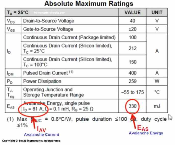 Therefore, in datasheets MOSFET Avalanche Energy is presented as the quantity of energy the MOSFET is able to tolerate while it is being subjected to the avalanche test, or when the MOSFET's maximum breakdown voltage rating is crossed.
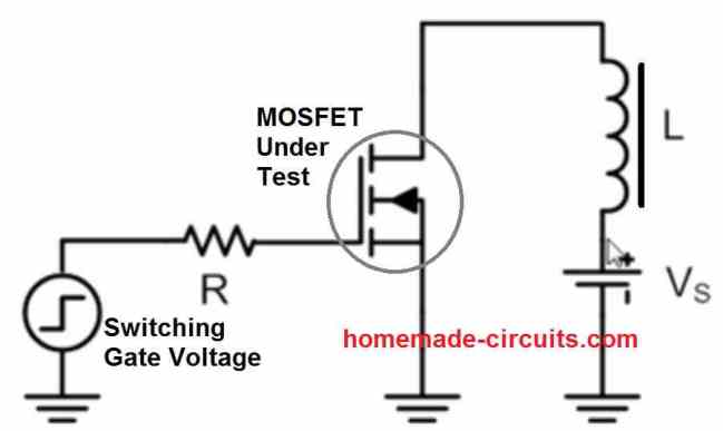 Thus we see a voltage supply in series with an inductor, L, which is also in series with the MOSFET under test.
We can also see a gate driver for the FET whose output is in series with a FET gate resistor R.
In the below image, we find, the LTC55140 controller device, which is used in Texas Instrument lab to evaluate the UIS characteristics of the FET.
Thus we see a voltage supply in series with an inductor, L, which is also in series with the MOSFET under test.
We can also see a gate driver for the FET whose output is in series with a FET gate resistor R.
In the below image, we find, the LTC55140 controller device, which is used in Texas Instrument lab to evaluate the UIS characteristics of the FET.
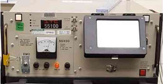 The UIS characteristic subsequently helps not only to find out the FET datasheet rating, but also the value utilized to scan the FET in the final testing procedure.
The tool allows tweaking the load inductor value from 0.2 to 160 millihenries.
It allows the adjustment of the the drain voltage of the MOSFET under test from 10 to 150 volts.
This, as a result makes it possible to screen even those FETs which are rated to handle only 100 volt breakdown voltage.
And, it becomes possible applying drain currents from 0.1 to 200 amps.
And this is the UIS current range which the FET may have to tolerate during the testing procedure.
Additionally the tool allows setting different ranges of the MOSFET case temperatures, from -55 to +150 degrees.
The UIS characteristic subsequently helps not only to find out the FET datasheet rating, but also the value utilized to scan the FET in the final testing procedure.
The tool allows tweaking the load inductor value from 0.2 to 160 millihenries.
It allows the adjustment of the the drain voltage of the MOSFET under test from 10 to 150 volts.
This, as a result makes it possible to screen even those FETs which are rated to handle only 100 volt breakdown voltage.
And, it becomes possible applying drain currents from 0.1 to 200 amps.
And this is the UIS current range which the FET may have to tolerate during the testing procedure.
Additionally the tool allows setting different ranges of the MOSFET case temperatures, from -55 to +150 degrees.
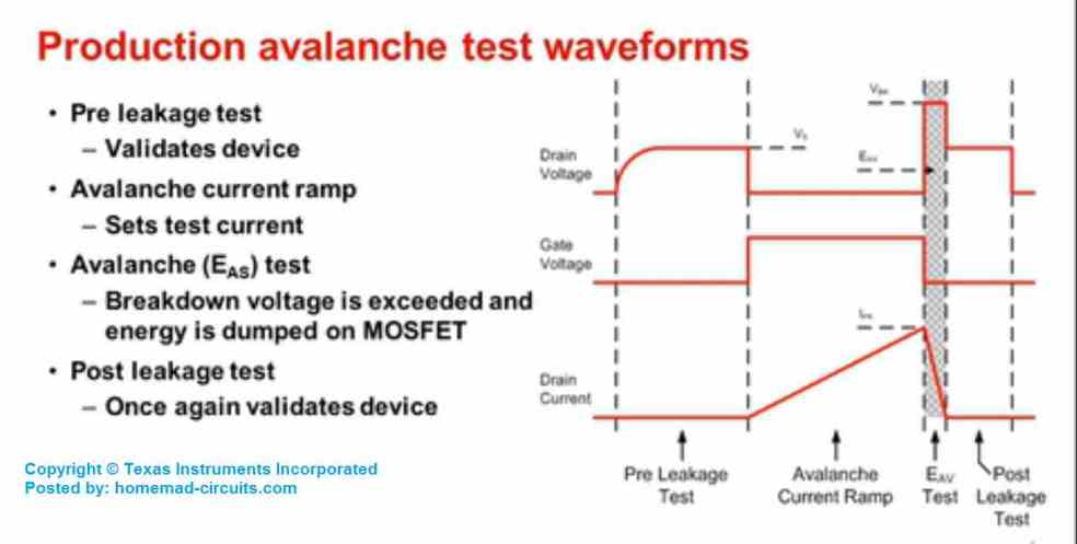 The first stage consists of the pre-leakage test, in which the supply voltage biases the FET drain.
Fundamentally, the idea here is to try to ensure the FET is performing in the normal expected manner.
Thus, in the first stage the FET is held switched off.
It keeps the supply voltage blocked across the daim-emitter terminals, without experiencing any kind of excessive leakage current flowing through it.
In the second stage, which is known as the Avalanche Current ramp up, the FET is switched ON, which causes its drain voltage to drop.
This results in the current to increase gradually through the inductor with a constant di/dt.
So basically in this stage, the inductor is allowed to charge up.
In the the third stage, the actual avalanche test is carried out, where the FET is practically subjected to the avalanche.
In this stage the FET is turned off by removing its gate bias.
This results in a massive di/dt getting through the inductor, causing the FET drain voltage to shoot high above the breakdown voltage limit of the FET.
This forces the FET to go through the avalanche surge.
In this process, the FET absorbs the whole energy generated by the inductor, and stays shut off, until the 4rth stage is executed, involving the post leakage test
In this 4rth stage the FET is once again subjected to the a repeat avalanche test, just to be sure whether the MOSFET is still behaving normally or not.
If it does, then the FET is deemed to have passed the avalanche test.
Next, the FET has to go through the above test many more times, wherein the UIS voltage level is gradually increased with each test, until the level where the MOSFET is unable to withstand and fails the post-leakage test.
And this current level is noted to be the MOSFET's maximum UIS current withstanding capability.
The first stage consists of the pre-leakage test, in which the supply voltage biases the FET drain.
Fundamentally, the idea here is to try to ensure the FET is performing in the normal expected manner.
Thus, in the first stage the FET is held switched off.
It keeps the supply voltage blocked across the daim-emitter terminals, without experiencing any kind of excessive leakage current flowing through it.
In the second stage, which is known as the Avalanche Current ramp up, the FET is switched ON, which causes its drain voltage to drop.
This results in the current to increase gradually through the inductor with a constant di/dt.
So basically in this stage, the inductor is allowed to charge up.
In the the third stage, the actual avalanche test is carried out, where the FET is practically subjected to the avalanche.
In this stage the FET is turned off by removing its gate bias.
This results in a massive di/dt getting through the inductor, causing the FET drain voltage to shoot high above the breakdown voltage limit of the FET.
This forces the FET to go through the avalanche surge.
In this process, the FET absorbs the whole energy generated by the inductor, and stays shut off, until the 4rth stage is executed, involving the post leakage test
In this 4rth stage the FET is once again subjected to the a repeat avalanche test, just to be sure whether the MOSFET is still behaving normally or not.
If it does, then the FET is deemed to have passed the avalanche test.
Next, the FET has to go through the above test many more times, wherein the UIS voltage level is gradually increased with each test, until the level where the MOSFET is unable to withstand and fails the post-leakage test.
And this current level is noted to be the MOSFET's maximum UIS current withstanding capability.
 Copyright Texas Instruments Incorporated
Many of the MOSFET manufacturers intentionally test the MOSFET with larger inductors, so that they are able to boast a larger avalanche energy magnitude, creating an impression that the MOSFET is tested for withstanding huge avalanche energies, and therefore has an increased durability to avalanche.
But the above method of using larger inductor looks misleading, that is exactly why the Texas Instruments engineers test with smaller inductance in the order of 0.1 mH, so that the MOSFET under test are subjected to higher Avalanche current and extreme breakdown stress levels.
So, in datasheets, it is not the Avalanche energy, rather Avalanche current that should be bigger in quantity, which displays better MOSFET ruggedness.
This makes the final testing highly stringent and enables filtering out as many weaker MOSFETs as possible.
This test value is not only used as the final value before the FET layout is passed for the production, but this is also the value which is entered in the datasheet.
In the next step, the above test value is derated by 65%, so that the end user is able to get a wider margin of tolerance for their MOSFETs.
So for example, if the tested avalanche current was 125 Amps, the final value which is entered in the datasheet happens to be 81 Amps, after the derating.
Copyright Texas Instruments Incorporated
Many of the MOSFET manufacturers intentionally test the MOSFET with larger inductors, so that they are able to boast a larger avalanche energy magnitude, creating an impression that the MOSFET is tested for withstanding huge avalanche energies, and therefore has an increased durability to avalanche.
But the above method of using larger inductor looks misleading, that is exactly why the Texas Instruments engineers test with smaller inductance in the order of 0.1 mH, so that the MOSFET under test are subjected to higher Avalanche current and extreme breakdown stress levels.
So, in datasheets, it is not the Avalanche energy, rather Avalanche current that should be bigger in quantity, which displays better MOSFET ruggedness.
This makes the final testing highly stringent and enables filtering out as many weaker MOSFETs as possible.
This test value is not only used as the final value before the FET layout is passed for the production, but this is also the value which is entered in the datasheet.
In the next step, the above test value is derated by 65%, so that the end user is able to get a wider margin of tolerance for their MOSFETs.
So for example, if the tested avalanche current was 125 Amps, the final value which is entered in the datasheet happens to be 81 Amps, after the derating.
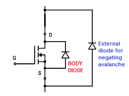 Courtesy: MOSFET Avalanche
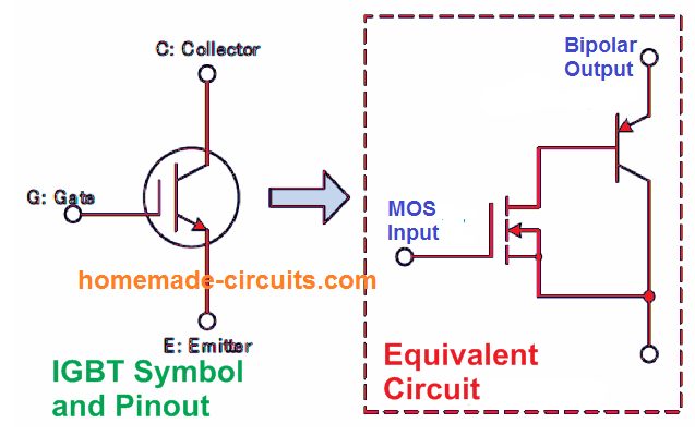 IGBTs, promising fast switching speed along with minimal saturation voltage characteristics, are being used in a extensive range, from commercial applications like in solar energy harnessing units and uninterruptible power supply (UPS), to consumer electronic fields, like temperature control for induction heater cooktops, air conditioning equipment PFC, inverters, and digital camera stroboscopes.
Figure 2 below reveals an evaluation between IGBT, bipolar transistor, and MOSFET internal layouts and attributes.
The fundamental framework of the IGBT is same as that of a MOSFET having a p+ layer put into the drain (collector) section, and also an extra pn junction.
IGBTs, promising fast switching speed along with minimal saturation voltage characteristics, are being used in a extensive range, from commercial applications like in solar energy harnessing units and uninterruptible power supply (UPS), to consumer electronic fields, like temperature control for induction heater cooktops, air conditioning equipment PFC, inverters, and digital camera stroboscopes.
Figure 2 below reveals an evaluation between IGBT, bipolar transistor, and MOSFET internal layouts and attributes.
The fundamental framework of the IGBT is same as that of a MOSFET having a p+ layer put into the drain (collector) section, and also an extra pn junction.

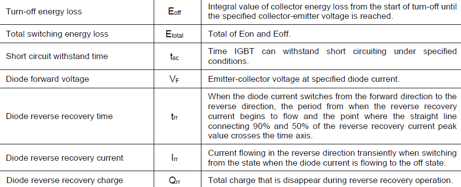 Collector current, Collector Dissipation: Figure 3 demonstrates the collector dissipation temperature waveform of the IGBT RBN40H125S1FPQ.
The maximum tolerable collector dissipation is displayed for various different case temperatures.
Collector current, Collector Dissipation: Figure 3 demonstrates the collector dissipation temperature waveform of the IGBT RBN40H125S1FPQ.
The maximum tolerable collector dissipation is displayed for various different case temperatures.
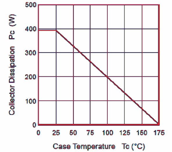 The below shown formula becomes applicable in situations when the ambient temperature TC = 25 degrees Celsius or more.
Pc = (Tjmax - Tc) / Rth(j - c)
For conditions where the ambient temperature TC is = 25�� or lower, the IGBT collector dissipation is applied in accordance with their absolute maximum rating.
The formula for calculating the collector current of an IGBT is:
Ic = (Tjmax - Tc) / Rth(j c)��VCE(sat)
However the above is the general formula, is simply a temperature dependent computation of the device.
Collector current of IGBTs is determined by their collector/emitter saturation voltage VCE(sat), and also depending on their current and temperature conditions.
Additionally, the collector current (peak) of an IGBT is defined by the amount of current it can handle which is in turn dependent on the way it is installed and its reliability.
For that reason, users are advised never to exceed the maximum tolerable limit of IGBTs while using them in a given circuit application.
On the other hand even if the collector current may be lower than the maximum rating of the device, it could get restricted by the unit's junction temperature or the safe operation area.
Therefore make sure you consider these scenarios while implementing an IGBT.
Both the parameters, collector current and collector dissipation are usually designated as the maximum ratings of the device.
The below shown formula becomes applicable in situations when the ambient temperature TC = 25 degrees Celsius or more.
Pc = (Tjmax - Tc) / Rth(j - c)
For conditions where the ambient temperature TC is = 25�� or lower, the IGBT collector dissipation is applied in accordance with their absolute maximum rating.
The formula for calculating the collector current of an IGBT is:
Ic = (Tjmax - Tc) / Rth(j c)��VCE(sat)
However the above is the general formula, is simply a temperature dependent computation of the device.
Collector current of IGBTs is determined by their collector/emitter saturation voltage VCE(sat), and also depending on their current and temperature conditions.
Additionally, the collector current (peak) of an IGBT is defined by the amount of current it can handle which is in turn dependent on the way it is installed and its reliability.
For that reason, users are advised never to exceed the maximum tolerable limit of IGBTs while using them in a given circuit application.
On the other hand even if the collector current may be lower than the maximum rating of the device, it could get restricted by the unit's junction temperature or the safe operation area.
Therefore make sure you consider these scenarios while implementing an IGBT.
Both the parameters, collector current and collector dissipation are usually designated as the maximum ratings of the device.
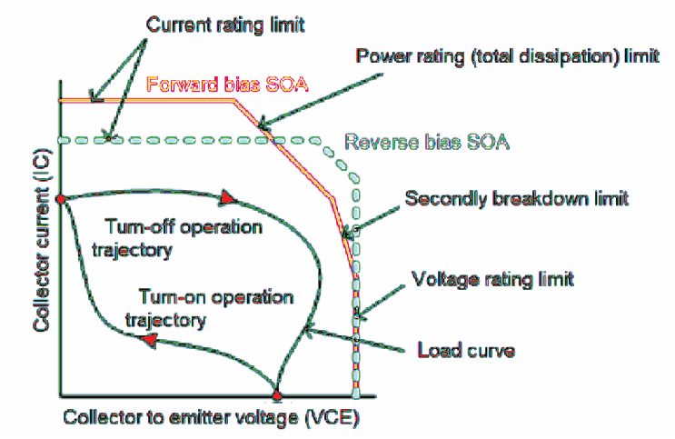 The SOA of an IGBT consists of a forward bias SOA and a reverse bias SOA, however since the particular range of values could differ in accordance with device specs, users are advised to verify the facts equivalent in the data sheet.
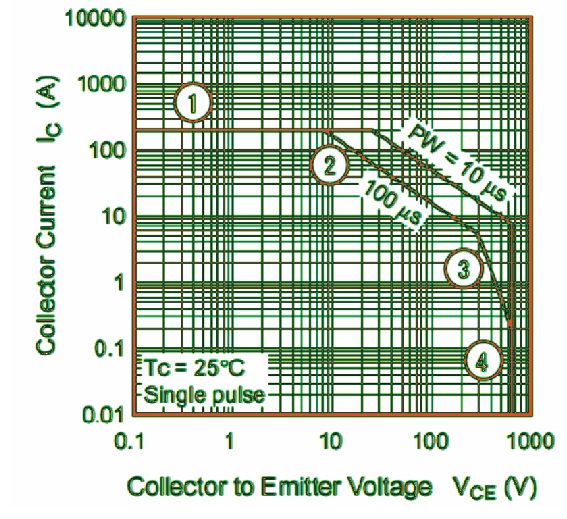 The SOA is split into 4 regions depending on particular limitations, as outlined below:
Area restricted by the highest rated collector pulse current IC(peak).
Area restricted by collector dissipation region
Area restricted by the secondary breakdown.
Remember that this kind of malfunction causes the safe operating area of an IGBT to get narrower, except when the device features a secondary breakdown margin.
Area restricted by maximum collector to emitter voltage VCES rating.
The SOA is split into 4 regions depending on particular limitations, as outlined below:
Area restricted by the highest rated collector pulse current IC(peak).
Area restricted by collector dissipation region
Area restricted by the secondary breakdown.
Remember that this kind of malfunction causes the safe operating area of an IGBT to get narrower, except when the device features a secondary breakdown margin.
Area restricted by maximum collector to emitter voltage VCES rating.
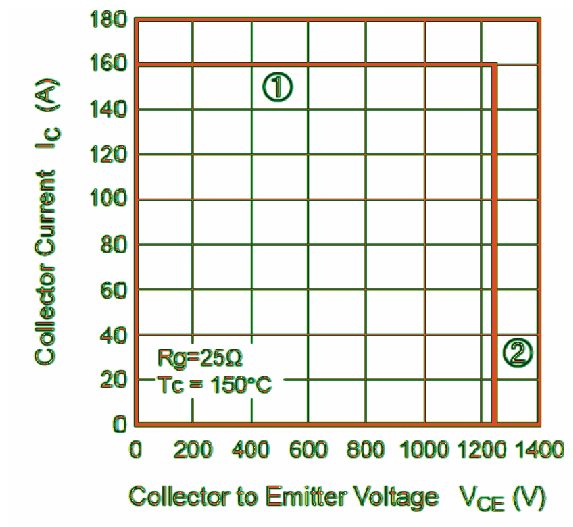 This particular characteristic works in accordance with the reverse bias SOA of the bipolar transistor.
Whenever a reverse bias, which includes no bias, is supplied across the gate and the emitter of the IGBT during its turn-off period for an inductive load, we find a high voltage being delivered to the IGBT��s collector-emitter.
Simultaneously, a large current constantly moves as a result of residual hole.
Having said that, in this functioning the forward bias SOA cannot be used, while the reverse bias SOA can be utilized.
The reverse bias SOA is divided into 2 restricted areas, as explained in the following points; eventually the area is established by validating the real functioning procedures of the IGBT.
Area restricted by the maximum peak collector current Ic(peak).
Area restricted by the maximum collector-emitter voltage breakdown rating VCES.
Observe that the IGBT may get damaged if a specified VCEIC operation trajectory strays away from the device's SOA specifications.
Hence, while designing an IGBT based circuit, it must be ensured that the dissipation and other performance issues are as per the recommended boundaries, and also the specific characteristics and circuit breakdown constants relevant to breakdown tolerance must be taken care of.
For instance, reverse bias SOA carries a temperature characteristic which dips at extreme temperatures, and the VCE/IC operating locus shifts in accordance with the IGBT's gate resistance Rg and gate voltage VGE.
That is why, it is vital to determine the Rg and VGE parameters with respect to the working ecosystem and lowest gate resistance value during switch off periods.
In addition, a snubber circuit could be helpful for controlling the dv/dt VCE.
This particular characteristic works in accordance with the reverse bias SOA of the bipolar transistor.
Whenever a reverse bias, which includes no bias, is supplied across the gate and the emitter of the IGBT during its turn-off period for an inductive load, we find a high voltage being delivered to the IGBT��s collector-emitter.
Simultaneously, a large current constantly moves as a result of residual hole.
Having said that, in this functioning the forward bias SOA cannot be used, while the reverse bias SOA can be utilized.
The reverse bias SOA is divided into 2 restricted areas, as explained in the following points; eventually the area is established by validating the real functioning procedures of the IGBT.
Area restricted by the maximum peak collector current Ic(peak).
Area restricted by the maximum collector-emitter voltage breakdown rating VCES.
Observe that the IGBT may get damaged if a specified VCEIC operation trajectory strays away from the device's SOA specifications.
Hence, while designing an IGBT based circuit, it must be ensured that the dissipation and other performance issues are as per the recommended boundaries, and also the specific characteristics and circuit breakdown constants relevant to breakdown tolerance must be taken care of.
For instance, reverse bias SOA carries a temperature characteristic which dips at extreme temperatures, and the VCE/IC operating locus shifts in accordance with the IGBT's gate resistance Rg and gate voltage VGE.
That is why, it is vital to determine the Rg and VGE parameters with respect to the working ecosystem and lowest gate resistance value during switch off periods.
In addition, a snubber circuit could be helpful for controlling the dv/dt VCE.
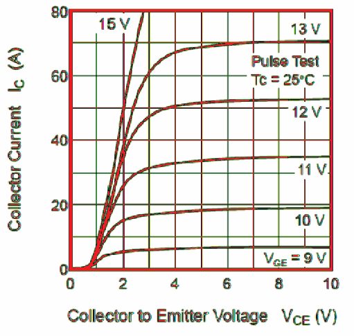 The collector-emitter voltage, that impacts the current handling efficiency and loss during switch ON condition, varies according to the gate voltage and body temperature.
All these parameters needs to be taken into account while designing an IGBT driver circuit.
The current goes up whenever VCE reaches the values of 0.7 to 0.8 V, although this is because of the forward voltage of the PN collector-emitter PN junction.
Figure 8 demonstrates the collector-emitter saturation voltage vs.
gate voltage characteristics of IGBt RBN40H125S1FPQ.
The collector-emitter voltage, that impacts the current handling efficiency and loss during switch ON condition, varies according to the gate voltage and body temperature.
All these parameters needs to be taken into account while designing an IGBT driver circuit.
The current goes up whenever VCE reaches the values of 0.7 to 0.8 V, although this is because of the forward voltage of the PN collector-emitter PN junction.
Figure 8 demonstrates the collector-emitter saturation voltage vs.
gate voltage characteristics of IGBt RBN40H125S1FPQ.
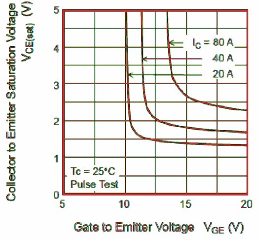 Essentially, VCE (sat) begins dropping as the gate-emitter voltage VGE rises, although the change is nominal while VGE = 15 V or higher.
Therefore, it is advised working with a gate/emitter voltage VGE that's around 15 V, whenever possible.
Figure 9 exhibits the collector current vs.
gate voltage characteristics of IGBT RBN40H125S1FPQ.
Essentially, VCE (sat) begins dropping as the gate-emitter voltage VGE rises, although the change is nominal while VGE = 15 V or higher.
Therefore, it is advised working with a gate/emitter voltage VGE that's around 15 V, whenever possible.
Figure 9 exhibits the collector current vs.
gate voltage characteristics of IGBT RBN40H125S1FPQ.
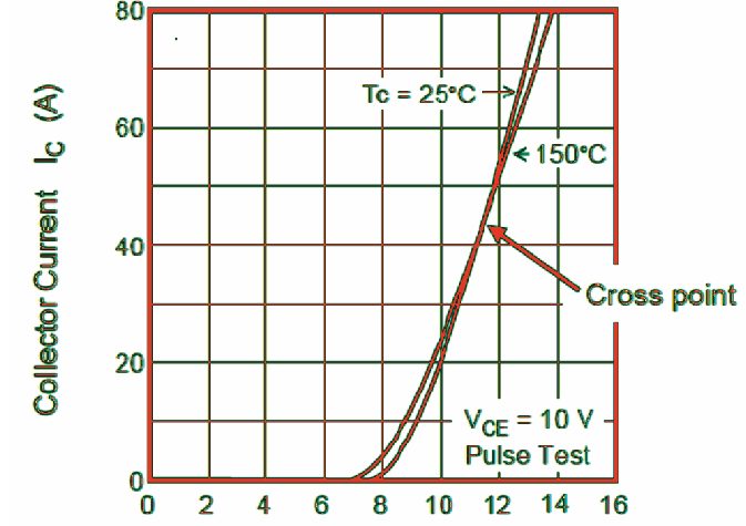 The IC/VGE characteristics are based on temperature changes, however the region of low gate voltage towards the intersection point, tend to be negative temperature coefficient, while the high gate voltage region signifies positive temperature coefficients.
Considering that power IGBTs will generate heat while in operation, it is actually more advantageous to pay attention to the positive temperature coefficient region particularly when the devices are operated in parallel.
The recommended gate voltage condition using VGE = 15V exhibits the positive temperature characteristics.
Figures 10 and 11 demonstrate how the performance of the collector-emitter saturation voltage, along with gate threshold voltage
of an IGBT are dependent on temperature.
The IC/VGE characteristics are based on temperature changes, however the region of low gate voltage towards the intersection point, tend to be negative temperature coefficient, while the high gate voltage region signifies positive temperature coefficients.
Considering that power IGBTs will generate heat while in operation, it is actually more advantageous to pay attention to the positive temperature coefficient region particularly when the devices are operated in parallel.
The recommended gate voltage condition using VGE = 15V exhibits the positive temperature characteristics.
Figures 10 and 11 demonstrate how the performance of the collector-emitter saturation voltage, along with gate threshold voltage
of an IGBT are dependent on temperature.
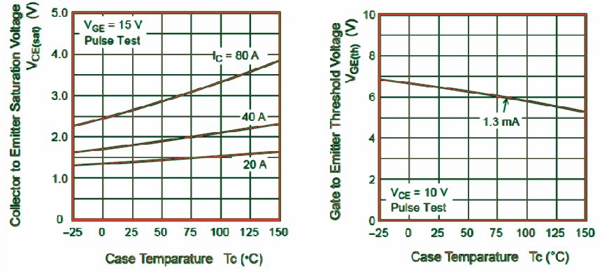 Due to the fact that the collector-emitter saturation voltage features a positive temperature coefficient characteristics, it is not easy for current to pass while the IGBT operation is dissipating high amount of temperature, which becomes responsible for blocking the effective current during parallel IGBT operation.
On the contrary, the operation of gate-emitter threshold voltage relies on negative temperature characteristics.
During high heat dissipation, the threshold voltage falls downward, causing a higher possibility of malfunctioning of the device resulting from noise generation.
Therefore, mindful testing, centered around the above specified characteristics may be crucial.
Due to the fact that the collector-emitter saturation voltage features a positive temperature coefficient characteristics, it is not easy for current to pass while the IGBT operation is dissipating high amount of temperature, which becomes responsible for blocking the effective current during parallel IGBT operation.
On the contrary, the operation of gate-emitter threshold voltage relies on negative temperature characteristics.
During high heat dissipation, the threshold voltage falls downward, causing a higher possibility of malfunctioning of the device resulting from noise generation.
Therefore, mindful testing, centered around the above specified characteristics may be crucial.
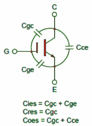 IGBT gate characteristics are essentially in line with the very same principles applied for power MOSFETs and provide as the variables that decide the device's drive current and drive dissipation.
Figure 13 reveals the characteristic curve, divided into Periods 1 to 3.
The working procedures related with each period are explained below.
IGBT gate characteristics are essentially in line with the very same principles applied for power MOSFETs and provide as the variables that decide the device's drive current and drive dissipation.
Figure 13 reveals the characteristic curve, divided into Periods 1 to 3.
The working procedures related with each period are explained below.
 Period 1: Gate voltage is raised up to threshold voltage where current just starts to stream.
The section ascending from VGE = 0V is the portion responsible for charging the gate-emitter capacitance Cge.
Period 2: While the transition from the active region to the saturation region transpires, the collector-emitter voltage begins altering and gate-collector capacitance Cgc gets charged.
This particular period comes with a noticeable increase in capacitance because of the mirror effect, which causes VGE to become constant.
On the other hand while an IGBT is entirely in the ON state, the change in the voltage across collector-emitter (VCE) and the mirror effect vanish.
Period 3: In this particular period the IGBT gets into a completely saturated condition and the VCE shows no changes.
Now, the gate-emitter voltage VGE begins increasing with time.
Period 1: Gate voltage is raised up to threshold voltage where current just starts to stream.
The section ascending from VGE = 0V is the portion responsible for charging the gate-emitter capacitance Cge.
Period 2: While the transition from the active region to the saturation region transpires, the collector-emitter voltage begins altering and gate-collector capacitance Cgc gets charged.
This particular period comes with a noticeable increase in capacitance because of the mirror effect, which causes VGE to become constant.
On the other hand while an IGBT is entirely in the ON state, the change in the voltage across collector-emitter (VCE) and the mirror effect vanish.
Period 3: In this particular period the IGBT gets into a completely saturated condition and the VCE shows no changes.
Now, the gate-emitter voltage VGE begins increasing with time.
 This eventually may be impacting switching time and switching deficits.
It is crucial to choose a suitable Rg with respect to the device's characteristics in use.
This eventually may be impacting switching time and switching deficits.
It is crucial to choose a suitable Rg with respect to the device's characteristics in use.
 Because the diode clamp is hooked up in parallel to inductive load L, the delay of the IGBT turn-on (or the turn-on loss) is usually afflicted by the diode��s recovery time characteristics.
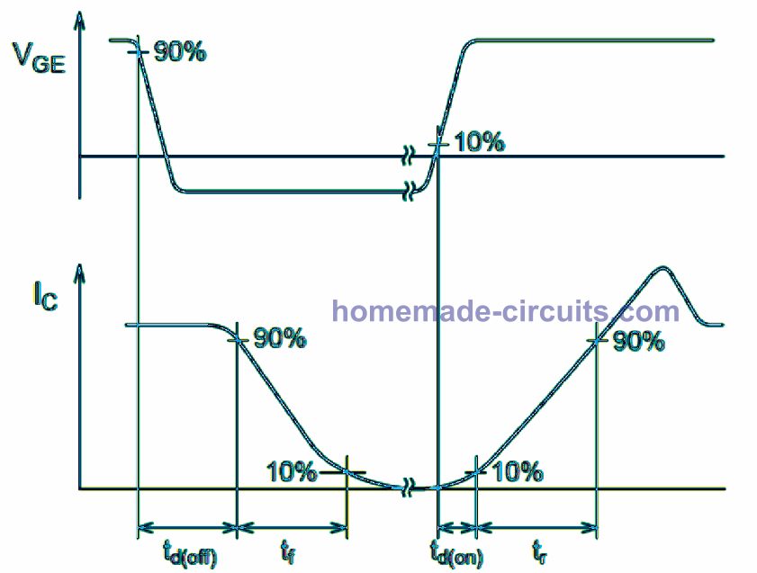 Due to the fact that the time changes drastically for every single period with respect to Tj, IC, VCE, VGE, and Rg situations, this period is assessed with the following outlined conditions.
td(on) (turn-on delay time): The point of time from where the gate-emitter voltage extends to 10% of forward bias voltage to a level until the collector current increases to 10%.
tr (rise time): The point of time from where the collector current increases from 10% to 90%.
td(off) (turn-off delay time): The point of time from where gate-emitter voltage attains 90% of forward bias voltage to a level until the collector current drops to 90%.
tf (fall time): The point of time from where the collector current reduces from 90% to 10%.
ttail(tail time): The IGBT turn-off period consists of a tail time (ttail).
This can be defined as the time consumed by the excess carriers leftover on the IGBT's collector side to recede through recombination despite of the IGBT getting shut off and causing the collector-emitter voltage to increase.
Due to the fact that the time changes drastically for every single period with respect to Tj, IC, VCE, VGE, and Rg situations, this period is assessed with the following outlined conditions.
td(on) (turn-on delay time): The point of time from where the gate-emitter voltage extends to 10% of forward bias voltage to a level until the collector current increases to 10%.
tr (rise time): The point of time from where the collector current increases from 10% to 90%.
td(off) (turn-off delay time): The point of time from where gate-emitter voltage attains 90% of forward bias voltage to a level until the collector current drops to 90%.
tf (fall time): The point of time from where the collector current reduces from 90% to 10%.
ttail(tail time): The IGBT turn-off period consists of a tail time (ttail).
This can be defined as the time consumed by the excess carriers leftover on the IGBT's collector side to recede through recombination despite of the IGBT getting shut off and causing the collector-emitter voltage to increase.
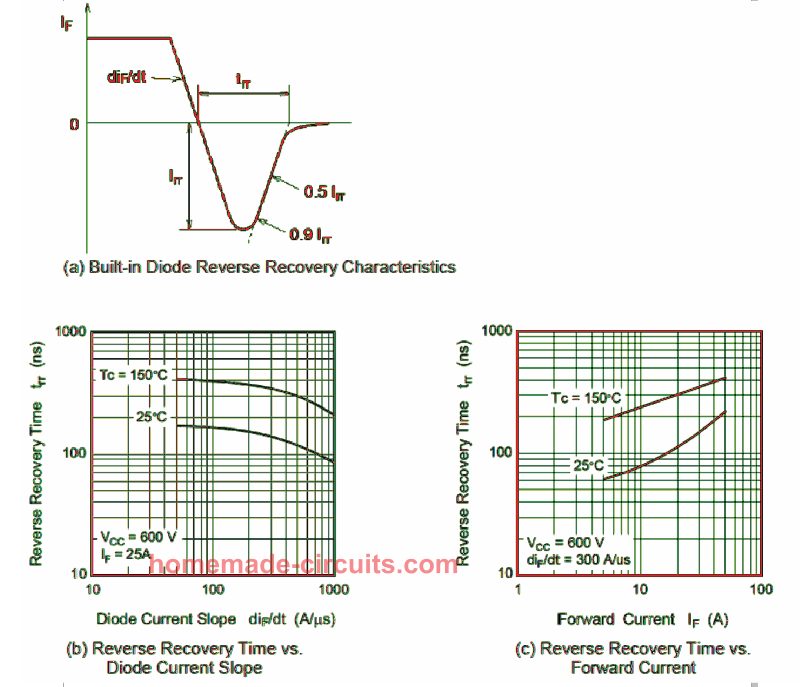 On the other hand, if trr gets faster, di/dt results in being steeper around the recovery period, as happens with the corresponding collector-emitter voltage dv/dt, which causes an increase in the propensity for noise generation.
Following are the examples which provides the ways through which noise generation can be countered.
Decrease diF/dt (reduce IGBT switch-ON time).
Include a snubber capacitor across the collector and emitter of the device to minimize collector-emitter voltage dv/dt.
Replace the built-in diode with some soft recovery diode.
The reverse recovery property significantly relies on the voltage/current tolerance capacity of the device.
This feature could be enhanced using lifetime management, hefty metallic diffusion, and various other techniques.
On the other hand, if trr gets faster, di/dt results in being steeper around the recovery period, as happens with the corresponding collector-emitter voltage dv/dt, which causes an increase in the propensity for noise generation.
Following are the examples which provides the ways through which noise generation can be countered.
Decrease diF/dt (reduce IGBT switch-ON time).
Include a snubber capacitor across the collector and emitter of the device to minimize collector-emitter voltage dv/dt.
Replace the built-in diode with some soft recovery diode.
The reverse recovery property significantly relies on the voltage/current tolerance capacity of the device.
This feature could be enhanced using lifetime management, hefty metallic diffusion, and various other techniques.
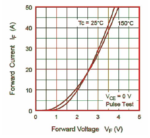 Diode forward voltage VF signifies declining voltage produced when current IF through the diode runs in the direction of the diode's forward voltage drop.
Since this characteristic may result in power loss in the course of back EMF generation (free-wheeling diode) in motor or inductive applications, selecting smaller VF is recommended.
Additionally, as depicted in Figure 19, the positive and negative temperature coefficient characteristics is determined by the diode's forward current magnitude IF.
Diode forward voltage VF signifies declining voltage produced when current IF through the diode runs in the direction of the diode's forward voltage drop.
Since this characteristic may result in power loss in the course of back EMF generation (free-wheeling diode) in motor or inductive applications, selecting smaller VF is recommended.
Additionally, as depicted in Figure 19, the positive and negative temperature coefficient characteristics is determined by the diode's forward current magnitude IF.
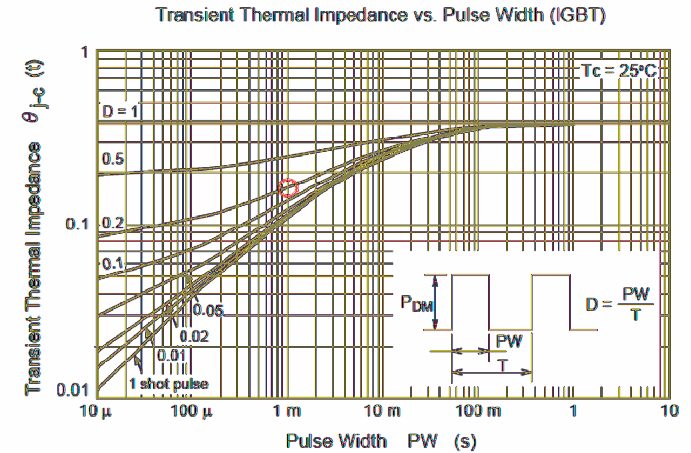
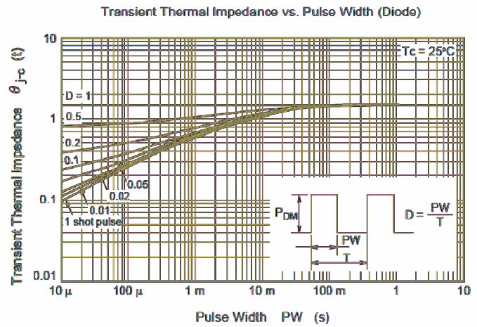 This characteristic is used for determining junction temperature Tj of the IGBT.
The pulse width (PW) shown over the horizontal axis signifies the switching time, which defines the single one shot pulse and the results of repetitive operations.
For instance, PW = 1ms and D = 0.2 (duty cycle = 20%) signifies that the repetition frequency is 200Hz since the repetition period is T = 5ms.
If we imagine PW = 1ms and D = 0.2, and dissipation power Pd = 60W, it is possible to determine the increase in IGBT junction temperature ��Tj in the following manner:
��Tj = Pd �� ��j - c(t) = 60 �� 0.17 = 10.2
This characteristic is used for determining junction temperature Tj of the IGBT.
The pulse width (PW) shown over the horizontal axis signifies the switching time, which defines the single one shot pulse and the results of repetitive operations.
For instance, PW = 1ms and D = 0.2 (duty cycle = 20%) signifies that the repetition frequency is 200Hz since the repetition period is T = 5ms.
If we imagine PW = 1ms and D = 0.2, and dissipation power Pd = 60W, it is possible to determine the increase in IGBT junction temperature ��Tj in the following manner:
��Tj = Pd �� ��j - c(t) = 60 �� 0.17 = 10.2
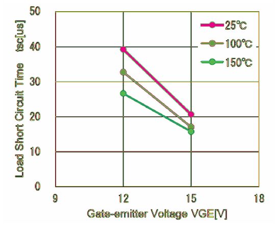
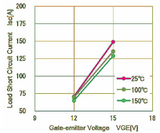 This short circuit withstanding capacity of an IGBT is commonly expressed with regard to time tSC.
This withstanding capability is determined mainly based on the IGBT's gate-emitter voltage, body temperature, and power supply voltage.
This ought to be looked at while designing a critical H-bridge IGBT circuit design.
Additionally make sure to opt for an optimally rated IGBT device in terms of the following parameters.
Gate-emitter voltage VGE: With an increase in the gate voltage, the short circuit current also rises and the current handling capacity of the device decreases.
Case temperature: With an increase in the case temperature ��Tj of the IGBT, the current withstanding capacity declines, until the device reaches the breaks down situation.
Power supply voltage
VCC: As the input supply voltage to the device increases the short circuit current also increases causing the current withstand capacity of the device to deteriorate.
Furthermore, during the instant when the short circuit or over-load protection circuit senses the short circuit current and shuts down the gate voltage, the short circuit current is actually incredibly large than the standard operational current magnitude of the IGBT.
During the turning off process with this substantial current using standard gate resistance Rg, it might cause the development of big surge voltage, exceeding the IGBT rating.
For this reason, you must appropriately select the IGBT gate resistance suitable for tackling the short circuit conditions, having at least 10-times higher than the normal gate resistance value (yet remain inside the forward bias SOA value).
This is to counteract surge voltage generation across collector-emitter ledas of the IGBT during the periods when short circuit current is cut-off.
Additionally, the short circuit withstand time tSC may cause distribution of the surge across the other associate devices.
Care must be taken to ensure adequate margin of a minimum of 2 times the standard time-frame needed for the short-circuit protection circuit to begin operating.
This short circuit withstanding capacity of an IGBT is commonly expressed with regard to time tSC.
This withstanding capability is determined mainly based on the IGBT's gate-emitter voltage, body temperature, and power supply voltage.
This ought to be looked at while designing a critical H-bridge IGBT circuit design.
Additionally make sure to opt for an optimally rated IGBT device in terms of the following parameters.
Gate-emitter voltage VGE: With an increase in the gate voltage, the short circuit current also rises and the current handling capacity of the device decreases.
Case temperature: With an increase in the case temperature ��Tj of the IGBT, the current withstanding capacity declines, until the device reaches the breaks down situation.
Power supply voltage
VCC: As the input supply voltage to the device increases the short circuit current also increases causing the current withstand capacity of the device to deteriorate.
Furthermore, during the instant when the short circuit or over-load protection circuit senses the short circuit current and shuts down the gate voltage, the short circuit current is actually incredibly large than the standard operational current magnitude of the IGBT.
During the turning off process with this substantial current using standard gate resistance Rg, it might cause the development of big surge voltage, exceeding the IGBT rating.
For this reason, you must appropriately select the IGBT gate resistance suitable for tackling the short circuit conditions, having at least 10-times higher than the normal gate resistance value (yet remain inside the forward bias SOA value).
This is to counteract surge voltage generation across collector-emitter ledas of the IGBT during the periods when short circuit current is cut-off.
Additionally, the short circuit withstand time tSC may cause distribution of the surge across the other associate devices.
Care must be taken to ensure adequate margin of a minimum of 2 times the standard time-frame needed for the short-circuit protection circuit to begin operating.
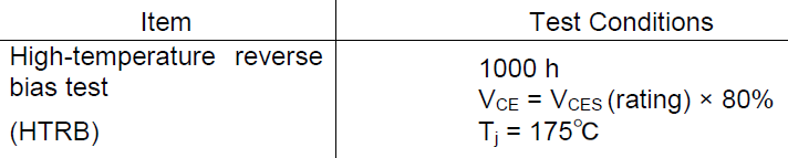 In order to guarantee effective operations at Tjmax = 175��, many of the parameters for the standard consistency test at 150�� had been improved and operational verification performed.
Having said that, testing grounds range with respect to the device specs.
Make sure you validate the reliability data related to the device you might be applying, for added information.
Likewise remember that the Tjmax value isn't just a restriction for constant working, rather also a specification for the regulation which should not be surpassed even for a moment.
Safety against high temperature dissipation, even for a brief moment for an IGBT, during ON/OFF switching must be strictly considered.
Make sure to work with IGBT in an environment which in no way exceeds the max breakdown case temperature of Tj = 175��.
In order to guarantee effective operations at Tjmax = 175��, many of the parameters for the standard consistency test at 150�� had been improved and operational verification performed.
Having said that, testing grounds range with respect to the device specs.
Make sure you validate the reliability data related to the device you might be applying, for added information.
Likewise remember that the Tjmax value isn't just a restriction for constant working, rather also a specification for the regulation which should not be surpassed even for a moment.
Safety against high temperature dissipation, even for a brief moment for an IGBT, during ON/OFF switching must be strictly considered.
Make sure to work with IGBT in an environment which in no way exceeds the max breakdown case temperature of Tj = 175��.
 The factors Eon and Eoff are heavily influenced by the collector current, gate resistance, and operating temperature.
Eon (Turn-on energy loss)
The volume of loss developed during the turn-on process of the IGBT for an inductive load, along with the recovery loss at reverse recovery of the diode.
Eon is calculated from the point when gate voltage is powered to the IGBT and the collector current begins travelling, until the point of time when the IGBT is completely transited to the switched ON state
Eoff (Turn-off energy loss
It is the magnitude of loss resulting during the turn-off period for inductive loads, which includes the tail current.
Eoff is measured from the point where the gate current is just cut off and the collector-emitter voltage begins climbing, until the point of time where the IGBT reaches a complete switched OFF state.
The factors Eon and Eoff are heavily influenced by the collector current, gate resistance, and operating temperature.
Eon (Turn-on energy loss)
The volume of loss developed during the turn-on process of the IGBT for an inductive load, along with the recovery loss at reverse recovery of the diode.
Eon is calculated from the point when gate voltage is powered to the IGBT and the collector current begins travelling, until the point of time when the IGBT is completely transited to the switched ON state
Eoff (Turn-off energy loss
It is the magnitude of loss resulting during the turn-off period for inductive loads, which includes the tail current.
Eoff is measured from the point where the gate current is just cut off and the collector-emitter voltage begins climbing, until the point of time where the IGBT reaches a complete switched OFF state.
 Symbol of depletion mode IGBT
In case the amplifiers use insulated-gate bipolar transistor often synthesize waveforms which are complex in nature along with low-pass filters and pulse width modulation; as insulated-gate bipolar transistor are basically design to turn on and off on a fast and rapid pace.
The pulse repetition rates are boasted by the modern devices which consist of switching application and fall well within the ultrasonic range which are the frequencies which are ten times higher than the highest audio frequency handled by the device when the devices is used in the form of an analog audio amplifier.
The MOSFETs consisting of high current and characteristics of a simple gate-drive is combined with the bipolar transistors which has low-saturation-voltage capacity by the IGTB.
Symbol of depletion mode IGBT
In case the amplifiers use insulated-gate bipolar transistor often synthesize waveforms which are complex in nature along with low-pass filters and pulse width modulation; as insulated-gate bipolar transistor are basically design to turn on and off on a fast and rapid pace.
The pulse repetition rates are boasted by the modern devices which consist of switching application and fall well within the ultrasonic range which are the frequencies which are ten times higher than the highest audio frequency handled by the device when the devices is used in the form of an analog audio amplifier.
The MOSFETs consisting of high current and characteristics of a simple gate-drive is combined with the bipolar transistors which has low-saturation-voltage capacity by the IGTB.
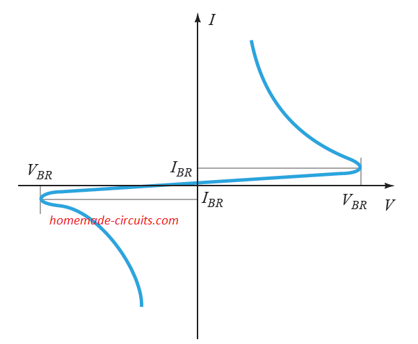 Since a diac can be switched in both directions or bidirectionally, the feature is effectively exploited in many AC switching circuits.
The next figure below illustrates how the layers are arranged internally, and also shows the graphical symbol of the diac.
It may be interesting to note that both the terminals of the diac are assigned as anodes (anode 1 or electrode 1 and an anode 2 or electrode 2) , and there is no cathode for this device.
Since a diac can be switched in both directions or bidirectionally, the feature is effectively exploited in many AC switching circuits.
The next figure below illustrates how the layers are arranged internally, and also shows the graphical symbol of the diac.
It may be interesting to note that both the terminals of the diac are assigned as anodes (anode 1 or electrode 1 and an anode 2 or electrode 2) , and there is no cathode for this device.
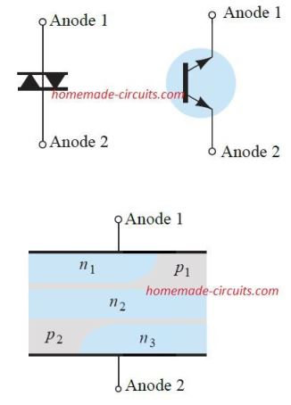 When the connected supply across the diac is positive on anode 1 with respect to anode 2, the relevant layers function as p1n2p2 and n3.
When the connected supply is positive on anode 2 with respect to anode 1, the functional layers are as p2n2p1 and n1.
When the connected supply across the diac is positive on anode 1 with respect to anode 2, the relevant layers function as p1n2p2 and n3.
When the connected supply is positive on anode 2 with respect to anode 1, the functional layers are as p2n2p1 and n1.
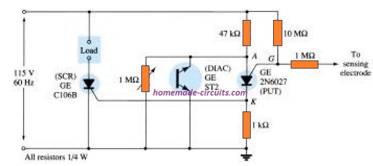 Here we can see that an SCR is incorporated in series with the load and the programmable unijunction transistor (PUT) which is joined with the sensing probe directly.
When a human body comes near to the sensing probe, causes an increase in the capacitance across the probe and the ground.
As per the characteristics of a silicon programmable UJT, it will fire when the voltage VA at its anode terminal exceeds its gate voltage by at least 0.7 V.
This causes a short circuit across the anode cathode of the device.
Depending on the setting of the 1M preset, the diac follows the input AC cycle and fires at a specified voltage level.
Due to this continues firing of the diac, the anode voltage VA of the UJT is never allowed to increase its gate potential VG which is always held at almost as high as the input AC.
And this situation keeps the programmable UJT switched OFF.
However, when a human body approaches the sensing probe, it lowers the gate potential VG of the UJT substantially, allowing the anode potential VA of the UJT of the UJT to go higher than VG.
This instantly causes the UJT to fire.
When this happens, the UJTs creates a short across its anode/cathode terminals, providing the necessary gate current for the SCR.
The SCR fires and switches ON the attached load, indicating the presence of a human proximity near the sensor probe.
Here we can see that an SCR is incorporated in series with the load and the programmable unijunction transistor (PUT) which is joined with the sensing probe directly.
When a human body comes near to the sensing probe, causes an increase in the capacitance across the probe and the ground.
As per the characteristics of a silicon programmable UJT, it will fire when the voltage VA at its anode terminal exceeds its gate voltage by at least 0.7 V.
This causes a short circuit across the anode cathode of the device.
Depending on the setting of the 1M preset, the diac follows the input AC cycle and fires at a specified voltage level.
Due to this continues firing of the diac, the anode voltage VA of the UJT is never allowed to increase its gate potential VG which is always held at almost as high as the input AC.
And this situation keeps the programmable UJT switched OFF.
However, when a human body approaches the sensing probe, it lowers the gate potential VG of the UJT substantially, allowing the anode potential VA of the UJT of the UJT to go higher than VG.
This instantly causes the UJT to fire.
When this happens, the UJTs creates a short across its anode/cathode terminals, providing the necessary gate current for the SCR.
The SCR fires and switches ON the attached load, indicating the presence of a human proximity near the sensor probe.
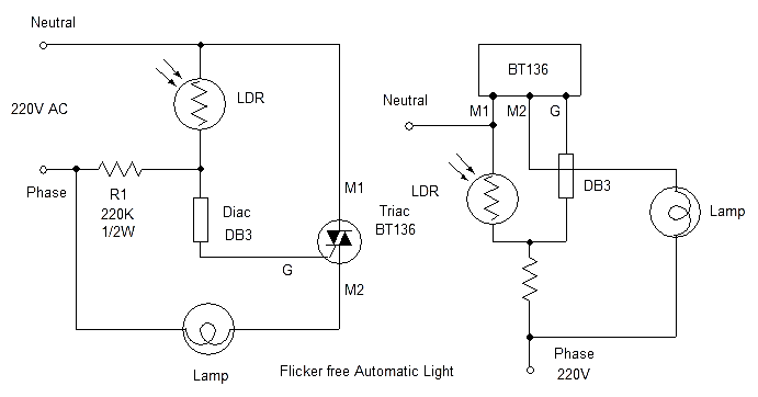 A simple automatic mast light circuit using an LDR, triac and a Diac can be see in the above drawing.
The working of this circuit is pretty simple, and the critical switching job is handled by the diac DB-3. When evening sets in, the light on the LDR starts falling, which causes the voltage at the junction of R1, DB-3 to gradually rise, due to the increasing resistance of the LDR.
When this voltage rises to the break over point of the diac, the diac fires and actuates the triac gate, which in turn switches ON the connected lamp.
During morning, the light on the LDR gradually increases, which causes the potential across the diac to diminish due to grounding of the R1/DB-3 junction potential.
And when the light is sufficiently bright, the LDR resistance causes the diac potential to drop to almost zero, switching off the triac gate current, and hence the lamp is also switched OFF.
The diac here ensures that the triac is switched without much flickering during the twilight transition.
Without the diac, the lamp would have flickered for many minutes before switching completely ON or OFF.
Thus the breakdown triggering feature of the diac is thoroughly exploited in favor of the automatic light design.
A simple automatic mast light circuit using an LDR, triac and a Diac can be see in the above drawing.
The working of this circuit is pretty simple, and the critical switching job is handled by the diac DB-3. When evening sets in, the light on the LDR starts falling, which causes the voltage at the junction of R1, DB-3 to gradually rise, due to the increasing resistance of the LDR.
When this voltage rises to the break over point of the diac, the diac fires and actuates the triac gate, which in turn switches ON the connected lamp.
During morning, the light on the LDR gradually increases, which causes the potential across the diac to diminish due to grounding of the R1/DB-3 junction potential.
And when the light is sufficiently bright, the LDR resistance causes the diac potential to drop to almost zero, switching off the triac gate current, and hence the lamp is also switched OFF.
The diac here ensures that the triac is switched without much flickering during the twilight transition.
Without the diac, the lamp would have flickered for many minutes before switching completely ON or OFF.
Thus the breakdown triggering feature of the diac is thoroughly exploited in favor of the automatic light design.
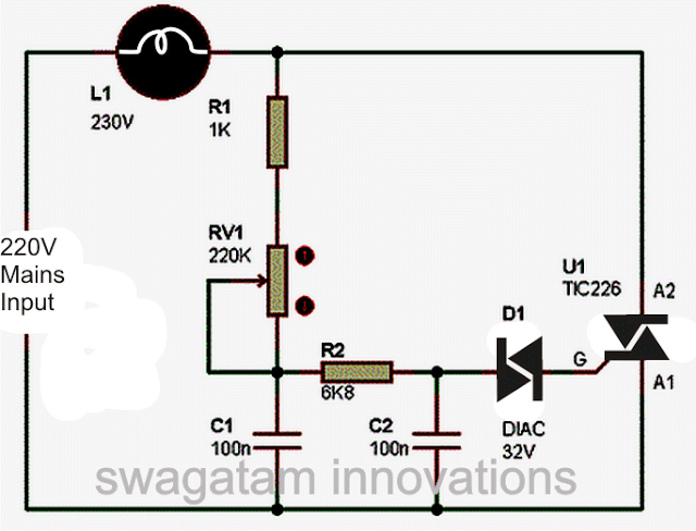 A light dimmer circuit is perhaps the most popular application using a triac diac combination.
For each cycle of the AC input the diac fires only when the potential across it reaches its breakdown voltage.
The time delay after which the diac fires decides for how much time the triac remains switched ON during each cycle of the phase.
This in turn decides the amount of current and illumination on the lamp.
The time delay in firing the diac is set by the shown 220 k pot adjustment, and the C1 value.
This RC time delay components determine the ON time of the triac through the diac firing which results in chopping of the AC phase over specific sections of the phase depending on the firing delay of the diac.
When the delay is longer, a narrower portion of the phase is allowed to switch the triac and trigger the lamp, causing lower brightness on the lamp.
For quicker time intervals, the triac is allowed to switch for longer periods of the AC phase, and thus the lamp also is switched for longer sections of the AC phase causing higher brightness on it.
A light dimmer circuit is perhaps the most popular application using a triac diac combination.
For each cycle of the AC input the diac fires only when the potential across it reaches its breakdown voltage.
The time delay after which the diac fires decides for how much time the triac remains switched ON during each cycle of the phase.
This in turn decides the amount of current and illumination on the lamp.
The time delay in firing the diac is set by the shown 220 k pot adjustment, and the C1 value.
This RC time delay components determine the ON time of the triac through the diac firing which results in chopping of the AC phase over specific sections of the phase depending on the firing delay of the diac.
When the delay is longer, a narrower portion of the phase is allowed to switch the triac and trigger the lamp, causing lower brightness on the lamp.
For quicker time intervals, the triac is allowed to switch for longer periods of the AC phase, and thus the lamp also is switched for longer sections of the AC phase causing higher brightness on it.
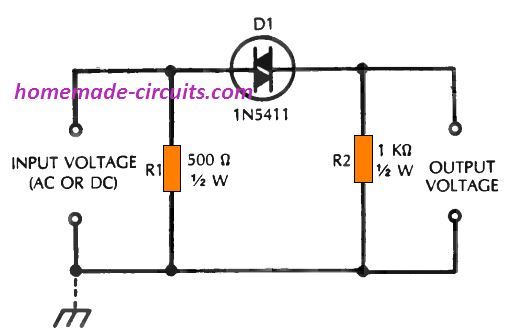 An voltage of around 35 volts dc or peak ac is applied which switches ON the diac into conduction, due to which a current of around 14 mA begins flowing through the output resistor, R2. Specific diacs may possibly turn on at voltages below 35 volts.
Using 14 mA switching current, the output voltage created across the 1k resistor gets to 14 volts.
In case the supply source includes an inside conductive path within the output circuit, resistor R1 could be ignored and eliminated.
While working with the circuit, try adjusting the supply voltage so that it gradually increases from zero while simultaneously check the output response.
When the supply reaches around 30 volts, you will see small or slight bit of output voltage, due to the extremely low leakage current from the device.
However, at roughly 35 volts, you will find the diac suddenly breaking down and a full output voltage quickly showing up across resistor R2. Now, start reducing the supply input, and observe that the output voltage correspondingly reduces, finally getting at zero when the input voltage is reduced to zero.
At zero volts, the diac is completely "shut off," and goes into a situation which requires it to be triggered again through the 35 volt amplitude level.
An voltage of around 35 volts dc or peak ac is applied which switches ON the diac into conduction, due to which a current of around 14 mA begins flowing through the output resistor, R2. Specific diacs may possibly turn on at voltages below 35 volts.
Using 14 mA switching current, the output voltage created across the 1k resistor gets to 14 volts.
In case the supply source includes an inside conductive path within the output circuit, resistor R1 could be ignored and eliminated.
While working with the circuit, try adjusting the supply voltage so that it gradually increases from zero while simultaneously check the output response.
When the supply reaches around 30 volts, you will see small or slight bit of output voltage, due to the extremely low leakage current from the device.
However, at roughly 35 volts, you will find the diac suddenly breaking down and a full output voltage quickly showing up across resistor R2. Now, start reducing the supply input, and observe that the output voltage correspondingly reduces, finally getting at zero when the input voltage is reduced to zero.
At zero volts, the diac is completely "shut off," and goes into a situation which requires it to be triggered again through the 35 volt amplitude level.
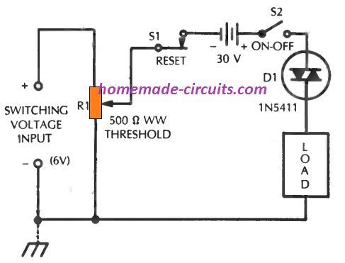 Figure above demonstrates a switching circuit featuring the theory of incremental voltage switching as explained above.
Within this set up, a 30 volt is supply is given to the 1N5411 diac (D1) (here this supply is shown as a battery source for convenience, nevertheless the 30 volts could be applied through any other constant regulated source dc).
With this voltage level, the diac is unable to turn ON, and no current runs via the connected external load.
However, when the potentimeter is gradually adjusted, the supply voltage slowly increases and finally the diac is turned ON, which enables the current to pass through the load and switch it ON.
Once the diac is switched ON, decreasing the supply voltage through the potentiometer has no effect on the diac.
However, after reducing the voltage through the potentiometer, the reset switch S1 could be used for toggling OFF the diac conduction and reset the circuit in the original switched Off condition.
The shown diac or DB-3 will be able to remain idle at around 30 V, and will not go through a self firing action.
That said, some diacs may require lower voltages than 30 V to keep them in the non-conducing condition.
In the same way specific diacs may require higher than 5 V for the incremental switch ON option.
The value of the potentiometer R1 should not be more than 1 k Ohms,, and should be wire wound type.
The above concept can be used for implementing latching action in low current applications through a simple two terminal diac device instead of depending on complex 3 terminal devices like SCRs.
Figure above demonstrates a switching circuit featuring the theory of incremental voltage switching as explained above.
Within this set up, a 30 volt is supply is given to the 1N5411 diac (D1) (here this supply is shown as a battery source for convenience, nevertheless the 30 volts could be applied through any other constant regulated source dc).
With this voltage level, the diac is unable to turn ON, and no current runs via the connected external load.
However, when the potentimeter is gradually adjusted, the supply voltage slowly increases and finally the diac is turned ON, which enables the current to pass through the load and switch it ON.
Once the diac is switched ON, decreasing the supply voltage through the potentiometer has no effect on the diac.
However, after reducing the voltage through the potentiometer, the reset switch S1 could be used for toggling OFF the diac conduction and reset the circuit in the original switched Off condition.
The shown diac or DB-3 will be able to remain idle at around 30 V, and will not go through a self firing action.
That said, some diacs may require lower voltages than 30 V to keep them in the non-conducing condition.
In the same way specific diacs may require higher than 5 V for the incremental switch ON option.
The value of the potentiometer R1 should not be more than 1 k Ohms,, and should be wire wound type.
The above concept can be used for implementing latching action in low current applications through a simple two terminal diac device instead of depending on complex 3 terminal devices like SCRs.
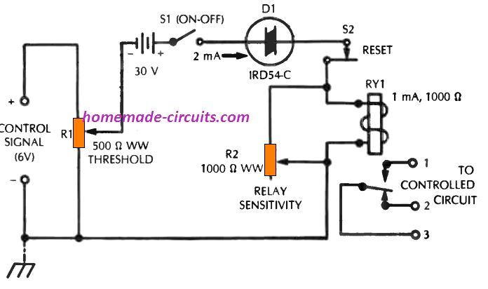 Figure shown above indicates the circuit of a dc relay which is designed to remain latched the moment it is powered through an input signal.
The design is as good as latching mechanical relay.
This circuit makes use of the concept explained in the previous paragraph.
Here also, the diac is held switched off at 30 volts, a voltage level that's typically small for a diac conduction.
However, as soon as a 6 V series potential is given to the diac, the latter begins pushing current which switches ON and latches the relay (the diac after that remains switched ON, even though the 6 volt control voltage no longer exists).
With R1 and R2 optimized correctly, the relay will switch ON efficiently in response to an applied control voltage.
After this the relay will remain latched even without the input voltage.
However, the circuit can be reset back to its previous position by pressing the indicated reset switch.
The relay has to be a low current type, may be with a coil resistance of 1 k.
Figure shown above indicates the circuit of a dc relay which is designed to remain latched the moment it is powered through an input signal.
The design is as good as latching mechanical relay.
This circuit makes use of the concept explained in the previous paragraph.
Here also, the diac is held switched off at 30 volts, a voltage level that's typically small for a diac conduction.
However, as soon as a 6 V series potential is given to the diac, the latter begins pushing current which switches ON and latches the relay (the diac after that remains switched ON, even though the 6 volt control voltage no longer exists).
With R1 and R2 optimized correctly, the relay will switch ON efficiently in response to an applied control voltage.
After this the relay will remain latched even without the input voltage.
However, the circuit can be reset back to its previous position by pressing the indicated reset switch.
The relay has to be a low current type, may be with a coil resistance of 1 k.
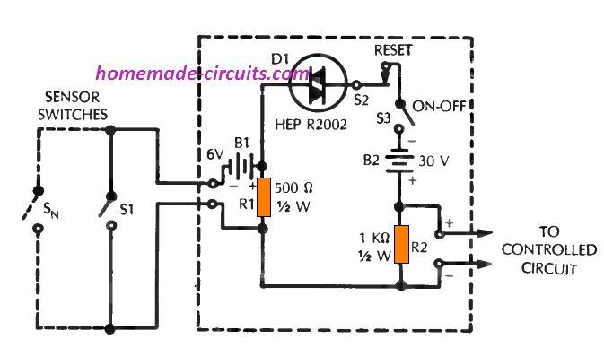 Here, a HEP R2002 diac works like a switching device.
In this particular set up, the diac stays in the stand-by mode at 30 volts supply through B2.
But, the moment switch S1 is toggled, that could be a "sensor" on a door or window, contributes 6 volts (from B1), to the existing 30 V bias, causing the resultant 35 volts to fire the diac and generate around 1 V output across R2.
Here, a HEP R2002 diac works like a switching device.
In this particular set up, the diac stays in the stand-by mode at 30 volts supply through B2.
But, the moment switch S1 is toggled, that could be a "sensor" on a door or window, contributes 6 volts (from B1), to the existing 30 V bias, causing the resultant 35 volts to fire the diac and generate around 1 V output across R2.
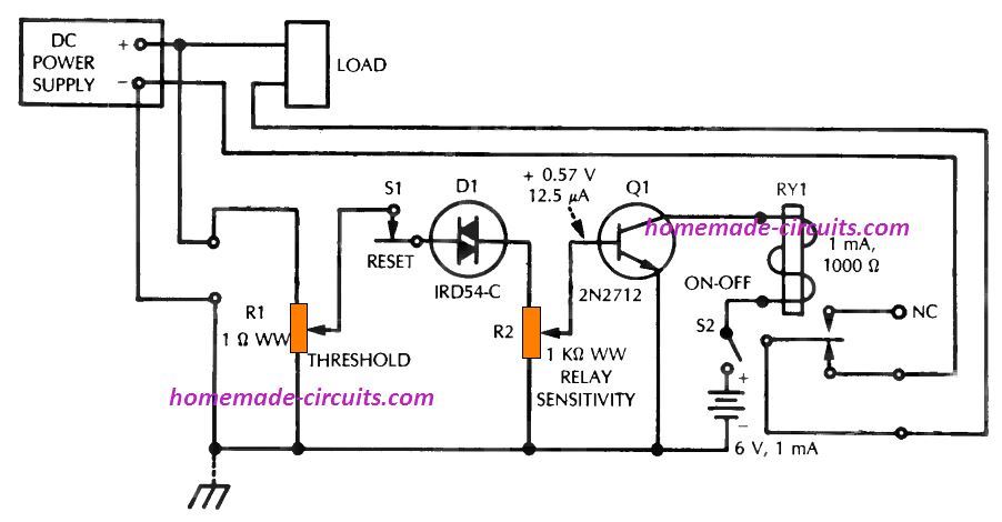 Figure above demonstrates a circuit that will instantly switch off a load when the dc supply voltage surpasses a fixed level.
The unit then stays turned off until the voltage is lowered and the circuit is reset.
In this particular set up, the diac (D1) is normally switched OFF, and transistor current is not high enough to trigger the relay (RY1).
When the supply input goes beyond a specified level as set by the potentiometer R1, the diac fires, and the DC from the diac output reaches the transistor base.
The transistor now switches ON through potentiometer R2 and activates the relay.
The relay now disconnects the load from the input supply, preventing any damage to the system due to overload.
The diac after that continues to be switched ON keeping the relay turned ON until the circuit is reset switch, by opening the S1, momentarily.
In order to adjust the circuit in the beginning, fine-tune potentiometers R1 and R2 to ensure that the relay just clicks ON once the input voltage actually reaches the desired diac firing threshold.
The relay after that must keep activated until the voltage reduces back to its normal level and the reset switch is momentarily opened.
If the circuit works properly, the diac "firing" voltage input must be around 35 volts (specific diacs could activate with a smaller voltage, although this is often corrected by adjusting of potentiometer R2), as well as the dc voltage at the transistor base must be roughly 0.57 volt (at around 12.5 mA).
The relay is a 1k coil resistance.
Figure above demonstrates a circuit that will instantly switch off a load when the dc supply voltage surpasses a fixed level.
The unit then stays turned off until the voltage is lowered and the circuit is reset.
In this particular set up, the diac (D1) is normally switched OFF, and transistor current is not high enough to trigger the relay (RY1).
When the supply input goes beyond a specified level as set by the potentiometer R1, the diac fires, and the DC from the diac output reaches the transistor base.
The transistor now switches ON through potentiometer R2 and activates the relay.
The relay now disconnects the load from the input supply, preventing any damage to the system due to overload.
The diac after that continues to be switched ON keeping the relay turned ON until the circuit is reset switch, by opening the S1, momentarily.
In order to adjust the circuit in the beginning, fine-tune potentiometers R1 and R2 to ensure that the relay just clicks ON once the input voltage actually reaches the desired diac firing threshold.
The relay after that must keep activated until the voltage reduces back to its normal level and the reset switch is momentarily opened.
If the circuit works properly, the diac "firing" voltage input must be around 35 volts (specific diacs could activate with a smaller voltage, although this is often corrected by adjusting of potentiometer R2), as well as the dc voltage at the transistor base must be roughly 0.57 volt (at around 12.5 mA).
The relay is a 1k coil resistance.
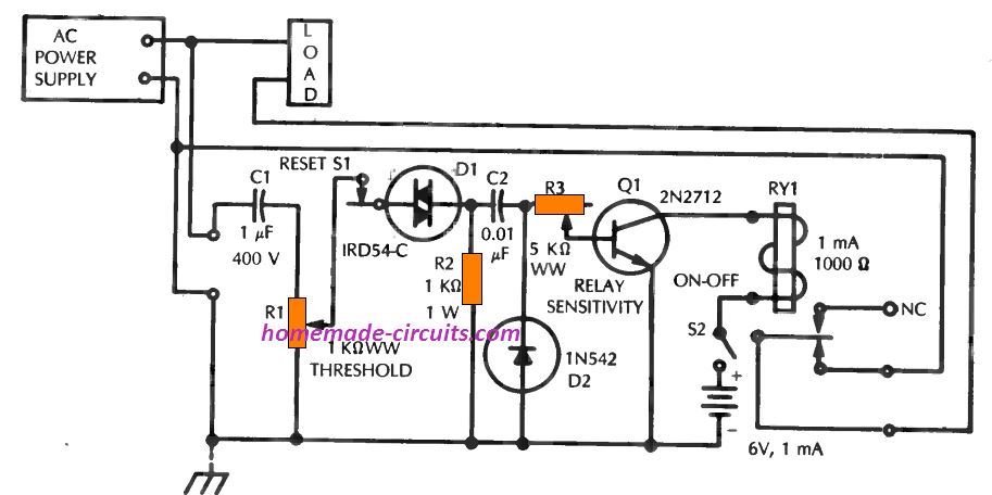 The circuit diagram above demonstrates the circuit of an ac overload circuit breaker.
This idea works the identical way as the dc set up explained in the earlier {part.
The ac circuit {differs|varies} from the dc version due to the presence of the capacitors C1 and C2 and diode rectifier D2.
The circuit diagram above demonstrates the circuit of an ac overload circuit breaker.
This idea works the identical way as the dc set up explained in the earlier {part.
The ac circuit {differs|varies} from the dc version due to the presence of the capacitors C1 and C2 and diode rectifier D2.
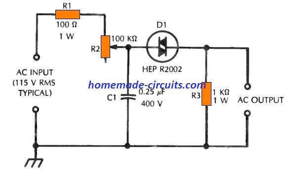 Figure above displays typical diac trigger circuit.
This set up fundamentally regulates the firing angle of the diac, and this is achieved by manipulating the phase control network built around the parts R1 R2 and C1.
The values of the resistance and capacitance provided here are as reference values only.
For a specific frequency (generally the AC mains line frequency), R2 is tweaked in order that the diac break-over voltage is attained at an instant that corresponds to the preferred point in the ac half cycle where the diac is required to switch on and provide the output pulse.
The diac following this may keep repeating this activity throughout each +/- AC half cycle.
Eventually, the phase is decided not just by R1 R2 and C1, but also through the impedance of the ac source and the impedance of the circuit which the diac set up activates.
For the majority of applications, this diac circuit project will likely be beneficial to analyze the phase of the diac resistance and capacitance, to know efficiency of the circuit.
The following Table below, for instance, illustrates the phase angles which may correspond to different settings of the resistance in accordance with the 0.25 ��F capacitance in the figure above.
Figure above displays typical diac trigger circuit.
This set up fundamentally regulates the firing angle of the diac, and this is achieved by manipulating the phase control network built around the parts R1 R2 and C1.
The values of the resistance and capacitance provided here are as reference values only.
For a specific frequency (generally the AC mains line frequency), R2 is tweaked in order that the diac break-over voltage is attained at an instant that corresponds to the preferred point in the ac half cycle where the diac is required to switch on and provide the output pulse.
The diac following this may keep repeating this activity throughout each +/- AC half cycle.
Eventually, the phase is decided not just by R1 R2 and C1, but also through the impedance of the ac source and the impedance of the circuit which the diac set up activates.
For the majority of applications, this diac circuit project will likely be beneficial to analyze the phase of the diac resistance and capacitance, to know efficiency of the circuit.
The following Table below, for instance, illustrates the phase angles which may correspond to different settings of the resistance in accordance with the 0.25 ��F capacitance in the figure above.
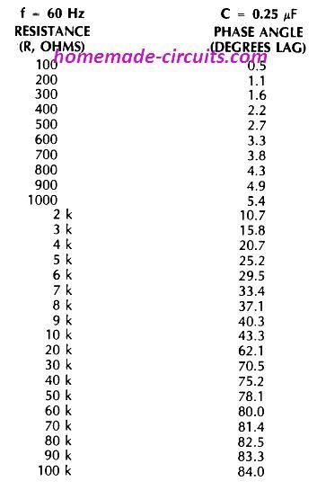 The information are shown intended for 60 Hz.
Remember, as indicated in the table as the resistance is decreased, the trigger pulse keeps appearing in earlier positions in the supply voltage cycle, which causes the diac to "fire" earlier in the cycle and to remain switched ON that much longer.
Since the RC circuit includes series resistance and shunt capacitance, the phase is, naturally, lagging that signifies that the trigger pulse comes after the supply voltage cycle within time cycle.
The information are shown intended for 60 Hz.
Remember, as indicated in the table as the resistance is decreased, the trigger pulse keeps appearing in earlier positions in the supply voltage cycle, which causes the diac to "fire" earlier in the cycle and to remain switched ON that much longer.
Since the RC circuit includes series resistance and shunt capacitance, the phase is, naturally, lagging that signifies that the trigger pulse comes after the supply voltage cycle within time cycle.
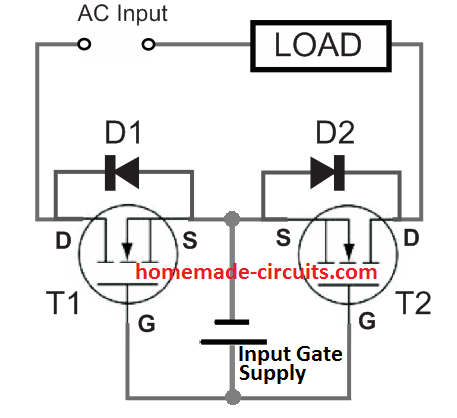 In the above shown basic SSR design, we can see a couple of appropriately rated MOSFETs T1 and T2 connected back to back with their source and gate terminals joined in common with each other.
D1 and D2 are the internal body diodes of the respective MOSFETs, which may be reinforced with external parallel diodes, if required.
An input DC supply can also be seen attached across the common gate/source terminals of the two MOSFETs.
This supply is used for triggering the MOSFETs ON or for enabling permanent switch ON for the MOSFETs while the SSR unit is operational.
The AC supply which could be up to grid mains level and the load are connected in series across the two drains of the MOSFETs.
In the above shown basic SSR design, we can see a couple of appropriately rated MOSFETs T1 and T2 connected back to back with their source and gate terminals joined in common with each other.
D1 and D2 are the internal body diodes of the respective MOSFETs, which may be reinforced with external parallel diodes, if required.
An input DC supply can also be seen attached across the common gate/source terminals of the two MOSFETs.
This supply is used for triggering the MOSFETs ON or for enabling permanent switch ON for the MOSFETs while the SSR unit is operational.
The AC supply which could be up to grid mains level and the load are connected in series across the two drains of the MOSFETs.
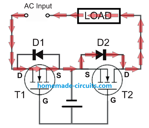
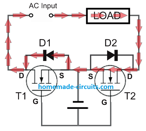 With the above setup, due to the input gate supply connected, T1 and T2 are both in the switched ON position.
When the load side AC input is switch ON, the left diagram shows how the positive half cycle conducts through the relevant MOSFET/diode pair (T1, D2) and the right side diagram shows how the negative AC cycle conducts through the other complementing MOSFET/diode pair (T2, D1).
In the left diagram we find one of the AC half cycles goes through T1, and D2 (T2 being reverse biased), and finally completes the cycle via the load.
The right side diagram shows how the other half cycle completes the circuit in the opposite direction by conducting through the load, T2, D1 (T1 being reversed biased in this case).
In this way the two MOSFETs T1, T2 along with their respective body diodes D1, D2, allow both the half cycles of the AC to conduct, powering the AC load perfectly, and accomplishing the SSR role efficiently.
With the above setup, due to the input gate supply connected, T1 and T2 are both in the switched ON position.
When the load side AC input is switch ON, the left diagram shows how the positive half cycle conducts through the relevant MOSFET/diode pair (T1, D2) and the right side diagram shows how the negative AC cycle conducts through the other complementing MOSFET/diode pair (T2, D1).
In the left diagram we find one of the AC half cycles goes through T1, and D2 (T2 being reverse biased), and finally completes the cycle via the load.
The right side diagram shows how the other half cycle completes the circuit in the opposite direction by conducting through the load, T2, D1 (T1 being reversed biased in this case).
In this way the two MOSFETs T1, T2 along with their respective body diodes D1, D2, allow both the half cycles of the AC to conduct, powering the AC load perfectly, and accomplishing the SSR role efficiently.
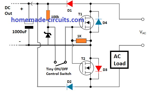 The above SSR circuit is configured exactly in the same way as discussed in the earlier basic design.
However, here we find two additional diodes D1, and D2, along with the MOSFET body diodes D3, D4.
The diodes D1, D2 are introduced for a specific purpose such that it forms a bridge rectifier in conjunction with the D3, D4 MOSFET body diodes.
The tiny on OFF switch could be used for turning the SSR ON/OFF.
This switch could be a reed switch or any low current switch.
For high speed switching you can replace the switch with a opto-coupler as shown below.
The above SSR circuit is configured exactly in the same way as discussed in the earlier basic design.
However, here we find two additional diodes D1, and D2, along with the MOSFET body diodes D3, D4.
The diodes D1, D2 are introduced for a specific purpose such that it forms a bridge rectifier in conjunction with the D3, D4 MOSFET body diodes.
The tiny on OFF switch could be used for turning the SSR ON/OFF.
This switch could be a reed switch or any low current switch.
For high speed switching you can replace the switch with a opto-coupler as shown below.
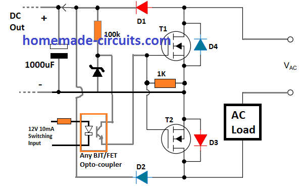 In essence the circuit now fulfills 3 requirements.
It powers the AC load through the MOSFET/Diode SSR configuration.
The bridge rectifier formed by D1---D4 simultaneously converts the load AC input into rectified and filtered DC, and this DC is used for biasing the gates of the MOSFETs.
This allows the MOSFETs to get appropriately turned ON through the load AC itself, without depending on any external DC.
The rectified DC is further terminated as an auxiliary DC output which could be used for powering any suitable external load.
In essence the circuit now fulfills 3 requirements.
It powers the AC load through the MOSFET/Diode SSR configuration.
The bridge rectifier formed by D1---D4 simultaneously converts the load AC input into rectified and filtered DC, and this DC is used for biasing the gates of the MOSFETs.
This allows the MOSFETs to get appropriately turned ON through the load AC itself, without depending on any external DC.
The rectified DC is further terminated as an auxiliary DC output which could be used for powering any suitable external load.
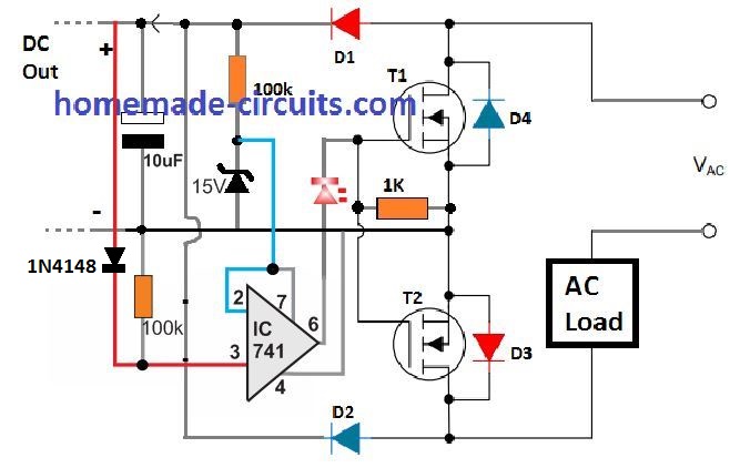 The objective here is, to make sure that the MOSFETs do not conduct until an optimum 15 V is developed across the zener diode, or across the gate/source of the MOSFETs
The op amp ensures that its output fires only once the DC line crosses the 15 V zener diode reference threshold, which allows the MOSFET gates to get an optimal 15 V DC for the conduction.
The red line associated with pin3 of IC 741 can be toggled through an opto coupler for the required switching from an external source.
How it Works: As we can see, the inverting input of the op amp is tied with the 15V zener, which forms a reference level for the op amp pin2. Pin3 which is the non-inverting input of the op amp is connected with the positive line.
This configuration ensures that the output pin6 of the op amp produces a 15V supply only once its pin3 voltage reaches above 15 V mark The action ensures that the MOSFETs conduct only through a valid 15 V optimal gate voltage, enabling a proper working of the SSR.
The objective here is, to make sure that the MOSFETs do not conduct until an optimum 15 V is developed across the zener diode, or across the gate/source of the MOSFETs
The op amp ensures that its output fires only once the DC line crosses the 15 V zener diode reference threshold, which allows the MOSFET gates to get an optimal 15 V DC for the conduction.
The red line associated with pin3 of IC 741 can be toggled through an opto coupler for the required switching from an external source.
How it Works: As we can see, the inverting input of the op amp is tied with the 15V zener, which forms a reference level for the op amp pin2. Pin3 which is the non-inverting input of the op amp is connected with the positive line.
This configuration ensures that the output pin6 of the op amp produces a 15V supply only once its pin3 voltage reaches above 15 V mark The action ensures that the MOSFETs conduct only through a valid 15 V optimal gate voltage, enabling a proper working of the SSR.
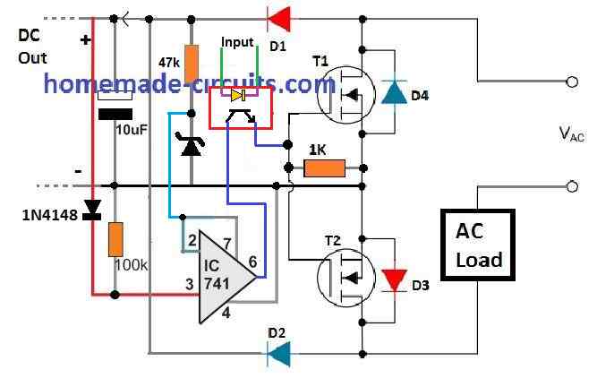
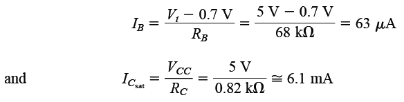 If we test the the equation 2 with these results we get:
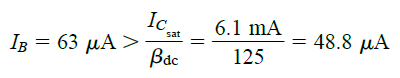 This appears to be perfectly satisfying the required condition.
No doubt, any value of IB which is higher than 60 uA will be allowed to enter across Q-point over the load line situated extremely closely to the vertical axis.
Now, eferring to the BJT network shown in the first diagram, while Vi = 0 V, IB = 0 uA, and asuming IC = ICEO = 0 mA, the volatge drop occurring across RC will be as per the formula:
VRC = ICRC = 0 V.
This gives us VC = +5 V for the first diagram above.
In addition to computer logoc switching applications, this BJT configuration can be also implemented like a switch using the same extreme points of the load line.
When saturation takes place, the current IC tends to get quite high, which corresponding drops the voltage VCE to a lowest point.
This gives rise to a resistance level across the two terminals as depicted in the following figure and calculated using the following formula:
R(sat) = VCE(sat) / IC(sat) as indicated in the following figure.
This appears to be perfectly satisfying the required condition.
No doubt, any value of IB which is higher than 60 uA will be allowed to enter across Q-point over the load line situated extremely closely to the vertical axis.
Now, eferring to the BJT network shown in the first diagram, while Vi = 0 V, IB = 0 uA, and asuming IC = ICEO = 0 mA, the volatge drop occurring across RC will be as per the formula:
VRC = ICRC = 0 V.
This gives us VC = +5 V for the first diagram above.
In addition to computer logoc switching applications, this BJT configuration can be also implemented like a switch using the same extreme points of the load line.
When saturation takes place, the current IC tends to get quite high, which corresponding drops the voltage VCE to a lowest point.
This gives rise to a resistance level across the two terminals as depicted in the following figure and calculated using the following formula:
R(sat) = VCE(sat) / IC(sat) as indicated in the following figure.
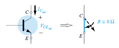 If we assume a typical average value for the VCE(sat) such as 0.15 V in the above formula, we get:
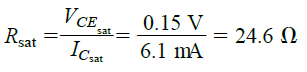 This resistance value across the collector emitter terminals looks quite small when compared to a series resistance in kilo Ohms at the collector terminals of the BJT.
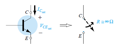 Now, when the input Vi = 0 V, the BJT switching will be cut off causing the resistance across the collector emitter to be:
R(cutoff) = Vcc / ICEO = 5 V / 0 mA = �� ��
This gives rise to an open circuit kind of situation across the collector emitter terminals.
If we consider a typical value 10 uA for the ICEO, the value of the cut off resistance will be as given below:
Rcutoff = Vcc / ICEO = 5 V / 10 uA = 500 k ��
This value looks significantly large and an equivalent to an open circuit for most BJT configuration as a switch.
Now, when the input Vi = 0 V, the BJT switching will be cut off causing the resistance across the collector emitter to be:
R(cutoff) = Vcc / ICEO = 5 V / 0 mA = �� ��
This gives rise to an open circuit kind of situation across the collector emitter terminals.
If we consider a typical value 10 uA for the ICEO, the value of the cut off resistance will be as given below:
Rcutoff = Vcc / ICEO = 5 V / 10 uA = 500 k ��
This value looks significantly large and an equivalent to an open circuit for most BJT configuration as a switch.
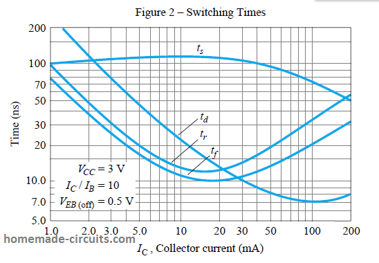 The effect of the time periods on the collector speed response is defined by the collector current response as shown below:
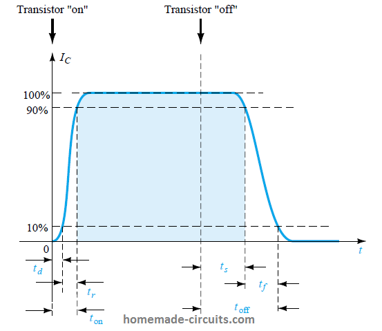 The total time needed for the transistor to switch from the ��off�� to the ��on�� state is symbolized as t(on) and can be established by the formula:
t(on) = tr + td
Here td identifies the delay happening while the input switching signal is changing state and the transistor output is responding to the change.
The time tr indicates the final switching delay from 10% to 90%.
The total time taken by a bJt from a turned ON state to turned OFF state is indicated as t(off), and expressed by the formula:
t(off) = ts + tf
ts determines the storage time, while tf identifies the fall time from 90% to 10% of the original value.
Refferrng to the above graph, for a general purpose BJT, if the collector current Ic = 10 mA, we can see that:
ts = 120 ns, td = 25 ns, tr = 13 ns, tf = 12 ns
which means t(on) = tr + td = 13 ns + 25 ns = 38 ns
t(off) = ts + tf = 120 ns + 12 ns = 132 ns
The total time needed for the transistor to switch from the ��off�� to the ��on�� state is symbolized as t(on) and can be established by the formula:
t(on) = tr + td
Here td identifies the delay happening while the input switching signal is changing state and the transistor output is responding to the change.
The time tr indicates the final switching delay from 10% to 90%.
The total time taken by a bJt from a turned ON state to turned OFF state is indicated as t(off), and expressed by the formula:
t(off) = ts + tf
ts determines the storage time, while tf identifies the fall time from 90% to 10% of the original value.
Refferrng to the above graph, for a general purpose BJT, if the collector current Ic = 10 mA, we can see that:
ts = 120 ns, td = 25 ns, tr = 13 ns, tf = 12 ns
which means t(on) = tr + td = 13 ns + 25 ns = 38 ns
t(off) = ts + tf = 120 ns + 12 ns = 132 ns
 However, suppose we have the same diode with its outer opaque cover scraped of or removed and connected with a reverse bias supply.
This will expose the PN junction of the diode to light, and there will be an instant flow of current through it, in response to the incident light.
This may result in a current as much as 1 mA through the diode, causing a rising voltage to develop across R1.
The photodiode in the above figure can be also connected on the ground side as shown below.
This will produce a opposite response, resulting in a decreasing voltage across R1, when the photodiode is illuminated with external light.
However, suppose we have the same diode with its outer opaque cover scraped of or removed and connected with a reverse bias supply.
This will expose the PN junction of the diode to light, and there will be an instant flow of current through it, in response to the incident light.
This may result in a current as much as 1 mA through the diode, causing a rising voltage to develop across R1.
The photodiode in the above figure can be also connected on the ground side as shown below.
This will produce a opposite response, resulting in a decreasing voltage across R1, when the photodiode is illuminated with external light.
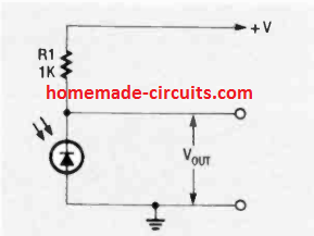 The working of all P-N junction based devices is similar and will exhibit photo-conductivity when exposed to light.
The schematic symbol of a photodiode can be see below.
The working of all P-N junction based devices is similar and will exhibit photo-conductivity when exposed to light.
The schematic symbol of a photodiode can be see below.
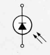 Compared to cadmium-sulphide or cadmium-selenide photocells like LDRs, photodiodes are generally less sensitive to light, but their response to light changes is much faster.
Due to this reason, photocells like LDRs are generally used in applications that involve visible light, and where the response time does not need to be quick.
On the other hand, photodiodes are specifically selected in applications that require fast detection of lights mostly in the infrared region.
You will find photodiodes in systems such as infrared remote control circuits, beam interruption relays and intruder alarm circuits.
There's another variant of photodiode which uses lead-sulfide (PbS) and there working characteristic is quite similar to LDRs but are designed to respond only to the infrared range lights.
Compared to cadmium-sulphide or cadmium-selenide photocells like LDRs, photodiodes are generally less sensitive to light, but their response to light changes is much faster.
Due to this reason, photocells like LDRs are generally used in applications that involve visible light, and where the response time does not need to be quick.
On the other hand, photodiodes are specifically selected in applications that require fast detection of lights mostly in the infrared region.
You will find photodiodes in systems such as infrared remote control circuits, beam interruption relays and intruder alarm circuits.
There's another variant of photodiode which uses lead-sulfide (PbS) and there working characteristic is quite similar to LDRs but are designed to respond only to the infrared range lights.
 Image Credit: https://commons.wikimedia.org/wiki/File:GE_1N3716_tunnel_diode.jpg
 Therefore, when the diode is powered within the shaded area of its IF-UF curve, the forward current comes down as the voltage goes up.
The resistance of the diode is without any doubts negative, and normally presented as -Rd.
The design presented in this article takes the advantage of the above quality of tunnel diodes by implementing a set of serially connected tunnel diode devices to charge a battery through solar heat (not solar panel).
As observed in Figure below, seven or more Gallium-Indium Antimonide (GISp) tunnel diodes are hooked up in series and clamped over on a big heatsink, which helps prevent dissipation of their power (tunnel diodes get cooler as UF goes higher or increased).
Therefore, when the diode is powered within the shaded area of its IF-UF curve, the forward current comes down as the voltage goes up.
The resistance of the diode is without any doubts negative, and normally presented as -Rd.
The design presented in this article takes the advantage of the above quality of tunnel diodes by implementing a set of serially connected tunnel diode devices to charge a battery through solar heat (not solar panel).
As observed in Figure below, seven or more Gallium-Indium Antimonide (GISp) tunnel diodes are hooked up in series and clamped over on a big heatsink, which helps prevent dissipation of their power (tunnel diodes get cooler as UF goes higher or increased).
 Heatsink is used to enable an effective accumulation of solar heat, or any other form of heat that may be applied, whose energy is required to be transformed into a charge current for charging the proposed Ni-Cd battery.
 Observe that the meter should be specified to indicate the polarity of the current, because it could very well happen that a specific diode has a really excessive IP:Iv ratio (tunnel slope) causing the battery to unexpectedly charged on implementing a small forward bias.
The analysis has to be performed at an atmospheric temperature below 7��C (try a cleaned out freezer), and note down the UF-IF curve for every single diode by meticulously increasing the forward bias through the potentiometer, and documenting the resulting magnitudes of IF, as displayed on the meter reading.
Next, bring an FM radio close by to make certain that the diode which are being tested are not oscillating at 94.67284 MHz (Freq , for GISp at doping level 10-7).
If you find this happening , the specific diode may be unsuitable for the present application.
Determine the range of OF that guarantees -Rd for just about all diodes.
Based on the manufacturing threshold of the diodes in the available lot, this range could be as minimal as, say, 180 to 230 mV.
Observe that the meter should be specified to indicate the polarity of the current, because it could very well happen that a specific diode has a really excessive IP:Iv ratio (tunnel slope) causing the battery to unexpectedly charged on implementing a small forward bias.
The analysis has to be performed at an atmospheric temperature below 7��C (try a cleaned out freezer), and note down the UF-IF curve for every single diode by meticulously increasing the forward bias through the potentiometer, and documenting the resulting magnitudes of IF, as displayed on the meter reading.
Next, bring an FM radio close by to make certain that the diode which are being tested are not oscillating at 94.67284 MHz (Freq , for GISp at doping level 10-7).
If you find this happening , the specific diode may be unsuitable for the present application.
Determine the range of OF that guarantees -Rd for just about all diodes.
Based on the manufacturing threshold of the diodes in the available lot, this range could be as minimal as, say, 180 to 230 mV.
 The way a varactor diode operates depends on the existing capacitance over the p-n junction of the diode while it's in a reversed biased mode.
In this condition we find a region of uncovered charges being established across the p-n sides of the junction, which together result in a depletion region across the junction.
This depletion region establishes the depletion width in the device, symbolized as Wd.
The transition in the capacitance due to the above explained isolated uncovered charges, across the p-n junction can be determined using the formula:
CT = ��.
A/Wd
where �� is the permittivity of the semiconductor materials, A is the p-n junction area, and Wd is the depletion width.
The way a varactor diode operates depends on the existing capacitance over the p-n junction of the diode while it's in a reversed biased mode.
In this condition we find a region of uncovered charges being established across the p-n sides of the junction, which together result in a depletion region across the junction.
This depletion region establishes the depletion width in the device, symbolized as Wd.
The transition in the capacitance due to the above explained isolated uncovered charges, across the p-n junction can be determined using the formula:
CT = ��.
A/Wd
where �� is the permittivity of the semiconductor materials, A is the p-n junction area, and Wd is the depletion width.
 We can see the steep initial drop in CT in response to the increase reverse bias potential.
Normally, the range for the applied reverse bias voltage VR for a variable voltage capacitance diode is restricted to 20 V.
With regard to the applied reverse bias voltage, the transition capacitance can be approximated using the formula:
CT = K / (VT + VR)n
In this formula, K is a constant as determined by the type of semiconductor material used and its constructional layout.
VT is the knee potential, as described below:
We can see the steep initial drop in CT in response to the increase reverse bias potential.
Normally, the range for the applied reverse bias voltage VR for a variable voltage capacitance diode is restricted to 20 V.
With regard to the applied reverse bias voltage, the transition capacitance can be approximated using the formula:
CT = K / (VT + VR)n
In this formula, K is a constant as determined by the type of semiconductor material used and its constructional layout.
VT is the knee potential, as described below:
 VR is the amount of reverse bias potential applied on the device.
n can have the value 1/2 for varicap diodes using alloy junction, and 1/3 for diodes using diffused junctions.
In the absence of a biasing voltage or at a zero voltage biasing, the capacitance C(0) as the function of VR can be expressed through the following formula.
CT(VR) = C(0) / (1 + |VR/VT|)n
VR is the amount of reverse bias potential applied on the device.
n can have the value 1/2 for varicap diodes using alloy junction, and 1/3 for diodes using diffused junctions.
In the absence of a biasing voltage or at a zero voltage biasing, the capacitance C(0) as the function of VR can be expressed through the following formula.
CT(VR) = C(0) / (1 + |VR/VT|)n
 The right side figure provides an approximate simulation circuit for a varicap diode.
Being a diode and in the reverse biased region, the resistance in the equivalent circuit RR is shown significantly large (around 1M Ohms), while the geometric resistance value Rs is quite small.
The value of CT may vary between 2 and 100 pF depending on the type of varicap used.
In order to make sure that the value RR is sufficiently large, so that the leakage current can be minimum, a silicon material is normally selected for a varicap diode.
Since a varicap diode is supposed to be specifically used in extremely high frequency applications, the inductance LS cannot be ignored even though it may look small, in nanohenries.
The effect of this small looking inductance can be a quite significant, and can be proved through the following reactance calculation.
XL = 2��fL, Let's imagine, the frequency to be at 10 GHz, and LS = 1 nH, will generate in an XLS = 2��fL = (6.28)(1010 Hz)( 10-9 F) = 62.8 Ohms.
This looks too big, and no doubt this is why varicap diodes are specified with a strict frequency limit.
If we suppose the frequency range to be appropriate, and the values of RS, XLS to be low compared to the other series elements, the above indicated equivalent circuit could be simply replaced with a variable capacitor.
The right side figure provides an approximate simulation circuit for a varicap diode.
Being a diode and in the reverse biased region, the resistance in the equivalent circuit RR is shown significantly large (around 1M Ohms), while the geometric resistance value Rs is quite small.
The value of CT may vary between 2 and 100 pF depending on the type of varicap used.
In order to make sure that the value RR is sufficiently large, so that the leakage current can be minimum, a silicon material is normally selected for a varicap diode.
Since a varicap diode is supposed to be specifically used in extremely high frequency applications, the inductance LS cannot be ignored even though it may look small, in nanohenries.
The effect of this small looking inductance can be a quite significant, and can be proved through the following reactance calculation.
XL = 2��fL, Let's imagine, the frequency to be at 10 GHz, and LS = 1 nH, will generate in an XLS = 2��fL = (6.28)(1010 Hz)( 10-9 F) = 62.8 Ohms.
This looks too big, and no doubt this is why varicap diodes are specified with a strict frequency limit.
If we suppose the frequency range to be appropriate, and the values of RS, XLS to be low compared to the other series elements, the above indicated equivalent circuit could be simply replaced with a variable capacitor.
 The ratio of C3/C25 in the above figure, demonstrates the ratio of the capacitance level when the diode is applied with a reverse bias potential between 3 to 25 V.
The ratio helps us to get a quick reference regarding the level of change in the capacitance with respect to the applied reverse bias potential.
The figure of Merit Q provides the range of consideration for implementing the device for an application, and it is also a rate of the ratio of energy stored by the capacitive device per cycle to the energy lost or dissipated per cycle.
Since the loss of energy is mostly considered as a negative attribute, higher the relative value of the ratio, the better.
Another aspect in the datasheet is the resonant frequency of a varicap diode.
And this is determined by the formula:
fo = 1/2�С�LC
This factor decides the application range of the varicap diode.
The ratio of C3/C25 in the above figure, demonstrates the ratio of the capacitance level when the diode is applied with a reverse bias potential between 3 to 25 V.
The ratio helps us to get a quick reference regarding the level of change in the capacitance with respect to the applied reverse bias potential.
The figure of Merit Q provides the range of consideration for implementing the device for an application, and it is also a rate of the ratio of energy stored by the capacitive device per cycle to the energy lost or dissipated per cycle.
Since the loss of energy is mostly considered as a negative attribute, higher the relative value of the ratio, the better.
Another aspect in the datasheet is the resonant frequency of a varicap diode.
And this is determined by the formula:
fo = 1/2�С�LC
This factor decides the application range of the varicap diode.
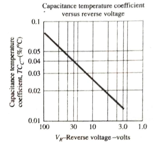 Referring to the above graph, the capacitance temperature coefficient of a varicap diode may be evaluated using the following formula:
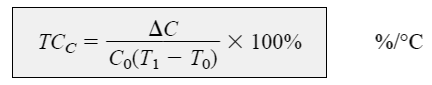 where ��C signifies the variations in the capacitance of the device due to change in temperature represented by (T1 - T0), for a specific reverse bias potential.
In the above datasheet for example, it shows C0 = 29 pF with VR = 3 V and T0 = 25 degrees Celsius.
Using the above data we can evaluate the change in the capacitance of the varicap diode, simply by substituting the new temperatures T1 value and the TCC from the graph (0.013).
Having the new VR, the TCC value can be expected to vary accordingly.
Referring back to the datasheet, we find that the maximum frequency attained will be 600 MHz.
Using this frequency value, the reactance XL of the varicap can be calculated as:
XL = 2��fL = (6.28)(600 x 1010 Hz)(2.5 x 10⁻⁹ F) = 9.42 Ohms
The result is a magnitude which is relatively small and it's acceptable to ignore it.
where ��C signifies the variations in the capacitance of the device due to change in temperature represented by (T1 - T0), for a specific reverse bias potential.
In the above datasheet for example, it shows C0 = 29 pF with VR = 3 V and T0 = 25 degrees Celsius.
Using the above data we can evaluate the change in the capacitance of the varicap diode, simply by substituting the new temperatures T1 value and the TCC from the graph (0.013).
Having the new VR, the TCC value can be expected to vary accordingly.
Referring back to the datasheet, we find that the maximum frequency attained will be 600 MHz.
Using this frequency value, the reactance XL of the varicap can be calculated as:
XL = 2��fL = (6.28)(600 x 1010 Hz)(2.5 x 10⁻⁹ F) = 9.42 Ohms
The result is a magnitude which is relatively small and it's acceptable to ignore it.
 The circuit consists of a combination of L-C tank circuits, whose resonant frequency is determined by:
fp = 1/2�С�LC'T (a high-Q system) having a C'T level = CT + Cc, established by the applied reverse-bias potential VDD.
The coupling capacitor CC ensures the required protection against the shorting tendency of L2 the applied biasing voltage.
The intended frequencies of the tuned circuit are subsequently allowed to move to the high-input impedance amplifier for the further amplification.
The circuit consists of a combination of L-C tank circuits, whose resonant frequency is determined by:
fp = 1/2�С�LC'T (a high-Q system) having a C'T level = CT + Cc, established by the applied reverse-bias potential VDD.
The coupling capacitor CC ensures the required protection against the shorting tendency of L2 the applied biasing voltage.
The intended frequencies of the tuned circuit are subsequently allowed to move to the high-input impedance amplifier for the further amplification.
 This type of circuit in which a single rectifier diode is applied with a time-varying sinusoidal AC signal input to generate a DC output having a value half of the input is called a half wave rectifier.
The diode is referred to as the rectifier in this circuit.
During the period between t = 0 �� T/2 of the AC waveform, the polarity of the voltage vi creates a "pressure" in the direction as depicted in the diagram below.
This allows the diode to switch ON and conduct with a polarity as indicated just above the diode symbol.
This type of circuit in which a single rectifier diode is applied with a time-varying sinusoidal AC signal input to generate a DC output having a value half of the input is called a half wave rectifier.
The diode is referred to as the rectifier in this circuit.
During the period between t = 0 �� T/2 of the AC waveform, the polarity of the voltage vi creates a "pressure" in the direction as depicted in the diagram below.
This allows the diode to switch ON and conduct with a polarity as indicated just above the diode symbol.
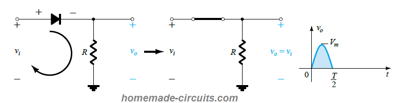 Since the diode is conducting fully, substituting the diode with a short circuit, will produce an output as shown in the above right side image.
No doubt, the generated output appears to be an exact replication of the applied input signal above the central axis of the waveform.
During the period T/2 �� T, the polarity of the input signal vi becomes negative, which causes the diode to turn OFF, resulting in an open circuit equivalent across the diode terminals.
Due to this the charge is unable to flow across the diode path during the period T/2 �� T, causing vo to be:
vo = iR = 0R = 0 V (using Ohm's Law).
The response can be visualized in the following diagram:
Since the diode is conducting fully, substituting the diode with a short circuit, will produce an output as shown in the above right side image.
No doubt, the generated output appears to be an exact replication of the applied input signal above the central axis of the waveform.
During the period T/2 �� T, the polarity of the input signal vi becomes negative, which causes the diode to turn OFF, resulting in an open circuit equivalent across the diode terminals.
Due to this the charge is unable to flow across the diode path during the period T/2 �� T, causing vo to be:
vo = iR = 0R = 0 V (using Ohm's Law).
The response can be visualized in the following diagram:
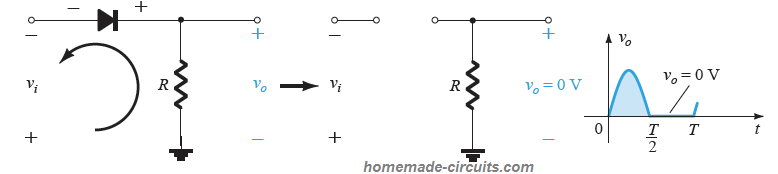 In this diagram we can see the DC output Vo from the diode produces a net average positive region above the axis, for the input full cycle, which can be determined by the formula:
Vdc = 0.318 Vm (half-wave)
The input vi and the output vo voltages during the diode half-wave rectification process is presented in the following figure:
In this diagram we can see the DC output Vo from the diode produces a net average positive region above the axis, for the input full cycle, which can be determined by the formula:
Vdc = 0.318 Vm (half-wave)
The input vi and the output vo voltages during the diode half-wave rectification process is presented in the following figure:
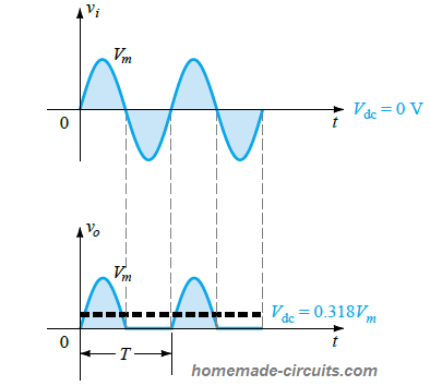 From the above diagrams and explanation we can define half-wave rectification as a process in which one-half of the input cycle is eliminated by the diode at its output.
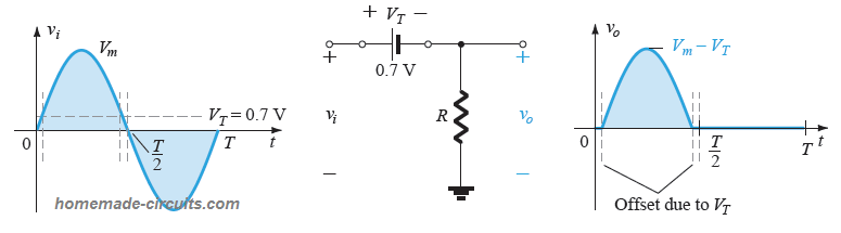 The VT = 0.7 V means that now the input signal must be at least 0.7 V to ensure the diode turns ON successfully.
In case the input VT is less than 0.7 V would simply fail to switch ON the diode and the diode will continue to be in its open circuit mode, with Vo = 0 V.
While the diode conducts during the rectification process, it generates a DC output that carries a fixed voltage level for the voltage difference vo - vi, equal to the above discussed forward drop of 0.7 V.
We can express this fixed level with the following formula:
vo = vi - VT
This produces a reduction in the average output voltage above the axis, causing a slight net reduction of the rectified output from the diode.
Referring the above figure, if we consider the Vm (peak signal level) to be adequately high than the VT, such that Vm >> VT, we can evaluate the average DC output value from the diode using the following formula, quite accurately.
Vdc 0.318(Vm - VT)
More precisely, if the input AC peak is sufficiently higher than VT (forward drop) of the diode, then we can simply use the previous formula for estimating the rectified DC output from the diode:
Vdc = 0.318 Vm
The VT = 0.7 V means that now the input signal must be at least 0.7 V to ensure the diode turns ON successfully.
In case the input VT is less than 0.7 V would simply fail to switch ON the diode and the diode will continue to be in its open circuit mode, with Vo = 0 V.
While the diode conducts during the rectification process, it generates a DC output that carries a fixed voltage level for the voltage difference vo - vi, equal to the above discussed forward drop of 0.7 V.
We can express this fixed level with the following formula:
vo = vi - VT
This produces a reduction in the average output voltage above the axis, causing a slight net reduction of the rectified output from the diode.
Referring the above figure, if we consider the Vm (peak signal level) to be adequately high than the VT, such that Vm >> VT, we can evaluate the average DC output value from the diode using the following formula, quite accurately.
Vdc 0.318(Vm - VT)
More precisely, if the input AC peak is sufficiently higher than VT (forward drop) of the diode, then we can simply use the previous formula for estimating the rectified DC output from the diode:
Vdc = 0.318 Vm
 Solution: For the above circuit network, the diode will turn ON for the negative portion of the input signal, and vo will be as indicated in the following sketch.
 For the full period of the input AC cycle, the DC output will be:
Vdc = 0.318Vm = - 0.318(20 V) = - 6.36 V
The negative sign indicates the polarity of the output DC which is opposite to the sign provided in the diagram under the problem.
Problem#2: Solve the above problem considering the diode to be a silicon diode.
In case of a silicon diode, the output waveform would look like this:
For the full period of the input AC cycle, the DC output will be:
Vdc = 0.318Vm = - 0.318(20 V) = - 6.36 V
The negative sign indicates the polarity of the output DC which is opposite to the sign provided in the diagram under the problem.
Problem#2: Solve the above problem considering the diode to be a silicon diode.
In case of a silicon diode, the output waveform would look like this:
 And the output DC would can be calculated as explained below:
Vdc - 0.318(Vm - 0.7 V) = - 0.318(19.3 V) - 6.14 V
The drop in the output DC voltage due to the 0.7 V factor is around 0.22V or approximately 3.5%
And the output DC would can be calculated as explained below:
Vdc - 0.318(Vm - 0.7 V) = - 0.318(19.3 V) - 6.14 V
The drop in the output DC voltage due to the 0.7 V factor is around 0.22V or approximately 3.5%
 When the positive input cycle progresses through the period t = 0 to T/2, the polarity of the input AC signal across the diode and the output from the diode are as represented below:
 Here, we can see that due to the special arrangement of the diode network in the bridge, when D2, D3 conduct, the opposite diodes D1, D4 remain reversed biased and in switched OFF state.
 The net output DC generated from this rectification process through D2, D3 can be seen in the above diagram.
Since we have imagined the diodes to be ideal, the output is vo = vin.
Now, likewise for the negative half cycle of the input signal diodes D1, D4 conduct, and diodes D2, D3 go into an OFF state, as illustrated below:
The net output DC generated from this rectification process through D2, D3 can be seen in the above diagram.
Since we have imagined the diodes to be ideal, the output is vo = vin.
Now, likewise for the negative half cycle of the input signal diodes D1, D4 conduct, and diodes D2, D3 go into an OFF state, as illustrated below:
 We can clearly see that the output from the bridge rectifier has converted both the positive and the negative half cycles of the input AC into two DC half cycles above the central axis.
Since this region above the axis is now two times more than the region obtained for a half wave rectification, the output DC will also become twice the magnitude, as calculated using the following formula:
Vdc = 2(0.318Vm)
or
Vdc = 0.636Vm (full-wave)
We can clearly see that the output from the bridge rectifier has converted both the positive and the negative half cycles of the input AC into two DC half cycles above the central axis.
Since this region above the axis is now two times more than the region obtained for a half wave rectification, the output DC will also become twice the magnitude, as calculated using the following formula:
Vdc = 2(0.318Vm)
or
Vdc = 0.636Vm (full-wave)
 As depicted in the above figure, if instead of ideal diode a silicon diode is used, applying Kirchhoff��s voltage law over the conduction line would give us the following result:
vi - VT - vo - VT = 0, and vo = vi - 2VT,
Therefore, the output voltage peak vo will be:
Vomax = Vm - 2VT
In a situation where V >> 2VT, we can use our earlier equation to get the average value with a reasonably high degree of precision:
Vdc - 0.636(Vm - 2VT),
Yet again, if we have Vm significantly higher than 2VT, the 2VT can be simply ignored, and the equation can be solved as:
Vdc - 0.636(Vm)
As depicted in the above figure, if instead of ideal diode a silicon diode is used, applying Kirchhoff��s voltage law over the conduction line would give us the following result:
vi - VT - vo - VT = 0, and vo = vi - 2VT,
Therefore, the output voltage peak vo will be:
Vomax = Vm - 2VT
In a situation where V >> 2VT, we can use our earlier equation to get the average value with a reasonably high degree of precision:
Vdc - 0.636(Vm - 2VT),
Yet again, if we have Vm significantly higher than 2VT, the 2VT can be simply ignored, and the equation can be solved as:
Vdc - 0.636(Vm)
 For a full bridge rectifier also, the PIV rating calculation is the same as half wave rectifier, that is:
PIV �� Vm, since Vm is the total voltage that's applied to the connected load as depicted in the following figure.
For a full bridge rectifier also, the PIV rating calculation is the same as half wave rectifier, that is:
PIV �� Vm, since Vm is the total voltage that's applied to the connected load as depicted in the following figure.
 Solution: For the positive half cycle, the circuit would behave as depicted in the following diagram:
 We can redraw this in the following manner for better understanding:
 Here, vo = 1/2vi = 1/2Vi(max) = 1/2(10 V) = 5 V
For the negative half cycle, the conduction role of the diodes can be interchanged, which will produce an output vo as shown below:
Here, vo = 1/2vi = 1/2Vi(max) = 1/2(10 V) = 5 V
For the negative half cycle, the conduction role of the diodes can be interchanged, which will produce an output vo as shown below:
 The absence of two diodes in the bridge results in the reduction in the DC output with a magnitude:
Vdc = 0.636(5 V) = 3.18 V
This is quite the same that we would have obtained from a half bridge rectifier with the same input.
The PIV will be equal to the maximum voltage generated across R, which is 5 V, or half of that needed for a half wave rectified with the same input.
The absence of two diodes in the bridge results in the reduction in the DC output with a magnitude:
Vdc = 0.636(5 V) = 3.18 V
This is quite the same that we would have obtained from a half bridge rectifier with the same input.
The PIV will be equal to the maximum voltage generated across R, which is 5 V, or half of that needed for a half wave rectified with the same input.
 In electronics we may find voltages and currents varying continuously with different ranges and magnitudes.
In digital circuits the voltage signal is in two forms, either as a logic high or logic low logic levels, which represent binary values of 1 or 0.
In a analog to digital converters (ADC), the input analog signal is represented as a digital magnitude, while a digital-analog converter (DAC) converts the digital magnitude back to an analog signal.
In electronics we may find voltages and currents varying continuously with different ranges and magnitudes.
In digital circuits the voltage signal is in two forms, either as a logic high or logic low logic levels, which represent binary values of 1 or 0.
In a analog to digital converters (ADC), the input analog signal is represented as a digital magnitude, while a digital-analog converter (DAC) converts the digital magnitude back to an analog signal.
 Solving the above example we get the following output voltage:
 As we see, a digital input of 01102 gets converted to an analog output of 6 V.
The purpose of the ladder network is to change the 16 potential binary magnitudes
through 0000 to 1111 into one of the 16 voltage quantities at intervals of Vref/16.
Therefore, it may be possible to process more binary inputs by including more number of ladder units, and to accomplish higher quantization for each step.
Meaning, suppose if we use a 10 step ladder network, will allow use to increase the voltage step quantity or the resolution to Vref/210 or Vref/1024. In this case, if we used a reference voltage Vref = 10 V would generate output voltage in steps of 10 V / 1024, or at around 10 mV.
Thus, adding more number of ladder stages will give us proportionately higher resolution.
Typically, for n number of ladder steps, this can be represented through the following formula:
Vref / 2n
As we see, a digital input of 01102 gets converted to an analog output of 6 V.
The purpose of the ladder network is to change the 16 potential binary magnitudes
through 0000 to 1111 into one of the 16 voltage quantities at intervals of Vref/16.
Therefore, it may be possible to process more binary inputs by including more number of ladder units, and to accomplish higher quantization for each step.
Meaning, suppose if we use a 10 step ladder network, will allow use to increase the voltage step quantity or the resolution to Vref/210 or Vref/1024. In this case, if we used a reference voltage Vref = 10 V would generate output voltage in steps of 10 V / 1024, or at around 10 mV.
Thus, adding more number of ladder stages will give us proportionately higher resolution.
Typically, for n number of ladder steps, this can be represented through the following formula:
Vref / 2n

 Here, an electronic switch is employed to transfer the desired analog input signal to an integrator, also called a ramp generator.
This ramp generator may be in the form of a capacitor charged with a constant current for generating the linear ramp.
This produces the required digital conversion through a counter stage that works for both positive and negative slope intervals of the integrator.
The method may be understood with the following description:
The full measuring range of the counter decides the fixed time interval.
For this interval the input analog voltage applied to the integrator causes the comparator input voltage to rise to some positive level.
Referring to the (b) section of the diagram above, shows that the voltage from the integrator at the end of the fixed time interval is higher than the input voltage that's larger in magnitude.
When the fixed time interval finishes, the count is set to 0, which prompts the electronic switch to connect the integrator to a fixed reference input voltage level.
After this, the output of the integrator which is also the input of the capacitor begins dropping at a constant rate.
During this period, the counter keeps advancing, while the output of the integrator continues to drop at a constant rate, until it goes below the reference voltage of the comparator.
This causes the comparator output to change state and triggers the control logic stage to stop the counting.
The stored digital magnitude inside the counter becomes the digital output of the converter.
The use of a common clock and integrator stage during both the positive and negative slope intervals adds some sort of compensation for controlling the drifting of the clock frequency, and accuracy limit of the integrator.
It may be possible to scale the counter output as per user preference by suitably setting up the reference input value, and the clock rate.
We can have the counter as binary, BCD or in other digital format, if it's required.
Here, an electronic switch is employed to transfer the desired analog input signal to an integrator, also called a ramp generator.
This ramp generator may be in the form of a capacitor charged with a constant current for generating the linear ramp.
This produces the required digital conversion through a counter stage that works for both positive and negative slope intervals of the integrator.
The method may be understood with the following description:
The full measuring range of the counter decides the fixed time interval.
For this interval the input analog voltage applied to the integrator causes the comparator input voltage to rise to some positive level.
Referring to the (b) section of the diagram above, shows that the voltage from the integrator at the end of the fixed time interval is higher than the input voltage that's larger in magnitude.
When the fixed time interval finishes, the count is set to 0, which prompts the electronic switch to connect the integrator to a fixed reference input voltage level.
After this, the output of the integrator which is also the input of the capacitor begins dropping at a constant rate.
During this period, the counter keeps advancing, while the output of the integrator continues to drop at a constant rate, until it goes below the reference voltage of the comparator.
This causes the comparator output to change state and triggers the control logic stage to stop the counting.
The stored digital magnitude inside the counter becomes the digital output of the converter.
The use of a common clock and integrator stage during both the positive and negative slope intervals adds some sort of compensation for controlling the drifting of the clock frequency, and accuracy limit of the integrator.
It may be possible to scale the counter output as per user preference by suitably setting up the reference input value, and the clock rate.
We can have the counter as binary, BCD or in other digital format, if it's required.
 The process allows the voltage to increase with each count step.
A comparator monitors this incrementing staircase voltage and compares it with the analog input voltage.
As soon as the comparator senses the staircase voltage going above the analog input, its output prompts to stop the counting.
The counter value at this point becomes the digital equivalent of the analog signal.
The level of change in the voltage generated by the steps of the staircase signal is determined by the amount of count bits used.
For example a 12 stage counter using 10 V reference will operate a 10 stage ladder network with step voltages of:
Vref/212 = 10 V / 4096 = 2.4 mV
This will create a conversion resolution of 2.4 mV.
The time required for the execution of the conversion is determined by the clock rate of the counter.
If the clock rate of 1 MHz is used for operating a 12 stage counter, the maximum time taken for the conversion would be:
4096 x 1 ��s = 4096 ��s �� 4.1 ms
The least number of conversions that may be possible per second can be found as:
no.
of conversions = 1/4.1 ms �� 244 conversions/second
The process allows the voltage to increase with each count step.
A comparator monitors this incrementing staircase voltage and compares it with the analog input voltage.
As soon as the comparator senses the staircase voltage going above the analog input, its output prompts to stop the counting.
The counter value at this point becomes the digital equivalent of the analog signal.
The level of change in the voltage generated by the steps of the staircase signal is determined by the amount of count bits used.
For example a 12 stage counter using 10 V reference will operate a 10 stage ladder network with step voltages of:
Vref/212 = 10 V / 4096 = 2.4 mV
This will create a conversion resolution of 2.4 mV.
The time required for the execution of the conversion is determined by the clock rate of the counter.
If the clock rate of 1 MHz is used for operating a 12 stage counter, the maximum time taken for the conversion would be:
4096 x 1 ��s = 4096 ��s �� 4.1 ms
The least number of conversions that may be possible per second can be found as:
no.
of conversions = 1/4.1 ms �� 244 conversions/second
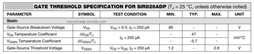 The table above indicates the threshold levels and the relevant test conditions for an example MOSFET.
For a desired application the designer might be worried about a dreaded situation known as "induced" gate voltage, which may be a serious issue for example in a low side MOSFET of synchronous buck converter.
As discussed earlier, here too we must understand that crossing the threshold VGS(th) level may not force the device to run into a shoot-through breakdown condition.
This level actually tells the designer regarding the threshold at which the MOSFET just begins turning ON and is not a situation where things just end altogether.
It may be advisable that while the MOSFET is in the switched OFF condition the gate voltage is maintained below the VGS(th) level , to prevent current leakage.
But while turning it ON this parameter may be simply ignored.
The table above indicates the threshold levels and the relevant test conditions for an example MOSFET.
For a desired application the designer might be worried about a dreaded situation known as "induced" gate voltage, which may be a serious issue for example in a low side MOSFET of synchronous buck converter.
As discussed earlier, here too we must understand that crossing the threshold VGS(th) level may not force the device to run into a shoot-through breakdown condition.
This level actually tells the designer regarding the threshold at which the MOSFET just begins turning ON and is not a situation where things just end altogether.
It may be advisable that while the MOSFET is in the switched OFF condition the gate voltage is maintained below the VGS(th) level , to prevent current leakage.
But while turning it ON this parameter may be simply ignored.
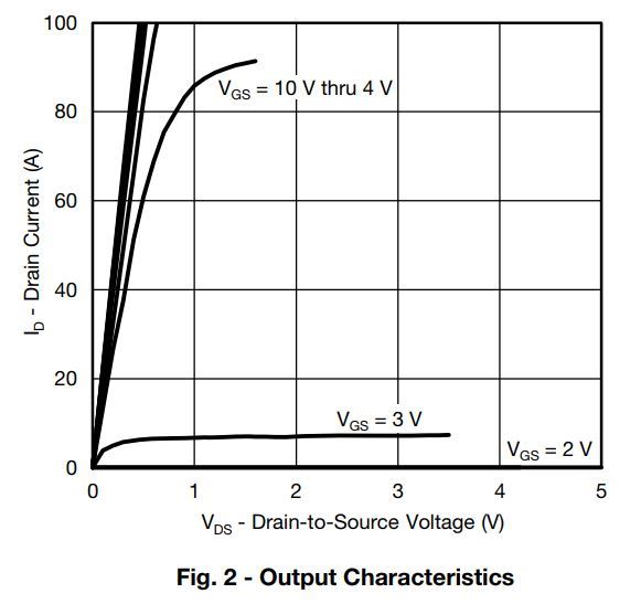 Here, for the various levels of VGS the forward drop of the MOSFET is measured as a function of current.
Device engineers use this curve data to confirm the optimal level of gate voltage.
For each level of gate voltage that ensures a full switch ON of the MOSFET [RDS(on)], we get a range of voltage drops (VGS) across drain-to-source having strictly linear response with drain current.
The range begins from zero and upwards.
For lower gate voltages (VGS), when the drain current is increased, we find the curve losing the linear response, moving through the "knee" and then going flat.
Here, for the various levels of VGS the forward drop of the MOSFET is measured as a function of current.
Device engineers use this curve data to confirm the optimal level of gate voltage.
For each level of gate voltage that ensures a full switch ON of the MOSFET [RDS(on)], we get a range of voltage drops (VGS) across drain-to-source having strictly linear response with drain current.
The range begins from zero and upwards.
For lower gate voltages (VGS), when the drain current is increased, we find the curve losing the linear response, moving through the "knee" and then going flat.
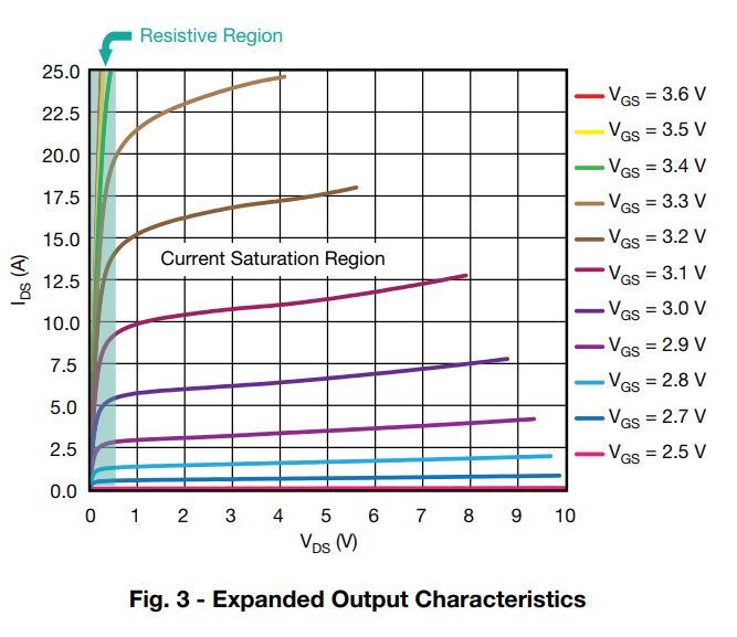 The above curve details provide us the complete output characteristics for a range of gate voltages from 2.5 V to 3.6 V.
MOSFET users may normally contemplate this as the linear function.
However, in contrast device engineers may prefer to pay more attention towards the gray region of the graph which suggests the current saturation region for applied gate voltage.
It reveals the current data that has touched the saturation point or the saturation limit.
At this point, if the VDS is increased will result in a marginal increase in the current, but a small increase in drain current may lead to a much larger VDS.
For increased gate voltage levels, which enable the MOSFET to turn ON fully, the green shaded area will show us the operating point for the process, indicated as resistive (or Ohmic) region.
Please note that the curves here show the typical values only, and does not include any minimum or maximum boundaries.
While operating at lower ambient temperatures, the device will require higher gate voltage to stay in the resistive region, which may go upward at the rate of 0.3 %/��C.
The above curve details provide us the complete output characteristics for a range of gate voltages from 2.5 V to 3.6 V.
MOSFET users may normally contemplate this as the linear function.
However, in contrast device engineers may prefer to pay more attention towards the gray region of the graph which suggests the current saturation region for applied gate voltage.
It reveals the current data that has touched the saturation point or the saturation limit.
At this point, if the VDS is increased will result in a marginal increase in the current, but a small increase in drain current may lead to a much larger VDS.
For increased gate voltage levels, which enable the MOSFET to turn ON fully, the green shaded area will show us the operating point for the process, indicated as resistive (or Ohmic) region.
Please note that the curves here show the typical values only, and does not include any minimum or maximum boundaries.
While operating at lower ambient temperatures, the device will require higher gate voltage to stay in the resistive region, which may go upward at the rate of 0.3 %/��C.
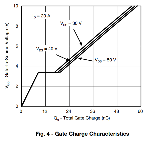 Although the above curve is a standard inclusion in all MOSFET datasheets, the underlying indications are seldom comprehended by the MOSFET user.
Moreover, the modern advancement in the MOSFET layouts, such as trench and shielded gates, call for a revised addressing of the data.
For example, the specification named "gate-charge" may appear slightly misleading by itself.
The linear and divided sections of the curve do not appear like voltage charging a capacitor, regardless of how much non-linear value it may exhibit.
To be precise, the gate charge curve signifies an associated data of two non parallel capacitors, having dissimilar magnitudes and carrying different voltage levels.
In theory, the functional capacitance as witnessed from MOSFET gate terminal is defined with the equation:
Ciss = Cgs + Cgd
where Ciss = gate capacitance, Cgs = gate source capacitance, Cgd = gate drain capacitance
Although it may appear rather simple to measure this unit and specify in the datasheets, it must be noted that the term Ciss is actually not a real capacitance.
It may be completely wrong to think that a MOSFET is turned ON merely through a voltage applied on the "the gate capacitance Ciss".
Although the above curve is a standard inclusion in all MOSFET datasheets, the underlying indications are seldom comprehended by the MOSFET user.
Moreover, the modern advancement in the MOSFET layouts, such as trench and shielded gates, call for a revised addressing of the data.
For example, the specification named "gate-charge" may appear slightly misleading by itself.
The linear and divided sections of the curve do not appear like voltage charging a capacitor, regardless of how much non-linear value it may exhibit.
To be precise, the gate charge curve signifies an associated data of two non parallel capacitors, having dissimilar magnitudes and carrying different voltage levels.
In theory, the functional capacitance as witnessed from MOSFET gate terminal is defined with the equation:
Ciss = Cgs + Cgd
where Ciss = gate capacitance, Cgs = gate source capacitance, Cgd = gate drain capacitance
Although it may appear rather simple to measure this unit and specify in the datasheets, it must be noted that the term Ciss is actually not a real capacitance.
It may be completely wrong to think that a MOSFET is turned ON merely through a voltage applied on the "the gate capacitance Ciss".
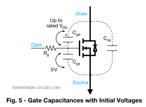 As indicated in the above figure, just before a MOFET turns ON, the gate capacitance has no charge, but the capacitance at gate-drain Cgd possesses a negative charge which needs to be eliminated.
Both these capacitance have a non-linear nature and their values largely vary as the applied voltages vary.
Hence, it is important to note that it is the stored charges of the MOSFET that determines its switching characteristics, and not the capacitance value for a specific voltage level.
Since the two capacitance elements constituting Ciss have different physical attributes, they tend to get charged with dissimilar voltage levels, requiring the turn ON process of the MOSFET also to go through two stages.
The precise sequence may be different for resistive and inductive applications, but typically most practical loads being highly inductive, the process could be simulated as depicted in the following figure:
As indicated in the above figure, just before a MOFET turns ON, the gate capacitance has no charge, but the capacitance at gate-drain Cgd possesses a negative charge which needs to be eliminated.
Both these capacitance have a non-linear nature and their values largely vary as the applied voltages vary.
Hence, it is important to note that it is the stored charges of the MOSFET that determines its switching characteristics, and not the capacitance value for a specific voltage level.
Since the two capacitance elements constituting Ciss have different physical attributes, they tend to get charged with dissimilar voltage levels, requiring the turn ON process of the MOSFET also to go through two stages.
The precise sequence may be different for resistive and inductive applications, but typically most practical loads being highly inductive, the process could be simulated as depicted in the following figure:
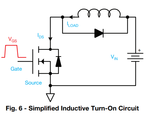
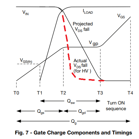 It may be understood with the following explanation:
T0 - T1: Cgs charges from zero to VGS(th).
VDS or IDS does not go through any changes.
T1-T2, current starts rising in the MOSFET in response to the increasing gate voltage from VGS(th) upto the plateau voltage Vgp.
Here, IDS increases and reaches to full load current from 0 V, although VDS remains unaffected and constant.
The associated charge is formed through the integral of Cgs from 0 V to Vgp, and Qgs given in the datasheets.
T2 - T3: Observe the flat region between T2 and T3, it's called the Miller plateau.
Before the switch ON, Cgd charges and holds up to the supply voltage VIN, until IDS reaches the peak value I(load) at T2.
The time between period T2 and T3, the negative charge (VIN - Vgp) gets converted into positive charge with respect to the plateau voltage Vgp.
This can be also visualized as the falling of the drain voltage from VIN to around almost zero.
The charge involved is equal to around the Cgd integral from 0 to Vin, which is shown as Qgd in datasheets.
During T3 - T4, the gate voltage climbs from Vgp to VGS, and here we find hardly any change for VDS and IDS, but the effectual RDS(on) drops slightly as the gate voltage rises.
At some voltage level above Vgp, provides the manufactures enough confidence to fix the upper limit on the effective RDS(on).
It may be understood with the following explanation:
T0 - T1: Cgs charges from zero to VGS(th).
VDS or IDS does not go through any changes.
T1-T2, current starts rising in the MOSFET in response to the increasing gate voltage from VGS(th) upto the plateau voltage Vgp.
Here, IDS increases and reaches to full load current from 0 V, although VDS remains unaffected and constant.
The associated charge is formed through the integral of Cgs from 0 V to Vgp, and Qgs given in the datasheets.
T2 - T3: Observe the flat region between T2 and T3, it's called the Miller plateau.
Before the switch ON, Cgd charges and holds up to the supply voltage VIN, until IDS reaches the peak value I(load) at T2.
The time between period T2 and T3, the negative charge (VIN - Vgp) gets converted into positive charge with respect to the plateau voltage Vgp.
This can be also visualized as the falling of the drain voltage from VIN to around almost zero.
The charge involved is equal to around the Cgd integral from 0 to Vin, which is shown as Qgd in datasheets.
During T3 - T4, the gate voltage climbs from Vgp to VGS, and here we find hardly any change for VDS and IDS, but the effectual RDS(on) drops slightly as the gate voltage rises.
At some voltage level above Vgp, provides the manufactures enough confidence to fix the upper limit on the effective RDS(on).
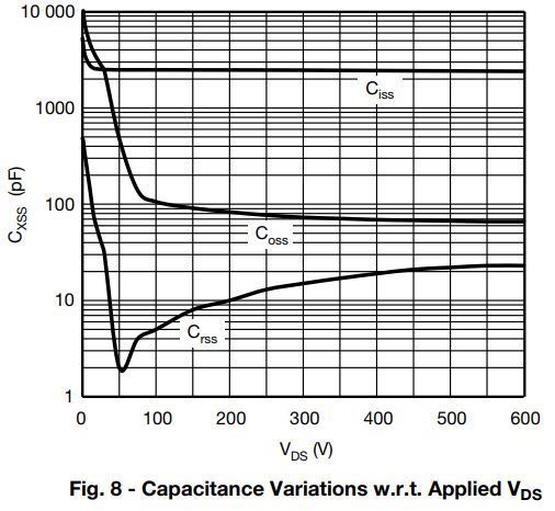 The variation range that exists in the value of Crss (reverse transfer) is more than 200:1 within the initial 100 V.
Due to this the actual fall time of voltage against the gate charge curve appears more like the dashed line shown in red color in figure 7.
At higher voltages, the rise and fall times of the charges, along with their equivalent dV/dt values are more reliant on the value of Crss, instead of the integral of the whole curve indicated as Qgd.
When users want to compare MOSFET specs within different design environments, they should realize that MOSFET with half the Qgd value won't necessarily feature two times faster switching rate, or 50% less switching losses.
This is because, according to the Cgd curve and its magnitude at higher voltages, it may be quite possible for a MOSFET to have a low Qgd in datasheet, but without any increase in the switching speed.
The variation range that exists in the value of Crss (reverse transfer) is more than 200:1 within the initial 100 V.
Due to this the actual fall time of voltage against the gate charge curve appears more like the dashed line shown in red color in figure 7.
At higher voltages, the rise and fall times of the charges, along with their equivalent dV/dt values are more reliant on the value of Crss, instead of the integral of the whole curve indicated as Qgd.
When users want to compare MOSFET specs within different design environments, they should realize that MOSFET with half the Qgd value won't necessarily feature two times faster switching rate, or 50% less switching losses.
This is because, according to the Cgd curve and its magnitude at higher voltages, it may be quite possible for a MOSFET to have a low Qgd in datasheet, but without any increase in the switching speed.
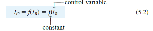 But sadly, this convenient linear relationship may not be achievable in JFETs across their input and output magnitudes.
Rather, the relationship between the drain current ID and the gate voltage VGS is defined by Shockley��s equation:
But sadly, this convenient linear relationship may not be achievable in JFETs across their input and output magnitudes.
Rather, the relationship between the drain current ID and the gate voltage VGS is defined by Shockley��s equation:
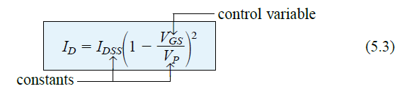 Here, the squared expression becomes responsible for the non-linear response across the ID and VGS, which gives rise to a curve growing exponentially, as the magnitude of VGS is decreased.
Although a mathematical approach would be easier to implement for the dc analysis, the graphical way might require a plotting of the above equation.
This can present the device in question and the plotting of the network equations relating to the identical variables.
We find the solution by looking at the point of intersection of the two curves.
Remember, that when you use the graphical method, the characteristics of the device remains unaffected by the network where the device is implemented.
As the intersection between the two curves changes, it also changes the network equation, but this has no effect on the transfer curve defined by the above Eq, 5.3.
Therefore, in general we can say that:
The transfer characteristic defined by Shockley's Equation is not affected by the network where the device is implemented.
We can get the transfer curve using Shockley's equation, or from the output characteristics as depicted in Fig.5.10
In the figure below, we can see two graphs.
The vertical line measures milliamperes for the two graphs.
Here, the squared expression becomes responsible for the non-linear response across the ID and VGS, which gives rise to a curve growing exponentially, as the magnitude of VGS is decreased.
Although a mathematical approach would be easier to implement for the dc analysis, the graphical way might require a plotting of the above equation.
This can present the device in question and the plotting of the network equations relating to the identical variables.
We find the solution by looking at the point of intersection of the two curves.
Remember, that when you use the graphical method, the characteristics of the device remains unaffected by the network where the device is implemented.
As the intersection between the two curves changes, it also changes the network equation, but this has no effect on the transfer curve defined by the above Eq, 5.3.
Therefore, in general we can say that:
The transfer characteristic defined by Shockley's Equation is not affected by the network where the device is implemented.
We can get the transfer curve using Shockley's equation, or from the output characteristics as depicted in Fig.5.10
In the figure below, we can see two graphs.
The vertical line measures milliamperes for the two graphs.
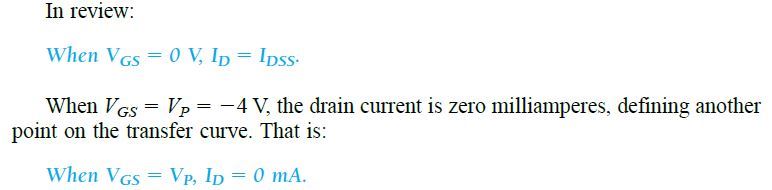 Note that the drain characteristics show the relationship between one drain output magnitude with another drain output magnitude, wherein the two axes are interpreted by variables in the same region of the MOSFET characteristics.
Thus, transfer characteristics can be defined as a plot of a MOSFET drain current versus a quantity or a signal acting as an input control.
This consequently results in a direct "transfer" across input/output variables, when the curve is used at the left of Fig 5.15. If it had been a linear relationship, the plot of ID vs VGS would have been a straight line across IDSS and VP.
However, this results in a parabolic curve due to the vertical spacing between the VGS stepping over the drain characteristics, that decreases to an appreciable extent as VGS gets increasingly negative, in Fig 5.15 .
If we compare the space between VGS = 0 V and VGS = -1V with that of between VS = -3 V and the pinch-off, we see that the difference to be identical, although it's a lot different for the ID value.
We are able to identify another point on the transfer curve by drawing a horizontal line from VGS = -1 V curve until the axis of ID and subsequently extending it to the other axis.
Observe that VGS = - 1V at the bottom axis of the transfer curve when ID = 4.5 mA.
Also note that, in the ID definition at VGS = 0 V and -1 V, the saturation levels of ID are used, while the ohmic region is neglected.
Moving further ahead, with VGS = -2 V and - 3V, we are able to finish the transfer curve plot.
Note that the drain characteristics show the relationship between one drain output magnitude with another drain output magnitude, wherein the two axes are interpreted by variables in the same region of the MOSFET characteristics.
Thus, transfer characteristics can be defined as a plot of a MOSFET drain current versus a quantity or a signal acting as an input control.
This consequently results in a direct "transfer" across input/output variables, when the curve is used at the left of Fig 5.15. If it had been a linear relationship, the plot of ID vs VGS would have been a straight line across IDSS and VP.
However, this results in a parabolic curve due to the vertical spacing between the VGS stepping over the drain characteristics, that decreases to an appreciable extent as VGS gets increasingly negative, in Fig 5.15 .
If we compare the space between VGS = 0 V and VGS = -1V with that of between VS = -3 V and the pinch-off, we see that the difference to be identical, although it's a lot different for the ID value.
We are able to identify another point on the transfer curve by drawing a horizontal line from VGS = -1 V curve until the axis of ID and subsequently extending it to the other axis.
Observe that VGS = - 1V at the bottom axis of the transfer curve when ID = 4.5 mA.
Also note that, in the ID definition at VGS = 0 V and -1 V, the saturation levels of ID are used, while the ohmic region is neglected.
Moving further ahead, with VGS = -2 V and - 3V, we are able to finish the transfer curve plot.
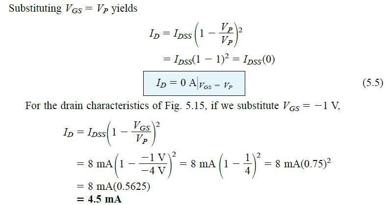 This matches the plot shown in Fig.5.15.
Observe how carefully the negative signs for VGS and VP are managed in the above calculations.
Missing out even a single negative sign could lead to a totally erroneous result.
It is pretty clear from the above discussion, that if we have the values of IDSS and VP (which can be referred from the datasheet), we can quickly determine the value of ID for any magnitude of VGS.
On the other hand, through standard Algebra we can derive an equation (via Eq.5.3), for the resulting VGS level for a given level of ID.
This could be derived quite simply, to get:
This matches the plot shown in Fig.5.15.
Observe how carefully the negative signs for VGS and VP are managed in the above calculations.
Missing out even a single negative sign could lead to a totally erroneous result.
It is pretty clear from the above discussion, that if we have the values of IDSS and VP (which can be referred from the datasheet), we can quickly determine the value of ID for any magnitude of VGS.
On the other hand, through standard Algebra we can derive an equation (via Eq.5.3), for the resulting VGS level for a given level of ID.
This could be derived quite simply, to get:
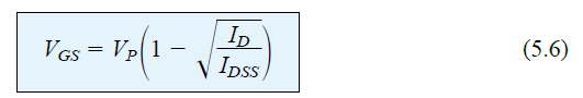 Now let us verify the above equation by determining the VGS level that produces a drain current of 4.5 mA for a MOSFET having the characteristics matching Fig 5.15.
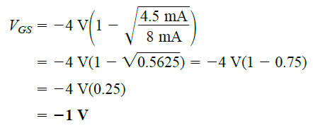 The result verifies the equation as it conforms with the Fig.5.15.
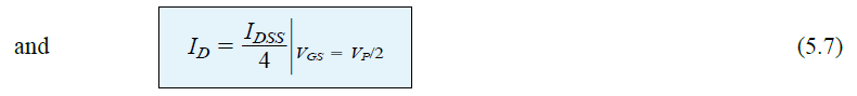 It must be noted that the above equation is not created for a specific level of VP.
The equation is a general form for all VP levels for so long as VGS = VP/2. The result of the equation suggests that the drain current will be always 1/4th of the saturation level IDSS as long as the gate-to-source voltage has a value that's 50% less than the pinch-off value.
Please note that the level of ID for VGS = VP/2 = -4V/2 = -2V as per the Fig.5.15
Opting ID = IDSS/2 and substituting it into Eq.5.6 we get the following results:
It must be noted that the above equation is not created for a specific level of VP.
The equation is a general form for all VP levels for so long as VGS = VP/2. The result of the equation suggests that the drain current will be always 1/4th of the saturation level IDSS as long as the gate-to-source voltage has a value that's 50% less than the pinch-off value.
Please note that the level of ID for VGS = VP/2 = -4V/2 = -2V as per the Fig.5.15
Opting ID = IDSS/2 and substituting it into Eq.5.6 we get the following results:
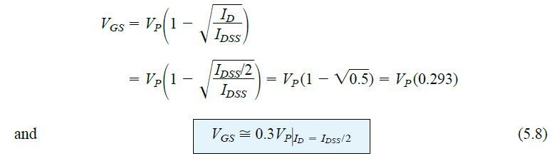 Although further number points can be established, sufficient level of accuracy can be simply achieved by drawing the transfer curve using only 4 plot points, as identified above and also in Table 5.1 below.
In most cases we can employ just the plot point using VGS = VP/2, while the axis intersections at IDSS and VP will give us a curve sufficiently reliable for most of the analysis.
Although further number points can be established, sufficient level of accuracy can be simply achieved by drawing the transfer curve using only 4 plot points, as identified above and also in Table 5.1 below.
In most cases we can employ just the plot point using VGS = VP/2, while the axis intersections at IDSS and VP will give us a curve sufficiently reliable for most of the analysis.
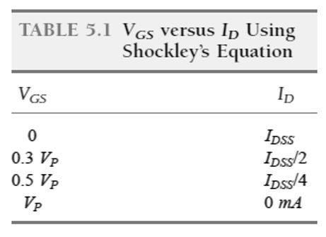
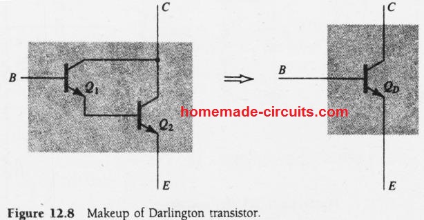
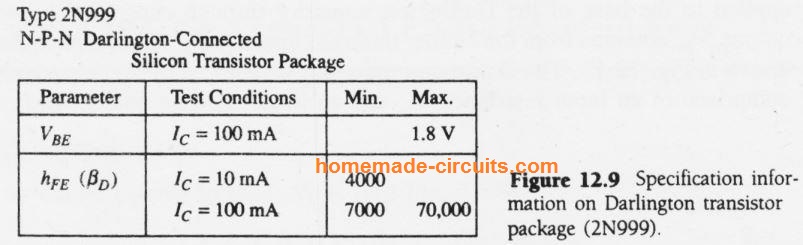 The indicated current gain, is the net gain from the two BJTs.
The unit comes with 3 standard terminals externally, namely base, emitter, collector.
This kind of packaged Darlington transistors have external features similar to a normal transistor but have very high and enhanced current gain output, compared to the normal single transistors.
The indicated current gain, is the net gain from the two BJTs.
The unit comes with 3 standard terminals externally, namely base, emitter, collector.
This kind of packaged Darlington transistors have external features similar to a normal transistor but have very high and enhanced current gain output, compared to the normal single transistors.
 Here the base current can be calculated using the formula:
IB = VCC - VBE / RB + ��DRE -------------- (12.9)
Although this may look similar to the equation which is normally applied for any regular BJT, the value ��D in the above equation will be substantially higher, and the VBE will be comparatively larger.
This has been also proven in the sample datasheet presented in the previous paragraph.
Therefore, the emitter current can be calculated as:
IE = (��D + 1)IB �� ��DIB -------------- (12.10)
DC voltage will be:
VE = IE RE -------------- (12.11)
VB = VE + VBE -------------- (12.12)
Here the base current can be calculated using the formula:
IB = VCC - VBE / RB + ��DRE -------------- (12.9)
Although this may look similar to the equation which is normally applied for any regular BJT, the value ��D in the above equation will be substantially higher, and the VBE will be comparatively larger.
This has been also proven in the sample datasheet presented in the previous paragraph.
Therefore, the emitter current can be calculated as:
IE = (��D + 1)IB �� ��DIB -------------- (12.10)
DC voltage will be:
VE = IE RE -------------- (12.11)
VB = VE + VBE -------------- (12.12)
 Solution: Applying Eq.12.9 the base current is determined as:
IB = 18 V - 1.6 V / 3.3 M�� + 8000(390��) �� 2.56 ��A
Applying Eq.12.10, the emitter current may be evaluated as:
IE �� 8000(2.56 ��A) �� 20.28 mA �� IC
Emitter DC voltage can be calculated using equation 12.11, as:
VE = 20.48 mA(390��) �� 8 V,
Finally collector voltage can be assessed by applying Eq.
12.12 as given below:
VB = 8 V + 1.6 V = 9.6 V
In this example the supply voltage at the collector of the Darlington will be:
VC = 18 V
Solution: Applying Eq.12.9 the base current is determined as:
IB = 18 V - 1.6 V / 3.3 M�� + 8000(390��) �� 2.56 ��A
Applying Eq.12.10, the emitter current may be evaluated as:
IE �� 8000(2.56 ��A) �� 20.28 mA �� IC
Emitter DC voltage can be calculated using equation 12.11, as:
VE = 20.48 mA(390��) �� 8 V,
Finally collector voltage can be assessed by applying Eq.
12.12 as given below:
VB = 8 V + 1.6 V = 9.6 V
In this example the supply voltage at the collector of the Darlington will be:
VC = 18 V
 The output ac signal obtained through capacitor C2 is associated with the emitter terminal of the device.
The simulation result of the above configuration is presented in the following figure.
Here the Darlington transistor can be seen replaced with an ac equivalent circuit having an input resistance ri and an output source of current represented as ��DIb
The output ac signal obtained through capacitor C2 is associated with the emitter terminal of the device.
The simulation result of the above configuration is presented in the following figure.
Here the Darlington transistor can be seen replaced with an ac equivalent circuit having an input resistance ri and an output source of current represented as ��DIb
 The AC Input Impedance can be calculated as explained below:
Ac base current passing through ri is:
Ib = Vi - Vo / ri ---------- (12.13)
Since
Vo = (Ib + ��DIb)RE ---------- (12.14)
If we apply Eq 12.13 in Eq.
12.14 we get:
Ib ri = Vi - Vo = Vi - Ib (1 + ��D)RE
Solving the above for Vi :
Vi = Ib[ri + (1 + ��D)RE]
Vi / Ib = ri + ��DRE
Now, examining the transistor base, its ac input impedance can be evaluated as:
Zi = RB ri + ��DRE ---------- (12.15)
The AC Input Impedance can be calculated as explained below:
Ac base current passing through ri is:
Ib = Vi - Vo / ri ---------- (12.13)
Since
Vo = (Ib + ��DIb)RE ---------- (12.14)
If we apply Eq 12.13 in Eq.
12.14 we get:
Ib ri = Vi - Vo = Vi - Ib (1 + ��D)RE
Solving the above for Vi :
Vi = Ib[ri + (1 + ��D)RE]
Vi / Ib = ri + ��DRE
Now, examining the transistor base, its ac input impedance can be evaluated as:
Zi = RB ri + ��DRE ---------- (12.15)
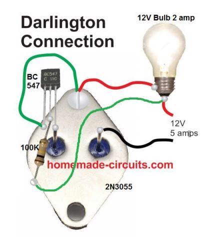 Th average current gain (hFE) of 2N3055 is around 40, while for BC547 it's 400. When the two are combined as a Darlington pair, the gain shoots up substantially to 40 x 400 = 16000, awesome isn't it.
That's the sort of power we are able to get from a Darlington transistor configuration, and an ordinary looking transistor could be turned into a hugely rated device just with a simple modification.
Th average current gain (hFE) of 2N3055 is around 40, while for BC547 it's 400. When the two are combined as a Darlington pair, the gain shoots up substantially to 40 x 400 = 16000, awesome isn't it.
That's the sort of power we are able to get from a Darlington transistor configuration, and an ordinary looking transistor could be turned into a hugely rated device just with a simple modification.
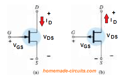 You can clearly notice that the arrow marks which are pointing inward for the n-channel device to indicate the direction in which IG (gate current) is supposed to flow when the p-n junction were forward-biased.
In case of a p-channel device the conditions are identical except the difference in the direction of the arrow symbol.
You can clearly notice that the arrow marks which are pointing inward for the n-channel device to indicate the direction in which IG (gate current) is supposed to flow when the p-n junction were forward-biased.
In case of a p-channel device the conditions are identical except the difference in the direction of the arrow symbol.
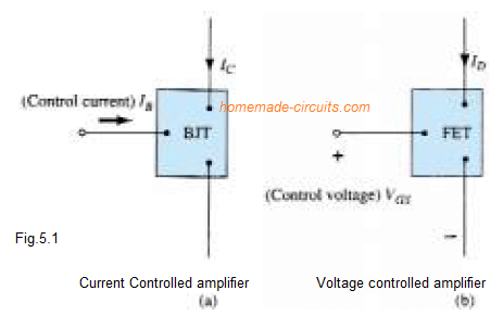 In both the instances the current of the output circuit will be governed by a parameter of the input circuit.
In one situation a current level and in the other an applied voltage.
Just like npn and pnp for bipolar transistors, you will find n-channel and p-channel field-effect transistors.
But, you should remember that the BJT transistor is a bipolar device the prefix bi- indicating that the conduction level is a function of two charge carriers, electrons and holes.
The FET on the other hand is a unipolar device that solely depends on either electron (n-channel) or hole (p-channel) conduction.
The phrase "field-effect" can be explained like this: all of us are aware of the power of a permanent magnet to attract metal filings towards the magnet without any physical contact.
Quite in a similar way inside FET an electric field is created by the existing charges that influence the conduction path of the output circuit without having any direct contact between the controlling and controlled quantities.
Probably one of the most crucial features of the FET is its high input impedance.
Ranging from a magnitude of 1 to many hundred megohms it significantly surpasses the normal input resistance ranges of the BJT configurations, an extremely important attribute while developing linear ac amplifier models.
However, the BJT carries a greater sensitivity to variations in the input signal.
Meaning, the change in output current is commonly significantly more for BJTs than FETs for the same amount of change in their input voltages.
Because of this, standard ac voltage gains for BJT amplifiers can be a much higher compared to FETs.
Generally speaking, FETs are considerably more thermally resilient than BJTs, and also are often smaller sized in structure compared to BJTs, which make them specifically suitable for embedding as integrated-circuit (IC) chips.
The structural characteristics of some FETs, on the other hand, can allow them to be extra sensitive to physical contacts than BJTs.
In both the instances the current of the output circuit will be governed by a parameter of the input circuit.
In one situation a current level and in the other an applied voltage.
Just like npn and pnp for bipolar transistors, you will find n-channel and p-channel field-effect transistors.
But, you should remember that the BJT transistor is a bipolar device the prefix bi- indicating that the conduction level is a function of two charge carriers, electrons and holes.
The FET on the other hand is a unipolar device that solely depends on either electron (n-channel) or hole (p-channel) conduction.
The phrase "field-effect" can be explained like this: all of us are aware of the power of a permanent magnet to attract metal filings towards the magnet without any physical contact.
Quite in a similar way inside FET an electric field is created by the existing charges that influence the conduction path of the output circuit without having any direct contact between the controlling and controlled quantities.
Probably one of the most crucial features of the FET is its high input impedance.
Ranging from a magnitude of 1 to many hundred megohms it significantly surpasses the normal input resistance ranges of the BJT configurations, an extremely important attribute while developing linear ac amplifier models.
However, the BJT carries a greater sensitivity to variations in the input signal.
Meaning, the change in output current is commonly significantly more for BJTs than FETs for the same amount of change in their input voltages.
Because of this, standard ac voltage gains for BJT amplifiers can be a much higher compared to FETs.
Generally speaking, FETs are considerably more thermally resilient than BJTs, and also are often smaller sized in structure compared to BJTs, which make them specifically suitable for embedding as integrated-circuit (IC) chips.
The structural characteristics of some FETs, on the other hand, can allow them to be extra sensitive to physical contacts than BJTs.
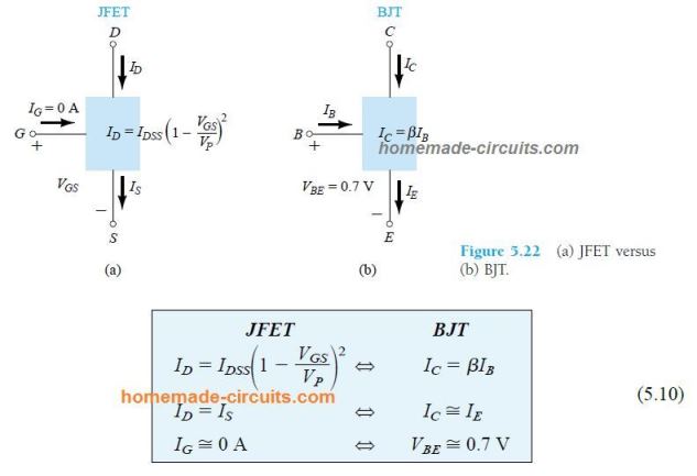 For a BJT VBE = 0.7 V is the important factor for starting an analysis of its configuration.
Similarly, the parameter IG = 0 A is commonly the first thing considered for the analysis of a JFET circuit.
For the BJT configuration, IB is often the first factor that becomes necessary to be determined.
Likewise, for the JFET, it is typically the VGS.
In this article we will be focussing on JFETs or junction field effect transistors, in the next article we'll dicuss about metal-oxide-semiconductor field-effcet transistor or MOS-FET.
For a BJT VBE = 0.7 V is the important factor for starting an analysis of its configuration.
Similarly, the parameter IG = 0 A is commonly the first thing considered for the analysis of a JFET circuit.
For the BJT configuration, IB is often the first factor that becomes necessary to be determined.
Likewise, for the JFET, it is typically the VGS.
In this article we will be focussing on JFETs or junction field effect transistors, in the next article we'll dicuss about metal-oxide-semiconductor field-effcet transistor or MOS-FET.
 The upper part of the n-type channel is joined through an Ohmic contact with a termnal named the drain (D), while the lower section of the same channel also connected through a Ohmic contact with another terminal named the source (S).
The couple of p-type materials are together linked with the terminal referred to as the gate (G).
Essentially we find that the drain and source terminals are joined to the ends of the n-type channel.
The gate terminal is joined to a pair of p-channel material.
When there's no voltage applied across a jfet, its two p-n junctions are without any biasing conditions.
In this situation there exists a depletion region on each junction as indicated in the above figure, which looks quite like a diode p-n region under no biasing.
The upper part of the n-type channel is joined through an Ohmic contact with a termnal named the drain (D), while the lower section of the same channel also connected through a Ohmic contact with another terminal named the source (S).
The couple of p-type materials are together linked with the terminal referred to as the gate (G).
Essentially we find that the drain and source terminals are joined to the ends of the n-type channel.
The gate terminal is joined to a pair of p-channel material.
When there's no voltage applied across a jfet, its two p-n junctions are without any biasing conditions.
In this situation there exists a depletion region on each junction as indicated in the above figure, which looks quite like a diode p-n region under no biasing.
 Here, the water pressure can be compared with the applied voltage magnitude from drain towards source.
The flow of water can be compared with the flow of electrons.
The mouth of the tap imitates the source terminal of the JFET, while the upper portion of the tap where the water is forced in depicts the Drain of the JFET.
The tap knob acts like the Gate of the JFET.
With the help of an input potential it controls the flow of electrons (charge) from drain to source, just as the tap knob controls the flow of water on the mouth opening.
From the JFET structure we can see that the drain and the source terminals are at the opposite ends of the n-channel, and as the term is based of electron flow we can write:
VGS = 0 V, VDS Some Positive Value
In the Fig 5.4 we can see a positive voltage VDS applied across the n-channel.
The gate terminal is directly joined to the source to create a condition VGS = 0V.
This enables the gate and the source terminals to be at an identical potential, and results in a lower end depletion region of each p-material, exactly as we see in the first diagram above with a no-bias condition.
As soon as a voltage VDD ( = VDS) is applied, electrons are pulled towards the drain terminal, generating the conventional flow of current ID, as indicated in Fig 5.4.
The direction of the flow of the charge reveals that the drain and source current are equal in magnitude (ID = IS).
As per the conditions depicted in the Fig 5.4, the flow of the charge looks quite unrestricted, and only affected by the resistance of the n-channel between drain and the source.
Here, the water pressure can be compared with the applied voltage magnitude from drain towards source.
The flow of water can be compared with the flow of electrons.
The mouth of the tap imitates the source terminal of the JFET, while the upper portion of the tap where the water is forced in depicts the Drain of the JFET.
The tap knob acts like the Gate of the JFET.
With the help of an input potential it controls the flow of electrons (charge) from drain to source, just as the tap knob controls the flow of water on the mouth opening.
From the JFET structure we can see that the drain and the source terminals are at the opposite ends of the n-channel, and as the term is based of electron flow we can write:
VGS = 0 V, VDS Some Positive Value
In the Fig 5.4 we can see a positive voltage VDS applied across the n-channel.
The gate terminal is directly joined to the source to create a condition VGS = 0V.
This enables the gate and the source terminals to be at an identical potential, and results in a lower end depletion region of each p-material, exactly as we see in the first diagram above with a no-bias condition.
As soon as a voltage VDD ( = VDS) is applied, electrons are pulled towards the drain terminal, generating the conventional flow of current ID, as indicated in Fig 5.4.
The direction of the flow of the charge reveals that the drain and source current are equal in magnitude (ID = IS).
As per the conditions depicted in the Fig 5.4, the flow of the charge looks quite unrestricted, and only affected by the resistance of the n-channel between drain and the source.
 You may observe that the depletion region is bigger around the top section of both p-type materials.
This difference in size of the region is ideally explained through the Fig.
5.5. Let's imagine having a uniform resistance in the n-channel, this could be split up to the sections indicated in Fig.
5.5.
You may observe that the depletion region is bigger around the top section of both p-type materials.
This difference in size of the region is ideally explained through the Fig.
5.5. Let's imagine having a uniform resistance in the n-channel, this could be split up to the sections indicated in Fig.
5.5.
 The current ID may build the voltage ranges through the channel as pointed out in the same figure.
As a result the upper region of the p-type material is going to be reverse biased by a level of around 1.5 V, with the lower region being merely reverse-biased by 0.5 V.
The point that the p-n junction is reverse-biased along the entire channel gives rise to a gate current with zero amperes as displayed in the same figure.
This characteristic which leads to IG = 0 A is an important characteristic of the JFET.
As VDS potential is increased from 0 to a some volts, the current increases as per Ohm��s law and the plot of ID versus VDS can look as proven in Fig.
5.6.
The comparative straightness of the plotting shows that for the low value regions of VDS, the resistance is basically uniform.
As VDS rises and nears a level known as VP in Fig.
5.6, the depletion regions widens as given in Fig 5.4.
This results in a apparent lowering of the channel width.
The decreased conduction path leads to the increase in resistance giving rise to the curve of Fig.
5.6.
The more horizontal the curve gets, the higher is the resistance, indicating that the resistance is getting towards ��infinite�� ohms in the horizontal region.
When VDS increases to an extent where it would appear that the two depletion regions might ��contact�� as displayed in Fig.
5.7, gives rise to a situation known as pinch-off.
The amount by which VDS develops this situation is called the pinch-off voltage and it is symbolized by VP as presented in Fig.
5.6. In general, the word pinch-off is misleading because it implies the current ID is "pinched off" and falls to 0 A.
As proven in Fig.
5.6, this hardly looks evident in this case.
ID retains a saturation level characterized as IDSS in Fig.
5.6.
The truth is a very little channel continues to exist, with a current of significantly high concentration.
The point that ID does not drop off at pinch-off and preserves the saturation level as indicated in Fig.
5.6 is confirmed with the following proof:
Since there's no drain current eliminates the possibility of diverse potential levels through the n-channel material for determining the changing amounts of reverse bias along the p-n junction.
The end result being loss of the depletion region distribution that triggered pinch-off to start with.
The current ID may build the voltage ranges through the channel as pointed out in the same figure.
As a result the upper region of the p-type material is going to be reverse biased by a level of around 1.5 V, with the lower region being merely reverse-biased by 0.5 V.
The point that the p-n junction is reverse-biased along the entire channel gives rise to a gate current with zero amperes as displayed in the same figure.
This characteristic which leads to IG = 0 A is an important characteristic of the JFET.
As VDS potential is increased from 0 to a some volts, the current increases as per Ohm��s law and the plot of ID versus VDS can look as proven in Fig.
5.6.
The comparative straightness of the plotting shows that for the low value regions of VDS, the resistance is basically uniform.
As VDS rises and nears a level known as VP in Fig.
5.6, the depletion regions widens as given in Fig 5.4.
This results in a apparent lowering of the channel width.
The decreased conduction path leads to the increase in resistance giving rise to the curve of Fig.
5.6.
The more horizontal the curve gets, the higher is the resistance, indicating that the resistance is getting towards ��infinite�� ohms in the horizontal region.
When VDS increases to an extent where it would appear that the two depletion regions might ��contact�� as displayed in Fig.
5.7, gives rise to a situation known as pinch-off.
The amount by which VDS develops this situation is called the pinch-off voltage and it is symbolized by VP as presented in Fig.
5.6. In general, the word pinch-off is misleading because it implies the current ID is "pinched off" and falls to 0 A.
As proven in Fig.
5.6, this hardly looks evident in this case.
ID retains a saturation level characterized as IDSS in Fig.
5.6.
The truth is a very little channel continues to exist, with a current of significantly high concentration.
The point that ID does not drop off at pinch-off and preserves the saturation level as indicated in Fig.
5.6 is confirmed with the following proof:
Since there's no drain current eliminates the possibility of diverse potential levels through the n-channel material for determining the changing amounts of reverse bias along the p-n junction.
The end result being loss of the depletion region distribution that triggered pinch-off to start with.
 As we increase VDS above VP, the close contact region where the two depletion regions will encounter with each other increase in length along the channel.
However the ID level continues to be essentially unchanged.
Thus the moment VDS is higher than Vp, the JFET acquires the characteristics of current source.
As proven in Fig 5.8 current in a JFET is determined at ID = IDSS, but voltage VDS higher than VP is established by the connected load.
As we increase VDS above VP, the close contact region where the two depletion regions will encounter with each other increase in length along the channel.
However the ID level continues to be essentially unchanged.
Thus the moment VDS is higher than Vp, the JFET acquires the characteristics of current source.
As proven in Fig 5.8 current in a JFET is determined at ID = IDSS, but voltage VDS higher than VP is established by the connected load.
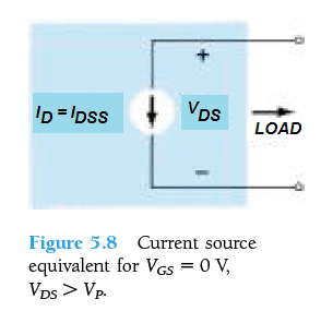 The selection of IDSS notation is based on the fact that it is the Drain to Source current having a short circuited link across gate to source.
Further investigation gives us the following evaluation:
IDSS is the highest drain current for a JFET and is established by the conditions VGS = 0 V and VDS > |VP|.
Notice that in Fig.
5.6 VGS is 0V for the complete stretch of the curve.
In the following sections we will learn how the Fig 5.6 attributes become influenced as the level of VGS is varied.
The selection of IDSS notation is based on the fact that it is the Drain to Source current having a short circuited link across gate to source.
Further investigation gives us the following evaluation:
IDSS is the highest drain current for a JFET and is established by the conditions VGS = 0 V and VDS > |VP|.
Notice that in Fig.
5.6 VGS is 0V for the complete stretch of the curve.
In the following sections we will learn how the Fig 5.6 attributes become influenced as the level of VGS is varied.
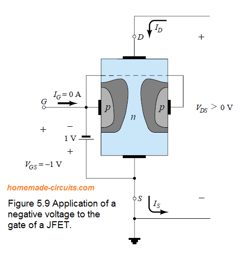 The objective of negative potential bias VGS is to develop depletion regions resembling the situation of VGS = 0, but at significantly reduced VDS.
This causes the gate to attain a saturation point with a lower levels of VDS as indicated in Fig.
5.10 (VGS = -1V).
The corresponding saturatio level for ID can be found to be reduced and actually just goes on decreasing as VGS is made more negative.
You can clearly see in Fig.
5.10 how the pinch-off voltage carries on dropping with a parabolic shape as VGS gets more and more negative.
Finally, when VGS = -Vp, it gets sufficiently negative to establish a saturation level which is eventually 0 mA.
At this level, the JFET is completely "turned OFF".
The objective of negative potential bias VGS is to develop depletion regions resembling the situation of VGS = 0, but at significantly reduced VDS.
This causes the gate to attain a saturation point with a lower levels of VDS as indicated in Fig.
5.10 (VGS = -1V).
The corresponding saturatio level for ID can be found to be reduced and actually just goes on decreasing as VGS is made more negative.
You can clearly see in Fig.
5.10 how the pinch-off voltage carries on dropping with a parabolic shape as VGS gets more and more negative.
Finally, when VGS = -Vp, it gets sufficiently negative to establish a saturation level which is eventually 0 mA.
At this level, the JFET is completely "turned OFF".
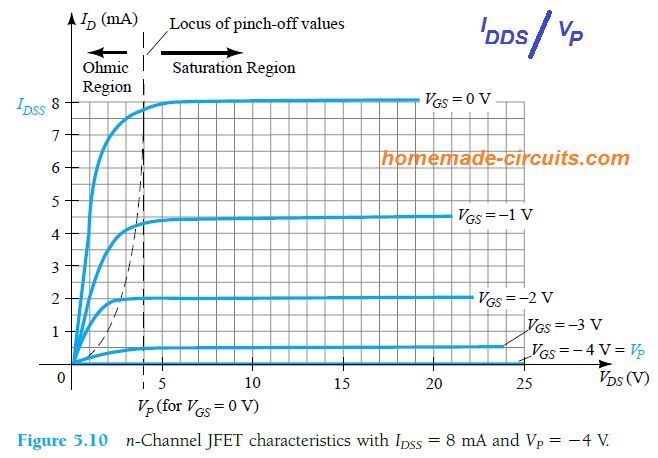 The level of VGS which causes ID to reach 0 mA is characterized by VGS = VP, wherein VP is a negative voltage for n-channel devices and a positive voltage for p-channel JFETs.
Commonly, you may find most JFET datasheets showing pinch-off voltage specified as VGS(off) instead of VP.
The area at the right hand side of the pinch-off locus in the above figure is the place conventionally used in linear amplifiers for achieving distortion free signal.
This region is generally called constant-current, saturation or linear amplification region.
The level of VGS which causes ID to reach 0 mA is characterized by VGS = VP, wherein VP is a negative voltage for n-channel devices and a positive voltage for p-channel JFETs.
Commonly, you may find most JFET datasheets showing pinch-off voltage specified as VGS(off) instead of VP.
The area at the right hand side of the pinch-off locus in the above figure is the place conventionally used in linear amplifiers for achieving distortion free signal.
This region is generally called constant-current, saturation or linear amplification region.
 The directions of the current flow can be also seen as reversed, along with the actual polarities of voltage VGS and VDS.
In case of a p-channel JFET, the channel will get constrained in response to increasing positive potential across the gate/source .
The notation with a double subscript for the VDS will give rise to negative voltage for VDS, as shown on the characteristics of Fig.5.12. Here, you can find IDSS at 6 mA, while a pinch-off voltage at VGS = +6V.
Please do not get puzzled due to the presence of thee minus sign for the VDS.
It simply indicates that source carries a higher potential than the drain.
The directions of the current flow can be also seen as reversed, along with the actual polarities of voltage VGS and VDS.
In case of a p-channel JFET, the channel will get constrained in response to increasing positive potential across the gate/source .
The notation with a double subscript for the VDS will give rise to negative voltage for VDS, as shown on the characteristics of Fig.5.12. Here, you can find IDSS at 6 mA, while a pinch-off voltage at VGS = +6V.
Please do not get puzzled due to the presence of thee minus sign for the VDS.
It simply indicates that source carries a higher potential than the drain.
 You can see that the curves for high VDS levels abruptly rise to values that look unrestricted.
The indicated rise which are vertical symbolize a breakdown situation, which means the current through the channel device is entirely controlled by the external circuitry at this point of time.
Although this is not apparent in Fig.5.10 for n-channel device, it may be a possibility under sufficiently high voltage.
This region can be eliminated if the VDS(max) is noted from the datasheet of the device, and the device is configured such that the actual VDS value is lower than this noted value for any VGS.
You can see that the curves for high VDS levels abruptly rise to values that look unrestricted.
The indicated rise which are vertical symbolize a breakdown situation, which means the current through the channel device is entirely controlled by the external circuitry at this point of time.
Although this is not apparent in Fig.5.10 for n-channel device, it may be a possibility under sufficiently high voltage.
This region can be eliminated if the VDS(max) is noted from the datasheet of the device, and the device is configured such that the actual VDS value is lower than this noted value for any VGS.
 Any different form of display not matching the approximate 0.7 V, such as 0, 4, or 12 V, or a negative could be an indication of a faulty device, and the network connections might require a deeper analysis during such a situation.
For a pnp transistor, the very same strategy may be used however the meter probe polarity will need to be reversed for getting a similar response.
Any different form of display not matching the approximate 0.7 V, such as 0, 4, or 12 V, or a negative could be an indication of a faulty device, and the network connections might require a deeper analysis during such a situation.
For a pnp transistor, the very same strategy may be used however the meter probe polarity will need to be reversed for getting a similar response.
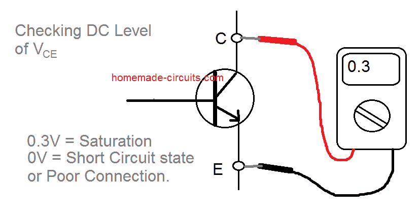 For Example if supply voltage VCC = 20 V, and a display on the meter for collector-emitter current VCE is may be 1 to 2 V or 18 to 20 V then undoubtedly it is an an abnormal outcome.
Unless, otherwise this is intentionally designed the network and connections must be inspected.
This can be witnessed in the below shown image.
For Example if supply voltage VCC = 20 V, and a display on the meter for collector-emitter current VCE is may be 1 to 2 V or 18 to 20 V then undoubtedly it is an an abnormal outcome.
Unless, otherwise this is intentionally designed the network and connections must be inspected.
This can be witnessed in the below shown image.
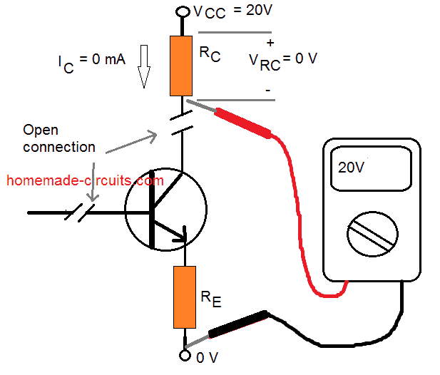 Here we can see the black probe of the voltmeter is attached to the common ground of the source and the red probe to the lower terminal of the resistor.
With collector current not present and a corresponding zero voltage drop around RC may result in a reading of 20 V.
When the meter is joined to the collector terminal of the BJT, the reading will probably be 0 V because the supply VCC is cut off from the active device due to the open circuit.
Here we can see the black probe of the voltmeter is attached to the common ground of the source and the red probe to the lower terminal of the resistor.
With collector current not present and a corresponding zero voltage drop around RC may result in a reading of 20 V.
When the meter is joined to the collector terminal of the BJT, the reading will probably be 0 V because the supply VCC is cut off from the active device due to the open circuit.
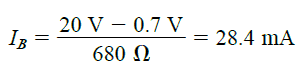 A base current of 28.4 mA would undoubtedly mean the device is in the saturation region which might result in damaging the device.
Due to the fact real resistor values in many cases are not the same as the minimal color-code value, it might be advisable to confirm the resistor value with a Ohm-meter before applying it in the circuit.
This will ensure that genuine values are closer to assumptive ranges and give the user certain assurance regarding the correct resistance value being exercised.
A base current of 28.4 mA would undoubtedly mean the device is in the saturation region which might result in damaging the device.
Due to the fact real resistor values in many cases are not the same as the minimal color-code value, it might be advisable to confirm the resistor value with a Ohm-meter before applying it in the circuit.
This will ensure that genuine values are closer to assumptive ranges and give the user certain assurance regarding the correct resistance value being exercised.
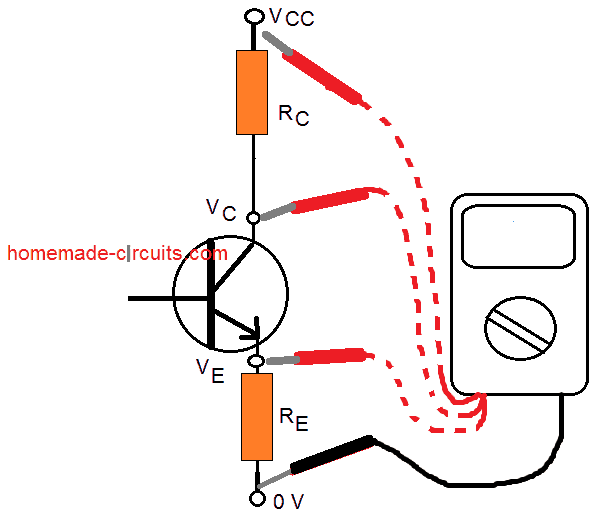 In the figure above, when the red probe is attached directly to supply VCC, it must display the fed VCC voltage level on the meter.
This is simply because the network works with a single common ground for the connected supply and other parameters.
At VC the reading must be less, depending on the voltage drop across RC.
And the voltage VE must be lower than VC by a magnitude equal to VCE or the collector-emitter voltage.
The failure of registering any of these instances would be enough to define a faulty connection or element.
If VRC and VRE carry fair values but VCE shows 0 V, the likelihood may be that the BJT is internally damaged resulting in a short-circuit kind of reading between collector and emitter terminals.
As noted earlier, if VCE registers a level of about 0.3 V as defined by VCE = VC - VE (due to the variation of the two quantities as assessed above), the system may indicate a saturated condition with a BJT that may be defective or perhaps may not be defective.
It must be relatively apparent through the above discussion that the voltmeter whether analogue or digital is pretty crucial in the repairing procedure.
Current (ampere) ranges are often determined through the voltage levels itself, measured across the various resistors, rather than unnecessarily ��breaking�� the network to insert the milliammeter probes of a multimeter.
For checking bigger schematics, precise voltage ranges are supplied in datasheets with reference to ground for effortless testing and recognition of probable troublesome areas.
In the figure above, when the red probe is attached directly to supply VCC, it must display the fed VCC voltage level on the meter.
This is simply because the network works with a single common ground for the connected supply and other parameters.
At VC the reading must be less, depending on the voltage drop across RC.
And the voltage VE must be lower than VC by a magnitude equal to VCE or the collector-emitter voltage.
The failure of registering any of these instances would be enough to define a faulty connection or element.
If VRC and VRE carry fair values but VCE shows 0 V, the likelihood may be that the BJT is internally damaged resulting in a short-circuit kind of reading between collector and emitter terminals.
As noted earlier, if VCE registers a level of about 0.3 V as defined by VCE = VC - VE (due to the variation of the two quantities as assessed above), the system may indicate a saturated condition with a BJT that may be defective or perhaps may not be defective.
It must be relatively apparent through the above discussion that the voltmeter whether analogue or digital is pretty crucial in the repairing procedure.
Current (ampere) ranges are often determined through the voltage levels itself, measured across the various resistors, rather than unnecessarily ��breaking�� the network to insert the milliammeter probes of a multimeter.
For checking bigger schematics, precise voltage ranges are supplied in datasheets with reference to ground for effortless testing and recognition of probable troublesome areas.
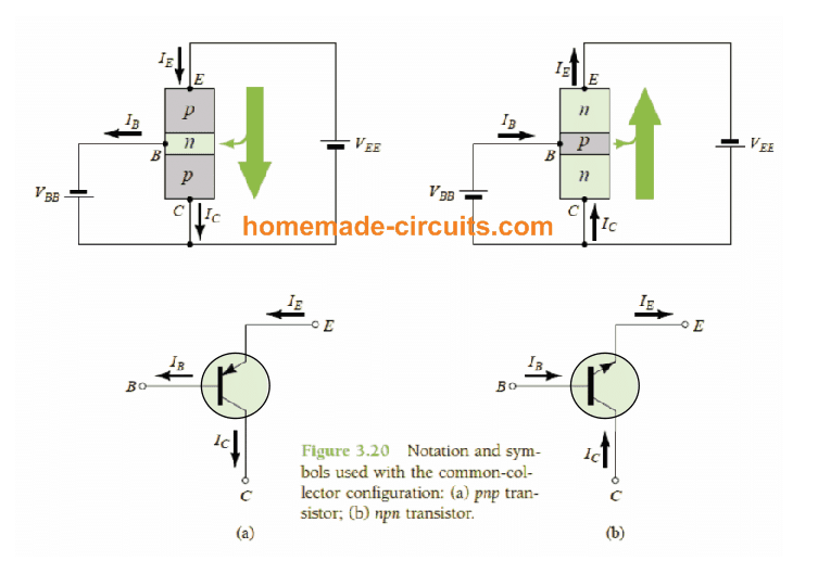
 From the figure above we can see that the load here is attached with the emitter pin of the transistor and the collector is connected to a common reference with respect to the base (input).
Meaning, the collector is common to both the input and the output load.
In other words, the supply coming to the base and the collector both share the common polarity.
Here, the base becomes the input and the emitter becomes the output.
It would be interesting to note that, although the configuration resembles our previous common-emitter configuration, the collector can be seen attached with the "Common Source".
With regards to the design features, we don't have to incorporate the set of common collector characteristics for establishing the circuit parameters.
For all practical implementations, the output characteristics of a common-collector configuration will be exact as attributed for the common-emitter
Therfeore, we can simply design it by using the characteristics employed for the common-emitter network.
For every common-collector configuration, the output characteristics are plotted by applying IE vs VECfortheavailableIBrangeofvalues.
This implies that the both common-emitter and common-collector have identical input current values.
For achieving the horizontal axis for a common-collector, we just need to change the polarity of collector-emitter voltage in a common-emitter characteristics.
Finally, you will see that there's hardly any difference in the vertical scale of a common-emitter IC, if this is interchanged with IE in a common-collector characteristics, (since �� 1 ).
While designing the input side, we can apply the common-emitter base characteristics in order to achieve the essential data.
From the figure above we can see that the load here is attached with the emitter pin of the transistor and the collector is connected to a common reference with respect to the base (input).
Meaning, the collector is common to both the input and the output load.
In other words, the supply coming to the base and the collector both share the common polarity.
Here, the base becomes the input and the emitter becomes the output.
It would be interesting to note that, although the configuration resembles our previous common-emitter configuration, the collector can be seen attached with the "Common Source".
With regards to the design features, we don't have to incorporate the set of common collector characteristics for establishing the circuit parameters.
For all practical implementations, the output characteristics of a common-collector configuration will be exact as attributed for the common-emitter
Therfeore, we can simply design it by using the characteristics employed for the common-emitter network.
For every common-collector configuration, the output characteristics are plotted by applying IE vs VECfortheavailableIBrangeofvalues.
This implies that the both common-emitter and common-collector have identical input current values.
For achieving the horizontal axis for a common-collector, we just need to change the polarity of collector-emitter voltage in a common-emitter characteristics.
Finally, you will see that there's hardly any difference in the vertical scale of a common-emitter IC, if this is interchanged with IE in a common-collector characteristics, (since �� 1 ).
While designing the input side, we can apply the common-emitter base characteristics in order to achieve the essential data.
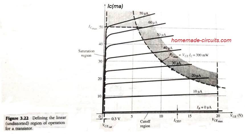 You will also find these limits of operation on all transistor datasheets.
A few of these limits of operation are easily understandable, for example we know what is maximum collector current (referred to as continuous collector current in datasheets), and maximum collector-to-emitter voltage (typically abbreviated as VCEOindatasheets).
For the example BJT demonstrated in the above graph, we find IC(max) is specified as 50 mA and VCEO as 20 V.
The vertical line drawn indicated as VCE(sat) on the characteristic , exhibits the minimum VCE which can be implemented without crossing the non-linear region, indicated with the name "saturation region".
The VCE(sat) specified for BJTs is normally around 0.3V.
The highest possible dissipation level is calculated using the following formula:
You will also find these limits of operation on all transistor datasheets.
A few of these limits of operation are easily understandable, for example we know what is maximum collector current (referred to as continuous collector current in datasheets), and maximum collector-to-emitter voltage (typically abbreviated as VCEOindatasheets).
For the example BJT demonstrated in the above graph, we find IC(max) is specified as 50 mA and VCEO as 20 V.
The vertical line drawn indicated as VCE(sat) on the characteristic , exhibits the minimum VCE which can be implemented without crossing the non-linear region, indicated with the name "saturation region".
The VCE(sat) specified for BJTs is normally around 0.3V.
The highest possible dissipation level is calculated using the following formula:
 In the above characteristic image, the assumed BJT's collector power dissipation is shown as 300mW.
Now the question is, what is the method through which we can plot the curve for the collector power dissipation, defined by the following specifications:
In the above characteristic image, the assumed BJT's collector power dissipation is shown as 300mW.
Now the question is, what is the method through which we can plot the curve for the collector power dissipation, defined by the following specifications:
 E
This implies that the product of VCE and IC must be equal to 300mW, at any point on the characteristics.
If suppose IC has a maximum value of 50mA, substituting this in the above equation gives us the following results:
E
This implies that the product of VCE and IC must be equal to 300mW, at any point on the characteristics.
If suppose IC has a maximum value of 50mA, substituting this in the above equation gives us the following results:
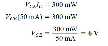 The above results tells us that if IC = 50mA, then VCE will be 6V on the power dissipation curve, as proven in Fig 3.22.
Now if we pick VCE with the highest value of 20V, then the IC level will be as estimated below:
The above results tells us that if IC = 50mA, then VCE will be 6V on the power dissipation curve, as proven in Fig 3.22.
Now if we pick VCE with the highest value of 20V, then the IC level will be as estimated below:
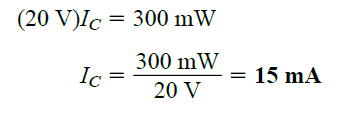 This establishes the second point over the power curve.
Now if we select a level of IC around the mid-way, let's say at 25mA, and apply it on the resultant level of VCE, then we get the following solution:
This establishes the second point over the power curve.
Now if we select a level of IC around the mid-way, let's say at 25mA, and apply it on the resultant level of VCE, then we get the following solution:
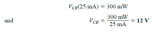 The same is proven in Fig 3.22 also.
The 3 points explained can be effectively applied for getting an approximate value of the actual curve.
No doubt we can use more number of points for the estimation and get even better accuracy, nevertheless an approximate becomes just enough for most applications.
The area that can be seen below IC = ICEO is called the cut-off region.
This region must not be reached to ensure a distortion free working of the BJT.
The same is proven in Fig 3.22 also.
The 3 points explained can be effectively applied for getting an approximate value of the actual curve.
No doubt we can use more number of points for the estimation and get even better accuracy, nevertheless an approximate becomes just enough for most applications.
The area that can be seen below IC = ICEO is called the cut-off region.
This region must not be reached to ensure a distortion free working of the BJT.
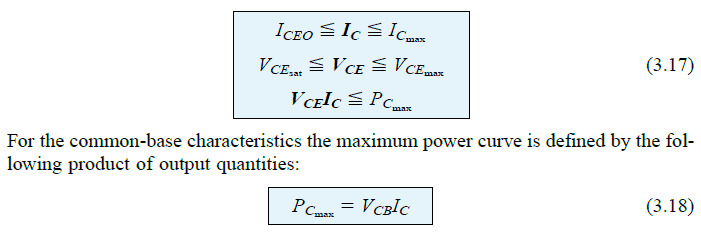
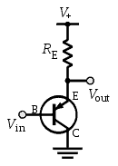 PNP version of the emitter follower circuit, all polarities are reversed.
Even the smallest of the voltage deviations at the base of a common collector transistor is duplicated across the emitter lead, which to an extent is dependent on the gain (Hfe) of the transistor and the resistance of the load attached).
The main benefit of this circuit is its high input impedance feature, which allows the circuit to perform efficiently regardless of the input current or the load resistance, meaning even huge loads can be efficiently operated with inputs having minimal current.
That's why a common collector is used as a buffer, meaning a stage which efficiently integrates high load operations from a relatively weak current source (example a TTL or Arduino source)
The high input impedance is expressed with the formula:
PNP version of the emitter follower circuit, all polarities are reversed.
Even the smallest of the voltage deviations at the base of a common collector transistor is duplicated across the emitter lead, which to an extent is dependent on the gain (Hfe) of the transistor and the resistance of the load attached).
The main benefit of this circuit is its high input impedance feature, which allows the circuit to perform efficiently regardless of the input current or the load resistance, meaning even huge loads can be efficiently operated with inputs having minimal current.
That's why a common collector is used as a buffer, meaning a stage which efficiently integrates high load operations from a relatively weak current source (example a TTL or Arduino source)
The high input impedance is expressed with the formula:
 and the small output impedance, so it can drive low-resistance loads:
 Practically seeing, the emitter resistor could be significantly larger and can therefore be ignored in the above formula, which finally gives us the relationship:
 Formally, the term��ac is referred to as common-emitter, forward-current amplification factor.
Since in common-emitter circuits the collector current typically becomes the output of the BJT circuit, and the base current acts like the input, the amplification factor is expressed as shown in the above nomenclature.
The format of equation 3.11 quite resembles the format of��ac asdiscussed in our earlier section 3.4.
In this section we avoided the procedure of determining the value of��ac from the characteristics curves due to the involved complexity of measuring the genuine changes between the IC and IE over the curve.
However, for the equation 3.11 we find it possible to explain it with some clarity, and furthermore it also allows us to find the value of ��acfrom a derivation.
In BJT datasheets, ��acis normally shown as hfe.
Here we can see that the difference is only the in the lettering of the fe, which are in lowercase compared to the uppercase as used for��dc.
Here too the letter h is used for identifying the h as in the phrasehybrid equivalent circuit, and fe is derived from the phrases forward current gain and common-emitter configuration.
Fig 3.14a shows the best method of implementing the Eq.3.11 through a numerical example, with a set of characteristics, and this is produced again in Fig.
3.17.
Now let's see how we can determine��acfor a region of the characteristics identified by an operating point having values IB = 25 ��a and VCE = 7.5 V as shown in Fig 3.17.
Formally, the term��ac is referred to as common-emitter, forward-current amplification factor.
Since in common-emitter circuits the collector current typically becomes the output of the BJT circuit, and the base current acts like the input, the amplification factor is expressed as shown in the above nomenclature.
The format of equation 3.11 quite resembles the format of��ac asdiscussed in our earlier section 3.4.
In this section we avoided the procedure of determining the value of��ac from the characteristics curves due to the involved complexity of measuring the genuine changes between the IC and IE over the curve.
However, for the equation 3.11 we find it possible to explain it with some clarity, and furthermore it also allows us to find the value of ��acfrom a derivation.
In BJT datasheets, ��acis normally shown as hfe.
Here we can see that the difference is only the in the lettering of the fe, which are in lowercase compared to the uppercase as used for��dc.
Here too the letter h is used for identifying the h as in the phrasehybrid equivalent circuit, and fe is derived from the phrases forward current gain and common-emitter configuration.
Fig 3.14a shows the best method of implementing the Eq.3.11 through a numerical example, with a set of characteristics, and this is produced again in Fig.
3.17.
Now let's see how we can determine��acfor a region of the characteristics identified by an operating point having values IB = 25 ��a and VCE = 7.5 V as shown in Fig 3.17.
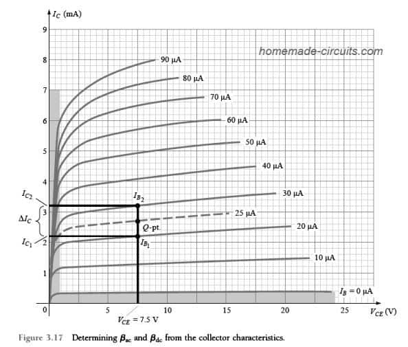 The rule that restricts VCE = constant demands the vertical line to be drawn in a way that it cuts through the operating point at VCE = 7.5 V.
This renders the valueVCE = 7.5 V to remain as a constant throughout this vertical line.
The variation in IB (��IB) as apparent in Eq.
3.11 is consequently described by selecting a couple of points on the two sides of the Q-point (operating point) along the vertical axis having approximately uniform distances on either side of the Q-point.
For the indicated situation the curves involving the magnitudes IB = 20 ��A and 30 ��A satisfy the requirements by staying close to the Q-point.
These furthermore establish the levels of IB which are defined without difficulty instead of requiring the need to interpolate the IB level between the curves.
It might be important to note that best results is determined typically by selecting ��IBas small as possible.
We can find out the two magnitudes of IC at the place where the two intersections of IB and the vertical axis intersect by drawing a horizontal line across the vertical axis and by evaluating the resulting values of IC.
The��ac established for the specific region could then be identified by solving the formula:
The rule that restricts VCE = constant demands the vertical line to be drawn in a way that it cuts through the operating point at VCE = 7.5 V.
This renders the valueVCE = 7.5 V to remain as a constant throughout this vertical line.
The variation in IB (��IB) as apparent in Eq.
3.11 is consequently described by selecting a couple of points on the two sides of the Q-point (operating point) along the vertical axis having approximately uniform distances on either side of the Q-point.
For the indicated situation the curves involving the magnitudes IB = 20 ��A and 30 ��A satisfy the requirements by staying close to the Q-point.
These furthermore establish the levels of IB which are defined without difficulty instead of requiring the need to interpolate the IB level between the curves.
It might be important to note that best results is determined typically by selecting ��IBas small as possible.
We can find out the two magnitudes of IC at the place where the two intersections of IB and the vertical axis intersect by drawing a horizontal line across the vertical axis and by evaluating the resulting values of IC.
The��ac established for the specific region could then be identified by solving the formula:
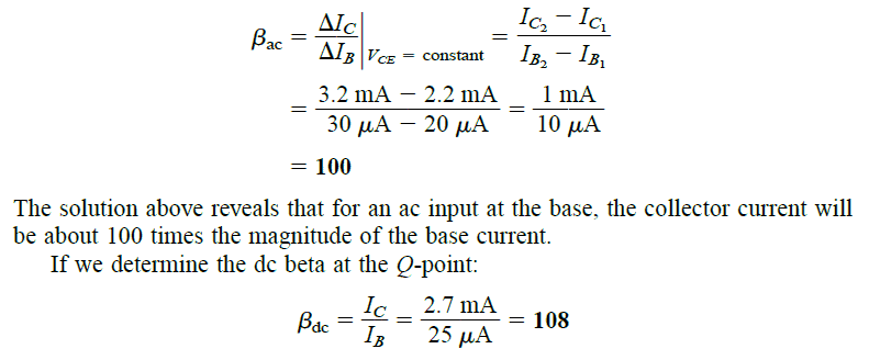 The values of��ac and��dc can be found reasonably close to each other, and therefore they could be often interchanged.
Meaning if the value of��ac is identified, we may be able to use the same value for assessing��dc also.
However, remember that these values could be vary across BJTs, even if they are from the same batch or lot.
Typically, the similarity in the values of the two betas depends on how small the specification of ICEOis for the particular transistor.
Smaller ICEO will present higher similarity and vice versa.
Since the preference is to have the least ICEO value for a BJT, the similarity dependence of the two betas turns out to be a genuine and acceptable occurrence.
If we had the characteristic appearing as shown in Fig.
3.18, we would had the��ac similar at all the regions of the characteristics,
You can see that the step of IB is set at 10��A and the curves have identical vertical spaces across all the characteristics points,which is 2 mA.
If we evaluate the value of ��acat the indicated Q-point, would produce the result as shown below:
The values of��ac and��dc can be found reasonably close to each other, and therefore they could be often interchanged.
Meaning if the value of��ac is identified, we may be able to use the same value for assessing��dc also.
However, remember that these values could be vary across BJTs, even if they are from the same batch or lot.
Typically, the similarity in the values of the two betas depends on how small the specification of ICEOis for the particular transistor.
Smaller ICEO will present higher similarity and vice versa.
Since the preference is to have the least ICEO value for a BJT, the similarity dependence of the two betas turns out to be a genuine and acceptable occurrence.
If we had the characteristic appearing as shown in Fig.
3.18, we would had the��ac similar at all the regions of the characteristics,
You can see that the step of IB is set at 10��A and the curves have identical vertical spaces across all the characteristics points,which is 2 mA.
If we evaluate the value of ��acat the indicated Q-point, would produce the result as shown below:
 This proves that the values of the ac and dc betas will be identical if the characteristic of the BJT appear like in the Fig.3.18. Specifically, we can notice here that the ICEO = 0��A
 In the following analysis, we will be ignoring the ac or dc subscripts for the betas just to keep the symbols simple and clean.
Therefore for any BJT configuration the symbol�� will be considered as the beta for both ac and dc calculations.
We have already discussed regarding alpha in one of our earlier posts.
Let's now see how we can create a relationship between the alpha and beta by applying the fundamental principles learned so far.
Using �� = IC / IB
we get IB = IC /��,
Similarly for the term alpha also, we can deduce the following value:
�� = IC / IE, and IE = IC /��
Therefore substituting and rearranging the terms we find the following relationship:
In the following analysis, we will be ignoring the ac or dc subscripts for the betas just to keep the symbols simple and clean.
Therefore for any BJT configuration the symbol�� will be considered as the beta for both ac and dc calculations.
We have already discussed regarding alpha in one of our earlier posts.
Let's now see how we can create a relationship between the alpha and beta by applying the fundamental principles learned so far.
Using �� = IC / IB
we get IB = IC /��,
Similarly for the term alpha also, we can deduce the following value:
�� = IC / IE, and IE = IC /��
Therefore substituting and rearranging the terms we find the following relationship:
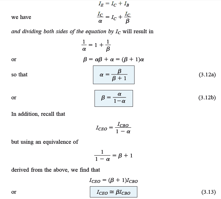 The above results is as indicated in Fig.
3.14a.
Beta becomes a crucial parameter as it allows us to identify a direct relationship between the magnitudes of currents across the input and output stages for a common-emitter configuration.
This can be acknowledged from the following evaluations:
The above results is as indicated in Fig.
3.14a.
Beta becomes a crucial parameter as it allows us to identify a direct relationship between the magnitudes of currents across the input and output stages for a common-emitter configuration.
This can be acknowledged from the following evaluations:
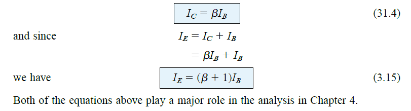 This concludes our analysis regarding what is beta in BJT configurations.
If you have any suggestions or further information please do share in the comments section.
This concludes our analysis regarding what is beta in BJT configurations.
If you have any suggestions or further information please do share in the comments section.
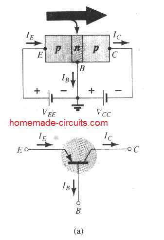 Figure 3.6
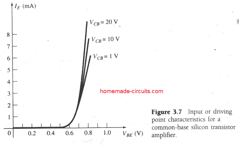 The output set applies an output current (IC) for an output voltage (VCB) for a variety of ranges of input current (IE) as demonstrated in Fig.
3.8. The output, or the group of collector characteristics, possesses 3 fundamental elements of interest, as pointed out in Fig.
3.8: the active, cutoff, and saturation regions.
The active region will be the region typically useful for linear (undistorted) amplifiers.
Specifically:
Within the active region the collector-base junction will be reverse-biased, while the base-emitter junction is forward-biased.
The active region is characterized by the biasing configurations as indicated in Fig.
3.6. On the lower end of the active region the emitter current (IE) will be zero, the collector current is in this situation simply as a result of reverse saturation current ICO, as illustrated in Fig.
3.8.
The output set applies an output current (IC) for an output voltage (VCB) for a variety of ranges of input current (IE) as demonstrated in Fig.
3.8. The output, or the group of collector characteristics, possesses 3 fundamental elements of interest, as pointed out in Fig.
3.8: the active, cutoff, and saturation regions.
The active region will be the region typically useful for linear (undistorted) amplifiers.
Specifically:
Within the active region the collector-base junction will be reverse-biased, while the base-emitter junction is forward-biased.
The active region is characterized by the biasing configurations as indicated in Fig.
3.6. On the lower end of the active region the emitter current (IE) will be zero, the collector current is in this situation simply as a result of reverse saturation current ICO, as illustrated in Fig.
3.8.
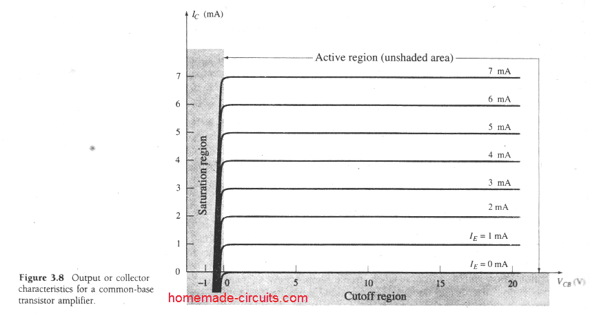 The current ICO is so negligible (microamperes) in dimension in comparison to the vertical scale of IC (milliamperes) that it presents itself practically on the same horizontal line as IC = 0.
The circuit considerations which are present when IE = 0 for the common-base setup can be seen in Fig.
3.9. The annotation most often applied for ICO on datasheets and spec sheets is as pointed out in Fig.
3.9, ICBO.
On account of superior design methods, the degree of ICBO for general-purpose transistors (particularly silicon) within the low- and midpower ranges is normally so minimal that its influence could be overlooked.
The current ICO is so negligible (microamperes) in dimension in comparison to the vertical scale of IC (milliamperes) that it presents itself practically on the same horizontal line as IC = 0.
The circuit considerations which are present when IE = 0 for the common-base setup can be seen in Fig.
3.9. The annotation most often applied for ICO on datasheets and spec sheets is as pointed out in Fig.
3.9, ICBO.
On account of superior design methods, the degree of ICBO for general-purpose transistors (particularly silicon) within the low- and midpower ranges is normally so minimal that its influence could be overlooked.
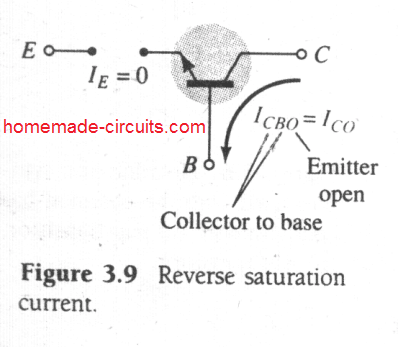 Having said that, for larger power devices ICBO might continue to show up in the microampere range.
Furthermore, remember that ICBO, just likeIs in case of diodes (both are reverse leakage currents) could be vulnerable to changes in temperature.
At increased temperatures the impact of ICBO may result being a crucial aspect because it can rise significantly quickly in response to temperature elevations.
Be aware in Fig.
3.8 as the emitter current rises over zero, the collector current goes up to a level primarily equivalent to that of the emitter current as established by the fundamental transistor-current relationships.
Notice also that there's quite an ineffective influence of VCB on the collector current for the active region.
The curved shapes evidently reveal that an initial estimation to the relationship between IE and IC in the active region can be presented as:
Having said that, for larger power devices ICBO might continue to show up in the microampere range.
Furthermore, remember that ICBO, just likeIs in case of diodes (both are reverse leakage currents) could be vulnerable to changes in temperature.
At increased temperatures the impact of ICBO may result being a crucial aspect because it can rise significantly quickly in response to temperature elevations.
Be aware in Fig.
3.8 as the emitter current rises over zero, the collector current goes up to a level primarily equivalent to that of the emitter current as established by the fundamental transistor-current relationships.
Notice also that there's quite an ineffective influence of VCB on the collector current for the active region.
The curved shapes evidently reveal that an initial estimation to the relationship between IE and IC in the active region can be presented as:
 As deduced from its title itself, the cutoff region is understood to be that location where the collector current is 0 A, as disclosed on Fig.
3.8. Furthermore:
In the cut-off region the collector-base and base-emitter junctions of a transistor tend to be in the reverse-biased mode.
The saturation region is identified as that section of the characteristics across the left side of VCB = 0 V.
The horizontal scale in this area has been enlarged to distinctly reveal the remarkable enhancements made on attributes in this region.
Observe the exponential upsurge in collector current in response to the increase in the voltage VCB toward 0 V.
The collector-base and base-emitter junctions can be seen to be forward-biasIn the saturation region.
The input characteristics of Fig.
3.7 show you that for any predetermined magnitudes of collector voltage (VCB), the emitter current increases in such a way that may strongly resemble to that of the diode characteristics.
Actually, the effect of a rising VCB tends to be so minimal on the characteristics that for any preliminary evaluation the difference caused by variations in VCB could be disregarded and the characteristics could be actually represented as demonstrated in Fig.
3.10a below.
If we therefore utilize the piecewise-linear technique, this will produce the characteristics as revealed in Fig.
3.10b.
Taking this one level up, and disregarding the slope of the curve and consequently the resistance generated due to a forward-biased junction will lead to the characteristics as displayed in Fig.
3.10c.
For all the future investigations that would be discussed in this website, the equivalent design of Fig.
3.10c is going to be exercised for all dc evaluations of transistor circuits.
Meaning , whenever a BJT is in the ��conducting�� status, the base-to-emitter voltage is going to be considered as expressed in the following equation: VBE = 0.7 V (3.4).
As deduced from its title itself, the cutoff region is understood to be that location where the collector current is 0 A, as disclosed on Fig.
3.8. Furthermore:
In the cut-off region the collector-base and base-emitter junctions of a transistor tend to be in the reverse-biased mode.
The saturation region is identified as that section of the characteristics across the left side of VCB = 0 V.
The horizontal scale in this area has been enlarged to distinctly reveal the remarkable enhancements made on attributes in this region.
Observe the exponential upsurge in collector current in response to the increase in the voltage VCB toward 0 V.
The collector-base and base-emitter junctions can be seen to be forward-biasIn the saturation region.
The input characteristics of Fig.
3.7 show you that for any predetermined magnitudes of collector voltage (VCB), the emitter current increases in such a way that may strongly resemble to that of the diode characteristics.
Actually, the effect of a rising VCB tends to be so minimal on the characteristics that for any preliminary evaluation the difference caused by variations in VCB could be disregarded and the characteristics could be actually represented as demonstrated in Fig.
3.10a below.
If we therefore utilize the piecewise-linear technique, this will produce the characteristics as revealed in Fig.
3.10b.
Taking this one level up, and disregarding the slope of the curve and consequently the resistance generated due to a forward-biased junction will lead to the characteristics as displayed in Fig.
3.10c.
For all the future investigations that would be discussed in this website, the equivalent design of Fig.
3.10c is going to be exercised for all dc evaluations of transistor circuits.
Meaning , whenever a BJT is in the ��conducting�� status, the base-to-emitter voltage is going to be considered as expressed in the following equation: VBE = 0.7 V (3.4).
 To put it differently, the influence of the changes in the value of VCB along with the input characteristics slope will tend to be overlooked as we make an effort to evaluate BJT configurations in such a way that may help us to acquire an optimal approximation towards the actual response, without too much involving ourselves with parameter which may be of less significance.
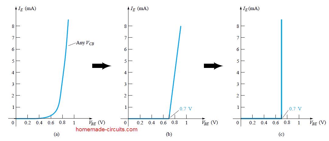 Figure 3.10
We all should actually thoroughly appreciate the assertion expressed in the above characteristics of Fig.
3.10c.
They define that with the transistor in the ��on�� or active condition the voltage moving from base to emitter is going to be 0.7 V for any amount of emitter current as regulated by the associated external circuit network.
To be more precise , for any initial experimentation with a BJT circuit in the dc configuration, the user can now quickly define that the voltage through base to emitter is 0.7 V while the device is in the active region - this can be considered as an extremely crucial bottom line for all our dc analysis which would be discussed in our upcoming articles..
Figure 3.10
We all should actually thoroughly appreciate the assertion expressed in the above characteristics of Fig.
3.10c.
They define that with the transistor in the ��on�� or active condition the voltage moving from base to emitter is going to be 0.7 V for any amount of emitter current as regulated by the associated external circuit network.
To be more precise , for any initial experimentation with a BJT circuit in the dc configuration, the user can now quickly define that the voltage through base to emitter is 0.7 V while the device is in the active region - this can be considered as an extremely crucial bottom line for all our dc analysis which would be discussed in our upcoming articles..
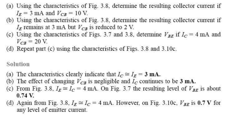 In the above sections we learned what is common-base configuration about the relationship between base current IC and emitter current IE of a BJT in section 3.4. With reference to this article we can now design a configuration which would allow the BJT to amplify current, as represented in Fig 3.12 below common-base amplifier circuit.
But before investigating this, it would be important for us to learn what is alpha(��).
In the above sections we learned what is common-base configuration about the relationship between base current IC and emitter current IE of a BJT in section 3.4. With reference to this article we can now design a configuration which would allow the BJT to amplify current, as represented in Fig 3.12 below common-base amplifier circuit.
But before investigating this, it would be important for us to learn what is alpha(��).
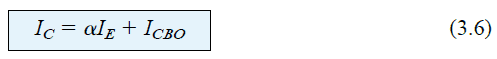 Referring to the characteristic in graph Fig 3.8, when IE = 0 mA, IC value consequently becomes = ICBO.
However, from our previous discussions we know that the level of ICBO is often minimal, and therefore it becomes almost unidentifiable in the graph of 3.8.
Meaning, whenever IE = 0 mA in the above mentioned graph, IC also turns into 0 mA for the VCB range of values.
When we consider an ac signal, wherein the point of operation travels over the characteristic curve, an ac alpha can be written as:
Referring to the characteristic in graph Fig 3.8, when IE = 0 mA, IC value consequently becomes = ICBO.
However, from our previous discussions we know that the level of ICBO is often minimal, and therefore it becomes almost unidentifiable in the graph of 3.8.
Meaning, whenever IE = 0 mA in the above mentioned graph, IC also turns into 0 mA for the VCB range of values.
When we consider an ac signal, wherein the point of operation travels over the characteristic curve, an ac alpha can be written as:
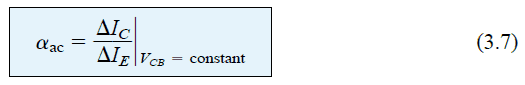 There are a few formal names given to ac alpha which are: common-base, amplification factor, short-circuit.The reasons for these names will get more apparent in the upcoming chapters while evaluating equivalent circuits of BJTs.
At this point we can find that Eq 3.7 above confirms that a relatively modest variation in the collector current gets divided by the resultant change in IE, while the collector-to-base is at a constant magnitude.
In majority conditions, the quantity of�� ac and�� dc are almost equal allowing an exchange of magnitudes among each other.
There are a few formal names given to ac alpha which are: common-base, amplification factor, short-circuit.The reasons for these names will get more apparent in the upcoming chapters while evaluating equivalent circuits of BJTs.
At this point we can find that Eq 3.7 above confirms that a relatively modest variation in the collector current gets divided by the resultant change in IE, while the collector-to-base is at a constant magnitude.
In majority conditions, the quantity of�� ac and�� dc are almost equal allowing an exchange of magnitudes among each other.
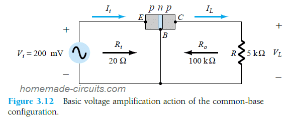 The dc biasing is not shown in the above figure since our actual intent is to analyze the ac response only.
As we learned in our earlier posts regarding common-base configuration, the input ac resistance as indicated in Fig 3.7 looks quite minimal and varying typically within a range of 10 and 100 ohm.
While in the same chapter we also saw in Fig 3.8 the output resistance in a common-base network looks significantly high, which could vary typically in the range of 50 k to 1 M Ohm.
These differences in resistance values is basically on account of the forward-biased junction appearing on the input side (between base to emitter), and the reverse biased junction appearing at the output side between base and collector.
By applying a typical value of say 20 Ohms (as given in the above figure) for the input resistance, and 200mV for input voltage, we can evaluate the amplification level or range at the output side through the following solved example:
The dc biasing is not shown in the above figure since our actual intent is to analyze the ac response only.
As we learned in our earlier posts regarding common-base configuration, the input ac resistance as indicated in Fig 3.7 looks quite minimal and varying typically within a range of 10 and 100 ohm.
While in the same chapter we also saw in Fig 3.8 the output resistance in a common-base network looks significantly high, which could vary typically in the range of 50 k to 1 M Ohm.
These differences in resistance values is basically on account of the forward-biased junction appearing on the input side (between base to emitter), and the reverse biased junction appearing at the output side between base and collector.
By applying a typical value of say 20 Ohms (as given in the above figure) for the input resistance, and 200mV for input voltage, we can evaluate the amplification level or range at the output side through the following solved example:
 Thus, the voltage amplification at the output can be found by solving the following equation:
 This is a typical voltage amplification value for any common-base BJT circuit which could possibly vary between 50 and 300. For such network, the current amplification IC / IE is always less than 1, since IC = alphaIE, and alpha is always less than 1.
In preliminary experiments the fundamental amplifying action was introduced through a transfer of current I across a low to a high-resistance circuit.
The relationship between the two italic phrases in the above sentence actually resulted in the term transistor:
transfer + resistor = transistor.
In the next tutorial we will discuss Common-Emitter Amplifier
Reference:https://en.wikipedia.org/wiki/Common_base
This is a typical voltage amplification value for any common-base BJT circuit which could possibly vary between 50 and 300. For such network, the current amplification IC / IE is always less than 1, since IC = alphaIE, and alpha is always less than 1.
In preliminary experiments the fundamental amplifying action was introduced through a transfer of current I across a low to a high-resistance circuit.
The relationship between the two italic phrases in the above sentence actually resulted in the term transistor:
transfer + resistor = transistor.
In the next tutorial we will discuss Common-Emitter Amplifier
Reference:https://en.wikipedia.org/wiki/Common_base
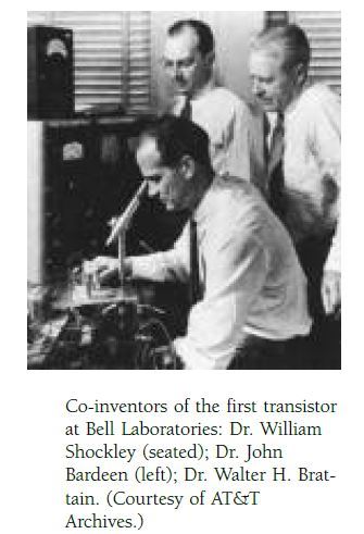 On December 23, 1947, however, the electronics industry was going witness the arrival of an absolutely brand new "direction of interest" and improvement.
It turned out on the mid-day that Walter H.
Brattain and John Bardeen exhibited and proved the amplifying function of the very first transistor at the Bell Telephone Laboratories.
The very first transistor (which was in the form of a point-contact transistor) is demonstrated in Fig.
3.1.
On December 23, 1947, however, the electronics industry was going witness the arrival of an absolutely brand new "direction of interest" and improvement.
It turned out on the mid-day that Walter H.
Brattain and John Bardeen exhibited and proved the amplifying function of the very first transistor at the Bell Telephone Laboratories.
The very first transistor (which was in the form of a point-contact transistor) is demonstrated in Fig.
3.1.
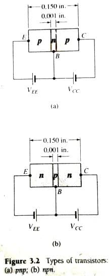
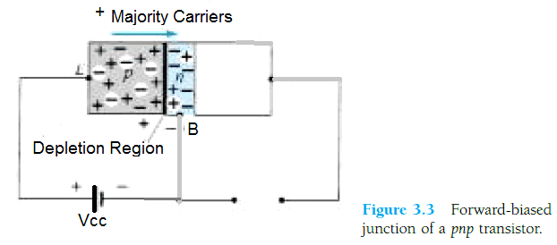 In case the base-to-emitter bias of the pnp transistor is removed as demonstrated in Fig 3.4, the flow of the majority carriers becomes zero, allowing the flow of only minority carriers.
Briefly we can understand that, in a biased situation one p-n junction of a BJT becomes reverse biased while the other junction is forward biased.
In Fig.
3.5 we can see both biasing voltages being applied to a pnp bipolar transistor, which causes the indicatedmajority- and minority-carrier flow.
Here, from the widths of the depletion regions we can clearly visualize which junction has working with a forward-biased condition and which is in reverse-biased.
As shown in the figure a substantial quantity of majority carriers end up being diffused across the forward-biased p-n junction into the n-type material.
This raises a question in our minds, could these carriers play any important roleto promote the base current IB or enable it to flow directly into the p-type material?
Considering that the sandwiched n-type content is incredibly thin and possesses minimal conductivity, an exceptionally few of these carriers is going to take this particular route of high resistance across the base terminal.
The level of the base current is normally around microamperes rather than milliamperes for the emitter and collector currents.
The bigger range of these majority carriers are going to diffuse along the reverse-biased junction into the p type material attached to the collector terminal as pointed out in Fig.
3.5.
The actual cause behind this relative ease with which the majority carriers are allowed to get across the reverse-biased junction is quickly realized by the example of a reverse biased diode where the induced majority carriers turn up as minority carriers in the n-type material.
To put it differently, we find an introduction of minority carriers into the n-type base region material.
With this knowledge and along with the fact that for diodes all the minority carriers in the depletion region get across the reverse-biased junction, results in the flow of electrons, as indicated in Fig.
3.5.
In case the base-to-emitter bias of the pnp transistor is removed as demonstrated in Fig 3.4, the flow of the majority carriers becomes zero, allowing the flow of only minority carriers.
Briefly we can understand that, in a biased situation one p-n junction of a BJT becomes reverse biased while the other junction is forward biased.
In Fig.
3.5 we can see both biasing voltages being applied to a pnp bipolar transistor, which causes the indicatedmajority- and minority-carrier flow.
Here, from the widths of the depletion regions we can clearly visualize which junction has working with a forward-biased condition and which is in reverse-biased.
As shown in the figure a substantial quantity of majority carriers end up being diffused across the forward-biased p-n junction into the n-type material.
This raises a question in our minds, could these carriers play any important roleto promote the base current IB or enable it to flow directly into the p-type material?
Considering that the sandwiched n-type content is incredibly thin and possesses minimal conductivity, an exceptionally few of these carriers is going to take this particular route of high resistance across the base terminal.
The level of the base current is normally around microamperes rather than milliamperes for the emitter and collector currents.
The bigger range of these majority carriers are going to diffuse along the reverse-biased junction into the p type material attached to the collector terminal as pointed out in Fig.
3.5.
The actual cause behind this relative ease with which the majority carriers are allowed to get across the reverse-biased junction is quickly realized by the example of a reverse biased diode where the induced majority carriers turn up as minority carriers in the n-type material.
To put it differently, we find an introduction of minority carriers into the n-type base region material.
With this knowledge and along with the fact that for diodes all the minority carriers in the depletion region get across the reverse-biased junction, results in the flow of electrons, as indicated in Fig.
3.5.
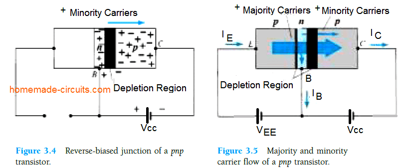 Assuming the transistor in Fig.3.5 to be a single node, we can apply Kirchhoff's current law to get the following equation:
IE = IC + IB
Which shows that the emitter current is equal to the sum of base and collector current.
However, the collector current is made up of a couple of elements, which are namely the majority and the minority carriers as proven in Fig.3.5.
The minority-current carrier element here constitutes the leakage current, and is symbolized as ICO (current IC having an open emitter terminal).
Consequently, the net collector current is established as given in the following equation 3.2:
IC = ICmajority + ICOminority
Collector current IC is measured in mA for all general purpose transistors, while ICO is calculated in uA or nA.
ICO will behave quite like a reverse biased diode and therefore could be vulnerable to temperature changes, and therefore must be appropriately taken care while testing, especially in circuits which are designed to work in widely varying temperature range scenarios, or else the result can be hugely affected due to the temperature factor.
That said, due to the many advanced enhancements in the construction layout of the modern bipolar transistors, the ICO is significantly reduced and can be completely ignored for all today's BJTs.
In the next chapter we will learn how to configure BJTs in the common base mode.
References:https://en.wikipedia.org/wiki/John_Bardeen
Assuming the transistor in Fig.3.5 to be a single node, we can apply Kirchhoff's current law to get the following equation:
IE = IC + IB
Which shows that the emitter current is equal to the sum of base and collector current.
However, the collector current is made up of a couple of elements, which are namely the majority and the minority carriers as proven in Fig.3.5.
The minority-current carrier element here constitutes the leakage current, and is symbolized as ICO (current IC having an open emitter terminal).
Consequently, the net collector current is established as given in the following equation 3.2:
IC = ICmajority + ICOminority
Collector current IC is measured in mA for all general purpose transistors, while ICO is calculated in uA or nA.
ICO will behave quite like a reverse biased diode and therefore could be vulnerable to temperature changes, and therefore must be appropriately taken care while testing, especially in circuits which are designed to work in widely varying temperature range scenarios, or else the result can be hugely affected due to the temperature factor.
That said, due to the many advanced enhancements in the construction layout of the modern bipolar transistors, the ICO is significantly reduced and can be completely ignored for all today's BJTs.
In the next chapter we will learn how to configure BJTs in the common base mode.
References:https://en.wikipedia.org/wiki/John_Bardeen
 Figure 4.17 BJT Bias Circuit with Emitter Resistor
In our discussions we'll begin our analysis of the design by first inspecting the loop around the base-emitter region of the circuit, and then use the results for further investigating the loop around the collector-emitter side of the circuit.
Figure 4.17 BJT Bias Circuit with Emitter Resistor
In our discussions we'll begin our analysis of the design by first inspecting the loop around the base-emitter region of the circuit, and then use the results for further investigating the loop around the collector-emitter side of the circuit.
 We can redraw the above base-emitter loop in the way shown below in Fig 4.18, and if we apply Kirchhoff's voltage lawon this loop in the clockwise direction, helps us to get the following equation:
+Vcc = IBRB - VBE - IERE = 0 -------(4.15)
From our previous discussions we know that: IE = (��+1)IB-------(4.16)
Substituting the value of IE in Eq.(4.15) provides the following result:
Vcc = IBRB- VBE- (��+1)IBRE= 0
Putting the terms in their respective groups yields the following:
We can redraw the above base-emitter loop in the way shown below in Fig 4.18, and if we apply Kirchhoff's voltage lawon this loop in the clockwise direction, helps us to get the following equation:
+Vcc = IBRB - VBE - IERE = 0 -------(4.15)
From our previous discussions we know that: IE = (��+1)IB-------(4.16)
Substituting the value of IE in Eq.(4.15) provides the following result:
Vcc = IBRB- VBE- (��+1)IBRE= 0
Putting the terms in their respective groups yields the following:
 If you recall from our previous chapters, the fixed bias equation was derived in the following form:
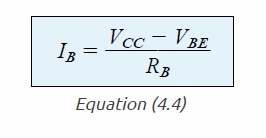 If we compare this fixed bias equation with the (4.17) equation we find the only difference between the two equation for current IB is the the term(��+1)RE.
When the equation 4.17 is used for drawing a series based configuration we are able to extract an interesting result, which actually is the similar to equation 4.17.
If we compare this fixed bias equation with the (4.17) equation we find the only difference between the two equation for current IB is the the term(��+1)RE.
When the equation 4.17 is used for drawing a series based configuration we are able to extract an interesting result, which actually is the similar to equation 4.17.
 Take the example of the following network in Fig 4.19:
If we solve the system for current IB, results in the same equation obtained in Eq.
4.17. Observe that besides the voltage from base to emitter VBE, the resistor RE could be seen appearing again at the input of the base circuit by a level(��+1).
Meaning, the emitter resistor which forms a part of the collector-emitter loop shows up as(��+1)REin the base-emitter loop.
Assuming that �� could be mostly above 50 for most BJTs, the resistor at the emitter of the transistors could be significantly bigger in the base circuit.
Hence, we are able to derive the following general equation for the Fig.4.20:
Ri=(��+1)RE------(4.18)
You will find this equation quite handy while solving many future networks.
Actually, this equation facilitates memorizing equation 4.17 in an easier way.
As per Ohm's law we know that the current through a network is the voltage divided by the resistance of the circuit.
The voltage for a base-emitter design is = Vcc - VBE
The resistances seen in the 4.17 are RB + RE, which is reflected as(��+1),and the result is what we have in Eq 4.17.
Take the example of the following network in Fig 4.19:
If we solve the system for current IB, results in the same equation obtained in Eq.
4.17. Observe that besides the voltage from base to emitter VBE, the resistor RE could be seen appearing again at the input of the base circuit by a level(��+1).
Meaning, the emitter resistor which forms a part of the collector-emitter loop shows up as(��+1)REin the base-emitter loop.
Assuming that �� could be mostly above 50 for most BJTs, the resistor at the emitter of the transistors could be significantly bigger in the base circuit.
Hence, we are able to derive the following general equation for the Fig.4.20:
Ri=(��+1)RE------(4.18)
You will find this equation quite handy while solving many future networks.
Actually, this equation facilitates memorizing equation 4.17 in an easier way.
As per Ohm's law we know that the current through a network is the voltage divided by the resistance of the circuit.
The voltage for a base-emitter design is = Vcc - VBE
The resistances seen in the 4.17 are RB + RE, which is reflected as(��+1),and the result is what we have in Eq 4.17.
 The figure above shows the collector-emitter loop, applying Kirchhoff's law to the indicated loop in the clockwise direction, we get the following equation:
+IERE +VCE+ ICRC- VCC= 0
The figure above shows the collector-emitter loop, applying Kirchhoff's law to the indicated loop in the clockwise direction, we get the following equation:
+IERE +VCE+ ICRC- VCC= 0
 Solving a practical example for an emitter stabilized bias circuit as given below:
For the emitter bias network as given in the above figure 4.22, evaluate the following:
IB
IC
VCE
VC
VE
VB
VBC
Solving a practical example for an emitter stabilized bias circuit as given below:
For the emitter bias network as given in the above figure 4.22, evaluate the following:
IB
IC
VCE
VC
VE
VB
VBC
 The maximum collector current which becomes the collector saturation level for an emitter bias network could be calculated by employing the identical strategy which had been applied for our earlier fixed bias circuit.
 It may be implemented by creating a short circuit across the collector and emitter leads of the BJT, as indicated in the above diagram 4.23, and then we can evaluate the resulting collector current using the following formula:
Example problem for solving saturation current in an emitter stabilized BJT circuit:
It may be implemented by creating a short circuit across the collector and emitter leads of the BJT, as indicated in the above diagram 4.23, and then we can evaluate the resulting collector current using the following formula:
Example problem for solving saturation current in an emitter stabilized BJT circuit:

 Load Line Analysis
The load-line analysis of the emitter-bias BJT circuit is quite similar to our earlier discussed fixed-bias configuration.
The only difference being the level of IB [as derived in our Eq.(4.17)] defines the level of IB on the characteristics as shown in the following Fig.
4.24 (indicated as IBQ).
Load Line Analysis
The load-line analysis of the emitter-bias BJT circuit is quite similar to our earlier discussed fixed-bias configuration.
The only difference being the level of IB [as derived in our Eq.(4.17)] defines the level of IB on the characteristics as shown in the following Fig.
4.24 (indicated as IBQ).

 Q1 is still very much in "active" operating mode because the collector to base voltage is zero.
Furthermore, connecting the bases and emitters of Q1 and Q2 results in their sharing the same base-emitter voltage.
For a silicon transistor, resistor R1 provides a fixed-bias current to Q1, yielding a base-emitter voltage of roughly 0.6 volts.
Q2 is biased into conduction by this voltage.
For amoment, we'll suppose that the base-emitter voltage and gain of both transistors are perfectly matched, and that the current gain is exceptionally high.
Because the base-emitter voltages for Q1 and Q2 are identical, the base and emitter currents are also identical.
When Q2 has a load inside its "compliance" range, the collector currents across both transistors are preciselyidentical, which is the most important aspect of the circuit.
The base currents are insignificant with such a large gain, and the collector current of Q2 matches the current through Q1.
We can assert that the source current from R1 is "mirrored" by Q2 assuming conventional flow of current (flow of electron from a positive terminal to a negative terminal) to explain the circuit response.
Q2 sinks the identicalamount of current at its collector as Q1. As a result, this form of circuit is referred to as a "current mirror".
Transistor Q2's "compliance" range, where its sink current is identical to its source current, could be anywhere between +V and 0.6 volts.
Q2's collector-base junction would have a negative bias if the voltage decreases under 0.6 volts.
For example, shorting Q2's collector to +V,or employing a resistive load of adequatevalue to decrease +V to 0.6 volts at the load (or source) current determined by R1are also feasible options.
R1's value can becalculatedby the formula:
( +V - 0.6V) /Isink
Naturally, the transistors used must be capable of handling the required current.
The base-emitter voltage (0.6 V) that Q1 and Q2 share is a "singularity" on its own, in the fundamental current mirror circuit.
Regardless ofwhat we do to the output circuit at Q2 by using idealparts and matching, the singularity would not alter.
No matter whatever load, it maintains its predicted voltage.
One example is the circuit indicated in the following figure.
Q1 is still very much in "active" operating mode because the collector to base voltage is zero.
Furthermore, connecting the bases and emitters of Q1 and Q2 results in their sharing the same base-emitter voltage.
For a silicon transistor, resistor R1 provides a fixed-bias current to Q1, yielding a base-emitter voltage of roughly 0.6 volts.
Q2 is biased into conduction by this voltage.
For amoment, we'll suppose that the base-emitter voltage and gain of both transistors are perfectly matched, and that the current gain is exceptionally high.
Because the base-emitter voltages for Q1 and Q2 are identical, the base and emitter currents are also identical.
When Q2 has a load inside its "compliance" range, the collector currents across both transistors are preciselyidentical, which is the most important aspect of the circuit.
The base currents are insignificant with such a large gain, and the collector current of Q2 matches the current through Q1.
We can assert that the source current from R1 is "mirrored" by Q2 assuming conventional flow of current (flow of electron from a positive terminal to a negative terminal) to explain the circuit response.
Q2 sinks the identicalamount of current at its collector as Q1. As a result, this form of circuit is referred to as a "current mirror".
Transistor Q2's "compliance" range, where its sink current is identical to its source current, could be anywhere between +V and 0.6 volts.
Q2's collector-base junction would have a negative bias if the voltage decreases under 0.6 volts.
For example, shorting Q2's collector to +V,or employing a resistive load of adequatevalue to decrease +V to 0.6 volts at the load (or source) current determined by R1are also feasible options.
R1's value can becalculatedby the formula:
( +V - 0.6V) /Isink
Naturally, the transistors used must be capable of handling the required current.
The base-emitter voltage (0.6 V) that Q1 and Q2 share is a "singularity" on its own, in the fundamental current mirror circuit.
Regardless ofwhat we do to the output circuit at Q2 by using idealparts and matching, the singularity would not alter.
No matter whatever load, it maintains its predicted voltage.
One example is the circuit indicated in the following figure.
 In tandem with Q2, transistors Q3 and Q4 have been introduced.
Along with Q2, each of the extra transistors may now sink the identicalamount of current.
We may now sink a current three times the quantityof the input source current by interconnecting the collectors of Q2, Q3, and Q4 as illustrated in the figure below indicated below.
In tandem with Q2, transistors Q3 and Q4 have been introduced.
Along with Q2, each of the extra transistors may now sink the identicalamount of current.
We may now sink a current three times the quantityof the input source current by interconnecting the collectors of Q2, Q3, and Q4 as illustrated in the figure below indicated below.
 This is because, since the "composite" transistors Q2-Q3-Q4 now have 3 times the silicon area of a single transistor.
Thus, while building integrated circuits, current mirrors employ transistors having variable chip areas to produce varying levelsof current throughout the IC.
This is common in "current- steering" circuits.
The current mirror is an excellent current sink (when used with NPN devices) or source (with PNP units).
Either circuit can be simply built on a monolithic chip.
As you can see, our "Mbius" circuit includessome interesting (and useful) characteristics, although we have gone a little too far in analyzing it with the topological comparison.
It may appear to be an "optimal" circuit at this point, enabling a huge number of paralleled outputs with flawless performance.
In reality, however, this never happens.
As we shall see in the next breadboard tests, parameters including base-emitter voltage and gain matching, temperature monitoring, and output resistance all have varying degrees of influence on circuit efficiency.
In addition, we will demonstrate some circuit adjustments that will greatly enhance our findings.
This is because, since the "composite" transistors Q2-Q3-Q4 now have 3 times the silicon area of a single transistor.
Thus, while building integrated circuits, current mirrors employ transistors having variable chip areas to produce varying levelsof current throughout the IC.
This is common in "current- steering" circuits.
The current mirror is an excellent current sink (when used with NPN devices) or source (with PNP units).
Either circuit can be simply built on a monolithic chip.
As you can see, our "Mbius" circuit includessome interesting (and useful) characteristics, although we have gone a little too far in analyzing it with the topological comparison.
It may appear to be an "optimal" circuit at this point, enabling a huge number of paralleled outputs with flawless performance.
In reality, however, this never happens.
As we shall see in the next breadboard tests, parameters including base-emitter voltage and gain matching, temperature monitoring, and output resistance all have varying degrees of influence on circuit efficiency.
In addition, we will demonstrate some circuit adjustments that will greatly enhance our findings.
 Starting with an 8200 ohm value for R1, the input reference current would be:
(9.0 volts - 0.6 volts) /8200 ohms or approximately 1 mA.
Apply voltage to the circuit and hook upammeter M1 in series with R1. Take the reading of the current measurement.
Repeat the procedure by changing R1 to 82,000 ohms.
We wouldnow observe a reading of around 100 microamps; make a note of that as well.
Remove M1 from the circuit and reconnect R1. Measure the voltage drop between the base-emitter junctions of Q1 and Q2 with Q2's collector pin in theopen condition, which should be around 0.6 volts.
Q2's collector should be connected to +V (for the NPN type) or ground (for the PNP type).
You might find the base-emitter voltage dropincreased by 10 to 20 mV.
This is due to transistors limited gain and output resistance, that have non-standardspecs in the physical realm.
We'll explain you the effects of such an increase soon.
Attach M2 in series with Q2's collector terminal (obviously, using an ammeter) and record the output current with R1 at 82,000 ohms.
Now, ameasurement in the range of 100 microamps should be seen.
Replace a different transistor for Q2 with identicalnumber.
Take note of the output current once more.
Allow the circuit temperature to normalize after handling any of the transistors, toensure accurate readings.
Connect the previousoriginal transistor to the existing Q2 and record the output current, that should be equivalent to the total of your earlier observations.
Return to one unit for Q2 and repeat the process with another few BJTsto checkif you can locate a transistor which matches Q1. If you are able to achievewithin 10% or 20% of the target, consider yourself lucky!
Modify R1 again to 8200 ohms for a 1 mA reference current as soon asyou've found the "closestmatch."
The reference current is minimally affected by the voltage drop, while the output current is substantially affected!
Touch Q2 with your finger now, and observe the inverse result: the output current increases fast as Q2's effective bias thresholdfalls, but the net base/emitter voltage, as well as the reference current, stay constant.
Implementing discrete BJT devices, temperature monitoring across both transistors becomes obviously a major issue.
Using a common heatsink or even gluing the BJTstogether of course, benefits a lot.
The ideal solution, nevertheless, is to employ components that were manufactured along the same substrate and packaged together.
Afterwards, we'll go over thismethod in further detail.
We'll now try to learnthe implications of finite gain and output resistance employing our "matching" circuit discussed above.
Check the output current once the temperatures of both transistors have settled, and noting that it is around 1 mA.
R2 now could be added to the circuit, as illustrated in the below Fig.
C, which is the NPN form of the circuit.
R2 is introduced in the sameway if you're dealing with the PNP variant of the circuit.
R2 should be set to 1000 ohms.
Take note of the current output.
Starting with an 8200 ohm value for R1, the input reference current would be:
(9.0 volts - 0.6 volts) /8200 ohms or approximately 1 mA.
Apply voltage to the circuit and hook upammeter M1 in series with R1. Take the reading of the current measurement.
Repeat the procedure by changing R1 to 82,000 ohms.
We wouldnow observe a reading of around 100 microamps; make a note of that as well.
Remove M1 from the circuit and reconnect R1. Measure the voltage drop between the base-emitter junctions of Q1 and Q2 with Q2's collector pin in theopen condition, which should be around 0.6 volts.
Q2's collector should be connected to +V (for the NPN type) or ground (for the PNP type).
You might find the base-emitter voltage dropincreased by 10 to 20 mV.
This is due to transistors limited gain and output resistance, that have non-standardspecs in the physical realm.
We'll explain you the effects of such an increase soon.
Attach M2 in series with Q2's collector terminal (obviously, using an ammeter) and record the output current with R1 at 82,000 ohms.
Now, ameasurement in the range of 100 microamps should be seen.
Replace a different transistor for Q2 with identicalnumber.
Take note of the output current once more.
Allow the circuit temperature to normalize after handling any of the transistors, toensure accurate readings.
Connect the previousoriginal transistor to the existing Q2 and record the output current, that should be equivalent to the total of your earlier observations.
Return to one unit for Q2 and repeat the process with another few BJTsto checkif you can locate a transistor which matches Q1. If you are able to achievewithin 10% or 20% of the target, consider yourself lucky!
Modify R1 again to 8200 ohms for a 1 mA reference current as soon asyou've found the "closestmatch."
The reference current is minimally affected by the voltage drop, while the output current is substantially affected!
Touch Q2 with your finger now, and observe the inverse result: the output current increases fast as Q2's effective bias thresholdfalls, but the net base/emitter voltage, as well as the reference current, stay constant.
Implementing discrete BJT devices, temperature monitoring across both transistors becomes obviously a major issue.
Using a common heatsink or even gluing the BJTstogether of course, benefits a lot.
The ideal solution, nevertheless, is to employ components that were manufactured along the same substrate and packaged together.
Afterwards, we'll go over thismethod in further detail.
We'll now try to learnthe implications of finite gain and output resistance employing our "matching" circuit discussed above.
Check the output current once the temperatures of both transistors have settled, and noting that it is around 1 mA.
R2 now could be added to the circuit, as illustrated in the below Fig.
C, which is the NPN form of the circuit.
R2 is introduced in the sameway if you're dealing with the PNP variant of the circuit.
R2 should be set to 1000 ohms.
Take note of the current output.
 Next, increase R2's value by roughly 2000 ohms and record the output current once more.
Continue to increase R2's value while measuring the output current until you achieve around 7500 ohms.
At thispresent level, the transistors must be close to their optimum compliance voltage.
With common transistors, the output current drops by 20% or so when the value of R2 is raised across the compliancerange.
The circuit in parallel with R2 has a low output impedance, which causes this.
Next, increase R2's value by roughly 2000 ohms and record the output current once more.
Continue to increase R2's value while measuring the output current until you achieve around 7500 ohms.
At thispresent level, the transistors must be close to their optimum compliance voltage.
With common transistors, the output current drops by 20% or so when the value of R2 is raised across the compliancerange.
The circuit in parallel with R2 has a low output impedance, which causes this.
 When a typical red LED is biased at 5 mA, the voltage drop across the diode reaches 1.6 volts.
Because the base-emitter voltage of Q1 is approximately 0.6 volts, 1 volt is seenacross R1.
The output current is proportional to the voltage at the base of the emitter.
The output current reduces by a decade with every 60 mV reduction in voltage.
The output current must be close to 10 microamps when R2 is set to drop 120 mV at 10 microamps.
LED1and Q1 have identical temperature coefficients that subtract from R1's voltage drop; hence, excellent compensation may be achieved.
The reference current is easily determined by dividing the value of R1 by one volt.
The circuit has the extra benefit of allowing considerably lower values for R1 to be employed.
This is highly beneficial in situations when low output current values are required.
When a typical red LED is biased at 5 mA, the voltage drop across the diode reaches 1.6 volts.
Because the base-emitter voltage of Q1 is approximately 0.6 volts, 1 volt is seenacross R1.
The output current is proportional to the voltage at the base of the emitter.
The output current reduces by a decade with every 60 mV reduction in voltage.
The output current must be close to 10 microamps when R2 is set to drop 120 mV at 10 microamps.
LED1and Q1 have identical temperature coefficients that subtract from R1's voltage drop; hence, excellent compensation may be achieved.
The reference current is easily determined by dividing the value of R1 by one volt.
The circuit has the extra benefit of allowing considerably lower values for R1 to be employed.
This is highly beneficial in situations when low output current values are required.
 Additional resistor, R2, may be seen in Q2's emitter circuit.
Assume the reference current is adjusted to 1 mA and R1is fixed at8200 ohms, and you want an output current of 10 microamps.
Without R2, R1 would require a value of 820,000 ohms to accomplish this.
By adding R2, however, we may lower the base-emitter voltage supplied to Q2.
Try a value of 12,000 ohms for R2 on the breadboard.
With significantly lower resistor values, you might achieve an outputnearto 10 microamps.
Also, examine the output across its compliance range to see whether the accuracy has increased.
The output impedance of the Widlar mirror is greater.
To decrease output resistance and bias issues, some designs employ anadditional transistor to provide the base-current drive for Q1 and Q2.
The extreme speeds possible with current generators are demonstrated in our concluding current mirror example.
Discrete BJT basedcurrent sources or sinks provide a significant benefit over op-amp-based solutions in certain cases.
Additional resistor, R2, may be seen in Q2's emitter circuit.
Assume the reference current is adjusted to 1 mA and R1is fixed at8200 ohms, and you want an output current of 10 microamps.
Without R2, R1 would require a value of 820,000 ohms to accomplish this.
By adding R2, however, we may lower the base-emitter voltage supplied to Q2.
Try a value of 12,000 ohms for R2 on the breadboard.
With significantly lower resistor values, you might achieve an outputnearto 10 microamps.
Also, examine the output across its compliance range to see whether the accuracy has increased.
The output impedance of the Widlar mirror is greater.
To decrease output resistance and bias issues, some designs employ anadditional transistor to provide the base-current drive for Q1 and Q2.
The extreme speeds possible with current generators are demonstrated in our concluding current mirror example.
Discrete BJT basedcurrent sources or sinks provide a significant benefit over op-amp-based solutions in certain cases.
 The circuit employs a 2N5117 transistor as an integrator, which is powered by an op-amp and gated at high speed.
The current mirror, as you can see, is a very flexible circuit that could be categorized as a "Mbius" circuit.
If you examine the relevance of the base-emitter voltage, it appears to have a singularity.
Why not include it into your upcomingproject?
The circuit employs a 2N5117 transistor as an integrator, which is powered by an op-amp and gated at high speed.
The current mirror, as you can see, is a very flexible circuit that could be categorized as a "Mbius" circuit.
If you examine the relevance of the base-emitter voltage, it appears to have a singularity.
Why not include it into your upcomingproject?
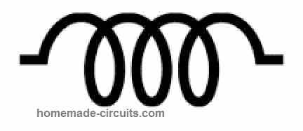 Figure 1: Symbol of Inductor
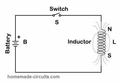 Figure 2: Inductor Circuit
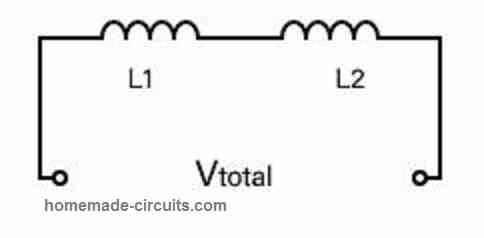 Figure 3: Inductors in Series
In parallel, see Figure 4, total equivalent, Inductance will be:
Ltotal = 1 / (1/L1+1/L2+��1/Ln)
Figure 3: Inductors in Series
In parallel, see Figure 4, total equivalent, Inductance will be:
Ltotal = 1 / (1/L1+1/L2+��1/Ln)
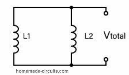 Figure 4: Inductors in parallel


 Figure 5: PQ Type Core
Now we have the following data with us:
Inductance required = 0.1 milliheneries
current = 1 Ampere
AL = 1200
As we know current is 1A, and looking up the wire sizing table, select SWG22 copper wire size which can carry current up to 1.2A.
Calculate the required number of turns by putting these values in the below equation:
N= 103��L/AL
Calculations:
N= 1030.11200
N = 1000*0.3162/34.6410
N = 9 Turns
Figure 5: PQ Type Core
Now we have the following data with us:
Inductance required = 0.1 milliheneries
current = 1 Ampere
AL = 1200
As we know current is 1A, and looking up the wire sizing table, select SWG22 copper wire size which can carry current up to 1.2A.
Calculate the required number of turns by putting these values in the below equation:
N= 103��L/AL
Calculations:
N= 1030.11200
N = 1000*0.3162/34.6410
N = 9 Turns
 Figure 6 : PQ Ferrite Core Chart
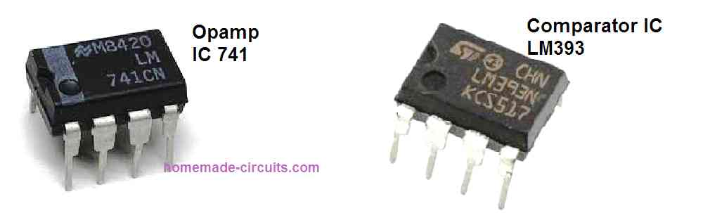 Seen externally, opamps and comparators appear to have no difference at all.
Both device have identical power supply connections, both include ��+�� and ��-�� input pinouts and a solitary output pin.
Examining the inner circuit configuration, we find that once again both units look largely the same (although a comparator IC having an open-collector or open-drain output might appear much different to an op amp).
Seen externally, opamps and comparators appear to have no difference at all.
Both device have identical power supply connections, both include ��+�� and ��-�� input pinouts and a solitary output pin.
Examining the inner circuit configuration, we find that once again both units look largely the same (although a comparator IC having an open-collector or open-drain output might appear much different to an op amp).
 However when it comes to a comparator the internal output circuit is built to work in saturation mode, meaning, to ensure switching between the upper and lower supply limits of output voltage without depending on an external feedback.
Comparators usually also come with a ground connection besides the normal power supply connections, and deliver digital logic levels on their outputs, although it can also accept symmetrical analogue input signals.
What do these differences actually indicate in practical use?
However when it comes to a comparator the internal output circuit is built to work in saturation mode, meaning, to ensure switching between the upper and lower supply limits of output voltage without depending on an external feedback.
Comparators usually also come with a ground connection besides the normal power supply connections, and deliver digital logic levels on their outputs, although it can also accept symmetrical analogue input signals.
What do these differences actually indicate in practical use?
 This indicates that the second set of conditions needed for balancing (ZA = Z3 and Z4 = ZB) cannot be be fulfilled.
The third conditions required for balance the AC circuit cannot be fulfilled either.
Having said that, we can see that the initial conditions (ZA = ZB and Z3 = Z4) could be fulfilled.
The impedance ZA consists of R1 and a part of R3, while the impedance ZB comprises of R2 and a some part of R3. The impedance Z3 is attributed to the capacitor C1, while Z4 is the impedance that is used to represent C2.
Provided that C1 remains equal to C2 and any R1 and R2 difference is tweaked and corrected by R3, then we can achieve a well balanced bridge.
Here the impedance of active components, such as resistors and capacitors is determined by the frequency.
However we find that the Fig.
1 is not dependent on frequency because the C1, C2 reactances could alter together whenever the frequency changes.
An additional variant of the above discussed AC bridge circuit can be seen in Fig.
2. Although this circuit is designed to work well, it isn't one of the favorite AC bridge versions due to the presence of the DC isolation across only one side of the meter (at point B).
In this circuit R1/R2 = C1/C2 when the variable resistor R3 is appropriately adjusted to get a zero or null reading on the meter V.
This indicates that the second set of conditions needed for balancing (ZA = Z3 and Z4 = ZB) cannot be be fulfilled.
The third conditions required for balance the AC circuit cannot be fulfilled either.
Having said that, we can see that the initial conditions (ZA = ZB and Z3 = Z4) could be fulfilled.
The impedance ZA consists of R1 and a part of R3, while the impedance ZB comprises of R2 and a some part of R3. The impedance Z3 is attributed to the capacitor C1, while Z4 is the impedance that is used to represent C2.
Provided that C1 remains equal to C2 and any R1 and R2 difference is tweaked and corrected by R3, then we can achieve a well balanced bridge.
Here the impedance of active components, such as resistors and capacitors is determined by the frequency.
However we find that the Fig.
1 is not dependent on frequency because the C1, C2 reactances could alter together whenever the frequency changes.
An additional variant of the above discussed AC bridge circuit can be seen in Fig.
2. Although this circuit is designed to work well, it isn't one of the favorite AC bridge versions due to the presence of the DC isolation across only one side of the meter (at point B).
In this circuit R1/R2 = C1/C2 when the variable resistor R3 is appropriately adjusted to get a zero or null reading on the meter V.
 If a DC content comes through the input source, it could result in much unfavorable effects.
Additionally it could be complicated to bias a meter-input amplifier hooked up at point A without modifying the input signal level at A.
If a DC content comes through the input source, it could result in much unfavorable effects.
Additionally it could be complicated to bias a meter-input amplifier hooked up at point A without modifying the input signal level at A.
 Let's analyze the initial condition (ZA = ZB and Z3 = Z4).
Given that the reactance of the capacitor pairs C1/C2 and C3/C4 can change in the same way in response to the changing frequency, the balanced state of the AC bridge is not dependent on the frequency.
This is likewise true for the 3rd condition (ZA = ZB = Z3 = Z4).
Another alternative could be that C1 and C3 are made identical, and C2 and C4 are made identical.
With these conditions fulfilled and the input frequency fine-tuned to get identical phase shift across points A and B, a perefct balance can be achieved in the bridge circuit.
However, the above conditions prevents the bridge from being independent to the input frequency.
Regardless of what conditions we use for getting the AC bridge circuit properly balanced, if the value of any one of the capacitors is changed will cause the generation of an AC voltage output between points A and B.
Since the points A and B are both kept well isolated from the input AC power source, it is fairly easy to connect this high impedance points to any preferred differential amplifier for further processing of the results.
Let's analyze the initial condition (ZA = ZB and Z3 = Z4).
Given that the reactance of the capacitor pairs C1/C2 and C3/C4 can change in the same way in response to the changing frequency, the balanced state of the AC bridge is not dependent on the frequency.
This is likewise true for the 3rd condition (ZA = ZB = Z3 = Z4).
Another alternative could be that C1 and C3 are made identical, and C2 and C4 are made identical.
With these conditions fulfilled and the input frequency fine-tuned to get identical phase shift across points A and B, a perefct balance can be achieved in the bridge circuit.
However, the above conditions prevents the bridge from being independent to the input frequency.
Regardless of what conditions we use for getting the AC bridge circuit properly balanced, if the value of any one of the capacitors is changed will cause the generation of an AC voltage output between points A and B.
Since the points A and B are both kept well isolated from the input AC power source, it is fairly easy to connect this high impedance points to any preferred differential amplifier for further processing of the results.
 So far, the phase shift symbols of active components did not demand consideration.
However, inductors and capacitors both can give rise to phase shift.
Capacitors possess a positive phase shift, and inductors can generate negative phase shift.
Therefore, in case an inductor is connected in one leg of the of the AC bridge, a capacitor must be connected at the other opposite leg (unless you may want to work with an additional inductor hooked up at the adjacent leg of the AC bridge).
These elements will possess equal and opposite phase shift only when they are positioned diagonally across from one another in the AC bridge diagram.
However , the phase shift needs to be identical for the left-hand and the right-hand portions of the circuit together.
This may be only achievable at frequency levels where the reactances of the active components are identical.
Therefore, the L1 and C1 reactances in Fig.
6 should be identical to one another at the operating frequency.
It is possible to balance the shown bridge if an additional condition is implemented.
The rule is, If the L1 reactance of becomes equal to the R1 resistance, and the C1 reactance becomes same as the the R2 resistance at the operating frequency.
This means that R1 should be same as R2.
We can evaluate the reactances of the capacitive and inductive components in an AC bridge circuit by replacing R1 and R2 with variable resistance, or potetiometers.
After this we can measure the resistance, once proper balancing of the pots are accomplished.
So far, the phase shift symbols of active components did not demand consideration.
However, inductors and capacitors both can give rise to phase shift.
Capacitors possess a positive phase shift, and inductors can generate negative phase shift.
Therefore, in case an inductor is connected in one leg of the of the AC bridge, a capacitor must be connected at the other opposite leg (unless you may want to work with an additional inductor hooked up at the adjacent leg of the AC bridge).
These elements will possess equal and opposite phase shift only when they are positioned diagonally across from one another in the AC bridge diagram.
However , the phase shift needs to be identical for the left-hand and the right-hand portions of the circuit together.
This may be only achievable at frequency levels where the reactances of the active components are identical.
Therefore, the L1 and C1 reactances in Fig.
6 should be identical to one another at the operating frequency.
It is possible to balance the shown bridge if an additional condition is implemented.
The rule is, If the L1 reactance of becomes equal to the R1 resistance, and the C1 reactance becomes same as the the R2 resistance at the operating frequency.
This means that R1 should be same as R2.
We can evaluate the reactances of the capacitive and inductive components in an AC bridge circuit by replacing R1 and R2 with variable resistance, or potetiometers.
After this we can measure the resistance, once proper balancing of the pots are accomplished.
 In this AC bridge circuit, the phase shift across the two left and right sections are the same for a particular frequency.
A little modification in either the capacitance or inductance within one of the bridge legs will cause the generation of an AC output at points A and B.
This bridge circuit could be balanced by fine-tuning C2 instead of a adjusting the resistor for the balancing.
In this AC bridge circuit, the phase shift across the two left and right sections are the same for a particular frequency.
A little modification in either the capacitance or inductance within one of the bridge legs will cause the generation of an AC output at points A and B.
This bridge circuit could be balanced by fine-tuning C2 instead of a adjusting the resistor for the balancing.
 By adding a sensitive voltmeter in series with a variable resistor, it becomes possible to calibrate to any desired output range within bridge's tolerable voltage range.
This bridge can perform very nicely for detecting the inductance value of any type of inductor that may be introduced in the bridge.
By adding a sensitive voltmeter in series with a variable resistor, it becomes possible to calibrate to any desired output range within bridge's tolerable voltage range.
This bridge can perform very nicely for detecting the inductance value of any type of inductor that may be introduced in the bridge.
 The bridge network which is near the meter works like a full-wave rectifier that let's us know regarding the DC meter's sensitivity for displaying the changes in the AC voltages.
If necessary it may be possible to include more than one element to the specific legs of the bridge.
While this could make the system quite complex mathematically, the factors required for the balance may not change, meaning, to keep identical voltage difference at the nodes while closely watching and adjusting the phase shift.
Understanding regarding phase shift and exactly what components need to complement with one another in the AC bridge circuit is really important, if you are intending to utilize the circuits to your greatest advantage.
Getting well versed with the fundamentals of the AC bridge circuit could resolve many of your future electronic design complications.
The bridge network which is near the meter works like a full-wave rectifier that let's us know regarding the DC meter's sensitivity for displaying the changes in the AC voltages.
If necessary it may be possible to include more than one element to the specific legs of the bridge.
While this could make the system quite complex mathematically, the factors required for the balance may not change, meaning, to keep identical voltage difference at the nodes while closely watching and adjusting the phase shift.
Understanding regarding phase shift and exactly what components need to complement with one another in the AC bridge circuit is really important, if you are intending to utilize the circuits to your greatest advantage.
Getting well versed with the fundamentals of the AC bridge circuit could resolve many of your future electronic design complications.
 The inductor L can be compared to the mass of the quartz piece.
The capacitor C compares to the the rigidity of the quartz piece.
The resistor R corresponds to the energy losses taking place due to the physical distortions happening in the crystal.
The other capacitor, Co, behaves like the capacitance between the conductive electrodes coated on the two sides of the quartz material.
Normally, L can be a extremely large inductance while C is extremely low in value.
For instance, in a crystal which is appropriately cut for vibrating at 200 kHz, L can be 27 H, C can be basically 0.024 pF, R can be 2 k and C0 can be 9 pF.
The magnitudes like these are generally used while modelling the crystal behavior in computer simulations.
The L to C ratio utilized is extremely high which we're able to obtain by making use of genuine electronic parts, providing the crystal an extremely high Q (quality factor).
A crystal often have a Q factor of around 100,000, whereas the Q of a most LC network is only in the range of a few hundred.
The inductor L can be compared to the mass of the quartz piece.
The capacitor C compares to the the rigidity of the quartz piece.
The resistor R corresponds to the energy losses taking place due to the physical distortions happening in the crystal.
The other capacitor, Co, behaves like the capacitance between the conductive electrodes coated on the two sides of the quartz material.
Normally, L can be a extremely large inductance while C is extremely low in value.
For instance, in a crystal which is appropriately cut for vibrating at 200 kHz, L can be 27 H, C can be basically 0.024 pF, R can be 2 k and C0 can be 9 pF.
The magnitudes like these are generally used while modelling the crystal behavior in computer simulations.
The L to C ratio utilized is extremely high which we're able to obtain by making use of genuine electronic parts, providing the crystal an extremely high Q (quality factor).
A crystal often have a Q factor of around 100,000, whereas the Q of a most LC network is only in the range of a few hundred.
 When a crystal is installed in place of an inductor, the frequency gets a lot more accurately set.
In this type of oscillator circuit, the crystals are generally controlled in parallel resonance mode, possessing highest possible impedance in the resonant frequency and thus generating an output frequency with very high amplitude.
The Pierce oscillator demonstrated in the following figure is an example which exhibits a crystal working in the series resonance mode.
Feedback is directed by means of the crystal and it attains the maximum level as the crystal resonates in the series mode, using minimum impedance.
When a crystal is installed in place of an inductor, the frequency gets a lot more accurately set.
In this type of oscillator circuit, the crystals are generally controlled in parallel resonance mode, possessing highest possible impedance in the resonant frequency and thus generating an output frequency with very high amplitude.
The Pierce oscillator demonstrated in the following figure is an example which exhibits a crystal working in the series resonance mode.
Feedback is directed by means of the crystal and it attains the maximum level as the crystal resonates in the series mode, using minimum impedance.
 Observe that this oscillator can work reliably with the need of a tuned circuit, depending simply on the crystal to decide its oscillating frequency.
Crystal oscillators are not only very accurate with their functioning, they are in addition one of the fastest of the oscillators, typically.
Present day digital circuits demand extremely fast clocks to operate them, with frequencies that may range in hundreds of megahertz.
Observe that this oscillator can work reliably with the need of a tuned circuit, depending simply on the crystal to decide its oscillating frequency.
Crystal oscillators are not only very accurate with their functioning, they are in addition one of the fastest of the oscillators, typically.
Present day digital circuits demand extremely fast clocks to operate them, with frequencies that may range in hundreds of megahertz.
 Since the gaps between the electrodes on the two ends ascertains which frequency would be fed more strongly into the SAW and retrieved from the other end, SAWs are generally applied in bandpass filters.
The time required for the wave to travel across the strip provides the filter the characteristics of a delay line unit.
When used as an element of an oscillator, a SAW delay line can be used exactly in the above manner at the RC network of a phase shift filter.
The time taken to create a phase shift of 180�� is incredibly brief, and therefore, the frequency of this kind of oscillators is tremendously high.
Normally, they range up to around 2 GHz.
Oscillators that work with dielectric resonators in the feedback loop can even go beyond the 2 GHz range.
At this level we could be effectively into the microwave spectrum, which possess their own specialized characteristics.
Since the gaps between the electrodes on the two ends ascertains which frequency would be fed more strongly into the SAW and retrieved from the other end, SAWs are generally applied in bandpass filters.
The time required for the wave to travel across the strip provides the filter the characteristics of a delay line unit.
When used as an element of an oscillator, a SAW delay line can be used exactly in the above manner at the RC network of a phase shift filter.
The time taken to create a phase shift of 180�� is incredibly brief, and therefore, the frequency of this kind of oscillators is tremendously high.
Normally, they range up to around 2 GHz.
Oscillators that work with dielectric resonators in the feedback loop can even go beyond the 2 GHz range.
At this level we could be effectively into the microwave spectrum, which possess their own specialized characteristics.
 This expression is stated as B is equal to NOT A.
The NOT bar shows that signal A has become inverted.
Keep in mind that A could be either a binary 0 or a binary 1. NOT A, needless to say, will be the opposite, or complementary to the NOT B.
Considering that it is not easy to write a bar on top of the letter as demonstrated in Fig.
1, some other easier techniques happen to be created for symbolizing inversion.
Occasionally the inverted variable is mentioned by an asterisk or a prime (just like an accent).
Applying the variables in Fig.
1 we get the following equation:
B= A * or B =A'
This expression is stated as B is equal to NOT A.
The NOT bar shows that signal A has become inverted.
Keep in mind that A could be either a binary 0 or a binary 1. NOT A, needless to say, will be the opposite, or complementary to the NOT B.
Considering that it is not easy to write a bar on top of the letter as demonstrated in Fig.
1, some other easier techniques happen to be created for symbolizing inversion.
Occasionally the inverted variable is mentioned by an asterisk or a prime (just like an accent).
Applying the variables in Fig.
1 we get the following equation:
B= A * or B =A'
 The a pair of inputs to the AND gate are A and B and the output is specified as C.
Understand this manifestation for the output:
C =AB
In normal algebra AB might suggest multiply A and B together.
For this reason the output of an AND gate is normally referred to as product of the inputs.
Like in standard algebra, it isn't essential to indicate any symbolic representation between a pair of variables (despite the fact that at times a dot can be used).
As an alternative, the letters are simply put next to one another.
Figure 3 exhibits a four-input AND gate having different input variables.
Frequently you might notice the output equation expressed using certain variables split up by parentheses.
Every input expression presents itself inside a pair of parentheses to help keep these visually segregated in order to avoid confusion.
However given each of these terms are written immediately next to one another, it indicates that the variables are ANDed with each other.
The a pair of inputs to the AND gate are A and B and the output is specified as C.
Understand this manifestation for the output:
C =AB
In normal algebra AB might suggest multiply A and B together.
For this reason the output of an AND gate is normally referred to as product of the inputs.
Like in standard algebra, it isn't essential to indicate any symbolic representation between a pair of variables (despite the fact that at times a dot can be used).
As an alternative, the letters are simply put next to one another.
Figure 3 exhibits a four-input AND gate having different input variables.
Frequently you might notice the output equation expressed using certain variables split up by parentheses.
Every input expression presents itself inside a pair of parentheses to help keep these visually segregated in order to avoid confusion.
However given each of these terms are written immediately next to one another, it indicates that the variables are ANDed with each other.
 In Fig.
3, we state that the output product is:
TX = (D7)(EB)(CLK)(RST)
In Fig.
3, we state that the output product is:
TX = (D7)(EB)(CLK)(RST)
 This may be carried out by inserting a bar on top of the whole expression as found in Fig.
5. For expressing in an alternate way, the ANDed input terms could be placed into parentheses and an asterisk or apostrophe applied to suggest the NOT function.
Observe that the term B includes a NOT bar on top of it.
This may be carried out by inserting a bar on top of the whole expression as found in Fig.
5. For expressing in an alternate way, the ANDed input terms could be placed into parentheses and an asterisk or apostrophe applied to suggest the NOT function.
Observe that the term B includes a NOT bar on top of it.
 Once again remember that one term, DZ, is inverted at the input.
Now, applying those basic (Boolean) expressions for every single logic gates, a lot more complex circuits could be quickly displayed.
Once again remember that one term, DZ, is inverted at the input.
Now, applying those basic (Boolean) expressions for every single logic gates, a lot more complex circuits could be quickly displayed.
 Observe that the input variables are marked.
The output is specified as G.
The task is to produce the expression for G with regards to the input variables.
It's truly much less difficult than it actually appears to be.
To get started, you begin with the variables at the inputs which are all on the left hand side of the circuit.
Write down their expression for each circuit's output.
For instance, the AND-gate 1 output is basically written as AB.
The inverter 2 output is written as NOT C.
The AND-gate 3 output is represented as DEF.
The outputs of gates 1 and 3, and inverter 2, constitute the inputs to OR-gate 4.
To finish the expression, we simply OR each of the inputs together with gate 4.
Subsequently, the output expression G turns into the following:
G = AB +C +DEF
Check out the equation that we derived just above.
You will usually notice an expression like this called a sum of products.
In our case, the products are classified as the ANDed variables AB and DEF.
The sum, naturally, appertains to the ORing together of each of the products.
Observe that the input variables are marked.
The output is specified as G.
The task is to produce the expression for G with regards to the input variables.
It's truly much less difficult than it actually appears to be.
To get started, you begin with the variables at the inputs which are all on the left hand side of the circuit.
Write down their expression for each circuit's output.
For instance, the AND-gate 1 output is basically written as AB.
The inverter 2 output is written as NOT C.
The AND-gate 3 output is represented as DEF.
The outputs of gates 1 and 3, and inverter 2, constitute the inputs to OR-gate 4.
To finish the expression, we simply OR each of the inputs together with gate 4.
Subsequently, the output expression G turns into the following:
G = AB +C +DEF
Check out the equation that we derived just above.
You will usually notice an expression like this called a sum of products.
In our case, the products are classified as the ANDed variables AB and DEF.
The sum, naturally, appertains to the ORing together of each of the products.
 A little more advanced circuit is demonstrated in Fig.8. Even here the analysis procedure will be the exact same.
Start working out from the circuit across left to right writing the output terms for each gate.
The gate 1 output will be A1(K) as displayed.
We employ parentheses in cases like this to signify the separation amongst the a pair of variables, still they may be written next to each other to denote a product or AND function.
Next, the output of gate1 is ORed with the input of J.
The causes the output from gate 2 to be:
A1(K) +J
This turns into one of the inputs to AND-gate 3. This expression is ANDed with input B to provide the finishing output expression:
M = B(A1(K) +J)
Yet again parentheses are employed here to separate the variables from each other and to guarantee that proper logical operation is depicted.
A little more advanced circuit is demonstrated in Fig.8. Even here the analysis procedure will be the exact same.
Start working out from the circuit across left to right writing the output terms for each gate.
The gate 1 output will be A1(K) as displayed.
We employ parentheses in cases like this to signify the separation amongst the a pair of variables, still they may be written next to each other to denote a product or AND function.
Next, the output of gate1 is ORed with the input of J.
The causes the output from gate 2 to be:
A1(K) +J
This turns into one of the inputs to AND-gate 3. This expression is ANDed with input B to provide the finishing output expression:
M = B(A1(K) +J)
Yet again parentheses are employed here to separate the variables from each other and to guarantee that proper logical operation is depicted.
 Examine the illustration in Fig.9. Once again, the method is to build the output expressions of the input gates, and then procedd through from left to right to generate the output.
The output from gate1 will be:
(W +X +Y)
The gate 2 output can be written as:
(W + X)
The a pair of outputs serve as the inputs to AND-gate 3. The final output expression is generated as, Z, simply by ANDing the two expressions with each other.
We get the result as:
Z= (W +X +Y)(W +X)
You may possibly come across this type of expression which is known as a product of sums.
Examine the illustration in Fig.9. Once again, the method is to build the output expressions of the input gates, and then procedd through from left to right to generate the output.
The output from gate1 will be:
(W +X +Y)
The gate 2 output can be written as:
(W + X)
The a pair of outputs serve as the inputs to AND-gate 3. The final output expression is generated as, Z, simply by ANDing the two expressions with each other.
We get the result as:
Z= (W +X +Y)(W +X)
You may possibly come across this type of expression which is known as a product of sums.
 The circuit drawn accordingly can be witnessed in Fig.
10.
A rather more complicated illustration can be observed in the following equation:
X= (A +B +C)(D +E)(F)
The parenthesis let you know you have 3 distinct groups of variables ANDed together to create the output, X.
The variables inside the groups are ORed with each other.
This could be started by making the circuits for each group of variables.
The + sign within the parenthesis signify that an OR gate needs to be drawn.
To begin with we can draw an OR gate having inputs A, B, and C.
An additional expression comes by ORing the input variables D with E.
Now draw an OR gate having the a pair of variables as its inputs.
The variable F within parenthesis will be ANDed along with the other pair of expressions.
The circuit drawn accordingly can be witnessed in Fig.
10.
A rather more complicated illustration can be observed in the following equation:
X= (A +B +C)(D +E)(F)
The parenthesis let you know you have 3 distinct groups of variables ANDed together to create the output, X.
The variables inside the groups are ORed with each other.
This could be started by making the circuits for each group of variables.
The + sign within the parenthesis signify that an OR gate needs to be drawn.
To begin with we can draw an OR gate having inputs A, B, and C.
An additional expression comes by ORing the input variables D with E.
Now draw an OR gate having the a pair of variables as its inputs.
The variable F within parenthesis will be ANDed along with the other pair of expressions.
 Lastly, to finish the circuit just draw an AND gate having 3 inputs and join these with the outputs of the a pair of OR gates and a signal input F as demonstrated in Fig.
11.
More on Boolean Algebra can be learned from the following pdf document:
https://www.homemade-circuits.com/wp-content/uploads/2021/05/boolean.pdf
Lastly, to finish the circuit just draw an AND gate having 3 inputs and join these with the outputs of the a pair of OR gates and a signal input F as demonstrated in Fig.
11.
More on Boolean Algebra can be learned from the following pdf document:
https://www.homemade-circuits.com/wp-content/uploads/2021/05/boolean.pdf
 Often we are able to obtain better understanding of a circuit functioning by exploring at its basic equivalent circuit.
In Fig.
1B we find a straightforward DC circuit which symbolizes the basic working of an inverter gate.
Often we are able to obtain better understanding of a circuit functioning by exploring at its basic equivalent circuit.
In Fig.
1B we find a straightforward DC circuit which symbolizes the basic working of an inverter gate.
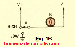 Switch S1 is positioned to select either a high signal (V +) or a low signal (ground or 0 volts) as being the input to the circuit.
The lamp shows the output condition: a switch ON for a high output and switch off for a low output.
While the switch is in the HIGH position, each sides of the lamp get exactly the same voltage difference, which causes the lamp to remain shut off.
Switch S1 is positioned to select either a high signal (V +) or a low signal (ground or 0 volts) as being the input to the circuit.
The lamp shows the output condition: a switch ON for a high output and switch off for a low output.
While the switch is in the HIGH position, each sides of the lamp get exactly the same voltage difference, which causes the lamp to remain shut off.
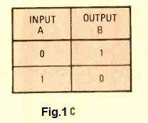 This signifies a low output.
As soon as the switch S1 is selected in the low position, the lamp obtains both ground and V+ therefore the lamp illuminates to demonstrate a high output.
The truth table for the NOT gate can be found in Fig.
1C.
Here we see that the input is A and the output is B, which means that a low input at A delivers a high output at B, and a high input at A delivers a low output at B.
This signifies a low output.
As soon as the switch S1 is selected in the low position, the lamp obtains both ground and V+ therefore the lamp illuminates to demonstrate a high output.
The truth table for the NOT gate can be found in Fig.
1C.
Here we see that the input is A and the output is B, which means that a low input at A delivers a high output at B, and a high input at A delivers a low output at B.
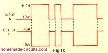 This circuit operation is demonstrated in Fig.
1D.
Here, the A is the input, while the B or A signifies the output.
The line or the bar shown above the input or output in logic notation signifies an opposite signal to whatever the "unbarred" signal may be having.
As an example, if suppose A is high, then A will be low.
This notation allows us to signify the relationship between the input and the output as represented in the following expression:
B = A
This is a manifestation can be found in Boolean algebra, and it represents the mathematics of digital logic.
This circuit operation is demonstrated in Fig.
1D.
Here, the A is the input, while the B or A signifies the output.
The line or the bar shown above the input or output in logic notation signifies an opposite signal to whatever the "unbarred" signal may be having.
As an example, if suppose A is high, then A will be low.
This notation allows us to signify the relationship between the input and the output as represented in the following expression:
B = A
This is a manifestation can be found in Boolean algebra, and it represents the mathematics of digital logic.
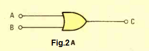 An OR gate (Fig.
2A) generates a high output when at least one of its inputs is high.
Therefore when, A or B, or both A and B are high, then it gives a high output.
An alternate way to explain this is, to get a low output from an OR gate, it is necessary for both of its inputs to be low.
An OR gate (Fig.
2A) generates a high output when at least one of its inputs is high.
Therefore when, A or B, or both A and B are high, then it gives a high output.
An alternate way to explain this is, to get a low output from an OR gate, it is necessary for both of its inputs to be low.
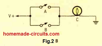 Figure 2B exhibits a clear-cut equivalent circuit for the OR gate.
Here we see that the lamp (output) is switched ON (high) when either switch A "or" switch B is high.
That is exactly why these gates are known as "OR" gates.
Figure 2B exhibits a clear-cut equivalent circuit for the OR gate.
Here we see that the lamp (output) is switched ON (high) when either switch A "or" switch B is high.
That is exactly why these gates are known as "OR" gates.
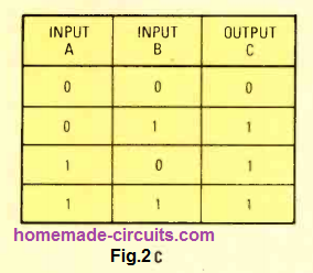 A truth table for the OR gate can be seen in Fig.
2C.
What it affirms is that the output is low as long as all inputs are likewise low, and a high signal on any one of the both inputs generates a high output.
A truth table for the OR gate can be seen in Fig.
2C.
What it affirms is that the output is low as long as all inputs are likewise low, and a high signal on any one of the both inputs generates a high output.
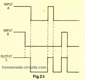 The behavior of the circuit with the above specified rules can be witnessed in a realistic form in Fig.
2D.
Each of the inputs get a series of pulses, and the variations in its output demonstrates how the gate operates in accordance to these input levels.
The behavior of the circuit with the above specified rules can be witnessed in a realistic form in Fig.
2D.
Each of the inputs get a series of pulses, and the variations in its output demonstrates how the gate operates in accordance to these input levels.
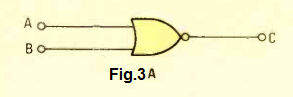 The NOR gate can be made by interconnecting an OR gate with an inverter gate or NOT gate.
(Observe the ring around the output pin in Fig.
3A.) The gate could be described as a NOT/OR gate.
The NOR gate generates a low output when any one or both of its inputs are high.
The NOR gate can be made by interconnecting an OR gate with an inverter gate or NOT gate.
(Observe the ring around the output pin in Fig.
3A.) The gate could be described as a NOT/OR gate.
The NOR gate generates a low output when any one or both of its inputs are high.
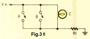 A comparable circuit for the NOR gate using mechanical switch can be seen in Fig.
3B.
So long as each of the switches are in the open condition, the lamp remains switched ON, however if any one of the switch is closed then it causes the lamp to be switched off.
A comparable circuit for the NOR gate using mechanical switch can be seen in Fig.
3B.
So long as each of the switches are in the open condition, the lamp remains switched ON, however if any one of the switch is closed then it causes the lamp to be switched off.
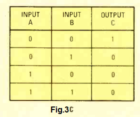 The truth table for this circuit can be witnessed in Fig.
3C, which may be understood in a nutshell through the following guidelines:
You will get a HIGH from a NOR gate output when, and only when, both of its inputs are supplied with low logic (meaning the output will be logic low only if any of its inputs is high.)
The truth table for this circuit can be witnessed in Fig.
3C, which may be understood in a nutshell through the following guidelines:
You will get a HIGH from a NOR gate output when, and only when, both of its inputs are supplied with low logic (meaning the output will be logic low only if any of its inputs is high.)
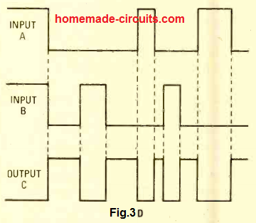 Talking about an NOR gates, the same regulations can be understood in a graphical manner as shown in Fig.
3D
Talking about an NOR gates, the same regulations can be understood in a graphical manner as shown in Fig.
3D
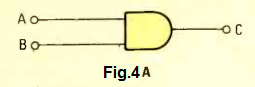 The AND gate as indicated in the Fig.
4A will generate a high output in a condition when both its inputs are high.
The AND gate as indicated in the Fig.
4A will generate a high output in a condition when both its inputs are high.
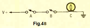 We can witness a equivalent switch and bulb replicating the AND gate function in Fig.
4B.
The lamp is switched when both its switches A and switch B are turned ON.
We can witness a equivalent switch and bulb replicating the AND gate function in Fig.
4B.
The lamp is switched when both its switches A and switch B are turned ON.
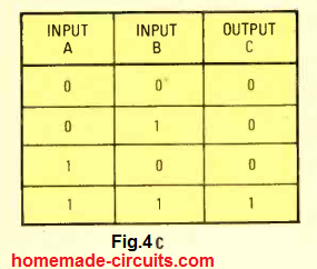 As given in Fig 4C we can summarize the truth table in the following manner:
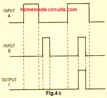 The output of an AND will turn low when both its inputs are is low and its output will be high only when both of its inputs are high).
The very same rules can be described in practical circuits through the graphical diagram as depicted in the Fig.
4D.
The output of an AND will turn low when both its inputs are is low and its output will be high only when both of its inputs are high).
The very same rules can be described in practical circuits through the graphical diagram as depicted in the Fig.
4D.
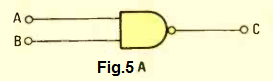 A NAND gate can be seen in the Fig.
5A which is yet another gate built with a combination of an AND gate with a NOT inverter gate.
A NAND gate can be seen in the Fig.
5A which is yet another gate built with a combination of an AND gate with a NOT inverter gate.
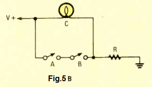 We can witness an equivalent lamp/switch circuit of the same in Fig.
5B.
In a situation when both the indicated switches are in the open state, the lamp will be switched ON.
The lamp will be turned OFF only in a situation when both the switches are toggled OFF.
We can witness an equivalent lamp/switch circuit of the same in Fig.
5B.
In a situation when both the indicated switches are in the open state, the lamp will be switched ON.
The lamp will be turned OFF only in a situation when both the switches are toggled OFF.
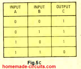 The appropriate functional rules for a NAND gate can be witnessed in the truth table as indicated in the fig.
5C.
The same maye be comprehended at a glimpse by reading the following:
The output of a NAND gate will be high when one or both of its inputs are held low.
In other words, the output of a NAND gate will be low only when both of its inputs are held high.
The appropriate functional rules for a NAND gate can be witnessed in the truth table as indicated in the fig.
5C.
The same maye be comprehended at a glimpse by reading the following:
The output of a NAND gate will be high when one or both of its inputs are held low.
In other words, the output of a NAND gate will be low only when both of its inputs are held high.
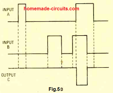 Just like in our previous examples, the same rules can be expressed in a graphical manner as depicted in Fig.
5D.
Just like in our previous examples, the same rules can be expressed in a graphical manner as depicted in Fig.
5D.
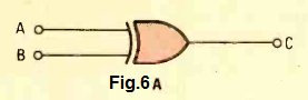 This is last in the list of our basic standard gates which is known as the Exclusive-OR (XOR).
That image of the XORR gate can be witnessed in the Fig.
6A which apperaes to be a bit uncommon, however it can be used for a plenty of practical digital circuit applications.
This is last in the list of our basic standard gates which is known as the Exclusive-OR (XOR).
That image of the XORR gate can be witnessed in the Fig.
6A which apperaes to be a bit uncommon, however it can be used for a plenty of practical digital circuit applications.
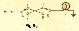 For a pictorial working circuit of this XOR gate you may refer to the Fig.
6B.
The lamp/switch circuit is built using a a couple of SPDT switches interconnected with each other.
For a pictorial working circuit of this XOR gate you may refer to the Fig.
6B.
The lamp/switch circuit is built using a a couple of SPDT switches interconnected with each other.
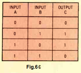 From the supplied the truth table as in Fig.
6C we are able to learn a few useful actions: When both the inputs of a XOR gate are low, then it provide a low output.
In case both of its inputs are high, then we get an output that is yet again low.
In a situation when one of its inputs is applied with a high signal, and the other input is applied with a low signal, then the output produces a high signal.
To put it differently, the output will be low only in a situation when both of its inputs are applied with identical signals, meaning when both the input are either high, or both are low.
From the supplied the truth table as in Fig.
6C we are able to learn a few useful actions: When both the inputs of a XOR gate are low, then it provide a low output.
In case both of its inputs are high, then we get an output that is yet again low.
In a situation when one of its inputs is applied with a high signal, and the other input is applied with a low signal, then the output produces a high signal.
To put it differently, the output will be low only in a situation when both of its inputs are applied with identical signals, meaning when both the input are either high, or both are low.
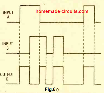 That working pattern of a XOR gate can be witnessed in the Fig.
6D.
That working pattern of a XOR gate can be witnessed in the Fig.
6D.
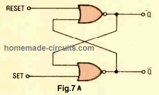
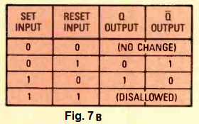 The NOR-logic flip-flop circuit can be witnessed in Fig.
7A, and the truth table for the same is provided in Fig.
7B.
The NOR logic configuration makes use of active-high inputs.
To put it differently, when a low signal is applied on both of its inputs simultaneously, it causes no change or variations in its output.
However in case, any one of its input is applied with a high logic, with a low logic applied to the other input, then this actions results in a change in its output-state.
What change in the state of the output happens will depend on which of the inputs (the set or reset) had been rendered active.
Applying both the inputs simultaneously with a high signal is prohibited simply because in that case the output results can become unpredictable and unstable.
The NOR-logic flip-flop circuit can be witnessed in Fig.
7A, and the truth table for the same is provided in Fig.
7B.
The NOR logic configuration makes use of active-high inputs.
To put it differently, when a low signal is applied on both of its inputs simultaneously, it causes no change or variations in its output.
However in case, any one of its input is applied with a high logic, with a low logic applied to the other input, then this actions results in a change in its output-state.
What change in the state of the output happens will depend on which of the inputs (the set or reset) had been rendered active.
Applying both the inputs simultaneously with a high signal is prohibited simply because in that case the output results can become unpredictable and unstable.
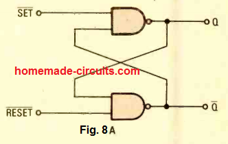
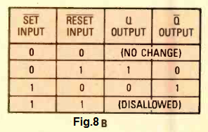 The NAND logic configuration as depicted in Fig.
8A works by using two-input NAND gates as opposed to NOR gates for creating a flip-flop circuit.
They behave exactly oppositely to the NOR-gate flip-flops (you can compare the truth table results from Fig.
8B with Fig.
7B).
In NAND logic flip flop we find a couple of R-S flip-flop ICs obtained from the CMOS family of ICs.
The IC 4043 is a quad NOR-logic R-S flip -flop ("quad" name is given since it includes four R-S flip -flop's internal to the IC).
Likewise, we have the IC 4044 which is a quad NAND logic R-S flip -flop.
The NAND logic configuration as depicted in Fig.
8A works by using two-input NAND gates as opposed to NOR gates for creating a flip-flop circuit.
They behave exactly oppositely to the NOR-gate flip-flops (you can compare the truth table results from Fig.
8B with Fig.
7B).
In NAND logic flip flop we find a couple of R-S flip-flop ICs obtained from the CMOS family of ICs.
The IC 4043 is a quad NOR-logic R-S flip -flop ("quad" name is given since it includes four R-S flip -flop's internal to the IC).
Likewise, we have the IC 4044 which is a quad NAND logic R-S flip -flop.
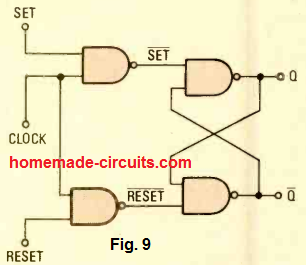 A remedy to these sorts of challenges can be the implementation of clocked R-S flip -flop configuration as shown in the Fig.
9.
The two gates on the right side constitute a NAND gate logic R-S flip -flop in the identical fashion as done in Fig.
8A.
The control of inputs of this flip-flop are implemented by the outputs of the other two NAND gates.
For so long as the clock input stays at a low logic, the outputs of each of the left gates stay latched in the high logic mode, which means that the R-S flip-flop is unable to operate now.
However, if the clock pulse to the turns high, then the R-S flip flop outputs respond and change the output state either to set or to reset.
A remedy to these sorts of challenges can be the implementation of clocked R-S flip -flop configuration as shown in the Fig.
9.
The two gates on the right side constitute a NAND gate logic R-S flip -flop in the identical fashion as done in Fig.
8A.
The control of inputs of this flip-flop are implemented by the outputs of the other two NAND gates.
For so long as the clock input stays at a low logic, the outputs of each of the left gates stay latched in the high logic mode, which means that the R-S flip-flop is unable to operate now.
However, if the clock pulse to the turns high, then the R-S flip flop outputs respond and change the output state either to set or to reset.
 Another type of flip flop called the "master-slave" flip-flop, which is also known as the load/transfer flip-flop, can be seen in the Fig.
10. This flip flop configuration is built using two clocked R-S flip-flops, A and B as indicated in the diagram.
The configuration is designed in such a way that the left side flip flop's outputs trigger the inputs of the right side flip flop.
The two clock lines are operated with signals that are out of phase with each other but the signals come from a common clock source, called the load/transfer, or the L/T input.
When the L/T line has a high signal, then the clock at the A flip-flop is turned low and the B side flip flop is turned high.
In this situation, B will be active, and A will be inactive.
Whatever logic levels show up on the A outputs are instantly shifted to the B outputs on account of CLK2 being high.
However once the L/T line becomes low, flip flop B gets disabled (although its outputs continue to remain the same) and flip flop A becomes enabled.
Any variations caused on the S and R inputs are reproduced on the Q1/Q outputs of flip flop A.
When the L/T line is applied with a high signal again, these new quantities are shifted to the outputs of flip flop B.
Another type of flip flop called the "master-slave" flip-flop, which is also known as the load/transfer flip-flop, can be seen in the Fig.
10. This flip flop configuration is built using two clocked R-S flip-flops, A and B as indicated in the diagram.
The configuration is designed in such a way that the left side flip flop's outputs trigger the inputs of the right side flip flop.
The two clock lines are operated with signals that are out of phase with each other but the signals come from a common clock source, called the load/transfer, or the L/T input.
When the L/T line has a high signal, then the clock at the A flip-flop is turned low and the B side flip flop is turned high.
In this situation, B will be active, and A will be inactive.
Whatever logic levels show up on the A outputs are instantly shifted to the B outputs on account of CLK2 being high.
However once the L/T line becomes low, flip flop B gets disabled (although its outputs continue to remain the same) and flip flop A becomes enabled.
Any variations caused on the S and R inputs are reproduced on the Q1/Q outputs of flip flop A.
When the L/T line is applied with a high signal again, these new quantities are shifted to the outputs of flip flop B.
 The master-slave flip-flop is used in applications where noise or synchronization can be an issue.
In certain flip-flops we find a differences between the clock triggering.
Figures 11A and 11B indicate the difference between positive and negative level triggering.
With level triggering, the circuit reacts once the level is either high (positive-level triggering) or low (negative-level triggering).
Triggering at the edge of the signal happen when the input signal is just changing over from either low-to-high (referred to as positive-edge triggering), as in Fig.
11C, or high-to-low (referred to as negative-edge triggering), as displayed in Fig.
11D.
The master-slave flip-flop is used in applications where noise or synchronization can be an issue.
In certain flip-flops we find a differences between the clock triggering.
Figures 11A and 11B indicate the difference between positive and negative level triggering.
With level triggering, the circuit reacts once the level is either high (positive-level triggering) or low (negative-level triggering).
Triggering at the edge of the signal happen when the input signal is just changing over from either low-to-high (referred to as positive-edge triggering), as in Fig.
11C, or high-to-low (referred to as negative-edge triggering), as displayed in Fig.
11D.
 The type-D flip-flop, also referred to as one-bit data latch.
As shown in the Fig.
12A it is a digital device designed to send the data on the D input line only in the situation when the clock (CLK) line is active.
In the majority of type-D flip -flop's, the clock is rendered active whenever a high signal is applied to the CLK line.
Therefore the rule can be interpreted as:
The data level on the D input is delivered to the Q output as soon as there's a high signal on the CLK line.
Hence, the type-D flip-flop is known to "latch" the D input data for one clock cycle.
In other words: As long as the CLK line has a high signal, the state of the Q output follows the D input.
All of the transitions or the changeovers taking place at the D input are goes through an inversion (gets inverted) and then it is transferred to the Q output.
Meaning, a high signal at the input delivers a low output, and a low signal at the input generates a high output.
In Figure 12B we are able to witness a graphical picture showing how the type-D flip-flop actually performs.
We find four clock pulses depicted as: A, B, C, and D.
These are exihibited in the form of periodic square-wave string of pulses, but it is not necessary for them to be this much regular.
It is possible to connect the CLK line to an input source which only turns high occasionally.
Suppose the Q output is low at the beginning.
At a time T1 the CLK turns high and the D input is low.
As a result, the Q output will hold low during this period.
But remember, during the time pulse A is still high, the D input will make a sudden changeover to high.
At this stage, the Q output instantly turns high and continues to be in that position after pulse A has terminated at time T2.
In a situation where the D input turns low again, the Q output would follow the sequence.
You can take a look at the the rest of the pulses for understanding the relationship between the output and input levels in response to the the clock signal.
Good examples of typeD flip-flop is the IC 7474 dual edge-triggered TTL flip-flop, and the IC 4013 CMOS device.
The IC 7475 is a TTL quad-latch device, however it includes just a couple of clock-inputs.
Each one clock input is hooked up to a set of two flip-flops.
If the two clock lines are joined with each other the 7475 functions like a four bit data latch.
The type-D flip-flop, also referred to as one-bit data latch.
As shown in the Fig.
12A it is a digital device designed to send the data on the D input line only in the situation when the clock (CLK) line is active.
In the majority of type-D flip -flop's, the clock is rendered active whenever a high signal is applied to the CLK line.
Therefore the rule can be interpreted as:
The data level on the D input is delivered to the Q output as soon as there's a high signal on the CLK line.
Hence, the type-D flip-flop is known to "latch" the D input data for one clock cycle.
In other words: As long as the CLK line has a high signal, the state of the Q output follows the D input.
All of the transitions or the changeovers taking place at the D input are goes through an inversion (gets inverted) and then it is transferred to the Q output.
Meaning, a high signal at the input delivers a low output, and a low signal at the input generates a high output.
In Figure 12B we are able to witness a graphical picture showing how the type-D flip-flop actually performs.
We find four clock pulses depicted as: A, B, C, and D.
These are exihibited in the form of periodic square-wave string of pulses, but it is not necessary for them to be this much regular.
It is possible to connect the CLK line to an input source which only turns high occasionally.
Suppose the Q output is low at the beginning.
At a time T1 the CLK turns high and the D input is low.
As a result, the Q output will hold low during this period.
But remember, during the time pulse A is still high, the D input will make a sudden changeover to high.
At this stage, the Q output instantly turns high and continues to be in that position after pulse A has terminated at time T2.
In a situation where the D input turns low again, the Q output would follow the sequence.
You can take a look at the the rest of the pulses for understanding the relationship between the output and input levels in response to the the clock signal.
Good examples of typeD flip-flop is the IC 7474 dual edge-triggered TTL flip-flop, and the IC 4013 CMOS device.
The IC 7475 is a TTL quad-latch device, however it includes just a couple of clock-inputs.
Each one clock input is hooked up to a set of two flip-flops.
If the two clock lines are joined with each other the 7475 functions like a four bit data latch.
 Fig.
13A shows an illustration of J-K Flip-Flop device which could be powered through one of the two methods: direct and clocked.
Fig.
13A shows an illustration of J-K Flip-Flop device which could be powered through one of the two methods: direct and clocked.
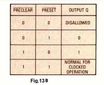 The truth table logic for the direct mode can be witnessed in Fig.
13B.
While they are held in the low logic positions, the direct inputs of the device (clear and set) remain active.
For implementing direct function the J and K inputs are usually attached to the inactive state.
In this case the inactive state is low logic.
The working of the J-K flip-flop configuration depends on these inputs, and the clock input is unimportant (while held in the "don't-care" condition).
Observe that the figure indicates all four possible combinations of clear-and set-input states.
In a situation when both set and clear are in the low logic, the J-K flip-flop is unable to "understand" what it needs to do, therefore this condition is forbidden.
In this condition the outputs can be erratic, therefore such combination of inputs are no allowed.
In any situation while the clear input is applied with a low logic and the set input is applied with a high logic, in this situation the Q output quickly attains the low logic and the Q output turns high.
However as soon as the set input is applied with a low logic and the clear input with a high, the results turn opposite:
Q now becomes high and Q becomes low.
Now observe how the device behaves when set and clear both the inputs are applied with high logic levels: the J-K flip-flop now gets organized in the clocked operation mode and we have a different set of rules being implemented.
The truth table logic for the direct mode can be witnessed in Fig.
13B.
While they are held in the low logic positions, the direct inputs of the device (clear and set) remain active.
For implementing direct function the J and K inputs are usually attached to the inactive state.
In this case the inactive state is low logic.
The working of the J-K flip-flop configuration depends on these inputs, and the clock input is unimportant (while held in the "don't-care" condition).
Observe that the figure indicates all four possible combinations of clear-and set-input states.
In a situation when both set and clear are in the low logic, the J-K flip-flop is unable to "understand" what it needs to do, therefore this condition is forbidden.
In this condition the outputs can be erratic, therefore such combination of inputs are no allowed.
In any situation while the clear input is applied with a low logic and the set input is applied with a high logic, in this situation the Q output quickly attains the low logic and the Q output turns high.
However as soon as the set input is applied with a low logic and the clear input with a high, the results turn opposite:
Q now becomes high and Q becomes low.
Now observe how the device behaves when set and clear both the inputs are applied with high logic levels: the J-K flip-flop now gets organized in the clocked operation mode and we have a different set of rules being implemented.
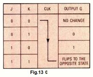 The truth table for the above discussed clocked operation for the J-K flip-flop can be learned from the Fig.
13C.
The J-K flip-flop works with a negative-edge triggered clocks.
Meaning , the output changeover for these devices can only take place during the high-to-low transition at the input clock pinout (CLK).
In case if both J and K inputs of the deviceare applied with are low signals, then it produces absolutely no change in the output condition, even if the clocks are being applied.
However when J is applied with a low logic and K is applied with a high, in this situation during the transition of the input clock causes Q to go low and Q to go high.
In the same way, in a situation when J is applied with a high logic and K is applied with a low, we get the opposite results: now Q turns high and Q turns low.
If we apply high logic signal to both J and K inputs, in this condition Q output will switch to the opposite state during the negative-edge clock changeover of the input clock.
The truth table for the above discussed clocked operation for the J-K flip-flop can be learned from the Fig.
13C.
The J-K flip-flop works with a negative-edge triggered clocks.
Meaning , the output changeover for these devices can only take place during the high-to-low transition at the input clock pinout (CLK).
In case if both J and K inputs of the deviceare applied with are low signals, then it produces absolutely no change in the output condition, even if the clocks are being applied.
However when J is applied with a low logic and K is applied with a high, in this situation during the transition of the input clock causes Q to go low and Q to go high.
In the same way, in a situation when J is applied with a high logic and K is applied with a low, we get the opposite results: now Q turns high and Q turns low.
If we apply high logic signal to both J and K inputs, in this condition Q output will switch to the opposite state during the negative-edge clock changeover of the input clock.
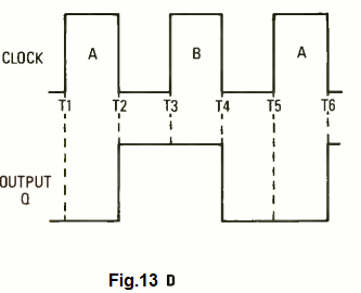 The above situation can we winessed in the Fig.
13D.
Here, it looks like that the input frequency is getting divided by two.
At time T1 the clock happens to be positive-edged, therefore we don not find any switching taking place.
However during time T2, we have a negative-going transition, which leads to the output suddenly changing state from low to high.
During the upcoming negative-going clock transition at time T4, the output line suddenly becomes low again.
The above procedures tells us that supplying a pair of input pulses to the clock lines (A and B) is necessary so that the output pulse is able to generate one full cycle, hence we get the following relationship:
fin = 2fout
The above situation can we winessed in the Fig.
13D.
Here, it looks like that the input frequency is getting divided by two.
At time T1 the clock happens to be positive-edged, therefore we don not find any switching taking place.
However during time T2, we have a negative-going transition, which leads to the output suddenly changing state from low to high.
During the upcoming negative-going clock transition at time T4, the output line suddenly becomes low again.
The above procedures tells us that supplying a pair of input pulses to the clock lines (A and B) is necessary so that the output pulse is able to generate one full cycle, hence we get the following relationship:
fin = 2fout
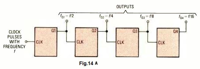 When we configure J -K flip -flops in a cascaded manner, as shown in Fig.
14A, it results in the creation of a binary-division chain.
The figure exhibits a four-bit scenario, where the input clock frequency applied at the input is denoted as f, and the frequency at the Q1 input becomes f /2, at Q2 the frequency turns into f/4, at Q3 = f /8, and at Q4 it becomes f/16.
When we configure J -K flip -flops in a cascaded manner, as shown in Fig.
14A, it results in the creation of a binary-division chain.
The figure exhibits a four-bit scenario, where the input clock frequency applied at the input is denoted as f, and the frequency at the Q1 input becomes f /2, at Q2 the frequency turns into f/4, at Q3 = f /8, and at Q4 it becomes f/16.
 We can witness the above explained series of clock pulses and the resultant outputs in the example figure 14B.
 Thus, the amount of power to the load could be controlled at any desired level, merely by varying the triac triggering point on the AC phase waveform.
This is how phase control works using a triac.
Thus, the amount of power to the load could be controlled at any desired level, merely by varying the triac triggering point on the AC phase waveform.
This is how phase control works using a triac.
 A neon lamp may also be employed in place of a diac for the same response.
The time utilized by the 0.1��f capacitor to charge upto the firing threshold of the diac is dependent upon the resistance setting of the control potentiometer.
Now suppose if the potentiometer is adjusted to a zero resistance, will cause the capacitor to charge instantly to the diac's firing level, which will in turn cause the to go into conduction for pretty much the entire AC half-cycle.
On the other hand, when the potentiometer is adjusted at it maximum resistance value might cause the capacitor to charge to the firing level only until half-cycle has almost reached its finishing point.
This will allow the
Triac to conduct only for a very short time while the AC waveform travels across its end of the half cycle.
Although the dimmer circuit demonstrated above really is easy and low-cost to construct includes one significant limitation - it doesn't allow a smooth control of power on the load from zero to maximum.
As we rotate the potentiometer, we may find the load current rising pretty abruptly from zero to some higher levels from where this could only then be operated smoothly in the higher or the lower levels.
In the event the AC supply is briefly cut off and the lamp illumination goes below this 'jump' (hysteresis) level, the lamp remains switched off even after the power is finally restored.
A neon lamp may also be employed in place of a diac for the same response.
The time utilized by the 0.1��f capacitor to charge upto the firing threshold of the diac is dependent upon the resistance setting of the control potentiometer.
Now suppose if the potentiometer is adjusted to a zero resistance, will cause the capacitor to charge instantly to the diac's firing level, which will in turn cause the to go into conduction for pretty much the entire AC half-cycle.
On the other hand, when the potentiometer is adjusted at it maximum resistance value might cause the capacitor to charge to the firing level only until half-cycle has almost reached its finishing point.
This will allow the
Triac to conduct only for a very short time while the AC waveform travels across its end of the half cycle.
Although the dimmer circuit demonstrated above really is easy and low-cost to construct includes one significant limitation - it doesn't allow a smooth control of power on the load from zero to maximum.
As we rotate the potentiometer, we may find the load current rising pretty abruptly from zero to some higher levels from where this could only then be operated smoothly in the higher or the lower levels.
In the event the AC supply is briefly cut off and the lamp illumination goes below this 'jump' (hysteresis) level, the lamp remains switched off even after the power is finally restored.
 Correction: Please replace 100 uF with 100 uH for the RFI coil
This circuit works great as a household light dimmer.
All parts could be fitted at the rear of a wall switch board and in case the load happens to be below 200 watts, the Triac could work without depending on a heatsink.
Practically 100% absence of hysteresis is necessary for light dimmers used in orchestral performances and theaters, to enable consistent illumination control of the lamps.
This feature may be accomplished by working with the circuit revealed in Fig.
4 below.
Correction: Please replace 100 uF with 100 uH for the RFI coil
This circuit works great as a household light dimmer.
All parts could be fitted at the rear of a wall switch board and in case the load happens to be below 200 watts, the Triac could work without depending on a heatsink.
Practically 100% absence of hysteresis is necessary for light dimmers used in orchestral performances and theaters, to enable consistent illumination control of the lamps.
This feature may be accomplished by working with the circuit revealed in Fig.
4 below.
 Correction: Please replace 100 uF with 100 uH for the RFI coil
 This set up helps to sustain virtually a constant output regardless of any significant variations in mains AC input voltage.
It is regularly found in photographic and other applications where a highly stable and fixed level of light becomes essential.
This set up helps to sustain virtually a constant output regardless of any significant variations in mains AC input voltage.
It is regularly found in photographic and other applications where a highly stable and fixed level of light becomes essential.
 This set up turns ON the lamps as darkness sets in, and turns them off again at dawn.
It is necessary for the photo cell to see the ambient light but be shielded from the lamp which is being controlled.
This set up turns ON the lamps as darkness sets in, and turns them off again at dawn.
It is necessary for the photo cell to see the ambient light but be shielded from the lamp which is being controlled.
 Through this set up the motor speed can vary in response to changes in load and the supply voltage,
However, for applications that are not critical (for example fan speed control), in which the load is fixed at any given speed, the circuit won't require any changes.
Motor speed which usually, when pre-programmed, is kept constant even with changes in the load conditions appears to be a helpful characteristic for power tools, laboratory stirrers, watchmakers' lathes potters' wheels, etc.
To achieve this 'load sensing' feature, an SCR is usually included in a half -wave arrangement (Fig.
7).
Through this set up the motor speed can vary in response to changes in load and the supply voltage,
However, for applications that are not critical (for example fan speed control), in which the load is fixed at any given speed, the circuit won't require any changes.
Motor speed which usually, when pre-programmed, is kept constant even with changes in the load conditions appears to be a helpful characteristic for power tools, laboratory stirrers, watchmakers' lathes potters' wheels, etc.
To achieve this 'load sensing' feature, an SCR is usually included in a half -wave arrangement (Fig.
7).
 The circuit operates pretty good within a limited motor speed range although may be vulnerable to low-speed 'hiccups' and the half -wave working rule inhibits stabilized operation very much above the 50% speed range.
A load sensing phase -control circuit where a Triac delivers complete zero to maximum control is displayed in Fig.
8.
The circuit operates pretty good within a limited motor speed range although may be vulnerable to low-speed 'hiccups' and the half -wave working rule inhibits stabilized operation very much above the 50% speed range.
A load sensing phase -control circuit where a Triac delivers complete zero to maximum control is displayed in Fig.
8.
 Hypothetically this circuit could keep the temperature stabilized to within 1% of the predetermined point regardless of AC line voltage alterations of +/-10%.
Precise overall performance may be determined by the structure and design of the system where the controller is applied.
This circuit delivers a relative control, which means, total power is given to the heating load as the load is starting to warm up, then at some midway point, the power is lowered through a measure that's proportionate to the difference between the actual temperature of the load and the intended load temperature.
The proportional range is variable through a 'gain' control.
The circuit is straightforward yet effective, however it includes one significant downside which limits its use to basically lighter loads.
This issue is regarding the emission of heavy radio interference, due to triac phase chopping.
Hypothetically this circuit could keep the temperature stabilized to within 1% of the predetermined point regardless of AC line voltage alterations of +/-10%.
Precise overall performance may be determined by the structure and design of the system where the controller is applied.
This circuit delivers a relative control, which means, total power is given to the heating load as the load is starting to warm up, then at some midway point, the power is lowered through a measure that's proportionate to the difference between the actual temperature of the load and the intended load temperature.
The proportional range is variable through a 'gain' control.
The circuit is straightforward yet effective, however it includes one significant downside which limits its use to basically lighter loads.
This issue is regarding the emission of heavy radio interference, due to triac phase chopping.
 The time constant element signifies the length of time in the form of time factor, for example at 1 time factor of the RC network, 63 % total voltage is accumulated, in a period after 2X time constant, 80% total voltage is built up inside the capacitor; and so forth.
After a time constant of 5 almost (but not quite) 100% voltage may build up across the capacitor.
The discharge factors of a capacitor occur in the same fundamental manner but in the inverse sequence.
Meaning, after an interval of time equal to the time constant 5, the voltage applied to the capacitor will achieve a drop of 100 - 63 = 37 % of the full voltage and so forth.
The time constant element signifies the length of time in the form of time factor, for example at 1 time factor of the RC network, 63 % total voltage is accumulated, in a period after 2X time constant, 80% total voltage is built up inside the capacitor; and so forth.
After a time constant of 5 almost (but not quite) 100% voltage may build up across the capacitor.
The discharge factors of a capacitor occur in the same fundamental manner but in the inverse sequence.
Meaning, after an interval of time equal to the time constant 5, the voltage applied to the capacitor will achieve a drop of 100 - 63 = 37 % of the full voltage and so forth.
 Next, when switch 1 is opened, the capacitor may then be in a situation where it will be storing a voltage equal to the actual applied voltage.
And it will hold this charge for an indefinite period of time provided the capacitor has zero internal leakage.
This process of losing charge will be actually extremely sluggish, since in real world no capacitor can be perfect, however for certain significant period of time this stored charge may continue being an effective source of the original "full charge" voltage.
When the capacitor is applied with a high voltage, it can quickly be in a position of delivering an electrical shock in case touched even after the circuit is powered down.
To execute the cycle of charge/discharge as displayed in the second graphical diagram above, when switch 2 is closed, the capacitor begins discharging via the connected resistance, and takes some period of time to accomplish its discharge process.
Next, when switch 1 is opened, the capacitor may then be in a situation where it will be storing a voltage equal to the actual applied voltage.
And it will hold this charge for an indefinite period of time provided the capacitor has zero internal leakage.
This process of losing charge will be actually extremely sluggish, since in real world no capacitor can be perfect, however for certain significant period of time this stored charge may continue being an effective source of the original "full charge" voltage.
When the capacitor is applied with a high voltage, it can quickly be in a position of delivering an electrical shock in case touched even after the circuit is powered down.
To execute the cycle of charge/discharge as displayed in the second graphical diagram above, when switch 2 is closed, the capacitor begins discharging via the connected resistance, and takes some period of time to accomplish its discharge process.
 The figure above is a very basic relaxation oscillator circuit operating using the basic charge discharge theory of a capacitor.
It includes a resistor (R) and capacitor (C) wired in series to a dc voltage source.
In order to be able to see the working of the circuit physically, a neon lamp is used in parallel with the capacitor.
The lamp behaves virtually like an open circuit until the voltage reaches its threshold voltage limit, when it instantly switches ON and conducts current quite like a conductor and begins glowing.
The source of supply voltage for this current hence must be higher than that of the neon triggering voltage.
The figure above is a very basic relaxation oscillator circuit operating using the basic charge discharge theory of a capacitor.
It includes a resistor (R) and capacitor (C) wired in series to a dc voltage source.
In order to be able to see the working of the circuit physically, a neon lamp is used in parallel with the capacitor.
The lamp behaves virtually like an open circuit until the voltage reaches its threshold voltage limit, when it instantly switches ON and conducts current quite like a conductor and begins glowing.
The source of supply voltage for this current hence must be higher than that of the neon triggering voltage.
 This resistance, aided by the capacitor, gives rise to an RC combination that may be responsible of generating a certain time constant.
It is crucial that this time constant complements the specification of the input AC signal frequency which is being transferred from one stage to another.
If we assume the example of an audio amplifier circuit, the highest range the input frequency could be approximately around 10 kHz.
The time period cycle of this sort of frequency will be 1/10,000 = 0.1 milliseconds.
That said, in order to allow this frequency, each cycle implements two charge/discharge characteristics with regards to the coupling capacitor function, which are one positive and one negative.
Therefore the period of time for a solitary charge/ discharge functionality will be 0.05 milliseconds.
The RC time constant required to enable this functioning must satisfy the 0.05 milliseconds value in order to reach the 63 % of the fed ac voltage level, and essentially somewhat less to allow the passage of higher than 63 percent of the applied voltage.
This resistance, aided by the capacitor, gives rise to an RC combination that may be responsible of generating a certain time constant.
It is crucial that this time constant complements the specification of the input AC signal frequency which is being transferred from one stage to another.
If we assume the example of an audio amplifier circuit, the highest range the input frequency could be approximately around 10 kHz.
The time period cycle of this sort of frequency will be 1/10,000 = 0.1 milliseconds.
That said, in order to allow this frequency, each cycle implements two charge/discharge characteristics with regards to the coupling capacitor function, which are one positive and one negative.
Therefore the period of time for a solitary charge/ discharge functionality will be 0.05 milliseconds.
The RC time constant required to enable this functioning must satisfy the 0.05 milliseconds value in order to reach the 63 % of the fed ac voltage level, and essentially somewhat less to allow the passage of higher than 63 percent of the applied voltage.
 If we look at the input side, we find a resistor attached in series with a capacitive reactance, causing a voltage drop to develop across the two elements.
In case the capacitor reactance (Xc) happens to be higher than R, almost all of the input voltage builds up across the capacitor and therefore the output voltage attains the level equal to the input voltage.
We know that capacitor reactance is inversely proportional to frequency, This implies, if the AC frequency is increased will cause the reactance to decrease, resulting in the output voltage to increase proportionality (but a significant portion of the input voltage will be dropped by the resistor).
If we look at the input side, we find a resistor attached in series with a capacitive reactance, causing a voltage drop to develop across the two elements.
In case the capacitor reactance (Xc) happens to be higher than R, almost all of the input voltage builds up across the capacitor and therefore the output voltage attains the level equal to the input voltage.
We know that capacitor reactance is inversely proportional to frequency, This implies, if the AC frequency is increased will cause the reactance to decrease, resulting in the output voltage to increase proportionality (but a significant portion of the input voltage will be dropped by the resistor).
 The critical point, called the roll-off point or cut-off frequency (f) is evaluated as:
fc = 1 / 2��RC
where R is in ohms, C is in farads, and �� = 3.1416
But from the previous discussion we know that RC = time constant T, therefore the equation becomes:
fc = 1 / 2��T
where T is the time constant in seconds.
The working efficiency of this type of filter is characterized by their cut-off frequency and by the rate through which the volts(in) / volts(out) ratio begins to drop above the cut-off frequency threshold.
The latter is generally represented as (some) dB per octave (for each frequency doubled), as indicated in the following figure which exhibits the relationship between dB and volts(in) /volts(out) ratio, and also provides an accurate frequency response curve.
The critical point, called the roll-off point or cut-off frequency (f) is evaluated as:
fc = 1 / 2��RC
where R is in ohms, C is in farads, and �� = 3.1416
But from the previous discussion we know that RC = time constant T, therefore the equation becomes:
fc = 1 / 2��T
where T is the time constant in seconds.
The working efficiency of this type of filter is characterized by their cut-off frequency and by the rate through which the volts(in) / volts(out) ratio begins to drop above the cut-off frequency threshold.
The latter is generally represented as (some) dB per octave (for each frequency doubled), as indicated in the following figure which exhibits the relationship between dB and volts(in) /volts(out) ratio, and also provides an accurate frequency response curve.
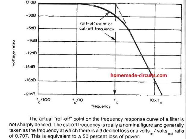
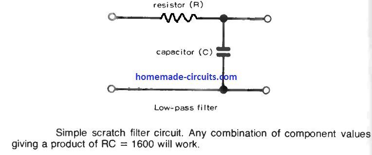 It is possible to calculate exact component values for these filters.
As an example, a standard scratch filter normally used in amplifiers could be built to attenuate frequencies over, say, 10 kHz.
This specific value signifies the intended cut-off frequency of the filter.
It is possible to calculate exact component values for these filters.
As an example, a standard scratch filter normally used in amplifiers could be built to attenuate frequencies over, say, 10 kHz.
This specific value signifies the intended cut-off frequency of the filter.
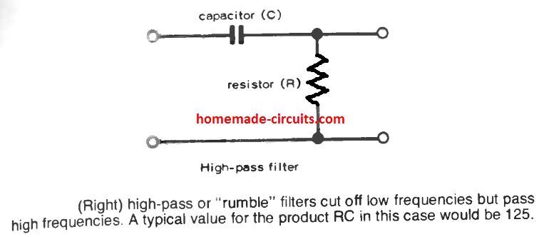 A high pass filter is similar to its low pass counterpart.
These are generally employed in amplifiers and audio devices, to get rid of noise or "rumble" generated by the inherent, unwanted low frequencies.
The selected cut-off frequency which is to be eliminated should be low enough so that it doesn't conflict with the "good" bass response.
Therefore, the decided magnitude is normally in the range of 15 to 20 Hz.
A high pass filter is similar to its low pass counterpart.
These are generally employed in amplifiers and audio devices, to get rid of noise or "rumble" generated by the inherent, unwanted low frequencies.
The selected cut-off frequency which is to be eliminated should be low enough so that it doesn't conflict with the "good" bass response.
Therefore, the decided magnitude is normally in the range of 15 to 20 Hz.

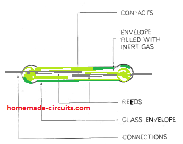 A standard reed relay switch can be witnessed as shown in the above figure.
It is made up a pair of flattened ferromagnetic strips (reeds) which are hermetically sealed in a tiny glass tube.
The reeds are clamped firmly on either ends of the glass tube in such a way that their free ends are slightly overlapped at the center with a separation of approximately 0.1 mm.
During the sealing process the air inside the tube is pumped out and is replaced by dry nitrogen.
This is crucial to ensure that the contacts work in an inert atmosphere which helps to keep the contacts corrosion free, eliminate air resistance, and make it long lasting.
A standard reed relay switch can be witnessed as shown in the above figure.
It is made up a pair of flattened ferromagnetic strips (reeds) which are hermetically sealed in a tiny glass tube.
The reeds are clamped firmly on either ends of the glass tube in such a way that their free ends are slightly overlapped at the center with a separation of approximately 0.1 mm.
During the sealing process the air inside the tube is pumped out and is replaced by dry nitrogen.
This is crucial to ensure that the contacts work in an inert atmosphere which helps to keep the contacts corrosion free, eliminate air resistance, and make it long lasting.
 Typically, a reed switch will close when the magnet is brought at a distance of 1 inch from it, but it may need the magnet to be moved around 3 inches away to open the contacts to its original form, due to magnetic hysteresis.
 Make sure that the left side fixed magnet is not within the pull-in range of the reed switch, rather at some distance away, otherwise the reed will remain closed and will open only when the right side magnet is brought too close to the reed.
Therefore, the distance of the fixed magnet must be experimented with some trial and error until the right differential is achieved, and the reed activates sharply at a fixed point by the moving magnet.
Make sure that the left side fixed magnet is not within the pull-in range of the reed switch, rather at some distance away, otherwise the reed will remain closed and will open only when the right side magnet is brought too close to the reed.
Therefore, the distance of the fixed magnet must be experimented with some trial and error until the right differential is achieved, and the reed activates sharply at a fixed point by the moving magnet.
 In the majority of systems in which a reed switch is operated through 'a permanent magnet, the magnet is installed over a moving element, and the reed is installed over a fixed or constant platform.
However, you may find several programs where both the magnet and the reed has to be positioned over a fixed platform.
The ON/OFF operation of the reed in such cases is then achieved by distorting the magnetic field with the help of an external moving ferrous agent, as explained in the following paragraph.
In the majority of systems in which a reed switch is operated through 'a permanent magnet, the magnet is installed over a moving element, and the reed is installed over a fixed or constant platform.
However, you may find several programs where both the magnet and the reed has to be positioned over a fixed platform.
The ON/OFF operation of the reed in such cases is then achieved by distorting the magnetic field with the help of an external moving ferrous agent, as explained in the following paragraph.
 Additionally, you may find spurious or false reed triggering due to negative peaks from the magnet's field pattern curve.
In situations where the negative peaks are high, the reeds may switch ON/OFF several times as the magnet moves past across the end to end length of the reed.
Activation of the reed through a rotational movement can be also implemented successfully.
To achieve this, you can use among the many set ups shown below:
Additionally, you may find spurious or false reed triggering due to negative peaks from the magnet's field pattern curve.
In situations where the negative peaks are high, the reeds may switch ON/OFF several times as the magnet moves past across the end to end length of the reed.
Activation of the reed through a rotational movement can be also implemented successfully.
To achieve this, you can use among the many set ups shown below:
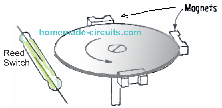 FIGURE A
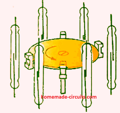 FIGURE B
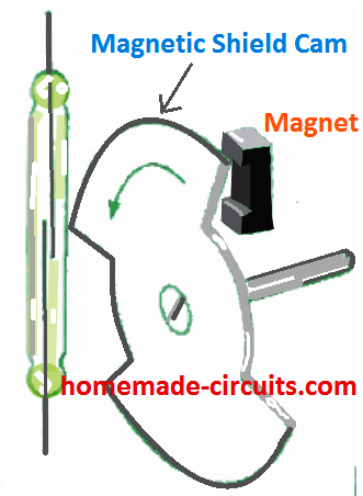 FIGURE C
It is also possible to use a rotational motion for triggering a reed switch set up.
In figure A and B, the reed switches are installed in a fixed position, while magnets are attached with the rotating disc which causes the magnets to move past the reed switch on each rotation, switching the reed ON/OFF correspondingly.
In figure C, the magnet and the reed switch both are stationery, while a specially carved magnetic shield cam is rotated between them such that the cam cuts the magnetic field alternately on each rotation causing the reed to open and close in the same sequence
Rotary motion may also be used to actuate a reed switch, In A and B the switches are stationary and the magnets rotate.
In examples C and D both the switches and the magnets are stationary and the switch operates whenever the cutout portion of the magnetic shield is between magnet and switch.
Switching rates can be adjusted one second to well over 2000 per minute simply by changing the rotating disc speed.
FIGURE C
It is also possible to use a rotational motion for triggering a reed switch set up.
In figure A and B, the reed switches are installed in a fixed position, while magnets are attached with the rotating disc which causes the magnets to move past the reed switch on each rotation, switching the reed ON/OFF correspondingly.
In figure C, the magnet and the reed switch both are stationery, while a specially carved magnetic shield cam is rotated between them such that the cam cuts the magnetic field alternately on each rotation causing the reed to open and close in the same sequence
Rotary motion may also be used to actuate a reed switch, In A and B the switches are stationary and the magnets rotate.
In examples C and D both the switches and the magnets are stationary and the switch operates whenever the cutout portion of the magnetic shield is between magnet and switch.
Switching rates can be adjusted one second to well over 2000 per minute simply by changing the rotating disc speed.
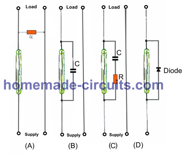
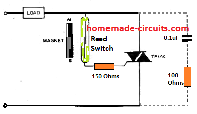 The gate current being significantly less than the load current, the reed switch will work efficiently and allow the triac to be switched wit the high current load.
Even minute reed switch can be applied here, and will work without issues.
The optional 0.1 uF and the 100 ohm RC is a snubber network is for protecting the triac against high current inductive spikes, if the load is an inductive load.
The gate current being significantly less than the load current, the reed switch will work efficiently and allow the triac to be switched wit the high current load.
Even minute reed switch can be applied here, and will work without issues.
The optional 0.1 uF and the 100 ohm RC is a snubber network is for protecting the triac against high current inductive spikes, if the load is an inductive load.
 The most basic item will be the copper clad for making the printed circuit board alone, and you will find a variety of these.
The base (insulating) stuff is generally either fibreglass or SRBP (sheet resin bonded paper), and the latter is usually the more affordable option.
However, fibreglass has become the widely used both with commercial and recreational consumers as it is equipped with a couple of positive aspects.
The first is basically that it is tougher and for that reason less susceptible to bending and breaking than SRBP.
The improved durability is additionally very helpful for boards that bear weighty parts for example transformers.
An additional benefit is that fibreglass is translucent and thus typically allows us to view the copper paths through the top (component) area of the board which is often worthwhile when examining and fault-finding.
Having said that, the standard of SRBP boards is more than satisfactory for many requirements.
Marketing campaigns usually make reference to board as 1mm, 1.6mm, etc., and this is actually refering to the thickness of the base material.
The most basic item will be the copper clad for making the printed circuit board alone, and you will find a variety of these.
The base (insulating) stuff is generally either fibreglass or SRBP (sheet resin bonded paper), and the latter is usually the more affordable option.
However, fibreglass has become the widely used both with commercial and recreational consumers as it is equipped with a couple of positive aspects.
The first is basically that it is tougher and for that reason less susceptible to bending and breaking than SRBP.
The improved durability is additionally very helpful for boards that bear weighty parts for example transformers.
An additional benefit is that fibreglass is translucent and thus typically allows us to view the copper paths through the top (component) area of the board which is often worthwhile when examining and fault-finding.
Having said that, the standard of SRBP boards is more than satisfactory for many requirements.
Marketing campaigns usually make reference to board as 1mm, 1.6mm, etc., and this is actually refering to the thickness of the base material.
 I personally prefer using nail enamels or nail polish, any cheap brand can be used and will work great as an etch resist.
 A simple solution would be to utilize an worn-out fibre-tip pen in paint brush manner, which can help develop outstanding final results although it might not look like quite a exquisite means to fix the issue.
An easier way of implementing the resist is to use one of the commercially available etch resist pens which can be easily bought from any electronic part dealer.
Any kind of pen that uses a spirit based ink and a sharp point should be workable with this application.
In case you are uncertain regarding the appropriateness of a pen you can easily pull out a few traces over a discarded copper laminate board then etch the board to verify if the ink maintains the etchant away correctly.
An additional type of resist are the rub-down etch resistant transfers which are available from several component merchants and which often can provide truly outstanding and specialized outcomes as demonstrated in the following example.
A simple solution would be to utilize an worn-out fibre-tip pen in paint brush manner, which can help develop outstanding final results although it might not look like quite a exquisite means to fix the issue.
An easier way of implementing the resist is to use one of the commercially available etch resist pens which can be easily bought from any electronic part dealer.
Any kind of pen that uses a spirit based ink and a sharp point should be workable with this application.
In case you are uncertain regarding the appropriateness of a pen you can easily pull out a few traces over a discarded copper laminate board then etch the board to verify if the ink maintains the etchant away correctly.
An additional type of resist are the rub-down etch resistant transfers which are available from several component merchants and which often can provide truly outstanding and specialized outcomes as demonstrated in the following example.
 Actually you may find that there are lots of chemicals that can be applied as the etchant, but the majority of these are hazardous for some reason or another and are not likely suited to home designed boards.
 The etchant typically employed for home developed boards is ferric chloride, and while this is less hazardous compared to the majority of the choices, it is nevertheless a chemical that needs to be implemented with caution.
This should hence always be rinsed off quickly with running tap water in case you spill any on your skin.
Make sure you don't store ferric chloride in metallic containers, since this chemical is reactive to metals and make the metal porous and cause leakages.
As ferric chloride is toxic (and in in the course of many uses progressively gets transformed into copper chloride which is likewise extremely poisonous) it must obviously be stored far from foodstuff and utensils etc.
The etchant typically employed for home developed boards is ferric chloride, and while this is less hazardous compared to the majority of the choices, it is nevertheless a chemical that needs to be implemented with caution.
This should hence always be rinsed off quickly with running tap water in case you spill any on your skin.
Make sure you don't store ferric chloride in metallic containers, since this chemical is reactive to metals and make the metal porous and cause leakages.
As ferric chloride is toxic (and in in the course of many uses progressively gets transformed into copper chloride which is likewise extremely poisonous) it must obviously be stored far from foodstuff and utensils etc.
 Some companies may provide the ferric chloride as crystals, also known as "Ferric Chloride Rock" sometimes.
This label is very suitable since in this form it certainly looks like pieces of yellow rock rather then tiny nice crystals, which is pretty much rock solid.
In this type ferric chloride is normally available in 500gm packages, which is enough to generate one litre of etching solution.
You can as well get this in bigger packages, but since 500gm is enough to etch a seriously great number of regular size boards and may easily survive even an diligent constructor a very long time it is most likely not rewarding getting bigger than 500gm pack altogether.
Some companies may provide the ferric chloride as crystals, also known as "Ferric Chloride Rock" sometimes.
This label is very suitable since in this form it certainly looks like pieces of yellow rock rather then tiny nice crystals, which is pretty much rock solid.
In this type ferric chloride is normally available in 500gm packages, which is enough to generate one litre of etching solution.
You can as well get this in bigger packages, but since 500gm is enough to etch a seriously great number of regular size boards and may easily survive even an diligent constructor a very long time it is most likely not rewarding getting bigger than 500gm pack altogether.
 Typically, it is recommended to use a diameter of under 1mm for semiconductors and a number of other components that have thinner leads.
0.7mm or 0.8mm appear to be acceptable diameter for these components.
In case you have access to high quality drill bits they must be pretty tough.
However drill bits of around 0.7mm to 1.4mm in diameter may be quite weak and should be handled relatively carefully.
If they are maintained with downwards straight vertical pressure it may be fine, but if the orientation is not maintained at right angles to the board a proper hole won't be created which is quite possible that the drill bit will break in two.
You have to for that reason take realistic care while drilling holes using such drill bits, and preferably the machine should be used with a adjustable stand as shown below.
Typically, it is recommended to use a diameter of under 1mm for semiconductors and a number of other components that have thinner leads.
0.7mm or 0.8mm appear to be acceptable diameter for these components.
In case you have access to high quality drill bits they must be pretty tough.
However drill bits of around 0.7mm to 1.4mm in diameter may be quite weak and should be handled relatively carefully.
If they are maintained with downwards straight vertical pressure it may be fine, but if the orientation is not maintained at right angles to the board a proper hole won't be created which is quite possible that the drill bit will break in two.
You have to for that reason take realistic care while drilling holes using such drill bits, and preferably the machine should be used with a adjustable stand as shown below.
 We have so far discussed the key things which are necessary while making a printed circuit board, and there may be some other probabilities and ends which might be essential.
These are typically basic domestic objects though, and these will be unveiled as we advance with the etching course of action.
You will find many different methods for manufacturing a printed circuit board.
Despite the fact that all of them are fundamentally the identical and the major dissimilarities are just the sequence through which the different measures along the way are performed.
We are going to hence begin by taking into consideration one approach of manufacturing a board, after which a couple of alternate techniques will be explained.
We have so far discussed the key things which are necessary while making a printed circuit board, and there may be some other probabilities and ends which might be essential.
These are typically basic domestic objects though, and these will be unveiled as we advance with the etching course of action.
You will find many different methods for manufacturing a printed circuit board.
Despite the fact that all of them are fundamentally the identical and the major dissimilarities are just the sequence through which the different measures along the way are performed.
We are going to hence begin by taking into consideration one approach of manufacturing a board, after which a couple of alternate techniques will be explained.
 The size of the printed circuit should be available in the text or the schematic, however in many instances it will be required to consider the proportions through the real size copper track pattern.
Mark the boundary of the finalized board on the copper side of the laminate board, then pull an additional set of lines approximately 2mm or so on the outer side of the previous marking.
By cautiously cutting between these outlines you should be able to generate a section of board with decent precision and straight edges with minimum issues.
The sides of the board could be smoothed using a small flat file, and with fibre glass board that eliminates the abrasive ends which can be undesirable.
Be aware that the markings should be done on the copper side of the board and sawn from the same side to prevent peeling of the copper while cutting the board.
Therefore, make sure to cut, or drill the board always from the copper side, and not from the laminate side
The next step would be to draw the positions of the holes for the components, and wherever suitable, the fitting holes for the board mounting.
The quick method to get this done is to clamp the schematic drawing over the board on the copper track, by accurately aligning the drawing and the board edges.
Then, with a bradawl or similar pointed tool carefully and accurately marking through the schematic onto the board by punching small indentations in the copper.
It is not necessarily essential to mark the board by punching with a pointed tool, and an alternate way is to simply align and stick the drawing to the board using cello tape, and then drill down through the drawing which now itself acts like drilling markers.
The size of the printed circuit should be available in the text or the schematic, however in many instances it will be required to consider the proportions through the real size copper track pattern.
Mark the boundary of the finalized board on the copper side of the laminate board, then pull an additional set of lines approximately 2mm or so on the outer side of the previous marking.
By cautiously cutting between these outlines you should be able to generate a section of board with decent precision and straight edges with minimum issues.
The sides of the board could be smoothed using a small flat file, and with fibre glass board that eliminates the abrasive ends which can be undesirable.
Be aware that the markings should be done on the copper side of the board and sawn from the same side to prevent peeling of the copper while cutting the board.
Therefore, make sure to cut, or drill the board always from the copper side, and not from the laminate side
The next step would be to draw the positions of the holes for the components, and wherever suitable, the fitting holes for the board mounting.
The quick method to get this done is to clamp the schematic drawing over the board on the copper track, by accurately aligning the drawing and the board edges.
Then, with a bradawl or similar pointed tool carefully and accurately marking through the schematic onto the board by punching small indentations in the copper.
It is not necessarily essential to mark the board by punching with a pointed tool, and an alternate way is to simply align and stick the drawing to the board using cello tape, and then drill down through the drawing which now itself acts like drilling markers.
 While designing a board of this kind it is recommended work with a printed circuit resist pen (or a appropriate alternative) with an even finer nib.
In places that may have many narrow, tightly packed parallel tracks, you must take the help of a ruler to allow fine straight lines to be sketched.
If you see the tracks or pads merging with each other, wait for the resist to dry up and then make use of a compass point or other sharp pointed to scratch away the excess overlapping resist.
As soon as the resist has dried out and the PCB is inspected, the next task is to submerge the board in the etchant solution until eventually all the exposed copper has been taken off.
While designing a board of this kind it is recommended work with a printed circuit resist pen (or a appropriate alternative) with an even finer nib.
In places that may have many narrow, tightly packed parallel tracks, you must take the help of a ruler to allow fine straight lines to be sketched.
If you see the tracks or pads merging with each other, wait for the resist to dry up and then make use of a compass point or other sharp pointed to scratch away the excess overlapping resist.
As soon as the resist has dried out and the PCB is inspected, the next task is to submerge the board in the etchant solution until eventually all the exposed copper has been taken off.
 Figure above shows a few easy options for accomplishing this.
In Figure (a) a curved dish is employed which ensures that the board is maintained in place through the four corners, and does not come in contact with the dish at any other points.
The technique demonstrated in (b) a good choice for bigger PCBs which may necessitate a rather huge dish to enable the procedure.
The container has to be pretty sizeable, anything similar to a classic instant coffee jar would work.
A great deal of etchant will probably be required so as to practically fill up the jar.
This might look a bit pricey at first, however the etchant will certainly last proportionately more time compared to a smaller quantity.
Alternatively, a lesser amount of etchant can be diluted with higher amount of water, but this could considerably decelerate etching and is not advisable.
For substantially large boards the only functional method of etching the board could be to employ a big flat dish (like a photographic dish) with the copper side facing upwards.
Frequent agitation may be accustomed to speed up the etching time.
Etching will be seen happening faster on areas of where there are smaller regions of open copper, and will take a lot longer on areas of the board where there are relatively wider areas of open copper.
Etching also takes place more quickly round the perimeters of the board.
Figure above shows a few easy options for accomplishing this.
In Figure (a) a curved dish is employed which ensures that the board is maintained in place through the four corners, and does not come in contact with the dish at any other points.
The technique demonstrated in (b) a good choice for bigger PCBs which may necessitate a rather huge dish to enable the procedure.
The container has to be pretty sizeable, anything similar to a classic instant coffee jar would work.
A great deal of etchant will probably be required so as to practically fill up the jar.
This might look a bit pricey at first, however the etchant will certainly last proportionately more time compared to a smaller quantity.
Alternatively, a lesser amount of etchant can be diluted with higher amount of water, but this could considerably decelerate etching and is not advisable.
For substantially large boards the only functional method of etching the board could be to employ a big flat dish (like a photographic dish) with the copper side facing upwards.
Frequent agitation may be accustomed to speed up the etching time.
Etching will be seen happening faster on areas of where there are smaller regions of open copper, and will take a lot longer on areas of the board where there are relatively wider areas of open copper.
Etching also takes place more quickly round the perimeters of the board.
 A method which usually works more effectively and is typically far easier in practice is displayed above.
Here a pair of wooden or plastic rods are put down the entire length of the dish, on opposite sides.
These are relatively longer than the dish to allow them to rest on top.
The board is then hung from the rods supported on a couple of wire pieces, one at each end of the board.
Just a single wire is demonstrated in Figure for better understanding.
If copper wire is used make sure it is a super Enameled copper wire having a thickness of 18 SWG.
The wires are attached to the rods simply by turning the ends round the diameter of the rod once or twice.
A method which usually works more effectively and is typically far easier in practice is displayed above.
Here a pair of wooden or plastic rods are put down the entire length of the dish, on opposite sides.
These are relatively longer than the dish to allow them to rest on top.
The board is then hung from the rods supported on a couple of wire pieces, one at each end of the board.
Just a single wire is demonstrated in Figure for better understanding.
If copper wire is used make sure it is a super Enameled copper wire having a thickness of 18 SWG.
The wires are attached to the rods simply by turning the ends round the diameter of the rod once or twice.
 It may be also feasible to obtain printed circuit polishing blocks that happen to be likewise well suited for scrubbing of the resist.
One more technique is to try using a scouring pad or powder, and this is basically among the most straightforward activities of printed circuit production which should certainly not present any kind of challenges.
To enable the final assembly of the components on the ready PCB with perfect soldering and absolutely no "dry" joints, the copper tracks and pads must be polished to a glossy finishing before the soldering of the components can be actually commenced.
It may be also feasible to obtain printed circuit polishing blocks that happen to be likewise well suited for scrubbing of the resist.
One more technique is to try using a scouring pad or powder, and this is basically among the most straightforward activities of printed circuit production which should certainly not present any kind of challenges.
To enable the final assembly of the components on the ready PCB with perfect soldering and absolutely no "dry" joints, the copper tracks and pads must be polished to a glossy finishing before the soldering of the components can be actually commenced.
 The 4 gates of a 7400 are exactly the same with their specs:
Gate A pins 1, 2 inputs, pin 3 output
Gate B pins 4, 5 inputs, pin 6 output
Gate C pins 10, 9 inputs, pin 8 output
Gate D pins 13, 12 inputs, pin 11 output
You may find a specific circuit indicating an oscillator applying gates A and B, however this also means that the same can be designed using gates A and C, B and C or C and D also, without any problems.
The 4 gates of a 7400 are exactly the same with their specs:
Gate A pins 1, 2 inputs, pin 3 output
Gate B pins 4, 5 inputs, pin 6 output
Gate C pins 10, 9 inputs, pin 8 output
Gate D pins 13, 12 inputs, pin 11 output
You may find a specific circuit indicating an oscillator applying gates A and B, however this also means that the same can be designed using gates A and C, B and C or C and D also, without any problems.
 Figure 1 exhibits the logic circuit of your 7400 I.C.
Figure 2 demonstrates the logic symbolic representation for just one gate, every single gate usually a "2 Input NAND Gate".
Figure 1 exhibits the logic circuit of your 7400 I.C.
Figure 2 demonstrates the logic symbolic representation for just one gate, every single gate usually a "2 Input NAND Gate".
 The internal configuration with an individual gate is displayed in figure 3. The 7400 is a TTL logic I.C., that means it works by using "Transistor-Transistor-Logic".
Every single gate employs Four transistors, every 7400 is made up of 4 x 4= 16 transistors.
The logic gates include a pair of states, depending on the binary system, 1 or "High" typically 4 volts, and 0 (zero) or "Low" typically 0 volts.
In case a gate terminal is not used.
that may correspond to a 1 input.
Meaning an open gate pin is at "high" level.
When a gate input pin is connected with the ground or 0 volts line, the input then becomes 0 or logic low.
A NAND gate is actually a mix of "NOT and AND" gate when both of its inputs (and function) are at logic 1, output is a NOT gate output which is 1.
The output from a NOT gate will be 0V in response to a 1 input signal or + supply input, meaning output will be logic Zero when input is at + supply level.
For a NAND gate when both inputs are logic 0, output turns into logic 1, which is exactly like a NOT gate response.
It might look difficult to comprehend exactly why the output is 1 when inputs held at 0, and vice versa.
It can be explained in this way
For a switching of state an AND function must come about, that is each inputs must transform for the toggling of state.
This solely happens when the two inputs switch through 0 to 1. The 7400 gates are 2 input NAND gates however 3 input NAND gates 7410 I.C., 4 input NAND gates 7420 and also an 8 input NAND gate 7430 can be also procured easily from the market.
Regarding the 7430, its 8 input gate will switch state only when each one of the 8 inputs are either 1 or 0.
When the 8 inputs of the 7430 are 1,1,1,1,1,1,1,0 then the output will continue to be 1. The change of state will not occur as long all 8 inputs do not have the identical logics.
But as soon as the last input changes from 0 to 1 the output changes from 1 to 0. The technique that causes "change of state" is a crucial aspect to understand the functionality of logic circuits.
The number of pins a logic IC may commonly have are 14 or 16. A 7400 consists of four NAND gates, with 2 input pins and 1 output pin for each of the gates, and also a pair of pins for the power supply inputs, pin 14 and pin 7.
The internal configuration with an individual gate is displayed in figure 3. The 7400 is a TTL logic I.C., that means it works by using "Transistor-Transistor-Logic".
Every single gate employs Four transistors, every 7400 is made up of 4 x 4= 16 transistors.
The logic gates include a pair of states, depending on the binary system, 1 or "High" typically 4 volts, and 0 (zero) or "Low" typically 0 volts.
In case a gate terminal is not used.
that may correspond to a 1 input.
Meaning an open gate pin is at "high" level.
When a gate input pin is connected with the ground or 0 volts line, the input then becomes 0 or logic low.
A NAND gate is actually a mix of "NOT and AND" gate when both of its inputs (and function) are at logic 1, output is a NOT gate output which is 1.
The output from a NOT gate will be 0V in response to a 1 input signal or + supply input, meaning output will be logic Zero when input is at + supply level.
For a NAND gate when both inputs are logic 0, output turns into logic 1, which is exactly like a NOT gate response.
It might look difficult to comprehend exactly why the output is 1 when inputs held at 0, and vice versa.
It can be explained in this way
For a switching of state an AND function must come about, that is each inputs must transform for the toggling of state.
This solely happens when the two inputs switch through 0 to 1. The 7400 gates are 2 input NAND gates however 3 input NAND gates 7410 I.C., 4 input NAND gates 7420 and also an 8 input NAND gate 7430 can be also procured easily from the market.
Regarding the 7430, its 8 input gate will switch state only when each one of the 8 inputs are either 1 or 0.
When the 8 inputs of the 7430 are 1,1,1,1,1,1,1,0 then the output will continue to be 1. The change of state will not occur as long all 8 inputs do not have the identical logics.
But as soon as the last input changes from 0 to 1 the output changes from 1 to 0. The technique that causes "change of state" is a crucial aspect to understand the functionality of logic circuits.
The number of pins a logic IC may commonly have are 14 or 16. A 7400 consists of four NAND gates, with 2 input pins and 1 output pin for each of the gates, and also a pair of pins for the power supply inputs, pin 14 and pin 7.
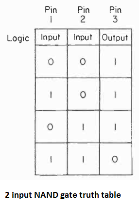 To help you fully grasp the functionality of a NAND gate, a TRUTH table is demonstrated above for a 2 input NAND gate.
Equivalent truth tables could be evaluated for just about any logic gate.
The truth table for an 8 input gate like the 7430 is somewhat more complex.
To help you fully grasp the functionality of a NAND gate, a TRUTH table is demonstrated above for a 2 input NAND gate.
Equivalent truth tables could be evaluated for just about any logic gate.
The truth table for an 8 input gate like the 7430 is somewhat more complex.
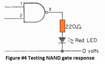 In order to check a 7400 IC, you can apply power across pins 14 and 7. Keep pins 1 and 2 connected to positive supply, this will show the output as 0.
Next, without changing pin 2 connection, connect pin 1 to 0 volts.
This will enable the inputs to become 1, 0. This will cause the output to turn 1, illuminating the LED.
Now simply, swap pin 1 and pin 2 connections, so that the Inputs become 0, 1, this will switch the output to logic 1, shutting off the LED.
In the final step, connect both the input pins 1 and 2 to ground or 0 volts so that the Inputs are at logic 0, 0. This will yet again turns output to logic high or 1, switching ON the LED.
The glowing of the LED signifies the logic level 1.
When LED is OFF this suggests logic level 0. The analysis could be repeated for the gates B, C and D.
Note: each of the circuits proven here work with 1/4W 5% resistors - all electrolytic capacitors are generally 25V rated.
If a circuit fails to work, you may look at the connections, the possibility of a faulty IC may be highly unlikely compared to an incorrect connection of the pins.
This connections of a NAND gate shown below may be the most basic and works by using only 1 gate of a 7400.
In order to check a 7400 IC, you can apply power across pins 14 and 7. Keep pins 1 and 2 connected to positive supply, this will show the output as 0.
Next, without changing pin 2 connection, connect pin 1 to 0 volts.
This will enable the inputs to become 1, 0. This will cause the output to turn 1, illuminating the LED.
Now simply, swap pin 1 and pin 2 connections, so that the Inputs become 0, 1, this will switch the output to logic 1, shutting off the LED.
In the final step, connect both the input pins 1 and 2 to ground or 0 volts so that the Inputs are at logic 0, 0. This will yet again turns output to logic high or 1, switching ON the LED.
The glowing of the LED signifies the logic level 1.
When LED is OFF this suggests logic level 0. The analysis could be repeated for the gates B, C and D.
Note: each of the circuits proven here work with 1/4W 5% resistors - all electrolytic capacitors are generally 25V rated.
If a circuit fails to work, you may look at the connections, the possibility of a faulty IC may be highly unlikely compared to an incorrect connection of the pins.
This connections of a NAND gate shown below may be the most basic and works by using only 1 gate of a 7400.
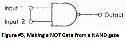 When the input pins a of a NAND gate are shorted with each other the circuit then works like an inverter, meaning the output logic shows always the opposite of the input.
When the shorted input pins of the gate is connected to 0V, the output will turn into 1 and vice versa.
Because the "NOT" configuration provides an opposing response across the input and the output pins, hence the name NOT gate.
This phrase is actually a technically appropriate one.
When the input pins a of a NAND gate are shorted with each other the circuit then works like an inverter, meaning the output logic shows always the opposite of the input.
When the shorted input pins of the gate is connected to 0V, the output will turn into 1 and vice versa.
Because the "NOT" configuration provides an opposing response across the input and the output pins, hence the name NOT gate.
This phrase is actually a technically appropriate one.
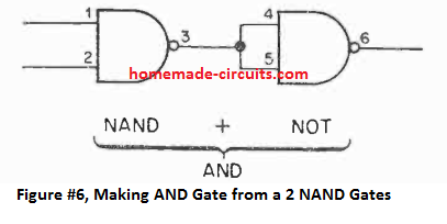 Since a NAND gate is also a kind of a "NOT AND" gate, therefore in case a "NOT" gate is introduced after a NAND gate, the circuit turns into a "NOT NOT AND" gate.
A couple of negatives produce a positive (a notion that's popular in math concepts too).
The circuit has now become an "AND" gate as shown above.
Since a NAND gate is also a kind of a "NOT AND" gate, therefore in case a "NOT" gate is introduced after a NAND gate, the circuit turns into a "NOT NOT AND" gate.
A couple of negatives produce a positive (a notion that's popular in math concepts too).
The circuit has now become an "AND" gate as shown above.
 Inserting a NOT gate before each NAND gate inputs generates an OR gate as demonstrated above.
This is usually a 2 -input OR gate.
Inserting a NOT gate before each NAND gate inputs generates an OR gate as demonstrated above.
This is usually a 2 -input OR gate.
 In the previous design we created an OR gate from NAND gates.
A NOR gate in fact becomes a NOT OR gate when we add an extra NOT gate just after an OR gate as shown above.
In the previous design we created an OR gate from NAND gates.
A NOR gate in fact becomes a NOT OR gate when we add an extra NOT gate just after an OR gate as shown above.
 This logic level tested circuit can be created through a single 7400 NAND gate as an inverter or NOT gate for indicating logic levels.
A couple of red LEDs are employed to distinguish the logic levels across the LED 1 and LED 2.
The LED pin which is longer becomes the cathode or the negative pin of the LED.
When the input is at logic level 1 or HIGH, LED 1 illuminates naturally.
The pin 3 which is the output pin is the opposite of the input at logic 0 which causes the LED 2 to remain OFF.
When the input gets a logic 0, LED 1 shuts OFF naturally, but LED 2 now glows due to the opposite response of the gate.
This logic level tested circuit can be created through a single 7400 NAND gate as an inverter or NOT gate for indicating logic levels.
A couple of red LEDs are employed to distinguish the logic levels across the LED 1 and LED 2.
The LED pin which is longer becomes the cathode or the negative pin of the LED.
When the input is at logic level 1 or HIGH, LED 1 illuminates naturally.
The pin 3 which is the output pin is the opposite of the input at logic 0 which causes the LED 2 to remain OFF.
When the input gets a logic 0, LED 1 shuts OFF naturally, but LED 2 now glows due to the opposite response of the gate.
 This circuit makes use of a couple of NAND gates cross-coupled, to make a S-R bistable latch circuit.
The outputs are marked as Q and 0. The line above the Q signifies NOT.
The 2 outputs Q and 0 acts like complements of each other.
Meaning, when Q reaches logic level 1, Q turns 0; when Q is 0, Q turns 1.
The circuit could be activated into both of the 2 stable states through an appropriate input pulse.
Essentially this allows the circuit a "memory" feature and creates this into a super easy 1 bit (one binary digit) data storage chip.
The two inputs are branded S and R or Set and Reset, thus this circuit is usually known as S.R.F.F.
(Set Reset Flip-Flop).
This circuit can be quite useful and it is applied in a number of circuits.
This circuit makes use of a couple of NAND gates cross-coupled, to make a S-R bistable latch circuit.
The outputs are marked as Q and 0. The line above the Q signifies NOT.
The 2 outputs Q and 0 acts like complements of each other.
Meaning, when Q reaches logic level 1, Q turns 0; when Q is 0, Q turns 1.
The circuit could be activated into both of the 2 stable states through an appropriate input pulse.
Essentially this allows the circuit a "memory" feature and creates this into a super easy 1 bit (one binary digit) data storage chip.
The two inputs are branded S and R or Set and Reset, thus this circuit is usually known as S.R.F.F.
(Set Reset Flip-Flop).
This circuit can be quite useful and it is applied in a number of circuits.
 The SR Flip-Flop circuit can be configured to work like a square wave generator.
If the F.F.
is applied with a sine wave, let's say from a 12V AC from a transformer, with minimum 2 volts peak to peak range, the output will respond by generating square waves having peak to peak equivalent to the Vcc voltage.
These square wave can be expected to be perfectly square in shape due to the extremely fast rise and fall times of the IC.
The inverter or NOT gate output feeding the to the R input results in creating complementary ON/OFF inputs across the R and S inputs of the circuit.
The SR Flip-Flop circuit can be configured to work like a square wave generator.
If the F.F.
is applied with a sine wave, let's say from a 12V AC from a transformer, with minimum 2 volts peak to peak range, the output will respond by generating square waves having peak to peak equivalent to the Vcc voltage.
These square wave can be expected to be perfectly square in shape due to the extremely fast rise and fall times of the IC.
The inverter or NOT gate output feeding the to the R input results in creating complementary ON/OFF inputs across the R and S inputs of the circuit.
 In this circuit an S-R FLIP-FLOP can be seen applied as a switch contact bounce eliminator.
Whenever switch contacts are closed it is usually followed by the contacts bouncing rapidly a few times between due to mechanical stress and pressure.
This mostly results in the generation of spurious spikes, which may cause interference and erratic circuit operation.
The above circuit eliminates this possibility.
When the contacts close initially it latches the circuit, and due to this the interference from contact bounce fails to create any effect on the flip-flop.
In this circuit an S-R FLIP-FLOP can be seen applied as a switch contact bounce eliminator.
Whenever switch contacts are closed it is usually followed by the contacts bouncing rapidly a few times between due to mechanical stress and pressure.
This mostly results in the generation of spurious spikes, which may cause interference and erratic circuit operation.
The above circuit eliminates this possibility.
When the contacts close initially it latches the circuit, and due to this the interference from contact bounce fails to create any effect on the flip-flop.
 This is a another variant of circuit eight.
For experimenting with circuits like half adder or other logic circuits, it really is necessary to be capable of analyzing the circuit since it works with a single pulse at a time.
This could be achieved by the application of a hand operated clocking.
Whenever the switch is toggled a solitary trigger turns up at the output.
The circuit works extremely well with a binary counter.
Whenever the switch is toggled, only a single pulse at a time is allowed to happen due to anti-bounce feature of the circuit, enabling the count to progress one trigger at a time.
This is a another variant of circuit eight.
For experimenting with circuits like half adder or other logic circuits, it really is necessary to be capable of analyzing the circuit since it works with a single pulse at a time.
This could be achieved by the application of a hand operated clocking.
Whenever the switch is toggled a solitary trigger turns up at the output.
The circuit works extremely well with a binary counter.
Whenever the switch is toggled, only a single pulse at a time is allowed to happen due to anti-bounce feature of the circuit, enabling the count to progress one trigger at a time.
 This circuit is designed using the basic S-R Flip-Flop.
The output is determined by the last input.
D indicates the DATA input.
An "enabling" pulse becomes necessary to activate gates B and C.
Q forms the identical logic level as D, Meaning this assumes the value of D and continues to be in this condition (see picture 14).
The pin numbers aren't given for simplicity sake.
All 5 gates are 2 input NAND, a couple of 7400s are needed.
The diagram above only denotes a logic circuit, yet can be quickly converted into a circuit diagram.
This streamlines diagrams that include huge amounts of logic gates to work with.
The enable signal could be a pulse from the "manual clock circuit" explained previously.
The circuit works whenever a "CLOCK" signal is applied, this is usually a basic principle employed in all computer related applications.
The couple of circuits explained above may be built using just two 7400 ICs wired up with each other.
This circuit is designed using the basic S-R Flip-Flop.
The output is determined by the last input.
D indicates the DATA input.
An "enabling" pulse becomes necessary to activate gates B and C.
Q forms the identical logic level as D, Meaning this assumes the value of D and continues to be in this condition (see picture 14).
The pin numbers aren't given for simplicity sake.
All 5 gates are 2 input NAND, a couple of 7400s are needed.
The diagram above only denotes a logic circuit, yet can be quickly converted into a circuit diagram.
This streamlines diagrams that include huge amounts of logic gates to work with.
The enable signal could be a pulse from the "manual clock circuit" explained previously.
The circuit works whenever a "CLOCK" signal is applied, this is usually a basic principle employed in all computer related applications.
The couple of circuits explained above may be built using just two 7400 ICs wired up with each other.
 This is actually another type of SR flip flop with memory.
The data input is governed with a clock signal, the output through the S-R Flip-Flop is likewise regulated by the clock.
This Flip-Flop works well like a storage register.
The clock is actually a master controller for the input and output movement of pulses.
This is actually another type of SR flip flop with memory.
The data input is governed with a clock signal, the output through the S-R Flip-Flop is likewise regulated by the clock.
This Flip-Flop works well like a storage register.
The clock is actually a master controller for the input and output movement of pulses.
 This particular circuit is designed using the S-R Flip -Flop and is accustomed to sense and display a specific pulse within a logic circuit.
This pulse latches the circuit, the output is then applied to the inverter input which causes red LED to glow.
The circuit continues to be in this particular state until it is eliminated by toggling the single pole switch, reset switch.
This particular circuit is designed using the S-R Flip -Flop and is accustomed to sense and display a specific pulse within a logic circuit.
This pulse latches the circuit, the output is then applied to the inverter input which causes red LED to glow.
The circuit continues to be in this particular state until it is eliminated by toggling the single pole switch, reset switch.
 This circuit shows how to use of the S-R Flip -Flop in another way.
Here, two flip-flops are incorporated through 7 NAND gates.
The fundamental theory in this circuit is the application of S-R flip-flops and the INHIBIT lines.
SI and S2 form the switches that govern the flip-flops.
The moment the flip-flop latches the concerned LED switches ON and the complementary flip-flop is prevented from latching.
When the switches are in the form of push buttons, releasing the button causes resetting of the circuit.
The diodes employed are 0A91 or any other will do such as 1N4148.
Gates A, B, C form the stage for S1 and LED 1.
Gates D, E, F constitute stage for S2 and LED 2.
Gate G confirms that the INHIBIT and INHIBIT lines work like complementary pairs.
This circuit shows how to use of the S-R Flip -Flop in another way.
Here, two flip-flops are incorporated through 7 NAND gates.
The fundamental theory in this circuit is the application of S-R flip-flops and the INHIBIT lines.
SI and S2 form the switches that govern the flip-flops.
The moment the flip-flop latches the concerned LED switches ON and the complementary flip-flop is prevented from latching.
When the switches are in the form of push buttons, releasing the button causes resetting of the circuit.
The diodes employed are 0A91 or any other will do such as 1N4148.
Gates A, B, C form the stage for S1 and LED 1.
Gates D, E, F constitute stage for S2 and LED 2.
Gate G confirms that the INHIBIT and INHIBIT lines work like complementary pairs.
 The circuit uses two NAND gates connected as inverters and cross coupled to form an astable multivibrator.
The frequency can be altered by increasing the value of CI and C2 (lower frequency) or decreasing the value of C1 and C2 (higher frequency).
As electrolytic capacitors make sure the polarity connection is correct.
Circuits fifteen, sixteen and seventeen are also types of low frequency oscillators created from circuit fourteen.
However, in these circuits the output is configured to make the LEDs flash.
We can observe that all these circuit resemble each other quite closely.
However, in this circuit if an LED is used at the output will cause flashing of the LED at a very rapid rate which can be virtually indistinguishable by our eyes due to persistence of vision.
This principle is used in pocket calculators.
The circuit uses two NAND gates connected as inverters and cross coupled to form an astable multivibrator.
The frequency can be altered by increasing the value of CI and C2 (lower frequency) or decreasing the value of C1 and C2 (higher frequency).
As electrolytic capacitors make sure the polarity connection is correct.
Circuits fifteen, sixteen and seventeen are also types of low frequency oscillators created from circuit fourteen.
However, in these circuits the output is configured to make the LEDs flash.
We can observe that all these circuit resemble each other quite closely.
However, in this circuit if an LED is used at the output will cause flashing of the LED at a very rapid rate which can be virtually indistinguishable by our eyes due to persistence of vision.
This principle is used in pocket calculators.
 Here we incorporate a couple of NAND gates for creating a very low frequency oscillator.
The design controls two red LEDs causing the LEDs to flash with alternate ON OFF switching.
The circuit works with two NAND gates, the remaining two gates of the IC could be additionally employed within the same circuit.
Different capacitor values could be used for this second circuit to generate an alternate LED flasher stage.
Higher value capacitors will cause the LEDs to flash slower and vice versa.
Here we incorporate a couple of NAND gates for creating a very low frequency oscillator.
The design controls two red LEDs causing the LEDs to flash with alternate ON OFF switching.
The circuit works with two NAND gates, the remaining two gates of the IC could be additionally employed within the same circuit.
Different capacitor values could be used for this second circuit to generate an alternate LED flasher stage.
Higher value capacitors will cause the LEDs to flash slower and vice versa.
 This specific design is produced out of circuit fifteen which works like a low power stroboscope.
The circuit in fact is a high speed LED flasher.
The red LED twitches fast but the eye struggles to distinguish the specific flashes (due to persistence of vision).
The output light cannot be expected to be too powerful which means that the stroboscope may work better only when it is dark, and not during day time.
The ganged variable resistors is used to vary the frequency of the strobe so that the stroboscope can easily adjusted for any desired strobe rate.
The stroboscope work extremely well at higher frequencies by modifying the timing capacitor value.
The LED actually being a diode is able to support very high frequencies with ease.
We recommend that it could possibly be applied to capture extremely high speed pictures through this circuit.
This specific design is produced out of circuit fifteen which works like a low power stroboscope.
The circuit in fact is a high speed LED flasher.
The red LED twitches fast but the eye struggles to distinguish the specific flashes (due to persistence of vision).
The output light cannot be expected to be too powerful which means that the stroboscope may work better only when it is dark, and not during day time.
The ganged variable resistors is used to vary the frequency of the strobe so that the stroboscope can easily adjusted for any desired strobe rate.
The stroboscope work extremely well at higher frequencies by modifying the timing capacitor value.
The LED actually being a diode is able to support very high frequencies with ease.
We recommend that it could possibly be applied to capture extremely high speed pictures through this circuit.
 Two NAND gates function may be configured like a Schmitt trigger to create this specific design.
In order to experiment with this circuit you may want to tweak R1 which is positioned for hysteresis effect.
Two NAND gates function may be configured like a Schmitt trigger to create this specific design.
In order to experiment with this circuit you may want to tweak R1 which is positioned for hysteresis effect.
 This circuit is rigged as a crystal controlled oscillator.
A pair of gates are wired as inverters, the resistors provide the correct amount of biasing for the associated gates.
The 3rd gate is configured like a "buffer" which prevents over loading the oscillator stage.
Remember that when a crystal is employed in this particular circuit, it is going to oscillate at its fundamental frequency, meaning, it won't oscillate at its harmonic or overtone frequency.
In case the circuit operates at a considerably reduced frequency than estimated, would imply that the crystal frequency is operating at an overtone.
In other words, it may be operating with several fundamental frequencies.
This circuit is rigged as a crystal controlled oscillator.
A pair of gates are wired as inverters, the resistors provide the correct amount of biasing for the associated gates.
The 3rd gate is configured like a "buffer" which prevents over loading the oscillator stage.
Remember that when a crystal is employed in this particular circuit, it is going to oscillate at its fundamental frequency, meaning, it won't oscillate at its harmonic or overtone frequency.
In case the circuit operates at a considerably reduced frequency than estimated, would imply that the crystal frequency is operating at an overtone.
In other words, it may be operating with several fundamental frequencies.
 This circuit constitutes a simple two bit decoder.
The inputs are across the line A and B, outputs are across the line 0, 1, 2, 3.
Input A can be as logic 0 or 1. Input B can be as logic 0 or 1. If A and B both are applied with logic 1, this becomes a binary count of 11 which is equal to denary 3 and the output across line 3 is "high".
Likewise, A, 0 B, 0 output line 0. The highest count is based on the amount of inputs.
The greatest counter using 2 inputs is 22 - 1 = 3. It may be possible to extend the circuit further, for example if four inputs were employed A, B, C and D, in that case the highest count will be 24 - 1 = 15 and the outputs are from 0 to 15.
This circuit constitutes a simple two bit decoder.
The inputs are across the line A and B, outputs are across the line 0, 1, 2, 3.
Input A can be as logic 0 or 1. Input B can be as logic 0 or 1. If A and B both are applied with logic 1, this becomes a binary count of 11 which is equal to denary 3 and the output across line 3 is "high".
Likewise, A, 0 B, 0 output line 0. The highest count is based on the amount of inputs.
The greatest counter using 2 inputs is 22 - 1 = 3. It may be possible to extend the circuit further, for example if four inputs were employed A, B, C and D, in that case the highest count will be 24 - 1 = 15 and the outputs are from 0 to 15.
 This is a simple photodetector based circuit which employs a couple of NAND gates to trigger a darkness activated latching action.
When the ambient light is higher than the set threshold, the output remains unaffected and at zero logic.
When darkness falls below the set threshold, the potential at the input of the NAND gate toggles it to logic high, which in turn latches the output into a high logic permanently.
Removing the diode removes the latching feature and now the gates operates in tandem with the light responses.
Meaning the output alternately goes High and LOW in response to the light intensities on the photodetector.
This is a simple photodetector based circuit which employs a couple of NAND gates to trigger a darkness activated latching action.
When the ambient light is higher than the set threshold, the output remains unaffected and at zero logic.
When darkness falls below the set threshold, the potential at the input of the NAND gate toggles it to logic high, which in turn latches the output into a high logic permanently.
Removing the diode removes the latching feature and now the gates operates in tandem with the light responses.
Meaning the output alternately goes High and LOW in response to the light intensities on the photodetector.
 The next design shows how to build a a two tone oscillator using two pairs of NAND gates.
Two oscillators stages are configured using this NAND gates, one having a high frequency using 0.22 ��F, while the other with a low frequency oscillator 0.47 uF capacitors.
The oscillators coupled with each other together in a way that the low frequency oscillator modulates the high frequency oscillator.
This produces a warbling sound output which sounds more pleasing and interesting than a mono tone produced by a 2 -gate oscillator.
The next design shows how to build a a two tone oscillator using two pairs of NAND gates.
Two oscillators stages are configured using this NAND gates, one having a high frequency using 0.22 ��F, while the other with a low frequency oscillator 0.47 uF capacitors.
The oscillators coupled with each other together in a way that the low frequency oscillator modulates the high frequency oscillator.
This produces a warbling sound output which sounds more pleasing and interesting than a mono tone produced by a 2 -gate oscillator.
 This is another crystal based oscillator circuit for use with a L.S.I.
IC clock "chip" for a 50 Hz base.
The output is adjusted at 500 kHz so to get 50 Hz, this output needs to be connected to four 7490 I.C.s in cascade manner.
Each 7490 then divides the subsequent output by 10 enabling a total division of 10,000.
This finally produces an the output equal to 50 Hz (500,000 10 �� 10 �� 10+ 10 = 50).
The 50 Hz reference is normally acquired from the mains line but using this circuit allows the clock to be independent from the mains line and also get an equally precise 50 Hz time base.
This is another crystal based oscillator circuit for use with a L.S.I.
IC clock "chip" for a 50 Hz base.
The output is adjusted at 500 kHz so to get 50 Hz, this output needs to be connected to four 7490 I.C.s in cascade manner.
Each 7490 then divides the subsequent output by 10 enabling a total division of 10,000.
This finally produces an the output equal to 50 Hz (500,000 10 �� 10 �� 10+ 10 = 50).
The 50 Hz reference is normally acquired from the mains line but using this circuit allows the clock to be independent from the mains line and also get an equally precise 50 Hz time base.
 This circuit is made up of a tone generator and a switching stage.
The tone generator operates non-stop, but without any kind of output on the earpiece.
However, as soon as a logic 0 appears at the input gate A, it inverts gate A to a logic 1. The logic 1 opens gate B and the sound frequency is allowed to reach the earpiece.
Even though a tiny crystal earpiece is employed here, this is still able to generate an amazingly loud sound.
The circuit could possibly be applied like a buzzer featuring along side an electronic alarm clock I.C.
This circuit is made up of a tone generator and a switching stage.
The tone generator operates non-stop, but without any kind of output on the earpiece.
However, as soon as a logic 0 appears at the input gate A, it inverts gate A to a logic 1. The logic 1 opens gate B and the sound frequency is allowed to reach the earpiece.
Even though a tiny crystal earpiece is employed here, this is still able to generate an amazingly loud sound.
The circuit could possibly be applied like a buzzer featuring along side an electronic alarm clock I.C.
 This circuit is designed to work as a phase detector through four NAND gates.
The phase detector analyzes two inputs and generates an error voltage which is proportional to the difference between the two input frequencies.
The detector output converts the signal through an RC network comprising of a 4k7 resistor and a 0.47uF capacitor to produce a DC error voltage.
The phase detector circuit works extremely well in a P.L.L.
(phase lock loop) applications.
This circuit is designed to work as a phase detector through four NAND gates.
The phase detector analyzes two inputs and generates an error voltage which is proportional to the difference between the two input frequencies.
The detector output converts the signal through an RC network comprising of a 4k7 resistor and a 0.47uF capacitor to produce a DC error voltage.
The phase detector circuit works extremely well in a P.L.L.
(phase lock loop) applications.
 The above diagram shows a block diagram of a full P.L.L.
network.
The error voltage generated by the phase detector is boosted to regulate the multivibrator frequency of the V.C.O.
(voltage controlled oscillator).
The P.L.L.
is a incredibly useful technique and is very effective in F.M demodulation at 10.7 MHz (radio) or 6 MHz (TV sound) or to reestablish the 38 KHz subcarrier within a stereo multiplex decoder.
The above diagram shows a block diagram of a full P.L.L.
network.
The error voltage generated by the phase detector is boosted to regulate the multivibrator frequency of the V.C.O.
(voltage controlled oscillator).
The P.L.L.
is a incredibly useful technique and is very effective in F.M demodulation at 10.7 MHz (radio) or 6 MHz (TV sound) or to reestablish the 38 KHz subcarrier within a stereo multiplex decoder.
 The design incorporates 4 NAND gates and applies them in a chopper mode for controlling the diode bridge.
The diode bridge switches either for enabling the conduction of the RF or for blocking the RF.
How much RF is allowed through the channel is ultimately determined by the gating signal.
The diodes can be any high speed silicon diodes or even our own 1N4148 will work (see diagram 32).
The design incorporates 4 NAND gates and applies them in a chopper mode for controlling the diode bridge.
The diode bridge switches either for enabling the conduction of the RF or for blocking the RF.
How much RF is allowed through the channel is ultimately determined by the gating signal.
The diodes can be any high speed silicon diodes or even our own 1N4148 will work (see diagram 32).
 The circuit works with five NAND gates for developing a 2-frequency switch.
Here, a bistable latch circuit is used along with a single pole switch for neutralizing the debouncing effect from the SPDT switch.
The final output could be f1 or f2, depending on the position of the SPDT.
The circuit works with five NAND gates for developing a 2-frequency switch.
Here, a bistable latch circuit is used along with a single pole switch for neutralizing the debouncing effect from the SPDT switch.
The final output could be f1 or f2, depending on the position of the SPDT.
 This circuit works with a computer type concept and can be used to learn the basic logic functions that arise in a computer, leading to errors.
Checking errors is performed with the addition of a supplementary bit (binary digit) in "words" in order that the final amount appearing in a computer "word" is consistently odd or even.
This technique is referred to as a "PARITY CHECK".
The circuit examines odd or even parity for 2 bits.
We can find that the design quite resembles to the phase error detector circuit.
This circuit works with a computer type concept and can be used to learn the basic logic functions that arise in a computer, leading to errors.
Checking errors is performed with the addition of a supplementary bit (binary digit) in "words" in order that the final amount appearing in a computer "word" is consistently odd or even.
This technique is referred to as a "PARITY CHECK".
The circuit examines odd or even parity for 2 bits.
We can find that the design quite resembles to the phase error detector circuit.
 This circuit employs seven NAND gates to create a half adder circuit.
A0, B0 constitute the binary digit inputs.
S0, C0 represent the sum and carry lines.
To be able to learn how these types of circuits function imagine how basic math is educated to kids.
You can refer to the half adder TRUTH Table below.
This circuit employs seven NAND gates to create a half adder circuit.
A0, B0 constitute the binary digit inputs.
S0, C0 represent the sum and carry lines.
To be able to learn how these types of circuits function imagine how basic math is educated to kids.
You can refer to the half adder TRUTH Table below.
 0 and 0 is 0
I and 0 is I sum 1 carry 0.
0 and 1 is I sum 1 carry 0.
I and I is 10 sum 0 carry 1.
1 0 shouldn't be mistaken as "ten" rather it is pronounced as "one zero" and symbolizes 1 x 2^1 + (0 x 2^0).
Two whole half adder circuits in addition to an "OR" gate gives rise to a full adder circuit.
In the following diagram A1 and B1 are the binary digits, C0 is the carry from the previous stage, S1 becomes the sum, C1 is the carry to the next stage.
0 and 0 is 0
I and 0 is I sum 1 carry 0.
0 and 1 is I sum 1 carry 0.
I and I is 10 sum 0 carry 1.
1 0 shouldn't be mistaken as "ten" rather it is pronounced as "one zero" and symbolizes 1 x 2^1 + (0 x 2^0).
Two whole half adder circuits in addition to an "OR" gate gives rise to a full adder circuit.
In the following diagram A1 and B1 are the binary digits, C0 is the carry from the previous stage, S1 becomes the sum, C1 is the carry to the next stage.
 This circuit and next ones below are configured using only NOR gates.
The 7402 IC comes with four 2-input NOR gates.
The half adder operates with the help of five NOR gates as depicted above.
Output lines:
This circuit and next ones below are configured using only NOR gates.
The 7402 IC comes with four 2-input NOR gates.
The half adder operates with the help of five NOR gates as depicted above.
Output lines:
 This design depicts a full adder circuit using a pair of NOR gate half-adders along with a couple of extra NOR gates.
The circuit works with a total of 12 NOR gates and needs in all 3nos of 7402 I.C.s.
The output lines are:
This design depicts a full adder circuit using a pair of NOR gate half-adders along with a couple of extra NOR gates.
The circuit works with a total of 12 NOR gates and needs in all 3nos of 7402 I.C.s.
The output lines are:
 Input lines A, B and K.
K is actually the digit that carries forward from the previous line.
Observe that the output is implemented by means of a couple of NOR gates that are equal to a single OR gate.
The circuit settles back to two half adders in addition to an OR gate.
We can compare this with our previously discussed circuits.
Input lines A, B and K.
K is actually the digit that carries forward from the previous line.
Observe that the output is implemented by means of a couple of NOR gates that are equal to a single OR gate.
The circuit settles back to two half adders in addition to an OR gate.
We can compare this with our previously discussed circuits.
 A basic signal injector which can be used for testing audio equipment faults or other frequency related issues, could be created employing two NAND gates.
The unit uses 4.5V volt through 3nos of 1.5V AAA cells in series (see diagram 42).
Another signal injector circuit can be built as shown below using a half 7413 IC.
This is more reliable since it employs a Schmitt trigger as a multivibrator
A basic signal injector which can be used for testing audio equipment faults or other frequency related issues, could be created employing two NAND gates.
The unit uses 4.5V volt through 3nos of 1.5V AAA cells in series (see diagram 42).
Another signal injector circuit can be built as shown below using a half 7413 IC.
This is more reliable since it employs a Schmitt trigger as a multivibrator
 A pair of NAND gates designed as inverters could be wired in series for developing a simple audio amplifier.
The 4k7 resistor is employed to generate a negative feedback in the circuit, although this does not help to eliminate all the distortions.
The amplifier output can be used with any loudspeaker rated at 25 to 80 ohms.
An 8 Ohm loudspeaker can be tried although that could cause the IC to get a lot warmer.
Lower values for the 4k7 could be also tried but that can lead to lower volume at the output.
A pair of NAND gates designed as inverters could be wired in series for developing a simple audio amplifier.
The 4k7 resistor is employed to generate a negative feedback in the circuit, although this does not help to eliminate all the distortions.
The amplifier output can be used with any loudspeaker rated at 25 to 80 ohms.
An 8 Ohm loudspeaker can be tried although that could cause the IC to get a lot warmer.
Lower values for the 4k7 could be also tried but that can lead to lower volume at the output.
 Here a Schmitt trigger is used in conjunction with a low frequency oscillator, the RC values determine the frequency of the circuit.
The clock frequency is about 1 Hz or 1 pulse per second.
Here a Schmitt trigger is used in conjunction with a low frequency oscillator, the RC values determine the frequency of the circuit.
The clock frequency is about 1 Hz or 1 pulse per second.
 Just a couple of NAND can be used for making a touch operated relay control switch as shown above.
The basic configuration is the same as the RS flip flip explained previously, which triggers its output in response to the two touch pads at their inputs.
Touching the Touch pad 1 causes the output go high activating the relay driver stage, so that the connected load is switched ON.
When the lower touch pad is touched it resets the output turning it back to logic zero.
This action switches OFF the relay driver and the load.
Just a couple of NAND can be used for making a touch operated relay control switch as shown above.
The basic configuration is the same as the RS flip flip explained previously, which triggers its output in response to the two touch pads at their inputs.
Touching the Touch pad 1 causes the output go high activating the relay driver stage, so that the connected load is switched ON.
When the lower touch pad is touched it resets the output turning it back to logic zero.
This action switches OFF the relay driver and the load.
 NAND gates can be also used for achieving an efficient PWM controlled output from minimum to maximum.
The NAND gate shown at the left side does two things, it generates the required frequency, and also allows the user to change the ON time and the OFF time of the frequency pulses separately via two diodes which control the charge and discharge timing of the capacitor C1.
The diodes isolate the two parameters and enables the charging and the discharging control of C1 separately via the pot adjustments.
This in turn allows the output PWM to be controlled discretely through the pot adjustments.
This set up could be used for controlling DC motor speed accurately with minimum components.
NAND gates can be also used for achieving an efficient PWM controlled output from minimum to maximum.
The NAND gate shown at the left side does two things, it generates the required frequency, and also allows the user to change the ON time and the OFF time of the frequency pulses separately via two diodes which control the charge and discharge timing of the capacitor C1.
The diodes isolate the two parameters and enables the charging and the discharging control of C1 separately via the pot adjustments.
This in turn allows the output PWM to be controlled discretely through the pot adjustments.
This set up could be used for controlling DC motor speed accurately with minimum components.
 NAND gates can be also applied for making efficient voltage doubler circuits as shown above.
Nand N1 is configured as a clock generator or frequency generator.
The frequency is reinforced and buffered through the remaining 3 Nand gates wired in parallel.
The output is then fed to a diode capacitor voltage doubler or multipliers stage to finally accomplish the 2X voltage level change at the output.
Here 5V is doubled to 10V, however other voltage level up to 15V maximum and be also used for getting the required voltage multiplication.
NAND gates can be also applied for making efficient voltage doubler circuits as shown above.
Nand N1 is configured as a clock generator or frequency generator.
The frequency is reinforced and buffered through the remaining 3 Nand gates wired in parallel.
The output is then fed to a diode capacitor voltage doubler or multipliers stage to finally accomplish the 2X voltage level change at the output.
Here 5V is doubled to 10V, however other voltage level up to 15V maximum and be also used for getting the required voltage multiplication.
 If you are thinking NAND gate can be only used for making low voltage circuits, you may be wrong.
A single 4011 IC can be quickly applied for making a powerful 12V to 220V inverter as shown above.
N1 gate along with RC elements form the basic 50 Hz oscillator.
The RC parts must be selected appropriately to get the intended 50 Hz or 60 Hz frequency.
N2 to N4 are arranged as buffers and inverters so that the final output at the bases of the transistors produce alternately switching current for the required push pull action on the transformer via the transistor collectors.
If you are thinking NAND gate can be only used for making low voltage circuits, you may be wrong.
A single 4011 IC can be quickly applied for making a powerful 12V to 220V inverter as shown above.
N1 gate along with RC elements form the basic 50 Hz oscillator.
The RC parts must be selected appropriately to get the intended 50 Hz or 60 Hz frequency.
N2 to N4 are arranged as buffers and inverters so that the final output at the bases of the transistors produce alternately switching current for the required push pull action on the transformer via the transistor collectors.
 NAND gate oscillators can be customized for implementing many different circuit ideas.
This post is not yet completed, and will be updated with more NAND gate based designs as time permits.
If you have something interesting related to NAND gate circuits, please let us know your feedback will be greatly appreciated.
NAND gate oscillators can be customized for implementing many different circuit ideas.
This post is not yet completed, and will be updated with more NAND gate based designs as time permits.
If you have something interesting related to NAND gate circuits, please let us know your feedback will be greatly appreciated.
 The conversion of the analogue to digital is done through a comparator IC, usually an LM393.
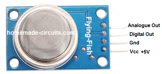 Component Side View
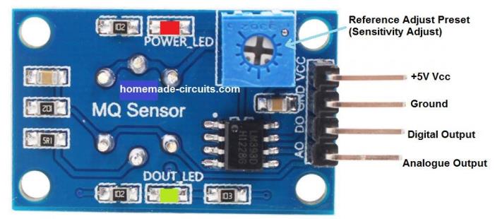 The analogue out is directly taken from the MQ-6 sensor pin.
The Vcc works with a +5V DC supply, ground is the negative or the 0V terminal of the module.
The digital output is derived from the output of a differential comparator using the IC LM393.
The analogue out is directly taken from the MQ-6 sensor pin.
The Vcc works with a +5V DC supply, ground is the negative or the 0V terminal of the module.
The digital output is derived from the output of a differential comparator using the IC LM393.
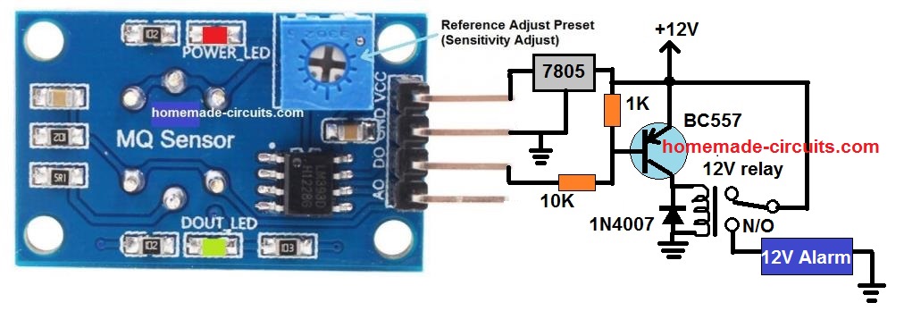 Video Demo
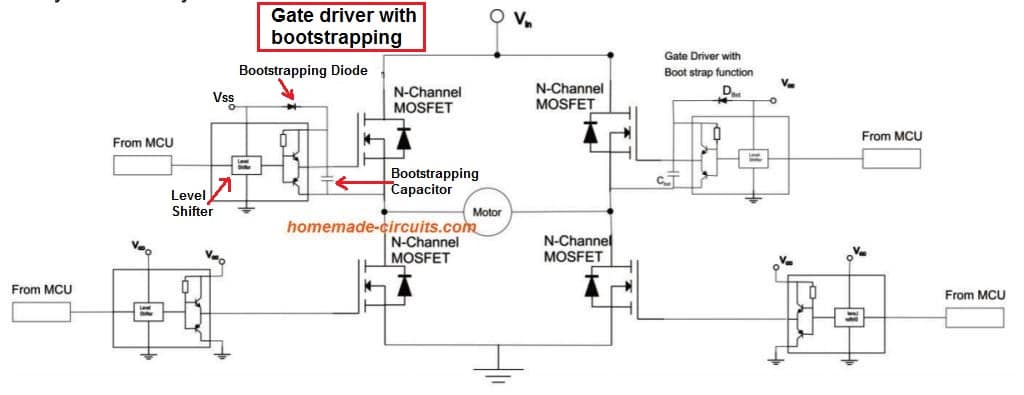 Using only 4 N-channel MOSFETS
In this arrangement, if the high side switch is built with a P-channel MOSFET, the driver design simplifies the layout tremendously., as shown below:
Using only 4 N-channel MOSFETS
In this arrangement, if the high side switch is built with a P-channel MOSFET, the driver design simplifies the layout tremendously., as shown below:
 Using P and N-channel MOSFETs
The need for a bootstrapped charge pump is eliminated for switching the high side switch.
Here this can simply be driven directly by the input signal and through a level shifter (3V to 5V converter, or 5V to 12V converter stage).
Using P and N-channel MOSFETs
The need for a bootstrapped charge pump is eliminated for switching the high side switch.
Here this can simply be driven directly by the input signal and through a level shifter (3V to 5V converter, or 5V to 12V converter stage).
 The table above depicting the MOSFET losses within the particular application reveals that the overall power losses are governed by the conduction losses as proven in the following pie chart.
 Additionally it looks like if P-channel MOSFET is preferred having comparable gate charges as that of the N-channel, the switching losses will be identical, but the conduction losses may probably be excessively high.
Therefore, for low switching applications with lower frequencies the high side P-channel MOSFET should madatorily have a comparable RDS(on) like that of the low side N-channel.
Additionally it looks like if P-channel MOSFET is preferred having comparable gate charges as that of the N-channel, the switching losses will be identical, but the conduction losses may probably be excessively high.
Therefore, for low switching applications with lower frequencies the high side P-channel MOSFET should madatorily have a comparable RDS(on) like that of the low side N-channel.
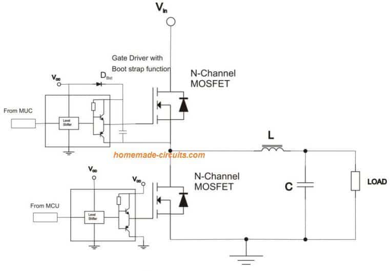 Another space-saving approach would be to substitute the high side N-channel MOSFET with a P-channel.
The P-channel method gets rid of the complex supplemental circuitry to drive the gate, which becomes necessary for an N-channel MOSFET on the high side.
The diagram below demonstrates the fundamental design of a buck converter having a P-channel MOSFET implemented on the high side.
Another space-saving approach would be to substitute the high side N-channel MOSFET with a P-channel.
The P-channel method gets rid of the complex supplemental circuitry to drive the gate, which becomes necessary for an N-channel MOSFET on the high side.
The diagram below demonstrates the fundamental design of a buck converter having a P-channel MOSFET implemented on the high side.
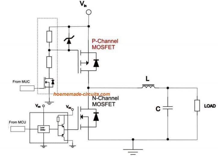 Normally the switching frequencies in non-isolated Point of Load applications will likely be close to 500kHz, or even at times as high as up to 2MHz.
Contradicting the earlier design concepts, the main loss at such frequencies turns out to be the switching losses.
The figure below indicates the loss from a MOSFET in a 3 watt non-isolated Point of Load application running at a switching frequency of 1MHz.
Normally the switching frequencies in non-isolated Point of Load applications will likely be close to 500kHz, or even at times as high as up to 2MHz.
Contradicting the earlier design concepts, the main loss at such frequencies turns out to be the switching losses.
The figure below indicates the loss from a MOSFET in a 3 watt non-isolated Point of Load application running at a switching frequency of 1MHz.
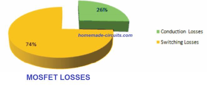 Thus it shows the level of gate charge that must be specified to a P-channel when it is selected for a high side application, with respect to a high side N-channel device.
 In the above image we can see a commercial mosquito bat circuit board, populated with many stages and electronic components.
If you find your mosquito bat is no more working (no lights, no sparks), then most probably none of the parts in the circuit may be faulty or damaged.
Do not throw it or submit it into a junk shop because most of the time the fault in a mosquito bat is too basic which can be easily repaired at home using ordinary tools such as soldering iron and a multimeter.
Frequently, it's either the battery that is completely exhausted or may have become unresponsive to the charging cycles.
In the above image we can see a commercial mosquito bat circuit board, populated with many stages and electronic components.
If you find your mosquito bat is no more working (no lights, no sparks), then most probably none of the parts in the circuit may be faulty or damaged.
Do not throw it or submit it into a junk shop because most of the time the fault in a mosquito bat is too basic which can be easily repaired at home using ordinary tools such as soldering iron and a multimeter.
Frequently, it's either the battery that is completely exhausted or may have become unresponsive to the charging cycles.
 Parts of Mosquito Swatter Racket
 The main function of this mosfet topology is to switch the "load" or the transformer primary in this diagram, in a flip-flop manner.
Meaning, to create an alternating push-pull current across the connected transformer winding.
To implement this the diagonally arranged mosfets are switched ON/OFF simultaneously.
And this is cycled alternately for the diagonal pairs.
For instance the pairs Q1/Q4 and Q2/Q3 are together switched ON/OFF, alternately.
When Q1/Q4 is ON, Q2/Q3 is OFF, and vice versa.
The above action forces current to alternately change its polarity across the connected transformer winding.
This in turn causes the induced high voltage across the secondary of the transformer also to change its polarity, producing the intended AC or alternating output on the secondary side of the transformer.
The main function of this mosfet topology is to switch the "load" or the transformer primary in this diagram, in a flip-flop manner.
Meaning, to create an alternating push-pull current across the connected transformer winding.
To implement this the diagonally arranged mosfets are switched ON/OFF simultaneously.
And this is cycled alternately for the diagonal pairs.
For instance the pairs Q1/Q4 and Q2/Q3 are together switched ON/OFF, alternately.
When Q1/Q4 is ON, Q2/Q3 is OFF, and vice versa.
The above action forces current to alternately change its polarity across the connected transformer winding.
This in turn causes the induced high voltage across the secondary of the transformer also to change its polarity, producing the intended AC or alternating output on the secondary side of the transformer.
 In this example if you measure the voltage across the motor you will find it to be just 7V, although 12V is applied at the drain side.
This is because the 12 - 7 = 5V is the bare minimum gate/source or Vgs that's being utilized by the mosfet to keep the conduction ON.
Since the motor here is a 12V motor it still rotates with the 7V supply.
If suppose we used a 50V motor with 50V supply on the drain and 12V on the gate/source, we may see just 7V on the source, producing absolutely no movement on the 50V motor.
However, if we apply around 62V across the gate/source of the mosfet.
This would instantly turn ON the mosfet, and its source voltage would rapidly start rising until it reaches to the maximum 50V drain level.
But even at 50V source voltage, the gate being 62V would be still 62 - 50 = 12V higher than the source, enabling a full conduction of the mosfet and the motor.
This implies, the gate source terminals in the above example would require something around 50 + 12 = 62V to enable a full speed switchng on the 50V motor.
Because this allows the gate voltage level of the mosfet to be properly elevated at the specified 12V level above the source.
In this example if you measure the voltage across the motor you will find it to be just 7V, although 12V is applied at the drain side.
This is because the 12 - 7 = 5V is the bare minimum gate/source or Vgs that's being utilized by the mosfet to keep the conduction ON.
Since the motor here is a 12V motor it still rotates with the 7V supply.
If suppose we used a 50V motor with 50V supply on the drain and 12V on the gate/source, we may see just 7V on the source, producing absolutely no movement on the 50V motor.
However, if we apply around 62V across the gate/source of the mosfet.
This would instantly turn ON the mosfet, and its source voltage would rapidly start rising until it reaches to the maximum 50V drain level.
But even at 50V source voltage, the gate being 62V would be still 62 - 50 = 12V higher than the source, enabling a full conduction of the mosfet and the motor.
This implies, the gate source terminals in the above example would require something around 50 + 12 = 62V to enable a full speed switchng on the 50V motor.
Because this allows the gate voltage level of the mosfet to be properly elevated at the specified 12V level above the source.
 The working of the above H-bridge application design can be understood with the following points:
The crucial aspect here is to develop a voltage across the 10uF such that it becomes equal to the "desired load voltage" plus the supply 12V at the gates of the high side MOSFETs, during their ON periods.
The shown configuration executes this very efficiently.
Imagine clock#1 is high, and clock#2 is low (since they are supposed to be alternately clocking).
In this situation the top right mosfet becomes OFF, while the lower left mosfet is switched ON.
The 10uF capacitor quickly charges up to +12V through the 1N4148 diode and lower mosfet drain/source.
In the next instant, as soon as clock#1 becomes low and clock#2 becomes high, the charge across the left 10uF switches ON the top left MOSFET which immediately begins conducting.
In this situation its drain voltage begins rushing towards its source, and simultaneously the voltages starts pushing into the 10uF capacitor in such a way that the existing charge +12V "sits" over this instantaneously pushing voltages from the MOSFET terminal.
This addition of the drain potential into the 10uF capacitor through the source terminal ensures that the two potentials add up and enable the instantaneous potential across gate/source of the MOSFET to be just at around +12V above the drain potential.
For example if the drain voltage is selected to be 100V, then this 100V pushes into the 10uF causing a continuously compensating potential gate voltage which maintains at +12 just above the 100V.
I hope this helped you to understand the basic working of the high side bootstrapping using discrete capacitor diode network.
Conclusion
From the above discussion we understand that bootstrapping is crucial for all H-bridge topologies in order to allow effective switch ON of the high side mosfets.
In this process an appropriately selected capacitor across the gate/emitter of the High side mosfet is charged to 12V higher than the applied drain voltage level.
Only when this happens the high side mosfets are able to switch ON and complete the intended push pull switching of the connected load.
The working of the above H-bridge application design can be understood with the following points:
The crucial aspect here is to develop a voltage across the 10uF such that it becomes equal to the "desired load voltage" plus the supply 12V at the gates of the high side MOSFETs, during their ON periods.
The shown configuration executes this very efficiently.
Imagine clock#1 is high, and clock#2 is low (since they are supposed to be alternately clocking).
In this situation the top right mosfet becomes OFF, while the lower left mosfet is switched ON.
The 10uF capacitor quickly charges up to +12V through the 1N4148 diode and lower mosfet drain/source.
In the next instant, as soon as clock#1 becomes low and clock#2 becomes high, the charge across the left 10uF switches ON the top left MOSFET which immediately begins conducting.
In this situation its drain voltage begins rushing towards its source, and simultaneously the voltages starts pushing into the 10uF capacitor in such a way that the existing charge +12V "sits" over this instantaneously pushing voltages from the MOSFET terminal.
This addition of the drain potential into the 10uF capacitor through the source terminal ensures that the two potentials add up and enable the instantaneous potential across gate/source of the MOSFET to be just at around +12V above the drain potential.
For example if the drain voltage is selected to be 100V, then this 100V pushes into the 10uF causing a continuously compensating potential gate voltage which maintains at +12 just above the 100V.
I hope this helped you to understand the basic working of the high side bootstrapping using discrete capacitor diode network.
Conclusion
From the above discussion we understand that bootstrapping is crucial for all H-bridge topologies in order to allow effective switch ON of the high side mosfets.
In this process an appropriately selected capacitor across the gate/emitter of the High side mosfet is charged to 12V higher than the applied drain voltage level.
Only when this happens the high side mosfets are able to switch ON and complete the intended push pull switching of the connected load.
 Now let's understand how the CRT works with its basic functions.
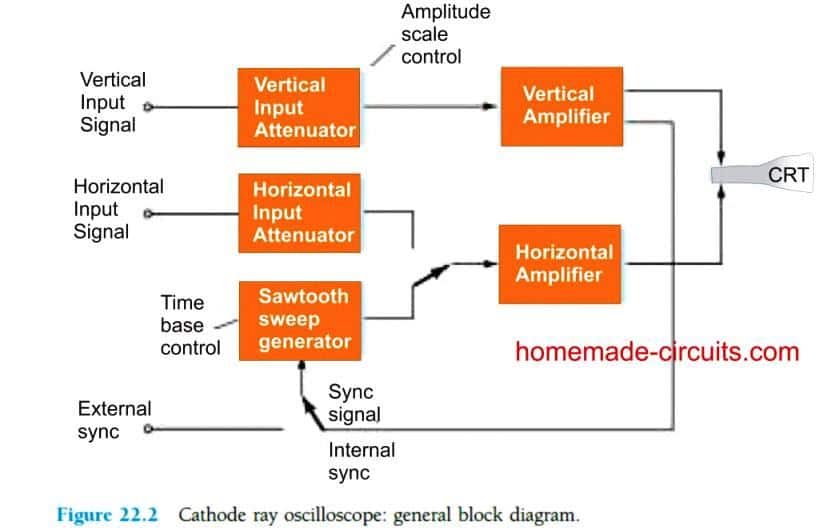
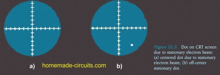
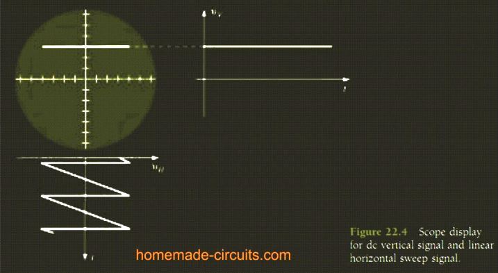 When the electron beam is held over a selected fixed vertical distance, the horizontal voltage is forced to travel from negative to zero to positive, causing the beam to travel from left side of the screen, to the center, and to the right side of the screen.
This movement of the electron beam generates a straight line above the center vertical reference, displaying an appropriate dc voltage in the form of a starlight line.
Instead of producing a single sweep, the sweep voltage is implemented to work like a continuous waveform.
This is essentially to ensure a consistent display to be visible on the screen.
If just a single sweep is used, it wouldn't last and would fade out instantly.
That's why repeated sweeps are generated per second inside the CRT which gives an appearance of a continuous waveform on the screen due to our persistence of vision.
If we reduce the above sweep rate depending on the time-scale provided on the oscilloscope, the real moving impression of the beam could be witnessed on the screen.
If onlya sinusoidal signal is applied to the vertical input without the presence of the horizontal sweep, we would see a vertical straight line as depicted in Fig 22.5.
When the electron beam is held over a selected fixed vertical distance, the horizontal voltage is forced to travel from negative to zero to positive, causing the beam to travel from left side of the screen, to the center, and to the right side of the screen.
This movement of the electron beam generates a straight line above the center vertical reference, displaying an appropriate dc voltage in the form of a starlight line.
Instead of producing a single sweep, the sweep voltage is implemented to work like a continuous waveform.
This is essentially to ensure a consistent display to be visible on the screen.
If just a single sweep is used, it wouldn't last and would fade out instantly.
That's why repeated sweeps are generated per second inside the CRT which gives an appearance of a continuous waveform on the screen due to our persistence of vision.
If we reduce the above sweep rate depending on the time-scale provided on the oscilloscope, the real moving impression of the beam could be witnessed on the screen.
If onlya sinusoidal signal is applied to the vertical input without the presence of the horizontal sweep, we would see a vertical straight line as depicted in Fig 22.5.
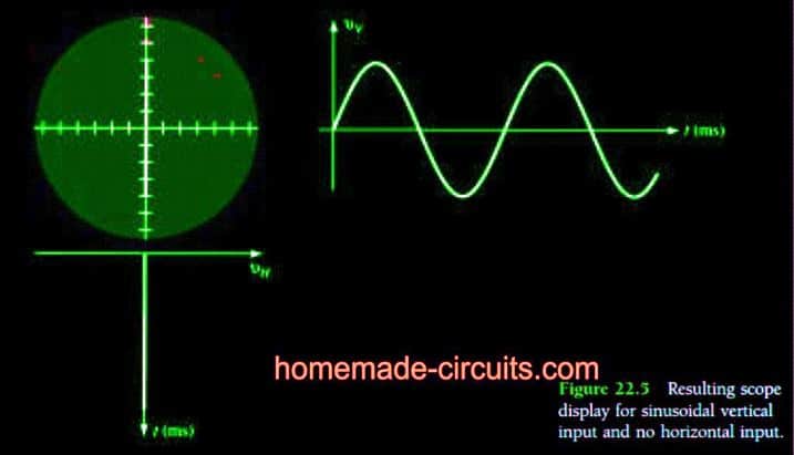 And if the speed of this sinusoidal vertical input is sufficiently reduced enables us to see the electron beam travelling up down along the path of a straight line.
 In order to obtain a single cycle on the screen for the applied input, a synchronization of the input signal and the linear sweep frequencies becomes essential.
Even with a minute difference or incorrect syncing the display may fail to show any movement.
If the sweep frequency is reduced, more number of cycles of the sine input signal could be made visible on the CRO screen.
On the other hand, if we increase the frequency of the sweep would allow lower number of vertical input sine signal cycles to be visible on the display screen.
This would in fact result in generating a magnified portion of the applied input signal on the CRO screen.
Solved Practical Example:
In order to obtain a single cycle on the screen for the applied input, a synchronization of the input signal and the linear sweep frequencies becomes essential.
Even with a minute difference or incorrect syncing the display may fail to show any movement.
If the sweep frequency is reduced, more number of cycles of the sine input signal could be made visible on the CRO screen.
On the other hand, if we increase the frequency of the sweep would allow lower number of vertical input sine signal cycles to be visible on the display screen.
This would in fact result in generating a magnified portion of the applied input signal on the CRO screen.
Solved Practical Example:
 In Fig.22.7 we can see the oscilloscope screen displaying a pulsed signal in response to a pulse like waveform applied to the vertical input with a horizontal sweep
The numbering for each waveform enables the display to follow the variations of the input signal and the sweep voltage for each cycle.
In Fig.22.7 we can see the oscilloscope screen displaying a pulsed signal in response to a pulse like waveform applied to the vertical input with a horizontal sweep
The numbering for each waveform enables the display to follow the variations of the input signal and the sweep voltage for each cycle.
 After this the sawtooth voltage returns quickly back to the starting negative voltage limit with the electron beam correspondingly moving to the left side of the screen.
During this period of time when the sweep voltage undergoes a swift return to the negative (retrace), the electron goes through a blank phase (wherein the grid voltage inhibits the electrons from striking the face of the tube)
For enabling the display to produce a stable signal image for every sweep of the beam, it becomes essential to initiate the sweep from the exact same point in the input signal cycle.
In Fig.22.9 we can see that a rather low sweep frequency causing the display to produce an appearance of a left side drift of the beam.
After this the sawtooth voltage returns quickly back to the starting negative voltage limit with the electron beam correspondingly moving to the left side of the screen.
During this period of time when the sweep voltage undergoes a swift return to the negative (retrace), the electron goes through a blank phase (wherein the grid voltage inhibits the electrons from striking the face of the tube)
For enabling the display to produce a stable signal image for every sweep of the beam, it becomes essential to initiate the sweep from the exact same point in the input signal cycle.
In Fig.22.9 we can see that a rather low sweep frequency causing the display to produce an appearance of a left side drift of the beam.
 When set to a high sweep frequency as proven in Figure 22.10, the display produces a appearance of a right side drift of the beam on the screen.
 Needless to say, it can be very difficult or impracticable to adjust the sweep signal frequency exactly equal to the input signal frequency for achieving a steady or constant sweep on the screen.
A more feasible looking solution is to wait for the signal to return back to the starting point of the trace in a cycle.
This type of triggering includes some good features which we'll discuss in the following paragraphs.
Needless to say, it can be very difficult or impracticable to adjust the sweep signal frequency exactly equal to the input signal frequency for achieving a steady or constant sweep on the screen.
A more feasible looking solution is to wait for the signal to return back to the starting point of the trace in a cycle.
This type of triggering includes some good features which we'll discuss in the following paragraphs.
 When the selector switch is toggled towards the "INTERNAL" enables a portion of the input signal to be used by the trigger generator circuit.
Then, the output trigger generator output is used to initiate or start the main sweep of the CRO, which remains visible for a period as set by the time/cm control of the scope.
The initialization of the triggering at several different points across a signal cycle can be visualized in Fig.
22.12. The functioning of the trigger sweep could be also analyzed through the resultant waveform patterns.
When the selector switch is toggled towards the "INTERNAL" enables a portion of the input signal to be used by the trigger generator circuit.
Then, the output trigger generator output is used to initiate or start the main sweep of the CRO, which remains visible for a period as set by the time/cm control of the scope.
The initialization of the triggering at several different points across a signal cycle can be visualized in Fig.
22.12. The functioning of the trigger sweep could be also analyzed through the resultant waveform patterns.
 The signal which is applied as the input is used for generating a trigger waveform for the sweep signal.
As shown in the Fig 22.13, the sweep is initiated with the input signal cycle and it sustains for a period decided by the sweep length control setting.
Subsequently, the CRO operation waits until the input signal attains an identical point in its cycle before initiating a new sweep operation.
The signal which is applied as the input is used for generating a trigger waveform for the sweep signal.
As shown in the Fig 22.13, the sweep is initiated with the input signal cycle and it sustains for a period decided by the sweep length control setting.
Subsequently, the CRO operation waits until the input signal attains an identical point in its cycle before initiating a new sweep operation.
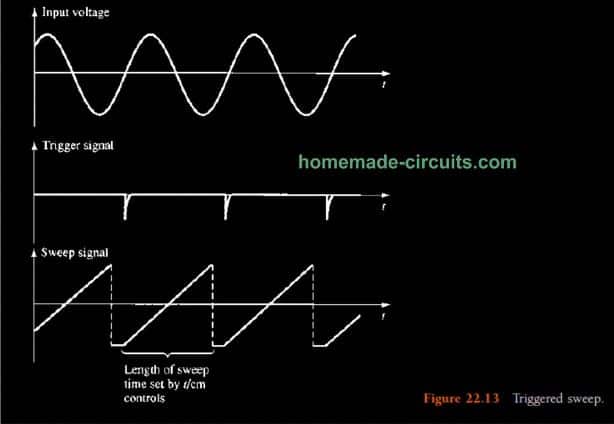 The above explained triggering method enables the synchronization process, while the number of cycles that can be viewed on the display is determined by the length of the sweep signal.
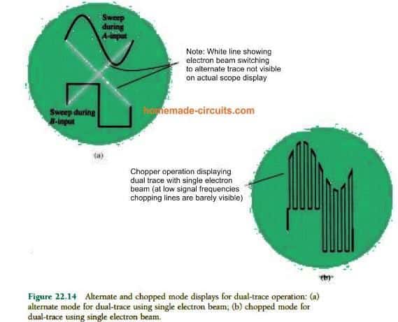

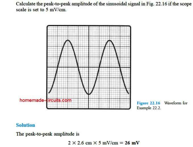 Note: This is the advantage of a oscilloscope against multimeters, since multimeters only provide the RMS value of the AC signal, while a scope is able to provide both the value of RMS as well as the peak-to-peak value of the signal.
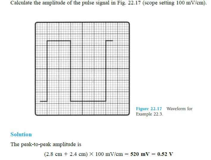
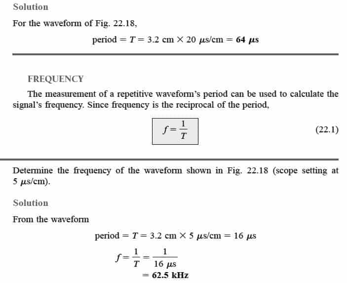
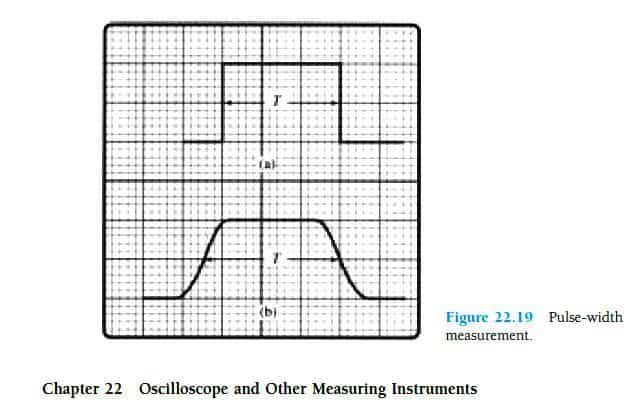 The following solved example helps to understand the above procedure in a better way:
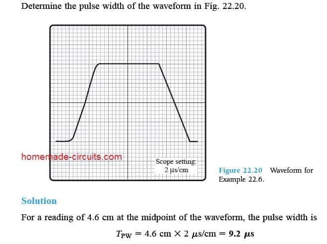
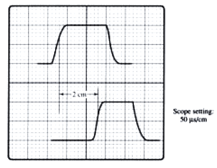 Figure 22.21
Practical solved example showing how to measure pulse delay in CRO
Figure 22.21
Practical solved example showing how to measure pulse delay in CRO
 Conclusion:
I have tried to include most of the basic details regarding how Cathode Ray Oscilloscope (CRO) work , and have tried to explain how to use this device for measuring various frequency based signals through its calibrated screen.
However there can be still many more aspects that I might have missed here, nonetheless I'll keep checking from time to time and update more info whenever it is possible.
Reference:https://en.wikipedia.org/wiki/Oscilloscope
Conclusion:
I have tried to include most of the basic details regarding how Cathode Ray Oscilloscope (CRO) work , and have tried to explain how to use this device for measuring various frequency based signals through its calibrated screen.
However there can be still many more aspects that I might have missed here, nonetheless I'll keep checking from time to time and update more info whenever it is possible.
Reference:https://en.wikipedia.org/wiki/Oscilloscope
 In the image above we can see the basic pinout configuration of an NPN and an PNP transistors (BJTs).
For the NPN the emitter becomes the ground line, and is connected with the negative supply.
Normally when the word "ground" is used in a DC circuit, we assume it to be the negative supply line.
However, for a transistor the ground line associated with the emitter is with reference to its base and the collector voltages, and the emitter "ground" may not necessarily mean the negative supply line.
Yes, for an NPN BJT the ground could be the negative supply line, but for an PNP transistorthe "ground" is always referenced to the positive supply line, as shown in the figure above.
The switching ON/OFF function of both the BJTs is basically the same, but the polarity changes.
Since the emitter of a BJT is the "exit" passage for the current entering through and base and the collector, it has to be "grounded" to a supply line which should be opposite to the voltage used at base/collector inputs.
Otherwise the circuit won't complete.
For a NPN BJT, the base and the collector inputs are associated with a positive trigger or switching voltage, therefore the emitter must be referenced to the negative line.
This ensures that the positive voltages entering the base and collector are able to reach the negative line through the emitter and complete the circuit.
For a PNP BJT, the base and the collector are associated with a negative voltage input, therefore naturally the emitter of a PNP must be referenced to the positive line, so that the positive supply can enter through the emitter and finish its journey from the base and the collector pins.
Note that the flow of current for the NPN is from base/collector towards emitter, while for the PNP, it's from the emitter towards the base/collector.
In both the cases, the objective is to switch ON the collector load through a small voltage input at the base of the BJT, only the polarity changes that's all.
The following simulation shows the basic operation:
In the image above we can see the basic pinout configuration of an NPN and an PNP transistors (BJTs).
For the NPN the emitter becomes the ground line, and is connected with the negative supply.
Normally when the word "ground" is used in a DC circuit, we assume it to be the negative supply line.
However, for a transistor the ground line associated with the emitter is with reference to its base and the collector voltages, and the emitter "ground" may not necessarily mean the negative supply line.
Yes, for an NPN BJT the ground could be the negative supply line, but for an PNP transistorthe "ground" is always referenced to the positive supply line, as shown in the figure above.
The switching ON/OFF function of both the BJTs is basically the same, but the polarity changes.
Since the emitter of a BJT is the "exit" passage for the current entering through and base and the collector, it has to be "grounded" to a supply line which should be opposite to the voltage used at base/collector inputs.
Otherwise the circuit won't complete.
For a NPN BJT, the base and the collector inputs are associated with a positive trigger or switching voltage, therefore the emitter must be referenced to the negative line.
This ensures that the positive voltages entering the base and collector are able to reach the negative line through the emitter and complete the circuit.
For a PNP BJT, the base and the collector are associated with a negative voltage input, therefore naturally the emitter of a PNP must be referenced to the positive line, so that the positive supply can enter through the emitter and finish its journey from the base and the collector pins.
Note that the flow of current for the NPN is from base/collector towards emitter, while for the PNP, it's from the emitter towards the base/collector.
In both the cases, the objective is to switch ON the collector load through a small voltage input at the base of the BJT, only the polarity changes that's all.
The following simulation shows the basic operation:
 In the simulation above, as soon as the button is pressed, the external voltage input enters the base of the BJT and reaches the ground line via the emitter.
While this happens the collector/emitter passage inside the BJT opens up, and allows the positive supply from top to enter the bulb, and pass through the emitter to ground, switching ON the bulb (load).
Both the switching happen almost simultaneously in response to the pressing of the push button.
The emitter pin here becomes the common "exit" pinout for both the input feeds (base and collector).
And the emitter supply line becomes the common ground line for the input supply trigger, and also the load.
Which means that, the supply line connecting with the BJT emitter must be also strictly connected with the ground of the external trigger source, and the load.
In the simulation above, as soon as the button is pressed, the external voltage input enters the base of the BJT and reaches the ground line via the emitter.
While this happens the collector/emitter passage inside the BJT opens up, and allows the positive supply from top to enter the bulb, and pass through the emitter to ground, switching ON the bulb (load).
Both the switching happen almost simultaneously in response to the pressing of the push button.
The emitter pin here becomes the common "exit" pinout for both the input feeds (base and collector).
And the emitter supply line becomes the common ground line for the input supply trigger, and also the load.
Which means that, the supply line connecting with the BJT emitter must be also strictly connected with the ground of the external trigger source, and the load.
 In this image we can see how a programmed Arduino is used for operating a small load in the form of relay via BJT driver stage.
The relay coil becomes the collector load, while the signal from the selected Arduino output pin acts like the input switching signal for the BJT base.
In this image we can see how a programmed Arduino is used for operating a small load in the form of relay via BJT driver stage.
The relay coil becomes the collector load, while the signal from the selected Arduino output pin acts like the input switching signal for the BJT base.
 Although, a relay becomes the best option for operating heavy loads via a transistor driver, when mechanical switching becomes an undesirable factor, upgrading BJTs becomes a better choice for operating high current DC loads, as shown below.
In the above example a Darlington transistor network can be seen, configured for handling the indicated high current 100 watt load without depending on a relay.
This allows seamless switching of the LED with minimum disturbance, ensuring a long working life for all the parameters.
Now let's proceed further, and see how mosfets can be configured with an Arduino
Although, a relay becomes the best option for operating heavy loads via a transistor driver, when mechanical switching becomes an undesirable factor, upgrading BJTs becomes a better choice for operating high current DC loads, as shown below.
In the above example a Darlington transistor network can be seen, configured for handling the indicated high current 100 watt load without depending on a relay.
This allows seamless switching of the LED with minimum disturbance, ensuring a long working life for all the parameters.
Now let's proceed further, and see how mosfets can be configured with an Arduino
 In the figure, the MOSFET can be seen configured with a couple of BJT buffer stages which allows the MOSFET to use the 12V from the power supply and switch ON itself and the load effectively.
Two BJTs are used here since a single BJT would cause the MOSFET to conduct oppositely in response to every positive Arduino signals.
Suppose one BJT is used, then the while the BJT is ON with a positive Arduino signal, the mosfet would be switched Off, since its gate would be grounded by the BJT collector, and the load would be switched ON while the Arduino is OFF.
Basically, one BJT would invert the Arduino signal for the mosfet gate resulting in an opposite switching response.
To correct this situation, two BJTs are used, so that the second BJT inverts the response back and allows the mosfet to switch ON for every positive signals only from the Arduino.
Final Thoughts
By now you should have comprehensively understood the correct method of connecting BJTs and mosfets with a microcontroller or an Arduino.
You might have noticed that we have mostly used NPN BJTs and N-channel mosfets for the integrations, and have avoided using the PNP and P-channel devices.
This is because NPN versions work ideally like a switch and is easy to comprehend while configuring.
It's like driving a car normally in the forward direction, rather than looking behind and driving it in the reverse gear.
In both ways the car would operate and move, but driving in the reverse gear is much inefficient and doesn't make sense.
The same analogy applies here, and using NPN or N-channel devices become a better preference compared to PNP or P-channel mosfets.
If you have any doubts, or if you think I may have missed something here, please use the comment box below for further discussion.
In the figure, the MOSFET can be seen configured with a couple of BJT buffer stages which allows the MOSFET to use the 12V from the power supply and switch ON itself and the load effectively.
Two BJTs are used here since a single BJT would cause the MOSFET to conduct oppositely in response to every positive Arduino signals.
Suppose one BJT is used, then the while the BJT is ON with a positive Arduino signal, the mosfet would be switched Off, since its gate would be grounded by the BJT collector, and the load would be switched ON while the Arduino is OFF.
Basically, one BJT would invert the Arduino signal for the mosfet gate resulting in an opposite switching response.
To correct this situation, two BJTs are used, so that the second BJT inverts the response back and allows the mosfet to switch ON for every positive signals only from the Arduino.
Final Thoughts
By now you should have comprehensively understood the correct method of connecting BJTs and mosfets with a microcontroller or an Arduino.
You might have noticed that we have mostly used NPN BJTs and N-channel mosfets for the integrations, and have avoided using the PNP and P-channel devices.
This is because NPN versions work ideally like a switch and is easy to comprehend while configuring.
It's like driving a car normally in the forward direction, rather than looking behind and driving it in the reverse gear.
In both ways the car would operate and move, but driving in the reverse gear is much inefficient and doesn't make sense.
The same analogy applies here, and using NPN or N-channel devices become a better preference compared to PNP or P-channel mosfets.
If you have any doubts, or if you think I may have missed something here, please use the comment box below for further discussion.
 In a basic amplifier design we find that it mostly includes a few stages having networks of bipolar transistors or BJTs, field effect transistors (FETs), or operational amplifiers.
Such amplifier blocks or modules could be seen having a couple of terminals for feeding the input signal, and another pair of terminals at the output for acquiring the amplified signal over a connected loudspeaker.
One of the terminals out of these two is the ground terminals and could be seen as a common line across the input and the output stages.
In a basic amplifier design we find that it mostly includes a few stages having networks of bipolar transistors or BJTs, field effect transistors (FETs), or operational amplifiers.
Such amplifier blocks or modules could be seen having a couple of terminals for feeding the input signal, and another pair of terminals at the output for acquiring the amplified signal over a connected loudspeaker.
One of the terminals out of these two is the ground terminals and could be seen as a common line across the input and the output stages.
 The difference in the amplified signal between the output and the input is termed as the gain of the amplifier.
It is the magnitude or the amount by which the amplifier is able to amplify the input signal across its output terminals.
Take for example, if an amplifier is rated to process an input signal of 1 volt into an amplified signal of 50 volts, then we would say that the amplifier has a gain of 50, it is as simple as that.
This enhancement of a low input signal to a higher output signal is called the gain of an amplifier.
Alternatively, this may be understood as an increase of the input signal by a factor of 50.
Gain RatioThus, the gain of an amplifier is basically ratio of output and input values of the signal levels, or simply the output power divided by the input power, and is attributed by the letter "A" which also signifies the amplification power of the amplifier.
Types of Amplifier GainsThe different types of amplifier gains may be classified as:
Voltage Gain (Av)
Current Gain (Ai)
Power Gain (Ap)
Example Formulas for Calculating Amplifier GainsDepending upon the above 3 types of gains, the formulas for calculating these could be learned from the following examples:
Voltage Gain (Av) = Output Voltage / Input Voltage = Vout / Vin
Current Gain (Ai) = Output Current / Input Current = Iout/ Iin
Power Gain (Ap) = Av.x.Ai
For calculating power gain, alternatively you may also use the formula:
Power Gain (Ap) = Output Power / Input Power = Aout/ AinIt would be important to note that the subscript p, v, i used for calculating power are assigned for identifying the specific type of signal gain that's being worked upon.
The difference in the amplified signal between the output and the input is termed as the gain of the amplifier.
It is the magnitude or the amount by which the amplifier is able to amplify the input signal across its output terminals.
Take for example, if an amplifier is rated to process an input signal of 1 volt into an amplified signal of 50 volts, then we would say that the amplifier has a gain of 50, it is as simple as that.
This enhancement of a low input signal to a higher output signal is called the gain of an amplifier.
Alternatively, this may be understood as an increase of the input signal by a factor of 50.
Gain RatioThus, the gain of an amplifier is basically ratio of output and input values of the signal levels, or simply the output power divided by the input power, and is attributed by the letter "A" which also signifies the amplification power of the amplifier.
Types of Amplifier GainsThe different types of amplifier gains may be classified as:
Voltage Gain (Av)
Current Gain (Ai)
Power Gain (Ap)
Example Formulas for Calculating Amplifier GainsDepending upon the above 3 types of gains, the formulas for calculating these could be learned from the following examples:
Voltage Gain (Av) = Output Voltage / Input Voltage = Vout / Vin
Current Gain (Ai) = Output Current / Input Current = Iout/ Iin
Power Gain (Ap) = Av.x.Ai
For calculating power gain, alternatively you may also use the formula:
Power Gain (Ap) = Output Power / Input Power = Aout/ AinIt would be important to note that the subscript p, v, i used for calculating power are assigned for identifying the specific type of signal gain that's being worked upon.
 In class A configuration, identical sets of transistors are applied across two halves of the output waveform.
And depending upon the kind of biasing it employs, the output power transistors are always rendered in the switched ON position, regardless of whether the input signal is applied or not.
Because of this, class A amplifiers get an extremely poor efficiency in terms of power consumption, since the actual delivery of power to the output gets hampered due to excess wastage through device dissipation.
With the above explained situation, class amplifiers can be seen always having over heated output power transistors even in the absence of an input signal.
Even while there's no input signal, the DC (Ic) from the power supply is allowed to flow through the power transistors, that may be equal to the current flowing through the loudspeaker when input signal was present.
This gives rise to a continuous "hot" transistors and wastage of power.
Class B Amplifier Operation
In contrast to class A amplifier configuration which depend on single power transistors, class B uses a pair of complementary BJTs across each half sections of the circuit.
These could be in the form of NPN/PNP, or N-channel mosfet/P-channel mosfet).
Here, one of the transistors is allowed to conduct in response to the one half waveform cycle of the input signal, while the other transistor handles the other half cycle of the waveform.
This ensures that each transistor in the pair conducts for half of the time within the active region and half of the time in the cut-off region, thus allowing only 50% involvement in the amplification the signal.
Unlike class A amplifiers, In class B amplifiers the power transistors are not biased with a direct DC, instead the configuration ensures that they conduct only while the input signal goes higher than the base emitter voltage, which could be around 0.6V for silicon BJTs.
This implies that, when there's no input signal, the BJTs remain shut off and the output current is zero.
And due to this only 50% of the input signal is allowed to enter the output at any instance enabling a much better efficiency rate for these amplifiers.
The result can be witnessed in the following diagram:
In class A configuration, identical sets of transistors are applied across two halves of the output waveform.
And depending upon the kind of biasing it employs, the output power transistors are always rendered in the switched ON position, regardless of whether the input signal is applied or not.
Because of this, class A amplifiers get an extremely poor efficiency in terms of power consumption, since the actual delivery of power to the output gets hampered due to excess wastage through device dissipation.
With the above explained situation, class amplifiers can be seen always having over heated output power transistors even in the absence of an input signal.
Even while there's no input signal, the DC (Ic) from the power supply is allowed to flow through the power transistors, that may be equal to the current flowing through the loudspeaker when input signal was present.
This gives rise to a continuous "hot" transistors and wastage of power.
Class B Amplifier Operation
In contrast to class A amplifier configuration which depend on single power transistors, class B uses a pair of complementary BJTs across each half sections of the circuit.
These could be in the form of NPN/PNP, or N-channel mosfet/P-channel mosfet).
Here, one of the transistors is allowed to conduct in response to the one half waveform cycle of the input signal, while the other transistor handles the other half cycle of the waveform.
This ensures that each transistor in the pair conducts for half of the time within the active region and half of the time in the cut-off region, thus allowing only 50% involvement in the amplification the signal.
Unlike class A amplifiers, In class B amplifiers the power transistors are not biased with a direct DC, instead the configuration ensures that they conduct only while the input signal goes higher than the base emitter voltage, which could be around 0.6V for silicon BJTs.
This implies that, when there's no input signal, the BJTs remain shut off and the output current is zero.
And due to this only 50% of the input signal is allowed to enter the output at any instance enabling a much better efficiency rate for these amplifiers.
The result can be witnessed in the following diagram:
 Since there's no direct involvement of DC for biasing the power transistors in class B amplifiers, in order to initiate the conduction in response to the each half +/- waveform cycles, it becomes imperative for their base/emitter Vbe to acquire a higher potential than 0.6V (standard base biasing value for BJTs)
Due to the above fact, it implies that the while the output waveform is below the 0.6V mark, it cannot be amplified and reproduced.
This gives rise to a distorted region for the output waveform, just during the period when one of the BJTs becomes switched OFF and waits for the other to switch back ON.
This results in a small section of the waveform being subjected to minor distortion during the cross over period or the transition period near the zero crossing, exactly when the changeover from one transistor to the other occurs across complementary pairs.
Class AB Amplifier Operation
The class AB amplifier is built using a blend f characteristics from class A and Class B circuit designs, hence the name Class AB.
Although Class AB design also works with a pair of complementary BJTs, the output stage ensures that the biasing of the power BJTs are controlled close the the cut-off threshold, in the absence of an input signal.
In this situation, as soon as an input signal is sensed, the transistors negin operating normally in their active region thus inhibiting any possibility of a cross over distortion, which is normally prevalent in Class B configurations.
However, there could be a slight amount of collector current conducting across the BJTs, the amount may be considered negligible compared to Class A designs.
Class AB type of amplifier exhibit a much improved efficiency rate and a linear response as opposed to the Class A counterpart.
Class AB Amplifier Output Waveform
Since there's no direct involvement of DC for biasing the power transistors in class B amplifiers, in order to initiate the conduction in response to the each half +/- waveform cycles, it becomes imperative for their base/emitter Vbe to acquire a higher potential than 0.6V (standard base biasing value for BJTs)
Due to the above fact, it implies that the while the output waveform is below the 0.6V mark, it cannot be amplified and reproduced.
This gives rise to a distorted region for the output waveform, just during the period when one of the BJTs becomes switched OFF and waits for the other to switch back ON.
This results in a small section of the waveform being subjected to minor distortion during the cross over period or the transition period near the zero crossing, exactly when the changeover from one transistor to the other occurs across complementary pairs.
Class AB Amplifier Operation
The class AB amplifier is built using a blend f characteristics from class A and Class B circuit designs, hence the name Class AB.
Although Class AB design also works with a pair of complementary BJTs, the output stage ensures that the biasing of the power BJTs are controlled close the the cut-off threshold, in the absence of an input signal.
In this situation, as soon as an input signal is sensed, the transistors negin operating normally in their active region thus inhibiting any possibility of a cross over distortion, which is normally prevalent in Class B configurations.
However, there could be a slight amount of collector current conducting across the BJTs, the amount may be considered negligible compared to Class A designs.
Class AB type of amplifier exhibit a much improved efficiency rate and a linear response as opposed to the Class A counterpart.
Class AB Amplifier Output Waveform
 Amplifier Class is an important parameter which is depending on how the transistors are biased through the amplitude of the input signal, for implementing the amplification process.
It relies upon how much of the magnitude of the input signal waveform is utilized for the transistors to conduct, and also the efficiency factor, which is determined by the amount of power actually used for delivering the output and/or wasted through dissipation.
With regards to these factors we can finally create a comparison report showing the differences between the various classes of amplifiers, as given in the following table.
Then we can make a comparison between the most common types of amplifier classifications in the following table.
Amplifier Class is an important parameter which is depending on how the transistors are biased through the amplitude of the input signal, for implementing the amplification process.
It relies upon how much of the magnitude of the input signal waveform is utilized for the transistors to conduct, and also the efficiency factor, which is determined by the amount of power actually used for delivering the output and/or wasted through dissipation.
With regards to these factors we can finally create a comparison report showing the differences between the various classes of amplifiers, as given in the following table.
Then we can make a comparison between the most common types of amplifier classifications in the following table.

 image courtesy:en.wikipedia.org/wiki/File:PID_en.svg
Here we are able to see a set of variables such as e(t) corresponding to the error value, r(t) corresponding to the targeted set point, and y(t) as the measured process variable.
The PID controller throughout its operation monitors the error value e(t) by assessing the difference between the intended setpoint r(t) or SP and measured process value y(t) or PV, and consequently executes a feedback correction or optimization using the parameters namely: proportional, integral, and derivative.
The controller continues making an effort to reduce the error effect throughout, by adjusting the control variable u(t) to fresh values based on the analyzed weighted sum of the control terms (p, I, d).
For example, in the operation of a valve control, its opening and closing may be continuously varied by a PID through complex assessments, as explained above.
In the shown system the various terms can be understood as explained below:
P- Controller:
The term P is proportional to the instantaneous error values e(t) acquired by assessing the result for SP �C PV.
In situation when the error value tends to get large, the control output also gets proportionately larger with reference to the gain factor ��K��.
However in a process requiring compensation such as in temperature control, proportional control solitarily may lead to inaccuracies across the setpoint and the actual process value, since it cannot work satisfactorily without an error feedback to generate the proportional response.
Implies that without an error feedback, proper corrective response may not be possible.
I- Controller:
The term I becomes responsible for the previously evaluated values of SP �C PV errors, and integrates them during its operational period to create the term I.
For instance while the proportional control is being applied if the SP �C PV produces some error, the parameter I gets active and attempts to terminate this residual error.
This actually happens with a control response triggered due to cumulative value of the error recorded at an earlier time.
As soon as this happens the I term stops enhancing any further.
This causes the proportional effect to correspondingly minimize as the error factor deceases, although this also gets compensated as the integral effect develops.
D- Controller:
The term D is a most suitable approximation deduced for the evolving trends for the SP �C PV error, depending on the instantaneous rate of change of the error factor.
If this rate of change enhances rapidly, the feedback control implements more aggressively, and vice versa.
image courtesy:en.wikipedia.org/wiki/File:PID_en.svg
Here we are able to see a set of variables such as e(t) corresponding to the error value, r(t) corresponding to the targeted set point, and y(t) as the measured process variable.
The PID controller throughout its operation monitors the error value e(t) by assessing the difference between the intended setpoint r(t) or SP and measured process value y(t) or PV, and consequently executes a feedback correction or optimization using the parameters namely: proportional, integral, and derivative.
The controller continues making an effort to reduce the error effect throughout, by adjusting the control variable u(t) to fresh values based on the analyzed weighted sum of the control terms (p, I, d).
For example, in the operation of a valve control, its opening and closing may be continuously varied by a PID through complex assessments, as explained above.
In the shown system the various terms can be understood as explained below:
P- Controller:
The term P is proportional to the instantaneous error values e(t) acquired by assessing the result for SP �C PV.
In situation when the error value tends to get large, the control output also gets proportionately larger with reference to the gain factor ��K��.
However in a process requiring compensation such as in temperature control, proportional control solitarily may lead to inaccuracies across the setpoint and the actual process value, since it cannot work satisfactorily without an error feedback to generate the proportional response.
Implies that without an error feedback, proper corrective response may not be possible.
I- Controller:
The term I becomes responsible for the previously evaluated values of SP �C PV errors, and integrates them during its operational period to create the term I.
For instance while the proportional control is being applied if the SP �C PV produces some error, the parameter I gets active and attempts to terminate this residual error.
This actually happens with a control response triggered due to cumulative value of the error recorded at an earlier time.
As soon as this happens the I term stops enhancing any further.
This causes the proportional effect to correspondingly minimize as the error factor deceases, although this also gets compensated as the integral effect develops.
D- Controller:
The term D is a most suitable approximation deduced for the evolving trends for the SP �C PV error, depending on the instantaneous rate of change of the error factor.
If this rate of change enhances rapidly, the feedback control implements more aggressively, and vice versa.
 In this mathematical model, all non-negative constants Kp, Ki, and Kd signify coefficients for the proportional, integral, and derivative terms respectively (on some occasions these are also denoted P, I, and D).
 Assume a circuit using a microcontroller or an IC, if we close the circuit, the input pin goes ��LOW�� and the relay turns ��ON��.
If we open the switch, the relay should turn ��OFF�� right? Well not really.
We know that the digital ICs and digital microcontrollers only takes input as either ��HIGH�� or ��LOW��, when we open the switch, the input pin is just open circuited.
It is neither ��HIGH�� nor ��LOW��.
The input pin must be ��HIGH�� in order to turn the relay off, but in the open situation this pin becomes vulnerable to stray pickups, stray static charges, and other electrical noise from surrounding, which can cause the relay to go ON and OFF randomly.
To prevent such random triggers due to stray voltage, in this example it becomes mandatory to tie the shown digital input pin to a ��HIGH�� logic, so that when the switch is flipped off, the pin automatically connects to a defined state ��HIGH�� or the positive supply level of the IC.
To keep the pin ��HIGH�� we can connect the input pin to Vcc.
In the below circuit the input pin is connected to Vcc, which keeps the input ��HIGH�� if we open the switch, which prevents random triggering of the relay.
You may think, now we have the solution worked out.
But no....not yet!
Assume a circuit using a microcontroller or an IC, if we close the circuit, the input pin goes ��LOW�� and the relay turns ��ON��.
If we open the switch, the relay should turn ��OFF�� right? Well not really.
We know that the digital ICs and digital microcontrollers only takes input as either ��HIGH�� or ��LOW��, when we open the switch, the input pin is just open circuited.
It is neither ��HIGH�� nor ��LOW��.
The input pin must be ��HIGH�� in order to turn the relay off, but in the open situation this pin becomes vulnerable to stray pickups, stray static charges, and other electrical noise from surrounding, which can cause the relay to go ON and OFF randomly.
To prevent such random triggers due to stray voltage, in this example it becomes mandatory to tie the shown digital input pin to a ��HIGH�� logic, so that when the switch is flipped off, the pin automatically connects to a defined state ��HIGH�� or the positive supply level of the IC.
To keep the pin ��HIGH�� we can connect the input pin to Vcc.
In the below circuit the input pin is connected to Vcc, which keeps the input ��HIGH�� if we open the switch, which prevents random triggering of the relay.
You may think, now we have the solution worked out.
But no....not yet!
 As per the diagram if we close the switch there will be short circuit and shut off and short circuit the whole system.
Your circuit can never have any worst situation than a short circuit.
The short circuit is due to very large current flowing through a low resistance path which burns the PCB traces, blowing of fuse, triggering safety switches and even may cause fatal damage to your circuit.
To prevent such heavy current flow and also to keep the input pin in ��HIGH�� condition, we can utilize a resistor which is connected to Vcc, that is between the "red line".
In this situation the pin will be in a ��HIGH�� state if we open the switch, and on closing the switch there won��t be any short circuit, and also the input pin is allowed to directly connect with the GND, making it ��LOW��.
If we close the switch there will be negligible voltage drop via the pull-Up resistor and rest of the circuit will remain unaffected.
One must choose the Pull-Up / Pull-Down resistor value optimally so that it won��t draw excess through the resistor.
As per the diagram if we close the switch there will be short circuit and shut off and short circuit the whole system.
Your circuit can never have any worst situation than a short circuit.
The short circuit is due to very large current flowing through a low resistance path which burns the PCB traces, blowing of fuse, triggering safety switches and even may cause fatal damage to your circuit.
To prevent such heavy current flow and also to keep the input pin in ��HIGH�� condition, we can utilize a resistor which is connected to Vcc, that is between the "red line".
In this situation the pin will be in a ��HIGH�� state if we open the switch, and on closing the switch there won��t be any short circuit, and also the input pin is allowed to directly connect with the GND, making it ��LOW��.
If we close the switch there will be negligible voltage drop via the pull-Up resistor and rest of the circuit will remain unaffected.
One must choose the Pull-Up / Pull-Down resistor value optimally so that it won��t draw excess through the resistor.
 Since the output is either ground or open circuit, we need to connect an external Pull-Up resistor which can turn the pin ��HIGH�� when the transistor is OFF.
This is same for Open drain; the only difference is that the internal transistor inside the IC is a MOSFET.
Now, you may ask why do we need an open drain configuration? We need to connect a Pull-Up resistor anyway.
Well, the output voltage can be varied by choosing different resistor values at the open collector output, so it gives more flexibility for the load.
We can connect load at output which has higher or lower operating voltage.
If we had a fixed pull-up resistor value we can��t control the voltage at the output.
One disadvantage of this configuration is that, it consumes huge current and may not be battery friendly, it need higher current for its correct operation.
Let��s take example of IC 7401 open drain logic ��NAND�� gate and see how to calculate pull-up resistor value.
We need to know the following parameters:
VOL(MAX) which is the maximum input voltage to IC 7401 which can guarantee to turn the output ��LOW�� (0.4V).
IOL(MAX) which is the Low level input current (16mA).
Vcc is the operating voltage which is 5V.
Since the output is either ground or open circuit, we need to connect an external Pull-Up resistor which can turn the pin ��HIGH�� when the transistor is OFF.
This is same for Open drain; the only difference is that the internal transistor inside the IC is a MOSFET.
Now, you may ask why do we need an open drain configuration? We need to connect a Pull-Up resistor anyway.
Well, the output voltage can be varied by choosing different resistor values at the open collector output, so it gives more flexibility for the load.
We can connect load at output which has higher or lower operating voltage.
If we had a fixed pull-up resistor value we can��t control the voltage at the output.
One disadvantage of this configuration is that, it consumes huge current and may not be battery friendly, it need higher current for its correct operation.
Let��s take example of IC 7401 open drain logic ��NAND�� gate and see how to calculate pull-up resistor value.
We need to know the following parameters:
VOL(MAX) which is the maximum input voltage to IC 7401 which can guarantee to turn the output ��LOW�� (0.4V).
IOL(MAX) which is the Low level input current (16mA).
Vcc is the operating voltage which is 5V.
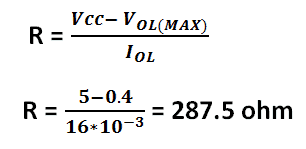 So, we here we can connect a Pull-Up resistor value around 287 ohm.
Have any questions? Please use the comment box below to express your thoughts, your queries will be replied ASAP
So, we here we can connect a Pull-Up resistor value around 287 ohm.
Have any questions? Please use the comment box below to express your thoughts, your queries will be replied ASAP
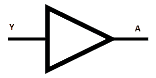 The above symbol is similar to logic ��NOT�� gate without the ��o�� at the tip of the triangle, which means that it does not perform any inversion.
The Boolean equation for the digital buffer is Y = A.
��Y�� is the input and ��A�� output.
The above symbol is similar to logic ��NOT�� gate without the ��o�� at the tip of the triangle, which means that it does not perform any inversion.
The Boolean equation for the digital buffer is Y = A.
��Y�� is the input and ��A�� output.
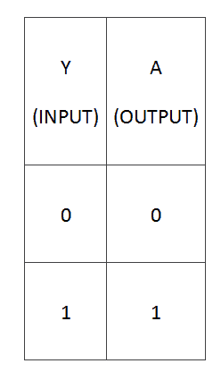 Truth table:
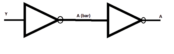 The input signal is first inverted by the first NOT gate on left hand side and the inverted signal is then further inverted by the next ��NOT�� gate on the right hand side, which makes the output same as input.
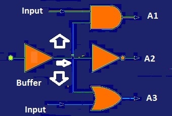 FAN-OUT: The fan-out can be defined as the number of logic gates or digital ICs that can be driven in parallel by a digital buffer (or any digital ICs).
A typical digital buffer has fan-out of 10, which means the digital buffer can drive 10 digital ICs in parallel.
FAN-IN: The fan-in is the number of digital inputs that can be accepted by the digital logic gate or digital IC.
In the above schematic the digital buffer has fan-in of 1, which means one input.
A ��2-input�� logic ��AND�� gate has fan-in of two and so on.
From the above schematic a buffer is connected to the 3 inputs of three different logic gates.
If we just connect a piece of wire in the place of the buffer in the above circuit, the input signal might not be with sufficient current and causes voltage to drop across gates and might not even recognize the signal.
So in conclusion a digital buffer is used for amplifying a digital signal with higher current output.
FAN-OUT: The fan-out can be defined as the number of logic gates or digital ICs that can be driven in parallel by a digital buffer (or any digital ICs).
A typical digital buffer has fan-out of 10, which means the digital buffer can drive 10 digital ICs in parallel.
FAN-IN: The fan-in is the number of digital inputs that can be accepted by the digital logic gate or digital IC.
In the above schematic the digital buffer has fan-in of 1, which means one input.
A ��2-input�� logic ��AND�� gate has fan-in of two and so on.
From the above schematic a buffer is connected to the 3 inputs of three different logic gates.
If we just connect a piece of wire in the place of the buffer in the above circuit, the input signal might not be with sufficient current and causes voltage to drop across gates and might not even recognize the signal.
So in conclusion a digital buffer is used for amplifying a digital signal with higher current output.
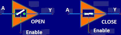 The above is the equivalent circuit of the tri-state buffer.
The enable pin can connect or disconnect the output from the input.
There are four types of Tri-state buffer:
Active ��HIGH�� Tri-state buffer
Active ��LOW�� Tri-state buffer
Active ��HIGH�� Inverting Tri-state buffer
Active ��LOW�� Inverting Tri-state buffer
Let��s look each of them sequentially.
The above is the equivalent circuit of the tri-state buffer.
The enable pin can connect or disconnect the output from the input.
There are four types of Tri-state buffer:
Active ��HIGH�� Tri-state buffer
Active ��LOW�� Tri-state buffer
Active ��HIGH�� Inverting Tri-state buffer
Active ��LOW�� Inverting Tri-state buffer
Let��s look each of them sequentially.
 In the Active ��HIGH�� tri-state buffer (for example: 74LS241) the output pin gets connected to input pin when we apply ��HIGH�� or ��1�� or positive signal at the enable pin.
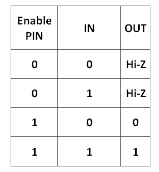 If we apply ��LOW�� or ��0�� or negative signal to the enable pin, the output gets disconnected from input and goes to ��HI-Z�� state where the output will not respond to input and output will be in open circuit state.
 Here the output will be connected to input when we apply ��LOW�� or ��0�� or negative signal at the enable pin.
If we apply ��HIGH�� or ��1�� or positive signal to enable pin, the output gets disconnected from input and output will be in ��HI-Z�� state / open circuit state.
Here the output will be connected to input when we apply ��LOW�� or ��0�� or negative signal at the enable pin.
If we apply ��HIGH�� or ��1�� or positive signal to enable pin, the output gets disconnected from input and output will be in ��HI-Z�� state / open circuit state.
 Truth Table:
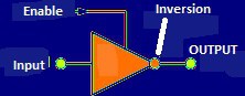 In active ��HIGH�� inverting Tri-state buffer (example: 74LS240), the gate act as logic ��NOT�� gate but, with the enable pin.
If we apply ��HIGH�� or ��1�� or positive signal at the enable input the gate gets activated and act like a regular logic ��NOT�� gate where its output is inversion / complementary of input.
If we apply ��LOW�� or ��0�� or negative signal to the enable pin, the output will be in ��HI-Z�� or open circuit state.
In active ��HIGH�� inverting Tri-state buffer (example: 74LS240), the gate act as logic ��NOT�� gate but, with the enable pin.
If we apply ��HIGH�� or ��1�� or positive signal at the enable input the gate gets activated and act like a regular logic ��NOT�� gate where its output is inversion / complementary of input.
If we apply ��LOW�� or ��0�� or negative signal to the enable pin, the output will be in ��HI-Z�� or open circuit state.
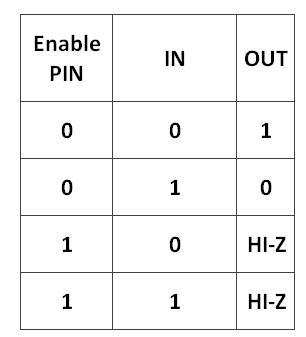 Truth table:
 In active ��LOW�� Inverting Tri-state buffer, the gate acts as logic ��NOT�� gate but, with enable pin.
If we apply ��LOW�� or ��0�� or negative signal to enable pin, the gate activates and work like regular logic ��NOT�� gate.
If we apply ��HIGH�� or ��1�� or positive signal to enable pin, the output pin will be in ��HI-Z�� state / open circuit state.
Truth Table:
In active ��LOW�� Inverting Tri-state buffer, the gate acts as logic ��NOT�� gate but, with enable pin.
If we apply ��LOW�� or ��0�� or negative signal to enable pin, the gate activates and work like regular logic ��NOT�� gate.
If we apply ��HIGH�� or ��1�� or positive signal to enable pin, the output pin will be in ��HI-Z�� state / open circuit state.
Truth Table:
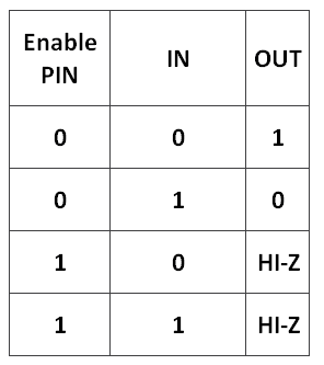
 The tri-state buffer is used to isolate logic devices, microprocessors and microcontrollers from one another in a data bus.
A decoder will allows only one set of tri-state buffers to pass data through the bus.
Say if the data set ��A�� is connected to a microcontroller, data set ��B�� to a microprocessor and data set ��C�� to some logic circuits.
In the above schematic all the buffers are active high tri-state buffer.
When the decoder sets the ENA ��HIGH�� the data set ��A�� is enabled, now the microcontroller can send data through the bus.
Rest of the two data sets ��B�� and ��C�� are in ��HI-Z�� or very high impedance state which electrically isolates the microprocessor and logical circuits from the bus, which is presently used by the microcontroller.
When the decoder sets ENB ��HIGH�� the data set ��B�� can send data over the bus and rest of the data sets ��A�� and ��C�� are isolated from the bus in ��HI-Z�� state.
Similarly, for when data set ��C�� is enabled.
The data bus is used by anyone of the data sets ��A�� or ��B�� or ��C�� at a given time to prevent contention.
We can also establish duplex (bi-directional) communication by connecting two tri-state buffers in parallel and in opposite direction.
The enable pins can be used as direction control.
For such kind of applications IC 74245 can be utilized.
Here are the commonly available list of digital buffers and Tri-state buffers:
74LS07 Hex Non-inverting Buffer
74LS17 Hex Buffer/Driver
74LS244 Octal Buffer/Line Driver
74LS245 Octal Bi-directional Buffer
CD4050 Hex Non-inverting Buffer
CD4503 Hex Tri-state Buffer
HEF40244 Tri-state Octal Buffer
This concludes our discussion regarding how digital buffers work, and their various digital configurations, I hope it helped you understand the details well.
If you have any further questions or suggestions, please express your questions in the comment section you may get a quick reply.
The tri-state buffer is used to isolate logic devices, microprocessors and microcontrollers from one another in a data bus.
A decoder will allows only one set of tri-state buffers to pass data through the bus.
Say if the data set ��A�� is connected to a microcontroller, data set ��B�� to a microprocessor and data set ��C�� to some logic circuits.
In the above schematic all the buffers are active high tri-state buffer.
When the decoder sets the ENA ��HIGH�� the data set ��A�� is enabled, now the microcontroller can send data through the bus.
Rest of the two data sets ��B�� and ��C�� are in ��HI-Z�� or very high impedance state which electrically isolates the microprocessor and logical circuits from the bus, which is presently used by the microcontroller.
When the decoder sets ENB ��HIGH�� the data set ��B�� can send data over the bus and rest of the data sets ��A�� and ��C�� are isolated from the bus in ��HI-Z�� state.
Similarly, for when data set ��C�� is enabled.
The data bus is used by anyone of the data sets ��A�� or ��B�� or ��C�� at a given time to prevent contention.
We can also establish duplex (bi-directional) communication by connecting two tri-state buffers in parallel and in opposite direction.
The enable pins can be used as direction control.
For such kind of applications IC 74245 can be utilized.
Here are the commonly available list of digital buffers and Tri-state buffers:
74LS07 Hex Non-inverting Buffer
74LS17 Hex Buffer/Driver
74LS244 Octal Buffer/Line Driver
74LS245 Octal Bi-directional Buffer
CD4050 Hex Non-inverting Buffer
CD4503 Hex Tri-state Buffer
HEF40244 Tri-state Octal Buffer
This concludes our discussion regarding how digital buffers work, and their various digital configurations, I hope it helped you understand the details well.
If you have any further questions or suggestions, please express your questions in the comment section you may get a quick reply.
 Here the ��A�� and ��B�� are the two inputs and the ��Y�� is output.
The Boolean expression for logic AND gate: The output ��Y�� is multiplication of the two inputs ��A�� and ��B��.
(A.B) = Y.
The Boolean multiplication is denoted by a dot (.)
If ��A�� is ��1�� and ��B�� is ��1�� the output is (A.B) = 1 x 1 = ��1�� or ��high��
If ��A�� is ��0�� and ��B�� is ��1�� the output is (A.B) = 0 x 1 = ��0�� or ��Low��
If ��A�� is ��1�� and ��B�� is ��0�� the output is (A.B) = 1 x 0 = ��0�� or ��Low��
If ��A�� is ��0�� and ��B�� is ��0�� the output is (A.B) = 0 x 0 = ��0�� or ��Low��
The above conditions are simplified in the truth table.
Truth Table (Two Input):
Here the ��A�� and ��B�� are the two inputs and the ��Y�� is output.
The Boolean expression for logic AND gate: The output ��Y�� is multiplication of the two inputs ��A�� and ��B��.
(A.B) = Y.
The Boolean multiplication is denoted by a dot (.)
If ��A�� is ��1�� and ��B�� is ��1�� the output is (A.B) = 1 x 1 = ��1�� or ��high��
If ��A�� is ��0�� and ��B�� is ��1�� the output is (A.B) = 0 x 1 = ��0�� or ��Low��
If ��A�� is ��1�� and ��B�� is ��0�� the output is (A.B) = 1 x 0 = ��0�� or ��Low��
If ��A�� is ��0�� and ��B�� is ��0�� the output is (A.B) = 0 x 0 = ��0�� or ��Low��
The above conditions are simplified in the truth table.
Truth Table (Two Input):
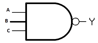 Illustration of 3 input AND gate:
Logic AND gates can have ��n�� number of inputs, which means it can have more than two inputs (Logic AND gates will have at-least two input and always one output).
For a 3 input AND gate the Boolean equation turns like this: (A.B.C) = Y, similarly for 4 input and above.
Truth Table for 3 input logic AND gate:
Illustration of 3 input AND gate:
Logic AND gates can have ��n�� number of inputs, which means it can have more than two inputs (Logic AND gates will have at-least two input and always one output).
For a 3 input AND gate the Boolean equation turns like this: (A.B.C) = Y, similarly for 4 input and above.
Truth Table for 3 input logic AND gate:
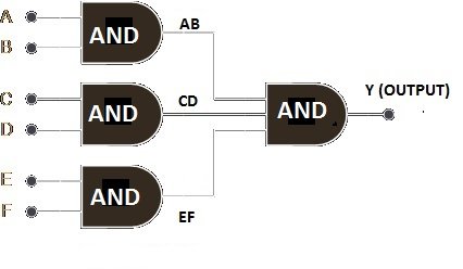 Now the Boolean equation for the above circuit becomes Y = (A.B).(C.D).(E.F)
Still, all the mentioned logical rules apply to the above circuit.
If you are going to use only 5 inputs from the above 6 inputs AND gates, we can connect a pull-up resistor at any one pin and now it becomes 5 input AND gate.
Transistor Based two input Logic AND gate:
Now we know, how a logic AND gate functions, let��s construct a 2 input AND gate using two NPN transistors.
The logic ICs are constructed in the almost same the same way.
Two Transistor AND gate Schematic:
Now the Boolean equation for the above circuit becomes Y = (A.B).(C.D).(E.F)
Still, all the mentioned logical rules apply to the above circuit.
If you are going to use only 5 inputs from the above 6 inputs AND gates, we can connect a pull-up resistor at any one pin and now it becomes 5 input AND gate.
Transistor Based two input Logic AND gate:
Now we know, how a logic AND gate functions, let��s construct a 2 input AND gate using two NPN transistors.
The logic ICs are constructed in the almost same the same way.
Two Transistor AND gate Schematic:
 If you want to buy logic AND gate from the market, you will get in the above configuration.
It has 14 pins; the pin #7 and pin #14 are GND and Vcc respectively.
It is operated at 5V.
If you want to buy logic AND gate from the market, you will get in the above configuration.
It has 14 pins; the pin #7 and pin #14 are GND and Vcc respectively.
It is operated at 5V.
 ��Exclusive NOR�� gate equivalent Circuit:
 The above is the equivalent circuit for logic Ex-NOR, which is basically combination of logic ��Exclusive OR�� gate and logic ��NOT�� gate.
Here the ��A�� and ��B�� are the two inputs and the ��Y�� is output.
The Boolean expression for logic Ex-NOR gate: Y = (AB) + AB.
If ��A�� is ��1�� and ��B�� is ��1�� the output is ((AB) + AB) = 0 + 1 = ��1�� or ��HIGH��
If ��A�� is ��0�� and ��B�� is ��1�� the output is ((AB) + AB) = 0 + 0 = ��0�� or ��LOW��
If ��A�� is ��1�� and ��B�� is ��0�� the output is ((AB) + AB) = 0 + 0 = ��0�� or ��LOW��
If ��A�� is ��0�� and ��B�� is ��0�� the output is ((AB) + AB) = 1 + 1 = ��1�� or ��HIGH��
The above conditions are simplified in the truth table.
Truth Table (Two Input):
The above is the equivalent circuit for logic Ex-NOR, which is basically combination of logic ��Exclusive OR�� gate and logic ��NOT�� gate.
Here the ��A�� and ��B�� are the two inputs and the ��Y�� is output.
The Boolean expression for logic Ex-NOR gate: Y = (AB) + AB.
If ��A�� is ��1�� and ��B�� is ��1�� the output is ((AB) + AB) = 0 + 1 = ��1�� or ��HIGH��
If ��A�� is ��0�� and ��B�� is ��1�� the output is ((AB) + AB) = 0 + 0 = ��0�� or ��LOW��
If ��A�� is ��1�� and ��B�� is ��0�� the output is ((AB) + AB) = 0 + 0 = ��0�� or ��LOW��
If ��A�� is ��0�� and ��B�� is ��0�� the output is ((AB) + AB) = 1 + 1 = ��1�� or ��HIGH��
The above conditions are simplified in the truth table.
Truth Table (Two Input):
 Truth Table for 3 input logic EX-OR gate:
 The above design has major drawback, we need 3 different logic gates to make one Ex-NOR gate.
But we can overcome this problem by implementing Ex-NOR gate with only logic ��NAND�� gates, this is also economical to fabricate.
Exclusive NOR gate using NAND gate:
The above design has major drawback, we need 3 different logic gates to make one Ex-NOR gate.
But we can overcome this problem by implementing Ex-NOR gate with only logic ��NAND�� gates, this is also economical to fabricate.
Exclusive NOR gate using NAND gate:
 Exclusive NOR gates are used to perform complicated computing tasks such as arithmetic operations, binary adders, binary subtraction, parity checkers and they are used as digital comparators.
Logic Exclusive-NOR Gate IC 74266:
Exclusive NOR gates are used to perform complicated computing tasks such as arithmetic operations, binary adders, binary subtraction, parity checkers and they are used as digital comparators.
Logic Exclusive-NOR Gate IC 74266:
 If you want to buy logic Ex-NOR gate from the market, you will get in the above DIP configuration.
It has 14 pins; the pin #7 and pin #14 are GND and Vcc respectively.
It is operated at 5V.
Propagation delay:
Propagation delay is the time taken for the output to change from LOW to HIGH and vice versa after giving input.
The propagation delay from LOW to HIGH is 23 nanoseconds.
The propagation delay from HIGH to LOW is 23 nanoseconds.
Commonly available ��EX-NOR�� gate ICs:
74LS266 Quad 2-input
CD4077 Quad 2-input
If you want to buy logic Ex-NOR gate from the market, you will get in the above DIP configuration.
It has 14 pins; the pin #7 and pin #14 are GND and Vcc respectively.
It is operated at 5V.
Propagation delay:
Propagation delay is the time taken for the output to change from LOW to HIGH and vice versa after giving input.
The propagation delay from LOW to HIGH is 23 nanoseconds.
The propagation delay from HIGH to LOW is 23 nanoseconds.
Commonly available ��EX-NOR�� gate ICs:
74LS266 Quad 2-input
CD4077 Quad 2-input
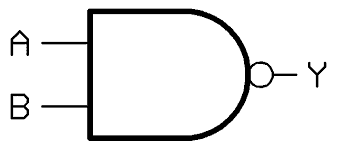 Here the ��A�� and ��B�� are the two inputs and the ��Y�� is output.
This symbol is ��AND�� gate with inversion ��o��.
Logic ��NAND�� Gate Equivalent Circuit:
Here the ��A�� and ��B�� are the two inputs and the ��Y�� is output.
This symbol is ��AND�� gate with inversion ��o��.
Logic ��NAND�� Gate Equivalent Circuit:
 The logic NAND gate is the combination of logic ��AND�� gate and logic ��NOT�� gate.
The Boolean expression for logic NAND gate: The output ��Y�� is complementary multiplication of the two inputs ��A�� and ��B��.
Y = ((A.B) )
The Boolean multiplication is denoted by a dot (.) and the complementary (inversion) is represented by a bar (-) over a letter.
If ��A�� is ��1�� and ��B�� is ��1�� the output is ((A.B) ) = (1 x 1) = ��0�� or ��LOW��
If ��A�� is ��0�� and ��B�� is ��1�� the output is ((A.B) ) = (0 x 1) = ��1�� or ��HIGH��
If ��A�� is ��1�� and ��B�� is ��0�� the output is ((A.B) ) = (1 x 0) = ��1�� or ��HIGH��
If ��A�� is ��0�� and ��B�� is ��0�� the output is ((A.B) ) = (0 x 0) = ��1�� or ��HIGH��
The above conditions are simplified in the truth table.
Truth Table (Two Input):
The logic NAND gate is the combination of logic ��AND�� gate and logic ��NOT�� gate.
The Boolean expression for logic NAND gate: The output ��Y�� is complementary multiplication of the two inputs ��A�� and ��B��.
Y = ((A.B) )
The Boolean multiplication is denoted by a dot (.) and the complementary (inversion) is represented by a bar (-) over a letter.
If ��A�� is ��1�� and ��B�� is ��1�� the output is ((A.B) ) = (1 x 1) = ��0�� or ��LOW��
If ��A�� is ��0�� and ��B�� is ��1�� the output is ((A.B) ) = (0 x 1) = ��1�� or ��HIGH��
If ��A�� is ��1�� and ��B�� is ��0�� the output is ((A.B) ) = (1 x 0) = ��1�� or ��HIGH��
If ��A�� is ��0�� and ��B�� is ��0�� the output is ((A.B) ) = (0 x 0) = ��1�� or ��HIGH��
The above conditions are simplified in the truth table.
Truth Table (Two Input):
 Now the Boolean equation for the above circuit becomes Y = ((A.B.C.D) )
Still, all the mentioned logical rules apply to the above circuit.
If you are going to use only 3 inputs from the above 4 inputs NAND gate, we can connect a pull-up resistor to any one pin and now it becomes 3 input NAND gate.
Transistor Based two input Logic NAND gate:
Now we know, how a logic NAND gate functions, let��s construct a 2 input NAND gate using two
NPN transistors.
The logic ICs are constructed in the almost same the same way.
Two Transistor NAND gate Schematic:
Now the Boolean equation for the above circuit becomes Y = ((A.B.C.D) )
Still, all the mentioned logical rules apply to the above circuit.
If you are going to use only 3 inputs from the above 4 inputs NAND gate, we can connect a pull-up resistor to any one pin and now it becomes 3 input NAND gate.
Transistor Based two input Logic NAND gate:
Now we know, how a logic NAND gate functions, let��s construct a 2 input NAND gate using two
NPN transistors.
The logic ICs are constructed in the almost same the same way.
Two Transistor NAND gate Schematic:
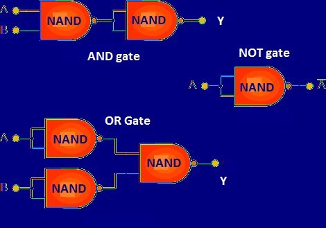 In above schematics just 3 types of gates are shown but, we can make any Boolean logic.
Quad NAND gate IC 7400:
In above schematics just 3 types of gates are shown but, we can make any Boolean logic.
Quad NAND gate IC 7400:
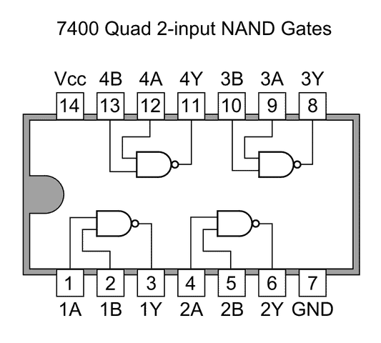 If you want to buy a logic NAND gate from the market, you will get in the above DIP configuration.
It has 14 pins; the pin #7 and pin #14 are GND and Vcc respectively.
It is operated at 5V.
Propagation delay:
Propagation delay is the time taken for the output to change from LOW to HIGH and vice versa after giving an input.
The propagation delay from LOW to HIGH is 22 nanoseconds.
The propagation delay from HIGH to LOW is 15 nanoseconds.
There several other NAND gate ICs available:
74LS00 Quad 2-input
74LS10 Triple 3-input
74LS20 Dual 4-input
74LS30 Single 8-input
CD4011 Quad 2-input
CD4023 Triple 3-input
CD4012 Dual 4-input
If you want to buy a logic NAND gate from the market, you will get in the above DIP configuration.
It has 14 pins; the pin #7 and pin #14 are GND and Vcc respectively.
It is operated at 5V.
Propagation delay:
Propagation delay is the time taken for the output to change from LOW to HIGH and vice versa after giving an input.
The propagation delay from LOW to HIGH is 22 nanoseconds.
The propagation delay from HIGH to LOW is 15 nanoseconds.
There several other NAND gate ICs available:
74LS00 Quad 2-input
74LS10 Triple 3-input
74LS20 Dual 4-input
74LS30 Single 8-input
CD4011 Quad 2-input
CD4023 Triple 3-input
CD4012 Dual 4-input
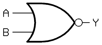 Here the ��A�� and ��B�� are the two inputs and the ��Y�� is output.
This symbol is ��OR�� gate with inversion ��o��.
Logic ��NOR�� Gate Equivalent Circuit:
Here the ��A�� and ��B�� are the two inputs and the ��Y�� is output.
This symbol is ��OR�� gate with inversion ��o��.
Logic ��NOR�� Gate Equivalent Circuit:
 The logic NOR gate is the combination of logic ��OR�� gate and logic ��NOT�� gate.
The Boolean expression for logic NOR gate: The output ��Y�� is complementary addition of the two inputs ��A�� and ��B��.
Y = ((A+B) )
The Boolean addition is denoted by (+) and the complementary (inversion) is represented by a bar (-) over a letter.
If ��A�� is ��1�� and ��B�� is ��1�� the output is ((A+B) ) = (1+ 1) = ��0�� or ��LOW��
If ��A�� is ��0�� and ��B�� is ��1�� the output is ((A+B) ) = (0+ 1) = ��0�� or ��LOW��
If ��A�� is ��1�� and ��B�� is ��0�� the output is ((A+B) ) = (1+ 0) = ��0�� or ��LOW��
If ��A�� is ��0�� and ��B�� is ��0�� the output is ((A+B) ) = (0+ 0) = ��1�� or ��HIGH��
The above conditions are simplified in the truth table.
Truth Table (Two Input):
The logic NOR gate is the combination of logic ��OR�� gate and logic ��NOT�� gate.
The Boolean expression for logic NOR gate: The output ��Y�� is complementary addition of the two inputs ��A�� and ��B��.
Y = ((A+B) )
The Boolean addition is denoted by (+) and the complementary (inversion) is represented by a bar (-) over a letter.
If ��A�� is ��1�� and ��B�� is ��1�� the output is ((A+B) ) = (1+ 1) = ��0�� or ��LOW��
If ��A�� is ��0�� and ��B�� is ��1�� the output is ((A+B) ) = (0+ 1) = ��0�� or ��LOW��
If ��A�� is ��1�� and ��B�� is ��0�� the output is ((A+B) ) = (1+ 0) = ��0�� or ��LOW��
If ��A�� is ��0�� and ��B�� is ��0�� the output is ((A+B) ) = (0+ 0) = ��1�� or ��HIGH��
The above conditions are simplified in the truth table.
Truth Table (Two Input):
 Logic NOR gates can have ��n�� number of inputs, which means it can have more than two inputs (Logic NOR gates will have at-least two input and always one output).
For a 3 input NOR gate the Boolean equation turns like this: ((A+B+C) ) = Y, similarly for 4 input and above.
Truth Table for 3 input logic NOR gate:
Logic NOR gates can have ��n�� number of inputs, which means it can have more than two inputs (Logic NOR gates will have at-least two input and always one output).
For a 3 input NOR gate the Boolean equation turns like this: ((A+B+C) ) = Y, similarly for 4 input and above.
Truth Table for 3 input logic NOR gate:
 Now the Boolean equation for the above circuit becomes Y = ((A+B+C+D) )
Still, all the mentioned logical rules apply to the above circuit.
If you are going to use only 3 inputs from the above 4 inputs NOR gate, we can connect a pull-down resistor to any one of the pin and now it becomes 3 input NOR gate.
Transistor Based two input Logic NOR gate:
Now we know, how a logic NOR gate functions, let��s construct a 2 input NOR gate using two NPN transistors.
The logic ICs are constructed in the almost same the same way.
Two Transistor NOR gate Schematic:
Now the Boolean equation for the above circuit becomes Y = ((A+B+C+D) )
Still, all the mentioned logical rules apply to the above circuit.
If you are going to use only 3 inputs from the above 4 inputs NOR gate, we can connect a pull-down resistor to any one of the pin and now it becomes 3 input NOR gate.
Transistor Based two input Logic NOR gate:
Now we know, how a logic NOR gate functions, let��s construct a 2 input NOR gate using two NPN transistors.
The logic ICs are constructed in the almost same the same way.
Two Transistor NOR gate Schematic:
 In above schematics just 3 types of gates are showcased but, we can make any Boolean logics.
Quad NOR gate IC 7402:
In above schematics just 3 types of gates are showcased but, we can make any Boolean logics.
Quad NOR gate IC 7402:
 If you want to buy a logic NOR gate from the market, you will get in the above DIP configuration.
It has 14 pins; the pin #7 and pin #14 are GND and Vcc respectively.
It is operated at 5V.
Propagation delay:
Propagation delay is the time taken for the output to change from LOW to HIGH and vice versa after giving an input.
The propagation delay from LOW to HIGH is 22 nanoseconds.
The propagation delay from HIGH to LOW is 15 nanoseconds.
There several other NOR gate ICs available:
74LS02 Quad 2-input
74LS27 Triple 3-input
74LS260 Dual 4-input
CD4001 Quad 2-input
CD4025 Triple 3-input
CD4002 Dual 4-input
If you want to buy a logic NOR gate from the market, you will get in the above DIP configuration.
It has 14 pins; the pin #7 and pin #14 are GND and Vcc respectively.
It is operated at 5V.
Propagation delay:
Propagation delay is the time taken for the output to change from LOW to HIGH and vice versa after giving an input.
The propagation delay from LOW to HIGH is 22 nanoseconds.
The propagation delay from HIGH to LOW is 15 nanoseconds.
There several other NOR gate ICs available:
74LS02 Quad 2-input
74LS27 Triple 3-input
74LS260 Dual 4-input
CD4001 Quad 2-input
CD4025 Triple 3-input
CD4002 Dual 4-input
 Let��s assume ��A�� is the input and ��Y�� is the output, the Boolean equation for logic NOT gate is: �� = Y.
The equation states that the output is inversion of the input.
Truth Table for logic NOT gate:
Let��s assume ��A�� is the input and ��Y�� is the output, the Boolean equation for logic NOT gate is: �� = Y.
The equation states that the output is inversion of the input.
Truth Table for logic NOT gate:
 The ��NOT�� gate can be constructed using logic ��NAND�� and logic ��NOR�� gates by joining all the input pins, this applies to gates with 3, 4 and higher input pins.
Transistor based Logic ��NOT�� gate:
The ��NOT�� gate can be constructed using logic ��NAND�� and logic ��NOR�� gates by joining all the input pins, this applies to gates with 3, 4 and higher input pins.
Transistor based Logic ��NOT�� gate:
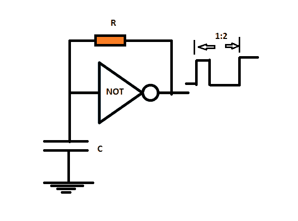 The above circuit is an oscillator which produce square wave at 33% duty cycle.
Initially the capacitor is in discharged state and the ground signal will be available at input of NOT gate.
The output turns positive and charges the capacitor via resistor ��R��, the capacitor charges till the upper threshold voltage of the inverter and changes the state, the output turns negative signal and capacitor starts to discharge via the resistor ��R�� until capacitor voltage reaches the lower threshold level and changes the state, the output turns positive and charges the capacitor.
This cycle repeats as long the power supply is given to the circuit.
The frequency of the above oscillator can be calculated: F= 680/RC
The above circuit is an oscillator which produce square wave at 33% duty cycle.
Initially the capacitor is in discharged state and the ground signal will be available at input of NOT gate.
The output turns positive and charges the capacitor via resistor ��R��, the capacitor charges till the upper threshold voltage of the inverter and changes the state, the output turns negative signal and capacitor starts to discharge via the resistor ��R�� until capacitor voltage reaches the lower threshold level and changes the state, the output turns positive and charges the capacitor.
This cycle repeats as long the power supply is given to the circuit.
The frequency of the above oscillator can be calculated: F= 680/RC
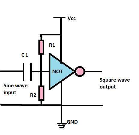 Where, F is frequency.
R is resistance in ohms.
C is capacitance in farad.
Square wave converter:
The above circuit will convert sine wave signal to square wave, actually it can convert any analog waves into square wave.
The two resistors R1 and R2 work as voltage divider, this is utilized to get a biasing point and the capacitor blocks any DC signals.
If the input signal goes above Upper threshold level or below lower threshold level the output turns
LOW or HIGH according to the signal, this produces square wave.
IC 7404 NOT gate Inverter:
Where, F is frequency.
R is resistance in ohms.
C is capacitance in farad.
Square wave converter:
The above circuit will convert sine wave signal to square wave, actually it can convert any analog waves into square wave.
The two resistors R1 and R2 work as voltage divider, this is utilized to get a biasing point and the capacitor blocks any DC signals.
If the input signal goes above Upper threshold level or below lower threshold level the output turns
LOW or HIGH according to the signal, this produces square wave.
IC 7404 NOT gate Inverter:
 The IC 7404 is one of the most commonly used logic NOT gate IC.
It has 14 pins, pin #7 is ground and pin #14 is Vcc.
The operating voltage is from 4.5V to 5V.
Propagation delay:
The propagation delay is the time taken by the gate to process the output after giving an input.
In logic ��NOT�� gate takes around 22 nano seconds to change its state from HIGH to LOW and vice versa.
There are several other logic ��NOT gate ICs:
74LS04 Hex Inverting NOT Gate
74LS14 Hex Schmitt Inverting NOT Gate
74LS1004 Hex Inverting Drivers
CD4009 Hex Inverting NOT Gate
CD4069 Hex Inverting NOT Gate
The IC 7404 is one of the most commonly used logic NOT gate IC.
It has 14 pins, pin #7 is ground and pin #14 is Vcc.
The operating voltage is from 4.5V to 5V.
Propagation delay:
The propagation delay is the time taken by the gate to process the output after giving an input.
In logic ��NOT�� gate takes around 22 nano seconds to change its state from HIGH to LOW and vice versa.
There are several other logic ��NOT gate ICs:
74LS04 Hex Inverting NOT Gate
74LS14 Hex Schmitt Inverting NOT Gate
74LS1004 Hex Inverting Drivers
CD4009 Hex Inverting NOT Gate
CD4069 Hex Inverting NOT Gate
 Here the ��A�� and ��B�� are the two inputs and the ��Y�� is output.
The Boolean expression for logic OR gate: The output ��Y�� is addition of the two inputs ��A�� and ��B��, (A+B) = Y.
The Boolean addition is denoted by (+)
If ��A�� is ��1�� and ��B�� is ��1�� the output is (A + B) = 1 + 1 = ��1�� or ��high��
If ��A�� is ��0�� and ��B�� is ��1�� the output is (A + B) = 0 + 1 = ��1�� or ��high��
If ��A�� is ��1�� and ��B�� is ��0�� the output is (A + B) = 1 + 0 = ��1�� or ��high��
If ��A�� is ��0�� and ��B�� is ��0�� the output is (A + B) = 0 + 0 = ��0�� or ��Low��
The above conditions are simplified in the truth table.
Truth Table (Two Input):
Here the ��A�� and ��B�� are the two inputs and the ��Y�� is output.
The Boolean expression for logic OR gate: The output ��Y�� is addition of the two inputs ��A�� and ��B��, (A+B) = Y.
The Boolean addition is denoted by (+)
If ��A�� is ��1�� and ��B�� is ��1�� the output is (A + B) = 1 + 1 = ��1�� or ��high��
If ��A�� is ��0�� and ��B�� is ��1�� the output is (A + B) = 0 + 1 = ��1�� or ��high��
If ��A�� is ��1�� and ��B�� is ��0�� the output is (A + B) = 1 + 0 = ��1�� or ��high��
If ��A�� is ��0�� and ��B�� is ��0�� the output is (A + B) = 0 + 0 = ��0�� or ��Low��
The above conditions are simplified in the truth table.
Truth Table (Two Input):
 Logic OR gates can have ��n�� number of inputs, which means it can have more than two inputs (Logic OR gates will have at-least two input and always one output).
For a 3 input logic OR gate the Boolean equation turns like this: (A + B + C) = Y, similarly for 4 input and above.
Truth Table for 3 input logic OR gate:
Logic OR gates can have ��n�� number of inputs, which means it can have more than two inputs (Logic OR gates will have at-least two input and always one output).
For a 3 input logic OR gate the Boolean equation turns like this: (A + B + C) = Y, similarly for 4 input and above.
Truth Table for 3 input logic OR gate:
 Now the Boolean equation for the above circuit becomes Y = (A+B)+(C+D)+(E+F)
Still, all the mentioned logical rules apply to the above circuit.
If you are going to use only 5 inputs from the above 6 inputs OR gate, we can connect a pull-down resistor at any one pin and now it becomes 5 input OR gate.
Transistor Based two input Logic OR gate:
Now we know, how a logic OR gate functions, let��s construct a 2 input OR gate using two NPN transistors.
The logic ICs are constructed in the almost same the same way.
Two Transistor OR gate Schematic:
Now the Boolean equation for the above circuit becomes Y = (A+B)+(C+D)+(E+F)
Still, all the mentioned logical rules apply to the above circuit.
If you are going to use only 5 inputs from the above 6 inputs OR gate, we can connect a pull-down resistor at any one pin and now it becomes 5 input OR gate.
Transistor Based two input Logic OR gate:
Now we know, how a logic OR gate functions, let��s construct a 2 input OR gate using two NPN transistors.
The logic ICs are constructed in the almost same the same way.
Two Transistor OR gate Schematic:
 If you want to buy logic OR gate from the market, you will get in the above configuration.
It has 14 pins; the pin #7 and pin #14 are GND and Vcc respectively.
It is operated at 5V.
Propagation delay:
Propagation delay is the time taken for the output to change from LOW to HIGH and vice versa.
The propagation delay from LOW to HIGH is 7.4 nanoseconds at 25 degree Celsius.
The propagation delay from HIGH to LOW is 7.7 nanoseconds at 25 degree Celsius.
74LS32 Quad 2-input
CD4071 Quad 2-input
CD4075 Triple 3-input
CD4072 Dual 4-input
If you want to buy logic OR gate from the market, you will get in the above configuration.
It has 14 pins; the pin #7 and pin #14 are GND and Vcc respectively.
It is operated at 5V.
Propagation delay:
Propagation delay is the time taken for the output to change from LOW to HIGH and vice versa.
The propagation delay from LOW to HIGH is 7.4 nanoseconds at 25 degree Celsius.
The propagation delay from HIGH to LOW is 7.7 nanoseconds at 25 degree Celsius.
74LS32 Quad 2-input
CD4071 Quad 2-input
CD4075 Triple 3-input
CD4072 Dual 4-input
 Here the ��A�� and ��B�� are the two inputs and the ��Y�� is output.
The Boolean expression for logic Ex-OR gate: Y = (A.) B+A.B
If ��A�� is ��1�� and ��B�� is ��1�� the output is (A .B+A.B ) = 0 x 1 + 1 x 0 = ��1�� or ��LOW��
If ��A�� is ��0�� and ��B�� is ��1�� the output is (A .B+A.B ) = 1 x 1 + 0 x 0 = ��1�� or ��HIGH��
If ��A�� is ��1�� and ��B�� is ��0�� the output is (A .B+A.B ) = 0 x 0 + 1 x 1= ��1�� or ��HIGH��
If ��A�� is ��0�� and ��B�� is ��0�� the output is (A .B+A.B ) = 1 x 0 + 0 x 1 = ��0�� or ��Low��
The above conditions are simplified in the truth table.
Truth Table (Two Input):
Here the ��A�� and ��B�� are the two inputs and the ��Y�� is output.
The Boolean expression for logic Ex-OR gate: Y = (A.) B+A.B
If ��A�� is ��1�� and ��B�� is ��1�� the output is (A .B+A.B ) = 0 x 1 + 1 x 0 = ��1�� or ��LOW��
If ��A�� is ��0�� and ��B�� is ��1�� the output is (A .B+A.B ) = 1 x 1 + 0 x 0 = ��1�� or ��HIGH��
If ��A�� is ��1�� and ��B�� is ��0�� the output is (A .B+A.B ) = 0 x 0 + 1 x 1= ��1�� or ��HIGH��
If ��A�� is ��0�� and ��B�� is ��0�� the output is (A .B+A.B ) = 1 x 0 + 0 x 1 = ��0�� or ��Low��
The above conditions are simplified in the truth table.
Truth Table (Two Input):
 Truth Table for 3 input logic EX-OR gate:
 The above design has major drawback, we need 3 different logic gates to make one Ex-OR gate.
But we can overcome this problem by implementing Ex-OR gate with only logic NAND gates, this is also economical to fabricate.
Exclusive OR gate using NAND gate:
The above design has major drawback, we need 3 different logic gates to make one Ex-OR gate.
But we can overcome this problem by implementing Ex-OR gate with only logic NAND gates, this is also economical to fabricate.
Exclusive OR gate using NAND gate:
 Exclusive OR gates are used to perform complicated computing tasks such as arithmetic operations, full adders, half-adders, it can also deliver carry out functionality.
Logic Exclusive OR Gate IC 7486:
Exclusive OR gates are used to perform complicated computing tasks such as arithmetic operations, full adders, half-adders, it can also deliver carry out functionality.
Logic Exclusive OR Gate IC 7486:
 If you want to buy logic Ex-OR gate from the market, you will get in the above DIP configuration.
It has 14 pins; the pin #7 and pin #14 are GND and Vcc respectively.
It is operated at 5V.
Propagation delay:
Propagation delay is the time taken for the output to change from LOW to HIGH and vice versa after giving input.
The propagation delay from LOW to HIGH is 23 nanoseconds.
The propagation delay from HIGH to LOW is 17 nanoseconds.
Commonly available ��EX-OR�� gate ICs:
74LS86 Quad 2-input
CD4030 Quad 2-input
I hope the above detailed explanation might have helped you to understand regarding what logic gates are and how logic gates work, if you still have any questions? Please express in the comment section, you may get a quick reply.
If you want to buy logic Ex-OR gate from the market, you will get in the above DIP configuration.
It has 14 pins; the pin #7 and pin #14 are GND and Vcc respectively.
It is operated at 5V.
Propagation delay:
Propagation delay is the time taken for the output to change from LOW to HIGH and vice versa after giving input.
The propagation delay from LOW to HIGH is 23 nanoseconds.
The propagation delay from HIGH to LOW is 17 nanoseconds.
Commonly available ��EX-OR�� gate ICs:
74LS86 Quad 2-input
CD4030 Quad 2-input
I hope the above detailed explanation might have helped you to understand regarding what logic gates are and how logic gates work, if you still have any questions? Please express in the comment section, you may get a quick reply.
 The LM317 in CC and CV mode, I have limited the voltage to 4.20V and current to 800mA (for 2AH battery) with 1.5ohm 1 watt resistor.
I am getting exactly 4.20V at output (open circuit) and short circuit current of exactly 0.80A.
But when I connect a Li-ion battery (with half charge which is old batteries from laptop) the current consumption is just 0.10A, and almost discharged battery not consuming not more than 0.20A.
If charging is done at this rate it might take 10 hrs or more for reaching full battery, which is not feasible.
Is it possible to force the current to flow through the battery at 0.80A rate?
As far as i know the batteries are in good condition.
The LM317 in CC and CV mode, I have limited the voltage to 4.20V and current to 800mA (for 2AH battery) with 1.5ohm 1 watt resistor.
I am getting exactly 4.20V at output (open circuit) and short circuit current of exactly 0.80A.
But when I connect a Li-ion battery (with half charge which is old batteries from laptop) the current consumption is just 0.10A, and almost discharged battery not consuming not more than 0.20A.
If charging is done at this rate it might take 10 hrs or more for reaching full battery, which is not feasible.
Is it possible to force the current to flow through the battery at 0.80A rate?
As far as i know the batteries are in good condition.
 When this happens the emitter is not able to acquire a 0V potential, and the BJT is unable to turn ON with a regular 0.6V.
Suppose a 0.6V is applied to its base, due to the emitter load, the transistor only just begins conducting which is not enough to trigger the load.
As the base voltage is increased from 0.6V to 1.2V, the emitter begins to conduct and allows a 0.6V to reach its emitter, now suppose the base voltage is further increased to 2V��.this prompts the emitter
voltage to reach around 1.6V.
From the above scenario we find that the emitter of the tramsistor is always 0.6V behind the base voltage and this gives an impression that the emitter is following the base, and hence the name.
The main features of an emitter follower transistor configuration can be studied as explained below:
The emitter voltage is always around 0.6V lower than the base voltage.
The emitter voltage can be varied by varying the base voltage accordingly.
The emitter current is equivalent to the collector current.
This
makes the configuration rich in current if the collector is directly
connected with the supply (+) rail.
The load being attached between the emitter and the ground, the base
is attributed with a high impedance feature, meaning the base being not
vulnerable of getting connected to the ground rail through the emitter,
does not require high resistance to safeguard itself, and is normally
protected from high current.
When this happens the emitter is not able to acquire a 0V potential, and the BJT is unable to turn ON with a regular 0.6V.
Suppose a 0.6V is applied to its base, due to the emitter load, the transistor only just begins conducting which is not enough to trigger the load.
As the base voltage is increased from 0.6V to 1.2V, the emitter begins to conduct and allows a 0.6V to reach its emitter, now suppose the base voltage is further increased to 2V��.this prompts the emitter
voltage to reach around 1.6V.
From the above scenario we find that the emitter of the tramsistor is always 0.6V behind the base voltage and this gives an impression that the emitter is following the base, and hence the name.
The main features of an emitter follower transistor configuration can be studied as explained below:
The emitter voltage is always around 0.6V lower than the base voltage.
The emitter voltage can be varied by varying the base voltage accordingly.
The emitter current is equivalent to the collector current.
This
makes the configuration rich in current if the collector is directly
connected with the supply (+) rail.
The load being attached between the emitter and the ground, the base
is attributed with a high impedance feature, meaning the base being not
vulnerable of getting connected to the ground rail through the emitter,
does not require high resistance to safeguard itself, and is normally
protected from high current.
 Referring to the re circuit:
Zi: The input impedance can be calculated using the formula:
Referring to the re circuit:
Zi: The input impedance can be calculated using the formula:
 Zo: The output impedance can be best defined by first evaluating the equation for the current Ib:
Ib = Vi / Zb
and subsequently multiplying by (�� +1) to get Ie.
Here's the result:
Ie = (�� +1)Ib = (�� +1)Vi / Zb
Substituting for Zb gives:
Ie = (�� +1)Vi / ��re + (�� +1)RE
Ie = Vi / [��re + (�� +1)] + RE
since (�� +1) is almost equal to �� and ��re / �� +1 is almost equal to ��re / �� = re we get:
Zo: The output impedance can be best defined by first evaluating the equation for the current Ib:
Ib = Vi / Zb
and subsequently multiplying by (�� +1) to get Ie.
Here's the result:
Ie = (�� +1)Ib = (�� +1)Vi / Zb
Substituting for Zb gives:
Ie = (�� +1)Vi / ��re + (�� +1)RE
Ie = Vi / [��re + (�� +1)] + RE
since (�� +1) is almost equal to �� and ��re / �� +1 is almost equal to ��re / �� = re we get:
 Now, if we build a network using the above derived equation, presents us with the following configuration:
 Therefore, the output impedance could be determined by setting the input voltage Vi to zero and
Zo = RE||re
Since, RE is normally much bigger than re, the following approximation is mostly taken into account:
Zo re
This gives us the expression for the output impedance of an emitter follower circuit.
Therefore, the output impedance could be determined by setting the input voltage Vi to zero and
Zo = RE||re
Since, RE is normally much bigger than re, the following approximation is mostly taken into account:
Zo re
This gives us the expression for the output impedance of an emitter follower circuit.
 Adjustable Zener Diode:
Normally a zener diode comes with a fixed value which cannot be changed or altered as per a given circuit application need.
The following diagram which is actually a simple cell phone charger circuit is designed using an emitter follower circuit configuration.
Here, simply by changing the indicated base zener diode with a 10K pot, the design can be transformed into an effective adjustable zener diode circuit, another cool emitter follower application circuit.
Adjustable Zener Diode:
Normally a zener diode comes with a fixed value which cannot be changed or altered as per a given circuit application need.
The following diagram which is actually a simple cell phone charger circuit is designed using an emitter follower circuit configuration.
Here, simply by changing the indicated base zener diode with a 10K pot, the design can be transformed into an effective adjustable zener diode circuit, another cool emitter follower application circuit.
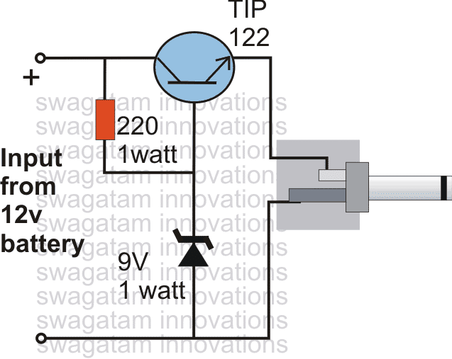
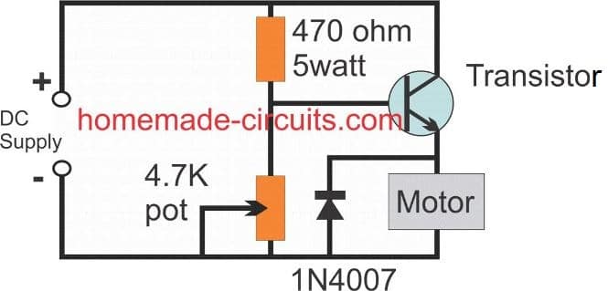
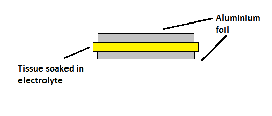 The stack of aluminium and tissue is rolled into cylinder form and housed into aluminium chassis.
The diameter of the roll, height and thickness of the tissue determines the various parameters of the capacitor.
The electrolytic capacitors are polarized, which means it has anode and cathode terminal and we should not be interchanged the input supply polarity to the capacitor as we do on other type of capacitors.
The stack of aluminium and tissue is rolled into cylinder form and housed into aluminium chassis.
The diameter of the roll, height and thickness of the tissue determines the various parameters of the capacitor.
The electrolytic capacitors are polarized, which means it has anode and cathode terminal and we should not be interchanged the input supply polarity to the capacitor as we do on other type of capacitors.
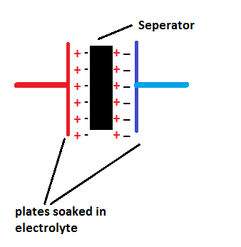 By now you would have an idea about supercapacitor and its fundamental functioning.
 ,and to be more precise this may be expressed as the voltage required for charging the capacitor with respect to the parameter "time", as indicated below:
Charging
V(t) = V0(1e^t/��)
Discharging
V(t) = V0(e^t/��)
,and to be more precise this may be expressed as the voltage required for charging the capacitor with respect to the parameter "time", as indicated below:
Charging
V(t) = V0(1e^t/��)
Discharging
V(t) = V0(e^t/��)
 is also typically associated with an alternative parameter, the cutoff frequency fc, and may be expressed by the formula:�� = R C = 1/ 2 �� f c
rearranging the above gives:, f c = 1 / 2 �� R C = 1/ 2 �� ��
where resistance in ohms and capacitance in farads yields the time constant in seconds or the frequency in Hz.
The above expressions may be further understood with short conditional equations, for example:
fc in Hz = 159155 / �� in ��s�� in ��s = 159155 / fc in Hz
Other similar useful equations are represented below which can be used for assessing a typical RC constant behavior:
rise time (20% to 80%)
t r �� 1.4 �� �� 0.22 / f c
rise time (10% to 90%)
t r �� 2.2 �� �� 0.35 / f c
In certain complicated circuits that may accompany in excess of one resistor and/or capacitor, the open-circuit time constant approach happens to offer a way of deriving the cutoff frequency by analyzing and calculating the total of many associated RC time constants.
is also typically associated with an alternative parameter, the cutoff frequency fc, and may be expressed by the formula:�� = R C = 1/ 2 �� f c
rearranging the above gives:, f c = 1 / 2 �� R C = 1/ 2 �� ��
where resistance in ohms and capacitance in farads yields the time constant in seconds or the frequency in Hz.
The above expressions may be further understood with short conditional equations, for example:
fc in Hz = 159155 / �� in ��s�� in ��s = 159155 / fc in Hz
Other similar useful equations are represented below which can be used for assessing a typical RC constant behavior:
rise time (20% to 80%)
t r �� 1.4 �� �� 0.22 / f c
rise time (10% to 90%)
t r �� 2.2 �� �� 0.35 / f c
In certain complicated circuits that may accompany in excess of one resistor and/or capacitor, the open-circuit time constant approach happens to offer a way of deriving the cutoff frequency by analyzing and calculating the total of many associated RC time constants.
 In this alternating AC, the current can be seen alternating across the central zero line and across the top positive and bottom negative peak levels, through a particular phase angle.
This phase angle can be seen rising and declining exponentially, meaning it is doing so in a gradually rising and gradually falling manner.
The alternating cycle in an AC happens 50 times per second for 220V mains and 60 times per second for 120V mains inputs as set by the standard rules.
This 50 cycle response is called 50 Hz frequency and the 60 Hz is called 60 Hz frequency for these mains outlets in our homes.
Whenever we switch ON an appliance or an electronic device to the mains, it is subjected to a sudden entry of the AC phase, and if this entry point happens to be at the peak of the phase angle could imply maximum current being forced to the device at the switch ON point.
Although, most devices will be ready for this and might be equipped with protection stages using resistors, or NTC or MOV, it is never recommended to subject them to such sudden unpredictable situations.
To tackle such an issue, a zero crossing detector stage is used which ensures that whenever a gadget is switched ON with mains power, the zero crossing circuit waits until the AC phase cycle reaches the zero line, and at this point it switches ON the mains power to the gadget.
In this alternating AC, the current can be seen alternating across the central zero line and across the top positive and bottom negative peak levels, through a particular phase angle.
This phase angle can be seen rising and declining exponentially, meaning it is doing so in a gradually rising and gradually falling manner.
The alternating cycle in an AC happens 50 times per second for 220V mains and 60 times per second for 120V mains inputs as set by the standard rules.
This 50 cycle response is called 50 Hz frequency and the 60 Hz is called 60 Hz frequency for these mains outlets in our homes.
Whenever we switch ON an appliance or an electronic device to the mains, it is subjected to a sudden entry of the AC phase, and if this entry point happens to be at the peak of the phase angle could imply maximum current being forced to the device at the switch ON point.
Although, most devices will be ready for this and might be equipped with protection stages using resistors, or NTC or MOV, it is never recommended to subject them to such sudden unpredictable situations.
To tackle such an issue, a zero crossing detector stage is used which ensures that whenever a gadget is switched ON with mains power, the zero crossing circuit waits until the AC phase cycle reaches the zero line, and at this point it switches ON the mains power to the gadget.
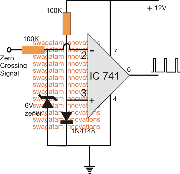 Note: Input AC should be from a Bridge Rectifier
The figure above show s simple 741 opamp based zero crossing detector circuit which can be used for all applications requiring a zero crossing based execution.
As can be seen, the 741 is configure as a comparator, wherein its non-inverting pin is connected with ground through a 1N4148 diode, which causes a 0.6V drop potential at this input pin.
The other input pin#2 which is the inverting pin of ther iC is used for the zero crossing detection, and is applied with the preferred AC signal.
As we know that as long as pin#3 potential is lower than pin#2, the output potential at pin#6 will be 0V, and as soon as pin#3 voltage goes above the pin#2, the output voltage will quickly switch to the 12V (supply level).
Therefore within the fed input AC signal during the periods when the phase voltage is well above the zero line, or at least above the 0.6V over the zero line, the opamp output shows a zero potential....but during the periods when the phase is about to enter or cross the zero line, the pin#2 experiences a potential below 0.6V reference as set for pin#3, causing an immediate reversion of the output to 12V.
Thus the output during these points becomes 12v high level, and this sequence goes on triggering each time the phase crosses the zero line of its phase cycle.
The resultant waveform can be seen at the output of the IC which clearly expresses and confirms the zero crossing detection of the IC.
Note: Input AC should be from a Bridge Rectifier
The figure above show s simple 741 opamp based zero crossing detector circuit which can be used for all applications requiring a zero crossing based execution.
As can be seen, the 741 is configure as a comparator, wherein its non-inverting pin is connected with ground through a 1N4148 diode, which causes a 0.6V drop potential at this input pin.
The other input pin#2 which is the inverting pin of ther iC is used for the zero crossing detection, and is applied with the preferred AC signal.
As we know that as long as pin#3 potential is lower than pin#2, the output potential at pin#6 will be 0V, and as soon as pin#3 voltage goes above the pin#2, the output voltage will quickly switch to the 12V (supply level).
Therefore within the fed input AC signal during the periods when the phase voltage is well above the zero line, or at least above the 0.6V over the zero line, the opamp output shows a zero potential....but during the periods when the phase is about to enter or cross the zero line, the pin#2 experiences a potential below 0.6V reference as set for pin#3, causing an immediate reversion of the output to 12V.
Thus the output during these points becomes 12v high level, and this sequence goes on triggering each time the phase crosses the zero line of its phase cycle.
The resultant waveform can be seen at the output of the IC which clearly expresses and confirms the zero crossing detection of the IC.
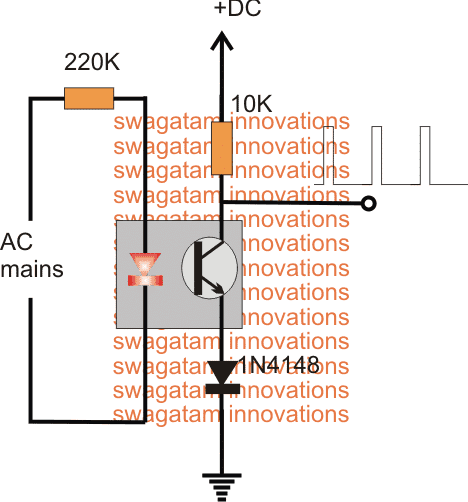 Note: Input AC should be from a Bridge Rectifier
Referring to the image above, the BJT in the form of a phototransistor associated inside an opto coupler can be effectively configured as a simplest zero crossing detector circuit.
The AC mains is fed to the LED of the opamp via a high value resistor.
During its phase cycles as long as the mains voltage is above 2V, the phototransistor stays in the conducting mode and the output response is held at near zero volts, however during times when the phase reaches the zero line of its travel, the LED inside the opto shuts off causing the transistor to also shut off, this response instantly causes a high logic to appear at the indicated output point of the configuration.
Note: Input AC should be from a Bridge Rectifier
Referring to the image above, the BJT in the form of a phototransistor associated inside an opto coupler can be effectively configured as a simplest zero crossing detector circuit.
The AC mains is fed to the LED of the opamp via a high value resistor.
During its phase cycles as long as the mains voltage is above 2V, the phototransistor stays in the conducting mode and the output response is held at near zero volts, however during times when the phase reaches the zero line of its travel, the LED inside the opto shuts off causing the transistor to also shut off, this response instantly causes a high logic to appear at the indicated output point of the configuration.
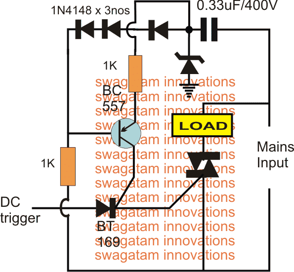 Note: Input AC should be from a Bridge Rectifier
In the concept above, a triac is fired through a small signal SCR controlled by a PNP BJT.
This PNP BJT is configured to execute a zero crossing sensing for the intended safe switching of the triac and the associated load.
Anytime when power is switched ON, the SCR gets its anode supply from the existing DC trigger source, however its gate voltage is switched ON only at the moment when the input transits through its first zero crossing point.
Once the SCR is triggered at the safe zero crossing point, it fires the triac and the connected load, and in turn becomes latched ensuring a continual gate current for the triac.
This kind of switching at the zero crossing points every time power is switched ON ensures a consistent safe switch-ON for the load eliminating all possible dangers that is normally associated with mains sudden power switch ON.
Note: Input AC should be from a Bridge Rectifier
In the concept above, a triac is fired through a small signal SCR controlled by a PNP BJT.
This PNP BJT is configured to execute a zero crossing sensing for the intended safe switching of the triac and the associated load.
Anytime when power is switched ON, the SCR gets its anode supply from the existing DC trigger source, however its gate voltage is switched ON only at the moment when the input transits through its first zero crossing point.
Once the SCR is triggered at the safe zero crossing point, it fires the triac and the connected load, and in turn becomes latched ensuring a continual gate current for the triac.
This kind of switching at the zero crossing points every time power is switched ON ensures a consistent safe switch-ON for the load eliminating all possible dangers that is normally associated with mains sudden power switch ON.


 An accelerometer is a sensory electronic device that measure acceleration deceleration of a moving body or a vibrating body.
Accelerometer comes in surface mount form, looks pretty much like an IC.
Accelerometers are embedded in our Smartphone which tells orientation of the phone, thus your image on your screen rotates accordingly.
Have you ever wondered how you��re racing car on your Smartphone moves left and right when you tilt your phone from left to right? It��s all possible due to accelerometer.
An accelerometer is a sensory electronic device that measure acceleration deceleration of a moving body or a vibrating body.
Accelerometer comes in surface mount form, looks pretty much like an IC.
Accelerometers are embedded in our Smartphone which tells orientation of the phone, thus your image on your screen rotates accordingly.
Have you ever wondered how you��re racing car on your Smartphone moves left and right when you tilt your phone from left to right? It��s all possible due to accelerometer.

 The following explanation can be studied to learn how an accelerometer works
An accelerometer is a Micro-electromechanical system or simply (MEMS).
There are moving parts inside an accelerometer which detect changes in acceleration.
Capacitance is the key concept utilized in an accelerometer.
There are dielectric and metallic plates arranged in parallel manner attached with moving mass.
Three such modules are placed orthogonally each other.
All the parallel plates are capable of moving independently.
Each modules measure at one axis.
When accelerometer is tilted, due to moving mass, alignment of capacitor plates changes which alters the capacitance value.
These changes are measured by built in circuitry and outputs an analogue signal.
The signals from accelerometer can be given to a microcontroller or a microprocessor depending on your design and application.
The following explanation can be studied to learn how an accelerometer works
An accelerometer is a Micro-electromechanical system or simply (MEMS).
There are moving parts inside an accelerometer which detect changes in acceleration.
Capacitance is the key concept utilized in an accelerometer.
There are dielectric and metallic plates arranged in parallel manner attached with moving mass.
Three such modules are placed orthogonally each other.
All the parallel plates are capable of moving independently.
Each modules measure at one axis.
When accelerometer is tilted, due to moving mass, alignment of capacitor plates changes which alters the capacitance value.
These changes are measured by built in circuitry and outputs an analogue signal.
The signals from accelerometer can be given to a microcontroller or a microprocessor depending on your design and application.

 Thank you very much Swag.
I'm not familiar with the characteristics of the TIP122 or the 4N35 so I will get their datasheets and construct the circuit to test.
This may take longer than would be ideal as I have just broken my arm, so soldering is going to be a challenge!
Nonetheless, I am very grateful for your assistance.
I wonder if you have any thoughts on replacing the 18V supply with a capacitive discharge circuit?
I suspect that this will be much more straightforward and I can no doubt find references on the Internet to standard charge/discharge schematics, but if you have any that you have done before, I would be eager to see?
All the best,
Jerry
Hi Jerry,
I think now I am beginning to understand the configuration completely.
Could you specify the voltage level required for the load to fire?
This would help me to design the finalized circuit along with the capacitive discharge stage.
Best Regards.
Swag
Thank you very much Swag.
I'm not familiar with the characteristics of the TIP122 or the 4N35 so I will get their datasheets and construct the circuit to test.
This may take longer than would be ideal as I have just broken my arm, so soldering is going to be a challenge!
Nonetheless, I am very grateful for your assistance.
I wonder if you have any thoughts on replacing the 18V supply with a capacitive discharge circuit?
I suspect that this will be much more straightforward and I can no doubt find references on the Internet to standard charge/discharge schematics, but if you have any that you have done before, I would be eager to see?
All the best,
Jerry
Hi Jerry,
I think now I am beginning to understand the configuration completely.
Could you specify the voltage level required for the load to fire?
This would help me to design the finalized circuit along with the capacitive discharge stage.
Best Regards.
Swag
 Hi Swag,
Thank you once again for your time on this.
You have so much more expertise in analog electronics than I do and have achieved in a few days what I had spent many months puzzling over.
I totally understand your point about detecting the range of the load - this was only an aspiration and the system will not fail to work without it.
I have taken what you have provided and run it through the EasyEDA circuit simulator where it performs exactly as I had hoped - at least with a single circuit.
It indicates that with the potentiometer at 10%, the ADC will see 0.36V when there is an ignitor present, and 0V when it is open, which is what I will require for this to work.
When the ignitor is energized, this goes up to 1.4V which is perfectly safe.
The sensing current isn't even measurable while the firing current looks like 3.2A which will fire anything.
My next task is to simulate multiple independent circuits, up to the 24 I will have in a module, and look for any evidence of crossover.
I have attached the schematic of the circuit and the simulated currents & voltages.
I have ghad to work with what is supported, which is why the simulation uses a different darlington transistor, but I believe - unless you advise me otherwise - that it illustrates the expected behaviour.
V1 incidentally is a 5V square wave with frequency 1Hz, since this allows for simulation of the 5V firing pin going high.
Can you suggest how much of the circuit can be shared between the 24 cues in a module?
The primary supply voltage will, as will any lower voltage supply required to feed the LM7805, and of course a common ground.
Can a single LM7805 be used to provide the input for all of the 4N35s?
I'm guessing that the rest will have to be unique for each cue, which gives me a shopping list, but I would appreciate your thoughts on the construction of a 24 cue module.
Finally, I am still wondering what the options are for adding a capacitive discharge energy source in place of the 18V source?
My understanding is that commercial firing systems will use them because their low internal resistance makes it possible to pass high currents through low resistance ignitors.
Is it correct that a C.D.
source will have lower internal resistance than a battery? Some firing systems may have quite a high fire voltage but this is probably just a consequence of how capacitive discharge works.
18V is as much as is needed, though more will certainly not hurt.
Is a C.D.
source a straightforward thing to add? Would it be possible to add something that would run off 6 x 1.2V rechargeable AA batteries?
If that were possible then that same 7.2V source will happily power both the LM7805 for the firing circuit and the arduino board too.
I feel that would be a pretty perfect solution.
All best wishes,
Jerry
Hi Jerry,
Hi Swag,
Thank you once again for your time on this.
You have so much more expertise in analog electronics than I do and have achieved in a few days what I had spent many months puzzling over.
I totally understand your point about detecting the range of the load - this was only an aspiration and the system will not fail to work without it.
I have taken what you have provided and run it through the EasyEDA circuit simulator where it performs exactly as I had hoped - at least with a single circuit.
It indicates that with the potentiometer at 10%, the ADC will see 0.36V when there is an ignitor present, and 0V when it is open, which is what I will require for this to work.
When the ignitor is energized, this goes up to 1.4V which is perfectly safe.
The sensing current isn't even measurable while the firing current looks like 3.2A which will fire anything.
My next task is to simulate multiple independent circuits, up to the 24 I will have in a module, and look for any evidence of crossover.
I have attached the schematic of the circuit and the simulated currents & voltages.
I have ghad to work with what is supported, which is why the simulation uses a different darlington transistor, but I believe - unless you advise me otherwise - that it illustrates the expected behaviour.
V1 incidentally is a 5V square wave with frequency 1Hz, since this allows for simulation of the 5V firing pin going high.
Can you suggest how much of the circuit can be shared between the 24 cues in a module?
The primary supply voltage will, as will any lower voltage supply required to feed the LM7805, and of course a common ground.
Can a single LM7805 be used to provide the input for all of the 4N35s?
I'm guessing that the rest will have to be unique for each cue, which gives me a shopping list, but I would appreciate your thoughts on the construction of a 24 cue module.
Finally, I am still wondering what the options are for adding a capacitive discharge energy source in place of the 18V source?
My understanding is that commercial firing systems will use them because their low internal resistance makes it possible to pass high currents through low resistance ignitors.
Is it correct that a C.D.
source will have lower internal resistance than a battery? Some firing systems may have quite a high fire voltage but this is probably just a consequence of how capacitive discharge works.
18V is as much as is needed, though more will certainly not hurt.
Is a C.D.
source a straightforward thing to add? Would it be possible to add something that would run off 6 x 1.2V rechargeable AA batteries?
If that were possible then that same 7.2V source will happily power both the LM7805 for the firing circuit and the arduino board too.
I feel that would be a pretty perfect solution.
All best wishes,
Jerry
Hi Jerry,
 The characteristic effective resistances of brand new Energizer alkaline cylindrical batteries (through a 5 mA stabilization drain and immediately with a 505 mA, 100 millisecond pulse) could be expected to be around 150 to 300 milliohms, as determined by the relative dimension.
 The same process applies for this set up too, as was done with the above explained boost converter design.
As can be seen the output stage is now altered with a buck converter set up, the transistors are now replaced with PNP types and the positions of the inductor, diode changed appropriately.
Thus, by using the above two methods anybody can determine or calculate inductors in buck boost smps circuits without using complex and unfeasible formulas.
The same process applies for this set up too, as was done with the above explained boost converter design.
As can be seen the output stage is now altered with a buck converter set up, the transistors are now replaced with PNP types and the positions of the inductor, diode changed appropriately.
Thus, by using the above two methods anybody can determine or calculate inductors in buck boost smps circuits without using complex and unfeasible formulas.
 ) can be deduced with the help of the following expression
Vi - Vo = LdI/dt
Also, the current variations (
) can be deduced with the help of the following expression
Vi - Vo = LdI/dt
Also, the current variations ( The current with the aid of the resistive divider could perhaps be about one hundred times as massive as the feedback bias current:
I(r1/2) > or = 100 x I(fb) ---------- (9)
I(r1/2) = current in the course of the resistive divider to GND
I(fb) = feedback bias current from data sheet
This augments below 1% inaccuracy to the voltage evaluation.
The current is additionally considerably larger.
The main problem with smaller resistor values is an increased power loss in the resistive divider, except the relevancy might be somewhat elevated.
With the above conviction, the resistors are worked out as listed below:
R2 = V(fb) / I(r1/2) ---------- (10)
R1 = R2 x [Vout / V(fb) - 1] ---------- (11)
R1, R2 = resistive divider.
V(fb) = feedback voltage from the data sheet
I(r1/2) = current due to the resistive divider to GND, established in Equation 9
Vout = planned output voltage
The current with the aid of the resistive divider could perhaps be about one hundred times as massive as the feedback bias current:
I(r1/2) > or = 100 x I(fb) ---------- (9)
I(r1/2) = current in the course of the resistive divider to GND
I(fb) = feedback bias current from data sheet
This augments below 1% inaccuracy to the voltage evaluation.
The current is additionally considerably larger.
The main problem with smaller resistor values is an increased power loss in the resistive divider, except the relevancy might be somewhat elevated.
With the above conviction, the resistors are worked out as listed below:
R2 = V(fb) / I(r1/2) ---------- (10)
R1 = R2 x [Vout / V(fb) - 1] ---------- (11)
R1, R2 = resistive divider.
V(fb) = feedback voltage from the data sheet
I(r1/2) = current due to the resistive divider to GND, established in Equation 9
Vout = planned output voltage
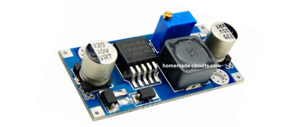
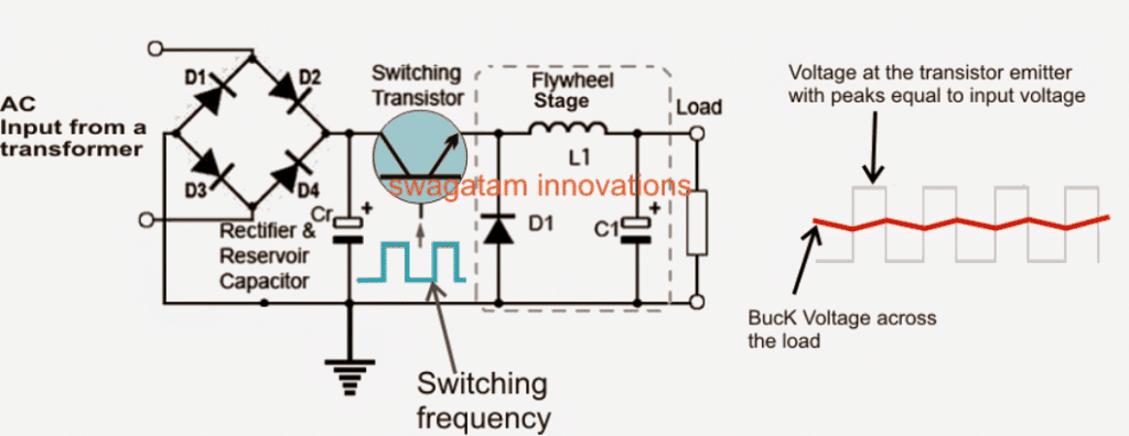
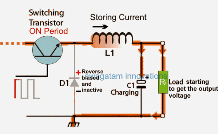
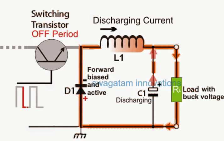
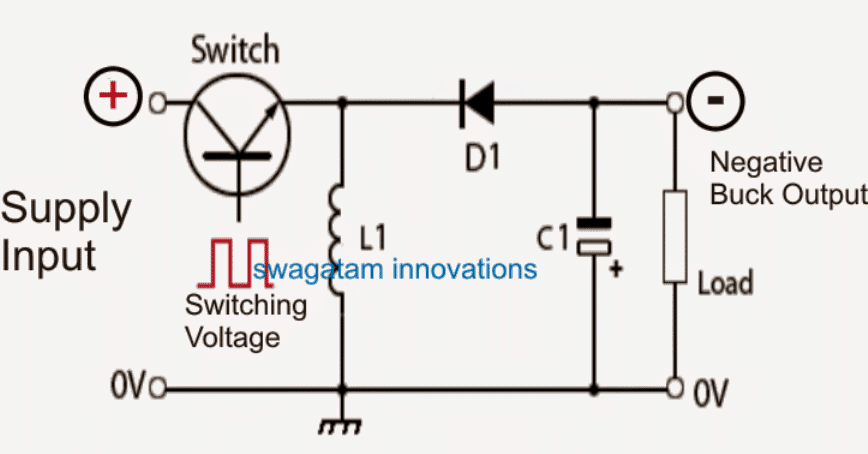


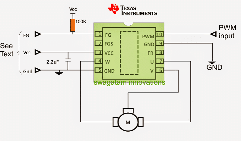 The above image shows the simple layout of the circuit which apparently includes nothing but the IC itself.
The various pinouts are allocated for carrying out the specified functions such as PWM speed control of the motor, direction control, etc by simply feeding the relevant pinouts with the specified datas from an external source.
The following image shows the package of the chip, which looks like a 10 pin DIL IC, the various pinout functions of the same may be studied from the data as furnished under the diagram:
The above image shows the simple layout of the circuit which apparently includes nothing but the IC itself.
The various pinouts are allocated for carrying out the specified functions such as PWM speed control of the motor, direction control, etc by simply feeding the relevant pinouts with the specified datas from an external source.
The following image shows the package of the chip, which looks like a 10 pin DIL IC, the various pinout functions of the same may be studied from the data as furnished under the diagram:
 Referring to the circuit diagram of the proposed sensorless BLDC driver circuit as presented in the previous article and also the chip image above, the pinouts details may be understood as follows:
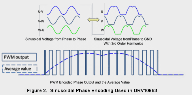 This coding strategy streamlines the driver specifications for the reason that there will probably often be one phase output that could be on par with zero.
The outcome amplitude varies according to the supply voltage (VCC) and the mandated PWM duty cycle (PWM) as defined in Equation 1 and highlighted in Figure 3. The optimum amplitude is implemented once the instructed PWM duty cycle is 100 PERCENT.
Vphpk = PWMdc > < VCC
This coding strategy streamlines the driver specifications for the reason that there will probably often be one phase output that could be on par with zero.
The outcome amplitude varies according to the supply voltage (VCC) and the mandated PWM duty cycle (PWM) as defined in Equation 1 and highlighted in Figure 3. The optimum amplitude is implemented once the instructed PWM duty cycle is 100 PERCENT.
Vphpk = PWMdc > < VCC
 The motor speed is regulated not directly through the use of the PWM order to regulate the amplitude of the phase voltages that happen to be used for the motor.
The duty cycle of PWM input is modified into a 9 bit digital quantity (from 0 to 511).
The regulation resolution is 1/512 == 0.2%.
The duty cycle analyzer facilitates an initial order exchange operation amongst the input duty cycle and the 9 bits digital figure.
This is highlighted in Figure 4, in which r=80 ms.
The motor speed is regulated not directly through the use of the PWM order to regulate the amplitude of the phase voltages that happen to be used for the motor.
The duty cycle of PWM input is modified into a 9 bit digital quantity (from 0 to 511).
The regulation resolution is 1/512 == 0.2%.
The duty cycle analyzer facilitates an initial order exchange operation amongst the input duty cycle and the 9 bits digital figure.
This is highlighted in Figure 4, in which r=80 ms.
 The exchange performance between the PWM ordered duty cycle along with the output maximum amplitude is variable in the DRV10963 device.
The outcome maximum amplitude is discussed by Equation 1 when PWM command > minimum functioning duty cycle.
The lowest operation duty cycle often is established to possibly 13%, 10%, 5% or no restriction by OTP setting (MINOP_DC1:0).
Table 1 demonstrates the recommended configurations for the minimal operation duty cycle.
Whenever the PWM instructed duty cycle is less than lowest functioning duty cycle and more than 1.5%, the output is going to be regulated at the minimal operation duty cycle.
Any time the input duty cycle is under a 1.5%, the DRV10963 device will likely not run the output, and is sent to the standby mode.
This can be illustrated in Figure 6.
The exchange performance between the PWM ordered duty cycle along with the output maximum amplitude is variable in the DRV10963 device.
The outcome maximum amplitude is discussed by Equation 1 when PWM command > minimum functioning duty cycle.
The lowest operation duty cycle often is established to possibly 13%, 10%, 5% or no restriction by OTP setting (MINOP_DC1:0).
Table 1 demonstrates the recommended configurations for the minimal operation duty cycle.
Whenever the PWM instructed duty cycle is less than lowest functioning duty cycle and more than 1.5%, the output is going to be regulated at the minimal operation duty cycle.
Any time the input duty cycle is under a 1.5%, the DRV10963 device will likely not run the output, and is sent to the standby mode.
This can be illustrated in Figure 6.
 The motor initialization graph consists of device configurable alternatives for open loop to close loop changeover limit (HOW.), align time (TAHQH), and accelerate rate (RACE).
To line up the rotor to the commutation logic the DRV10963 executes an x% duty cycle on phases V and W at the same time controlling phase U at GND.
This scenario is sustained for TAIign seconds.
The x% significance is identified by the VCC voltage (as shown in Table 2) to keep up ample rotational torque over various different supply voltages.
As the align sequence accomplishes, the motor is forced to speed up by putting on sinusoidal phase voltages with peak levels as illustrated in Table 2 and boosting by means of the commutation range at an expanding rate represented by RACE until the level of commutation grows to Hom., Hz.
AS soon as this limit is arrived at, the DRV��l0963 converts to closed loop mode whereby the commutation drive progression is recognized by the in-built control algorithm while the employed voltage is identified by the PWM mandated duty cycle input.
The open loop to close loop changeover limit (Hom), align time (TAHQH), and the accelerate rate (RACE) are configurable through OTP configurations.
The selection of handoff threshold (HOW,) are typically approved by trial and error assessment.
The objective would be to prefer a handoff tolerance that could be as little as feasible and enables the motor to effortlessly and faithfully changeover between the open loop acceleration and the closed loop acceleration.
Commonly increased speed motors (maximum speed) necessitate a superior handoff tolerance due to the fact elevated speed motors comprise decreased Kt hence more affordable BEMF.
Table 3 demonstrates the configurable preferences for the handoff tolerance.
Highest speed in electrical Hz are proven as a reference to help out with choosing the desirable handoff speed for a specific submission.
The motor initialization graph consists of device configurable alternatives for open loop to close loop changeover limit (HOW.), align time (TAHQH), and accelerate rate (RACE).
To line up the rotor to the commutation logic the DRV10963 executes an x% duty cycle on phases V and W at the same time controlling phase U at GND.
This scenario is sustained for TAIign seconds.
The x% significance is identified by the VCC voltage (as shown in Table 2) to keep up ample rotational torque over various different supply voltages.
As the align sequence accomplishes, the motor is forced to speed up by putting on sinusoidal phase voltages with peak levels as illustrated in Table 2 and boosting by means of the commutation range at an expanding rate represented by RACE until the level of commutation grows to Hom., Hz.
AS soon as this limit is arrived at, the DRV��l0963 converts to closed loop mode whereby the commutation drive progression is recognized by the in-built control algorithm while the employed voltage is identified by the PWM mandated duty cycle input.
The open loop to close loop changeover limit (Hom), align time (TAHQH), and the accelerate rate (RACE) are configurable through OTP configurations.
The selection of handoff threshold (HOW,) are typically approved by trial and error assessment.
The objective would be to prefer a handoff tolerance that could be as little as feasible and enables the motor to effortlessly and faithfully changeover between the open loop acceleration and the closed loop acceleration.
Commonly increased speed motors (maximum speed) necessitate a superior handoff tolerance due to the fact elevated speed motors comprise decreased Kt hence more affordable BEMF.
Table 3 demonstrates the configurable preferences for the handoff tolerance.
Highest speed in electrical Hz are proven as a reference to help out with choosing the desirable handoff speed for a specific submission.
 The choice of align time (TAHQH) and accelerate rate (RACE) can even be contingent on trial and error examination.
Motors with greater inertia normally demand an extended align time and a more sluggish speed up rate in contrast to motors with low inertia that commonly demand a briefer align time together with a speedier accelerate percentage.
Program tradeoffs needs to be implemented to capitalize on launch stability as opposed to rotate up period.
TI endorses starting with deciding on the less intense configurations (slower RACE and significant Tmign) to compromise the torque up time in support of maximum fulfillment rate.
As soon as the equipment is confirmed to perform conscientiously the extra forceful configurations (greater RACC and lesser TAHQH) may be used to diminish the turn up moment and at the same time cautiously keeping track of the fulfillment rate.
Table 4 exhibits the configurable settings for TA"g,, and RACE.
The choice of align time (TAHQH) and accelerate rate (RACE) can even be contingent on trial and error examination.
Motors with greater inertia normally demand an extended align time and a more sluggish speed up rate in contrast to motors with low inertia that commonly demand a briefer align time together with a speedier accelerate percentage.
Program tradeoffs needs to be implemented to capitalize on launch stability as opposed to rotate up period.
TI endorses starting with deciding on the less intense configurations (slower RACE and significant Tmign) to compromise the torque up time in support of maximum fulfillment rate.
As soon as the equipment is confirmed to perform conscientiously the extra forceful configurations (greater RACC and lesser TAHQH) may be used to diminish the turn up moment and at the same time cautiously keeping track of the fulfillment rate.
Table 4 exhibits the configurable settings for TA"g,, and RACE.
 The remaining part of the explanation regarding this sensorless BLDC IC is furnished in this original datasheet
Please feel free to comment to know more regarding the above discussed sensorless BLDC motor driver circuit details
The remaining part of the explanation regarding this sensorless BLDC IC is furnished in this original datasheet
Please feel free to comment to know more regarding the above discussed sensorless BLDC motor driver circuit details
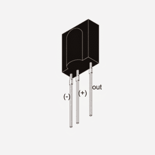 NOTE: The pinout polarity is different for the TSOP1838 IR detector, as shown below.
So please verify the pinout sequence if you are using a different variant of the IC.
NOTE: The pinout polarity is different for the TSOP1838 IR detector, as shown below.
So please verify the pinout sequence if you are using a different variant of the IC.
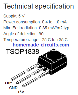
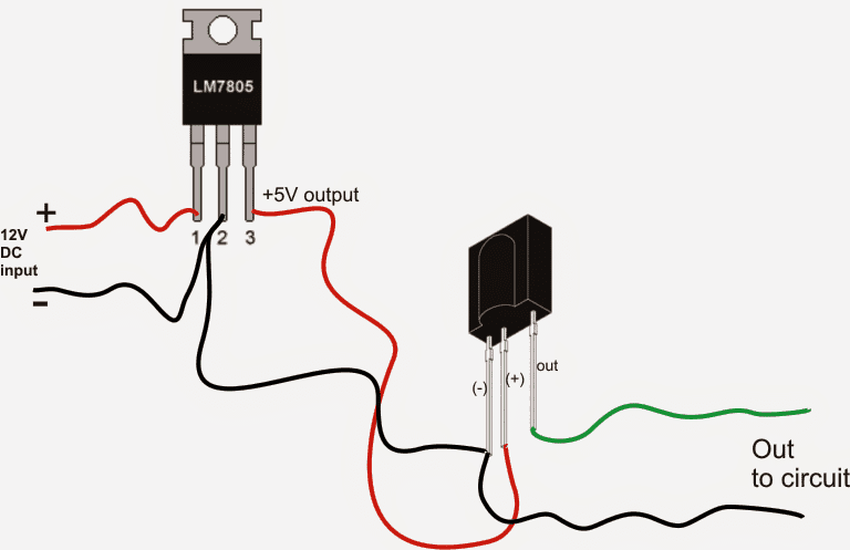
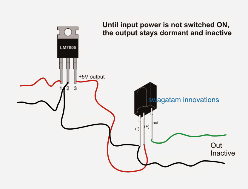 In the above diagram we see that as long as the supply input is not connected to the TSOP circuit, its output stays dormant or inactive, meaning it's neither positive nor negative.
 Video Clip
 Simplified Design
 A less costly alternative to many of the other the eye-wateringly expensive isolators also shown on EBay might be really useful.
Might this be a useful DIY project for the pages of Homemade Circuit Projects?
Thank you, John Waterman
A less costly alternative to many of the other the eye-wateringly expensive isolators also shown on EBay might be really useful.
Might this be a useful DIY project for the pages of Homemade Circuit Projects?
Thank you, John Waterman
 When this SPWM consisting of growing and shrinking pulse widths is applied to a transformer, the output from the transformer transforms this SPWM into an analogue equivalent which closely replicates an analogue sine waveform.
The easiest known method of generating a sinewaver PWM (SPWM), is by feeding a couple of exponentially varying signals to the input of an opamp for the required processing.
Among the two input signals one needs to be much higher in its frequency compared to the other.
The IC 555 can also be used effectively for generating sine equivalent PWMs, by incorporating its built-in opamps and an R/C triangle ramp generator circuit.
The following discussion will help you to understand the entire procedure.
New hobbyists and even the professionals will now find it quite easy to understand regarding how sine wave PWMs (SPWM) are implemented by processing a couple of signals by using an opamp, let's figure it out with the help of the following diagram, and simulation.
When this SPWM consisting of growing and shrinking pulse widths is applied to a transformer, the output from the transformer transforms this SPWM into an analogue equivalent which closely replicates an analogue sine waveform.
The easiest known method of generating a sinewaver PWM (SPWM), is by feeding a couple of exponentially varying signals to the input of an opamp for the required processing.
Among the two input signals one needs to be much higher in its frequency compared to the other.
The IC 555 can also be used effectively for generating sine equivalent PWMs, by incorporating its built-in opamps and an R/C triangle ramp generator circuit.
The following discussion will help you to understand the entire procedure.
New hobbyists and even the professionals will now find it quite easy to understand regarding how sine wave PWMs (SPWM) are implemented by processing a couple of signals by using an opamp, let's figure it out with the help of the following diagram, and simulation.
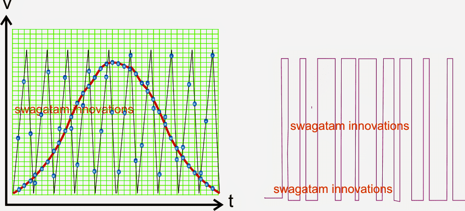
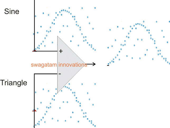 Here we can witness the above explanation being implemented practically, and this is quite how the opamp would be executing the same (although at a much fater rate, in ms).
The upper figure shows a slightly more accurate SPWM depiction than the second scrolling diagram, this is because in the first figure I had the comfort of the graph layout in the background whereas in the second simulated diagram I had to plot the same without the help of the graph coordinates, therefore I might have missed a few of the coinciding points and therefore the outputs looks a little inaccurate compared to the first one.
Nevertheless, the operation is quite evident and distinctly brings out how an opamp is supposed to process a PWM sine wave by comparing two simultaneously varying signals at its inputs as explained in the previous sections.
Actually an opamp would process the sine wave PWMs much more accurately than the above shown simulation, may be a 100 times better, producing a extremely uniform and well dimensioned PWMs corresponding to the fed sample.
sinewave.
Here we can witness the above explanation being implemented practically, and this is quite how the opamp would be executing the same (although at a much fater rate, in ms).
The upper figure shows a slightly more accurate SPWM depiction than the second scrolling diagram, this is because in the first figure I had the comfort of the graph layout in the background whereas in the second simulated diagram I had to plot the same without the help of the graph coordinates, therefore I might have missed a few of the coinciding points and therefore the outputs looks a little inaccurate compared to the first one.
Nevertheless, the operation is quite evident and distinctly brings out how an opamp is supposed to process a PWM sine wave by comparing two simultaneously varying signals at its inputs as explained in the previous sections.
Actually an opamp would process the sine wave PWMs much more accurately than the above shown simulation, may be a 100 times better, producing a extremely uniform and well dimensioned PWMs corresponding to the fed sample.
sinewave.
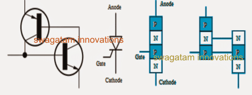 The two transistor equivalent circuit shows that the collector current of the NPN transistor TR2 feeds directly into the base of the PNP transistor TR1, while the collector current of TR1 feeds into the base of TR2.
These two inter-connected transistors rely upon each other for conduction as each transistor gets its base-emitter current from the other��s collector-emitter current.
So until one of the transistors is given some base current nothing can happen even if an Anode-to-Cathode voltage is present.
Simulating the SCR topology with a two transistor integration reveals the formation to be in a manner such that the collector current of the NPN transistor is supplying straight to the base of the PNP transistor TR1, while the collector current of TR1 is connecting the supply with the base of TR2.
The simulated two transistor configuration seem to interlock and complement each others conduction by receiving the base drive from the collector emitter current of the other, this makes the gate voltage very crucial and ensures that the shown configuration can never conduct until a gate potential is applied, even in the presence of the anode to cathode potential may be persistent.
In a situation when the device's anode lead is more negative than its cathode, allows the N-P junction to remain forward biased, but ensuring the outer P-N junctions to be reverse biased such that it acts like a standard rectifier diode.
This property of an SCR enables it to block a reverse current flow, until a significantly high magnitude of voltage which may be beyond its beak down specs is inflicted across the mentioned leads, which forces the SCR to conduct even in the absence of a gate drive.
The above refers to a critical characteristics of thyristors which can causes the device to get triggered undesirably through a reverse high voltage spike and/or an high temperature, or a rapidly increasingly dv/dt voltage transient.
Now suppose in a situation where the Anode terminal experiences more positive with regards to its cathode lead, this helps the outer P-N junction to become forward biased, although the central N-P junction continues to remain reverse biased.
This consequently ensures that the forward current is also blocked.
Therefore in case a positive signal induced across the base of the NPN transistor TR2 results the passage of the collector current towards the base f TR1, which in trun forces the collector current to pass towards the PNP transistor TR1 boosting the base drive of TR2 and the process gets reinforced.
The two transistor equivalent circuit shows that the collector current of the NPN transistor TR2 feeds directly into the base of the PNP transistor TR1, while the collector current of TR1 feeds into the base of TR2.
These two inter-connected transistors rely upon each other for conduction as each transistor gets its base-emitter current from the other��s collector-emitter current.
So until one of the transistors is given some base current nothing can happen even if an Anode-to-Cathode voltage is present.
Simulating the SCR topology with a two transistor integration reveals the formation to be in a manner such that the collector current of the NPN transistor is supplying straight to the base of the PNP transistor TR1, while the collector current of TR1 is connecting the supply with the base of TR2.
The simulated two transistor configuration seem to interlock and complement each others conduction by receiving the base drive from the collector emitter current of the other, this makes the gate voltage very crucial and ensures that the shown configuration can never conduct until a gate potential is applied, even in the presence of the anode to cathode potential may be persistent.
In a situation when the device's anode lead is more negative than its cathode, allows the N-P junction to remain forward biased, but ensuring the outer P-N junctions to be reverse biased such that it acts like a standard rectifier diode.
This property of an SCR enables it to block a reverse current flow, until a significantly high magnitude of voltage which may be beyond its beak down specs is inflicted across the mentioned leads, which forces the SCR to conduct even in the absence of a gate drive.
The above refers to a critical characteristics of thyristors which can causes the device to get triggered undesirably through a reverse high voltage spike and/or an high temperature, or a rapidly increasingly dv/dt voltage transient.
Now suppose in a situation where the Anode terminal experiences more positive with regards to its cathode lead, this helps the outer P-N junction to become forward biased, although the central N-P junction continues to remain reverse biased.
This consequently ensures that the forward current is also blocked.
Therefore in case a positive signal induced across the base of the NPN transistor TR2 results the passage of the collector current towards the base f TR1, which in trun forces the collector current to pass towards the PNP transistor TR1 boosting the base drive of TR2 and the process gets reinforced.
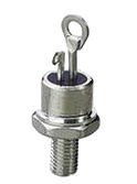 The above condition allows the two transistors to enhance their conduction until the point of saturation owing to their shown regenerative configuration feedback loop which keeps the situation interlocked and latched.
Thus as soon as the SCR is triggered, it allows a current to flow from its anode to cathode with only a minimal forward resistance of around coming in the path, ensuring an efficient conduction and operation of the device..
When subjected to an AC, the SCR may block both the cyles of the AC until the SCR is offered with a triggering voltage across its gate and cathode, which instantly allows the positive half cycle of the AC to pass across the anode cathode leads, and the device begins imitating a standard rectifier diode, but only as long as the gate trigger stays switched ON, the conduction breaks the moment gate trigger is removed.
The enforced voltage-current or I-V characteristics curves for the activation of a silicon controlled rectifier may be witnessed in the following image:
The above condition allows the two transistors to enhance their conduction until the point of saturation owing to their shown regenerative configuration feedback loop which keeps the situation interlocked and latched.
Thus as soon as the SCR is triggered, it allows a current to flow from its anode to cathode with only a minimal forward resistance of around coming in the path, ensuring an efficient conduction and operation of the device..
When subjected to an AC, the SCR may block both the cyles of the AC until the SCR is offered with a triggering voltage across its gate and cathode, which instantly allows the positive half cycle of the AC to pass across the anode cathode leads, and the device begins imitating a standard rectifier diode, but only as long as the gate trigger stays switched ON, the conduction breaks the moment gate trigger is removed.
The enforced voltage-current or I-V characteristics curves for the activation of a silicon controlled rectifier may be witnessed in the following image:
 However For a DC input, as soon as the thyristor is triggered ON, due to the explained regenerative conduction it undergoes a latching action such that the anode to cathode conduction holds on and keeps conducting even if the gate trigger is removed.
Thus for a DC power the gate completely loses its influence once the first triggering pulse is applied across the gate of the device ensuring a latched current from its anode to cathode.
It may be broken by momentarily breaking the anode/cathode current source while the gate is completely inactive.
However For a DC input, as soon as the thyristor is triggered ON, due to the explained regenerative conduction it undergoes a latching action such that the anode to cathode conduction holds on and keeps conducting even if the gate trigger is removed.
Thus for a DC power the gate completely loses its influence once the first triggering pulse is applied across the gate of the device ensuring a latched current from its anode to cathode.
It may be broken by momentarily breaking the anode/cathode current source while the gate is completely inactive.
 At the outset of each positive half-cycle the SCR is ��OFF��.
On the induction of the gate voltage activates the SCR into conduction and allows it to be entirely latched ��ON�� throughout the positive half cycle.
When the thyristor is switched on at the start of the half-cycle (�� = 0o), the connected load (a lamp or any similar) would be ��ON�� for the whole positive cycle of the AC waveform (half-wave rectified AC) at an elevated average voltage of 0.318 x Vp.
As the initialization of the gate switch ON is raised along the half cycle (�� = 0o to 90o), the connected lamp is lighted for a smaller amount time and the net voltage brought to the lamp likewise proportionally less dropping its intensity.
Subsequently it is easy to exploit a silicon controlled rectifier as an AC light dimmer and in many different additional AC power applications for example: AC motor-speed control, heat control devices and power regulator circuits, and so on.
Up till now we have witnessed that a thyristor is fundamentally a half-wave device that is able to pass current in only the positive half of the cycle whenever the Anode is positive and prevents current flow just like a diode in cases where the Anode is negative, even if the gate current remains active.
Nevertheless you may find many more variants of similar semiconductor products to choose from which originate under the title of ��Thyristor�� designed to operate in both directions of the half cycles, full-wave units, or could be switched ��OFF�� by the Gate signal.
This kind of products incorporate ��Gate Turn-OFF Thyristors�� (GTO), ��Static Induction Thyristors�� (SITH), ��MOS Controlled Thyristors�� (MCT), ��Silicon Controlled Switch�� (SCS), ��Triode Thyristors�� (TRIAC) and ��Light Triggered Thyristors�� (LASCR) to identify a few, with so many of these devices accessible in many different voltage and current ratings which makes them interesting to be used in purposes at very high power levels.
At the outset of each positive half-cycle the SCR is ��OFF��.
On the induction of the gate voltage activates the SCR into conduction and allows it to be entirely latched ��ON�� throughout the positive half cycle.
When the thyristor is switched on at the start of the half-cycle (�� = 0o), the connected load (a lamp or any similar) would be ��ON�� for the whole positive cycle of the AC waveform (half-wave rectified AC) at an elevated average voltage of 0.318 x Vp.
As the initialization of the gate switch ON is raised along the half cycle (�� = 0o to 90o), the connected lamp is lighted for a smaller amount time and the net voltage brought to the lamp likewise proportionally less dropping its intensity.
Subsequently it is easy to exploit a silicon controlled rectifier as an AC light dimmer and in many different additional AC power applications for example: AC motor-speed control, heat control devices and power regulator circuits, and so on.
Up till now we have witnessed that a thyristor is fundamentally a half-wave device that is able to pass current in only the positive half of the cycle whenever the Anode is positive and prevents current flow just like a diode in cases where the Anode is negative, even if the gate current remains active.
Nevertheless you may find many more variants of similar semiconductor products to choose from which originate under the title of ��Thyristor�� designed to operate in both directions of the half cycles, full-wave units, or could be switched ��OFF�� by the Gate signal.
This kind of products incorporate ��Gate Turn-OFF Thyristors�� (GTO), ��Static Induction Thyristors�� (SITH), ��MOS Controlled Thyristors�� (MCT), ��Silicon Controlled Switch�� (SCS), ��Triode Thyristors�� (TRIAC) and ��Light Triggered Thyristors�� (LASCR) to identify a few, with so many of these devices accessible in many different voltage and current ratings which makes them interesting to be used in purposes at very high power levels.
 Image courtesy: commons.wikimedia.org/wiki/File:Mosquito_Tasmania_crop.jpg
 In the above image we can see a straight line at the 9V level, this is achieved because the 9V level in not changing with respect to time and therefore we are able to witness a straight line.
Now if this 9V is switched ON and OFF after every 1 second, then the above graph would look this this:
In the above image we can see a straight line at the 9V level, this is achieved because the 9V level in not changing with respect to time and therefore we are able to witness a straight line.
Now if this 9V is switched ON and OFF after every 1 second, then the above graph would look this this:
 We can clearly see that now the 9V line is no longer a straight line rater in the form of blocks after every 1 second, since the 9V is switched ON and OFF after every second alternately.
The above traces look like rectangle blocks because when the 9V is switched ON and OFF the operations are instant which suddenly makes the 9V to go to zero level and then suddenly to the 9V level thereby forming the rectangular shapes on the graph.
The above condition gives rise to a pulsating voltage which has two parameters to be measured namely: the peak voltage and the average voltage or the RMS voltage.
We can clearly see that now the 9V line is no longer a straight line rater in the form of blocks after every 1 second, since the 9V is switched ON and OFF after every second alternately.
The above traces look like rectangle blocks because when the 9V is switched ON and OFF the operations are instant which suddenly makes the 9V to go to zero level and then suddenly to the 9V level thereby forming the rectangular shapes on the graph.
The above condition gives rise to a pulsating voltage which has two parameters to be measured namely: the peak voltage and the average voltage or the RMS voltage.
 In this example the PWMs are optimized to produce a peak voltage of 9V but an average voltage of 3.15V since the ON time is just 35% of one full complete ON/OFF cycle.
One complete cycle refers to the time period which allows the given pulse to complete its one full ON time and one OFF time.
Similarly one may intend to optimize the pulse width of a frequency with the following data:
In this example the PWMs are optimized to produce a peak voltage of 9V but an average voltage of 3.15V since the ON time is just 35% of one full complete ON/OFF cycle.
One complete cycle refers to the time period which allows the given pulse to complete its one full ON time and one OFF time.
Similarly one may intend to optimize the pulse width of a frequency with the following data:
 Here the ON time can be seen increased than the OFF time by 65% across one full cycle, therefore here the average value of the voltage becomes 5.85V.
The above discussed average voltage is also called the RMS or the root mean square value of the voltage.
Since these are all rectangular or square pulses, the RMS can be calculated simply by multiplying the duty cycle percentage with the peak voltage.
Here the ON time can be seen increased than the OFF time by 65% across one full cycle, therefore here the average value of the voltage becomes 5.85V.
The above discussed average voltage is also called the RMS or the root mean square value of the voltage.
Since these are all rectangular or square pulses, the RMS can be calculated simply by multiplying the duty cycle percentage with the peak voltage.
 As we can see in the above image the width of the pulses are changing with regard to the instantaneous level of the sine wave.
As the sine wave tends to reach the peak, the corresponding width of the pulse becomes wider and vice versa.
As we can see in the above image the width of the pulses are changing with regard to the instantaneous level of the sine wave.
As the sine wave tends to reach the peak, the corresponding width of the pulse becomes wider and vice versa.
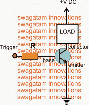
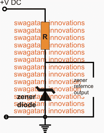
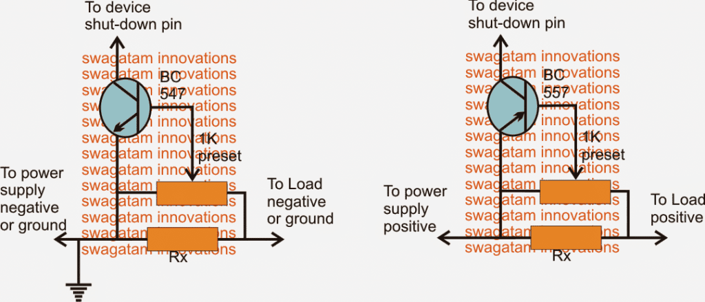
 Figure 1.Villard circuit
Essentially, the Villard circuit is a form of diode clamp circuit.
The negative high cycles are used in order to charge the capacitor to the AC peak voltage (Vpk).
The AC waveform as the input along with the capacitor��s steady DC��s superposition forms the output.
The waveform��s DC value is shifted by using the effect of the circuit on it.
Since the diode clamps the AC waveform��s negative peaks to the value of 0V (in actual terms it is �CVF, which is the small forward bias voltage of the diode); the output waveform��s positive peaks are of the value of 2Vpk.
The peak-to-peak is difficult to smoothen since it is of enormous size of the value of 2Vpk and thus it can be smoothed only when the circuit is transformed into any other more sophisticated forms in an effective manner.
The negative high voltage is supplied to the magnetron by using this circuit (which consists of diode in reverse form) in a microwave oven.
Figure 1.Villard circuit
Essentially, the Villard circuit is a form of diode clamp circuit.
The negative high cycles are used in order to charge the capacitor to the AC peak voltage (Vpk).
The AC waveform as the input along with the capacitor��s steady DC��s superposition forms the output.
The waveform��s DC value is shifted by using the effect of the circuit on it.
Since the diode clamps the AC waveform��s negative peaks to the value of 0V (in actual terms it is �CVF, which is the small forward bias voltage of the diode); the output waveform��s positive peaks are of the value of 2Vpk.
The peak-to-peak is difficult to smoothen since it is of enormous size of the value of 2Vpk and thus it can be smoothed only when the circuit is transformed into any other more sophisticated forms in an effective manner.
The negative high voltage is supplied to the magnetron by using this circuit (which consists of diode in reverse form) in a microwave oven.
 Figure 2. Greinacher circuit
The Villard cell stage is followed by the circuit in order to work by using an envelope detector stage or a peak detector.
The effect of the peak detector is such that much of the ripple is removed while the output of the peak voltage is preserved as such.
Heinrich Greinacher was the first person to invent this circuit in 1913 (which was published in 1914) in order to provide the voltage of 200-300V which was needed by him for his ionometer which was again a new invention by him.
The requirement of inventing this circuit to get that much voltage arose because the power supplied by the Zurich power stations was of only 110V AC and thus was insufficient.
Heinrich developed this idea more in 1920 and extended it to make a cascade of multipliers.
Most of the times, people refer this cascade of multipliers invented by Heinrich Greinacher as a Villard cascade which is inaccurate and not true.
This cascade of multipliers is also known as Cockroft-Walton after the scientists John Cockroft and Ernest Walton who had built the particle accelerator machine and had rediscovered the circuit independently in 1932.
The use of two Greinacher cells which have polarities opposite to each other but being driven from the same AC source can extend the concept of this kind of topology to a voltage quadrupler circuit.
The two individual outputs are used in order to take down the output across them.
The grounding of the input and output simultaneously in this circuit is quite impossible as is the case with a bridge circuit.
Figure 2. Greinacher circuit
The Villard cell stage is followed by the circuit in order to work by using an envelope detector stage or a peak detector.
The effect of the peak detector is such that much of the ripple is removed while the output of the peak voltage is preserved as such.
Heinrich Greinacher was the first person to invent this circuit in 1913 (which was published in 1914) in order to provide the voltage of 200-300V which was needed by him for his ionometer which was again a new invention by him.
The requirement of inventing this circuit to get that much voltage arose because the power supplied by the Zurich power stations was of only 110V AC and thus was insufficient.
Heinrich developed this idea more in 1920 and extended it to make a cascade of multipliers.
Most of the times, people refer this cascade of multipliers invented by Heinrich Greinacher as a Villard cascade which is inaccurate and not true.
This cascade of multipliers is also known as Cockroft-Walton after the scientists John Cockroft and Ernest Walton who had built the particle accelerator machine and had rediscovered the circuit independently in 1932.
The use of two Greinacher cells which have polarities opposite to each other but being driven from the same AC source can extend the concept of this kind of topology to a voltage quadrupler circuit.
The two individual outputs are used in order to take down the output across them.
The grounding of the input and output simultaneously in this circuit is quite impossible as is the case with a bridge circuit.
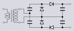 Figure 3.Voltage quadrupler �C two Greinacher cells of opposite polarities
There are many safety hazards and issues associated with the generation of voltages of more than 5kV along with being highly uneconomic in a transformer mostly in the equipment which are domestic equipment.
But an e.h.t.
of 10kV is a basic requirement of the television sets which are black and white while the colour television sets require even more e.h.t.
There are different ways and means by which the e.h.t.
of such dimensions are achieved such as: doubling the voltage on the mains transformer within an e.h.t winding on it by using voltage doublers; or by applying the voltage doublers to the waveform on the line flyback coils.
The two peak detectors consisting of half-wave within a circuit are functionally similar to the peak detector cells found in the Greinacher circuit.
The half-cycles which are opposite to each other of the incoming waveform are used for operating by each of the two peak detector cells.
The output is always found to be double of the peak input voltage since the outputs produced by them are in series.
Figure 3.Voltage quadrupler �C two Greinacher cells of opposite polarities
There are many safety hazards and issues associated with the generation of voltages of more than 5kV along with being highly uneconomic in a transformer mostly in the equipment which are domestic equipment.
But an e.h.t.
of 10kV is a basic requirement of the television sets which are black and white while the colour television sets require even more e.h.t.
There are different ways and means by which the e.h.t.
of such dimensions are achieved such as: doubling the voltage on the mains transformer within an e.h.t winding on it by using voltage doublers; or by applying the voltage doublers to the waveform on the line flyback coils.
The two peak detectors consisting of half-wave within a circuit are functionally similar to the peak detector cells found in the Greinacher circuit.
The half-cycles which are opposite to each other of the incoming waveform are used for operating by each of the two peak detector cells.
The output is always found to be double of the peak input voltage since the outputs produced by them are in series.
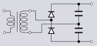 Figure 4. Bridge (Delon) voltage doubler
 Figure 5.
Switched capacitor voltage doubler achieved by simply switching charged capacitors from parallel to seriesThese types of circuits are known as switched capacitor circuits.
The applications which are powered by low voltage are the applications which especially use this approach since integrated circuits have a requirement of a supply of specific amount of voltage which is more than what the battery can actually deliver or produce.
In most of the cases, there is always an availability of a clock signal on board of the integrated circuit and thus this makes it unnecessary to have any other additional circuitry or only little circuitry is needed to generate it.
Thus, the diagram in Figure 5 displays schematically the simplest form of switched capacitor configuration.
In this diagram, there are two capacitors which have been charged to the same voltage simultaneously in a parallel.
Post this; capacitors are switched into series after switching off the supply.
Thus, the output voltage produced is twice the supply or input voltage in case the output is derived from the two capacitors in series.
There are various different kinds of switching devices which can be used in such circuits, but MOSFET devices are the most frequently used switching devices in the case of integrated circuits.
Figure 5.
Switched capacitor voltage doubler achieved by simply switching charged capacitors from parallel to seriesThese types of circuits are known as switched capacitor circuits.
The applications which are powered by low voltage are the applications which especially use this approach since integrated circuits have a requirement of a supply of specific amount of voltage which is more than what the battery can actually deliver or produce.
In most of the cases, there is always an availability of a clock signal on board of the integrated circuit and thus this makes it unnecessary to have any other additional circuitry or only little circuitry is needed to generate it.
Thus, the diagram in Figure 5 displays schematically the simplest form of switched capacitor configuration.
In this diagram, there are two capacitors which have been charged to the same voltage simultaneously in a parallel.
Post this; capacitors are switched into series after switching off the supply.
Thus, the output voltage produced is twice the supply or input voltage in case the output is derived from the two capacitors in series.
There are various different kinds of switching devices which can be used in such circuits, but MOSFET devices are the most frequently used switching devices in the case of integrated circuits.
 Figure 6.Charge-pump voltage doubler schematic
The diagram in Figure 6 displays schematically one of the other basic concepts of the ��Charge Pump��.
The input voltage is used to first charge the Cp, the charge pump capacitor.
After this, the output capacitor, C0 is charged by switching in series with the input voltage which results in charging the C0 double the amount of input voltage.
In order to successfully charge C0 fully, the charge pump may be required to take many cycles.
But once a steady state has been acquired, the only essential thing for the charge pump capacitor, Cp is to pump charge in small amounts which is equivalent to the charge being supplied from the output capacitor, C0 to the load.
A ripple is formed on the output voltage when C0 gets discharged partially into the load while it is being disconnected from the charge pump.
This ripple formed in this process has the characteristic of shorter discharge time and easy to be filtered and thus these characteristics make them smaller for frequencies for higher clock frequencies.
Thus, for any given specific ripple, the capacitors can be made smaller.
The maximum amount of clock frequency for all practical purposes in the integrated circuits typically falls in the range of hundreds of kHz.
Figure 6.Charge-pump voltage doubler schematic
The diagram in Figure 6 displays schematically one of the other basic concepts of the ��Charge Pump��.
The input voltage is used to first charge the Cp, the charge pump capacitor.
After this, the output capacitor, C0 is charged by switching in series with the input voltage which results in charging the C0 double the amount of input voltage.
In order to successfully charge C0 fully, the charge pump may be required to take many cycles.
But once a steady state has been acquired, the only essential thing for the charge pump capacitor, Cp is to pump charge in small amounts which is equivalent to the charge being supplied from the output capacitor, C0 to the load.
A ripple is formed on the output voltage when C0 gets discharged partially into the load while it is being disconnected from the charge pump.
This ripple formed in this process has the characteristic of shorter discharge time and easy to be filtered and thus these characteristics make them smaller for frequencies for higher clock frequencies.
Thus, for any given specific ripple, the capacitors can be made smaller.
The maximum amount of clock frequency for all practical purposes in the integrated circuits typically falls in the range of hundreds of kHz.
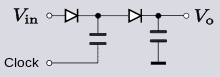 Figure 7.Dickson charge-pump voltage-doubler
The circuits where Dickson multipliers are mostly and frequently used are the integrated circuits where the supply voltage such as from any battery is less than what is required by the circuitry.
The fact that all the semiconductors used in this are basically similar acts as an advantage for the manufacturers of the integrated circuit.
The standard logic block which is most commonly found and used in numerous integrated circuits is the MOSFET devices.
This is one of the reasons why the diodes are many a times replaced by the transistor of this type, but are also wired to a function in the form of a diode.
This arrangement is also known as a diode-wired MOSFET.
The diagram in Figure 8 depicts a Dickson voltage doubler using this kind of diode-wired n-channel enhancement type MOSFET devices.
Figure 7.Dickson charge-pump voltage-doubler
The circuits where Dickson multipliers are mostly and frequently used are the integrated circuits where the supply voltage such as from any battery is less than what is required by the circuitry.
The fact that all the semiconductors used in this are basically similar acts as an advantage for the manufacturers of the integrated circuit.
The standard logic block which is most commonly found and used in numerous integrated circuits is the MOSFET devices.
This is one of the reasons why the diodes are many a times replaced by the transistor of this type, but are also wired to a function in the form of a diode.
This arrangement is also known as a diode-wired MOSFET.
The diagram in Figure 8 depicts a Dickson voltage doubler using this kind of diode-wired n-channel enhancement type MOSFET devices.
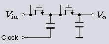 Figure 8.Dickson voltage doubler using diode-wired MOSFETs
The basic form of Dickson charge pump has undergone a lot many improvements and variations.
Most of these improvements are in the area of the reduction of the effect produced by the transistor drain source voltage.
This improvement is considered as significant in case the input voltage is small as is in the case of a low-voltage battery.
The output voltage is always an integral multiple of the input voltage (twice in case of a voltage doubler) when ideal switching elements are used.
But in case where a single-cell battery is used as the input source along with MOSFET switches, the output in such cases are far lesser than this value because there will a drop in the voltage across the transistors.
Due to the extremely low drop in the voltage in the on-state of a circuit which is using discrete components, the Schottky diode is considered a good choice as a switching element.
But the designers of integrated circuit mostly prefer MOSFET to use as it is more easily available which more than compensate for the presence of inadequacies and high complexity in the circuit which is present in MOSFET devices.
To illustrate this, let us take an example: a nominal voltage of the tune of 1.5V is present in an alkaline battery.
The output in this can be doubled to 3.0V by using a voltage doubler along with ideal switching elements which has a voltage drop of zero.
But the diode-wired MOSFET��s voltage drop of drain-source when it is in the state of on must be at the minimum equal to the gate threshold voltage which is typically in the tune of 0.9V.
The output voltage can be raised by the voltage doubler successfully only by approximately 0.6V to 2.1V.
The increase in the voltage by the circuit cannot be achieved without using multiple stages in case the drop across the final smoothing transistor is also considered and taken into account.
On the other hand, the onstage voltage of a typical Schottky diode is of 0.3 V.
the output voltage produced by a voltage doubler will be in the range of 2.7V if it uses Schottky diode, or 2.4V if it uses smoothing diode.
Figure 8.Dickson voltage doubler using diode-wired MOSFETs
The basic form of Dickson charge pump has undergone a lot many improvements and variations.
Most of these improvements are in the area of the reduction of the effect produced by the transistor drain source voltage.
This improvement is considered as significant in case the input voltage is small as is in the case of a low-voltage battery.
The output voltage is always an integral multiple of the input voltage (twice in case of a voltage doubler) when ideal switching elements are used.
But in case where a single-cell battery is used as the input source along with MOSFET switches, the output in such cases are far lesser than this value because there will a drop in the voltage across the transistors.
Due to the extremely low drop in the voltage in the on-state of a circuit which is using discrete components, the Schottky diode is considered a good choice as a switching element.
But the designers of integrated circuit mostly prefer MOSFET to use as it is more easily available which more than compensate for the presence of inadequacies and high complexity in the circuit which is present in MOSFET devices.
To illustrate this, let us take an example: a nominal voltage of the tune of 1.5V is present in an alkaline battery.
The output in this can be doubled to 3.0V by using a voltage doubler along with ideal switching elements which has a voltage drop of zero.
But the diode-wired MOSFET��s voltage drop of drain-source when it is in the state of on must be at the minimum equal to the gate threshold voltage which is typically in the tune of 0.9V.
The output voltage can be raised by the voltage doubler successfully only by approximately 0.6V to 2.1V.
The increase in the voltage by the circuit cannot be achieved without using multiple stages in case the drop across the final smoothing transistor is also considered and taken into account.
On the other hand, the onstage voltage of a typical Schottky diode is of 0.3 V.
the output voltage produced by a voltage doubler will be in the range of 2.7V if it uses Schottky diode, or 2.4V if it uses smoothing diode.
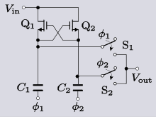 Figure 9.Cross-coupled switched-capacitor voltage doubler
The transistor Q2 is turned off in case the clock is low.
At the same time, the transistor Q1 is turned on if the clockis high and this results in the charging of the capacitor C1 to the voltage Vn.
the top plate of C1 is pushed up to double Vin in case the 1 goes high.
In order to enable this voltage to appear as an output, the switch S1 closes at the same time.
Also, at the same time C2 is allowed to charge by turning on the Q2.
The roles of the components are reversed in the next half cycle: 1 will be low, S1 will open, 2 will be high, and S2 will close.
Thus alternatively from each side of the circuit, the output voltage is supplied with 2Vin.
the loss incurred in this circuit is low since there is a lack of diode-wired MOSFETs and the threshold voltage problems associated with it.
One of the other advantages of the circuit is that it doubles the ripple frequency since there are two voltage doublers present which supply the output effectively from the phase clocks.
The basic disadvantage of this circuit is that the stray capacitances of the Dickinson multiplier is found to be much less significant than this circuit and thus accounts for the most of the losses which are incurred in this circuit.
Courtesy:https://en.wikipedia.org/wiki/Voltage_doubler
Figure 9.Cross-coupled switched-capacitor voltage doubler
The transistor Q2 is turned off in case the clock is low.
At the same time, the transistor Q1 is turned on if the clockis high and this results in the charging of the capacitor C1 to the voltage Vn.
the top plate of C1 is pushed up to double Vin in case the 1 goes high.
In order to enable this voltage to appear as an output, the switch S1 closes at the same time.
Also, at the same time C2 is allowed to charge by turning on the Q2.
The roles of the components are reversed in the next half cycle: 1 will be low, S1 will open, 2 will be high, and S2 will close.
Thus alternatively from each side of the circuit, the output voltage is supplied with 2Vin.
the loss incurred in this circuit is low since there is a lack of diode-wired MOSFETs and the threshold voltage problems associated with it.
One of the other advantages of the circuit is that it doubles the ripple frequency since there are two voltage doublers present which supply the output effectively from the phase clocks.
The basic disadvantage of this circuit is that the stray capacitances of the Dickinson multiplier is found to be much less significant than this circuit and thus accounts for the most of the losses which are incurred in this circuit.
Courtesy:https://en.wikipedia.org/wiki/Voltage_doubler
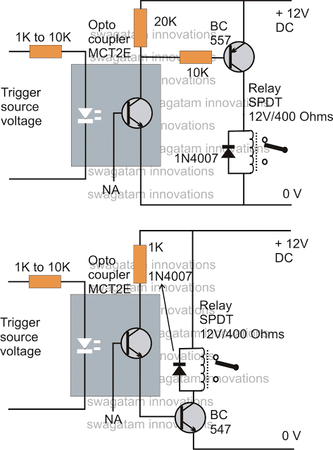
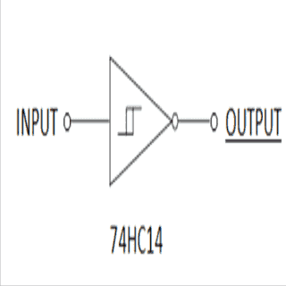
 For constant values of VD and R, the current only depends on V.
For forward biased diodes, VD is about 0.3 - 0.35 volts for germanium, and 0.6 - 0.7 volts for silicon diodes, and is relatively constant over a wide range of currents.
LEDs are similar to diodes, except that they are constructed using special materials that emit light.
For constant values of VD and R, the current only depends on V.
For forward biased diodes, VD is about 0.3 - 0.35 volts for germanium, and 0.6 - 0.7 volts for silicon diodes, and is relatively constant over a wide range of currents.
LEDs are similar to diodes, except that they are constructed using special materials that emit light.
 As the strain gauge resistance (Rg) changes, the output voltage (Vout) changes by a few milliVolts, and this voltage is then amplified by a differential amplifier to return a readable value.
This Wheatstone circuit is also well suited for temperature compensation - it can almost eliminate the effects of temperature.
Sometimes the gauge material is designed to compensate for thermal expansion, but this does not totally remove the thermal sensitivity.
To achieve better thermal compensation, a resistor such as R3 could be replaced by a similar strain gauge.
This would tend to nullify temperature effects.
In fact, all four resistors could be replaced by strain gauge sensors for maximum temperature stability.
Two of them (R1 and R3) could be set up to measure compression, while the other two (R2 and R4) are set up to measure tension.
Not only will this compensate for temperature, but it also increases the sensitivity by a factor of four.Strain gauges with electric resistance elements are by far the most common type of sensor for measuring strain, as they possess the advantages of lower cost, as well as being well-established.
They are available in small sizes and are only moderately affected by temperature changes, simultaneously achieving error of less than +/-0.10%.
Bonded resistance strain gauges are also highly sensitive, and can be used to measure both static and dynamic strain.
However, there are other types available for certain applications, such as piezo-resistive, carbon-resistive, semi-conductive, acoustic, optical, and inductive.
There are even strain gauge sensors based on a capacitor circuit..
As the strain gauge resistance (Rg) changes, the output voltage (Vout) changes by a few milliVolts, and this voltage is then amplified by a differential amplifier to return a readable value.
This Wheatstone circuit is also well suited for temperature compensation - it can almost eliminate the effects of temperature.
Sometimes the gauge material is designed to compensate for thermal expansion, but this does not totally remove the thermal sensitivity.
To achieve better thermal compensation, a resistor such as R3 could be replaced by a similar strain gauge.
This would tend to nullify temperature effects.
In fact, all four resistors could be replaced by strain gauge sensors for maximum temperature stability.
Two of them (R1 and R3) could be set up to measure compression, while the other two (R2 and R4) are set up to measure tension.
Not only will this compensate for temperature, but it also increases the sensitivity by a factor of four.Strain gauges with electric resistance elements are by far the most common type of sensor for measuring strain, as they possess the advantages of lower cost, as well as being well-established.
They are available in small sizes and are only moderately affected by temperature changes, simultaneously achieving error of less than +/-0.10%.
Bonded resistance strain gauges are also highly sensitive, and can be used to measure both static and dynamic strain.
However, there are other types available for certain applications, such as piezo-resistive, carbon-resistive, semi-conductive, acoustic, optical, and inductive.
There are even strain gauge sensors based on a capacitor circuit..
 The above three contact piezo may also be used in two wire transducer application where the third central feedback contact is not used.
The external frequency from a piezo driver is applied across the metal base and the inner piezo material, the piezo then starts vibrating at the applied frequency level, generating a high pitched sound.
However this sound can be very insignificant and low in volume unless the piezo is fixed over a special plastic housing with a center hole.
The size of the hole matters and should not be more than 8mm in diameter or less than 6mm in diameter.
The plastic housing should be such that the piezo is stuck with a adhesive over a raise platform just a couple of mm above the base of the housing which consists of the above explained hole.
The raised portion should be just 2 mm wide, barely supporting the circumference edge of the piezo.
The whole sticking (installation) procedure has been explained in this simple buzzer circuit article.
The above three contact piezo may also be used in two wire transducer application where the third central feedback contact is not used.
The external frequency from a piezo driver is applied across the metal base and the inner piezo material, the piezo then starts vibrating at the applied frequency level, generating a high pitched sound.
However this sound can be very insignificant and low in volume unless the piezo is fixed over a special plastic housing with a center hole.
The size of the hole matters and should not be more than 8mm in diameter or less than 6mm in diameter.
The plastic housing should be such that the piezo is stuck with a adhesive over a raise platform just a couple of mm above the base of the housing which consists of the above explained hole.
The raised portion should be just 2 mm wide, barely supporting the circumference edge of the piezo.
The whole sticking (installation) procedure has been explained in this simple buzzer circuit article.

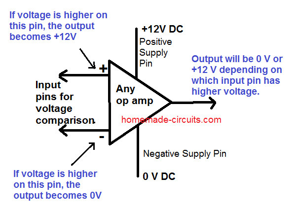 REMEMBER, THE VOLTAGE ON THE INPUT PINS SHOULD NOT EXCEED THE DC SUPPLY LEVEL OF THE OP AMP, IN THE ABOVE FIGURE IT SHOULDN'T EXCEED +12 V
The two input pins of an op amp are called the inverting (with a minus sign) and the non-inverting pin (with a plus sign) become the sensing inputs of the op amp.
When used as a comparator, one of the pins out of the two is applied with a fixed reference voltage while the other pin is fed with the voltage whose level needs to be monitored, as shown below.
REMEMBER, THE VOLTAGE ON THE INPUT PINS SHOULD NOT EXCEED THE DC SUPPLY LEVEL OF THE OP AMP, IN THE ABOVE FIGURE IT SHOULDN'T EXCEED +12 V
The two input pins of an op amp are called the inverting (with a minus sign) and the non-inverting pin (with a plus sign) become the sensing inputs of the op amp.
When used as a comparator, one of the pins out of the two is applied with a fixed reference voltage while the other pin is fed with the voltage whose level needs to be monitored, as shown below.
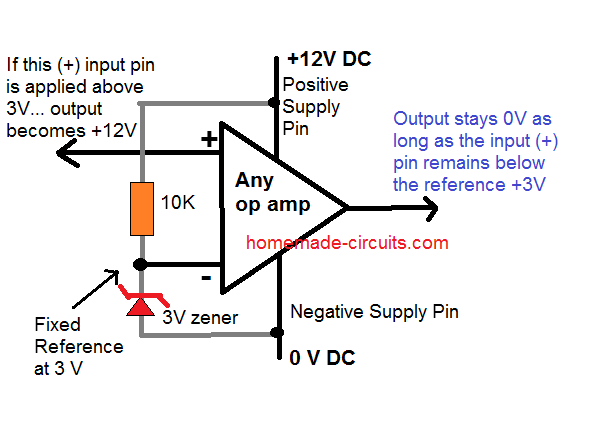 The monitoring of the above voltage is done with reference to the fixed voltage that's been applied to the other complementary pin.
Therefore if the voltage which is to be monitored goes above or falls below the fixed reference threshold voltage, the output reverts state or changes its original condition or changes its output voltage polarity.
The monitoring of the above voltage is done with reference to the fixed voltage that's been applied to the other complementary pin.
Therefore if the voltage which is to be monitored goes above or falls below the fixed reference threshold voltage, the output reverts state or changes its original condition or changes its output voltage polarity.
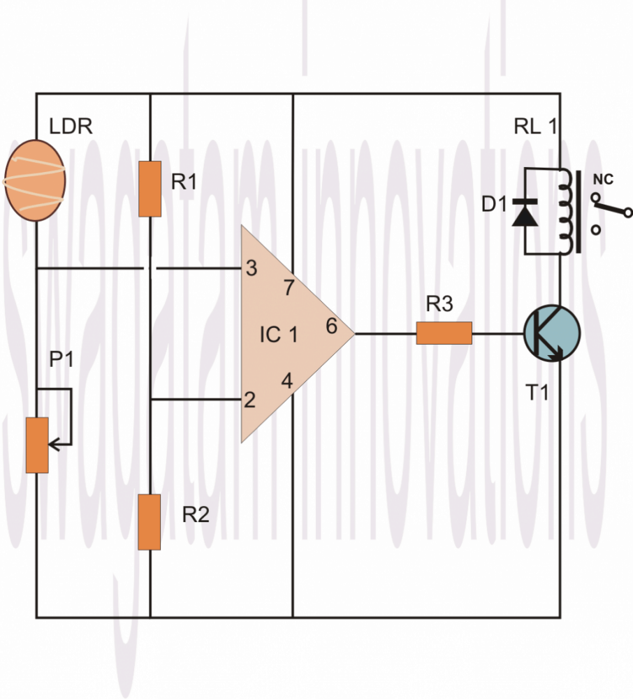 We can see that the Pin #7 of the opamp which is the +supply pin is connected to the positive rail, similarly its pin #4 which is the negative supply pin is connected to the negative or rather the zero supply rail of the power supply.
The above couple of pin connections powers the IC so that it can carry on with its intended functions.
Now as discussed earlier, pin #2 of the IC is connected at the junction of two resistors whose ends are connected to the power supply positive and negative rails.
This arrangement of the resistors is called a potential divider, meaning the potential or the voltage level at the junction of these resistors will be approximately the half of the supply voltage, so if the supply voltage is 12, the junction of the potential divider network will be 6 volts and so on.
If the supply voltage is well regulated, the above voltage level will also be well fixed and therefore can be used as the reference voltage for the pin #2.
Therefore referring to the junction voltage of the resistors R1/R2, this voltage becomes the reference voltage at pin #2 which means the IC will monitor and respond to any voltage that might go above this level.
The sensing voltage which is to be monitored is applied to pin #3 of the IC, in our example it is via an LDR.
The pin #3 is connected at the junction of the LDR pin and a preset terminal.
That means this junction again becomes a potential divider, whose voltage level this time is not fixed because the LDR value cannot be fixed and will vary with the ambient light conditions.
Now suppose you want the circuit to sense the LDR value at some point just around when dusk falls, you adjust the preset such that the voltage at pin #3 or at the junction of the LDR and the preset just crosses above the 6V mark.
When this happens the value rises above the fixed reference at pin #2, this informs the IC about the sense voltage rising above the reference voltage at pin #2, this instantly reverts the output of the IC which changes to positive from its initial zero voltage position.
The above change in the state of the IC from zero to positive, triggers the relay driver stage which switches ON the load or the lights which might be connected to the relevant contacts of the relay.
Remember, the values of the resistors connected to pin #2 may also be altered for altering the sensing threshold of pin #3, so they are all inter-depended, giving you a wide angle of variation of the circuit parameters.
Another feature of the R1 and R2 is that it avoids the need of using a dual polarity power supply making the involved configuration very simple and neat.
We can see that the Pin #7 of the opamp which is the +supply pin is connected to the positive rail, similarly its pin #4 which is the negative supply pin is connected to the negative or rather the zero supply rail of the power supply.
The above couple of pin connections powers the IC so that it can carry on with its intended functions.
Now as discussed earlier, pin #2 of the IC is connected at the junction of two resistors whose ends are connected to the power supply positive and negative rails.
This arrangement of the resistors is called a potential divider, meaning the potential or the voltage level at the junction of these resistors will be approximately the half of the supply voltage, so if the supply voltage is 12, the junction of the potential divider network will be 6 volts and so on.
If the supply voltage is well regulated, the above voltage level will also be well fixed and therefore can be used as the reference voltage for the pin #2.
Therefore referring to the junction voltage of the resistors R1/R2, this voltage becomes the reference voltage at pin #2 which means the IC will monitor and respond to any voltage that might go above this level.
The sensing voltage which is to be monitored is applied to pin #3 of the IC, in our example it is via an LDR.
The pin #3 is connected at the junction of the LDR pin and a preset terminal.
That means this junction again becomes a potential divider, whose voltage level this time is not fixed because the LDR value cannot be fixed and will vary with the ambient light conditions.
Now suppose you want the circuit to sense the LDR value at some point just around when dusk falls, you adjust the preset such that the voltage at pin #3 or at the junction of the LDR and the preset just crosses above the 6V mark.
When this happens the value rises above the fixed reference at pin #2, this informs the IC about the sense voltage rising above the reference voltage at pin #2, this instantly reverts the output of the IC which changes to positive from its initial zero voltage position.
The above change in the state of the IC from zero to positive, triggers the relay driver stage which switches ON the load or the lights which might be connected to the relevant contacts of the relay.
Remember, the values of the resistors connected to pin #2 may also be altered for altering the sensing threshold of pin #3, so they are all inter-depended, giving you a wide angle of variation of the circuit parameters.
Another feature of the R1 and R2 is that it avoids the need of using a dual polarity power supply making the involved configuration very simple and neat.
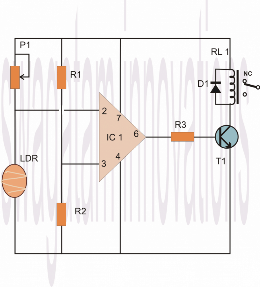 THis is how any basic opamp behaves when it is configured as a comparator.
To summarize we can say that in any opamp based compartaor, the following operations take place:
THis is how any basic opamp behaves when it is configured as a comparator.
To summarize we can say that in any opamp based compartaor, the following operations take place:
 Image Credit - https://cndingwen.en.made-in-china.com/offer/QMsmDPNUHgYy/Sell-285W-Polycrystalline-Solar-Panels.html
 The three leads of the transistors are open and needs the required setting up via the passive parts.
As explained above, the emitter is the common outlet.
Since we are using an NPN type of transistor, the emitter must go to the ground, so we connect it to the ground or the negative supply rail of the circuit.
The base is the main sensing or the triggering input, so this input needs to be connected to the sensor element.
The sensor element here is a pair of metal terminals.
One of the terminals is connected to the positive supply and the other terminal needs to be connected to the base of the transistor.
The sensor is used to detect the presence of rain water.
The moment raining begins; the water droplets bridge the two terminals.
Since water has a low resistance, starts leaking the positive voltage across its terminals, to the base of the transistor.
This leaking voltage feeds the base of the transistor and in the course reaches the ground through the emitter.
The moment this happens, as per the property of the device, it opens the gates between the collector and the emitter.
It means that now if we connect a positive voltage source to the collector, it will be immediately connected to the ground via its emitter.
Therefore we connect the collector of the transistor to the positive, however we do this via the load so that the load operates with the switching, and that��s exactly what we are looking for.
Simulating the above operation quickly, we see that the positive supply leaks through the metal terminals of the sensor, touches the base and carries on its course to finally reach the ground completing the base circuit, however this operation instantly pulls the collector voltage to the ground via the emitter, switching ON the load which is a buzzer here.
The buzzer sounds.
This set up is the basic set up, however it needs many corrections and also can be modified in many different ways.
The three leads of the transistors are open and needs the required setting up via the passive parts.
As explained above, the emitter is the common outlet.
Since we are using an NPN type of transistor, the emitter must go to the ground, so we connect it to the ground or the negative supply rail of the circuit.
The base is the main sensing or the triggering input, so this input needs to be connected to the sensor element.
The sensor element here is a pair of metal terminals.
One of the terminals is connected to the positive supply and the other terminal needs to be connected to the base of the transistor.
The sensor is used to detect the presence of rain water.
The moment raining begins; the water droplets bridge the two terminals.
Since water has a low resistance, starts leaking the positive voltage across its terminals, to the base of the transistor.
This leaking voltage feeds the base of the transistor and in the course reaches the ground through the emitter.
The moment this happens, as per the property of the device, it opens the gates between the collector and the emitter.
It means that now if we connect a positive voltage source to the collector, it will be immediately connected to the ground via its emitter.
Therefore we connect the collector of the transistor to the positive, however we do this via the load so that the load operates with the switching, and that��s exactly what we are looking for.
Simulating the above operation quickly, we see that the positive supply leaks through the metal terminals of the sensor, touches the base and carries on its course to finally reach the ground completing the base circuit, however this operation instantly pulls the collector voltage to the ground via the emitter, switching ON the load which is a buzzer here.
The buzzer sounds.
This set up is the basic set up, however it needs many corrections and also can be modified in many different ways.
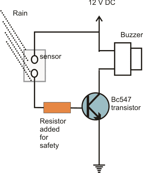 Looking at the schematic we find that the circuit does not include a base resistor because the water itself acts as a resistor, but what happens if the sensor terminals are accidentally shorted, the entire current would be dumped to the base of the transistor, frying it instantly.
Therefore for safety reasons we add a resistor to the base of the transistor.
However the base resistor value decides how much triggering current can enter across the base/emitter pins, and therefore in turn affects the collector current.
Conversely, the base resistor should be such that it allows sufficient current to be pulled from collector to the emitter, permitting perfect switching of the collector load.
For easier calculations, as a rule of thumb, we can assume the base resistor value to be 40 times more than the collector load resistance.
So, in our circuit, assuming the collector load is a buzzer, we measure the resistance of the buzzer which amounts to say 10K.
40 times 10K means the base resistance must be somewhere around 400K, however we find that the water resistance is around 50K, so deducting this value from 400K, we get 350K, that��s the base resistor value we need to select.
Now suppose we want to connect an LED to this circuit instead of a buzzer.
We cannot connect the LED directly to the collector of the transistor because LEDs are also vulnerable and will require a current limiting resistor if the operating voltage is higher than its specified forward voltage.
Looking at the schematic we find that the circuit does not include a base resistor because the water itself acts as a resistor, but what happens if the sensor terminals are accidentally shorted, the entire current would be dumped to the base of the transistor, frying it instantly.
Therefore for safety reasons we add a resistor to the base of the transistor.
However the base resistor value decides how much triggering current can enter across the base/emitter pins, and therefore in turn affects the collector current.
Conversely, the base resistor should be such that it allows sufficient current to be pulled from collector to the emitter, permitting perfect switching of the collector load.
For easier calculations, as a rule of thumb, we can assume the base resistor value to be 40 times more than the collector load resistance.
So, in our circuit, assuming the collector load is a buzzer, we measure the resistance of the buzzer which amounts to say 10K.
40 times 10K means the base resistance must be somewhere around 400K, however we find that the water resistance is around 50K, so deducting this value from 400K, we get 350K, that��s the base resistor value we need to select.
Now suppose we want to connect an LED to this circuit instead of a buzzer.
We cannot connect the LED directly to the collector of the transistor because LEDs are also vulnerable and will require a current limiting resistor if the operating voltage is higher than its specified forward voltage.
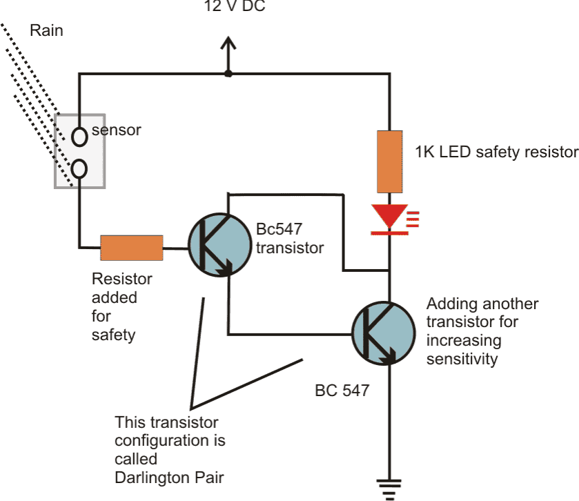 Therefore we connect a LED in series with a 1K resistor across the collector and positive of the above circuit, replacing the buzzer.
Now the resistor in series with the LED may be considered as the collector load resistance.
So now the base resistance should be 40 times this value, which amounts to 40K, however the water resistance itself is 150K, means the base resistance is already too high, meaning when rain water bridges the sensor, the transistor won��t be able to switch ON the LED brightly, rather will illuminate it very dimly.
So how can we solve this problem?
We need to make the transistor more sensitive, so we connect another transistor to aid the existing one in a Darlington configuration.
With this arrangement the transistor pair becomes highly sensitive, at least 25 times more sensitive than the previous circuit.
25 times more sensitivity means we can select a base resistance that may be 25+40 = 65 to 75 times the collector resistance; we get the maximum range of about 75 into 10 = 750K, so this can be taken as the total value of the base resistor.
Deducting 150K water resistance from 750K we get 600K, so that��s the base resistor value we can choose for the present configuration.
Remember the case resistor can be any value as long as it��s fulfilling two conditions: it��s not heating up the transistor and it��s helping to switch the collector load satisfactorily.
That��s it.
Therefore we connect a LED in series with a 1K resistor across the collector and positive of the above circuit, replacing the buzzer.
Now the resistor in series with the LED may be considered as the collector load resistance.
So now the base resistance should be 40 times this value, which amounts to 40K, however the water resistance itself is 150K, means the base resistance is already too high, meaning when rain water bridges the sensor, the transistor won��t be able to switch ON the LED brightly, rather will illuminate it very dimly.
So how can we solve this problem?
We need to make the transistor more sensitive, so we connect another transistor to aid the existing one in a Darlington configuration.
With this arrangement the transistor pair becomes highly sensitive, at least 25 times more sensitive than the previous circuit.
25 times more sensitivity means we can select a base resistance that may be 25+40 = 65 to 75 times the collector resistance; we get the maximum range of about 75 into 10 = 750K, so this can be taken as the total value of the base resistor.
Deducting 150K water resistance from 750K we get 600K, so that��s the base resistor value we can choose for the present configuration.
Remember the case resistor can be any value as long as it��s fulfilling two conditions: it��s not heating up the transistor and it��s helping to switch the collector load satisfactorily.
That��s it.
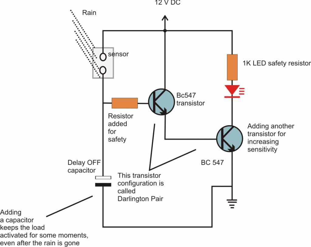 Now suppose we add a capacitor across the base of the transistor and the ground.
The capacitor, as explained above will store initially some current when raining begins through the leakages across the sensor terminals.
Now after the rain stops, and the sensor bridge leakage is disconnected, the transistor still keeps conducting sounding the buzzer��how? The stored voltage inside the capacitor now feeds the transistor base and keeps it switched ON until it has discharged below the base switching voltage.
This shows how a capacitor might serve in an electronic circuit.
Now suppose we add a capacitor across the base of the transistor and the ground.
The capacitor, as explained above will store initially some current when raining begins through the leakages across the sensor terminals.
Now after the rain stops, and the sensor bridge leakage is disconnected, the transistor still keeps conducting sounding the buzzer��how? The stored voltage inside the capacitor now feeds the transistor base and keeps it switched ON until it has discharged below the base switching voltage.
This shows how a capacitor might serve in an electronic circuit.
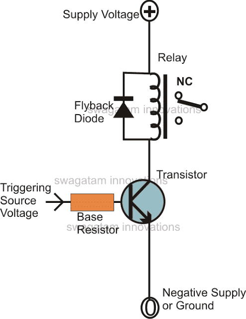 Referring to the above circuit diagram we see that the configuration only involves a transistor, a base resistor and the relay with a flyback diode.
However there are a few complexities that need to be settled before the design could be used for the required functions:
Since the base drive voltage to transistor is the major source for controlling the relay operations, it needs to be perfectly calculated for optimal results.
The base resistor value id directly proportional to the current across the collector/emitter leads of the transistor or in other words, the relay coil current, which is the collector load of the transistor, becomes one of the main factors, and directly influences the value of the base resistor of the transistor.
Referring to the above circuit diagram we see that the configuration only involves a transistor, a base resistor and the relay with a flyback diode.
However there are a few complexities that need to be settled before the design could be used for the required functions:
Since the base drive voltage to transistor is the major source for controlling the relay operations, it needs to be perfectly calculated for optimal results.
The base resistor value id directly proportional to the current across the collector/emitter leads of the transistor or in other words, the relay coil current, which is the collector load of the transistor, becomes one of the main factors, and directly influences the value of the base resistor of the transistor.
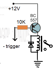 However a PNP will need a negative trigger at its base for the triggering, so in case you wish to implement the system with a positive trigger then you may have to use a combination of both NPN and PNP BJTs as shown in the following figure:
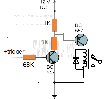 If you have any specific query regarding the above concept, please feel free to express them through the comments for getting quick replies.
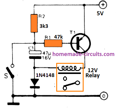 The circuit can be seen wired to a supply voltage capable of holding the relay perfectly.
During the time S1 is open, C1 gets charged via R2 upto the supply voltage.
R1 is coupled to the + terminal and T1 remains switched OFF.
The moment S1 is presed, the T1 base gets connected to supply common through R1, so that it switches ON and drives the relay.
The positive terminal of C1 connects to the common ground through the switch S1. Considering that this capacitor initially had been charged to the supply voltage its -terminal at this point becomes negative.
The voltage across the relay coil therefore reaches two times more than the supply voltage, and this pull in the relay.
Switch S1 could be, certainly, be substituted with a any general purpose transistor which can be switched on or off as required.
The circuit can be seen wired to a supply voltage capable of holding the relay perfectly.
During the time S1 is open, C1 gets charged via R2 upto the supply voltage.
R1 is coupled to the + terminal and T1 remains switched OFF.
The moment S1 is presed, the T1 base gets connected to supply common through R1, so that it switches ON and drives the relay.
The positive terminal of C1 connects to the common ground through the switch S1. Considering that this capacitor initially had been charged to the supply voltage its -terminal at this point becomes negative.
The voltage across the relay coil therefore reaches two times more than the supply voltage, and this pull in the relay.
Switch S1 could be, certainly, be substituted with a any general purpose transistor which can be switched on or off as required.
 Note: Moving C1 from the existing position to across base/emitter of T1 will be more effective in tackling spurious switching response of the circuit, and this will also allow C1 value to be much smaller, may be 0.22uF
As shown in the figure transistor T1 and T2 are configured in such a manner that T2 follows T1 to either conduct and or to stop the conduction depending upon the trigger received at the input of T1.
T2 also acts as a buffer and produces better response even to very small signals.
When a small positive signal is applied at the input of T1, T1 instantly conducts and pulls the base of T2 to ground.
This initiates T2 which also starts conducting with the received negative biasing offered by the conduction of T1.
It must be noted here that T being NPN device responds to positive signals while T2 being a PNP responds to negative potential generated by the conduction of T1.
Uptill here the function looks pretty ordinary as we witness a very normal and obvious transistor functioning.
Note: Moving C1 from the existing position to across base/emitter of T1 will be more effective in tackling spurious switching response of the circuit, and this will also allow C1 value to be much smaller, may be 0.22uF
As shown in the figure transistor T1 and T2 are configured in such a manner that T2 follows T1 to either conduct and or to stop the conduction depending upon the trigger received at the input of T1.
T2 also acts as a buffer and produces better response even to very small signals.
When a small positive signal is applied at the input of T1, T1 instantly conducts and pulls the base of T2 to ground.
This initiates T2 which also starts conducting with the received negative biasing offered by the conduction of T1.
It must be noted here that T being NPN device responds to positive signals while T2 being a PNP responds to negative potential generated by the conduction of T1.
Uptill here the function looks pretty ordinary as we witness a very normal and obvious transistor functioning.

 The result of the experiment is that, when the motor rotates and the external coil's wires are connected to a load, it does not load the motor, instead surprisingly it reduces the loading on the motor further.
As the load on the external coil wires is increased it even further decreases the loading on the motor.
Due to this, the motor RPM keeps increasing in a perpetual manner, as the external load increases.
This opposite reaction is called the regenerative motor acceleration effect, which is a kind of perpetual overunity generation from the motor and can be used for many useful applications.
The whole explanation of the regenerative motor acceleration concept was researched and sent to me by one of the dedicated readers of this blog Mr.
Thamal Indika
For more information on this subject you can directly email Mr.
Thamal on this email ID:
intelligentdecent@gmail.com
Now let's learn more about this interesting regenerative motor overunity theory through the following description.
The result of the experiment is that, when the motor rotates and the external coil's wires are connected to a load, it does not load the motor, instead surprisingly it reduces the loading on the motor further.
As the load on the external coil wires is increased it even further decreases the loading on the motor.
Due to this, the motor RPM keeps increasing in a perpetual manner, as the external load increases.
This opposite reaction is called the regenerative motor acceleration effect, which is a kind of perpetual overunity generation from the motor and can be used for many useful applications.
The whole explanation of the regenerative motor acceleration concept was researched and sent to me by one of the dedicated readers of this blog Mr.
Thamal Indika
For more information on this subject you can directly email Mr.
Thamal on this email ID:
intelligentdecent@gmail.com
Now let's learn more about this interesting regenerative motor overunity theory through the following description.
 In this diagram, I will explain how the Lenz's Law causes 2 brakes and thus decreases the RPM of the Magnet Rotor, when the Conventional Generator coil is connected to the Load.
 So as you can see in this configuration the Regenx coil is magnetized for ��N �� pole, when the rotor magnet has reached the TDC, so that there is a repulsion in the Magnets and the rotor magnet is pushed away by the coil core (Because it is a N pole Magnet )and this is the first Acceleration effect of this regenerative acceleration effect.
As the rotor is in the N S N S magnet configuration, then this coil core simultaneously attracts the next S pole rotor magnet and it is the second acceleration effect.
Actually the Lenz law is happening here, But it gets much delayed because of the new alterations and accelerates the Magnet Rotor when connected to the load.
we can charge some heavy duty batteries like 12V 7A or 12V Car batteries, if we can sue some big magnets with big copper coils like Guage 20 copper wire because they will provide much ampere.
In my small set up, I have used Guage 28 thin copper wire, but I can charge my mobile phone battery and also I can lit my lampshade and the RPM of the Magnet Rotor increases well when I connect these loads to the regenex coil and the current which motor takes from the drive battery gets much decreased when I connected the load.
I have also well understood that, if we can add more regenex coils with loads the rotor RPM increases simultaneously.
For me this is a very amazing phenomena and as my first small set up worked very well, I am going to make a much bigger design.
My design will consist of two magnet rotors.
One rotor will be the prime mover for the other Rotor which I will use for achieving this effect.
So for the first rotor I will arrange magnets in the N N N N configuration and will fix around 6 to 7 bedini driver coils to get a high RPM with a 6V power supply from a Battery as shown in the following Video.
I hope to achieve this speed, using a 6V battery.
But in my first experiment, I understood that we can achieve this regenerative acceleration effect using a normal RPM, if we can increase the number of turns of the regenex coil.
So then I will connect this driving rotor to the other Rotor (N S N S configuration) through a shaft and I will add a regenex coil set to charge another 6V battery first.
Because when the Drive Battery gets discharged, I can swap the drive battery with the charging battery.
I will add another regenexx coil set to charge up a 12V 7A battery which I currently have and I can use it to supply the power for the small fan, the lampshade in my room and so on.
In this set up, it will run indefinitely, because I always charge a 6V battery for driving rotor and swap it with the drive battery when it gets discharged.
Please note that I have experimentally proved that, if we add more regenex coils, the RPM of the Rotor increases simultaneously, and the prime mover takes much less current from the drive battery.
It is marvelous fact and this will direct me to provide many overunity motors and we have reached this overunity situation 90 percent now.
I am sorry, my explanation is too long and it might have taken your worth time.
But I did this, just to encourage you to make a device like this and see the results.
I hope you will reply me at your earliest convenience.
Also please search in the ��Youtube �� as �� Thane Henis Theory �� then you can find so many valuable lessons and videos about this special effect.
This is a small experimental set up created by Mr.
Thamal, to demonstrate the effect of regenerative motor acceleration in response to the loading of the external generator coils.
So as you can see in this configuration the Regenx coil is magnetized for ��N �� pole, when the rotor magnet has reached the TDC, so that there is a repulsion in the Magnets and the rotor magnet is pushed away by the coil core (Because it is a N pole Magnet )and this is the first Acceleration effect of this regenerative acceleration effect.
As the rotor is in the N S N S magnet configuration, then this coil core simultaneously attracts the next S pole rotor magnet and it is the second acceleration effect.
Actually the Lenz law is happening here, But it gets much delayed because of the new alterations and accelerates the Magnet Rotor when connected to the load.
we can charge some heavy duty batteries like 12V 7A or 12V Car batteries, if we can sue some big magnets with big copper coils like Guage 20 copper wire because they will provide much ampere.
In my small set up, I have used Guage 28 thin copper wire, but I can charge my mobile phone battery and also I can lit my lampshade and the RPM of the Magnet Rotor increases well when I connect these loads to the regenex coil and the current which motor takes from the drive battery gets much decreased when I connected the load.
I have also well understood that, if we can add more regenex coils with loads the rotor RPM increases simultaneously.
For me this is a very amazing phenomena and as my first small set up worked very well, I am going to make a much bigger design.
My design will consist of two magnet rotors.
One rotor will be the prime mover for the other Rotor which I will use for achieving this effect.
So for the first rotor I will arrange magnets in the N N N N configuration and will fix around 6 to 7 bedini driver coils to get a high RPM with a 6V power supply from a Battery as shown in the following Video.
I hope to achieve this speed, using a 6V battery.
But in my first experiment, I understood that we can achieve this regenerative acceleration effect using a normal RPM, if we can increase the number of turns of the regenex coil.
So then I will connect this driving rotor to the other Rotor (N S N S configuration) through a shaft and I will add a regenex coil set to charge another 6V battery first.
Because when the Drive Battery gets discharged, I can swap the drive battery with the charging battery.
I will add another regenexx coil set to charge up a 12V 7A battery which I currently have and I can use it to supply the power for the small fan, the lampshade in my room and so on.
In this set up, it will run indefinitely, because I always charge a 6V battery for driving rotor and swap it with the drive battery when it gets discharged.
Please note that I have experimentally proved that, if we add more regenex coils, the RPM of the Rotor increases simultaneously, and the prime mover takes much less current from the drive battery.
It is marvelous fact and this will direct me to provide many overunity motors and we have reached this overunity situation 90 percent now.
I am sorry, my explanation is too long and it might have taken your worth time.
But I did this, just to encourage you to make a device like this and see the results.
I hope you will reply me at your earliest convenience.
Also please search in the ��Youtube �� as �� Thane Henis Theory �� then you can find so many valuable lessons and videos about this special effect.
This is a small experimental set up created by Mr.
Thamal, to demonstrate the effect of regenerative motor acceleration in response to the loading of the external generator coils.
 The proposed self-powered generator is designed to work day and night providing continuous electrical output, quite like our solar panel units.
The initial unit was constructed using 4 coils as the stator and a central rotor having a 5 magnets embedded around its circumference as depicted below:
The proposed self-powered generator is designed to work day and night providing continuous electrical output, quite like our solar panel units.
The initial unit was constructed using 4 coils as the stator and a central rotor having a 5 magnets embedded around its circumference as depicted below:
 The shown red arrow tells us regarding the adjustable gap between the rotor and the coils which can be changed by loosening the nut and then moving the coil assembly near or away from the stator magnets for the desired optimized outputs.
The gap can be anywhere between 1mm to 10 mm.
The rotor assembly and mechanism should be extremely accurate with its alignment and ease of rotation, and therefore must be built using precision machines such as a lathe machine.
The material used for this can be clear acrylic, and the assembly must include 5 sets of 9 magnets fixed inside cylindrical pipe like cavities as shown in the figure.
The top opening of these 5 cylindrical drums are secured with plastic rings extracted from the same cylindrical pipes, to ensure that the magnets stay fixed tightly in their respective positions inside cylindrical cavities.
The shown red arrow tells us regarding the adjustable gap between the rotor and the coils which can be changed by loosening the nut and then moving the coil assembly near or away from the stator magnets for the desired optimized outputs.
The gap can be anywhere between 1mm to 10 mm.
The rotor assembly and mechanism should be extremely accurate with its alignment and ease of rotation, and therefore must be built using precision machines such as a lathe machine.
The material used for this can be clear acrylic, and the assembly must include 5 sets of 9 magnets fixed inside cylindrical pipe like cavities as shown in the figure.
The top opening of these 5 cylindrical drums are secured with plastic rings extracted from the same cylindrical pipes, to ensure that the magnets stay fixed tightly in their respective positions inside cylindrical cavities.
 Very shortly, the 4 coils had been enhanced to 5 in which the newly added coil had three independent windings.
The designs will be understood gradually as we run through the various circuit diagrams and explain how the generator works.
The first basic circuit diagram can be witnessed below
Very shortly, the 4 coils had been enhanced to 5 in which the newly added coil had three independent windings.
The designs will be understood gradually as we run through the various circuit diagrams and explain how the generator works.
The first basic circuit diagram can be witnessed below
 The battery designated as ��A�� energizes the circuit.
A rotor ��C��, made up of 5 magnets is manually moved pushed such that one of the magnets moves close to the coils.
The coils set ��B�� includes 3 independent windings over a single central core and the magnet going past these three coils generates a tiny current inside them.
The current in coil number ��1�� runs through the resistor ��R�� and into the base of the transistor, forcing it to switch on.
The energy moving through the transistor coil ��2�� enables it to turn into a magnet which shoves the rotor disc ��C�� on its path, initiating a spinning motion on the rotor.
This rotation simultaneously induces a current winding ��3�� which is rectified through the blue diodes and transferred back to charge battery ��A��, replenishing nearly all of the current drawn from that battery.
As soon as the magnet inside rotor ��C�� moves away from the coils, the transistor switches off, restoring its collector voltage in a short time close to the +12 Volt supply line.
This depletes coil ��2�� of current.
Because of the manner the coils are positioned, it pulls the collector voltage upwards to around 200 volts and above.
However this does not happen because the output is connected to series five batteries which drop the rsising voltage according to their total rating.
The batteries have a series voltage of approximately 60 volts (which explains why a strong, fast-switching, high-voltage MJE13009 transistor has been incorporated.
As the collector voltage goes by the voltage of the series battery bank, the red diode commences turning ON, releasing the stored electricity in the coil into the battery bank.
That current pulse moves through all 5 batteries, charging every one of them.
Casually speaking, this constitutes the self powered generator design.
In the prototype, the load used for long-term, tireless testing was a 12 volt 150-watt inverter illuminating a 40-watt mains lamp:
The battery designated as ��A�� energizes the circuit.
A rotor ��C��, made up of 5 magnets is manually moved pushed such that one of the magnets moves close to the coils.
The coils set ��B�� includes 3 independent windings over a single central core and the magnet going past these three coils generates a tiny current inside them.
The current in coil number ��1�� runs through the resistor ��R�� and into the base of the transistor, forcing it to switch on.
The energy moving through the transistor coil ��2�� enables it to turn into a magnet which shoves the rotor disc ��C�� on its path, initiating a spinning motion on the rotor.
This rotation simultaneously induces a current winding ��3�� which is rectified through the blue diodes and transferred back to charge battery ��A��, replenishing nearly all of the current drawn from that battery.
As soon as the magnet inside rotor ��C�� moves away from the coils, the transistor switches off, restoring its collector voltage in a short time close to the +12 Volt supply line.
This depletes coil ��2�� of current.
Because of the manner the coils are positioned, it pulls the collector voltage upwards to around 200 volts and above.
However this does not happen because the output is connected to series five batteries which drop the rsising voltage according to their total rating.
The batteries have a series voltage of approximately 60 volts (which explains why a strong, fast-switching, high-voltage MJE13009 transistor has been incorporated.
As the collector voltage goes by the voltage of the series battery bank, the red diode commences turning ON, releasing the stored electricity in the coil into the battery bank.
That current pulse moves through all 5 batteries, charging every one of them.
Casually speaking, this constitutes the self powered generator design.
In the prototype, the load used for long-term, tireless testing was a 12 volt 150-watt inverter illuminating a 40-watt mains lamp:
 The simple design demonstrated above was further improved by the inclusion of a couple of more pick-up coils:
 Coils ��B��, ��D�� and ��E�� are all activated simultaneously by 3 individual magnets.
The electric power generated in all of the three coils is handed down to the 4 blue diodes to manufacture a DC power which is applied to charge battery ��A��, which powers the circuit.
The supplemental input to the drive battery a result of the inclusion of 2 extra drive coils to the stator, enables the machine to run solidly in the form of a self-powered machine, sustaining the battery "A"voltage infinitely.
The sole moving portion of this system is the rotor which is 110 mm in diameter and is a 25 mm thick acrylic disc installed on a ball-bearing mechanism, salvaged from your discarded computer hard disc drive.
The set up appears like this:
Coils ��B��, ��D�� and ��E�� are all activated simultaneously by 3 individual magnets.
The electric power generated in all of the three coils is handed down to the 4 blue diodes to manufacture a DC power which is applied to charge battery ��A��, which powers the circuit.
The supplemental input to the drive battery a result of the inclusion of 2 extra drive coils to the stator, enables the machine to run solidly in the form of a self-powered machine, sustaining the battery "A"voltage infinitely.
The sole moving portion of this system is the rotor which is 110 mm in diameter and is a 25 mm thick acrylic disc installed on a ball-bearing mechanism, salvaged from your discarded computer hard disc drive.
The set up appears like this:
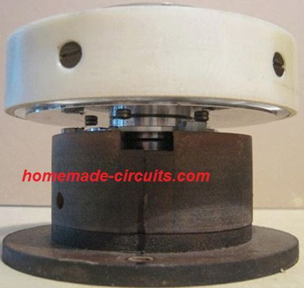 In the images, the disc appears to be hollow however in reality it is solid, crystal clear plastic material.
Holes are drilled on the disc is across five equally spread out locations throughout the circumference, meaning, with 72 degree separations.
The 5 primary openings drilled on the disc are for holding the magnets which are in groups of nine circular ferrite magnets.
Each of these are 20 mm in diameter and 3 mm in height, creating stacks of magnets with a total height of 27 mm long and diameter of 20 mm.
These stacks of magnets are placed in such a way that their North poles project outwards.
After the magnets are mounted, the rotor is put inside a plastic pipe strip in order to secure the magnets tightly in place while the disc spins speedily.
The plastic pipe is clamped with the rotor with the aid of five mounting bolts with countersunk heads.
The coil bobbins are 80 mm long with 72 mm end diameter.
The middle spindle of every coil is constructed of a 20 mm long plastic pipe having an outer and an inner diameter of 16 mm.
providing a wall density of 2 mm.
After the coil winding is completed, this inner diameter becomes full with a number of welding rods with their welding coating taken out.
These are subsequently enveloped in polyester resin, but a solid bar of soft iron can also become a excellent alternative:
In the images, the disc appears to be hollow however in reality it is solid, crystal clear plastic material.
Holes are drilled on the disc is across five equally spread out locations throughout the circumference, meaning, with 72 degree separations.
The 5 primary openings drilled on the disc are for holding the magnets which are in groups of nine circular ferrite magnets.
Each of these are 20 mm in diameter and 3 mm in height, creating stacks of magnets with a total height of 27 mm long and diameter of 20 mm.
These stacks of magnets are placed in such a way that their North poles project outwards.
After the magnets are mounted, the rotor is put inside a plastic pipe strip in order to secure the magnets tightly in place while the disc spins speedily.
The plastic pipe is clamped with the rotor with the aid of five mounting bolts with countersunk heads.
The coil bobbins are 80 mm long with 72 mm end diameter.
The middle spindle of every coil is constructed of a 20 mm long plastic pipe having an outer and an inner diameter of 16 mm.
providing a wall density of 2 mm.
After the coil winding is completed, this inner diameter becomes full with a number of welding rods with their welding coating taken out.
These are subsequently enveloped in polyester resin, but a solid bar of soft iron can also become a excellent alternative:
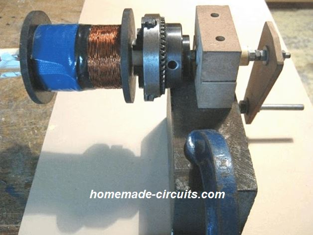 The 3 wire strands that constitute coils ��1��, ��2�� and ��3�� are 0.7 mm in diameter wire and are wrapped with each other before it's wound on the bobbin ��B��.
This method of a bifilar winding creates a lot heavier composite wire bundle which can be simple coil over a spool effectively.
The winder shown above works with a chuck to hold the coil core for enabling the winding, nevertheless any kind of basic winder can also be used.
The designer carried out the wire twisting by extending the 3 strands of wire, each originating from a independent 500 gram bundle reel.
The three strands are tightly held at each end with the wires pressing one another at each end having three metres space between the clamps.
After that, the wires are fixed at the center and 80 turns ascribed to the midsection.
This allows 80 turns for every single of the two 1.5 metre spans positioned between clamps.
The twisted or the wrapped wire set is curled on a temporary reel to maintain it neat because this twisting will have to be duplicated 46 more occasions since all the contents of the wire reels will be required for this one composite coil:
The 3 wire strands that constitute coils ��1��, ��2�� and ��3�� are 0.7 mm in diameter wire and are wrapped with each other before it's wound on the bobbin ��B��.
This method of a bifilar winding creates a lot heavier composite wire bundle which can be simple coil over a spool effectively.
The winder shown above works with a chuck to hold the coil core for enabling the winding, nevertheless any kind of basic winder can also be used.
The designer carried out the wire twisting by extending the 3 strands of wire, each originating from a independent 500 gram bundle reel.
The three strands are tightly held at each end with the wires pressing one another at each end having three metres space between the clamps.
After that, the wires are fixed at the center and 80 turns ascribed to the midsection.
This allows 80 turns for every single of the two 1.5 metre spans positioned between clamps.
The twisted or the wrapped wire set is curled on a temporary reel to maintain it neat because this twisting will have to be duplicated 46 more occasions since all the contents of the wire reels will be required for this one composite coil:
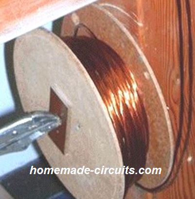 The next 3 meters of the three wires are then clamped and 80 turns wound to the middle position, but on this occassion the turns are placed in the opposite direction.
Even now exactly the same 80 turns are implemented, but if the previous winding had been ��clockwise�� then this winding is flipped ��counter-clockwise��.
This particular modification in the coil directions provides a completed range of twisted wires in which the twist direction becomes opposite every 1.5 meters over the whole length.
This is how the commercially manufactured Litz wire is set up.
This specific great looking twisted wires sets are now employed for winding the coils.
A hole is drilled in one spool flange, exactly near the middle tube and core, and the start of the wire is inserted through it.
The wire is next bent forcefully at 90 degrees and applied round the spool shaft to begin the winding of the coil.
The winding of the wire bundle is executed with great care next to each other across the entire spool shaft and you will see 51 no of winding around each layer and the following layer is wound straight over the top of this very first layer, going back again towards the start.
Make certain that the turns of this second layer rests precisely over the top of the winding underneath them.
This can be uncomplicated because the wire pack is thick enough for allowing the placement quite simple.
In case you like, you can try wrapping one thick white paper around the first layer, to make the second layer distinct as it is turned around.
You will need 18 of such layers to finish the coil, that will ultimately weigh 1.5 kilograms and the finished assembly might looks something as shown below:
The next 3 meters of the three wires are then clamped and 80 turns wound to the middle position, but on this occassion the turns are placed in the opposite direction.
Even now exactly the same 80 turns are implemented, but if the previous winding had been ��clockwise�� then this winding is flipped ��counter-clockwise��.
This particular modification in the coil directions provides a completed range of twisted wires in which the twist direction becomes opposite every 1.5 meters over the whole length.
This is how the commercially manufactured Litz wire is set up.
This specific great looking twisted wires sets are now employed for winding the coils.
A hole is drilled in one spool flange, exactly near the middle tube and core, and the start of the wire is inserted through it.
The wire is next bent forcefully at 90 degrees and applied round the spool shaft to begin the winding of the coil.
The winding of the wire bundle is executed with great care next to each other across the entire spool shaft and you will see 51 no of winding around each layer and the following layer is wound straight over the top of this very first layer, going back again towards the start.
Make certain that the turns of this second layer rests precisely over the top of the winding underneath them.
This can be uncomplicated because the wire pack is thick enough for allowing the placement quite simple.
In case you like, you can try wrapping one thick white paper around the first layer, to make the second layer distinct as it is turned around.
You will need 18 of such layers to finish the coil, that will ultimately weigh 1.5 kilograms and the finished assembly might looks something as shown below:
 This finished coil at this point consists of 3 independent coils tightly wrapped to each other and this set up is intended to create an fantastic magnetic induction across the other two coils, whenever one of the coils is energized with a supply voltage.
This winding currently includes coils 1,2 and 3 of the circuit diagram.
You don't need to to keep worrying about tagging the ends of each strand of wire as you can easily identify them using an ordinary Ohmmeter by checking the continuity across the specific wire ends.
Coil 1 can be used as the triggering coil that will switch the transistor ON during the right periods.
Coil 2 could be the drive coil that is energized by the transistor, and Coil 3 could be the one of the first output coils:
This finished coil at this point consists of 3 independent coils tightly wrapped to each other and this set up is intended to create an fantastic magnetic induction across the other two coils, whenever one of the coils is energized with a supply voltage.
This winding currently includes coils 1,2 and 3 of the circuit diagram.
You don't need to to keep worrying about tagging the ends of each strand of wire as you can easily identify them using an ordinary Ohmmeter by checking the continuity across the specific wire ends.
Coil 1 can be used as the triggering coil that will switch the transistor ON during the right periods.
Coil 2 could be the drive coil that is energized by the transistor, and Coil 3 could be the one of the first output coils:
 Coils 4 and 5 are straightforward spring like coils that are connected parallel with the drive coil 2. They help to boost the drive and therefore are important.
Coil 4 carries a DC resistance of 19 ohms and coil 5 resistance can be around 13 ohms.
However, research is ongoing currently to figure out the most effective coil arrangement for this generator and possibly further coils could be the identical to the first coil, coil ��B�� and all three coils are attached in the very same manner and the driving winding on each coil operated through the a single highly rated and, fast switching transistor.
The present set up looks like this:
Coils 4 and 5 are straightforward spring like coils that are connected parallel with the drive coil 2. They help to boost the drive and therefore are important.
Coil 4 carries a DC resistance of 19 ohms and coil 5 resistance can be around 13 ohms.
However, research is ongoing currently to figure out the most effective coil arrangement for this generator and possibly further coils could be the identical to the first coil, coil ��B�� and all three coils are attached in the very same manner and the driving winding on each coil operated through the a single highly rated and, fast switching transistor.
The present set up looks like this:
 You may ignore the shown gantries since these were included only for examining different ways of activating the transistor.
Currently, coils 6 and 7 (22 ohms each) work as additional output coils attached in parallel with output coil 3 which is built with 3 strands each and with a resistance of 4.2 ohms.
These could be air-core or with a solid iron core.
When tested it revealed that the air core variant performs just a bit better than with an iron core.
Each of these two coils are consist of 4000 turns wound on 22 mm diameter spools using 0.7 mm (AWG # 21 or swg 22) super enameled copper wire.
All the coils have the same specs for the wire.
Using this coil set up, the prototype could run non-stop for around 21 days, preserving the drive battery at 12.7 volts constantly.
After 21 days, the system had been stopped for some modifications and tested again using a completely new arrangement.
In the construction demonstrated above, the current moving from the drive battery into the circuit is actually 70 milliamps, which at 12.7 volts produces an input power of 0.89 watts.
The output power is approximately near 40 watts, confirming a COP of 45.
This is excluding the three additional 12V batteries which are additionally being charged simultaneously.
The results indeed appear to be extremely impressive for the proposed circuit.
The drive method had been employed so many times by John Bedini, that the creator opted to experiment with John��s approach of optimization for highest efficiency.
Even so, he found that eventually a Hall-effect semiconductor specifically aligned correctly with a magnet offers the most effective outcomes.
More research goes on and the power output has at this point attained 60 watts.
This looks truly amazing for such a tiny system, particularly when you see it includes no realistic input.
For this next step we reduce the battery to just one.
The set up can be seen below:
You may ignore the shown gantries since these were included only for examining different ways of activating the transistor.
Currently, coils 6 and 7 (22 ohms each) work as additional output coils attached in parallel with output coil 3 which is built with 3 strands each and with a resistance of 4.2 ohms.
These could be air-core or with a solid iron core.
When tested it revealed that the air core variant performs just a bit better than with an iron core.
Each of these two coils are consist of 4000 turns wound on 22 mm diameter spools using 0.7 mm (AWG # 21 or swg 22) super enameled copper wire.
All the coils have the same specs for the wire.
Using this coil set up, the prototype could run non-stop for around 21 days, preserving the drive battery at 12.7 volts constantly.
After 21 days, the system had been stopped for some modifications and tested again using a completely new arrangement.
In the construction demonstrated above, the current moving from the drive battery into the circuit is actually 70 milliamps, which at 12.7 volts produces an input power of 0.89 watts.
The output power is approximately near 40 watts, confirming a COP of 45.
This is excluding the three additional 12V batteries which are additionally being charged simultaneously.
The results indeed appear to be extremely impressive for the proposed circuit.
The drive method had been employed so many times by John Bedini, that the creator opted to experiment with John��s approach of optimization for highest efficiency.
Even so, he found that eventually a Hall-effect semiconductor specifically aligned correctly with a magnet offers the most effective outcomes.
More research goes on and the power output has at this point attained 60 watts.
This looks truly amazing for such a tiny system, particularly when you see it includes no realistic input.
For this next step we reduce the battery to just one.
The set up can be seen below:
 Within this set up, coil ��B�� is also applied with the pulses by the transistor, and the output from the coils around the rotor is now channelized to the output inverter.
Here the drive battery is removed and is replaced with a low-power 30V transformer and diode.
This is in turn operated from the inverter output.
Giving a slight rotational thrust to the rotor produces ample charge on the capacitor to enable the system cranking without any battery.
The output power for this present set up can be seen going up to 60 watts which is an awesome 50% enhancement.
The 3 12 volt batteries are also taken off, and the circuit can easily run using just one single battery.
Continuous power output from a solitary battery that by no means requires for an external recharging appears to be a great achievement.
The next improvement is through a circuit that incorporates a Hall-effect sensor and an FET.
The Hall-effect sensor is arranged precisely in line with the magnets.
Meaning , the sensor is placed in between one of the coils and the rotor magnet.
We have a 1 mm clearance between the sensor and the rotor.
The following image shows how exactly it needs to be done:
Within this set up, coil ��B�� is also applied with the pulses by the transistor, and the output from the coils around the rotor is now channelized to the output inverter.
Here the drive battery is removed and is replaced with a low-power 30V transformer and diode.
This is in turn operated from the inverter output.
Giving a slight rotational thrust to the rotor produces ample charge on the capacitor to enable the system cranking without any battery.
The output power for this present set up can be seen going up to 60 watts which is an awesome 50% enhancement.
The 3 12 volt batteries are also taken off, and the circuit can easily run using just one single battery.
Continuous power output from a solitary battery that by no means requires for an external recharging appears to be a great achievement.
The next improvement is through a circuit that incorporates a Hall-effect sensor and an FET.
The Hall-effect sensor is arranged precisely in line with the magnets.
Meaning , the sensor is placed in between one of the coils and the rotor magnet.
We have a 1 mm clearance between the sensor and the rotor.
The following image shows how exactly it needs to be done:
 Another view from top when the coil is in the right position:
 This circuit showed an immense 150 watt of nonstop output using three 12-volt batteries.
The first battery helps to power the circuit while the second gets recharged via three diodes hooked up in parallel to increase the current transmission for the battery which is being charged.
The DPDT changeover switch ��RL1�� swaps the battery connections every couple of minutes with the help of the circuit displayed below.
This operation allows both the batteries to remain fully charged all the time.
The recharging current as well runs through a second set of three parallel diodes recharging the third 12-volt battery.
This 3rd battery operates the inverter through which the intended load is run.
The test load used for this set up was a 100-watt bulb and a 50-watt fan.
The Hall-effect sensor switches an NPN transistor nevertheless virtually any fast-switching transistor for instance a BC109 or a 2N2222 BJT will work extremely well.
You will realize that all of the coils are at this point being operated by the IRF840 FET.
The relay employed for the switching is a latching type as indicated in this design:
This circuit showed an immense 150 watt of nonstop output using three 12-volt batteries.
The first battery helps to power the circuit while the second gets recharged via three diodes hooked up in parallel to increase the current transmission for the battery which is being charged.
The DPDT changeover switch ��RL1�� swaps the battery connections every couple of minutes with the help of the circuit displayed below.
This operation allows both the batteries to remain fully charged all the time.
The recharging current as well runs through a second set of three parallel diodes recharging the third 12-volt battery.
This 3rd battery operates the inverter through which the intended load is run.
The test load used for this set up was a 100-watt bulb and a 50-watt fan.
The Hall-effect sensor switches an NPN transistor nevertheless virtually any fast-switching transistor for instance a BC109 or a 2N2222 BJT will work extremely well.
You will realize that all of the coils are at this point being operated by the IRF840 FET.
The relay employed for the switching is a latching type as indicated in this design:
 And it is powered by a low current IC555N timer as shown below:
 The blue capacitors are selected to toggle the specific actual relay which is used in the circuit.
These briefly allow the relay to be ON and OFF every five minutes or so.
The 18K resistors over the capacitors are positioned to discharge off the capacitor throughout the five minutes when the timer is in the OFF state.
However, if you do not want to have this switching between the batteries, you can simply set it up in the following manner:
The blue capacitors are selected to toggle the specific actual relay which is used in the circuit.
These briefly allow the relay to be ON and OFF every five minutes or so.
The 18K resistors over the capacitors are positioned to discharge off the capacitor throughout the five minutes when the timer is in the OFF state.
However, if you do not want to have this switching between the batteries, you can simply set it up in the following manner:
 In this arrangement,, the battery powering the inverter connected with the load is specified with higher capacity.
Although the creator utilized a couple of 7 Ah batteries, any common 12-volt 12 Amp-Hour scooter battery may be used.
Basically one of the coils is employed to deliver current to the output battery and the one leftover coil, which may be the part of the three-strand main coil.
This is accustomed to provide supply voltage directly to the drive battery.
The diode 1N5408 is rated to handle 100-volt 3-amp.
The diodes without any value can be any diode such as 1N4148 diode.
The coils ends joined to the IRF840 FET transistor are physically installed near the circumference of the rotor.
One can find 5 such coils.
The ones which are grey in color reveal that the extreme right three coils consist of the separate strands of the main 3-wire composite coil already duscussed in our earlier circuits.
While we saw the use of the three-strand twisted wire coil for the Bedini-style switching incorporated for both drive and output purposes, it was ultimately found unnecessary to incorporate this type of coil.
Consequently, an ordinary helical type wound coil made up of 1500 grams of 0.71 mm diameter enameled copper wire was found to be equally effective.
Further experimentation and research helped to develop the following circuit which worked even better than the previous versions:
In this arrangement,, the battery powering the inverter connected with the load is specified with higher capacity.
Although the creator utilized a couple of 7 Ah batteries, any common 12-volt 12 Amp-Hour scooter battery may be used.
Basically one of the coils is employed to deliver current to the output battery and the one leftover coil, which may be the part of the three-strand main coil.
This is accustomed to provide supply voltage directly to the drive battery.
The diode 1N5408 is rated to handle 100-volt 3-amp.
The diodes without any value can be any diode such as 1N4148 diode.
The coils ends joined to the IRF840 FET transistor are physically installed near the circumference of the rotor.
One can find 5 such coils.
The ones which are grey in color reveal that the extreme right three coils consist of the separate strands of the main 3-wire composite coil already duscussed in our earlier circuits.
While we saw the use of the three-strand twisted wire coil for the Bedini-style switching incorporated for both drive and output purposes, it was ultimately found unnecessary to incorporate this type of coil.
Consequently, an ordinary helical type wound coil made up of 1500 grams of 0.71 mm diameter enameled copper wire was found to be equally effective.
Further experimentation and research helped to develop the following circuit which worked even better than the previous versions:
 In this improved design we find the use of a 12-volt non-latching relay.
The relay is rated to consume around 100 milliamps at 12 volts.
Inserting a 75 ohm or a 100 ohm series resistor in series with the relay coil helps to bring down the consumption to 60 milliamps.
This is consumed only for half the time during its operation periods because it remains non-operational while its contacts are in the N/C position.
Just like the previous versions, this system too powers itself indefinitely without any concerns.
In this improved design we find the use of a 12-volt non-latching relay.
The relay is rated to consume around 100 milliamps at 12 volts.
Inserting a 75 ohm or a 100 ohm series resistor in series with the relay coil helps to bring down the consumption to 60 milliamps.
This is consumed only for half the time during its operation periods because it remains non-operational while its contacts are in the N/C position.
Just like the previous versions, this system too powers itself indefinitely without any concerns.
 The results were distinctly evident on the oscilloscope screen which he used to verify the test results.
Mr.
Steven E.
Jones is an American physicist who particularly became popular for his intense research on muon-catalyzed fusion
While trying to develop a simple overunity theory he could discover this unique 8x overunity effect in his special joule thief circuit, using the advanced Tektronix oscilloscope, which made his finding look even more credible.
When asked from where the 8x free energy was coming from, professor said "I don't know where the energy is coming from, but it's coming from somewhere," and he himself seemed interested in solving it through other researchers.
During the course of the experiment, to be precisely sure about the working ability of the circuit, he kept it running overnight for 9 hours.
In his prototype an LED was used as the load and a AAA cell, as the power supply.
The results were undoubtedly confirmed when he found that even after nine hours of continuous operation, the LED continued to remain illuminated brightly, yet the charge in the cell had hardly depleted.
Without his circuit the cell would have easily gotten empty and the LED extinguished long before.
Although we are discussing just a fraction of milliwatts here, it's a good start and enough to prove the a substantial 8x overunity.
The results were distinctly evident on the oscilloscope screen which he used to verify the test results.
Mr.
Steven E.
Jones is an American physicist who particularly became popular for his intense research on muon-catalyzed fusion
While trying to develop a simple overunity theory he could discover this unique 8x overunity effect in his special joule thief circuit, using the advanced Tektronix oscilloscope, which made his finding look even more credible.
When asked from where the 8x free energy was coming from, professor said "I don't know where the energy is coming from, but it's coming from somewhere," and he himself seemed interested in solving it through other researchers.
During the course of the experiment, to be precisely sure about the working ability of the circuit, he kept it running overnight for 9 hours.
In his prototype an LED was used as the load and a AAA cell, as the power supply.
The results were undoubtedly confirmed when he found that even after nine hours of continuous operation, the LED continued to remain illuminated brightly, yet the charge in the cell had hardly depleted.
Without his circuit the cell would have easily gotten empty and the LED extinguished long before.
Although we are discussing just a fraction of milliwatts here, it's a good start and enough to prove the a substantial 8x overunity.
 The circuit designed by Steve can be seen in the above figure, which is a modified variant of a joule thief circuit based on "blocking oscillator" principle.
In this mode, an LC network can be seen operating with the base of the BJT which you usually won't find in regular blocking oscillator designs. Professor Steven names this stage as the "boost resonator" since this stage resonates at a particular frequency and also becomes responsible for boosting the output and generating the overunity effect.
According to Mr.
Steve, he could also develop a method of fine-tuning the efficiency of the circuit to a level where the input consumption virtually reaches to almost nothing.
He further revealed that the crucial element of the circuit was the inductor in the form of a torroid, specially devised by him.
Although the construction of this torroidal inductor is easy, and could be hand wound, it lets you witness some amazing results.
In his design the following parts were used
Rb = 2k, 1/4 watt
Ro = 9.8k,
Rr = 3.1k,
T1 = MPS2222
Cb = 151pF,
D = LED red,
Power supply: 2V DC from a couple of rechargeable AA cells.
Both CSR = 1 ohm 1/4 watt (current sensing resistors)
The circuit designed by Steve can be seen in the above figure, which is a modified variant of a joule thief circuit based on "blocking oscillator" principle.
In this mode, an LC network can be seen operating with the base of the BJT which you usually won't find in regular blocking oscillator designs. Professor Steven names this stage as the "boost resonator" since this stage resonates at a particular frequency and also becomes responsible for boosting the output and generating the overunity effect.
According to Mr.
Steve, he could also develop a method of fine-tuning the efficiency of the circuit to a level where the input consumption virtually reaches to almost nothing.
He further revealed that the crucial element of the circuit was the inductor in the form of a torroid, specially devised by him.
Although the construction of this torroidal inductor is easy, and could be hand wound, it lets you witness some amazing results.
In his design the following parts were used
Rb = 2k, 1/4 watt
Ro = 9.8k,
Rr = 3.1k,
T1 = MPS2222
Cb = 151pF,
D = LED red,
Power supply: 2V DC from a couple of rechargeable AA cells.
Both CSR = 1 ohm 1/4 watt (current sensing resistors)
 The inductor was constructed with the following details:
L-B, L-O = 9 turns using bifilar winding
Core = Torroid 1"OD, 1/2"ID, 7/16" tall
Inductance value: approximately 90uH each
The inductor was constructed with the following details:
L-B, L-O = 9 turns using bifilar winding
Core = Torroid 1"OD, 1/2"ID, 7/16" tall
Inductance value: approximately 90uH each
 The above outstanding research by Dr.
Steven, finally proves that overunity is actually possible through some means even if it remains mysteriously untraceable.
The above outstanding research by Dr.
Steven, finally proves that overunity is actually possible through some means even if it remains mysteriously untraceable.
 The picture shows a 27mm two terminal piezo at the base, the golden colored area represents the metal plate of the piezo while the white circle represents the central piezo material laid down on the golden plate.
Over the white portion of the piezo we can see a black insulation tape stuck to provide an insulated resting platform for the bridge rectifier which is made up of 4 x BAS86 Schottky diodes (shown red color).
The bridge is firmly assembled on the above mentioned surface with pieces of copper wires, we can see two of them terminating from the central junctions of the bridge rectifier, one soldered on golden plate of the piezo while the other soldered on the central white piezo material (be careful while soldering on the white surface as it's quite delicate and may easily get stripped of).
The positive and the negative ends of the bridge is terminated using red/black wires, and these wires from each of the piezo/bridge assembly needs to connected together.
Meaning suppose we have 50 such piezo assemblies, then all the red wires from the 50 assemblies should be joint together, and the 50 black wires joined together.
These common negative/positive joints then may be connected to a higher value electrolytic capacitor., and further on to the (+)(-) battery terminals (for charging).
The diodes may be additionally secured by applying a few drops of super glue on each of the diodes.
You can also opt for SMD diodes in order to make the bridge extremely compact and light weight.
This concludes the piezo bridge assembly which explains how to connect the piezos in parallel for multiplying current output, now let's move ahead and learn the best possible method of configuring the above assembly with a mechanism that would most effectively convert foot steps into electricity from the piezos.
The picture shows a 27mm two terminal piezo at the base, the golden colored area represents the metal plate of the piezo while the white circle represents the central piezo material laid down on the golden plate.
Over the white portion of the piezo we can see a black insulation tape stuck to provide an insulated resting platform for the bridge rectifier which is made up of 4 x BAS86 Schottky diodes (shown red color).
The bridge is firmly assembled on the above mentioned surface with pieces of copper wires, we can see two of them terminating from the central junctions of the bridge rectifier, one soldered on golden plate of the piezo while the other soldered on the central white piezo material (be careful while soldering on the white surface as it's quite delicate and may easily get stripped of).
The positive and the negative ends of the bridge is terminated using red/black wires, and these wires from each of the piezo/bridge assembly needs to connected together.
Meaning suppose we have 50 such piezo assemblies, then all the red wires from the 50 assemblies should be joint together, and the 50 black wires joined together.
These common negative/positive joints then may be connected to a higher value electrolytic capacitor., and further on to the (+)(-) battery terminals (for charging).
The diodes may be additionally secured by applying a few drops of super glue on each of the diodes.
You can also opt for SMD diodes in order to make the bridge extremely compact and light weight.
This concludes the piezo bridge assembly which explains how to connect the piezos in parallel for multiplying current output, now let's move ahead and learn the best possible method of configuring the above assembly with a mechanism that would most effectively convert foot steps into electricity from the piezos.
 As may be seen in the above design, the plank is punched with holes corresponding to the number of piezos that needs to be stuck, one piezo can be seen fixed from under the plank such that only its golden border makes contact with the plank while the remaining central section stays aloof within the hole gap.
This method of sticking ensures the most effective vibrational impact on the piezos whenever its hit with somebody's footstep.
As may be seen in the above design, the plank is punched with holes corresponding to the number of piezos that needs to be stuck, one piezo can be seen fixed from under the plank such that only its golden border makes contact with the plank while the remaining central section stays aloof within the hole gap.
This method of sticking ensures the most effective vibrational impact on the piezos whenever its hit with somebody's footstep.
 As we can see, an iron nail is inserted at the lower edge of the plank and a magnet placed on the bottom base parallel to the nail, such that whenever the plank tends to tilt due to a foot stepping, the magnet pulls the edge more quickly towards the tilted side causing an enhanced "knocking" impact on the relevant side, which in turn causes an equivalent amount more vibrational stress on the respective piezo assembly, ensuring a higher electricity generation from them.
 The pendulum is fixed with the motor shaft, such that whenever the pendulum moves the motors internal coil magnet mechanism also undergoes an equivalent amount of movement which ultimately helps in the intended electricity generation.
 Since the pendulum oscillations range could be limited to a 90 degree swing on either sides, the generated voltage levels could be proportionately limited compared to full rotations, therefore it is advised to use a motor having a relatively higher voltage spec, at around 12 to 24V, which would possibly allow an output of around 2 to 4V, depending on the vehicle's speed or braking levels.
The output could be directly connected to a cellphone for enabling a quick charging of the phone through this free electricity generator concept in cars or any vehicle.
Since the pendulum oscillations range could be limited to a 90 degree swing on either sides, the generated voltage levels could be proportionately limited compared to full rotations, therefore it is advised to use a motor having a relatively higher voltage spec, at around 12 to 24V, which would possibly allow an output of around 2 to 4V, depending on the vehicle's speed or braking levels.
The output could be directly connected to a cellphone for enabling a quick charging of the phone through this free electricity generator concept in cars or any vehicle.
 Video Clip:
And somehow if the striking is sustained through some external means, would enable the LED to illuminate rapidly, or even continuously if a capacitor is connected across its leads.
If the output across the piezo wires is measured, you would be surprised to see the voltage to be as high as upto 3V depending on how hard the striking was.
While conducting the above experiment make sure the piezo is pinched tightly from opposite edge with your other hand fingers, do not clamp through any mechanical tool as that could crack the piezo causing permanent damage to the element
Applications Hints:
Please also see how to charge battery with a piezo mat circuit
Video Clip:
And somehow if the striking is sustained through some external means, would enable the LED to illuminate rapidly, or even continuously if a capacitor is connected across its leads.
If the output across the piezo wires is measured, you would be surprised to see the voltage to be as high as upto 3V depending on how hard the striking was.
While conducting the above experiment make sure the piezo is pinched tightly from opposite edge with your other hand fingers, do not clamp through any mechanical tool as that could crack the piezo causing permanent damage to the element
Applications Hints:
Please also see how to charge battery with a piezo mat circuit
 For this you may have to procure an 1800W induction cooktop (for around $55), next, you will need to build a bifilar coil that should be approximately the same size of the induction
coil inside cooktop.
The next step would be to configure the bifilar coil in the form of a power source, and connect its end terminals with a power connector module.
After this, plug in or attach the appliance or the load as per your own preference, for optimal response make sure the load is a resistive type appliance for ensuring best
efficiency, for example you could try using an incandescent light bulbs, water heaters, soldering iron etc.
In my prototype I found that at around a load of 4kW the lamp started showing signs of fluctuations and dimmed a little so I inferred that it may not be suitable to increase the load above this value, so don't go over that for each
induction device.
For this you may have to procure an 1800W induction cooktop (for around $55), next, you will need to build a bifilar coil that should be approximately the same size of the induction
coil inside cooktop.
The next step would be to configure the bifilar coil in the form of a power source, and connect its end terminals with a power connector module.
After this, plug in or attach the appliance or the load as per your own preference, for optimal response make sure the load is a resistive type appliance for ensuring best
efficiency, for example you could try using an incandescent light bulbs, water heaters, soldering iron etc.
In my prototype I found that at around a load of 4kW the lamp started showing signs of fluctuations and dimmed a little so I inferred that it may not be suitable to increase the load above this value, so don't go over that for each
induction device.

 A MEG device comprises of a couple of winding sections wherein the first input and the output inductors operate along the regions of the first magnetic path, while the second input and output inductors operate along regions of the second magnetic path.
To execute the above function, the input coils are alternately agitated through an external pulsating DC, so that the back EMF from the input coils are able to induce an identical pulsating current over the secondary coils at a specified magnitude and rate.
This magnitude of output power as measured by the inventors show outstanding enhancement by a factor of COP 3. COP is the abbreviation for coefficient of performance, and a COP 3 overunity means an output power that's 3 time more than the input power.....
it's like getting 3 watts from an input power of only 1 watt.
If we examine the proposed MEG device we realize that it's actually not violating any law of thermodynamics.
The secret behind the increase in the COP value is due to the smart application of the coils and the permanent magnets, and their interaction with the central ferromagnetic core.
In one of my earlier posts we discussed about the parallel path magnetic device and learned how a small electrical pulse applied externally to its coils is able to channelize the power of the permanent magnets towards the relevant edges of the device generating immense magnetic force over those ends, and this immense concentrated magnetic force was as high as 4 times more than the capability of the input power.
The proposed motionless electromagnetic generator circuit exploits the same principle, by mobilizing the dormant stored power of the permanent magnets for generating electrical energy much higher than the applied input triggering pulses.
A MEG device comprises of a couple of winding sections wherein the first input and the output inductors operate along the regions of the first magnetic path, while the second input and output inductors operate along regions of the second magnetic path.
To execute the above function, the input coils are alternately agitated through an external pulsating DC, so that the back EMF from the input coils are able to induce an identical pulsating current over the secondary coils at a specified magnitude and rate.
This magnitude of output power as measured by the inventors show outstanding enhancement by a factor of COP 3. COP is the abbreviation for coefficient of performance, and a COP 3 overunity means an output power that's 3 time more than the input power.....
it's like getting 3 watts from an input power of only 1 watt.
If we examine the proposed MEG device we realize that it's actually not violating any law of thermodynamics.
The secret behind the increase in the COP value is due to the smart application of the coils and the permanent magnets, and their interaction with the central ferromagnetic core.
In one of my earlier posts we discussed about the parallel path magnetic device and learned how a small electrical pulse applied externally to its coils is able to channelize the power of the permanent magnets towards the relevant edges of the device generating immense magnetic force over those ends, and this immense concentrated magnetic force was as high as 4 times more than the capability of the input power.
The proposed motionless electromagnetic generator circuit exploits the same principle, by mobilizing the dormant stored power of the permanent magnets for generating electrical energy much higher than the applied input triggering pulses.
 The figure above shows the basic layout or set up of the coils, magnets and the core.
The green colored section indicates the ferromagnetic core, which are in the form of 2 C-cores joined edge to edge, like this [ ].
The violet colored items are the collector coils wound over plastic bobbins, these coils react with accumulated, concentrated pulsating magnetic fields and convert them into COP3 electrical energy or COP 3 overunity output.
The white sections indicate the smaller trigger coils which accept the pulsating DC input from an external power supply source.
The central red, blue blocks refer to the magnets which should be preferably neodymium types.
In the image the upper drawing shows the side view of the device while the lower diagram presents the top view of the ME Generator.
The coils indicated in white are required to be pulsated alternately at some specified frequency which could be according to the core specification.
For laminated iron C-cores, the frequency could be anywhere between 50 and 200Hz, this might need some experimentation for figuring out the optimal or the most beneficial outcome, in terms of the COP value.
The following circuit diagram can be effectively used for powering the primary coils, as stated in the above paragraph.
The figure above shows the basic layout or set up of the coils, magnets and the core.
The green colored section indicates the ferromagnetic core, which are in the form of 2 C-cores joined edge to edge, like this [ ].
The violet colored items are the collector coils wound over plastic bobbins, these coils react with accumulated, concentrated pulsating magnetic fields and convert them into COP3 electrical energy or COP 3 overunity output.
The white sections indicate the smaller trigger coils which accept the pulsating DC input from an external power supply source.
The central red, blue blocks refer to the magnets which should be preferably neodymium types.
In the image the upper drawing shows the side view of the device while the lower diagram presents the top view of the ME Generator.
The coils indicated in white are required to be pulsated alternately at some specified frequency which could be according to the core specification.
For laminated iron C-cores, the frequency could be anywhere between 50 and 200Hz, this might need some experimentation for figuring out the optimal or the most beneficial outcome, in terms of the COP value.
The following circuit diagram can be effectively used for powering the primary coils, as stated in the above paragraph.
 Inventors: Patrick Stephen L; Bearden Thomas E.; Hayes James C.; Moore Kenneth D.; Kenny James L.
Appl.
No.:656313 Filed:September 6, 2000
Inventors: Patrick Stephen L; Bearden Thomas E.; Hayes James C.; Moore Kenneth D.; Kenny James L.
Appl.
No.:656313 Filed:September 6, 2000
 The dimensions of the wheel and the gear mechanism needs to be appropriately modified for a particular vehicle as per its mass.
The idea of the proposed regenerative braking mechanism can be witnessed below:
The dimensions of the wheel and the gear mechanism needs to be appropriately modified for a particular vehicle as per its mass.
The idea of the proposed regenerative braking mechanism can be witnessed below:
 The rear wheel of the bicycle can be seen replaced with a proportionately heavier flywheel, and this flywheel is geared up through a locking chain with another gear fixed with the axle of the vehicle wheel.
The flywheel is attached with an alternator for converting its rotations into electricity.
The rear wheel of the bicycle can be seen replaced with a proportionately heavier flywheel, and this flywheel is geared up through a locking chain with another gear fixed with the axle of the vehicle wheel.
The flywheel is attached with an alternator for converting its rotations into electricity.
 But sadly he could never use it since making such device or using it was forbidden, and he knew that the government would come and confiscate his machine.
DePalma completed his studies from Harvard university and later taught physics at the Massachusetts.
Institute of Technology for over a period of 15 years.
According to his claim, the free electricity generator developed by him has the potentials of providing inexpensive, unlimited, self sustaining, and a pollution free source of energy through principles that simply flout the laws as laid down by conventional physics.
But sadly he could never use it since making such device or using it was forbidden, and he knew that the government would come and confiscate his machine.
DePalma completed his studies from Harvard university and later taught physics at the Massachusetts.
Institute of Technology for over a period of 15 years.
According to his claim, the free electricity generator developed by him has the potentials of providing inexpensive, unlimited, self sustaining, and a pollution free source of energy through principles that simply flout the laws as laid down by conventional physics.
 The above diagram provides us with a reasonably clear picture of the proposed free energy generator which can be easily replicated using our own imagination and improvements.
The following diagram drawn by me shows a tweaked design of the N machine, which can be further improved by the user through the process of experimentation.
The above diagram provides us with a reasonably clear picture of the proposed free energy generator which can be easily replicated using our own imagination and improvements.
The following diagram drawn by me shows a tweaked design of the N machine, which can be further improved by the user through the process of experimentation.
 Referring to the shown diagram above, and discussed in the earlier sections, we can witness the main parts of the machine, which are as follows:

 The set up may be understood as follows:
The concave lens is made by curving a polished steel or tin sheet at some calculated radius, and its focal point is noted with some trial and error.
A transparent bucket is clamped as shown in the figure right at the middle of the reflector where the focal point is supposed to be at the optimal level.
A transparent vessel is recommended to further speed up the heating process, since transparent quality helps to hold the long waves of the sun rays inside the vessel much better than an opaque vessel, which in turn results in greater heat retention, and vaporization of water.
The bucket can be seen having a lid with a PVC pipe glued over a hole at its center and terminating outwards towards the collecting vessel positioned a little below on the right side of the reflector assembly.
When this unit is placed in an open area under peak sunshine....the sun rays can be expected to be reflected back and focused sharply over the bucket filled with sea water.
Due to the intense heat concentration, the water inside the bucket may be expected to reach around 90 degrees Celsius temperature within 1/2 an hour, and the process of vaporization initialized.
Once this begins, the water may be expected to enter the PVC pipe and pass outwards and in the process cool down to form distilled water droplets, which might be seen dropping into the collector vessel positioned below the pipe opening.
The set up may be understood as follows:
The concave lens is made by curving a polished steel or tin sheet at some calculated radius, and its focal point is noted with some trial and error.
A transparent bucket is clamped as shown in the figure right at the middle of the reflector where the focal point is supposed to be at the optimal level.
A transparent vessel is recommended to further speed up the heating process, since transparent quality helps to hold the long waves of the sun rays inside the vessel much better than an opaque vessel, which in turn results in greater heat retention, and vaporization of water.
The bucket can be seen having a lid with a PVC pipe glued over a hole at its center and terminating outwards towards the collecting vessel positioned a little below on the right side of the reflector assembly.
When this unit is placed in an open area under peak sunshine....the sun rays can be expected to be reflected back and focused sharply over the bucket filled with sea water.
Due to the intense heat concentration, the water inside the bucket may be expected to reach around 90 degrees Celsius temperature within 1/2 an hour, and the process of vaporization initialized.
Once this begins, the water may be expected to enter the PVC pipe and pass outwards and in the process cool down to form distilled water droplets, which might be seen dropping into the collector vessel positioned below the pipe opening.


 This can be seen as a manual electricity generator using a flywheel wherein the flywheel needs to be pushed occasionally for sustaining a consistent rotation over the attached motor.
The motor wires can be appropriately terminated with a battery for acquiring the proposed free electricity from the set up.
The advantage of this set up is that once the flywheel is rotated with the specified maximum torque, the rotational can be sustained by pushing the flywheel with significantly less amount of energy.
Although efficient, the above set up may not look too impressive due to the requirement of an individual all the time near the system.
This can be seen as a manual electricity generator using a flywheel wherein the flywheel needs to be pushed occasionally for sustaining a consistent rotation over the attached motor.
The motor wires can be appropriately terminated with a battery for acquiring the proposed free electricity from the set up.
The advantage of this set up is that once the flywheel is rotated with the specified maximum torque, the rotational can be sustained by pushing the flywheel with significantly less amount of energy.
Although efficient, the above set up may not look too impressive due to the requirement of an individual all the time near the system.
 If the explanation provided in Wikipedia is believed to be correct, then the above design should work as per the proposed overunity concept here.
In the design above we can see an appropriately calculated flywheel, motor, and a battery circuit set up.
If the explanation provided in Wikipedia is believed to be correct, then the above design should work as per the proposed overunity concept here.
In the design above we can see an appropriately calculated flywheel, motor, and a battery circuit set up.
 The above image shows a simple boost converter circuit with a feedback error amplifier regulator stage.
The output from the windmill is suitably rectified by the associated bridge rectifier network and fed to the IC 555 based boost rectifier circuit.
Assuming the average windmill motor output to be around 12V, the boost circuit can be expected to boost this voltage to upto 60V+, however T2 stage in the circuit is designed to restrict this voltage to a specified stabilized output.
The zener diode at the base of T2 decides the regulation level and can be selected as per the required load restrictions specs.
The diagram shows a laptop battery being attached for charging from a windmill generator, other types of batteries may also be charged using the same circuit, simply by adjusting the value of the T2 zener diode.
Alternatively the number of turns of the boost inductor can also be altered and tweaked for acquiring other voltage ranges, depending upon the individual application specs.
The above image shows a simple boost converter circuit with a feedback error amplifier regulator stage.
The output from the windmill is suitably rectified by the associated bridge rectifier network and fed to the IC 555 based boost rectifier circuit.
Assuming the average windmill motor output to be around 12V, the boost circuit can be expected to boost this voltage to upto 60V+, however T2 stage in the circuit is designed to restrict this voltage to a specified stabilized output.
The zener diode at the base of T2 decides the regulation level and can be selected as per the required load restrictions specs.
The diagram shows a laptop battery being attached for charging from a windmill generator, other types of batteries may also be charged using the same circuit, simply by adjusting the value of the T2 zener diode.
Alternatively the number of turns of the boost inductor can also be altered and tweaked for acquiring other voltage ranges, depending upon the individual application specs.
 The control circuit is operational and the NiCad battery is charged by means ofthe LM334 current source wheneverthe windmillgenerator voltage output is lowerthan 13.8V.
The lead-acid battery in this situationisn't getting any current.
The 12V lead acid battery beginschargingat a rate of around 1A/hour as soon asthe generator voltage output getsbetween 13.8V and 15.1V.
(restrictedby the power FET).
If the generator voltage increases over15.1V (due to high wind speed or a completely charged 12V battery), a fixed 36 ohm 5 W load gets switched by the extreme right side MOSFET, restricting the generator RPM and preventing any possibledamage.
Where wind energy is abundant, for example inaboard yachts or remote radio repeater locations, this charger can be utilized as a remote source of energy.
In contrast to the solar panels, this device may be used in inclement weather and at also duringnight.
The control circuit is operational and the NiCad battery is charged by means ofthe LM334 current source wheneverthe windmillgenerator voltage output is lowerthan 13.8V.
The lead-acid battery in this situationisn't getting any current.
The 12V lead acid battery beginschargingat a rate of around 1A/hour as soon asthe generator voltage output getsbetween 13.8V and 15.1V.
(restrictedby the power FET).
If the generator voltage increases over15.1V (due to high wind speed or a completely charged 12V battery), a fixed 36 ohm 5 W load gets switched by the extreme right side MOSFET, restricting the generator RPM and preventing any possibledamage.
Where wind energy is abundant, for example inaboard yachts or remote radio repeater locations, this charger can be utilized as a remote source of energy.
In contrast to the solar panels, this device may be used in inclement weather and at also duringnight.
 Image Courtesy: https://cdn.sparkfun.com//assets/parts/6/3/2/2/11015-04.jpg
The above figure shows a small 5V spring loaded solenoid which appears to be the right choice for our proposed shoe generator application.
Image Courtesy: https://cdn.sparkfun.com//assets/parts/6/3/2/2/11015-04.jpg
The above figure shows a small 5V spring loaded solenoid which appears to be the right choice for our proposed shoe generator application.

 The set up above is presented in a pictorial format for showing the connection details regarding how to generate electricity from shoe, practically all the elements will need to be appropriately concealed inside an enclosure and firmly attached with the shoe heel.
In the figure we can clearly see how the solenoid needs to be positioned at the heel of the shoe, such that the solenoid is subjected to a pressing and a releasing pressure on its shaft while the user walks.
Each time the solenoid shaft is pulled or pushed, the magnet associated with the shaft inside the unit interacts with the coil surrounding the magnet generating electricity which becomes available across the connecting wires of the solenoid.
Since the to and fro motion of the solenoid shaft is supposed to induce an alternating current at the output, this needs to rectified for acquiring a DC, that's why a bridge rectifier may be seen connected with the wires of the solenoid.
The rectified DC now can be used for charging a Li-ion battery or any other battery that may be rated at the specified voltage level.
The set up above is presented in a pictorial format for showing the connection details regarding how to generate electricity from shoe, practically all the elements will need to be appropriately concealed inside an enclosure and firmly attached with the shoe heel.
In the figure we can clearly see how the solenoid needs to be positioned at the heel of the shoe, such that the solenoid is subjected to a pressing and a releasing pressure on its shaft while the user walks.
Each time the solenoid shaft is pulled or pushed, the magnet associated with the shaft inside the unit interacts with the coil surrounding the magnet generating electricity which becomes available across the connecting wires of the solenoid.
Since the to and fro motion of the solenoid shaft is supposed to induce an alternating current at the output, this needs to rectified for acquiring a DC, that's why a bridge rectifier may be seen connected with the wires of the solenoid.
The rectified DC now can be used for charging a Li-ion battery or any other battery that may be rated at the specified voltage level.
 Warning: The circuit does not include an over charge protection, which can be dangerous for the battery, nowadays Li-ion cells come with internal PCMs or protection circuit modules which ensure total safety for the cells against over charging or over discharging...make sure the Li-ion cell has this module attached so that you can charge it safely using the proposed concept of generating electricity from while walking.
 Referring to the figure above, we can see a relatively simple set up consisting of a DC motor rated at 12V, 5amp (or any other specs depending upon the output requirement), a bridge rectifier, a few super capacitors and a 7805 IC voltage regulator.
 The idea looks pretty simple, in the set up image above we can see two pulleys (enhanced with ball bearing) on the top, and a generator motor at the bottom center.
We can also see a relatively large wheel with a lever handle mechanism on the left hand side of the set up, while on the right side a suspended heavy load.
All the above mechanisms are linked up with a rope, such that the mechanism becomes operational as explained below:
The idea looks pretty simple, in the set up image above we can see two pulleys (enhanced with ball bearing) on the top, and a generator motor at the bottom center.
We can also see a relatively large wheel with a lever handle mechanism on the left hand side of the set up, while on the right side a suspended heavy load.
All the above mechanisms are linked up with a rope, such that the mechanism becomes operational as explained below:
 When it comes to the generation of high voltages, nothing can be easier than using a CDI transformer, as may be witnessed in the above diagram.

 The blue capacitor is a 0.22u/400V, the black capacitor is a 10uF/400V and the diodes are 1N4148
Some 80 years ago Nikola Tesla used a set up in which he used a 6 feet metallic antenna rod and could extract electricity free of cost that powered a 60 kW AC motor which was later tried out inside a test electric automobile.
The blue capacitor is a 0.22u/400V, the black capacitor is a 10uF/400V and the diodes are 1N4148
Some 80 years ago Nikola Tesla used a set up in which he used a 6 feet metallic antenna rod and could extract electricity free of cost that powered a 60 kW AC motor which was later tried out inside a test electric automobile.
 It says:
��There is about a 300 000 volt (V) potential difference between the Earth��s surface and the electrosphere, which gives an average electric field strength of about 6 V/metre (m) throughout the atmosphere.
Near the surface, the fine-weather electric field strength is about 100 V/m..�� Average height of a man is 6 feet or 2 meters so 100 V/m x 2 meters = 200 Volts 6 feet off the ground.
Wikipedia also affirms that Earth��s atmosphere is electrically charged.
They reveal the fact by disclosing the following explanation �C
��The measurements of atmospheric electricity can be seen as measurements of difference of potential between a point of the Earth��s surface, and a point somewhere in the air above it.
The atmosphere in different regions is often found to be at different local potentials, which differ from that of the earth sometimes even by as much as 3000 Volts within 100 feet (30 m).
The electrostatic field and the difference of potential of the earth field according to investigations, is in summer about 60 to 100 volts and in winter 300 to 500 volts per meter of difference in height, a simple calculation gives the result that when such a collector is arranged for example on the ground, and a second one is mounted vertically over it at a distance of 2000 meters and both are connected by a conducting cable, there is a difference in potential in summer of about 2,000,000 volts and in winter even of 6,000,000 volts and more.��https://en.wikipedia.org/wiki/Atmospheric_electricity
The above statements are exactly in line with what Nikola Tesla and Dr.
Thomas Henry Moray proved about 80 years ago and tried their best to inform the world about it, that our planet and we are surrounded by a envelope of free electrical energy, it's just about knowing the right method of tapping and extracting this unlimited source of free energy for powering any desired equipment on earth.
It says:
��There is about a 300 000 volt (V) potential difference between the Earth��s surface and the electrosphere, which gives an average electric field strength of about 6 V/metre (m) throughout the atmosphere.
Near the surface, the fine-weather electric field strength is about 100 V/m..�� Average height of a man is 6 feet or 2 meters so 100 V/m x 2 meters = 200 Volts 6 feet off the ground.
Wikipedia also affirms that Earth��s atmosphere is electrically charged.
They reveal the fact by disclosing the following explanation �C
��The measurements of atmospheric electricity can be seen as measurements of difference of potential between a point of the Earth��s surface, and a point somewhere in the air above it.
The atmosphere in different regions is often found to be at different local potentials, which differ from that of the earth sometimes even by as much as 3000 Volts within 100 feet (30 m).
The electrostatic field and the difference of potential of the earth field according to investigations, is in summer about 60 to 100 volts and in winter 300 to 500 volts per meter of difference in height, a simple calculation gives the result that when such a collector is arranged for example on the ground, and a second one is mounted vertically over it at a distance of 2000 meters and both are connected by a conducting cable, there is a difference in potential in summer of about 2,000,000 volts and in winter even of 6,000,000 volts and more.��https://en.wikipedia.org/wiki/Atmospheric_electricity
The above statements are exactly in line with what Nikola Tesla and Dr.
Thomas Henry Moray proved about 80 years ago and tried their best to inform the world about it, that our planet and we are surrounded by a envelope of free electrical energy, it's just about knowing the right method of tapping and extracting this unlimited source of free energy for powering any desired equipment on earth.
 The law if reflection narrates that in specular reflection the incident wave angle on a particular surface corresponds to the angle at which it's reflected back.
Solar panels material and the glass reflect most of the energy that could be otherwise accumulated throughout the day and night 24x7, absolutely free of cost.
The law if reflection narrates that in specular reflection the incident wave angle on a particular surface corresponds to the angle at which it's reflected back.
Solar panels material and the glass reflect most of the energy that could be otherwise accumulated throughout the day and night 24x7, absolutely free of cost.
 In order to convert the present solar panels into extremely efficient energy converting devices or energy receiving antennas, is to make these devices with non-reflective material painted black.
Black will absorb all radiant energy present in the atmosphere whether its day or night it won;t really matter, the solar panels will then be able to convert sun energy into electricity in day time and EM energy into electricity during night, enabling a perfect free energy generating machine.
In order to convert the present solar panels into extremely efficient energy converting devices or energy receiving antennas, is to make these devices with non-reflective material painted black.
Black will absorb all radiant energy present in the atmosphere whether its day or night it won;t really matter, the solar panels will then be able to convert sun energy into electricity in day time and EM energy into electricity during night, enabling a perfect free energy generating machine.

 The above discussion explained the mechanical implementation of the proposed speed breaker electricity generation concept.
 We can see a couple of horizontal plates sandwiching two permanent magnets between them at the ends.
Two vertical plates can also be seen positioned across the ends of the horizontal plates.
And the central vacant section of the horizontal plates possess coils of wire around them which are interconnected with each other and terminated for accepting an electrical potential or voltage.
Without any electricity applied to the coils, the vertical plates are subjected with a magnetic force of attraction that may be equal to the strength of the fields of the enclosed permanent magnets.
We can assume it to be unit 1 since the force is the fundamental force of attraction from the magnets and are equal on both the sides of the system.
We can see a couple of horizontal plates sandwiching two permanent magnets between them at the ends.
Two vertical plates can also be seen positioned across the ends of the horizontal plates.
And the central vacant section of the horizontal plates possess coils of wire around them which are interconnected with each other and terminated for accepting an electrical potential or voltage.
Without any electricity applied to the coils, the vertical plates are subjected with a magnetic force of attraction that may be equal to the strength of the fields of the enclosed permanent magnets.
We can assume it to be unit 1 since the force is the fundamental force of attraction from the magnets and are equal on both the sides of the system.
 L = 800 turns bifilar coil around a ferrite core, about 30 ohms
C= 30��F, 4000VDC
In the above circuit, both the switches needs to be closed and opened briskly together.
L = 800 turns bifilar coil around a ferrite core, about 30 ohms
C= 30��F, 4000VDC
In the above circuit, both the switches needs to be closed and opened briskly together.
 At the instant when the switches are closed, as per the standard rules the inductor would store the energy in the form of magnetic energy, this would result a high resistance across the battery, allowing no current to be consumed by the inductor.
 But as soon as the switches are opened, the capacitor could be seen getting charged up with a high voltage from the inductor.


 More info on the above design:

 During experiments of my newest sec exciter, tower powered Regulator circuit, I decided to use a spot on the circuit board of my newest Lm317 sec exciter, tower powered regulator circuit,
so I decided to test a neon Out on it so I soldered it into that spot it was marked with a question mark on The other circuit above , the neon light up so there was more than enough Voltage coming out of the output of that circuit to light up the neon.
During experiments of my newest sec exciter, tower powered Regulator circuit, I decided to use a spot on the circuit board of my newest Lm317 sec exciter, tower powered regulator circuit,
so I decided to test a neon Out on it so I soldered it into that spot it was marked with a question mark on The other circuit above , the neon light up so there was more than enough Voltage coming out of the output of that circuit to light up the neon.
 I did some more testing the sec exciter coil tower powered lm317 voltage regulator circuit and with the neon blinking on and off with the power to the circuit on and the power switch at the circuit in the off position ,
i measured the voltage input into the driver circuit to see if anything was still flowing into it with the power switch in the off position, and measured a tiny 7.0 millivolts through the off switch into the driver circuit , with the amount of parts in the driver circuit and the amount of wire in the sec tower coil it shouldn't off even been able to ignite a neon at all even very dimly on and off like it dose and with 7.0 millivolts input leaking through and the neon blinking on an off continuously while i have my finger grounded to the regulator circuits negative output is a strange one.
The next circuit runs off a one negative wire output of the lm317 circuit that's powered from the one wire output of the sec exciter tower its weird way of operating may be hard to explain for me anyhow so you can see some of what i written down on the drawing , its could end up being the rf version of a new parasite zapper for all i know till i do some more testing 2 of the neons also respond like a body's efeild sensor and lite up when you bring your hands near it
I did some more testing the sec exciter coil tower powered lm317 voltage regulator circuit and with the neon blinking on and off with the power to the circuit on and the power switch at the circuit in the off position ,
i measured the voltage input into the driver circuit to see if anything was still flowing into it with the power switch in the off position, and measured a tiny 7.0 millivolts through the off switch into the driver circuit , with the amount of parts in the driver circuit and the amount of wire in the sec tower coil it shouldn't off even been able to ignite a neon at all even very dimly on and off like it dose and with 7.0 millivolts input leaking through and the neon blinking on an off continuously while i have my finger grounded to the regulator circuits negative output is a strange one.
The next circuit runs off a one negative wire output of the lm317 circuit that's powered from the one wire output of the sec exciter tower its weird way of operating may be hard to explain for me anyhow so you can see some of what i written down on the drawing , its could end up being the rf version of a new parasite zapper for all i know till i do some more testing 2 of the neons also respond like a body's efeild sensor and lite up when you bring your hands near it
 If you have questions feel free to ask Steven about it....
stevenchiverton(at)hotmail.com
Now rf currents output is at the end out the last thicker wire coil and so by switching it on and off like you do to a transformer in reverse mode you are in a way stepping it up but the rf output goes into the circuit of the ac powered relay and one track goes into the set up of diodes and other parts
so you still have a strange set up and this has yet to be explained better if can be but it helps in the stepping up of the rf currents in the coil and air waves you can bring one leg of a neon up to coil while holding the other and it will light up and via the body capacitance so somewhere between that and the air waves is the other energy to complete the circuit so it may be getting tapped into more of have its energy share stepped up to assist in the amazing way this all operates,
If you have questions feel free to ask Steven about it....
stevenchiverton(at)hotmail.com
Now rf currents output is at the end out the last thicker wire coil and so by switching it on and off like you do to a transformer in reverse mode you are in a way stepping it up but the rf output goes into the circuit of the ac powered relay and one track goes into the set up of diodes and other parts
so you still have a strange set up and this has yet to be explained better if can be but it helps in the stepping up of the rf currents in the coil and air waves you can bring one leg of a neon up to coil while holding the other and it will light up and via the body capacitance so somewhere between that and the air waves is the other energy to complete the circuit so it may be getting tapped into more of have its energy share stepped up to assist in the amazing way this all operates,
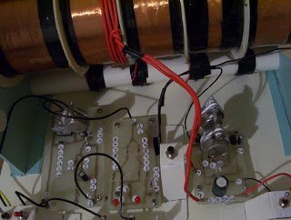 I��ve been building and experimenting with these special energy exciter things on the net sec exciter for short , and have come up with some great improvements and ideas you may be able to apply your skills to and further improve them more than what i could do.for a start i recycle pvc storm water pipes into a long sec tower, coil winder , and hand wounded my coils using it, then i watched the youtube videos on the sec exciters and saw one by jonny davro who in one video used a bd135 transistor and his interest is using as less voltage or current input to get more but after trying that using atfirst smaller transistors.
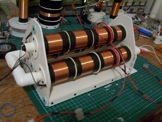 i realized they can��t handle the heat so the bd135 was better for it and i use more voltage and current than those on youtube did at the time so i used the bd135 and even the bd139 and i used a paralleled pair for more voltage handling and so on.
i improvised by using the metal transistor bodies as heatsinks and they work well for there thickness and heat absorbing and ive come up with some interesting circuit experiments using the energy output of these sec exciter towers, like digital rf tv jamming and fast ni-mh battery charging and the battery seemed to be recharging itself in some or one test after ive finished testing the circuit out on it and ive got a circuit that is a mixture of the afremenko plug diodes and a led power meter from another site
and some ideas i threw in that has some kind of rf coupling when placed side by side and charges up hv caps from the output energy of the sec tower its a long story but ill slowly update you soon and email you pictures.
i realized they can��t handle the heat so the bd135 was better for it and i use more voltage and current than those on youtube did at the time so i used the bd135 and even the bd139 and i used a paralleled pair for more voltage handling and so on.
i improvised by using the metal transistor bodies as heatsinks and they work well for there thickness and heat absorbing and ive come up with some interesting circuit experiments using the energy output of these sec exciter towers, like digital rf tv jamming and fast ni-mh battery charging and the battery seemed to be recharging itself in some or one test after ive finished testing the circuit out on it and ive got a circuit that is a mixture of the afremenko plug diodes and a led power meter from another site
and some ideas i threw in that has some kind of rf coupling when placed side by side and charges up hv caps from the output energy of the sec tower its a long story but ill slowly update you soon and email you pictures.
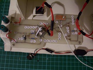 also ive been monitoring the airwaves with another gravity wave detector with a modification and in the area im in back with my partner in the same house as before im receiving all kinds of weird sounds and signals even what sounds like an electric train powering down and a steam whistle when the train line hear is not electric yet as they haven��t extended the electric train line from the other suburb to here yet so we don��t get electric trains this far, anyhow as for the steam whistle sound we don��t have a steam train here either last one was years ago and no longer running.
i think so how does a gravity wave detector receive sounds like this its as if it something from either the other side or dimension or reality even 2 sound bursts of what sounds like air vibration of air over the wings of a plane crashing down on a movie to and faint voices to and sounds like digital sounds to and other weird things and also a sound of a large dynamo powering down to a stop sounds like a sci-fi movie giant spacecraft slowing down in our skies etc etc as i imagined it like that to one sound sounded like a truck zooming down the highways at a distance
also ive been monitoring the airwaves with another gravity wave detector with a modification and in the area im in back with my partner in the same house as before im receiving all kinds of weird sounds and signals even what sounds like an electric train powering down and a steam whistle when the train line hear is not electric yet as they haven��t extended the electric train line from the other suburb to here yet so we don��t get electric trains this far, anyhow as for the steam whistle sound we don��t have a steam train here either last one was years ago and no longer running.
i think so how does a gravity wave detector receive sounds like this its as if it something from either the other side or dimension or reality even 2 sound bursts of what sounds like air vibration of air over the wings of a plane crashing down on a movie to and faint voices to and sounds like digital sounds to and other weird things and also a sound of a large dynamo powering down to a stop sounds like a sci-fi movie giant spacecraft slowing down in our skies etc etc as i imagined it like that to one sound sounded like a truck zooming down the highways at a distance
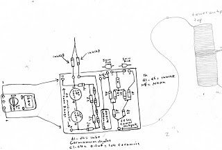
 Its inspired from Bedinis concept of generating free energy.
In my prototype I have a side of the circuit which runs a coil which in turn runs a motor while the other side recharges a battery. When not charging I would like to run a motor where the 110 neon light goes.
Any help would be really appreciated.
I would like to step this up to run on 24 volts and 48 volts and eventually put a switching circuit in top monitor when a battery is charged to flip flop So I can keep the batteries running continuously.
I'm using size 22 and 18 wire gauge wire about a thousand turns for the iron filled coil to run the magnetic wheel I built
In its small scale it works flawlessly however I can not figure out how to step up the components to get the larger amperage through the circuit without blowing things up.
The coil wires are run together around a wood spool about a thousand turns then I have them stuffed with ironIn the center to make my core i'm using welding rod as the core.
The magnetic motor is 12 magnets on a wheel all the poles facing in the same direction.
When you add your power supply the magnetic wheel starts spinning from the start coil, however the run side of the coil charges the secondary battery.
When the 2ndbattery is disconnected the neon light turns on since I need to have that voltage go somewhere.
I keep putting bigger rated transistors but I keep burning up other parts of the circuit.
If
I figure this out ill be able to run my house without the need of the power company.
That��s including running ac units as well.
I don��t remember the guys name who designed the circuit I cant find his forum anywhere.
It was 2 years ago and its been running Continuously in my garage non stop.
I finally decided to try and power things up with it by manipulating the way the coil works
Its been running for 2 years continuously right now I manually switch the batteries from start to charge as one side charges the system the other drains it.
This system actually puts out more Voltage than it uses so there is always excess voltage keeping the charge side fully charged at all times.
I designed a stator that will run the house at a very low rpm so if I can solve this part of the circuit at the higher amp rating and be stable without burning up, the electric company will be a thing of the past.
Ed
Its inspired from Bedinis concept of generating free energy.
In my prototype I have a side of the circuit which runs a coil which in turn runs a motor while the other side recharges a battery. When not charging I would like to run a motor where the 110 neon light goes.
Any help would be really appreciated.
I would like to step this up to run on 24 volts and 48 volts and eventually put a switching circuit in top monitor when a battery is charged to flip flop So I can keep the batteries running continuously.
I'm using size 22 and 18 wire gauge wire about a thousand turns for the iron filled coil to run the magnetic wheel I built
In its small scale it works flawlessly however I can not figure out how to step up the components to get the larger amperage through the circuit without blowing things up.
The coil wires are run together around a wood spool about a thousand turns then I have them stuffed with ironIn the center to make my core i'm using welding rod as the core.
The magnetic motor is 12 magnets on a wheel all the poles facing in the same direction.
When you add your power supply the magnetic wheel starts spinning from the start coil, however the run side of the coil charges the secondary battery.
When the 2ndbattery is disconnected the neon light turns on since I need to have that voltage go somewhere.
I keep putting bigger rated transistors but I keep burning up other parts of the circuit.
If
I figure this out ill be able to run my house without the need of the power company.
That��s including running ac units as well.
I don��t remember the guys name who designed the circuit I cant find his forum anywhere.
It was 2 years ago and its been running Continuously in my garage non stop.
I finally decided to try and power things up with it by manipulating the way the coil works
Its been running for 2 years continuously right now I manually switch the batteries from start to charge as one side charges the system the other drains it.
This system actually puts out more Voltage than it uses so there is always excess voltage keeping the charge side fully charged at all times.
I designed a stator that will run the house at a very low rpm so if I can solve this part of the circuit at the higher amp rating and be stable without burning up, the electric company will be a thing of the past.
Ed
 Referring to the figure below we see that the set up is especially intended for exploiting the rise and the fall of the sea water ebbs or rather the giant waves and the surfs.
During the rising stance of the wave, we may notice a significant increase in the level of the sea water for the relevant section of the water.
This instantaneous increase in the level of the sea reduces to minimal levels when the water ebbs out or when the waves crashes down to repeat the cycle afresh.
This ongoing process if trapped inside an enclosed area effectively simulates a pumping or piston like action.
In other words, the above operation of the sea water generates a powerful push pull effect of the air column inside the enclosed area.
Referring to the figure below we see that the set up is especially intended for exploiting the rise and the fall of the sea water ebbs or rather the giant waves and the surfs.
During the rising stance of the wave, we may notice a significant increase in the level of the sea water for the relevant section of the water.
This instantaneous increase in the level of the sea reduces to minimal levels when the water ebbs out or when the waves crashes down to repeat the cycle afresh.
This ongoing process if trapped inside an enclosed area effectively simulates a pumping or piston like action.
In other words, the above operation of the sea water generates a powerful push pull effect of the air column inside the enclosed area.

 The MOSFET IRF540 can be replaced with any low power MOSFET such as BS170 etc
Slowing down the rise time of the modulation signal produces a somewhat better output audio, and this is accomplished by inserting a simple R/C low pass filter (R5 and C3) between the astableoutput and theTr3 gate.
Tr3 is implemented in a standard VCA that also includes R6 and R7.
C1 and C2 serve as DC blocking capacitors, while C6 serves as a supply decoupling capacitor.
The circuit has the effect of modifyingthe input voicesignals to two degrees of attenuation, the highest of which is approximately 26 dB greater than the lower, which results in the production of the robot like manipulated sound.
The modulation oscillator ��breaks up�� the signal by switching it between these two levels with a frequencyof manyHertz, giving the desired robotic voiceeffect.
Despite the fact that this circuit employs the most commonly adopted technique of electronically creating a computer-generated voice effect, it performs admirably in practical use.
The input signal level can be as high as a few volts peak to peak without causing any overloading issues.
S1 controls the on/off switch.
The circuit drawsaround 1 milliampere of current.
You will need an audio amplifier unit hooked up with the output of the circuit for hearing the robot voice loudly over a loudspeaker.
The MOSFET IRF540 can be replaced with any low power MOSFET such as BS170 etc
Slowing down the rise time of the modulation signal produces a somewhat better output audio, and this is accomplished by inserting a simple R/C low pass filter (R5 and C3) between the astableoutput and theTr3 gate.
Tr3 is implemented in a standard VCA that also includes R6 and R7.
C1 and C2 serve as DC blocking capacitors, while C6 serves as a supply decoupling capacitor.
The circuit has the effect of modifyingthe input voicesignals to two degrees of attenuation, the highest of which is approximately 26 dB greater than the lower, which results in the production of the robot like manipulated sound.
The modulation oscillator ��breaks up�� the signal by switching it between these two levels with a frequencyof manyHertz, giving the desired robotic voiceeffect.
Despite the fact that this circuit employs the most commonly adopted technique of electronically creating a computer-generated voice effect, it performs admirably in practical use.
The input signal level can be as high as a few volts peak to peak without causing any overloading issues.
S1 controls the on/off switch.
The circuit drawsaround 1 milliampere of current.
You will need an audio amplifier unit hooked up with the output of the circuit for hearing the robot voice loudly over a loudspeaker.
 In this post we discuss 5 different ways to create an electronic version or a digital version of a dice which can be used to get random numbers between 1 to 6 through either LED display or digital display.
 The working of this 4017 IC based dice circuit is pretty simple.
We know that when clock signals are fed at the pin#14 of the 4017 IC, the output of the IC starts sequencing forward from pin#3 towards pin#11.
But since here the pin#5 is connected with the reset pin#15 of the IC, the outputs are able to sequence only up to pin#1 and return back to pin#3 for a new sequence.
This sequencing keeps repeating as long as a clock frequency is applied at pin#14 of the IC.
This clock frequency is applied by the IC 555 which is configured like a free running astable multivibrator with a high frequency output.
When the push button PB1 is pressed for a brief moment and released, the capacitor 1000uF charges up fully and powers the IC 555, the IC 555 uses this power and remains switched ON for a few seconds, allowing the IC 4017 to sequence rapidly across the output pins.
When the charge inside the 1000uF capacitor is fully used up, the IC 555 turns OFF and stops providing the clock pulses to the IC 4017. This output sequencing of the IC 4017 now halts to a randomly selected output of the IC between pin#3 and pin#1.
The outputs of the IC can be seen wired with series LEDs which illuminate and indicate the random dice number when the sequencing stops.
The working of this 4017 IC based dice circuit is pretty simple.
We know that when clock signals are fed at the pin#14 of the 4017 IC, the output of the IC starts sequencing forward from pin#3 towards pin#11.
But since here the pin#5 is connected with the reset pin#15 of the IC, the outputs are able to sequence only up to pin#1 and return back to pin#3 for a new sequence.
This sequencing keeps repeating as long as a clock frequency is applied at pin#14 of the IC.
This clock frequency is applied by the IC 555 which is configured like a free running astable multivibrator with a high frequency output.
When the push button PB1 is pressed for a brief moment and released, the capacitor 1000uF charges up fully and powers the IC 555, the IC 555 uses this power and remains switched ON for a few seconds, allowing the IC 4017 to sequence rapidly across the output pins.
When the charge inside the 1000uF capacitor is fully used up, the IC 555 turns OFF and stops providing the clock pulses to the IC 4017. This output sequencing of the IC 4017 now halts to a randomly selected output of the IC between pin#3 and pin#1.
The outputs of the IC can be seen wired with series LEDs which illuminate and indicate the random dice number when the sequencing stops.
 The working of the above shown IC 4017 electronic LED dice circuit is the same as the first diagram, except the number of LEDs used, which has restricted to one LED per output, for the IC.
When the push button is pressed, the IC 555 starts oscillating at a very high speed, causing the IC 4017 output to sequence from pin#3 to pin#1 at an equivalently high speed.
The high speed sequencing makes it difficult for the user to realize exactly where the sequence would stop after the push button is released.
Thus, when the push button is released, the sequencing abruptly stops at some random output pin of the IC denoting the respective dice number, in accordance with the LED indication.
For example if the LEDs are marked from 1 to 6, with respect to the output pin#3 to pin#1, then if suppose the sequence stops at pin#7, illuminating the LED at pin#7 would indicate the dice number of 4, and so on.
The working of the above shown IC 4017 electronic LED dice circuit is the same as the first diagram, except the number of LEDs used, which has restricted to one LED per output, for the IC.
When the push button is pressed, the IC 555 starts oscillating at a very high speed, causing the IC 4017 output to sequence from pin#3 to pin#1 at an equivalently high speed.
The high speed sequencing makes it difficult for the user to realize exactly where the sequence would stop after the push button is released.
Thus, when the push button is released, the sequencing abruptly stops at some random output pin of the IC denoting the respective dice number, in accordance with the LED indication.
For example if the LEDs are marked from 1 to 6, with respect to the output pin#3 to pin#1, then if suppose the sequence stops at pin#7, illuminating the LED at pin#7 would indicate the dice number of 4, and so on.
 When the mode is in the high state, data is delivered into Qa - Qd via inputs A- D through the subsequent negative-going clock edge.
When the mode is in the low state, data is transferred over Qa - Qd through the subsequent negative-going clock edge.
By attaching the mode control to Qa ensures that the register alternately conducts between load and shift, enabling the input word to be a function of the existing output word.
Using some basic logic, the register is finally designed to implement count numbers that switch the LEDs randomly in a dice display, to imitate the random numbers of a real cubical type dice.
Remember that the LEDs are illuminated whenever the outputs are low logic.
IC1a is configured like a standard Schmitt oscillator that supplies clock pulses to the register.
Switch SW 1 is used to stop the oscillator and inhibit the counting process.
Therefore, to get the dice number, the user has to press the SW1, which freezes the count and provides the random dice number to the user.
When power is first switched ON, the register may possibly commence with an invalid count, however after a few clock periods it will create a legitimate count after which it will continue to be in that specific sequence
When the mode is in the high state, data is delivered into Qa - Qd via inputs A- D through the subsequent negative-going clock edge.
When the mode is in the low state, data is transferred over Qa - Qd through the subsequent negative-going clock edge.
By attaching the mode control to Qa ensures that the register alternately conducts between load and shift, enabling the input word to be a function of the existing output word.
Using some basic logic, the register is finally designed to implement count numbers that switch the LEDs randomly in a dice display, to imitate the random numbers of a real cubical type dice.
Remember that the LEDs are illuminated whenever the outputs are low logic.
IC1a is configured like a standard Schmitt oscillator that supplies clock pulses to the register.
Switch SW 1 is used to stop the oscillator and inhibit the counting process.
Therefore, to get the dice number, the user has to press the SW1, which freezes the count and provides the random dice number to the user.
When power is first switched ON, the register may possibly commence with an invalid count, however after a few clock periods it will create a legitimate count after which it will continue to be in that specific sequence
 IC1a and IC1b is designed to operate like an oscillator producing a frequency output of some kilohertz.
The output is applied to the IC 7490 which is a binary counter and is configured to generate an output of 0 to 5 in BCD.
To ensure that the digital dice behaves exactly like a cube dice, the digital display must be capable of producing the reading from 1 to 6 and not 0-5.
Also, whenever the IC 7490's outputs are all '0's, the 7 segment LED display must indicate the number 6.
IC1c, d and IC3 are used exactly to implement this job, for changing an output of 000 from IC2 to 110 (b).
IC4 is a BCD to 7-segment decoder which is configured to run the 7-segment LED display by means of the current limit resistors R4-R10.
The switch PB1 is a push-to-off switch, which must pushed and then released momentarily to get the random digital dice number on the digital display.
IC1a and IC1b is designed to operate like an oscillator producing a frequency output of some kilohertz.
The output is applied to the IC 7490 which is a binary counter and is configured to generate an output of 0 to 5 in BCD.
To ensure that the digital dice behaves exactly like a cube dice, the digital display must be capable of producing the reading from 1 to 6 and not 0-5.
Also, whenever the IC 7490's outputs are all '0's, the 7 segment LED display must indicate the number 6.
IC1c, d and IC3 are used exactly to implement this job, for changing an output of 000 from IC2 to 110 (b).
IC4 is a BCD to 7-segment decoder which is configured to run the 7-segment LED display by means of the current limit resistors R4-R10.
The switch PB1 is a push-to-off switch, which must pushed and then released momentarily to get the random digital dice number on the digital display.

 In this set up we can see the electromagnet fixed at the upper center area of the wooden structures, while the LED and LDR are positioned face to face over the adjacent upright wooden structures, just below the electromagnet.
It is important that the LED and the LDR are placed inside an opaque plastic tubes to ensure that only the LED light beam enters the LDR tube and illuminates it, and no other external ambient light is able to reach the LDR.
Once the electromagnetic levitation circuit is powered ON, the LED illuminates and hits the LDR, which causes the electromagnet to switch ON.
Now, the electromagnet being switched ON, if a iron object is brought near the electromagnet will cause the object to be pulled towards the electromagnet.
However, during this process the iron object wil tend to block the LED beam from the reaching the LDR.
This will instantly cause the electromagnet to switch OFF.
As soon as this happens the iron object will tend to fall down, but in the process will move away from the LED beam illuminating the LDR and switching ON the electromagnet back in action.
This rapid ON/OFF process of the electromagnet will cause the iron object to remains hanging just below the electromagnet creating an impression of a true levitation or anti-gravity effect, as shown in the following image.
In this set up we can see the electromagnet fixed at the upper center area of the wooden structures, while the LED and LDR are positioned face to face over the adjacent upright wooden structures, just below the electromagnet.
It is important that the LED and the LDR are placed inside an opaque plastic tubes to ensure that only the LED light beam enters the LDR tube and illuminates it, and no other external ambient light is able to reach the LDR.
Once the electromagnetic levitation circuit is powered ON, the LED illuminates and hits the LDR, which causes the electromagnet to switch ON.
Now, the electromagnet being switched ON, if a iron object is brought near the electromagnet will cause the object to be pulled towards the electromagnet.
However, during this process the iron object wil tend to block the LED beam from the reaching the LDR.
This will instantly cause the electromagnet to switch OFF.
As soon as this happens the iron object will tend to fall down, but in the process will move away from the LED beam illuminating the LDR and switching ON the electromagnet back in action.
This rapid ON/OFF process of the electromagnet will cause the iron object to remains hanging just below the electromagnet creating an impression of a true levitation or anti-gravity effect, as shown in the following image.
 As you can see there's hardly any components in the design, and the entire circuit is built around a single IC 741 which is configured like a comparator.
The pin#2 of the op amp is fixed with a constant reference voltage using the preset 1k.
This reference voltage is not very critical, since the LDR switching is either ON or OFF.
The LED light can be seen focused on the LDR as explained in our previous construction set of the unit.
During the time the light remains focused on the LDR, its resistance drops to a much lower level, causing the pin#3 potential of the op amp to rise above the pin#2 reference potential as fixed by the 1k preset.
Due to this the output of the op amp remains high, enabling the electromagnet to remain activated.
As discussed in the previous paragraphs, when the iron object is pulled towards the electromagnet, in the process it attempts to block the LED beams reaching the LDR.
When this happens, the pin#3 potential drops below the pin#2 reference potential which now rises above the pin#3 potential.
Due to this, the pin#6 output of the op amp turns off, which also turns off the driver transistor and the electromagnet.
This instantaneous switching off of the electromagnet tends to drop the iron object, which causes the LDR to again get illuminated by the LDR beam, which reverts the op amp output high, switching ON the electromagnet back, so that the iron objetc s again pulled up.
This pulling and dropping process of the iron object continuous at an extremely fast rate causing, such that the the object appears to remains stationery just below the electromagnet, which gives an impression of the object being levitated, and it is hanging in mid-air due to anti-gravity effect.
As you can see there's hardly any components in the design, and the entire circuit is built around a single IC 741 which is configured like a comparator.
The pin#2 of the op amp is fixed with a constant reference voltage using the preset 1k.
This reference voltage is not very critical, since the LDR switching is either ON or OFF.
The LED light can be seen focused on the LDR as explained in our previous construction set of the unit.
During the time the light remains focused on the LDR, its resistance drops to a much lower level, causing the pin#3 potential of the op amp to rise above the pin#2 reference potential as fixed by the 1k preset.
Due to this the output of the op amp remains high, enabling the electromagnet to remain activated.
As discussed in the previous paragraphs, when the iron object is pulled towards the electromagnet, in the process it attempts to block the LED beams reaching the LDR.
When this happens, the pin#3 potential drops below the pin#2 reference potential which now rises above the pin#3 potential.
Due to this, the pin#6 output of the op amp turns off, which also turns off the driver transistor and the electromagnet.
This instantaneous switching off of the electromagnet tends to drop the iron object, which causes the LDR to again get illuminated by the LDR beam, which reverts the op amp output high, switching ON the electromagnet back, so that the iron objetc s again pulled up.
This pulling and dropping process of the iron object continuous at an extremely fast rate causing, such that the the object appears to remains stationery just below the electromagnet, which gives an impression of the object being levitated, and it is hanging in mid-air due to anti-gravity effect.
 In our plasma ball circuit, an ordinary 100 watt bulb is used for the display unit.
The glass lamp used in this design is customized by gluing a small sheet of aluminum foil directly to the back half of the glass, to make a kind of high voltage capacitor.
The filament inside the lamp bulb works like one particular plate of the capacitor, the glass of the bulb acts like the dielectric, and the aluminum foil serves like the second plate.
The aluminum foil, which acts like the negative plate of a polarized electrolytic capacitor, needs to be grounded by connecting the aluminum foil with the negative line.
A high voltage is discharged inside the bulb by means of its inner filament electrode, ionizing the thin gas that stays within the glass envelope, producing a spectacular visual effect identical to an electrical lightening and storm.
In our plasma ball circuit, an ordinary 100 watt bulb is used for the display unit.
The glass lamp used in this design is customized by gluing a small sheet of aluminum foil directly to the back half of the glass, to make a kind of high voltage capacitor.
The filament inside the lamp bulb works like one particular plate of the capacitor, the glass of the bulb acts like the dielectric, and the aluminum foil serves like the second plate.
The aluminum foil, which acts like the negative plate of a polarized electrolytic capacitor, needs to be grounded by connecting the aluminum foil with the negative line.
A high voltage is discharged inside the bulb by means of its inner filament electrode, ionizing the thin gas that stays within the glass envelope, producing a spectacular visual effect identical to an electrical lightening and storm.
 The moment TR1 fires or conducts, a small burst of electricity is driven through C2 to the primary side winding of T1. (Remember that as soon as AC mains input is first applied to the capacitor C2, it behaves like a short, after which the capacitor starts to charge towards the applied voltage level.)
This burst of electricity induces a strong rush of magnetic field inside the T1 primary winding, triggering an equivalent amount of stepped-up high voltage across its secondary winding of the ignition coil.
Next, as soon as the capacitor C2 starts to charge to its maximum peak level, the AC voltage to the diac begins to drop quickly.
As the voltage drops downwards, the current necessary to keep triac switched ON sinks below the holding level, the triac now gets switched off.
After this positive cycle, the next half of the AC signal which is negative commences.
As the AC voltage cycle starts getting more negative, a potential begins appearing to the triac's trigger input via the diac, triggering it to fire.
Since triacs are designed to conduct for both the AC half cycles, the triac fires during both the voltage cycles of the AC.
Now as TR1 conducts in the reverse direction, the C2 charge begins draining off, via TR1, which causes the next burst of electricity with opposite voltage to get induced in the primary winding of T1, causing the equivalent amount of stepped up voltage to be transferred in its secondary winding.
During these conductions of the triac, high-voltage output of more than 2 kv is generated at the secondary of T1 which is applied to the lamp, filament, creating a plasma ball display to be generated inside the lamp.
The C2 value should be selected such that it is not beyond 2-2.5 ��F to protect against damage to the ignition coil T1.
Alternatively, if the C2 value is selected very small, the plasma ball sparking inside the bulb might fail to glow with satisfactory effect and brightness.
Inductors LI and L2 have been included in order to block the ignition coil switching transients and spikes from returning back to the home AC wiring or the AC line.
The moment TR1 fires or conducts, a small burst of electricity is driven through C2 to the primary side winding of T1. (Remember that as soon as AC mains input is first applied to the capacitor C2, it behaves like a short, after which the capacitor starts to charge towards the applied voltage level.)
This burst of electricity induces a strong rush of magnetic field inside the T1 primary winding, triggering an equivalent amount of stepped-up high voltage across its secondary winding of the ignition coil.
Next, as soon as the capacitor C2 starts to charge to its maximum peak level, the AC voltage to the diac begins to drop quickly.
As the voltage drops downwards, the current necessary to keep triac switched ON sinks below the holding level, the triac now gets switched off.
After this positive cycle, the next half of the AC signal which is negative commences.
As the AC voltage cycle starts getting more negative, a potential begins appearing to the triac's trigger input via the diac, triggering it to fire.
Since triacs are designed to conduct for both the AC half cycles, the triac fires during both the voltage cycles of the AC.
Now as TR1 conducts in the reverse direction, the C2 charge begins draining off, via TR1, which causes the next burst of electricity with opposite voltage to get induced in the primary winding of T1, causing the equivalent amount of stepped up voltage to be transferred in its secondary winding.
During these conductions of the triac, high-voltage output of more than 2 kv is generated at the secondary of T1 which is applied to the lamp, filament, creating a plasma ball display to be generated inside the lamp.
The C2 value should be selected such that it is not beyond 2-2.5 ��F to protect against damage to the ignition coil T1.
Alternatively, if the C2 value is selected very small, the plasma ball sparking inside the bulb might fail to glow with satisfactory effect and brightness.
Inductors LI and L2 have been included in order to block the ignition coil switching transients and spikes from returning back to the home AC wiring or the AC line.
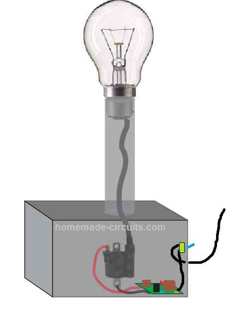 The aluminum foil behind the glass bulb is not shown in the above image, so make sure to stick an aluminum foil behind the bulb glass externally and connect it wire it with the circuit appropriately as per the indicated diagram layout.
Once the above set up is built and tested, do not forget to cover the lamp structure with another plastic tube, so that the glass can e protected from accidental knocks and damages, as shown below:
The aluminum foil behind the glass bulb is not shown in the above image, so make sure to stick an aluminum foil behind the bulb glass externally and connect it wire it with the circuit appropriately as per the indicated diagram layout.
Once the above set up is built and tested, do not forget to cover the lamp structure with another plastic tube, so that the glass can e protected from accidental knocks and damages, as shown below:
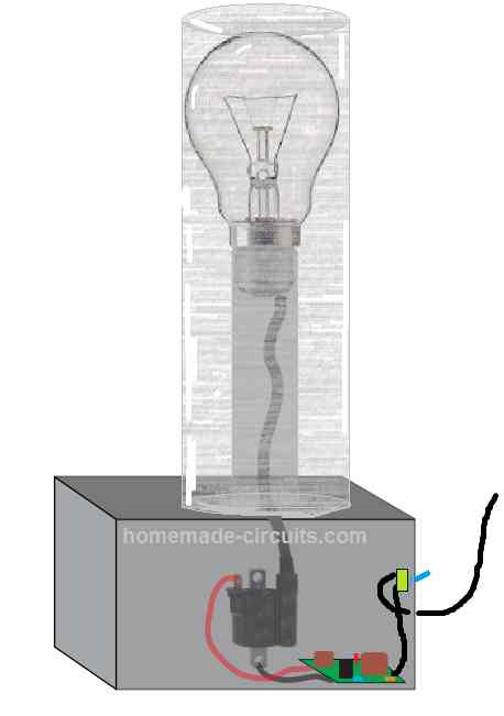
 Another simple plasma ball circuit can be seen in the following article:
https://www.homemade-circuits.com/wp-content/uploads/2021/05/plasma-ball-circuit.pdf
WARNING: THIS PROJECT INVOLVES EXTREMELY HIGH LETHAL VOLTAGES.
USERS ARE ADVISED TO MAINTAIN EXTREME CAUTION AND TAKE APPROPRIATE PROTECTION MEASURES WHILE BUILDING AND TESTING THIS CIRCUIT.
Another simple plasma ball circuit can be seen in the following article:
https://www.homemade-circuits.com/wp-content/uploads/2021/05/plasma-ball-circuit.pdf
WARNING: THIS PROJECT INVOLVES EXTREMELY HIGH LETHAL VOLTAGES.
USERS ARE ADVISED TO MAINTAIN EXTREME CAUTION AND TAKE APPROPRIATE PROTECTION MEASURES WHILE BUILDING AND TESTING THIS CIRCUIT.

 Referring to the above block diagram, sound vibration is detected through the mic, and boosted through a basic opamp pre-amplifier.
The the op-amp output is rectified (meaning transformed from a.c.
to d.c.) and applied to control a Darlington power amplifier.
As soon as the power amplifier triggers on, a substantial amount of current moves through the solenoid and the LEDs.
Referring to the above block diagram, sound vibration is detected through the mic, and boosted through a basic opamp pre-amplifier.
The the op-amp output is rectified (meaning transformed from a.c.
to d.c.) and applied to control a Darlington power amplifier.
As soon as the power amplifier triggers on, a substantial amount of current moves through the solenoid and the LEDs.
 Because resistor R4 feeds back the output signal of the op amp with the inverting input, the AC content gets eliminated.
On the other hand, capacitor C3 gives an AC connection to 0V through R5.
At this point the only portion of the a.c.
output shows up on pin 2, and the output is therefore moderately lowered.
The R4 to R5 divider fixes the average optimum a.c.
gain reached by the circuit.
Because resistor R4 feeds back the output signal of the op amp with the inverting input, the AC content gets eliminated.
On the other hand, capacitor C3 gives an AC connection to 0V through R5.
At this point the only portion of the a.c.
output shows up on pin 2, and the output is therefore moderately lowered.
The R4 to R5 divider fixes the average optimum a.c.
gain reached by the circuit.
 Verify that the diodes and transistors are installed the right way round, and a BC184L is employed for TR1, instead of a BC184 which contains pinouts in some other order.
Capacitors C2 and C6 are usually axial forms, that rest flat on the PCB surface.
Make sure that capacitors C2, C3, C4 and C6 are fixed the right way round.
Attach wire pins for the mic, LEDs, solenoid and power accessory.
Switch S1 could be avoided in case the circuit is to be driven from a mains adapter device.
Last but not least press the 741 IC straight into its socket, making certain that pin#1 sits in the right spot.
This IC is not really sensitive to static electricity, and therefore could be touched without having any safety measures.
Verify that the diodes and transistors are installed the right way round, and a BC184L is employed for TR1, instead of a BC184 which contains pinouts in some other order.
Capacitors C2 and C6 are usually axial forms, that rest flat on the PCB surface.
Make sure that capacitors C2, C3, C4 and C6 are fixed the right way round.
Attach wire pins for the mic, LEDs, solenoid and power accessory.
Switch S1 could be avoided in case the circuit is to be driven from a mains adapter device.
Last but not least press the 741 IC straight into its socket, making certain that pin#1 sits in the right spot.
This IC is not really sensitive to static electricity, and therefore could be touched without having any safety measures.
 Slots must be created on the table tennis balls, to ensure they generate a snug fit around the solenoid axle.
The chord or the string tied to the solenoid armature results in the balls to turn in one particular direction, while the elastic string drags them back again.
Selfadhesive tape could be used to attach the chords to the axle.
The Halloween "eye" movement limit is determined by the solenoid shaft sitting alongside the upper surface of the box.
While the eyes are in the closed position, the shaft should be completely drawn into the case and with the eyes in the open position the shaft should be extended upward.
Long insulated wires must be soldered on the PCB on the LED points, and inserted via the drilled holes in the enclosure for connecting the LEDs.
Make sure the LEDs are attached with the right polarity.
Using colored wires which might help prevent connection faults.
The LEDs may then be pressed into the slots drilled on the mask, right before the mask is mounted into position.
Slots must be created on the table tennis balls, to ensure they generate a snug fit around the solenoid axle.
The chord or the string tied to the solenoid armature results in the balls to turn in one particular direction, while the elastic string drags them back again.
Selfadhesive tape could be used to attach the chords to the axle.
The Halloween "eye" movement limit is determined by the solenoid shaft sitting alongside the upper surface of the box.
While the eyes are in the closed position, the shaft should be completely drawn into the case and with the eyes in the open position the shaft should be extended upward.
Long insulated wires must be soldered on the PCB on the LED points, and inserted via the drilled holes in the enclosure for connecting the LEDs.
Make sure the LEDs are attached with the right polarity.
Using colored wires which might help prevent connection faults.
The LEDs may then be pressed into the slots drilled on the mask, right before the mask is mounted into position.


 Note: Please use at least 10K resistor at the base of the BC548 transistor, 330 Ohms is too low.
The transformer step down the 230VAC to 12VAC and bridge rectifier convert AC onto DC current and the current passes through an electrolytic capacitor to smooth the power supply.
A fixed 12V voltage regulator gives power to arduino, GSM modem and relay.
The GSM modem is connected to arduino at pin #0 and pin #1, which are RX and TX respectively.
The RX of GSM is connected to TX of arduino and TX of GSM is connected to RX of arduino.
If you are confused, just look at the below diagram, misconnection will not send or receive SMS.
ARDUINO TX----------------------RX GSM modem
RX----------------------TX
Ground to ground connection is also established between arduino and GSM modem.
Try to get a male jack power connector for the GSM and arduino, if not just solder the wires directly from power supply to arduino and GSM, which might increase the mess in the project.
The transistor drives the relay and the diode protects the circuit from high voltage spikes while switching the relay ON/OFF.
The LED indicator shows the status of the relay.
If the LED glows the relay activated and if the LED is off, the relay is deactivated.
Insert a valid SIM on the GSM modem and try to take advantage of the offers availed by the network provider for SMS such as rate cutters, which will reduce the expenses for SMS.
Note: Please use at least 10K resistor at the base of the BC548 transistor, 330 Ohms is too low.
The transformer step down the 230VAC to 12VAC and bridge rectifier convert AC onto DC current and the current passes through an electrolytic capacitor to smooth the power supply.
A fixed 12V voltage regulator gives power to arduino, GSM modem and relay.
The GSM modem is connected to arduino at pin #0 and pin #1, which are RX and TX respectively.
The RX of GSM is connected to TX of arduino and TX of GSM is connected to RX of arduino.
If you are confused, just look at the below diagram, misconnection will not send or receive SMS.
ARDUINO TX----------------------RX GSM modem
RX----------------------TX
Ground to ground connection is also established between arduino and GSM modem.
Try to get a male jack power connector for the GSM and arduino, if not just solder the wires directly from power supply to arduino and GSM, which might increase the mess in the project.
The transistor drives the relay and the diode protects the circuit from high voltage spikes while switching the relay ON/OFF.
The LED indicator shows the status of the relay.
If the LED glows the relay activated and if the LED is off, the relay is deactivated.
Insert a valid SIM on the GSM modem and try to take advantage of the offers availed by the network provider for SMS such as rate cutters, which will reduce the expenses for SMS.

 When we send SMS command ��/MOTOR ON/�� the pin # 9 goes high and trigger the relay ON.
If the relay connects the common and N/O pins the pump starts and also turns ON the transformer which will give +5 at the output.
The +5V signal is fed to pin # 7 which will confirm and return with an acknowledgement ��Motor activated��.
When we send ��/MOTOR OFF/�� the pin # 9 turns LOW and relay disconnects the common and N/O pins, this will turn off the pump as well as the connected transformer.
The output at pin # 7 goes LOW and returns with an acknowledgement ��Motor deactivated��.
If no acknowledgement SMS is received in your cellphone, we can confirm that no action was taken and the pump is at the last requested state, you may go to the site and troubleshoot or no acknowledgement is received due power cut.
When we send SMS command ��/MOTOR ON/�� the pin # 9 goes high and trigger the relay ON.
If the relay connects the common and N/O pins the pump starts and also turns ON the transformer which will give +5 at the output.
The +5V signal is fed to pin # 7 which will confirm and return with an acknowledgement ��Motor activated��.
When we send ��/MOTOR OFF/�� the pin # 9 turns LOW and relay disconnects the common and N/O pins, this will turn off the pump as well as the connected transformer.
The output at pin # 7 goes LOW and returns with an acknowledgement ��Motor deactivated��.
If no acknowledgement SMS is received in your cellphone, we can confirm that no action was taken and the pump is at the last requested state, you may go to the site and troubleshoot or no acknowledgement is received due power cut.
 NOTE: The 100uF /10K and 220uF and 47K values may need some adjustments in order ensure the correct amount of delay for the respective transistors and relay stages.
 NOTE: Please replace the transistor base resistor 330 ohm with a 10 K resistor, because 330 ohm value is too low and is incorrect.
The circuit consists of Arduino, which sense intrusion and take decisions.
GSM modem receives command for sending SMS to user and few other passive components to detect intrusion.
The Arduino scans the laser beam for interruption in light 500 times a second.
The LDR senses the presence laser light and gives signal to Arduino.
The 10K and LDR forms voltage divider, the analogue signal is taken from a point between these two components.
When the incident light intensity reduces to certain degree or light completely cut-off the arduino recognize as intrusion.
The 10K resistor which is connected to ��activate button�� acts as pull down resistor to prevent the arduino pin from activating randomly.
The transistor activates the relay in case of an intrusion and the diode protects the rest of the circuit from high voltage spike while switching the relay on and off.
You can connect a siren or lights or whatever you wish to connect to relay.
To activate the security system, we have to press the activate button, the LED indicator confirms that the button is pressed.
The system gets activated only after 2 minutes; this will give time to lock you property and leave the place.
When you return home, to deactivate the system press the reset button.
Solder a push-to-on button from reset button terminal of Arduino, so that the reset button to deactivate the system is easily accessible from outside the setup.
Once the circuit detected intrusion, the relay will be activated for 2 minutes and it turns off and it will be ready to detect next intrusion.
The GSM modem need external power supply as arduino can��t provide enough current to the module.
Please insert a valid SIM card with a working SMS plan.
That��s all about this SMS based laser security circuit; now let��s see how to implement the setup in correct way.
NOTE: Please replace the transistor base resistor 330 ohm with a 10 K resistor, because 330 ohm value is too low and is incorrect.
The circuit consists of Arduino, which sense intrusion and take decisions.
GSM modem receives command for sending SMS to user and few other passive components to detect intrusion.
The Arduino scans the laser beam for interruption in light 500 times a second.
The LDR senses the presence laser light and gives signal to Arduino.
The 10K and LDR forms voltage divider, the analogue signal is taken from a point between these two components.
When the incident light intensity reduces to certain degree or light completely cut-off the arduino recognize as intrusion.
The 10K resistor which is connected to ��activate button�� acts as pull down resistor to prevent the arduino pin from activating randomly.
The transistor activates the relay in case of an intrusion and the diode protects the rest of the circuit from high voltage spike while switching the relay on and off.
You can connect a siren or lights or whatever you wish to connect to relay.
To activate the security system, we have to press the activate button, the LED indicator confirms that the button is pressed.
The system gets activated only after 2 minutes; this will give time to lock you property and leave the place.
When you return home, to deactivate the system press the reset button.
Solder a push-to-on button from reset button terminal of Arduino, so that the reset button to deactivate the system is easily accessible from outside the setup.
Once the circuit detected intrusion, the relay will be activated for 2 minutes and it turns off and it will be ready to detect next intrusion.
The GSM modem need external power supply as arduino can��t provide enough current to the module.
Please insert a valid SIM card with a working SMS plan.
That��s all about this SMS based laser security circuit; now let��s see how to implement the setup in correct way.
 Place the laser source and arduino circuit in such a way that the laser light falls exactly on LDR.
You can also try mirrors reflecting the laser beam to cover a large area.
If you own pets and to prevent accidental or false alarm, elevate the whole setup to hip level of an adult.
You pets will go under the laser beams preventing false triggering.
The LDR is susceptible to errors/false alarm when ambient light falls on it.
To avoid these kinds of errors, we need to enclose the LDR with opaque hollow cylinder with one end open and other end closed made up of plastic or any other material.
Place the laser source and arduino circuit in such a way that the laser light falls exactly on LDR.
You can also try mirrors reflecting the laser beam to cover a large area.
If you own pets and to prevent accidental or false alarm, elevate the whole setup to hip level of an adult.
You pets will go under the laser beams preventing false triggering.
The LDR is susceptible to errors/false alarm when ambient light falls on it.
To avoid these kinds of errors, we need to enclose the LDR with opaque hollow cylinder with one end open and other end closed made up of plastic or any other material.
 Make sure the front portion of the tube is covered as well and only tiny hole with few millimeters in diameter for entering laser beam.
When the laser beam falls on the LDR the value read by the arduino is low but when light interruption is detected the value will go to peak at the same instant, which you can witness the same from serial monitor.
Once the light intensity goes below the pre-determined threshold, arduino trigger the relay and send SMS alert to the user.
Make sure the front portion of the tube is covered as well and only tiny hole with few millimeters in diameter for entering laser beam.
When the laser beam falls on the LDR the value read by the arduino is low but when light interruption is detected the value will go to peak at the same instant, which you can witness the same from serial monitor.
Once the light intensity goes below the pre-determined threshold, arduino trigger the relay and send SMS alert to the user.
 An external power supply is used for heater coil of the sensor.
The input for IC7805 must be above 8 volt.
The GSM modem must be powered form its DC jack and not hosted from arduino supply.
The ground to ground connection is established between external power, GSM modem and arduino.
Use a valid SIM card and make sure that, your SIM has working SMS plan.
An external power supply is used for heater coil of the sensor.
The input for IC7805 must be above 8 volt.
The GSM modem must be powered form its DC jack and not hosted from arduino supply.
The ground to ground connection is established between external power, GSM modem and arduino.
Use a valid SIM card and make sure that, your SIM has working SMS plan.
 Resistors R2-R4 and capacitor C1 are configured like a timing circuit together with IC1, which is a 556 dual timer IC.
As long as S2 remains in the open condition, the C1's charge/discharge period is fixed at somewhere around 2 Hz.
When S2 is switched ON, it boosts the charge/discharge period of C1 to roughly around 4 Hz.
The output pin#5 of the IC1 is connected through R5 and C3 with pin#8 of IC1. The area of IC1 consisting of the parts R7, R8, and C4 build the second timing circuit.
The function of the first timer is to produce the delay time in Hz, while the 2nd timer generates the required precision pulses for the inductor.
The pulses for the inductor is delivered to the base of Q1 transistor by means of a current limiting resistor R8.
During the period transistor Q1 switches ON, the primary winding of the audio-transformer T1 gets grounded briefly, which cause T1 to energize.
Each time T1 is energized and de-energized cause the capacitor C5 to charge and discharge.
This repetitive charging cycles decreases the rise and fall time of the pulse, which subsequently enhances the time-span of the output pulse through T1, and simultaneously carve the output waveform edges to appear more like a half sinewave.
Parts C5, D1, and R9 are further used for shaping the output waveform of the circuit.
Potentiometer R10 is employed to regulate the pulse amplitude up to as high as 200 V along with an interval of 2 ms, which may have an total current drain of below 10 mA.
Resistors R2-R4 and capacitor C1 are configured like a timing circuit together with IC1, which is a 556 dual timer IC.
As long as S2 remains in the open condition, the C1's charge/discharge period is fixed at somewhere around 2 Hz.
When S2 is switched ON, it boosts the charge/discharge period of C1 to roughly around 4 Hz.
The output pin#5 of the IC1 is connected through R5 and C3 with pin#8 of IC1. The area of IC1 consisting of the parts R7, R8, and C4 build the second timing circuit.
The function of the first timer is to produce the delay time in Hz, while the 2nd timer generates the required precision pulses for the inductor.
The pulses for the inductor is delivered to the base of Q1 transistor by means of a current limiting resistor R8.
During the period transistor Q1 switches ON, the primary winding of the audio-transformer T1 gets grounded briefly, which cause T1 to energize.
Each time T1 is energized and de-energized cause the capacitor C5 to charge and discharge.
This repetitive charging cycles decreases the rise and fall time of the pulse, which subsequently enhances the time-span of the output pulse through T1, and simultaneously carve the output waveform edges to appear more like a half sinewave.
Parts C5, D1, and R9 are further used for shaping the output waveform of the circuit.
Potentiometer R10 is employed to regulate the pulse amplitude up to as high as 200 V along with an interval of 2 ms, which may have an total current drain of below 10 mA.

 The secondary side winding of the transformer includes a couple of 4V windings to preheat the tube filaments, and also a 80 V winding to provide the discharge current supply across the tube and a 240V winding to generate a initial static voltage for starting the tube conduction.
Choke L1 can be seen connected in series with the 80 V winding of the transformer, in order to control the current through the tube.
Besides providing the current limit for the tube, the choke L1 also provides stabilization of the tube current for the supply voltage fluctuations.
When the input supply voltage rises, the inverter frequency also increases proportionately forcing the choke impedance to rise and vice-versa.
This automatically adjusting L1 impedance helps to keep lamp current steady in response to the variations in supply voltage between 10 V and 15 volts.
The secondary side winding of the transformer includes a couple of 4V windings to preheat the tube filaments, and also a 80 V winding to provide the discharge current supply across the tube and a 240V winding to generate a initial static voltage for starting the tube conduction.
Choke L1 can be seen connected in series with the 80 V winding of the transformer, in order to control the current through the tube.
Besides providing the current limit for the tube, the choke L1 also provides stabilization of the tube current for the supply voltage fluctuations.
When the input supply voltage rises, the inverter frequency also increases proportionately forcing the choke impedance to rise and vice-versa.
This automatically adjusting L1 impedance helps to keep lamp current steady in response to the variations in supply voltage between 10 V and 15 volts.
 This means that you must hold the wires for both the winding together and then begin winding the primary 1 and primary 2 simultaneously to make sure they are laid together in a combined way.
This also implies that both these winding are laid down in perfectly adjacent with each other all through the length of the winding.
The other windings for T1 can be implemented in the regular fashion, but you must make sure that each of these winding is wound in the identical direction and also their start points and finish points are soldered to the appropriate terminals, as suggested in Table 1 below.
This means that you must hold the wires for both the winding together and then begin winding the primary 1 and primary 2 simultaneously to make sure they are laid together in a combined way.
This also implies that both these winding are laid down in perfectly adjacent with each other all through the length of the winding.
The other windings for T1 can be implemented in the regular fashion, but you must make sure that each of these winding is wound in the identical direction and also their start points and finish points are soldered to the appropriate terminals, as suggested in Table 1 below.
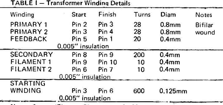 After finishing the winding process, you may insert the pair of 'E' cores into the bobbin slots, and secure the whole construction firmly together using sticky tape or an appropriate metal clamp being careful that the metal clamp doesn't cause a short circuiting across any of the turn.
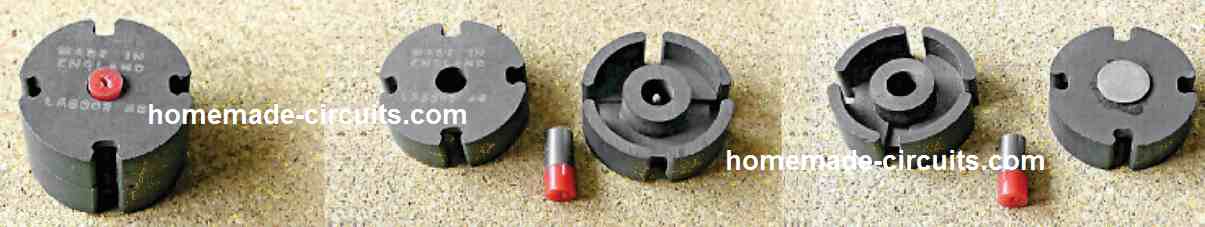 Coil former: as shown in the image (in yellow):
 Note: cores should be clamped with each other through 3/16" brass bolt and nut- a 3/16" brass washer can be accustomed to create an air gap.
Winding: 250 turns of 0.4 mm thick wire.
After the above steps, the winding are clamped between a pair of Mullard FX2242 cores as shown in the table#2 images.
It is important to introduce a thin brass washer is interposed between the two cores, in order to create an air gap.
Note: cores should be clamped with each other through 3/16" brass bolt and nut- a 3/16" brass washer can be accustomed to create an air gap.
Winding: 250 turns of 0.4 mm thick wire.
After the above steps, the winding are clamped between a pair of Mullard FX2242 cores as shown in the table#2 images.
It is important to introduce a thin brass washer is interposed between the two cores, in order to create an air gap.
 The transistors Q1 and 02 needs to be installed over an appropriate heatsink, which must have a minimum dimension of around 4" by 6".
Insulation washers should be applied to keep both the transistors well isolated from the heat sink.
All the parts now can be casually hooked up and the full system attached to a 12V source.
Be careful not to touch the transistors or the transformer output side terminals because all these elements will be at fairly large voltage which could give you a painful electrical shock.
The transistors Q1 and 02 needs to be installed over an appropriate heatsink, which must have a minimum dimension of around 4" by 6".
Insulation washers should be applied to keep both the transistors well isolated from the heat sink.
All the parts now can be casually hooked up and the full system attached to a 12V source.
Be careful not to touch the transistors or the transformer output side terminals because all these elements will be at fairly large voltage which could give you a painful electrical shock.
 The module has 4 pinouts for configuring into the intended driver circuit.
The supply pinouts are indicated with Vcc and Gnd pins.
Where Vcc is the positive 5V input for the module, and the Gnd is supposed to be connected with the negative line of the input power supply.
The trigger pin works with a 10 us pulse which activates the two transducers for transmitting and receiving the reflected ultrasonic wave.
When a series of reflected signals is detected, the "Echo" pin becomes high for initiating the external relay or the solenoid or any preferred load.
The module has 4 pinouts for configuring into the intended driver circuit.
The supply pinouts are indicated with Vcc and Gnd pins.
Where Vcc is the positive 5V input for the module, and the Gnd is supposed to be connected with the negative line of the input power supply.
The trigger pin works with a 10 us pulse which activates the two transducers for transmitting and receiving the reflected ultrasonic wave.
When a series of reflected signals is detected, the "Echo" pin becomes high for initiating the external relay or the solenoid or any preferred load.
 The wavelength falling in the range between 100 and 280 nm is the ultraviolet range which has the ability to eliminate all forms of pathogens including bacteria and viruses.
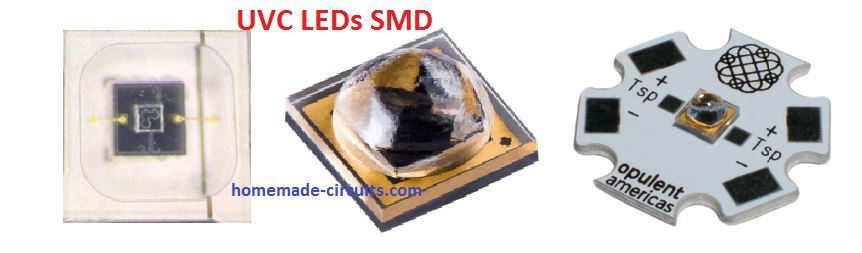 datasheet1, datasheet2, datasheet3
Due to the fact that UVC in this range may be also harmful for human skin, that's exactly why the UVC LED in this concept has been confined inside a separate enclosure prohibiting any contact of the light with the human skin.
datasheet1, datasheet2, datasheet3
Due to the fact that UVC in this range may be also harmful for human skin, that's exactly why the UVC LED in this concept has been confined inside a separate enclosure prohibiting any contact of the light with the human skin.
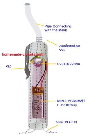 The inside surface of the tube must be white in color so that the UV rays can be reflected from the tube walls enhancing the disinfection efficiency.
Here, we can see a small cylindrical tube enclosing an UVC LED and a Li-Ion battery.
The lower mouth of the tube is open for enabling the atmospheric air or possibly infected air to enter the tube, while the other end is attached with a pipe which connects with the face mask.
The connection set up can be witnessed in the following image.
The inside surface of the tube must be white in color so that the UV rays can be reflected from the tube walls enhancing the disinfection efficiency.
Here, we can see a small cylindrical tube enclosing an UVC LED and a Li-Ion battery.
The lower mouth of the tube is open for enabling the atmospheric air or possibly infected air to enter the tube, while the other end is attached with a pipe which connects with the face mask.
The connection set up can be witnessed in the following image.
 If the tube connection looks cumbersome and messy, it could be improvised into a plug-in type unit as shown in the following example
 The set up allows the air to enter the tube, and get disinfected by the UV light, and then move ahead through the connecting pipe into the face mask interior.
When the user exhales, the opposite happens.
Now, the exhaled air exits out from the tube, and in the process gets disinfected while moving out from the tube.
This way the UVC LED disinfects the air both ways, while inhalation and exhalation, thus helping greatly to suppress the spreading of the contagious disease.
The set up allows the air to enter the tube, and get disinfected by the UV light, and then move ahead through the connecting pipe into the face mask interior.
When the user exhales, the opposite happens.
Now, the exhaled air exits out from the tube, and in the process gets disinfected while moving out from the tube.
This way the UVC LED disinfects the air both ways, while inhalation and exhalation, thus helping greatly to suppress the spreading of the contagious disease.
 Specifications of3.7V 300 mAH Lipo Battery:-
Voltage: 3.7 V
Capacity: 300 mAh
Size approx : 30 mm x 20 mm x 4 mm
Specifications of3.7V 300 mAH Lipo Battery:-
Voltage: 3.7 V
Capacity: 300 mAh
Size approx : 30 mm x 20 mm x 4 mm
 When the glow on the filament of the bulb is almost zero, the battery can be assumed to be fully charged.
 ICL7136 voltmeter
This IC also has an internal oscillator which works with a minimal clock frequency which ensures that the the entire module is able to function using minimum power, yet without any flicker on the display.
The temperature readout calibration of the circuit is carried by adjusting the preset P1 appropriately.
ICL7136 voltmeter
This IC also has an internal oscillator which works with a minimal clock frequency which ensures that the the entire module is able to function using minimum power, yet without any flicker on the display.
The temperature readout calibration of the circuit is carried by adjusting the preset P1 appropriately.
 The IC3 along with this associated components work like a voltage monitor stage for the solar cell supply.
The op amp switches OFF the main thermometer circuit stage through the transistor T2 whenever the solar cell output voltage drops below 0.7 V.
This feature makes sure that the IC1, IC2 stages do not malfunction during such low voltage and produce temperature readouts with errors.
In order to work correctly the LM35 requires a minimum supply voltage of 5.5 V, while for IC2 the minimum reference potential required is 7 V for its normal functioning.
The IC3 along with this associated components work like a voltage monitor stage for the solar cell supply.
The op amp switches OFF the main thermometer circuit stage through the transistor T2 whenever the solar cell output voltage drops below 0.7 V.
This feature makes sure that the IC1, IC2 stages do not malfunction during such low voltage and produce temperature readouts with errors.
In order to work correctly the LM35 requires a minimum supply voltage of 5.5 V, while for IC2 the minimum reference potential required is 7 V for its normal functioning.
 Assembling the PCB is easy, but the LCD module must be handled with precautions while inserting into the PCB, since the device is quite delicate and vulnerable to breaking.
 Make sure you do not forget the A couple of wire connections on the PCB.
Do not initially fit IC2 LM35 on the PCB to allow the introduction of +1.000 V across Vout and GND terminals of the LM35. Before this make sure to adjust P1 so that the display reads 100 ��C.
Once this is done, remove the solar cell or the external supply if any used, and now fix IC2 on the PCB.
Make sure you do not forget the A couple of wire connections on the PCB.
Do not initially fit IC2 LM35 on the PCB to allow the introduction of +1.000 V across Vout and GND terminals of the LM35. Before this make sure to adjust P1 so that the display reads 100 ��C.
Once this is done, remove the solar cell or the external supply if any used, and now fix IC2 on the PCB.
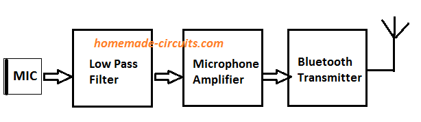 The working concept of the proposed wireless bluetooth stethoscope circuit is rather simple:
The heart beat sound pulses hit the MIC, which converts them into equivalent electrical pulses.
These electrical pulses are amplified by an integrated op amp amplifier stage to appropriate levels.
The amplified signals are fed to a bluetooth transmitter input which converts them into wireless bluetooth signals.
The transmitted bluetooth signals are captured by a tuned mobile phone which converts it back into audible signals.
The converted bluetooth data through the mobile headphone is used by a concerned doctor for diagnosing the patients heart rate and the related ailments.
The working concept of the proposed wireless bluetooth stethoscope circuit is rather simple:
The heart beat sound pulses hit the MIC, which converts them into equivalent electrical pulses.
These electrical pulses are amplified by an integrated op amp amplifier stage to appropriate levels.
The amplified signals are fed to a bluetooth transmitter input which converts them into wireless bluetooth signals.
The transmitted bluetooth signals are captured by a tuned mobile phone which converts it back into audible signals.
The converted bluetooth data through the mobile headphone is used by a concerned doctor for diagnosing the patients heart rate and the related ailments.
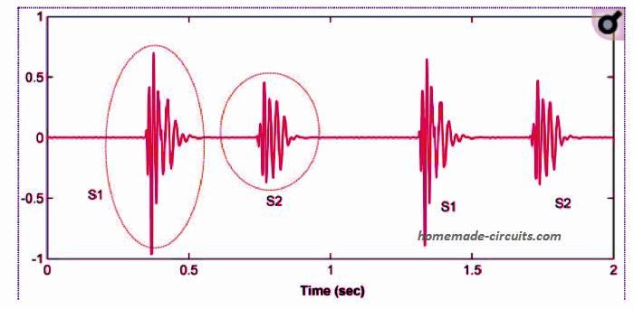 A typical heart sound waveform example.
S1 signifies the first heart sound S2 signifies the second heart sound.
Image Courtesy:heartbeat waveform
Each set of these pulses last for about 100 ms, which is actually quite sufficient for any relevant medical analysis.
Also, because the frequency of the pulses are between 20 and 150 Hz, it becomes convenient to examine the waveform within the 1st and the 2nd music octaves.
This requires a low pass filter designed in accordance with the frequency specifications of the heart rate, as explained below:
A typical heart sound waveform example.
S1 signifies the first heart sound S2 signifies the second heart sound.
Image Courtesy:heartbeat waveform
Each set of these pulses last for about 100 ms, which is actually quite sufficient for any relevant medical analysis.
Also, because the frequency of the pulses are between 20 and 150 Hz, it becomes convenient to examine the waveform within the 1st and the 2nd music octaves.
This requires a low pass filter designed in accordance with the frequency specifications of the heart rate, as explained below:
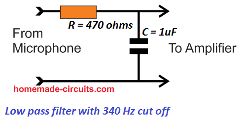 In the above low pass filter circuit any frequency above 350 hz will be severely attenuated.
The cut-off result could be adjusted or verified using the following formula;
fc= 1/(2��RC), where R will be in ohms and C will be in farads.
In the above low pass filter circuit any frequency above 350 hz will be severely attenuated.
The cut-off result could be adjusted or verified using the following formula;
fc= 1/(2��RC), where R will be in ohms and C will be in farads.
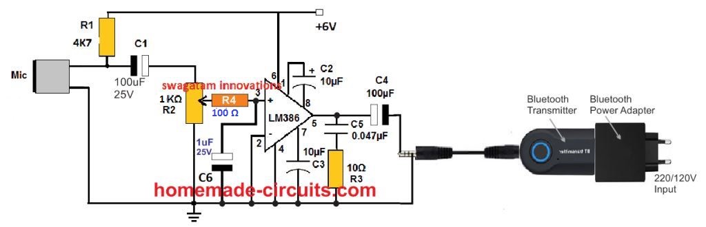
 The MIC must be neatly clamped near the person's chest area where the heart beat sound is most prominent.
Now, as soon as the circuit is powered, the heart beat sound should be audible across the head phones.
If the sound has problems or is not clear, try optimizing the parameters until the sound is distinctly clear.
This may be done by adjusting the volume control pot, and/or the the value of the capacitor C2. The supply voltage to the circuit could be also tweaked for the same.
Care must be taken that the MIC does not oscillate or rub against the body of the person to whom it is attached, which may otherwise create a huge amount unnecessary disturbance at the output, obscuring the actual heart beat sound.
The MIC must be neatly clamped near the person's chest area where the heart beat sound is most prominent.
Now, as soon as the circuit is powered, the heart beat sound should be audible across the head phones.
If the sound has problems or is not clear, try optimizing the parameters until the sound is distinctly clear.
This may be done by adjusting the volume control pot, and/or the the value of the capacitor C2. The supply voltage to the circuit could be also tweaked for the same.
Care must be taken that the MIC does not oscillate or rub against the body of the person to whom it is attached, which may otherwise create a huge amount unnecessary disturbance at the output, obscuring the actual heart beat sound.

 The IC MLX90247 is made up of piled thermocouple network over the surface of a membrane.
The heat receptive junctions of the thermocouple are strategically positioned near the center of the base membrane, while the differential cold junctions are placed at edge of the device which form the silicon bulk area of the unit.
Since the membrane is designed to be a bad conductor of heat, the detected heat from the source is able to rise quickly near the menbrane center than the bulk edge of the device.
Due to this a quick difference of heat is able to develop across the thermopile junction ends causing an effective electrical potential to develop across these terminals through thermo-electric principle.
The best part of the thermopile sensor is that, unlike standard ICs it does not require an external electrical supply to work, rather it generates its own electrical potential for enabling the required measurement.
You get two variants of the IC MLX90247 as shown below, wherein one variant provides a ground Vss option, and the other is without a Vss pin.
The IC MLX90247 is made up of piled thermocouple network over the surface of a membrane.
The heat receptive junctions of the thermocouple are strategically positioned near the center of the base membrane, while the differential cold junctions are placed at edge of the device which form the silicon bulk area of the unit.
Since the membrane is designed to be a bad conductor of heat, the detected heat from the source is able to rise quickly near the menbrane center than the bulk edge of the device.
Due to this a quick difference of heat is able to develop across the thermopile junction ends causing an effective electrical potential to develop across these terminals through thermo-electric principle.
The best part of the thermopile sensor is that, unlike standard ICs it does not require an external electrical supply to work, rather it generates its own electrical potential for enabling the required measurement.
You get two variants of the IC MLX90247 as shown below, wherein one variant provides a ground Vss option, and the other is without a Vss pin.
 The upper option allows a bipolar measurement of the IR temperature.
Meaning the output can show temperatures higher than the ambient temperature and also lower than the ambient temperatures.
The lower option can be used to measure temperature either above the ambient level or below the ambient level, and thus allows a unipolar measurement facility.
The upper option allows a bipolar measurement of the IR temperature.
Meaning the output can show temperatures higher than the ambient temperature and also lower than the ambient temperatures.
The lower option can be used to measure temperature either above the ambient level or below the ambient level, and thus allows a unipolar measurement facility.
 In the above prototype circuit of a contactless IR thermometer circuit, we find the thermopile sensor IC MLX90247 in the bipolar mode, configured with an external op amp designed to amplify tiny electrical from the thermopile into a measurable output.
The upper op amp amplifies the thermocouple output from the IC MLX90247, while the lower op amp amplifies the ambient temperature of the IC.
A simple differential VU meter is attached across the outputs of the two op amps.
As long as there no heat emitting body in front of the thermopile, its internal thermocouple temperature remains equal to the adjoining thermistor temperature.
Due to this the two op amp outputs generate equal amount of voltages.
The VU meter thus indicates a 0 V at the center of its dial.
In case a human body having a higher temperature than the surrounding is brought within the sensing range of the thermopile, its thermocouple output across pin2 and pin4 begins rising exponentially, and exceeds the thermistor output across pin3 and pin1.
This results in the upper op amp generating more positive voltage than the lower op amp.
The VU meter responds to this and its needle begins shifting on the right side of the 0V calibration.
The reading directly shows the temperature level of the target detected by the thermopile.
In the above prototype circuit of a contactless IR thermometer circuit, we find the thermopile sensor IC MLX90247 in the bipolar mode, configured with an external op amp designed to amplify tiny electrical from the thermopile into a measurable output.
The upper op amp amplifies the thermocouple output from the IC MLX90247, while the lower op amp amplifies the ambient temperature of the IC.
A simple differential VU meter is attached across the outputs of the two op amps.
As long as there no heat emitting body in front of the thermopile, its internal thermocouple temperature remains equal to the adjoining thermistor temperature.
Due to this the two op amp outputs generate equal amount of voltages.
The VU meter thus indicates a 0 V at the center of its dial.
In case a human body having a higher temperature than the surrounding is brought within the sensing range of the thermopile, its thermocouple output across pin2 and pin4 begins rising exponentially, and exceeds the thermistor output across pin3 and pin1.
This results in the upper op amp generating more positive voltage than the lower op amp.
The VU meter responds to this and its needle begins shifting on the right side of the 0V calibration.
The reading directly shows the temperature level of the target detected by the thermopile.
 In this INA333 op amp circuit the resistor RG determines the gain of the circuit, and can be calculated using the formula:
Gain = 1 + 100 / RG
The output result will be in kilo Ohms.
Through this formula we can set the overall gain of the circuit depending on the level of microvolt received from the thermopile.
The gain can be adjusted right from 0 to 10,000 which provides the op amp with an exceptional level of amplifying capability for microvolt inputs.
To be able to use this instrumentation amplifier with out thermopile IC, we will need two of these op amp modules.
One will be used for amplifying the thermocouple signal output, and the other will be use for amplifying the thermistor signal output, as shown below;
In this INA333 op amp circuit the resistor RG determines the gain of the circuit, and can be calculated using the formula:
Gain = 1 + 100 / RG
The output result will be in kilo Ohms.
Through this formula we can set the overall gain of the circuit depending on the level of microvolt received from the thermopile.
The gain can be adjusted right from 0 to 10,000 which provides the op amp with an exceptional level of amplifying capability for microvolt inputs.
To be able to use this instrumentation amplifier with out thermopile IC, we will need two of these op amp modules.
One will be used for amplifying the thermocouple signal output, and the other will be use for amplifying the thermistor signal output, as shown below;
 The set up can be used for making a contactless IR thermometer, which will produce an linearly increasing analogue output in response to a a linearly increasing IR heat, as detected by the thermopile.
The analogue output can be either attached to a milivolt VU meter or a digital mV meter for getting an instant interpretation of the temperature level of the body.
The output Vo could be also estimated through the following equation:
Vo = G(Vin+ - Vin-)
The set up can be used for making a contactless IR thermometer, which will produce an linearly increasing analogue output in response to a a linearly increasing IR heat, as detected by the thermopile.
The analogue output can be either attached to a milivolt VU meter or a digital mV meter for getting an instant interpretation of the temperature level of the body.
The output Vo could be also estimated through the following equation:
Vo = G(Vin+ - Vin-)
 where ��E refers to the electrical time constant (Rd Cd), ��T indicates the
thermal time constant (RT CT), and ��e symbolizes the radiant
power from the target detected by the sensor.
The above discussions and equations prove that the output voltage Vo from a PIR is directly proportional to the radiant power emitted from the source, and thus becomes ideally suitable for contactless temperature measuring applications.
However, we know that a PIR cannot respond to a stationery IR source, and requires the source to be in motion for enabling an readable output.
Since the speed of the movement also affects the output data, we have to make sure that the source moves with a precise speed, an aspect which may be an impossible to implement on a human target.
Therefore, an easy way to counter this it to let the human target be stationery, and replicate its movement by interfacing an artificial motor based chopper with the PIR lens system.
where ��E refers to the electrical time constant (Rd Cd), ��T indicates the
thermal time constant (RT CT), and ��e symbolizes the radiant
power from the target detected by the sensor.
The above discussions and equations prove that the output voltage Vo from a PIR is directly proportional to the radiant power emitted from the source, and thus becomes ideally suitable for contactless temperature measuring applications.
However, we know that a PIR cannot respond to a stationery IR source, and requires the source to be in motion for enabling an readable output.
Since the speed of the movement also affects the output data, we have to make sure that the source moves with a precise speed, an aspect which may be an impossible to implement on a human target.
Therefore, an easy way to counter this it to let the human target be stationery, and replicate its movement by interfacing an artificial motor based chopper with the PIR lens system.
 To ensure an efficient working of the system the distance between the IR source and the sensor's field of view (FOV) must be around 40 cm.
In other words the radiating body and the PIR lens must be at a distance of 40 cm from each other.
We can also see a chopper system consisting of a small stepper motor with a propeller installed between the fresnel lens and the PIR pyroelectric sensor.
To ensure an efficient working of the system the distance between the IR source and the sensor's field of view (FOV) must be around 40 cm.
In other words the radiating body and the PIR lens must be at a distance of 40 cm from each other.
We can also see a chopper system consisting of a small stepper motor with a propeller installed between the fresnel lens and the PIR pyroelectric sensor.
 In this chopper the following dimensions must be employed:
The chopper should have 4 blades and a diameter Dc should be around 80 mm.
It should be driven through a stepper motor or a PWM controlled circuit.
The approximate rotational frequency should eb around 5 Hz to 8 Hz for optimal performance.
The PIR fresnel lens must be positioned 16 mm behind the pyroelectric sensor, such that the incoming IR signal diameter falling on the lens is around 4 mm, and this diameter is supposed to be much smaller than the "tooth-width" TW of the chopper disk.
In this chopper the following dimensions must be employed:
The chopper should have 4 blades and a diameter Dc should be around 80 mm.
It should be driven through a stepper motor or a PWM controlled circuit.
The approximate rotational frequency should eb around 5 Hz to 8 Hz for optimal performance.
The PIR fresnel lens must be positioned 16 mm behind the pyroelectric sensor, such that the incoming IR signal diameter falling on the lens is around 4 mm, and this diameter is supposed to be much smaller than the "tooth-width" TW of the chopper disk.
 The solenoid in the above image is connected to the output of a monostable circuit.
A monostable circuit is a configuration which causes a momentary high output in response to a momentary input trigger.
The output stays high for a predetermined fixed period regardless of the input trigger duration.
In this automatic sanitizer dispenser circuit the monostable is triggered by a PIR as soon as an approaching human hand is detected by the PIR.
The monostable in turn activates the solenoid for some moment of time as determined by its RC timing components.
The activation of the solenoid causes its central spindle to quickly push and pull in the vertical direction, pressing the pump handle of the sanitizer bottle once.
This eventually causes the bottle to dispense the sanitizing liquid into the hand of the user.
Once the user withdraws his hand from the system, the PIR shuts down, and the monostable also deactivates the whole system, until another user brings his hand in the range of the PIR to repeat the procedure.
The monostable triggering circuit for the proposed automatic hand sanitizer dispensing unit can be designed using transistorized monostable or through a popular IC 555 based monostable circuit.
We will discuss both the variants in the following discussions:
The solenoid in the above image is connected to the output of a monostable circuit.
A monostable circuit is a configuration which causes a momentary high output in response to a momentary input trigger.
The output stays high for a predetermined fixed period regardless of the input trigger duration.
In this automatic sanitizer dispenser circuit the monostable is triggered by a PIR as soon as an approaching human hand is detected by the PIR.
The monostable in turn activates the solenoid for some moment of time as determined by its RC timing components.
The activation of the solenoid causes its central spindle to quickly push and pull in the vertical direction, pressing the pump handle of the sanitizer bottle once.
This eventually causes the bottle to dispense the sanitizing liquid into the hand of the user.
Once the user withdraws his hand from the system, the PIR shuts down, and the monostable also deactivates the whole system, until another user brings his hand in the range of the PIR to repeat the procedure.
The monostable triggering circuit for the proposed automatic hand sanitizer dispensing unit can be designed using transistorized monostable or through a popular IC 555 based monostable circuit.
We will discuss both the variants in the following discussions:
 The transistorized version of the circuit looks very straightforward.
When the PIR device detects a human intervention, it conducts and sends a pulse to the base of T1 via C1.
The current through C1 instantly activates T1, which in turn activates T2 and also the solenoid pump.
In the meantime, C1 quickly charges and prevents the entry of any further current to the base of T1, thus blocking the repeat DC pulses from the PIR output.
This ensures that the system works only momentarily for each detection, and then shuts down until the hand is removed and a fresh cycle is initiated.
This one-shot activation of T1/T2 ensures that the connected solenoid load activates to generate a single push-pull action on its magnetic spindle.
The spindle operates the sanitizer pump handle to dispense a single dose of the sanitizing liquid on the user's hand.
You can notice that the solenoid is connected at the emitter side of the transistor, instead of the regular collector side.
The emitter connection actually ensures that the solenoid activates with a gentle soft-start pushing in response to the charging of the 10uF capacitor C2.
If it is connected at the collector side would result in the solenoid being pushed with a sudden thrust, which might not look very impressive.
The transistorized version of the circuit looks very straightforward.
When the PIR device detects a human intervention, it conducts and sends a pulse to the base of T1 via C1.
The current through C1 instantly activates T1, which in turn activates T2 and also the solenoid pump.
In the meantime, C1 quickly charges and prevents the entry of any further current to the base of T1, thus blocking the repeat DC pulses from the PIR output.
This ensures that the system works only momentarily for each detection, and then shuts down until the hand is removed and a fresh cycle is initiated.
This one-shot activation of T1/T2 ensures that the connected solenoid load activates to generate a single push-pull action on its magnetic spindle.
The spindle operates the sanitizer pump handle to dispense a single dose of the sanitizing liquid on the user's hand.
You can notice that the solenoid is connected at the emitter side of the transistor, instead of the regular collector side.
The emitter connection actually ensures that the solenoid activates with a gentle soft-start pushing in response to the charging of the 10uF capacitor C2.
If it is connected at the collector side would result in the solenoid being pushed with a sudden thrust, which might not look very impressive.
 The figure above shows a standard IC 555 monostable circuit.
Here, when pin2 is grounded, causes the output pin3 to go high for a period decided by the R1, C1 values or their product.
In this automatic sanitizer dispenser design the R1, C1 is calculated to produce an approximately 1 second output high, in response to a low signal at pin2.
When the PIR detects a human hand, it conducts and switches ON the BC547 transistor which in turn triggers the pin2 of the IC.
This instantly causes the pin3 to go high and activates the TIP142 transistor and the connected solenoid, generating a 1 second long push and then a shut down pull-up on the solenoid shaft.The pull is generated by the attached spring tension on the solenoid shaft.
Again, in this version also the solenoid can be seen connected at the emitter side of the transistor in order to enable a soft thrust on the solenoid shaft depending on the charging response of C3.
An animated view of the whole system can be visualized in the following GIF image.
The figure above shows a standard IC 555 monostable circuit.
Here, when pin2 is grounded, causes the output pin3 to go high for a period decided by the R1, C1 values or their product.
In this automatic sanitizer dispenser design the R1, C1 is calculated to produce an approximately 1 second output high, in response to a low signal at pin2.
When the PIR detects a human hand, it conducts and switches ON the BC547 transistor which in turn triggers the pin2 of the IC.
This instantly causes the pin3 to go high and activates the TIP142 transistor and the connected solenoid, generating a 1 second long push and then a shut down pull-up on the solenoid shaft.The pull is generated by the attached spring tension on the solenoid shaft.
Again, in this version also the solenoid can be seen connected at the emitter side of the transistor in order to enable a soft thrust on the solenoid shaft depending on the charging response of C3.
An animated view of the whole system can be visualized in the following GIF image.

 The characteristics of this proximity IR sensor module can be understood from the following data:
 From the internal layout diagram of the sensor we can clearly see that the module consist of a photodiode which emits the IR signal towards the target, and an adjoining phototransistor receiver which is positioned to receive the reflected IR signal from the target.
To adapt the sensor in an automatic hand sanitizer machine, we can yet again implement our work horse IC 555 based monostable, a shown below:
From the internal layout diagram of the sensor we can clearly see that the module consist of a photodiode which emits the IR signal towards the target, and an adjoining phototransistor receiver which is positioned to receive the reflected IR signal from the target.
To adapt the sensor in an automatic hand sanitizer machine, we can yet again implement our work horse IC 555 based monostable, a shown below:
 The circuit is quite self explanatory, but if you have problems understanding the details, you can always feel free to use the comment box below for initiating a discussion.
 The circuit shown above can be used for implementing an automatic sanitizer dispenser through the ultrasonic proximity detector module, HC-SR04, and a couple of IC 555 circuits.
The left side IC 555 is configured as an astable multivibrator while the right side IC 555 circuit is wired as a monostable multivibtator.
The astable RA, RB, C components values must be calculated to enable a 10us ON and 60us OFF PWM from pin3 of this IC.
The RA and C timing components of the monostable must be adjusted to produce a 1 second high one-shot output from pin3 of this stage.
This output could be used for powering the dispensing pump, motor, solenoid etc as per the requirement of the design.
The circuit shown above can be used for implementing an automatic sanitizer dispenser through the ultrasonic proximity detector module, HC-SR04, and a couple of IC 555 circuits.
The left side IC 555 is configured as an astable multivibrator while the right side IC 555 circuit is wired as a monostable multivibtator.
The astable RA, RB, C components values must be calculated to enable a 10us ON and 60us OFF PWM from pin3 of this IC.
The RA and C timing components of the monostable must be adjusted to produce a 1 second high one-shot output from pin3 of this stage.
This output could be used for powering the dispensing pump, motor, solenoid etc as per the requirement of the design.


 Reference: Using far-UVC on mammalian skin

 Nucleocapsid Protein (N): This section is attached with the RNA genome to constitute the nucleocapsid.
Spike Protein (S): It plays a vital role in binding with the host receptor cells to help easy entry into the host cell.
Envelope Protein (E): It works together with Membrane Protein to create the viral envelope.
Membrane Protein (M): It works as the main organizer of the CoV body, and also defines the structure of the viral envelope.
Nucleocapsid Protein (N): This section is attached with the RNA genome to constitute the nucleocapsid.
Spike Protein (S): It plays a vital role in binding with the host receptor cells to help easy entry into the host cell.
Envelope Protein (E): It works together with Membrane Protein to create the viral envelope.
Membrane Protein (M): It works as the main organizer of the CoV body, and also defines the structure of the viral envelope.

 Once powered, the top open terminal of the 200 turn coil will begin emitting corona discharge, and this may also initiate the generation of ozone.
To use this set up for killing coronavirus, operate the unit inside a locked premise with doors and windows closed.
Make sure there are no living creatures inside the room.
The Tesla coil circuit should be controlled with a timer so that it is automatically switched OFF after a a couple of hours.
This timer must be accompanied with an exhaust fan so that once the ozone generation stops, the exhaust fan is switched ON to suck out the harmful ozone from the room.
After about about 30 minutes from the elapsed time, it may be safe to enter the room, which now may be considered disinfected.
Once powered, the top open terminal of the 200 turn coil will begin emitting corona discharge, and this may also initiate the generation of ozone.
To use this set up for killing coronavirus, operate the unit inside a locked premise with doors and windows closed.
Make sure there are no living creatures inside the room.
The Tesla coil circuit should be controlled with a timer so that it is automatically switched OFF after a a couple of hours.
This timer must be accompanied with an exhaust fan so that once the ozone generation stops, the exhaust fan is switched ON to suck out the harmful ozone from the room.
After about about 30 minutes from the elapsed time, it may be safe to enter the room, which now may be considered disinfected.
 For generating rapid and high concentration of ozone, the following high voltage arc generator can be used, which is built using a standard automobile ignition coil and a CDI circuit:
 The set up looks simple, and just needs to be connected as per the given schematic for getting the proposed high voltage arcing and ozone generation.
You will require the following parts for the construction:
1/4 watt 5% Resistors 1k, 100k, 10k - 1 each
1/2 watt 5% resistors 470 ohm, 100 ohm - 1 each
Potentiometer 100k - 1no
Electrolytic capacitors 1uF/25V, 100uF/25 V - 1 each
0.01uF ceramic disc - 1no
1uF / 400V PPC associated with the SCR - 1no
SCR - BT151 philips
Diodes 1N4007 = 4nos
Transistor TIP122 - 1no
IC 555 - 1no
Two wheeler Ignition coil unit - 1no
Transformer 0-12V/1 amp/220V
Mains AC to 12V DC adapter for powering the circuit
Adjusting the 100 k pot will allow the spark to be slower or faster, and also stronger or weaker.
The sparks generated from this circuit will generate high amounts ozone for disinfecting any standard room from coronavirus.
However, make sure the gas is not inhaled by any living creature.
Also, the voltage generated from this apparatus can be up to 30 kv, and therefore can kill a human within seconds, so please proceed with caution.
Again, use of a timer is recommended for automatically switching OFF the system, and switching an exhaust fan.
The set up looks simple, and just needs to be connected as per the given schematic for getting the proposed high voltage arcing and ozone generation.
You will require the following parts for the construction:
1/4 watt 5% Resistors 1k, 100k, 10k - 1 each
1/2 watt 5% resistors 470 ohm, 100 ohm - 1 each
Potentiometer 100k - 1no
Electrolytic capacitors 1uF/25V, 100uF/25 V - 1 each
0.01uF ceramic disc - 1no
1uF / 400V PPC associated with the SCR - 1no
SCR - BT151 philips
Diodes 1N4007 = 4nos
Transistor TIP122 - 1no
IC 555 - 1no
Two wheeler Ignition coil unit - 1no
Transformer 0-12V/1 amp/220V
Mains AC to 12V DC adapter for powering the circuit
Adjusting the 100 k pot will allow the spark to be slower or faster, and also stronger or weaker.
The sparks generated from this circuit will generate high amounts ozone for disinfecting any standard room from coronavirus.
However, make sure the gas is not inhaled by any living creature.
Also, the voltage generated from this apparatus can be up to 30 kv, and therefore can kill a human within seconds, so please proceed with caution.
Again, use of a timer is recommended for automatically switching OFF the system, and switching an exhaust fan.

 Relative color intensity vs Wavelength in nanometers (nm)
The wavelength of RED light spectrum lies between 600 and 800 nm, and is found to be helpful for straightening facial wrinkles.
Lights of this wavelength and higher have the ability to penetrate around 5mm under the skin to influence the cells.
As per the studies red light therapy works by inducing a biochemical process within the skin cells, boosting mitochondria activity.
Mitochondriaare the active organelles that energize our body cell by producing adenosine triphosphate (ATP), the essential energy molecule consumed by the cells.
Due to the influence of Red light, mitochodria in our skin cells get stimulated and they begin producing higher amounts of ATP, which helps our skin to appear more lively and tighter.
The process also helps faster skin repair and removal of fine facial wrinkles.
Relative color intensity vs Wavelength in nanometers (nm)
The wavelength of RED light spectrum lies between 600 and 800 nm, and is found to be helpful for straightening facial wrinkles.
Lights of this wavelength and higher have the ability to penetrate around 5mm under the skin to influence the cells.
As per the studies red light therapy works by inducing a biochemical process within the skin cells, boosting mitochondria activity.
Mitochondriaare the active organelles that energize our body cell by producing adenosine triphosphate (ATP), the essential energy molecule consumed by the cells.
Due to the influence of Red light, mitochodria in our skin cells get stimulated and they begin producing higher amounts of ATP, which helps our skin to appear more lively and tighter.
The process also helps faster skin repair and removal of fine facial wrinkles.

 That concludes our tutorial for a homemade yet effective LED lightsim circuit for an non-evasive skin repair therapy.
Warning: Although the theory explained above is technically correct and is created after a thorough research on the field, the author takes no responsibilities for the consequences whatsoever, from this design.
Users are advised to exercise discretion.
Additionally, the LEDs used in the circuit are too bright and may be harmful for the eyes.
Therefore, users must avoid looking directly into the LEDs from top, and not use the therapy directly on eyes, or exercise appropriate protections while implementing the actions.
That concludes our tutorial for a homemade yet effective LED lightsim circuit for an non-evasive skin repair therapy.
Warning: Although the theory explained above is technically correct and is created after a thorough research on the field, the author takes no responsibilities for the consequences whatsoever, from this design.
Users are advised to exercise discretion.
Additionally, the LEDs used in the circuit are too bright and may be harmful for the eyes.
Therefore, users must avoid looking directly into the LEDs from top, and not use the therapy directly on eyes, or exercise appropriate protections while implementing the actions.
 Referring to the above shown hospital room call bell circuit, the idea may be understood as follows:
The transistor T1, T2 basically forms a transistorized latch circuit wherein a trigger at the base of T1 causes the circuit to hold into a latching mode, meaning a single momentary positive pulse at the base of T1 enables T1/T2 to go into a permanent conduction mode until the feed from R3 is grounded by pressing the reset button.
On pressing the button at the patent's end latches the circuit into conduction and causes a DC pulse to be sent through D2 to the connected DC bell.
The bell sounds loudly until the 1000uF capacitor is charged fully, after which the bell ceases to operate.
However the latching action keeps the RED LED switched ON along with the green LED which is supposed to be positioned in the patient's room beside the call button.
This LED informs the patient regarding the call been sent and confirms regarding the same.
The red LED intimates the nurse regarding the patient's room.
Identical stages as explained above may be repeated and installed for each of the rooms in the hospital for enabling the respective occupants to execute a foolproof interaction with the nurses rooms whenever the patient may be in need for help.
The reset button is provided for enabling the nurse to reset or restore the situation back to the switched OFF condition which also simultaneously tells the patient regarding the response from the nurse's room, so that the patient is able to anticipate the help being on the way.
Referring to the above shown hospital room call bell circuit, the idea may be understood as follows:
The transistor T1, T2 basically forms a transistorized latch circuit wherein a trigger at the base of T1 causes the circuit to hold into a latching mode, meaning a single momentary positive pulse at the base of T1 enables T1/T2 to go into a permanent conduction mode until the feed from R3 is grounded by pressing the reset button.
On pressing the button at the patent's end latches the circuit into conduction and causes a DC pulse to be sent through D2 to the connected DC bell.
The bell sounds loudly until the 1000uF capacitor is charged fully, after which the bell ceases to operate.
However the latching action keeps the RED LED switched ON along with the green LED which is supposed to be positioned in the patient's room beside the call button.
This LED informs the patient regarding the call been sent and confirms regarding the same.
The red LED intimates the nurse regarding the patient's room.
Identical stages as explained above may be repeated and installed for each of the rooms in the hospital for enabling the respective occupants to execute a foolproof interaction with the nurses rooms whenever the patient may be in need for help.
The reset button is provided for enabling the nurse to reset or restore the situation back to the switched OFF condition which also simultaneously tells the patient regarding the response from the nurse's room, so that the patient is able to anticipate the help being on the way.
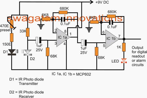
 In the following section we'll learn about a simple heart rate monitor and alarm circuit specially designed for the elderly citizens for keeping a track of their heart critical rate.
Here explores a simple circuit which may be used for monitoring the critical heart rate of a patient (senior citizen), the circuit also includes an alarm for indicating the situation.
The idea was requested by Mr.
Raj Kumar Mukherji
In the following section we'll learn about a simple heart rate monitor and alarm circuit specially designed for the elderly citizens for keeping a track of their heart critical rate.
Here explores a simple circuit which may be used for monitoring the critical heart rate of a patient (senior citizen), the circuit also includes an alarm for indicating the situation.
The idea was requested by Mr.
Raj Kumar Mukherji
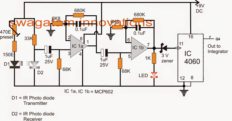
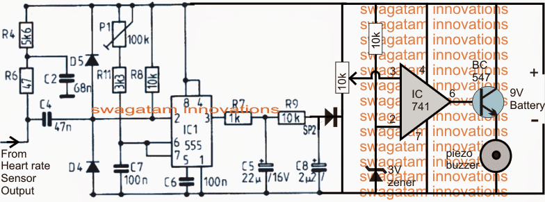 Referring to the diagrams above, we are able to see a couple of circuit stages, the first being the heart rate sensor/processor with an integrated frequency multiplier, while the second in the form of an integrator, comparator.
The upper signal processor design has been comprehensively explained in the previous paragraph, the additional voltage multiplier which is been integrated to the processor uses the IC 4060 for multiplying the relatively slower heart rates into a proportionately varying high frequency rate.
The above proportionately varying high frequency heart pulse rate from pin7 of IC 4060 is fed to the input of an integrator whose job is to convert the digitally varying frequency into a proportionately varying exponential analogue signal.
Finally this analogue voltage is applied to the non inverting input of a Ic 741 comparator.
The comparator is set through the attached 10k preset such that the voltage level at pin3 stays just below the reference voltage at pin2 when the heart rate is in the vicinity of the safe region.
However if the heart rate tends to increase over the critical region, a proportionately higher voltage level is developed at pin3 which crosses the pin2 reference level causing the output of the opamp to go high and sound the alarm.
The above set up only monitors and alarms regarding the higher critical heart rate, in order to achieve a two way monitoring, meaning to get an alarm for both higher and lower critical heart rates...the second circuit comprising the IC555 and IC741 could be entirely eliminated and replaced with a standard IC LM567 circuit set to keep its output low at the safe pulse rate, and go high at the up or down critical rates.
The signal conditioning circuit consists of two identical active low pass filters with a cut-off frequency of about 2.5 Hz.
This means the maximum measurable heart rate is about 150 bpm.
The operational amplifier IC used in this circuit is MCP602, a dual OpAmp chip from Microchip.
It operates at a single power supply and provides rail-to-rail output swing.
The filtering is necessary to block any higher frequency noises present in the signal.
Referring to the diagrams above, we are able to see a couple of circuit stages, the first being the heart rate sensor/processor with an integrated frequency multiplier, while the second in the form of an integrator, comparator.
The upper signal processor design has been comprehensively explained in the previous paragraph, the additional voltage multiplier which is been integrated to the processor uses the IC 4060 for multiplying the relatively slower heart rates into a proportionately varying high frequency rate.
The above proportionately varying high frequency heart pulse rate from pin7 of IC 4060 is fed to the input of an integrator whose job is to convert the digitally varying frequency into a proportionately varying exponential analogue signal.
Finally this analogue voltage is applied to the non inverting input of a Ic 741 comparator.
The comparator is set through the attached 10k preset such that the voltage level at pin3 stays just below the reference voltage at pin2 when the heart rate is in the vicinity of the safe region.
However if the heart rate tends to increase over the critical region, a proportionately higher voltage level is developed at pin3 which crosses the pin2 reference level causing the output of the opamp to go high and sound the alarm.
The above set up only monitors and alarms regarding the higher critical heart rate, in order to achieve a two way monitoring, meaning to get an alarm for both higher and lower critical heart rates...the second circuit comprising the IC555 and IC741 could be entirely eliminated and replaced with a standard IC LM567 circuit set to keep its output low at the safe pulse rate, and go high at the up or down critical rates.
The signal conditioning circuit consists of two identical active low pass filters with a cut-off frequency of about 2.5 Hz.
This means the maximum measurable heart rate is about 150 bpm.
The operational amplifier IC used in this circuit is MCP602, a dual OpAmp chip from Microchip.
It operates at a single power supply and provides rail-to-rail output swing.
The filtering is necessary to block any higher frequency noises present in the signal.