In this RGB spotlight mixer circuit project, 3 individual spot lights are used, having red, green and blue focus light bulbs in them.
The lights can be focused on walls, ceilings or floors to create interesting slow rising, slow fading red, green blue light patterns that mix and diffuse to generate interesting, additional secondary colors.
Contributed By: Antoine de Lafayette
The intensity of the RGB lights slowly increase and decrease, as per the settings of the individual focus lights, which causes the ficus outputs to change color like a chameleon does, very slowly and subtly with different time constants, producing multitude of different colors shades and themes, on the surface where the lights are projected.
Red + green + blue = white
Red + green = yellow
Green + blue = cyan (green-blue)
Blue + red = magenta (purple)
Yellow + blue = green
Cyan + red = white
Magenta + green = white
Circuit Description
The basic idea here is to chop the AC supply to the specific RGB lamps at some predetermined rate, such the glow on the lamps slowly brighten and slowly dim, generating interesting color blends and intriguing complex color bands around the focused areas.
Referring to the RGB spotlight mixer circuit we can see 3 identical stages, each comprising of a IC 555 astable sawtooth generator stage, an intermediate BJT amplifier stage, and a triac lamp driver stage.
The bases of T1, T5 and T9 can be seen connected to 3 separate SPDT switches.
These switches can be used for removing the IC 555 feed and operate the bases manually through 3 individual potentiometers.
The slider arm of these pots will go to the transistor bases via the SPDT switches, while the other two ends of the pots will go to the DC supply rails.
The function of all the 3 IC 555, BJT amplifier and the triac lamp driver stages is the same.
The IC 555 ICs are all rigged as astable which has a sharp and fast charge time but a slow discharge time due to the inclusion of the diode across pin#7 and pin#6/2.
This generates very long ON time, and short OFF time at the respective pin#3 of the all the 555 ICs.
The OFF time outputs at the pin#3 of the ICs are in the form of a momentary pulse, which is applied to the bases of the respective BJTs T1, T5, T9, which are configured as emitter followers.
With ON/OFF pulses from the pin#3, causes the emitter follower transistors to be activated accordingly, generating a corresponding level regulated voltage across their emitters.
This emitter voltage from the emitter followers BJTs is applied as an interrupting potential across the transistor buffer stages built around T3, T4, T7, T8, T11, T12.
We can see that the first transistor from these buffer stages, that is T2, T6, T10 are pulsed at the 50 Hz rate from the transformer AC via D12. This 50 Hz pulses causes the all the 3 triac lamp drivers to be operated with a constant level of illumination, only as long a the IC 555 pulses are not available.
However, with the interruption caused by the IC 555 pulses, buffer stage transistors are forced to create a specific chopping waveform that are incrementing and decrementing in nature.
This incrementing and decrementing chopping pulses causes the triacs to switch the AC across the connected RGB lamps, with gradually increasing and decreasing ON/OFF times across all the 3 triacs.
As a result the RGB spot lamps focus color slowly and automatically become brighter and dimmer, creating interesting color mixing of the red, green, blue illuminations, focused on a specific surface.
PCB Design
Parts List
Xenon Strobe Light Control Circuit
The circuits presented in the following article could be used for generating strobed lighting effect over 4 Xenon tubes in a sequential manner.
The proposed sequential xenon lighting effect could be applied in discotheques, in DJ parties, in cars or vehicles, as warning indicators, or as decorating ornamental lights during festivals.
A wide range of xenon tubes are available in the market with a matching ignition transformer set (that we are going to talk about afterwards).
In theory, just about any xenon tube works extremely well in the strobe control circuit presented in figure below.
How Xenon Tube Rating is Calculated
The circuit is designed for a '60 Watts per second' xenon tube and this is all it is going to accommodate.
Sadly, the power ratings of xenon tubes are typically mentioned as "x" watts per second, which often signifies an issue!
The reason behind the particular capacitor values in the diagram and DC voltage level may be comprehended through the following simple equation:
E = 1/2 C.U2
The quantity of electrical power utilized by the xenon tube may be determined simply by multiplying energy and the xenon repetition pulse frequency.
With a frequency of 20 Hz and a power of 60 Ws, the tube might 'consume' around 1.2 kW! But that looks huge, and can't be justified.
Actually, the mathematics in the above is using an incorrect formula.
As an alternative, this should be depending on the optimum acceptable tube dissipation and the resulting energy with respect to the frequency.
Considering that the xenon tube specifications which we are enthusiastic about should be capable of handling a highest possible dissipation up to 10 W, or an optimum level of 0.5 Ws energy should be discharged at 20 Hz.
Calculating the Discharge Capacitors
The above explained criteria calls for a discharge capacitance with a value 11uF and having an anode voltage of 300 V.
As could be witnessed, this value matches relatively well with the values of C1 and C2 as indicated in the diagram.
Now the question is, just how do we select the correct capacitor values, in a situation where we have no rating printed on the xenon tube? Currently since we have with us the relationship between 'Ws' and W', the below shown rule-of -thumb equation could be tested out:
C1 = C2 = X .
Ws / 6 [uF]
This is actually just a relevant clue.
In case the xenon tube is specified with an optimal working range of under 250 continuous hours, it is best to apply the equation over a reduced allowable dissipation.
A useful recommendation you may want to follow with regards to all types of xenon tubes.
Ensure that their connection polarity is proper, this means that, attach the cathodes to ground.
In many instances, the anode is marked with a red-colored spot.
The grid network is either available as like a wire at the cathode terminal side or simply as a third 'lead' between the anode and the cathode.
How Xenon Tube is Ignited
Alright, so inert gases have the ability to generate illumination when electrified.
But this fails to clarify just how the xenon tube is actually ignited.
The electrical power storage capacitor described previously is indicated in figure 1 above, through a couple of capacitors C1 and C2.
Given that the xenon tube needs a voltage of 600 V across the anode and the cathode, diodes D1 and D2 constitute a voltage doubler network in conjunction with the electrolytic capacitors C1 and C2.
How the Circuit Works
The a pair of capacitors are consistently charged to the maximum AC voltage value and as a result R1 and R2 are incorporated to restrict the current during the xenon tube's ignition period.
If R1, R2 were not included the xenon tube would at some point degrade and stop working.
The resistor R1 and R2 values are selected to ensure C1 and C2 are charged up to the peak voltage level (2 x 220 V RMS) with the maximum xenon repetition frequency.
The elements R5, Th2, C3 and Tr represent the ignition circuit for the xenon tube.
Capacitor C3 discharges through the ignition coil's primary winding which generates a grid voltage of many kilovolts across the secondary winding, for igniting the xenon tube.
This is how the xenon tube fires and illuminates brightly, which also implies that now it instantly draws the entire electrical power held inside C1 and C2, and dissipates the same by means of a dazzling flash of light.
Capacitors C1, C2 and C3 subsequently recharges so that the charge allows the tube to go for a new pulse of flash.
The ignition circuit obtains the switching signal through an opto-coupler, an built-in LED and a photo transistor enclosed collectively inside a single plastic DIL package.
This guarantees excellent electrical isolation across the strobe lights and the electronic control circuit.
As soon as the photo transistor is lit up by the LED, it becomes conductive and actuates the SCR.
The input supply for the opto-coupler is taken from the 300V ignition voltage from across C2. It is nonetheless lowered to 15V by diode R3 and D3 for apparent factors.
Control Circuit
Since the working theory of the driver circuit is understood, we can now learn how the xenon tube could be designed to produce a sequential strobing effect.
A control circuit for producing this effect is demonstrated in figure 2 below.
The highest repeat strobe rate is limited to 20 Hz.
The circuit has the capacity to handle 4 strobe devices at the same time and essentially is made up of range of switching devices and a clock generator.
The 2N2646 unijunction transistor UJT works like a pulse generator.
The network associated with this is intended to enable the frequency of the output signal to be tweaked around the 8 �� 180 Hz rate using P1. The oscillator signal is fed to the clock signal input of the decimal counter IC1.
Figure 3 below shows a picture of the signal waveforms at the IC1 output with regards to the clock signal.
The signals coming from the IC 4017 switch at a frequency of 1 �� 20 Hz are applied to the switches S1 �� S4. The positioning of the switches decides the sequential pattern of the strobe.
It allows the lighting sequence to be adjusted from right to left, or the opposite, etc.
When S1 to S4 are set at totally clockwise, the push-buttons become in the operational mode, enabling one of the 4 xenon tubes to be activated manually.
The control signals activate the LED driver stages through transistors T2 .
. .
T5. The LEDs D1 �� D4 work like functional indicators for the strobe lights.
The control circuit could be tested by just grounding the cathodes of D1 �� D4. These will show immediately whether or not the circuit is working correctly.
A Simple Stroboscope using IC 555
In this simple stroboscope circuit the IC 555 works like an astable oscillator driving a transistor and an attached transformer.
The transformer converts 6V DC into 220 V low current AC for the stroboscope stage.
The 220 V is further converted to a high voltage peak 300 V with the help of the diode capacitor rectifier.
When the capacitor C4 charges up to the triggering threshold of the SCR gate neon bulb, through the resistive network, the SCR fires and triggers the driver grid coil of the stroboscope lamp.
This action dumps the entire 300 V into the stroboscope bulb illuminating it brightly, until the C4 is fully discharged for the next cycle to repeat.
Musical Christmas Decoration Light Circuit
A very interesting musical Christmas decoration light circuit can be built using a single IC, and some other few passive components, let��s learn the details as furnished below.
By: Ritu Panday
How it Works
The circuit of a selectable muti-musical song player with 5 sequential light pattern generator is discussed here using just a single chip M668, and a few resistors and BJTs.
The sequential light control also exhibits multiple patterns depending on the pressing of a button, and this is executed through 5nos of SCRs and lamps.
The lamps are in the form single 10 watt filament bulbs or even colored 1 watt LED bulbs might work beautifully for this application.
Referring to the diagram the IC M668 may have 25 different Christmas melodies or songs embedded in it, which is played randomly as long as the circuit is powered.
Additionally the button TG can be pressed anytime for changing the song number, and playing any other desired number on the connected loudspeaker.
The loudspeaker is a tiny 32 ohms speaker, which is driven by a BJT amplifier capable of producing an adequate watt power over the speaker which may be quite enough for anybody to listen to the melodies within the premise.
The VOL button can be used for adjusting the volume as per individual preference and tolerance.
The best thing about this musical Christmas light sequencer circuit is not only its dual function feature of music and light generation but also its transformerless compact design.
The power for this decoration light circuit can be directly acquired from the AC mains through a little transformerless power supply circuit comprising of some diodes and capacitors as shown below:
Mains Power Supply Connection Details
As can be seen , direct AC mains Vdd1 is used for powering the AC lamps, therefore make sure the connected lamps are rated at 120V AC, or 220CV AC and not anything less than that.
Vdd is used for powering the IC based circuit and is therefore stabilized to 12V, however care must be taken not to touch the circuit while it's powered because this musical Christmas light decoration circuit is absolutely NOT isolated from mains, and therefore is life threatening in open condition.
This implies that the whole circuit must be enclosed inside a suitable enclosure with only the mains cord terminating for AC plug in.
The lights could be terminated through wire and bulb holder arrangement and here too care should be taken to perfectly insulate the individual bulb strings and holders so that no accidental shocks are encountered while decorating the lights over a Christmas tree or any similar desired position.
The following image provides the list of songs that the IC M668 may have embedded in it:
Fish Aquarium Oxygen Generator Circuit
In this article we discuss how to make a simple fish aquarium oxygen generator circuit using the concept of electrolysis of water.
Generating Pure Oxygen
The production of oxygen through electrolysis can be expected to supply a pure and a bigger quantity of oxygen compared to the usual pumped air concept which injects only only a portion of oxygen in the aquarium, therefore using electrolysis procedure looks a more efficient than the pumped air option
In one of my earlier artilces we learned how to generate oxygen and hydrogen gas through electrolysis in large volumes, here we employ the same principle for the generation of pure oxygen using mains rectified AC.
The complete operational set up can be witnessed in the above shown figure.
The right side section of the diagram shows a small tank filled with clean tap water, having a lid which is appropriately fabricated to hold a plastic bottle such that its neck can protrudes out, and having a small opening some distance away for allowing the unused hydrogen gas to escape.
Two wires can be seen entering the water container with one of the wires pushed inside the bottle from its bottom end and appropriately sealed with epoxy glue and the other wire loosely held just below the lid opening.
The wire entering the bottle end is tied up with an electrode which could be ideally of graphite (salvaged from an old dead AAA cells) in order to prevent degradation due to oxidization, overtime
The wires can be seen attached with the output of a bridge rectifier, which is supplied with an input from the mains AC 220V or a 120V.
When mains is switched ON, the power enters the bridge rectifier and gets converted into a pulsating DC, this DC is introduced inside the water tank for initiating the required electrolysis.
The potential at positive end electrode of the wire generates O, or pure oxygen, while the potential at the negative wire electrode breaks H+H atoms from water generating hydrogen which escapes through the lid opening into the atmosphere.
The oxygen gas is forced to bubble inside the water enclosed inside the bottle and it emanates through the tube into the aquarium where it bubbles back from bottom to the surface enriching the water with pure oxygen and making sure that the marine life inside the aquarium gets the best of the experience in terms of breathing and oxygen absorption.
Please note that in the discussed concept the water alone is forced to break into its constituent parts, absolutely NO external catalyst in the form acid or salt should be added in the electrolysis tank, which might otherwise cause the generation of poisonous gasses instead of oxygen.
Making the Bottle Oxygen Collector
The bottle which acts as the intermediate oxygen collector can be easily built using any ordinary empty cold drink bottle or a mineral water bottle.
As demonstrated in the figure below, the wire end with the electrode is inserted from the bottom corner of the bottle and sealed with epoxy glue or putty.
Next, many small holes are punched near the bottom end of the bottle so that water is able to enter and fill the bottle and enable the process of electrolysis inside it.
Further on, a plastic flexible tube is inserted through the lid or the cork of the bottle and glued with epoxy, the other end of the tube is immersed in the aquarium jar for allowing the oxygen to pass into it for initiating the required fish aquarium oxygen generation.
After this the bottle is pushed in the tank so that water fills in and hlds the bottle erect in the tank.
The wires are then appropriately attached with the bridge rectifier source enclosed inside a plastic box, with a mains cord terminating out from the input of the bridge.
That's it! Once the above procedures are finished, it's just about plugging and switching ON the mains, and watching the the oxygen bubbling out inside the fish aquarium, making the lives of the fishes merrier.
Warning: The explained electrolysis set up for the fish aquarium generator circuit is very dangerous due to the involvement of AC mains in the electrolysis tank.
Extreme caution and safety must be exercised while building and testing the proposed units.
8 Function Christmas Light Circuit
A simple mains operated, transformerless 8 function Christmas light circuit can be made by using a single IC, a rotary switch and a few SCRs, let's learn the procedures in detail.
The circuit is based on a single chip UTC8156 which is internally preprogrammed to produce 8 unique selectable light effects across 4 numbers of connected AC/DC lamps.
Usually such multi-function light effect generators are based on microcontrollers and require some complex programming but this this is a ready made preprogrammed IC which can deliver interesting changing light patterns over 4 mains operated lamps.
Circuit Application Hints
The proposed 8 function Christmas light circuit as the name suggest can be used for decoration during festivals, for example in Christmas the circuit can be applied for decorating a Christmas tree, in other popular festivals such as in Diwali the same circuit can be used for decorating door entrances, balconies and so on.
The 8 light patterns specified in the IC are very unique and can be selected using a small rotary switch with a plastic knob, this is important because the entire circuit is directly linked with the mains and therefore not isolated from the mains current, due to this reason a plastic knob for the rotary switch becomes extremely important to avoid lethal electric shocks.
The following images show the basic functional and wiring details of the proposed 8 function Christmas light circuit.
Both the designs are basically the same, the first is based on the 18 pin IC, while the second one is configured using the 16 pin IC version.
How the IC Works
The pinouts of the IC on the left are designated with the "function" specs, which can be appropriately switched using a rotary selector switch whose pole can be seen connected with the ground or the negative line of the circuit for executing the selected function.
The circuit can be operated from any desired supply input source, as per individual preference, it can be operated from the mains 220V or from mains 110V input supply using the configuration depicted above, and also from any 5 to 24V AC/DC adapter unit.
The lamps must be rated as per the input supply used, meaning for 220V it should be 220V rated lamps, for 110V the lamps ought to be 110V rated, and for 24V it should be rated at 24V
For 220V and 110V operations the involved resistors and the capacitor might need to be changed appropriately as shown in the following table:
As per the specifications, the IC is able to operate even from supplies as low as 5V, which implies that the circuit can be possibly operated through a mobile charger.
As can be seen in the diagram that the supply Vdd to the IC is substantially dropped through R1, which probably means that the current to the IC and for the SCRs could be very low, in the order of a few milliamps.
Therefore here the applicable SCRs could be the smaller ones which can work with 1 to 5mA gate current such as BT169, and hence the lamps would also need to be smaller in current, for example the 10 watt or smaller lamps.
However, according to me the circuit can be appropriately modified for handling high watt mains bulbs simply by reducing R1 to 100 ohms and operating the circuit using a 5V cellphone charger and replacing the SCRs with C106 type of SCRs.
But with the above case the bulb top rail will need to be connected to one of the mains input for example the phase, and the negative common rail of the circuit will be required to be connected with the neutral line.
8 Functions Light effect
The IC is specified to generate the following 8 different light effect patterns as per the position of the rotary switch within the stipulated selection pinouts
1) The IC continuously scans and randomly generates the 8 functions in a row.
2) In this position the IC generates a wave like effect on the connected lamps.
3) In this mode the lights are illuminated in sequence one after the other and shutting off in the same order.
4) The fourth selection gives rise to a slow-glow kind of flashing visual over the connected lamps
5) Here the lights are switched off and ON with a chasing and simultaneously flashing style.
6) A quick switch ON of the lamps but a slow-fade effect can be witnessed in this position
7) The 7th preference produces a twinkling flashing effect on the lamps quite resembling the stars on the sky.
8) In the last mode the lamps actually do nothing but light up solid ON which also sometimes becomes useful for certain decorative applications.
For using the above circuit with high watt AC lamps, the design could be modified in the following manner:
Courtesy:search.alkon.net/cgi-bin/pdf.pl?pdfname=utc/8156.pdf
220V Dual Alternate Lamp Flasher Circuit
This is a mains operated transformerless flasher circuit that can be used for alternately switching a couple of CFL or similar 220V/120V lamp to produce a decorative lighting effect.
Circuit Operation
The below shown design depicts a simple mains operated dual or alternate lamp flasher, which is designed to flash or blink two mains operated lamps alternately at a specific rate as determined by the 100k pot adjustments.
The circuit stage built around T1 and T2 is an ordinary astable multivibrator wherein the transistors switch alternately at a given rate as set by the values of C1, C2 and /or the values of the pots VR1 and VR2.
VR1 and VR2 can be discretely adjusted to produce different sets of flashing rates for the two lamps, or can be fixed in the middle for generating a uniform flashing pattern for the lamps.
The lamps are switched through the indicated triacs whose switching is controlled by the switching rate of the transistors, during the transistor OFF periods the traics are switched ON and vice versa, this effect is not simultaneous, rather implemented alternately for the traics giving rise to the proposed alternate flashing effect for the lamps.
Power Supply
The entire circuit is powered through a simple 12V stabilized transformerless power supply made by using a high voltage capacitor 474/400V, a rectifier diode and a 12V zener diode.
The 100uF capacitor filters the 12V stabilized half rectified output from the 1N4007 output and feeds a clean DC to the rest of the circuit for the intended operations.
THE CIRCUIT IS NOT ISOLATED FROM MAINS, AND IS THEREFORE EXTREMELY DANGEROUS TO TOUCH IN POWERED CONDITION AND WITHOUT AN INSULATED ENCLOSURE
Remote Controlled Fish Feeder Circuit �C Solenoid Controlled
In this design a solenoid is operated using an IR remote control, which in turn toggles the fish feeder mechanism.
In this article we learn how to make a simple infrared controlled fish feeder circuit.
The idea was requested by Mr.
Harishvar.
I just want a circuit which should turn on when i press and hold a key from my remote.
my use is: i have a motor as a vibrator and i have fixed it near my aquarium tank.
i just want to trigger the motor whenever i press a key from a particular remote i.e.
if i press a key and hold it the motor should be on and as soon as i release the key the motor should be off, actually i have attached the motor to a container containing fish food.
if i press the remote the motor should be on due to which the container will vibrate and food will fall into the tank and as soon a s i leave the button the motor should be off.
this is the main aim of circuit....and also sir the motor should be triggered only with a particular kind of remote...so plzz design a circuit for the
remote also...the motor should not be triggered with any other remote, instead it should be triggered only with the unique remote that you should design, so please give the circuit as soon as possible....thank you
I just want a remote and a receiver, if i press the button on the remote the receiver should trigger the motor as long as i keep the button pressed, you may take the range any value.
if i sit on my sofa and operate, it should operate.
My sofa and my aquarium tank has about the distance of 5 meters so do it anyway you want.
i just want the circuit to be working that's all and also sir plxx make use of the components that are easily available and plzz make it as simple as possible....
The Design
The following diagram shows the basic circuit layout for the proposed remote controlled fish feeder circuit.
A rough Simulation of the above requested circuit can be witnessed below:
The above presented simulation of the proposed remote controlled fish feeder circuit can be realized with the help of the following points:
For ensuring 100% safety to the solenoid and the circuit, it is recommended to add a 1000uF capacitor network at the collector of the relay driver transistor.
This will ensure that the relay never stays ON for more than a second, and thus prevent overloading of the solenoid.
Video Demo
Circuit Operation
As soon as the infrared signal from the remote handset is pressed, the IR signals reach and hit the IR sensor TSOP1738, and causes it to produce a low across its output/ground pinouts.
This low or negative signal enables T1 to conduct causing a positive pulse to flow to the base of T2, which in turn conducts and switches ON the relay.
The relay contacts can be seen wired with the desired fish feeder mechanism through possibly a DC 12V solenoid, as indicated in the above simulation.
Therefore whenever the remote handset is toggled, the relay and the fish feeder mechanism also respond accordingly, and stay activated until the input signal is cut off or the remote handset is switched OFF.
The design can be used in fish aquariums for implementing a remote fish feeding operation without the need of practically moving near the fish aquarium.
R1 = 100 ohms
R3, R4 = 10K
R2 = 1K (please replace this with a 100uF capacitor for improved response)
T1 = BC557
T2= BC547
Relay = 12V SPDT
C1, C2 = 10uF/25V
IC1 = 7805
IRS = TSOP1738
Although the above design might look extremely easy to build and use, it has a drawback.
The circuit can be operated using any standard IR remote handset, while in the request a uniquely operated Rx, Tx could be seen proposed.
In order to achieve a unique IR remote control sets, the above design needs to be upgraded to a rather sophisticated tuned IR remote control system.
The diagram for the same may be studied below:
A detailed explanation of the concept may be read in the article titled Tuned infrared detector modules.
The article details the entire functioning of the relevant components used in the design and also regarding how to set up the modules in order to make them uniquely compatible with each other.
Fishing YoYo Stop-Motion Switch Circuit with Indicator
The post discusses a stop-motion switch circuit or a strike indicator for aiding fishing yo yo applications.
The idea was requested by Mr.
Mike.
Technical Specifications
(kindly bear the long discussion) Hello Sir,
My name is Mike.
I am the one requesting help with this stop-motion switch from the "Homemade Circuits" Blog page.
Your help in this is greatly appreciated and a donation is most definable applicable.
I am working on this project for a customer and I have most of it done but this particular part has me hung up.
Once I get this complete, and get paid for it, then I will offer compensation for your time.
As it is well deserved.
For the circuit is for a fishing yo yo.
Once the device is triggered, the rotation of the line spool will rotate an optical wheel like that in an old ball mouse.
The optical encoder circuit is the first part.
The digital output from the encoder will trigger a motion detector that will trip the flash pattern.
When active, the motion will flash the LED yellow until motion stops (the fish fighting on the line stops).
When the motion stops, the system will switch from high to Low from the 556 switching the LED from a flashing yellow to a solid green indicating the fish is too tired to fight anymore and can be retrieved from the water with little or no fight.
I have attached a jpg photo of my schematic I have so far.
Before spending the money on components, I was wanting to double check the system on a prototype breadboard first.
(The attached file is checked and clean of bugs)
Thank you again.
Sorry to bug, promise I'll keep messages limited.
But I had a revision of the original print.
Thought with the digital output from the encoder, why would I need a detector to trigger the flasher?
Couldn't I just use the digital output from the encoder to trigger the 556 and remove the detector part altogether?
But with that circuit, would the high side of 556a flash until the threshold switches low to trigger 556b and set the second led to ON until reset?
Then on reset, both go low (off) until signal from the encoder triggers the 556 again? Just double checking my work.
Thanks Hello Mike,
Analyzing the YoYo Concept
Your second concept looks fine, you can try a few mods though, replace R3 with a 1uF/25V cap and use a series resistor, may be a 10k in between the collector of 2N3906 to the trigger of 556, this would stabilize the motion sensor output and provide a clean input to the 556 trigger pinout.
Kindly note that I always prefer publishing readers views and schematics in my blog, I won't publish this info in my blog since you don't want it to be, but please remember that in future I would always want them to get public through my blog.
I completely understand.
As myself looking for a solution to something like this, I too (obviously) search blogs as well.
I will say, that the overall project is under provisional patent and the Utility Patent is going to be applied for the first of October this year.
But the schematic and electronics are only under patent IF used in the same manor as described in the overall design of the device (the fishing yo yo).
All that to say...
the schematic, function, and design are open for any other application with no restrictions other than using on a yo yo.
So, please...
By all means let the info free! I would have done it myself, but didn't know how.
If you can, consider this email as written permission from an authorized representative of the Tyendaga Research Center to edit, print, duplicate, distribute, or anyway use the information regarding the electrical circuitry in any manor within US Legal boundaries and not infringing upon the patented Automatic Night Fishing Yo Yo that you see fit.
In short, thank you for your help and by all means...
Publish!
And for the circuit, I get what you're saying.
That makes sense.
Thank you.
I'll get the components this weekend and plug them in the protoboard.
If you are interested (I promise I won't bug if you don't want.) I can send you pics of the outcome.
ya, sorry bout the rant.
It was late and I was tired.
I tend to babble when I don't get sleep.
But good enough.
Stop-Motion Relay Switch
The actual title of the original idea for the circuit (what I was looking for) is called: a Stop-Motion Relay Switch".
But of course there is no longer a relay so you can use the same title or use a different one.
The circuit is not patented unless combined with the yoyo (but you get that I know).
I still don't quite know how to post pics, so would it be cool to just send you an email with them and you can post?? or is there a want that I can that I don't know?
Like I say...
you help me, I help you.
I think the Barter system is the BEST system ever created! Better than money even...
sometimes!
I'll get back with you the first of the week with what I got.
Please check the attached diagram above, I think this will do the job.
I saw one serious fault in your design, the 2N3906 did not have a base resistor, I think you might have already blown of this transistor during the testing procedures.
Ra, Rb and C may be appropriately selected for getting the desired flash rate on the LED.
That's crazy, man! how'd you come up with the idea of the second pnp combined with the npn?!? That controls both the reset AND the output! Ingenious! I think that might work.
I'll play with that and let you know how it turns out.
Thanks Bro
Welcome Bro,,,,I forgot to include a resistor at pin#3 of 555, please connect a 1K resistor there, else you'll fry the LED:)
Ya, I caught that too.
Already plugged one in.
But good eye.
Taking the day off.
Trying to track down another 2n3904 but have some stuff to rip apart to find it.
I'll get back on it tomorrow and let you know how it turns out.
BTW...
Because you have been such a help in this, I'm including you in the compensation side too.
That was the deal, right? So, once I get paid, I will pay it forward.
God bless
Just a bit of correction, the resistor should be across the cathode and ground of the LED and not with pin#3, because we want pin#3 to ground all vibrational signals from the emitter of the NPN transistor every time it goes zero.,
That means now have two resistor in line, one resistor at the collector of the NPN and another at the cathode of the LED, this will 100% fix the matter for sure.
...and thanks very much for considering my contributions:)
Best...
Ughhhh! Mechanical Engineering is SO much easier!
Ok.
Here's what I got...
Redid the circuit 4 times to double check my work.
I only have two parts in question.
The 0.47uF capacitor off of Q3 is impossible to find without ordering one.
I used a 0.1uF being the closest one I have.
Is there another value that I can substitute? Also, the Detector (Q1) is from a mouse circuit with a 3-pin photo-transistor.
I don't want to blow it out so I left the base open and connected the collector to HI and the emitter to base of Q2 (2n3904).
All other values are as spec.
I added a few photos to give visual aid to my work.
Maybe you can see something I missed.
(note: The led is solid not blinking) If you want video, I can send that too.
(There will be another email to this so this is 1 of 2)
PS...
Notice the title block of the schematic.
I added something.
I figured you deserve it.
I plan on copywriting this when its done and I will put your name on the copywrite as a co-writer if you're cool with that.
I'll let you know how that turns out.
Checking the Final Design
Yes the circuit looks perfect now, but I could not understand the pics, do you mean the circuit isn't functioning?
because with a well defined voltage at 3906 collector the 555 should start flashing the LED.
For the receiver you can use any IR sensor of TSOP17XX series.
As for the reset function, you can do it by adding an additional set/reset stage, along with a spdt spring switch.
The switch would load on pressure and set the circuit into operation, once the fish is caught and removed of the hook, the switch would reset the circuit into off position and switch-off the LED..
I'll try to provide the details through a diagram soon.
You can use 1uF in place of 0.47uF.......0.1uF would hardly filter anything, won't do any good.
This is just an idea, not sure if it would suit your requirement exactly? Referring to the diagram, as long as the string is without any tension the magnet stays close to the reed switch due to spring pressure keeping the reed closed.
The situation keeps the PNP switched OFF which in turn keeps our LED circuit switched OFF.
The moment string is pulled > the magnet pulls away > the reed disconnects > the PNP switches ON > our LED circuit gets activated, and starts performing the proposed actions....our LED circuit remains activated for so long as the fish is not pulled of the hook or the string looses tension.
Feedback:
Very cool idea.
I might use that for my reset function.
I got the thing to work.
The base of the Q1 Detector was sent to high (Vcc) and it started working.
Blinking with no motion and fast blink (Almost like an always on but still pulsed to the speed of the opti wheel.
Works!) but there wasn't any way to reset without physical grounding (Light off).
once ground was removed, blinking began without motion.
Maybe a transistor to switch from reset ground of Pin 4 to the Base of Q1. Once Q1 senses motion, it trips a 3904 (?) from low to high activating the circuit then a push button momentary switch could "reset the transistor back to low until signal received again.
What do you think?
I like your idea with the magnet but again, trying to keep it simple for manufacturing.
More parts, more money, then higher price on the shelf, less buyers.
I'll see what I can do though.
Good work on that reed switch.
I'll work on that.
I get it! Instead of a reed switch, why not use the catch/release lever to act as a switch itself.
Both parts are made of metal.
I can insulate the latch from the body and once the cord releases the lever, it would make contact with the catch stop and whalla! Contact! I'll send you a pic of what I mean...
One final question...
Currently, I am using 4 off-the-shelf AAA batteries to achieve 6.3vDC.
However, I was wanting to reduce the package size to achieve the same or close to voltage.
How long do you thing 2 coil cells like a CR2032 or similar last?
I have 2 LC-16340 3vDC @ 1000mAh batteries like the CR123A but rechargeable, but I didn't want to over power the current on the board and fry everything.
If I use the 16340's, I could add a simple charging circuit to the system and make them rechargeable.
But again, I don't want to fry the board.
Thoughts?
Also, I am planning on using an ultra-bright high power led for the circuit (Not sure of specs yet).
Would the current values of the rest of the circuit be ok for that power? BTW, the 555 I used was a cn rated for 18v max @ 600mA.
Fine-Tweaking the Circuit
As long as the supply voltage is within 15V, current is immaterial, you can use any AH battery that suits your costing...
no issues, higher current (AH) would mean greater back up time without recharging and vice versa.
As for the resetting issue of the 555 IC, the IC would cleanly stop flashing if it's pin#4 is kept aloof of any residual voltage (above 3v).
I think the PNP 3906 might not be switching off completely or may be is faulty.
Once Q1 switches off, Q2, Q3 should also completely switch off cutting of pin#4 of 555 from the supply completely, and grounding it via R3.
The main thing to watch out is the voltage at the collector of the PNP 3906, it should be zero voltage when the detector is not detecting anything.
I saw one more issue in our circuit, to be be more safe the detector collector should be connected with a resistor (470 ohms will be OK) so that Q2 base does not get affected.
Hey brother,
The Fishing YOYO Design Finalized
Sorry I didn't get back with you.
But here's an update...
The final fishing yo yo stop motion switch circuit works well enough to suite my needs.
Thank you SOOO much for your help.
So this is where we are at...
Tuesday, 1 Oct, I am filing for a utility patent.
It takes 8-12 weeks for us to be awarded the final patent.
I have a buyer lined up waiting for the patent to go through.
Once the process if finalized and the sale is complete, we all get paid.
Nice working with you, Swags.
You the man.
Hope to work with you again in the near future.
Best Regards and God Bless you, Brother!
Mike Gimlin
Senior Design Engineer
Tyendaga Research Center
Cincinnati, Ohio 45140, USA
+1-513-277-9765
tyendaga@gamil.com
Footstep Activated LED Trouser Light Circuit
The post explains how to transform your ordinary trousers into a chasing LED lit trousers which produces an shooting LED light chasing effect in response to your footstep movement orthumping.
The Circuit Concept
The proposed foot step activated chasing LED trouser will enable you to decorate any piece of clothing with LEDs that will respond to your walking pattern or your footstep vibrations.
As long as you are motionless or not walking the LEDs will stay switched off, and as soon a foot step is detected, the LEDs will jump in a chasing or sequencing fashion to create a dazzling and fluctuating bar graph like effect.
The above feature is actually helpful in keeping the current consumption to the minimum so that the attached battery can last for a much longer duration of time compared to the other forms of LED trousers where the LEDs are always ON wasting precious battery power.
Moreover the idea generates an eye-catching running light effect with every step you take.
Circuit Operation
The circuit is actually a simple vibration sensor which relies on the vibrations picked up by an attached mic.
The sensing circuit is configured around the IC LM3915 which is a dot/bar LED driver chip, it's primary function is to convert minute voltage variations into correspondingly fluctuating output in the form of sequencing LED graph.
In the shown LED trouser chasing light circuit, when a vibration is detected (foot steps), the mic detects it and converts it into minute electrical pulses.
Precisely with every vibration impulse the mic momentarily produces short across it terminals, this results in momentary grounding of the base of the NPN transistor through the 0.1uF capacitor.
This in turn causes the base drive via the 1M resistor to become zero switching of the transistor momentarily.
This results in a full supply potential being allowed to pin#5 of the IC.
As per the specifications of the IC this causes the output of the IC to shoot and illuminate all the LEDs from LED#1 to LED#10 in a rapid sequencing pattern.
As soon as the foot step is paused the transistor is again switched ON shutting off all the LEDs in a blink.
The above action keeps on repeating as long the individual keeps walking creating a random shooting LED bar effect on the trousers.
The LEDs used should be high bright type preferably in blue/white/red colors or as per individual preferences.
The entire circuit could be powered by a single 9V PP3 battery, which should last for a long time unless you are running around non-sop with the LED trousers on, all night long.
Two such modules can be installed on the side stitch of the trouser legs, the mics should be place at the bottom of the trouser, preferably tied up with the heel side of the shoe, this should be done by terminating the mic through a few inches of flexible wires.
The shown 10k preset is for adjusting the sensitivity of the circuit so that the LEDs don't respond to external sounds such as loud music, vehicle horns etc.
Circuit Diagram
Diwali, Christmas 220V Lamp Chaser Circuit
The post explains a simple, compact, 220V, 120V transformerless light chaser circuit which can be used for illuminating 220 V mains operated lamps or bulbs in a sequential chasing manner.
Main Technical Features
The chasing or running lamp effect can be altered by means of pot controls.
The system can be used as a decorative lighting during festive seasons like in Christmas and Diwali.
The idea was requested by Mr.
Ashish.
As usual, the proposed Diwali, Christmas light chaser circuit is built around the ubiquitous IC 4017 which is a divide by 10 Johnsons counter/divider IC.
It basically has 10 outputs in the order 3, 2, 4, 7, 1, 10, 5, 6, 9, 10 pinouts which can be made to shift in a sequential manner, one after the other by providing voltage pulses at its pin#14.
The above outputs can be either connected with LEDs for acquiring an illuminated chasing effect or can be terminated with triacs for driving 220 V mains operated lamps or incandescent bulbs in the same fashion, as shown in the diagram below.
Referring to the circuit diagram, we can see that the IC1 is clocked or pulsed at its pin#14 through a transistorized AMV stage.
Circuit Operation
This transistor astable multivibrator produces alternate high and low pulses at the collectors which can be witnessed by the blinking red LED.
With every high pulse or blink of the red LED, the output of IC1 sequences to the next subsequent output pin and continues to do this with every subsequent pulses at pin#14.
When the output reaches pin#11, the ICresets and the sequence returns to pin#3 for commencing a new cycle.
Here, since the outputs are terminated to gates of triacs, the triacs conduct with the same sequence illuminating the connected AC lamps producing a running or chasing effect.
The speed of this chasing or sequencing can be altered by simply adjusting the two pots VR1, VR2 appropriately.
The circuit runs from direct mains through a capacitive power supply and is therefore not isolated from lethal mains current, observe extreme caution while testing/handling the circuit while it's in an uncovered position.
Circuit Diagram
CAUTION: NO MAINS ISOLATION PRESENT....HANDLE WITH EXTREME CAUTION TO AVOID SHOCKS, AND FATALITY.
Parts List
R1, R2, R3, R4, R5----R15: 1K
VR1, VR2 = 100k
C1, C2 = 10uF/25V
C3 = 474/400V
C4 = 100uF/25V
D1 = 12V zener, 1 watt
D2 = 1N4007
R16 = 10 ohms, 2 watt
Triacs = BT136
IC1 = 4017
T1,T2 = BC547
LED = red, 5mm
220 V Lamp Chaser using IC 7413
Through this circuit four 220V lamps could be used to illuminate in sequence, such that a 'running-light' effect is generated.
The circuit is made up of square-wave generator (T1 , IC1), a shift register (IC2, IC3), and the lamp driver stages.
P1 is used to vary the frequency of the square-wave from 0.1 Hz to about 10 Hz.
The square-wave voltage is supplied to the clock inputs of the shift register.
When S2 is pressed the flip-flops get reset.
The Q-outputs then turn into '0' and the Q-outputs into '1', all LED's are shut off and all the lamps are switched OFF.
When S2 is released, S1 comes in position 1 causing the input of the register toturn into logic '1'.
Following one clock pulse, the input data of the flip-flop is carried to the output which illuminates the first lamp; S1 is now gets reset to position 2. From here on every subsequent clock pulse shifts the logic '1' on to the next flip-flop which in turn resets the last one, which causes the lamps to light up in sequence, producing a four 220V lamp chasing effect.
LED Chaser Circuits �C Knight Rider, Scanner, Reverse-Forward, Cascaded
The article discusses the construction of 9 interesting LED chaser circuits, which not only create beautiful running light effect but are also easy to build.
We also discuss how to modify these into a design popularly known as "knight rider" chaser circuit.
These primarily incorporate LEDs as well as mains operated bulbs through triacs.
The proposed circuit is transformerless and is thus a lot compact and light weight.
What is a Light Chaser
Light chasers are decorative lights or LEDs arranged in different moving patterns which create a chasing light or running light kind of effect.
These look very interesting and are surely eye catching and that��s why these types of lighting arrangement have gained immense popularity in today��s world.
Though the more complex lighting might need the incorporation of microcontroller ICs, simpler yet very interesting light effects can be generated through ordinary ICs like IC 4017 and IC 555 as shown below.
This design requires very few components for the configuration.
Simple LED Chaser Circuit Diagram (The 100K pot can be adjusted to get any desired chasing speed or rate)
Parts List
All resistors are 1/4 watt 5% unless specified
1K = 11nos
10K = 2nos
100K pot = 1no
Capacitors
0.01uF ceramic disc
10uF/25V electrolytic
Semiconductors
LEDs RED, 5mm High Bright or as desired = 11nos
IC 4017 = 1no
IC 555 = 1no
For learning the pinouts and datasheet of the IC 4017 please refer to this article
For a detailed explanation regarding IC 555 astable, you can click on this article
As can be seen in this configuration, in response to the pulses from IC 555, the IC 4017 generates a running or chasing light pattern across the connected 10 output LEDs.
The chasing pattern goes on repeating itself from start to finish as long as the IC 555 keeps pulsing pin #14 of the IC 4017.
How to Calculate the Chaser Speed
The chaser speed can be easily adjusted by determining the correct frequency rate of the IC 555, as explained below:
Formula for IC 555 frequency is = 1/T = 1.44 / (R1 + R2 x 2) x C, where R1 is the resistor between pin#7 and the positive line, R2 is the resistor between pin#7 and pin#6/2. C is the capacitor between pin#6/2 and ground, and should be in Farads.
TL = 0.693 x R2 x C (TL refers to time LOW or the OFF time of the frequency)
TH = 0.693 x (R1 + R2) x C (TH refers to time HIGH or the ON time of the frequency)
D = Duty Cycle= (R1 + R2) / (R1 + 2R2)
Or,
R1 = 1.44 x (2 x D-1) / (F x C)
R2 = 1.44 x (1 - D) / (F x C)
The lights connected are mostly LEDs, however it can be modified for using with mains operated lamps also.
Although the above design looks great, it is possible to create even more complex and interesting light effects using the same IC 4017 and IC 555 combination, through some minor modifications, as described below:
LED Knight Rider Chaser Circuit
The first concept presented here is basically a running light effect generator circuit, quite resembling the effect produced over the popular "knight rider" car.
The circuit mainly comprises of IC 555 and the IC 4017 for implementing the required functions.
The IC 555 is used to generate the clock pulses which is fed to the clock input of the IC 4017.
These clock pulses received from the IC555 is translated into a sequencing or chasing effect over the LEDs connected across the various outputs of the IC 4017.
In its normal mode the IC 4017 would have generated a simple start to end sequencing of the LEDs wherein the LEDs would have lit up and shut off one after the other in a sequencing pattern with a rate determined by the IC555 cock frequency, this would repeat continuously as long as the unit stays powered.
However in the proposed knight rider LED light chaser circuit, the output of the IC4017 is configured in a special way using a group of diodes which enable the output sequencing to produce a to and fro chasing of the connected LEDs, albiet through 6 LEDs only in contrast to10 LEDsas in the normal mode.
How it Works
As can be seen in the first circuit diagram, the design produces a reverse forward moving effect of the LEDs in response to the clocks generated by the IC555 which is basically wired as an astable.
The frequency of this astable can be varied by adjusting the associated 500k pot which in turn influences the LED sequencing speed.
The entire circuit is powered via a compact transformerless power supply circuit thus avoiding the need of bulky transformersor costly SMPS.
This circuit can be also modified for illuminating mains operated bulbs by incorporating a few triacs in conjunction with the LEDs present at the outputs.
The second figure shows the complete arrangement where we can see 6 triacs being rigged across the output LED ends via 1 K resistors.
Again, this mains operated knight rider light chaser does not depend on bulky power supply stages rather employs a simple capacitive power supply for implementing the proposed running light or chasing LeD effect.
WARNING: THE CIRCUIT IS NOT ISOLATED FROM MAINS AC SUPPLY, THEREFORE IS EXTREMELY DANGEROUS TO TOUCH IN POWERED AND UNCOVERED CONDITION.
Parts List
1K = 1
22K = 1
1M = 1
10 ohms = 1
500K pot = 1
1uF/25V = 1
1000uF/25V = 1
0.47uF/400V PPC = 1
12V zener 1 watt = 1
1N4007 diodes = 4
1N4148 diode = 10
LEDs = 6
IC 4017 = 1
IC 555 = 1
Video Clip:
Knight Rider Circuit using 220V Mains Lamps
Knight Rider Chaser using 12V Bulbs
The above circuit can be also as effectively used for car installation by doing the following modifications to the above circuit.
The circuit shows how the design can be used for illuminating 12V car automotive lamps.
2) LED Scanner Circuit Mustang Type
In next idea is also a chaser circuit which produces a LED scanner type illusion through the various sequencing illumination modes over the attached LED arrays.
The idea was requested by Mr.
Danely Sooknanan.
Technical Specifications
I want to build the new Knight rider mustang light for my car scoop.What i have read is.
It's made up out of 480 distinct LEDs, arranged in three rows of 80 in each row, then divided up into two sides.
My question is how you build it.
The size i want to work with is 12 inches in length by 1/2 inch in width.
How many rows of leds will i get by that dimension.
What kind of led to use? What can i use for the diffuser case? What to use for the control box.
The Design
In the actual knight rider LED scanner unit as shown in the video, there are as many as 29 number of functions to be precise, implementing those is virtually impossible using discrete components and without employing MCUs, however here we'll see how a few of these could be possibly made using just a handful of components.The main two functions of the proposed Mustang LED scanner circuit may be assessed as given in the following description:
1) LEDs light up in a bar mode fashion from the two ends of the strip and meet up at the center, illuminating the whole module brightly.
In the next sequence the LEDs begin shutting off in the same sequence as above from the outer extreme ends until all the LEDs are switched OFF.
The rate or the speed of the above procedures are adjustable through a pot as per individual preferences.
2) The second scanning sequence is similar to the above, except the shutting off procedure which is done for all the LEDs at once instead of one at a time.
The above two functions can be easily implemented using a couple of 74LS164 ICs and a 555 IC oscillator as shown in the following circuit diagram:
In the shown mustang scanner LED light circuit, a couple of 8-bit parallel-out shift register ICs 74LS164 are employed, driven by the IC555 configured as the clock oscillator.
The circuit may be understood by considering the following two modes in the design:
As may be seen in the above circuit diagram, a 3 pole, 9 throw switch is used as the changeover switch for imitating the 2 functions explained in the previous section above.
In mode1 S1 is connected as shown in the circuit diagram, in this position the LEDs illuminate in an sequencing LED bar like fashion with every rising edge of the clocks from the IC555 until all the LED light up and the final "high" reaches pin16, when T1 momentarily resets both the ICs producing in instant shutting off of all the LEDs at once.In the actual prototype the LEDs from Q9----Q16 must be arranged such that Q16 faces Q8, while Q9 faces the outer end of the relevant strip.
As soon as the above happens, a new cycle initiates afresh and the cycle repeats for so long as the S1 position isn't changed.
Mode#2
In mode 2 let's consider the switch S1 connected with the positive supply, thus S1a gets connected with the +5V line, S1b gets hooked up with the collector of T1 while S1c with R5.Also the reset pin9 of IC1 and IC2 get connected with the collector of T1 whose base can be seen configured with the last output Q16 of IC2.
On power switch ON, the LEDs begin illuminating in a BAR like mode as before from Q1 to Q8 and from Q9 towards Q16 in response to each clock pulses supplied by the astable IC 555 at pin8 of the two 74LS164 ICs.Now as soon as the high across the shifting outputs reach pin 16, T1 instantly inverts and renders a low to the serial pins1,2 of the ICs so that now the LEDs begin shutting off one by one across the arrays in the same sequence as it illuminated in response to every clock from IC555.
The LED Sequence Keeps Recycling
The procedure keeps repeating as long the switch S1 position is not changed from its existing position.The above two functions are pretty easily implemented and we have our LEDs scan the whole array quite in the manner the actual Mustang scanner is supposed to do, however with the above two functions the features look much limited and we would want to insert a few more of the features as may be witnessed in the original video.
I'll keep the article updated with the new added features, but in the meantime let's learn how the LEDs could configured to the above scanner design as per the request made by Mr.
Dannel.For ease of calculation and configuration we incorporate 32 + 32 LEDs on each left and right strips.
The arrangement and the connection details may be verified through the following diagram:
Enabling Rapid Up/Down Sequence
Another interesting scanner function that could be easily added to the above circuit with a feature producing rapid to and fro sequencing over the two strips in groups of four.
This could be easily done by toggling an arrangement wherein T1 would freeze once all the LEDs switch ON in bar like style.
Now in this position a 4017 with its own oscillator would come into the scene with its outputs switching OFF the lit LEDs rapidly in a reverse forward manner.
The switching could be done using BJTs which would ground the relevant anodes of the LEDs in the process.
So now we have three interesting scanning sequences toggled in our very own homemade mustang LED scanner circuit, any more possible solutions are welcome from the readers.
3) LED Chaser Circuit with Slow Adjustable Fading Effect
The third circuit below discusses a cool chasing LED light circuit that features a timed delay fading slow transition effect across the whole illuminated sequencing LEDs.
The idea was requested by Mr.
Tamam
Technical Specifications
I want to design a circuit consisting equal no.
of Red, Green, Blue, Yellow, Violet, Orange and White LEDs.
I want to have these LEDs in a continuous and smooth transition effect like
below,
At first, Red branch of LEDs lit for a preset time then slowly fade out and then Green branch of LEDs fade in and fade out then next branch fade in and so on.
I would like to have control on transition time delay, light timing, fade in or out timing if possible.
And I don't want to use any Programmable IC for this.
So please please let me know if it possible without any programmable IC.
It is okay even if I need several ICs to accomplish the job.
You just show me the way !!
Thank you very much once again for your valuable time and for a quick reply! I am looking forward to you response!!
Circuit Diagram
The Design
The proposed chasing, fading LEd light circuit may be understood with the help of the above schematic and the following description:
The upper circuit is a standard LED chaser design comprising of a decade counter IC 4017 and a clock oscillator using IC 555 astable configuration.
This IC 4017 generates a sequencing high logic (equal to supply voltage) across its entire output pins in response to the clocks at its pin14 from the IC 555.
If we connect LED directly across the 4017 outputs and ground, the LEDs would illuminate in a dot mode fashion from the first pinout upto the last in a sequencing pattern resembling a chasing effect.
This effect is pretty ordinary and we all probably have come across and built such light chasers circuits quite often.
However as per the request the effect needs to be enhanced by adding a slow transition over the LED illumination as it sequences across the entire channel.
This fading transition on the sequencing LEds is expected to generate an interesting group LED chasing effect instead of an illuminated dot like appearance.
The above intriguing show could be easily implemented by connecting the LEDs to an intermediate BJT delay generator circuit.
This BJT circuit becomes responsible of generating the intended transition delay over the LED illumination and can be witnessed in the lower design.
This stage needs to be repeated across all the selected outputs of the 4017 outputs for achieving the desired chasing, fading slow transition over the LEDs.
As requested the rate of the above fading slow transition could be controlled by adjusting the given pot.
The circuit is basically a simple delay timer which sustains the illumination on the sequencing LEDs for a few moments depending upon the set value of the pot.
The stored charge on the capacitor produces this timed delay effect on the LEDs which could be predetermined as per ones own choice.
The speed of the sequencing could be also altered by tweaking the 555 IC 100k pot as per individual choice which this could in turn interfere with the delay transition effect and thus is a matter of some trial and error until the most attractive set up is determined.
For Improved Fading effect
For an improved fading response the LED could be connected across the emitter and ground of the circuit, as indicated the below given diagram:
4) 18 LED Light Chaser Circuit Using Two IC 4017
The next fourth design explains how to build an 18 LED chaser circuit through a simple cascading of two 4017 ICs, and some passive electronic components.
Working Explanation
Here we are discussing how to make a simple LED running light which can be built by any newcomer in the field albeit the individual has some knowledge of soldering and regarding the commonly used electronic components.
The concept of a light chaser discussed here utilizes the popular Johnson��s decade counter IC 4017 for getting the desired light chasing effect.IC 555 is used as the Oscillator
The IC 555 provides the clock signals to the counter ICs.
We all have probably seen how the IC 4017 can be configured for creating the light chasing effect using LEDs, however the number of maximum LEDs supported by this IC is not more than ten.
In the following paragraphs we��ll learn how to make an eighteen LED light chaser by cascading two of these ICs.
Cascading two IC 4017 Johnsons Counter for the 18 LED Effect
Looking at the above light chaser circuit diagram we see how the two ICs are configured so that the ��chasing�� or "running"of the LEDs at its outputs are carried on for 18 LEDs.
The diodes included in the circuit especially are responsible for switching the ICs into a cascading action.
The diodes make sure the IC outputs are carried forward from one IC to another, so that the ��chasing�� effect is pulled for the entire 18 LEDs in the array.
The whole circuit can be built over a general purpose PCB, and connected together by soldering with the help of the shown diagram.
The circuit can be operated in between 6 volts to 12 volts.
HAVE FURTHER DOUBTS? PLEASE FEEL FREE TO COMMENT!
Parts List
R1, R2, R3, R4 = 2k7,
R5 = 100k,
C1 = 10 uF/25V,
N1, N2, N3, N4, N5, N6 = IC 4049,
IC1,2 = 4017,
All diodes are = 1N4148,
PCB = General purpose
LED = as per choice.
The above 18 LED cascaded chaser circuit can be also conveniently built using a 555 astable circuit, as shown below:
Video Clip of the above circuit in operational mode:
100 to 200 LED Reverse Forward Chaser Circuit for Diwali, Christmas Decorations
In the following article we will earn how to build a simple LED chaser circuit with a push pull or reverse forward sequencing effect, and also in the later part of the article we will learn how this simple LED chaser cold be upgraded to a 100 to 200 LED laser circuit with a reverse forward LED sequencing effect.
Introduction
As learned earlier, an LED light chaser circuit typically refers to an electronic configuration able to generate or illuminate a group of LEDs in somepredeterminedsequence.
One popular IC 4017 is very commonly employed for making this type LED sequencer circuit.
Here also the IC basically is a Johnson's 10 stage decade counter/divider and can be used for many interesting light pattern generations, and may be used for variousdecorativepurposes.
So far we have circuits using the above IC for producing chasing light effects, however making the IC create "reverse" "forward" "chasing" pattern with LEDs is something many of us might not be acquainted with.
Here we will learn how to make a simple yet effective to and fro or reverse forward light chaser circuit using LEDs.
Understanding IC 4017 pinouts
But before that let's take a brief look at theIC 4017 pin out details.
The IC 4017 is a 16 pin dual in line (DIN) IC.
The IC has 10 outputs which generate the sequencing high outputs in the order of the pin outs - 3, 2, 4,7, 10, 1,5, 6, 9, 11. The sequencing takes place in response to a frequency applied at pin 14 of the iC
Pin 16 is the positive supply input, pin 8 is the negative supply input or the ground line.
Pin 13 is used clock inhibit inhibit and will stall the circuit if connected topositivesupplyterminal, however connecting it to ground makes everything normal, so we connect it to ground.
Pin 12 is the clock carry out, not required for single 4017aapplications, so we leave it open.
Pin 15 is the reset pin, and it resets the output to the start pin in response to a positive response to it.
The pin 15 of the IC is connected to the second last pin 9 of the IC, whichmeansthe output resetsevery-timethe sequencing reaches pin 9m,and the moment this pin goes high, the IC repeats the action byresettingthe system.
Pin 14 is the clock input and requires to be fed with asquarewave frequency, easy obtainable through any astable oscillator made from ICs like IC 555, IC 4049, transistors etc.
Circuit Diagram
How it Works
Looking at the shown reverse forward LED light chaser circuit, we see that basically the IC is arranged in its normal sequencing or chasing mode, however the clever introduction of the diodes at the outputs of the IC make thesequencingappear to be reversing and forwarding from start tofinishand vice versa.
The smart arrangement of the diodes enables the output sequence of the IC to feed the LEDs in a way that the relevant LeDs are able to imitate a to and fro chasing pattern.
This is achieved by by forcing 5 outputs to move in a forward chasingpattern,while the following 5 outputs are redirectedtowardthe same LEDs but in theoppositedirection, making the pattern look like a to and fro chasing motion.
Parts List for the proposed 4017 LED light chaser circuit
In the above example we have seen how a reverse forward LED sequencing may geimplemented over 5 LEDs, however in order to get a more interesting effect we would want to increase the number of LED to higher numbers so that the illumination increases and the visual effect is able to get much enhanced.
The following section will explain how this may be accomplished using 200 LEDs, however any number of LED could be used just by modifying the transistors and the series parallel connections for the LEDs, let's learn the details.
Circuit Operation
The circuit diagram shows a simple yet an effective configuration which is able handle up to200 different colored LEDsand create the required to and fro chasing show.
The IC 4017 is the main part of the entire system whose outputs have been very cleverly manipulated using diodes.
Normally, in response to a clock signal theoutputsof a 4017 IC would begin shifting sequentially from pin#3 to pin#11 covering ten of its pin outs in a certain random order.
If the LEDs are arranged in these ten outputs, one would acquire ordinary one direction sequencing of the LEDs.
In the discussed circuit, five of the end sequence pin outs have beendivertedin such way that the connected LEDs produce a to and fro moving effect, however with this arrangement the total number of outputs get restricted to only 5,neverthelesssufficient for implementing theintriguingvisuals.
Normally the outputs wouldaccommodate a maximum of 4 LEDs, a total of 20 numbers.
For handling as high 200 LEDs, transistor buffer stages have been included in the circuity.
Each transistor or the channel can hold upto 50 LEDs, the LEDs are connected in series and parallel combination as shown in the last diagram.
The LEDs are connected to the collector of the respective transistors as referred to in the last diagram.
The IC 555 is wired up as an astable forgeneratingthe required clock pulses at the input pin#14 of IC 4017.
These clocksdeterminesthe sequencing rate of the connected LEDs which may varied by adjusting variable resistor R3.
The circuit may be powered from a 12V battery or a 12V/3amp SMPS adapter unit.
Circuit Diagram with 200 LED Chaser Circuit
The basic reverse forward LED circuit using single LEDs can be studied elaborately in thisLED scanner article,and the video can be witnessed below:
How to Connect the LEDs
The followingdiagramillustrates the connection arrangement of the LEDs to the above circuit.
A single series for each channel has been shown in the diagram.
The numbers can be simply increased just by inserting more such series in parallel to the respective strings of the different channels.
Circuit Diagram for Series Parallel LED Connections
Parts List
R1 = 1K,
R2 = 4K7,
R3 = 1K,
R4 = 100K pot, linear,
C1 = 10nF,
C2 = 4.7 uF/25V,
IC1 = 4017,
IC2 = 555
All diodes are = 1N4007
All transistors are = BD139
All transistor base resistors are = 1K
LED resistors are = 150 Ohms 1/4 watt.
5) LED Chaser Circuit cum Blinker Using IC 4017
The sixth concept presented below is also another LED chaser circuit but includes a blinking effect to the design.
The circuit initially was intended to be used for generating LED strobe light effects and was asked to be modified such that it could be used as an LED sequencer as well as a blinker.
The change over would be implemented via a toggle switch.
Circuit Operation
The IC 4017 is not new to us and we all know how versatile and competent this device is.
Basically the IC a Johnson��s decade counter/divide by 10 IC, fundamentally used in applications where sequencing positive output signals are required or desired.
The sequencing or the orderly shifting of the outputs take place in response to a clock pulse that needs to be applied at the clock input pin #14 of the IC.
With every rising positive edge of the clock input, the IC responds and pushes its output��s positive from the existing pin out to the next pin out in the order.
Here a couple of NOT gates are used as a oscillator for providing the above clock pulses to the IC 4017. VR1 may be adjuted for determining or fixing the speed of the sequencing.
The outputs of the IC are connected to an array of LEDs in a specific order which makes the LEDs look like as if they are running or chasing during the operations.
If the circuit would be required only to produce the chasing effect, the diodes would not be required, however as per the present ask the diodes become important and allows the circuit to be used as a blinker also, depending upon the position of the switch S1.
When the switch S1 is positioned at A, the circuit behaves like a light chaser and produces the normal chasing effect over the LEDs which start illuminating in sequence from top to the bottom, repeating the operations as long as the circuit remains powered.
As soon as S1 is flicked toward B, the clock signals from the oscillator are shifted into the input of the transistor T1, which instantly stats to pulsate all the LEDs together in response to the received clocks from N1/N2 configuration.
Thus as per the requirement we have successfully modified an ordinary light chaser circuit with an additional feature through which the circuit now is also able to function as a LED flasher.
Do not forget to connect the inputs of the remaining unused gates from the IC 4049 either to the positive or the negative of the supply.
The supply pins of the IC 4049 also need to be connected to the relevant supply rails of the circuit, kindly refer to the datasheet of the IC.
If all the ten outputs of the IC 4017 are required to be integrated with LED sequencing, just connect pin #15 of the IC to ground and use the left over outputs of the IC for the required sequencing of the LEDs in the order of: 3,2,4,7,10,1,5,6,9,11
Circuit Diagram
The following parts will be needed for making this LED light chaser cum flasher circuit:
R1, R2, R3 = 1K,
R4 = 100k
VR1 = 100K linear pot.
All LED resistors are = 470 Ohms,
All diodes are = 1N4148,
All LEDs = RED, 5mm or as per choice,
T1 = 2N2907, or 8550 or 187,
C1 = 10uF/25V
C2 = 0.1uF,
IC1 = 4017,
N1, N2 = IC4049
Conclusion
Guys, so these were 6 best looking LED chaser circuits for you all that could be built and applied as a decorative piece of lighting with a dazzling eye catching effect.
You can use them anywhere you like, in your home, in your vehicles, garden, hall room, for parties, on caps/hats, apparels, during festivals etc.
Think have more such ideas, please share them here for the pleasure of the entire homemade circuit community.
100 to 200 LED Reverse Forward Chaser Circuit for Diwali, Christmas Decorations
LED Fader Circuit �C Slow Rise, Slow Fall LED Effect Generator
The following article explains a simple circuit which can be used for alternately switching LEDs with gradual brightening and fading effects.
Circuit Operation
The circuit can be effectively used for generating spooky effects in idols, for example it can be used for illuminating the eyes of a Jack-o'-lantern during haloween celebrations.
The circuit is overly simple and requires just a couple of op amps and a few other passive components for implementing the proposed brightening and fading actions in the LEDs.
The opamps can be a couple of separate IC 741 or a single IC with dual opamp such as IC 1458, 4558 or a TL072.
The opamp A1 is used for generating a gradual rising and sinking voltage, which ranges from 3 to 6 volts.
The opamp A2 is simply configured as a comparator for supplying an alternately varying voltage between 2 and 7 volts in order to charge and discharge C1 and C2 through a constant current input.
Thus the above operations become responsible for generating a linear peak to peak ramping signal at pin#1 of A1.
This signal is amplified with a couple of transistors wired as emitter followers to pin#2 of A1. Here the LEDs become the emitter loads of the transistors.
R4, together with C1 and C2 determines the rise and fall frequency of the connected LEDs.
R4 can be replaced with a 100K pot for making the fading rate manually adjustable.
The circuit should be operated from a 12V DC power supply for supporting at two LEDs on each channel.
Foraccommodatingmore LeDs, the collector of T1 and the upper end of R7 should be connected to a separate high voltagesupply may be to a 30V supply which would then allow the connection of 6 LEDs on each channel.
Parts List for alternate brightening and fading LED circuit
The article discusses a very simple yet amusing mains operated xenon tube flasher circuit using ordinary electronic components.
Circuit Operation
The circuit was taken from one of the old elektor electronics magazine and it is indeed a very cute little circuit which may be used for creating high intensity lighting effects during festivals, parties and fun gatherings.
The circuit may be understood by referring to the diagram and with the following explanations:
Diodes D1 and D2 along with the capacitors C1 and C2 form a voltage doubler circuit which creates a voltage level twice the value of the input voltage (across C1/C2).
Resistors R4 along with R5 and P1 provides the gate current to the triac so that it can fire for the required actions.
However the triac is unable to fire until the voltage reaches above the diac firing voltage which is around 60 volts (due to D3/D4).
Once this happens the triac triggers, inducing a momentary pulse inside the primary winding of the pulse transformer via C3.
This in turn jumps a high voltage pulse into thesecondaryof the transformer which is connected to the trigger wire of the xenon bulb.
The xenon bulb triggers due to the above actions passing the entire voltage across C1/C2 through it.
This generates a blinding arc light inside the tube, producing the required high intensity flash.
However once the tube fires C1/C2completelydischarges making the gate voltage of the triac fall to zero switching OFF the xenon bulb instantly
The whole circuit returns to its original condition until C1/C2 charges up again and repeats the cycle.
Thus theflashingkeeps repeating as long as mains power stays connected at the input.
XENON FLASH TUBE
Xenon Tube
As the name suggests, it's a tube filled with inert xenon gas.
A metal ring is attached toward the anode side of the tube which becomes the gate trigger point of the device.Thisring isterminatedwith a wire so that it can be connected with s pulse source.
When a high voltage is set across the anode/cathode pins of the tube and a pulse applied across the trigger gate wire and cathode, the tube gets charged up and allows the whole voltage across its Anode.cathode to pass through creating an intense arc lighting inside the tube due to thepassageof the high speed electrons through the xenon gas.
Any standard xenon tube can be used here, preferably the ones which are used in electronic cameras.
The transformer
The transformer may be built bywinding100 turns of 36 SWG wire over a tiny ferrite core.
This becomes the secondary winding (A to B)
And about 10 turns of 22 SWG over the above winding.
This becomes the primary winding of the transformer (A to C)
220V Mains Operated LED Flasher Circuit
The following triac/diac based mains operated LED flasher circuit which is actually an astable multivibrator circuit utilizes only a diac and resistor arrangement for implementing interesting wig wag flashing of two LEDs.
The simple 220V flasher circuit was shared with me by Mr.Vineesh, who is one of the keen followers of this blog.
I would like to present the email that was sent to me by Mr.Vineesh.
The Circuit Objective
Dear sir,
Hope you remember me.
I am not an electronics engineer,working as manager in a company, dealing basically with Tool & Die Engineer, but self studying electronics for past 12-13 years,and have designed and made many simple projects of my own.
Some of them are marketed too actually this entire ckt attached is not my idea.
I have gone through 230V blinking LED circuit in some sites.
I just converted it to alternate blinking circuit working fine for last 2-3 months continuously (used green bright leds).
I know very well no need to explain the working of ckt.
But just given 2 lines because if I am wrong in theory, you can correct me.
Practically crkt is working well.
While cap charging, led2, (series with cap) lights.
DB3 get less than 30V while cap charging and does not conduct.
After full charge of cap, diac conducts and led1( series to diac) lights, and cap discharge through 1N 4007 ,that time LED2 light get dim, which gives alternate blinking effect.
1.8K Resistor series to led1 is more than the requirement, but given for matching the light intensity with LED2 all my ckts are drawn in note books, just selected one small ckt from that which is easy to draw in CAD & and convert pdf bcoz don't want to send shabby hand drawn drawings.
Thanks & Regards
vineesh
Analyzing the Circuit
Dear Vineesh,
Your explanation is absolutely correct, and the LED flasher circuit is also very good, it can be well modified for ganpati, diwali, Christmas or for other similar decoration purposes.
Good effort.
Thanks and Regards
Swagatam
How to Make a Cheap LED Name Plate with Illuminated Back Light
The post details a simple method for making an inexpensive LED name plate with illuminated back light, which can be made by incorporating only 4 LEDs and yet acquire a dazzling back light illumination for the name plate.
Introduction
LEDs are no doubt gaining popularity by leaps and bounds and probably most of the illuminated decorative articles today incorporate LED as the light source.
These devices are relatively cheap, extremely bright and outstandingly efficient with their operations.
Digital displays today also incorporate LED technology and we all know how impressive they look with the involved digits distinctly visible with an illuminated back light.
The back illumination especially gives a fuller look and helps to highlight the display in a better way.
However these displays can be pretty expensive and require microcontroller ICs for producing the involved illuminations.
A new hobbyist may find it difficult to grasp and make such displays at home.
Using LEDs in series for designing alphanumerical displays consisting of the desired names and numbers looks good but these don't produce the effects which is generally obtained from a back illuminated displays.
Creating Back Illumination
A cheap way of making a back illuminated display or a name plate having the desired alphabets is explained here, let's see how we can implement the whole concept very cheaply.
For making the proposed back illuminated name plate circuit design we will basically require the following very few of the components.
Four high bright LEDs, color will depend on the user preference, I used blue LEDs in my prototype because my party wanted blue back light illumination for his displays.
A rectangular plastic lens, made up of acrylic material.
PCB as shown in the figure.
Positive film of the desired name or, a screen printed film with the name portion kept transparent while the rest of the area painted black and opaque.
150 Ohm resistor, 1 no.
Refer circuit diagram
How to Make the Display.
Connect the LEDs and the resistor as shown in the figure below such that the LEDs focus the light across the length of the rectangular PCB.
Cut the acrylic lens such that it perfectly fits in between the LEDs, make notches or grooves at the lens ends for making a snug fitting with the LEDs.
Now scratch one of the surfaces of the acrylic lens with a polish paper or an emery paper, such that it becomes rough and grainy on that surface and almost opaque for a clear vision, this operation is the secret behind producing a perfect and uniform back light.
Place a white paper cut to size on the PCB such that the light from the LEDs floods the white paper across the length.
Next place the lens in the center of the LED, over the PCB and the above white paper with its roughened surface on the top side.
Next place the positive film of the name display over the above lens.
Switch ON power to the LEDs, wow! your name plate is glowing bright with an illuminated back-light that's uniformly lit across the whole displayed name.
Put insulation tape over the side ends of the unit such that light does not escape from these areas.
Enclose the whole unit inside a suitable rectangular box for displaying it in the preferred location.
PCB, LED and the Lens Set Up
Lens Placed over the PCB
Example film positive of a particular display name:
Positive film of the name placed over the lens for the final illuminated get-up:
Now some glimpses of the actual prototype:
First, the PCB/LED design:
Completed Prototype, Switched ON:
Back-light illumination In Dark:
How to Make Any Light a Strobe Light Using Just Two Transistors
If you feel strobe lights very interesting but are disappointed by the fact that these wonderful light effects can be produced only through complex xenon tube then probably you are quite mistaken.
It is very much possible to make any light a strobe light if you are equipped with a proper driving circuit capable of handling different lighting devices to generate the desired strobe light effect.
The present article shows how a circuit as basic as a multivibrator may be modified in different ways and made compatible with ordinary bulbs, lasers, LEDs to produce spectacular light pulses.
A strobe light may be used for warning, scientific analysis or as an entertainment device, whatever may be the application the effects are simply dazzling.
In fact it is possible to make any light a strobe light through a proper driving circuit.
Explained with Circuit Diagrams.
Difference Between Flashing and Strobing
A light when made to blink or flash indeed looks pretty eye-catching and that��s the reason why they are used in number of places as a warning device or for decorations.
However a strobe light in particular may also be considered a flashing light yet is uniquely different from ordinary light flashers.
Unlike them in a strobe light the ON/OFF pattern is so optimized that it produces sharp dazzling pulsed flashes of light.
There��s no doubt why they are mostly used in conjunction with fast music to enhance a party mood.
Nowadays green lasers are being popularly used as a strobing device in party halls and gatherings and have become hot favorite among the new generation.
Whether it��s LEDs, lasers or an ordinary filament bulb, all can be made to flash or rather strobe using an electronic circuit capable of producing the required pulsed switching in the connected lighting element.
Here we will see how we can make any light a strobe light using a simple electronic circuit.
The following section will acquaint you with the circuit details.
Let��s go through it.
Pulsating any Light to Produce Strobing Effect
Through one of my previous articles we came across a nice little circuit able to produce interesting strobe effects over a few of the connected LEDs.
But this circuit is only suitable for driving low power LEDs and thus cannot be applied to illuminate big areas and premises.
The proposed circuit allows you to drive not only LEDs but also powerful lighting agents like incandescent bulbs, lasers, CFLs etc.
The first diagram shows the most basic form of a multivibrator circuit using transistors as the main active components.
The connected LEDs can be made to strobe by suitably adjusting the two potentiometers VR1 and VR2.
UPDATE:
I have explained a few transistorized strobe light circuits in this article, however the below shown design is the easiest one and is tested by me.
So you can begin with this design, and customize it as per your own preference and liking.
Video Illustration
The above discussed simple design can be further modified as explained below for greater control and refined outputs.
The above circuit forms the base for all the following circuits through some suitable modifications and additions.
Using a Flashlight Lamp as Strobe Light
For example if you want to illuminate and pulsate a small torch bulb using it, you would just need to do the simple modifications as shown in the second diagram.
Here by adding a PNP power transistor and triggering it through the collector of T2, a torch bulb is easily made to strobe.
Off course, optimum effect is achieved only through proper adjustment of the two Pots.
As already discussed already in the previous section, green laser pointers are pretty popular nowadays; the diagram illustrated shows a simple method of converting the above circuit into a pulsating green laser pointer strobe light.
Here the zener diode along with the transistor works like a constant voltage circuit ensuring that the laser pointer is never supplied with a voltage higher than its maximum rating.
This also ensures that the current to the laser can also never exceed the rated value.
This the zener and the transistor functions like a constant voltage and also an indirect constant current driver for the laser.
Using AC 220V or 120V Lamp as Strobe Light
The next diagram shows how an AC mains lamp may be used as a strobing light source using the above circuit.
Here a triac forms the main switching component receiving the required gate pulses from T2��s collector.
Thus we see that through the above circuit designs it becomes very easy to make any light a strobe light simply by doing the relevant modifications within a simple transistor based circuit as exlained in the above examples.
For the slow astable use the following parts:
R1, R4 = 680 ��
R2, R3 = 18K
C1 = 100 ��F
C2 = 100 ��F
T1, T2 = BC547
For the Fast astable use the following parts
R1, R4 = 680 ��
R2, R3 = 10K
preset = 100K
C1 = 47 ��F
C2 = 47 ��F
T1, T2 = BC547
36 Watt Current Controlled Strobe LED Light
This 36 watt LED strobe light circuit with current control feature was requested by one of the dedicated readers of the website, Mr.
Rohit.
The design idea can be learned from the following explnation:
I am trying to make a fast flash LED strobe light like the ones used by cameramenfor photography.
I have seen some circuits on your website regarding LEDs like constant current driver, powering high wattage LED lights, LED strobe light.
However, I think my application is a combination of these projects.
So what I want to do is power 18W or 36W LEDs for 1 microsecond flash and need a constant current driver so that every flash has the same intensity.
I hope to hear from you soon.
Feel freeto contact me if you have any questions by email or call me to discuss further
The complete circuit diagram for the 36 watt high power LED strobe light with current control feature can be witnessed in the following image:
LED Christmas Tree Circuit
In this post we present two circuit ideas for creating Christmas tree decoration.
The first idea explains a PCB mounted LED Christmas tree which blinks many LEDs in glittering manner imitating a small Christmas tree.
The second designs describes a single IC random LED effect generator which can be installed over a real Christmas tree for decorating it with randomly blinking LED lights.
The circuit diagram for the Electronic LED Christmas Tree can be witnessed in the following figure.
The circuit gets the power from two D batteries connected in series.
The circuit employs a couple of 7556 dual timers, U1 and U2, in order to accomplish the random pulsating light effect.
Half of the section of each timer is utilized like an astable multivibrator (clock generator) configured to some other clock speed.
Slower LED flashing speed is selected to simulate the blinking light bulbs applied to actual Christmas trees.
The flashing clock rates are set at 0.58, 1.02, 1.25, and 1.77 Hz.
These 4 frequencies are transferred to the IC 74HC04 which is a hex inverter, IC U3.
You can find four inverter gates configured from this IC, which are U3a, U3b, U3e, and U3f.
Each of these inverters get one of the inward clock signals from U1a, U1b, U2a, and U2b.
As soon as the inverter input becomes low, its output gets high, and when the inverter input gets high, its outputs gets low.
Each inverter output is used for illuminating four LEDs arranged at the border of the PC, using random color LEDs for a glittering color effect.
The rest of the two CMOS inverters, U3c and U3d, are configured to illuminate the top LED.
These gates are linked with each other through a "diode on" setup, therefore whenever one of those gates or both of those gates are high, causes current to pass across one particular or both of the 1N4148 diodes, D1 and D2, towards the upper LED, LED 9.
In this system the upper LED is shut off only while the two of those gates are low.
In case a single gate is low and the other is high, the diode conducts; when the two gates are high, the diode becomes higher in intensity, triggering a rapidly blinking LED effect.
Troubleshooting
If the uppermost LED fails to illuminate correctly, examine the direction of the couple of 1N4148 diodes along with the polarity of the LED itself.
Examine the direction of the other LEDs and check whether they too are illuminating or not.
If you find series of four LEDs not lighting up, trace the connections up to U3 and ensure that the IC 74HC04 stage gets the required clock signal.
In case it is, the trouble can be possibly one of the LEDs and/or resistors, or the IC itself.
Do another inspection to check for shorts due to soldering jumps, before you consider the IC to be the main culprit.
If you see a few of the LEDs are still failing to blink, return to the relevant portion of the timer stage and inspect the complementing parts.
To check if the 7556 timers are causing the issue, try swapping the ICs with one another.
If you see the very same LEDs continue to be in the non-blinking state, you may deem the issue to be in the complementing circuitry.
In case interchanging the 7556 ICs leads to one array of LEDs to start blinking and another array to remain shut off, only in such a situation it may be advisable to consider that the relevant timer ICs may be faulty.
PCB Design
The PCB design and the component overlay for the above explained LED Christmas tree can be found in the following images:
Random LED Flasher Circuit for Decorating a Christmas Tree
The next concept explains a simple random LED flasher circuit which can be used for decorating Christmas trees or other similar items during festivals.
How the Circuit Functions
I have already discussed a few interesting applications of the IC 4060 as an oscillator for driving clock input ICs like 4017 and also as a timer for producing variable time delays, ranging from a few seconds to many hours.
The oscillator function of the IC can also be effectively employed for driving colorful LEDs and for creating interesting LED light show.
The idea can be used for illuminating vehicles, houses and typically Christmas trees during Christmas.
As discussed in one of my previous articles regarding the use of the IC as an oscillator, here the IC is set up as an oscillator for generating the required oscillations or clock signals at the different outputs.
Since the IC is able to generate clock signals or square waves through all its outputs, every output from the IC can be effectively used for displaying interesting LED light flashing with different rates of frequency.
The oscillations generated at the outputs of the IC increment with multiples of two or in other words they just double with their frequency across all the outputs at a specified pin out order.
Therefore some pin out LEDs may flash at very high rates while some may flash at very slow rates while still other may flash at intermediate rates, each LED chain having its own specific flashing rate.
The entire light show presented by the configuration thus creates an intriguing effect which can be very eye-catching.
The figure shows rather simple wiring where the IC itself acts as an oscillator as well as the LED driver.
Each of its output is wired into a string of colorful LEDs which may be set up or arranged in any desired format for acquiring the most interesting lighting effects.
The pot may be used for optimizing the flashing of the LEDs to the desired levels or at the rate which might suit the particular decorative application the most.
The circuit should be operated with voltages above 12 or precisely speaking, the applied voltage should be ideally fixed at 15 volts (regulated).
This typically high voltage enables many LEDs to be connected across each input, four to five LEDs to be exact.
Since so many LEDs are involved the power rating the transformer needs to be at least 500 mA.
The whole LED Christmas tree circuit may be enclosed inside a plastic box with strings of LEDs terminating out of the box so that they may attached to any desired structure like the Christmas tree.
Make an Electronic Candle at Home Circuit
The proposed electronic candle circuit does not use wax, paraffin or flame, yet the device perfectly simulates a conventional candle.
Basically it incorporates ordinary electronic parts like LED and battery.
The interesting part of it is that it can be extinguished with literally a puff of air.
The proposed electronic LED candle circuit helps you to get rid of the age old types of candles which use wax and fire for illuminations.
This modern candle not only produces better illumination than the conventional types, it also lasts much longer and that too very economically.
Moreover, making the project at home can be a lot of fun.The main features of this electronic candle circuit includes, higher illumination, low consumption, automatic switch-ON facility when power fails and is extinguishable, literally by ��puffing�� OFF the candle.
Circuit Operation
CAUTION - THE CIRCUIT IS EXTREMELY DANGEROUS TO TOUCH WHEN OPEN AND CONNECTED TO AC MAINS, WITHOUT OBSERVING APPROPRIATE PRECAUTIONS CAN CAUSE DEATH OR PARALYSIS.
Before learning the circuit details please note that the unit functions with AC mains potential without any isolation, therefore may carry voltages at dangerous mains level, which can kill anyone.
Therefore extreme care and precaution is advised while working with the construction of this project.
The circuit functioning may be understood with the following points:
The whole circuit can be divided into three separate stages, the transformerless power supply, the LED driver and the ��puff�� amplifier stage.
The parts comprising C1, R10, R1 and Z1 form the basic capacitive power supply stage, which is required for keeping the circuit ��aware�� of the mains power availability and for keeping the LED switched OFF under the conditions.
The mains input is applied across R1 and C1. R1 makes sure that the initial surge currents don��t enter the circuit and cause damage to the vulnerable parts.
With the surge controlled through R1, C1 conducts normally and delivers the expected amount of current to the preceding zener diode section.
The zener diode clamps the positive half-cycle voltages from C1 to the specified limit (12 volts here).
For the negative half-cycles, the zener diode acts as a short and switches them to ground.
This further helps to control the surge currents and keep the input to the circuit well under safe conditions.
Capacitor C2 filters the rectified DC from the zener diode so that a perfect DC becomes available to the circuit.Resistor R10 is kept for biasing the transistor T4, however in the presence of the input power, the base is held at the positive potential and any negative from the ground is inhibited to the base of T4. This restricts T4 from conducting and it remains switched OFF.
Since the battery is connected across the emitter if T4 and ground, it also remains cut OFF and the voltage is unable to reach the circuit.
Thus ,as long as the mains input is active, the power from the battery is kept aloof from the actual ��LED candle�� circuit, keeping the LED switched OFF.
In case the power fails, the positive potential at the base of T4 vanishes, so that the ground potential from R11 now gets an easy passgae to the base of T4.
T4 conducts and allows the battery voltage to reach across its collector arm.Here, the battery voltage flows to the positive of the preceding electronic and also through C3 (only instantaneously).
However, this fractional voltage from C3 switches the SCR into conduction and latches it, even after C3 charges and inhibits any further gate current to the SCR.
The latching of the SCR illuminates the LED and keeps it switched ON for so long as the mains power is absent.
If the mains power restores, the battery is instantly cut OFF by T4, bringing the circuit back to its original position, as explained above.
The above explanation describes the power supply and the switching stage, corresponding to the presence or the absence of an AC input.
However the circuit incorporates another interesting feature of extinguishing the LED by ��puffing�� air, as we usually do with wax and flame type of candles.
This feature becomes available in the absence of AC mains input, with the LED illuminated.
This is done by ��puffing�� air onto the MIC or simply by tapping it.
The momentary response from the MIC gets converted into minute electrical signals which are suitably amplified by T1, T2and T3.
When T3 conducts, it brings the anode of the SCR to the positive potential cutting OFF the ��latch�� function, the SCR is immediately switched OFF and so is the LED.
Diode D1 trickle charges the battery when mains power is ON.
How to Assemble the Electronic Candle Circuit
This electronic LED candle circuit may be assembled in the usual way, by soldering the procured components over a veroboard, with the help of the given schematic.
To give the unit an impression of a candle, the LED may be hoisted over a long cylindrical plastic pipe, the circuit part will however must be enclosed inside a suitable plastic box.
The pipe and the cabinet should be integrated together as shown in the diagram.
The cabinet should also be equipped with two AC plug-in type of pins so that the unit can be held fixed over an existing AC socket outlet.The batteries may be accommodated inside the pipe.
To get the required 4.5 volts, three pen light type of cell must be attached in series.
These must be chargeable types, capable of supplying 1.2 volts each.
The above explained design can be further enhanced such that it responds to light from a lit match stick, using an LDR as the light sensor.
The modified diagram can be viewed as shown below:
Referring to the figure we can see that the transistor biasing resistor R11 is now replaced with an LDR.
In absence of light the LDR presents a very high resistance causing the SCR to remain switched OFF, however when an burning match stick is brought near the LDR, its resistance decreases and the transistor begins conducting, which in turn allows the SCR to get triggered and latched.....
230 Volts Bulb String Light Circuit for Diwali and Christmas
The article describes how to wire tiny 12 volt flashlight bulbs into decorative string light for decorating houses during festivals like Diwali and Christmas.
What are String Lights
As the name suggests a string light is a wired lamp system in which many lamps such as bulbs or LEDs are joined together in series to form string or chain like arrangement.
The series connections are specifically done to divide the supply voltage uniformly across the lamps and to ensure that this voltage value is within the specifications of the lamps.
Diwali and Christmas string lights are also popularly known as TORAN in India.
The articles describes in a very simple to understand language, the basic concept and also the entire wiring details of these TORAN lights or the string lights.
The article explains how tiny 12 volts flashlight bulbs can be strung up together by pieces of electrical wires by soldering them serially.
In one of my earlier articles I discussed and shared with you the moments and the celebration atmosphere of various Indian festive occasions.
We also talked regarding the outrageous light shows generally accompanied with typical Indian festivals.
In the article we learned how to build a traditional illuminated STAR using bamboo canes and some colorful gelatin paper.
We also discussed about the very popular TORAN lights which are most extensively used during these festivals and I��m sure you all very share the making procedure of these TORAN lights here, which are also commonly known as string lights throughout the world.In this article we are going to discuss a very simple configuration of making AC mains operated string lights using ordinary small incandescent torch bulbs.Though the wiring may appear pretty straightforward, it too definitely involves some bit of calculations.
Before we study the complete connection details of the various designs covered here, grasping the basic concept would be handy.
A Simple Flashlight Wiring
A flashlight is the most simple and common form of electrical wiring that one can refer to.
As shown in the diagram, the configuration includes a couple of cells, a small incandescent bulb, a switch and the relevant connections which together constitutes the flashlight circuit.
The only important few things to be taken into account in the above wiring are the compatibility of the involved units among each other.
The two cells which are joined in series contribute a potential difference of 3 volts, making it obvious for the bulb to be also rated at around this level, so the bulb is found to be of 3 volts.
The current of the battery, which is another prime factor is also considered, given in some AH (Ampere Hour), is also matched with the bulb so that the illumination lasts for quite some time with optimum results.
Now suppose a larger flashlight with four of these cells, 1.5 volts each, together producing a potential difference of 6 volts.
For this we would require a 6 volt bulb as the above 3 volt bulb would get burnt off within seconds and wouldn��t last the potential which is double its maximum rating.
However supposing you wanted to use 3 volts bulb with the above 6 volts, then as per the calculations, you would require two of them in series to match 6 volts across them without any danger.
Thus, basically it��s just about adding up the light bulbs in series such that it matches or becomes close to the applied voltage across the connected load or the light bulbs.
It must be noted that, with incandescent bulbs or any resistive load, the type of current does not make any difference.
Therefore, whether it��s an AC or DC, the results or rather the calculations remain exactly the same.
Making a String Light TORAN Using 12 Volt Torch Bulbs
For making the suggested string lights with 230 volts AC mains, we employ the same theory as explained above.
In order to keep things clean and avoid too much of wiring mess, we choose light bulbs rated at 12 volts, instead of 3 volts.
Selecting 3 volt light bulbs would mean, 230 �M3 = 77 numbers, which is huge and would require a hell lot of connections to be done.
To avoid the clutter we rather use 12 volt devices, since dividing 230 by 12 gives around 20 numbers of light bulbs, which is a pretty manageable quantity as far as knitting them together is concerned.
Parts Required
Wire �C 14/36, 10 meters or as per the required length.
Soldering Iron �C 25 watt, 230 volts,
Solder wire �C 60/40, 18 SWG,
Solder Paste also called flux.
Light Bulbs �C 12 volts, 100 mA torch bulbs or similar.
Two pin plug �C 1No.
Construction Procedure:
As shown in the above string light circuit diagram, we can see that the bulbs are simply connected in series, end to end in sequence, until two wire terminate from the ��string�� which are connected to the supply mains outlet.
Usually the metal cylindrical body of the bulb forms one of the terminals, while the bottom soldered point forms the second electrical termination of it.
These two points are the only places where the wires need to be soldered.
For proper soldering results, the portions must be perfectly cleaned using sand paper, however the use of solder paste itself is enough to make the soldering without the need of much cleaning.
Initially, the wire pieces must be cut and stripped as per the desired length, then the wire ends can be dipped in solder paste so that it may be soldered on the shown areas by touching the wire end and the soldering iron hot tip filled with molten solder simultaneously.
The point will sizzle; hold the wire in place until the solder solidifies, holding the wire end firmly in place.
Finish the assembly procedure with the above steps to finally complete the light string or the toran.
The toran can also be made by using a few colored bulbs rated at the Mains AC level.
In this case it simply needs to connect the bulbs in parallel and not in series.
Use holders for better convenience.
If bulb holders are used, the need of soldering is simply eliminated.
CAUTION - SINCE THE STRING LIGHT OPERATES AT AC MAINS POTENTIAL, ALL EXPOSED AREAS OF THE BULBS MUST BE APPROPRIATELY SHIELDED OR COVERED WITH INSULATING PLASTIC CAPS OR SIMILAR ENCLOSURES, NOT FOLLOWING THIS CAN RESULT IN SEVERE ELECTRIC SHOCK OR EVEN DEATH TO ANYONE TOUCHING IT IN POWERED POSITION.
12V String LED Flasher Circuit
Looking for a simple LED project? Learn how easy it is to build a LED wig wag string light flasher using just a couple of transistors and few other passive components.
LED Flashing String Lights for Decorating Homes
A LED flasher schematic has also been provided to facilitate the ease of construction.
It��s a simple home fun project that will cost you hardly anything, yet the result will truly amuse you.
Build a simple LED flasher and find ways to use it for decoration.
There you must have studied how a transistor can be used to switch a load connected to its collector through a small voltage applied to its base.
The circuit of a simple LED wig wag flasher presented here incorporates just a couple of transistor and is wired as a multivibrator.
The transistors alternately switch the LEDs connected to their collector points to produce an attractive flashing effect of LEDs.
The circuit may also be used as an LED emergency flasher unit.
Parts Required for the proposed LED flasher circuit using transistor AMV
You will require the following very few numbers of components to build this circuit: Resistors watt, CFR, 5%
R1 and R2 = 22 K,
Potentiometers = 47 K,
LED series resistors are all = 150 Ohms,
LED RANDOM COLORED 5mm = 40 nos.
Capacitors Electrolytic Radial
C1 and C2 = 10 ��F / 25 Volts,
Transistors, General purpose
T2 and T2 = BC 547 B
General Purpose Board = Small piece 4�� by 4��
How to Build a LED String Light AMV Flasher?
The construction of this LED flasher is very simple and is finished through the following simple steps: In the given general purpose board, begin by inserting the two transistors somewhere around the centre of the board.
Keep at least an inch of space in between them.
Solder and cut of their leads cleanly.
Next fill the board with the resistors and the capacitors.
As above solder and cut their leads with the help of a nipper.
Now go on interconnecting their soldered leads as shown in the circuit diagram.
The entire procedure should take not more than an hour.
This concludes the circuit board assembly.
Take a suitable plastic enclosure, drill appropriate holes for the potentiometers on its front panel.
Fix the potentiometers into these holes and connect them to the relevant points of the circuit board with the help of flexible wires as per the circuit schematic.
How to make the LED Series Connections?
To complete the LED string wiring just go through the following points: In one of my previously written articles you can find a detailed discussion regarding the method of connecting the LEDs in series and then in parallel.
Just follow the circuit description of the article and complete the construction of two LED strings.
Or alternatively you may just do it as per the wiring diagram of the LED connections in this article itself.
Ultimately you will find that there are two negative points coming out of the two LED strings and a common positive.
How to Test it?
With the help of the given LED wig wag flasher schematic you may proceed the testing of the unit in the following manner: Connect by soldering the LED string outputs to the appropriate points of the circuit board.
Finally connect a 12 supply to the completed circuit assembly, instantly the whole of the LED string will start flashing displaying a true fairy light effect.
This LED string light may be positioned appropriately over the wind shield of your car for a nice little decoration.
The potentiometer controls may be optimized as per your taste to get more amazing results from the circuit.
Single Transistor LED Flasher Circuit
It is possibly the smallest 12 V LED flasher to date, which is able to flash an LED ON/OFF infinitely using a single transistor, a resistor, and a capacitor.
Can you imagine making a great looking LED flasher or blinker with just a single transistor and a couple of other passive parts? That's exactly what we learn in this post! This is perhaps the world's simplest and the tiniest LED flasher you can get!
How it Works
I came across this phenomena some eight years ago (2006), accidentally, while trying to make a smallest possible motorcycle side indicator flasher, and was surprised the phenomenon.
However, then I realized that the phenomenon was already discovered by Mr.
Dick Cappels while investigating the negative resistance theory in BJTs by the Japanese researcher Mr.
Reona Esaki (Aka Leo).
Reona Esaki's thesis work in the relevant field and on tunnel diodes ultimately won him the Nobel Prize in 1972.
That looks too good to be true, however the following diagram will simply prove that it's really possible to create a working LED flasher circuit using just one general purpose transistor as the main component.
Then I did have not any idea that it was happening due to the negative resistance characteristics of the transistor.
The circuit actually exploits the negative resistance factor in transistors to produce the blinking effect.
I'll be soon writing a comprehensive article on this and we'll see there how the concept can be modified in many different ways.
Parts List for the proposed single transistor LED flasher circuit
R1 = 2K7,
R2 = 100 Ohms,
T1 = BC 547,
C1 = 100 uF to 470 uF
LED = Any Type, any color
The flashing rate could be varied either by changing the value of R1 or C1 or both together.
But the supply voltage not be less than 9V otherwise the circuit might fail to work correctly.
Circuit Diagram
Connecting an External Transistor for Higher Loads
Video Clip:
PCB Design
Simple LED Circuits
In this post we will learn how to build a few interesting LED circuits, and also learn how to connect LEDs correctly in a circuit.
LED stands for Light Emitting Diode, which is actually a semiconductor diode which has the property of emitting light, when current is passed through it in the right direction, or when the LED is forward biased.
An LED has two terminals for connecting to an electrical circuit.
Since, an LED is basically a diode, its terminals have polarity in the form of anode and cathode.
The anode terminal is supposed to be connected with the positive supply, and the cathode to a negative supply.
Mostly, the maximum voltage an LED can tolerate is 3.5 V, however 3.3 V is the optimal value that is recommended for most standard LEDs.
LED Resistor
Although an LED is a diode, it's highly sensitive to current, and cannot tolerate anything exceeding its specified range.
In order to ensure that an LED is safe from an over-current situation, a calculated resistor is normally added in series with one of the terminals of the LED.
This resistor may be connected in series with either the cathode terminal or the anode terminal of the LED.
This current limiting resistor can be simply calculated using the following formula:
R = Input Supply - LED Voltage rating / LED max current.
For example let's say an LED has a forward voltage rating of 3.3 V, and max current limit of 20 mA (0.02 Amps), then assuming the input supply is 6 V, the value of the series limiting resistor can be calculated as follows:
R = 6 - 3.3 / 0.02 = 135 ohms, the nearest safe available value being 150 ohms.
How to Connect an LED
Connecting an LED to a supply DC, for getting an optimal illumination, is very easy.
A simple connection diagram can be seen in the following image, which is applicable to all LEDs.
The current limiting resistor must be calculated as explained in the above paragraphs.
Here, the shorter terminal which is the cathode goes to the negative supply input, while the longer terminal which is the anode pin of the LED is connected with the positive input of the DC supply through a limiting resistor.
Application Circuits
LEDs are fascinating devices since these are able to produce powerful light output in different colors, as desired by the user for a given application.
LEDs can be used for making plenty of eye catching ornamental or indicator circuits for many useful purposes.
Without further ado, let's take a look at a few interesting LED application circuits as presented in the following paragraphs.
Smallest LED Flasher
Flashing LED indicator look very attractive but the design can be more interesting if the circuit uses the least number of parts.
The following circuit shows how a single LED can be configured with a single transistor to create a reliable flashing LED indicator.
For more information about this circuit you can refer this article.
Random LED Flashing Light for Christmas Tree
The best use of LED devices is their ability to decorate anything as desired by the user.
The following circuit shows how a single IC 4060 could be used for building a multiple LED flasher circuit as shown in the following diagram.
All the connected LED strings will flash and twinkle at different random rate depending on the adjustment of the P1 pot or the value of the capacitor C1. It is used for decorating a Christmas tree or applied for making a twinkling LED necklace around an idol.
Full description of the design is provided in this article.
LED Rotating Light
If you are interested to build a rotating police or ambulance light effect without actually using a rotating mechanism for the lamp, then the following circuit can help you.
The LED used in this circuit is a 1 watt LED which will generate a slow alternating bright illumination and fading, producing a rotating LED light effect.
More information about the circuit can be found in this article.
LED Back light Nameplate
The following image shows an example of how an attractive back light illuminated LED name plate circuit can be built using just 4 LEDs attached horizontally at the 4 corners of the nameplate, internally.
More information on this and the full building procedure can be read in this article
LED Cube Circuit
To build a LED cube light you will need a plastic cube, a bunch of LEDs, and a cascaded delay circuit.
For each LED a two transistor delay ON circuit is used, and many of these delay ON circuits are cascaded with one another, depending upon the number of LEDs, to form a long delay chain, looped from end to end.
When power is applied, the LEDs begin switching ON one by one until all the LEDs installed on the cube are lit up.
After all the LEDs are lit up, the reverse happens, and the LED turn off one by one, and the cycle keeps repeating.
The details of the circuit can be found in this article
Water Level Indicator
LEDs can be also used for indicating the level of water in a water tank.
For this we need a handful of LEDs some transistors, and resistors.
The complete design can be seen in the following diagram.
When the water bridges the contacts (A to D), between the transistor base resistors and the positive supply, the respective LEDs illuminate in succession, indicating the rising level of the water.
More on this can be learned from this article.
Simple Continuity Test
Just a couple of transistors along with an LED is all that may be needed to make a simple continuity tester circuit.
This circuit can be used for testing the continuity of transformers, wire bundles, or any electrical system having complex wiring system.
In this continuity tester configuration, when one end of the wire bundle is touched with one hand and the other hand held over the positive supply, then touching the 1M resistor end with the other end of the wire indicates the continuity of the wire bundle
More on this can be learned through this article.In the above article we discussed a few interesting LED circuits, but this might be just the tip of the iceberg, since there are innumerable more circuits that can be designed using LEDs for getting fascinating lighting effects or for useful indication purposes.
If you are interested to investigate more LED circuits, you can refer to the following link:
DIY LED Projects
Cube Light Circuits
In this post we learn how to make simple yet fascinating cube light circuits, in which LEDs are connected inside a plastic cube to produce interesting illuminating effects.
All the designs presented below are very simple to build and do not involve any complex microcontroller or Arduino coding.
Why a Cube
Because cube lights look very attractive compared to other LED set ups.
A cube as we know is a square box which has a visible length, breadth, height, and depth, meaning a cube is a perfect unit which can be used for exhibiting a specific parameter through an interesting 3 dimensional mode.
When LEDs are fitted across the walls of a cubical box, and illuminated with specific patterns, we are able to witness fascinating work of lightning, which can be attractive enough to catch the attention of any individual viewing it.
In the cube light project, we will fit one LED on each block of the cube, and illuminate them one after the other in sequence, so that all the blocks start illuminating one by one until the whole cube is illuminated.
The pattern can be sub divided into other variants, for example the delay timers can be made random, so that each block illuminates randomly imitating the house lights of a building apartments switching ON at night randomly.
In another pattern, the delay patterns could be triggered from two ends so that blocks start illuminating from two ends and finally meet at the center to illuminate the whole cube.
Using a Delay ON Timer
We have already studied a simple delay timer in one of our earlier posts, which is shown below:
Parts List
R1 = 47k
R2 = 100k
R3, R4 = 10k
R5 = 1k
D1 = 3V zener
D3 = 1N4148
T1 = BC547
T2 = BC557
C2 = 100uF/25V
The idea is very simple, when power is switched, T1 is unable to conduct due to the presence of C2. At power switch ON, C2 grounds the T1 base voltage via R2 D3, and slowly begins charging.
During this time T2 also remains switched OFF, since it is unable to get the required base bias through T1 collector.
As C2 charges, the voltage across it rises slowly, until it reaches a value which is sufficiently high than the combined forward voltages of D3, D1, and T1 (base/emitter drop), which is equal to around 4.2V.
Once this happens T1 now conducts along with T2, and the LED switches ON.
So the delay for the LED to switch ON is determined by the values of R2, C2, D1, D3.
Creating a Sequential LED Lighting
It is easy to cascade many of these timer modules to create a sequential LED ON effect, which can be then implemented for illuminating our cube lights.
The design for 3 cascaded sequential LED delay stages can be seen in the following diagram.
You may need a total of 25 such stages in all to create the intended sequential cube LED lighting as shown in the GIF image above.
If you want to make it quicker, then you can reduce the number of stage to 12, and add two LED in series in each module to cover two blocks at a time in the cube.
Alternatively, you can use 3 such stages, and connect 8 LEDs from each row of the cube to each delay timer, in sequence to create a rising skyscraper effect.
However, if you want to use all the specified 25 stages and want to make it faster or slower, you can do it by selecting lower or higher values for the capacitor C2 appropriately.
How it Works
When the first LED illuminates after a set delay, the collector of T2, provides the charging voltage to the C2 of the next delay timer stage, which causes the second LED to light up after a predetermined delay.
Once the second LED lights, the collector of the relevant T2 feeds the next subsequent delay stage to light up the 3rd LED after the set delay...and the system continues to illuminate the cube LEDs with a delayed sequence, one after the other until the whole cube is illuminated.
Adding an Auto-Reset
The cube LED cascaded design shown above has a manual resetting function, to add an auto resetting feature, you can replace the reset switch with a NPN transistor or a BC547, and connect its base to the collector of the last T2 through a feedback link, as shown in the following diagram:
Reverse LED chasing
Adding a 10k resistor in series with the collector of the blue transistor will cause sequence operate in slow reverse direction, meaning now all the illuminated LEDs will start shutting off slowly, one after the other, until the last LED is shut off, then the LED will again start illuminating in the forward direction sequentially, and the cycle will keep repeating.
RED, GREEN, BLUE, (RGB) Cube Light
If you have a white cube like box, you can convert it into an interesting RGB color changing cube light circuit, as described below:
The complete diagram can be witnessed in the following image
As you can it is same circuit as before, but with only 3 delay timer stages.
The 3 stages are equipped with the respective RGB LED lights, which illuminate in sequence and then shut off one by one in sequence, producing the intended slow RGB color changing illumination through the cube walls.
All the red, green, blue lights can be 1 watt 300 mA LED lamps.
Ceiling LED Lamp Driver Circuit
Nowadays the CFL and fluorescent lamps are almost completely replaced with LED lamps, which are mostly in the form of circular or square shaped flat ceiling mounted LED lamps.
These lamps beautifully merge with the flat ceiling surface of our homes, offices or shops providing an aesthetic look for the lights, along with a high efficiency output, in terms of power saving and space illumination.
In this article we discuss a simple mains operated buck converter which can be used as a driver for illuminating ceiling LED lamps between 3 watt and 10 watt range .
The circuit is actually a 220 V to 15 V SMPS circuit but since it is a non-isolated design it gets rid of the complex ferrite transformer and the involved critical factors.
Although a non-isolated design does not provide isolation to the circuit from mains AC, a simple rigid plastic cover over the unit easily counters this drawback, guaranteeing absolutely no threat to the user.
On the other hand, the best things about a non-isolated driver circuit is that, it is cheap, easy to build, install and use, due to the absence of a critical SMPS transformer, which is replaced by a simple inductor.
The use of a single IC VIPer22A by ST microelectronics makes the design virtually damage proof, and permanent, provided the input AC supply is within the specified 100 V and 285 V range.
About the IC VIPer22A-E
The VIPer12A-E and the VIPer22A-E that happen to be a pin-for-pin match, and are designed for numerous mains AC to DC power supply applications.
This document presents an off-line, nonisolated SMPS LED driver power supply using the VIPer12/22A-E.
Four unique driver designs are included here.
The chip VIPer12A-E can be used for driving 12 V at 200 mA and 16 V 200 mA ceiling LED lamps.
The VIPer22A-E can be applied for higher wattage ceilng lamps arted with 12 V/350 mA and 16 V /350 mA supplies.
The same PCB layout could be employed for any output voltage from 10 V to 35 V.
This makes the application hugely diverse, and suitable for powering a wide range of LED lamps, from 1 watt to 12 watt.
In the schematic, for loads less which can work with less than 16 V, diode D6 and C4 are included, for loads requiring over 16 V, diode D6 and capacitor C4 are simply removed.
How the Circuit Works
The circuit functions for all the 4 variants are essentially identical.
The variation is in the startup circuit stage.
We will explain Model as illustrated in the Figure 3.
The converter design output is not isolated from the mains AC 220V input.
This causes the AC neutral line to be common to the output ground of the DC line, hence providing a back reference connection to the mains neutral.
This LED buck converter costs less because it does not depend upon the traditional ferrite E-core based transformer and the isolated opto coupler.
The mains AC line is applied via diode D1 which rectifies the alternate AC half cycles to a DC output.
C1, L0, C2 constitute a pie-filter {to help} minimize EMI noise.
The value of the filter capacitor is selected to manage an acceptable pulse valley, since the capacitors get charged each alternate half cycle.
A couple of diodes can be applied instead of D1 to endure ripple burst pulses of up to 2 kV.
R10 satisfies a couple of objectives, one is for restricting inrush surge and the other is to work as a fuse in case there is a catastrophic malfunction.
A wire wound resistor deals with the inrush current.
Fire resistant resistor and a fuse works extremely well according to system and security specifications.
C7 controls the EMI by leveling line and neutral disturbance without needing the Xcap.
This ceiling LED driver will certainly comply with and pass the EN55022 level "B" specifications.
If the load demand is lower, then this C7 could be omitted from the circuit.
The voltage developed inside C2 is applied to the IC's MOSFET drain through pins 5 to 8 connected together.
Internally, the IC VIPer has a constant current source that provides 1mA to the Vdd pin 4. This 1 mA current is used to charge the capacitor C3.
As soon as the voltage on the Vdd pin extends to a minimal value of 14.5 V, the IC's internal current source switches off and the VIPer begins triggering ON/OFF.
While in this situation, the power is delivered through the Vdd cap.
The electricity stored inside this capacitor has to be higher than the power necessary to provide the output load current together with power to charge of the output capacitor, before the Vdd cap drops below 9 V.
This could be noticed in given circuit schematics.
The capacitor value is thus selected to support the initial switch ON time.
When a short circuit happens, the charge inside Vdd cap drops lower than the minimum value allowing the ICs built in high voltage current generator to trigger a fresh startup cycle.
The capacitor's charging and discharging phases decide the period of time that the power supply will be switched on and off.
This decreases the RMS warming impact on all parts.
The circuit that regulates this includes Dz, C4 and D8. D8 charges C4 to its peak value throughout the cycling period while D5 is in the conduction mode.
During this period, the supply source or reference voltage to the IC is reduced by the forward voltage drop of a diode below the ground level, that makes up for the D8 drop.
Therefore primarily the Zener voltage is equivalent to the output voltage.
C4 is attached over Vfb and the supply source to smoothen the regulation voltage.
Dz is a 12 V, 12 W Zener having a particular test current rating of 5 mA.
These Zeners that are rated at a smaller current provide higher precision of the output voltage.
In case the output voltage is below 16 V, the circuit could be set up as shown in Figure 3, where Vdd is isolated from the Vfb pin.
As soon as the IC's built in current source charges the Vdd capacitor, Vdd can attain 16V at the worse circumstances.
A 16 V Zener having a 5% minimal tolerance could be 15.2 V in addition to the built in resistance to ground is 1.230k �� that generates an extra 1.23 V to give an overall of 16.4 V.
For 16 V output and bigger, the Vdd pin and the Vfb pin can be allowed to promote a common diode and capacitor filter exactly as indicated in Figure 4.
Inductor selection
At the inductor's starting up operating stage in the discontinuous mode could be determined through the below given formula which provides an effective estimation for the inductor.
L = 2 [ Pout / (Idpeak)2 x f) ]
Where Idpeak is the lowest maximum drain current, 320 mA for the IC VIPer12A-E and 560 mA for the VIPer22A-E, f denotes the switching frequency at 60 kHz.
The highest peak current controls the power supplied within the buck converter configuration.
As a result, the above given calculation looks suitable for an inductor designed to work in discontinuous mode.
When the input current slips down to zero, then the output peak current gets two times the output.
This restricts the output current to 280 mA for the IC VIPer22A-E.
In case the inductor has a bigger value, switching between continuous and discontinuous mode, we are able to achieve 200 mA easily far from the current restriction issue.
C6 needs to be a minimal ESR capacitor to achieve the low ripple voltage.
Vripple = Iripple x Cesr
D5 requires to be a high speed switching diode, but D6 and D8 can be ordinary rectifier diodes.
DZ1 is employed to fix the output voltage to 16 V.
The characteristics of the buck converter causes it to charge-up at the peak point with no-load condition.
It is advised to use a Zener diode that's 3 to 4 V greater than the output voltage.
FIGURE#3
Figure 3 above shows the circuit diagram for the ceiling LED lamp prototype design.
It is designed for 12 V LED lamps having a optimum current of 350 mA.
In case a lesser amount of current is desirable, then the VIPer22A-E could be transformed into a VIPer12A-E and capacitor C2 could be lowered from 10 ��f to 4.7 ��F.
This gives as much as 200 mA.
FIGURE#4
Figure 4 above demonstrates the identical design except for 16 V output or more, D6 and C4 could be omitted.
The jumper connects the output voltage with the Vdd pin.
Layout ideas and Suggestions
The L value provides the threshold limits between continuous and discontinuous mode for a specified output current.
To be able to function in discontinuous mode, the value of the inductor must be smaller than:
L = 1/2 x R x T x (1 - D)
Where R indicates the load resistance, T denotes the switching period, and D gives the duty cycle.
You will find a couple of factors to take into account.
The first is, the greater the discontinuous the larger the maximum current.
This level must be held below the minimal pulse by pulse current control of the VIPer22A-E that is 0.56 A.
The other is when we work with a bigger sized inductor to operate constantly, we encounter surplus heat due to switching deficits of the MOSFET within the VIPer IC.
Inductor Specifications
Needless to say, the inductor current specification should be more than the output current to avoid the chance of saturating the inductor core.
Inductor L0 can be built by winding 24 SWG super enameled copper wire over suitable ferrite core, until the inductance value of 470 uH is achieved.
Likewise, the inductor L1 could be built by winding 21 SWG super enameled copper wire over any suitable ferrite core, until the inductance value of 1 mH is achieved.
Complete Parts List
For more details and PCB design please refer to thisComplete Datasheet
LED Obstruction Light Circuit
Obstruction lights are warning lights that we see at the top of tall structures like towers and skyscrapers, installed for indicating the aircrafts and other flying objects about these obstructions.
These lights alert the flying aircrafts regarding the minimum height they should maintain above these tall structures to avoid a possible collision and accidents.
Obstruction lights are mostly red in color so that they can be visualized from maximum distance and even during foggy conditions.
These can be a continuously illuminated type of lamp or a flashing, revolving beacon type of lamp.
In this this article we discuss about an easy construction of a powerful LED based obstruction light system, using minimum parts, and efficient working.
The idea was requested by Mr.
Jerry as given below:
Circuit Specifications
I have a medium intensity obstruction light that has gone faulty.
It��s input voltage is 48 VDC and it��s power is 60 W.
It has four circuits that has 12 LEDs per circuit.
It also has an LDR which is supposed to switch the light off during the day time and ON during the night.
Now because of the damaged components which I couldn't find their ideal numbers, I want you to design another circuit for me that will be able to perform the same function as before, remember that it flashes (it goes on and off) flip flop.
The four different circuits have their supply from the 48VDC.
The four circuits I guess work in two ways: The upper part and the lower part.
Two circuits controls the upper part while the other two controls the down part.
The flash should be about 2 sec interval (on and off) that should be continuous, it has a photocell also.
Design a circuit that will be able to control the upper and lower parts of the system at the same time and make a provision should there be need to separate the upper part from the lower part.
The power is 60W/48VDC.
Circuit Analysis
Analyzing the above description we are able to conclude the following assumptions.
It seems the 4 circuits are 4 separate but identical LED drivers, employed for controlling current for the 4 LED groups separately.
The separate drivers ensure that all LEDs together can never fail in case of a malfunction.
The 60 watt power is for all the LEDs combined, therefore each 12 LED group should be rated at 5 watts.
In other words the current through each 12 LED string can be 0.12 amps, or 120 mA.
The inclusion of an LDR and also a photocell appear confusing, so we'll ignore the photocell and use only an LDR for the required automatic day night switching.
Circuit Design
As explained above, the 4 circuits can be 4 LED drivers, or to be precise current controller circuits for safeguarding the LEDs from over current.
However, a deeper analysis shows that a 120 mA LEDs may not require a special current controller, and a resistive current limiting may be quite sufficient.
We consider the input supply 48V DC to be relatively constant.
The LED that we can select for this obstruction light circuit project are 2835 SMD LEDs for optimum brightness.
The technical details can be studied from the from data:
2835 SMD LED Specifications
Forward Current: 120 mA to 150 mA
Forward Voltage: 3.1 V DC
Luminous Flux: 10 to 15 LM
Power: 0.5 watt
Calculating Current Limiting Resistor
The current limiting resistor for each of the series 12 LED group can be calculated from the following formula:
R = Vs - Total FWD Drop / Limiting Current
where Vs is the supply voltage = 48 V
Total Fwd drop = 12 x 3.1 = 37.2
Limiting current: 0.12 amperes
Therefore,
R = 48 - 37.2 / 0.12 = 90 Ohm
Wattage of the resistors will be (48 - 37.2) x 0.12 = 1.2 watts or 1.5 watts rounded of.
Using a Transistor Astable for Flashing the LEDs
Since the obstruction light LEDs need to be blinked in a flip flop mode, a transistorized astable circuit appears to be a good choice.
This is because a transistor based astable offers two alternately oscillating transistor outputs which could be used for blinking two sets of LEDs separately.
Complete Circuit Diagram can be seen below:
Parts
R1, R4 = 22 k ��
R2, R3 = 78 k ��
R9, R10, R11 = 6k8
R12 = 100 k preset
R5, R6, R7, R8 = 90 Ohms 1.5 watt
C1, C2 = 1 ��F/60 V
T1, T2, T5 = BC547
T3, T4 = IRFD110
D1, D2 = 1N4148
LDR, photoresistor = typically, 30 k in day light under shade
LEDs = As discussed above, 48 nos.
How it Works
The proposed LED obstruction light circuit working can be understood with the following point:
The 4 resistors at the center, along with C1, C2 and T1, T2 form a basic transistorized astable multivibrator circuit.
The main feature of this astable is its low cost, and quick failproof functioning as soon as it's powered.
Once switched ON, T1 and T2 alternately begin switching at a frequency rate determined by the base resistors R2, R3, and the capacitors C1, C2.
These specific components can be changed as desired for altering the switching rate of the T1 and T2. Higher values will produce slower switching rates and vice versa.
Another advantage of this astable is that it can be dimensioned to operate at higher voltages, such as 48 V here, without incorporating special voltages regulator stages.
Furthermore, we are able to achieve a two alternately switching outputs, which may not be possible with IC based astables, unless an external BJT is applied.
The MOSFETs T3, T4 are used for switching the LEDs in accordance with the blinking signals from the respective astable BJT collectors.
The LEDs are divided into 2 groups of 24 LEDs each, which can be configured on top and bottom of the obstruction light cabinet.
These groups of the LEDs then go on flashing flip flop continuously as long as they are powered.
The T5 stage is the day night automatic switcher circuit.
When sufficient light is available during day time, T5 gets biased through the LDR low resistance, and keeps the two MOSFETs switched OFF by grounding their gates.
As darkness falls, the LDR resistance increases, which gradually depletes the base bias from T5, ultimately switching it OFF.
When this happens, the MOSFETs become enabled and they begin switching the LEDs alternately, quickly serving the intended function of an obstruction lamp.
During day time the maximum consumption of the circuit is not more than 5 mA.
Wireless Music Level Indicator Circuit
A wireless music level indicator is an electronic device built for sensing the varying levels of a music signal and convert it into corresponding levels of illumination over an LED array bar.
This simple circuit will create dazzling LED light effect by detecting any music frequency in the atmosphere and by illuminating a 10 LED bar graph meter, indicating the level of music.
The proposed circuit is suitable for applications where music and entertainment are involved, such as in parties, festivals, get to togethers etc.
Since the circuit is designed to operate without wires, no physical contact becomes necessary making the unit easy to handle and very portable.
The circuit can be powered with a 3V battery or even with your cellphone charger and could be plugged in anywhere in the music hall for getting the intended dazzling music operated light effects.
How it Works
Referring to the circuit diagram below, we can understand the design with the help of the following points:
The circuit is basically built around two stages: 1) a microphone amplifier, 2) a LM3915 based digital LED display processor.
The T1, T2, T3 forms a simple transistorized mic amplifier circuit, which amplifies weak atmospheric music or audio levels to relatively stronger voltage amplitudes at the collector of T3.
The LM3915 is configured as a voltage detector and an LED driver.
Any voltage rise and fall pattern at its pin#5 is transformed into a correspondingly sequencing 10 LED display bar graph display connected across the 10 outputs of the IC.
Meaning, at the minimum voltage range, LED#1 will illuminate and as the voltage rises, the corresponding LEDs will begin illuminating in an incrementing sequential manner.
At the maximum range the 10th LED will illuminate.
The process will reverse as the voltage drops at this pin, creating a continuous to and fro movement on the LED illumination witha wonderful music enriched light effect.
This maximum detection range can be set or adjusted with the shown 10K preset attached on the same pinout of the IC.
In the proposed design, the amplified audio output from the MIC stage is applied to pin#5 of LM3915. The IC sense the varying amplitudes of the music signals and accordingly causes the LEDs to dance in the intended reverse forward pattern.
The values of C2 and R2 together for individually could be tweaked for adjusting the time response of the sequencing.
Higher values will allow slower movement of the LEDs, while lower values will allow the LEDs to sequence at a faster rate.
Video Demonstration:
Parts List
R1 = 4k7
R2, R6, R9 = 1K
R3 = 2M2
R4 = 33K
R5 = 470 ohms
R7 = 10K
R8 = 10k preset
C1 = 0.22uF ceramic
C2 = 100uF/16V or 25V
C3, C4 = 1uF/16V or 25V
T1, T2 = BC547
T3 = BC557
MIC = electret MIC
LEDs = all are red LEDs, 5mm, 20mA type, or as desired.
How to Connect with a 3.5mm jack Audio Input
For users who do not wish to have a wireless music level detection functionality can easily modify the design accordingly by eliminating the MIC amplifier stage entirely.
The schematic for a 10 LED music level indcicator for USB connection or for a 3.5mm mobile phone connection is shown below.
The circuit input can be also be directly connected with a loudspeaker terminals for achieving the required high quality music level indication.
3 Best Joule Thief Circuits
A joule thief circuit is basically an efficient, self-oscillating voltage booster circuit, built using a single transistor, resistor and an inductor, which can boost voltages as low as 0.4 V from any dead AAA 1.5 cell, to much higher levels.
Technically it may seem impossible to illuminate a 3.3 V LED with a 1.5V source, but the amazing concept of joule thief makes this look so easy and effective, and virtually unbelievable.
Moreover the circuit additionally makes sure that not a single drop of "joule" is left unused in the cell.
A joule thief circuit is pretty popular with all electronic hobbyists, because the concept allows us to operate even the white and the blue LEDs from a 1.5V source which normally require 3V to illuminate brightly.
Design#1: Joule thief 1 watt LED Driver
The present article discusses 3 such circuits, however here we replace the traditional 5mm LED with a 1 watt LED.
The concept discussed here remains exactly identical to the usual joule thief configuration, we just replace the normallyused 5mm LED with a 1 watt LED.
Of course this would mean the battery getting drained pretty much earlier than a 5mm LED, but it's still economical than using a two 1.5 cells and not including a joule thief circuit.
Let's try to understand the proposed circuity with the followingpoints:
If you see the circuit diagram the only seemingly difficult part is the coil, rest of the parts are just too easy to configure.However if you have a suitable ferrite core and some spare thin copper wires, you would make the coil within minutes.
The above design may be improved further by attaching a rectifying network using a diode and a capacitor, as shown below:
Parts List
R1 = 1K, 1/4 watt
C1 = 0.0047uF/50V
C2 = 1000uF/25V
T1 = 2N2222
D1 = 1N4007 better if BA159 or FR107 is used
Coil = 20 turns each side using 1 mm enameled copper wire over a ferrite ring which accommodates the winding comfortably
The coil may be wound over a T13 torroidal ferrite core using a 0.2mm or 0.3mm superenameledcopper wire.
About twenty turns on each side will be quite enough.
In fact any ferrite core will, a ferrite rod or bar will also serve the purpose well.
After this is done, its all about fixing the parts in the shown manner.
If everything is donecorrectly,connectinga 1.5 V penlight cell would instantly illuminate the attached 1 watt LED very brightly.
If you find the circuit connections to be alright yet the LED not illuminating, justinterchangethe coil winding terminals (either the primary ends or the secondary ends) this would fix the problemimmediately.
How the Circuit Functions
When the circuit is switched ON, T1 receives a biasing trigger via R1 and the associatedprimarywinding of TR1.
T1 switches ON and pulls the entire supply voltage to ground and in the course chokes the current across the primary winding of the coil so that the biasing to T2 dries up, shutting off T1instantaneously.
The above situation switches OFF the voltage across thesecondarywinding triggering a reverse emf from the coil which is effectively dumped across the connected LED.
The LED illuminates!!
However the shutting of T1 instantaneously also releases the primary winding and restores it to original condition so that the supply voltage now can pass across to the base of T1. This initiates the whole process yet again and the cycle repeats at a frequency of around 30 to 50 kHz.
The connected LED also illuminates at this rate, however due to the persistence of vision we find it illuminatedcontinuously.
Actually the LED is ON only for 50 percent of the time period, and that's what makes the unit so economical.
Also because TR1 is able to generate voltages that may be many times greater than the supply voltage, the required 3.3V to the LED is sustained even after the cell voltage has dropped to about 0.7V, keeping the LED well illuminated even at these levels.
How to wind the Torroid Coil
As can be seen in the shown joule thief circuits, the coil is ideally made over a torroid core.
The details of the coil could be found in the following article.
The coil structure is exactly similar and compatible with the circuits discussed on this page.
R1 = 1K, 1/4 watt T1 = 8050 TR1 = see text LED= 1 watt, high bright Cell = 1.5V AAA penlight
The above circuit can be also driven using a DC motor.
A simple diode and a filter capacitor rectification would be enough to convert thesupplyfrom the motor suitable for illuminating the LED very brightly.
If the motor rotation is sustained with the help of a turbine/propeller arrangement and operated by wind energy, the LED can be kept illuminatedcontinuously,absolutely free of cost.
Parts List
R1 = 1K, 1/4 watt
T1 = 8050
TR1 = see text
LED= 1 watt, high bright Cell = 1.5V Ni-Cd
D1---D4 = 1N4007
C1 = 470uF/25V
M1 = Small 12V DC motor with propeller
Design#2: Illuminating a Blue LED with 1.5V Cell
LEDs are getting popular day by day and are being incorporated for many applications wherever an economic lighting solution becomes an issue.
LEDs are by itself are very economic as far as power consumption is concerned, however the researches are never satisfied and they are trying hard, relentlessly to make the device yet further efficient with their power requirements.
Here's an alternate joule thief design of a simple Blue and white LED driver that works with just 1.5 volts for the illuminating 3.3V LEDs, and looks pretty amazing and too good to be true.
If we go through the datasheet of a blue or a white LED, we can easily find that these devices need a minimum of 3 volts to light up optimally.
However the present design employs just a single 1.5 V cell for producing the same as with a 3 V battery.
That��s where the whole configuration becomes very special.
The Importance of Inductor
The trick lies with the inductor L1 which in fact becomes the heart of the circuit.
The entire circuit is built around a single active component T1, which is wired up as a switch and is responsible for switching the LED at a very high frequency and at a relatively high voltage.
Thus the LED is never switched ON continuously rather stays ON only for a certain portion of the time period, however due to persistence of vision we find it switched ON permanently without any oscillation.
And because of this partial switching the power consumption also becomes partial making the consumption very economic.
This LED Joule thief circuit may be simulated with the following points:
How it Works
As can be seen in the diagram, the circuit involves only a single transistor T1, a couple of resistors R1, R2 and the inductor L1 for the main operation.
When power is switched ON, transistor T1 is forward biased instantaneously through the left half winding of L1. This pulls the current stored inside L1 through the collector of T1 to ground which is technically twice the value of the applied supply voltage.
The grounding of L1 instantly switches off T1since the action inhibits the base bias current of T1.
However the moment T1 switches OFF, a peak voltage twice the value of the supply voltage, generated as a result of a back EMF from the coil is dumped inside the Led, illuminating it brightly.
The condition however stays only for a fraction of a second or even less when the T1 switches ON once again, because its collector is no longer pulling the base drive to ground during that instant.
The cycle keeps on repeating, switching the LED as described above at a very rapid rate.
The LED consumes a nominal 20 mA in the switched ON condition, making the whole proceeding truly efficient.
Making the Coil L1
The making of L1 is by no means difficult at all, in fact it does not carry much criticality, you may try a number of versions by varying the number of turns and by trying out different material as the core, of course they all must be magnetic by nature.
For the proposed circuit, one can use the wire from a discarded 1amp transformer.
Use the secondary winding wire.
A 3 inches nail may be selected as the core over which the above wire needs to be wound.
Initially you may try winding about 90 to 100 turns over it, don��t forget to remove the center tap at 50th winding.
Alternatively, if you a have some lengths of telephone wire in your junk box, you may try it for the design.
Tear apart one of the wires from the twin section and wind it over an iron nail having a length of about 2 inches.
Wind at least 50 turns and follow the procedures as explained above.
Rest of the things may be assembled with the help of the given schematic.
Switching ON power to the assembled circuit will instantly illuminate the LED and you can use the unit for any relevant desired application.
Parts List
You will require the following parts for the proposed 1.5 white/blue LED driver circuit:
R1 = 1K5,
R2 = 22 Ohms,
C1 = 0.01uF
T1 = BC547B,
L1 = as explained in the text.
SW1 = Push to ON switch.
LED = 5 mm, Blue, white LED.
UV LEDs can aso be driven with this circuit.
Supply = From 1.5 penlight cell or a button cell.
Design#3: Illuminating four 1 watt LEDS with 1.5V Cell
Can you imagine illuminating four numbers of 1 watt LEDs through a a few 1.5V cells? Looks quite impossible.
But it can be done simply using a coil of ordinary speaker wire, a transistor, a resistor and of-course a 1.5V pencil cell.
The idea was suggested to me by one the keen followers of this blog Ms.
MayaB, here are the details, let's learn them:
Circuit Operation
FYI, I tried this simple JT using a 40ft.
paired speaker wire (24AWG) purchased at dollar store (of course, for $1).
No torroid, no ferrite rod, just simple air core wound to make it more like a coil (about 3" diameter) and tied the wire with a twistie tie (so that the wire will stay as a coil).
I used 2N2222 transistor, 510 ohm resistor (found out that is the best with a help of potentiometer) and was able to BRIGHTLY lit four (that is all I had) 1-watt high power LED in series (which requires same amount of current as if it was used for only one LED) using two 1.5V AA batteries (that is 3V power supply).
Can be used only one 1.5AA but will be dim (of course).
I have also added a diode 1N4148 at the transistor's collecter pin just before the LED but can't tell if it increased any brightness.
Many people have used a capacitor in parallel to the battery claiming it will light the LEDs longer, I have not tested that part yet.
I have read adding a 220uF/50V electrolytic capacitor parallel to the battery would make the lights run longer, adding a 470pF/50V ceramic disc capacitor parallel to resistor will recouple the waste current in the resistor, and adding a 1N4148 diode (it is a switching diode but I don't know how would that effect the brightness) at collector of the transistor before the LEDs in series makes the LEDs brighter.
Using AAA 1.5V Cells
I don't have an oscilloscope to check all that effects.
However, I would like to use rechargeable batteries instead of regular AAA 1.5V battery and make it self-regulated (or at least semi-self regulated) circuit by adding a calculator solar cell and a mini Joule Thief on a small toroid to keep charging the battery to last much-much longer.
I indeed need to add a LDR to light the LEDs only at dark and recharge the batteries during the daytime.
Your suggestions and ideas are always welcome.
Thanks, once again, for your interest.
Regards,
MayaB
Circuit Diagram
Prototype Images
Feedback from MayaB
Hi Swagatam, Though it is long known Joule Thief circuit, not something new I discovered but thank you for posting a new article on behalf of me, I appreciated it.
Regards, MayaB
How to Improve Brightness of the LEDs
Ps.
Over the weekend I hybridized your circuit with the circuit I sent you here and it turned out to be dazzling bright (warning: may blind your eyesight, hehe).
I used the same speaker wire (mentioned above), a 8050SL transistor, 2.2K resistor (paralled with a 470pf capacitor), one 1W high power LED, a 100uH choke (connected from collector of the transistor to the positive rail of power supply), and 1 diode (1N5822 connected at base of the transitor to the positive rail of the power supply).
I used two 1.5V (total of 3V) AA batteries for power supply.
And btw, a LDR between 2.2K resistor and the negative rail can be added to turn the LED off during the daylight.
Unfortunately, could not light more than one 1W LED with 8050SL transistor in this configuration.
Another Design for Illuminating High Power LEDs
The concept discusses yet another popular joule thief circuit, this time using power BJT 2n3055, improvised by my old friend steven in his own unique way.
Let's get to the core of the developments with the following article:
In a few earlier article we covered some interesting theories summarized as given below:
Stevens radiant joule thief battery charger circuit tests and results sunday may 9th 2010.
The radiant joule thief circuit I built From a circuit schematic featured on a youtube video and here are the results So far
With a aa size energizer battery, with a Measure voltage of only 1.029 volts left in it I got an output from the radiant Joule thief battery charger of 12.16 volts @14.7 milli amps.
Test 2 using a small a23 energizer battery With a measured voltage of 9.72 volts in it I got 10.96 volts out from the circuit @0.325 milli amps.
Test 3 I used a fully charged nimh rechargeable 9 volts battery with a measured charge of 9.19 volts dc in it and I Got 51.4 volts @137.3 milli amps output from the radiant joule thief battery Charger circuit.
Test 4 I used a 3575a button cell battery With a measured charge of 1.36 volts in it and I got 12.59 volts out @8.30 milli amps.
Test 5 I used an l1154 button cell battery With 1.31 volts measured in it and I got an output of 12.90 volts @7.50 milli amps.
With an slr battery with a voltage of 12 Volts left in it I got 54.9 volts output @0.15 amps.
Here is the simplified drawing I built the Radiant joule thief battery charger by.
The inductor I wound so many turns till It was to full to wind anymore.
But I brought 2x 5 or 6 meter lengths of Stranded copper wire unknown gauge from dicksmiths electronics insulated wire, and I wound most of it on except I think a few feet left over.
The latest test I used my pencil energizer Battery but I didn't remeasure the volts in it.
I powered the radiant energy Joule thief with it and at the outputs I put a 2200uf electrolytic capacitor Rated at 50 volts.
I ran my multimeter leads from it and got up to before I Stopped 35.8 volts , and that��s the charge being fed into the capacitor to ,
Before that I was getting 27.8 volts but as the capacitor was charging past the half way mark the voltage climb was slowing down, maybe due to the voltage from the battery getting low.
I'll have to remeasure it and do the test again in more detail.
Shorting the capacitor gave a snap noise And sparks.
I tried it again charging it so far but This time I dumped the capacitor charge back into the input and this illuminated the neon for a second before the cap charge went down
Next experiment was different I had the Outputs to my meter set to 200 millivolts range and the negative input I had my A23 energizer negative sitting on the negative input and the top positive well
My finger was on it only as for the positive input it was run to a rectangle peace of circuit Board on the end of a wire held in the air By an aligater clip.
The reading was climbing at a Faster rate I got o 47.2 millivolts before I stopped it I was getting power at
A good rate from no where with an open circuit here but I was also holding the Battery case to while doing the experiment.
I just repeated these tests and got much improved results now.....
My tests will go on, and I'll keep you all updated with the latest, until then keep DIYing.
Well, these were 3 best circuits using the joule thief concept that I presented for you, if you have any more such examples please feel free to post the info through your valuable comments.
Reference:https://en.wikipedia.org/wiki/Joule_thief
200, 600 LED String Circuit on Mains 220V
The post details the construction of a 200 to 600 LED project, using series parallel LEDs for creating an alphabetical display sign board.
The idea was requested by Mr.
Mubarak Idris.
Circuit Objectives and Requirements
I need a blinking LED light that show"WELCOME TO" blink and then "COLLEGE OF ENGINEERING" base on my rough estimation I'm going to use about 696 LEDs e.g for"WELCOME TO" = 216 LEDS"COLLEGE OF ENGINEERING" 480 LEDS the name welcome and college of engineering is going to flip flop and I'm thinking of connecting them to AC and only use relay to toggle the"welcome to" and "college of engineering" alternately.
hope to hear from you sir very soon and thanks in advance.
The Design
I have already discussed one related article where we learned how to calculate connect LEDs in series and parallel, in this post we are going to incorporate the same concept and formulas for estimating the connection details of the proposed 200 to 600 LED project for making the specified display sign board.
Since the LEDs are supposed to be operated from 220V mains, after rectification and filtration this would end up being at a 310V DC level.
Therefore we'll have to configure the LED groups as per the above mentioned DC level.To do this we'll first have to evaluate the total forward drop of the LED series that would fit comfortably within the 310 V limit.
Let's assume the LEDs are rated at 20mA / 3.3V, if we divide the 3.3v value with 310V, we get:
310/3.3 = 93nos.
It implies that 93 LEDs can be connected in series with the 310 input comfortably for getting an optimal illumination, however considering a possible low voltage situation and to ensure that the LEDs continue to glow even at low voltages we can go for 50% less LEDs in series, that is may be around 46 LEDs.
As per the request the welcome sign needs to have 216 LEDs, dividing this 216 with 46 gives us approximately 5 strings, in which 4 strings having around 46 LEDs in series, while the 5th could have 32 LEDs.
Therefore now we have 4 strings of 46 series LEDs and 1 string having 32 LEDs, all these strings now needs to be connected in parallel.
But as we know, in order to allow proper current distribution across the strings and allow uniform illumination, these LED strings need to have calculated resistors in series with them.
Calculating LED Current Limiter Resistor
This can be calculated with the help of the following formula:
R = Supply - Total LED FWD voltage / LED Current
= 310 - (46 x 3.3) / 0.02
here 310 is the DC supply voltage after rectification of the 220V AC supply, 46 is the total number of LEDs, 3.3 is the forward operating voltage of each LED, 0.02 is the current in amps for each LED (20mA), and 4 is number of strings.
Solving the above gives us: 7910 ohms or 7.9K, or simply a standard will 8k2 resistor will do.
wattage will be = 310 - (46 x 3.3) x 0.02 = 3.164 watts or simply a standard 5 watts resistor will do the job
the above 8k2 5 watt resistor will need to be connected with each of the strings having 46 LEDs
Now for the single 32 LEDs, we may have to follow the above procedures separately, as shown below:
R = 310 - (32 x 3.3) / 0.02 = 10220 ohms or 10.2 k or simply a standard 10K will do the job
wattage will be 310 - (32 x 3.3) x 0.02 = 4.088 or again a 5 watts will do.
Circuit Diagram
Through the above formulas we calculated the series parallel connections with resistor for configuring a 216 LED display, however, the above strings will now need to be arranged appropriately in the shape of the alphabets, corresponding to the word "WELCOME".
This might require some effort and could be a little time consuming, and might require some patience and skill.
For the second group of LEDs consisting of 696 LEDs, the process will be quite similar.
We first divide the 696 with 46 which gives us around 15.13, meaning 14 strings can be configured with a series of 46 LeDs and one string having 52 LEDs...all these strings will likewise need to be connected in parallel and physically arranged to represent the phrase " COLLEGE OF ENGINEERING".
The resistor values for the 46 LED strings can be as calculated in the above sections, while for the 52 LED, it may done as given below:
R = 310 - (52 x 3.3) / 0.02 = 6920 ohms or simply a 6k9 standard resistor may be used.
wattage will be = R = 310 - (52 x 3.3) x 0.02 = 2.76 watts or 3 watts
The above explanation provides us the information regarding how to build any 200 to 400 LED based project for boards or display sign boards using mains voltage without the need of a transformer.
Now, to enable the two sets of LED groups flash alternately using a relay, the following simple IC 555 flasher could be used:
The LED Flasher Circuit
R1, R2, and C can be suitably adjusted for getting the desired blinking rate over the connected 200 to 400 LED strings.
The relay does not need to be a 15amp as indicated in the diagram it could be any ordinary 12v 400 ohm 5 amp type of relay
7 Watt LED Driver SMPS Circuit �C Current Controlled
The presented 7 watt LED driver circuit is an SMPS based non-isolated, transformerless circuit which ensures a safe current controlled output for the attached LED, it is very affordable to build without involving complex transformer winding.
Constant Current and Load Regulation Objective
The aim behind the design of the IC TPS92310 (from TEXAS INSTRUMENTS) is to offer a constant current line and load regulation to the load through a primary side sensing flyback inductor, which operates in the critical conduction mode, and eliminates the need of the traditional opto coupler based secondary side feedback control.
The proposed design employs a non-isolated single inductor smps design and thus removes the obligatory transformers, making the design much compact and involving less BOM, yet meets the standard performance criteria of an LED driver specifications.
The design also includes a PFC stage for ensuring a cleaner output and satisfy the modern PFC IEC 61000-3-2 rules
The following explanation provides us with the operating principle of the proposed 7 watt LED driver SMPS circuit:
Circuit Diagram and Functioning
1) The LED controller chip TPS92314A includes an advanced constant ON-time control feature for ensuring a high power factor at the input, and quasi-resonant switching for guarantying greater efficiency and minimum EMI emission.
2) The design facilitates load power regulation through the stored energy of an inductor configured in the form of a high-side buck converter .
3) The inclusion of a diode/capacitor at the output additionally regulates the DC content, without depending on any extra auxiliary winding which is commonly seen in traditional isolated forms of SMPS designs...here this is eliminated causing the unit to become very compact, highly efficient and cost effective.
4) The figure shows a standard full bridge rectifier network at the input for converting the alternating input current into a single positive AC bus.
The pulsating sine voltage here faithfully follows the pulsating sine current.
due to the presence of a 100nF capacitor immediately after the bridge rectifier, and this helps in maintaining a high power factor response.
5) The above processed supply is fed to the drain of a mosfet which is configured as a high side switching device, having its source hooked up with D8 freewheeling diode along with inductor L3 and output capacitor C5.
6) In the figure the IC input side of the IC could be seen referenced to a switching junction SW, which makes sure that the IC does not switch ON until the processed AC has a potential higher than the connected LED's forward voltage value, and also for so along as the input is not drawing any current.
This parameter causes a delay factor during power switch, and can be calculated through the following expression:
�� T = Sine (inverse)VLED / ��2 xVac
During the critical conduction mode periods of the IC TPS92314, the peak current from the inductor becomes two times more than the input peak current.
The inductor value for this 7 watt LED driver SMPS circuit can be calculated using the following formula:
L = [1.41 x Vac - VLED] x Ton / ��Ipeak
Due to the fact that this IC involves a critical conduction mode operation implies that the every subsequent ON periods is initiated only once the current within the inductor has ramped down to almost zero.
A feedback voltage in the form of VLED is applied back to the IC which acts like a supply voltage for the IC, because VLED can be seen linked with the input side bridge network ground.
This particular implementation allows the design to comfortably work with only a single non-isolated inductor and gets rid of the complex extra biasing winding.
This makes this 7 watt non isolated SMPS LED driver circuit extremely compact, durable, efficient and very long lasting and also compliant with the present SMPS laws.
Design Specifications
The design can be adapted for all power LEDs ranging from 1 watt to 7 watt.
The main specifications of the driver circuit can be witnessed in the following table:
Complete Datasheet Here
Greatest Myths about LED Lighting
LED lighting products are relatively new for the commercial market and as with any new product, they have to deal with doubt and negative comments from consumers�� side.
There just is a lot of false information about LED lights that creates many misconceptions about them.
So here are the greatest myths about LED lamps and also some facts that show how untrue these myths are.
By Arthur Smith
LED lighting lasts forever
It��s often speculated that LED bulbs last forever, and, if they are used correctly, you will never have to change them.
But that is not quite true.
Although LED bulbs really don��t burn out as quickly as fluorescent lamps or flood lights, they still degrade and dim over time.
Usually, the diodes will become dimmer and less bright when they near the end of their lifespan.
However, since the average life of a LED bulbs is about 50,000 hours of burn time, this will be a very slow process and you will still be able to use your LEDs a lot longer than other types of bulbs.
And if you want to prolong the lifespan of LED bulb even further, avoid overheating them and use only appropriate light fixtures and dimmers with your LEDs, and you should be able to get away with using a single LED bulb for about two decades.
LEDs have low carbon footprint, because they are energy efficient
Many people think that LED lighting has very low or no carbon footprint at all.
Actually if we compare the carbon footprint of LED bulbs and fluorescent or halogen bulbs, which are the main rivals for LEDs, then LED bulbs really do emit much less carbon dioxide, simply because they produce light by using less electricity.
The issue, however, is that smaller electricity consumption and lower energy costs urge people to use more light, so ultimately the amount of CO2 emissions remain about the same.
Add to that the fact, that the production of LED lamps haven��t become as efficient as it should be yet, so it also creates carbon dioxide as well as other pollution, and you can say that, although LEDs do have lower carbon footprint, it is nowhere near an eco-friendly level.
LED bulbs emit too much blue lighting
Another great misconception is that LED bulbs emit too much blue light.
But that is not true.
When LED bulbs first showed up on the commercial market, they did emit only blue light, so this is probably where this myth came from.
But nowadays, manufacturers have come up with techniques that enable them to convert the blue-light emitting diodes to give out white or yellow-white light.
So you can buy LEDs that won��t emit virtually any blue light, however, you can also sill buy cool-white LED bulbs, that will have blue illumination.
Just check the color temperature of the bulbs when you are choosing your next LEDs, and you should be able to avoid having bulbs, that give out too much blue light.
All LED bulbs are the same, so I can just buy the cheapest ones
Very common myth about LED lighting is that all the LED bulbs have the same features and quality, so you can just buy the cheapest bulbs and call it a day.
The truth is that there are many different LED bulb manufacturers and they are quite different from each other, which means that the quality of their bulbs differ to, therefore consumers always should pay attention to what they are buying.
I would recommend to buy LED bulbs only from reputable companies that offer guarantees with their product.
These companies invest in research and testing, to ensure highest quality for their products.
Which means that you will have the best bulbs that you can have for the money you spend on them.
LED lamps might be efficient, but they are too expensive
Lastly, another myth that discourage many consumers from buying LED bulbs is that they are just way too expensive to be a valid light bulb alternative.
It is true that LED bulbs are more expensive than traditional incandescent bulbs or halogen bulbs, but they will pay back in no-time.
Mainly because LED bulbs not only lasts for a long time, but consumers will also be able to save a lot of money on electricity using LEDs as well.
Switching to LED lights really requires for some investment, but it will be a lot cheaper in a long run.
Many people just assume that rumors, which they have heard somewhere about LED lighting, are true, so they don��t buy LED bulbs and opt for less efficient incandescent, halogen or fluorescent bulbs.
But that is the wrong choice, because, even if you do your own research before switching to LEDs full time, you will only find more reasons to convert to LED lights and forget about all other options.
Make this Foot Activated Staircase Light Circuit
The post explains a simple foot activated staircase light circuit comprising of a chain of LEDs which activate sequentially in response to each climbed step.
The idea was requested by Mr.
Dwayne.
Circuit Objectives and Requirements
I'm hoping you can help me.
I am hoping to make a LED light up staircase.
Using LED light strips on each step I would like the circuit to be activated by a Pressure switch on the first step (and top step for coming back down).
There are 2 ways I would like it to work.
Option 1:
The LED's to light up in a delay, step-by-step with say a 1 or 2 second delay between each step illuminating.
But the lights staying on until the last light is illuminated, then they all turn off together maybe 3 or 4 seconds after the last step is illuminated.
Option 2:
I imagine somewhat easier and more simple would be;
The LED's to all activate at the same time upon being activated by the pressure switch.
Remaining on for 10 or 15 seconds then all turning off together.
I have not done anything like this before so would really appreciate all possible support and information.
Many thanks in advance.
Using separate Sensors and LEDs for Sequential Lighting
The proposed foot activated staircase LED light circuit can be implemented in two unique ways:
1) The first idea allows a chain of LEDs installed across the length of the entire staircase to be lit sequentially, one after the other in response to each step climbed by the visitor.
2) The second concept allows all the LEDs to light up together when the visitors steps on the first stair, and the light is shut off as soon as the visitor has crossed the last uppermost
The first concept can be implemented by installing the following circuit across each of the stair steps:
Circuit Diagram
The piezo transducer in the design is used as a pressure to electricity converter.
The piezo element is supposed to be embedded within each of the stairs, while each of the associated circuitry to be wired within the nearby wall, along with the LED.
Once done, whenever someone steps on the staircases, the relevant piezo generates a small electric pulse in response to the vibration, which in turn triggers the 2N2222 delay OFF timer stage, and the LED which now lights up for a few seconds and then automatically shuts off.
The above action goes on happening as the visitor climbs the steps, illuminating and shutting off each subsequent LED in a sequential manner.
Using a Flip Flop and Delay Timer for Creating a String Light Effect
The second foot activated staircase light circuit idea can be enforced by installing the following across the first and the last staircases.
In the above design two piezo transducers can be seen embedded across the first and the last staircases.
When the first piezo is hit by the foot of the visitor, the tiny electrical pulses generated from the piezo is amplified by the T1/T2 stage and applied at pin#14 of the IC 4017, which is rigged as a flip flop stage here.
The trigger allows the 4017 to toggle ON the relay driver stage which lights up the LED lamp.
The process also triggers a delay ON timer circuit which begins counting the delay for which it is been fixed.
In the meantime the user continues climbing the steps until he reaches the upper most step, and his foot activates the second piezo transducer, which yet again toggles the IC 4017, but this time to switch OFF the relay driver stage and the LED.
In case the user decides not the climb the steps and returns back or takes abnormally too long to complete his journey across the steps, the delay timer comprising T3/T4 switches ON into action and resets the IC 4017 IC causing the LED to switch OFF.
If you have more innovative suggestions to improve the discussed foot activated staircase LED light circuit, please use the comment box for expressing the same.
Sunrise Sunset Simulator LED Circuit
In this post we learn how to make a sunrise/sunset simulator circuit using LEDs and just a couple of BJTs.
The idea was requested by Mr.
Jerry
Circuit Objectives and Requirements
Apparently natural daylight is best for humans in regulating our circadian rhythm.
I would like to build an LED lighting circuit to control ceiling LED lamps for my darker and windowless rooms.
I'm hoping for thin flat panel lamps with a nice trim could mimic the characteristics of natural daylight (as coming through a window).
I envision a solar panel outside regulating our circuit and possibly charging a back-up battery.
To create the change of kelvin and brightness that natural daylight has during a typical day, we may be required to use a soft-white and a bright-white LED combo to create about 1100 lumin from each lamp.
Kelvins and brightness start low in the morning and increase towards midday then fall off as evening approaches.
None of the companies I've seen do this any of this well imo.
Some don��t have a kelvin adjustment.
Other companies went Wi-FI smart bulb route, but they have timing circuits that get out of sync with the seasons and other issues.
I'd like to make thin flat panel lamps with nice molding trim and maybe have 2 lamps per circuit.
Making it to handle 1 to 4 lamps would be an ideal option, but more issues in the circuit build.
Using a small solar panel outside and a battery/ charge circuit indoors for night time lamp use and power outage lighting.
I appreciate any thoughts.
Making just a single one lamp circuit and using simple power supply for night time use would be a great start to make lighting work this winter
The Design
As proposed, a simple sunrise and sunset simulator circuit can be implemented using the circuit shown in the following diagram:
The entire circuit can be seen powered from a single solar panel for the required sunrise/sunset simulation effect on the connected LEDs.
The NPN BJT stage using the TIP122 becomes the main section of the circuit and can be expected to execute the required slow brightening of the yellow/white LEDs proportionately in response to the rising sunlight level exposed on the solar panel.
The PNP stage using TIP127 is optional and this stage is introduced to do the exact opposite of its NPN counterpart.
The indicated cool white/blue LEDs are supposed to gradually illuminate and get brighter as the sunsets.
During day time, the solar panel operates the gradual brightening of the warm LEDs simulating sunrise effect, and simultaneously it also charges an attached back up battery.
When night falls, the same battery provides power to the cool white LEDs which keeps the house illuminated when its completely dark.
The battery is also under-charge protected since the 4 LEDs which are connected in series simply stop conducting as soon as the battery voltage drops below the 11V mark making sure that it does not go through a deep discharge.
For the above shown example sunrise/sunset simulator circuit using LEDs, the approximate specifications of the components could be selected as described below:
In this article we learn how to make an LED dimmer circuit for enabling a dimming facility to any mains operated LEDs bulb.
How LED Bulbs Work
We know that our ceiling fans and incandescent bulbs can be easily controlled using triac dimmer switches, and we are quite used to with dimmer switches in our homes installed for controlling such devices.
However with the advent of LED bulbs and tubes, incandescent bulbs are slowly making an exit, and our home bulb holders are getting replaced with LED bulbs.
LED bulbs come with a built in SMPS driver within their holder cabinet, and an SMPS circuit makes it difficult to operate or control through a triac dimmer switches, until and unless its suitably modified for the application.
Because, the SMPS driver inside LED bulbs and tubes strictly employ inductor or capacitive based circuits which are never recommended to be used through triac dimmers, since triac dimmers utilize phase chopping technology for the dimming purpose which unfortunately does not suit inductive/capacitive load control.
If used then the LED bulbs do not dim correctly rather show erratic dimming or brightening behavior, due to an incompatible reaction.
The best method and probably the technically correct approach is the PWM technology which can be effectively used for controlling or dimming LED bulbs or tubes.
The figure shows the design may be implemented.
How it Works
The idea is actually very simple, thanks to the MOC series opto couplers which make triac control through PWM extremely easy and compatible.
The right side of the figure comprises a standard MOC3063 IC based triac controller circuit which is operated through an IC 555 based PWM circuit shown at the left side of the figure.
The IC 555 is configured as a standard adjustable PWM generator which feeds the desired PWM to the input pin#1/2 of the MOC IC.
The adjustable PWMs are appropriately processed by the IC through its built in zero crossing detector circuit and photo triac which is ultimately used for controlling an external triac BT136 via its output pin#4/6.
The connected LED bulb now responds to the PWM content applied by the 555 circuit and proportionately adjusts its brightness as per the user preference.
The PWM control is executed through the associated 100K pot, which must be suitably insulated, as the whole circuit is not isolated from mains current.
The circuit is not isolated from mains despite of the opto coupler due to fact that the IC 555 requires a DC supply for operating which is supplied from anon-isolated transformerless power supply, this is done in order to keep the design compact and avoid the use of costly SMPS module which could have been otherwise an overkill.
If you have any concerned question regarding the above explained dimmer circuit for LED bulb, you can express them through your comments.
UPDATE:
A deeper inspection of the above concept shows that the concept might not work due to the presence of the internal filter capacitor in every LED bulb circuit, right after the bridge rectifier.
This filter capacitor will hold the charge and keep the LED bulb ON even during the OFF times of the PWMs, preventing the dimming effect.
This means that dimming an LED bulb through an external means can be impossible.
However, the dimming effect can be perhaps implemented by connecting the series LED section of the LED bulb with the IC 555 circuit, as indicated in the following diagram:
We know that an LED bulb circuit is nothing but a small AC to DC SMPS circuit, which employs a small ferrite transformer for stepping down the mains voltage to a lower LED DC voltage.
The secondary side of the transformer produces the stepped down voltage which is rectified by a single diode and a large filter capacitor.
The rectified DC is then transferred to a series LED assembly for lighting it up.
We have to modify this LED section and connect it with the IC 555 PWM stage as shown above.
This can be implemented wiht the following steps:
Open the LED bulb container.
Cut the wire of the LED assembly which goes to the negative line of the DC supply.
Connect this negative LED wire to the transistor collector of the 555 pwm circuit.
Finally connect the 555 pwm circuit's positive/negative wires with the LED DC supply, coming from the ferrite transformer secondary.
This also means that the 555 IC circuit does not need an external DC, and it can be derived from DC supply from the smps, meant for driving the LEDs.
Finally, connect the LED smps input to AC mains and check the dimming effect by varying the IC 555 pwm pot.
Remember the smps circuit primary side is not isolated from mains and therefore extremely dangerous to touch in switched ON condition.
Illuminating an LED using Wireless Power Transmission
In this post we learn how to illuminate an LED using wireless power transmission.
Wireless Power Technology
Wireless power is an emerging technology in this present world.
But the stunning fact is that it��s a century old concept.
This concept was emerged by Nikola Tesla.
Charging batteries through wireless power is used in many high end Smartphones, electric cars, electric toothbrush, and wearable electronics like smart watches and so on.
The major problem of wireless power transmission is the efficiency.
Today��s gadgets that utilizes wireless power has terrible efficiency, it can only receive 1/4th of the transmitted power.
Rest of them dissipated as heat and some lost as magnetic field.
The range between transmitter and receiver is very short, at a range of few centimeters.
Before going for circuit diagrams and explanations here are some common myths people might think about wireless power transmission.
Some people think that it is a dangerous protocol that will kill or injure you.
The fact is that, the power is transmitted in the form of pulsating magnetic field which won��t harm you and not electricity itself transmitted.
Some people might think, it says wireless so; it can be transmit power over a huge distance like radio waves.
But that��s not true, wireless power utilizes nearly the same principle as transformer, but at high frequencies and without core.
However both the transmitting and receiving coils must be close as possible to achieve greater efficiency.
Circuit Operation
The proposed setup for illuminating an LED with wireless power transmission consists of transmitter and receiver circuits.
The power is transmitted by 5+5 winded coil which is coupled with 4.7nf capacitor.
The receiving coil consists of 10 turns and also coupled with 4.7nf capacitor.
The coil diameter is around 5 cm both.
This 4.7nf (C2 & C4) capacitor is responsible for efficiency, if the value is mismatched, for example: transmitter coil coupled with 10nf and receiving coil coupled with some other value, you may not get the correct result.
This is because the transmitting and receiving coil has resonant frequency.
Both transmitting and receiving coil��s resonating frequency must match.
The transistor BD139 should be mounted on a heat sink.
C1 and R1 are oscillatory components which generate frequency in combination with transistor.
The frequency spikes are applied to coil, which generate alternating magnetic field around the transmitter coil.
This field is picked up by the receiving coil and rectified by 1N4148.
Use a germanium diode with low forward voltage drop such as 1N4148. Use a red LED because some red LED has low forward voltage than green or blue colors, but other color LED will also work without any problem.
The coil can be made from electrical wire that lying around your house.
See the prototype to get an idea on the coils.
Prototype Image of Wireless LED Lamp
How to make simple a LI-FI (Light Fidelity) Circuit
LI-FI is buzzing around the Internet since past few years; recently LI-FI is gained more popularity around the internet and developers.
LI-FI stands for Light Fidelity which was coined by Harald Hass.
Circuit Objective
The objective of LI-FI is transfer data through visible light.
Since the bandwidth of visible light is 10,000 times more than Radio waves, more data can be transferred through light at short period of time.
Visible light communication (VLC) eliminates the risk of some disease caused by the Radio waves due to long period exposure.
This protocol can be adapted where Radio waves are restricted, such as airplanes, hospitals, and in some research facilities.
Researchers reached bit rate of 224 GB/s which is 100s of times faster than our average WI-FI connection at home or office.
This article explains about the basic idea how to make a very simple LI-FI circuit in which we will be able to transfer any audio source through light and receive it from the receiver which is placed few feet from the Transmitter.
Here explained about analogue communication through light, where as original LI-FI system uses digital communication, which is more complex and difficult to make one at hobby lab.
But the concept is exactly the same.
Here is a simple block diagram explaining LI-FI:
The Design:
The circuit consists of two parts, which are receiver and transmitter.
The transmitter consists of 3 transistors and few passive components paired with 1 watt LED.
The transistors are configured as common emitter amplifiers which alters the LED brightness with respect to audio signal.
But changes in brightness due to audio signal will not visible to human eye.
We only see static illumination of white LED.
The receiver consists of a photo detector (here I used solar cell) which is paired with an amplifier.
The sound output is given by the speaker.
The transmitter is transistorized amplifier which consists of 3 amplifiers connected in parallel to drive the 1 watt white LED.
Each transistor base consists of voltage divider which gives necessary bias for the individual transistor.
The input stage has capacitors at each transistor��s base for blocking DC signals which could degrade the quality of output.
LI-Fi Circuit Diagram
Update: The above design can be also tried using a single transistor as shown below:
You can use a current limiting resistor series with LED if you want operate the circuit at higher voltage (say 12V).You can also use standard 0.5mm white LED with current limiting resistor.
For an audio source you can use mp3 player, mobile phone or a microphone with pre-amplifier etc.
The receiver consists of a 6 volt solar cell (3 volts above works fine) in series with 2.2uf capacitor which is paired with an amplifier.
The amplifier need not to be the same illustrated here, but you can use any amplifier lying around your house.
But make sure it as good sensitivity.
Amplifier Schematic
Here is author��s prototype
Li-Fi Video Clip:
You can use any amplifier with good sensitivity for receiver part.
To test this circuit, go to a room where ambient light is dim and make sure no nearby electrical light source.
Place the 1 Watt LED parallel to solar cell.
Turn ON the power supply for both transmitter and receiver, give audio input to transmitter, adjust the volume to transmitter.
You can here clear audio sound on the receiving speaker.
The above explained Li-Fi circuit can also be tried using a photodiode as shown below, where the amplifier section is replaced with a LM386 amplifier circuit:
UPDATE:
Some Important Notes and Considerations Regardingthe aboveLi-Fi Circuit
In this Li-Fi the LED does flicker, but it is in-significant for our eyes to detect.
If your eyes can detect those flickers, something wrong with the build.
The change in the brightness of LED due to the audio input is very small, but there is change in the brightness, where our eyes can��t detect.
If there is no audio input, the LED stays solid ON, the solar cell produce some voltage.
The input capacitor at receiver blocks those DC signal giving almost zero voltage to amplifier.
When we apply audio signal at transmitter there will be change in the LED��s brightness (Very small).
The solar cell replicates the small varying voltage, the capacitor will allow the small variation in voltage amplitude to amplifier and rejecting strong constant DC voltage.
The amplifier must have good sensitivity since the input is feeble.
Probably that��s why many readers are commenting on loudness of the audio.
I have used old-school home theater��s amplifier which had very good sensitivity and the resulting output was LOUD and CLEAR.
Rechargeable LED Lantern Circuit Using Dynamo
In this post we study a simple rechargeable LED lantern circuit which features battery charging option from a dynamo as well as from a mains 220V source.
The idea was requested by Mr.
Chidimonday.
I like what you doing here, i have even put in work some of your circuit and it functioned well, please sir can you help me, am writing from Nigeria, please i need a circuit diagram of 9v rechargeable lantern using dynamo and also electric current, thanks,i will be grateful if you respond back immediately, you can, send it through my Gmail account (chidimonday@gmail.com)
The Design
The simple diagram presented above explains how a 9V battery may be charged from a dynamo and also from an external 12V DC source simultaneously or separately, and subsequently used for powering an LED lantern.
The opamp IC along with the shown associated component basically forms a shunt regulator stage, which regulates the dynamo voltage and current by shorting its power to ground whenever it tries to exceed the 12V mark.
The controlled 12V is allowed to pass to the connected 9V battery for charging via a LM317 current limiter stage.
The DC acquired from an external source such as from an AC/DC wall adapter can be also seen fed at the input of the LM317 regulator, which is further appropriately trimmed down by the LM317 stage in order to enable a safe charging for the connected battery,
The value of Rx can be calculated as per the information provided in the following article:
Universal current limiter circuit for high watt LEDs
Parts list for the proposed LED lantern circuit using a dynamo and mains AC
In this post we learn to make a simple sequential timer generator circuit which can be used for getting a sequential triggering of a connected load, or can be simply used like a sequential LED bar graph effect generator, using only transistors.
The idea was requested by Mr Babusan.
Technical Specifications
Is it possible i add one more LED to this circuit but it will delay on around 2seconds after the 1st LED light up and both LED will off at the same time.
Thanks for your help.
Babusan
The Design
The proposed 2 LED sequential timer design can be witnessed above, it can be also used as a transistor LED sequential bar graph generator circuit.
I have shown 3 delay geneartor stages instead of two here, however any number of stages can be included as per the application specs.
Here once the circuit is powered, the LEDs are supposed to switch ON in sequence one after the other at a particular rate depending upon the values of the relevant RC components which are discretely adjustable, and may be set individually for each of the sequential stages..
Basically, the circuit is made by configuring a group of two-transistor (T1 and T2) delay ON timer stages.
Initially when power is switched ON all the LEDs or the connected loads stays switched OFF
First the extreme left C2 begins charging slowly, and after a predetermined time as set by the values of C2, R2, P1 and D1, T1 is triggered ON, with T1 ON, T2 also switches ON and the first LED from left switches ON.
With the above action T2 collector simultaneously feeds a charging voltage for the center delay timer's C2, which again repeats the cycle identically as sated above.
Due to this the center LED lights up, and its T2 feeds the signal to the right hand side stage, which goes through an identical phase illuminating the third LED in the sequence.
The situation now stays latched with all the LEDs illuminated until the "reset" switch is pressed for a few moments and released.
The pressing of the reset button enables the LeDs to shut off slowly in the reverse order sequentially.
3 Step LED Light Chaser Circuit
In case where the circuit is required to work automatically resembling an LED chaser circuit, wherein the LEDs are required to cycle sequentially creating an incrementing bar graph type sequence, and a reverse bar graph shutting off effect, the following shown design can be incorporated for the same.
In the above concept, T3 is initially switched ON when the circuit is first powered.
Once the last LED is lit, T3 is forced to shut off due to positive potential from the collector of the extreme right hand side T2 transistor.
The LEDs now begin shutting one after the other with a time lapse as determined by the value of R1s.
For conditions where the LEDs are required to shut off suddenly or instantly, the above design can be modified as per the following diagram:
As may be seen, in the above diagram, as soon as the last LED is lit, T3 is also triggered ON, and it forces all the timing capacitor to shut down immediately or abruptly.
When this happens all the LEDs shut off, and T3 in turn is switched OFF so that the cycle is allowed to repeat once again.
Transformerless Constant Current LED Driver Circuit
In this post we learn how just a single IC MBI6001 can be used as a transformerless constant current LED driver circuit for illuminating a chain of many LED in series.
The MBI6001 series of ICs are designed to work with mains AC inputs and convert it into a lower voltage DC output which may be suitably used for driving a group of series connected LEDs.
The IC features a pulsed current PWM output which enables setting of current to the precise levesl as per the rating of the LEDs.
The IC marked N1x are specified to operate with 110V AC inputs while the N2x series with 220V inputs.
Using the IC MBI6001
Referring to the standard transformerless constant current LED driver circuit using the IC MBI6001, we can see hardly any external components being used except a few resistors.
Here the resistors R1, R2, and R3 help to determine the correct PWM setting for achieving the intended constant current output from the IC.
The values of the resistors are recommended by the manufacturer and may be used as per the given instructions.
We��ll talk about this in the later part of the article.
How many LEDs can be used at the Output.
The number of LEDs that can be safely used at the output of this IC is actually not critical.
One may use any number of LEDs across the shown output pins of the IC, the voltage across the series is automatically adjusted by the ICs internal circuitry.
However the maximum combined forward voltage of the connected LED series cannot exceed the the input AC voltage value, otherwise the light from the LEDs may get reduced and dull.
Selecting Constant Current Limit for the LEDs
As explained earlier the IC uses PWM for controlling the current to the LED, and this may be set as per the requirement or the maximum safe limit of the LED string.
The above is determined by the various resistors included externally with the IC and is implemented by either increasing the PWM duty cycle or by decreasing the duty cycle of the PWM.
However 90mA is the highest amount of current that may be achieved from this IC, that implies high watt LEDs cannot be used with this transformerless constant current LED driver IC circuit.
Also, above 23mA the IC might start heating up, reducing the overall efficiency of the circuit, therefore above this limit the IC must be stuck with a piece of aluminum heatsink in order to maintain optimum response.
LED Specification Chart
The following table shows the values of R2 which may be appropriately selected by the user as per the preferred LED specs.
The resistor R1 may be replaced with a 1K resistor and is not much critical, although its purpose is intended for fine tuning the intensity of the connected LED string, therefore may be tweaked a bit for getting the desired intensity from the LEDs.
R3 is optional and may be simply omitted, its use is restricted for some advanced requirement and may be ignored for general application as described above.
Using a MOSFET
If you find the above mentioned IC obsolete, you can try the following universal MOSFET based constant voltage, constant current transformerless LED driver circuit.
PLEASE REMOVE C1 FROM THE INDICATED POSITION AND PUT IT ACROSS THE OUTPUT TERMINALS OF THE CIRCUIT
The series bulb can be eliminated if the load current is within the MOSFET's handling capacity.
R2 can be calculated using the following formula:
R2 = (Supply Voltage after bridge - LED total forward voltage) / LED Current
CREE XM-L T6 LED Driver Circuit �C Specifications and Practical Application
This article explains how to illuminate a Cree XM-L T6 LED using a current controlled driver circuit while the supply input is from a battery, or in case a mains SMPS is intended as the driver unit.
The idea was requested by Mr.
Jaco.
Thanks for the great advice and circuits! Have you had a chance to have a look at a circuit for the LED mentioned by Guruh?
I would like to retrofit my 3 cell Maglite with this Cree LED and upgrade the batteries to Li Polymer.
Do you have any advice on the battery voltage I should choose and how would I achieve changing the intensity of the LED to a high, medium and low state with the existing on/of switch?
Typical information on the LED:
CREE XM-L T6 Mounted on star board
2.9V-3.5V 3000mA 6500K
Maximum Drive Current 3 A
Maximum Power 10 W
Light Output 1040 lm @ 10 W
Forward Voltage 3.1 V
Regards and thanks in advance,
Jaco
The Design
For a battery operated circuit the LED driver could be simply in the form of a current controller stage, because here voltage regulation is not important and can be eliminated.
As per the above request, the Cree XM-L T6 LED driver is required to be operated from a 3.7V/3amp source, with a 3-way switchable dimmer control facility.
The design can be implemented using the following transistorized current control stage.
Although it's not one of the most efficient of the designs, the simplicity wins over the slight inefficiency.
Referring to the above diagram, the design is a basic current controlled stage where T2 determines the maximum current limit of T1 by controlling the base potential of T1.
Circuit Operation
When the circuit is switched ON, T1 is triggered via R1 illuminating the LED.
The process allows the entire current consumed by the LED to pass through one of the selected resistors (R2, R3, or R4) to ground.
This induces a proportionate amount of voltage across this current sensing resistor, which in turn forms the triggering voltage for the base of T2.
If this sensed voltage exceeds 0.7V, T2 is forced to trigger and ground the base potential of T1, thereby restricting its conduction, and subsequently restricting power to the LED.
The LED is now forced to shut down, however the process as the LED tries to shut off it also begins reducing the voltage across the particular base resistor of T2.
T2 now experiences a loss of triggering voltage and switches OFF, restoring the LED back to its original state via T1, until again the restriction process is initiated and this continues, maintaining a current controlled illumination over the connected LED, which is a Cree XM-L 10 watt lamp in this case.
Here R4 must be selected to allow the LED to illuminate with optimal consumption (max brightness), that is at its rated 3 amp level....R2 and R3 may be selected to offer any other desired lower current operation (lower intensity) to the LED such that by selecting these produces three different intensity levels for the LED.
Parts List
T1 = TIP 41 (on heatsink)
T2 = TIP 31 (on heatsink)
R1 may be calculated by using the following formula:
R1 = (Us - LEDv) x hFe / LED current
= (3.5 - 3.3) x 25 / 3 = 1.66 ohms
Wattage of the resistor = (3.5 - 3.3) x 3 = 0.6 watts or 1 watt
R2, R3, R4 may be calculated as:
Low Intensity = R2 = 0.7/1 = 0.7 ohms, wattage = 0.7 x 1 = 0.7 watts or 1 watt
Medium Intensity R3 = 0.7/2 = 0.35 ohms, wattage = 0.7 x 2 = 1.4 watts
Optimal Intensity = R4 = 0.7/3 = 0.23 ohms, wa ttage = 0.7 x 3 = 2.1 watts
Operating through SMPS
In order to drive the proposed Cree LED from an mains operated SMPS, the following steps may be incorprated in order to implment the required volatge and current controlled operations:
1) Procure a 12V/3amp readymade SMPS.
2) Open it and look for the small optocoupler part on the PCB.
This will look like a small 4-pin black IC.
3) Once you have located it, modify its input side by carefully conducting all the instructins as indicated in the following article: https://www.homemade-circuits.com/how-to-make-variable-current-smps/
Make this 2 Pin Bi-Color LED Flasher Circuit
This transformerless mains power supply circuit will allow flashing of a Bi-color 100 LED string, in an alternately switching red, green effect.
Using 2-pin Bi-color LEDs
The proposed circuit can be used as a Bi-color LED flasher, for generating an alternate red, green flashing effect over a string of 100 LEDs.
Bi-color LEDs are available in 3-pin and 2-pin variations, in our project we use the 2-pin Bi-color LED option for keeping things compact and much efficient.
Circuit Operation
Looking at the design shown above, we can see a simple configuration using a push-pull clock generator IC 4047.
The IC is used for generating an alternately switching pair of outputs, from the shown pinout#10 and 11 of the IC.
The frequency of these alternately conducting outputs can be set by appropriately adjusting the pot P1 and by selecting the desired range with C1.
The switching outputs can be seen configured with two oppositely wired SCRs, which are in turn hooked up with the Bi-color LED string across the mains input through a dropping high voltage capacitor C3.
The circuit also incorporates a transformerless power supply stage consisting of C2, D1, C4, Z1, for powering the IC with the required low voltage DC.
When the proposed 2 pin Bi-color LED flasher circuit is switched ON, the IC starts oscillating at the set rate across its pin#10 and pin#11 alternately, driving the SCRs at the same alternating rate.
The SCRs respond to these pulses and conduct accordingly, enabling the Bi-color LED string to illuminate through an alternately green and red color flashing effect.
Caution: The above circuit is not isolated from mains, therefore is extremely dangerous to touch in an uncovered and switch-ON positioned.
Parts list
R1, R2, R3 = 1K
C1, C4 = 100uF 25V
C2, C3 = 0.33uF/400V
Z1 = 12V 1 watt zener
D1 = 1N4007 diode
SCRs = 2nos BT169G
LEDs = 100nos (for 220V input), 50nos (for 110V input) of 2pin, Hi-bright RED, Green Bi-color LEDs
Input: 220V/110V
Correction Update
The design shown above has a serious flaw in it.
The SCR1 is configured wrongly and might not conduct as proposed in the explanation.
The following diagram using an DPDT relay appears to be the correct approach for implementing the above discussed Bi-color LED flashing operations:
Up/Down LED Indicator using LM3915
This circuit can be used for moving an LED bar graph in the upward sequence or downward sequence through a couple of push button switches.
The concept can be implemented for many other useful applications.
Using IC LM3915
In many circuit applications we require a digitally operated control system enabling an upward or downward control of a particular parameter, such as for controlling heat, sound volume, PWM, motor speed etc.
The application need may look straightforward but implementing it practically might not be that easy, unless specialized (hard to find) ICs are involved.
Here we'll see how the same may be achieved with the help of the IC LM3915 which is very commonly available across the globe and is reasonably cheap.
Understanding the proposed up/down LED sequence controller circuit using push button is very easy, and may be done by referring to the above figure.
How it Works
The image shows a LM3915 LED bar graph driver IC, configured in its standard mode.
Ten LEDs can be seen connected across the ten outputs of the ICs.
The LEDs are supposed to illuminate one after the other in a straight sequence from pin#1 to pin#10 of the IC, in response to a rising potential across its pin#5, meaning as long as the potential at pin#5 is zero, all the LEDs can be assumed to be switched OFF, and as the potential at pin#5 is increased, the LEDs may be seen illuminating sequentially from pin#1 until pin#10.
Pin#10 LED illuminates when the potential at pin#5 reaches about 2.2V.
The sequencing of the LEDs can be in the dot mode (when pin#9 is open) or in the bar mode (when pin#9 is connected with the positive supply).
In the above design since the pin#9 is not used or is unconnected, the sequencing of the LEDs are in the dot mode, meaning only one LED is lit at any instant across the relevant pinout of the IC.
For implementing the up or down sequence, SW#1 or SW#2 needs to be manually pressed.
When SW#2 is pressed, the capacitor across pin#5 of the IC is allowed to discharge slowly, causing the potential to drop gradually until may be it reaches 0V.
In response to this the LED sequence may be seen "running" backwards" from pin#10 to pin#1.
Conversely when SW#1 is pressed, the 10uF capacitor is allowed to get charged gradually which prompts the IC outputs to push the LED sequencing from pin#1 towards pin#10.
Thus the two push buttons may be appropriately pressed and released for achieving any one desired pinout of the IC to be in the active state, depending upon the charge level of the pin#5 capacitor.
The idea can be implemented for many other similar applications simply by integrating the control stage with the various pinouts of the IC in the required sequence.
1 watt LED Lamp Circuit using SMD LEDs
The post comprehensively discusses the construction procedure of a 1 watt LED lamp using SMD LEDs such as 3528 smd LEDs or 2214 SMD LEDs.
Let's learn the details.
1 Watt LED vs3528 smd LEDs or 2214 SMD LEDs
Today 1 watt LEDs are very popular and these are utilized in most LED lamp applications.
Although these are extremely efficient in terms of light intensity levels and current consumption, these high watt LEDs require a formidable heatsink in order to keep them functioning correctly and optimally.
Without a heatsink, 1 watt LEDs can become completely useless as it would mean an immediate damage to the devices due to over heating and thermal runaway.
Moreover these LEDs require special aluminum base PCBs for the assembly, which in turn requires an external aluminum heatsink for added cooling.
All these compulsions make these LED modules fairly difficult to assemble and apply for hobbyists or any interested new electronic enthusiast.
However with the advent of many smaller SMD LED variants which range right from 20mA to 60mA, making 1 watt LEd equivalents with matching illumination and reliability is now a child's play, and since these smaller variants do not require heatsink for functioning makes them extremely desirable and feasible for the many newcomers in the field who may be avidly intrigued and interested to play with, and make their own LED light projects for their homes, and boast the same among their friends.
Making a 1 watt LED using 3528 smd LEDs or 2214 SMD LEDs
A 1 watt LED equivalent lamp can be quite easily made by incorporating a many 20mA or 50mA smaller LEDs and configuring these together with a suitable supply voltage.
In fact any high watt equivalent LED can be made by using these smaller low current LEDs as desired, therefore it's possible to make a 3 watt, or a 5 watt or even higher rated LED using the smaller counterparts such as the 3528 LEDs or the 2214 LEDs.
The advantage of using smaller LEDs for generating an equivalent illumination comparable to the 1 watt, 3 watt or 5 watt can be summarized as given below:
Advantages using SMD LEDs
Low current LEDs can be operated without the need of a heatsink, and over any ordinary PCB.
The use of special, expensive aluminum base PCBs can thus be avoided with these LEDs.
Low current LEDs become compatible with transformerless capacitive power supply units, and therefore SMPS operation can be eliminated.
With a capacitive power supply in use, the need of a current control becomes immaterial because the input capacitor itself acts like an effective current controller and alone is able to restrict current to the calculated levels.
A high watt LED made by using low amp LED may have the capability of producing more illumination compared to a single identically rated high watt LED.
Due to the above comforts, such high watt equivalents can be easily built even by the noobs or people who are relatively new in the field of electronics.
Disadvantages of SMD LEDs
The only disadvantage is the involved size of such modules which could be slightly bigger area wise, and also the assembly could be slightly time consuming.
The following diagram shows an example 1 watt LED lamp circuit made by using 16nos of 2214 (20mA) SMD LEDs and a suitably rated transformerless power supply.
Circuit Diagram
All the 20mA LEDs can be seen connected in series with a compact transformerless power supply.
A 20mH inductor can also be seen, this is included to arrest the initial switch ON surge, the zener diode provides an extra protection from any possible voltage fluctuations.
One may also include an NTC thermistor at the input for providing even greater protection to the LEDs from surge currents.
Simple RGB LED Color Mixer Circuit using LM317 IC
The post explains a simple LM317 IC based RGB 3 watt LED color mixer circuit, which can be used for demonstrating the color mixing effects of red, blue, green colors as specified in the standard color charts.
The idea was requested by Mr.Praveen.
Technical Specifications
My name is Pravin, I work in school as Physics technician.I need to show kids colour mixing of red green and
blue.
I would like to be able to vary the brightness of the three
colours LEDs to show the effect it has on screen.
I have 3W RGB LEDs.
Could you please help me to make a circuit .
The simple the better.I have tried to make one with LM317 IC.
Regards,
Pravin
Analyzingthe RGB LED Specifications
The following image shows a typical 3 watt RGB LED.
According to the datasheet of this LED the three leads on each side correspond with the three leads on the other side on a straight line such that the two straight ends left to right form the terminals of the red, green, blue LEDs embedded respectively inside the package.
Therefore, the upper most left, right end to end leads may form the cathode, anode of the red LED, the center left, right leads may correspond to the green LED, and identically the lower most left, right end to end leads may signify the terminals for the blue LED.
How to Configure the LED Pinouts
Configuring these leads of this RGB LED such that the individual colors can be adjusted separately, is actually quite easy.
The idea is simply to integrate three separate adjustable voltage regulators for these three LEDs, for example by using a LM317 voltage regulator, as shown in the following diagram.
Using LM317 Regulator for the Control Circuit
Referring to the above diagram one can visualize that the three LM317 voltage regulators are in fact exactly identical with their part and wiring configuration.
Each of the modules have the facility of voltage adjustment and are all current controlled through a BC547 transistor and a resistor Rc.
The leads of the 3 watt LED are hooked up individually to the outputs of the 3 LM317 circuits, while the input is fed to all the 3 modules through a common DC source which could be a SMPS adapter rated appropriately for handling the RGB illumination.
The anode, cathode orientation of the LED is also indicated in the diagram which must be carefully and correctly set before connecting them to the 317 outputs.
Once everything is completed, and the power is switched ON, the voltage control feature present in the LM317 modules can be used for setting up the illumination levels of the respective LEDs discretely for creating any of the specified color effects, right from the primary RGB to voilet, indigo, orange, maroon etc etc.
The 10K presets of the 317 circuit can be replaced with 10K pots for enabling an external control for the intended color mixing effects on the LED.
The value of Rc can be calculated by using the following formula:
Rc = 0.6/LED current rating
Simple RGB Color Mixer using Transistors
For color mixing, 3nos of 8050 variable voltage power supply could beuilt and their outputs connected with points A, B and C.
For creating fading effect, fading circuit could be connected to point E
For flashing effect point F could be used for supplying the flashing signal.
220V/120V LED String Light Circuit using a Single Capacitor
The post explains how to make a LED string light which can be operated from 220V mains through a single inexpensive PPC capacitor.
The idea was requested by Mr.
Basit Momin.
Technical Specifications
I am trying to make AC 1 watt led bulb like 6.2 v 3 amp miniature lamp or festival decoration lamp so it will be easy to solder led without seeing plus and minus of leds ,so it will be easy to solder led in series without seeing plus and minus of led so pleas help
Actually I want to make 100 nos of led toran of 2 array each array of 50 leds I am trying to convert leds in AC bulbs like 6.2 v festival decoration lamps so that's my question sir
Can we run the LEDs without the circuit by adding some ics to each led.
I want to run it direct on 230v AC without any circuit like festival series lamps.
Basit Momin
Analyzingthe Circuit Request
Hello Basit,
LEDs are different from filament bulbs and are much vulnerable to current fluctuations, without a dropping capacitor the LEDs will start blowing off with the slightest voltage fluctuations if connected directly or through resistors.
Therefore a recommended capacitive power supply circuit has to be used with it.
Basit: So we cannot make AC led Series bulbs ?
Solving the Circuit Issue
You'll have to include the high voltage isolating capacitor, rest of the components can be eliminated.
make two 50 LED series and connect their opposite ends together, meaning the anode end of one series should be connected with the cathode end of the other series in both the ends.
Now simply connect one end of this assembly to one of the mains terminals while the other to the other mains terminal through a high voltage capacitor.
The whole set up will be too dangerous to touch, exercise adequate caution.
The Circuit Diagrams
Testing the above LED string light design using a single PPC capacitor:
The idea looks simple and feasible and also quite reliable due to the large number of LEDs in series taking care of the initial surge current.
The large number of LEDs makes sure that the total LED forward drop is close to the AC mains value which enables restricting the initial current to a reasonable level.
If we assume the forward drop of the shown white LEDs to be around 3.3V, then with 50 LEDs in series it gets to approximately 3.3 x 50 = 165V, though not too close to 220V but sufficient enough to just counter the initial surge from the PPC capacitor which acts like a momentary short circuit each time power is switched ON.
Probably 90 numbers would be just adequate and perfectly safe.
As can be seen in the above diagram, there are 50 LEDs on the upper string joined in series and an identical string with an identical number of LEDs at the lower side of the design.
The free ends of these two series are connected to each other but using the opposite polarities, that is the anode side of one string is made common with the cathode side of the other string and vice versa.
The mains AC is applied to these common joints through a PPC high voltage capacitor.
A nominal 0.33uF is shown in the diagram assuming that 5mm LEDs are used in the circuit.
We know that mains AC is fundamentally composed of alternating current which changes its cycle polarity 50 times a second, constituting the 50 Hz spec.
The LED strings are deliberately connected with their opposite end polarity so that one string illuminates in response of one half AC cycle while the other string for the other opposite AC half cycle.
Since this is supposed to happens very quickly (50 times per second) the human eye is unable to distinguish the fractional lapse or shutting off of the strings, and both the strings appear to be lit up brightly and continuously.
The above design was successfully built and tried by Mr.
Ram, the following picture provides a dazzling performance proof for the same.The circuit was also built and tested by Mr.
Raj, who is also an avid follower of this blog, the picture below was sent by him for the readers viewing pleasure.
Blinking 3 LEDs (R,G,B) Sequentially Using Arduino Circuit
The post explains how to run or blink three LEDs in sequence using Arduino.
The post was written and submitted by: Jack FrankoPROGRAM/* make RGB LEDs to blink in series one by one at interval
of 1000MS */ int R = 12;int G = 11;int B = 10;void setup(){ pinMode
(R,OUTPUT); pinMode
(G,OUTPUT); pinMode
(B,OUTPUT);}void loop(){ digitalWrite
(R,HIGH); delay (1000); digitalWrite
(R,LOW); delay (1000); digitalWrite
(G,HIGH); delay (1000); digitalWrite
(G,LOW); delay (1000); digitalWrite
(B,HIGH); delay (1000); digitalWrite
(B,LOW); delay (1000);}
DESCRIPTION
Today, We are going
to learn to turn on and off 3 LEDs (RED, GREEN, BLUE) one by one at the interval of
1000MS that is one second.
int R = 12;int G = 11;int B = 10;
as we are aware of integer statement we had learned before ,
today we will use integer R,G & B which will be set on arduino pin no 12, 11 and 10 respectively.
We are using R,G and B for led colors to set on and off it confidentially to make less complicated and easy to understand what we are doing.
After setting all integers as shown in program above, we will set the main program part which is void setup stated as below
void setup(){ pinMode
(R,OUTPUT); pinMode
(G,OUTPUT); pinMode
(B,OUTPUT);
here we are stating the pine mode as output with previously set integer ie.
R for pin no 12, G for pin no 11 & B for pin no 10. After stating arduino pin with pinmode as output with integer tis time to set our loop for all pins to work with.
Here 2nd main function is void loop as stated below.
void loop(){ digitalWrite
(R,HIGH); delay (1000); digitalWrite
(R,LOW); delay (1000); digitalWrite
(G,HIGH); delay (1000); digitalWrite
(G,LOW); delay (1000); digitalWrite
(B,HIGH); delay (1000); digitalWrite
(B,LOW); delay (1000);}Here in statement of loop we are telling arduino to work with pin no 12 which is stated as R in integer and output in void setup.
We will tell arduino to set pin no 12 at position ��high�� which means ��ON�� and wait for one second which 1000MS in arithmetical language with the help of function ��delay�� .
script stated below will set led to on position and it will wait for 1 second but Arduino will not understand that what to do after waiting for 1 second, this will leads to stay led in on position for long.
digitalWrite
(R,HIGH); delay (1000);
so after one second we must tell arduino to set pin no�� 12�� ie�� R�� to position�� low�� which is ��OFF��.
digitalWrite
(R,LOW);
the statement stated above will set the led off .
If we dint comment to wait for 1 second Arduino will continue to read the loop and turn the LED to ��ON�� position frequently .so at this stage we have to comment and state the delay function to tell Arduino that after pin no 12 in �� OFF�� wait for 1 second which 1000MS.
delay (1000);
this is a complete loop for pin no 12 which we had stated for RED LED.
This will result to put ON the led and wait for 1 second and OFF the LED and wait for 1 Second.
After this we have to set the same loop for GREEN and BLUE LED which is as follows.
digitalWrite
(G,HIGH); delay (1000); digitalWrite
(G,LOW); delay (1000); digitalWrite
(B,HIGH); delay (1000); digitalWrite
(B,LOW); delay (1000);
this program will set three LEDs R, G & B to turn ��ON�� and ��OFF�� respectively for long time.
Her you can program more then 3 LEDs also to turn on and off as you wish.
This tutorials are for Newbees to understand the program and to play with Arduino.
Blinking an LED with Arduino �C Complete Tutorial
The post comprehensively discusses a basic Arduino code implementation guide for blinking its on-board LED.
The data was built, tested, and written by Jack Franko.
CODE: for simply inbuilt LED on pin 13 of ARDUINO BOARD by default it is programed to blink frequently at 50 Mili Seconds as it in description it will be stated asms (milliseconds).
/* first Simple
Program on Arudino BY JACKFRANKO */
int l = 13;
//where l is pin 13void setup(){ pinMode
(l,OUTPUT); }void loop() { digitalWrite
(l,HIGH); delay(50); digitalWrite
(l,LOW); delay(50);}
Note :As we are studying an Arduino UNO R3 Board Programing if you are not a programmer or a designer or a hobbyist, as a student you must start from the basics.
The first thing is to understand the Arduino Uno R3 by getting a kit which is available on online shops.
Description :
as by tradition it is to get our name before the program starts is an good IDEA , here is my first basic program which is stated above has started with this sign /* and the text of name and all stuff you want to type between it */ is which does not affect the program and it is not a part of program because the Arduino program Compiler knows that the stuff between ��/*,*/ �� mark must skip, it��s just the title for program.
/* first Simple
Program on Arudino BY JACKFRANKO */Next Line int l = 13;
//where l is pin 13
It is a Declaration part of the program where we are going to declare the integer with command ��int �� followed by small alphabet L which is equal to 13 and ended with semicolon then after double slash ��//�� and some text.
Here we had given command ��int�� which we usually say integer and small L equal to 13 and we ended with semicolon here we said to compiler that the value ��l �� is equal to 13 which is located at pin no.
thirteen on the arduino board , here ��l �� is just a value which is designated to pin no 13 , that ��l �� is not any function or script for compiler, it is for us to make code little bit friendly that ��l �� in this project is a short for LED.
I want to make code little smaller and save some space.
At this point if you don��t want to keep it as ��l �� then say that you want to keep it for i.e ��me�� then in the whole code where ever there is ��l �� you have to change it �� me �� otherwise the compiler will not work and it will give you error.
This statement consist of second part which is followed by ��// ��and some text here we need to understand that whatever statements are followed by ��//�� at opening and didn't have any closing, the compiler will not read that statement.
It can be in multiple lines without closing.
This is for us to give some reference and notes in code for understanding.
Before understanding the rest part of the code we must understand the basic functions of code and that are ��void setup �� and ��void loop�� here these two functions are very important because we are going to declare our INPUT, OUTPUT and what type of work done by in it .
so let��s start with void setup , this is a part of code where we are going to state our INPUTS & OUTPUTS which must run once for our project.
Here we are going to talk about only one output as per our code.
The Other function void loop is the second part of the code which is going to run in the form of loop .
here these both functions consist curve bracket open and closed and then after curly bracket open holding some code and curly bracket close.
I will give information about these bracket in next program .
here we have to focus on curly brackets where we have some code enclosed between these brackets.
void setup(){ pinMode
(l,OUTPUT); }
Here we have stated the function which must run once for our project and that as our output.
if You have noticed that we have written our code in curly brackets where we have declared pinMode l is output in curve brackets and ended with semicolon,
here pinMode is function designated to integer l as OUTPUT.
Hence l is designated to pin no 13 on arduino compiler will understand that pin no 13 is called l and l is pin no 13 if we put 13 at the place of l after PinMode function
as output it will consider both 13 as well as l.
if we delete int l = 13 it will not consider alphabet l and it will give you an error.
Here we had set pin
no 13 which is alphabet l as output, it's always written in uppercase letter as OUTPUT and function pinmode is written in pinMode starting with small letter without space, other word Mode starting with uppercase letter which is understood by the compiler which is case sensitive.
Next we come to loop mode of our program here we state all that function which must run in loop
for a unlimited long time.
void loop() { digitalWrite
(l,HIGH); delay(50); digitalWrite
(l,LOW); delay(50);}
Here we had declared integer l to HIGH with the function digitalWrite.
This statement digitalWrite will make integer l HIGH means when ONit will turn ON pin no13 on Arduino board as we had stated pin no 13 is l which is separated by comma in the curve brackets.
Here after we said that delay (50); this statement will count time in ms (millisecond) where 1000ms is equal to 1 second.
In this program I want my led to flash 20 time in one second mathematical calculation
gave me a value 50 which is enclosed in brackets.
This means under the loop section first line will turn on my LED located at pin no 13 and wait for 5ms.
If we didn't give further function to loop to turn OFF the LED it will remain ON.
Though we had said that delay for 50ms.
So we have given a command to turn OFF the LED
in digitalWrite (l,LOW) , after stating this statement LED will not turn OFF because the loop is incomplete without delay (50); first we turn on the LED then we wait for 50ms then we turn OFF led and then we wait for 50ms to complete the one loop which is going to play for a infintely as long as the Arduino is powered.
It will turn ON & OFF your led at pin no
13 for 20 times per seconds.
How to Build a Grow Light Circuit
The post discusses a typical grow light circuit application for plants in order to stimulate photosynthesis effect in an artificially lit environment using multicolored LEDs.
The idea was suggested by Mr.
Jack.
The CircuitObjective
I would like to donate to your site and pay you also for work you do on projects here.
But first, to receive money from individuals on the web you will have to get a Pay Pal account.
Once this is established, you will have to decide how you would like to operate it.
You provide thousands of people from all over the world with technical information to make there life better, there is no reason not to have a "donate page" to make your life better also.
That is unless you are independently wealthy.
You have web site costs, food, living expenses, travel, etc.
I will gladly share my projects with you.
You can post them on your site.
Here in the USA, residential LED lightings has not caught on yet and there are many reason for this.
Commercial lighting is even worse.
Electricity is really a big mystery to most of the average working class people and they feel it is best to avoid it if possible.
I have several friends who are very successful, and do no know what a "watt" is.
That is OK.
But not being aware slows down our evolutionary process.
The very poor people are the last to enjoy the benefits.
The very big corporation have enslaved us all.
This will change soon.
I have a "grow light" project I'm just finishing up and can send you the details and pics if you'd like.
My grow light is a 28 led mix (red, blue, white) that will cost me about $30 and the same light runs $300 -$500 in some on the large lighting companies.
The big problem with "grow lights" and I'm sure your aware of this, is the different forward voltages of the different colors, i.
e., red (1.63v-2.03v) and blue (2.48v-3.7v).
Having red and blue in the same circuit, there can be 1v to 1.5v difference in forward voltages.
In the circuit I just built, I have the red lights operating at 1.7v and the blue operating at 3.5v, this difference causes much heat.
I can solve the problem by putting each on there own circuit but I don't wish to do that yet.
I'm using 16 ohm, 10w power resistors (7 leds in series per row, and 4 rows) at the start on each row.
Even they get hot.
Need to balance this circuit.
I'm using a DC power supply 24v and 4amps to power the circuit.
The next project will be several large lights for my shop,.........50 - 60 led fixtures.
After that will be to put in advanced LED lighting in a warehouse - office complex these will be 50 - 200 led lighting fixtures.
I'm looking to use 120vac - 220vac to supply the power.
Is it possible to design a led driver circuit (LDC) on a single IC chip??? I know it can be done.
How about making an LCD eprom??
Let me know if you'd like to post the grow light experiment.
Best regard,
Jack
.....I just discovered why my grow light circuit is producing so much heat.
It is caused not only by the forward voltage difference between red and blue lights but by the imbalance of my series strings.
In other words, if I have a different number of blue light in each string, than I will get heat build up.
If I make the number of blue light the same in each string than it should work.
You probably know this already.
Analyzingthe Circuit Request
Thank you Jack, I'll provide you with the formula for calculating the series LED resistances so that you can balance the LEDs correctly and obtain optimal performance from them
R = (U - Tot.LEDfwdV) / LED current.
In the above formula U is the supply voltage, Tot.LEDfwdV is the combined or the total forward voltage value of the particular LED series, and LED current is the LED amp rating.
In your case for the red LED the formula could be solved in the following way:
Let's assume U = 24V, Fwd voltage = 2V, total number in the series = 7, and LED current = 20mA or 0.02amps
R = {24 - (2x7)}/0.2
= (24 -14)/0.02
= 10/0.02
= 500 ohms
wattage may be calculated using the formula
W = Tot.LEDfwdV x LED current
= 14 x 0.02 = 0.28 watts
You just have to follow the above calculation procedures for each of your LED series and position the calculated resistors in series with the particular color strings.
I hope it won't be too difficult for you to do this.
If you have problems please do let me know.
The circuit diagram for the proposed grow light may be witnessed in the following diagram.
Basic Circuit Diagram
In the above sections we learned how to wire a low power grow light circuit using 5mm LeDs, here we see how the same may be done using 4 watt power LEDs.
The idea was suggested by Mr.
Jack.
Hello Swag,
During my exploration of LED lighting and the various circuits employed I would like to post some of my recent finding.
Acknowledgements to LED Magazine and Steve Roberts.
I've attached several pictures of my recent build,.....28 - 3watt leds, 7 leds, in series per row and 4 row in parallel.
I'm using a 24v-32v, 4amp power supply.
These lights were purchased as emitters and the bases had to made and heat sinks applied to each emitter.
The leds were mounted to aluminum channel.
Since the completion of the circuit, I've experienced various heating problems and it was continuing to be difficult to balance the circuit, to run cool, stable, and steady electronic output.
I decided to look deeper into this and leds in general and here is what I've found.
Even if the LEDs are all from the same production batch and sequentially manufactured, the foward voltage (Vf) of individual LEDs still has a �� 20% tolerance.
The tolerances this high means that the total forward voltage for each led in a string can be very different and therefore the current mismatch can be very significant.
Consider, if we have 5 leds in series with a forward voltage of 4v, that is (4v)(5) = 20v.
WRONG!!!
Given the tolerance above, the forward voltage is really, 16v to 24v, that an 8v spread.
How are you going to design a circuit that requires you to place things in BALANCE if the tolerances are that hight? This is one of the reasons that things go array.
There are many others!!!
Jack Sturgeon
For a newcomer or a new hobbyist wiring LED lights could look complex with many hidden intricacies, actually it's not.
Wiring the LEDs
It just needs to be done as per the rules, for getting the correct results.
Referring to the above images sent by Mr.Jack, we can see that the LED strings are not correctly wired and that's exactly why the design is giving erroneous and erratic response.
You should never wire LEDs having different V/I specs in series.
You should always group up the LEDs with identical specs together when a series connection is needed to be implemented.
However if the requirement is in a mix and match manner as in the above images, yet still the same color LEDs must be connected in series and if necessary in parallel with their individual series resistors.
High watt LEDs will emit heat, therefore assembling these devices over a heatsink is imperative and to avoid a thermal runaway we can incorporate a current regulator, that's all right, no issues with these parameters.
But said that the LEDs must be wired up as instructed in the above paragraphs, only then you would be able to acquire an efficient response from the system.
And suppose you have a power supply which is rated to supply a lower voltage but higher current in that case you could simply hook up all the LEDs singly in parallel with each LED equipped with its own limiting resistor, a well calculated one.
Calculating the LEDs for the grow light circuit using power LEDs
I have already discussed this in one of my previous posts, you may read it hereTherefore the correct way of wiring the LEDs for the above example high power grow light assembly should be as expressed in the following diagram.All the positive and negative ends of the respective strings now simply needs to be integrated with the power supplies (+)/(-) terminalsIf you have any questions or doubts feel free to post them in the comment box below.I think I completely missed something in the above design.
Since the current specs of all the LEDs are same, voltage specs can be ignored, and different color LEDs may be connected within the same strings.
So let's analyze the design correctly yet again.
The first string from left has 4 red LEDs and 3 blue LEDs, supply is 24V, therefore the current limiting resistor for this string could be calculated as follows:
R = supply minus total LED fwd.
voltage divided by LED current
= 24 - (4x2)+(3x3.2) divided by 0.6 (600mA)
= 10.66 ohms
wattage =(4x2) + (3x3.2) x 0.6 = 10,56 watts
you can calculate resistors for the other strings too, in the above manner.
The current control for the above set up can be constructed as explained in the following artices:
https://www.homemade-circuits.com/2013/06/universal-high-watt-led-current-limiter.htmlhttps://www.homemade-circuits.com/2011/12/make-hundred-watt-led-floodlight.html
LED Driver Power Supply Circuit Using Dimmer Switch
In this post we discuss an effective and efficient high current compact LED Driver power supply using a dimmer switch gadget.
In one of my other posts I discussed a high voltage transformerless power supply circuit that used a triac for controlling the capacitive output, however since the concept involved shorting the capacitive output by the triac the design suffered heavy losses and thus lost much efficiency in the course.
The Circuit Concept
Any power supply where a shunting of the output is involved will lose efficiency due to the precious power being subjected to the ground...which is a very crude method of achieving a voltage control.
The correct procedure for achieving optimal performance is to do just the opposite, it is to cut off power to the output as soon as the output tends to go above the specified or the rated load voltage, rather than shunting the output V and I.
Acquiring an optimal current supply from a capacitive power supply can be difficult because a capacitive power supply as we all know work efficiently only as long as the output load voltage rating matches with the input voltage of the power supply, example a capacitive power supply working at 220V will work efficiently only if the load specs are also rated at 220V...otherwise the efficiency of the supply will begin falling and result in drastic voltage and current drop across the connected load.
Therefore when a lower DC load is intended to be operated from a 220 V capacitive power supply and a resistor is incorporated as a straightforward or a cheaper alternative for dropping power, a lot of energy gets wasted in the form of heat and the system becomes unable to work with max efficiency, the same happens with a circuit that shunts output voltage for implementing voltage regulation.
Using a Dimmer Switch for Controlling AC
In the present design we make use of a dimmer switch for driving LED lights.
As we know a dimmer switch employs a triac for controlling voltage but instead of shunting power the circuit chops the AC into sections such that the average voltage at the output becomes compatible to the desired load voltage.
Chopping the AC into wider or narrower sections as per the required load potential allows the capacitor to work at its full efficiency since the excess power from it is simply cut off instead of shunting or shorting to ground.
A nice example may be witnessed in the above diagram where a dimmer switch may be seen wired with a capacitive transformerless power supply circuit for operating a high current load such as a string of high watt LEDs.
Capacitor for Controlling Current
As may be seen the capacitor used is a 4uF high value capacitor which may be rated to provide as high as 350mA of current when operated in its max efficiency only as long as the load doesn't shunt or short the power.
The dimmer switch allows the entire high current to pass through the capacitor but restricts the voltage by chopping the AC phase into calculated segments.
The above feature ensures a full 350 mA to for illuminating the LEDs yet prevent the dangerous high voltage from the capacitor to the load in order to prevent the load from damage or over heating....the procedure ensures a perfect efficient operation of the proposed high current transformerless LED driver power supply circuit.
Automatic LED Candle Light Circuit
The post describes a simple 220V mains transformerless LED candle light circuit which switches ON automatically in the absence of ambient light in the room and vice versa.
The idea was requested by Mr.
Don
Technical Specifications
I only dabble with electronics here and there but in trying to move from incandescent and CFL's to LED's I have come across a strange dilemma.
I have used electric 110v-120v "Sensor Candles" for many years and they employ a very simple circuit of an LDR/Resistor/Switching Transistor on a circuit board about 1/2" square that fits into the body of the candle.
The candles (not flickering) use c7 5-7 watt incandescent bulbs.
The equal c7 LED of about .5 watts do not work in these candles.
What is it about the LED bulbs that causes them not to work? Is there a modification that can be done to the existing circuit boards to make them compatible with LED's? I have searched all over for electric candles that use LED's and can find none.
The LED candles that are available are only battery operated.
It boggles my very old and simple mind that the switching transistor does not simply switch the necessary voltage to the LED.
I find it hard to understand why these products have not been produced to function with LED's.
Perhaps this is a product to might want to design for manufacturers.
I have one grandchild who has a degree in electrical and computer engineering that promised to review the possibilities but other his other priorities have taken precedence, even though I told him that a patent on the idea might be rewarding.
I can send you a candle, circuit board, or whatever information you may require.
Thanks,
Don Jengo
The Design
The proposed automatic darkness triggered candle light circuit can be seen in the shown diagram which uses an amber colored LED for simulating a candle light effect.
As per the request the circuit needs to be LDR based which also means the unit must activate only when it's sufficiently dark inside the room or as soon as the main indoor lights are switched OFF, or when the user goes to bed.
The presented automatic LED candle light is very straightforward and fairly reliable with its operations, let's understand it through the following explanation:
The 0.33uF/400 V capacitor along with the four diodes and capacitor forms a compact transformerless power supply circuit stage for powering the LED during dark or in the absence of ambient light.
The first transistor from left in the presence of ambient light conditions receives sufficient base drive via the LDRs lower resistance and conducts to keep the base of the second BC547 at ground potentials.
Due to this the second transistor remains inactive and switched OFF making sure that the connected LED also remains switched OFF under such ambient external illuminations.
However as soon as the ambient light around the LDR diminishes or is switched OFF, the left transistor is inhibited from the base drive due to the LDRs high resistance in the absence of ambient light, which further prompts the right hand side transistor to start conducting, thereby switching ON the LED.
The opposite reaction is quickly exhibited in case the ambient light is switched ON or during daybreak.Caution: The circuit is not isolated from mains voltage, utmost care and precaution is expected from the user wile assembling, testing, installing the unit in powered situation.
The LDR must be appropriately enclosed inside a suitable cover such that the LED light never reaches it under any condition, otherwise it may lead to false triggering and oscillations of the circuit and the LED.
32V, 3 Amp LED Driver SMPS Circuit
The article presents a 32V, 3 amp SMPS circuit which may be specifically used as an SMPS 100 watt LED driver, rated with the same specs.
The circuit of the proposed 32 V, 3 amp smps led driver may be understood with the the help of the following points:
Circuit Operation
The mains voltage is rectified and filtered by the bridge network and the associated filter capacitor C1. This rectified 310 V DC passes through R1, R2 and triggers T1 into conduction.
T1 switches ON and pulls this DC to ground through the 30 + 30 primary winding inducing a steep pulse through this winding and also across the lower auxiliary winding.
This pulse across the auxiliary winding enables a negative pulse to be generated at the junction of R1/R2 which momentarily sinks the base drive to ground such that T1 now shuts off.
In the meantime C2 charges up drying up the auxiliary winding impact, and allows T1 with a fresh triggering potential at its base.
T1 conducts yet again and the cycle keeps repeating at a frequency determined by the value of R2/R3/C2 which could be around 60 kHz here.
This rapid switching induces a corresponding voltage and current across the secondary winding which may be well over 32 V, 3amps AC as per the given winding details.
The above voltage is appropriately filtered by C4 and applied across R6, R7 for feeding the shunt regulator and the opto coupler stage.
R6 is appropriately adjusted such that the output voltage settles to about 32 V.
The Shunt Regulator
The shunt regulator instantly activates the opto in case the voltage tends to rise above the set value.
The opto in turn "kills" the base drive of T1 temporarily disabling the primary operations until the output potential is restored to the correct value, the opto now releases T1 and allows the operations to work normally, only until the output rises again to initiate the opto yet again, the process keeps repeating ensuring a constant 32 V at the output, for driving the 100 watt LED module safely
Circuit Diagram of 32V 3A LED Driver for 100 Watt LED
The transformer is wound over a standard EE ferrite core having a central cross sectional area of at least 7 square mm.
Referring to the figure, the upper two primary winding are made up 30 turns of 0.3 mm diameter super enameled copper wire.
How to Wind the Ferrite Transformer
The lower primary auxiliary primary winding consists of 4 turns of the same wire as above.
The secondary is wound with 22 turns of 0.6mm super enameled copper wire.
The procedures are as follows:
First begin winding the upper 30 turns, secure its ends on the bobbin leads by soldering, and put a thick layer of insulation tape over these turns.
Next, wind the secondary 22 turns and solder its end terminals on the other side of the bobbin leads, put a layer of thick insulation tape.
Over the above layer start winding the auxiliary 4 turns and as above secure the ends appropriately on the primary side leads of the bobbin, again put some layers of insulation over this,
Finally, wind the second 30 primary turns starting from the previous 30 turn end, and secure the end over one of the leads of the bobbin on the primary side.
Cover the finished winding with additional layers of insulation tapes.
Make sure you remember the terminated leads properly so that you don't make incorrect connections with the circuit and cause a possible fire hazard.
The post explains the construction of a homemade 100 watt capacitive tubelight circuit using 1 watt LEDs.
The idea was requested, constructed, tested and verified by one the avid readers of this blog Mr.
Tamam.
Let's go through the entire discussion.
Discussing the Proposed The Design
I regularly visit your blog, and so far I have constructed several circuits from you blog.
It's been a long time I am trying to build an AC LED Tube light which will run at 220-240 VAC and produce more or at least equivalent light as like a 60 Watt regular tube/florescent light, because I want to replace my room's tube light which annoy me always.
I like LEDs very much because of their low power consumption rate and high brightness.
I have already seen several circuits related to AC LED lights on your blog, but none are fit to my criteria.
My Requirements:
1. I will use 1 Watt LED (3.3V, 10mm, 180 degree) a number of maximum 100-150 piece.
2. Power Supply will be Capacitive Type with maximum protection as far as possible.
I don't want to use transformer.
3. Output light has to be bright as much as a regular tube light (60 Watt) like I said above.
I know it's easy for you to design a circuit considering above requirements.
I badly need the circuit, its my humble request to you, please take time and design the circuit for me.Sorry for my bad English & Thanks in advance !!
My Reply:
I appreciate your interest, I already have the requested circuit in my blog, please check out the following link:
https://www.homemade-circuits.com/2014/04/simplest-100-watt-led-bulb-circuit.html
Feedback!
Thank you for your reply.
Sorry to bother you bro, I don't understand "SMPS types NTC thermistor"
Even my local spare parts dealers did not understand.
All they asked me for a value in Ohms for the thermistor, is the termistor compulsory for the circuit?
Because, I assembled and tested your circuit in project board successfully without the thermistor.
If it is not compulsory then I wont use it.
Using an Inductor as the surge Suppressor
My advise is that you explain the dealer by saying that you want a thermistor that are normally used in 12V smps adapters.
I am not sure about the exact ohms so can't suggest it correctly.
Alternatively you can simply eliminate theNTC and use an inductor directly in series with the LED chain, this inductor could be made by winding a magnet wire (super enameled copper wire) over any ferrite core, use 100 turns of it with 10mm diameter.
The data is not critical could be a little here and there, we simply need a coil having a resistance of 10 ohms in series with the LED...that's all.
Building the Prototype
Thank you for providing your 100 Watt LED Circuit.
After some trial and error I have successfully built the circuit but slightly modified your circuit as below:
1. I have used total 96 nos.
of 1 Watt high bright worm white LEDs.
2. I have changed the value of the AC capacitor in your circuit from 5uF/400V to 14uF / 400V (After putting total 4 nos.
of 3.5uF capacitors in parallel) as I am not getting sufficient light with 5uF/400V.
I used bleeding resistor rated 1 Mega Ohms between leads of capacitors.
3. I have also changed the Filter capacitor next to bridge rectifier from 10uF/400V to 100uF/400V and added a bleeding resistor rated 470 Kilo Ohms across its output.
4. I have put a Varistor between incoming AC Neutral and Phase to the circuit.However, I am posting some images of the project.
The following image presents PCB design layout for the above 100 watt LED tubelight circuit, Courtesy Mr.
Abu Tamam.
Variable LED Intensity Controller Circuit
The post presents a couple of simple LED intensity controller circuit which may be appropriately configured for specific related applications.
The idea was requested by Mr.
Chand.
Technical Specifications
I would like to have a circuit designed by you which is very simple and straightforward.
This will be incorporated as a stand alone feature in a device which I am working on.
What my requirements are -
1. A row of 12 displays (1 seven segment type x 12)
2. A potentiometer with knob to control each display illumination individually ( so in all 12 pot knobs).
Each knob increases or decreases the intensity value from 0 to 9 for its individual display.
3. A separate row of 3 displays (1 seven segment type x 3).
Function remains the same as point number 2 above.
Please let me know the cost for this circuit along with the schematics.
Thanks
Chand Sharma
The Design
The proposed LED intensity controller circuit may be learned as shown in the diagram.
Two diagrams can be seen, the left hand side may be used for controlling common anode type displays while the right hand side for common cathode types.
The design is basically a common collector BJT circuit where the base potential of the relevant transistors get proportionately delivered across their emitter base terminals.
Thus by varying the potential at their bases the emitter potential is also proportionately varied with a range right from 0V to the maximum supply voltage level (-0.7V).
Each of the following LED intensity controller modules could be used for the proposed 7 segment LED display control application.
The preset may be replaced with a pot and its dial appropriately calibrated for getting the intended varying illumination through a range of 0 to 9.
Compatible LED Tube Light Circuit for Standard Ballast Fixtures
In this article we will study a simple LED tube light circuit which could be directly replaced with faulty 40 watt T17 fluorescent tubes and fitted directly on the existing fixture.
Thus the circuit is compatible with all standard iron ballast fixture assemblies.
How Conventional Fixtures are Wired
As shown in the below diagram, traditional fluorescent fixtures consist of two side connectors, a series iron core ballast and a complementing series starter unit.
All these are normally wired as shown below over a long MS metal fixture.
The florescent tube gets fixed between the two spring loaded side connectors which have a couple of embedded clips for holding and connecting the tube light endpinouts.
A Standard Iron-core Ballast Fixture Wiring
The starter is wired across one of the adjacent pair of end pins while the ballast is attached in series with the other adjacent pins of the side connectors.
The series outputs from the ballast and one of the connectors are finally terminated for receiving the mains AC voltage.
When AC is first switched ON, the starter fires randomly and switches the tube in a flickering mode, which forces reverse high voltage EMFs to be generated by the ballast.
This kick starts and ignites the tube internal gas and illuminates the tube bypassing the starter such that now the starter no longer conducts current, rather the current is now conducted through the illuminated tube internal gaseous path.
Once the tube is triggered fully the choke or the ballast simply acts like a current limiter for restricting a safe specified amount of amps to the tube as per the resistance of the ballast coil.
In good quality ballasts the resistance or the number of turns inside the ballast will be correctly calculated to minimize heat generation and ensure longer tube life.
Drawback of Electrical Fluorescent Type Fixtures
However one big drawback with these traditional iron core ballasts is the emission of excessive heat while limiting current to the tube, which makes it rather inefficient as far power saving is concerned.
LED tube lights similar to T17 fluorescent have become very common in the market nowadays but these come with their own specific fixtures, and cannot be replaced on the traditional FTL fixtures.
Since most homes have these traditional iron core type fixtures fitted on their walls, getting an LED tube replacement which is directly compatible with these becomes highly desirable and handy.
In this post we discuss a simple LEd tube light circuit which provides all the good features of LED technology and yet is directly replaceable over conventional T17 FTL fixtures.
LED Tube directly Replaceable with Fluorescent Tube Fixture
The circuit design could be seen in the following diagram located at the middle of fixture wiring and shows how the circuit configuration allows a direct installation feature.
The circuit is an ordinary capacitive power supply which is half wave rectified by D1 and filtered by C1.
The zener Z1 ensures a constant 180V DC across the connected LED module.
The LED module is nothing, but consists of around 50 numbers of 1 watt LEDs in series end to end.
The existing choke or the iron ballast is allowed to be in the wiring chain which now acts like a perfect surge suppressor and helps arresting the incoming current in-rush during initial switch ON.
The starter however plays no role in the design and may be either removed or its presence may be ignored.
LED Tube using the Old Electrical Fixture
Parts List
C1 = 105/400V
C2 = 10uF/400V
D1 = 1N4007
Z1 = 180V zener, 1 watt
LED Module = see text
0.6V to 6V/12V Boost Converter Circuit
In this post we learn how to make a 0.6V to 6V or 12V boost converter circuit using a single chipMC74VHC1G14, which uses under 1V to operate.
About the ICMC74VHC1G14
Normally, we all know that a silicon transistor would find it difficult functioning below 0.7V, unlike germanium counterparts which are capable of doing it with ease, however nowadays we don't often hear about these devices which have become quite obsolete with time.
The circuit discussed here uses an inexpensiveSchmitttrigger NOT gateMC74VHC1G14from the 74XXTTLfamily which are designed to work with voltages well below 0.6V, to be precise even with as low as 0.45V.
The device we employ is manufactured by Motorola.
The presented 0.6V to 6V boost converter circuit can be even modified to achieve upto 12V from a 0.6V source.
Referringto the figure below, we see a ratherstraightforwardset up consisting of anoscillatorstage using a single NOTgateinverter module as discussed above.
You can also try a Joule Thief Circuit for getting similar results.
Circuit Operation
This NOT gate is very special since it's able tooscillateeven atvoltageas low as 0.5V which makes it verysuitablefor the present 0.6V to 6V or 12V boost converter application.
The oscillation frequency here is determined by R1 and C1 which is calculated to be around 100kHz.
The above frequency is fed to the base of an NPN transistor for the required amplification.
C2 makes sure the two IC and the BJT stages are kept isolated from direct contact in order to avoid the low input voltage from dropping below 0.5V
R2 and thee schottky diodes D1 keeps the BJT sufficiently biased for helping an optimal oscillatory response for the transistor.
D2 is another schottky diode which is introduced to keep the charge from C3 disconnected during the switch OFF periods of Q1 otherwise the storedchargeinside C3 could get discharged or shorted via Q1.
The IC 7806 at the output is to maintain a fixed 6V irrespective of the boost level created by L1 and the associated converter stages.
L1 must be wound strictly over a ferrite core.
The dimension and data of the coil is a matter of some trial and error or it may be procured as a ready made unit for the same.
Circuit Diagram
Simplest 100 Watt LED Bulb Circuit
The article discusses a very simple 100 watt LED bulb circuit using a few high voltage capacitors.
The entire circuit could be built at a cost less than $25.
I have already discussed many capacitive type of transformerless power supply circuits in this blog, however all these suffers from a couple of issues, namely lack of optimal current output, and surge inrush vulnerability.
Using Capacitive Power Supply
Upon studying capacitive power supplies deeply I could conclude a few crucial things regarding these configurations:
Capacitive power supplies are quite like solar panels which work efficiently, at their maximum power point specs when they are operated with their open circuit voltages, otherwise the current specs from these units go through heavy losses and produce highly inefficient results.
In simple words if we one desires to acquire high current outputs from a capacitive power supplies at will, the circuit will need to be operated with a load having a voltage requirement equal to the maximum output of the system.
For example with a 220V input, a capacitive power supply after rectification would produce an output of around 310V DC, so any load assigned with a 310V rating could be operated with full efficiency and at any required current level depending upon the requirement of the load.
If the above condition is satisfied, it also tackles the current inrush issue, since the load is specified at 310V, an inrush of full input voltage now has no effect on the load and the load remains safe even during sudden switch ON of the circuit.
Analyzing the The Design
In the proposed 100 watt LED bulb circuit we employ the same technique as discussed in the above sections.
As discussed, if the input is 220V the load would need to be rated at 310V.
With 1 watt 350mA standard LEDs this would mean adding 310/3.3 = 93 LEDs in series, that's close to 100nos.
A single 1uF/400V capacitor produces around 60mA current at the above specified 310V DC, therefore for achieving the required 350mA more such capacitors will need to be added in parallel, to be precise a total of 350/60 = 5 capacitors, that could also be a single 5uF/400V but should be a non-polar type.
An NTC thermistor may be added for extra safety, although it may not be critically required.
Similarly a resistor could be also included to provide extra bit of safety from fluctuating voltage conditions.
The resistance value may be approximately calculated as R = Us - VFd/I = 310-306/.35 = 10 ohm, 1 watt
For a 120V input, the above specs would simply need to be halved, that is use 47nos of LEDs instead of 93, and for the capacitor a 5uF/200V would be enough.
Circuit Diagram
The above diagram can be additionally safeguarded from surge inrush voltages, and mains fluctuations by adding a 10 ohm limiting resistors and a zener diode, as shown below.
Here the value of zener diode should be 310V, 2 watt
Improved design with current control
The following circuit is a foolproof circuit design that will never allow the LEDs to come across a stressful condition.
The mosfet and thee associated current control ensure 100% constant voltage and constant current for the connect LED bulb chain.
The number of LEDs in the chain can be adjusted as per the selected voltage, or conversely the voltage can be adjusted as per the selected number of LEDs in the chain.
Make this Red LED Sign Circuit
The post presents a simple transformerless red LED sign circuit which can be made even by a novice.
The circuit uses only a few high voltage capacitors, two resistors, and a few red LEDs....
nothing more.
The circuit idea and the images were submitted by Mr.
John Hungerford.
The following email was sent to me by Mr.
John, let's learn all the details about the proposed red led sign circuit idea, sent by Mr.
John.
I had this bright red LED EXIT commercial old sign given by my son-in-law who works in electrical field.
He always finds something useful and saves just anything
I have used its components and parts for the red LED sign project.
Now I have removed the enclosed 120/277 vac transformer and taken out 16 LEDs out of the total 10 sets of many red LEDs in series and assembled them over a circuit board.
This can go without transformer as youwill see this pictures and video.
I��m learning and trying to understand how the voltage works.
I��m not perfect in such layout and drawings.
In this drawing there are two perspectives: the bottom drawing is what is done over thecircuit board.
My question is how the voltage drop from 120 to 14.5 vac handle it without any heat while LEDs light stay on? Test red probes of DMM were measured on R2 and LED and black probe on white (neutral) is 14.5 vac.
I thought these caps were supposed to increase voltage.
So this capacitors C1 and C2 I measure is 662nF are parallel are like resistors that split and reduce voltage, right?.
I took out one LED for testing my home made LED tester.
Each Red LED is 1.8 volt times 8 LED is 14.5 vac.
I see 16 total LED half go that using 14.5 vac.
Now I find it amazing how without a transformer it stays switched on and can withstand 120 vac directly without transformer.
Can you explain how this voltage/current flow to get voltage reduced by only four capacitors and two resistors to light up 16 LEDs.
See my paper written down on bottom with thelist of components.
The components are old but it is working great as you would see in the video.
Also I haven��t tested the design on my scope yet, if the sine wave showing any different?
I hope this design is safe to use.
So now looking for an idea of what project I can use it:)
Could not send video.......it's too large.
Only Pictures:(
Thanks,John Hungerford
(deafguy)
Solving the Circuit Query
Thanks for the nice images, I appreciate your work.
Here's the explanation:
What you have made is a simple capacitive power supply, where the capacitors act like resistances (for AC) and drop the voltage/current to the required limits of the LEDs.
Since 5mm red LEDs are able to produce bright illuminations even at voltages as low as 2V and @10mA, your circuit is able to produce those dazzling results even without a transformer.
In your red LED sign circuit you have connected two LED strings back to back with opposite polarities making it possible for both the halves of AC cycles to pass through the LED strings.
This configuration has allowed the elimination of the diodes as rectification of the AC is done by the LEDs itself in the course of their switching.
The positive cycles find its way through the upper LED string while the negative cycles pass through the lower LED string.
This actually means that both the strings are never illuminated together, rather are switched ON alternately.
Since this happens 50 times per seconds, we are unable to make out the alternate switching due to persistence of vision, and find all the LEDs switched ON continuously.
However C3 and C4 may not be required as these would only reduce the available current for the LEDs and make them dimmer.
I hope the above explanation will solve your curiosity.
Best Regards.
Light Dependent LED Intensity Controller Circuit
The following post explains a simple ambient light dependent LED illumination controller circuit.
The light fades or intensifies proportionately i response to the ambient light conditions.
With brighter daylights, the LEd illumination gets softer and vice versa.
The idea was requested by one of the dedicated members of this blog.
Technical Specifications
While seeking through the internet for a fully automated day/night LED Time Controller, I found your blog and I was wondering if you could help me with an advice.
I want to add some kind of controller to give me smooth transition from sunrise/sunset of an aquarium LED lamp and with what I found on internet so far, seems way too complicated or just expensive for my goal.
I was looking for something simple, without the need of simulating a thunderstorm through an Arduino board with n channels I will never use.
I want something that could light up some LEDs at a given time while fading other LEDs, all with a smooth transition.
And this has to repeat twice a day, every day.
What do you say, can you help me?
The lamp I have, is:
12 x Cree XP-G2 R5 - 6500 - 7000K
4 x Cree XP-G2 R2 - 2700 - 3200K
2 x OSRAM SSL80 Hyper Red
- for night time
2x CREE XP-G R2
All connected through 5 x KSQ 400mA (with the maximum of 6 LEDs in a row for each KSQ 400mA) to a laptop power adapter.
Now, I don't know if my LEDs have dimming capability or I have to pass them through some dimmable drivers to obtain the desired effect.
Also, the systems I found so far, are all based on a Arduino and they seem bulky.
ex.
Neptune (Apex), Profilux, Reef Keeper, DIM4
So, that being said,
thank you in advance for any help.
The Design
The shown light dependent led controller circuit is basically a light dependent PWM optimizer circuit whose duty cycle varies in accordance with the potential difference or level at itscotrol pinout.
As can be seen the circuit includes a couple 555 ICs.
IC1 is configured as a standard astable having a frequency of around 80Hz.
This frequency is not crucial in terms of the circuit functioning.
IC2 is configured as a PWM generator such that it compares the square wave signal at its pin2 and the triangle wave across its pin6/7.
This results in an output with a particular PWM content at pin#3 of ICs.
However this PWM duty cycle can be varied simply varying the potential difference at pin#5 of IC2.
An LDR can be seen attached across a potential divider preset at pin#5 of this IC.
The preset can be used for fine tuning the results as desired.
The LDR resistance level now determines and varies the potential across this sensing pinout which in turn results in a proportionately varying duty cycle at pin#3.
The varying duty cycle causes the connected transistors to conduct accordingly and produce the correspondingly varying intensities over the connected LEDs.
The two transistors are configured as inverters which ensure opposite responses over the LED sets connected across the collector of the respective transistors.
Using Aluminum Strip Heatsink for Hi-watt LEDs instead of PCB
Whenever we come across using 1 watt LEDs or other higher watt LEDs, we are always advised to use high grade aluminum based heatsinks for safeguarding the LEDs from heat, and for acquiring optimal performance from them.
Double Side PCB can be Costly
However as we all know such PCBs are highly costly and could be beyond the reach of new hobbyists.
Using an ordinary aluminum strip as heatsink instead of a PCB looks to be an easy way out, let's learn more.
1 Watt, 350 mA type of white LEDs have gotten immensely popular nowadays and these are fundamentally being used for all types of high watt LED light applications.
These LEDs have become particularly useful since these can be discretely configured for making right from the basic 1 watt LED lamp to massive 1000 watt LED flood light systems simply by adding the relevant number of LEDs on the panel.
Although everything looks pretty decent and simple with the construction of such high efficiency lights using these devices, the extreme amount of heat involved becomes the major hurdle, especially when it's tried by a ordinary hobbyist.
This issue calls for employing an appropriately dimensioned heatsink with these LEDs, however since these LEDs are small and have no screwing feature available, attaching heatsink directly with them becomes impossible, and incorporating aluminum based heatsink becomes the only option in hand.
Aluminum back based PCB heatsinks are extremely sophisticated PCBs which require hi-end manufacturing process and therefore are very costly, moreover designing the PCB layout as per ones requirement makes the process even more expensive.
PCB cab be Avoided
However these PCBa can be simply avoided by employing a simple technique as explained in the following section:
With high watt LEds the only issues are: to enable quick dissipation of the heat from the LED into the air and to find an appropriate solution for attaching the LEDs over an aluminum plate without shorting them across through the plate.
One method is to paint the aluminum with a thick layer of good quality oil paint (white) over the area where the LED needs to aligned and stuff the LEDs as per the series/parallel layout directly over the wet paint, and allow the assembly to dry up completely.
How to Stick the LEDs on Aluminum Strip
Pressing the LEDs hard over the wet paint will almost produce a direct contact of the LEDs with the aluminum surface.
The application of paint is just to allow a temporary grip of the LEDs over the plate.
Once the paint dries up the LEDs should be reinforced with epoxy glue so that the grip become firmer.
You may scratch the area slightly over the aluminum so that the glue "bites" into surface and produces a good grip over the entire assembly.
After this the LEDs could be wired by soldering small pieces of copper leads to form the intended circuitry.
The underlying paint would act like an insulation and prevent shorting of the leads with the bottom aluminum.
Reinforcing with Epoxy Glue
Finally the whole assembly could be further reinforced with epoxy glue since the paint adhesion could be insufficient to hold the LEDs in place forever.
Alternatively, epoxy glue may be directly used for fixing the LEDs over the aluminum plate, and wire up the LED terminals as per the correct layout orientation after the epoxy is hardened.
However in this case care should taken to keep the LED leads lifted well above the aluminum base, or for better safety small bits of plastic or card paper could be stuffed between the existing fine gaps.
The above discussed methods of using using an aluminum plate as heatsink for assembling 1 watt led modules could be in fact much more effective than using the recommended aluminum based PCB due to the involved direct contact with the actual base aluminum plate, resulting in an efficient heat dissipation.
Preferably a thin gauged plate should be selected, because thinner material will allow quicker extraction and dissipation of the heat.
Using a Current Limiter
Even though the above procedures could look quick and effective, it is strictly recommended to have a current limiter circuit added in between the the power supply and the LEDs as discussed in the this article.
Also please remember to add resistors between each LED string for ensuring uniform distribution of current across the channels.
The following picture shows a classic example of using an ordinary aluminum plate as heatsink for a group high watt LED assembly for making an LED tubelight.
Image courtesy: Debabrata Mandal
Some Important Suggestions by Mr.Debabrata
Heat sink compound has been appliedbetween led & its heat sink
Heat sink compound has been applied between led-heat-sink & aluminium frame
Epoxy glue does NOT grip onto aluminium frame as such (nothing does).
So after all the LEDs are laid out on frame with epoxy, the frame has to be heated from behind so that the frame heat melts the epoxy & then only the aluminium & epoxy will stick...
heating to be done in stages & during this heating process it has to be made sure tat the epoxy is actually melting cause epoxy doesn't melt instantly but gradually hence heating in stages
To stick multiple strips together, there's again 2 methods...
epoxy between 2 strips & then heating them together...
dendrite between them &sudden heating thensudden cooling & then overnight stay...
I made 2 frames like this & both seem strong
Not to paint the frame cause...
1. Paint doesn't technically��stick�� to aluminium, nothing does, except its own oxide...
2. Will hugely decrease aluminium��s heatradiating capacity cause paint is a very bad conductor of heat
AnalyzingHow to Stick or attach 1 Watt LEDs on Aluminum Plate Heatsink
The only legit way of fixing the LEDs on the plate is by first applying a layer of paint on the aluminum and before it dries attach the LEDs firmly with the required orientation and allow the assembly to dry completely.
A thin layer of paint will be hardly a few microns thick, and will not restrict the LED heat from getting absorbed by the aluminum, so it's fine.
In fact the paint will ensure a tight contact of the LED base with the aluminum.
Recall, for transistors we normally use a mica isolatorwhile mounting them on heatsink, and that does not restrict the heat from the transistor to the heatsink, althoughmica is a completenon-conductor of heat.
The paint stick is just temporary, for further strengthening you can put some feviquick glue (acrabond) around the LED bases for fixing the LEDs permanently, and finally join the series with wire links.
In fact, an acrabond glue can be directly used instead of paint for fixing the LEDs on the lauminum plate.
We are using the gluing option for some reason, just imagine how uncomfortable, messy, unaligned, and time consuming it can be if you try to install the LED assembly without a prior fixing arrangement of the LEDs on the base plate.
110V Compact LED Tubelight Circuit
The article explains a simple single IC LED tube ligt circuit applicable for 110V/120V AC inputs.
The circuit uses 30 numbers of 1 watt LEDs, and also includes a voltage and current control features.
In my previous post I discussed the IC TL783 which is a 1.25V to 120V variable DC regulator IC.
We learned how this IC could be configured for acquiring the specified adjustable outputs.
Here we employ the same basic configuration for making a simple 120V compact current controlled LED tubelight circuit.
Circuit Operation
Referring to the 120V compact tube light circuit shown below, we can see the fundamental design incorporating the IC TL783 with the addition of a current control stage made around a single NPN transistor BC546.
30 nos of 1 watt high bright LEDs can also be seen connected across the output of the circuit.
All the LEDs are connected in series.
The transistor BC546 along with its base/emitter 2 ohm resistor forms a classic current control stage.
It ensures that the current to the LEDs can never exceed the 300mA limit, which is quite enough for providing an optimal glow over the LEDs.
Before connecting the LED string to the circuit output via the switch S1, the 100k pot should be adjusted to produce exactly 100V across the specified output terminals of the circuit, before or at the left of S1.
Once this voltage is ascertained, S1 may be pressed ON for integrating the LEDs with the circuit.
The above setting ensures that the LEDs are subjected to the correct 3.3V per LED spec and at a current of 300mA.
20 Watt is Equal to 40 Watt
The overall illumination level of this 120V compact transformerless tubelight circuit would be equivalent to a 40 watt fluorescent tubelight.
The 100kpotcould be also used for reducing the brightness of the "tubelight", however be sure you don't accidentally increase the voltage above 100V...although this won't damage the LEDs due to the current control feature being present, it's not recommended.
The IC TL 783 will require a good heatsink for enabling optimal results.
This circuit cannot be used in countries with 220V AC Mains specification.
Circuit Diagram
5630 SMD LED Driver/Tube light Circuit
The post explains a simple transformerless SMD 5630 type LED tube light circuit which can be built by anybody for illuminating home interior cheaply.
The idea was requested by Mr.
Smeet.
Technical Specifications
I am a very big fan of your website and it has been much helpful to me in my college projectsi wanted to design a driver to drive 1 to 50 SMD 5630 LEand input voltage 110 to 235 v , forward voltage of LED is 3.3vand i need a very efficient circuit i.e all LED should be maximum brighwould u please help us with this circuitlooking forward to your reply soon
thank you
The Design
The LED model shown below is the 5630 type surface mount LED from Samsung which has the following typical voltage and current specifications:
Forward voltage: 3.3V
Optimal Current: Between 50 and 150mA
Power dissipation: 0.5 watts approximate.
Although it is recommended to operate any LED via a current controlled SMPS, for simplicity sake the following compact transformerless power supply may be tried and could prove as good as it's other counterparts.
The present design is based on my previous variable transformerless power supply design, which enjoys a novel crowbar network concept for safeguarding the involved sophisticated devices.
The proposed 5630 SMD LED driver or compact tube light circuit may be understood with the help of the following discussion:
Circuit Operation
The input capacitor which is a high voltage metalized polyester 2uF/400V rated capacitor drops the mains 220v to desirable limits and feeds the connected the bridge rectifier stage.
The bridge rectifier in conjunction with the 1uF/400V rectifies the AC into a 330V DC.
This high DC is applied across the crowbar network comprising the zener, MOSFET and the preset in the stage.
The preset is appropriately set such that the the output matches the total forward drop of the connected LEDs.
If 50 LEDs are connected in series at the output the above preset must be selected to produce precisely a voltage of around 50 x 3.3 = 165V
Once set, this voltage gets clamped and never exceeds even under worse conditions.
The LEDs thus stay safeguarded from all possible high voltage and surge current hazards.
This happens owing to the fact that the mosfet tends to conduct and ground the output voltage whenever the voltage across its drain/source tries to rise above the set value which may be 165V as assumed here.
Other different number of LEDs may be opted for at the output as per individual preferences, and the preset set up as per the calculations discussed above.
In the shown circuit diagram all the LEDs are connected in series to form a chain of 50 LEDs connected one behind the other with anode of one LED connected to the cathode of the other, and so on.
NOTE: Please connect a 50 Ohm / 1 watt resistor in series with the LED chain for better safety of the LEDs
Circuit Diagram
THE WHOLE CIRCUIT WOULD BE FLOATING WITH LETHAL MAINS AC, EXTREME CAUTION IS EXPECTED FROM THE USER WHILE TESTING THE CIRCUIT IN UNCOVERED POSITION.
Feedback from one of the dedicated readers of this blog, Mr.
Raghavendra Kolkar:
Hello sir good evening, thanks a lot for sending the circuit diagram of led driver.
After 5 failures finally the circuit was successful.
I am sending you the picture of the driver and working.
Thanks a lot, so far all your circuits are working well and nice.
2 Best Current Limiter Circuits Explained
The post explains 2 simple universal current controller circuits which can be used for safely operating any desired high watt LED.
The universal high watt LED current limiter circuit explained here can be integrated with any crude DC supply source for getting an outstanding over current protection for the connected high watt LEDs.
Why Current Limiting is Crucial for LEDs
We know that LEDs are highly efficient devices which are able to produce dazzling illuminations at relatively lower consumption, however these devices are highly vulnerable especially to heat and current which are complementary parameters and affect an LED performance.
Especially with high watt LEds which tend to generate considerable heat, the above parameters become crucial issues.
If an LED is driven with higher current it will tend to get hot beyond tolerance and get destroyed, while conversely if the heat dissipation is not controlled the LED will start drawing more current until it gets destroyed.
In this blog we have studied a few versatile work horse ICs such as LM317, LM338, LM196 etc which are attributed with many outstanding power regulating capabilities.
LM317 is designed for handling currents up to 1.5 amps, LM338 will allow a maximum of 5 amps while LM196 is assigned for generating as high as 10 amps.
Here we utilize these devices for current limiting application for LEds in the most simplest possible ways:
The first circuit given below is simplicity in itself, using just one calculated resistor the IC can be configured as an accurate current controller or limiter.
PICTORIAL REPRESENTATION OF THE ABOVE CIRCUIT
Calculating the Current Limiter Resistor
The figure shows a variable resistor for setting the current control, however R1 can be replaced with a fixed resistor by calculating it using the following formula:
R1 (Limiting Resistor) = Vref/current
or R1 = 1.25/current.
R1 wattage = 1.25 x current
Current may be different for different LEDs and can be calculated by dividing the optimal forward voltage with its wattage, for example for a 1watt LED, the current would be 1/3.3 = 0.3amps or 300 ma, current for other LEDs may be calculated in similar fashion.
The above figure would support a maximum of 1.5 amps, for larger current ranges, the IC may be simply replaced with an LM338 or LM196 as per the LED specs.
Application Circuits
Making a current controlled LED tubelight.
The above circuit can be very efficiently used for making precision current controlled LED tube light circuits.
A classic example is illustrated below, which can be easily modified as per the requirements and LED specs.
30 watt Constant Current LED Driver Circuit
The series resistor connected with the three LEDs is calculated by using the following formula:
R = (supply voltage �C Total LED forward voltage) / LED current
R(watts) = (supply voltage �C Total LED forward voltage) x LED current
R = (12 - 3.3+3.3+3.3)/3amps
R= (12 - 9.9)/3
R = 0.7 ohms
R watts = V x A = (12-9.9) x 3 = 2.1 x 3 = 6.3 watts
Restricting LED Current using Transistors
In case you do not have an access to the IC LM338 or if the device unavailable in your area, then you could simply configure a few transistors or BJTs and form an effective current limiter circuit for your LED.
The schematic for the current control circuit using transistors can be seen below.
The design is an example for a 100 watt LED current limiter, with 35V as the input supply and the 2.5 amp as the maximum current limit.
PNP Version of the Above Circuit
How to Calculate the resistors
In order to determine R1 you may use the following formula:
R1= (Us - 0.7)Hfe/Load Current,
where Us = supply voltage, Hfe = T1 forward current gain, Load current = LED current = 100W/35V = 2.5 amps
R1 = (35 - 0.7)30/2.5= 410 Ohms,
Wattage for the above resistor would beP = V2 / R = 35 x 35 / 410 = 2.98 or 3 watts
R2 may be calculated as shown below:
R2 = 0.7/LED current
R2 = 0.7/2.5 = 0.3 ohms,
wattage may becalculatedas = 0.7 x 2.5 = 2 watts
Using MOSFET for Higher Current Applications
MOSFETs are more efficient than BJTs in terms of handling higher current and wattage.
therefore, for applications that require high current limiting, for high wattage loads, a MOSFET can be used in place of T1.
The current handling capacity of the MOSFET will depend on its VDS and IDS ratings, with respect to the case temperature.
Meaning, the MOSFET will be able to tolerate the amount of current defined by the product of its VDS x IDS, provided the case temperature does not exceed 40 degrees Celsius.
This may appear practically impossible, therefore the actual limit will be defined by the amount of VDS and IDS that allows the device to work below the 40 degrees Celsius mark.
The above BJT based current limit circuits can be upgraded by replacing T1 with a MOSFET as shown below:
The resistor value calculations will remain the same as discussed above for the BJT version
Variable Current Limiter Circuit
We can easily convert the above fixed current limiter into a versatile variable current limiter circuit.
Using a Darlington Transistor
This current controller circuit features a Darlington pair T2/T3 coupled with T1 to implement a negative feedback loop.
The working can be understood as follows.
Let's say the input supply the source current I starts rising due to high consumption by the load for some reason.
This will result in an increase in the potential across R3, causing the T1 base/emitter potential to rise and a conduction across its collector emitter.
This would in turn cause the base bias of the Darlington pair to start getting more grounded.
Due to this the current increase would get countered and restricted through the load.
The inclusion of R2 pull up resistor makes sure that T1 always conducts with a constant current value (I) as set by the following formula.
Thus the supply voltage fluctuations have no effect on the current limiting action of the circuit
R3 = 0.6 / I
Here, I is the current limit in amps as required by the application.
Another Simple Current Limiter Circuit
This concept uses a simple BJT common collector circuit.
which gets its base bias from a 5 k variable resistor.
This pot helps the user to adjust or set the maximum cut off current for the output load.
With the values shown, the output cut off current or current limit can be set from 5 mA to 500 mA.
Although, from the graph we can realize that the current cut-off process is not very sharp, yet its is actually quite enough to ensure proper safety for the output load from an over current situation.
That said, the limiting range and accuracy can be affected depending on the temperature of the transistor.
How to Connect 5mm LEDs to a 3.7V Li-Ion Cell
The article explains regarding how to connect and illuminate a few 5mm LEDs using a 3.7V Li-Ion cell, normally used in cell phones.
I keep receiving requests from the readers who seem confused with the connection details of 5mm LEds with a 3.7V Li-ion cell.
The requests inspired me to write this post, hopefully it would answer the many related queries.
Using a Cellphone Li-ion Cell
Since standard 3.7V Li-Ion cells which are normally used in cell phones are rated at around 800 to 1100mAh, are quite capable of supporting a few 5mm LEDs, and would be able to keep them illuminated for quite sometime.
A normal 5mm white LED requires about 20mA current at 3.3V for gettingilluminatedoptimally.
The circuit involved for illuminating 5mm LEds through a 3.7V Li-Ion cell is actually too simple, primarily because the parameters are closely matched with each other.
Here, connecting the 5mm LEDs in series wouldn't be feasible because the maximum volts from the cell is just 3.7V while even two LEDS in series would call for above 6V.
Therefore the only option left is putting them in parallel.
Ideally when parallel connections are involved, a series limiting resistor becomes imperative with each LED in the array.
This helps ensure uniform light distribution or emission from the LEDs.
However it's not an absoluterequirement,especially when the driving voltage is close to the forward voltage of the LEDs.
Also taking the simplicity factor into account, a singlelimitingresistor may be used in such cases and therefore here too we have eliminated individual resistors.
How to Connect the LEDs
The circuit diagram below shows a simple configuration comprising of a 3.7V Li-ion cell, 5nos 5mm LEDs and a limiting resistor R1. The procedure shows how simply a Li-ion cell may be used for illuminating 5mm LEDs for a reasonably long period of time.
Each LED is supposed to consume 20mA current, therefore 5nos would together consume around 100mA, therefore R1 may becalculated asfollows:
The Formula
R = (Supply voltage - LEd forward voltage)/LED current
= (3.7 - 3.3)/100 = 0.4/0.1 = 4 ohms.
The required wattage would be 0.4 x 0.1 = 0.04W, so a 1/4 watt resistor would be more than enough.
Assuming the cell to be rated at 800mAH, with 5 LEDs, the approximate back up time available from the cell could be calculated using the following cross-multiplication.
800/100 = x/1100x = 800x = 800/100 = 8 hoursideally.
However practically you would find the above calculated back up time to be considerably less due to many inherentinefficienciesassociated with the system or the circuit.
More LEDs can be added, if you are ready to compromise the backup time proportionately.
Converting a Dead CFL into an LED Tubelight
You might have already read about thisinterestingidea in many different sites.
It's about converting a dead CFL into a sleek LED tube light circuit.
In this post we learn the procedures with more details.
How many times did you throw away a dead or over usedfaultyCFL unit into the dust bin? Well, we do this quite oftenwheneverwe find one of our home CFL lamps no longer illuminating or illuminating dimly.
You would be surprised to know that the circuit inside the lamp in fact never blows of or becomes weak.
It's the tube portion which getsblackened,and unresponsive.
It means the circuit ofmostof the discarded CFL units never goes faulty, and can be recycled through some other means.
For a layman this might look pretty tough....but actually it's quite easy.
The tube portion of the CFL may be simply replaced with LEDs, and reused for getting the same illumination that your previous CFL used to give...wellalmost the same.
Let's learn the procedures.
How to Convert CFL into LED Bulb
Find a dead CFL unit, and very carefully open up the lid which holds the tube from the lower cup type enclosure.
You must dothisvery carefully using a screwdriver equipment, making sure you don't damage the internal circuit while doing this.
If you find it difficult to insert the screwdriver endacrossthe joint opening, use a fine hacksaw to make a small section of the opening wider by sawing it some.
Now you can force open the lid by using the screwdriver.
This will immediately expose the internal circuit and the connections.
You will find the tube ends terminating with a pair ofwiresand connecting with the circuit board at four points arranged in a row through fine wire links.
Cut these connections with a sniper so that the tubeportiongets separated from the circuit board.
Join the above terminals from the ends so that only two terminals end up as the output.
Next using 4 nos 1N4007 diodes build a bridge rectifier, and connect it to the above terminals as shown in the diagram.
Now through a suitable holder and plug device connect the above system to mains and check the voltage a the output of the above connected rectifier.
It should be around 100 to 150 volts DC.
You have just transformed a dead CFL into a small transformerless power supply ideally suitable for illuminating LEDs (white).
Now comes the LED assembly part which may be constructed in the following manner:
To figure out the number of LEDs that would fit inside the output voltage of the above unit, we need to divide the measured voltage with 3.3V.
Suppose the measured voltage was 120V, dividing this by 3.3 would give around 36 (numbers).
Use the derived number of LEDs and connect all of them in series with a 5 Ohm, 1/4 watt series resistor.
Done! Now simply connect the LED assembly end terminals with the bridge output of the modified CFL power supply.
You can test the system by providing mains supply to it....the LEDs should illuminate with dazzling light.
Now fix the assembly appropriately so that the CFL circuit gets inside its originalholderwhile the LEDs may be integrated to theholderover a suitable rectangle type of box, or inside any other decorative cabinet as per user preference.
WARNING: THE IDEA IS BASED ON A SIMILAR CIRCUIT WHICH WAS PUBLISHED IN A DIFFERENT WEBSITE, IT HAS NOT BEEN VERIFIED BY THE AUTHOR.
THE CIRCUIT IS NOT ISOLATED FROM MAINS, AND THEREFORE IS EXTREMELY DANGEROUS INUNCOVERED,POWEREDPOSITION.
Another Idea
The method of converting a blown CFL into an LED lamp as explained above looks unnecessarily complex and risky.
A better and a foolproof technique would be to salvage a few of the useful parts from the CFL PCB and then apply them to build a simple tranformerless LED driver.
The parts which needs to be extracted can be learned from the following explanation.
Typically, you will find a few PPC capacitors present (which look like chewing gums), check the values and pick up the one which has the highest value in terms of uF and also the voltage value.
The voltage is more important, and make sure the picked one is rated above the supply value of your home AC.
So if the supply AC is 220V, the capacitor should be above 250V minimum, and likewise.
Next, remove the filter capacitor, which would be in electrolytic form, and also the 4 diodes from the bridge rectifier.
After collecting these de-soldered items, assemble them back over a separate stripboard or piece of general purpose board with the help of the following schematic:
Once you have built this, the rest of the parts and the CFL PCB could be removed and thrown away, we don't need it anymore.
After this, procure around 50 LEDs @ 20mA , preferably SMD type as shown below, and assemble them in series over a circular PCB.
Finally connect the +/- ends of this series LED assembly with the "LED board" points of the above explained power supply circuit.
Feed the 220V input to the capacitive supply and watch the LED dazzle up with mind blowing brightness.
That's it, you have just converted a dead CFL into a high bright LED bulb.
Enclose the whole thing inside the CFL box, and glue the PCB appropriately, plug it in your home bulb AC socket for the preferred use
Note: The quantity of LEDs is intentionally selected to be 50nos to get an increased brightness and also better surge control.
Remember here we are assuming the input PPC capacitor to be not more than 0.22uF.
If its more than this value then you may have apply a series resistor with the LED assembly to enable an improved surge restriction.
Make this 1000 watt LED Flood Light Circuit
The article discusses a simple 1000 watt LED flood light circuit which can be very easily made by even a layman.
Technical Specifications:
design for a 1000 watts electronic ballast for metal halide lamp ? a variable one would be even better .
A 1000 watt ballast will be difficult for me to design, I tried to find it on the net but I couldn't find any.
By the way you can go for LEDs instead of the proposed type of lamp for better efficiency and light.
Designing a 1000 Watt LED Lamp
A 1000 watt LED lamp can be designed either by connecting 1000 nos of 1 watt LEDs over a suitably designed PCB or by using 10nos of 100 watt LEDs togrther.
In fact a 100 watt LED module would also consist of 100 nos of 1 watt LEDs wired up internally.
The unit may be designed by incorporating 10 nos of 100 watt LEDs in parallel for generating the intended 1000 watts of white flood light.
The design would not involve much complexity, all the 10 modules can be connectedtogether in parallel with their respective current limiting resistors.
Since each 100 watt module would require a maximum 36V, the current consumption would be around 100/36 = 2.7 amps.
Therefore the limiting resistor would be R = (36 - 32)/2.7 = 1.5 Ohms/ 5watts.
32v is the assumed forward voltage of the 100 watt module.
However there's onedrawbackwith the above design, it requires a 36V supply which is a pretty odd value and it would be difficult to acquire a suitable smps or a transformer with this rating.
Integrating 1000 nos of 1watt LEds might look a very time consuming task but it would provide you the liberty of designing the module for any desired voltage source.
For example if you wanted the module to work with a 12V supply you could wire 3 nos of these LEds in series and connect all these series in parallel.
Similarly with a 24V supply 6 nos could be wired up in series and then in parallel.
Preferably, using 1 watt LEDs looks more comfortable as these can be tailored as per user preferences.
The following diagram shows how to wire 1 watt LEDs in series and parallel for implementing a 1000 watt flood light circuit.
For making the wiring easier, a 24V supply is selected here, which allows us to put 6 nos of 1 watt LEDs in series and make appropriate numbers of them in parallel so that the end value reaches close to the 1000 watt mark.
Calculating the Current Limiting Resistor
In all 1000/6 = 166 nos of strings can be used here, due to lack of space all the connections couldn't be included in the diagram.
The resistor value is again found with the help of the formula:
R = {24 - (3.3x6)}/0.3 = 14 ohms
wattage ={24 - (3.3x6)} x 0.3 = 1.26 watts or simply using 2 watt will be fine
The assembly should be done over a aluminum basedheatabsorbing type of PCB.
Using a Fan Dimmer for Controlling LED Intensity
The circuit idea presented in this article can be used for controlling the intensity of many LEDs through a ceiling fandimmerswitch unit.
This circuit was requested by Mr.
Joseph who wanted a simple method through which anordinaryhomedimmer switch could be integrated with a chain of LEDs for controlling its brightness from zero to max.
Let'slearnmore.
Hi there!
I noticed your blog online and I could really use your help.
Are you too busy to work on a 19 LED circuit (dimmable with basic TRIAC dimmer, 120V mains, and transformerless)? I know the LED's I want to use and have a good idea about the other components, but I'm not an engineer like you.
I would be able to pay you; not much, but some of my own money.
This project is my first lighting project and I'm doing it all on my savings so that I don't have to work with crappy investors who want to take it all!!
I hope to hear from you soon! Thanks!
Hi,
I don't think you would need a triac dimmer for this application, you can do it just by using a few capacitors and resistors and a pot.
I'll show you how to do it in my blog...
Regards
Swagatam.
Thanks for the reply! I have felt alone in this venture and ANY help is very, very much appreciated.
Well, here's the deal here in the U.S..
Everyone wants an LED fixture, but they don't want to replace their old style wall dimmers.
They do want to dim their fixtures from their old mains dimmer with a wide range (10%-100%).
The LEDs I want to use are a chain of 350mA �C 3V.
I'm trying to achieve >300 lumens from one fixture (quantity of LED's could vary).
So I started a bit of research on the following component��
There's a video on that page explaining exactly what I'm in search of.
It's an affordable component and can be used with a transformerless circuit.
I also got beat to the market with a product by Tech Lighting (which is actually not made well and very, very expensive for the consumer)��
The big things in LED market right now�� dimmable (nearly full range), remote phosphor coated diffuser (cooler), dimmable with old style dimmers (not just CFL/LED dimmers), very small footprint (low profile), chainable fixtures, etc.
etc..
Basically everyone wants what old technology "can do" but they want the energy savings and low temperatures of LED lighting.
Thanks already for any help! I'm lost!
The Design:
The above request can be implemented in two possible ways, let's refer the respective diagrams and understand how we can control an LED tube light circuit using a dimmer switch.
In the above figure we can see a chain of LEDs connected in series and powered in the usual manner via a bridge rectifier and a limiting resistor.
As suggested in the request the supply has been derived from a dimmer switch by connecting the LED circuit in series with the dimmer switch.
As we all know a dimmer switch is able to reduce power to the output load by chopping of sections of the AC mains such that the overall value of the AC gets reduced and thus the connected load also receives a cut down power.
However the triac would be able to handle current that's within its rated specs.
Therefore we connect a 470 Ohms resistor in series with the LEDs which makes sure that the dimmer remains safe even at full LED illuminations.
This resistor might get considerably hot at full brightness and vice versa, therefore it's rated at 5 watts, yet it will get hot.
If the heating up of the resistor looks undesirable, the above circuit may be modified in the following manner.
As can be witnessed in the above diagram, a high voltage, high value capacitor has been introduced at the input of the LED chain, which means now the voltage from the dimmer switch has to pass through this capacitor before reaching the LEDs.
The capacitor effectively restricts high currents from entering the circuit keeping the dimmer as well as the LEDs completely safe, and alsoeliminatesthe need of using high wattage "hot" resistors.
However, during switch ON the capacitor (as per its standard characteristics) will act like a "short" for a fraction of a second.
This might inflict high initial surge voltage impact to the connected vulnerable LEDs.
Though it will not do any harm to the dimmer, can instantly damage the LED chain.
For restricting this initial surge, aresistor/capacitor "sand box" is inserted at the positive line of the LED.
The two 56 Ohm resistors and the 10uF/100V capacitor effectively absorbs the initial surge and keeps the LEDs safe and illuminating.
The number of LEDs is not critical any number can be used provided the total forward voltage comes within the supply voltage range.
WARNING: THE IDEA IS BASED ON MY ASSUMPTIONS ONLY, AND HAS NEVER BEEN TESTED PRACTICALLY.
APPROPRIATE CAUTION MUST BE OBSERVED BY THE CONSTRUCTOR.
USE A SERIES 100 WATT BULB WHILE TESTING THE PROTOTYPE.
THE BULB SHOULD REMAIN COMPLETELY SHUT OFF WHILE OPERATING THE DIMMER FROM ZERO TO MAX.
IF THE BULB ILLUMINATES WOULD MEAN SOMETHING'S WRONG WITH THE CIRCUIT.
3 Watt, 5 Watt LED DC to DC Constant Current Driver Circuit
The following article provides a simple yet very decent solution for driving powerful LEDs rated at 3 watt or 5 watt.
Circuit Objective
These 3 watt 5 watt and similar high watt LEDs are able to produce highly intense and powerful light outputs, however these are extremely vulnerable too with their operating parameter.
Let's learn more how to operate these devices very safely using a simple power supply.
We have seen quite many power supply and driver circuits in this blog using the IC LM338, that's because this particular device is so versatile with power regulation and control functions.
The same IC yet again takes the center stage in this application too.
Here the IC LM338 has been configured in its standard mode and it perfectly executes the expected current as well as voltage regulations for driving a 3 watt or a 5 watt LED.
Circuit Operation
As shown in the circuit diagram below, in its standard mode the resistor 240 ohms is a regular placement, and the next resistor connected to it is the one which decides the voltage at the output of the IC.
Here it has been calculated and set for producing around 3.3V at the output, which is the optimal voltage value for driving all types of white LEDs.
However the IC itself cannot control the current and normally would allow about 5 amp at the output.
We can see that the IC is associated with an additional active component which is the transistor connected to its ADJ pin.
The transistor here is employed solely for controlling the current at the output to the specified limits.
The resistor across ground and base decides how much current would be allowed to the output.
As indicated in the diagram, 0.6 ohms will pass about 1 amp maximum current which becomes suitable for driving a 3 watt led safely, and if a 5 watt LED needs to be driven safely, this resistor must be replaced with a 0.3 Ohms, which will allow amaximumof 2 amps of current.
The input to the IC can be derived from a standard transformer bridge capacitor power supply or from a suitably rated battery supply.
In fact, the transistor and the associated base/emitter resistors are absolutely not required, because once the voltage is set to precise 3.3V, the current would automatically get adjusted as per the LEDs specs.
So the correct circuit should be as given below:
Update:
The above suggestion is not recommended if the ambient temperature is above 25 degrees Celsius.
Therefore users are requested to go with the first universal design using the BC547 as the current limiter stage, for enabling the intended current control function.
Converting Ordinary Rice Bulb String Light to LED String Light
In this post we study how to convert a rice bulb string light into an LED string light using some simply circuit modification.
Circuit Concept
Whether it's during a festiveoccasionor for mere decoration purpose, theChineserice bulb flashing lights have become hugely popularnowadays
These can be seen as multiple interlaced wire strings consisting of many different colored minute rice shaped bulbs which produce variety of lightingpatternswhen switched ON.
Though these generate stunningly beautiful illuminations, are not much reliable.
The aboveexplainedtypes of rice bulb circuits incorporate triacs, controlled by an embedded automatic sequencing chip (COB) circuit.
How Rice Bulb Strings Work
There may be three, four or five channels controlled by the chip circuit terminated through tiny low current triacs.
These triacs are high voltage, low current types, meaning these can handle upto 300 or 400 volts but cannot withstand more than say 10 to 20 mA of current
The bulb strings which are operated through these triacs are all tied up in series, therefore they present high voltage across these triacs, but since they have a very highfilamentresistance, the currentconsumptionis very low.
The criteria perfectly match the triac ratings.
However being in series means if any of the bulb fuses, the entire string shuts off.
Another issue with such products is there low quality wires which often tend to break spoiling the operation of the entire unit.
Though the circuit box often remains in working condition the wiredelementstend to get damaged, torn, blown of etc.
Recently one of the keen readers of this blog Mr.
PP suggested the use of LEDs in place of bulbs which according to him could make the lights more reliable and long lasting and also more beautiful looking.
Replacing Rice Bulbs with LEDs
LEDs can be used in place of the filament bulb, however these devices have entirely different operatingcharacteristics.
First of all they cannot restrict current like filament bulbs, meaning if directly replaced with the bulbs, both the triac and the LEDs will get destroyed instantly.
The above issue can be solved by employing a series capacitor reactance for limiting the current to 20 mA or so.
Normally, on opening the circuit box we would see small transistor shapedcomponentslined up in a row terminating the corresponding string's wire ends.
Simply by adding series high voltage capacitors with the subsequent LEDs, the bulbs probably can be replaced with LED strings.
The following diagram shows how it can be done.
The idea prettystraightforward just connect the LEDs in series along with the shown capacitors, hopefully all would start flashing and running instantly when switched ON.
The procedure is based on my assumptions and has not been tested practically so kindly be careful with it if you are actually trying this idea practically.........
How to Make a LED Flashlight Circuit
White LEDs have become so common nowadays that even school kids today know how to use them for making simple LED projects.
LEDs are typically used for illuminating purposes, the discussed circuit is also intended for similar applications.
The post talks about how to wire LEDs and battery to make a simple DIY LED flashlight.
White LEDs are Awesome
Before the advent of the efficient white LEDs, incandescent bulbs were the only option which could be used for making flashlights.
Though not as bright as a white LEDs, filament bulb type flashlights served the purpose quite well, until LEDs were invented, which completely transformed the scenario.
White LEDs are so efficient that they produce 4 times more light than a conventional incandescent type flashlight yet consume 60% less power.
No surprise why white LEDs are being considered as the future option for all lighting applications.
The LED flashlight circuit explained here is very simple, and it simply requires to follow the instructions as given for making it successfully.
The proposed circuit utilizes just a single high bright white LED, three 1.5 volt button cells and a switch.
White LED Forward Drop Voltage
As we all know, a white LED typically needs a 3.5 volt supply for illuminating directly, without the need of any current limiting resistors.
Therefore here we connect the three 1.5 volt button cell connections directly across the LED terminal for switching it ON and for getting the intended illumination from it.
Being low in current the 4.5 V output from the cells does not produce any damaging effect, rather automatically adjusts to illuminate the LED very brightly.
Now add a switch anywhere in between the above cell and LED connection, it becomes switchable manually, your simple LED flashlight circuit is ready.
The discussed flashlight arrangement will require a proper casing for holding all the parts in place securely so that it can be comfortably operated by hand.
A sample design is shown below, which may be copied for making the enclosure for the above circuit.
Circuit Diagram
Economical Flashlight using Switched Output
Due to the fact the full illumination of a flashlight is not always required, an appropriate dimmer might be a pleasant power saver.
The device was created around an astable multivibrator whose duty-cycle could be adjusted through potentiometer P1. The diode is included to enhance the rise time.
The diode can be a 1N4148.
Through T3 the AMV switches transistor T4, which in turn switches the LED lamp.
T4 can work without any heatsink.
The control range is such that the lamp could be tweaked to consume at about one third of its total brightness level; which means the batteries will likely then continue to operate 3 times more than its normal life.
The implementation of the circuit is naturally not restricted to flashlights alone; it could likewise be employed for solar lights, radio dial brightness, etc.
If an LDR is used in place of P1, it might be possible to achieve an automated dimmer that self adjusts the illumination of the lamp depending on the background light conditions.
Illuminating 24 White LEDs from two 9 Volt Cells
In this post we learn about a special circuit which can illuminate 24 high bright white LEDs from a single 9V PP3 battery, let's unravel the secret behind this amazing circuit.
Nine volt cells as the rating suggest, provides 9 volt output, but what about the current? A 9 volt PP3 battery will not provide more than 400 mAH of current,meaning any load consuming 400 mAH would last for 1 hour, well that's with an ideal battery, normally it would last not more than 20 minutes, and the battery would get flat.
How to illuminate 24 LEDs from a 9V Battery
Lighting white LEDs from a 9volt PP3 battery might look interesting but only as long the number of LEDs is below 10....and don't expect the battery to last more than an hour.
Imagine illuminating 24 high efficiency white LEDs with a couple 9 volt batteries and making it last for almost a day, now that's something that might intrigue you.
This become feasible only when a boost circuit, based on PWM is employed.
The present circuit is based exactly on the above principle, and thus it becomes feasible to keep 24 high bright LEDs lit from just two ordinary 9 volt batteries for almost a day.
The shown circuit for illuminating 24 white LEDs from two 9 volt batteries, utilizes the IC ZXSC400 from ZETEX which functions as a boost converter circuit and generates as high as 70 volts from a source of 18 volts.
The input of 18 volts to the circuit is derived by putting two 9 volt batteries in series.
D1 is a schotky diode having a high switching rate.
An externally applied PWM pulse input to the IC is used for controlling the brightness of the LEDs and thus helps in saving power.
Make this LED Driver Circuit for Backlighting Small LCD Screens
In this post we study a LED driver circuit specially designed for backlighting LCD screens applications, Introductionlet' learn more about this interesting device.
Introduction
Today LCD products have become very common and a part of our everyday life.
Whether it's your cell phone, DVD player, TV set, car, all incorporate LCD screens for indicating or displaying purposes.
The big reason of LCDs getting so popular is probably the presence of the back lighting that illuminates the entire surface of the unit brightly, making the relevant readings distinct and full of life.
LEDs are the prime components which are used for the above illumination applications.
Genarally a group of high efficient LEDs are placed behind a responsive surface for getting the desired LCD effect or the back light illuminations.
For smaller color LCD units, around 8 white LEDs are usually sufficient for the required intensities.
When placed uniformly, they almost present a perfectly balanced illumination of the LCD.
Circuit Operation
An effective LED driver circuit for LCD back lighting application has been discussed here which utilizes the IC ZXLD1100/1101/1937 from ZETEX.
The proposed circuit is based on the principle of PFM inductive boost converter concept.
The circuit is able to handle six series connected LEDs, powered by a Li-Ion cell and up to eight LEDs from a supply of 5 volts.
The ZETEX ICs are able to provide a good 350 mAof current for driving the above LEDs through a boost of up to 28 volts from the above discussed supply sources.
The minimum current required for keeping the IC operational is around 0.5uA, below which the IC shuts down itself.
The converter output is variable and can be varied by applying definite PWM control pulses across the enable pin out of the IC.
Depending upon the frequency of the fed PWM, the generated output is either chopped or a true continuous analogue.
3 Best LED Bulb Circuits you can Make at Home
The post elaborately explains how to build a 3 simple LED bulb using many LEDs in series and powering them through a capacitive power supply circuit
UPDATE:
After doing a lot of research in the field of cheap LED bulbs, I could finally come up with a universal cheap yet reliable circuit that ensures a fail-proof safety to the LED series without involving costly SMPS topology.
Here's the finalized design for you all:
Universal Design, Developed by Swagatam
You just have to adjust the pot to set the output according to the total forward drop of the LED series string.
Meaning, if the total voltage of the LED series is say 3.3V x 50nos = 165V, then adjust the pot to get this output level and then connect it with the LED string.
This will instantly illuminate the LEDs at full brightness and with complete over voltage and over current or surge inrush current protections.
R2 can be calculated using the formula: 0.6 / Max LED current Limit
Why use LEDs
LEDs are being Incorporated in vast magnitudes today for everything that may involve lights and illuminations.
White LEDs have especially become very popular due to their mini size, dramatic illuminating capabilities and high efficiency with power consumptions.
In one of my earlier post I discussed how to make a super simple LED tube light circuit, here the concept is quite similar but the product is a bit different with its specs.
Here we are discussing the making of a simple LED bulb CIRCUIT DIAGRAM, By the word "bulb" we mean the shape of the unit and the fitting secs will be similar to that of an ordinary incandescent bulb, but actually the whole body of the "bulb" would involve discrete LEDs fitted in rows over a cylindrical housing.
The cylindrical housing ensures proper and equal distribution of the generated illumination across the entire 360 degrees so that the entire premise is equally illuminated.
The image below explains how the LEDs needs to be installed over the proposed housing.
The circuit of a LED bulb explained here is very easy to build and the circuit is very reliable and long lasting.
The reasonably smart surge protection feature included in the circuit ensures an ideal shielding of the unit from all electrical power ON surges.
How the Circuit Functions
The diagram shows a single long series of LEDs connected one behind the other to form a long LED chain.
To be precise we see that basically 40 LEDs have been used which are connected in series.
Actually for a 220V input, you could probably invorporate around 90 LEDs in series, and for 120V input around 45 would suffice.
These figures are obtained by dividing the rectified 310V DC (from 220V AC) by the forward voltage of the LED.
Therefore, 310/3.3 = 93 numbers, and for 120V inputs it's calculated as 150/3.3 = 45 numbers.
Remember as we go on reducing the number of LEDs below these figures, the risk of switch ON surge increases proportionately, and vice versa.
The power supply circuit used for powering this array is derived from a high voltage capacitor, whose reactance value is optimized for stepping down the high current input to a lower current suitable for the circuit.
The two resistors and a capacitor at the at the positive supply are positioned for suppressing the initial power ON surge and other fluctuations during voltage fluctuations.
In fact the real surge correction is done by C2 introduced after the bridge (in between R2 and R3).
All instantaneous voltage surges are effectively sunk by this capacitor, providing a clean and safe voltage to the integrated LEDs at the next stage of the circuit.
CAUTION: THE CIRCUIT SHOWN BELOW IS NOT ISOLATED FROM THE AC MAINS, THEREFORE IS EXTREMELY DANGEROUS TO TOUCH IN POWERED POSITION.
Circuit Diagram#1
Parts List
R1 = 1M 1/4 watt
R2, R3 = 100 Ohms 1watt,
C1 = 474/400V or 0.5uF/400V PPC
C2, C3 = 4.7uF/250V
D1---D4 = 1N4007
All LEDs = white 5mm straw-hat type input = 220/120V mains...
The above design lacks a genuine surge protection feature and therefore could be severely prone to damage in the long run....in order to safeguard and guarantee the design against all sorts of surge and transients
The LEDs in the above discussed LED lamp circuit can be also protected and their life increased by adding a zener diode across the supply lines as shown in the following image.
The zener value shown is 310V/2 watt, and is suitable if the LED light includes around 93 to 96V LEDs.
For other lower number of LED strings, simply reduce the zener value as per the total forward voltage calculation of the LED string.
For example if a 50 LED string is used, multiply 50 with the forward drop of each LED that is 3.3 V which gives 50 x 3.3 = 165V, therefore a 170V zener will keep the LED well protected from any sort of voltage surge or fluctuations....and so on
Video clip showing an LED circuit circuit using 108 numbers of LED (two 54 LED series strings connected in parallel)
High Watt LED Bulb using 1 watt LEDs and Capacitor
A simple high power LED bulb can be built using 3 or 4nos 1 watt LEDs in series, although the LEDs would be operated only at their 30% capacity, still the illumination will be amazingly high compared to the ordinary 20mA/5mm LEDs as shown below.
Moreover you won't require a heatsink for the LEDs since these are being operated at only 30% of their actual capacity.
Likewise, by joining 90nos of 1 watt LEDs in the above design you could achieve a 25 watt high bright, highly efficient bulb.
You may think that getting 25 watt from 90 LEDs is "inefficient", but actually it is not.
Because these 90nos of 1 watt LEDs would be running at 70% less current, and therefore at zero stress level, which would allow them to last almost forever.
Next, these would be comfortably working without a heatsink, so the entire design could be configured into a much compact unit.
No heatsink also means minimum effort and time consumed for the construction.
So all these benefits ultimately makes this 25 watt LED more efficient and cost effective than the traditional approach.
Circuit Diagram#2
Surge Controlled Voltage Regulation
If you require an improved or a confirmed surge control and voltage regulation for the LED bulb, then the following shunt regulator could be applied with the above 3 watt LED design:
Video Clip:
In the videosabove I have purposely flickered the LEDs by twitching the supply wire just to test ensure that the circuit is 100% surge proof.
Solid State LED Bulb Circuit with Dimmer Control using IC IRS2530D
A simple yet efficient mains transformerless solid state LED controller circuit is explained here using a single full bridge driver IC IRS2530D.
Highly Recommended for you: Simple Highly Reliable Non-Isolated LED Driver - Don't Miss this, Fully Tested
Introduction
Normally LED control circuits are based on buck boost or flyback principles, where the circuit is configured to produce a constant DC for illuminating an LED series.
The above LED control systems have their respective drawbacks and the positives in which the range of operating voltage and the number of LEDs at the output decide the efficiency of the circuit.
Other factors like whether the LEDs are included in parallel or series or whether they need to bedimmed or not, also affects the above typologies.
These considerations make these LED control circuits rather dicey and complicated.The circuit explained here employs a different approach and relies on a resonant mode of application.
Though the circuit does not provide direct isolation from the input AC, it has the features of driving many LEDs with current levels as high as 750 mA.
The soft switching process involved in the circuit ensures greater efficiency to the unit.
How the LED Controller Functions
Basically the mains transformerless LED control circuit is designed around the fluorescent lamp dimmer control IC IRS2530D.
The circuit diagram shows how the IC has been wired up and how its output has been modified for controlling LEDs in place of the usual fluorescent lamp.
The usual preheating stage required for a tube light utilized a resonant tank which is now effectively replaced by a LC circuit suitable for driving LEDs.Because the current at the output is an AC, the need of a bridge rectifier at the output became imperative; this makes sure that current is continuously passing through the LEDs during every switching cycle of the frequency.
The AC current sensing is done by the resistor RCS, placed across the common and the bottom of the rectifier.This provides an instant AC measurement of the amplitude of the rectified LED current.The DIM pin of the IC receives the above AC measurement via the resistor RFB and capacitor CFB.
This allows the dimmer control loop of the IC to keep track of the LED current amplitude and regulates it by instantaneously varying the frequency of the half bridge switching circuit, such that the voltage across the LED maintains a correct RMS value.
The dimmer loop also helps to keep the LED current constant irrespective of the line voltage, load current and temperature changes.Whether a single LED is connected or a group in series, the LED parameters is always maintained correctly by the IC.
Alternatively the configuration may also be used as a high current transformerless power supply circuit.
How to Make 1 A Constant Current LED Driver Circuit
The article explains a simple 1 amp constant current LED driver circuit using the IC MBI6651 from MACROBLOCK.
The IC has been specifically designed for operating high power LEDs safely by providing a constant current output.
The circuit includes very few external components and therefore becomes very easy to assemble at home.
About the IC MBI6651
The IC MBI6651 is a high efficiency, step down DC to DC converter chip capable of driving high power LEDs at a safe 1 Amp constant current.
The IC requires just four passive external components for making it functional.
The output current of the IC can be externally set by selecting the appropriate resistor value.
The IC also features a PWM controlled dimming control of the connected LEDs.
Some of the other outstanding features of this IC includes UVLO meaning under voltage lockout, over temperature shut down, LED open circuit protection and LED short circuit protection, all these ensure complete safety to the IC from wrongly configured output loads.
Typical Application Areas of this device are:
Automotive decoration and illumination
LED flood lights using high intensity, high power LED.
The IC also can be used as a constant current source in particular circuit applications.
Setting the output Current
The output current of the IC is fixed through an external resistor Rsen.
The output current Iout and the adjustment resistor Rsen has the following relation:
Given Vsen=0.1V
Rsen=(Vsen/Iout)=(0.1V/Iout)
Where Rsen is the value of the external resistor.
This resistor is connected across the pin outs SEN and Vsen of the IC.
The optimum current with Rsen 0.1 Ohms is 1000 mA or 1 Amp.
Optimizing External Component Selection
Inductor: Two issues specify the inductor type, the switching frequency and the ripple current.
The involved calculation can be written as:
L1>{Vin - Vout - Vsen - (Rds(on) * Iout)} * D/fsw * delta.IL
where, Rds(on) is the on-resistance of the IC's internal MOSFET.
The value is typically around 0.45 at 12V
D is the duty cycle of the IC, given as D = Vout/Vin
fsw is the switching frequency of the IC
While designing the inductor for the given circuit, along with the inductance the saturation current must also be taken into account,because these are two basic factors which typically affects the overall performance of the circuit.
The rule of thumb, the saturation current of the inductor should be selected 1.5 times greater than the LED current.
Moreover, selecting high values for the inductance provides better line and load regulation.
Selecting the Schottky diode
The diode D1 shown in the circuit diagram basically acts as the flywheel diode for nullifying the inductor back emf during the periods when the LED is switched OFF.
The diode must be selected with the following couple of important characteristics:
It should have a low forward voltage rating and maximum possible reverse voltage tolerance.
Selecting the capacitor
The general rule is always to select a capacitor value with a voltage tolerance 1.5 times higher than the supply voltage.
Preferably, a tantalum capacitor should be selected because these have high capacitance and low ESR characteristics.
The proposed circuit of 1 Amp constant current LED driver circuit is given below:
In the first design which is the most recommended one, we study an SMPS LED driver circuit which can be used for driving high watt LEDs rated anywhere between 1 watt LED upto 12 watts.
It can be directly driven from any domestic 220V AC or 120V AC mains outlets.
Introduction
The first design explains a small non isolated SMPS buck converter design (non-isolated Point of Loads), which is very accurate, safe and easy to build circuit.
Let's learn the details.
Main Features
The proposed smps LED driver circuit is extremely versatile and specifically suited for driving high watt LEDs.
However being a non-isolated topology does not provide safety from electric shocks at the LED side of the circuit.
Apart from the above drawback, the circuit is flawless and is virtually protected from all possible mains surge related dangers.
Although a non-isolated configuration may look a bit undesirable, it relieves the constructor from winding complex primary/secondary sections on E-cores, since the transformer here is replaced with a couple of simple ferrite drum type of chokes.
The main component here responsible for the execution of all the features is the IC VIPer22A from ST microelectronics, which has been specifically designed for such small transformerless compact 1 watt LED driver applications.
The circuit functioning of this 1 watt to 12 watt LED driver can be understood as given under:
The input mains 220V or 120V AC is half wave rectified by D1 and C1.
C1 along with the inductor L0 and C2 constitute a pie filter network for cancelling EMI disturbances.
D1 should be preferably replaced with two diodes in series for sustaining the 2kv spikes bursts generated by C1 and C2.
R10 ensures some level of surge protection and acts like a fuse during catastrophic situations.
As can be seen in the above circuit diagram, the voltage across C2 is applied to the internal mosfet drain of the IC at pin5 to pin8.
An inbuilt constant current source of the VIPer IC delivers a 1mA current to pin4 of the IC which is also the Vdd pin of the IC.
At about 14.5V at Vdd, the current sources gets switched OFF and forces the IC circuitry into an oscillatory mode or initiates pulsing of the IC.
The components Dz, C4 and D8 become the circuit regulation network, where D8 charges C4 to the peak voltage in the freewheeling period and when D5 is forward biased.
During the above actions, the source or the reference of the IC is set to about 1V below ground.
For a comprehensive info about the circuit details of the 1 watt to 12 watt LED driver, please go through the following pdf datasheet by ST microelectronics.
DATASHEET
2) Using Transformerless Capacitive Power Supply
The next 1 watt LED driver explained below shows how to build a few simple 220 V or 110 V operated 1 watt LED driver circuit,that would cost you not more 1/2 a dollar, excluding the LEDof course.
I have already discussed capacitive type of power supply in a couple posts, like in LED tube light circuit and in a transformerless power supply circuit, the present circuit also utilizes the same concept for driving the proposed 1 watt LED.
Circuit Operation
In the circuit diagram we see a very simple capacitive power supply circuit for driving a 1 watt LED, which may be understood with the following points.
The 1uF/400V capacitor at the input forms theheartof the circuit and functions as the main current limiter component of the circuit.
The current limiting function makes sure that the voltage applied to the LED never exceeds the required safe level.
However high voltage capacitors have one serious issue, these do not restrict or are not able to inhibit the initial switch ON mains power in rush, which can be fatal for any electronic circuit LEDs are no exceptions.
Adding a 56 Ohm resistor at the input helps to introduce some damage control measures, but still it alone cannot do the complete safeguarding of the involved electronics.
An MOV would certainly do, also what about a thermistor? Yep, a thermistor would also be a welcome proposition.
But these are relatively at the costlier side and we are discussing a cheap version for the proposed design, so we would want to exclude anything that would cross a dollar mark as far as the total cost goes.
So I thought of an innovative way of replacing an MOV with an ordinary, cheap alternative.
What is the function of an MOV
It's to sink the initial burst of high voltage/current to ground such that it is ground before reaching the LED in this case.
Wouldn't a high voltagecapacitordo the same function if connected across the LED itself.
Yes it would surely operate the same way as an MOV.
The figure shows the insertion of another high voltage capacitor directly across the LED, which sucks the instantaneous influx of voltage surge during power switch ON, it does this while charging up and thus sinks almost the entire initial voltage in rush making all the doubts associated with a capacitive type of power supply distinctly clear.
The end result as shown in the figure is a clean, safe, simple and a low cost 1 watt LED driver circuit, which can be built right at home by any eletronic hobbyist and used for personal pleasures and utility.
CAUTION: THE CIRCUIT SHOWN BELOW IS NOTISOLATEDFROM THE AC MAINS,THEREFOREIS EXTREMELY DANGEROUS TO TOUCH IN POWERED POSITION.
Circuit Diagram
NOTE: The LED in the above diagram is a 12V 1 watt as shown below:
In the above shown simple 1 watt led driver circuit, the two 4.7uF/250 capacitors along with the 10 ohm resistors form a kind of "speed breaker" in the circuit, this approach helps to arrest the initial switch ON surge inrush which in turn helps to safeguard the LED from getting damaged.
This feature can be replaced with an NTC which are popular for their surge suppressing features.
This enhanced way of tackling the initial surge inrush problem could be by connecting an NTC thermistor in series with the circuit or the load.
Pleasecheck out the following link for knowing how to incorporate an NTC thermister in the proposed 1 watt LED driver circuit
The above circuit can be modified in the following manner, however the light may be a little compromised.
A good way of tackling the initial surge inrush problem is by connecting an NTC thermistor in series with the circuit or the load.
Pleasecheck out the following link for knowing how to incorporate an NTC thermister in the proposed 1 watt LED driver circuit
https://www.homemade-circuits.com/2013/02/using-ntc-resistor-as-surge-suppressor.html
3) A Stabilized 1 watt LED Driver using Capacitive Power Supply
As can be seen, 6nos of 1N4007 diodes are used across the output, in their forward biased mode.
Since each diode would produce a drop of 0.6V across itself, 6 diodes would create a total drop of 3.6V, which is just the right amount of voltage for the LED.
This also means that the diodes would shunt the rest of the power from the source tp ground, and thus keep the supply for the LED perfectly stabilized and safe.
Another Stabilized 1 watt Capacitive Driver Circuit
The following MOSFET controlled design is probably the best universal LED driver circuit that guarantees a 100% protection for the LED from all types of hazardous situations, such as sudden over voltage and over current or surge current.
A 1 watt LED connected with the above circuit would be able to produce around 60 Lumens of light intensity, equivalent to a 5 watt incandescent lamp.
Prototype Images
The above circuit can be modified in the following manner, however the light may be a little compromised.
4) 1 Watt LED Driver Circuit Using a 6V Battery
As can be seen in the fourth diagram, the concept hardly utilizes any circuit or rather does not incorporate any hi-end active component for the required implementation of driving a 1 watt LED.
The only active devices that's been employed in the proposed simplest 1 watt LED driver circuit are a few diodes and a mechanical switch.
The initial 6 volts from a charged battery is dropped to the required 3.5 volts limit by keeping all the diodes in series or in the path of the LED supply voltage.
Since each diode drops 0.6 volts across it, all four together allow only 3.5 volts to reach the LED, lighting it safely, yet brightly.
As the illumination of the LED drops, each diode is bypassed subsequently using the switch, to restore the brightness of the LED.
The use of the diodes for dropping the voltage level across the LEDs makes sure that the procedure does not dissipate any heat and therefore becomes very efficient in comparison to a resistor, which would have otherwise dissipated a lot of heat in the process.
5) Illuminate 1 Watt LED with a 1.5V AAA Cell
In the 5th design let's learn how to illuminate a 1 watt LED using a 1.5 AAA cell for a reasonable amount of time.The circuit is obviously based on boost driver technology, other wise driving such a huge load w such minimal source is beyond imagination.
A 1 watt LED is relatively huge when compared to a 1.5 V AAA cell source.
A 1 watt LED needs minimum 3 volts supply which is double the above cell rating.
Secondly a 1 watt LED would require anywhere between 20 to 350 mA of current for operating, 100 mA being a respectable current for driving these light machines.
Therefore using a AAA penlight cell for the above operation looks very remote and out of question.
However the discussed circuit here proves all of us wrong and successfully drives a 1 watt LED without much complications.
THANKS TO ZETEX, for providing us with this wonderful little IC ZXSC310, which requires just a few ordinary passive components for making this feat possible.
Circuit Operation
The diagram shows a rather simple configuration, which is basically a boost converter set up.
The input DC of 1.5 volts is processed by the IC to generate a high frequency output.
The frequency is switched by the transistor and the schottky diode via the inductor.
The rapid switching of the inductor provides the required boost in the voltage which becomes just appropriate for driving the connected 1 watt LED.
Here, during the completion of each frequency, the equivalent stored energy inside the inductor is pumped back into the LED generating the required voltage boost, which keeps the LED illuminated for long hours even with a source that's as small as a 1.5 volt cell.
Prototype image
1 Watt Solar LED Driver
This is school exhibition project which can be used by children to show how solar energy can be used for illuminating a 1 watt LED.
The idea was requested by Mr.
Ganesh, as given below:
Hi Swagatam, I have come across your site and find your work very inspiring.
I am currently working on a Science, Technology, Engineering and Math (STEM) program for year 4-5 students in Australia.
The project focuses on increasing children��s curiosity about science and how it connects to real-world applications.
The program also introduces empathy in the engineering design process where young learners are introduced to a real project (context) and engages with their fellow school peers to solve a worldly problem.
For the next three years, our focus is on introducing children to the science behind electricity and the real-world application of electrical engineering.
An introduction to how engineers solve real-world problems for the greater good of society.
I am currently working on online content for the program, which will focus on young learners(Grade 4-6) learning the basics of electricity, in particular, renewable energy, i.e.
solar in this instance.
Through a self-directed learning program, children learn and explore about electricity and energy, as they are introduced to a real-world project, i.e.
providing lighting to children sheltered in the refugee camps around the world.
On completion of a five-week program, children are grouped in teams to construct solar lights, which are then sent to the disadvantaged children around the world.
As a not 4 profit educational foundation we are seeking your assistance to layout a simple circuit diagram, which could be used for the construction of a 1 watt solar light as practical activity in class.
We have also procured 800 solar light kits from a manufacturer, which the children will assemble, however, we need someone to simplify the circuit diagram of these light kits, which will be used for simple lessons on electricity, circuits, and calculation of power, volts, current and conversion of solar energy to electrical energy.
I look forward to hearing from you and keep on with your inspiring work.
The Circuit Design
Whenever a simple yet safe solar controller is required we inevitably go for the ubiquitous IC LM317. Here too, we use the same inexpensive device for implementing the proposed 1 watt LED lamp using a solar panel.
The complete circuit design can be seen below:
A quick inspection reveals that if a current control is present, voltage regulation can be ignored.
Here's a simplified version for the above concept, using only a current limiter circuit.
How to Make a Simple 12 Volt LED Lantern Circuit
In this post we will try to build a simple 12V LED lantern circuit which may be used at night while travelling and outings such as in picnics, trekking, or camping etc.
Introduction
So far we have discussed white LEDs comprehensively through many of my earlier articles and have learned how efficient these lights are with power consumption.
In this article we will study a very simple configuration for making a LED lamp or a LED lantern.
New electronic enthusiasts often get confused with the wiring intricacies while configuring many LEDs in groups.
Here we��ll see how we can connect as many as 64 LEDs for making the proposed unit.
How it Works
The circuit diagram details may be understood from the following points:
White LEDs typically have a forward voltage drop of about 3 volts.
When operated at the above voltage level, the device is able to produce lights at optimum levels and the spec also maintains better life expectancy.
The minimum current required at the above voltage level is around 20 mA, which again is an optimal magnitude and is ideally suited for a white LED.
That means for driving a single white LED in the most straightforward way we would require 3 * 0.02 = 0.06 watts, that��s pretty negligible compared to the relative illumination received from it.
The best thing is that as long as the above voltage and current spec is observed, the device continues to consume 0.06 watts irrespective of the number of LEDs connected.
In the present circuit, the maximum voltage available is 12, dividing 12 by 3 = 4, meaning 4 numbers of LEDs can be accommodated at this voltage and yet we are able to limit the power to 0.06 watts.
However the above calculation would make the circuit quite vulnerable to voltage drops and if the voltage dropped even by a single volt would make the LED too dim or might just shut them OFF, we don��t want this to happen.
Therefore though the efficiency may drop a bit, we opt for a configuration which would enable the circuit to work even at lower voltages.
We include only two LEDs in the series @ o.06 watts.
Now it��s all about connecting the desired number of strings of two LEDs each in parallel until all the 64 bulbs are included in the circuit.
However connecting in parallel would mean multiplying current.
Since we have 32 parallel connections means the total consumption will now become 32 * 0.06 = 1.92 watts, still pretty much reasonable.
Circuit Diagram for the LED Lantern
The connection details can be easily traced from the given schematic.
Your simple LED lantern is ready and may be taken anywhere outdoors with you, probably during night time explorations.
Pats List
All resistors are = 470 Ohms, 1.4 watts,
All LEDs are = white, 5mm, hi-efficiency
Diode = 1N4007
Simple Hi Efficiency LED Torch Circuit
A simple LED torch circuit that would light up 3 white LEDs from a 6 volt supply and would make your battery last forever is described here.
A useful voltage doubler circuit is incorporated here to make a highly efficient circuit using just a handful of components.
Introduction
Learn more how to build it.
White LEDs are quite renowned for producing dazzling lights at very low currents.
But, if they are not configured cleverly can in fact be pretty poor in the above respect.
Learn the simple trick to optimize and make a highly efficient LED torch at home.
Illuminating 6 LEDs from a 3V Source
You may find it impossible illuminating 3 white LEDs fully, at 6 volts/20 mA without incorporating complex inductor assemblies.
Such a LED torch can be truly handy as the light output produced from it is reasonably high with battery lasting almost forever.
Moreover nothing could be as satisfying as building this beautiful circuit right in your home.
We know that, LEDs in series always provide better results.
Simply because, just by increasing the required voltage appropriately, we are able to drive the whole series using the same amount of current as required for a single LED.
For example, if we consider a single white LED, it requires about 20 mA of current at 3.8 volts to illuminate brightly, so if we connect 3 such LEDs in parallel, would mean a current consumption of 60 mA �C that��s huge, and would discharge a small battery pretty fast, within minutes.
However, if we connect the above LEDs in series and step up the voltage to about 10 volts, it would become possible to light them up using just 20 mA of current, making the whole circuit very efficient.
Using IC4049 Circuit as an Oscillator
Using the versatile IC 4049, which contains six inverter gates or NOT gates in one package, a very simple voltage stepper can be wired.
By configuring two of its gates as an oscillator, we find that 4 of its gates can be tied up in parallel to produce the required buffering to the oscillator output and step this buffered output to drive a single series of 3 LEDs.
To add up more such series you would just require increasing the number of gates (ICs) and using them as buffers for the relevant LED series.
One oscillator will be enough and may be used commonly to drive all these added buffers and the LED series.
Let��s track down the proposed circuit��s working principle.
How it Works
In the adjoining figure (click to enlarge) we see how simply a single IC 4049 and few other passive components are used to drive three white LEDs from a 6 volt source at just 20 mAcurrent.
The present configuration ensures almost 100 % efficiency and thus a good battery life.
Gates N1 and N2 along with R1 and C1 are all wired up as an oscillator with a frequency determined by the values of R1 and C1.
The remaining gates N3, N4, N5 and N6 are all joined in parallel as buffers, i.e.
their inputs are all linked together and connected to the frequency source from the oscillator.
Their outputs are also made into a single common outlet and terminated to the following voltage enhancer circuit.
The Voltage Multiplier Circuit
A standard configuration using two diodes and the same number of electrolytic capacitors are used to create a voltage multiplier circuit.
The above configuration will work only for alternating voltages and will double the received input.
The applied oscillating frequency from the buffers is successfully made almost twice by the above multiplier circuit.
Three high efficiency white LEDs in series are integrated at the output of the voltage multiplier circuit to complete the unit.
The LEDs receive the suitable voltage from the circuit and illuminate quite brightly.
Parts List
R1 = 68K,C1 = 680pF,
C2, C3 = 100 uF/ 25V,
D1, D2 =1N4148,
N1, N2, N3, N4 = IC 4049,
LEDs White = 3 nos.
GeneralPurpose PCB = As per size,
Ni-Cd Cells = 5 nos.
1.2 volts each (rechargeable)
Suitable Enclosure = Small plastic box to hold the circuit, batteries and the LEDs.
How to Assemble
Building the circuit of this LED torch is pretty easy, just procure all the components and solder them together with the help of the given circuit schematic.
Then it��s just a matter of connecting the battery pack to the circuit and checking its illumination.
If possible check the current consumption of the circuit using a milliammeter, should not be more than 15 to 20 mA.
Enclose the whole unit inside a suitable plastic box; make sure that the LEDs suitably protrude out of the box��s front surface.
You can use suitable reflectors to increase its light output.
A fully charged battery pack should last for a very long time, almost more than five years even if used quite frequently.
PCB Layout
Making LED Lamp using Cellphone Charger
A plug-in type powerful wall LED lamp can be built at home by using a few white LEDs and by powering it through a cell phone charger.
The power from cell phone charger is around 6 volts at 500 mA approximately.
Why use a Cell Phone Charger
The supply from a cell phone charger may be well suited and can be tried for powering white LED lights.
The application includes some important types like a LED tube light circuit, LED wall lamp circuit, LED porch light, LED table lamp etc.
to name a few.
A discarded, spare cell phone charger and a few inexpensive LEDs are all that you want you make a simple yet powerful LED tube light.
The cell phone charger can also be used for making a porch light, a bed room wall light or a table lamp.
Full circuit schematic is enclosed here in.
A nice little wall mounted cool LED tube lamp circuit can be built using a few number of white LEDs and s discarded AC mobile charger adapter.
The use of a cell phone charger makes the entire unit very compact and perfectly mountable on wall sockets.
Cell phone chargers are not new to us and nowadays we all seem to have a couple of in spare with us.
This may be mainly due to the reason that whenever a new cell phone is procured a charger comes free within the package with the handset.
This units are so long-lasting and rugged that most of the time chargers last more than the cell phones.
These spare cell phone chargers often lie idle and at some point of time we tend to dispose them off or simply discard them from our house.
For a lay man these units may be a piece of junk, but a technical individual might make a complete gem out of it.
Especially a person who may be an electronic hobbyist will very well know how valuable a cell phone charger can be even when it��s not being used for its actual intended purpose.
What are Cell Phone Chargers and How do they Function
We all have seen a cell phone charger working or rather being used for charging cell phones.
Therefore we definitely know that it��s something to do with the supplying of some sort of power output.
That��s correct, these are actually a form of AC to DC adapters, however they are incredibly efficient as compared to an ordinary adapter which may employ a transformer for the required conversions.
Cell phone chargers are able to provide a nice six volts at a massive 800 mA of current.
That��s quite big considering the size and the weight of these units.
Basically a cell phone charger is a high-grade SMPS power supply at the above rated level.
Fortunately a white LED also works at potentials which quite matches with the above specs.
This prompted me to think of using a spare cell phone charger to be used as a plug-in type wall lamp.
Mind you one charger can provide enough power to support at least 30 odd numbers of high power high-efficiency white LEDs.
It simply means that the lights can be used as a compact LED tube light which can comfortably replace a common CFL light and generate light quite as good.At no loads, a cell phone charger may provide outputs up to 10 volts, which can easily power a couple of LEDs in series.
The series will consume a minimum of 20 mA, however since the charger can supply a good 500 ma plus current we can add 15 more such series in parallel, making the total accommodation close to 30 or more LEDs.
Parts Required for the proposed cell phone charger LED tube light circuit
You will require the following parts for constructing the proposed project:
Series Resistors - All 68 Ohms, 1/4 WattAn ordinary spare cell phone charger �C 1no.
White LEDs �C 30 nos.
for making a small tube light or 10 LEDs for making a wall mounted bedroom lamp etc.
(see text)
PCB �C General purpose type or as per the project specifications.
Construction Clues
Constructing this LED wall lamp using cellphone charger is not difficult as it only requires the LEDs to be fixed in rows and columns correctly as shown in the diagram.
You may use the power from the cell phone to light any number if LEDs depending upon the requirement.
For example if you want to make a porch light for illuminating your house veranda, then probably you would need to assemble not more than 6 LEDs.
Making a Bedroom LED Light
For making a cool bedroom room lamp a single LED would suffice, instead of sitting in complete darkness, this light may be used or switched ON while watching TVs or videos.
For making a table lamp for reading purposes, a group of 10 LEDs would provide enough light for the purpose.
And as discussed above, a descent LED tube light can also be built by assembling some 30 + LEDs in conjunctionwith a cell phone charger power supply.
How to Solder the LEDs
For all the above applications, the basic mode of soldering and fixing the LEDs remains the same.
Fix and solder a series of two LEDs with a series current limiting resister and now go on repeating this series as many times as you want, depending upon the type of lamp you are trying to build.
Once you finish assembling this layout, you may go joining all the free ends of the resistors which becomes one of the supply terminals, similarly join all the remaining free ends of the LEDs, which becomes the other supply terminal of the unit.
These supply inputs now just needs to be connected with the cell phone charger supply.
The LEDs should immediately come ON and produce illumination just as desired by you.
The assembly now needs to be housed appropriately inside a suitable plastic enclosure as per individual specification and liking.
A Simpler Design
A much simpler configuration can be seen below:
Since the optimal voltage/current from a standard charger is around 8V / 1 amp, having 2 LEDs in series, we can connect 61 of such series in parallel to get 8 watt output
Illuminating 100 LEDs from 6 Volt Battery
The article explains an innovative way of driving more than a hundred white LEDs from a 6 volt battery.
The circuit utilizes the IC 555 for driving a step up transformer, whose output is finally used for illuminating the LEDs.
A special PWM configuration makes the circuit much power efficient.
Main Stages of the Design
The main stages of this 6V 100 LED pwm driver using IC 555 are an astable multivibrator stage configured with PWM control facility and an output transformer step-up stage.
The pulses generated by the pwm stage is used for dumping and saturating the input winding of the transformer, which get amplified to the specified levels at the output winding of the transformer driving the bunch of LEDs connected there.
Using IC 555 for PWM Control
The IC 555 is wired up in its most usual configuration, as an astable multivibrator.
Everything about the circuit looks pretty common as the pin outs of the IC is configured with its usual format, except for the two diodes and a couple of presets which makes the circuit a bit different from the typical 555 astable set ups.
The inclusion of the two diodes and the presets here enables the control of the pulse formations discretely.
This control of the pulses is termed PWM or pulse width modulation.
The PWM implementation in the circuit can be understood by refering the diagram and with the following points:
Initially when the circuit is powered, pin #2 which is trigger pin of the IC, goes low, with the capacitor in the discharging mode, holding the output low.
Once C2 is fully discharged, flips the output which was initially low to high.At this point the capacitor C2 begins charging through D1 and P1, until the voltage across C2 reaches 2/3rd of the supply voltage, when pin #6 of the IC is switched, resulting the output and pin #7 to go low yet again.
Circuit Diagram
The above procedure repeats, causing sustained oscillations at the output.
However since the charging and discharging periods of C2 directly corresponds to the output periods of the pulses, it simply means that by varying or controlling the charging and discharging of C2 separately, we should be able to dimension the output pulses correspondingly.
The pots or the presets P1 and P2 are exactly placed for these adjustments and hence constitutes the PWM function.
The PWM application contributes to another important function for the present application.
By suitably optimizing the pulses, we can set the circuit to a most economic position for obtaining optimum brightness from the LEDs at relatively lower battery consumption.
The output from the IC is taken from its pin number three and used for driving as power transistor.
Since the collector of the power transistor is joined to the secondary (low voltage) winding of an ordinary AC-DC transformer, the entire supply voltage is dumped periodically into this section of the transformer inductor.
As anticipated, this pulsed voltage which is forced into the secondary winding induces a proportional magnitude of voltage into the primary winding of the transformer.
The process is entirely reversed as compared to the situation when the transformer is used with its normal AC-DC adapter applications.
The voltage is stepped-up rather than stepping down to about 230 volts which happens to be its normal primary winding specification.
This stepped up voltage available at the free winding ends of the transformer is actually used for driving a large number of LEDs which are wired up through long series and a few parallel connections.
How the Circuit is Powered
The proposed 6V 100 LED Driver circuit is powered by a SMF battery of 6 volts and around 4 AH of capacity.
The power of the battery may appear to be quite high but the parameters are not suitable for driving a very high number of LEDs.
I have already discussed about this issue in number of my earlier posts.
Basically LEDs are voltage driven devices and not current, i.e.
if the applied voltage satisfies the forward voltage, the LEDs get illuminated with nominal current levels and on the contrary if the voltage does not match the LEDs forward voltage spec, then the LED refuses to light even if the applied current is made 100 times the saturating value.
Another factor associated with LEDs is that, these devices can be run in series with its minimum specified current levels.
That means if the voltage of the series matches the total forward voltage of the series, the current required would be just around the magnitude that would be required for lighting a single LED.
This parameter rather feature with LEDs wiring becomes imperative when the source voltage is quite low.
Thus for driving many numbers of LEDs as discussed for the proposed circuit from a 6 volts source, the above rule becomes necessary and has been effectively employed.
Parts List
The following parts will be required for making the above PWM LED driver circuit:
All the resistors are watt unless otherwise specified.
R1 , R2 = 1 K,
R3 = 10 K,
R4, R5, R6 = 100 Ohms,
P1, P2 = 100 K
C1 = 10 uF / 25 V,C2 = 0.001 uF, ceramic disc,
IC = LM 555,
T1 = TIP 127,
TR1 = sec.
�C 0 �C 6 V, prim.
�C 0 �C 230 V, 500mA
Battery �C 6 volts, 4 AH, SUNCA type,
PCB �C Veroboard, cut according to the required size.
LEDs �C 5 mm, white, high bright, high-efficiency.CAUTION - THE CIRCUIT IS BASED ON THE ASSUMPTIONS MADE BY THE AUTHOR AND HAS NOT BEEN PRACTICALLY VERIFIED, VIEWERS DISCRETION IS ADVISED.
Make a 100 Watt LED Floodlight Constant Current Driver
You might have probably come across these fantastic high power, high efficiency LED modules and wondered how do you make these? Here we learn how to make a 100 watt LED flashlight out of it?
Introduction
The article revises the datasheet of this LED module and explains a simple driver circuit which can be used for operating it safely for the intended lighting purpose.
So far we have learned about LEDs with rather smaller features and applications.
However the present article finds out how a LED module in the order of 100 watts can be actually used for illuminating a house at costs probably 5 times lower than the conventional lighting devices.
100 Watt LED Module Image
We have all studied a great deal about LEDs and about their high-efficiency with power consumption.
The LED technology has helped us to design and incorporate very high intensity light installations at minimal consumptions as compared to the other conventional form of lighting concepts.
Lower power consumption also means low heat emissions, which again is an added feature and helps to keep the crucial issue of global warming at bay when LEDs are utilized.
As days pass by, technology keeps on improving and we are able to witness many incredible and unbelievable results with these outstanding lighting devices.
The 100 watt LED module is one such marvel of modern science which has created a breakthrough in the field of LED lighting.
Not surprisingly, the device is able to generate an astonishing 6500 lumens of light intensity at a consumption of mere 100 watts, but the interesting part is the size, which is barely 40 square mm.
The saving made by these devices is estimated to be five times more than any other form of light producing device and the if we compare the specified intensity of 6500 lumens, that corresponds to an excess of 500 watts light power that might be acquired from a halogen lamp.
Let��s discuss the important specifications of this amazing LED in brief and in such a way that even a layman understands:
100 Watt LED Datasheet
Typically the preferred color is white, as that produces the most favorable and desirable illumination for all applications.
The power consumed is 100 watts for optimal performance.
The emanated heat for the specified white color is up to 6000 Kelvin.
The intensity of light generated with the above specs is a staggering 6500 lumens.
Typical operating voltage of the device is around 35 volts.
The current required for producing the above light intensity is around 3 Amps.
ESD level is safe and very high up to 4000 V.
The safe operating temperature level is very wide, ranging from minus 40 to 110 degrees Celsius.
The optimum angle of viewing is also wide, up to 120 degree.
Dimension of the unit is truely mini, the height being 4.3 mm, length 56 mm and width 40 mm only.
Typical Specifications
LED Type: 100W COB LED
CRI: Ra70-80/ Ra80-85/ Ra90-95 / Ra95-98
IF (Forward Current): 3500mA
VF (Forward Voltage): 29-34volts
Chip Category: Bridgelux
Power Output: 100 Watt
Angle of Beam: 120 degree
Illumination Magnitude: 10000-14000lm
Substrate: high-grade copper
CCT: 3000K, 4000K, 5000K, 6000K.(any CCT can be customized)
Main application areas: Spotlight, Roving head light, light in stage shows, photography, High intensity rescue floodlight, etc
The specification narrated are sufficient for illuminating a 20 square meter space amply, almost at flood light levels ��..
baffling.
Main Features of the 100 Watt LED
The advantages include the following:
High power light output without degradation even after long usages.
Highly robust mechanical specifications, involving less wear and tear and high resistance to changing atmospheric hostilities.
The overall performance is consistently optimal throughout the operating life.Having discussed the above features of the proposed 100 watt LED lamp, it would be interesting to also learn regarding a useful recommended circuit that may be used for driving or operating the device at safe levels.
How to Make a Current Controlled 100 watt LED flood Light Circuit
A simple two transistor, powerful current limiter, LED driver circuit, which can be used for converting the above discussed device into a 100 watt LED flashlight or to be more accurate, a floodlight is described below:
The circuit of a 100 watt LED flood light shown below has been discussed in few of my other articles also, due its versatile and rather straightforward design; the circuit becomes very suitable in places where current limiting at low costs becomes an issue.
Though the discussed designs mostly dealt with low current applications, the present circuit is specifically intended for handling high currents and up to 100 watts and more power.
Circuit Diagram
Looking at the figure we can see a couple of transistors are coupled together such that the base of the upper transistor T1 becomes the collector load of the bottom transistor T2.
The upper transistor T1 which actually carries the LED current is quite vulnerable itself, and is not equipped to control the amount of current through itself and the LED.
However since the base current of this transistor decides the amount of collector current that can pass, it simply means that by restricting its base current to some safe specified levels, it might be possible to keep the overall consumption within tolerable limits.
A current sensing resistor connected at the emitter of T1 is used to convert the current consumed, into a potential difference, across it.
This potential difference becomes the base trigger for R2.
However as long as this voltage is below 0.6 volts or simply below the minimum forward voltage drop of T2, T2 remains unresponsive, but once it starts exceeding this value, triggers T2 which in turn clamps the base voltage of T1, rendering it inactive.
This instantaneous cut off of the base drive to T1 shuts the LED for some fraction of a second, bringing the current and the potential drop across the current limiting resistor to zero.
This action reverts the circuit to its original stance and the LED is again switched ON.
The process repeats a number of times per second to keep the LED and the current to safe and precisely tolerable limits.
The value of R2 is calculated in such a way that it keeps the potential difference across itself below 0.6 volts until the LED current reaches 100 watts, after which the restricting process begins.Warning: The LED must be mounted on a correctly optimized heatsink as per the specifications provided in its datasheet..
How to Calculate the Current Limiting Resistor
For calculating R1 you may use the following formula:
R1= (Us - 0.7)Hfe/Load Current,
where Us = supply voltage, Hfe = T1 forward current gain, Load current = LED current = 100/35 = 2.5 amps
R1 = (35 - 0.7)30/2.5= 410 Ohms,
wattage for the above resistor would be= 35 x (35/410) = 2.98 or 3 watts
Formula for calculating R2 is:
R2 = 0.7/LED current
R2 = 0.7/2.5 = 0.3 ohms,
wattage may becalculatedas = 0.7 x 2.5 = 2 watts
For an SMPS driver circuit please refer to this article
Current Controlled 100 watt LED Lamp complete schematic
Simple LED Tubelight Circuit
An LED tube-light is lighting device built using high efficiency LEDs for illuminating a premise where it is installed, through the available AC mains supply.
The following post explains the complete construction details of a simple LED light tube circuit using 20 mA, 5 mm high bright white LEDs.
The circuit can be operated directly from the 230V AC mains of your domestic supply.
This will not only save electric power but also help curb the global warming issue.
Transformerless LED Tubelight for Power Saving
The simple construction of an LED light tube discussed here will not only save electric power but also if used in every house will help reduce the ever increasing global warming effects.
Today we are all aware regarding the bad effects of global warming and how it��s gripping our only planet day after day.
But for this we ourselves are to be blamed.
You may be thinking how a common person can contribute to help solve the problem.
Well look around you, yeah, it��s the lights that we are using presently generate quite an appreciable amount of heat to add to the global warming effect.
CFLs are considered to be quite efficient, but they too release quite a bit of heat.
The issue can be very easily solved simply by transforming our heat producing lights into the "cool" white LED lights.
We will learn in this article how simple it is to build a LED light tube that can easily replace your existing "hot" fluorescent tube lights!
You will require the following Parts for the construction:
One 36 inches long, 2 inches in diameter white PVC pipe,
150 Nos.
White LEDs (5mm),
4 nos.
1N4007 diodes,
3 nos.
100 Ohms resistors,
1no.
1M resistor, 1/4 W,
1no.
Capacitor 105/400V, Polyester,
14/36 Wire for connections,
Soldering iron, solder wire etc.
Construction Clues
The construction of this circuit is carried out through the following simple procedures:
Cut the PVC pipe lengthwise into half.
Drill equally distributed LED size holes over the entire area of the two halves of PVC pipes.
As shown in the diagrams just fix all the LEDS throughout the pipe.
Be sure to keep the position of the polarity of all the LEDs in the same orientation, Cut and bend the LED leads so that the leads touch each other side by side.
Make 3 series of 50 LEDS each by soldering the joints.
Make sure that each series comprises the given resistor of 470 Ohms.
Connect the 3 series LEDs groups in parallel by joining their positive and negative leads together through flexible wires.
Make a bridge configuration rectifier by joining the 4 diodes together, and connect the relevant points to the LEDs and to a 2 pin mains cord, as shown in the figure.
How to Test it?
Testing this LED tube light circuit is probably the simplest part of the whole operation; it is done through the following simple steps:
After finishing the construction procedure as described above, just plug in the 2 pin plug into the mains socket (be extremely careful as the whole circuit may contain leakage currents).
Instantly all the LEDS should come ON giving a dazzling effect.
If any of the series is dead or not glowing, switch OFF the power and check for the LEDs connected with wrong polarity.
Glue all the LEDs so that they may not come out of the holes I which they are inserted.
Finally join the two halves of the PVC pipes with the LEDS, either by tying them or gluing them together with cynoacralite bond.
Close the two open ends of the tube appropriately.
This concludes the construction of the LED light tube circuit.
For optimum performance it would better to hang the unit from the ceiling so that the light is distributed equally.
The PCB Design Layout for the above LED tube-light circuit can be seen in the following image.
Video Clip showing the testing of a similar LED tubelight using 108 LED in series parallel combination
Below is a 50 LED Tube Light made by Merley, for your viewing pleasure:
LED string light made by Mr.Bibin Edmond using the explained capacitive power supply.
Here's the image of the simple capacitive PS circuit used for lighting the above string LED light.....
courtesy: Bibin Edmond
In case you think that a transformerless based LED tubelight may not be reliable or not powerful enough, you can opt for a transformer based power supply design for accomplishing the same, as described below.
LED Tube light using a Transformer or Battery
In the following sections we will see how to make a simple lED tubelight using a transformer based power supply, and by connecting the desired number of LEDs in series parallel connection.
Using white LEDs for illuminating our homes is becoming popularnowadays, due to the high power efficiency involved with these devices.
The diagram shows a straightforward configuration involving many LEDs, arranged in series and parallel.
Circuits Description
Referring to the shown LED tube light circuit using transformer we see the LEDs are driven by a general purpose 24 V power supply for illuminating the LED bank very brightly.
The power supply incorporates standard bridge and capacitor network for the required rectification andfiltrationof the supply voltage to the LEDs.The arrangement of the LEDs is done in the following way:
The supply voltage being 24, dividing it by the forward voltage of a white LED which is around 3 volts gives 24/3 = 6, meaning the supplyvoltagewill be able to support at the most 6 LEDs in series.
However since we are interested to include many LEDs (132 here), we need to connect many of these series connected strings of LED through parallel connections.
That'sexactlywhat we do here.
Total 22 strings of LEDs having 6 in each are connected in parallel, as shown in the figure.
Since current limiting becomes an important issue with the white LEDs, a limitingresistoris added in series with each of the strings.
The value of the resistor may be optimized by the user foradjustingthe overallilluminationof the LEDtube light.
The proposed design will provide enough light forilluminatinga small 10 by 10 room brightly, and willconsumenot more than 0.02 * 22 = 0.44 Amps or 0.44 * 24 = 10.56 watts of power.
24 Volt, LED Tube Light Circuit Using Transformer, Circuit Diagram
In the above designs we have learned how to make LED tube light without any current control which may be OK if the LEDs are not power LEDs and do not have the property of getting too hot due the extremely high bright illumination.
However for power LEDs which are designed to emit extremely high bright lights and which have the tendency to become too warm quickly, a heatsink and a current control feature become very important.
Employing Current Control
Current control in an LED tube light becomes crucial because LEDs are current sensitive devices and can quickly get into a thermal runaway situation, ultimately damaging it permanently.
In an LED thermal runaway situation the LED starts drawing more current, and begins getting warmer due to the absence of a current control limit.
The rising heat inside the LED fores the LED to draw even more current, which in turn cause more heat, this goes on until the LED is completely burnt and destryed.
This phenomenon is known as thermal runaway situation in an LED.
To avoid this current control becomes too crucial for any LED driver circuit.
In this circuit resistor R2 is placed forconvertingthe rising current to voltage across itself.
This voltage is sensed by R2 which immediately conducts and grounds T1's base rendering it inactive, the instantaneous processinitiatesa switching effect, producing the desired current control and safeguarding of the LEDs.
Each channel consists of 50 white LEDs in series.
R2 is calculated with the following formula: R = 0.7 / I, where I = Total safe current consumed by the LEDs.The whole circuit of the current controlled LED tube light may be understood in this manner:
Circuit Operation
When input AC is applied to the circuit, C1 drops the input current down to a lower level which can be considered to be safe for operating the involved electronic circuit.
The diodes rectify the low current AC and feeds to the next current sensing stage consisting of T1 and T2.
Initially T1 is biased through R1 and conducts fully illuminating theentirearray of LEDs.
As long as the current delivered by T1 or rather current drawn by the LEDs iswithinthe specified safe limit, T2 remains in a non-conducting state, however of the current drawn by the LEDsbeginsto cross the safe limit, the voltage across the limiting resistor R2 begins to develop a small voltage across it.
When this voltage exceeds 0.6, T2 begins to leak through its collector emitter pin outs.
Since the collector of T2 is connected to the base of T1, the biasing current to T1 now starts leaking to ground.
This inhibits T1 from conducting fully and its collector current stops rising any further.
Since the LEDs form the collector load of T1, the current through the LEDs also gets restricted and the devices are safeguarded from the rising current intake.
Ths above rise in the current takes place when the input AC rises, producing an equivalent increase in the LED current consumption, but the inclusion of T1 and T2, ensures thatanythingthat's dangerous to the LEDs iseffectivelycontrolled and curbed.
Parts List for the proposed current controlled LED tube light circuit
T1 and T2 = KST42
R1, R2 = To be calculated.
R3 = 1 M, 1/4 W
Diodes = 1N4007,
C1 = 2 uF / 400 V,
LED Specifications and Datasheet
Continuous Forward Current
IF
30
mA
Peak Forward Current(Duty /10 @ 1KHZ)
IFP
100
mA
Reverse Voltage
VR
5
V
Operating Temperature
Topr
-40 ~ +85
��
Storage Temperature
Tstg
-40 ~ +100
��
Soldering Temperature (T=5 sec)
Tsol
260 �� 5
��
Power Dissipation
Pd
100
mW
Zener Reverse Current
Iz
100
mA
Electrostatic Discharge
ESD
4K
V
LED Absolute Maximum Ratings (Ta=25��)
Parameter
Symbol
Rating
Unit
Continuous Forward Current
IF
30
mA
Peak Forward Current(Duty /10 @ 1KHZ)
IFP
100
mA
Reverse Voltage
VR
5
V
Operating Temperature
Topr
-40 ~ +85
��
Storage Temperature
Tstg
-40 ~ +100
��
Soldering Temperature (T=5 sec)
Tsol
260 �� 5
��
Power Dissipation
Pd
100
mW
Zener Reverse Current
Iz
100
mA
Electrostatic Discharge
ESD
4K
V
Simple 4 Watt LED Driver Circuit Using IC 338
This 4 watt LED driver is a device that will illuminate a 4 watt LED safely through a constant current circuit using the IC LM338.
The IC LM338 as we know is a highly versatile device when it comes to controlling voltages and current levels.
Circuit Configuration
In the present design, the device is configured in theautomaticcurrent control mode.
White LEDs specifically need a well dimensioned input, technically the current to these LEDs must be strictly controlled.
By connecting its ADJ pin with the output makes sure that the current at the output is constantly monitored bytheADJ pin and is never allowed to go beyond thepredeterminedlevel set by the 0.6 Ohm resistor.
The device can support at least 3 amps of current through it, therefore easily becomes compatible for driving 1 to 5 numbers of 1 watt LEDs, each having their own current limiting resistors.
The current limiting resistors can be experimented with, probably lesser values may be tried forincreasingthe brightness levels of the LEDs, howeveranythingless than 50 Ohms should not be tried, because it might cause a permanent damage to the LEDs.
Circuit Operation
The input to the LM 338 IC can be from an regulated DC power supply, capable of supplying 12 volts at 3 amps or more.
The IC LM 338 should be mounted over an heatsink for better performance.
The input diode should be rated at 3 amps, so a 1N5408 becomes OK for the application.
If the circuit is intended for operating outdoors, the input may be taken from a 12 v battery, like from an automobile battery.
Thus the proposed 4 watt LED driver circuit becomes especially suitable for illuminating vehicle interiors, for example as a roof light etc.
Calculating the Limiting Resistor
The formula for selecting the resistor value if a single 4 watt LED is conected is R = 1.25/LED current.
Here, LED current = 4/3.3 = 1.21A
Therefore R = 1.25/1.21 = about 1 ohm (0.6 is not correct)
R watts = 1.25 x 1.21 = 1.5 or 2 watt
for 4 nos 1 watt LEDs, total current is 300mA
Therefore R = 1.25/0.3 = 4 ohms
A very simple 10 LED roulette wheel circuit is shown here.
pressing the button starts the LEDs in a rotational motion (sequencing) at full swing initially, and gradually slows down, until it stops to a particular, randomly selected LED.
The randomness of the selection depends upon the time for which the push remains switched ON by the finger.
Even a difference of 0.1 second is able to change the position of the final LED position, making the rouletteapplicationhighly foolproof.10 LED
SimpleRoulette Wheel Circuit Diagram
Wheel of Fortune
The Wheel of Fortune circuit could be categorized into a range of specific stages; the LED display stage, an wheel sound audio stage, a voltage controlled oscillator, and a touch sensitive/monostable circuit.
While in the switched "off' condition resistor R1 maintains the IC1a input high and therefore the output of this gate, rigged like an inverter, stays low and C1 is discharged.
Connecting the touch pads allows the gate's output to turn high and causes C1 to charge up through D1.
As soon as the finger is taken off from the touch pads and the IC1a output becomes low again, C1 is prohibited from discharging into this gate as D1 now gets reverse biased, rather C1 discharges gradually through R2. The VCO is created through the elements involved with IC1b, c and d.
This wheel of fortune circuit actually produces a number of negative pulses with fixed time period split up by "gaps" whose length of time could be chnaged through the control voltage.
As soon as the control voltage (the voltage across capacitor C1) goes under a given limit which is of about 1 / 2 supply voltage the circuit stops oscillating.
In case if it is assumed that the voltage across capacitor C1 goes up to the supply voltage level, which could happen once the touch pads are contacted with the finger, capacitor C2 will begin to slowly charge.
The C2 voltage is provided by means of R4, to the schmitt trigger created by IC1a and b.
As the voltage delivered across the schmitt passes across its top switching limit, the IC1d output, which is responsible for inverting and buffering the schmitt's output, turns low.
This forces capacitor C2 to start discharging very fast through the fairly low impedance route provided by R6 and D2. As the voltage across capacitor C2 falls below the lower limit of the schmitt IC1d output turns high again allowing C2 to resume charging yet again.
The time consumed for C2 voltage to get to the schmitt's trigger level relies upon the voltage across C1.
Therefore once the voltage across the capacitor C1 become large enough, causes capacitor C2 to swiftly reach the activation stage and the VCO begins generating a high frequency, this frequency goes on becoming less and less as the voltage across C1 slowly drops.
The output voltage generated from the VCO is delivered to both IC3 to operate the connected LED ring and also to IC2a, b and c to generate the "tick-tick" audio output, imitating the roulette wheel rotation sound.
The crystal earpiece which is used for producing the "clicking" sound is operated through a bridge circuit.
This successfully causes voltage applied to the transducer to become twice in value and as a result, using the formula P = V^2/R, helps to create a louder audio output.
The LEDs are operated by IC3 whose cathodes can be seen hooked up by means of R7, to the IC2d output.
The output of this gate normally stays high, and turns low only when the voltage across the capacitor C1 goes over the half supply threshold.
With the IC3 outputs in the active high position, the wheel of fortune LED display is as a result gets enabled for a time slot that is a little bit extended compared to the time duration of the VCO's oscillation frequency.
Capacitors C3 and C4 are incorporated to enable the decoupling of the supply voltage, and capacitor C5 is included to protect against any RF disturbance that may affect the circuit's functioning adversely.
Infrared (IR) LED Flood Light Circuit
An infrared flood light is a circuit that creates an illumination over a wide range of area using infrared frequency.
This infrared illuminated area can be perfectly visualized through specialized infrared gasses and IR cameras, but can be totally invisible to naked eye.
In this post we study a simple infra red based flood light system which can used for illuminating large landscapes during night for monitoring wide aresa through IR spectacle.
The Design
The adjoining design shows a simple IR flood light circuit diagram for IR illumination applications.The 4049 section is the basic voltage doubler circuit which effectively boosts the 9 V supply to a level of around 15 V which further becomes the supply voltage for the next 555 pulse modulator section.
The voltage is suitably pulsed as per the settings of P1 and P2 for driving the associated IR LEDs.
The main feature of this infrared IR LED flood light circuit is that it utilizes just a single PP3 9 volt battery and yet is able to provide lights (IR) at dazzling levels.
Infra Red (IR) LED Flood Light Circuit Diagram
LED Strobe Light Circuit with Chasing, Flashing Effects
The proposed LED strobe light circuit will not only flash a group of LEDs with strobe pulses, but will also create a sequentially chasing effect over the strobing LEDs.
You might be quite familiar with colorful LED strobe lights, and should have seen them pretty commonly in parties and discotheques.
Let's see how we can make one such circuit at home using LEDs.
Although these devices use laser light a for the generation of the required strobe effect, using high bright LEDs can also be a good alternative, if many of are included.
Here we discuss a very simple yet very effective LED strobe light circuit which is in fact more innovative than its commercial counterparts as it produces a chasing effect to lights while implementing the strobing flashing effect simultaneously.
Circuit Operation:
The proposed LED strobe light circuit is highly innovative and versatile, it actually can be used in many different applications, like in toys, decoration items, as party lights, and in avionics for displaying warning signals from the airplane (tail light probably).
The circuit utilizes the popular IC 4017 for generating the basic chasing or sequencing output through its outputs.
However the above chasing effect becomes a very primary application of the IC and here we are not looking for just a chasing effect, rather we are interested in the strobing pattern which is induced in the circuit by forcing the outputs of the 4017 IC to flash or blink rapidly as it sequences the lights.
To make the IC output strobe, we introduce another IC 4049 and integrate it to the LEDs in the circuit.
The IC 4049 basically consists of 6 NOT gate.
Here two of them are used and configured as an oscillator.
Two of the gates are used buffers for facilitating better grounding effect to the LEDs, while the remaining two are used as another oscillator for driving the IC 4017 clock input.
The strobing oscillator and the clocking oscillator can be varied discretely through the respective pots for creating user defined intriguing LED strobe effects.
The LEDs common cathode termination is not connected to its usual position, i.e.
to the ground; rather it��s connected to the output of the buffer NOT gates.
The oscillator from the 4049 IC transmits; rapid high and low logic pulses to the buffers which carry forward the response to the LED cathode.
When the buffer out is high the LEDs remain shut off during that instant.
However the moment the buffer outputs go low, the LEDs light up and flash rapidly while sequencing, as the LED cathodes now find the ground path through the buffer low output.
The following figure shows the complete LED strobe light circuit diagram with chasing effect enhanced with a synchronized flashing effect.
Circuit Diagram
The following inquiry for making a single IC Strobe light circuit was sent to me by one of the keen readers of this blog, using the concept of IC 555 based LED strobe light effect generator circuit, let's learn the whole issue.
Thanks for this guide, I went by my local radio shack and picked up most of these components...Two
things I was not able to acquire was a 1m pot (all they had was a giant
sized pot in the 1m rating) and a 100k resistor (they were out)
I picked up a 4 pack of 22k resistors and wired them in series which gave me 88k which again is close.
I also picked up two 100k pots which i hoped could prove useful.
Knowing full well I don't have the recommended materials on the list I got an effect which didn't much resemble a strobe.
Using the 100k pot there is some variance in the flash speed but it isn't really slow to really fast.
Also my led never goes all the way out using this, again possibly my fault for having the wrong components.
Circuit Objective
What I would like: the ability to strobe a LED three or 4 sharp fast pulses with a pause between bursts
What will the difference between 88k ohms and 100k ohms in the resistor be visually?
I assume a 1m pot will give a much wider range of speed adjustment.
To get pulses with the led do I need an oscillator? with another pot?
Thanks in advance!
Solving the Circuit Objective
Thanks for replying.
I think the above circuit is not very suitable for obtaining strobe light effects, because it is not designed for generating differentiated mark and space ratios.
Your requirement of making the pulses pause for a moment in between sharp pulses would require a PWM kind of design with the IC 555.
A conventional type of PWM generator using a IC 555 is shown below and can be hopefully used for your type of application.
Here the pot can be used of discretely adjusting the mark/space ratio of the output pulses which in turn helps to optimize the output for obtaining the intended sharp pulses and pauses, this dimensioned output ultimately produces the required strobe effects with the connected LEDs.
IC 555 Strobe Light Circuit Diagram
Basic Electronic Circuits Explained �C Beginner��s Guide to Electronics
The article below comprehensively discusses all the basic facts, theories and information regarding the working and use of common electronic components such as resistors, capacitors, transistors, MOSFETs, UJTs, triacs, SCRs.
The various small basic electronic circuits explained here can be effectively applied as building blocks or modules for creating multistage circuits, by integrating the designs with each other.
We will begin the tutorials with resistors, and try to understand regarding their working and applications.
But before we begin let's quickly summarize the various electronic symbols that will be used in this article schematics.
How Resistors Work
The function of resistors is to offer resistance to the flow of current.
The unit of resistance is Ohm.
When a potential difference of 1 V is applied across a 1 Ohm resistor, a current of 1 Ampere will be forced through, as per the Ohm's law.
Voltage (V) acts like the potential difference across a resistor (R)
Current (I) constitutes the flow of electrons through the resistor (R).
If we know the values of any two these 3 elements V, I and R, the value of the 3rd unknown element could be easily calculated using the following Ohm's law:
V = I x R, or I = V/R, or R = V/I
When current flows through a resistor, it will dissipate power, which may be calculated using the following formulas:
P = V X I, or P = I2 x R
The result from the above formula will be in Watts, meaning the unit of power is watt.
It is always crucial to make sure that all the elements in the formula are expressed with standard units.
For example, if we millivolt is used, then it must be converted to volts, similarly miliamps should be converted to Ampere, and milliohm or kiloOhm should be converted to Ohms while entering the values in the formula.
Fr most applications, the wattage of the resistor is in 1/4 watt 5% unless otherwise specified for special cases where the current is exceptionally high.
Resistors in Series and Parallel Connections
Resistor values can be adjusted to different customized values by adding assorted values in series or parallel networks.
However, the resultant values of such networks has to be calculated precisely through formulas as given below:
How to Use Resistors
A resistor is normally used to limit current through a series load such as a lamp, an LED, an audio system, a transistor etc.
in order to protect these vulnerable devices from over-current situations.
In the above example, the current though the LED could be calculated using Ohm's law.
However, the LED may not begin to illuminate properly until its minimum forward voltage level is applied, which may be anywhere between 2 V to 2.5 V (for RED LED), therefore the formula which can be applied for calculating the current through the LED will be
I = (6 - 2) / R
Potential Divider
Resistors can be used as potential dividers, for reducing the supply voltage to a desired lower level, as shown in the following diagram:
However, such resistive dividers can be used for generating reference voltages, only for high impedance sources.
The output cannot be used for a operating a load directly, since the involved resistors would make the current significantly low.
Wheatstone Bridge Circuit
A wheatstone bridge network is a circuit which is used for measuring resistor values with great accuracy.
The fundamental circuit of a wheatsone bridge network is shown below:
The working details of the wheatstone bridge, and how to find precise results using this network is explained in the diagram above.
Precision Wheatstone Bridge Circuit
The wheatstone bridge circuit shown in the adjoining figure enables the user to measure the value of an unknown resistor (R3) with very high precision.
For this, the rating of the known resistors R1 and R2 needs to be accurate too (1% type).
R4 should be a potentiometer, which could be precisely calibrated for the intended readings.
R5 can be a preset, positioned as a current stabilizer from the power source.
Resistor R6 and switch S1 work like shunt network for ensuring adequate protection of the meter M1. To initiate the testing procedure, the user must adjust R4 until a zero reading is obtained on the meter M1. The condition is, R3 will be equal to the adjustment of R4. In case R1 is not identical to R2, then the following formula could be used to determine the value of R3. R3 = (R1 x R4) / R2
Capacitors
Capacitors work by storing an electric charge within a couple of internal plates, which also form the terminal leads of the element.
The unit of measurement for capacitors is Farad.
A capacitor rated at 1 Farad when connected across a supply of 1 volt will be able to store a charge of 6.28 x 10¹⁸ electrons.
However, in practical electronics, capacitors in Farads are considered too big and are never used.
Instead much smaller capacitor units are used such as picofarad (pF), nanofarad (nF), and microfarad (uF).
The relationship between the above units can be understood from the following table, and this can be also used for converting one unit into another.
1 Farad = 1 F
1 microfarad = 1 uF = 10-6 F
1 nanofarad = 1 nF = 10-9 F
1 picofarad = 1 pF = 10-12 F
1 uF = 1000 nF = 1000000 pF
Capacitor Charging and Discharging
A capacitor will instantly charge when its leads are connected across an appropriate voltage supply.
The charging process can be delayed or made slower by adding a resistor in series with the supply input, as depicted in the above diagrams.
The discharging process is also similar but in the opposite way.
The capacitor will instantly discharge when its leads are shorted together.
The discharge process could be proportionately slowed down by adding a resistor in series with the leads.
Capacitor in Series
Capacitors can be added in series by connecting their leads with each other as shown below.
For polarized capacitors, the connection should be such that the anode of one capacitor connects with the cathode of the other capacitor, and so on.
For non-polar capacitors the leads can be connected any way round.
When connected in series the capacitance value decreases, for example when two 1 uF capacitors are connected in series, the resultant value becomes 0.5 uF.
This seems to be just the opposite of resistors.
When connected in series connection, it adds up the voltage rating or the breakdown voltage values of the capacitors.
For example, when two 25 V rated capacitors are connected in series, their voltage tolerance range adds up and increases to 50 V
Capacitors in Parallel
Capacitors can be also connected in parallel by joining their leads in common, as shown in the above diagram.
For polarized capacitors, the terminals with like poles must be connected with each other, for non-polar caps this restriction can be ignored.
When connected in parallel, the resultant total value of capacitors increases, which is just the opposite in the case of resistors.
Important: A charged capacitor can hold the charge between its terminals for a significantly long time.
If the voltage is high enough in the range of 100 V and higher can inflict painful shock if the leads are touched.
Smaller levels of voltages can have enough power to even melt a small piece of metal when the metal is brought between the leads of the capacitor.
How to Use Capacitors
Signal Filtering: A capacitor can be used for filtering voltages in a few ways.
When connected across an AC supply it can attenuate the signal by grounding some of its content, and allowing an average acceptable value at the output.
DC Blocking: A capacitor can be used in series connection to block a DC voltage and pass an AC or pulsating DC content through it.
This feature allows audio equipment to use capacitors at their input/output connections to enable the passage of the audio frequencies, and prevent the unwanted DC voltage from entering the amplification line.
Power Supply Filter: Capacitors also work as DC supply filters in power supply circuits.
In a power supply, after rectification of the AC signal the resultant DC may be full of ripple fluctuations.
A large value capacitor connected across this ripple voltage results in a significant amount filtration causing the fluctuating DC to become a constant DC with ripples reduced to an amount as determined by the value of the capacitor.
How to Make an Integrator
The function of an integator circuit is to shape a square wave signal into a triangle waveform, through a resistor, capacitor or RC network, as shown in the above figure.
Here we can see the resistor is at the input side, and is connected in series with the line, while the capacitor is connected on the output side, across the resistor output end and the ground line.
The RC components act like a time constant element in the circuit, whose product must be 10 times higher than the period of the input signal.
Otherwise, it may cause the amplitude of the output triangle wave to be reduced.
In such conditions the circuit will function like a low pass filter blocking high frequency inputs.
How to Make a Differentiator
The function of a differentiator circuit is to convert a square wave input signal into a spiked waveform having a sharp rising and a slow falling waveform.
The value of the RC time constant in this case must be 1/10th of the input cycles.
Differentiator circuits are normally used for generating short and sharp trigger pulses.
Understanding Diodes and Rectifiers
Diodes and rectifiers are categorized under semiconductor devices, which are designed to pass current only in one specified direction while block from the opposite direction.
However, a diode or diode based modules will not begin to pass current or conduct until the necessary minimum forward voltage level is acquired.
For example a silicon diode will conduct only when the applied voltage is above 0.6 V, while a germanium diode will conduct at a minimum of 0.3 V.
If two two diodes are connected in series then this forward voltage requirement will also double to 1.2 V, and so on.
Using Diodes as Voltage Dropper
As we discussed in the previous paragraph, diodes require around 0.6 V to begin conducting, this also means that the diode would drop this level of voltage across its output and ground.
For example, if 1 V is applied, the diode will produce 1 - 0.6 = 0.4 V at its cathode.
This feature allows diodes to be used as voltage dropper.
Any desired voltage drop can be achieved by connecting the corresponding number of diodes in series.
Therefore if 4 diodes are connected in series, it will create a total deduction of 0.6 x 4 = 2.4 V at the output and so on.
The formula for calculating this given below:
Output Voltage = Input Voltage - (no of diodes x 0.6)
Using Diode as Voltage Regulator
Diodes due to their forward voltage dropping feature can be also used for generating stable reference voltages, as shown in the adjoining diagram.
The output voltage can be calculated through the following formula:
R1 = (Vin - Vout) / I
Make sure to use proper wattage rating for the D1 and R1 components as per the wattage of the load.
They must be rated at least two times more than the load.
Triangle to Sine Wave Converter
Diodes can also work as triangle wave to sine wave converter, as indicated in the above diagram.
The amplitude of the output sine wave will depend on the number of diodes in series with D1, and D2.
Peak Reading Voltmeter
Diodes may be also configured for getting peak voltage reading on a voltmeter.
Here, the diode works like a half wave rectifier, allowing half cycles of the frequency to charge the capacitor C1 to the peak value of the input voltage.
The meter then shows this peak value through its deflection.
Reverse Polarity Protector
This is one of the very common applications of diode, which uses a diode to protect a circuit against accidental reverse supply connection.
Back EMF and Transient Protector
When an inductive load is switched through a transistor driver or an IC, depending on its inductance value, this inductive load could generate high voltage back EMF, also called reverse transients, which may have the potentials of causing an instant destruction of the driver transistor or the IC.
A diode placed in parallel to the load can easily circumvent this situation.
Diodes in this type of configuration is known as freewheeling diode.
In a transient protector application, a diode is normally connected across an inductive load to enable the bypassing of a reverse transient from the inductive switching through the diode.
This neutralizes the spike, or the transient by short circuiting it through the diode.
If the diode is not used, the back EMF transient would pass through the driver transistor or the circuit in the reverse direction, causing an instant damage to the device.
Meter Protector
A moving coil meter can be a very sensitive piece of instrument, which can get severely damaged if the supply input is reversed.
A diode connected in parallel can protect the meter from this situation.
Waveform Clipper
A diode can be used to chop and clip off the peaks of a waveform, as shown in the above diagram, and create an output with reduced average value waveform.
The resistor R2 can be a pot for adjusting the clipping level.
Full wave Clipper
The first clipper circuit has the capability of clipping the positive section of the waveform.
For enabling clipping of both the ends of an input waveform, two diodes could be used in parallel with opposite polarity, as shown above.
Half wave Rectifier
When a diode is used as a half wave rectifier with an AC input, it blocks the half reverse input AC cycles, and allows only the other half to pass through it, creating half wave cycle outputs, hence the name half wave rectifier.
Since the AC half cycle are removed by the diode, the output becomes DC and the circuit is also called half wave DC converter circuit.
Without a filter capacitor, the output will be a pulsating half wave DC.
The previous diagram can be modified using two diodes, for getting two separate outputs with opposite halves of the AC rectified into corresponding DC polarities.
Full Wave Rectifier
A full wave rectfier, or a bridge rectifier is a circuit built using 4 rectifier diodes in a bridged configuration, as depicted in the above figure.
The specialty of this bridge rectifier circuit is that it is able to convert both the positive and the negative half cycles of the input into a full wave DC output.
The pulsating DC at the output of the bridge will have a frequency twice of the input AC due to the inclusion of the negative and the positive half cycle pulses into a single positive pulse chain.
Voltage Doubler Module
Diodes can be also implemented as voltage doubler by cascading a couple diodes with a couple of electrolytic capacitors.
The input should be in the form of pulsating DC or an AC, which causes the output to generate approximately two time more voltage than the input.
The input pulsating frequency can be from a IC 555 oscillator.
Voltage Doubler using Bridge Rectifier
A DC to DC voltage doubler could be also implemented using a bridge rectifier and a couple of electrolytic filter capacitors, as shown in the above diagram.
Using a bridge rectifier will result in higher efficiency of the doubling effect in terms of current compared to the previous cascaded doubler.
Voltage Quadrupler
The above explained voltage multiplier circuits are designed to generate 2 times more output than the input peak levels, however, if an application needs even higher levels of multiplication in the order of 4 times more voltage then the this voltage quadrupler circuit could be applied.
Here, the circuit is made using 4 numbers of cascaded diodes and capacitors for getting 4 times more voltage at the output then the input frequency peak.
Diode OR Gate
Diodes can be wired to imitate an OR logic gate using the circuit as shown above.
The adjoining truth table shows the output logic in response to a combination of two logic inputs.
NOR Gate using Diodes
Just like an OR gate, a NOR gate can be also replicated using a couple of diodes as shown above.
AND Gate NAND Gate using Diodes
It may be also possible to implement other logic gates such as AND gate and NAND gate using diodes as exhibited in the above diagrams.
The truth tables shown beside the diagrams provide the exact required logic response from the set ups.
Zener Diode Circuit Modules
The difference between a rectifier and zener diode is that, a rectifier diode will always block reverse DC potential, while the a zener diode will block the reverse DC potential only until its breakdown threshold (zener voltage value) is reached, and then it will switch ON fully and allow the DC to pass through it completely.
In the forward direction, a zener will act similar to a rectifier diode and will allow the voltage to conduct once the minimum forward voltage of 0.6 V is reached.
Thus, a zener diode can be defined as a voltage sensitive switch, which conducts and switches ON when a specific voltage threshold is reached as determined by the breakdown value of the zener.
For example a 4.7 V zener will begin conducting in the reverse order a soon as the 4.7 V is reached, while in the forward direction it will need just a potential; of 0.6 V.
The graph below sums up the explanation quickly for you.
Zener Voltage Regulator
A zener diode can be used to create stabilized voltage outputs as shown in the adjoining diagram, by using a limiting resistor.
The limiting resistor R1 limit the maximum tolerable current for the zener and protects it from burning due to over current.
Voltage Indicator Module
Since zener diodes are available with a variety of breakdown voltage levels, the facility could be applied for making an effective yet simple voltage indicator using appropriate zener rating as shown in the above diagram.
Voltage Shifter
Zener diodes can be also used for shifting a voltage level to some other level, by using suitable zener diode values, as per the needs of the application.
Voltage Clipper
Zener diodes being a voltage controlled switch can be applied to clip the amplitude of an AC waveform to a lower desired level depending on its breakdown rating, as shown in the diagram above.
Bipolar junction transistors or BJTs are one of the most important semiconductor devices in the electronic component family, and it forms the building blocks for almost all electronic based circuits.
BJTs are versatile semiconductor devices which can be configured and adapted for implementing any desired electronic application.
In the following paragraphs a compilation of BJT application circuits which could be employed as circuit modules for constructing countless different customized circuit applications, as per the requirement of the user.
Let's discuss them in details through the following designs.
OR Gate Module
Using a couple of BJTs and some resistors, a quick OR gate design could be made for implementing the OR logic outputs in response to different input logic combinations as per the truth table shown in the diagram above.
NOR Gate Module
With some suitable modifications the above explained OR gate configuration could be transformed into a NOR gate circuit for implementing the specified NOR logic functions.
AND Gate Module
If you do not have a quick access to a AND gate logic IC, then probably you can configure a couple of BJTs for making an AND logic gate circuit and for executing the above indicated AND logic functions.
NAND Gate Module
The versatility of BJTs allows BJTs to make any desired logic function circuit, and a NAND gate application is no exception.
Again, using a couple of BJTs you can quickly build and enforce a NAND logic gate circuit as depicted in the figure above.
Transistor as Switches
As indicated in the diagram above a BJT can be simply used as a DC switch for switching a suitably rated load ON/OF.
In the shown example, the mechanical switch S1 imitates a logic high or low input, which causes the BJT to switch ON/OFF the connected LED.
Since an NPN transistor is shown, the positive connection of S1, cause the BJT switch ON the LED in the left circuit, while in the right side circuit LED is switched OFF when the S1 is positioned at the positive ens of the switch.
Voltage Inverter
A BJT switch as explained in the previous paragraph can be also wired as voltage inverter, meaning for creating output response opposite to the input response.
In the example above, the output LED will switch ON in the absence of a voltage at point A, and will switch OFF in the presence of a voltage at point A.
BJT Amplifier Module
A BJT can be configured as a simple voltage/current amplifier for amplifying a small input signal into much higher level, equivalent to the supply voltage used.
The diagram is shown in the following diagram
BJT Relay Driver Module
The transistor amplifier explained above can be used for applications like a relay driver, in which a higher voltage relay could be triggered through a tiny input signal voltage as shown in the below given image.
The relay could be triggered in response to an input signal received from a specific low signal sensor or detector device, like an LDR, Microphone, PIR, LM35, thermistor, ultrasonic etc.
Relay Controller Module
Just two BJTs can be wired like a relay flasher as shown in the image below.
The circuit will pulse the relay ON/OFF at a particular rate which can be adjusted using the two variable resistor R1 and R4.
Constant Current LED Driver Module
If you are looking for a cheap yet extremely reliable current controller circuit your LED, you can quickly build it using the two transistor configuration as show in the following image.
3V Audio Amplifier Module
This 3 V audio amplifier can be applied as the output stage for any sound system such as radios, microphone, mixer, alarm etc.
The main active element is the transistor Q1, while the input output transformers act like complementary stages for generating a high gain audio amplifier.
Two Stage Audio Amplifier Module
For higher amplification level, a two transistor amplifier can be employed as shown in this diagram.
Here an extra transistor is included at the input side, although the input transformer has been eliminated, making the circuit more compact and efficient.
MIC Amplifier Module
The image below shows a basic preamplifier circuit module, which can used with any standard electret MIC for raising its small 2 mV signal into a reasonably higher 100 mV level, which may be just suitable for integrating to a power amplifier.
Audio Mixer Module
If you have an application in which two different audio signals needs to be mixed and blended together into a single output, then the following circuit will work nicely.
It employs a single BJT and a few resistors for the implementation.
The two variable resistors at the input side determine the amount of signal that can be mixed across the two sources for amplification at the desired ratios.
Simple Oscillator Module
An oscillator is actually a frequency generator, which can be used for generating a musical tone over a speaker.
The simplest version of such an oscillator circuit is shown below using just a couple of BJTs.
R3 controls the frequency output from the oscillator, which also varies the tone of the audio on the speaker.
LC Oscillator Module
In the above example we learned an RC based transistor oscillator.
The following image explains a simple single transistor, LC based or inductance, capacitance based oscillator circuit module.
The details of the inductor is given in the diagram.
Preset R1 can be used for varying the tone frequency from the oscillator.
Metronome Circuit
We have already studied a few metronome circuits earlier in the website, simple two transistor metronome circuit is shown below.
Logic Probe
A logic probe circuit is an important piece of equipment for troubleshooting crucial circuit board faults.
The unit can be constructed using as minimum as a single transistor and a few resistors.
The complete design is shown in the following diagram.
Adjustable Siren Circuit Module
A very useful and powerful siren circuit can be created as depicted in the following diagram.
The circuit uses just two transistors for generating a rising and falling type siren sound, which can be toggled using the S1. The switch S2 selects the frequency range of the tone, higher frequency will generate shriller sound than the lower frequencies.
The R4 allows the user to vary the tone even further within the selected range.
White Noise Generator Module
A white noise is a sound frequency which generates a low frequency hissing type of sound, for example the sound which is heard during a constant heavy rainfall, or from an untuned FM station, or from a TV set not connected to a cable connection, a high speed fan etc.
The above single transistor will generate the similar kind of white noise, when its output is connected to a suitable amplifier.
Switch Debouncer Module
This switch debouncer switch can be used with a push button switch to ensure that the circuit which is being controlled by the push button is never rattled or disturbed due to voltage transients generated while releasing the switch.When the switch is pressed the output become 0 V instantly and when released the output turns high in slow mode without causing any issues to the attached circuit stages.
Small AM Transmitter Module
This one transistor, small wireless AM transmitter can send a frequency signal to an AM radio kept some distance away from the unit.
The coil can be any ordinary AM/MW antenna coil, also known as loopstick antenna coil.
Frequency Meter Module
A fairly accurate analogue frequency meter module could be built using the single transistor circuit shown above.
The input frequency should be 1 V peak to peak.
The frequency range can be adjusted by using different values for C1, and by setting the R2 pot appropriately.
Pulse Generator Module
Only a couple of BJTs and a few resistors are required to create a useful pulse generator circuit module as shown in the figure above.
The pulse width can be adjusted using different values for C1, while R3 can be used for adjusting the pulse frequency.
Meter Amplifier Module
This ammeter amplifier module can be used for measuring extremely small current magnitudes in the range of microamperes, into readable output across a 1 mA ammeter.
Light Activated Flasher Module
An LED will begin flashing at a specified as soon as an ambient light or an external light is detected over an attached light sensor.
The application of this light sensitive flasher may be diverse and very much customizable, depending on user preferences.
Darkness Triggered Flasher
Quite similar, but with opposite effects to the above application, this module will begin flashing an LED as soon as the ambient light level drops to almost darkness, or as set by the R1, R2 potential divider network.
High Power Flasher
A high power flasher module can be constructed using just a couple of transistor as shown in the above schematic.
The unit will blink or flash a connected incandescent or halogen lamp brightly, and the power of this lamp can be upgraded by suitably upgrading the specs of the Q2.
LED Light Transmitter/Receiver Remote Control
We can notice two circuit modules in the above schematic.
The left side module works like a LED frequency transmitter, while the right side module works like the light frequency receiver/detector circuit.
When the transmitter is switched ON and focused on the receiver's light detector Q1, the frequency from the transmitter is detected by the receiver circuit and the attached piezo buzzer begins vibrating at the same frequency.
The module can be modified in many different ways, as per specific requirement.
FET Circuit Modules
FET stands for Field Effect Transistors which are considered to be highly efficient transistors compared to the BJTs, in many aspects.
In the following example circuits we will learn about many interesting FET based circuit modules which can be integrated across each other for creating many different innovative circuits, for personalized used and applications.
FET Switch
In the earlier paragraphs we learned how to use a BJT as a switch, quite similarly, an FET can be also applied like a DC ON/OFF switch.
The figure above shows, an FET configured like a switch for toggling an LED ON/OFF in response to a 9V and 0V input signal at its gate.
Unlike a BJT which can switch ON/OFF an output load in response to an input signal as low as 0.6 V, an FET will do the same but with an input signal of around 9V to 12 V.
However, the 0.6 V for a BJT is current dependent and the current with 0.6 V has to be correspondingly high or low with respect to the load current.
Contrary to this, the input gate drive current for an FET is not load dependent and can be as low as a microampere.
FET Amplifier
Quite like a BJT, you can also wire an FET for amplifying extremely low current input signals to an amplified high current high voltage output, as indicated the figure above.
High Impedance MIC Amplifier Module
If you are wondering how to use a Field Effect Transistor for constructing a Hi-Z or a High impedance MIC amplifier circuit, then the above explained design might help you in accomplishing the objective.
FET Audo Mixer Module
An FET can be also used as an audio signal mixer, as illustrated in the diagram above.
Two audio signals fed across points A and B are mixed together by the FET and merged at the output via C4.
FET Delay ON Circuit Module
A reasonably high delay ON timer circuit could be configured using the schematic below.
When S1 is pushed ON, the supply gets stored inside the C1 capacitor, and the voltage also switches ON the FET.
When S1 is released, the stored charge inside C1 continues to keep the FET ON.
However, the FET being a high impedance input device does not allow the C1 to discharge quickly and therefore the FET remains switched ON for a pretty long time.
In the meantime, as long as the FET Q1 stays ON, the attached BJT Q2 remains switched OFF, due the inverting action of the FET which keeps the Q2 base grounded.
The situation also keeps the buzzer switched OFF.
Eventually, and gradually the C1 discharges to a point where the FET is unable to remain switched ON.
This reverts the condition at the base of Q1, which now switches ON and activates the connected buzzer alarm.
Delay OFF Timer Module
This design does exactly similar to the above concept, except for the inverting BJT stage, which isn't present here.
Due to this reason, the FET acts like a delay OFF timer.
Meaning, the output remains ON initially while the capacitor C1 is discharging, and the FET is switched ON, and ultimately when the C1 is fully discharged, the FET switches OFF and the buzzer sounds.
Simple Power Amplifier Module
Using just a couple of FETs it may be possible to accomplish a reasonably powerful audio amplifier of around 5 watt or even higher.
Dual LED Flasher Module
This a very simple FET astable circuit that can be used for alternately flashing two LEDs across the two drains f the MOSFETs.
The good aspect of this astable is that the LEDs will switch at a well defined sharp ON/OFF rate without any dimming effect or slow fade and rise.
The flashing rate could be adjusted through the pot R3.
UJT Oscillator Circuit Modules
UJT or for Unijunction Transistor, is a special type of transistor which can be configured as an flexible oscillator using an external RC network.
The basic electronic circuit of an electronic UJT based oscillator can be seen in the following diagram.
The RC network R1, and C1 determines the frequency output from the UJT device.
Increasing the values of either R1 or C1 reduces the frequency rate and vice versa.
UJT Sound Effect Generator Module
A nice little sound effect generator could be built using a couple UJTs oscillators and by combining their frequencies.
The complete circuit diagram is shown below.
One Minute Timer Module
A very useful one minute ON/OFF delay timer circuit can be built using a single UJT as shown below.
It is actually an oscillator circuit using high RC values in order to slow down the ON/OFF frequency rate to 1 minute.
This delay could be further increased by increasing the values of the R1 and C1 components.
Piezo Transducer Modules
Piezo transducers are specially created devices using piezo material which is sensitive and responsive to electric current.
The piezo material inside a piezo transducer reacts to an electric field causing distortions in its structure which gives rise to vibrations on the device, resulting in the generation of sound.
Conversely, when a calculated mechanical strain is applied on a piezo transducer, it mechanically distorts the piezo material inside the device resulting in the generation of a proportional amount of electric current across the transducer terminals.
When used like DC buzzer, the piezo transducer must be attached with an oscillator for creating the vibration noise output, because these devices can only respond to a frequency.
The image shows a simple piezo buzzer connection with a supply source.
This buzzer has an internal oscillator for responding to the supply voltage.
Piezo buzzers can be used for indicating a logic high or low conditions in circuit through the following shown circuit.
Piezo Tone Generator Module
A piezo transducer can be configured to generate continuous low volume tone output the following circuit diagram.
The piezo device should be a 3 terminal device.
Variable Tone Piezo Buzzer Module
The next basic electronic circuit below shows a couple of buzzer concepts using piezo transducers.
The piezo elements are supposed to be 3-wire elements.
The left side diagram shows a resistive design for forcing oscillations in the piezo transducer, while the right side diagram exhibits an inductive concept.
The inductor or coil based deign induces the oscillations through feedback spikes.
SCR Circuit Modules
SCRs or thyristors are semiconductor devices which behave like rectifier diodes but facilitate its conduction through an external DC signal input.
However, as per their characteristics, SCRs have the tendency to latch up when the load supply is DC.
The following figure indicates a simple set up which exploits this latching feature of the device to switch ON and OFF a load RL in response to the pressing of the switches S1 and S2. S1 switches ON the load, while S2 switches OFF the load.
Light Activated Relay Module
A simple light activated relay module could be built using an SCR, and a phototransistor, as illustrated in the figure below.
As soon as the light level on the phototransistor exceeds a set triggering threshold level of the SCR, the SCR triggers and latches ON, switch ON the relay.
The latching remains as is until the reset switch S1 is pressed as sufficient darkness, or the power is switched OFF and then ON..
Relaxation Oscillator using Triac Module
A simple relaxation oscillator circuit can be constructed using an SCR and an RC network as exhibited in the diagram below.
The oscillator frequency will produce a low frequency tone over the connected speaker.
The tone frequency of this relaxation oscillator can be adjusted through variable resistor R1, and R2, and also the capacitor C1.
Triac AC Motor Speed Controller Module
A UJT normally is renowned for its reliable oscillatory functions.
However, the same device can be also used with triac for enabling a 0 to full speed control of AC motors.
The resistor R1 functions like a frequency control adjustment for the UJT frequency.
This variable frequency output switches the triac at different ON/OFF rates depending on the R1 adjustments.
This variable switching of the triac in turn causes a proportionate amount of variations on the speed of the connected motor.
Triac Gate Buffer Module
The basic electronic circuit diagram above shows how simply a triac can be switched ON OFF through an ON/OFF switch and also ensure safety to the triac by using the load itself as a buffer stage.
The R1 limits the current to the triac gate, while the load additionally provide the triac gate protection from sudden switch ON transients, and allows the triac to switch ON with a soft start mode.
Triac/UJT Flasher UJT Module
A UJT oscillator can be also implemented as an AC lamp dimmer as shown in the diagram below.
The pot R1 is used for adjusting the oscillating rate or frequency, which in turn determines the ON/OFF switching rate of the triac and the connected lamp.
The switching frequency being too high, the lamp seems to ne ON permanently, although it intensity varies due to the average voltage across it varying in accordance with the UJT switching.
Conclusion
In the above sections we discussed many fundamental concepts and theories of electronics and learned how to configure small circuits using diodes, transistors, FETs etc.
There are actually countless more number of circuit modules that can be created using these basic components for implementing any desired circuit idea, as per given specifications.
After getting well versed with all these basic electronic circuit modules, any newcomer in the filed can then learn to integrate these modules across each other for getting numerous other interesting circuits or for accomplishing a specialized circuit application.
If you have any further questions regarding these basics concepts of electronics or regarding how to join these modules for specific needs, please feel free to comment and discuss the topics.
A unijunction transistor is a 3 terminal semiconductor device which is unlike a BJT has only a single pn junction.
It is basically designed to be used as a single-stage oscillator circuit for generating pulsed signals suitable for digital-circuit applications.
UJT Relaxation Oscillator Circuit
The unijunction transistor could be typically wired in the form of a relaxation oscillator as shown in the following basic circuit.
Here the components RT and CT work like the timing elements and determine the frequency or the oscillation rate of the UJT circuit.
For calculating the oscillating frequency we can use the following formula, which incorporates the unijunction transistor intrinsic stand-off ratio �� as one of the parameters along with RT and CT for determining the oscillating pulses.
The standard value of the stand-off ratio for a typical UJT device is between 0.4 and 0.6.
Thus considering the value of �� = 0.5, and substituting it in the above equation we get:
When the supply is switched ON, the voltage through the resistor RT charges the capacitor CT towards the supply level VBB.
Now, the stand-off voltage Vp is determined by Vp across B1 - B2, in conjunction with the UJT stand-off ratio �� as: Vp = ��VB1VB2 - VD.
For so long the the voltage VE across the capacitor stays lower than the Vp, the UJT terminals across B1, B2 exhibits an open circuit.
But the moment the voltage across CT goes beyond Vp, the unijunction transistor fires, quickly discharging the capacitor, and initiating a fresh cycle.
During the firing instance of the UJT, results in the potential across R1 to rise, and the potential across R2 to drop.
The resultant waveform across the emitter of the UJT produces a sawtooth signal, which exhibits a positive-going potential at B2, and a negative-going potential at B1 leads of the UJT
Application Areas of Unijunction Transistor
The following are the main application areas where unijunction transistors are widely used.
Triggering Circuits
Oscillators Circuits
Voltage/Current Regulated supplies.
Timer based Circuits,
Sawtooth Generators,
Phase Control Circuits
Bistable networks
Main Features
Easily Accessible and Cheap: The cheap price and easy availability of UJTs along with some exceptional features has led to a wide implementation of this device in many electronic applications.
Low Power Consumption: Due to their a low power consumption feature under normal working conditions, the device is considered as an incredible breakthrough in the constant effort to develop reasonably efficient devices.
Highly Stable Reliable Operation: When used as an oscillator or in delay triggering circuit, the UJT works with extreme reliability and with an extremely accurate output response.
Unijunction Transistor Basic Construction
Figure #1
The UJT is a three-terminal semiconductor device which incorporates a simple construction as depicted in the above figure.
In this construction, a block of mildly doped n-type silicon material (having increased resistance characteristic) provides a pair of base contacts connected to two ends of one surface, and an aluminum rod alloyed on the opposite rear surface.
The p-n junction of the device is created on the border of the aluminum rod and the n-type silicon block.
This so formed single p-n junction is the reason for the name of the device "unijunction".
The device was initially known as duo (double) base diode because of the occurrence of a pair of base contacts.
Notice that in the above figure that the aluminum rod is fused/merged on the silicon block at a position more close to the base 2 contact than the base 1 contact, and also the base 2 terminal has become positive with respect to the base 1 terminal by VBB volts.
How these aspects influence the working of the UJT will be apparent in the following sections
Symbolic Representation
The symbolic representation of the unijunction transistor can be seen in the below image.
Figure #2
Observe that the emitter terminal is shown with an angle to the straight line which depicts the block of n-type material.
The arrow head can be seen directing in the direction of typical current (hole) flow while the unijunction device is in the forward-biased, triggered, or conducting condition.
Unijunction Transistor Equivalent Circuit
Figure #3
The equivalent UJT circuit can be witnessed in the above shown image.
We can find how relatively simple this equivalent circuit appears to be, which includes a couple of resistors (one fixed, one adjustable) and a solitary diode.
The resistance RB1 is displayed as a adjustable resistor considering its value will change as the current IE changes.
Actually, in any transistor that represents a unijunction, RB1 may fluctuate from 5 k�� down to 50 �� for any equivalent change of IE from 0 to 50 = ��A.
The interbase resistance RBB represents the resistance of the device between terminals B1 and B2 when IE = 0. In formula for this is,
RBB = (RB1 + RB2)| IE = 0
The range of RBB is normally within 4 and 10 k.
The aluminum rod placement as shown in the first figure provides the relative magnitudes of RB1, RB2 when IE = 0. We can estimate the value of VRB1 (when IE = 0) using the voltage-divider law, as given below:
VRB1 = (RB1 x VBB) / (RB1 + RB2) = ��VBB (with IE = 0)
The Greek letter �� (eta) is known as the intrinsic stand-off ratio of the unijunction transistor device and is defined by:
�� = RB1 / (RB1 + RB2)( with IE = 0) = RB1 / RBB
For the indicated emitter voltage (VE) higher than VRB1( = ��VBB) by the diode's forward voltage drop VD (0.35 �� 0.70 V), the diode will get triggered ON.
Ideally we may assume the short-circuit condition, such that IE will start to conduct via RB1. Through equation, the triggering voltage level of the emitter can be expressed as:
VP = ��VBB + VD
Main Characteristics and Working
The characteristics of a representative unijunction transistor for VBB = 10 V is indicated in the figure below.
Figure #4
We can see that, for emitter potential indicated at the left side of the peak point, the IE value never exceeds the IEO (which is in microamperes).
The current IEO more or less follows the reverse leakage current ICO of the conventional bipolar transistor.
This region, is referred to as the cutoff region, as also indicated in the fig.
As soon as conduction is achieved at VE = VP, the emitter potential VE decreases as IE potential increases, which is precisely in accordance with the decreasing resistance RB1 for increasing current IE, as explained previously.
The above characteristic provides a unijunction transistor with a highly stable negative resistance region, that enables the device to work and to be applied with extreme reliability.
During the above process, the valley point could be expected to be finally attained, and any increase in IE beyond this range causes the device to enter the saturation region.
The figure #3 shows a diode equivalent circuit in the same region with a similar characteristics approach.
The drop in the resistance value of the device in the active region is caused on account of the injected holes into the n-type block by the p-type aluminum rod as soon as the firing of the device happens.
This results in an increase in the quantity of holes on the n-type section increases the free electrons number, causing an enhanced conductivity (G) across the device with an equivalent decrease in its resistance (R �� = 1/G ��)
Important Parameters
You will find three additional important parameters associated with a unijunction transistor which are IP, VV, and IV.
All of these are indicated in the figure #4.
These are actually quite easy to understand.
The normally existing emitter characteristic can be learned from below figure #5.
Figure #5
Here we can observe that IEO(��A) is unnoticeable because the horizontal scale is calibrated in milliamperes.
Each of the curve intersecting the vertical axis is the corresponding results of VP.
For constant values of �� and VD, the VP value changes in accordance with VBB, as formulated below:
Unijunction Transistor Datasheet
A standard range of technical specs for the UJT can be learned from Figure #5 below.
UJT Pinout Details
The pinout details is also included in the above datasheet.
Notice that the base terminals B1 and B2 are situated opposite to each other while the emitter pin E is positioned at the center, between these two.
Moreover, the base pin which is supposed to be connected with higher supply levels is situated near to the off shoot on the collar of the package.
How to use an UJT for Triggering an SCR
One relatively popular application of the UJT is for triggering power device such as the SCR.
The fundamental components of this type of triggering circuit is depicted in the below shown diagram #6.
Figure #6: Triggering an SCR using an UJT
Figure #7: UJT Load line for a triggering for an external device like SCR
The main timing components are formed by R1 and C, while R2 works like a pull down resistors for the output triggering voltage.
How to Calculate R1
The resistor R1 has to be calculated to guarantee that the load line as defined by R1 travels via the device's characteristics within the negative resistance region, meaning, towards the right side of the peak point but to the left side of the valley point as indicated in Fig #7.
If the load line isn't able to cross the right side of the peak point, the unijunction device cannot start up.
The R1 formula which guarantees a switch ON condition could be determined once we take into account the peak point where IR1 = IP and VE = VP.
The equation IR1 = IP looks logical because the capacitor's charging current, at this point, is zero.
Meaning , the capacitor at this specific point is transiting through a charging to a discharging condition.
For the above condition we can therefore write:
Alternatively, in order to guarantee a complete SCR turn off :
R1 > (V - Vv) / Iv
This implies that the selection range of the resistor R1 has to be as expressed as given below:
(V - Vv) / Iv < R1 < (V - Vp) / Ip
How to Calculate R2
The resistor R2 must be adequately small to ensure that the SCR is not falsely triggered by voltage VR2 across R2 when IE 0 Amp.
For this the VR2 must be calculated as per the following formula:
VR2 R2V / (R2 + RBB) (when IE 0)
The capacitor provides the time delay between the triggering pulses, and also determines the length of each pulse.
How to Calculate C
Referring to the figure below, as soon as the circuit is powered, the voltage VE which is equal to VC will begin charging the capacitor towards voltage VV, through a time constant �� = R1C.
Figure #8
The general equation that determines the charging period of C in a UJT network is:
vc = Vv + (V - Vv)( 1 - e-t/R1C)
Through our previous calculations we already know the volatge across R2 during the above charging period of the capacitor.
Now, when vc = vE = Vp, the UJT device will get into switch ON state, causing the capacitor to discharge via RB1 and R2, with a rate depending on the time constant:
�� = (RB1 + R2)C
The following equation can be used for calculating discharge time when
vc = vE
vc Vpe-t/(RB1 + R2)C
This equation has turned a bit complex due to RB1, which goes through a decrease in value as the the emitter current increases, along with other aspects in the circuit like R1 and V, which also affect the discharge rate of C overall.
Despite of this, if we refer to the equivalent circuit as given above Figure #8 (b), typically the values of R1 and RB2 can be such that a Th��venin network for the configuration around the capacitor C might be marginally affected by the R1, RB2 resistors.
Although the voltage V appears to be rather large, the resistive divider aiding the Th��venin voltage could be generally overlooked and eliminated, as shown in the below reduced equivalent diagram:
Therefore, the simplified version above helps us to get the following equation for the discharge phase of the capacitor C, when VR2 is at its peak.
VR2 R2(Vp - 0.7) / R2 + RB1
For more application circuits you may also refer to this article
Zener diodes - named after its inventor Dr.
Carl Zener are fundamentally used in electronic circuits for generating precise voltage references.
These are devices that are able to create a practically constant voltage across them regardless of variations in circuit and voltage situations.
Externally, you may find zener diodes a lot similar to standard diodes such as 1N4148. Zener diodes also work by rectifying AC into pulsating DC quite like their traditional alternatives.
However contrary to standard rectifier diodes, zener diodes are configured with their cathode directly connected with the positive of the supply, and anode with the negative supply.
Characteristics
In its standard configuration, Zener diodes exhibit a high resistance below a particular, critical, voltage (known as the Zerier voltage).
When this specific critical voltage is surpassed, the active resistance of Zener diode falls to an extremely low level.
And at this low resistance value, an effective constant voltage is held across the Zeners, and this constant voltage can be expected to retain regardless of any change in the source current.
In simple words, whenever the supply across the zener diode exceeds the rated zener value, the zener diode conducts and grounds the excess voltage.
Due to this the voltage drops below the zener voltage which switches OFF the zener, and the supply yet again tries to exceed the zener voltage, switching ON the zener yet again.
This cycle repeats rapidly which ultimately results in stabilizing the output to exactly at a constant zener voltage value.
This characteristic is graphically highlighted in the below figure which indicates that above the 'Zener voltage' the reverse voltage continues to be almost constant even with variations in reverse current.
As a result Zener diodes are often used for getting a constant voltage drop, or reference voltage, with their internal resistance.
Zener diodes are designed in many wattage ratings and with voltage ratings which range from 2.7 Volts to 200 Volts.
(However mostly , Zener diodes with values far above 30 Volts are hardly ever used.)
Basic Zener Diode Circuit Working
A standard voltage regulator circuit, using a single resistor and a Zener diode, can be witnessed in the following image.
Here, let's assume the value of the Zener diode is 4.7 V and the supply voltage V in is 8.0 V.
The basic working of a zener diode can be explained with the following points:
In an absence of a load across the output of the zener diode, a 4.7 Volts can be seen dropped across the Zener diode while a cut off 2.4 Volts is developed across resistor R.
Now, in case the input voltage is altered, let's imagine, from 8.0 to 9.0 V, will cause the voltage drop across the Zener to still maintain the rated 4.7 V.
However the voltage drop across the resistor R could be seen raised, from 2.4 V, to 3.4 V.
The voltage drop across an ideal Zener can be expected to be pretty constant.
Practically , you may find the voltage across the zener increasing slightly because of the dynamic resistance of the Zener.
The procedure through which the change in Zener voltage is calculated is by multiplying the zener dynamic resistance with the change in Zener current.
The resistor R1, in the above basic regulator design, symbolizes the preferred load that may be connected with the zener.
R1 in this connection will draw certain amount of current which was moving through the Zener.
Since the current in Rs will be higher than the current entering the load, an amount of current will continue to go through the Zener enabling a perfectly constant voltage across the Zener and the load.
The indicated series resistor Rs should be determined in such a way that the lowest current entering the Zener is always higher than the minimum level specified for a stable regulation from the zener.
This level starts just under the 'knee' of the reverse voltage/reverse current curve as learned from the previous graphical diagram above.
You must additionally make sure that the selection of Rs ensures that current passing through the Zener diode never goes beyond its power rating: which may be equivalent to the Zener voltage x Zener current.
It is the highest amount of current that may pass through the Zener diode in the absence of the load R1.
How to Calculate Zener Diodes
Designing a basic zener circuit is actually simple and can be implemented through the following instructions:
Determine the maximum and minimum load current (Li), for example 10 mA and 0 mA.
Determine the maximum supply voltage that may develop, for example a 12 V level, also ensuring that the minimum supply voltage is always = 1.5 V + Vz (the zener voltage rating).
As indicated in the basic regulator design the required output voltage which is the equivalent Zener voltage Vz = 4.7 Volts, and the selected lowest Zener current is 100 microamps.
This implies that the maximum intended Zener current here is 100 microamps plus 10 milliamps, which is 10.1 milliamps.
The series resistor Rs must allow the minimum amount of current 10.1 mA even when the input supply is a the lowest specified level, which is 1.5 V higher than the selected zener value Vz, and may be calculated using Ohms law as: Rs = 1.5 / 10.1 x 10-3 = 148.5 Ohms.
The closest standard value seems to be 150 Ohm, so Rs may be 150 ohms.
If the supply voltage rises to 12 V, the voltage drop across Rs will be Iz x Rs, where Iz = current through the zener.
Therefore, applying Ohm's law we get Iz = 12 - 4.7 / 150 = 48.66 mA
The above is the maximum current that will be allowed to pass through the zener diode.
In other words, the maximum current that may flow during maximum output load or maximum specified supply voltage input.
Under these conditions, the zener diode will dissipate a power of Iz x Vz = 48.66 x 4.7 = 228 mW.
The closest standard power rating value to fulfill this is 400 mW.
Effect of Temperature on Zener Diodes
Along with voltage and load parameters, Zener diodes are also quite resistant to temperature variations around them.
However, above an extent the temperature may have some affect on the device as indicated in the graph below:
It shows the zener diode temperature coefficient curve.
Although at higher voltages the coefficient curve responds at around 0.1% per degree Celsius, it moves through zero at 5 V and then turns negative for the lower voltage levels.
Eventually it reaches -0.04% per degree Celsius at around 3.5 V.
Using Zener Diode as Temperature Sensor
One good use of the Zener diode's sensitivity to temperature change is to apply the device as a temperature sensor device as shown in the following diagram
The diagram shows a bridge network built using a pair of resistors and a pair of Zener diodes having identical characteristics.
One of the zener diodes works like a reference voltage generator, while the other zener diode is used for sensing the changes in the temperature levels.
A standard 10 V Zener may have a temperature coefficient of +0.07%/ ��C which may correspond to 7 mV/ ��C variation in temperature.
This will create an imbalance of around 7 mV between the two arms of the bridge for every single degree Celsius variation in the temperature.
A 50 mV full FSD meter can be used in the indicated position for showing the corresponding temperature readings.
Customizing Zener Diode Value
For some circuit application it may be necessary to have a precise zener value which may be a non-standard value, or a value not readily available.
For such cases an array of zener diodes can be created which may then be used for getting a desired customized zener diode value, as shown below:
In this example, many customized, non standard zener values could be acquired across the various terminals, as described in the following list:
You can use other values in the indicated positions to get many other customized sets of zener diode output
Zener Diodes with AC Supply
Zeners diodes are normally used with DC supplies, however these devices can be also designed to work with AC supplies.
A few AC applications of zener diodes include audio, RF circuits, and other forms of AC control systems.
As shown in the below example when an AC supply is used with a zener diode, the zener will instantly conduct as soon as the AC signal passes from zero towards the negative half of its cycle.
Because, the signal is negative therefore the AC will be shorted via the anode to cathode of the zener, causing 0 V to appear the output.
When the AC supply moves across the positive half of the cycle, the zener doesn't conduct until the AC climbs up to the zener voltage level.
When the AC signal crosses the zener voltage, the zener conducts and stabilizes the output to a 4.7 V level, until the AC cycle drops back to zero.
Remember, while using zener with an AC input, makes sure that Rs is calculated as per the AC peak voltage.
In the above example, the output is not symmetrical, rather a pulsating 4.7 V DC.
In order to get a symmetrical 4.7 V AC at the output, two back to back zeners could be connected as depicted in the below diagram
Suppressing Zener Diode Noise
Although zener diodes provide a quick and easy way to create stabilized fixed voltage outputs, it has one drawback which may affect sensitive audio circuits such as power amplifiers.
Zener diodes generate noise while operating due to their junction avalanche effect while switching, ranging from 10 uV to 1 mV.
This can be suppressed by adding a capacitor in parallel with the zener diode, as shown below:
The value of the capacitor can be between 0.01uF and 0.1uF, which will allow noise suppression by a factor of 10, and will maintain the best possible voltage stabilization.
The following graph shows the effect of the capacitor for reducing zener diode noise.
Using Zener for Ripple Voltage Filtering
Zener diodes can be also applied as effective ripple voltage filters, just as it's used for AC voltage stabilization.
Due to its extremely low dynamic impedance, zener diodes are able to work like ripple filter quite the same way as filter capacitor do.
Very impressive ripple filtering can be obtained by connecting a Zener diode across the load, with any DC source.
Here, the voltage must be same as the ripple trough level.
In most circuit applications this may work as effectively as a typical smoothing capacitor having several thousand microfarads capacity, resulting in a significant reduction in the level of ripple voltage superimposed on the DC output.
How to Increase Zener Diode Power Handling Capacity
An easy way to increase zener diode power handling capacity is probably to just connect them in parallel as shown below:
However, practically this may not be as simple as it looks and may not work as intended.
This is because just like any other semiconductor device, zeners also never come with exactly identical characteristics, therefore one of the zeners may conduct before the other drawing the entire current through itself, eventually getting destroyed.
A quick way to counter this problem may be to add low values series resistors with each zener diodes as shown below, which will allow each zener diode to share the current uniformly through compensating voltage drops generated by the resistors R1 and R2:
Although, the power handling capacity can be increased by connecting Zener diodes in parallel, a much improved approach may be to add a shunt BJT in conjunction with a zener diode configured as a reference source.
Please see the following example schematic for the same.
Adding a shunt transistor not only enhances the zener power handling capacity by a factor of 10, it further improves the voltage regulation level of the output, which may be as high as the specified current gain of the transistor.
This type of shunt transistor zener regulator can be used for experimental purposes because the circuit features a 100% short circuit proof facility.
That said, the design is rather inefficient because the transistor may dissipate a significant amount of current in the absence of a load.
For even better results, a series pass transistor type of regulator as shown below looks a better option and preferable.
In this circuit the Zener diode creates a reference voltage for the series pass transistor, which, essentially, works like an emitter follower.
As a result the emitter voltage is maintained between a few tenths of a volt of the transistor base voltage as created by the Zener diode.
Consequently the transistor works like a series component and enables effective control of the supply voltage variations.
The entire load current now runs via this series transistor.
The power handling capacity of this type of configuration is established totally by the value and the specification of the transistors, and also depends on the efficiency and quality of the heatsink used.
Excellent regulation could be achieved from the above design using a 1k series resistor.
The regulation could be increased with a factor of 10 by replacing the normal zener with a special low dynamic zener diode such as a 1N1589).
In case you want the above circuit to provide a variable voltage regulated output, it could be easily achieved by using a 1K potentiometer across the Zener diode.
This allows a variable reference voltage to be adjusted at the base of the series transistor.
However, this modification may result in a lower regulation efficiency due to some shunting effect created by the potentiometer.
Constant Current Zener Diode Circuit
A simple Zener-regulated constant current supply can be designed through a single transistor as a variable series resistor.
The figure below demonstrates the basic circuit diagram.
You can see a couples of circuit passages here, one via the zener diode connected in series with the biasing resistor, while the other path is through the resistors R1, R2, and the series transistor.
In case the current deviates from its original range, it creates a proportionate change in the biasing level of R3, which in turn causes the series transistor resistance to increase or decrease proportionately.
This adjustment in the resistance of the transistor results in an automatic correction of the output current to the desired level.
The accuracy of the current control in this design will be around +/- 10% in response to an output conditions that may range between a short circuit and a loading of up to 400 Ohm.
Sequential Relay Switching Circuit using Zener Diode
If you have an application where a set of relays are required to be switched sequentially one after the other on power switch instead of all activating together, then the following design can prove quite handy.
Here, sequentially incrementing zener diodes are installed in series with a group of relays along with individual low value series resistors.
When power is switched ON, the zener diodes conduct one after the other in sequence in an increasing order of their zener values.
This results in the relay switching ON in sequence as desired by the application.
The values of the resistors can be 10 ohms or 20 ohms depending on the resistance value of the relay coil.
Zener Diode Circuit for Over Voltage Protection
Due to their voltage sensitive characteristic, it is possible to combine Zener diodes with the current sensitive characteristic of fuses for safeguarding crucial circuit components from high voltage surges, and additionally eliminating the hassle of fuse from blowing frequently, which may happen especially when a fuse rating is very near to the operating current spec of the circuit.
By joining a correctly rated Zener diode across the load, a fuse which is suitably rated to handle the intended load current for extended periods can be employed.
In this situation, suppose the input voltage increases to an extent that exceeds the Zener breakdown voltage - will force the Zener diode to conduct.
This will cause a sudden increase in the current blowing the fuse almost instantaneously.
The advantage of this circuit is that it prevents the fuse from blowing frequently and unpredictably due to its close fusing value to the load current.
Instead, the fuse blows only when the voltage and current genuinely rises beyond a specified unsafe level.
Undervoltage Protection Circuit using Zener Diode
A relay and an appropriately selected zener diode are enough to create an accurate low voltage or under voltage cut off protection circuit for any desired application.
The circuit diagram is presented below:
The operation is actually very simple, the supply Vin which is acquired from a transformer bridge network varies proportionately depending on the input AC variations.
That implies, if suppose the 220 V corresponds to 12 V from the transformer, then 180 V should correspond to 9.81 V and so on.
Therefore, if 180 V is assumed to be the low voltage cut off threshold, then selecting the zener diode as a 10 V device will cut off the relay operation whenever the input AC drops below 180 V.
3 Terminal Fixed Voltage Regulators �C Working and Application Circuits
The popular 3 terminal fixed regulators available today are in the form of IC 7805, IC 7809, IC 7812, IC 7815, and IC 7824, which correspond to fixed voltage outputs of 5 V, 9 V, 12 V, 15V, and 24 V.
These are called fixed voltage regulators since these ICs are able to produce excellent stabilized fixed DC output voltages in response to a much higher unregulated DC input voltage.
These high end monolithic voltage regulators can be very cheaply purchased nowadays, which is normally less costlier and less complicated to work with, compared to building discrete regulator circuit equivalents.
These 3-terminal regulators are incredibly easy to wire, as can be viewed in the circuit diagram below that demonstrates the standard method by which these ICs are implemented.
The three terminals of the IC are for apparent reasons, designated with the names input, common and output.
The supply positive and negative are simply connected across the input and common terminals of the IC respectively, while the regulated stabilized voltage is acquired across the output and common terminals.
The only discrete external part optionally demanded are a capacitor on the input and the output leads of the IC.
These capacitors are necessary to enhance the level of output regulation of the device, and to improve the transient response.
The microfarads values of these capacitors are generally not critical, and therefore are normally anything between 100 nf, 220 nf or 330 nf.
Types of 78XX Series Regulators
The most popular and widely used types of fixed voltage, monolithic voltage regulators are the 78XX series positive regulators, and the 79XX series negative regulators.
These are found with 3 output current specifications.
They provide you with 9 positive types and nine 9 negative types of variants, as revealed in the chart below.
These 78XX series of ICs come with additional voltage ratings both in positive and negative forms.
Standard ranges for these 78XX regulators are 8 V, 9 V, 10 V, 18 V, 20 V and 24 V, which correspond to ICs 7808, 7809, 7810, 7818, 7820, 7824 ICs.
Many of these devices carry suffix characters or figures with their printed number, depending on the manufacturer or the brand type.
However, all of them are essentially the same with identical rating.
Several part dealres will not actually promote these ICs by type number, rather just point out their polarity, voltage and current specs, and occasionally with reference to their package style.
Main Features
These ICs feature in-built current limiting and short circuit protection for the output load.
In medium and high power 78XX series of regulators this feature is generally of the foldback type.
Foldback current limiting is a condition in which an output overload is simply not responded by the output current due to an automatic current limiting.
What is Foldback Current Limit
The foldback reaction of a foldback current limiting circuit can be witnessed in the following figure, that distinctly demonstrates how the output current minimizes under overload conditions to typically less than 50 % the ideal output current.
The primary reason for employing foldback current limiting is that it significantly cuts down the dissipation within the regulator under short circuit situations.
The foldback current limiting response can be understood from the following explanation:
Suppose we have 7805 IC with a 10 V input and it undergoes a short circuit across its output terminals.
In this situation under ordinary type of current limiting the output of the IC will continue to generate 1 amp current giving a dissipation of 10 watts.
But with a special foldback current limiting the short circuit current may get restricted to around 400 mA, resulting in a dissipation in the device of only 4 watts only.
Thermal Shutdown Feature
The majority of monolithic voltage regulators likewise also feature an in-built thermal shutdown protection circuitry.
This feature helps to reduce the output current in the event the device goes through an overheat situation.
These types of voltage regulator ICs are as a result extremely robust, and never easily damaged even when these are incorrectly use.
That said, one way through which they could be destroyed is by application of a high input supply voltage than the specified range.
You will find variations in the maximum tolerable input voltages specified by different suppliers for these ICs of the identical standard type, although 25 volts is apparently the minimum offered range for any 5 volt device (7805).
Greater voltage regulators can handle a minimum of 30 volts, while for 20 and 24 volt varieties the input range is up to 40 volts.
For the circuit to work correctly the input voltage must be higher by 2.5 volts than the required output voltage, with the exception for 7805 regulator where the input voltage is supposed to be just more than 2 V above the required 5 V output, meaning it should be minimum 7 V.
Standby Current without Load
The quiescent current or the idle current consumption of these ICs without any load at the output can be between between 1 and 5 mA, although this may be up to 10 mA in some very high power variants.
Line and Load Regulation
The line regulation for all 78XX regulator ICs is smaller than 1%.
Meaning, the output voltage may show a variation of less than 1% regardless of the input voltage variation from the maximum and minimum input voltage range.
The load regulation is also normally lower than 1% for most of these devices.
This features ensures that the output will continue to provide the rated constant output voltage irrespective of the output loading conditions.
The ripple rejection feature for most of these regulator ICs is in the vicinity of 60 dB along with an output noise level which may be lower than 100 microvolts.
Power Dissipation
When you use these 78XX regulator ICs you must remember that these ICs are rated to handle only a finite amount of power dissipation.
Hence, under highest output load the input voltage should never be allowed to exceed a few volts higher than the maximum tolerable input limit.
The maximum power dissipation at normal room temperature (25 degrees Celsius) for the low, medium, and high power 78XX ranges of devices is 0.7 watts, 1 watt and and 2 watts respectively.
The above limitation could be significantly improved to 1.7 watts, 5 watts and 15 watts respectively if the devices are mounted on a substantially big heatsink.
The power dissipated in all these regulator devices is proportionate to the difference between the input and output voltages, multiplied by the output current.
How to Apply Heatsink to 78XX ICs
In this situation when the device is fully loaded at around 800 mA, the dissipation from the device could be as much as 4 watts (0.8A x 5V = 4W).
This appears to be two times more than maximum permisible 2 watts PD for the 7815 device.
This implies that the extra 2 watts has to be compensated through a heatsink.
A broad selection of heatsinks are generally available in the market, and these are identified with rating of a particular degrees/watt.
This rating basically indicates the temperature rise that is caused for every single watt of power dissipated via the heatsink.
This also indicates that for larger heatsink, the degrees per watt will proportionately lower.
The lowest size of heatsinking necessary for a 78xx regulator device could determined in the following way.
We have to primarily find out the nominal atmospheric temperature where the device is being used.
Except if the device is likely to be used in an uncommonly warm surroundings, a figure of around 30 degrees Centigrade can be considered a reasonable assumption.
Safe Temperature Rating
Next, it may be essential to learn the maximum safe temperature rating for the specific 78XX regulator IC.
For monolithic 78XX regulators this range may be at 125 degrees Centigrade.
Having said that, this is actually the junction temperature, and not the case temperature which the IC can withstand.
The absolute maximum permissible case temperature is around 100 degrees Centigrade.
Therefore it becomes important not to allow the device temperature to increase above 70 degrees Centigrade (100 - 30 = 70).
Because a power of 2 watts may result in a rise in temperature of a maximum of 70 degrees, a heatsink rated to dissipate of 35 degrees Centigrade/watt or less (70 degrees divided by 2 watts = 35 degrees C per watt) will be good enough.
Practically, a relatively bigger heatsink should be employed, since the heat transfer is never very efficient in most cases.
Furthermore, to get a long lasting stability it must be ensured that the device is ideally operated at somewhat below the rated maximum permissible temperature range.
If at all possible ensure a reasonable margin +/- 20 degrees or maybe more.
When the regulator IC is enclosed inside a container and covered away from the free atmosphere, may cause the trapped air in the container to warm up by the regulator dissipation.
This might in turn cause the other sensitive parts on the PCB to to work under warmer conditions.
Such situation might call for a larger heatsink for the regulator IC.
Application Circuits
A typical application circuit of a power supply using a fixed voltage 78XX monolithic voltage regulator can be seen below.
In this design a 7815 IC is used as the regulator IC which provides us with around +15 volts at approximately 800 mA current.
The transformer used is rated with 18 -0 - 18V for the secondary with a current rating of 1 amp.
It is connected to a push-pull full wave rectifier which provides an unloaded voltage of about 27 V Dc after being filtered through C1.
Capacitors C2 and C3 work like input and output decoupling capacitors which should be attached relatively closer to the body of the IC.
When the output load is full you will see the applied input voltage to the IC1 attaining a level at 19 to 20 volts, allowing approximately 5 volts difference across the input/output of the regulator.
How to Make Dual Power Supply Circuit
Since fixed voltage 78XX monolithic regulators can be purchased both in negative and positive variants, they appear perfect for implementing dual balanced power supplies.
When, for instance, a regulated supply is needed for operating an op amp based circuit with positive and negative supplies of 12 volts at 100 mA, the design shown in the following figure could be applied.
In this example, T1 is a 15-0-15 volt transformer rated with secondary current rating of 200 mA or more.
You can find a couple of push-pull full wave rectifiers; D2 and D3 that give you a positive output.
D1 along with D4 deliver a negative output.
The positive supply is filtered by C1 while the negative line is cleaned and filtered by C2.
IC1 gives you a regulated positive supply output, while the IC2 works like a negative supply regulator.
C3 to C6 are positioned like decoupling capacitors for enhancing the output efficiency in terms of better response to spikes, noise and transients.
Higher Output Voltage using series Regulator Circuit
The configuration shown above could also be utilized for getting combined voltage values of the two regulators.
Meaning , if the 79L12 is replaced with 78L12 regulator will enable the output to be 24V.
In such configuration, the 0V line may be ignored, and the +24V output may accessed directly across the positive and negative lines of the output.
Higher Output Voltage using Series Diode Circuit
It is actually very easy to get a small voltage boost at the output utilizing some rectifier diode between the ground pin of the IC and the ground line.
This approach enables the user to access a little higher voltage level which may not be directly obtained from any ready made regulator device.
The exact technique of wiring this configuration can be witenessed in the following image.
In this example we have estimated the required output voltage to be approximately 6V, and have implemented the same through a 5 volt regulator IC by boosting the output by 1 volt.
As can be seen, this 1 V elevation is effectively achieved by simply incorporating a couple of series rectifiers diodes with the common lead of the regulator.
The rectifiers are wired to make sure they are forward biased through the quiescent current utilized by the regulator, and which moves via the common GND terminal of the device.
The attached diodes as a result behave somewhat like low voltage zener diodes, wherein each diodes drops around 0.5 to 0.6 volts enabling a combined zener voltage of about 1 to 1.2 volts.
The objective of the design is to lift the common terminal of the regulator by 1 volt over the ground supply potential.
Here the regulator 7805 IC actually stabilizes the rated output at 5 V above the ground line, hence, by elevating the ground terminal by around 1 V, the output is also lifted by the very same magnitude, causing the output also to get regulated at approximately 6 V level.
This procedure works extremely well with all three terminal 78XX voltage regulator ICs.
Biasing Resistor for the Diodes
However in some cases you may have to attach an external resistor across the GND and the output pin of the IC to aid some extra bit of current to diodes, so that they are able conduct optimally for the intended results.
Since each rectifier diode will facilitate a forward drop of around 0.65 V approximately, by calculating more such diodes in series we can achieve proportionately higher level of boosted voltage across the IC output.
However, for this to happen the input level must be higher by at least 3V than the final estimated output level.
Silicon diodes like 1N4148 will work quite nicely for the application.
Alternatively if diodes look cumbersome, a single equivalent zener diode could be also used for getting the same effect, as shown in the following example.
Having said that, please make sure that the procedure is implemented for getting not more than 3 V higher than the actual rating of the device.
Beyond this level the output stabilization may get affected.
Increasing Current Capacity
Another great modification to a 78XX regulator could be implemented for achieving an increased output current higher than the maximum rating of the device.
One method of doing this is shown below.
The indicated R1, and R2 configuration ratio assures that for every milliamp current that passes through R1, D1 and the regulator, a bit of current in excess of 4 mA is shifted via Tr1 and R2.
As a result when the full 1 amp is used through IC1, we have a current of more than 4 amps passing via Tr1. This situation allows the circuit to deliver a optimum output current which is a bit higher than 5 amps.
Even in an overload conditions, the currents through Tr1 and IC1 continue to have a ratio of somewhat higher than 4 :1, therefore, the current limiting feature of the IC continues to work without issues.
Circuits of this form have actually proved to be needless nowadays because of the availability of higher power regulators devices like the 78H05, 781-112 etc that come with a maximum current rating of 5 amps, and enable the user to configure them exactly with the same ease as the lower current counterparts.
OPTOCOUPLERS OR OPTOISOLATORS are devices that enable efficient transmission of DC signal and other data across two circuit stages, and also simultaneously maintain an excellent level of electrical isolation between them.
Optocouplers become specifically useful where an electrical signal is required to be sent across two circuit stages, but with an extreme degree of electrical isolation across the stages.
Optocoupling devices work as logic level changeovers between two circuits, It has the ability to block noise transfer across the integrated circuits, for isolating logic levels from high voltage AC line, and for eliminating ground loops.
Optocouplers become an effective replacement for relays, and for transformers for interfacing digital circuits stages.
Additionally, Optocoupler frequency response prove to be incomparable in analog circuits.
Optocoupler Internal Construction
Internally an optocoupler contains an infrared or IR emitter LED (normally built using gallium arsenide).
This IR LED is optically coupled to an adjacent silicon photo-detector device which is generally a photo-transistor, a photodiode or any similar photosensitive element).
These two complementary devices are hermetically embedded in an opaque light proof package.
The above figure shows a dissected view of a typical six pin dual-in-line (DIP) optocoupler chip.
When the terminals connected with the IR LED is supplied with an appropriate forward biased voltage it internally emits an infrared radiation in the wavelength of 900 to 940 nanometer range.
This IR signal falls on the adjacent photodetector which is normally an NPN phototransistor (having a sensitivity set in the identical wavelength), and it instantly conducts, creating a continuity across its collector/emitter terminals.
As can be seen in the image the IR LED and the phototransistor are mounted on adjacent arms of a lead-frame.
The lead-frame is in the form of stamping carved out from fine conductive sheet metal having several branch like finishing.
The isolated substrates which is included to reinforce the device are created with the aid of the inner branches.
The respective pinout of the DIP are correspondingly developed from the outer branches.
Once the conductive connections are established between the die case and the appropriate lead-frame pins, the space surrounding the IR LED and the phototransistor is sealed within an transparent IR supported resin which behaves like a "light pipe" or optical wave-guide between the two IR devices.
The complete assembly is finally molded in a light proof epoxy resin forming the DIP package.
At the finish, the lead-frame pin terminals are neatly bent downward.
Optocoupler Pinout
The diagram above shows the pinout diagram of the typical optocoupler in DIP package.
The device is also known as opto-isolator since no current is involved between the two chips, rather only light signals, and also because the IR emitter and IR detector feature a 100% electrically insulation and isolation.
The other popular names associated with this device are photocoupler or photoncoupled isolators.
We can see that the base of the internal IR transistor is terminated at pin 6 of the IC.
This base is normally left unconnected since the main purpose of the devices is to couple the two circuits through an isolated internal IR light signal.
Likewise the pin 3 is an open or an unconnected pinout and is not relevant.
It is possible to transform the internal IR phototransistor into a photodiode simply by shorting and connecting the base pin 6 with the emitter pin 4.
However, the above feature may not be accessible in a 4-pin optocoupler or multi channel optocouplers.
Optocoupler Characteristics
Optocoupler exhibit one very useful characteristic and that is its light coupling efficiency termed as current transfer ratio, or the CTR.
This ratio is enhanced with an ideally matching IR LED signal spectrum with its adjacent phototransistor detection spectrum.
CTR is thus defined as the ratio of output current to input current, at a rated bias level of a specific optocoupler device.
It is represented by a percent:
CTR = Iced / If x 100%
When the specification suggests a CTR of 100% it refers to an output current transfer of 1 mA for each mA of current to the IR LED.
Minimum values for the CTR may show variations between 20 to 100 % for different optocouplers.
The factors that may vary the CTR depends on the instantaneous specifications of input and output supply voltage and current to the device.
The figure above shows the characteristic plot of an optocoupler internal phototransistor's output current (ICB) vs.
input current (IF) when a VCB of 10 V is applied across its collector/base pins.
Important OptoCoupler Specifications
A few of the essential optocoupler specification parameters can be studied from the below given data:
Isolation voltage (Viso): It is defined as the absolute maximum AC voltage that can exist across the input and output circuit stages of the optocoupler, without causing any harm to the device.
The standard values for this parameter may fall between 500 V to 5 kV RMS.
VCE: it may be understood as the maximum DC voltage that could be applied across the device's phototransistor pinouts.
Typically this may range between 30 to 70 volts.
If: It is the maximum continuous DC forward current that may flow in the IR LED or the IRED.
It is the standard values of current handling capacity specified to a phototransistor output of the optocoupler, which may range between 40 to 100 mA.
Rise/fall time: This parameter defines the logical speed of the optocoupler response across the internal IR LED and the phototransistor.
This may be typically from 2 to 5 microseconds for both rise and fall.
This also tells us about the bandwidth of the optocoupler device.
Optocoupler Basic Configuration
The figure above shows a basic optocoupler circuit.
The amount of current that may pass through the phototransistor is determined by the applied forward bias current of the IR LED or the IRED, despite being entirely separated.
While the switch S1 is held open, current flow through the IRED is inhibited, which means no IR energy is available to the phototransistor.
This renders the device completely inactive causing zero voltage to develop across output resistor R2.
When S1 is closed, current is allowed to flow through the IRED and R1.
This activates the IR LED which begins emitting IR signals on the phototransistor enabling it to switch ON, and this in turn causes an output voltage to develop across R2.
This basic optocoupler circuit will specifically respond well to ON/OFF switching input signals.
However, if required the circuit can be modified to work with analog input signals and generate corresponding analog output signals.
Types of Optocouplers
The phototransistor of any optocoupler may come with many different output output gain and working specifications.
The schematic explained below depicts six other forms of optocouplers variants which have their own specific combinations of IRED and output photodetector.
The first variant above indicates a bidirectional input and phototransistor output optocoupler schematic featuring a couple of back-to-back connected gallium-arsenide IRED's for coupling input AC signals, and also to safeguard against reverse polarity input.
Commonly this variant may exhibit a minimum CTR of 20%.
The next type above illustrates an opto-coupler whose output is enhanced with a silicon based photo-darlington amplifier.
This allows it to produce higher output current compared to the other normal opto-coupler.
Due to the Darlington element at the output this type of optocouplers are able to produce a minimum of 500% CTR when the collector-to-emitter voltage is around 30 to 35 volts.
This magnitude appears to be about ten times higher than a normal optocoupler.
However, these may not be as fast as the other normal devices and this may be a significant tradeoff while working with a photodarlington coupler.
Also, it may have a decreased amount of the effective bandwith by about a factor of ten.
Industry standard versions of photoDarlington optocouplers are 4N29 to 4N33 and 6N138 and 6N139.
You can also get them as Dual and quad channel photodarlington couplers.
The third schematic above shows an optocoupler having an IRED and a MOSFET photosensor featuring bi-directional linear output.
The isolation voltage range of this variant can be as high as 2500 volts RMS.
The breakdown voltage range can be within 15 to 30 volts, while the rise and fall times is around 15 microseconds each.
The next variant above demonstrates a basic SCR or thyristor based opto photosensor.
Here the output is controlled through an SCR.
The isolation voltage of OptoSCR type of couplers is typically around 1000 to 4000 volts RMS.
It features a minimum blocking voltages of 200 to 400 V.
The highest turn ON currents (Ivr) can be around 10 mA.
The image above displays an optocoupler having a phototriac-output.
These kind of Thyristor based output couplers generally feature a forward blocking voltages (VDRM) of 400 V.
Optocouplers featuring Schmitt trigger property are also available.
This type of optocoupler is displayed above that includes a IC based optosensor having a Schmitt trigger IC that will convert a sine wave or any form of pulsed input signal into rectangular output voltage.
These IC photodetectors based devices are actually designed to work like a multivibrator circuit.
Isolation voltages may range between 2500 to 4000 volts.
Turn-on current is usually specified between 1 to 10 mA.
The minimum and maximum working supply levels are between 3 to 26 volts, and the maximum speed of data rate (NRZ) is 1 MHz.
Application Circuits
The internal functioning of optocouplers is exactly similar to the working of an discretely set up IR transmitter and receiver assembly.
Input Current Control
Just like any other LED, the IR LED of an optocoupler also needs a resistor to control the input current to safe limits.
This resistor can be connected in two basic ways with the optocoupler LED, as demonstrated below:
The resistor can be added in series either with the anode terminal (a) or cathode terminal (b) of the IRED.
AC Optocoupler
In our earlier discussions we learned that for AC input, the AC optocouplers is recommended.
However, any standard optocoupler can be also safely configured with an AC input by adding an external diode to IRED input pins as proven in the following diagram.
This design also ensures safety for the device against accidental reverse input voltage conditions.
Digital or Analogue Conversion
In order to get a digital or analogue conversion at the output of the optocoupler, a resistor can be added in series with the optotransistor collector pin or the emitter pin respectively, a shown below:
Converting to Photo-Transistor or Photo-Diode
As indicated below, an regular 6-pin DIP optocoupler's output photo-transistor can be converted to a photo-diode output by connecting the transistor's base pin 6 of its photo-transistor with ground, and by keeping the emitter unconnected or shorting it with pin6.
This configuration causes a significant increase in the rise time of the input signal, but also results in a drastic reduction in the CTR value down to 0.2%.
Optocoupler Digital Interfacing
Optocouplers can be excellent when it comes to digital signal interfacing, operated at various supply levels.
Optocouplers can be used for interfacing digital IC's across identical TTL, ECL or CMOS family, and likewise across these chip families.
Optocouplers are also the favorites when it comes to interfacing personal computers or microcontrollers with other mainframe computers, or loads like motors, relays, solenoid, lamps etc.
The below shown diagram illustrates the interfacing diagram of an opto-coupler with TTL circuits.
Interfacing TTL IC with Optocoupler
Here we can see that IRED of the optocoupler is connected across the +5V and the TTL gate output, instead of the usual way which is between the TTL output and ground.
This is because the TTL gates are rated to produce very low output currents (around 400 uA), but are specified to sink current at a fairly high rate (16 mA).
Therefore the above connection allows optimal activation current for IRED whenever the TTL is low.
However this also means the output response will be inverted.
Another drawback that exists with TTL gate output is that, when its output is HIGH or logic 1, might produce around a 2.5 V level, which might not be enough to switch OFF the IRED fully.
It must be at least 4.5 V or 5 V to enable complete switch OFF of the IRED.
To correct this issue, R3 is included which makes sure the IRED shuts off completely whenever the TTL gate output turns HIGH even with a 2.5 V.
The collector output pin of the optocoupler can be seen is connected between the input and ground of the TTL IC.
This is important because a TTL gate input must be adequately grounded at least below 0.8 V at 1.6 mA to enable a correct logic 0 at the gate output.
It must be noted that the set up shown in the above figure allows a non-inverting response at the output.
Interfacing CMOS IC with Optocoupler
Unlike TTL counterpart, CMOS IC outputs have the ability to source and sink sufficient currents magnitudes up to many mAs without an issue.
Therefore, these IC's can be easily interfaced with optocoupler IRED either in the sink mode, or source mode as shown below.
No matter which configuration is selected at the input side, R2 at the output side must be sufficiently large to enable a full output voltage swing between logic 0 and 1 states at the CMOS gate output.
Interfacing Arduino Microcontroller and BJT with Optocoupler
The above figure shows how to interface a microcontroller or Arduino output signal (5 volts, 5 mA) with a relatively high current load through an optocoupler and BJT stages.
With a HIGH +5V logic from the Arduino, the optocoupler IRED and phototransistor both remain switched off, and this allows Q1, Q2 and the load motor to remain turned ON.
Now, as soon as the Arduino output goes low, the optocoupler IRED activates and turns ON the phototransistor.
This instantly grounds the base bias of Q1, switching OFF Q1, Q2 and the motor.
Interfacing Analogue Signals with Optocoupler
An optocoupler can be also effectively used for interfacing analog signals across two circuit stages by determining a threshold current through the IRED and subsequently modulating it with the applied analog signal.
The following figure shows how this technique may be applied for coupling an analogue audio signal.
The op amp IC2 is configured like a unity gain voltage follower circuit.
The IRED of the opto-coupler's can be seen rigged to the negative feedback loop.
This loop causes the voltage across R3 (and therefore the current through the IRED) to precisely follow, or track the voltage that's applied to pin#3 of the op amp, which is the non-the inverting input pin.
This pin3 of the is op amp set up at half the supply voltage via R1, R2 potential divider network.
This allows the pin3 to be modulated with an AC signals which can be an audio signal and causes the IRED illumination to vary as per this audio or the modulating analogue signal.
The quiescent current or the idle current draw for the IRED current is attained at 1 to 2 mA via R3.
On the output side of the optocoupler the quiescent current is determined by the phototransistor.
This current develops a voltage across potentiometer R4 whose value needs to be adjusted such that it generates a quiescent output which is also equal to the half the supply voltage.
The tracking modulated audio-output signal equivalent is extracted across potentiometer R4, and decoupled through C2 for further processing .
Interfacing Triac with Optocoupler
Optocouplers can be ideally used for creating a perfectly isolated coupling across a low DC control circuit and a high AC mains based triac control circuit.
It is recommended to keep the ground side of the DC input connected to a proper earthing line.
The complete set up can be viewed in the following diagram:
The above design can be used for an isolated control of mains AC lamps, heaters, motors and other similar loads.
This circuit is not zero crossing controlled set up, meaning the input trigger will cause the triac to switch at any point of the AC waveform.
Here the network formed by R2, D1, D2 and C1 create a 10 V potential difference derived from the AC line input.
This voltage is used for triggering the triac through Q1 whenever the input side is switched ON by closing the switch S1. Meaning as long as S1 is open the optocoupler is off due to a zero base bias for Q1, which keeps the triac switched OFF.
The moment S1 is closed it activates the IRED, which switches ON Q1. Q1 subsequently connects the 10 V DC to the gate of the triac which switches the triac ON, and eventually also switches ON the connected load.
The next circuit above is designed with a silicon monolithic zero-voltage switch, the CA3059/ CA3079. This circuits allows the triac to trigger synchronously, that is only during the zero voltage crossing of the AC cycle waveform.
When S1 is pressed, the opamp responds to it only if the triac input AC cycle is near a few mV near the zero crossing line.
If the input trigger is made while the AC is not near the zero crossing line, then the op amp waits until the waveform reaches the zero crossing and only then triggers the triac via a positive logic from its pin4.
This zero crossing switching feature safeguards the connected from sudden huge current surge and spike, since the turn ON is done at the zero crossing level and not when the AC is at its higher peaks.
This also eliminates unnecessary RF noise and disturbances in the power line.
This optocoupler triac based zero crossing switch can be effectively used for making SSR or solid state relays.
PhotoSCR and PhotoTriacs Optocoupler Application
Optocouplers having their photodetector in the form of photoSCR and photo-Triac-output are generally rated with lower output current.
However, unlike other optocoupler devices, optoTriac or optoSCR feature a rather high surge current handling capacity (pulsed) which may be much higher than their rated RMS values.
For SCR optocouplers, the surge current specification may be as high as 5 amps, but this can be in the form of a 100 microsecond pulse width and a duty cycle no more than 1%.
With triac optocouplers, the surge specification may be 1.2 amps, which must last only for 10 microsecond pulse with a maximum duty cycle of 10%.
The following images show a few application circuits using triac optocouplers.
In the first diagram, the photoTriac can be seen configured to activate the lamp directly from the AC line.
Here the bulb must be rated at less than 100 mA RMS and a peak inrush current ratio lower than 1.2 amps for safe working of the optocoupler.
The second design shows how the photoTriac optocoupler can be configured for triggering a slave Triac, and subsequently activating a load as per any preferred power rating.
This circuit is recommended to be used only with with resistive loads such as incandescent lamps or heater elements.
The third figure above illustrates how the upper two circuits could be modified for handling inductive loads like motors.
The circuit consists of R2, C1, and R3 that generate a phase shifting on the gate drive network of the Triac.
This allows the triac to go through a correct triggering action.
Resistor R4 and C2 are introduced as a snubber network to suppress and control surge spikes due to inductive back EMFs..
In all the above applications, R1 must be dimensioned such that the IRED is supplied with at least 20 mA forward current for proper triggering of the triac photodetector.
Speed Counter or RPM Detector Application
The above figures explain a couple of unique customized optocouplers modules which could be used for speed counter or RPM measurement applications.
The first concept shows a customized slotted coupler-interrupter assembly.
We can see a slot in the form of an air gap is placed between the IRED and the phototransistor, which are mounted on separate boxes facing each other across the air gap slot.
Normally the Infrared signal is able to pass across the slot without any blockage while the module is powered.
We know that infrared signals can be totally blocked by placing an opaque object in its path.
In the discussed application when an obstruction like wheel spokes is allowed to moved through the slot, causes interruptions to the passage of the IR signals.
These subsequently get converted to clock frequency across the output of the phototransistor terminals.
This output clock frequency will vary depending on the speed of the wheel, and could be processed for the required measurements.
.
The indicated slot may have a width of 3 mm (0.12 inch).
The phototransistor used inside the module has a phototransistor should be specified with a minimum CTR of about 10% in the "open" condition.
The module is actually a replica of a standard optocoupler having an embedded IR and a photoransistor, the only difference is, here these are discretely assembled inside a separate boxes with an air gap slot separating them.
The first module above can be used for measuring revolution or like a revolution counter.
Each time wheel tab crosses the slot of the optocoupler, the phototransistor switches OFF generating a single count.
The attached second design shows optocoupler module designed to respond to reflected IR signals.
The IRED and the phototransistor are installed in separate compartments in the module such that normally they cannot "see" each other.
However the two devices are mounted in such a way that both share a common focal point angle that's 5 mm (0.2 -inch) away.
This enables the interrupter module to detect nearby moving objects which cannot be inserted in thin slot.
This type of the reflector opto module can be used for counting the passage of large objects over conveyor belts or objects sliding down a feed tube.
In the second figure above we can see the module being applied as a revolution counter which detects the reflected IR signals between the IRED and the phototransistor through the mirror reflectors mounted on the opposite surface of the rotating disk.
The separation between the optocoupler module and the spinning disk is equal to the 5 mm focal length of the emitter detector pair.
The reflective surfaces on the wheel can be made using metallic paint or tape, or glass.
These customized discrete optocouplers modules could be also effectively applied for engine shaft speed counting, and engine shaft RPM or rotation per minute measurement etc.
The above explained Photo interrupters and photoreflectors concept can be built using any opto detector device such as a photodarlington, photoSCR, and photoTriac devices, as per the output circuit configuration specifications.
Door/Window Intrusion Alarm
The above explained optoisolator interrupter module can be also effectively as a door or window intrusion alarm, a shown below:
This circuit is more effective and easier to install than the conventional magnetic reed relay type intrusion alarm.
Here the circuit utilizes a IC 555 timers as a one shot timer for sounding the alarm.
The air gap slot of the optoisolator is blocked with a lever kind of attachment, which is also integrated to the window or the door.
In an event the door is opened or the window is opened, the blockage in the slot is removed, and the LED IR reaches the phototransistors and activates the one shot monostable IC 555 stage.
The IC 555 instantly triggers the piezo buzzer alerting regarding the intrusion.
Schottky barrier diodes are semiconductor diodes designed with minimal forward voltage and fast switching speeds which may be as low as 10 ns.
These are manufactured in current ranges of 500 mA to 5 amps and up to 40 V.
Due to these features they become specifically suitable in low voltage, high frequency applications such as in SMPS, and also as efficient freewheeling diodes.
The symbol of the device is shown in the following image:
Courtesy: https://en.wikipedia.org/wiki/Schottky_diode
Internal Construction
Schottky diodes are constructed differently compared to the traditional p-n junction diodes.
Instead of a p-n junction they are built using a metal semiconductor junction as shown below.
The semiconductor section is mostly built using n-type silicon, and also with a bunch different materials such as platinum, tungsten, molybdenum, chrome etc.
The diode may have different set of characteristics depending on which material is used, enabling them to have enhanced switching speed, lower forward voltage drop etc.
How it Works
In Schottky diodes electrons become the majority carrier in the semiconductor material, while in the metal exhibits extremely small minority carriers (holes).
When the two materials are linked, the electrons present in the silicon semiconductor start flowing rapidly towards the connected metal, resulting in a massive transfer of majority carriers.
Owing to their increased kinetic energy than the metal, they are in general called "hot carriers".
The the normal p-n junction diodes the minority carriers are injected across a different adjacent polarities.
Whereas in Schottky diodes electrons are injected across regions with identical polarity.
The massive influx of electrons towards the metal causes heavy loss of carriers for the silicon material at the area close to the junction surface, which resembles the depletion region of p-n junction of other diodes.
The additional carriers in the metal creates a "negative wall" in the metal between the metal and the semiconductor which blocks further entry of current.
Meaning the negatively charged electrons at the silicon semiconductor inside Schottky diodes facilitates a carrier free region along with a negative wall at the metal surface.
Referring to the figure shown below, applying forward bias current in the first quadrant causes a reduction in the energy of the negative barrier due to the positive attraction from the electrons in this area.
This leads to the return flow of electrons in huge amounts across the boundary.
The magnitude of these electrons depends on the magnitude of the potential applied for the biasing.
Difference between Normal diodes and Schottky diodes
Compared to normal p-n junction diodes the barrier junction in Schottky diodes is lower, both in forward and reverse bias regions.
This allows the Schottky diodes to have much improved current conduction for the same level of bias potential, across both forward and reverse bias regions.
This appears to be a good feature in the forward bias region, although bad for the reverse bias region.
The definition of general characteristics of a semiconductor diode for the forward- and reverse-bias regions is represented by the equation:
ID = IS ( ekVd/Tk -1)
where Is = reverse saturation current
k = 11,600/ �� with �� = 1 for Germanium material and �� = 2 for Silicon material
The same equation describes the exponential rise in current in Schottky diodes in the following figure, however the factor �� is determined by the type of construction of the diode.
In the reverse-bias region, the current Is is mainly due to those metal electrons travelling into the semiconductor material.
Temperature Characteristics
For Schottky diodes, one of the primary aspects that has been continuously researched is how to minimize its substantial leakage currents at high temperatures over 100��C.
This has led to the production of better and improved devices that can work efficiently even at extreme temperatures between - 65 to +150��C.
In typical room temperatures this leakage can be in the range of microamperes for low power Schottky diodes, and in the range of milliamperes for the high power devices.
However, these figures are bigger when compared with normal p-n diodes at the same power specifications.
Also, the PIV rating for a Schottky diodes can be much less than our traditional diodes.
For example, normally a 50 amp device may have a PIV rating of 50 V, whereas this may be up to 150 V for a normal 50 amp diode.
That said, recent advancements have enabled Schottky diodes with PIV ratings over 100 V at the similar amperage values.
It becomes quite clear from the above graphical representation that Schottky diodes are attributed with an almost ideal set of characteristics, even better than a crystal diode (point contact diode).
The forward drop of a point contact diode is typically lower than a normal p-n junction diodes.
The VT or the forward voltage drop of the Schottky diode to a great extent is determined by the metal inside.
There happens to be trade-off between the effect of temperature and the VT level.
If one of these parameters increases the other also increases degrading the efficiency level of the device.
Furthermore, the VT also depends on the current range, lower allowable values ensure lower values of VT.
The VT forward drop can be essentially down to zero for a given low level units, in an approximate evaluation.
For middle and higher current ranges, the forward drop values could be around 0.2 V, and this appears to be a fine representative value.
At the moment the maximum tolerable current range Schottky diode available is around 75 amps, although up to 100 amps may also be on the horizon soon.
Schottky diode Application
The main application area of Schottky diodes is in switching power supplies or SMPS, which are intended to work with frequencies over 20 kHz.
Typically, a 50 amp Schottky diode at room temperature may be rated with a forward voltage of 0.6 V, and a 10 ns recovery time, specifically designed for an SMPS application.
On the other hand an ordinary p-n junction diode may exhibit a forward drop of 1.1 V and recovery tome of around 30 to 50 ns, at the same current spec.
You may find the above forward voltage difference to be quite small, however if we look at the the power dissipation level between the two: P(hot carrier) = 0.6 x 50 = 30 watts, and P(p-n) = 1.1 x 50 = 55 watts, which is quite a measurable difference, that can harm the efficiency of the SMPS critically.
Although, in the reverse bias region the dissipation in a Schottky diode may be slightly higher, still the net forward and reverse bias dissipation will be much better than a p-n junction diode.
Reverse Recovery Time
In ordinary p-n semiconductor diode, the reverse recovery time (trr) is high on account of the injected minority carriers.
In Schottky Diodes due to extremely low minority carriers, the reverse recovery time is substantially low.
This is why Schottky Diodes are able to work so effectively even at frequencies of 20 GHz, which require the devices to switch at an extremely fast speed.
For higher frequencies than this, a point-contact diode or a crystal diode is still employed, due to their very tiny junction area or point junction area.
Schottky Diodes Equivalent Circuit
The next figure depicts the equivalent circuit of a Schottky Diode with typical values.
The adjoining symbol is the standard symbol of the device.
The inductance Lp and the capacitance Cp are the values specified in the package itself, rB constitutes the series resistance made up of the contact resistance and the bulk resistance.
The values for the resistance rd and capacitance Cj are as per the calculations discussed in the previous paragraphs.
Schottky diode Specification Chart
The chart below provides us a list of hot-carrier rectifiers manufactured by Motorola Semiconductor Products along with their specifications and pinout details.
MOSFETs �C Enhancement-Type, Depletion-Type
Two main types of FETs that presently exist are: JFETs and MOSFETs.
MOSFETs can be further classified into depletion type and enhancement type. Both these types define the fundamental mode of operation of MOSFETs, while the term MOSFET itself is the abbreviation of metal-oxide-semiconductor-field-effect transistor.
Due to the fact that the two types have different working characteristics, we'll be evaluating each of them separately in different articles.
Difference between Enhancement and Depletion MOSFET
Basically, unlike enhancement MOSFETs, depletion MOSFETs are in an on-state even in the presence of a 0 V across the gate-to-source terminals (VGS).
For an enhancement MOSFET, the gate-to-source voltage (VGS) must be above its gate-to-source threshold voltage (VGS(th)) in order to make it conduct.
However, for an N-channel depletion MOSFET, its VGS(th) value is above 0 V.
This means that even if VGS = 0 V, a depletion MOSFET is able to conduct current.
To turn it off, the VGS of a depletion MOSFET needs to be reduced below the VGS(th) (negative).
In this present article we'll discuss the depletion type MOSFET, which are said to have characteristics matching that of a JFET.
The similarity is between cut-off and saturation near IDSS.
Basic Construction
Fig.5.23 shows the basic internal structure of a n-channel depletion-type MOSFET.
We can find a block of p-type material created using a silicon base.
This block is called the substrate.
The substrate is the base or the foundation over which a MOSFET is constructed.
For some MOSFETs it is internally linked with the "source" terminal.
Also, many devices offer an extra output in the form of SS, featuring a 4-terminal MOSFET, as revealed in Fig.5.23
The drain and the source terminals are connected through conductive contacts to n-doped locations, and attached through an n-channel, as indicated in the same figure.
The gate is also connected to a metallic layer, although it is insulated from the n-channel through a fine layer of silicon dioxide (SiO2).
SiO2 possesses a unique form of insulation property called dielectric which creates an opposing electric field within itself in response to an externally applied electric field.
Being an insulating layer, the material SiO2 offers us the following important information:
A complete isolation is developed between the gate terminal and the mosfet channel with this material.
Moreover, it is because of SiO2, the gate of the mosfet is able to feature an extremely high degree of input impedance.
Due to this vital high input impedance property, the gate current IG is virtually zero amps for any dc-biased MOSFET configuration.
Basic Operation and Characteristics
AS can be seen in Fig.5.24, the gate to source voltage has been configured at zero volts by connecting the two terminals together, while a voltage VDS is applied across the drain and source terminals.
With the above setting, the drain side establishes a positive potential by the n-channel free electrons, along with an equivalent current through the JFET channel.
Also, the resulting current VGS = 0V is still being identified as IDSS, as given in Fig.
5.25
We can see that in Fig.5.26 the gate source voltage VGS is given a negative potential in the form of -1V.
This negative potential tries to force electrons toward the p-channel substrate (since charges repel), and pull holes from the p-channel substrate (since opposite charges attract).
Depending on how large this negative bias VGS is, a recombination of holes and electrons takes place which results in the reduction of free electrons in the n-channel available for the conduction.
Higher levels of negative bias results in higher rate of recombination.
The drain current consequently is reduced as the above negative bias condition is increased, which is proven in Fig.5.25 for VGS levels of VGS = -1, -2 and so forth, until the pinch-off mark of -6V.
The drain current as a result along with the transfer curve plot proceeds just like that of a JFET.
Now, for the positive VGS values, the gate positive will attract excess electrons (free carriers) from the p-type substrate, on account of the reverse leakage current.
This will establish fresh carriers by the way of resultant collisions across the accelerating particles.
As the gate-to-source voltage tends to rise at the positive rate, the drain current shows a rapid increase, as proven in the Fig.5.25 for the same reasons as discussed above.
The gap developed between the curves of VGS = 0V and VGS = +1 distinctly shows the amount by which the current increased due to the 1 - V variation of the VGS
Due to the fast rise of the drain current we must be careful about the maximum current rating, otherwise it could cross the positive gate voltage limit.
For example, for the device type depicted in the Fig.5.25, applying a VGS = +4V would cause the drain current to rise at 22.2 mA, which may be crossing the maximum breakdown limit (current) of the device.
The above condition shows that the use of a positive gate-to-source voltage generates an enhanced effect on the quantity of the free carriers in the channel, as opposed to when VGS = 0V.
This is why the positive gate voltage region on the drain or transfer characteristics is generally known as enhancement region.
This region lies between the cut-off and the saturation level of IDSS or the depletion region.
Solving an Example Problem
Advantages and Applications
In contrast to enhancement-mode MOSFETs, where we find the drain current dropping to zero in response to a zero gate-to-source voltage, the modern depletion-mode FET features noticeable current with zero gate voltage.
To be precise, the drain-to-source resistance is usually 100 Ohms in zero voltage.
As indicated in the above graph, the ON-resistance rds(on) vs analogue signal range looks like a practically flat response.
This characteristic, in conjunction with the low-capacitance levels of the these advanced depletion type device, allow them to be specifically ideal as analogue switches for audio and video switching applications.
The depletion-mode MOSFET's 'normally-on' attribute enables the device to be perfectly suitable for single FET current regulators.
One such example circuit can be seen in the following figure.
The Rs value could be determined using the formula:
Rs = VGSoff [ 1 - ( ID/IDSS)1/2] / ID
where ID is the amount of regulated current required at the output.
The main advantage of depletion-mode MOSFETs in current-source application is their minimal drain capacitance, that makes them appropriate for biasing applications in low-input leakage, medium-speed (>50 V/us) circuits.
The figure below exhibits a low-input-leakage current differential front-end using a double low-leakage function FET.
Generally speaking, either side of the JFET is going to be biased at ID = 500 uA.
Therefore, the current obtainable for charging compensation and stray capacitances becomes restricted to 2ID or, in cases like this, 1.0 mA.
The JFET's corresponding features are production-proven and assured on the datasheet.
Cs symbolizes the output capacitance of the input stage 'tail' current source.
This capacitance is crucial in non-inverting amplifiers, due to the fact that the input stage experiences significant signal exchanges throughout this network, and the charging currents in Cs could be big.
In case normal current sources are employed, this tail capacitance could be accountable for noticeable slew-rate deterioration in non-inverting circuits (compared to inverting applications, where the charging currents in Cs tend to be minimal).
The drop in the slew-rate could be expressed as:
1 / 1+ (Cs/Sc)
So long as Cs is lower than Cc (the compensation capacitor), there may be hardly any variation in the slew rate.
Working with the DMOS FET, Cs can be around 2 pF.
This strategy produces a huge improvement in the slew-rate.
Where current deficits higher than 1 to 5 mA are needed, the device could be biased into the enhancement mode to generate as much as 20 mA for a maximum VGS of +2.5 V, with minimal output capacitance continuing to be a key aspect.
The next application below exhibits a proper enhancement-mode current source circuit.
A 'normally-on' analogue switch could be built for requirements where standard condition becomes necessary during a supply voltage failure, for example in automatic ranging of test tools or for ensuring accurate start-up of logic circuits at switch ON.
The reduced negative threshold voltage of the device offers basic drive prerequisites and permits working with minimal voltage.
The circuit below demonstrates the common bias factors for any depletion-mode DMOS analogue switch.
To cause the device to switch off, a negative voltages becomes necessary on the gate.
Having said that, the on-resistance could be minimized when the FET is additionally enhanced using a positive gate voltage, enabling it specifically in the enhancement-mode region along with the depletion-mode region.
This response can be witnessed in in the following graph.
The high-frequency gain of the unit, together with its low capacitance values, delivers an increased 'figure of merit'.
It is really an crucial element in VHF and UHF amplification, which specifies the gain-bandwidth product (GBW) of the FET, which could be depicted as:
GBW = gfs / 2��(Cin + Cout)
p-Channel Depletion-Type MOSFET
The construction of a p-channel depletion-type MOSFET is a perfect reverse of an n-channel version shown in Fig.5.23. Meaning, the substrate now takes the form of an n-type and the channel becomes a p-type, as can be seen in Fig.5.28a below.
The terminal identification remains unchanged, but the voltage and the current polarities are reversed, as indicated in the same figure.
The drain characteristics would be exactly as depicted in Fig.5.25, except VDS sign which will in this case get a negative value.
The drain current ID shows a positive polarity in this case too, that's because we have already reversed its direction.
VGS shows an opposite polarity, which is understandable, as indicated in Fig.5.28c.
Because VGS is reversed produces a mirror image for the transfer characteristics as indicated in Fig.5,28b.
Meaning, the drain current increases in the positive VGS region from the cut-off point at VGS = Vp until IDSS, then it continues to rise as the negative value of VGS rises.
Symbols
The graphical signs for an n- and p-channel depletion-type MOSFET can be witnessed in the above Fig.
5.29.
Observe the way the selected symbols aim to represent the true structure of the device.
The absence of a direct interconnection (because of the gate insulation) between the gate and channel is symbolized by a gap between the gate and the different terminals of the symbol.
The vertical line which represents the channel is attached between the drain and source and is ��held�� by the substrate.
Two groups of symbols are furnished in the figure above for each type of channel to highlight the fact that in some devices the substrate may be accessible externally while in others this may not be seen.
MOSFET (Enhancement-Type)
Although depletion type and enhancement type MOSFETs look similar with their internal structures and functional mode, their characteristics may be quite different.
The main difference being the drain current which depends on a specific level of gate-to-source voltage for the cut off action.
Precisely, an n-channel enhancement-type MOSFET can work with a positive gate/source voltage, instead of a range of negative potentials which can normally impact a depletion type MOSFET.
Basic Construction
You can visualize the n-channel enhancement-type MOSFET in the following
Fig.
5.31.
A p-type material section is created through a silicon base, and as learned before it is termed as the substrate.
This substrate on some occasions is attached internally with the source pin in a depletion-type MOSFET, while in some instances it is terminated as a fourth lead for enabling an external control of its potential level.
The source and drain terminals are as usual joined using metallic contacts to n-doped regions.
However, it may be important to visualize that in Fig.
5.31 the channel between the two n-doped regions is missing.
This may be considered as the fundamental dissimilarity between a depletion-type and an enhancement-type MOSFET's internal layout, that is an absence of an inherent channel which is supposed to be a part of the device.
The SiO2 layer can be seen still prevalent, which ensures an isolation between the metallic base of the gate terminal and the region between the drain and source.
However, here it can be witnessed standing separated from the p-type material section.
From the above discussion we can conclude that a depletion and enhancement MOSFET internal layout may have some similarities, except the missing channel between drain/source for an enhancement type of MOSFET.
Basic Operation and Characteristics
For an enhancement type MOSFET when a 0 V is introduced at its VGS, due to the missing n-channel (which is known to carry a lot of free carriers) causes a current output to be zero, which is quite unlike of a depletion type of MOSFET, having ID = IDSS.
In such a situation due to a missing path across drain/source terminals, large amounts of carriers in the form of electrons are unable to accumulate at drain/source (because of the n-doped regions).
Applying some positive potential at VDS, with VGS set at zero volts and the SS terminal shorted with the source terminal, we actually find a couple of reverse biased p-n junctions between the n-doped regions and the p-substrate to enable any notable conduction across drain to source.
In Fig.
5.32 shows a condition where VDS and VGS are applied with some positive voltage higher than 0 V, allowing the drain and gate to be at a positive potential with respect to the source.
The positive potential at the gate pushes the holes in the p-substrate along the edge of the SiO2 layer departing the location and entering deeper into the regions of the p-substrate, as shown in the above figure.
This happens because of the like charges that repel each other.
This results in a depletion region being created close to the SiO2 insulating layer that is void of holes.
Despite of this, the p-substrate electrons which are the minority carriers of the material are pulled towards the positive gate and start gathering in the region close to the surface of the SiO2 layer.
Due to the insulation property of the SiO2 layer negative carriers allow the negative carriers from getting absorbed at the gate terminal.
As we increase the level of VGS, the electron density close to the SiO2 surface also increase, until finally the induced n-type region is able to allow a quantifiable conduction across drain/source.
The VGS magnitude that causes an optimal increase in the drain current is termed as the threshold voltage, signified by the symbol VT.
In datasheets you will be able to see this as VGS(Th).
As learned above, due to the absence of a channel at VGS = 0, and "enhanced" with the positive gate-to-source voltage application, this type of MOSFET are known as enhancement-type MOSFETs.
You will find that both depletion- and enhancement-type MOSFETs exhibit enhancement-type regions, but the term enhancement is used for the latter because it specifically works using an enhancement mode of operation.
Now, when VGS is pushed over the threshold value, the concentration of the free carriers will boost in the channel where it's induced.
This causes the drain current to increase.
On the other hand, if we keep the VGS constant and increase the VDS (drain-to-source voltage) level, this will ultimately cause the MOSFET to reach its saturation point, as normally would also happen to any JFET or a depletion MOSFET.
As shown in Fig.
5.33 the drain current ID gets leveled off with the aid of a pinching-off process, indicated by the narrower channel towards the drain end of the induced channel.
By applying applying Kirchhoff��s voltage law to the MOSFET's terminal voltages in Fig.
5.33, we get:
If VGS is kept constant to a specific value, for example 8 V, and VDS is raised from 2 to 5 V, the voltage VDG by Eq.
5.11 could be seen dropping from -6 to -3 V, and the gate potential getting less and less positive with respect to the drain voltage.
This response prohibits the free carriers or electrons from getting pulled towards this region of the induced channel, which in turn results in a drop in the effective width of the channel.
Ultimately, the channel width decreases to the point of pinch-off , reaching a saturation condition similar to what we already learned in our earlier depletion MOSFET article.
Meaning, increasing the VDS any further with a fixed VGS does not affect the saturation level of ID, until the point where a breakdown situation is reached.
Looking at the Fig 5.34 we can identify that for a MOSFET as in Fig.5.33 having VGS = 8 V, saturation takes place at a VDS level of 6 V.
To be precise the VDS saturation level is associated to the applied VGS level by:
No doubt, it thus implies that when the VT value is fixed, increasing the level of VGS will proportionately cause higher levels of saturation for VDS through the locus of saturation levels.
Referring to the characteristics shown in the above figure, the VT level is 2 V, which is evident by the fact that the drain current has fallen to 0 mA.
Therefore typically we can say:
When VGS values are less than the threshold level for enhancement-type MOSFET, its drain current is 0 mA.
We can also clearly see in the above figure that as long as the VGS is raised higher from VT to 8 V, the corresponding saturation level for ID also increases from 0 to 10 mA level.
Moreover we can further notice that the space between the VGS levels increases with an increase in the value of VGS, causing an infinitely rising increments in drain current.
We find the drain current value is related to the gate-to-source voltage for VGS levels that's greater than VT, through the following nonlinear relationship:
The term which is shown squared bracket is the term which is responsible for the nonlinear relatinship between ID and VGS.
The term k is a constant and is a function of the MOSFET layout.
We can find out the value of this constant k through the following equation:
where the ID(on) and VGD(on) each are values specifically depending on the characteristic of the device.
In the next Fig.
5.35 below we find the drain and transfer characteristics are arranged one beside the other to clarify the transfer process across one another.
Basically, it is similar to the process explained previously for JFET and depletion-type MOSFETs.
However, for the present case we have to remember that the drain current is 0 mA for VGS VT.
Here ID may see a noticeable amount of current, which will increase as determined by Eq.
5.13.
Note, while defining the points over the transfer characteristics from the drain characteristics, we only consider the saturation levels.
This restricts the region of operation to VDS values higher than the saturation levels as established by Eq.
(5.12).
p-Channel Enhancement-Type MOSFETs
The structure of a p-channel enhancement-type MOSFET as shown in Fig.
5.37a is just the opposite of that showing up in Fig.
5.31.
Meaning, now you find that an n-type substrate and p-doped regions beneath the drain and source joints.
The terminals continue to be as established, but each of the current directions and the voltage polarities are reversed.
The drain characteristics can look like as given in Fig.
5.37c, having increasing amounts of current caused by a continuously more negative magnitudes of VGS.
The transfer characteristics would be the mirror impression (around the ID axis) of the transfer curve of Fig.
5.35, having ID increasing with more and more negative values of VGS above VT, as displayed in Fig.
5.37b.
Equations (5.11) through (5.14) are similarly appropriate to p-channel devices.
References:
https://en.wikipedia.org/wiki/MOSFEThttps://hi.wikipedia.org/wiki/%E0%A4%AE%E0%A5%89%E0%A4%B8%E0%A4%AB%E0%A5%87%E0%A4%9F
Capacitor Inductor Calculations
Inductors can be imagined as the opposite of capacitors.
The main difference between a capacitor and an inductor is that a capacitor carries a protective dielectric between its plates, which inhibits the conduction of current across its terminals.
Here it acts like an open circuit.
On the other hand the inductance of an inductor is normally (although not always) of incredibly low or minimal resistance.
It essentially behaves like a closed circuit.
Capacitor Inductor Duality
There exists a unique term in electronics for this type of relationship between two parameters of a circuit or portions of a circuit.
The elements of this type of pair are known as duals of one another.
For example, depending on capability to conduct current, an open circuit is the dual of a closed circuit.
On the same principle, an inductor is the dual of a capacitor.
The duality of inductors and capacitors is much deeper than just the natural capacity to conduct current.
In this article, we compare the working principle of inductor and capacitor of and evaluate the results with calculations and formulas.
Despite the fact that inductors normally are rarely seen in electronic circuits, since today it's mostly substituted by opamps in active lters), the other parts involved in a circuit seem to carry some quantity of inductance.
The self-inductance of the terminals of a capacitor or resistor becomes a big issue in high-frequency circuits, which explains why lead-less surface-mount resistors and capacitors are so frequently employed in such applications.
Basic Capacitor Equations
The fundamental equation for capacitors is the one with which the farad is dened:
C = Q / I [Eq.19]
where C is the capacitance in farad, Q is the charge in coulomb, and U is the pd between the plates in volts.
Through Eq.
19, we obtain an formula of the form Q = �� I dt + c where c is the initial charge, if available.
Having identified Q, we are able to determine U from Eq.
19:
U = 1 / C �� I dt + c/ C [Eq.21]
An important characteristics of a capacitor can be like this, if a periodic current is applied to it (usually a current that oscillates sinusoidally), the charge on the capacitor and the voltage across it also fluctuate sinusoidally.
The charge or voltage curve is a negative cosine curve, or we can imagine it as a sine curve which lags behind the current curve by ��/2 rad (90��).
The fundamental equation that denes the henry, the unit of inductance, is
L = N�� / I [Eq.22]
With refernce to a single coil, the self-inductance in henry may be the ux relationship (the magnetic ux <1) in weber multiplied by the number of winding N, (because the magnetic flux cuts through each turn), when a unit current passes through it (I = 1 A).
An even more handy denition could be extracted from Eq.
22, using Neumann��s equation.
This claims that:
U = N (d�� / dt) [Eq.23]
What this equation suggests is the fact that the e.m.f.
induced within a inductor is relative to the linked rate of change of ux.
The quicker the ux varies, the higher the induced e.m.f.
For instance, when the flux over the inductor or coil rises at the rate of 2 mWb s-1 , and assuming the coil has TWENTY FIVE turns, then U = 25x2 = 50V.
The path of the e.m.f.
is such that it resists the variations in flux as outlined by Lenz��s Law.
This truth is oftentimes pointed out by preceding the right side of the equation with a minus sign, however so long as we believe that U is the back e.m.f., the sign could be removed.
Differentials
The term d�� / dt in Eq.
23 indicates what we learned as the rate of change of ux.
The phrase is called the differential of �� with respect to t, and a entire branch of arithmetic is dedicated to working with this kind of expressions.
The phrase has got the form of a single number (d��) divided by one more quantity (dt).
Differentials are utilized to associate numerous sets of proportions: dy/dx, for instance, corelates variables x and y.
When a graph is plotted using values of x across the horizontal axis and values of y across the vertical axis, dy/dx signifies how steep the slope is, or gradient, of the graph.
If U is the FET gate-source voltage, where T is the related drain current, then dI/dU signifies the quantity with which I changes for given changes in U.
Alternatively we can say, dI/dU is the trans-conductance.
While discussing inductors, d�� /dt could be the rate of change of ux with time.
Calculating a differential can be regarded as the inverse procedure of integration.
There isn't adequate room in this article to look into the theory of differentiation, nevertheless we will define a table of commonly used quantities along with their differentials.
Standard Differentials
The table above works by using I and t as the factors instead of the routine x and y.
So that its details are specifically pertinent to electronics.
As an example, considering that I= 3t +2, the way I deviates with respect to time can be visualized in the graph of Fig.
38. To nd the rate of change of I at any moment, we estimate dI/dt, by referring to the table.
The rst element in the function is 3t or, to format it as the rst line of the table, 3t1 .
Ifn = 1, the differential is 3t1-1 = 3t0.
Since t0 = 1, the differential is 3.
The second quantity is 2, that can be expressed as 2t0 .
This changes n = 0, and the magnitude of the differential is zero.
The differential of a constant will be always zero.
Getting both of these combined, we have:
dI / dt = 3
In this illustration the differential doesn't include t, that means the differential is not dependent on time.
Put simply, the slope or gradient of the curve in Fig.
38 is 3 continuously all the time.
Figure 39 below displays the curve for a different function, I = 4 sin 1.5t.
With reference to the table, �� = 1.5 and b = 0 in this function.
The table shows, dl/dt = 4x1.5cos1.5t = 6cos 1.5t.
This informs us the instantaneous rate of change of I.
For example, at t = 0.4, dI/dt = 6cos0.6 = 4.95. This could be noticed in Fig.
39, in which the curve for 6 cos0.6t includes the value 4.95 when t = 0.4.
We can also observe that the slope of the curve 4sin1.5t is 4.95 when t = 0.4, as shown by the tangent to the curve at that point, (with respect to the different scales on the two axes).
When t = ��/3, a point when the current is at its highest and constant, in this case dI/dt = 6cos(1.5x��/3): 0, corresponding to zero change of current.
On the contrary , when t = 2��/3 and the current is switching at highest possible level from positive to negative, dI/dt = 6cos�� = -6, we see its highest negative value, exhibiting a high reduction of current.
The simple benefit of differentials is they allow us to determine rates of change for functions that are a lot more complex compared to I = 4sin 1.5t, and without having to to plot the curves.
Back to Calculations
By Reorganizing the terms in Eq 22 we get:
�� = (L / N)I [Eq.24]
Where L and N have constant dimensions, but �� and I may a having value with respect to time.
Differentiating the two sides of the equation with respect to time gives:
d�� / dt = (L / N)(dI / dt) [Eq.
25]
Merging this equation with Eq.23 gives:
U = N(L/N)(dI / dt) = L (dI / dt) [Eq.26]
This is another way of expressing the henry.
We can say that, a coil having self-inductance of 1 H, a change of current of 1 A s-1 generates a back e.m.f.
of 1 V.
Given a function which defines how a current varies with time, Eq.
26 helps us to calculate the back e.m.f. of an inductor at any instant.
Following are a few examples.
A) I= 3 (a constant current of 3 A); dl/dt = 0. You cannot find any change of current therefore the back e.m.f.
is zero.
B) I = 2t (a ramp current); dI/dt = 2 A s-1.
With a coil carrying L = 0.25 H, the back e.m.f.
will be constant at 0.25x2 = 0.5 V.
C) I = 4sin1.5t (the sinusoidal current given in the previous illustration; dl/dt = 6cos 1.5t.
Given a coil with L = 0.1 H, the instantaneous back e.m.f.
is 0.6cos1.5t.
The back e.m.f.
follows the differential curve of Fig.
39, but with amplitude 0.6 V rather than 6 A.
Understanding "Duals"
The following two equations signify the equation of a capacitor and inductor respectively:
It helps us to determine the level of voltage produced across the component by current varying in time as per a specific funtion.
Let's evaluate the result obtained by differentiating the L and H sides of Eq.21 with respect to time.
dU / dt = (1 / C)I
As we know differentiation is the inverse of integration, differentiation of ��I dt reverses the integration, with only I as the result.
Differentiating c/C gives zero, and rearranging the terms produces the following:
I = C.dU / dt [Eq.27]
This allows us to know the direction of the current whether it's going towards the capacitor or coming out from it, in response to a voltage varying according to a given function.
The interesting thing is that the above capacitor current equation looks similar to the voltage equation (26) of an inductor, which exhibits the capacitance, inductance duality.
Similarly, the current and potential difference (pd) or the rate of change of current and pd can be duals when applied to capacitors and inductors.
Now, let's integrate Eq.26 with respect to time to complete the equation quatret:
�� U dt+c = LI
The integral of dI/dt is = I , we rearrange the expressions to get:
I = 1/L�� U dt + e/L
This again looks quite similar to Eq.21, further proving the dual nature of capacitance and inductance, and their pd and current.
By now we have a set of four equations which can be used for solving capacitor and inductor related problems.
For Example Eq.27 can be applied to solve the problem as as this one:
Problem: A voltage pulse applied across a 100uF produces a curve as shown in the Fig below.
This can be defined using the following piece-wise function.
Calculate the current moving through the capacitor and plot the corresponding graphs.
Solution:
For the first stage we apply Eq.27
I = C(dU / dt) = 0
For the second instance where U may be rising with a constant rate:
I = C(dU / dt) = 3C = 300��A
This shows a constant charging current.
For the third stage when U drops in an exponential manner:
This indicates current flowing away from the capacitor in an exponential decreasing rate.
Phase Relationship
In the abobe figure, an alternating pd is applied to an inductor.
This pd at any instant can be expressed as:
Where Uo is the peak value of the pd.
If we analyze the circuit in the form of a loop, and apply Kirchhoff's voltage law in clockwise direction, we get:
However, since the current is sinusoidal here, the terms in the bracket must have the value equal to the peak current Io, therefore we finally get:
If we compare the Eq.29, and Eq.30 we find that the current I and the voltage U have the same frequency, and I lags behind U by ��/2.
The resultant curves can be studies in the following diagram:
C
This shows the contrasting relationship between capacitor and inductor.
For an inductor current lags the potential difference by ��/2,whileforacapacitor,thecurrentleadsthepd.
This yetagaindemonstratesthedual nature of the two components.
How Electret Microphones Work �C Full Tutorial and Diagram
The post explains how electret microphone devices work, through appropriate diagrams and formulas.
What's a Microphone
A microphone is a device designed for transforming weak sound vibrations into tiny electrical pulses, which can be then amplified through a power amplifier over a loudspeaker for achieving a louder reproduction of the sound.
The most common and versatile form of microphone device employed in electronic circuits are the electret microphones.
These MICs are miniature in size, extremely sensitive, and are able to capture or respond to sound vibrations from across all angles, that is from across a full 360 degree angle.
How Electret Microphones Work
An electret microphone mainly consists of a diaphragm, a couple of electrodes and an in-built JFET.
The diaphragm is made of thin Teflon material and is also termed as ��electret�� and hence the name electret MIC.
This electret has a fixed charge (C ) and is embedded between the two electrodes.
The electret along with the two electrodes takes the form of a sensitive variable capacitor whose outer surface responds to sound vibrations, giving rise to a varying capacitance across the two electrodes.
Sound waves in the form of air pressure moves one of the electrodes facing the open side of the MIC, causing effective variations across the capacitive plates .
The instantaneous value of the varying capacitance of the MIC becomes directly proportional to the sound pressure hitting the electret at that instant.
MIC Capacitance Calculation
As mentioned earlier, since the charge value on the Teflon material is fixed, the potential difference developed across the MIC capacitor becomes equivalent to the value which can be expressed with the following formula:
Q = C.V
Where Q is the charge (which is fixed for the electret)
C indicates the capacitance, while the V signifies the developed voltage level or the potential difference across the electrodes.
The above discussion implies that the electret MIC's internal construction behaves like a AC coupled voltage source.
Most electret MICs have an in-built JFET whose gate is connected with the electret capacitor forming an buffer for the MIC��s capacitor.
Since the charge of the capacitor is fixed, this buffer needs to be of a very high impedance and that��s exactly why a JFET is used.
The following diagram shows the basic internal wiring layout of a typical electret microphone.
Sound vibrations hitting the electret capacitor varies its capacitance producing a modulating voltage for the gate of the JFET, indicated as Vg.
This modulation alters the current flow pattern across the drain/source of the JFET, represented as Imic.
A stabilizing resistor RG can be also seen connected internally across the gate and source of the JFET, it is ensured that this resistor has an extremely high value to avoid shunting of the electret output for the JFET gate.
Sectional View of an Electret MIC internal Structure
The following image shows a sectional cut view of an example electret MIC.
One of the electrodes is formed by metalization of its layer over a charged polymer film.
This metalized layer is joined with the case of the MIC through a metallic washer.
The case of the MIC is in turn connected with the source lead of the internal JFET.
The other capacitor plate or the second electrode is made by using a backside metal plate, which can be seen separated from the metalized layer film by a plastic washer.
This plate is then connected with the gate terminal of the JFET
Sound waves hitting this plate generate a strain level on it, thereby varying the distance between the capacitive electrodes, and causing an equivalent potential difference to develop across them.
This varying voltage across the drain of the JFET is used as the output for a subsequent preamplifier circuit stage which further amplifies this to a level which can be reproduced over a loudspeaker, and an amplified version of the sound waves can be heard.
Internal Composition of an Electret MIC
A following images show the actual parts used inside a typical electret MIC
If you have more questions regarding how electret microphones work, please do not hesitate to put them forth through the comments.
Force Sensing Resistor Explained
In this article we are going to see, what force sensing resistor is, their construction, specification and finally how to interface it with Arduino microcontroller.
What is Force Sensing Resistor
A force sensing resistor senses the force applied to it and correspondingly changes its resistance.
The resistance is inversely proportional to force.
This means when the applied force high, it reduces its resistance and vice-versa.
The ��force sensing resistor�� or FSR is not an ideal term, since it is actually sensing the pressure and the output is dependent on the pressure on the surface of the resistor.
The more appropriate name would be pressure-sensitive resistor.
But force-sensing resistor became common term to refer it.
It has a wide range of resistance, it can vary from few ohm to >1M ohm.
An unloaded FSR would have around 1M ohm and fully loaded would have around few ohm resistance.
The force-sensing resistor comes in various shapes; the common shapes are circle and square.
It can sense weight ranging from 100g to 10Kg.
The major disadvantage is that, it is not very accurate and has very high tolerance value.
The accuracy reduces overtime due to usage.
But it is reliable enough to be used for hobby projects and non critical industrial measurements.
It is not suitable for high current applications.
Specifications:
The device measures from 20 x 24 inches to as small as 0.2 x 0.2 inches.
The thickness ranging from 0.20 mm to 1.25mm depending on the material used.
The force sensitivity is from 100g to 10Kg.
The pressure sensitivity ranging from 1.5psi to 150 psi or 0.1Kg/Cm square to 10Kg/Cm square.
The response time of FSR ranges from 1-2 milliseconds.
The operating temperature is from -30 degree Celsius to +70 degree Celsius.
The maximum current is 1 mA/Cm square.
So handle this resistor carefully, do not apply huge current through this resistor.
The life time of FSR is greater than 10 million actuations.
The brake force or minimum force to respond by FSR must be from 20-100 gram.
The resistance is not affected by noise or vibration.
Working of FSR:
The force sensing resistor consists of three layers: an active area, plastic spacer and conductive film.
The active area where the force is applied, the plastic spacer which isolates the two layers and an air vent is provided for discharge of air bubbles.
The accumulation of air bubble leads to unreliable results.
The conducting film consists of both electric and dielectric particles which are suspended in matrix form.
When force is applied it changes its resistance in predictable manner.
These are microscopic particles ranges few micrometers.
The conductive film is basically a kind of an ink coated on plastic film.
When pressure is applied the conducting particles come close together and reduce resistance and vice-versa.
Basic circuits using force sensitive resistor:
You can use this resistor for any application to detect changes in force.
For instant, you can make a pressure sensitive switch by paring FSR with op-amp.
Interfacing with Ardiono
You can set threshold by adjusting 10k potentiometer.
When you apply force to the resistor and reaches above threshold voltage the output goes high and vice-versa.
Thus we can obtain digital outputs from it; this output can be interfaced to digital circuits.
Here is another circuit using arduino which measures different pressure level:
The input is fed to analog read pin, which takes different voltage levels digitally from 0 to 255.
User can set their own threshold level in the program (Program is not given).
When light pressure is given blue LED turns ON, when medium pressure is given green LED turns ON, if high pressure is applied red LED turns ON.
Just use your imagination to find new applications and it��s endless.
How to Select MOV �C Explained with a Practical Design
MOVs or metal oxide varistors are devices designed for controlling mains switch ON surges in electrical and electronic circuits.
Selecting an MOV for a particular electronic circuit might require some consideration and calculation, let's learn the procedures here.
What are MOVs
Metal oxide varistors or simply varistors are non-linear surge suppressor devices which are used for suppressing sudden, high abnormal voltage transients or surges, especially during power switch ON or thunder lightening situations.
These are mostly used in sensitive electronic circuits for safeguarding against such catastrophic occurrences.
MOVs are basically non-polar, voltage dependent devices, meaning these devices will react to changes in voltage conditions.
Therefore MOVs are specified to trigger ON whenever the rated magnitude of voltage across their connections is exceeded.
This voltage rating at which an MOV may be rated to fire and short the transient to ground is called its clamping voltage specification.
For example, if suppose the clamping voltage rating of an MOV is 350V then it will switch ON whenever the voltage across it surpasses this limit.
When an MOV switches ON or is triggered by a high voltage surge it shorts the voltage spike across its terminals, preventing it from entering the vulnerable electronic device attached on the other side.
This action protects the electronic circuit from such accidental voltage surges and transient spikes.
And since the above reaction is sudden, MOVs are characterized as non-linear devices, which implies that these will not vary their characteristics gradually but suddenly when the specified parameters is exceeded.
The best characteristic of an MOV is its ability to absorb high current content accompanied with the voltage surge .
Depending on the MOV specification the current absorbing capacity of an MOV could be anywhere between 1 amp to a massive 2500 amps
Current-voltage characteristic waveform of a typical zinc oxide MOV
However the duration of the current handling feature of an MOV may be limited to a few microseconds only, which means the activation of an MOV under such sever situations can not be more than a few microseconds, otherwise it could burn the device and damage it permanently.
Therefore it is advised to use a fuse in series with the mains line in conjunction with the attached MOV for ensuring safety to both the electronic circuit and also to the MOV under a possible extreme catastrophic conditions.
ELECTRICAL CHARACTERISTICS
Typically the V/I characteristic of a ZnO varistor (MOV) can be understood with the following explanation:
The relationship between voltage and current of a varistor can be roughly estimated with the following formula
V = C xI��
where:
V = Voltage
C = Varistor voltage at 1 A
I = Actual working current
�� = Tangent of angle curve deviating from the horizontal
Practical Example
When:
C = 230 V at 1 A
�� = 0.035 (ZnO)
I = 10-3 A or 102 A
V = C x I��
so that for current of 10-3 A: V = 230 x (10-3)0.035= 180 V and
for a current of 102 A: V = 230 x (102)0.035= 270 V
Source:https://www.vishay.com/docs/29079/varintro.pdf
How to Select an MOV
Selecting an MOV for a desired application is actually easy.
First determine the maximum peak safe operating voltage of the electronic circuit which needs the protection and then apply an MOV specified to conduct near about this voltage limit.
For example, suppose it's an SMPS device with a max capability of 285V RMS from the mains input, implies that the unit would be able to handle a peak mains surge of not more than 285/0.707 = 403V
The 403V figure provides us the max peak mains handling capacity of the SMPS circuit which must be avoided under any circumstances and therefore an MOV rated with a clamping voltage of around 400V could be applied to this SMPS safely.
The current rating of the MOV could be twice that of the SMPS rating, meaning if the SMPS wattage is rated at 24 watts at the secondary, then the primary could be calculated as 24/285 = 0.084 amps, therefore the MOV current could be anywhere above 0.084 x 2 = 0.168 amps or 200mA.
However a 200mA MOV could be difficult to obtain therefore a standard 1 amp device could be used for serving the purpose with utmost efficiency.
In the next article we'll further discuss regarding how to select MOVs and learn the same in detail through charts and tables.
SMD Resistors �C Introduction and Working
Resistors which are based on SMT technology are called SMT resistors which are one of the members of the SMD family or surface mount device family.
By: S.
Prakash
The electronic equipment of various types such as televisions, commercial communication equipment, cell phones, research equipment of high technology and MP3 player uses the SMD resistors.
Basic Construction of SMD Resistor
The shape of the SMD resistor is rectangular.
There is a presence of a metallized area in the chip resistors at any one side of their body which in turn enables the contact of the printed circuit board with the chip resistor by using the solder.
A ceramic substrate is one of the components of the resistor and a metal oxide film is deposited over it.
The resistance of the resistor is determined by the actual film��s length and thickness.
Since metal oxide is used to manufacture the SMD resistors which enable the resistor to be highly stable along with the tolerance level also being high.
The element with which a ceramic substrate is made up of is high alumina ceramic.
The use of the high alumina ceramic in the SMD resistors provide stable insulation on the basis of the resistive metal oxide element on which the resistor is set down.
The terminations of the SMD resistors are also important.
The contact which the SMD resistor needs to make with the chip resistor��s resistive element needs to be reliable while at the same time it should provide solderability of very high levels.
Such high levels are achieved through the usage of the nickel based layer to make an internal connection.
At the same time and outer layer which is tin based is used to make the outer connection thereby achieving solderability of very high levels.
Packages of SMD Resistors
There are variety of different packages in which the SMD (Surface mount resistors) come.
The size in which the packages of the chip resistors come has decreased significantly because of the advancement of the technology over a period of time.
Specifications of SMD Resistors
There are a large number of companies which are involved in the manufacturing of the SMD resistors.
The specifications of the SMD resistors thus vary based on the specifications provided by the manufacturer.
Thus, while deciding on the requirement of the SMD Resistors, one needs to check the rating of the manufacturer for the given SMD resistor.
At the same time one can anticipate the rating at a general level.
Power Rating: Due consideration needs to be provided to the power rating in a given design.
The power levels of the designs which use the SMD resistors are of very smaller levels when compared to the circuit designs which use wire ended components.
Tolerance: The tolerance values of the Surface Mount Resistors which use the metal oxide film for their manufacturing is very close.
The tolerance levels which are available at a large scale include 1%, 5%, and 2%.
Additionally, the values of the 0.1% and 0.5% can be achieved for the applications which are specialist applications.
Temperature Coefficient: The temperature coefficient values of the Surface Mount Resistors which use the metal oxide film for their manufacturing is very high.
The temperature coefficients levels which are available at a large scale include 100 ppm/C and 25,50 ppm/C.
Applications of SMD Resistors
There are a variety of designs for which the use of the surface mount resistors is done.
The size of the SMD resistors enables them to have various advantages such as: they can be used for the techniques of the automatic assembly; provide high performance at radio frequencies; and high suitability for the circuit boards which are compact in nature.
The capacitance and the inductance of the SMD resistor are spurious in nature because of their size.
Thus, one needs to be careful while the power dissipation of the SMD resistors are calculated since the power levels which are dissipated is very low.
Types of Switches, Working and Internal Details
One of the key elements used in the industry of the electronics is the switches.
The various different types of tasks for which the switches are used include providing the power supply to a circuit and selection of a specific element for the circuit which will be used in a given specific application or operation.
By: S.
Prakash
Since the early days, the electronic equipment industries are using a wide range of switches varieties.
The functions of the switches essentially remain same irrespective of the type of the switch which is being used.
Basics of a Switch
The requirements of switches are of large numbers.
In a situation which is ideal the resistance of the switches will be infinite while the contacts will have zero capacitance when the opening of the switch is done.
The condition changes when the switch is closed and the resistance becomes zero in this case.
In the scenario when the switch is opened, a complete isolation is provided by the switch and the connectivity is completed when the switch is closed.
A switch which is practical and real is unable to achieve this.
But, in most of the cases the ideal resistance levels are approximately achieved, especially for the required levels of the voltage and current by the majority of the electronic equipment.
This is false for the electrical systems of high current.
The connectivity and isolation levels provided by the mechanical switches are better in general in comparison to those of the semiconductor switches.
But one of the major disadvantages of the mechanical switches is that their life is limited and their speed is very slow.
Thus, this results in the applicability of the different technologies of the switches for a variety of applications along with a variety of uses to which the different technologies of switches can be put to.
Types of Switches
One can buy a variety of switches available in the market.
As discussed above, the different applications use different types of switches and thereby the correct switch needs to be selected for a specific application.
Rotary Switch: The process of rotation is used to operate the rotary switch.
In case when the requirement is for more than two positions then the rotary switches come in use for these cases.
Such cases include the change of the bands in a radio receiver.
A rotor or a spindle is present in the rotary switches along with a number of terminals which are contacted by the circular contractor which is determined by the spindle��s position.
Thus, the selection of a number of contacts or one specific contact can be done in this way.
Toggle Switch: A switch which is actuated manually through the use of rocking mechanism, handle, or a mechanical lever is known as toggle switch.
The toggle switch generally consists of two positions.
The mechanical mechanism starts functioning after the arm is actuated and holds the arm in any one of the two positions positively.
The designing of the internal mechanics are done in a manner in which the when the arm passes a specific point after the movement starts, and then the arm goes into the next position.
Thus, this enables the firm holding of the switch in either of the two positions.
Rocker Switch: The rocker switch is similar to the toggle switch in many areas; especially that it also possesses two positions like the former.
The switching action in the rocker switch is not positive as is in the case of the toggle switch since the former does not follow the mechanism of the latter.
Electronic Switch: The switching of the electrical and electronic circuits can be done through the use of the SCRs, bipolar transistors, and FETs.
The switches are occasionally known as ��electronic switches�� if the technology used is the lone semiconductor technology.
Types of Inductors Explored
The electronics industry uses various different styles and types of inductors.
Inductors are used in a circuit in order to perform many functions of various different styles.
By: S.
Prakash
Some of the functions which are carried out by some types of the inductors in a circuit are removal and filtering of the spikes present on the power lines.
On the other hand, the high performance filters use the other types of inductors.
Also, there are other types of inductors which are used in various other areas such as within oscillators.
This has resulted in the manufacturing and availability of inductors in various types.
The factors which majorly act as determining factors on the basis of which the inductors of different types are differentiated include value, size, current, and frequency, among other hoard of factors.
Basics of the Inductors
The laws of nature which all the inductor types follow basically is same irrespective of their being of different types or having different features.
Each and every inductor has the basic nature of surrounding the conductor by setting up a field of magnetic field.
Additionally, all the inductors possess reactance to a certain amount.
The inductors use these basic parameters irrespective of their being of different types or having different features.
Note: The electrical and electronic circuits are affected by one basic factor which is inductance.
The specific amount of the inductance which is associated with a coil or a wire is due to the set up of the magnetic field around it when there is a flow of current.
This results in the storage of the energy in the magnetic field which results in the coil acting to produce a resistance to the changes which are observed in the coil or the conductor.
Cores of the Inductor
The shape in which the inductors are generally manufactured is in the ��coiled shape��.
The inductors are manufactured in the coiled form since there is a linkage of the magnetic field with the gap between the builds up and the windings.
The manufacturing of the inductors which possesses large amount of inductance capacity is an easier process.
The inductance of the inductor is majorly effected by the medium��s permeability wherein the coil is placed and thereby a core is used which runs down the coil through its center.
The materials which are used for the core include magnetic materials such as ferrite and iron.
Thus, there is an increase in the inductance level which is possible to be obtained through this.
But one must take care while selecting the core which will be used since it should be suitable to provide a high performance at the given level of frequency, power, and the inductor��s general application.
Inductor Cores and its different types
There is a large variety of inductors available in the industry similar to other component types like capacitors.
But a difficulty maybe faced in defining the inductor types in exact manner since the applications for which the inductors are used are of large variety.
The inductors can be possibly defined through the type of their core material and are thus used for categorizing the inductors and define them in basic form.
But it should be noted that this is not the lone way of categorizing the inductors but are used at a large scale.
Air Cored Inductor: The RF applications such as radio transmitters and receivers generally use the air coiled inductor since these applications require a very small level of inductance.
There are many advantages which are brought forth by this inductor because of the absence of a coil.
One of the advantages is that there is absence of any loss from the core since it is made up of only air which cannot be lost which in turn produces Q of very high level given that the resistance of the coil or the inductor is of low level.
Against this phenomenon, the increase in the physical size of the inductor can be observed since the turns which are present the coil is higher in number and larger also which enables it to gain the inductance of same level.
Iron Cored Inductor: The inductors which require high inductance capacity and high power generally use the iron cores.
An iron laminate may be used by some of the chokes or the audio coils.
In general there is very limited use of this type of inductors.
Ferrite Cored inductor: There are a large variety of inductor types which widely use ferrite as the material for their core.
Ferrite is a form of metal oxide ceramic and it is Ferric Oxide (Fe2O3) around which it is based along with the extrusion or pressing of the nickel-zinc oxides or alternatively the manganese-zinc oxides into the shape which is required.
Iron Powder Inductor: There are also a large variety of inductor types which widely use iron powder as the material for their core.
Similar to the core ferrite, the inductor with iron powder as their core enables the manufacturing of the inductors or inductance coils of very high inductance in a considerably small space by providing elevating the permeability significantly.
Mechanical Inductor Types and their applications
Another way apart from the coil type which can be used to categorize the inductors is on the basis of the mechanical construction of the inductors.
The various types of the standards used to differentiate the inductors are:
Bobbin based Inductor: In the bobbin based inductor, there is a bobbin of cylindrical shape around which the inductor is wound.
The bobbin based inductor is designed such that they can be used for the mounting of the printed circuit board.
This inductor can also be used for the surface mounting but the drawback is that their size may be larger and thus they will be required to be mounted through the use of other means which are mechanical in nature.
There are some versions of the bobbin based inductor which are older and can be found to have similarity in terms of the format when compared to the normal leaded resistors.
Toroidal Inductor: A circular former is used in this inductor which is also known asteroid around which the inductor is wounded.
In order to increase the core��s permeability the toroidal inductor uses ferrite to make the circular former.
One of the advantages which is achieved by using the toroid is that the latter enables the travelling of the magnetic flux around itself in a circular manner which results in a very low leakage of the flux.
One of the disadvantages which is observed in the toroidal inductor is that there is an additional requirement of a winding machine specially in order to complete the manufacturing process since the at each of the turn it is required that through the toroid, the wire needs to be passed.
Multilayer Ceramic Inductor: The technology for which the multilayer ceramic inductor is used at a wide scale is the surface mount technology.
The manufacturing of the inductor is commonly done by using the material of magnetic ceramic such as ferrite.
The ceramic��s body contains the coil and this is in turn presented on the end caps at the external circuit.
This process is very similar to the one followed in the chip capacitors.
Film Inductors: The base material which is used in the film inductors is a film of conductor.
Thereafter the profile of the conductor which is required is given by shaping or etching the film.
Thus, according to the above discussion, it is clear that there are a number of ways in which an inductor can be classified.
Each of the classification set has advantages of its own and thus it is quintessential that the while selecting any of the classification categories, one needs to consider the application for which the inductor is required.
The use of the modern materials in the manufacturing of the inductors has ensured the high performance of the inductors significantly.
At the same time, there are many more avenues available to the designers of the circuits including the applications such as power applications, combating EMI, and RF applications.
Types of Thermistors, Characteristic Details and Working Principle
The thermistor name has been devised as a short form for the ��thermally sensitive resistor��.
The full form of the thermistor provides the general and the detailed idea of the action which is the feature of the thermistor.
By: S.
Prakash
The various different types of the devices in which the thermistor are used include a wide range of devices such as temperature sensors and electronic circuits where they provide temperature compensation.
Although the usage of the thermistor is not as common as the transistors, resistors, and capacitors of the ordinary form, the electronic field uses the thermistors at a large scale.
Symbol of the Thermistor Circuit
The symbol which is used by the thermistor for its recognition is the circuit symbol of its own.
The circuit symbol of a thermistor consists of a base which is made up of standard resistor rectangle along with a diagonal line which passes through the base and consists of a vertical section of a small size.
The circuit diagrams widely use the circuit symbol of the thermistor.
Types of Thermistor
The thermistor can be divided into various types and categories based on a number of different ways.
These ways in which they are to be categorized are firstly based on the manner in which the thermistor reacts to the exposure of heat.
The resistance of some of the capacitors increases with the increase in the temperature while the opposite is observed in the other types of thermistor resulting in the decrease in the resistance.
This idea can be expanded by the thermistor��s curve which can be depicted by an equation of simple form:
Relationship Between Resistance and Temperature
��R = k x & ��T
The above equation constitutes of:
��R = Resistance��s change observed
��T = Temperature��s change observed
k = temperature coefficient of resistance of first order
There is a non-linear relationship between the resistance and temperature in majority of the cases.
But with the various small changes in the resistance and temperature, there is a change in the relationship as well which is observed and the relationship becomes linear in nature.
The value of the ��k�� can be either positive or negative depending on the type of the thermistor.
NTC Thermistor (Negative Temperature Coefficient Thermistor): The property of the NTC Thermistor enables it to decrease its resistance with the increase in the temperature and thereby the ��k�� factor for the NTC thermistor is negative.
PTC Thermistor (Positive Temperature Coefficient Thermistor): The property of the NTC Thermistor enables it to increase its resistance with the increase in the temperature and thereby the ��k�� factor for the NTC thermistor is positive.
Another way in which the thermistor can be differentiated and categorized apart from their resistance change feature is dependent on the material type which is used for the thermistor.
The material being used is of two major types:
Single crystal semiconductors
Compounds which are metallic in nature such as oxides
Thermistor: Development and History
The phenomenon of the variation observed in the resistor due to changes in the temperature was demonstrated in the early nineteenth century.
There are many ways in which the thermistor has continued to be used till date.
But a majority of this thermistor suffers from the drawback that they are able to show very small variation in resistance in correspondence to the large range of temperature.
The usage of the semiconductors is generally implied in the thermistors which enable the thermistors to show larger variations in resistance in correspondence to the large range of temperature.
The materials which are used for the manufacturing of thermistor are of two types including the metallic compounds which were the first materials to be discovered for thermistor.
In 1833, while measuring the variation in the resistance with respect to the silver sulphide��s temperature, Faraday discovered the negative temperature coefficient.
But the availability of the metallic oxides at a large scale commercially occurred only in the 1940s.
The investigation of the silicon thermistor and the crystal germanium thermistor were carried out post the Second World War while the study of the semiconductor materials was being done.
Although the semiconductor and the metallic oxides are two thermistor types, the temperature ranges covered by them are different and thus they need not compete.
Composition and Structure of Thermistor
On the basis of the applications in which the thermistor needs to be used along with the range of the temperature range over which the thermistor is going to operate; the sizes, shapes, and the material type used to manufacture the thermistor is decided.
In case the applications in which the flat surface needs to be in constant contact by the thermistor; the shape of the thermistor in these cases is of flat discs.
In case, there are temperature probes for which the thermistor needs to be made then the shape of the thermistor is in the form of rods or beads.
Thus, the requirements which are adherent to the applications for which the thermistor will be used directs the thermistor��s actual physical shape.
The range of temperature for which the thermistor of the metallic oxide type is used is 200-700 K.
The component which is used to manufacture these thermistors is found in the version of a fine powder which is sintered and compressed at a very high temperature.
The materials which are most commonly used for these thermistors include nickel oxide, ferric oxide, manganese oxide, copper oxide, and cobalt oxide.
The temperatures for which the semiconductor thermistors are used are very low.
The silicon thermistors are used less frequently than the germanium thermistors which are used more widely for the temperatures which are in the range that is below the range of 100o of absolute zero i.e.
100K.
The temperature for which the use of the silicon thermistor can be done is to the maximum of 250K.
If the temperature increases more than 250K, then the silicon thermistor experiences the setting in of the positive temperature coefficients.
A single crystal is used to manufacture the thermistor wherein the level at which the doping of the crystal is carried out is 10^16 - 10^17/cm3.
Applications of Thermistor
The thermistor can be used for many different types of applications and there are many other applications in which they are found.
The most attractive feature of the thermistor which makes them popular to be used in the circuits is that the elements provided by them in the circuits are very cost effective since they perform effectively and yet are available at cheap price.
The fact that whether the temperature coefficient is negative or positive determines the applications in which the thermistor can be used.
In case the temperature coefficient is negative, the thermistor can be used for the following applications:
Thermometers of very low temperature: the thermistors are used to measure the temperature of very low levels in the thermometers of very low temperature.
Digital thermostats: The digital thermostats of the modern day use the thermistors widely and commonly.
Battery Pack Monitors: The battery packs�� temperature throughout the period they are charged is monitored through the use of the NTC thermistors.
Some of the batteries which are used in the modern day industry are sensitive towards overcharging including the widely used Li-ion batteries.
In such batteries their charging state is effectively indicated by the temperature and thereby enabling the determination of the time when the charging cycle needs to be terminated.
In-rush protection devices: The power supply circuits use the NTC thermistors in the form of devices which limits the in-rush current.
The NTC thermistors while acting as the in-rush protection devices prevents the flow of large amounts of current at the point of turn-on and by providing an initial level of high resistance.
After this, the thermistor gets heated and thus the initial level of resistance being provided by it decreases substantially thereby allowing the flow of high amounts of current during the circuit��s normal operation.
The thermistors used for the purpose of this application are designed accordingly and thus their size is larger in comparison to the measuring type thermistors.
In case the temperature coefficient is positive, the thermistor can be used for the following applications:
Current limiting devices: The electronic circuits use the PTC thermistors in the form of current limiting devices.
The PTC thermistors act as an alternative device for the more commonly used fuse.
There are no undue or side effects caused by the heat which is generated in small amounts when the device experiences a flow of current during normal conditions.
But in case the flow of the current through the device is very large then it may result in the increase in the resistance since the heat may not be dissipated in the surroundings since the device may be unable to do so.
This results in the generation of more heat thereby producing a phenomenon of positive feedback effect.
The device is protected by such heat and fluctuation in current since the fall in current is observed when there is increase in the resistance.
The applications in which the thermistors can be used are of a wide range.
Thermistors can be used to sense temperatures in a reliable, cheap (cost-effective), and simple manner.
The various devices in which the thermistors can be used include thermostats and fire alarms.
Thermistors can be used alone as well along with in the unison of other devices.
In the latter case, thermistor can be used to provide accuracy of high degrees by making it a part of the Wheatstone Bridge.
Also, the thermistors are used in the form of temperature compensation devices.
In a large percentage of the resistors, there is an increase in the resistance which is observed with a corresponding increase in the temperature due to their positive temperature coefficient.
In case, there is a high requirement of stability by the applications, the thermistor which possesses negative temperature coefficient is used.
This is achieved when the circuit incorporates the thermistor in order to counteract the component��s effects produced due to their positive temperature coefficient.
Types of Resistors and their Working Differences Explored
The industry of electronic circuits uses resistors of various different types available in the market.
The properties of these resistors vary and are different for each type being ruled by their manufacturing and construction process.
By: S.
Prakash
Over a time period, the resistors of various types which were and are being used in the production of electronics have undergone continuous change.
The resistors which were used previously consisted of lead as their component along with being very large in size when compared to the resistors of the present day which resulted in low performance level of the former.
The current day resistors are comparatively smaller in size along with performing at a high level.
Resistors of variable and fixed types
The most major and basic category in which a resistor can be differentiated is on their nature of being either of variable or fixed type.
The applications for which these resistors of different types are used differ respectively.
Fixed Resistors: The resistor which is used most widely in the industry is the fixed resistors.
The electronic circuits use the fixed resistors for correcting and setting the right and appropriate conditions within their circuits.
The determination of the values of the resistors is carried out in the circuit��s design phase.
These values are not required to be adjusted or changed in any manner with respect to the circuit.
The decision as to which resistor type needs to be used is dependent on the various circumstances in which they are to be used.
These resistor types have been described in further detail in the subsequent sections.
Variable Resistors: The variable resistors consist of two elements, namely a fixed resistor element.
The main element of the resistor is tapped onto by the slider present in the resistor.
Thus, this provides the resistor��s components with three connections.
Out of these three connections, the fixed element is fixed to the two connections while the slider is the third connection.
Thus, this enables the components to act as an agent of the variable potential divider.
This also required that they use the three connections altogether.
The variable resistance can be provided to the resistor by connecting the one end of the resistor with the slider.
Potentiometers, presets and rheostats are some of the common examples of variables resistors
Resistors of Fixed Types
The various different fixed resistor types are as follows:
Carbon composition: The carbon composition resistors were very common previously but the currently their usage has decreased considerably.
The carbon resistors are manufactured by mixing the granules of the carbon with an element which acts as a binder and this mixture in turn is made in the shape of small rods.
The carbon resistors had a disadvantage in terms of suffering from a very high negative temperature coefficient.
This is due to their comparatively large size when viewed from the current day standards.
The carbon composition resistors also suffered another downfall wherein due to aging of the resistor with time or an exposure to excessive heat, the carbon composition resistor goes through irreversible changes which are erratic and large.
Additionally, a large amount of noise is generated in the carbon composition resistor when the current flows through it because of the carbon��s granular nature and its association with the binder.
Carbon Film (CFR 5%): The carbon film resistor is manufactured by the induction of the process of a hydrocarbon��s cracking into a former made up of ceramic.
The resistance of the film which is deposited as a result of the above process is set by making a cut into the film in the shape of helix.
This has resulted in very high inductance in the carbon film resistors and thus most of the RF applications cannot use it much.
A -900 ppm/oC to -100 ppm/oC of temperature coefficient is exhibited by the carbon film resistors.
A ceramic tube or a conformal epoxy coating is used to protect the carbon film.
Metal Oxide Film (MFR 1%): The metal oxide film resistor has come to become the resistor which is used in the current day industry at a wide scale along with another resistor type of the metal film type.
The metal oxide film resistor type uses a film of metal oxide instead of a carbon film to be deposited on the ceramic rod.
The deposition of the metal oxide which can be found on the ceramic rod can include tin oxide.
There are two ways in which the component��s resistance is adjusted.
Firstly, at the initial stages of the manufacturing process, the deposited layer��s thickness is controlled.
Thereafter the adjustment is done in more accurate way by cutting a grove in the shape of helical form in the film.
Again, as in the previous case, the conformal epoxy coating is heavily coated on the film to protect it.
The ��15 ppm/oK of temperature coefficient has been observed in the metal oxide film resistor which results in a very high and superior function of this resistor when compared to any other resistor which is carbon based.
Additionally, the tolerance levels to which these resistors are supplied are very close including the standard tolerance levels of ��2%, ��1%, and ��5% being available.
Also, when compared with the resistors which are carbon based, there is very low exhibition of noise in these resistors.
Metal Film: There is a great similarity which can be observed between the metal oxide film resistor and the metal film resistors in terms of their performance and appearance.
A metal film is used by this resistor in place of the metal oxide film which is used in the metal oxide film resistor.
The metal film which is used in the resistor can include nickel alloy.
Wire Wound: The applications which require very high power in general use this type of resistor.
A wire is wounded around a former in order to manufacture this type of resistors.
The resistance of these wires is higher than that of the normal resistance.
The varieties of these resistors which are expensive consist of the wire which is wound on a former made up of ceramic along with a cover of the silicone or citreous enamel over it.
The temperature coefficient of these resistors is very low along with a reliability of very high level being exhibited by these resistors when exposed to high power which enables it to operate at high performance level.
But these properties are also dominated by various other factors such as type of the wire being used, type of former being used, and more.
Thin Film: The majority of the resistors which are of surface mount types use the technology of the thin film.
The resistors based on this technology are used widely in the current day industry where the number goes up to billions here.
Non-Leaded and Leaded types of Resistors
The manner in which the components or the resistors are connected acts as an important determinant of the differentiation of the components and the resistors.
The manner in which the components were connected previously has changed over the time majorly due to the use of the techniques of mass production and the circuit boards being used at a widespread level.
This is especially true for the components which the mass production process incorporates.
On the basis of the method of connection, the two major categories of the resistors are as follows:
Leaded Resistors: Since the times when the electronic components had first come into use, the leaded resistors had also come into use since those times.
The lead which came from the element of the resistor were required wherein the components were required to be connected in various different forms to the terminal posts.
Their usage has not stopped till date and only technique has changed wherein in the current practices where there is more use of the printed circuit boards, the holes present in the boards are used to insert the lead and then the reverse side is used to solder it where one can find the tracks.
Surface Mount Resistors: The since the time when the technology of the surface mount have been introduced, there has been a significant increase in the surface mount resistors.
The technology which is used to manufacture the surface mount resistor is the thin film technology.
Through this technology, the resistor can obtain the values in full range.
Standard Resistor E-series Values
The resistor��s values which are provided to them fall within a category of standard or preferred resistor values.
By: S.
Prakash
The values present within the standard resistor category are in sequence which is logarithmic and are in correspondence to the accuracy of the component.
This enables the values present within the standard resistor category to be placed in respect to the tolerance which is present on the component.
The application of these values present within the standard resistor category can be done for other resistors, components, and capacitors as well.
Since the manufacturing of the component values including values of the resistors cannot be done exactly, a specific tolerance value is associated with each and every resistor.
The typical tolerance values associated with the resistors can be ��5%, ��10%, and ��20%.
Apart from these tolerance values, there is availability of the tolerance value of ��2% as well.
A list has been made consisting of the standard resistor values and the preferred values in order to ensure and enable the selection of the standard values from the available set of manufacturers.
Thus, this enable the manufacturing of the resistors to be an easy process along with the reduction of the inventory of the manufacturers for the stock holdings by having and following only the range of resistor values which come under the preferred range.
This area has garnered a lot of attraction since there is a requirement of special values of high precision.
Standard Resistor Values and their E-series
The E-series is used by the resistors in order to space and place the common resistor values in correspondence to their respective tolerance levels.
The E-series used is the series for the preferred or standard values.
The resistors are placed in such a manner that the spacing is done in order to avoid the overlapping of the tolerance band��s bottom and one value of the tolerance band with the next band and value of the tolerance band.
For example, in case of a resistor of 1 Ohm value and ��20% tolerance level; the resistor will have 1.2 Ohms value of the tolerance band at the bottom if the component��s actual resistor is placed at the tolerance band��s top.
In another example, where a resistor of 1.5 Ohm value and ��20% tolerance level; the resistor will have 1.2 Ohms value of the tolerance band at the bottom if the component��s actual resistor is placed at the tolerance band��s top.
Thus, one can build a series through the calculation of the values for a wide range in the manner elaborated in the above two examples.
This calculation and building of series is done at the interval of every ten years.
The series for the standard values of the resistor which is generated through the process elaborated above is known as the E-series and the values generated are known as the preferred values.
One of the most basic series is the E3 series within the range of E series and consists of three values which are namely 4.7, 1.0, and 2.2.
Since the tolerance associated with the resistors is very wide, the frequency with which this is used for the current day applications is very less.
But the basic values of the resistor are used widely in order to reduce their stock holding.
The other series within the range of the E-series is the E6 series whose values are calculated at the interval of every ten years and consists of six values for a tolerance level of ��20%.
The other series within the range of the E-series are the E12 and E24 series whose values are calculated at the interval of every ten years and consists of twelve and twenty-four values for a tolerance level of ��10% and ��5% respectively.
The other series such as the E96 and E48 series within the range of E-series are also available but they are not very common.
In most of the resistors, there is availability of the E12 and E6 series.
But this is not true for the E24series since its tolerance series is very close and thus the E24series are mostly found in the resistors whose tolerance levels are very high.
Thus, the resistors for which the E24series are commonly used in the current day include the metal oxide film resistors along with the other types.
The E24 series is rarely used for the carbon type resistors, the availability of which is again scarce.
This is because the carbon type resistors have tolerance ranges at very low level since there is no guarantee of their values to a tolerance level which is so close.
The standard and preferred resistor ranges of the E-series are used in a wide range and thus have been adopted by various different manufacturing organizations as a standard.
For example, the preferred values of the E series have been adopted by the North American organization, ��Electrical Industries Association (EIA)��.
The standard and preferred values of various other components
The system which is used for the resistors for the standard component values adoption works very efficiently.
This can be equally applied for the resistor��s other components.
Another way which is applicable consists of the concept of the values enlisted in the standard list to be used and which in turn are determined by the component��s tolerance levels.
The capacitors also use the preferred values of the E series which includes the series such as �CE3 which are of the lower order.
The capacitors which have low tolerance level use the E6 series of the E series.
The tolerance level of the electrolytic capacitors is very wide in range.
On the other hand, the tolerance levels of the ceramic capacitors are very high, higher than that of the electrolytic capacitors and thereby they can use the values of the E24 and E12 series as well.
For example, the component such as the Zener diodes also follow the preferred values of the E series of EIA for breakdown voltages of theirs.
The standard voltage of the Zener diodes conforms to the voltage values of the E24 and E12 series.
This is especially true for the level of 5 volts where Zener diode is of the value of 5.1 Volts.
Types of Capacitors Explained
In this post we learn regarding the basics of capacitor, and also regarding the various types of capacitors which are commonly available in the market and used in most electronic circuits.
Overview
A capacitor is simply a passive electronic part which is designed to store an electric charge.
In physical form, it is made of a pair of metal plates or electrodes separated by an insulation content or dielectric.
Applying a dc voltage across the capacitor terminals instantly generates a scarcity of electrons on the positive plate and overabundance of electrons on the negative plate, as demonstrated in the following figure.
This differential build up of electrons gives rise to an electric charge, that accumulates a specific level (based on the voltage) after which stays at that level.
If a dc is involved, the insulator inside the capacitor works like a blocking system for the flow of current (however might be a slight transient charging current that prevents when the capacitor is completely charged).
When ac is used across the capacitor the charge accumulated throughout half ac cycle gets reversed with the next 2nd half cycle, which causes the capacitor to allow the current through it to run efficiently, as though the dielectric insulation never existed.
Therefore when ac is involved, a capacitor simply works like a coupling device.
You will find hardly any electronic circuits carrying ac and not incorporating a few capacitors, possibly for coupling or for optimizing the general frequency response of the system.
In the last mentioned scenario, a capacitor is connected with a resistor to create an RC combination.
The charge/discharge occurrence involved with capacitors could also be used in various other circuits e.g.
, the photographic electronic flash.
Just like resistors, capacitors could be configured work with fixed values or be adjustable in their magnitude.
Fixed capacitors happen to be the primary foundations of a circuit (along with resistors).
Variable capacitors mostly are intended for optimizing tuned circuits.
The performance parameters of every capacitor are different and thus their applications also differ accordingly.
One of the electronic components�� forms which is used widely is the electronic capacitors.
Apart from this, the other capacitors used in the industry include ceramic, silver mica, electrolytic, plastic, tantalum, and others.
Each type of the capacitor is used in various applications according to their respective disadvantages and advantages.
It is quintessential that the right type of capacitor must be selected as the circuit in which the capacitor is used is greatly by the capacitor.
Thus, in case a correct type of capacitor is not selected to insert in the circuit on the basis of its parameters, it can result in the improper or faulty functioning of the circuit.
Basics of the capacitors
The physical laws which basically govern the various types of capacitors are same and are adhered to accordingly.
These basic laws determine various parameters of the capacitors such as how the capacitor would operate, the value of the capacitor, and its capacitance (the maximum amount of charge which the capacitor will hold).
Thus, the basic theory on which capacitors are built and work enables to understand the different capacitors forms and how these can be or are used.
Note: Even though there have been numerous developments in the field of dielectrics, the basic laws on which the capacitors work has not changed and they apply to date.
Types of Capacitors and Dielectrics
As discussed above, although the basic laws on which the capacitors work, the properties of the capacitors differ enormously because of the manner in which each type of the capacitor is constructed.
The various properties which various types of capacitors possess is given by their main element which is located between the two plates of the capacitor and is known as ��dielectric��.
The dielectric constant of the capacitor can impact the capacitance level which the capacitor can achieve at a given specific volume.
Also, various capacitors of different types can be found to be polarized in nature wherein the voltage running across the capacitor is tolerated in one single direction only.
On the other hand, various capacitors of different types can be found to be non-polarized in nature wherein the voltage running across the capacitor is tolerated in both the direction.
The capacitors are commonly named on the basis of the nature of the dielectric which is present in the capacitor.
This is indicative of the general properties which the capacitor will be exhibiting along with the various different types of circuit functions where they can be used.
Overview of capacitors and its different types
Different forms of design are employed for nonpolarized capacitors, nearly all of which are easily recognized from the style of the capacitor.
You don't need to to look into fine detail regarding the real constructions.
Their particular features are crucial, although, since these can decide the ideal variety to work with for a specific application.
Non-Polarized Capacitors
Paper dielectric capacitors, typically identifiable through their tubular shape, are the cheapest yet typically bulky.
Their many other key limitation is they aren't well suited for use at high frequencies over 1 MHz, which practically confines their application to audio circuits.
These are usually found in values from 0.05 ��F up to 1 or 2��F, having operating voltages between 200 to 1,000 volts.
Plastic coated paper dielectric capacitors could have a lot larger operating voltages.
Ceramic capacitors are very popular in small audio and rf circuits.
These are pretty cheap and they are obtainable in a variety of values from 1 pF to 1 ��F with substantial operating voltages, and in addition recognized by very low leakage.
They may be manufactured in both discs and cylindrical structures and as metallized ceramic plates.
Silver-mica capacitors are costlier than ceramic capacitors but they have outstanding high-frequency working capability and very much smaller tolerances, so are usually considered to be well suited for vital applications.
They could be manufactured with extremely high operating voltages.
Polystyrene capacitors are created from metallic foil separated with a polystyrene film, normally having a integrated polystyrene cover to guarantee an enhanced insulation property.
These are known for their minimal losses with high frequencies, excellent stability and consistency.
Values could vary from 10 pF to 100,000 pF, however working voltage typically comes down significantly with rising capacitance values.
Polycarbonate capacitors tend to be typically manufactured in the form of rectangular pieces having end terminating as wires which can be easily inserted into PCB holes.
They provide high values (as much as 1��F) in tiny dimensions, along with the features of reduced losses and minimal inductance.
Just like polystyrene capacitors, operating voltages become compromized with higher capacitance values.
Polyester film capacitors are likewise manufactured for direct assembly in printed circuit boards, having values from 0.01 ��F up to 2.2 ��F.
These are usually bigger in size compared to polycarbonate capacitors.
Their small inner inductance allows them to be specifically well suited for coupling and decoupling functions in electronic circuits.
Values of polyester film capacitors are usually mentioned with a color code comprising 5 color rings.
Mylar film capacitors could be considered to be a standard film type capacitor, commonly found in values from 0.001 ��F up to 0.22��F, having a operating voltage up to 100 volts dc.
The various types of capacitors which are being used in most electronic circuits are as follows:
Ceramic Capacitor:
The capacitor namely, ceramic capacitor is used for multiple applications including RF and audio.
The range of the values of the ceramic capacitor is between few picofarads and 0.1 microfarads.
The ceramic capacitors are the most widely used in the industry since it the most reliable and cheap type of capacitor available.
Also, another reason for its common and wide usage is that the loss factor of the ceramic capacitor is very low.
But the loss factor of the capacitor is also dependent on the dielectric which is used in the capacitor.
The ceramic capacitors are used in both the formats of surface mount and leaded because of the constructional properties of the capacitors.
Electrolytic Capacitor:
One type of capacitor which is polarized in nature is electrolytic capacitors.
The capacitance values which are offered by the electrolytic capacitor is very high which ranges more than 1��F.
the electrolytic capacitors are used in the industry commonly for the applications which are conducted on low frequency such as decoupling applications, power supplies, and applications of audio coupling.
This is because these applications have the frequency limit of nearly 100 kHz.
Tantalum Capacitor:
Another type of capacitor which is polarized in nature is tantalum capacitor.
The capacitance level provided by the tantalum capacitor at their volume is very high.
One of the drawbacks of the tantalum capacitor is that there is no tolerance in the tantalum capacitor towards reverse biasing which can result in the explosion of the capacitor when exposed to stress.
Another drawback is that it has very low tolerance to the ripple currents and thus they should not be exposed to high voltages (such as voltages which is higher than their working voltage) and high ripple current.
The tantalum capacitors are available in both the formats of surface mount and leaded.
Silver Mica Capacitor:
Although the usage of the silver mica capacitors have decreased significantly in the current era, the stability provided by the silver mica capacitors are still very high along with providing high accuracy and low loss.
Also, there is sufficient space available in the silver mica capacitors.
The applications where they are primarily used include the RF applications.
The maximum values to which the silver mica capacitor is limited to is approximately 100pF.
Polystyrene Film Capacitor:
The polystyrene film capacitors provide capacitor of close tolerance wherever required.
Also, these capacitors are relatively cheaper than that of other capacitors.
The dielectric sandwich or the plates present in the polystyrene film capacitors are rolled together which results in the shape of the capacitor in tubular form.
The placement of the dielectric sandwich and shape of the capacitor limits the response of the capacitor to high frequencies due to addition of inductance and thus responds to only few 100kHz.
The general availability of the polystyrene film capacitors is in the form of leaded electronics components.
Polyester Film Capacitor:
The tolerance provided by the polyester film capacitor is very low and thereby these capacitors are used in situations when the prior consideration is the cost.
The tolerance level of a large percentage of the polyester film capacitors available is either 10% or 5% and this is considered as sufficient for a range of applications.
The general availability of the polyester film capacitors is in the form of leaded electronics components.
Metallized Polyester Film Capacitor
The metallized polyester film type of capacitors consists of polyester films which are metallized and in every other sense, it is similar to the polyester film capacitors or another form of it.
One of the advantages which is achieved by metallic polyester film is that it makes the electrodes of very small width and thereby enabling the encasement of the capacitor in a package of very small sizes as well.
The general availability of the metallized polyester film capacitors is in the form of leaded electronics components.
Polycarbonate capacitor:
The applications where the most critical and crucial requirement is high performance and reliability, these applications use the polycarbonate capacitors.
The capacitance value is held over a long period of time by the polycarbonate capacitors since their tolerance level is very high.
Such high tolerance levels are achieved because of the stability of the polycarbonate film used in the polycarbonate capacitor.
Additionally, the dissipation factor of the polycarbonate capacitor is very low and they can withstand temperature of wide range and remain stable.
The range of temperature which this capacitor can withstand is between -55oC and +125oC.
In spite of all these properties, the manufacturing and production of the polycarbonate capacitors has significantly decreased.
PPC or Polypropylene Capacitor:
In this types of capacitors, the tolerance level required is higher than what the polyester capacitor can provide, then the polypropylene capacitors are used in these cases.
The material used for the dielectric in the polypropylene capacitor is a polypropylene film.
The advantage which the polypropylene capacitor has over the other capacitors is that it can withstand very high voltage across a time period and thereby the change in the capacitance level due to the increase and decrease of voltage over a time period is very low.
The polypropylene capacitor is also used in cases where the frequency being used is very low, mostly in the range of 100kHz being the maximum limit.
The general availability of the polypropylene capacitor is in the form of leaded electronics components.
Glass Capacitors:
The dielectric which is used in the glass capacitor is made up of glass.
Even though the glass capacitors are expensive, their performance levels are very high.
The RF current capability of the glass capacitors is very high along with the loss being extremely low.
Additionally, there is absence of any piezo-electric noise in the glass capacitors.
All these and some additional properties of the glass capacitors make them most appropriate and ideal for RF applications which require high performance.
Supercapacitor:
The other names by which the supercap is known are ultracapacitor or supercapacitor.
The capacitance values of these capacitors are very large as such is their name.
The capacitance levels of the ultracapacitor go nearly towards many thousand Farads.
The ultracapacitor is used in the industry for providing a supply of memory hold-up along with various uses within the realm of automotive applications.
The different major types of the capacitors are included under the supercap.
Along with them, there are various other capacitor types of capacitors which are used when the applications are specialized in nature.
The identification of the capacitors is majorly done through their parameters such as values which are marked over the cases of the capacitors.
In order to display the parameters in a manner which is compact, the markings of the parameters are done in the form of a code.
VARIABLE CAPACITORS
Variable capacitors are built with alternate pieces of metal plates, a single set being fixed and non movable and the other movable.
The plates are segregated with a dielectric which can be air or a solid dielectric.
Motion of a single set of plates shifts the overall section of the plates, thereby altering the capacitance across the plates.
Additionally, standard differentiation between tuning capacitors utilized for repeated manipulation (e.g., to adjust a radio receiver station) and trimmer capacitors intended for preliminary setting up of a tuned circuit.
Tuning capacitors tend to be bigger, more powerful in structure and usually of air dielectric type.
Trimmer capacitors are often determined by a mica or film dielectric having a reduced quantity of plates, where capacitance is tweaked by rotating a middle bolt to alter the strain across plates and dielectric mica.
Due to the fact these are more compact in size, even so, a trimmer capacitor might at times be applied like a tuning capacitor on a pocket sized FM radio circuit, although exclusive mini tuning capacitors are manufactured to install rightaway on a PCB.
When it comes to tuning capacitors, the structure of the vanes tells the way in which capacitance varies as the spindle is moved.
All these attributes generally are categorized in one of the following descriptions:
1. Linear: where each spindle rotation degree generates a similar alteration in capacitance.
This is the most typical kind selected for radio receivers.
2. Logarithmic: where each degree of spindle movement generates a consistently varying level of frequency of a tuned circuit.
3. Even frequency: where every single spindle movement degree delivers the same variation in frequency in the tuned circuit.
4. Square law: in which the variation in the capacitance is proportionate to the square of the angle of spindle movement.
Understanding Color Codes of Resistors with Practical Examples
The post comprehensively explains regarding the various standard resistor color codes, and systems employed for assigning resistors their specific values.
The post also explains how to read and identify resistor values from their color codes.
By: S.
Prakash
The color codes used in resistors denote a leaded resistor��s value.
These color codes of resistors have been used for a long time now.
The color code system used for the resistors is one of the most reliable and easiest methods for indicating the value.
This is true because at many occasions it has been observed that the values which are printed on the resistors are erased or obscured while transfer and handling of the resistors and thus identifying the values become difficult.
Basics of the color codes used in Resistors
The color coding on a resistor is done on the rings which the resistor has placed around itself and are colored.
The printing of figures or numbers on the resistor becomes difficult since all the leaded resistors are virtually of cylindrical shape.
Also, as discussed above, the usage and handling of the resistors can eliminate or obscure the prints.
In case, the coding scheme of the resistor is partially marked, the various rings present around it on which the color coding is dependent enables the deciphering of the various information related to the parameters and the values of the resistor.
The color coding systems which can be applied on a resistor is decided by the accuracy and the tolerance level which the resistor requires.
The color code systems used in various different resistors can be observed to be based on the same outline but the information which is provided by them is of different levels.
The major color coding systems which can be observed on a resistor are:
Color code scheme of resistors consisting of four bands
Color code scheme of resistors consisting of five bands
Color code scheme of resistors consisting of six bands
The color code scheme in the resistors is provided on the basis of the number of rings which are being used by the resistor.
Color code scheme of resistors consisting of four bands
The series values for which the color code scheme of four bands is used are E24, E6, and E12 respectively.
The significant values which can be accommodated in this can range up to two figures.
The resistor accepts the values which are in range of maximum E24 along with the tolerance vale which is being accommodated by the resistor is in a maximum range of ��2%.
The color code scheme of the four bands of resistor provides information regarding various parameters of the resistors such as the temperature coefficient, value, and tolerance level.
The name given to the band which is located closest to the resistor��s end body is ��Band 1��.
Out of the four bands, the resistor��s value��s significant figures are represented by the first two bands; while the multiplier is represented by the color code of the third band placed on the resistor.
For example the color code scheme present on the above shown resistor consists of colors red, black, and orange along with a red band at the right side as the fourth band.
The first two color bands namely red and orange represent the significant figures of the resistor��s values which is 10; while the third color band orange represents the multiplier which is 1000.
The fourth color band which is red represents the tolerance level of the resistor which is ��2%.
Thus, the value of the resistor can be interpreted to be 10,000 or 10k.
Note: In case a resistor consists of only three color bands, then the first two bands will represent the significant figures of the resistor��s values while the third will represent the multiplier.
The fourth color band representing tolerance will be absent here.
Color code scheme of resistors consisting of five bands
The color code scheme of resistors consisting of five bands is used for the series E192, E48, and E96 since these resistors require high tolerance levels which are in the range of ��1%.
Thus, in order to represent the significant figures of the resistor��s value, three bands are required and thus one extra band can be observed in this case.
In all other sense, the color code scheme of resistors consisting of five bands is similar to that of the four bands only.
For example, the color bands present on the above resistor are orange, brown, blue, red, and brown.
The first three color bands represent the significant figures of the resistor��s value which is 316; and the fourth color band represents the multiplier of the resistor which is 100.
The fifth color band of the resistor represents its tolerance value which is ��1%.
Thus, the value of the resistor can be written as 31.6k or 31600.
Color code scheme of resistors consisting of six bands
The color code scheme of resistors consisting of six bands provides the maximum level of information regarding the parameters of the resistor.
The series for which the color code scheme of resistors consisting of six bands is used are E192, E$*, and E96 respectively.
The color code scheme of six bands is used for the resistors which has tolerance values which are very high and in the range of ��1%.
An example of the color code scheme of resistors consisting of six bands is shown above wherein the six colors on a resistor are orange, brown, blue, red, brown, and red.
The first three color bands present on the resistor represent the significant figures of the resistor��s value which is 316 while the fourth color band represents the multiplier which is 100.
The fifth color band represents the tolerance level of the resistor which is 1%.
The sixth and the final color band represent the temperature coefficient of the resistor which is 50ppm/oK.
Thus, the value of the resistor can be written as 31.6k or 31600.
Color Code Chart for the Resistors
All types of leaded resistors which has approximately one watt of dissipation levels of power uses a color code.
Apart from this, the size of the resistors is sufficiently large and constructed accordingly in order to mark the various values and parameters in figures.
Thus, the leaded resistors widely use the colour code scheme.
The color coding scheme of the capacitors is also based on basics of similar concept.
Understanding Capacitor Codes and Markings
The article comprehensively explains everything regarding how to read and understand capacitor codes and markings through various diagrams and charts.
The information can be used for identifying and selecting capacitors correctly for a given circuit application.
By Surbhi Prakash
Capacitor Codes and associated Markings
The various parameters of the capacitors such as their voltage and tolerance along with their values is represented by different types of markings and codes.
Some of these markings and codes include capacitor polarity marking; capacity colour code; and ceramic capacitor code respectively.
There are various different ways in which the marking is done on the capacitors.
The markings�� format is dependent upon what type of capacitor is given.
The type of component acts as a deciding factor of the types of the codes used.
The component deciding the coding can be surface mount, technology, traditional lead, or capacitor dielectric component.
Another factor which plays a role in deciding the marking is the size of the capacitor as it impacts the space which is available for capacitor��s marking.
The EIA (Electronic Industry Alliance) has also been playing a crucial role in providing standardized systems of marking the capacitors which can be followed as a standard in the industry.
Basics of Capacitor Markings
As discussed above, there are various factors and standards which are followed while marking the capacitors.
The various manufacturers manufacturing specific types of capacitors follow both basic or standard marking systems depending on the type of capacitor being manufactured and what is the best fit for it.
The marking ����F�� is denoted by an abbreviation namely ��MFD�� on many occasions.
MFD is not used for denoting ��MegaFarad�� as is the general conception.
One can easily decode the markings and codes present on the capacitors if the person has a general knowledge of the marking and coding systems used for the capacitors.
The two types of general marking systems followed for marking the capacitors are:
Markings which are non-coded: one of the most common processes adopted to mark the parameters of a capacitor is to create a marking on the case of the capacitor or encapsulating them in some manner.
This is more feasible and suitable for capacitors of large size as it enables to provide enough space for creating the marks.
Capacitor markings which are abbreviated:
The capacitors which are small in size does not provide space required for clear markings and only few figures can be accommodated in the given space in order to mark it and provide a code for their various parameters.
Thus, abbreviated markings are used in such cases wherein three characters are used to mark the code of the capacitor.
There is a similarity between this marking system and the resistor��s color codes system which can be observed here, except for the ��color�� which is used in the coding system.
Out of the three characters used in this marking system, the first two characters represent figures which are significant and the third character is representative of a multiplier.
In case the capacitors are tantalum, ceramic, or film capacitors, ��Picofarads�� is used to denote the capacitor��s value; while in case the capacitor is of aluminium electrolytes, ��Microfarads�� is used to denote the capacitor��s value.
In case, small values with decimal points needs to be represented, then the alphabetical letter ��R�� is used such as 0.5 is represented as 0R5, 1.0 as 1R0, and 2.2 as 2R2 respectively.
This type of marking can be observed to be used more commonly in the surface mount capacitors where there is very limited space available.
The different types of coding system used for the capacitors are:
Colour Code: A ��colour code�� is used in capacitors which are old.
In the present times, industry rarely use colour code system except seldom on some of the components.
Tolerance Codes: The tolerance code is used in some of the capacitors.
The tolerance codes used in the capacitors are similar to the codes used in the resistors.
Working Voltage Code of Capacitors:
The working voltage of a capacitor is one of its key parameter.
This coding is used widely in various types of capacitors, especially for the capacitors which have enough space to write alphanumeric codes.
In other cases where the capacitors are small with no space available for alphanumeric coding, there is absence of voltage coding and thus any person handling such capacitors must take extra care when he/she observes that any kind of marking is absent on the storage container or the reel.
Some of the capacitors such as the tantalum capacitor and SMD electrolytic capacitor use a code consisting of one single character.
This coding system is similar to that of the standard system followed by EIA and also requires very small amount of space.
Temperature Coefficient Codes: the capacitors required to be marked or coded in a manner which denotes the capacitor��s temperature coefficient.
The temperature coefficient codes which are used for a capacitor are in most of the cases the standard codes given by the EIA.
But there are other temperature coefficient codes which are used in the industry by different manufacturers, especially for capacitors including film and ceramic type of capacitors.
The code used to quote the temperature coefficient is ��PPM/oC (parts per million per degree C).
Polarity Markings of a capacitor
The polarized capacitors require having markings denoting their polarity.
In case the polarity markings are not provided to the capacitors, it may result in severe damage being caused to the component along with the entire circuit board.
Thus, utmost care needs to be taken to ensure that there are polarity markings on the capacitors when the latter is inserted into the circuits.
The polarized capacitors are in other words capacitors which are made of tantalum and aluminium electrolytes.
A capacitor��s polarity can be easily determined if they are marked with signs such as ��+�� and ��-��.
Most of the capacitors which are circulating in the industry recently possess such markings.
Another marking format which can be used for the polarized capacitors, especially electrolytic capacitor is the by marking the components with stripes.
A stripe marking denotes a ��negative lead�� in an electrolytic capacitor.
The stripe marking on a capacitor can also be accompanied by the symbol of an arrow pointing towards the negative side of the lead.
This is done when axial version capacitor is present where both ends of the capacitor consist of lead.
The positive lead of a leaded titanium capacitor is denoted by the polarity markings on the capacitor.
The polarity marking is marked near the positive lead with a ��+�� sign indicating the marking.
In case of a new capacitor, an additional polarity marking is placed on the capacitor to denote that the negative lead is shorter than the positive lead.
Different types of capacitors and their markings
The markings on the capacitors can also be done by printing it on the capacitor.
This is true for capacitors which provide enough space for marking to be printed and include film capacitors, disc ceramics, and electrolytic capacitors.
These large capacitors provide sufficient space to print markings which shows the tolerance, ripple voltage, value, working voltage, and any other parameter associated with the capacitor.
The differences between the markings and codes of the various types of lead capacitors are very minimal or marginal; but nevertheless these differences are many in number.
Markings on Electrolytic Capacitor: The lead type capacitors are manufactured in both large and small sizes.
But the large leaded capacitors are more abundant.
Thus, for these large capacitors, the parameters such as value and others can be provided in detail instead of giving in abbreviated form.
On the other hand, for the smaller capacitors due to lack of sufficient space the parameters are provided in the form of abbreviated codes.
An example of the marking which can be typically observed in a capacitor is ��22��F 50V��.
Here, 22��F is the value of the capacitor while 50V denotes the working voltage.
The marking of a bar is used to denote the polarity of the capacitor indicating the negative terminal.
Markings of leaded tantalum capacitor: The unit, ��Microfarad (��F)�� is used to mark the values in the leaded tantalum capacitors.
An example of a typical marking observed on a capacitor is ��22 and 6V��.
These figures indicate that the capacitor is of 22��F and 6V is its maximum voltage.
Markings of Ceramic Capacitor: The markings on a ceramic capacitor are more concise in nature since it is smaller in size as compared to electrolytic capacitors.
Thus, for such concise markings many different types of schemes or solutions are adopted.
The value of the capacitor is indicated in ��Picofarads��.
Some of the marking figures which can be observed are 10n which denotes that the capacitor is of 10nF.
In a similar way, 0.51nF is indicated by the marking n51.
Codes of SMD Ceramic Capacitor: The capacitors such as surface mount capacitor do not have sufficient space available for markings due to their small size.
The manufacturing of these capacitors are done in such a manner that any type of marking is not required.
These capacitors are loaded in a machine called pick and place which eliminates any marking need.
Markings of SMD tantalum capacitor: Similar to the ceramic capacitors, there is absence of markings which are observed in some of the tantalum capacitors.
The tantalum capacitors only consist of the polarity markings.
This is present in order to ensure the correct insertion of the capacitor in the circuit board.
The marking format consist of three figures is generally used for the capacitors which has sufficient space available such as is evident in the ceramic capacitors.
The marking of a bar can be observed in some of the capacitors across their one end denoting the capacitor��s polarity.
The marking for polarity is important in order to identify and check the capacitor��s polarity since the destruction of the capacitor can occur if the polarity is not known and a person places it in reverse biasing, especially in the case of tantalum capacitors.
It is utmost important that one can identify, read, and check a capacitor��s value.
Since there are a range of capacitors available and their different coding and marking systems, it is quintessential that a basic understanding of these marking and coding is there to an individual in order to apply it appropriately to respective capacitors.
An individual can determine the capacitor��s value with practice and experience and just going through few examples mentioned here would not suffice.
Capacitor Color Code Chart
Transistor Zener Diode Circuit for Handling High Current Stabilization
The high power "zener diode" circuit using transistor shunt regulator presented here can be used for obtaining a highly accurate, temperature and voltage stabilized outputs from high current sources, safely.
Normal Zener Limitation
The low power zener diodes that we normally use in electronic circuits are specified to work with low currents, and therefore cannot be used for shunting or stabilizing high current supplies.
Although higher rated zener diodes are available, these could be relatively expensive.
Nonetheless, it is actually possible to make a customizable high power zener diode using a power transistors and a shunt regulator IC as shown below:
Circuit Diagram
Using a Shunt Regulator
Looking at the figure we can see the involvement of a specialized shunt regulator IC in the form of LM431 or TL431, which is basically a low power adjustable zener diode.
Apart from the variable voltage attribute, the device also includes the feature of producing a temperature stabilized output, meaning ambient temperature conditions is not going to influence the performance of this device, which is not possible with the ordinary diodes.
But as far as power handling capacity is concerned the TL431 device is no better than the conventional zener diode counterpart.
However when it is combined with a power transistor such as the shown TIP147, the unit gets transformed into a highly versatile high power zener diode unit, capable of shunting and stabilizing high current sources without getting damaged.
Example Application
A classic application example of this circuit can be visualized in this motorcycle shunt regulator circuit where the design is employed for shunting and safeguarding the motorcycle alternator from the high reverse EMFs.
The design can be also tried in high current capacitive power supplies for acquiring surge free stabilized output from these rather unsafe but compact transformerless power supplies.
Other suitable applications of this versatile circuit could be for controlling windmill outputs and as electronic load controller for regulating hydro-generators outputs.
Without the TIP147 integration, the LM431 stage looks pretty vulnerable, and also the regulation being developed only across the anode/cathode of the device rather than across the main supply terminals.
High Power Control
With the power transistor integrated the scenario changes completely and now the transistor simulates the shunt regulator's results, shunting the high current from the input to the correct levels, as specified by the LM431 configurations.
The potential divider made by using the 3k3 and the 4k7 resistors at the reference input of the IC essentially determine the triggering threshold for the IC, typically the upper resistor can be tweaked for getting any desired zener stabilized voltage output from the transistor circuit.
The detailed calculations for the resistors may be learned from this TL431 shunt regulator datasheet
Note: The TIP147 must be mounted on a substantially big finned type heatsink for enabling a proper and an optimal functioning of the circuit.
How PNP Transistors Work
In this post we learn regarding how a PNP transistor works or conducts in response to a fixed biasing voltage and a varying supply voltage, across its base and emitter.
The question was put forth by Mr.
Aaron Keenan.
Question Regarding PNP BJT Working
Great information and lots of interesting circuits!
I have a question about a specific circuit on the page above.Here's the exact circuit.
I'm going a little crazy trying to figure out exactly how it works to trigger at a low voltage threshold.
I graduated Electrical Engineering in 2004, I guess I've gotten rusty and would really appreciate if you could help explain?
Here's what I understand: - The circuit acts purely like a voltage divider until the voltage at the point between VR1 and R2 is aproximately 3.3v lower than the voltage at the base of the transistor.
At which point the zener conducts in reverse and the transistor conducts (illuminating the diode).
The voltage at the base of the transistor is aproximately 0.7 volts (Vbe) lower than the input (emitter) As an example, if the source voltage is 12 volts:Assume Vbe = 0.7 12v - 0.7 - 3.3 = 8v
The voltage divider would have to be 4 Volt drop across VR1 (min) and 8Volts across R2 (maximum) in order for the transistor to conduct.
Let's set VR1=1K (4v drop) and R2=2K (8v drop) What I don't understand is that if the voltage increases (ie.
from 12 to 36) then I would expect the light to go off (since the circuits purpose is for the light to come on when the voltage is low).
However, increasing the source voltage would only increase the difference in voltage across the zener (ie.
futher exceeding its breakdown voltage) and the light would continue to stay on.
For example, at 36 Volts :VR1 voltage drop = 12R2 Voltage drop = 24.
Since we have 36 - 0.7 = 35.3 volts at the base and 24 Volts across R2 we have further exceeded the breakdown voltage and the light is still on.
If I decrease the voltage to 6 Volts:VR1 voltage drop = 2 Volts R2 voltage drop = 4 Volts
Since we have 6 - 0.7 = 5.3 at one end of the zener and 4 Volts at the other, the breakdown voltage of the zener was not exceeded and therefore the light is off.
I'm not one to just use circuits blindly and would like to fully understand how it works.
Could you be so kind as to put me on the right track? I'd really really appreciate it!! (2 days I can't sleep trying to figure it out!)
Thanks again!Aaron
Solution (as per my assumption and derivation):
How a PNP Transistor Actually Works
Thanks Aaron,
To learn how PNP transistors work can be a little confusing due to their opposite course of actions compared to their NPN counterparts.
I'll try to explain the functioning with a simple cross multiplication which is derived as per my understanding: Let's remove R2 and the zener to make the simulation easier.
Let's assume, with a 12V supply we adjust the preset to produce 0.6V across base/emitter of the transistor.
This lights up the LED brightly.
From here on if we increase the voltage the 0.6V across B/E of the transistor can be expected to drop and making the conduction difficult for the transistor and correspondingly reduce the brightness level on the LED.
The trick here is to consider an inversely proportional calculation instead of a directly proportional calculation which might be true for an NPN transistor but not for a PNP.
The following formula can be tried for verifying the results:
12/V = b/0.6
Here 12 refers to the threshold voltage level at which the preset is adjusted to achieve 0.6V across B/E of the transistor.
V is the "test" voltage level which may be higher than 12V, b is the change in the B/E voltage in response to the applied higher "test" voltage.
So let's take 36V as per your suggestion for the expression V, solving the above formula with 36V we get
12/36 = b/0.6
36 x b = 12 x 0.6
b = 0.2V
At 0.2V the transistor will be completely shut off.
This is how I assume the calculation to be, and how a PNP might conduct in response to a set base/emitter voltage and a rising supply voltage
Please feel free to investigate and respond on the above assumption.
In this post we comprehensively discuss a 3 basic proximity sensor circuits with many application circuits and detailed features of the circuit.
The first two capacitive proximity sensor circuits uses a simple IC 741 and IC 555 based concepts, while the last one is a bit more accurate and incorporates a precision IC PCF8883 based design
1) Using IC 741
The circuit explained below could be configured to activate a relay or any suitable load such as a water tap, as soon as human body or hand comes near the capacitive sensor plate.
With specific conditions the hand proximity is only enough to trigger the circuit output.
A high impedance input is given by Q1, which is an regular field effect transistor like 2N3819. A standard 741 op amp is employed in the form of a sensitive voltage level switch which subsequently drives the current buffer Q2, a medium current pnp bipolar transistor, thus activating the relay that may be accustomed to switch a device, such as alarms, faucet etc.
While the circuit is in the idle standby condition, the voltage at pin 3 of the op amp is fixed at greater than the pin 2 voltage level by appropriately adjusting preset VR1.
This makes sure that the voltage at the output pin 6 will be high causing transistor Q2 and the relay to remain switched off.
When the finger is brought in close proximity to the sensor plate or lightly touching, a lowering opposite bias VGS will increase the drain current of the FET Q1 and the resulting drop across R1 voltage will reduce the op amp pin 3 voltage below the voltage existing at pin 2.
This will result in the pin 6 voltage to fall and consequently switch on the relay by means of Q2. Resistor R4 might be determined in order that the relay is kept turned OFF under normal conditions, considering that a tiny positive off set voltage might develop at the op amp pin 6 output even if the pin 3 voltage happens to be lower than pin 2 voltage in the quiescent (idle) state.
This problem could be remedied simply by adding an LED in series with the Q2 base.
2) Using IC 555
The postexplainsaneffectiveIC 555 based capacitive proximity sensor circuit which may be used for detecting intruders near a pricedobjectsuch as your vehicle.
The idea was requested by Mr.
Max Payne.
The Circuit Request
Hello Swagatam,
Please Post a Capacitive/Body/ Sensitive Circuit can be applied on bicycle.
Such device seen on car security system, When somebody come closer to car or a simple 1 in ch proximity would trigger the alarm for 5 seconds.
How this type of alarm works, the alarm only trigger when somebody come closer (say 30cm) what type of sensor they use?
Circuit Diagram
Circuit Image Courtesy: Elektor Electronics
The Design
The capacitive sensor circuit may be understood with the help of the following description:
IC1 is basically wired as anastable, but without incorporating a real capacitor.
Here a capacitive plate is introduced and takes the position of the capacitor required for the astable operation.
It must be noted that larger capacitive plate will produce better and much reliable response from the circuit.
Since the circuit is intended to work as a vehicle body proximity alert security system, the body itself could be used as the capacitive plate, and it being huge by volume would suit the application quite well.
Once the capacitive proximity sensor plate is integrated, the IC555 comes into a standby position for the astable actions.
On detecting a "ground" element at a close proximity, which could be the hand of a human, the required capacitance is developed across pin2/6 and ground of the IC.
The above results in an instantaneous development of frequency as the IC starts oscillating in itsastable mode.
The astable signal is acquired at pin3 of the IC which is appropriately "integrated" with the help of R3, R4, R5 along with C3----C5.
The "integrated" result is fed to an opamp stage rigged as a comparator.
The comparator formed around IC2 responds to this change from IC1 and translates it into a triggering voltage, operating T1 and the corresponding relay.
The relay may be wired with a siren or a horn for the required alarming.
However it's seen practically that IC1 produces a peak positive to negative voltage pulse at the instant when a caapcitive ground is detected near the plate.
IC2 solely responds to this sudden rise in the peak voltage for the required triggering.
If the capacitive body continues to be at the close proximity of the plate, the peak frequency voltage at pin3 vanishes to a a level which may be undetectable by IC2, rendering it inactive, meaning the relay stays active only at the instant the capacitive element is brought or removed near the plate surface.
P1,P2 may be adjusted for acquiring maximum sensitivity from the capacitive plate
For obtaining a latching action, the output of IC2 may be further integrated to a flip flop circuit, making the capacitive proximity sensor circuit extremely accurate and responsive
3) Proximity Sensor with Alarm
The next proximity detector circuit exploits the extremely high input impedance and high power features of the FET to create an easy, yet very sensitive, proximity sensor and alarm driver circuit.
Thte sensor is formed by a 3x3 inch metal object which is hooked up with the Q1 gate.
The resistor R2 which is a 100 M resistor, separates the Q1's gate from R1, permitting its input impedance to stay extremely high.
If you are unable to find a 100 M resistor, you may simply connect five 22 M resistors in series and work with this resistor string instead of R2.
Precisely speaking , R2 value could be created even higher than this for enhancing the proximity detection sensitivity.
Potentiometer R1 is adjusted to a point where the piezo buzzer just starts buzzing ON and then R1 could be meticulously adjusted back to the point where the buzzer just stops sounding anymore.
Testing with the R1 adjustment can be useful in having the greatest sensitivity setting for this capacitive proximity circuit.
4) Using IC PCF8883
The IC PCF8883 is designed to work like a precision capacitive proximity sensor switch through a unique (EDISEN patented) digital technology for sensing the minutest difference in the capacitance around its specified sensing plate.
Main Features
The main features of this specialized capacitive proximity sensor can be studies as given below:
The following image shows the internal configuration of the IC PCF8883
The IC doesn't rely on the traditional dynamic capacitance mode of sensing rather detects the variation in the static capacitance by employing automatic correction through continuous auto-calibration.
The sensor is basically in the form of a small conductive foil which may be directly integrated with the relevant pinouts of the IC for the intended capacitive sensing or perhaps terminated to longer distances through coaxial cables for enabling accurate and effective remote capacitive proximity sensing operations
The following figures represent the pinout details of the IC PCF8883. The detailed functioning of the various pinouts and the in-built circuitry may be understood with the following points:
Pinout Details of the ICPCF8883
The pinout IN which is supposed to be connected with the external capacitive sensing foil is linked with the ICs internal RC network.
The discharge time given by "tdch" of the RC network is compared by the discharge time of the second in-bult RC network denoted as "tdchimo".
The two RC networks go through periodic charging by VDD(INTREGD) through a couple of identical and synchronized switch networks, and subsequently discharged with the help of a resistor to Vss or the ground
The rate at which this charge discharge is executed is regulated by a sampling rate denoted by "fs".
In case if the potential difference is seen to be dropping below the internally set reference voltage VM, the corresponding output of the comparator tends to become low.
The logic level which follows the comparators identifies the exact comparator that actually could switch before the other.
And if the upper comparator is identified to have fired first, this results with a pulse being rendered on CUP, whereas if the lower comparator is detected to have switched prior to the upper, then the pulse is enabled at CDN.
The above pulses engage in controlling the charge level over the external capacitor Ccpc associated with pin CPC.
When a pulse is generated on CUP, the Ccpc is charged through VDDUNTREGD for a given period of time which triggers a rising potential on Ccpc.
Quite on the same lines, when a pulse is rendered at CDN, the Ccpc gets linked with current sink device to ground which discharges the capacitor causing its potential to collapse.
Whenever the capacitance at pin IN gets higher, it correspondingly increases the discharge time tdch, which causes the voltage across the relevant comparator to fall at a correspondingly longer time.
When this takes place the output of the comparator tends to get low which in turn renders a pulse at CDN forcing the external capacitor CCP to discharge to some smaller degree.
This implies that CUP now generates the majority of the pulses which causes CCP to charge up even more without going through any further steps.
Inspite of this, the automatic voltage controlled calibration feature of the IC which relies on a sink current regulation "ism" associated with pin IN makes an effort to balance out the discharge time tdch by referring it with an internally set discharge time tdcmef.
The voltage across Ccpg is current controlled and becomes responsible for the discharge of the capacitance on IN rather rapidly whenever the potential across CCP is detected to be increasing.
This perfectly balances the increasing capacitance on input pin IN.
This effect give rise to a closed loop tracking system which continuously monitors and engages into an automatic equalizing of the discharge time tdch with reference to tdchlmf.
This helps to correct sluggish variations in capacitance across IN pinout of the IC.
During rapidly charging sates for example when a human finger is approached the sensing foil quickly, the discussed compensation might not transpire, in equilibrium conditions the length of the discharge period do not differ causing the pulse to alternately fluctuate across CUP and CDN.
This further implies that with larger Ccpg values a relatively restricted voltage variation for each pulse may be expected for CUP or CDN.
Therefore the internal current sink gives rise to a slower compensation, thereby enhancing the sensitivity of the sensor.
On the contrary, when CCP experiences a decrease, causes the sensor sensitivity to go down.
In-Built Sensor Monitor
An in-built counter stage monitors the sensor triggers and correspondingly counts the pulses across CUP or CDN, the counter gets reset each time the pulse direction across the CUP to CDN alternates or changes.
The output pin represented as OUT undergoes an activation only when adequate number of pulses across CUP or CDN are detected.
Modest levels of interference or slow interactions across the sensor or input capacitance does not produce any effect on the output triggering.
The chip makes note of several conditions such as unequal charge/discharge patterns so that a confirmed output switching is rendered and spurious detection are eliminated.
Advanced Start-up
The IC includes an advanced start-up circuitry which enables the chip to reach equilibrium rather quickly as soon as the supply to it is switched ON.
Internally the pin OUT is configured as an open drain which initiates the pinout with a high logic (Vdd) with a maximum of 20mA current for an attached load.
In case the output is subjected with loads over 30mA, the supply is instantly disconnected due to the short circuit protection feature which is instantly triggered.
This pinout is also CMOS compatible and therefore becomes appropriate for all CMOS based loads or circuit stages.
As mentioned earlier, the sampling rate parameter "fs" relates itself as 50% of the frequency employed with the RC timing network.
The sampling rate can be set across a predetermined span by appropriately fixing the value of CCLIN.
An internally modulated oscillator frequency at 4% through a pseudo-random-signal inhibits any chance of interferences from surrounding AC frequencies.
Output State Selector Mode
The IC also features a useful "output state selection mode" which can be used for enabling the output pin to either in the monostable or bistable state in response to the capacitive sensing of the input pinout.
It's rendered in the following manner:
Mode#1 (TYPE enabled at Vss): The output is rendered active for sp long as the input is held under the external capacitive influence.
Mode#2 (TYPE enabled at VDD/NTRESD): In this mode the output is alternately switched ON and OFF (high and low) in response to subsequent capacitive interaction across the sensor foil.
Mode#3 (CTYPE enabled between TYPE and VSS): With this condition the output pin is triggered (low) for some predetermined length of time in response to each capacitive sensing inputs, whose duration is proportional to the value of CTYPE and can be varied with a rate of 2.5ms per nF capacitance.
A standardvalue for CTYPE for getting around a 10ms delay in mode#3 could be 4.7nF, and the maximum permissible value for CTYPE being 470nF, which may result in with a delay of about a second.
Any abrupt capacitive interventions or influences during this period are simply ignored.
How to Use the Circuit
In the following sections we learn a typical circuit configuration using the same IC which can be applied in all products requiring precision remote proximity stimulated operations.
The proposed capacitive proximity sensor may be diversely used in many different applications as indicated in the following data:
A typical application configuration using the IC can be witnessed below:
Application Circuit Configuration
The+ input supply is attached with the VDD.
A smoothing capacitor may be preferably connected across and VDD and ground and also across VDDUNTREGD and ground for more reliable working of the chip.
The capacitance value of COLIN as produced on pin CLIN fixes the sampling rate effectively.
Increasing sampling rate may enable enhance reaction time on the sensing input with a proportionate increase in the current consumption
Proximity Sensor Plate
The sensing capacitive sensing plate could be in the form of a miniature metal foil or plate shielded and isolated with a non conductive layer.
This sensing area could be either terminated over a longer distances via a coaxial cable CCABLE whose other ends may be linked with the IN of the IC, or the plate could be simply directly connected with the INpinout of the IC depending on the application needs.
The IC is equipped with an internal low pass filter circuitry which helps to suppress all forms of RF interferences that may try to make way in to the IC through the IN pin of the IC.
Additionally as indicated in the diagram one may also add an external configuration using RF and CF to further enhance the RF suppression and reinforce RF immunity for the circuit.
In order to achieve an optimal performance from the circuit, it's recommended that the sum of the capacitance values of CSENSE + CCABLE + Cp should be within a given appropriate range, a good level could be around 30pF.
This helps the control loop to work in a better way with the static capacitance over CSENSE for equalizing the rather slower interactions on the sensing capacitive plate.
Achieve Increased Capacitive Inputs
For achieving an increased levels of capacitive inputs it may be recommended to include a supplementary resistor Rc as indicated in the diagram which helps to control the discharge time as per the internal timing requirement specs.
The cross sectional area of the attached sensing plate or a sensing foil becomes directly proportional to the sensitivity of the circuit, in conjunction with the value of the capacitor Ccpc, reducing Ccpc value can greatly affect the sensitivity of the sensing plate.
Therefore for achieving an effective amount of sensitivity, Ccpc could be increased optimally and accordingly.
The pinout marked CPC is internally attributed with a high impedance and therefore could be susceptible to leakage currents.
Make sure that Ccpc is chosen with a high quality PPC of MKT type of capacitor or X7R type for obtaining optimal performance from the design.
Operating at Low Temperatures
In case the system is intended to be operated with a restricted input capacitance of upto 35pF and at freezing temperatures -20 degrees C, then it may be advisable to bring down the supply voltage to the IC to around 2.8V.
This in turn brings down the operating range of Vlicpc voltage whose specification lies between 0.6V to VDD - 0.3V.
Moreover, lowering the operating range of Vucpc could result in lowering the input capacitance range of the circuit proportionately.
Also, one may notice that as Vucpc value increases with decreasing temperatures as demonstrated in the diagrams, which tells us why appropriately lowering the supply voltage helps in decreasing temperatures.
Recommended Component Specifications
Table 6 and Table7 indicates the recommended range of the components values which may be appropriately chosen as per the desired application specifications with reference to the above instructions.
Reference:https://www.nxp.com/docs/en/data-sheet/PCF8883.pdf
40A Diode with Reverse and Overvoltage Protection
In this post we study an outstanding high current diode which features not only an in-built reverse current protection but also an over-voltage protection for safeguarding sensitive electronic circuits against back emfs, transients and load dump occurrences.
How 40 Amp Diode RBO40-40G/T Works
The device RBO40-40G/T from STMicroelectronics comes in a TO-220 package and looks quite like a power transistor, however practically it's designed to work like a rectifier diode rated at a high 40 Amps.
The 40 amp rating itself makes the device immediately suitable for all high current motor and inverter application in the form of a freewheeling diode for countering the dangerous back EMFs, which becomes a serious issue with all such applications.
Although this versatile diode may be ideally suitable as a freewheeling diode and also in the form of blocking diode for safeguarding against reverse battery polarity, the device includes a special over voltage protection for countering voltage surges and load dumps.
As per the datasheet, the device is assigned with the following features:
In-built spike protector for safeguarding against "load dump" voltage pulses.
Can be used as regular 40 amp blocking diode for countering accidental battery polarity reversal.
A Monolithic structure ensures improved reliability
Breakdown voltage is not above 24V, so here the feature may be restricted within this limit.
Spike clamping voltage is set at +/- 40V
The absolute maximum ratings of the RBO40-40G/T may be studied from the following data:
Instantaneous (10ms) non-repetitive surge peak forward current limit is 120Amps
Continuous DC forward current handling capacity is 40 amps
Instantaneous peak load dump voltage handling capacity is 80V
Instantaneous peak power handling capacity is 1500 watts
Internal Layout Description
Referring to the above figure which shows the internal structure of the diode, the involved three main functions of the device may be understood as given under:
1) The indicated diode D1 is assigned for functioning in the standard rectifier diode mode for safeguarding against accidental battery reversal.
2) T2 component associated with the device acts like an effective transil to counter against positive peak transients pulses or back EMFs which may be generated by the associated high power relays, inductors, ignition coils, transformers, motor winding etc.
3) The third part T1 which can be seen in the internal layout of the device is specifically included for motor applications to protect the transistors drivers from the motor coil back EMFs or negative voltage spikes.
Pinout Details
The pinout configuration or the connection details of the proposed 40 amp diode with reverse and overvoltage protection can be seen in the following diagram.
Nothing looks complex in the design, it's just about connecting the leads as per the correct polarity, and getting maximum protection from reverse voltage, transients, spikes, over-voltages etc in a circuit which may be highly prone to such parameters.
Courtesy:st.com/web/en/resource/technical/document/datasheet/CD00001320.pdf
What's Ripple Current in Power Supplies
The post explains regarding what's ripple current in power supply circuits, what causes it and how it can be reduced or eliminated using smoothing capacitor.
What's Ripple in Power Supply Circuits
In all AC to DC power supplies the DC output is acquired by rectifying the AC input power and filtering through a smoothing capacitor.
Although the process cleans the AC to almost a pure DC, a small content of unwanted residual alternating current is always left over within the DC content, and this unwanted interference in the DC is termed ripple current or ripple voltage.
This remaining unwanted AC content in DC mostly is due to inadequate filtration or suppression of the rectified DC, or sometimes due to some other complex phenomenon such as feedback signals from inductive or capacitive loads associated with the power supply or also could be from high frequency signal processing units.
The above explained residual ripple factor (��) is technically defined as the ratio of the root mean square (RMS) magnitude of the actual ripple voltage to the absolute amount introduced in the DC line of the power supply output, and is normally represented in percentage.
Expressing Ripple Factor
There's also an alternative method of expressing the ripple factor, and that is through the peak-to-peak voltage value.
And this method appears to be much easier to express and measure by using an oscilloscope, and can be much easily evaluated through an available formula.
Before we understand the formula for evaluating the ripple content in DC, it would be first important to understand the process of converting an alternating current into a direct current using rectifier diodes and capacitors.
Normally a bridge rectifier which comprises of four diodes is used for converting an alternating current into a full wave direct current.
However even after rectifying, the resultant DC may have a huge amount ripple due to the large peak-to-peak voltage (deep valley) still persistent in the DC.
This is because the function of the rectifier is limited only upto converting the negative cycles of the AC to positive cycles as shown below.
Diagram Showing Ripple Valley
The persistent deep valleys between each rectified half cycle introduces maximum ripple, which can be tackled only by adding a filter capacitor across the output of the bridge rectifier.
This large peak-to-peak voltage between the valleys and the peak cycles are smoothed or compensated using filter capacitors or smoothing capacitors across the output of the bridge rectifier.
How Filter Capacitor Functions
This smoothing capacitor is also called the reservoir capacitor since it functions like a reservoir tank and stores the energy during the peak cycles of the rectified voltage.
The filter capacitor stores the peak voltage and current during the rectified peak cycles, simultaneously the load also receives the peak power during these cycles, however during the falling edges of these cycles or at the valleys, the capacitor instantly kicks back the stored energy to the load ensuring the compensation to the load, and the load is allowed to receive a fairly consistent DC with a reduced peak to peak ripple as compared with the actual ripple without the capacitor.
The cycle continues, as the capacitor charges and discharges in the process in an attempt to minimize the difference of the actual peak-to-peak ripple content for the connected load.
Smoothing Efficiency Depends on Load Current
The above smoothing efficiency of the capacitor greatly relies on the load current, as this increases the smoothing ability of the capacitor proportionately decreases and that's the reason larger loads demand larger smoothing capacitor in power supplies.
The above discussion explains what's ripple in a DC power supply and how it can be reduced by inserting a smoothing capacitor after the bridge rectifier.
In the next article we will learn how to calculate the ripple current or simple the peak-to-peak difference in a DC content through the association of a smoothing capacitor.
In other words we will learn how to calculate the correct or the optimal capacitor value so that the ripple in a DC power supply is reduced to the minimum level.
Calculating Filter Capacitor for Smoothing Ripple
In the previous article we learned about ripple factor in power supply circuits, here we continue and evaluate the formula for calculating ripple current, and consequently the filter capacitor value for eliminating the ripple content in the DC output.
The previous post explained how a DC content after rectification may carry the maximum possible amount of ripple voltage, and how it may be reduced significantly by using a smoothing capacitor.
Although the final ripple content which is the difference between the peak value and the minimum value of the smoothed DC, never seem to eliminate completely, and directly relies on the load current.
In other words if the load is relatively higher, the capacitor begins losing its ability to compensate or correct the ripple factor.
Standard Formula for Calculating Filter Capacitor
In the following section we will try to evaluate the formula for calculating filter capacitor in power supply circuits for ensuring minimum ripple at the output (depending on the connected load current spec).
C = I / (2 x f x Vpp)
where I = load current
f = input frequency of AC
Vpp = the minimum ripple (the peak to peak voltage after smoothing) that may be allowable or OK for the user, because practically it's never feasible to make this zero, as that would demand an unworkable, non-viable monstrous capacitor value, probably not feasible for anybody to implement.
Let's try to understand the relation between load current, ripple and the optimal capacitor value from the following evaluation.
Relation Between Load Current, Ripple, and Capacitor Value
In the mentioned formula we can see that the ripple and the capacitance are inversely proportional, meaning if the ripple needs to be minimum, the capacitor value needs to increase and vice versa.
Suppose we agree to a Vpp value that's, say 1V, to be present in the final DC content after smoothing, then the capacitor value may be calculated as shown below:
Example:
C = I / 2 x f x Vpp (assuming f = 100Hz and load current requirement as 2amp))
Vpp should be ideally always a one because expecting lower values can demand huge unpracticable capacitors values, so "1" Vpp can be taken as a reasonable value.
Solving the above Formula we get:
C = I / (2 x f x Vpp)
= 2 / (2 x 100 x 1) = 2 / 200
= 0.01 Farads or 10,000uF (1Farad = 1000000 uF)
Thus, the above formula clearly shows how the required filter capacitor may be calculated with respect to the load current and the minimum allowable ripple current in the DC component.
By referring to the above solved example, one may try varying the load current, and/or the allowable ripple current and easily evaluate the filter capacitor value accordingly for ensuring an optimal or the intended smoothing of the rectified DC in a given power supply circuit.
How to Identify Component Specifications in Schematics
The post explains the correct way of understanding and identifying component specifications in a given circuit schematics, even if the details are missing in the document or the schematic.
Schematics without Part Specifications
When a new hobbyist searches for a particular electronic circuit of his choice, the internet provides him with a multitude of schematics to choose from, and the individual ultimately is able to locate the one which may be perfectly suiting his application need.
However, even after having the entire circuit design accessed, very often the hobbyists find themselves confused with the part specification details, since this is one section which seems to be missing in most of the websites, including mine.
This may be frustrating for anybody, but a knowledgeable user will know that there's nothing to be worried about and how to manage efficiently with whatever information may be given with the diagram.
Building a circuit without having all the details of the parts for the circuit is actually not difficult because components specs is not so critical as the connections are supposed to be.
Here we'll try to understand and learn regarding how to perceive or recognize the details of a part in a given circuit diagram even if it's not supplied in the article.
We'll begin with the resistors:
Identifying Resistors:
Resistors are the most primitive, basic, passive electronic components yet one of the most crucial members of the electronic family.
Whenever you come across a particular circuit diagram with no detailed resistor specifications mentioned (only values mentioned), you can certainly assume the resistors to be the default standard ones having the following specs:
Watt = 1/4 watt, typical and standard value Type: carbon or CFR (carbon film resistor) for non-critical applications, metal or MFR (metal film resistor, 1%) for circuits which may demand extreme accuracy in terms resistance tolerance (not over 1% +/-).
Wire wound type may be opted if the current through the resistor is intended to be above 200 milliamp.
Basically the watt parameter indicates how much current the resistor may safely handle for the given position in the circuit.
Now, after identifying the above specs, sometimes one may seem to be confused with the values too, for example the hobbyist may find the value 750K difficult to find in his locality, but there's nothing to worry about.
Resistor values are never too critical, so for the above example any value between 680K and 810K will mostly do the job, or the user may simply join a couple of odd resistors in series to achieve the same,accurately and efficiently (for example 470k + 270k will yield 740K)
Identifying Capacitors:
Capacitors are normally two types, viz polar and non-polar.
The examples of polar capacitors are electrolytic and tantalum, while for the non-polar the range can be quite large.
The non-polar capacitors could be the basic disc ceramic type, electrolytic type, polypropylene type, metallized polyester type.
The voltage rating for the capacitors is important and as a rule of thumb, it should be twice that of the supply voltage spec of the circuit.
Therefore, if the supply voltage is 12V, the typical voltage spec for the capacitors can be selected to be around 25V, higher than this parameter will never be harmful but is not recommended just because nobody would appreciate an unnecessary increase in the cost and space of the material.
If the diagram has not identified the "type" specifically, one can assume them to be having the following typical specifications:
Non-polar capacitors below 1uF can be assumed to be disc ceramic type of capacitors for most low voltage DC circuits, within 24V range.
For higher voltage circuits, one may need to specify the shopkeeper about the voltage rating of the capacitors, which must be as per the explained data in the above section.
For voltages at the mains level, the capacitor type should be always PPC or MPC, which stand for polypropylene or metallized polyester.
Electrolytic capacitors do not have any specific recommendation, these just need to fixed with the correct polarity and voltage rating to be maintained as per the previous discussion.
In circuits which may demand extreme accuracy in terms of low leakage, for example in timer applications, one may opt for tantalum type of capacitors instead of the electrolytic counterparts which are designed to offer minimum possible leakage and high efficiency.
Identifying Diodes:
Diode specs can be easily identified in any circuit from the given data, since the part number itself will carry all the required info about it.
In a special case if you find it missing, you can assume the specs to be as per the following instructions:
If it's positioned in series with the supply voltage, for normal low current circuits a 1N4007 will do the job, which is rated to handle upto 1amp at 300V.
If the circuit is specified to work with higher currents, then a 1N5408 can be employed which is rated at 300V, 3 amps, a 6A4 may be selected for 5amp circuits....and so on.
For freewheeling applications such as in relays, a 1N4007 or 1N4148 can be used,
for higher current loads such as motors or solenoids the diode may be
appropriately upgraded as described above.
For higher current circuits the device the device simply needs to be upgraded with their amp specs.
If the diode is indicated as 1N4001, 1N4002 etc, simply ignore those and go for the ultimate 1N4007 variant, since its assigned for handling the maximum voltage in the range.
Same may be true for the other diodes too.
Always refer to the datasheets of the particular series to learn which one in the range is the most advanced, in terms of voltage specs (not current, because current may be equal for all the diode in the series, for example 1N4001, 2, 3, 4....7 all are rated at 1 amp but with different voltage specs).
If the circuit is a high speed switching type circuit (like SMPS circuit), then the diode could be replaced with a Schottky type diode which are specified to work like fast switching fast recovery diodes.
this variant too could be available from lowest to the highest current range, from which the matching device may be selected.
Some examples of fast switching diodes are BA159, FR107 etc.
Identifying Transistors:
Transistors are one of the most important parts in an electronic circuit, and this too just like the above components can be customized as per the user's comfort.
Transistors are identified by their numbers which commonly end with a prefix, for example a BC547 may be available as BC547A, BC547B, BC547C etc.
If the circuit is a standard 12V operated one, in that case you can simply overlook the prefixes and just use any "BC547" transistors, however if the voltage spec of the circuit is on the higher side, then the prefix value should be taken into account, because the A,B,C endings indicate the maximum tolerable voltage limit for the device or their breakdown voltage limits.
You may want to check out the datasheet of the particular device for identifying its exact voltage rating.
The second parameter which needs to be identified is the ampere (or mA) which can be again traced out from the datasheet of the particular device.
Therefore in an event a BJT number is not clearly specified in a circuit diagram, then the same can be identified by the above explained method, or if the shown number is obsolete and difficult to obtain, any other variant with a matching current and voltage spec can be used instead of the referred one.
The same may be true for mosfet and IGBTs.
Another factor that may become crucial while identifying transistors is their hFe value, however this can be ignored since all low signal BJTs are attributed with high gain or hFe values, so it's automatically taken care of.
So from the above discussion we can conclude that after all it's not so difficult to identify the correct and the safe working part specification for a given circuit, even if a detailed bill of material is not furnished along with it.
If you have more doubts please feel free to ask through the below given comment box
How a Connect a Potentiometer
In this article we study how potentiometers work and try to understand how to connect potentiometers in electronic circuits.
How Potentiometers Work
Potentiometers, or pots as these are called in short form are passive electronic devices which are basically just variable resistors, or resistors whose values can be altered from zero maximum within the given range (potentiometer value) manually.
For example a 10k pot will have a range from 0 to 10000 ohms and its value can be set anywhere within this window, depending upon the selected rotational position of the pt shaft.
The variable function of a pot is implemented by rotating the shaft of the pot either clockwise or anticlockwise causing its relevant terminals to determine an increasing or decreasing resistance values and vice versa.
A potentiometer normally has three terminals or leads across which the variable resistance output can be measured and determined for a given electronic circuit application.
Looking at the given simulation, we find that when the shaft of the pot is rotated, the resistance changes across the either sides of the center lead at an opposite rate.
In other words, for instance a clockwise rotation of the shaft may continuously and proportionately produce an increasing resistance between its center and right side leads, while a proportionately decreasing resistance between its center and the left hand side lead.
The above response is thus differential across the two sides of the center lead of the pot.
The resistance may be exactly equal across the left and the right leads with respect to the center lead, if the shaft is positioned approximately at the center of the rotational dial.
How to Connect a Pot Using three Leads
Since a Potentiometer normally has three leads, it can be used either in a 2-way deferentially varying resistance mode or in the form of a 1-way single variable resistor.
We leaned in our previous explanation how a pot may cause a variable differential resistance output when all the three leads of the pot are used in the application.
However most circuit applications might need the pot to be used only as a single mode variable resistor.
How to Connect a Pot using Two Leads
For this we need to select any of the two leads of the pot as shown below, which must include the center lead.
Here the center lead is crucial and must be compulsorily included, otherwise the intended result cannot be obtained.
The remaining 3rd lead of the pot can be simply kept unconnected or open, or could be joined with the center lead of the pot.
What is the function of a Potentiometer
As explained earlier a potentiometer produces a varying resistance across its three leads in response to the rotation of its shaft.
This resistance value is used to generate a potential difference effect across the connected points in the circuit.
This varying potential difference in turn is used for producing or predetermining or fixing a desired reference value (potential) in the circuit.
What's a Preset
A preset or a trimpot is exactly identical to a potentiometer, and is designed to work the same way as pots do, expect the fact that a preset does not have a long, hand operable shaft, rather these devices are intended to be operated (rotated) using a a screwdriver spindle through a given slot on their body.
Presets are designed for PCB mounting applications, and can be soldered directly over the given PCB holes, unlike potentiometers which are required to be mounted on the enclosure of the unit with the help of a screw nut arrangement.
If you have more questions regarding potentiometer functioning details, please feel free to express the same through comment.
How to Connect Diodes in Parallel
In this post we systematically discuss how to connect diodes in parallel for getting upgrading the overall current specifications of the assembly.
This requires special circuit arrangement to ensure uniform current distribution between the devices.
Whenever an inductor based load is involved in a DC circuit, incorporating a back EMF protection diode or a freewheeling diode becomes imperative in order to protect the BJT or the mosfet responsible for driving it.
How to Calculate Parallel Diode
However calculating and connecting diodes in parallel is never an easy task to implement.
We all know that just like capacitors inductors have the property of storing and reverting electrical energy across itself.
The storing of the electrical energy takes place when the inductor is subjected to a potential difference across its leads while the throwing back or discharging the stored electrical energy happens the moment this potential difference is removed.
The above explained "kicking back" of the stored energy across an inductor or a coil is termed as "back EMF"and since the polarity of the "back emfs" is always opposite to the applied potential difference becomes a serious threat to the device employed for controlling or driving the inductor.
High Current Diodes for Back EMF Protection
The threat lies in the fact that the reverse voltage inflicted by the inductor tries to make its way through the associated power device such as a BJT with a reverse polarity causing a instant damage to the device.
A simple idea to counter this issue is to add a rectifier diode directly across the coil or the inductor, where the cathode connects with the positive side of the coil while the anode towards the negative.
Such diode arrangement across DC coils is also called freewheeling or a flyback diode.
Now whenever the potential across the coil is removed, the generated back emfs swiftly finds its path through the diode and gets neutralized instead of forcing through the driver device.
A classic example of this phenomenon may be witnessed in a BJT driven relay driver stage, you might have come across plenty of these in numerous different circuits.
A diode could be normally seen connected across such relay drivers stages, which is done for protecting the BJT from the lethal back emfs kicked from the relay coil every time it's switched OFF by the BJT.
Flyback High Current Diode Schematic
A relay being a relatively small load (high resistance coil), normally a 1 amp rated 1N4007 diode becomes more than sufficient for such applications, however in cases where the load is relatively huge or the coil resistance is very low, the generated back emfs could be equivalent to the applied current levels, meaning if the applied current is in the range of 10 amp, the reverse emf would also be around this level.
To absorb such massive jolts the reverse back emf, the diode too must be robust with its amp specs.
Normally, in such cases where the back emf could be above 10 or 20 amps, finding a suitable single diode becomes difficult or too expensive.
A good way to counter this is to connect many smaller rated diodes in parallel, however since diodes just like BJTs are semiconductor devices, don't go well when connected in parallel.
The reason being, each diode connected in the parallel string could have a slightly different switch ON levels making the devices conduct separately and the one which switches ON first becomes responsible of taking on the greatest bulk of the induced current, which itself makes the particular diode vulnerable.
Therefore, in order to solve the above concern each diode must be added with a series resistor, appropriately calculated for the freewheeling application as per the given parameters.
Connecting Diodes in Parallel
The procedure of connecting diodes in parallel correctly may be done in the following manner:
Suppose the maximum assumed emf current across the inductor is 20 amps, and we prefer to use four 6 amp diodes as the freewheeling diodes across this coil, implies that each diode should share around 5 amp current, the same applies for the resistors also, which may be connected in series with them.
Using Ohm's law we can calculate the resistors such that they generate minimum safe resistance together but singly offers an optimal high resistance forcing the current to share the paths equally across all the diodes.
Generally a 0.5 ohm resistance will be quite safe for safeguarding the power device, therefore 0.5 x 4 becomes 2 ohms, so each diode could be 2 ohms rated.
The wattage together must be rated for handling the entire 20 amps, therefore dividing 20 by 4 gives 5, meaning each resistor must be rated at 5 watts each.
Using Resistors in Series with Diodes to Prevent Thermal Runaway
Electronic Component Buying Guide for New Hobbyists
Are you a beginner to electronics? Then here are few guidelines which might help you to buy some really useful components, so that you are always for an electronic and are never short of some crucial component..
OBJECTIVE:
Not only for beginners, this will also help other hobbyists to buy some most commonly used components.
Keeping a spare of some components will prevent us going to the market for every circuit we make.
It will also enable us to repair any previously made circuits easily without going to the market.
Please note that the components marked ��*�� are very important to buy.
Others can be bought or left according to your budget.
LIST OF COMPONENTS:
RESISTORS:
These are most commonly seen and basic component for electronics.
You may buy these values of resistors to help you.
10ohm* �C 3 ;
100 ohm* �C 5 ;
470 ohm �C 5 ;
1.0K* �C 20 ;
3.3K �C 3 ;
4.7K �C 3 ;
8.2K �C 3 ;
10K* �C 20 ;
22K* �C 5 ;
47k �C 5 ;
100K* �C 15 ;
150K -3 ;
220K �C 5 ;
470K* �C 5,
1 meg* �C 10 ;
2.2 meg* �C 5 ;
4.7 meg* ; .
You can obtain the desired value resistance by connecting two resistors in series.
For example, if you want 330K resistance, then you can connect a 220K resistor and 100K resistor and a 10K resistor in series which would be equal to 330K.
DIODES:
Diodes occupy an important place in electronics.
The 1N4007 diodes are required to rectify the low voltage AC from step down transformers to DC.
Buy these diodes which are good enough for novices:
1N4007 *�C 20 , 1N4148* �C 5 .
VARIABLE RESISTORS (or) PRESET RESISTORS:
Variable resistors are required to adjust timing in timing circuits and for adjusting sensitivity in sensor circuits.
These values are useful: 10K , 100K , 1meg linear potentiometers are useful values.
Buy 2 of each.
CAPACITORS:
Capacitors are useful in timing circuits.
Most importantly for getting smooth DC.
Buy these capacitors which are commonly used in circuits.....
NON �C POLARIZED: 0.01uf* - 20 ; 0.1*uf - 5 ; 0.047uf �C 5 ; 0.022uf �C 5 , POLARIZED: 1uf, 50V �C 2 ; 4.7uf*, 50V �C 3 ; 10uf*, 25V �C 5; 47uf*, 25V �C 3 ; 100uf*, 25V �C 5 ; 470uf, 35V ; 1000uf*, 35V �C 10 .
Note: ��uf�� stands for ��micro farads��.
TRANSISTORS:
NPN:
BC107 �C 4; BC108 �C 4 ; BC547 *�C 8; BC548* �C 4; 2N2222* �C 2; 2N3904 �C 2.
PNP:
BC557* - 8 ; 2N4403 �C 2.
These transistors are quite enough for novices....to try small basic circuits.
INTEGRATED CIRCUITS (IC��s):
NE555 �C 5 (IF you plan to do permanent circuits by soldering, its better to buy 10) The NE555 IC is pretty enough for now, you may buy other IC��s when you are doing specific circuits.
Don��t forget to buy DIL IC holders if you do soldering, as the IC��s are sensitive and are easily damaged by heat.
LED��s:
Red led��s �C 10 , green led��s �C 10 , white led��s �C 5.
OTHER COMPONENTS TO CONSIDER:
LDR �C 2,
Piezo Buzzer �C 2,
Condenser microphone �C 1 or 2,
Relays ; 6V relay �C 1, 12V relay �C 1.
A 12V relay efficiently replaces a 9V relay.
So there is no need to buy a 9V relay.
Switches �C SPST, SPDT switches.
Two of each.
VOLTAGE REGULATOR IC��S:
In most of the cases, you may need to derive a lower DC voltage from the high volt DC source.
In such cases, the voltage regulators are very useful.
For example if you want to derive 5V from a 12 V battery, a 7805 voltage regulator would be useful.
Buy these regulators:
7805, 7809, 7812, 7815. Buy 2 of each.
You can also buy aluminium heat sinks which are connected to the Voltage regulator using screw, so that the heat generated would be dissipated to surroundings.
But they are not necessary until the IC is converting high DC voltages..
PCB��s & BREADBOARDS:
You should buy a bread board to make circuits and some single cored connecting wires too.
If you can do soldering, then buy general purpose PCB��s of dimensions 95/127 mm.
The above components are enough for beginners to start with small basic circuits.
But please remember that there are still many components that are used in complex circuits.
You may buy those components when attempting those circuits.
STORAGE INSTRUCTIONS:
The components are to be stored very carefully and in a particular manner so that there will be easy access to any component without searching much for it.
Here are the instructions how to store components: First you��ll need a plastic container with 18 divisions in it.
It will look like this:
Next keep all the components in the box in this manner:
After filling the box, with all the components, take another plastic container and use it for storing relays, switches and other bigger components which you may have to get in future for making bigger circuits.
After completing the procedures it will look like this:
You can write the name of components present in a box and stick the paper to the respective box using sticky tape as shown in the above picture.
Now you are ready to start with basic circuits.
You can find plenty of easy circuits from this blog.
Good Luck!
Written and Submitted by: SS Kopparthy
2 Digital Potentiometer Circuits Explained
The post explains a 2 simple, single chip digital potentiometer circuits which can be controlled through a single pushbutton, a dual pushbutton (up/down) or even through external digital (CMOS/TTL) input triggers.
1) About DS1869 Dallastat
TM is a rheostat or potentiometer.
This unit delivers 64 conceivable consistent tap outputs over the over-all resistive spectrum.
The typical resistive stretches are 10 k, 50 k, and 100 k.
The Dallastat may be governed by both a mechanical switch contact closure input or simply a computerized reference input for example a CPU.
The DS1869 functions from 3V or 5V supplies.
Wiper setting is sustained without having power by means of a EEPROM memory cell range.
The EEPROM cell array is going to endure higher than 50,000 writes.
The DS1869 can be obtained from two regular IC packages such as an 8-pin 300-mil DIP and an 8-pin 208-mil SOIC.
The DS1869 could be set up to function employing an individual pushbutton, combined pushbutton or electronic base input by switching power-on setting.
This is drawn out in Figures 1 and 2. The DS1869 pinouts enable entry to each ends of the potentiometer RL, RH, in addition to the wiper, RW.
Control inputs contain the digital reference input, D, the up contact input, UC, and the down contact input, DC.
Supplementary pins incorporate the positive, +V, and negative, -V, supply inputs.
The DS1869 is stipulated to function from -40��C to +85��C.
Main Features and Pinout Details:
Circuit Operation
The DS1869 could be custom made to execute from an individual contact closure, twin contact closure, or a digital root input.
Figures 1 and 2 depict the two contact closure variations.
Contact closure is considered as a changeover from an increased level to a reduced degree on the up contact (UC) or down contact (DC) inputs.
All three control inputs are busy while in a low status and are sedentary while in a high disposition.
The DS1869 interprets input pulse widths as the method of regulating wiper motion.
One pulse input on the UC, DC, or D input terminals will result in the wiper placement to relocate 1/64th of the entire resistance.
A changeover from a high to low on these inputs is regarded as the outset of pulse process or contact closure.
One pulse has to be more than 1 ms nevertheless running not anymore than 1 second.
Pulse timings are presented in Figure 5.
Recurring pulsed inputs may be used to approach via every resistive placement of the unit in a typically rapid technique (see Figure 5b).
The necessity for frequent pulsed inputs is because pulses needs to be split up by optimum time of 1 ms.
In the event that the input is not permitted to be sedentary (high) for a minimum of 1 ms, the DS1869 will probably read repetitive pulses as just one pulse.
Pulse inputs continuing more than 1 second will result in the wiper to relocate one place every 100 ms following the preliminary 1-second store time.
The complete time to transcend the whole potentiometer employing a nonstop input pulse is presented the equation below:
��1 second + 63 X 100 ms = 7.3 (seconds)
Schematic Diagrams
2) Digital Potentiometer using IC X9315
In this second design we investigate the IC X9315 which is actually a solid state digital potentiometer and could be used exactly like a mechanical potentiometer, but through logical supply inputs.
The IC X9315 from Intersil, is a digitally controlled solid state potentiometer, which internally possesses an array of resistors, wiper switches, a controlling system, and a non-volatile memory section.
Block Diagram
The IC utilizes a 3 wire interface for controlling the various positions of the wiper, and the potentiometer function is implemented through the array of resistors which are 31 numbers of resistive network, associated with the wiper switching network.
The entire array along with the end points of this resistive network are all integrated with the wiper network such that the wiper is able to access any point of the resistor array for executing the corresponding values of the potentiometer output through the 3 wire interface.
The CS, U/D and the INC pinouts of the IC actually control the wiper positioning.
The device can be also used as a 2 terminal potentiometer or a 2 terminal variable resistor.
The system becomes enabled and selected as soon as the CS input is applied a LOW logic (0V).
The value of the instantaneous wiper position is saved in non-volatile memory space, whenever the CS pinout is
delivered with a HIGH logic, in conjunction with INC input.
As soon as the store function is finished the X9315 is put into a low power standby position, until the unit gets selected yet again with a logic LOW.
How the IC X9315 digital pot works
You will find 3 parts in the X9315: the input control, counter and decode sections; the non-volatile memory; and the resistor range.
The input control segment works very much like an up/down counter.
The output of this counter is processed and translated to activate a solitary electronic switch integrating a stage from the resistor range with the wiper terminal.
During appropriate and necessary circumstances the details of the counter is often saved in non-volatile memory and held on to for long term usage.
The resistor range is made up of 31 unique resistors attached in a sequence.
At both terminate of the range and in between every resistor there exists an electronic switch which interlinks the network at that position with the wiper.
The wiper, during its course across specified end points, works similar to its mechanical counterpart and doesn't shift further than the final location.
That means, the counter will not flip over, if its clocked to either of the extreme end positions.
The electronic switches within the product work in a ��make before break�� kind of setting once the wiper begins changing tap placements.
When the wiper is transferred a few positions, multiple taps tend to get coupled to the wiper for t IW (INC to V W change).
The R TOTAL figure for the product may momentarily be minimized with a considerable magnitude when the wiper goes through a number of positions.
Once the unit is switched OFF, the instantaneous wiper position is saved and preserved in the non-volatile memory.
Next time the power is switched ON, the saved data from the memory are usually remembered and the wiper is placed to the position which was on the last stored power OFF.
How to Program The digital Pot IC
The INC , U/D and CS inputs manage the movements of the wiper together with the resistor array.
With CS fixed LOW the unit is selected and activated to react to the U/D and INC inputs.
HIGH to LOW transitions on INC goes through a a five bit incrementing or decrementing counter sequence (based upon on the state of the U/D input) .
The output from this counter is decoded back to pick one out of thirty two wiper placements together with the resistive array.
The position of the counter is saved in non-volatile memory, anytime CS changes HIGH and also when INC input is HIGH.
As soon as the wiper action is carried out as explained previously and once the newest placement is arrived at, the device must maintain INC LOW whilst putting CS at a HIGH.
The fresh wiper placement is now preserved as long as it's not altered by the circuit, or a power OFF is not enforced.
Otherwise the system may select the X9315, activate the wiper shifting, and subsequently unselect the unit without saving the newest wiper placement in non-volatile memory.
The above feature makes sure that the IC always switches ON with the last wiper position data from its memory.
Pin Description of the Device
The (RH /VH ) and (RL /VL ) terminals of the X9315 could be compared to the fixed terminals of any standard mechanical pot.
Vcc/Vss:
The Vcc pin is the + DC for the IC, while the Vss is the (-) supply pin of the IC
The minimum voltage is Vss and the maximum is Vcc.
RL /VL and RH /VHand U/D
The terms RL /VL and RH /VH refer to the relative positions of the potentiometer with respect to the wiper transitional path as selected by the U/D input, and not the voltage level on the terminal.
RW /VW RW /VW
RW /VW RW /VW indicate the wiper link and could be compared with any standard mechanical pot.
A given position of the wiper across the resistor array is determined by the control inputs.
The terminal resistance of the wiper is typically around 200 �� when the supply at Vcc = 5V.
Up/Down (U/D )
The signal on U/D pinout controls the direction of the wiper movement and determines the incrementing or decrementing situation of the counter.
Increment (INC )
The INC input wil respond to a negative-edge trigger.
Whenever INC is switched the wiper moves and causes the counter to increment or decrement in the direction which will depend on U/D input logic level.
Chip Select (CS )
The potentiometer system becomes enabled and selected as soon as a low logic is applied at the CS pinout of the IC.
The instantaneous value of the pot position gets stored in the nonvolatile memory of the chip, as soon as a high logic is detected at the INC pin of the chip.
Once this happens the IC goes into low power sleep mode, until the CS pin is selected again with a logic low.
Courtesy:https://www.intersil.com/content/dam/Intersil/documents/x931/x9315.pdf
Inductors in AC/DC Circuits Explained
The post explains the response of inductors to DC and AC voltages as well as when applied with capacitors which is often used as a complementing part with an inductor.
Properties of Inductor
Inductors are known for their property of storing electrical energy in them in the form of magnetic energy.
This takes place when an inductor is applied with an electric current inside a closed circuit.
The inductor responds by storing the electrical energy within it to the particular initial instantaneous polarity of the current, and releases the stored energy back into the circuit as soon as the polarity of the current is reversed or the electrical supply is switched OFF.
This resembles to a capacitor functioning, albeit in the opposite way, since capacitors do not respond to the initial current surge rather stores it gradually.
Therefore inductors and capacitors complement each when used together in an electronic circuit.
Inductor with Capacitor
An inductor will basically behave and produce a short across itself when subjected to a DC, while offer an opposing or restricting response when applied with an AC.
The magnitude of this opposing response or force of an inductor to an AC or alternating current is called the reactance of the inductor.
The above reactance will depend on the magnitude of the frequency and current of the AC, and will be directly proportional to them.
Inductors are generally also named as coils since all inductors mostly are made up of coils or turns of wires.
The above discussed property of an inductor which fundamentally involves opposition of instantaneous current entries across it is termed as the inductance of an inductor.
This property of an inductor has many potential applications in electronic circuits such as for suppressing high frequencies, suppressing surge currents, for bucking or boosting voltages etc.
Due to this suppressing nature of inductors these are also called ��chokes�� which refers to the ��choking�� effect or the suppression created by these components for electricity.
Inductors and Capacitors in Series
As indicated in the above, a capacitor and an inductor which are complementary to each other, could be connected in series or parallel for obtaining some very useful effects.
The effect particularly refers to the resonating feature of these components at a particular frequency which may be specific to that combination.
When connected in series as shown in the figure given below, the combination resonates at a particular frequency depending upon their values which results in the creation of a minimum impedance across the combination.
For so long as the resonant point is not reached, the combination presents a very high impedance across itself.
Impedance refers to the opposing property to AC, similar to resistance which does the same but with DC.
Inductor Capacitor in Parallel
When connected in parallel (see figure below), the response is just the opposite, here the impedance becomes infinite at the resonant point and as long as this point is not reached the circuit offers extremely low impedance to the following current.
Now we can imagine why in tank circuits, the current across such combination becomes the highest and optimal the moment a resonant point is achieved.
Inductors Response for a DC Supply
As discussed in the above sections, when an inductor is subjected to a current having a particular polarity, it tries to oppose it while it's being stored inside the inductor in the form of magnetic energy.
This response is exponential, meaning gradually varying with time , during which the resistance of the inductor ismaximum at the onset of the DC application and gradually reduces and moves towards zero resistance with time, eventually reaching zero ohm after some specified time depending upon the magnitude of the inductance (directly proportional).
The above response can be visualized through the presented graph below.
The green waveform shows the curren (Amp) response through the inductor when a DC applied to it.
It can be clearly seen that the current is zero through the inductor at the onset and gradually increases to the maximum value as it stores the energy magnetically.
The brown line indicates the voltage across the inductor for the same.
We can witness it to be maximum at the switch ON instant, which gradually dies down to the lowest value during the course of the inductor energy storage.
Inductor response for AC Voltages
An AC or an alternating current is nothing but a DC changing it's polarity at some given rate also called the frequency.
An inductor will respond to an AC exactly in the manner explained above however since it would be subjected to a constantly changing polarity at the given frequency, the storing and releasing of electrical energy inside theinductor will also correspond to this frequency resulting in an opposition to the current.
This magnitude or the impedance may be assumed to be the average or the RMS value of this continuous give-and-take of electrical energy across the inductor.
Thus in short the response of the inductor to AC would be identical to that of a resistor in a DC circuit.
Comparing IGBTs with MOSFETs
The post discusses the main differences between an IGBT and a MOSFeT device.
Let's learn more about the facts from the following article.
Comparing IGTB with power MOSFETs
The insulated-gate bipolar transistor features a voltage drop which is significantly low when compared to a conventional MOSFET in the devices which have a voltage of higher blocking.
The n-drift region��s depth must also increase along with an increase in the rating of the blocking voltage of the IGBT and MOSFET devices; and the dropping needs to be decreased which results in a relationship which is a square relationship decrease in the forward conduction versus the device��s blocking voltage capability.
MosfetIGBT
The resistance of the n-drift region is reduced significantly decreased by introducing holes or minority carriers from the p-region which is the collector to the n-drift region during the process of the forward conduction.
But this reduction in the resistance of the n-drift region on the on-state forward voltage comes with the following properties:
How IGBT Works
The reverse flow of the current is blocked by the additional PN junction.
Thus, it can be deducted that IGBTs are not able to conduct in the reverse direction like the other device such as MOSFET.
Thus, an additional diode which is known as freewheeling diode is placed in the bridge circuits where there is a need for the flow of reverse current.
These diodes are placed in parallel to the IGBT device in order to conduct the current in reverse direction.
The penalty in this process was not as severe as it was assumed in the first place, because the discrete diodes give very high performance than the MOSFET��s body diode since IGBT usage is dominated at the higher voltages.
The rating of reverse bias of the n-drift region to the collector p-region diode is mostly of tens of volts.
Thus, in this case, an additional diode needs to be used if the reverse voltage is applied by the circuit application to the IGBT.
A lot of time is taken by the minority carriers in order to enter, exit, or recombine which are injected into the n-drift region at every turn on and turn off.
Thus, this results in switching time to be longer and hence significant loss in the switching in comparison to power MOSFET.
The on-stage drop of voltage in forward direction in the IGBT devices showcases a very different behavioral pattern when compared to the power devices of MOSFETS.
How Mosfets Work
The voltage drop of the MOSFET can be easily modeled in the form of a resistance, with the voltage drop being in proportion to the current.
In contrast to this, the IGBT devices consist of a voltage drop in the form of a diode (mostly in the range of 2V) which increases only with the respect to the log of the current.
In case of blocking voltage of smaller range, the resistance of MOSFET is lower which means that the choice and selection between the devices of IGBT and power MOSFETS is based on the blocking voltage and the current which is involved in any of the specific application along with the various different characteristics of switching which have been mentioned above.
IGBT is Better than Mosfet for High Current Applications
In general, IGBT devices are favored by high current, high voltage, and low switching frequencies while on the other hand the MOSFET devices are mostly favored by the characteristics such as low voltage, high switching frequencies, and low current.
By Surbhi Prakash
1.25V to 120V Mains Adjustable Voltage Regulator Circuit
The TL783 is a variable three lead mains voltage regulator chip having an output range of 1.25 V to 125 V and a DMOS output transistor which is able to handle in excess of 700 mA current.
High Voltage Specification
It is specifically configured internally for working with high-voltage applications where ordinary bipolar voltage regulators become useless.
High grade performance specifications, much enhanced than most bipolar regulators are implemented through a hi-breed circuit network and sophisticated layout technology.
In this innovative regulator device, the TL783 integrates the standard bipolar circuit technology with high-voltage double-diffused MOS transistors on one chip, to create a device attributed with properties for enduring higher voltages far higher than traditional 78XX bipolar integrated circuits.
Due to the inability of secondary-breakdown and thermal-runaway situations inherently common with bipolar devices these become quite vulnerable to high voltages, unlike these the TL783 ensures full overload protection even under extreme operating conditions ranging up to 125 V across input to output.
Built-in Current Limiter
The chip also includes an in-built current limiting feature, a safe operating area safeguard and also a thermal shutdown feature.
In a worst case even if the ADJ gets isolated accidentally, all the above protection features stay functional.
The IC can be initiated and made functional just by adding a couple of external passive components.
An input bypass capacitor becomes only essential in case the DC supply source is fetched from beyond 6 inches from the IC.
The IC also exhibits excellent response to sudden output short circuits and sudden voltage spikes or transients.
Circuit Diagram
WARNING: PLEASE REMOVE THE 100uF/250 CAPACITOR FROM THE INDICATED POSITION AND PLACE IT ACROSS THE OUTPUT TERMINALS OF THE CIRCUIT, THIS WILL ENSURE THAT THE 120V INPUT DOESN'T GET TRANSFORMED INTO A DANGEROUS 160V PEAK AND DAMAGE THE IC.
THE GROUND SYMBOLS SHOWN WITH THE NEGATIVE LINE OF THE ABOVE CIRCUIT SHOULD NOT BE MISTAKEN WITH "EARTHING" OF THE 3-PIN SOCKET.
THE GROUND SYMBOLS ARE ONLY FOR HIGHLIGHTING THE NEGATIVE LINE OF THE BRIDGE RECTIFIER.
CAUTION: THIS CIRCUIT IS NOT ISOLATED FROM MAINS AND THEREFORE IS EXTREMELY DANGEROUS TO TOUCH WHILE POWERED AND IN AN UNCOVERED SITUATION.
How to Cascade IC 4033 in Multiple Digit Counter Display
The article comprehensively explains the how to cascade many 4033 ICs together for driving multiple 7 segment counter displays.
In one of my previous articles I have uniquely explained the role of pin#3 and pin#4 which become crucial when the IC 4033 are intended to function for driving multiple displays.
Multiple Digit Display
I tried a lot to find a suitable IC 4033 multiple digit display circuit on the net which could show the correct method of configuring these pinouts of the IC, but I was surprised and sad to see that nobody not even the relevant datasheets explained how these needed to be wired.
You will come across many sites explaining how to cascade IC 4033, however you will find the information presented there are so mediocre and incomplete.
Therefore I sat down to study the concept myself and after a little brain storming figured out the exact method of cascading many IC 4033 for applying them with any required numbers of displays.
All other pinouts except pin#3 and pin#4 are pretty easy to understand and are are configured in a standard mode for all types of of counter configurations.
However pin#3 and pin#4 of the IC require special attention when multiple digit displays are involved in large counter circuits.
Ripple Blanking Pinouts
According to the datasheets of the IC 4033, pin#3 and pin#4 of this IC are the ripple blanking IN and ripple blanking OUT pinouts of the IC.
Let's understand the importance of the above pinouts when applied in multi-digit display counter circuits:
As explained in my previous article, in multi-digit displays for enabling the RBI and the RBO (pin#3/#4) correctly on the integer side, we need to connect RBI of the IC associated with the most significant digit to a low logic or ground and the RBO of that IC to the preceding lower significant IC��s RBI.
This should continued until we reach the first IC associated with the extreme left digit of the integer side.
The above explanation can be better understood by looking at the following figure which shows the correct method of cascading the IC 4033. Here I have shown 6 nos of IC 4033 cascaded with each other for driving six discrete 7 segment displays.
Here I have assumed the decimal point to be after three displays, therefore here on the integer side the most significant digit is the one that's immediately on the left hand side of the decimal.
therefore as per the explanation pin#3 of the IC associated with this most significant digit is connected with ground.
Next as per the above explanation, the pin#4 of the same IC is linked with the next lower significant digit's IC which immediately on the left of the above explained most significant IC, and the process is repeated until the extreme left IC which is the least significant on the integer side is reached.
Pin#4 of the above the least significant integer side IC is kept open as its irrelevant in the design.
Now let's focus on the fractional side of the display.
As per my earlier explanation here the least significant digit is the one situated at the extreme right hand side that is the sixth display at the right in the array.
Cascading with Least Important Digit
As discussed earlier pin#3 of the IC associated with this least important digit on the fractional side is kept grounded, while its pin#4 is connected with pin#3 of the IC which is immediately at the left of this IC and is repeated so forth until the IC associated with the digit display touching the right hand side of the decimal point.
The above method can be employed for cascading any number of ICs for driving the corresponding number of displays in the system.
Cascading the ICs in the said manner eliminates all the unnecessary zeros in the display which may have otherwise caused undesirable increase in the power consumption.
For example in a hand calculator we initially see only one zero at the extreme right, instead of 8 zeros over the entire display, which is also technically correct but is irrelevant and could be a nuisance in terms of power consumption.
Circuit Diagram
Understanding IC 4043B, IC 4044B CMOS Quad 3-State R/S Latch �C Working and Pinouts
The post discusses the pinout function and other important specifications of the IC 4043. Let's learn about the complete datasheet of this very interesting chip.
Pinout Datasheet of IC 4043
Technically the IC 4043 is a quad set/reset (R/S) latch with 3 logic state output.
To be more precise this chip has 4 sets of inputs (meaning 8 input pinouts) and 4 corresponding single outputs.
The 4 sets of inputs consist of 4 pairs of set/reset inputs.
For every set/reset we have one corresponding output.
All these set reset inputs respond to high logic signals, creating a bistable effect at their corresponding output pinouts.
Bistable Flip/Flop
Bistable refers to flip flop action, in other words a high pulse to the "set" input makes the corresponding output high from its original low state, and a high to the reset input reverts the above state from high back to low state.
Therefore basically to make a corresponding outputs high, we need to apply a high on their "set" inputs and to make the outputs low again we simply need to apply another high to their reset inputs.
The functioning of the input and output pinouts are as simple as that.
In addition to this, the IC has another interesting input pinout OE which is a common output enable pinout.
Set/Reset Function
For enabling the above explained set/reset actions in the IC, this OE input should be connected with logic high or simply with Vdd (supply votage).
In the above situation the output is allowed with the specified flip flop functioning.
If the OE input is connected with ground, the output freezes and produces a high impedance response, that is neither shows a low output nor a high, rather locks input a unresponsive blocked state, hence the name 3 logic state output.
Thus the OE input can be used to shut down the IC functioning if required for a particular application.
The IC works best with supply voltages from 5 to 15V.
Let's summarize the input output pinout functions and specifications of the IC 4043 with the following data:
1Q to 4Q (Pins: 2, 9, 10, 1) 3-state buffered latch output
1R to 4R (Pins: 3, 7, 11, 15) reset input (active HIGH)
1S to 4S (Pins: 4, 6, 12, 14) set input (active HIGH)
OE (Pin:5) common output enable input
VSS (Pin: 8) ground supply voltage
N.C.
(Pin: 13) not connected
VDD (Pin: 16) supply voltage
More Updates:
In this posts we try to understand the working of the IC 4043 and IC 4044 by studying the various specifications, datasheet of the devices and their pinout arrangement.
Basically both the variants are quad cross-coupled CMOS 3-state R/S or Reset/Set Latches.
Quad means having 4 outputs which can be set or latched with a logic high through a control input signal, or reset to logic zero by a subsequent input signal.
The 3-state feature allows the ICs to be controlled using 3 logic
The basic working principle of IC 4043 and IC 4044 is the same as above, the only difference being, IC 4043B are quad cross-coupled 3-state NOR Latch, and IC 4044B are quad cross-coupled 3-state NAND Latch.
Pinout Diagram
The following pinouts diagrams of the ICs show the internal structure and pinout details of the devices:
In the diagrams above we can see that each of the types has 4 latches with one output and 2 individual RESET/SET inputs.
The function of the ENABLE pin for all the SET/RESET inputs is identical.
A logic HIGH at the ENABLE pin allows the latch states to get connected with the relevant outputs, a logic low or 0 disconnects the latch states from their outputs causing a complete open circuit across the outputs.
NOR Latch, NAND Latch Equivalent Logic Diagrams
The following diagrams show the equivalent latches in the form of NOR and NAND latches, which are presentinside each of the 4 latches of the individual ICs.
As we can see, each of the latch blocks are controlled using 3 logic control inputs, namely SET, RESET, and ENABLE, therefore the output is dependent on these 3 input states.
The truth table for these 3 logic states can be learned from the following diagram:
In the above truth table, the full-form of the various abbreviated symbolic alphabets can be understood as given below:
S = SET Pin
R = RESET Pin
E = ENABLE Pin
Q = OUTPUT Pin
OC = Open Circuit
NC = No Change
Main Features of the IC 4043, and IC 4044 are summarized below:
Practical Basic Working Simulation of the SET/RESET and ENABLE Pins
Working Description
From the above simulation GIF we can understand the working of the quad latch modules with the following points:
When the SET is pin applied with a positive supply, the output goes high and becomes latched even if the positive potential is removed from SET pin, as indicated by the red LED (forward biased).
When the RESET pin is applied with a positive pulse, the latch breaks, and the output goes LOW permanently even if the positive is removed from the RESET pin.
This is indicated by the illumination of the blue LED.
The above operations can be implemented only as long as the ENABLE pin of the IC is at a positive supply potential.
When attached to a negative or ground potential, the output of the latch becomes open and unresponsive to the SET/RESET operations.
How to Protect MOSFETs �C Basics Explained
In this post we comprehensively learn how to protect mosfets and prevent mosfet burning in electronic circuits by following some basic guidelines related to correct PCB layout, and careful manual handling of these sensitive devices.
Introduction
Even after connecting everything correctly you find the mosfets in your circuit becoming HOT and blowing off within minutes.
This is quite a common issue faced by most new as well as experienced hobbyists while designing and optimizing mosfet based circuits especially the ones which involve high frequencies.
Obviously, connecting all the parts correctly as per the given details is the main thing that needs to be checked and confirmed first before assuming other issues, because unless the fundamental things are put absolutely right it would be meaningless tracing the other hidden bugs in your circuit.
Basic Mosfet protection application becomes critical specifically in those circuits which involve high frequencies in the order of many kHz.
This is because high frequency applications calls for quick (within ns) turn ON and OFF of the devices which in turn demands efficient implementation of all the criteria associated directly or indirectly with the concerned switching.
So what are the main hindrances which cause improper or inefficient switching of the mosfets, let's learn comprehensively how to protect mosfets with the following points.
Get Rid of Stray Inductance:
The most common and prime bug in the que is the stray inductance that may be hidden within the circuit tracks.
When the switching frequency and current are high, even a slightest unnecessary increase in the connecting path that is the PCB track may result in inter-linked inductance which in turn may affect the mosfet behavior drastically due to inefficient conduction, transients and spikes.
In order to get rid of this issue it's strongly recommended to keep the tracks wider and to keep the devices AS CLOSE AS POSSIBLE to each other and to the driver IC which are being used to drive the respective mosfets.
That's why SMD is preferred and is the best way of eliminating cross inductance across the components, also the use of double sided PCB helps controlling the issue due to its short "printed-through-hole" connections across the components.
Even the standing height of the mosfets must be brought to minimum by inserting the lead as deep down as possible into the PCB, using SMD is probably the best option.
We all know that mosfets include in-built capacitors which require charging and discharging in order to make the device conduct.
Basically these capacitors are connected across the gate/source and gate/drain.
Mosfets "don't like" prolonged delayed charging and discharging of its capacitance since these are directly related to its efficiency.
Connecting the mosfets directly to a logic source output might seem to solve this problem, because the logic source would easily switch and sink the capacitance from Vcc to zero quickly, and vice versa due to the absence of any obstacle in its path.
However, implementing the above consideration could also lead to the generation of transients and negative spikes with dangerous amplitudes across the drain and gate making the mosfet vulnerable to the generated spikes due to sudden high current switching across drain/source.
This could easily break the silicon separation between the sections of the mosfet rendering a short circuit inside the device, and damaging it permanently.
Importance of Gate Resistance:
To get rid of the above issue it is recommended to use low value resistor in series with the logic input and the mosfet gate.
With relatively lower frequencies(50 Hz to 1kHz), the value could be anywhere between 100 and 470 ohms, while for frequencies above this the value could be within 100 ohms, for much higher frequencies (10kHz and above) this must not exceed 50 ohms.
The above consideration allows exponential charging or gradual charging of the internal capacitors reducing or blunting of the chances of negative spikes across the drain/gate pins.
Using Reverse Diodes:
In the above consideration an exponential charging of the gate capacitance reduces the chances of spikes but that also means that the discharging of the involved capacitance would be delayed due to the resistance in the path of the logic input, every time it switches to logic zero.
Causing a delayed discharging would mean forcing the mosfet to conduct under stressful conditions, making it unnecessarily warmer.
Including a reverse diode parallel with the gate resistor is always a good practice, and simply tackles the delayed discharging of the gate by providing a continuous path for the gate discharge through the diode and into the logic input.
The above mentioned points regarding correct implementation of mosfets can be easily included in any circuit in order to safeguard mosfets from mysterious malfunctions and burning.
Even in complicated applications such half-bridge or full bridge mosfet driver circuits along with some additional recommended protections.
Using a Resistor Between Gate and Source
Although we have not indicated this inclusion in the previous images, this is strongly recommended to safeguard the mosfet from blowing of under all circumstances.
So how does a resistor across gate/source provide a guaranteed protection?
Well, normally mosfets have the tendency to latch up whenever a switching voltage is applied, this latching effect can sometimes be hard to revert, and by the time an opposite switching current is applied it is already too late.
The mentioned resistor ensures that as soon as the switching signal is removed the mosfet is able to quickly turn OFF, and prevent a possible damage.
This resistor value could be anywhere between 1K and 10K, however lower values would provide better and more effective results.
Avalanche Protection
MOSFETs may get damaged if its junction temperature suddenly increases beyond the tolerable limit due to over voltage conditions across its internal body diodes.
This occurrence is termed as avalanche in MOSFETs.
The problem can arise when an inductive load is used at the drain side of the device, and during the MOSFET switch OFF periods the inductor's reverse EMF passing through the MOSFET body diode becomes too high, causing a sudden rise in the MOSFET's junction temperatures, and its breakdown.
The problem can be tackled by adding an external high power diode across drain/source terminals of the MOSFETs, so that the reverse current is shared across the diodes, and excess heat generation is eliminated.
Protecting Mosfets in H-Bridge Circuits from Burning
While using a full bridge driver circuit involving a driver IC such as the IR2110 in addition to the above, the following aspects should be bored in mind (I'll discuss this in details in one of my upcoming articles soon)
Add a decoupling capacitor close to the driver IC supply pinouts, this will reduce the switching transients across the internal supply pinouts which in turn will prevent unnatural output logic to the mosfet gates.
Always use high quality low ESD, low leakage type of capacitors for the bootstrapping capacitor and possibly use a couple of them in parallel.
Use within the recommended value given in the datasheet.
Always connect the four mosfet interlinks as close as possible to each other.
As explained above this will reduce stray inductance across the mosfets.
AND, connect a relatively large value capacitor across the high side positive (VDD), and the low side ground (VSS), this will effectively ground all stray inductance that may be hiding around the connections.
Join the VSS, the mosfet low side ground, and the logic input ground all together, and terminate into a single common thick ground to the supply terminal.
Last but not the least wash the board thoroughly with acetone or similar anti-flux agent in order to remove all possible traces of the soldering flux for evading hidden inter connections and shorts.
Protecting Mosfets from OverHeating
Lighting dimmers often suffer from MOSFET failures.
Most dimmers used in low-temperature AC industrial applications are enclosed and often embedded in the wall.
This can cause heat dissipation issues, and can result in heat build-up - leading to a thermal event.
Usually, the MOSFET used for the lighting dimmer circuits fails in 'resistive mode'.
A reflow-able thermal protection or RTP from TE Connectivity provides an answer to MOSFET failure in low-temperature AC applications.
This device acts like a low-value resistor at the normal operating temperatures of the MOSFET.
It is mounted almost directly on the MOSFET, and is therefore able to sense the temperature with precision.
If for any reason, the MOSFET drifts into a high temperature condition, this is sensed by the RTP, and at a predefined temperature, the RTP changes into a high-value resistor.
This effectively cuts off the power to the MOSFET, saving it from destruction.
Thus, a lower priced resistor sacrifices itself to save a more expensive MOSFET.
A similar analogy could be the use of a fuse (low-value material) in protecting more complexcircuitry (e.g.
a television).
One of the most interesting aspects of the RTP from TE Connectivity is its ability to withstand enormous temperatures - up to 260oC.
This is surprising since the resistance change (to protect the MOSFET) usually occurs at around 140oC.
This miraculous feat is accomplished via innovative design by TE Connectivity.
The RTP has to be activated before it starts protecting the MOSFET.
The electronic activation of the RTP occurs after the flow soldering (attachment) is completed.
Each RTP has to be individually armed by sending a specified current through the arming pin of the RTP for a specified time.
The time-current characteristics are part of the specifications of the RTP.
Before it is armed, the value of the resistor of the RTP will follow the specified characteristics.
However, once it is armed, the arming pin will become electrically open - preventing further changes.
It is very important that the layout specified by TE Connectivity be followed when designing and mounting the MOSFET and the RTP on the PCB.
Since the RTP has to sense the temperature of the MOSFET, it naturally follows that the two should remain in close proximity.
The RTP resistance will allow up to 80A of current at 120V AC through the MOSFET as long as the temperature of the MOSFET remains below the Open Temperature of the RTP, which can be between 135-145oC.
5V 3 Amp Fixed Voltage Regulator Circuit using IC LM123
The article explains the main specifications, datasheet and circuit application notes of the IC LM123, LM323 which are precision 5V, 3 amp fixed voltage regulator IC.
These ICs can be used for generating highly regulated 5 V output with a an impressive 3 amp current output.
The maximum input to the IC should not exceed 20 V.
The best application of this regulator IC can be for charging cell phones or smart phones from a 12 V source such as from a car battery, or from renewable energy sources such as solar panels, windmills, small hydro power generators etc.
Introduction
We have learned a lot regarding the IC7805 which is also a 5V fixed voltage regulator having excellent line and load regulation attributes.
However these are specified to produce a maximum of 1 Amp output, and therefore become less useful for higher current applications.
The IC LM123 includes all the impressive features of its above smaller counterpart and yet is enhanced for handling up to 3 Amps of load current.
The main features and specifications of this 5V, 3 Amp fixed voltage regulator can be studied from the following discussion:
Main Technical Features
Guaranteed 1% Initial Accuracy
Guaranteed 3 Amp Output Current
Built-in Current and Thermal Limiting
0.01�� Typical Output Impedance
Not more than 30W Power Dissipation
P+ Product Enhancement tested
No external component required for acquiring the rated 5V output
Is Virtually Blow-out proof
Package: Steel TO-3
Pin Out Details:
LM123 Electrical Specifications
The following parameters indicate the main operating specs of the IC LM123:
Input Voltage: Minimum 7.5V, Maximum 15V
Output Voltage: Minimum 4.7V Maximum 5.3V
Line Regulation: Typically 5mV at 7.5V and 25mV at 15V
Load Regulation: Typically 25mV at 7.5V and 100mV at 15V
Circuit Diagram of IC LM123, input 7.5V to 15V, output fixed 5V, 3Amp
Application Note:
Making a Solar Cell Phone Charger Circuit Using IC LM123
The following circuit shows one typical example where the above IC is effectively used for charging 3 to 4 cell phones simultaneously from a 12V 3 amp source.
The source can be a 12 V lead acid car battery, a AC/DC adapter or a renewable input such as from a solar panel, wind turbine etc.
Stereo FM Transmitter Circuit using IC BA1404
The following posts explains how to build a simple to build FM stereo transmitter circuit using IC BA1404.
About the IC BA1404
An exceptional stereo audio FM wireless transmitter circuit is presented below.
The circuit relies upon the IC BA1404 from ROHM Semiconductors.
BA1404 is a monolithic FM stereo modulator which includes integrated stereo modulator, FM modulator, RF amplifier circuitry.
The FM modulator could be controlled from 76 to 108MHz and power source for the circuit could be nearly anything between one.25 to three volts.
Circuit Operation
In the circuit R7, C16, C14 and R6, C15, C13 makes the pre-emphasis system for the right and left stations respectively.
This is achieved for complementing the frequency response of the FM transmitter with the FM receiver.
Inductor L1 and capacitor C5 is employed to fix the oscillator frequency.
Group C9,C10, R4,R5 enhances the station splitting up.
38kHz crystal X1 is linked between pins 5 and 6 of the IC.
Composite stereo reception is formed by the stereo modulator circuit employing the 38kHz quartz regulated frequency.
Construct the circuit on a high quality PCB.
Operating the circuit from a battery pack minimizes disturbances.
Work with an 80 cm copper cable as antenna.
For L1 try to make three turns of 0.5mm dia enamelled copper wire on a 5mm dia ferrite core.
Stereo FM Transmitter Circuit Diagram
An improved version of the above design is explained in the following post.
The FM stereo transmitter circuit described below can be used for broadcasting a much clearer stereo FM music to all nearby FM radios.
FM basics
Most of the basic wireless FM transmitters tend to be monophonic only.
A stereo broadcast signal features a pair of channels: left and right.
The sound frequency cover a bandwidth of 50 to 15,000 Hertz, along with the higher frequencies provided a treble boost or pre-emphasis for noise-reduction.
Each channels are incorporated collectively and broadcast as primary channel audio (L+R) to ensure that monophonic FM receivers will manage to reproduce the entire input music content for the audience to take pleasure from.
Together with the main channel music, a stereo signal includes a 19 -kHz pilot carrier at 10% amplitude of the primary channel, and also a sideband subcarrier from 23 kHz to 53 kHz made up of the difference between the right and left audio signals (L - R).
The stereo receiver makes use of the 19 kHz signal to duplicate a phase locked 38 kHz signal (kept in check at the transmitter) to decode the sideband carriers back into the right and left channels.
The following figure displays the frequency spectrum of an FM stereo signal.
The receiver additionally offers a treble cut (known as de-emphasis), that makes up for the pre-emphasis that has been included at the transmitter.
How it works
The main part of this circuit design is the IC1, a BA1404 FM stereo transmitter as shown in the figure above.
The left - channel input signal is tweaked to correct level by RI.
Treble boost (pre-emphasis) is supplied by the parallel blend of Cl and R3.
This matches the acoustic specs to the standard 75 microsecond as per the rules by the FCC.
Sound is paired by C10 to the left-channel input of IC1 on pin 1. Bad RF disturbances are bypassed to ground via C2 to protect against undesirable feedback.
The right channel input stage to pin 18 of ICI is actually the same as the left channel.
Power supply decoupling executed by C14, and any prior amplification for the sound input is decoupled by C12 on pin 2 of the chip.
A 38 -kHz signal is necessary to multiplex the incoming sound and develop the preliminary carrier signal.
The inner circuit stages of IC1 facilitates the application of a 38 kHz SX-cut crystal, as proven by the dotted line within the schematic of Figure above.
However, the 38 kHz crystals can be tough to get in the market, plus they may cost a lot if you happen to get one.
A much more easily accessible crystal, may be available that operates at 38.400 kHz.
This works in the majority of conditions: studies conducted in the course of the development of this particular design confirmed that a few FM stereo receivers might not "shake hands" reliably to the pilot carrier created from 38.400 kHz crystal.
The remedy was to work with an extremely secure alternative Hartley oscillator built using cheap, easily accessible components in place of either crystal oscillator.
The 38 kHz sine wave is produced by Q1 and the adjacent parts (the Hartley oscillator).
High gain transistor Q1 features a gain of over 300: lower gain devices may well not perform because of the reduced supply voltage (1.5 volts DC) which is supplied by a single AA cell.
The variable inductor employed for T1 is a 1st intermediate frequency (IF) transformer commonly seen in portable transistor radios, and it is intended for 455 kHz processing.
The coil in T1 is packed with ample capacitance by C23 to carry its working frequency down to approximately 38 kHz.
It is possible to fine-tune Ti's core to place the oscillator precisely on frequency.
Despite the fact that the oscillator may possibly drift a lot more compared to a quartz crystal, it's certainly not an issue simply because receivers make use of phase locked loops which could track the trivial floating away.
Take note that the circuit is not going to oscillate if transformer Ti's wiring is flipped or reversed.
A base view of Ti is shown in Fig to assist you with the connections.
The multiplexed audio tracks comes out of pin 14 of IC1 and is blended with the pilot carrier on pin 13 with the aid of the circuitry of R5, R6, C22, and C13.
The resulting audio output is sent to the modulator input at pin 12. To circumvent any kind of RF feedback complications, pin 12 is bypassed through C6. A Colpitts oscillator, working from 88 to 95 MHz, is created at pins 9 and 10 together with the circuitry of C15 to C17, C20, and L3.
The crude frequency realignment is done by adjusting the coil turn gaps of L3, and the fine tweaking done via C20.
RF energy which is developed through the tank circuit is held back from running back into the power supply stages using bypass capacitor C7 and RF choke L2.
The crude frequency realignment is done by adjusting the coil turn gaps of L3, and the fine tweaking done via C20. RF energy which is developed through the tank circuit is held from running back into the power supply stages using bypass capacitor C7 and RF-choke L2.
The modulated transmission at pin 10 of ICI is combined internally to the RF output amplifier comprising C18, C19, and L4 attached to pin 7.
This stage enhances the oscillator audio to commute the antenna, and this inhibits variations in antenna loading via switching the oscillator frequency.
A tap is extracted at a point on L4 on the antenna for having the highest possible power transmission.
The structure of IC1 is hard-wired intended for 1.5 volt operation having an absolute maximum of 3.5 volts.
Initial examining of this circuit revealed that the broadcast range failed to expand substantially when 3 volts was utilized to supply the circuit, and the current consumption increased 3 times .
As a result, the rise in operating voltage is not really advised.
The FM transmitter circuit consumes just about 5 mA, therefore just one AA cell might serve for a quite a while.
Construction
Any circuit working with high frequencies demands appropriate grounding and shielding.
However.
in order to make this assignment as easy as possible, a PCB was not used.
Instead of a PCB, an empty one sided copper clad had been utilized, with the copper on the component side creating a ground plane, and wiring connections done on the opposite side.
The constructor will be able to identify each of the essential components intended for this circuit design.
As demonstrated in main figure, the majority of the components can be seen with one terminal heading straight to ground.
For these components you need to drill a hole through the board just for the ungrounded pin.
The other pin could be soldered right to the ground surface on top of the PCB.
It is recommended that you drill and solder the parts step by step.
Doing this it might be simpler to fix each of the components correctly.
Make sure to maintain all terminals as small as you can.
Additionally, ensure that decoupling capacitors be positioned as near as feasible to the pins of ICI, L3, and L4.
You can construct coil L3 by compactly winding 3 turns of #20 enameled wire upon the shaft of a 3/16 inch drill bit and stretching it out to 1/4 inch immediately after its taken of from the drill bit.
To create coil L4, wind four turns of #20 wire closely as suggested before, and pull the turns out up to 3/8 inch after removing from the drill shaft.
Each coils are installed on the board 1/46 inch raised over the board copper surface.
Position the coils at right angles to one another and at minimum 1 inch separated to minimize coupling across the two.
The RF chokes (L1 and L2) also needs to be installed at right angles to coils L3 and L4.
Checkout and tune up Take a couple of minutes to examine your hard work.
Make certain the copper is taken off all around the slots meant for component terminal through pass.
Prior to switching ON power, do a couple of inspections with the ohmmeter from ICI's pins to ground to verify if any kind of shorts are present where these really should not.
Additionally look for appropriate polarity of the electrolytic capacitors.
Attach the battery and determine the current drain; it must be below 5 milliamps.
Connect the antenna to the top of L4, on the very first turn from the end which is linked to pin 7 of IC1.
The 17 inch antenna shown for the prototype will be the size in most cases identified on portable radios; use just the right size for the antenna to prevent disturbances with the radios nearby.
Integrate a stereo music signal to the transmitter left at J1 and right at J2.
Adjust your FM radio across the whole band tuning in for the transmitted signal.
Adjust C19 and C20 at their center points and fine-tune L3 at around 92 MHz.
Now you can employ C20 to align for the specified frequency.
Even though you most likely have a decent broadcasting range, it is possible to optimize the circuit for highest output by tracking the signal power indicator on the FM receiver you may be working with, and stretching or compressing the coil gap between the turns of L4 using a insulated, non-magnetic instrument.
As you near the optimum point, the coils tend to be somewhat interactive, therefore modifying just one may impact the other.
Keep doing the procedure until you achieve a highest possible outcome.
Having a stereo signal placed on J1 and J2, tune in to the output from the FM receiver, ideally via headphones, and fine-tune R1 and R2 to the level slightly below where distortion comes about on noisy parts of audio.
An signal level slightly below 200 mV is recommended at the input.
The 38 kHz oscillator is ideally tweaked using a frequency counter attached to pin 5 of ICI.
If the equipment is not accessible, you may fine-tune the core of T1 reading the positions where the receiver's stereo indicator light triggers ON and off.
Adjust the core midway in between these two positions.
Additional Adjustments
There could be instances when you would like to broadcast a monophonic transmission, say for example a speaker's output to an auditorium sound system.
A toggle switch could be included with the circuit to insert a 0.01 ��F capacitor across IC pin 6 ICI and ground to restrict stereo functioning.
If perhaps a long term monophonic functioning is preferred, the 38 kHz oscillator elements and C5 could be removed from the circuit.
Incorporating an electret MIC to the J1 input with a 2.2K resistor attached to + 1.5 volts will turn this circuit into a wireless microphone for kids-room tracking or for use in lecture rooms.
Hook up the components into the circuit in place of R1 as demonstrated below.
Stereo function lets you use two inputs together.
You could possibly consider incorporating vocals on one channel and musical instrument on the other for the program from your audio system.
Alternatively, you could also keep track of the phone or an infant on the left channel and tune in to your scanning device on the right channel all at a time as you clean up your vehicle or mow your garden, or when you wear a headphone receiver.
Using an NTC Thermistor as a Surge Suppressor
A Negative Temperature Coefficient (NTC) thermistor is a device which suppresses switch ON current surge by resisting current through a temporary increase in its body temperature.
This increase in temperature occurs due to the sudden inrush switch ON current which in turn helps to increase the NTC temperature and cause an increase in its resistance value.
When the current lowers, the temperature of the device also lowers and its resistance to current returns to an acceptable value, so that the load is able to work normally.
In this post we learn how to use an NTC thermistors in circuits for suppressing surge current during power switch ON.
We also learn the datasheet and the electrical specifications of an NTC.
Today electronics is getting more and more compact and light weight, it's basically due to the involvement of compact converters which have completely eliminated the ageold ironcored transformers.
However, this had to come at a cost, these units became too vulnerable to switch ON power surges.
But electronics always has appropriate answers,whatevermay be the issues.
NTC thermistors were created exactly for tacking this, that is in-rush surge currents during power switch ON.
What's an NTC
NTC (Negative temperature coefficient) thermistor is a semiconductor that contains metallic oxides.
It displays an electrical resistance which has an extremely foreseeable alteration with warmth.
The resistance differs substantially with heat, much more in comparison to
normal resistors.
These are incredibly perceptive to heat change, very precise and interchangeable.
They possess a broad temperature envelope which enable it to be hermetically packed to be used in damp conditions also.
Main Features:
* Durability of service, superior stability
* Compactness, robustness, sturdy surge current resistance
* Quick reaction time to surge current
* Extensive operating spectrum
* Significant element constant (B value), minimal stay resistance.
How does an NTC Functions
An NTC is attributed with a special property through which it is able to raise its resistance significantly during power switch ON.
When used in electronic circuits this property helps blocking the initial surge currents in to the connected circuit.
However in the process, the NTC becomes relatively warmer, which brings down its resistance to lower levels such that the normalized safe power subsequently is allowed to pass over to the adjacent circuits.
Practical application:
Thermistors are commonly used as
* Inrush current limiters
* As Temperature sensors
* In the form of self-resetting over current protectors
* In self regulating heating elements
* Power Converters, switch mode power supply SMPS, UPS power protection
* Energy efficient lights, electronic ballasts and chokes,
* Many vulnerable electronic circuits, power supply circuits etc.
The following image shows an example NTC component:
Identifying the NTC Thermistor from its Print Mark:
Before learning how to use an NTC thermistor, the users must first know to read the label and the rating of the device.
The first digit "5" indicates the resistance of the part at normal conditions.
Here it indicates 5 Ohms.
The subsequent alphabet and the digit indicate the diameter of the particular part, here it's 11mm.
How to Connect an NTC Thermistor in Practical Electronic Circuits
Normally in an electronic circuit an NTC is connected at one of the mains inputs, in series.
Alternatively, an NTC may be also used by connecting the device after the bridge rectifier, as shown in the following examples of surge controlled compact transformerless 1 watt LED driver circuits.
Filter Capacitors and NTC
The main issue related to current surges in switch-mode power supplies is a result of the large filter capacitors employed to filter the ripple in the rectified 60 Hz current before getting chopped at the high frequency.
The picture below shows a circuit generally found in switching power supplies.
In this schematic the highest current during power switch on is the peak line voltage divided by the value of the resistor R.
For mains supply of 120 V AC, this can be roughly 120 x ��2/R.
In the best possible scenario, just when Power is switched ON, the value of the resistor R needs to be much bigger, and quickly after once the mains supply is in its normal state, the R value must drop to zero.
An NTC thermistor is designed to work quite in this way, and therefore is best suited for most power supply application.
The job of an NTC is to limit the initial switch ON surge current by working like a power resistor that drops from a high value cool resistor to a low value warm resistor, the warmth being created by the normal current flowing through it.
NTC Considerations
A few of the aspects that needs to be considered while using NTC thermistor as an inrush current limiter are:
Highest allowable surge current during Power switch-on
Finding the equivalent thermistor size with respect to the the filter capacitors
Maximum value of the current during it staeady state and normal continuous operation
Highest possible ambient temperature around the thermistor
Maximum expected life of the power supply
Maximum Surge Current
The major intent behind restricting inrush current is always to protect the electronic components that are connected in series with the input line of the DC/DC converter.
Generally, inrush protection inhibits annoying blowing of fuses or tripping of circuit breakers and sometimes burning or fusing of the of switch contacts.
Since the majority of thermistor elements are extremely ohmic at any assigned temperature, the lowest no-load resistance of the thermistor is computed by dividing the peak input voltage by the maximum permissible surge current in the power supply
Normal NTC Resistance = Vpeak / Imax surge
Turn-ON Current Surge
As soon as the input AC of an SMPS is switch-ON, all the associated filter capacitors inside the SMPS act like temporary instantaneous short circuit points, which store a charge equivalent to 1/2CV2 .
This sudden and instantaneous large inrush of current due to the the capacitors storing the charge has to make its way through the NTC.
Due to this the NTC temperature rises rapidly during this period, and as a result its resistance drops which ensures that subsequently when the capacitors are charged the NTC will stop restricting any further current and allow the current to reach the load normally.
The total time taken by the capacitors to charge optimally is dependent on the voltage.
The amount of current surge or power surge the NTC will be able to tolerate, fundamentally depends on the "mass" of the NTC.
The above logical view can be justified with the following expression and formula:
Input Energy = Energy Stored + Energy Dissipated
Pdt = HdT + (T �C TA)dt
where:
P = Amount of power developed inside the NTC, t = Time
H = Capacity of the thermistor to heat up
T = Thermistor body Temperature or the Dissipation constant
TA = Ambient temperature
During the brief moment while the capacitors are charging (normally lower than 0.1 second), hardly any power is dissipated by the NTC.
Almost all of the input energy is adjusted as heat within the thermistor body.
In standard charts for inrush current limiters you can find outlined an advisable value of maximum capacitance at 120 V and 240 V.
This rating is not really meant to specify the overall capacities of the thermistors; rather, this indicates a practical value over and above which there can be some decrease in the life span of the limiter device.
Maximum Steady-State Current
The maximum steady-state current rating of a thermistor is mainly decided by the practical life of the power supply unit, for which the thermistor is being used and selected for protection.
In the steady-state situation, the balance of power in the differential equation explained earlier boils down to the below given heat balance formula:
Power = I2R = (T �C TA)
As higher and higher current passes through the limiter device, its steady-state working temperature increases and its resistance decreases.
The highest current rating corresponds to the maximum permitted temperature.
In the standard inrush current limiters tables you will find a list of resistance values with respect to the load for each device, and also a recommended optimum steady-state current.
These ratings are dependent on standard PCB heat sinking, without considering the air ventilation, within a ambient temperature of 77�� (25��C).
Having said that, the majority of power supplies include a reasonable air flow, which means a further increase in the the safety margin in addition to what is actually included in the maximum current rating.
In order to derate the maximum working steady state current with an increased ambient temperatures, you may make use of the below shown equation:
Iderated = ��(1.1425�C0.0057 x TA) x Imax @ 77��F (25��C)
Understanding SG3525 IC Pinouts
The article explains the pinout functions of the IC SG3525 which is a regulating pulse width modulator IC.
Let's understand in details:
Main Technical Features
The main features of the IC SG3525 may be understood with the following points:
Operating voltage = 8 to 35V
Error amp reference voltage internally regulated to 5.1V
Oscillator frequency is variable through an external resistor within the range of 100Hz to 500 kHz.
Facilitates a separate oscillator sync pinout.
Dead time control is also variable as per intended specs.
Has an internal soft start feature
Shut down facility features a pulse by pulse shutdown enhancement.
Inputunder voltageshut down feature also is included.
PWM pulses arecontrolledthrough latching for inhibiting multiple pulse outputs or generation.
Output supports a dual totem pole driver configuration.
Pinout Diagram of the IC
SG3525 PinOut Description
A practical implementation of the following pinout data may be understood through this inverter circuit
The IC SG3525 is a single package multi function PWM generator IC, the main operations of the respective pin outs are explained with the following points:
Pin#1 and #2 (EA inputs): These are inputs of the built-in error amplifier of the IC.
Pin#1 is the inverting input while pin#2 is the complementary non-inverting input.
It's a simple op amp arrangement inside the IC which controls the PWM of the IC outputs at Pin#11 and Pin#14. Thus these EA pins 1 and 2 can beeffectivelyconfigured for implementing an automatic the output voltage correction of a converter.
It is usually done by applying a feedback voltage from the output through a voltage divider network to the non-inverting input of the op amp (pin#1).
The feedback voltage should be adjusted to be just below the internal reference voltage value (5.1 V) when the output is normal.
Now, if the output voltage tends to increase above this set limit, the feedback voltage would also increase proportionately and at some point exceed the reference limit.
This will prompt the IC to take necessary corrective measures by adjusting the output PWM, so that the voltage is restricted to the normal level.
Pin#3 (Sync): This pinout can be used for synchronizing the IC with an external oscillator frequency.
This is generally done when more than a single IC is used and requires to be controlled with a common oscillator frequency.
Pin#4 (Osc.
Out): It's the oscillator output of the IC, the frequency of the IC may be confirmed at this pin out.
Pin#5 and #6(Ct, Rt): These are termed CT, RT respectively.
Basically these pinouts are connected with an external resistor and a capacitor for setting up thefrequencyof the inbuilt oscillator stage or circuit.
Ct must beattachedwith a calculated capacitor while the Rt pin with a resistor for optimizing the frequency of the IC.
The formula for calculating the frequency of IC SG3525 with respect to RT and CT is given below:
f = 1 / Ct(0.7RT + 3RD)
Where, f = Frequency (in Hertz)
CT = Timing Capacitor at pin#5 (in Farads)
RT = Timing Resistor at pin#6 (in Ohms)
RD = Deadtime resistor connected between pin#5 and pin#7 (in Ohms)
Pin#7 (discharge): This pinout can be used for determining the deadtime of the IC, meaning the time gap between the switching of the two outputs of the IC (A and B).
A resistor connected across this pin#7 and pin#5 fixes the dead time of the IC.
Pin#8 (Soft Start): This pinout as the name suggests is used for initiating the operations of the IC softly instead of a sudden or an abrupt start.
The capacitor connected across this pin and ground decides the level of soft initialization of the output of the IC.
Pin#9 (Compensation): This pinout is for compensating the error amplifier op amp.
Mostly this pinout is connected to ground via a RC network.
However, if required this pinout can be configured with an external transistor which can ground this pin during a critical situation, enabling a shutdown of the IC output.
Pin#10 (Shutdown): As the name suggest this pinout may be used for shutting down the outputs of the IC in an event of a circuit malfunction or some drastic conditions.
A logic high at this pin out will instantly narrow down te PWM pulses to the maximum possible level making the output device's current go down to minimal levels.
However if the logic high persists for longer period of time, the IC prompts the slow start capacitor to discharge, initiating a slow turn ON and release.
This pinout should not be kept unconnected for avoiding stray signal pick ups.
Pin#11 and #14 (output A and output B): These are the two outputs of the IC which operate in a totem pole configuration or simply in a flip flop or push pull manner.
External devices which are intended for controlling the converter transformers are integrated with these pinouts for implementing the final operations.
Pin#12 (ground): It's the ground pin of the IV or the Vss.
Pin#13(Vcc): The output to A and B are switched via the supply applied to pin#13. This is normally done via a resistor connected to the main DC supply.
Thus this resistor decides the magnitude of trigger current to the output devices.
Pin#15 (Vi): It's the Vcc of the IC, that is the supply input pin.
Pin#16: The internal 5.1V reference is terminated through this pinout and can be used for external reference purposes.
Example, you can use this 5.1V for setting up a fixed reference for a low battery cut-off op amp circuit, etc.
If it's not used then this pin must be grounded with a low value capacitor.
Comparing MOSFETs with BJTransistors �C Pros and Cons
The post comprehensively discusses the the similarities and difference between mosfets and BJTs and also their particular pros and cons.
Introduction
When we talk of electronics, one name becomes extremely related or rather common with this subject and that is the transistors, morepreciselythe BJT.
Electronics is in fact based on these outstanding andindispensablemember, without which electronics might virtually cease to exist.
However with advancements in technology, mosfets have emerged as the new cousins of the BJTs and have of late taken the center stage.
For the many newcomers, mosfets can be confusing parameters compared to the traditional BJTs, simply because configuring them requires critical steps to be followed, notadheringto which mostly leads topermanentdamage to these components.
The article here has been specifically presented with a view to explain in simple words regarding the many similarities and differences between these two very important active parts of the electronics family, and also regarding the pros and cons of the respective members.
Comparing BJTs or Bipolar Transistors with Mosfets
All of us are familiar with BJTs and know that these basically have three leads, the base, the collector and the emitter.
The emitter is the exit route of the current applied to the base and the collector of a transistor.
The base requires in the order of 0.6 to 0.7V across it and the emitter for enabling switching of relatively higher voltages and currents across its collector and emitter.
Though 0.6V looks small, and is pretty much fixed, the current associated needs to be varied or ratherincreasedin accordance to the load connected at the collector.
Meaning, if supposeyouconnect an LED with a 1K resistor at the collector of a transistor, you would probably need just 1 or 2 miiliamps at the base for making the LED glow.
However, if you connect a relay in place of the LED, you would require more than 30 milliamps at the base of the same transistor for operating it.
The above statements clearly proves that a transistor is a current driven component.
Unlike the above situation, a mosfet behaves entirely in the opposite way.
Comparing the base with the gate of the mosfet, the emitter with the source, and the collector with the drain, a mosfet would require at least 5V across its gate and source for enabling a load to be switched fully at its drain terminal.
5 volts might look massive compared to the transistor's 0.6V needs, however one great thing about mosfets is that this 5V works withnegligiblecurrent, irrespective of the connected load current, meaning it doesn't matter whether you've connected an LED, a relay, a stepper motor or an inverter transformer, the current factor at the gate of the mosfet becomes immaterial and may be as small as a few microamps.
That said, the voltage may need some elevation, may be upto 12V for mosfets attheirgates, if the connected load is too high, in the order of 30 to 50 amps.
The above statements shows that a mosfet is a voltage driven component.
Since voltage is never a problem with any circuit, operating mosfets becomes much simpler and efficient especially when bigger loads are involved.
Bipolar Transistor Pros and Cons:
Transistors are cheaper and does not require specialattentionswhile handling.
Transistors can be operated even with voltages as low as 1.5V.
Have little chance of getting damaged, unless something drastic is done with the parameters.
Require higher currents for triggering if the connected load is bigger, making it imperative for an intermediate driver stage, making things much complex.
The above drawback makes it unsuitable for interfacing with CMOS or TTL outputs directly, in case the collector load is relatively higher.
Have negative temperaturecoefficient, and therefore requires special care while connecting more numbers in parallel.
MOSFET Pros and Cons:
Requires negligible current for triggering, regardless of the load current magnitude, therefore becomes compatible with all types of input sources.
Especially when CMOS ICs are involved, mosfets readily "shake hands" with the such low current inputs.
These devices are positive temperaturecoefficient, meaning more mosfets can be added in parallel without the fear of a thermal runaway situation.
Mosfets are comparatively costlier and needs to be handled with care,especiallywhile soldering.
As these are sensitive to static electricity, adeqaye specified precautions become necessary.
Mosfets generally require at least 3v for triggering so cannot be used for voltages lower than this value.
These are relatively sensitive components, little negligence with the precautions can lead to an instant damage to the part.
How to Replace a Transistor (BJT) with a MOSFET
In this post we discuss the method of correctly replacing a BJT with a MOSFET, without affecting the final outcome of the circuit.
Introduction
Until MOSFETs arrived in the field of electronics, transistors or BJTs to be precise ruled the power switching circuits and applications.
Though even Bipolar Junction Transistors (BJTs) can not be ignored due to there immenseflexibilityand low cost, MOSFETs also have certainly become hugely popular as far as switching heavy loads is concerned and due to the high efficiency associated with these components.
However even though these two counterparts may look similar with their functions and style, these two components are completelydifferentwiththeircharacteristics andconfigurations.
Difference Between BJT and MOSFET
The main difference between a BJT and a MOSFET is that, a BJT operation depends on current and needs to beproportionatelyincreased with the load, whereas a mosfet depends on voltage.
But here the MOSFET gets an edge over a BJT, because voltage can be easily manipulated and achieved to the required degrees without much trouble, in contrast increasing current means greater power that's to be delivered, which results in bad efficiency, bulkier configurations etc.
Another big advantage of a MOSFET against the BJT is it's high input resistance, which makes it possible to be integrated with any logic IC directly, no matter how big the load may be that's being switched by the device.
This advantage also allows us to connect many MOSFETs in parallel even with very low current inputs (in mA).
MOSFETs are basically of two types, viz.
enhancement mode type and depletion mode type.
Enhancement type is more frequently used and is the prevalent one.
The N-type MOSFETs can be turned ON or activated by applying a specified positive voltage at their gates while P-type MOSFETs will require just the opposite that is a negative voltage to get turn ON.
BJT Base Resistor vs MOSFET Gate Resistor
As explained above, a the base switching of a BJT is current dependent.
Meaning its base current needs to be increasedproportionatelywith increase in its collector load current.
This implies that the base resistor in a BJT plays an important role and must be correctly calculated to ensure that the load is optimally switched ON.
However, the base voltage for a BJT does not matter much, as it can be as low as 0.6 to 1 volts for a satisfactory switching of the connected load.
With MOSFETs it's just the opposite, you can switch them ON with any voltage between 3 V and 15 V, with current as low as 1 to 5 mA.
Hence, a base resistor may be crucial for a BJT but a resistor for the gate of the MOSFET may be immaterial.
That said, a low value gate resistor must be included, just to safeguard the device from sudden voltage spikes and transients.
Since voltages above 5 V or up to 12 V are easily available from most digital and analogue ICs, a MOSFET gate can be quickly interfaced with anysuch signal source,irrespective of the load current.
How to Replace a Transistor (BJT) with a MOSFET
In general we can easily replace a BJT with a MOSFET, provided we take care of the relevant polarities.
For an NPN BJT, we may replace the BJT with a correctlyspecified MOSFET in the following manner:
Remove the base resistor from the circuit because we don't typically need it anymore with a MOSFET.
Connectthegateof the N-MOSFET directly to the activation voltage source.
Keep the positivesupplyconnected to one of the load terminals, and connect the other terminal of the load to the drain of the MOSFET.
Lastly, connect the source of the MOSFET to ground.......DONE, you have replaced the BJT with a mosfet within minutes.
The procedure will remain as above even for a PNP BJT to be replaced with a P-channel MOSFET, you will need to just reverse the relevant supply polarities.
Compatible Pinout Replacement Diagram for PNP BJT with P-Channel MOSFET
Cheapest SMPS Circuit Using MJE13005
The explained circuit in this article is probably the simplest and the cheapest, since it employs minimum number of components and the making of the circuit is very straightforward.
Circuit Operation
Generally SMPS topology involves some fixed standard stages and criteria.
Thgey may be listed in the following manner:
The first stage which is the input stage incorporates an obvious mains rectifiers stage, followed a few important protection components.
The above protection components may be in the form of an MOV , or an NTC or both of these for suppressing high voltage transients.
The next stage involves a mosfet based IC in conjunction with the primary of a small transformer for generating the required oscillations.
The IC is normally a state-of -the-art chip having many in built features and abilities.
Further on the secondary of the transformer is clamped with the mosfet IC through a optocoupler which takes the responsibility of controlling the output voltage to a predetermined fixed level.
However the proposed circuit of a cheapest SMPS circuit is rather free from all these complications and employs a very simple configuration.
The input does not involve any protection, which is rather replaced with the snubber network around the transistor.
Moreover the rugged MJE13055 is assumably strong enough to take on most the situations.
The two winding on the primary side are so arranged that on switch ON the circuit immediately starts oscillating at around 100 kHz.
The secondary winding typically decides the output voltage and here no optos or zeners are introduced for the sake of simplicity.
Having said that, the circuit may be considered quite crude and therefore in some way might be vulnerable at some point of time in the long run.
Here's another identical simple 220V SMPS circuit design you would like to investigate:
Transistor 2N3904 �C Pinout and Specifications
In this post we learn the main specifications and pinout details of the NPN transistor 2N3904
Introduction
The transistor 2N3904 comes under the category of NPN small signal, low power, general purpose transistor, mainly applicable for switching and for signal amplification.
It's dynamic range may include a current handling capability of more than 100mA for switching applications and a 100MHz frequency handling capacity fits with amplification purposes.
The absolute maximum ratings of this transistor may be understood from the following data:
The Vceo or the maximum tolerable Collector-Emitter voltage is 4 volts.
The Vcbo or the maximum tolerable voltage across collector-base is 60 volts.
The maximum allowable collector to emitter or the Ic must not exceed 200mA.
Other Useful Characteristics of this device are discussed below:
Maximum collector to emitter breakdown voltage for a 2N3904 transistor is 40 volts.
Similarly the maximum collector to base breakdown voltage is 60 volts.
The maximum base to emitter breakdown voltage is 6 volts.
Minimum current required for keeping the base of the transistor activated is 50nA.
Similarly the minimum amount of current required to keep the collector load switched is also 50nA
The hFE or the forward current gain of the device is between 100 to 300.
The minimum amount of voltage required for activating the collector is 0.2 volts, its also known as the collector-emitter saturation voltage.
The minimum amount of voltage required to trigger the base of the device is 0.65 volts, its also called the case/emitter saturation voltage.
The above data is quite sufficient and adequate for any electronic hobbyist for understanding the transistor 2N3904 safely and correctly.
The pin outs of the transistor 2N3904 are given in the following diagram.
IC LM338 Application Circuits
In this post we will try to analyze a few interesting IC LM338 based power supply circuits and related application circuits which can used by all hobbyists and professional for their day to day electronic circuits and experiments
Introduction
The IC LM338 by TEXAS INSTRUMENTS, is a versatile IC which can be wired in numerous different ways for obtaining high quality power supply circuit configurations.
The following circuit examples simply depict few of the very interesting useful power supply circuits using this IC.
Let's study each circuit diagram in details:
Simple Adjustable Voltage Power Supply Circuit
The first circuit shows the typical wiring format done around the IC.
The circuit provides an adjustable output right from 1.25V to the maximum applied input voltage which shouldn't be more than 35 vots.
R2 is used for varying the output voltage continuously.
Simple 5 Amp Regulated Power Supply Circuit
This circuit produces an output that may be equal to the input supply voltage but the current is well regulated and can never exceed the 5 Amp mark.
R1 is precisely selected so as to maintain a safe 5 amp maximum current limit that can be withdrawn from the circuit.
15 Amp, Variable Voltage Regulator Circuit
The IC LM 338 alone is specified for handling a maximum of 5 Amp of current, however if the IC is needed to handle higher currents, in the region of 15 amps, it can well be modified to produce that much of current with the appropriate modifications as shown below.
The circuit utilizes three IC LM338 for the intended implementations with output voltage that's adjustable as explained for the first circuit.
R8 is used for the voltage adjustment operations.
Digitally Adjustable Power Supply Circuit:
In the above designs, the power supply utilized a pot for implementing the voltage adjustment procedure, the below given design incorporates discrete transistors which can be digitally triggered separately for obtaining the relevant voltage levels at the outputs.
The collector resistance values are chosen in an incremental order so that a correspondingly varying voltages can be selected and becomes available through the external triggers.
Light Controller Circuit
Other than power supplies, LM338 can also be used as a light controller.
The circuit shows a very simple design where a phototransistor replaces the resistor which normally acts as the component for adjusting the output voltage.
The light which needs to be controlled is powered by the output of the IC and its light is allowed to fall on this phototransistor.
As the light increases the value of the photo-transistor decreases which in turn pulls the ADJ pin of the IC more toward the ground, forcing the output voltage to decrease which also decreases the light illumination, maintaining a constant glow on the lamp.
Current Controlled Power Supply Circuit:
The next circuit shows a super simple wiring with the IC LM338 whose ADJ pin is connected to the output after a current sensing preset.
The value of the preset determines the maximum amount of current that becomes permissible through the IC at the output.
12V Current Controlled Battery Charger Circuit
The circuit below can be used to charge a 12 volt lead acid battery safely.
The resistor Rs may be selected appropriately for determining the desired level of current for the connected battery.
R2 can be adjusted for obtaining other voltages for charging other categories of batteris.
Slow Turn ON Output Power Supply
Some sensitive electronic circuits require a slow start rather than the usual instant start.
The inclusion of C1 makes it sure that the output from the circuit rises gradually to the set maximum level ensuring the intended safety to the connected circuit.
Heater Controller Circuit
IC LM338 can also be configured for controlling temperature of a certain parameter like a heater.
Another important IC LM334 is used as the sensor which is connected across the ADJ and ground of the IC LM338. If the heat from the source tends to increase above the predetermined threshold, the sensor lowers its resistance correspondingly, forcing the output voltage of LM338 to fall, subsequently decreasing the voltage to the heater element.
10 Amp Regulated Power Supply Circuit
The following circuit shows another circuit whose current is restricted to 10 amps, that means the output can be made suitable for high current rated loads, the voltage is adjustable as usual via the pot R2.
Adjusting Many LM338 modules via a Single Control
The given circuit shows a simple configuration which can be used for controlling the outputs of many LM338 power supply modules simultaneously though a single pot.
In the above section we learned a few of the important application circuits using the IC LM338, which were basically collected from the datasheet of the IC, if you have more clues regarding such LM338 based circuits, please let us know through the comments below.
How to Understand and Use IC 4093 NAND Gates, PinOuts
In this article we learn how to use NAND Gates from the IV 4093 or any other similar IC consisting of NAND gates.
About IC 4093
The IC 4093 may not have complicated specifications and attributes yet it proposes many useful utilities.
It consists of some fundamental blocks which can be configured according to personal preferences and used for numerous different applications.
Externally the IC 4093 looks quite an ordinary dual in line type of IC.
It consists of 14 pins and has four CMOS blocks internally embedded inside its package.
These blocks are called gates, here these are termed NAND gates.
Understanding and using NAND gates of IC 4093 is simple and there��s nothing complicated about these gates.
You can imagine them as an electronic component having a couple of inputs and a single output, quite like a transistor, but these gates are embedded inside a package and are not individual components like transistors.
However the above explained gates are entirely different with their characteristics compared to linear devices like transistors.
The gates are simply made to produce specified sets of output voltages in response to the particular specified sets of input voltage commands.
Consider a single NAND gate which will have two inputs and a single output.
Provide a positive voltage to both the inputs; you get a negative voltage at the output pin.
Apply negative or ground voltages to both the inputs and you get a positive voltage at the output.
Applying opposite voltage levels at the input pins produces no effect on the output and it stays positive with its voltage.
The information tells us about the logical property of the gate that is for a NAND gate, and is generally given in the form of truth tables.
It is important thing to note that the inputs should always be applied with definite voltage levels and cannot be left open.
Absolute Maximum Rating
The following ratings indicate the maximum and the minimum values that must not be exceeded while using the IC 4093, under any circumstances, to avoid permanent damage to the IC
VDD Supply voltage at pin#14 = -0.5 to +22V
VI DC input voltage = -0.5 to VDD + 0.5
II DC input current = ��10 mA
PD Power dissipation per package = 200 mW
PD Power dissipation per output transistor = 100 mW
Top Operating temperature -55 to +125��C
Tstg Storage temperature -65 to +150
How to Use
The IC 4093 may be used depending on the truth table functions, and the working of the gate outputs in response to gate input logics, or voltages.
The output pin may be normally used for triggering the next stage in an electronic circuit, however it does not carry any criticality and will not damage the IC if left open.
However, the applied voltage to the inputs of the gates should never exceed the supply voltage to the IC which in turn should be within the specified range, normally within 2 to 15 volts.
Undefined voltage levels according to CMOS gates are within 0.75 and 2.5 volts.
Anything above 2.5 is considered to be logic 1 or logic high and anything below 0.75 is considered to be a logic 0 or a logic low.
What is Schmitt Trigger
Although the functioning of IC 4093 is exactly same as any ordinary NAND gate, and even the truth table figures are exactly identical, yet the IC 4093 is referred to as schmitt trigger.
Why?
It is because, the IC 4093 gate output response to an input signal lags with a small time delay, which ensures that the output is never influenced by accidental, or stray input signal variations, rather the output response are created only to genuine input signals.
This function happens due to the internal hysteresis effect attribute of the IC.
For example, suppose a very short momentary pulse is applied to the gate input, which may be just around the threshold of a genuine input logic pulse level.
Such pulses will be ignored by the 4093 schmitt trigger gates, since the slight delay in the output response will cause the gate to wait until the signal is detected to be above the correct thresholds.
In this situation the output of the gate will remain stable and unchanged.
The gate output status will change state only once a genuine input pulse is detected, which remains consistently high or low, for the hysteresis delay margin of the gate.
Application Circuit
A simple twin alternate LED flasher circuit is shown above using a single IC 4093. The LEDs will flash alternately, and the flashing speed, or the frequency can be adjusted through the P1 pot.
The R2, and R3 will depend on the number of LEDs used, and the supply voltage.
These can be set by using the following formula:
R = supply voltage - total LED forward voltage / LED current
for a standard single LED the forward voltage can be assumed to be 3.3V, for 2 in series this will be 6.6 and so on.
Small Running LED Effect
A small and compact running LED effect can be generated using a single 4093 IC, as shown in the following figure.
The connected LEDs will appear like chasing one after the other in a circle, whose speed will depend on the capacitors C1, C2, C3, and resistors R1, R2, R3.
You can increase or decrease these components to adjust the running frequency of the LEDs.
High Voltage Transistors BUX 86 and BUX 87 �C Specifications
In this article we are going to make an effort to understand the technical specs of the BJTs BUX86 and BUX87 which are high voltage complementary paired transistors.
Introduction
The Bux 86 and BUX 87 are typically high voltage switching transistors with silicon epibase.
They come in TO-126 package and are NPN types.
These devices are especially known for their outstanding short switching characteristics and for having a high dielectric strength.
The main applications using these devices can be found with TV circuits, electronic ballasts, converters, SMPS power suppliers etc.
Technical Specifications and Electrical Tolerances
The maximum tolerable electrical parameters for BUX 86 and BUX 87 may be understood with the following points:
Maximum collector to emitter voltage for BUX 86 is 400 volts and 450 Volts for BUX 87.
Maximum tolerable collector current for is 500 mA for both the devices.
Maximum tolerable instantaneous peak current across collector and emitter is 1 Amp for <2 ms for both the devices
Maximum tolerable constant base current is 200 mA for both the devices.
Maximum peak instantaneous base tolerable current is 300 mA for both the devices.
Maximum power dissipation must not exceed 20 watts for both the devices
Typical Static characteristics @ 25 degree ambient temperature of BUX 86 and BUX 87 transistors are listed below:
Collector cut-off current is <0.1 mA
Typical forward current gain for both the devices is around 50
Collector to emitter saturation voltage is less than 1.5 V @ 100 mA collector current and 10 mA base current.
Base to emitter saturation voltage is less than 1 volts @ 200 mA collector current and 20 mA base current.
Maximum frequency handling capacity is 20 MHz for both the devices
Turn ON switching speed is 0.25 micro-second.
3 Basic Capacitor Functioning and Working Explored
The article explains 3 popular functions of capacitors and how to use capacitors in electronic circuit by analyzing their appropriate working modes depending on the application need of a given circuit stage
Introduction
Seen those colorful, cylindrical and chocolate shaped parts on a PCB? These may be actually the capacitors of different makes and brands used extensively in electronic circuits.
To know more regarding what is a capacitor, just go through the article.
If you are new to electronics and eager to grasp the subject fast, then perhaps you will first have to get familiar with the various components used in electronic circuits.
One of the very important components which finds its place almost in every piece of electronic circuit is the capacitor.
Let��s try to understand what is a capacitor?
How Does a Capacitor Function?
Looking at the symbol of a capacitor we see that, it has two plates or poles separated by a space.
Practically too, that is what a capacitor is exactly made up of.
Also known as condensers, a capacitor internally consists of two conducting plates separated by an insulator or the dielectric.
According to its working principle, when a voltage (DC) is applied to its pair of conducting plates, an electric field is generated across them.
This field or energy is stored across the plates in the form of charge.
The relation between voltage, charge and the capacitance is expressed through the formula:
C = Q/V.
Where C = Capacitance, Q = Charge and V = Voltage.
So it can be clearly understood from the above formula that the potential drop or the voltage across the plates of a capacitor is proportional to the instantaneous charge Q stored in the capacitor.
The unit of measurement of capacitance is Farad.
The value of a capacitor (in Farads) depends on the amount of charge it can store in it.
What is a capacitor used for?
The following illustrations will clearly make you understand what is a capacitor used for? In electronic circuits, capacitors are commonly used for the following purposes:
To Filter AC:
A power supply circuit may be rendered useless without a filter capacitor.
Even after full wave rectification, the voltage of a power supply may be full of ripples.
A filter capacitor smoothes down these ripples and fills up the voltage�� notches�� or gaps by discharging its internal stored energy.
Thus the circuit connected to it is able to receive a clean DC supply voltage.
To Block DC:
Another very interesting property of capacitors is to block DC (Direct Current) and allow AC (Alternating Current) to pass through it.
The internal operation of many sophisticated electronic circuits involves the use of frequencies which are in fact small alternating voltages.
But since every circuit requires a DC to be functional, sometimes it becomes very important to block it from entering the restricted areas of the circuit.
This is effectively countered using capacitors which allow the frequency part to pass and block the DC.
To Resonate:
A capacitor when conjugated with an inductor will resonate to a particular frequency which is fixed by their values.
In simple words the pair will respond and lock to a particular external applied frequency and will start oscillating at the same frequency itself.
The behavior is well exploited in RF circuits, Transmitters, metal detectors etc.
In general you must have now understood what is a capacitor? But there are still numerous different complicated ways through which a capacitor may be configured.
Hopefully you will get to read them in my forth coming articles.
How to Make a Bridge Rectifier
A bridge rectifier is an electronic network using 4 diodes which is used for converting an AC input to DC output.
The process is called full wave rectification.
Here we learn the basic working principle of rectifier diodes such as a 1N4007 or a 1N5408, and also learn how to connect 1N4007 diodes to build a bridge rectifier circuit quickly.
Introduction
Diodes are one of the important electronic components used for rectifying an AC into DC.
Diodes have the property of allowing DC through a specified direction and rectifying AC across its pin outs.
Let��s learn the components more elaborately.
Diodes are tiny electronic components which are normally recognized by their cylindrical black colored body having a white band at the edge of their body.
Diode Pinouts
They have two pin across the two ends of their body.
The pins also called leads are assigned with appropriate polarities termed as the cathode and the anode.
The terminal coming out from the banded side is the cathode while the opposite termination is the anode.
The black colored diodes are normally rated at higher amps while the smaller ones which are red in color are much lower with their power rating.
The power rating suggests how much current can be passed across the device without heating up the part to damaging levels.
Diodes have one important function which becomes their sole property.
When an alternating current is applied across the anode and the ground of a diode, the output across the cathode and the ground is a direct current, meaning the diode is able to convert an AC to DC through a process called rectification.
How does Rectification in Diodes Take place
We know that an alternating current is made up of a voltage content which is not stable, meaning the voltage and the current flow constantly changes its polarity from zero to the given highest voltage peak, then it falls back to zero, then reverts to the negative polarity and heads toward the negative voltage peak and gradually falls back to the zero mark for repeating yet another similar cycle.
This repeated change of polarity or the cycles may have a specific tome periods depending upon the frequency of the AC or vice versa.
When the above AC is introduced at the anode of a diode with respect to ground, the negative cycles are blocked by the diode and only the positive cycles are allowed to pass which appears at the cathode of the diode with respect to the ground.
Now if the same AC is applied across the cathode of the diode with respect to the ground, the positive cycles get blocked and we are able to receive a only the negative cycles with respect to the ground.
Thus depending upon the polarity of the diode, the applied AC is effectively rectified such that only a specified voltage appears at the other end or the output of the device.
In case it is required to process both the cycles of an AC for better efficiency and for getting a completely rectified AC, the use of a bridge rectifier is employed.
A bridge rectifier configuration is a smart arrangement of four diodes such that the applied AC across the network results in the rectification of both the halves of the AC cycle.
It means the positive half as well as the negative half cycles are both converted to positive potentials at the output of the bridge configuration.
This arrangement results in a better and a more efficient of an AC signal.
A filter capacitor is normally used at the output of a bridge so that the notches or the instantaneous voltage blackouts can be compensated through the charge stored inside the capacitor and for generating an well optimized and a smoother DC at the output.
How to Make a Bridge Rectifier Circuit using 1N4007 Diodes
Making a bridge rectifier using four 1N4007 diodes is not at all a difficult task.
Simply by twisting the terminals of the four diodes in a specific pattern, a bridge rectifier can be made within seconds.
The following steps may be incorporated for making a bridge rectifier:
Take four 1N4007 diodes.
Pick two of them and align there banded sides or the cathodes together such that they are held in an arrow like shape.
Now twist the terminals tightly such that the joint holds the orientation intact.
Keep this joined pair of diodes aside.
Now pick the remaining couple of diodes and repeat the above procedure, however make sure now the opposite ends or the anodes go through the above explained steps.
Finally it��s time to fix the final bridge network, which is done by integrating the above two assemblies together with their respective free ends as shown in the figure.
Your bridge rectifier design is ready and may be used for the intended application.
Alternatively the above explained method of making a bridge can be followed over a PCB also by inserting the diodes in the PCB as per the explained orientations, and by soldering them at the required places.
How to Use Transistors
If you have understood correctly, how to use transistors in circuits, you might have already conquered half of electronics and its principles.
In this post we make an effort in this direction.
Introduction
Transistors are 3 terminal semiconductor devices which is able to conduct relatively high power across their two terminals, in response to a significantly low power input at the third terminal.
Transistors are basically of two types: bipolar junction transistor (BJT), and metal�Coxide�Csemiconductor field-effect transistor (MOSFET)
For a BJT, the 3 terminals are designated as base, emitter, collector.
A low power signal across base/emitter terminal allows the transistor to switch a comparatively high power load across its collector terminal.
For MOSFETs these are designated as Gate, Source, Drain.
A low power signal across Gate/Source terminal allows the transistor to switch a comparatively high power load across its collector terminal.
For the sake of simplicity we will discuss BJTs here, since their charcaeritics is less complex compared to MOSFETs.
Transistors (BJTs) are the building blocks of all semiconductor devices found today.
If there wouldn��t be transistors there wouldn��t be any ICs or any other semiconductor component.
Even ICs are made up of 1000s of closely knit transistors which constitute the features of the particular chip.
New electronic hobbyists usually find it difficult to handle these useful components and configure them as circuits for an intended application.
Here we��ll study the functions and the way of handling and implementing bipolar transistors into practical circuits.
How to use Transistors like a Switch
Bipolar transistors are generally a three lead active electronic component which fundamentally work as a switch for either switching ON or switching OFF power to an external load or an associated electronic stage of the circuit.
A classic example can be seen below, where a transistor is connected as a common emitter amplifier:
This is the standard method of using any transistor like a switch for controlling a given load.
You can see when a small external voltage is applied to the base, the transistor switches ON and conducts heavier current across the collector emitter terminals, switching on a bigger load.
The base resistor value can be calculated using the formula:
Rb = (Base Supply Vb - Base-Emitter Forward Voltage) x hFE / Load Current
Also remember that, the negative or the ground line of the external voltage must be connected with the transistor ground line or the emitter, otherwise the external voltage will have no effect on the transistor.
Using Transistor as a Relay Driver
I have already explained in one of my earlier posts regarding how to make a transistor driver circuit.
Basically it uses the same configuration as shown above.
Here's the standard circuit for the same:
If you are confused about the relay, you can refer to this comprehensive article which explains everything about relay configurations.
Using Transistor to Light Dimmer
The following configuration shows how a transistor can be used as a light dimmer using a emitter follower circuit.
You can see as the variable resistor or the pot is varied, the lamp intensity also varies.
We call it emitter-follower, because the voltage at the emitter or across the bulb follows the voltage at the base of the transistor.
To be precise the emitter voltage will be just 0.7 V behind the base voltage.
For example, if the base voltage is 6 V, the emitter will 6 - 0.7 = 5.3 V and so on.
The 0.7 V difference is due to the minimum forward voltage drop rating of the transistor across the base emitter.
Here, the pot resistance along with the 1 K resistor forms a resistive divider network at the base of the transistor.
As the pot slider is moved, the voltage at the base of the transistor is changed, and this correspondingly alters the emitter voltage across the lamp, and the lamp intensity changes accordingly.
Using Transistor as a Sensor
From the above discussions you might have observed that the transistor is doing one crucial thing in all the applications.
It is basically amplifying the voltage at its base by allowing a large current to be switched across its collector emitter.
This amplifying feature is also exploited when a transistor is used as a sensor.
The following example shows how it can used to sense the difference in ambient light, and switch ON/OFF a relay accordingly.
Here too the LDR and the 300 ohm/5 k preset forms a potential divider at the base of the transistor.
The 300 ohm is actually not required.
It is included to ensure that the transistor base is never fully grounded, and thus it is never completely disabled or shut off.
It also ensures that the current through the LDR can never exceed a certain minimum limit, no matter how bright the light intensity is on the LDR.
When it's dark, the LDR has a high resistance which is many times higher than the combined value of the 300 ohm and the 5 K preset.
Due to this the transistor base gets more ground side voltage (negative) than the positive voltage, and its collector/emitter conduction remains switched OFF.
However when sufficient light falls on the LDR, its resistance drops to a few kilo-ohm value.
This enables the base voltage of the transistor to rise well over the 0.7 V mark.
The transistor now gets biased and switches ON the collector load, that is the relay.
As you can see, in this application too the transistors is basically amplifying the tiny base voltage such that a bigger load at its collector could be switched ON.
The LDR can be replaced with other sensors such as a thermistor for heat sensing, a water sensor for water sensing, a photodiode for IR beam sensing, and so forth.
Question for you: What happens if the position of the LDR and the 300/5 K preset are swapped with each other?
Transistor Packages
Transistors are normally recognized by their external package in which the particular device may be embedded.The most common types of package in which these useful devices are enclosed, are the T0-92, TO-126, TO-220 and TO-3. We will try to understand all these specifications of transistors and also learn how to use them in practical circuits.
Understanding Small Signal TO-92 Transistors:
Transistors like BC547, BC557, BC546, BC548, BC549, etc all come under this category.
These are the most elementary in the group and are used for applications involving low voltages and currents.
Interestingly this category of transistors is used most extensively and universally in electronic circuits due to their versatile parameters.
Normally these devices are designed to handle voltages anywhere between 30 to 60 volts across their collector and emitter.
The base voltage is not more than 6, but they can be easily triggered with a voltage level as low as 0.7 volts at their base.
However the current must be limited to 3 mA approximately.
The three leads of a TO-92 transistor may be identified in the following manner:
Keeping the printed side toward us, the right side lead is the emitter, the center one is the base and the left hand side leg is the collector of the device.
UPDATE: Want to know how to use transistors with Arduino?Read it here
How to Configure a TO-92 Transistor into Practical The Designs
Transistors are mainly of two types, an NPN type and a PNP type, both are complementary to each other.
Basically they both behave the same way but in the opposite references and directions.
For example an NPN device will require a positive trigger with respect to the ground while a PNP device will require a negative trigger with reference to a positive supply line for implementing the specified results.
The three leads of the transistor explained above needs to be assigned with specified inputs and outputs for making it work for a particular application which obviously is for switching a parameter.
The leads need to be assigned with the following input and output parameters:
The emitter of any transistor is the reference pinout of the device, meaning it needs to be assigned the specified common supply reference so that the remaining two leads can operate with reference to it.
An NPN transistor will always need a negative supply as the reference, connected at its emitter lead for proper functioning, while for a PNP, it will be the positive supply line for its emitter.
The collector is the load carrying lead of a transistor and the load which needs to be switched is introduced at the collector of a transistor (see figure).
The base of a transistor is the trigger terminal which is required to be applied with a small voltage level so the current through the load can pass through, across to the emitter line making the circuit complete and operating the load.
The removal of the trigger supply to the base immediately switches OFF the load or simply the current across the collector and the emitter terminals.
Understanding TO-126, TO-220 Power Transistors:
These are medium type of power transistors used for applications which require switching of powerful relatively powerful loads lie transformers, lamps etc.
and for driving TO-3 devices, typical egs are BD139, BD140, BD135 etc.
Identifying BJT pinouts
The pinout are identified in the following manner:
Holding the device with its printed surface facing you, the right side lead is the emitter, the center lead is the collector and the left side lead is the base.
The functioning and the triggering principle is exactly similar to what is explained in the previous section.
The device is operated with loads anywhere from 100 mA to 2 amps across their collector to emitter.
The base trigger can be anywhere from 1 to 5 volts with currents not exceeding 50 mA depending upon the power of the loads to be switched.
Understanding TO-3 Power Transistors:
These can be seen in metallic packages as shown in the figure.
The common examples of TO-3 power transistors are 2N3055, AD149, BU205, etc.
The leads of a TO-3 package can be identified as follows:
Holding the lead side of the device toward you such that the metal part beside the leads having larger area is held upward (see figure), the right side lead is the base, the left side lead is the emitter while the metallic body of the device forms the collector of the package.
The function and operating principle is just about the same as explained for the small signal transistor however the power specs increase proportionately as given below:
Collector-emitter voltage can be anywhere between 30 to 400 volts and current between 10 to 30 Amps.
Base trigger should be optimally around 5 volts, with current levels from 10 to 50 mA depending upon the magnitude of the load to be triggered.
The base triggering current is directly proportional to the load current.
Have more specific questions? Please ask them through your comments, I am here to solve them all for you.
Build Simple Transistor Circuits
A compilation of important assorted transistor simple circuits to build has been included here.
Simple Transistor Circuits for New Hobbyists
Many simple transistor configurations like, rain alarm, delay timer, set reset latch, crystal tester, light sensitive switch and many more have been discussed in this article.
In this compilation of simple transistor circuits (schematics) you will come across many small very important transistor configurations, especially designed and compiled for new budding electronic enthusiasts.
The simple circuits to build (schematics) shown below have very useful applications and are yet easy to build even for new electronic enthusiasts.
Let��s begin discussing them:
Adjustable DC power supply:
A very nice adjustable power supply unit may be built using just a couple of transistors and a few other passive components.
The circuit provides good load regulation, its maximum current being not more than 500mA, sufficient for most applications.
Rain Alarm
This circuit is built around just two transistors as the main active components.
The configuration is in the form of a standard Darlington pair, which increases its current amplification capacity hugely.
Rain drops or water drops falling and bridging the base with the positive supply is enough to trigger the alarm.
Hum free power supply:
For many audio amplifier circuits hum pick-ups can become a big nuisance, even proper grounding sometimes are unable to rectify this problem.
However, a high-power transistor and a few capacitors when connected as shown can definitely curb this problem and provide the required hum free and ripple free power to the entire circuit.
Set-Reset Latch:
This circuit also utilizes a very few components and will faithfully set and reset the relay and the output load according to the input commands.
Pressing the upper push switch energizes the circuit and the load, whereas it is deactivated by pressing the lower push button.
Simple Delay Timer
A very simple yet very effective timer circuit can be designed by incorporating just two transistors and other handful of components.
Pressing the push ON switch instantly charges the 1000uF capacitor and switching ON the transistors and the relay.
Even after releasing the switch the circuit holds on the position until C1 is completely discharged.
The time delay is determined by the values of R1 and C1. In the present design it��s around 1 minute.
Crystal Tester:
Crystals can be quite unfamiliar components especially with the electronic novices.
The shown circuit is basically a standard Colpitts oscillator incorporating a crystal to initiate its oscillations.
If the connected crystal is a good one, will be indicated through the illuminated bulb, a faulty crystal will keep the lamp shut.
Water Level Warning Indicator:
No more peeping and nervous apprehensions with overflowing water tanks.
This circuit will produce a nice little buzzing sound well before you tank spills over.
Nothing can be as simple as this one.
Keep watching for more of these little giants, I mean simple circuits to build with huge potentials.
Hand Stability Tester:
Pretty confident regarding your hand dexterity? The present circuit can definitely challenge you.
Build this circuit and just try sliding a constricted metal ring over the positive supply terminal without touching it.
A buzzing sound from the speaker will entitle you with ��antsy hands��.
Light Sensitive Switch:
Parts List is Given Here
If you are interested to build a low-cost light dependent switch, then this circuit is just for you.
The idea is simple, a presence of light switches OFF the relay and the connected load, absence of light does exactly the opposite.
Need more explanations or help? Just keep posting your valuable comments (comments need moderation, may take time to appear).
Simple Tester Circuit
Passive testing of an electronic circuit appears pretty straightforward job.
All you want is really a Ohm meter.
Sadly, still, working with this type of device for semiconductors is not really advisable.
The output currents will probably harm semiconductor junctions.
The tester explained in this write-up is simple to construct and possesses the benefit that a maximum of around 50 ��A can only be delivered in the circuit under test.
Therefore it may be used for the majority of standard IC's and semiconductors which includes MOS based elements.
The indication is implemented through a little loudspeaker, to ensure that in the course of testing, it isn't required to keep on referring to the testing device rather than the concentrating on the test points.
The transistor T1 and T2 constitute a basic voltage controlled LF-oscillator, with a loudspeaker working like a load.
The oscillator frequency is formed by C1, R1, R4 and the external resistance between the measuring leads.
Resistor R3 is the collector resistance of T2; C2 behaves like a low frequency decoupling of this particular resistor.
As previously mentioned, the tester never will cause any sort of harm to the circuit under check; alternatively, it is best to include diodes D1 and D2 in order that the circuit under test is no way able to counter damage the tester parts.
So long as you don't have an electrical interconnection between the testing prods, the circuit pulls absolutely no current.
Battery-life can then be approximately same as the shelf life of the battery.
Car Fused Tail Lamp Indicator
For those who would like to be assured that the lamps on their automobile are in excellent order, this circuit is probably the remedy.
It is quite basic and offers an honest indication any time a specific light fuses or stops working.
With respect to the current drawn by the lamp L, a voltage drop develops around resistance Rx.
This voltage drop should result in being around 400 mV, which can help determine the value of R..
For instance, if it is the tail lights, where a pair of lamps of 10 W 12 V may be parallel, Rx may be worked out as given below:
The current may be expressed as P/V = 20/12 = 1.7 amps
Then Rx can be calculated as V / I = 0.4 / 1.67 = 0.24 Ohms
T2 can be a BC557
Due to the fact the 400 mV drop develops across RX, T1 is typically switched ON leading to T2 getting cut off.
In case one of the tail lights blows out, the current by means of Rx is lowered by one half, which is 0.84 Amp.
The voltage drop across Rx at this point results in being 0.84 x 0.24 = 0.2 V.
This voltage looks appreciably minimal to activate T1, which means this T2 now gets base current via R1, and the LED illuminates.
To get a well-performing indication on lamps failure, it is suggested to make use of a single detector circuit for may be only a couple of lamps.
It is rather allowable, nonetheless, to use a single LED for a number of detectors: D1 and R3 work commonly to all sensors, and the collectors of all T2 transistors may be wired up with each other.
R3 must be 470 Ohms for a 12 V circuitry and 220 Ohms for a 6 V procedure.
Simple Regulated Variable Power Supply
A very simple variable power supply with stabilized output can e built with just a couple of transistors as shown below:
Transistors T1 and T2 form a high current gain Darlington pair for controlling the output voltage.
Since the design is basically an emitter follower, the emitter output follows the base voltage, which means varying the base voltage proportionately varies the emitter output voltage.
R1, along with the zener diode determines the base voltage of the Darlington which in turn provides the equivalent emitter output voltage.
R1 and the zener can be fixed as desired, by selecting the values as per the following date:
PCB Design for the above transistorized stabilized power supply can be seen in the following figure.
Simple 30 Watt Power Amplifier Circuit
This simple 30 watt fully transistorized amplifier circuit can be used for powering small speaker systems from USB or from mobile, Ipod music sources.
The unit will provide great sounding amplified music output sufficient for any small room.
The distortion level for this 30 watt transistor amplifier circuit is highly reduced and the stability is awesome.
Capacitor C7 is positioned to make up for the phase shift from the output transistors.
The value of R1 is decreased to 56 k, and supplemental decoupling, by means of a 47 k resistor and a I0 ��F capacitor are placed in series with high potential side of R1 and power supply positive.
The output impedance is rather minimal, since T5/T7 and T6/T8 work like power darlingtons.
The control amplifier stage is effectively competent at delivering the 1-V RMS input voltage.
Due to the reduced input sensitivity, the amplifier provides excellent stability and its level of sensitivity to hum is minimal.
Significant negative feedback through R4 and R5 guarantees reduced distortion.
Optimum allowable supply voltage is 42 V.
The power supply circuit must be designed as a stabilized power supply unit for the amplifier.
Besides the heat sinks presented the 3nos 2N3055 transistors needs to be cooled down by clamping them on the metal cabinet using mica insulating washers.
The power supply table is designed for stereo.
Electrical Specifications for the 30 watt amplifier circuit is given below:
Full parts list for the the above amplifier circuit
Car Interior Lights Delay OFF
When a vehicle trip begins after sunset, it is helpful to provide a system that can keep the interior lights on sometime after the doors have been locked, making it easy for the drivers to strap seat belts and turn the ignition key.
A simple delay OFF circuit shown below can be used for implementing this function perfectly.
When the doors are shut, the door contact is opened, disconnecting the transistor base from the ground line vi D3. This breaks the ground bias for the pnp transistor.
However, the relay still holds for sometime due to C1, which allows the BC557 base current to conduct via C1 and the relay coil, until eventually the C1 charges fully and shuts off the transistors and the relay.
7-Segment Display Light controller Circuit
Typical 7 Segment display currents should be restricted to approximately 25 mA, which is normally carried out through series resistors.
When fitted with resistors, the display illumination cannot be any further altered.
The circuit demonstrated here, alternatively, supplies the display from an adjustable voltage source built with an emitter follower circuit.
Display's LED illumination varies according to the adjustments of voltage controls P1 (coarse) and P2 (fine), approximately within 0 and 43 volts, the precise setting being somewhat crucial because of the diode characteristic of the LED.
While adjusting the display light, the voltage output is initially fixed at the minimum point, after that steadily increased attain the proper brightness.
The overall current for any 7-digit display must not go over around 1 amp to get a safe and sound segment current of 25 mA (7 segments at 25 mA for 6 digits).
The selection of the series transistor (T1) is determined through its recommended dissipation spec.
Operating Relay with Lower Supply voltage
Once a relay is operated with the rated voltage, it is actually able to hold the activation even if the driving voltage is reduced considerably.
With reduced voltage it allows the relay to perform optimally yet save power.
However, the initial voltage has to be close to the relay's specified voltage, otherwise the relay may not activate.
The circuit explained below allows the relay to switch ON from a lower than the rated supply by ensuring that at the switch ON the voltage is boosted through a diode/capacitor voltage doubler network.
This boosted voltage provides the relay with the required higher initial supply.
Once the activation is accomplished, the voltage drops to the lower value, enabling the relay to hold and work with a reduced economical power.
Simple Two Transistor Oscillator
This small experimental two transistor oscillator circuit can easily create audible frequencies within the range between 100 Hz and 2 kHz, operating a little loudspeaker.
The circuit could be driven through 4nos of AA cells or constant 6 volt power supply.
Current specifications for this circuit is determined by the power supply voltage and the impedance of the loudspeaker used and the range normally can be from 10 to 300 mA.
Potentiometer P1 sets the running frequency spectrum which is established inside a wide range of values.
Potentiometers upto 1 M ohms may be tried, transforming the frequency range bottom control to approximately 10 Hz.
C1 may likewise be modified, and values between 0.01 uF and 0.22 uF can suit the testing.
Bigger C1 values will generate frequencies in the bottom spectrum of the range.
The circuit works extremely well in applications like alarms, video games, playthings and to get more info regarding transistorized oscillators.
FET Lamp Flasher
The simple lamp flasher circuit is created using a couple of FET's, that are put together like a basic astable multivibrator.
These transistors conduct alternately and switch ON/OFF the two lamps.
The R/C values shown in the diagram fixes the flashing rate to about 1/3rd Hz.
By simply adjusting either the values of the resistor or the capacitor pretty much any flashing rate can be obtained.
For using higher rated bulbs you can put more number of MOSFTs in parallel, without employing any specific current dependent parts.
The lamps can be a typical 12V to 14V lamp having 6 ohms resistance with cold filament.
Whenever 12 volts is utilized, the starting current used by the circuit will be 2 amps.
The same lamp, once switched ON and OFF mode will work using only 200 mA.
9 V Neon Globe Flasher Circuit
Flashing neon globes are employed in numerous applications, but their fairly excessive operating voltage prohibits their normal use in situations where a mains supply cannot be accessed.
This proposed neon globe flasher circuit circuit makes it possible for neon bulbs to be powered through a low voltage dc supply.
The voltage necessary to fire up the neon tube is achieved through an normal step down transformer 240-6.3V connected in the in the reverse order.
The circuit's battery drain is pretty low which can be in the range of 1 to 2 milliamps with respect to a 9 volt battery supply.
Q1 is a unijunction transistor that is configured to work like a relaxation oscillator.
Its functional frequency is established by the R2 -C1 network.
The pulses generated from the UJT Q1 are fed to the transistor Q2 which consequently switches transistor Q3 into saturation.
The sharp increase in the current arising from the 6.3V transformer winding due to Q3 going into saturation mode, forces a high voltage into the secondary winding of the transformer triggering the neon globe to flash.
The diode D1 is positioned to safeguard the transistor coming from high voltage spikes produced due to the inductive switching of the transformer.
Simple Beeper Circuit
This simple beeper circuit is built around an assymetric multivibrator initialized through a pushbutton.
The loudspeaker is a tiny piece having a coil impedance of about 25 to 40 ohms.
You can also use earphones having an impedance of around 500 ohms instead of the recommended speaker.
The resistor R1 can be employed for adjusting the audio frequency range of the beeper.
You can use any silicon, NPN, low frequency, small signal transistor for Q1 for example AC127, BC107, BC108 etc, and for Q2 any PNP transistor such as 8550, 2N2907, BD140 etc can be tried.
The battery specifications can be according to the drain current of Q2.
Single Transistor Bass/Treble Circuit
This basic one transistor circuit will deliver roughly 15 dB boost at 100 Hz, or cut at 15 kHz.
A low noise general purpose audio transistor is employed in this simple bass, treble circuit, and the output could be coupled straight into any power amplifier volume control, where the tone control is usually configured.
The gain of this single transistor tone control circuit is close to unity, when measured with the controls adjusted in the "flat" position.
5 Interesting Flip Flop Circuits �C Load ON/OFF with Push-Button
Five simple yet effective electronic toggle flip flop switch circuits can be built around the IC 4017, IC 4093, and IC 4013. We will see how these can be implemented for switching a relay alternately ON OFF, which in turn will switch an electronic load such as fan, lights, or any similar appliance using a single push-button pressing.
What's a Flip Flop Circuit
A flip flop relay circuit works on a bistable circuit concept in which it has two stable stages either ON or OFF.
When used in practical applications circuits it allows a connected load to alternately toggle from an ON state to OFF state and vice versa in response to an external ON/OFF switching trigger.
In our following examples we will learn how to make a 4017 IC and 4093 IC based flip flop relay circuits.
These are designed to respond to alternate triggers through push-button, and correspondingly operate a relay and a load alternately from an ON state to OFF state and vice versa.
By adding just a handful of other passive components the circuit can be made to toggle accurately through subsequent input triggers either manually or electronically.
They may be operated through external triggers either manually or an electronic stage.
1) Simple Electronic Toggle Switch Flip Flop Circuit Using IC 4017
The first idea talks about an useful electronic flip flop toggle switch circuit built around the IC 4017. The component count here is minimum, and the result obtained is always up to the mark.
Referring to the figure we see that the IC is wired into its standard configuration, i.e.
a logic high at its output shifts from one pin to the other in the influence of the applied clock at its pin # 14.
The alternate toggling at its clock input is recognized as clock pulses and is converted into the required toggling at its output pins.
The whole operation may me understood with the following points:
Parts List
R4 = 10K,
R5 = 100K,
R6, R7 = 4K7,
C6, C7 = 10��F/25V,
C8 = 1000��F/25V,
C10 = 0.1, DISC,
ALL DIODES ARE 1N4007,
IC = 4017,
T1 = BC 547, T2 = BC 557,
IC2 = 7812
TRANSFORMER = 0-12V, 500ma, INPUT AS PER AREA SPECIFICATIONS.
How it Works
We know that in response to every logic high pulse at pin #14, the output pins of the IC 4017 are switched high sequentially from # 3 to # 11 in the order: 3, 4, 2, 7, 1, 5, 6, 9, 10, and 11.
However, this proceeding may be stopped at any instant and repeated by just connecting any of the above pins to the reset pin # 15.
For example (in the present case), pin # 4 of the IC is connected to pin #15, therefore, sequence will be restricted and will bounce back to its initial position (pin # 3) each time the sequence (logic High) reaches pin # 4 and the cycle repeats.
It simply means that now the sequence toggles from pin # 3 to pin # 2 in a back and forth manner constituting a typical toggling action.
The operation of this electronic toggle switch circuit may be further understood as follows:
Every time a positive trigger is applied to the base of T1, it conducts and pulls down pin # 14 of the IC to ground.
This brings the IC to a standby position.
The moment the trigger is removed, T1 stops conducting, pin # 14 now instantly receives a positive pulse from R1. The IC acknowledges this as a clock signal and quickly toggles its output from its initial pin #3 to pin #2.
The next pulse produces the same result so that now the output shifts from pin #2 to pin #4, but since pin #4 is connected to reset pin #15, as explained, the situation bounces back to pin #3 (initial point).
Thus the procedure is repeated every time T1 receives a trigger either manually or through an external circuit.
Video Clip:
Upgrading the circuit to control more than one load
Now let's see how the above IC 4017 concept can be upgraded to operate 10 possible electrical loads through a single push button.
The idea was requested by Mr.
Dheeraj.
Circuit Objectives and Requirements
I am Dhiraj Pathak from Assam, India.
As per the below diagram, following following operations should take place -
The AC switch S1 when switched ON for the first time, AC load 1 should switch On and stay in ON state till S1 is witched OFF.
AC load 2 should stay off during this operation
The second time when S1 is again switched ON, AC Load 2 should switch ON and stay ON till S1 is switched OFF.
AC load 1 should stay off during this operation
The third time when S1 is again switched ON, both the AC loads should switch ON and stay ON till S1 is switched OFF.4. The fourth time when the S1 is switched ON , the operation cycle should repeat asmentioned in step 1, 2 and 3.
My intention is to use this design in my single living room of my rented apartment.
The room has concealed wiring and the fan is located at the center of the roof.
The light will be connected parallel to the fan as a center light for the room.
There is no extra power outlet at the center of the roof.
Only outlet available is for the fan.
I do not wish to run separate wires from switchboard to the center light.
Hence, I though of designing a logical circuit which can detect the state (On/OFF) of the power source and switch loads accordingly.
For using the center light, I do not wish to keep the fan ON all the time and vice versa.
Every time the circuit is powered ON, the last know state should trigger the next operation of the circuit.
The Design
A simple electronic switch circuit customized to perform the above mentioned functions is shown below, without an MCU.
A bell push-button type switch is used for executing the sequential switching for the connected light and fan.
The design is self explanatory, if you have any doubts regarding the circuit description, please feel free to get it clarified through your comments.
Electronic Switch without Push Button
As per the request and the feedback received from Mr.
Dheeraj, the above design can be modified to work without a push button....
that is, using the existing ON/OFF switch at the mains input side for generating the specified toggling sequences.
The updated design can be witnessed in the below given figure:
Another interesting ON OFF relay witch with a single button can be configured using a single IC 4093. Let's learn the procedures with the following explanation.
2) Accurate CMOS Flip Flop Circuit Using IC 4093
IC4093 Pinout Details
Parts List
R3 = 10K,
R4, R5 = 2M2,
R6, R7 = 39K,
C4, C5 = 0.22, DISC,
C6 = 100��F/25V,
D4, D5 = 1N4148,
T1 = BC 547,
IC = 4093,
The second concept is about a rather accurate circuit can be made using three gates of IC 4093.
Looking at the figure we see that the inputs of N1 and N2 are joined together to form logic inverters, just like NOT gates.
It means that, any logic level applied to their inputs will be inverted at their outputs.
Also, these two gates are connected in series to form a latch configuration with the help of a feedback loop via R5.
N1 and N2 will instantly latch the moment it senses a positive trigger at its input.
Another gate N3 has been introduced basically to break this latch alternately after every subsequent input pulse.
The functioning of the circuit may be further understood with following explanation:
How it Works
On receiving a pulse at the trigger input, N1 quickly responds, its output changes state forcing N2 to also change state.
This causes the output of N2 to go high providing a feedback (via R5) to N1��s input and both the gates latch in that position.
At this position the output of N2 is locked at logic high, the preceding control circuit activates the relay and the connected load.
The high output also slowly charges C4, so that now one input of gate N3 becomes high.
At this juncture, the other input of N3 is held at logic low by R7.
Now a pulse at the trigger point will make this input also go high momentarily, forcing its output to go low.
This will pull the input of N1 to ground via D4, instantly breaking the latch.
This will make the output of N2 to go low, deactivating the transistor and the relay.
The circuit is now back to its original state and ready for the next input trigger to repeat the entire procedure.
3) Flip Flop Circuit using IC 4013
The quick availability of the many CMOS ICs today has made designing of much complicated circuits a child's play, and no doubt the new enthusiasts are enjoying making circuits with these magnificent ICs.
One such device is the IC 4013, which is basically a dual D-type flip flop IC, and may be used discretely for implementing the proposed actions.
In short the IC carries two in built modules which may be easily configured as flip flops just by adding a few external passive components.
IC 4013 Pinout Function
The IC may be understood with the following points.
Each individual flip flop module consists of the following pin outs:
Q and Qdash = Complementary outputs
CLK = Clock input.
Data = Irrelevant pin out, must be either connected to the positive supply line or the negative supply line.
SET and RESET = Complementary pin outs used for setting or resetting the output conditions.
The outputs Q and Qdash switch their logic states alternately in response to the set/reset or the clock pin out inputs.
When a clock frequency is applied at the CLK input, the output Q and Qdash change states alternately as long as the clocks keep repeating.
Similarly the Q and Qdash status can be changed by manually pulsing the set or the reset pins with a positive voltage source.
Normally the set and the reset pin should be connected to the ground when not utilized.
The following circuit diagram shows a simple IC 4013 set up which may be used as a flip flop circuit and applied for the intended needs.
Both may be utilized if required, however if only one of them is employed, make sure the set/reset/data and clock pins of the other unused section is grounded appropriately.
A practical application flip flop circuit example can be seen below, using the above explained 4013 IC
Mains Failure Backup and Memory for the Flip Flp Circuit
If you are interested to include a mains failure memory and back up facility for the above explained 4013 design, you can upgrade it with a capacitor backup as shown in the following figure:
As can be seen, a high value capacitor and resistor network is added with the supply terminal of the IC, and also a couple of diodes to ensure that the stored energy inside the capacitor is used for supplying only the IC and not to the other external stages.
Whenever mains AC fails, the 2200 uF capacitor steadily and very slowly allows its stored energy to reach the supply pin of the IC keeping the IC's "memory alive" and to make sure that the latch position is remembered by the IC while the mains is unavailable.
As soon as the mains returns, the IC delivers the original latching action on the relay as per the earlier situation, and thus prevents the relays from losing its previous switch ON status during the mains absence.
4) SPDT Electronic 220V Toggle Switch using IC 741
A toggle switch refers to a device which is used for switching an electrical circuit ON and OFF alternately whenever required.
Normally mechanical switches are used for such operations and are extensively employed wherever electrical switching is required.
However mechanical switches have one big drawback, they are prone to wear and tear and have the tendency of producing sparking and RF noise.
A simple circuit explained here provides an electronic alternative to the above operations.
Using a single op amp and a few other cheap passive parts, a very interesting electronic toggle switch can be built and used for the said purpose.
Though the circuit also employs a mechanical input device but this mechanical switch is a tiny micro switch which just requires alternate pushing for implementing the proposed toggling actions.
A micro switch is a versatile device and very much resistant to mechanical stress and therefore does not affect the efficiency of the circuit.
How the Circuit Functions
The figure shows a straightforward electronic toggle switch circuit design, incorporating a 741 opamp as the main part.
The IC is configured as a high gain amplifier and therefore its output has the tendency of easily getting triggered to either logic 1 or logic 0, alternately.
A tiny portion of the output potential is applied back to the non inverting input of opamp
When the push button is operated, C1 connects with the inverting input of the opamp.
Assuming the output was at logic 0, the opamp immediately changes state.
C1 now begins charging through R1.
However keeping the switch pressed for a longer period of time will only charge C1 fractionally and only when it��s released does C1 begins charging up and continues to charge up to the supply voltage level.
Because the switch is open, now C1 gets disconnected and this helps it to ��retain�� the output information.
Now if the switch is pressed once again, the high output across the fully charged C1 becomes available at the inverting input of the op amp, the op amp yet again changes state and creates a logic 0 at the output so that C1 starts discharging bringing the position of the circuit to the original condition.
The circuit is restored and is ready for the next repetition of the above cycle.
The output is a standard triac trigger set up used for responding to the outputs of the opamp for the relevant switching actions of the connected load.
Under this fifth and last but not the least fliop flop design we learn a couple of transistorized flip flop circuits which can be used for toggling a load ON/OFF through a single push button trigger.
These are also called transistor bistable circuits.
The term transistor bistable refers to a state of a circuit where the circuit works with an external trigger to render itself stable (permanently) over two states: ON state and OFF state, hence the name bistable meaning stable on either ON/OFF states.
This ON/OFF stable toggling of the circuit alternately could be normally done through a mechanical push button or through a digital voltage trigger inputs.
Let's understand the proposed bistable transistor circuits with the help of the following two circuit examples:
Circuit Operation
In the first example we can see a simple cross coupled transistor circuit which looks quite similar to a monostable multivibrator configuration except the the base to positive resistors which are missing here intentionally.
Understanding the transistor bistable functioning is rather straightforward.
As soon as power is switched ON, depending upon the slight imbalance in the component values and the transistor characteristics, one of the transistor will switch ON completely rendering the other to switch OFF completely.
Suppose we consider the right hand side transistor to conduct first, it will get its biasing via the left hand side LED, 1k and the 22uF capacitor.
Once the right hand side transistor has switched completely, the left transistor will switch OFF completely since its base will now be held to ground via the 10k resistor across the right transistor collector/emitter.
The above position will be held solid and permanent as long as power to the circuit is sustained or until the push-to-ON switch is depressed.
When the the shown push button is pushed momentarily, the left 22uF capacitor now will be unable to show any response since its already fully charged, however the right 22uF being in a discharged state will get an opportunity to conduct freely and provide a harder biasing to the left transistor which will instantly switch ON reverting the situation in its favor, wherein the right hand side transistor will be forced to shut off.
The above position will be held intact until the press button is yet again pressed.
The toggling can be flipped alternately from left to right transistor and vice versa by actuating the push switch momentarily.
The connected LEDswill light up alternately depending upon which transistor is rendered active due to the bistable actions.
Circuit Diagram
Transistor bistable flip-flop circuit using a relay
In the above example we learned how a couple of transistors can be made to latch in bistable modes by pressing a single push button and used for toggling relevant LEdsand the required indications.
In many occasions a relay toggling becomes imperative in order to switch heavier external loads.
The same circuit which is explained above can be applied for activating a relay ON/OFF with some ordinary modifications.
Looking at the following transistor bistable configuration we see that the circuit is basically identical to the above except the right hand LED which is now replaced with a relay and the resistor values have been adjusted a bit for facilitating more current that may be required for the relay activation.
The operations of the circuit is also identical.
Pressing the switch will either switch OFF or switch ON the relay depending upon the initial condition of the circuit.
The relay can be flipped alternately from an ON state to OFF state simply by pressing the attached push button as many times as desired for switching the external load connected with the relay contacts accordingly.
Bistable Flip Flop Image
Do you any more ideas regrading flip flop projects, please do share with us, we'll be most glad to post them here for you and for the pleasure of all the dedicated readers.
Flip Flop Circuit using IC 4027
After touching the touch-finger pad.
Transistor T1 (a type of pnp) begins to operate.
The resultant pulse at the 4027 's input clock has extremely sluggish edges (due to CI and C2).
Accordingly (and extraordinarily) the first J -K flip-flop in 4027 then serves as a Schmitt control gate turning the very sluggish pulse at its input (pin 13) into a smooth electrical signal that can be added to the next flip-flop's clock input (pin 3).
Afterwards the second flip-flop functions as per the textbook, providing a real switching signal which can be used to turn a relay on and off through a transistor stage, T2.
The relay conducts alternately if you tap the contact plate with your finger.
The circuit current consumption while the relay is off is less than 1 mA, and when the relay is on, up to 50 mA.
Any relay that is more affordable can be used for as long as the coil voltage level is 12 V
However use a relay with correctly rated contacts when operating a mains device.
Using IC 4049
Set-Reset Flip Flop Using IC 4011
CMOS IC's feature several benefits above TTL.
One of the key features being the high input impedance.
In the following figure, a couple of NOR gates are connected across each other with a cross coupled configuration to create a flipflop.
When touch plate S is touched background noise develops an AC voltage at G1 input.
In the course of the first positive cycle G1 output turns negative which causes the flipflop to SET, switching ON the relay RLA1 on.
This continues to be on as long as the R plate or the RESET plate is not touched.
R1 and R2 should not be removed given that they discharge any voltage levels developed on the plates soon after they are touched, hence enabling the flipflop to get its state altered swiftly.
R1 and R2 additionally protect against any static charges racking up, which can cause damage to the IC, when the supply is in the disconnected condition.
The 22Mohm resistors can be hard to obtain therefore a pair of 10 Mohm resistors can be connected in series.
The flip flop circuit could be kept switch ON continuously since a milliameter reveals absolutely no current being consumed in the relay off position.
In case relay RLA1 is removed TR 1 collector turns into a TTL output having a high fan out.
Attach the inputs of G3 and G4 to ground in case these are kept unused.
The touch plates could be positioned many feet away from the IC only if shielded termination is used for the connecting wires.
220V Solid State Relay (SSR) Circuit using Triac and OptoCoupler
An AC mains solid state relay or SSR is a device which is used for switching heavy AC loads at mains level, through isolated minimal DC voltage triggers, without incorporating mechanical moving contacts.
In this post we learn how to construct a simple mains operated solid state relay or an SSR circuit using a Triac, BJTs, a zero crossing opto coupler.
Advantage of Solid State SSR over Mechanical Relays
Mechanical type of relays can be pretty inefficient in applications which require highly smooth, very swift and clean switching.
The proposed circuit of an SSR can be built at home and used in places which require truly sophisticated load handling.
A mains 220 V solid state relay circuit with in built zero crossing detector is described in this article.
The circuit is very easy to understand and build yet provides with useful features like clean switching, free from RF disturbances, and able to handle loads up to 500 watts.We have learned a lot about relays and how they function.
We know that these devices are used for switching heavy electrical loads through external isolated pair of contacts, in response to a small electrical pulse received from an electronic circuit output.
Normally the trigger input is in the vicinity of the relay coil voltage, which may be 6, 12 or 24 V DC, while the load and the current switched by the relay contacts are mostly at the levels of AC mains potentials.
Basically relays are useful because they are able to toggle heavy connected to their contacts without bringing the dangerous potentials in contact with the vulnerable electronic circuit through which it is being switched.
However the advantages are accompanied by a few critical drawbacks which cannot be ignored.
Since the contacts involve mechanical operations, sometimes are quite inept with sophisticated circuits which require highly accurate, quick and efficient switching.
Mechanical relays also have the bad reputation of generating RF interference and noise during switching which also results in its contacts degradation with time.
For a MOSFET based SSR please refer to this post
Using SCR or Triac for Making SSR
Triacs and SCRs are thought to be good replacements in places where the above relays prove inefficient, however these too may involve RF interference generation problems while operating.
Also SCRs and Triacs when integrated directly to electronic circuits require the circuit��s ground line to be connected with its cathode, which means the circuit section is now no longer isolated from the lethal AC voltages from the device �C a serious drawback as far as safety to the user is concerned.
However a triac can be very efficiently implemented if the above discussed couple of drawbacks are completely taken care of.
Therefore the two things which must be removed with triacs, if they were to be efficiently replaced for relays are, RF interference while changeover, and the entry of the dangerous mains into the circuit.
Solid State relays are designed exactly with the above specifications, which eliminates RF inference and also keeps the two stages completely aloof from exh other.
Commercial SSRs can be very costly and aren��t serviceable if anything goes wrong.
However making a solid state relay all by you and using it for the required application can be just what the ��doctor had ordered.�� Since it can be built using discrete electronic components becomes completely repairable, modifiable and moreover it provides you with a clear idea regarding the internal operations of the system.
Here we will study the making of a simple 220V solid state relay.
How it Works
As discussed in the above section, in the proposed SSR or solid state relay circuit design the RF interference is checked by forcing the triac to switch only around the zero mark of the AC sine phase and the use of an opto coupler ensures that the input is kept well away from the AC mains potentials present with the triac circuit.
Let��s try to understand how the circuit functions:
As shown in the diagram the opto coupler becomes the portal between the trigger and the switching circuit.
The input trigger is applied to the LED of the opto which illuminates and makes the photo-transistor conduct.
The voltage from the photo-transistor passes across the collector to the emitter and finally reaches the triac��s gate to operate it.
The above operation is pretty ordinary and is commonly associated with the trigger of all Triacs and SCRs.
However this may not be enough to make the RF noise eliminate.
The section comprising the three transistors and some resistors are especially introduced with the view of checking the RF generation, by ensuring that the triac conducts only in the vicinity of the zero thresholds of the AC sine waveform.
When AC mains is applied to the circuit, a rectified DC becomes available at the collector of the opto transistor and it conducts as explained above, however the voltage at the junction of the resistors connected to the base of T1 is so adjusted that it conducts immediately after the AC waveform rises above the 7 volt mark.
For so long the waveform stays above this level keeps T1 switched ON.
This grounds the collector voltage of the opto transistor, inhibiting the triac from conducting, but the moment the voltage reaches 7 volts and nears zero, the transistors stop conducting allowing the triac to switch.
The process is repeated during the negative half cycle when T2, T3 conducts in response to voltages above minus 7 volts again making sute that the triac fires only when the phase potential nears zero, effectively eliminating the induction of zero crossing RF interferences.
Circuit Diagram of Triac based Solid State Relay Circuit
Today with the advent of modern opto-couplers, making a high grade solid state relay (SSR) has really become easy.
The 4N40 is one of these devices which uses a photo SCR for the required isolated triggering of an AC load.
This opto-coupler can be simply configured for creating a highly reliable and effective SSR circuit.
This circuit can be used for triggering a 220V load through a thoroughly isolated 5V logic control, as shown below:
SSR Using MOC3020 Opto-coupler IC and Triac
The ICs MOC3040 or MOC3041 are similar to a normal opto-coupler where the typical phototransistor is substituted by a phototriac (100 mA/400 Vat 25��C).
The main feature of this IC is that it practically allows all forms of silicon-controlled rectifiers (SCRs) and triacs to be employed in the circuit, which usually may not be possible with phototransistor based opto-couplers.
Determining the type of triac for making a 220V operated solid state relay is possible, based on the kind of load to be operated by the relay.
Considering that the SSR load is resistive, the triac TIC 226D/400 V can be used satisfactorily.
In case, an inductive load is specified for the load, a 630 V triac may be required, for example, a type TIC 226M, can be necessary.
Remember the working voltage of capacitor C1 should match the specs of the triac used.
The input side resistor R1 can be determined depending on the level of the input voltage, Vin.
Its value can be evaluated using the following formula:
R1 = 1000 (Vin - 1.3)/Ioc.
In this equation Vin will be in volts, R1 is in ohms, and Ioc will be in mA, which indicates the current through the LED in the MOC opto-coupler.
If we consider the LED side input of the opto coupler to be Vin = 12 V, and the current Ioc = 30 mA (which are the standard specifications of the MOC 3040 opto coupler), the worked out value of R1 will be equal to 356 Ohms, and we can round it of to a practically feasible value of 330 Ohms.
In the MOC 3041 the current specification Ioc of the LED is simply 15 mA, which means that, practically it may be possible to allow the R1 limiting resistance value to be around 680 Ohms.
The maximum current this 220V solid state relay can handle is approximately 8 Amps, for higher power you can change the triac accordingly
Image courtesy: Farnel
Understanding MOSFET Current Rating in Datasheets
The post comprehensively explains the current rating of MOSFETs in their datasheets, and helps us to understand how it is calculated by the design engineers, keeping in mind the various external parameters, which potentially impact the current limitations of the device.
In simple terms, MOSFET current rating can be defined as the maximum amount of current a MOSFET can handle safely and optimally across its drain to source terminals, with its case temperature held below 40 ��C.
The Current rating is perhaps the most deceiving parameter on a MOSFET datasheet, since you cannot find any industry standard technique to precisely evaluate this parameter.
Although there may be different approaches for estimating this, the descriptions can be apparently varied and misleading across different brands and manufacturers.
Which is the reason it's important to look at the footnotes wherever these are available, to know exactly where these ratings originated from.
Another truly essential factor to remember is that, in any datasheet the transistor current ratings are just entirely calculated figures.
These are definitely not measured by an equipment, nor are these verified part by part during the production process.
To implement the current rating calculations, it is important to consider specific issues related to the circumstances which the device will likely be subjected to, for example the PCB assembly factor of the designer, the thermal surroundings etc.
Therefore each of these parameters may not be commonly relevant for every single MOSFET?
The final thing to note is that current ratings effects many of the additional statistics down the road within the datasheet.
Therefore even when they may be calculated, all those computations could include ramifications for some other variables and stats.
Absolute Maximum Current Ratings
The MOSFET current ratings could be found basically, in the Absolute Maximum Ratings Table as indicated in the figure below:.
Thus when we focus into our Absolute Maximum Table, we are able to see these are actually classified by 4 separate current limiting factors for the same device.
Package Limit
Silicon Limit
Continuous Drain Current
Pulsed Drain Current
Let's learn each of those parameters in greater depth.
At the beginning, we see the package current limit, which signifies the limit characterized by the practical external limitations of the MOSFET package itself.
Next comes the silicon current limit, which is characterized by the magnitude of current which the silicon die of the device can practically tackle, as soon as the MOSFET case temperature attains a specific value.
Here, this is presented considering the device case temperature held at 25 ��C.
Other suppliers may possibly offer this at some different temperature level.
For Texas Instrument T-0220 MOSFETs, for example, this is presented at 25 ��C, and also 100 ��C case temperature.
Below this temperature level, there may be an additional continuous current rating, calculated with safe tolerance margins, with regards to the specific device's junction to ambient thermal impedance.
After that lastly, instead of a continuous current, we find a pulsed current rating included, which is, actually, calculated relative to both duty cycle and pulse duration.
And hence for sure, the thermal impedance of the device.
Now let's understand all the above MOSFET current limitations with an in-depth detail.
We will start with the package current limit of the device.
Package Current Limit
The package current limit, as we discussed earlier, depend on the true restrictions of the device package itself, and the internal chip connections between the silicon die and the plastic package or lead frame.
Having said that, this current limit parameter is not actually a final limit.
Meaning, if the MOSFET package is rated to handle 50 amp current, it doesn't mean that exceeding 50 amps, will suddenly cause an explosion of the device.
The 50 amp value may actually signify that, if the FET current is exceeded above this value, the effects could be unpredictable, and this may possibly reduce the long-term reliability of the device.
Therefore you can apply higher current than the specified package limit, if, perhaps you are able to maintain the MOSFET case temperature sufficiently cool, so that it remains under the maximum allowable thermal limitation value.
That said, frequently crossing the package limit could endanger the long-term reliability of the device to a great extent.
Typically, the package limit is usually below the calculated silicon limit.
This may not be always true for the higher-resistance devices.
Nevertheless generally, the package limit could be considered as the limit that is outlined with greater cautiousness and greater +/- margin than the silicon limit.
The package current limit is generally not dependent on the ambient temperature conditions? It is more dependent on the temperature that's just close by between the internal connections, which leads to the thermal compression and expansion, and eventually deterioration of those connections.
Therefore, the situation may lead to the breaking of the internal connecting wires due to extensive thermal expansion and shrinkage.
Additional breakdown factors consist of wire melting when they get exceedingly hot by themselves, due to huge current flow; thermal wreckage of the molding element that holds the wires attached to the lead frame; and various other complications attributable to electromigration strains of the real electrons flow.
Silicon Current Limit
However if we consider the silicon current limit of a MOSFET it may appear a lot more relevant and genuine current limitation.
Because it assumes that you could keep the MOSFET case temperature to a particular level, since this calculation is carried out from the junction-to-case thermal impedance, in contrast to the junction-to-ambient thermal impedance.
Therefore basically, what is assumed in the silicon current limit is an overly ideal heatsinking condition, which is able to hold the case-to-ambient thermal impedance effectively to 0. This may be equivalent to immersing the MOSFET inside liquid nitrogen, which could be practically impossible.
Right?
However the above scenario provides some clue regarding thermal performance, at least over a relative degree from MOSFET to MOSFET.
Yet again, it's not actually a strict limit, although it can be definitely never encouraged exceeding this current limit, which would otherwise mean crossing the maximum allowable temperature limit.
This could in turn result in your MOSFET bursting, or it might simply cause a massive degradation of the device, along with adversely affecting the long-term reliability of the MOSFET.
Calculating Power Dissipation
Let's examine how the calculations are worked out.
We will begin by figuring out the maximum permissible power dissipation PMax of the device.
As discussed before this will be from the junction-to-case thermal impedance, and using the delta (Tj,Max - TC) of the maximum allowed junction temperature to the case temperature which we assume to keep the case temperature at.
PMax = Tj,Max - TC / R��JC (Equation#1)
where Tj,Max is the maximum junction temperature of the MOSFET,
R��JC = junction-to-ambient thermal impedance of the MOSFET
and TC is the case temperature of the MOSFET
ID = �� PMax / RDS(ON) (Equation#2)
where,
RDS(ON) = Max RDS(ON) x Temperature Coefficient @ Tj,Max (Equation#3)
Once again, this will be generally 25 ��C, although not exactly always.
Following this, the calculation is simply a fundamental P = I2R equation which allows us to find out the drain current of the device.
The Role of RDS(ON)
We can see the parameter RDS(ON) incorporated in this equation here, which is the maximum drain to source resistance value of the MOSFET on the datasheet.
Typically, it can be the optimum resistance at the maximum possible gate voltage.
For example, when we use RDS(ON) at 4.5 milliohms, and 10 volts for a selected part, we take the 10 volt maximum resistance into consideration .
However, it will be also important to multiply this figure with the temperature coefficient at the maximum junction temperature.
Mainly because, we have assumed that the silicon die would become hot, up to its maximum allowable temperature, at this rating.
Temperature Coefficient at the Maximum Junction Temperature
You may find this curve in all Texas Instrument MOSFET datasheets.
This curve is the device's drain/source normalized resistance value versus its case temperature value.
In the above graph, we find that if the maximum case temperature of the MOSFET reaches upto 150 ��C, it might cause the drain/source resistance of the device to climb to 2 Ohms which seems to be twice the resistance value at the 25 ��C mark.
Therefore, we have to consider this maximum resistance value 2 and multiply it with our Max RDS(ON) , to get the MOSFET resistance at its maximum allowable junction temperature.
And this is the resistance that's employed in this Equation#3.
This resistance value is not only implemented in the silicon limit current formula, but also in all of the current limit calculations.
Meaning, we always consider the maximum resistance RDS(ON) of the device at its maximum case temperature.
After this, we have one more continuous drain current limitation, on this occasion, determined by the junction-to-ambient thermal impedance of the MOSFET.
Meaning, this current limitation is going to be described at a particular ambient temperature, in the present situation, this will be usually the room temperature, or at 25 ��C.
This will be normally indicated at the footnote, regarding what exactly R��JA, junction-to-ambient, thermal impedance was assumed for this specific calculation.
What is R��JA?
Now, what is R��JA? It is a value which is far more dependent on the circuit board layout of the designer, compared to the MOSFET parameter itself.
Therefore for this limitation the manufacturer has to assume the possible board layout parameters on which the MOSFET would be installed by a potential user.
Now, with the board layout assumptions the manufacturer has to be very cautious again.
For example, to be on the safer side it may be assumed to consider a junction-to-ambient thermal impedance of 40 ��C per watt.
But on the other hand, possibly the user may have a PCB layout designed with much superior R��JA than the assumed 40 ��C per watt.
That would then allow the user to use higher current levels through their MOSFET than the indicated limit on the datasheet?
Still, even in such scenarios, the specified conservative (subdued) value of R��JA in the datasheet would be the safest recommended current limit for the MOSFET.
Now, R��JA could be as much as 2 times higher than our assumed R��JC therefore this magnitude could naturally be a lot lower compared to calculated silicon limit of the MOSFET.
You may not find this R��JA for all the MOSFET packages that are released by the Texas Instrument.
For example, since the TO-220 devices are normally fitted on large heat sinks in real life applications, the R��JA practically will be nearer to the R��JC value compared to the value which may be offered on the datasheet.
And therefore, this type of current limit may not necessarily indicative of the amount of current the device could handle in a real life usage.
It possibly might manage to handle higher than the 62 ��C per watt R��JA value presented on the data sheet.
Pulsed Drain Current Limit
Finally, now we arrive at the pulsed drain current limitation parameter, or IDM, which refers to the maximum amount of current the MOSFET is able to tolerate, using shorter gate pulse periods or with a specific duty cycle instead of constant DC operation.
Referring to the equations, we find them all identical to out earlier Equation#1, except for the normal R��JC which is now replaced with Z��JC.
PMax = Tj,Max - TC / Z��JC (Equation#4)
Z��JC is known as the transient thermal impedance, which is actually the normal thermal impedance multiplied by certain normalization element, with regard to the pulse duration, and also the duty cycle.
Z��JC (t, DC) = R��JC x Normalization Factor (Equation#5)
Depending on the package type.
this current limit are specified differently.
For example, for the TO-220s 5 x 6 QFNs are designated at 400 amps maximum, since forcing the package limit any further than 400 amps appeared unrealistic and too stressful, for any MOSFET to handle.
This is why, in particular, the pulse current limitations of a FET device would be the limitations which normally outline the SOA current limit lines.
Recalling from one of our earlier posts, every single pulse duration indicated in the SOA signified a distinctive current limitation magnitude.
That's where the pulse current limitation lines are usually calculated.
Nevertheless these are usually assigned at 400 amps, for TO-220 devices and 5 x 6 QFNs.
Practical Example
Now let's evaluate a real MOSFET CSD17579Q5A example for figuring out the pulse current.
This is a 30-volt, 5 x 6 QFN MOSFET.
And let's imagine we would like to determine the current with specifications as featured on the front page of the datasheet, that happen to be 100 microseconds and 1% duty cycle.
We can quickly grab the given available from the datasheet, as indicated above.
We have the maximum resistance of the CSD17579Q5A , at 10 volts Vgs, to be 9.7 milliohms, as foreseen in the datasheet electrical characteristics table.
In the the Absolute-Maximum table we discover that the maximum allowable junction temperature for this device is 150 ��C.
Likewise if we refer to the thermal data table we realize that the maximum R��JC for this device is 4.3 ��C per watt.
Calculations
Now, we have reached the point where we can begin our calculations.
First of all we have to find out what this transient thermal impedance value is.
Looking at the figure 1 in the datasheet (zoomed in the below image) we are able to visualize what our normalization factor is, which needs to be multiplied with our continuous thermal impedance.
Thus considering these factors, we look at the 100 microseconds (0.0001 seconds) figure.
And after that we focus on the line which indicates 1% duty cycle, represented as the brown line.
And we discover a normalization factor of approximately 0.12, that we multiply by our 4.3 ��C per watt to generate a transient thermal impedance of 0.52 ��C per watt.
And finally we divide that into our temperature delta to determine the amount of power as 240 watts, which can be dissipated by this MOSFET, for this pulse period and duty cycle.
PMax = Tj,Max - TC / Z��JC
= 150 ��C - 25 ��C / 0.12 x 4.3 ��C/W
= 125 ��C / 0.52 ��C/W
= 240.3 watts
The final data we want to determine is, to what extent this maximum resistance of the device could rise at the maximum 150 ��C case temperature.
Therefore we refer to the figure 8 of the datasheet.
In this graph, we search for our temperature coefficient value, which seems to be around 1.75, corresponding to the 150 ��C temperature point (as shown below).
Therefore, we can now multiply our maximum resistance with this 1.75 temperature coefficient value, to get the RDS(ON) at 150 ��C.
RDS(ON) = Max RDS(ON) x Temperature Coefficient @ Tj,Max
= 9.7 m�� x 1.75 = 17 m��
We get the result as 17 milliohms, which explains that at the maximum 150 ��C, breakdown limit, the RDS(ON) resistance of this MOSFET could possibly maximize up to 17 milliohms.
After this, using the above conditions we are now able to quickly calculate the maximum tolerable pulse current as 119 amps, as shown below.
ID = �� PMax / RDS(ON)
= �� 240.3 / 17 m�� = 119 A
Comparing with Datasheet Results
However, now it will be important to check, whether or not this 119 amp value actually matches with the relevant figure presented on the front page of the datasheet? The answer seems to be negative,
NO! it doesn't.
On the datasheet front page we find the equivalent value to be only 105 amps.
Why so?
The reason behind this could be hidden in our SOA table of the datasheet.
Referring to the SOA table below we find that unlike the longer pulse duration lines which ranges between 10 milliseconds or 1 millisecond, the smaller 100 microsecond line seems to hit the MOSFET's max RDS(ON) line, even before it is able to touch our 119 amp limit.
This simply means that, the real resistance of the MOSFET is actually limiting the amount of current that could be possibly pushed across the device, before the device is able to arrive at its maximum thermal limit, with regards to current.
Thus, the above illustration explains that, despite of all the calculations, oftentimes the physical limitations of the device is a factor that must be taken into account.
The above discussed SOA line intersection takes place at 105 amps, that's exactly what is considered in the Absolute-Maximum table of the datasheet.
Understanding the 400 A Limit?
Returning to the point where we learned that in datasheets the pulsed current ratings of MOSFETs is fixed depending on their package style.
For instance, in Texas Instruments QFN and TO-220 packages this is normally fixed at 400 amps.
This is because anything above this may be beyond the practical testing range or could be too much stressful for the MOSFET under test.
However, if we refer to the datasheet of a 30-volt CSD17570Q5B MOSFET, it provides us the current data ratings that we could reach at, if we tried to ignore the 400 amps cap.
Which means that for example, the 1% duty cycle, 100-microsecond pulse period value shown in the datasheet would in fact correspond to a mammoth 3,500 amps, which looks unpracticable.
Right?
And this is exactly why the pulse currents is limited to 400 amps.
Furthermore, that's also the reason why the datasheet SOA will be usually be tied to the 400 amps limit.
Not every suppliers might comply with this specifications.
So, in case you happen to come across a supplier datasheet that provides an unbelievably high pulse current capacity, this could be based on just pure hypothetical calculation, rather than the package limitations on that value.
Original Source: ti.com-training
Understanding MOSFET Safe Operating Area or SOA
If you are wondering or worried about precisely how much power your MOSFET can tolerate under extreme conditions, or under extreme dissipative situations, then the SOA figures of the device is exactly what you should be looking at.
In this post we will be comprehensively discussing the Safe Operating Area, or the SOA, as it shows up in the MOSFET datasheet.
The following is the MOSFET safe operating area or the SOA graph which is normally seen in all Texas Instruments datasheets.
MOSFET SOA is described as the magnitude that specifies the maximum power the FET can handle while it's operating in the saturation region.
The magnified glimpse of the SOA graph can be see in the next image below.
In the SOA graph above we are able to see all these limitations and boundaries.
And further deeper in the graph we find additional limitations for many different individual pulse duration.
And these lines inside of the graph, could be determined either through calculations or physical measurements.
In earlier and older datasheets, these parameters were estimated with calculated values.
However, it is normally recommended that these parameters are practically measured.
If you assess them using formulas, you could end up getting hypothetical values which may be literally much larger than the FET can tolerate in real world application.
Or perhaps you may derate (over-compensate) the parameters to a level that may be way too subdued, relative to what the FET can actually deal with.
So in our following discussions we learn the SOA parameters which are evaluated through real practical methods and not by formulas or simulations.
Let's begin by understanding what is saturation mode and linear mode in FETs.
Linear Mode vs Saturation Mode
Referring to the above graph, linear mode is, defined as the region, in which the RDS(on) or the drain-source resistance of the FET is consistent.
This means, the current passing through the FET is directly proportional to the drain-to-source bias through the FET.
It is also often known as the ohmic region, since the FET is essentially acting similar to a fixed resistor.
Now, if we begin increasing the drain-source bias voltage to the FET, we eventually find the FET operating in a region known as the saturation region.
Once the MOSFET operation is forced into the saturation region, the current (amps) moving via the MOSFET across drain to source no longer responds to the drain-to-source bias voltage increase.
Therefore regardless of how much you increase the drain-voltage, this FET continues to transfer a fixed maximum level of current through it.
The only way through which you are able to manipulate the current is usually by varying the gate-to-source voltage.
However, this situation appears to be slightly puzzling, since these are generally your textbook descriptions of linear and saturation region.
Previously we learned that this parameter is quite often referred to as the ohmic region.
Nevertheless a few folks actually name this as the linear region.
Perhaps, the mindset is, well, this looks like a straight line, so it has to be linear?
If you notice folks discussing hot-swap applications, they are going to express, well, I'm working in a linear region.
But that essentially is technologically inappropriate.
Understanding MOSFET SOA
Now since we know what an FET saturation region is, we can now review our SOA graph in detail.
The SOA could be broken down into 5 individual limitations.
Let's learn what exactly they are.
RDS(on) Limitation
The first line in the graph which is grey in color, represents the RDS(on) limitation of the FET.
And this is the region which effectively limits the maximum amount of current through the FET on account of the on-resistance of the device.
In other words, it indicates the highest on resistance of the MOSFET that may exist at the maximum tolerable junction temperature of the MOSFET.
We observe that this grey line has a positive constant slope of unity, simply because each point within this line possesses an identical amount of ON resistance, in accordance to Ohm's law, which states R equals V divided by I.
Current Limitation
The next limitation line in the SOA graph represents the current limitation.
Up on the graph, the different pulse values indicated by the blue, green, violet lines can be seen, limited at 400 amps by the upper horizontal black line.
The short horizontal section of the RED line indicates the package limit of the device, or the continuous current limit (DC) of the FET, at around 200 amps.
Maximum Power Limitation
The third SOA limitation is the maximum power limitation line of the MOSFET, represented by the orange sloping line.
As we notice this line carries a constant slope but a negative one.
It is constant since every point on this SOA power limit line carries the same constant power, represented by the formula P = IV.
Hence, in this SOA logarithmic curve, this generates a slope of -1. The negative sign is due to the fact that the current flow through the MOSFET here decreases as the drain-source voltage increases.
This phenomenon is primarily due to the negative coefficient characteristics of the MOSFET which restricts current through device as its junction temperature increases.
Thermal Instability Limitation
Next, the fourth MOSFET limitation across its safe operating area is indicated by the yellow sloping line, which represents the thermal instability limitation.
It is across this region of the SOA which becomes really crucial to actually measure the operating capacity of the device.
This is because this thermal instability region cannot be predicted by any proper means.
Therefore, we practically need to analyze the MOSFET in this area to find out where the FET may fail, and exactly what the working capability of the specific device is?
Thus we can see right now, if we were to take this maximum power limitation, and extend it all the way down at the bottom of the yellow line, then, suddenly what we find?
We find that the MOSFET failure limitation lands at the very low level, which is much lower in value compared to the maximum power limitation region promoted on the datasheet (represented by the orange slope).
Or suppose we happen to be too much conservative, and tell the people that, hey look the bottom region of the yellow line is actually what the FET can handle at the max.
Well, we may be on the safest side with this declaration, but then we might have over-compensated the power limitation capability of the device, which may not be reasonable, right?
That is exactly why this thermal instability region cannot be determined or claimed with formulas, but must be actually tested.
Breakdown Voltage Limitation
The fifth limitation region in the SOA graph is the breakdown voltage limitation, represented by the black vertical line.
Which is merely the maximum drain-source voltage handling capacity of the FET.
As per the graph the device features a 100-volt BVDSS, which explains why this black vertical line is enforced at 100 volts Drain-Source mark.
It would be intresting to investigate the earlier notion of thermal instability a little bit more.
To accomplish this, we will need to outline a phrase referred to as "temperature coefficient".
MOSFET Temperature Coefficient
MOSFET temperature coefficient can be defined as the change in current over the change in junction temperature of the MOSFET.
Tc = ID / Tj
Therefore when we examine the transfer characteristics curve of a MOSFET in its datasheet, we find the drain-to-source current of the FET versus the increasing gate-to-source voltage of the FET, we also find that this characteristics is evaluated at 3 different temperature ranges.
Zero Temperature Coefficient (ZTC)
If we look at the point represented with the orange circle, this is what we'd indicate as the zero temperature coefficient of the MOSFET.
At this point even if the junction temperature of the device keeps increasing produces no enhancement in the current transfer through the FET.
ID / Tj = 0, where ID is the drain current of the MOSFET, Tj represents the junction temperature of the device
If we look at the region over this zero temperature coefficient (orange circle), as we move from the negative -55 to 125 degrees Celsius, the current through the FET actually begins dropping.
ID / Tj < 0
This situation is indicative that the MOSFET is really getting hotter, but the power dissipated through the device is getting lower.
This implies that there's actually no danger of instability for the device, and overheating the device may be permissible, and unlike BJTs there's possibly no risk of a thermal runaway situation.
However, at currents in the region below the zero temperature coefficient (orange circle), we notice the trend, where an increase in the temperature of the device, that is, across the negative -55 to 125 degrees, causes the current transferring capacity of the device to actually increase.
ID / Tj > 0
This happens due to the fact that the temperature coefficient of the MOSFET is at these points higher than zero.
But, on the other hand an increase in current through the MOSFET, causes a proportionate increase in the MOSFET's RDS(on) (drain-source resistance) and also causes a proportionate rise in the body temperature of the device progressively, leading to further current transfer through the device.
When the MOSFET gets into this region of a positive feedback loop, it may develop an instability in the MOSFET behavior.
However, nobody can tell if the above situation might happen or not, and there's no easy design for forecasting when this kind of instability might arise within the MOSFET.
This is because there may be plenty of parameters involved with the MOSFET depending on its cell density structure itself, or the flexibility of the package to dissipate heat evenly all through the MOSFET body.
Due to these uncertainties, factors like thermal runaway or any thermal instability in the indicated regions must be confirmed for each particular MOSFET.
No, these attributes of the MOSFET cannot be guessed simply by applying the maximum power loss equation.
Why SOA is so Crucial
The SOA figures can be critically useful in MOSFET applications where the device is frequently operated in the saturation regions.
It is also useful in hot-swap or Oring controller applications, where it becomes crucial to know exactly how much power the MOSFET will be able to tolerate, by referring to their SOA charts.
Practically you will find that MOSFET safe operating area values tend to be very useful for most consumers dealing with motor control, inverter/converter or SMPS products, where the device is usually operated in extreme temperature or overload conditions.
Sources: MOSFET training, Safe Operating Area
 The intensity of the RGB lights slowly increase and decrease, as per the settings of the individual focus lights, which causes the ficus outputs to change color like a chameleon does, very slowly and subtly with different time constants, producing multitude of different colors shades and themes, on the surface where the lights are projected.
Red + green + blue = white
Red + green = yellow
Green + blue = cyan (green-blue)
Blue + red = magenta (purple)
Yellow + blue = green
Cyan + red = white
Magenta + green = white
The intensity of the RGB lights slowly increase and decrease, as per the settings of the individual focus lights, which causes the ficus outputs to change color like a chameleon does, very slowly and subtly with different time constants, producing multitude of different colors shades and themes, on the surface where the lights are projected.
Red + green + blue = white
Red + green = yellow
Green + blue = cyan (green-blue)
Blue + red = magenta (purple)
Yellow + blue = green
Cyan + red = white
Magenta + green = white

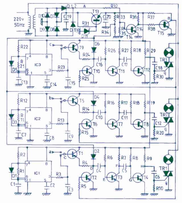 The bases of T1, T5 and T9 can be seen connected to 3 separate SPDT switches.
These switches can be used for removing the IC 555 feed and operate the bases manually through 3 individual potentiometers.
The slider arm of these pots will go to the transistor bases via the SPDT switches, while the other two ends of the pots will go to the DC supply rails.
The function of all the 3 IC 555, BJT amplifier and the triac lamp driver stages is the same.
The IC 555 ICs are all rigged as astable which has a sharp and fast charge time but a slow discharge time due to the inclusion of the diode across pin#7 and pin#6/2.
This generates very long ON time, and short OFF time at the respective pin#3 of the all the 555 ICs.
The OFF time outputs at the pin#3 of the ICs are in the form of a momentary pulse, which is applied to the bases of the respective BJTs T1, T5, T9, which are configured as emitter followers.
With ON/OFF pulses from the pin#3, causes the emitter follower transistors to be activated accordingly, generating a corresponding level regulated voltage across their emitters.
This emitter voltage from the emitter followers BJTs is applied as an interrupting potential across the transistor buffer stages built around T3, T4, T7, T8, T11, T12.
We can see that the first transistor from these buffer stages, that is T2, T6, T10 are pulsed at the 50 Hz rate from the transformer AC via D12. This 50 Hz pulses causes the all the 3 triac lamp drivers to be operated with a constant level of illumination, only as long a the IC 555 pulses are not available.
However, with the interruption caused by the IC 555 pulses, buffer stage transistors are forced to create a specific chopping waveform that are incrementing and decrementing in nature.
This incrementing and decrementing chopping pulses causes the triacs to switch the AC across the connected RGB lamps, with gradually increasing and decreasing ON/OFF times across all the 3 triacs.
As a result the RGB spot lamps focus color slowly and automatically become brighter and dimmer, creating interesting color mixing of the red, green, blue illuminations, focused on a specific surface.
The bases of T1, T5 and T9 can be seen connected to 3 separate SPDT switches.
These switches can be used for removing the IC 555 feed and operate the bases manually through 3 individual potentiometers.
The slider arm of these pots will go to the transistor bases via the SPDT switches, while the other two ends of the pots will go to the DC supply rails.
The function of all the 3 IC 555, BJT amplifier and the triac lamp driver stages is the same.
The IC 555 ICs are all rigged as astable which has a sharp and fast charge time but a slow discharge time due to the inclusion of the diode across pin#7 and pin#6/2.
This generates very long ON time, and short OFF time at the respective pin#3 of the all the 555 ICs.
The OFF time outputs at the pin#3 of the ICs are in the form of a momentary pulse, which is applied to the bases of the respective BJTs T1, T5, T9, which are configured as emitter followers.
With ON/OFF pulses from the pin#3, causes the emitter follower transistors to be activated accordingly, generating a corresponding level regulated voltage across their emitters.
This emitter voltage from the emitter followers BJTs is applied as an interrupting potential across the transistor buffer stages built around T3, T4, T7, T8, T11, T12.
We can see that the first transistor from these buffer stages, that is T2, T6, T10 are pulsed at the 50 Hz rate from the transformer AC via D12. This 50 Hz pulses causes the all the 3 triac lamp drivers to be operated with a constant level of illumination, only as long a the IC 555 pulses are not available.
However, with the interruption caused by the IC 555 pulses, buffer stage transistors are forced to create a specific chopping waveform that are incrementing and decrementing in nature.
This incrementing and decrementing chopping pulses causes the triacs to switch the AC across the connected RGB lamps, with gradually increasing and decreasing ON/OFF times across all the 3 triacs.
As a result the RGB spot lamps focus color slowly and automatically become brighter and dimmer, creating interesting color mixing of the red, green, blue illuminations, focused on a specific surface.
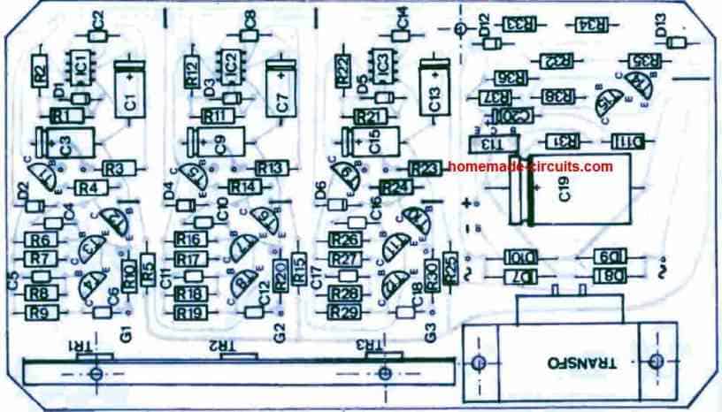
 Alright, so inert gases have the ability to generate illumination when electrified.
But this fails to clarify just how the xenon tube is actually ignited.
The electrical power storage capacitor described previously is indicated in figure 1 above, through a couple of capacitors C1 and C2.
Given that the xenon tube needs a voltage of 600 V across the anode and the cathode, diodes D1 and D2 constitute a voltage doubler network in conjunction with the electrolytic capacitors C1 and C2.
Alright, so inert gases have the ability to generate illumination when electrified.
But this fails to clarify just how the xenon tube is actually ignited.
The electrical power storage capacitor described previously is indicated in figure 1 above, through a couple of capacitors C1 and C2.
Given that the xenon tube needs a voltage of 600 V across the anode and the cathode, diodes D1 and D2 constitute a voltage doubler network in conjunction with the electrolytic capacitors C1 and C2.
 The highest repeat strobe rate is limited to 20 Hz.
The circuit has the capacity to handle 4 strobe devices at the same time and essentially is made up of range of switching devices and a clock generator.
The 2N2646 unijunction transistor UJT works like a pulse generator.
The network associated with this is intended to enable the frequency of the output signal to be tweaked around the 8 �� 180 Hz rate using P1. The oscillator signal is fed to the clock signal input of the decimal counter IC1.
Figure 3 below shows a picture of the signal waveforms at the IC1 output with regards to the clock signal.
The highest repeat strobe rate is limited to 20 Hz.
The circuit has the capacity to handle 4 strobe devices at the same time and essentially is made up of range of switching devices and a clock generator.
The 2N2646 unijunction transistor UJT works like a pulse generator.
The network associated with this is intended to enable the frequency of the output signal to be tweaked around the 8 �� 180 Hz rate using P1. The oscillator signal is fed to the clock signal input of the decimal counter IC1.
Figure 3 below shows a picture of the signal waveforms at the IC1 output with regards to the clock signal.
 The signals coming from the IC 4017 switch at a frequency of 1 �� 20 Hz are applied to the switches S1 �� S4. The positioning of the switches decides the sequential pattern of the strobe.
It allows the lighting sequence to be adjusted from right to left, or the opposite, etc.
When S1 to S4 are set at totally clockwise, the push-buttons become in the operational mode, enabling one of the 4 xenon tubes to be activated manually.
The control signals activate the LED driver stages through transistors T2 .
. .
T5. The LEDs D1 �� D4 work like functional indicators for the strobe lights.
The control circuit could be tested by just grounding the cathodes of D1 �� D4. These will show immediately whether or not the circuit is working correctly.
The signals coming from the IC 4017 switch at a frequency of 1 �� 20 Hz are applied to the switches S1 �� S4. The positioning of the switches decides the sequential pattern of the strobe.
It allows the lighting sequence to be adjusted from right to left, or the opposite, etc.
When S1 to S4 are set at totally clockwise, the push-buttons become in the operational mode, enabling one of the 4 xenon tubes to be activated manually.
The control signals activate the LED driver stages through transistors T2 .
. .
T5. The LEDs D1 �� D4 work like functional indicators for the strobe lights.
The control circuit could be tested by just grounding the cathodes of D1 �� D4. These will show immediately whether or not the circuit is working correctly.
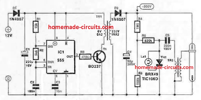 In this simple stroboscope circuit the IC 555 works like an astable oscillator driving a transistor and an attached transformer.
The transformer converts 6V DC into 220 V low current AC for the stroboscope stage.
The 220 V is further converted to a high voltage peak 300 V with the help of the diode capacitor rectifier.
When the capacitor C4 charges up to the triggering threshold of the SCR gate neon bulb, through the resistive network, the SCR fires and triggers the driver grid coil of the stroboscope lamp.
This action dumps the entire 300 V into the stroboscope bulb illuminating it brightly, until the C4 is fully discharged for the next cycle to repeat.
In this simple stroboscope circuit the IC 555 works like an astable oscillator driving a transistor and an attached transformer.
The transformer converts 6V DC into 220 V low current AC for the stroboscope stage.
The 220 V is further converted to a high voltage peak 300 V with the help of the diode capacitor rectifier.
When the capacitor C4 charges up to the triggering threshold of the SCR gate neon bulb, through the resistive network, the SCR fires and triggers the driver grid coil of the stroboscope lamp.
This action dumps the entire 300 V into the stroboscope bulb illuminating it brightly, until the C4 is fully discharged for the next cycle to repeat.
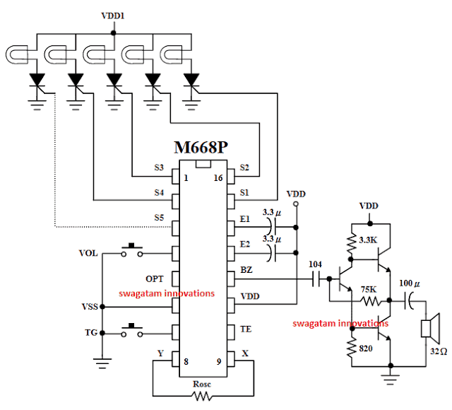 Referring to the diagram the IC M668 may have 25 different Christmas melodies or songs embedded in it, which is played randomly as long as the circuit is powered.
Additionally the button TG can be pressed anytime for changing the song number, and playing any other desired number on the connected loudspeaker.
The loudspeaker is a tiny 32 ohms speaker, which is driven by a BJT amplifier capable of producing an adequate watt power over the speaker which may be quite enough for anybody to listen to the melodies within the premise.
The VOL button can be used for adjusting the volume as per individual preference and tolerance.
The best thing about this musical Christmas light sequencer circuit is not only its dual function feature of music and light generation but also its transformerless compact design.
The power for this decoration light circuit can be directly acquired from the AC mains through a little transformerless power supply circuit comprising of some diodes and capacitors as shown below:
Referring to the diagram the IC M668 may have 25 different Christmas melodies or songs embedded in it, which is played randomly as long as the circuit is powered.
Additionally the button TG can be pressed anytime for changing the song number, and playing any other desired number on the connected loudspeaker.
The loudspeaker is a tiny 32 ohms speaker, which is driven by a BJT amplifier capable of producing an adequate watt power over the speaker which may be quite enough for anybody to listen to the melodies within the premise.
The VOL button can be used for adjusting the volume as per individual preference and tolerance.
The best thing about this musical Christmas light sequencer circuit is not only its dual function feature of music and light generation but also its transformerless compact design.
The power for this decoration light circuit can be directly acquired from the AC mains through a little transformerless power supply circuit comprising of some diodes and capacitors as shown below:
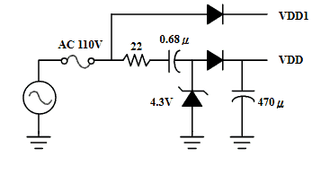 As can be seen , direct AC mains Vdd1 is used for powering the AC lamps, therefore make sure the connected lamps are rated at 120V AC, or 220CV AC and not anything less than that.
Vdd is used for powering the IC based circuit and is therefore stabilized to 12V, however care must be taken not to touch the circuit while it's powered because this musical Christmas light decoration circuit is absolutely NOT isolated from mains, and therefore is life threatening in open condition.
This implies that the whole circuit must be enclosed inside a suitable enclosure with only the mains cord terminating for AC plug in.
The lights could be terminated through wire and bulb holder arrangement and here too care should be taken to perfectly insulate the individual bulb strings and holders so that no accidental shocks are encountered while decorating the lights over a Christmas tree or any similar desired position.
As can be seen , direct AC mains Vdd1 is used for powering the AC lamps, therefore make sure the connected lamps are rated at 120V AC, or 220CV AC and not anything less than that.
Vdd is used for powering the IC based circuit and is therefore stabilized to 12V, however care must be taken not to touch the circuit while it's powered because this musical Christmas light decoration circuit is absolutely NOT isolated from mains, and therefore is life threatening in open condition.
This implies that the whole circuit must be enclosed inside a suitable enclosure with only the mains cord terminating for AC plug in.
The lights could be terminated through wire and bulb holder arrangement and here too care should be taken to perfectly insulate the individual bulb strings and holders so that no accidental shocks are encountered while decorating the lights over a Christmas tree or any similar desired position.

 In one of my earlier artilces we learned how to generate oxygen and hydrogen gas through electrolysis in large volumes, here we employ the same principle for the generation of pure oxygen using mains rectified AC.
The complete operational set up can be witnessed in the above shown figure.
The right side section of the diagram shows a small tank filled with clean tap water, having a lid which is appropriately fabricated to hold a plastic bottle such that its neck can protrudes out, and having a small opening some distance away for allowing the unused hydrogen gas to escape.
Two wires can be seen entering the water container with one of the wires pushed inside the bottle from its bottom end and appropriately sealed with epoxy glue and the other wire loosely held just below the lid opening.
The wire entering the bottle end is tied up with an electrode which could be ideally of graphite (salvaged from an old dead AAA cells) in order to prevent degradation due to oxidization, overtime
The wires can be seen attached with the output of a bridge rectifier, which is supplied with an input from the mains AC 220V or a 120V.
When mains is switched ON, the power enters the bridge rectifier and gets converted into a pulsating DC, this DC is introduced inside the water tank for initiating the required electrolysis.
The potential at positive end electrode of the wire generates O, or pure oxygen, while the potential at the negative wire electrode breaks H+H atoms from water generating hydrogen which escapes through the lid opening into the atmosphere.
The oxygen gas is forced to bubble inside the water enclosed inside the bottle and it emanates through the tube into the aquarium where it bubbles back from bottom to the surface enriching the water with pure oxygen and making sure that the marine life inside the aquarium gets the best of the experience in terms of breathing and oxygen absorption.
Please note that in the discussed concept the water alone is forced to break into its constituent parts, absolutely NO external catalyst in the form acid or salt should be added in the electrolysis tank, which might otherwise cause the generation of poisonous gasses instead of oxygen.
In one of my earlier artilces we learned how to generate oxygen and hydrogen gas through electrolysis in large volumes, here we employ the same principle for the generation of pure oxygen using mains rectified AC.
The complete operational set up can be witnessed in the above shown figure.
The right side section of the diagram shows a small tank filled with clean tap water, having a lid which is appropriately fabricated to hold a plastic bottle such that its neck can protrudes out, and having a small opening some distance away for allowing the unused hydrogen gas to escape.
Two wires can be seen entering the water container with one of the wires pushed inside the bottle from its bottom end and appropriately sealed with epoxy glue and the other wire loosely held just below the lid opening.
The wire entering the bottle end is tied up with an electrode which could be ideally of graphite (salvaged from an old dead AAA cells) in order to prevent degradation due to oxidization, overtime
The wires can be seen attached with the output of a bridge rectifier, which is supplied with an input from the mains AC 220V or a 120V.
When mains is switched ON, the power enters the bridge rectifier and gets converted into a pulsating DC, this DC is introduced inside the water tank for initiating the required electrolysis.
The potential at positive end electrode of the wire generates O, or pure oxygen, while the potential at the negative wire electrode breaks H+H atoms from water generating hydrogen which escapes through the lid opening into the atmosphere.
The oxygen gas is forced to bubble inside the water enclosed inside the bottle and it emanates through the tube into the aquarium where it bubbles back from bottom to the surface enriching the water with pure oxygen and making sure that the marine life inside the aquarium gets the best of the experience in terms of breathing and oxygen absorption.
Please note that in the discussed concept the water alone is forced to break into its constituent parts, absolutely NO external catalyst in the form acid or salt should be added in the electrolysis tank, which might otherwise cause the generation of poisonous gasses instead of oxygen.
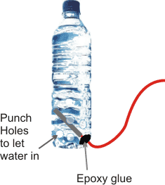 That's it! Once the above procedures are finished, it's just about plugging and switching ON the mains, and watching the the oxygen bubbling out inside the fish aquarium, making the lives of the fishes merrier.
Warning: The explained electrolysis set up for the fish aquarium generator circuit is very dangerous due to the involvement of AC mains in the electrolysis tank.
Extreme caution and safety must be exercised while building and testing the proposed units.
That's it! Once the above procedures are finished, it's just about plugging and switching ON the mains, and watching the the oxygen bubbling out inside the fish aquarium, making the lives of the fishes merrier.
Warning: The explained electrolysis set up for the fish aquarium generator circuit is very dangerous due to the involvement of AC mains in the electrolysis tank.
Extreme caution and safety must be exercised while building and testing the proposed units.
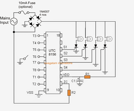
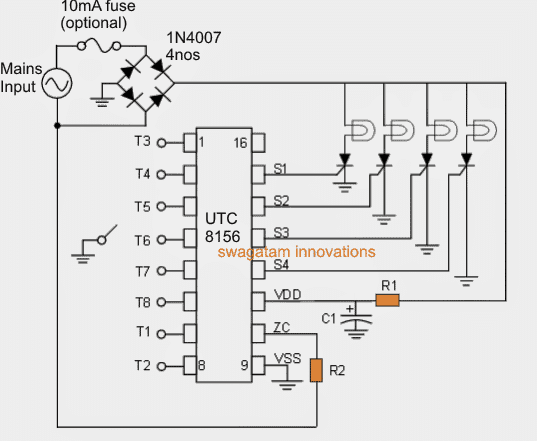
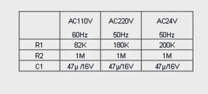 As per the specifications, the IC is able to operate even from supplies as low as 5V, which implies that the circuit can be possibly operated through a mobile charger.
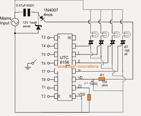 Courtesy:search.alkon.net/cgi-bin/pdf.pl?pdfname=utc/8156.pdf
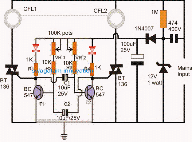 The circuit stage built around T1 and T2 is an ordinary astable multivibrator wherein the transistors switch alternately at a given rate as set by the values of C1, C2 and /or the values of the pots VR1 and VR2.
VR1 and VR2 can be discretely adjusted to produce different sets of flashing rates for the two lamps, or can be fixed in the middle for generating a uniform flashing pattern for the lamps.
The lamps are switched through the indicated triacs whose switching is controlled by the switching rate of the transistors, during the transistor OFF periods the traics are switched ON and vice versa, this effect is not simultaneous, rather implemented alternately for the traics giving rise to the proposed alternate flashing effect for the lamps.
The circuit stage built around T1 and T2 is an ordinary astable multivibrator wherein the transistors switch alternately at a given rate as set by the values of C1, C2 and /or the values of the pots VR1 and VR2.
VR1 and VR2 can be discretely adjusted to produce different sets of flashing rates for the two lamps, or can be fixed in the middle for generating a uniform flashing pattern for the lamps.
The lamps are switched through the indicated triacs whose switching is controlled by the switching rate of the transistors, during the transistor OFF periods the traics are switched ON and vice versa, this effect is not simultaneous, rather implemented alternately for the traics giving rise to the proposed alternate flashing effect for the lamps.
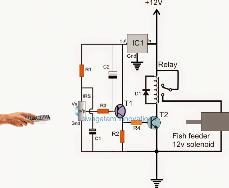
 The above presented simulation of the proposed remote controlled fish feeder circuit can be realized with the help of the following points:
For ensuring 100% safety to the solenoid and the circuit, it is recommended to add a 1000uF capacitor network at the collector of the relay driver transistor.
This will ensure that the relay never stays ON for more than a second, and thus prevent overloading of the solenoid.
The above presented simulation of the proposed remote controlled fish feeder circuit can be realized with the help of the following points:
For ensuring 100% safety to the solenoid and the circuit, it is recommended to add a 1000uF capacitor network at the collector of the relay driver transistor.
This will ensure that the relay never stays ON for more than a second, and thus prevent overloading of the solenoid.
 Video Demo
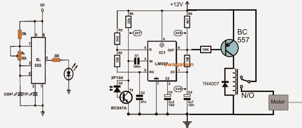 A detailed explanation of the concept may be read in the article titled Tuned infrared detector modules.
The article details the entire functioning of the relevant components used in the design and also regarding how to set up the modules in order to make them uniquely compatible with each other.
A detailed explanation of the concept may be read in the article titled Tuned infrared detector modules.
The article details the entire functioning of the relevant components used in the design and also regarding how to set up the modules in order to make them uniquely compatible with each other.
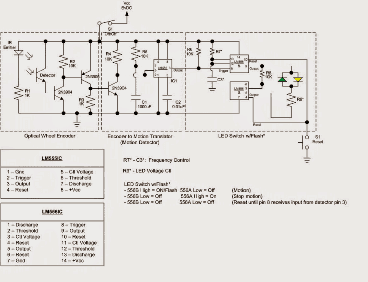 Sorry to bug, promise I'll keep messages limited.
But I had a revision of the original print.
Thought with the digital output from the encoder, why would I need a detector to trigger the flasher?
Couldn't I just use the digital output from the encoder to trigger the 556 and remove the detector part altogether?
But with that circuit, would the high side of 556a flash until the threshold switches low to trigger 556b and set the second led to ON until reset?
Then on reset, both go low (off) until signal from the encoder triggers the 556 again? Just double checking my work.
Thanks Hello Mike,
Sorry to bug, promise I'll keep messages limited.
But I had a revision of the original print.
Thought with the digital output from the encoder, why would I need a detector to trigger the flasher?
Couldn't I just use the digital output from the encoder to trigger the 556 and remove the detector part altogether?
But with that circuit, would the high side of 556a flash until the threshold switches low to trigger 556b and set the second led to ON until reset?
Then on reset, both go low (off) until signal from the encoder triggers the 556 again? Just double checking my work.
Thanks Hello Mike,
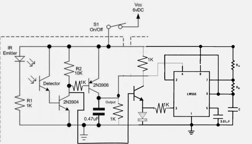 Please check the attached diagram above, I think this will do the job.
I saw one serious fault in your design, the 2N3906 did not have a base resistor, I think you might have already blown of this transistor during the testing procedures.
Ra, Rb and C may be appropriately selected for getting the desired flash rate on the LED.
That's crazy, man! how'd you come up with the idea of the second pnp combined with the npn?!? That controls both the reset AND the output! Ingenious! I think that might work.
I'll play with that and let you know how it turns out.
Thanks Bro
Welcome Bro,,,,I forgot to include a resistor at pin#3 of 555, please connect a 1K resistor there, else you'll fry the LED:)
Ya, I caught that too.
Already plugged one in.
But good eye.
Taking the day off.
Trying to track down another 2n3904 but have some stuff to rip apart to find it.
I'll get back on it tomorrow and let you know how it turns out.
BTW...
Because you have been such a help in this, I'm including you in the compensation side too.
That was the deal, right? So, once I get paid, I will pay it forward.
God bless
Just a bit of correction, the resistor should be across the cathode and ground of the LED and not with pin#3, because we want pin#3 to ground all vibrational signals from the emitter of the NPN transistor every time it goes zero.,
That means now have two resistor in line, one resistor at the collector of the NPN and another at the cathode of the LED, this will 100% fix the matter for sure.
...and thanks very much for considering my contributions:)
Best...
Ughhhh! Mechanical Engineering is SO much easier!
Ok.
Here's what I got...
Redid the circuit 4 times to double check my work.
I only have two parts in question.
The 0.47uF capacitor off of Q3 is impossible to find without ordering one.
I used a 0.1uF being the closest one I have.
Is there another value that I can substitute? Also, the Detector (Q1) is from a mouse circuit with a 3-pin photo-transistor.
I don't want to blow it out so I left the base open and connected the collector to HI and the emitter to base of Q2 (2n3904).
All other values are as spec.
I added a few photos to give visual aid to my work.
Maybe you can see something I missed.
(note: The led is solid not blinking) If you want video, I can send that too.
(There will be another email to this so this is 1 of 2)
PS...
Notice the title block of the schematic.
I added something.
I figured you deserve it.
I plan on copywriting this when its done and I will put your name on the copywrite as a co-writer if you're cool with that.
I'll let you know how that turns out.
Please check the attached diagram above, I think this will do the job.
I saw one serious fault in your design, the 2N3906 did not have a base resistor, I think you might have already blown of this transistor during the testing procedures.
Ra, Rb and C may be appropriately selected for getting the desired flash rate on the LED.
That's crazy, man! how'd you come up with the idea of the second pnp combined with the npn?!? That controls both the reset AND the output! Ingenious! I think that might work.
I'll play with that and let you know how it turns out.
Thanks Bro
Welcome Bro,,,,I forgot to include a resistor at pin#3 of 555, please connect a 1K resistor there, else you'll fry the LED:)
Ya, I caught that too.
Already plugged one in.
But good eye.
Taking the day off.
Trying to track down another 2n3904 but have some stuff to rip apart to find it.
I'll get back on it tomorrow and let you know how it turns out.
BTW...
Because you have been such a help in this, I'm including you in the compensation side too.
That was the deal, right? So, once I get paid, I will pay it forward.
God bless
Just a bit of correction, the resistor should be across the cathode and ground of the LED and not with pin#3, because we want pin#3 to ground all vibrational signals from the emitter of the NPN transistor every time it goes zero.,
That means now have two resistor in line, one resistor at the collector of the NPN and another at the cathode of the LED, this will 100% fix the matter for sure.
...and thanks very much for considering my contributions:)
Best...
Ughhhh! Mechanical Engineering is SO much easier!
Ok.
Here's what I got...
Redid the circuit 4 times to double check my work.
I only have two parts in question.
The 0.47uF capacitor off of Q3 is impossible to find without ordering one.
I used a 0.1uF being the closest one I have.
Is there another value that I can substitute? Also, the Detector (Q1) is from a mouse circuit with a 3-pin photo-transistor.
I don't want to blow it out so I left the base open and connected the collector to HI and the emitter to base of Q2 (2n3904).
All other values are as spec.
I added a few photos to give visual aid to my work.
Maybe you can see something I missed.
(note: The led is solid not blinking) If you want video, I can send that too.
(There will be another email to this so this is 1 of 2)
PS...
Notice the title block of the schematic.
I added something.
I figured you deserve it.
I plan on copywriting this when its done and I will put your name on the copywrite as a co-writer if you're cool with that.
I'll let you know how that turns out.
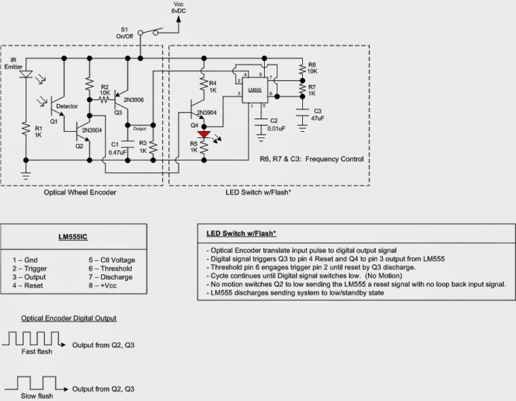
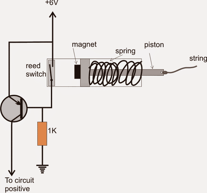 This is just an idea, not sure if it would suit your requirement exactly? Referring to the diagram, as long as the string is without any tension the magnet stays close to the reed switch due to spring pressure keeping the reed closed.
The situation keeps the PNP switched OFF which in turn keeps our LED circuit switched OFF.
The moment string is pulled > the magnet pulls away > the reed disconnects > the PNP switches ON > our LED circuit gets activated, and starts performing the proposed actions....our LED circuit remains activated for so long as the fish is not pulled of the hook or the string looses tension.
Feedback:
Very cool idea.
I might use that for my reset function.
I got the thing to work.
The base of the Q1 Detector was sent to high (Vcc) and it started working.
Blinking with no motion and fast blink (Almost like an always on but still pulsed to the speed of the opti wheel.
Works!) but there wasn't any way to reset without physical grounding (Light off).
once ground was removed, blinking began without motion.
Maybe a transistor to switch from reset ground of Pin 4 to the Base of Q1. Once Q1 senses motion, it trips a 3904 (?) from low to high activating the circuit then a push button momentary switch could "reset the transistor back to low until signal received again.
What do you think?
I like your idea with the magnet but again, trying to keep it simple for manufacturing.
More parts, more money, then higher price on the shelf, less buyers.
I'll see what I can do though.
Good work on that reed switch.
I'll work on that.
I get it! Instead of a reed switch, why not use the catch/release lever to act as a switch itself.
Both parts are made of metal.
I can insulate the latch from the body and once the cord releases the lever, it would make contact with the catch stop and whalla! Contact! I'll send you a pic of what I mean...
One final question...
Currently, I am using 4 off-the-shelf AAA batteries to achieve 6.3vDC.
However, I was wanting to reduce the package size to achieve the same or close to voltage.
How long do you thing 2 coil cells like a CR2032 or similar last?
I have 2 LC-16340 3vDC @ 1000mAh batteries like the CR123A but rechargeable, but I didn't want to over power the current on the board and fry everything.
If I use the 16340's, I could add a simple charging circuit to the system and make them rechargeable.
But again, I don't want to fry the board.
Thoughts?
Also, I am planning on using an ultra-bright high power led for the circuit (Not sure of specs yet).
Would the current values of the rest of the circuit be ok for that power? BTW, the 555 I used was a cn rated for 18v max @ 600mA.
This is just an idea, not sure if it would suit your requirement exactly? Referring to the diagram, as long as the string is without any tension the magnet stays close to the reed switch due to spring pressure keeping the reed closed.
The situation keeps the PNP switched OFF which in turn keeps our LED circuit switched OFF.
The moment string is pulled > the magnet pulls away > the reed disconnects > the PNP switches ON > our LED circuit gets activated, and starts performing the proposed actions....our LED circuit remains activated for so long as the fish is not pulled of the hook or the string looses tension.
Feedback:
Very cool idea.
I might use that for my reset function.
I got the thing to work.
The base of the Q1 Detector was sent to high (Vcc) and it started working.
Blinking with no motion and fast blink (Almost like an always on but still pulsed to the speed of the opti wheel.
Works!) but there wasn't any way to reset without physical grounding (Light off).
once ground was removed, blinking began without motion.
Maybe a transistor to switch from reset ground of Pin 4 to the Base of Q1. Once Q1 senses motion, it trips a 3904 (?) from low to high activating the circuit then a push button momentary switch could "reset the transistor back to low until signal received again.
What do you think?
I like your idea with the magnet but again, trying to keep it simple for manufacturing.
More parts, more money, then higher price on the shelf, less buyers.
I'll see what I can do though.
Good work on that reed switch.
I'll work on that.
I get it! Instead of a reed switch, why not use the catch/release lever to act as a switch itself.
Both parts are made of metal.
I can insulate the latch from the body and once the cord releases the lever, it would make contact with the catch stop and whalla! Contact! I'll send you a pic of what I mean...
One final question...
Currently, I am using 4 off-the-shelf AAA batteries to achieve 6.3vDC.
However, I was wanting to reduce the package size to achieve the same or close to voltage.
How long do you thing 2 coil cells like a CR2032 or similar last?
I have 2 LC-16340 3vDC @ 1000mAh batteries like the CR123A but rechargeable, but I didn't want to over power the current on the board and fry everything.
If I use the 16340's, I could add a simple charging circuit to the system and make them rechargeable.
But again, I don't want to fry the board.
Thoughts?
Also, I am planning on using an ultra-bright high power led for the circuit (Not sure of specs yet).
Would the current values of the rest of the circuit be ok for that power? BTW, the 555 I used was a cn rated for 18v max @ 600mA.

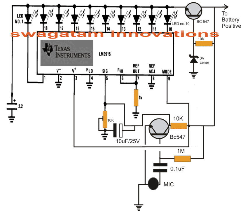
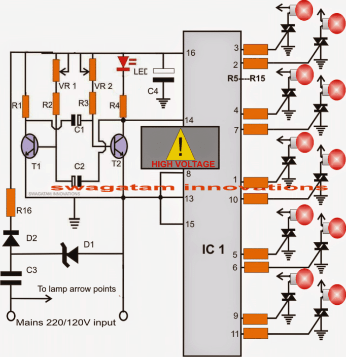
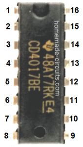 CAUTION: NO MAINS ISOLATION PRESENT....HANDLE WITH EXTREME CAUTION TO AVOID SHOCKS, AND FATALITY.
Parts List
R1, R2, R3, R4, R5----R15: 1K
VR1, VR2 = 100k
C1, C2 = 10uF/25V
C3 = 474/400V
C4 = 100uF/25V
D1 = 12V zener, 1 watt
D2 = 1N4007
R16 = 10 ohms, 2 watt
Triacs = BT136
IC1 = 4017
T1,T2 = BC547
LED = red, 5mm
CAUTION: NO MAINS ISOLATION PRESENT....HANDLE WITH EXTREME CAUTION TO AVOID SHOCKS, AND FATALITY.
Parts List
R1, R2, R3, R4, R5----R15: 1K
VR1, VR2 = 100k
C1, C2 = 10uF/25V
C3 = 474/400V
C4 = 100uF/25V
D1 = 12V zener, 1 watt
D2 = 1N4007
R16 = 10 ohms, 2 watt
Triacs = BT136
IC1 = 4017
T1,T2 = BC547
LED = red, 5mm
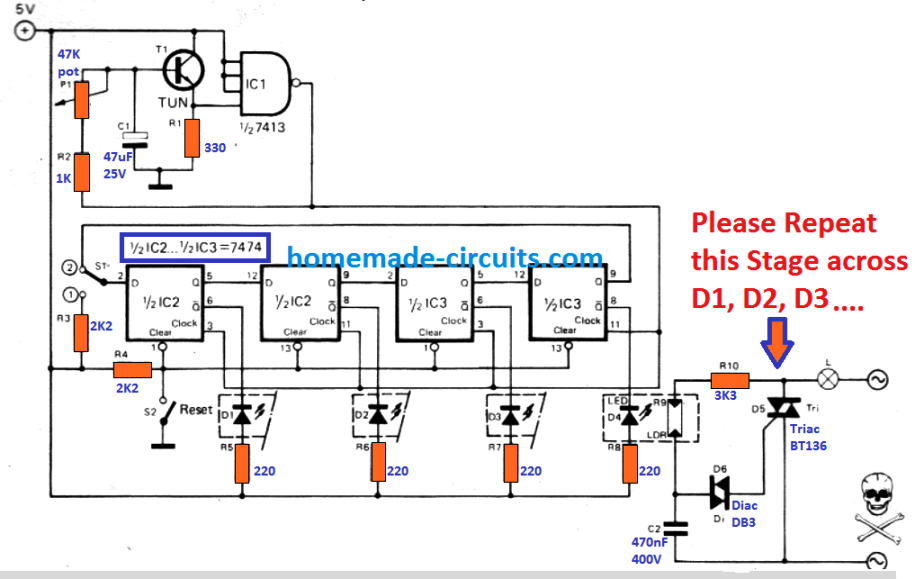 Through this circuit four 220V lamps could be used to illuminate in sequence, such that a 'running-light' effect is generated.
The circuit is made up of square-wave generator (T1 , IC1), a shift register (IC2, IC3), and the lamp driver stages.
P1 is used to vary the frequency of the square-wave from 0.1 Hz to about 10 Hz.
The square-wave voltage is supplied to the clock inputs of the shift register.
When S2 is pressed the flip-flops get reset.
The Q-outputs then turn into '0' and the Q-outputs into '1', all LED's are shut off and all the lamps are switched OFF.
When S2 is released, S1 comes in position 1 causing the input of the register toturn into logic '1'.
Following one clock pulse, the input data of the flip-flop is carried to the output which illuminates the first lamp; S1 is now gets reset to position 2. From here on every subsequent clock pulse shifts the logic '1' on to the next flip-flop which in turn resets the last one, which causes the lamps to light up in sequence, producing a four 220V lamp chasing effect.
Through this circuit four 220V lamps could be used to illuminate in sequence, such that a 'running-light' effect is generated.
The circuit is made up of square-wave generator (T1 , IC1), a shift register (IC2, IC3), and the lamp driver stages.
P1 is used to vary the frequency of the square-wave from 0.1 Hz to about 10 Hz.
The square-wave voltage is supplied to the clock inputs of the shift register.
When S2 is pressed the flip-flops get reset.
The Q-outputs then turn into '0' and the Q-outputs into '1', all LED's are shut off and all the lamps are switched OFF.
When S2 is released, S1 comes in position 1 causing the input of the register toturn into logic '1'.
Following one clock pulse, the input data of the flip-flop is carried to the output which illuminates the first lamp; S1 is now gets reset to position 2. From here on every subsequent clock pulse shifts the logic '1' on to the next flip-flop which in turn resets the last one, which causes the lamps to light up in sequence, producing a four 220V lamp chasing effect.
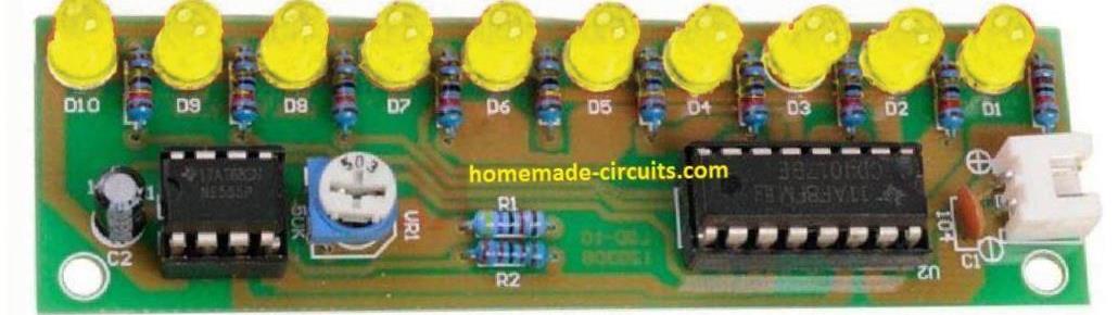
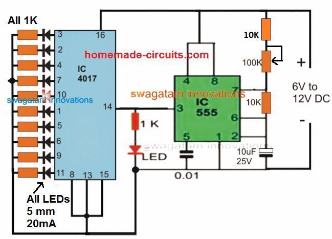 Parts List
All resistors are 1/4 watt 5% unless specified
1K = 11nos
10K = 2nos
100K pot = 1no
Capacitors
0.01uF ceramic disc
10uF/25V electrolytic
Semiconductors
LEDs RED, 5mm High Bright or as desired = 11nos
IC 4017 = 1no
IC 555 = 1no
For learning the pinouts and datasheet of the IC 4017 please refer to this article
For a detailed explanation regarding IC 555 astable, you can click on this article
As can be seen in this configuration, in response to the pulses from IC 555, the IC 4017 generates a running or chasing light pattern across the connected 10 output LEDs.
The chasing pattern goes on repeating itself from start to finish as long as the IC 555 keeps pulsing pin #14 of the IC 4017.
Parts List
All resistors are 1/4 watt 5% unless specified
1K = 11nos
10K = 2nos
100K pot = 1no
Capacitors
0.01uF ceramic disc
10uF/25V electrolytic
Semiconductors
LEDs RED, 5mm High Bright or as desired = 11nos
IC 4017 = 1no
IC 555 = 1no
For learning the pinouts and datasheet of the IC 4017 please refer to this article
For a detailed explanation regarding IC 555 astable, you can click on this article
As can be seen in this configuration, in response to the pulses from IC 555, the IC 4017 generates a running or chasing light pattern across the connected 10 output LEDs.
The chasing pattern goes on repeating itself from start to finish as long as the IC 555 keeps pulsing pin #14 of the IC 4017.
 The circuit mainly comprises of IC 555 and the IC 4017 for implementing the required functions.
The IC 555 is used to generate the clock pulses which is fed to the clock input of the IC 4017.
These clock pulses received from the IC555 is translated into a sequencing or chasing effect over the LEDs connected across the various outputs of the IC 4017.
In its normal mode the IC 4017 would have generated a simple start to end sequencing of the LEDs wherein the LEDs would have lit up and shut off one after the other in a sequencing pattern with a rate determined by the IC555 cock frequency, this would repeat continuously as long as the unit stays powered.
However in the proposed knight rider LED light chaser circuit, the output of the IC4017 is configured in a special way using a group of diodes which enable the output sequencing to produce a to and fro chasing of the connected LEDs, albiet through 6 LEDs only in contrast to10 LEDsas in the normal mode.
The circuit mainly comprises of IC 555 and the IC 4017 for implementing the required functions.
The IC 555 is used to generate the clock pulses which is fed to the clock input of the IC 4017.
These clock pulses received from the IC555 is translated into a sequencing or chasing effect over the LEDs connected across the various outputs of the IC 4017.
In its normal mode the IC 4017 would have generated a simple start to end sequencing of the LEDs wherein the LEDs would have lit up and shut off one after the other in a sequencing pattern with a rate determined by the IC555 cock frequency, this would repeat continuously as long as the unit stays powered.
However in the proposed knight rider LED light chaser circuit, the output of the IC4017 is configured in a special way using a group of diodes which enable the output sequencing to produce a to and fro chasing of the connected LEDs, albiet through 6 LEDs only in contrast to10 LEDsas in the normal mode.
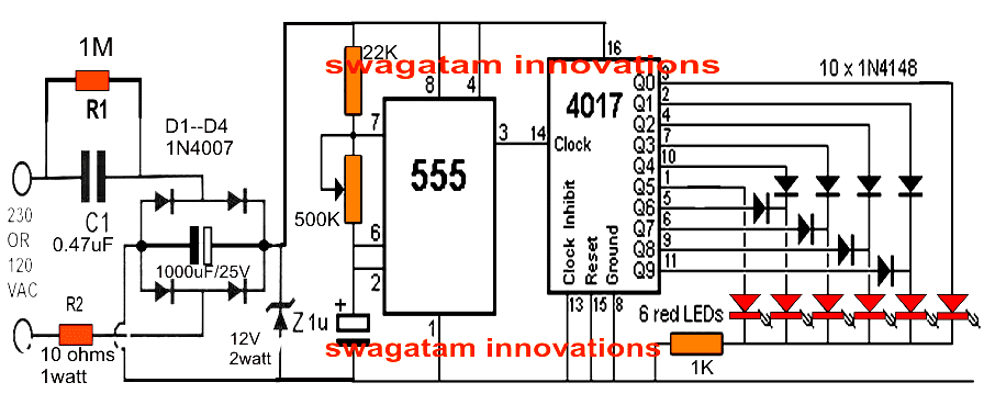 Parts List
1K = 1
22K = 1
1M = 1
10 ohms = 1
500K pot = 1
1uF/25V = 1
1000uF/25V = 1
0.47uF/400V PPC = 1
12V zener 1 watt = 1
1N4007 diodes = 4
1N4148 diode = 10
LEDs = 6
IC 4017 = 1
IC 555 = 1
Video Clip:
Parts List
1K = 1
22K = 1
1M = 1
10 ohms = 1
500K pot = 1
1uF/25V = 1
1000uF/25V = 1
0.47uF/400V PPC = 1
12V zener 1 watt = 1
1N4007 diodes = 4
1N4148 diode = 10
LEDs = 6
IC 4017 = 1
IC 555 = 1
Video Clip:
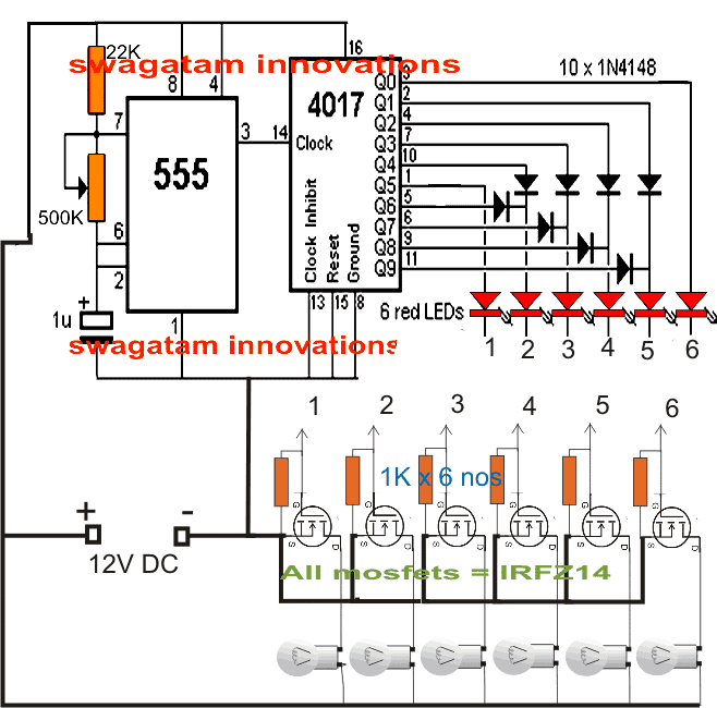
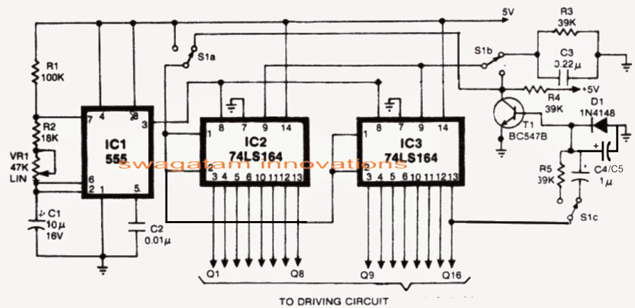 Looking for a Meteor Shower LED Effect Circuit? Please check out this article

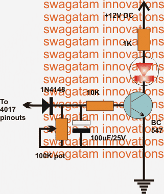
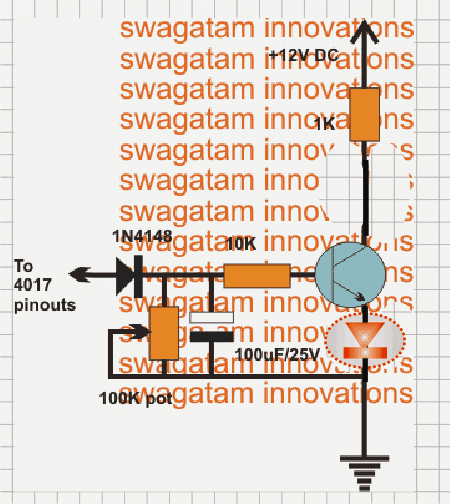
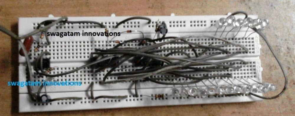
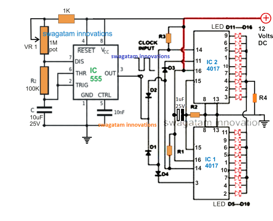 Video Clip of the above circuit in operational mode:
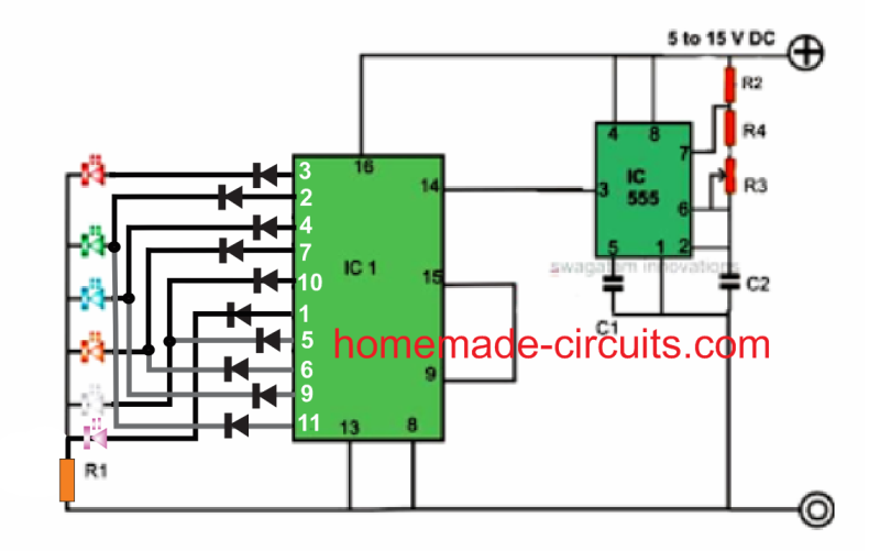
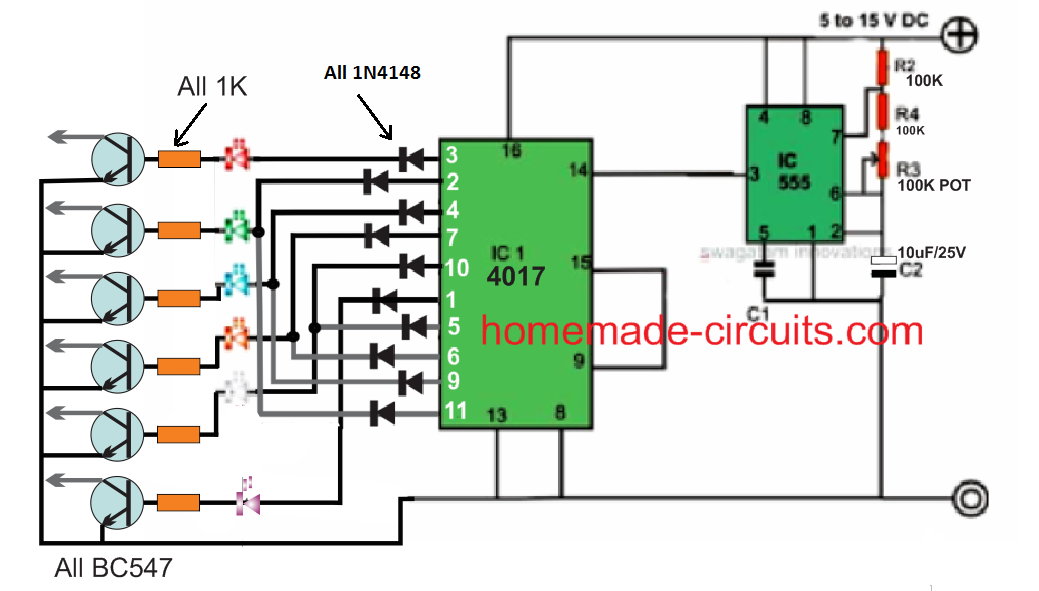 The basic reverse forward LED circuit using single LEDs can be studied elaborately in thisLED scanner article,and the video can be witnessed below:
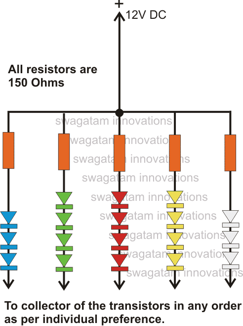
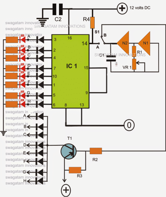 The following parts will be needed for making this LED light chaser cum flasher circuit:
R1, R2, R3 = 1K,
R4 = 100k
VR1 = 100K linear pot.
All LED resistors are = 470 Ohms,
All diodes are = 1N4148,
All LEDs = RED, 5mm or as per choice,
T1 = 2N2907, or 8550 or 187,
C1 = 10uF/25V
C2 = 0.1uF,
IC1 = 4017,
N1, N2 = IC4049
The following parts will be needed for making this LED light chaser cum flasher circuit:
R1, R2, R3 = 1K,
R4 = 100k
VR1 = 100K linear pot.
All LED resistors are = 470 Ohms,
All diodes are = 1N4148,
All LEDs = RED, 5mm or as per choice,
T1 = 2N2907, or 8550 or 187,
C1 = 10uF/25V
C2 = 0.1uF,
IC1 = 4017,
N1, N2 = IC4049
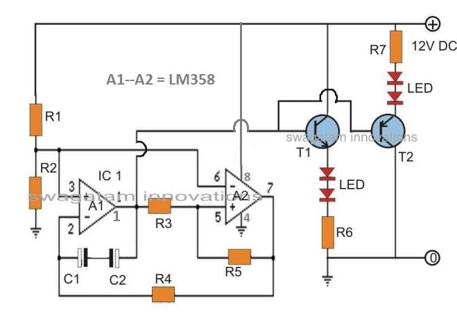
 XENON FLASH TUBE
 Lens Placed over the PCB
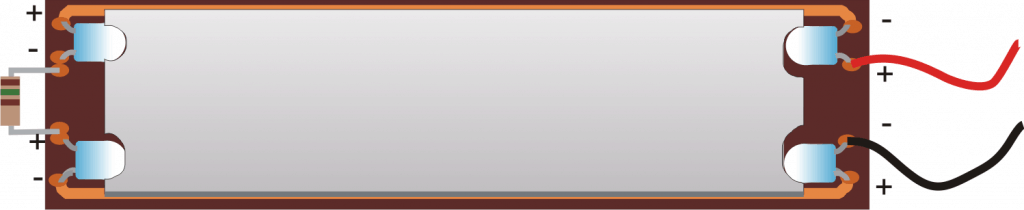 Example film positive of a particular display name:
 Positive film of the name placed over the lens for the final illuminated get-up:

 Completed Prototype, Switched ON:


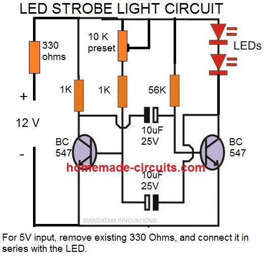 Video Illustration
The above discussed simple design can be further modified as explained below for greater control and refined outputs.
Video Illustration
The above discussed simple design can be further modified as explained below for greater control and refined outputs.
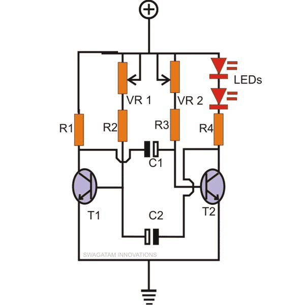 The above circuit forms the base for all the following circuits through some suitable modifications and additions.
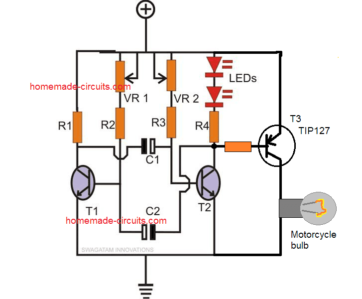 As already discussed already in the previous section, green laser pointers are pretty popular nowadays; the diagram illustrated shows a simple method of converting the above circuit into a pulsating green laser pointer strobe light.
Here the zener diode along with the transistor works like a constant voltage circuit ensuring that the laser pointer is never supplied with a voltage higher than its maximum rating.
This also ensures that the current to the laser can also never exceed the rated value.
This the zener and the transistor functions like a constant voltage and also an indirect constant current driver for the laser.
As already discussed already in the previous section, green laser pointers are pretty popular nowadays; the diagram illustrated shows a simple method of converting the above circuit into a pulsating green laser pointer strobe light.
Here the zener diode along with the transistor works like a constant voltage circuit ensuring that the laser pointer is never supplied with a voltage higher than its maximum rating.
This also ensures that the current to the laser can also never exceed the rated value.
This the zener and the transistor functions like a constant voltage and also an indirect constant current driver for the laser.
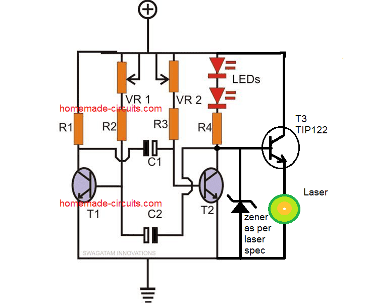
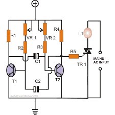 Thus we see that through the above circuit designs it becomes very easy to make any light a strobe light simply by doing the relevant modifications within a simple transistor based circuit as exlained in the above examples.
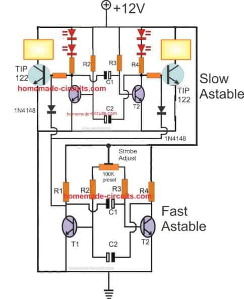 For the slow astable use the following parts:
R1, R4 = 680 ��
R2, R3 = 18K
C1 = 100 ��F
C2 = 100 ��F
T1, T2 = BC547
For the Fast astable use the following parts
R1, R4 = 680 ��
R2, R3 = 10K
preset = 100K
C1 = 47 ��F
C2 = 47 ��F
T1, T2 = BC547
For the slow astable use the following parts:
R1, R4 = 680 ��
R2, R3 = 18K
C1 = 100 ��F
C2 = 100 ��F
T1, T2 = BC547
For the Fast astable use the following parts
R1, R4 = 680 ��
R2, R3 = 10K
preset = 100K
C1 = 47 ��F
C2 = 47 ��F
T1, T2 = BC547

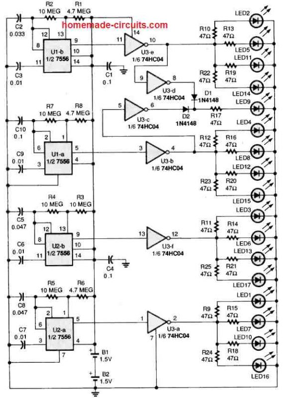 The circuit employs a couple of 7556 dual timers, U1 and U2, in order to accomplish the random pulsating light effect.
Half of the section of each timer is utilized like an astable multivibrator (clock generator) configured to some other clock speed.
Slower LED flashing speed is selected to simulate the blinking light bulbs applied to actual Christmas trees.
The flashing clock rates are set at 0.58, 1.02, 1.25, and 1.77 Hz.
These 4 frequencies are transferred to the IC 74HC04 which is a hex inverter, IC U3.
You can find four inverter gates configured from this IC, which are U3a, U3b, U3e, and U3f.
Each of these inverters get one of the inward clock signals from U1a, U1b, U2a, and U2b.
As soon as the inverter input becomes low, its output gets high, and when the inverter input gets high, its outputs gets low.
Each inverter output is used for illuminating four LEDs arranged at the border of the PC, using random color LEDs for a glittering color effect.
The rest of the two CMOS inverters, U3c and U3d, are configured to illuminate the top LED.
These gates are linked with each other through a "diode on" setup, therefore whenever one of those gates or both of those gates are high, causes current to pass across one particular or both of the 1N4148 diodes, D1 and D2, towards the upper LED, LED 9.
In this system the upper LED is shut off only while the two of those gates are low.
In case a single gate is low and the other is high, the diode conducts; when the two gates are high, the diode becomes higher in intensity, triggering a rapidly blinking LED effect.
Troubleshooting
If the uppermost LED fails to illuminate correctly, examine the direction of the couple of 1N4148 diodes along with the polarity of the LED itself.
Examine the direction of the other LEDs and check whether they too are illuminating or not.
If you find series of four LEDs not lighting up, trace the connections up to U3 and ensure that the IC 74HC04 stage gets the required clock signal.
In case it is, the trouble can be possibly one of the LEDs and/or resistors, or the IC itself.
Do another inspection to check for shorts due to soldering jumps, before you consider the IC to be the main culprit.
If you see a few of the LEDs are still failing to blink, return to the relevant portion of the timer stage and inspect the complementing parts.
To check if the 7556 timers are causing the issue, try swapping the ICs with one another.
If you see the very same LEDs continue to be in the non-blinking state, you may deem the issue to be in the complementing circuitry.
In case interchanging the 7556 ICs leads to one array of LEDs to start blinking and another array to remain shut off, only in such a situation it may be advisable to consider that the relevant timer ICs may be faulty.
PCB Design
The PCB design and the component overlay for the above explained LED Christmas tree can be found in the following images:
The circuit employs a couple of 7556 dual timers, U1 and U2, in order to accomplish the random pulsating light effect.
Half of the section of each timer is utilized like an astable multivibrator (clock generator) configured to some other clock speed.
Slower LED flashing speed is selected to simulate the blinking light bulbs applied to actual Christmas trees.
The flashing clock rates are set at 0.58, 1.02, 1.25, and 1.77 Hz.
These 4 frequencies are transferred to the IC 74HC04 which is a hex inverter, IC U3.
You can find four inverter gates configured from this IC, which are U3a, U3b, U3e, and U3f.
Each of these inverters get one of the inward clock signals from U1a, U1b, U2a, and U2b.
As soon as the inverter input becomes low, its output gets high, and when the inverter input gets high, its outputs gets low.
Each inverter output is used for illuminating four LEDs arranged at the border of the PC, using random color LEDs for a glittering color effect.
The rest of the two CMOS inverters, U3c and U3d, are configured to illuminate the top LED.
These gates are linked with each other through a "diode on" setup, therefore whenever one of those gates or both of those gates are high, causes current to pass across one particular or both of the 1N4148 diodes, D1 and D2, towards the upper LED, LED 9.
In this system the upper LED is shut off only while the two of those gates are low.
In case a single gate is low and the other is high, the diode conducts; when the two gates are high, the diode becomes higher in intensity, triggering a rapidly blinking LED effect.
Troubleshooting
If the uppermost LED fails to illuminate correctly, examine the direction of the couple of 1N4148 diodes along with the polarity of the LED itself.
Examine the direction of the other LEDs and check whether they too are illuminating or not.
If you find series of four LEDs not lighting up, trace the connections up to U3 and ensure that the IC 74HC04 stage gets the required clock signal.
In case it is, the trouble can be possibly one of the LEDs and/or resistors, or the IC itself.
Do another inspection to check for shorts due to soldering jumps, before you consider the IC to be the main culprit.
If you see a few of the LEDs are still failing to blink, return to the relevant portion of the timer stage and inspect the complementing parts.
To check if the 7556 timers are causing the issue, try swapping the ICs with one another.
If you see the very same LEDs continue to be in the non-blinking state, you may deem the issue to be in the complementing circuitry.
In case interchanging the 7556 ICs leads to one array of LEDs to start blinking and another array to remain shut off, only in such a situation it may be advisable to consider that the relevant timer ICs may be faulty.
PCB Design
The PCB design and the component overlay for the above explained LED Christmas tree can be found in the following images:

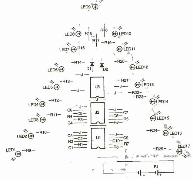
 The figure shows rather simple wiring where the IC itself acts as an oscillator as well as the LED driver.
Each of its output is wired into a string of colorful LEDs which may be set up or arranged in any desired format for acquiring the most interesting lighting effects.
The pot may be used for optimizing the flashing of the LEDs to the desired levels or at the rate which might suit the particular decorative application the most.
The circuit should be operated with voltages above 12 or precisely speaking, the applied voltage should be ideally fixed at 15 volts (regulated).
This typically high voltage enables many LEDs to be connected across each input, four to five LEDs to be exact.
Since so many LEDs are involved the power rating the transformer needs to be at least 500 mA.
The whole LED Christmas tree circuit may be enclosed inside a plastic box with strings of LEDs terminating out of the box so that they may attached to any desired structure like the Christmas tree.
The figure shows rather simple wiring where the IC itself acts as an oscillator as well as the LED driver.
Each of its output is wired into a string of colorful LEDs which may be set up or arranged in any desired format for acquiring the most interesting lighting effects.
The pot may be used for optimizing the flashing of the LEDs to the desired levels or at the rate which might suit the particular decorative application the most.
The circuit should be operated with voltages above 12 or precisely speaking, the applied voltage should be ideally fixed at 15 volts (regulated).
This typically high voltage enables many LEDs to be connected across each input, four to five LEDs to be exact.
Since so many LEDs are involved the power rating the transformer needs to be at least 500 mA.
The whole LED Christmas tree circuit may be enclosed inside a plastic box with strings of LEDs terminating out of the box so that they may attached to any desired structure like the Christmas tree.

 The circuit functioning may be understood with the following points:
The whole circuit can be divided into three separate stages, the transformerless power supply, the LED driver and the ��puff�� amplifier stage.
The parts comprising C1, R10, R1 and Z1 form the basic capacitive power supply stage, which is required for keeping the circuit ��aware�� of the mains power availability and for keeping the LED switched OFF under the conditions.
The mains input is applied across R1 and C1. R1 makes sure that the initial surge currents don��t enter the circuit and cause damage to the vulnerable parts.
With the surge controlled through R1, C1 conducts normally and delivers the expected amount of current to the preceding zener diode section.
The zener diode clamps the positive half-cycle voltages from C1 to the specified limit (12 volts here).
For the negative half-cycles, the zener diode acts as a short and switches them to ground.
This further helps to control the surge currents and keep the input to the circuit well under safe conditions.
Capacitor C2 filters the rectified DC from the zener diode so that a perfect DC becomes available to the circuit.Resistor R10 is kept for biasing the transistor T4, however in the presence of the input power, the base is held at the positive potential and any negative from the ground is inhibited to the base of T4. This restricts T4 from conducting and it remains switched OFF.
Since the battery is connected across the emitter if T4 and ground, it also remains cut OFF and the voltage is unable to reach the circuit.
Thus ,as long as the mains input is active, the power from the battery is kept aloof from the actual ��LED candle�� circuit, keeping the LED switched OFF.
In case the power fails, the positive potential at the base of T4 vanishes, so that the ground potential from R11 now gets an easy passgae to the base of T4.
T4 conducts and allows the battery voltage to reach across its collector arm.Here, the battery voltage flows to the positive of the preceding electronic and also through C3 (only instantaneously).
However, this fractional voltage from C3 switches the SCR into conduction and latches it, even after C3 charges and inhibits any further gate current to the SCR.
The latching of the SCR illuminates the LED and keeps it switched ON for so long as the mains power is absent.
If the mains power restores, the battery is instantly cut OFF by T4, bringing the circuit back to its original position, as explained above.
The above explanation describes the power supply and the switching stage, corresponding to the presence or the absence of an AC input.
However the circuit incorporates another interesting feature of extinguishing the LED by ��puffing�� air, as we usually do with wax and flame type of candles.
This feature becomes available in the absence of AC mains input, with the LED illuminated.
This is done by ��puffing�� air onto the MIC or simply by tapping it.
The momentary response from the MIC gets converted into minute electrical signals which are suitably amplified by T1, T2and T3.
When T3 conducts, it brings the anode of the SCR to the positive potential cutting OFF the ��latch�� function, the SCR is immediately switched OFF and so is the LED.
Diode D1 trickle charges the battery when mains power is ON.
The circuit functioning may be understood with the following points:
The whole circuit can be divided into three separate stages, the transformerless power supply, the LED driver and the ��puff�� amplifier stage.
The parts comprising C1, R10, R1 and Z1 form the basic capacitive power supply stage, which is required for keeping the circuit ��aware�� of the mains power availability and for keeping the LED switched OFF under the conditions.
The mains input is applied across R1 and C1. R1 makes sure that the initial surge currents don��t enter the circuit and cause damage to the vulnerable parts.
With the surge controlled through R1, C1 conducts normally and delivers the expected amount of current to the preceding zener diode section.
The zener diode clamps the positive half-cycle voltages from C1 to the specified limit (12 volts here).
For the negative half-cycles, the zener diode acts as a short and switches them to ground.
This further helps to control the surge currents and keep the input to the circuit well under safe conditions.
Capacitor C2 filters the rectified DC from the zener diode so that a perfect DC becomes available to the circuit.Resistor R10 is kept for biasing the transistor T4, however in the presence of the input power, the base is held at the positive potential and any negative from the ground is inhibited to the base of T4. This restricts T4 from conducting and it remains switched OFF.
Since the battery is connected across the emitter if T4 and ground, it also remains cut OFF and the voltage is unable to reach the circuit.
Thus ,as long as the mains input is active, the power from the battery is kept aloof from the actual ��LED candle�� circuit, keeping the LED switched OFF.
In case the power fails, the positive potential at the base of T4 vanishes, so that the ground potential from R11 now gets an easy passgae to the base of T4.
T4 conducts and allows the battery voltage to reach across its collector arm.Here, the battery voltage flows to the positive of the preceding electronic and also through C3 (only instantaneously).
However, this fractional voltage from C3 switches the SCR into conduction and latches it, even after C3 charges and inhibits any further gate current to the SCR.
The latching of the SCR illuminates the LED and keeps it switched ON for so long as the mains power is absent.
If the mains power restores, the battery is instantly cut OFF by T4, bringing the circuit back to its original position, as explained above.
The above explanation describes the power supply and the switching stage, corresponding to the presence or the absence of an AC input.
However the circuit incorporates another interesting feature of extinguishing the LED by ��puffing�� air, as we usually do with wax and flame type of candles.
This feature becomes available in the absence of AC mains input, with the LED illuminated.
This is done by ��puffing�� air onto the MIC or simply by tapping it.
The momentary response from the MIC gets converted into minute electrical signals which are suitably amplified by T1, T2and T3.
When T3 conducts, it brings the anode of the SCR to the positive potential cutting OFF the ��latch�� function, the SCR is immediately switched OFF and so is the LED.
Diode D1 trickle charges the battery when mains power is ON.
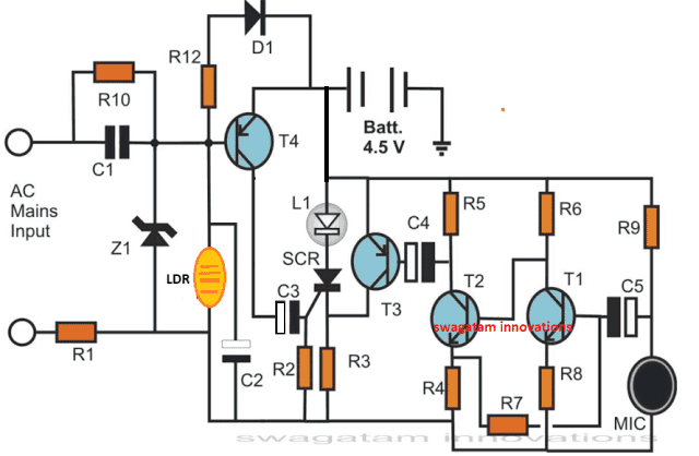 Referring to the figure we can see that the transistor biasing resistor R11 is now replaced with an LDR.
In absence of light the LDR presents a very high resistance causing the SCR to remain switched OFF, however when an burning match stick is brought near the LDR, its resistance decreases and the transistor begins conducting, which in turn allows the SCR to get triggered and latched.....
Referring to the figure we can see that the transistor biasing resistor R11 is now replaced with an LDR.
In absence of light the LDR presents a very high resistance causing the SCR to remain switched OFF, however when an burning match stick is brought near the LDR, its resistance decreases and the transistor begins conducting, which in turn allows the SCR to get triggered and latched.....
 As shown in the above string light circuit diagram, we can see that the bulbs are simply connected in series, end to end in sequence, until two wire terminate from the ��string�� which are connected to the supply mains outlet.
Usually the metal cylindrical body of the bulb forms one of the terminals, while the bottom soldered point forms the second electrical termination of it.
These two points are the only places where the wires need to be soldered.
For proper soldering results, the portions must be perfectly cleaned using sand paper, however the use of solder paste itself is enough to make the soldering without the need of much cleaning.
Initially, the wire pieces must be cut and stripped as per the desired length, then the wire ends can be dipped in solder paste so that it may be soldered on the shown areas by touching the wire end and the soldering iron hot tip filled with molten solder simultaneously.
The point will sizzle; hold the wire in place until the solder solidifies, holding the wire end firmly in place.
Finish the assembly procedure with the above steps to finally complete the light string or the toran.
As shown in the above string light circuit diagram, we can see that the bulbs are simply connected in series, end to end in sequence, until two wire terminate from the ��string�� which are connected to the supply mains outlet.
Usually the metal cylindrical body of the bulb forms one of the terminals, while the bottom soldered point forms the second electrical termination of it.
These two points are the only places where the wires need to be soldered.
For proper soldering results, the portions must be perfectly cleaned using sand paper, however the use of solder paste itself is enough to make the soldering without the need of much cleaning.
Initially, the wire pieces must be cut and stripped as per the desired length, then the wire ends can be dipped in solder paste so that it may be soldered on the shown areas by touching the wire end and the soldering iron hot tip filled with molten solder simultaneously.
The point will sizzle; hold the wire in place until the solder solidifies, holding the wire end firmly in place.
Finish the assembly procedure with the above steps to finally complete the light string or the toran.
 The toran can also be made by using a few colored bulbs rated at the Mains AC level.
In this case it simply needs to connect the bulbs in parallel and not in series.
Use holders for better convenience.
If bulb holders are used, the need of soldering is simply eliminated.
CAUTION - SINCE THE STRING LIGHT OPERATES AT AC MAINS POTENTIAL, ALL EXPOSED AREAS OF THE BULBS MUST BE APPROPRIATELY SHIELDED OR COVERED WITH INSULATING PLASTIC CAPS OR SIMILAR ENCLOSURES, NOT FOLLOWING THIS CAN RESULT IN SEVERE ELECTRIC SHOCK OR EVEN DEATH TO ANYONE TOUCHING IT IN POWERED POSITION.
The toran can also be made by using a few colored bulbs rated at the Mains AC level.
In this case it simply needs to connect the bulbs in parallel and not in series.
Use holders for better convenience.
If bulb holders are used, the need of soldering is simply eliminated.
CAUTION - SINCE THE STRING LIGHT OPERATES AT AC MAINS POTENTIAL, ALL EXPOSED AREAS OF THE BULBS MUST BE APPROPRIATELY SHIELDED OR COVERED WITH INSULATING PLASTIC CAPS OR SIMILAR ENCLOSURES, NOT FOLLOWING THIS CAN RESULT IN SEVERE ELECTRIC SHOCK OR EVEN DEATH TO ANYONE TOUCHING IT IN POWERED POSITION.
 A LED flasher schematic has also been provided to facilitate the ease of construction.
It��s a simple home fun project that will cost you hardly anything, yet the result will truly amuse you.
Build a simple LED flasher and find ways to use it for decoration.
There you must have studied how a transistor can be used to switch a load connected to its collector through a small voltage applied to its base.
The circuit of a simple LED wig wag flasher presented here incorporates just a couple of transistor and is wired as a multivibrator.
The transistors alternately switch the LEDs connected to their collector points to produce an attractive flashing effect of LEDs.
The circuit may also be used as an LED emergency flasher unit.
A LED flasher schematic has also been provided to facilitate the ease of construction.
It��s a simple home fun project that will cost you hardly anything, yet the result will truly amuse you.
Build a simple LED flasher and find ways to use it for decoration.
There you must have studied how a transistor can be used to switch a load connected to its collector through a small voltage applied to its base.
The circuit of a simple LED wig wag flasher presented here incorporates just a couple of transistor and is wired as a multivibrator.
The transistors alternately switch the LEDs connected to their collector points to produce an attractive flashing effect of LEDs.
The circuit may also be used as an LED emergency flasher unit.
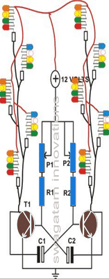
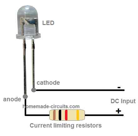

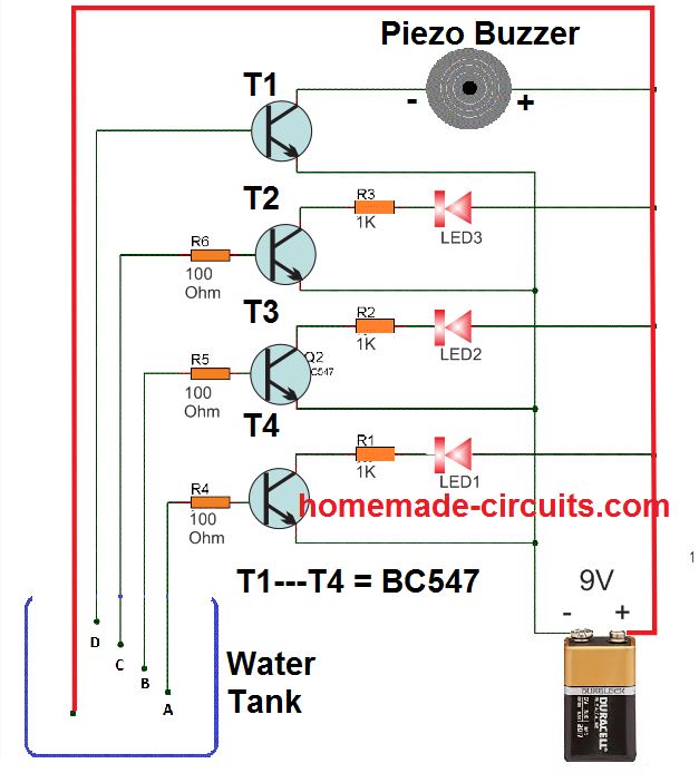
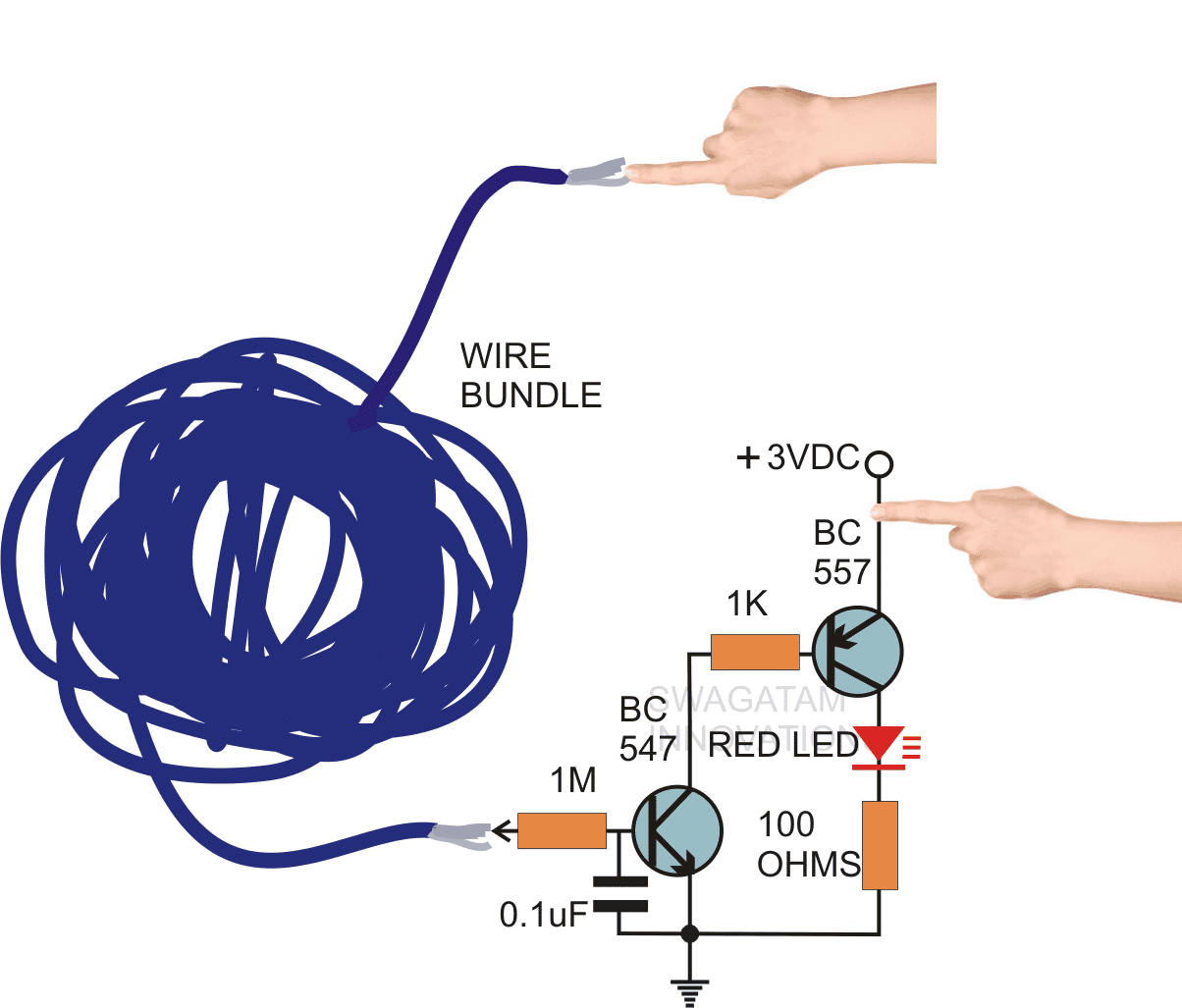 In the above article we discussed a few interesting LED circuits, but this might be just the tip of the iceberg, since there are innumerable more circuits that can be designed using LEDs for getting fascinating lighting effects or for useful indication purposes.
If you are interested to investigate more LED circuits, you can refer to the following link:
DIY LED Projects
In the above article we discussed a few interesting LED circuits, but this might be just the tip of the iceberg, since there are innumerable more circuits that can be designed using LEDs for getting fascinating lighting effects or for useful indication purposes.
If you are interested to investigate more LED circuits, you can refer to the following link:
DIY LED Projects
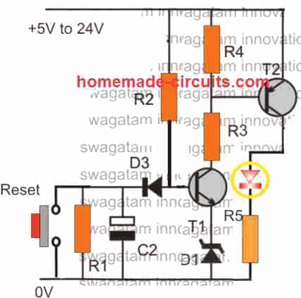 Parts List
R1 = 47k
R2 = 100k
R3, R4 = 10k
R5 = 1k
D1 = 3V zener
D3 = 1N4148
T1 = BC547
T2 = BC557
C2 = 100uF/25V
The idea is very simple, when power is switched, T1 is unable to conduct due to the presence of C2. At power switch ON, C2 grounds the T1 base voltage via R2 D3, and slowly begins charging.
During this time T2 also remains switched OFF, since it is unable to get the required base bias through T1 collector.
As C2 charges, the voltage across it rises slowly, until it reaches a value which is sufficiently high than the combined forward voltages of D3, D1, and T1 (base/emitter drop), which is equal to around 4.2V.
Once this happens T1 now conducts along with T2, and the LED switches ON.
So the delay for the LED to switch ON is determined by the values of R2, C2, D1, D3.
Parts List
R1 = 47k
R2 = 100k
R3, R4 = 10k
R5 = 1k
D1 = 3V zener
D3 = 1N4148
T1 = BC547
T2 = BC557
C2 = 100uF/25V
The idea is very simple, when power is switched, T1 is unable to conduct due to the presence of C2. At power switch ON, C2 grounds the T1 base voltage via R2 D3, and slowly begins charging.
During this time T2 also remains switched OFF, since it is unable to get the required base bias through T1 collector.
As C2 charges, the voltage across it rises slowly, until it reaches a value which is sufficiently high than the combined forward voltages of D3, D1, and T1 (base/emitter drop), which is equal to around 4.2V.
Once this happens T1 now conducts along with T2, and the LED switches ON.
So the delay for the LED to switch ON is determined by the values of R2, C2, D1, D3.
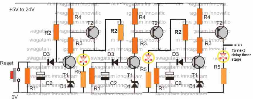 You may need a total of 25 such stages in all to create the intended sequential cube LED lighting as shown in the GIF image above.
If you want to make it quicker, then you can reduce the number of stage to 12, and add two LED in series in each module to cover two blocks at a time in the cube.
Alternatively, you can use 3 such stages, and connect 8 LEDs from each row of the cube to each delay timer, in sequence to create a rising skyscraper effect.
However, if you want to use all the specified 25 stages and want to make it faster or slower, you can do it by selecting lower or higher values for the capacitor C2 appropriately.
You may need a total of 25 such stages in all to create the intended sequential cube LED lighting as shown in the GIF image above.
If you want to make it quicker, then you can reduce the number of stage to 12, and add two LED in series in each module to cover two blocks at a time in the cube.
Alternatively, you can use 3 such stages, and connect 8 LEDs from each row of the cube to each delay timer, in sequence to create a rising skyscraper effect.
However, if you want to use all the specified 25 stages and want to make it faster or slower, you can do it by selecting lower or higher values for the capacitor C2 appropriately.
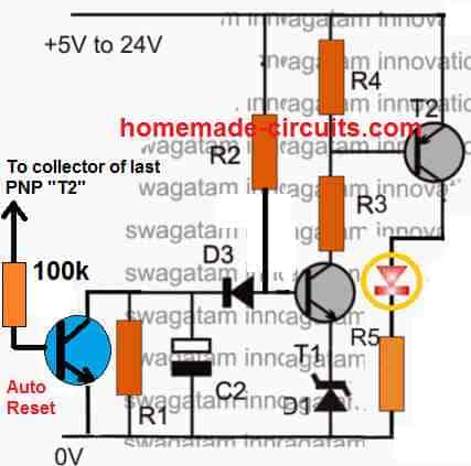
 The complete diagram can be witnessed in the following image
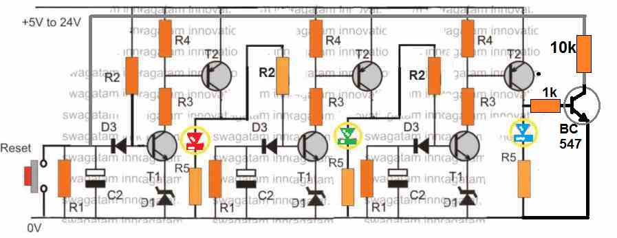 As you can it is same circuit as before, but with only 3 delay timer stages.
The 3 stages are equipped with the respective RGB LED lights, which illuminate in sequence and then shut off one by one in sequence, producing the intended slow RGB color changing illumination through the cube walls.
All the red, green, blue lights can be 1 watt 300 mA LED lamps.
As you can it is same circuit as before, but with only 3 delay timer stages.
The 3 stages are equipped with the respective RGB LED lights, which illuminate in sequence and then shut off one by one in sequence, producing the intended slow RGB color changing illumination through the cube walls.
All the red, green, blue lights can be 1 watt 300 mA LED lamps.
 In this article we discuss a simple mains operated buck converter which can be used as a driver for illuminating ceiling LED lamps between 3 watt and 10 watt range .
The circuit is actually a 220 V to 15 V SMPS circuit but since it is a non-isolated design it gets rid of the complex ferrite transformer and the involved critical factors.
Although a non-isolated design does not provide isolation to the circuit from mains AC, a simple rigid plastic cover over the unit easily counters this drawback, guaranteeing absolutely no threat to the user.
On the other hand, the best things about a non-isolated driver circuit is that, it is cheap, easy to build, install and use, due to the absence of a critical SMPS transformer, which is replaced by a simple inductor.
The use of a single IC VIPer22A by ST microelectronics makes the design virtually damage proof, and permanent, provided the input AC supply is within the specified 100 V and 285 V range.
In this article we discuss a simple mains operated buck converter which can be used as a driver for illuminating ceiling LED lamps between 3 watt and 10 watt range .
The circuit is actually a 220 V to 15 V SMPS circuit but since it is a non-isolated design it gets rid of the complex ferrite transformer and the involved critical factors.
Although a non-isolated design does not provide isolation to the circuit from mains AC, a simple rigid plastic cover over the unit easily counters this drawback, guaranteeing absolutely no threat to the user.
On the other hand, the best things about a non-isolated driver circuit is that, it is cheap, easy to build, install and use, due to the absence of a critical SMPS transformer, which is replaced by a simple inductor.
The use of a single IC VIPer22A by ST microelectronics makes the design virtually damage proof, and permanent, provided the input AC supply is within the specified 100 V and 285 V range.
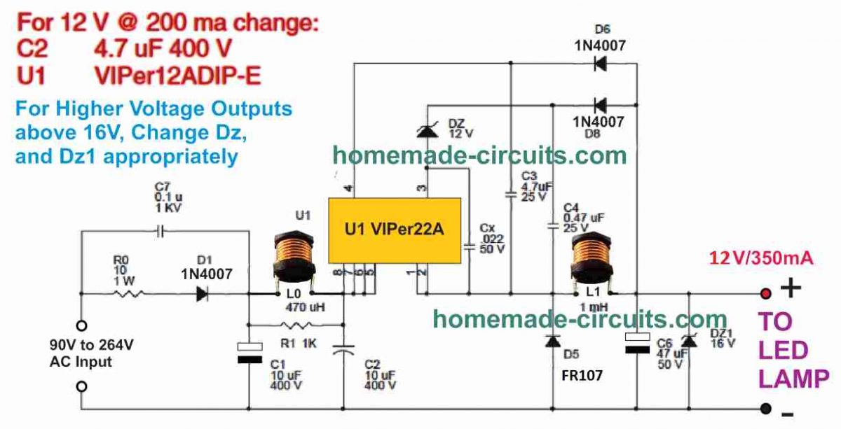 FIGURE#3
Figure 3 above shows the circuit diagram for the ceiling LED lamp prototype design.
It is designed for 12 V LED lamps having a optimum current of 350 mA.
In case a lesser amount of current is desirable, then the VIPer22A-E could be transformed into a VIPer12A-E and capacitor C2 could be lowered from 10 ��f to 4.7 ��F.
This gives as much as 200 mA.
FIGURE#3
Figure 3 above shows the circuit diagram for the ceiling LED lamp prototype design.
It is designed for 12 V LED lamps having a optimum current of 350 mA.
In case a lesser amount of current is desirable, then the VIPer22A-E could be transformed into a VIPer12A-E and capacitor C2 could be lowered from 10 ��f to 4.7 ��F.
This gives as much as 200 mA.
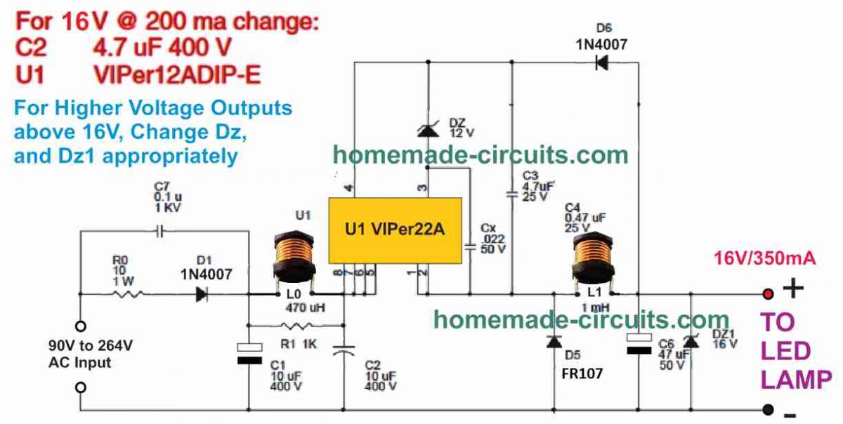 FIGURE#4
Figure 4 above demonstrates the identical design except for 16 V output or more, D6 and C4 could be omitted.
The jumper connects the output voltage with the Vdd pin.
FIGURE#4
Figure 4 above demonstrates the identical design except for 16 V output or more, D6 and C4 could be omitted.
The jumper connects the output voltage with the Vdd pin.
 For more details and PCB design please refer to thisComplete Datasheet
 These lights alert the flying aircrafts regarding the minimum height they should maintain above these tall structures to avoid a possible collision and accidents.
Obstruction lights are mostly red in color so that they can be visualized from maximum distance and even during foggy conditions.
These can be a continuously illuminated type of lamp or a flashing, revolving beacon type of lamp.
In this this article we discuss about an easy construction of a powerful LED based obstruction light system, using minimum parts, and efficient working.
The idea was requested by Mr.
Jerry as given below:
These lights alert the flying aircrafts regarding the minimum height they should maintain above these tall structures to avoid a possible collision and accidents.
Obstruction lights are mostly red in color so that they can be visualized from maximum distance and even during foggy conditions.
These can be a continuously illuminated type of lamp or a flashing, revolving beacon type of lamp.
In this this article we discuss about an easy construction of a powerful LED based obstruction light system, using minimum parts, and efficient working.
The idea was requested by Mr.
Jerry as given below:
 2835 SMD LED Specifications
Forward Current: 120 mA to 150 mA
Forward Voltage: 3.1 V DC
Luminous Flux: 10 to 15 LM
Power: 0.5 watt
2835 SMD LED Specifications
Forward Current: 120 mA to 150 mA
Forward Voltage: 3.1 V DC
Luminous Flux: 10 to 15 LM
Power: 0.5 watt
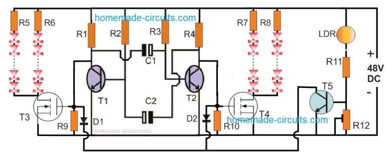
 The proposed circuit is suitable for applications where music and entertainment are involved, such as in parties, festivals, get to togethers etc.
Since the circuit is designed to operate without wires, no physical contact becomes necessary making the unit easy to handle and very portable.
The circuit can be powered with a 3V battery or even with your cellphone charger and could be plugged in anywhere in the music hall for getting the intended dazzling music operated light effects.
The proposed circuit is suitable for applications where music and entertainment are involved, such as in parties, festivals, get to togethers etc.
Since the circuit is designed to operate without wires, no physical contact becomes necessary making the unit easy to handle and very portable.
The circuit can be powered with a 3V battery or even with your cellphone charger and could be plugged in anywhere in the music hall for getting the intended dazzling music operated light effects.
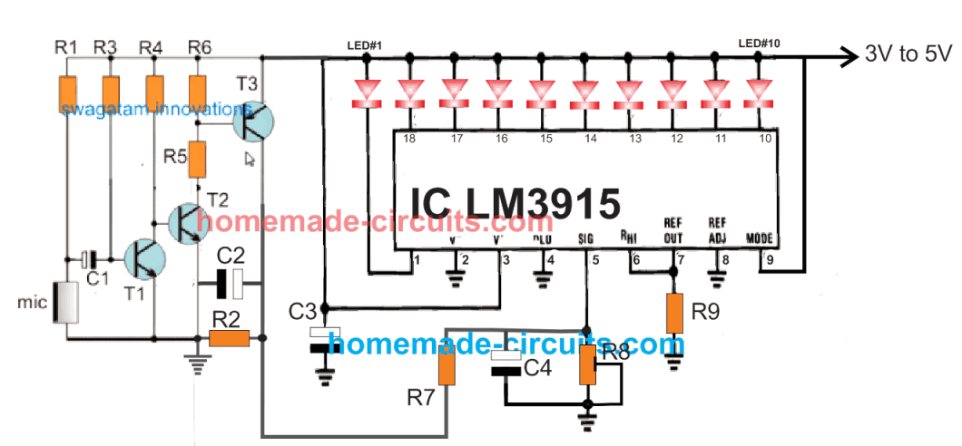 Video Demonstration:
Parts List
R1 = 4k7
R2, R6, R9 = 1K
R3 = 2M2
R4 = 33K
R5 = 470 ohms
R7 = 10K
R8 = 10k preset
C1 = 0.22uF ceramic
C2 = 100uF/16V or 25V
C3, C4 = 1uF/16V or 25V
T1, T2 = BC547
T3 = BC557
MIC = electret MIC
LEDs = all are red LEDs, 5mm, 20mA type, or as desired.
Video Demonstration:
Parts List
R1 = 4k7
R2, R6, R9 = 1K
R3 = 2M2
R4 = 33K
R5 = 470 ohms
R7 = 10K
R8 = 10k preset
C1 = 0.22uF ceramic
C2 = 100uF/16V or 25V
C3, C4 = 1uF/16V or 25V
T1, T2 = BC547
T3 = BC557
MIC = electret MIC
LEDs = all are red LEDs, 5mm, 20mA type, or as desired.
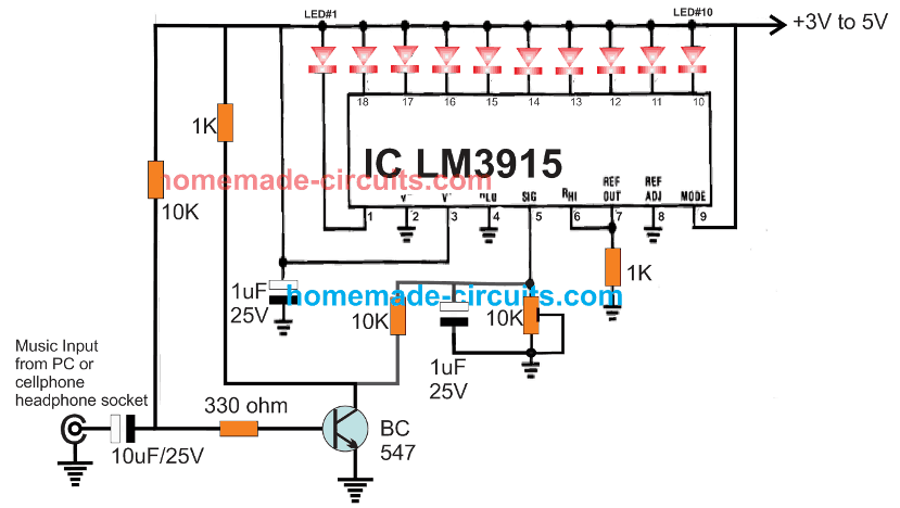
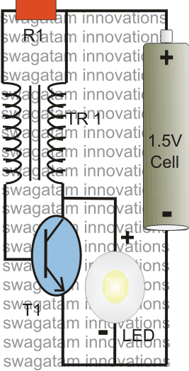 The above design may be improved further by attaching a rectifying network using a diode and a capacitor, as shown below:
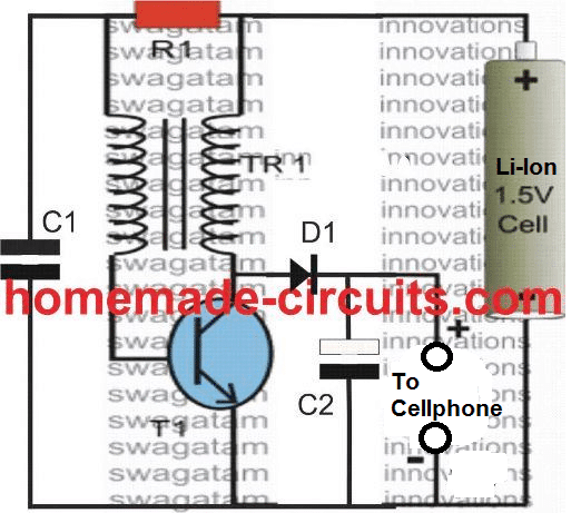
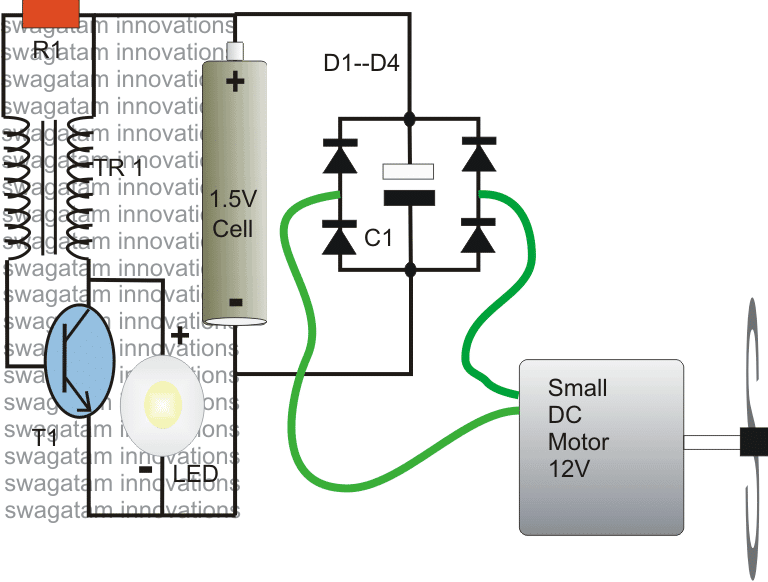
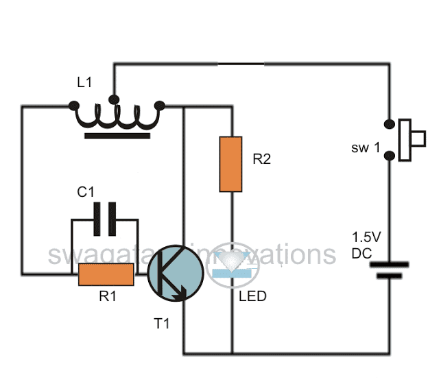 This LED Joule thief circuit may be simulated with the following points:
 Feedback from MayaB
Hi Swagatam, Though it is long known Joule Thief circuit, not something new I discovered but thank you for posting a new article on behalf of me, I appreciated it.
Regards, MayaB
Feedback from MayaB
Hi Swagatam, Though it is long known Joule Thief circuit, not something new I discovered but thank you for posting a new article on behalf of me, I appreciated it.
Regards, MayaB
 Here is the simplified drawing I built the Radiant joule thief battery charger by.
The inductor I wound so many turns till It was to full to wind anymore.
But I brought 2x 5 or 6 meter lengths of Stranded copper wire unknown gauge from dicksmiths electronics insulated wire, and I wound most of it on except I think a few feet left over.
Here is the simplified drawing I built the Radiant joule thief battery charger by.
The inductor I wound so many turns till It was to full to wind anymore.
But I brought 2x 5 or 6 meter lengths of Stranded copper wire unknown gauge from dicksmiths electronics insulated wire, and I wound most of it on except I think a few feet left over.
 The latest test I used my pencil energizer Battery but I didn't remeasure the volts in it.
I powered the radiant energy Joule thief with it and at the outputs I put a 2200uf electrolytic capacitor Rated at 50 volts.
I ran my multimeter leads from it and got up to before I Stopped 35.8 volts , and that��s the charge being fed into the capacitor to ,
Before that I was getting 27.8 volts but as the capacitor was charging past the half way mark the voltage climb was slowing down, maybe due to the voltage from the battery getting low.
I'll have to remeasure it and do the test again in more detail.
Shorting the capacitor gave a snap noise And sparks.
I tried it again charging it so far but This time I dumped the capacitor charge back into the input and this illuminated the neon for a second before the cap charge went down
The latest test I used my pencil energizer Battery but I didn't remeasure the volts in it.
I powered the radiant energy Joule thief with it and at the outputs I put a 2200uf electrolytic capacitor Rated at 50 volts.
I ran my multimeter leads from it and got up to before I Stopped 35.8 volts , and that��s the charge being fed into the capacitor to ,
Before that I was getting 27.8 volts but as the capacitor was charging past the half way mark the voltage climb was slowing down, maybe due to the voltage from the battery getting low.
I'll have to remeasure it and do the test again in more detail.
Shorting the capacitor gave a snap noise And sparks.
I tried it again charging it so far but This time I dumped the capacitor charge back into the input and this illuminated the neon for a second before the cap charge went down
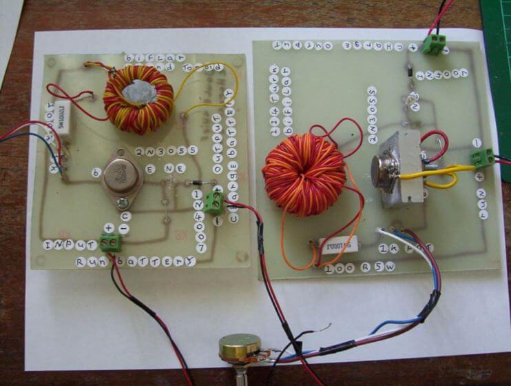 Next experiment was different I had the Outputs to my meter set to 200 millivolts range and the negative input I had my A23 energizer negative sitting on the negative input and the top positive well
My finger was on it only as for the positive input it was run to a rectangle peace of circuit Board on the end of a wire held in the air By an aligater clip.
The reading was climbing at a Faster rate I got o 47.2 millivolts before I stopped it I was getting power at
A good rate from no where with an open circuit here but I was also holding the Battery case to while doing the experiment.
I just repeated these tests and got much improved results now.....
My tests will go on, and I'll keep you all updated with the latest, until then keep DIYing.
Well, these were 3 best circuits using the joule thief concept that I presented for you, if you have any more such examples please feel free to post the info through your valuable comments.
Reference:https://en.wikipedia.org/wiki/Joule_thief
Next experiment was different I had the Outputs to my meter set to 200 millivolts range and the negative input I had my A23 energizer negative sitting on the negative input and the top positive well
My finger was on it only as for the positive input it was run to a rectangle peace of circuit Board on the end of a wire held in the air By an aligater clip.
The reading was climbing at a Faster rate I got o 47.2 millivolts before I stopped it I was getting power at
A good rate from no where with an open circuit here but I was also holding the Battery case to while doing the experiment.
I just repeated these tests and got much improved results now.....
My tests will go on, and I'll keep you all updated with the latest, until then keep DIYing.
Well, these were 3 best circuits using the joule thief concept that I presented for you, if you have any more such examples please feel free to post the info through your valuable comments.
Reference:https://en.wikipedia.org/wiki/Joule_thief
 Through the above formulas we calculated the series parallel connections with resistor for configuring a 216 LED display, however, the above strings will now need to be arranged appropriately in the shape of the alphabets, corresponding to the word "WELCOME".
This might require some effort and could be a little time consuming, and might require some patience and skill.
For the second group of LEDs consisting of 696 LEDs, the process will be quite similar.
We first divide the 696 with 46 which gives us around 15.13, meaning 14 strings can be configured with a series of 46 LeDs and one string having 52 LEDs...all these strings will likewise need to be connected in parallel and physically arranged to represent the phrase " COLLEGE OF ENGINEERING".
Through the above formulas we calculated the series parallel connections with resistor for configuring a 216 LED display, however, the above strings will now need to be arranged appropriately in the shape of the alphabets, corresponding to the word "WELCOME".
This might require some effort and could be a little time consuming, and might require some patience and skill.
For the second group of LEDs consisting of 696 LEDs, the process will be quite similar.
We first divide the 696 with 46 which gives us around 15.13, meaning 14 strings can be configured with a series of 46 LeDs and one string having 52 LEDs...all these strings will likewise need to be connected in parallel and physically arranged to represent the phrase " COLLEGE OF ENGINEERING".
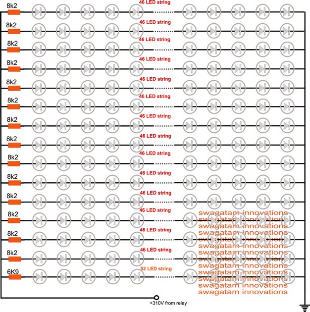 The resistor values for the 46 LED strings can be as calculated in the above sections, while for the 52 LED, it may done as given below:
R = 310 - (52 x 3.3) / 0.02 = 6920 ohms or simply a 6k9 standard resistor may be used.
wattage will be = R = 310 - (52 x 3.3) x 0.02 = 2.76 watts or 3 watts
The above explanation provides us the information regarding how to build any 200 to 400 LED based project for boards or display sign boards using mains voltage without the need of a transformer.
Now, to enable the two sets of LED groups flash alternately using a relay, the following simple IC 555 flasher could be used:
The resistor values for the 46 LED strings can be as calculated in the above sections, while for the 52 LED, it may done as given below:
R = 310 - (52 x 3.3) / 0.02 = 6920 ohms or simply a 6k9 standard resistor may be used.
wattage will be = R = 310 - (52 x 3.3) x 0.02 = 2.76 watts or 3 watts
The above explanation provides us the information regarding how to build any 200 to 400 LED based project for boards or display sign boards using mains voltage without the need of a transformer.
Now, to enable the two sets of LED groups flash alternately using a relay, the following simple IC 555 flasher could be used:
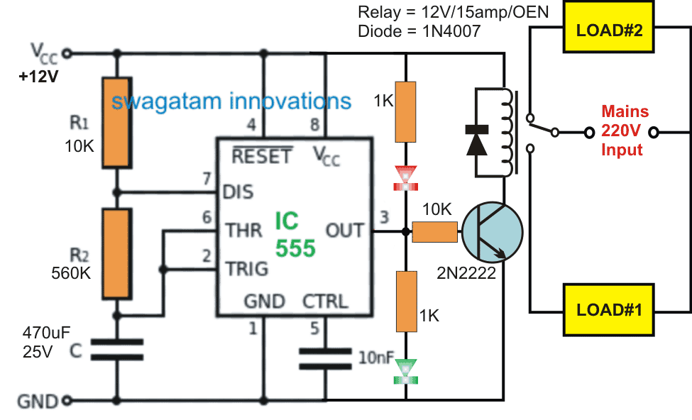 R1, R2, and C can be suitably adjusted for getting the desired blinking rate over the connected 200 to 400 LED strings.
The relay does not need to be a 15amp as indicated in the diagram it could be any ordinary 12v 400 ohm 5 amp type of relay
R1, R2, and C can be suitably adjusted for getting the desired blinking rate over the connected 200 to 400 LED strings.
The relay does not need to be a 15amp as indicated in the diagram it could be any ordinary 12v 400 ohm 5 amp type of relay
 The proposed design employs a non-isolated single inductor smps design and thus removes the obligatory transformers, making the design much compact and involving less BOM, yet meets the standard performance criteria of an LED driver specifications.
The design also includes a PFC stage for ensuring a cleaner output and satisfy the modern PFC IEC 61000-3-2 rules
The following explanation provides us with the operating principle of the proposed 7 watt LED driver SMPS circuit:
The proposed design employs a non-isolated single inductor smps design and thus removes the obligatory transformers, making the design much compact and involving less BOM, yet meets the standard performance criteria of an LED driver specifications.
The design also includes a PFC stage for ensuring a cleaner output and satisfy the modern PFC IEC 61000-3-2 rules
The following explanation provides us with the operating principle of the proposed 7 watt LED driver SMPS circuit:
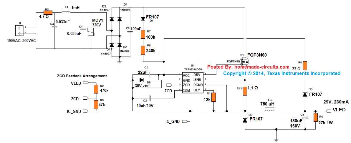 1) The LED controller chip TPS92314A includes an advanced constant ON-time control feature for ensuring a high power factor at the input, and quasi-resonant switching for guarantying greater efficiency and minimum EMI emission.
2) The design facilitates load power regulation through the stored energy of an inductor configured in the form of a high-side buck converter .
3) The inclusion of a diode/capacitor at the output additionally regulates the DC content, without depending on any extra auxiliary winding which is commonly seen in traditional isolated forms of SMPS designs...here this is eliminated causing the unit to become very compact, highly efficient and cost effective.
4) The figure shows a standard full bridge rectifier network at the input for converting the alternating input current into a single positive AC bus.
The pulsating sine voltage here faithfully follows the pulsating sine current.
due to the presence of a 100nF capacitor immediately after the bridge rectifier, and this helps in maintaining a high power factor response.
5) The above processed supply is fed to the drain of a mosfet which is configured as a high side switching device, having its source hooked up with D8 freewheeling diode along with inductor L3 and output capacitor C5.
6) In the figure the IC input side of the IC could be seen referenced to a switching junction SW, which makes sure that the IC does not switch ON until the processed AC has a potential higher than the connected LED's forward voltage value, and also for so along as the input is not drawing any current.
This parameter causes a delay factor during power switch, and can be calculated through the following expression:
�� T = Sine (inverse)VLED / ��2 xVac
During the critical conduction mode periods of the IC TPS92314, the peak current from the inductor becomes two times more than the input peak current.
The inductor value for this 7 watt LED driver SMPS circuit can be calculated using the following formula:
L = [1.41 x Vac - VLED] x Ton / ��Ipeak
Due to the fact that this IC involves a critical conduction mode operation implies that the every subsequent ON periods is initiated only once the current within the inductor has ramped down to almost zero.
A feedback voltage in the form of VLED is applied back to the IC which acts like a supply voltage for the IC, because VLED can be seen linked with the input side bridge network ground.
This particular implementation allows the design to comfortably work with only a single non-isolated inductor and gets rid of the complex extra biasing winding.
This makes this 7 watt non isolated SMPS LED driver circuit extremely compact, durable, efficient and very long lasting and also compliant with the present SMPS laws.
1) The LED controller chip TPS92314A includes an advanced constant ON-time control feature for ensuring a high power factor at the input, and quasi-resonant switching for guarantying greater efficiency and minimum EMI emission.
2) The design facilitates load power regulation through the stored energy of an inductor configured in the form of a high-side buck converter .
3) The inclusion of a diode/capacitor at the output additionally regulates the DC content, without depending on any extra auxiliary winding which is commonly seen in traditional isolated forms of SMPS designs...here this is eliminated causing the unit to become very compact, highly efficient and cost effective.
4) The figure shows a standard full bridge rectifier network at the input for converting the alternating input current into a single positive AC bus.
The pulsating sine voltage here faithfully follows the pulsating sine current.
due to the presence of a 100nF capacitor immediately after the bridge rectifier, and this helps in maintaining a high power factor response.
5) The above processed supply is fed to the drain of a mosfet which is configured as a high side switching device, having its source hooked up with D8 freewheeling diode along with inductor L3 and output capacitor C5.
6) In the figure the IC input side of the IC could be seen referenced to a switching junction SW, which makes sure that the IC does not switch ON until the processed AC has a potential higher than the connected LED's forward voltage value, and also for so along as the input is not drawing any current.
This parameter causes a delay factor during power switch, and can be calculated through the following expression:
�� T = Sine (inverse)VLED / ��2 xVac
During the critical conduction mode periods of the IC TPS92314, the peak current from the inductor becomes two times more than the input peak current.
The inductor value for this 7 watt LED driver SMPS circuit can be calculated using the following formula:
L = [1.41 x Vac - VLED] x Ton / ��Ipeak
Due to the fact that this IC involves a critical conduction mode operation implies that the every subsequent ON periods is initiated only once the current within the inductor has ramped down to almost zero.
A feedback voltage in the form of VLED is applied back to the IC which acts like a supply voltage for the IC, because VLED can be seen linked with the input side bridge network ground.
This particular implementation allows the design to comfortably work with only a single non-isolated inductor and gets rid of the complex extra biasing winding.
This makes this 7 watt non isolated SMPS LED driver circuit extremely compact, durable, efficient and very long lasting and also compliant with the present SMPS laws.
 Complete Datasheet Here

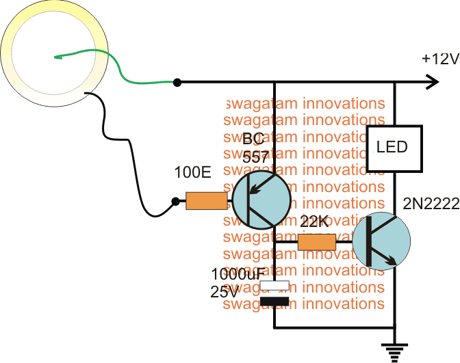 The piezo transducer in the design is used as a pressure to electricity converter.
The piezo element is supposed to be embedded within each of the stairs, while each of the associated circuitry to be wired within the nearby wall, along with the LED.
Once done, whenever someone steps on the staircases, the relevant piezo generates a small electric pulse in response to the vibration, which in turn triggers the 2N2222 delay OFF timer stage, and the LED which now lights up for a few seconds and then automatically shuts off.
The above action goes on happening as the visitor climbs the steps, illuminating and shutting off each subsequent LED in a sequential manner.
The piezo transducer in the design is used as a pressure to electricity converter.
The piezo element is supposed to be embedded within each of the stairs, while each of the associated circuitry to be wired within the nearby wall, along with the LED.
Once done, whenever someone steps on the staircases, the relevant piezo generates a small electric pulse in response to the vibration, which in turn triggers the 2N2222 delay OFF timer stage, and the LED which now lights up for a few seconds and then automatically shuts off.
The above action goes on happening as the visitor climbs the steps, illuminating and shutting off each subsequent LED in a sequential manner.

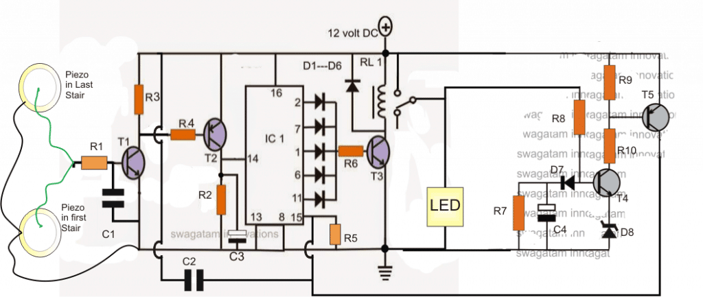
 The entire circuit can be seen powered from a single solar panel for the required sunrise/sunset simulation effect on the connected LEDs.
The NPN BJT stage using the TIP122 becomes the main section of the circuit and can be expected to execute the required slow brightening of the yellow/white LEDs proportionately in response to the rising sunlight level exposed on the solar panel.
The PNP stage using TIP127 is optional and this stage is introduced to do the exact opposite of its NPN counterpart.
The indicated cool white/blue LEDs are supposed to gradually illuminate and get brighter as the sunsets.
During day time, the solar panel operates the gradual brightening of the warm LEDs simulating sunrise effect, and simultaneously it also charges an attached back up battery.
When night falls, the same battery provides power to the cool white LEDs which keeps the house illuminated when its completely dark.
The battery is also under-charge protected since the 4 LEDs which are connected in series simply stop conducting as soon as the battery voltage drops below the 11V mark making sure that it does not go through a deep discharge.
For the above shown example sunrise/sunset simulator circuit using LEDs, the approximate specifications of the components could be selected as described below:
The entire circuit can be seen powered from a single solar panel for the required sunrise/sunset simulation effect on the connected LEDs.
The NPN BJT stage using the TIP122 becomes the main section of the circuit and can be expected to execute the required slow brightening of the yellow/white LEDs proportionately in response to the rising sunlight level exposed on the solar panel.
The PNP stage using TIP127 is optional and this stage is introduced to do the exact opposite of its NPN counterpart.
The indicated cool white/blue LEDs are supposed to gradually illuminate and get brighter as the sunsets.
During day time, the solar panel operates the gradual brightening of the warm LEDs simulating sunrise effect, and simultaneously it also charges an attached back up battery.
When night falls, the same battery provides power to the cool white LEDs which keeps the house illuminated when its completely dark.
The battery is also under-charge protected since the 4 LEDs which are connected in series simply stop conducting as soon as the battery voltage drops below the 11V mark making sure that it does not go through a deep discharge.
For the above shown example sunrise/sunset simulator circuit using LEDs, the approximate specifications of the components could be selected as described below:
 We know that an LED bulb circuit is nothing but a small AC to DC SMPS circuit, which employs a small ferrite transformer for stepping down the mains voltage to a lower LED DC voltage.
The secondary side of the transformer produces the stepped down voltage which is rectified by a single diode and a large filter capacitor.
The rectified DC is then transferred to a series LED assembly for lighting it up.
We have to modify this LED section and connect it with the IC 555 PWM stage as shown above.
This can be implemented wiht the following steps:
Open the LED bulb container.
Cut the wire of the LED assembly which goes to the negative line of the DC supply.
Connect this negative LED wire to the transistor collector of the 555 pwm circuit.
Finally connect the 555 pwm circuit's positive/negative wires with the LED DC supply, coming from the ferrite transformer secondary.
This also means that the 555 IC circuit does not need an external DC, and it can be derived from DC supply from the smps, meant for driving the LEDs.
Finally, connect the LED smps input to AC mains and check the dimming effect by varying the IC 555 pwm pot.
Remember the smps circuit primary side is not isolated from mains and therefore extremely dangerous to touch in switched ON condition.
We know that an LED bulb circuit is nothing but a small AC to DC SMPS circuit, which employs a small ferrite transformer for stepping down the mains voltage to a lower LED DC voltage.
The secondary side of the transformer produces the stepped down voltage which is rectified by a single diode and a large filter capacitor.
The rectified DC is then transferred to a series LED assembly for lighting it up.
We have to modify this LED section and connect it with the IC 555 PWM stage as shown above.
This can be implemented wiht the following steps:
Open the LED bulb container.
Cut the wire of the LED assembly which goes to the negative line of the DC supply.
Connect this negative LED wire to the transistor collector of the 555 pwm circuit.
Finally connect the 555 pwm circuit's positive/negative wires with the LED DC supply, coming from the ferrite transformer secondary.
This also means that the 555 IC circuit does not need an external DC, and it can be derived from DC supply from the smps, meant for driving the LEDs.
Finally, connect the LED smps input to AC mains and check the dimming effect by varying the IC 555 pwm pot.
Remember the smps circuit primary side is not isolated from mains and therefore extremely dangerous to touch in switched ON condition.
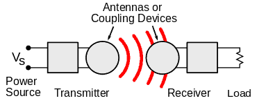
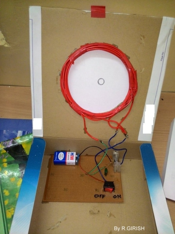
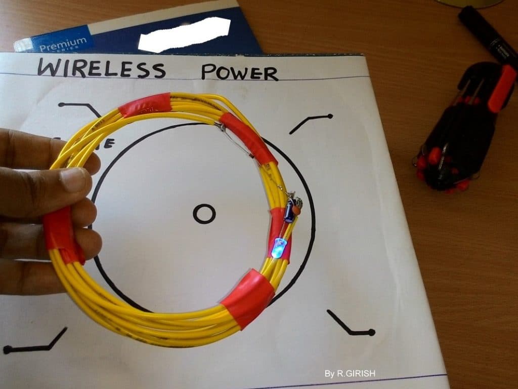
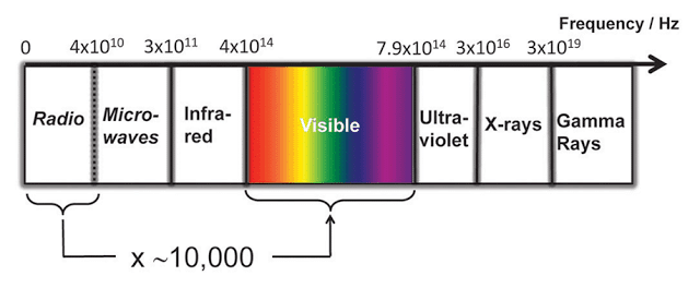 Here is a simple block diagram explaining LI-FI:

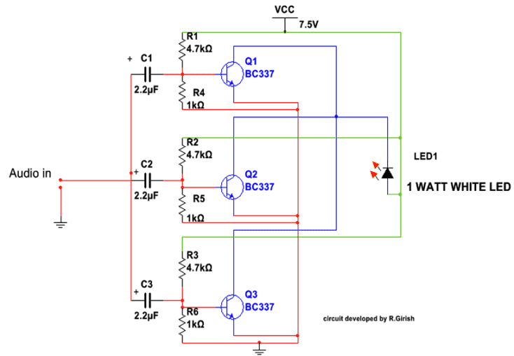 Update: The above design can be also tried using a single transistor as shown below:
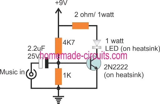 You can use a current limiting resistor series with LED if you want operate the circuit at higher voltage (say 12V).You can also use standard 0.5mm white LED with current limiting resistor.
For an audio source you can use mp3 player, mobile phone or a microphone with pre-amplifier etc.
The receiver consists of a 6 volt solar cell (3 volts above works fine) in series with 2.2uf capacitor which is paired with an amplifier.
The amplifier need not to be the same illustrated here, but you can use any amplifier lying around your house.
But make sure it as good sensitivity.
You can use a current limiting resistor series with LED if you want operate the circuit at higher voltage (say 12V).You can also use standard 0.5mm white LED with current limiting resistor.
For an audio source you can use mp3 player, mobile phone or a microphone with pre-amplifier etc.
The receiver consists of a 6 volt solar cell (3 volts above works fine) in series with 2.2uf capacitor which is paired with an amplifier.
The amplifier need not to be the same illustrated here, but you can use any amplifier lying around your house.
But make sure it as good sensitivity.
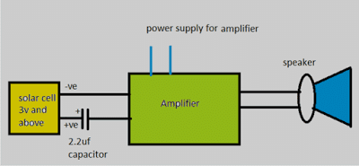
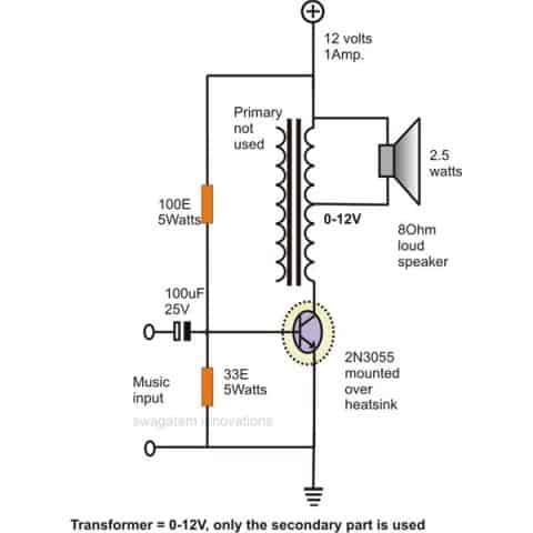 Here is author��s prototype
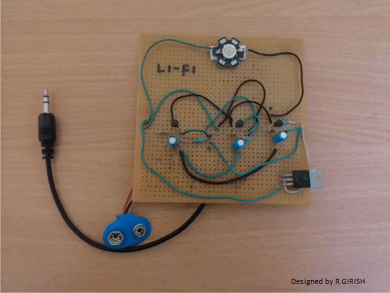
 UPDATE:
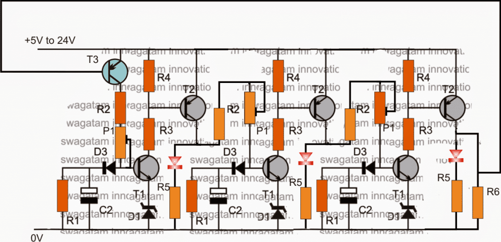 In the above concept, T3 is initially switched ON when the circuit is first powered.
Once the last LED is lit, T3 is forced to shut off due to positive potential from the collector of the extreme right hand side T2 transistor.
The LEDs now begin shutting one after the other with a time lapse as determined by the value of R1s.
For conditions where the LEDs are required to shut off suddenly or instantly, the above design can be modified as per the following diagram:
In the above concept, T3 is initially switched ON when the circuit is first powered.
Once the last LED is lit, T3 is forced to shut off due to positive potential from the collector of the extreme right hand side T2 transistor.
The LEDs now begin shutting one after the other with a time lapse as determined by the value of R1s.
For conditions where the LEDs are required to shut off suddenly or instantly, the above design can be modified as per the following diagram:
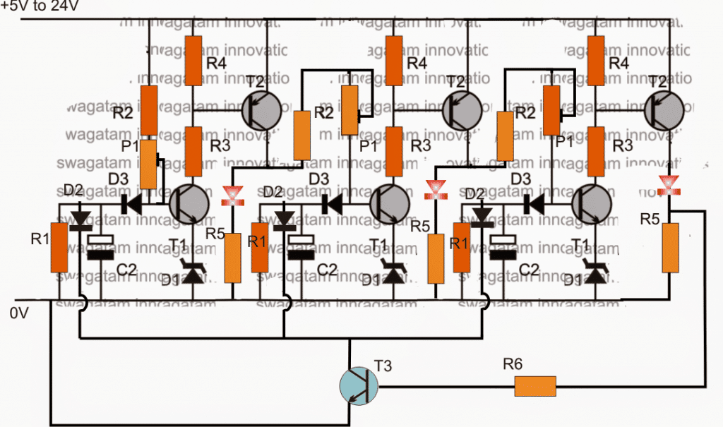 As may be seen, in the above diagram, as soon as the last LED is lit, T3 is also triggered ON, and it forces all the timing capacitor to shut down immediately or abruptly.
When this happens all the LEDs shut off, and T3 in turn is switched OFF so that the cycle is allowed to repeat once again.
As may be seen, in the above diagram, as soon as the last LED is lit, T3 is also triggered ON, and it forces all the timing capacitor to shut down immediately or abruptly.
When this happens all the LEDs shut off, and T3 in turn is switched OFF so that the cycle is allowed to repeat once again.
 Referring to the standard transformerless constant current LED driver circuit using the IC MBI6001, we can see hardly any external components being used except a few resistors.
Here the resistors R1, R2, and R3 help to determine the correct PWM setting for achieving the intended constant current output from the IC.
The values of the resistors are recommended by the manufacturer and may be used as per the given instructions.
We��ll talk about this in the later part of the article.
Referring to the standard transformerless constant current LED driver circuit using the IC MBI6001, we can see hardly any external components being used except a few resistors.
Here the resistors R1, R2, and R3 help to determine the correct PWM setting for achieving the intended constant current output from the IC.
The values of the resistors are recommended by the manufacturer and may be used as per the given instructions.
We��ll talk about this in the later part of the article.
 The resistor R1 may be replaced with a 1K resistor and is not much critical, although its purpose is intended for fine tuning the intensity of the connected LED string, therefore may be tweaked a bit for getting the desired intensity from the LEDs.
R3 is optional and may be simply omitted, its use is restricted for some advanced requirement and may be ignored for general application as described above.
The resistor R1 may be replaced with a 1K resistor and is not much critical, although its purpose is intended for fine tuning the intensity of the connected LED string, therefore may be tweaked a bit for getting the desired intensity from the LEDs.
R3 is optional and may be simply omitted, its use is restricted for some advanced requirement and may be ignored for general application as described above.
 PLEASE REMOVE C1 FROM THE INDICATED POSITION AND PUT IT ACROSS THE OUTPUT TERMINALS OF THE CIRCUIT
The series bulb can be eliminated if the load current is within the MOSFET's handling capacity.
R2 can be calculated using the following formula:
R2 = (Supply Voltage after bridge - LED total forward voltage) / LED Current
PLEASE REMOVE C1 FROM THE INDICATED POSITION AND PUT IT ACROSS THE OUTPUT TERMINALS OF THE CIRCUIT
The series bulb can be eliminated if the load current is within the MOSFET's handling capacity.
R2 can be calculated using the following formula:
R2 = (Supply Voltage after bridge - LED total forward voltage) / LED Current
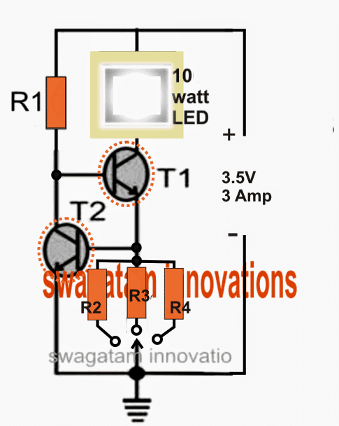 Referring to the above diagram, the design is a basic current controlled stage where T2 determines the maximum current limit of T1 by controlling the base potential of T1.
 Bi-color LEDs are available in 3-pin and 2-pin variations, in our project we use the 2-pin Bi-color LED option for keeping things compact and much efficient.
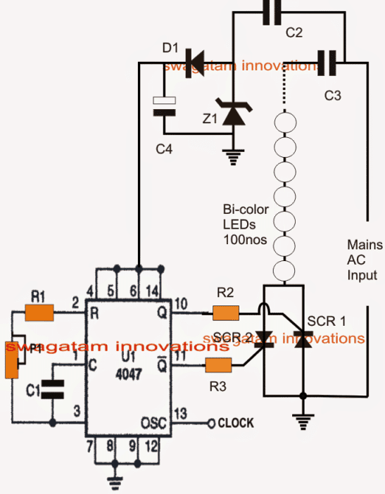
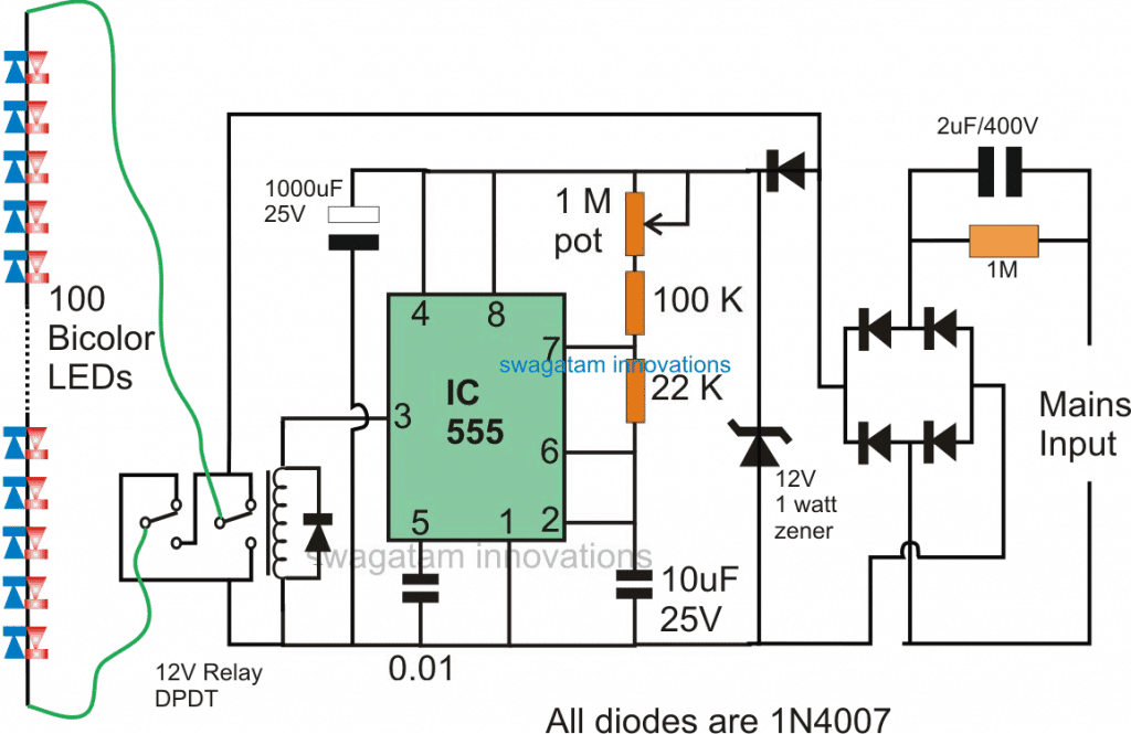
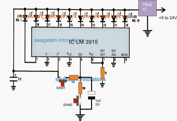 Understanding the proposed up/down LED sequence controller circuit using push button is very easy, and may be done by referring to the above figure.
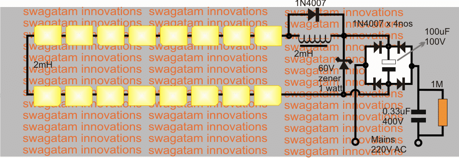 All the 20mA LEDs can be seen connected in series with a compact transformerless power supply.
A 20mH inductor can also be seen, this is included to arrest the initial switch ON surge, the zener diode provides an extra protection from any possible voltage fluctuations.
One may also include an NTC thermistor at the input for providing even greater protection to the LEDs from surge currents.
All the 20mA LEDs can be seen connected in series with a compact transformerless power supply.
A 20mH inductor can also be seen, this is included to arrest the initial switch ON surge, the zener diode provides an extra protection from any possible voltage fluctuations.
One may also include an NTC thermistor at the input for providing even greater protection to the LEDs from surge currents.
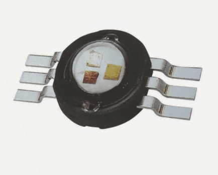
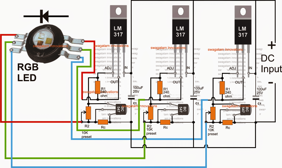

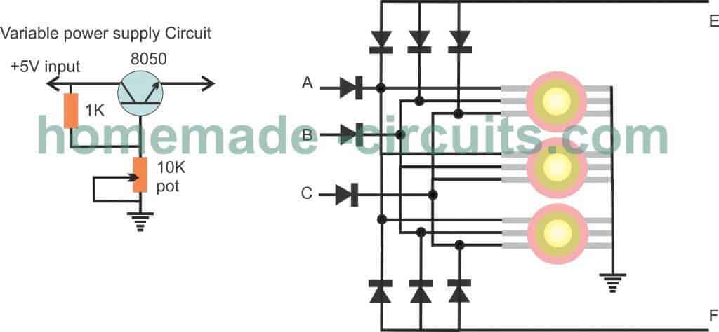 For color mixing, 3nos of 8050 variable voltage power supply could beuilt and their outputs connected with points A, B and C.
For creating fading effect, fading circuit could be connected to point E
For flashing effect point F could be used for supplying the flashing signal.
For color mixing, 3nos of 8050 variable voltage power supply could beuilt and their outputs connected with points A, B and C.
For creating fading effect, fading circuit could be connected to point E
For flashing effect point F could be used for supplying the flashing signal.

 The circuit was also built and tested by Mr.
Raj, who is also an avid follower of this blog, the picture below was sent by him for the readers viewing pleasure.
The circuit was also built and tested by Mr.
Raj, who is also an avid follower of this blog, the picture below was sent by him for the readers viewing pleasure.

 CODE: for simply inbuilt LED on pin 13 of ARDUINO BOARD by default it is programed to blink frequently at 50 Mili Seconds as it in description it will be stated asms (milliseconds).
/* first Simple
Program on Arudino BY JACKFRANKO */
CODE: for simply inbuilt LED on pin 13 of ARDUINO BOARD by default it is programed to blink frequently at 50 Mili Seconds as it in description it will be stated asms (milliseconds).
/* first Simple
Program on Arudino BY JACKFRANKO */
 In the above sections we learned how to wire a low power grow light circuit using 5mm LeDs, here we see how the same may be done using 4 watt power LEDs.
The idea was suggested by Mr.
Jack.
Hello Swag,
During my exploration of LED lighting and the various circuits employed I would like to post some of my recent finding.
Acknowledgements to LED Magazine and Steve Roberts.
I've attached several pictures of my recent build,.....28 - 3watt leds, 7 leds, in series per row and 4 row in parallel.
I'm using a 24v-32v, 4amp power supply.
These lights were purchased as emitters and the bases had to made and heat sinks applied to each emitter.
The leds were mounted to aluminum channel.
Since the completion of the circuit, I've experienced various heating problems and it was continuing to be difficult to balance the circuit, to run cool, stable, and steady electronic output.
I decided to look deeper into this and leds in general and here is what I've found.
Even if the LEDs are all from the same production batch and sequentially manufactured, the foward voltage (Vf) of individual LEDs still has a �� 20% tolerance.
The tolerances this high means that the total forward voltage for each led in a string can be very different and therefore the current mismatch can be very significant.
Consider, if we have 5 leds in series with a forward voltage of 4v, that is (4v)(5) = 20v.
WRONG!!!
Given the tolerance above, the forward voltage is really, 16v to 24v, that an 8v spread.
How are you going to design a circuit that requires you to place things in BALANCE if the tolerances are that hight? This is one of the reasons that things go array.
There are many others!!!
Jack Sturgeon
In the above sections we learned how to wire a low power grow light circuit using 5mm LeDs, here we see how the same may be done using 4 watt power LEDs.
The idea was suggested by Mr.
Jack.
Hello Swag,
During my exploration of LED lighting and the various circuits employed I would like to post some of my recent finding.
Acknowledgements to LED Magazine and Steve Roberts.
I've attached several pictures of my recent build,.....28 - 3watt leds, 7 leds, in series per row and 4 row in parallel.
I'm using a 24v-32v, 4amp power supply.
These lights were purchased as emitters and the bases had to made and heat sinks applied to each emitter.
The leds were mounted to aluminum channel.
Since the completion of the circuit, I've experienced various heating problems and it was continuing to be difficult to balance the circuit, to run cool, stable, and steady electronic output.
I decided to look deeper into this and leds in general and here is what I've found.
Even if the LEDs are all from the same production batch and sequentially manufactured, the foward voltage (Vf) of individual LEDs still has a �� 20% tolerance.
The tolerances this high means that the total forward voltage for each led in a string can be very different and therefore the current mismatch can be very significant.
Consider, if we have 5 leds in series with a forward voltage of 4v, that is (4v)(5) = 20v.
WRONG!!!
Given the tolerance above, the forward voltage is really, 16v to 24v, that an 8v spread.
How are you going to design a circuit that requires you to place things in BALANCE if the tolerances are that hight? This is one of the reasons that things go array.
There are many others!!!
Jack Sturgeon
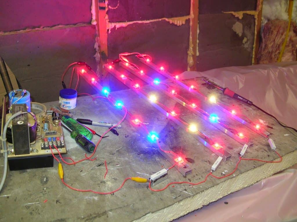
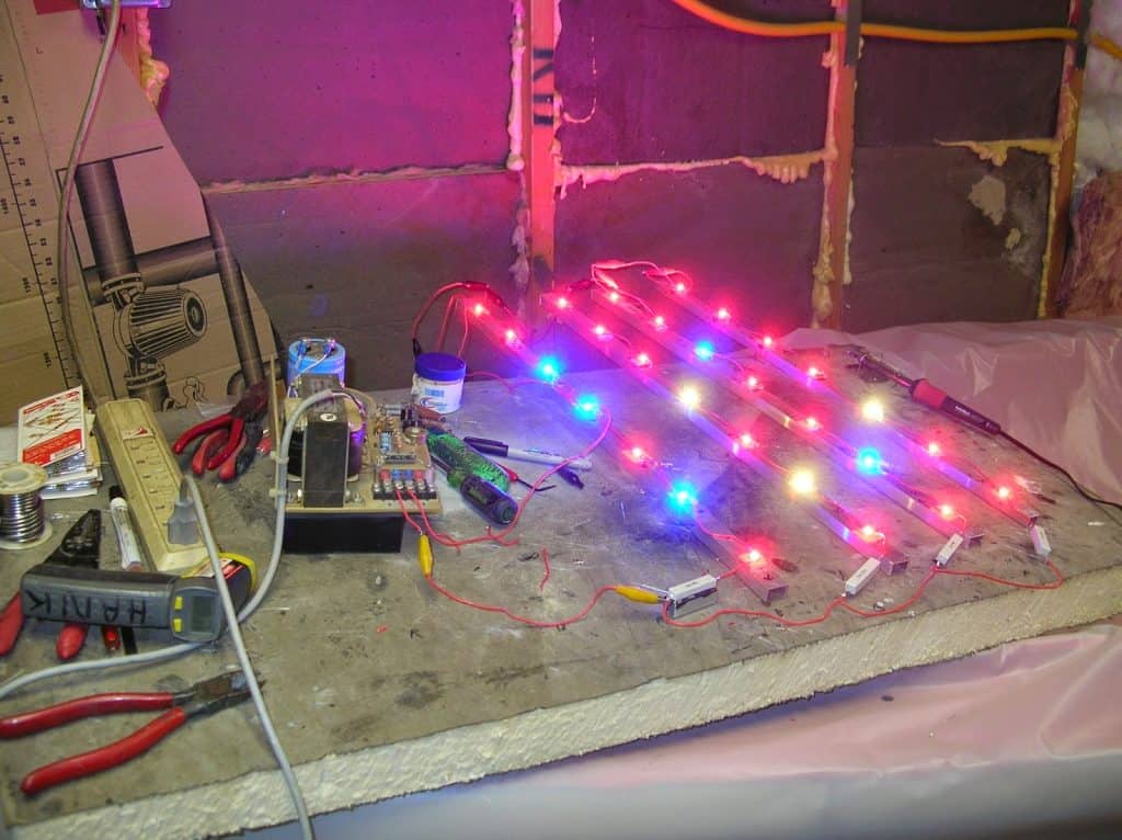
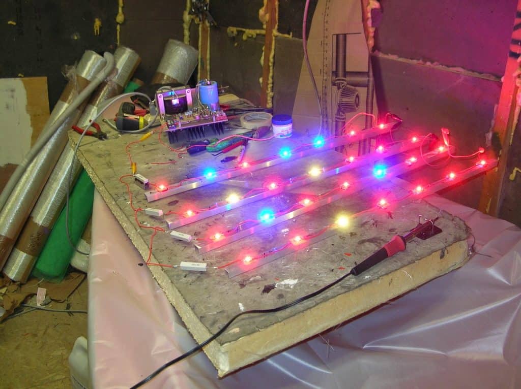 For a newcomer or a new hobbyist wiring LED lights could look complex with many hidden intricacies, actually it's not.
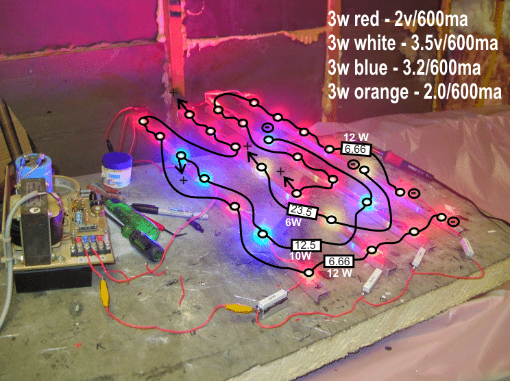 I think I completely missed something in the above design.
Since the current specs of all the LEDs are same, voltage specs can be ignored, and different color LEDs may be connected within the same strings.
So let's analyze the design correctly yet again.
The first string from left has 4 red LEDs and 3 blue LEDs, supply is 24V, therefore the current limiting resistor for this string could be calculated as follows:
R = supply minus total LED fwd.
voltage divided by LED current
= 24 - (4x2)+(3x3.2) divided by 0.6 (600mA)
= 10.66 ohms
wattage =(4x2) + (3x3.2) x 0.6 = 10,56 watts
you can calculate resistors for the other strings too, in the above manner.
The current control for the above set up can be constructed as explained in the following artices:
https://www.homemade-circuits.com/2013/06/universal-high-watt-led-current-limiter.html
https://www.homemade-circuits.com/2011/12/make-hundred-watt-led-floodlight.html
I think I completely missed something in the above design.
Since the current specs of all the LEDs are same, voltage specs can be ignored, and different color LEDs may be connected within the same strings.
So let's analyze the design correctly yet again.
The first string from left has 4 red LEDs and 3 blue LEDs, supply is 24V, therefore the current limiting resistor for this string could be calculated as follows:
R = supply minus total LED fwd.
voltage divided by LED current
= 24 - (4x2)+(3x3.2) divided by 0.6 (600mA)
= 10.66 ohms
wattage =(4x2) + (3x3.2) x 0.6 = 10,56 watts
you can calculate resistors for the other strings too, in the above manner.
The current control for the above set up can be constructed as explained in the following artices:
https://www.homemade-circuits.com/2013/06/universal-high-watt-led-current-limiter.html
https://www.homemade-circuits.com/2011/12/make-hundred-watt-led-floodlight.html
 A nice example may be witnessed in the above diagram where a dimmer switch may be seen wired with a capacitive transformerless power supply circuit for operating a high current load such as a string of high watt LEDs.
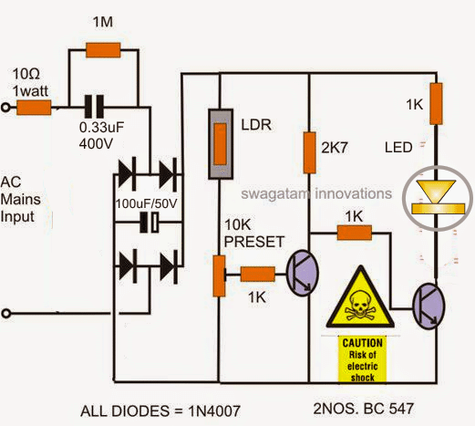
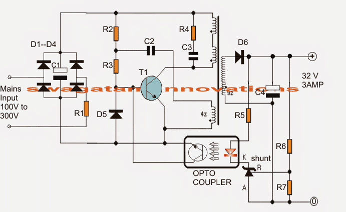 The transformer is wound over a standard EE ferrite core having a central cross sectional area of at least 7 square mm.
Referring to the figure, the upper two primary winding are made up 30 turns of 0.3 mm diameter super enameled copper wire.
The transformer is wound over a standard EE ferrite core having a central cross sectional area of at least 7 square mm.
Referring to the figure, the upper two primary winding are made up 30 turns of 0.3 mm diameter super enameled copper wire.

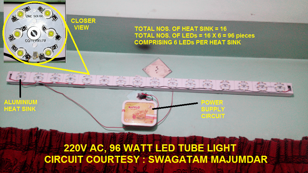

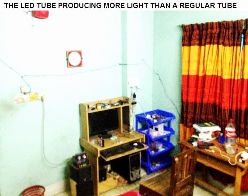

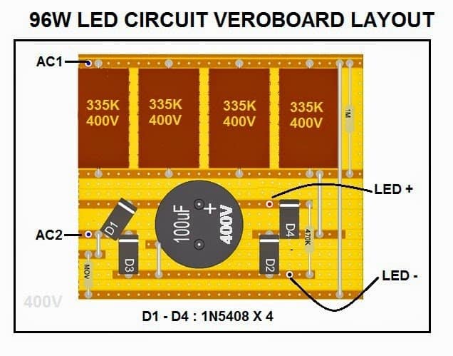 The following image presents PCB design layout for the above 100 watt LED tubelight circuit, Courtesy Mr.
Abu Tamam.
The following image presents PCB design layout for the above 100 watt LED tubelight circuit, Courtesy Mr.
Abu Tamam.

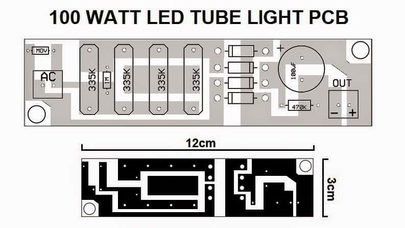
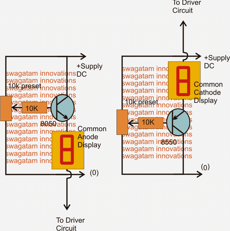
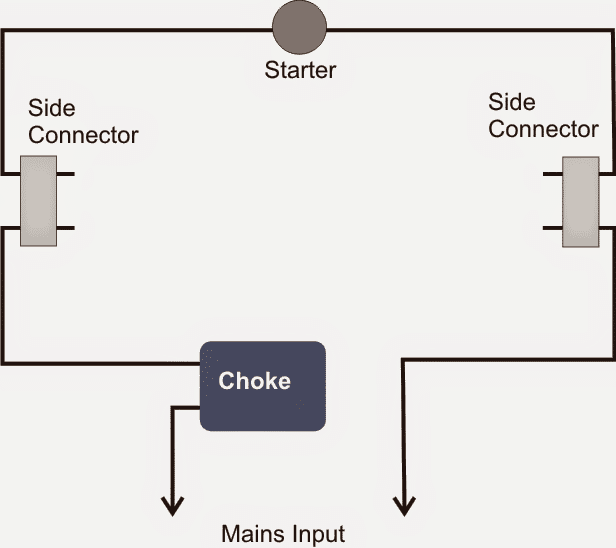 The starter is wired across one of the adjacent pair of end pins while the ballast is attached in series with the other adjacent pins of the side connectors.
The series outputs from the ballast and one of the connectors are finally terminated for receiving the mains AC voltage.
When AC is first switched ON, the starter fires randomly and switches the tube in a flickering mode, which forces reverse high voltage EMFs to be generated by the ballast.
This kick starts and ignites the tube internal gas and illuminates the tube bypassing the starter such that now the starter no longer conducts current, rather the current is now conducted through the illuminated tube internal gaseous path.
Once the tube is triggered fully the choke or the ballast simply acts like a current limiter for restricting a safe specified amount of amps to the tube as per the resistance of the ballast coil.
In good quality ballasts the resistance or the number of turns inside the ballast will be correctly calculated to minimize heat generation and ensure longer tube life.
The starter is wired across one of the adjacent pair of end pins while the ballast is attached in series with the other adjacent pins of the side connectors.
The series outputs from the ballast and one of the connectors are finally terminated for receiving the mains AC voltage.
When AC is first switched ON, the starter fires randomly and switches the tube in a flickering mode, which forces reverse high voltage EMFs to be generated by the ballast.
This kick starts and ignites the tube internal gas and illuminates the tube bypassing the starter such that now the starter no longer conducts current, rather the current is now conducted through the illuminated tube internal gaseous path.
Once the tube is triggered fully the choke or the ballast simply acts like a current limiter for restricting a safe specified amount of amps to the tube as per the resistance of the ballast coil.
In good quality ballasts the resistance or the number of turns inside the ballast will be correctly calculated to minimize heat generation and ensure longer tube life.
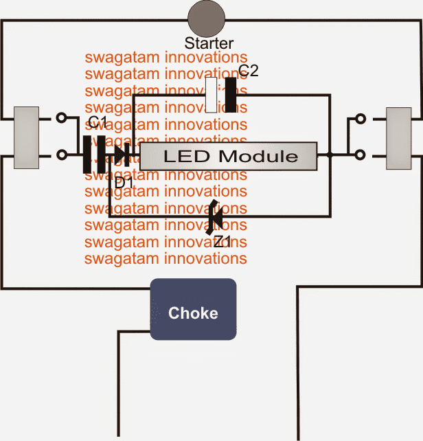
 The above diagram can be additionally safeguarded from surge inrush voltages, and mains fluctuations by adding a 10 ohm limiting resistors and a zener diode, as shown below.
Here the value of zener diode should be 310V, 2 watt
The above diagram can be additionally safeguarded from surge inrush voltages, and mains fluctuations by adding a 10 ohm limiting resistors and a zener diode, as shown below.
Here the value of zener diode should be 310V, 2 watt
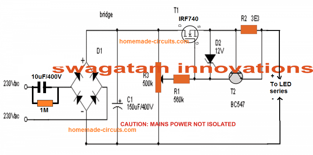
 The following email was sent to me by Mr.
John, let's learn all the details about the proposed red led sign circuit idea, sent by Mr.
John.
I had this bright red LED EXIT commercial old sign given by my son-in-law who works in electrical field.
He always finds something useful and saves just anything
I have used its components and parts for the red LED sign project.
Now I have removed the enclosed 120/277 vac transformer and taken out 16 LEDs out of the total 10 sets of many red LEDs in series and assembled them over a circuit board.
This can go without transformer as youwill see this pictures and video.
I��m learning and trying to understand how the voltage works.
I��m not perfect in such layout and drawings.
In this drawing there are two perspectives: the bottom drawing is what is done over thecircuit board.
My question is how the voltage drop from 120 to 14.5 vac handle it without any heat while LEDs light stay on? Test red probes of DMM were measured on R2 and LED and black probe on white (neutral) is 14.5 vac.
I thought these caps were supposed to increase voltage.
So this capacitors C1 and C2 I measure is 662nF are parallel are like resistors that split and reduce voltage, right?.
I took out one LED for testing my home made LED tester.
Each Red LED is 1.8 volt times 8 LED is 14.5 vac.
I see 16 total LED half go that using 14.5 vac.
Now I find it amazing how without a transformer it stays switched on and can withstand 120 vac directly without transformer.
Can you explain how this voltage/current flow to get voltage reduced by only four capacitors and two resistors to light up 16 LEDs.
See my paper written down on bottom with thelist of components.
The components are old but it is working great as you would see in the video.
Also I haven��t tested the design on my scope yet, if the sine wave showing any different?
I hope this design is safe to use.
So now looking for an idea of what project I can use it:)
Could not send video.......it's too large.
Only Pictures:(
Thanks,John Hungerford
(deafguy)
The following email was sent to me by Mr.
John, let's learn all the details about the proposed red led sign circuit idea, sent by Mr.
John.
I had this bright red LED EXIT commercial old sign given by my son-in-law who works in electrical field.
He always finds something useful and saves just anything
I have used its components and parts for the red LED sign project.
Now I have removed the enclosed 120/277 vac transformer and taken out 16 LEDs out of the total 10 sets of many red LEDs in series and assembled them over a circuit board.
This can go without transformer as youwill see this pictures and video.
I��m learning and trying to understand how the voltage works.
I��m not perfect in such layout and drawings.
In this drawing there are two perspectives: the bottom drawing is what is done over thecircuit board.
My question is how the voltage drop from 120 to 14.5 vac handle it without any heat while LEDs light stay on? Test red probes of DMM were measured on R2 and LED and black probe on white (neutral) is 14.5 vac.
I thought these caps were supposed to increase voltage.
So this capacitors C1 and C2 I measure is 662nF are parallel are like resistors that split and reduce voltage, right?.
I took out one LED for testing my home made LED tester.
Each Red LED is 1.8 volt times 8 LED is 14.5 vac.
I see 16 total LED half go that using 14.5 vac.
Now I find it amazing how without a transformer it stays switched on and can withstand 120 vac directly without transformer.
Can you explain how this voltage/current flow to get voltage reduced by only four capacitors and two resistors to light up 16 LEDs.
See my paper written down on bottom with thelist of components.
The components are old but it is working great as you would see in the video.
Also I haven��t tested the design on my scope yet, if the sine wave showing any different?
I hope this design is safe to use.
So now looking for an idea of what project I can use it:)
Could not send video.......it's too large.
Only Pictures:(
Thanks,John Hungerford
(deafguy)

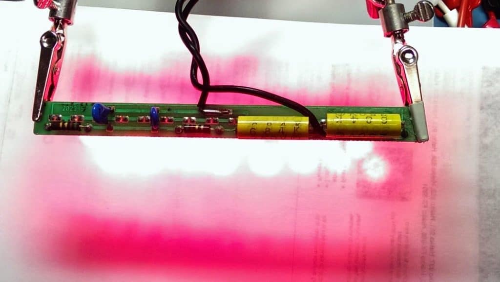
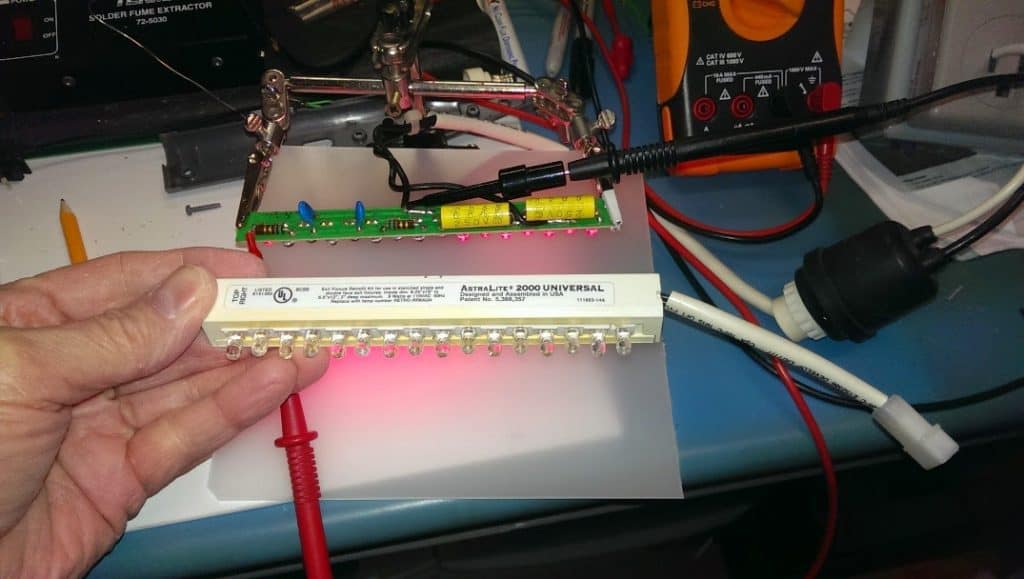
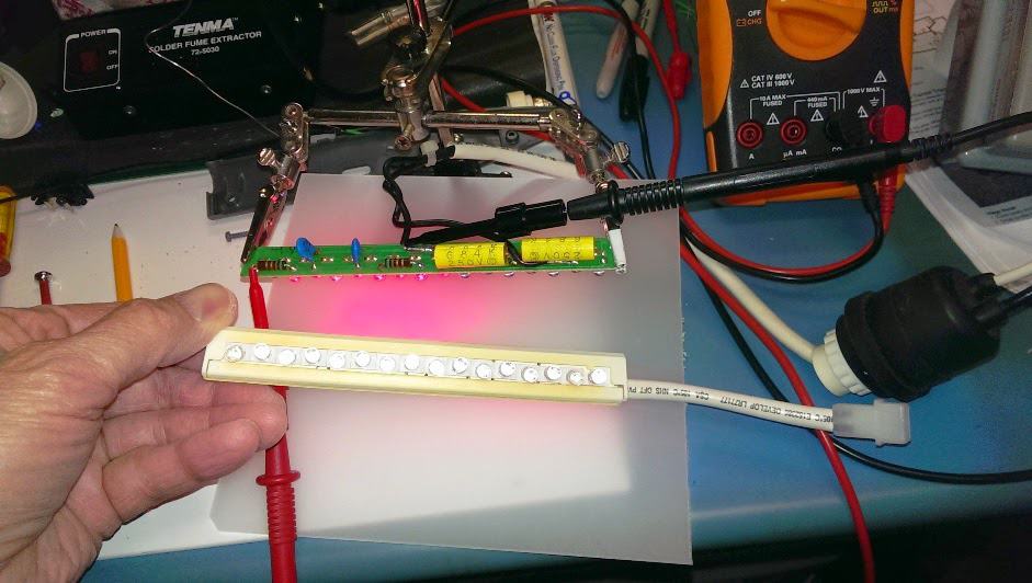
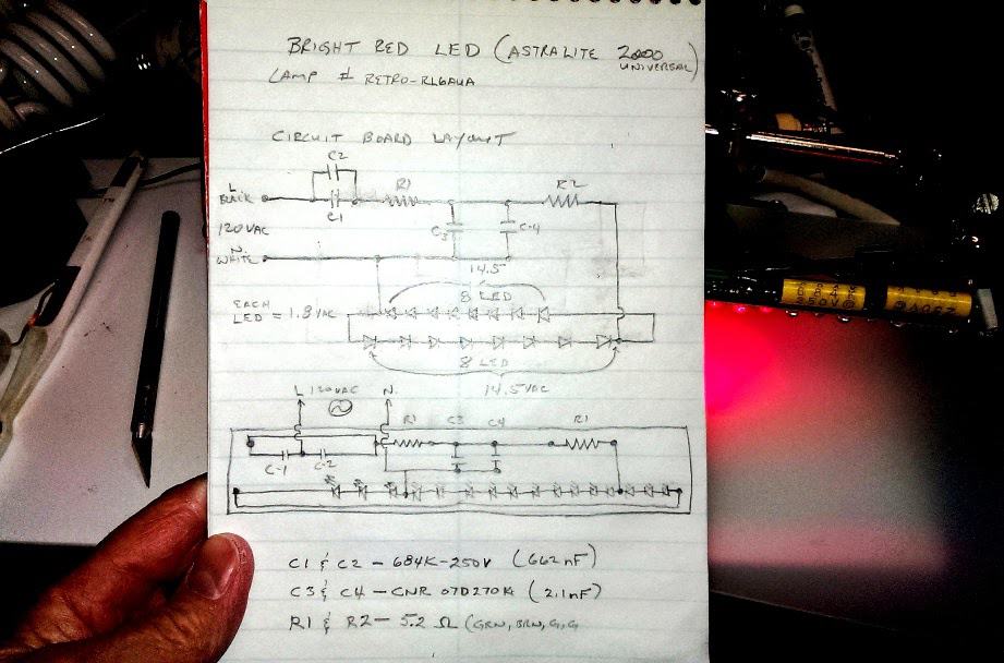
 The shown light dependent led controller circuit is basically a light dependent PWM optimizer circuit whose duty cycle varies in accordance with the potential difference or level at itscotrol pinout.
As can be seen the circuit includes a couple 555 ICs.
IC1 is configured as a standard astable having a frequency of around 80Hz.
This frequency is not crucial in terms of the circuit functioning.
IC2 is configured as a PWM generator such that it compares the square wave signal at its pin2 and the triangle wave across its pin6/7.
This results in an output with a particular PWM content at pin#3 of ICs.
However this PWM duty cycle can be varied simply varying the potential difference at pin#5 of IC2.
An LDR can be seen attached across a potential divider preset at pin#5 of this IC.
The preset can be used for fine tuning the results as desired.
The LDR resistance level now determines and varies the potential across this sensing pinout which in turn results in a proportionately varying duty cycle at pin#3.
The varying duty cycle causes the connected transistors to conduct accordingly and produce the correspondingly varying intensities over the connected LEDs.
The two transistors are configured as inverters which ensure opposite responses over the LED sets connected across the collector of the respective transistors.
The shown light dependent led controller circuit is basically a light dependent PWM optimizer circuit whose duty cycle varies in accordance with the potential difference or level at itscotrol pinout.
As can be seen the circuit includes a couple 555 ICs.
IC1 is configured as a standard astable having a frequency of around 80Hz.
This frequency is not crucial in terms of the circuit functioning.
IC2 is configured as a PWM generator such that it compares the square wave signal at its pin2 and the triangle wave across its pin6/7.
This results in an output with a particular PWM content at pin#3 of ICs.
However this PWM duty cycle can be varied simply varying the potential difference at pin#5 of IC2.
An LDR can be seen attached across a potential divider preset at pin#5 of this IC.
The preset can be used for fine tuning the results as desired.
The LDR resistance level now determines and varies the potential across this sensing pinout which in turn results in a proportionately varying duty cycle at pin#3.
The varying duty cycle causes the connected transistors to conduct accordingly and produce the correspondingly varying intensities over the connected LEDs.
The two transistors are configured as inverters which ensure opposite responses over the LED sets connected across the collector of the respective transistors.

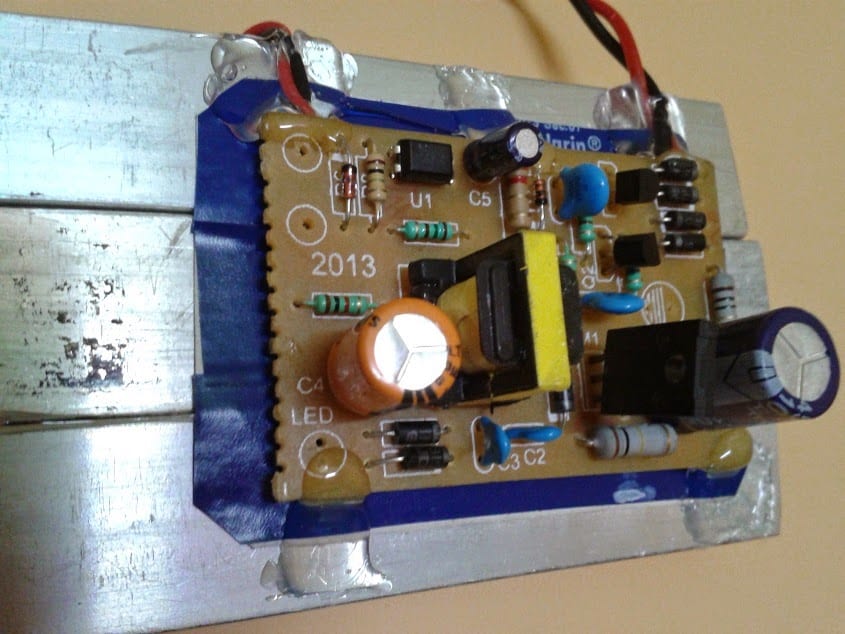
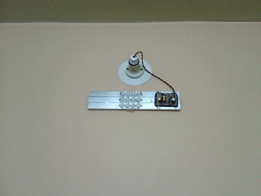
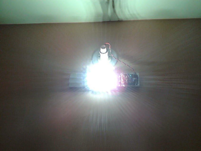
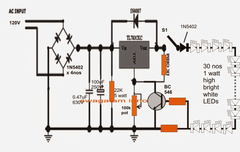
 Although it is recommended to operate any LED via a current controlled SMPS, for simplicity sake the following compact transformerless power supply may be tried and could prove as good as it's other counterparts.
The present design is based on my previous variable transformerless power supply design, which enjoys a novel crowbar network concept for safeguarding the involved sophisticated devices.
The proposed 5630 SMD LED driver or compact tube light circuit may be understood with the help of the following discussion:
Although it is recommended to operate any LED via a current controlled SMPS, for simplicity sake the following compact transformerless power supply may be tried and could prove as good as it's other counterparts.
The present design is based on my previous variable transformerless power supply design, which enjoys a novel crowbar network concept for safeguarding the involved sophisticated devices.
The proposed 5630 SMD LED driver or compact tube light circuit may be understood with the help of the following discussion:
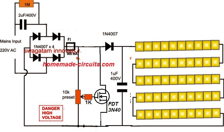 THE WHOLE CIRCUIT WOULD BE FLOATING WITH LETHAL MAINS AC, EXTREME CAUTION IS EXPECTED FROM THE USER WHILE TESTING THE CIRCUIT IN UNCOVERED POSITION.
Feedback from one of the dedicated readers of this blog, Mr.
Raghavendra Kolkar:
THE WHOLE CIRCUIT WOULD BE FLOATING WITH LETHAL MAINS AC, EXTREME CAUTION IS EXPECTED FROM THE USER WHILE TESTING THE CIRCUIT IN UNCOVERED POSITION.
Feedback from one of the dedicated readers of this blog, Mr.
Raghavendra Kolkar:

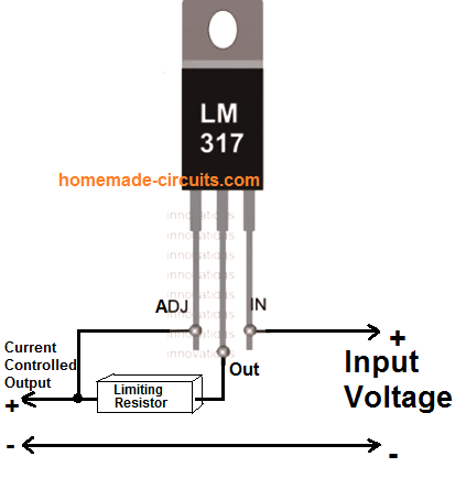 PICTORIAL REPRESENTATION OF THE ABOVE CIRCUIT
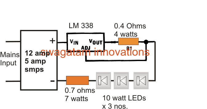 The series resistor connected with the three LEDs is calculated by using the following formula:
R = (supply voltage �C Total LED forward voltage) / LED current
R(watts) = (supply voltage �C Total LED forward voltage) x LED current
R = (12 - 3.3+3.3+3.3)/3amps
R= (12 - 9.9)/3
R = 0.7 ohms
R watts = V x A = (12-9.9) x 3 = 2.1 x 3 = 6.3 watts
The series resistor connected with the three LEDs is calculated by using the following formula:
R = (supply voltage �C Total LED forward voltage) / LED current
R(watts) = (supply voltage �C Total LED forward voltage) x LED current
R = (12 - 3.3+3.3+3.3)/3amps
R= (12 - 9.9)/3
R = 0.7 ohms
R watts = V x A = (12-9.9) x 3 = 2.1 x 3 = 6.3 watts
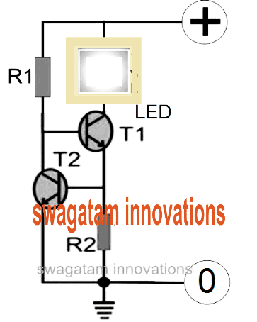

 The working can be understood as follows.
Let's say the input supply the source current I starts rising due to high consumption by the load for some reason.
This will result in an increase in the potential across R3, causing the T1 base/emitter potential to rise and a conduction across its collector emitter.
This would in turn cause the base bias of the Darlington pair to start getting more grounded.
Due to this the current increase would get countered and restricted through the load.
The inclusion of R2 pull up resistor makes sure that T1 always conducts with a constant current value (I) as set by the following formula.
Thus the supply voltage fluctuations have no effect on the current limiting action of the circuit
R3 = 0.6 / I
Here, I is the current limit in amps as required by the application.
The working can be understood as follows.
Let's say the input supply the source current I starts rising due to high consumption by the load for some reason.
This will result in an increase in the potential across R3, causing the T1 base/emitter potential to rise and a conduction across its collector emitter.
This would in turn cause the base bias of the Darlington pair to start getting more grounded.
Due to this the current increase would get countered and restricted through the load.
The inclusion of R2 pull up resistor makes sure that T1 always conducts with a constant current value (I) as set by the following formula.
Thus the supply voltage fluctuations have no effect on the current limiting action of the circuit
R3 = 0.6 / I
Here, I is the current limit in amps as required by the application.
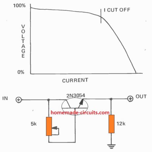 Although, from the graph we can realize that the current cut-off process is not very sharp, yet its is actually quite enough to ensure proper safety for the output load from an over current situation.
That said, the limiting range and accuracy can be affected depending on the temperature of the transistor.
Although, from the graph we can realize that the current cut-off process is not very sharp, yet its is actually quite enough to ensure proper safety for the output load from an over current situation.
That said, the limiting range and accuracy can be affected depending on the temperature of the transistor.
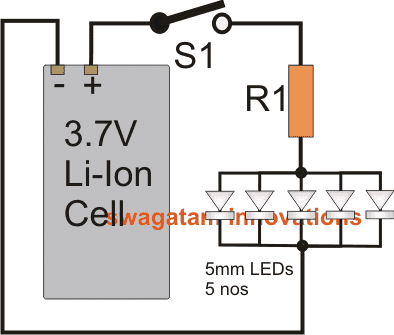
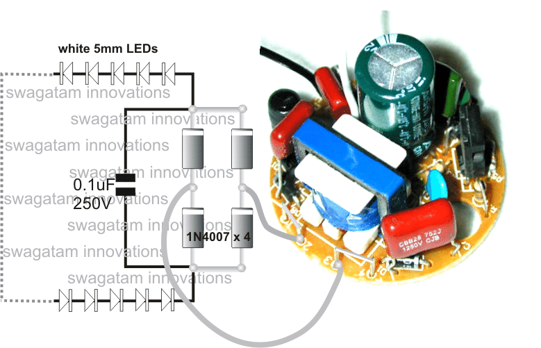 Another Idea
The method of converting a blown CFL into an LED lamp as explained above looks unnecessarily complex and risky.
A better and a foolproof technique would be to salvage a few of the useful parts from the CFL PCB and then apply them to build a simple tranformerless LED driver.
The parts which needs to be extracted can be learned from the following explanation.
Typically, you will find a few PPC capacitors present (which look like chewing gums), check the values and pick up the one which has the highest value in terms of uF and also the voltage value.
The voltage is more important, and make sure the picked one is rated above the supply value of your home AC.
So if the supply AC is 220V, the capacitor should be above 250V minimum, and likewise.
Next, remove the filter capacitor, which would be in electrolytic form, and also the 4 diodes from the bridge rectifier.
After collecting these de-soldered items, assemble them back over a separate stripboard or piece of general purpose board with the help of the following schematic:
Another Idea
The method of converting a blown CFL into an LED lamp as explained above looks unnecessarily complex and risky.
A better and a foolproof technique would be to salvage a few of the useful parts from the CFL PCB and then apply them to build a simple tranformerless LED driver.
The parts which needs to be extracted can be learned from the following explanation.
Typically, you will find a few PPC capacitors present (which look like chewing gums), check the values and pick up the one which has the highest value in terms of uF and also the voltage value.
The voltage is more important, and make sure the picked one is rated above the supply value of your home AC.
So if the supply AC is 220V, the capacitor should be above 250V minimum, and likewise.
Next, remove the filter capacitor, which would be in electrolytic form, and also the 4 diodes from the bridge rectifier.
After collecting these de-soldered items, assemble them back over a separate stripboard or piece of general purpose board with the help of the following schematic:
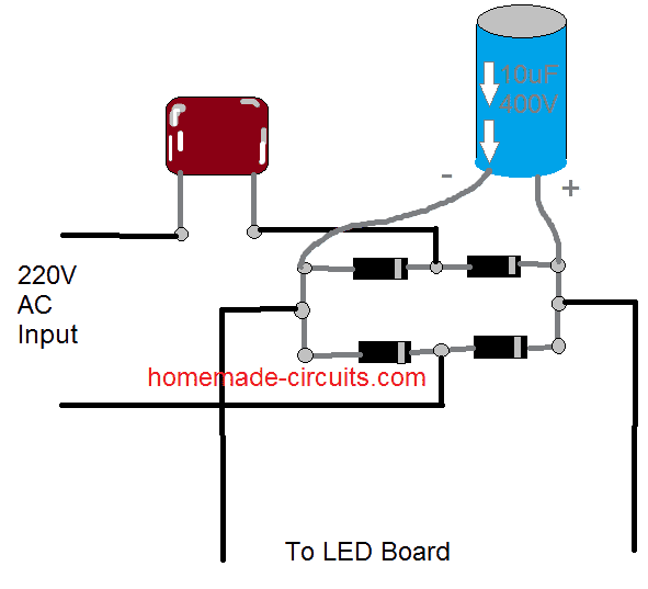 Once you have built this, the rest of the parts and the CFL PCB could be removed and thrown away, we don't need it anymore.
After this, procure around 50 LEDs @ 20mA , preferably SMD type as shown below, and assemble them in series over a circular PCB.
Once you have built this, the rest of the parts and the CFL PCB could be removed and thrown away, we don't need it anymore.
After this, procure around 50 LEDs @ 20mA , preferably SMD type as shown below, and assemble them in series over a circular PCB.
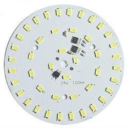 Finally connect the +/- ends of this series LED assembly with the "LED board" points of the above explained power supply circuit.
Feed the 220V input to the capacitive supply and watch the LED dazzle up with mind blowing brightness.
That's it, you have just converted a dead CFL into a high bright LED bulb.
Enclose the whole thing inside the CFL box, and glue the PCB appropriately, plug it in your home bulb AC socket for the preferred use
Note: The quantity of LEDs is intentionally selected to be 50nos to get an increased brightness and also better surge control.
Remember here we are assuming the input PPC capacitor to be not more than 0.22uF.
If its more than this value then you may have apply a series resistor with the LED assembly to enable an improved surge restriction.
Finally connect the +/- ends of this series LED assembly with the "LED board" points of the above explained power supply circuit.
Feed the 220V input to the capacitive supply and watch the LED dazzle up with mind blowing brightness.
That's it, you have just converted a dead CFL into a high bright LED bulb.
Enclose the whole thing inside the CFL box, and glue the PCB appropriately, plug it in your home bulb AC socket for the preferred use
Note: The quantity of LEDs is intentionally selected to be 50nos to get an increased brightness and also better surge control.
Remember here we are assuming the input PPC capacitor to be not more than 0.22uF.
If its more than this value then you may have apply a series resistor with the LED assembly to enable an improved surge restriction.

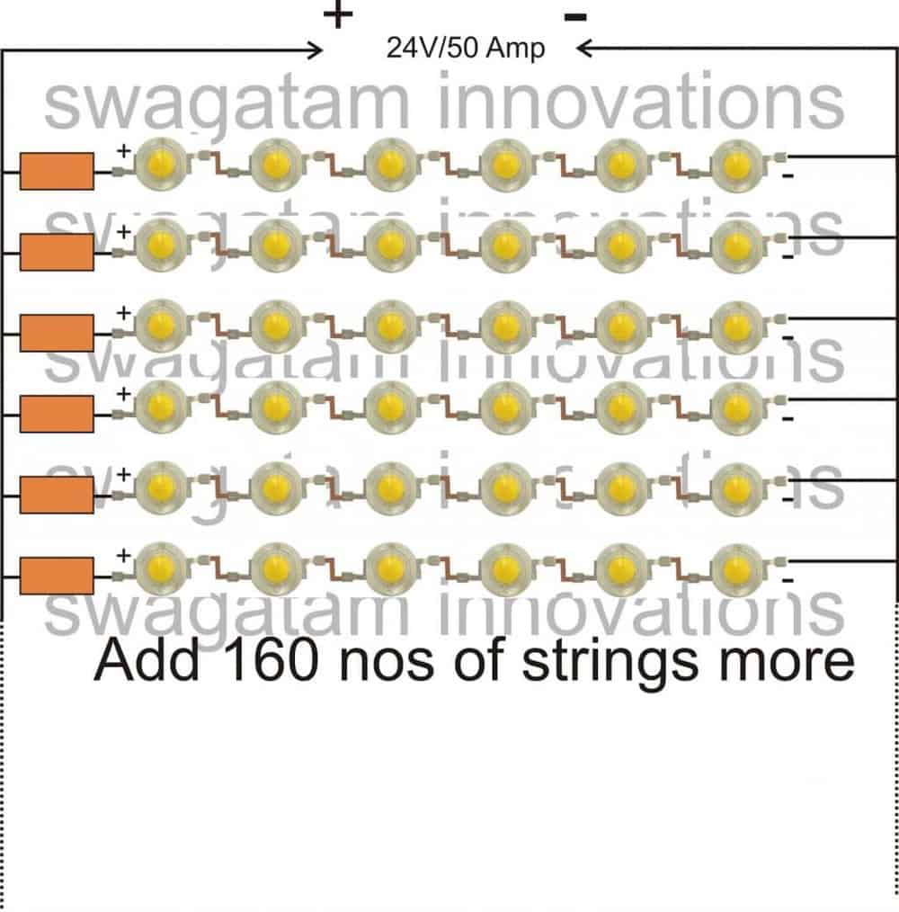
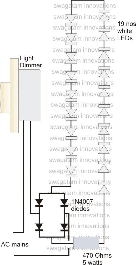 In the above figure we can see a chain of LEDs connected in series and powered in the usual manner via a bridge rectifier and a limiting resistor.
As suggested in the request the supply has been derived from a dimmer switch by connecting the LED circuit in series with the dimmer switch.
As we all know a dimmer switch is able to reduce power to the output load by chopping of sections of the AC mains such that the overall value of the AC gets reduced and thus the connected load also receives a cut down power.
However the triac would be able to handle current that's within its rated specs.
Therefore we connect a 470 Ohms resistor in series with the LEDs which makes sure that the dimmer remains safe even at full LED illuminations.
This resistor might get considerably hot at full brightness and vice versa, therefore it's rated at 5 watts, yet it will get hot.
If the heating up of the resistor looks undesirable, the above circuit may be modified in the following manner.
In the above figure we can see a chain of LEDs connected in series and powered in the usual manner via a bridge rectifier and a limiting resistor.
As suggested in the request the supply has been derived from a dimmer switch by connecting the LED circuit in series with the dimmer switch.
As we all know a dimmer switch is able to reduce power to the output load by chopping of sections of the AC mains such that the overall value of the AC gets reduced and thus the connected load also receives a cut down power.
However the triac would be able to handle current that's within its rated specs.
Therefore we connect a 470 Ohms resistor in series with the LEDs which makes sure that the dimmer remains safe even at full LED illuminations.
This resistor might get considerably hot at full brightness and vice versa, therefore it's rated at 5 watts, yet it will get hot.
If the heating up of the resistor looks undesirable, the above circuit may be modified in the following manner.
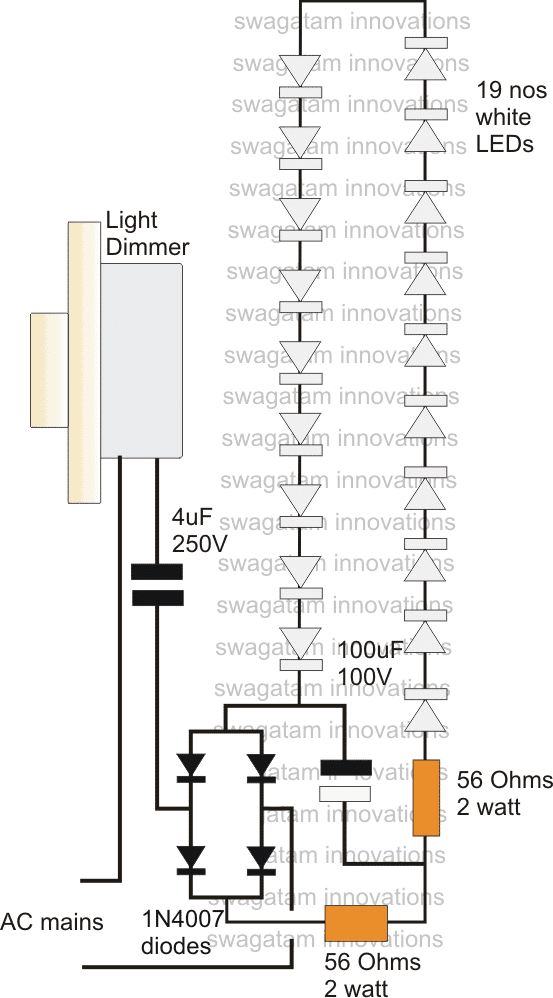 As can be witnessed in the above diagram, a high voltage, high value capacitor has been introduced at the input of the LED chain, which means now the voltage from the dimmer switch has to pass through this capacitor before reaching the LEDs.
The capacitor effectively restricts high currents from entering the circuit keeping the dimmer as well as the LEDs completely safe, and alsoeliminatesthe need of using high wattage "hot" resistors.
However, during switch ON the capacitor (as per its standard characteristics) will act like a "short" for a fraction of a second.
This might inflict high initial surge voltage impact to the connected vulnerable LEDs.
Though it will not do any harm to the dimmer, can instantly damage the LED chain.
For restricting this initial surge, aresistor/capacitor "sand box" is inserted at the positive line of the LED.
The two 56 Ohm resistors and the 10uF/100V capacitor effectively absorbs the initial surge and keeps the LEDs safe and illuminating.
The number of LEDs is not critical any number can be used provided the total forward voltage comes within the supply voltage range.
WARNING: THE IDEA IS BASED ON MY ASSUMPTIONS ONLY, AND HAS NEVER BEEN TESTED PRACTICALLY.
APPROPRIATE CAUTION MUST BE OBSERVED BY THE CONSTRUCTOR.
USE A SERIES 100 WATT BULB WHILE TESTING THE PROTOTYPE.
THE BULB SHOULD REMAIN COMPLETELY SHUT OFF WHILE OPERATING THE DIMMER FROM ZERO TO MAX.
IF THE BULB ILLUMINATES WOULD MEAN SOMETHING'S WRONG WITH THE CIRCUIT.
As can be witnessed in the above diagram, a high voltage, high value capacitor has been introduced at the input of the LED chain, which means now the voltage from the dimmer switch has to pass through this capacitor before reaching the LEDs.
The capacitor effectively restricts high currents from entering the circuit keeping the dimmer as well as the LEDs completely safe, and alsoeliminatesthe need of using high wattage "hot" resistors.
However, during switch ON the capacitor (as per its standard characteristics) will act like a "short" for a fraction of a second.
This might inflict high initial surge voltage impact to the connected vulnerable LEDs.
Though it will not do any harm to the dimmer, can instantly damage the LED chain.
For restricting this initial surge, aresistor/capacitor "sand box" is inserted at the positive line of the LED.
The two 56 Ohm resistors and the 10uF/100V capacitor effectively absorbs the initial surge and keeps the LEDs safe and illuminating.
The number of LEDs is not critical any number can be used provided the total forward voltage comes within the supply voltage range.
WARNING: THE IDEA IS BASED ON MY ASSUMPTIONS ONLY, AND HAS NEVER BEEN TESTED PRACTICALLY.
APPROPRIATE CAUTION MUST BE OBSERVED BY THE CONSTRUCTOR.
USE A SERIES 100 WATT BULB WHILE TESTING THE PROTOTYPE.
THE BULB SHOULD REMAIN COMPLETELY SHUT OFF WHILE OPERATING THE DIMMER FROM ZERO TO MAX.
IF THE BULB ILLUMINATES WOULD MEAN SOMETHING'S WRONG WITH THE CIRCUIT.
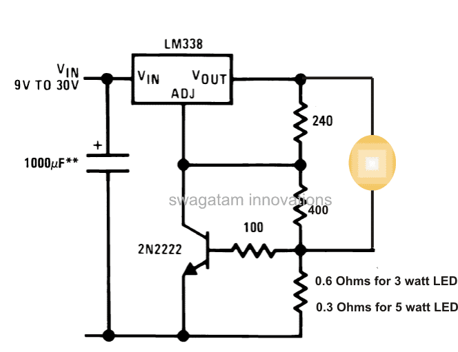 In fact, the transistor and the associated base/emitter resistors are absolutely not required, because once the voltage is set to precise 3.3V, the current would automatically get adjusted as per the LEDs specs.
So the correct circuit should be as given below:
In fact, the transistor and the associated base/emitter resistors are absolutely not required, because once the voltage is set to precise 3.3V, the current would automatically get adjusted as per the LEDs specs.
So the correct circuit should be as given below:
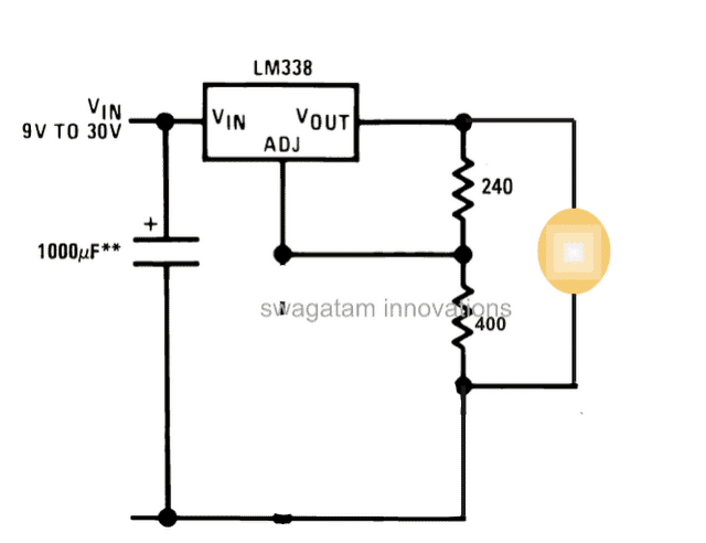
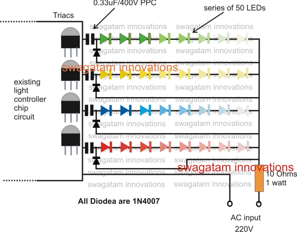
 No surprise why white LEDs are being considered as the future option for all lighting applications.
The LED flashlight circuit explained here is very simple, and it simply requires to follow the instructions as given for making it successfully.
The proposed circuit utilizes just a single high bright white LED, three 1.5 volt button cells and a switch.
No surprise why white LEDs are being considered as the future option for all lighting applications.
The LED flashlight circuit explained here is very simple, and it simply requires to follow the instructions as given for making it successfully.
The proposed circuit utilizes just a single high bright white LED, three 1.5 volt button cells and a switch.
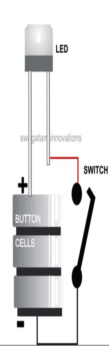
 The implementation of the circuit is naturally not restricted to flashlights alone; it could likewise be employed for solar lights, radio dial brightness, etc.
If an LDR is used in place of P1, it might be possible to achieve an automated dimmer that self adjusts the illumination of the lamp depending on the background light conditions.
The implementation of the circuit is naturally not restricted to flashlights alone; it could likewise be employed for solar lights, radio dial brightness, etc.
If an LDR is used in place of P1, it might be possible to achieve an automated dimmer that self adjusts the illumination of the lamp depending on the background light conditions.
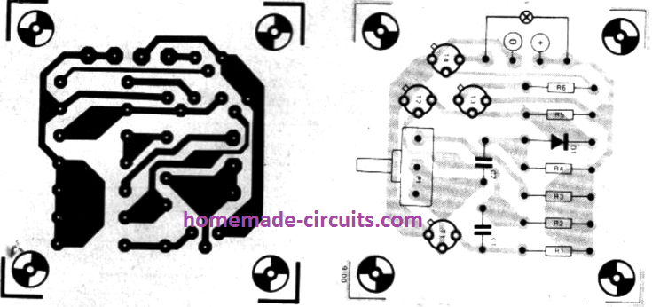
 The big reason of LCDs getting so popular is probably the presence of the back lighting that illuminates the entire surface of the unit brightly, making the relevant readings distinct and full of life.
LEDs are the prime components which are used for the above illumination applications.
Genarally a group of high efficient LEDs are placed behind a responsive surface for getting the desired LCD effect or the back light illuminations.
For smaller color LCD units, around 8 white LEDs are usually sufficient for the required intensities.
When placed uniformly, they almost present a perfectly balanced illumination of the LCD.
The big reason of LCDs getting so popular is probably the presence of the back lighting that illuminates the entire surface of the unit brightly, making the relevant readings distinct and full of life.
LEDs are the prime components which are used for the above illumination applications.
Genarally a group of high efficient LEDs are placed behind a responsive surface for getting the desired LCD effect or the back light illuminations.
For smaller color LCD units, around 8 white LEDs are usually sufficient for the required intensities.
When placed uniformly, they almost present a perfectly balanced illumination of the LCD.
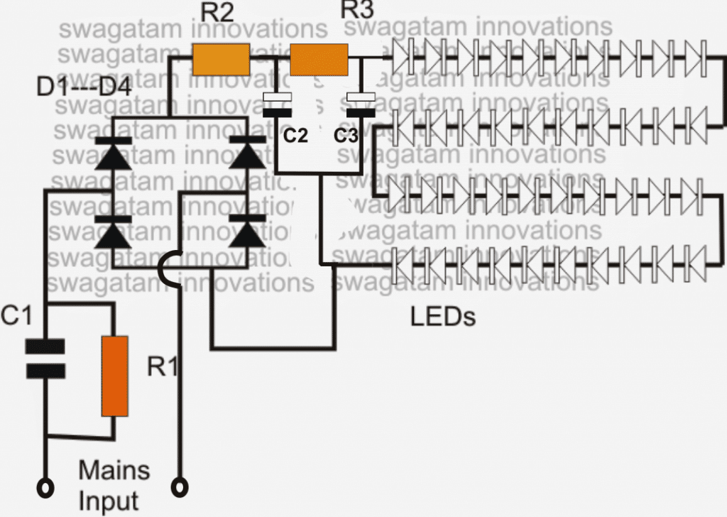
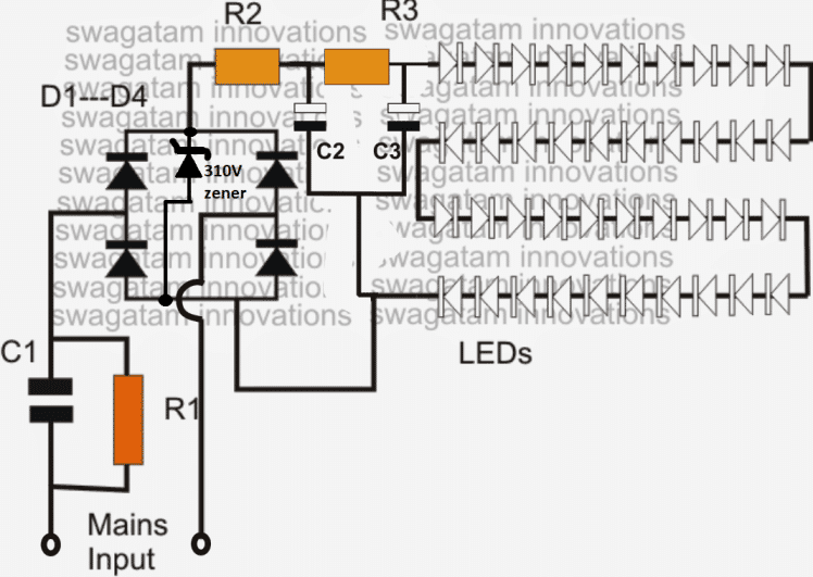 Video clip showing an LED circuit circuit using 108 numbers of LED (two 54 LED series strings connected in parallel)
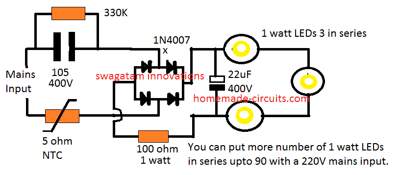 Moreover you won't require a heatsink for the LEDs since these are being operated at only 30% of their actual capacity.
Likewise, by joining 90nos of 1 watt LEDs in the above design you could achieve a 25 watt high bright, highly efficient bulb.
You may think that getting 25 watt from 90 LEDs is "inefficient", but actually it is not.
Because these 90nos of 1 watt LEDs would be running at 70% less current, and therefore at zero stress level, which would allow them to last almost forever.
Next, these would be comfortably working without a heatsink, so the entire design could be configured into a much compact unit.
No heatsink also means minimum effort and time consumed for the construction.
So all these benefits ultimately makes this 25 watt LED more efficient and cost effective than the traditional approach.
Moreover you won't require a heatsink for the LEDs since these are being operated at only 30% of their actual capacity.
Likewise, by joining 90nos of 1 watt LEDs in the above design you could achieve a 25 watt high bright, highly efficient bulb.
You may think that getting 25 watt from 90 LEDs is "inefficient", but actually it is not.
Because these 90nos of 1 watt LEDs would be running at 70% less current, and therefore at zero stress level, which would allow them to last almost forever.
Next, these would be comfortably working without a heatsink, so the entire design could be configured into a much compact unit.
No heatsink also means minimum effort and time consumed for the construction.
So all these benefits ultimately makes this 25 watt LED more efficient and cost effective than the traditional approach.
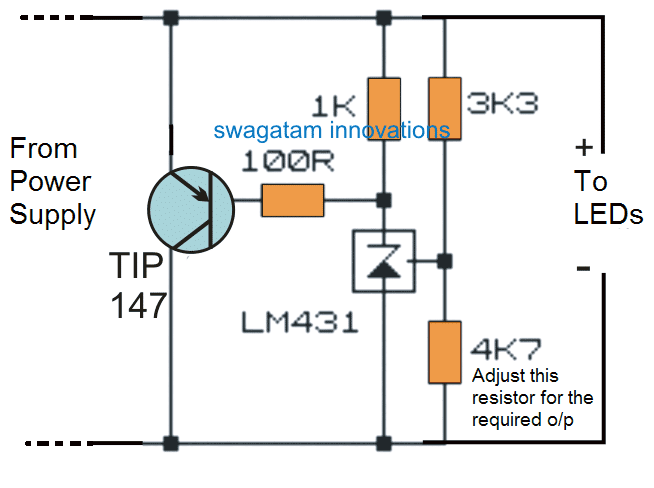 Video Clip:
In the videosabove I have purposely flickered the LEDs by twitching the supply wire just to test ensure that the circuit is 100% surge proof.
Video Clip:
In the videosabove I have purposely flickered the LEDs by twitching the supply wire just to test ensure that the circuit is 100% surge proof.
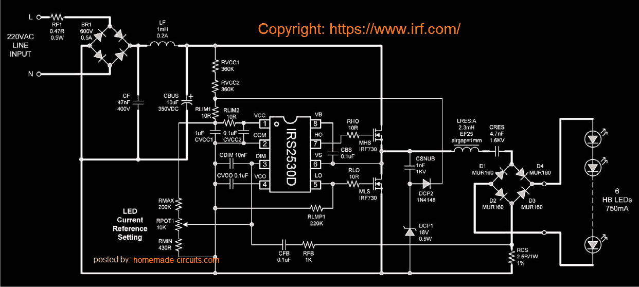 Original article can be foundhere
 Pin Out Specs:
 Courtesy: https://www.homemade-circuits.com/wp-content/uploads/2012/04/mbi6651.pdf
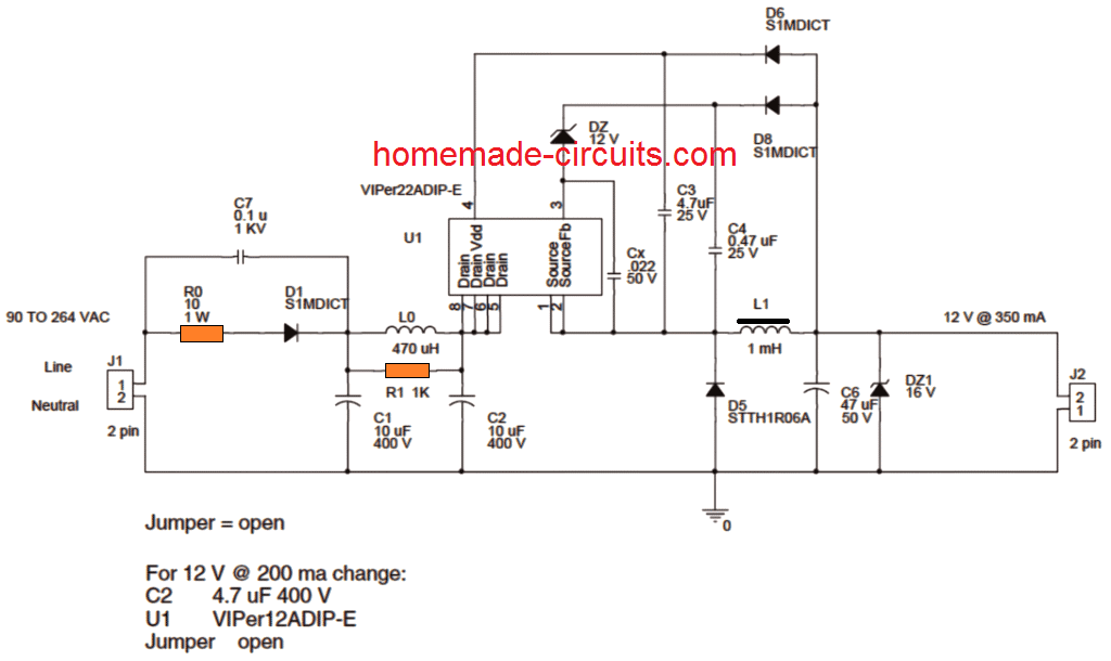 Image Courtesy: STMicroelectronics - All rights reserved
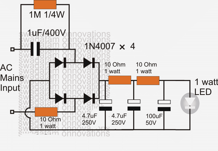 NOTE: The LED in the above diagram is a 12V 1 watt as shown below:
 In the above shown simple 1 watt led driver circuit, the two 4.7uF/250 capacitors along with the 10 ohm resistors form a kind of "speed breaker" in the circuit, this approach helps to arrest the initial switch ON surge inrush which in turn helps to safeguard the LED from getting damaged.
This feature can be replaced with an NTC which are popular for their surge suppressing features.
This enhanced way of tackling the initial surge inrush problem could be by connecting an NTC thermistor in series with the circuit or the load.
Pleasecheck out the following link for knowing how to incorporate an NTC thermister in the proposed 1 watt LED driver circuit
The above circuit can be modified in the following manner, however the light may be a little compromised.
A good way of tackling the initial surge inrush problem is by connecting an NTC thermistor in series with the circuit or the load.
Pleasecheck out the following link for knowing how to incorporate an NTC thermister in the proposed 1 watt LED driver circuit
https://www.homemade-circuits.com/2013/02/using-ntc-resistor-as-surge-suppressor.html
In the above shown simple 1 watt led driver circuit, the two 4.7uF/250 capacitors along with the 10 ohm resistors form a kind of "speed breaker" in the circuit, this approach helps to arrest the initial switch ON surge inrush which in turn helps to safeguard the LED from getting damaged.
This feature can be replaced with an NTC which are popular for their surge suppressing features.
This enhanced way of tackling the initial surge inrush problem could be by connecting an NTC thermistor in series with the circuit or the load.
Pleasecheck out the following link for knowing how to incorporate an NTC thermister in the proposed 1 watt LED driver circuit
The above circuit can be modified in the following manner, however the light may be a little compromised.
A good way of tackling the initial surge inrush problem is by connecting an NTC thermistor in series with the circuit or the load.
Pleasecheck out the following link for knowing how to incorporate an NTC thermister in the proposed 1 watt LED driver circuit
https://www.homemade-circuits.com/2013/02/using-ntc-resistor-as-surge-suppressor.html
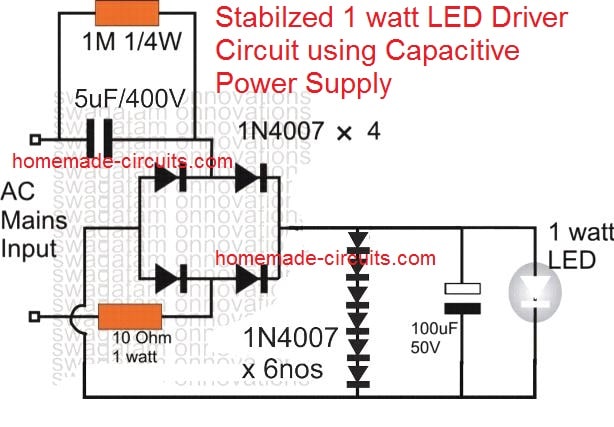 As can be seen, 6nos of 1N4007 diodes are used across the output, in their forward biased mode.
Since each diode would produce a drop of 0.6V across itself, 6 diodes would create a total drop of 3.6V, which is just the right amount of voltage for the LED.
This also means that the diodes would shunt the rest of the power from the source tp ground, and thus keep the supply for the LED perfectly stabilized and safe.
As can be seen, 6nos of 1N4007 diodes are used across the output, in their forward biased mode.
Since each diode would produce a drop of 0.6V across itself, 6 diodes would create a total drop of 3.6V, which is just the right amount of voltage for the LED.
This also means that the diodes would shunt the rest of the power from the source tp ground, and thus keep the supply for the LED perfectly stabilized and safe.
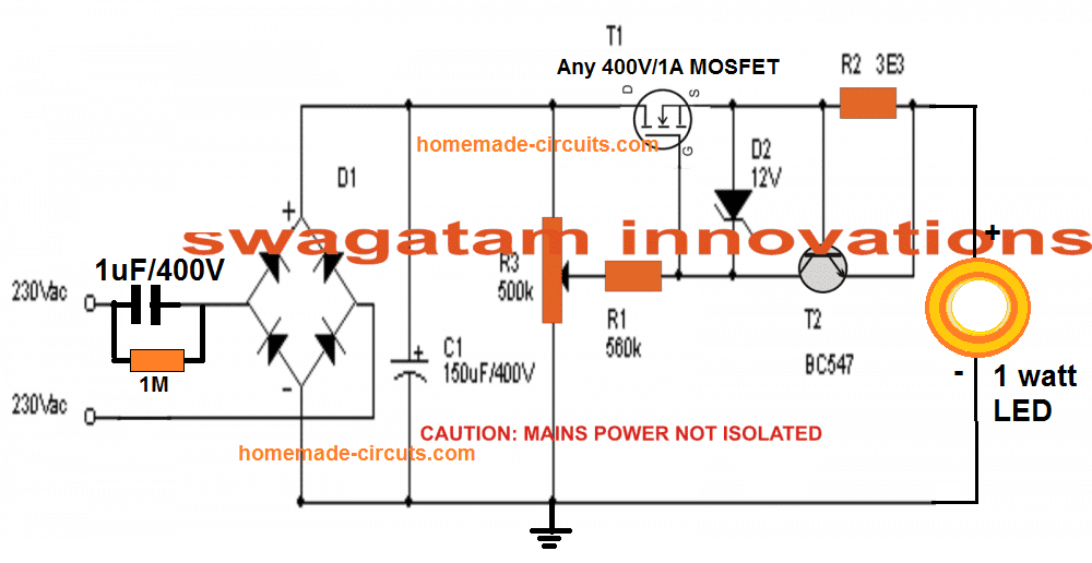 A 1 watt LED connected with the above circuit would be able to produce around 60 Lumens of light intensity, equivalent to a 5 watt incandescent lamp.
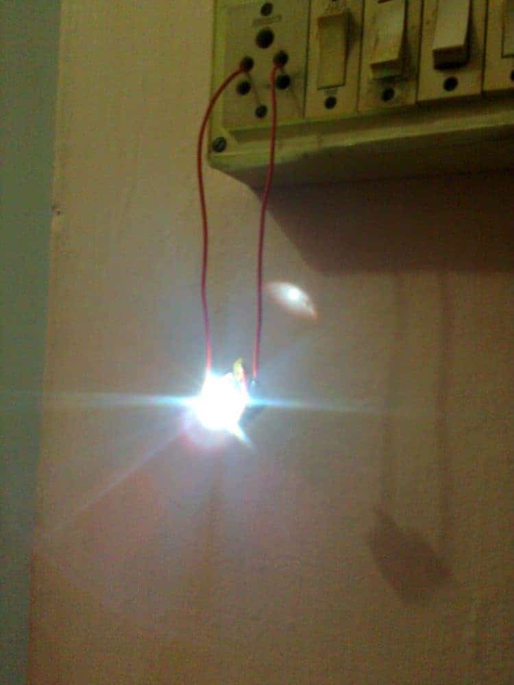 The above circuit can be modified in the following manner, however the light may be a little compromised.
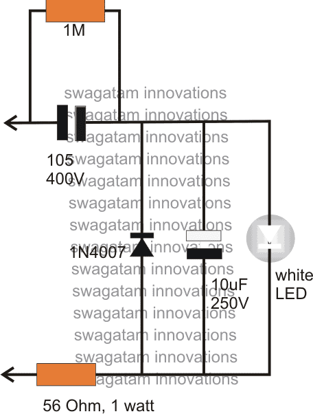
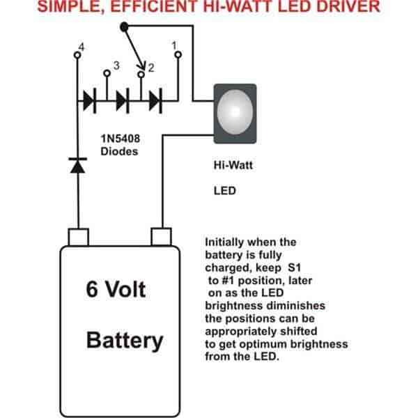
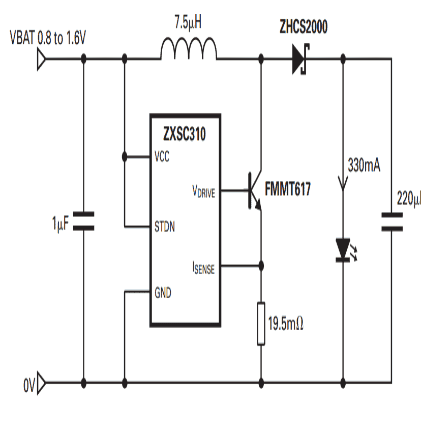

 A quick inspection reveals that if a current control is present, voltage regulation can be ignored.
Here's a simplified version for the above concept, using only a current limiter circuit.
A quick inspection reveals that if a current control is present, voltage regulation can be ignored.
Here's a simplified version for the above concept, using only a current limiter circuit.

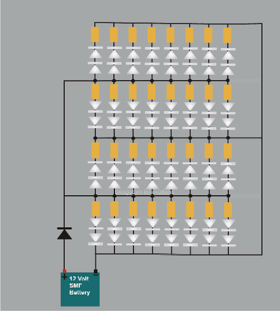

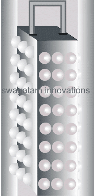

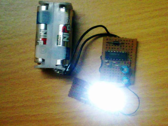

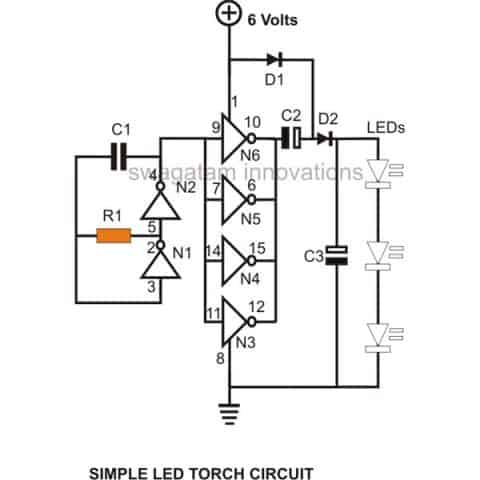 The present configuration ensures almost 100 % efficiency and thus a good battery life.
Gates N1 and N2 along with R1 and C1 are all wired up as an oscillator with a frequency determined by the values of R1 and C1.
The remaining gates N3, N4, N5 and N6 are all joined in parallel as buffers, i.e.
their inputs are all linked together and connected to the frequency source from the oscillator.
Their outputs are also made into a single common outlet and terminated to the following voltage enhancer circuit.
The present configuration ensures almost 100 % efficiency and thus a good battery life.
Gates N1 and N2 along with R1 and C1 are all wired up as an oscillator with a frequency determined by the values of R1 and C1.
The remaining gates N3, N4, N5 and N6 are all joined in parallel as buffers, i.e.
their inputs are all linked together and connected to the frequency source from the oscillator.
Their outputs are also made into a single common outlet and terminated to the following voltage enhancer circuit.

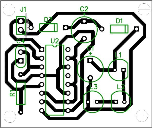
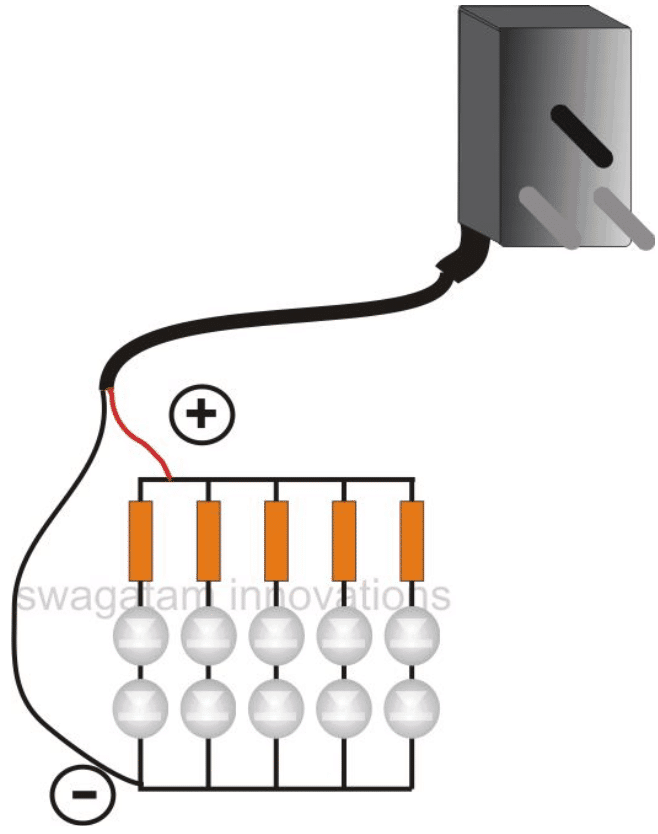 And as discussed above, a descent LED tube light can also be built by assembling some 30 + LEDs in conjunctionwith a cell phone charger power supply.
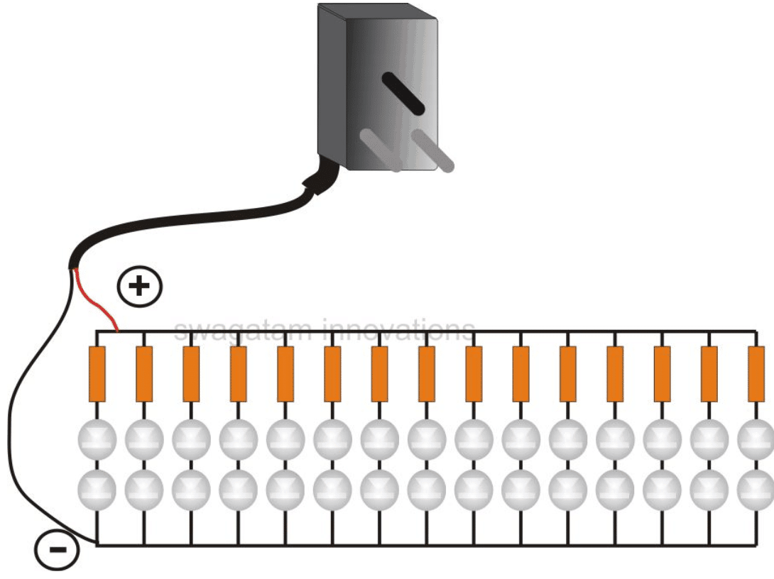
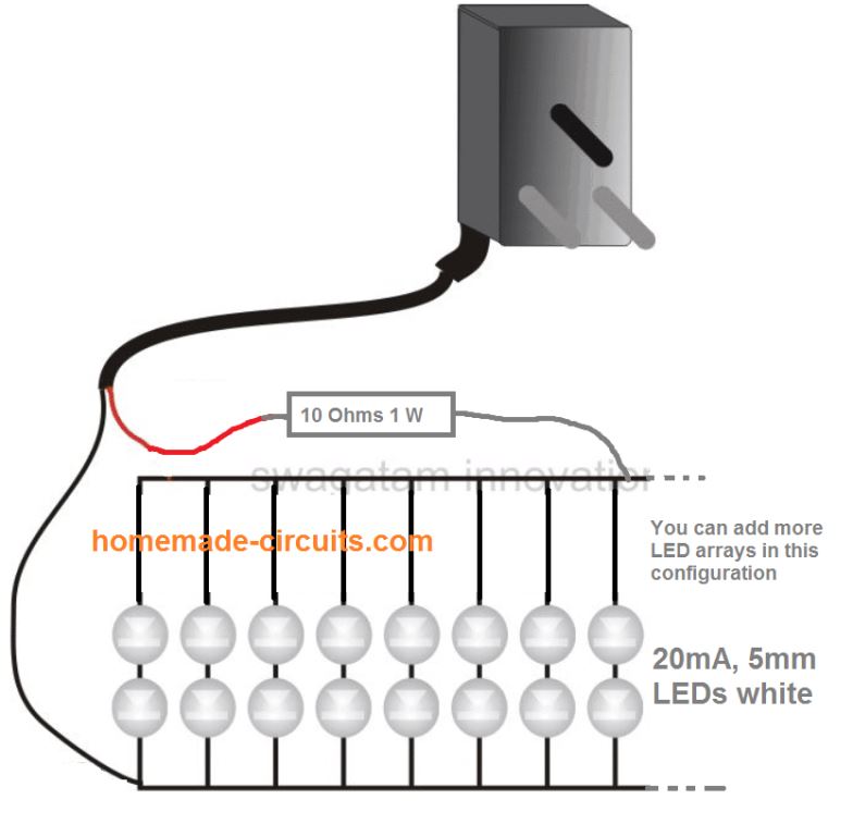
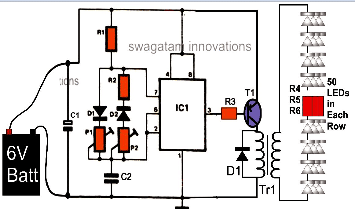 The above procedure repeats, causing sustained oscillations at the output.
However since the charging and discharging periods of C2 directly corresponds to the output periods of the pulses, it simply means that by varying or controlling the charging and discharging of C2 separately, we should be able to dimension the output pulses correspondingly.
The pots or the presets P1 and P2 are exactly placed for these adjustments and hence constitutes the PWM function.
The PWM application contributes to another important function for the present application.
By suitably optimizing the pulses, we can set the circuit to a most economic position for obtaining optimum brightness from the LEDs at relatively lower battery consumption.
The output from the IC is taken from its pin number three and used for driving as power transistor.
Since the collector of the power transistor is joined to the secondary (low voltage) winding of an ordinary AC-DC transformer, the entire supply voltage is dumped periodically into this section of the transformer inductor.
As anticipated, this pulsed voltage which is forced into the secondary winding induces a proportional magnitude of voltage into the primary winding of the transformer.
The process is entirely reversed as compared to the situation when the transformer is used with its normal AC-DC adapter applications.
The voltage is stepped-up rather than stepping down to about 230 volts which happens to be its normal primary winding specification.
This stepped up voltage available at the free winding ends of the transformer is actually used for driving a large number of LEDs which are wired up through long series and a few parallel connections.
The above procedure repeats, causing sustained oscillations at the output.
However since the charging and discharging periods of C2 directly corresponds to the output periods of the pulses, it simply means that by varying or controlling the charging and discharging of C2 separately, we should be able to dimension the output pulses correspondingly.
The pots or the presets P1 and P2 are exactly placed for these adjustments and hence constitutes the PWM function.
The PWM application contributes to another important function for the present application.
By suitably optimizing the pulses, we can set the circuit to a most economic position for obtaining optimum brightness from the LEDs at relatively lower battery consumption.
The output from the IC is taken from its pin number three and used for driving as power transistor.
Since the collector of the power transistor is joined to the secondary (low voltage) winding of an ordinary AC-DC transformer, the entire supply voltage is dumped periodically into this section of the transformer inductor.
As anticipated, this pulsed voltage which is forced into the secondary winding induces a proportional magnitude of voltage into the primary winding of the transformer.
The process is entirely reversed as compared to the situation when the transformer is used with its normal AC-DC adapter applications.
The voltage is stepped-up rather than stepping down to about 230 volts which happens to be its normal primary winding specification.
This stepped up voltage available at the free winding ends of the transformer is actually used for driving a large number of LEDs which are wired up through long series and a few parallel connections.
 We have all studied a great deal about LEDs and about their high-efficiency with power consumption.
The LED technology has helped us to design and incorporate very high intensity light installations at minimal consumptions as compared to the other conventional form of lighting concepts.
Lower power consumption also means low heat emissions, which again is an added feature and helps to keep the crucial issue of global warming at bay when LEDs are utilized.
As days pass by, technology keeps on improving and we are able to witness many incredible and unbelievable results with these outstanding lighting devices.
The 100 watt LED module is one such marvel of modern science which has created a breakthrough in the field of LED lighting.
Not surprisingly, the device is able to generate an astonishing 6500 lumens of light intensity at a consumption of mere 100 watts, but the interesting part is the size, which is barely 40 square mm.
The saving made by these devices is estimated to be five times more than any other form of light producing device and the if we compare the specified intensity of 6500 lumens, that corresponds to an excess of 500 watts light power that might be acquired from a halogen lamp.
Let��s discuss the important specifications of this amazing LED in brief and in such a way that even a layman understands:
We have all studied a great deal about LEDs and about their high-efficiency with power consumption.
The LED technology has helped us to design and incorporate very high intensity light installations at minimal consumptions as compared to the other conventional form of lighting concepts.
Lower power consumption also means low heat emissions, which again is an added feature and helps to keep the crucial issue of global warming at bay when LEDs are utilized.
As days pass by, technology keeps on improving and we are able to witness many incredible and unbelievable results with these outstanding lighting devices.
The 100 watt LED module is one such marvel of modern science which has created a breakthrough in the field of LED lighting.
Not surprisingly, the device is able to generate an astonishing 6500 lumens of light intensity at a consumption of mere 100 watts, but the interesting part is the size, which is barely 40 square mm.
The saving made by these devices is estimated to be five times more than any other form of light producing device and the if we compare the specified intensity of 6500 lumens, that corresponds to an excess of 500 watts light power that might be acquired from a halogen lamp.
Let��s discuss the important specifications of this amazing LED in brief and in such a way that even a layman understands:
 Looking at the figure we can see a couple of transistors are coupled together such that the base of the upper transistor T1 becomes the collector load of the bottom transistor T2.
The upper transistor T1 which actually carries the LED current is quite vulnerable itself, and is not equipped to control the amount of current through itself and the LED.
However since the base current of this transistor decides the amount of collector current that can pass, it simply means that by restricting its base current to some safe specified levels, it might be possible to keep the overall consumption within tolerable limits.
A current sensing resistor connected at the emitter of T1 is used to convert the current consumed, into a potential difference, across it.
This potential difference becomes the base trigger for R2.
However as long as this voltage is below 0.6 volts or simply below the minimum forward voltage drop of T2, T2 remains unresponsive, but once it starts exceeding this value, triggers T2 which in turn clamps the base voltage of T1, rendering it inactive.
This instantaneous cut off of the base drive to T1 shuts the LED for some fraction of a second, bringing the current and the potential drop across the current limiting resistor to zero.
This action reverts the circuit to its original stance and the LED is again switched ON.
The process repeats a number of times per second to keep the LED and the current to safe and precisely tolerable limits.
The value of R2 is calculated in such a way that it keeps the potential difference across itself below 0.6 volts until the LED current reaches 100 watts, after which the restricting process begins.Warning: The LED must be mounted on a correctly optimized heatsink as per the specifications provided in its datasheet..
Looking at the figure we can see a couple of transistors are coupled together such that the base of the upper transistor T1 becomes the collector load of the bottom transistor T2.
The upper transistor T1 which actually carries the LED current is quite vulnerable itself, and is not equipped to control the amount of current through itself and the LED.
However since the base current of this transistor decides the amount of collector current that can pass, it simply means that by restricting its base current to some safe specified levels, it might be possible to keep the overall consumption within tolerable limits.
A current sensing resistor connected at the emitter of T1 is used to convert the current consumed, into a potential difference, across it.
This potential difference becomes the base trigger for R2.
However as long as this voltage is below 0.6 volts or simply below the minimum forward voltage drop of T2, T2 remains unresponsive, but once it starts exceeding this value, triggers T2 which in turn clamps the base voltage of T1, rendering it inactive.
This instantaneous cut off of the base drive to T1 shuts the LED for some fraction of a second, bringing the current and the potential drop across the current limiting resistor to zero.
This action reverts the circuit to its original stance and the LED is again switched ON.
The process repeats a number of times per second to keep the LED and the current to safe and precisely tolerable limits.
The value of R2 is calculated in such a way that it keeps the potential difference across itself below 0.6 volts until the LED current reaches 100 watts, after which the restricting process begins.Warning: The LED must be mounted on a correctly optimized heatsink as per the specifications provided in its datasheet..
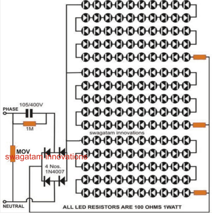 Today we are all aware regarding the bad effects of global warming and how it��s gripping our only planet day after day.
But for this we ourselves are to be blamed.
You may be thinking how a common person can contribute to help solve the problem.
Well look around you, yeah, it��s the lights that we are using presently generate quite an appreciable amount of heat to add to the global warming effect.
CFLs are considered to be quite efficient, but they too release quite a bit of heat.
The issue can be very easily solved simply by transforming our heat producing lights into the "cool" white LED lights.
We will learn in this article how simple it is to build a LED light tube that can easily replace your existing "hot" fluorescent tube lights!
Today we are all aware regarding the bad effects of global warming and how it��s gripping our only planet day after day.
But for this we ourselves are to be blamed.
You may be thinking how a common person can contribute to help solve the problem.
Well look around you, yeah, it��s the lights that we are using presently generate quite an appreciable amount of heat to add to the global warming effect.
CFLs are considered to be quite efficient, but they too release quite a bit of heat.
The issue can be very easily solved simply by transforming our heat producing lights into the "cool" white LED lights.
We will learn in this article how simple it is to build a LED light tube that can easily replace your existing "hot" fluorescent tube lights!
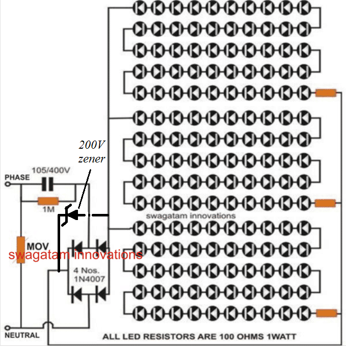 You will require the following Parts for the construction:
One 36 inches long, 2 inches in diameter white PVC pipe,
150 Nos.
White LEDs (5mm),
4 nos.
1N4007 diodes,
3 nos.
100 Ohms resistors,
1no.
1M resistor, 1/4 W,
1no.
Capacitor 105/400V, Polyester,
14/36 Wire for connections,
Soldering iron, solder wire etc.
You will require the following Parts for the construction:
One 36 inches long, 2 inches in diameter white PVC pipe,
150 Nos.
White LEDs (5mm),
4 nos.
1N4007 diodes,
3 nos.
100 Ohms resistors,
1no.
1M resistor, 1/4 W,
1no.
Capacitor 105/400V, Polyester,
14/36 Wire for connections,
Soldering iron, solder wire etc.
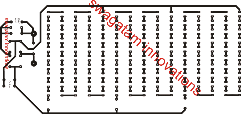 Video Clip showing the testing of a similar LED tubelight using 108 LED in series parallel combination
Below is a 50 LED Tube Light made by Merley, for your viewing pleasure:
Video Clip showing the testing of a similar LED tubelight using 108 LED in series parallel combination
Below is a 50 LED Tube Light made by Merley, for your viewing pleasure:
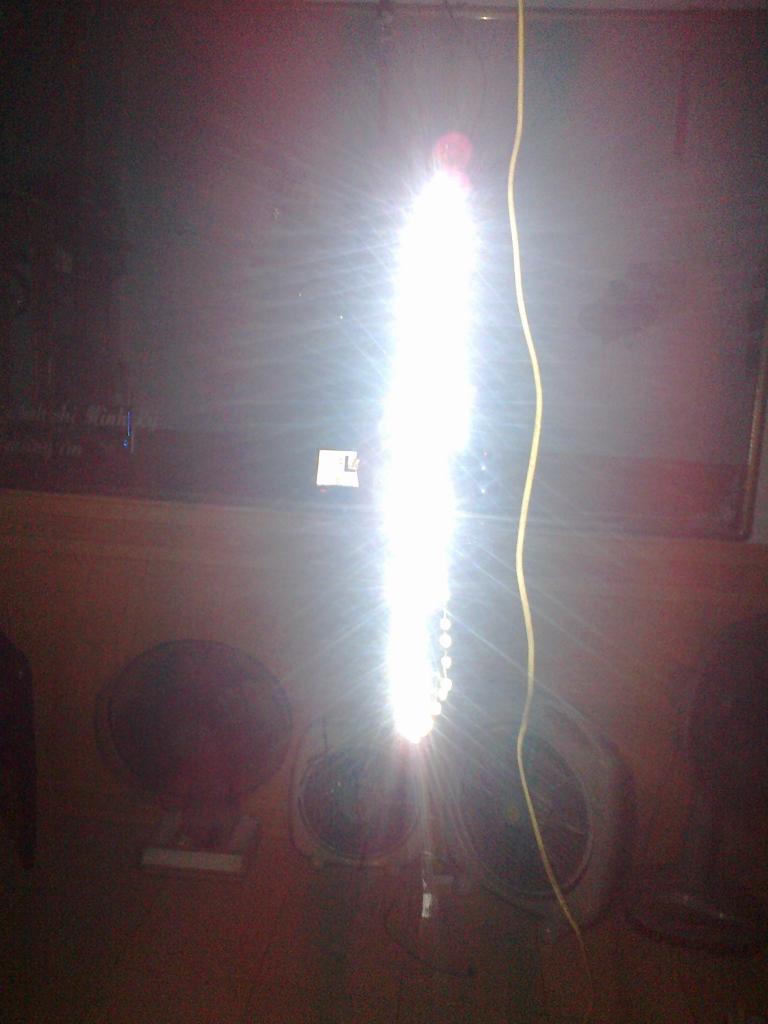 LED string light made by Mr.Bibin Edmond using the explained capacitive power supply.
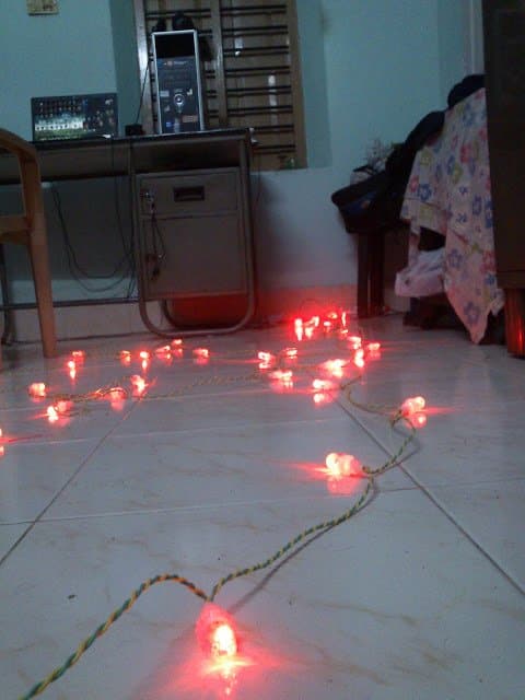 Here's the image of the simple capacitive PS circuit used for lighting the above string LED light.....
courtesy: Bibin Edmond
Here's the image of the simple capacitive PS circuit used for lighting the above string LED light.....
courtesy: Bibin Edmond
 In case you think that a transformerless based LED tubelight may not be reliable or not powerful enough, you can opt for a transformer based power supply design for accomplishing the same, as described below.
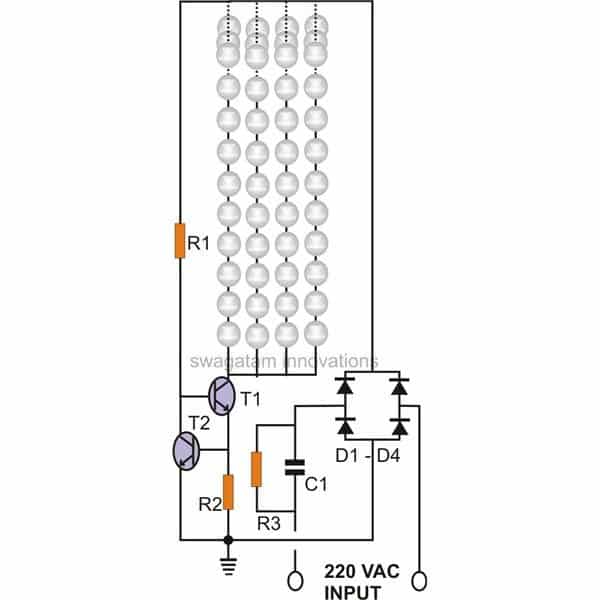
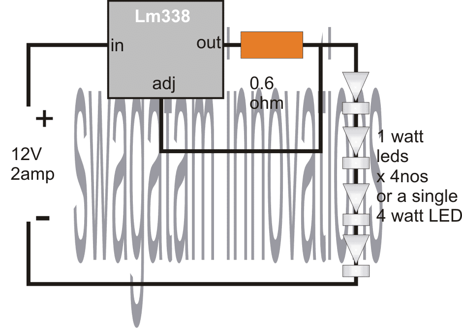
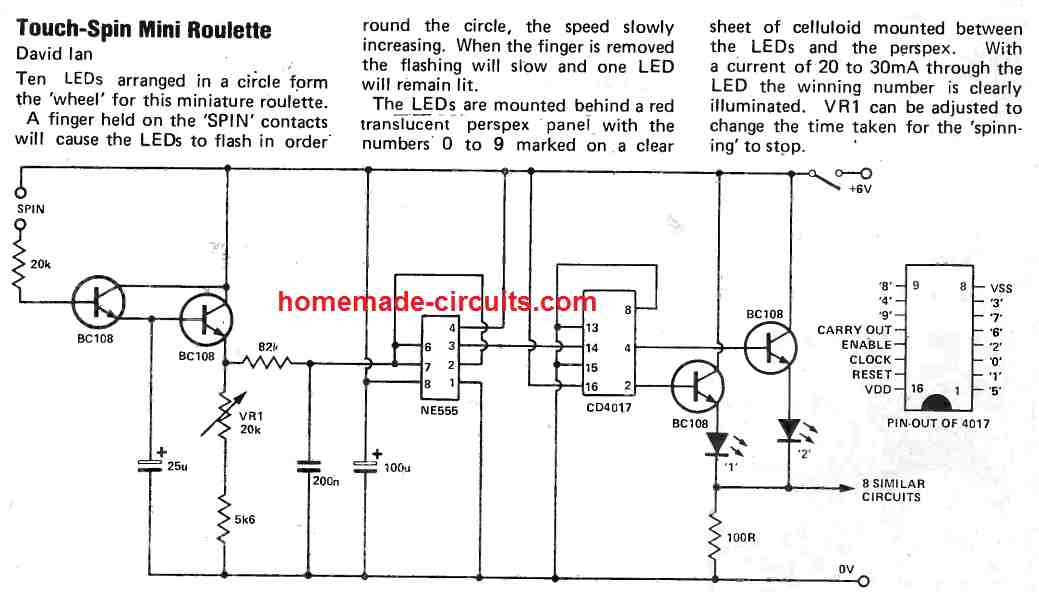
 The Wheel of Fortune circuit could be categorized into a range of specific stages; the LED display stage, an wheel sound audio stage, a voltage controlled oscillator, and a touch sensitive/monostable circuit.
While in the switched "off' condition resistor R1 maintains the IC1a input high and therefore the output of this gate, rigged like an inverter, stays low and C1 is discharged.
Connecting the touch pads allows the gate's output to turn high and causes C1 to charge up through D1.
As soon as the finger is taken off from the touch pads and the IC1a output becomes low again, C1 is prohibited from discharging into this gate as D1 now gets reverse biased, rather C1 discharges gradually through R2. The VCO is created through the elements involved with IC1b, c and d.
This wheel of fortune circuit actually produces a number of negative pulses with fixed time period split up by "gaps" whose length of time could be chnaged through the control voltage.
As soon as the control voltage (the voltage across capacitor C1) goes under a given limit which is of about 1 / 2 supply voltage the circuit stops oscillating.
In case if it is assumed that the voltage across capacitor C1 goes up to the supply voltage level, which could happen once the touch pads are contacted with the finger, capacitor C2 will begin to slowly charge.
The C2 voltage is provided by means of R4, to the schmitt trigger created by IC1a and b.
As the voltage delivered across the schmitt passes across its top switching limit, the IC1d output, which is responsible for inverting and buffering the schmitt's output, turns low.
This forces capacitor C2 to start discharging very fast through the fairly low impedance route provided by R6 and D2. As the voltage across capacitor C2 falls below the lower limit of the schmitt IC1d output turns high again allowing C2 to resume charging yet again.
The time consumed for C2 voltage to get to the schmitt's trigger level relies upon the voltage across C1.
Therefore once the voltage across the capacitor C1 become large enough, causes capacitor C2 to swiftly reach the activation stage and the VCO begins generating a high frequency, this frequency goes on becoming less and less as the voltage across C1 slowly drops.
The output voltage generated from the VCO is delivered to both IC3 to operate the connected LED ring and also to IC2a, b and c to generate the "tick-tick" audio output, imitating the roulette wheel rotation sound.
The crystal earpiece which is used for producing the "clicking" sound is operated through a bridge circuit.
This successfully causes voltage applied to the transducer to become twice in value and as a result, using the formula P = V^2/R, helps to create a louder audio output.
The LEDs are operated by IC3 whose cathodes can be seen hooked up by means of R7, to the IC2d output.
The output of this gate normally stays high, and turns low only when the voltage across the capacitor C1 goes over the half supply threshold.
With the IC3 outputs in the active high position, the wheel of fortune LED display is as a result gets enabled for a time slot that is a little bit extended compared to the time duration of the VCO's oscillation frequency.
Capacitors C3 and C4 are incorporated to enable the decoupling of the supply voltage, and capacitor C5 is included to protect against any RF disturbance that may affect the circuit's functioning adversely.
The Wheel of Fortune circuit could be categorized into a range of specific stages; the LED display stage, an wheel sound audio stage, a voltage controlled oscillator, and a touch sensitive/monostable circuit.
While in the switched "off' condition resistor R1 maintains the IC1a input high and therefore the output of this gate, rigged like an inverter, stays low and C1 is discharged.
Connecting the touch pads allows the gate's output to turn high and causes C1 to charge up through D1.
As soon as the finger is taken off from the touch pads and the IC1a output becomes low again, C1 is prohibited from discharging into this gate as D1 now gets reverse biased, rather C1 discharges gradually through R2. The VCO is created through the elements involved with IC1b, c and d.
This wheel of fortune circuit actually produces a number of negative pulses with fixed time period split up by "gaps" whose length of time could be chnaged through the control voltage.
As soon as the control voltage (the voltage across capacitor C1) goes under a given limit which is of about 1 / 2 supply voltage the circuit stops oscillating.
In case if it is assumed that the voltage across capacitor C1 goes up to the supply voltage level, which could happen once the touch pads are contacted with the finger, capacitor C2 will begin to slowly charge.
The C2 voltage is provided by means of R4, to the schmitt trigger created by IC1a and b.
As the voltage delivered across the schmitt passes across its top switching limit, the IC1d output, which is responsible for inverting and buffering the schmitt's output, turns low.
This forces capacitor C2 to start discharging very fast through the fairly low impedance route provided by R6 and D2. As the voltage across capacitor C2 falls below the lower limit of the schmitt IC1d output turns high again allowing C2 to resume charging yet again.
The time consumed for C2 voltage to get to the schmitt's trigger level relies upon the voltage across C1.
Therefore once the voltage across the capacitor C1 become large enough, causes capacitor C2 to swiftly reach the activation stage and the VCO begins generating a high frequency, this frequency goes on becoming less and less as the voltage across C1 slowly drops.
The output voltage generated from the VCO is delivered to both IC3 to operate the connected LED ring and also to IC2a, b and c to generate the "tick-tick" audio output, imitating the roulette wheel rotation sound.
The crystal earpiece which is used for producing the "clicking" sound is operated through a bridge circuit.
This successfully causes voltage applied to the transducer to become twice in value and as a result, using the formula P = V^2/R, helps to create a louder audio output.
The LEDs are operated by IC3 whose cathodes can be seen hooked up by means of R7, to the IC2d output.
The output of this gate normally stays high, and turns low only when the voltage across the capacitor C1 goes over the half supply threshold.
With the IC3 outputs in the active high position, the wheel of fortune LED display is as a result gets enabled for a time slot that is a little bit extended compared to the time duration of the VCO's oscillation frequency.
Capacitors C3 and C4 are incorporated to enable the decoupling of the supply voltage, and capacitor C5 is included to protect against any RF disturbance that may affect the circuit's functioning adversely.
 The following inquiry for making a single IC Strobe light circuit was sent to me by one of the keen readers of this blog, using the concept of IC 555 based LED strobe light effect generator circuit, let's learn the whole issue.
Thanks for this guide, I went by my local radio shack and picked up most of these components...Two
things I was not able to acquire was a 1m pot (all they had was a giant
sized pot in the 1m rating) and a 100k resistor (they were out)
I picked up a 4 pack of 22k resistors and wired them in series which gave me 88k which again is close.
I also picked up two 100k pots which i hoped could prove useful.
Knowing full well I don't have the recommended materials on the list I got an effect which didn't much resemble a strobe.
Using the 100k pot there is some variance in the flash speed but it isn't really slow to really fast.
Also my led never goes all the way out using this, again possibly my fault for having the wrong components.
The following inquiry for making a single IC Strobe light circuit was sent to me by one of the keen readers of this blog, using the concept of IC 555 based LED strobe light effect generator circuit, let's learn the whole issue.
Thanks for this guide, I went by my local radio shack and picked up most of these components...Two
things I was not able to acquire was a 1m pot (all they had was a giant
sized pot in the 1m rating) and a 100k resistor (they were out)
I picked up a 4 pack of 22k resistors and wired them in series which gave me 88k which again is close.
I also picked up two 100k pots which i hoped could prove useful.
Knowing full well I don't have the recommended materials on the list I got an effect which didn't much resemble a strobe.
Using the 100k pot there is some variance in the flash speed but it isn't really slow to really fast.
Also my led never goes all the way out using this, again possibly my fault for having the wrong components.
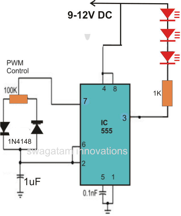

 In the above example, the current though the LED could be calculated using Ohm's law.
However, the LED may not begin to illuminate properly until its minimum forward voltage level is applied, which may be anywhere between 2 V to 2.5 V (for RED LED), therefore the formula which can be applied for calculating the current through the LED will be
I = (6 - 2) / R
In the above example, the current though the LED could be calculated using Ohm's law.
However, the LED may not begin to illuminate properly until its minimum forward voltage level is applied, which may be anywhere between 2 V to 2.5 V (for RED LED), therefore the formula which can be applied for calculating the current through the LED will be
I = (6 - 2) / R
 However, such resistive dividers can be used for generating reference voltages, only for high impedance sources.
The output cannot be used for a operating a load directly, since the involved resistors would make the current significantly low.
However, such resistive dividers can be used for generating reference voltages, only for high impedance sources.
The output cannot be used for a operating a load directly, since the involved resistors would make the current significantly low.
 The working details of the wheatstone bridge, and how to find precise results using this network is explained in the diagram above.

 The charging process can be delayed or made slower by adding a resistor in series with the supply input, as depicted in the above diagrams.
 The discharging process is also similar but in the opposite way.
The capacitor will instantly discharge when its leads are shorted together.
The discharge process could be proportionately slowed down by adding a resistor in series with the leads.
The discharging process is also similar but in the opposite way.
The capacitor will instantly discharge when its leads are shorted together.
The discharge process could be proportionately slowed down by adding a resistor in series with the leads.
 When connected in series the capacitance value decreases, for example when two 1 uF capacitors are connected in series, the resultant value becomes 0.5 uF.
This seems to be just the opposite of resistors.
When connected in series connection, it adds up the voltage rating or the breakdown voltage values of the capacitors.
For example, when two 25 V rated capacitors are connected in series, their voltage tolerance range adds up and increases to 50 V
When connected in series the capacitance value decreases, for example when two 1 uF capacitors are connected in series, the resultant value becomes 0.5 uF.
This seems to be just the opposite of resistors.
When connected in series connection, it adds up the voltage rating or the breakdown voltage values of the capacitors.
For example, when two 25 V rated capacitors are connected in series, their voltage tolerance range adds up and increases to 50 V
 Capacitors can be also connected in parallel by joining their leads in common, as shown in the above diagram.
For polarized capacitors, the terminals with like poles must be connected with each other, for non-polar caps this restriction can be ignored.
When connected in parallel, the resultant total value of capacitors increases, which is just the opposite in the case of resistors.
Important: A charged capacitor can hold the charge between its terminals for a significantly long time.
If the voltage is high enough in the range of 100 V and higher can inflict painful shock if the leads are touched.
Smaller levels of voltages can have enough power to even melt a small piece of metal when the metal is brought between the leads of the capacitor.
Capacitors can be also connected in parallel by joining their leads in common, as shown in the above diagram.
For polarized capacitors, the terminals with like poles must be connected with each other, for non-polar caps this restriction can be ignored.
When connected in parallel, the resultant total value of capacitors increases, which is just the opposite in the case of resistors.
Important: A charged capacitor can hold the charge between its terminals for a significantly long time.
If the voltage is high enough in the range of 100 V and higher can inflict painful shock if the leads are touched.
Smaller levels of voltages can have enough power to even melt a small piece of metal when the metal is brought between the leads of the capacitor.
 DC Blocking: A capacitor can be used in series connection to block a DC voltage and pass an AC or pulsating DC content through it.
This feature allows audio equipment to use capacitors at their input/output connections to enable the passage of the audio frequencies, and prevent the unwanted DC voltage from entering the amplification line.
DC Blocking: A capacitor can be used in series connection to block a DC voltage and pass an AC or pulsating DC content through it.
This feature allows audio equipment to use capacitors at their input/output connections to enable the passage of the audio frequencies, and prevent the unwanted DC voltage from entering the amplification line.
 Power Supply Filter: Capacitors also work as DC supply filters in power supply circuits.
In a power supply, after rectification of the AC signal the resultant DC may be full of ripple fluctuations.
A large value capacitor connected across this ripple voltage results in a significant amount filtration causing the fluctuating DC to become a constant DC with ripples reduced to an amount as determined by the value of the capacitor.
Power Supply Filter: Capacitors also work as DC supply filters in power supply circuits.
In a power supply, after rectification of the AC signal the resultant DC may be full of ripple fluctuations.
A large value capacitor connected across this ripple voltage results in a significant amount filtration causing the fluctuating DC to become a constant DC with ripples reduced to an amount as determined by the value of the capacitor.

 The function of an integator circuit is to shape a square wave signal into a triangle waveform, through a resistor, capacitor or RC network, as shown in the above figure.
Here we can see the resistor is at the input side, and is connected in series with the line, while the capacitor is connected on the output side, across the resistor output end and the ground line.
The RC components act like a time constant element in the circuit, whose product must be 10 times higher than the period of the input signal.
Otherwise, it may cause the amplitude of the output triangle wave to be reduced.
In such conditions the circuit will function like a low pass filter blocking high frequency inputs.
The function of an integator circuit is to shape a square wave signal into a triangle waveform, through a resistor, capacitor or RC network, as shown in the above figure.
Here we can see the resistor is at the input side, and is connected in series with the line, while the capacitor is connected on the output side, across the resistor output end and the ground line.
The RC components act like a time constant element in the circuit, whose product must be 10 times higher than the period of the input signal.
Otherwise, it may cause the amplitude of the output triangle wave to be reduced.
In such conditions the circuit will function like a low pass filter blocking high frequency inputs.
 The function of a differentiator circuit is to convert a square wave input signal into a spiked waveform having a sharp rising and a slow falling waveform.
The value of the RC time constant in this case must be 1/10th of the input cycles.
Differentiator circuits are normally used for generating short and sharp trigger pulses.
The function of a differentiator circuit is to convert a square wave input signal into a spiked waveform having a sharp rising and a slow falling waveform.
The value of the RC time constant in this case must be 1/10th of the input cycles.
Differentiator circuits are normally used for generating short and sharp trigger pulses.

 As we discussed in the previous paragraph, diodes require around 0.6 V to begin conducting, this also means that the diode would drop this level of voltage across its output and ground.
For example, if 1 V is applied, the diode will produce 1 - 0.6 = 0.4 V at its cathode.
This feature allows diodes to be used as voltage dropper.
Any desired voltage drop can be achieved by connecting the corresponding number of diodes in series.
Therefore if 4 diodes are connected in series, it will create a total deduction of 0.6 x 4 = 2.4 V at the output and so on.
The formula for calculating this given below:
Output Voltage = Input Voltage - (no of diodes x 0.6)
As we discussed in the previous paragraph, diodes require around 0.6 V to begin conducting, this also means that the diode would drop this level of voltage across its output and ground.
For example, if 1 V is applied, the diode will produce 1 - 0.6 = 0.4 V at its cathode.
This feature allows diodes to be used as voltage dropper.
Any desired voltage drop can be achieved by connecting the corresponding number of diodes in series.
Therefore if 4 diodes are connected in series, it will create a total deduction of 0.6 x 4 = 2.4 V at the output and so on.
The formula for calculating this given below:
Output Voltage = Input Voltage - (no of diodes x 0.6)
 Diodes due to their forward voltage dropping feature can be also used for generating stable reference voltages, as shown in the adjoining diagram.
The output voltage can be calculated through the following formula:
R1 = (Vin - Vout) / I
Make sure to use proper wattage rating for the D1 and R1 components as per the wattage of the load.
They must be rated at least two times more than the load.
Diodes due to their forward voltage dropping feature can be also used for generating stable reference voltages, as shown in the adjoining diagram.
The output voltage can be calculated through the following formula:
R1 = (Vin - Vout) / I
Make sure to use proper wattage rating for the D1 and R1 components as per the wattage of the load.
They must be rated at least two times more than the load.
 Diodes can also work as triangle wave to sine wave converter, as indicated in the above diagram.
The amplitude of the output sine wave will depend on the number of diodes in series with D1, and D2.
Diodes can also work as triangle wave to sine wave converter, as indicated in the above diagram.
The amplitude of the output sine wave will depend on the number of diodes in series with D1, and D2.
 Diodes may be also configured for getting peak voltage reading on a voltmeter.
Here, the diode works like a half wave rectifier, allowing half cycles of the frequency to charge the capacitor C1 to the peak value of the input voltage.
The meter then shows this peak value through its deflection.
Diodes may be also configured for getting peak voltage reading on a voltmeter.
Here, the diode works like a half wave rectifier, allowing half cycles of the frequency to charge the capacitor C1 to the peak value of the input voltage.
The meter then shows this peak value through its deflection.
 This is one of the very common applications of diode, which uses a diode to protect a circuit against accidental reverse supply connection.
 A moving coil meter can be a very sensitive piece of instrument, which can get severely damaged if the supply input is reversed.
A diode connected in parallel can protect the meter from this situation.
A moving coil meter can be a very sensitive piece of instrument, which can get severely damaged if the supply input is reversed.
A diode connected in parallel can protect the meter from this situation.
 A diode can be used to chop and clip off the peaks of a waveform, as shown in the above diagram, and create an output with reduced average value waveform.
The resistor R2 can be a pot for adjusting the clipping level.
A diode can be used to chop and clip off the peaks of a waveform, as shown in the above diagram, and create an output with reduced average value waveform.
The resistor R2 can be a pot for adjusting the clipping level.
 The first clipper circuit has the capability of clipping the positive section of the waveform.
For enabling clipping of both the ends of an input waveform, two diodes could be used in parallel with opposite polarity, as shown above.
The first clipper circuit has the capability of clipping the positive section of the waveform.
For enabling clipping of both the ends of an input waveform, two diodes could be used in parallel with opposite polarity, as shown above.
 When a diode is used as a half wave rectifier with an AC input, it blocks the half reverse input AC cycles, and allows only the other half to pass through it, creating half wave cycle outputs, hence the name half wave rectifier.
Since the AC half cycle are removed by the diode, the output becomes DC and the circuit is also called half wave DC converter circuit.
Without a filter capacitor, the output will be a pulsating half wave DC.
When a diode is used as a half wave rectifier with an AC input, it blocks the half reverse input AC cycles, and allows only the other half to pass through it, creating half wave cycle outputs, hence the name half wave rectifier.
Since the AC half cycle are removed by the diode, the output becomes DC and the circuit is also called half wave DC converter circuit.
Without a filter capacitor, the output will be a pulsating half wave DC.
 The previous diagram can be modified using two diodes, for getting two separate outputs with opposite halves of the AC rectified into corresponding DC polarities.
 A full wave rectfier, or a bridge rectifier is a circuit built using 4 rectifier diodes in a bridged configuration, as depicted in the above figure.
The specialty of this bridge rectifier circuit is that it is able to convert both the positive and the negative half cycles of the input into a full wave DC output.
The pulsating DC at the output of the bridge will have a frequency twice of the input AC due to the inclusion of the negative and the positive half cycle pulses into a single positive pulse chain.
A full wave rectfier, or a bridge rectifier is a circuit built using 4 rectifier diodes in a bridged configuration, as depicted in the above figure.
The specialty of this bridge rectifier circuit is that it is able to convert both the positive and the negative half cycles of the input into a full wave DC output.
The pulsating DC at the output of the bridge will have a frequency twice of the input AC due to the inclusion of the negative and the positive half cycle pulses into a single positive pulse chain.
 Diodes can be also implemented as voltage doubler by cascading a couple diodes with a couple of electrolytic capacitors.
The input should be in the form of pulsating DC or an AC, which causes the output to generate approximately two time more voltage than the input.
The input pulsating frequency can be from a IC 555 oscillator.
Diodes can be also implemented as voltage doubler by cascading a couple diodes with a couple of electrolytic capacitors.
The input should be in the form of pulsating DC or an AC, which causes the output to generate approximately two time more voltage than the input.
The input pulsating frequency can be from a IC 555 oscillator.
 A DC to DC voltage doubler could be also implemented using a bridge rectifier and a couple of electrolytic filter capacitors, as shown in the above diagram.
Using a bridge rectifier will result in higher efficiency of the doubling effect in terms of current compared to the previous cascaded doubler.
A DC to DC voltage doubler could be also implemented using a bridge rectifier and a couple of electrolytic filter capacitors, as shown in the above diagram.
Using a bridge rectifier will result in higher efficiency of the doubling effect in terms of current compared to the previous cascaded doubler.
 The above explained voltage multiplier circuits are designed to generate 2 times more output than the input peak levels, however, if an application needs even higher levels of multiplication in the order of 4 times more voltage then the this voltage quadrupler circuit could be applied.
Here, the circuit is made using 4 numbers of cascaded diodes and capacitors for getting 4 times more voltage at the output then the input frequency peak.
The above explained voltage multiplier circuits are designed to generate 2 times more output than the input peak levels, however, if an application needs even higher levels of multiplication in the order of 4 times more voltage then the this voltage quadrupler circuit could be applied.
Here, the circuit is made using 4 numbers of cascaded diodes and capacitors for getting 4 times more voltage at the output then the input frequency peak.
 Diodes can be wired to imitate an OR logic gate using the circuit as shown above.
The adjoining truth table shows the output logic in response to a combination of two logic inputs.
Diodes can be wired to imitate an OR logic gate using the circuit as shown above.
The adjoining truth table shows the output logic in response to a combination of two logic inputs.
 Just like an OR gate, a NOR gate can be also replicated using a couple of diodes as shown above.
 It may be also possible to implement other logic gates such as AND gate and NAND gate using diodes as exhibited in the above diagrams.
The truth tables shown beside the diagrams provide the exact required logic response from the set ups.
It may be also possible to implement other logic gates such as AND gate and NAND gate using diodes as exhibited in the above diagrams.
The truth tables shown beside the diagrams provide the exact required logic response from the set ups.

 A zener diode can be used to create stabilized voltage outputs as shown in the adjoining diagram, by using a limiting resistor.
The limiting resistor R1 limit the maximum tolerable current for the zener and protects it from burning due to over current.
A zener diode can be used to create stabilized voltage outputs as shown in the adjoining diagram, by using a limiting resistor.
The limiting resistor R1 limit the maximum tolerable current for the zener and protects it from burning due to over current.
 Since zener diodes are available with a variety of breakdown voltage levels, the facility could be applied for making an effective yet simple voltage indicator using appropriate zener rating as shown in the above diagram.
 Zener diodes can be also used for shifting a voltage level to some other level, by using suitable zener diode values, as per the needs of the application.
 Zener diodes being a voltage controlled switch can be applied to clip the amplitude of an AC waveform to a lower desired level depending on its breakdown rating, as shown in the diagram above.
 A BJT switch as explained in the previous paragraph can be also wired as voltage inverter, meaning for creating output response opposite to the input response.
In the example above, the output LED will switch ON in the absence of a voltage at point A, and will switch OFF in the presence of a voltage at point A.
A BJT switch as explained in the previous paragraph can be also wired as voltage inverter, meaning for creating output response opposite to the input response.
In the example above, the output LED will switch ON in the absence of a voltage at point A, and will switch OFF in the presence of a voltage at point A.


 The above single transistor will generate the similar kind of white noise, when its output is connected to a suitable amplifier.
 This switch debouncer switch can be used with a push button switch to ensure that the circuit which is being controlled by the push button is never rattled or disturbed due to voltage transients generated while releasing the switch.When the switch is pressed the output become 0 V instantly and when released the output turns high in slow mode without causing any issues to the attached circuit stages.
 A fairly accurate analogue frequency meter module could be built using the single transistor circuit shown above.
The input frequency should be 1 V peak to peak.
The frequency range can be adjusted by using different values for C1, and by setting the R2 pot appropriately.
A fairly accurate analogue frequency meter module could be built using the single transistor circuit shown above.
The input frequency should be 1 V peak to peak.
The frequency range can be adjusted by using different values for C1, and by setting the R2 pot appropriately.
 Only a couple of BJTs and a few resistors are required to create a useful pulse generator circuit module as shown in the figure above.
The pulse width can be adjusted using different values for C1, while R3 can be used for adjusting the pulse frequency.
Only a couple of BJTs and a few resistors are required to create a useful pulse generator circuit module as shown in the figure above.
The pulse width can be adjusted using different values for C1, while R3 can be used for adjusting the pulse frequency.
 This ammeter amplifier module can be used for measuring extremely small current magnitudes in the range of microamperes, into readable output across a 1 mA ammeter.
 An LED will begin flashing at a specified as soon as an ambient light or an external light is detected over an attached light sensor.
The application of this light sensitive flasher may be diverse and very much customizable, depending on user preferences.
An LED will begin flashing at a specified as soon as an ambient light or an external light is detected over an attached light sensor.
The application of this light sensitive flasher may be diverse and very much customizable, depending on user preferences.
 Quite similar, but with opposite effects to the above application, this module will begin flashing an LED as soon as the ambient light level drops to almost darkness, or as set by the R1, R2 potential divider network.
 A high power flasher module can be constructed using just a couple of transistor as shown in the above schematic.
The unit will blink or flash a connected incandescent or halogen lamp brightly, and the power of this lamp can be upgraded by suitably upgrading the specs of the Q2.
A high power flasher module can be constructed using just a couple of transistor as shown in the above schematic.
The unit will blink or flash a connected incandescent or halogen lamp brightly, and the power of this lamp can be upgraded by suitably upgrading the specs of the Q2.
 The figure above shows, an FET configured like a switch for toggling an LED ON/OFF in response to a 9V and 0V input signal at its gate.
Unlike a BJT which can switch ON/OFF an output load in response to an input signal as low as 0.6 V, an FET will do the same but with an input signal of around 9V to 12 V.
However, the 0.6 V for a BJT is current dependent and the current with 0.6 V has to be correspondingly high or low with respect to the load current.
Contrary to this, the input gate drive current for an FET is not load dependent and can be as low as a microampere.
The figure above shows, an FET configured like a switch for toggling an LED ON/OFF in response to a 9V and 0V input signal at its gate.
Unlike a BJT which can switch ON/OFF an output load in response to an input signal as low as 0.6 V, an FET will do the same but with an input signal of around 9V to 12 V.
However, the 0.6 V for a BJT is current dependent and the current with 0.6 V has to be correspondingly high or low with respect to the load current.
Contrary to this, the input gate drive current for an FET is not load dependent and can be as low as a microampere.
 Quite like a BJT, you can also wire an FET for amplifying extremely low current input signals to an amplified high current high voltage output, as indicated the figure above.
 If you are wondering how to use a Field Effect Transistor for constructing a Hi-Z or a High impedance MIC amplifier circuit, then the above explained design might help you in accomplishing the objective.
 An FET can be also used as an audio signal mixer, as illustrated in the diagram above.
Two audio signals fed across points A and B are mixed together by the FET and merged at the output via C4.
An FET can be also used as an audio signal mixer, as illustrated in the diagram above.
Two audio signals fed across points A and B are mixed together by the FET and merged at the output via C4.
 When S1 is pushed ON, the supply gets stored inside the C1 capacitor, and the voltage also switches ON the FET.
When S1 is released, the stored charge inside C1 continues to keep the FET ON.
However, the FET being a high impedance input device does not allow the C1 to discharge quickly and therefore the FET remains switched ON for a pretty long time.
In the meantime, as long as the FET Q1 stays ON, the attached BJT Q2 remains switched OFF, due the inverting action of the FET which keeps the Q2 base grounded.
The situation also keeps the buzzer switched OFF.
Eventually, and gradually the C1 discharges to a point where the FET is unable to remain switched ON.
This reverts the condition at the base of Q1, which now switches ON and activates the connected buzzer alarm.
When S1 is pushed ON, the supply gets stored inside the C1 capacitor, and the voltage also switches ON the FET.
When S1 is released, the stored charge inside C1 continues to keep the FET ON.
However, the FET being a high impedance input device does not allow the C1 to discharge quickly and therefore the FET remains switched ON for a pretty long time.
In the meantime, as long as the FET Q1 stays ON, the attached BJT Q2 remains switched OFF, due the inverting action of the FET which keeps the Q2 base grounded.
The situation also keeps the buzzer switched OFF.
Eventually, and gradually the C1 discharges to a point where the FET is unable to remain switched ON.
This reverts the condition at the base of Q1, which now switches ON and activates the connected buzzer alarm.
 This design does exactly similar to the above concept, except for the inverting BJT stage, which isn't present here.
Due to this reason, the FET acts like a delay OFF timer.
Meaning, the output remains ON initially while the capacitor C1 is discharging, and the FET is switched ON, and ultimately when the C1 is fully discharged, the FET switches OFF and the buzzer sounds.
This design does exactly similar to the above concept, except for the inverting BJT stage, which isn't present here.
Due to this reason, the FET acts like a delay OFF timer.
Meaning, the output remains ON initially while the capacitor C1 is discharging, and the FET is switched ON, and ultimately when the C1 is fully discharged, the FET switches OFF and the buzzer sounds.

 This a very simple FET astable circuit that can be used for alternately flashing two LEDs across the two drains f the MOSFETs.
The good aspect of this astable is that the LEDs will switch at a well defined sharp ON/OFF rate without any dimming effect or slow fade and rise.
The flashing rate could be adjusted through the pot R3.
This a very simple FET astable circuit that can be used for alternately flashing two LEDs across the two drains f the MOSFETs.
The good aspect of this astable is that the LEDs will switch at a well defined sharp ON/OFF rate without any dimming effect or slow fade and rise.
The flashing rate could be adjusted through the pot R3.


 Piezo buzzers can be used for indicating a logic high or low conditions in circuit through the following shown circuit.


 As soon as the light level on the phototransistor exceeds a set triggering threshold level of the SCR, the SCR triggers and latches ON, switch ON the relay.
The latching remains as is until the reset switch S1 is pressed as sufficient darkness, or the power is switched OFF and then ON..
As soon as the light level on the phototransistor exceeds a set triggering threshold level of the SCR, the SCR triggers and latches ON, switch ON the relay.
The latching remains as is until the reset switch S1 is pressed as sufficient darkness, or the power is switched OFF and then ON..
 The oscillator frequency will produce a low frequency tone over the connected speaker.
The tone frequency of this relaxation oscillator can be adjusted through variable resistor R1, and R2, and also the capacitor C1.
The oscillator frequency will produce a low frequency tone over the connected speaker.
The tone frequency of this relaxation oscillator can be adjusted through variable resistor R1, and R2, and also the capacitor C1.
 A UJT normally is renowned for its reliable oscillatory functions.
However, the same device can be also used with triac for enabling a 0 to full speed control of AC motors.
The resistor R1 functions like a frequency control adjustment for the UJT frequency.
This variable frequency output switches the triac at different ON/OFF rates depending on the R1 adjustments.
This variable switching of the triac in turn causes a proportionate amount of variations on the speed of the connected motor.
A UJT normally is renowned for its reliable oscillatory functions.
However, the same device can be also used with triac for enabling a 0 to full speed control of AC motors.
The resistor R1 functions like a frequency control adjustment for the UJT frequency.
This variable frequency output switches the triac at different ON/OFF rates depending on the R1 adjustments.
This variable switching of the triac in turn causes a proportionate amount of variations on the speed of the connected motor.
 The basic electronic circuit diagram above shows how simply a triac can be switched ON OFF through an ON/OFF switch and also ensure safety to the triac by using the load itself as a buffer stage.
The R1 limits the current to the triac gate, while the load additionally provide the triac gate protection from sudden switch ON transients, and allows the triac to switch ON with a soft start mode.
The basic electronic circuit diagram above shows how simply a triac can be switched ON OFF through an ON/OFF switch and also ensure safety to the triac by using the load itself as a buffer stage.
The R1 limits the current to the triac gate, while the load additionally provide the triac gate protection from sudden switch ON transients, and allows the triac to switch ON with a soft start mode.
 The pot R1 is used for adjusting the oscillating rate or frequency, which in turn determines the ON/OFF switching rate of the triac and the connected lamp.
The switching frequency being too high, the lamp seems to ne ON permanently, although it intensity varies due to the average voltage across it varying in accordance with the UJT switching.
The pot R1 is used for adjusting the oscillating rate or frequency, which in turn determines the ON/OFF switching rate of the triac and the connected lamp.
The switching frequency being too high, the lamp seems to ne ON permanently, although it intensity varies due to the average voltage across it varying in accordance with the UJT switching.
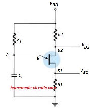 Here the components RT and CT work like the timing elements and determine the frequency or the oscillation rate of the UJT circuit.
For calculating the oscillating frequency we can use the following formula, which incorporates the unijunction transistor intrinsic stand-off ratio �� as one of the parameters along with RT and CT for determining the oscillating pulses.
Here the components RT and CT work like the timing elements and determine the frequency or the oscillation rate of the UJT circuit.
For calculating the oscillating frequency we can use the following formula, which incorporates the unijunction transistor intrinsic stand-off ratio �� as one of the parameters along with RT and CT for determining the oscillating pulses.
 The standard value of the stand-off ratio for a typical UJT device is between 0.4 and 0.6.
Thus considering the value of �� = 0.5, and substituting it in the above equation we get:
The standard value of the stand-off ratio for a typical UJT device is between 0.4 and 0.6.
Thus considering the value of �� = 0.5, and substituting it in the above equation we get:
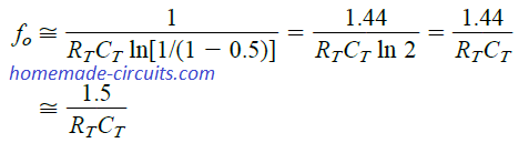 When the supply is switched ON, the voltage through the resistor RT charges the capacitor CT towards the supply level VBB.
Now, the stand-off voltage Vp is determined by Vp across B1 - B2, in conjunction with the UJT stand-off ratio �� as: Vp = ��VB1VB2 - VD.
For so long the the voltage VE across the capacitor stays lower than the Vp, the UJT terminals across B1, B2 exhibits an open circuit.
But the moment the voltage across CT goes beyond Vp, the unijunction transistor fires, quickly discharging the capacitor, and initiating a fresh cycle.
During the firing instance of the UJT, results in the potential across R1 to rise, and the potential across R2 to drop.
When the supply is switched ON, the voltage through the resistor RT charges the capacitor CT towards the supply level VBB.
Now, the stand-off voltage Vp is determined by Vp across B1 - B2, in conjunction with the UJT stand-off ratio �� as: Vp = ��VB1VB2 - VD.
For so long the the voltage VE across the capacitor stays lower than the Vp, the UJT terminals across B1, B2 exhibits an open circuit.
But the moment the voltage across CT goes beyond Vp, the unijunction transistor fires, quickly discharging the capacitor, and initiating a fresh cycle.
During the firing instance of the UJT, results in the potential across R1 to rise, and the potential across R2 to drop.
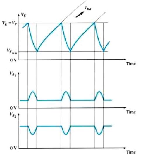
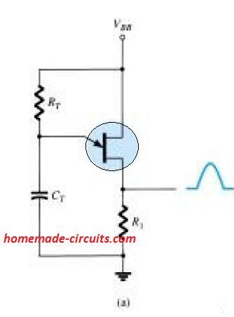
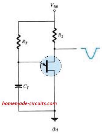
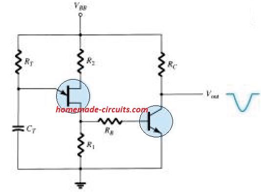 The resultant waveform across the emitter of the UJT produces a sawtooth signal, which exhibits a positive-going potential at B2, and a negative-going potential at B1 leads of the UJT
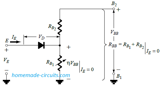 Figure #3
The equivalent UJT circuit can be witnessed in the above shown image.
We can find how relatively simple this equivalent circuit appears to be, which includes a couple of resistors (one fixed, one adjustable) and a solitary diode.
The resistance RB1 is displayed as a adjustable resistor considering its value will change as the current IE changes.
Actually, in any transistor that represents a unijunction, RB1 may fluctuate from 5 k�� down to 50 �� for any equivalent change of IE from 0 to 50 = ��A.
The interbase resistance RBB represents the resistance of the device between terminals B1 and B2 when IE = 0. In formula for this is,
RBB = (RB1 + RB2)| IE = 0
The range of RBB is normally within 4 and 10 k.
The aluminum rod placement as shown in the first figure provides the relative magnitudes of RB1, RB2 when IE = 0. We can estimate the value of VRB1 (when IE = 0) using the voltage-divider law, as given below:
VRB1 = (RB1 x VBB) / (RB1 + RB2) = ��VBB (with IE = 0)
The Greek letter �� (eta) is known as the intrinsic stand-off ratio of the unijunction transistor device and is defined by:
�� = RB1 / (RB1 + RB2)( with IE = 0) = RB1 / RBB
For the indicated emitter voltage (VE) higher than VRB1( = ��VBB) by the diode's forward voltage drop VD (0.35 �� 0.70 V), the diode will get triggered ON.
Ideally we may assume the short-circuit condition, such that IE will start to conduct via RB1. Through equation, the triggering voltage level of the emitter can be expressed as:
VP = ��VBB + VD
Figure #3
The equivalent UJT circuit can be witnessed in the above shown image.
We can find how relatively simple this equivalent circuit appears to be, which includes a couple of resistors (one fixed, one adjustable) and a solitary diode.
The resistance RB1 is displayed as a adjustable resistor considering its value will change as the current IE changes.
Actually, in any transistor that represents a unijunction, RB1 may fluctuate from 5 k�� down to 50 �� for any equivalent change of IE from 0 to 50 = ��A.
The interbase resistance RBB represents the resistance of the device between terminals B1 and B2 when IE = 0. In formula for this is,
RBB = (RB1 + RB2)| IE = 0
The range of RBB is normally within 4 and 10 k.
The aluminum rod placement as shown in the first figure provides the relative magnitudes of RB1, RB2 when IE = 0. We can estimate the value of VRB1 (when IE = 0) using the voltage-divider law, as given below:
VRB1 = (RB1 x VBB) / (RB1 + RB2) = ��VBB (with IE = 0)
The Greek letter �� (eta) is known as the intrinsic stand-off ratio of the unijunction transistor device and is defined by:
�� = RB1 / (RB1 + RB2)( with IE = 0) = RB1 / RBB
For the indicated emitter voltage (VE) higher than VRB1( = ��VBB) by the diode's forward voltage drop VD (0.35 �� 0.70 V), the diode will get triggered ON.
Ideally we may assume the short-circuit condition, such that IE will start to conduct via RB1. Through equation, the triggering voltage level of the emitter can be expressed as:
VP = ��VBB + VD
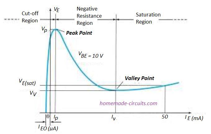 Figure #4
We can see that, for emitter potential indicated at the left side of the peak point, the IE value never exceeds the IEO (which is in microamperes).
The current IEO more or less follows the reverse leakage current ICO of the conventional bipolar transistor.
This region, is referred to as the cutoff region, as also indicated in the fig.
As soon as conduction is achieved at VE = VP, the emitter potential VE decreases as IE potential increases, which is precisely in accordance with the decreasing resistance RB1 for increasing current IE, as explained previously.
The above characteristic provides a unijunction transistor with a highly stable negative resistance region, that enables the device to work and to be applied with extreme reliability.
During the above process, the valley point could be expected to be finally attained, and any increase in IE beyond this range causes the device to enter the saturation region.
The figure #3 shows a diode equivalent circuit in the same region with a similar characteristics approach.
The drop in the resistance value of the device in the active region is caused on account of the injected holes into the n-type block by the p-type aluminum rod as soon as the firing of the device happens.
This results in an increase in the quantity of holes on the n-type section increases the free electrons number, causing an enhanced conductivity (G) across the device with an equivalent decrease in its resistance (R �� = 1/G ��)
Figure #4
We can see that, for emitter potential indicated at the left side of the peak point, the IE value never exceeds the IEO (which is in microamperes).
The current IEO more or less follows the reverse leakage current ICO of the conventional bipolar transistor.
This region, is referred to as the cutoff region, as also indicated in the fig.
As soon as conduction is achieved at VE = VP, the emitter potential VE decreases as IE potential increases, which is precisely in accordance with the decreasing resistance RB1 for increasing current IE, as explained previously.
The above characteristic provides a unijunction transistor with a highly stable negative resistance region, that enables the device to work and to be applied with extreme reliability.
During the above process, the valley point could be expected to be finally attained, and any increase in IE beyond this range causes the device to enter the saturation region.
The figure #3 shows a diode equivalent circuit in the same region with a similar characteristics approach.
The drop in the resistance value of the device in the active region is caused on account of the injected holes into the n-type block by the p-type aluminum rod as soon as the firing of the device happens.
This results in an increase in the quantity of holes on the n-type section increases the free electrons number, causing an enhanced conductivity (G) across the device with an equivalent decrease in its resistance (R �� = 1/G ��)
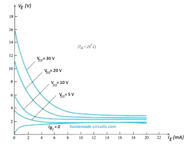 Figure #5
Here we can observe that IEO(��A) is unnoticeable because the horizontal scale is calibrated in milliamperes.
Each of the curve intersecting the vertical axis is the corresponding results of VP.
For constant values of �� and VD, the VP value changes in accordance with VBB, as formulated below:
Figure #5
Here we can observe that IEO(��A) is unnoticeable because the horizontal scale is calibrated in milliamperes.
Each of the curve intersecting the vertical axis is the corresponding results of VP.
For constant values of �� and VD, the VP value changes in accordance with VBB, as formulated below:
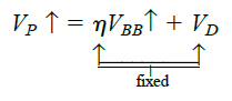
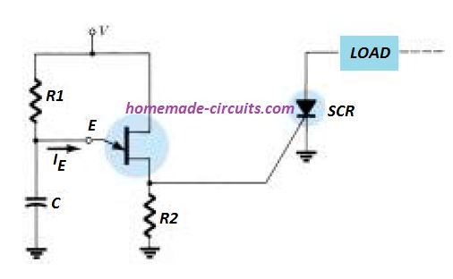 Figure #6: Triggering an SCR using an UJT
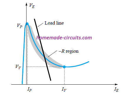 Figure #7: UJT Load line for a triggering for an external device like SCR
The main timing components are formed by R1 and C, while R2 works like a pull down resistors for the output triggering voltage.
Figure #7: UJT Load line for a triggering for an external device like SCR
The main timing components are formed by R1 and C, while R2 works like a pull down resistors for the output triggering voltage.
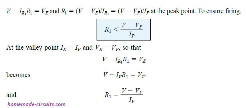 Alternatively, in order to guarantee a complete SCR turn off :
R1 > (V - Vv) / Iv
This implies that the selection range of the resistor R1 has to be as expressed as given below:
(V - Vv) / Iv < R1 < (V - Vp) / Ip
Alternatively, in order to guarantee a complete SCR turn off :
R1 > (V - Vv) / Iv
This implies that the selection range of the resistor R1 has to be as expressed as given below:
(V - Vv) / Iv < R1 < (V - Vp) / Ip
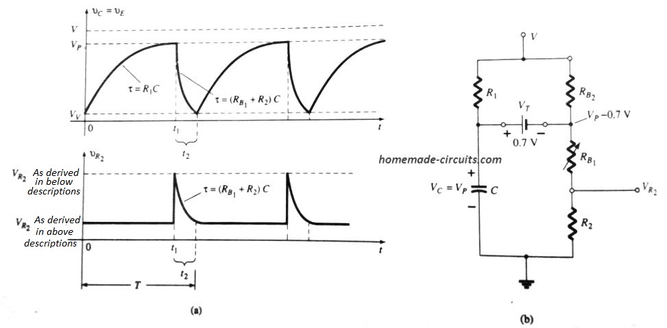 Figure #8
The general equation that determines the charging period of C in a UJT network is:
vc = Vv + (V - Vv)( 1 - e-t/R1C)
Through our previous calculations we already know the volatge across R2 during the above charging period of the capacitor.
Now, when vc = vE = Vp, the UJT device will get into switch ON state, causing the capacitor to discharge via RB1 and R2, with a rate depending on the time constant:
�� = (RB1 + R2)C
The following equation can be used for calculating discharge time when
vc = vE
vc Vpe-t/(RB1 + R2)C
This equation has turned a bit complex due to RB1, which goes through a decrease in value as the the emitter current increases, along with other aspects in the circuit like R1 and V, which also affect the discharge rate of C overall.
Despite of this, if we refer to the equivalent circuit as given above Figure #8 (b), typically the values of R1 and RB2 can be such that a Th��venin network for the configuration around the capacitor C might be marginally affected by the R1, RB2 resistors.
Although the voltage V appears to be rather large, the resistive divider aiding the Th��venin voltage could be generally overlooked and eliminated, as shown in the below reduced equivalent diagram:
Figure #8
The general equation that determines the charging period of C in a UJT network is:
vc = Vv + (V - Vv)( 1 - e-t/R1C)
Through our previous calculations we already know the volatge across R2 during the above charging period of the capacitor.
Now, when vc = vE = Vp, the UJT device will get into switch ON state, causing the capacitor to discharge via RB1 and R2, with a rate depending on the time constant:
�� = (RB1 + R2)C
The following equation can be used for calculating discharge time when
vc = vE
vc Vpe-t/(RB1 + R2)C
This equation has turned a bit complex due to RB1, which goes through a decrease in value as the the emitter current increases, along with other aspects in the circuit like R1 and V, which also affect the discharge rate of C overall.
Despite of this, if we refer to the equivalent circuit as given above Figure #8 (b), typically the values of R1 and RB2 can be such that a Th��venin network for the configuration around the capacitor C might be marginally affected by the R1, RB2 resistors.
Although the voltage V appears to be rather large, the resistive divider aiding the Th��venin voltage could be generally overlooked and eliminated, as shown in the below reduced equivalent diagram:
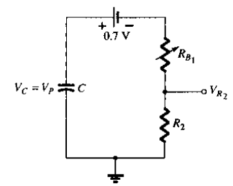 Therefore, the simplified version above helps us to get the following equation for the discharge phase of the capacitor C, when VR2 is at its peak.
VR2 R2(Vp - 0.7) / R2 + RB1
For more application circuits you may also refer to this article
Therefore, the simplified version above helps us to get the following equation for the discharge phase of the capacitor C, when VR2 is at its peak.
VR2 R2(Vp - 0.7) / R2 + RB1
For more application circuits you may also refer to this article
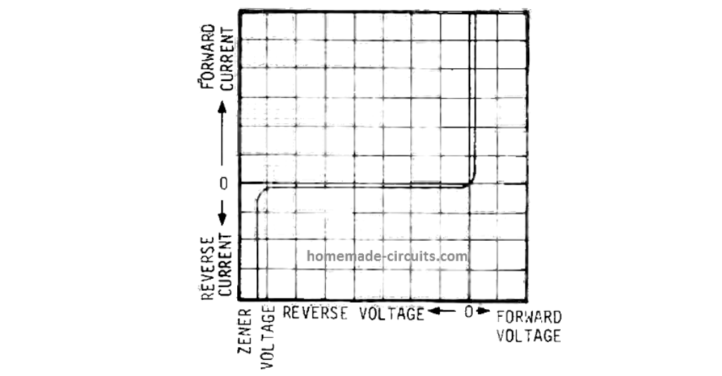
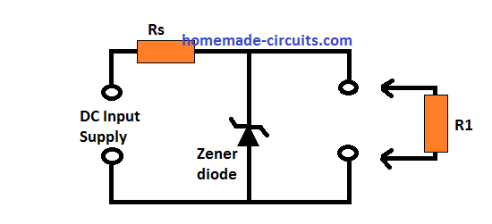 The basic working of a zener diode can be explained with the following points:
In an absence of a load across the output of the zener diode, a 4.7 Volts can be seen dropped across the Zener diode while a cut off 2.4 Volts is developed across resistor R.
Now, in case the input voltage is altered, let's imagine, from 8.0 to 9.0 V, will cause the voltage drop across the Zener to still maintain the rated 4.7 V.
However the voltage drop across the resistor R could be seen raised, from 2.4 V, to 3.4 V.
The voltage drop across an ideal Zener can be expected to be pretty constant.
Practically , you may find the voltage across the zener increasing slightly because of the dynamic resistance of the Zener.
The procedure through which the change in Zener voltage is calculated is by multiplying the zener dynamic resistance with the change in Zener current.
The resistor R1, in the above basic regulator design, symbolizes the preferred load that may be connected with the zener.
R1 in this connection will draw certain amount of current which was moving through the Zener.
Since the current in Rs will be higher than the current entering the load, an amount of current will continue to go through the Zener enabling a perfectly constant voltage across the Zener and the load.
The indicated series resistor Rs should be determined in such a way that the lowest current entering the Zener is always higher than the minimum level specified for a stable regulation from the zener.
This level starts just under the 'knee' of the reverse voltage/reverse current curve as learned from the previous graphical diagram above.
You must additionally make sure that the selection of Rs ensures that current passing through the Zener diode never goes beyond its power rating: which may be equivalent to the Zener voltage x Zener current.
It is the highest amount of current that may pass through the Zener diode in the absence of the load R1.
The basic working of a zener diode can be explained with the following points:
In an absence of a load across the output of the zener diode, a 4.7 Volts can be seen dropped across the Zener diode while a cut off 2.4 Volts is developed across resistor R.
Now, in case the input voltage is altered, let's imagine, from 8.0 to 9.0 V, will cause the voltage drop across the Zener to still maintain the rated 4.7 V.
However the voltage drop across the resistor R could be seen raised, from 2.4 V, to 3.4 V.
The voltage drop across an ideal Zener can be expected to be pretty constant.
Practically , you may find the voltage across the zener increasing slightly because of the dynamic resistance of the Zener.
The procedure through which the change in Zener voltage is calculated is by multiplying the zener dynamic resistance with the change in Zener current.
The resistor R1, in the above basic regulator design, symbolizes the preferred load that may be connected with the zener.
R1 in this connection will draw certain amount of current which was moving through the Zener.
Since the current in Rs will be higher than the current entering the load, an amount of current will continue to go through the Zener enabling a perfectly constant voltage across the Zener and the load.
The indicated series resistor Rs should be determined in such a way that the lowest current entering the Zener is always higher than the minimum level specified for a stable regulation from the zener.
This level starts just under the 'knee' of the reverse voltage/reverse current curve as learned from the previous graphical diagram above.
You must additionally make sure that the selection of Rs ensures that current passing through the Zener diode never goes beyond its power rating: which may be equivalent to the Zener voltage x Zener current.
It is the highest amount of current that may pass through the Zener diode in the absence of the load R1.
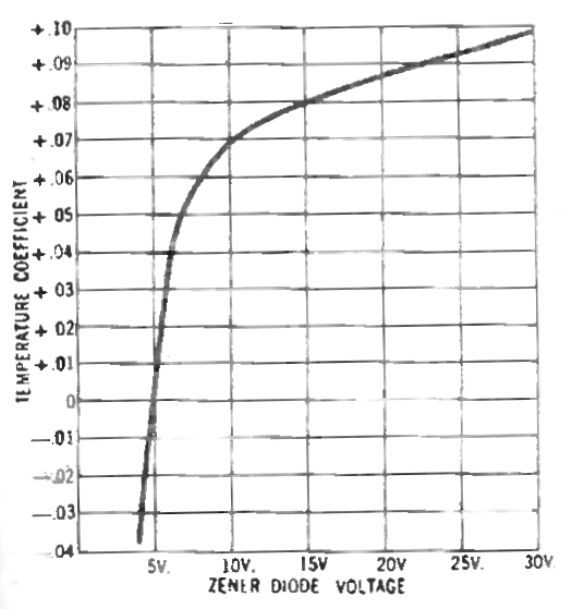 It shows the zener diode temperature coefficient curve.
Although at higher voltages the coefficient curve responds at around 0.1% per degree Celsius, it moves through zero at 5 V and then turns negative for the lower voltage levels.
Eventually it reaches -0.04% per degree Celsius at around 3.5 V.
It shows the zener diode temperature coefficient curve.
Although at higher voltages the coefficient curve responds at around 0.1% per degree Celsius, it moves through zero at 5 V and then turns negative for the lower voltage levels.
Eventually it reaches -0.04% per degree Celsius at around 3.5 V.
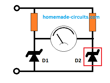 The diagram shows a bridge network built using a pair of resistors and a pair of Zener diodes having identical characteristics.
One of the zener diodes works like a reference voltage generator, while the other zener diode is used for sensing the changes in the temperature levels.
A standard 10 V Zener may have a temperature coefficient of +0.07%/ ��C which may correspond to 7 mV/ ��C variation in temperature.
This will create an imbalance of around 7 mV between the two arms of the bridge for every single degree Celsius variation in the temperature.
A 50 mV full FSD meter can be used in the indicated position for showing the corresponding temperature readings.
The diagram shows a bridge network built using a pair of resistors and a pair of Zener diodes having identical characteristics.
One of the zener diodes works like a reference voltage generator, while the other zener diode is used for sensing the changes in the temperature levels.
A standard 10 V Zener may have a temperature coefficient of +0.07%/ ��C which may correspond to 7 mV/ ��C variation in temperature.
This will create an imbalance of around 7 mV between the two arms of the bridge for every single degree Celsius variation in the temperature.
A 50 mV full FSD meter can be used in the indicated position for showing the corresponding temperature readings.
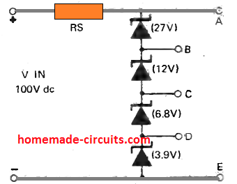 For such cases an array of zener diodes can be created which may then be used for getting a desired customized zener diode value, as shown below:
In this example, many customized, non standard zener values could be acquired across the various terminals, as described in the following list:
For such cases an array of zener diodes can be created which may then be used for getting a desired customized zener diode value, as shown below:
In this example, many customized, non standard zener values could be acquired across the various terminals, as described in the following list:
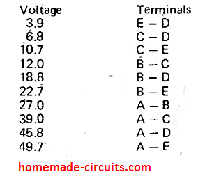 You can use other values in the indicated positions to get many other customized sets of zener diode output
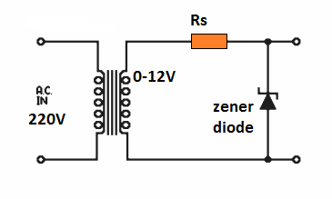 When the AC supply moves across the positive half of the cycle, the zener doesn't conduct until the AC climbs up to the zener voltage level.
When the AC signal crosses the zener voltage, the zener conducts and stabilizes the output to a 4.7 V level, until the AC cycle drops back to zero.
When the AC supply moves across the positive half of the cycle, the zener doesn't conduct until the AC climbs up to the zener voltage level.
When the AC signal crosses the zener voltage, the zener conducts and stabilizes the output to a 4.7 V level, until the AC cycle drops back to zero.
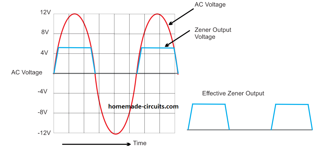 Remember, while using zener with an AC input, makes sure that Rs is calculated as per the AC peak voltage.
In the above example, the output is not symmetrical, rather a pulsating 4.7 V DC.
In order to get a symmetrical 4.7 V AC at the output, two back to back zeners could be connected as depicted in the below diagram
Remember, while using zener with an AC input, makes sure that Rs is calculated as per the AC peak voltage.
In the above example, the output is not symmetrical, rather a pulsating 4.7 V DC.
In order to get a symmetrical 4.7 V AC at the output, two back to back zeners could be connected as depicted in the below diagram
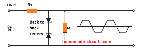
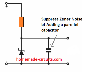 The value of the capacitor can be between 0.01uF and 0.1uF, which will allow noise suppression by a factor of 10, and will maintain the best possible voltage stabilization.
The following graph shows the effect of the capacitor for reducing zener diode noise.
The value of the capacitor can be between 0.01uF and 0.1uF, which will allow noise suppression by a factor of 10, and will maintain the best possible voltage stabilization.
The following graph shows the effect of the capacitor for reducing zener diode noise.
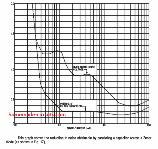
 However, practically this may not be as simple as it looks and may not work as intended.
This is because just like any other semiconductor device, zeners also never come with exactly identical characteristics, therefore one of the zeners may conduct before the other drawing the entire current through itself, eventually getting destroyed.
A quick way to counter this problem may be to add low values series resistors with each zener diodes as shown below, which will allow each zener diode to share the current uniformly through compensating voltage drops generated by the resistors R1 and R2:
However, practically this may not be as simple as it looks and may not work as intended.
This is because just like any other semiconductor device, zeners also never come with exactly identical characteristics, therefore one of the zeners may conduct before the other drawing the entire current through itself, eventually getting destroyed.
A quick way to counter this problem may be to add low values series resistors with each zener diodes as shown below, which will allow each zener diode to share the current uniformly through compensating voltage drops generated by the resistors R1 and R2:
 Although, the power handling capacity can be increased by connecting Zener diodes in parallel, a much improved approach may be to add a shunt BJT in conjunction with a zener diode configured as a reference source.
Please see the following example schematic for the same.
Although, the power handling capacity can be increased by connecting Zener diodes in parallel, a much improved approach may be to add a shunt BJT in conjunction with a zener diode configured as a reference source.
Please see the following example schematic for the same.
 Adding a shunt transistor not only enhances the zener power handling capacity by a factor of 10, it further improves the voltage regulation level of the output, which may be as high as the specified current gain of the transistor.
This type of shunt transistor zener regulator can be used for experimental purposes because the circuit features a 100% short circuit proof facility.
That said, the design is rather inefficient because the transistor may dissipate a significant amount of current in the absence of a load.
For even better results, a series pass transistor type of regulator as shown below looks a better option and preferable.
Adding a shunt transistor not only enhances the zener power handling capacity by a factor of 10, it further improves the voltage regulation level of the output, which may be as high as the specified current gain of the transistor.
This type of shunt transistor zener regulator can be used for experimental purposes because the circuit features a 100% short circuit proof facility.
That said, the design is rather inefficient because the transistor may dissipate a significant amount of current in the absence of a load.
For even better results, a series pass transistor type of regulator as shown below looks a better option and preferable.
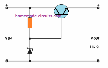 In this circuit the Zener diode creates a reference voltage for the series pass transistor, which, essentially, works like an emitter follower.
As a result the emitter voltage is maintained between a few tenths of a volt of the transistor base voltage as created by the Zener diode.
Consequently the transistor works like a series component and enables effective control of the supply voltage variations.
The entire load current now runs via this series transistor.
The power handling capacity of this type of configuration is established totally by the value and the specification of the transistors, and also depends on the efficiency and quality of the heatsink used.
Excellent regulation could be achieved from the above design using a 1k series resistor.
The regulation could be increased with a factor of 10 by replacing the normal zener with a special low dynamic zener diode such as a 1N1589).
In case you want the above circuit to provide a variable voltage regulated output, it could be easily achieved by using a 1K potentiometer across the Zener diode.
This allows a variable reference voltage to be adjusted at the base of the series transistor.
In this circuit the Zener diode creates a reference voltage for the series pass transistor, which, essentially, works like an emitter follower.
As a result the emitter voltage is maintained between a few tenths of a volt of the transistor base voltage as created by the Zener diode.
Consequently the transistor works like a series component and enables effective control of the supply voltage variations.
The entire load current now runs via this series transistor.
The power handling capacity of this type of configuration is established totally by the value and the specification of the transistors, and also depends on the efficiency and quality of the heatsink used.
Excellent regulation could be achieved from the above design using a 1k series resistor.
The regulation could be increased with a factor of 10 by replacing the normal zener with a special low dynamic zener diode such as a 1N1589).
In case you want the above circuit to provide a variable voltage regulated output, it could be easily achieved by using a 1K potentiometer across the Zener diode.
This allows a variable reference voltage to be adjusted at the base of the series transistor.
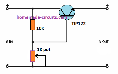 However, this modification may result in a lower regulation efficiency due to some shunting effect created by the potentiometer.
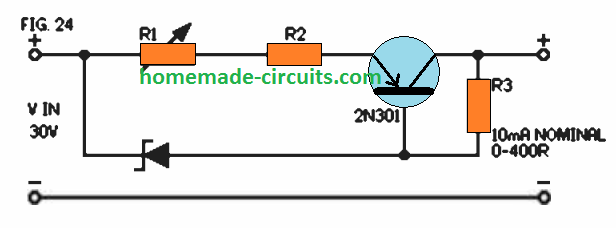 You can see a couples of circuit passages here, one via the zener diode connected in series with the biasing resistor, while the other path is through the resistors R1, R2, and the series transistor.
In case the current deviates from its original range, it creates a proportionate change in the biasing level of R3, which in turn causes the series transistor resistance to increase or decrease proportionately.
This adjustment in the resistance of the transistor results in an automatic correction of the output current to the desired level.
The accuracy of the current control in this design will be around +/- 10% in response to an output conditions that may range between a short circuit and a loading of up to 400 Ohm.
You can see a couples of circuit passages here, one via the zener diode connected in series with the biasing resistor, while the other path is through the resistors R1, R2, and the series transistor.
In case the current deviates from its original range, it creates a proportionate change in the biasing level of R3, which in turn causes the series transistor resistance to increase or decrease proportionately.
This adjustment in the resistance of the transistor results in an automatic correction of the output current to the desired level.
The accuracy of the current control in this design will be around +/- 10% in response to an output conditions that may range between a short circuit and a loading of up to 400 Ohm.
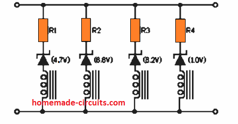 Here, sequentially incrementing zener diodes are installed in series with a group of relays along with individual low value series resistors.
When power is switched ON, the zener diodes conduct one after the other in sequence in an increasing order of their zener values.
This results in the relay switching ON in sequence as desired by the application.
The values of the resistors can be 10 ohms or 20 ohms depending on the resistance value of the relay coil.
Here, sequentially incrementing zener diodes are installed in series with a group of relays along with individual low value series resistors.
When power is switched ON, the zener diodes conduct one after the other in sequence in an increasing order of their zener values.
This results in the relay switching ON in sequence as desired by the application.
The values of the resistors can be 10 ohms or 20 ohms depending on the resistance value of the relay coil.
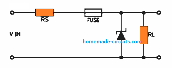 By joining a correctly rated Zener diode across the load, a fuse which is suitably rated to handle the intended load current for extended periods can be employed.
In this situation, suppose the input voltage increases to an extent that exceeds the Zener breakdown voltage - will force the Zener diode to conduct.
This will cause a sudden increase in the current blowing the fuse almost instantaneously.
The advantage of this circuit is that it prevents the fuse from blowing frequently and unpredictably due to its close fusing value to the load current.
Instead, the fuse blows only when the voltage and current genuinely rises beyond a specified unsafe level.
By joining a correctly rated Zener diode across the load, a fuse which is suitably rated to handle the intended load current for extended periods can be employed.
In this situation, suppose the input voltage increases to an extent that exceeds the Zener breakdown voltage - will force the Zener diode to conduct.
This will cause a sudden increase in the current blowing the fuse almost instantaneously.
The advantage of this circuit is that it prevents the fuse from blowing frequently and unpredictably due to its close fusing value to the load current.
Instead, the fuse blows only when the voltage and current genuinely rises beyond a specified unsafe level.
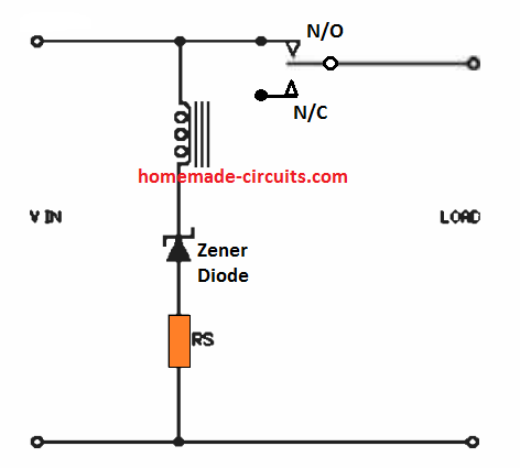 The operation is actually very simple, the supply Vin which is acquired from a transformer bridge network varies proportionately depending on the input AC variations.
That implies, if suppose the 220 V corresponds to 12 V from the transformer, then 180 V should correspond to 9.81 V and so on.
Therefore, if 180 V is assumed to be the low voltage cut off threshold, then selecting the zener diode as a 10 V device will cut off the relay operation whenever the input AC drops below 180 V.
The operation is actually very simple, the supply Vin which is acquired from a transformer bridge network varies proportionately depending on the input AC variations.
That implies, if suppose the 220 V corresponds to 12 V from the transformer, then 180 V should correspond to 9.81 V and so on.
Therefore, if 180 V is assumed to be the low voltage cut off threshold, then selecting the zener diode as a 10 V device will cut off the relay operation whenever the input AC drops below 180 V.
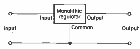 The three terminals of the IC are for apparent reasons, designated with the names input, common and output.
The supply positive and negative are simply connected across the input and common terminals of the IC respectively, while the regulated stabilized voltage is acquired across the output and common terminals.
The only discrete external part optionally demanded are a capacitor on the input and the output leads of the IC.
These capacitors are necessary to enhance the level of output regulation of the device, and to improve the transient response.
The microfarads values of these capacitors are generally not critical, and therefore are normally anything between 100 nf, 220 nf or 330 nf.
The three terminals of the IC are for apparent reasons, designated with the names input, common and output.
The supply positive and negative are simply connected across the input and common terminals of the IC respectively, while the regulated stabilized voltage is acquired across the output and common terminals.
The only discrete external part optionally demanded are a capacitor on the input and the output leads of the IC.
These capacitors are necessary to enhance the level of output regulation of the device, and to improve the transient response.
The microfarads values of these capacitors are generally not critical, and therefore are normally anything between 100 nf, 220 nf or 330 nf.
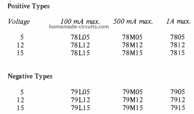 These 78XX series of ICs come with additional voltage ratings both in positive and negative forms.
Standard ranges for these 78XX regulators are 8 V, 9 V, 10 V, 18 V, 20 V and 24 V, which correspond to ICs 7808, 7809, 7810, 7818, 7820, 7824 ICs.
Many of these devices carry suffix characters or figures with their printed number, depending on the manufacturer or the brand type.
However, all of them are essentially the same with identical rating.
Several part dealres will not actually promote these ICs by type number, rather just point out their polarity, voltage and current specs, and occasionally with reference to their package style.
These 78XX series of ICs come with additional voltage ratings both in positive and negative forms.
Standard ranges for these 78XX regulators are 8 V, 9 V, 10 V, 18 V, 20 V and 24 V, which correspond to ICs 7808, 7809, 7810, 7818, 7820, 7824 ICs.
Many of these devices carry suffix characters or figures with their printed number, depending on the manufacturer or the brand type.
However, all of them are essentially the same with identical rating.
Several part dealres will not actually promote these ICs by type number, rather just point out their polarity, voltage and current specs, and occasionally with reference to their package style.
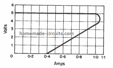 The foldback current limiting response can be understood from the following explanation:
Suppose we have 7805 IC with a 10 V input and it undergoes a short circuit across its output terminals.
In this situation under ordinary type of current limiting the output of the IC will continue to generate 1 amp current giving a dissipation of 10 watts.
But with a special foldback current limiting the short circuit current may get restricted to around 400 mA, resulting in a dissipation in the device of only 4 watts only.
The foldback current limiting response can be understood from the following explanation:
Suppose we have 7805 IC with a 10 V input and it undergoes a short circuit across its output terminals.
In this situation under ordinary type of current limiting the output of the IC will continue to generate 1 amp current giving a dissipation of 10 watts.
But with a special foldback current limiting the short circuit current may get restricted to around 400 mA, resulting in a dissipation in the device of only 4 watts only.
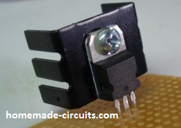 In this situation when the device is fully loaded at around 800 mA, the dissipation from the device could be as much as 4 watts (0.8A x 5V = 4W).
This appears to be two times more than maximum permisible 2 watts PD for the 7815 device.
This implies that the extra 2 watts has to be compensated through a heatsink.
A broad selection of heatsinks are generally available in the market, and these are identified with rating of a particular degrees/watt.
This rating basically indicates the temperature rise that is caused for every single watt of power dissipated via the heatsink.
This also indicates that for larger heatsink, the degrees per watt will proportionately lower.
The lowest size of heatsinking necessary for a 78xx regulator device could determined in the following way.
We have to primarily find out the nominal atmospheric temperature where the device is being used.
Except if the device is likely to be used in an uncommonly warm surroundings, a figure of around 30 degrees Centigrade can be considered a reasonable assumption.
In this situation when the device is fully loaded at around 800 mA, the dissipation from the device could be as much as 4 watts (0.8A x 5V = 4W).
This appears to be two times more than maximum permisible 2 watts PD for the 7815 device.
This implies that the extra 2 watts has to be compensated through a heatsink.
A broad selection of heatsinks are generally available in the market, and these are identified with rating of a particular degrees/watt.
This rating basically indicates the temperature rise that is caused for every single watt of power dissipated via the heatsink.
This also indicates that for larger heatsink, the degrees per watt will proportionately lower.
The lowest size of heatsinking necessary for a 78xx regulator device could determined in the following way.
We have to primarily find out the nominal atmospheric temperature where the device is being used.
Except if the device is likely to be used in an uncommonly warm surroundings, a figure of around 30 degrees Centigrade can be considered a reasonable assumption.
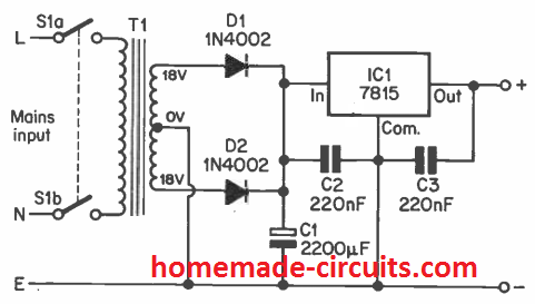 It is connected to a push-pull full wave rectifier which provides an unloaded voltage of about 27 V Dc after being filtered through C1.
Capacitors C2 and C3 work like input and output decoupling capacitors which should be attached relatively closer to the body of the IC.
When the output load is full you will see the applied input voltage to the IC1 attaining a level at 19 to 20 volts, allowing approximately 5 volts difference across the input/output of the regulator.
It is connected to a push-pull full wave rectifier which provides an unloaded voltage of about 27 V Dc after being filtered through C1.
Capacitors C2 and C3 work like input and output decoupling capacitors which should be attached relatively closer to the body of the IC.
When the output load is full you will see the applied input voltage to the IC1 attaining a level at 19 to 20 volts, allowing approximately 5 volts difference across the input/output of the regulator.
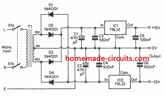 In this example, T1 is a 15-0-15 volt transformer rated with secondary current rating of 200 mA or more.
You can find a couple of push-pull full wave rectifiers; D2 and D3 that give you a positive output.
D1 along with D4 deliver a negative output.
The positive supply is filtered by C1 while the negative line is cleaned and filtered by C2.
IC1 gives you a regulated positive supply output, while the IC2 works like a negative supply regulator.
C3 to C6 are positioned like decoupling capacitors for enhancing the output efficiency in terms of better response to spikes, noise and transients.
In this example, T1 is a 15-0-15 volt transformer rated with secondary current rating of 200 mA or more.
You can find a couple of push-pull full wave rectifiers; D2 and D3 that give you a positive output.
D1 along with D4 deliver a negative output.
The positive supply is filtered by C1 while the negative line is cleaned and filtered by C2.
IC1 gives you a regulated positive supply output, while the IC2 works like a negative supply regulator.
C3 to C6 are positioned like decoupling capacitors for enhancing the output efficiency in terms of better response to spikes, noise and transients.
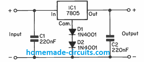 In this example we have estimated the required output voltage to be approximately 6V, and have implemented the same through a 5 volt regulator IC by boosting the output by 1 volt.
As can be seen, this 1 V elevation is effectively achieved by simply incorporating a couple of series rectifiers diodes with the common lead of the regulator.
The rectifiers are wired to make sure they are forward biased through the quiescent current utilized by the regulator, and which moves via the common GND terminal of the device.
The attached diodes as a result behave somewhat like low voltage zener diodes, wherein each diodes drops around 0.5 to 0.6 volts enabling a combined zener voltage of about 1 to 1.2 volts.
The objective of the design is to lift the common terminal of the regulator by 1 volt over the ground supply potential.
Here the regulator 7805 IC actually stabilizes the rated output at 5 V above the ground line, hence, by elevating the ground terminal by around 1 V, the output is also lifted by the very same magnitude, causing the output also to get regulated at approximately 6 V level.
This procedure works extremely well with all three terminal 78XX voltage regulator ICs.
In this example we have estimated the required output voltage to be approximately 6V, and have implemented the same through a 5 volt regulator IC by boosting the output by 1 volt.
As can be seen, this 1 V elevation is effectively achieved by simply incorporating a couple of series rectifiers diodes with the common lead of the regulator.
The rectifiers are wired to make sure they are forward biased through the quiescent current utilized by the regulator, and which moves via the common GND terminal of the device.
The attached diodes as a result behave somewhat like low voltage zener diodes, wherein each diodes drops around 0.5 to 0.6 volts enabling a combined zener voltage of about 1 to 1.2 volts.
The objective of the design is to lift the common terminal of the regulator by 1 volt over the ground supply potential.
Here the regulator 7805 IC actually stabilizes the rated output at 5 V above the ground line, hence, by elevating the ground terminal by around 1 V, the output is also lifted by the very same magnitude, causing the output also to get regulated at approximately 6 V level.
This procedure works extremely well with all three terminal 78XX voltage regulator ICs.
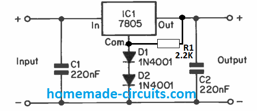 Since each rectifier diode will facilitate a forward drop of around 0.65 V approximately, by calculating more such diodes in series we can achieve proportionately higher level of boosted voltage across the IC output.
However, for this to happen the input level must be higher by at least 3V than the final estimated output level.
Silicon diodes like 1N4148 will work quite nicely for the application.
Alternatively if diodes look cumbersome, a single equivalent zener diode could be also used for getting the same effect, as shown in the following example.
Since each rectifier diode will facilitate a forward drop of around 0.65 V approximately, by calculating more such diodes in series we can achieve proportionately higher level of boosted voltage across the IC output.
However, for this to happen the input level must be higher by at least 3V than the final estimated output level.
Silicon diodes like 1N4148 will work quite nicely for the application.
Alternatively if diodes look cumbersome, a single equivalent zener diode could be also used for getting the same effect, as shown in the following example.
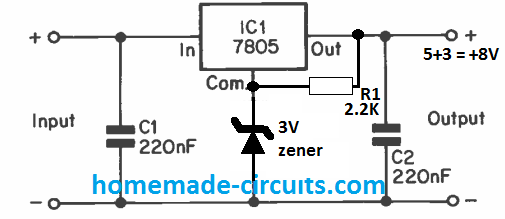 Having said that, please make sure that the procedure is implemented for getting not more than 3 V higher than the actual rating of the device.
Beyond this level the output stabilization may get affected.
Having said that, please make sure that the procedure is implemented for getting not more than 3 V higher than the actual rating of the device.
Beyond this level the output stabilization may get affected.
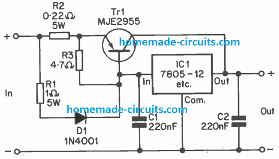 The indicated R1, and R2 configuration ratio assures that for every milliamp current that passes through R1, D1 and the regulator, a bit of current in excess of 4 mA is shifted via Tr1 and R2.
As a result when the full 1 amp is used through IC1, we have a current of more than 4 amps passing via Tr1. This situation allows the circuit to deliver a optimum output current which is a bit higher than 5 amps.
Even in an overload conditions, the currents through Tr1 and IC1 continue to have a ratio of somewhat higher than 4 :1, therefore, the current limiting feature of the IC continues to work without issues.
Circuits of this form have actually proved to be needless nowadays because of the availability of higher power regulators devices like the 78H05, 781-112 etc that come with a maximum current rating of 5 amps, and enable the user to configure them exactly with the same ease as the lower current counterparts.
The indicated R1, and R2 configuration ratio assures that for every milliamp current that passes through R1, D1 and the regulator, a bit of current in excess of 4 mA is shifted via Tr1 and R2.
As a result when the full 1 amp is used through IC1, we have a current of more than 4 amps passing via Tr1. This situation allows the circuit to deliver a optimum output current which is a bit higher than 5 amps.
Even in an overload conditions, the currents through Tr1 and IC1 continue to have a ratio of somewhat higher than 4 :1, therefore, the current limiting feature of the IC continues to work without issues.
Circuits of this form have actually proved to be needless nowadays because of the availability of higher power regulators devices like the 78H05, 781-112 etc that come with a maximum current rating of 5 amps, and enable the user to configure them exactly with the same ease as the lower current counterparts.
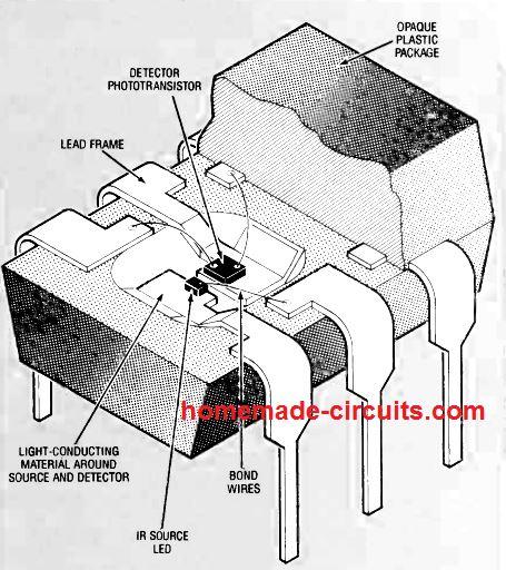 The above figure shows a dissected view of a typical six pin dual-in-line (DIP) optocoupler chip.
When the terminals connected with the IR LED is supplied with an appropriate forward biased voltage it internally emits an infrared radiation in the wavelength of 900 to 940 nanometer range.
This IR signal falls on the adjacent photodetector which is normally an NPN phototransistor (having a sensitivity set in the identical wavelength), and it instantly conducts, creating a continuity across its collector/emitter terminals.
As can be seen in the image the IR LED and the phototransistor are mounted on adjacent arms of a lead-frame.
The lead-frame is in the form of stamping carved out from fine conductive sheet metal having several branch like finishing.
The isolated substrates which is included to reinforce the device are created with the aid of the inner branches.
The respective pinout of the DIP are correspondingly developed from the outer branches.
Once the conductive connections are established between the die case and the appropriate lead-frame pins, the space surrounding the IR LED and the phototransistor is sealed within an transparent IR supported resin which behaves like a "light pipe" or optical wave-guide between the two IR devices.
The complete assembly is finally molded in a light proof epoxy resin forming the DIP package.
At the finish, the lead-frame pin terminals are neatly bent downward.
The above figure shows a dissected view of a typical six pin dual-in-line (DIP) optocoupler chip.
When the terminals connected with the IR LED is supplied with an appropriate forward biased voltage it internally emits an infrared radiation in the wavelength of 900 to 940 nanometer range.
This IR signal falls on the adjacent photodetector which is normally an NPN phototransistor (having a sensitivity set in the identical wavelength), and it instantly conducts, creating a continuity across its collector/emitter terminals.
As can be seen in the image the IR LED and the phototransistor are mounted on adjacent arms of a lead-frame.
The lead-frame is in the form of stamping carved out from fine conductive sheet metal having several branch like finishing.
The isolated substrates which is included to reinforce the device are created with the aid of the inner branches.
The respective pinout of the DIP are correspondingly developed from the outer branches.
Once the conductive connections are established between the die case and the appropriate lead-frame pins, the space surrounding the IR LED and the phototransistor is sealed within an transparent IR supported resin which behaves like a "light pipe" or optical wave-guide between the two IR devices.
The complete assembly is finally molded in a light proof epoxy resin forming the DIP package.
At the finish, the lead-frame pin terminals are neatly bent downward.
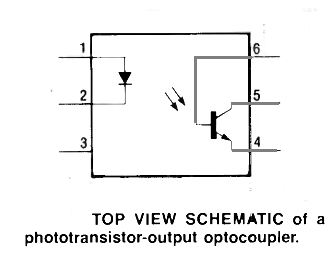
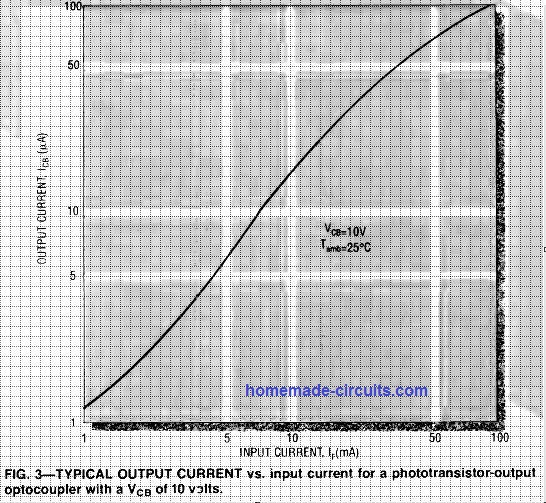 The figure above shows the characteristic plot of an optocoupler internal phototransistor's output current (ICB) vs.
input current (IF) when a VCB of 10 V is applied across its collector/base pins.
The figure above shows the characteristic plot of an optocoupler internal phototransistor's output current (ICB) vs.
input current (IF) when a VCB of 10 V is applied across its collector/base pins.
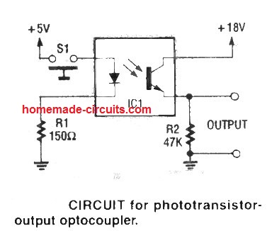 The figure above shows a basic optocoupler circuit.
The amount of current that may pass through the phototransistor is determined by the applied forward bias current of the IR LED or the IRED, despite being entirely separated.
While the switch S1 is held open, current flow through the IRED is inhibited, which means no IR energy is available to the phototransistor.
This renders the device completely inactive causing zero voltage to develop across output resistor R2.
When S1 is closed, current is allowed to flow through the IRED and R1.
This activates the IR LED which begins emitting IR signals on the phototransistor enabling it to switch ON, and this in turn causes an output voltage to develop across R2.
This basic optocoupler circuit will specifically respond well to ON/OFF switching input signals.
However, if required the circuit can be modified to work with analog input signals and generate corresponding analog output signals.
The figure above shows a basic optocoupler circuit.
The amount of current that may pass through the phototransistor is determined by the applied forward bias current of the IR LED or the IRED, despite being entirely separated.
While the switch S1 is held open, current flow through the IRED is inhibited, which means no IR energy is available to the phototransistor.
This renders the device completely inactive causing zero voltage to develop across output resistor R2.
When S1 is closed, current is allowed to flow through the IRED and R1.
This activates the IR LED which begins emitting IR signals on the phototransistor enabling it to switch ON, and this in turn causes an output voltage to develop across R2.
This basic optocoupler circuit will specifically respond well to ON/OFF switching input signals.
However, if required the circuit can be modified to work with analog input signals and generate corresponding analog output signals.
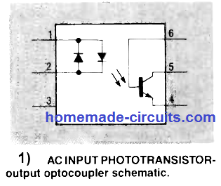 The first variant above indicates a bidirectional input and phototransistor output optocoupler schematic featuring a couple of back-to-back connected gallium-arsenide IRED's for coupling input AC signals, and also to safeguard against reverse polarity input.
Commonly this variant may exhibit a minimum CTR of 20%.
The first variant above indicates a bidirectional input and phototransistor output optocoupler schematic featuring a couple of back-to-back connected gallium-arsenide IRED's for coupling input AC signals, and also to safeguard against reverse polarity input.
Commonly this variant may exhibit a minimum CTR of 20%.
 The next type above illustrates an opto-coupler whose output is enhanced with a silicon based photo-darlington amplifier.
This allows it to produce higher output current compared to the other normal opto-coupler.
Due to the Darlington element at the output this type of optocouplers are able to produce a minimum of 500% CTR when the collector-to-emitter voltage is around 30 to 35 volts.
This magnitude appears to be about ten times higher than a normal optocoupler.
However, these may not be as fast as the other normal devices and this may be a significant tradeoff while working with a photodarlington coupler.
Also, it may have a decreased amount of the effective bandwith by about a factor of ten.
Industry standard versions of photoDarlington optocouplers are 4N29 to 4N33 and 6N138 and 6N139.
You can also get them as Dual and quad channel photodarlington couplers.
The next type above illustrates an opto-coupler whose output is enhanced with a silicon based photo-darlington amplifier.
This allows it to produce higher output current compared to the other normal opto-coupler.
Due to the Darlington element at the output this type of optocouplers are able to produce a minimum of 500% CTR when the collector-to-emitter voltage is around 30 to 35 volts.
This magnitude appears to be about ten times higher than a normal optocoupler.
However, these may not be as fast as the other normal devices and this may be a significant tradeoff while working with a photodarlington coupler.
Also, it may have a decreased amount of the effective bandwith by about a factor of ten.
Industry standard versions of photoDarlington optocouplers are 4N29 to 4N33 and 6N138 and 6N139.
You can also get them as Dual and quad channel photodarlington couplers.
 The third schematic above shows an optocoupler having an IRED and a MOSFET photosensor featuring bi-directional linear output.
The isolation voltage range of this variant can be as high as 2500 volts RMS.
The breakdown voltage range can be within 15 to 30 volts, while the rise and fall times is around 15 microseconds each.
The third schematic above shows an optocoupler having an IRED and a MOSFET photosensor featuring bi-directional linear output.
The isolation voltage range of this variant can be as high as 2500 volts RMS.
The breakdown voltage range can be within 15 to 30 volts, while the rise and fall times is around 15 microseconds each.
 The next variant above demonstrates a basic SCR or thyristor based opto photosensor.
Here the output is controlled through an SCR.
The isolation voltage of OptoSCR type of couplers is typically around 1000 to 4000 volts RMS.
It features a minimum blocking voltages of 200 to 400 V.
The highest turn ON currents (Ivr) can be around 10 mA.
The next variant above demonstrates a basic SCR or thyristor based opto photosensor.
Here the output is controlled through an SCR.
The isolation voltage of OptoSCR type of couplers is typically around 1000 to 4000 volts RMS.
It features a minimum blocking voltages of 200 to 400 V.
The highest turn ON currents (Ivr) can be around 10 mA.
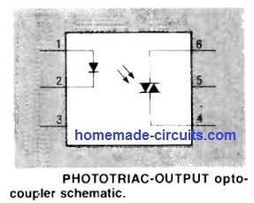 The image above displays an optocoupler having a phototriac-output.
These kind of Thyristor based output couplers generally feature a forward blocking voltages (VDRM) of 400 V.
The image above displays an optocoupler having a phototriac-output.
These kind of Thyristor based output couplers generally feature a forward blocking voltages (VDRM) of 400 V.
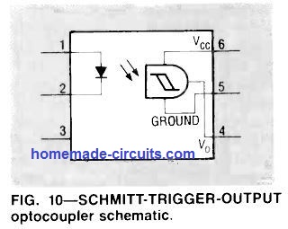 Optocouplers featuring Schmitt trigger property are also available.
This type of optocoupler is displayed above that includes a IC based optosensor having a Schmitt trigger IC that will convert a sine wave or any form of pulsed input signal into rectangular output voltage.
These IC photodetectors based devices are actually designed to work like a multivibrator circuit.
Isolation voltages may range between 2500 to 4000 volts.
Turn-on current is usually specified between 1 to 10 mA.
The minimum and maximum working supply levels are between 3 to 26 volts, and the maximum speed of data rate (NRZ) is 1 MHz.
Optocouplers featuring Schmitt trigger property are also available.
This type of optocoupler is displayed above that includes a IC based optosensor having a Schmitt trigger IC that will convert a sine wave or any form of pulsed input signal into rectangular output voltage.
These IC photodetectors based devices are actually designed to work like a multivibrator circuit.
Isolation voltages may range between 2500 to 4000 volts.
Turn-on current is usually specified between 1 to 10 mA.
The minimum and maximum working supply levels are between 3 to 26 volts, and the maximum speed of data rate (NRZ) is 1 MHz.
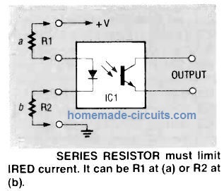 The resistor can be added in series either with the anode terminal (a) or cathode terminal (b) of the IRED.
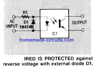 This design also ensures safety for the device against accidental reverse input voltage conditions.
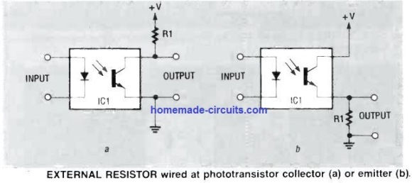
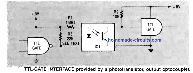 Here we can see that IRED of the optocoupler is connected across the +5V and the TTL gate output, instead of the usual way which is between the TTL output and ground.
This is because the TTL gates are rated to produce very low output currents (around 400 uA), but are specified to sink current at a fairly high rate (16 mA).
Therefore the above connection allows optimal activation current for IRED whenever the TTL is low.
However this also means the output response will be inverted.
Another drawback that exists with TTL gate output is that, when its output is HIGH or logic 1, might produce around a 2.5 V level, which might not be enough to switch OFF the IRED fully.
It must be at least 4.5 V or 5 V to enable complete switch OFF of the IRED.
To correct this issue, R3 is included which makes sure the IRED shuts off completely whenever the TTL gate output turns HIGH even with a 2.5 V.
The collector output pin of the optocoupler can be seen is connected between the input and ground of the TTL IC.
This is important because a TTL gate input must be adequately grounded at least below 0.8 V at 1.6 mA to enable a correct logic 0 at the gate output.
It must be noted that the set up shown in the above figure allows a non-inverting response at the output.
Here we can see that IRED of the optocoupler is connected across the +5V and the TTL gate output, instead of the usual way which is between the TTL output and ground.
This is because the TTL gates are rated to produce very low output currents (around 400 uA), but are specified to sink current at a fairly high rate (16 mA).
Therefore the above connection allows optimal activation current for IRED whenever the TTL is low.
However this also means the output response will be inverted.
Another drawback that exists with TTL gate output is that, when its output is HIGH or logic 1, might produce around a 2.5 V level, which might not be enough to switch OFF the IRED fully.
It must be at least 4.5 V or 5 V to enable complete switch OFF of the IRED.
To correct this issue, R3 is included which makes sure the IRED shuts off completely whenever the TTL gate output turns HIGH even with a 2.5 V.
The collector output pin of the optocoupler can be seen is connected between the input and ground of the TTL IC.
This is important because a TTL gate input must be adequately grounded at least below 0.8 V at 1.6 mA to enable a correct logic 0 at the gate output.
It must be noted that the set up shown in the above figure allows a non-inverting response at the output.
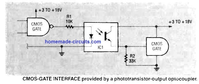 No matter which configuration is selected at the input side, R2 at the output side must be sufficiently large to enable a full output voltage swing between logic 0 and 1 states at the CMOS gate output.
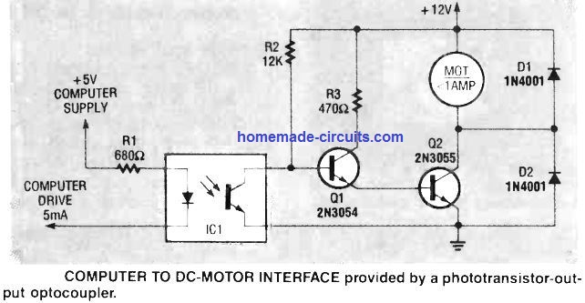 The above figure shows how to interface a microcontroller or Arduino output signal (5 volts, 5 mA) with a relatively high current load through an optocoupler and BJT stages.
With a HIGH +5V logic from the Arduino, the optocoupler IRED and phototransistor both remain switched off, and this allows Q1, Q2 and the load motor to remain turned ON.
Now, as soon as the Arduino output goes low, the optocoupler IRED activates and turns ON the phototransistor.
This instantly grounds the base bias of Q1, switching OFF Q1, Q2 and the motor.
The above figure shows how to interface a microcontroller or Arduino output signal (5 volts, 5 mA) with a relatively high current load through an optocoupler and BJT stages.
With a HIGH +5V logic from the Arduino, the optocoupler IRED and phototransistor both remain switched off, and this allows Q1, Q2 and the load motor to remain turned ON.
Now, as soon as the Arduino output goes low, the optocoupler IRED activates and turns ON the phototransistor.
This instantly grounds the base bias of Q1, switching OFF Q1, Q2 and the motor.
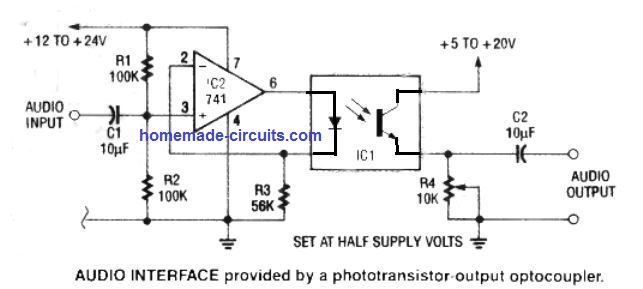 The op amp IC2 is configured like a unity gain voltage follower circuit.
The IRED of the opto-coupler's can be seen rigged to the negative feedback loop.
This loop causes the voltage across R3 (and therefore the current through the IRED) to precisely follow, or track the voltage that's applied to pin#3 of the op amp, which is the non-the inverting input pin.
This pin3 of the is op amp set up at half the supply voltage via R1, R2 potential divider network.
This allows the pin3 to be modulated with an AC signals which can be an audio signal and causes the IRED illumination to vary as per this audio or the modulating analogue signal.
The quiescent current or the idle current draw for the IRED current is attained at 1 to 2 mA via R3.
On the output side of the optocoupler the quiescent current is determined by the phototransistor.
This current develops a voltage across potentiometer R4 whose value needs to be adjusted such that it generates a quiescent output which is also equal to the half the supply voltage.
The tracking modulated audio-output signal equivalent is extracted across potentiometer R4, and decoupled through C2 for further processing .
The op amp IC2 is configured like a unity gain voltage follower circuit.
The IRED of the opto-coupler's can be seen rigged to the negative feedback loop.
This loop causes the voltage across R3 (and therefore the current through the IRED) to precisely follow, or track the voltage that's applied to pin#3 of the op amp, which is the non-the inverting input pin.
This pin3 of the is op amp set up at half the supply voltage via R1, R2 potential divider network.
This allows the pin3 to be modulated with an AC signals which can be an audio signal and causes the IRED illumination to vary as per this audio or the modulating analogue signal.
The quiescent current or the idle current draw for the IRED current is attained at 1 to 2 mA via R3.
On the output side of the optocoupler the quiescent current is determined by the phototransistor.
This current develops a voltage across potentiometer R4 whose value needs to be adjusted such that it generates a quiescent output which is also equal to the half the supply voltage.
The tracking modulated audio-output signal equivalent is extracted across potentiometer R4, and decoupled through C2 for further processing .
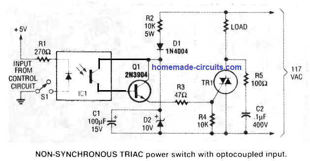 The above design can be used for an isolated control of mains AC lamps, heaters, motors and other similar loads.
This circuit is not zero crossing controlled set up, meaning the input trigger will cause the triac to switch at any point of the AC waveform.
Here the network formed by R2, D1, D2 and C1 create a 10 V potential difference derived from the AC line input.
This voltage is used for triggering the triac through Q1 whenever the input side is switched ON by closing the switch S1. Meaning as long as S1 is open the optocoupler is off due to a zero base bias for Q1, which keeps the triac switched OFF.
The moment S1 is closed it activates the IRED, which switches ON Q1. Q1 subsequently connects the 10 V DC to the gate of the triac which switches the triac ON, and eventually also switches ON the connected load.
The above design can be used for an isolated control of mains AC lamps, heaters, motors and other similar loads.
This circuit is not zero crossing controlled set up, meaning the input trigger will cause the triac to switch at any point of the AC waveform.
Here the network formed by R2, D1, D2 and C1 create a 10 V potential difference derived from the AC line input.
This voltage is used for triggering the triac through Q1 whenever the input side is switched ON by closing the switch S1. Meaning as long as S1 is open the optocoupler is off due to a zero base bias for Q1, which keeps the triac switched OFF.
The moment S1 is closed it activates the IRED, which switches ON Q1. Q1 subsequently connects the 10 V DC to the gate of the triac which switches the triac ON, and eventually also switches ON the connected load.
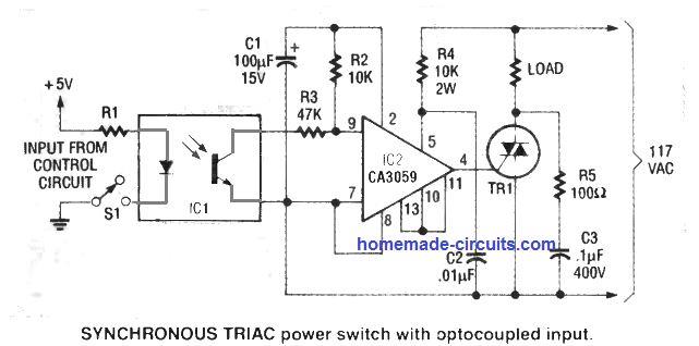 The next circuit above is designed with a silicon monolithic zero-voltage switch, the CA3059/ CA3079. This circuits allows the triac to trigger synchronously, that is only during the zero voltage crossing of the AC cycle waveform.
When S1 is pressed, the opamp responds to it only if the triac input AC cycle is near a few mV near the zero crossing line.
If the input trigger is made while the AC is not near the zero crossing line, then the op amp waits until the waveform reaches the zero crossing and only then triggers the triac via a positive logic from its pin4.
This zero crossing switching feature safeguards the connected from sudden huge current surge and spike, since the turn ON is done at the zero crossing level and not when the AC is at its higher peaks.
This also eliminates unnecessary RF noise and disturbances in the power line.
This optocoupler triac based zero crossing switch can be effectively used for making SSR or solid state relays.
The next circuit above is designed with a silicon monolithic zero-voltage switch, the CA3059/ CA3079. This circuits allows the triac to trigger synchronously, that is only during the zero voltage crossing of the AC cycle waveform.
When S1 is pressed, the opamp responds to it only if the triac input AC cycle is near a few mV near the zero crossing line.
If the input trigger is made while the AC is not near the zero crossing line, then the op amp waits until the waveform reaches the zero crossing and only then triggers the triac via a positive logic from its pin4.
This zero crossing switching feature safeguards the connected from sudden huge current surge and spike, since the turn ON is done at the zero crossing level and not when the AC is at its higher peaks.
This also eliminates unnecessary RF noise and disturbances in the power line.
This optocoupler triac based zero crossing switch can be effectively used for making SSR or solid state relays.
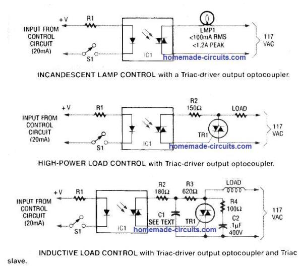 In the first diagram, the photoTriac can be seen configured to activate the lamp directly from the AC line.
Here the bulb must be rated at less than 100 mA RMS and a peak inrush current ratio lower than 1.2 amps for safe working of the optocoupler.
The second design shows how the photoTriac optocoupler can be configured for triggering a slave Triac, and subsequently activating a load as per any preferred power rating.
This circuit is recommended to be used only with with resistive loads such as incandescent lamps or heater elements.
The third figure above illustrates how the upper two circuits could be modified for handling inductive loads like motors.
The circuit consists of R2, C1, and R3 that generate a phase shifting on the gate drive network of the Triac.
This allows the triac to go through a correct triggering action.
Resistor R4 and C2 are introduced as a snubber network to suppress and control surge spikes due to inductive back EMFs..
In all the above applications, R1 must be dimensioned such that the IRED is supplied with at least 20 mA forward current for proper triggering of the triac photodetector.
In the first diagram, the photoTriac can be seen configured to activate the lamp directly from the AC line.
Here the bulb must be rated at less than 100 mA RMS and a peak inrush current ratio lower than 1.2 amps for safe working of the optocoupler.
The second design shows how the photoTriac optocoupler can be configured for triggering a slave Triac, and subsequently activating a load as per any preferred power rating.
This circuit is recommended to be used only with with resistive loads such as incandescent lamps or heater elements.
The third figure above illustrates how the upper two circuits could be modified for handling inductive loads like motors.
The circuit consists of R2, C1, and R3 that generate a phase shifting on the gate drive network of the Triac.
This allows the triac to go through a correct triggering action.
Resistor R4 and C2 are introduced as a snubber network to suppress and control surge spikes due to inductive back EMFs..
In all the above applications, R1 must be dimensioned such that the IRED is supplied with at least 20 mA forward current for proper triggering of the triac photodetector.
 The above figures explain a couple of unique customized optocouplers modules which could be used for speed counter or RPM measurement applications.
The first concept shows a customized slotted coupler-interrupter assembly.
We can see a slot in the form of an air gap is placed between the IRED and the phototransistor, which are mounted on separate boxes facing each other across the air gap slot.
Normally the Infrared signal is able to pass across the slot without any blockage while the module is powered.
We know that infrared signals can be totally blocked by placing an opaque object in its path.
In the discussed application when an obstruction like wheel spokes is allowed to moved through the slot, causes interruptions to the passage of the IR signals.
These subsequently get converted to clock frequency across the output of the phototransistor terminals.
This output clock frequency will vary depending on the speed of the wheel, and could be processed for the required measurements.
.
The indicated slot may have a width of 3 mm (0.12 inch).
The phototransistor used inside the module has a phototransistor should be specified with a minimum CTR of about 10% in the "open" condition.
The module is actually a replica of a standard optocoupler having an embedded IR and a photoransistor, the only difference is, here these are discretely assembled inside a separate boxes with an air gap slot separating them.
The first module above can be used for measuring revolution or like a revolution counter.
Each time wheel tab crosses the slot of the optocoupler, the phototransistor switches OFF generating a single count.
The attached second design shows optocoupler module designed to respond to reflected IR signals.
The IRED and the phototransistor are installed in separate compartments in the module such that normally they cannot "see" each other.
However the two devices are mounted in such a way that both share a common focal point angle that's 5 mm (0.2 -inch) away.
This enables the interrupter module to detect nearby moving objects which cannot be inserted in thin slot.
This type of the reflector opto module can be used for counting the passage of large objects over conveyor belts or objects sliding down a feed tube.
In the second figure above we can see the module being applied as a revolution counter which detects the reflected IR signals between the IRED and the phototransistor through the mirror reflectors mounted on the opposite surface of the rotating disk.
The separation between the optocoupler module and the spinning disk is equal to the 5 mm focal length of the emitter detector pair.
The reflective surfaces on the wheel can be made using metallic paint or tape, or glass.
These customized discrete optocouplers modules could be also effectively applied for engine shaft speed counting, and engine shaft RPM or rotation per minute measurement etc.
The above explained Photo interrupters and photoreflectors concept can be built using any opto detector device such as a photodarlington, photoSCR, and photoTriac devices, as per the output circuit configuration specifications.
The above figures explain a couple of unique customized optocouplers modules which could be used for speed counter or RPM measurement applications.
The first concept shows a customized slotted coupler-interrupter assembly.
We can see a slot in the form of an air gap is placed between the IRED and the phototransistor, which are mounted on separate boxes facing each other across the air gap slot.
Normally the Infrared signal is able to pass across the slot without any blockage while the module is powered.
We know that infrared signals can be totally blocked by placing an opaque object in its path.
In the discussed application when an obstruction like wheel spokes is allowed to moved through the slot, causes interruptions to the passage of the IR signals.
These subsequently get converted to clock frequency across the output of the phototransistor terminals.
This output clock frequency will vary depending on the speed of the wheel, and could be processed for the required measurements.
.
The indicated slot may have a width of 3 mm (0.12 inch).
The phototransistor used inside the module has a phototransistor should be specified with a minimum CTR of about 10% in the "open" condition.
The module is actually a replica of a standard optocoupler having an embedded IR and a photoransistor, the only difference is, here these are discretely assembled inside a separate boxes with an air gap slot separating them.
The first module above can be used for measuring revolution or like a revolution counter.
Each time wheel tab crosses the slot of the optocoupler, the phototransistor switches OFF generating a single count.
The attached second design shows optocoupler module designed to respond to reflected IR signals.
The IRED and the phototransistor are installed in separate compartments in the module such that normally they cannot "see" each other.
However the two devices are mounted in such a way that both share a common focal point angle that's 5 mm (0.2 -inch) away.
This enables the interrupter module to detect nearby moving objects which cannot be inserted in thin slot.
This type of the reflector opto module can be used for counting the passage of large objects over conveyor belts or objects sliding down a feed tube.
In the second figure above we can see the module being applied as a revolution counter which detects the reflected IR signals between the IRED and the phototransistor through the mirror reflectors mounted on the opposite surface of the rotating disk.
The separation between the optocoupler module and the spinning disk is equal to the 5 mm focal length of the emitter detector pair.
The reflective surfaces on the wheel can be made using metallic paint or tape, or glass.
These customized discrete optocouplers modules could be also effectively applied for engine shaft speed counting, and engine shaft RPM or rotation per minute measurement etc.
The above explained Photo interrupters and photoreflectors concept can be built using any opto detector device such as a photodarlington, photoSCR, and photoTriac devices, as per the output circuit configuration specifications.
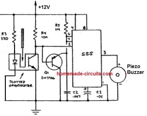 This circuit is more effective and easier to install than the conventional magnetic reed relay type intrusion alarm.
Here the circuit utilizes a IC 555 timers as a one shot timer for sounding the alarm.
The air gap slot of the optoisolator is blocked with a lever kind of attachment, which is also integrated to the window or the door.
In an event the door is opened or the window is opened, the blockage in the slot is removed, and the LED IR reaches the phototransistors and activates the one shot monostable IC 555 stage.
The IC 555 instantly triggers the piezo buzzer alerting regarding the intrusion.
This circuit is more effective and easier to install than the conventional magnetic reed relay type intrusion alarm.
Here the circuit utilizes a IC 555 timers as a one shot timer for sounding the alarm.
The air gap slot of the optoisolator is blocked with a lever kind of attachment, which is also integrated to the window or the door.
In an event the door is opened or the window is opened, the blockage in the slot is removed, and the LED IR reaches the phototransistors and activates the one shot monostable IC 555 stage.
The IC 555 instantly triggers the piezo buzzer alerting regarding the intrusion.
 Courtesy: https://en.wikipedia.org/wiki/Schottky_diode
 The semiconductor section is mostly built using n-type silicon, and also with a bunch different materials such as platinum, tungsten, molybdenum, chrome etc.
The diode may have different set of characteristics depending on which material is used, enabling them to have enhanced switching speed, lower forward voltage drop etc.
The semiconductor section is mostly built using n-type silicon, and also with a bunch different materials such as platinum, tungsten, molybdenum, chrome etc.
The diode may have different set of characteristics depending on which material is used, enabling them to have enhanced switching speed, lower forward voltage drop etc.
 In the reverse-bias region, the current Is is mainly due to those metal electrons travelling into the semiconductor material.
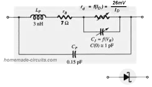 The inductance Lp and the capacitance Cp are the values specified in the package itself, rB constitutes the series resistance made up of the contact resistance and the bulk resistance.
The values for the resistance rd and capacitance Cj are as per the calculations discussed in the previous paragraphs.
The inductance Lp and the capacitance Cp are the values specified in the package itself, rB constitutes the series resistance made up of the contact resistance and the bulk resistance.
The values for the resistance rd and capacitance Cj are as per the calculations discussed in the previous paragraphs.
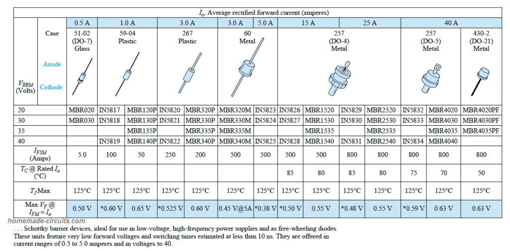
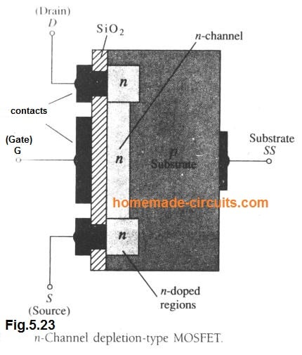 Fig.5.23 shows the basic internal structure of a n-channel depletion-type MOSFET.
We can find a block of p-type material created using a silicon base.
This block is called the substrate.
The substrate is the base or the foundation over which a MOSFET is constructed.
For some MOSFETs it is internally linked with the "source" terminal.
Also, many devices offer an extra output in the form of SS, featuring a 4-terminal MOSFET, as revealed in Fig.5.23
The drain and the source terminals are connected through conductive contacts to n-doped locations, and attached through an n-channel, as indicated in the same figure.
The gate is also connected to a metallic layer, although it is insulated from the n-channel through a fine layer of silicon dioxide (SiO2).
SiO2 possesses a unique form of insulation property called dielectric which creates an opposing electric field within itself in response to an externally applied electric field.
Being an insulating layer, the material SiO2 offers us the following important information:
A complete isolation is developed between the gate terminal and the mosfet channel with this material.
Moreover, it is because of SiO2, the gate of the mosfet is able to feature an extremely high degree of input impedance.
Due to this vital high input impedance property, the gate current IG is virtually zero amps for any dc-biased MOSFET configuration.
Fig.5.23 shows the basic internal structure of a n-channel depletion-type MOSFET.
We can find a block of p-type material created using a silicon base.
This block is called the substrate.
The substrate is the base or the foundation over which a MOSFET is constructed.
For some MOSFETs it is internally linked with the "source" terminal.
Also, many devices offer an extra output in the form of SS, featuring a 4-terminal MOSFET, as revealed in Fig.5.23
The drain and the source terminals are connected through conductive contacts to n-doped locations, and attached through an n-channel, as indicated in the same figure.
The gate is also connected to a metallic layer, although it is insulated from the n-channel through a fine layer of silicon dioxide (SiO2).
SiO2 possesses a unique form of insulation property called dielectric which creates an opposing electric field within itself in response to an externally applied electric field.
Being an insulating layer, the material SiO2 offers us the following important information:
A complete isolation is developed between the gate terminal and the mosfet channel with this material.
Moreover, it is because of SiO2, the gate of the mosfet is able to feature an extremely high degree of input impedance.
Due to this vital high input impedance property, the gate current IG is virtually zero amps for any dc-biased MOSFET configuration.
 AS can be seen in Fig.5.24, the gate to source voltage has been configured at zero volts by connecting the two terminals together, while a voltage VDS is applied across the drain and source terminals.
With the above setting, the drain side establishes a positive potential by the n-channel free electrons, along with an equivalent current through the JFET channel.
Also, the resulting current VGS = 0V is still being identified as IDSS, as given in Fig.
5.25
AS can be seen in Fig.5.24, the gate to source voltage has been configured at zero volts by connecting the two terminals together, while a voltage VDS is applied across the drain and source terminals.
With the above setting, the drain side establishes a positive potential by the n-channel free electrons, along with an equivalent current through the JFET channel.
Also, the resulting current VGS = 0V is still being identified as IDSS, as given in Fig.
5.25
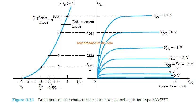 We can see that in Fig.5.26 the gate source voltage VGS is given a negative potential in the form of -1V.
This negative potential tries to force electrons toward the p-channel substrate (since charges repel), and pull holes from the p-channel substrate (since opposite charges attract).
We can see that in Fig.5.26 the gate source voltage VGS is given a negative potential in the form of -1V.
This negative potential tries to force electrons toward the p-channel substrate (since charges repel), and pull holes from the p-channel substrate (since opposite charges attract).
 Depending on how large this negative bias VGS is, a recombination of holes and electrons takes place which results in the reduction of free electrons in the n-channel available for the conduction.
Higher levels of negative bias results in higher rate of recombination.
The drain current consequently is reduced as the above negative bias condition is increased, which is proven in Fig.5.25 for VGS levels of VGS = -1, -2 and so forth, until the pinch-off mark of -6V.
The drain current as a result along with the transfer curve plot proceeds just like that of a JFET.
Now, for the positive VGS values, the gate positive will attract excess electrons (free carriers) from the p-type substrate, on account of the reverse leakage current.
This will establish fresh carriers by the way of resultant collisions across the accelerating particles.
As the gate-to-source voltage tends to rise at the positive rate, the drain current shows a rapid increase, as proven in the Fig.5.25 for the same reasons as discussed above.
The gap developed between the curves of VGS = 0V and VGS = +1 distinctly shows the amount by which the current increased due to the 1 - V variation of the VGS
Due to the fast rise of the drain current we must be careful about the maximum current rating, otherwise it could cross the positive gate voltage limit.
For example, for the device type depicted in the Fig.5.25, applying a VGS = +4V would cause the drain current to rise at 22.2 mA, which may be crossing the maximum breakdown limit (current) of the device.
The above condition shows that the use of a positive gate-to-source voltage generates an enhanced effect on the quantity of the free carriers in the channel, as opposed to when VGS = 0V.
This is why the positive gate voltage region on the drain or transfer characteristics is generally known as enhancement region.
This region lies between the cut-off and the saturation level of IDSS or the depletion region.
Depending on how large this negative bias VGS is, a recombination of holes and electrons takes place which results in the reduction of free electrons in the n-channel available for the conduction.
Higher levels of negative bias results in higher rate of recombination.
The drain current consequently is reduced as the above negative bias condition is increased, which is proven in Fig.5.25 for VGS levels of VGS = -1, -2 and so forth, until the pinch-off mark of -6V.
The drain current as a result along with the transfer curve plot proceeds just like that of a JFET.
Now, for the positive VGS values, the gate positive will attract excess electrons (free carriers) from the p-type substrate, on account of the reverse leakage current.
This will establish fresh carriers by the way of resultant collisions across the accelerating particles.
As the gate-to-source voltage tends to rise at the positive rate, the drain current shows a rapid increase, as proven in the Fig.5.25 for the same reasons as discussed above.
The gap developed between the curves of VGS = 0V and VGS = +1 distinctly shows the amount by which the current increased due to the 1 - V variation of the VGS
Due to the fast rise of the drain current we must be careful about the maximum current rating, otherwise it could cross the positive gate voltage limit.
For example, for the device type depicted in the Fig.5.25, applying a VGS = +4V would cause the drain current to rise at 22.2 mA, which may be crossing the maximum breakdown limit (current) of the device.
The above condition shows that the use of a positive gate-to-source voltage generates an enhanced effect on the quantity of the free carriers in the channel, as opposed to when VGS = 0V.
This is why the positive gate voltage region on the drain or transfer characteristics is generally known as enhancement region.
This region lies between the cut-off and the saturation level of IDSS or the depletion region.

 As indicated in the above graph, the ON-resistance rds(on) vs analogue signal range looks like a practically flat response.
This characteristic, in conjunction with the low-capacitance levels of the these advanced depletion type device, allow them to be specifically ideal as analogue switches for audio and video switching applications.
The depletion-mode MOSFET's 'normally-on' attribute enables the device to be perfectly suitable for single FET current regulators.
One such example circuit can be seen in the following figure.
As indicated in the above graph, the ON-resistance rds(on) vs analogue signal range looks like a practically flat response.
This characteristic, in conjunction with the low-capacitance levels of the these advanced depletion type device, allow them to be specifically ideal as analogue switches for audio and video switching applications.
The depletion-mode MOSFET's 'normally-on' attribute enables the device to be perfectly suitable for single FET current regulators.
One such example circuit can be seen in the following figure.
 The Rs value could be determined using the formula:
Rs = VGSoff [ 1 - ( ID/IDSS)1/2] / ID
where ID is the amount of regulated current required at the output.
The main advantage of depletion-mode MOSFETs in current-source application is their minimal drain capacitance, that makes them appropriate for biasing applications in low-input leakage, medium-speed (>50 V/us) circuits.
The figure below exhibits a low-input-leakage current differential front-end using a double low-leakage function FET.
The Rs value could be determined using the formula:
Rs = VGSoff [ 1 - ( ID/IDSS)1/2] / ID
where ID is the amount of regulated current required at the output.
The main advantage of depletion-mode MOSFETs in current-source application is their minimal drain capacitance, that makes them appropriate for biasing applications in low-input leakage, medium-speed (>50 V/us) circuits.
The figure below exhibits a low-input-leakage current differential front-end using a double low-leakage function FET.
 Generally speaking, either side of the JFET is going to be biased at ID = 500 uA.
Therefore, the current obtainable for charging compensation and stray capacitances becomes restricted to 2ID or, in cases like this, 1.0 mA.
The JFET's corresponding features are production-proven and assured on the datasheet.
Cs symbolizes the output capacitance of the input stage 'tail' current source.
This capacitance is crucial in non-inverting amplifiers, due to the fact that the input stage experiences significant signal exchanges throughout this network, and the charging currents in Cs could be big.
In case normal current sources are employed, this tail capacitance could be accountable for noticeable slew-rate deterioration in non-inverting circuits (compared to inverting applications, where the charging currents in Cs tend to be minimal).
The drop in the slew-rate could be expressed as:
1 / 1+ (Cs/Sc)
So long as Cs is lower than Cc (the compensation capacitor), there may be hardly any variation in the slew rate.
Working with the DMOS FET, Cs can be around 2 pF.
This strategy produces a huge improvement in the slew-rate.
Where current deficits higher than 1 to 5 mA are needed, the device could be biased into the enhancement mode to generate as much as 20 mA for a maximum VGS of +2.5 V, with minimal output capacitance continuing to be a key aspect.
The next application below exhibits a proper enhancement-mode current source circuit.
Generally speaking, either side of the JFET is going to be biased at ID = 500 uA.
Therefore, the current obtainable for charging compensation and stray capacitances becomes restricted to 2ID or, in cases like this, 1.0 mA.
The JFET's corresponding features are production-proven and assured on the datasheet.
Cs symbolizes the output capacitance of the input stage 'tail' current source.
This capacitance is crucial in non-inverting amplifiers, due to the fact that the input stage experiences significant signal exchanges throughout this network, and the charging currents in Cs could be big.
In case normal current sources are employed, this tail capacitance could be accountable for noticeable slew-rate deterioration in non-inverting circuits (compared to inverting applications, where the charging currents in Cs tend to be minimal).
The drop in the slew-rate could be expressed as:
1 / 1+ (Cs/Sc)
So long as Cs is lower than Cc (the compensation capacitor), there may be hardly any variation in the slew rate.
Working with the DMOS FET, Cs can be around 2 pF.
This strategy produces a huge improvement in the slew-rate.
Where current deficits higher than 1 to 5 mA are needed, the device could be biased into the enhancement mode to generate as much as 20 mA for a maximum VGS of +2.5 V, with minimal output capacitance continuing to be a key aspect.
The next application below exhibits a proper enhancement-mode current source circuit.
 A 'normally-on' analogue switch could be built for requirements where standard condition becomes necessary during a supply voltage failure, for example in automatic ranging of test tools or for ensuring accurate start-up of logic circuits at switch ON.
The reduced negative threshold voltage of the device offers basic drive prerequisites and permits working with minimal voltage.
The circuit below demonstrates the common bias factors for any depletion-mode DMOS analogue switch.
A 'normally-on' analogue switch could be built for requirements where standard condition becomes necessary during a supply voltage failure, for example in automatic ranging of test tools or for ensuring accurate start-up of logic circuits at switch ON.
The reduced negative threshold voltage of the device offers basic drive prerequisites and permits working with minimal voltage.
The circuit below demonstrates the common bias factors for any depletion-mode DMOS analogue switch.
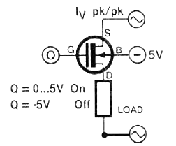 To cause the device to switch off, a negative voltages becomes necessary on the gate.
Having said that, the on-resistance could be minimized when the FET is additionally enhanced using a positive gate voltage, enabling it specifically in the enhancement-mode region along with the depletion-mode region.
This response can be witnessed in in the following graph.
To cause the device to switch off, a negative voltages becomes necessary on the gate.
Having said that, the on-resistance could be minimized when the FET is additionally enhanced using a positive gate voltage, enabling it specifically in the enhancement-mode region along with the depletion-mode region.
This response can be witnessed in in the following graph.
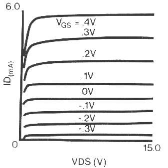 The high-frequency gain of the unit, together with its low capacitance values, delivers an increased 'figure of merit'.
It is really an crucial element in VHF and UHF amplification, which specifies the gain-bandwidth product (GBW) of the FET, which could be depicted as:
GBW = gfs / 2��(Cin + Cout)
The high-frequency gain of the unit, together with its low capacitance values, delivers an increased 'figure of merit'.
It is really an crucial element in VHF and UHF amplification, which specifies the gain-bandwidth product (GBW) of the FET, which could be depicted as:
GBW = gfs / 2��(Cin + Cout)
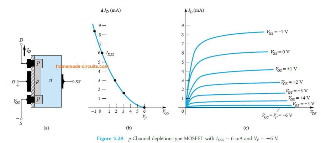 The terminal identification remains unchanged, but the voltage and the current polarities are reversed, as indicated in the same figure.
The drain characteristics would be exactly as depicted in Fig.5.25, except VDS sign which will in this case get a negative value.
The drain current ID shows a positive polarity in this case too, that's because we have already reversed its direction.
VGS shows an opposite polarity, which is understandable, as indicated in Fig.5.28c.
Because VGS is reversed produces a mirror image for the transfer characteristics as indicated in Fig.5,28b.
Meaning, the drain current increases in the positive VGS region from the cut-off point at VGS = Vp until IDSS, then it continues to rise as the negative value of VGS rises.
The terminal identification remains unchanged, but the voltage and the current polarities are reversed, as indicated in the same figure.
The drain characteristics would be exactly as depicted in Fig.5.25, except VDS sign which will in this case get a negative value.
The drain current ID shows a positive polarity in this case too, that's because we have already reversed its direction.
VGS shows an opposite polarity, which is understandable, as indicated in Fig.5.28c.
Because VGS is reversed produces a mirror image for the transfer characteristics as indicated in Fig.5,28b.
Meaning, the drain current increases in the positive VGS region from the cut-off point at VGS = Vp until IDSS, then it continues to rise as the negative value of VGS rises.
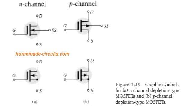 The graphical signs for an n- and p-channel depletion-type MOSFET can be witnessed in the above Fig.
5.29.
Observe the way the selected symbols aim to represent the true structure of the device.
The absence of a direct interconnection (because of the gate insulation) between the gate and channel is symbolized by a gap between the gate and the different terminals of the symbol.
The vertical line which represents the channel is attached between the drain and source and is ��held�� by the substrate.
Two groups of symbols are furnished in the figure above for each type of channel to highlight the fact that in some devices the substrate may be accessible externally while in others this may not be seen.
The graphical signs for an n- and p-channel depletion-type MOSFET can be witnessed in the above Fig.
5.29.
Observe the way the selected symbols aim to represent the true structure of the device.
The absence of a direct interconnection (because of the gate insulation) between the gate and channel is symbolized by a gap between the gate and the different terminals of the symbol.
The vertical line which represents the channel is attached between the drain and source and is ��held�� by the substrate.
Two groups of symbols are furnished in the figure above for each type of channel to highlight the fact that in some devices the substrate may be accessible externally while in others this may not be seen.
 This substrate on some occasions is attached internally with the source pin in a depletion-type MOSFET, while in some instances it is terminated as a fourth lead for enabling an external control of its potential level.
The source and drain terminals are as usual joined using metallic contacts to n-doped regions.
However, it may be important to visualize that in Fig.
5.31 the channel between the two n-doped regions is missing.
This may be considered as the fundamental dissimilarity between a depletion-type and an enhancement-type MOSFET's internal layout, that is an absence of an inherent channel which is supposed to be a part of the device.
The SiO2 layer can be seen still prevalent, which ensures an isolation between the metallic base of the gate terminal and the region between the drain and source.
However, here it can be witnessed standing separated from the p-type material section.
From the above discussion we can conclude that a depletion and enhancement MOSFET internal layout may have some similarities, except the missing channel between drain/source for an enhancement type of MOSFET.
This substrate on some occasions is attached internally with the source pin in a depletion-type MOSFET, while in some instances it is terminated as a fourth lead for enabling an external control of its potential level.
The source and drain terminals are as usual joined using metallic contacts to n-doped regions.
However, it may be important to visualize that in Fig.
5.31 the channel between the two n-doped regions is missing.
This may be considered as the fundamental dissimilarity between a depletion-type and an enhancement-type MOSFET's internal layout, that is an absence of an inherent channel which is supposed to be a part of the device.
The SiO2 layer can be seen still prevalent, which ensures an isolation between the metallic base of the gate terminal and the region between the drain and source.
However, here it can be witnessed standing separated from the p-type material section.
From the above discussion we can conclude that a depletion and enhancement MOSFET internal layout may have some similarities, except the missing channel between drain/source for an enhancement type of MOSFET.
 In Fig.
5.32 shows a condition where VDS and VGS are applied with some positive voltage higher than 0 V, allowing the drain and gate to be at a positive potential with respect to the source.
The positive potential at the gate pushes the holes in the p-substrate along the edge of the SiO2 layer departing the location and entering deeper into the regions of the p-substrate, as shown in the above figure.
This happens because of the like charges that repel each other.
This results in a depletion region being created close to the SiO2 insulating layer that is void of holes.
Despite of this, the p-substrate electrons which are the minority carriers of the material are pulled towards the positive gate and start gathering in the region close to the surface of the SiO2 layer.
Due to the insulation property of the SiO2 layer negative carriers allow the negative carriers from getting absorbed at the gate terminal.
As we increase the level of VGS, the electron density close to the SiO2 surface also increase, until finally the induced n-type region is able to allow a quantifiable conduction across drain/source.
The VGS magnitude that causes an optimal increase in the drain current is termed as the threshold voltage, signified by the symbol VT.
In datasheets you will be able to see this as VGS(Th).
As learned above, due to the absence of a channel at VGS = 0, and "enhanced" with the positive gate-to-source voltage application, this type of MOSFET are known as enhancement-type MOSFETs.
You will find that both depletion- and enhancement-type MOSFETs exhibit enhancement-type regions, but the term enhancement is used for the latter because it specifically works using an enhancement mode of operation.
Now, when VGS is pushed over the threshold value, the concentration of the free carriers will boost in the channel where it's induced.
This causes the drain current to increase.
On the other hand, if we keep the VGS constant and increase the VDS (drain-to-source voltage) level, this will ultimately cause the MOSFET to reach its saturation point, as normally would also happen to any JFET or a depletion MOSFET.
In Fig.
5.32 shows a condition where VDS and VGS are applied with some positive voltage higher than 0 V, allowing the drain and gate to be at a positive potential with respect to the source.
The positive potential at the gate pushes the holes in the p-substrate along the edge of the SiO2 layer departing the location and entering deeper into the regions of the p-substrate, as shown in the above figure.
This happens because of the like charges that repel each other.
This results in a depletion region being created close to the SiO2 insulating layer that is void of holes.
Despite of this, the p-substrate electrons which are the minority carriers of the material are pulled towards the positive gate and start gathering in the region close to the surface of the SiO2 layer.
Due to the insulation property of the SiO2 layer negative carriers allow the negative carriers from getting absorbed at the gate terminal.
As we increase the level of VGS, the electron density close to the SiO2 surface also increase, until finally the induced n-type region is able to allow a quantifiable conduction across drain/source.
The VGS magnitude that causes an optimal increase in the drain current is termed as the threshold voltage, signified by the symbol VT.
In datasheets you will be able to see this as VGS(Th).
As learned above, due to the absence of a channel at VGS = 0, and "enhanced" with the positive gate-to-source voltage application, this type of MOSFET are known as enhancement-type MOSFETs.
You will find that both depletion- and enhancement-type MOSFETs exhibit enhancement-type regions, but the term enhancement is used for the latter because it specifically works using an enhancement mode of operation.
Now, when VGS is pushed over the threshold value, the concentration of the free carriers will boost in the channel where it's induced.
This causes the drain current to increase.
On the other hand, if we keep the VGS constant and increase the VDS (drain-to-source voltage) level, this will ultimately cause the MOSFET to reach its saturation point, as normally would also happen to any JFET or a depletion MOSFET.
 As shown in Fig.
5.33 the drain current ID gets leveled off with the aid of a pinching-off process, indicated by the narrower channel towards the drain end of the induced channel.
By applying applying Kirchhoff��s voltage law to the MOSFET's terminal voltages in Fig.
5.33, we get:
As shown in Fig.
5.33 the drain current ID gets leveled off with the aid of a pinching-off process, indicated by the narrower channel towards the drain end of the induced channel.
By applying applying Kirchhoff��s voltage law to the MOSFET's terminal voltages in Fig.
5.33, we get:
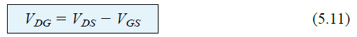 If VGS is kept constant to a specific value, for example 8 V, and VDS is raised from 2 to 5 V, the voltage VDG by Eq.
5.11 could be seen dropping from -6 to -3 V, and the gate potential getting less and less positive with respect to the drain voltage.
This response prohibits the free carriers or electrons from getting pulled towards this region of the induced channel, which in turn results in a drop in the effective width of the channel.
Ultimately, the channel width decreases to the point of pinch-off , reaching a saturation condition similar to what we already learned in our earlier depletion MOSFET article.
Meaning, increasing the VDS any further with a fixed VGS does not affect the saturation level of ID, until the point where a breakdown situation is reached.
Looking at the Fig 5.34 we can identify that for a MOSFET as in Fig.5.33 having VGS = 8 V, saturation takes place at a VDS level of 6 V.
To be precise the VDS saturation level is associated to the applied VGS level by:
If VGS is kept constant to a specific value, for example 8 V, and VDS is raised from 2 to 5 V, the voltage VDG by Eq.
5.11 could be seen dropping from -6 to -3 V, and the gate potential getting less and less positive with respect to the drain voltage.
This response prohibits the free carriers or electrons from getting pulled towards this region of the induced channel, which in turn results in a drop in the effective width of the channel.
Ultimately, the channel width decreases to the point of pinch-off , reaching a saturation condition similar to what we already learned in our earlier depletion MOSFET article.
Meaning, increasing the VDS any further with a fixed VGS does not affect the saturation level of ID, until the point where a breakdown situation is reached.
Looking at the Fig 5.34 we can identify that for a MOSFET as in Fig.5.33 having VGS = 8 V, saturation takes place at a VDS level of 6 V.
To be precise the VDS saturation level is associated to the applied VGS level by:
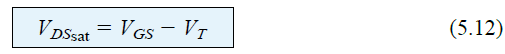 No doubt, it thus implies that when the VT value is fixed, increasing the level of VGS will proportionately cause higher levels of saturation for VDS through the locus of saturation levels.
Referring to the characteristics shown in the above figure, the VT level is 2 V, which is evident by the fact that the drain current has fallen to 0 mA.
Therefore typically we can say:
When VGS values are less than the threshold level for enhancement-type MOSFET, its drain current is 0 mA.
No doubt, it thus implies that when the VT value is fixed, increasing the level of VGS will proportionately cause higher levels of saturation for VDS through the locus of saturation levels.
Referring to the characteristics shown in the above figure, the VT level is 2 V, which is evident by the fact that the drain current has fallen to 0 mA.
Therefore typically we can say:
When VGS values are less than the threshold level for enhancement-type MOSFET, its drain current is 0 mA.
 We can also clearly see in the above figure that as long as the VGS is raised higher from VT to 8 V, the corresponding saturation level for ID also increases from 0 to 10 mA level.
Moreover we can further notice that the space between the VGS levels increases with an increase in the value of VGS, causing an infinitely rising increments in drain current.
We find the drain current value is related to the gate-to-source voltage for VGS levels that's greater than VT, through the following nonlinear relationship:
We can also clearly see in the above figure that as long as the VGS is raised higher from VT to 8 V, the corresponding saturation level for ID also increases from 0 to 10 mA level.
Moreover we can further notice that the space between the VGS levels increases with an increase in the value of VGS, causing an infinitely rising increments in drain current.
We find the drain current value is related to the gate-to-source voltage for VGS levels that's greater than VT, through the following nonlinear relationship:
 The term which is shown squared bracket is the term which is responsible for the nonlinear relatinship between ID and VGS.
The term k is a constant and is a function of the MOSFET layout.
We can find out the value of this constant k through the following equation:
where the ID(on) and VGD(on) each are values specifically depending on the characteristic of the device.
The term which is shown squared bracket is the term which is responsible for the nonlinear relatinship between ID and VGS.
The term k is a constant and is a function of the MOSFET layout.
We can find out the value of this constant k through the following equation:
where the ID(on) and VGD(on) each are values specifically depending on the characteristic of the device.
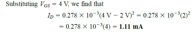 In the next Fig.
5.35 below we find the drain and transfer characteristics are arranged one beside the other to clarify the transfer process across one another.
Basically, it is similar to the process explained previously for JFET and depletion-type MOSFETs.
However, for the present case we have to remember that the drain current is 0 mA for VGS VT.
Here ID may see a noticeable amount of current, which will increase as determined by Eq.
5.13.
Note, while defining the points over the transfer characteristics from the drain characteristics, we only consider the saturation levels.
This restricts the region of operation to VDS values higher than the saturation levels as established by Eq.
(5.12).
In the next Fig.
5.35 below we find the drain and transfer characteristics are arranged one beside the other to clarify the transfer process across one another.
Basically, it is similar to the process explained previously for JFET and depletion-type MOSFETs.
However, for the present case we have to remember that the drain current is 0 mA for VGS VT.
Here ID may see a noticeable amount of current, which will increase as determined by Eq.
5.13.
Note, while defining the points over the transfer characteristics from the drain characteristics, we only consider the saturation levels.
This restricts the region of operation to VDS values higher than the saturation levels as established by Eq.
(5.12).
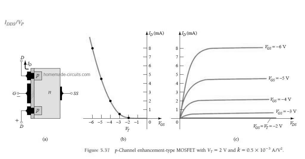 The transfer characteristics would be the mirror impression (around the ID axis) of the transfer curve of Fig.
5.35, having ID increasing with more and more negative values of VGS above VT, as displayed in Fig.
5.37b.
Equations (5.11) through (5.14) are similarly appropriate to p-channel devices.
References:
https://en.wikipedia.org/wiki/MOSFET
https://hi.wikipedia.org/wiki/%E0%A4%AE%E0%A5%89%E0%A4%B8%E0%A4%AB%E0%A5%87%E0%A4%9F
The transfer characteristics would be the mirror impression (around the ID axis) of the transfer curve of Fig.
5.35, having ID increasing with more and more negative values of VGS above VT, as displayed in Fig.
5.37b.
Equations (5.11) through (5.14) are similarly appropriate to p-channel devices.
References:
https://en.wikipedia.org/wiki/MOSFET
https://hi.wikipedia.org/wiki/%E0%A4%AE%E0%A5%89%E0%A4%B8%E0%A4%AB%E0%A5%87%E0%A4%9F
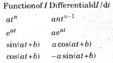 The table above works by using I and t as the factors instead of the routine x and y.
So that its details are specifically pertinent to electronics.
As an example, considering that I= 3t +2, the way I deviates with respect to time can be visualized in the graph of Fig.
38. To nd the rate of change of I at any moment, we estimate dI/dt, by referring to the table.
The table above works by using I and t as the factors instead of the routine x and y.
So that its details are specifically pertinent to electronics.
As an example, considering that I= 3t +2, the way I deviates with respect to time can be visualized in the graph of Fig.
38. To nd the rate of change of I at any moment, we estimate dI/dt, by referring to the table.
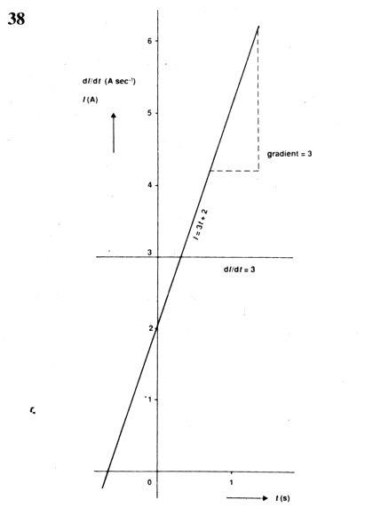 The rst element in the function is 3t or, to format it as the rst line of the table, 3t1 .
Ifn = 1, the differential is 3t1-1 = 3t0.
Since t0 = 1, the differential is 3.
The second quantity is 2, that can be expressed as 2t0 .
This changes n = 0, and the magnitude of the differential is zero.
The differential of a constant will be always zero.
Getting both of these combined, we have:
dI / dt = 3
In this illustration the differential doesn't include t, that means the differential is not dependent on time.
Put simply, the slope or gradient of the curve in Fig.
38 is 3 continuously all the time.
Figure 39 below displays the curve for a different function, I = 4 sin 1.5t.
The rst element in the function is 3t or, to format it as the rst line of the table, 3t1 .
Ifn = 1, the differential is 3t1-1 = 3t0.
Since t0 = 1, the differential is 3.
The second quantity is 2, that can be expressed as 2t0 .
This changes n = 0, and the magnitude of the differential is zero.
The differential of a constant will be always zero.
Getting both of these combined, we have:
dI / dt = 3
In this illustration the differential doesn't include t, that means the differential is not dependent on time.
Put simply, the slope or gradient of the curve in Fig.
38 is 3 continuously all the time.
Figure 39 below displays the curve for a different function, I = 4 sin 1.5t.
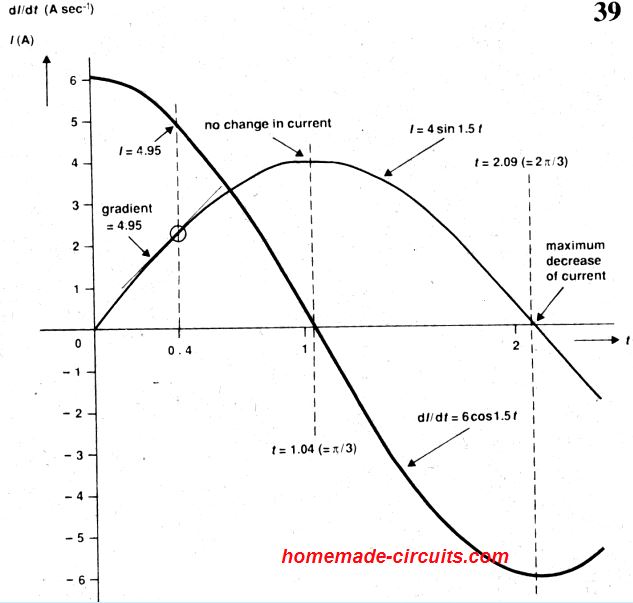 With reference to the table, �� = 1.5 and b = 0 in this function.
The table shows, dl/dt = 4x1.5cos1.5t = 6cos 1.5t.
This informs us the instantaneous rate of change of I.
For example, at t = 0.4, dI/dt = 6cos0.6 = 4.95. This could be noticed in Fig.
39, in which the curve for 6 cos0.6t includes the value 4.95 when t = 0.4.
We can also observe that the slope of the curve 4sin1.5t is 4.95 when t = 0.4, as shown by the tangent to the curve at that point, (with respect to the different scales on the two axes).
When t = ��/3, a point when the current is at its highest and constant, in this case dI/dt = 6cos(1.5x��/3): 0, corresponding to zero change of current.
On the contrary , when t = 2��/3 and the current is switching at highest possible level from positive to negative, dI/dt = 6cos�� = -6, we see its highest negative value, exhibiting a high reduction of current.
The simple benefit of differentials is they allow us to determine rates of change for functions that are a lot more complex compared to I = 4sin 1.5t, and without having to to plot the curves.
Back to Calculations
By Reorganizing the terms in Eq 22 we get:
�� = (L / N)I [Eq.24]
Where L and N have constant dimensions, but �� and I may a having value with respect to time.
Differentiating the two sides of the equation with respect to time gives:
d�� / dt = (L / N)(dI / dt) [Eq.
25]
Merging this equation with Eq.23 gives:
U = N(L/N)(dI / dt) = L (dI / dt) [Eq.26]
This is another way of expressing the henry.
We can say that, a coil having self-inductance of 1 H, a change of current of 1 A s-1 generates a back e.m.f.
of 1 V.
Given a function which defines how a current varies with time, Eq.
26 helps us to calculate the back e.m.f. of an inductor at any instant.
Following are a few examples.
A) I= 3 (a constant current of 3 A); dl/dt = 0. You cannot find any change of current therefore the back e.m.f.
is zero.
B) I = 2t (a ramp current); dI/dt = 2 A s-1.
With a coil carrying L = 0.25 H, the back e.m.f.
will be constant at 0.25x2 = 0.5 V.
C) I = 4sin1.5t (the sinusoidal current given in the previous illustration; dl/dt = 6cos 1.5t.
Given a coil with L = 0.1 H, the instantaneous back e.m.f.
is 0.6cos1.5t.
The back e.m.f.
follows the differential curve of Fig.
39, but with amplitude 0.6 V rather than 6 A.
With reference to the table, �� = 1.5 and b = 0 in this function.
The table shows, dl/dt = 4x1.5cos1.5t = 6cos 1.5t.
This informs us the instantaneous rate of change of I.
For example, at t = 0.4, dI/dt = 6cos0.6 = 4.95. This could be noticed in Fig.
39, in which the curve for 6 cos0.6t includes the value 4.95 when t = 0.4.
We can also observe that the slope of the curve 4sin1.5t is 4.95 when t = 0.4, as shown by the tangent to the curve at that point, (with respect to the different scales on the two axes).
When t = ��/3, a point when the current is at its highest and constant, in this case dI/dt = 6cos(1.5x��/3): 0, corresponding to zero change of current.
On the contrary , when t = 2��/3 and the current is switching at highest possible level from positive to negative, dI/dt = 6cos�� = -6, we see its highest negative value, exhibiting a high reduction of current.
The simple benefit of differentials is they allow us to determine rates of change for functions that are a lot more complex compared to I = 4sin 1.5t, and without having to to plot the curves.
Back to Calculations
By Reorganizing the terms in Eq 22 we get:
�� = (L / N)I [Eq.24]
Where L and N have constant dimensions, but �� and I may a having value with respect to time.
Differentiating the two sides of the equation with respect to time gives:
d�� / dt = (L / N)(dI / dt) [Eq.
25]
Merging this equation with Eq.23 gives:
U = N(L/N)(dI / dt) = L (dI / dt) [Eq.26]
This is another way of expressing the henry.
We can say that, a coil having self-inductance of 1 H, a change of current of 1 A s-1 generates a back e.m.f.
of 1 V.
Given a function which defines how a current varies with time, Eq.
26 helps us to calculate the back e.m.f. of an inductor at any instant.
Following are a few examples.
A) I= 3 (a constant current of 3 A); dl/dt = 0. You cannot find any change of current therefore the back e.m.f.
is zero.
B) I = 2t (a ramp current); dI/dt = 2 A s-1.
With a coil carrying L = 0.25 H, the back e.m.f.
will be constant at 0.25x2 = 0.5 V.
C) I = 4sin1.5t (the sinusoidal current given in the previous illustration; dl/dt = 6cos 1.5t.
Given a coil with L = 0.1 H, the instantaneous back e.m.f.
is 0.6cos1.5t.
The back e.m.f.
follows the differential curve of Fig.
39, but with amplitude 0.6 V rather than 6 A.
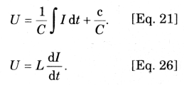 It helps us to determine the level of voltage produced across the component by current varying in time as per a specific funtion.
Let's evaluate the result obtained by differentiating the L and H sides of Eq.21 with respect to time.
dU / dt = (1 / C)I
As we know differentiation is the inverse of integration, differentiation of ��I dt reverses the integration, with only I as the result.
Differentiating c/C gives zero, and rearranging the terms produces the following:
I = C.dU / dt [Eq.27]
This allows us to know the direction of the current whether it's going towards the capacitor or coming out from it, in response to a voltage varying according to a given function.
The interesting thing is that the above capacitor current equation looks similar to the voltage equation (26) of an inductor, which exhibits the capacitance, inductance duality.
Similarly, the current and potential difference (pd) or the rate of change of current and pd can be duals when applied to capacitors and inductors.
Now, let's integrate Eq.26 with respect to time to complete the equation quatret:
�� U dt+c = LI
The integral of dI/dt is = I , we rearrange the expressions to get:
I = 1/L�� U dt + e/L
This again looks quite similar to Eq.21, further proving the dual nature of capacitance and inductance, and their pd and current.
By now we have a set of four equations which can be used for solving capacitor and inductor related problems.
For Example Eq.27 can be applied to solve the problem as as this one:
Problem: A voltage pulse applied across a 100uF produces a curve as shown in the Fig below.
It helps us to determine the level of voltage produced across the component by current varying in time as per a specific funtion.
Let's evaluate the result obtained by differentiating the L and H sides of Eq.21 with respect to time.
dU / dt = (1 / C)I
As we know differentiation is the inverse of integration, differentiation of ��I dt reverses the integration, with only I as the result.
Differentiating c/C gives zero, and rearranging the terms produces the following:
I = C.dU / dt [Eq.27]
This allows us to know the direction of the current whether it's going towards the capacitor or coming out from it, in response to a voltage varying according to a given function.
The interesting thing is that the above capacitor current equation looks similar to the voltage equation (26) of an inductor, which exhibits the capacitance, inductance duality.
Similarly, the current and potential difference (pd) or the rate of change of current and pd can be duals when applied to capacitors and inductors.
Now, let's integrate Eq.26 with respect to time to complete the equation quatret:
�� U dt+c = LI
The integral of dI/dt is = I , we rearrange the expressions to get:
I = 1/L�� U dt + e/L
This again looks quite similar to Eq.21, further proving the dual nature of capacitance and inductance, and their pd and current.
By now we have a set of four equations which can be used for solving capacitor and inductor related problems.
For Example Eq.27 can be applied to solve the problem as as this one:
Problem: A voltage pulse applied across a 100uF produces a curve as shown in the Fig below.
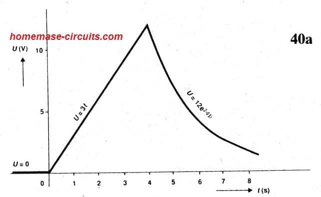 This can be defined using the following piece-wise function.
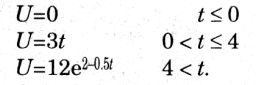 Calculate the current moving through the capacitor and plot the corresponding graphs.
Solution:
For the first stage we apply Eq.27
I = C(dU / dt) = 0
For the second instance where U may be rising with a constant rate:
I = C(dU / dt) = 3C = 300��A
This shows a constant charging current.
For the third stage when U drops in an exponential manner:
Calculate the current moving through the capacitor and plot the corresponding graphs.
Solution:
For the first stage we apply Eq.27
I = C(dU / dt) = 0
For the second instance where U may be rising with a constant rate:
I = C(dU / dt) = 3C = 300��A
This shows a constant charging current.
For the third stage when U drops in an exponential manner:
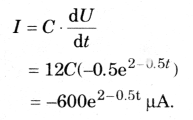 This indicates current flowing away from the capacitor in an exponential decreasing rate.
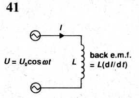 In the abobe figure, an alternating pd is applied to an inductor.
This pd at any instant can be expressed as:
In the abobe figure, an alternating pd is applied to an inductor.
This pd at any instant can be expressed as:
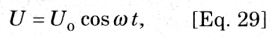 Where Uo is the peak value of the pd.
If we analyze the circuit in the form of a loop, and apply Kirchhoff's voltage law in clockwise direction, we get:
Where Uo is the peak value of the pd.
If we analyze the circuit in the form of a loop, and apply Kirchhoff's voltage law in clockwise direction, we get:
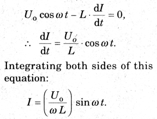 However, since the current is sinusoidal here, the terms in the bracket must have the value equal to the peak current Io, therefore we finally get:
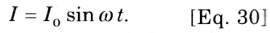 If we compare the Eq.29, and Eq.30 we find that the current I and the voltage U have the same frequency, and I lags behind U by ��/2.
The resultant curves can be studies in the following diagram:
If we compare the Eq.29, and Eq.30 we find that the current I and the voltage U have the same frequency, and I lags behind U by ��/2.
The resultant curves can be studies in the following diagram:
 C
This shows the contrasting relationship between capacitor and inductor.
For an inductor current lags the potential difference by ��/2,whileforacapacitor,thecurrentleadsthepd.
This yetagaindemonstratesthedual nature of the two components.
C
This shows the contrasting relationship between capacitor and inductor.
For an inductor current lags the potential difference by ��/2,whileforacapacitor,thecurrentleadsthepd.
This yetagaindemonstratesthedual nature of the two components.

 Sound vibrations hitting the electret capacitor varies its capacitance producing a modulating voltage for the gate of the JFET, indicated as Vg.
This modulation alters the current flow pattern across the drain/source of the JFET, represented as Imic.
A stabilizing resistor RG can be also seen connected internally across the gate and source of the JFET, it is ensured that this resistor has an extremely high value to avoid shunting of the electret output for the JFET gate.
Sound vibrations hitting the electret capacitor varies its capacitance producing a modulating voltage for the gate of the JFET, indicated as Vg.
This modulation alters the current flow pattern across the drain/source of the JFET, represented as Imic.
A stabilizing resistor RG can be also seen connected internally across the gate and source of the JFET, it is ensured that this resistor has an extremely high value to avoid shunting of the electret output for the JFET gate.
 One of the electrodes is formed by metalization of its layer over a charged polymer film.
This metalized layer is joined with the case of the MIC through a metallic washer.
The case of the MIC is in turn connected with the source lead of the internal JFET.
The other capacitor plate or the second electrode is made by using a backside metal plate, which can be seen separated from the metalized layer film by a plastic washer.
This plate is then connected with the gate terminal of the JFET
Sound waves hitting this plate generate a strain level on it, thereby varying the distance between the capacitive electrodes, and causing an equivalent potential difference to develop across them.
This varying voltage across the drain of the JFET is used as the output for a subsequent preamplifier circuit stage which further amplifies this to a level which can be reproduced over a loudspeaker, and an amplified version of the sound waves can be heard.
One of the electrodes is formed by metalization of its layer over a charged polymer film.
This metalized layer is joined with the case of the MIC through a metallic washer.
The case of the MIC is in turn connected with the source lead of the internal JFET.
The other capacitor plate or the second electrode is made by using a backside metal plate, which can be seen separated from the metalized layer film by a plastic washer.
This plate is then connected with the gate terminal of the JFET
Sound waves hitting this plate generate a strain level on it, thereby varying the distance between the capacitive electrodes, and causing an equivalent potential difference to develop across them.
This varying voltage across the drain of the JFET is used as the output for a subsequent preamplifier circuit stage which further amplifies this to a level which can be reproduced over a loudspeaker, and an amplified version of the sound waves can be heard.


 The force sensing resistor consists of three layers: an active area, plastic spacer and conductive film.
The active area where the force is applied, the plastic spacer which isolates the two layers and an air vent is provided for discharge of air bubbles.
The accumulation of air bubble leads to unreliable results.
The conducting film consists of both electric and dielectric particles which are suspended in matrix form.
When force is applied it changes its resistance in predictable manner.
These are microscopic particles ranges few micrometers.
The conductive film is basically a kind of an ink coated on plastic film.
When pressure is applied the conducting particles come close together and reduce resistance and vice-versa.
The force sensing resistor consists of three layers: an active area, plastic spacer and conductive film.
The active area where the force is applied, the plastic spacer which isolates the two layers and an air vent is provided for discharge of air bubbles.
The accumulation of air bubble leads to unreliable results.
The conducting film consists of both electric and dielectric particles which are suspended in matrix form.
When force is applied it changes its resistance in predictable manner.
These are microscopic particles ranges few micrometers.
The conductive film is basically a kind of an ink coated on plastic film.
When pressure is applied the conducting particles come close together and reduce resistance and vice-versa.

 The input is fed to analog read pin, which takes different voltage levels digitally from 0 to 255.
User can set their own threshold level in the program (Program is not given).
When light pressure is given blue LED turns ON, when medium pressure is given green LED turns ON, if high pressure is applied red LED turns ON.
Just use your imagination to find new applications and it��s endless.
The input is fed to analog read pin, which takes different voltage levels digitally from 0 to 255.
User can set their own threshold level in the program (Program is not given).
When light pressure is given blue LED turns ON, when medium pressure is given green LED turns ON, if high pressure is applied red LED turns ON.
Just use your imagination to find new applications and it��s endless.
 MOVs are basically non-polar, voltage dependent devices, meaning these devices will react to changes in voltage conditions.
Therefore MOVs are specified to trigger ON whenever the rated magnitude of voltage across their connections is exceeded.
This voltage rating at which an MOV may be rated to fire and short the transient to ground is called its clamping voltage specification.
For example, if suppose the clamping voltage rating of an MOV is 350V then it will switch ON whenever the voltage across it surpasses this limit.
When an MOV switches ON or is triggered by a high voltage surge it shorts the voltage spike across its terminals, preventing it from entering the vulnerable electronic device attached on the other side.
This action protects the electronic circuit from such accidental voltage surges and transient spikes.
And since the above reaction is sudden, MOVs are characterized as non-linear devices, which implies that these will not vary their characteristics gradually but suddenly when the specified parameters is exceeded.
The best characteristic of an MOV is its ability to absorb high current content accompanied with the voltage surge .
Depending on the MOV specification the current absorbing capacity of an MOV could be anywhere between 1 amp to a massive 2500 amps
MOVs are basically non-polar, voltage dependent devices, meaning these devices will react to changes in voltage conditions.
Therefore MOVs are specified to trigger ON whenever the rated magnitude of voltage across their connections is exceeded.
This voltage rating at which an MOV may be rated to fire and short the transient to ground is called its clamping voltage specification.
For example, if suppose the clamping voltage rating of an MOV is 350V then it will switch ON whenever the voltage across it surpasses this limit.
When an MOV switches ON or is triggered by a high voltage surge it shorts the voltage spike across its terminals, preventing it from entering the vulnerable electronic device attached on the other side.
This action protects the electronic circuit from such accidental voltage surges and transient spikes.
And since the above reaction is sudden, MOVs are characterized as non-linear devices, which implies that these will not vary their characteristics gradually but suddenly when the specified parameters is exceeded.
The best characteristic of an MOV is its ability to absorb high current content accompanied with the voltage surge .
Depending on the MOV specification the current absorbing capacity of an MOV could be anywhere between 1 amp to a massive 2500 amps
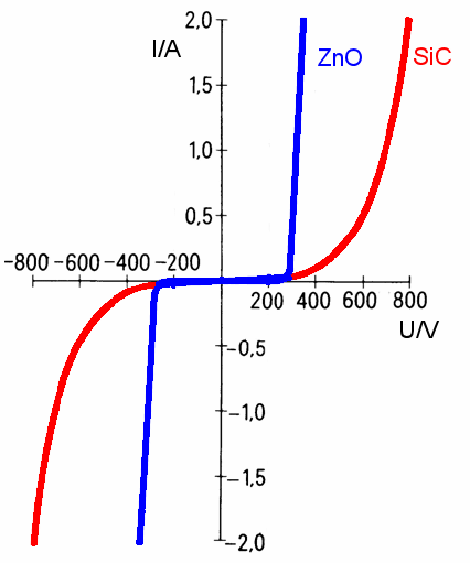
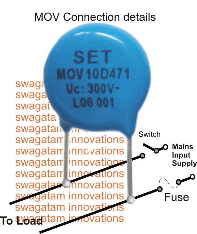
 The shape of the SMD resistor is rectangular.
There is a presence of a metallized area in the chip resistors at any one side of their body which in turn enables the contact of the printed circuit board with the chip resistor by using the solder.
A ceramic substrate is one of the components of the resistor and a metal oxide film is deposited over it.
The resistance of the resistor is determined by the actual film��s length and thickness.
Since metal oxide is used to manufacture the SMD resistors which enable the resistor to be highly stable along with the tolerance level also being high.
The element with which a ceramic substrate is made up of is high alumina ceramic.
The use of the high alumina ceramic in the SMD resistors provide stable insulation on the basis of the resistive metal oxide element on which the resistor is set down.
The terminations of the SMD resistors are also important.
The contact which the SMD resistor needs to make with the chip resistor��s resistive element needs to be reliable while at the same time it should provide solderability of very high levels.
Such high levels are achieved through the usage of the nickel based layer to make an internal connection.
At the same time and outer layer which is tin based is used to make the outer connection thereby achieving solderability of very high levels.
The shape of the SMD resistor is rectangular.
There is a presence of a metallized area in the chip resistors at any one side of their body which in turn enables the contact of the printed circuit board with the chip resistor by using the solder.
A ceramic substrate is one of the components of the resistor and a metal oxide film is deposited over it.
The resistance of the resistor is determined by the actual film��s length and thickness.
Since metal oxide is used to manufacture the SMD resistors which enable the resistor to be highly stable along with the tolerance level also being high.
The element with which a ceramic substrate is made up of is high alumina ceramic.
The use of the high alumina ceramic in the SMD resistors provide stable insulation on the basis of the resistive metal oxide element on which the resistor is set down.
The terminations of the SMD resistors are also important.
The contact which the SMD resistor needs to make with the chip resistor��s resistive element needs to be reliable while at the same time it should provide solderability of very high levels.
Such high levels are achieved through the usage of the nickel based layer to make an internal connection.
At the same time and outer layer which is tin based is used to make the outer connection thereby achieving solderability of very high levels.
 The toggle switch generally consists of two positions.
The mechanical mechanism starts functioning after the arm is actuated and holds the arm in any one of the two positions positively.
The designing of the internal mechanics are done in a manner in which the when the arm passes a specific point after the movement starts, and then the arm goes into the next position.
Thus, this enables the firm holding of the switch in either of the two positions.
Rocker Switch: The rocker switch is similar to the toggle switch in many areas; especially that it also possesses two positions like the former.
The toggle switch generally consists of two positions.
The mechanical mechanism starts functioning after the arm is actuated and holds the arm in any one of the two positions positively.
The designing of the internal mechanics are done in a manner in which the when the arm passes a specific point after the movement starts, and then the arm goes into the next position.
Thus, this enables the firm holding of the switch in either of the two positions.
Rocker Switch: The rocker switch is similar to the toggle switch in many areas; especially that it also possesses two positions like the former.
 The switching action in the rocker switch is not positive as is in the case of the toggle switch since the former does not follow the mechanism of the latter.
Electronic Switch: The switching of the electrical and electronic circuits can be done through the use of the SCRs, bipolar transistors, and FETs.
The switches are occasionally known as ��electronic switches�� if the technology used is the lone semiconductor technology.
The switching action in the rocker switch is not positive as is in the case of the toggle switch since the former does not follow the mechanism of the latter.
Electronic Switch: The switching of the electrical and electronic circuits can be done through the use of the SCRs, bipolar transistors, and FETs.
The switches are occasionally known as ��electronic switches�� if the technology used is the lone semiconductor technology.

 The circuit symbol of a thermistor consists of a base which is made up of standard resistor rectangle along with a diagonal line which passes through the base and consists of a vertical section of a small size.
The circuit diagrams widely use the circuit symbol of the thermistor.
The circuit symbol of a thermistor consists of a base which is made up of standard resistor rectangle along with a diagonal line which passes through the base and consists of a vertical section of a small size.
The circuit diagrams widely use the circuit symbol of the thermistor.

 The NTC thermistors while acting as the in-rush protection devices prevents the flow of large amounts of current at the point of turn-on and by providing an initial level of high resistance.
After this, the thermistor gets heated and thus the initial level of resistance being provided by it decreases substantially thereby allowing the flow of high amounts of current during the circuit��s normal operation.
The thermistors used for the purpose of this application are designed accordingly and thus their size is larger in comparison to the measuring type thermistors.
In case the temperature coefficient is positive, the thermistor can be used for the following applications:
Current limiting devices: The electronic circuits use the PTC thermistors in the form of current limiting devices.
The PTC thermistors act as an alternative device for the more commonly used fuse.
There are no undue or side effects caused by the heat which is generated in small amounts when the device experiences a flow of current during normal conditions.
But in case the flow of the current through the device is very large then it may result in the increase in the resistance since the heat may not be dissipated in the surroundings since the device may be unable to do so.
This results in the generation of more heat thereby producing a phenomenon of positive feedback effect.
The device is protected by such heat and fluctuation in current since the fall in current is observed when there is increase in the resistance.
The applications in which the thermistors can be used are of a wide range.
Thermistors can be used to sense temperatures in a reliable, cheap (cost-effective), and simple manner.
The various devices in which the thermistors can be used include thermostats and fire alarms.
Thermistors can be used alone as well along with in the unison of other devices.
In the latter case, thermistor can be used to provide accuracy of high degrees by making it a part of the Wheatstone Bridge.
Also, the thermistors are used in the form of temperature compensation devices.
In a large percentage of the resistors, there is an increase in the resistance which is observed with a corresponding increase in the temperature due to their positive temperature coefficient.
In case, there is a high requirement of stability by the applications, the thermistor which possesses negative temperature coefficient is used.
This is achieved when the circuit incorporates the thermistor in order to counteract the component��s effects produced due to their positive temperature coefficient.
The NTC thermistors while acting as the in-rush protection devices prevents the flow of large amounts of current at the point of turn-on and by providing an initial level of high resistance.
After this, the thermistor gets heated and thus the initial level of resistance being provided by it decreases substantially thereby allowing the flow of high amounts of current during the circuit��s normal operation.
The thermistors used for the purpose of this application are designed accordingly and thus their size is larger in comparison to the measuring type thermistors.
In case the temperature coefficient is positive, the thermistor can be used for the following applications:
Current limiting devices: The electronic circuits use the PTC thermistors in the form of current limiting devices.
The PTC thermistors act as an alternative device for the more commonly used fuse.
There are no undue or side effects caused by the heat which is generated in small amounts when the device experiences a flow of current during normal conditions.
But in case the flow of the current through the device is very large then it may result in the increase in the resistance since the heat may not be dissipated in the surroundings since the device may be unable to do so.
This results in the generation of more heat thereby producing a phenomenon of positive feedback effect.
The device is protected by such heat and fluctuation in current since the fall in current is observed when there is increase in the resistance.
The applications in which the thermistors can be used are of a wide range.
Thermistors can be used to sense temperatures in a reliable, cheap (cost-effective), and simple manner.
The various devices in which the thermistors can be used include thermostats and fire alarms.
Thermistors can be used alone as well along with in the unison of other devices.
In the latter case, thermistor can be used to provide accuracy of high degrees by making it a part of the Wheatstone Bridge.
Also, the thermistors are used in the form of temperature compensation devices.
In a large percentage of the resistors, there is an increase in the resistance which is observed with a corresponding increase in the temperature due to their positive temperature coefficient.
In case, there is a high requirement of stability by the applications, the thermistor which possesses negative temperature coefficient is used.
This is achieved when the circuit incorporates the thermistor in order to counteract the component��s effects produced due to their positive temperature coefficient.
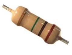
 The metal oxide film resistor type uses a film of metal oxide instead of a carbon film to be deposited on the ceramic rod.
The deposition of the metal oxide which can be found on the ceramic rod can include tin oxide.
There are two ways in which the component��s resistance is adjusted.
Firstly, at the initial stages of the manufacturing process, the deposited layer��s thickness is controlled.
Thereafter the adjustment is done in more accurate way by cutting a grove in the shape of helical form in the film.
Again, as in the previous case, the conformal epoxy coating is heavily coated on the film to protect it.
The ��15 ppm/oK of temperature coefficient has been observed in the metal oxide film resistor which results in a very high and superior function of this resistor when compared to any other resistor which is carbon based.
Additionally, the tolerance levels to which these resistors are supplied are very close including the standard tolerance levels of ��2%, ��1%, and ��5% being available.
Also, when compared with the resistors which are carbon based, there is very low exhibition of noise in these resistors.
Metal Film: There is a great similarity which can be observed between the metal oxide film resistor and the metal film resistors in terms of their performance and appearance.
A metal film is used by this resistor in place of the metal oxide film which is used in the metal oxide film resistor.
The metal film which is used in the resistor can include nickel alloy.
Wire Wound: The applications which require very high power in general use this type of resistor.
A wire is wounded around a former in order to manufacture this type of resistors.
The metal oxide film resistor type uses a film of metal oxide instead of a carbon film to be deposited on the ceramic rod.
The deposition of the metal oxide which can be found on the ceramic rod can include tin oxide.
There are two ways in which the component��s resistance is adjusted.
Firstly, at the initial stages of the manufacturing process, the deposited layer��s thickness is controlled.
Thereafter the adjustment is done in more accurate way by cutting a grove in the shape of helical form in the film.
Again, as in the previous case, the conformal epoxy coating is heavily coated on the film to protect it.
The ��15 ppm/oK of temperature coefficient has been observed in the metal oxide film resistor which results in a very high and superior function of this resistor when compared to any other resistor which is carbon based.
Additionally, the tolerance levels to which these resistors are supplied are very close including the standard tolerance levels of ��2%, ��1%, and ��5% being available.
Also, when compared with the resistors which are carbon based, there is very low exhibition of noise in these resistors.
Metal Film: There is a great similarity which can be observed between the metal oxide film resistor and the metal film resistors in terms of their performance and appearance.
A metal film is used by this resistor in place of the metal oxide film which is used in the metal oxide film resistor.
The metal film which is used in the resistor can include nickel alloy.
Wire Wound: The applications which require very high power in general use this type of resistor.
A wire is wounded around a former in order to manufacture this type of resistors.
 The resistance of these wires is higher than that of the normal resistance.
The varieties of these resistors which are expensive consist of the wire which is wound on a former made up of ceramic along with a cover of the silicone or citreous enamel over it.
The temperature coefficient of these resistors is very low along with a reliability of very high level being exhibited by these resistors when exposed to high power which enables it to operate at high performance level.
But these properties are also dominated by various other factors such as type of the wire being used, type of former being used, and more.
Thin Film: The majority of the resistors which are of surface mount types use the technology of the thin film.
The resistors based on this technology are used widely in the current day industry where the number goes up to billions here.
The resistance of these wires is higher than that of the normal resistance.
The varieties of these resistors which are expensive consist of the wire which is wound on a former made up of ceramic along with a cover of the silicone or citreous enamel over it.
The temperature coefficient of these resistors is very low along with a reliability of very high level being exhibited by these resistors when exposed to high power which enables it to operate at high performance level.
But these properties are also dominated by various other factors such as type of the wire being used, type of former being used, and more.
Thin Film: The majority of the resistors which are of surface mount types use the technology of the thin film.
The resistors based on this technology are used widely in the current day industry where the number goes up to billions here.
 The technology which is used to manufacture the surface mount resistor is the thin film technology.
Through this technology, the resistor can obtain the values in full range.
The technology which is used to manufacture the surface mount resistor is the thin film technology.
Through this technology, the resistor can obtain the values in full range.

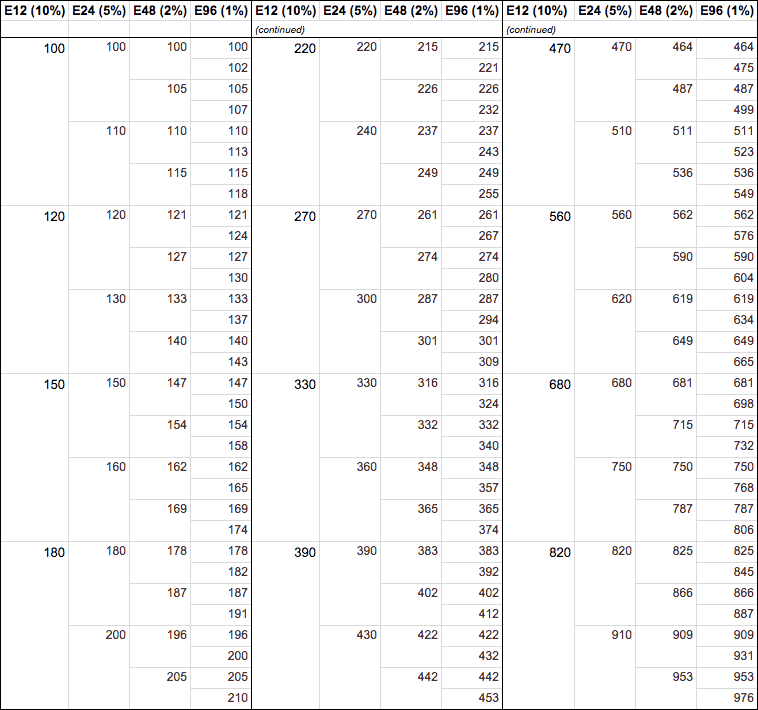
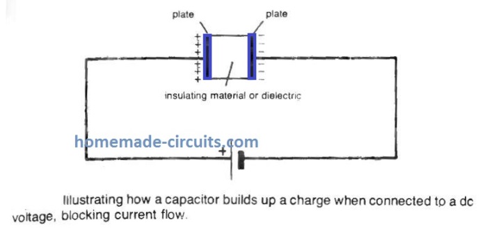 This differential build up of electrons gives rise to an electric charge, that accumulates a specific level (based on the voltage) after which stays at that level.
If a dc is involved, the insulator inside the capacitor works like a blocking system for the flow of current (however might be a slight transient charging current that prevents when the capacitor is completely charged).
When ac is used across the capacitor the charge accumulated throughout half ac cycle gets reversed with the next 2nd half cycle, which causes the capacitor to allow the current through it to run efficiently, as though the dielectric insulation never existed.
Therefore when ac is involved, a capacitor simply works like a coupling device.
You will find hardly any electronic circuits carrying ac and not incorporating a few capacitors, possibly for coupling or for optimizing the general frequency response of the system.
In the last mentioned scenario, a capacitor is connected with a resistor to create an RC combination.
The charge/discharge occurrence involved with capacitors could also be used in various other circuits e.g.
, the photographic electronic flash.
Just like resistors, capacitors could be configured work with fixed values or be adjustable in their magnitude.
Fixed capacitors happen to be the primary foundations of a circuit (along with resistors).
Variable capacitors mostly are intended for optimizing tuned circuits.
The performance parameters of every capacitor are different and thus their applications also differ accordingly.
One of the electronic components�� forms which is used widely is the electronic capacitors.
Apart from this, the other capacitors used in the industry include ceramic, silver mica, electrolytic, plastic, tantalum, and others.
Each type of the capacitor is used in various applications according to their respective disadvantages and advantages.
It is quintessential that the right type of capacitor must be selected as the circuit in which the capacitor is used is greatly by the capacitor.
Thus, in case a correct type of capacitor is not selected to insert in the circuit on the basis of its parameters, it can result in the improper or faulty functioning of the circuit.
This differential build up of electrons gives rise to an electric charge, that accumulates a specific level (based on the voltage) after which stays at that level.
If a dc is involved, the insulator inside the capacitor works like a blocking system for the flow of current (however might be a slight transient charging current that prevents when the capacitor is completely charged).
When ac is used across the capacitor the charge accumulated throughout half ac cycle gets reversed with the next 2nd half cycle, which causes the capacitor to allow the current through it to run efficiently, as though the dielectric insulation never existed.
Therefore when ac is involved, a capacitor simply works like a coupling device.
You will find hardly any electronic circuits carrying ac and not incorporating a few capacitors, possibly for coupling or for optimizing the general frequency response of the system.
In the last mentioned scenario, a capacitor is connected with a resistor to create an RC combination.
The charge/discharge occurrence involved with capacitors could also be used in various other circuits e.g.
, the photographic electronic flash.
Just like resistors, capacitors could be configured work with fixed values or be adjustable in their magnitude.
Fixed capacitors happen to be the primary foundations of a circuit (along with resistors).
Variable capacitors mostly are intended for optimizing tuned circuits.
The performance parameters of every capacitor are different and thus their applications also differ accordingly.
One of the electronic components�� forms which is used widely is the electronic capacitors.
Apart from this, the other capacitors used in the industry include ceramic, silver mica, electrolytic, plastic, tantalum, and others.
Each type of the capacitor is used in various applications according to their respective disadvantages and advantages.
It is quintessential that the right type of capacitor must be selected as the circuit in which the capacitor is used is greatly by the capacitor.
Thus, in case a correct type of capacitor is not selected to insert in the circuit on the basis of its parameters, it can result in the improper or faulty functioning of the circuit.
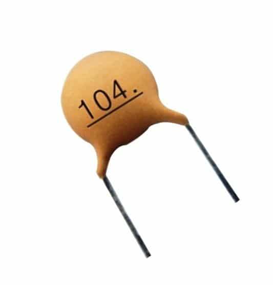 The capacitor namely, ceramic capacitor is used for multiple applications including RF and audio.
The range of the values of the ceramic capacitor is between few picofarads and 0.1 microfarads.
The ceramic capacitors are the most widely used in the industry since it the most reliable and cheap type of capacitor available.
Also, another reason for its common and wide usage is that the loss factor of the ceramic capacitor is very low.
But the loss factor of the capacitor is also dependent on the dielectric which is used in the capacitor.
The ceramic capacitors are used in both the formats of surface mount and leaded because of the constructional properties of the capacitors.
The capacitor namely, ceramic capacitor is used for multiple applications including RF and audio.
The range of the values of the ceramic capacitor is between few picofarads and 0.1 microfarads.
The ceramic capacitors are the most widely used in the industry since it the most reliable and cheap type of capacitor available.
Also, another reason for its common and wide usage is that the loss factor of the ceramic capacitor is very low.
But the loss factor of the capacitor is also dependent on the dielectric which is used in the capacitor.
The ceramic capacitors are used in both the formats of surface mount and leaded because of the constructional properties of the capacitors.
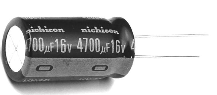 One type of capacitor which is polarized in nature is electrolytic capacitors.
The capacitance values which are offered by the electrolytic capacitor is very high which ranges more than 1��F.
the electrolytic capacitors are used in the industry commonly for the applications which are conducted on low frequency such as decoupling applications, power supplies, and applications of audio coupling.
This is because these applications have the frequency limit of nearly 100 kHz.
One type of capacitor which is polarized in nature is electrolytic capacitors.
The capacitance values which are offered by the electrolytic capacitor is very high which ranges more than 1��F.
the electrolytic capacitors are used in the industry commonly for the applications which are conducted on low frequency such as decoupling applications, power supplies, and applications of audio coupling.
This is because these applications have the frequency limit of nearly 100 kHz.
 Another type of capacitor which is polarized in nature is tantalum capacitor.
The capacitance level provided by the tantalum capacitor at their volume is very high.
One of the drawbacks of the tantalum capacitor is that there is no tolerance in the tantalum capacitor towards reverse biasing which can result in the explosion of the capacitor when exposed to stress.
Another drawback is that it has very low tolerance to the ripple currents and thus they should not be exposed to high voltages (such as voltages which is higher than their working voltage) and high ripple current.
The tantalum capacitors are available in both the formats of surface mount and leaded.
Another type of capacitor which is polarized in nature is tantalum capacitor.
The capacitance level provided by the tantalum capacitor at their volume is very high.
One of the drawbacks of the tantalum capacitor is that there is no tolerance in the tantalum capacitor towards reverse biasing which can result in the explosion of the capacitor when exposed to stress.
Another drawback is that it has very low tolerance to the ripple currents and thus they should not be exposed to high voltages (such as voltages which is higher than their working voltage) and high ripple current.
The tantalum capacitors are available in both the formats of surface mount and leaded.
 Although the usage of the silver mica capacitors have decreased significantly in the current era, the stability provided by the silver mica capacitors are still very high along with providing high accuracy and low loss.
Also, there is sufficient space available in the silver mica capacitors.
The applications where they are primarily used include the RF applications.
The maximum values to which the silver mica capacitor is limited to is approximately 100pF.
Although the usage of the silver mica capacitors have decreased significantly in the current era, the stability provided by the silver mica capacitors are still very high along with providing high accuracy and low loss.
Also, there is sufficient space available in the silver mica capacitors.
The applications where they are primarily used include the RF applications.
The maximum values to which the silver mica capacitor is limited to is approximately 100pF.
 The polystyrene film capacitors provide capacitor of close tolerance wherever required.
Also, these capacitors are relatively cheaper than that of other capacitors.
The dielectric sandwich or the plates present in the polystyrene film capacitors are rolled together which results in the shape of the capacitor in tubular form.
The placement of the dielectric sandwich and shape of the capacitor limits the response of the capacitor to high frequencies due to addition of inductance and thus responds to only few 100kHz.
The general availability of the polystyrene film capacitors is in the form of leaded electronics components.
The polystyrene film capacitors provide capacitor of close tolerance wherever required.
Also, these capacitors are relatively cheaper than that of other capacitors.
The dielectric sandwich or the plates present in the polystyrene film capacitors are rolled together which results in the shape of the capacitor in tubular form.
The placement of the dielectric sandwich and shape of the capacitor limits the response of the capacitor to high frequencies due to addition of inductance and thus responds to only few 100kHz.
The general availability of the polystyrene film capacitors is in the form of leaded electronics components.
 The tolerance provided by the polyester film capacitor is very low and thereby these capacitors are used in situations when the prior consideration is the cost.
The tolerance level of a large percentage of the polyester film capacitors available is either 10% or 5% and this is considered as sufficient for a range of applications.
The general availability of the polyester film capacitors is in the form of leaded electronics components.
The tolerance provided by the polyester film capacitor is very low and thereby these capacitors are used in situations when the prior consideration is the cost.
The tolerance level of a large percentage of the polyester film capacitors available is either 10% or 5% and this is considered as sufficient for a range of applications.
The general availability of the polyester film capacitors is in the form of leaded electronics components.
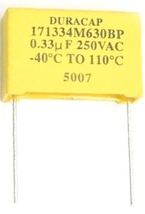 The metallized polyester film type of capacitors consists of polyester films which are metallized and in every other sense, it is similar to the polyester film capacitors or another form of it.
One of the advantages which is achieved by metallic polyester film is that it makes the electrodes of very small width and thereby enabling the encasement of the capacitor in a package of very small sizes as well.
The general availability of the metallized polyester film capacitors is in the form of leaded electronics components.
The metallized polyester film type of capacitors consists of polyester films which are metallized and in every other sense, it is similar to the polyester film capacitors or another form of it.
One of the advantages which is achieved by metallic polyester film is that it makes the electrodes of very small width and thereby enabling the encasement of the capacitor in a package of very small sizes as well.
The general availability of the metallized polyester film capacitors is in the form of leaded electronics components.
 The applications where the most critical and crucial requirement is high performance and reliability, these applications use the polycarbonate capacitors.
The capacitance value is held over a long period of time by the polycarbonate capacitors since their tolerance level is very high.
Such high tolerance levels are achieved because of the stability of the polycarbonate film used in the polycarbonate capacitor.
Additionally, the dissipation factor of the polycarbonate capacitor is very low and they can withstand temperature of wide range and remain stable.
The range of temperature which this capacitor can withstand is between -55oC and +125oC.
In spite of all these properties, the manufacturing and production of the polycarbonate capacitors has significantly decreased.
The applications where the most critical and crucial requirement is high performance and reliability, these applications use the polycarbonate capacitors.
The capacitance value is held over a long period of time by the polycarbonate capacitors since their tolerance level is very high.
Such high tolerance levels are achieved because of the stability of the polycarbonate film used in the polycarbonate capacitor.
Additionally, the dissipation factor of the polycarbonate capacitor is very low and they can withstand temperature of wide range and remain stable.
The range of temperature which this capacitor can withstand is between -55oC and +125oC.
In spite of all these properties, the manufacturing and production of the polycarbonate capacitors has significantly decreased.
 The other names by which the supercap is known are ultracapacitor or supercapacitor.
The capacitance values of these capacitors are very large as such is their name.
The capacitance levels of the ultracapacitor go nearly towards many thousand Farads.
The ultracapacitor is used in the industry for providing a supply of memory hold-up along with various uses within the realm of automotive applications.
The different major types of the capacitors are included under the supercap.
Along with them, there are various other capacitor types of capacitors which are used when the applications are specialized in nature.
The identification of the capacitors is majorly done through their parameters such as values which are marked over the cases of the capacitors.
In order to display the parameters in a manner which is compact, the markings of the parameters are done in the form of a code.
The other names by which the supercap is known are ultracapacitor or supercapacitor.
The capacitance values of these capacitors are very large as such is their name.
The capacitance levels of the ultracapacitor go nearly towards many thousand Farads.
The ultracapacitor is used in the industry for providing a supply of memory hold-up along with various uses within the realm of automotive applications.
The different major types of the capacitors are included under the supercap.
Along with them, there are various other capacitor types of capacitors which are used when the applications are specialized in nature.
The identification of the capacitors is majorly done through their parameters such as values which are marked over the cases of the capacitors.
In order to display the parameters in a manner which is compact, the markings of the parameters are done in the form of a code.
 Variable capacitors are built with alternate pieces of metal plates, a single set being fixed and non movable and the other movable.
The plates are segregated with a dielectric which can be air or a solid dielectric.
Motion of a single set of plates shifts the overall section of the plates, thereby altering the capacitance across the plates.
Variable capacitors are built with alternate pieces of metal plates, a single set being fixed and non movable and the other movable.
The plates are segregated with a dielectric which can be air or a solid dielectric.
Motion of a single set of plates shifts the overall section of the plates, thereby altering the capacitance across the plates.
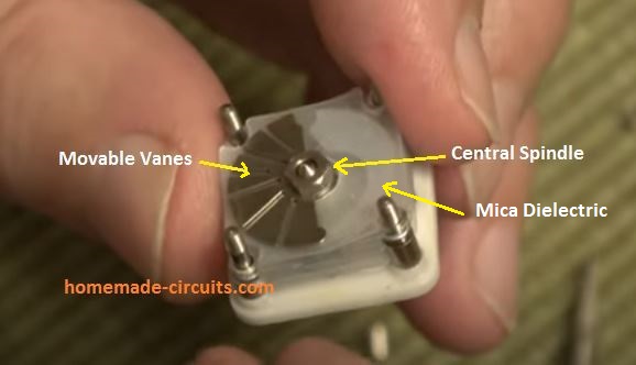 Additionally, standard differentiation between tuning capacitors utilized for repeated manipulation (e.g., to adjust a radio receiver station) and trimmer capacitors intended for preliminary setting up of a tuned circuit.
Tuning capacitors tend to be bigger, more powerful in structure and usually of air dielectric type.
Trimmer capacitors are often determined by a mica or film dielectric having a reduced quantity of plates, where capacitance is tweaked by rotating a middle bolt to alter the strain across plates and dielectric mica.
Due to the fact these are more compact in size, even so, a trimmer capacitor might at times be applied like a tuning capacitor on a pocket sized FM radio circuit, although exclusive mini tuning capacitors are manufactured to install rightaway on a PCB.
When it comes to tuning capacitors, the structure of the vanes tells the way in which capacitance varies as the spindle is moved.
All these attributes generally are categorized in one of the following descriptions:
1. Linear: where each spindle rotation degree generates a similar alteration in capacitance.
This is the most typical kind selected for radio receivers.
2. Logarithmic: where each degree of spindle movement generates a consistently varying level of frequency of a tuned circuit.
3. Even frequency: where every single spindle movement degree delivers the same variation in frequency in the tuned circuit.
4. Square law: in which the variation in the capacitance is proportionate to the square of the angle of spindle movement.
Additionally, standard differentiation between tuning capacitors utilized for repeated manipulation (e.g., to adjust a radio receiver station) and trimmer capacitors intended for preliminary setting up of a tuned circuit.
Tuning capacitors tend to be bigger, more powerful in structure and usually of air dielectric type.
Trimmer capacitors are often determined by a mica or film dielectric having a reduced quantity of plates, where capacitance is tweaked by rotating a middle bolt to alter the strain across plates and dielectric mica.
Due to the fact these are more compact in size, even so, a trimmer capacitor might at times be applied like a tuning capacitor on a pocket sized FM radio circuit, although exclusive mini tuning capacitors are manufactured to install rightaway on a PCB.
When it comes to tuning capacitors, the structure of the vanes tells the way in which capacitance varies as the spindle is moved.
All these attributes generally are categorized in one of the following descriptions:
1. Linear: where each spindle rotation degree generates a similar alteration in capacitance.
This is the most typical kind selected for radio receivers.
2. Logarithmic: where each degree of spindle movement generates a consistently varying level of frequency of a tuned circuit.
3. Even frequency: where every single spindle movement degree delivers the same variation in frequency in the tuned circuit.
4. Square law: in which the variation in the capacitance is proportionate to the square of the angle of spindle movement.
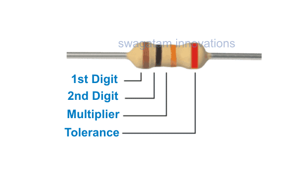 For example the color code scheme present on the above shown resistor consists of colors red, black, and orange along with a red band at the right side as the fourth band.
The first two color bands namely red and orange represent the significant figures of the resistor��s values which is 10; while the third color band orange represents the multiplier which is 1000.
The fourth color band which is red represents the tolerance level of the resistor which is ��2%.
Thus, the value of the resistor can be interpreted to be 10,000 or 10k.
Note: In case a resistor consists of only three color bands, then the first two bands will represent the significant figures of the resistor��s values while the third will represent the multiplier.
The fourth color band representing tolerance will be absent here.
For example the color code scheme present on the above shown resistor consists of colors red, black, and orange along with a red band at the right side as the fourth band.
The first two color bands namely red and orange represent the significant figures of the resistor��s values which is 10; while the third color band orange represents the multiplier which is 1000.
The fourth color band which is red represents the tolerance level of the resistor which is ��2%.
Thus, the value of the resistor can be interpreted to be 10,000 or 10k.
Note: In case a resistor consists of only three color bands, then the first two bands will represent the significant figures of the resistor��s values while the third will represent the multiplier.
The fourth color band representing tolerance will be absent here.
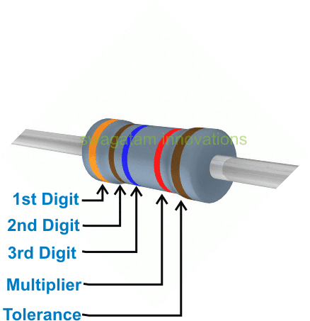 For example, the color bands present on the above resistor are orange, brown, blue, red, and brown.
The first three color bands represent the significant figures of the resistor��s value which is 316; and the fourth color band represents the multiplier of the resistor which is 100.
The fifth color band of the resistor represents its tolerance value which is ��1%.
Thus, the value of the resistor can be written as 31.6k or 31600.
For example, the color bands present on the above resistor are orange, brown, blue, red, and brown.
The first three color bands represent the significant figures of the resistor��s value which is 316; and the fourth color band represents the multiplier of the resistor which is 100.
The fifth color band of the resistor represents its tolerance value which is ��1%.
Thus, the value of the resistor can be written as 31.6k or 31600.
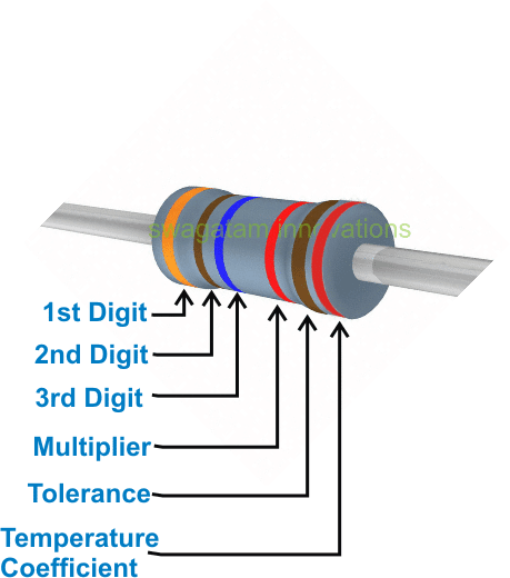 An example of the color code scheme of resistors consisting of six bands is shown above wherein the six colors on a resistor are orange, brown, blue, red, brown, and red.
The first three color bands present on the resistor represent the significant figures of the resistor��s value which is 316 while the fourth color band represents the multiplier which is 100.
The fifth color band represents the tolerance level of the resistor which is 1%.
The sixth and the final color band represent the temperature coefficient of the resistor which is 50ppm/oK.
Thus, the value of the resistor can be written as 31.6k or 31600.
An example of the color code scheme of resistors consisting of six bands is shown above wherein the six colors on a resistor are orange, brown, blue, red, brown, and red.
The first three color bands present on the resistor represent the significant figures of the resistor��s value which is 316 while the fourth color band represents the multiplier which is 100.
The fifth color band represents the tolerance level of the resistor which is 1%.
The sixth and the final color band represent the temperature coefficient of the resistor which is 50ppm/oK.
Thus, the value of the resistor can be written as 31.6k or 31600.
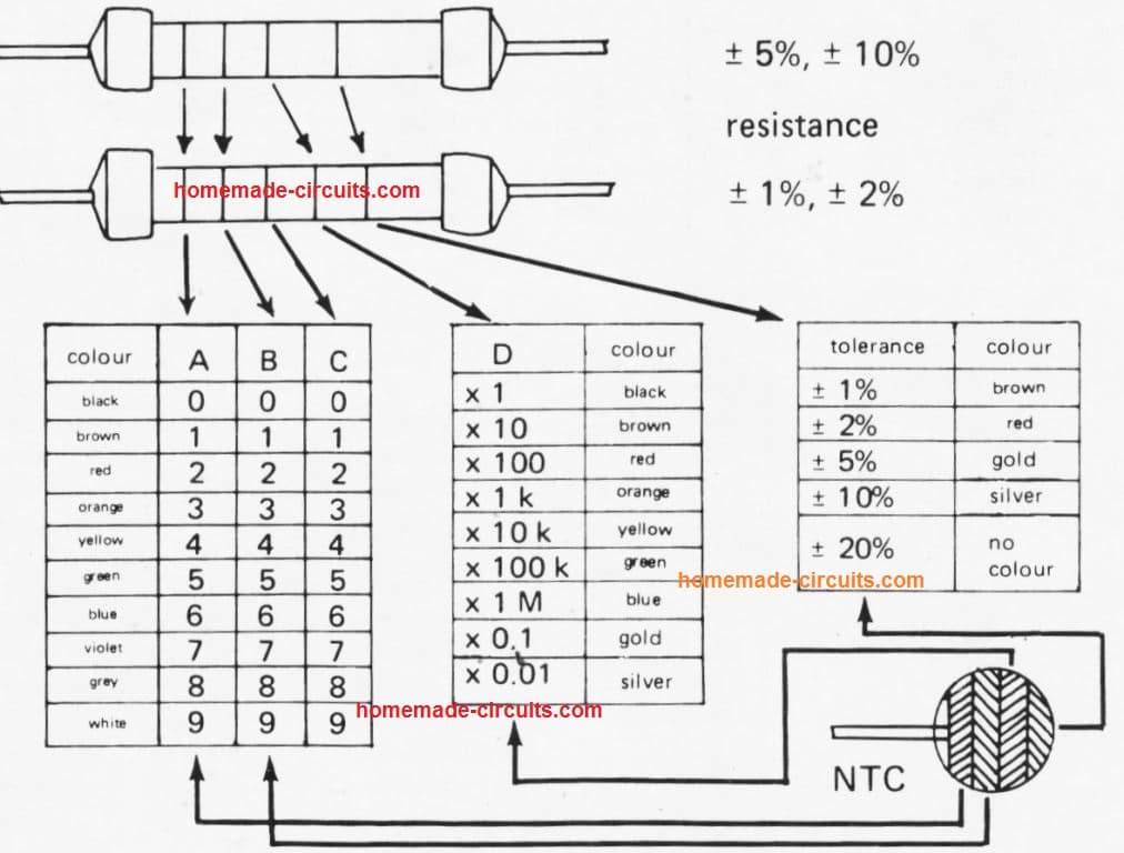

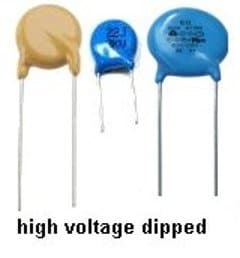
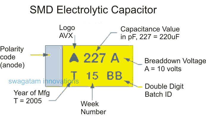 Thus, for these large capacitors, the parameters such as value and others can be provided in detail instead of giving in abbreviated form.
On the other hand, for the smaller capacitors due to lack of sufficient space the parameters are provided in the form of abbreviated codes.
An example of the marking which can be typically observed in a capacitor is ��22��F 50V��.
Here, 22��F is the value of the capacitor while 50V denotes the working voltage.
The marking of a bar is used to denote the polarity of the capacitor indicating the negative terminal.
Markings of leaded tantalum capacitor: The unit, ��Microfarad (��F)�� is used to mark the values in the leaded tantalum capacitors.
An example of a typical marking observed on a capacitor is ��22 and 6V��.
These figures indicate that the capacitor is of 22��F and 6V is its maximum voltage.
Markings of Ceramic Capacitor: The markings on a ceramic capacitor are more concise in nature since it is smaller in size as compared to electrolytic capacitors.
Thus, for such concise markings many different types of schemes or solutions are adopted.
The value of the capacitor is indicated in ��Picofarads��.
Some of the marking figures which can be observed are 10n which denotes that the capacitor is of 10nF.
In a similar way, 0.51nF is indicated by the marking n51.
Codes of SMD Ceramic Capacitor: The capacitors such as surface mount capacitor do not have sufficient space available for markings due to their small size.
Thus, for these large capacitors, the parameters such as value and others can be provided in detail instead of giving in abbreviated form.
On the other hand, for the smaller capacitors due to lack of sufficient space the parameters are provided in the form of abbreviated codes.
An example of the marking which can be typically observed in a capacitor is ��22��F 50V��.
Here, 22��F is the value of the capacitor while 50V denotes the working voltage.
The marking of a bar is used to denote the polarity of the capacitor indicating the negative terminal.
Markings of leaded tantalum capacitor: The unit, ��Microfarad (��F)�� is used to mark the values in the leaded tantalum capacitors.
An example of a typical marking observed on a capacitor is ��22 and 6V��.
These figures indicate that the capacitor is of 22��F and 6V is its maximum voltage.
Markings of Ceramic Capacitor: The markings on a ceramic capacitor are more concise in nature since it is smaller in size as compared to electrolytic capacitors.
Thus, for such concise markings many different types of schemes or solutions are adopted.
The value of the capacitor is indicated in ��Picofarads��.
Some of the marking figures which can be observed are 10n which denotes that the capacitor is of 10nF.
In a similar way, 0.51nF is indicated by the marking n51.
Codes of SMD Ceramic Capacitor: The capacitors such as surface mount capacitor do not have sufficient space available for markings due to their small size.
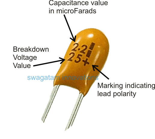 The tantalum capacitors only consist of the polarity markings.
This is present in order to ensure the correct insertion of the capacitor in the circuit board.
The marking format consist of three figures is generally used for the capacitors which has sufficient space available such as is evident in the ceramic capacitors.
The marking of a bar can be observed in some of the capacitors across their one end denoting the capacitor��s polarity.
The marking for polarity is important in order to identify and check the capacitor��s polarity since the destruction of the capacitor can occur if the polarity is not known and a person places it in reverse biasing, especially in the case of tantalum capacitors.
The tantalum capacitors only consist of the polarity markings.
This is present in order to ensure the correct insertion of the capacitor in the circuit board.
The marking format consist of three figures is generally used for the capacitors which has sufficient space available such as is evident in the ceramic capacitors.
The marking of a bar can be observed in some of the capacitors across their one end denoting the capacitor��s polarity.
The marking for polarity is important in order to identify and check the capacitor��s polarity since the destruction of the capacitor can occur if the polarity is not known and a person places it in reverse biasing, especially in the case of tantalum capacitors.
 It is utmost important that one can identify, read, and check a capacitor��s value.
Since there are a range of capacitors available and their different coding and marking systems, it is quintessential that a basic understanding of these marking and coding is there to an individual in order to apply it appropriately to respective capacitors.
An individual can determine the capacitor��s value with practice and experience and just going through few examples mentioned here would not suffice.
It is utmost important that one can identify, read, and check a capacitor��s value.
Since there are a range of capacitors available and their different coding and marking systems, it is quintessential that a basic understanding of these marking and coding is there to an individual in order to apply it appropriately to respective capacitors.
An individual can determine the capacitor��s value with practice and experience and just going through few examples mentioned here would not suffice.

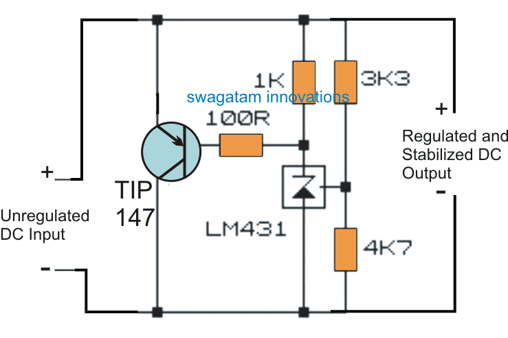
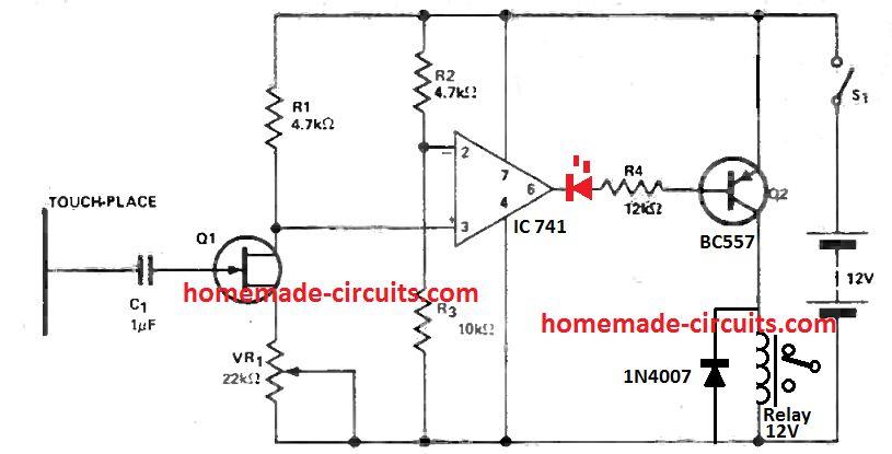 A high impedance input is given by Q1, which is an regular field effect transistor like 2N3819. A standard 741 op amp is employed in the form of a sensitive voltage level switch which subsequently drives the current buffer Q2, a medium current pnp bipolar transistor, thus activating the relay that may be accustomed to switch a device, such as alarms, faucet etc.
While the circuit is in the idle standby condition, the voltage at pin 3 of the op amp is fixed at greater than the pin 2 voltage level by appropriately adjusting preset VR1.
This makes sure that the voltage at the output pin 6 will be high causing transistor Q2 and the relay to remain switched off.
When the finger is brought in close proximity to the sensor plate or lightly touching, a lowering opposite bias VGS will increase the drain current of the FET Q1 and the resulting drop across R1 voltage will reduce the op amp pin 3 voltage below the voltage existing at pin 2.
This will result in the pin 6 voltage to fall and consequently switch on the relay by means of Q2. Resistor R4 might be determined in order that the relay is kept turned OFF under normal conditions, considering that a tiny positive off set voltage might develop at the op amp pin 6 output even if the pin 3 voltage happens to be lower than pin 2 voltage in the quiescent (idle) state.
This problem could be remedied simply by adding an LED in series with the Q2 base.
A high impedance input is given by Q1, which is an regular field effect transistor like 2N3819. A standard 741 op amp is employed in the form of a sensitive voltage level switch which subsequently drives the current buffer Q2, a medium current pnp bipolar transistor, thus activating the relay that may be accustomed to switch a device, such as alarms, faucet etc.
While the circuit is in the idle standby condition, the voltage at pin 3 of the op amp is fixed at greater than the pin 2 voltage level by appropriately adjusting preset VR1.
This makes sure that the voltage at the output pin 6 will be high causing transistor Q2 and the relay to remain switched off.
When the finger is brought in close proximity to the sensor plate or lightly touching, a lowering opposite bias VGS will increase the drain current of the FET Q1 and the resulting drop across R1 voltage will reduce the op amp pin 3 voltage below the voltage existing at pin 2.
This will result in the pin 6 voltage to fall and consequently switch on the relay by means of Q2. Resistor R4 might be determined in order that the relay is kept turned OFF under normal conditions, considering that a tiny positive off set voltage might develop at the op amp pin 6 output even if the pin 3 voltage happens to be lower than pin 2 voltage in the quiescent (idle) state.
This problem could be remedied simply by adding an LED in series with the Q2 base.
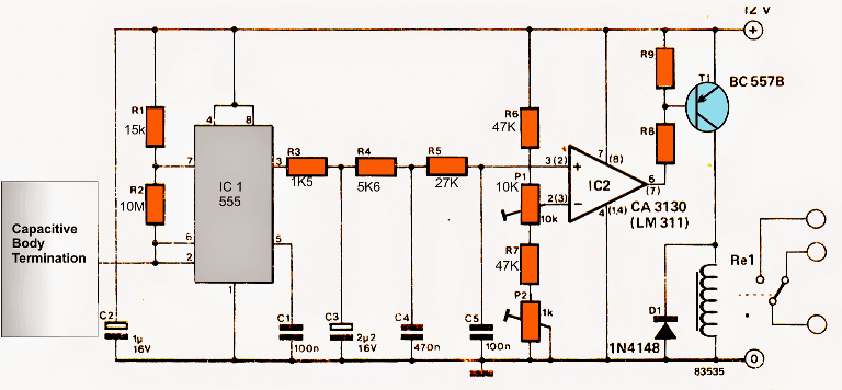 Circuit Image Courtesy: Elektor Electronics
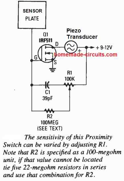 Thte sensor is formed by a 3x3 inch metal object which is hooked up with the Q1 gate.
The resistor R2 which is a 100 M resistor, separates the Q1's gate from R1, permitting its input impedance to stay extremely high.
If you are unable to find a 100 M resistor, you may simply connect five 22 M resistors in series and work with this resistor string instead of R2.
Precisely speaking , R2 value could be created even higher than this for enhancing the proximity detection sensitivity.
Potentiometer R1 is adjusted to a point where the piezo buzzer just starts buzzing ON and then R1 could be meticulously adjusted back to the point where the buzzer just stops sounding anymore.
Testing with the R1 adjustment can be useful in having the greatest sensitivity setting for this capacitive proximity circuit.
Thte sensor is formed by a 3x3 inch metal object which is hooked up with the Q1 gate.
The resistor R2 which is a 100 M resistor, separates the Q1's gate from R1, permitting its input impedance to stay extremely high.
If you are unable to find a 100 M resistor, you may simply connect five 22 M resistors in series and work with this resistor string instead of R2.
Precisely speaking , R2 value could be created even higher than this for enhancing the proximity detection sensitivity.
Potentiometer R1 is adjusted to a point where the piezo buzzer just starts buzzing ON and then R1 could be meticulously adjusted back to the point where the buzzer just stops sounding anymore.
Testing with the R1 adjustment can be useful in having the greatest sensitivity setting for this capacitive proximity circuit.
 The following image shows the internal configuration of the IC PCF8883
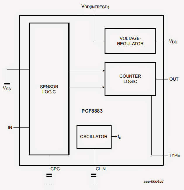 The IC doesn't rely on the traditional dynamic capacitance mode of sensing rather detects the variation in the static capacitance by employing automatic correction through continuous auto-calibration.
The sensor is basically in the form of a small conductive foil which may be directly integrated with the relevant pinouts of the IC for the intended capacitive sensing or perhaps terminated to longer distances through coaxial cables for enabling accurate and effective remote capacitive proximity sensing operations
The following figures represent the pinout details of the IC PCF8883. The detailed functioning of the various pinouts and the in-built circuitry may be understood with the following points:
The IC doesn't rely on the traditional dynamic capacitance mode of sensing rather detects the variation in the static capacitance by employing automatic correction through continuous auto-calibration.
The sensor is basically in the form of a small conductive foil which may be directly integrated with the relevant pinouts of the IC for the intended capacitive sensing or perhaps terminated to longer distances through coaxial cables for enabling accurate and effective remote capacitive proximity sensing operations
The following figures represent the pinout details of the IC PCF8883. The detailed functioning of the various pinouts and the in-built circuitry may be understood with the following points:
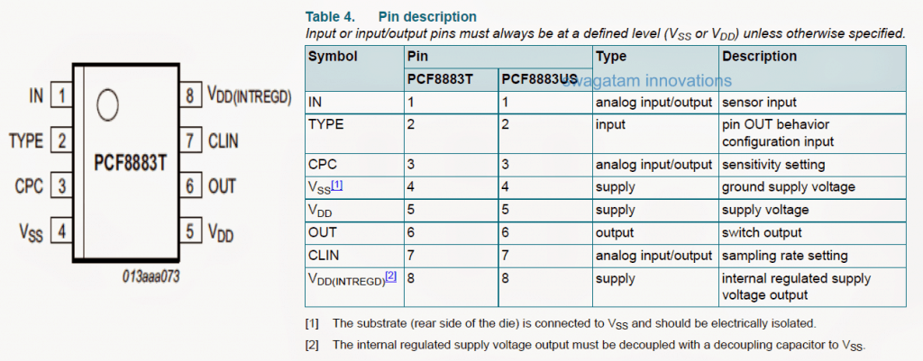
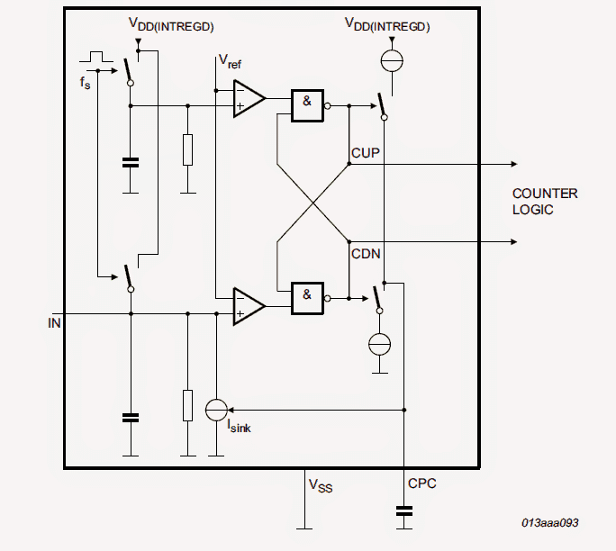 The pinout IN which is supposed to be connected with the external capacitive sensing foil is linked with the ICs internal RC network.
The discharge time given by "tdch" of the RC network is compared by the discharge time of the second in-bult RC network denoted as "tdchimo".
The two RC networks go through periodic charging by VDD(INTREGD) through a couple of identical and synchronized switch networks, and subsequently discharged with the help of a resistor to Vss or the ground
The rate at which this charge discharge is executed is regulated by a sampling rate denoted by "fs".
In case if the potential difference is seen to be dropping below the internally set reference voltage VM, the corresponding output of the comparator tends to become low.
The logic level which follows the comparators identifies the exact comparator that actually could switch before the other.
And if the upper comparator is identified to have fired first, this results with a pulse being rendered on CUP, whereas if the lower comparator is detected to have switched prior to the upper, then the pulse is enabled at CDN.
The above pulses engage in controlling the charge level over the external capacitor Ccpc associated with pin CPC.
When a pulse is generated on CUP, the Ccpc is charged through VDDUNTREGD for a given period of time which triggers a rising potential on Ccpc.
Quite on the same lines, when a pulse is rendered at CDN, the Ccpc gets linked with current sink device to ground which discharges the capacitor causing its potential to collapse.
Whenever the capacitance at pin IN gets higher, it correspondingly increases the discharge time tdch, which causes the voltage across the relevant comparator to fall at a correspondingly longer time.
When this takes place the output of the comparator tends to get low which in turn renders a pulse at CDN forcing the external capacitor CCP to discharge to some smaller degree.
This implies that CUP now generates the majority of the pulses which causes CCP to charge up even more without going through any further steps.
Inspite of this, the automatic voltage controlled calibration feature of the IC which relies on a sink current regulation "ism" associated with pin IN makes an effort to balance out the discharge time tdch by referring it with an internally set discharge time tdcmef.
The voltage across Ccpg is current controlled and becomes responsible for the discharge of the capacitance on IN rather rapidly whenever the potential across CCP is detected to be increasing.
This perfectly balances the increasing capacitance on input pin IN.
This effect give rise to a closed loop tracking system which continuously monitors and engages into an automatic equalizing of the discharge time tdch with reference to tdchlmf.
This helps to correct sluggish variations in capacitance across IN pinout of the IC.
During rapidly charging sates for example when a human finger is approached the sensing foil quickly, the discussed compensation might not transpire, in equilibrium conditions the length of the discharge period do not differ causing the pulse to alternately fluctuate across CUP and CDN.
This further implies that with larger Ccpg values a relatively restricted voltage variation for each pulse may be expected for CUP or CDN.
Therefore the internal current sink gives rise to a slower compensation, thereby enhancing the sensitivity of the sensor.
On the contrary, when CCP experiences a decrease, causes the sensor sensitivity to go down.
The pinout IN which is supposed to be connected with the external capacitive sensing foil is linked with the ICs internal RC network.
The discharge time given by "tdch" of the RC network is compared by the discharge time of the second in-bult RC network denoted as "tdchimo".
The two RC networks go through periodic charging by VDD(INTREGD) through a couple of identical and synchronized switch networks, and subsequently discharged with the help of a resistor to Vss or the ground
The rate at which this charge discharge is executed is regulated by a sampling rate denoted by "fs".
In case if the potential difference is seen to be dropping below the internally set reference voltage VM, the corresponding output of the comparator tends to become low.
The logic level which follows the comparators identifies the exact comparator that actually could switch before the other.
And if the upper comparator is identified to have fired first, this results with a pulse being rendered on CUP, whereas if the lower comparator is detected to have switched prior to the upper, then the pulse is enabled at CDN.
The above pulses engage in controlling the charge level over the external capacitor Ccpc associated with pin CPC.
When a pulse is generated on CUP, the Ccpc is charged through VDDUNTREGD for a given period of time which triggers a rising potential on Ccpc.
Quite on the same lines, when a pulse is rendered at CDN, the Ccpc gets linked with current sink device to ground which discharges the capacitor causing its potential to collapse.
Whenever the capacitance at pin IN gets higher, it correspondingly increases the discharge time tdch, which causes the voltage across the relevant comparator to fall at a correspondingly longer time.
When this takes place the output of the comparator tends to get low which in turn renders a pulse at CDN forcing the external capacitor CCP to discharge to some smaller degree.
This implies that CUP now generates the majority of the pulses which causes CCP to charge up even more without going through any further steps.
Inspite of this, the automatic voltage controlled calibration feature of the IC which relies on a sink current regulation "ism" associated with pin IN makes an effort to balance out the discharge time tdch by referring it with an internally set discharge time tdcmef.
The voltage across Ccpg is current controlled and becomes responsible for the discharge of the capacitance on IN rather rapidly whenever the potential across CCP is detected to be increasing.
This perfectly balances the increasing capacitance on input pin IN.
This effect give rise to a closed loop tracking system which continuously monitors and engages into an automatic equalizing of the discharge time tdch with reference to tdchlmf.
This helps to correct sluggish variations in capacitance across IN pinout of the IC.
During rapidly charging sates for example when a human finger is approached the sensing foil quickly, the discussed compensation might not transpire, in equilibrium conditions the length of the discharge period do not differ causing the pulse to alternately fluctuate across CUP and CDN.
This further implies that with larger Ccpg values a relatively restricted voltage variation for each pulse may be expected for CUP or CDN.
Therefore the internal current sink gives rise to a slower compensation, thereby enhancing the sensitivity of the sensor.
On the contrary, when CCP experiences a decrease, causes the sensor sensitivity to go down.
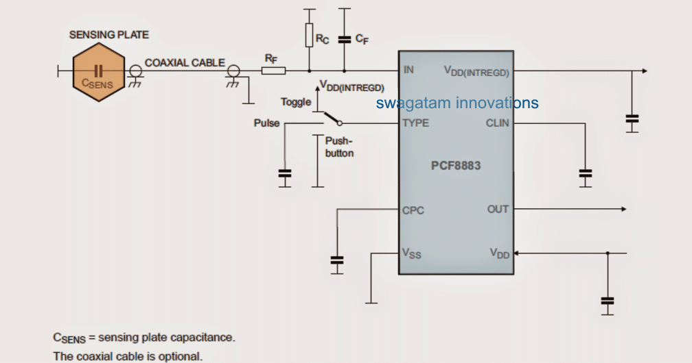

 A typical application configuration using the IC can be witnessed below:
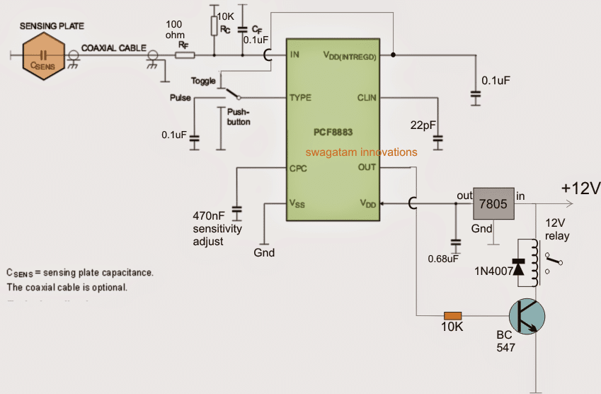 The+ input supply is attached with the VDD.
A smoothing capacitor may be preferably connected across and VDD and ground and also across VDDUNTREGD and ground for more reliable working of the chip.
The capacitance value of COLIN as produced on pin CLIN fixes the sampling rate effectively.
Increasing sampling rate may enable enhance reaction time on the sensing input with a proportionate increase in the current consumption
The+ input supply is attached with the VDD.
A smoothing capacitor may be preferably connected across and VDD and ground and also across VDDUNTREGD and ground for more reliable working of the chip.
The capacitance value of COLIN as produced on pin CLIN fixes the sampling rate effectively.
Increasing sampling rate may enable enhance reaction time on the sensing input with a proportionate increase in the current consumption
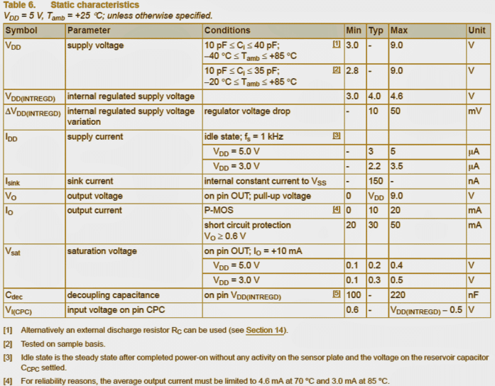
 Reference:https://www.nxp.com/docs/en/data-sheet/PCF8883.pdf
 The 40 amp rating itself makes the device immediately suitable for all high current motor and inverter application in the form of a freewheeling diode for countering the dangerous back EMFs, which becomes a serious issue with all such applications.
Although this versatile diode may be ideally suitable as a freewheeling diode and also in the form of blocking diode for safeguarding against reverse battery polarity, the device includes a special over voltage protection for countering voltage surges and load dumps.
As per the datasheet, the device is assigned with the following features:
In-built spike protector for safeguarding against "load dump" voltage pulses.
Can be used as regular 40 amp blocking diode for countering accidental battery polarity reversal.
A Monolithic structure ensures improved reliability
Breakdown voltage is not above 24V, so here the feature may be restricted within this limit.
Spike clamping voltage is set at +/- 40V
The absolute maximum ratings of the RBO40-40G/T may be studied from the following data:
Instantaneous (10ms) non-repetitive surge peak forward current limit is 120Amps
Continuous DC forward current handling capacity is 40 amps
Instantaneous peak load dump voltage handling capacity is 80V
Instantaneous peak power handling capacity is 1500 watts
The 40 amp rating itself makes the device immediately suitable for all high current motor and inverter application in the form of a freewheeling diode for countering the dangerous back EMFs, which becomes a serious issue with all such applications.
Although this versatile diode may be ideally suitable as a freewheeling diode and also in the form of blocking diode for safeguarding against reverse battery polarity, the device includes a special over voltage protection for countering voltage surges and load dumps.
As per the datasheet, the device is assigned with the following features:
In-built spike protector for safeguarding against "load dump" voltage pulses.
Can be used as regular 40 amp blocking diode for countering accidental battery polarity reversal.
A Monolithic structure ensures improved reliability
Breakdown voltage is not above 24V, so here the feature may be restricted within this limit.
Spike clamping voltage is set at +/- 40V
The absolute maximum ratings of the RBO40-40G/T may be studied from the following data:
Instantaneous (10ms) non-repetitive surge peak forward current limit is 120Amps
Continuous DC forward current handling capacity is 40 amps
Instantaneous peak load dump voltage handling capacity is 80V
Instantaneous peak power handling capacity is 1500 watts
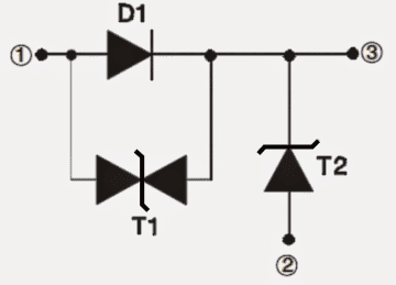 Referring to the above figure which shows the internal structure of the diode, the involved three main functions of the device may be understood as given under:
1) The indicated diode D1 is assigned for functioning in the standard rectifier diode mode for safeguarding against accidental battery reversal.
2) T2 component associated with the device acts like an effective transil to counter against positive peak transients pulses or back EMFs which may be generated by the associated high power relays, inductors, ignition coils, transformers, motor winding etc.
3) The third part T1 which can be seen in the internal layout of the device is specifically included for motor applications to protect the transistors drivers from the motor coil back EMFs or negative voltage spikes.
Referring to the above figure which shows the internal structure of the diode, the involved three main functions of the device may be understood as given under:
1) The indicated diode D1 is assigned for functioning in the standard rectifier diode mode for safeguarding against accidental battery reversal.
2) T2 component associated with the device acts like an effective transil to counter against positive peak transients pulses or back EMFs which may be generated by the associated high power relays, inductors, ignition coils, transformers, motor winding etc.
3) The third part T1 which can be seen in the internal layout of the device is specifically included for motor applications to protect the transistors drivers from the motor coil back EMFs or negative voltage spikes.
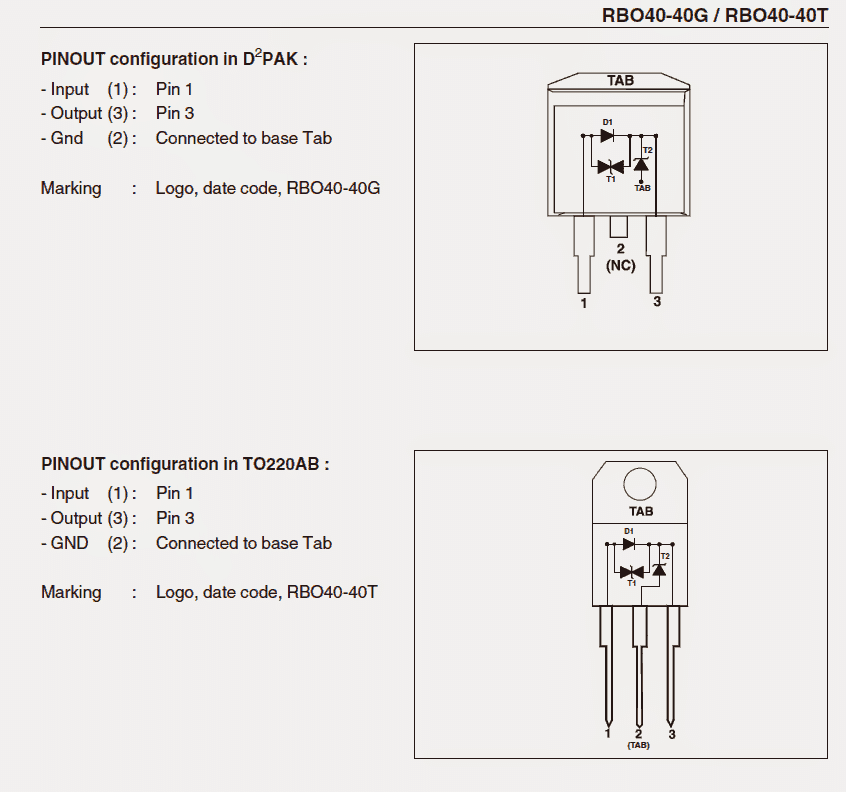 Courtesy:st.com/web/en/resource/technical/document/datasheet/CD00001320.pdf

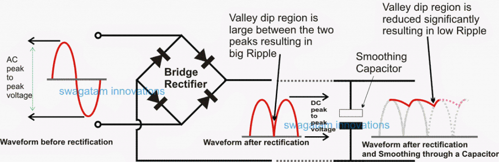 Diagram Showing Ripple Valley
The persistent deep valleys between each rectified half cycle introduces maximum ripple, which can be tackled only by adding a filter capacitor across the output of the bridge rectifier.
This large peak-to-peak voltage between the valleys and the peak cycles are smoothed or compensated using filter capacitors or smoothing capacitors across the output of the bridge rectifier.
Diagram Showing Ripple Valley
The persistent deep valleys between each rectified half cycle introduces maximum ripple, which can be tackled only by adding a filter capacitor across the output of the bridge rectifier.
This large peak-to-peak voltage between the valleys and the peak cycles are smoothed or compensated using filter capacitors or smoothing capacitors across the output of the bridge rectifier.
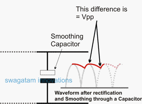 Let's try to understand the relation between load current, ripple and the optimal capacitor value from the following evaluation.
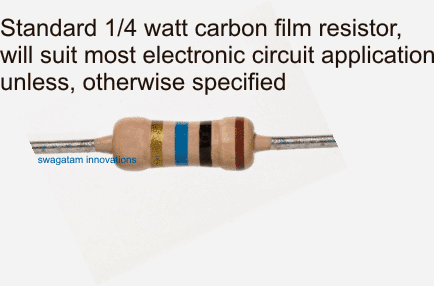

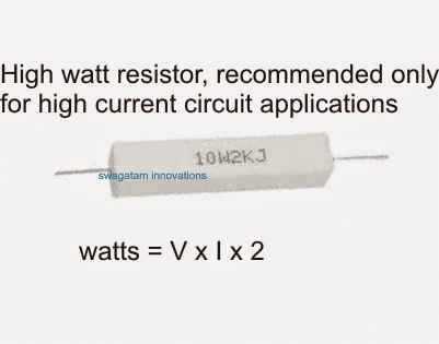 Now, after identifying the above specs, sometimes one may seem to be confused with the values too, for example the hobbyist may find the value 750K difficult to find in his locality, but there's nothing to worry about.
Resistor values are never too critical, so for the above example any value between 680K and 810K will mostly do the job, or the user may simply join a couple of odd resistors in series to achieve the same, accurately and efficiently (for example 470k + 270k will yield 740K)
Now, after identifying the above specs, sometimes one may seem to be confused with the values too, for example the hobbyist may find the value 750K difficult to find in his locality, but there's nothing to worry about.
Resistor values are never too critical, so for the above example any value between 680K and 810K will mostly do the job, or the user may simply join a couple of odd resistors in series to achieve the same, accurately and efficiently (for example 470k + 270k will yield 740K)
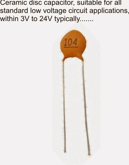
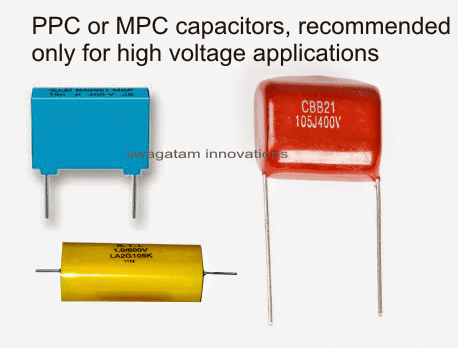 For voltages at the mains level, the capacitor type should be always PPC or MPC, which stand for polypropylene or metallized polyester.
Electrolytic capacitors do not have any specific recommendation, these just need to fixed with the correct polarity and voltage rating to be maintained as per the previous discussion.
For voltages at the mains level, the capacitor type should be always PPC or MPC, which stand for polypropylene or metallized polyester.
Electrolytic capacitors do not have any specific recommendation, these just need to fixed with the correct polarity and voltage rating to be maintained as per the previous discussion.
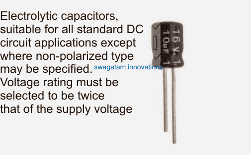 In circuits which may demand extreme accuracy in terms of low leakage, for example in timer applications, one may opt for tantalum type of capacitors instead of the electrolytic counterparts which are designed to offer minimum possible leakage and high efficiency.
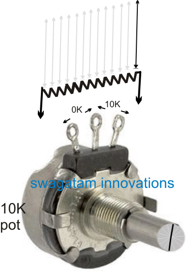 In other words, for instance a clockwise rotation of the shaft may continuously and proportionately produce an increasing resistance between its center and right side leads, while a proportionately decreasing resistance between its center and the left hand side lead.
The above response is thus differential across the two sides of the center lead of the pot.
The resistance may be exactly equal across the left and the right leads with respect to the center lead, if the shaft is positioned approximately at the center of the rotational dial.
In other words, for instance a clockwise rotation of the shaft may continuously and proportionately produce an increasing resistance between its center and right side leads, while a proportionately decreasing resistance between its center and the left hand side lead.
The above response is thus differential across the two sides of the center lead of the pot.
The resistance may be exactly equal across the left and the right leads with respect to the center lead, if the shaft is positioned approximately at the center of the rotational dial.
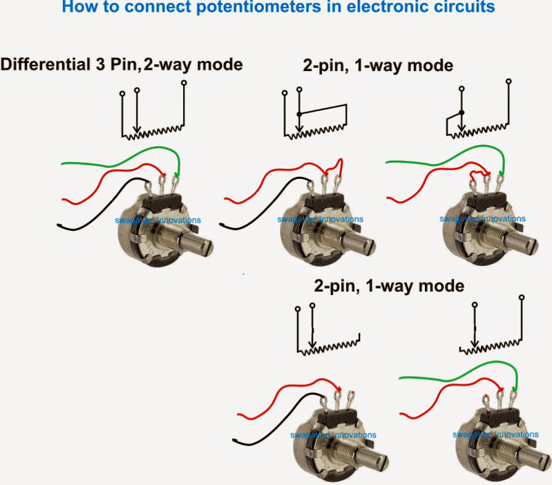
 Presets are designed for PCB mounting applications, and can be soldered directly over the given PCB holes, unlike potentiometers which are required to be mounted on the enclosure of the unit with the help of a screw nut arrangement.
If you have more questions regarding potentiometer functioning details, please feel free to express the same through comment.
Presets are designed for PCB mounting applications, and can be soldered directly over the given PCB holes, unlike potentiometers which are required to be mounted on the enclosure of the unit with the help of a screw nut arrangement.
If you have more questions regarding potentiometer functioning details, please feel free to express the same through comment.
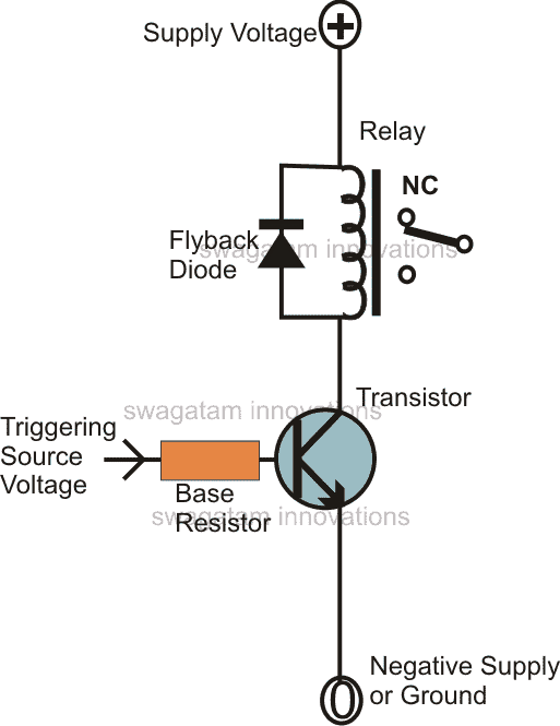 A relay being a relatively small load (high resistance coil), normally a 1 amp rated 1N4007 diode becomes more than sufficient for such applications, however in cases where the load is relatively huge or the coil resistance is very low, the generated back emfs could be equivalent to the applied current levels, meaning if the applied current is in the range of 10 amp, the reverse emf would also be around this level.
To absorb such massive jolts the reverse back emf, the diode too must be robust with its amp specs.
Normally, in such cases where the back emf could be above 10 or 20 amps, finding a suitable single diode becomes difficult or too expensive.
A good way to counter this is to connect many smaller rated diodes in parallel, however since diodes just like BJTs are semiconductor devices, don't go well when connected in parallel.
The reason being, each diode connected in the parallel string could have a slightly different switch ON levels making the devices conduct separately and the one which switches ON first becomes responsible of taking on the greatest bulk of the induced current, which itself makes the particular diode vulnerable.
Therefore, in order to solve the above concern each diode must be added with a series resistor, appropriately calculated for the freewheeling application as per the given parameters.
A relay being a relatively small load (high resistance coil), normally a 1 amp rated 1N4007 diode becomes more than sufficient for such applications, however in cases where the load is relatively huge or the coil resistance is very low, the generated back emfs could be equivalent to the applied current levels, meaning if the applied current is in the range of 10 amp, the reverse emf would also be around this level.
To absorb such massive jolts the reverse back emf, the diode too must be robust with its amp specs.
Normally, in such cases where the back emf could be above 10 or 20 amps, finding a suitable single diode becomes difficult or too expensive.
A good way to counter this is to connect many smaller rated diodes in parallel, however since diodes just like BJTs are semiconductor devices, don't go well when connected in parallel.
The reason being, each diode connected in the parallel string could have a slightly different switch ON levels making the devices conduct separately and the one which switches ON first becomes responsible of taking on the greatest bulk of the induced current, which itself makes the particular diode vulnerable.
Therefore, in order to solve the above concern each diode must be added with a series resistor, appropriately calculated for the freewheeling application as per the given parameters.
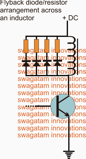
 Next keep all the components in the box in this manner:
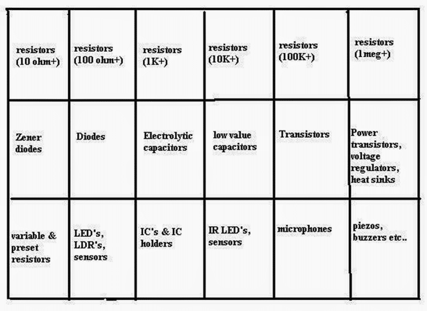 After filling the box, with all the components, take another plastic container and use it for storing relays, switches and other bigger components which you may have to get in future for making bigger circuits.
After completing the procedures it will look like this:
After filling the box, with all the components, take another plastic container and use it for storing relays, switches and other bigger components which you may have to get in future for making bigger circuits.
After completing the procedures it will look like this:

 You can write the name of components present in a box and stick the paper to the respective box using sticky tape as shown in the above picture.
Now you are ready to start with basic circuits.
You can find plenty of easy circuits from this blog.
Good Luck!
Written and Submitted by: SS Kopparthy
You can write the name of components present in a box and stick the paper to the respective box using sticky tape as shown in the above picture.
Now you are ready to start with basic circuits.
You can find plenty of easy circuits from this blog.
Good Luck!
Written and Submitted by: SS Kopparthy
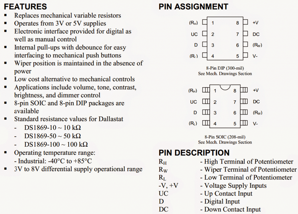


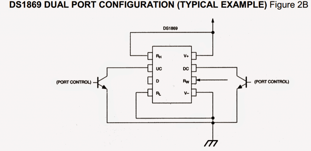
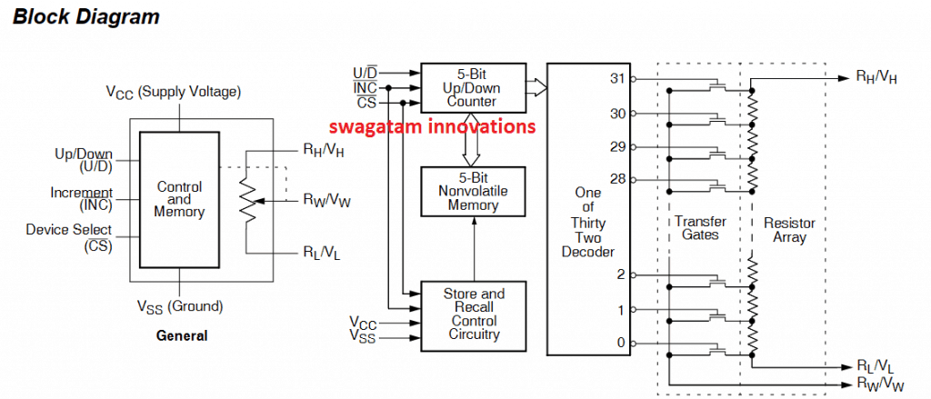 The IC utilizes a 3 wire interface for controlling the various positions of the wiper, and the potentiometer function is implemented through the array of resistors which are 31 numbers of resistive network, associated with the wiper switching network.
The entire array along with the end points of this resistive network are all integrated with the wiper network such that the wiper is able to access any point of the resistor array for executing the corresponding values of the potentiometer output through the 3 wire interface.
The CS, U/D and the INC pinouts of the IC actually control the wiper positioning.
The device can be also used as a 2 terminal potentiometer or a 2 terminal variable resistor.
The system becomes enabled and selected as soon as the CS input is applied a LOW logic (0V).
The value of the instantaneous wiper position is saved in non-volatile memory space, whenever the CS pinout is
delivered with a HIGH logic, in conjunction with INC input.
As soon as the store function is finished the X9315 is put into a low power standby position, until the unit gets selected yet again with a logic LOW.
The IC utilizes a 3 wire interface for controlling the various positions of the wiper, and the potentiometer function is implemented through the array of resistors which are 31 numbers of resistive network, associated with the wiper switching network.
The entire array along with the end points of this resistive network are all integrated with the wiper network such that the wiper is able to access any point of the resistor array for executing the corresponding values of the potentiometer output through the 3 wire interface.
The CS, U/D and the INC pinouts of the IC actually control the wiper positioning.
The device can be also used as a 2 terminal potentiometer or a 2 terminal variable resistor.
The system becomes enabled and selected as soon as the CS input is applied a LOW logic (0V).
The value of the instantaneous wiper position is saved in non-volatile memory space, whenever the CS pinout is
delivered with a HIGH logic, in conjunction with INC input.
As soon as the store function is finished the X9315 is put into a low power standby position, until the unit gets selected yet again with a logic LOW.
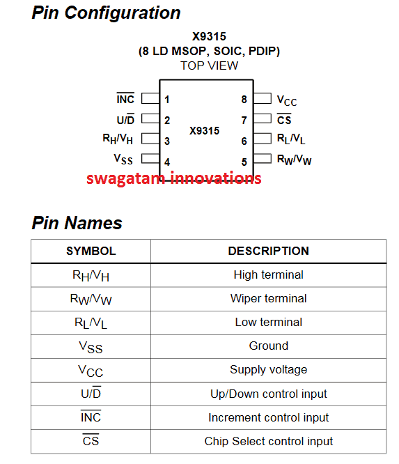

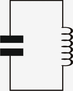
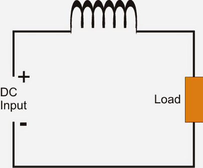
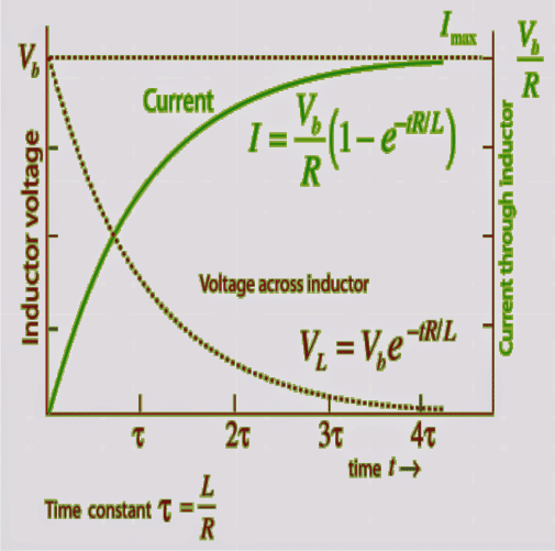
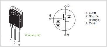
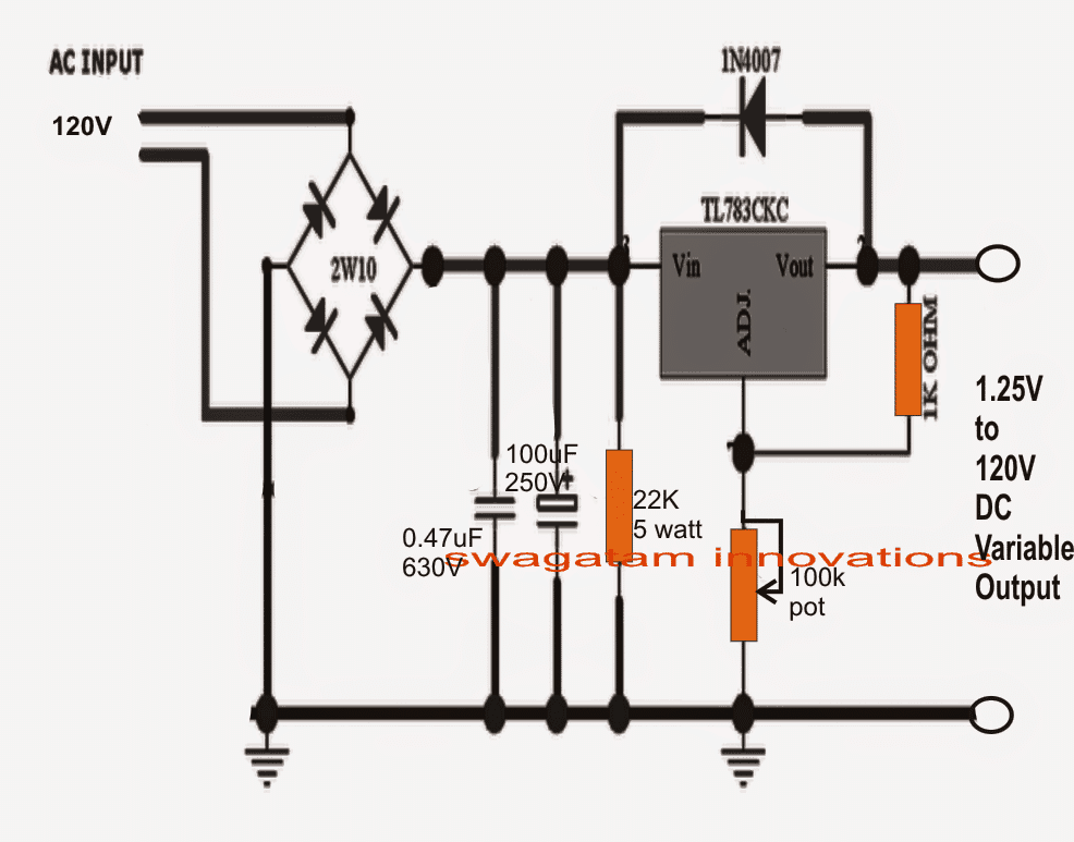 WARNING: PLEASE REMOVE THE 100uF/250 CAPACITOR FROM THE INDICATED POSITION AND PLACE IT ACROSS THE OUTPUT TERMINALS OF THE CIRCUIT, THIS WILL ENSURE THAT THE 120V INPUT DOESN'T GET TRANSFORMED INTO A DANGEROUS 160V PEAK AND DAMAGE THE IC.
THE GROUND SYMBOLS SHOWN WITH THE NEGATIVE LINE OF THE ABOVE CIRCUIT SHOULD NOT BE MISTAKEN WITH "EARTHING" OF THE 3-PIN SOCKET.
THE GROUND SYMBOLS ARE ONLY FOR HIGHLIGHTING THE NEGATIVE LINE OF THE BRIDGE RECTIFIER.
WARNING: PLEASE REMOVE THE 100uF/250 CAPACITOR FROM THE INDICATED POSITION AND PLACE IT ACROSS THE OUTPUT TERMINALS OF THE CIRCUIT, THIS WILL ENSURE THAT THE 120V INPUT DOESN'T GET TRANSFORMED INTO A DANGEROUS 160V PEAK AND DAMAGE THE IC.
THE GROUND SYMBOLS SHOWN WITH THE NEGATIVE LINE OF THE ABOVE CIRCUIT SHOULD NOT BE MISTAKEN WITH "EARTHING" OF THE 3-PIN SOCKET.
THE GROUND SYMBOLS ARE ONLY FOR HIGHLIGHTING THE NEGATIVE LINE OF THE BRIDGE RECTIFIER.
 CAUTION: THIS CIRCUIT IS NOT ISOLATED FROM MAINS AND THEREFORE IS EXTREMELY DANGEROUS TO TOUCH WHILE POWERED AND IN AN UNCOVERED SITUATION.
 Let's summarize the input output pinout functions and specifications of the IC 4043 with the following data:
1Q to 4Q (Pins: 2, 9, 10, 1) 3-state buffered latch output
1R to 4R (Pins: 3, 7, 11, 15) reset input (active HIGH)
1S to 4S (Pins: 4, 6, 12, 14) set input (active HIGH)
OE (Pin:5) common output enable input
VSS (Pin: 8) ground supply voltage
N.C.
(Pin: 13) not connected
VDD (Pin: 16) supply voltage
More Updates:
In this posts we try to understand the working of the IC 4043 and IC 4044 by studying the various specifications, datasheet of the devices and their pinout arrangement.
Basically both the variants are quad cross-coupled CMOS 3-state R/S or Reset/Set Latches.
Quad means having 4 outputs which can be set or latched with a logic high through a control input signal, or reset to logic zero by a subsequent input signal.
The 3-state feature allows the ICs to be controlled using 3 logic
The basic working principle of IC 4043 and IC 4044 is the same as above, the only difference being, IC 4043B are quad cross-coupled 3-state NOR Latch, and IC 4044B are quad cross-coupled 3-state NAND Latch.
Let's summarize the input output pinout functions and specifications of the IC 4043 with the following data:
1Q to 4Q (Pins: 2, 9, 10, 1) 3-state buffered latch output
1R to 4R (Pins: 3, 7, 11, 15) reset input (active HIGH)
1S to 4S (Pins: 4, 6, 12, 14) set input (active HIGH)
OE (Pin:5) common output enable input
VSS (Pin: 8) ground supply voltage
N.C.
(Pin: 13) not connected
VDD (Pin: 16) supply voltage
More Updates:
In this posts we try to understand the working of the IC 4043 and IC 4044 by studying the various specifications, datasheet of the devices and their pinout arrangement.
Basically both the variants are quad cross-coupled CMOS 3-state R/S or Reset/Set Latches.
Quad means having 4 outputs which can be set or latched with a logic high through a control input signal, or reset to logic zero by a subsequent input signal.
The 3-state feature allows the ICs to be controlled using 3 logic
The basic working principle of IC 4043 and IC 4044 is the same as above, the only difference being, IC 4043B are quad cross-coupled 3-state NOR Latch, and IC 4044B are quad cross-coupled 3-state NAND Latch.


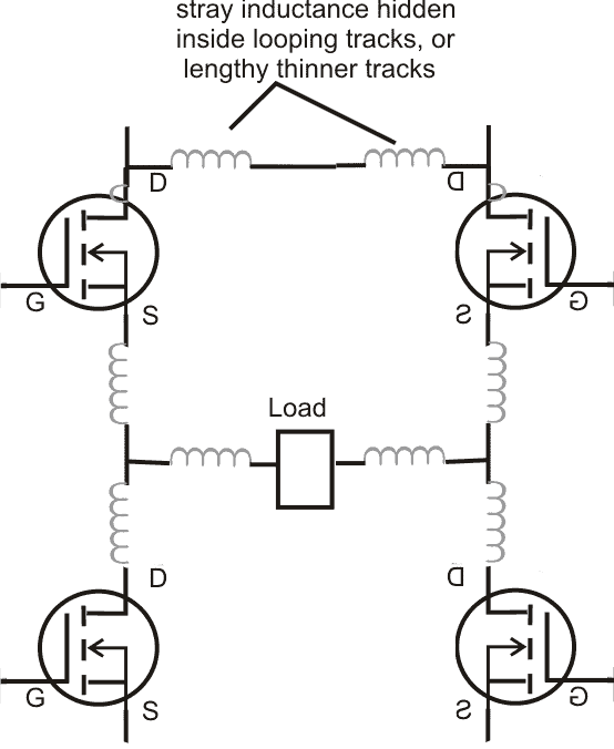 We all know that mosfets include in-built capacitors which require charging and discharging in order to make the device conduct.
Basically these capacitors are connected across the gate/source and gate/drain.
Mosfets "don't like" prolonged delayed charging and discharging of its capacitance since these are directly related to its efficiency.
Connecting the mosfets directly to a logic source output might seem to solve this problem, because the logic source would easily switch and sink the capacitance from Vcc to zero quickly, and vice versa due to the absence of any obstacle in its path.
However, implementing the above consideration could also lead to the generation of transients and negative spikes with dangerous amplitudes across the drain and gate making the mosfet vulnerable to the generated spikes due to sudden high current switching across drain/source.
This could easily break the silicon separation between the sections of the mosfet rendering a short circuit inside the device, and damaging it permanently.
We all know that mosfets include in-built capacitors which require charging and discharging in order to make the device conduct.
Basically these capacitors are connected across the gate/source and gate/drain.
Mosfets "don't like" prolonged delayed charging and discharging of its capacitance since these are directly related to its efficiency.
Connecting the mosfets directly to a logic source output might seem to solve this problem, because the logic source would easily switch and sink the capacitance from Vcc to zero quickly, and vice versa due to the absence of any obstacle in its path.
However, implementing the above consideration could also lead to the generation of transients and negative spikes with dangerous amplitudes across the drain and gate making the mosfet vulnerable to the generated spikes due to sudden high current switching across drain/source.
This could easily break the silicon separation between the sections of the mosfet rendering a short circuit inside the device, and damaging it permanently.
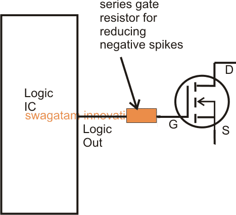
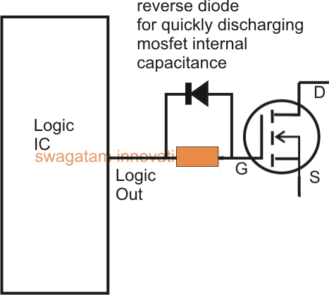
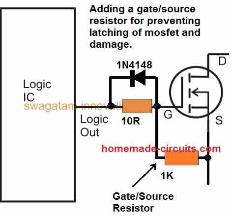
 The problem can be tackled by adding an external high power diode across drain/source terminals of the MOSFETs, so that the reverse current is shared across the diodes, and excess heat generation is eliminated.
 One of the most interesting aspects of the RTP from TE Connectivity is its ability to withstand enormous temperatures - up to 260oC.
This is surprising since the resistance change (to protect the MOSFET) usually occurs at around 140oC.
This miraculous feat is accomplished via innovative design by TE Connectivity.
The RTP has to be activated before it starts protecting the MOSFET.
The electronic activation of the RTP occurs after the flow soldering (attachment) is completed.
Each RTP has to be individually armed by sending a specified current through the arming pin of the RTP for a specified time.
The time-current characteristics are part of the specifications of the RTP.
Before it is armed, the value of the resistor of the RTP will follow the specified characteristics.
However, once it is armed, the arming pin will become electrically open - preventing further changes.
It is very important that the layout specified by TE Connectivity be followed when designing and mounting the MOSFET and the RTP on the PCB.
Since the RTP has to sense the temperature of the MOSFET, it naturally follows that the two should remain in close proximity.
The RTP resistance will allow up to 80A of current at 120V AC through the MOSFET as long as the temperature of the MOSFET remains below the Open Temperature of the RTP, which can be between 135-145oC.
One of the most interesting aspects of the RTP from TE Connectivity is its ability to withstand enormous temperatures - up to 260oC.
This is surprising since the resistance change (to protect the MOSFET) usually occurs at around 140oC.
This miraculous feat is accomplished via innovative design by TE Connectivity.
The RTP has to be activated before it starts protecting the MOSFET.
The electronic activation of the RTP occurs after the flow soldering (attachment) is completed.
Each RTP has to be individually armed by sending a specified current through the arming pin of the RTP for a specified time.
The time-current characteristics are part of the specifications of the RTP.
Before it is armed, the value of the resistor of the RTP will follow the specified characteristics.
However, once it is armed, the arming pin will become electrically open - preventing further changes.
It is very important that the layout specified by TE Connectivity be followed when designing and mounting the MOSFET and the RTP on the PCB.
Since the RTP has to sense the temperature of the MOSFET, it naturally follows that the two should remain in close proximity.
The RTP resistance will allow up to 80A of current at 120V AC through the MOSFET as long as the temperature of the MOSFET remains below the Open Temperature of the RTP, which can be between 135-145oC.
 Application Note:
 The receiver additionally offers a treble cut (known as de-emphasis), that makes up for the pre-emphasis that has been included at the transmitter.
 The main part of this circuit design is the IC1, a BA1404 FM stereo transmitter as shown in the figure above.
The left - channel input signal is tweaked to correct level by RI.
Treble boost (pre-emphasis) is supplied by the parallel blend of Cl and R3.
This matches the acoustic specs to the standard 75 microsecond as per the rules by the FCC.
Sound is paired by C10 to the left-channel input of IC1 on pin 1. Bad RF disturbances are bypassed to ground via C2 to protect against undesirable feedback.
The right channel input stage to pin 18 of ICI is actually the same as the left channel.
Power supply decoupling executed by C14, and any prior amplification for the sound input is decoupled by C12 on pin 2 of the chip.
A 38 -kHz signal is necessary to multiplex the incoming sound and develop the preliminary carrier signal.
The inner circuit stages of IC1 facilitates the application of a 38 kHz SX-cut crystal, as proven by the dotted line within the schematic of Figure above.
However, the 38 kHz crystals can be tough to get in the market, plus they may cost a lot if you happen to get one.
A much more easily accessible crystal, may be available that operates at 38.400 kHz.
This works in the majority of conditions: studies conducted in the course of the development of this particular design confirmed that a few FM stereo receivers might not "shake hands" reliably to the pilot carrier created from 38.400 kHz crystal.
The remedy was to work with an extremely secure alternative Hartley oscillator built using cheap, easily accessible components in place of either crystal oscillator.
The 38 kHz sine wave is produced by Q1 and the adjacent parts (the Hartley oscillator).
High gain transistor Q1 features a gain of over 300: lower gain devices may well not perform because of the reduced supply voltage (1.5 volts DC) which is supplied by a single AA cell.
The variable inductor employed for T1 is a 1st intermediate frequency (IF) transformer commonly seen in portable transistor radios, and it is intended for 455 kHz processing.
The coil in T1 is packed with ample capacitance by C23 to carry its working frequency down to approximately 38 kHz.
It is possible to fine-tune Ti's core to place the oscillator precisely on frequency.
Despite the fact that the oscillator may possibly drift a lot more compared to a quartz crystal, it's certainly not an issue simply because receivers make use of phase locked loops which could track the trivial floating away.
Take note that the circuit is not going to oscillate if transformer Ti's wiring is flipped or reversed.
A base view of Ti is shown in Fig to assist you with the connections.
The multiplexed audio tracks comes out of pin 14 of IC1 and is blended with the pilot carrier on pin 13 with the aid of the circuitry of R5, R6, C22, and C13.
The resulting audio output is sent to the modulator input at pin 12. To circumvent any kind of RF feedback complications, pin 12 is bypassed through C6. A Colpitts oscillator, working from 88 to 95 MHz, is created at pins 9 and 10 together with the circuitry of C15 to C17, C20, and L3.
The crude frequency realignment is done by adjusting the coil turn gaps of L3, and the fine tweaking done via C20.
RF energy which is developed through the tank circuit is held back from running back into the power supply stages using bypass capacitor C7 and RF choke L2.
The crude frequency realignment is done by adjusting the coil turn gaps of L3, and the fine tweaking done via C20. RF energy which is developed through the tank circuit is held from running back into the power supply stages using bypass capacitor C7 and RF-choke L2.
The modulated transmission at pin 10 of ICI is combined internally to the RF output amplifier comprising C18, C19, and L4 attached to pin 7.
This stage enhances the oscillator audio to commute the antenna, and this inhibits variations in antenna loading via switching the oscillator frequency.
A tap is extracted at a point on L4 on the antenna for having the highest possible power transmission.
The structure of IC1 is hard-wired intended for 1.5 volt operation having an absolute maximum of 3.5 volts.
Initial examining of this circuit revealed that the broadcast range failed to expand substantially when 3 volts was utilized to supply the circuit, and the current consumption increased 3 times .
As a result, the rise in operating voltage is not really advised.
The FM transmitter circuit consumes just about 5 mA, therefore just one AA cell might serve for a quite a while.
The main part of this circuit design is the IC1, a BA1404 FM stereo transmitter as shown in the figure above.
The left - channel input signal is tweaked to correct level by RI.
Treble boost (pre-emphasis) is supplied by the parallel blend of Cl and R3.
This matches the acoustic specs to the standard 75 microsecond as per the rules by the FCC.
Sound is paired by C10 to the left-channel input of IC1 on pin 1. Bad RF disturbances are bypassed to ground via C2 to protect against undesirable feedback.
The right channel input stage to pin 18 of ICI is actually the same as the left channel.
Power supply decoupling executed by C14, and any prior amplification for the sound input is decoupled by C12 on pin 2 of the chip.
A 38 -kHz signal is necessary to multiplex the incoming sound and develop the preliminary carrier signal.
The inner circuit stages of IC1 facilitates the application of a 38 kHz SX-cut crystal, as proven by the dotted line within the schematic of Figure above.
However, the 38 kHz crystals can be tough to get in the market, plus they may cost a lot if you happen to get one.
A much more easily accessible crystal, may be available that operates at 38.400 kHz.
This works in the majority of conditions: studies conducted in the course of the development of this particular design confirmed that a few FM stereo receivers might not "shake hands" reliably to the pilot carrier created from 38.400 kHz crystal.
The remedy was to work with an extremely secure alternative Hartley oscillator built using cheap, easily accessible components in place of either crystal oscillator.
The 38 kHz sine wave is produced by Q1 and the adjacent parts (the Hartley oscillator).
High gain transistor Q1 features a gain of over 300: lower gain devices may well not perform because of the reduced supply voltage (1.5 volts DC) which is supplied by a single AA cell.
The variable inductor employed for T1 is a 1st intermediate frequency (IF) transformer commonly seen in portable transistor radios, and it is intended for 455 kHz processing.
The coil in T1 is packed with ample capacitance by C23 to carry its working frequency down to approximately 38 kHz.
It is possible to fine-tune Ti's core to place the oscillator precisely on frequency.
Despite the fact that the oscillator may possibly drift a lot more compared to a quartz crystal, it's certainly not an issue simply because receivers make use of phase locked loops which could track the trivial floating away.
Take note that the circuit is not going to oscillate if transformer Ti's wiring is flipped or reversed.
A base view of Ti is shown in Fig to assist you with the connections.
The multiplexed audio tracks comes out of pin 14 of IC1 and is blended with the pilot carrier on pin 13 with the aid of the circuitry of R5, R6, C22, and C13.
The resulting audio output is sent to the modulator input at pin 12. To circumvent any kind of RF feedback complications, pin 12 is bypassed through C6. A Colpitts oscillator, working from 88 to 95 MHz, is created at pins 9 and 10 together with the circuitry of C15 to C17, C20, and L3.
The crude frequency realignment is done by adjusting the coil turn gaps of L3, and the fine tweaking done via C20.
RF energy which is developed through the tank circuit is held back from running back into the power supply stages using bypass capacitor C7 and RF choke L2.
The crude frequency realignment is done by adjusting the coil turn gaps of L3, and the fine tweaking done via C20. RF energy which is developed through the tank circuit is held from running back into the power supply stages using bypass capacitor C7 and RF-choke L2.
The modulated transmission at pin 10 of ICI is combined internally to the RF output amplifier comprising C18, C19, and L4 attached to pin 7.
This stage enhances the oscillator audio to commute the antenna, and this inhibits variations in antenna loading via switching the oscillator frequency.
A tap is extracted at a point on L4 on the antenna for having the highest possible power transmission.
The structure of IC1 is hard-wired intended for 1.5 volt operation having an absolute maximum of 3.5 volts.
Initial examining of this circuit revealed that the broadcast range failed to expand substantially when 3 volts was utilized to supply the circuit, and the current consumption increased 3 times .
As a result, the rise in operating voltage is not really advised.
The FM transmitter circuit consumes just about 5 mA, therefore just one AA cell might serve for a quite a while.
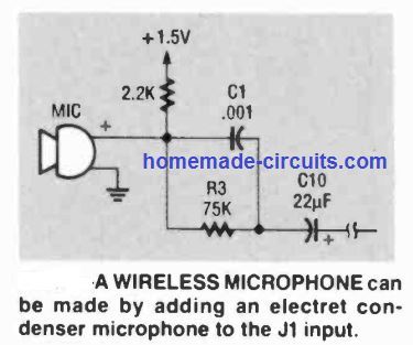 Stereo function lets you use two inputs together.
You could possibly consider incorporating vocals on one channel and musical instrument on the other for the program from your audio system.
Alternatively, you could also keep track of the phone or an infant on the left channel and tune in to your scanning device on the right channel all at a time as you clean up your vehicle or mow your garden, or when you wear a headphone receiver.
Stereo function lets you use two inputs together.
You could possibly consider incorporating vocals on one channel and musical instrument on the other for the program from your audio system.
Alternatively, you could also keep track of the phone or an infant on the left channel and tune in to your scanning device on the right channel all at a time as you clean up your vehicle or mow your garden, or when you wear a headphone receiver.
 In this schematic the highest current during power switch on is the peak line voltage divided by the value of the resistor R.
For mains supply of 120 V AC, this can be roughly 120 x ��2/R.
In the best possible scenario, just when Power is switched ON, the value of the resistor R needs to be much bigger, and quickly after once the mains supply is in its normal state, the R value must drop to zero.
An NTC thermistor is designed to work quite in this way, and therefore is best suited for most power supply application.
The job of an NTC is to limit the initial switch ON surge current by working like a power resistor that drops from a high value cool resistor to a low value warm resistor, the warmth being created by the normal current flowing through it.
In this schematic the highest current during power switch on is the peak line voltage divided by the value of the resistor R.
For mains supply of 120 V AC, this can be roughly 120 x ��2/R.
In the best possible scenario, just when Power is switched ON, the value of the resistor R needs to be much bigger, and quickly after once the mains supply is in its normal state, the R value must drop to zero.
An NTC thermistor is designed to work quite in this way, and therefore is best suited for most power supply application.
The job of an NTC is to limit the initial switch ON surge current by working like a power resistor that drops from a high value cool resistor to a low value warm resistor, the warmth being created by the normal current flowing through it.
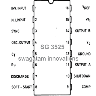
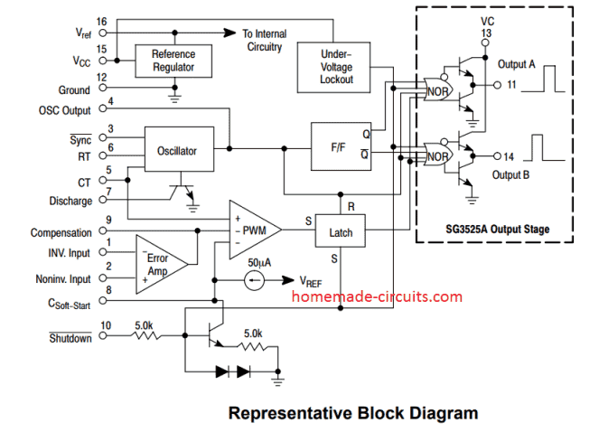
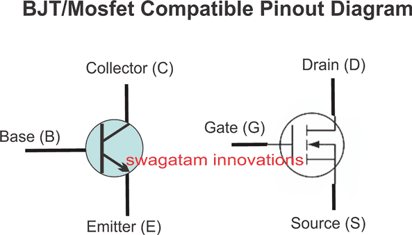 For an NPN BJT, we may replace the BJT with a correctlyspecified MOSFET in the following manner:
Remove the base resistor from the circuit because we don't typically need it anymore with a MOSFET.
Connectthegateof the N-MOSFET directly to the activation voltage source.
Keep the positivesupplyconnected to one of the load terminals, and connect the other terminal of the load to the drain of the MOSFET.
Lastly, connect the source of the MOSFET to ground.......DONE, you have replaced the BJT with a mosfet within minutes.
The procedure will remain as above even for a PNP BJT to be replaced with a P-channel MOSFET, you will need to just reverse the relevant supply polarities.
For an NPN BJT, we may replace the BJT with a correctlyspecified MOSFET in the following manner:
Remove the base resistor from the circuit because we don't typically need it anymore with a MOSFET.
Connectthegateof the N-MOSFET directly to the activation voltage source.
Keep the positivesupplyconnected to one of the load terminals, and connect the other terminal of the load to the drain of the MOSFET.
Lastly, connect the source of the MOSFET to ground.......DONE, you have replaced the BJT with a mosfet within minutes.
The procedure will remain as above even for a PNP BJT to be replaced with a P-channel MOSFET, you will need to just reverse the relevant supply polarities.
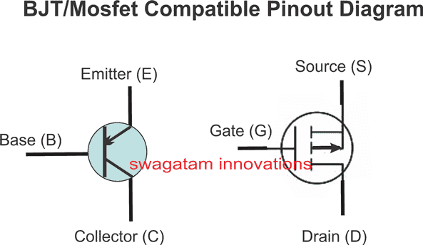
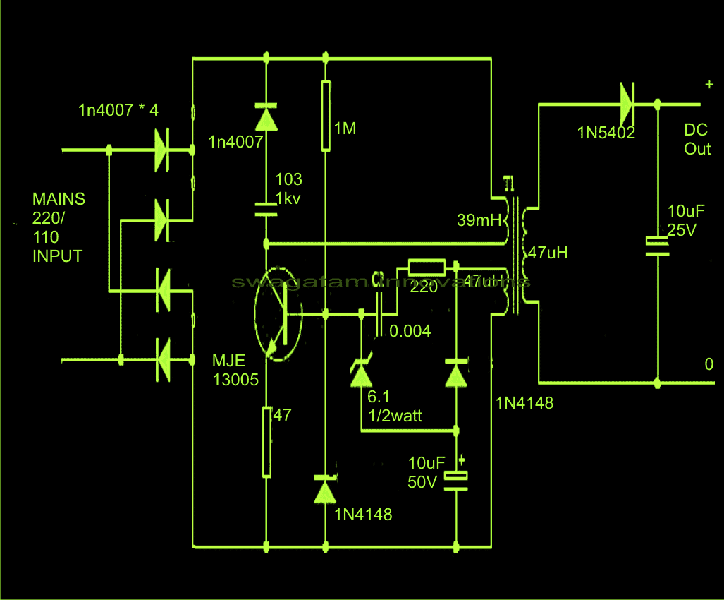 Here's another identical simple 220V SMPS circuit design you would like to investigate:
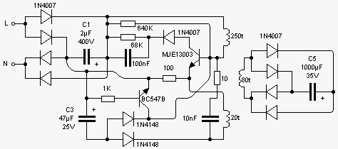
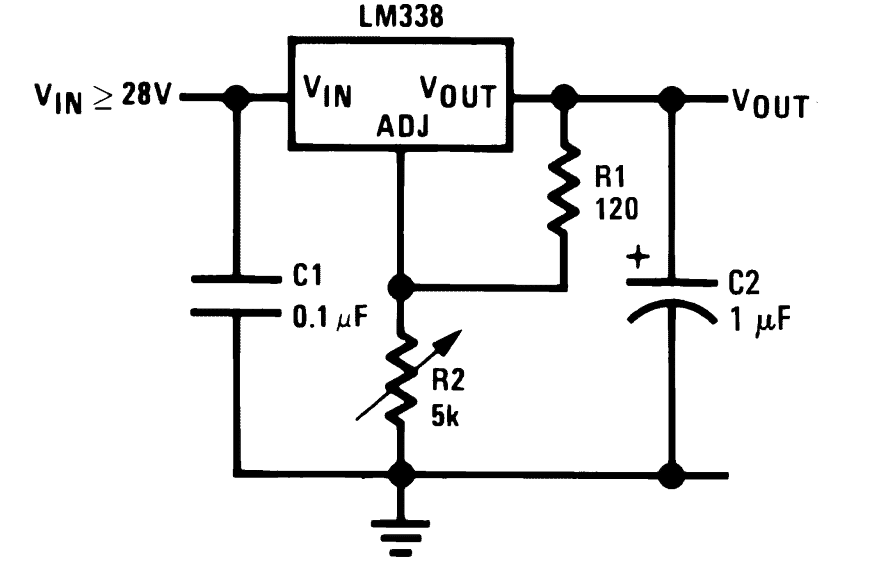
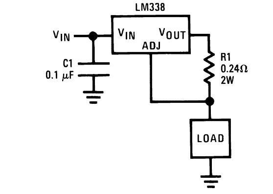
 The circuit utilizes three IC LM338 for the intended implementations with output voltage that's adjustable as explained for the first circuit.
R8 is used for the voltage adjustment operations.
The circuit utilizes three IC LM338 for the intended implementations with output voltage that's adjustable as explained for the first circuit.
R8 is used for the voltage adjustment operations.
 The collector resistance values are chosen in an incremental order so that a correspondingly varying voltages can be selected and becomes available through the external triggers.
 The light which needs to be controlled is powered by the output of the IC and its light is allowed to fall on this phototransistor.
As the light increases the value of the photo-transistor decreases which in turn pulls the ADJ pin of the IC more toward the ground, forcing the output voltage to decrease which also decreases the light illumination, maintaining a constant glow on the lamp.
The light which needs to be controlled is powered by the output of the IC and its light is allowed to fall on this phototransistor.
As the light increases the value of the photo-transistor decreases which in turn pulls the ADJ pin of the IC more toward the ground, forcing the output voltage to decrease which also decreases the light illumination, maintaining a constant glow on the lamp.
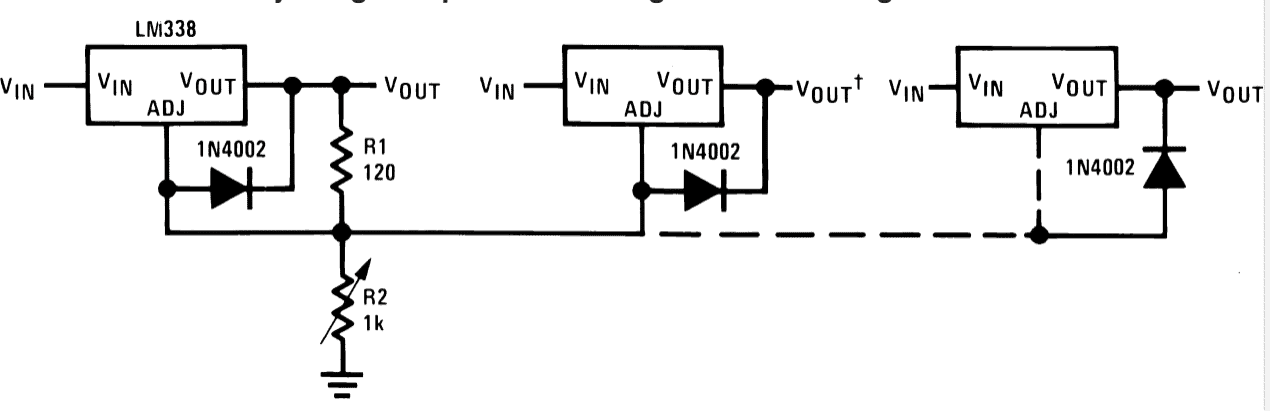 In the above section we learned a few of the important application circuits using the IC LM338, which were basically collected from the datasheet of the IC, if you have more clues regarding such LM338 based circuits, please let us know through the comments below.
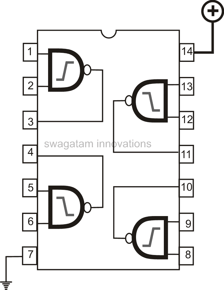
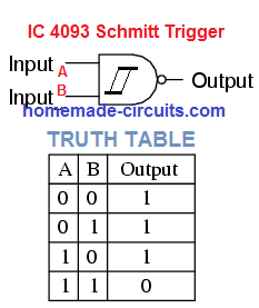 The output pin may be normally used for triggering the next stage in an electronic circuit, however it does not carry any criticality and will not damage the IC if left open.
However, the applied voltage to the inputs of the gates should never exceed the supply voltage to the IC which in turn should be within the specified range, normally within 2 to 15 volts.
Undefined voltage levels according to CMOS gates are within 0.75 and 2.5 volts.
Anything above 2.5 is considered to be logic 1 or logic high and anything below 0.75 is considered to be a logic 0 or a logic low.
The output pin may be normally used for triggering the next stage in an electronic circuit, however it does not carry any criticality and will not damage the IC if left open.
However, the applied voltage to the inputs of the gates should never exceed the supply voltage to the IC which in turn should be within the specified range, normally within 2 to 15 volts.
Undefined voltage levels according to CMOS gates are within 0.75 and 2.5 volts.
Anything above 2.5 is considered to be logic 1 or logic high and anything below 0.75 is considered to be a logic 0 or a logic low.
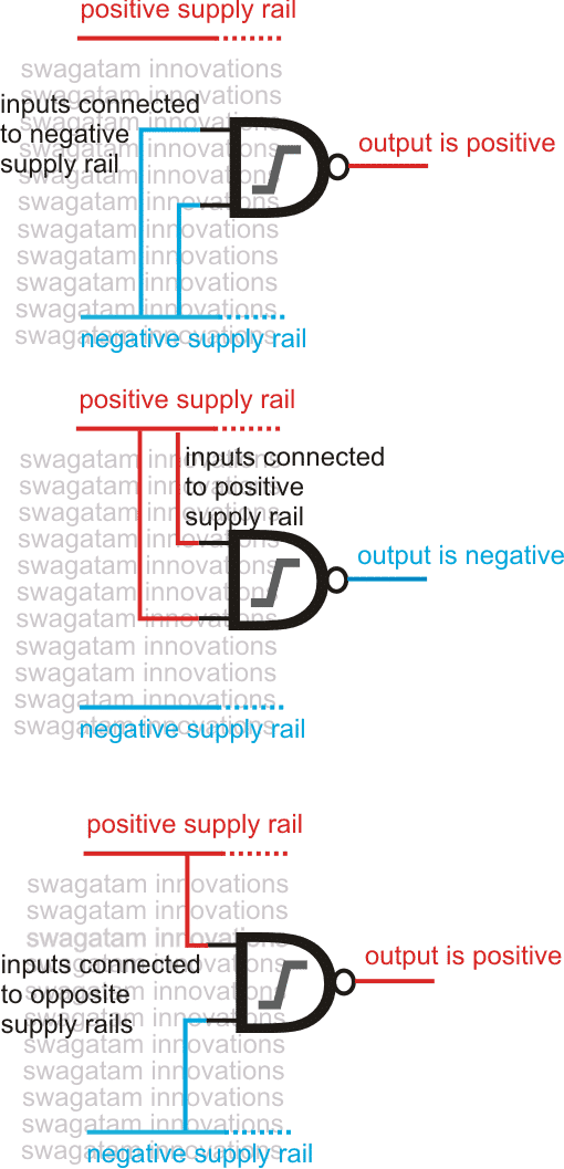
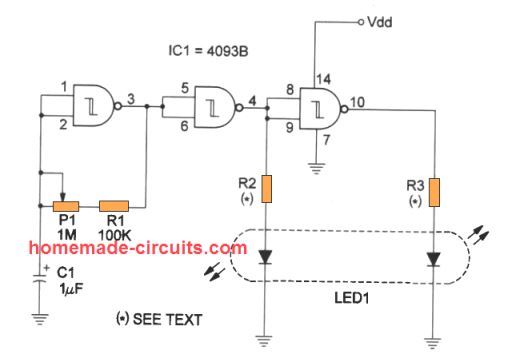 A simple twin alternate LED flasher circuit is shown above using a single IC 4093. The LEDs will flash alternately, and the flashing speed, or the frequency can be adjusted through the P1 pot.
The R2, and R3 will depend on the number of LEDs used, and the supply voltage.
These can be set by using the following formula:
R = supply voltage - total LED forward voltage / LED current
for a standard single LED the forward voltage can be assumed to be 3.3V, for 2 in series this will be 6.6 and so on.
A simple twin alternate LED flasher circuit is shown above using a single IC 4093. The LEDs will flash alternately, and the flashing speed, or the frequency can be adjusted through the P1 pot.
The R2, and R3 will depend on the number of LEDs used, and the supply voltage.
These can be set by using the following formula:
R = supply voltage - total LED forward voltage / LED current
for a standard single LED the forward voltage can be assumed to be 3.3V, for 2 in series this will be 6.6 and so on.
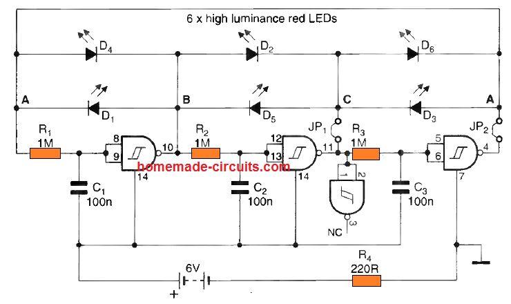
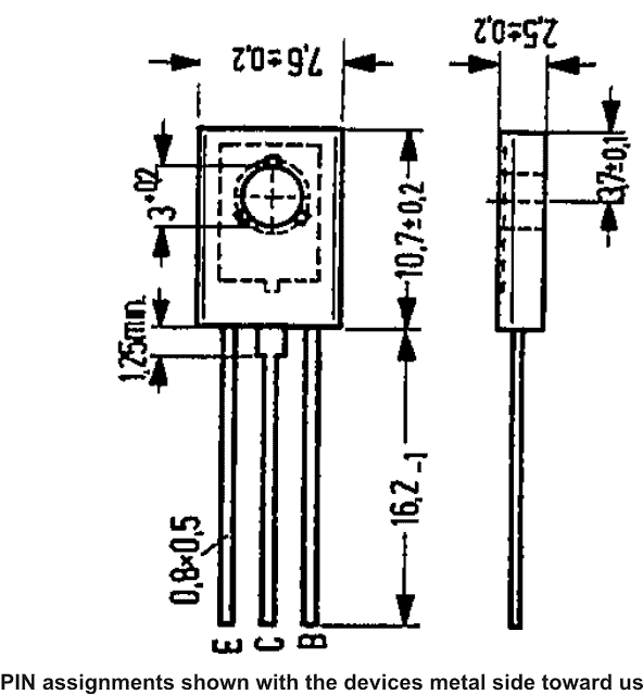
 Looking at the symbol of a capacitor we see that, it has two plates or poles separated by a space.
Practically too, that is what a capacitor is exactly made up of.
Also known as condensers, a capacitor internally consists of two conducting plates separated by an insulator or the dielectric.
According to its working principle, when a voltage (DC) is applied to its pair of conducting plates, an electric field is generated across them.
This field or energy is stored across the plates in the form of charge.
The relation between voltage, charge and the capacitance is expressed through the formula:
C = Q/V.
Where C = Capacitance, Q = Charge and V = Voltage.
So it can be clearly understood from the above formula that the potential drop or the voltage across the plates of a capacitor is proportional to the instantaneous charge Q stored in the capacitor.
The unit of measurement of capacitance is Farad.
The value of a capacitor (in Farads) depends on the amount of charge it can store in it.
Looking at the symbol of a capacitor we see that, it has two plates or poles separated by a space.
Practically too, that is what a capacitor is exactly made up of.
Also known as condensers, a capacitor internally consists of two conducting plates separated by an insulator or the dielectric.
According to its working principle, when a voltage (DC) is applied to its pair of conducting plates, an electric field is generated across them.
This field or energy is stored across the plates in the form of charge.
The relation between voltage, charge and the capacitance is expressed through the formula:
C = Q/V.
Where C = Capacitance, Q = Charge and V = Voltage.
So it can be clearly understood from the above formula that the potential drop or the voltage across the plates of a capacitor is proportional to the instantaneous charge Q stored in the capacitor.
The unit of measurement of capacitance is Farad.
The value of a capacitor (in Farads) depends on the amount of charge it can store in it.
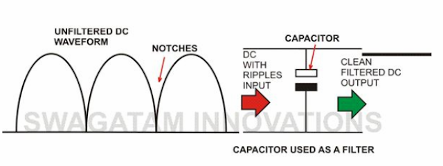
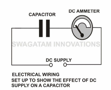
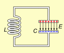 A capacitor when conjugated with an inductor will resonate to a particular frequency which is fixed by their values.
In simple words the pair will respond and lock to a particular external applied frequency and will start oscillating at the same frequency itself.
The behavior is well exploited in RF circuits, Transmitters, metal detectors etc.
In general you must have now understood what is a capacitor? But there are still numerous different complicated ways through which a capacitor may be configured.
Hopefully you will get to read them in my forth coming articles.
A capacitor when conjugated with an inductor will resonate to a particular frequency which is fixed by their values.
In simple words the pair will respond and lock to a particular external applied frequency and will start oscillating at the same frequency itself.
The behavior is well exploited in RF circuits, Transmitters, metal detectors etc.
In general you must have now understood what is a capacitor? But there are still numerous different complicated ways through which a capacitor may be configured.
Hopefully you will get to read them in my forth coming articles.
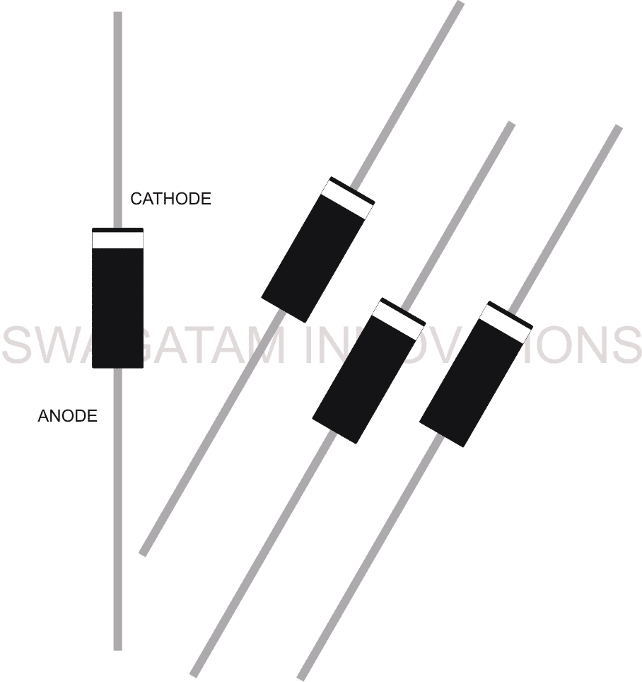
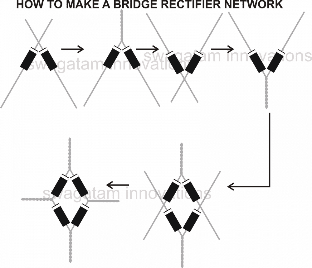
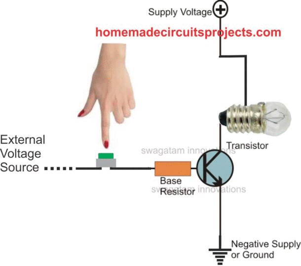 This is the standard method of using any transistor like a switch for controlling a given load.
You can see when a small external voltage is applied to the base, the transistor switches ON and conducts heavier current across the collector emitter terminals, switching on a bigger load.
The base resistor value can be calculated using the formula:
Rb = (Base Supply Vb - Base-Emitter Forward Voltage) x hFE / Load Current
Also remember that, the negative or the ground line of the external voltage must be connected with the transistor ground line or the emitter, otherwise the external voltage will have no effect on the transistor.
This is the standard method of using any transistor like a switch for controlling a given load.
You can see when a small external voltage is applied to the base, the transistor switches ON and conducts heavier current across the collector emitter terminals, switching on a bigger load.
The base resistor value can be calculated using the formula:
Rb = (Base Supply Vb - Base-Emitter Forward Voltage) x hFE / Load Current
Also remember that, the negative or the ground line of the external voltage must be connected with the transistor ground line or the emitter, otherwise the external voltage will have no effect on the transistor.
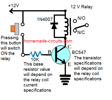 If you are confused about the relay, you can refer to this comprehensive article which explains everything about relay configurations.
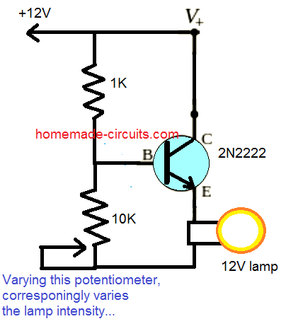 Here, the pot resistance along with the 1 K resistor forms a resistive divider network at the base of the transistor.
As the pot slider is moved, the voltage at the base of the transistor is changed, and this correspondingly alters the emitter voltage across the lamp, and the lamp intensity changes accordingly.
Here, the pot resistance along with the 1 K resistor forms a resistive divider network at the base of the transistor.
As the pot slider is moved, the voltage at the base of the transistor is changed, and this correspondingly alters the emitter voltage across the lamp, and the lamp intensity changes accordingly.
 Here too the LDR and the 300 ohm/5 k preset forms a potential divider at the base of the transistor.
The 300 ohm is actually not required.
It is included to ensure that the transistor base is never fully grounded, and thus it is never completely disabled or shut off.
It also ensures that the current through the LDR can never exceed a certain minimum limit, no matter how bright the light intensity is on the LDR.
When it's dark, the LDR has a high resistance which is many times higher than the combined value of the 300 ohm and the 5 K preset.
Due to this the transistor base gets more ground side voltage (negative) than the positive voltage, and its collector/emitter conduction remains switched OFF.
However when sufficient light falls on the LDR, its resistance drops to a few kilo-ohm value.
This enables the base voltage of the transistor to rise well over the 0.7 V mark.
The transistor now gets biased and switches ON the collector load, that is the relay.
As you can see, in this application too the transistors is basically amplifying the tiny base voltage such that a bigger load at its collector could be switched ON.
The LDR can be replaced with other sensors such as a thermistor for heat sensing, a water sensor for water sensing, a photodiode for IR beam sensing, and so forth.
Question for you: What happens if the position of the LDR and the 300/5 K preset are swapped with each other?
Here too the LDR and the 300 ohm/5 k preset forms a potential divider at the base of the transistor.
The 300 ohm is actually not required.
It is included to ensure that the transistor base is never fully grounded, and thus it is never completely disabled or shut off.
It also ensures that the current through the LDR can never exceed a certain minimum limit, no matter how bright the light intensity is on the LDR.
When it's dark, the LDR has a high resistance which is many times higher than the combined value of the 300 ohm and the 5 K preset.
Due to this the transistor base gets more ground side voltage (negative) than the positive voltage, and its collector/emitter conduction remains switched OFF.
However when sufficient light falls on the LDR, its resistance drops to a few kilo-ohm value.
This enables the base voltage of the transistor to rise well over the 0.7 V mark.
The transistor now gets biased and switches ON the collector load, that is the relay.
As you can see, in this application too the transistors is basically amplifying the tiny base voltage such that a bigger load at its collector could be switched ON.
The LDR can be replaced with other sensors such as a thermistor for heat sensing, a water sensor for water sensing, a photodiode for IR beam sensing, and so forth.
Question for you: What happens if the position of the LDR and the 300/5 K preset are swapped with each other?
 Normally these devices are designed to handle voltages anywhere between 30 to 60 volts across their collector and emitter.
The base voltage is not more than 6, but they can be easily triggered with a voltage level as low as 0.7 volts at their base.
However the current must be limited to 3 mA approximately.
The three leads of a TO-92 transistor may be identified in the following manner:
Keeping the printed side toward us, the right side lead is the emitter, the center one is the base and the left hand side leg is the collector of the device.
UPDATE: Want to know how to use transistors with Arduino?Read it here
Normally these devices are designed to handle voltages anywhere between 30 to 60 volts across their collector and emitter.
The base voltage is not more than 6, but they can be easily triggered with a voltage level as low as 0.7 volts at their base.
However the current must be limited to 3 mA approximately.
The three leads of a TO-92 transistor may be identified in the following manner:
Keeping the printed side toward us, the right side lead is the emitter, the center one is the base and the left hand side leg is the collector of the device.
UPDATE: Want to know how to use transistors with Arduino?Read it here
 The base of a transistor is the trigger terminal which is required to be applied with a small voltage level so the current through the load can pass through, across to the emitter line making the circuit complete and operating the load.
The removal of the trigger supply to the base immediately switches OFF the load or simply the current across the collector and the emitter terminals.
The base of a transistor is the trigger terminal which is required to be applied with a small voltage level so the current through the load can pass through, across to the emitter line making the circuit complete and operating the load.
The removal of the trigger supply to the base immediately switches OFF the load or simply the current across the collector and the emitter terminals.
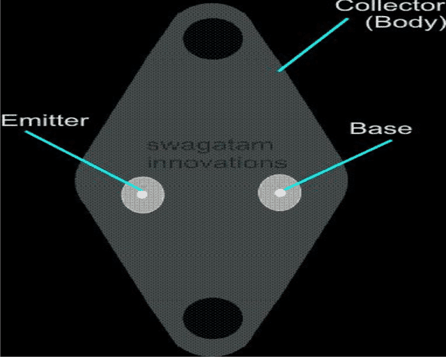
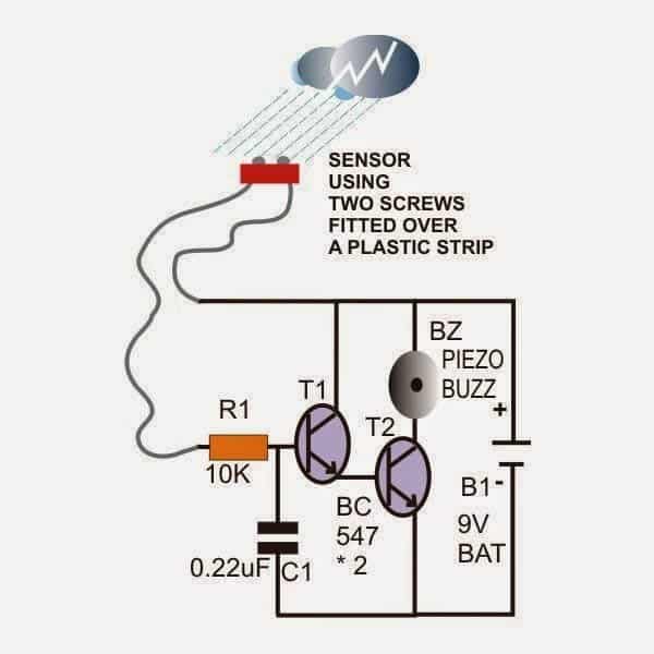 This circuit is built around just two transistors as the main active components.
The configuration is in the form of a standard Darlington pair, which increases its current amplification capacity hugely.
Rain drops or water drops falling and bridging the base with the positive supply is enough to trigger the alarm.
This circuit is built around just two transistors as the main active components.
The configuration is in the form of a standard Darlington pair, which increases its current amplification capacity hugely.
Rain drops or water drops falling and bridging the base with the positive supply is enough to trigger the alarm.
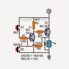 This circuit also utilizes a very few components and will faithfully set and reset the relay and the output load according to the input commands.
Pressing the upper push switch energizes the circuit and the load, whereas it is deactivated by pressing the lower push button.
This circuit also utilizes a very few components and will faithfully set and reset the relay and the output load according to the input commands.
Pressing the upper push switch energizes the circuit and the load, whereas it is deactivated by pressing the lower push button.
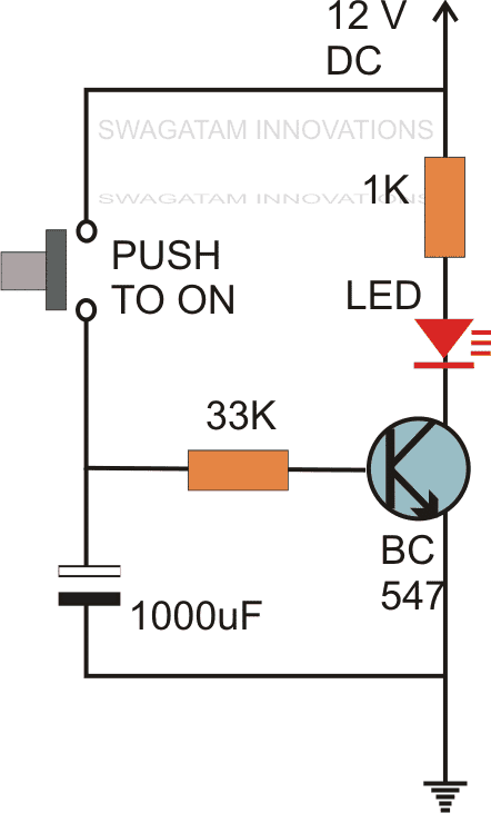 A very simple yet very effective timer circuit can be designed by incorporating just two transistors and other handful of components.
Pressing the push ON switch instantly charges the 1000uF capacitor and switching ON the transistors and the relay.
Even after releasing the switch the circuit holds on the position until C1 is completely discharged.
The time delay is determined by the values of R1 and C1. In the present design it��s around 1 minute.
A very simple yet very effective timer circuit can be designed by incorporating just two transistors and other handful of components.
Pressing the push ON switch instantly charges the 1000uF capacitor and switching ON the transistors and the relay.
Even after releasing the switch the circuit holds on the position until C1 is completely discharged.
The time delay is determined by the values of R1 and C1. In the present design it��s around 1 minute.
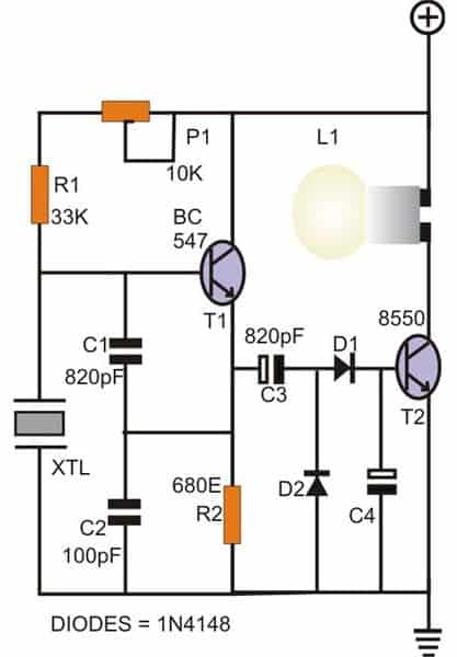 Crystals can be quite unfamiliar components especially with the electronic novices.
The shown circuit is basically a standard Colpitts oscillator incorporating a crystal to initiate its oscillations.
If the connected crystal is a good one, will be indicated through the illuminated bulb, a faulty crystal will keep the lamp shut.
Crystals can be quite unfamiliar components especially with the electronic novices.
The shown circuit is basically a standard Colpitts oscillator incorporating a crystal to initiate its oscillations.
If the connected crystal is a good one, will be indicated through the illuminated bulb, a faulty crystal will keep the lamp shut.
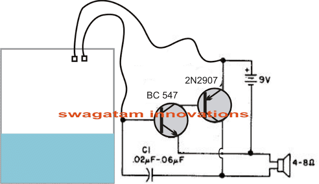 No more peeping and nervous apprehensions with overflowing water tanks.
This circuit will produce a nice little buzzing sound well before you tank spills over.
Nothing can be as simple as this one.
Keep watching for more of these little giants, I mean simple circuits to build with huge potentials.
No more peeping and nervous apprehensions with overflowing water tanks.
This circuit will produce a nice little buzzing sound well before you tank spills over.
Nothing can be as simple as this one.
Keep watching for more of these little giants, I mean simple circuits to build with huge potentials.
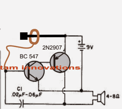 Pretty confident regarding your hand dexterity? The present circuit can definitely challenge you.
Build this circuit and just try sliding a constricted metal ring over the positive supply terminal without touching it.
A buzzing sound from the speaker will entitle you with ��antsy hands��.
Pretty confident regarding your hand dexterity? The present circuit can definitely challenge you.
Build this circuit and just try sliding a constricted metal ring over the positive supply terminal without touching it.
A buzzing sound from the speaker will entitle you with ��antsy hands��.
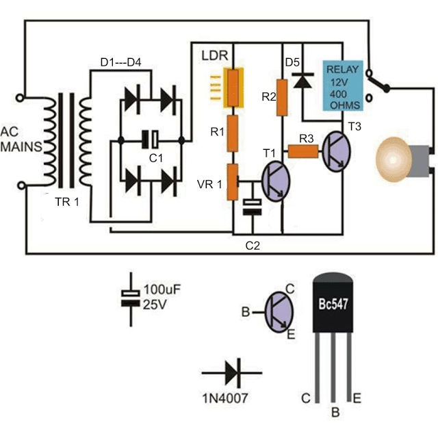 Parts List is Given Here
If you are interested to build a low-cost light dependent switch, then this circuit is just for you.
The idea is simple, a presence of light switches OFF the relay and the connected load, absence of light does exactly the opposite.
Need more explanations or help? Just keep posting your valuable comments (comments need moderation, may take time to appear).
Parts List is Given Here
If you are interested to build a low-cost light dependent switch, then this circuit is just for you.
The idea is simple, a presence of light switches OFF the relay and the connected load, absence of light does exactly the opposite.
Need more explanations or help? Just keep posting your valuable comments (comments need moderation, may take time to appear).
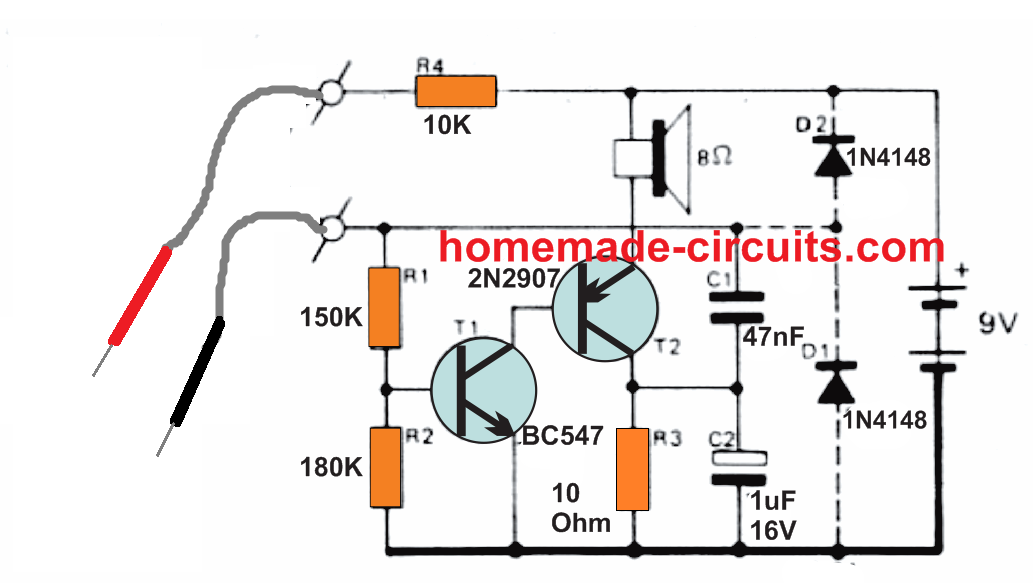 Passive testing of an electronic circuit appears pretty straightforward job.
All you want is really a Ohm meter.
Sadly, still, working with this type of device for semiconductors is not really advisable.
The output currents will probably harm semiconductor junctions.
The tester explained in this write-up is simple to construct and possesses the benefit that a maximum of around 50 ��A can only be delivered in the circuit under test.
Therefore it may be used for the majority of standard IC's and semiconductors which includes MOS based elements.
The indication is implemented through a little loudspeaker, to ensure that in the course of testing, it isn't required to keep on referring to the testing device rather than the concentrating on the test points.
The transistor T1 and T2 constitute a basic voltage controlled LF-oscillator, with a loudspeaker working like a load.
The oscillator frequency is formed by C1, R1, R4 and the external resistance between the measuring leads.
Resistor R3 is the collector resistance of T2; C2 behaves like a low frequency decoupling of this particular resistor.
As previously mentioned, the tester never will cause any sort of harm to the circuit under check; alternatively, it is best to include diodes D1 and D2 in order that the circuit under test is no way able to counter damage the tester parts.
So long as you don't have an electrical interconnection between the testing prods, the circuit pulls absolutely no current.
Battery-life can then be approximately same as the shelf life of the battery.
Passive testing of an electronic circuit appears pretty straightforward job.
All you want is really a Ohm meter.
Sadly, still, working with this type of device for semiconductors is not really advisable.
The output currents will probably harm semiconductor junctions.
The tester explained in this write-up is simple to construct and possesses the benefit that a maximum of around 50 ��A can only be delivered in the circuit under test.
Therefore it may be used for the majority of standard IC's and semiconductors which includes MOS based elements.
The indication is implemented through a little loudspeaker, to ensure that in the course of testing, it isn't required to keep on referring to the testing device rather than the concentrating on the test points.
The transistor T1 and T2 constitute a basic voltage controlled LF-oscillator, with a loudspeaker working like a load.
The oscillator frequency is formed by C1, R1, R4 and the external resistance between the measuring leads.
Resistor R3 is the collector resistance of T2; C2 behaves like a low frequency decoupling of this particular resistor.
As previously mentioned, the tester never will cause any sort of harm to the circuit under check; alternatively, it is best to include diodes D1 and D2 in order that the circuit under test is no way able to counter damage the tester parts.
So long as you don't have an electrical interconnection between the testing prods, the circuit pulls absolutely no current.
Battery-life can then be approximately same as the shelf life of the battery.
 T2 can be a BC557
Due to the fact the 400 mV drop develops across RX, T1 is typically switched ON leading to T2 getting cut off.
In case one of the tail lights blows out, the current by means of Rx is lowered by one half, which is 0.84 Amp.
The voltage drop across Rx at this point results in being 0.84 x 0.24 = 0.2 V.
This voltage looks appreciably minimal to activate T1, which means this T2 now gets base current via R1, and the LED illuminates.
To get a well-performing indication on lamps failure, it is suggested to make use of a single detector circuit for may be only a couple of lamps.
It is rather allowable, nonetheless, to use a single LED for a number of detectors: D1 and R3 work commonly to all sensors, and the collectors of all T2 transistors may be wired up with each other.
R3 must be 470 Ohms for a 12 V circuitry and 220 Ohms for a 6 V procedure.
T2 can be a BC557
Due to the fact the 400 mV drop develops across RX, T1 is typically switched ON leading to T2 getting cut off.
In case one of the tail lights blows out, the current by means of Rx is lowered by one half, which is 0.84 Amp.
The voltage drop across Rx at this point results in being 0.84 x 0.24 = 0.2 V.
This voltage looks appreciably minimal to activate T1, which means this T2 now gets base current via R1, and the LED illuminates.
To get a well-performing indication on lamps failure, it is suggested to make use of a single detector circuit for may be only a couple of lamps.
It is rather allowable, nonetheless, to use a single LED for a number of detectors: D1 and R3 work commonly to all sensors, and the collectors of all T2 transistors may be wired up with each other.
R3 must be 470 Ohms for a 12 V circuitry and 220 Ohms for a 6 V procedure.
 PCB Design for the above transistorized stabilized power supply can be seen in the following figure.
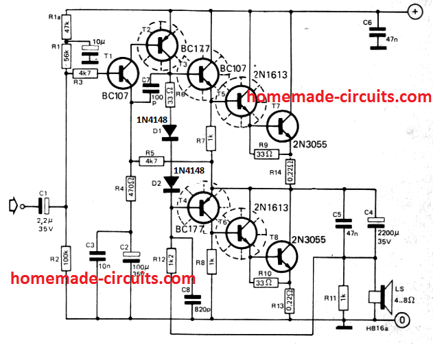 Capacitor C7 is positioned to make up for the phase shift from the output transistors.
The value of R1 is decreased to 56 k, and supplemental decoupling, by means of a 47 k resistor and a I0 ��F capacitor are placed in series with high potential side of R1 and power supply positive.
The output impedance is rather minimal, since T5/T7 and T6/T8 work like power darlingtons.
The control amplifier stage is effectively competent at delivering the 1-V RMS input voltage.
Due to the reduced input sensitivity, the amplifier provides excellent stability and its level of sensitivity to hum is minimal.
Significant negative feedback through R4 and R5 guarantees reduced distortion.
Optimum allowable supply voltage is 42 V.
The power supply circuit must be designed as a stabilized power supply unit for the amplifier.
Besides the heat sinks presented the 3nos 2N3055 transistors needs to be cooled down by clamping them on the metal cabinet using mica insulating washers.
The power supply table is designed for stereo.
Electrical Specifications for the 30 watt amplifier circuit is given below:
Capacitor C7 is positioned to make up for the phase shift from the output transistors.
The value of R1 is decreased to 56 k, and supplemental decoupling, by means of a 47 k resistor and a I0 ��F capacitor are placed in series with high potential side of R1 and power supply positive.
The output impedance is rather minimal, since T5/T7 and T6/T8 work like power darlingtons.
The control amplifier stage is effectively competent at delivering the 1-V RMS input voltage.
Due to the reduced input sensitivity, the amplifier provides excellent stability and its level of sensitivity to hum is minimal.
Significant negative feedback through R4 and R5 guarantees reduced distortion.
Optimum allowable supply voltage is 42 V.
The power supply circuit must be designed as a stabilized power supply unit for the amplifier.
Besides the heat sinks presented the 3nos 2N3055 transistors needs to be cooled down by clamping them on the metal cabinet using mica insulating washers.
The power supply table is designed for stereo.
Electrical Specifications for the 30 watt amplifier circuit is given below:
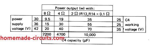 Full parts list for the the above amplifier circuit
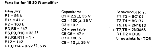
 When the doors are shut, the door contact is opened, disconnecting the transistor base from the ground line vi D3. This breaks the ground bias for the pnp transistor.
However, the relay still holds for sometime due to C1, which allows the BC557 base current to conduct via C1 and the relay coil, until eventually the C1 charges fully and shuts off the transistors and the relay.
When the doors are shut, the door contact is opened, disconnecting the transistor base from the ground line vi D3. This breaks the ground bias for the pnp transistor.
However, the relay still holds for sometime due to C1, which allows the BC557 base current to conduct via C1 and the relay coil, until eventually the C1 charges fully and shuts off the transistors and the relay.
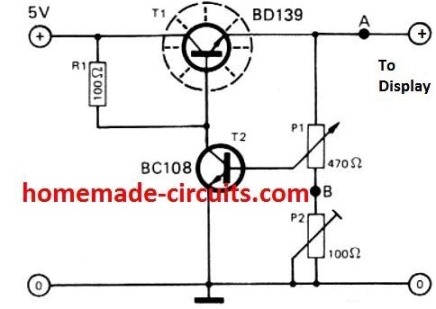 Display's LED illumination varies according to the adjustments of voltage controls P1 (coarse) and P2 (fine), approximately within 0 and 43 volts, the precise setting being somewhat crucial because of the diode characteristic of the LED.
While adjusting the display light, the voltage output is initially fixed at the minimum point, after that steadily increased attain the proper brightness.
The overall current for any 7-digit display must not go over around 1 amp to get a safe and sound segment current of 25 mA (7 segments at 25 mA for 6 digits).
The selection of the series transistor (T1) is determined through its recommended dissipation spec.
Display's LED illumination varies according to the adjustments of voltage controls P1 (coarse) and P2 (fine), approximately within 0 and 43 volts, the precise setting being somewhat crucial because of the diode characteristic of the LED.
While adjusting the display light, the voltage output is initially fixed at the minimum point, after that steadily increased attain the proper brightness.
The overall current for any 7-digit display must not go over around 1 amp to get a safe and sound segment current of 25 mA (7 segments at 25 mA for 6 digits).
The selection of the series transistor (T1) is determined through its recommended dissipation spec.
 The circuit explained below allows the relay to switch ON from a lower than the rated supply by ensuring that at the switch ON the voltage is boosted through a diode/capacitor voltage doubler network.
This boosted voltage provides the relay with the required higher initial supply.
Once the activation is accomplished, the voltage drops to the lower value, enabling the relay to hold and work with a reduced economical power.
The circuit explained below allows the relay to switch ON from a lower than the rated supply by ensuring that at the switch ON the voltage is boosted through a diode/capacitor voltage doubler network.
This boosted voltage provides the relay with the required higher initial supply.
Once the activation is accomplished, the voltage drops to the lower value, enabling the relay to hold and work with a reduced economical power.
 The R/C values shown in the diagram fixes the flashing rate to about 1/3rd Hz.
By simply adjusting either the values of the resistor or the capacitor pretty much any flashing rate can be obtained.
For using higher rated bulbs you can put more number of MOSFTs in parallel, without employing any specific current dependent parts.
The lamps can be a typical 12V to 14V lamp having 6 ohms resistance with cold filament.
Whenever 12 volts is utilized, the starting current used by the circuit will be 2 amps.
The same lamp, once switched ON and OFF mode will work using only 200 mA.
The R/C values shown in the diagram fixes the flashing rate to about 1/3rd Hz.
By simply adjusting either the values of the resistor or the capacitor pretty much any flashing rate can be obtained.
For using higher rated bulbs you can put more number of MOSFTs in parallel, without employing any specific current dependent parts.
The lamps can be a typical 12V to 14V lamp having 6 ohms resistance with cold filament.
Whenever 12 volts is utilized, the starting current used by the circuit will be 2 amps.
The same lamp, once switched ON and OFF mode will work using only 200 mA.
 This proposed neon globe flasher circuit circuit makes it possible for neon bulbs to be powered through a low voltage dc supply.
The voltage necessary to fire up the neon tube is achieved through an normal step down transformer 240-6.3V connected in the in the reverse order.
The circuit's battery drain is pretty low which can be in the range of 1 to 2 milliamps with respect to a 9 volt battery supply.
Q1 is a unijunction transistor that is configured to work like a relaxation oscillator.
Its functional frequency is established by the R2 -C1 network.
The pulses generated from the UJT Q1 are fed to the transistor Q2 which consequently switches transistor Q3 into saturation.
The sharp increase in the current arising from the 6.3V transformer winding due to Q3 going into saturation mode, forces a high voltage into the secondary winding of the transformer triggering the neon globe to flash.
The diode D1 is positioned to safeguard the transistor coming from high voltage spikes produced due to the inductive switching of the transformer.
This proposed neon globe flasher circuit circuit makes it possible for neon bulbs to be powered through a low voltage dc supply.
The voltage necessary to fire up the neon tube is achieved through an normal step down transformer 240-6.3V connected in the in the reverse order.
The circuit's battery drain is pretty low which can be in the range of 1 to 2 milliamps with respect to a 9 volt battery supply.
Q1 is a unijunction transistor that is configured to work like a relaxation oscillator.
Its functional frequency is established by the R2 -C1 network.
The pulses generated from the UJT Q1 are fed to the transistor Q2 which consequently switches transistor Q3 into saturation.
The sharp increase in the current arising from the 6.3V transformer winding due to Q3 going into saturation mode, forces a high voltage into the secondary winding of the transformer triggering the neon globe to flash.
The diode D1 is positioned to safeguard the transistor coming from high voltage spikes produced due to the inductive switching of the transformer.
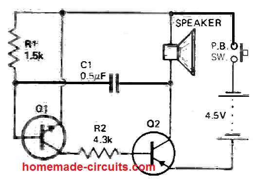 The resistor R1 can be employed for adjusting the audio frequency range of the beeper.
You can use any silicon, NPN, low frequency, small signal transistor for Q1 for example AC127, BC107, BC108 etc, and for Q2 any PNP transistor such as 8550, 2N2907, BD140 etc can be tried.
The battery specifications can be according to the drain current of Q2.
The resistor R1 can be employed for adjusting the audio frequency range of the beeper.
You can use any silicon, NPN, low frequency, small signal transistor for Q1 for example AC127, BC107, BC108 etc, and for Q2 any PNP transistor such as 8550, 2N2907, BD140 etc can be tried.
The battery specifications can be according to the drain current of Q2.
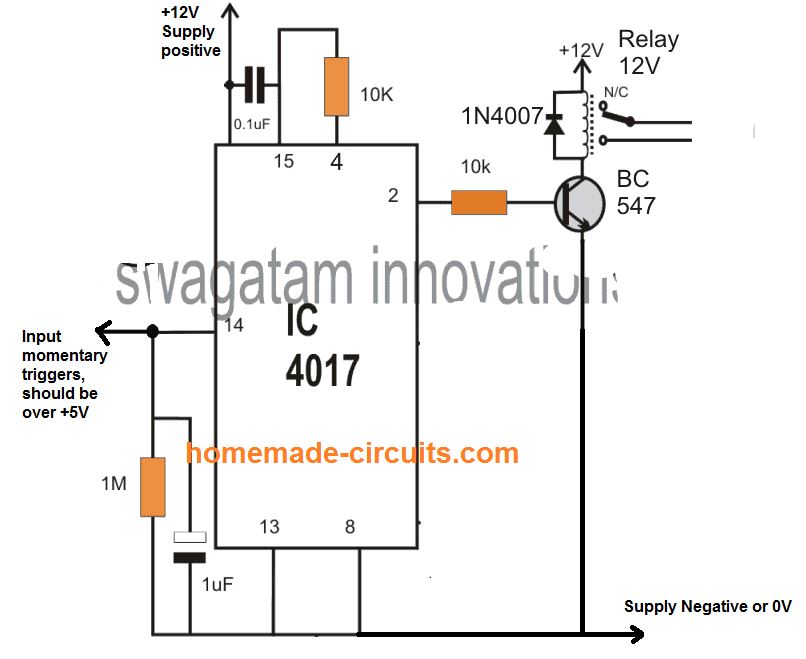
 My intention is to use this design in my single living room of my rented apartment.
The room has concealed wiring and the fan is located at the center of the roof.
The light will be connected parallel to the fan as a center light for the room.
There is no extra power outlet at the center of the roof.
Only outlet available is for the fan.
I do not wish to run separate wires from switchboard to the center light.
Hence, I though of designing a logical circuit which can detect the state (On/OFF) of the power source and switch loads accordingly.
For using the center light, I do not wish to keep the fan ON all the time and vice versa.
Every time the circuit is powered ON, the last know state should trigger the next operation of the circuit.
The Design
A simple electronic switch circuit customized to perform the above mentioned functions is shown below, without an MCU.
A bell push-button type switch is used for executing the sequential switching for the connected light and fan.
The design is self explanatory, if you have any doubts regarding the circuit description, please feel free to get it clarified through your comments.
My intention is to use this design in my single living room of my rented apartment.
The room has concealed wiring and the fan is located at the center of the roof.
The light will be connected parallel to the fan as a center light for the room.
There is no extra power outlet at the center of the roof.
Only outlet available is for the fan.
I do not wish to run separate wires from switchboard to the center light.
Hence, I though of designing a logical circuit which can detect the state (On/OFF) of the power source and switch loads accordingly.
For using the center light, I do not wish to keep the fan ON all the time and vice versa.
Every time the circuit is powered ON, the last know state should trigger the next operation of the circuit.
The Design
A simple electronic switch circuit customized to perform the above mentioned functions is shown below, without an MCU.
A bell push-button type switch is used for executing the sequential switching for the connected light and fan.
The design is self explanatory, if you have any doubts regarding the circuit description, please feel free to get it clarified through your comments.
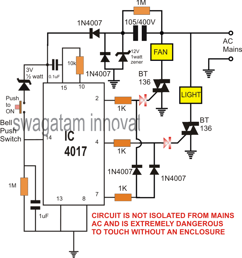
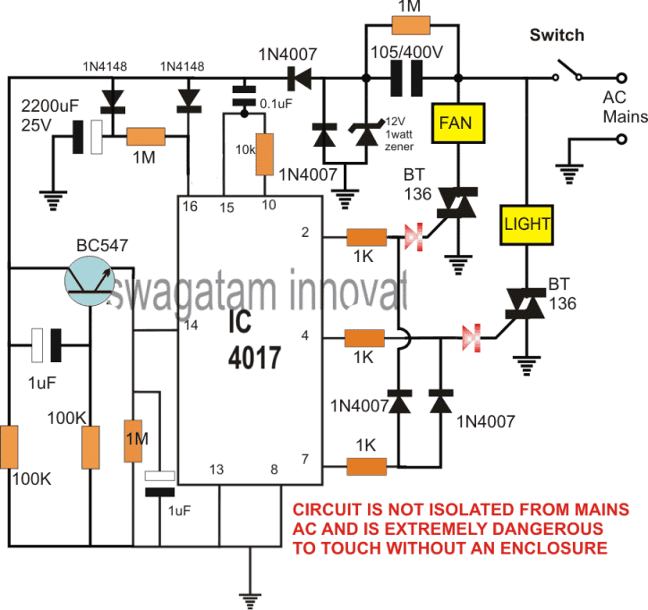 Another interesting ON OFF relay witch with a single button can be configured using a single IC 4093. Let's learn the procedures with the following explanation.
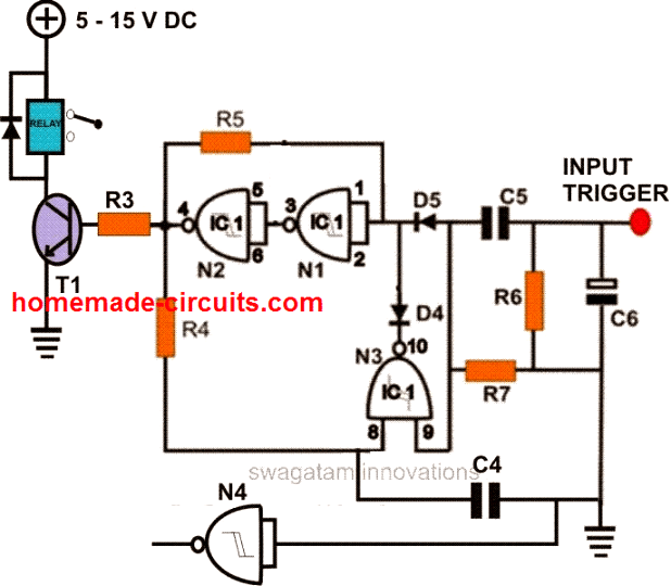 IC4093 Pinout Details
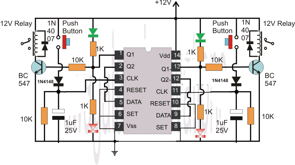
 As can be seen, a high value capacitor and resistor network is added with the supply terminal of the IC, and also a couple of diodes to ensure that the stored energy inside the capacitor is used for supplying only the IC and not to the other external stages.
Whenever mains AC fails, the 2200 uF capacitor steadily and very slowly allows its stored energy to reach the supply pin of the IC keeping the IC's "memory alive" and to make sure that the latch position is remembered by the IC while the mains is unavailable.
As soon as the mains returns, the IC delivers the original latching action on the relay as per the earlier situation, and thus prevents the relays from losing its previous switch ON status during the mains absence.
As can be seen, a high value capacitor and resistor network is added with the supply terminal of the IC, and also a couple of diodes to ensure that the stored energy inside the capacitor is used for supplying only the IC and not to the other external stages.
Whenever mains AC fails, the 2200 uF capacitor steadily and very slowly allows its stored energy to reach the supply pin of the IC keeping the IC's "memory alive" and to make sure that the latch position is remembered by the IC while the mains is unavailable.
As soon as the mains returns, the IC delivers the original latching action on the relay as per the earlier situation, and thus prevents the relays from losing its previous switch ON status during the mains absence.
 Though the circuit also employs a mechanical input device but this mechanical switch is a tiny micro switch which just requires alternate pushing for implementing the proposed toggling actions.
A micro switch is a versatile device and very much resistant to mechanical stress and therefore does not affect the efficiency of the circuit.
Though the circuit also employs a mechanical input device but this mechanical switch is a tiny micro switch which just requires alternate pushing for implementing the proposed toggling actions.
A micro switch is a versatile device and very much resistant to mechanical stress and therefore does not affect the efficiency of the circuit.
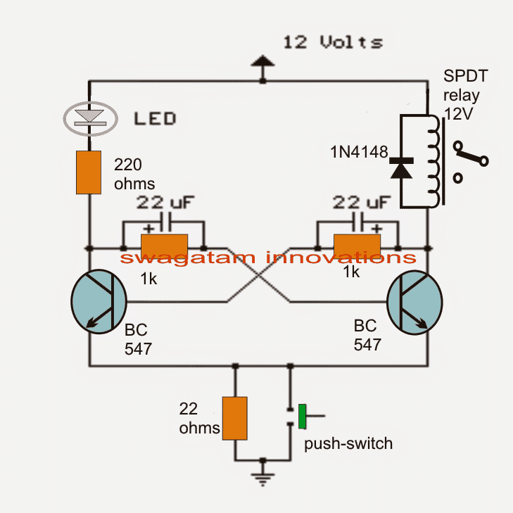 Do you any more ideas regrading flip flop projects, please do share with us, we'll be most glad to post them here for you and for the pleasure of all the dedicated readers.
 Accordingly (and extraordinarily) the first J -K flip-flop in 4027 then serves as a Schmitt control gate turning the very sluggish pulse at its input (pin 13) into a smooth electrical signal that can be added to the next flip-flop's clock input (pin 3).
Afterwards the second flip-flop functions as per the textbook, providing a real switching signal which can be used to turn a relay on and off through a transistor stage, T2.
The relay conducts alternately if you tap the contact plate with your finger.
The circuit current consumption while the relay is off is less than 1 mA, and when the relay is on, up to 50 mA.
Any relay that is more affordable can be used for as long as the coil voltage level is 12 V
However use a relay with correctly rated contacts when operating a mains device.
Accordingly (and extraordinarily) the first J -K flip-flop in 4027 then serves as a Schmitt control gate turning the very sluggish pulse at its input (pin 13) into a smooth electrical signal that can be added to the next flip-flop's clock input (pin 3).
Afterwards the second flip-flop functions as per the textbook, providing a real switching signal which can be used to turn a relay on and off through a transistor stage, T2.
The relay conducts alternately if you tap the contact plate with your finger.
The circuit current consumption while the relay is off is less than 1 mA, and when the relay is on, up to 50 mA.
Any relay that is more affordable can be used for as long as the coil voltage level is 12 V
However use a relay with correctly rated contacts when operating a mains device.
 R1 and R2 additionally protect against any static charges racking up, which can cause damage to the IC, when the supply is in the disconnected condition.
The 22Mohm resistors can be hard to obtain therefore a pair of 10 Mohm resistors can be connected in series.
The flip flop circuit could be kept switch ON continuously since a milliameter reveals absolutely no current being consumed in the relay off position.
In case relay RLA1 is removed TR 1 collector turns into a TTL output having a high fan out.
Attach the inputs of G3 and G4 to ground in case these are kept unused.
The touch plates could be positioned many feet away from the IC only if shielded termination is used for the connecting wires.
R1 and R2 additionally protect against any static charges racking up, which can cause damage to the IC, when the supply is in the disconnected condition.
The 22Mohm resistors can be hard to obtain therefore a pair of 10 Mohm resistors can be connected in series.
The flip flop circuit could be kept switch ON continuously since a milliameter reveals absolutely no current being consumed in the relay off position.
In case relay RLA1 is removed TR 1 collector turns into a TTL output having a high fan out.
Attach the inputs of G3 and G4 to ground in case these are kept unused.
The touch plates could be positioned many feet away from the IC only if shielded termination is used for the connecting wires.
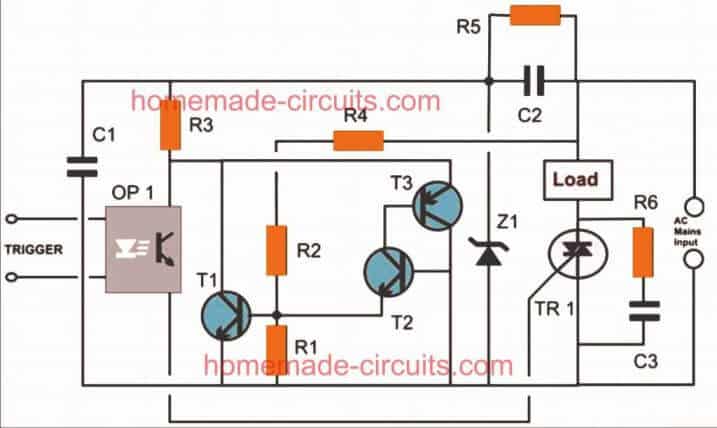
 Considering that the SSR load is resistive, the triac TIC 226D/400 V can be used satisfactorily.
In case, an inductive load is specified for the load, a 630 V triac may be required, for example, a type TIC 226M, can be necessary.
Remember the working voltage of capacitor C1 should match the specs of the triac used.
The input side resistor R1 can be determined depending on the level of the input voltage, Vin.
Its value can be evaluated using the following formula:
R1 = 1000 (Vin - 1.3)/Ioc.
In this equation Vin will be in volts, R1 is in ohms, and Ioc will be in mA, which indicates the current through the LED in the MOC opto-coupler.
If we consider the LED side input of the opto coupler to be Vin = 12 V, and the current Ioc = 30 mA (which are the standard specifications of the MOC 3040 opto coupler), the worked out value of R1 will be equal to 356 Ohms, and we can round it of to a practically feasible value of 330 Ohms.
In the MOC 3041 the current specification Ioc of the LED is simply 15 mA, which means that, practically it may be possible to allow the R1 limiting resistance value to be around 680 Ohms.
The maximum current this 220V solid state relay can handle is approximately 8 Amps, for higher power you can change the triac accordingly
Image courtesy: Farnel
Considering that the SSR load is resistive, the triac TIC 226D/400 V can be used satisfactorily.
In case, an inductive load is specified for the load, a 630 V triac may be required, for example, a type TIC 226M, can be necessary.
Remember the working voltage of capacitor C1 should match the specs of the triac used.
The input side resistor R1 can be determined depending on the level of the input voltage, Vin.
Its value can be evaluated using the following formula:
R1 = 1000 (Vin - 1.3)/Ioc.
In this equation Vin will be in volts, R1 is in ohms, and Ioc will be in mA, which indicates the current through the LED in the MOC opto-coupler.
If we consider the LED side input of the opto coupler to be Vin = 12 V, and the current Ioc = 30 mA (which are the standard specifications of the MOC 3040 opto coupler), the worked out value of R1 will be equal to 356 Ohms, and we can round it of to a practically feasible value of 330 Ohms.
In the MOC 3041 the current specification Ioc of the LED is simply 15 mA, which means that, practically it may be possible to allow the R1 limiting resistance value to be around 680 Ohms.
The maximum current this 220V solid state relay can handle is approximately 8 Amps, for higher power you can change the triac accordingly
Image courtesy: Farnel
 Thus when we focus into our Absolute Maximum Table, we are able to see these are actually classified by 4 separate current limiting factors for the same device.
Package Limit
Silicon Limit
Continuous Drain Current
Pulsed Drain Current
Let's learn each of those parameters in greater depth.
At the beginning, we see the package current limit, which signifies the limit characterized by the practical external limitations of the MOSFET package itself.
Next comes the silicon current limit, which is characterized by the magnitude of current which the silicon die of the device can practically tackle, as soon as the MOSFET case temperature attains a specific value.
Here, this is presented considering the device case temperature held at 25 ��C.
Other suppliers may possibly offer this at some different temperature level.
For Texas Instrument T-0220 MOSFETs, for example, this is presented at 25 ��C, and also 100 ��C case temperature.
Below this temperature level, there may be an additional continuous current rating, calculated with safe tolerance margins, with regards to the specific device's junction to ambient thermal impedance.
After that lastly, instead of a continuous current, we find a pulsed current rating included, which is, actually, calculated relative to both duty cycle and pulse duration.
And hence for sure, the thermal impedance of the device.
Now let's understand all the above MOSFET current limitations with an in-depth detail.
We will start with the package current limit of the device.
Thus when we focus into our Absolute Maximum Table, we are able to see these are actually classified by 4 separate current limiting factors for the same device.
Package Limit
Silicon Limit
Continuous Drain Current
Pulsed Drain Current
Let's learn each of those parameters in greater depth.
At the beginning, we see the package current limit, which signifies the limit characterized by the practical external limitations of the MOSFET package itself.
Next comes the silicon current limit, which is characterized by the magnitude of current which the silicon die of the device can practically tackle, as soon as the MOSFET case temperature attains a specific value.
Here, this is presented considering the device case temperature held at 25 ��C.
Other suppliers may possibly offer this at some different temperature level.
For Texas Instrument T-0220 MOSFETs, for example, this is presented at 25 ��C, and also 100 ��C case temperature.
Below this temperature level, there may be an additional continuous current rating, calculated with safe tolerance margins, with regards to the specific device's junction to ambient thermal impedance.
After that lastly, instead of a continuous current, we find a pulsed current rating included, which is, actually, calculated relative to both duty cycle and pulse duration.
And hence for sure, the thermal impedance of the device.
Now let's understand all the above MOSFET current limitations with an in-depth detail.
We will start with the package current limit of the device.
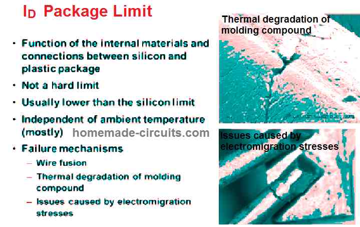 Having said that, this current limit parameter is not actually a final limit.
Meaning, if the MOSFET package is rated to handle 50 amp current, it doesn't mean that exceeding 50 amps, will suddenly cause an explosion of the device.
The 50 amp value may actually signify that, if the FET current is exceeded above this value, the effects could be unpredictable, and this may possibly reduce the long-term reliability of the device.
Therefore you can apply higher current than the specified package limit, if, perhaps you are able to maintain the MOSFET case temperature sufficiently cool, so that it remains under the maximum allowable thermal limitation value.
That said, frequently crossing the package limit could endanger the long-term reliability of the device to a great extent.
Typically, the package limit is usually below the calculated silicon limit.
This may not be always true for the higher-resistance devices.
Nevertheless generally, the package limit could be considered as the limit that is outlined with greater cautiousness and greater +/- margin than the silicon limit.
The package current limit is generally not dependent on the ambient temperature conditions? It is more dependent on the temperature that's just close by between the internal connections, which leads to the thermal compression and expansion, and eventually deterioration of those connections.
Therefore, the situation may lead to the breaking of the internal connecting wires due to extensive thermal expansion and shrinkage.
Additional breakdown factors consist of wire melting when they get exceedingly hot by themselves, due to huge current flow; thermal wreckage of the molding element that holds the wires attached to the lead frame; and various other complications attributable to electromigration strains of the real electrons flow.
Having said that, this current limit parameter is not actually a final limit.
Meaning, if the MOSFET package is rated to handle 50 amp current, it doesn't mean that exceeding 50 amps, will suddenly cause an explosion of the device.
The 50 amp value may actually signify that, if the FET current is exceeded above this value, the effects could be unpredictable, and this may possibly reduce the long-term reliability of the device.
Therefore you can apply higher current than the specified package limit, if, perhaps you are able to maintain the MOSFET case temperature sufficiently cool, so that it remains under the maximum allowable thermal limitation value.
That said, frequently crossing the package limit could endanger the long-term reliability of the device to a great extent.
Typically, the package limit is usually below the calculated silicon limit.
This may not be always true for the higher-resistance devices.
Nevertheless generally, the package limit could be considered as the limit that is outlined with greater cautiousness and greater +/- margin than the silicon limit.
The package current limit is generally not dependent on the ambient temperature conditions? It is more dependent on the temperature that's just close by between the internal connections, which leads to the thermal compression and expansion, and eventually deterioration of those connections.
Therefore, the situation may lead to the breaking of the internal connecting wires due to extensive thermal expansion and shrinkage.
Additional breakdown factors consist of wire melting when they get exceedingly hot by themselves, due to huge current flow; thermal wreckage of the molding element that holds the wires attached to the lead frame; and various other complications attributable to electromigration strains of the real electrons flow.
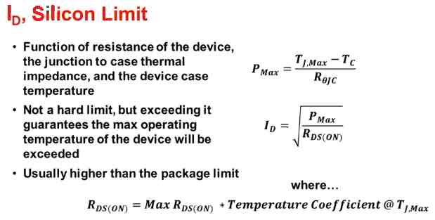 Therefore basically, what is assumed in the silicon current limit is an overly ideal heatsinking condition, which is able to hold the case-to-ambient thermal impedance effectively to 0. This may be equivalent to immersing the MOSFET inside liquid nitrogen, which could be practically impossible.
Right?
However the above scenario provides some clue regarding thermal performance, at least over a relative degree from MOSFET to MOSFET.
Yet again, it's not actually a strict limit, although it can be definitely never encouraged exceeding this current limit, which would otherwise mean crossing the maximum allowable temperature limit.
This could in turn result in your MOSFET bursting, or it might simply cause a massive degradation of the device, along with adversely affecting the long-term reliability of the MOSFET.
Therefore basically, what is assumed in the silicon current limit is an overly ideal heatsinking condition, which is able to hold the case-to-ambient thermal impedance effectively to 0. This may be equivalent to immersing the MOSFET inside liquid nitrogen, which could be practically impossible.
Right?
However the above scenario provides some clue regarding thermal performance, at least over a relative degree from MOSFET to MOSFET.
Yet again, it's not actually a strict limit, although it can be definitely never encouraged exceeding this current limit, which would otherwise mean crossing the maximum allowable temperature limit.
This could in turn result in your MOSFET bursting, or it might simply cause a massive degradation of the device, along with adversely affecting the long-term reliability of the MOSFET.
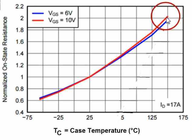 This curve is the device's drain/source normalized resistance value versus its case temperature value.
In the above graph, we find that if the maximum case temperature of the MOSFET reaches upto 150 ��C, it might cause the drain/source resistance of the device to climb to 2 Ohms which seems to be twice the resistance value at the 25 ��C mark.
Therefore, we have to consider this maximum resistance value 2 and multiply it with our Max RDS(ON) , to get the MOSFET resistance at its maximum allowable junction temperature.
And this is the resistance that's employed in this Equation#3.
This resistance value is not only implemented in the silicon limit current formula, but also in all of the current limit calculations.
Meaning, we always consider the maximum resistance RDS(ON) of the device at its maximum case temperature.
After this, we have one more continuous drain current limitation, on this occasion, determined by the junction-to-ambient thermal impedance of the MOSFET.
Meaning, this current limitation is going to be described at a particular ambient temperature, in the present situation, this will be usually the room temperature, or at 25 ��C.
This will be normally indicated at the footnote, regarding what exactly R��JA, junction-to-ambient, thermal impedance was assumed for this specific calculation.
This curve is the device's drain/source normalized resistance value versus its case temperature value.
In the above graph, we find that if the maximum case temperature of the MOSFET reaches upto 150 ��C, it might cause the drain/source resistance of the device to climb to 2 Ohms which seems to be twice the resistance value at the 25 ��C mark.
Therefore, we have to consider this maximum resistance value 2 and multiply it with our Max RDS(ON) , to get the MOSFET resistance at its maximum allowable junction temperature.
And this is the resistance that's employed in this Equation#3.
This resistance value is not only implemented in the silicon limit current formula, but also in all of the current limit calculations.
Meaning, we always consider the maximum resistance RDS(ON) of the device at its maximum case temperature.
After this, we have one more continuous drain current limitation, on this occasion, determined by the junction-to-ambient thermal impedance of the MOSFET.
Meaning, this current limitation is going to be described at a particular ambient temperature, in the present situation, this will be usually the room temperature, or at 25 ��C.
This will be normally indicated at the footnote, regarding what exactly R��JA, junction-to-ambient, thermal impedance was assumed for this specific calculation.
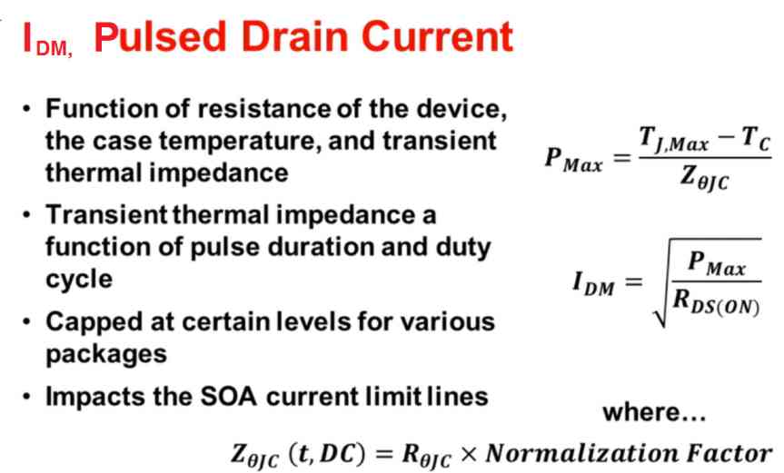 Referring to the equations, we find them all identical to out earlier Equation#1, except for the normal R��JC which is now replaced with Z��JC.
PMax = Tj,Max - TC / Z��JC (Equation#4)
Z��JC is known as the transient thermal impedance, which is actually the normal thermal impedance multiplied by certain normalization element, with regard to the pulse duration, and also the duty cycle.
Z��JC (t, DC) = R��JC x Normalization Factor (Equation#5)
Depending on the package type.
this current limit are specified differently.
For example, for the TO-220s 5 x 6 QFNs are designated at 400 amps maximum, since forcing the package limit any further than 400 amps appeared unrealistic and too stressful, for any MOSFET to handle.
This is why, in particular, the pulse current limitations of a FET device would be the limitations which normally outline the SOA current limit lines.
Recalling from one of our earlier posts, every single pulse duration indicated in the SOA signified a distinctive current limitation magnitude.
That's where the pulse current limitation lines are usually calculated.
Nevertheless these are usually assigned at 400 amps, for TO-220 devices and 5 x 6 QFNs.
Referring to the equations, we find them all identical to out earlier Equation#1, except for the normal R��JC which is now replaced with Z��JC.
PMax = Tj,Max - TC / Z��JC (Equation#4)
Z��JC is known as the transient thermal impedance, which is actually the normal thermal impedance multiplied by certain normalization element, with regard to the pulse duration, and also the duty cycle.
Z��JC (t, DC) = R��JC x Normalization Factor (Equation#5)
Depending on the package type.
this current limit are specified differently.
For example, for the TO-220s 5 x 6 QFNs are designated at 400 amps maximum, since forcing the package limit any further than 400 amps appeared unrealistic and too stressful, for any MOSFET to handle.
This is why, in particular, the pulse current limitations of a FET device would be the limitations which normally outline the SOA current limit lines.
Recalling from one of our earlier posts, every single pulse duration indicated in the SOA signified a distinctive current limitation magnitude.
That's where the pulse current limitation lines are usually calculated.
Nevertheless these are usually assigned at 400 amps, for TO-220 devices and 5 x 6 QFNs.
 We can quickly grab the given available from the datasheet, as indicated above.
We have the maximum resistance of the CSD17579Q5A , at 10 volts Vgs, to be 9.7 milliohms, as foreseen in the datasheet electrical characteristics table.
In the the Absolute-Maximum table we discover that the maximum allowable junction temperature for this device is 150 ��C.
Likewise if we refer to the thermal data table we realize that the maximum R��JC for this device is 4.3 ��C per watt.
We can quickly grab the given available from the datasheet, as indicated above.
We have the maximum resistance of the CSD17579Q5A , at 10 volts Vgs, to be 9.7 milliohms, as foreseen in the datasheet electrical characteristics table.
In the the Absolute-Maximum table we discover that the maximum allowable junction temperature for this device is 150 ��C.
Likewise if we refer to the thermal data table we realize that the maximum R��JC for this device is 4.3 ��C per watt.
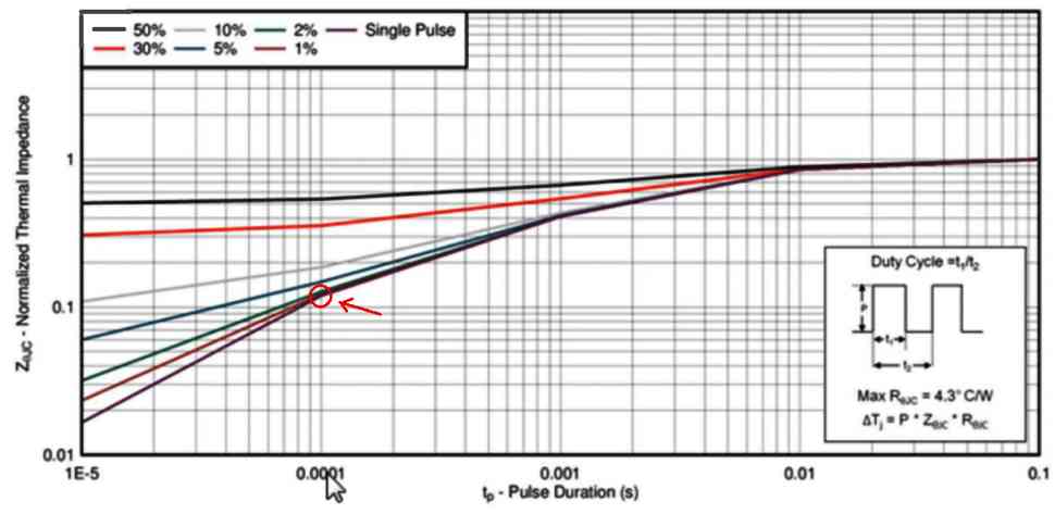 Thus considering these factors, we look at the 100 microseconds (0.0001 seconds) figure.
And after that we focus on the line which indicates 1% duty cycle, represented as the brown line.
And we discover a normalization factor of approximately 0.12, that we multiply by our 4.3 ��C per watt to generate a transient thermal impedance of 0.52 ��C per watt.
And finally we divide that into our temperature delta to determine the amount of power as 240 watts, which can be dissipated by this MOSFET, for this pulse period and duty cycle.
PMax = Tj,Max - TC / Z��JC
= 150 ��C - 25 ��C / 0.12 x 4.3 ��C/W
= 125 ��C / 0.52 ��C/W
= 240.3 watts
The final data we want to determine is, to what extent this maximum resistance of the device could rise at the maximum 150 ��C case temperature.
Therefore we refer to the figure 8 of the datasheet.
In this graph, we search for our temperature coefficient value, which seems to be around 1.75, corresponding to the 150 ��C temperature point (as shown below).
Thus considering these factors, we look at the 100 microseconds (0.0001 seconds) figure.
And after that we focus on the line which indicates 1% duty cycle, represented as the brown line.
And we discover a normalization factor of approximately 0.12, that we multiply by our 4.3 ��C per watt to generate a transient thermal impedance of 0.52 ��C per watt.
And finally we divide that into our temperature delta to determine the amount of power as 240 watts, which can be dissipated by this MOSFET, for this pulse period and duty cycle.
PMax = Tj,Max - TC / Z��JC
= 150 ��C - 25 ��C / 0.12 x 4.3 ��C/W
= 125 ��C / 0.52 ��C/W
= 240.3 watts
The final data we want to determine is, to what extent this maximum resistance of the device could rise at the maximum 150 ��C case temperature.
Therefore we refer to the figure 8 of the datasheet.
In this graph, we search for our temperature coefficient value, which seems to be around 1.75, corresponding to the 150 ��C temperature point (as shown below).
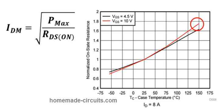 Therefore, we can now multiply our maximum resistance with this 1.75 temperature coefficient value, to get the RDS(ON) at 150 ��C.
RDS(ON) = Max RDS(ON) x Temperature Coefficient @ Tj,Max
= 9.7 m�� x 1.75 = 17 m��
We get the result as 17 milliohms, which explains that at the maximum 150 ��C, breakdown limit, the RDS(ON) resistance of this MOSFET could possibly maximize up to 17 milliohms.
After this, using the above conditions we are now able to quickly calculate the maximum tolerable pulse current as 119 amps, as shown below.
ID = �� PMax / RDS(ON)
= �� 240.3 / 17 m�� = 119 A
Therefore, we can now multiply our maximum resistance with this 1.75 temperature coefficient value, to get the RDS(ON) at 150 ��C.
RDS(ON) = Max RDS(ON) x Temperature Coefficient @ Tj,Max
= 9.7 m�� x 1.75 = 17 m��
We get the result as 17 milliohms, which explains that at the maximum 150 ��C, breakdown limit, the RDS(ON) resistance of this MOSFET could possibly maximize up to 17 milliohms.
After this, using the above conditions we are now able to quickly calculate the maximum tolerable pulse current as 119 amps, as shown below.
ID = �� PMax / RDS(ON)
= �� 240.3 / 17 m�� = 119 A
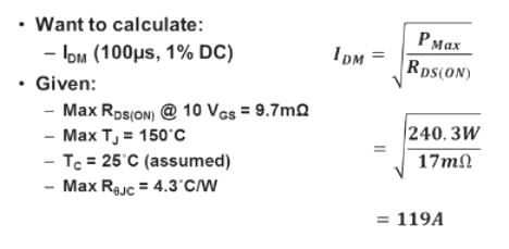
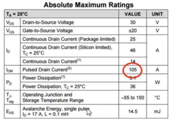 The reason behind this could be hidden in our SOA table of the datasheet.
Referring to the SOA table below we find that unlike the longer pulse duration lines which ranges between 10 milliseconds or 1 millisecond, the smaller 100 microsecond line seems to hit the MOSFET's max RDS(ON) line, even before it is able to touch our 119 amp limit.
The reason behind this could be hidden in our SOA table of the datasheet.
Referring to the SOA table below we find that unlike the longer pulse duration lines which ranges between 10 milliseconds or 1 millisecond, the smaller 100 microsecond line seems to hit the MOSFET's max RDS(ON) line, even before it is able to touch our 119 amp limit.
 This simply means that, the real resistance of the MOSFET is actually limiting the amount of current that could be possibly pushed across the device, before the device is able to arrive at its maximum thermal limit, with regards to current.
Thus, the above illustration explains that, despite of all the calculations, oftentimes the physical limitations of the device is a factor that must be taken into account.
The above discussed SOA line intersection takes place at 105 amps, that's exactly what is considered in the Absolute-Maximum table of the datasheet.
This simply means that, the real resistance of the MOSFET is actually limiting the amount of current that could be possibly pushed across the device, before the device is able to arrive at its maximum thermal limit, with regards to current.
Thus, the above illustration explains that, despite of all the calculations, oftentimes the physical limitations of the device is a factor that must be taken into account.
The above discussed SOA line intersection takes place at 105 amps, that's exactly what is considered in the Absolute-Maximum table of the datasheet.
 However, if we refer to the datasheet of a 30-volt CSD17570Q5B MOSFET, it provides us the current data ratings that we could reach at, if we tried to ignore the 400 amps cap.
Which means that for example, the 1% duty cycle, 100-microsecond pulse period value shown in the datasheet would in fact correspond to a mammoth 3,500 amps, which looks unpracticable.
Right?
And this is exactly why the pulse currents is limited to 400 amps.
Furthermore, that's also the reason why the datasheet SOA will be usually be tied to the 400 amps limit.
Not every suppliers might comply with this specifications.
So, in case you happen to come across a supplier datasheet that provides an unbelievably high pulse current capacity, this could be based on just pure hypothetical calculation, rather than the package limitations on that value.
Original Source: ti.com-training
However, if we refer to the datasheet of a 30-volt CSD17570Q5B MOSFET, it provides us the current data ratings that we could reach at, if we tried to ignore the 400 amps cap.
Which means that for example, the 1% duty cycle, 100-microsecond pulse period value shown in the datasheet would in fact correspond to a mammoth 3,500 amps, which looks unpracticable.
Right?
And this is exactly why the pulse currents is limited to 400 amps.
Furthermore, that's also the reason why the datasheet SOA will be usually be tied to the 400 amps limit.
Not every suppliers might comply with this specifications.
So, in case you happen to come across a supplier datasheet that provides an unbelievably high pulse current capacity, this could be based on just pure hypothetical calculation, rather than the package limitations on that value.
Original Source: ti.com-training

 MOSFET SOA is described as the magnitude that specifies the maximum power the FET can handle while it's operating in the saturation region.
The magnified glimpse of the SOA graph can be see in the next image below.
MOSFET SOA is described as the magnitude that specifies the maximum power the FET can handle while it's operating in the saturation region.
The magnified glimpse of the SOA graph can be see in the next image below.
 In the SOA graph above we are able to see all these limitations and boundaries.
And further deeper in the graph we find additional limitations for many different individual pulse duration.
And these lines inside of the graph, could be determined either through calculations or physical measurements.
In earlier and older datasheets, these parameters were estimated with calculated values.
However, it is normally recommended that these parameters are practically measured.
If you assess them using formulas, you could end up getting hypothetical values which may be literally much larger than the FET can tolerate in real world application.
Or perhaps you may derate (over-compensate) the parameters to a level that may be way too subdued, relative to what the FET can actually deal with.
So in our following discussions we learn the SOA parameters which are evaluated through real practical methods and not by formulas or simulations.
Let's begin by understanding what is saturation mode and linear mode in FETs.
In the SOA graph above we are able to see all these limitations and boundaries.
And further deeper in the graph we find additional limitations for many different individual pulse duration.
And these lines inside of the graph, could be determined either through calculations or physical measurements.
In earlier and older datasheets, these parameters were estimated with calculated values.
However, it is normally recommended that these parameters are practically measured.
If you assess them using formulas, you could end up getting hypothetical values which may be literally much larger than the FET can tolerate in real world application.
Or perhaps you may derate (over-compensate) the parameters to a level that may be way too subdued, relative to what the FET can actually deal with.
So in our following discussions we learn the SOA parameters which are evaluated through real practical methods and not by formulas or simulations.
Let's begin by understanding what is saturation mode and linear mode in FETs.
 Referring to the above graph, linear mode is, defined as the region, in which the RDS(on) or the drain-source resistance of the FET is consistent.
This means, the current passing through the FET is directly proportional to the drain-to-source bias through the FET.
It is also often known as the ohmic region, since the FET is essentially acting similar to a fixed resistor.
Now, if we begin increasing the drain-source bias voltage to the FET, we eventually find the FET operating in a region known as the saturation region.
Once the MOSFET operation is forced into the saturation region, the current (amps) moving via the MOSFET across drain to source no longer responds to the drain-to-source bias voltage increase.
Therefore regardless of how much you increase the drain-voltage, this FET continues to transfer a fixed maximum level of current through it.
The only way through which you are able to manipulate the current is usually by varying the gate-to-source voltage.
However, this situation appears to be slightly puzzling, since these are generally your textbook descriptions of linear and saturation region.
Previously we learned that this parameter is quite often referred to as the ohmic region.
Nevertheless a few folks actually name this as the linear region.
Perhaps, the mindset is, well, this looks like a straight line, so it has to be linear?
If you notice folks discussing hot-swap applications, they are going to express, well, I'm working in a linear region.
But that essentially is technologically inappropriate.
Referring to the above graph, linear mode is, defined as the region, in which the RDS(on) or the drain-source resistance of the FET is consistent.
This means, the current passing through the FET is directly proportional to the drain-to-source bias through the FET.
It is also often known as the ohmic region, since the FET is essentially acting similar to a fixed resistor.
Now, if we begin increasing the drain-source bias voltage to the FET, we eventually find the FET operating in a region known as the saturation region.
Once the MOSFET operation is forced into the saturation region, the current (amps) moving via the MOSFET across drain to source no longer responds to the drain-to-source bias voltage increase.
Therefore regardless of how much you increase the drain-voltage, this FET continues to transfer a fixed maximum level of current through it.
The only way through which you are able to manipulate the current is usually by varying the gate-to-source voltage.
However, this situation appears to be slightly puzzling, since these are generally your textbook descriptions of linear and saturation region.
Previously we learned that this parameter is quite often referred to as the ohmic region.
Nevertheless a few folks actually name this as the linear region.
Perhaps, the mindset is, well, this looks like a straight line, so it has to be linear?
If you notice folks discussing hot-swap applications, they are going to express, well, I'm working in a linear region.
But that essentially is technologically inappropriate.
 MOSFET temperature coefficient can be defined as the change in current over the change in junction temperature of the MOSFET.
Tc = ID / Tj
Therefore when we examine the transfer characteristics curve of a MOSFET in its datasheet, we find the drain-to-source current of the FET versus the increasing gate-to-source voltage of the FET, we also find that this characteristics is evaluated at 3 different temperature ranges.
MOSFET temperature coefficient can be defined as the change in current over the change in junction temperature of the MOSFET.
Tc = ID / Tj
Therefore when we examine the transfer characteristics curve of a MOSFET in its datasheet, we find the drain-to-source current of the FET versus the increasing gate-to-source voltage of the FET, we also find that this characteristics is evaluated at 3 different temperature ranges.