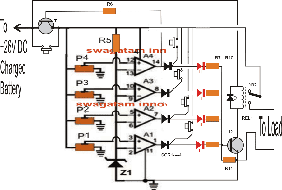
3v, 4.5v, 6v, 9v, 12v, 24v, Automatic Battery Charger Circuit with Indicator
An all-in-one automatic voltage battery charger circuit is discussed in the following post; the circuit can be modified in many different ways as per individual requirements and applications. The following circuit will allow you to charge any battery right from 1.5V to 24V simply by setting up a given preset.How it Works using LM3915 IC
The circuit functioning may be understood with the following points: The IC LM3915 which is a Dot/Bar voltage display chip forms the main section of the circuit. The IC has ten linearly incrementing output which sequence one after the other in response to a rising potential fed at its pin#5. Thus the output sequence corresponds to the instantaneous voltage level at the "signal input" pin out of the IC. The 10K preset associated with the above IC is set as per the battery voltage which needs to be charged. After this the LEds connected at the output linearly indicate the charge level of the battery by illuminating in sequence, and finally when the last LED is lit which happens when the battery gets fully charged, the SCR is triggered shutting off the charging process permanently until the power is reset. Discover the Widest Range of Automatic Battery Charger Circuits The stage comprising the IC LM338 is a standard voltage regulator IC, the preset associated with IC is set as per the required full charge limit of the connected battery. The transistor BC547 provides a fixed 3V for the connected LEDs for controlling the IC dissipation. The transistor BC557 remains switched OFF as long as the last LED in the array which may be selected for the full charge indication is not illuminated. As soon as the last "full charge" LED switches ON, the BC557 is also switched ON triggering the SCR. The SCR instantly grounds ADJ pin of the LM338 completely disabling the IC and the output to the battery. The battery now stops receiving any voltage and thus it is inhibited from getting over charged.How to Set Up this Circuit
The circuit can be used for charging 1.5V, 3V, 6V, 9V, 12V, 15V, 18V, 21V and 24V batteries, in fact any voltage that may lie between 1 and 24V. Suppose you want to charge a 6V battery, the full charge level for this battery would be 7V. The setting of the circuit may be done in the following manner: Do not connect the battery initially and also keep the SCR gate disconnected from the BC557 network. Apply a relatively higher DC potential at the input of the IC LM338, may be a 9V or a 12V input. Adjust the 10K preset under the LM338 such that the battery terminal points receive a 7V output. Now adjust the 10K preset under the IC LM3915 such that the last LED just flickers ON at this voltage, meaning at the applied 7V. Restore the the SCR gate connection as per the circuit diagram. That's it the circuit is all set now. During the charging process each LED will correspond to 7/10 = 0.7 volts, meaning say at 5V the 7th LEd will be illuminated and with a rise of 0.7V the subsequent LED will be lit and the sequence will proceed from 7t to 8th to 9th and then finally to the 10th LEd shutting off the circuit and the charging of the battery. Alternatively if you you are interested in making the circuit respond with all batteries from 3V to 12V then you may adjust the LM3915 preset such that the last LED barely illuminates at 14.4V. Now each pinout of the IC corresponding to the relevant LED would sequence at the rate of 14.4/10 = 1.4V, therefore for a 6V battery the full charge LED pinout would be 7/1.4 = 5, meaning the 5th LED illuminated would indicate that the connected 6V battery is now fully charge. For enabling automatic cut off for the above situation you just have make sure the base of the BC557 is connected to the 5th pinout of the IC LM3915 from left to right. For a 9V battery it would 9/1.4 = 6.4th LEd, meaning when the 6th LED is fully glowing and the 7th LED is barely flickering, the 7th LEd may be selected and joined with BC557 base for acquiring the required automatic cut off.Circuit Diagram

Using Transistor Latch instead of SCR
If the above circuit fails to respond with an SCR, the following circuit using a transistor latch can be employed: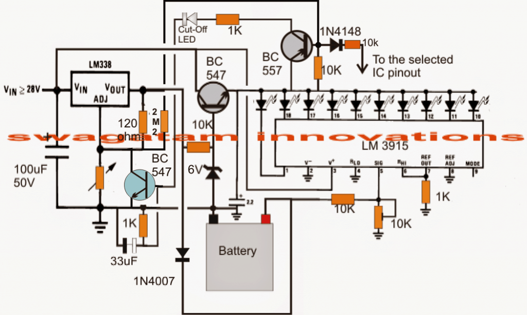
For an Automatic ON/OFF Function
If you want the above multipurpose battery charger circuit to cut off the charger while the battery reaches the full change limit, and then quickly switch ON the charging when the battery starts dropping below the full charge limit, and continue flip flopping at this threshold level, in that case you can try modifying the design in the following manner: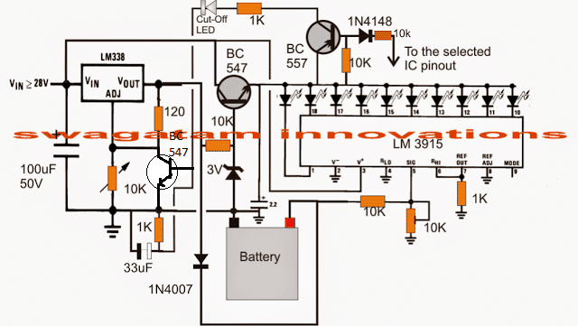
Solar Boost Charger Circuit with LED Driver Dimmer
The article explains a simple solar boost charger with LED driver circuit which also includes a single push dimmable feature. The idea was requested by Mr. Ashutosh.Technical Specifications
Hi swagatam,Myself Ashutosh. I m very new to ur website, n i ll say u r superb, u r doing one of the best thing by helping hobbyists. Thank you very much. I want an LED driver cum charger circuit for our project. i know u already have thousands of request pending and at the same time u might be working on different circuits,even thoughi want to ask for it, my circuit details are as below-
1. It's an LED lamp 2. Having 3volt (0.5watt) of solar panel for charging the battery. 3. Have to charge 3.6 volt battery from the solar panel (for this may be some boost ic is required ). 4. Regarding switching---> have one switch---> when all the connection are there the LED should be in off mode---> after 1st press it should glow in full brightness i mean 100% duty cycle----> 2nd time when i press 2nd time the switch the LEDs brightness shoulddecreasedby 40-50%---> when i press the switch 3rd time the LED should get more dimmed(say the brightness should decreased by 70-80%)----> and when i press the switch 4th time the LED should get off. 5. Circuit should be very compact(made up of very few components) and no use of microcontroller plz as, i dnt have that much idea about the microcontroller. 6. Also suggest the best LED for brightness whether it ll be an SMD LED and it's specification.
it won't be so difficult for u sir. i m bookmarking you this page for your reply, as i know from ur site, ur best thing is u used to reply almosteveryone keep doing it. A positive reply is expected from you. Thank you very much.
The Design
When an input is applied, the transistor instantly goes into an oscillating mode inducing a relatively stepped up voltage across the connected battery. The process starts charging the battery and depending upon the position of the IC 4017 output illuminates the connected LED with a certain intensity. The IC 4017 operates in three modes as requested above. The modes can be selected by pressing the given button momentarily. The above toggling sequences the output from the pin2 to pin7 in steps producing different glow intensities on the LED. At the first pin out pin#3 (not shown) the LED shuts down completely as it's not associated with theswitchingnetworkin anyway.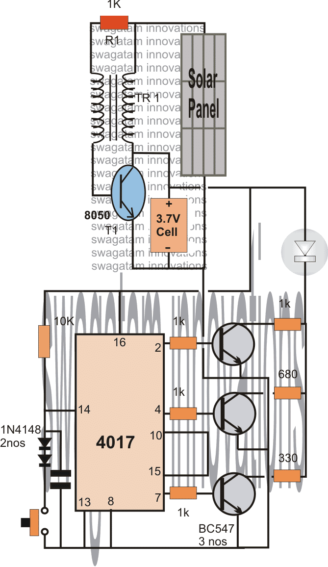
Zero Drop LDO Solar Charger Circuit
The article discusses a simple low dropout LDO, or zero drop solar charger circuit without microcontroller which can be modified in many different ways as per user preference. The circuit does not depend on microcontroller and can be built even by a layman.What is a Zero Drop Charger
A zero drop solar charger is a device which ensures that the voltage from the solar panel reaches the battery without undergoing any drop in voltage, either due to resistance or semiconductor interference. The circuit here uses a MOSFET as a switch for ensuring minimum drop in voltage from the attached solar panel. Moreover the circuit has a distinct advantage over other forms of zero drop charger designs, it does not unnecessarily shunt the panel making sure the panel is allowed to operate at its highest efficiency zone. Let's understand how these features could be achieved through this novel circuit idea designed by me.Simplest LDO Circuit
Here's a simplest LDO solar charger example which can be built in minutes, by any interested hobbyist. These circuits can be effectively used in place of expensive Schottky diodes, for getting an equivalent zero drop transfer of solar energy to the load. A P channel MOSFET is used as a zero drop LDO switch.
The zener diode protects the MOSFET from high solar panel voltages above 20 V.
The 1N4148 protects the MOSFET from a reverse solar panel connection.
Thus, this MOSFET LDO becomes fully protected from reverse polarity conditions and also allows the battery to charge without dropping any voltage in the middle.
For an N-channel version you can try the following variant.
A P channel MOSFET is used as a zero drop LDO switch.
The zener diode protects the MOSFET from high solar panel voltages above 20 V.
The 1N4148 protects the MOSFET from a reverse solar panel connection.
Thus, this MOSFET LDO becomes fully protected from reverse polarity conditions and also allows the battery to charge without dropping any voltage in the middle.
For an N-channel version you can try the following variant.

Using Op Amps
If you are interested to build a zero drop charger with automatic cut off feature, you can apply this using an op amp is wired as a comparator as shown below. In this design the non-inverting pin of the IC is positioned as the voltage sensor via a voltage divider stage made by R3 and R4. Referring to the proposed zero drop voltage regulator charger circuit diagram we see a rather straightforward configuration consisting of an opamp and a mosfet as the main active ingredients. The inverting pin is as usual rigged as the reference input using R2 and the zener diode. Assuming the battery to be charged is a 12V battery, the junction between R3 and R4 is calculated such that it produces 14.4V at a certain optimal input voltage level which may be the open circuit voltage of the connected panel. On applying the solar voltage at the shown input terminals, the mosfet initiates with the help of R1 and allows the entire voltage across its drain lead which finally reaches the R3/R4 junction. The voltage level is instantly sensed here and if in case it's higher than the set 14.4V, switches ON the opamp output to a high potential. This action instantly switches OFF the mosfet making sure no further voltage is allowed to reach its drain. However in the process the voltage now tends to fall below the 14.4V mark across the R3/R4 junction which yet again prompts the opamp output to go low and in turn switch ON the mosfet. The above switching goes on repeating rapidly which results in a constant 14.4V at the output fed to the battery terminals. The use of the mosfet ensures an almost zero drop output from the solar panel. D1/C1 are introduced for maintaining and sustaining a constant supply to the IC supply pins. Unlike shunt type regulators, here the excess voltage from the solar panel is controlled by switching OFF the panel, which ensures zero loading of the solar panel and allows it to operate at its most efficient conditions, quite like an MPPT situation. The LDO solar charger circuit without microcontroller can be easily upgraded by adding an auto cut off, and an over current limit features.Circuit Diagram
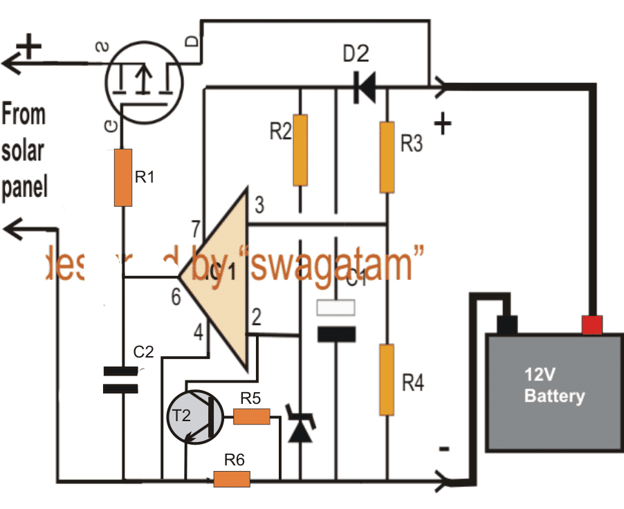 NOTE: PLEASE CONNECT THE PIN#7 OF THE IC DIRECTLY WITH THE (+)TERMINAL OF THE SOLAR PANEL OTHERWISE THE CIRCUIT WILL NOT FUNCTION.
USE LM321 IF THE SOLAR PANEL VOLTAGE IS HIGHER THAN 18 V.
Parts List
R1,R2 = 10K
R3,R4 = use an online potential divider calculator for fixing the required junction voltage
D2 = 1N4148
C1 = 10uF/50V
C2 = 0.22uF
Z1 = should be much lower than the selected battery over charge level
IC1 = 741
Mosfet = as per the battery AH and the solar voltage.
NOTE: PLEASE CONNECT THE PIN#7 OF THE IC DIRECTLY WITH THE (+)TERMINAL OF THE SOLAR PANEL OTHERWISE THE CIRCUIT WILL NOT FUNCTION.
USE LM321 IF THE SOLAR PANEL VOLTAGE IS HIGHER THAN 18 V.
Parts List
R1,R2 = 10K
R3,R4 = use an online potential divider calculator for fixing the required junction voltage
D2 = 1N4148
C1 = 10uF/50V
C2 = 0.22uF
Z1 = should be much lower than the selected battery over charge level
IC1 = 741
Mosfet = as per the battery AH and the solar voltage.
Using N-Channel MOSFET
The proposed low dropout can be also effectively implemented using an N-channel MOSFET. as indicated below: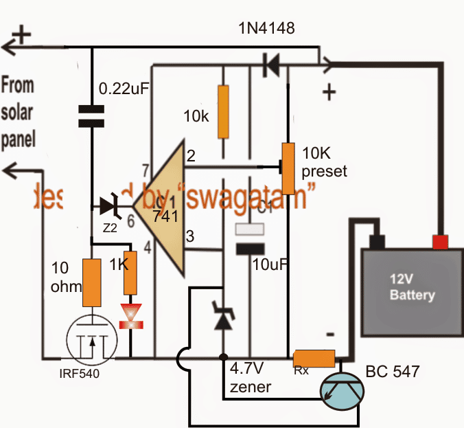 NOTE: PLEASE CONNECT THE PIN#4 OF THE IC DIRECTLY WITH THE (-)TERMINAL OF THE SOLAR PANEL, OTHERWISE THE CIRCUIT WILL CEASE TO WORK.
USE LM321 INSTEAD OF 741 IF THE PANEL OUTPUT IS HIGHER THAN 18 V.
NOTE: PLEASE CONNECT THE PIN#4 OF THE IC DIRECTLY WITH THE (-)TERMINAL OF THE SOLAR PANEL, OTHERWISE THE CIRCUIT WILL CEASE TO WORK.
USE LM321 INSTEAD OF 741 IF THE PANEL OUTPUT IS HIGHER THAN 18 V.
Adding a Current Control Feature
The second diagram above shows how the above the design may be upgraded with a current control feature by simply adding a BC547 transistor stage across the inverting input of the opamp. R5 can be any low value resistor such as a 100 ohm. R6 determines the maximum allowable charging current to the battery which may be set by using the formula: R(Ohms) = 0.6/I, where I is the optimal charging rate (amps) of the connected battery.Finalized Solar zero drop battery charger circuit:
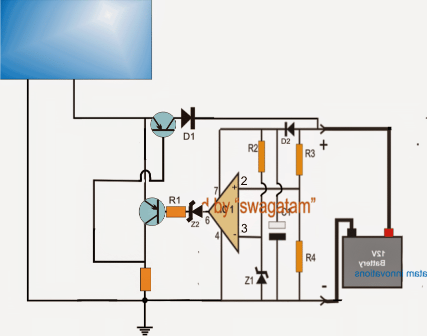
As per the suggestion of "jrp4d"the above explained designs needed some serious modifications for operating correctly. I have presented the finalized, corrected working designs for the same through the below shown diagrams: According to "jrp4d": Hi - I've been messing about with Mosfets (voltage control circuits) and I don't think either circuit will work except where the line in voltage is only a few volts large than the target battery voltage. For anything where the line in is much more than the battery the mosfet will just conduct because the control circuit can't control it. In both circuits its the same problem, with P-channel the op-amp cant drive the gate high enough to turn it off (as observed by one post) - it just passes the line voltage straight thru to the battery. In the N channel version the op-amp can't drive the gate low enough because its operating at a higher voltage than the -ve line in side. Both circuits need a driving device operating at the full line in voltage, controlled by the op-amp The suggestion above looks valid and correct. The simplest way to rectify the above problem is to connect Pin#7 of the opamp IC with the (+) of the solar panel directly. This would instantly solve the issue! Alternatively the above designs could be modified in the manner shown below for the same: Using NPN BJT or N-channel mosfet: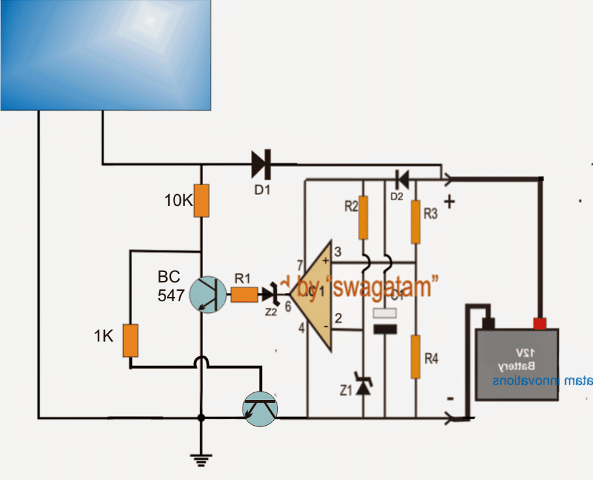 The diode D1 can be removed once the working of the LDO is confirmed
In the above figure the NPN power transistor could be a TIP142, or a IRF540 mosfet .....and please Remove D1 as it's simply not required
The diode D1 can be removed once the working of the LDO is confirmed
In the above figure the NPN power transistor could be a TIP142, or a IRF540 mosfet .....and please Remove D1 as it's simply not required
Using PNP transistor or P-mosfet
 The diode D1 can be removed once the working is confirmed
In the above figure, the power transistor could be a TIP147 or a IRF9540 mosfet, the transistor associated with R1 could be a BC557 transistor......and please Remove D1 as it's simply not required.
The diode D1 can be removed once the working is confirmed
In the above figure, the power transistor could be a TIP147 or a IRF9540 mosfet, the transistor associated with R1 could be a BC557 transistor......and please Remove D1 as it's simply not required.
How to Set up the LDO solar charger circuit
It's very easy. Do not connect any supply at the mosfet side. Replace the battery with a variable power supply input and adjust it to the charging level of the battery which is supposed to be charged. Now carefully adjust the pin2 preset until the LED just shuts off....flick the preset to and fro and check the LED response it should also blink ON/OFF correspondingly, finally adjust the preset to a point where the LeD just shuts off completely....seal the preset. Your zero drop solar charger is ready, and set. You can confirm the above by applying a much higher input voltage at the mosfet side, you'll find the battery side output producing the perfectly regulated voltage level that was previously set by you.Convert SMPS into a Solar Charger
The post explains how to convert smps into a solar charger circuit. The method will result in an extremely efficient and fast solar charging of the connected battery.SMPS Solar Chargers
SMPSs have become very common nowadays and we find them being used in the form of AC to DC adapters wherever needed. The best example is our cell phone chargers which are actually compact SMPS 5V chargers. Solar charger devices are also becoming popular nowadays and folks are constantly in look out for options in the form of solar chargers having the most efficient charging response. Solar panels or PV devices are normally utilized for charging lead acid batteries which tends to take relatively long hours for getting fully charged, besides when the sunlight conditions are bad things start getting even more sluggish. For tackling the above condition or rather for enabling quicker charging from solar panels, special MPPT based soar chargers have been developed which effectively monitor the solar panel maximum power point levels and generate the most efficient charging conditions for the connected battery. In this article although we won't be discussing an ideal MPPT, yet the discussed method will give you an opportunity to acquire the most efficient way of charging your battery through a solar panel. As proposed in one of my previous articles discussing understanding solar mppt solar chargers, a switch mode based power supply (SMPS) is probably the best option for making it work as a solar charger circuit, so here we will learn how to make an smps based solar charger circuit at home. Making an SMPS can be quite complex and might require considerable amount of time and knowledge for the implementations, so here rather we will focus on how to convert a ready made smps into an effective solar charger circuit quickly. For this you will require the following materials, assuming the battery to be charged is 12V rated: A ready-made 120V or 220V to 12V SMPS unit having current rating equal to 1/5th of the battery AH which is to be charged. A few Solar Panels whose total open circuit voltage equals around 100V. Connecting wires.Converting SMPS into a Solar Charger Circuit.
As we all know a normal mains SMPS are mostly rated with minimum of 85V to 100V input in order to provide the specified output DC, let's assume it to be 12V, meaning for acquiring 12V it must be supplied with a minimum of 100V at the input. Keeping the above issue in mind, we must select a solar panel which may be able to produce approximately 100V for making the procured SMPS work. Since PV panels with such high voltage might not be available, we may opt for many low voltage solar panels connected in series for generating the above voltage. For instance you can go for 3nos. of 30V solar panels and connect them in series to get 90V from it, which might just do the job. The above input supplied to the procured SMPS would generate the required 12V which may be directly attached to the battery for charging it efficiently. However a 12V supply might not charge a 12V battery we need at least 14V for it, so that's not a big issue, the required voltage can be easily tweaked and set by adjusting the output voltage of the SMPS manually, the procedures can be learned in this article which explains how to modify an SMPS circuit. That's it, you have just now converted a ready made SMPS unit into an efficient solar charger circuit that might generate results equivalent to MPPT charger circuits for you.
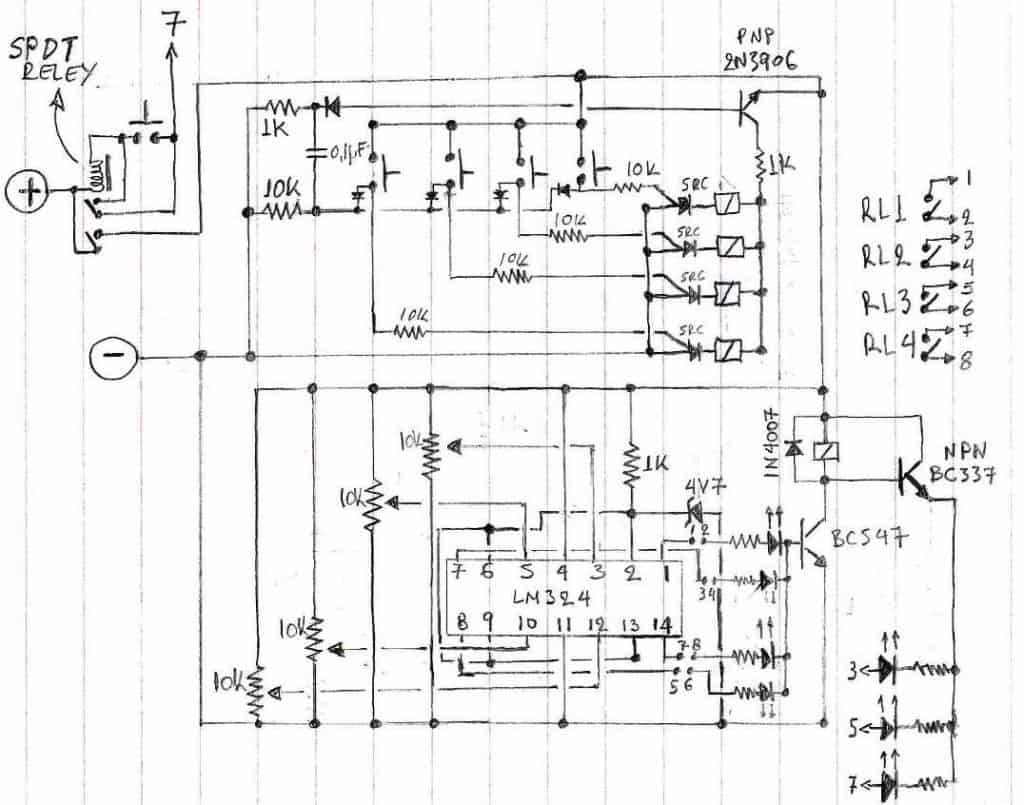
Selectable 4 Step Low Voltage Battery Cut off Circuit
The post explains a circuitconfigurationwhich facilitates a multi-step low voltage selection and cut-off for the battery being used and monitored. The circuit was proposed by Mr. Pete.Technical Specifications
Dear Swagatam,Your assistance during the past few days has been incredible, thanks to which I think I have managed to get close to this 4 step low battery cut off circuit I need.
Having combined yourinfo, a selector circuit I found in a different source and by adding my own ideas I came up with the following circuit:
I know there are issues which with my knowledge I cannot solve, but I think I am close (I will list these issues at the end of this post).
My knowledge is limited (I am neither an expert nor a novice in electronics), so I would like to hear your opinion and recommendations.
To my understanding, what I expect it to do is as follows:
LM324 will monitor the voltage and turn off the relay at the bottom of four scales: 18.5-20V, 20-22V, 22-24V, 24-28V adjusted by the various 10K presets.
The circuit starts (battery full) with the relay armed (load connected) and the 24-28V LED on (left hand side set of LEDs). The selector circuit (top part) assures that only the selected OPAMP arms the relay although all of the OPAMP outputs will be high at the same time (this I need for a later function, see end of next paragraph).
During discharge, when 24V is reached the equivalent output (1) will go low and the relay will disarm, disconnecting the load. At the same time BC337 (NPN) will conduct and light up the three right hand side LEDs, to indicate scale options that are available.
Once a button on the selector is pressed for a lower scale (i.e 22-24V), the relay at the lower circuit will arm by the second OPAMP (output 7) and the load will be connected. Same goes for the equivalent left hand side LED. The same applies for the 20-22V scale, but only 2 LEDs will light from the right hand side set).
Now, if the last scale (18-20V) is selected, when 18V is reached the 4th OPAMP of the LM324 will disconnect the load once again but at the same time the SPDT relay at the top left of my picture which is connected as a latching relay will disarm and take power completely off of the circuit to minimize consumption as the battery will be very deeply discharged now. In order to start the system again, manual reset will be required via the push button near the latching relay, once the battery is charged again.
The purpose of this circuit is for a solar system used to power an emergency communications station. This is the reason it cannot be set in a completely automatic way. Although deep discharging of the batteries is not recommended, in such stations the operator will have to judge whether he must deep discharge the battery or not, in case the type of emergency makes it inevitable. Under normal situations, the power will cut off at 24V automatically protecting the batteries, but it is important that the operator will have the option to continue drowning the batteries if necessary.
So here are my circuit issues: 1. I have a fear that in the way the circuit works, the outputs go high, not low when thresholds are met. If it is so the circuit will not operate in the intended way, especially the latch relay function.
2. I have a feeling that there will be a lot of small and big flaws in my additions to the design. I am confident in building it when it is all designed, but designing of circuits is a skill I only have to certain extend.
3. I wonder if I can substitute the relays of the top part of the circuit with some kind of low power MOSFET. If so, please give me a clue as to how to connect them.
4. I am also thinking that the disconnection of the load will cause the system to do some chasing effect, so I wonder if some small hysteresis can be added.
Please get back to me with you thoughts; I believe this can be a useful 4 step low battery cut off circuit if ever completed for many people (maybe by adjusting the thresholds to higher values, not everybody needs to drain their batteries so much).
My gratitude once again for the tones of information you have helped me to collect during the past week.
Regards, Pete SimplifiedDiagram for the above Circuit Issue [Solved]
Parts List
All resistors can be 10K 1/4 watt All presets = 10K T1, T2 = BC547 Relay = 24V/SPDT Scr = BT169 IC = LM324 D1 = 1N4007 Z1 = 6V/400mWCalculating Solar Panel, Inverter, Battery Charger
The following post explains through calculations how to select and interface the solar panel, inverter and charger controller combinations correctly, for acquiring the most optimal results from the set up.
Calculating Solar Panel, Inverter and Battery Charger Specifications
For the sake of convenience, let's believe you possess a a 100 watt appliance or load that you would like to operate, free of charge through solar power, for around ten hours every night. In order to exactly determine the dimensions of the solar panel, batteries, charge controller and inverter the following mentioned parameters will need to be strictly calculated and configured.Estimating Load Wattage
1) First you will need to estimate how much watts of electricity you may require for the specified load. Let's say you have a 100 watt load that needs to be operated for approximately 10 hours, in that case the total power required could be estimated simply by multiplying the load with hours, as given under 100 Watts x 10 hours = 1,000 Watt hours. This becomes the absolute power necessary from the panel.Determining Approximate Solar Panel Dimension
2) Next, we need to determine the approximate dimensions of the solar panel for satisfying the above estimated load requirement. If we assume a roughly ten hour daily optimal sunshine, the specifications for the solar panel could be simply and quickly calculated as explained in the following expression: 1,000 Watt hours / 10 hours sunlight = 100 Watt solar panel. However, you may notice that mostly during the summer seasons you may normally get around 10 hours of reasonable amount of sunshine, but the winter season may produce roughly around 4-5 hours of effective sunshine. Contemplating the above scenario, you too might agree and recommend considering the worst possible sunshine hour into calculation so that even on the weakest of sunshines your load keeps running optimally. Therefore taking into account the 4 to 5 hours sunshine per day consideration, we calculate the true power for the solar panel which would enable your load to keep running throughout the year . 1,000 Watt hours / 5 hours sunlight = 200 Watt solar panel.Calculating Battery Ah
3) Once you have calculated the solar panel as per the above calculations, it's time to calculate the AH rating for the batteries that might be required for operating the specified load under all conditions. If the selected battery is rated at 12V, in that case: Dividing 1,000 Watt hours by 12 Volts = 83 Amp Hours of reserve battery power. Let's upgrade this value a little more with a 20% added tolerance, which finally gives a rounded up figure of around 100 AH. Hence, a 100AH 12V battery is what you may finally require for the inverter.Evaluating Charger Controller Specifications
4) Now, to figure out how big your solar charge controller would need to be for the above calculated parameters, you might need to take your solar panel current or the Amperage specs into consideration, which may be simply gotten by dividing the panel's wattage rating with its voltage rating (Ohms law remember?) 100 / 12 = 8.3 Amps. We have so far applied a "plus tolerance" to all the previous parameters, so let's show some generosity to the Amp spec of the panel also, and instead of sticking to the 8.3 amps limit, you might be happy raising the level to around 10 Amps? That looks good, right?Assessing Inverter Specifications
5) Finally we boil down to the inverter specifications, and determine the reasonably exact capacity that would keep the unit compatible with the above discussed results, and keep the load running without issues, whenever required. Well, calculating the inverter specs doesn't look difficult at this point of the discussion. Since we already know the maximum load wattage which is 100 Watts, implies that we simply choose an inverter which might be capable of handling a 100 watt comfortably. That implies, we simply need to get an inverter rated at 100 watts,.... OK, you may be thinking of adding some tolerance to this candidate also, not an issue, instead of 100 watts you can opt for a 125 watt inverter, allowing all the gadgets to happily "shake-hands" and your house powered round the clock forever, free of cost.Low Battery Indicator Circuit Using Two Transistors Only
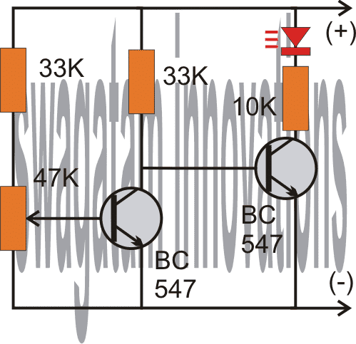
The following post describes a simple low battery indicator circuit by using just two inexpensive NPN transistors. The main feature of this circuit is its very low stand by current consumption.The Circuit Concept
We have so far seen how to make a low battery indicator circuits using a 741 IC and a 555 IC, which are no doubt outstanding with their abilities of detecting and indicating low battery voltage thresholds. However the following post relates yet another similar circuitwhich is much cheaper and employs just a couple of NPN transistors for producing the required low battery indications.Advantage of Transistor over IC
The main advantage of the proposed two transistor low battery indicator circuit is its very low current consumption compared to the IC counterparts which consume relatively higher currents. A IC 555 would consume around 5mA, a IC741 around 3 mA, while the present circuit would just consume around 1.5mA current. Thus the present circuit becomes more efficient especially in cases where stand by current consumption tend to become an issue, example suppose in units which depend on low current battery supplies such as a 9V PP3 battery.Circuit can Operate at 1.5V
Another advantage of this circuit is it's ability to work even at voltages around 1.5V which gives it a clear edge over the IC based circuits. As shown in the following circuit diagram, the two transistors are configured as voltage sensor and inverter. The first transistor on the left senses the threshold voltage level as per the setting of the 47K preset. As long as this transistor conducts, the second transistor on the right is held switched OFF, which also keeps the LED switched OFF. As soon as the battery voltage falls below the set threshold level, the left transistor is no longer able to conduct. This situation instantly triggers the right hand side transistor, switching ON the LED. The LED switches ON and provides the required indications of a low battery warning.Circuit Diagram
 Video Demonstration:
The above circuit was successfully built and installed by Mr.
Allan in his paranormal depletion detector unit.
The following video presents the implementation results:
Video Demonstration:
The above circuit was successfully built and installed by Mr.
Allan in his paranormal depletion detector unit.
The following video presents the implementation results:
Upgrading the above Transistorized Low Battery circuit into a Low Battery Cut-off Circuit
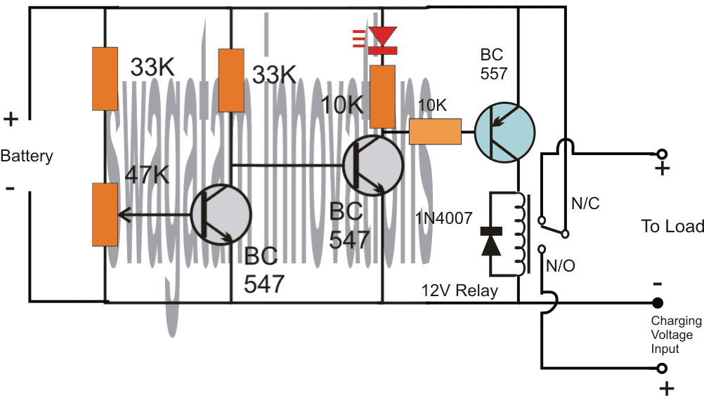 Referring to the above diagram, the low battery indicator is formed by the two NPN transistors, while the additional BC557 and the relay are used for cutting OFF the battery from the load when it reaches the lower threshold, in this state the relay connects the battery to the available charging input.
However when the battery is in its normal state the relay connects the battery with the load and allows the load to operate through battery power.
Referring to the above diagram, the low battery indicator is formed by the two NPN transistors, while the additional BC557 and the relay are used for cutting OFF the battery from the load when it reaches the lower threshold, in this state the relay connects the battery to the available charging input.
However when the battery is in its normal state the relay connects the battery with the load and allows the load to operate through battery power.
Adding Hysteresis
One drawback of the above design could be the chattering of the relay at the threshold voltage levels, due to the battery voltage dropping immediately during the relay changeover process. This can be prevented by adding a 100uF at the base of the middle BC547. However, this still wouldn't stop the relay from constantly switching ON/OFF at the low battery changeover threshold. In order to rectify this, a hysteresis effect will need to be introduced which can be accomplished through a feedback resistor between the collector of the BC557 and the middle BC547 transistor. The modified design for implementing the above condition can be seen in the following diagram: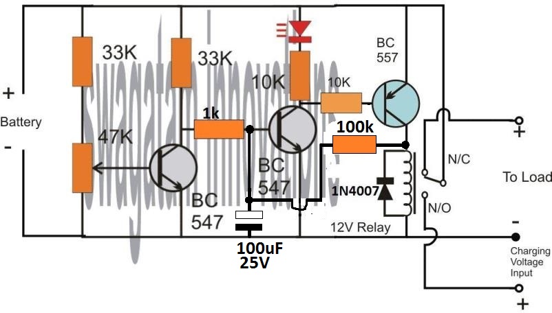 The two resistors, one at the base of BC547 and the other at the collector of BC557 decide the other threshold of the relay changeover, meaning the full charge cut off threshold of the battery.
Here, the values are arbitrarily selected, for accurate results these values will need to be optimized with some trial and error.
The two resistors, one at the base of BC547 and the other at the collector of BC557 decide the other threshold of the relay changeover, meaning the full charge cut off threshold of the battery.
Here, the values are arbitrarily selected, for accurate results these values will need to be optimized with some trial and error.
Low Battery Indicator using a PUT
This low battery indicator circuit is used with a programmable unijunction transistor (PUT), since the threshold characteristics of the UJT could be effectively defined, and can be designed to flash a connected LED indicator. The PUT (Q1) is configured like a relaxation oscillator circuit. As the supply voltage which is being monitored (Vmon) starts dropping, the gate voltage of the PUT (Vg) also begins dropping, while its anode voltage (Va) basically stays constant.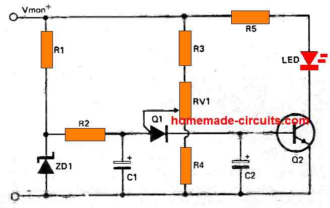 The PUT begins oscillating only as soon as the gate voltage drops below Va by 0.6 volts.
As Vmon comes down further, Vg also drops accordingly and this situation triggers ON the PUT.
Therefore, the period of the cycle becomes lesser and this causes an increase in the frequency of flashing indicating that the battery has become too low and needs to be changed.
The PUT begins oscillating only as soon as the gate voltage drops below Va by 0.6 volts.
As Vmon comes down further, Vg also drops accordingly and this situation triggers ON the PUT.
Therefore, the period of the cycle becomes lesser and this causes an increase in the frequency of flashing indicating that the battery has become too low and needs to be changed.
Parts List
How to Recharge Dead Batteries
In this post we learn how to recharge and use bad, defective discarded batteries using an innovative battery charging process invented by John Bedini. Lead acid batteries can sometimes be a problem to get rid of. They can also be high priced to upgrade. In case discarded in the wrong way, they have a tendency to finish up in the land fill up or even rotting of in your junkyard.Contribution of John Bedini
John Bedini has presented a bequest to the world which can bring back and enrich the used, abandoned, sulfated batteries. In case your battery is sulfated from typical utilization, it may commonly be recovered using this discovery. Batteries which have material impairment or have warped plates are worthless. The Bedini SSG (Simplified School Girl) generator can separate the sulfation on the battery plates and energize the batteries. On many occasions, the battery will in fact acquire further voltage, workable power compared to the time it had been purchased. By means of routine utilization, a battery would probably gradually drop its potential to hold electricity. This can be witnessed by the necessity to charge the battery far sooner every time. Typical battery chargers often give rise to this consequence due to heating effect of the battery. Because the plates get hot by way of charging, these are steadily weakened. A battery may have less electrical power every time it is utilized. With the Bedini charger, that is not the situation. I have reconditioned batteries which were found resting around in a trash. A couple of such batteries that possessed a charge of below 2 volts each presently are running my electric boat generator. These types of batteries were not consuming a charge with regular chargers. After a while and many rounds with the Bedini charger, the batteries have become superior to brand new.How Bedini SSG Function
This electric motor would not self start. You need to provide it with a little bit force to pick it up going, however once it begins rotating it is going to turn up by itself and self adjust its very own acceleration and speed depending on the dimensions and charge condition of the batteries getting charged. Since a magnet moves down the coil, a tiny electric current is stimulated into the main coil. This activates the transistor to switch on, enabling electricity from the operated battery to stream by way of the supplementary coil. The magnetic field generated in the secondary coil provides the cycle a tiny lift up on its path past the coil. As the magnetic field sets off the coil, the transistor is turned back off. This leads to the magnetic field in the supplementary coil to drop (back emf). During this period, the vibrant electric power makes its way into the process which is emptied via a diode into the batteries to be charged. This method could be demonstrated to generate additional energy on the recharging aspect compared to the need to steer the motor. In the method presented, the input current amounts between 150-200 mA.
Solar Water Heater Circuit with Battery Charger
The proposed solar water heater with battery charger controller circuit explains a simple method of utilizing the excess solar energy from a solar panel for heating water in water tanks orswimmingpools or poultry egg chambers. Normally the circuit also functions like an automatic solar battery charger, and simultaneously powers domestic electrical appliances.Understanding Solar Charging
Solar energy is abundantly available across the globe and it's free to use. It's all about laying down a solar energy collector or simply a solar PV panel, and harness the available resource. In this blog and in many other sites you might have come across various efficient solar battery charger circuits. However these circuits generally speak about using the solar panel for acquiring electrical energy. While functioning, the involved regulators/chargers stabilize the solar voltage suchthat the output voltagebecomes suitable for the connected battery which is normally a 12V lead acid battery. Since normally a solar panel is designed for generating voltages in excess of 12V, that is around 20 to 30 volts, the process of stabilization completely neglects the excess voltage which is either shunted to ground or cancelled out through electronic circuitry. In the present article we learn a simple method of converting excess solar energy to heat even while charging a battery, and operating household appliances safely together. The circuit functioning may be understood withthefollowing points:Using Excess Unused Solar Power for Heating Water
In the given solar water heater with battery charger controller circuit diagram, let's assume at peak sunshine the attached solar panel is capable of generating around 24V. In the diagram we can see a couple of opamps positioned in between the solar input and the battery charging outlet. The opamp at the left is basically set for allowing the specified charging voltage to its right hand side stages. For a 12V battery this voltage would be around 14.4V. RV1 is therefore adjusted such that the output of the opamp becomes high in case the input voltage exceeds the 14.4V mark. The opamp at the right is designated as the over charge cut off stage which is responsible for monitoring the charging voltage of the battery, and cut it off when the upper threshold is reached. This happens when the non inverting input of U1B senses the higher threshold and shuts off the positive bias to the mosfet which in turn cuts off power to the connected battery. However the load which is essentially an inverter stays operative, as now it starts deriving the power from the charged battery. In the course, if the voltage drops even by a few voltages, U1B reverts its output to logic high and the battery once again begins getting charged while simultaneously allowing the connected appliances to remain operative via the common panel voltage. Meanwhile as discussed in the previous lines, U1A monitors the panel voltage and just like U1B when it instantaneously senses the panel voltage exceeding the 14.4 mark, it switches its output to logic high so that the connected transistors are instantly switched ON. A DC heater coil can be seen attached across the collector and positive of the transistor. When the transistor conducts, the coil is shunted across the direct panel voltage, and therefore it instantly begins getting hot. The low resistance of the coil pulls lot of current from the panel which forces the voltage to drop below the set 14.4 level for U1A. The moment this tends to happen, U1A reverts the situation and cuts off the supply to the transistors and the process rapidly fluctuates, such that the voltage fed to the battery stays within the 14.4V mark and in the process the heater coil manages to stay active so that its heat becomes applicable for any preferred purpose.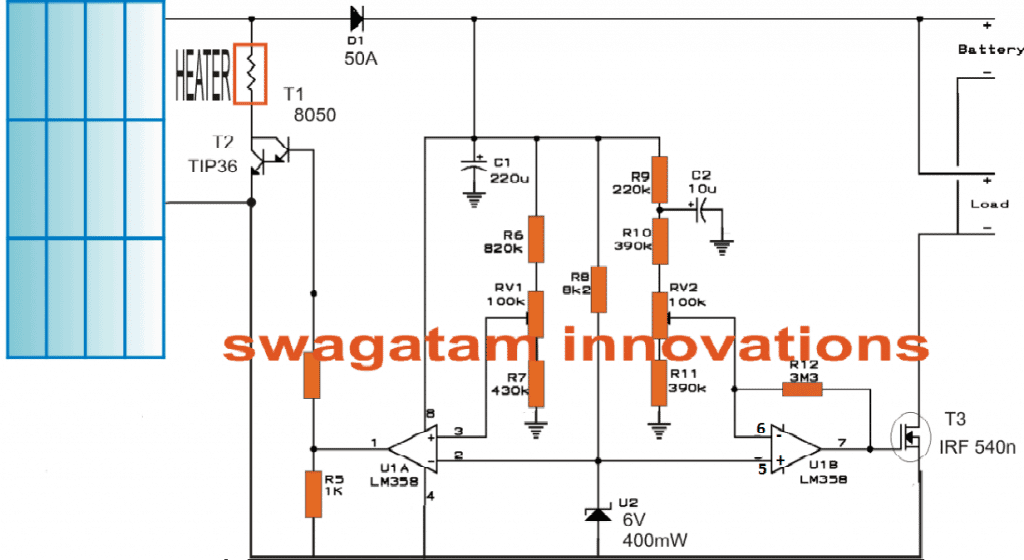
Diagram for the solar water heater with battery charger controller circuit
Single Transformer Inverter/Charger Circuit
The post explains how to build an innovative inverter circuit with a single transformer that works both as an inverter and a battery charger transformer, Let's learn the details from the following discussion.The Circuit Objective
Though you may find many inverters having an integral battery charger, the section will mostly employ a separate transformer for implementing it. The following article describes a unique design which utilizes the inverter transformer for power inverting as well as for charging the battery. The circuit diagram below shows a design where a single power transformer is used for inverting purpose as well as for charging the battery when mains is present. The good thing about the circuit is that the transformer doesn't employ separate winding for this, rather works with the same input winding and reverts DC to the battery with the help of a few DPDT relays. The circuit can be understood with the following points:How the Circuit Functions
The inverter section can be easiy recognized in the diagram, R1 to R6, including the T1 and T2 forms a general astable multivibrator circuit for producing the required 50 or 60 Hz pulses. These pulses drive the mosfets alternately which in turn saturate the transformer by switching the battery voltage in it. Thesecondary ofthe transformer generates the corresponding magnitude of AC which is finally used for operating the connected appliances. The above configuration suggests an normal or ordinary inverter operation. By adding a couple of DPDT relays in the above discussed operation, we can force the circuit to charge the battery in the prsence of an AC mains source. The coils of the two relays are powered through a capacitive low current compact power supply, involving C6, C5, D1----D5. The above circuit is connected to a mains AC source, this source is also connected to RL1 poles. The second relay RL2 is wired up with input winding of the transformer. In the absence of mains AC, the position of the relay contacts are in the N/C as shown in the figure. In this position the mosfets get linked with the transformer input winding, and the battery with the circuit so that the inverter starts oscillating and the output appliances gets the AC power from the battery. In the presence of mains AC the relay coils instantly get the required DC power and the contacts activate. RL1 activates andconnectsthe mains input to the transformer, theappliancesalso get connected with the mains AC in the process. Also due to the action of RL2 the mosfets get disconnected from the transformer, while the the lower tap connects with D6. Since the center is already connected to battery positive, the inclusion of D6 provides a half wave rectified voltage to the battery, which is effectively filtered by C3 so that the battery is able to get the required sufficient charging voltage. The above charging process continues until mains is present, so itshouldbe monitored manually. When mains fails, the action reverts into inverting mode without interrupting the applianceoperations andby using a single transformer for both the operations. C4 makes sure that RL1 always activates a shade later than RL2 for safetyreasons.Parts List
R1, R2 = 27K, R3, R4, R5, R6 = 470 Ohms, C1,C2 = 0.47uF/100V metallized T1, T2 = BC547, T3, T4 = any 30V, 10amp mosfet, N-channel. C3 = 47000uF/25V C4 = 220uF/25v C5 = 47uF/100v C6 = 105/400V R7 = 1M D1---D5 = 1N4007 D6 = 1N5402 RL1, RL2 = DPDT, 400 OHMS, 12V, 7 AMPS/220V Transformer = 12-0-12V, current as per requirement. For only inverter design please refer to this ARTICLEUsing a 2-Wire Transformer
If you do not want to use a center tap transformer for the inverter, then you can use the following P-channel and N-channel MOSFET H-bridge inverter module for getting an identical single transformer inverter/charger results: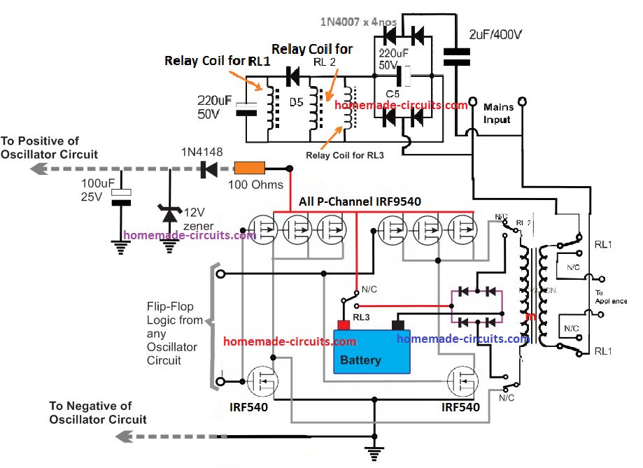
High Current Solar Battery Charger Circuit ¨C 25 Amps
This circuit is capable of providing as high as 25 Amps of current at any specified voltage between 1.25 V to 30V as per the adjustment of the given pot. The current is constant irrespective of the voltage settings. The circuit can be used for charging batteries in range of 50 to 200 AH.How it Works
The figure below shows a straightforward design of a simple high current solar battery charger power supply circuit which would generate a constant 25 amps of current from any source which is able to generate currents in excess of 25 amps and at 32 volts maximum. We know that the IC LM338 is specified with a maximum of 5 amp current, the IC restricts anything above this limit. By connecting 5 of these ICs in parallel it thus becomes possible to generate a current output of about 25 amps. The great thing about using these ICs is that, these devices are internally protected from thermal runaway situations and short circuit or overload conditions. It means the present circuit automatically becomes safe from such adverse parameters and thus becomes completely indestructible given the input is not exceeded above 32 volts. However the ICs cannot be directly connected in parallel, because that would cause a difference in the voltages at the output from each of the ICs which in turn would cause an imbalance between the IC dissipation, this wouldn't be good for the overall functioning of the circuit. Therefore the additional components in the form of the opamp and the transistor have been included in the circuit which controls and maintains a constant voltage output from all the ICs keeping the situation well under control.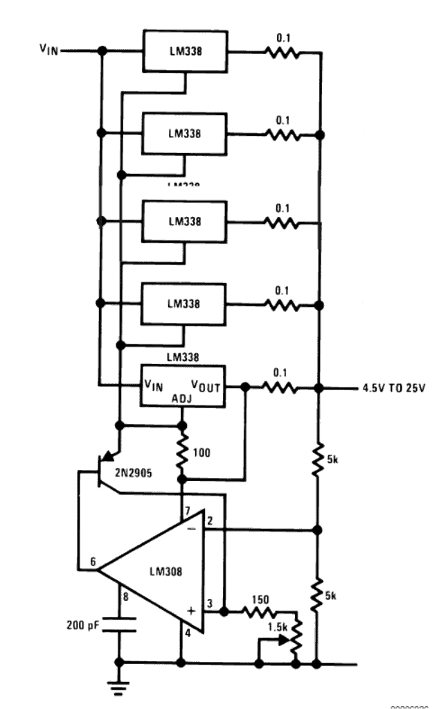
How to Illuminate 1 Watt LEDs with Cell Phone Charger
Nowadays probably all of us have a spare cell phone charger lying idle in our cupboards or table drawers......so wouldn't it be a great idea if we could employitlike a super bright 1 watt LED driver and illuminate our room with white cool moon light.Circuit Concept
As we all know that a 1 watt LED consumes about 350 mA of current and is capable of generating intense blinding white point lights. If this little high bright light source is enclosed within a reflector cabinet consisting of mirror finish lens, the light from it can be enhanced to great levels. However a 1 watt type of LED would require a suitable constant voltage power supply for illuminating safely with thespecifiedoutputs. Though there are a number of suitable drivers which are available in the market, a cell phone charger can be ideally used for this purpose. If we look at the diagram given below, we see that the whole thing can be configured using just a single current limiting resistor.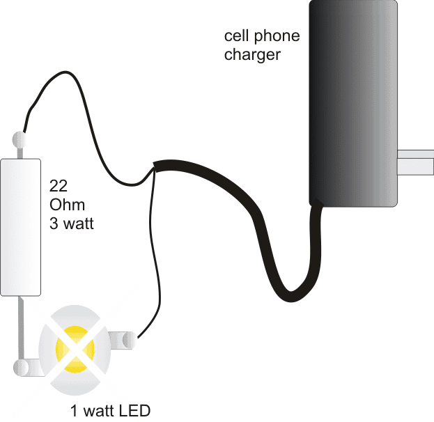 Let's learn regarding the involved making procedures with the following points:
You would require a standard cell phone charger.
A 1 watt LED/350 mA white.
A 22 Ohm 3 watt resistor,
An aluminum heatsink, as specified in the given text.
Small piece of general purpose PCB, about 1 by 1 inch.
Let's learn regarding the involved making procedures with the following points:
You would require a standard cell phone charger.
A 1 watt LED/350 mA white.
A 22 Ohm 3 watt resistor,
An aluminum heatsink, as specified in the given text.
Small piece of general purpose PCB, about 1 by 1 inch.
Construction Procedure:
Since the LED would be generating considerable amount heat, a neatly fabricated aluminum heatsink would be required to be integrated with it so that the life and theefficiencyof the device is maintained for many many years. Please see the below given diagram to know thebasicheatsink design, the holes must be drilled just as soecified in the diagram and the LED leads should not touch the heatsink while it ispassedthrough the holes and soldered over the underside PCB pads. A small 1 mm square piece of aluminum cut into 1/2 by 1/2 inch would just suffice.
Drill the holes into the above metal, as shown in the below given diagram and fix the heatsink over the PCB using small 1/8 x1/4 screw nuts.
A small 1 mm square piece of aluminum cut into 1/2 by 1/2 inch would just suffice.
Drill the holes into the above metal, as shown in the below given diagram and fix the heatsink over the PCB using small 1/8 x1/4 screw nuts.
 Next fix the LED over the heatsink in between the two center holes, and solder it leads with supporting copper wires such that it becomes locked with the underneath PCB pads.
Be careful not to short the leads with the heatsink metal.
Connect the 22 Ohm resistor with one of the leads of the LED, preferably with the positive lead.
Finally, connect the cell phone charger wires to the resistor end and the other free LED end.
Make sure the polarity is correct while connecting the wires t the LED, identify them using a digital multimeter before doing the connections.
Your cell phone charger powered 1 watt LED lamp is ready,placeit neatly over some corner of the room, plug it in and experience the awesome illumination, dazzling the entirepremise.
Optionally the unit canbefixed inside a halogen lamp reflector for enhancing the light intensity many folds.
Next fix the LED over the heatsink in between the two center holes, and solder it leads with supporting copper wires such that it becomes locked with the underneath PCB pads.
Be careful not to short the leads with the heatsink metal.
Connect the 22 Ohm resistor with one of the leads of the LED, preferably with the positive lead.
Finally, connect the cell phone charger wires to the resistor end and the other free LED end.
Make sure the polarity is correct while connecting the wires t the LED, identify them using a digital multimeter before doing the connections.
Your cell phone charger powered 1 watt LED lamp is ready,placeit neatly over some corner of the room, plug it in and experience the awesome illumination, dazzling the entirepremise.
Optionally the unit canbefixed inside a halogen lamp reflector for enhancing the light intensity many folds.
Making a 1 watt LED automatic emergency light circuit
As suggested by Mr.Amit (see comment) the above concept can be very simply converted into a nice little emergency light circuit, let's see how it is done: Referring to the figure below, assuming the voltage from the mains operated charger input to be present, and the switch in the closed position, T1 is held reverse biased so that it isunableto conduct and the LED remains switched OFF. At this position the batteries are trickle charged through R2, R3 and D2. In case the mains fails, T1 instantly conducts and switches ON the LEDautomaticallyand vice versa. Now suppose during the presence of mains the switch is turned of, T1 instantly switches ON, however now the LED lights up through the charger voltage (mains) while the batteries still continue to get trickle charged without getting drained through the LED.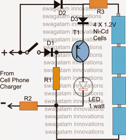
Parts List
R1= 100 Ohms, 1/2 watt R2 = 47 Ohms, 1/2 watt R3 = 22 Ohms, 1/2 watt D1,D2,D3 = 1N4007 T1 = 8550 or 187, 2N2907 LED = 1 watt, 350 mA, high bright Battery = 4 nos. Ni-Cd, AAA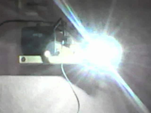
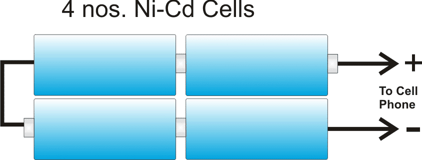
Cell Phone Emergency Charger Pack using Ni-Cd Batteries
In this post we discuss the construction of a simple emergency charger pack using Nicket Cadmium (Ni-Cd) batteries for your cellphones and smart phones for emergency charging of your cellphone, so that next time you are never stuck on a highway with a full discharged dead cellphone battery.Circuit Concept
It often happens, our cell phone goes into a low battery condition right in the middle of animportantconversation, and even worse it happens while we are travelling or situated in some remoteoutdoorlocation where there's no charging facility available. No matter what, this little pack will give your cell phone an immediate refillevery timeit tends to get flatoutdoors. We all know that at 3.7 V DC, a cell phone battery isconsideredto be fully charged. For charging it at the above level a charging source needs to provide around 4 to 5 volts to the discharged cell phone battery. Since here we are discussing an energy transfer from one battery to the other or rather from some power source to the cell phone, we need to have some sort of chargeable battery pack which wouldgeneratethe required 4 volts and which could be used anytime for charging a flat cell phone simply by integrating the two together. The above emergency battery pack can be very easily made by putting four Ni-Cd cells in series. Let's learn how to do it.Materials you will Require
It's not difficult, you would require four 1.2V Ni-Cd AAA penlight cells, a four cell holder assembly and a 1 Ohm 1 watt resistor.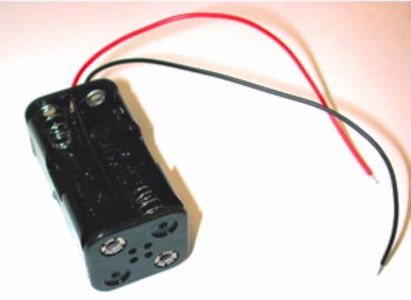
How to Build the Cellphone Battery Bank
The above holder would generate a voltage of about 4.8V at its wire terminals with four AAA 1.2 Ni-Cd attached to within the given slots correctly. The 1 Ohm resistor can be connected at the center of the red wire by cutting the red wire at the center and bridging the resistor terminals such that it comes in series with the red wire. The resistor should covered under a plastic tubing or sleeving.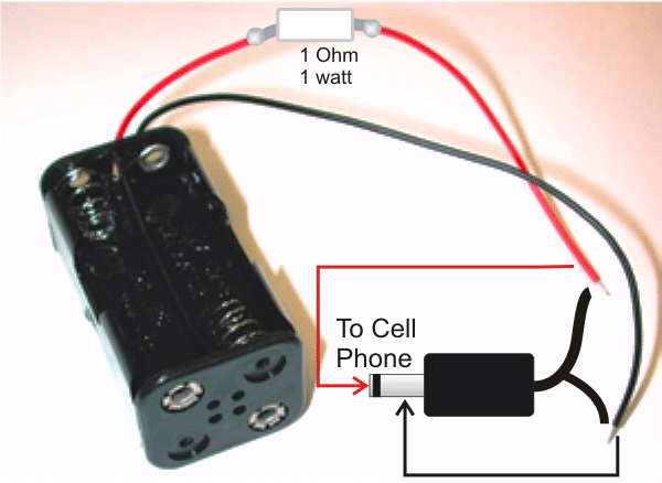 The red and the black wires of above assembly should be terminated with a suitable cell phone charger-pin so that it can be easily inserted into the cell phone charging socket whenever required.
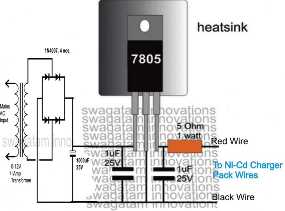
 Now let's learn how we can charge the above emergency battery pack at home.
Ni-Cd cells can be charged safely for about 10 to 14 hours using a constant voltage charger at C/10 rate.
The very useful 7805 voltage regulator IC can be used here for charging the Ni-Cd battery pack.
The following diagramshowsa very simple Ni-Cd charger circuit which can be used for charging the above battery pack so that it remains in a standby position and can be taken outdoors in the form of anemergencycell phone charger unit.
Now let's learn how we can charge the above emergency battery pack at home.
Ni-Cd cells can be charged safely for about 10 to 14 hours using a constant voltage charger at C/10 rate.
The very useful 7805 voltage regulator IC can be used here for charging the Ni-Cd battery pack.
The following diagramshowsa very simple Ni-Cd charger circuit which can be used for charging the above battery pack so that it remains in a standby position and can be taken outdoors in the form of anemergencycell phone charger unit.
How to Switch Two Batteries Manually using Opto Coupler
Thefollowing article explaining a dual battery changeover relay circuit was requested by Mr.Raja so that it could become possible to switch between his old and new inverter batteriesautomatically,eliminating manualinterventions. Let's read it in details. "Ibought a new 12v 110 Ah lead acid battery for the dc home lighting system. I had another 12v 110ah battery which is about 8year old. ( which is connected earlier in the same lighting system in my house itself) . But the old one has approximately 25ah capacity as i calculated. But it is not sufficient to glow light for about 5 hours of night.(i.e. From 6pm to 11pm) So i want to use old and new Battery. But i can't join them in parallel, as old one may takes charge from new battery, which decrease the life of new one (as i think) Therefore at present i am using a'Two-way' switch to switch on and off between old and new battery. Whenever lighting system controller shows red light, i.e. At about 11.5v, i manually operate the two way switch to switch on the new battery. Now , please give me the circuit to switch on and off between two batteries in such a way that, initially lighting system operates with old bty and as the voltage of old bty decreases (below 11.5v) then only switch on to new one.. Thanking you"The Design
The designed idea of the proposed dual battery changeover circuit or rather old to new batterychangeovercircuit may be understood with the followingpoints: Referringto the circuit diagram we see a IC 4017 which functions as a sequence toggler or switcher. The IC will shift its output from pin#3 to pin#2 and then to pin#4 inresponseto every positive pulse at its input pin#14. pin#4 of the IC has been connected to the reset pin#15 of the IC, means the moment the logic sequence reaches pin#4, thesequence getsreset back to pin#3 so that the cycle can repeat. Here the input pulse is derived from the low battery warning indicator from the existing inverter system. The LED light from the low battery warning has been integrated to an LDR using a light proof tubing. Initially when the power is switched ON, the 1uF capacitor resets the IC so that the logic sequence initiates from pin#3. The relay at this pointremainsconnected with its N/C pole connecting the old battery positive with the inverter. The inverterstartsoperating, draining the old battery On reaching the lowbatterythreshold, the inverter low battery LED illuminates which instantly lowers the enclosed LDR resistance supplying a positive pulse to the pin#14 of the IC. The IC responds shifting the logic sequence from pin#3 to pin#2. Since pin#2 of the IC is connected to the relay driver transistor, the relay immediately activates, switching the new battery into action through its N/O contacts. The new battery being fully charged toggles OFF the low battery indicator light, the IC goes into a standby position holding the situation intact.... until, the new battery also reaches a low-battery condition switching ON the LED and resetting the IC into its initial position. The cycle then repeats producing the required automatic dual battery changeover actions.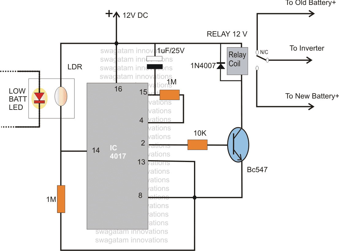
3 Step Automatic Battery Charger/Controller Circuit
Generallyit is noticed that while charging batteries people hardly pay any special attentiontowardthe procedures. For them charging a battery is simply connecting any DC supply with matching voltage with the battery terminals.How to Correctly Charge a Lead Acid Battery
I have seen motor garage mechanics charge all types of batteries with the same power supply source irrespective of the AH rating associated with the particular batteries. That's gravely wrong! That's like giving the batteries a slow "death". Lead Acid batteries to a very extent are rugged and are capable of taking on the crude charging methods, however it's alwaysrecommendedto charge even the LA batteries with a lot care. This "care" will not only increase thelongevitybut will also enhance theefficiencyof the unit. Ideally all batteries should be charged in a step wise manner, meaning the current should be reduced in steps as the voltage nears the "full charge" value. For a typical Lead Acid battery or an SMF/VRL battery the above approach can be considered very healthy and a reliable method. In this post we are discussing one such automatic step battery charger circuit which can be effectively used for charging most of the rechargeable types of batteries.How the Circuit Functions
Referring to the circuit diagram below, two 741 ICs are configured as comparaters. The presets at pin#2 of each stage is adjusted such that the output goes high after specific voltage levels are identified, or in other words theoutputsof the respective ICs are made to go high in sequence after predetermined charge levels areaccomplisheddiscretely over the connectedbattery. The IC associated with RL1 is the one which conducts first, after say the battery voltage reaches around 13.5V, until this point the battery is charged with the maximum specified current (determined by the value of R1). Once the charge reaches the above value, RL#1 operates, disconnect R1 and connects R2 in line with the circuit. R2 is selected higher than R1 and is appropriately calculated to provide a reduced charging current to the battery. Once the battery terminals reaches the maximum specified charging voltage say at 14.3V, Opamp supporting RL#2 triggers the relay. RL#2 instantly connects R3 in series with R2bringingdown the current to a trickle charge level. Resistors R1, R2, and R3 along with the transistor and the IC LM338 forms a current regulator stage, where the value of theresistorsdetermines the maximum allowable current limit to the battery, or the output of the IC LM338. At this point the battery may be leftunattendedfor many hours, yet the charge level remains perfectly safe,intact and in a topped up condition. The above 3 step charging process ensures a veryefficientway of charging resulting in almost a 98% chargeaccumulationwith the connected battery. The circuit has been designed by "Swagatam"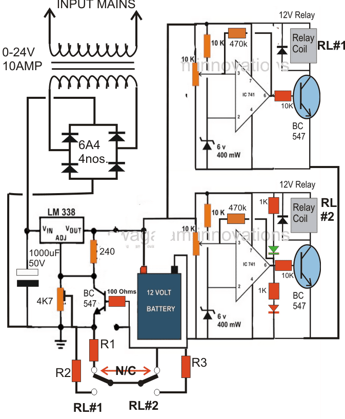 R1 = 0.6/ half battery AH
R2 = 0.6/one fifth of battery AH
R3 = 0.6/one 50th of battery AH.
A closer inspection of the above diagram reveals that during the period when the relay contacts are about to release or move from the N/C position might cause a momentary diconnection of the ground to the circuit which in turn migh result in a ringing effect on the relay operation.
The remedy is to connect the ground of the circuit directly with the bridge rectifier ground and keep the ground from the R1/R2/R3 resistors attached solely with the battery negative.
The corrected diagram may be witnessed below:
R1 = 0.6/ half battery AH
R2 = 0.6/one fifth of battery AH
R3 = 0.6/one 50th of battery AH.
A closer inspection of the above diagram reveals that during the period when the relay contacts are about to release or move from the N/C position might cause a momentary diconnection of the ground to the circuit which in turn migh result in a ringing effect on the relay operation.
The remedy is to connect the ground of the circuit directly with the bridge rectifier ground and keep the ground from the R1/R2/R3 resistors attached solely with the battery negative.
The corrected diagram may be witnessed below:
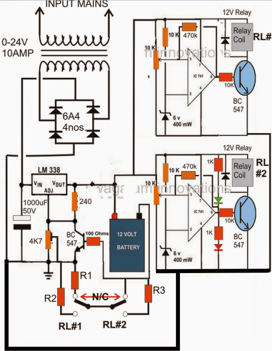 How to Set up the Circuit
Remember if you are using 741 IC then you must remove the red LED from the lower opamp and connect it in series with the base of the transistor to prevent permanent triggering of the transistor due to IC leakage current.
Do the same with the upper transistor base also, connect another LED there.
However if you use an LM358 IC then you may not have to this modification and use the design exactly as given.
Now let's learn how to set it up:
Initially keep the 470K feedback resistors disconnected.
Keep the slider of the presets towards ground line.
Now let's say we want the first relay RL#1 to operate at 13.5V, therefore adjust the LM338 pot to get 13.5V across the circuit supply line.
Next, adjust the upper preset slowly until the relay just toggles ON.
Similarly, suppose we want the next transition to happen at 14.3V, ...increase the voltage to 14.3V by carefully adjusting the LM338 pot.
Then tweak the lower 10K preset such that RL#2 just clicks ON.
Done! your set up procedure is complete.
Seal of the presets with some kind of glue to keep them fixed in the set positions.
Now you can attach a discharged battery to see the actions happening automatically as the battery charges with a 3 step mode.
The 470K feedback resistor can be actually eliminated and removed, instead you can connect a large value capacitor in the order of 1000uF/25V acrossthe relay coils to restrict threshold chattering of the relay contacts.
How to Set up the Circuit
Remember if you are using 741 IC then you must remove the red LED from the lower opamp and connect it in series with the base of the transistor to prevent permanent triggering of the transistor due to IC leakage current.
Do the same with the upper transistor base also, connect another LED there.
However if you use an LM358 IC then you may not have to this modification and use the design exactly as given.
Now let's learn how to set it up:
Initially keep the 470K feedback resistors disconnected.
Keep the slider of the presets towards ground line.
Now let's say we want the first relay RL#1 to operate at 13.5V, therefore adjust the LM338 pot to get 13.5V across the circuit supply line.
Next, adjust the upper preset slowly until the relay just toggles ON.
Similarly, suppose we want the next transition to happen at 14.3V, ...increase the voltage to 14.3V by carefully adjusting the LM338 pot.
Then tweak the lower 10K preset such that RL#2 just clicks ON.
Done! your set up procedure is complete.
Seal of the presets with some kind of glue to keep them fixed in the set positions.
Now you can attach a discharged battery to see the actions happening automatically as the battery charges with a 3 step mode.
The 470K feedback resistor can be actually eliminated and removed, instead you can connect a large value capacitor in the order of 1000uF/25V acrossthe relay coils to restrict threshold chattering of the relay contacts.
Make a Battery Charger in 15 Minutes
I have posted many battery charger circuits in this site, some are easy to build but less efficient, while some are too sophisticated involving complex construction steps. The one posted here is possibly the easiset with its concept and also is extremely easy to build. In fact if you had all the required material you would build it within 15 minutes of time.Introduction
The concept is indeed hugely simple and therefore pretty crude with its going. This means that though this idea is too simple, would require appropriate monitoring of the charging conditions of the battery, so that it does not get over charged or damaged.Materials Required
To make this simplest battery charger circuit quickly, you would require the following bill of materials: One rectifier diode, 1N5402 An incandescent bulb, havingvoltagerating equal to the battery which needs to be charged and current rating close to 1/10th of the battery AH. A transformer having voltage rating equal to twice that of the battery voltage and current twice the charging rate of the battery. That means if the battery is 12V, the transformer should be 24V, and if the AH of the battery is 7.5 then dividing this by 10 gives 750mA which becomes therecommendedcharging rate of the battery,multiplyingthis by 2 gives 1.5Amps, so this becomes the required current rating of the transformer.Building this Simplest Charger Circuit
After you have collected all the above material, you may simply connect the above parameters together with the help of the diagram. The functioning of the circuit may be explained in the following manner: When the power is switched ON, the 1N5402 diode rectifies the 24V DC to produce half wave 24V DC at the output. Though the RMS value of this voltage may appear to be 12V, the peak voltage is still 24V, therefore it cannot be applied directly to the battery. To blunt of this peak value, we introduce a bulb in series with the circuit. The bulb absorbs the high peak values of the voltage and provides a relatively controlled output to the battery, which becomes self regulatory through the glow of the filament intensity of the bulb (varying resistance). The voltage and current thus automatically becomes adjusted to appropriate charging levels which becomes just suitable for the battery safe charging. The charging of the battery can be witnessed by the gradual dimming of the bulb as the threshold charging voltage of the battery isreached. However once the battery voltage reaches close to 14.5V, thechargingmust be stopped, irrespective of the bulb glow condition.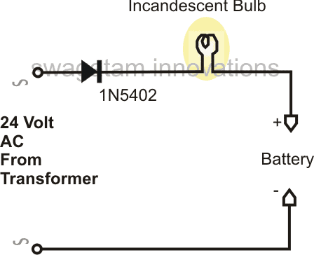
Circuit Diagram
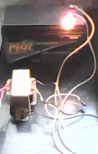 Video Clip showing the charging process using a single diode:
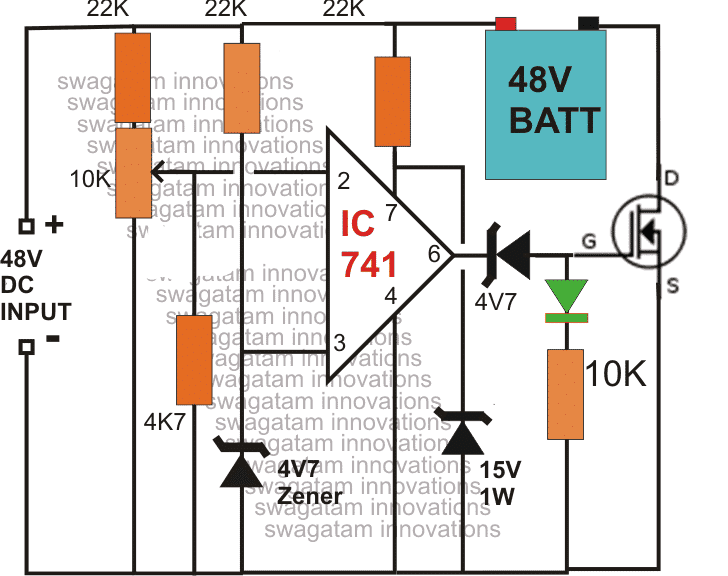
Simple 48V Automatic Battery Charger Circuit
The proposed 48 Vautomaticbattery charger circuit will charge any 48 V battery up to an optimal 56 V full charge level, utilizing veryordinarycomponents. The circuit is highly accurate with its over chargecutoff features.CircuitDescription:
Asshownin the circuit diagram, the mainelementin the circuit is the opamp IC 741, which has been arranged as a comparator. Pin#3 which is the inverting input of the IC is referenced with a fixed voltage of 4.7V through therespective zener/resistor network. The other input isappliedwith the sensing voltage which isactuallythe voltage merged from the supply and the from the battery, in other words the charging voltage which is applied to the battery for charging. The resistornetworkat pin#2 along with the preset forms a voltage divider network which is initially adjusted such that the voltage at this pin stays below the voltage level at pin3, which is the reference voltage set at 4.7v by the zener diode. The preset is set in such a way that the voltage at pin#2 rises above the 4.7 mark as soon as the battery voltage rises above 50V or the fill charge threshold level of the battery. The moment this happens, the output of the opamp goes low switching OFF the mosfet, and cutting off the voltage to the battery. Initially as ling as the battery voltage and the over all voltage from the 48V supply remains below the full charge threshold level of the battery, the output of the opamp stays high and the mosfet us kept switched ON. This allows the voltage to the battery for charging, until the above explained threshold is reached which automatically inhibits the battery from further charging. The mosfet can be selected as per the AH rating of the battery. UPDATE: For converting this into a Solar version you can read this article1) Using Mosfet Cut Of
2) Current Controlled Version of the above Design
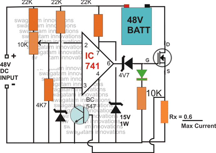 NOTE: The above diagrams mistakenly shows 48V as the input, the correct value is 56V.
Because the full charge level of a 48 V battery is around 56/57 V.
NOTE: You will have to connect the battery first and then switch ON the input supply, otherwise the mosfet will fail to initiate for the charging process. Make sure the green LED remains illuminated after power switch ON, this will confirm the charging status of the battery.
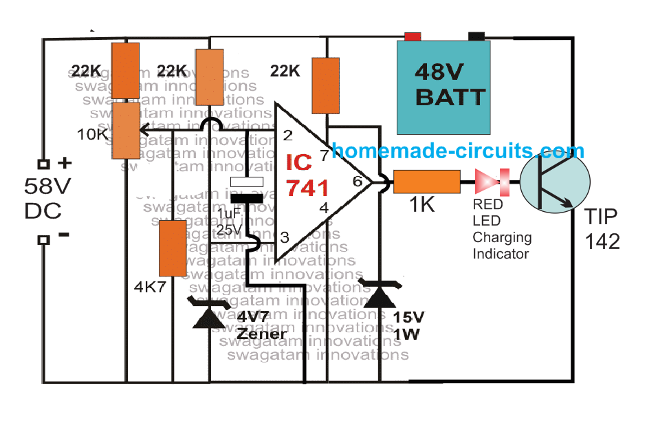
The above design can be also built using a TIP142 and a red led charging indicator.
NOTE: The above diagrams mistakenly shows 48V as the input, the correct value is 56V.
Because the full charge level of a 48 V battery is around 56/57 V.
NOTE: You will have to connect the battery first and then switch ON the input supply, otherwise the mosfet will fail to initiate for the charging process. Make sure the green LED remains illuminated after power switch ON, this will confirm the charging status of the battery.
The above design can be also built using a TIP142 and a red led charging indicator.
Simple 48 V 100 Ah charger Circuit using OP Amp and TIP142
 3) Making a Fully Automatic Version
The above circuit can be upgraded into an over charge cut off, as well as low charge restoring battery charger system, for charging 48V batteries.
The modifications enables the circuit to switch OFF the battery charging process at the set over charge threshold and restore back the process when the battery voltage falls below the low threshold value.
The 10k preset must be adjusted to set the full charge level while the 22k preset for detecting the lower threshold of the battery.
3) Making a Fully Automatic Version
The above circuit can be upgraded into an over charge cut off, as well as low charge restoring battery charger system, for charging 48V batteries.
The modifications enables the circuit to switch OFF the battery charging process at the set over charge threshold and restore back the process when the battery voltage falls below the low threshold value.
The 10k preset must be adjusted to set the full charge level while the 22k preset for detecting the lower threshold of the battery.
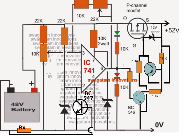 NOTE: In the above two circuits, please connect the RED LED in series with the BC546 base.
This will prevent the op amp offset voltage from reaching the BC546 base and false triggering.
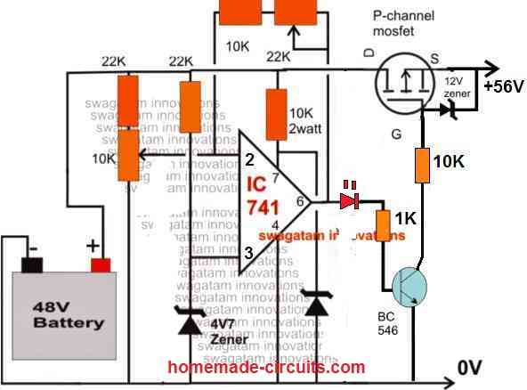
The above design can be further simplified as shown in the following image.
Notice that the input pins of the op amp are swapped in this design, which allowed the elimination of the extra PNP BJT from the circuit.
NOTE: In the above two circuits, please connect the RED LED in series with the BC546 base.
This will prevent the op amp offset voltage from reaching the BC546 base and false triggering.
The above design can be further simplified as shown in the following image.
Notice that the input pins of the op amp are swapped in this design, which allowed the elimination of the extra PNP BJT from the circuit.
How to Set up the above Circuit:
For setting up procedure, the sample power supply should be connected across the points where the battery is connected, the mosfet does not require any attention initially. DO NOT connect the battery while carrying out this procedure. Also keep the 22k preset link disconnected initially. Apply the higher threshold level across the above mentioned points and adjust the 10K preset such that the RED LED just switches ON. Seal the adjusted preset with some glue. Now reconnect the 22k preset link back into position. Next, reduce the sample voltage to the lower threshold value and adjust the 22k preset such that now the green LED just lights up, while switching OFF the RED LED. If you find no response from the circuit try using a 100K preset instead of the 22k preset. Seal the adjusted preset as above. The setting up of the circuit is over and done. Please note that during actual operations, the above circuit will remain functional only as long as a battery stays connected at the shown points, without a battery the circuit will not detect or respond.Feedback from Mr. Rohit
I have a 50-52v solar panel setup which is charging a 48v 78ah battery. What I want is when my battery is fully charged that is it reaches to 54v the battery charging stops and the supply which is coming from the solar panels is directed to another port from which we can charge any other device connected to the port. This charging should only continue till the battery is above 48v. Once it reaches 48v the battery again starts charging on solar panels and the supply to the other port is stopped. Hoping you will reply soon. My Response to the above Circuit Request You can try the last circuit from the following artcilehttps://www.homemade-circuits.Battery Charger Problems Troubleshooting Discussed
The included battery charger circuit was designed and built by Mr.Vinod Chandran, however there's some issues and problems with the circuit the troubleshooting of the same is addressed in this article. Let's learn the discussion between Vinod and me.Discussing a Transistor Battery Charger Problem
Vinod: I am attaching the circuit image of the charger with hysteresis feature. (with my modification.). This charger is working good. But i need your suggestions and confirmation.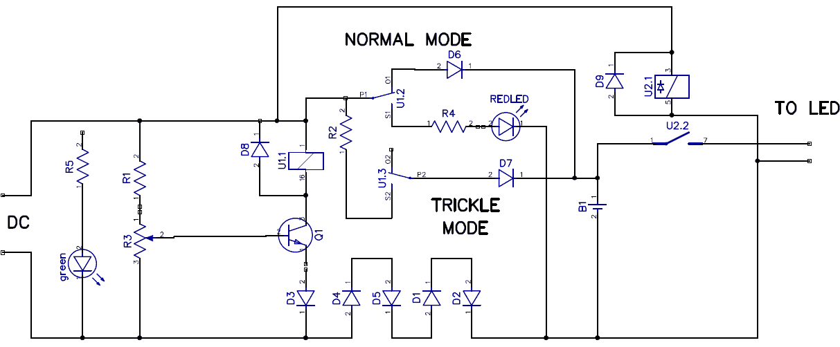 Swagatam: Using a transistor won't give accurate results, moreover the setting part would become very tedious.
The circuit is technically correct, if you can adjust the tripping point correctly, then it might just work.
Vinod: I am going to test this circuit.
I already build this in general board.
automatic cut-off is set in 13.6v now.
All i want to wait for the battery to discharge around 12v.
I will inform you the result.
Vinod: I made the charger (hysteresis) but there is a problem.
i will attach the image to explain the problem.
When i connect multimeter in that particular red dots, the voltage shows 16.8.(0.43 A) but when i disconnect battery from the charger and measured again.
then there is no problem.
the out put is 14.2. And the other pin of the relay(through the current limiting resistor) will deliver a clean output voltage of 13.9 (0.033A).
Why this is happening ?.
The only change i have made from this circuit is to grab the green LED and R1 from there and connect it after the D6.
Swagatam: Using a transistor won't give accurate results, moreover the setting part would become very tedious.
The circuit is technically correct, if you can adjust the tripping point correctly, then it might just work.
Vinod: I am going to test this circuit.
I already build this in general board.
automatic cut-off is set in 13.6v now.
All i want to wait for the battery to discharge around 12v.
I will inform you the result.
Vinod: I made the charger (hysteresis) but there is a problem.
i will attach the image to explain the problem.
When i connect multimeter in that particular red dots, the voltage shows 16.8.(0.43 A) but when i disconnect battery from the charger and measured again.
then there is no problem.
the out put is 14.2. And the other pin of the relay(through the current limiting resistor) will deliver a clean output voltage of 13.9 (0.033A).
Why this is happening ?.
The only change i have made from this circuit is to grab the green LED and R1 from there and connect it after the D6.
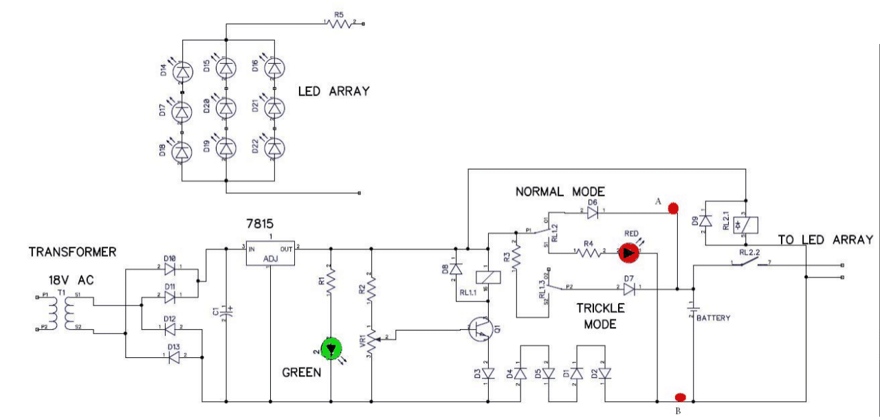 Swagatam: It's difficult to understand and troubleshoot the fault, if you are connecting meter prods across the battery terminals, it should show the dropped voltage level of the battery ...
this problem can happen only if the source current is too high and not at the recommended 1/10th level of the battery AH, make sure to use an input that is specified with the above current limit
You can repeat the checking by switching OFF the power supply and then again switching ON the power supply keeping the meter connected to the points A and B.
Hi Swagat, At last i made a charger that suits my needs.
this is the schematic.(plz look attachment).
Until battery gets 13v this is a constant current charger(400-500mA).
After 13v, charging current is 25mA.
And the LED's indicate the charging stages.
Regards Vinod chandran
Swagatam: It's difficult to understand and troubleshoot the fault, if you are connecting meter prods across the battery terminals, it should show the dropped voltage level of the battery ...
this problem can happen only if the source current is too high and not at the recommended 1/10th level of the battery AH, make sure to use an input that is specified with the above current limit
You can repeat the checking by switching OFF the power supply and then again switching ON the power supply keeping the meter connected to the points A and B.
Hi Swagat, At last i made a charger that suits my needs.
this is the schematic.(plz look attachment).
Until battery gets 13v this is a constant current charger(400-500mA).
After 13v, charging current is 25mA.
And the LED's indicate the charging stages.
Regards Vinod chandran
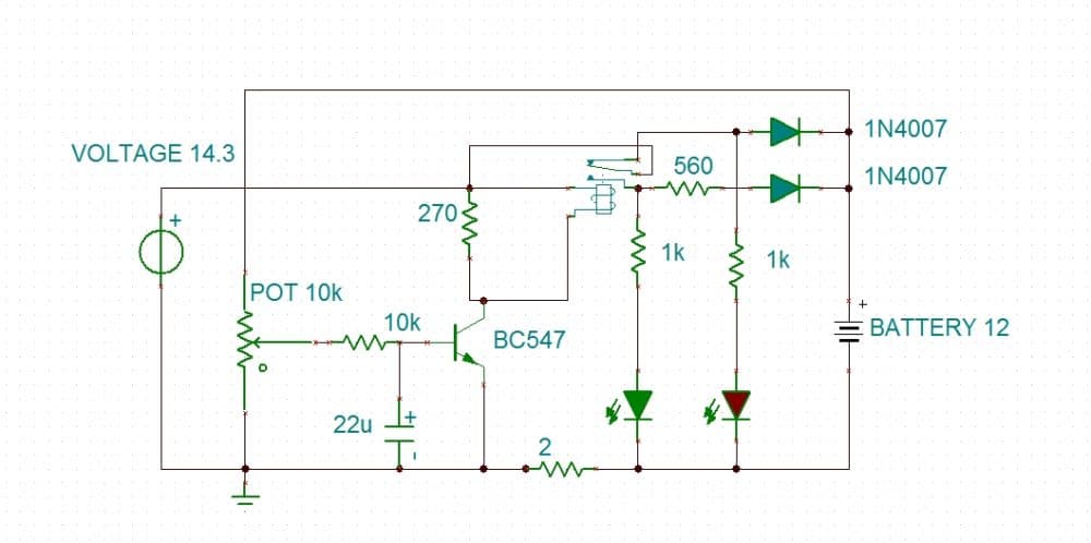
5 Best 6V 4Ah Automatic Battery Charger Circuits Using Relay and MOSFET
The following 5 versions of 6 volt 4 AH battery charger circuits has been designed by me and posted here in response to the request from Mr. Raja, let's learn the whole conversation. "Dear sir, please post a circuit to charge 6 volt 3.5 ah lead acid battery from 12 volt battery. The charger should automatically stop charging as the battery is fully charged. Please use transistor instead of relay to stop charging, and also tell me how to use 12 volt relay for the same circuit. Explain Which is safe and durable either relay or transistor to cut off charging. (At present i am charging my above said battery by simply using LM317 with 220 ohm and 1 kilo ohm resistors and a couple of capacitor) i'm awaiting your article, thank you".The Design
The following circuit shows a simple automatic 6 volt 4 to 10 AH battery charger circuit using a 12 volt relay, designed to automatically cut off the supply to the battery as soon as the full charge level for the battery is reached.How it Works
Assuming no battery is connected with the circuit, when power is switched ON, the relay contact will be at the N/C and no power will be able to reach the IC 741 circuit. Now when battery is connected, the supply from the battery will actuate the circuit, and assuming the battery to be in a discharged state, pin#2 will be lower than pin#3 causing a high at pin#6 of the IC. This will switch ON the transistor relay driver, which in turn will shift the relay contact from N/C to N/O connecting the charging supply with the battery. The battery will now begin charging slowly and as soon a its terminals reaches at 7V, pin#2 will tend to become higher than pin#3, causing pin#6 of the IC to become low, switching OFF the relay and cutting off supply to the battery. The existing low at pin#6 will also cause pin#3 to become permanently low through the linked 1N4148 diode, and thus the system will be latched, until power is switched OFF and ON again. If you don't wish to have this latching arrangement, you can very well eliminate the 1N4148 feedback diode. Note: The LED indicator section for all 3 following diagrams were recently modified after a practical testing and confirmation Circuit#1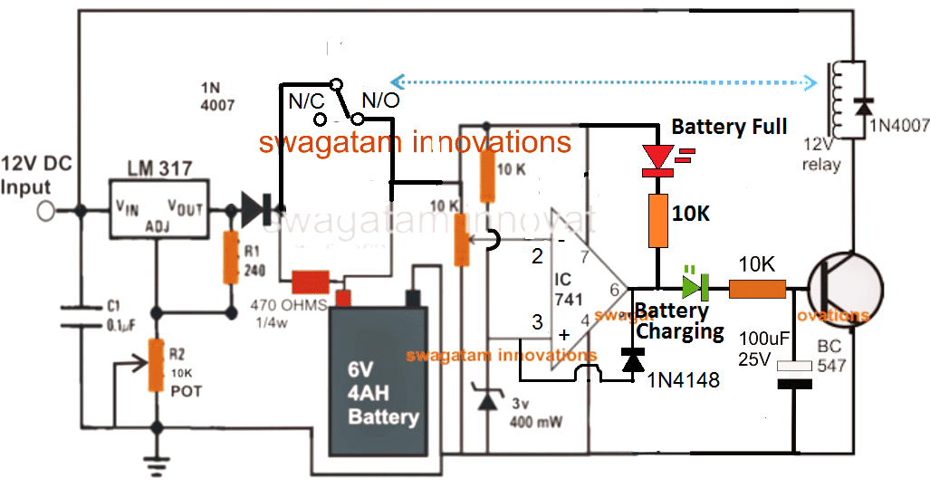 PLEASE CONNECT A 10uF ACROSS PIN2 AND PIN4, SO THAT THE OP AMP OUTPUT ALWAYS BEGINS WITH A "HIGH" ON POWER SWITCH ON
The following circuit shows a simple automatic 6 volt 4 AH battery charger circuit without using a relay, rather directly through a transistor, you can replace the BJT with a mosfet also to enable high Ah level charging also.
PLEASE CONNECT A 10uF ACROSS PIN2 AND PIN4, SO THAT THE OP AMP OUTPUT ALWAYS BEGINS WITH A "HIGH" ON POWER SWITCH ON
The following circuit shows a simple automatic 6 volt 4 AH battery charger circuit without using a relay, rather directly through a transistor, you can replace the BJT with a mosfet also to enable high Ah level charging also.
PCB Design for the Above Circuit
The PCB layout design were contributed by one of the avid followers of this website, Mr. Jack009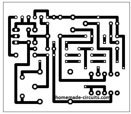
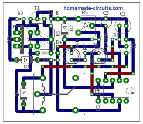 Circuit#2
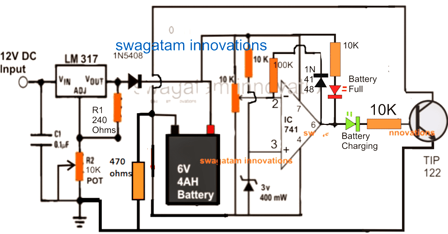 PLEASE CONNECT A 10uF ACROSS PIN2 AND PIN4, SO THAT THE OP AMP OUTPUT ALWAYS BEGINS WITH A "HIGH" ON POWER SWITCH ON
How to Set Up the Circuit
Initially, keep the pin6 feedback resistor disconnected and without connecting any battery adjust R2 to get exactly 7.2V at the output of the LM317 (across cathode of 1N5408 and ground line), for powering the IC 741 circuit. Now simply play with the 10k preset and identify a position where the RED/GREEN LEDs just flip/flop or change or swap between their illumination. This position within the preset adjustment may be considered as the cut-off or the threshold point. Carefully adjust it to a point at which the RED LED in the first circuit just lights up......but for the second circuit it should be the green LED that is supposed to get illuminated. The cut-off point is now set for the circuit, seal the preset in this position and reconnect the pin6 resistor across the shown points. Your circuit is now set for charging any 6V 4 AH battery or other similar batteries with an automatic cut-off feature as soon as or each time the battery becomes fully charged at the above set 7.2V. Both the above circuits will perform equally well, however the upper circuit can be altered to handle high currents even up to 100 and 200 AH just by modifying the IC and the relay. The lower circuit may be made to do this only up to a certain limit, may be up to 30 A or so. The second circuit from above was successfully built and tested by Dipto who is an avid reader of this blog, the submitted images of the 6V solar charger prototype can be witnessed below: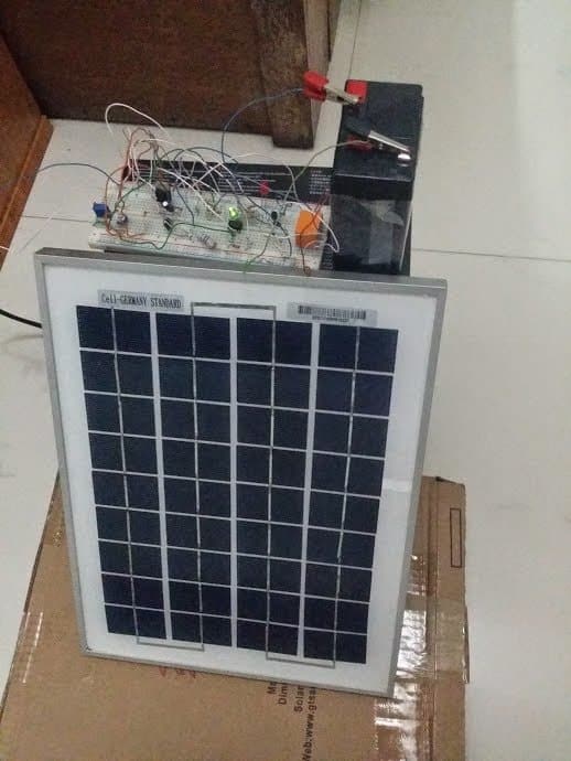
Adding a Current Control:
An automatic current control regulator function can be added with the above shown designs by simply introducing a BC547 circuit as shown in the following diagram: Circuit#3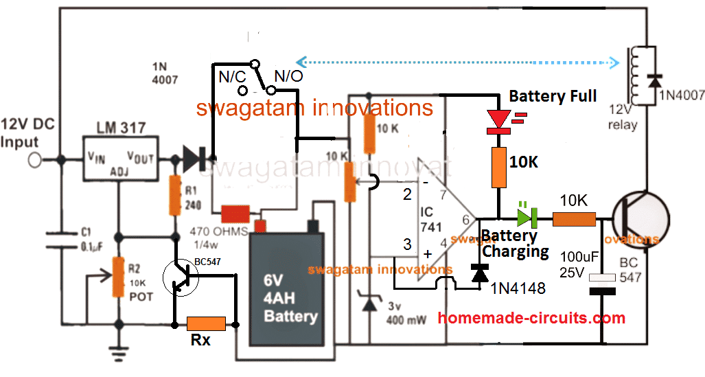 PLEASE CONNECT A 10uF ACROSS PIN2 AND PIN4, SO THAT THE OP AMP OUTPUT ALWAYS BEGINS WITH A "HIGH" ON POWER SWITCH ON
The current sensing resistor can be calculated through the simple Ohm's law formula:
Rx = 0.6 / Max charging current
Here 0.6V refers to the triggering voltage of the left side BC547 transistor while max charging current signifies the maximum safe charging for the battery, which may be 400mA for a 4AH lead acid battery.
Therefore solving the above formula gives us:
Rx = 0.6 / 0.4 = 1.5 Ohms.
Watts = 0.6 x 0.4 = 0.24 watts or 1/4 watt
By adding this resistor will ensure that the charging rate is fully controlled and it is never exceeded the specified safe charging current limit.
PLEASE CONNECT A 10uF ACROSS PIN2 AND PIN4, SO THAT THE OP AMP OUTPUT ALWAYS BEGINS WITH A "HIGH" ON POWER SWITCH ON
The current sensing resistor can be calculated through the simple Ohm's law formula:
Rx = 0.6 / Max charging current
Here 0.6V refers to the triggering voltage of the left side BC547 transistor while max charging current signifies the maximum safe charging for the battery, which may be 400mA for a 4AH lead acid battery.
Therefore solving the above formula gives us:
Rx = 0.6 / 0.4 = 1.5 Ohms.
Watts = 0.6 x 0.4 = 0.24 watts or 1/4 watt
By adding this resistor will ensure that the charging rate is fully controlled and it is never exceeded the specified safe charging current limit.
Test Report Video Clip:
The following video clip shows the testing of the above automatic charger circuit in real time. Since I did not have a 6V battery, I tested the design on a 12V battery, which does not make any difference, and its all about setting the preset accordingly for the 6V or a 12V battery as per user preference. The above shown circuit configuration was not changed in any manner. The circuit was set to cut off at 13.46V, which was selected as the full charge cut off level. This was done to save time because the actual recommended value of 14.3V could have taken lot of time, therefore to make it quickly I selected 13.46V as the high cut off threshold. However one point to be noted is that the feedback resistor was not employed here, and the lower threshold activation was automatically implemented at 12.77V by the circuit, as per the IC 741's natural hysteresis property.6V Charger Design#2
Here's another simple yet accurate automatic, regulated 6V lead acid battery charger circuit which switches off the current to the battery as soon as the battery reaches full charge. An illuminated LED at the output indicates the fully charged condition of the battery.How it Works
The CIRCUIT DIAGRAM can be understood with the the following points: Fundamentally the voltage control and regulation is done by the versatile, work horse IC LM 338. An input DC supply volt in the range of 30 is applied to the input of the IC. The voltage may be derived from a transformer, bridge and capacitor network. The value of R2 is set to get the required output voltage, depending upon the battery voltage to be charged. If a 6 volt battery needs to charged, R2 is selected to produce a voltage of around 7 volts at the output, for a 12 volt battery it becomes 14 volts and for a 24 volt battery, the setting is done at around 28 volts. The above settings take care of the voltage that needs to be applied to the battery under charge, however the tripping voltage or the voltage at which the circuit should cut off is set by adjusting the 10 K pot or preset. The 10K preset is associated with the circuit involving the IC 741 which is basically configured as a comparator. The inverting input of the IC 741 is clamped at a fixedreferencevoltage of 6 via a 10K resistor. With reference to this voltage the tripping point is set via the 10 K preset connected across the non inverting input of the IC. The output supply from the IC LM 338 goes to the battery positive for charging it. This voltage also acts as the sensing as well as the operating voltage for the IC 741. As per the setting of the 10 K preset when the battery voltage during the charging process reaches or crosses the threshold, the output of the IC 741 goes high. The voltage passes through the LED and reaches the base of the transistor which in turn conducts and switches off the IC LM 338. The supply to the battery is immediately cut off. The illuminated LED indicates the charged condition of the connected battery.Circuit#4
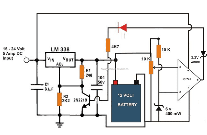 This automatic battery charger circuit can be used for charging all lead acid or SMF batteries having voltages in between 3 and 24 volts.
The above circuit was found not so satisfactory by some of the readers, so I have modified the above circuit for a better and guaranteed functioning.
Kindly see the modified design in the below given figure.
This automatic battery charger circuit can be used for charging all lead acid or SMF batteries having voltages in between 3 and 24 volts.
The above circuit was found not so satisfactory by some of the readers, so I have modified the above circuit for a better and guaranteed functioning.
Kindly see the modified design in the below given figure.
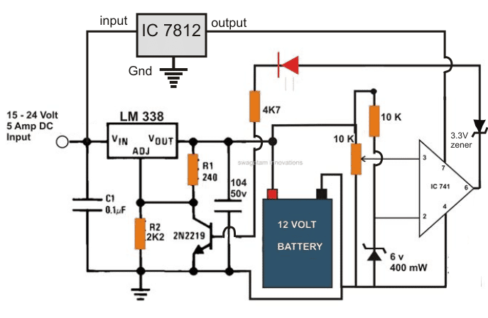
PCB Design for the above finalized 6V, 12V, 24V automatic battery charger circuit
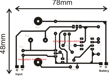
Solar 6V Battery Charger Circuit with Over Current Protection
So far we learned how to a simple 6V battery charger circuit with over current protection using mains input. In the following discussion we will try to understand how the same could be configured in conjunction with a solar panel, and also with an AC/DC adapter input. The circuit also includes a 4 stage battery status indication feature, an over current controller stage, automatic switch OFF for the load and battery charging, and also a separate cell phone charging outlet. The idea was requested by Mr. Bhushan Trivedi. Greetings, I trust you are well. I am Bhushan, and I am working on a hobby project currently. I am very impressed by the knowledge you share at your blog, and was hoping if you would like to guide me a bit with my project. My project is around charging a 6V 4.5 Ah sealed battery with grid and solar panel. This battery will supply power to led lights and a mobile phone charging point. Actually, the battery will be kept in a box. and box will have two inputs for battery charging. These two inputs are solar (9V) and AC (230V) for charging the 6V Battery. There will not be any automatic switchover. Its like the user has an an option to either charge the battery from solar or grid. but both the input options shall be available. For example, if on a rainy day or for some reason the battery can't be charged from a solar panel, then grid charging should be done. So I am looking for an option of both the inputs to the battery. Nothing automatic hereThe battery level indicator LED should indicate in red yellow and green on the battery level. Automatic battery cut off after voltage goes down certain limits to ensure long battery life. I am attaching a short problem statement along this email for your reference. I am looking for a circuit for the arrangement shown in it. I am keen to hear from you on this Kind Regards, BhushanThe 5th Design
The required 6V solar battery charger circuit can be witnessed in the diagram presented below. Referring to the diagram, the various stages may be understood with the help of the following points: The IC LM317 which is a standard voltage regulator IC is configured to produce a fixed 7V output determined by the resistances 120 ohms and 560 ohms. The BC547 transistor and its base 1 ohm resistor ensure that the charging current to the 6V/4.5AH battery never exceeds the optimal 500mA mark. The output of the LM317 stage is directly connected with the 6V battery for the intended charging of the battery. The input to this IC is selectable via a SPDT switch, either from the given solar panel or from an AC/DC adapter unit, depending whether the solar panel is producing sufficient voltage or not, which could be monitored through a voltmeter connected across the output pins of the LM317 IC. The four opamps from the IC LM324 which is a quad opamp in one packageare wired up as voltage comparators and producea visual indications for the various voltage levels at any instant, during the charging process or during the discharging process through the connected LEd panel or any other load. All the inverting inputs of the opamps are clamped to a fixed reference of 3V through the relevant zener diode. The non-inverting inputs of the opamps are individually attached to presets which are appropriately set to respond to the relevant voltage levels by making their outputs high sequentially. The indications for the same could be monitored via the connected coloredLEDs. The yellow LED associated with A2 may be set for indicating the low voltage cut-off threshold. When this LED shuts off (white lights up), the transistor TIP122 is inhibited from conducting and cuts off the supply to the load, thereby ensuring that the battery is never allowed to discharge to dangerous unrecoverable limits. A4 LED indicates the upper full charge level of the battery....this output could be fed to the base of the LM317 transistor in order to cut-off the charging voltage to the battery preventing overcharging (optional). Please note that since the A2/A4 do not have hysteresis included could produce oscillations at the cut-off thresholds, which won't necessarily be an issue or affect the battery performance or life. Circuit#5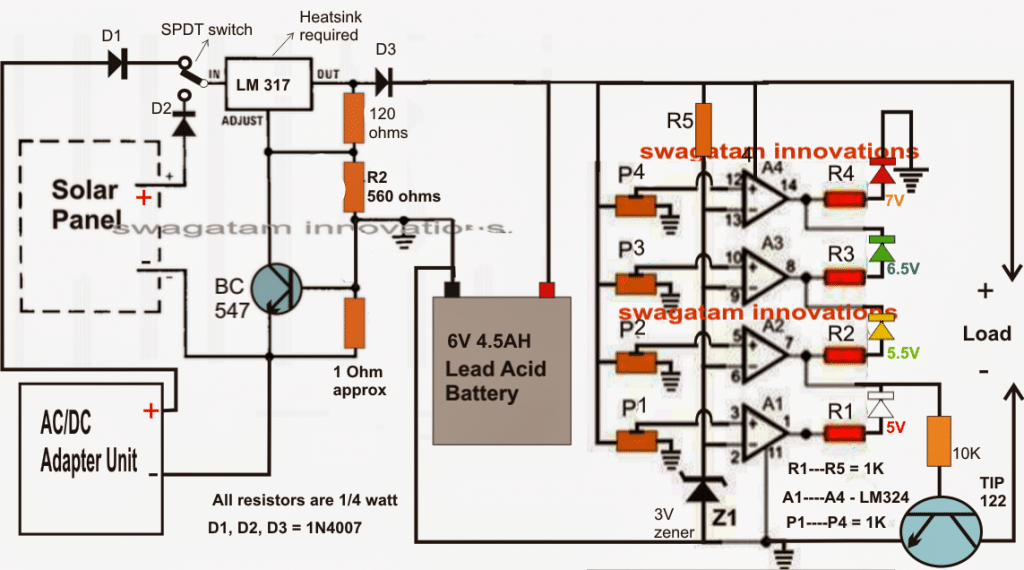
Adding an Auto-cut OFF on Batery Battery Full Charge
The modified diagram with over charge auto-cut of can be implemented by connecting A4 output with the BC547. But now the current limiting resistor formula will be as follows: R = 0.6 + 0.6 / max charge current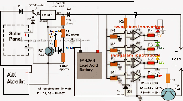
Feedback from Mr. Bhushan
Thank you very much for your continuedsupport and the above circuit designs. I have a few minor changes to the designnow, which I would like to request you for incorporating in the circuitdesign. I would like to express thatcost of the PCB and components is a big concern, but I do understand quality isalso very important. Hence, I request you to strike a fine balance between theperformance and cost of this circuit.So to begin with, we have this BOX, inwhich will house the 6V 4.5 Ah SMF Lead Acid Battery and the PCB too. The 6V 4.5 Ah Battery will be charged either through the followingnoptions from one single input: a) A 230 V AC to 9V DCAdaptor (I wish to go ahead with a 1 amp rating charger, your views?) ˇ®ORˇŻ b) A 3-5 Watt Solar module(Max Voltage: 9 V (6V nominal), Max Current: 0.4 to 0.5 Amps)Block Diagram
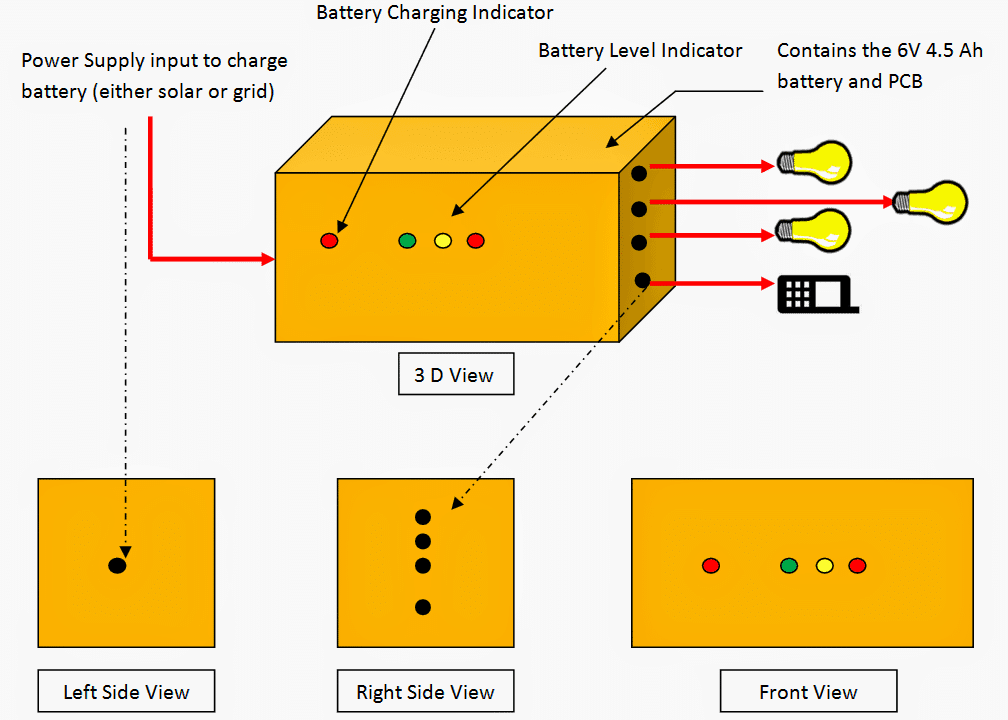 The battery can be charged by only one supply at a time hence will only have one input on the left side of the box.
For the time when this battery is being charged, there will be small red led light which glows on the font face of the box (Battery Charging Indicator in diagram) Now, at this point, the system should also have a battery level indicator (Battery level Indicator in diagram)
I wish to have three levels of indications for the battery state.
These tables state the open circuit voltage.
Now with the very little electronic knowledge I have, I am assuming this is ideal voltage and not the actual conditions, right?
I think I will leave that on you to decide and use any correction factors if required for calculations.
I wish to have the following indicator levels:
Charge level 100% to 65% = Small Green LED is ON (Yellow and Red LED off)
Charge level 40% to 65% = Small Yellow LED is ON (Green and Red LED off)
Charge level 20% to 40% = Small Red LED is ON (Green and Yellow LED off)
At 20% Charge level, battery disconnects and stops supplying output power.
On the Output side now (Right Side View in diagram)
The system will supply power to the following applications:
a) 1 Watt, 6V DC LED Bulb ¨C 3 NoˇŻs
b) One output for Mobile Phone Charging I wish to incorporate a feature here.
As you see, the DC loads connected to the battery are of relatively less wattage.
(just a mobile phone and three 1 watt LED Bulbs).
Now, the feature to be added in the circuit should kind of work as a fuse ( I donˇŻt mean an actual fuse here).
Assume if a CFL bulb is connected here or some other application of higher wattage rating, power supply should be cut off.
If the total power drawn is in excess of 7.5 Watts DC connected to this system, the system should cut off supply and shall only resume when the load is below 7.5 Watts.
I basically wish to ensure that this system is not misused or drawn excessive energy from, thereby damaging the battery.
This is just an idea.
I do however understand this can potentially increase the complexity and cost of the circuit.
I will look for your recommendation on this on whether to include this feature or no as we already are cutting off the battery supply once the state of charge reaches 20%.
I hope you find this project exciting to work on.
I look forward to receiving your much valued inputs on this.
I am thanking you for all your help till now and in advance for your extended cooperation on this.
Kind Regards,
Bhushan.
The battery can be charged by only one supply at a time hence will only have one input on the left side of the box.
For the time when this battery is being charged, there will be small red led light which glows on the font face of the box (Battery Charging Indicator in diagram) Now, at this point, the system should also have a battery level indicator (Battery level Indicator in diagram)
I wish to have three levels of indications for the battery state.
These tables state the open circuit voltage.
Now with the very little electronic knowledge I have, I am assuming this is ideal voltage and not the actual conditions, right?
I think I will leave that on you to decide and use any correction factors if required for calculations.
I wish to have the following indicator levels:
Charge level 100% to 65% = Small Green LED is ON (Yellow and Red LED off)
Charge level 40% to 65% = Small Yellow LED is ON (Green and Red LED off)
Charge level 20% to 40% = Small Red LED is ON (Green and Yellow LED off)
At 20% Charge level, battery disconnects and stops supplying output power.
On the Output side now (Right Side View in diagram)
The system will supply power to the following applications:
a) 1 Watt, 6V DC LED Bulb ¨C 3 NoˇŻs
b) One output for Mobile Phone Charging I wish to incorporate a feature here.
As you see, the DC loads connected to the battery are of relatively less wattage.
(just a mobile phone and three 1 watt LED Bulbs).
Now, the feature to be added in the circuit should kind of work as a fuse ( I donˇŻt mean an actual fuse here).
Assume if a CFL bulb is connected here or some other application of higher wattage rating, power supply should be cut off.
If the total power drawn is in excess of 7.5 Watts DC connected to this system, the system should cut off supply and shall only resume when the load is below 7.5 Watts.
I basically wish to ensure that this system is not misused or drawn excessive energy from, thereby damaging the battery.
This is just an idea.
I do however understand this can potentially increase the complexity and cost of the circuit.
I will look for your recommendation on this on whether to include this feature or no as we already are cutting off the battery supply once the state of charge reaches 20%.
I hope you find this project exciting to work on.
I look forward to receiving your much valued inputs on this.
I am thanking you for all your help till now and in advance for your extended cooperation on this.
Kind Regards,
Bhushan.
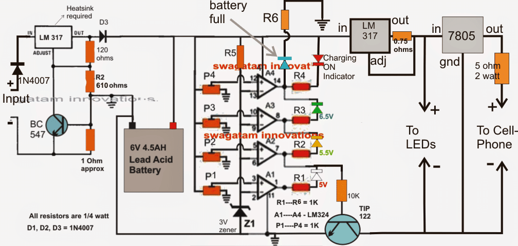
The Design
Here's a brief explanation of the various stages included in the proposed 6V battery charger circuit with over current protection: The left side LM317 is responsible for producing a fixed 7.6V charging voltage across its output pin and ground for the battery, which drops to around 7V via D3 to become an optimal level for the battery. This voltage is determined by the associated 610 ohm resistor, this value can be reduced or increased for changing the output voltage proportionately if required. The associated 1 ohm resistor and the BC547 restricts the charging current to around a safe 600mA for the battery. The opamps A1---A4 are all identical and perform the function of voltage comparators. As per the rules if the voltage at their pin3 exceeds the level at pin2, the corresponding outputs become high or at the supply level..... and vice versa. The associated presets may be set for enabling the opamps to sense any desired level at their pin3 and make their corresponding outputs go high (as explained above), thus A1 preset is set such that its output becomes high at 5V (Charge level 20% to 40%)....A2 preset is set to respond with an output high at 5.5V (Charge level 40% to 65%), while A3 triggers with a high output at 6.5V (80%), and finally A4 alarms the owner with the blue LED at battery level reaching the 7.2V mark (100% charged). At this point the input power will need to be switched off manually since you did not demand for an automatic action. Once the input is switched off, the 6v battery level sustains the above positions for the opamps, while the output from A2 ensures that the TIP122 conducts keeping the relevant loads connected with the battery and operative. The LM317 stage at the right is a current controller stage which has been rigged to restrict the output amp consumption to 1.2 amps or around 7 watts as per the requirements. The 0.75 ohm resistor may be varied for altering the restriction levels. The next 7805 IC stage is a separate inclusion which generates a suitable voltage/current level for charging standard cell phones. Now, as power is consumed the battery level begins receding in the opposite direction, which are indicated by the relevant LEDs.... Blue is the first one to shut off illuminating the green LEd, which shuts off off below 6.5V illuminating the yellow LEd which identically shuts off at 5.9V making sure that now the TIP122 no longer conducts and the loads are shut off.... But here the condition may oscillate for some moment until the voltage finally reaches below 5.5V illuminating the white LEd and alarming the user for an input power switch on and commence the charging procedure. The above concept can be further improved by adding an automatic full charge cut off facility, as shown below: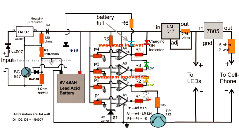
Sec Exciter Powered HV Capacitor Charger Circuit
My friend Steven hasupdateda few more of his findings related to his secexciter experiment, let's learn more what Mr. Steven has to say.NEW SEC EXCITER POWERED HV CAP CHARGER WITH HV DCOUTPUT
Here's the newest circuit originally it was a 3 piece circuit i found on YouTube so i modified it and upgraded it and threw in some ideas to get this beauty , now it has the tip3055 and inductor as on the YouTube video, and a ac light but you can see all the changes I've done to it to make it suitable to power off the single rf output of the sec exciter tower i threw in the microwave cap look carefully the inductor has 2 coils one runs through the collector of the tranny and back to above the second av plug diodes i used in the modified circuit so for all i can say its acting as an rf antennae to and opposite to the other coil so if there's any induction going on then maybe it explains why i get a fast voltage reading till it gets to 454 volts dc then stays there and as for the current output well its high enough to zap you and i had some problems in measuring the current output so i may have to get it done by using a regulator circuit so i can get a steady reading , but I'm sure its high enough as when the cap seems to charge and output the dc voltage it sure zaps you when you touch the hv outputs , so this is not bad for a sec exciter powered hv cap charger , i threw in the hand wound bifilar wound joule thief toroid to and all diodes which are 1n60 germanium and the inductor has 120 on top of it it was from my parts draws which i have collected parts from old TVs etc , so when i fire my sec exciter up and connect the single RF output to this circuit it doesn't take long to charge up so i have to do some more tests and experiments and see what else i can get out of this , so add this to the circuits that use microwave caps as the only other ones are microwave oven circuits , so my collection of new ideas and circuits i modify to be powered from a single output from an sec exciter grows more and more.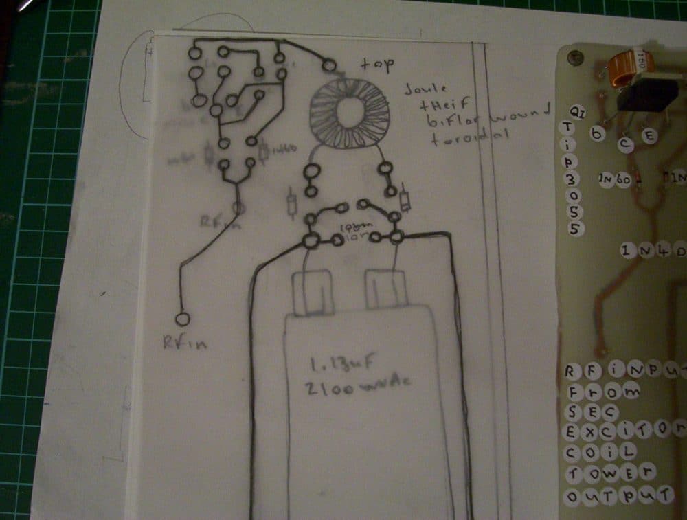
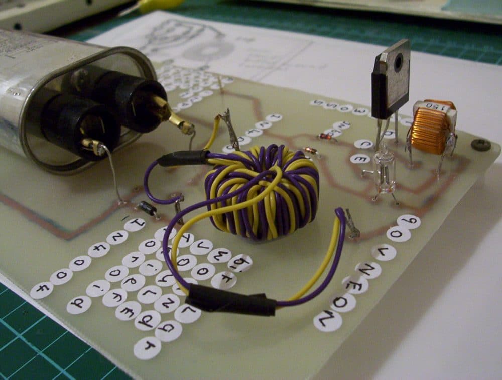
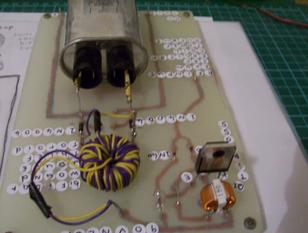
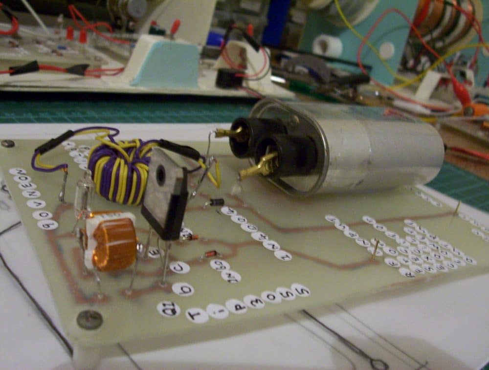
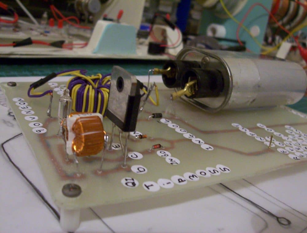
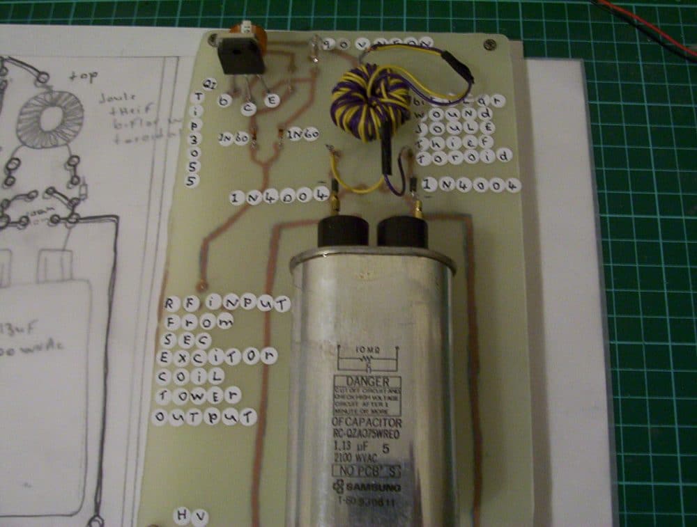
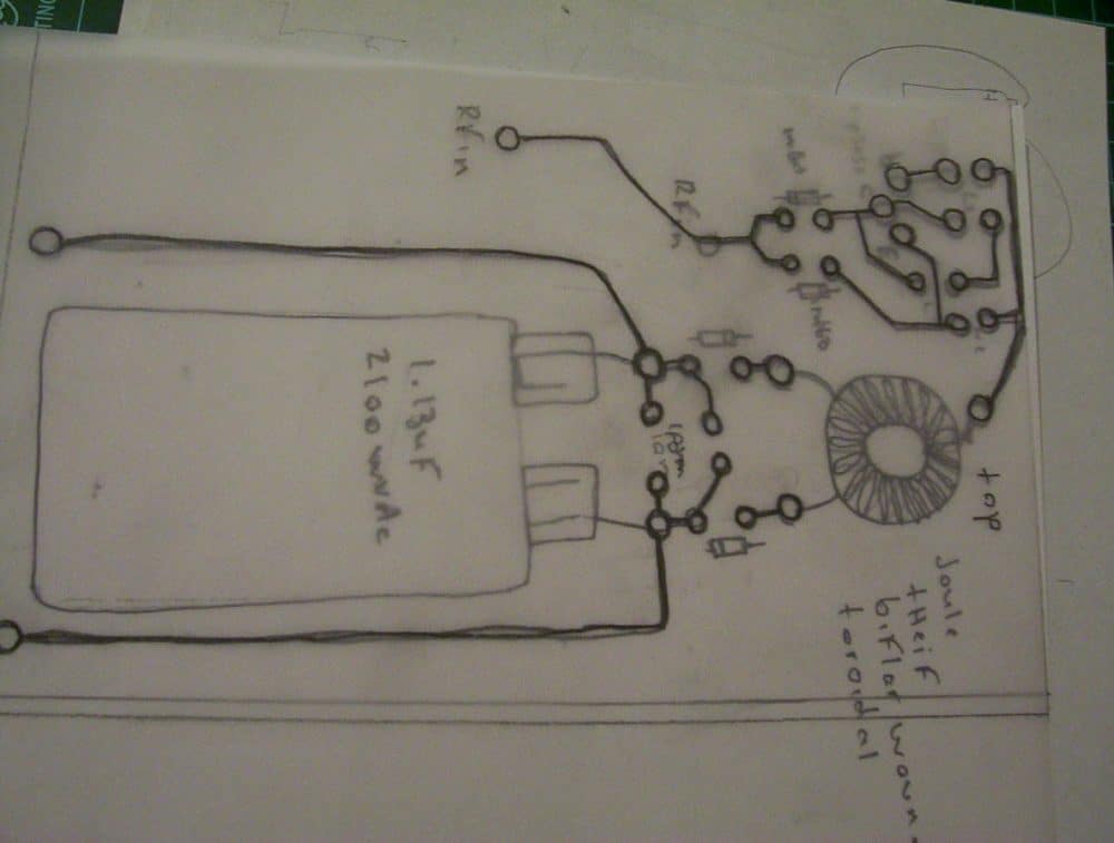
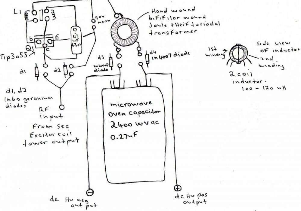
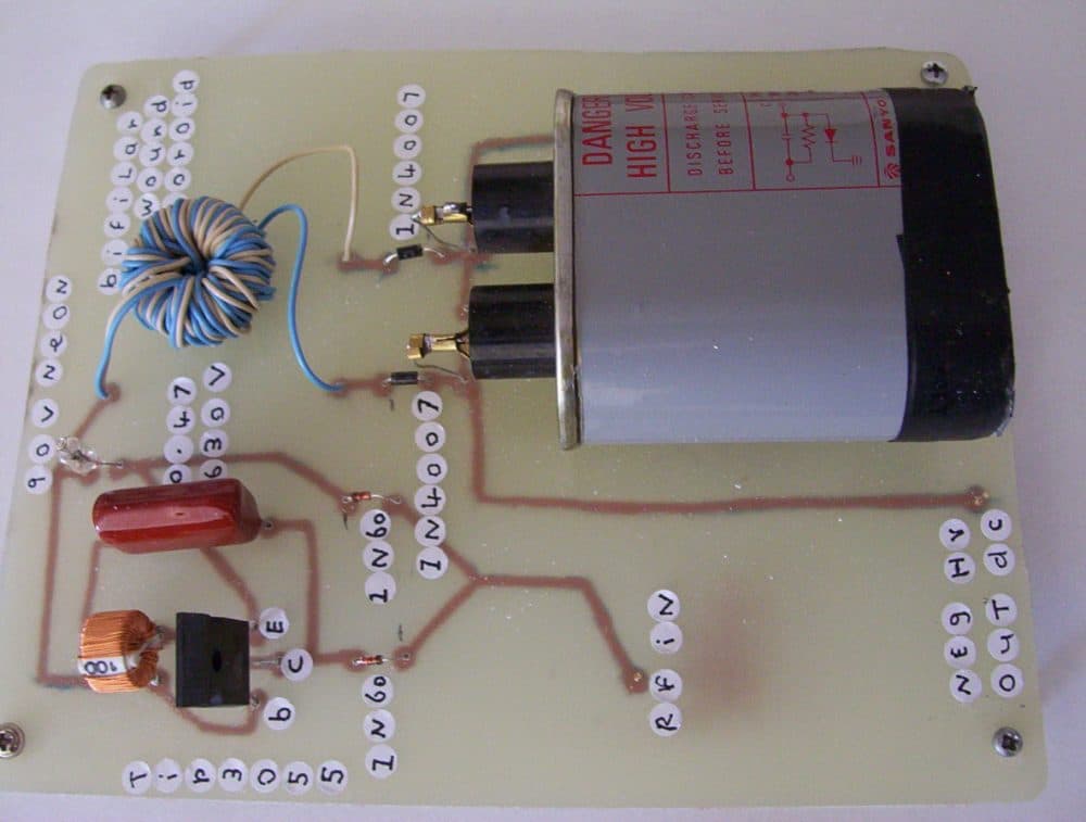
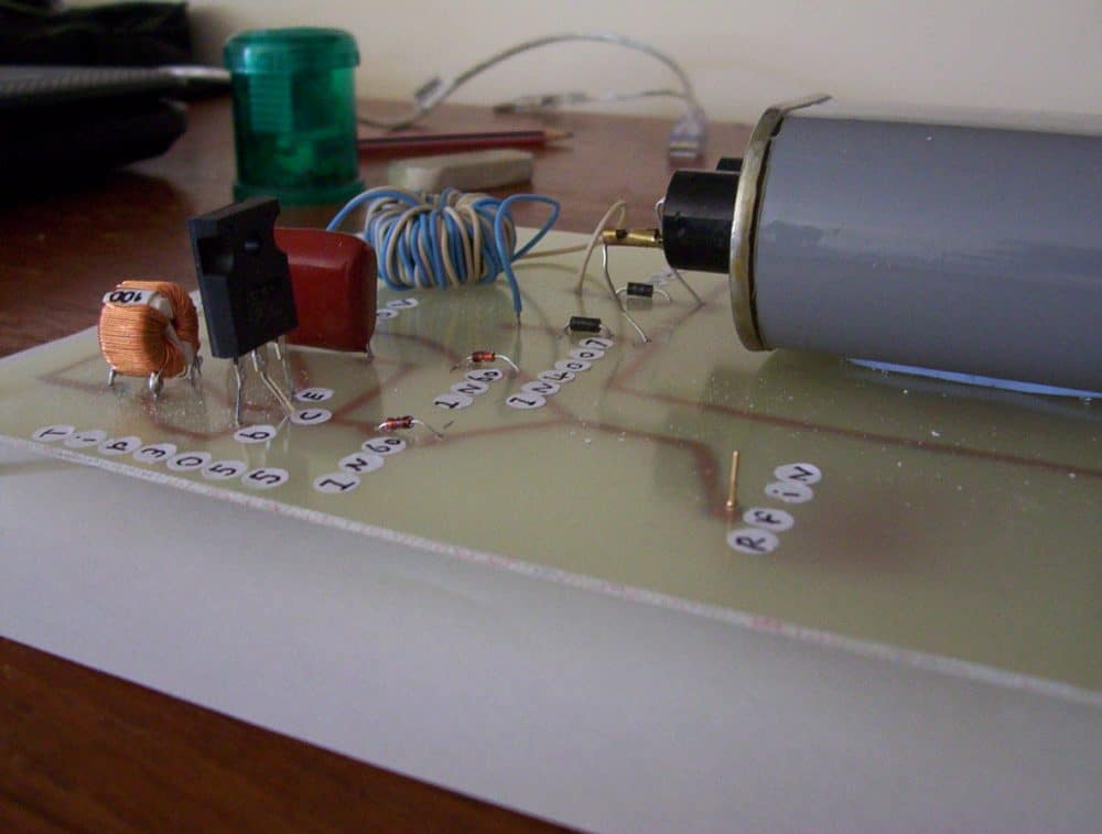
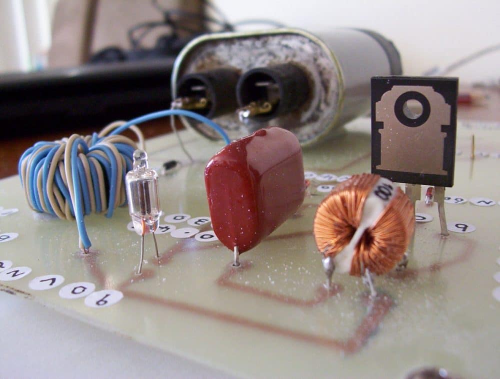
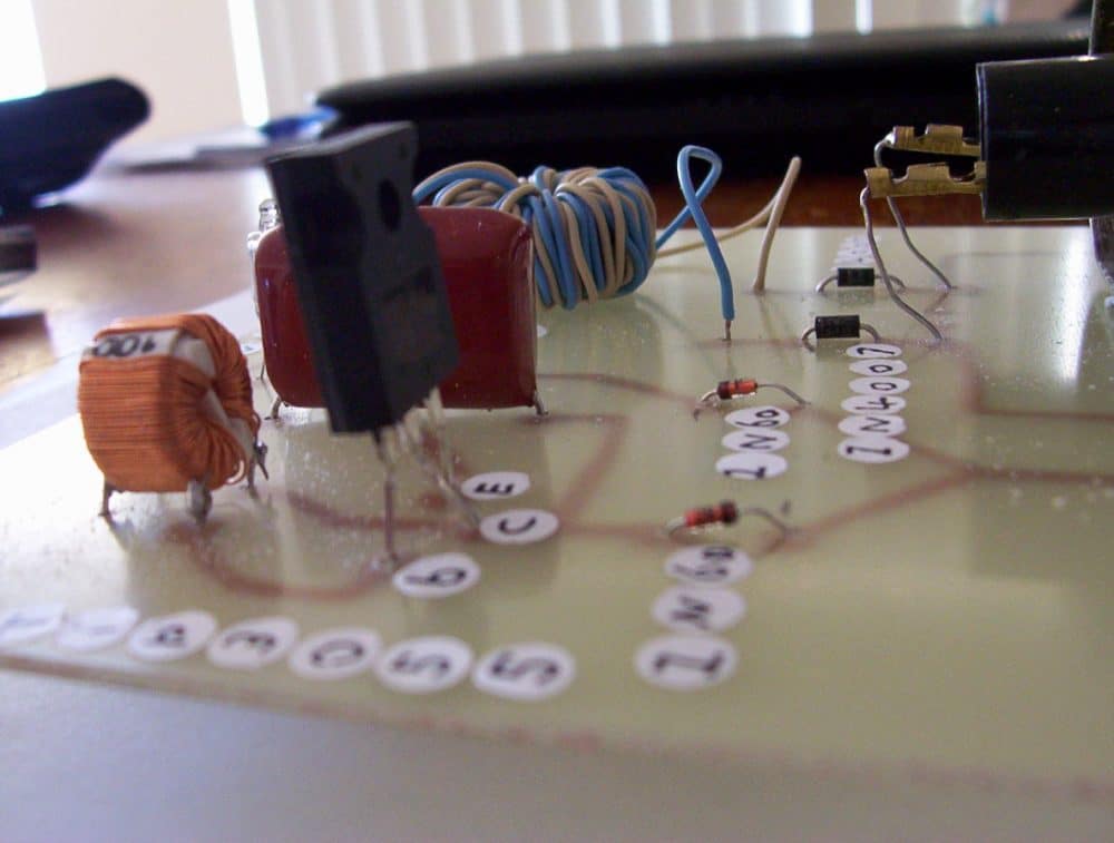
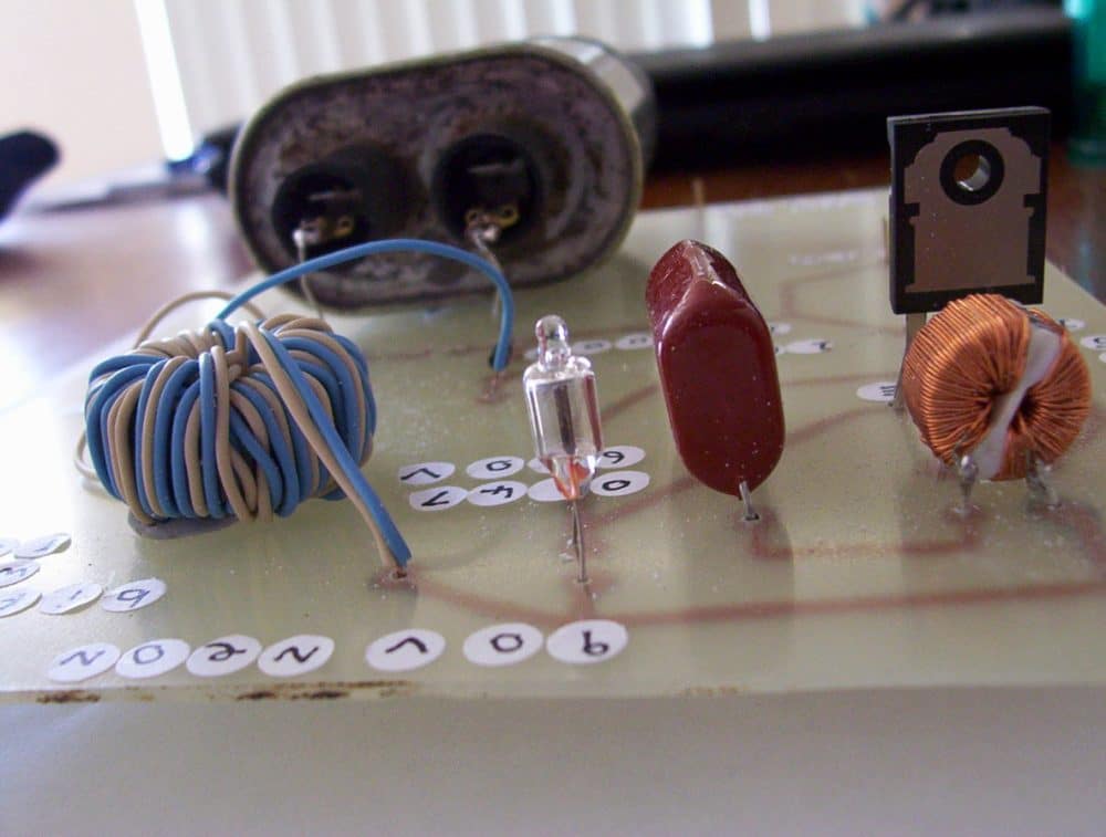
Here are the pics of another newer sec exciter powered hv dc output circuit,
this one puts out more voltage than the other 2 similar circuits and it exceeds the 1100 volts ac rating of the microwave cap even though its dc and the current well up to 13 set to amps on a clamp meter i have top be sure i read it right but it sure gives a shock,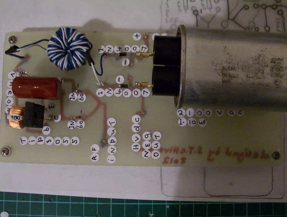
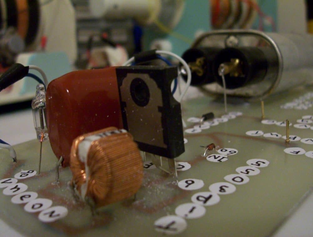
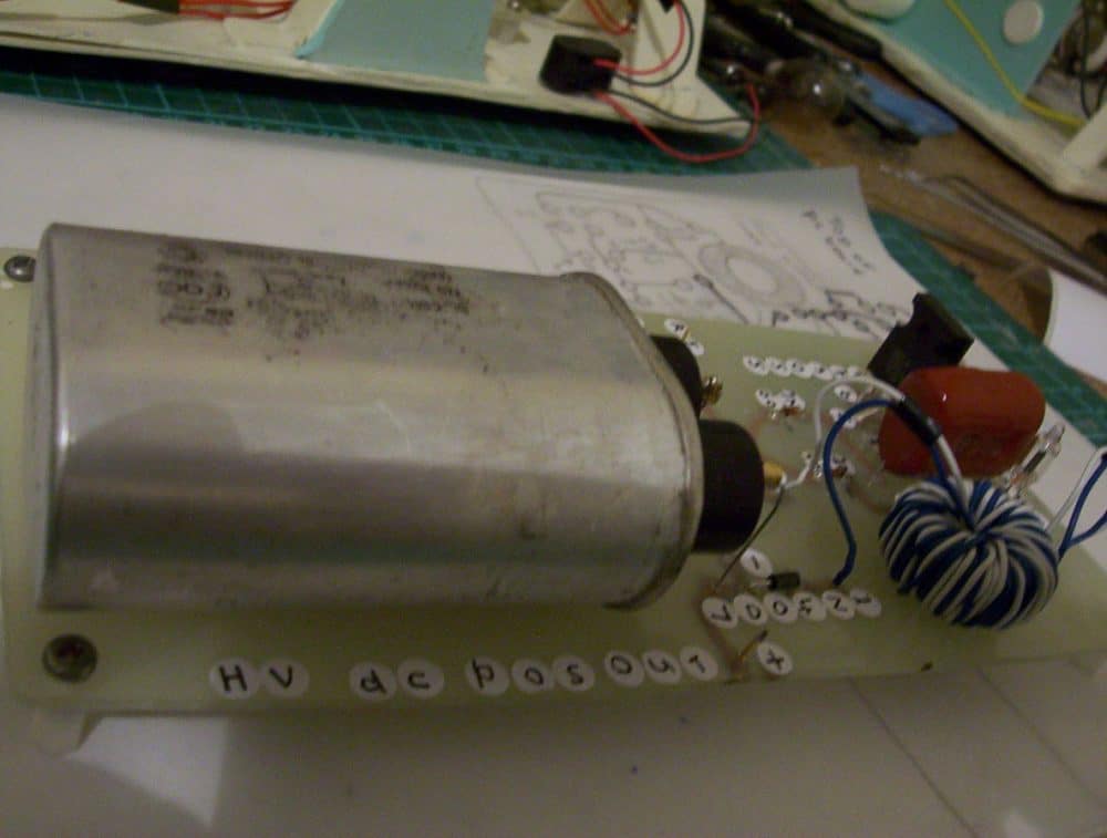

Here are 7 new pictures of the first out of 3 news sec exciters completed,
the series coils have their taps running to a printed circuit board under the coil , these taps are for testing the coil to insure continuity through all the coils . tap number 5 runs to the new circuit via a plug at the top wall this last tap is the power coil tap where all the power comes out of and goes into the hv, dc, ac and rf booster or amp section its outputs run to the terminals on the side the driver circuit and its switch are at the front end where the input starts at no 1. the series center core goes inside a pvc pipe and it slides in and out for tuning purposes through the center of the series coils you can see the pvc pipe sticking out each end , that is the sliding flux concentrating core housing pipe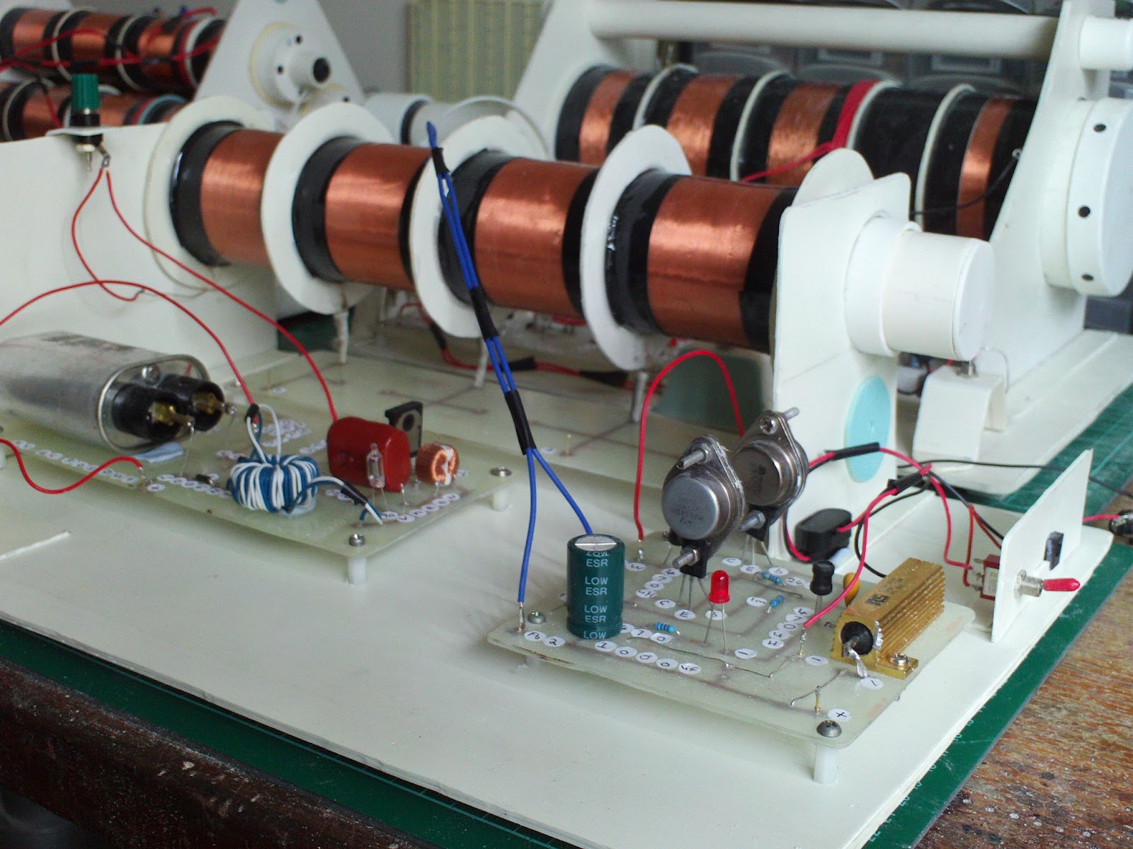


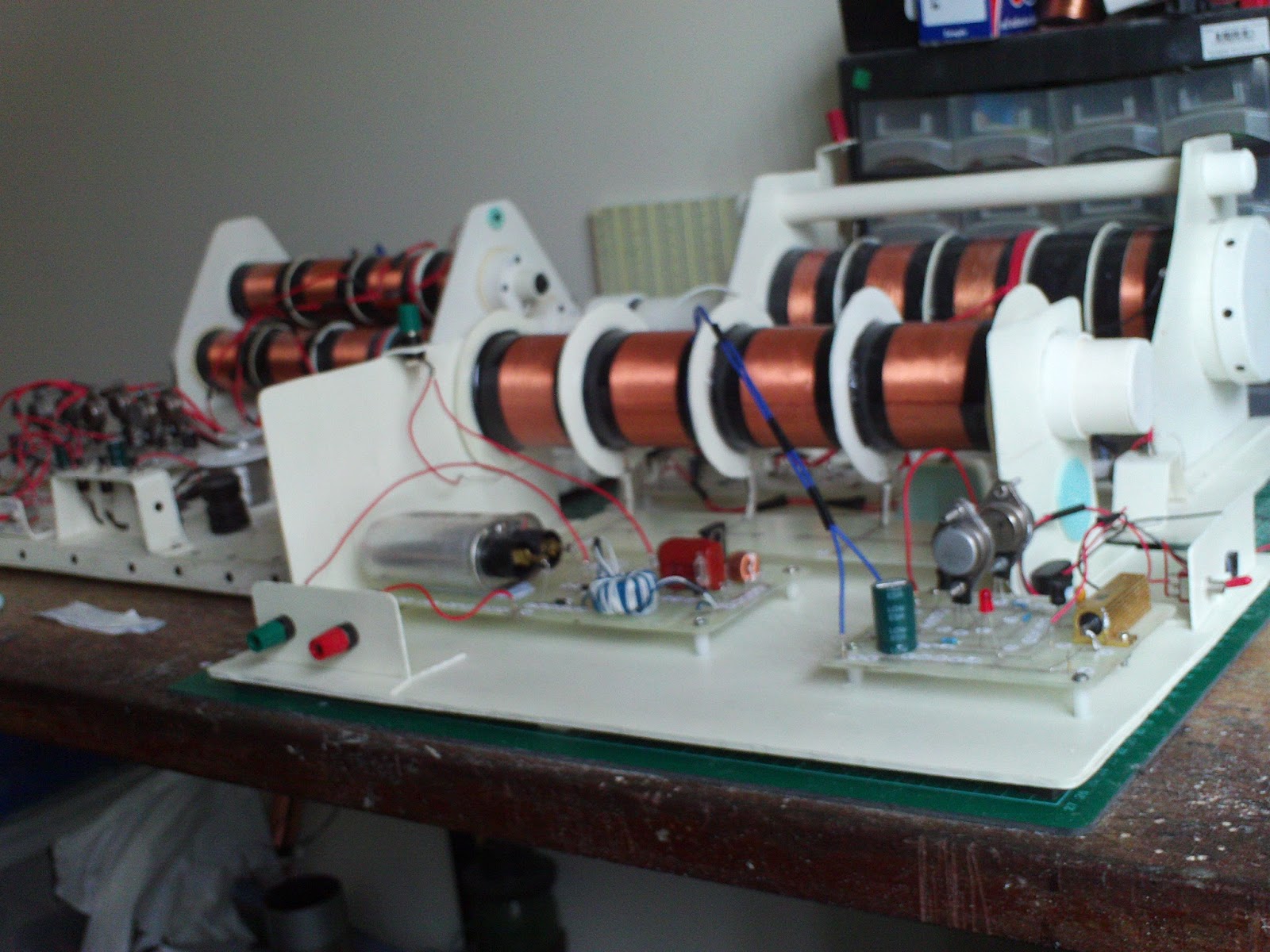
 I've done a test of the newest sec exciter coil tower etc etc first the transistors didn't come on and oscillate so that was easy to fix by bridging a metal, object from one transistor to the other .
take note of the power transistors they are used as heat sinks for the bd139 transistors so they have no legs so i bridged the metal object across them both to kick start the transistors into oscillation, when i did that i felt no output at the hv circuit till i inserted the core which i borrowed from my other sec exciter series coil tower projects,
then i held a neon by one leg above each of the series coil sections and the neon lit up well and from a good range to but some spots the neon was less brighter , so i move the flux concentrating core out till the neon started to get brighter ,
i then new that the flux concentrating core was working in tuning the sec exciter for maximum output, as the neon would get brighter near some of the coil sections and the last coil which is the power coil it got bright there to when i pulled the core out so far and that was when the hv dc, hv ac, and RF booster kicked in and gave the high outputs so it all worked ,
I've swapped the feed backs over since the first test as it sometimes helps in the transistors oscillation without having to kick start them,
I've done a test of the newest sec exciter coil tower etc etc first the transistors didn't come on and oscillate so that was easy to fix by bridging a metal, object from one transistor to the other .
take note of the power transistors they are used as heat sinks for the bd139 transistors so they have no legs so i bridged the metal object across them both to kick start the transistors into oscillation, when i did that i felt no output at the hv circuit till i inserted the core which i borrowed from my other sec exciter series coil tower projects,
then i held a neon by one leg above each of the series coil sections and the neon lit up well and from a good range to but some spots the neon was less brighter , so i move the flux concentrating core out till the neon started to get brighter ,
i then new that the flux concentrating core was working in tuning the sec exciter for maximum output, as the neon would get brighter near some of the coil sections and the last coil which is the power coil it got bright there to when i pulled the core out so far and that was when the hv dc, hv ac, and RF booster kicked in and gave the high outputs so it all worked ,
I've swapped the feed backs over since the first test as it sometimes helps in the transistors oscillation without having to kick start them,
Battery Cut Off Charger Circuit Using a Single Relay
Amazed to hear this! Yep thatˇŻs actually possible, you would need only one relay and a handful of diodes to make a simplest one relay automatic battery charger circuit.How it Works
The idea struck me while trying to design the easiest possible battery charger circuit for one my clients. The concept is simple; just raise the operating or triggering voltage of the relay up to the optimal battery charging threshold voltage by dropping the required amount of supply voltage to the relay coil, with the help of series diodes.The idea may be understood from the following points: Take an ordinary relay, measure its triggering voltage by carefully applying a variable voltage across its coil.Now suppose the triggering voltage of the particular relay was about 9 volts, and also assume you want to raise its voltage to 14 volts, which may be your 12 volt batteryˇŻs charging threshold voltage. We know that a 1N4007 diode drops about 0.6 volts across it, so if we add sufficient number of diodes in series with the relay coil would hopefully pull its tripping or triggering voltage to about 14 volts. That means, 14 ¨C 9 = 5, weˇŻll require 5/0.5 = 10 diodes in series to achieve this rise in the triggering voltage of the relay.ThatˇŻs pretty simple and interesting isnˇŻt it?The rest may be done with the help of the shown diagramˇ..your simplest single relay automatic battery charger is ready.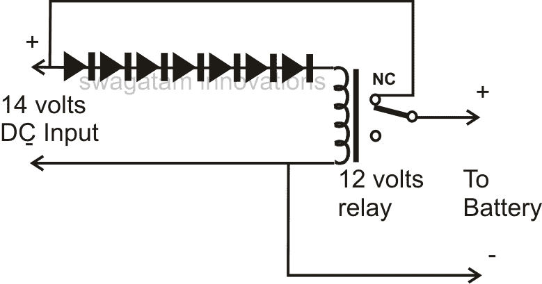
2 Simple Battery Desulfator Circuits Explored
In this article we investigate 2 simple yet powerful battery desulfator circuits, which can be used to effectively to remove and prevent desulfation in lead acid batteries. The first method uses PWM pulses, while the second method implements a ordinary bridge rectifier for the same. Sulphation in lead acid batteries is quite common and a big problem because the process completely hampers the efficiency of the battery. Charging a lead acid battery through PWM method is said to initiate desulfation, helping recover battery efficiency to some levels.What is Sulphation in Lead Acid Batteries
Sulphation is a process where the sulfuric acid present inside lead acid batteries react with the plates overtime to form layers of white powder like substance over the plates. This layer deposit seriously deteriorates the chemical actions inside the battery while charging or discharging making the battery inefficient with its power delivering capabilities. Normally this happens when the battery is not being used for long periods and the charging, discharging processes are not done very frequently. Unfortunately there's no effective way of tackling this problem, however it has been researched that the jammed sulphur deposits over an effected battery may be broken down to some extent by subjecting the battery to high current bursts while charging it. These high current charging pulses should be well optimized through some control circuit and should be diagnosed carefully while implementing the process.1) Using PWM
Implementing the method through PWM controlled circuit is probably the best way of doing it. Here's an excerpt from wikipedia, which says,"Desulfation is achieved by high current pulses produced between the terminals of the battery. This technique, also calledpulse conditioning, breaks down the sulfate crystals that are formed on the battery plates. Short high current pulses tend to work best. Electronic circuits are used to regulate the pulses of different widths and frequency of high current pulses. These can also be used to automate the process since it takes a long period of time to desulfate a battery fully." https://en.wikipedia.org/wiki/Talk%3ABattery_regeneratorThe circuit of a PWM battery charger discussed here can be considered as the best design for carrying out the above desulfation process.
How the Circuit Functions
The IC 555 is configured and used in its standard PWM control mode. The output from the IC is appropriately amplified through a couple transistors so that it is able to deliver the said high current pulses to the battery which needs to be desulfated. The PWM control may be set at low "mark" ratio for implementing a desulfation process. Conversely if the circuit is intended to be used for charging normal batteries, the PWM control may be adjusted for generating pulses with equal mark/space ratios or as per the desired specs. The controlling of the PWM will solely depend on an individuals personal preference, so should be done correctly as per the battery manufacturers instructions. Failing to follow the correct procedures may lead to fatal accidents with the battery, due to a possible explosion of the battery. An input current level equal to the battery AH level may be chosen initially, and reduced gradually if a positive response is detected from the battery.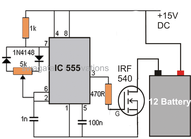
2) Desulfating with a Transformer and Bridge Rectifier Circuit
To make this simplest yet effective battery desulfator with charger circuit you would just require a suitably rated transformer, and a bridge rectifier. The design not only desulfates a battery, it keeps the new batteries from developing this issue and simultaneously charges them to the desired levels. At the beginning of this post we learned how to desulfate using PWM concept, however a deeper research shows that the process of desulfating a battery may not necessarily require a precision PWM circuit, the supply just needs to be oscillating at some given rate, and that's enough to initiate the desulfating process (in most cases)... provided the battery is still within the curing range and is not beyond the reviving state. So what would you need to make this super simple battery desulfator circuit which will also charge the given battery, and additionally possess the ability to keep the new batteries from developing the sulfation issue? A suitably rated transformer, a bridge rectifier and an ammeter are all that's needed for the purpose. The transformer voltage must be rated approximately 25% more than the battery voltage rating, that is for a 12V battery a 15 to 16V supply may be used across the battery terminals. The current can be approximately equal to the Ah rating of the battery for those which need to be revived and are badly sulfated, for the good batteries the charging current could be around 1/10th or 2/10th of their Ah rating. The bridge rectifier must be rated according to the specified or calculated charging levels. Desulfator Schematic using Bridge Rectifier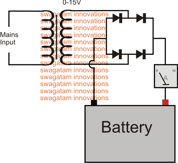
How Bridge Rectifier Operates as a Desulfator
The diagram above shows the bare minimum requirement for the proposed battery desulfator with charger circuit. We can see the most standard or rather crude AC to DC power supply set up, where the transformer steps down the mains voltage to 15V AC for the specified 12V battery. Before it can reach the battery terminals, the 15V AC goes through the rectification process through the attached bridge rectifier module and gets converted into a full-wave 15V DC. With a 220V mains input, the frequency before the bridge would be 50Hz (standard grid spec), and after rectification this is supposed to become double that is at 100Hz. For a 110V AC input this would be around 120Hz. This happens because the bridge network inverts the lower half cycles of the stepped down AC and combines it with the upper half cycles, to finally produce a 100Hz or 120 Hz pulsating DC. It is this pulsating DC which becomes responsible for shaking-up or knocking down the sulfate deposits on the internal plates of the particular battery. For a good battery this 100 Hz pulsed charging supply ensures that the sulfation ceases to occur on the first place and thus helps to keep the plates relatively free from this issue. You can also see an ammeter connected in series with the supply input, it provides a direct indication of he current consumption by the battery and provides a "LIVE update" of the charging procedure, and whether or not anything positive might be happening. For good batteries this will provide the start to finish info regarding the charging process, that is initially the needle of the meter will indicate the specified charging rate by the battery and may be gradually expected to drop down to the zero mark, and that's when the charging supply needs to be disconnected. A more sophisticated approach can be employed for enabling an automatic cut-off once the battery is fully charge by employing an opamp based automatic battery full charge cut off circuit (the second diagram).Using High Voltage Pulse
The configuration detailed below provides the most up-to-date methods of desulfating lead-acid batteries. It is a circuit which routinely supplies quick yet intense pulses to the battery, while discharging the battery marginally between the pulses.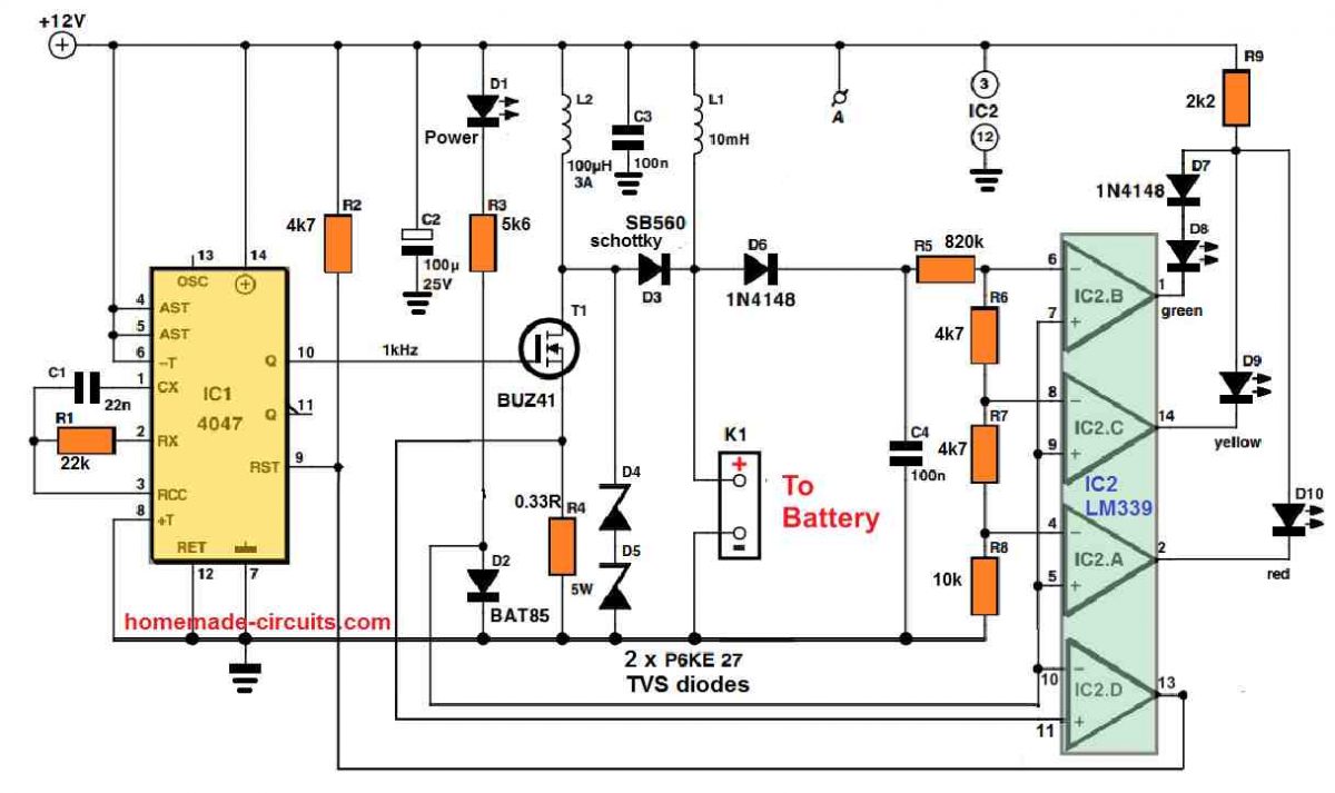 This technique, as much as recognized right now, is the best way to knock of undesirable build up of sulphate crystals and to bring back the battery plates into a good condition.
Because the voltage necessary for the high voltage pulses comes from the battery itself (this might appear a little bizarre initially, however the discharge of the battery is likewise a part of this technique), it is advised to hook up a charger in parallel with the battery and desulfator once the battery has not much capacity remaining.
This technique, as much as recognized right now, is the best way to knock of undesirable build up of sulphate crystals and to bring back the battery plates into a good condition.
Because the voltage necessary for the high voltage pulses comes from the battery itself (this might appear a little bizarre initially, however the discharge of the battery is likewise a part of this technique), it is advised to hook up a charger in parallel with the battery and desulfator once the battery has not much capacity remaining.
Pulse generator
It could be noticed in the circuit diagram that the parts needed for the desulphator tend to be extremely humble. The circuit consists of a couple of stages: a high voltage generator constructed using IC1, IC2d and T1, that generates the charging pulses, and an indicator circuit which involves not more than 3 op amps (IC2a, b, c) and three LEDs, that indicate exactly what condition the battery is in. LetˇŻs go through the pulse generator initially. Just like the other parts of the circuit, its supply voltage is obtained from the battery itself through K1. Although weˇŻre discussing the supply voltage, this must have a pretty consistent voltage and should be devoid of any spikes (except those produced by the circuit itself). Inductor L1 works like a suppressor, and is included in order to eliminate undesirable voltage spikes, along with C2 and C3 which work like smoothing capacitors. LED D1 illuminates as soon as the supply voltage is switched ON. To proceed with the pulse generator, IC1 (a 4047) produces a square wave having a frequency of 1 kHz and a duty cycle which typically is 50 PERCENT. When the Q output of IC1 turns high, FET T1 switches ON. This results in a (discharge) current to move through the battery by means of L2, that boosts linearly until the voltage across R4 is approximately 0.35 V; the current can now be around 1 A. At this instant comparator IC2d changes state, triggering IC1 to be reset and T1 to become switched off. The stashed magnetic energy inside L2 now gets converted to a voltage spike, which is inflicted to the battery through D3. How big the spike is can be determined by the condition of the battery. If the battery is in a decent condition and its internal resistance is rather small, in that case the spike voltage level may also be reduced (under 15 V). In case the battery has a high internal resistance then the peak level of the spike could be as huge as 50 V. Its highest magnitude will be restricted and equal to the value of the two series connected zener diodes, D4 and D5.LED Indicators
Considering that the health of the battery could be dependent on how big the charging pulses are, we have included a straightforward LED circuit which indicates the optimum value of the pulses. The 3 comparators IC2a-c evaluate the peak value inside C4 and changeover at voltages of 15, 20 and 30 V correspondingly. Therefore in case the battery is in a reasonably good shape, the green LED (D8) illuminates, with a under-performing battery, the yellow LED (D9) lights up, and with an incredibly bad battery the red LED (D10) glows. We have an information that needs to be pointed out regarding the indicator circuit: in order to prevent all three LEDs from illuminating simultaneously in response to a high peak voltage, they are attached in parallel to a single common series resistor (R9). Since the red LED carries a smaller voltage drop compared to yellow LED, they may in no way illuminate together. But the yellow and green LEDs have got a identical voltage drop, so a similar technique will not do the job here, which explains why the green LED comes with an normal diode (D7), hooked up in series with it. You will find three alternative methods through which the desulfator may be used. The first is to apply it within an existing system (inside a car as an example) to avoid sulphation from taking place inside a battery having minimum sulphation. The advanced desulfator circuit is built-in with the system by hooking it up straight to the battery using shortest possible cabling. Because the circuit could be kept connected forever, absolutely nothing more needs to be done. The current consumption is approximately 20 mA, therefore the battery might discharge in case it is not charged up from time to time. Recovery of batteries which have previously sulphated can be carried out in a couple of techniques. The first method would be to charge the battery, eliminate the charger and after that hook up the desulfator circuit. Since the power for the charging pulses is derived directly from the battery itself, it is going to gradually discharge. This technique needs to be observed carefully because a completely discharged battery must be recharged quickly. Most likely in real life many charge/discharge cycles will probably be necessary before a terribly sulphated battery could be restored to life. Since the approach described above needs a great deal of attention and has a danger that the battery could be left in a discharged condition unnecessarily (which can be extremely harmful to a lead acid battery!), another method can be perhaps much better. The battery is coupled to the desulfator circuit, using a trickle charger hooked up in parallel. This implies, no chargers must be integrated that supply a current of 7 A or higher, yet one that provides a optimum of 1 or 2 A. This could be left coupled to the battery endlessly with no issues.6 Useful DC Cell phone Charger Circuits Explained
A DC cell phone or mobile phone charger is a device which charges a cellphone from an available DC supply source. The device converts the unregulated DC source into a constant current and constant voltage output which becomes safe for any mobile phone charging. In this article we learn how to build DC to DC cell phone charger circuits using 6 unique concepts. The first concept concept uses the IC 7805, the second concept works with a single BJT, the third idea uses a IC M2575, in the fourth method we try LM338 IC, the 5th circuit shows how to charge multiple mobiles from a single source while the last or the 6th technique shows us how to use PWM for implementing an effective charging of a mobile phone. Warning: Although the concepts are all tested and technically correct, the author does not take any responsibility of the results, please do it at your own risk.Introduction
A simple DC cell phone charger circuit is one of those mates of cell phone that cannot be ignored because a cell phone would be dead without a charger. Normally a DC cell phone charger circuit come as anintegralpart of a cell phone package and we use it in conjunction with our AC mains supply. But what happens if your cell phone gasps for power in the middle of a journey, probably when you are driving or biking away on a middle of a highway?How it Functions
A very simple yet reasonably effective DC to DC cell phone charger circuit is discussed in this article, which can be easily built at home even by a layman. Though the proposed charger circuit won't charge your cell phone at the rate equal to a normal AC to DC charger, nevertheless it will complete the function without fail and won'tbetrayyou for sure. The proposed DC cellphone charger circuit can be understood with the followingpoints: We all know the general specs of acellphone battery, it's around 3.7 volts and 800 mAH. It means the cell phone would require at around 4.5 volts for initiating thechargingprocess. However a Li-Ion battery which is employed inside cell phones are pretty sensitive to bad voltages and may just blow off causing serious life and property issues. Keeping this in mind the cell phone internal circuitry is specifically dimensioned very strictly. The parameters just won't permit any voltage which may be even slightly out of the range of the battery specifications. The use of the versatile IC 7805 in the circuit answers the above issue just perfectly, such that the charging voltage at its output becomes ideally suitable for charging the cell phone battery. A high wattage resistor connected at the output of the IC makes sure that the current to the cell phone stays wellwithinthe specified range, though this might have not been a problem anyway, the cell phone would just refuse to charge if the resistor was not included.1) Circuit Diagram of the DC cellphone charger
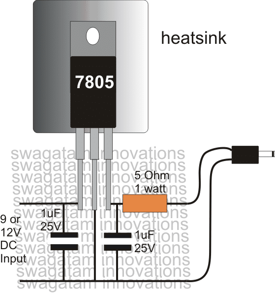
Pictorial Diagram
You can use this DC cellphone charger circuit for charging you cell phone during emergencies when there's no mains AC outlets, the circuit may be powered from any 12 volt leadacidbatteryor similar DC power sourceParts List
R1 = 5 Ohm, 2 Watt, C1, C2 = 10uF/ 25V, D1 = 1N4007, IC1 = 7805, mounted on a heatsink, Battery, any 12 volt automobile battery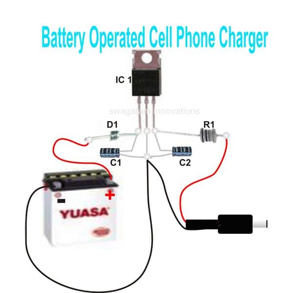
Using LM123/LM323
In the above concept a 7805 IC is used for charging, which can deliver a maximum of 1 amp. This current may not sufficient enough for charging smart phones, or cellphones with bigger mAH rating in the range of 4000 mAh. Since these high current batteries may require current up to 3 amps for charging at reasonably fast rate. A 7805 might be completely useless for such applications. However, the IC LM123 is one candidate which can fulfill the above requirement, by providing a precision 5 V output with a good 3 amp current. The input can be from any 12 V source such a car/motorcycle battery, or a solar panel. The simple 3 amp mobile phone charger diagram can be seen below: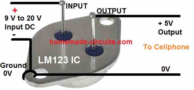 As can be seen above the 3 amp charger circuit requires no external components for implementing the procedures, and yet is extremely precise with its output voltage and current regulation, and is virtually nondestructive due to it many internal protection features.
2) DC Cell phone Charger using a Single Transistor
The next design explains a DC cell phone charger using a single BJT is probably the simplest in its forms and may be built very cheaply andusedfor charging any standard cell phone from a DC 12 volts external source.Circuit Operation
The circuit diagram illustrates a ratherstraightforwarddesign incorporating very few components for implementing the proposed cell phone charging actions. Here the main active part is an ordinary power transistor which has been configured with another active part, the zenet diode for forming a nice little DC to DC cell phone charger circuit. The resistor is the only passive component other than the above couple of active parts which has been associated in the circuit. So just three component is to be used and a full fledged cell phone charger circuit is ready within minutes. The resistor acts as the biasing component for the transistor and also acts as the "starter" for the transistor. The zener has been included to inhibit the transistor from conducting more than the specified voltage determined by the zener voltage. Though, a cell phone ideally requires just 4 volts for initiating the charging process, here the zener voltage and subsequently the output voltage has been fixed at 9V, because the current releasing ability of this circuit is not very efficient and presumably the power should be dropping to the required 4v level once the cell phone is connected at the output. However the current may be decreased or increased by suitably increasing or decreasing the value of the resistor respectively. If the cell phone "refuses" to get charged, the resistor value nay be increased a bit or a different higher value may be tried for making the cell phone respond positively. Kindly note that the circuit was designed by me based on assumptions only and the circuit has not been tested or confirmed practically.Circuit Diagram
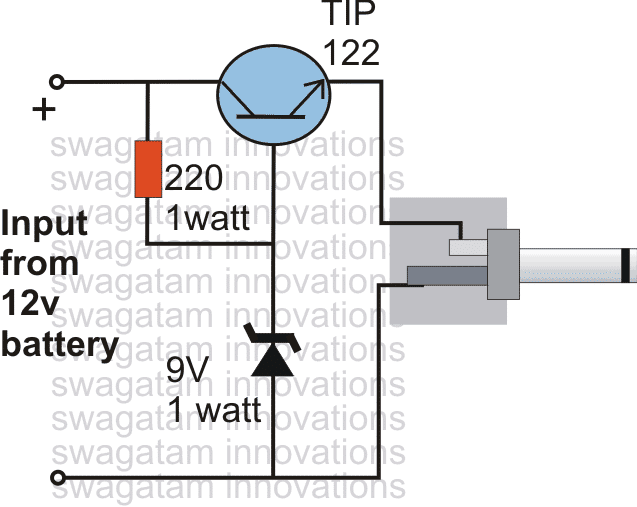
3) Using1-A Simple Step-Down Switching Voltage Regulator
If you are not satisfied with a linear regulator charger, then you can opt for this 1 A simple step-down switching voltage regulator based DC cell phone charger circuit which works with a switched buck converter principle which enables circuit to charge a cell phone with great efficiency.How it Works
In one of my previous posts we learned about the versatile voltage regulator IC LM2575 from TEXAS INSTRUMENTS. As can be seen, the diagram hardly utilizes any external components for making the circuit functional. A couple of capacitors a schottky diode and an inductor of all that is needed to make this DC to DC cell phone charger circuit. The output generates an accurate 5 volts which becomes very much suitable for charging a cell phone. The input voltage has a wide range, right from 7V to 60V, any level ma be applied which results the required 5 volts at the output. The inductor is introduced specifically for obtaining a pulsed output at around 52 kHz. Half of the energy from the inductor is used back for charging the cell phone ensuring that the IC remains switched only for half the charging cycle period. This keeps the IC cool and keeps it effectively in working even without using a heatsink. This ensures power saving as well as efficient functioning of the entire unit for the intended application. The input may be derived from any DC source like an automobile battery. Courtesy and Original Circuit:ti.com/lit/ds/symlink/lm2575.pdf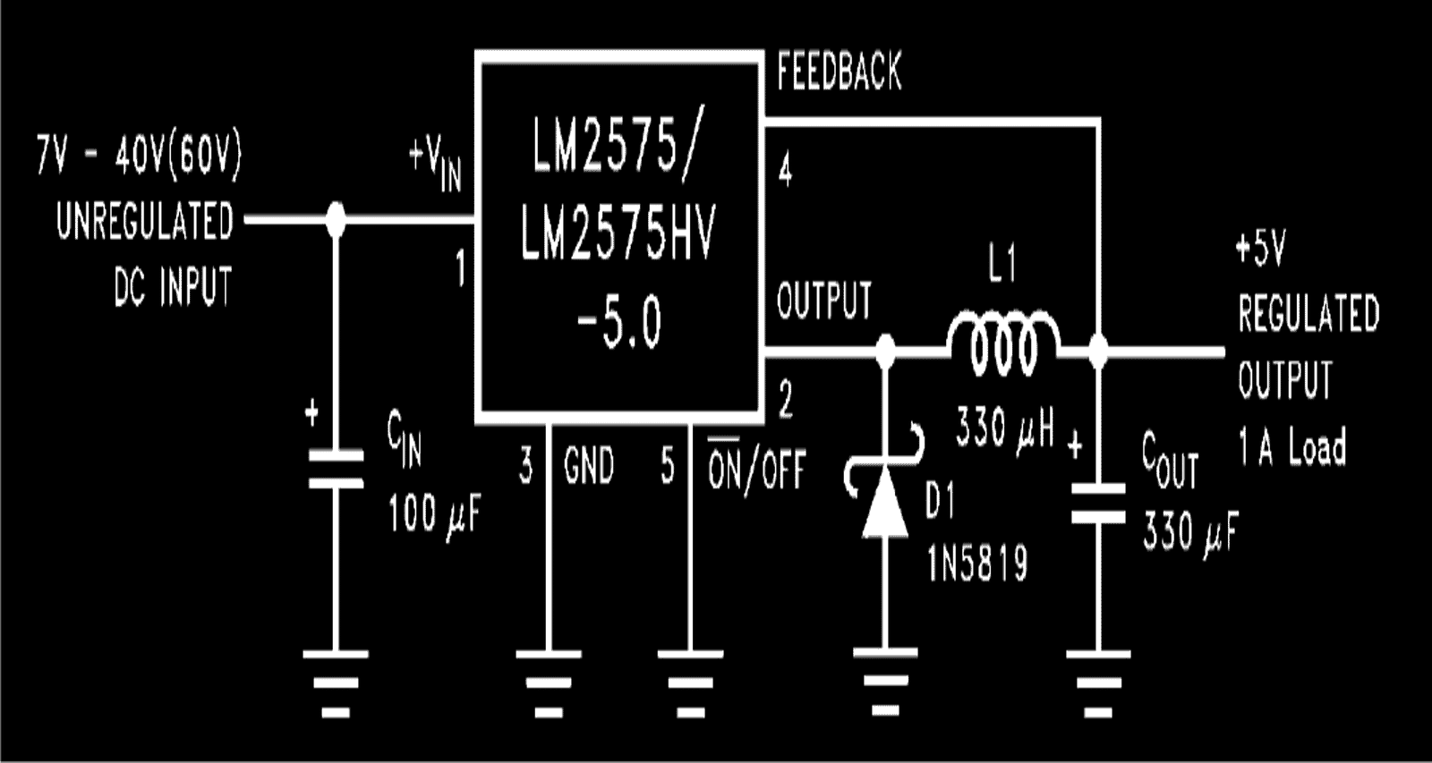
4) DC Double Cellphone Charger
A recent request from one of my followers Mr. Raja Gilse (via email), prompted me to design a DC double cellphone charger circuit that is able to facilitate charging of many cell phones simultaneously, let's learn how to make the circuit. I have already explained regarding a couple of DC to DC cellphone charging circuits, however all these are designed for charging a single cell phone. For charging more than one cell phone from an external DC source like an automobile battery, requires an elaborate circuit.Technical Specifications
Dear sir. Please tell me that what alterations should i do, to charge two mobiles at a time from your "12V BATTERY OPERATED CELL PHONE CHARGER CIRCUIT".(from bright hub) I am using the circuit from last 8 months, it's fine. Please post that article in your new blog also. Dear sir, i tried so many time to post this comment in your blog in the "simple dc to dc cell phone charger circuit" but in vain. Please answer here~ Sir, i used another 10 ohm 2 watt resistor in parallel with the existing one, as i donˇŻt have the higher watt resistor. ItˇŻs working fine. Thank you very much, i have one doubt, earlier, in bright hub in the same article you told to use 10 ohm resistor, but here it is 5 ohm which is suitable ? I have another question out of this article; please guide me could I use three 1N4007 silicon diode instead of one 1N5408 silicon diode? My aim is to allow 3A current in only one direction. But i donˇŻt have diode of 3A i.e. 1N5408. As 1N4007 is of 1 amps capacity could use three 1N4007 in parallel and like wise for 5A five 1N4007 in parallel, because i have number of 1N4007 rajagilseSolving the Circuit Request
Hi Rajagilse,Use the following DC double cellphone charger circuit given below: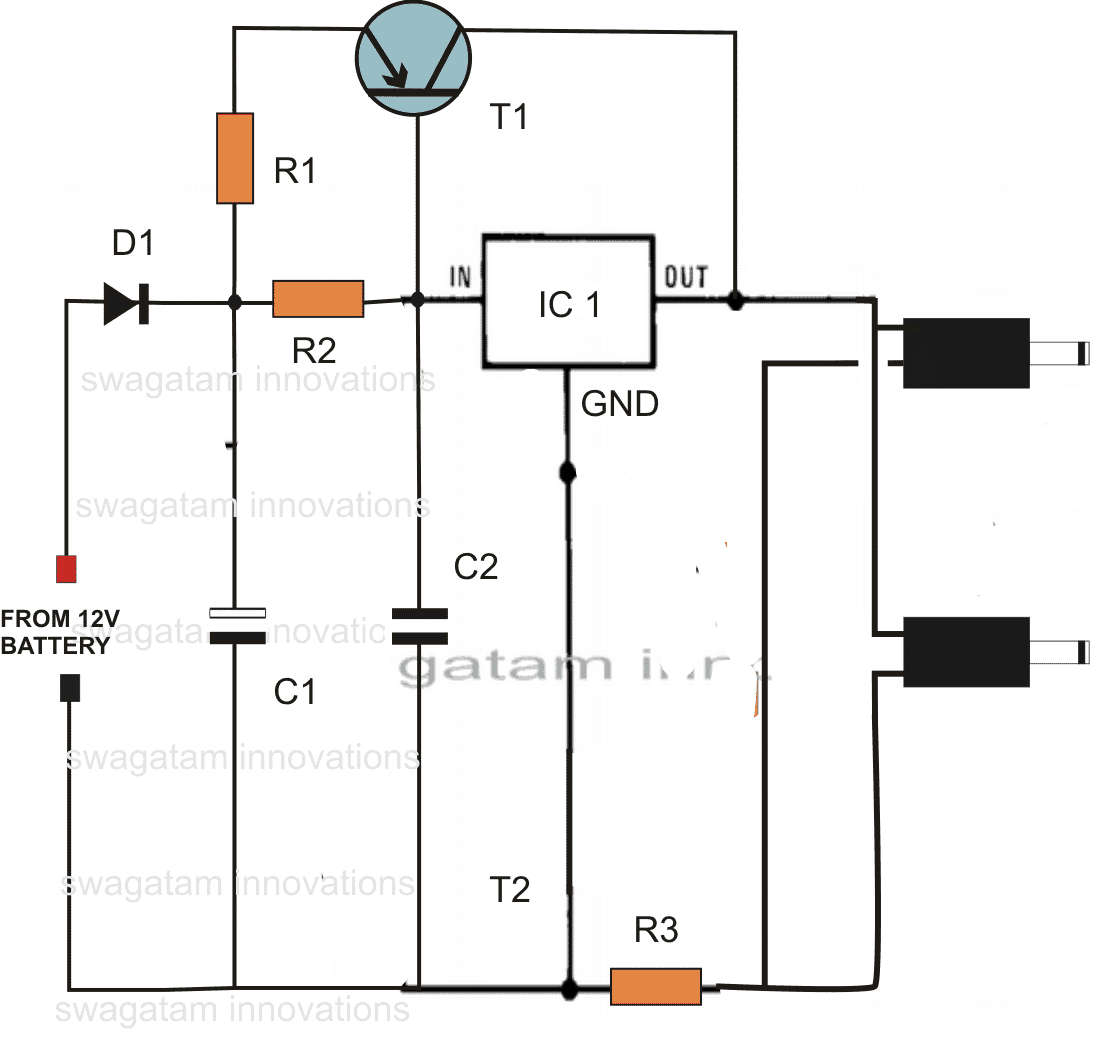 Hi Raja,
As you increase the limiting resistor value, the charging becomes slower, therefore a 5 Ohm resistor would charge the cell phone faster than a 10 Ohm, and so on.
I'll check the problem with the commenting in my blog...however other comments are coming normally as usual! Let's see.
Thanks and Regards.
Hi Raja,
As you increase the limiting resistor value, the charging becomes slower, therefore a 5 Ohm resistor would charge the cell phone faster than a 10 Ohm, and so on.
I'll check the problem with the commenting in my blog...however other comments are coming normally as usual! Let's see.
Thanks and Regards.
Parts List
R1 = 0.1 Ohms 2 watt, R2 = 2 Ohms 2 Watt R3 = 3 Ohms 1 watt C1 = 100uF/25V C2 = 0.1 discT1 = BD140 D1 = 1N5408 IC1 = 7805PCB Design
The circuit of the double DC cell phone charger was successfully tried and built by Mr. Ajay Dussa over a home designed PCB, the following images of the PCB layout and the prototype were sent by Mr. Ajay.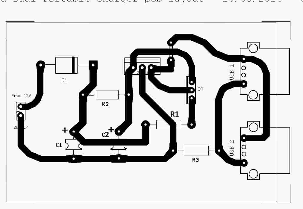
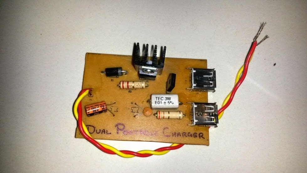
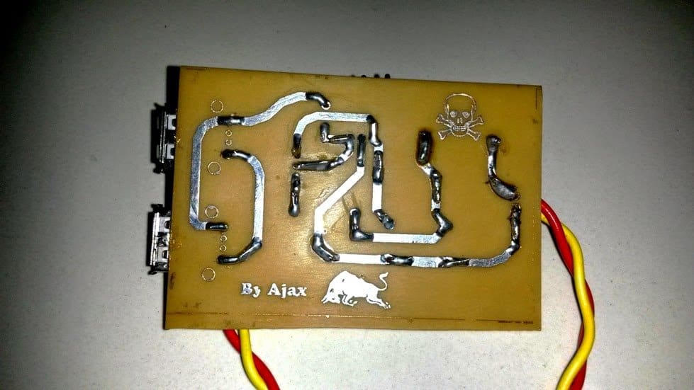
5) LM338 Based Cell Phone Charger Circuit
The following circuit can be used for charging as many as 5 cell phones at a time. The circuit employs the versatile IC LM338 for producing the required power. The input is selected to be a 6V but can be as high as 24V. A single cell phone can also be charged from this circuit.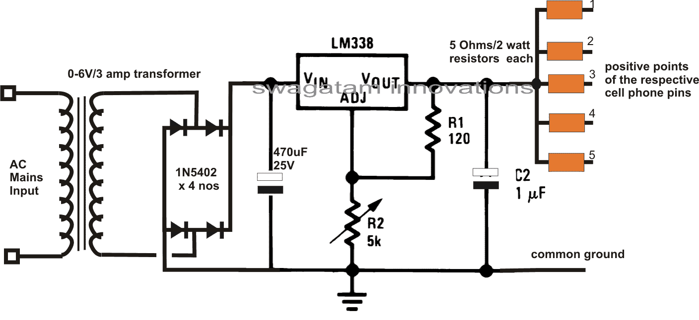
Multiple Cellphone Charger Circuit using IC 7805
Any desired number of cellphones can be charged by using IC 7805 in parallel as shown the following figure. Since the ICs are all mounted on the same heatsink the heat among them is uniformly shared ensuring a uniform charging across all the connected multiple cellphone devices. Here 5 ICs are used for charging by medium sized cellphones, more number of ICs could added to accommodate more number of cellphones in the charging array.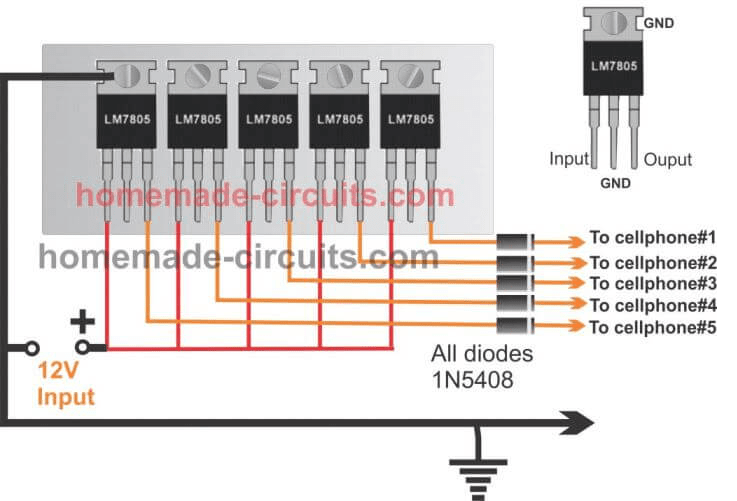
6) Using PWM For Charging Cellphone Battery
This circuit can be easily made at home by any school kid and used for displaying in his science fair exhibition. The circuit is a simple cell phone charger that may be operated in conjunction with any DC source, from a car or a motorcycle battery or from any ordinary 12 V AC DC adapter. Nowadays we find most of the vehicles have their in built cell phone battery charger units which surely becomes very handy for travelers who mostly remain outdoors travelling in their vehicle. The proposed cell phone charger circuit is as good as the conventional chargers which come fitted inside the cars and bikes. Moreover the circuit can be simply integrated to ones own vehicle if the feature is not originally available in the vehicle. Alternatively one may think of manufacturing the present unit and selling them in the market as an automobile cell phone charger and earn some hard bucks.Circuit Operation
Cell phones as we all know are highly sophisticated gadgets by nature and when it comes to charging cell phones the parameters no doubt also needs to be of very high standards. The AC/DC cell phone chargers which come with the cell phones are all SMPS based and are extremely good with their outputs and thatˇŻs why the cell phone gets so efficiently charged by them. However if we try to make our own version, it may fail altogether and the cell phones may just not respond to the current and display a ˇ°not chargingˇ± on the screen. Cell phone battery cannot just be charged by supplying DC 4 volts, unless the current is optimally dimensioned the charging wonˇŻt initiate.PWM vs Linear
Using voltage regulator IC for making a DC to DC charger, which I have discussed in one of my earlier article is a good approach, but the IC tends to become too hot while charging the cell phone battery and therefore requires adequate heatsinking for remaining cool and operative. This makes the unit a bit bulkier and moreover some significant amount of power is wasted in the form of heat, so the design cannot be considered very efficient. The present PWM controlled DC to DC cell phone charger circuit is outstanding in its respect because, the involvement of PWM pulses helps to keep the output very suitable to the cell phone circuitry and also the concept involves no heating of the output device, making the entire circuit truly efficient. Looking at the circuit we find that again the work horse IC 555 comes to our rescue and performs the important function of generating the required PWM pulses. The input to the circuit is supplied through some standard DC source, ideally from an automobile battery. The voltage powers the IC which instantly starts generating the PWM pulses and feeds it to the components connected at its output pin #3. At the output the power transistor is used for switching the DC voltage at its collector directly to the cell phone. However only the average DC voltage is finally fed to the cell phone due to the presence of the 10uF capacitor, which effectively filters the pulsating current and provides a stable, standard 4 volts to the cell phone. After the circuit is built, the given pot will need to be optimized perfectly so that a well dimensioned voltage is produced at the output which may be ideally suited for charging the cell phone.Circuit Diagram
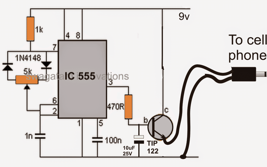
12V Battery Charger Circuits [using LM317, LM338, L200, Transistors]
In this article we will be discussing a list of simple 12V battery charger circuits which are very easy and cheap by its design yet extremely accurate with its output voltage and current specs. All the designs presented here are current controlled meaning their outputs will never go beyond a predetermined fixed current level. UPDATE: Looking for a high current battery charger? These powerful Lead Acid battery charger designs might help you to fulfill your requirement.Simplest 12 V Battery Charger
As I have reiterated in many articles, the main criteria to charge a battery safely is to keep the maximum input voltage slightly below the full charge spec of the battery, and keep the current at a level that does not cause warming of the battery. If these two conditions are maintained you can charge any battery using a minimal circuit as simple as the following one: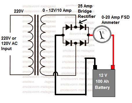 In the above simplest layout the 12 V is the RMS output of the transformer.
That means, the peak voltage after rectification will be 12 x 1.41 = 16.92 V.
Although this looks higher than the 14 V full-charge level of the 12 V battery, the battery is not actually harmed due to the low current specification of the transformer.
That said, it is advisable to remove the battery as soon as the ammeter reads near zero volts.
Auto Shut-OFF: If you want to make the above design to auto shut off when the full charge level is reached, you can easily accomplish this by adding a BJT stage with the output as shown below:
In the above simplest layout the 12 V is the RMS output of the transformer.
That means, the peak voltage after rectification will be 12 x 1.41 = 16.92 V.
Although this looks higher than the 14 V full-charge level of the 12 V battery, the battery is not actually harmed due to the low current specification of the transformer.
That said, it is advisable to remove the battery as soon as the ammeter reads near zero volts.
Auto Shut-OFF: If you want to make the above design to auto shut off when the full charge level is reached, you can easily accomplish this by adding a BJT stage with the output as shown below:
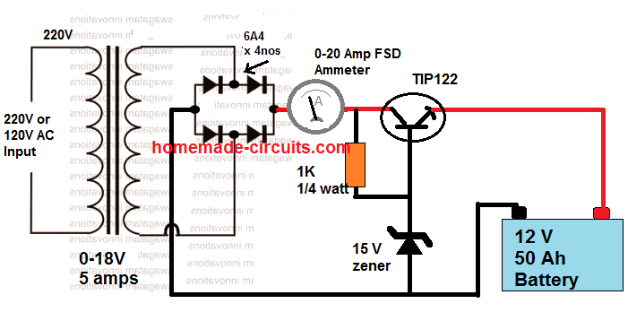 In this design, we have used a common emitter BJT stage which has its base clamped at 15 V, which means that the emitter voltage can never go beyond 14 V.
And when the battery terminals tend to reach above the 14 V level, the BJT gets reversed biased and simply goes into an auto shut down mode.
You can tweak the 15V zener value until you have around 14.3 V at the output for the battery.
This transforms the first design into a fully automatic 12 V charger system, which is simple to build yet entirely safe.
Also, since there's no filter capacitor the 16 V is not applied as a continuous DC, rather as 100 Hz ON/OFF switching.
This causes less stress on the battery, and also prevents sulfation of the battery plates.
In this design, we have used a common emitter BJT stage which has its base clamped at 15 V, which means that the emitter voltage can never go beyond 14 V.
And when the battery terminals tend to reach above the 14 V level, the BJT gets reversed biased and simply goes into an auto shut down mode.
You can tweak the 15V zener value until you have around 14.3 V at the output for the battery.
This transforms the first design into a fully automatic 12 V charger system, which is simple to build yet entirely safe.
Also, since there's no filter capacitor the 16 V is not applied as a continuous DC, rather as 100 Hz ON/OFF switching.
This causes less stress on the battery, and also prevents sulfation of the battery plates.
Why Current Control is Important (Constant Current Setup)
Charging any form of chargeable battery can be critical and involves some attention to be paid. When the input current at which the battery is being charged is significantly high, adding a current control becomes an important factor. We all know how smart the IC LM317 is and itˇŻs no surprise why this device finds so many applications requiring precise power control. The Current Controlled 12V Battery Charger Circuit Using IC LM317 presented here shows how the IC LM317 can be configured using just a couple resistors and an ordinary transformer bridge power supply for charging a 12 volt battery with utmost accuracy.How it Works
The IC is basically wired in its usual mode where R1 and R2 are included for the required voltage adjustment purpose. The input power to the IC is fed from an ordinary transformer/diode bridge network; the voltage is around 14 volts after the filtration via C1. The filtered 14 V DC is applied to the input pin of the IC. The ADJ pin of the IC is fixed to the junction of the resistor R1 and the variable resistor R2. R2 can be fine set for aligning the final output voltage with the battery. Without the inclusion of Rc, the circuit would behave like a simple LM 317 power supply where the current wouldn't be sensed and controlled. However with Rc along with BC547 transistor placed in the circuit at the shown position makes it capable of sensing the current thatˇŻs being delivered to the battery. As long as this current is within the desired safe range, the voltage remains at the specified level, however if the current tends to rise, the voltage is withdrawn by the IC and dropped, restricting the current rise any further and ensuring appropriate safety for the battery.The formula for calculating Rc is:
R = 0.6/I, where I is the maximum desired output current limit. The IC will require a heatsink for operating optimally. The connected ammeter is used for monitoring the charge condition of the battery. Once the ammeter shows zero voltage, the battery may be detached from the charger for the intended use.Circuit Diagram #1
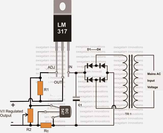
Parts List
The following parts will be required for making the above explained circuit R1 = 240 Ohms, R2 = 10k preset. C1 = 1000uF/25V, Diodes = 1N4007, TR1 = 0-14V, 1AmpHow to Connect pot with LM317 or LM338 Circuit
The following image shows how the 3 pins of a pot needs to be correctly configured or wired with any LM317 voltage regulator circuit or a LM338 voltage regulator circuit: As can be seen the center pin and any one of the outer pins is selected for connecting the potentiometer or the pot with the circuit, the third unconnected pin is kept unused.Circuit Diagram #2
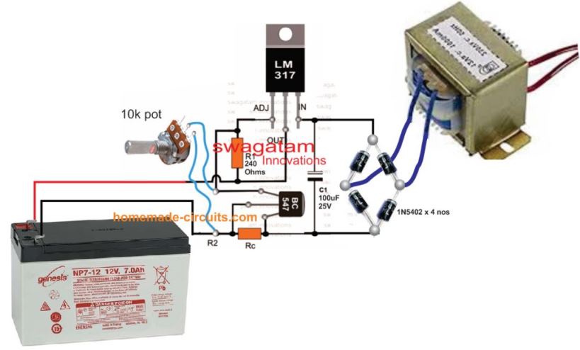
Adjustable High Current LM317 Battery Charger Circuit #3
For upgrading the above circuit into a variable high current LM317 battery charger circuit, the following modifications can be implemented: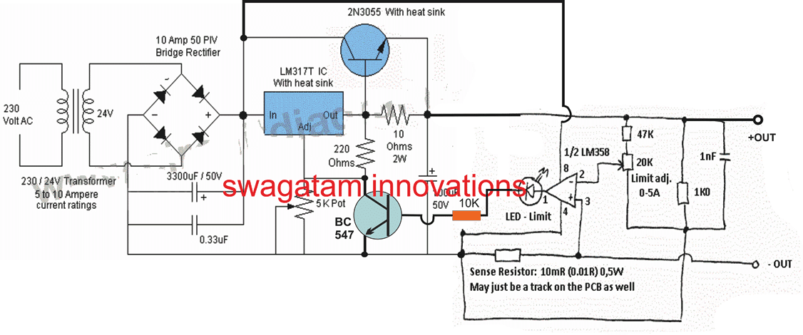
Adjustable Current Charger Circuit #4
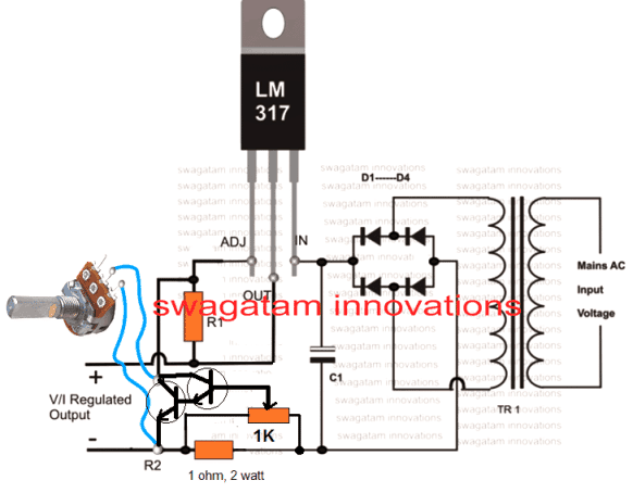
5) Compact 12 volt Battery Charger Circuit Using IC LM 338
The IC LM338 is an outstanding device which can be used for unlimited number of potential electronic circuit applications. Here we use it to make an automatic 12V battery charger circuit.Why LM338 IC
Basically the main function of this IC is voltage control and can also be wired for controlling currents through some simple modifications. Battery charger circuit applications are ideally suited with this IC and we are going to study one example circuits for making a 12 volt automatic battery charger circuit using the IC LM338. Referring to the circuit diagram we see that the entire circuit is wired around the IC LM301, which forms the control circuit for executing the trip off actions. The IC LM338 is configured as the current controller and as the circuit breaker module.Using LM338 as a Regulator and Opamp as the Comparator
The whole operation can be analyzed trough the following points:The IC LM 301 is wired as a comparator with its non inverting input clamped to a fixed reference point derived from a potential divider network made from R2 and R3. The potential acquired from the junction of R3 and R4 is used for setting the output voltage of the IC LM338 to a level thatˇŻs a shade higher than the required charging voltage, to about 14 volts. This voltage is fed to the battery under charger via the resistor R6 which is included here in the form of a current sensor. The 500 Ohm resistor connected across the input and the output pins of the IC LM338 makes sure that even after the circuit is automatically switched OFF, the battery is trickle charged as long as it remains connected to the circuit output. The start button is used to initiate the charging process after a partially discharged battery is connected to the output of the circuit. R6 may be selected appropriately for acquiring different charging rates depending upon the battery AH.Circuit Functioning Details (As Explained By +ElectronLover)
" As soon as the connected battery is charged fully, the potential at the inverting input of the opamp becomes higher than the set voltage at non-inverting input of the IC. This instantly switches the output of the opamp to logic low." According to my assumption: V+ = VCC - 74mV V- = VCC - Icharging x R6 VCC= Voltage on pin 7 of Opamp. When The battery charges fully Icharging reduces. V- become greater than V+, output of the Opamp goes low, Turning on the PNP and LED. Also, R4 gets a ground connection through the diode. R4 becomes parallel to R1 reducing the effective resistance seen from the pin ADJ of LM338 to GND. Vout(LM338) = 1.2+1.2 x Reff/(R2+R3), Reff is the Resistance of pin ADJ to GND. When the Reff reduces the output of LM338 reduces and inhibit charging.Circuit Diagram
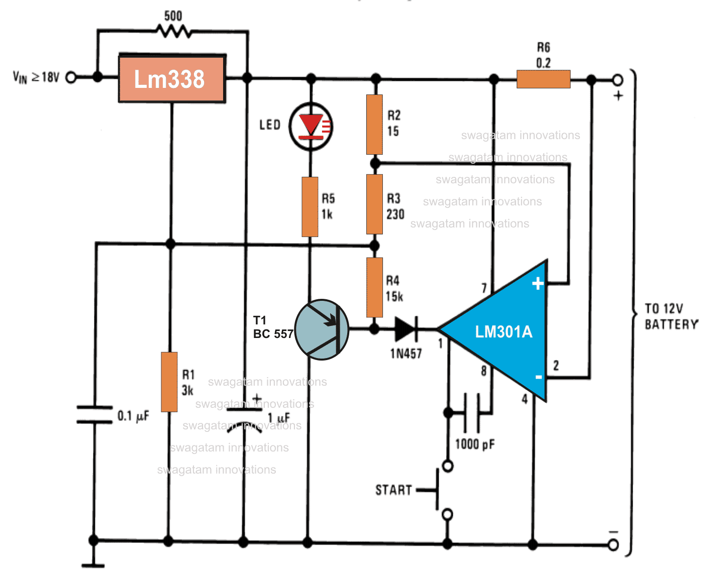
6) 12V Charger Using IC L200
Are you looking for a constant current charger circuit to facilitate a safe charging battery? The 5th simple circuit presented here using the IC L200 will simply show you how to build a constant current battery charger unit.Importance of Constant Current
A constant current charger is highly recommended as far as maintaining safety and long battery life is concerned. Using the IC L200, a simple yet a very useful and powerful automobile battery charger providing constant current output can be built. I have already discussed many useful battery charger circuits through my previous articles, some being too accurate and some much simpler in design. Although the main criteria involved with charging batteries largely depends on the type of the battery, but basically itˇŻs the voltage and the current which particularly needs appropriate dimensioning to ensure an effective and safe charging of any battery. In this article we discuss a battery charger circuit suitable for charging automobile batteries equipped with visual reverse polarity and full-charge indicators. The circuit incorporates the versatile but not so popular voltage regulator IC L200 along with a few external complementing passive components to form a full fledged battery charger circuit. LetˇŻs learn more about this constant current charger circuit.Circuit diagram using L200 IC
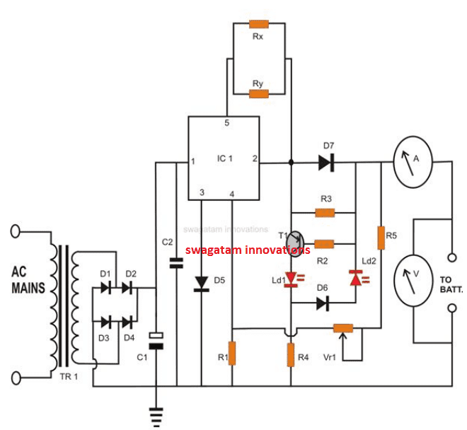
Circuit Operation
The IC L200 produces a good voltage regulation and therefore ensures a safe and a constant current charging, a must for any kind of chargeable battery. Referring to the figure, the input supply is acquired from a standard transformer/bridge configuration, C1 forms the main filter capacitor and C2 being responsible for grounding any left residual AC. The charging voltage is set by adjusting the variable resistor VR1, with no load connected at the output. The circuit includes a reverse polarity indicator using LED LD1. Once the connected battery becomes fully charged i.e. when its voltage becomes to the set voltage, the IC restricts the charging current and stops the battery from over charging. The above situation also reduces the positive biasing of T1 and creates a potential difference of above -0.6 volts, so that it starts conducting and switches LD2 ON, indicating that the battery has reached its full charge and may be removed from the charger. The resistors Rx and Ry are the current limiting resistors required to fix or determine the maximum charging current or the rate at which the battery needs to be charged. It is calculated using the formula:I = 0.45 (Rx + Ry) / Rx.Ry.
The IC L200 may be mounted on a suitable heatsink to facilitate consistent charging of the battery; however the built-in protection circuitry of the IC virtually never allows the IC to get damaged. It typically includes built-in thermal run away, output short circuit and over load protections. Diode D5 ensures that the IC doesnˇŻt get damaged in case the battery accidentally gets wrongly connected with reverse polarities at the output. Diode D7 is included to restrict the connected battery from getting discharged through the IC in case the system is switched OFF without disconnecting the battery. You may quite easily modify this constant current charger circuit to make it compatible with the charging of a 6 Volt battery by doing the simple changes in the value of a few resistors. Please refer the parts list to get the required info.Parts list
R1 = 1K R2 =100E, R3 = 47E, R4 = 1K R5 = 2K2, VR1 = 1K, D1ˇŞD4 AND D7 = 1N5408, D5, D6 = 1N4148, LEDS = RED 5mm, C1 = 2200uF/ 25V, C2 = 1uF/25V, T1 = 8550, IC1 = L200 (TO-3 Package) A = Ammeter, 0-5amp, FSDV =Voltmeter, 0-12Volt FSD TR1 = 0 - 24V, current = 1/10 of the battery AHHow to Set up the CC Charger Circuit
The circuit is set up in the following manner: Connect a variable power supply to the circuit. Set the voltage close to the upper threshold volt level. Adjust the preset so that the relay remains activated at this voltage. Now raise the voltage slightly more to upper threshold volt level and again adjust the preset such that the relay just trips off. The circuit is set, and can be used normally using a fixed 48 volts input for charging the desired battery. A request from one of my followers: Hi Swagatam, I got your email from a website www.brighthub.com where you shared your expertise with regards to construction of a battery charger. Please i have a little problem that i hope you could help me out: I am just a layman with no much knowledge of electronics. I have been using a 3000w inverter and recently i discovered it doesnt charge the battery (but inverts). We have no much experts around here and for fear of further damaging it, i decided to get a separate charger to charge the battery. My question is: the charger i got has an output of 12volts 6Amps will that charge my dry-cell battery with 200ahs capacity? If yes, how long will it take to full and if no, what charger capacity do i get to serve that purpose? I have had experience in the past where a charger damaged my battery and i dont want to risk that this time. Many thanks. Habu MaksMy Answer to Mr. Habu
Hi Habu, The charging current of a charger should be ideally rated at 1/10 of the battery AH. That means for your 200 Ah battery the charger must be rated at around 20 Amps. At this rate the battery will take around 10 to 12 hours for getting fully charged. With a 6 amp charger it may take ages for your battery to get charged, or simply the charging process might fail to initiate. Thanks and Regards.7) Simple 12V Battery Charger Circuit with 4 LED Indicator
A current controlled automatic 12V battery charger circuit with 4 LED indicators can be learned in the following post. The design also includes a 4 level charging status indicator using LEDs.Battery Charger with 4 LED Status Indicator
I would like to ask and look forward to you to be made Automatic cellphone charger circuit 5 Volt and Battery Charger Circuit 12 V (in the schematic circuit and the first transformer CT) automatic / cut off by using a battery indicator and LED lights red as an indicator were charging (Charging On Indicator) using IC LM 324, and LM 317 and a full battery using a green LED and breaking electrical current when the battery is full. For cellphone charger circuit 5 Volt I want to have levels of the following indicators: 0-25% battery is in the charger using a red LED.25-50% using a blue LED (red LED goes out)55-75% using a yellow LED (LED red, blue outages)75-100% using a green LED (LED red, blue, yellow outages) next to Battery Charger Circuit 12 V I want to use the 5 LED lights as follows:0-25% using a red LED25-50% using orange LED (red LED goes out)50-75% using a yellow LED (LED red, orange outages)75-100% using a blue LED (Led red, orange, yellow outages)more than 100% using the green LED (LED red, orange, yellow, blue outages). I hope you, the components are common and accessible and made a circuit schematic above as soon as possible because I really need schematics details. I hope you will help me to find a better solution.The Design
The requested design make use of 4 level status indicator and can be witnessed below.The TIP122 controls over-discharge of the battery while the TIP127 ensures an instant supply cut-of for the battery, whenever an overcharge limit is reached for the battery. The SPDT switch can be used to select the battery charging either from a mains adapter or from a renewable energy source such as a solar panel.Circuit Diagram
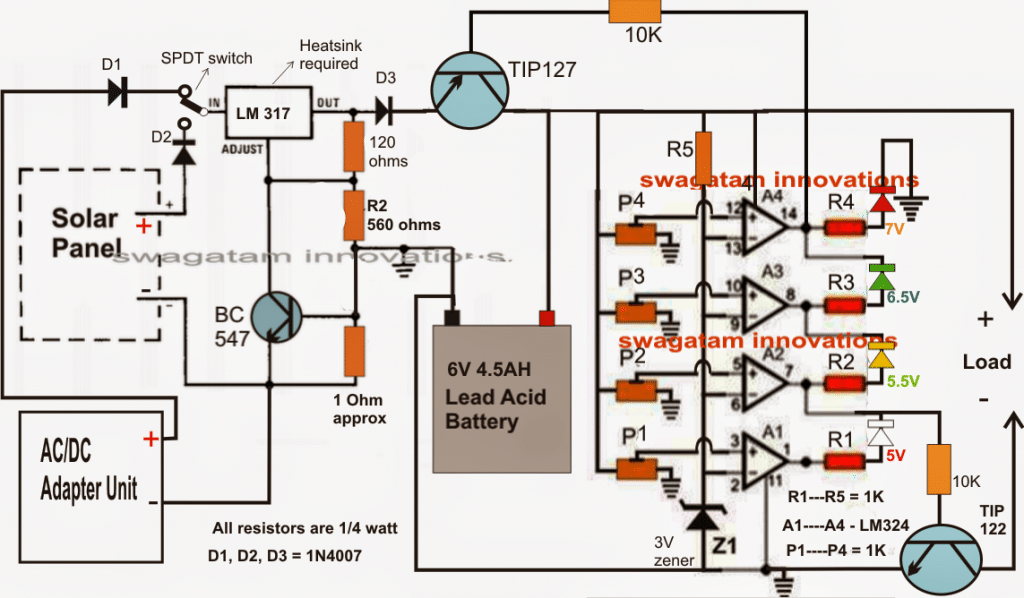 UPDATE:
The following tested 12V charger circuit schematic was sent to be by "Ali Solar" with a request to share it in this post:
UPDATE:
The following tested 12V charger circuit schematic was sent to be by "Ali Solar" with a request to share it in this post:
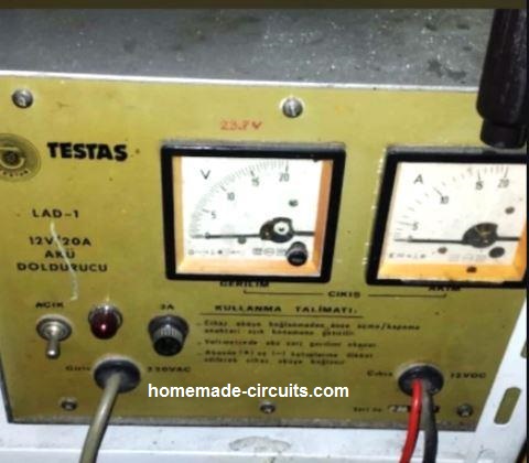
Smart 12V Battery Charger Circuits
The following automatic 12V smart battery charger circuit was exclusivelydesigned by me in response to requests from two keen readers of this blog, Mr. Vinod and Mr.Sandy. Let's hear what Mr.Vinod discussed with me through emails regarding the making of a smart battery charger circuit:8) Discussing a Personal 12V Battery Charger The Design
"Hi Swagatam, My name is vinod chandran. Professionally i am a dubbing artist in malayalam film industry but i am an electronic enthusiast too. I am a regular visitor of your blog. Now i need your help. I just built an automatic SLA battery charger but there is some problems with that. I am attaching the circuit with this mail. The red LED in circuit is supposed to glow when battery is full but it glows all the time .(my battery shows only 12.6v). Another problem is with 10k pot. there is no difference when i turn the pot left and right. . So i request you to either correct these problems or help me to find an automatic charger circuit which gives me a visual or audio alert when battery is full and low . As a hobbyist i used to make things from old electronic appliances. For the battery charger i have some components. 1. Transformer from an old vcd player. out put of 22v, 12v,3.3v. And i don't know how to measure ampere. My DMM has only the ability to check 200mA. It has a 10A port but i can't measure any ampere with that.(meter shows "1") So i assumed that the transformer is above 1A and below 2A with the size and requirements of the vcd player. 2. Another transformer -12-0-12 5A 3. Another transformer - 12v 1A 4. Transformer from my old ups(Numeric 600exv). Is this transformer's input is regulated AC ? 5. couple of LM 317's 6. SLA battery from old ups- 12v 7Ah. (Now it has a 12.8v charge) 7. SLA battery from old 40w inverter - 12v 7Ah. ( the charge is 3.1v) One thing i forgot to tell you. After the first charger circuit, i made another one (i'll attach this too). This is not an automatic one but it is working. And i need to measure the ampere of this charger. For that purpose i googled for an animated circuit simulation software but didn't get one yet. But i can't draw my circuit in that tool. there is no parts like LM317 and LM431(variable shunt regulator). not even a potetiometer or led. So i request you to help me to find a visual circuit simulation tool. I hope you will help me. regards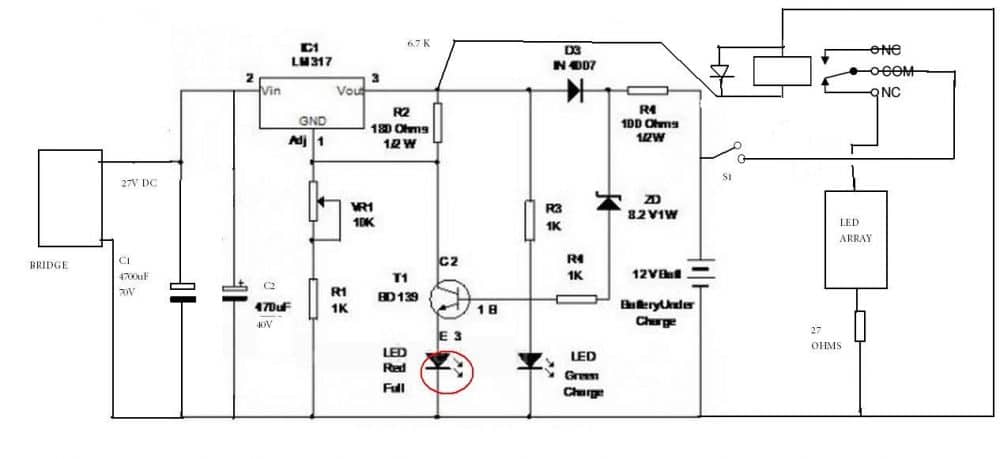
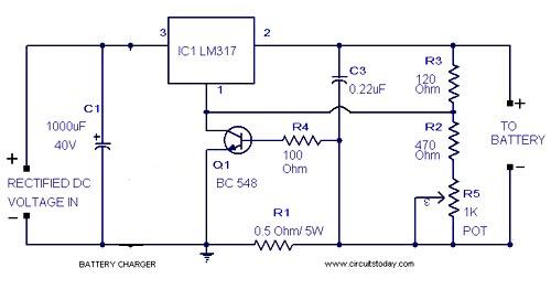 Hi Vinod, The red LED should not glow all the time and turning the pot should change > the output voltage, without the battery connected.
You can do the following things: > > Remove the 1K resistor in series with the 10K pot and connect the pot's relevant terminal directly to ground.
Connect a 1K pot across the base of the transistor and ground (use center and any one of the other terminals of the pot).
Remove everything that's presented at the right side of the battery in the diagram, I mean the relay and all.....
Hopefully with the above changes, you should be able to adjust the voltage and also adjust the base transistor pot for making the LED glow only after the battery is fully charged, at around 14V.
I don't trust and use simulators, I believe in practical tests, which is the best method of verifying.
For 12v 7.5 ah battery, use a 0-24V 2amp transformer, adjust the output voltage of the above circuit to 14.2 vollts.
Adjust the base transistor pot such that the LED just starts to glow at 14V.
Do these adjustents without the battery connected at the output.
The second circuit is also good but is not automatic....is current controlled, though.
Let me know your thoughts.
Thanks, Swagatam
Hi Swagatam,
First of all let me say thank you for your fast replying.
I will try your suggestions.
before that i need to confirm the changes you mentioned.
I will attach an image consisting your suggestions.
So please confirm the changes in the circuit.
-vinod chandran
Hi Vinod, The red LED should not glow all the time and turning the pot should change > the output voltage, without the battery connected.
You can do the following things: > > Remove the 1K resistor in series with the 10K pot and connect the pot's relevant terminal directly to ground.
Connect a 1K pot across the base of the transistor and ground (use center and any one of the other terminals of the pot).
Remove everything that's presented at the right side of the battery in the diagram, I mean the relay and all.....
Hopefully with the above changes, you should be able to adjust the voltage and also adjust the base transistor pot for making the LED glow only after the battery is fully charged, at around 14V.
I don't trust and use simulators, I believe in practical tests, which is the best method of verifying.
For 12v 7.5 ah battery, use a 0-24V 2amp transformer, adjust the output voltage of the above circuit to 14.2 vollts.
Adjust the base transistor pot such that the LED just starts to glow at 14V.
Do these adjustents without the battery connected at the output.
The second circuit is also good but is not automatic....is current controlled, though.
Let me know your thoughts.
Thanks, Swagatam
Hi Swagatam,
First of all let me say thank you for your fast replying.
I will try your suggestions.
before that i need to confirm the changes you mentioned.
I will attach an image consisting your suggestions.
So please confirm the changes in the circuit.
-vinod chandran
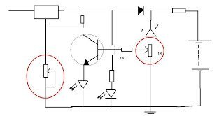 Hi Vinod,
That's perfect.
Adjust the transistor base preset until the LED just starts glowing dimly at around 14 volts, with no battery connected.
Regards.
Hi Swagatam Your Idea is great.
The charger is working and now one LED is glowing to indicate the charging is in progress.
but how can i configure the charge full indicator LED.
When i turn the pot to ground side (means lower resistance) LED starts glowing.
when resistance goes high LED will be off.
After 4 hours of charging my battery shows 13.00v.
But that charge full LED is off now.
Plz help me.
I am sorry disturb you again.
The last email was a mistake.
i didn't see your suggestion correctly.
So please ignore that mail.
Now i adust the 10k pot to 14.3v(it's quite difficult to adjust the pot, because a slight variation will result a bigger voltage output.
).
And i adjust the 1k pot to glow a little.
Is this charger supposed to indicate a 14v battery?.
After all let me know the danger level full charge of the battery.
As you suggested, everything was alright when i test the circuit from breadboard.
But after solder into PCB thing are happening strangely.
The red LED is not working.
charging voltage is ok.
Anyway i am attaching the image that shows the present condition of the circuit.
plz help me.
After all let me ask you one thing.
Could you please give me an automatic charger circuit with a battery full indicator.
?.
Hi swagatam, Actually i am in the middle of your automatic charger with hysteresis feature.
I just added a few modifications .
i will attach the circuit with this mail.
plz check this out.
If this circuit is not ok then i can wait for you to tomorrow .
Hi Vinod,
That's perfect.
Adjust the transistor base preset until the LED just starts glowing dimly at around 14 volts, with no battery connected.
Regards.
Hi Swagatam Your Idea is great.
The charger is working and now one LED is glowing to indicate the charging is in progress.
but how can i configure the charge full indicator LED.
When i turn the pot to ground side (means lower resistance) LED starts glowing.
when resistance goes high LED will be off.
After 4 hours of charging my battery shows 13.00v.
But that charge full LED is off now.
Plz help me.
I am sorry disturb you again.
The last email was a mistake.
i didn't see your suggestion correctly.
So please ignore that mail.
Now i adust the 10k pot to 14.3v(it's quite difficult to adjust the pot, because a slight variation will result a bigger voltage output.
).
And i adjust the 1k pot to glow a little.
Is this charger supposed to indicate a 14v battery?.
After all let me know the danger level full charge of the battery.
As you suggested, everything was alright when i test the circuit from breadboard.
But after solder into PCB thing are happening strangely.
The red LED is not working.
charging voltage is ok.
Anyway i am attaching the image that shows the present condition of the circuit.
plz help me.
After all let me ask you one thing.
Could you please give me an automatic charger circuit with a battery full indicator.
?.
Hi swagatam, Actually i am in the middle of your automatic charger with hysteresis feature.
I just added a few modifications .
i will attach the circuit with this mail.
plz check this out.
If this circuit is not ok then i can wait for you to tomorrow .
Simple Circuit Diagram #8
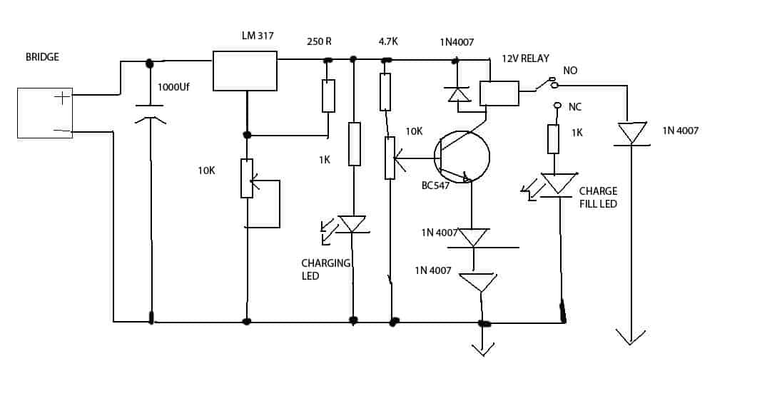 I forgot to ask one thing.
My transformer is about 1 - 2 A.
I don't know what is the correct.
how can i test with my multimeter?.
Besides if it is a 1A or 2A transformer, how can i reduce the current
to 700mA.
regards
Hi Vinod, The circuit is OK, but won't be accurate, will give you a lot of trouble > while adjusting.
A 1 amp transformer would provide 1amp when short circuited (check by connecting the meter prods to the supply wires at 10amp range and set to either DC or AC depending upon the output).
Meaning the maximum power of is 1 amp at zero volts.
You may use it freely with a 7.5 Ah battery, it won't do any harm, as the voltage would drop to the battery voltage level at 700 ma current and the battery would get safely charged.
But remember to disconnect the battery when the voltage reaches 14 volts.
Anyway, a current control facility would be added in the circuit that I would be providing you, so there's nothing to worry
Regards.
I'll provide you with a perfect and easy automatic circuit, please wait until tomorrow.
Hi swagatam,
I hope you will help me to find a better solution.
Thank you.
regards
vinod chandran
In the meantime, another keen follower of this blog Mr.Sandy also requested a similar 12V smart battery charger circuit through comments.
So finally I designed the circuit which will hopefully satisfy the needs of Mr.Vinod and Mr.Sandy for the intended purpose.
The following 9th figure shows an automatic 3 to 18 volts, voltage controlled, current controlled, double stage battery charger circuit with standby charging feature.
I forgot to ask one thing.
My transformer is about 1 - 2 A.
I don't know what is the correct.
how can i test with my multimeter?.
Besides if it is a 1A or 2A transformer, how can i reduce the current
to 700mA.
regards
Hi Vinod, The circuit is OK, but won't be accurate, will give you a lot of trouble > while adjusting.
A 1 amp transformer would provide 1amp when short circuited (check by connecting the meter prods to the supply wires at 10amp range and set to either DC or AC depending upon the output).
Meaning the maximum power of is 1 amp at zero volts.
You may use it freely with a 7.5 Ah battery, it won't do any harm, as the voltage would drop to the battery voltage level at 700 ma current and the battery would get safely charged.
But remember to disconnect the battery when the voltage reaches 14 volts.
Anyway, a current control facility would be added in the circuit that I would be providing you, so there's nothing to worry
Regards.
I'll provide you with a perfect and easy automatic circuit, please wait until tomorrow.
Hi swagatam,
I hope you will help me to find a better solution.
Thank you.
regards
vinod chandran
In the meantime, another keen follower of this blog Mr.Sandy also requested a similar 12V smart battery charger circuit through comments.
So finally I designed the circuit which will hopefully satisfy the needs of Mr.Vinod and Mr.Sandy for the intended purpose.
The following 9th figure shows an automatic 3 to 18 volts, voltage controlled, current controlled, double stage battery charger circuit with standby charging feature.
Circuit Diagram #9
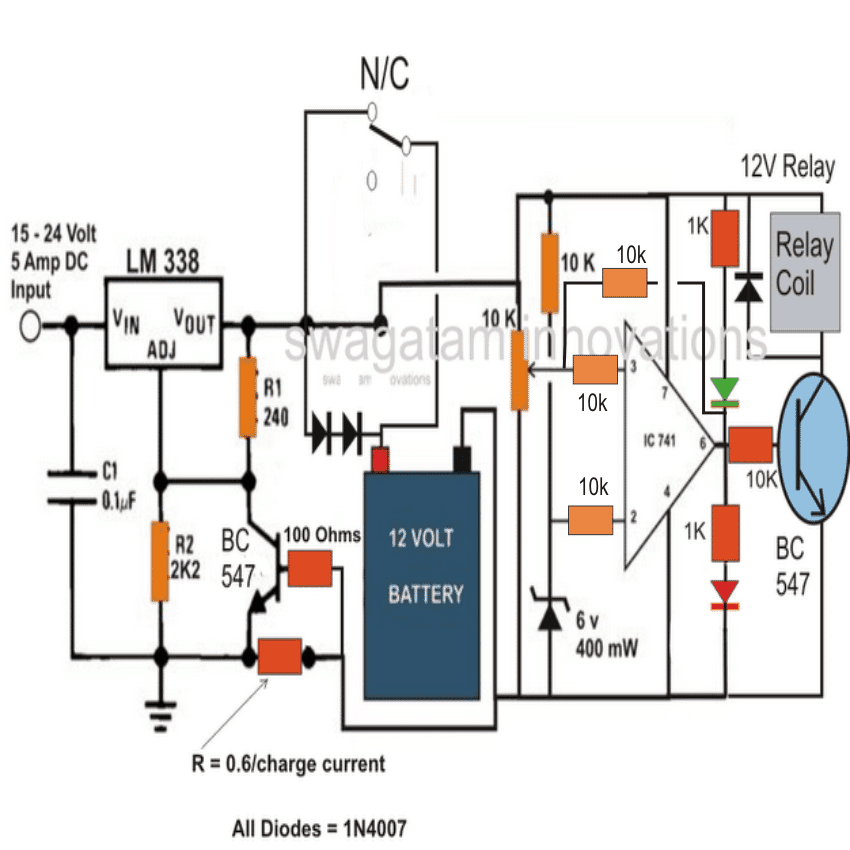
NiMH Battery Charger Circuit
A single state-of-the-art chip, a transistor and a few other inexpensive passive components are the only materials required for making this outstanding, self regulating, over charge controlled, automatic NiMH battery charger circuit. LetˇŻs study the whole operation explained in the article. Main Features:
How the Charger Circuit Works
Referring to the diagram we see a single IC being used which alone performs the function of a versatile high grade battery charger circuit and offers utmost protection to the connected battery while itˇŻs being charged by the circuit. FULL DATASHEET
This helps to keep the battery in a healthy environment and yet charge it with a relatively rapid rate.
This IC ensures a high battery life even after many hundreds of charging cycles.
The internal functioning of the NiMH battery charger circuit can be understood with the following points:
When the circuit is not powered, the IC enters into a sleep mode and the loaded battery is disconnected from the relevant IC pin out by the action of the internal circuitry.
The sleep mode is also triggered and the shut down mode is initiated when the supply voltage exceeds the specified threshold of the IC.
Technically, when the Vcc goes above the ULVO (under voltage lock out) fixed limit, the IC triggers the sleep mode and disconnects the battery from the charging current.
The ULVO limits are defined by the potential difference level detected across the connected cells.
This means the number of cells connected determines the shut down threshold of the IC.
The number of cells to be connected must be initially programmed with the IC through suitable component settings; the issue is discussed later on the article.
The rate of charging or the charging current can be set externally through a program resistor connected to the PROG pin out of the IC.
With the present configuration an inbuilt amplifier causes a virtual reference of 1.5 V to appear across the PROG pin.
This means that now the programming current flows through an in built N channel FET toward the current divider.
The current divider is handled by the charger state control logic which produces a potential difference across resistor, creating a fast charging condition for the connected battery.
The current divider is also responsible for providing a constant current level to the battery through the pin Iosc.
The above pin out in conjunction with a TIMER capacitor determines an oscillator frequency used for delivering the charging input to the battery.
The above charging current is activated through the collector of the externally connected PNP transistor, while its emitter is rigged with the ICˇŻs SENSE pin out for providing the charging rate information to the IC.
FULL DATASHEET
This helps to keep the battery in a healthy environment and yet charge it with a relatively rapid rate.
This IC ensures a high battery life even after many hundreds of charging cycles.
The internal functioning of the NiMH battery charger circuit can be understood with the following points:
When the circuit is not powered, the IC enters into a sleep mode and the loaded battery is disconnected from the relevant IC pin out by the action of the internal circuitry.
The sleep mode is also triggered and the shut down mode is initiated when the supply voltage exceeds the specified threshold of the IC.
Technically, when the Vcc goes above the ULVO (under voltage lock out) fixed limit, the IC triggers the sleep mode and disconnects the battery from the charging current.
The ULVO limits are defined by the potential difference level detected across the connected cells.
This means the number of cells connected determines the shut down threshold of the IC.
The number of cells to be connected must be initially programmed with the IC through suitable component settings; the issue is discussed later on the article.
The rate of charging or the charging current can be set externally through a program resistor connected to the PROG pin out of the IC.
With the present configuration an inbuilt amplifier causes a virtual reference of 1.5 V to appear across the PROG pin.
This means that now the programming current flows through an in built N channel FET toward the current divider.
The current divider is handled by the charger state control logic which produces a potential difference across resistor, creating a fast charging condition for the connected battery.
The current divider is also responsible for providing a constant current level to the battery through the pin Iosc.
The above pin out in conjunction with a TIMER capacitor determines an oscillator frequency used for delivering the charging input to the battery.
The above charging current is activated through the collector of the externally connected PNP transistor, while its emitter is rigged with the ICˇŻs SENSE pin out for providing the charging rate information to the IC.
Understanding the pinout functions of the LTC4060
Understanding the pin outs of the IC will make the building procedure of this NiMH battery charger circuit easier, let's go through the data with the following instructions: DRIVE (pin #1): The pin is connected to the base of the external PNP transistor and is responsible for providing the base bias to the transistor. This is done by applying a constant sink current to the base of the transistor. The pin out has current protected output. BAT (pin #2): This pin is used to monitor the charging current of the connected battery while it is being charged by the circuit. SENSE (pin #3): As the name suggests it senses the charging current applied to the battery and controls the conduction of the PNP transistor. TIMER (pin #4): It defines the oscillator frequency of the IC and helps to regulate the charge cycle limits along with the resistor thatˇŻs calculated at the PROG and GND pin outs of the IC. SHDN (pin #5): When this pin out is triggered low, the IC shuts down the charging input to the battery, minimizing the supply current to the IC. PAUSE (pin #7): This pin out may be used for stopping the charging process for some period of time. The process may be restored by providing a low level back to the pin out. PROG (pin #7): A virtual reference of 1.5V across this pin is created through a resistor connected across this pin and ground. The charging current is 930 times the level of the current that flows through this resistor. Thus this pinout may be used for programming the charging current by altering the resistor value appropriately for determining different charging rates. ARCT (pin #8): ItˇŻs the auto-recharge pinout of the IC and is used for programming the threshold charge current level. When the battery voltage falls below a preprogrammed voltage level, the charging is reinitiated instantly. SEL0, SEL1 (pin #9 and #10): These pin outs are used for making the IC compatible with different number of cells to be charged. For two cells, SEL1 is connected to ground and SEL0 to the supply voltage of the IC.How to Charge 3 Series Number of Cells
For charging three cells in series SEL1 is rigged to the supply terminal while SEL0 is wired up to the ground. For conditioning four cells in series, both the pins are connected to the supply rail, that is to the positive of the IC. NTC (pin #11): An external NTC resistor may be integrated to this pin out for making the circuit work with respect to the ambient temperature levels. If the conditions become too hot the pin out detects it through the NTC and shuts down the proceedings. CHEM (pin #12): This pin out detects the battery chemistry by sensing the negative Delta V level parameters of NiMH cells and selects the appropriate charging levels as per the sensed load. ACP (pin #13): As discussed earlier, this pin detects the Vcc level, if it reaches below the specified limits, in such conditions the pinout becomes high impedance, shutting down the IC in sleep mode, and shutting off the LED. However, if the Vcc is compatible with respect to the battery full charge specifications, then this pinout turns low, illuminating the LED and initiating the battery charging process. CHRG (pin #15): An LED connected to this pin out provides the charging indications and indicates that the cells are being charged. Vcc (pin #14): ItˇŻs simply the supply input terminal of the IC. GND (pin #16): As above itˇŻs the negative supply terminal of the IC.Wireless Li-Ion Battery Charger Circuit
Charging batteries through inductive wireless charging is one of the applications thatˇŻs becoming very popular and getting appreciated by the uses. Here weˇŻll study how to make a wireless Li-Ion battery charger circuit using the same concept. Any electrical system which involves wire networks or cables can be very messy and cumbersome.Introduction
Today the world is getting hi-tech and the electrical systems are also transiting into better and hassle-free versions for providing more convenience to us. Inductive power transfer is one such interesting concept which facilitates power transfer without the use of wires, or rather wirelessly. As the name refers to, inductive power transfer is a process through which a certain magnitude of power is transferred from one fixed place to another through the air without using conductors, just as radio signals or cell phone signals are transmitted. However the concept isnˇŻt that easy as it sounds to be, because with radios and cell phones the transmitted power is merely in few watts and thus becomes quite feasible, but transferring power (wirelessly) so that it can be used for powering high current devices is entirely a different ball game. Here we are talking about several watts or probably several hundreds of watts that needs to be carried without any dissipation, from point to the other without using wires, an issue difficult to implement. However researchers are trying their best to find appropriate set ups which may become just suitable for implementing the above concept successfully. The following points outline the concept, and help us to know how the above procedure actually takes place: Induction as we all know is a process through which electrical power is transferred from one position to the other without incorporating direct connections. The best example is our regular electrical transformers, where an input AC is applied at one of its windings and an induced power is received at the other winding through magnetic inductions. However the distance between the two windings inside a transformer is very small and therefore the actions take place very conveniently and efficiently. When the procedure needs to be implemented at greater distances the task gets a bit complicated. By evaluating the induction concept we find that there are basically two obstacles that make the power transfer difficult and inefficient, especially as the distance between the inducting destinations are increased. The first hurdle is the frequency and the second hurdle is the generated eddy currents in the winding core. The two parameters are inversely proportionate and therefore are directly dependent on each other. Another factor that hampers the proceedings, is the winding core material, which in turn directly affects the above two parameters. By carefully dimensioning these factors in the most efficient way, the distance between the inducting devices can be considerably stretched. For transferring wireless power in the above discussed method, we firstly require an AC, meaning the power which needs to be transferred must be a pulsating current. This frequency of the current when applied to a winding generates eddy currents, which are reverse currents opposing the applied current.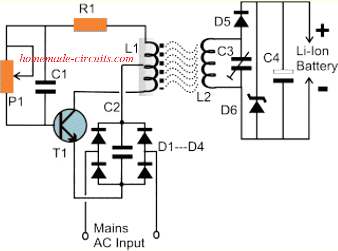 Generation of more eddy current means less efficiency and more power loss through core heating.
However as the frequency is increased, generation of eddy currents is reduced proportionately.
Also, if a ferrite material is used in place of the conventional iron stampings as the core of the winding helps to further reduce the eddy currents.
Therefore for implanting the above concept in the most efficient way we need to make the source power high in frequency, in the order of many kilohertz and use an input induction system thatˇŻs made up of ferrite as the core.
Hopefully, this solves the issue to great extents; at least for the making the proposed project of an inductive charging circuit for Li-ion batteries.
Generation of more eddy current means less efficiency and more power loss through core heating.
However as the frequency is increased, generation of eddy currents is reduced proportionately.
Also, if a ferrite material is used in place of the conventional iron stampings as the core of the winding helps to further reduce the eddy currents.
Therefore for implanting the above concept in the most efficient way we need to make the source power high in frequency, in the order of many kilohertz and use an input induction system thatˇŻs made up of ferrite as the core.
Hopefully, this solves the issue to great extents; at least for the making the proposed project of an inductive charging circuit for Li-ion batteries.
How it Works
WARNING - THE CIRCUIT IS NOT ISOLATED FROM AC MAINS AND SO IS EXTREMELY DANGEROUS IF TOUCHED IN POWERED CONDITION. This wireless cell phone charger circuit is designed by me, but has not been verified practically, so I would advise the readers to take a note of this. The circuit can be understood with the following points: Referring to the figure we see two units, one is the base or the transmitting module and the other one is the receiver module. As discussed in the above paragraph, the core material of the base winding is a ferrite E-core which is relatively larger in size. The bobbin thatˇŻs fitted inside the E-core has a single stage, neatly wound with 100 turns of 24 SWG super enameled copper wire. A center tap is extracted from the winding from its 50th winding turn. The above coil or transformer is connected to an oscillator circuit consisting of the transistor T1, preset P1 and the corresponding resistor and capacitor. The preset is used for increasing the frequency through the winding up to optimal levels and needs to be experimented some. A DC voltage is fed to the circuit for initiating the required oscillations, which is derived directly by rectifying and filtering the AC mains. On applying the DC, the circuit begins oscillating and the oscillations from the inductor being high in frequency escapes into the air to a considerable distance and needs to be grabbed back for the proposed inductive reception. The receiving unit also incorporates an inductor consisting of air cored 50 turns of 21 SWG super enameled copper wire, which becomes a kind of antenna for anticipating the released power waves from the base circuit.Capacitor C3 is a variable capacitor, the one used in radio for tuning may be tried. It's used for trimming the reception until the resonating point is reached and L2 gets optimally tuned with the transmitting waves. This instantly raises the output voltage from L2 and becomes optimally suitable for the charging requirements. D6 and C4 are the rectifying components which finally converts the AC signals into pure DC. When brought to a considerable proximity, the inductions from the lower base unit is induced inside the receiving coil, the induced frequency is suitably rectified and filtered inside the receiver circuit and is used for charging the connected Li-Ion battery. An LED could be connected across the output for getting an instant indication of the wireless power transfer intensity at any point of time. CAUTION: THE ABOVE EXPLAINED WIRELESS LI-ION BATTERY CHARGER CIRCUIT IS BASED ON MY ASSUMPTIONS ONLY; READERS DISCRETION IS STRICTLY ADVISED WHILE EMPLOYING THE DISCUSSED CONCEPT AND THE CIRCUIT.Parts List for the above discussed wireless mobile phone charger circuit
The following parts would be required for making this inductive battery charging circuit: R1 = 470 Ohms, R2 = 10K, 1Watt, C1 = 0.47uF/400V, non polar, C2 = 2uF/400V, non polar C3 = Variable Gang Condenser, C4 = 10uF/50V, D1---D5= 1N4007, D6 = Equal to Battery voltage, 1watt T1 =UTC BU508 AFIL1 = 100 turns, 25 SWG, center tap, over largest possible ferrite E-coreL2 = 50 piled turns, 20 SWG, 2 inches diameter, air coredOne Transistor Automatic Battery Charger Circuit
This one transistor cheap battery charger circuit is designed to automatically switch OFF the supply to the battery as soon as the battery has reached its full charge level. A very simple single transistor automatic battery charger circuit is described in this article, which uses just a single transistor for the voltage detection as well as for automatically disconnecting the battery from the supply when it gets fully charged.Circuit Operation
As shown in the diagram we can see a straightforward configuration where a solitary transistor is connected in itˇŻs standard operating mode. The circuit functioning may be understood with the help of the following points: Considering the battery to be charged is a 12 volt battery, we know that it is advised to charge the battery until it reaches between 13.9V to 14.3 volts. The transistor base voltage is adjusted using the preset P1, such that the transistor just conducts and operates the relay at around 14 volts.How to Adjust the Cut of Thresholds
This adjustment becomes the high voltage trip point of the circuit and is used to switch OFF the charging voltage to the battery when it gets fully charged or its voltage reaches around 14 volts. The lower trip point of the circuit cannot be adjusted as this circuit is too simple and does not incorporate the low voltage detection feature. However the transistor is itself equipped with a switch OFF feature in case its base voltage becomes too low. Typically a general purpose transistor like the one which is shown (BC547) when adjusted to switch ON at 14 volts may have the lower threshold of around 10 volts, when it might get just switched OFF. This wide voltage difference between the high set threshold and the lower natural threshold is because of the involved big hysteresis with the design. This acts like a natural hysteresis in the design. The lower threshold of 10 volts is dangerously low and we cannot wait for the circuit to restart the charging process until the battery voltage falls to this dangerous 10 volts level. Allowing the battery to discharge down to 10 volts can make the battery flat permanently and reduce its life. . Therefore to eliminate this issue the circuit needed to somehow reduce the hysteresis level. This is done by introducing a couple of diodes at the emitter of the transistor. We know that normally a 1N4007 diodes would drop around 0.7 volts across it and two if them would make a total of 1.4 volts. By inserting the two diodes in series with the emitter of the transistor, we force the transistor to switch off 1.4 V earlier than its normal specified limit of 10 volts. Therefore now the lower operating threshold of the circuit becomes 10 + 1.4 = 11.4 volts, which may be considered just OK for the battery and for the automatic restart of the charging process. Having both the thresholds updated as per the standard charging requirements, we now have an automatic automotive battery charger thatˇŻs not only cheap to build but also smart enough to take care of the battery charge conditions very efficiently.Circuit Diagram
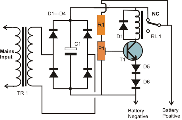 Parts List for the proposed one transistor automatic battery charger circuit
R1 = 4K7
P1 = 10K preset,
T1 = BC547B,
Relay = 12V, 400 Ohms, SPDT,
TR1 = 0 - 14V, current 1/10th of the battery AH
Bridge diodes = Equal to the current rating of the
transformer,
Emitter diodes = 1N4007,
C1 = 100uF/25V
Parts List for the proposed one transistor automatic battery charger circuit
R1 = 4K7
P1 = 10K preset,
T1 = BC547B,
Relay = 12V, 400 Ohms, SPDT,
TR1 = 0 - 14V, current 1/10th of the battery AH
Bridge diodes = Equal to the current rating of the
transformer,
Emitter diodes = 1N4007,
C1 = 100uF/25V
PCB Design
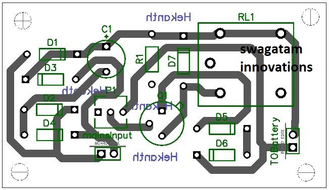
Self Regulating Battery Charger Circuit
The post explains how a neat little self regulating automatic battery charger circuit can be made using just two inexpensive transistors. This circuit will automatically regulate the charging supply to the battery depending on its charge level, by switching the input supply ON and OFF periodically.How it Works
As can be seen in the diagram, this auto-regulating battery charger circuit utilizes just two transistors for detecting the charging thresholds, and cuts off the process as soon as these limits are detected. Using two transistor actually makes the design hugely sensitive compared to a single transistor charger circuit. The indicated preset is set in such a way that the T1 is just able to conduct at the specified full charge threshold of the battery. When this happens T2 begins switching OFF, and ultimately at a point it is unable to sustain the relay conduction and switches OFF the relay, which in turn cuts of the input charging source with the connected battery. Conversely, when the battery voltage begins dropping, T1 gradually deprived of its adequate conduction voltage level, and ultimately it ceases to conduct, which quickly prompts T2 to initiate its conduction and trigger the relay into action, The relay now reconnects the charging input supply with the battery, and restores the charging process until it yet again reaches the full charge threshold, when the regulating cycle repeats itself.How to Sep Up the Circuit
Setting up this battery charger circuit for automatic regulation is very simple and may be done in the following way: Initially, do not connect the fixed transformer power supply; instead connect a 0-24V, variable supply voltage to the circuit. Remove the anode of D6 from the relay contact and connect it to the positive of the power supply. Keep both the presets somewhere at the center position. Switch ON the power and adjust the voltage to 11.5 volts or lower. Adjust P2, so that the relay just activates. Now increase the volts to about 13.5 volts, and adjust P1 so that the relay just deactivates. The setting procedure of the circuit is now complete. Check the whole procedure by continuously varying the voltage up and down. You may now remove the variable power supply and connect the fixed transformer, bridge power supply to it. DONˇŻT FORGET TO RECONNECT THE ANODE OF D6 BACK TO THE RELAY CONTACT OR THE BATTERY POSITIVE. The battery connected to this circuit will be charged only as long as its voltage is in between the above "window" level. If the battery voltage crosses the above "window", the relay will trip and stop the battery from charging.Parts List
R1, R2 = 10K, P1, P2 = 10K PRESET, T1, T2 = BC 547B, C1 = 2200uF/25V C2 = 47uF/25V (Please connect this capacitor across the relay coil) D1---D4 = 1N5408, D5, D6 = 1N4007, RELAY = 12 VOLT, SPDT, TRANSFORMER = AS PER THE CONNECTED BATTERY AH (DIVIDE BY 5)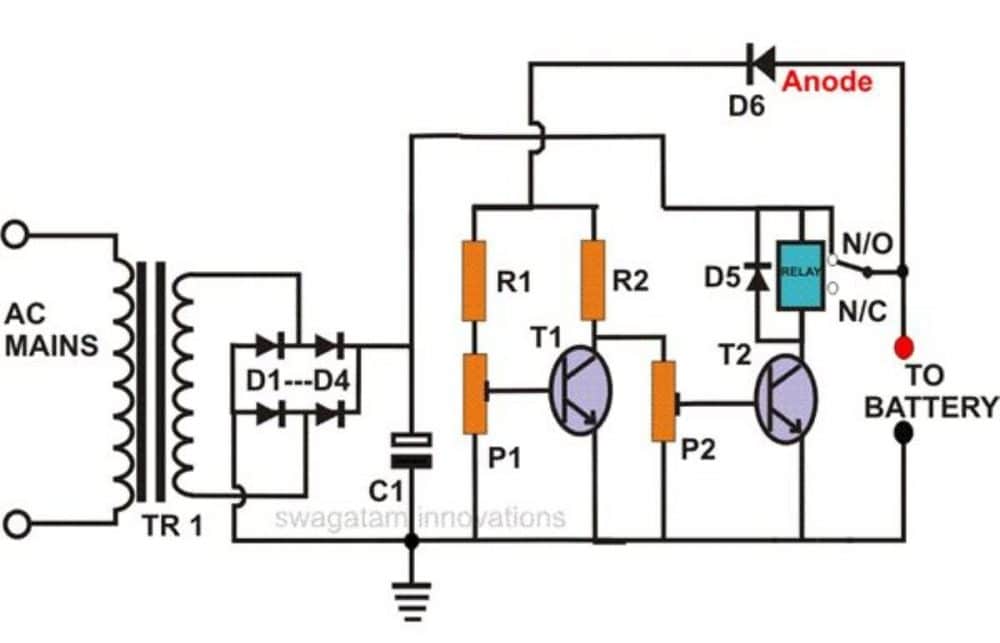 The following diagram shows the instructions which needs to be followed while setting-up the circuit with the desired cut-of thresholds, using a variable power supply unit:
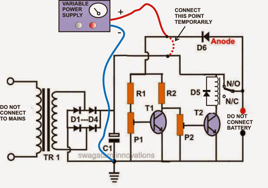 The above self-regulating battery charger circuit was successfully built and tested by Mr.
Sai Srinivas, who is just a school kid but nevertheless has an immense interest in the field of electronics.
The following images were sent by him which displays his talent and intense dedication in the field.
The above self-regulating battery charger circuit was successfully built and tested by Mr.
Sai Srinivas, who is just a school kid but nevertheless has an immense interest in the field of electronics.
The following images were sent by him which displays his talent and intense dedication in the field.
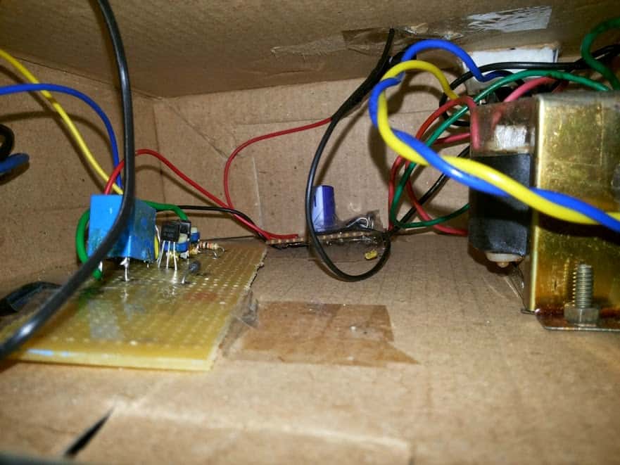
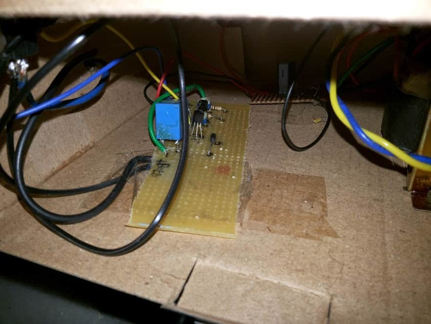
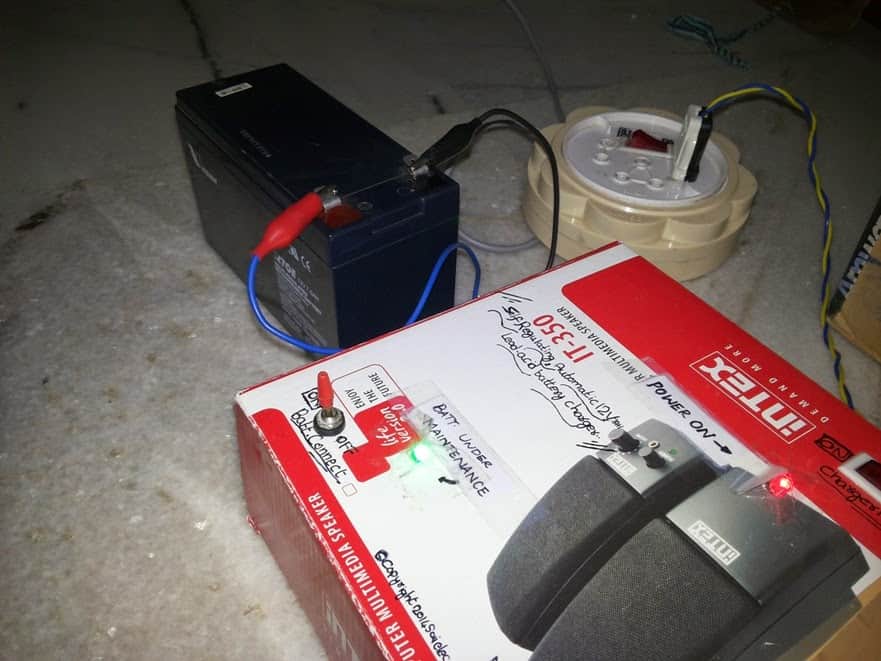

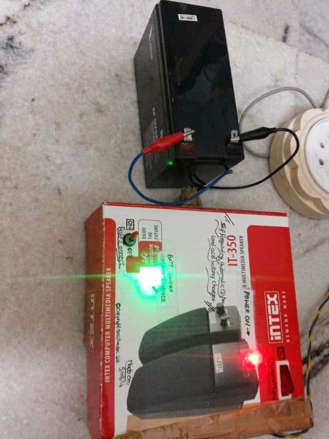 For One Shot Operation
If you want the above circuit to lock itself into a permanent cut off position when the battery is fully charged, then you may modify the design as shown below:
For One Shot Operation
If you want the above circuit to lock itself into a permanent cut off position when the battery is fully charged, then you may modify the design as shown below:
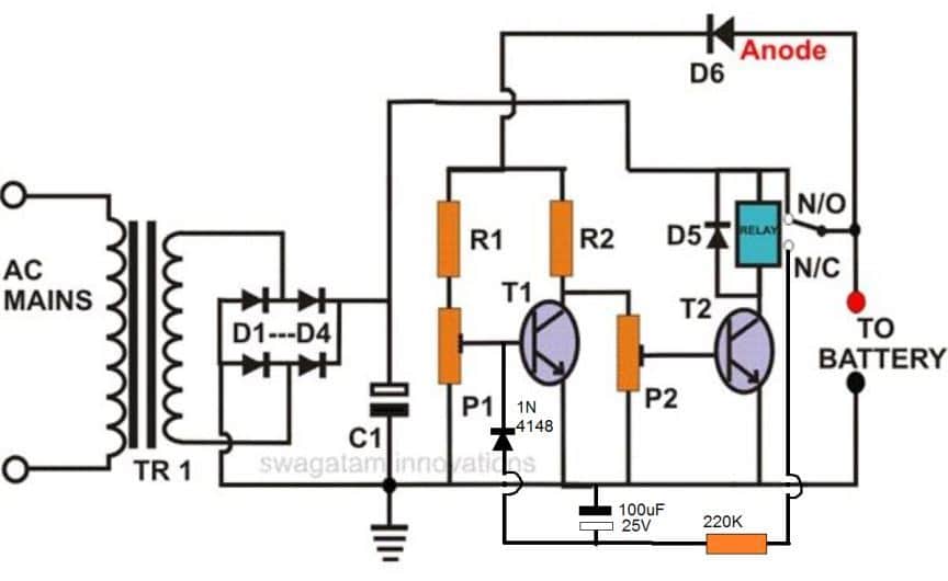 Note: To ensure the relay does not latch itself quickly on power switch ON, always connect the discharged battery first across the shown terminals and then switch ON the input power.
In order to indicate the charging status of the battery, we can add a couple of LEDs to the above design, as shown below.
Note: To ensure the relay does not latch itself quickly on power switch ON, always connect the discharged battery first across the shown terminals and then switch ON the input power.
In order to indicate the charging status of the battery, we can add a couple of LEDs to the above design, as shown below.
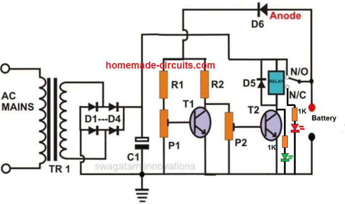 The above circuit was also successfully built and tested by one of the dedicated electronic enthusiasts from this blog.
The following pictures verify the results:
The above circuit was also successfully built and tested by one of the dedicated electronic enthusiasts from this blog.
The following pictures verify the results:

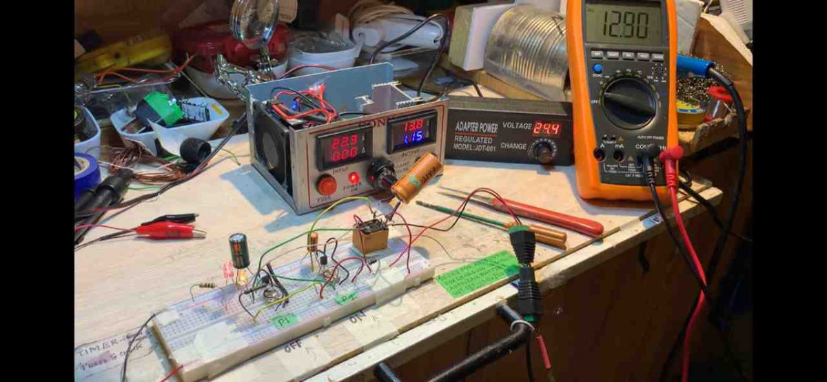
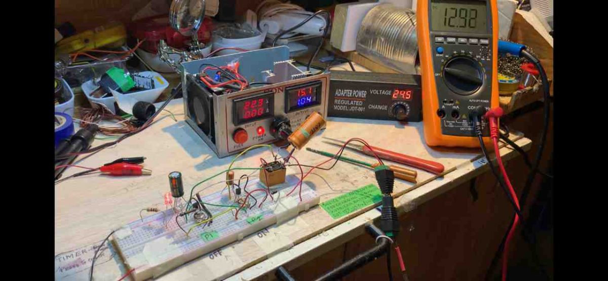
 Image showing the Battery that was used for the charging process
Warning: Make sure to test the preset setting thoroughly before you leave this application unattended.
And be sure to use only 14V as the input supply for a 12V battery.
Image showing the Battery that was used for the charging process
Warning: Make sure to test the preset setting thoroughly before you leave this application unattended.
And be sure to use only 14V as the input supply for a 12V battery.
Lead Acid Battery Charger Circuits
The lead acid battery charger circuits explained in this article can be used for charging all types of lead acid batteries at a specified rate. This article explains a few lead acid battery charger circuits with automatic over charge, and low discharge cut off. All these designs are thoroughly tested and can be used to charge all automotive and SMF batteries up to 100 Ah, and even 500 Ah.Introduction
Lead acid batteries are normally used for heavy duty operations involving many 100s of amps. To charge these batteries we specifically need chargers rated to handle high ampere charging levels for long periods of time. Lead acid battery charger are specifically designed for charging heavy duty batteries through specialized control circuits. The 5 useful and high power lead acid battery charger circuits presented below can be used for charging large high current lead acid batteries in the order of 100 to 500 Ah, the design is perfectly automatic and switches of the power to the battery and also itself, once the battery gets fully charged. UPDATE: You may also want to build these simple Charger circuits for 12 V 7 Ah Batteries, check them out.What does Ah Signify
The unit Ah or Ampere-hour in any battery signifies the ideal rate at which the battery would be fully discharged, or fully charged within a span of 1 hour. For example, if a 100 Ah battery was charged at 100 ampere rate, it would take 1 hour for the battery to get fully charged. Likewise, if the battery was discharged at 100 ampere rate, the backup time would last not more an hour. But wait, never try this, as charging/discharging at the full Ah rate can be disastrous for your lead acid battery. The unit Ah is there only to provide us with a benchmark value which can be used for knowing the approximate charge/discharge time of the battery at a stipulated current rate. For example when the above discussed battery is charged at 10 ampere rate, using the Ah value we can find the full charge time in the following formula: Since charging rate is inversely proportional to the time, we have: Time = Ah Value / Charging Rate T = 100 / 10 where 100 is the Ah level of the battery, 10 is the charging current, T is the time at the 10 amp rate T = 10 Hours. The formula suggests it would ideally require around 10 hours for the battery to get optimally charged at 10 amp rate, but for a real battery this may be around 14 hours for the charging, and 7 hours for the discharging. Because in real world even a new battery won't work with ideal conditions, and as it ages the situation may get even worse.Important Parameters to be Considered
Lead acid batteries are expensive, and you will want to ensure that it lasts as long as possible. So please do not use cheap and untested charger concepts, which may look easy but may harm your battery slowly. The big question is, is ideal method of charging a battery essential? The simple answer is NO. Because when we apply ideal charging method as discussed in "Wikipedia" or "Battery University" websites, we try to charge the battery at its maximum possible capacity. For example, at the ideal 14.4 V level your battery may be fully charged, but it can be risky to do this using ordinary methods. To achieve this without risks you may have to employ an advanced charger step charger circuit, which can be difficult to build, and might require too many calculations. If you want to avoid this, you can still charge your battery optimally (@ around 65%) by ensuring that the battery is cut-off at a little lower level. This will allow the battery to be always under less stressful condition. The same goes for the discharge level and rate. Basically it must have the following parameters for a safe charging which does not require special step chargers: Fixed Current or Constant Current (1/10th of Battery Ah Rating) Fixed Voltage or Constant Voltage (17% higher than Battery Printed Voltage) Over Charge Protection (Cut-OFF when Battery gets charged to the above level) Float Charge (Optional, not compulsory at all) If you do not have these minimum parameters in your system, then it may slowly degrade the performance and damage your battery, reducing its back up time drastically. For example, if your battery is rated at 12 V, 100 Ah, then the fixed input voltage should be 17% higher than the printed value, that's equal to around 14.1 V ( not 14.40 V, unless you are using a step charger). Current (ampere) ideally should be 1/10th of the Ah level printed on the battery, so in our case this can be 10 amperes. A slightly higher Amp input can be fine since our full charge level is already lower. Charging auto cut off is recommended at the above mentioned 14.1 V, but it's not compulsory since we already have the full charge level slightly lower. Float Charge is a process of reducing the current to negligible limits after the battery has reached full charge. This prevents the battery from self discharging and holds it at the full level continuously until it's removed by the user for usage. It is completely optional. It may be necessary only if you are not using your battery for long periods of time. In such cases too it's better to remove the battery from the charger and top it up occasionally once every 7 days. The easiest way to get fixed voltage and current is by using voltage regulator ICs, as we will learn below. Another easy way is to use a ready made 12 V SMPS 10 Amp unit as the input source, with an adjustable preset. The SMPS will have a small preset at the corner which can be tweaked to 14.0 V. Remember you will have to keep the battery connected for at least 10 to 14 hours, or until your battery terminal voltage reaches 14.2 V. Although this level may look slightly undercharged than the standard 14.4 V full level, this ensures your battery can never get over charged and guarantees a long life for the battery. All the details are presented in this infographic below: However, if you are an electronic hobbyist and interested to build a full fledged circuit with all the ideal options, in that case you can go for the following comprehensive circuit designs.
[New Update] Current Dependent Battery Auto Cut OFF
Normally, a voltage detected or voltage dependent automatic cut off is used in all conventional battery charger circuits. However, a current detection feature can be also employed for initiating an auto cut off when the battery reaches its most optimal full charge level. The complete circuit diagram for the current detected auto cut off is shown below: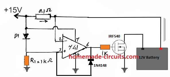 PLEASE CONNECT A 1K RESISTOR IN SERIES WITH THE RIGHT SIDE 1N4148 DIODE
How it Works
The 0.1 Ohm resistor acts like a current sensor by developing an equivalent potential difference across itself . The value of the resistor must be such that the minimum potential deference across it is at least 0.3V higher than the diode drop at pin 3 of the IC, until the battery has reached the desired full charge level. When the full charge is reached this potential should come down below the diode drop level. Initially , while the battery is charging, the current draw develops a negative potential difference of say -1V across the input pins of the IC. Which means that the pin 2 voltage now becomes lower than the pin3 voltage by at least 0.3V. Due to this pin 6 of the IC goes high allowing the MOSFET to conduct and connect the battery with the supply source. As the battery charges to its optimal level, the voltage across the current sensing resistor drops to a sufficiently lower level causing the potential difference across the resistor to become almost zero. When this happens, pin 2 potential rises higher than pin3 potential, causing pin 6 of the IC to go low, and switching OFF the MOSFET. The battery thus gets disconnected from the supply disabling the charging process. The diode connected across pin 3 and pin 6 locks or latches the circuit in this position until power is switched OFF and ON again for a fresh cycle. The above current dependent charging circuit can be also expressed as given below: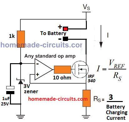 When power is switched ON, the 1 uF capacitor grounds the inverting pin of the op amp causing a momentary high at the op amp output, which switches ON the MOSFET.
This initial action connects the battery with the supply via the MOSFET and the sense resistor RS.
The current drawn by the battery causes an appropriate potential to develop across RS which raises the non-invering input of the op amp above the reference inverting input (3V).
The op amp output now latches ON and charges the battery, until the battery is almost fully charged.
This situation reduces the current through RS such that the potential across it drops below 3 V reference and the op amp output turns low, switching OFF the MOSFET and the charging process for the battery.
The above current dependent battery charging system design can be understood more elaborately in the below comprehensively drawn diagram, which can be used for charging very high capacity batteries in the order of 200 Ah to 500 Ah very safely:
When power is switched ON, the 1 uF capacitor grounds the inverting pin of the op amp causing a momentary high at the op amp output, which switches ON the MOSFET.
This initial action connects the battery with the supply via the MOSFET and the sense resistor RS.
The current drawn by the battery causes an appropriate potential to develop across RS which raises the non-invering input of the op amp above the reference inverting input (3V).
The op amp output now latches ON and charges the battery, until the battery is almost fully charged.
This situation reduces the current through RS such that the potential across it drops below 3 V reference and the op amp output turns low, switching OFF the MOSFET and the charging process for the battery.
The above current dependent battery charging system design can be understood more elaborately in the below comprehensively drawn diagram, which can be used for charging very high capacity batteries in the order of 200 Ah to 500 Ah very safely:
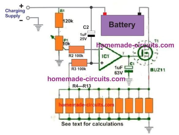 Adjust the 10 k preset so that just around 0.3 V or 0.4 V is available at the (-) input of the op amp, and set the R4---R13 resistor bank such that their net resistance is:
R = 1 / Max charging current.
Suppose the battery is 100 Ah, then the max charging current will be 10 amps, therefore,
R = 1 / 10 = 0.1 Ohms
Adjust the 10 k preset so that just around 0.3 V or 0.4 V is available at the (-) input of the op amp, and set the R4---R13 resistor bank such that their net resistance is:
R = 1 / Max charging current.
Suppose the battery is 100 Ah, then the max charging current will be 10 amps, therefore,
R = 1 / 10 = 0.1 Ohms
1) Using a Single Op amp
Looking at the first high current circuit for charging large batteries, we can understand the circuit idea through the following simple points: There are basically three stages in the shownconfigurationviz: the power supply stage consisting of a transformer and a bridge rectifier network. A filter capacitor after the bridge network has been ignored for the sake of simplicity, however for better DC output to the battery one can add a 1000uF/25V capacitor across the bridge positive and negative. The output from the power supply is directly applied to the battery which requires to be charged. The next stage consists of an opamp 741 IC voltage comparator, which is configured to sense the battery voltage while it is being charged and switch its output at pin #6 with the relevant response. Pin #3 of the IC is rigged with the battery or thesupplypositive of the circuit via a 10K preset. The preset is adjusted such that the IC reverts its output at pin #6 when the battery becomes fully charged and reaches about 14 volts which happens to be the transformer voltage at normal conditions. Pin #2 of the IC is clamped with a fixed reference via a voltage divider network consisting of a 10K resistor and a 6 volt zener diode. The output from the IC is fed to a relay driver stage where the transistor BC557 forms the main controlling component. Initially, power to the circuit is initiated by pressing the "start" switch. On doing this, the switch bypasses the contacts of the relay and powers the circuit momentarily. The IC senses the battery voltage and since it will be low during that stage, the output of the IC responds with a logic low output. This switches ON the transistor and the relay, the relay instantly latches the power via its relevant contacts such that now even if the "start" switch is released, the circuit remains switched ON and begins charging the connected battery. Now as the battery charge reaches about 14 volts, the IC senses this and instantly reverts its output to a high logic level. The transistor BC557 responds to this high pulse and switches OFF the relay which in turn switches of the power to the circuit,breakingthe latch. The circuit gets completely switched OFF until the start button is pressed once again and the connected battery has a charge that's under the set 14 volt mark.How to set up.
It's very easy. Do not connect any battery to the circuit. Switch ON power by pressing the start button and keep it depressed manually, simultaneouslyadjust the preset such that the relay just trips or switches OFF at the given rated transformer voltage which should be around 14 volts. The setting is complete, now connect a semi discharged battery to the shown points in the circuit and press the "start" switch. Due to the discharged battery, now the voltage to the circuit will drop under 14 volts and the circuit will instantly latch, initiating the procedure as explained in the above section. Circuit Diagram for the proposed battery charger with high ampere capacity is shown below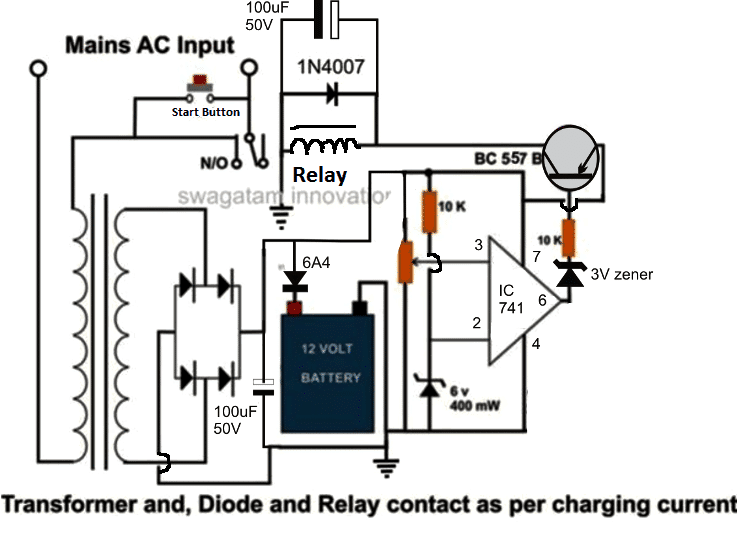 NOTE: Please do not use a filter capacitor across the bridge.
Instead keep a 1000uF/25V capacitor connected right across the relay coil.
If the filter capacitor is not removed the relay may go into an oscillating mode, in the absence of a battery.
NOTE: Please do not use a filter capacitor across the bridge.
Instead keep a 1000uF/25V capacitor connected right across the relay coil.
If the filter capacitor is not removed the relay may go into an oscillating mode, in the absence of a battery.
2) 12V, 24V / 20 amp Charger Using two opamps:
The second alternative way of achieving battery charging for a lead acid battery with high amperage can be observed in the following diagram, using a couple of op amps: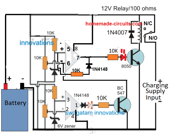 The working of the circuit can be understood through the following points:
When the circuit is powered without a battery connected, the circuit does not respond to the situation since the initial N/C position of the relay keeps the circuit disconnected from the charging supply.
Now suppose a discharged battery is connected across the battery points.
Let's assume the battery voltage to be at some intermediate level, which may be between the full charge level and the low charge level.
The circuit gets powered through this intermediate battery voltage.
As per the setting of the pin 6 preset, this pin detects a low potential than the pin 5 reference level.
which prompts its output pin 7 to go high.
This in turn causes the relay to activate and connect the charging supply to the circuit and the battery via the N/O contacts.
As soon as this happens, the charging level also drops to the battery level and the two voltages merge at the battery voltage level.
The battery now begins charging, and its terminal voltage begins increasing slowly.
When the battery reaches it full charge level, the pin 6 of the upper opamp becomes high than its pin 5 causing its output pin 7 to go low, and this switches off the relay, and the charging is cut off.
At this point another thing happens.
The pin 5 is connected to the negative potential at pin 7 via the 10k/1N4148 diode, which further lowers the pin 5 potential compared to pin 6. This is called hysteresis, which ensure that even if the battery now drops to some lower level that won't trigger the op amp back to charging mode, instead the battery level now has to drop significantly down until the lower op amp is activated.
Now, suppose the battery level keeps dropping due to some connected load, and its potential level reaches the lowest discharge level.
This is detected by pin 2 of the lower op amp whose potential now goes below its pin 3, which prompts its output pin 1 to become high and activate the BC547 transistor.
The BC547 grounds the pin 6 of the upper op amp competely.
This causes the hysteresis latch to break due to pin 6 potential dropping below pin 5.
This instantly causes the output pin 7 to go high and activate the relay, which yet again initializes the charging of the battery, and the cycle repeats the procedure as long as the battery remains connected with the charger.
LM358 Pinout
The working of the circuit can be understood through the following points:
When the circuit is powered without a battery connected, the circuit does not respond to the situation since the initial N/C position of the relay keeps the circuit disconnected from the charging supply.
Now suppose a discharged battery is connected across the battery points.
Let's assume the battery voltage to be at some intermediate level, which may be between the full charge level and the low charge level.
The circuit gets powered through this intermediate battery voltage.
As per the setting of the pin 6 preset, this pin detects a low potential than the pin 5 reference level.
which prompts its output pin 7 to go high.
This in turn causes the relay to activate and connect the charging supply to the circuit and the battery via the N/O contacts.
As soon as this happens, the charging level also drops to the battery level and the two voltages merge at the battery voltage level.
The battery now begins charging, and its terminal voltage begins increasing slowly.
When the battery reaches it full charge level, the pin 6 of the upper opamp becomes high than its pin 5 causing its output pin 7 to go low, and this switches off the relay, and the charging is cut off.
At this point another thing happens.
The pin 5 is connected to the negative potential at pin 7 via the 10k/1N4148 diode, which further lowers the pin 5 potential compared to pin 6. This is called hysteresis, which ensure that even if the battery now drops to some lower level that won't trigger the op amp back to charging mode, instead the battery level now has to drop significantly down until the lower op amp is activated.
Now, suppose the battery level keeps dropping due to some connected load, and its potential level reaches the lowest discharge level.
This is detected by pin 2 of the lower op amp whose potential now goes below its pin 3, which prompts its output pin 1 to become high and activate the BC547 transistor.
The BC547 grounds the pin 6 of the upper op amp competely.
This causes the hysteresis latch to break due to pin 6 potential dropping below pin 5.
This instantly causes the output pin 7 to go high and activate the relay, which yet again initializes the charging of the battery, and the cycle repeats the procedure as long as the battery remains connected with the charger.
LM358 Pinout
 For more auto cut-off charger ideas, you can read this article regarding opamp automatic battery charger circuits.
Video Clip:
The set up of the above circuit can be visualized in the following video which shows the cut off responses of the circuit to the upper and the lower voltage thresholds, as fixed by the relevant presets of the opamps
For more auto cut-off charger ideas, you can read this article regarding opamp automatic battery charger circuits.
Video Clip:
The set up of the above circuit can be visualized in the following video which shows the cut off responses of the circuit to the upper and the lower voltage thresholds, as fixed by the relevant presets of the opamps
3) Using IC 7815
The third circuit explanation below details how a battery may be charged effectively without using any IC or relay, rather simply by using BJTs, let's learn the procedures: The idea was suggested by Mr. Raja Gilse.Charging a Battery with a Voltage Regulator IC
I have a 2N6292 . My friend suggest me to make the simple fixed voltage high current DC power supply to charge an SMF battery. He had given the attached rough diagram. I don't know anything about the above transistor. Is it so ? My input is 18 volt 5 Amp transformer. He told me to add 2200 uF 50 Volt capacitor after rectification. Is it works ? If so , is there any heat sink necessary for transistor or/and IC 7815 ? Is it stops automatically after battery reaches 14.5 volt ? Or any other alteration needed ? Please guide me sirCharging with an Emitter Follower Configuration
Yes it will work and will stop charging the battery when around 14 V is reached across the battery terminals. However I am not sure about the 1 ohm base resistor value...it needs to be calculated correctly. The transistor and the IC both may be mounted on a common heatsink using mica separator kit. This will exploit the thermal protection feature of the IC and will help safeguard both the devices from overheating.Circuit Diagram
Circuit description
The shown high current battery charger circuit is a smart way of charging a battery and also achieving an auto shut off when the battery attains a full charge level. The circuit is actually a simple common collector transistor stage using the shown 2N6292 power device. The configuration is also referred as an emitter follower and as the name suggests the emitter follows the base voltage and allows the transistor to conduct only as long as the emitter potential is 0.7V lower that the applied base potential. In the shown high current battery charger circuit using a voltage regulator, the base of the transistor is fed with a regulated 15 V from the IC 7815, which ensures a potential difference of about 15 - 0.7 = 14.3 V across the emitter/ground of the transistor. The diode is not required and must be removed from the base of the transistor in order to prevent an unnecessary drop of an extra 0.7 V. The above voltage also becomes the charging voltage for the connected battery across these terminals. While the battery charges and its terminal voltage continues to be below the 14.3 V mark, the transistor base voltage keeps conducting and supplying the required charging voltage to the battery. However as soon as the battery begins attaining the full and above 14.3 V charge, the base is inhibited from a 0.7 V drop across its emitter which forces the transistor to stop conducting and the charging voltage is cut off to the battery for the time being, as soon as the battery level begins going below the 14.3 V mark, the transistor is switched ON again...the cycle keeps repeating ensuring a safe charging fr the connected battery. Base resistor = Hfe x battery internal resistance Here's a more appropriate design which will help to achieve optimal charging using IC 7815 IC As you can see, a 2N6284 is used here in the emitter follower mode.
This is because 2N6284 is a Darlington transistor with high gain, and will enable optimal charging of the battery at the intended 10 amp rate.
This can be further simplified by using a single 2N6284, and a potentiometer as shown below:
As you can see, a 2N6284 is used here in the emitter follower mode.
This is because 2N6284 is a Darlington transistor with high gain, and will enable optimal charging of the battery at the intended 10 amp rate.
This can be further simplified by using a single 2N6284, and a potentiometer as shown below:
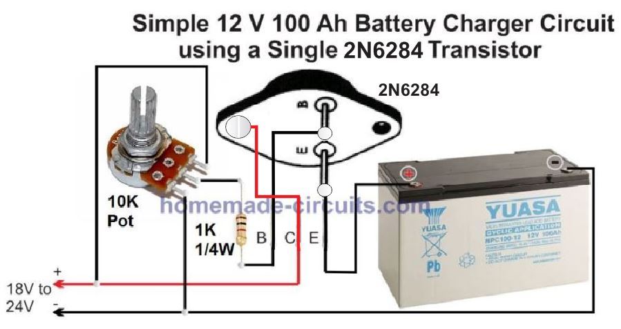 Make sure that you adjust the pot to get a precise 14.2 V at the emitter of the battery.
All the devices must be mounted on large heatsinks.
Make sure that you adjust the pot to get a precise 14.2 V at the emitter of the battery.
All the devices must be mounted on large heatsinks.
4) 12V 100 Ah Lead Acid Battery Charger Circuit
The proposed 12V 100 ah battery charger circuit was designed by one of the dedicated members of this blog Mr. Ranjan, let's learn more regarding the circuit functioning of the charger and how it could be used as a trickle charger circuit also.The Circuit Idea
My self Ranjan from Jamshedpur, Jharkhand. Recently while googling I came to know about your blog, and become a regular reader of your blog. I learned a lot of things from your blog. For my personal use I would like to make a battery charger. I have a 80 AH tubular batery and a 10 Amps 9-0-9 volts transformer. So I can get 10 amps 18-0 volts if I use the two 9volts leads of transformer.(Transfomer is actually obtained from an old 800VA UPS). I have constructed a circuit diagram based on your blog. Please have a look on it and suggest me. Please note that,. 1) I am belonging to very rural area hence there is a huge power fluctuation it varies from 50V ~ 250V. Also note that I will draw very less amount of current from the battery( Generally using LED lights during power cuts) approx 15 - 20 Watt. 2) 10amps transformer i think safely charges 80AH Tubular Battery 3) All diodes used for the circuit are 6A4 dides. 4) Two 78h12a used as parallel to get 5+5 = 10 amps output. Although I think Battery must not draw full 10 amps. as it will be in charged condition in day to day use so internal resistance of battery will be high and will draw lesser current. 5) A switch S1 is used thinking that for normal charge it will be kept in off state. and after fully charging the battery it switched to on state to maintain a trickle charge with lower voltage. NOW question is that is this safe for the battery to kept in charge unattended for long time. Please reply me with your valuable suggestions.100 Ah battery charger circuit diagram designed by Mr. Ranjan
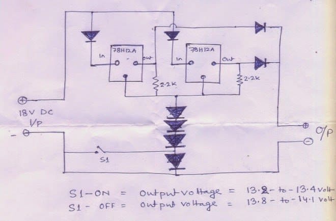
Solving the Circuit Request
Dear Ranjan, To me your high current VRLA battery charger circuit using IC 78H12A looks perfect and should work as expected. Still for guaranteed confirmation it would be advisable to check the voltage and current practically before connecting it with the battery. Yes, the shown switch can be used in the trickle charge mode and in this mode the battery can be kept permanently connected without attending, however this should be done only after the battery has been fully charged upto around 14.3V. Please note that the four series diodes attached with the GND terminals of the ICs could be 1N4007 diodes, while the remaining diodes should be rated well over 10amps, this could be implemented by connecting two 6A4 diodes in parallel at each of the shown positions. Also, it is strongly recommended to put both the ICs over a single large common heatsink for better and uniform thermal sharing and dissipation. Caution: The shown circuit does not include a full charge cut-off circuit, therefore the maximum charging voltage should be preferably restricted between 13.8 to 14V. This will ensure that the battery is never able to reach the extreme full charge threshold, and thus remain safe from over charge conditions. However this would also mean that the lead acid battery would be able to attain only around 75% charge level, nevertheless keeping the battery undercharged will ensure longer life for the battery and allow more charge/discharge cycles. Using 2N3055 to Charge a 100 Ah Battery The following circuit presents a simple and safe alternative way of charging a 100 Ah battery using 2N3055 transistor. It also has a constant current arrangement so the battrey can e charged with the correct amount of current. Being an emitter follower, at the full charge level the 2N3055 will be almost OFF, ensuring the battery is never over charged.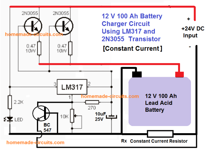 The current limit can be calculated using the following formula:
R(x) = 0.7 / 10 = 0.07 Ohms
Wattage will be = 10 watts
The current limit can be calculated using the following formula:
R(x) = 0.7 / 10 = 0.07 Ohms
Wattage will be = 10 watts
How to Simply Add a Float Charge
Remember other sites may present unnecessarily complex explanation regarding float charge making it complex for you to understand the concept. Float charge it simply a small adjusted current level which prevents self discharge of the battery. Now you may ask what's self discharge of the battery. It's the declining level of charge in battery as soon as the charging current is removed. You can prevent this by adding a high value resistor such as a 1 K 1 watt across the input 15 V SOURCE and the battery positive. This will not allow the battery to self discharge and will hold the 14 V level as long as the battery is attached to the supply source.5) IC 555 Lead Acid Battery Charger Circuit
The fifth concept below explains a simple, versatile automatic battery charger circuit. The circuit will allow you to charge all types of lead acid battery right from a 1 Ah to a 1000 Ah battery.Using IC 555 as the Controller IC
The IC 555 is so versatile, it can be considered the single chip solution for all circuit application needs. No doubt it's been utilized here too for yet another useful application. A single IC 555, a handful of passive component is all that's needed for making this outstanding, fully automatic battery charger circuit. The proposed design will automatically sense and keep the attached battery up to date. The battery which is required to be charged may be kept connected to the circuit permanently, the circuit willcontinuouslymonitor the charge level, if the charge level exceeds the upper threshold, the circuit will cut off the charging voltage to it, and in case the charge falls below the lower set threshold, the circuit will connect, and initiate the charging process.How it Works
The circuit may be understood with the following points: Here the IC 555 is configured as a comparator for comparing the battery low and high voltage conditions at pin#2 and pin#6 respectively. As per the internal circuit arrangement, a 555 IC will make its output pin#3 high when the potential at pin#2 goes below 1/3 of supply voltage. The above position sustains even if the voltage at pin#2 tends to drift a little higher. This happens due to the internal set hysteresis level of the IC. However if the voltage continues to drift higher, pin#6 gets hold of the situation and the moment it senses a potential difference higher than 2/3rd of supply voltage, it instantly reverts the output from high to low at pin#3. In the proposed circuit design, it simply means that, the presets R2 and R5 should be set such that the relay just deactivates when the battery voltage goes 20% lower than printed value and activates when the battery voltage reaches 20% above printed value. Nothing can be as simple as this. The power supply section is an ordinary bridge/capacitor network. The diode rating will depend on the charging current rate of the battery. As a rule of thumb the diode current rating should be twice that of the battery charging rate, while the battery charging rate should be 1/10th of the battery Ah rating. It implies that TR1 should be around 1/10th of the connected battery Ah rating. The relay contact rating should be also selected as per the ampere rating of TR1.How to set the battery cut off threshold
Initially keep the power to the circuit switched OFF. Connect a variable power supply source across the battery points of the circuit. Apply a voltage that may be exactly equal to the desired low voltage threshold level of the battery, then adjust R2, such that the relay just deactivates. Next, slowly increase the voltage up to the desired higher voltage threshold of the battery, adjust R5 such that the relay just activates back. The setting up of the circuit is now done. Remove the external variable source, replace it with any battery which needs to be charged, connect the input of TR1 to mains, and switch ON. Rest will be automatically taken care of, that is now the battery will start charging and will cut off when its fully charged, and also will get connected to power automatically in case its voltage falls below the set lower voltage threshold.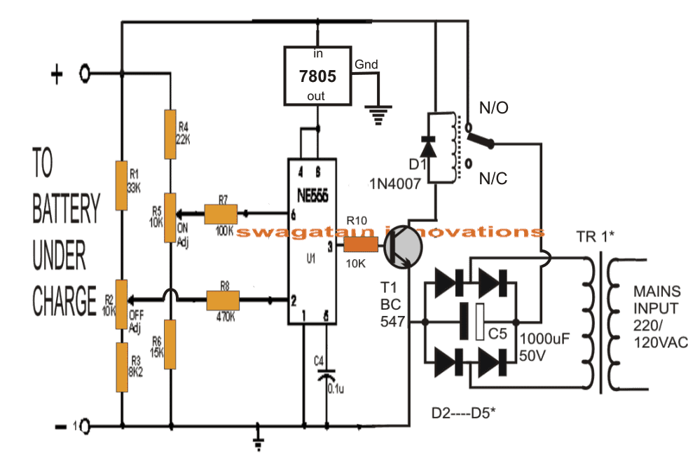 IC 555 Pinouts
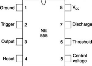
IC 7805 Pinout
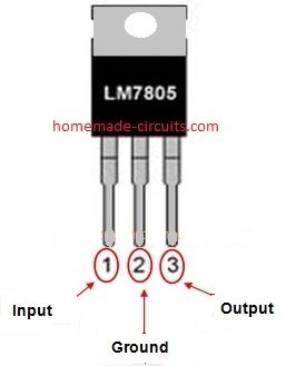
How to Set Up the Circuit.
The setting up of the voltage thresholds for the above circuit may be done as explained below: Initially keep the transformer power supply section at the right hand side of the circuit completely disconnected from the circuit. Connect an external variable voltage source at the (+)/(-) battery points. Adjust the voltage to 11.4V, and adjust the preset at pin#2 such that the relay just activates. The above procedure sets the lower threshold operation of the battery. Seal the preset with some glue. Now increase the voltage to about 14.4V and adjust the preset at pin#6 to just deactivate the relay from its previous state. This will set up the higher cut off threshold of the circuit. The charger is now all set. You may now remove the adjustablepowersupply fromthe batterypoints and use the charger asexplainedin the above article. Do the above procedures with lot of patience and thinkingFeedback from one of the dedicated readers of this blog:
 untung suharto January 1, 2017 at 7:46 AM
Hi, you have made a mistake on preset R2 and R5, they should not be 10k but 100k, I just made one and it was a success, thank you.As per the above suggestion, the previous diagram may be modified as shown below:
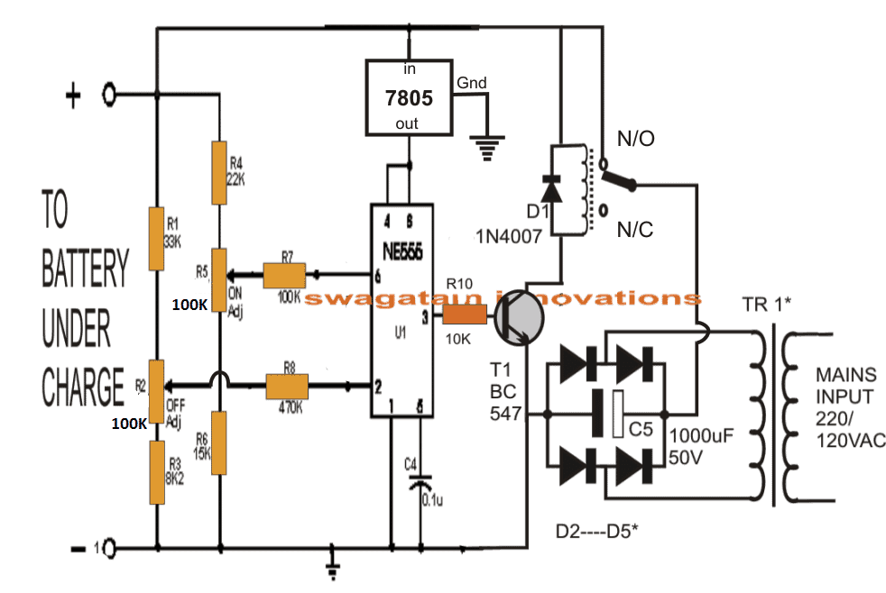
Wrapping it up
In the above article we learned 5 great techniques which could be applied for making lead acid battery chargers, right from 7 Ah to 100 Ah, or even 200 Ah to 500 Ah, simply by upgrading the relevant devices or the relays. If you have specific questions regarding this concepts, please feel free to ask them through the comment box below.IC 555 Current Dependent Battery Charging
The IC 555 lead acid battery charger circuit could be also built using a current sensor at its pin#2. The complete circuit diagram is shown below: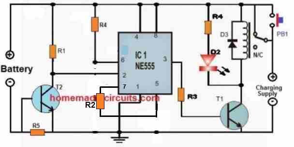 R1, R3 = 10k
R2 = 100k
LED resistor can be 1k
Pin#6 resistor R4 can be shorted with jumper link
R5 = 1 / max charging current
Relay = 12V relay for 12V battery.
Relay diode = 1N4007
T1, T2 = BC547
R1, R3 = 10k
R2 = 100k
LED resistor can be 1k
Pin#6 resistor R4 can be shorted with jumper link
R5 = 1 / max charging current
Relay = 12V relay for 12V battery.
Relay diode = 1N4007
T1, T2 = BC547
How it Works
The circuit is actually configured as a set/reset latch circuit. The R4 can be replaced with a wire short. At the start when power is applied, the relay contact being at the N/C, the circuit does not respond. Pressing the PB1 push button, initializes the circuit by momentarily supplying the current throgh the PB1 to the battery. The battery acts as the load, and creates a voltage drop across R5, which triggers ON the T2. With T2 conducting pin#2 of the IC is held low, which prompts the output pin#3 to become high, and switch ON the relay. The relay contacts now changes to N/O point and the circuit gets latched. The PB1 pressing is thus only required momentarily, and then it can be released. As the battery gets charged, the voltage across R5 keeps getting lower, until the point when the battery is almost fully charged, when the R5 voltage drop is unable to hold the T2 ON any longer. T2 switches OFF, causing pin#2 to go high again, and this in turn causes the pin#3 to go low, and turn OFF the relay and turn OFF the charging supply to the circuit and the battery.References:
Charging Lead Acid Battery How lead acid battery worksPolice/Ambulance Siren Circuit with Rotating Beacon Light
In this post we are going to learn how to construct a police, ambulance or a fire truck siren circuit using evergreen IC 555 timer and we will also learn how to build a revolving beacon light without any mechanical parts. The proposed project is divided into two parts the siren circuit and the rotating beacon light, but before dive in to the details letˇŻs answer a very simple question.Why do Emergency Vehicles have Sirens and a Rotating Beacon Light?
The purpose of siren and rotating lights on emergency vehicles are to convey the urgency of the journey to the commuters on the road and the traffic ahead. They provide visual and auditory signals to vehicles on the road within a range so that non-emergency vehicles can give way to the emergency vehicles. Only emergency vehicles and vehicles of VIP govt. officials are granted permission to install siren and beacon lights and this law may differ from country to country. Now letˇŻs see how we can build a two tone siren as a hobby / science fair project.Circuit Diagram of Two Tone Siren:
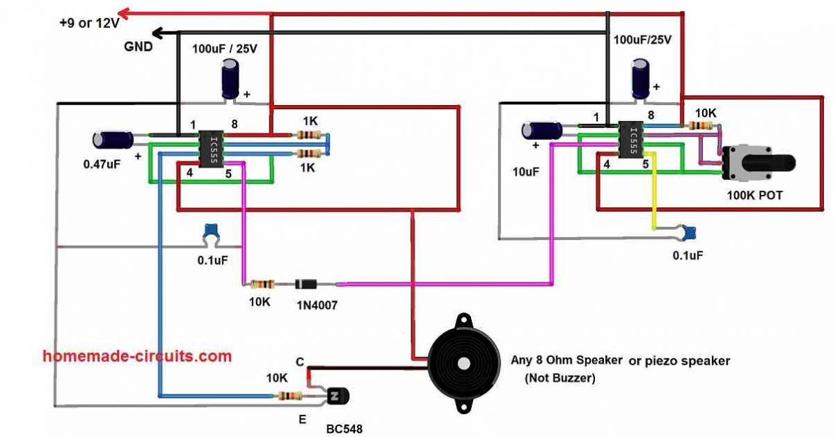 The above shown circuit can generate two different tones whose generated sound resembles an emergency vehicleˇŻs siren, such as police siren or ambulance siren.
LetˇŻs see in detail how we achieved two tone output.
There are two IC 555s deployed in the circuit and they are configured as astable multivibrator.
The IC 555 on the left hand side controls a speaker and it is tuned to generate frequency in the range of KHz.
The IC 555 on the right hand side produces frequency in the range from 0.5Hz to 6Hz.
To achieve two different tones from the speaker we need to alter the frequency of IC 555 present at left hand side, this is done by applying a voltage at pin #5 which is called a ˇ°control pinˇ±.
By applying a voltage level at pin #5 of IC 555 we can achieve a frequency output that is altered from its original.
Here a 10K resistor is connected so that we can get a second tone that is pleasant and resembles a siren.
Readers may experiment with different resistor values to get different tones.
We can see a diode is connected with 10K resistor in series so that only +Ve input enters pin #5. Please note that negative input will also alter the speaker frequency (tone) but we found it to be unpleasant in our practical setup.
We provided a 100K potentiometer to adjust the speed of the siren at which the two frequency switches.
You may use any 8 ohm speaker (or with any other impedance value) or use a piezo speaker.
The speaker is driven by a low power NPN transistor which amplifies the feeble signal from IC 555. A 10K base resistor is connected to limit the current to the transistor.
The whole police/ambulance siren circuit setup can be powered using any general purpose 9V battery.
Note: Please donˇŻt skip any 0.1uF value capacitors that are connected to pin #5 of IC 555, they provide good stability to the generated frequencies and hence stable audio output.
This concludes about the two tone siren sound generator.
Now letˇŻs see about the rotating beacon light.
The above shown circuit can generate two different tones whose generated sound resembles an emergency vehicleˇŻs siren, such as police siren or ambulance siren.
LetˇŻs see in detail how we achieved two tone output.
There are two IC 555s deployed in the circuit and they are configured as astable multivibrator.
The IC 555 on the left hand side controls a speaker and it is tuned to generate frequency in the range of KHz.
The IC 555 on the right hand side produces frequency in the range from 0.5Hz to 6Hz.
To achieve two different tones from the speaker we need to alter the frequency of IC 555 present at left hand side, this is done by applying a voltage at pin #5 which is called a ˇ°control pinˇ±.
By applying a voltage level at pin #5 of IC 555 we can achieve a frequency output that is altered from its original.
Here a 10K resistor is connected so that we can get a second tone that is pleasant and resembles a siren.
Readers may experiment with different resistor values to get different tones.
We can see a diode is connected with 10K resistor in series so that only +Ve input enters pin #5. Please note that negative input will also alter the speaker frequency (tone) but we found it to be unpleasant in our practical setup.
We provided a 100K potentiometer to adjust the speed of the siren at which the two frequency switches.
You may use any 8 ohm speaker (or with any other impedance value) or use a piezo speaker.
The speaker is driven by a low power NPN transistor which amplifies the feeble signal from IC 555. A 10K base resistor is connected to limit the current to the transistor.
The whole police/ambulance siren circuit setup can be powered using any general purpose 9V battery.
Note: Please donˇŻt skip any 0.1uF value capacitors that are connected to pin #5 of IC 555, they provide good stability to the generated frequencies and hence stable audio output.
This concludes about the two tone siren sound generator.
Now letˇŻs see about the rotating beacon light.
Rotating Beacon Light:
Rotating beacon lights or revolving police lights are installed on the roof of emergency vehicles and they rotate with the help of small DC motors at the same time the bulbs get powered too. They do a good job of alerting the commuters that an emergency vehicle is approaching, but they have their disadvantages just like any (electro) mechanical devices suffers from, that is wear and tear due to friction and since they rotate 360 degrees and need for conducting electricity to the bulbs, over time they build contact resistance which could reduce the brightness, develop mechanical jams, etc. (some beacons have stationary bulb and rotating reflectors). We can overcome all the mechanical related issues with a solid state rotating beacon light, meaning they donˇŻt have any mechanical parts. One such design is shown below.Pin Diagram of IC 4017:
 Power supply: Pin #16 is Vcc and pin #8 is GND and can operate from 5V to 18V maximum.
Sequential output pins: Pins 3, 2, 4, 7, 10, 1, 5, 6, 9 and 11 (Q0 to Q9) are output pins whose output turns HIGH with every successive clock input it receives (one pin at an instant and rest stay LOW).
Pin 15: Reset, when this pin is turned high, the count of the IC gets reset.
During normal operation this pin will be pulled to GND.
Pin 14: Clock input, this pin receives clock input from an external source.
Pin 13: Clock enable, if you make this pin HIGH, any clock pulse applied at pin 14 will be ignored by the IC.
During normal operation pin 13 is pulled to GND.
Pin 12: Carry out; this pin is utilized for cascading IC 4017.
In the circuit diagram the outputs are wired according to the sequential outputs mentioned before, but we have terminated the count at 5th output (Q4) by connecting the reset pin #15 to pin #10, as we only need four sequential outputs and rest of the output stays unused.
Each output is connected to a low power NPN transistor to amplify ICˇŻs output so that we can draw more current for the LEDs (load under 500 mA per array).
Power supply: Pin #16 is Vcc and pin #8 is GND and can operate from 5V to 18V maximum.
Sequential output pins: Pins 3, 2, 4, 7, 10, 1, 5, 6, 9 and 11 (Q0 to Q9) are output pins whose output turns HIGH with every successive clock input it receives (one pin at an instant and rest stay LOW).
Pin 15: Reset, when this pin is turned high, the count of the IC gets reset.
During normal operation this pin will be pulled to GND.
Pin 14: Clock input, this pin receives clock input from an external source.
Pin 13: Clock enable, if you make this pin HIGH, any clock pulse applied at pin 14 will be ignored by the IC.
During normal operation pin 13 is pulled to GND.
Pin 12: Carry out; this pin is utilized for cascading IC 4017.
In the circuit diagram the outputs are wired according to the sequential outputs mentioned before, but we have terminated the count at 5th output (Q4) by connecting the reset pin #15 to pin #10, as we only need four sequential outputs and rest of the output stays unused.
Each output is connected to a low power NPN transistor to amplify ICˇŻs output so that we can draw more current for the LEDs (load under 500 mA per array).
Astable Circuit
To make the circuit flash / rotate, we need a clock source, the source can be any astable multivibrator and one such multivibrator is shown below using IC 555.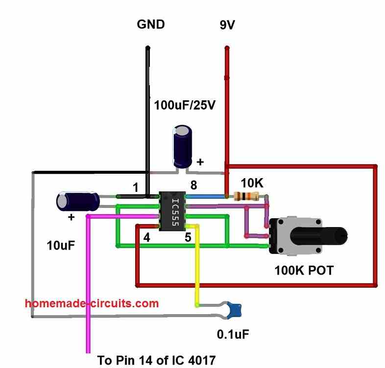 The above circuit operates at 9V, the same as IC 4017 stage.
The above circuit can generate frequency from 0.5 Hz to 6 Hz and the output can be adjusted using the 100K potentiometer.
The frequency of this astable multivibrator will determine the speed of the rotating light.
This concludes the project.
The above circuit operates at 9V, the same as IC 4017 stage.
The above circuit can generate frequency from 0.5 Hz to 6 Hz and the output can be adjusted using the 100K potentiometer.
The frequency of this astable multivibrator will determine the speed of the rotating light.
This concludes the project.
Vehicle Parking Lot Counter Circuit
In this post we are going to learn how to construct a vehicle counter circuit that can count the number of vehicles entered in a parking lot at office building, schools, libraries, restaurants, hotels etc. The proposed project can count up to 999 vehicles especially cars and two wheelers and it can even count long vehicles like bus, vans and trucks.Block diagram:
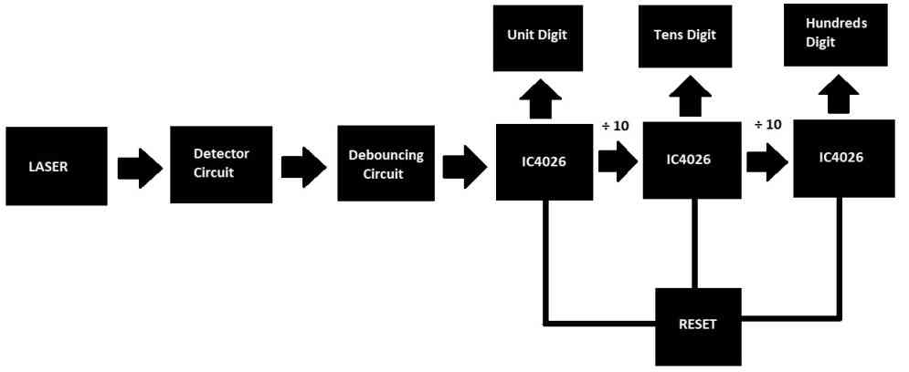 The vehicle parking counter circuit we are going to build will be based on the above functional blocks.
At the left hand side we have a laser module which emits laser beam.
The power output of the beam should be greater than or equal to 5mW so that the laser beam is sufficiently bright.
A detector circuit receives the laser beam and when the laser beam is interrupted the detector stage gives out an appropriate signal to debouncing stage.
The debouncing stage is responsible for giving out a clean pulse to the counter stage.
The debouncing stage removes unwanted surplus pulses received by the detector circuit.
The next three stages are counters which can display counts up to 999. There are three IC 4026s which will drive three common cathode LED displays.
The cascaded ICs gives output 1 pulse for every ten pulses it received at clock input, thus we can derive units, tens and hundreds digit places.
A reset button is connected to all IC 4026s so that a user can reset the count to zero according to their circumstances if necessary.
The vehicle parking counter circuit we are going to build will be based on the above functional blocks.
At the left hand side we have a laser module which emits laser beam.
The power output of the beam should be greater than or equal to 5mW so that the laser beam is sufficiently bright.
A detector circuit receives the laser beam and when the laser beam is interrupted the detector stage gives out an appropriate signal to debouncing stage.
The debouncing stage is responsible for giving out a clean pulse to the counter stage.
The debouncing stage removes unwanted surplus pulses received by the detector circuit.
The next three stages are counters which can display counts up to 999. There are three IC 4026s which will drive three common cathode LED displays.
The cascaded ICs gives output 1 pulse for every ten pulses it received at clock input, thus we can derive units, tens and hundreds digit places.
A reset button is connected to all IC 4026s so that a user can reset the count to zero according to their circumstances if necessary.
Circuit diagram:
We will be exploring the circuit diagram one stage at a time so that we can grasp the circuit better. Laser setup. LDR detector and debouncing circuit. 7 segment counter circuit. Laser setup: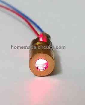 A 5V laser module is utilized in this project and the optical power output of the module can be equal to or greater than 5mW which provides sufficient brightness.
On the receiver side we need to make the below illustrated setup so that the receiver can receive the laser beam with least interference with ambient light sources.
A 5V laser module is utilized in this project and the optical power output of the module can be equal to or greater than 5mW which provides sufficient brightness.
On the receiver side we need to make the below illustrated setup so that the receiver can receive the laser beam with least interference with ambient light sources.
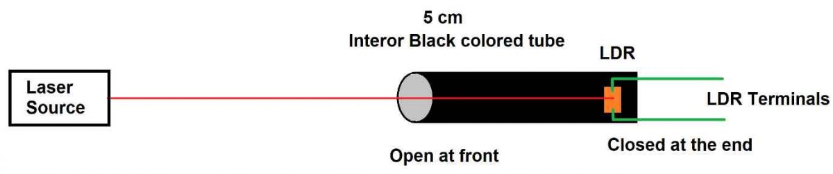 You need to find or make a hollow cylindrical tube that is at least 5 cm in length and a small opening (1.5 to 2 cm) at the front and the LDR is placed at rear end of the tube which is sealed with suitable material to prevent light entering through rear.
It is recommended to paint the interior of the tube with black paint.
The laser and the hollow tube must be aligned in such a way that laser beam directly hits the LDR.
The vehicles pass between the laser transmitter and LDR setup.
Please leave sufficient gap between the two so that vehicles can move freely.
You need to find or make a hollow cylindrical tube that is at least 5 cm in length and a small opening (1.5 to 2 cm) at the front and the LDR is placed at rear end of the tube which is sealed with suitable material to prevent light entering through rear.
It is recommended to paint the interior of the tube with black paint.
The laser and the hollow tube must be aligned in such a way that laser beam directly hits the LDR.
The vehicles pass between the laser transmitter and LDR setup.
Please leave sufficient gap between the two so that vehicles can move freely.
Detector and Debouncing circuit:
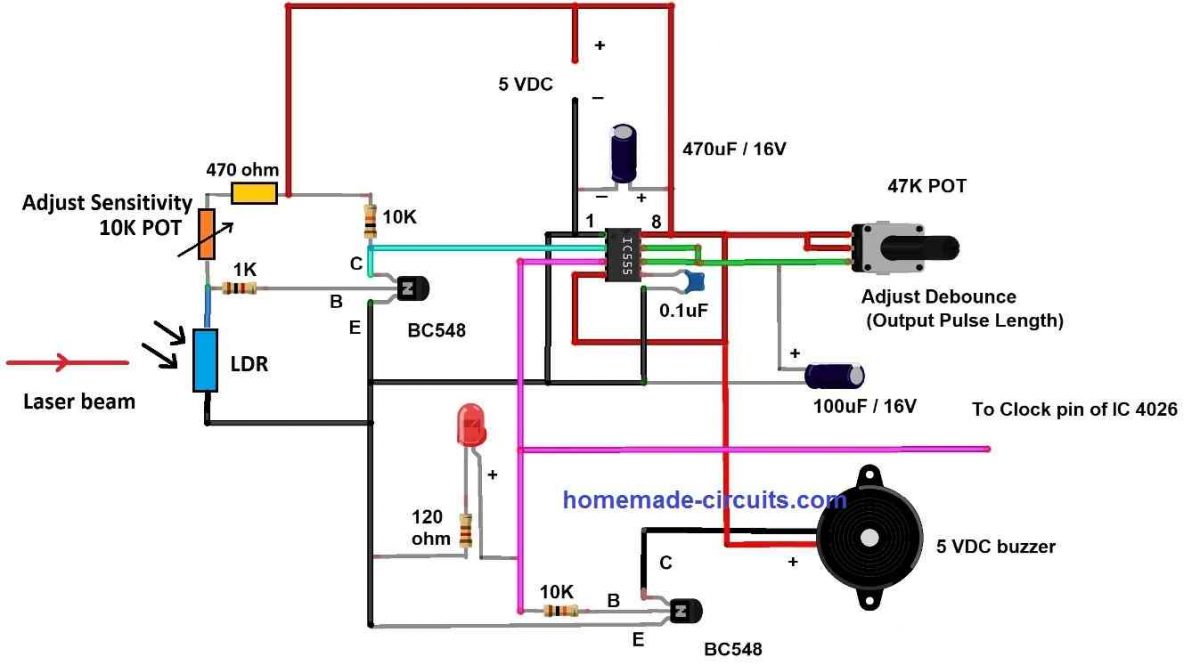 The detector circuit consists of a LDR, a NPN transistor and few resistors.
When the laser hits the LDR, its resistance drop to a very low value and negative signal will be available at the base terminal of the transistor, this will prevent the transistor turning ON.
When a vehicle interrupts the laser beam LDRˇŻs resistance increases significantly and positive signal will be available at the base (positive supply via potentiometer and 470 ohm resistor), this will turn ON the transistor and gives out negative signal (at collector terminal) to IC555ˇŻs pin #2 which is necessary for triggering IC555ˇŻs output pin high.
The debouncing circuit is nothing but a monostable multivibrator, once a negative pulse is received by IC 555 its output pin #3 will turn HIGH and it will ignore pulses from the detector circuit until the IC 555 goes back to its stable state (idle output is LOW), this will gives out a clean positive pulse to the next stage.
The debouncing circuit is implemented to ignore multiple pulses generated by the moments of the vehicles especially with two wheels where the laser beam could get interrupted multiple times.
A 47K ohm potentiometer is provided to adjust debouncing time (maximum 5 seconds).
A buzzer and LED are provided to indicate that a vehicle has entered the parking lot and a count has been registered.
The detector circuit consists of a LDR, a NPN transistor and few resistors.
When the laser hits the LDR, its resistance drop to a very low value and negative signal will be available at the base terminal of the transistor, this will prevent the transistor turning ON.
When a vehicle interrupts the laser beam LDRˇŻs resistance increases significantly and positive signal will be available at the base (positive supply via potentiometer and 470 ohm resistor), this will turn ON the transistor and gives out negative signal (at collector terminal) to IC555ˇŻs pin #2 which is necessary for triggering IC555ˇŻs output pin high.
The debouncing circuit is nothing but a monostable multivibrator, once a negative pulse is received by IC 555 its output pin #3 will turn HIGH and it will ignore pulses from the detector circuit until the IC 555 goes back to its stable state (idle output is LOW), this will gives out a clean positive pulse to the next stage.
The debouncing circuit is implemented to ignore multiple pulses generated by the moments of the vehicles especially with two wheels where the laser beam could get interrupted multiple times.
A 47K ohm potentiometer is provided to adjust debouncing time (maximum 5 seconds).
A buzzer and LED are provided to indicate that a vehicle has entered the parking lot and a count has been registered.
7 Segment display counter circuit:
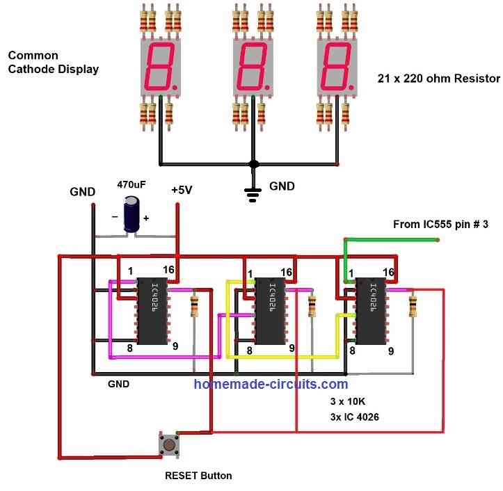
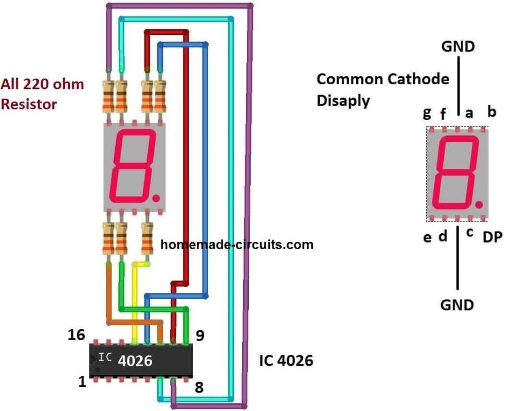 This stage of the vehicle parking counter circuit is responsible for counting number of vehicles entered in the parking lot.
Before we try to understand the above circuit, we need to understand IC 4026ˇŻs pin diagram and what each of the 16 pins does and you will find it very easy to understand.
This stage of the vehicle parking counter circuit is responsible for counting number of vehicles entered in the parking lot.
Before we try to understand the above circuit, we need to understand IC 4026ˇŻs pin diagram and what each of the 16 pins does and you will find it very easy to understand.
Pin diagram of IC4026:
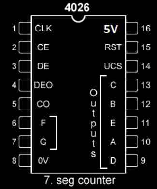 Pin 1: Clock input.
Pin 2: Clock inhibit, Ignores clock input if this pin is connected to high.
During normal operation pin 2 is connected to GND.
Pin 3: Digit enable, when this pin is connected to high, the output A to G is enabled.
Pin 5: Carry out, when the IC receives every 10th pulse this pins turns high which can be fed to another IC 4026ˇŻs clock input pin, thus we cascade them.
Cascading can be done with any number of IC 4026s to get large numbers.
Pins 6, 7, 9, 10, 11, 12, 13 are segments A, B, C, D, E, F, G respectively.
Pin 8: GND.
Pin 15: Reset, when this pin is turned high the count will turn zero.
During normal operation this pin is connected to GND.
Pin 16: Vcc.
By just understanding the above pin description you can understand the circuit why the pins are connected in a certain way.
The 10K resistors are used to pull the pin #15 to down (GND) during normal operation and when you press the reset button the pin 15 turns high which resets all the IC 4026s to zero.
Note: You can place the proposed vehicle parking lot counter circuit at the entrance and also at exit.
By doing this you can know how many vehicles have entered the parking lot and how many left the parking lot and by doing the below shown calculation we can find number of vehicles currently parked:
Entrance count ¨C Exit count = Vehicles parked currently
Pin 1: Clock input.
Pin 2: Clock inhibit, Ignores clock input if this pin is connected to high.
During normal operation pin 2 is connected to GND.
Pin 3: Digit enable, when this pin is connected to high, the output A to G is enabled.
Pin 5: Carry out, when the IC receives every 10th pulse this pins turns high which can be fed to another IC 4026ˇŻs clock input pin, thus we cascade them.
Cascading can be done with any number of IC 4026s to get large numbers.
Pins 6, 7, 9, 10, 11, 12, 13 are segments A, B, C, D, E, F, G respectively.
Pin 8: GND.
Pin 15: Reset, when this pin is turned high the count will turn zero.
During normal operation this pin is connected to GND.
Pin 16: Vcc.
By just understanding the above pin description you can understand the circuit why the pins are connected in a certain way.
The 10K resistors are used to pull the pin #15 to down (GND) during normal operation and when you press the reset button the pin 15 turns high which resets all the IC 4026s to zero.
Note: You can place the proposed vehicle parking lot counter circuit at the entrance and also at exit.
By doing this you can know how many vehicles have entered the parking lot and how many left the parking lot and by doing the below shown calculation we can find number of vehicles currently parked:
Entrance count ¨C Exit count = Vehicles parked currently
Infrared Controlled Car Door Lock
In this post we will learn how to build a simple yet foolproof infrared based remote control, which can be used for locking and unlocking any vehicle door through a personal remote handset. The remote controlled vehicle door lock is foolproof since it works only with a specific IR frequency range, and will not respond to a different frequency to the one set in the circuit. The most widely used frequency range intended for remote-control purposes is in the 900 nanometer spectrum, generally known as the infrared spectrum of the light range. This is the spot in which the most of the InfraRed (IR) LED's and phototransistors generate the maximum output and sensitivity. The most basic IR remote control system is one that works with a switched (on/off) IR light supply for a transmitter and a photo-sensitive detector device having a switchable output for the receiver. This kind of remote-control systems functions only with a condition that the receiver does not get subjected to some other IR light source. Because the receiver is unable to differentiate between a day light IR radiation or any other high intensity source, from the transmitter's IR output. The effectiveness of this type of basic or ordinary IR remote system is particularly minimal. Therefore we need a system that may be capable of rejecting all types ambient IR light sources, and detect and respond to only the infrared beam coming from a tuned compatible IR transmitter unit. The following designs are exactly built in this way for detecting only a specific band of IR signals and prohibit all other unwanted IR disturbances present in the atmosphere.Infrared Transmitter
The IR remote-control design reduces the risk for the atmospheric infrared-radiation challenge by applying a modulated light source for the transmitter along with a tuned detector for the receiver circuit. While this type of design prevents the receiver from reacting to ambient IR-light sources apart from the intended one, it is unable to stop the IR detector from viewing the ambient IR sources. In case the IR detector is not guarded against powerful IR emitters, the detector may get over-loaded and stop responding to the intended remote transmitter's signals. Shielding from atmospheric IR radiations can be effortlessly implemented by covering the IR phototransistor inside an opaque box and by permitting an IR light to reach the detector only through one particular direction.Infrared Receiver
The receiver design can be witnessed from the Fig. 2 below which is designed to be perfectly compatible with our transmitter circuit exhibited in Fig. 1 above. In the above IR receiver circuit, the modulated IR signal from the transmitter is recognized by the phototransistor Q3, which oscillates between the thresholds of saturation and cutoff, synchronized with the transmitter signal.
The AC element of the transmission existing at the Q3 collector is transferred through C2 to the Q1 base for more amplification.
Later on, this enhanced signal is applied to U1, which is an another 567 PLL, configured like a decoder circuit and tuned with the identical frequency as the transmitter PLL.
As soon as the transmission IR waves hitting the pin3 input of U1 is at the right frequency and over 50 millivolts, causes the U1 output at pin 8 to be pulled low or to the ground potential activating the relay circuit.
This is indicated by an illuminated LED1.
Transistor Q2 tracks the DC part of the received IR signal (which includes all the wanted and unwanted IR radiation striking the phototransistor) indicating the proper processing of the IR beam through the attached voltmeter.
The DC-carrier voltage diminishes as the strength of the IR light increases, therefore a lower voltage level (signal) on the meter implies that a genuinely powerful IR signal from the transmitter is striking Q3.
As long as the voltage at the Q3 collector continues over 2 volts (as indicated on the meter), the receiver works perfectly; however in case the ambient IR striking the phototransistor is very powerful, the voltage could decrease to a level where the actual transmitter's IR beams will never be recognized.
For switching other heavier loads, the LED1 could be replaced with an optocoupler, and thus enable almost anything to be switched on or off with the easy IR remote-control system.
In the present design a transistorized relay driver is used and connected with the pin8 output of the receiver circuit.
The relay driver actuates the central lock device of the car in response to the ON/OFF operation of the IR receiver, through the IR transmitter handset.
In the above IR receiver circuit, the modulated IR signal from the transmitter is recognized by the phototransistor Q3, which oscillates between the thresholds of saturation and cutoff, synchronized with the transmitter signal.
The AC element of the transmission existing at the Q3 collector is transferred through C2 to the Q1 base for more amplification.
Later on, this enhanced signal is applied to U1, which is an another 567 PLL, configured like a decoder circuit and tuned with the identical frequency as the transmitter PLL.
As soon as the transmission IR waves hitting the pin3 input of U1 is at the right frequency and over 50 millivolts, causes the U1 output at pin 8 to be pulled low or to the ground potential activating the relay circuit.
This is indicated by an illuminated LED1.
Transistor Q2 tracks the DC part of the received IR signal (which includes all the wanted and unwanted IR radiation striking the phototransistor) indicating the proper processing of the IR beam through the attached voltmeter.
The DC-carrier voltage diminishes as the strength of the IR light increases, therefore a lower voltage level (signal) on the meter implies that a genuinely powerful IR signal from the transmitter is striking Q3.
As long as the voltage at the Q3 collector continues over 2 volts (as indicated on the meter), the receiver works perfectly; however in case the ambient IR striking the phototransistor is very powerful, the voltage could decrease to a level where the actual transmitter's IR beams will never be recognized.
For switching other heavier loads, the LED1 could be replaced with an optocoupler, and thus enable almost anything to be switched on or off with the easy IR remote-control system.
In the present design a transistorized relay driver is used and connected with the pin8 output of the receiver circuit.
The relay driver actuates the central lock device of the car in response to the ON/OFF operation of the IR receiver, through the IR transmitter handset.
Integrating with Car Central Lock
A car central lock system is powered by a magnetic solenoid, which pushes and pulls the lever of the lock for implementing the locking and unlocking of the car doors. The following image shows how the car central mechanism works, whose shaft is pulled and pushed by the actuation of an internal geared motor. This happens when the power or the voltage to the motor is alternately switched with a forward conduction and reverse conduction, by changing the polarity of the input supply. However, it must be noted that the after the solenoid gets actuated, the supply must be immediately cut off to the solenoid, otherwise the solenoid can burn.
This issue is effectively taken care of in the relay driver circuit, where a separate DPDT is employed for operating the solenoid, which delivers the current to the solenoid via two 1000 uF capacitors.
The capacitors ensure that the current is supplied to the solenoid only momentarily as long as the capacitors are charged, and then it is cut off.
As shown in the IR receiver circuit diagram pin#8 of the IC 567 which is the output of the IC, is connected with the relay driver circuit.
Whenever the IR receiver is activated with a compatible frequency, pin#8 goes low, and the relay drivers actuates the car lock solenoid once, which causes the doors to either lock or unlock depending on its initial situation.
When the next activation is carried out by pressing the transmitter IR remote, the solenoid now operate in the reverse direction, causing the appropriate locking or unlocking action on the door locks.
However, it must be noted that the after the solenoid gets actuated, the supply must be immediately cut off to the solenoid, otherwise the solenoid can burn.
This issue is effectively taken care of in the relay driver circuit, where a separate DPDT is employed for operating the solenoid, which delivers the current to the solenoid via two 1000 uF capacitors.
The capacitors ensure that the current is supplied to the solenoid only momentarily as long as the capacitors are charged, and then it is cut off.
As shown in the IR receiver circuit diagram pin#8 of the IC 567 which is the output of the IC, is connected with the relay driver circuit.
Whenever the IR receiver is activated with a compatible frequency, pin#8 goes low, and the relay drivers actuates the car lock solenoid once, which causes the doors to either lock or unlock depending on its initial situation.
When the next activation is carried out by pressing the transmitter IR remote, the solenoid now operate in the reverse direction, causing the appropriate locking or unlocking action on the door locks.
Power Supply
Any well-regulated DC supply from a suitable AC to DC adapter having an output DC of 12 volts at about 500 milliamps could be employed to test the receiver circuit. Once tested on work bench, the circuit may installed and integrated with any vehicle door lock, having a 12 V battery The transmitter circuit could be constructed on a piece of stripboard and encased inside a little plastic-type box with the IR diode sticking out in one edge of the box. A small convex lens could be included to both the transmitter/receiver units in order to focus the IR strength for increased working range.Automobile Electrical Fault Finder Probe Circuit
This simple automotive electrical fault finder probe circuit will enable you to solve most electrical troubleshooting in your cars, tempos, motorcycles etc with a lot of ease and in a hassle free manner. The idea is very simple. The circuit exploits the high impedance gate value of the MOSFET which makes the circuit extremely sensitive to voltage levels, so that it is able to detect even the slightest bit of continuity. The probe point is used for locating the faulty line running anywhere in the electrical system. The probe point can be touched where a continuity is to be detected. Our hand holding the probe body connects our body with the junction of the MOSFET drain and the lamp.
Our other hand is supposed to be touched to one of the known earth point of the car chassis.
With this arrangement, the troubleshooting process can be commenced, and if the probe locates even the slightest of continuity, it will cause the lamp to light up.
In the circuit for the automotive fault finder probe, the resistor Rx indicates the resistance of our body.
This depicts, one hand holding or touching the drain side of the MOSFET while the other hand resting on the chassis of the car, or the car body.
Our hand holding the probe body connects our body with the junction of the MOSFET drain and the lamp.
Our other hand is supposed to be touched to one of the known earth point of the car chassis.
With this arrangement, the troubleshooting process can be commenced, and if the probe locates even the slightest of continuity, it will cause the lamp to light up.
In the circuit for the automotive fault finder probe, the resistor Rx indicates the resistance of our body.
This depicts, one hand holding or touching the drain side of the MOSFET while the other hand resting on the chassis of the car, or the car body.
Construction
The construction of the car electrical fault finder probe can be see in the above picture. The body of the unit is actually made up of a metallic substance, such as steel or copper or aluminum. The MOSFET and the resistor assembly is housed inside a plastic cap and fitted at the lower end of the metal body. A tinned copper wire is used as the probe point fitted on the other end of the plastic cap. A sel-tapping screw is used for connecting the metal body with the drain connection of the MOSFeT and the lamp.How the Circuit Works
Suppose the user wants to locate the continuity of an earth wire across the electrical wiring, which might have lost its contact to a specific electrical gadget. The user holds the probe with his one hand, so that the body comes in contact with the MOSFET drain and the 3V from the lamp. Next, he holds the car body, so that the 3V battery positive from his body enters the car body. After this the probe point is touched to the different wires for tracing the continuity. As long as a continuity is present, the probe's +3V from the user's body passing through the car body reaches the probe point, and the MOSFET gets the required gate voltage, which keeps the lamp illuminated. However, once the probe reaches a point where the probe lamp stops illuminating will indicate towards the broken continuity point., and the user can quickly troubleshoot the area by correcting the cable joint appropriately.Car Electrical Fault Finder
This handy car electrical fault finder probe was created as a part of an inexpensive test equipment to keep in the car for anon-the-spot electrical system debugging. It may be created in a variety of styles to meet the needs of the particular consumer. The probe's primary section is made up ofof two LEDs that display the health of any wiring in the car. When the probe is removed, two LEDs illuminate, representing a voltage level that is neither positive nor negative. When the probe is attached to a contact that has a certain voltage state, the relevant LED will illuminate and the other one will turn off.Voltage detection
The probe's second stageis a voltage detecting circuit that employs a 741 operational amplifier to monitor when the voltage across the automobile battery exceeds 12.5 volts. This gives a quick method to see if the battery is charging. It is clear how LEDs 2 and 3 sense voltage levels. Both are wired in series with the current-limiting resistors R4 and R5. As soon as the probe is linked to a positive or negative voltage, one of the LEDs is virtually shorted out, keeping only the other LED switchedon.
Circuit of a Comparator
A 741 op ampIC is implemented as a comparator in the second stageof the circuit. As soon as the voltage on one input increases above the voltage on the other, the output state toggles. The input on pin 3 detects a reference voltage over Zener diode D1, and pot R6 is utilized to establish the necessary voltage on pin 2. Once the battery voltage decreases, the voltage on pin 2 falls below the potentialon pin 3, prompting the output to go high and illuminating LED 1, which is designated asCHARGING.Testing the Probe
After completing the circuit, it must be tested by first placing R6 to the center of its range and coupling a variable-voltage supply and a voltmeter across C2. Now, with the car tester circuitswitched on, if you adjusta voltage between 6 and 12 volts, LED1 illuminates (or turnsoff). The presetis at this moment is set such that the LED only illuminates when the supply voltage reaches 12.5 volts.Ignition Timing
Put the testing probe in the glove compartment or trunk of your car. In the event of a power outage, you'll always have it quickly accessible. It may also be utilized to detect the exact moment the CDI contactsopen, allowing for precise static ignition timing.Automobile Engine RPM Servicing Meter Circuit (Analogue Tachometer Circuits)
These useful lightweight, cheap, analogue tachometer circuits are developed for facilitating car or auto servicing mechanics for precisely adjusting a car ignition system RPM to get maximum efficiency from it. The proposed circuits are actually combined results of a tachometer and a dwell meter.Application
The car RPM servicing meter circuit can be applied for analyzing the ignition timing at several RPMs, along with a timing lamp. When the circuit is utilized in the form of a dwell meter it can be used for reading the angle at which the ignition pulse is switched ON, and thus it can provide the necessary information to the auto mechanic regarding the timing adjustment of the CDI circuit. The complete configuration is demonstrated in the figure below and is designed for cars or automobile having negative earthing system, that the majority of contemporary cars have. The idea can be also tailored for positive earth vehicles by connecting all diodes and electrolytic capacitors with reverse polarity, and by replacing PNP transistors with NPN and vice versa. The circuit is powered through the car battery supply itself. The working of the circuit can be understood with the following points:How the Circuit Works
 Please swap the emitter/collector pins of the T7 which is incorrectly oriented in the diagram
Transistors T1 and T2 are rigged as a Schmitt trigger.
For so long as no positive pulse is detected at the input from the pickup coil, T1 stays switched off and T2 is switched on, which means T4 is furthermore switched on.
This causes a positive voltage corresponding to the battery supply voltage minus the T4 base-emitter voltage to be generated at T4 emitter.
However, when a positive pulse is generated from the pickup coil, T1 is activated and the Schmitt trigger toggles the opposite way.
T4 is at this point switched off causing voltage existing at its emitter to become zero.
The average voltage at the T4 emitter is as a result proportionate to the ratio of ON/OFF switching time of the pickup coil i.e.
or in other words, this voltage value is determined by the dwell angle.
When switch S1 is in 'a' position the average current via the meter will also be dependent on the dwell angle, hence the meter could be graduated linearly with respect to the dwell angle.
When the switch is in position 'b' the circuit simply works like a tachometer.
C2 works like a differentiator for the pulses coming from T3 collector and the resultant output is used to activate a monostable stage built built around transistors T5 and T6.
The monostable generates constant PWM output, however as the engine RPM increases the duty cycle of the pulses also rises.
The average voltage at the T7 emitter, and therefore the average current via the meter, now depends on the ratio of `pulse' to 'no-pulse' period.
This means that as the r.p.m.
rises and the pulses width get wider, the current via the meter also increases linearly.
Please swap the emitter/collector pins of the T7 which is incorrectly oriented in the diagram
Transistors T1 and T2 are rigged as a Schmitt trigger.
For so long as no positive pulse is detected at the input from the pickup coil, T1 stays switched off and T2 is switched on, which means T4 is furthermore switched on.
This causes a positive voltage corresponding to the battery supply voltage minus the T4 base-emitter voltage to be generated at T4 emitter.
However, when a positive pulse is generated from the pickup coil, T1 is activated and the Schmitt trigger toggles the opposite way.
T4 is at this point switched off causing voltage existing at its emitter to become zero.
The average voltage at the T4 emitter is as a result proportionate to the ratio of ON/OFF switching time of the pickup coil i.e.
or in other words, this voltage value is determined by the dwell angle.
When switch S1 is in 'a' position the average current via the meter will also be dependent on the dwell angle, hence the meter could be graduated linearly with respect to the dwell angle.
When the switch is in position 'b' the circuit simply works like a tachometer.
C2 works like a differentiator for the pulses coming from T3 collector and the resultant output is used to activate a monostable stage built built around transistors T5 and T6.
The monostable generates constant PWM output, however as the engine RPM increases the duty cycle of the pulses also rises.
The average voltage at the T7 emitter, and therefore the average current via the meter, now depends on the ratio of `pulse' to 'no-pulse' period.
This means that as the r.p.m.
rises and the pulses width get wider, the current via the meter also increases linearly.
How to Calibrate
The device could be calibrated as follows: With S1 in position 'a', connect the R1 input to ground line, then fine-tune P1 to obtain a full scale deflection of the meter. This becomes equivalent to a 360ˇă dwell angle and the scale could be calibrated linearly through 0 to 360 degrees. The tachometer scale must be calibrated with full-scale so that it corresponds to the highest optimum r.p.m. For the majority of applications 8000 could be just adequate. If the tool is to be applied on four and six-cylinder engines, in that case either a couple of scales may be needed, or S1 may need to be substituted by a 3 pole switch and P2 need to be replicated to correspond a single scale for various engine ranges. This is because a six cylinder engine generates proportionately a lot more pulses for a specific r.p.m. The device could be calibrated with the help of the basic transformer/bridge circuit shown, which produces a 100 Hz waveform. The 100 Hz frequency becomes equivalent to 3000 r.p.m.
for a four-cylinder engine, and 2000 r.p.m.
for a six-cylinder engine.
The output from this circuit is attached to the input of the analogue tachometer device and P2 is tweaked to optimize a precise deflection and reading on the meter.
The 100 Hz frequency becomes equivalent to 3000 r.p.m.
for a four-cylinder engine, and 2000 r.p.m.
for a six-cylinder engine.
The output from this circuit is attached to the input of the analogue tachometer device and P2 is tweaked to optimize a precise deflection and reading on the meter.
Two Transistor Tachometer for Finding Engine Faults
In the standby position T2 BC107 is in the conducting state. Each time a pulse is generated from the pickup coil, it is applied at the T1, through the resistive divider network R1 and R2. Resistor R3 is used for limiting the current to the base/emitter junction of T1, while the diode D1 ensures only the positive pulses are allowed to pass and block the bad negative pulses from the pickup coil. With each pulse from the pickup col, T1 responds causing in a proportionate change in its monostable output effect, which is indicated on the connected meter needle deflection, which is configured as an integrator for the fluctuating monostable signals. As the engine moves faster, the pickup coil signals also become faster causing the T1, T2 monostable to create longer output siganls for the meter, and meter needle correspondingly deflects higher and higher, and vice versa. So this simplest tachometer circuit which is built using just a couple of BJTs can be nicely used for understanding the engine performance and for detecting any faults in the engine rotation, by comparing the simple tachometer meter output reading with a normal engine performance.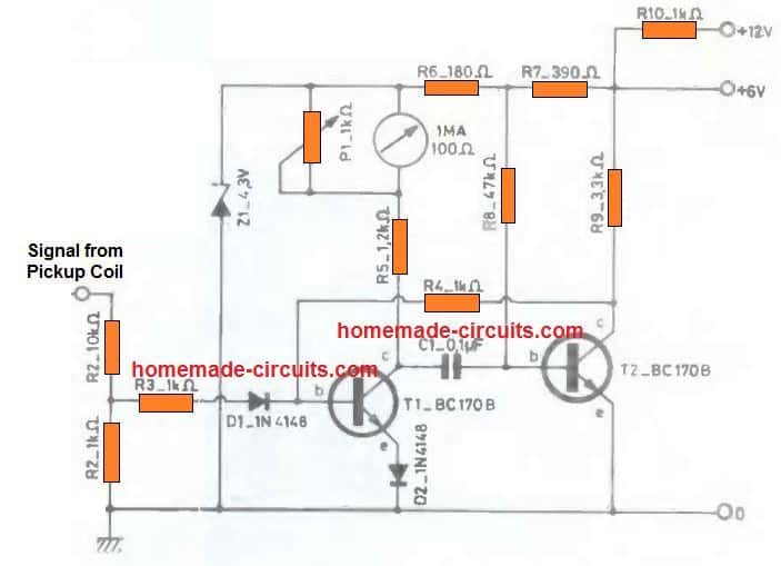
Complete PCB Design Layout
3-Pin Solid-State Car Turn Indicator Flasher Circuit ¨C Transistorized
Although, most of the car electronics have evolved into solid-sate versions, a turn indicator flasher unit is one device which still depend on a relay based design in many of the modern cars.Disadvantages of Relay Based Flasher
There are a couple major disadvantages of a relay based electromechanical flasher unit: 1) First, these being mechanical in nature, go through rapid wear and tear and therefore tend to get damaged soon. 2) Secondly, the flashing rate from these electromechanical circuits are load, voltage and temperature dependent. Meaning, the flashing speed can get affected if the ambient temperature is high or if the battery voltage drops, or if the load exceeds a specified limit. This also implies that if the user wants to flash all the 4 lamps together, he may find the flashing speed too fast and too slow.
Advantages of Solid-State Flasher Circuit
The 3 pin electronic solid state flasher circuit explained here is virtually free from all of these drawbacks. The repetition rate or the flashing rate from this design is practically independent of the supply voltage, ambient temperature, or the load (number of lamps connected). The circuit also features a warning switch which seems to be very reliable and handy during emergency, or road accident situations. The switch bypasses the car switch and allows the lamps to run directly through the flasher, enabling all the 4 lamps to flash together, sending an SOS like signal during a nighttime road mishap. In addition the specifications of this design conforms with all the current statutory requirements for car turn indicators. The repetition frequency of 40 to 90 flashes per minute set in this unit is as per the advised range and also the circuit is designed in such a way that the indicators lamps switch ON instantly when the turn indicator switch is powered.How the Circuit Works
The circuit is essentially an astable multivibrator built using a couple of CMOS NOR gates N1 and N2. N3, N4. Power transistors T1, T2 and T3 acts like a buffer stage for the output of this astable to operate the high wattage indicator lamps. Whenever the indicator switch is toggled ON C2 discharges swiftly via D1 and the indicator lamps.
Pin 13 of N1 turns high and its output becomes low.
The gate N3 and N4 outputs consequently become high, switching on T1, T2 and T3 and turning ON the indicator lamps.
The astable is now initiated to switch at around 1 Hz frequency, causing the indicator lamps to blink on and off at the same rate.
When the hazard warning switch, S1, is turned on, the circuit continues to function in just the identical manner except that all 4 indicator lamps now get linked in parallel and they all begin flashing simultaneously.
T3, which is responsible for handling maximum load current, should be installed on over a heatsink.
When a metallic enclosure is employed to accommodate the proposed 3 pin solid-state flasher circuit then T3 could be clamped to the surface of the case with screw/nut and insulation kit.
The current (amps) through the terminals attached to points A and B can be pretty substantial (up to 8 A) therefore thick wires should be used for these cable connections.
The positive battery supply terminal should be installed with a 10 A fuse if it is not included originally.
Whenever the indicator switch is toggled ON C2 discharges swiftly via D1 and the indicator lamps.
Pin 13 of N1 turns high and its output becomes low.
The gate N3 and N4 outputs consequently become high, switching on T1, T2 and T3 and turning ON the indicator lamps.
The astable is now initiated to switch at around 1 Hz frequency, causing the indicator lamps to blink on and off at the same rate.
When the hazard warning switch, S1, is turned on, the circuit continues to function in just the identical manner except that all 4 indicator lamps now get linked in parallel and they all begin flashing simultaneously.
T3, which is responsible for handling maximum load current, should be installed on over a heatsink.
When a metallic enclosure is employed to accommodate the proposed 3 pin solid-state flasher circuit then T3 could be clamped to the surface of the case with screw/nut and insulation kit.
The current (amps) through the terminals attached to points A and B can be pretty substantial (up to 8 A) therefore thick wires should be used for these cable connections.
The positive battery supply terminal should be installed with a 10 A fuse if it is not included originally.
PCB Design
 Parts List
Resistors:
R1,R3,R4 = 2M2
R2 = 100 k
R5 = 4k7
R6= 120 Ohm (1 Watt)
Capacitors:
C1 = 1O¦Ě/16 V
C2 = 1 ¦Ě/16 V (tantalum)
C3 = 1 nF
C4 = 220 nF
Semiconductors:
IC1 = 4001 (B)
T1 = BC 557, BC 177
T2 = BC 328, BC 327
T3= FT 2955 or TIP 2955
D1 = 1N4148
Parts List
Resistors:
R1,R3,R4 = 2M2
R2 = 100 k
R5 = 4k7
R6= 120 Ohm (1 Watt)
Capacitors:
C1 = 1O¦Ě/16 V
C2 = 1 ¦Ě/16 V (tantalum)
C3 = 1 nF
C4 = 220 nF
Semiconductors:
IC1 = 4001 (B)
T1 = BC 557, BC 177
T2 = BC 328, BC 327
T3= FT 2955 or TIP 2955
D1 = 1N4148
4 Solid-State Car Alternator Regulator Circuits Explored
The 4 simple car voltage current regulator circuits explained below is created as a immediate alternative to any standard regulator and, although developed principally for a dynamo it will function equally effectively with an alternator. If the functioning of a traditional car alternator voltage regulator is analyzed, we find it amazing that these kinds of regulators is often as trusted as they are. While most contemporary cars are furnished with solid-state voltage regulators to regulate the voltage and current output from the alternator, you may still find countless earlier cars installed with electromechanical type of voltage regulators that happen to be potentially unreliable.How Electro-Mechanical Car Regulator Work
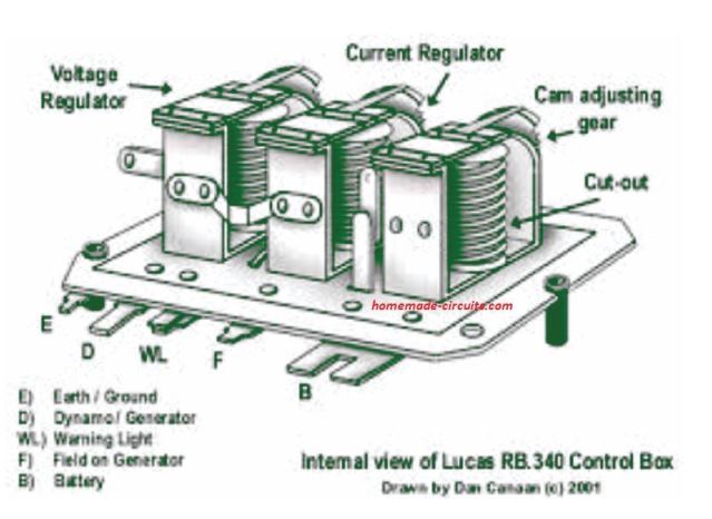 The standard functioning of a electro-mechanical car alternator voltage regulator can be as explained below:
Once the engine is in the idling mode the dynamo starts getting a field current through the ignition warning lamp.
In this position the dynamo armature remains unattached with the battery since its output is smaller compared to battery voltage, and the battery starts discharging through it.
As the speed of the engine begins increasing, the output voltage of the dynamo also begins rising.
As soon as it surpasses the battery voltage a relay is switched ON, connecting the dynamo armature with the battery.
This initiates the charging of the battery.
In case the dynamo output goes up even more an additional relay is activated at around 14.5 volts which cuts off the dynamo field winding.
The field current decays while the output voltage begins dropping right up until this relay deactivates.
The relay at this point consistently switches ON/OFF repeatedly, sustaining the dynamo output at 14.5 V.
This action safeguards the battery from overcharging.
There's also a 3rd relay containing its coil winding in series with the dynamo output, through which the entire dynamo output current passes.
Once the safe output current of the dynamo gets dangerously high, may be due to over discharged battery, this winding activates the relay.
This relay now detaches the field winding of the dynamo.
The function ensures that just the fundamental theory, and the specific circuit of the proposed car voltage current regulator may have different specs depending on a specific car dimensions.
The standard functioning of a electro-mechanical car alternator voltage regulator can be as explained below:
Once the engine is in the idling mode the dynamo starts getting a field current through the ignition warning lamp.
In this position the dynamo armature remains unattached with the battery since its output is smaller compared to battery voltage, and the battery starts discharging through it.
As the speed of the engine begins increasing, the output voltage of the dynamo also begins rising.
As soon as it surpasses the battery voltage a relay is switched ON, connecting the dynamo armature with the battery.
This initiates the charging of the battery.
In case the dynamo output goes up even more an additional relay is activated at around 14.5 volts which cuts off the dynamo field winding.
The field current decays while the output voltage begins dropping right up until this relay deactivates.
The relay at this point consistently switches ON/OFF repeatedly, sustaining the dynamo output at 14.5 V.
This action safeguards the battery from overcharging.
There's also a 3rd relay containing its coil winding in series with the dynamo output, through which the entire dynamo output current passes.
Once the safe output current of the dynamo gets dangerously high, may be due to over discharged battery, this winding activates the relay.
This relay now detaches the field winding of the dynamo.
The function ensures that just the fundamental theory, and the specific circuit of the proposed car voltage current regulator may have different specs depending on a specific car dimensions.
1) Using Power Transistors
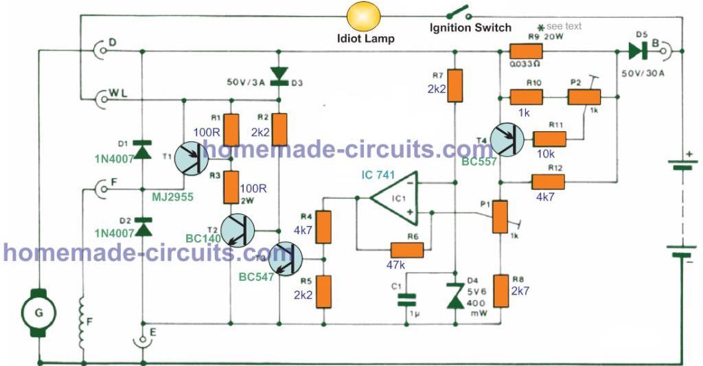 In the indicated design the cut-out relay is substituted by D5, which gets reverse-biased as soon as the dynamo output drops below the battery voltage.
The battery as a result is unable to discharge into the dynamo.
If the ignition is started up the dynamo field winding gets current through the tell-tale light and T1.
Diode D3 is incorporated to avoid current becoming drawn from the field coil due to the reduced armature resistance of the alternator.
As the speed of the engine increases the output from the dynamo proportionately rises, and starts delivering its own field current by means of D3 and T1.
As the cathode side voltage of D3 goes up the warning light gradually dims until it fades off.
When the dynamo output reaches to around 13-14 V the battery begins charging again.
IC1 works like a a voltage comparator which tracks the dynamo output voltage.
As the dynamo output voltage increases the voltage on the op amp inverting input is at first greater than at the non-inverting input, hence the IC output is held low and T3 remains switched off.
As soon as the output voltage goes higher than 5.6 V the inverting input voltage is regulated and controlled at this level by D4.
When the output voltage goes past the specified highest potential (set through P1), the non-inverting input of IC1 becomes higher than the inverting input, causing the IC1 output to change into positive.
This activates T3. which switches OFF T2 and T1, inhibiting current to the dynamo field.
The dynamo field current now decays and the output voltage begins dropping until the comparator reverts back again.
R6 supplies several hundred millivolts of hysteresis which helps the circuit to work like a switching regulator.
T1 is either toggled harder ON or is cut off such that it dissipates fairly low power.
Current regulation is impacted through T4. Once the current by means of R9 is higher than the selected highest level, the voltage drop around it results in T4 to switch on.
This raises the potential at the non-inverting input of IC1 and isolates the dynamo field current.
The value selected for R9 (0.033 Ohm/20 W, made up of 10nos of 0.33 Ohm/2 W resistors in parallel) is suitable to get a optimum output current as high as 20 A.
If larger output currents is desired, R9 value could be reduced appropriately.
The output voltage and current of the device must be fixed by appropriately setting up P1 and P2 to meet the standards of the original regulator.
T1 and D5 should be installed on heatsinks, and must be strictly isolated from the chassis.
In the indicated design the cut-out relay is substituted by D5, which gets reverse-biased as soon as the dynamo output drops below the battery voltage.
The battery as a result is unable to discharge into the dynamo.
If the ignition is started up the dynamo field winding gets current through the tell-tale light and T1.
Diode D3 is incorporated to avoid current becoming drawn from the field coil due to the reduced armature resistance of the alternator.
As the speed of the engine increases the output from the dynamo proportionately rises, and starts delivering its own field current by means of D3 and T1.
As the cathode side voltage of D3 goes up the warning light gradually dims until it fades off.
When the dynamo output reaches to around 13-14 V the battery begins charging again.
IC1 works like a a voltage comparator which tracks the dynamo output voltage.
As the dynamo output voltage increases the voltage on the op amp inverting input is at first greater than at the non-inverting input, hence the IC output is held low and T3 remains switched off.
As soon as the output voltage goes higher than 5.6 V the inverting input voltage is regulated and controlled at this level by D4.
When the output voltage goes past the specified highest potential (set through P1), the non-inverting input of IC1 becomes higher than the inverting input, causing the IC1 output to change into positive.
This activates T3. which switches OFF T2 and T1, inhibiting current to the dynamo field.
The dynamo field current now decays and the output voltage begins dropping until the comparator reverts back again.
R6 supplies several hundred millivolts of hysteresis which helps the circuit to work like a switching regulator.
T1 is either toggled harder ON or is cut off such that it dissipates fairly low power.
Current regulation is impacted through T4. Once the current by means of R9 is higher than the selected highest level, the voltage drop around it results in T4 to switch on.
This raises the potential at the non-inverting input of IC1 and isolates the dynamo field current.
The value selected for R9 (0.033 Ohm/20 W, made up of 10nos of 0.33 Ohm/2 W resistors in parallel) is suitable to get a optimum output current as high as 20 A.
If larger output currents is desired, R9 value could be reduced appropriately.
The output voltage and current of the device must be fixed by appropriately setting up P1 and P2 to meet the standards of the original regulator.
T1 and D5 should be installed on heatsinks, and must be strictly isolated from the chassis.
2) A Simpler Car Alternator Voltage Current Regulator
The following diagram shows another variant of a solid state car alternator voltage and current controller circuit using minimum number of components.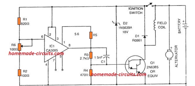 Normally while the battery voltage is below, the full charge level, the regulator IC CA 3085 output remains switch OFF, which allows the Darlington transistor to be in the conducting mode, which keeps the field coil energized, and the alternator operational.
Since the IC CA3085 is rigged as a basic comparator here, when the battery charges to its full charge level, may ba 14.2 V, the potential at pin#6 of the IC changes to 0V, switching OFF the supply to th field coil.
Due to this the current from the alternator decays, inhibiting any further charging of the battery.
The battery is thus stopped from overcharging.
Now, as the battery voltage drops below the CA3085 pin6 threshold, the output becomes high once again, causing the transistor to conduct, and power the field coil.
The alternator begins supplying to the battery, so that it begins charging again.
Normally while the battery voltage is below, the full charge level, the regulator IC CA 3085 output remains switch OFF, which allows the Darlington transistor to be in the conducting mode, which keeps the field coil energized, and the alternator operational.
Since the IC CA3085 is rigged as a basic comparator here, when the battery charges to its full charge level, may ba 14.2 V, the potential at pin#6 of the IC changes to 0V, switching OFF the supply to th field coil.
Due to this the current from the alternator decays, inhibiting any further charging of the battery.
The battery is thus stopped from overcharging.
Now, as the battery voltage drops below the CA3085 pin6 threshold, the output becomes high once again, causing the transistor to conduct, and power the field coil.
The alternator begins supplying to the battery, so that it begins charging again.
Parts List
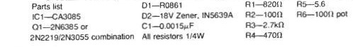
3) Transistorized Car Alternator Regulator Circuit
Referring lo the nest solid-state alternator voltage current regulator diagram below, V4 is configured like a series-pass transistor which regulates the current to the field of the alternator. This transistor along with the two 20 amp diodes are clamped on an external heatsink. It is intriguing to see that dissipation of V1 is not really very high even during the maximum eld current, rather merely within 3 amps.
4) IC 741 Car Alternator Voltage Current Regulator Charger Circuit
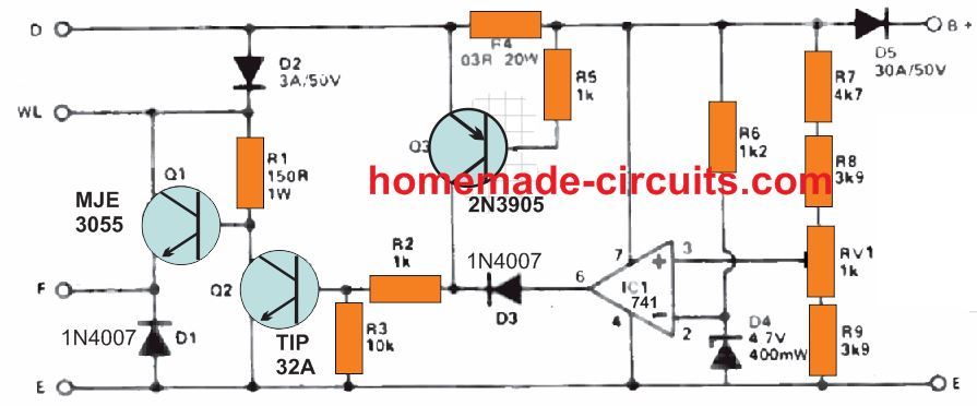 This circuit offers solid-state management of battery charging.
The alternator's field winding is in the beginning stimulated through the ignition light bulb just as in a traditional method.
Current moving across the WL terminal travels via Q1 to the F terminal then finally on the field coil.
As soon as the engine is powered, current from car's dynamo moves through D2 to Q1. The ignition tell-tale lamp fades out since the WL terminal voltage exceeds than that of the battery.
Current likewise moves through D5 towards the battery.
At this point, IC1 which is rigged as a comparator detects the battery voltage.
When this voltage on the non-inverting input becomes higher than the inverting input (clamped at 4.6 volts via zener D4) causes the output of the op amp to go high.
Current subsequently passes via D3 and R2 towards the Q2 base and instantly switches it ON.
This action as a result grounds the Q1 base switching it off and removing the current applied on the field winding.
The alternator output now drops, causing battery voltage to also drop correspondingly.
This procedure ensures that the battery voltage is always held constant, and is never allowed to be over charged.
The battery full charge voltage can be tweaked through RV1 to roughly 13.5 volts.
During cold weather conditions while starting the car, the battery voltage may drops significantly low.
As soon as the engine has ignited the battery's internal resistance also become quite low, forcing it to pull too much current from the alternator and thus leading to a possible deterioration of the alternator.
In order to restrict this high current consumption, resistor R4 is introduced within the primary power terminal from the alternator.
The R4 resistance is selected making sure that at highest possible current (Commonly 20 amps) 0.6 volts is generated across it which causes Q3 to turn ON.
The moment Q3 activates current moves through the power line through R2 towards the Q2 base, switching it on, which then, shuts off Q1 and cutting off current flow to the field winding.
Due to this the dynamo or the alternator output now drops.
No modifications need to be made to the original wiring of the alternator in the car.
The circuit could be encased within an old regulator box, Q1, Q2 and D5 must be attached to an appropriately dimensioned heat sink.
This circuit offers solid-state management of battery charging.
The alternator's field winding is in the beginning stimulated through the ignition light bulb just as in a traditional method.
Current moving across the WL terminal travels via Q1 to the F terminal then finally on the field coil.
As soon as the engine is powered, current from car's dynamo moves through D2 to Q1. The ignition tell-tale lamp fades out since the WL terminal voltage exceeds than that of the battery.
Current likewise moves through D5 towards the battery.
At this point, IC1 which is rigged as a comparator detects the battery voltage.
When this voltage on the non-inverting input becomes higher than the inverting input (clamped at 4.6 volts via zener D4) causes the output of the op amp to go high.
Current subsequently passes via D3 and R2 towards the Q2 base and instantly switches it ON.
This action as a result grounds the Q1 base switching it off and removing the current applied on the field winding.
The alternator output now drops, causing battery voltage to also drop correspondingly.
This procedure ensures that the battery voltage is always held constant, and is never allowed to be over charged.
The battery full charge voltage can be tweaked through RV1 to roughly 13.5 volts.
During cold weather conditions while starting the car, the battery voltage may drops significantly low.
As soon as the engine has ignited the battery's internal resistance also become quite low, forcing it to pull too much current from the alternator and thus leading to a possible deterioration of the alternator.
In order to restrict this high current consumption, resistor R4 is introduced within the primary power terminal from the alternator.
The R4 resistance is selected making sure that at highest possible current (Commonly 20 amps) 0.6 volts is generated across it which causes Q3 to turn ON.
The moment Q3 activates current moves through the power line through R2 towards the Q2 base, switching it on, which then, shuts off Q1 and cutting off current flow to the field winding.
Due to this the dynamo or the alternator output now drops.
No modifications need to be made to the original wiring of the alternator in the car.
The circuit could be encased within an old regulator box, Q1, Q2 and D5 must be attached to an appropriately dimensioned heat sink.
Automotive LED Driver Circuits ¨C Design Analysis
In cars or automobiles, LEDs have grown to be the preferred choice of lighting. Whether it's the rear tail-lights or the tell-tale indicators in the cluster as indicated in Figure 1 below, all incorporate LEDs nowadays. Their compact dimensions helps versatility in design and offers the prospective to be as durable as the vehicleˇŻs life expectancy itself. Figure #1
On the other hand, even though LEDs are highly efficient devices, they are vulnerable to deterioration from unregulated voltage, current and temperature parameters, particularly in the harsh automotive ecosystem.
To be able to enhance LED light efficiency and permanence, LED driver circuit design demands cautious analysis.
Electronic circuits that are applied as LED drivers fundamentally make use of transistors.
One standard circuit topology frequently used in LED drivers happens to be the linear topology, where the transistor is designed to work inside the linear region.
This topology gives us the option of making driver circuits through transistors only or using specialized ICs with built-in transistors and additional LED enhancement features.
In discrete applications, bipolar junction transistors (BJTs), which are highly accessible commodity products, tend to be the favorite.
Despite the fact that BJTs are simple to configure from a circuit point of view, major complications can be found while creating a total LED driver solution that fulfills current control accuracy, PCB dimension, heat management and fault diagnosis, which are a few important prerequisites throughout the entire working supply voltage and temperature range.
Furthermore, as the quantity of LEDs increases, circuit design using discrete BJT stages get even more sophisticated.
Compared to discrete parts, applying IC based alternatives seem to be more convenient with respect the circuit layout, but additionally the design and evaluation procedures.
Besides that, the general remedy may perhaps be even more affordable.
Figure #1
On the other hand, even though LEDs are highly efficient devices, they are vulnerable to deterioration from unregulated voltage, current and temperature parameters, particularly in the harsh automotive ecosystem.
To be able to enhance LED light efficiency and permanence, LED driver circuit design demands cautious analysis.
Electronic circuits that are applied as LED drivers fundamentally make use of transistors.
One standard circuit topology frequently used in LED drivers happens to be the linear topology, where the transistor is designed to work inside the linear region.
This topology gives us the option of making driver circuits through transistors only or using specialized ICs with built-in transistors and additional LED enhancement features.
In discrete applications, bipolar junction transistors (BJTs), which are highly accessible commodity products, tend to be the favorite.
Despite the fact that BJTs are simple to configure from a circuit point of view, major complications can be found while creating a total LED driver solution that fulfills current control accuracy, PCB dimension, heat management and fault diagnosis, which are a few important prerequisites throughout the entire working supply voltage and temperature range.
Furthermore, as the quantity of LEDs increases, circuit design using discrete BJT stages get even more sophisticated.
Compared to discrete parts, applying IC based alternatives seem to be more convenient with respect the circuit layout, but additionally the design and evaluation procedures.
Besides that, the general remedy may perhaps be even more affordable.
Parameters for Designing Automotive LED Drivers
Therefore, when designing LED driver circuits for an automotive lighting application, it is essential to contemplate LED focal points, evaluate circuit design alternatives, and factors in system demands. An LED is actually a P-type N-type (PN) junction diode which allows the current to move through it only in a single direction. Current begins flowing as soon as the voltage across the LED reaches the minimum forward voltage (VF). The level of illumination or the brightness of an LED is determined by the forward current (IF ); while how much current an LED consumes depends on the voltage applied across the LED. Even though the LED brightness and the forward current IF are linearly related, even a slight increase in the forward voltage VF across the LED can trigger an rapid escalation in the current intake of the LED. LEDs with different color specifications have different VF and IF specifications due to their specific semiconductor ingredients (Figure 2). It is necessary to consider each LEDˇŻs datasheet specs into account, specifically while applying different color LEDs within the a single circuit. Figure #2
For instance, when developing with red-green-blue (RGB) lighting, a red LED may come with a Forward voltage rating of around 2 V, while the same for a blue and green LEDs could be around 3 to 4 V.
Considering that youˇŻre operating these LEDs from a single common voltage supply, you might need a well calculated current-limiting resistor for each of the colored LEDs, to avoid LED deterioration.
Figure #2
For instance, when developing with red-green-blue (RGB) lighting, a red LED may come with a Forward voltage rating of around 2 V, while the same for a blue and green LEDs could be around 3 to 4 V.
Considering that youˇŻre operating these LEDs from a single common voltage supply, you might need a well calculated current-limiting resistor for each of the colored LEDs, to avoid LED deterioration.
Thermal and power efficiency
Apart from supply voltage and current parameters, temperature and power efficiency likewise demand careful analysis. Although, most of the current applied across an LED is converted into LED light, a small amount of power is turned into heat within the PN junction of the device. The temperature generated across an LED junction could be seriously affected by a few external parameters such as: by the atmospheric temperature (TA), by the thermal resistance between the LED junction and ambient air (R¦ČJA), and by the power dissipation (PD). The following Equation 1 reveals the power dissipation spec PD of an LED: PD =VF ˇÁ IF ------------ Eq #1 With the help of the above, we can further derive the following equation that calculates the junction temperature (TJ ) of an LED: TJ = TA + R¦ČJA ˇÁ PD ---------- Eq #2 It is essential to determine the TJ not just under normal working conditions, but also under an absolute maximum ambient temperature TA of the design, with regard to worst-case-scenario concerns. As the LED junction temperature TJ increases, its work efficiency deteriorates. An LEDˇŻs forward current IF and junction temperature TJ must stay below their absolute maximum ratings, as classified by the datasheets, so as to protect against destruction (Figure 3). Figure #3
Besides the LEDs, you should also take into account the power efficiency of resistors and the driving elements such as BJTs and operational amplifiers (op amps), specifically as the amount of discrete components increases.
Inadequate power efficiency of the driver stages, the LED on-time period and/or the ambient temperature all of these factors may lead to a rise in temperature of the device, influencing the BJT driver's current output, and reducing the VF drop of the LEDs.
As the rise in temperature reduces the LEDs forward voltage drop, the LED's current consumption rate rises; leading to a proportionately increased power dissipation PD and temperature, and this causes further reduction in LED's forward voltage drop VF.
This cycle of a continuous rise in temperature, also referred to as ˇ°thermal runaway,ˇ± forces the LEDs to function above their optimum operating temperature, causing rapid degradation, and at some point failure of the device, because of an increased level of IF consumption.
Figure #3
Besides the LEDs, you should also take into account the power efficiency of resistors and the driving elements such as BJTs and operational amplifiers (op amps), specifically as the amount of discrete components increases.
Inadequate power efficiency of the driver stages, the LED on-time period and/or the ambient temperature all of these factors may lead to a rise in temperature of the device, influencing the BJT driver's current output, and reducing the VF drop of the LEDs.
As the rise in temperature reduces the LEDs forward voltage drop, the LED's current consumption rate rises; leading to a proportionately increased power dissipation PD and temperature, and this causes further reduction in LED's forward voltage drop VF.
This cycle of a continuous rise in temperature, also referred to as ˇ°thermal runaway,ˇ± forces the LEDs to function above their optimum operating temperature, causing rapid degradation, and at some point failure of the device, because of an increased level of IF consumption.
Linear LED Drivers
Operating LEDs linearly through either transistors or ICs is actually quite convenient. Of all possibilities, the most simple approach to control an LED is usually to connect it right across the supply voltage source (VS). Having the right current-limiting resistor restricts the current draw of the device and fixes an accurate voltage drop for the LED. The following Equation 3 can be used for working out the series resistor (RS) value: RS = VS - VF / IF ---------- Eq #3 Referring to Figure #4 we see that 3 LEDs are used in series, the entire voltage drop VF across the 3 LEDs should be taken into consideration by the VF calculation (the LED's forward current IF remains constant.)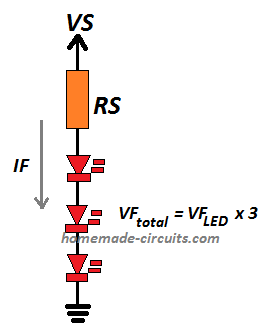 Figure #4
Although this can be the simplest LED driver configuration, it may be quite unpractical in a real-life implementation.
Power supplies, particularly automotive batteries, are susceptible to voltage fluctuations.
A minor increase in the supply input triggers the LED to draw higher amounts of current and consequently get destroyed.
Furthermore, excessive power dissipation PD in the resistor increases the device temperature, which may give rise to thermal runaway.
Figure #4
Although this can be the simplest LED driver configuration, it may be quite unpractical in a real-life implementation.
Power supplies, particularly automotive batteries, are susceptible to voltage fluctuations.
A minor increase in the supply input triggers the LED to draw higher amounts of current and consequently get destroyed.
Furthermore, excessive power dissipation PD in the resistor increases the device temperature, which may give rise to thermal runaway.
Discrete Constant-Current LED Drivers for Automotive Application
When a constant current feature is used, it ensures an enhanced power-efficient and reliable layout. Since the most prevalent technique to operate an LED is through an on and off switching, a transistor enables a well regulated current supply.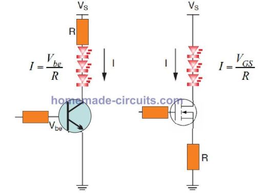 Figure #5
Referring to the Figure 5 above, it may be possible to go for either a BJT or a MOSFET, based upon on the voltage and current specifications of the LED configuration.
Transistors easily handles larger power compared to a resistor, yet are susceptible to voltage ups and downs and temperature variations.
For example, when the voltage around a BJT rises, its current also proportionately increases.
To guarantee additional stability, it is possible to customize these BJT or MOSFET circuits to deliver constant current despite having imbalances in the supply voltage.
Figure #5
Referring to the Figure 5 above, it may be possible to go for either a BJT or a MOSFET, based upon on the voltage and current specifications of the LED configuration.
Transistors easily handles larger power compared to a resistor, yet are susceptible to voltage ups and downs and temperature variations.
For example, when the voltage around a BJT rises, its current also proportionately increases.
To guarantee additional stability, it is possible to customize these BJT or MOSFET circuits to deliver constant current despite having imbalances in the supply voltage.
Designing LED Current Source
Figures 6 to 8 demonstrate a handful of current-source circuit illustrations. In Figure 6, a Zener diode generates a stable output voltage into the base of the transistor.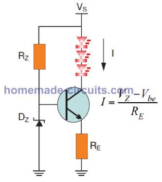 Current-limiting resistor RZ ensures a controlled current to enable the Zener diode to work correctly.
The Zener diode output produces a constant voltage despite of fluctuations in the supply voltage.
The voltage drop over emitter resistor RE should complement the voltage drop of the Zener diode, therefore the transistor adjusts the collector current; which ensures that the current through the LEDs always remains constant.
Current-limiting resistor RZ ensures a controlled current to enable the Zener diode to work correctly.
The Zener diode output produces a constant voltage despite of fluctuations in the supply voltage.
The voltage drop over emitter resistor RE should complement the voltage drop of the Zener diode, therefore the transistor adjusts the collector current; which ensures that the current through the LEDs always remains constant.
Using an Op Amp Feedback
In Figure 7 below, an op amp circuit with a feedback loop is shown for making an ideal automotive LED controller circuit. The feedback connection ensures that the output gets automatically adjusted in order that the potential developed at its negative input remains equal to its positive reference input.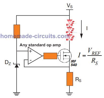 A Zener diode is clamped to generate a reference voltage at the non-inverting input of the op amp.
In case the LEDs current exceeds a predetermined value, it develops an proportionate amount of voltage across the sense resistor RS, which tries to surpass the zener reference value.
Since this causes the voltage at the negative inverting input of the op amp to exceed the positive reference zener value, forces the op amp output to switches OFF which in turn reduces the LED current and also the voltage across RS.
This situation again reverts the op amp output to switch ON state and activates the LED, and this self adjusting action of the op amp continues infinitely ensuring that the LED current never exceeds the calculated unsafe level.
A Zener diode is clamped to generate a reference voltage at the non-inverting input of the op amp.
In case the LEDs current exceeds a predetermined value, it develops an proportionate amount of voltage across the sense resistor RS, which tries to surpass the zener reference value.
Since this causes the voltage at the negative inverting input of the op amp to exceed the positive reference zener value, forces the op amp output to switches OFF which in turn reduces the LED current and also the voltage across RS.
This situation again reverts the op amp output to switch ON state and activates the LED, and this self adjusting action of the op amp continues infinitely ensuring that the LED current never exceeds the calculated unsafe level.
Constant Current LED Drivers using Integrated Circuits
These essential transistor based building blocks, could be easily replicated to operate several strings of LED, as displayed in Figure 9.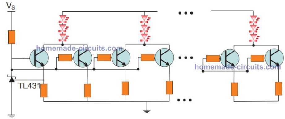 Controlling a group of LED strings quickly causes the component count to rise, occupying higher PCB space and consuming more number of general-purpose input/output (GPIO) pins.
Moreover, such designs are basically without brightness control and fault diagnostics considerations, which are essential needs for most power LED applications.
For including the specifications like brightness control and fault diagnostics requires additional number of discrete components and added design analysis procedures.
LED designs which include higher number of LEDs, causes discrete circuit designs to include higher number of parts, increasing the complexity of the circuit.
In order to streamline the design process, it is considered most effective to apply specialized ICs to function as LED drivers.
Many of discrete components as indicated in Figure 9 could be made easier with an IC based LED driver as revealed in Figure 10.
Controlling a group of LED strings quickly causes the component count to rise, occupying higher PCB space and consuming more number of general-purpose input/output (GPIO) pins.
Moreover, such designs are basically without brightness control and fault diagnostics considerations, which are essential needs for most power LED applications.
For including the specifications like brightness control and fault diagnostics requires additional number of discrete components and added design analysis procedures.
LED designs which include higher number of LEDs, causes discrete circuit designs to include higher number of parts, increasing the complexity of the circuit.
In order to streamline the design process, it is considered most effective to apply specialized ICs to function as LED drivers.
Many of discrete components as indicated in Figure 9 could be made easier with an IC based LED driver as revealed in Figure 10.
 Figure #10
LED driver ICs are specially designed for tackling critical voltage, current and temperature specifications of LEDs, and also for minimizing the part count and board dimensions.
Furthermore, LED driver ICs may have additional features for brightness control and diagnostics, including over temperature protection.
That said, it may be possible to achieve the above advanced features using discrete BJT based designs also, but ICs seem to be an easier alternative, comparatively.
Figure #10
LED driver ICs are specially designed for tackling critical voltage, current and temperature specifications of LEDs, and also for minimizing the part count and board dimensions.
Furthermore, LED driver ICs may have additional features for brightness control and diagnostics, including over temperature protection.
That said, it may be possible to achieve the above advanced features using discrete BJT based designs also, but ICs seem to be an easier alternative, comparatively.
Challenges in Automotive LED Applications
In many automotive LED implementation, brightness control becomes an esential necessity. Since adjusting the forward current IF through the LED adjusts the brightness level proportionately, analogue designs can be employed for achieving the results. A digital method of LED brightness control is through PWM or pulse width modulation. The following details analyzes the two concepts and shows how they can be applied for automotive LED applicationsDifference Between Analogue and PWM LED Brightness Control
Figure 11 evaluates the main difference between analogue and digital methods of controlling LED brightness. Figure #11
By using analog LED brightness control, the LED illumination is altered through the magnitude of the flowing current; larger current results in increased brightness and vice versa.
But, the quality of analog dimming or brightness control is not satisfactory, specifically at lower brightness ranges.
Analog dimming is usually not appropriate for color dependent LED applications, like RGB lighting or status indicators; since varying IF tends to affect the color output of the LED, causing poor color resolution from the RGB LEDs.
In contrast, PWM based LED dimmers do not vary the LED forward current IF, rather controls the intensity by varying the ON/OFF switching rate the LEDs.
Then, the average ON time LED current decides the proportionate brightness on the LED.
It is also called the duty cycle (the ratio of pulse width over the pulse interval of the PWM).
Through PWM, a higher duty cycle results in a higher average current through the LED causing higher brightness and vice versa.
Due to the fact that you are able to finely tweak the duty cycle to various illumination ranges, PWM dimming helps to achieve a much wider dimming ratio in comparison to analog dimming.
Although PWM guarantees an enhanced brightness control output, it necessitates more design analysis.
The PWM frequency has to be a lot higher than what our vision can perceive, otherwise the LEDs may end up appearing like they are flickering.
Furthermore, PWM dimmer circuits are notorious for generating electromagnetic interference (EMI).
Figure #11
By using analog LED brightness control, the LED illumination is altered through the magnitude of the flowing current; larger current results in increased brightness and vice versa.
But, the quality of analog dimming or brightness control is not satisfactory, specifically at lower brightness ranges.
Analog dimming is usually not appropriate for color dependent LED applications, like RGB lighting or status indicators; since varying IF tends to affect the color output of the LED, causing poor color resolution from the RGB LEDs.
In contrast, PWM based LED dimmers do not vary the LED forward current IF, rather controls the intensity by varying the ON/OFF switching rate the LEDs.
Then, the average ON time LED current decides the proportionate brightness on the LED.
It is also called the duty cycle (the ratio of pulse width over the pulse interval of the PWM).
Through PWM, a higher duty cycle results in a higher average current through the LED causing higher brightness and vice versa.
Due to the fact that you are able to finely tweak the duty cycle to various illumination ranges, PWM dimming helps to achieve a much wider dimming ratio in comparison to analog dimming.
Although PWM guarantees an enhanced brightness control output, it necessitates more design analysis.
The PWM frequency has to be a lot higher than what our vision can perceive, otherwise the LEDs may end up appearing like they are flickering.
Furthermore, PWM dimmer circuits are notorious for generating electromagnetic interference (EMI).
Interference from LED Drivers
An automotive LED driver circuit built with inadequate EMI control might adversely affect other neighboring electronic softwares, such as generation of buzzing noise in radio or similar sensitive audio equipment. LED driver ICs can certainly provide you with both analog and PWM dimming features along with supplemental functions to tackle EMI, such as programmable slew rate, or output channel phase-shift or group delay.LED diagnostics and fault reporting
LED diagnostics which includes over-heating, short-circuit or open circuit are a popular design prerequisite, particularly when the application demands multiple LED operation. Minimizing the risk of LED malfunction, LED drivers feature regulated output current with greater precision than transistor based discrete driver topolgies. Along with this, IC drivers additionally incorporate over-temperature protection to ensure higher operational life expectancy of the LEDs and the driver circuit itself. LED drivers designed for automobiles must be equipped to detect errors, for example an LED open or short circuit. A few applications might also necessitate followup measures to counter a detected fault. As an example, a car rear light module includes a number of strings of LEDs to illuminate tail lights and brake lights. In the event that a busted LED fault is detected in one of the LED strings, then the circuit must be able to switch off the entire array of LEDs, so as to ensure that further damage to the remaining LEDs can be avoided. The action would also warn the user regarding the non-standard degraded LED module which needs to be uninstalled and sent for maintenance to the manufacturer.Body Control Modules (BCM)
 To be able to provide a diagnostics alert to the car user, an intelligent high-side switch in the body control module (BCM) registers a fault through the rear-light element as illustrated in the above Figure 12.
Having said that, identification of an LED fault through the BCM could be complicated.
Occasionally you may use the same BCM board design to detect a standard incandescent bulb-based circuitry or an LED-based system; because LED current tend to be substantially smaller as opposed to incandescent bulb consumption, differentiating between a logical LED load.
To be able to provide a diagnostics alert to the car user, an intelligent high-side switch in the body control module (BCM) registers a fault through the rear-light element as illustrated in the above Figure 12.
Having said that, identification of an LED fault through the BCM could be complicated.
Occasionally you may use the same BCM board design to detect a standard incandescent bulb-based circuitry or an LED-based system; because LED current tend to be substantially smaller as opposed to incandescent bulb consumption, differentiating between a logical LED load.
Conclusion
An open or disconnected load could be difficult to identify if the current-sense diagnostics are not designed accurately. Instead of having an individual open LED string, switching OFF the entire string of LEDs strings becomes more easily detectable for the BCM for reporting an open load situation. A condition that ensures that if One-LED-fail then All-LED-fail criterion could be executed to shut down all the LEDs on detecting a single LED fault. Automotive linear LED drivers include the feature that allows a one-fail-all-fail reaction and can identify a common error bus throughout multiple ICs configurations.Car Warning Tone Generator for Ignition, Headlight, Turn Lights
The circuit explained here is basically a warning signal generator designed largely for automobile application. It triggers a warning signal in a situation when the turn indicator switch is not restored back to its neutral status. The circuit is especially useful for all those cars where the turn indicator system is not supported with an audible clicking sound. In addition to this, the circuit creates a warning signal as soon as the ignition switch is turned off but car headlights continue to be in the 'on' position.
The circuit is specifically designed for 12 volt negative earth cars.
In addition to this, the circuit creates a warning signal as soon as the ignition switch is turned off but car headlights continue to be in the 'on' position.
The circuit is specifically designed for 12 volt negative earth cars.
Turn Indicator Warning
When the turn indicator is in the pulsating mode, the circuit sends out a nonstop four step intermittent tones in a random sequence. The functioning can be learned as explained below: Point C obtains its supply voltage through the ignition switch. Point A is fed with several intermittent pulses from the turn signal relay contact which flashes the side indicator lights. Each one of the astables produces a frequency determined by the linked T3/T4 RC stage, with a fairly reduced frequency. The second astable T1/T2 oscillates at a varying frequency with respect to the pilot voltage derived via D5 or D4. T5 and T6 produce the timer interval necessary for bypassing the pulsating periods at times when the warning light is not operational. The alarm frequency is adequately boosted by transistors T7 ˇ T11 for loading the loudspeaker.Headlight Warning
This car warning circuit could similarly be applied like a 'switch off your headlamps' warning message indicator. The involved operations may be learned as described below: Switching the ignition switch "off" takes away supply from point C. Point B, on the other hand, remains energized through the light switch. This results in both astables and the amplifier stages to continue being functional, apart from T5. This turns OFF the control signal from T6 resulting in its collector to increase to 12 volts and evoking the AND gate D6/D7 to feed the signal frequency over to the transistor amplifier stage. A two-tone warning signal then begins operating. The terminals A, B and C, should be wired up with the flasher unit, the headlamp switch and the ignition key switch respectively, and you should not modify any of the car electrical substantially except the specified three connections as stated, along with the chassis ground connection.Understanding Motorcycle Voltage Regulator Wiring
The article provides a detailed explanation regarding the various voltage regulator wiring configurations used in motorcycles. The article was submitted by Mr. Abu-Hafss. After working on different voltage regulators, I feel to share my findings on your blog so that other people may also get benefit. Please insert the diagrams appropriately in the article. I will update further by providing examples of each type. Thanks and regards Abu-HafssUNDERSTANDING WIRING OF MOTORCYCLE VOLTAGE REGULATORS
Motorcycles are usually equipped with permanent magnet AC generators. The magnitude of the voltage produced by these generators depends upon the RPM of the engine. Despite these generators are specifically designed to produce about 13-15VAC at high RPMs, they do require a voltage regulator to provide a safe voltage for battery charging and for the electrical system. These generators could have single-phase or a three-phase winding. No matter the winding is single-phase or three-phase; all voltage regulator units have two parts i.e. Rectifier Section and Voltage Regulator Section. Here, we will only discuss various types of voltage regulators and not their internal circuits.VOLTAGE REGULATORS FOR SINGLE-PHASE GENERATORS
 1) 2-pin Regulator: This type may be found on some small bicycles which do not have battery and only have Head Lamp & Tail Lamp.
Since the incandescent bulbs work well on AC voltage, there is no rectifier section in this type of regulator.
The circuit inside the unit regulates the AC voltage coming from the generator to 13.5 ¨C 14 VAC for the bulbs.
This regulator is basically an AC voltage regulator.
1) 2-pin Regulator: This type may be found on some small bicycles which do not have battery and only have Head Lamp & Tail Lamp.
Since the incandescent bulbs work well on AC voltage, there is no rectifier section in this type of regulator.
The circuit inside the unit regulates the AC voltage coming from the generator to 13.5 ¨C 14 VAC for the bulbs.
This regulator is basically an AC voltage regulator.
 2) 3-pin Regulator: This type may be found on some motorcycles.
In this system, we see that one end of the winding is grounded to the chassis of the bike, which is connected to the negative terminal of the battery.
The other end of the winding supplies AC voltage to the rectifier section which converts it to DC voltage.
Then it enters the Regulator section which maintains the output to an ideal 14.4V for charging a 12V battery (or 7.2V for a 6V battery) and powering the electrical system.
2) 3-pin Regulator: This type may be found on some motorcycles.
In this system, we see that one end of the winding is grounded to the chassis of the bike, which is connected to the negative terminal of the battery.
The other end of the winding supplies AC voltage to the rectifier section which converts it to DC voltage.
Then it enters the Regulator section which maintains the output to an ideal 14.4V for charging a 12V battery (or 7.2V for a 6V battery) and powering the electrical system.
 3) 4-pin Regulator (A): This type may be found on some motorcycles.
In this system, both the ends of the winding go to the Rectifier section which converts AC to DC voltage and then the Regulator section regulates to 14.4V as discussed above.
3) 4-pin Regulator (A): This type may be found on some motorcycles.
In this system, both the ends of the winding go to the Rectifier section which converts AC to DC voltage and then the Regulator section regulates to 14.4V as discussed above.
 4) 4-pin Regulator (B): This is the most common type found on motorcycles with single-phase winding.
In this system, the stator has dual windings.
One supplies power for charging the battery and for the electrical system.
The other supplies power exclusively for the Head Lamps and the Tail Lamps.
This type of regulator unit is basically a combination of 3-pin Regulator and 2-pin Regulator.
The 3-pin Regulator section provides 14.4V DC for the battery and the 2-pn Regulator provides 13.5 ¨C 14V AC for the Lamps.
4) 4-pin Regulator (B): This is the most common type found on motorcycles with single-phase winding.
In this system, the stator has dual windings.
One supplies power for charging the battery and for the electrical system.
The other supplies power exclusively for the Head Lamps and the Tail Lamps.
This type of regulator unit is basically a combination of 3-pin Regulator and 2-pin Regulator.
The 3-pin Regulator section provides 14.4V DC for the battery and the 2-pn Regulator provides 13.5 ¨C 14V AC for the Lamps.
VOLTAGE REGULATORS FOR THREE-PHASE GENERATORS
 Three-phase windings are two types i.e.
Y-type and Delta type.
The working principle of a regulator for three-phase generator is the same as 4-pin Regulator (A), but of course, the internal circuitry would be quite different.
An example of such 3-phase regulator can be seen in the article: motorcycle shunt regulator circuit using SCR
.
Three-phase windings are two types i.e.
Y-type and Delta type.
The working principle of a regulator for three-phase generator is the same as 4-pin Regulator (A), but of course, the internal circuitry would be quite different.
An example of such 3-phase regulator can be seen in the article: motorcycle shunt regulator circuit using SCR
.
10 LED Tachometer Circuit
The post explains how an accurate 10 LED tachometer circuit can be built using ordinary parts like IC 555 and IC LM3915. The idea was requested by Mr. Munsif.What is a Tachometer
A tachometer is a device which is used for measuring vehicle engine RPM. Thus, it is basically used for checking the performance of the engine and helps an auto mechanic to understand the condition of the engine so that it can be corrected or optimized as per the desired specs. Generally a tachometer may be considered an expensive equipment as these are highly accurate and intended for obtaining correct RPM rates of the concerned engine under test. The conventional units are therefore very sophisticated and generate highly accurate results while testing. However it doesn't mean that a simpler version cannot be built at home. With electronics at its best today, making a tachometer circuit at home isn't at all difficult. What's more the results obtained from such circuits are fairly accurate and provides the required data for assessing the overall working condition of the system.The Design
A simple 10 LED tachometer circuit can be seen in the above diagram. The circuit basically consists of two mains stages. A monostable based tachometer using IC 555, and an LED driver stage using IC LM3915. Referring to the figure below, the left side stage consists of a IC 555 monostable stage which triggers to the input frequencies from a given source such as an automobile engine, and causes its output to stay ON for a predetermined period as set by the R/C components at its pin6/2.Circuit Diagram
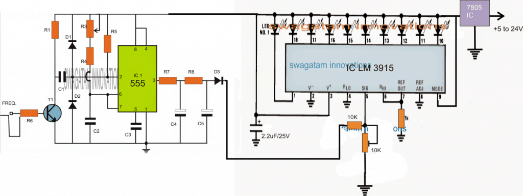 This situation allows the user to set the response pattern of the output.
The output triggering of the IC 555 is further smoothened by an integrator stage using R7/R8 and C4/C5.
The integrated or smothened output is applied to a 10 step dot/bar LED driver LM3915 circuit stage.
The processed frequency to voltage conversion from the IC 555 tachometer circuit is appropriately displayed across the 10 LEDs associated with the LM3915 IC.
Since pin#9 of the IC is attached with the positive rail, the LED displays a bar mode pattern of the frequency level or the RPM level of the connected engine.
The 10 LED bar graph ascend or descend their illumination in response to the frequency levels from the automobile engine and allow the circuit to be used like an effective 10 LED tachometer.
This situation allows the user to set the response pattern of the output.
The output triggering of the IC 555 is further smoothened by an integrator stage using R7/R8 and C4/C5.
The integrated or smothened output is applied to a 10 step dot/bar LED driver LM3915 circuit stage.
The processed frequency to voltage conversion from the IC 555 tachometer circuit is appropriately displayed across the 10 LEDs associated with the LM3915 IC.
Since pin#9 of the IC is attached with the positive rail, the LED displays a bar mode pattern of the frequency level or the RPM level of the connected engine.
The 10 LED bar graph ascend or descend their illumination in response to the frequency levels from the automobile engine and allow the circuit to be used like an effective 10 LED tachometer.
Parts list for the IC 555 section
Parts List R1 = 4K7 R3 = CAN BE VARIABLE 100K POT R4 = 3K3, R5 = 10K, R6 = 470K, R7 = 1K, R8 = 10K, C1 = 1uF, C2 = 100n, C3 = 100n, C4 = 22uF/25V, C5 = 2.2uF/25V T1 = BC547 IC1 = 555, D1, D2, D3 = 1N4148Using only LM3915
A closer inspection of the above circuit reveals that the IC 555 stage is actually not required and seems like an overkill for the purpose. The main concept here is to convert the frequencies into an average DC whose level would be proportionate to the input frequency level. This implies that a simple diode, resistor, capacitor network would be enough to accomplish this action. Also called an integrator, this small circuit network could be integrated with the LM3915 for ensuring that the voltage level stored in the capacitor is proportionately varied depending on the frequency levels. Faster frequencies would allow the capacitor to charge and hold the DC proportionately better resulting in a higher average DC output and vice versa. This would in turn produce an equivalent level of LED illuminations on the LEDs attached with LM3915 output. Here's the simplified version of the 10 LED tachometer using just a single IC M3915. A Video Demo for the above Circuit can be witnessed below:
My Conclusion is not Correct
It's indeed very silly of me, since I completely missed the point that the above circuit was only interpreting the voltage generated by the motor, so it is not representing the frequency or the RPM, rather only the generated voltage levels. Although this may be also proportionate to the RPM, it is technically NOT a tachometer circuit. Therefore I confess that the first circuit shown using the IC 555 circuit the actual and true tachometer design.Simple Tachometer Circuit
So far we studied a 10 LED version of a tachometer, however the idea could be much simplified using a moving coil meter as explained below. Here we learn how to build a simple IC 555 based tachometer circuit which can be used for directly measuring any frequency over an analogue volt meter.Circuit Operation
The circuit diagram shows a simple configuration utilizing the IC 555. The IC is basically configured as a monstable multivibrator. The pulse is derived from the spark plug and fed to the end of R6. The transistor responds to the pulses and conduct in accordance with triggers. The transistor activates the monostable with every rising pulse of the input. The monostable stays ON for a particular moment each time its triggered and generates an average ON time at the output which is directly proportional to the average trigger rate. The capacitor and the resistor at the output of the IC integrate the result so that it can be directly read over a 10V FSD voltmeter. The pot R3 should be adjusted such that the output generates the exact interpretations of the fed RPM rates. The above setting up must be done with the help of a good conventional tachometer unit.
Parts List
R1 = 4K7 R2 = 47E R3 = CAN BE VARIABLE 100K POT R4 = 3K3, R5 = 10K, R6 = 470K, R7 = 1K, R8 = 10K, R9 = 100K, C1 = 1uF/25V, C2 = 100nF, C3 = 100n, C4 = 33uF/25V, T1 = BC547 IC1 = 555, M1 = 10V FSD meter, D1, D2 = 1N4148 Video Demo shows the testing of the above circuitSimple Moving Coil Meter Tachometer Circuit
The figure below displays how a simple analog ,tachometer or revolutions per minute (rpm) meter can be built for motor vehicles. The circuit is driven by a regulated 8.2 volts acquired through the vehicle's 12 V battery and the ignition switch. The supply is stabilized using resistor R1, Zener diode D1, capacitor C1. The 555 is activated with a signal from the vehicle's pickup coil processed by the circuit stage comprising of resistor R2, capacitor C2, and Zener diode D2.
The 50 uA moving coil meter M1, which is rigged as the the rpm indicator here, is triggered through pin 3 of the 555 via diode D3. The meter gets the driving current by means of a series-connected resistor R5 and potentiometer R6 through the power supply the moment the 555's output is high.
However, the current is decreased almost to zero by means of diode D1 as soon as the 555's output becomes low.
The meter is actually a current indicating system, although it is hooked up like a voltage measuring meter with appropriate multiplying resistors.
The 555 is activated with a signal from the vehicle's pickup coil processed by the circuit stage comprising of resistor R2, capacitor C2, and Zener diode D2.
The 50 uA moving coil meter M1, which is rigged as the the rpm indicator here, is triggered through pin 3 of the 555 via diode D3. The meter gets the driving current by means of a series-connected resistor R5 and potentiometer R6 through the power supply the moment the 555's output is high.
However, the current is decreased almost to zero by means of diode D1 as soon as the 555's output becomes low.
The meter is actually a current indicating system, although it is hooked up like a voltage measuring meter with appropriate multiplying resistors.
FET Tachometer
The next diagram below exhibits a different analog tachometer meter which involves neither a multiplier resistor nor a stabilized power supply. In this design, the IC 555 output pin 3 is attached to the meter via JFET transistor Q1. The FET is wired like a constant-current generator by means of potentiometer R3, it delivers a fixed-amplitude pulse to the meter irrespective of the fluctuations in the supply source.
Bluetooth Car Ignition Lock Circuit ¨C Keyless Car Protection
This circuit will allow the user to lock his car ignition using his phone Bluetooth, meaning the ignition can be locked/unlocked only through a specific code from the user's cellphone Bluetooth.Overview
In one of my earlier posts I have already explained how to hack a Bluetooth headset and use it for any desired switching application via Bluetooth, here we apply the same concept for the proposed car ignition lock circuit using Bluetooth.In the project the cellphone becomes the Transmitter circuit, and the Bluetooth headset is used as the receiver. If you do not wish to modify the Bluetooth headset into a receiver circuit, you an procure a readymade Bluetooth receiver unit also for the same The idea is actually very simple, and may be understood by referring to the below given circuit:
How it Works
As can be seen the circuit is configured around a specialized phase-locked-loop IC LM567 which is designed to generate a low logic whenever it detects a frequency at its pin#3 that may be matching exactly to the IC's internal oscillator frequency set by R1/C1. For example, in the above diagram the internal oscillator frequency is set at 100kHz by appropriately selecting the values of the R1/C1 timing components, therefore it implies that the IC will produce a low logic whenever it detects a 100kHz across its pin#3 and ground. As long as this situation is not satisfied, pin#8 can be expected to be at a logic high level. The C4 end and the negative wire of the circuit is supposed to be joined with the Bluetooth headset or any selected similar Bluetooth audio receiver gadget. This could be also easily done through an opto coupler for allowing a complete isolation between the two stages. This takes care of the Bluetooth receiver stage circuit, now lets' move on and learn how your cellphone needs to be set up as the Bluetooth transmitter unit. For this, you will need to download a frequency signal generator app in your android phone, or if your phone is not an android phone, you can record a 5 second clip of the selected frequency, let's say a 100kHz frequency clip for the above shown design.How to Test the Circuit
Once this is done, it's time to test the proposed Bluetooth car ignition lock circuit, through the following steps: 1) Pair up the phone and the Bluetooth receiver gadget with Bluetooth. 2) Toggle the 100kHz frequency from your phone and simply send it to thee receiver gadget. 3) Wait for a few seconds, and ...."click".... you will find the relay operating, and unlocking or locking the car ignition, depending upon the initial situation of the relay. The slight delay in operating the flip flop relay is initiated by the 100k/1000uF components at pin#14, and this is crucial in order to make the system foolproof, so that an intruder may not make an attempt to break the lock by randomly sending a Bluetooth frequency to the receiver gadget. This delay must be confirmed with some trial and error, the indicated values of 100k and 1000uF is arbitrarily chosen, and may not be accurate. The IC 4017 is rigged as a flip flop circuit which toggles the relay ON/OFF alternately in response to the LM567 signal. The relay can be seen integrated in series with the ignition switch which implies that as long as this relay is switched OFF, the ignition key cannot be used for starting the vehicle, and it would work only once the relay is triggered. If you have any further queries regarding this circuit you can ask them through your comments belowMotorcycle Accident Alarm Circuit
In this post we learn how to make an useful motorcycle accident alarm circuit for sending alarm signal to the distant population in an event of an accident, especially if it happens in a relatively lonely area. The idea was requested by Mr. Rayan D'souza. Circuit Objectives and Requirements I want a circuit that has a buzzer in it. This buzzer activates only when the motorcycle has undergone a accident. That is, the buzzer should get activated when accident of a motorcycle takes place. So that the people can be aware of that accident. Can you make a circuit for this.
The Design
A simple motorcycle accident alarm circuit can be built at home with the help of the design shown in the above figure. The circuit is made up of two stages, the tilt sensor, and the delay ON alarm stage. The sensor can be seen at the left side of the design, consisting of a plastic ball, a small spherical neodymium magnet and a reed switch. The magnet is inserted into the plastic through a temporary hole made at the top, which is later on sealed with epoxy glue. On the outer side of the ball, a reed relay switch is glued such that the magnet and the reed lie side by side with only the ball plastic separating them. The above situation is supposed to keep the reed relay switched ON as long as the ball is not tilted and the magnet inside is vertically still in the shown specified position. The reed relay output can be seen integrated with a delay On relay timer circuit comprising a couple of BJTs and the associated resistors and capacitors. In the normal situations, while the reed relay is in the activated position, the base of T1 is held grounded and the delay ON timer is unable to react, and remains in a dormant condition. The sensor unit along with the circuit is supposed to be fixed in the bike such that as long as the bike is in its vertically standing position, the magnet maintains its position around the bottom center of the ball. However in an event of an accident, when the motorcycle could be in a tilted situation the magnet would roll and be displaced from the specified position allowing the reed switch to open. As soon as the reed relay opens, C2 begins charging and the delay circuit begins counting. Depending on the values of C2 and R2 (which could be set for 5 seconds delay), C2 charges fully and triggers T1 into conduction. This in turn switches ON T2 and the relay, sounding the alarm, and informing the people around regarding the mishap. The alarm is stopped as soon as the motorcycle is lifted on its upright position or the battery power is disconnected.Over Voltage Protection for Automotive Load Dump
The post explains an over voltage cut-off protection circuit in the form of automotive dump load for protecting sensitive and sophisticated modern automotive electronics from transient DC electrical spikes emanating in vehicle electrical. Transient bus voltages are a significant risk factor to integrated circuits. The maximum breakdown voltage that an integrated circuit may be specified to tolerate is determined by its style and design approach that can be predominantly low for tiny CMOS devices.What's Transient Voltage
Transient or repetitive over voltage circumstances that defeat an ICˇ®s absolute highest voltage spec may possibly irreversibly harm a device. The necessity for over voltage safety is notably prevalent in automobile 12V and 24V designs in which peak "load dump" transients is usually as very high as GOV. Certain load safeguarding strategies shunt input transient to ground through devices similar to avalanche diodes and MOVs. The difficulty with the shunt method is that a great deal of power could possibly end up being processed. Shunt techniques are usually undesirable should there be an obligation to render continual protection throughout an over voltage situation (as transpires with dual battery).The Design
The Over Voltage Protection Circuit for Automotive Load Dump shown in Figure 1 is a perfect series disconnect or series cut-of circuit which has been built to safeguard a switching regulator load that possessed an optimum input voltage of 24V. The circuit is intended from economical discrete devices and makes use of a single Texas Instruments LMV431AIMF. Given that this circuit employs a PFET pass device (Q1), there may be a marginal forward voltage drop or related power loss.Circuit Diagram
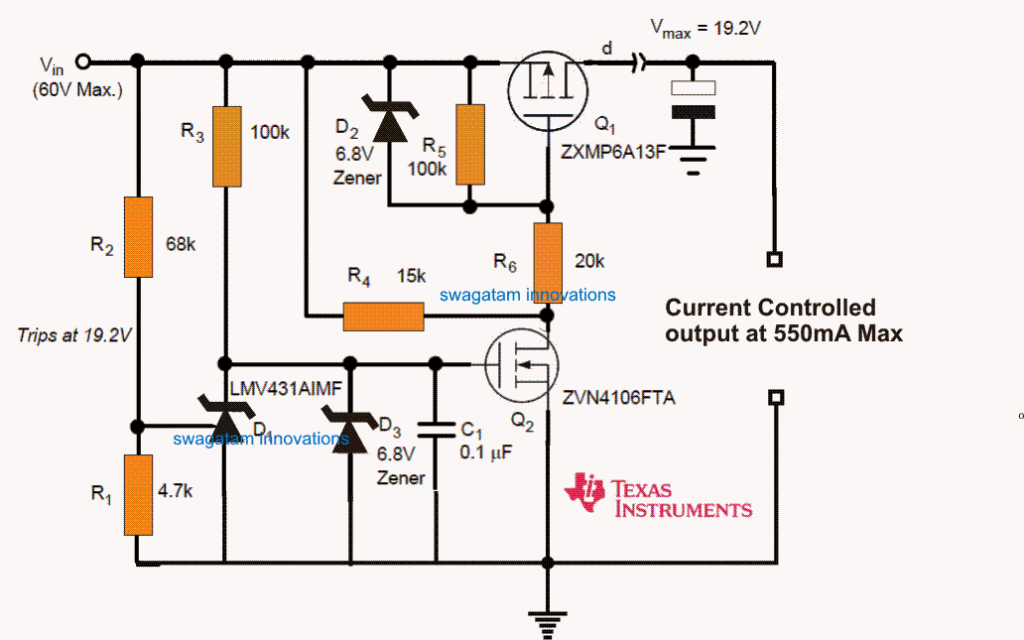 Figure.1
Courtesy: Over Voltage Protection Circuit for Automotive Load Dump
Figure.1
Courtesy: Over Voltage Protection Circuit for Automotive Load Dump
How LM431AIMF Diode Works
The LMV431AIMF (D1) adaptable reference works best for this situation just because it allows for an inexpensive means to ascertain a meticulous trip point and monitor optimal temperature accuracy which becomes quite difficult with a zener diode or likewise using other alternative options (1% for the A version, 0.5% for the B version). For preserving this accuracy and reliability, resistors R1 and R2 is selected to be 1% tolerance or a still better may be recommended. Variable reference voltages can be usually wrongly contemplated. Take for instance: "What's that third wire terminating from that diode'?" You may find numerous types of variable voltage references. Different possessing different in-built set voltage while others with an alternate current direction polarity. All of them can be identified with a couple of fundamental (and quite significant) stages: A temperature regulated, accurate band gap voltage reference, along with a gain error amplifier (incorporated as as a comparator in the discussed circuit). Majority of the parts exhibit uni-poIar results by incorporating an open collector or emitter. Figure 2 indicates conceptually what may be expected inside Texas Instruments LMV431AIMF.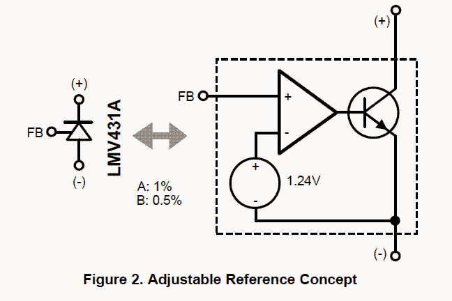
Calculating the Cut-of Threshold
The input voltage is checked and controlled by the LMV431 with the aid of voltage divider R1 and R2. The circuit detailed in Figure 1 is configured to activate at 19.2V although an arbitrary cut of level could be opted which may be figured out using the following equations: Vtrip = 1.24 x (R1 + R2 / R1) R2 = R1(Vtrip/1.24 - 1)How it Works
The output of the LMV431 brings down as soon as the set reference pin is detected to be above 1.24V. The cathode of an LMV431 is capable to bring down to a saturation level of approximately 1.2V. The mentioned level may be just enough to switch Q2 off. Q2 was predominantly hand picked to carry an elevated gate threshold (> 1.3V). It's not recommended to use a substitution for Q2 without considering this into account. The chip operating conditions for D1, Q2, and Q1 are indicated in Table 1 for the condition involving of a 19.2V cut of point.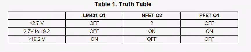 The circuits operating condition is detailed in Figure 3. The cut of level can be expected to be approximately in the 2.7V to GOV vicinity.
Below about 2.7V the circuit may be seen transiting to the off situation.
The reason being the absence of sufficient input voltage to level up the gate to source thresholds of Q1 and Q2.
While it's in the off state, the circuit offers around 42 kQ to the input (off status quiescent load).
Zener diodes D2 and D3 are crucial for restricting the over shooting gate to source voltages as expressed by Q, and Q2 (which may not be allowed to go beyond 20V).
D3 likewise inhibits the cathode of D, from shooting above its specified limit of of 35V.
Resistor Rd assures a compromised bias to Q2 so that it can fulfill Q2ˇŻs drain leakage in the off condition.
It's important to watch the body diode in Q, it implies that it carries no safeguarding to the load for wrongly connected battery (opposite polarity input voltages).
To be able to safeguard the condition of a wrong battery polarity, it may be advisable to incorporate a blocking diode or an reinforced alternate (one behind the other) PFET is may be also required.
The circuit can be seen attributed to actuate instantly although reestablish the conditions rather sluggishly.
Capacitor C, exhibits quick discharging to negative via the LMV431 in an even of an over voltage is sensing.
As soon as the situation restores to normal, reconnection is slightly held up by the R3-C1 time delay variables.
A significant number of loads (that may be regulators) employ substantial input capacitors which allow time delay for the cut-off circuit to work out by inhibiting the transient slew rate.
The working pattern of the standard transient and the available capacitance become responsible fix the intended delay response time.
The shut off implementation from the proposed Over Voltage Protection Circuit for Automotive Load Dump takes place in approximately twelve Sec.
The expected highest transient rise periods are constrained in a balanced level to the mentioned periods by C(load).
This circuit was verified with a C(load) of 1 pF.
Larger load is may be tried and is okay considering rapid surging, reduced source impedance transients are to be present.
The circuits operating condition is detailed in Figure 3. The cut of level can be expected to be approximately in the 2.7V to GOV vicinity.
Below about 2.7V the circuit may be seen transiting to the off situation.
The reason being the absence of sufficient input voltage to level up the gate to source thresholds of Q1 and Q2.
While it's in the off state, the circuit offers around 42 kQ to the input (off status quiescent load).
Zener diodes D2 and D3 are crucial for restricting the over shooting gate to source voltages as expressed by Q, and Q2 (which may not be allowed to go beyond 20V).
D3 likewise inhibits the cathode of D, from shooting above its specified limit of of 35V.
Resistor Rd assures a compromised bias to Q2 so that it can fulfill Q2ˇŻs drain leakage in the off condition.
It's important to watch the body diode in Q, it implies that it carries no safeguarding to the load for wrongly connected battery (opposite polarity input voltages).
To be able to safeguard the condition of a wrong battery polarity, it may be advisable to incorporate a blocking diode or an reinforced alternate (one behind the other) PFET is may be also required.
The circuit can be seen attributed to actuate instantly although reestablish the conditions rather sluggishly.
Capacitor C, exhibits quick discharging to negative via the LMV431 in an even of an over voltage is sensing.
As soon as the situation restores to normal, reconnection is slightly held up by the R3-C1 time delay variables.
A significant number of loads (that may be regulators) employ substantial input capacitors which allow time delay for the cut-off circuit to work out by inhibiting the transient slew rate.
The working pattern of the standard transient and the available capacitance become responsible fix the intended delay response time.
The shut off implementation from the proposed Over Voltage Protection Circuit for Automotive Load Dump takes place in approximately twelve Sec.
The expected highest transient rise periods are constrained in a balanced level to the mentioned periods by C(load).
This circuit was verified with a C(load) of 1 pF.
Larger load is may be tried and is okay considering rapid surging, reduced source impedance transients are to be present.
Make this DC CDI Circuit for Motorcycles
The circuit presented here is for a DC-CDI which are used in motorcycles. A DC-CDI is the one in which the high voltage (200-400VDC) is converted from 12V supply voltage. Researched and Submitted by: Abu-Hafss Studying the circuit, we see that it has two parts i.e. the CDI unit, enclosed in the pink box and the remaining circuit on the left is high voltage converter.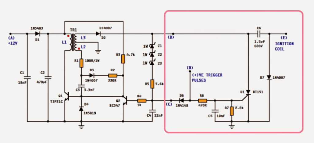 The working of the CDI may be found in this article.
The circuit on left is a high voltage converter based on a blocking oscillator.
The components Q1, C3, D3, R1, R2, R3 and transformer T1 forms the blocking oscillator.
L1 is the primary coil and L2 is the feedback coil.
C1, C2 and D1 are DC voltage smoothing components.
The working of the CDI may be found in this article.
The circuit on left is a high voltage converter based on a blocking oscillator.
The components Q1, C3, D3, R1, R2, R3 and transformer T1 forms the blocking oscillator.
L1 is the primary coil and L2 is the feedback coil.
C1, C2 and D1 are DC voltage smoothing components.
How it Works
When the circuit is powered on, R3 provides forward bais to the base of Q1. This turns on Q1 and current starts flowing thru the primary coil L1 of the transformer. This induces voltage in the secondary or the feedback coil L2. The red (phase) dots in the transformer symbol indicates that the phase of the voltage induced in L2 (and L3) is shifted 180ˇă. Which means when the bottom side of L1 is going negative, the bottom side of L2 will be going positive. The positive voltage of the L2 is fed back to the base of Q1 thru R1, D1, R2 and C3. This causes the Q1 to conduct more hence, more current flows thru L1 and ultimately more voltage is induced into L2. This causes L1 to saturate very rapidly which means no more changes in magnetic flux and hence no more voltage is induced into L2. Now, C3 starts discharging through R3 and finally Q1 is switched off. This stops the current flow in L1 and hence the voltage across L1 comes to zero. The transistor is now said to be "blocked". As C3 gradually loses its stored charge, the voltage on the base of Q1 begins reverting to a forward-bias condition by means of R3 thus switching on Q1, and hence the cycle is repeated. This switching of Q1 is very fast such that the circuit oscillate at quite high frequency. The primary coil L1 and secondary L3 forms a step-up transformer and thus a fairly high alternating voltage (more than 500V) is induced in L3.To convert it to DC a fast recovery diode D2 is deployed.
The zeners, R5 and C4 forms the regulator network. The sum of the values of the zeners should be equal to required high voltage to charge the CDI's main capacitor (C6). Or alternatively a single TVS diode with desired breakdown voltage may be used. When the output at the anode of D2 reaches the breakdown voltage (sum of zener values), the base of Q2 receives the forward bais and hence Q2 switches on. This action steals the forward bais of Q1 thus stopping the oscillator temporarily. When the output is dropped below the breakdown voltage, Q2 switches off and hence the oscillation resumes. This action is repeated very rapidly that the output is maintained slightly below the breakdown voltage. The positive trigger pulse at point (D) in the CDI unit is also fed to the base of Q2. This is important to pause the oscillation because SCR U1 demands the current across its MT1/MT2 to be zero to be able to self-disconnecting. Moreover, this increases power economy as all power supplied during discharging is wasted otherwise. A special request from Mr. Rama Diaz to have multi CDI sections sharing a common HV converter circuit. Some parts of his request is quoted below: Ok most engines these days don't have distributors anymore, they have a coil for each spark plug or in many cases have a dual post coil that fires 2 spark plugs at the same time, this is called "wasted spark" since only one of the two sparks is actually getting used each ignition event the other one just fires into the empty cylinder at the end of the exhaust stroke, so in this configuration a 2 channel CDi will run a 4cyl and 3 channel for 6cyl and 2 x 2 channel for v8 etc... Almost all 4 stroke engines have 2 cylinders that are paired so only 1 coil (connected to 2 spark plugs) will fire at a time the other one/s will fire at the alternate ignition events driven by a separate trigger signal, Yes aftermarket ECU's have up to 8 completely separate ignition trigger signals.... yes we could just have 2 or 3 totally separate units but i would like to have everything contained in one unit if possible, and im thinking there would be some way to share some of the circuitry... ...so im thinking you could have one heavier current step-up section to provide the ~400v then have two (or 3) separate CDI coil driver sections with a separate trigger signal for each one to drive the coils independently....possible?? That way i could use 2 (or 3) dual post coils attached to 4 (or 6) spark plugs and have then all fire at the correct time in wasted spark configuration This is exactly the way we often do it now inductively using simple transistor based ignitors but the spark strength is often not strong enough for turbo and high performance applications.
CIRCUIT DESIGN:
The entire circuit shown above can be used. The CDI unit enclosed in pink box can be used to drive one dual post ignition coil. For 4- cylinder engine, 2 CDI units; for 6-cyl, 3 CDI units can be used. When using multi CDI units, the diode D5 (encircled in blue) has to be introduced to isolate the C6 of each section.TRANSFORMER SPECIFICATIONS:
Since the frequency of the oscillation is fairly (more than 150kHz), ferrite core transformers are used. A tiny 13mm EE core transformer can perfectly do the job but, handling such a small component might not be easy. A little bigger may be selected. Enameled copper wire 0.33 - 0.38mm for the primary (L1) and 0.20 - 0.25mm for the secondary L2 & L3. The picture shows the bobbin's top view.Darkness Triggered Car Safety Park Light Circuit
In this post we discuss a circuit concept for enabling cars with an add-on automatic safety park light which triggers during night and signals the position of the car and consequently prevents a mistaken collision or dashing by another vehicle. The design ensures minimum consumption and relatively higher brightness for the involved LED lights. The idea was requested by Mr. Ankit.Technical Specifications
Kindly advise on the following circuit 1. A 12V circuit is desired to be designed to light a 12V LED, such that it lights the LED in pulses (that is to say that the current to led is sent intermittently (say once every 1 minute roughly) and the current pulse stays for a brief duration (say 5 seconds roughly)) 2. So, the LED lights repeatedly once every 1 min and stays on for roughly 5 sec each time. 3. It is also desirable that the above circuit starts working automatically when it is dark and stops when the atmosphere is lighted. 4. The above circuit is intended to be used in a parked car so that the LED keeps blinking in the rear when car is parked in dark and the cycle stops when it is day time. 5. Further, as expected, when the car is driven at night, its rear red lights will be on and the blinking LED will no longer be needed. So, it is desired that in some way a 12V +ve signal feeded to the circuit from rear red lights (when glowing) should stop the blinking cycle of the circuit. The significance of the proposed darkness triggered car safety park light is as follows... Mostly at night the cars are parked by the roadsides due to shortage of space inside homes. Often it is very dark due to absence of street lights or lack of electricity supply. So sometimes pedestrians, cycles or rikshaws or few vehicles without headlight bump into the cars. An intermittently pulsing LED as requested above would mark the presence of car, at the same time without undue battery drainage. When there is surrounding light in daytime or when the car is being driven, this blinking light would not be needed, So an LDR may turn off the circuit and also during driving the 12V +ve supply from car rear light would in some way turn off the blinking led. Sir, it will be so kind of you to help on the above mentioned aspects of the circuit. Dr Ankit
The Design
The requested darkness triggered car park light circuit can be made as per the above shown circuit details. The entire circuit is build around a single IC 4093, the gates N1 to N4 are from this IC which are appropriately configured with the associated passive components. N1 is wired as darkness sensor through the connected LDR across its input and ground. The pot determines the sensitivity control can be set for triggering N1 at the desired darkness level. N2 is wired as a PWM control frequency generator stage, the associated pot can be used for setting the required degree of ON or OFF time to the LEDs and consequently control their average brightness and consumption. N3 is used like a buffer, whose output is connected with the base of the driver transistor TIP122 which responds to the fed PWMs and drives the LEDs with the corresponding amount of brightness. The gate N4 is positioned to stop the TIP122 conduction and the LED illumination whenever the tail lights are detected ON, meaning while the taillight bulbs are ON, the proposed darkness triggered park lights are shut off. On the other hand, when a darkness is detected, N1 input is rendered negative which forces its output to go high, this high signal inhibits the oscillatory action of the N2, and causes its output to go low. With N2 output is low, N3 output is accordingly prompted to go high, which in turn switches ON the TIP122 transistor and the LEds. This positioned is held in the LED switched ON position (and flashing) until the darkness persists and dawn sets in, or/and the tail lights are switched ON.Illuminating DRL and Turn Lights with Single Common Lamp
The article discusses a simple circuit for enabling the turn signal lamp of any car to carry out a two-way function of DRL lights as well as well the stipulated turn lights. The idea was requested by Mr. Artem. Thank you for your fanaticism with electronics, this is really noticeable through your blog. I've been experimenting with some of your circuits, and everything is okay for now. Here I kindly ask your professional advise on my project. Some tiny vehicles have a certain lack of room to place LED lights in order to look fine. For one of those, Nissan Micra i was asked to combine LED Turns and DRL lights without placing one next to another.. Considering a small city car ergonomics i searched the market. I ordered twin color Y+W 1Watt 350mA LED-Emitters from China, so I could combine both functions by means of some kind a controller at one spot. And as it often happens, seller did not provide any specs for his product. 4-pin LEDs actually have common "+" so i can not drive six of them in series or implement any known driver. Please advise something useful, I believe you are able to. Thanks in advance, Artem, Moscow, Russia.
The Design
The proposed circuit which combines and enables illuminating DRL and turn signal lamps through a single common lamp can be seen above. The circuit basically allows the same lamp (preferably LEDs) to implement a dual function of DRL lights as well as turn signals, depending on which one is switched ON. The DRL switch is supposed to be switched ON permanently, so that the connected lamp illuminates through the TIP122 transistor, and as soon as the turn signal flasher is switched ON, the TIP122 is instantly disabled through the BC547, allowing the turn signal to flash the LED at the given frequency. The above happens since the BC547 becomes triggered ON through the turn signal switching and keeps the TIP122 base grounded and disabled. The 100uF/25 plays a crucial role here, and makes sure that the BC547 stays disabled for both the ON and the OFF periods of the turn signal inputs, therefore this capacitor might require some tweaking until the right minimum timing is determined. Bigger values will work but this might result in a delayed switch ON of the DRL each time the turn signal is deactivated, therefore the 100uF value could need some adjustments. The 10k preset at the base of the TIP122 may be used for determining the brightness level on the DRL, so this becomes an added feature in the design. Feedback from Mr. Artem Thank you for the circuit. But it seems you get me a little wrong. I wanted the circuit to drive 350ma double color leds, which has single common "+"positive and two "-"negative pins for white and yellow respectively. Both lampsare in single body for ergonomicreasons. Your suggested circuit doing the job well but we must take two colors with common positive pin in account.Solving the Circuit Query
As per the above response, the earlier diagram can be modified as shown below for executing the new function. I have assumed the LEDs to be having the current limiting feature originally, therefore it's not been shown here or included in the proposed designs. Otherwise 5 ohm, 2 watt resistors could be included in series with the respective negative lines of the LED module.
Question Regarding Switchback Driver Controller
The following request was sent by Mr. Dejan Djordjevic Hi Swagatam, Can you build a solid state switchback driver controller. You probably know has this works but if needed I will explain.On internet I find some schematics but they use relay and whole assembly is to big. Can you make schematic without relay? This controller have 3 wires, yellow, black and red.On yellow wire you connect signal from car turn signal, on red connect DRL (daytime runing lights) and black is ground for both.When DRL is ON and you turn ON turning signal DRL will go OFF.When turn signal is switched OFF DRL will automaticaly go ON again.So, this controller is just switching between DRLs and turn signals.You can see one example here My Reply: Please check the following diagram, I hope this will do the job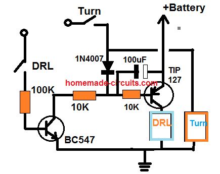 Feedback from Dejan
I tried this circuit and it's working fine.Just small correction if it is possible- can you add a little delay when switching from turn signal to DRL?For example-if turn light is not working for 2 seconds then DRL is switching on.
My Reply:
The delay feature is already present.
You can increase the 100uF capacitor value, or increase the 10K near the transistor base to increase delay
Feedback from Dejan
I tried this circuit and it's working fine.Just small correction if it is possible- can you add a little delay when switching from turn signal to DRL?For example-if turn light is not working for 2 seconds then DRL is switching on.
My Reply:
The delay feature is already present.
You can increase the 100uF capacitor value, or increase the 10K near the transistor base to increase delay
Make this Electric Scooter/Rickshaw Circuit
The article presents a simple electric scooter circuit design which can be also modified to make an electric auto-rickshaw. The idea was requested by Mr. Steve.The Circuit Request
I was lucky enough to find your blog, really amazing stuff that you've managed to design. I'm looking for a DC to DC Step Up and Controller for Electric Scooter Motor Input: SLA (sealed-lead-acid) Battery 12V, which is ~13.5V charged minimum voltage - cut off at ~10.5V Output: 60V DC motor 1000W. Have you came across a circuit like that? I can image it will be push-pull type, but have no idea of types of mosfets (give the wattage 80-100A), driving them, then the transformer, the core type and then diodes. Plus the minimum voltage cut off to cap the PWM's duty cycle. I have found some more information. The motor is 3 phase brushless with hall sensors. There are two ways to approach it, a/ leave the existing controller in place and only do 12V to 60V step up or b/ replace the controller too. There won't be any difference in power efficiency, the controller simply switches which phase get current based on the hall sensors. Therefore, sticking with plan a. Thank you very much, Steve
The Desi3n
Today making an electric vehicle is much easier than it used to be earlier, and this has become possible due to two main elements in the design, namely the BLDC motors and the Li-ion or the Li-polymer batteries. These two ultra efficient members have fundamentally allowed the concept of electric vehicles to become a reality and practically feasible.Why BLDC Motor
The BLDC motor or the brushless motor is efficient because it's designed to run with no physical contacts except the ball bearings of the shaft. In BLDC motors the rotor rotates solely through magnetic force making the system extremely efficient, contrary to the earlier brushed motors which had its rotors attached with the supply source through brushes, causing a lot of friction, sparking and wear and tear in the system.Why Li-Ion Battery
On similar lines, with the advent of the much upgraded Li-ion batteries and the Lipo batteries today achieving electricity from batteries is no longer considered an inefficient concept. Earlier we had only lead acid batteries at our disposal for all the DC back up systems which posed two major drawbacks: These counterparts needed much time to charge, possessed restricted rate of discharge, lower life, and were bulky and heavy, all these only adding to their inefficient nature of working. Opposing to this, Li-ion, or Li-po batts are lighter, compact, quickly chargeable at high current rates and are dischargeable at any desired high current rate, these have higher run life, are SMF types, all these features making them the right candidate for applications such as electric scooters, electric rickshaws, quadcopter drones etc. Although BLDC motors are extremely efficient, these require specialized ICs for driving their stator coils, today we have many manufacturers producing these exclusive next-generation IC modules which not only do the basic function of operating these motors, but are also specified with many advanced additional features, such as: PWM open loop control, sensor assisted closed loop control, multiple foolproof safeguards, motor reverse/forward control, braking control and a multitude of other state-of-the-art in-built features.Using a BLDC Driver Circuit
I have already discussed one such excellent chip in my previous post, specifically designed for handling high wattage BLDC motors, it's the MC33035 IC from Motorola. Let's learn how this module may be effectively implemented for making an electric scooter or an electric rickshaw, right in your home. I won't be discussing the mechanical details of the vehicle, rather only the electrical circuit and the wiring details of the system.Circuit Diagram
Parts List
All resistors including Rt but excluding Rs and R = 4k7, 1/4 watt Ct = 10nF Speed potentiometer = 10K Linear Upper power BJTs = TIP147 Lower Mosfets = IRF540 Rs = 0.1/max stator current capacity R = 1K C = 0.1uF The above figure shows a full-fledged high wattage brushless 3-phase DC motor driver IC MC33035 which becomes perfectly suitable for the proposed electric scooter or electric rickshaw application. The device has all the basic features that may be expected to be in these vehicles, and if required the IC could be enhanced with additional advanced features through many alternative possible configurations. The advanced features become specifically possible when the chip is configured in a closed loop mode, however the discussed application is an open loop configuration which is a more preferred configuration since it's much straightforward to configure, and yet is able to fulfill all of the required features that may be expected in a electric vehicle. We have already discussed the pinout functions of this chip in the previous chapter, let's summarize the same and also understand how exactly the above IC may be required to be implemented for achieving the various operations involved in an electric vehicle.How the IC Functions
The green shaded section is the MC 33035 IC itself which shows all the built-in sophisticated circuitry embedded inside the chip and what makes it so advanced with its performance. The yellow shaded portion is the motor, which includes a 3-phase stator indicated by the three coils in the "Delta" configuration, the circular rotor indicated with the N/S poled magnets and three Hall effect sensors on the top. The signals from the three Hall effect sensors are fed to the pin nos 4, 5, 6 of the IC for internal processing and generating the corresponding output switching sequence across the connected output power devices.Pinout Functions adn Controls
Pinouts 2, 1 and 24 control the externally configured upper power devices while the pins 19, 20, 21 are assigned to control the complementing lower series power devices. which together control the connected BLDC automotive motor as per the various fed commands. Since the IC is configured in an open loop mode, it's supposed to be activated and controlled using external PWM signals, whose duty cycle is supposed to determine the speed of the motor. However this smart IC does not require an external circuit for generating the PWMs, rather it's handled by an in-built oscillator and a couple of error amp circuitry. The Rt, and Ct components are appropriately selected for generating the frequency (20 to 30 kHz) for the PWMs, which is fed to pin#10 of the IC for further processing. The above is done through a 5V supply voltage generated by the IC itself at pin#8, this supply is simultaneous used for feeding the Hall effect devices, it seems everything is precisely done here....nothing is wasted. The portion shaded in red forms the speed control section of the configuration, as can be seen it's simply made using a single ordinary potentiometer....pushing it upwards increases the speed and vice versa. This is in turn made possible through the correspondingly varying PWM duty cycles across the pin#10, 11, 12, 13. The potentiometer could be converted into an LDR/LED assembly circuit, for achieving a friction-less pedal speed control in the vehicle. Pin#3 is for determining the forward, reverse direction of the motor rotation, or rather the scooter or the rickshaw direction. It implies that now your electric scooter or your electric rickshaw will have the facility of reversing back....just imagine a two-wheeler with a reverse facility, .....interesting? Pin#3 can be seen with a switch, closing this switch renders the pin#3 to ground enabling a "forward" motion to the motor, while opening it causes the motor to spin in the opposite direction (pin3 has an internal pull up resistor, so opening the switch does not cause anything detrimental to the IC). Identically, pin#22 switch selects the phase-shift signal response of the connected motor, this switch needs to be appropriately switched ON or OFF with reference to the motor specs, if a 60 degree phased motor is used then the switch needs to stay closed, and open for a 120 degree phased motor. Pin#16 is the ground pin of the IC and needs to be connected with the battery negative line and/or the common ground line associated with the system. Pin#17 is the Vcc, or the positive input pin, this pin needs to be connected to a supply voltage between 10V and 30V, 10V being the minimum value and 30V the maximum breakdown limit for the IC. Pin#17 may be integrated with the "Vm" or the motor supply line if the motor supply specs matches the IC Vcc specs, otherwise pin17 could be supplied from a separate step down regulator stage. Pin#7 is the "enable" pinout of the IC, this pin can be seen terminated to ground via a switch, for so long as it is switched ON and the pin#7 remains grounded, the motor is allowed to stay activated, when switched OFF, the motor is disabled resulting the motor to coast until finally it comes to a halt. The coasting mode may quickly come to a halt if the motor or the vehicle is under some load. Pin#23 is assigned with the "braking" ability, and causes the motor to stop and halt almost instantly when the associated switch is opened. The motor is allowed to run normally as long as this switch is kept closed and the pin#7 is held grounded. I would recommended to Gang-up the switch at pin#7 (enable) and pin#23 (brake) together so that these are switched with a dual action and together, this would probably help to "kill" the motor rotation effectively and collectively and also enable the motor to run with a combined signal from the two pnouts. "Rs" forms the sense resistor responsible for checking the overload or over current conditions for the motor, under such situations. the "fault" condition is instantly triggered switching off the motor immediately and the IC going into a lock-out mode internally. The condition stays in this mode until the fault is corrected and normalcy is restored. This concludes the detailed explanation regarding the various pinouts of the proposed electric scooter/rickshaw control module pinouts. It just needs to be correctly implemented as per the shown connection info in the diagram for successfully and safely implementing the vehicle operations. Additionally, the IC MC33035 also includes a couple of in-built protection features such as under-volatge lockout which ensures that the vehicle is switched off if in case the IC is inhibited from the required minimum supply voltage, and also a thermal overload protection ensuring that the IC never works with over temperatures.How to Connect the Battery (Power Supply)
As per the request, the electric vehicle is specified to work with a 60V input and the user requests for a boost converter for acquiring this higher level of voltage from a smaller 12V or a 24V battery. However, adding a boost converter could unnecessarily make the circuit more complex and might add to a possible inefficiency. The better idea is to use 5nos of 12V batteries in series. For sufficient back up time and current for the 1000 watt motor, each battery could be rated at 25AH or more. The wiring of the batteries may be implemented by referring to the following connection details:
Motorcycle Regulator, Rectifier Tester Circuit
The motorcycle regulator, rectifier tester circuit presented here can be used to test a 6-wire shunt type regulator-rectifiers for a 3-phase charging system of motorcycles. These reg./rectifiers (RR-units) are usually sealed with epoxy and it is considered difficult to find out if the unit is faulty or not. Designed and Written by: Abu-Hafss As the name suggests, the unit consists of 2 circuits i.e. the Regulator and the Rectifier. Usually, the wires are coded as below: Red = BATTERY + Green = EARTH (Chassis or Battery -) Black/Yellow = IGNITION 3 Yellow or 3 Pink = 3 PHASES To test those 2 circuits, the tester circuit is also divided accordingly.
REGULATOR TESTER:
To test the Regulator, its wires are connected to the test circuit as shown. The red wire is not used. The op-amp IC1-A (along with C1, R1, R2, R3, R5 and R6) is configured as an integrator.
R1 & R2 forms a voltage divider, which provides about 7V as reference voltage to the op-amp.
R5 & R6 forms another voltage divider to provide ramp-triggering voltage (lower than 7V) thru Q1 BC547 which act as a switch.
Initially Q1 is on, hence a ramp voltage is generated from about 7V to about 16.5V.
This ramp is fed into the RR-unit via its IGNITION wire (BLACK/YELLOW).
If the RR-unit is good, its regulator circuit will trip at 14.4-15V (and supply gate voltages to the 3 SCRs inside the RR-unit).
The anodes of those SCRs are connected to 3 phases, i.e.
the 3 YELLOW wires.
The three red LEDs will find path to ground via yellow wires & SCRs hence, they light up.
At the same time, voltage from one of the phases is fed into pin# 5 of IC1-B which is configured as voltage comparator.
It compares it with the reference voltage assigned by voltage divider R7 & R8. Since the voltage at pin#5 is lower than the ref.
voltage at pin# 6, the output at pin# 7 becomes low.
This switches off Q1 thereby cutting off the ramp-triggering voltage.
The ramp voltage comes to a halt.
This regulated voltage (14.4 - 15V) can be read with voltmeter M1.
If any of the LEDs does not light up or none of the LEDs light up, it indicates that one or more SCRs are bad.
If the voltmeter reads around 16.5V, it indicates the regulator circuit is not working.
The op-amp IC1-A (along with C1, R1, R2, R3, R5 and R6) is configured as an integrator.
R1 & R2 forms a voltage divider, which provides about 7V as reference voltage to the op-amp.
R5 & R6 forms another voltage divider to provide ramp-triggering voltage (lower than 7V) thru Q1 BC547 which act as a switch.
Initially Q1 is on, hence a ramp voltage is generated from about 7V to about 16.5V.
This ramp is fed into the RR-unit via its IGNITION wire (BLACK/YELLOW).
If the RR-unit is good, its regulator circuit will trip at 14.4-15V (and supply gate voltages to the 3 SCRs inside the RR-unit).
The anodes of those SCRs are connected to 3 phases, i.e.
the 3 YELLOW wires.
The three red LEDs will find path to ground via yellow wires & SCRs hence, they light up.
At the same time, voltage from one of the phases is fed into pin# 5 of IC1-B which is configured as voltage comparator.
It compares it with the reference voltage assigned by voltage divider R7 & R8. Since the voltage at pin#5 is lower than the ref.
voltage at pin# 6, the output at pin# 7 becomes low.
This switches off Q1 thereby cutting off the ramp-triggering voltage.
The ramp voltage comes to a halt.
This regulated voltage (14.4 - 15V) can be read with voltmeter M1.
If any of the LEDs does not light up or none of the LEDs light up, it indicates that one or more SCRs are bad.
If the voltmeter reads around 16.5V, it indicates the regulator circuit is not working.
RECTIFIER TESTER:
The rectifier section of RR-unit consists of only 6 rectifier diodes as shown. The wires are connected as shown. The Black/Yellow wire is not used. IC2 is a 555 which is configured as an astable vibrator.
Since the supply voltage is 18V and max voltage for 555 is 15V, a zener diode D2 is introduced to protect the IC.
The output is connected to 1 yellow wire at a time.
Both the LEDs should blink, indicating that the corresponding rectifiers are good.
If only one LED or no LED blinks, it indicates one or both rectifiers are bad.
Now, the connections of red and green wires are interchanged.
If one or both LEDs blink, it indicates that the rectifiers are short (bad).
p.s.
I have tested the above explained motorcycle regulator, rectifier tester circuit
-Abu Hafss
IC2 is a 555 which is configured as an astable vibrator.
Since the supply voltage is 18V and max voltage for 555 is 15V, a zener diode D2 is introduced to protect the IC.
The output is connected to 1 yellow wire at a time.
Both the LEDs should blink, indicating that the corresponding rectifiers are good.
If only one LED or no LED blinks, it indicates one or both rectifiers are bad.
Now, the connections of red and green wires are interchanged.
If one or both LEDs blink, it indicates that the rectifiers are short (bad).
p.s.
I have tested the above explained motorcycle regulator, rectifier tester circuit
-Abu Hafss
5 Simple Siren Circuits you can Build at Home
In this post we learn about a 5 simple siren circuits, using Arduino and also with ordinary components such as transistors and capacitors yet is able to produce an alarm sound at an excruciating level. The idea was contributed by "Abu-Hafss" Deeper in the article we also learn to make an advanced Arduino based design with adjustable and customizable tone features.1) The Design
This simple car siren circuit design explained here uses minimum number components and yet is able to produce an ear piercing alarm sound each time it's switched ON. The device is normally used as a car reverse horn, although it can used for any other relevant application too, depending upon the user's preference. In the automobile field this siren is also popularly know as the "Mega Siren" due to the massive decibel level it generates. The schematic details and other related info of the proposed car siren is presented below,which were furnished by Mr. Abu-Hafss, who is one of the dedicated readers and contributor of this blog.
Circuit Diagram
PCB Layout
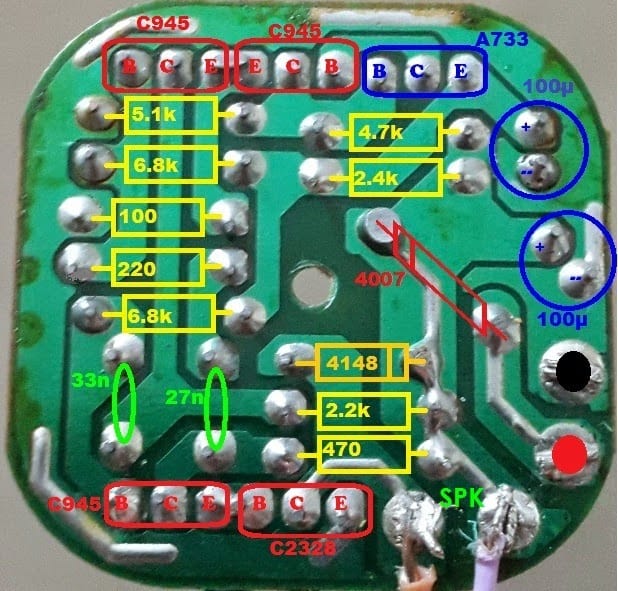 The following request was also attached with the above files in the email from Mr.
Abu-Hafss.
Dear Swagatam Attached,
please find a photo of a car 12V-20W siren which has really ear-piercing sound.
I opened it and found a small PCB as attached.
I have interpreted the PCB into schematic as attached.
My concern is to use the amplifier section for some other 15-20W application.
Frankly, I do not have practical experience of audio amplifiers.
I shall highly appreciate your help in this regard.
Best regards
Abu-Hafss
As per the above request, the amplifier section of the car siren is cheap and powerful (@ 20watts) and possibly could be used as an amplifier module for other applications requiring a cheap but powerful amplifier alternative.
The following request was also attached with the above files in the email from Mr.
Abu-Hafss.
Dear Swagatam Attached,
please find a photo of a car 12V-20W siren which has really ear-piercing sound.
I opened it and found a small PCB as attached.
I have interpreted the PCB into schematic as attached.
My concern is to use the amplifier section for some other 15-20W application.
Frankly, I do not have practical experience of audio amplifiers.
I shall highly appreciate your help in this regard.
Best regards
Abu-Hafss
As per the above request, the amplifier section of the car siren is cheap and powerful (@ 20watts) and possibly could be used as an amplifier module for other applications requiring a cheap but powerful amplifier alternative.
Analyzing the The Design
Studying the given diagram it appears that the stage comprising Q4, Q5 is only responsible for the amplification, the remaining sections are for generating the siren frequency for the Q4, Q5 base. The stage forms a powerful Darlington transistor amplifier stage with an extremely high gain (in the order of 1000 and more) Since the amplifier design is too basic, it might not be suitable for generating or handling Hi-fi music or frequencies above 4kHz. Moreover the transistor in the process could dissipate a significant amount of heat causing the consumption to be higher than the normal Hi-fi amplifiers. Therefore, although the amplifier incorporated in the above car siren circuit is cheap and simple it cannot be efficiently implemented for producing movie songs and melodies which involve frequencies up to 15kHz. However, it can be effectively used in units such as horns, bells, alarms, security systems etc.2) Generating Siren Sound with Arduino
The following Arduino based siren sound generator circuit can be used for generating the pitch perfectly imitating a typical siren sound and can be customized to produce many different siren effects simply by making relevant modification in the sketch. A siren sound, as we all know is a loud noise generated through a device designed for producing this sound either through a mechanical approach or through electronic circuits. Siren sound generator devices find many useful applications and are used in emergency service vehicles like in police and ambulance vehicles, and also in fire brigades etc. The discussed configurable siren enables a connected speaker to produce a custom siren sound. Basically there are two types of siren sound generating equipment, viz pneumatic and electronic. Pneumatic systems employ air pressure forced through an appropriately dimensioned pipe for creating the sound, while electronic equipment are more sophisticated, using loudspeakers or piezo devices for generating the relevant sound at any desired rate and pattern. Electronic sirens are more flexible, customizable and offer more variations and are extremely efficient.Types of Siren Sound
A Siren sound can be of many different types, a few common types are the police, ambulance, and the fire siren, others could be in the form of mega sirens as used in car horns, some are fast police siren tunes, another type could be ear piercing such as used for neutralizing mobs, a few could be in your cell phone for alerting while a new message is received. Therefore, the range could be too extensive and the proposed Arduno alarm circuit can be customized as per the users personal wish and preference for achieving the wished siren sound.Code sketch:
/* Siren A configurable siren for Arduino, requires an 8-ohm speaker attached to pin8 and ground. For high amplification use a transistor driver with pin8//Copyright (c) 2012 Jeremy Fonte
//This code is released under the MIT license
//https://opensource.org/licenses/MIT
const int pitchLow = 200;
const int pitchHigh = 1000;
int pitchStep = 10;
int currentPitch;
int delayTime;
const int speakerPin = 8;
void setup() {
currentPitch = pitchLow;
delayTime = 10;
}
void loop() {
tone(speakerPin, currentPitch, 10);
currentPitch += pitchStep;
if(currentPitch >= pitchHigh) {
pitchStep = -pitchStep;
}
else if(currentPitch <= pitchLow) {
pitchStep = -pitchStep;
}
delay(delayTime);
}
Arduino Wiring Diagram with Speaker and Supply Input

Video Demo:
Using a BJT Stage for Greater Amplification
For high amplification, the above set up can be modified as per the folowng connection diagram: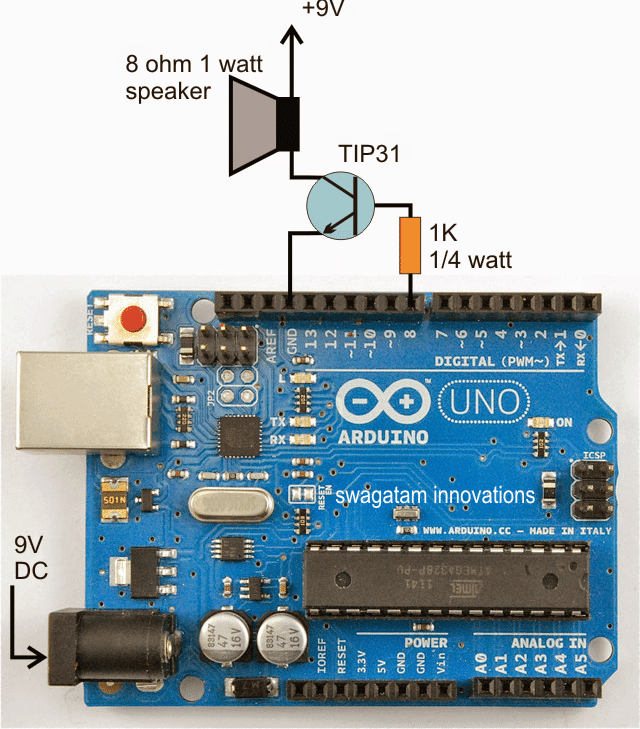 Modifying the Code
Upon Testing I fund the siren sound from the Arduino not very pleasant, and had slight distortions.
I experimented with the code, and finally made it extremely smooth and pleasant to hear.
Here's the improved for you:
Modifying the Code
Upon Testing I fund the siren sound from the Arduino not very pleasant, and had slight distortions.
I experimented with the code, and finally made it extremely smooth and pleasant to hear.
Here's the improved for you:
//Improved by Swagatam
const int pitchLow = 200;
const int pitchHigh = 1000;
int pitchStep = 10;
int currentPitch;
int delayTime;
const int speakerPin = 8;
void setup() {
currentPitch = pitchLow;
delayTime = 5;
}
void loop() {
tone(speakerPin, currentPitch, 20);
currentPitch += pitchStep;
if(currentPitch >= pitchHigh) {
pitchStep = -pitchStep;
}
else if(currentPitch <= pitchLow) {
pitchStep = -pitchStep;
}
delay(delayTime);
}
You can also play with theconst int pitchHigh = 1000;and increase to to 2000 for increasing the siren length, which is relevant to police sirens.
3) Police, Ambulance, Fire Brigade Siren - USA Style
The next siren circuit is a 3-in-1 siren, which will produce 3 distinct tones resembling, police siren, ambulance siren, and fire brigade sirens sound. These can be selected through a 3 pole switch, and simply by toggling the positions of the switch. The complete circuit diagram for this 3 in 1 siren circuit is furnished below: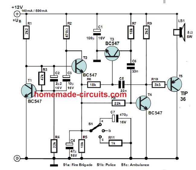
4) Siren Using IC 7400
Here's another simple and cheap siren using the IC 7400 that can be used for many different alarm applications.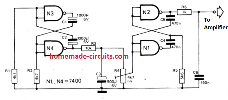 The circuit basically is configured around two astable multivibrators, N1/N2 and N3/N4. The N1/N2 stage generates a 0.2 Hz square wave signal which is coupled to the N3/N4, which causes an up and down swing of the 0.2 Hz.
The resulting siren output is 2 V peak to peak and can be amplified any suitable amplifier for getting a loud siren sound.
The circuit basically is configured around two astable multivibrators, N1/N2 and N3/N4. The N1/N2 stage generates a 0.2 Hz square wave signal which is coupled to the N3/N4, which causes an up and down swing of the 0.2 Hz.
The resulting siren output is 2 V peak to peak and can be amplified any suitable amplifier for getting a loud siren sound.
5) Siren Circuit using Unijunction Transistors
The indicated loud siren circuit is made up of a pair of unijunction relaxation oscillators. UJT Q1 is configured to generate low frequency while Q2 is wired to produce audio frequency. Resistor R3 connects the slow rising voltage over C1, decided by the time constant components C1 and R2, with the audio frequency across C2, established by the time constant of C2 and R4. The combination results an output where the audio frequency created by Q2 increases in pitch due to the application of the slow rising voltage across C1. This is applied through the resistor R3 to the time constant network C2/R4. This generated siren sound due to sharp intensity is able to travel a longer distances away compared to simple continuous siren sounds generated through just one oscillator.
If you want additional amplification you can accomplish it by integrating a couple of transistors in a super-alpha Darlington set up, as indicated in the dotted circuit stage.
R4 resistor shown at the center, must be substituted with a 100 ohm 1/4W resistor.
Hooked up to some pressure mat (through over C2), this specific UJT siren circuit could form a fantastic baby snatch alarm for strollers.
Resistor R3 connects the slow rising voltage over C1, decided by the time constant components C1 and R2, with the audio frequency across C2, established by the time constant of C2 and R4. The combination results an output where the audio frequency created by Q2 increases in pitch due to the application of the slow rising voltage across C1. This is applied through the resistor R3 to the time constant network C2/R4. This generated siren sound due to sharp intensity is able to travel a longer distances away compared to simple continuous siren sounds generated through just one oscillator.
If you want additional amplification you can accomplish it by integrating a couple of transistors in a super-alpha Darlington set up, as indicated in the dotted circuit stage.
R4 resistor shown at the center, must be substituted with a 100 ohm 1/4W resistor.
Hooked up to some pressure mat (through over C2), this specific UJT siren circuit could form a fantastic baby snatch alarm for strollers.
6) Ship Siren Circuit
This circuit will generate a high pitched sound just like a ship's siren. The design works well using the low power output source for model ships, when the output signal is appropriately amplified through a power amplifier, to produce a loud ship like alarm tone. The circuit is configured around a multivibrator through the transistors Q1 & Q2, and a low power output stage using the transistor Q3. The indicated speaker is required to have an impedance of around 40 to 80 ohms.
Capacitors C1 and C2 are responsible for the pitch intensity of the siren and with the values shown in the diagram, the pitch of the siren can be approximately around 300Hz.
The Quiescent current of the circuit is quite low and can be ignored.
If you wish to have a much more powerful ship siren sound, in that case you can integrate the Q2 collector output with an external amplifier input through a 1¦ĚF electrolytic, in series with a 12k resistor.
The circuit is configured around a multivibrator through the transistors Q1 & Q2, and a low power output stage using the transistor Q3. The indicated speaker is required to have an impedance of around 40 to 80 ohms.
Capacitors C1 and C2 are responsible for the pitch intensity of the siren and with the values shown in the diagram, the pitch of the siren can be approximately around 300Hz.
The Quiescent current of the circuit is quite low and can be ignored.
If you wish to have a much more powerful ship siren sound, in that case you can integrate the Q2 collector output with an external amplifier input through a 1¦ĚF electrolytic, in series with a 12k resistor.
High Power MOSFET Siren
The next concept shows a simple yet powerful MOSFET based siren circuit. Tr1 is utilized as a common emitter circuit, with R2 as the collector load and R1 providing base biasing. C3 connects the output of Tr1's collector to Tr2's input (gate terminal). Tr1's base operatesin phase with Tr2's collector, and both Tr1and Tr2 produce an inversion of the signal. As a result, C2 and R3 offer positive feedback, and the circuit's gain is big enough to create powerful oscillation. The MOSFET shown in the diagram can be replaced with IRF540
The drain terminal of the MOSFETTr2 receives an approximately squarewave signal, and the device is turned between hard on and hard off states.
This causes very large current pulses (about 500mA peak) to be pushed to the loudspeaker, resulting in a very loud sirentone output.
The working frequency is around 1kHz, however it may be adjusted by changing C2 and C3 values.
Varying their values can create an oppositelyproportionate change in theoscillatingfrequency, therefore make sure C2 and C3have identical vaues.
The MOSFET shown in the diagram can be replaced with IRF540
The drain terminal of the MOSFETTr2 receives an approximately squarewave signal, and the device is turned between hard on and hard off states.
This causes very large current pulses (about 500mA peak) to be pushed to the loudspeaker, resulting in a very loud sirentone output.
The working frequency is around 1kHz, however it may be adjusted by changing C2 and C3 values.
Varying their values can create an oppositelyproportionate change in theoscillatingfrequency, therefore make sure C2 and C3have identical vaues.
10 watt Power Siren
This ingenious small design makes use of the most recent developments in semiconductor technology to create a very compact, low-cost, yet extremely powerful alarm-sound generating unit that can be simply integrated into an existing intruder alarm system or equivalent "protection" equipment. The alarm circuit includes a basic alarm-signal generating stage, which is accompanied by a power amplifier stage. The alarm-signal component of the machine is built around a low-cost CMOS integrated circuit that uses almost no "standby" power. The power amplifier circuit is a true cutting-edge technology, a low-cost MOSFET power FET that uses almost no current while in "standby" mode.
As a result, there is no need for a discrete on/off switch, and the device may be left completely linked to a 12 volt battery supply.
IC1a and IC1b are wired as slow astable multivibrators, whereas IC1c-IC1d are connected as fast astables.
Each of these astables are "gated," meaning they may be switched on and off using PB1.
The ICa-IC1b slow astable's output is appliedto control the frequency of the 1C1c-IC1d fast astable, and the fast astable's output is supplied to the external speaker through the Q1 MOSFET power amplifier stage.
When PB1 is open, each of theastables and Q1 are inactive, and the circuit draws almost little standby current.
D1 and C1 are utilized to guarantee that voltage spikes produced into the battery supply connections through the speaker do not have a detrimental effect on the astable operations.
It should be noted that the circuitrequires an 8 Ohmspeaker rated to handle higher than10watts.
The power amplifier circuit is a true cutting-edge technology, a low-cost MOSFET power FET that uses almost no current while in "standby" mode.
As a result, there is no need for a discrete on/off switch, and the device may be left completely linked to a 12 volt battery supply.
IC1a and IC1b are wired as slow astable multivibrators, whereas IC1c-IC1d are connected as fast astables.
Each of these astables are "gated," meaning they may be switched on and off using PB1.
The ICa-IC1b slow astable's output is appliedto control the frequency of the 1C1c-IC1d fast astable, and the fast astable's output is supplied to the external speaker through the Q1 MOSFET power amplifier stage.
When PB1 is open, each of theastables and Q1 are inactive, and the circuit draws almost little standby current.
D1 and C1 are utilized to guarantee that voltage spikes produced into the battery supply connections through the speaker do not have a detrimental effect on the astable operations.
It should be noted that the circuitrequires an 8 Ohmspeaker rated to handle higher than10watts.
Adding a PWM Multi-spark to Automobile Ignition Circuit
The post investigates a simple 2 pin oscillator circuit which may be inserted between the pickup coil and the CDI unit of a vehicle for achieving an induced multi trigger input in response to each signal from the pickup coil coil, this in turn is expected to enhance the sparking ability of the CDI coil. The idea was requested by Mr. Vimal. Thank you for your help on the 555 buck boost circuit. Needed your help with one more circuit concept. Please note the details as below. 1) In a petrol engine vehicle, the sparking is done due to an ignition coil. This coil is driven on 12 volts pure dc. 2) In some experiments it was noticed that if the coil is supplied with pulsed dc at a certain frequency, the sparks become stronger due to the coil operating at its optimum resonant frequency without requiring an actual increase in operating input voltage or even bigger amperage draw. 3) Increasing input voltage from 12 volts to higher voltages would also increase the spark intensity, but this would lead to damage of the primary coil in the long run. Also as the primary coil would heat up more due to higher voltage, it would draw more amps eventually leading to coil failure. 4) I wanted your help in designing a circuit which is a passive dc to variable pulse dc converter, and does not require any ground connection to operate. The criteria of "NO GROUND CONNECTION" is due to the fact, that the circuit should fix in series on the +ve input line of the coil as it is not possible to modify the original harness of the vehicle to change coil connections. (+DC voltage IN and Pulsed DC voltage OUT fed directly only on the + live line connecting to the +ve terminal of the coil). 5) The total amp draw of a regular ignition coil usually does not exceed 15 amps. Hence this circuit should be able to handle 15 amps of power draw passing through it. 6) An increase of 1 - 2 volts above the input voltage is acceptable. 7) I found a circuit online which does not require an external ground to operate. I do not understand the deep working of electronics, hence I am attaching it herewith for your reference. I am not sure if this design would work for the application that I have in mind.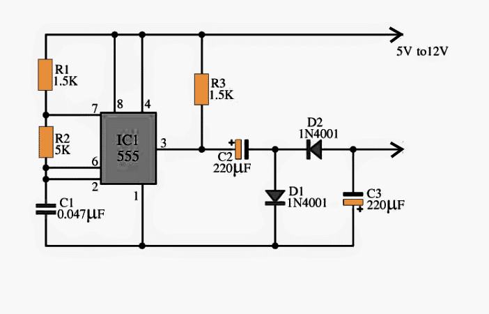 8) The reason behind having a variable frequency control on this circuit is that we can have a test bench setup to study the best resonant frequency at which automotive coils would operate without any damage.
I would really appreciate it if you could help me with the design and concepts of this kind of circuit.
Please note that the attached circuit is for your reference.
The actual circuit design required can be different, so please feel free to offer your kind advice if the required end results could be achieved by using different principles and circuit design.
P.S.
:- Sorry for not posting this on your blog, as I did not want to flood your blog with my outlandish ideas.
Thanks for your time and support.
Vimal Mehta
8) The reason behind having a variable frequency control on this circuit is that we can have a test bench setup to study the best resonant frequency at which automotive coils would operate without any damage.
I would really appreciate it if you could help me with the design and concepts of this kind of circuit.
Please note that the attached circuit is for your reference.
The actual circuit design required can be different, so please feel free to offer your kind advice if the required end results could be achieved by using different principles and circuit design.
P.S.
:- Sorry for not posting this on your blog, as I did not want to flood your blog with my outlandish ideas.
Thanks for your time and support.
Vimal Mehta
The Design
The attached circuit above might work if its 12V terminal is connected with the vehicle's +12V battery and the output from pin#3 to the pickup coil. This would enable breaking of the pickup signal into many short pulses, however the idea does not appear to be an efficient approach, since this would reduce the CDI triggering time to some lower level and in turn might cause a drop in the intensity of the generated sparks. Any other more efficient configuration doesn't look feasible with the above the design. The requested multi spark induction into an existing CDI ignition system may be achieved with the help of the following explained circuit: The circuit actually is inspired from a two pin automobile flasher circuit invented by me a long time ago.
The circuit actually oscillates in a regenerative kind of fashion, where the two transistors complement each other to turn ON fully and turn OFF fully at a set frequency.
You may also want to refer to the following related articles for more info:
Adjustabe CDI Spark Advance/Retard Circuit for Motorcycles
Universal Multi-spark Enhanced CDI Circuit for Automobiles
The frequency is determined by R1 and C1, any of these components can be altered for achieving the desired oscillations across the output terminals.
For the proposed multi spark variable frequency CDI ignition, the above circuit can be connected in series with the pick-up signal wire as illustrated in the diagram.
The voltage from each pulse is stored inside C2 for some extended limit of time, during which the circuit quickly delivers a number of short pulses, at a frequency determined by the C1, R1 combination.
R2, and R3 also influence the oscillation rates but these might also influence the pulse width of the output, and can be optimized some for getting the right amount of PWM, and a most effective response from the CDI coil.
The circuit actually is inspired from a two pin automobile flasher circuit invented by me a long time ago.
The circuit actually oscillates in a regenerative kind of fashion, where the two transistors complement each other to turn ON fully and turn OFF fully at a set frequency.
You may also want to refer to the following related articles for more info:
Adjustabe CDI Spark Advance/Retard Circuit for Motorcycles
Universal Multi-spark Enhanced CDI Circuit for Automobiles
The frequency is determined by R1 and C1, any of these components can be altered for achieving the desired oscillations across the output terminals.
For the proposed multi spark variable frequency CDI ignition, the above circuit can be connected in series with the pick-up signal wire as illustrated in the diagram.
The voltage from each pulse is stored inside C2 for some extended limit of time, during which the circuit quickly delivers a number of short pulses, at a frequency determined by the C1, R1 combination.
R2, and R3 also influence the oscillation rates but these might also influence the pulse width of the output, and can be optimized some for getting the right amount of PWM, and a most effective response from the CDI coil.
Parts List
R1 = 100k preset R2, R3 = 10K, R4 = 33K, T1 = TIP122 T3 = BC557, C1 = 0.33uF/25V C2 = 100uF/25V (other values can be tried) D1 = 1n4007,How to Make HHO Fuel Cell Circuit in Automobiles for better Fuel Efficiency
In this post we'll try to investigate the making of HHO gas in automobiles for enhancing their mileage by approximately 50% or more, that means a reduction of petrol or diesel consumption by the same amount. In the previous post I tried to put forth an innovative design of a high voltage low current generator which could be used for splitting water into HHO gas (by decomposing the H2O bond into two parts of hydrogen and one part of oxygen). Using a high voltage for the electrolysis allows the breaking apart of the water molecules by brute force without the need of a higher magnitudes of current (amps), which in turn makes the procedure extremely efficient. We can understand the above logic by analyzing the following example:Higher Voltage is more Effective
Suppose we have a 12V battery capable of delivering a maximum current of 7.5 amps, if we use this battery power for the electrolysis we would probably be implementing it very inefficiently and the power required for the electrolysis would easily exceed by far than the power of the accumulated HHO gas in terms of megajoules. However if the same 12V/7AH is boosted to say around 20,000 voltage with a current as low as 5mA would be able to yield better results (many people might not agree with this). Moreover since this high voltage is pulsed using a PWM circuit, the sharp rise and fall of the pulses adds up to the efficiency level of the process. Many critics argue and don't substantiate the use of a high voltage for yielding higher efficiency, however the following few examples provide us sufficient logical evidence regarding why a high voltage could be more effective than using high current for the electrolysis of water. Passing a low voltage, high current potential through a very high resistance could be useless because the current would be restricted by the high resistance and produce little effect on the process. Since pure water can be notorious with its resistance value (pure water may have a resistance as high as 200k or even more), a high current at low voltage would be quite ineffective. On the contrary a higher voltage would be strong enough to tear apart the water high resistance and be comparatively more effective, even though a lot lesser number of electrons would be passing through, but nevertheless we would see electrons crossing over with better efficiency.Assessing with Practical Examples
Just try applying a 12V/100amp through a 200k resistor and check the current with an ammeter, according to Ohms law it would be around I = 12/200000 = 0.00006amps or 0.06 mA, in contrast if a 20,000 volt is used we would find it to be capable of delivering I = 20000/200000 = 0.1 amps or 100mA, that looks much impressive, although we wouldn't want 100mA to be used for electrolysis in order to avoid explosions or atomization of water, we can expect about 10mA to be quite sufficient for the process. Another example that looks quite relevant to the subject is our body itself, we experience a lethal shock when we come across a high voltage AC with any part of our body, but in contrast if we touch a lower potential input such as a 12V AC we might not feel anything regardless of how high the source may be rated with amperage. The above example provides an authoritative proof regarding the power of high voltage in terms of its riping ability through high resistance passages, the same may be true with lightning thunder bolts which are equipped with millions of volts and that's why are able to knock out the huge atmospheric barrier and reach the earth surface. Having said this, in the proposed use of HHO gas in automobiles one must be careful regarding not supplying the high voltage with high current, otherwise that might lead to an explosion inside the water and result in atomization of water molecules which is definitely not an electrolysis.Installing HHO Fuel Cell in Automobiles for Enhancing its fuel Efficiency
Here we'll talk about using the HHO fuel cell idea in a motorbike and learn the procedure of installing and integrating it with a motorcycle engine. In our earlier post we discussed how HHO gas could be produced using a high voltage CDI coil circuit, we will use the same design for the proposed implementation and for enhancing a motorcycle's fuel efficiency. Since your motor cycle would be already having a CDI ignition system this could make things much easier for us, since we could simply borrow it's function for the discussed purpose. However we must be careful about a couple of things: the sharing of the high voltage pulse from the existing CDI should not hamper the actual ignition of the bike for which the CDI coil is originally installed. Secondly, we don't want the vehicle's alternator to work extra hard for compensating the sharing of the CDI sparks with our HHO fuel cell.Using Spark Suppressor
The above situations can be countered by employing a spark arrestor resistor or a spark suppressor device. This device is normally used in series with the high tension input from the CDI before it enters the spark plug. As the name suggests the spark suppressor is used for suppressing excessive voltage from reaching the spark plug thus helping to cancel out the generation of unnecessary RF disturbance and noise. This means that in normal conditions the spark plug would be wasting a good amount of energy by shorting the high voltage across it's spark gap which apparently looks pretty small compared to the enormous voltage it's been fed. The use of a suppressor ensures that the excess voltage which would otherwise become wasted in the spark plug now gets restricted and is converted to heat, which is again a wasted energy unless it's diverted for some useful purpose. The utilization of a spark suppressor resistor and by diverting the excess energy from the CDI coil to the HHO cell appears to be a smart move.Circuit Diagram
 An easy to understand set up for generating "on demand HHO gas" can be witnessed in the above diagram.
The electrodes are made out of good quality stainless steel pates which are appropriately arranged in a mesh like formation through a face to face intersection but without touching each other.
An easy to understand set up for generating "on demand HHO gas" can be witnessed in the above diagram.
The electrodes are made out of good quality stainless steel pates which are appropriately arranged in a mesh like formation through a face to face intersection but without touching each other.
Using Baking Soda to Increase Efficiency
A little baking soda is added in the water for speeding up the electrolysis process and assisting the electrons to flow with greater efficiency. In the left container we can see an air vent pipe, this is introduced to allow air to pass inside the vessel as the water is electrolyzed into HHO gas. This air vent pipe prevents vacuum formation in the vessel while the electrolysis is in process. Since the input high voltage is derived from the motorcycle's CDI coil or the spark plug, we can assume it to be in sync with the engines RPM and in accordance with the speed of the vehicle. Therefore the chance of inducing a disproportionate amount of HHO inside the combustion chamber is automatically controlled, making the procedures much safer and healthier for the vehicle's engine. The HHO gas output from the bubbler chamber is directly integrated with the air intake passage of the motorcycle's combustion chamber. Once the above set up is installed and initiated, an immediate improvement in the performance of the motorcycle's engine could be expected and a drastic reduction in the consumption of the primary fuel could be witnessed. WARNING: THE PROPOSED CONSTRUCTION GUIDE OF HHO GAS IN MOTORCYCLE FOR IMPROVING ITS EFFICIENCY HAS NOT YET BEEN TESTED BY THE AUTHOR PRACTICALLY, EXTREME CAUTION AND CARE MUST BE EXERCISED WHILE TRYING THE EXPLAINED THEORY. THE AUTHOR CANNOT BE HELD RESPONSIBLE IN AN EVENT OF AN ACCIDENT OR A FAILURE OF THE PROJECT WHILE CARRYING OUT THE EXPERIMENT.LED Brake Light Circuit for Motorcycle and Car
The post explains how to make and replace existing bulb type brake lights in vehicles with high efficiency LED lamps.The idea was requested by Mr. Awan. I would like to build a brake lamp project using 1 watt high power leds, consisting of 12-15 leds. the leds would light on dim parking lights and would light full on brake pedal press. kindly provide me a circuit.. kind regards, AwanThe Design
LEDs are a lot economical than ordinary incandescent lamps or even the modern halogen lamps in terms of their efficiency, luminance and life. Therefore even in automotive field we can now witness a rapid transition from the old filament type bulbs to the modern high bright LED lamps. These are normally being implemented as brake lights and head lights in most modern and the new generation vehicles. In the proposed automotive brake light circuit 1 watt high efficiency LEDs are employed for executing the ultra high intensity illumination. We all know that basically today's all modern high watt LEDs require two crucial parameters in order to function correctly and safely, namely a current controlled supply and thermal or heat controlled assembly. The first criterion can be implemented by using any modern sophisticated linear IC such as a LM338, I have discussed it elaborately in one of my previous articles high watt LED current limiter circuit. For the second condition one can simply use a special aluminum base PCB mounted on a heatsink for assembling the 1 watt LEDs.Circuit Diagram
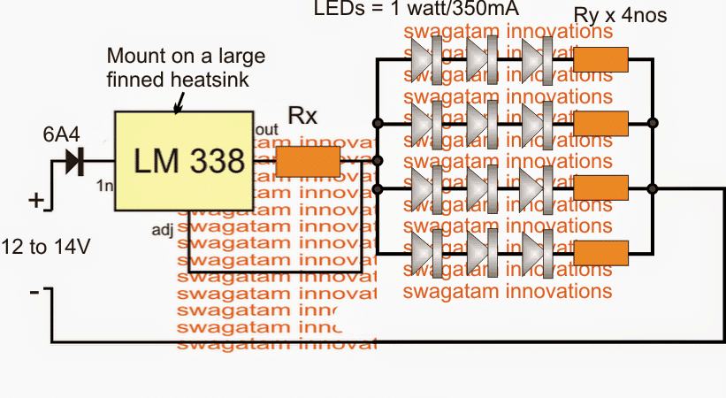
Circuit Operation
The circuit for the LED brake light may be witnessed above, and it looks pretty straightforward. The LM338 is configured as a current limiter, where Rx determines the maximum allowable amps to the connected LEDs. It may be calculated using the following formula: Rx = 1.25/LED current When LeDs are connected in series there effective current consumption is always equal to the rating of the one individual LED. Therefore in the diagram each string would consume 350mA since this is the rating of each 1 watt LED. Combined current for all the three strings would be 3 x 350mA = 1050mA or approximately 1 amp Substituting the above parameter in the formula we have: Rx = 1.25/1 = 1.25 Ohms Wattage = 1.25 x 1 = 1.25 watts The resistors Ry which can be seen connected in series with the LEDs are actually optional, these may be included only for assisting the IC and providing proper balance across the LED strings. It may be calculated using the following formula: Ry = (Supply - LED total FWD voltage) / LED current Since here the LEDs are specified with a forward voltage of 3.3V and 3 nos are arranged in the series, the combined forward voltage becomes 3 x 3.3 = 9.9V For reducing full loading of the LEDs, we can take the current at 300mA instead of the specified 350mA Therefore Ry = (13 - 9.9) / 0.3 = 10.33 ohms or simply 10 Ohms wattage = (13 - 9.9) x 0.3 = 0.93 watts or 1 watt It seems we missed an important inclusion in the above diagram, it's the dimmed LED feature during the normal course of the vehicle and while the brakes are not applied. The following diagram suggests how simply this may be implemented using a parallel connected resistor Rz, with Rx.Applying the Dimming Control
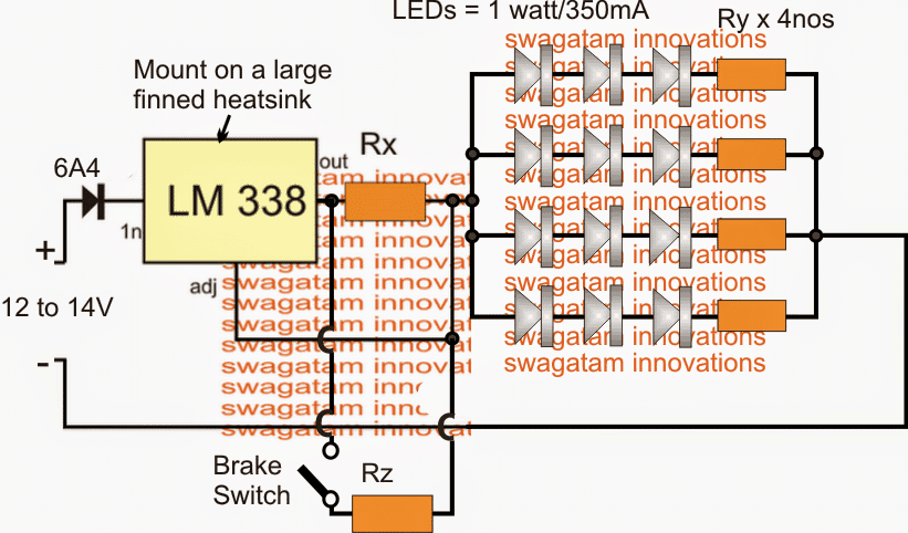 Here the values of the Rx and Rz may be identical but twice that of the above calculated value that is 1.25 x 2 = 2.5 Ohms.
This would allow a 50% dimming of the tail lights while the brakes are in the released position.
If one desires to obtain further dimming of the LEDs Rx may be increased to 3 ohms or 3.5 Ohms, this would also mean lowering the Rz value proportionately such that the parallel value of the two resistors constitutes 1.25 Ohms.
Here the values of the Rx and Rz may be identical but twice that of the above calculated value that is 1.25 x 2 = 2.5 Ohms.
This would allow a 50% dimming of the tail lights while the brakes are in the released position.
If one desires to obtain further dimming of the LEDs Rx may be increased to 3 ohms or 3.5 Ohms, this would also mean lowering the Rz value proportionately such that the parallel value of the two resistors constitutes 1.25 Ohms.
Make this Car Interior Light Fader Circuit
The post explains a simple circuit which can be used for producing a slow fading light effect each time it's switched OFF. The application can be typically used in car interior lights. Designed by: Abu-HafssThe Circuit Concept
Most of the modern cars are equipped with circuitry which switches on the Car's room lamp when a door is opened and switches off the lamp in fading manner when the door is closed. Here a simple circuit is presented which can be installed in old cars without any major alterations to get the same effect. Before we understand the description of the circuit, it is important to understand the wiring of a Car's interior lamp and how the door switches are operated.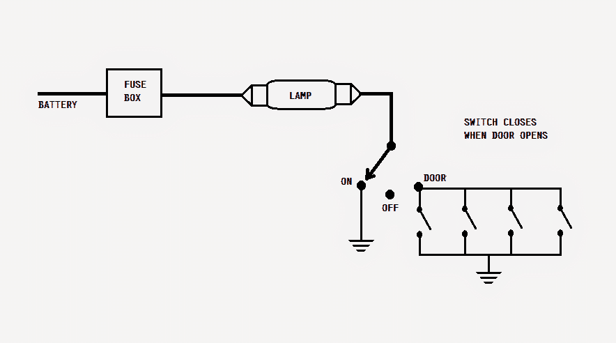 The lamp is connected to the battery's positive thru a fuse.
The other end of the lamp is connected to a single-pole-3-throw switch.
When this switch is positioned at ON, the other end of the lamp gets connected to ground i.e.
the negative terminal of the battery hence, the lamp gets illuminated.
In OFF position, the lamp remains disconnected from the ground.
In DOOR position, the lamp gets connected to the ground via door switches (in parallel).
When a door is opened, the corresponding door switch is closed.
The lamp is connected to the battery's positive thru a fuse.
The other end of the lamp is connected to a single-pole-3-throw switch.
When this switch is positioned at ON, the other end of the lamp gets connected to ground i.e.
the negative terminal of the battery hence, the lamp gets illuminated.
In OFF position, the lamp remains disconnected from the ground.
In DOOR position, the lamp gets connected to the ground via door switches (in parallel).
When a door is opened, the corresponding door switch is closed.
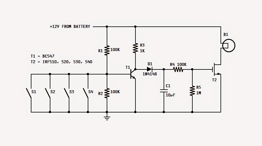
How it Works
Referring to the proposed car interior light fader circuit, when any of the door is opened, its switch is closed hence, the base of T1 gets connected to ground and thus stop conducting. In this state, C1 gets charged rapidly via R3 and D1. As soon as C1 is charged, the mosfet is fed with the gate voltage thru R4 and thus it starts conducting and consequently the lamp is illuminated. Now, when that door is closed, its switch gets open. The base of T1 gets disconnected from the ground and is held at a voltage delivered by the R1/R2 voltage divider. This action switches on T1, and the voltage coming from R3 finds it way to ground thru emitter of T1. The switching on of T1 deprives C1 of its charging current and thus C1 starts discharging slowly thru R4 and R5. The gate voltage of T2 reduces as C1 discharges. With this reduction in the gate voltage the intensity of the lamp is also reduced. Finally, when the gate voltage goes below the threshold voltage the lamp switches off. The values of R5 and C1 are responsible for the fading delay time of the lamp. Increasing the values will increase the time and vice versa. T2 should be any suitable N-channel mosfet capable of handling at least 50V and 10A. The whole circuit can be built on compact sized general purpose board and enclosed in the room lamp cover.Infrared Remote Control Safe Lock Circuit
A simple, cheap yet highly effective infrared remote control safe lock circuit can be studied in the following post.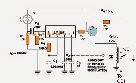
Using IC LM567
The LM567 IC is one of my favorites simply because it's too versatile, and becomes applicable in most of the crucial circuit concepts through hassle free configurations. One such crucial yet simple IR remote control receiver application can be seen in the above diagram, which activates only through a unique predetermined frequency as set by R1/C1 in the circuit. The above concept can be used in automotive security applications for locking the safe/vault through a uniquely set frequency code. In the shown circuit R1/C1 determines the latching frequency of the unit, which may be calculated using the following formula: f = 1/R1C1, which constitutes to be 100kHz for the shown values of R1, C1. Pin3 which is the receptor pinout of the IC is configured with a IR diode for receiving an incoming tone locked frequency set at the matching 100kHz frequency.How it Works
When such a matching frequency is detected at pin3 of the IC, pin8 responds and becomes low momentarily activating the transistor latch. The transistor and relay latch together to acknowledge the response and open the safe lock for the user. Any other frequency which may not coincide with the set R1/C1 value is simply rejected by the IC keeping the vault secured and locked, thus the system becomes extremely foolproof and safe from potential bike thieves. pin1 output from the IC can be configured with an audio amplifier and buzzer in case an audio signal is felt essential during the remote control activation. However this may require the transmitter to be equipped with a modulated audio signal over the carrier base frequency. A very simple complementing IR remote handset circuit may be seen below:Oil Burner Button Start Ignition Circuit
The post discusses a simple automatic ignition for an oil burner system system which is initiated with a push button operation. The idea was requested by Mr. Andreas.Technical Specifications
I have a request and i wonder if its possible for someone to find a simple circuit about oil burner controller. I'm sure most people knows the principal of how it works. The sequence it goes with this order. A motor and spark ignitor module start together,then after 5-6 seconds starts the solenoid valve that spray oil and a flame become then a photo resistor see the flame and stops the sparking, if no flame the whole controller trips and stops until you press reset. I hope you understand,Many thanks Andreas ChrisThe Design
The design of the proposed button start ignition circuit can be studied by referring to the following diagram.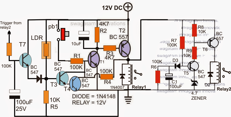 T1/T2 along with associated components form a latch circuit and gets triggered as soon as P1 is pressed.
The latching activates relay#1 which may be assumed to be wired with the motor and the ignition system.
As proposed this starts the motor and the ignition sparking.
The adjoining stage comprising T5/T6 constitutes a delay ON timer which simultaneously begins counting once the above system is initiated.
C1/R7 decides the delay ON period which may be appropriately set for achieving the desired 5/6 seconds.
once this delay period is lapsed relay2 is switched ON which may be assumed to be configured with a solenoid mechanism for spraying oil over the ignition chamber.
Once this is actuated, the flame lights up and illuminates an LDR which could be seen integrated with the Darlington T3/T4.
T3/T4 conducts in response to the illumination and instantly breaks the latch and the relay1 activation.
The motor and the sparking are inhibited from the supply and are instantly switched OFF.
The T7 protection stage ensures that in case no flame is sensed, after a couple of seconds it triggers and switches OFF the whole system.
The above explained automatic ignition burner mechanism could be also effectively used for vehicle button start implementation.
For a condition where the motor is required to keep running after the flame is detected, the above circuit may be modified as given under:
T1/T2 along with associated components form a latch circuit and gets triggered as soon as P1 is pressed.
The latching activates relay#1 which may be assumed to be wired with the motor and the ignition system.
As proposed this starts the motor and the ignition sparking.
The adjoining stage comprising T5/T6 constitutes a delay ON timer which simultaneously begins counting once the above system is initiated.
C1/R7 decides the delay ON period which may be appropriately set for achieving the desired 5/6 seconds.
once this delay period is lapsed relay2 is switched ON which may be assumed to be configured with a solenoid mechanism for spraying oil over the ignition chamber.
Once this is actuated, the flame lights up and illuminates an LDR which could be seen integrated with the Darlington T3/T4.
T3/T4 conducts in response to the illumination and instantly breaks the latch and the relay1 activation.
The motor and the sparking are inhibited from the supply and are instantly switched OFF.
The T7 protection stage ensures that in case no flame is sensed, after a couple of seconds it triggers and switches OFF the whole system.
The above explained automatic ignition burner mechanism could be also effectively used for vehicle button start implementation.
For a condition where the motor is required to keep running after the flame is detected, the above circuit may be modified as given under:
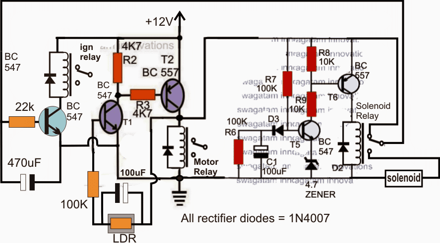 Here, when power is switched ON, T1/T2 get self-latched, the 100uF capacitor in parallel with the LDR ensures a feedback latch voltage for sustaining the latching effect.
The ignition relay also simultaneously gets switched ON through the N/C biasing voltage of the solenoid relay.
After 5/6 seconds when solenoid relay activates, the ignition still holds on due the presence of the 470uF capacitor.
The flame illumination overrides the 100uF capacitor and keeps the motor operative, however the ignition relay deactivates after a while when the 470uF is fully discharged.
In case the flame does not strike, the 100uF capacitor parallel to the LDR charges fully and breaks the latch switching OFF the motor relay, the solenoid relay as well as the ignition relay.
Here, when power is switched ON, T1/T2 get self-latched, the 100uF capacitor in parallel with the LDR ensures a feedback latch voltage for sustaining the latching effect.
The ignition relay also simultaneously gets switched ON through the N/C biasing voltage of the solenoid relay.
After 5/6 seconds when solenoid relay activates, the ignition still holds on due the presence of the 470uF capacitor.
The flame illumination overrides the 100uF capacitor and keeps the motor operative, however the ignition relay deactivates after a while when the 470uF is fully discharged.
In case the flame does not strike, the 100uF capacitor parallel to the LDR charges fully and breaks the latch switching OFF the motor relay, the solenoid relay as well as the ignition relay.
Pedal Speed Controller Circuit for Electric Vehicles
In this part of the article we learn about an innovative method of converting pedal press mechanism in electric vehicles into a correspondingly varying electrical signal, which may be further used for processing the speed control of the vehicle. The explained concept will work like an electronic accelerator, which will increase the vehicle speed linearly when the pedal is gradually pressed, and vice versa, using PWM technology The idea was requested by Mr.Lokesh MainiTechnical Specifications
I am a mechanical guy,currently working on an electric vehicle and i want to control the speed of my motor using pedal . i am not getting a controller for my motor please help me to build my own i'll be highly thankful Motor Specifications are 36volt,43amps and 1.5hp brushed dc motor.The Mechanical Design
An electronic version of a pedal accelerator will primarily require a mechanism to first convert mechanical pressing of the pedal into a correspondingly varying electrical signal, so that this signal can be processed through a signal processor stage for the desired conversion into a practical speed control of the vehicle. Many concepts can be tried such as by using a piezo load sensor, a capacitive load sensor, by a resonance sensor etc. In this article we'll learn a much simpler method devised by me which incorporates a LED/LDRassembly for achieving the same.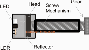 In the electromechanical arrangement shown in the figure above we are able to see the following integrated components:
A small gear attached with a screw mechanism.
The head of the screw having a white mat reflector surface
A LED/LDR assembly positioned in front of the screw head.
In the electromechanical arrangement shown in the figure above we are able to see the following integrated components:
A small gear attached with a screw mechanism.
The head of the screw having a white mat reflector surface
A LED/LDR assembly positioned in front of the screw head.
How the Proposed mechanism works.
The gear shown in the above figure is to be locked with another gear having a ratio that may be 10 times higher than this gear. The bigger gear needs to be configured with the pedal mechanism such that it initiates a rotational movement in response to the pressing of the pedal. The rotational response from the gears will in turn produce a forward motion of the screw head across the chamber where the LED/LDR assembly is located. The process will cause a proportionately varying amount of reflected light from the LED to be received by the LDR. This varying data (in the form of a varying resistance) corresponding to the pedal depression can be then fed to a signal processor circuit for enforcing the intended speed control of the particular vehicle. In the next post we'll learn the signal processor stage using PWM technique. In the above sectionwe learned about a simple electromechanical converter assembly for transforming the pedal action into a proportionately varying electrical signal.Converting Pedal Action to PWM
Now let's study a circuit implementation which will enable us to convert the pedal electric signal into a correspondingly varying PWM signal for the intended motor speed control of the vehicle.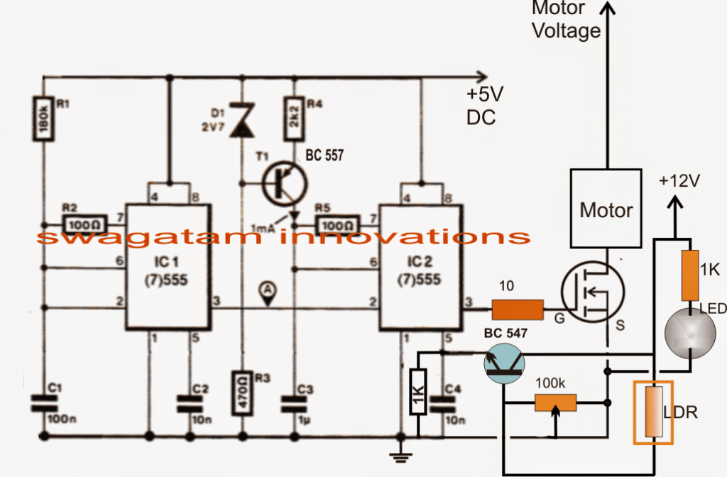 Referring to the above circuit diagram we can assess the circuit operation with the help of the following points:
IC1 is configured as a 80Hz pulse generator having maximum ON time and minimum OFF time as its duty cycle
IC2 is rigged as a comparator which first converts the above 80Hz pulse applied at its pin2 with triangle waves generated at its pin6 and compare the triangle waves with the modulating voltage available at its pin5.
The pin5 modulating voltage is derived from a BJT BC547 emitter which is configured as a common collector with its base connected with the LDR inputs achieved from the pedal actions.
The varying resistances in response to the pedal pressing is compared with the 100K preset setting and a proportionate magnitude of voltage is developed at the base of the transistor which converts the low current input into an equivalent high current signal over pin5 of IC2.
This instantaneous potential level is accepted and processed by IC2 generating proportionate magnitude of PWM signals for the mosfet and the connected motor.
The motor speed is thus controlled and varied as per the fluctuating PWMs in response to the pedal pressings of the vehicle.
The above procedures effectively convert the pedal actions into a controlled operations of the vehicle motor and its speed.
Referring to the above circuit diagram we can assess the circuit operation with the help of the following points:
IC1 is configured as a 80Hz pulse generator having maximum ON time and minimum OFF time as its duty cycle
IC2 is rigged as a comparator which first converts the above 80Hz pulse applied at its pin2 with triangle waves generated at its pin6 and compare the triangle waves with the modulating voltage available at its pin5.
The pin5 modulating voltage is derived from a BJT BC547 emitter which is configured as a common collector with its base connected with the LDR inputs achieved from the pedal actions.
The varying resistances in response to the pedal pressing is compared with the 100K preset setting and a proportionate magnitude of voltage is developed at the base of the transistor which converts the low current input into an equivalent high current signal over pin5 of IC2.
This instantaneous potential level is accepted and processed by IC2 generating proportionate magnitude of PWM signals for the mosfet and the connected motor.
The motor speed is thus controlled and varied as per the fluctuating PWMs in response to the pedal pressings of the vehicle.
The above procedures effectively convert the pedal actions into a controlled operations of the vehicle motor and its speed.
How to Set up the Circuit.
It's very easy. Press the pedal to its maximum point such that the screw head reaches to the nearest possible position in front of the LED/LDR assembly. Next adjust the 100k preset until pin3 of the IC2 starts generating PWMs with maximum width, this may be confirmed by measuring the voltage at pin3 to be as close as possible to the supply voltage of the circuit, that is 5V. Once this is done, the setting up procedure could be assumed to be complete. The results could be now verified by pressing the pedal at different levels and checking the motor speed vary in an identical manner.Wireless Helmet Mounted Brake Light Circuit
The post explains an innovative wireless LED brake light circuit which can be attached to a biker's helmet. The LEDs attached with the helmet circuit illuminates in response to the motorcycle braking generating an enhanced brake light effect from the user's helmet. The idea was requested by Mr. Bugoy.Technical Specifications
Good day Sir! How are you? Yes, it was indeed a very interesting project. I am really an advocate of safety and security when it comes to my bike Sir. I wish you could see it soon. By the way, here are some links of an aftermarket product: I am thinking of hacking a wireless doorbell or a remote controlled toy car with lights.
But I do not know how to do it.
So I'm asking for your help Sir if you know of a simple RF transceiver and receiver that could drive LED's.
Thank you so much Sir.
I am thinking of hacking a wireless doorbell or a remote controlled toy car with lights.
But I do not know how to do it.
So I'm asking for your help Sir if you know of a simple RF transceiver and receiver that could drive LED's.
Thank you so much Sir.
The Design
The proposed helmet brake light circuit could be easily implemented by using an inexpensive homemade FM transmitter and a small FM transistor radio. A small FM transmitter can be seen in the following diagram which becomes the brake light transmitter circuit for the helmet LEDs.The FM Radio as the Receiver
Any small FM radio could be used for the purpose of receiving the transmitted signals from the above explained FM transmitter. An example circuit of a small FM radio may be seen below: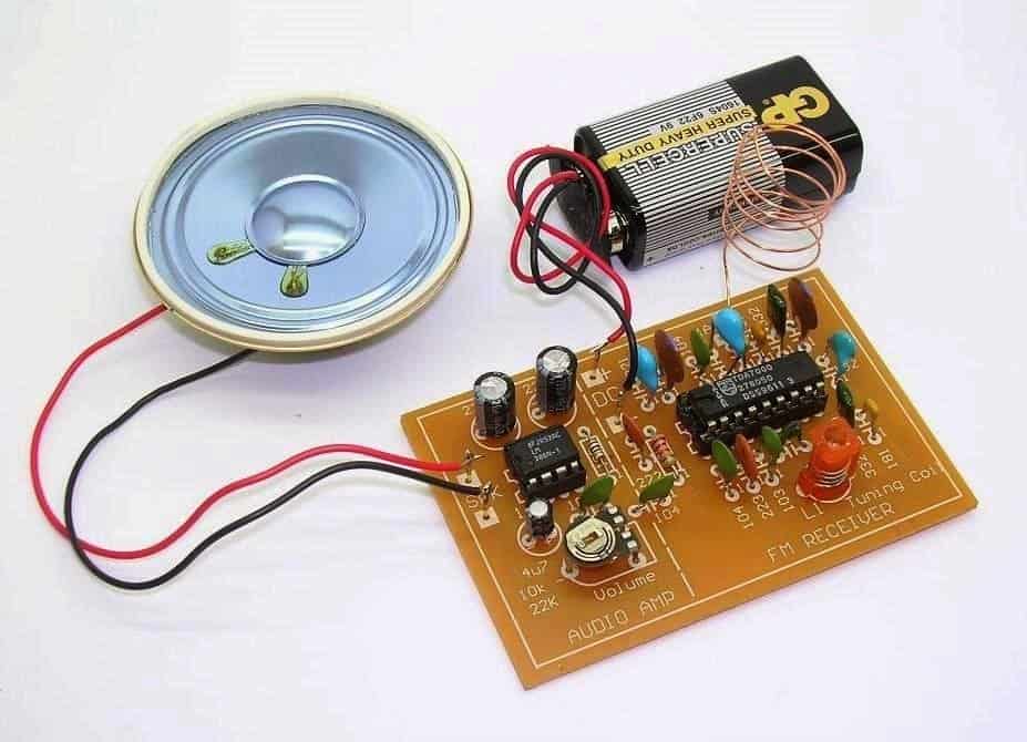 In the image we are able to see a speaker attached with the radio and also a 9 V battery as the supply source.
Both of the above mentioned attachments needs to be removed from the kit and should appear something as given below after the proposed modifications:
In the image we are able to see a speaker attached with the radio and also a 9 V battery as the supply source.
Both of the above mentioned attachments needs to be removed from the kit and should appear something as given below after the proposed modifications:
 In order to make the above radio compatible with a LEd driver stage and for illuminating a set of LEDs in response to the received FM transmitter signals, we need to make some interesting electrical modifications with the shown FM radio kit.
The following figure shows how a small electrical stage consisting a BJT and inductor may be used for transforming the amplified audio from the radio into a DC which would then illuminate a set of LEds brightly each time the brakes are applied in the motor bike.
In order to make the above radio compatible with a LEd driver stage and for illuminating a set of LEDs in response to the received FM transmitter signals, we need to make some interesting electrical modifications with the shown FM radio kit.
The following figure shows how a small electrical stage consisting a BJT and inductor may be used for transforming the amplified audio from the radio into a DC which would then illuminate a set of LEds brightly each time the brakes are applied in the motor bike.
 In the above diagram we see the speaker terminals of the FM radio being joined with an inductor and the output across the inductor further connected with a diode, capacitor rectifier stage for converting into a stable DC base drive for the following BC547 LED driver stage.
We can also see the 9 V battery being replaced with a 3.7 V Li-ion cell in order to make the design compact and easily inclosable inside the helmet.
When the radio begins receiving the switched audio, the weak audio frequency across the speaker wires become concentrated and boosted with the help of the connected inductor, this boosted voltage is rectified and filtered by the diode capacitor network so that the BC547 is able to receive a clean DC conversion for driving the set of LEds situated over the helmet body.
Now whenever the brakes are applied the signal from the transmitter is received by the FM radio inside the helmet resulting in the required illumination of the LED strip through the operations as explained in the above section.
In the above diagram we see the speaker terminals of the FM radio being joined with an inductor and the output across the inductor further connected with a diode, capacitor rectifier stage for converting into a stable DC base drive for the following BC547 LED driver stage.
We can also see the 9 V battery being replaced with a 3.7 V Li-ion cell in order to make the design compact and easily inclosable inside the helmet.
When the radio begins receiving the switched audio, the weak audio frequency across the speaker wires become concentrated and boosted with the help of the connected inductor, this boosted voltage is rectified and filtered by the diode capacitor network so that the BC547 is able to receive a clean DC conversion for driving the set of LEds situated over the helmet body.
Now whenever the brakes are applied the signal from the transmitter is received by the FM radio inside the helmet resulting in the required illumination of the LED strip through the operations as explained in the above section.
How to set up the proposed LED helmet brake light circuit
Before installing the Rx LED module over the helmet, the radio board needs to be set appropriately as per the following explanation: Switch ON the FM radio with no antenna connected and the station selection on the radio being on any random position. You may find the LEDs glowing in this situation, now adjust the volume control preset in the amplifier section of the FM board very slowly until you find the LED just stops illuminating. After the above setting disconnect the speaker output wires from the LED driver stage and let a speaker be connected with these wires. Also connect the antenna wire back in the shown position. Switch ON the transmitter unit and adjust the red colored frequency coil or it could be a capacitor trimmer in other variants of FM receivers, tune it carefully until a clean and powerful musical audio (UM66 music) is detected in the speaker. Seal the tuning device with glue. Now remove the speaker and connect the wires back with the LEd driver stage. Switch ON the transmitter and you'll find the LEDs glowing brightly in response to the received musical transmission from the Tx unit. Switching of the Tx circuit should switch OFF the LEDs as well instantly confirming the perfect working of the system. Check the response a few more times after which you may proceed with the final installations.Customizing Car Side Marker Lights to Flashing Side Markers
The article discusses a car side marker modification which enables it to respond to the existing turn signal pulses and flash in tandem with the turn signal flashing. The idea was requested by Mr. Jerry Klein.Technical Specifications
I have a 1990 automobile which I believe does not have very sophisticated circuitry controlling the direction signals /driving lightsand side markers. This should work in my favor when converting to LEDs. I am currently using a simple wiringmod that has worked successfully for20 years. I cut the side marker's ground wire and reconnected it to the turning signal lead off the direction signal /driving lights. The driving lights are dual filament 1157 and the side markers are single filament 158. I love they way they work and would like to convert them with my modification to LEDs. The side markers flash on when thedriving lights are off; theyflash off when the driving lights are on. I quickly realized that this will not work because the light bulbs are working with reversing polarity and therefore Iwill need a more managed solution. I think the solution isrunningthe side markerswith constant hot lead and controlling the blinking off or blinking on with some kind of control circuit on theside marker's ground. I would also like to connect up my rear side markers another 158 bulb to the same circuit. I am not a brain when it comes to circuitry but I have done some simple tasks with relays and am good with a soldering gun. I wanted to have my100W7 ampfog lights work off a dimmer so that I could tune them in to the exact lighting requirements. I purchased a boat dimmer unit that could handle the currentwhich worked with a taping pulse switchfor on off andhold for cycling brightness. HadI known about your before I could havesavedmoney with yourcircuit design. Boat parts are synonyms with big bucks. I can buy therequired parts and wire them up as directed. I have looked through your blogs and have not been able to find the exact solution. Can you please help me with this circuit design and parts list. I would have to know what wire goes towhat post on each component. I could not figure out how to join your blog and therefore this email.The enclosed chart represents the current wiring configuration of my car. After changing to an LED compatible flashing unit, everything is working correctly. The chart shows four LED Side Markers they are single function bulbs: off during the daytime; on at night.
They do not blink.The front and rear lights LED bulbs have dual function: two circuits One line controls night / on and a day / off.
The other line controls the turn signal blinking function.
We are only concerned with the turn signal function.
I would like the front and rear drivers side LED Markers to blink when the drivers side Front and Rear turn lights are blinking.I would like the front and rear passenger side LED Markers to blink when the passenger side Front and Rear turn lights are blinking.
The project is to create two identical circuits for the car's left and right turn signals.
The circuit taps into the blink turn signal line to determine when it is pulsing causing the car's turning light to blink.
The circuit will then blink the corresponding front LED Side Marker.
A wire will be run from the front LED Side Markers to the rear LED Side Markers giving them the same functionality.
During the day, it blinks the LED Side Markers ON.At night, since the LED Side Markers are illuminated the circuit reverses and blinks the LED Side Markers OFF.
Regards
The chart shows four LED Side Markers they are single function bulbs: off during the daytime; on at night.
They do not blink.The front and rear lights LED bulbs have dual function: two circuits One line controls night / on and a day / off.
The other line controls the turn signal blinking function.
We are only concerned with the turn signal function.
I would like the front and rear drivers side LED Markers to blink when the drivers side Front and Rear turn lights are blinking.I would like the front and rear passenger side LED Markers to blink when the passenger side Front and Rear turn lights are blinking.
The project is to create two identical circuits for the car's left and right turn signals.
The circuit taps into the blink turn signal line to determine when it is pulsing causing the car's turning light to blink.
The circuit will then blink the corresponding front LED Side Marker.
A wire will be run from the front LED Side Markers to the rear LED Side Markers giving them the same functionality.
During the day, it blinks the LED Side Markers ON.At night, since the LED Side Markers are illuminated the circuit reverses and blinks the LED Side Markers OFF.
Regards
The Design![]()
As per the requirement, the existing side marker lights which are designed to stay ON during night and OFF during day are expected to blink in response to the turn signals lamp switching.
It means the intended customization should be designed such that it blinks the side markers by alternately cutting off the supply during day time, and by alternately applying power during night time, these are two different modes which are required to induce the desired flashing effect on the specified side markers whenever the turn signals are switched ON.
Referring to the diagram, the positive line of the existing side marker needs to be cut and then joined across the two shown points of the recommended circuit.
The design can be understood as follows:
Once the above modification is done, during night, the side marker positive line carrying the positive supply would normally keep the lamp switched ON through the 1N4007 diode, and the N/C contact/pole of the relay.
Now if the turn signal lamp is switched ON, the relay driver BC547 would start pulsing in response to the acquired signals from the turn signal source.
This pulsing would alternately break the positive line of the side marker causing it to blink.
The TIP127 in this situation would have no effect on the N/O contact of the relay due to the positive feed at its base from the side marker supply.
However during night time, the positive line of the side marker would have no positive supply, in this situation whenever the relay would be activated in response to the turn signal pulse, the TIP127 also being activated (via base 10k resistor) would pass the positive from the turn signal feed to the side marker via the N/O contact of the blinking relay....this would make sure the side markers yet again blink as proposed in the above request.
Modifying to Flash According to Turn Signals
The following figure shows how to modify the above car side marker further such that it always flashes in accordance with the turn signal pulses:Circuit Diagram
 The 470uF makes sure that the PNP TIP127 remains completely disabled while the turn signal is operating.
How to Make a Car Power Window Controller Circuit
The article explains a car power window controller circuit using a single push button or a couple of push buttons. The idea was requested by Mr. Win.Technical Specifications
I'm winantiyo from Indonesia, i've read your post in your blogand i'm very like it. i have 2 project: 1. auto roll up power window for car 2. auto lock trigger by foot brake for car can u help me for the circuit n schematic? auto up power window: i want my car window can roll up or roll down automatically with single click on power windows button switch ..i ever see the auto roll up module with one relay 8pin, 2 transistor n 4 electrolytic capasitors but it has been broken, 1 resistor n 2 diode. but the series of part has been lost. there are 5 cables: +12V, ground, 1 cable to motor window, 1 cable to switch power window, and 1 cable again to another motor windows cable..here is the pic:
AUTO LOCK BY FOOT BRAKE:
i want to make my car door can locked automatically when all the door closed, key turn ON and i press my foot brake (+trigger). then the door can automatically unlocked when i turn off the key. i hope u understand my explanation...i'm sorry for my english..thank you very much.The Design
Window Glass Up/Down Controller using a Single switch The shown car power window controller circuit basically consists of three stages: a transistor latch which includes a current sensor, a NAND gate based flip flop stage and a relay driver stage for flipping the motor actions alternately. The indicated lock/unlock switch toggles the flip flop stage made by engaging three NAND gates from the IC 4093, whose output responds with a permanent high and low alternately with every push of the switch. Parts list
R1, R3, R6, R7 = 100K
R5,R8 = 2M2
R9 = 4K7
C1,C4 = 22uF/25V
C2,C3 = 0.22uF
T1,T3 = BC547
T4= 8050
T2 =8550
RL1,RL2 = 12V/20AMP
ALL DIODES = 1N4007
R10 = TO BE CALCULATED
N1---N3 = IC 4093
This switch also makes sure that the latch section comprising T1 and T2 gets activated in order to allow the supply voltage to reach the remaining part of the circuit.
The output from the flip flop acquired at N2 pin4 is fed to a relay driver stage for activating the power window motor with a forward or a reverse motion depending upon the position of the window glass.
It must be ensured that while connecting the motor the polarity of the wires are set such that a high at pin4 of N2 actuates the window in the closing mode, and vice versa.
The relay is a heavy duty DPDT relay whose N/C, N/O contact connections with the motor enable the motor to carry out the desired to and fro movement.
Normally, reed switches are employed for detecting the completion of the glass up and down movements in order to avoid the motor from getting loaded and destroyed, however here we have a taken a different and a much advanced approach.
In the proposed car power window controller circuit we have employed a current sensor stage in the form of T3, which detects a mounting current across R10 and switches ON itself when the level crosses a set threshold.
When T3 switches ON it breaks the T1/T2 latch disconnecting the supply to the motor.
However if a reed switch is incorporated for the above actions, the reed contacts positioned for detecting the up and the down thresholds of the glass may be wired across C1, and T3 stage may be removed entirely.
R10 may be replaced with a wire link (see figure below).
Parts list
R1, R3, R6, R7 = 100K
R5,R8 = 2M2
R9 = 4K7
C1,C4 = 22uF/25V
C2,C3 = 0.22uF
T1,T3 = BC547
T4= 8050
T2 =8550
RL1,RL2 = 12V/20AMP
ALL DIODES = 1N4007
R10 = TO BE CALCULATED
N1---N3 = IC 4093
This switch also makes sure that the latch section comprising T1 and T2 gets activated in order to allow the supply voltage to reach the remaining part of the circuit.
The output from the flip flop acquired at N2 pin4 is fed to a relay driver stage for activating the power window motor with a forward or a reverse motion depending upon the position of the window glass.
It must be ensured that while connecting the motor the polarity of the wires are set such that a high at pin4 of N2 actuates the window in the closing mode, and vice versa.
The relay is a heavy duty DPDT relay whose N/C, N/O contact connections with the motor enable the motor to carry out the desired to and fro movement.
Normally, reed switches are employed for detecting the completion of the glass up and down movements in order to avoid the motor from getting loaded and destroyed, however here we have a taken a different and a much advanced approach.
In the proposed car power window controller circuit we have employed a current sensor stage in the form of T3, which detects a mounting current across R10 and switches ON itself when the level crosses a set threshold.
When T3 switches ON it breaks the T1/T2 latch disconnecting the supply to the motor.
However if a reed switch is incorporated for the above actions, the reed contacts positioned for detecting the up and the down thresholds of the glass may be wired across C1, and T3 stage may be removed entirely.
R10 may be replaced with a wire link (see figure below).
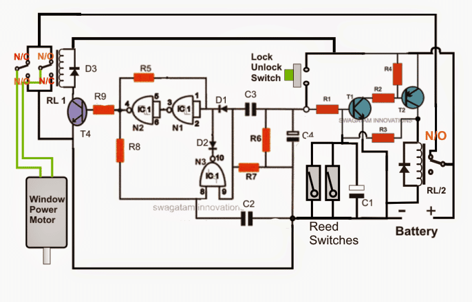
Using two switches
The above design could be much simplified if two separate push buttons are employed for the up/down operations of the window glass. The simplified power window circuit which incorporates just a few number of BJTs can be witnessed below.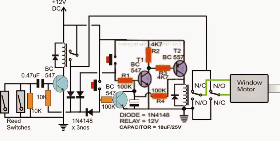 Four of the above circuits will need to be installed on each door of the vehicle for the required power window switching.
Upgrading the Car Power Window
In the above sections we discussed the circuit design of an automatic car power window controller, here we'll learn how it may be enhanced with more features. The main circuit using a single button, posted in the previous article can be witnessed below for reference purpose.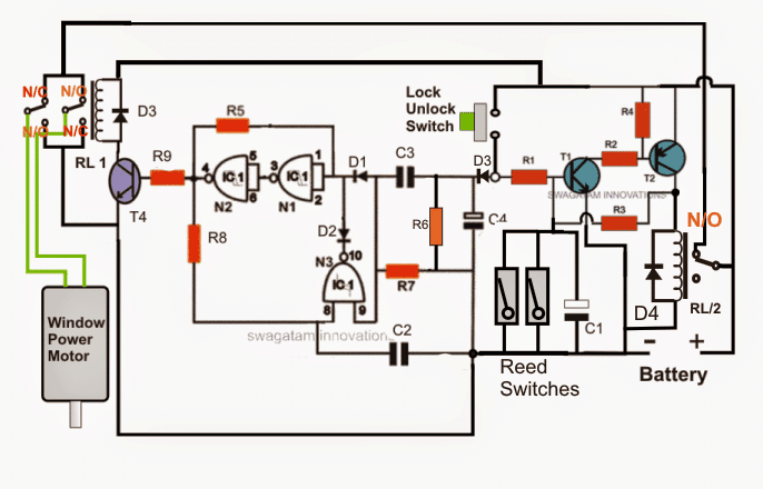 Parts list
R1, R3, R6, R7 = 100K
R5,R8 = 2M2
R9 = 4K7
C1,C4 = 22uF/25V
C2,C3 = 0.22uF
T1= BC547
T4= 8050
T2 =8550
RL1,RL2 = 12V/20AMP
ALL DIODES = 1N4007
N1---N4 = IC 4093
Now, as per the suggestion the window operation needs to be locked when all the doors are closed and the key switched in.
The above step could be implemented by adding the following design in conjunction with the above shown power window controller.
Parts list
R1, R3, R6, R7 = 100K
R5,R8 = 2M2
R9 = 4K7
C1,C4 = 22uF/25V
C2,C3 = 0.22uF
T1= BC547
T4= 8050
T2 =8550
RL1,RL2 = 12V/20AMP
ALL DIODES = 1N4007
N1---N4 = IC 4093
Now, as per the suggestion the window operation needs to be locked when all the doors are closed and the key switched in.
The above step could be implemented by adding the following design in conjunction with the above shown power window controller.
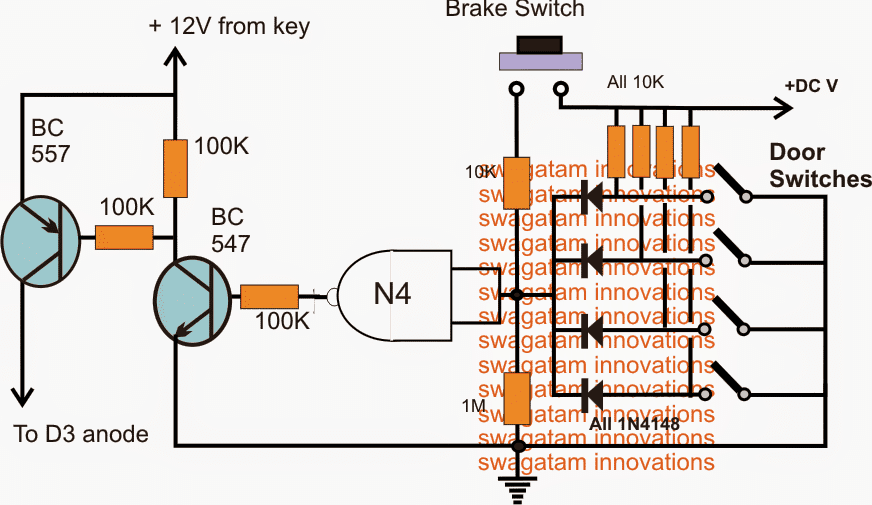
Circuit Operation
As can be seen, here we have effectively utilized the idle extra gate N4 from the IC 4093 and configured it with a few resistors and BJTs, for executing the proposed brake switch control feature. The operations may be understood with the help of the following points: When all the doors are closed, the relevant door switches also close and ground the positive available at the anodes of all the 1N4148 diodes. This immediately forces the input of N4 to go low due to the presence of the 1M resistor. The low at the input of N4 renders a high at its output which in turn activates the BJTs, positioned as a switches. However the BJTs would be still inactive as long as the positive from the key switch is not energized. As soon as the ignition switch is keyed, the BJTs become functional and locks the motor flip flop stage by feeding a positive across D3 cathode. D3 has been introduced specifically here so that the locking potential affects only the flip flop and not the T1/T2 latch stage. In the above mode the push button is rendered ineffective such that pressing it produces no effect on the window glasses which stays hard locked. However the above situation gets restored each time the brakes are applied and held activated. Braking activates the brake switch, causing a positive potential at the input of N4 which in turn produces a zero at its output, switching off the BJTs. The positive at D3 cathode now becomes relieved so that the push button is enabled yet again for the intended window up/down operations.Cellphone Controlled Car Starter Circuit
The post presents a simple cellphone triggered remote control circuit that can be applied as a cellphone operated remote car starter. The unit would cost less than $20 to build. I have already covered quite a few interesting cellphone remote control circuits in this blog, all of which can be implemented to control or toggle some electrical equipment remotely using ones own cell phone, exclusively.How it Works
The basic cellphone controlled relay circuit stage involved in all the previous circuits can be also effectively utilized for starting the ignition system of a vehicle, through the owners cell phone. The schematic for the same may be witnessed below and may understood with the following explanation: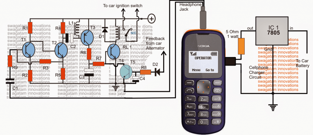 The design is basically a transistorized audio amplifier circuit, which is positioned for amplifying the assigned ringtone from the adjoining cell phone modem.
The cellphone shown with the circuit stays permanently attached with the circuit and forms the integral part of the whole system.
The diagram shows a NOKIA 1280 cellphone as the modem, however any cheap cellphone may be employed for the purpose provided the cellphone includes the "assign tone" feature discretely for the particular selected numbers.
The number of the owner or the user is first stored and assigned with a suitable ringtone available within the cellphone modem so that the modem responds only to the owners phone and not to any other irrelevant numbers.
The default ringtone of the modem is set to "empty" in order to mute all other unwanted calls.
When the owner calls the modem cellphone, the ringtone is detected by the circuit and amplified to a level sufficient for the relay to get energized.
The relay stays energized for so long as the call remains connected.
The design is basically a transistorized audio amplifier circuit, which is positioned for amplifying the assigned ringtone from the adjoining cell phone modem.
The cellphone shown with the circuit stays permanently attached with the circuit and forms the integral part of the whole system.
The diagram shows a NOKIA 1280 cellphone as the modem, however any cheap cellphone may be employed for the purpose provided the cellphone includes the "assign tone" feature discretely for the particular selected numbers.
The number of the owner or the user is first stored and assigned with a suitable ringtone available within the cellphone modem so that the modem responds only to the owners phone and not to any other irrelevant numbers.
The default ringtone of the modem is set to "empty" in order to mute all other unwanted calls.
When the owner calls the modem cellphone, the ringtone is detected by the circuit and amplified to a level sufficient for the relay to get energized.
The relay stays energized for so long as the call remains connected.
Configuring the Relay Contacts
Since the relay contacts are configured or integrated with the ignition switch of the car, immediately triggers the ignition system of the vehicle starting the engine and the whole system. A feed back from the activated alternator makes sure that the relay is instantly shut off irrespective of the call duration from the owner's cellphone. The car ignition thus is able to start without the owner or the driver having to get inside the car and go through the manual operations. The car starts remotely through the owner's cell phone, a fail proof and a foolproof procedure yet as cheap as anybody can think of.Parts List
R1 = 22k R2 = 220 Ohms, R3 = 100K, R4,R6,R7 = 4K7 R5 = 1K R8 = 33K R13 = 100 ohms, T1, T2, T4, T5 = BC547 T3 = BC557, C1 = 0.22uF C2,C3, C4 = 100uF/25v D1, D2 = 1N4007 L1 = 40 mH coil, example: a piezo buzzer coil will do. diode = 1N4007 Relay = 12V/SPDT Modem = NOKIA 1280 The charger section is shown in the diagram, and needs to remain connected permanently with the attached cellphone modem.Cellphone RF Triggered Car Amplifier Auto-Mute Circuit
The following article presents a circuit design which would mute your car amplifier music the moment it detects a cellphone call inside the car, enabling an automatic muting during the situations, and saving the user from the manual hassles. A loud music could be a nuisance while a phone call is being attended or dialed. We all normally love listening to loud music while traveling in cars, but this could mean problems in case a phone call is required to be attended.Automatic Car Amplifier Muting
An automatic muting system which could detect a cellphone call and mute the car amplifier automatically for the time being could be quite handy as it would save the user from some frustration, and manual hardwork. Let's learn how this may be possible using the following explained little circuit. We know that all cellphones generate a significant amount of radio frequency (RF) each time these are activated through an incoming or an outgoing call. The level of the generated RF could be different for different cellphones but nevertheless some degree of these will be always present around called cellphones no matter how much it's been restricted. These emitted RFs from a cell phone makes it very easy to sense it's operational condition and could be effectively used for any relevant toggling function through an attached circuitry.The RF Sniffer
The following circuit shows a simple RF sniffer or detector circuit which could be incorporated for the proposed vehicle amplifier muting while a call is being received or dialed over a cellphone inside the intended premise. Referring to the figure below, the design basically consists of two stages, the RF sensor made up of by A1 and A2 and a relay driver stage comprising the subsequent BC547 driver stage. A1 and A2 are each configured as a high gain amplifier and are connected in series for achieving maximum sensitivity. The feed back resistor 2M2 is responsible for determining the gain or the sensitivity level of the opamps. Increasing it increase the sensitivity and vice versa. The opamps together become ideally suited for picking up all kinds of RF signals that might be present in the vicinity.Adjusting the Sensitivity
It's sensitivity could be set by adjusting the 2M2 pot or preset as per the available RF level around. Inside a car there could be a host of other disturbances other than the cell phone Rf, therefore the sensitivity needs to be tweaked optimally such that the sensor picks up only the RFs from the cell phone and not from the ignition system of the vehicle. Additionally, more than one of these units could be positioned on differing corners of the car interior and the outputs integrated with the main relay driver so that the receiver is able to detect the Rfs from everywhere inside, and from the cell phones of the members who may occupying the rear car seats. This will also allow to keep the individual muting circuits set with minimum sensitivity making sure that these units sense only the cell phone RFs and no other spurious disturbances. Coming back to the proposed car amplifier mute circuit, as soon as a cellphone is activated with a call, the RFs are instantly detected by the circuit's antenna and converted into an amplified DC fluctuating at the cell phones varying emission levels. The amplified output across A2 outputs is appropriately filtered by the associated diode and capacitor network, and used for driving the relay stage wherein the relay clicks and switches ON the mute terminals of the car amplifier, forcing the music to shut down for the time being, until the call is finished or completed by the user.Circuit Diagram
Modifying Car Turn Signal Lights, Park-Lights and Side-Marker Lights
The post explains an innovative circuit modification which allows a single common lamp to be used as a parking light, turn signal indicator light, as well as a side marker light on the relevant positions. The idea was requested by Mr. ChrisTechnical Specifications
I have a project that is slightly related to this one and could use your help. I have 2 single filament bulbs that I would like to use as parking lights as well as turn signals. They would be wired to stay on anytime the car is running, and each light would turn off and on when the corresponding turn signal is activated. The wire from factory the turn signal harness controls the +12 side. I also have 2 single filament bulbs that I would like to use as side markers anytime the parking lights are on, and I want them to flash opposite the turn signal, so when the turn signal bulb is lit the side marker is off, and when the turn signal bulb is not lit, the side marker bulb is. The side markers will not be lit unless the parking lights are on, but I do still want them to flash anytime the turn signals are activated. I prefer not to use led's as my project is striving for a retro look, but I might if it's not possible with the incandescent bulbs.The Design
According to the first requirement a single lamp needs to perform the dual function of a turn signal lamp as well as a park light, also the lamp should switch ON as soon as the turn signal switch is turned ON. The following modified turn signal cum park lamp implements the features exactly as per the above specs. When the park light is in switched ON position, the TIP122 switches ON the lamp through its base trigger via the upper diode and the series 1K resistor. Now, if the turn signal switch is triggered, the TIP122 responds by flashing the lamp, while the lower BC547 transistor which also gets triggered with the turn signals makes sure that the signal received from the park light switch is grounded and inhibited from influencing the lamp. The second requirement demands another lamp which may be positioned as a side marker lamp to respond to the above side indicator or the turn signals but flash with an opposite switching.
Also the same lamp is also supposed to light up when the park lights are ON.
The second requirement demands another lamp which may be positioned as a side marker lamp to respond to the above side indicator or the turn signals but flash with an opposite switching.
Also the same lamp is also supposed to light up when the park lights are ON.
 The diagram of the enhanced or the modified side marker lamp as shown above satisfies the conditions by flashing the connected lamp with opposite switching, and also responds to the parking switch toggling during normal operations.
The TIP122 is responsible for triggering the lamp when the park lights are switch in.
However when the turn signal switch is toggled, irrespective of the park light input the BC547 begins oscillating in response to the turn flash signals causing the TIP122 to also blink the lamp with the corresponding flash rate.
The 100uF capacitor makes sure that the TIP122 is fed with its stored positive feed for sustaining the illumination on the bulb during the flashing actions.
As per the suggestions from Mr.
Chris, the first diagram has been slightly modified with the following couple of improvements:
1) The transistor has been upgraded to TIP142.
2) The park-light input trigger has been replaced with+12V trigger from the ignition key so that the lamp works as fog lights and not as parking lights.
The diagram of the enhanced or the modified side marker lamp as shown above satisfies the conditions by flashing the connected lamp with opposite switching, and also responds to the parking switch toggling during normal operations.
The TIP122 is responsible for triggering the lamp when the park lights are switch in.
However when the turn signal switch is toggled, irrespective of the park light input the BC547 begins oscillating in response to the turn flash signals causing the TIP122 to also blink the lamp with the corresponding flash rate.
The 100uF capacitor makes sure that the TIP122 is fed with its stored positive feed for sustaining the illumination on the bulb during the flashing actions.
As per the suggestions from Mr.
Chris, the first diagram has been slightly modified with the following couple of improvements:
1) The transistor has been upgraded to TIP142.
2) The park-light input trigger has been replaced with+12V trigger from the ignition key so that the lamp works as fog lights and not as parking lights.
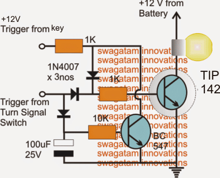 The above circuit could be enhanced further by adding a PWM dimming control feature as shown below.
The feature enables dimming of the fog lights when the park lights are turned ON, but ensures that the effect is inhibited as soon as the turn signals are switched ON.
The 100k preset could be set appropriately for achieving the desired reduction in the fog light illumination
The above circuit could be enhanced further by adding a PWM dimming control feature as shown below.
The feature enables dimming of the fog lights when the park lights are turned ON, but ensures that the effect is inhibited as soon as the turn signals are switched ON.
The 100k preset could be set appropriately for achieving the desired reduction in the fog light illumination
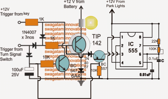
Upgrading Car Parklights to Enhanced DRLs
In this article we learn a simple circuit idea which can be applied in order to convert existing car park lights into advanced, smart DRL system. The idea was requested by Mr. Chris.Technical Specifications
I was very interested in reading the circuit diagram you posted a few months back regarding the 'Smart DRL/indicator circuits' (https://www.homemade-circuits.com/2014/04/smart-car-drl-controller-circuit.html)I was wondering if you could help me modify this circuit ever so slightly for my own project? I only have a basic knowledge of electrical circuits/PCBs and need some slight assistance. Essentially I am trying to replicate this system: https://www(dot)youtube(dot)com/watch?v=X51b_d4d6KQ Thanks for your time! Regards, ChrisThe Design
The referred video clipping shows the following effects over the modified park lights which are now replaced with LED DRLs. When the turn signals are switched ON, the relevant DRL partially shuts off so that the turn signal flashing becomes more prominent and highlighted. The moment turn signals are switched OFF, the DRL is automatically reverted to its original brightness, however the transition is not instant rather in a slow and gradually increasing manner (reverse fading). The above procedure is repeated each time the turn signals are switched ON, either left/right sides individually or together.Upgrading Park-Lights to DRL
The proposed upgradation from park-lights to an enhanced DRL circuit for producing the above effects can be done by implementing the shown circuit below. First of all the park lights will need to be replaced with LED DRL modules, and next the proposed circuit should be used in conjunction for the required enhancements. The operation of the circuit is pretty straightforwardand may be understood as under: The relay stays in a deactivated position as long as head lamp or the turn signals are not activated. Under this situation the N/C contacts allow the +12V (from ignition switch) to reach the switching transistor base which in turn keeps the connected DRL illuminated brightly or normally through its emitter voltage. Now in case either the head lamp or the turn signal is switched ON, the relay is supplied with the toggling voltage and it activates, shifting its contact from N/C to N/O The breaking of the N/C contacts stops T1 from conducting and the DRL is inhibited from the direct 12V supply, instead now it connects through the relay N/O and the 317 current controlled stage such that its glow gets much weaker or as as per the selected R1 value In the meantime C1 is discharged completely via R3. Next, the moment the relevant lights are switched OFF, the relay switches OFF and reverts to its original deactivated position, connecting the 12V supply back to the base of T1. However here T1 is forced to conduct slowly due to the presence of C1 which does not allow T1 to switch ON quickly, producing the required reverse fading of the DRL until its full bright.Circuit Diagram
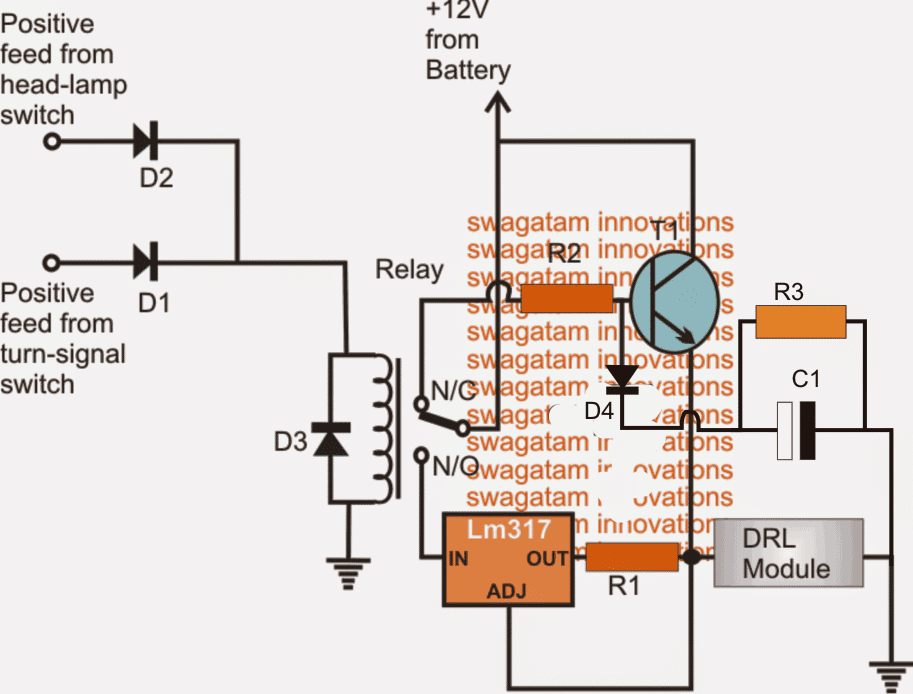
Parts List for the abovecircuitdesign
R1 = (1.25/DRL amp value) x 3 R2 = 1k 1/4 watt R3 = 10K C1 = 470uF/25V T1 = TIP122 D1, D2, D4 = 1N4007 D3 = also 1N4007 (optional) Relay = 12V, 400 ohms, SPDT Feedback from Mr. Chris Hi Swagatam, Thank you very much for working this out for me - a great explanation, diagram, and bill of materials! I just have a few simple questions: 1. The 12v feed from the indicator switch will have to come from the indicator stalk where there is a constant 12v, and not the intermittent/flashing 12v after the flasher relay, is this correct? 2. The 'DRL module' on your diagram - I assume this is just the white LEDs? Is there a maximum amount of LEDs that I can utilise or do I just have to adjust the resistor values accordingly? 3. If I was to add the 'indicator module' (orange LEDs) to this unit, as per the video, I assume I would just have to take the 'flashing' 12v feed from the existing flasher relay into a resistor, then the LEDs, and then to ground? Thanks again for your time, it is much appreciated. Kind regards, ChrisAnalyzingthe Issue
Hi Chris, Thanks! Here are the answers to yourquestions: 1) Ideally it should be a fixed 12V which could be taken from the flasher On/OFF dashboard switch, if a flashing feed is used, the relay coil of mycircuit will need to bestabilized with a 1000uF/25V capacitor in parallel so that the relay does not get rattled with the fluctuating 12V feed rather stays constantly switched ON. 2) LED configuration could bespecific to theDRL unit that I have not addressed inthe article, here the current (amp) consumption is what matters, which shouldn't exceed 1amp, if it does then the TIP122 may need an upgradation. 3) yes, justhook upthe orange LEDs with an appropriatecurrent limiter stage, and you can directly wire it up with the existing flashing DC source from the flasher unit. Best Regards.Darkness Activated Car Head Lamp Circuit with DRL
The post explains a simple automatic darkness activated switch for car head lamps and the DRLs, initiated by the ignition triggers. The circuit helps to save battery power and prevents unnecessary wastage of energy. The idea was requested by Mr. Vladnemir.Technical Specifications
I would like to build switch for driving car lights. I want to use HID pair (2x35W) and DRL 2x8(LED 1W per diode) Everything must be sensitive on ambient light and working just with key in the ignition (key sense +6V). Thank youDesigning the Circuit
The requested design of a ignition triggered and darkness activated dual head lamp circuit can be easily made using the ubiquitous IC 555. As shown in the figure below, the entire circuit consists of two exactly identical stages comprises of two IC 555 configured as comparators. The LDRs are used for sensing ambient light conditions and their deteriorating intensities.R1 on both the circuits are adjusted such that the respective ICs attain a particular light detection thresholds depending upon the user preference. For example the left R1 may be adjusted such that the relay just triggers when sun just begins to set, while the right hand side R1 may be set such that its relay gets activated only when its completely dark. As long as the above levels do not reach, pin2 of the ICsare allowed to receive a ground potential which keeps the corresponding pin3s at high, thereby inhibiting the relay activations. As soon as the respective thresholds are crossed, pin2 goes high via R1, consequently pin3 becomes low allowing the relay to get activated and illuminate the relevant lamps as suggested by the requester. Pin4 which is the reset input of the ICsare integrated to the ignition positive of the vehicle so that the circuit responds with the above actions only when the car or the vehicle is being used and not while its parked or not in use.Circuit Diagram
 The above diagram indicates how the proposed darkness activated car head lamp and DRL circuit can be built using a couple IC 555 stages
How to Make Car LED Bulb Circuit
Typically all car turn signal lamps are around 12 to 20 watt rated which are traditionally incandescent bulb types and produce much lower light intensities compared to LED lights. Here we learn how these lamps can be replaced with high efficiency, high intensity car LED bulbs.LED Car Bulb Design
The image below shows what could be a car LED lamp directly replaceable over the existing holder. It shows a decent looking arrangement of flat, tiny SMD LEds in a circular pattern for enabling optimal distribution of light via the enclosed hind reflector. The LED used here are the 3020 SMD LEDs, these tiny light emitting diodes are identical to the ordinary 5mm LEDs with their specs, however if we compare their light intensities, the witnessed difference appears to be huge, where the 3020 easily wins by an outstanding margin, that's why these LEDs are much preferred in place of the ordinary 5mm LEds nowadays.Technical Specifications of the 3020 LEDs are:
Forward voltage: 3 to 3.2V Forward current: 30mA optimal Luminous Efficiency: 100-110lm/w Size: 3.0x2.0x1.3mm Lifetime: 50,000hrs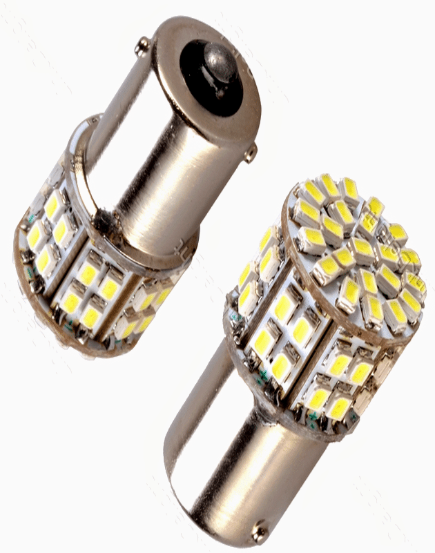
Construction
In the above image, we can see the LEDs assembled over pcs of PCB strips, tiled in a particular calculated manner. The vertical PCBs are 7 in numbers, and have 4 LEDs on each strips. One circular PCB consisting of 22 LEDs can be seen positioned over the vertical PCB structure. The vertical PCBs thus include 7 x 4 = 28 nos of 3020 LEDs, while the circular PCB mount 22 nos of LEds, giving a total of 28+ 22 = 50 LEDs These 50 LEDs are connected to form 12 strings of 4 LEDs each, and a single string of 2 LEds. Each of the 12 strings must have their own individual series resistor (SMD) whose value could be around 55 ohms 1/4 watt. The single 2 LED string must associate a separate 250 ohm, 1/4 watt resistor. These resistors act like current limiters for safeguarding the LEds from caralternator voltage fluctuations and also help to keep the illumination level across all the LED groups as uniform as possible. The resistors can be installed at the rear side of the PCB strips. The circuit diagram for the proposed simple car LED lamp is shown below:Circuit Diagram
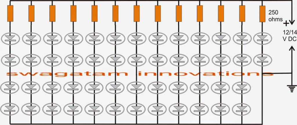
How to Connect Car LED Downlight
A car LED downlight available in the market can be easily integrated to an existing car battery if its rating is identical to the battery's voltage rating. Let's learn more regarding one such request sent by Mr. Allwyn Siqueira.How to Connect Downlight to 12V Car Battery
Hi Swagatam, I've just spent the last 3 days reading your blog and I'm just blown! I was doing a Google search on making a simple electric circuit and that's how I came across your website. Your site is just fascinating and you've shared so many wonderful circuits that its been driving me mad! I was trying to do a small home project using a 12V car battery and a 12V/5W LED Downlighter and wanted to know how I could connect the downlighter to the 12V car battery without going via an inverter. I looked at the following circuit on your blog, but not sure if this is what I need. https://www.homemade-circuits.com/2012/11/3-watt-5-watt-led-dc-to-dc-constant.html Would you be able to help me please? The LED Driver that came with the Downlighter is a rated at 3-5x1W PRI: 110-240VAC SEC: 9-17VDC / 300mA +/-5% The battery I would like to connect this to, is a 12V Car Battery 70Ah (without using the 240V LED Driver and an inverter) Any information into how I could make this circuit would be warmly appreciated. Thank you very much and once again, fantastic blog (I will continue to read the Solar related material when I get time) Best regards, Allwyn Siqueira Goa A Typical 5 Watt LED Car Downlight Image Connection Details Hi Allwyn, Thanks very much for liking my blog. If the LED that you have is rated at 12V/5watt means it can be directly connected to a 12V battery supply irrespective of the battery AH rating. The same will be true for any LED assigned with a voltage matching the battery voltage. For added safety you can include a 1 ohm 1 watt resistor in series with the LED. Hope this helps. Regards.Car Door Close Optimizer Circuit
The post discusses and tries to solve a common car door opening issue which may be seen in quite a few old model cars. The proposed circuit of a car door close optimizer was requested by Mr. Mark Rothwell.Technical Specifications
Just stumbled across your site, hope you can help/advise me?I have a 1999 Mercedes SLK and it has a well-known design flaw, the doors are frameless and the windows have the closed position set mechanically by a small metal bracket glued to the window within the door which stops the window at the correct position when closed so when the doors are opened and closed the window just catches the rubber seal as the door closes and allows the window to slide into the recess. The problem is these brackets fall off allowing the window to close a couple of mm higher than designed which isnˇŻt a problem for the window mech but this causes the window to catch on the rubber door seal and not sit into the seal recess properly, the only way to close the door properly is to drop the window slightly before closing the door. The door seals on my car are being worn out by the window rubbing on them when the door is closed and the on closing the window is being held on the outside of the door seal so I had an idea to incorporate a timer circuit to drop window few mm on opening the door then close it again after the door is shut, ideally to be activated by the ground signal for the interior lamp (i'm assuming its a ground sig but haven't checked yet) BMW 3 series (and poss others) have for many years had such a system incorporated in the car at manufacture that drops the window a couple of mm when the door is opened and closes the window when the door is closed and I think this car should have had this system when designed! My idea is to use a 555 timer circuit to achieve this but the last time I dabbled in circuit design was over 20 years ago and it is giving me a big headache trying to remember the theory, any help or advice would be much appreciated and although most modern cars have now taken BMWˇŻs initiative and now include this function there may even be a market out there for such a seal saving device on older cars?How the Circuit is Supposed to Work
1) Door opens, ground signal applied from door switch 2) Momentary energises relay or output to apply +12V 20A for approx 500 milliseconds (this time may need to be adjusted when fitted) to momentary send the window down (open) a fraction (this output to be connected to the window open button of the car) 3) On closing the door, ground signal removed 4) Momentary energises relay or output to apply +12V 20A for approx 1 second (this time may need to be adjusted when fitted) to momentary send the window up (closed) (this output to be connected to the window close button of the car) Any advice much appreciated! MarkThe Design:
The presented car door close optimizer circuit is simple enough, and self explanatory. As soon as the car door is opened, the transistor receives the required negative base bias triggering the attached DPDT relay. The DPDT relay contacts along with the 1000uf capacitors are wired such that the output across the capacitors changes polarity and switches ON the load only momentarily every time the door is opened or closed. The change in polarity is required for enabling the capacitorscharge and discharge process which in turn is necessary for the required transfer of the momentary pulses to the connected load. The above design was suitably modified by Mr.
Mark, let's learn more about it:
The above design was suitably modified by Mr.
Mark, let's learn more about it:
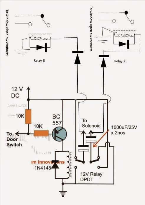 I was intending to connect the circuit to the contacts of the window switches, ive attached a jpg with some additional components, I think this will work with the additional relays using the solenoid outputs to drive 2 relays when each of the outputs are high and the capacitors giving the required cut off releasing the relays 2&3 that IˇŻve added at the correct timing.
The diodes IˇŻve added after the original solenoid outputs in your circuit are to protect the electrolytic from reverse polarity with the GND presented through the coils of relays 1 & 2 when the first relay is not energised (but IˇŻm not completely certain they are needed?).
Its not shown on the diagram but I later thought I could achieve a slight extension to the close relay energised time by adding an electrolytic cap across the relay coil of relay 3 and this will ensure the windows are always fully closed when the door is shut.
Something I have realised is when the windows are open in summer it means the circuit will always close the windows slightly when closing the door but I think that is a minor problem compared to currently wearing out the seals and the door not closing properly,
If everything works well I may look to see if I can tap a signal from somewhere that I can use to over ride the circuit when the roof is dropped or windows are lowered.
I will have to get it built and test and will let you know.
Following are some wonderful images and video sent by Mr.
Mark, backs up the above discussion, and provides a clearer view of the involved operations.
Image and video courtesy: Mr.
Mark Rothwell
I was intending to connect the circuit to the contacts of the window switches, ive attached a jpg with some additional components, I think this will work with the additional relays using the solenoid outputs to drive 2 relays when each of the outputs are high and the capacitors giving the required cut off releasing the relays 2&3 that IˇŻve added at the correct timing.
The diodes IˇŻve added after the original solenoid outputs in your circuit are to protect the electrolytic from reverse polarity with the GND presented through the coils of relays 1 & 2 when the first relay is not energised (but IˇŻm not completely certain they are needed?).
Its not shown on the diagram but I later thought I could achieve a slight extension to the close relay energised time by adding an electrolytic cap across the relay coil of relay 3 and this will ensure the windows are always fully closed when the door is shut.
Something I have realised is when the windows are open in summer it means the circuit will always close the windows slightly when closing the door but I think that is a minor problem compared to currently wearing out the seals and the door not closing properly,
If everything works well I may look to see if I can tap a signal from somewhere that I can use to over ride the circuit when the roof is dropped or windows are lowered.
I will have to get it built and test and will let you know.
Following are some wonderful images and video sent by Mr.
Mark, backs up the above discussion, and provides a clearer view of the involved operations.
Image and video courtesy: Mr.
Mark Rothwell

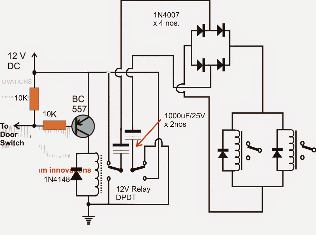
Lamp Outage Detector Circuit for Car Turn Signal
The O.E.M. turn signal flashing units installed in automobiles have two basic functions i.e. Flasher and Lamp outage detection. These flashers are usually built with an 8-pin IC like U2044B, U6432B etc. which are specifically made for automotive flashers. Designed and Written By Abu-HafssCircuit Operation
These flashers normally oscillate at about 1.4Hz. When a lamp goes bad, the oscillation is doubled. The flasherˇŻs faster clicking sound and the dashboard indicatorˇŻs faster flashing attracts the driverˇŻs attention that one of the bulbs has gone out. Here, we discuss a flasher circuit which performs similarly but uses a 555 IC and two comparators. The circuit consists of two parts ¨C the flashing unit and the lamp outage detection module. The flashing unit is built around 555 timer configured as an astable multivibrator. The resistors R12/R13 and capacitors C3/C4 sets the required frequency. Note that C3 is connected in parallel to C4 thru an NPN transistor, acting as a switch. When there is positive voltage at the base of the transistor, it conducts and connects C3 to ground. C3 & C4 in parallel makes the capacitance value double i.e. 220nF + 220nF = 440nF. This capacitance value together with R12 and R13 result in frequency of about 1.4Hz. In the Lamp outage detection module, a shunt resistor (a thick wire) with a calculated minor resistance (30m) is the key to detect the lamp outage. The voltage to lamps is fed thru this shunt. Hence, the shunt is connected in series to the network of the bulbs which are connected in parallel. The inverting input (-input) of the comparator U1 is also connected to the shunt. The non-inverting input (+input) is connected to a potential divider providing a reference voltage of 11.90V.NORMAL OPERATION:
-input = Square wave between 11.89V ¨C 12.0V +input = 11.9V (reference voltage) The comparator U1 compares the two voltages and the output is a square wave between 0-12V. This output is rectified thru diode D1 and filtered thru capacitor C1. Now, we have a triangular wave form which is fed into another comparator U2. +input = Triangular wave between 7V ¨C 8V -input = 1V (reference voltage) The comparator U2 compares them; the output is constant 12V which goes to the base of the NPN transistor. This switches on the NPN and hence C3 is connected to ground. In result, the 555 timer oscillates at about 1.4Hz. The output of 555 is connected to relay RLY1 which relays 12V direct from the battery (thru shunt) to the lamps.OPERATION WITH A DEFECTIVE LAMP:
When a bulb is defective, there is an increase in the resistance of the bulb network hence the voltage drop across the shunt is changed. So, in this case we would have: -input = Sq. wave between 11.95V ¨C 12V +input = 11.90V (reference voltage) The comparator U1 compares them and the output is almost zero volts. After the diode and the filter network, we finally have a few millivolts at the +input of U2 which is compared with the reference voltage, 1V. This results in low output of U2 which ultimately switches off the NPN and hence C3 is disconnected from the ground. Now, the timing network of 555 has only C4 to work with, therefore the frequency of the oscillation is doubled. This causes the remaining bulbs to flash at doubled rate.Circuit Diagram
Vehicle Speed Limit Alarm Circuit
In our previous articles we have learned comprehensively regarding the ICs LM2907/LM2917 which are fundamentally frequency to voltage converter ICs, and are ideally applicable in all such relevant fields. Here we see how the same chip can be applied for making a vehicle speed limit alarm circuit.Using a Single IC for Speed Detection
 As per the explained example the IC could be used for making a simple speed limit switch circuit which in turn could be applied in vehicles for detecting over-speeds and consecutively alarming or preventing the vehicle from crossing the set dangerous mark.
As shown in the below diagram a single LM2917 is enough for designing the proposed speed limiter circuit along with a few external passive parts.
Referring to the diagram, the input pin#1 receives the signal from the wheels of the vehicle through a magnet and pickup coil arrangement or through a Hall effect sensor circuit.
As per the explained example the IC could be used for making a simple speed limit switch circuit which in turn could be applied in vehicles for detecting over-speeds and consecutively alarming or preventing the vehicle from crossing the set dangerous mark.
As shown in the below diagram a single LM2917 is enough for designing the proposed speed limiter circuit along with a few external passive parts.
Referring to the diagram, the input pin#1 receives the signal from the wheels of the vehicle through a magnet and pickup coil arrangement or through a Hall effect sensor circuit.
Circuit Operation
You may refer to this article for knowing the basic set up of the wheel and pickup coil in the given diagram. The function is pretty much identical to the previously explained speedometer circuit functioning: The applied speed info in the form of pulses corresponding to the rotating wheel count is sensed by the differential opamp whose inverting input is referenced to ground for maximum sensitivity. The output from this opamp is fed to the next sage which is the charge pump stage responsible for tracking/holding/boosting the info in the form of a steady DC. This function relies particularly on the value of C a pin#2 of the IC. The above info is yet again amplified and compared by the subsequent opamp and common collector transistor stage. The output is terminated at pin#4 of the IC via the emitter of the internal common collector transistor.Formula for Setting the Speed Limit
As per the formula, the speed limit alarm can be set and calculated by using the formula: f(in) = R2/R1+R2 x 1/RC Once the set limit is reached, the IC detects it and produces a high logic at pin#4 which is equal to the supply voltage of the circuit. This high logic may be used for sounding an alarm, deactivating the engine or for triggering other similar preventive measures.Circuit Diagram
 A typical implementation of the above circuit can be witnessed in the following diagram.
Here the load or the speed alarm unit is connected at the transistor collector pin#5 output instead of pin#4 as narrated in the above section.
The collector load configuration provides the advantage of better current gain allowing a higher wattage device such as a relay or an alarm to be directly used with the circuit.
A typical implementation of the above circuit can be witnessed in the following diagram.
Here the load or the speed alarm unit is connected at the transistor collector pin#5 output instead of pin#4 as narrated in the above section.
The collector load configuration provides the advantage of better current gain allowing a higher wattage device such as a relay or an alarm to be directly used with the circuit.
Application Circuit
Making an Accurate Speedometer Circuit
Here we'll see how a simple yet accurate analogue speedometer circuit can be constructed at home using just a single IC and a few external passive components. The speedometer can be used with all 2-wheeler, 3-wheeler, even in bicycles for indicating their speeds.Using Frequency to Voltage Converter
 In my previous article we learned about these wonderful ICs 2N2907/2N2917 which are basically frequency to voltage converters and therefore perfectly become suitable for all frequency measuring related applications.
Referring to the simple speedometer circuit diagram below, we can see the IC LM2907 occupying the center stage in the configuration and forms the main detector device.
In my previous article we learned about these wonderful ICs 2N2907/2N2917 which are basically frequency to voltage converters and therefore perfectly become suitable for all frequency measuring related applications.
Referring to the simple speedometer circuit diagram below, we can see the IC LM2907 occupying the center stage in the configuration and forms the main detector device.
Circuit Operation
As can be see the internal of the IC comprises an input differential comparator, followed by a charge pump, an opamp buffer and a emitter follower amplifier stage. Pin#1 of the IC becomes the tachometer input and accepts the magnetic pick up information in the form of varying magnetic electrical pulses. The differential opamp compares the input with its ground referenced inverting input and amplifies even the minutest pulse detected at pin#1. The function of the charge pump stage is to hold and pump the above amplified signals such that with increasing frequency the corresponding amplified output from the differential stage is sustained and boosted proportionately across the next opamp buffer stage. This is achieved by the presence of the capacitors at pin#2 and the resistor at pin#3 of the IC. The final proportional boosted potential is fed through the emitter follower transistor across the 10k resistor. As given in the diagram, the output sensitivity here is around 1V for every 67Hz, meaning if the frequency reaches 67+67 = 134, would result a linear output of 2V and so forth.Calculating the Output Voltage
To be more precise, the outputvoltagecan be simply calculated using the formula: VOUT = fIN ˇÁ VCC ˇÁ Rx ˇÁ Cx, where Rx is the resistor at pin#3 and Cx the capacitor at pin#2 of the IC. This can be directly read by connecting an analogue moving coil voltmeter across the 10k resistor. The magnetic pick-up for the proposed speedometer circuit could be made by winding 50 turns of 30SWG wire over a small ferrite ring. The wheel should be complemented with an appropriately dimensioned magnet stuck or fixed over the rim such that the two elements come face to face once on every single rotation.Circuit Diagram
 If a hall effect sensor is intended to be used as the sensor, then the pin1 of the IC can be modified with an external BJT stage as shown below, for the required frequency sensing.
For Hall Effect Sensor Integration
Multi-spark CDI Circuit
The post explains an enhanced multi-spark CDI circuit which is universally suited for all types of automobiles. The unit can be built at home and installed in a particular vehicle for achieving greater speed to fuel efficiency.The Circuit Concept
The following diagram illustrates an enhanced version of a multi-spark CDI circuit. Fundamentally it can bifurcated into two discrete stages. Both the stages incorporate the IC IR2155 MOSFET driver with built in 50% duty cycle oscillator. The upper stage consisting of Q1, Q2 are configured for generating 300V DC from the available 12V DC input battery supply. The IC2 along with the connected mosfets Q6/Q7 form a push pull type pump circuit for alternately charging and discharging a high voltage capacitor across the connected ignition coil.Circuit Operation
IC1 is wired up for oscillating at about 22kHz as per the selection of the 33k resistor and the 102 capacitor across pin2/3 and pin3/ground respectively. This results in producing alternate switching of its output mosfetsQ1/Q2 connected across pins 5/7. The above switching performs a push pull reaction over the connected transformer wherein the two halves of the winding are saturated alternately with the mosfet conduction, which results in pumping of the entire 12V DC across the two half winding of the transformer. This action results in a stepped up induction across the secondary winding of the transformer giving rise to the required 300V AC switched at the 22kHz rate. The mosfets have their own internal transient protection system built in in the form of 60V zener diodes which limit the internal spikes to 60V safeguarding them from the relevant dangers, also the external gate 10 ohm resistors ensures a relatively exponential charge and discharge of the mosfet internal capacitance thereby reducing noise and disturbance which could otherwise influence the vehicle electrical adversely. A couple metalized capacitors rated at 10uF are installed in order to decouple DC from T1 so that Tr1 receives the 12V switching optimally across its winding. The stepped up voltage at the output of TR1 is rectified by the 4 fast recovery type diodes configured as a bridge rectifier. The ripples are further filtered by the metalized high voltage capacitor rated at 1uF/275V Even with the all the above high efficiency and protected circuitry, the IC1 stage has no ability os controlling the output voltage in response to the rising and falling of the 12V DC input which normally wouldn't be stable due to the vehicle's speeds and alternator RPM variations. To tackle this, an innovative transformer output voltage correction feature is Incorporated here using a voltage feedback circuitry involving ZD1---ZD4 along with Q3 and a few passive components. The four 75V zeners start conducting as soon as the voltage begins drifting above the 300V mark, which in turn results in the conduction of Q3. This action from Q3 results in dragging pin1 voltage of IC1 from 12V to gradually 6V.Using the Shut Down Option
Pin1 being the shut down pinout of the IC1 alerts the IC to trigger its internal under voltage cut-off feature resulting in an instantaneous shut down of its output pulses which in turn switches off the mosfets for that particular instant. The mosfets being switched OFF means no output voltage and Q3 unable to conduct which again restores the circuit to its original functional mode, and the operations repeat and rotate keeping the output voltage quite stabilized at the specified 300V volt mark. Another clever enhancement technique employed here is the use of three 33k resistors feedback loop from the output of TR1 to the IC1 supply pinout. This loop ensures that the circuit stays functional even when the vehicle is not running at optimal speeds or the supply voltage dropping considerably below the required 12V level. During such situations, the discussed 33kx3 feedback loop keeps the voltage level to IC1 well above 12V ensuring optimal response even under conditions with steep voltage falls. The 300V from TR1 is also applied to IC2 which is specifically configured as a high side mosfet driver, because here its output is not connected with a center tap transformer rather a single coil which needs a full drive across its winding in forward reverse method during each alternate pulse from IC2. Thanks to the IC IR2155 which has all the necessary features built in and effectively starts working as a high side driver with the help of just a few external passive parts C1, C6, D7.Function of the Ferrite Transformer
The conduction of Q6/Q7 pumps the 300V volts from TR1 inside the connected ignition coil primary via the 1uF/275V capacitor. The calculated configuration of various components across pin2 and pin3 of IC2 constitutes the intended multi sparks across the connected coil due to the interactions between these components. More precisely, the parts form a timer design with the help of the 180k resistor at pin2 along with the 0.0047uF capacitor across pin3 of IC2. The 10k resistor and the 0.0047uF capacitor between pin3 restricts over current while it's being triggered by the MMV circuit. The output from Q5 facilitates a low voltage output for integrating a tachometer in order to provide valid readings on the meter rather than connecting directly to the spark plug. If in case the multi spark feature seems not so useful or for some reasons inappropriate then it can be successfully disabled by eliminating C3, D10, D11 and the couple of 180k resistors along with the 33k and the 13k resistors. Also by substituting the 33k resistor with a 180 k resistor and a short link in place of D10. The above mods will force IC2 to generate just single 0.5ms pulses as soon as Q7 is triggered. The ignition coil now fires only in one direction while Q7 is ON and in once in the opposite direction when Q6 is ON. The associated MOV neutralizes any possibility of high voltage transients in case the output of the ignition coil is left open. The couple of 680k resistors across C2 provides a safe discharging path for C2 whenever the coil is disconnected from the circuit. This safeguards the circuit and the user from nasty high voltage discharge from C2.Circuit Diagram
 IC1 and IC2 are both IR2155 or equivalent
TR1 winding Details:
Start from pin7 (left hand side) using 0.25mm enameled super enameled copper wire as shown in the diagram and end at pin8(left hand side) with 360 turns. This completes the secondary winding. For the primary side wind in a bifilar manner meaning wind both the winding together, starting at pin2 and pin4 (right hand side) and ending after 13 turns at pin11 and pin9 respectively (left hand side) using 0.63mm wire. The bobbin used is for suiting N27 Ferrite Core L1 is 12 turns of 1mm wire on a Neosid Ringcore 17-732-22Transformer Design
LED ˇ°Halogenˇ± Lamp Circuit for Motorbike Headlamp
The post explains a simple 21 watt LED lamp circuit module which can be used as a direct replacement for a standard halogen lamp used in motorcycles headlamp.LED vs Halogen Lamp
The proposed "halogen" LED lamp replacement module image can be seen below: Conventional filament type halogen lamp is shown below:
 The image at the top shows an example LED lamp replacement for a standard halogen bulb fitting shown below it.
With the easy and extensive availability of LEds, today it's quite possible to make any desired LED lamp module at home for replacing other forms of less efficient lamp options.
So here we'll discuss how to make the proposed halogen LED lamp replacement circuit.
Let's learn the procedures:
Referring to the above image, we can see the LEDs are wired over 7 separate PCBs and then wired together to form one single module.
The image at the top shows an example LED lamp replacement for a standard halogen bulb fitting shown below it.
With the easy and extensive availability of LEds, today it's quite possible to make any desired LED lamp module at home for replacing other forms of less efficient lamp options.
So here we'll discuss how to make the proposed halogen LED lamp replacement circuit.
Let's learn the procedures:
Referring to the above image, we can see the LEDs are wired over 7 separate PCBs and then wired together to form one single module.
How to Assemble the Circuit
Each board can be seen with 3 LEDs each, constituting a total of 21 LEDs. 3nos LEDs are selected because the supply 12V available from the vehicle allows only 3nos to be connected in series, and series connection facilitates sharing the same current across the three LEDs. Now since more than 3nos. of LEds cannot be accommodated in series, 7 such strings are connected in parallel with each other for achieving the desired 21 watts. The above assembly must be done over a well designed heatsinkcored glass epoxy PCB. The entire configuration may be tightly fixed over an thick hexagonal aluminum cylindrical former or base to form the proposed halogen LED module unit. The aluminum will hep to sink the generated heat from the LEDs.A Current Limiter is Essential
The above unit will strictly require a current controlled driver circuit which can be understood with the following points: We once again take the help of the versatile LM338 IC for the required current control function. Referring to the circuit diagram we ca see it in it's simplest current limiting mode. The LEDs consume around 2.5 amps together which is never allowed to exceed by the IC keeping the unit safe from the issue.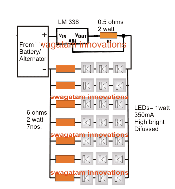 The above design can be upgraded with a Dimming option, as shown below:
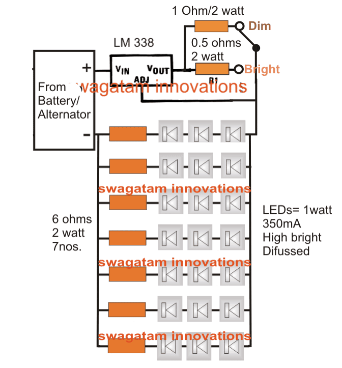 Aluminum mount (for heatsink) or base design for fixing the LED PCB assembly

Efficiency Comparison between Motorcycle Halogen Lamp and LED Lamp
<<<<Output----------------Halogen Lamp--------LED Halogen Lamp>>>> Nominal wattage----------55 watts-----------------------21 watts Nominal voltage-----------12V----------------------------12V Test voltage----------------13.2V--------------------------13.2V Color temperature -------3200K ------------------------6000K Luminous flux-------------1500lm------------------------2500lmMotorcycle Low Battery Over Discharge Protector Circuit
A simple motorcycle battery over discharge protector circuit is explained in the following post. The circuit will prevent the battery from over-discharging by the motorcycle headlamp whenever the mo-bike alternator is not enabled or is idling in the neutral mode in which case the battery is normally subjected to excess loads via the headlamp bulb.Increasing Motorcycle Battery Efficiency
Motorcycle batteries are normally a lot smaller with their sizes and ratings compared to the vehicle and the usage. The main use of the battery present in mo-bikes is for enabling electronic start through a press of the given start button. However this small sized battery also has to undergo further stresses while operating excess loads such as the horn, the indicator lights, the tail light and the brake light. Even though the above loads mostly tend to depend on the motorcycles battery power, these do not affect the battery charge level significantly. The one that truly affects the battery is the motorcycle headlamp, which when switched ON starts drawing huge current via the alternator and the battery in a shared manner. This is the reason why we normally see the headlight intensity vary with varying mo-bike speeds. At higher speeds the alternator shares the load to fair extents, but in cases when the vehicle is not moving or is idling in the neutral mode, the lamp starts consuming substantial amount of battery power, depleting it's charge to dangerous lower levels, and this may happen within minutes if not switched OFF. The proposed circuit of motorcycle headlamp low battery discharge protector circuit is intended exactly to tackle this issue automatically. It's nothing complicated, it's a simple low battery cut-off circuit set to switch of the link between the battery and the headlamp whenever the battery level falls below some set predetermined level. The circuit may be understood as follows:How it Works
The opamp 741 IC is configured as a comparator here. It's pin#3 is referenced at a fix voltage determined by the connected zener voltage. Pin#2 of the IC executes the function of the sensing input and keeps the output of the opamp pin#6 low as long as its potential stays above the reference value of pin#3. The above condition is held in position as long as the battery voltage is above the set safe threshold level, which in turn keeps the output pin#6 at a low logic level. The low at pin#6 ensures that the p-mosfet is allowed to conduct and illuminate the attached headlamp. Therefore the headlamp is allowed to receive the required power through the mosfet as long as battery voltage continues to be above the safe threshold. Now suppose the battery level begins falling beow the set level, this would mean pin#2 potential going down below the reference level at pin#3, or in other words pin#3 reference getting higher than pin#2 potential. The above situation instantly prompts the output of the opamp pin#6 to pull at the supply level or at a high logic. A high at pin#6 means the mosfet is now inhibited from conduction, switching off the headlamp. The above situation continues in a flip flop manner until the battery voltage is no longer able to rise above the safe threshold when the lamp is permanently switched Off.Circuit Diagram
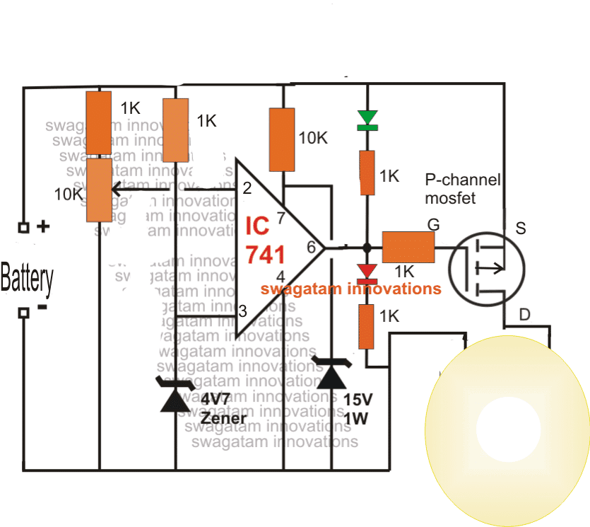
Bicycle LED Light Circuit Using a Single 1.5V Cell
The proposed bike flasher flashes two white LEDs from a single 1.5V cell by using a solitary general purpose transistor, and does not need core for the involved transformer, the main core being the Air itself.Using Joule Thief Concept
Every Joule Thief circuit uses ferrite rod or toroid core and its turns are wounded on a ferrite material. With the collapsing magnetic flux it produces an increased voltage, despite the core being Air. As the magnetic field quickly gives away, the circuit renders high voltage in the opposite direction. The magnetic field which surrounds the coil is efficient to produce energy. To build this efficient system, wind 30 turns on 10mm of 1/2ˇ± dia on a pen or screwdriver and another 30 turns on the top. Once you build the first circuit, connect it to the wires. Yu can even use 1 or 2 LED. In case it fails to work, just swap the wire which is going to the base. Add 10u electrolytic and 100k resistor, and remove the 1k5. The circuit is now ready to flash. Remember to use 2 LEDs for the flashing circuit.Coil Specifications
The 30 turns + 30 turns coil as in the picture takes 20mA for the illumination of 2 LEDs. Getting maximum energy from the coil becomes possible because of the air at the centre of the coil. As Air is unable to transfer high magnetic flux, the idea is to provide a larger area (volume) of low flux for the provision of energy. The larger 20mm coil reduces the current flow from 20mA to 11mA, keeping the same brightness.Circuit Operation
There are room to improve the performance but the problem lies that the coil gets bigger. It is essential to keep the two 30-turn windings together as the flux from main winding should cut the feedback winding to enable ON state of the transistor HARD. As the transistor turns on through 100k, the transistor generates magnetic flux in the main winding, cutting the feedback, and with it - a positive voltage is generated connected to 100k and 10u. Thus turns the transistor in ON mode and continues unless turned ON fully. During this point the magnetic flux does not expand, and the voltage drops to the lowest voltage. This causes the transistor to turn off. The current in the main winding also discontinues abruptly. The magnetic flux breaks down, producing a voltage in reverse direction, which is higher than the supply, thereby causing the LEDs to illuminate. This process also channels voltage through the feedback winding, which keeps the transistor in OFF state. As the magnetic flux breaks down, the negative leadsˇŻ voltage turns to as low as 10u, keeping the transistor in OFF state. The 10u discharges by 100k letting the base voltage increase to start the next cycle. If you are keen to perform an experiment with the aforesaid process, you can definitely do the same since 100k and 1k5 resistors and other necessary parts are available in plenty. Try to build the first circuit to flash white LED from a single cell. It covers various features and shows the efficiency of a LED, when pulsed briefly with high current. The two coils in the diagram form a Transformer and illustrate breaking down of magnetic field, producing a high voltage. The 10k and 100k creates a delay in the circuit, thereby producing the flash. However the Joule Thief circuit fails to perform various experimentation to simplify their circuit. That is one reason to follow ˇ®birds nestˇŻ arrangement for further experimentation. Note: Altering the turns to 40t for main winding and 20t for feedback, reduces the current to 8-9mA. However please ensure to keep the turns tighter while winding the wire around. Submitted By: DhrubaJyoti BiswasCircuit Diagram
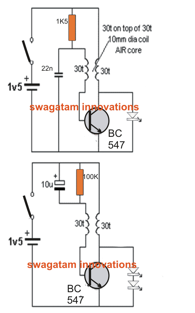
Free Energy Bicycle Generator Circuit
The following post describes a simple circuit idea which can be used for generating free electrical energy for illuminating a few safety flashing LEDs on a Bicycle.The Circuit Concept
A bicycle like any other modern vehicle needs provision of lighting system for its use at night or cycling in lesser light.Usually a bicycle is designed with the front light and the back light, being red in colour. The front light is often fitted with a cycle using a dynamo system. A dynamo generates alternating current by causing a friction in the tyre. This actually slows down the speed and the cyclist has to paddle with more power to generate speed. Another kind of lighting can run through battery which is usually a detachable device. But what if a situation when there is no need of dynamo, neither depending on battery for a bicycle light? The introduction of an innovative system called ˇ®Safety Flashing LightˇŻ has solved the purpose. It not only helps to eradicate the concept of battery or dynamo system; it indeed offers more powerful light and longer standby compared to the other types. This new electrical generating system has already created a sparkle in the bicycle market for its efficiency and ease-of-use.How the Free Energy Bicycle Generator with Safety Flashing Light Works?
The Safety Flashing Light is designed in a way to handle all possible situations when driving a bicycle. For instance, a cycle when running in slower speed; two white-front LEDs and three red-rear LEDs flashes to make others notice on its presence. In the case of standby mode, when the rear-wheel break is applied, the front and back LEDs gets activated. The lights are very bright and it can be noticed even in daylight. Even no maintenance is needed, which made the operation hassle-free and easier to operate. The Safety Flash Light also works perfectly even on a rainy day. This light system uses 8000-12000mcd LEDs for an optimum performance. By: Dhrubajyoti BiswasCircuit Diagram
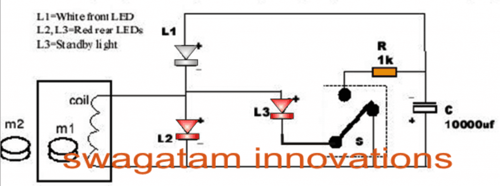
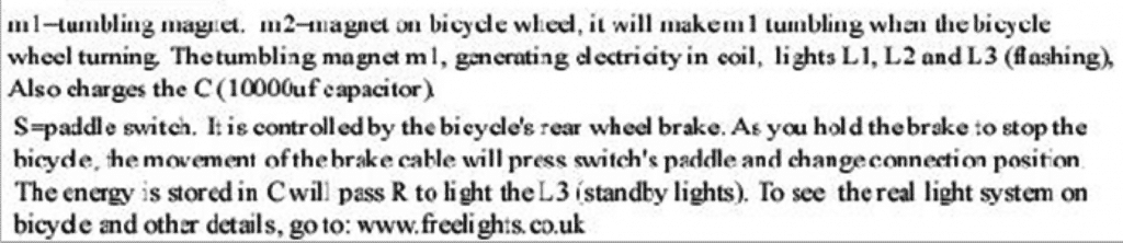
Car Speed Limit Warning Indicator Circuit
The following post describes a simple yet useful car speed limit warning indicator circuit which can be used in vehicles for getting an instant indication of a possible over speed limit conditions. The idea was requested by Mr. Abu-Hafss.Technical Specifications:
Shall appreciate, if you could design a circuit to warn with some melody that the car has reached preset speed limit. As soon as the speed is reduced below the limit the alarm should go off. The circuit should have 2 options for switching between 2 speed limits. 1. The circuit should have a selection switch --- Postion A >> 100Km/h (for ordinary highways) and Position B >> 120 Km/h (for Experessways). 2. When the switch is positioned for example at position B, a sensor which can get current speed from car speed-o-meter and then compare with the selected speed limit (120 Km/h). Whenever, the sensor reads the speed to be 120 Km/h or more, it will start playing a warning melody until the speed is reduced.The Design
The designed circuit of a car over speed limit indicator basically consists of two stages. Both the stages incorporate the ubiquitous IC 555. The stage which includes IC1 is configured as a simple frequency to voltage converter or a frequency dependent voltage generator circuit. Here IC1 is rigged in the form of a standard monostable multivibrator whose ON time is decided by the resistors R3/R4 and the capacitor C2. These components must be selected appropriately for getting most favorable output response. As we all know that all modern motor vehicles today incorporate electronic ignition systems which invariably include a CDI or a capacitive discharge ignition network, in contrast to the older circuit-breaker units. The the CDI unit is responsible for generating the required igniting sparks inside the engine of the vehicle and its rate of firing is directly proportionate to the speed of the vehicle. It means with an increase in the speed of the vehicle the charge/discharge rate of the CDI capacitor also increases and vice versa. The monostable built around IC1 exploits this feature of the CDI system and derives a sample potential from the CDI at the base of T1. T1 effectively switches the varying high voltage pulses from the CDI into low voltage triggering pulses across C1 and ground. With response to the above pulses, every time T1 conducts it pulls pin#2 of IC1 to ground initiating the monostable output to go high. The monostable sustains the output in the high position for a period determined by the values of the respective timing components as explained in the previous section. However, the continuous train of pulses initiates an appropriately stabilized high output at pin#3 of IC1 (due to the functioning of the monostable which produces almost an exact average DC output proportional to the frequency of the pulses.)Circuit Operation
The output is further stabilized into a perfect measurable equivalent DC by the integrator stage comprising R7/R8/C4/C5 and also P1. IC2 is wired up as a voltage comparator. Its pin#2 is allowed to receive the varying voltage from the IC1 output. P1 is set such that as soon as the output from IC1 rises to a certain limit which may be calculated as the over speed limit value, the potential; at pin#3 rises over 1/3rd Vcc This instantly prompts the output of IC2 to go low, activating the connected alarm device. This alarm would stay activated as long as the car speed does not come down below the preset limit. As soon as the speed is reduced, the alarm stops sounding. The preset P1 may be suitably replaced with a properly calculated potential divider ladder type network along with a selector switch for enabling the selection of different speed limits for different free-ways.Circuit Diagram
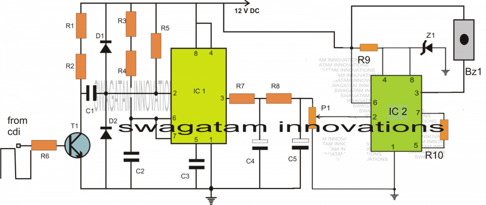 Parts List for the proposed Car Speed Limit Warning Indicator Circuit
R1 = 4K7
R2 = 47E
R3 = CAN BE A VARIABLE 100K RESISTOR
R4 = 3K3,
R5 = 10K,
R6 = 330K
R9 = 1K,
R7 = 1K,
R8 = 10K,
R10 = 100K,
C1 = 47n,
C2 = 100n,
C3 = 100n,
C4 = 100uF/25V,
C5 = 10uF/25
VP1 = 10k PRESET
Z1 = 6V ZENER
T1 = BC547
IC1, IC2 = 555,
D1,D2 = 1N4148
BZ1 = BUZZER OR MUSICAL ALARM DEVICE
Parts List for the proposed Car Speed Limit Warning Indicator Circuit
R1 = 4K7
R2 = 47E
R3 = CAN BE A VARIABLE 100K RESISTOR
R4 = 3K3,
R5 = 10K,
R6 = 330K
R9 = 1K,
R7 = 1K,
R8 = 10K,
R10 = 100K,
C1 = 47n,
C2 = 100n,
C3 = 100n,
C4 = 100uF/25V,
C5 = 10uF/25
VP1 = 10k PRESET
Z1 = 6V ZENER
T1 = BC547
IC1, IC2 = 555,
D1,D2 = 1N4148
BZ1 = BUZZER OR MUSICAL ALARM DEVICE
Improving the Design By using an Opamp
The accuracy and reliability of the above explained car speed warning indicator can be further improved by replacing the 555 buzzer stage with an opamp/relay stage as shown below:Circuit Diagram
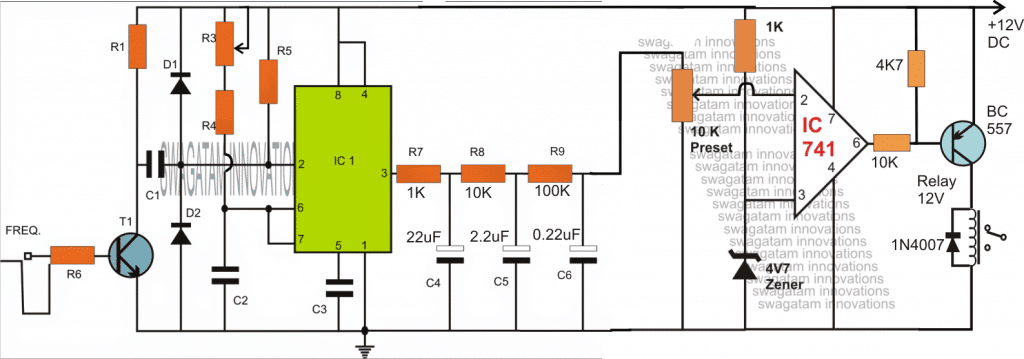 To make the relay latched on detection of an over-speed situation, a hysteresis feedback can be to the above design, as shown below:
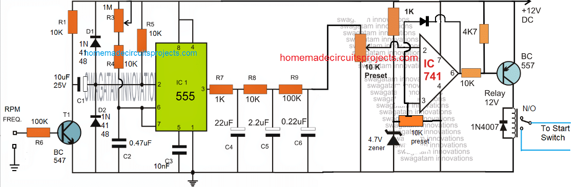
Make this Car Air Ionizer Circuit
The post discusses the construction of a car airionizercircuit which can be used for cleansing the atmosphere of car interior from smoke, pollution, dust particles, bad odor,pollenparticles etc.The Circuit Concept
In one of my previous posts we saw how simply a home air ionizer circuit can be built using a handful of capacitors and diodes. The unit works directly on our domestic mains outlet due to the availability of mains power. The same circuit can be converted to function as a car air ionizer circuit by adding a converter stage to the above circuit. The converter stage is a simple square wave inverter which converts 12V DC into the required 220V AC for operating the ionizer circuit. Asexplainedin my previous article, the basic design of the ionizer is taken from theCockroft-Walton Ladder Network which involves a series. parallel connection of many diodes and high voltage capacitors.How it Works
When powered with mains voltage the arrangement creates a push pull effect inside the circuit which results in stepping up of the voltage across the subsequent stages. At thefar endof the ladder network this stepped upvoltagemay be as high as 4kV. For obtaining the fundamental ionizing effect which is supposed to be having many health benefits the stepped up voltage should reach about -4kv. At this potential, the free end of the radiator tip release negative ions by losing an electron into the atmosphere. These ions being negatively charged attract everything that's neutral orpositivelycharged. Dust particles or any suspended particle in the air is by nature a neutralelementandtherefore when these particlescollidewith the negatively charged ions, they instantly stick with these ions. The ions continue colliding with the atmospheric particles until each ion become loaded with these unwantedparticles and become too heavy to float. When this happens the ions either get attached to the nearest wall or drop on the floor. In this way all pollutants are neatly cleansed away from the air by the ionizer unit.How to Build this Car Inonizer
In the diagram below we can see the circuit to be made up of two distinct stages. The section at the extreme left is the inverter stage, while the section on the right of the transformer is the ionizer stage. The two stages should beconstructedseparatelyon two different boards and testedseparately before integrating together. The ionizer circuit stagewhichconsists mainly of capacitors and diodes looks to be an easy arrangement to assemble, however the entire configuration is quite sensitive to bad solder orleakagesthrough flux deposits. Even a slightest bit of mistake canrenderthe circuit unresponsive. All the connections should be made with utmost care, making sure there's no dry solder or fluxdepositsin between the joined tracks. The ionizer stage may be tested by powering it with 220V AC at home. Be extremely careful as the entire circuit is directly linked with mains potential and can inflict lethal shock if touched without precaution. The procedures are explained in this room air ionizer article The inverter part is much easier as the design includes just a pair of transistor and a few resistors. The transformer is a small 12-0-12V 500 mA type.After makingit, power it with a DC 12V source and check the output, it should provide around 220V AC. For thefinaltesting, the above inverter output AC may be applied to the input of the ionizer circuit foracquiringthe required ionizing effect of release of ions across the extreme tip of theionizercircuit.Circuit Diagram
Car Head Lamp Fader Circuit (Breathing Effect Generator)
The proposed circuit of a modified car head lamp fader, "breather" circuit generates a slow flashing effect over the head lampsevery timethe lamps are switched OFF. The "breathing effect" continues for acertainpredetermined period after which the process automatically shuts off. I just wanted to say that what you do here in you blog is wonderful. I just came across them in Google looking for a chasing light circuit. Love it and will be using it. I do have a question about this timer circuit though. Could I have this hooked up to my headlight switch and when I turn off the switch it starts the count? I would like to add this to a breathing light circuit so when I turn off my lights, the head and tail lights fade in and out for a set amount of time. Would this be the circuit I need for the timing aspect? Thank you in advance, and there is no rush. Ray.The Design
The proposed car head lamp fader circuit can be witnessed in the the below given diagram, let's learn about it functioning details: As long as the main switch stays in switched ON position D2 is held reversed biased, so that T1 is unable to conduct and thus the entire circuit stays switched OFF. In an event the main head light isswitchedOFF D2 instantly receives a negative potential via the head lamp filaments which switches ON T1. T1 now provides the required supply to the IC 4060, which instantly initiates counting process. C4 makes sure that the IC begins the timing from zero and not randomly when power is switched ON. C3 makes sure that T1 keeps conducting even while D2 gets reversed biased in response to T3 flashing. Pin#2 starts counting, while pin#14 begins oscillating at some predetermined rate. The time periods at pin#2 and pin#14 can be optimized byappropriatelysetting the preset P1. The oscillating frequency at pin#14 triggers T2 in the corresponding manner which in turn switches T3, and the head lamp, with the required blinking/fading effect. The slow rise and fall or the "breathing effect" over the lamps is generated together with the help of R6, R7, and C2. The values of these components should be selected and optimized through experimentation for getting an interestingfading effect. In the meantime as pin#14 generates the pulses, pin#2 counts and as soon as the set time elapses, it becomes high. The high at pin#2latchesthe IC via D1 and also disables T2 from conducting. The situation shuts off the head lamps completely. The circuit remains locked in this position until the main switch is yet again resetmanually to repeat the process.
Parts list for the above car head lamp fader, "breathing effect" generator circuit
R1, R3, R4 = 100K R2, R9,R5 = 10K R6, R7 = 470 OHMS R8 = 50 OHMS, 2 WATT (ARBITRARY) C1, C4 = 0.1uF C2 = any value between 220uF and 1000uF C3 = 100uF/25V D1, D2 = 1N4148 P1 = 100K PRESET T4 = BC547 T1 = BC557 T2 = 2N2222 OR 8050 T3 = TIP36Car Turn Signal Flasher Circuit with Lamp Malfunction Indicator
The post discusses an automotive/car turn signal indicator circuit idea with a built-in load malfunction indicator, meaning anadditionalLED lampfittedon the dashboard which would warn if any of the side indicators went bad or fused. The idea wasresearchedand requested by Mr. Abu-Hafss.The Circuit Concept
I have found a transistor-based flasher including a relay, online Physically, the circuit oscillates when a Load is connected across the pin "C" of the relay and earth. If the load is less than 100 Ohms the oscillation is significantly fast. And if the load is say about 1K the frequency is normal. However, I could not understand the circuit nor it is simulating in LT Spice. Could you please explain me how the circuit is sensing the change in resistance of the load. And could you please make the simulation work.
OBJECTIVE:
To make a 555 based automotive turn signal flasher circuit which can detect lamp outage. If not possible with 555 then transistors may be considered.CIRCUIT ¨C A:
Above are the photos and schematic of the circuit. I have physically tested it. It also works on BC558/BC546. With bench power supply of 12V-2A and load connected at pin (L) and (-), following is the behavior: ˇ¤ No load, no oscillation ˇ¤ Pin (L) and (-) shorted, very fast oscillation (relay sounds) ˇ¤ Load 1 ¨C 1.5K, normal oscillation (about 1.4Hz) ˇ¤ Load increases, oscillation slows ˇ¤ Load decreases, oscillation decreases When using a car battery and 3 x 27W bulbs in parallel the circuit oscillates normally. Even, if a bulb is removed the frequency is unchanged. This means, this circuit does not detect lamp outage. However, the behavior of the circuit with a bench setup may give you some clue to my objective.CIRCUIT - B
Yesterday, I came across this circuit which has a relay to detect load. I have not yet tested it. I hope this circuit might also help us. Maybe we can replace the relay with a transistor. Thanks for your help. Abu-Hafss
IC 555 based car turn signal indicator with pilot warning lamp:
The required circuit design which is shown below may be understood with the following points: The IC 555 section is wired in the normal astable multivibrator whose pulse rate at pin## can be adjusted with the help of the given 100K pot. The two NPN transistors function as current sensor, and IC 555 reset controller. When power is switched ON, the N/C contacts of the relay connect theturnsignal lamps with the 12V supply. The lamps light up and in the process draw the required amount of current via the Rx resistor. The above current develops some voltage across Rx which triggersthe left BC547 transistor and switches OFF the right BC547 transistor. The above action resets the IC 555 so that it starts pulsing the relay and theconnectedlamps. The LED at its N/O contacts alsostartsblinkingin accordance indicating the correct presence of the lamps at the front and the rear side of the car. Rx value must be selected such that it develops just sufficient voltage across it to trigger the transistor in response to current consumed by two lamps at the specified rates. In case even one of the lampsmalfunction, the voltage across Rx then wouldn't be high enough to trigger the transistor. This situation would keep the entire circuit frozen, also keeping the warning LED shut off, providing the necessary malfunction indications to the driver.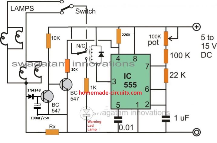
Sequential Bar Graph Turn Light Indicator Circuit for Car
The article illustrates a simple yet innovative, fancy car turn signal light circuit which produces a rising bar graph sequence effect when switched ON. The circuit idea was requested by Mr. +Bruce Lowry. Let's learn more. I am after a circuit design similar to the LED Bar Graph circuit that is found on this site/blog. What I want to develop is a front turn signal sequential flasher that illuminates and holds the lights from top to bottom and then cycles them again and again until the turn signal is turned off. I need to drive exactly 12 Amber LED's that drop 1.8 volts per LED. The LED's are laid out from top to bottom as such. 1 (number of LED's) 1(number of LED's) 1(number of LED's) 2(number of LED's) 3(number of LED's) 4(number of LED's) I would like to illuminate the first one at the top and hold and then move on to the second one down and so forth until all 6 rows which consist of 12 total LED's are illuminated and then start the sequence over. Variable resistors should be included so that the clock frequency can be altered. This will allow me speed up or slow down the illumination and hold of the LED's. Plus if there is a variance in the driver side circuit and the passenger side I could use the adjustability to "syncronize" the working rates of both sides. (turning on the hazard flashers to observe both sides being enabled and sequencing would be a good way to visually check this) In the connector to the front turn signals I am working with three connections. Top pin is 12 volts constant when running lights are turned on (oh, just a thought- It would be nice to use the entire string of LED's as running lights as well) Middle Pin is zero volts (GROUND) and lower pin is 0-12 volts when the turn signal is activated. I need a working circuit that will handle automotive voltages that are not always 12 volts in practice , but can range up to 14 or so volts in actual real world use. A complete circuit diagram would be helpful. Including resistor values for driving the different multiples of LED's and if each LED would have its own resistor or just run them in series with one resistor. Thank you.The Design
The above circuit can be built using two different types of circuit configurations. One which uses the IC 4017, and the other through the IC 74LS164. Here we'll discuss the one which uses the IC 4017. As shown in the first circuit diagram, the entire design is wired around the IC 4017. We know that the IC 4017 which is a johnsons divide by 10 decade counter/divider chip produces sequencing high logicpulseson its outputs in response to clocks applied on its pin#14. In response to each high pulse on pin#14, a high logic shifts from one output to the next in the following pin-out order: 3-2-4-7-10-1-5-6-9-11. Thus all the 10 outputs become highsequentiallyuntil the last pin#11 becomes high after which the sequence returns to pin#3 so that the cycle can repeat yet again. he cycle keeps repeating as long as the clock pulses are sustained at its pin#14. However the sequencing pattern does not keep the outputs illuminated while shifting. The outputs become high and then become low again as the sequence shifts from one pin out to the other. It means at any instant only one output is high during the sequencing process. If we connect 10 LEDs at the above 10 outputs of the IC 4017, it would provide an impression of asingle LEDchasing effect, however since for the present car turn signal application we want a bar graph kind of appearance we would want the LEDs to stay and hold their illumination as the sequence proceeds from the start to the finish pin-outs. To implement this "hold" feature we need to introduce a latching feature with the given outputs. This can be simply done with the use of SCRs, because as per the characteristics SCRs latch their MT1, MT2 leads if the supply is a DC. Therefore it perfectly suits our application. By connecting SCRs at the first 6 outputs of the IC we can simply implement the bar graph kind of feature such that the LeDs hold and stay illuminated until the complete is completed. Pin#1 provides the last sequencing output after which the IC should shut down all the LEDs and begin the procedure all over again. For actuating the above action, the transistor T1 stage in introduced at the next pin#5, which instantly inhibits the supply voltage to the SCrs so that all of them shutdown. Pin#6 is tied to the reset pin#15 of the IC which makes sure the sequence gets back to pin#3 as soon as the LEDs shut OFF, enabling the next cycle to commence.Circuit Diagram
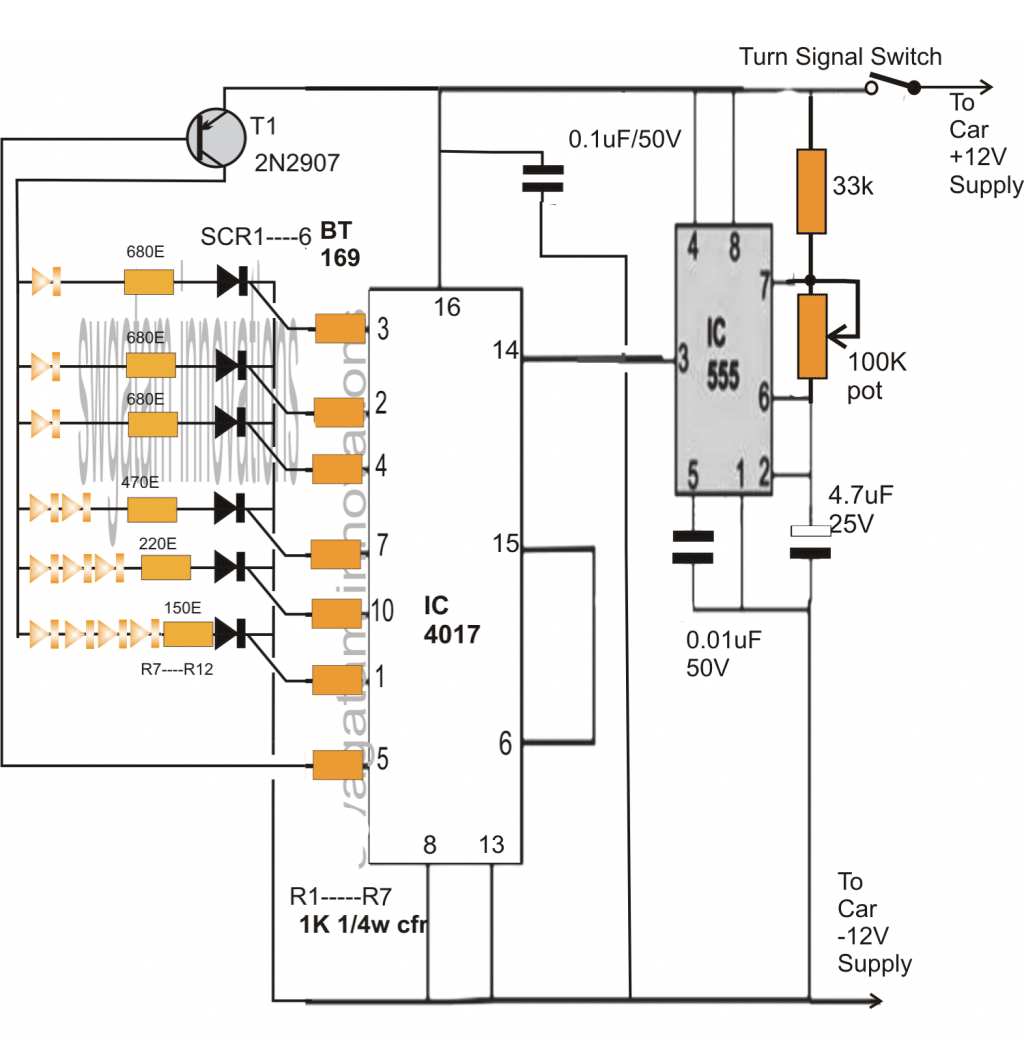
 As rightly expressed by Mr.
Bruce, the above circuit will not function properly under a fluctuating DC which would be normally available across the existing turn signal light outputs due to switching of the flasher relay.
As rightly expressed by Mr.
Bruce, the above circuit will not function properly under a fluctuating DC which would be normally available across the existing turn signal light outputs due to switching of the flasher relay.
Adding a Delay Timer
However the above circuit can be simply modified by adding a small time delay circuit, which would hold the current andkeepthe circuit functioning switched ON by supplying the required amount of power during theabsenceof supply from the flasher relay.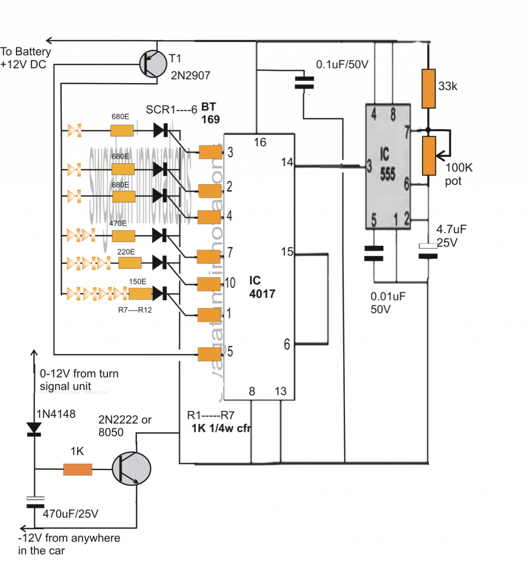 The above sequential car turn signal light circuit wassuccessfullybuilt and tested by Mr.Bruce Lowry.
The wonderful results can be witnessed in the following video.
Please refer to the comments to learn regarding the whole process.
With an adjustable rate of flash added, the circuit now looks much enhanced.
Courtesy: Mr.Bruce Lowry.
The above design was further modified by Mr.
Jason in order to implement additional specific actions such as making the LEDs stay solid when the brakes are applied, but also making sure that the LEDs stayed in the flashing/running mode in case both: the turn signal and the brakes were switched ON together or simultaneously.
The above sequential car turn signal light circuit wassuccessfullybuilt and tested by Mr.Bruce Lowry.
The wonderful results can be witnessed in the following video.
Please refer to the comments to learn regarding the whole process.
With an adjustable rate of flash added, the circuit now looks much enhanced.
Courtesy: Mr.Bruce Lowry.
The above design was further modified by Mr.
Jason in order to implement additional specific actions such as making the LEDs stay solid when the brakes are applied, but also making sure that the LEDs stayed in the flashing/running mode in case both: the turn signal and the brakes were switched ON together or simultaneously.
Video Clip of the prototype:
Another Clip:Modifying Further
The modified design which is attached below has an additional feature wherein the LEDs could also be used as park lights thereby making the above circuit a 3 in 1 unit: Here's the complete design drawn by Mr. Jason for your viewing pleasure: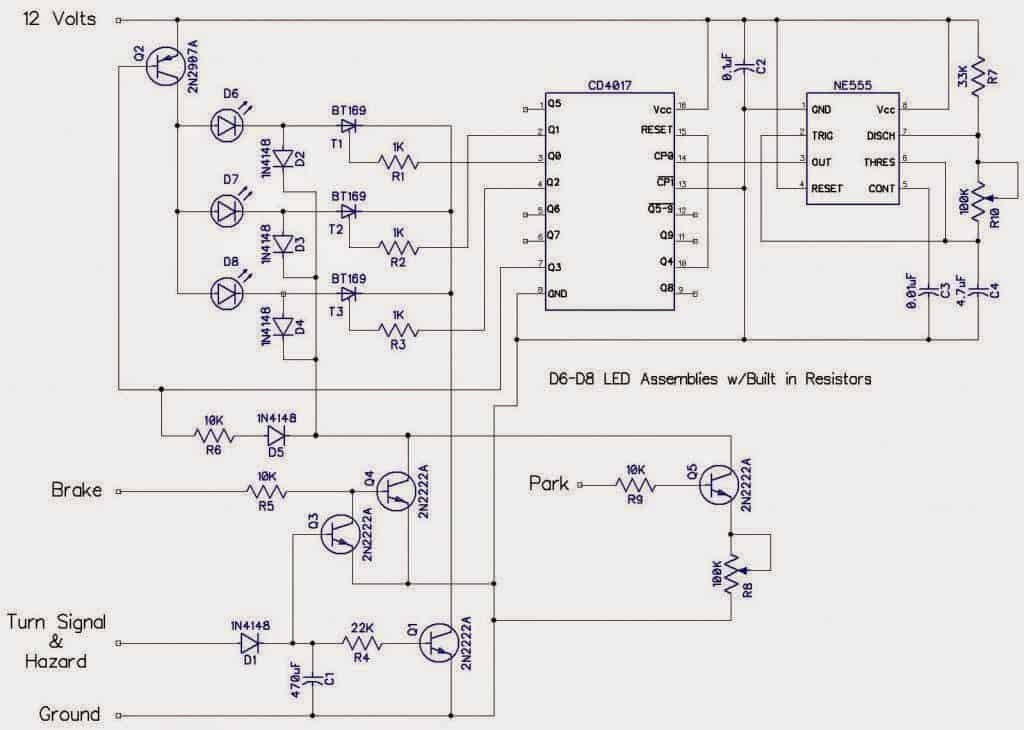
3 Interesting DRL (Day Time Running Light) Circuits for Your Car
DRL or Day Time Running Lights are a chain of bright lights mostly LEDs installed just under a vehicle's headlight, which illuminate automatically during day time to ensure that others can distinctly notice the vehicle approaching even from a distance. The presented circuit of a DRL or a Day Time Running Light was requested by Mr.Senthil. Let's understand the complete design.Technical Requirements
Hello Sir, I'm an avid DIYer. Recently, i was looking to make a DRL(daytime running light) for my car using 1 watt smd LEDs. But i couldn't find an appropriate circuit for my need. I want to drive Eight 1watt LEDs from my car battery. I would very much appreciate if you could design a simple and rugged circuit to drive 8 x 1watt leds from a 12-14v input. I'm also planning to add a heat-sink to dissipate any heat generated by the leds. Thanks & Regards, Senthil
The Design
What's a DRL or Day Time Running Light Device: A DRL is a safety car lighting devicespecificallyassigned to moving vehicles for increasing the conspicuity of the vehicle during day time, especially when the daylight is accompanied with fog or during dull overcast days.It is normally fixed just beside the headlamps on either sides. Normally a DRL system is in the form of constantly illuminated high intensity lamp. With the advent of modern High intensity LEDs, making a DRL lamp is matter of less than an hour. As per the request the proposed day time running light or DRL circuit would be in the following form: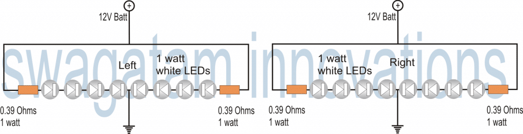 However in case you are interested to spice up the above idea a bit, and think that the system should do justice to the name that it has been specified, you would want to make it a literally "running" or chasing kinda thing!
Making a Chasing DRL Circuit
The DRL circuit discussed below shows how we can add a running effect to the above design and make it furtherinteresting. The circuit is actually a straightforward powerful LED light chaser circuit which is able to drive many 1 watt LeDs in a sequential manner. The IC 4017 is a Johnsons Decade counter which generates a sequential switching at its 10 outputs in response topositive pulsesfed at its pin#14. These pulses are referred to as clock signals. As can be seen in the given circuit diagram, the IC 555 is configured in its basic astable multivibrator mode, and generates the required clocks for the IC 4017. The clock pulses are taken from pin#3 of the IC555 and fed to pin#14 of IC4017. In response to the aboveclocks, the output of the IC 4017 shifts a high logicsequence from pin#3 to pin#6. Themomentit reaches pin#6, the sequence reverts to pin#3 and the cycle repeats. Since only 8 LEDs are requested, pin#9 is connected to the reset pin of the IC so that the only 8 outputs become active with the required functions. The speed at which this sequence may "run" or "chase" will depend on the setting of the 100k pot. Anyvaluebetween 1 to 5 Hz may be set by suitably adjusting the pot. The transistors respond to the sequencing high pulses at their bases and switch ON the connected 1 watt LEDs in the same pattern creating a powerful dazzling "running" LED light effect. Since the illumination is very powerful, would become visible even during daytime and on foggy days and thus the circuit becomes very suitable as a DRL unit and may be used in cars as a Day Time Running Light device.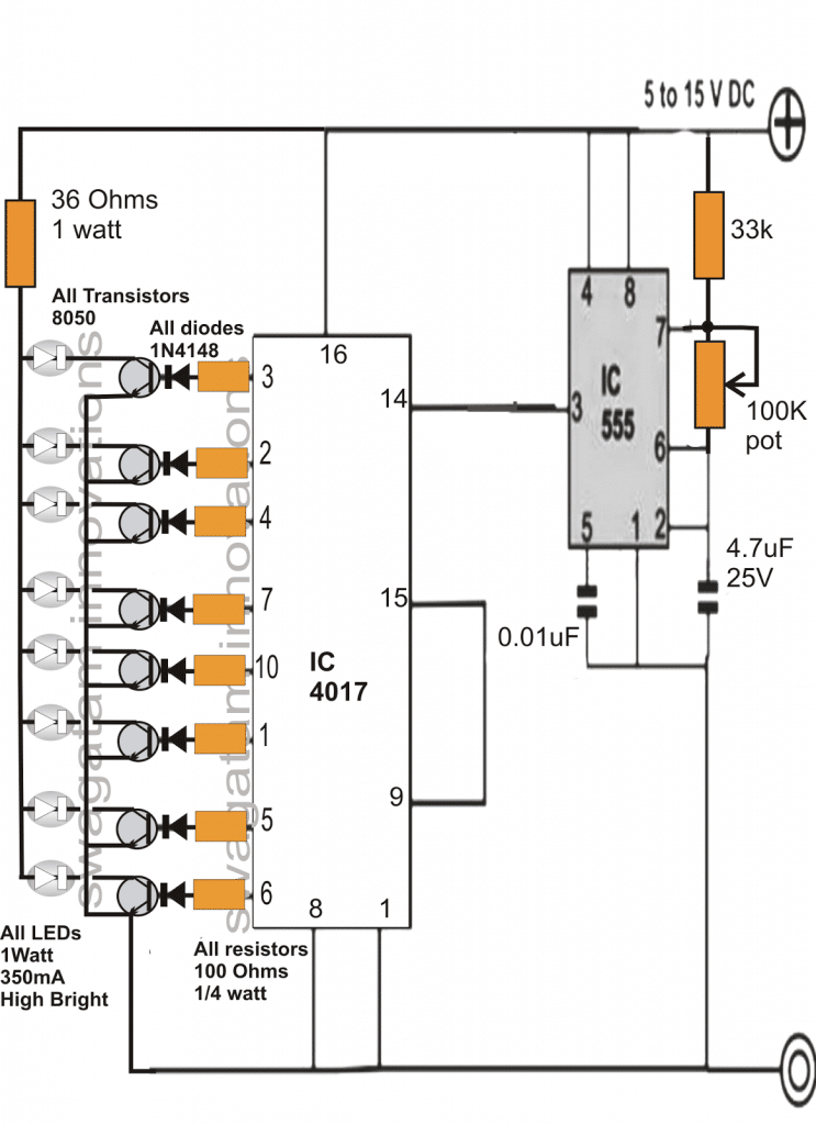
Chasing Dark Spot LED DRL Circuit
For creating a "running dark spot effect" use PNP transistors in place of the NPN ones, connect the emitters to the positive, and connect the LEDs across the collectors and ground. Do not forget to reverse the LED polarity too.2) Smart Car DRL Controller Circuit
The second design explainshow the DRLs in a car may be controlled byreducingits intensity while the headlamps ortheindicator lamps are being used, for enhancing itsefficiency. Theidea wasrequestedby Mr. Rob. Let's learn moreabout this smart DRL intensity manager circuit.Technical Specifications
Hi Swag, I'll try and explain in more detail. I want a module which will connect to a set of aftermarket DRLs that will allow them to turn on when the cars ignition is on (ideally via direct battery connection with a voltage sensor to turn them on but if not via ignition live feed). The module needs to connect to the headlight so that when it is turned on the DRLs dim to 50%. The module also needs to dim the DRLs when the indicator is activated on that particular side of the car (right DRL dims when right indicator is turned on etc.). This aspect isn't necessary when the headlights are on as the DRLs are already dim. When the indicators turn off I would like the DRL to fade back to full brightness say over a period of 2 seconds or similar. It is basically just like the new Audi DRLs which are built into their headlights. I hope this is enough information for you to produce a schematic but if not I can try and give you some more information. Also, using your relay method would be best! Thanks RobThe Circuit Design
The proposed smart, energy efficient DRL controllercircuit could be constructed in any of the following methods. The first one is a rather crude approach which will provide the intended results but will not save any electricity for you, so the purpose could fail here. The T1 stage is included for enabling the fade-back effect over the DRL, if this feature is not required, T1, R2, C1 may be entirely eliminated and the N/C of the relay directly joined with the junction of DRL positive and R1. C1 decides the gradual brightening period of the DRL The second design could be considered energy efficient due to the inclusion of a voltage regulator stage incorporating T2, R1, R2. T2 is configured as a common collector. Here T1 and the associated parts perform the same function as above while T2 is rigged to produce 50% less voltage for the DrL when the headlights or the turn signals are switched ON. The last circuit is also a smart way of controlling the DRL illumination. Here the T2 stage has been replaced with the LM317 current regulator stage which controls the DRL intensity by 50% during the recommended situations but unlike the second circuit it executes the operations by reducing the current instead of voltage.Circuit Diagram
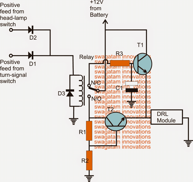
Parts List for the above circuit designs
R1, R2, R3 = 10k T1, T2 = TIP122 D1, D2 = 1N4007 D3 = also 1N4007 (optional) Relay = 12V, 400 ohms, SPDT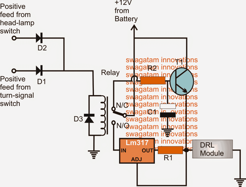
Parts List for the abovecircuitdesign
R1 = 1.25/DRL amp value (less 50% R2 = 10k 1/4 watt C1 = 470uF/25V T1 = TIP122 D1, D2 = 1N4007 D3 = also 1N4007 (optional) Relay = 12V, 400 ohms, SPDT Feedback, and suggested corrections from Mr. Rob Hi Swag, Thanks for doing the schematic of the DRL Indicator module. The reason we need it to dim is to make it legal in the UK to have DRLs and Indicators so close to each other.Anyway, I've ordered the parts for the schematic as I'm short on a few bits however just a query with the 12v + supply to the battery. As the battery is constantly live will this 'module' be constantly draining power when the car is not in use as the DRLs would always be on? If it were a 'ignition live' positive feed then this would only provide power to the 'module' when the ignition is turned on. What are your thoughts on this? Do we need to look at installing another circuit which goes to the battery that has a separate trigger switch that can identify when the car is not being used/ignition off? Thanks again RobAnalyzing the Feedback Query
Hi Rob, You are right, the +12V needs to come from the ignition feed, meaning only when the ignition is switched ON, the DRL and the associated circuitry should be triggered ON for the required operations.So the modification will be simple, instead of connecting the +12V to the battery we can integrate it with the ignition 12V feed. The above smart DRL circuits could be also used for high watt DRL applications, an example 50 watt modification is illustrated below: The 12V, 20 watt series lamp could be hidden somewhere under the bonnet, it's included for dipping the DRL illumination to approximately 50% less.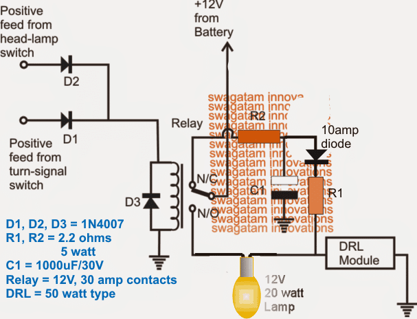 Upgrading DRL to a Solid State Version
The above designs can be upgraded to solid state versions by completely eliminating the relay, and repalcing it with an inexpensive BJT stage as shown below, the idea was requested by Mr.
Dhar Vader
Upgrading DRL to a Solid State Version
The above designs can be upgraded to solid state versions by completely eliminating the relay, and repalcing it with an inexpensive BJT stage as shown below, the idea was requested by Mr.
Dhar Vader
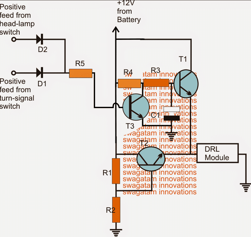
Parts List for the above Solid State Automatic DRL circuit:
R1, R2, R3 = 1K, 1watt. R4, R5 = 10k, 1/4 watt T1, T2 = TIP122 T3 = BC547, C1 = 470uF/25V D1, D2 = 1N54083) Multi-Feature DRL Circuit
The 3rd idea below discusses a multipurpose high power DRL circuit which can be used as park lights, head lights and also to specially respond to turn signal lights in order to light up the kerbs while passing through unpredictable blind turns or corners and subways. The idea was requested by Mr. Ian Auxley. Circuit Objectives and Requirements I have just found your web site and I am very impressed with your wonderful knowledge and friendliness. I am very interested in Automotive projects. I have designed and built a circuit using old tech stuff like auto relays, diodes, and resistors etc, all soldered together in a wooden box. This circuit works perfectly. It is used to turn on fog lights as day time running Lights and is also used to turn each one independently when either turn indicator is flashing on, the light uses capacitors to hold the relays on and not flash, it draws power from the indicators I this mode. In drl mode it draws power from the battery, there are 2 micro switches on the indicator stalk, one is a momentary to flash the drls and the other is to turn the drls on or off at night when the headlights are on. Some upscale cars use them when turning right or left to light up the kerbs and driveways when the indicators are used. I would like to make this into a solid state circuit that is smaller and easier to fit. I would like to have a circuit drawn up as a hobby project so anybody could use it. The lights I used in the older car I had were just dichroic 12v 60w household down lights with 60deg angle, I would love to use high powered LED lights instead. I could send you a hand drawn copy of the circuit if you are interested as used but not sure of values for diodes and resistors. I have other project ideas as well if you are interested. Could you help with the design.Designing a Multipurpose Power DRL Circuit for your Car
Referring to the request above, the idea could be summarized in the following manner: 1) two powerful LED lights to be used on the left/right sides of the car, which can be used as DRLs, park lights as well as head lights. 2) These lights needs to be controlled through separate switches as fog light, park light, and DRL lights. 3) The DRL light circuit should include the feature which ensures that when a side indicator is ON (flashing), the opposite DRL LED should be switched ON, but the DRL on the flashing indicator side should be switched OFF, however once the turn light is OFF the DRLs must return to their normal condition. The above feature needs to be implemented regardless of whether the DRLs are originally switched ON or not. 4) The unit needs to be solid-state in nature, and should avoid mechanical operators such as relays.Circuit Diagram
 The image above shows the intended solid state version of a high power DRL circuit with the recommended features, the details may be understood with the help of the following points:
1) two exactly identical stages can be seen on the left and the right sides, which form the respective DRL stages, along with a couple of delay timer stages for the specified switching actions through the turn signal feeds.
2) the 2N2907 and the associated TIP127 transistors form a simple current controlled LED driver stage for controlling the high power LED DRLs safely.
3) The other TIP127 transistor along with the BC547 forms a delay OFF timer stage intended for converting the flashing feed from the turn signal lights into a relatively constant DC.
4) The TIP127 delay OFF timers on L/R sections are configured in a such manner that it switches OFF it switches ON the opposite DRL while keeping its relevant side DRL ON.....
For example suppose while the left side indicator is active, the right DRL is forced to switch ON regardless of whether it's originally switched ON or not, and at the same time it forces the DRL at its own side to switch OFF regardless whether it's originally switched ON or not.
Exactly similar conditions are implemented for the right side indicator switching also.
The switches shown at the extreme sides allow the user to switch the DRLs ON or OFF together or individually at will.
The two LEDs confirm the powering of the DRLs and vice versa.
The image above shows the intended solid state version of a high power DRL circuit with the recommended features, the details may be understood with the help of the following points:
1) two exactly identical stages can be seen on the left and the right sides, which form the respective DRL stages, along with a couple of delay timer stages for the specified switching actions through the turn signal feeds.
2) the 2N2907 and the associated TIP127 transistors form a simple current controlled LED driver stage for controlling the high power LED DRLs safely.
3) The other TIP127 transistor along with the BC547 forms a delay OFF timer stage intended for converting the flashing feed from the turn signal lights into a relatively constant DC.
4) The TIP127 delay OFF timers on L/R sections are configured in a such manner that it switches OFF it switches ON the opposite DRL while keeping its relevant side DRL ON.....
For example suppose while the left side indicator is active, the right DRL is forced to switch ON regardless of whether it's originally switched ON or not, and at the same time it forces the DRL at its own side to switch OFF regardless whether it's originally switched ON or not.
Exactly similar conditions are implemented for the right side indicator switching also.
The switches shown at the extreme sides allow the user to switch the DRLs ON or OFF together or individually at will.
The two LEDs confirm the powering of the DRLs and vice versa.
Electronic 12V DC Capacitive Discharge Ignition (CDI) Circuits
The following post describes a simple yet enhanced 12V capacitive discharge ignition system which derives its operating voltage from the battery instead of the alternator for generating the igniting sparks. Since it works independently from the alternator voltage, without depending on a pickup coil signal, it is able to function more efficiently and consistently, enabling a much smoother ride of the vehicle even at lower speeds.Contact Breaker Vs CDI
A capacitive discharge ignition unit also called the CDI unit is the modern alternative for the age old contact breakers, which were quite crude with their functions and reliability. The modern CDI is an electronic version of the contact breaker which uses sophisticated electronic parts for generating the required arching across the spark plug terminals. The concept is not complicated at all, thesectionof the alternator provides the required 100 to 200V AC to the CDI circuit, where the voltage is intermittently stored and discharged by a high voltage capacitor through a few rectifying diodes. These rapid bursts of high voltage discharges are dumped into the primary winding of an ignition coil where its appropriately stepped up to many thousands of volts for acquiring the required arcing, which ultimately functions as the igniting sparks across the connected spark plug contacts. I have already discussed the basic electronic CDI circuit in one of my previous posts, though the circuit is extremely versatile, it depends and derives its operating voltage from the alternator. Since the alternator voltage depends on the engine speeds, the generated voltages tend to get affected with varying speeds. At higher speeds it works fine, but at lower speeds, the alternator voltage also lowers, this results in an inconsistent sparking forcing the alternator and the engine to stutter. Thisinconsistency ultimately affectsthefunctioningof the CDI and the whole system starts gettinghampered, sometimes even causing the engine to halt. The circuit of an enhanced capacitive discharge ignition circuit which is discussed here, eliminates the use of the alternator voltage for functioning, instead it utilizes the battery voltage for generating the required actions.The Circuit Concept
The whole concept for this electronic CDI can be understood by studying the shown circuit diagram below: The diodes, the SCR and the associated components form a standard CDI circuit. The high voltage of around 200V which needs to be fed to the above circuit is generated through an ordinary step down transformer connected the other way round. The secondary winding of the transformer now becomes the primary and vice versa. The low voltage primary winding is fed with high current pulsating DC generated by a standard IC555 circuit via a power transistor. This pulsating voltage is stepped up to the required 200V and becomes the operating voltage for the attached CDI circuit. The CDI circuit converts this 200V into bursts of high current for feeding the input winding of the ignition coil. These rapid high current bursts are further amplified to many thousandsofvolts by the ignition coil and finally fed to the connected spark plug for the required arcing and the initiating the ignition of the vehicle. As can be seen the input voltage is acquired from a 12V DC source which is actually thebatteryof the vehicle. Due to this the generated sparks are very consistent without interruptions providing the vehicle a constant supply of the required ignition sparksirrespectiveof the vehicle situation. The consistent sparking also makes the fuel consumption efficient, makes the engine less prone to wear and tear and enhances the overall mileage of the vehicle. Use a 1K resistor at the base of TIP122......
100 ohm is incorrectly shown
Use a 1K resistor at the base of TIP122......
100 ohm is incorrectly shown
Synchronizing with Wheel RPM
If you want the above circuit to be triggered by the alternator so that the combustion is ideally efficient and synchronized with the wheel RPM, the above design may be modified in the following way: A 1K resistor is used at the base of TIP122......
since 100 ohm is incorrectly shown.
The above configuration may be further modified as shown in the following diagram, which appears to be the most appropriate way of implementing the proposed enhanced CDI circuit for all 2 and 3 wheelers.
A 1K resistor is used at the base of TIP122......
since 100 ohm is incorrectly shown.
The above configuration may be further modified as shown in the following diagram, which appears to be the most appropriate way of implementing the proposed enhanced CDI circuit for all 2 and 3 wheelers.
How it Works
As we know, the reset pin#4 of IC 555 requires a positive potential to allow the normal functioning of the IC 555 as an astable or as monostable. If the pin#4 is not associated with the positive line, the IC remains dormant and disabled. Here the pin#4 of the IC can be seen connected with the alternator voltage. This voltage can be of any level from the alternator, it doesn't matter, since it is appropriately stabilized by the 33 k resistor and the following zener diode, capacitor network. The alternator will generate a positive and negative cycle pulses, in response to each rotation of the vehicle wheel. The positive pulse will be converted into a 12 V positive feed at the pin#4 which will cause the circuit to initiate and stay activated during the entire positive pulse duration cycle of the waveform. During these periods, the IC 555 will operate and fire the SCR multiple number if times in short bursts, causing the ignition to fire with higher efficiency and for a sustained period of time during the firing angle of the combustion and the piston. This will also enable the CDI to work in tandem with the wheel rotation generating an ideally synchronized combustion of the engine and with an optimal efficiency.Finalized Enhanced CDI Design with PWM Control
 CDI PCB Circuit
 Parts List
All resistors are 1/4w unless stated
1K - 1
10K- 1
POT 10K - 1
100 Ohms 1/2 watt - 1
56 Ohms 1/2 watt - 1
Diodes 1N4007 - 9
Capacitors
1uF/25V - 1
0.01uF/50V Ceramic - 1
105/400V PPC - 1
Semiconductors
IC 555 - 1
Mosfet IRF540 - 1
SCR - BT151
Transformer 0-12V/220V/1amp - 1
CDI ignition coil - 1
Video Clip showing the Test Result of the above shown electronic capacitive discharge circuit system
Parts List
All resistors are 1/4w unless stated
1K - 1
10K- 1
POT 10K - 1
100 Ohms 1/2 watt - 1
56 Ohms 1/2 watt - 1
Diodes 1N4007 - 9
Capacitors
1uF/25V - 1
0.01uF/50V Ceramic - 1
105/400V PPC - 1
Semiconductors
IC 555 - 1
Mosfet IRF540 - 1
SCR - BT151
Transformer 0-12V/220V/1amp - 1
CDI ignition coil - 1
Video Clip showing the Test Result of the above shown electronic capacitive discharge circuit system
Another Version of Electronic Ignition
The following diagram provides another version of a IC 555 based electronic ignition system, which I got from an old magazine page: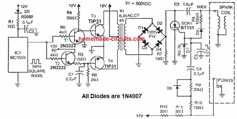 Here, the left side stage which includes the IC 555, 4 transistors and the X1 transformer, form a 12 V to 500 V step up push pull inverter.
The right side section using the SCR BT151, and the associated circuitry forms the capacitive discharge ignition stage.
The design works with the old contact breaker type of mechanism, for timing the ignition and triggering the SCR.
While the contact beaker remains closed, the SCR remains disabled, and this allows the capacitor C2 to charge via the 500 V DC from the inverter output.
Next, as soon as the contact breaker opens, the SCR gets its gate trigger via R9, 10, 11, 12, and C4, and it fires causing C2 to discharge across the attached ignition coil primary winding, which in turn causes the secondary of the ignition coil to produce the required high voltage pulse into the spark plug for the required ignition.
Here, the left side stage which includes the IC 555, 4 transistors and the X1 transformer, form a 12 V to 500 V step up push pull inverter.
The right side section using the SCR BT151, and the associated circuitry forms the capacitive discharge ignition stage.
The design works with the old contact breaker type of mechanism, for timing the ignition and triggering the SCR.
While the contact beaker remains closed, the SCR remains disabled, and this allows the capacitor C2 to charge via the 500 V DC from the inverter output.
Next, as soon as the contact breaker opens, the SCR gets its gate trigger via R9, 10, 11, 12, and C4, and it fires causing C2 to discharge across the attached ignition coil primary winding, which in turn causes the secondary of the ignition coil to produce the required high voltage pulse into the spark plug for the required ignition.
With Pickup Trigger
In modern vehicles we find the contact breaker being replaced with a pickup coil, which ensures a solid state working of the system without any wear and tear. The above electronic CDI design could be also used with pickup coil set up, with the following given modifications.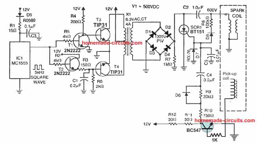
LED Tail Ring Light Circuit for your Car
The following article describes a fancy LED sequencing/diverging ring light circuit which can be used as a tail brake light in cars. The idea was requested by one of the avid readers of this blog, Mr. Bobby. let's learn more.Technical Specifications:
Hello, I was just reading thru your wonderful article on building an LED chasing tail light:https://www.homemade-circuits.com/how-to-make-car-led-chasing-tail-light/ Could this circuit be adapted to create a round tail light that lights rings in sequence from the center out as the brake is pressed, one ring at a time until all the LEDs are lit and then flash all the LEDs twice and keep all LEDs lit solid after? If not, could you design a circuit that would? I would be willing to pay for your time. Thank you, BobbyThe Design
The circuit diagram shown below has been designed as per the above request, let's understand its functioning with thefollowingpoints: IC1 which is a "serial shift resistor" forms the heart of the entire circuit, the main function of this IC is to illuminate the LEDs connected to pin outs #3-4-5-6-10-11-12-13 in a sequence, keeping the sequence latched and illuminated as it proceeds. This happens in response to each clock pulse applied at pin#8 of the IC. The LEDs which aretriggeredby the pin#3-4-5-6 and 10 are arranged as rings such that it illuminates from inner most ring first toward the outermost ring, producing an interesting and visually rich effect. And that's not all, after the aboveeffectthe whole illuminated group of arrays flash thrice and then shut off. The above "show" repeatsevery timebrakes are applied. When brakes are applied, battery voltage connects with the circuit initiating the following operations: C1 resets IC1 such that the sequence begins from pin#3 and not from any other in between pin out (this output illuminates the inner most ring). IC2 is an oscillator IC which generates the required clocks for the IC1 from its pin#3. In response to the above clocks, the sequence proceeds creating the desired diverging illumination effects, until it reaches pin#10. The LEDs receive the required positive supply through T1 which stays triggered due to the low logic at pin#13 of IC1 When the sequence reaches pin#10, T6 conducts which also switches ON T7. The emitter of T6 is connected to pin#3 of IC2 which is already generating the clocks for the required of IC1. The alternating low pulse from this pin out switches T6/T7 in a blinking mode. T7, in response to the above blinking, sends correspondingly pulsating positive pulses to base of T1. This in turn forces T1 to flash the LEDs in accordance with the above influence. The illuminated ring arrays startflashinguntil the sequence is forwarded to pin#13. The moment pin#13 becomes high, T1 switches OF and also the "high" reaches pin#11 of IC2. IC2 locks and stops the clocks at pin#3. The whole operationfreezes. The above system breaks and repeats itself only as soon as the brakes are released and pressed afresh.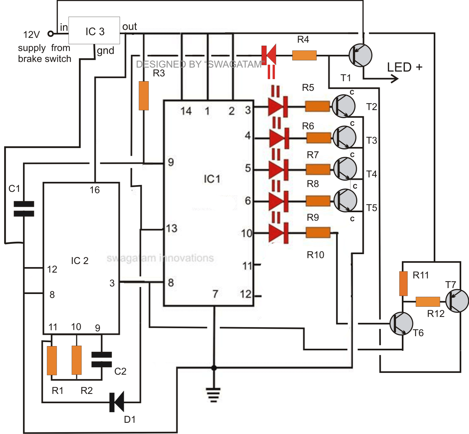 The LEDs which needs to be connected across the collectors of T1 and T2/T3/T4/T5 may be wired up in the following manner.
The arrangement should be designed in a circular manner to form the corresponding RINGs.
The LEDs which needs to be connected across the collectors of T1 and T2/T3/T4/T5 may be wired up in the following manner.
The arrangement should be designed in a circular manner to form the corresponding RINGs.
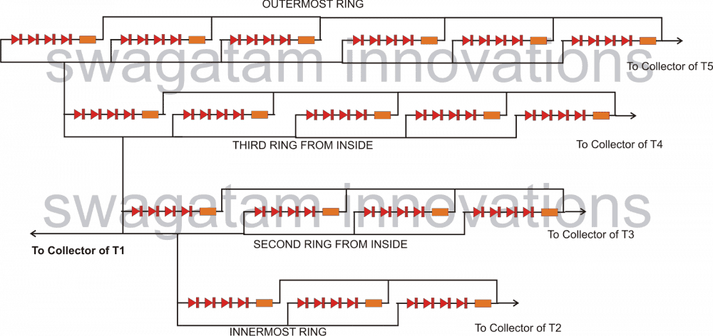
Parts List
R1 = 2M2 R2 = TO BE EXPERIMENTED R3 = 1M R4---R12 = 2K2 T1 = 8550 or 2N2907 T2----T6 = BC547 T7 = BC557 D1 =1N4148 C1,C2 = 0.1uF IC1 = 74LS164 IC2 = 4060 IC3 = 7812 ALL LEDS = RED 5MM, ASSOCIATED RESISTORS ARE ALL 150 OHMS, 1/4 WATTHigh Voltage, High Current DC Regulator Circuit
We all are pretty familiar with the 78XX voltage regulator ICs or the adjustable types such as LM317, LM338 etc. Though these regulators are outstanding with their specified functioning and reliability, these regulators have one big disadvantage.... they won't control anything above 35V.Circuit Operation
The circuit presented in the following article introduces a DC regulator design which effectively counters the above issue and is able handle voltages as high as 100V. I am a greatadmirerof the above mentioned types of ICs simply because they are easy tounderstand easy to configure and require bare minimum number of components, and are also relatively cheap to build. However in areas where input voltages can be higher than 35 or 40 volts, things become difficult with these ICs. While designing a solar controller for panels which produces in excess of 40 volts, I searched a lot over the net for some circuit that would control the 40+ volts from the panel to the desired output levels, say to 14V, but was quite disappointed as I couldn't find a single circuit which couldfulfillthe required specifications. All I could find was a 2N3055 regulator circuit whichcouldn'tsupply even 1 amp current. Failing to find a suitable match I had to advise the customer to go for a panel that would not generate anything above 30 volts...that's the compromise the customer had to make using a LM338 charger regulator. However after some thinking I could finally come up with a design which is able to tackle high input voltages (DC) and is a lot better than the LM338/LM317 counterparts. Let's try to understand my design in details with the following points: Referring to the circuit diagram, the IC 741 becomes the heart of the entireregulatorcircuit. Basically it has been set up as a comparator. Pin#2 is provided with t a fixedreferencevoltage, decided by the value of the zener diode. Pin#3 is clampedwitha potential divider network which is appropriately calculated for sensing the voltages exceeding the specified output limit of thecircuit. Initially when the power is switched ON, R1 triggers the power transistor which tries to transfer the voltage at its source (input voltage) across the other side of its drain pin. The moment voltage hits the Rb/Rc network, it senses the rising voltage conditions and within a fraction of a second the situation triggers the IC whose outputinstantaneouslygoes high, switching off the power transistor. This instantly tends to switch OFF the voltage at the output reducing the voltage across Rb/Rc,promptingthe IC output to go low again, turning ON the power trasistor so that the cycle locks in and repeats, initiating an outputlevelthat's just exactly equal to the desired value set by the user.Circuit Diagram
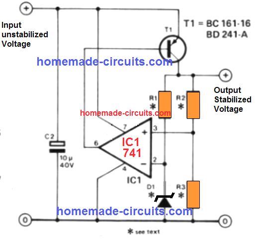 The values of the unspecified components in the circuit may be calculated by the following formulas and the desired output voltages may be fixed and set up:
R1 = 0.2 x R2 (k Ohms)
R2 = (Output V - D1 voltage) x 1k Ohm
R3 = D1 voltage x 1k Ohm.
The power transistor is a PNP, should be suitably selected which can handle the required high voltage, high current in order to regulate and convert the input source todesiredlevels.
You can also try replacing the power transistor with a P-channel MOSFET for even higher power output.
The maximum output voltage should not be set above 20 volts if a 741 IC is used.
With 1/4 IC 324, the maximum output voltage can be exceeded up to 30 volts.
The values of the unspecified components in the circuit may be calculated by the following formulas and the desired output voltages may be fixed and set up:
R1 = 0.2 x R2 (k Ohms)
R2 = (Output V - D1 voltage) x 1k Ohm
R3 = D1 voltage x 1k Ohm.
The power transistor is a PNP, should be suitably selected which can handle the required high voltage, high current in order to regulate and convert the input source todesiredlevels.
You can also try replacing the power transistor with a P-channel MOSFET for even higher power output.
The maximum output voltage should not be set above 20 volts if a 741 IC is used.
With 1/4 IC 324, the maximum output voltage can be exceeded up to 30 volts.
Motorcycle MOSFET Full Wave Shunt Regulator Circuit
The following post of a full wave motorcycle shunt regulator circuit was requested by Mr.Michael. Let's learn the circuit functioning in details.How a Shunt Regulator Works
Shunt regulator is a device which is used for regulating voltage to some fixed levels by means of shunting. Normally the process of shunting is done by grounding the excess voltage, just as zener diodes do in electronic circuits. However one bad aspect with such regulators is the generation of unnecessary heat. Thereasonfor heat generation is the principle of its operation where the excess voltage is shortcircuitedto ground. The above practice may beimplementedby simpler and cheaper means, but cannot be considered efficient and advanced. The system is based on destroying or killing energy instead of eliminating or inhibiting it. The circuit of a motorcycle shunt regulator discussed in this article takes a completely different approach and restricts the in-flow of excess voltage instead of "killing"energyand thus stops the generation of unnecessary heat.Circuit Operation
The circuit functioning may be understood as under: When the mobike is started, voltage enters across the P-channel mosfet source/drain pins due to the gate trigger that becomes available via R1. The moment the high voltage reaches R3, which happens to be the sensing input of the opamp, pin#3 of the IC senses an increased voltage. As per the set reference at puin#2, the instantaneously reacts to the situation and the result puts the output of the IC to a high logic level. The immediate high logic pulse restricts the negative base trigger of the mosfet, switching it OFF at that particular instant. The moment T1 switches OFF, voltage at the junction of R3/R4 reverts to theoriginalcondition, that is the voltage here now drops below the reference level......this instantly activates the opamp output with a low logic signal which in turn switches ON T1 back into action. The process repeats at a very rapid speed, keeping the output voltage marked with +/- at a constant level determined by the setting of R2/Z1 and R3/R4. The above principle utilizes voltage inhibition technique of the excess voltage instead of shunting it to ground, thus saves precious power and also helps to control global warming in some way.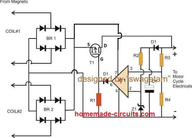 Parts List
R1, BR2 = 10Amp bridge rectifier
R1 = 1K
D1 = 1N4007
C1 = 100uF/25V
IC1 = IC741
T1 = mosfet J162
R2/Z1, R3/R4 = as explained in this article
Parts List
R1, BR2 = 10Amp bridge rectifier
R1 = 1K
D1 = 1N4007
C1 = 100uF/25V
IC1 = IC741
T1 = mosfet J162
R2/Z1, R3/R4 = as explained in this article
Shunting Excess Power to Ground is Recommended in Alternators
When it comes to alternators, the best way to restrict or limit excess voltage is to short the excess power or shunt the excess power to ground. This eliminates the rising current in the armature and protects the winding from heating up. A voltage regulator using this method can be witnessed in the following examples: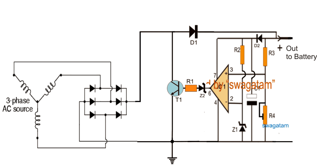
Video Clip below shows an opamp based shunt regulator circuit, and its testing procedure
Parts List
R1, R2, R3 = 10K R4 = 10K preset Z1, Z2 = 3V zener 1/4 watt C1 = 10uF/25V T1 = TIP142 (on large heatsink) IC1 = 741 D1 = 6A4 diode D2 = 1N4148 Bridge rectifier = standard motorcycle bridge rectifierHow to Set up the Circuit
For a 12V system, apply a 18V from a DC power supply from the T1 side, and adjust R4 to precisely set 14.4V across the output terminals. An even simpler motorcycle shunt regulator using the shunt regulator IC TL431 can be witnessed below, the 3k3 resistor can eb tweaked to chnage the output voltage to the most favorable level.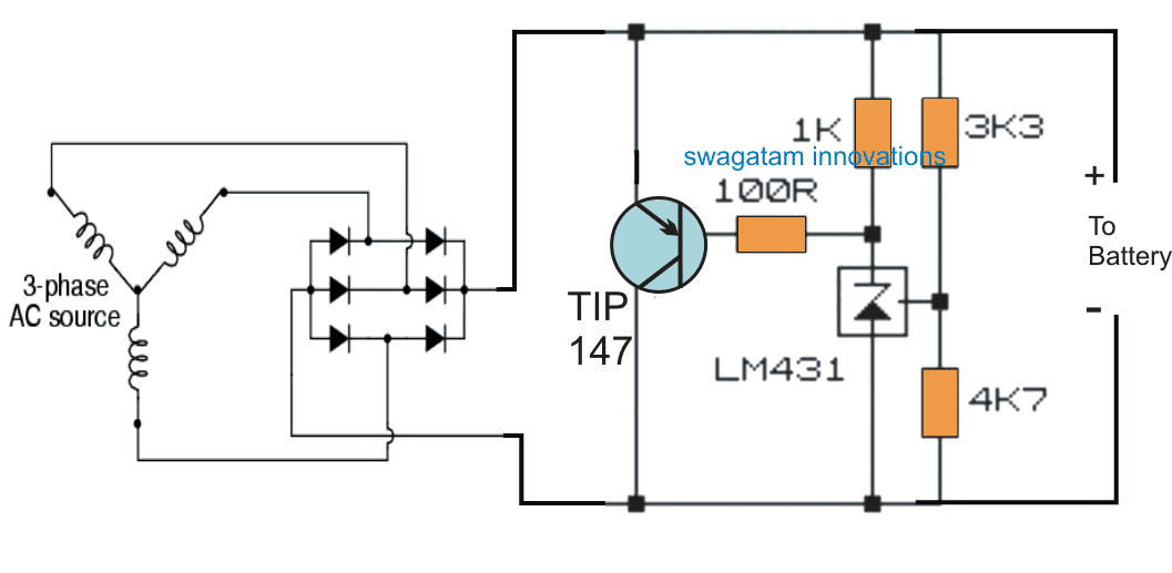 For single phase alternators, the 6 diode bridge rectifier could be replaced with a 4 diode bridge rectifier as shown in the following diagram:
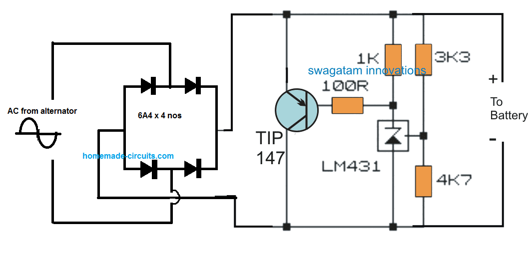 Feedback and Update from an Avid reader Mr.
Leonard Fons
I've come up with a bit more that needs to be considered.
I'm using a MOSFET (IXFK44N50P) for the clipper and series regulators.
Never did much with FETs because when they first came out, the least little static charge would blow them out in a heartbeat.
So this is actually my first attempt to use them.
I assumed that, like junction transistors, the more power they handle, the more power needed to drive them.
NOT TRUE.
In looking again at the datasheet, I see that Gate current is plus or minus 10 nano Amps.
Feedback and Update from an Avid reader Mr.
Leonard Fons
I've come up with a bit more that needs to be considered.
I'm using a MOSFET (IXFK44N50P) for the clipper and series regulators.
Never did much with FETs because when they first came out, the least little static charge would blow them out in a heartbeat.
So this is actually my first attempt to use them.
I assumed that, like junction transistors, the more power they handle, the more power needed to drive them.
NOT TRUE.
In looking again at the datasheet, I see that Gate current is plus or minus 10 nano Amps.
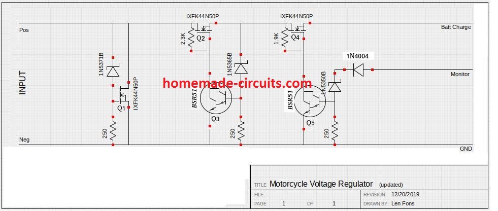 That is ten trillionth of an amp.
They do not require a TIP142 to drive them.
A one watt, high gain darlington will do the job very nicely.
And the entire circuit will fit on one board.
I still need another regulator housing for the rectifier.
But I'm about ready to put this all together and try it out.
Of course, I will try it out before I actually mount it into the housing, but I don't expect to make any modifications.
Realizing that these FETs use almost no gate current at all makes quite a difference.
I'll find out just haw accurate my theory is for the current to ground when clipped at 60 volts, rather than shunting all current to ground.
A when I pot it into the I have to insure that the FETs have no gap to the housing.
That was another issue with one of the others.
A sixteenth inch space between the components and the housing,
With that gap filled with epoxy, it's not very efficient at dissipating the heat.
By the time the housing starts getting warm, you'd burn your fingers on the components.
One change I may make is the series diode in the monitor line.
A green LED located where I can see it while riding will let me know if it's charging.
That is ten trillionth of an amp.
They do not require a TIP142 to drive them.
A one watt, high gain darlington will do the job very nicely.
And the entire circuit will fit on one board.
I still need another regulator housing for the rectifier.
But I'm about ready to put this all together and try it out.
Of course, I will try it out before I actually mount it into the housing, but I don't expect to make any modifications.
Realizing that these FETs use almost no gate current at all makes quite a difference.
I'll find out just haw accurate my theory is for the current to ground when clipped at 60 volts, rather than shunting all current to ground.
A when I pot it into the I have to insure that the FETs have no gap to the housing.
That was another issue with one of the others.
A sixteenth inch space between the components and the housing,
With that gap filled with epoxy, it's not very efficient at dissipating the heat.
By the time the housing starts getting warm, you'd burn your fingers on the components.
One change I may make is the series diode in the monitor line.
A green LED located where I can see it while riding will let me know if it's charging.
Rain Triggered Instant Start Windshield Wiper Timer Circuit
The following circuit was requested by one of the readers of this blog Mr. Keval. The actual request was for araintriggered windshield wiper circuit, but the idea here has been further enhanced with a quick start feature for betterefficiency.How Conventional Wiper Systems Work
Normally, electronic wiper control circuit involve a bistable for switching the wiper mechanism into anoscillatoryaction. The bistable switches ON the wiper motor and keeps it moving until the set time lapses, this process continues for so long the power is switched ON to the circuit. A 555 IC is fundamentally utilized forimplementingthis function, which is generally configured in it standard bistable mode. However one disadvantage with a standard 555 bistable circuit is that it introduces a delay of of around 1.6 times the set RC time interval value. Therefore if suppose the bistable delay is set to 10 seconds would mean a 555 bistable would require a 10*1.6 = 16 seconds to initiate the action, that can be very annoying.Enhancing an Instant StartAction
The present design eliminates the above issue by wiring the 555 bistable in a smart way. Referring to the circuit diagram, when the wiper switch S1 isdepressed, pin#6 of the IC isimmediatelyelevated to the supply voltage level of 12V via C1. This resets the bistable, making its output go low, which energizes the connected relay and the wiper motor gets instantly activated. The above process of instantly starting the motor using a 555circuit makes the present circuit different from the conventional circuits which employs the same IC but without the above modification. Now once C1 is charged, which happens via R2 after the output gets activated, pin#2 of the IC falls below the 1/3 Vcc mark. This situation pulls the output to high, switching OFF the relay and the system. After this C1 starts discharging through R1 and P1, once C1 completely discharged the cycle is yet again repeatedas longas S1 is kept depressed. The value of R1 and the setting of P1 decides the OFF time of the circuit. If the value of P1 and R1 is selected too low, then C1 may not get charged solely through them but also via R2, which will make the output and the relay system to stay switched ON forever, until S1 is switched OFF.Adding a Rain Trigger
An useful rain trigger feature can be added to the circuit for enabling an automatic start of the wiper motor when rain fall is detected. The two transistors T1 and T2 are configured as a high gain amplifier set up. The points A and B get bridged with rain water droplets introducing a low resistance across the points. This switches ON the transistors and the relay, which in turn switches ON the connected wiper motor. The wiper motor remains switched ON as long as rain persists and points A/Bstaysbridged with water droplets.Circuit Diagram
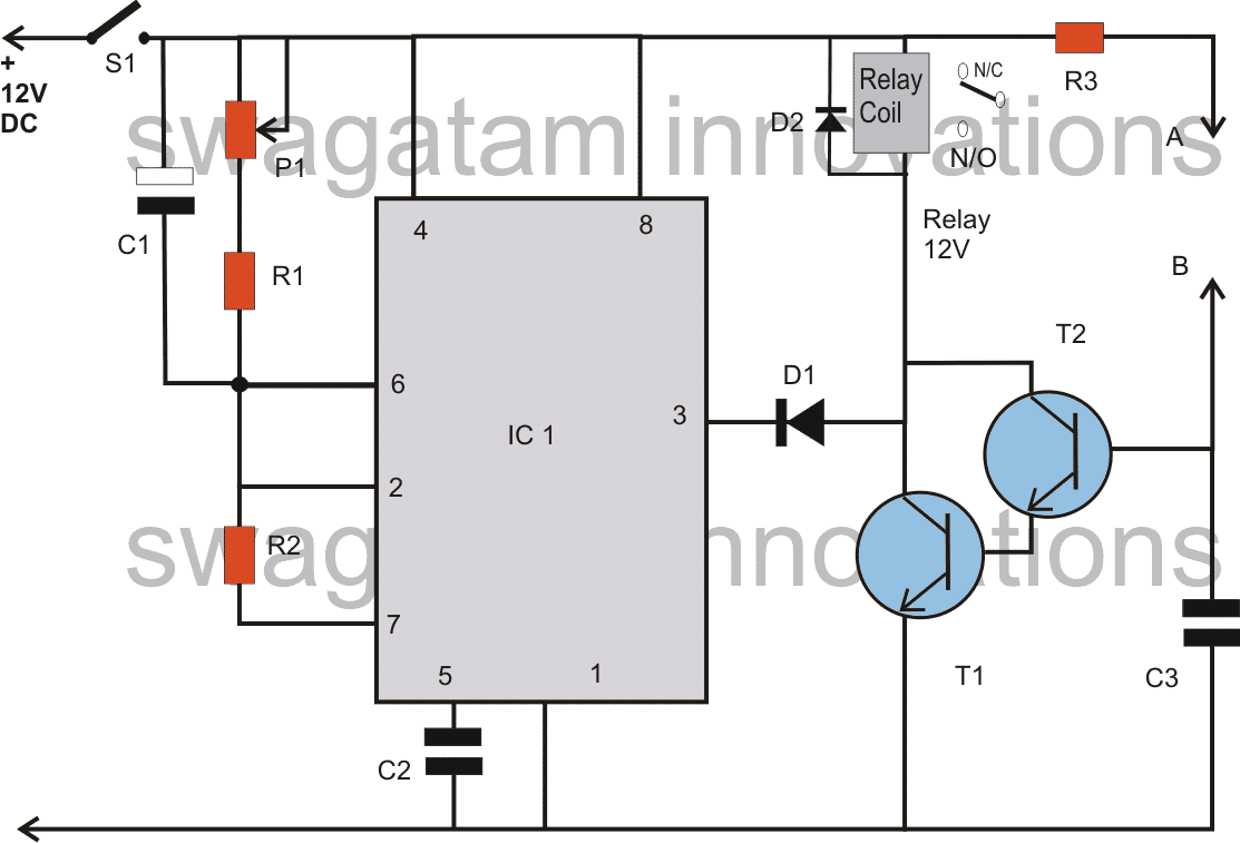
Parts List
R1 = 47K, R2 = 22K, R3 = 1K, P1 = 1M C1 = 33uF/25V C2 = 0.01uF C3 = 0.1uF D1,D2 = 1N4148 T1,T2 = BC547 IC1 = 555 RELAY = 12, SPDTAdjustable Windshield Wiper
The following IC 555 based windshield wiper facilitates the driver to control the wiper seed manually, and adjust the wiper action to any desired speed.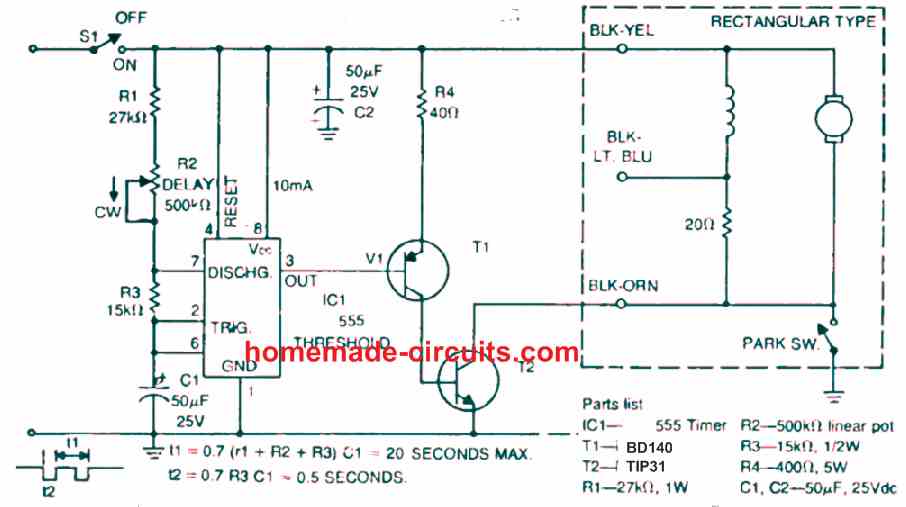
Wiper Delay Circuit
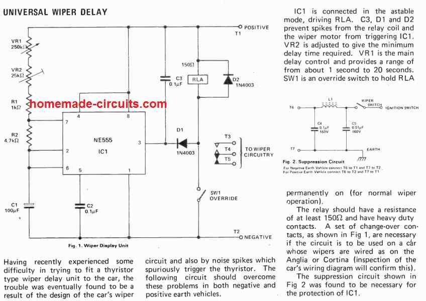
Another Simple Car Wiper Controller
U1 is set to work in the usual astable mode, which acts as a relaxation oscillator. Once power is supplied, C2 charges to 2/3of the supply voltage via R1, R2, and R3. U1 detects that its pin6threshold voltage isexceeded at this moment, and the timer is triggered, prompting its output at pin 3 to become high. When such high logicis supplied to Q1's base, the transistor remains in the off state. C2 now starts to discharge to pin 7 of U1 via R2. U1is switched back to its original state once C2 has drained to roughly 1/3rdof the supply voltage.
As pin 3 of U1drops low, C2 begins to charge afresh.
Q1, which acts as an emitter-follower buffer stage, turns on when pin 3 is low, enabling current to pass acrossthe coil of relay K1. As a result, Kl's contacts close, providing power to the carwipers.
The setting of potentiometer R3 determines the charging time of capacitor C2. Tantalum capacitor C2 is recommended, although virtually any 12 Vcoil relay with suitably heavy dutycontacts would suffice.
U1is switched back to its original state once C2 has drained to roughly 1/3rdof the supply voltage.
As pin 3 of U1drops low, C2 begins to charge afresh.
Q1, which acts as an emitter-follower buffer stage, turns on when pin 3 is low, enabling current to pass acrossthe coil of relay K1. As a result, Kl's contacts close, providing power to the carwipers.
The setting of potentiometer R3 determines the charging time of capacitor C2. Tantalum capacitor C2 is recommended, although virtually any 12 Vcoil relay with suitably heavy dutycontacts would suffice.
Make this Voltage Stabilizer Circuit for Your Car
In this post we learn about a car voltage stabilizer circuit which could be made and installed in all cars for ensuring a perfectly controlled and stabilized supply for the associated sensitive electronics and gadgets.Understanding Car Electrical
A car electrical is probably more volatile than our house electrical, simply because it is generated from a source called alternator whose output considerably varies with the speed of the vehicle. It means if you are driving your car with sudden changes in its speed or if you are often applying brakes, would consequently generate varying voltages from the alternator outputs. Since nowadays our car and other vehicle interiors heavily involve sophisticated electronic gadgets, an unstable voltage conditions can cause serious effects on their performance and life. The circuit idea was requested by Mr.Haziq, let's know more about the making of the proposed circuit (designed by me for the application). Today we have some wonderful ICs at our disposal which are specifically designed for voltage regulation applications. The LM317 and the LM338 are a couple of them which are versatile with their voltage regulation functions, I have discussed them elaborately in some my earlier posts. The LM317 can handle up to 1.5 Amps while its big brother the LM338 can hold not more than 5 Amps. However these values are quite meager when compared to the huge asks in automobiles. By suitably modifying the configurations, the IC can be made to regulate any desired levels of currents though. In the proposed car voltage stabilizer circuit we incorporate the IC LM317 and modify its standard design such that it enables the car electrical with sufficient power and yet restricts it from all possible dangers like overloads, over current, fluctuating voltages and short circuits, providing an ideal voltage conditions for the vehicle interiors.Circuit Operation
The circuit diagram shows a rather simple configuration where the IC 317 has been wired in its standard voltage regulator mode. R1 limits the surge current, while R2 decides the triggering voltage to T1, if the current consumption crosses the 1.5 amp mark, T1 conducts and assists the IC by sharing the excess current through it. P1 is set for achieving around 13 volts across C3. R5 monitors over load conditions and short circuits, if the current crosses beyond 12 amps, sufficient current develops across R5 to trigger T2, which instantly switches OFF the IC so that the output voltage drops and restricts the current below 12 amps.Ideal Specifications:
Constant voltage = 13 volts Current Limit = 12 Amp Overload protection = above 12 amp cut OFF Thermal protection (if the transistor and IC are mounted on the same heatsink with mica isolation) Short circuit protection (fire hazard protection)
Parts List
R1 = 0.1 Ohms, 100 watts, made from 1mm iron wire. R2 = 2 Ohms, 1 watt, R3 = 120 Ohms, 1/4watts, R4 = 0.1 Ohms, 20 watts, as explained for R1 (this resistor is actually not required, may be replaced with a wire short.) R5 = 0.05Ohms, 20 watts, make as R1 T1 = MJ2955 mounted on big finned type heatsink T2 = BC547, C1 = 10,000uF, 35V C2 = 1uF/50V C3 = 100uF/25V P1 = 4k7 preset, IC1 = LM317 D1, D2 = 20 amp diode (3nos. 6 amp diodes in parallel)Simplified Version
Using the IC LM196, the above configuration becomes extremely simple, you may refer to the following diagram which illustrates a simplified version of the proposed car alternator voltage stabilizer circuit using bare minimum components. R3 = 240 ohms
D1, D2 = 15 amp diodes
P1 = 10k preset
C1,C2,C3 as specified above
IC1 = LM196
R3 = 240 ohms
D1, D2 = 15 amp diodes
P1 = 10k preset
C1,C2,C3 as specified above
IC1 = LM196
Cell Phone Call Alert Security Circuit
This circuit will give call back alerts in the form of blank calls on your cell phone whenever it senses a break in or intrusion inside the particular restricted area where it has been installed for the intended security monitoring.Introduction
The cell phone call alert security system circuit which needs to be installed incorporates a cheap cell phone as the modem which is actually used for triggering the warning calls in the owners cell phone. The above modem cell phone is first attached with its own SIM card as normally done with any cell phone. For setting up the cell phone, the cover is removed and a couple of wires are neatly connected with the pads which represent the "green" button or the calling button of the phone. After securing the two connected wires with the green button terminals, the phone is again sealed back to it normal condition. The external ends of the above wires are then connected to the relay contacts of the control circuit as shown in the figure. Before the installation, a call is made from the above modem cell phone to the owners cell phone so that it gets recorded inside the green button as the "last call" made from the cell phone. Now every time the green button is activated thrice, a call gets connected to the owners cell phone. Since the wires from the call button are connected to a relay, it simply means that if the relay contacts gets energized thrice, would result a call being sent from the above cell phone.How the Control Circuit Works
The control circuit basically consists of a hold circuit and a pulse circuit. The "hold circuit section is made up of two NAND gates configured as a timer cum latch circuit. N1 and N2 together with C12 and R14 form a timer circuit, while the resistor R15 keeps the output latched as long as the timer counts and its timing lapses. After which the output reverts to its original position. The input of the above latch is connected to a reed relay sensor which may be appropriately centered for initiating the magnetic contacts when a possible intrusion takes place. The reed relay activates a relay (left side of the diagram) only momentarily via the capacitor C10. When the above relay contacts close, N1, N2 latch, and generate a negative or a logic low at the output. This logic low instantly grounds the reset pin of another timer IC 4060. This immediately prompts the IC 4060 to start counting. The process generates a set of three pulses at the pin #15 of the IC activating the relay thrice via the relay driver stage. This activates the cell phone modem which starts sending a blank call to the assigned number or the owners cell phone. Pin #2 makes sure that the IC counting and the output from pin#15 gets locked after the three relay pulses, this is done by sending a high pulse from pin #2 to pin #11 of the IC. The IC remains in this position for so long as N1 and N2 are in the counting mode after which the output of N2 goes high and the entire circuit is reverted to its original state and back in the alert mode. The modem cell phone is kept in a charged state by employing a 7805 charger circuit. This circuit was exclusively designed and invented by "Swagatam".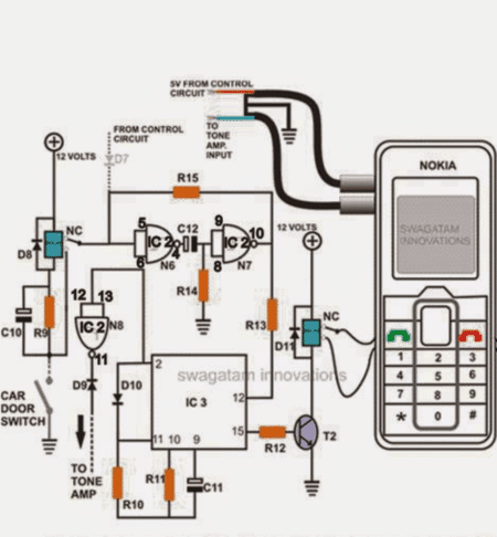
PARTS LIST
All Resistors are watt 5% CFR, unless otherwise stated. R9-10K, R10-2M2, R11-330K, R12-4K7, R13-39K, R14-1M, R15-1K, C10/C12-100uF/25V, C11-0.001uFDISC, D9/D10-1N4148, D8/D11-1N4007 T2 = BC547 IC2 (N6,N7,N8)-4093 IC3-4069 Relays-12V/400 OhmsSimple Electronic Fuse Circuit
In this article we investigate a electronic circuit design which works like a conventional fuse for safeguarding any electrical system from overloads, over-current, short circuit and related fire hazards. However, the main advantage of this electronic fuse is that it does not require frequent replacements like mechanical fuses, instead it can be reset with a single push of a button.What is a Fuse
A fuse is a device used in electrical wiring for preventing accidental fire hazards due to to a short circuit or overloads. In ordinary mechanical type of fuses, a special fusible wire is used which melts when there's short circuit at some point in the wiring. Though such fuses are fairly reliable, are surely not so efficient or elegant with their performance. A mechanical fusible type of fuse requires careful selection as far as the rating is concerned and once blown, again requires careful replacement of the device correctly. Even automobiles incorporate largely the above fusible types of fuses for the discussed precautions concerns. However the above inefficient fuse can be very effectively replaced with more versatile types of electronic fuse circuit with little consideration.Main Features
If you search for an electronic fuse circuit online, you may come across a few very ordinary designs which actually have no ability to handle high current short circuits or overloads. These circuits are created by school kids and cannot be used for serious applications. The design presented below uses a relay and is capable of supporting high current short circuits up to 5 amps or even 10 amps. This makes the design suitable for almost all high current DC circuits which demand a fool-proof short circuit protection.How this Electronic Fuse Works
The idea has been exclusively developed by me and the test results were pretty impressive. The CIRCUIT DIAGRAM is very simple, a relay is used to switch the battery power to the rest of the electrical of the vehicle via its contacts. A low value resistor is placed across the base emitter of a transistor for sensing the rise in the current levels. When a possible short circuit is sensed, an equivalent amount of voltage is developed across this low value resistor, this voltage becomes responsible for instantly triggering the transistor which in turn triggers the relay driver stage. The relay quickly reverts and switches OFF the supply to the vehicle electrical. However in the process it also latches itself so that it does not go into an oscillating mode. The relay contacts must be rated to handle the maximum allowable current specified for the vehicle's normal needs.Sensing Resistor
The value of the sensing resistor should be carefully selected for the intended tripping operations at the correct over load levels. I used an iron wire (1mm thick, 6 turns, 1 inch diameter) in place of the sensing resistor and it could handle well up to 4 amps after which it forced the relay to trip. For higher currents lower number of turns may be tried. To be precise, the sensing resistor could be calculated using the formula: Rx = 0.6 / Cut Off Current Rx Wattage = 0.6 x Cut Off Current The "push to OFF" switch is used to reset the circuit, but only after the short circuit condition is properly rectified. A simple electronic fuse circuit developed by me is shown below: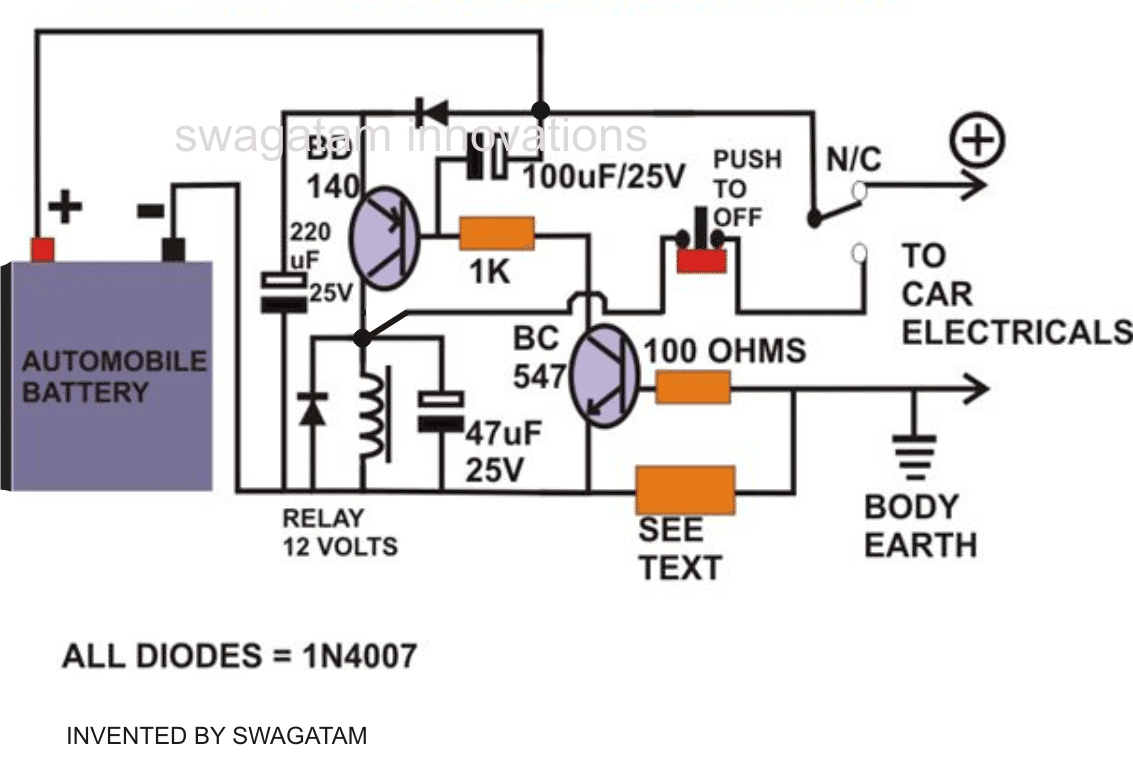
Another Simple Electronic Fuse
The electronic fuse signifies that load current is shut off as soon as an overload is detected. Actually it simply restricts the load current to a magnitude of certain amps. The next circuit will basically trigger the load current to drop to 0 %. In case it rises, causes IL x R2 > 0.7V/R2, Q4 to switch on, delivering base current to Q3. Q4 as a result activates, providing additional base current for Q4. Regenerative function goes on until eventually Q4 and Q3 are saturated.
Q3 will subsequently take off all base current from Q1, consequently turning Q2 off and enabling the load to be safe from over current.
In case the reset button is pressed, the entire current drive shall be taken off from Q3 and Q4, causing them to be void of saturation.
As soon as the reset button i released, the circuit is going to either go back to original situation in case the overload situation has been eliminated, or will click off yet again in case it is still existing.
Care must be observed with the "grounding" to prevent shorting of R2.
Regenerative function goes on until eventually Q4 and Q3 are saturated.
Q3 will subsequently take off all base current from Q1, consequently turning Q2 off and enabling the load to be safe from over current.
In case the reset button is pressed, the entire current drive shall be taken off from Q3 and Q4, causing them to be void of saturation.
As soon as the reset button i released, the circuit is going to either go back to original situation in case the overload situation has been eliminated, or will click off yet again in case it is still existing.
Care must be observed with the "grounding" to prevent shorting of R2.
Simple Car Shock Alarm Circuit
A simple car shock alarm circuit presented in this article can eb effectively used to alarm the owner each time the car comes across some kind of vibrational intrusion ether from a potential theft of simply a damaging hit from an external source.Introduction
Today most of the cars are equipped with this type of security feature where an alarm is raised in an event of a shock or a hit made over the car body. The article explains a very simple and cheap car shock alarm circuit which costs hardly 1/2 a dollar yet performs the actions reasonably accurately. The working Principle of the Shock alarm The principle employed here is pretty basic, a mic is used to sense the impact, the sensed output is amplified by a transistorized amplifier.How the Circuits Works
Looking the circuit diagram, the whole functioning can be understood with the following points: The mic stage consists of the mic itself, the biasing 2k7 resistor and the 47uF coupling capacitor. T1 and T2 form the first amplifier stage and is the heart of the circuit. The feedback 100K resistor plays an important function of keeping the amplification sustained at a stable rate. When a shock impact is sensed by the mic, it converts the shock vibrations into tiny electrical pulses. T1 and T2 work like a preamplifier, and amplifies the MIC response into a reasonably high electrical pulse, sufficient for driving the power output stage transistor T3 saturation. The T3 responds to the above signal and activates the connected alarm siren, alerting the folks around regarding the possible theft attempt. One big drawback of this cheap car shock alarm circuit is that it cannot distinguish between physical shocks and shock waves developed due to loud bangs or noises.
Parts List
R1 = 5k6 R2 = 47k R3 = 3M3 R4 = 33K R5 = 330 OHMS R6 = 2K2 C1 = 0.33uF/400V C2 = 4.7uF/25V T1, T2 = BC547 T3 = TIP127 D1 = 1N4007 Siren = Any 12 V car sirenPendulum Type Shock Alarm
The circuit may be implemented to safeguard automobiles, big items, houses and other sites since the sensor enables you to detect any kind of motion. This gadget may also be used for many technological tests. The relay can easily power high wattage audio or alarm devices, for example sirens, horns, lights, etc. Standby current consumption is extremely low (around 100 uA) during the time the relay is in the deactivated state, which increases the battery-life. The schematic diagram of the Pendulum shock Alarm is shown in Figure below.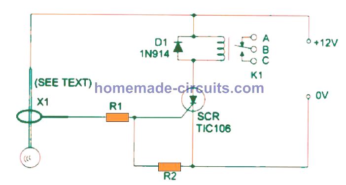 The circuit is centered around an SCR (Silicon Controlled Rectifier), that powers ON the relay whenever the sensor picks up any kind of movement.
Relay coil voltage is determined based on the power supply voltage.
You may use a small DPDT 1A Mini Relay or, for hefty loads, a 10A mini SPDT relay.
These types of rlays are usually rated at 12 VDC and consume not more than 38 mA.
Once initiated, the circuit will be latched permanently, in order to reset the circuit, or stop the alarm can be made a small push to ON switch may be wired between the SCR anode and cathode.
The leads of the polarized component like the SCR and diode, should be carefully noted and assembled with correct polarity.
The circuit is centered around an SCR (Silicon Controlled Rectifier), that powers ON the relay whenever the sensor picks up any kind of movement.
Relay coil voltage is determined based on the power supply voltage.
You may use a small DPDT 1A Mini Relay or, for hefty loads, a 10A mini SPDT relay.
These types of rlays are usually rated at 12 VDC and consume not more than 38 mA.
Once initiated, the circuit will be latched permanently, in order to reset the circuit, or stop the alarm can be made a small push to ON switch may be wired between the SCR anode and cathode.
The leads of the polarized component like the SCR and diode, should be carefully noted and assembled with correct polarity.
Parts List
SCR -TlC106 or SCR D1 - 1N914 or 1N4148 K1 - 12V relay (see text) S1 - SPST toggle switch Rl - 22k, 114W,5% resistor R2 - 10k, 114W,5% resistor X1 - Pendulum sensorPendulum Shock Sensor Assembly
The pendulum sensor is a simple homemade mechanism built using a small ball pen spring, a small steel ball as the load, from any ball-bearing system, and connecting copper wires as shown in the following figure. Make sure to use a spring that is very delicate and stats swinging even with slightest of jerk or shock.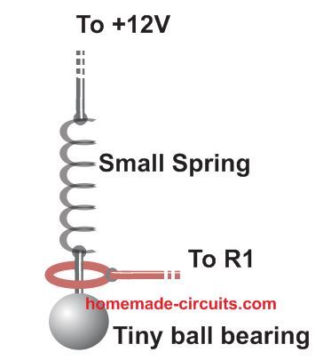
How to Manufacture Automobile Electronic Parts and Earn a Handsome Income
To set up an auto electrical manufacturing unit, it's important to have a thorough knowledge regarding the various technicalities associated with the field. The article makes a comprehensive approach and explains all the issues related to the subject.Introduction
We begin with the basic raw materials and man power required for the intended installations and further proceed with the list of electronic parts that can be manufactured and sold in the relevant markets. The products that are included for the production are flasher buzzers, piezo buzzers, CDI units, musical horns, auto testing machine etc. How these can be made is also explained through discrete articles, linked in the sections. Among most electronic products, the ones which are associated with automobiles are probably the largest selling types and are always in demand. Manufacturing these items and selling is surely a lucrative business. Here we discuss the procedures in details. Today one thing thatˇŻs common with all of us is that we all want to earn money. However, with the population thatˇŻs ever growing, all sources of earning money are being quickly captured, resulting in a cut-throat competition in every field. ItˇŻs feasible to make a way out from this intense competition only if you can manage an area where you are the master, and are able to create a monopoly. The auto market today has become huge and with tremendous opportunities, but also itˇŻs flooded with some tough competitors. Since vehicles cannot work without electricity and other associated electronic accessories, the products related to these have cropped up extensively and you can find a whole range of all sorts of electronic products, some of which are mandatorily used while some are just for decoration purposes. Whatever may be the seriousness of the application, electronic products have become today an integral part with all types of vehicles. Thus, auto electronics is probably one such field where you can expect some good money, provided you are equipped with all the know-how required for the initial manufacturing set ups. In this article we are going to discus the technical aspects required for setting up an auto electronic manufacturing plant for TWO-WHEELERS and THREE-WHEELERS, small though. However here we wonˇŻt discuss the legal procedures involved, like acquiring VAT number, CST number etc. The following steps provide some crucial data regarding earning money by manufacturing auto electrical products:What Electronic Products can be Manufactured for the Two-Wheeler Auto Market?
There are probably a host of them which you can choose from, or rather go for the entire range. Supplying or keeping the whole range will provide you with a better chance of fairing among the many vying vendors. The items commonly associated with two/three wheelers are the side indicators, CDI units, rectifiers, buzzers, melody maker horn, etc. To begin a manufacturing plant for producing the above auto electrical items, you would first want to acquire a space with a descent area; preferably a 20 by 40 sq ft will be ideal and sufficient to begin with. You would also require fixing some furniture in the form of a long narrow table closely attached to the longer wall and a few number of chairs that can be accommodated. This set up is required for implementing the production process by lining up the workers so that the assemblies can be done in the most efficient manner. The workers who would be responsible for assembling the electronic parts will need important and useful tools like the soldering iron, wire nipper, wire stripper, soldering paste, thinner etc. so all these must be procured in required numbers. The engineers may require more sophisticated tools like multitester, desolder pump/wik, magnifying glass, power supply etc. along with the above mentioned tools. Procure all of these as per the requirements. We are assuming that the workers required for carrying out the procedures would be appropriately employed, so we are not discussing how they can be contacted and interviewed etc. After the initial set ups as discussed above are done, itˇŻs time to select the items and chalk out the procedures plans. It would include the following points: There should be at least one product that has the potentials to run through out the year, under all odds. Make it the base of your companyˇŻs production line.

Manufacturing Piezo Buzzer
As an example you may select the buzzer unit, as itˇŻs the easiest to assemble, finish, and sell, moreover the concerned raw materials are easily available. However this product may carry pretty low profit margins and you would need to sell tons of them to actually witness any significant income, but can be rest assured a steady flow of income through out the season. You can refer to this circuit of a simple buzzer. itˇŻs the simplest in design and widely used all across the world for automobile applications, especially in conjunction with side turn signal or flasher units. The next type of selected product would be the one which sells like ˇ°hot cakeˇ± in the market, has reasonably less competition and has the potentials of providing fairly high profit margins. You can assess the product and insist the engineers to do improvements in the form of cost cutting or adding new features into the product, so that it can stand out from the rest of the brands. This will give you an edge while introducing your product in the market.Manufacturing Flasher with Buzzer
A flasher with buzzer is one such item which satisfies the above conditions, I have already published an improved and low cost flasher buzzer circuit, for your refernce

Manufacturing Capacitor Discharge Ignition (CDI) Units
CDI units are another indispensable auto part which can be manufactured and sold with good profit margins. You can find it in Bright Hub, just type the relevant words in the given in-site Google search box. You can refer this article to know how to make a two-three wheeler CDI circuit. Having discussed the manufacturing process, testing these circuits for accuracy and reliability can become a crucial issue. A suitable auto part testing machine therefore becomes imperative, without which the whole set up may fail or jeopardize. If you inquire about such a universal auto part testing machine, you would probably get it at very high costs. In Pune (India), Teckson Electronics has the monopoly of manufacturing these machines, and they charge an awful Rs.12000/- for each of them. I investigated the mechanism and developed my own version at less than Rs. 600/- which is more efficient, and more reliable than the above unit. The complete design will be comprehensively discussed in one of my forthcoming articles. ThatˇŻs all what may be basically required and concludes the fundamental technical procedures involved with setting up an electronic auto part manufacturing unit.Simple Ignition Code Lock Circuit for Automobile Protection
This extremely simple code lock switch circuit can be used for locking a vehicleˇŻs ignition by typing a hidden code over the given micro switch keypads. So now you can use this simple code lock ignition circuit for probably securing your car from a possible theft. Alternatively the circuit may be used for any application requiring security or safeguarding from external intrusions and thefts.The Use of SCRs in the Design
SCRs are well known to all of us and we are quite familiar to the many salient features of this important active electronic component. One important feature of this device is its latching ability when operated with a DC. Precisely when an SCR is triggered with a DC load across its anode and cathode, the device switches ON, latches and sustains the switched ON position permanently until power is switched OFF. For the newcomers, the device SCR is explained briefly with the following points: Called Silicon Controlled Rectifier, an SCR basically consists of three leads, the extreme right lead is the ˇ°gateˇ±, the center one is the cathode and the extreme right lead is termed as the anode. The cathode needs to be connected to the ground or the negative line of the circuit. The anode is the lead which is connected to the supply voltage (either a DC or an AC) via the load which is intended to be switched by the device. The gate is the triggering input which is triggered with a DC, for energizing the load connected at the anode of the device. A gate trigger instantly switches the SCR, connecting the load across the supply terminals through the SCR body. With AC as the supply across the load, the SCR remains switched ON as long as the gate is triggered with a DC. However when a DC is used for energizing the load, the SCR becomes a single shot switching device, because it latches and keeps the load switched ON even when the gate trigger is removed. The above feature has been effectively exploited in the present code lock circuit design, letˇŻs learn the circuit functioning with the following instructions: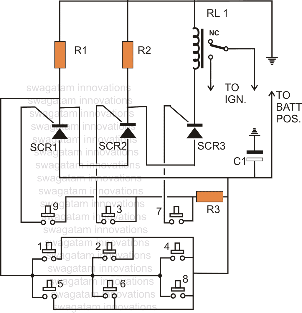 The figure shows a simple arrangement where, three SCRs are wired in conjunction with an array of ten micro switches.
Selecting the Code Numbers
As per the selected code, the particular switches are integrated with the gates of the SCRs in a given sequence as shown in the diagram. Here, the elected code is 9, 3, 7 and these buttons are connected with the relevant SCR gates. The other terminals of these buttons are made into a single common terminal, which is connected with the positive supply of the circuit.How the Code Lock Works
When the switch 9 is pressed, the gate of the first SCR is triggered; it latches via R1 which is connected as the load for SCR1. This SCR also conecys the anode of SCR 2 with the negative and puts it on a standby condition. Pressing button 3 triggers the gate of SCR2 which instantly latches with the load R2 and via the path provided by SCR1. This action connects the anode of SCR3 with the negative supply and in turn clamps SCR3 into an alert position. Finally when button no. 7 is pressed, SCR 3 latches via the path provided by the SCR2 and in the course switches ON the relay which forms the load of SCR3. The contacts of the relay which is possibly connected with the ignition of the vehicle become active so that the vehicle can be now started with the ignition key. The rest of the switches other than the ones which are selected as the codes may be rigged with the positive supply, so that when an intruder tries his luck by randomly pressing the codes, only succeeds in breaking a possible combination every time it accidentally switches any of the remaining buttons.Parts List
Parts required for making this simple code lock switch R1, R2, R3 = 1K, R3 = 470 Ohms, C1 = 100uF/25V, SCR1,2,3 = BT169, RL1 = relay 12 volts, 400 Ohms, SPDT Keyboard = 10nos. micro switch bankHow to Make Car LED Chasing Tail Light, Brake Light Circuit
The circuit explained here is presented in response to a request sent by one of the avid readers of this blog. The proposed circuit is of a sequential LED light driver, especially designed to suit the application of a multipurpose car tail light indicator.Circuit Connections
The circuit is integrated to the brake switch and works as a brake light, itˇŻs also connected to the turn signal switches for indicating the turning of the vehicle with chasing light patterns, and the circuit can also be used just as an ordinary tail light warning indicator. In order to successfully make the proposed car LED chasing tail light, brake light circuit, it will be important to first understand the circuit functioning in details with the following points: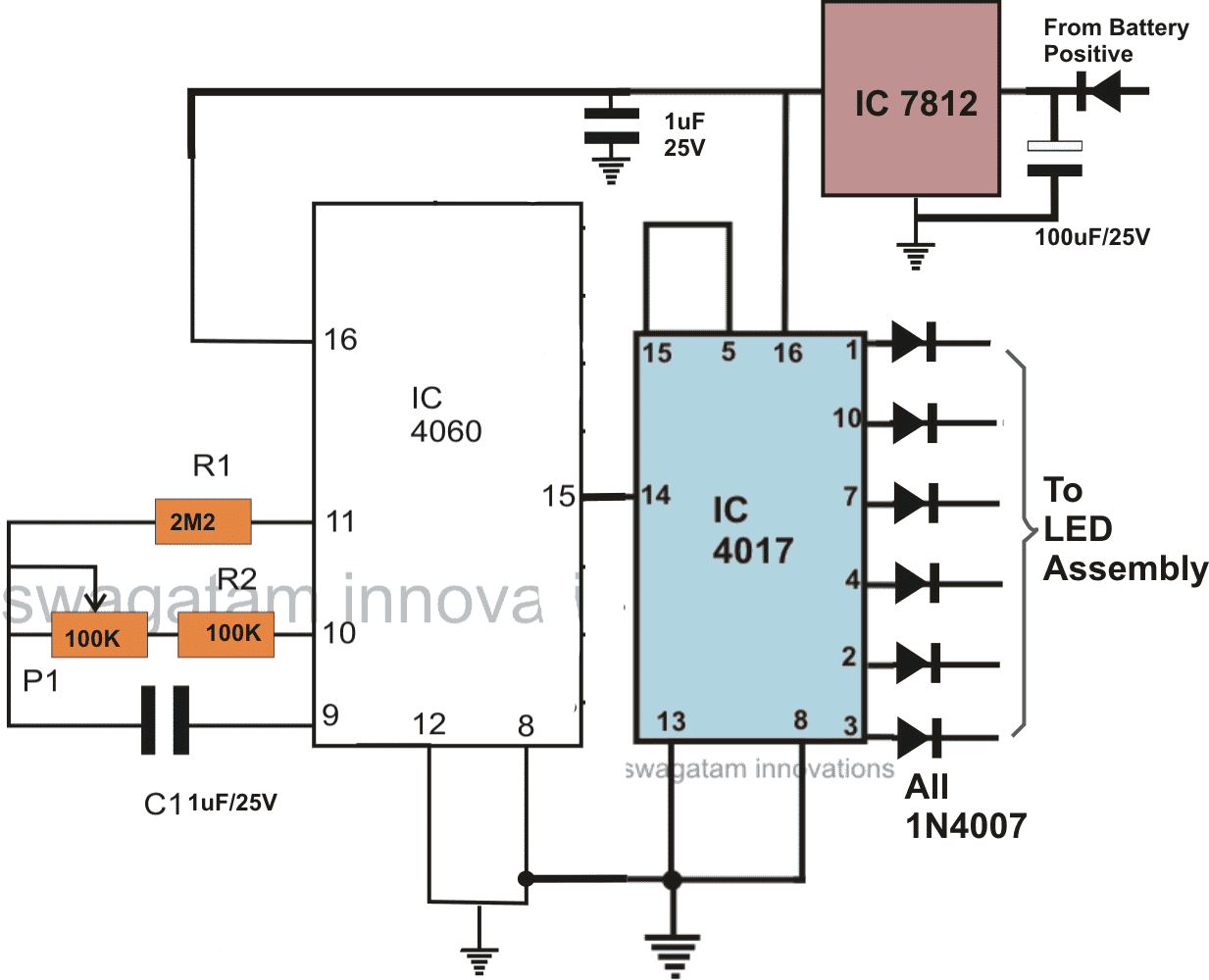
How it Works
The CIRCUIT DIAGRAM can be divided into two sections, the first consists of the LED driver stage, where the IC 4017 forms the main LED sequencer and is configured in its usual counter/divider mode. Only six channels of the IC 4017 have been used to avoid lengthy sequencing patterns and crowding of the LEDs. Two arrays of LED are taken from the above outputs such that they ˇ°runˇ± in opposite directions when switched ON, however both the channels are never run together since they are used for the LEFT, RIGHT turn indicator purpose and therefore only the relevant side is switched ON depending upon the vehicles turning side. The IC 4060 is configured in its standard mode, as an oscillator and is used for driving the IC 4017 with its clock signals. With every rising peak of the clocks, the outputs of the IC 4017 shift from one pin out to the next in the shown order, making the connected LED illuminate sequentially. The pot associated with the IC 4060 may be used for adjusting the sequencing speed as desired.Left Right LED Sequence Layout
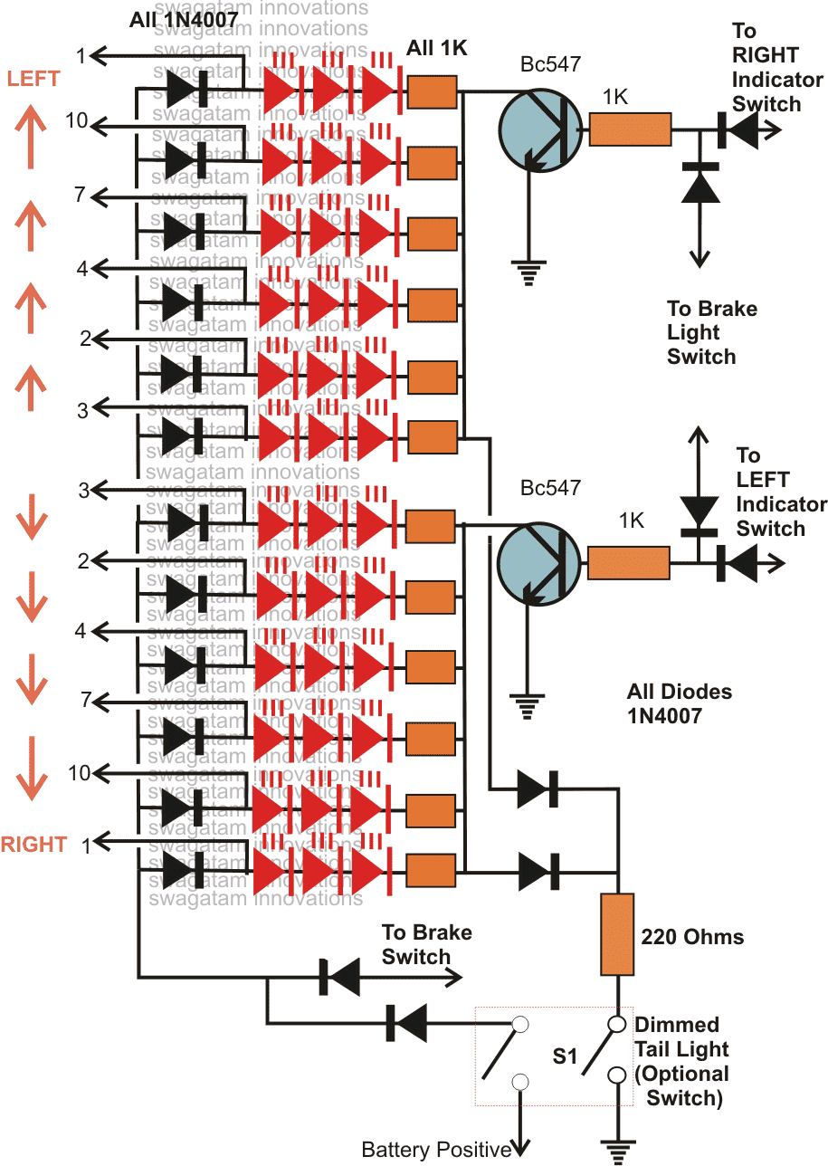 The LED stage consists of the LEDs arranged in a definite sequencing pattern as discussed in above explanation.
The LEDs are connected to the IC 4017 outputs so that they are able to perform the intended sequencing or chasing function.
The LEDs are also discretely wired up to the different vehicle controls like the brake switch, the turn signal switches and an optional DIM tail light switch.
When the brake switch is applied, the LEDs light up all together brightly, indicating the application of the brakes.
When one of the turn signal switches is switched ON, say for example the LEFT turn signal is applied, the LED array positioned on the LEFT portion starts sequencing from center, toward LEFT, indicating the intended moving direction of the vehicle.
The above function is repeated toward the RIGHT side by the right portion LED array when the right signaling is made with the relevant switch.
A couple of optional switches (S1) may also be included and wired up with the LEDs as shown in the diagram.
This provides a feature of operating the LEDs as a dim tail light indicator which stays switched all the time with a relatively lower brightness, however when the brakes are applied the LEDs light up brightly.
The driver circuit is powered through the IC 7812 which is a voltage regulator and provides safe operating stabilized voltage to the circuit, irrespective of the input fluctuations.
In the above position, the turn signals will also work, but is not recommended as the DIM light at the background may affect the signaling.
The following image shows the complete combined circuit design of the above discussed two stages:
The LED stage consists of the LEDs arranged in a definite sequencing pattern as discussed in above explanation.
The LEDs are connected to the IC 4017 outputs so that they are able to perform the intended sequencing or chasing function.
The LEDs are also discretely wired up to the different vehicle controls like the brake switch, the turn signal switches and an optional DIM tail light switch.
When the brake switch is applied, the LEDs light up all together brightly, indicating the application of the brakes.
When one of the turn signal switches is switched ON, say for example the LEFT turn signal is applied, the LED array positioned on the LEFT portion starts sequencing from center, toward LEFT, indicating the intended moving direction of the vehicle.
The above function is repeated toward the RIGHT side by the right portion LED array when the right signaling is made with the relevant switch.
A couple of optional switches (S1) may also be included and wired up with the LEDs as shown in the diagram.
This provides a feature of operating the LEDs as a dim tail light indicator which stays switched all the time with a relatively lower brightness, however when the brakes are applied the LEDs light up brightly.
The driver circuit is powered through the IC 7812 which is a voltage regulator and provides safe operating stabilized voltage to the circuit, irrespective of the input fluctuations.
In the above position, the turn signals will also work, but is not recommended as the DIM light at the background may affect the signaling.
The following image shows the complete combined circuit design of the above discussed two stages:
Complete Schematic Diagram
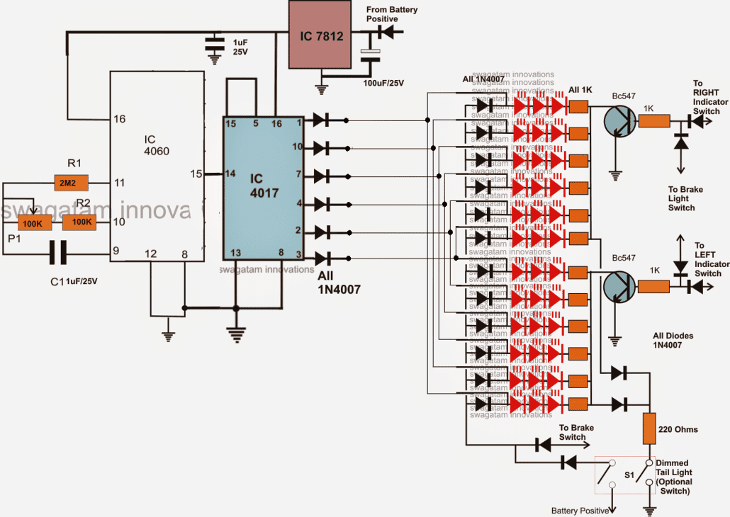 YOU CAN ADD A 22uF CAPACITOR ACROSS ALL THE 1N4007 DIODES AND GROUND, NEAR THE IC4017.
THIS WILL PRODUCE A NICE LAGGING EFFECT ON THE LEDS, IMITATING A METEOR SHOWER.
A simplified and scaled down version of the above explained car chasing light circuit with brake light and park light can be witnessed below:
YOU CAN ADD A 22uF CAPACITOR ACROSS ALL THE 1N4007 DIODES AND GROUND, NEAR THE IC4017.
THIS WILL PRODUCE A NICE LAGGING EFFECT ON THE LEDS, IMITATING A METEOR SHOWER.
A simplified and scaled down version of the above explained car chasing light circuit with brake light and park light can be witnessed below:
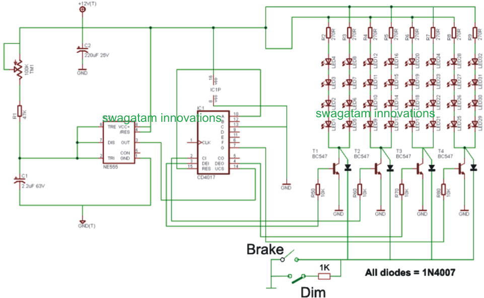 The post illustrates an elaborate circuit design that can be used as an enhanced "chasing" LED tail light for cars and other vehicles, the design also includes the modification details for the associated turn signal and the park light systems.
The idea was designed and presented by Mr.
Jason.
The entire discussion may be referred to in the comment section of this post:
Sequential Turn Signal Indicator
The post illustrates an elaborate circuit design that can be used as an enhanced "chasing" LED tail light for cars and other vehicles, the design also includes the modification details for the associated turn signal and the park light systems.
The idea was designed and presented by Mr.
Jason.
The entire discussion may be referred to in the comment section of this post:
Sequential Turn Signal Indicator
Modified car chasing light circuit
The circuit description below explains the proposed modified car chasing light circuit, as presented by Mr. Jason: Okay, I had a chance to work on it, but have not tested it on the breadboard yet. If this works, one 4017 and 555 timer chip can be used for both left and right turn signal.The schematic
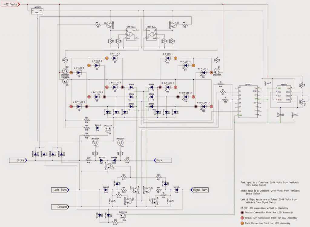
How the Circuit Functions
I hope you can understand what it is doing. The LED's I will be using have 3 wires out. One is ground, one is Brake/Turn, and one is Park. When just 12 volts is hooked up to the assemblies, It seems that there are different resistors to control the brightness (a fixed amount) for the brake/turn, and for the Park. Which is a nice factory option from the LED assemblies themselves. If I just use one wire (the brake/turn), and a potentiometer to adjust the brightness for the Park, I am thinking I would need a 19W potentiometer, and those are expensive. Each LED assembly draws 246mA at 12.8 volts. If all 6 lights were on, that's 246mA * 12.8 volts = 18.89W of power. So, wiring them separately and using a common ground to switch them on and off, would eliminate the need for a potentiometer, since the resistors are built into the lights themselves. I am using a NOR gate to turn off the Park LED's when the brake or turn signals are applied. I am not sure on the resistor values. I've changed the Vcc for the 4017 and 555 to run off of the LM7805 voltage regulator. By doing that, I have also run the other inputs/outputs of those chips off of the LM7805 as well? I am not sure of the Capacitor and Resistor values needed then. I'd like to switch all power to 5volts for less power consumption. Except for the LED supply voltage of course. that needs to stay the 12-14 volts coming straight from the wiring of the Truck. I took your suggestion and added the transistor and the resistor to rapid discharge the 470uF capacitors so the LED's do not continue to sequence for 15 seconds AFTER the turn signals have been turned off. As per your request, I have connected them to the last sequencing output of the 4017. It makes sense, and as you said, should work for turning off the LED's from sequencing. If I can get this to work, I plan on building a circuit to allow up to the 8 sequencing LED's (available outputs for the 4017 since two are used to reset the 4017 and the SCR's). I will do it using either dip switches or more simply, solder bridges. I will also make it so that solder bridges will be before and after a resistor of each LED, if a resistor is needed for standard LED's to be wired up. I need to do this for my car, and my new lights will have 5 rows of LED's I will need to sequence instead of the 3 that my nephews truck has. So I'll need to design the circuit to work for both. Fun Stuff!Using High Watt LEDs
Now let's discusses how to construct a chasing car tail light circuit using high watt amber LEDs. The idea was requested by Mr. Brian Walton. I've been giving the project some further thought. I am wondering what changes might be needed to use single, higher power leds instead of the advised 5mm ganged in threes? So there would be 6 LED's rather than 6*3 5mm The reason is that I have combined LED DRL & indicators on the front of my car, so I would like to retain the OEM look & feel at the rear - where I propose to use your excellent circuit design. I'm thinking along the lines of the LEDS in the link below. They are Osram Opto Diamond DRAGON Series GW Amber LED. They are designed for automotive use in DRL's and indicators. They are 2.9v forward voltage and appear to take about 1.4A at typical lumens. The LEDs above are not definitive but a suggestion in terms of output and style for my construction needs. So my question is can the circuit take or how do I need to modify the circuit to take the extra power these LED's may take. For info; from a practicalities point of view, I intend to have a separate driver circuit for each side of the vehicle - it makes installation simpler given i'm going to attach the pulse form the existing indicator relay as discussed previously with you. I hope you can advise me (again!) and many thanks for your devotion to the electronics hobbyist on the web. Best wishes BrianSolving the Circuit Query
Thanks Brian! Incorporating higher wattage LEDs will need individual transistor buffers across the 6 outputs from the IC, it's actually very easy to implement. I'll try to explain the connections verbally, although I am also thinking of updating a suitable diagram for this particular application, I may do it within a couple of days....in the meantime you could try doing the following mods in the above circuit: Use TIP122 for the buffer transistors. Connect the bases of the 6 transistors to the respective outputs of the IC 4017 via the indicated diodes. Make sure the base have individual series 1k resistors The LEDs will need to be attached across the transistor collectors and the positive, the LEDs too must have their own series limiting resistor The LED resistors could be calculated using the following formula: R = (Us - LEDfwd)/I where Us is the supply voltage, LEDfwd is the optimum glow voltage of the LED or the forward voltage drop spec. I is the optimum current for the LED as specified in its datasheet. That's all..... now your circuit is ready and would be capable of handling any type of high watt LEd in the range....Circuit Diagram
Simple Capacitive Discharge Ignition (CDI) Circuit
In this post we discuss the circuit for a simple, universal capacitive discharge ignition circuit or a CDI circuit using a standard ignition coil and a solid state SCR based circuit.How Ignition System in Vehicles Work
The ignition process in any vehicle becomes the heart of the entire system as without this stage the vehicle just wonˇŻt start. To initiate the process, earlier we used to have the circuit breaker unit for the required actions. Nowadays the contact-breaker is replaced with a more efficient and long lasting electronic ignition system, called the capacitor discharge ignition system.Basic Working Principle
The basic working of a CDI unit is executed through the following steps: Two voltage inputs are fed to the electronic CDI system, one is high voltage from the alternator in the range of 100 V to 200 V AC, other is a low pulse voltage from a pickup coil in the range of 10 V to 12 V AC. The high voltage is rectified and the resultant DC charges a high voltage capacitor. The short low voltage pulse drives an SCR which discharges or dumps the capacitor's stored voltage into the primary of an ignition transformer or coil. The ignition transformer steps up this voltage to many kilo-volts and feeds the voltage to the spark-plug for creating the sparks, which finally ignites the combustion engine.Circuit Description
Now letˇŻs learn the CDI circuit operations in detail with the following points: Basically as the name suggest, ignition system in vehicles refers to the process in which the fuel mixture is ignited for initiating the engine and the drive mechanisms. This ignition is done through an electrical process by generating high voltage electrical arcs. The above electrical arc is created through extreme high voltage passage across two potentially opposite conductors through the enclosed air gap. As we all know that for generating high voltages we require some kind of stepping up process, generally done through transformers. As the source voltage available in two wheeler vehicles is from an alternator, may not be powerful enough for the functions. Therefore the voltage needs to be stepped up many thousand folds in order to reach the desired arcing level. The ignition coil, which is very popular and we all have seen them in our vehicles is especially designed for the above stepping up of the input source voltage. However the voltage from the alternator cannot be directly fed to the ignition coil because the source may be low in current, therefore we employ a CDI unit or a capacitive discharge unit for collecting and releasing the alternator power in succession in order to make the output compact and high with current. PCB Design
CDI Circuit using an SCR, a few Resistors and Diodes
Referring to the above capacitor discharge ignition circuit diagram, we see a simple configuration consisting of a few diodes, resistors, a SCR and a single high voltage capacitor. The input to the CDI unit is derived from two sources of the alternator. One source is a low voltage around 12 volts while the other input is taken from the relatively high voltage tap of the alternator, generating around a 100 volts. The 100 volts input is suitably rectified by the diodes and converted to 100 volts DC. This voltage is stored inside the high voltage capacitor instantaneously. The low 12 voltage signal is applied to the triggering stage and used for triggering the SCR. The SCR responds to the half wave rectified voltage and switches the capacitors ON and OFF alternately. Now since the SCR is integrated to the ignition primary coil, the released energy from the capacitor is forcibly dumped in the primary winding of the coil. The action generates a magnetic induction inside the coil and the input from the CDI which is high in current and voltage is further enhanced to extremely high levels at the secondary winding of the coil. The generated voltage at the secondary of the coil may rise up to the level of many tens of thousands of volts. This output is appropriately arranged across two closely held metal conductors inside the spark plug. The voltage being very high in potential starts arcing across the points of the spark plug, generating the required ignition sparks for the ignition process. Parts List for the CIRCUIT DIAGRAM R4 = 56 Ohms, R5 = 100 Ohms, C4 = 1uF/250V SCR = BT151recommended. All Diodes = 1N4007 Coil = Standard two-wheeler ignition Coil The following video clip shows the basic working process of the above explained CDI circuit. The set up was tested on table, and therefore the trigger voltage is acquired from a 12V 50Hz AC. Since the trigger is from a 50Hz source, the sparks can be seen arcing at the rate 50Hz.Simple Car Burglar Alarm Circuit
Learn how to build a simple car burglar alarm circuit right in your home. The circuit is built around a few trivial components and yet proves to be totally fool proof with the security of car accessory to which it has been integrated. You certainly wonˇŻt like waking up just to see your car audio being cleaned up by a smart intruder. A tiny circuit of a car burglar alarm system described here can surely guarantee you a total piece of mind as far as the security of your car accessories are concerned.Why a Burglar Alarm is Necessary in Cars
How important is your car to you? Well, you may say thatˇŻs a ridiculous question, off-course a car is too important for any individual. In fact itˇŻs like a home to many and an indispensable part of life. Truly, a car is quite comparable to a house as today it is perfectly equipped with comforts equivalent to that present in a house. Take for example, a music system ¨C probably, the one that may be installed in your car is much sophisticated than the one situated in your home. Hmmˇ.but did you know that if itˇŻs so valuable to you, it can also be to many other eyesˇ.constantly hovering around vehicles to grab and run off with one your most valued gadget. Yes we are talking about burglars especially trained for robbing expensive car accessories too softly and swiftly for anyone to notice. Before you feel too enlightened and head for the market to get a security system installed in your car, I would like you to give it a rethink - regarding a simple 1 dollar electronic car burglar alarm circuit idea that would provide the same level of security to your car audio or any interior accessories for that matter as an expensive $100 system would offer. LetˇŻs read the following discussion to know regarding its circuit description:
How this Simple Burglar Alarm is Designed to Work
We know that normally the body or the metal chassis of any vehicle is kept at ground potential and is done by connecting the negative of the battery to the body of the vehicle. Thus it acts like a huge ground or ˇ°earthˇ± and helps to absorb all electrical interferences. This particularly helps the audio systems to produce clean outputs. Moreover this also provides an easy and short access to all electrical gadgets to the negative line as their negative contact can be directly fixed to ground avoiding cumbersome wiring. The above grounding feature proves to be an effective pick-up point for the present circuit. Basically, a trigger point from the circuit is attached to one of the fitting bolts of the car audio system. As long as this point of the circuit is held at the ground potential everything remains normal. However, if a burglar tries to uninstall the system and detaches the bolt, the circuit fires and sounds the car horn alarming everybody around, and you of a possible theft. The circuit of a car burglar alarm system shown alongside is brutally simple and easy to understand. Transistors T1 and T2 are configured as current amplifiers. As long as the junction of C1 and R1 is held at a ground potential (as explained above) T1 is inhibited from conducting. However the moment this connection gets disconnected from the ground potential, positive voltage gushes in through C1 and triggers T1 into conduction. This immediately charges C2 and also triggers T2 which ultimately sounds the horn and the alarm. C1 makes it sure that T1 is allowed to conduct only for a second, which happens to charge C2 fully. C2 along with R2 and R3 forms a kind of a short duration timer and keeps the horn active for a few seconds, enough to rattle the burglar and make him flee forever. Parts List R1 = 10K, R2 = 4.7K, R3 = 100 Ohms 1 watt, C1 = 100UF/25V, C2 = 1000UF/25V, T1 = BC517 T2 = TIP 127, FLEXIBLE WIRES, LUGS, SUITABLE ENCLOSER2-Pin Motorcycle Turn Signal Flasher Indicator Circuit with Beeper
A simple construction procedure of a motorcycle electronic 2 pin turn signal indicator with beeper circuit has been thoroughly explained in this article. Normally, the electro-mechanical types of turn signal indicators are not reliable due to low consistency and vulnerability to changing weather conditions. The present design easily withstands the above parameters and more importantly consists of an attached buzzer indication facility. The inclusion of an audible signal makes it sure that once the required deviating turn is completed by the vehicle; the driver remembers to switch off the unit and save precious battery power Conventionally a turn signal indicator will require three output terminals for its correct operation. Uniquely the proposed circuit works with just a couple of terminals, and moreover incorporates a built-in buzzer. Here we explain a simple motorcycle electronic turn signal with beeper circuit.Video Test Result
Introduction
Also popularly known as ˇ°flasher with buzzer,ˇ± turn signal actuators are indispensable piece of devices for every vehicle. The device is particularly used for switching or flashing the side indicator lights (left or right) of a vehicle while making a turn or a deviation from its normal path. Basically the flashing of the lamps acts like a warning signal and makes it easier for the other vehicles to identify the track of the indicating vehicle. This averts a possible collision and misunderstanding between vehicles. The device thus specifically helps in avoiding accidents and mishaps. Nowadays many folks prefer the above devices accompanied with an audio indication like a buzzer or a beeper which may produce a rhythmic note with the light switching. This facility proves to be useful in two ways, first: it assures the driver regarding the perfect working of the entire system and second: when the necessary deviating move or a turn is completed, the audio note keeps reminding the driver that the unit is still ON and needs to be switched off, thus saving precious battery power and false indications.Cheapest 2-pin Flasher Buzzer for 2 Wheelers
The present circuit of a motorcycle electronic turn signal flasher with beeper has been exclusively designed by me and tested thoroughly, in fact I have already sold more than 90,000 pieces of them in the market and the demand keeps growing. The circuit described here is very unique because of the following reasons: ˇ¤ Its 2-pin design makes it compatible with almost all 2 wheeler wiring system. ˇ¤ Since it is electronic and solid-state becomes very long lasting and weather proof. ˇ¤ A built-in high quality piezo buzzer makes it a better choice with the folks. Parts List
R1, R2, R3 = 10K,R4 = 33K,T1 = D1351,
T2 = BC547,
T3 = BC557,
C1, C2 = 33uF/25V
D1 = 1n4007,
COIL = Buzzer coil
Parts List
R1, R2, R3 = 10K,R4 = 33K,T1 = D1351,
T2 = BC547,
T3 = BC557,
C1, C2 = 33uF/25V
D1 = 1n4007,
COIL = Buzzer coil
Circuit Operation
LetˇŻs try to understand its functioning with the following points: From the circuit shown alongside we see that the whole circuit is built around just three inexpensive active components T1/T2 and T3. A few other passive components in the form of resistors and capacitors are used to initiate the flashing action and sustain it as long as power remains switched ON to the circuit. When power is first switched ON, capacitor C1 slowly charges via R1. The moment it reaches its full charge, T3 is able to conduct and provides some sort of an initial biasing voltage to T1/T2. T1/T2 partially conduct and in the process turns ON T3 much harder through R2, because now T3 receives full biasing through R2, T1 and the lamps switch ON. The lamp now receives full power through T1/T2 and ignites. But around this time C1 almost instantly discharges through R1, T1/T2 and the lamps, blocking the emitter of T3. T3 immediately stops conducting, so does T1/T2 and the lamp shuts-off influencing a fresh cycle to begin. The lamps thus start flashing. D1 and C2 are placed to filter out any AC component or spike that may be present in the auto electrical while itˇŻs in motion. The circuit of this motorcycle electronic turn signal beeper also incorporates a small yet powerful buzzer circuit connected in parallel to the supply line. During the flashing process, at the instants when the lamp is turned ON the buzzer stops sounding and vice versa. This happens because the lamps suck out almost all the power from the circuit and the buzzer is not able to receive the required voltage and is able to beep only when the lamp shuts off in between.2-pin Flasher using a Single IC 4093
A single gate of the Schmitt Nand IC 4093 works like a 1Hz free-running-multivibrator and the remaining three gates in parallel function like a buffer stage to turn the BUZ1 1 power mosfet ON/OFF. Zener diode shields the entire flasher circuit from voltage transients. The series lamp can be on the positive input line, or the negative input line, both ways it can flash without issues
At power switch on, the status of the gates are such that the mosfet remains switched off and C1 starts charging through D1, R2 and the automotive lamp.
Throughout this period, C2 gets charged via RI, finally turning ON the multivibrator, and switching the mosfet and the series lamp ON.
The Power to the 2 pin flasher circuit is delivered throughout this time period is through the charged C1. Capacitor C2 now begins discharging by means of R1; the opposite course of action starts transpiring, the mosfet is now turned off, making it possible for C1 to begin charging up again so that the cycle keeps repeating.
The series lamp can be on the positive input line, or the negative input line, both ways it can flash without issues
At power switch on, the status of the gates are such that the mosfet remains switched off and C1 starts charging through D1, R2 and the automotive lamp.
Throughout this period, C2 gets charged via RI, finally turning ON the multivibrator, and switching the mosfet and the series lamp ON.
The Power to the 2 pin flasher circuit is delivered throughout this time period is through the charged C1. Capacitor C2 now begins discharging by means of R1; the opposite course of action starts transpiring, the mosfet is now turned off, making it possible for C1 to begin charging up again so that the cycle keeps repeating.
Build a Homemade GSM Car Security System
This super simple circuit design of a gsm car security system really works.Don't believe it? Find out and learn the simple method of constructing it. How would you feel if you had the power of controlling your vehicle through your own cell phone, from any part of the world? Learn more how to build a homemade gsm car security system.Introduction
I always wondered how to become rich by inventing or developing an idea that may be simple in design yet breakthrough in its features.Cell phones have always intrigued me for the simple reason that, these gadgets are so compact and sleek in appearance and yet are able to do the monstrous task of sending signals wirelessly across the globe within seconds. One day it struck me - can there be a simple way of exploiting this outstanding feature so that it may be used as a ˇ°cell phone remote controlˇ± to operate any equipment by just a flick of a button from any part of the planet? Since all the commercial gsm based remote controls use a modem for the purpose so why canˇŻt a mobile phone be used as a modem? Such a ˇ°modemˇ± will be easy to acquire, user friendly, low cost and easy to install. Besides, the conventional types of gsm modems are costly, difficult to wire and require special SIM cards and prior intimation to the network providers for it to become functional. Inspired by the brilliant idea and after a relentless hard work it was a true sitting moment of success when I finally was able to complete a reasonably good, very economical gsm car security system that could not only immobilize a vehicle and do central locking but also send a revert back call to the ownerˇŻs mobile phone in case of an intrusion. The system is armed and disarmed through subsequent miss calls from the ownerˇŻs cell phone and no call costs are incurred during the process. Exuberant with the successful venture, I decided to contact relevant companies for the promotion of the unit. But the news was really shocking. These companies rejected my product saying that the design wasnˇŻt ˇ°industrialˇ± and the use of an attached cell phone as a modem was not acceptable. Very dejected I tried to promote and sell the unit through my friends and relatives, but, the task was uphill since the operation demanded lot of initial investment and after-sales service, so finally, I had to drop the decision. But folks, thereˇŻs a good news, I am ready to share the success story with you all and unleash complete details of this truly amazing circuit. The circuit is very simple, foolproof, fail proof and mind you itˇŻs already working perfectly in four of the vehicles and in one of the jewelers shops (as a security door lock) since last six months or so.
The Salient Features of the Circuit
Locking and unlocking of the vehicle is done through subsequent miss calls, thus no call costs incurred. The above operation may be done from any part of the world. The engine of the vehicle may be stopped even when itˇŻs in motion, from any part of the world. Vehicle Locked confirmation is done by rejecting the miss call while a continuous ring in the ownerˇŻs cell phone indicates that the vehicle has been unlocked. Any quantity of phone numbers may be assigned into the systemˇŻs cell phone so that it responds and can be operated only through these numbers. A break-in or an intrusion is effectively converted into a revert back call to the ownerˇŻs cell phone as a warning. The device includes a built-in automatic locking system, in case the owner forgets to lock the vehicle. Prerequisite: A prepaid SIM card to be fitted inside the modem (attached cell phone module) An entire unit will cost you not more than $80 USD. Warning: The unit will not work if installed in conjunction with some other form of security system already present in the vehicle. Let's move on to know exactly how to build this gsm car security system.The Trigger Circuit
 As shown in the circuit diagram, the small two transistor circuit forms the basic ˇ°beep onceˇ± tone amplifier coming out of the headphone socket of the cell phone.
As this ring tone is accompanied with a variety of unwanted glitches or strong RF disturbances, it became very important to stop these from entering the main control circuit.
These disturbances could easily rattle the entire circuit and produce bizarre results.
Resistor R18, capacitor C16 and inductor L1 are all included just for the above rectification.
The amplified signal moves into a relay to energize it momentarily as long the tone persists.
The unitˇŻs supply voltage is wired across the relayˇŻs N/O contacts so that when it operates, a logic high signal is transmitted to the main flip/flop control circuit.
The employment of a relay ensures that it is operated only by a genuine ringtone pulse and not by any other obscure stray disturbance emanating from the cell phone (if at all they are able to break into the defenses of R18, C16 and L1).
PARTS LIST
All Resistors are watt 5% CFR, unless otherwise stated.
R18- 100 ohms,
R19- 22K,
R20- 4K7,
R21- 220 Ohms,
R22- 1K,
R23- 10K
C14- 2.2¦ĚF PPC (PolyPropelene Capacitor),
C15- 47¦ĚF/25V,
C16 = 0.1/100V PPC
L1 = 40mH, BUZZER COIL, OR THINNEST POSSIBLE COPPER WIRE WOUND OVER ANY FERRITE MATERIAL WITH 1000 TO 2000TURNS.
Relay- 12V/400 Ohms
Diode- 1N4007
T4/T5 -BC547,
T6- BC557
Alternatively, L1 may be retrieved from any standard piezo buzzer.....the example image below provides a clear view of the buzzer inductor:
As shown in the circuit diagram, the small two transistor circuit forms the basic ˇ°beep onceˇ± tone amplifier coming out of the headphone socket of the cell phone.
As this ring tone is accompanied with a variety of unwanted glitches or strong RF disturbances, it became very important to stop these from entering the main control circuit.
These disturbances could easily rattle the entire circuit and produce bizarre results.
Resistor R18, capacitor C16 and inductor L1 are all included just for the above rectification.
The amplified signal moves into a relay to energize it momentarily as long the tone persists.
The unitˇŻs supply voltage is wired across the relayˇŻs N/O contacts so that when it operates, a logic high signal is transmitted to the main flip/flop control circuit.
The employment of a relay ensures that it is operated only by a genuine ringtone pulse and not by any other obscure stray disturbance emanating from the cell phone (if at all they are able to break into the defenses of R18, C16 and L1).
PARTS LIST
All Resistors are watt 5% CFR, unless otherwise stated.
R18- 100 ohms,
R19- 22K,
R20- 4K7,
R21- 220 Ohms,
R22- 1K,
R23- 10K
C14- 2.2¦ĚF PPC (PolyPropelene Capacitor),
C15- 47¦ĚF/25V,
C16 = 0.1/100V PPC
L1 = 40mH, BUZZER COIL, OR THINNEST POSSIBLE COPPER WIRE WOUND OVER ANY FERRITE MATERIAL WITH 1000 TO 2000TURNS.
Relay- 12V/400 Ohms
Diode- 1N4007
T4/T5 -BC547,
T6- BC557
Alternatively, L1 may be retrieved from any standard piezo buzzer.....the example image below provides a clear view of the buzzer inductor:
The Main Control Circuit
This circuit is basically a Flip/Flop circuit that toggles to alternately produce a stable logic Hi or a logic Lo in response to the input signal received from the above circuit. I wonˇŻt go into a detailed circuit description as the particular circuit has already been discussed in one of my previous articles. The out put of this circuit is used to activate/deactivate the ignition system and the central locking of the vehicle. PARTS LIST All Resistors are watt 5% CFR, unless otherwise stated. R1/R7-1M, R2-10K, R3-39K, R4/R5-2M2, R6-10K, R8-22E(2W) C1-100uF/25V, C2-10uF/25V, C3/C4/C5-0.22PPC, C6/C7/C8-33uF/25V, C9-0.1PPC All Diodes are 1N4148, T1-BC547, Zener-4.7V/400mW IC1, IC2 = 4093The Auto Lock Facility
The auto lock facility of this gsm car security system may be understood as follows: Referring to the figure, as long as the output of N2 is high (system in locked position), the auto lock comprising of N4 and N5 is disabled and cannot operate. The moment the output of N2 toggles low, N4 starts counting and after the set period of time (depending on the values of R1 and C1), the output of N5 goes high producing a trigger pulse at the input of N1, toggling it back to the locked position and once again disabling the auto lock. Thus the system can never be kept in an unlocked position for more than the set period. Within this set period of time the owner of the vehicle needs to insert the vehicles ignition key into its slot to stop the auto lock from initiating. Once the vehicle is locked, the ignition key will not work unless and until the system is unlocked through the ownerˇŻs cell phone.
The Ignition Control Circuit and the Central Locking Circuit
As shown in the figure, it is basically a simple relay driver circuit comprising of R24, T7 and T8. T7 and T8 alternately makes and breaks the ignition relay contacts in response to the pulse received from the above circuit. The central locking relay group is also rigged to T1 for a simultaneous operation with the ignition system. Central locking operation is responsible for locking and unlocking the doors of the vehicle (the car). The central locking machine generally incorporated in car doors is actually made up of a DC motor operated through subsequent positive and negative momentary voltage pulses to alternately lock (push) and unlock (pull) the lever of the door respectively. Keeping this particular feature in mind the present groups of relays and the capacitors have been arranged to result in the above operation. PARTS LIST All Resistors are watt 5% CFR, unless otherwise stated. R24-15K, R25-4K7 C18/C17-470uF/25V T7-BC547, T8-D1351 D14-1N4007 RL1-12V/100 Ohms/10Amps. RL2-12V/100 Ohms/10Amps. DPDT
The Call Back Feature
Looking at the circuit diagram we see that the IC 4060 is wired in its basic oscillator mode. The coil of relay (extreme left) is connected externally to the door switch of the vehicle. In the locked position if the door is opened, the system takes it as an ˇ°intrusionˇ±, momentarily activating the relay and triggering a monostable comprising of N6 and N7. As a result the output of N7 instantly goes low resetting pin # 12 IC 4060 and it starts counting. Pin # 2 of the IC goes high after a few seconds and latches itself, but during this particular period of time its pin # 15 produces exactly 4 pulses and is used to operate a relay whose contacts are wired with the call button of the attached cell phone (modem) internally. Therefore the cell phone starts making a call and the owner is immediately informed of a possible theft or a break in. Now monostable N6 and N7 will release itself exactly after one and a half minutes, until this period of time the entire circuit will be ˇ°sealedˇ± and will not respond even to the miss calls from the ownerˇŻs cell phone. This feature has been purposely incorporated to ensure that the circuit is not disturbed when the attached cell phone (Modem) is trying to make a call to the owner. PARTS LIST All Resistors are watt 5% CFR, unless otherwise stated. R9-10K, R10-2M2, R11-330K, R12-4K7, R13-39K, R14-1M, R15-1K, R16-330E, R17-1K C10/C12-100uF/25V, C11-0.001uFDISC, C13-47uF/25V. D9/D10-1N4148, D8/D11/D12-1N4007 T2, T3 = BC547 IC2 (N6,N7,N8)-4093 IC3-4069 Relays-12V/400 OhmsThe Call Rejection Feature
Another relay driver circuit as shown in the above figure takes care of the ˇ°call rejectionˇ± facility. When the system is locked through the ownerˇŻs miss call, a pulse is sent to the base of the driver transistor which operates a relay momentarily. Now since the contacts of the relay are wired across the ˇ°cancelˇ± button of the attached cell phone (Modem), the received call from the ownerˇŻs cell phone is immediately rejected and a ˇ°network busyˇ± is indicated in the ownerˇŻs cell phone confirming that the vehicle is securely locked.How to do the InternalWiringto the Modem Cell Phone
The internal wiring of the modem of this gsm car security system may be understood as follows: You will have to do this part of the wiring very carefully and if you are not crafty enough, things can get pretty messy and spoil the whole ˇ°gameˇ±. It would be better if you took the help of some mobile phone technician to complete the following operations: It goes without saying that the outer cover of the cell phone is to be removed and also the inner metal mesh which is used to shield the keypads. Carefully and very slowly peel off the keypad sticker and keep it in some secured place for later use. You will find the embedded keypads exposed. But the sad thing is that the pads arenˇŻt solderable, therefore the external wires from the relevant relay contacts cannot be attached to them through soldering. So the only possible way is to fix the relevant wires by sticking there stripped ends to these keypads and let the keypad sticker and the metal mesh frame do the rest by firmly pressing these wires against the keypads to make a reliable contact. The wires used may be the thin insulated ones, typically used to wire piezo transducers or simply a 36 SWG super enameled wire will do the job quite nicely. Do not forget to ˇ°tinˇ± the stripped ends of the wires so that they make good contact with the keypads. Also remember to remove the small disc shaped metallic contacts in the sticker from the points which correspond to the cancel button and the call button. After this you may replace the sticker carefully back in its position so that it secures the connected wires further in there places. Go on to fix the metallic wire mesh and screw it firmly to complete the ˇ°modemˇ± assembly. The outer most plastic cover is not required, so do not try to replace it. This modem assembly is now ready and can be connected to the main circuit after the whole circuit assembly is over.The Charger Section
The charger section of this gsm car security system utilizes a regulator IC 7805 and a current limiting resistor. It is connected to the cell phone modem permanently and is used to trickle charge its battery. ThereˇŻs no danger of overcharging the battery as every Nokia phone has a built-in self regulating automatic cut-off circuit.Setting up the Attached Cell Phone Modem
Once the entire circuit assembly and all the connections are completed, the above cell phone modem may be set up through the following simple steps: Insert a pre-paid SIM card into the cell phone (Modem), Switch it ON the by short circuiting its ˇ°cancel buttonˇ± wires externally using a piece of conductor. Since the keypads no longer exist, this is the only way to switch it ON. Save the mobile phone numbers through which the unit would be operated. Go to the name section of all the above saved numbers ¨C press options ¨C Assign Tone ¨C Select No Tone. Next, go to settings ¨C Tone settings ¨C Select empty (default ringtone switched OFF). Similarly set the tone for the messages in the OFF position. Also switch OFF the keypad tones, warning tones and the start-up tone by selecting the relevant commands. Finally, make a call through this modem cell phone into your cell phone by shorting its call button thrice externally using a piece of conductor, so that now the Modem "knows" exactly where to call back once a theft is sensed and will always call you back on this particular number every time the door of the car is opened (only when the system is in locked position). The Modem is now set perfectly and ready to use.How to Test the Unit?
After concluding the whole assembly procedure as explained in the whole article, you may test this outstanding gsm car security system through the following simple methods: Connect a good quality 12 volt regulated power supply to the circuit, The cell phone modem should immediately read "Charging", indicating that the charging process has initiated and is working perfectly. Connect small 12 volt motor to the "central lock" outputs of the circuit. Start dialing the SIM card number, the moment your call hits the cell phone Modem, you will find the relays operating accordingly and the connected motor reverses its direction of rotation alternately on every subsequent calls made. This confirms that the central lock section is operating perfectly and also the entire circuit. Check the continuity of the ignition section using a DMM. It should make and break on every subsequent calls made. Similarly you may connect a horn (siren type) at the alarm output to check the relevant section. The alarm should sound for a moment and stop at each and every received call by the modem. In the locked position (ignition relays in deactivated position), ground C10/R9's common point as might happen if the door of the car is opened (intrusion). The modem should immediately start calling the stored number and you will receive a call in your cell phone - the call back facility is working. The above steps should be enough to confirm the correct operation of the system and you are all set to fix it in your car and actually witness the amazing feats.Video clip showing how the control circuit is operated using a cellphone with a unique number
How to Make a Bicycle Horn Circuit with Ringtone
A bicycle horn is normally used in bicycles for generating an amplified alarm sound with a press of a button for alerting anybody getting on the path of the running bicycle. In this post we discuss the complete construction of an electronic bicycle horn circuit which will resemble a phone musical ringtone sound.Introduction
The old fashioned mechanical bicycle horns are slowly getting discarded now and the folks are more interested to replace them with the new musical horns imitating well as phone ringtones. One such project is discussed in this article. The circuit is very easy to build as it incorporates just a couple of active parts and a few other passive parts. The circuit can be operated with 3 volts DC through two penlight AAA size. Electronic hobbyists who also own a bicycle will love this project. The proposed idea will help you to get rid of your old mechanical bicycle honk with a brand new loud electronic musical device. It's a homemade project - another aspect that will amuse the young folks. Let's learn the whole procedure here.Circuit Operation
 Referring to the above circuit diagram we can see how simple it is to construct the proposed musical hooter as it utilizes very few electronic parts.
The transistor T1 is an ordinary general purpose transistor, the well known 8050. An 8050 is more powerful than the usual BC547 types and is able to handle current up to 150 mA comfortably.
The transistor also owns the property of having greater hFE levels than other similar types of transistor resulting in better amplification of the music, and yes it is there basically to amplify the music source.
The music source here is the incredible IC UM66 which has an embedded piece of music ˇ°writtenˇ± inside it.
It just needs a supply voltage of 3 V (not to exceed) to get going.
The pin-outs are also pretty simple to understand.
The left one is the negative, center one is the positive and the right leg is the output ¨C simple isnˇŻt that?
Once the relevant supply terminals of the UM66 are assigned to their posts, it starts ˇ°singingˇ± right away through its output pin.
However, this audio level is very low and needs to be amplified before feeding it to the step-up coil.
This is done by T1 as explained above and the amplified signal is sent to the coil.
Referring to the above circuit diagram we can see how simple it is to construct the proposed musical hooter as it utilizes very few electronic parts.
The transistor T1 is an ordinary general purpose transistor, the well known 8050. An 8050 is more powerful than the usual BC547 types and is able to handle current up to 150 mA comfortably.
The transistor also owns the property of having greater hFE levels than other similar types of transistor resulting in better amplification of the music, and yes it is there basically to amplify the music source.
The music source here is the incredible IC UM66 which has an embedded piece of music ˇ°writtenˇ± inside it.
It just needs a supply voltage of 3 V (not to exceed) to get going.
The pin-outs are also pretty simple to understand.
The left one is the negative, center one is the positive and the right leg is the output ¨C simple isnˇŻt that?
Once the relevant supply terminals of the UM66 are assigned to their posts, it starts ˇ°singingˇ± right away through its output pin.
However, this audio level is very low and needs to be amplified before feeding it to the step-up coil.
This is done by T1 as explained above and the amplified signal is sent to the coil.
Booster Coil
How the Buzzer Coil Works
The coil used here actually acts as a step-up transformer and is primarily used for stepping up the amplified music fluctuations from the transistor T1. The coil just like any other transformer as a primary and a secondary sections, however the sections are not isolated, rather are wound as a single winding with the center tap appropriately pulled out at the relevant calculated step. The primary and the secondary winding leads are identified by measuring the corresponding resistances using a multi-tester. The leads which show lower resistance is the primary winding, and the one which shows relatively higher value is the secondary winding. Normally the primary section will indicate a value of around 22 ohms while the secondary shows a value of around 160 ohms. The common lead across the measurements is the center tap and goes to the positive supply.How the Piezo Transducer Works
The piezo plate which is responsible for the actual reproduction of the sound is connected across the secondary winding directly. The terminals of the piezo from the central white area and the outer metal rim, both the areas are solderable, however soldering the connection over the inner circle needs great care, make sure the solder tip is lifted as soon as the solder spot is made, otherwise the white ceramic coating will immediately get burnt reducing some efficiency of the device.How to Install the Piezo Transducer
Another aspect with the piezo element is its installation or the fixing method. The fixing is done over a plastic dish or cap having some depth (around 5 mm) and an inner elevated step of about 1.5 mm in height and 1 mm in width, covering the inner bottom edge of the cap (see fig).
The inner diameter of the cap is such that the piezo just brushes inside the cap and settles over the elevated step.
And itˇŻs exactly how the piezo is placed and stuck inside the cap (see figure).
The sticking can be done by some good quality synthetic rubber based glue (as used for sticking rubber and leathers).
The opposite surface of the cap has a central hole of some calculated diameter (say around 7 mm) and it determines the loudness of the generated sound from the piezo element.
Varying this diameter of the hole can drastically vary the amplification and sharpness of the music intensity.
Once the entire wiring of the circuit and piezo assembly id completed, the unit can be powered using two penlight cells, which gives the required 3 volts to the circuit.
Amazingly even with such low power supply the music intensity can be found to be significantly loud and ear piercing.
The fixing is done over a plastic dish or cap having some depth (around 5 mm) and an inner elevated step of about 1.5 mm in height and 1 mm in width, covering the inner bottom edge of the cap (see fig).
The inner diameter of the cap is such that the piezo just brushes inside the cap and settles over the elevated step.
And itˇŻs exactly how the piezo is placed and stuck inside the cap (see figure).
The sticking can be done by some good quality synthetic rubber based glue (as used for sticking rubber and leathers).
The opposite surface of the cap has a central hole of some calculated diameter (say around 7 mm) and it determines the loudness of the generated sound from the piezo element.
Varying this diameter of the hole can drastically vary the amplification and sharpness of the music intensity.
Once the entire wiring of the circuit and piezo assembly id completed, the unit can be powered using two penlight cells, which gives the required 3 volts to the circuit.
Amazingly even with such low power supply the music intensity can be found to be significantly loud and ear piercing.
Using 3V for the Musical Chip
However the supply must not be exceeded this value because the IC UM66 cannot tolerate anything above 3 volts. Of course the unit can be used with higher supply voltages, up to 12 volts only if the supply to the IC is checked and regulated to 3 Volts by a resistor and a zener network. With 12 volts supply the amplification becomes very high and in fact becomes very compatible with cars for using as musical reverse horns.Parts List
All resistors are watt, CFR, 5 %, unless otherwise stated R1, R2 = 1 K, T1 = 8050,Coil = As shown in the diagram, COB = UM 66 IC or any other similar type. Piezo = 27 mm, two terminal type, as shown in the diagram. PCB = Veroboard or any general purpose PCB.How to Make Powerful Car Headlights Using LEDs
In this post we see how to build an enhanced and efficient car headlight lamp using Pirhana LEDs. A car LED headlight is a powerful lamp built using high efficiency LED arrays, which creates extremely powerful headlight lamp for the car, along with a very high efficiency in terms power consumption.Using 4-pin Pirhana LEDs
You might be pretty familiar with the ordinary two-pin, 5mm white LEDs, which are by no means ˇ°ordinaryˇ± and produce lights at reasonably high intensities. However when it comes to 4-pin LEDs, the 2-pin types stand no where near it. Include just 50 of them in a group, and you are well producing lights that may be more dazzling than conventional car headlight intensities. Here we discuss how to implement 4-pin LEDs in automobiles for making their headlights more power efficient and more powerful. In fact the application may not be restricted to just car headlights, you might want to use them for other applications also, like as a LED tube light in your home, that can result in a lot of saving in your electrical utility bills.
Before we proceed with the proposed circuit of efficient high power LED head light design details, letˇŻs first analyze the important specs of this interesting light emitting device.
A 4-pin super bright piranha LED might look complex at the first appearance, but a careful look will assure you that itˇŻs as easy to understand as a two pin type.
Though the device includes 4 pin outs, two on each side are actually shorted internally, and therefore technically it has just two outputs, one anode and the other cathode quite like our ordinary two pin LEDs.
However a four pin arrangement is made to suit itˇŻs size and for assisting firm PCB mounting, the square extra large shape of a 4-pin LED is designed to introduce some special features in it, attributing the qualities of generating extravagant light emissions to them.
In fact the application may not be restricted to just car headlights, you might want to use them for other applications also, like as a LED tube light in your home, that can result in a lot of saving in your electrical utility bills.
Before we proceed with the proposed circuit of efficient high power LED head light design details, letˇŻs first analyze the important specs of this interesting light emitting device.
A 4-pin super bright piranha LED might look complex at the first appearance, but a careful look will assure you that itˇŻs as easy to understand as a two pin type.
Though the device includes 4 pin outs, two on each side are actually shorted internally, and therefore technically it has just two outputs, one anode and the other cathode quite like our ordinary two pin LEDs.
However a four pin arrangement is made to suit itˇŻs size and for assisting firm PCB mounting, the square extra large shape of a 4-pin LED is designed to introduce some special features in it, attributing the qualities of generating extravagant light emissions to them.
Main Specifications of 4-pin super flux LED
The following text provides some of the important specs related to 4-pin LEDs: Safe operating temperature ¨C 25 to 80degree Celsius Typical operating voltage ¨C 3.5 volts, Maximum operating voltage ¨C not to exceed 4 volts. Normal continuous operating current ¨C 20 mA, Peak instantaneous current ¨C up to 100 mA Viewing angle ¨C 50 degrees.Efficient Car Headlights Using 4-Pin Super Flux Piranha LEDs
The DIAGRAM illustrates a simple application circuit using 48 high intensity 4-pin LEDs for automobile headlights. Since the operating forward voltage of the LED type is around 3.5, three of them accommodates in each channel, in series. The series are further connected in parallel for making the total number up to 48. Voltage is derived from the car battery via the dashboard switch. Preferably the LEDs may be arranged in circles for uniform distribution of light across the whole headlight enclosure.Circuit Diagram
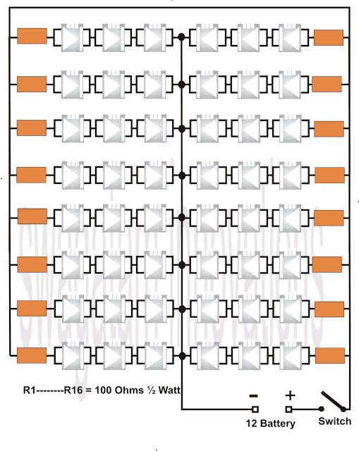 The PCB used must be a glass epoxy type, double sided; the hind side copper of the laminate is not etched and is used as a heatsink for absorbing heat from the LEDs and dissipating it in the air.
Using a Single 10 watt LED
If you thing the above discussed method is too laborious, then you can opt for a single 10 watt LED for enhancing your car headlights with low consumption LED lights. The following image shows how a 10 watt LED actually looks like: The two fins across the sides are the two terminals which will connect with the 12V supply from the car.
Not to mention each of these LEDs on the headlights must incorporate a current control circuit in order to ensure a safe and an optimal illumination, as shown below.
The two fins across the sides are the two terminals which will connect with the 12V supply from the car.
Not to mention each of these LEDs on the headlights must incorporate a current control circuit in order to ensure a safe and an optimal illumination, as shown below.
 R2 is the current sensing resistor and could be calculated as discussed in the below sections.
I have already posted a couple of LED current limiter circuits which you can study through the following links, and implement those in between the LED lamp and the 2V supply from the battery:
Current Limiter using LM338
Current Limiter using Transistors
Any of the above concepts can be applied for protecting the 10 watt car headlight LED lamps from over current or a thermal runaway situation.
However make sure the LEDs are mounted over well calculated heatsink, which could be a round finned type as shown below, this may be mounted behind the headlight box:
R2 is the current sensing resistor and could be calculated as discussed in the below sections.
I have already posted a couple of LED current limiter circuits which you can study through the following links, and implement those in between the LED lamp and the 2V supply from the battery:
Current Limiter using LM338
Current Limiter using Transistors
Any of the above concepts can be applied for protecting the 10 watt car headlight LED lamps from over current or a thermal runaway situation.
However make sure the LEDs are mounted over well calculated heatsink, which could be a round finned type as shown below, this may be mounted behind the headlight box:
Using other Forms of LEDs
If you wish to use any other form of LED having different specification than the above, you can definitely do that by calculating the resistor values appropriately by using the formula: Resistor = Supply voltage - Total Forward V spec of the LED series / LED current For example suppose you would want to make a headlight lamp using 1 watt, 3.3V 350mA LEDs, and your supply voltage is 12V from your car battery, in that case the above formula could be calculated in the following manner: Consider each string has 3 LEDs in series: R = 12 - (3.3 x 3) / 0.35 = 6 Ohm o it is 6 ohms resistor that you would need to put in series with each of the LED strings having 3 LEDs in series. And what about the resistor wattage? For evaluating wattage simply multiply the difference between the supply and LED total voltage drop with the LEd current, therefore for the above case we get: Wattage = 12 - (3.3 x 3) x 0.35 = 3.46 wattage, the nearest safer value is 4 watts. In this way you can use any desired LED for your car headlight by suitably calculating the series current limiting resistor.Adding a PWM Intensity Control
One added advantage of a LED based car headlight is that it can be facilitated with a PWM intensity control, which will not only enable the user to vary the intensity of the car headlight as desired, but also save precious battery power. The following image shows a simple IC 555 PWM control that can be used for the mentioned purpose very easily and effectively.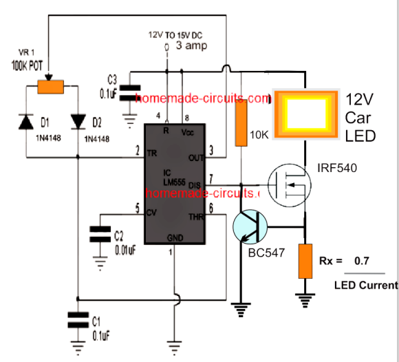 The above design also features a current controller stage which ensures that the LED can never consume more that the rated current and thus work safely under all circumstances.
The resistor Rx must be appropriately calculated depending on the maximum current rating of the LED.
The MOSFET must be mounted on a suitable heatsink to ensure optimal performance from the LED.
Caution: When high wattage LEDs are used always make sure to add a specialized current limiter stage in between the supply input and the LED module, as already explained in the previous paragraphs of this articles.
The above design also features a current controller stage which ensures that the LED can never consume more that the rated current and thus work safely under all circumstances.
The resistor Rx must be appropriately calculated depending on the maximum current rating of the LED.
The MOSFET must be mounted on a suitable heatsink to ensure optimal performance from the LED.
Caution: When high wattage LEDs are used always make sure to add a specialized current limiter stage in between the supply input and the LED module, as already explained in the previous paragraphs of this articles.
Vehicle Immobilizer Circuit Explained
If you own a car and still havenˇŻt incorporated any security system in it or perhaps your old security system is out of order, you can quickly opt for a cheap yet effective security option for your car or any vehicle by installing the proposed circuit. It will cost you not more than a dollar.Circuit Operation:
The circuit can be easily built over a small piece of vero-board by soldering all the components with reference to th shown circuit diagram. After making the simple vehicle immobilizer circuit and housing it appropriately, the unit can be integrated to your vehicles ignition for the required immobilizing actions. LetˇŻs understand the circuit with the following points: Referring to the above simple cheap vehicle immobilizer circuit, we can see that the whole circuit is fundamentally comprised of only a single passive component a high voltage capacitor (10 uF/400V).
As we all know capacitors have the property of grounding any signal that is made up of some kind of frequency, or rather a capacitor will always allow an AC to pass through it.
This property is well exploited here to get the required security feature from the proposed circuit.
All vehicle system primarily utilize their ignition system for starting and for sustaining their engine movements.
Thus the ignition system becomes the heart of the vehicles as far as their working is concerned.
The ignition system works by igniting a fuel mixture inside the ignition chamber through consistent high voltage arcing.
This high voltage arcing is generated from the ignition coil.
Therefore, finally we know that itˇŻs the high voltage arcing that needs to be inhibited to stop the vehicle or for making it completely immobilized.
By introducing a high voltage capacitor across the main ignition high voltage source and ground, we can easily terminate the passage of the high voltage pulses to the spark plugs and completely disable the ignition process.
As shown in the figure this is simply done by connecting the capacitor leads to the relevant points.
However if you wanted to override the system you could easily do it by disconnecting the capacitor from the system, simply by activating a hidden switch.
This switch can be placed somewhere inside the bonnet or in some hidden place that would be known only to you.
For the installation of the entire wiring, you can take the help of a professional cat electrician.
Referring to the above simple cheap vehicle immobilizer circuit, we can see that the whole circuit is fundamentally comprised of only a single passive component a high voltage capacitor (10 uF/400V).
As we all know capacitors have the property of grounding any signal that is made up of some kind of frequency, or rather a capacitor will always allow an AC to pass through it.
This property is well exploited here to get the required security feature from the proposed circuit.
All vehicle system primarily utilize their ignition system for starting and for sustaining their engine movements.
Thus the ignition system becomes the heart of the vehicles as far as their working is concerned.
The ignition system works by igniting a fuel mixture inside the ignition chamber through consistent high voltage arcing.
This high voltage arcing is generated from the ignition coil.
Therefore, finally we know that itˇŻs the high voltage arcing that needs to be inhibited to stop the vehicle or for making it completely immobilized.
By introducing a high voltage capacitor across the main ignition high voltage source and ground, we can easily terminate the passage of the high voltage pulses to the spark plugs and completely disable the ignition process.
As shown in the figure this is simply done by connecting the capacitor leads to the relevant points.
However if you wanted to override the system you could easily do it by disconnecting the capacitor from the system, simply by activating a hidden switch.
This switch can be placed somewhere inside the bonnet or in some hidden place that would be known only to you.
For the installation of the entire wiring, you can take the help of a professional cat electrician.
Automatic Vehicle Headlight Dipper/Dimmer Circuit
The circuitdescribed herecan be built and used in your vehicle for an automatic dipping and dimming operation of the vehicle headlamps, in response to the intense lights coming from an opposite vehicle headlamps.What's a Dimmer/Dipper in Automobiles
An automobile headlight dimmer/dipper is a circuit which automatically switches the headlight intensities of vehicles arriving from opposite directions in a controlled manner. This prevents the drivers from the blinding glares of the opposite side headlights, and allows the drivers to have proper control of their vehicles, and avoid serious accidents.Why an Automatic Headlight Dimmer/Dipper is so Important in Vehicles
You must have come across this irritating situation while driving at night when you find the headlight lamp focus from an opposite vehicle coming straight to your eyes, making things difficult to assess, and giving rise to a situation of a collision or a possible accident. Incidentally, the driver of the opposite vehicle might be going through the same situation due to the headlight focus from your vehicle. Such situations are normally tackled by using manual dipper switch mechanism, where the driver is prompted to "dip" the focus of his headlight, thus giving the opposite vehicle a chance to adjust his vehicle and also an indication that he too needs to "dip" his vehicle lamps. However, doing the above operation manually, every now and then can become horribly laborious and troublesome, therefore if some kind of automatic system is Incorporated, can help to save this headache of the driver, especially while he is driving in stressful conditions and on dangerous highways.Circuit Operation
The following diagram describes a simple yet effective auto head lamp dipper or dimmer circuit. The transistor is used as a comparator, which compares the preset resistance level and the LDR resistance level with reference to ground.Circuit Diagram
DPDT Relay Connection Diagram with Dipper Bulb
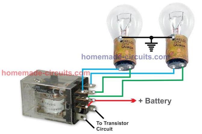
How the LDR Operates
Light falling over the LDR from the headlight of the vehicle coming from the front instantly lowers its resistance and allows more current to flow to the base of the transistor. The transistor conducts and activates the relay, which in turn flips the contacts such that the host vehicle's headlamps gets connected with the dipper filament, changing its intensity. The whole circuit may be enclosed in a small box and installed somewhere near the driver's dashboard area, however the LDR needs to be wired and placed out of the enclosure, in some corner of the wind shield, so that it is able to "see' the light from the opposite vehicles just as the driver would see them.Parts List
R1 = 1K, P1 = 10 K, LDR = With resistance @ around 10 to 50 K when illuminated in daylight (under shade). T1 = BC547, D1 = 1N4007 Relay = coil 400 Ohms, DPDT, 12 volts Making a vehicle dimmer/dipper without Relay The above automatic dipper circuit can be modified for operating with mosfets: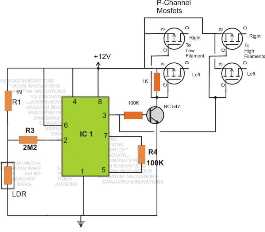
Dimmer Dipper with Cellphone Charger
The following brief explanation was provided by Miss Surya forgettinga better view of theproposedcircuit design of an automobile dimmer/dipper head light switch circuit with an optional cell phone charger circuit for facilitating the charging of a cell phone also on board.Circuit Operation
Here the IC 555 has been used not as a charging indicator rather as a comparator for controlling the dipping action of the head lamps. The use if IC 555 as a charging indicator would have made the circuit unnecessarily complicated, therefore a novel and simpler way is selected for the charging ON indication. The LED connected across the 5 Ohm watt current limiting resistoreffectivelyindicates the charging status of the cell phone and switches OFF the moment the charging process stops. The IC 555 works like a comprartor here, when light falls on the LDR, voltage at PIN#2 rises above the set internal threshold which prompts the IC to change its output PIN#3 voltage from 0 to 12, triggering theconnectedrelay. The relay contacts immediately transfer the positive supply from the "high" filament to the "low" filament of the head lamps, resulting in an instant dipping of the lamp intensity. The LDR must be positioned in such a way that it only receives light rays coming from front of the vehicle, which will be mostly the lights from another vehicle's head lamps.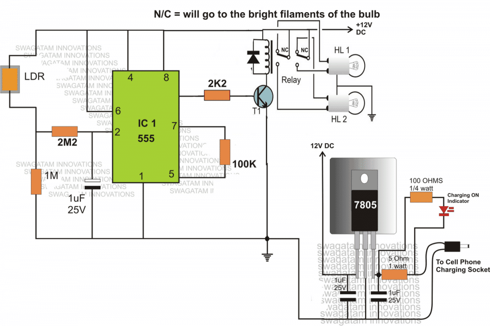
Using Photo Transistor
When photo-transistor Q1 detects the headlights of an approaching vehicle, the circuit gets operational and starts executing the dimming/dipping function. The 22 M resistor, R5, sets the sensitivity to approximately half a foot-candle. A 12 V, 0.3A coil is utilized for the relay. The photo transistorL14C1comes with an one-inch lens with a 10ˇă angle of view and a 1 inchdiameter.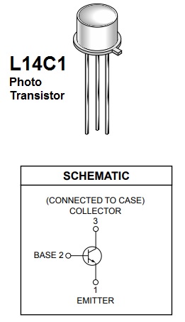
50 Amp Transistor MJ11032, MJ11033 Datasheet, Pinout
If you are looking for high current transistors in the range of 50 amps with a complementary pair, then you can try these Darlington transistors MJ11032 and MJ11033. The MJ11032 transistor is a Darlington NPN power transistor while the MJ11033 is its complementary PNP transistor which is also a Darlington power BJT.Main features
The main features of the MJ11032 MJ11033 complementary Darlington pair transistors are as given below: High DC current gain of 1000 hFE minimum when the collector is operated at 25 amp DC DC current gain capacity may be reduced to 400 hFE, if the collector current rises to 50 amp DC The transistor is able to handle up to 100 amp if the current is in the pulsed manner Internal protection diode are provided to the transistors for protection against inductive transients. The monolithic design of the BJTs also include internal base/emitter shunt resistor to limit maximum base current. The 50 amp transistors are rated to handle junction temperatures as high 200 degrees Celsius Total power dissipation or power handling capacity without heatsink is 300 wattsPinout Diagram
The pinout connections for the 50 amp MJ11032, MJ11033 complementary transistors can be seen in the following images: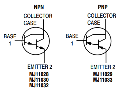
Maximum Tolerable Rating
The maximum tolerable rating of transistors mainly refers to the maximum amount of voltage and current the devices can tolerate at 25 degrees Celsius ambient temperature. The following table shows the maximum tolerable voltage and current limits of the 50 amp transistors MJ11032, MJ11033.LM3524 Datasheet, Pinout Function, How to Use
You may have heard a lot about the outstanding features of the IC LM3524 or the SG3524, however many of you may not be confident regarding how to set up the pinout functioning of these ICs? Or you may be wondering exactly how to use the IC for your specific needs and application designs? The paragraphs below explains everything you wanted to know regarding the working and practical implementation of the IC LM3524.
Main Features
Any seasoned electronic hobbyist will know the importance of this exceptionally versatile PWM controller IC LM3524, which is also popularly available with the prefix SG3524 and its series counterparts like SG3525 etc. The IC LM3524 or the SG3524 both are pin to pin compatible, and feature a host of outstanding onboard features such as :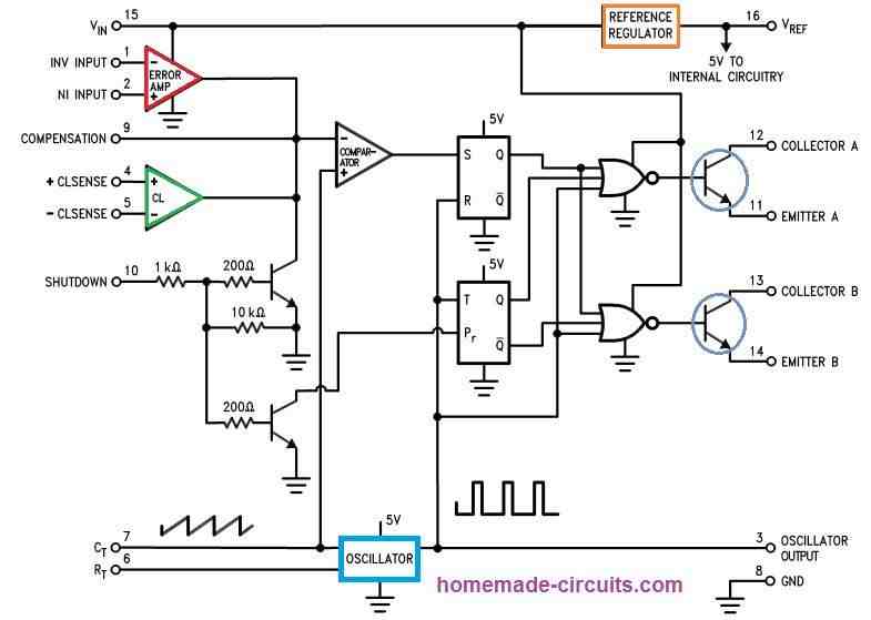 Fixed 5V Reference Source
Precision Totem pole output with guaranteed deadtime.
Inbuilt oscillator with externally configurable RC timing parts.
An integrated Error Amplifier for implementing an automatic output voltage correction
An On-chip Current sense amplifier for implementing an automatic output current control feature
Fixed 5V Reference Source
Precision Totem pole output with guaranteed deadtime.
Inbuilt oscillator with externally configurable RC timing parts.
An integrated Error Amplifier for implementing an automatic output voltage correction
An On-chip Current sense amplifier for implementing an automatic output current control feature
Main Applications
Inverters and Converters Switching Power Supplies Motor Control Robotics Drones Buck Boost Regulators Solar Controllers Battery ChargesAbsolute Maximum Ratings
The absolute maximum ratings refer to the maximum voltage and current parameters the IC LM3524 or the SG3524 are able to tolerate. The absolute maximum range informs us that the IC may burn or get permanently damaged if these parameter limits are exceeded From the above table, the basic facts that we realize is that the LM3524 maximum operating must not be exceeded the 40 V limit.
The maximum current handling capacity of the output pins of the IC is around 200 mA, for LM3524 chip, and is 100 mA for the SG3524 device.
From the above table, the basic facts that we realize is that the LM3524 maximum operating must not be exceeded the 40 V limit.
The maximum current handling capacity of the output pins of the IC is around 200 mA, for LM3524 chip, and is 100 mA for the SG3524 device.
Reference Regulator
The LM3524D features a built-in 5V, 50 mA, short-circuit proof voltage regulator (indicated in orange square). This voltage regulator enables powering of all the internal circuitry of the chip and also works as a fixed external reference. When the input supply voltage to the IC is below 8 V, the 5 V reference pin#15 VREF must be connected directly to pin#15, (VIN), in order to bypass the 5V regulator with the direct DC supply, as shown below. In this situation, the input voltage should not exceed 6V.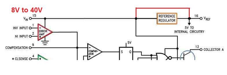 If the input supply is above 6V and 8V, then an external voltage regulator will become necessary, and can be easily implemented through an ordinary 7805 IC
Oscillator
The LM3524D includes an on-board regulated oscillator stage. Its frequency is defined through an external resistor, RT and a complementing external capacitor, CT. The formula for calculating the output frequency using RT and CT is given below: fosc = 1 / RTCT A graph plotted for RT, CT values with reference to their resulting oscillator frequency can be seen in Figure below.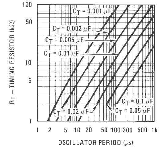 As shown in the following diagram, the pulses from the oscillator's output is used for switching an internal flip-flop stage.
This flip-flop then forwards the PWM data across the outputs of the IC, along with a blanking pulse which is used for shutting down the two outputs during the transition or crossover thresholds.
As shown in the following diagram, the pulses from the oscillator's output is used for switching an internal flip-flop stage.
This flip-flop then forwards the PWM data across the outputs of the IC, along with a blanking pulse which is used for shutting down the two outputs during the transition or crossover thresholds.
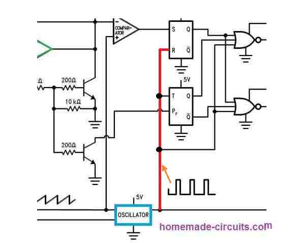 This completely prevents any risk of cross-conduction across the two outputs of the IC.
The blanking pulse is also referred to as the "deadtime" whose width or the pulse OFF time is governed by the value of CT, as indicated in the following graph.
This completely prevents any risk of cross-conduction across the two outputs of the IC.
The blanking pulse is also referred to as the "deadtime" whose width or the pulse OFF time is governed by the value of CT, as indicated in the following graph.
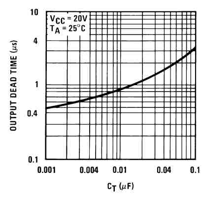 In the above CT vs deadtime graph we can see that as the capacitor CT value increases, the output "deadtime" also increases proportionately.
The value of RT is advised to be within 1.8 k¦¸ to 100 k¦¸, while CT should be within the boundary of 0.001 ¦ĚF to 0.1 ¦ĚF, to ensure normal working of the IC.
In the above CT vs deadtime graph we can see that as the capacitor CT value increases, the output "deadtime" also increases proportionately.
The value of RT is advised to be within 1.8 k¦¸ to 100 k¦¸, while CT should be within the boundary of 0.001 ¦ĚF to 0.1 ¦ĚF, to ensure normal working of the IC.
Synchronization
For applications that require combining more than two LM3524D's to work in a synchronized manner, it is simply implemented by joining all the pin#3's, and joining all the pin#7's with each other to a single common CT capacitor, and keep all pin#6's unconnected, except the one that is associated with the solitary RT resistor. This procedure works nicely only as long as the ICs are not placed greater than 6ˇĺ apart. An alternate synchronization technique may be possible, which can be applied without any restrictions on the IC placement. In this technique one of the LM3524D ICs, is wired up as the master chip, which must include the essential RT/CT timing elements, for setting up the intended correct oscillation frequency. The other LM3524D(s) ICs can be then configured as slave units, and these must each include their individual RT/CT fixed with a 10% longer period than the master. After this, the pin#3's of all the ICs could be interconnected so that the master chip is able to reset all the slave units appropriately.Synchronizing with an External Clock
In case it becomes necessary to synchronize the IC with an external clock source, this could be accomplished by setting up RT/CT in a way that the internal free-running oscillator frequency runs at 10% slower rate than the external clock. Next, the pin#3 of the IC may be integrated with an approximately 3 V frequency derived from the external clock source. Pulse width must be higher than 50 ns to guarantee 100 % synchronization.Error Amplifier
The IC LM3524 includes an error amplifier configured internally like a differential input, transconductance amplifier. Its gain is fixed at a minimal 86 dB either using a feedback or by incorporating an output loading. This output loading is possible either through a fully resistive load or through both a resistive and reactive elements. The error amplifier works like a comparator when it pin#1 and pin#2 are appropriately configured with a feedback signal from the output of the IC. One of the input pins of the error amplifier is referenced to a fixed voltage level (such as 5 V), while the other pin is connected with the feedback loop from the IC output. If this feedback signal tends to rise above the reference voltage level, the error amplifier output becomes active internally, such that it forces the flip-flop to narrow down the output PWM, and thus restore the output voltage and the feedback signal back to normal level The error amplifier's inputs are rated with a common-mode input voltage range between 1.5V¨C5.5V. Meaning, the potential difference between the pin#2 and pin#1 must not be lower than 1.5 V, and higher than 5.5 V. The existing in-built regulator 5 V output could be used here as the reference, for biasing the op amp inputs for ensuring the specified range.How to Connect Pin#9 Compensation
The output of the error op amp amplifier, which internally connects with the pulse width modulator input (pin#9), could be easily overridden with an external adjustable DC, due to its very high impedance i(ZO 5 M¦¸). This means that, an external adjustable DC voltage could be applied to pin#9 in order to overpower the error amplifier actions. The output pins are then forced to work with the PWM determined by the level of this external DC at pin#9. The above implementation could be tested with a unregulated motor speed control in which an adjustable DC voltage is forced to pin#9 of the IC to regulate motor speed by varying this DC voltage. The duty cycle is equivalent to the ratio proportion of each output's ON-time to the oscillator period. If the outputs are connected in parallel it will increase the witnessed duty cycle two fold.How to Connect the Error Amplifier
In the above paragraph we discussed the functioning of the in-built error amplifier op amp of the IC LM3524D, now let's learn how this facilitates the automatic control of the output PWM with reference to an triggering source. The following diagram explains the basic configuration: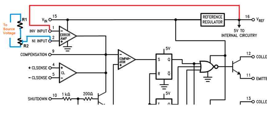 Here we can see that the pin#1 which is the inverting input of the op amp is connected with the IC's in-built +5V reference at pin#15.
Pin#2 of the error amp which is its non-inverting input is wired with a potential divider network using R1, R2, where R2 is a preset.
The ends of the R1/R2 are connected to the trigger source through the which output PWM needs to be regulated.
For example, suppose we want to ensure a fixed output voltage from an LM3524D based inverter circuit, then the this trigger source input could be derived from the output of the inverter transformer, through a bridge network.
R2 preset is adjusted such that the potential at pin#2 is just a shade below the reference +5V at pin#1, when the output voltage is just below the highest unsafe threshold.
This means that, now if the the output voltage tends to rise above the unsafe voltage limit, would proportionately cause the DC at pin#2 to exceed the pin#1, 5V reference level.
As soon as this happens, the error amplifier output would go high, causing the IC's output PWM to narrow down to a level which would force the output voltage to restore back to the specified safe lower limits.
There are other methods also that can be employed for configuring the error amplifier op amp with external sources in order to control output over voltage parameter.
The following diagrams were presented in the datasheet of SG3524.
Here we can see that the pin#1 which is the inverting input of the op amp is connected with the IC's in-built +5V reference at pin#15.
Pin#2 of the error amp which is its non-inverting input is wired with a potential divider network using R1, R2, where R2 is a preset.
The ends of the R1/R2 are connected to the trigger source through the which output PWM needs to be regulated.
For example, suppose we want to ensure a fixed output voltage from an LM3524D based inverter circuit, then the this trigger source input could be derived from the output of the inverter transformer, through a bridge network.
R2 preset is adjusted such that the potential at pin#2 is just a shade below the reference +5V at pin#1, when the output voltage is just below the highest unsafe threshold.
This means that, now if the the output voltage tends to rise above the unsafe voltage limit, would proportionately cause the DC at pin#2 to exceed the pin#1, 5V reference level.
As soon as this happens, the error amplifier output would go high, causing the IC's output PWM to narrow down to a level which would force the output voltage to restore back to the specified safe lower limits.
There are other methods also that can be employed for configuring the error amplifier op amp with external sources in order to control output over voltage parameter.
The following diagrams were presented in the datasheet of SG3524.
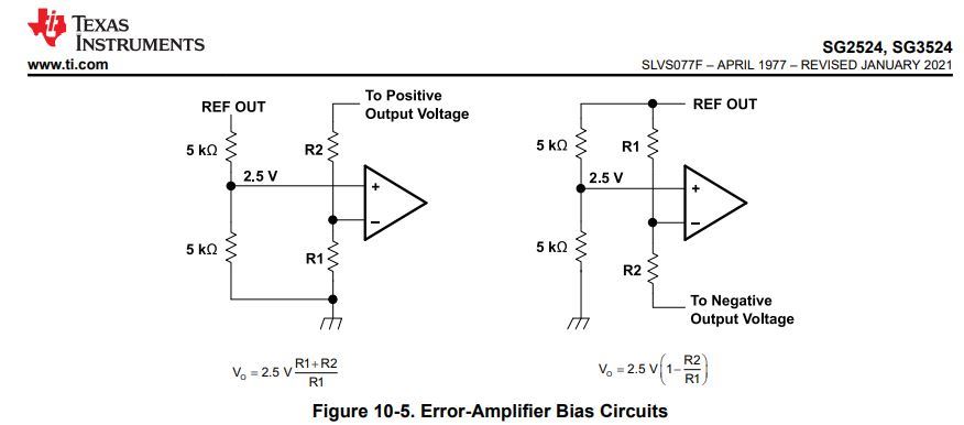
Current Limiting
The purpose of the current limit amplifier is to overpower the error amplifier's output, so that it now controls the pulse width of the IC. When the CL op amp of the IC is used for the current limiting actions, a detection of an over-current will enable the op amp output to reduce the output PWM by as much as 25%. The over-current just needs to be translated into a 200 mV potential between the +CL and CL sense terminals. If this sense voltage increases by approximately 5% might force the output PWM to go down to as low as 0% duty cycle. However, one must make sure that the sensing potential across the +CL and CL remains within the limits of 0.7V and +1.0V, input common-mode range.How to Implement Current Control
The current limiting feature for the above implementation can be easily achieved through a sense resistor as shown below. The reliability of this current limiting feature depends on how accurate the sensing resistor is, and also by a tiny offset current, normally 100 ¦ĚA, passing from +CL to CL.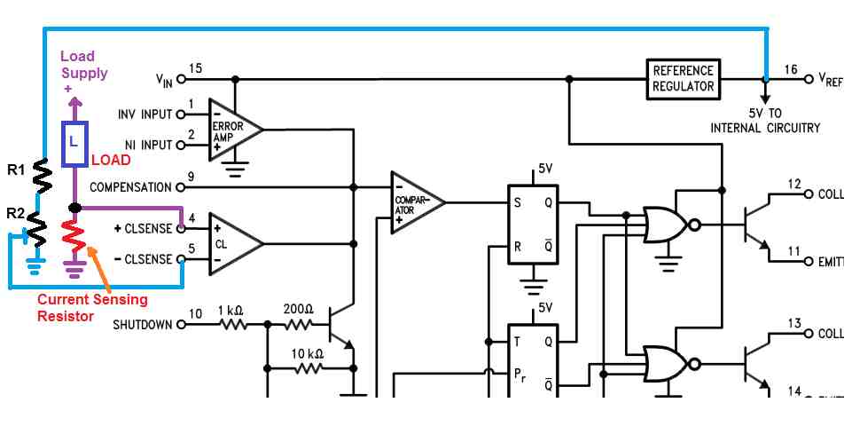 In the above figure we can see the standard way of configuring the current sense (CL) op amp of the LM3524D IC.
Here, too the reference voltage is acquired from the existing 5 V supply at pin#15 VREF of the IC.
This 5 V refernce is applied to the inverting input of the CL op amp through a resistive divider network.
The non-inverting input pin +CL is rigged between the load and a series connected current sensing resistor.
The preset R2 is adjusted such that the reference is dropped to a level that is just a few millivolts higher than the voltage drop expected to develop across the current sensing resistor, during an over load or over current conditions.
Normally, the preset is set such that the -CL pin gets around 0.4 V, which means, the voltage across the current sensing resistor must rise to around 0.6 V to trigger the op amp for the required PWM control of the output.
Therefore, the sensing resistor could be calculated as RS = 0.6 / Max Current Limit.
The current sensing can be also configured in the following simple manner, without depending on the 5 V reference input:
In the above figure we can see the standard way of configuring the current sense (CL) op amp of the LM3524D IC.
Here, too the reference voltage is acquired from the existing 5 V supply at pin#15 VREF of the IC.
This 5 V refernce is applied to the inverting input of the CL op amp through a resistive divider network.
The non-inverting input pin +CL is rigged between the load and a series connected current sensing resistor.
The preset R2 is adjusted such that the reference is dropped to a level that is just a few millivolts higher than the voltage drop expected to develop across the current sensing resistor, during an over load or over current conditions.
Normally, the preset is set such that the -CL pin gets around 0.4 V, which means, the voltage across the current sensing resistor must rise to around 0.6 V to trigger the op amp for the required PWM control of the output.
Therefore, the sensing resistor could be calculated as RS = 0.6 / Max Current Limit.
The current sensing can be also configured in the following simple manner, without depending on the 5 V reference input:
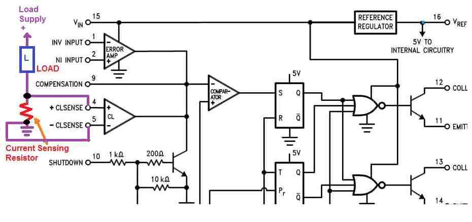 The sensing resistor must be calculated to ensure that the over current situation creates a voltage difference of not more than 0.5 V or 1 V, to keep the resistor value as small as possible.
Remember, the "LOAD" indicated in the above diagrams are supposed to be associated with the output of the IC.
The sensing resistor must be calculated to ensure that the over current situation creates a voltage difference of not more than 0.5 V or 1 V, to keep the resistor value as small as possible.
Remember, the "LOAD" indicated in the above diagrams are supposed to be associated with the output of the IC.
Output Stages
The IC LM3524D outputs are internally configured with NPN transistors, with open collectors and emitters. The open collector/emitter allows the user with greater diversity and options to configure the output pins in many different ways, depending on individual specifications. These outputs are designed to handle a maximum current of 200 mA. The internal transistors associated with the output pins are switched with a 180ˇă out of phase current and voltage. For Push-Pull Output Applications: For configure the output pins of the SG3524 IC, or the LM3524 IC, you can implement any one of the following designs, both will give identical response for driving the output power transistors in push-pull manner.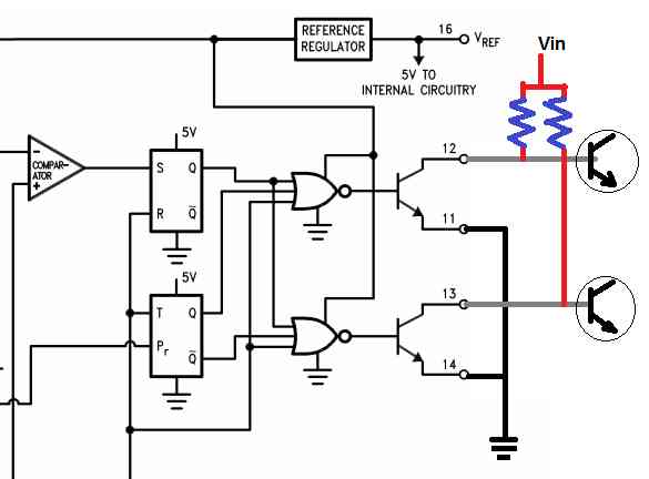 In the above configuration the IC's internal transistors are configured with the output power transistors as common base amplifier, which enables an alternate push-pull conduction of the output transistors and the load.
This set up can be used in push-pull 12 V to 220 V PWM inverter applications.
In the above configuration the IC's internal transistors are configured with the output power transistors as common base amplifier, which enables an alternate push-pull conduction of the output transistors and the load.
This set up can be used in push-pull 12 V to 220 V PWM inverter applications.
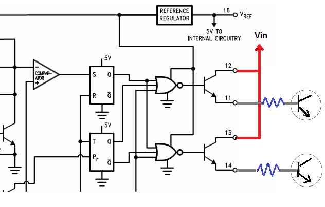 The second LM3524 output configuration will also deliver a push pull action on the output load and the transistors, however, here the IC's internal transistors as emitter-followers, which ultimately work like Darlington pairs wit the output power transistors enabling a high gain and current push pull conduction of the transistors and the load.
Again, this set up also becomes for constructing power inverters.
For Single Ended Applications: For single ended output configurations, where the output power transistor and the load is supposed to work with simple ON/OFF switching, the following set ups could be employed:
The second LM3524 output configuration will also deliver a push pull action on the output load and the transistors, however, here the IC's internal transistors as emitter-followers, which ultimately work like Darlington pairs wit the output power transistors enabling a high gain and current push pull conduction of the transistors and the load.
Again, this set up also becomes for constructing power inverters.
For Single Ended Applications: For single ended output configurations, where the output power transistor and the load is supposed to work with simple ON/OFF switching, the following set ups could be employed:
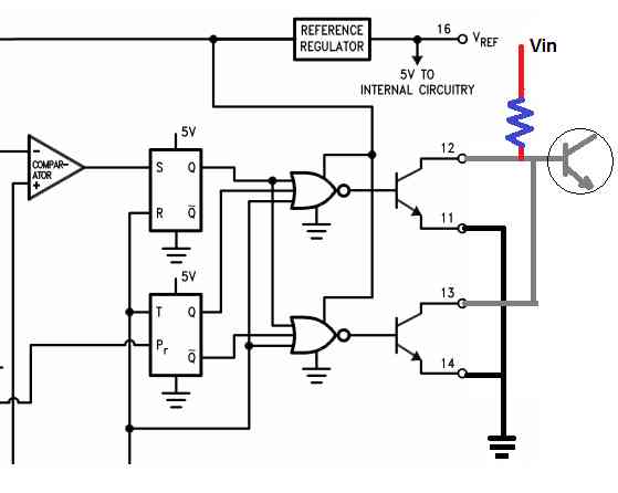 In the above set up the internal transistors can be seen joined in parallel and work as logic inverters for the load.
When the internal transistors switch ON, the output transistors and the load switch OFF and vice versa.
In the above set up the internal transistors can be seen joined in parallel and work as logic inverters for the load.
When the internal transistors switch ON, the output transistors and the load switch OFF and vice versa.
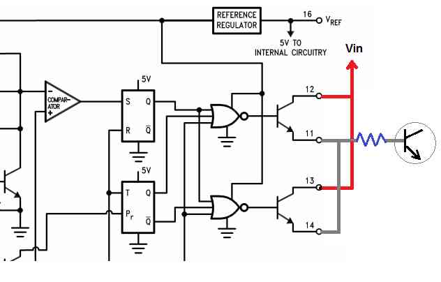 In the next single ended application set up above, the collectors of the internal ttarsistors are connected together with the positive and the emitters are connected together with the output transistor.
Here, the IC driver output transistors work as emitter followers with the output transistors and provide a high gain single ended operation for the load.
In the next single ended application set up above, the collectors of the internal ttarsistors are connected together with the positive and the emitters are connected together with the output transistor.
Here, the IC driver output transistors work as emitter followers with the output transistors and provide a high gain single ended operation for the load.
Wrapping Up
In the above posts we comprehensively learned how the LM3524 and the SG3524 ICs work, their pinout functioning and the how to connect these ICs for practical applications. We understood that these ICs are specifically designed as power regulators, and can be ideally implemented in power supply applications, with enhanced features such as automatic PWM control, automatic output over voltage correction, automatic over current control and constant current output. We also learned how to use and set up the on-chip facilities of the IC such as PWM control, adjustable frequency, automatic dead time, error amplifier and the current sense amplifier. If you have any further questions regarding the SG3524 or the LM3524 IC functions, or pinout details, or a specific application circuit, please feel free to express the same through your comment below:Modifying XL4015 Buck Converter with an Adjustable Current Limiter
The post explains a simple way to enhance the the XL4015 DC to DC buck converter with an adjustable current limiter, which seems to be missing in the original module.About XL4015
The XL4015 is a 180 KHz fixed frequency PWM buck (step-down) DC/DC converter, specially designed for operating a 5 V, 5 Amp load with good efficiency, minimal ripple and exceptional line and load regulation. Built using very few number of additional parts, the regulator module is easy to work with and consist of built-in frequency compensation along with a fixed-frequency oscillator.
The PWM control circuit features adjustable duty ratio at a constant rate from 0 to 100%.
The IC XL4015 also features an in-built over-current protection functionality.
When a short circuit is detected at the output, the operating frequency is instantly lowered from 180 KHz to 48 KHz, causing an immediate drop in the output voltage and current.
The chip has a fully integrated compensation block, without depending on any external components.
Built using very few number of additional parts, the regulator module is easy to work with and consist of built-in frequency compensation along with a fixed-frequency oscillator.
The PWM control circuit features adjustable duty ratio at a constant rate from 0 to 100%.
The IC XL4015 also features an in-built over-current protection functionality.
When a short circuit is detected at the output, the operating frequency is instantly lowered from 180 KHz to 48 KHz, causing an immediate drop in the output voltage and current.
The chip has a fully integrated compensation block, without depending on any external components.
XL4015 IC Main Features
Broad 8V to 36V Input Voltage Range Output voltage is Adjustable from 1.25V to 32V Maximum Duty Cycle can be as high as 100% Output Drop-Out is merely 0.3V Switching Frequency is fixed at 180 kHz Output current is constant at 5A. In-built Power MOSFETs ensure high voltage/current optimization Operating efficiency is very impressive at 96% Line and load regulation are extremely good IC features an internally controlled thermal shutdown function Likewise it also features an in-built current limit function Needless to say, the chip also includes an output short protection feature.Major Disadvantage
Although the XL4015 module is loaded with many excellent features a buck converter needs to have, it lacks one major facility. The module has no arrangement for adjusting the output current to preferred levels, as per the load specifications. So if you want to charge a Li-Ion battery with a XL4015 module, say at 2 amp rate, you won't be able to do that, due to the above mentioned drawback. Similarly, if you wanted to drive a 3.3 V LED at 3 amp maximum current rate, you'd be disappointed likewise, since the module is rated at a fixed 5 amp current.How XL4015 Works
The basic working schmetaic of the XL4015 buck converter is shown below: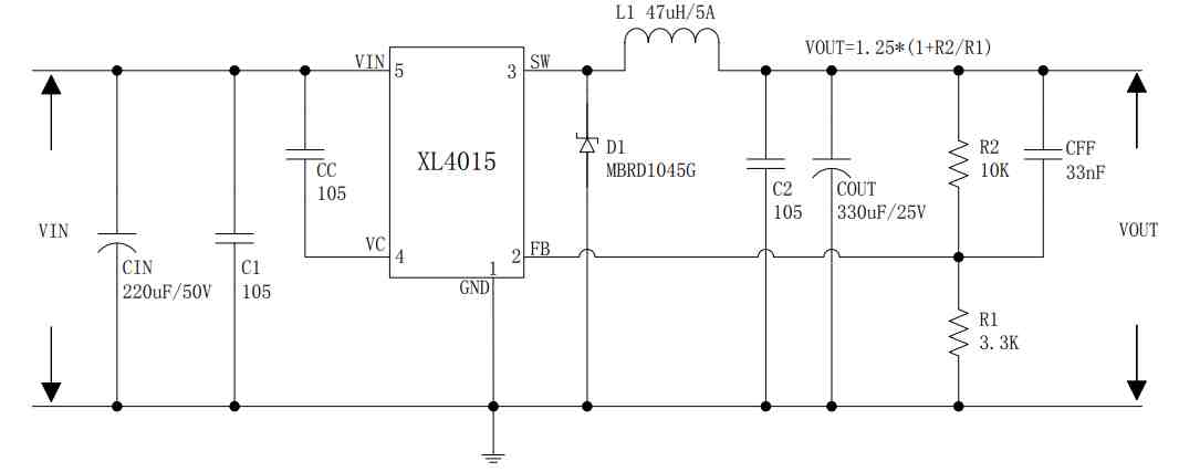 The circuit is configured to produce a fixed 5 V at a constant 5 amp current output in response to a supply input of 8 V to 36 V.
The input power specifications has to be higher than the output power, meaning the input supply wattage capacity must be higher than 5 V x 5 A = 25 W.
Therefore, if an input supply of 36 V is used, then the input current should be higher than 25 / 36 = 0.7 Amps.
If 8 V is used then the input current may be higher than 25 / 8 = 3 Amps, and so forth.
The internal circuitry of the IC XL4015 consists of the basic elements such as an oscillator and an error amp.
The well calculated and controlled 180 kHz oscillator frequency is generated at pin3 (SW) for feeding the external buck converter configuration consisting of the diode, inductor, and the capacitor.
This enables the buck stage to process the input supply to a precise 5 V, 5 A output.
The pin2 (FB) functions as the input for the error amp feedback.
A minimum of 1.25 V input at this pinout is enough to begin the shut down process for the IC.
This pinout can be seen configured with a potential divider R1, R2, which ensures that the output voltage can never go beyond the 5 V range, which then causes a voltage higher than 1.25 V to develop at the FB pin initiating the shut down process for the IC, thereby preventing the output from crossing the 5 V level.
This also implies that the output voltage could be adjusted to other voltage levels, such as 12 V or 15 V, by suitably varying the R1/R2 feedback divider values.
The R1/R2 can be also fixed using the following formula, for getting the desired output voltage:
Vout=1.25 x (1+R2/R1)
The circuit is configured to produce a fixed 5 V at a constant 5 amp current output in response to a supply input of 8 V to 36 V.
The input power specifications has to be higher than the output power, meaning the input supply wattage capacity must be higher than 5 V x 5 A = 25 W.
Therefore, if an input supply of 36 V is used, then the input current should be higher than 25 / 36 = 0.7 Amps.
If 8 V is used then the input current may be higher than 25 / 8 = 3 Amps, and so forth.
The internal circuitry of the IC XL4015 consists of the basic elements such as an oscillator and an error amp.
The well calculated and controlled 180 kHz oscillator frequency is generated at pin3 (SW) for feeding the external buck converter configuration consisting of the diode, inductor, and the capacitor.
This enables the buck stage to process the input supply to a precise 5 V, 5 A output.
The pin2 (FB) functions as the input for the error amp feedback.
A minimum of 1.25 V input at this pinout is enough to begin the shut down process for the IC.
This pinout can be seen configured with a potential divider R1, R2, which ensures that the output voltage can never go beyond the 5 V range, which then causes a voltage higher than 1.25 V to develop at the FB pin initiating the shut down process for the IC, thereby preventing the output from crossing the 5 V level.
This also implies that the output voltage could be adjusted to other voltage levels, such as 12 V or 15 V, by suitably varying the R1/R2 feedback divider values.
The R1/R2 can be also fixed using the following formula, for getting the desired output voltage:
Vout=1.25 x (1+R2/R1)
Current Limit Adjust
As we can see from the schematic the XL4015 module does not include a current limiting feature which apparently is a major limitation of the module. However, the module does include a shut down pinout FB that could be configured with an external current limiter circuit, for accomplishing the feature. This could be implemented as indicated in the following diagram: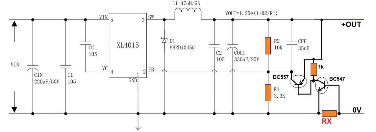 The RX may be calculated using Ohm's law:
RX = 0.2 / Current Limit
Since the two transistors are wired with a very high gain output, a potential difference of just 0.2 V across RX should be enough to trigger the FB pin of the IC and initiate the current limiting action.
As soon the current tends to exceed the desired limit, causes the required minimum potential to develop across RX causing the NPN to conduct, which in turn triggers the PNP BJT hard.
The action supplies the intended the positive DC on the FB pin, initiating the shut-down.
When this happens the output current drops below the set limit, turning OFF the BJTs and restoring the earlier condition, wherein the current yet again begins exceeding the set limit switching ON the BJTs.
The cycle keeps repeating, ensuring the current always remains within the set limit.
With this arrangement, the XL4015 becomes equipped with the very useful adjustable output current limit feature.
The RX may be calculated using Ohm's law:
RX = 0.2 / Current Limit
Since the two transistors are wired with a very high gain output, a potential difference of just 0.2 V across RX should be enough to trigger the FB pin of the IC and initiate the current limiting action.
As soon the current tends to exceed the desired limit, causes the required minimum potential to develop across RX causing the NPN to conduct, which in turn triggers the PNP BJT hard.
The action supplies the intended the positive DC on the FB pin, initiating the shut-down.
When this happens the output current drops below the set limit, turning OFF the BJTs and restoring the earlier condition, wherein the current yet again begins exceeding the set limit switching ON the BJTs.
The cycle keeps repeating, ensuring the current always remains within the set limit.
With this arrangement, the XL4015 becomes equipped with the very useful adjustable output current limit feature.
XL4015 Alternative (Equivalent Circuit)
Although, the XL4015 module is easily available from most online stores, the IC is not manufactured by reputed brands, and may be prone to becoming obsolete anytime. Therefore, having an alternative 5 V adjustable buck converter circuit using discrete components appears to be a much better option. The following diagram shows a very efficient 5 V buck converter using the popular TL494 chip: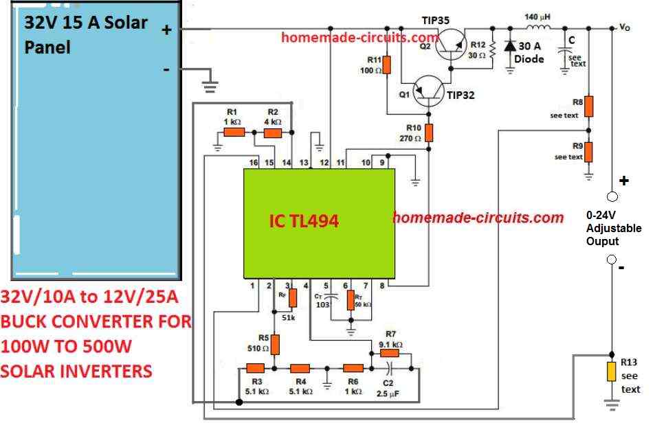 The example above shows a simple yet extremely handy, precision 5 V buck converter equivalent for the XL4015.
Here, it shows a solar inverter buck converter application, which can be adopted for any other desired DC to DC converter purpose.
The use of TL494 ensures that the design will not get obsolete easily and the replacement for the IC will be readily accessible whenever required.
Here too, an error amp feedback loop determines the output current by setting up the potential divider network built around R8/R9.
The current can be adjusted by tweaking the R13 resistor appropriately.
R13 = 0.2/Max Current Limit
Another great advantage of using the above discretely built buck converter is the output current level, which is not limited to 5 amps, rather could be upgraded to much higher levels simply by upgrading the transistors, the inductor wire thickness and the R13 resistor value.
The example above shows a simple yet extremely handy, precision 5 V buck converter equivalent for the XL4015.
Here, it shows a solar inverter buck converter application, which can be adopted for any other desired DC to DC converter purpose.
The use of TL494 ensures that the design will not get obsolete easily and the replacement for the IC will be readily accessible whenever required.
Here too, an error amp feedback loop determines the output current by setting up the potential divider network built around R8/R9.
The current can be adjusted by tweaking the R13 resistor appropriately.
R13 = 0.2/Max Current Limit
Another great advantage of using the above discretely built buck converter is the output current level, which is not limited to 5 amps, rather could be upgraded to much higher levels simply by upgrading the transistors, the inductor wire thickness and the R13 resistor value.
IC 723 Voltage Regulator ¨C Working, Application Circuit
In this post we will learn the main electrical features, pinout specifications, datasheet, and application circuit of the IC 723. The IC 723 is a general purpose, extremely versatile voltage regulator IC, which can be used for making various types of regulated power supplies such as: Positive Voltage Regulator Negative Voltage Regulator Switching Regulator Foldback Current LimiterMain Features
The minimum voltage that can be achieved from IC 723 Regulator Circuit is 2 V, and the maximum is around 37 V. The peak voltage that can handled by the IC is 50 V in pulsed form, and 40 V is the maximum continuous voltage limit. The maximum output current from this IC is 150 mA which can be upgraded to as high as10 amps through an external series pass transistor integration. The maximum tolerable dissipation of this IC 500 mW, therefore it should be mounted on a suitable heatsink in order to allow optimal performance from the device. Being a linear regulator, the IC 723 needs an input supply that should be at least 3 V higher than the desired output voltage, and the maximum difference between the input and the output voltage should never be allowed to exceed 37 V.ABSOLUTE MAXIMUM RATINGS
Pulse Voltage from V+ to V- (50 ms) = 50V Continuous Voltage from V+ to V- = 40V Input-Output Voltage Differential = 40V Maximum Amplifier Input Voltage (Either Input) = 8.5V Maximum Amplifier Input Voltage (Differential) = 5V Current from Vz 25 mA Current from VREF = 15 mA Internal Power Dissipation Metal Can = 800 mW CDIP = 900 mW PDIP = 660 mW Operating Temperature Range LM723 = -55ˇăC to +150ˇăC Storage Temperature Range Metal Can = -65ˇăC to +150ˇăC P DI P -55ˇăC to +150ˇăC Lead Temperature (Soldering, 4 sec. max.) Hermetic Package = 300ˇăC Plastic Package 260ˇăC ESD Tolerance = 1200V (Human body model, 1.5 k0 in series with 100 pF)Block Diagram
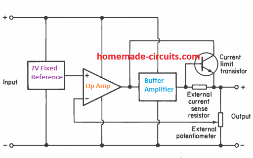 Referring to the above block diagram of the internal circuitry of the IC 723, we can see that the device is internally configured with a highly stable reference voltage at 7 V, created through advanced circuitry using op amp, buffer amplifier, and transistor current limiting stages.
We can also visualize that instead of creating a feedback stabilization by directly connecting the inverting input pin of the op amp with the output pinout of the IC, the inverting pin is rather terminated with a separate individual pinout of the IC.
This inverting pin facilitates integration with the center pin of an external potentiometer, while the other outer pins of the pot is linked with output pinout of the device and ground respectively.
Referring to the above block diagram of the internal circuitry of the IC 723, we can see that the device is internally configured with a highly stable reference voltage at 7 V, created through advanced circuitry using op amp, buffer amplifier, and transistor current limiting stages.
We can also visualize that instead of creating a feedback stabilization by directly connecting the inverting input pin of the op amp with the output pinout of the IC, the inverting pin is rather terminated with a separate individual pinout of the IC.
This inverting pin facilitates integration with the center pin of an external potentiometer, while the other outer pins of the pot is linked with output pinout of the device and ground respectively.
How Potentiometer Adjusts the Output Voltage
The potentiometer can then be used for accurately setting or adjusting the internal reference level of the IC 723, and therefore a stabilized output from the IC in the following manner: Gradually lowering the slider center arm of the pot towards ground interacts with the inverting pin of the opamp to raise the output voltage If the slider of the potentiometer is lowered down its track, instead of causing a stabilization of the output at a potential identical to the reference voltage, the feedback regulates the inverting input of the op amp at the potential developed by the potentiometer. Due to a decreased potential across the potentiometer pins, the output is prompted to increase to a greater potential so that it allows the inverting input to adjust at the correct suitable voltage level. If the pot center wiper arm is moved further down, causes a proportionately higher voltage drop, which prompts the output to climb even higher, causing the output voltage from the IC to become higher. To understand the working better, let's imagine, the center wiper of the pot is moved 2/3rd section in the lower direction. This may cause a feedback voltage to the inverting pin of the internal op amp to be just 1/3rd of the output voltage. This enables the output to become stabilized and constant at a potential that's 3 times higher than the reference voltage and allows an appropriate voltage level to be established on the inverting input of the internal op amp. Therefore this feedback control through a potentiometer facilitates the user to get the intended adjustable output voltage, along with a very high and efficient level of output stabilization.Calculating the Output Voltage using Formula
In case the output needs to be a fixed constant stabilized voltage, the pot could be replaced with a potential divider network using R1 and R2 resistors as shown below: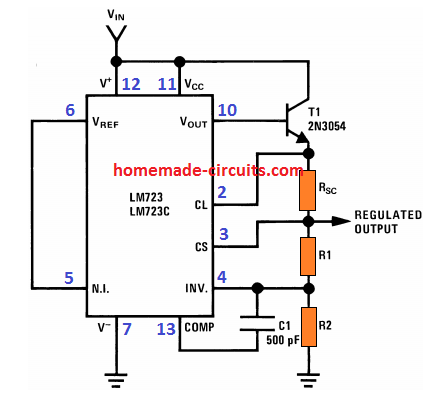 The formula 7 (R1 + R2)/R2 volts determines the desired constant output voltages, where the resistor R1 is connected between the output and the inverting input of the operational amplifier, while the resistor R2 is wired between the inverting input and the negative supply line of the device.
This implies that the reference voltage is directly associated with the non-inverting input of the IC 723 internal op amp.
The number 7 in the formula indicates the reference value, and also minimum output voltage the IC can deliver.
For getting fixed output voltages lower than 7 V, this number in the formula could be replaced by the desired minimum voltage value.
However, this minimum output voltage value for IC 723 cannot be less than 2 V, therefore the formula for fixing 2 V at the output will be: 2 (R1 + R2)/R2
The formula 7 (R1 + R2)/R2 volts determines the desired constant output voltages, where the resistor R1 is connected between the output and the inverting input of the operational amplifier, while the resistor R2 is wired between the inverting input and the negative supply line of the device.
This implies that the reference voltage is directly associated with the non-inverting input of the IC 723 internal op amp.
The number 7 in the formula indicates the reference value, and also minimum output voltage the IC can deliver.
For getting fixed output voltages lower than 7 V, this number in the formula could be replaced by the desired minimum voltage value.
However, this minimum output voltage value for IC 723 cannot be less than 2 V, therefore the formula for fixing 2 V at the output will be: 2 (R1 + R2)/R2
Understanding Current Limit Feature in IC 723
The IC 723 enables the user to get a precisely adjustable current control at the output depending on the load requirement. An array of discretely calculated resistors are employed for sensing and limiting current to the desired levels. The formula for calculating the current limiting resistor is simple, and as given below: Rsc = 0.66 / Maximum CurrentIC 723 Application Circuit
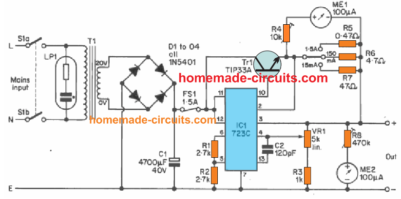 The above application circuit using IC 723 demonstrates a practical example of a useful bench power supply which can deliver an output voltage range from 3.5 V to 20 volts, and a optimum output current of 1.5 amps.
3 step switchable ranges of current limiting, accessible through 15 mA., 150 mA., and 1.5A current ranges (approximately).
The above application circuit using IC 723 demonstrates a practical example of a useful bench power supply which can deliver an output voltage range from 3.5 V to 20 volts, and a optimum output current of 1.5 amps.
3 step switchable ranges of current limiting, accessible through 15 mA., 150 mA., and 1.5A current ranges (approximately).
How it Works
The mains AC input supply is stepped down by the transformer T1 to 20 volts with a maximum current of 2 amps. A full wave rectifier built using by D1 to D4, and a filter capacitor C1 converts the 20 V RMS AC to 28 V DC . As discussed earlier, to be able to achieve the minimum 3.5 volts range at the output it is necessary to associate the reference source of the IC at pin 6 with the non-inverting pin 5 of the IC through a calculated potential divider stage. This is implemented through the network created by R1 and R2 which are selected with identical values. Due to the identical values of the R1/R2 divider, the 7 V reference at pin 6 gets divided by 2 to produce a minimum effective output range of 3.5 volts. The positive supply line from the bridge rectifier is attached to the pin 12, Vcc of the IC, and also with the pin12 buffer amplifier input of the ICI through fuse FS1. Since the power handling specification of the IC alone is quite low, it is not suitable for making a bench power supply directly. Due to this reason output terminal pin10 of the IC 723 is upgraded with an external emitter follower transistor Tr1. This allows the IC output to get upgraded to much higher current depending on the rating of the transistor. However, to ensure this high current is now controlled as per the needs of the output load specs, it is passed through a selectable current limiter stage having 3 switchable current sensing resistors. ME1 is actually a mV meter which is used like an ammeter. It measures the voltage drop across the current sensing resistors and translates it to the amount of current drawn by the load. R4 can be used for calibrating the full scale range in the order of 20 mA., 200 mA., and 2A, as determined by the limiting R5, R6, R7 resistors . This allows a more accurate and efficient reading of the current compared to having a single full scale range of 0 to 2A. VR1 and R3 is used for achieving the desired output voltage, which could be continuously varied from aapproximately 3.5 volts to 23 volts. It is advised to use 1% resistors for R1, R2 and R3 to ensure higher accuracy of the output regulation with minimum errors and deviations. C2 works like a compensation capacitor for the in-built compensation op amp stage of the IC, for complementing enhanced stability to the output. ME2 is configured like a voltmeter for reading the output volts. The associated resistor R8 is used for fine tuning and setting the full scale voltage range of the meter to about 25 volts. A 100 micro amp meter works great for this through a calibration of one division per volt.Parts List
Resistors R1 = 2.7k 1/4 watt 2% or better R2 = 2.7k 1/4 watt 2% or better R3 lk 1/4 watt 2% or better R4 = 10k 0.25 watt preset R5 = 0.47 ohms 2 watt 5% R6 = 4.7 ohms 1/4 watt 5% R7 = 47 ohms 1/4 watt 5% R8 = 470k 0.25 watt preset VR1 = 4.7k or 5k lin. carbon Capacitors C1 = 4700 AF 50V C2 = 120 pF ceramic Disc Semiconductors IC1 = 723C (14 pin DIL) Tr1 = TIP33A D1 to D4 = 1N5402 (4 off) Transformer T1 Standard mains primary, 20 volt 2 amp secondary Switches S1 = D.P.S.T. rotary mains or toggle type S2 = 3 way single pole rotary type capable of switching FS1 = 1.5A 20mm quick blow type Lamp Neon Lamp indicator neon having integral series resistor for use on 240V mains Meters MEI, ME2 100 ¦ĚA. moving coil panel meters (2 off) Miscellaneous Cabinet, output sockets, veroboard, mains cord, wire, 20mm chassis mounting fuseholder, solder etc.Automatic Ambient Light Illumination Adjust
This circuit will automatically adjust the illumination of an incandescent lamp with respect to the available ambient or reference light conditions. This can be ideal for instrument panel lights, bedroom clock lighting and related purposes.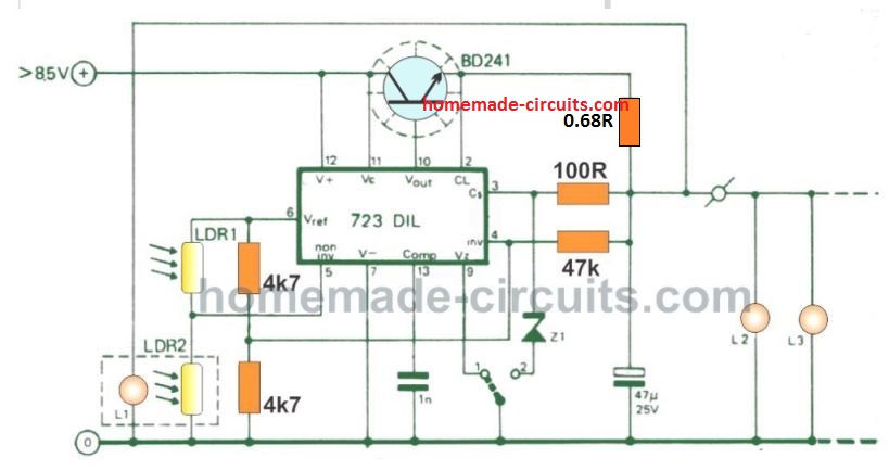 The circuit was created for 6-24 V lamps; the overall current should never go beyond 1 amp.
The ambient light adjuster works as explained in the following points.
LDR 1 scans and detects the ambient light.
LDR 2 is connected optically to an incandescent lamp.
The circuit tries to balance as soon as the two LDR 1 and LDR 2 detect the identical level of illumination.
The circuit should, nevertheless, induce the external lamp(s) to be higher in brightness than the intensity of the ambient light.
Due to this specific reason L1 needs to have rated with lower current than L2, L3 etc; or, if this is not followed, a small screen (small page of paper) could be positioned between the lamp (L1) and the LDR inside the opto-coupler.
The 0.68 ohm resistor restricts the lamp current; the 1 nF capacitor inhibits the circuit from going into oscillating mode.
The circuit should be powered by a minimum of 8.5 volts; lower voltages that this might affect the operation of the IC LM723.
We advise to employ a supply that is higher than the lamp voltage specs by at least 3 volts.
The zener (Z1) is selected to complement the lamp voltage; for 6 V lamps the in-built zener of the IC can be exploited by connecting terminal 9 of the IC to ground.
The circuit was created for 6-24 V lamps; the overall current should never go beyond 1 amp.
The ambient light adjuster works as explained in the following points.
LDR 1 scans and detects the ambient light.
LDR 2 is connected optically to an incandescent lamp.
The circuit tries to balance as soon as the two LDR 1 and LDR 2 detect the identical level of illumination.
The circuit should, nevertheless, induce the external lamp(s) to be higher in brightness than the intensity of the ambient light.
Due to this specific reason L1 needs to have rated with lower current than L2, L3 etc; or, if this is not followed, a small screen (small page of paper) could be positioned between the lamp (L1) and the LDR inside the opto-coupler.
The 0.68 ohm resistor restricts the lamp current; the 1 nF capacitor inhibits the circuit from going into oscillating mode.
The circuit should be powered by a minimum of 8.5 volts; lower voltages that this might affect the operation of the IC LM723.
We advise to employ a supply that is higher than the lamp voltage specs by at least 3 volts.
The zener (Z1) is selected to complement the lamp voltage; for 6 V lamps the in-built zener of the IC can be exploited by connecting terminal 9 of the IC to ground.
Reducing Dissipation in IC 723 Power Supply Circuit
The IC 723 is a quite commonly used IC regulator. For this reason the below circuit, that is designed to minimize power dissipation while the chip is applied through an external transistor, should be really popular.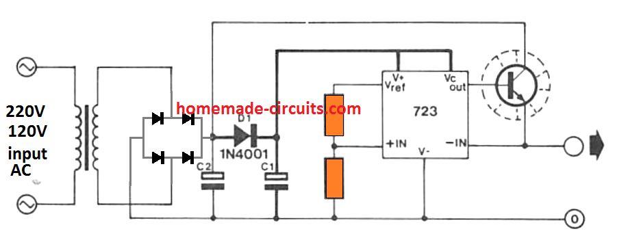 Based on the company datasheets the supply voltage to the IC 723 must strictly be a minimum of 8.5 V to guarantee proper functioning of the chip's in-built 7.5 V reference and also the IC's internal differential amplifier.
While using chip 723 in a low-voltage high-current mode, through an outer series transistor working through the existing power supply lines used by the IC 723, usually leads to abnormal heat dissipation on the series external transistor.
As an illustration, in a 5 V, 2 A supply for TTL approximately 3.5 V could well be dropped over the external transistor and a staggering 7 watt power would be wasted through heat at full load current conditions.
Additionally, the filter capacitor has to be bigger than required to stop the 723 voltage supply from dropping under 8.5 V within the ripple troughs.
Actually the supply voltage to the external transistor is required to be hardly 0.5 V higher than regulated output voltage, to enable its saturation.
The answer is to make use of another 8.5 V supply for your device 723 and a lower voltage supply to the external transistor.
Instead of working with individual transformer windings for the a pair of supplies, the supply source to the IC 723 is basically extracted through a peak rectifier network comprising of D1/C1.
Due to the fact the 723 requires just a tiny current C1 can quickly charge to essentially the peak voltage through the bridge rectifier, 1.414X the transformer RMS voltage minus the drop in voltage across the bridge rectifier.
The transformer voltage specification as a result has to be a minimum of 7 V to allow an 8.5 V source to the IC 723. On the other hand, through appropriate selection of the filter capacitor C2 the ripple around the mains unregulated supply could be implemented in a way that the voltage drops to around 0.5 V higher than the regulated output voltage within the ripple troughs.
The average voltage given to the external pass transistor may consequently be lower than 8.5 V and the heat dissipation shall be tremendously minimized.
The C1 value is dependent upon the highest base current that this 723 has to source to the series output transistor.
As a general guideline allow around 10 uF per mA.
The base current could be determined by dividing the highest output current by the transistor gain or the hFE.
An appropriate number for the mains filter capacitor C2 may be between 1500 uF and 2200 uF per amp of output current.
Based on the company datasheets the supply voltage to the IC 723 must strictly be a minimum of 8.5 V to guarantee proper functioning of the chip's in-built 7.5 V reference and also the IC's internal differential amplifier.
While using chip 723 in a low-voltage high-current mode, through an outer series transistor working through the existing power supply lines used by the IC 723, usually leads to abnormal heat dissipation on the series external transistor.
As an illustration, in a 5 V, 2 A supply for TTL approximately 3.5 V could well be dropped over the external transistor and a staggering 7 watt power would be wasted through heat at full load current conditions.
Additionally, the filter capacitor has to be bigger than required to stop the 723 voltage supply from dropping under 8.5 V within the ripple troughs.
Actually the supply voltage to the external transistor is required to be hardly 0.5 V higher than regulated output voltage, to enable its saturation.
The answer is to make use of another 8.5 V supply for your device 723 and a lower voltage supply to the external transistor.
Instead of working with individual transformer windings for the a pair of supplies, the supply source to the IC 723 is basically extracted through a peak rectifier network comprising of D1/C1.
Due to the fact the 723 requires just a tiny current C1 can quickly charge to essentially the peak voltage through the bridge rectifier, 1.414X the transformer RMS voltage minus the drop in voltage across the bridge rectifier.
The transformer voltage specification as a result has to be a minimum of 7 V to allow an 8.5 V source to the IC 723. On the other hand, through appropriate selection of the filter capacitor C2 the ripple around the mains unregulated supply could be implemented in a way that the voltage drops to around 0.5 V higher than the regulated output voltage within the ripple troughs.
The average voltage given to the external pass transistor may consequently be lower than 8.5 V and the heat dissipation shall be tremendously minimized.
The C1 value is dependent upon the highest base current that this 723 has to source to the series output transistor.
As a general guideline allow around 10 uF per mA.
The base current could be determined by dividing the highest output current by the transistor gain or the hFE.
An appropriate number for the mains filter capacitor C2 may be between 1500 uF and 2200 uF per amp of output current.
LDR Circuits and Working Principle
As the name suggests an LDR or Light Dependent Resistor is a kind of resistor that exhibit a wide range of resistance values depending on the intensity of light incident on its surface. The variation in the resistance range can be anywhere from few hundred ohms to many megaohms. They are also known as photoresistors. The resistance value in an LDR is inversely proportional to the intensity of the light falling on it. Meaning when the light is less, the resistance is more and vice versa.LDR Internal Construction
The following figure shows the internal dissected view of an LDR device wherein we can see the photoconductive substance applied within the zig zag or coiled pattern, embedded over a ceramic insulating base, and with the end points terminated as leads of the device. The pattern ensures maximum contact and interaction between the crystalline photoconductive material and the electrodes separating them. The photoconductive material generally consists of cadmium sulfide (CdS) or cadmium selenide (CdSe).
The type and thickness of the material and width of its deposited layer specify the range of the LDR resistance value and also the amount of watts it can handle.
The two leads of the device is embedded within an an opaque non-conductive base with an insulated transparent coating over the photo-conductive layer.
The schematic symbol of an LDR is shown below:
The photoconductive material generally consists of cadmium sulfide (CdS) or cadmium selenide (CdSe).
The type and thickness of the material and width of its deposited layer specify the range of the LDR resistance value and also the amount of watts it can handle.
The two leads of the device is embedded within an an opaque non-conductive base with an insulated transparent coating over the photo-conductive layer.
The schematic symbol of an LDR is shown below:
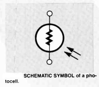
LDR Sizes
The diameter of photocells or LDRs may range from 1/8 inch (3 mm) to above one inch (25 mm). Commonly these are available with diameters of 3/8 inch (10 mm). LDRs smaller than this are generally used where space may be a concern or in SMD based boards. The smaller variants exhibit lower dissipation. You may also find a few variants that are hermetically sealed to ensure reliable working even under harsh and undesirable environments.Comparing LDR Characteristics with Human Eye
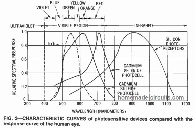 The graph above provides the comparison between the characteristics of photosensitive devices and our eye.
The graph shows the plotting of Relative spectral response against wavelength from 300 to 1200 nanometers (nm).
The human eye characteristic waveform indicated by the dotted bell shaped curve reveals the fact that our eye has enhanced sensitiveness to a relatively narrower band of the electromagnetic spectrum, approximately between 400 and 750 nm.
The peak of the curve has a maximum value in the green light spectrum within the range of 550 nm.
This stretches down into the violet spectrum having a range between 400 to 450 nm on one side.
On the other side this extends into the dark red light region having a range between 700 to 780 nm.
The figure above also reveals exactly why cadmium sulfide (CdS) photocells tend to be the favorites in light-controlled circuit application: the spectral response curve peaks for Cds is near 600 nm, and this specification is quite identical to the range of human eye.
In fact, the cadmium selenide (CdSe) response curve peaks may even extend beyond 720 nm.
The graph above provides the comparison between the characteristics of photosensitive devices and our eye.
The graph shows the plotting of Relative spectral response against wavelength from 300 to 1200 nanometers (nm).
The human eye characteristic waveform indicated by the dotted bell shaped curve reveals the fact that our eye has enhanced sensitiveness to a relatively narrower band of the electromagnetic spectrum, approximately between 400 and 750 nm.
The peak of the curve has a maximum value in the green light spectrum within the range of 550 nm.
This stretches down into the violet spectrum having a range between 400 to 450 nm on one side.
On the other side this extends into the dark red light region having a range between 700 to 780 nm.
The figure above also reveals exactly why cadmium sulfide (CdS) photocells tend to be the favorites in light-controlled circuit application: the spectral response curve peaks for Cds is near 600 nm, and this specification is quite identical to the range of human eye.
In fact, the cadmium selenide (CdSe) response curve peaks may even extend beyond 720 nm.
LDR Resistance Vs Light Graph
That said CdSe may exhibit higher sensitivity to almost the whole range of the visible-light spectrum. In general the characteristic curve of a CdS photocell may be as given in the following figure.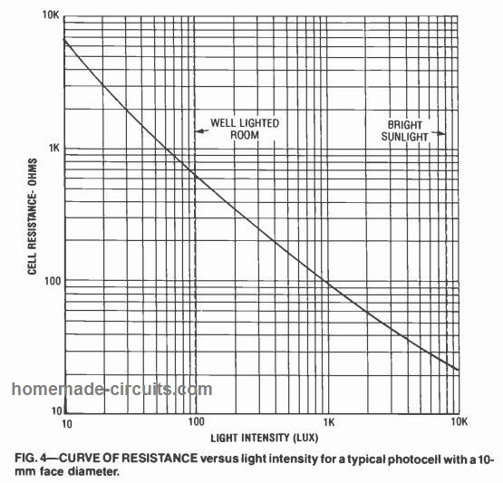 Its resistance in the absence of light can be around 5 megohms, which may drop to around 400 ohms in the presence of light intensity of of 100 lux or a level of light equivalent to an optimally illuminated room, and around 50 ohms when the light intensity is as high as 8000 lux.
typically as obtained from a direct bright sunlight.
The lux is the SI unit for illuminance generated by a luminous flux of 1 lumen evenly spread over a surface of 1 square meter.
The modern photocells or LDRs are adequately rated for power and voltage, at par with normal fixed type resistors.
The power dissipation capacity for a standard LDR could be around 50 and 500 milliwatts, which may depend on the quality of the material used for the detector.
Perhaps the only thing not so good about LDRs or photoresistors is their slow response specification to light changes.
Photocells built with Cadmium-selenide typically exhibit have shorter time constants than cadmium-sulfide photocells (approximately 10 milliseconds in contrast to 100 milliseconds).
You may also find these devices having lower resistances, increased sensitivity, and elevated temperature resistance coefficient.
The main applications in which Photocells are normally implemented are in photographic exposure meters, light and dark activated switches for controlling street lights, and burglar alarms.
In some light activated alarms applications the system is triggered through a light beam interruption.
You may also come across reflection based smoke alarms using photocells.
Its resistance in the absence of light can be around 5 megohms, which may drop to around 400 ohms in the presence of light intensity of of 100 lux or a level of light equivalent to an optimally illuminated room, and around 50 ohms when the light intensity is as high as 8000 lux.
typically as obtained from a direct bright sunlight.
The lux is the SI unit for illuminance generated by a luminous flux of 1 lumen evenly spread over a surface of 1 square meter.
The modern photocells or LDRs are adequately rated for power and voltage, at par with normal fixed type resistors.
The power dissipation capacity for a standard LDR could be around 50 and 500 milliwatts, which may depend on the quality of the material used for the detector.
Perhaps the only thing not so good about LDRs or photoresistors is their slow response specification to light changes.
Photocells built with Cadmium-selenide typically exhibit have shorter time constants than cadmium-sulfide photocells (approximately 10 milliseconds in contrast to 100 milliseconds).
You may also find these devices having lower resistances, increased sensitivity, and elevated temperature resistance coefficient.
The main applications in which Photocells are normally implemented are in photographic exposure meters, light and dark activated switches for controlling street lights, and burglar alarms.
In some light activated alarms applications the system is triggered through a light beam interruption.
You may also come across reflection based smoke alarms using photocells.
LDR Applications Circuits
The following images shows a few of the interesting practical photocell application circuits.Light Activated Relay
 THE TRANSISTOR CAN BE ANY SMALL SIGNAL TYPE SUCH AS BC547
The straightforward LDR circuit indicated in the above figure is built to respond whenever light falls on the LDR installed into a normally dark cavity for example the inside a box or housing.
The photocell R1 and resistor R2 create a potential divider that fixes the base bias of Q1. When it is dark, the photocell exhibits an increased resistance, leading to a zero bias on the base of Q1, due to which, Q1 and the relay RY1 remain switched off.
In case an adequate level of light is detected on the photocell LDR, its resistance level quickly falls to some lower magnitudes.
and a biasing potential is allowed to reach the base of Q1. This switches ON relay RY1, whose contacts is used to control an external circuit or load.
THE TRANSISTOR CAN BE ANY SMALL SIGNAL TYPE SUCH AS BC547
The straightforward LDR circuit indicated in the above figure is built to respond whenever light falls on the LDR installed into a normally dark cavity for example the inside a box or housing.
The photocell R1 and resistor R2 create a potential divider that fixes the base bias of Q1. When it is dark, the photocell exhibits an increased resistance, leading to a zero bias on the base of Q1, due to which, Q1 and the relay RY1 remain switched off.
In case an adequate level of light is detected on the photocell LDR, its resistance level quickly falls to some lower magnitudes.
and a biasing potential is allowed to reach the base of Q1. This switches ON relay RY1, whose contacts is used to control an external circuit or load.
Darkness Activated Relay
The next figure shows how the first circuit can be transformed into a darkness activated relay circuit.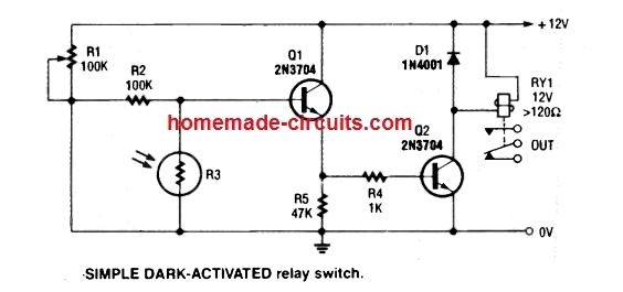 In this example the relay activates in the absence of light on the LDR.
R1 is used for adjusting setting up the sensitivity of the circuit.
Resistor R2 and the photocell R3 work like a voltage divider.
The voltage at the junction of R2 and R3 rises when light falls on the R3, which is buffered by emitter follower Q1. The emitter output of Q1 drives common emitter amplifier Q2 via R4, and correspondingly controls the relay.
In this example the relay activates in the absence of light on the LDR.
R1 is used for adjusting setting up the sensitivity of the circuit.
Resistor R2 and the photocell R3 work like a voltage divider.
The voltage at the junction of R2 and R3 rises when light falls on the R3, which is buffered by emitter follower Q1. The emitter output of Q1 drives common emitter amplifier Q2 via R4, and correspondingly controls the relay.
Precision LDR Light Detector
Although simple, the above LDR circuits are vulnerable to supply voltage changes and also ambient temperature changes. The next diagram shows how the drawback could be tackled through a sensitive-precision light activated circuit that would work without getting affected from voltage or temperature variations.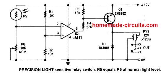 In this circuit the LDR R5, pot R6, and resistors R1 and R2 are configured with each other in the form of a Wheatstone bridge network.
The op amp ICI along with the transistor Q1 and relay RY1 work like a very sensitive balance detecting switch.
The balancing point of the bridge does not get affected, regardless of variations in the supply voltage or the atmospheric temperature.
It is only effected by the changes in the relative values of the components associated with the bridge network.
In this example the LDR R5 and pot R6 constitute one arm of the Wheatstone bridge.
R1 and R2 form the second arm of the bridge.
These two arms act like voltage dividers.
The R1/R2 arm establishes a constant 50% supply voltage to the non-inverting input of the op-amp.
The potential divider formed by the pot and the LDR generates a light dependent variable voltage to the inverting input of the op amp.
The setting up of the circuit, pot R6 is adjusted so that the the potential at the junction of R5 and R6 goes higher than the potential at pin3 when the desired amount of ambient light falls on the LDR.
When this happens the output of the op amp instantly changes state from positive to 0V, switching ON Q1 and the attached relay.
The relay activates and switches OFF the load which could be a lamp.
This op amp based LDR circuit is very precise and will respond even to minute changes in light intensities, which cannot be detected by human eye.
The above op amp design can be easily transformed into a darkness activated relay either by swapping the pin2 and pin3 connections, or by swapping the R5 and R6 positions, as demonstrated below:
In this circuit the LDR R5, pot R6, and resistors R1 and R2 are configured with each other in the form of a Wheatstone bridge network.
The op amp ICI along with the transistor Q1 and relay RY1 work like a very sensitive balance detecting switch.
The balancing point of the bridge does not get affected, regardless of variations in the supply voltage or the atmospheric temperature.
It is only effected by the changes in the relative values of the components associated with the bridge network.
In this example the LDR R5 and pot R6 constitute one arm of the Wheatstone bridge.
R1 and R2 form the second arm of the bridge.
These two arms act like voltage dividers.
The R1/R2 arm establishes a constant 50% supply voltage to the non-inverting input of the op-amp.
The potential divider formed by the pot and the LDR generates a light dependent variable voltage to the inverting input of the op amp.
The setting up of the circuit, pot R6 is adjusted so that the the potential at the junction of R5 and R6 goes higher than the potential at pin3 when the desired amount of ambient light falls on the LDR.
When this happens the output of the op amp instantly changes state from positive to 0V, switching ON Q1 and the attached relay.
The relay activates and switches OFF the load which could be a lamp.
This op amp based LDR circuit is very precise and will respond even to minute changes in light intensities, which cannot be detected by human eye.
The above op amp design can be easily transformed into a darkness activated relay either by swapping the pin2 and pin3 connections, or by swapping the R5 and R6 positions, as demonstrated below:
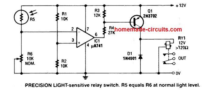
Adding Hysteresis Feature
If required this LDR circuit can be upgraded with a hysteresis feature as shown in the next diagram. This is done by introducing a feedback resistor R5 across the output pin and the pin3 of the IC.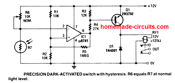 In this design the relay actuates normally when the light intensity goes above the preset level.
However when the light on the LDR drops and decreases than the preset value, it does not switch OFF the relay due to the hysteresis effect.
The relay switches OFF only when the light has dropped to a significantly lower level, which is determined by the value of R5. Lower values will introduce more delay lag (hysteresis), and vice versa.
In this design the relay actuates normally when the light intensity goes above the preset level.
However when the light on the LDR drops and decreases than the preset value, it does not switch OFF the relay due to the hysteresis effect.
The relay switches OFF only when the light has dropped to a significantly lower level, which is determined by the value of R5. Lower values will introduce more delay lag (hysteresis), and vice versa.
Combining Light and Dark Activation Features in One
 This design is a precision light/dark relay is designed by combining the previously explained dark and light switch circuits.
Basically it's a window comparator circuit.
The relay RY1 is switch ON when either the light level on the LDR surpasses one of the pot setting or drops below the other pot setting value.
Pot R1 determines the darkness activation level, while the pot R3 sets the threshold for the light level activation of the relay.
The pot R2 is used for adjusting the supply voltage to the circuit.
The setting up procedure includes adjusting the first preset pot R2 such that approximately half supply voltage is introduced at the LDR R6 and pot R2 junction, when the LDR receives light at some normal intensity level.
Potentiometer R1 is subsequently adjusted such that relay RY1 switches ON as soon as the LDR detects a light below the preferred darkness level.
Likewise, pot R3 can be set up so that the relay RY1 is switched ON at the intended brightness level.
This design is a precision light/dark relay is designed by combining the previously explained dark and light switch circuits.
Basically it's a window comparator circuit.
The relay RY1 is switch ON when either the light level on the LDR surpasses one of the pot setting or drops below the other pot setting value.
Pot R1 determines the darkness activation level, while the pot R3 sets the threshold for the light level activation of the relay.
The pot R2 is used for adjusting the supply voltage to the circuit.
The setting up procedure includes adjusting the first preset pot R2 such that approximately half supply voltage is introduced at the LDR R6 and pot R2 junction, when the LDR receives light at some normal intensity level.
Potentiometer R1 is subsequently adjusted such that relay RY1 switches ON as soon as the LDR detects a light below the preferred darkness level.
Likewise, pot R3 can be set up so that the relay RY1 is switched ON at the intended brightness level.
Light Triggered Alarm Circuit
 Now let's see how an LDR can be applied as a light activated alarm circuit.
The alarm bell or buzzer should be intermittent type meaning sounding with an continuous ON/OFF repetitions, and rated to work with current less than 2 amp.
LDR R3 and resistor R2 make a voltage divider network.
Under low light conditions, the photocell or LDR resistance is high which causes the voltage at R3 and R2 junction insufficient to trigger the attached SCR1 gate.
When the incident light is brighter, the LDR resistance drops to a level sufficient to trigger the SCR, which turns on and activates the alarm.
Oppositely when it gets darker, the LDR resistance increases, switching OFF the SCR and the alarm.
It is important to note that the SCR here turns OFF only because the alarm is an intermittent type which helps to break the latch of the SCR in the absence of a gate current, shutting off the SCR.
Now let's see how an LDR can be applied as a light activated alarm circuit.
The alarm bell or buzzer should be intermittent type meaning sounding with an continuous ON/OFF repetitions, and rated to work with current less than 2 amp.
LDR R3 and resistor R2 make a voltage divider network.
Under low light conditions, the photocell or LDR resistance is high which causes the voltage at R3 and R2 junction insufficient to trigger the attached SCR1 gate.
When the incident light is brighter, the LDR resistance drops to a level sufficient to trigger the SCR, which turns on and activates the alarm.
Oppositely when it gets darker, the LDR resistance increases, switching OFF the SCR and the alarm.
It is important to note that the SCR here turns OFF only because the alarm is an intermittent type which helps to break the latch of the SCR in the absence of a gate current, shutting off the SCR.
Adding a Sensitivity Control
The above SCR LDR alarm circuit is quite crude and feature very low sensitivity, and also lacks a sensitivity control. The next figure below reveals how the design could be enhanced with the mentioned features. Here, the fixed resistor in the previous diagram is replaced with a pot R6, and a buffer BJT stage introduced through Q1 between the gate of the SCR and the LDR output.
Additionally, we can see a push to off switch A1 and R4 parallel to the bell or the alarm device.
This stage allows the user to convert the system into a latching alarm regardless of the intermittent nature of the bell device.
The resistor R4 ensures that even while the bell rings in an self interrupting sound, the latching anode current never breaks and the SCR remains latched once triggered ON.
S1 is used to break the latch manually and shut down the SCR and the alarm.
In order to further enhance the above explained SCR light activated alarm with improved precision, an op amp based triggering can be added as shown below.
The working of the circuit is similar to the previously discussed LDR light activated designs.
Here, the fixed resistor in the previous diagram is replaced with a pot R6, and a buffer BJT stage introduced through Q1 between the gate of the SCR and the LDR output.
Additionally, we can see a push to off switch A1 and R4 parallel to the bell or the alarm device.
This stage allows the user to convert the system into a latching alarm regardless of the intermittent nature of the bell device.
The resistor R4 ensures that even while the bell rings in an self interrupting sound, the latching anode current never breaks and the SCR remains latched once triggered ON.
S1 is used to break the latch manually and shut down the SCR and the alarm.
In order to further enhance the above explained SCR light activated alarm with improved precision, an op amp based triggering can be added as shown below.
The working of the circuit is similar to the previously discussed LDR light activated designs.
LDR Alarm Circuit with Pulsed Tone Output
This is yet another dark activated alarm circuit featuring an integrated a low power 800 Hz pulse generator for driving a loud speaker. Two NOR gates IC1-c and ICI-d are configured as an astable multivibrator for generating a frequency of 800 Hz. This frequency is fed into the speaker via a small signal amplifier using the BJT Q1. The above NOR gate stage is activated only as long as the output of IC 1-b becomes low or 0V. The other two NOR gates IC 1-a and IC1-b are similarly hooked up as astable multivibrator for producing a 6 Hz pulse output and is also enabled only when the gate pin 1 is pulled low or at 0V. Pin1 can be seen rigged with the potential divider junction formed by the LDR R4 and pot R5. It works like this: When the light on the LDR is sufficiently bright the junction potential is high, which keeps both the astable multivibrators disabled, which means no sound output from the loudspeaker. However when the light level drops below the preset level, the R4/R5 junction gets sufficiently lower which activates the 6 Hz astable. This astable now begins gating or switching the 800 Hz astable at 6 Hz rate. This results in a multiplexed 800 Hz tone on the speaker, pulsed at 6 Hz. To add a latching facility to the above design, just add the switch S1, and the resistor R1 as given below:
 For getting a loud, boosted sound from the speaker, the same circuit can be upgraded with an enhanced output transistor stage as shown below:
 In our earlier discussion we learned how an op amp can be used for enhancing the LDR light detection precision.
The same can be applied in the above design to create a super precision pulse tone light detector circuit
In our earlier discussion we learned how an op amp can be used for enhancing the LDR light detection precision.
The same can be applied in the above design to create a super precision pulse tone light detector circuit
LDR Burglar Alarm Circuit
A simple LDR light beam interruption burglar alarm circuit can be seen below.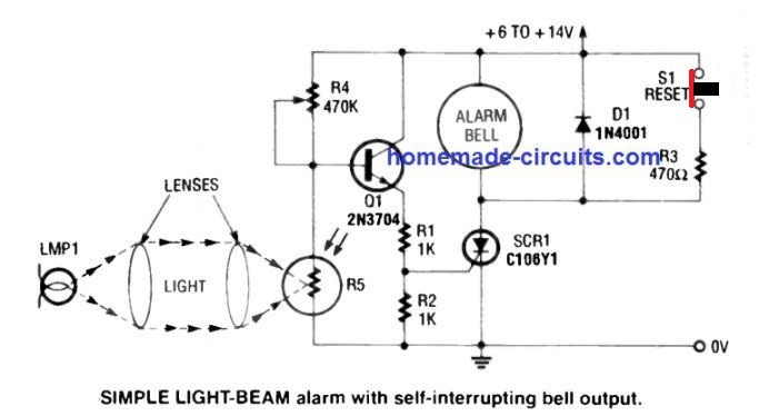 Normally, the photocell or the LDR receives the required amount of light through the installed light beam source.
This can be from a laser beam source also.
This keeps its resistance is low and this also produces insufficiently low potential at the pot R4 and photocell R5 junction.
Due to this the SCR along with bell remain deactivated.
However, in an event the light beam gets interrupted causes the LDR resistance to increase, significantly raising the junction potential of R4 and R5.
This immediately triggers the SCR1 switching ON the alarm bell.
Resistor R3 in series with switch S1 are introduced to enable permanent latching of the alarm.
Normally, the photocell or the LDR receives the required amount of light through the installed light beam source.
This can be from a laser beam source also.
This keeps its resistance is low and this also produces insufficiently low potential at the pot R4 and photocell R5 junction.
Due to this the SCR along with bell remain deactivated.
However, in an event the light beam gets interrupted causes the LDR resistance to increase, significantly raising the junction potential of R4 and R5.
This immediately triggers the SCR1 switching ON the alarm bell.
Resistor R3 in series with switch S1 are introduced to enable permanent latching of the alarm.
Summarizing LDR Specifications
There are many different names by which the LDR (Light Dependent Resistors) are known, which include names such as photoresistor, photocell, photoconductive cell, and photoconductor. Normally the term which is most prevalent and used most popularly in instructions and the datasheets is the name ˇ°photocellˇ±. There are a variety of uses to which the LDR or photoresistor can be applied since these devices are good with their photosensitive property and are also available at low cost as well. Thus, LDR could remain popular for a long period of time and extensively used in applications such as photographic light meters, burglar and smoke detectors, in street lamps to control the lighting, flame detectors, and card readers. The generic term of ˇ°photocellˇ± is used for the Light Dependent Resistors within the general literature.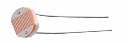
Discovery of LDR
As discussed above, the LDR has remained the favorite among the photocells for a long period of time. The early forms of the photoresistors were manufactured and introduced in the market in the early nineteenth century. This was manufactured through the discovery of the ˇ°seleniumˇŻs photoconductivityˇ± in 1873 by the scientist named Smith. A good range of different photoconductive devices have been manufactured since then. An important progress in this field was made in the early twentieth century, especially in 1920 by the renowned scientist T.W. Case who worked on the phenomenon of photoconductivity and his paper, ˇ°Thalofide Cell- a new photoelectric cellˇ± was published in 1920. During the next two decades in the 1940s and 1930s, a range of other relevant substances were studied for developing photocells which included PbTe, PbS, and PbSe. Further in 1952, the photoconductors the semiconductor version of these devices were developed by Simmons and Rollin using germanium and silicon.Symbol of the Light Dependent Resistors
The circuit symbol which is used for the photoresistor or the light dependent resistor is a combination of the resistor animated to indicate that the photoresistor is light sensitive in nature. The basic symbol of the light dependent resistor consists of a rectangle which symbolizes the resistor's function of the LDR.
The symbol additionally consists of two arrows in the incoming direction.
The same symbol is used to symbolize the sensitivity towards light in the phototransistors and photodiodes.
The symbol of the ˇ°resistor and arrowsˇ± as described above is used by the light dependent resistors in majority of their applications.
But there are few cases where the symbol used by the light dependent resistors depicts the resistor encased within a circle.
This is evident in the case when circuit diagrams are drawn.
But the symbol where there is absence of circle around the resistor is a more common symbol used by the photoresistors.
The basic symbol of the light dependent resistor consists of a rectangle which symbolizes the resistor's function of the LDR.
The symbol additionally consists of two arrows in the incoming direction.
The same symbol is used to symbolize the sensitivity towards light in the phototransistors and photodiodes.
The symbol of the ˇ°resistor and arrowsˇ± as described above is used by the light dependent resistors in majority of their applications.
But there are few cases where the symbol used by the light dependent resistors depicts the resistor encased within a circle.
This is evident in the case when circuit diagrams are drawn.
But the symbol where there is absence of circle around the resistor is a more common symbol used by the photoresistors.
Technical Specifications
The surface of LDR is built with two cadmium sulphide(cds) photoconductive cells having spectral responses comparable to that of the human eye. The resistance of the cells drop linearly as light intensity is increased on its surface. The photoconductor which is placed between the two contacts is used as a main responsive component by the photocell or the photoresistor. The resistance of the photoresistors undergoes a change when there is an exposure of the photoresistor to the light. Photoconductivity: The electron carriers are generated when the photoconductorˇŻs semiconductor materials used absorb the photons, and this results in the mechanism which works behind the light dependent resistors. Although you may find that the materials which are used by the photoresistors are different, they are mostly all semiconductors. When they are used in the form of photoresistors, then these materials act as resistive elements only where there is absence of PN junctions. This results in the device to become entirely passive in nature. The photoresistors or the photoconductors are basically of two types: Intrinsic Photoresistor: The photoconductive material which is used by a specific photoresistor type enables the charge carriers to get excited and jump to the conduction bands from their initial valence bonds respectively. Extrinsic Photoresistor: The photoconductive material which is used by a specific photoresistor type enables the charge carriers to get excited and jump to the conduction bands from their initial valence bonds or impurity respectively. This process requires non-ionized impurity dopants which are also shallow and requires this to take place when light is present. The design of the photocells or extrinsic photoresistors is done specifically considering the long wavelength radiations such as the infra-red radiations in most of the cases. But the designing also considers the fact that any type of thermal generation needs to be avoided since they are required to operate at temperatures which are very relatively low.Basic Structure of LDR
The number of natural methods which are commonly observed for the manufacturing of the photoresistors or the light dependent resistors is very few in number. A resistive material sensitive to light is employed by the light dependent resistors for constant exposure to light. As discussed above, there is a specific section which is processed by the light sensitive resistive material which is required to be in contact with both or one of the ends of the terminals. A semiconductor layer which is active in nature is used in a general structure of a photoresistor or a light dependent resistor and an insulating substrate is further used for depositing the semiconductor layer. In order to provide the semiconductor layer with the conductivity of the required level, the former is doped lightly. Thereafter, terminals are connected appropriately across the two ends. One of the key issues in the basic structure of the light dependent resistor or photocell is its materialˇŻs resistance. The contact area of the resistive material is minimized to ensure that when the device is exposed to the light, it undergoes a change in its resistance efficiently. In order to achieve this state, it is ensured that surrounding area of the contacts is doped heavily which results in the reduction of the resistance in the given area. The shape of the surrounding area of the contact is designed to be mostly in the interdigital pattern or the zig zag form. This enables the maximization of the exposed area along with the reduction in the levels of the spurious resistance which in turn results in the enhancement of the gain by contracting the distance between the two contacts of the photoresistors and making it small. There is also a possibility of the usage of the semiconductor material such as polycrystalline semiconductor depositing it on a substrate. One of the substrates which can be used for this is ceramic. This enables the light dependent resistor to be of low cost.Where Photoresistors are Used
The most attractive point of the light dependent resistor or a photoresistor is that it is of low cost and thus is widely used in a variety of electronic circuit designs. Apart from this their rugged features and simple structure also provides them with an advantage. Although the photoresistor lacks various features which are found in a phototransistor and a photodiode, it is still an ideal choice for a variety of applications. Thus, LDR has been continuously used for a long period of time in a range of applications such as photographic light meters, burglar and smoke detectors, in street lamps to control the lighting, flame detectors, and card readers. The factor which determines the photoresistor properties is the material type which is used and thus the properties can vary accordingly. Some of the materials used by the photoresistors possess constants of very long time. Thus, it is quintessential that the photoresistor type si selected carefully for specific applications or circuits.Wrapping up
Light dependent resistor or LDR is one of the very useful sensing devices which can be implemented in many different ways for processing light intensity. The device is cheaper compared to other light sensors, yet it is able to provide the required services with utmost efficiency. The above discussed LDR circuits are just a few examples which explains the basic mode of using an LDR in practical circuits. The discussed data can be studied and customized in several ways for many interesting applications. Have questions? Feel free to express through the comment box.Triacs ¨C Working and Application Circuits
A triac can be compared to a latching relay. It will instantly switch ON and close as soon as it's triggered, and will remain closed as long as the supply voltage remains above zero volts or the supply polarity is not changed. If the supply is an AC (alternating current), the triac will open during the periods the AC cycle crosses the zero line, but will close and switch ON as soon its re-triggered.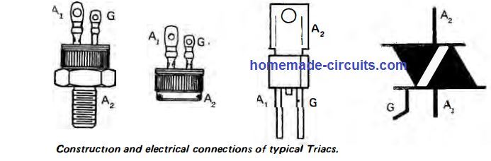
Advantages of Triac as Static Switches
Triacs can be effectively replaced for mechanical switches or relays for controlling loads in AC circuits. Triacs can be configured to switch relatively heavier loads through minimal current triggering. When triacs conduct (close) they do not produce debounce effect, as in mechanical switches. When triacs switch OFF (at AC zero crossing), it does this without producing any transients, due to back EMFs etc. Triacs also eliminate fusing of contacts or arcing issues, and other forms of of wear and tear which are commonly seen in mechanical based electrical switches. Triacs feature a flexible triggering, which allows them to be switched at any given point of the input AC cycle, through a low voltage positive signal across gate and common ground. This triggering voltage could be from any DC source such as a battery or a rectified signal from the AC supply itself. In any case, the triac will go through switch OFF periods whenever each half cycle AC waveform moves through the zero crossing (current) line, as depicted below: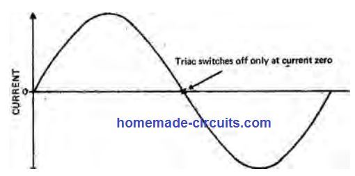
How to Switch-ON a Triac
A triac consists of three terminals: Gate, A1, A2, as shown below: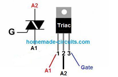 To switch-on a Triac, a gate trigger current must be applied on its gate pin (G).
This causes a gate current to flow across Gate and terminal A1. The gate current could be positive or negative with respect to A1 terminal of the triac.
A1 terminal may be wired in common to the negative VSS line or positive VDD line of the gate control supply.
The following diagram shows the simplified schematic of a Triac and also its internal silicon structure.
To switch-on a Triac, a gate trigger current must be applied on its gate pin (G).
This causes a gate current to flow across Gate and terminal A1. The gate current could be positive or negative with respect to A1 terminal of the triac.
A1 terminal may be wired in common to the negative VSS line or positive VDD line of the gate control supply.
The following diagram shows the simplified schematic of a Triac and also its internal silicon structure.
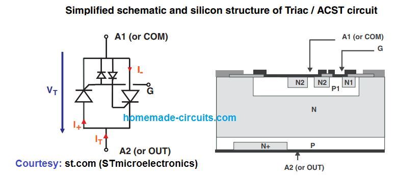 When a triggering current is applied to triac gate, it is switched ON by means of its inbuilt diodes embedded back-to-back between G terminal and and A1 terminal.
These 2 diodes are installed at the P1-N1 and P1-N2 junctions of the triac.
When a triggering current is applied to triac gate, it is switched ON by means of its inbuilt diodes embedded back-to-back between G terminal and and A1 terminal.
These 2 diodes are installed at the P1-N1 and P1-N2 junctions of the triac.
Triac Triggering Quadrants
Triggering of a triac is implemented through four quadrants depending on the polarity of the gate current, as shown below: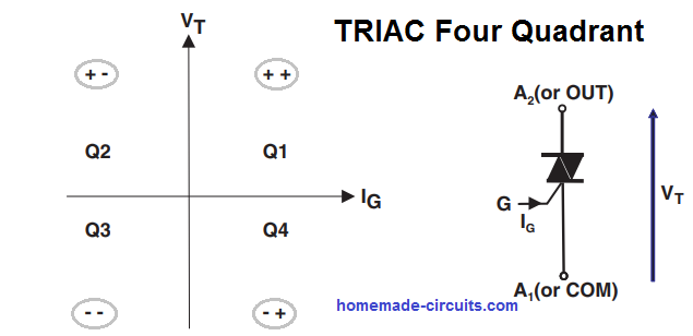 These triggering quadrants can be practically applied depending on the family and the class of the triac, as given below:
 Q2 and Q3 are the recommended triggering quadrants for triacs, since it allows minimal consumption and reliable triggering.
Q4 triggering quadrant is not advised as it calls for a higher gate current.
Q2 and Q3 are the recommended triggering quadrants for triacs, since it allows minimal consumption and reliable triggering.
Q4 triggering quadrant is not advised as it calls for a higher gate current.
Important Triggering Parameters for Triacs
We know that a triac can be used to switch high power AC load across its A1/A2 terminals through a relatively small DC trigger supply at its Gate terminal. While designing a triac control circuit, its gate triggering parameters become crucial. The triggering parameters are: triac gate triggering current IGT, gate triggering voltage VGT, and gate latching current IL. The minimum gate current required to turn on a triac is called gate triggering current IGT. This needs to be applied across the gate and the A1 terminal of the Triac which is common to the gate trigger supply. The gate current should be higher than the value rated for the lowest specified operating temperature. This ensures optimal triggering of the triac under all circumstances. Ideally the IGT value should 2 times higher than the rated value in the datasheet. The trigger voltage applied across the gate and the A1 terminal of a triac is referred to as VGT. It is applied through a resistor which will discuss shortly. The gate current that effectively latches a triac is the latching current and is given as LT. The latching can happen when the load current has reached the LT value, only after this the latching enables even while the gate current is removed. The above parameters are specified at an ambient temperature of 25 ˇăC, and may stat showing variations as this temperature varies. Non-isolated triggering of a triac can be done in two basic modes, the first method is shown below: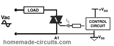 Here, a positive voltage equal to the VDD is applied across the gate and A1 terminal of the triac.
In this configuration we can see that the A1 is also connected to the Vss or the negative line of the gate supply source.
This is important otherwise the triac will never respond.
The second method is by applying a negative voltage to the triac gate as shown below:
Here, a positive voltage equal to the VDD is applied across the gate and A1 terminal of the triac.
In this configuration we can see that the A1 is also connected to the Vss or the negative line of the gate supply source.
This is important otherwise the triac will never respond.
The second method is by applying a negative voltage to the triac gate as shown below:
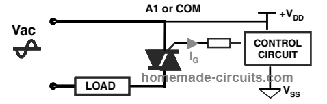 This method is identical to the previous except the polarity.
Since the gate is triggered with a negative voltage, A1 terminal is now joined in common with the VDD line instead of Vss of the gate source voltage.
Again, if this is not done, the triac will fail to respond.
This method is identical to the previous except the polarity.
Since the gate is triggered with a negative voltage, A1 terminal is now joined in common with the VDD line instead of Vss of the gate source voltage.
Again, if this is not done, the triac will fail to respond.
Calculating the Gate Resistor
The gate resistor sets the IGT or the gate current to the triac for the necessary triggering. This current increases as the temperature drops below the specified 25 ˇăC junction temperature. For example if the specified IGT is 10 mA at 25 ˇăC, this may increase up to 15 mA at 0 ˇăC. To ensure that the resistor is able to supply sufficient IGT even at 0 ˇăC, it must be calculated for the maximum available VDD from the source. A recommended value is around 160 to 180 ohms 1/4 watt for a 5V gate VGT. Higher values will also work if your ambient temperature is rather constant. Triggering through External DC or Existing AC: As shown in the following figure, a triac can be switched either through an external DC source such as battery or solar panel, or an AC/DC adapter. Alternatively, it can be also triggered from the existing AC supply itself.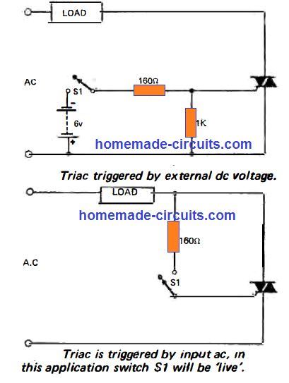 Here, the switch S1 has negligible stress on it since it switches the triac through a resistor causing minimal current to pass through the S1, thus saving it from any sort of wear and tear.
Switching a Triac through a Reed Relay: For switching a triac by a moving object, a magnetic based triggering could be incorporated.
A reed switch and a magnet can be used for such applications, as shown below:
Here, the switch S1 has negligible stress on it since it switches the triac through a resistor causing minimal current to pass through the S1, thus saving it from any sort of wear and tear.
Switching a Triac through a Reed Relay: For switching a triac by a moving object, a magnetic based triggering could be incorporated.
A reed switch and a magnet can be used for such applications, as shown below:
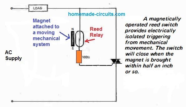 In this application the magnet is attached to the moving object.
Whenever the moving system gets past the reed relay, it triggers the triac into conduction through its attached magnet.
Reed relay can be also used when an electrical isolation is required between the triggering source and the triac, as shown below.
In this application the magnet is attached to the moving object.
Whenever the moving system gets past the reed relay, it triggers the triac into conduction through its attached magnet.
Reed relay can be also used when an electrical isolation is required between the triggering source and the triac, as shown below.
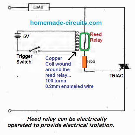 Here, the copper coil of suitable dimension is wound around the reed relay, and the coil terminals are connected to a DC potential via a switch.
Each time the switch is pressed causes an isolated triggering for the triac.
Due to the fact that reed switch relays are designed to withstand millions of ON/OFF operations, this switching system becomes extremely efficient and reliable in the long run.
Another example of isolated triggering of triac can be seen below, here an external AC source is used for switching a triac through an isolation transformer.
Here, the copper coil of suitable dimension is wound around the reed relay, and the coil terminals are connected to a DC potential via a switch.
Each time the switch is pressed causes an isolated triggering for the triac.
Due to the fact that reed switch relays are designed to withstand millions of ON/OFF operations, this switching system becomes extremely efficient and reliable in the long run.
Another example of isolated triggering of triac can be seen below, here an external AC source is used for switching a triac through an isolation transformer.
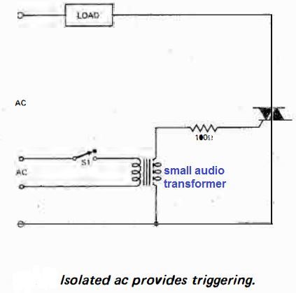 Yet another form of isolated triggering of triacs is shown below using a Photo-cell couplers.
In this method an LED and a photo-cell or photo diode are integrally mounted inside a single package.
These opto couplers are readily available in the market.
Yet another form of isolated triggering of triacs is shown below using a Photo-cell couplers.
In this method an LED and a photo-cell or photo diode are integrally mounted inside a single package.
These opto couplers are readily available in the market.
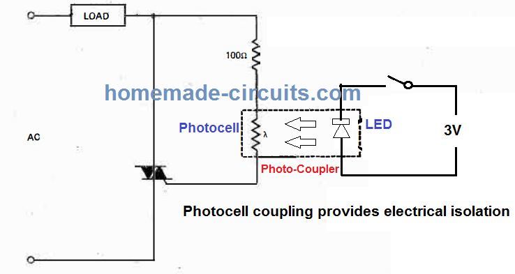 An unusual switching of the triac in the form of off/half-power/ full-power circuit is shown in the diagram below.
To implement 50% less power the diode is switched in series with the triac gate.
This method forces the Triac to switch ON only for the alternate positive AC input half-cycles.
An unusual switching of the triac in the form of off/half-power/ full-power circuit is shown in the diagram below.
To implement 50% less power the diode is switched in series with the triac gate.
This method forces the Triac to switch ON only for the alternate positive AC input half-cycles.
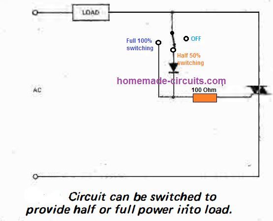 The circuit can be effectively applied for controlling heater loads, or other resistive loads having thermal inertia.
This might not work for lighting control, since the half positive AC cycles frequency will result in an annoying flicker on the lights; likewise, this triggering is not advised for inductive loads such as motors or transformers.
The circuit can be effectively applied for controlling heater loads, or other resistive loads having thermal inertia.
This might not work for lighting control, since the half positive AC cycles frequency will result in an annoying flicker on the lights; likewise, this triggering is not advised for inductive loads such as motors or transformers.
Set Reset Latching Triac Circuit
The following concept shows how a triac can be used for making a set reset latch using a couple push buttons.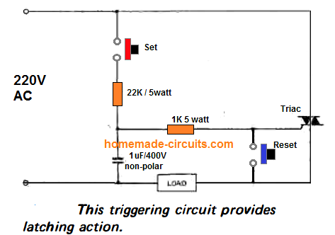 Pressing the set button latches the triac and the load ON, while pressing the reset button beaks the latch.
Triac Delay Timer Circuits
A triac can be set up as a delay timer circuit for switching a load ON or OFF after a set predetermined delay. The first example below shows a triac based delay OFF timer circuit. Initially when powered, the triac will switch ON. In the meantime the 100uF begins charging, and once the threshold is reached the UJT 2N2646 fires, switching ON the SCR C106. The SCR shorts the gate to ground switching OFF the triac. The delay is decided by the 1M setting and the series capacitor value.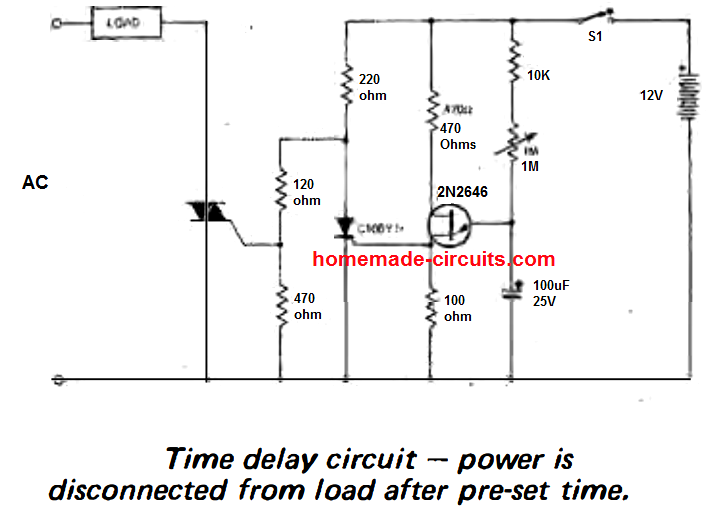 The next circuit represents a delay ON triac timer circuit.
When powered the triac does not respond immediately.
The diac remains switched OFF while the 100uF capacitor charges to its firing threshold.
Once this happens the diac fires and triggers the triac ON.
The delay time depends on the values of 1M and the 100uF.
The next circuit represents a delay ON triac timer circuit.
When powered the triac does not respond immediately.
The diac remains switched OFF while the 100uF capacitor charges to its firing threshold.
Once this happens the diac fires and triggers the triac ON.
The delay time depends on the values of 1M and the 100uF.
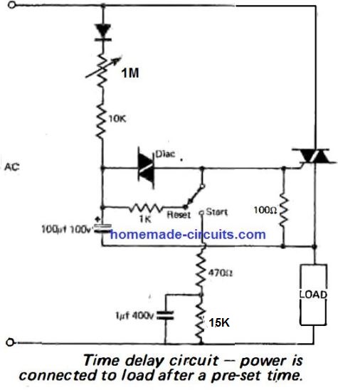 The next circuit is another version of a triac based timer.
When switched ON, the UJT is switched via the 100uF capacitor.
The UJT keeps the SCR switch OFF, depriving the triac from the gate current, and thus the triac also remains switched OFF.
After sometime depending on the adjustment of the 1M preset, the capacitor is fully charged switching OFF the UJT.
The SCR now switches ON, triggering the triac ON, and also the load.
The next circuit is another version of a triac based timer.
When switched ON, the UJT is switched via the 100uF capacitor.
The UJT keeps the SCR switch OFF, depriving the triac from the gate current, and thus the triac also remains switched OFF.
After sometime depending on the adjustment of the 1M preset, the capacitor is fully charged switching OFF the UJT.
The SCR now switches ON, triggering the triac ON, and also the load.
Triac Lamp Flasher Circuit
This triac flasher circuit can be used to flash a standard incandescent lamp with a frequency that may be adjusted between 2 and about 10 Hz. The circuit works by rectifyingthe mains voltage by a 1N4004 diode along with an variable RC network. The moment the electrolytic capacitor charges upto the breakdown voltage of the diac, it i forced to discharge through the diac, which in turn fires the triac, which results in flashing of the connected lamp.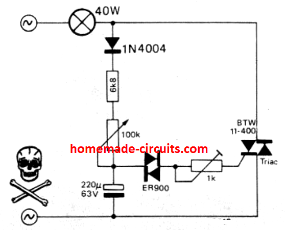 After a delay as set by the 100 k control, the capacitor recharges again to cause a repetition of the flashing cycle.
The 1 k control sets the triac triggering current.
After a delay as set by the 100 k control, the capacitor recharges again to cause a repetition of the flashing cycle.
The 1 k control sets the triac triggering current.
Conclusion
Triac is one of the most versatile components of the electronic family. Triacs can be used for implementing a variety of useful circuit concepts. In the above post we learned about a few simple triac circuit applications, however there are countless ways a triac can be configured and applied for making a desired circuit. In this website I have already posted many triac based circuits which you can refer to for further learning, here's the link to it:Comparator Datasheet Parameters
This post will help you to understand a few of the crucial comparator parameters or specifications which are generally found in comparator IC datasheets. Some of the major parameters that you may come across in the datasheet of a compartaor are: Propagation delay Current consumption Output stage type (open collector/drain or push-pull) Input offset voltage, hysteresis Output current capability Rise and fall time Input common mode voltage range Apart from these you may also find other parameters such as: input bias current, common mode and power supply rejection ratio, sample/hold function, and startup time. Mostly, a single comparator chip will have 5 pins: a couple of pins for power input VCC+,VCC-, two pins for feeding the input signals IN+, IN- and a single output OUT pin. In some ICs there may be an extra pin for the standby function.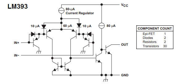 From our earlier discussions we know that when VIN(+) > VIN(-), the output is in high state, if VIN(+) < VIN(-), the output is in low state.
In other words when the non-inverting input (+) has a higher level of voltage than the inverting input (-), the output transistor inside the compartaor will be switched OFF.
Meaning its collector pin will show an open condition.
Since this collector pin is supposed to be linked with the positive supply rail through a pull-up resistor, allows the collector to have a positive or a high logic output in this situation.
From our earlier discussions we know that when VIN(+) > VIN(-), the output is in high state, if VIN(+) < VIN(-), the output is in low state.
In other words when the non-inverting input (+) has a higher level of voltage than the inverting input (-), the output transistor inside the compartaor will be switched OFF.
Meaning its collector pin will show an open condition.
Since this collector pin is supposed to be linked with the positive supply rail through a pull-up resistor, allows the collector to have a positive or a high logic output in this situation.
Output stage type (open collector/drain or push-pull)
With regards to the output pin configuration, comparators are of two types: push-pull and open collector (open drain). In a push-pull configuration, the load may be directly connected between the collector pin of the compartaor and the positive line which allows the load to be switched ON/OFF depending on the input signal conditions. This works like a push-pull switching and hence the name. Alternatively the collector pin can be connected with the positive rail through a pull-up resistor, and then the collector output may be used as a push-pull logic output. One os the advantages of this configuration is it enables a different voltage level than the Vcc of the comparator to be used for the load. In the open collector mode, the comparator can only sink current, but cannot supply current to the load. Due to its limited scope this mode is rarely used, although it allows more than one output to be connected in the OR gate mode for a specified application.Comparator Datasheet Parameters
Input common mode voltage range - VICM :
Input common mode voltage range is a measure of voltage which comes within the acceptable input range of the compartaor. It's a voltage range in which both the inputs of the compartaor are mandatorily used for ensuring the functioning of the configuration. In this mode the inputs work with the complete Vcc to 0V supply range across their input pins, hence it's also called rail to rail input stage. However, it is recommended to avoid a rail to rail common mode input range unless it's necessary, to minimize power consumption of the device.Input offset voltage - VIO (VTRIP)
The VIO parameter is the minimum input difference value which may be at the verge of causing the output to toggle its state. Input offset voltage differential level at the input can affect the resolution of the comparator because this differential magnitude could be very small and cause instability for the output toggling state. Therefore such small offset signals may cause the output to behave abnormally or simply not switch at all.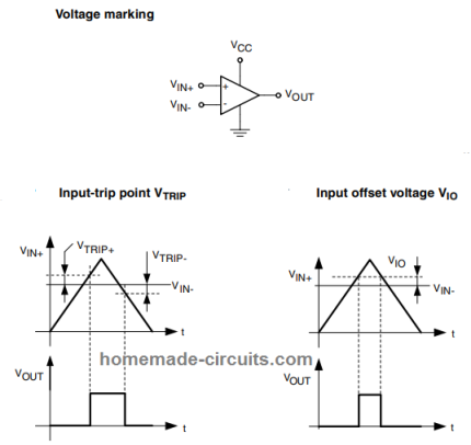 Low differential may cause the comparator transistor to become unstable resulting in an increase in the input offset voltage conditions to increase.
For compartaor that have internal hysteresis enabled VIO is defined as the average level of the sum of of VTRIP+ and VTRIP-, and the hysteresis value of VHYST = VTRIP+ - VTRIP- where VTRIP+ and VTRIP- constitute the input differential voltage that causes the output to switch from low to high state or high to low state respectively.
Low differential may cause the comparator transistor to become unstable resulting in an increase in the input offset voltage conditions to increase.
For compartaor that have internal hysteresis enabled VIO is defined as the average level of the sum of of VTRIP+ and VTRIP-, and the hysteresis value of VHYST = VTRIP+ - VTRIP- where VTRIP+ and VTRIP- constitute the input differential voltage that causes the output to switch from low to high state or high to low state respectively.
CMRR and SVR
CMRR stands for common mode voltage rejection ratio, provides the relationship between input offset voltage VIO and the input common mode voltage VICM. This may be understood as a ratio of common mode voltage value upon the input offset voltage. This parameter is usually expressed in logarithmic scale as: CMRR [dB] = 20 log (| ¦¤VICM /¦¤VIO| ) CMRR is calculated by measuring two input offset voltage magnitudes taken for two different input common mode voltages (typically 0 V and VCC). The term SVR stands for ˇ°supply voltage rejectionˇ± and is defined as a parameter that provides the relation between the input offset voltage VIO and the power supply voltage. Changing power supply voltage has the ability to somewhat affect the bias of the input differential transistor pairs. This implies that the variation might also cause the input offset voltage to change slightly. This is expressed through the formula: SVR [dB] = 20 log (| ¦¤VCC /¦¤VIO| )Voltage gain
This parameter helps us to understand the net gain of the comparator. When the comparator is attributed with higher gain specs, it means an improved response of the device to small input signal differentials. Typically the AVD range of a compartaor can be 200V/mV(106dB). Theoretically, amplitude of 200V is achieved when a 1mV input is amplified with 106dB. However, for a real device the peak level swing will be limited by the value of Vcc. Note that the AVD can never have any effect on external hysteresis since the output will be either in high or low state, and never in between .Propagation delay
TPD is defined as the time difference between the instant when the input signal just crosses the reference input level and the instant when the output state has just changed states. From our previous discussions we know that the output of the compartaor toggles in response to input pin voltage difference. Propagation delay TPD provides us with the specification that suggest how quickly the input pins have the ability to sense the difference and toggle the output without problems. Basically, TPD tells us about the input frequency level which the comparator can process comfortably for generating valid output responses.Hysteresis
We know that hysteresis is a parameter that prohibits quick changes of an output in response to an unstable or fluctuating input. Normally, in a comparator the output voltage can oscillate or fluctuate rapidly when the input differential signal hovers close to the reference value. Or this may happen when the input signal has a very low amplitude, causing the input differential level to change at a quick rate.Built-in hysteresis
There are actually many comparator devices that feature a built in hysteresis functionality. This may be around at a few mV, which is quite enough to suppress undesired output switching without affecting the devices resolution. For such devices, the evaluated average upper and lower voltage limits is called input offset voltage VIO, and the difference VTRIP+/VTRIP- is termed as hysteresis voltage or VHYST.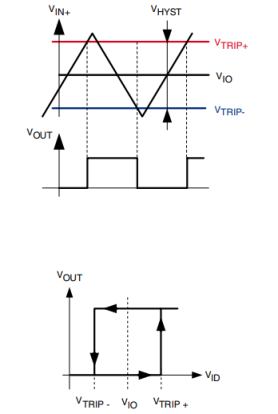
External Hysteresis
In case the comparator is without an in-built hysteresis, or if the intended hysteresis level is relatively bigger, then an external configuration may be added for implementing the hysteresis functionality via a positive feedback network, as shown below.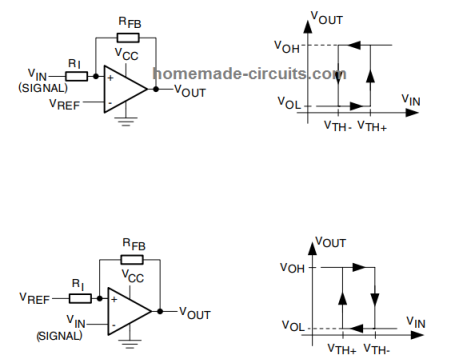 Wrapping up
So these a few crucial compartaor datasheet parameters which will be helpful for all enthusiast trying to achieve a prefect comparator based design, if you have further information regarding this subject please feel free to share them through your comments.
Wrapping up
So these a few crucial compartaor datasheet parameters which will be helpful for all enthusiast trying to achieve a prefect comparator based design, if you have further information regarding this subject please feel free to share them through your comments.
TL494 Datasheet, Pinout, Application Circuits
The IC TL494 is a versatile PWM control IC, which can be applied in many different ways in electronic circuits. In this articles we discuss in detail regarding the main functions of the IC, and also how to use it in practical circuits.General Description
The IC TL494 is specifically designed for single chip pulse width modulation application circuits. The device is mainly created for power supply control circuits, which can be efficiently dimensioned using this IC. The device comes with an in-built variable oscillator, a dead-time controller stage (DTC), a flip flop control for pulse-steering, a precision 5 V regulator, two error amps, and some output buffer circuits. The error amplifiers feature a common mode voltage range from - 0.3 V to VCC - 2V. The dead time control comparator is set with a fixed offset value for delivering a constant 5% dead time approximately. The on chip oscillator function can be overridden by connecting the RT pin#14 of the IC with reference pin#14, and by externally providing a sawtooth signal to the CT pin#5. This facility also allows driving many TL494 ICs synchronously having different power supply rails. The output transistors inside the chip having floating outputs are arranged to deliver either a common-emitter output or a emitter-follower output facility. The device allows the user to get either a push-pull type or a single ended oscillation across its output pins by appropriately configuring pin#13, which is the output-control function pin. The internal circuitry makes it impossible for any of the outputs to produce a double pulse, while the IC is wired in the push-pull function.Pin Function and Configuration
The following diagram and explanation provide us the basic information regarding the pin function for the IC TL494.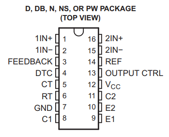 Pin#1 and Pin#2 (1 IN+ and 1IN-) : These are the non-inverting and inverting inputs of the error amplifier (op amp 1).
Pin#16, Pin#15 (1 IN+ and 1IN-) : As above these are the non-inverting and inverting inputs of the error amplifier (op amp 2).
Pin#8 and Pin#11 (C1, C2): These are the outputs 1 and 2 of the IC which connect with the collectors of the respective internal transistors.
Pin#5 (CT): This pin needs to be connected with an external capacitor for setting the oscillator frequency.
Pin#6 (RT): This pin needs to be connected with an external resistor for setting the oscillator frequency.
Pin#4 (DTC): It's the input of the internal op amp which controls the dead-time operation of the IC.
Pin#9 and Pin#10 (E1 and E2): These are the outputs of the IC which connect with emitter pins of the internal transistor.
Pin#3 (Feedback): As the name suggests, this input pin is used for integrating with an output sample signal for a desired automatic control of the system.
Pin#7 (Ground): This pin is the ground pin of the IC, which needs to connected with the 0 V of the supply source.
Pin#12 (VCC): This is the positive supply pin of the IC.
Pin#13 (O/P CNTRL): This pin can be configured for enabling the output of the IC in the push-pull mode or single ended mode.
Pin#14 (REF): This output pin provides a constant 5V output which can be used for fixing a reference voltage for the error op amps, in the comparator mode.
Pin#1 and Pin#2 (1 IN+ and 1IN-) : These are the non-inverting and inverting inputs of the error amplifier (op amp 1).
Pin#16, Pin#15 (1 IN+ and 1IN-) : As above these are the non-inverting and inverting inputs of the error amplifier (op amp 2).
Pin#8 and Pin#11 (C1, C2): These are the outputs 1 and 2 of the IC which connect with the collectors of the respective internal transistors.
Pin#5 (CT): This pin needs to be connected with an external capacitor for setting the oscillator frequency.
Pin#6 (RT): This pin needs to be connected with an external resistor for setting the oscillator frequency.
Pin#4 (DTC): It's the input of the internal op amp which controls the dead-time operation of the IC.
Pin#9 and Pin#10 (E1 and E2): These are the outputs of the IC which connect with emitter pins of the internal transistor.
Pin#3 (Feedback): As the name suggests, this input pin is used for integrating with an output sample signal for a desired automatic control of the system.
Pin#7 (Ground): This pin is the ground pin of the IC, which needs to connected with the 0 V of the supply source.
Pin#12 (VCC): This is the positive supply pin of the IC.
Pin#13 (O/P CNTRL): This pin can be configured for enabling the output of the IC in the push-pull mode or single ended mode.
Pin#14 (REF): This output pin provides a constant 5V output which can be used for fixing a reference voltage for the error op amps, in the comparator mode.
Absolute Maximum Ratings
(VCC) Maximum Supply voltage not to exceed = 41 V (VI) Maximum Voltage on input pins not to exceed = VCC + 0.3 V (VO) Maximum output voltage at collector of internal transistor = 41 V (IO) Maximum current on Collector of the internal transistor = 250 mA Maximum IC pin soldering heat at 1.6 mm (1/16 inch) away from IC body not to exceed 10 seconds @ 260 ˇăC Tstg Storage temperature range = ¨C65/150 ˇăCRecommended Operating Conditions
The following data gives you the recommended voltages and currents that can be used for operating the IC under safe and efficient conditions: VCC supply: 7 V to 40 V VI Amplifier Input Voltage: -0.3 V to VCC - 2 V VO Transistor Collector Voltage = 40, Collector Current for each Transistor = 200 mA Current into Feedback pin: 0.3 mA fOSC Oscillator frequency range: 1 kHz to 300 kHz CT Oscillator timing capacitor value: Between 0.47 nF to 10000 nF RT Oscillator timing resistor value: Between 1.8 k to 500 k Ohms.Internal Layout Diagram
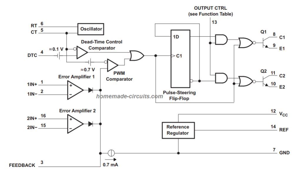
How to Use IC TL494
In the following paragraphs we learn the important functions of the IC TL494, and how to use it in PWM circuits. Overview: The TL494 IC is designed in such a way that it not only features the important circuitry needed to control a switching power supply, but additionally tackles several fundamental difficulties and minimizes the need of supplemental circuit stages necessary in the overall structure. The TL494 is basically a fixed-frequency pulse-width-modulation (PWM) control circuit. The modulation function of output pulses is achieved when the internal oscillator compares its sawtooth waveform through the timing capacitor (CT) with both pairs of control signals. The output stage is toggled in the period when the sawtooth voltage is higher than the voltage control signals. As the control signal increases, the time when the sawtooth input is higher decreases; consequently, the output pulse length reduces. A pulse-steering flip-flop alternately guides the modulated pulse to each of the two output transistors.5-V Reference Regulator
The TL494 creates a 5 V internal reference which is fed to the REF pin. This internal reference helps to develop a stable constant reference, which acts like a pre-regulator for ensuring a stable supply. This reference is then reliably used for powering various internal stages of the IC such as logic output control, flip flop pulse steering, oscillator, dead time control comparator, and PWM comparator.Oscillator
The oscillator generates a positive sawtooth waveform for the dead-time and the PWM comparators so that these stages can analyze the various control input signals. It's the RT and the CT which are responsible for determining the oscillator frequency and thus can be externally programmed. The sawtooth waveform generated by the oscillator charges the external timing capacitor CT with a constant current, determined by the complementing resistor RT. This results in the creation of a linear-ramp voltage waveform. Each time the voltage across CT reaches 3 V, the oscillator quickly discharges it, which subsequently restarts the charging cycle. The current for this charging cycle is calculated through the formula: Icharge = 3 V / RT --------------- (1) The period of the sawtooth waveform is given by: T = 3 V x CT / Icharge ----------(2) The oscillator frequency is thus determined using the formula: f OSC = 1 / RT x CT ---------------(3) However, this oscillator frequency will be compatible with the output frequency when the output is configured as single-ended. When configured in push-pull mode, the output frequency will be 1/2 of the oscillator frequency. Therefore, for single ended output the above equation no 3 can be used. For push pull application the formula will be: f = 1 / 2RT x CT ------------------(4)Dead-time Control
The dead-time pin set-up regulates the minimum dead time (off periods between the two outputs). In this function when voltage on the DTC pin exceeds the ramp voltage from the oscillator, forces the output comparator to switch OFF the transistors Q1 and Q2. The IC has an internally set offset level of 110 mV that guarantees a minimum dead time of around 3% when the DTC pin is connected with the ground line. The dead time response can be increased by applying an external voltage to the DTC pin#4. This allows to have a linear control over the dead-time function from the default 3% to a maximum of 100%, through a variable input of 0 to 3.3 V. If a full range control is used, the output can of the IC can be regulated through an external voltage without disturbing the error amplifier configurations. The dead-time feature can be employed in situations where added control of the output duty cycle becomes necessary. But for proper functioning it must be ensured that this input is either terminated to a voltage level or to ground and should be never left floating.Error Amplifiers
The two error amplifiers of the IC have a high gain, and are biased through the ICs VI supply rail. This enables a common-mode range of input from -0.3 V to VI - 2 V. Both the error amplifiers are internally set up to work like a single-ended single supply amplifiers, wherein each output have active-high capability only. Due to this capability, the amplifiers are able to activate independently for satisfying a narrowing PWM demand. Since the outputs of the two error amps are tied like OR gates with the input node of the PWM comparator, the amplifier which can work with minimum pulse out dominates. The amplifiers have their outputs biased with a low current sink so that the the IC output ensures maximum PWM when the error amplifiers are in the non-functional mode.Output-Control Input
This pin of the IC can be configured to allow the IC output to either work in a single ended mode that is both output oscillating together in parallel or in push pull manner producing alternately oscillating outputs. The output-control pin works asynchronously, enabling it to have a direct control over the output of the IC, without affecting the internal oscillator stage or the flip flop pulse-steering stage. This pin is normally configured with a fixed parameter as per the application specifications. For example, if the IC outputs are intended to work in parallel or single ended manner, the output-control pin is connected with the ground line permanently. Due to this the pulse-steering stage inside the IC gets disabled and the alternate flip flop stops at the output pins. Also, in this mode the pulses arriving at the dead-time control and PWM comparator are carried together by both the output transistors, allowing the output to switch ON/OFF in parallel. For obtaining a push pull output operation, the output-control pin simply needs to be connected to the +5V output reference pin (REF) of the IC. In this condition, each of the output transistors turn ON alternately through the pulse-steering flip-flop stage.Output Transistors
As can be seen the second diagram from top, the chip consists of two output transistors, which having uncommitted emitter and collector terminals. Both these floating terminals are rated to sink (take in) or source (give out) up to 200 mA current. The saturation point of the transistors is less than 1.3 V when configured in the common-emitter mode, and less than 2.5 V in the common-collector mode. They are internally protected from short circuit and over current.Application Circuits
As explained in the above, the TL494 is primarily a PWM controller IC, therefore the main application circuits are mostly PWM based circuits. A couple of example circuits are discussed below, which can be modified in various ways as per individual requirements.Solar Charger using TL494
The following design shows how the TL494 can be effectively configured to create a 5-V/10-A switching buck power supply. In this configuration the output works in parallel mode, and therefore we can see the output-control pin#13 is connected to ground. The two error amps are also used very efficiently here. One error amplifier controls the voltage feedback via R8/R9 and keep the output constant at the desired rate (5V) The second error amplifier is used for controlling the maximum current via R13.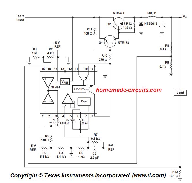
TL494 inverter
Here's a classic inverter circuit built around the IC TL494. In this example the output is configured to work in the push-pull manner, and therefore the output-control pin here is connected with the +5V reference, which is achieved from pin#14. The erst of the pins are also configured exactly as described in the above datasheet.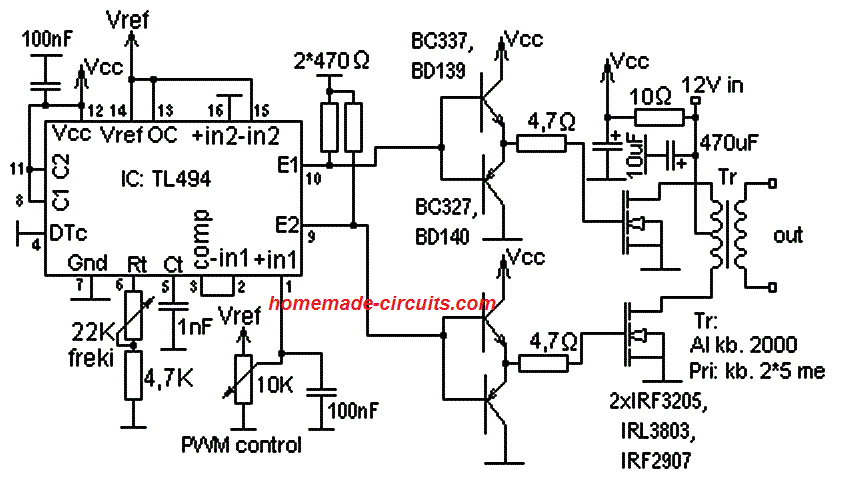
Conclusion
The IC TL494 is a PWM control IC with highly accurate output and feedback control facilities ensuring an ideal pulse control for any desired PWM circuit application. It is similar to SG3525 in many ways, and can be used as an effective replacement for it, although the pin numbers can be different and not exactly compatible. If you have any questions pertaining to this IC, please feel free to ask them through the comments below, I'll be happy to help! Reference: TL494 datasheet2N3055 Datasheet, Pinout, Application Circuits
The 2N3055 is a power bipolar transistor designed to handle high power loads in the range of 100 V, and 15 amps. In this post we comprehensively discuss the pinout function, electrical specification, and application designs for the power transistor 2N3055. If you are an electronic hobbyist, you might have certainly used this very useful, and efficient power transistor at least once in your experiments. I have used 2N3055 transistor many number of times in many of my high current circuit applications without any issues.Main Features
DC Current Gain or hFE = 20 70 @ IC = 4 Amps (Collector Current) CollectorEmitter Saturation Voltage VCE(sat) = 1.1 Vdc (Max) @ IC = 4 Adc Outstanding Safe Operating Area Available with PbFree PackagesPinout Diagram
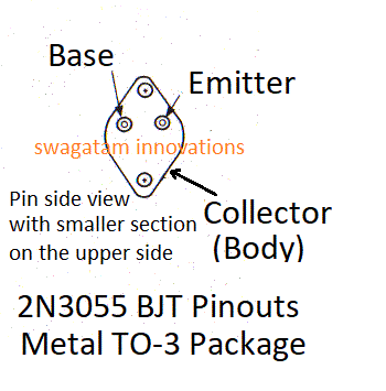
How to Connect the Pinouts
Just like any other npn BJT, 2N3055 connections are also pretty straightforward. In the common emitter mode which is most frequently used configuration, the emitter pin is connected with the ground line or the negative supply line.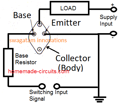 The base is connected across the input signal through which the transistor needs to be switched ON or OFF.
This input switching signal can be anywhere between 1V and 12V ideally.
A calculated resistor must be included in series with the base pinout of the transistor.
The base resistor value will depend on the load specifications attached at the collector pin of the transistor.
The basic formula can be studied from this article.
The collector pin should be connected with one terminal of the load, while the other terminal connects with the positive supply line.
The load current specs must be at any cost lower than 15 amps, in fact lower than 14 amps to avoid current reaching the breakdown limit.
The base is connected across the input signal through which the transistor needs to be switched ON or OFF.
This input switching signal can be anywhere between 1V and 12V ideally.
A calculated resistor must be included in series with the base pinout of the transistor.
The base resistor value will depend on the load specifications attached at the collector pin of the transistor.
The basic formula can be studied from this article.
The collector pin should be connected with one terminal of the load, while the other terminal connects with the positive supply line.
The load current specs must be at any cost lower than 15 amps, in fact lower than 14 amps to avoid current reaching the breakdown limit.
MAXIMUM RATINGS ANDSPECIFICATIONSOF2N3055TRANSISTOR
Maximum ratings are the highest tolerable values beyond which a permanent damage can occur to the device. These ratings specified to the device are stress limit values (not the standard operating criteria) for the particular device and are not valid simultaneously. If these limits are exceeded, device may cease to function with its standard specifications, causing severe damage to the device and also affecting its reliability parameters. Collector to Emitter Voltage VCER = 70 Vdc Collector to Base Voltage VCB = 100 Vdc Emitter to Base Voltage VEB = 7 Vdc Continuous Collector-Current IC = 15 Adc Base Current IB = 7 Adc Total Power Dissipation @ TC = 25ˇăC Derate Above 25ˇăC PD = 115 W @ 0.657 W/ˇăC Operating and Storage Junction Temperature Range TJ, Tstg = 65 to +200 ˇăCTHERMAL CHARACTERISTICSof2N3055
Thermal Resistance from JunctiontoCase R0JC = 1.52 C/WELECTRICAL CHARACTERISTICS of2N3055(TC = 25 C unless otherwise specified)
CHARACTERISTICSWHENDEVICEISOFF CollectorEmitter Sustaining Voltage at collector current IC = 200 mAdc, IB = 0) VCEO(sus) = 60 Vdc CollectorEmitter Sustaining Voltage at collector current IC = 200 mAdc, RBE = 100 fi) VCER(sus) = 70 Vdc Collector Cutoff Current (VCE = 30 Vdc, IB = 0) ICEO = 0.7 mA Collector Cutoff Current (VCE = 100 Vdc, VBE(off) = 1.5 Vdc) ICEX = 1.0 mA Emitter Cutoff Current (VBE = 7.0 Vdc, IC = 0) IEBO = 5.0 mA CHARACTERISTICSWHENDEVICEISON DC Current Gain (IC = 4.0 Adc, VCE = 4.0 Vdc) (IC = 10 Adc, VCE = 4.0 Vdc) hFE = 20 to 70 CollectorEmitter Saturation Voltage (IC = 4.0 Adc, IB = 400 mAdc) (IC = 10 Adc, IB = 3.3 Adc) VCE(sat) = 1.1 to 3 Vdc BaseEmitter On Voltage (IC = 4.0 Adc, VCE = 4.0 Vdc) VBE(on) = 1.5 Vdc DYNAMIC CHARACTERISTICS Current Gain Bandwidth Product (IC = 0.5 Adc, VCE = 10 Vdc, f = 1.0 MHz) fT = 2.5 MHz *SmallSignal Current Gain (IC = 1.0 Adc, VCE = 4.0 Vdc, f = 1.0 kHz) hfe = 15 to 120 *SmallSignal Current Gain Cutoff Frequency (VCE = 4.0 Vdc, IC = 1.0 Adc, f = 1.0 kHz) f hfe = 10 kHz *Indicates Within JEDEC Registration. (2N3055) The transistor comes with a couple of limitations in terms power handling capability. Average junction temperature Breakdown voltage Safe operating area curves indicate the IC VCE limits of the 2N3055 transistor that must be taken care of in order to ensure a stable and error free operation. Meaning the transistor must not be operated to increased dissipation levels than what is advised in the curves traces. The data given in the figure below is plotted while TC = 25ˇăC; TJ(pk) is variable in accordance with the power level.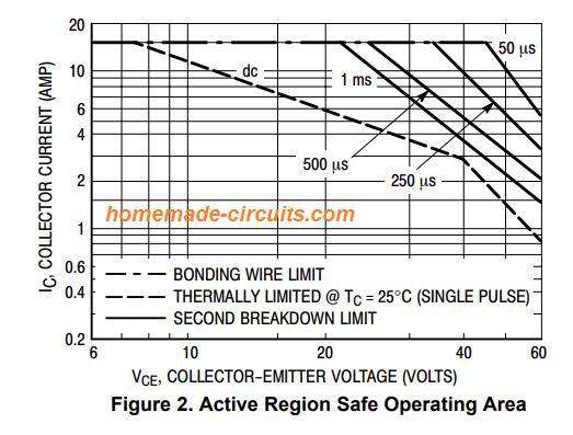 Second breakdown pulse boundaries are legitimate for duty cycles upto 10% but must be derated for temperatures as indicated in the following figure:
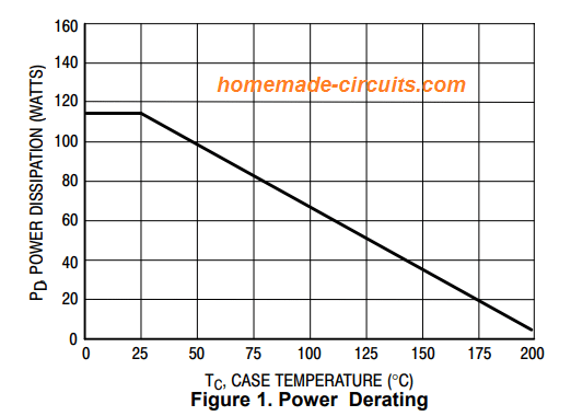
Application Circuits using 2N3055
The 2N3055 is a versatile NPN power transistor which can be effectively applied for all medium power (current) delivering circuit. The few main of these applications are in the field of inverters and power amplifiers. Due to relatively high hFE range this device can be used in a wide range of circuits for handling high current efficiently. It's metal TO3 case becomes ideally suited for attaching a fast cooling large heatsink quickly and easily allowing the device to work in its most favorable conditions. I have plenty of 2N3055 based circuits in this website, glad to present a few of them here. Amplifier Circuit using a single 2N3055 The circuit is the most basic form of power amplifier which can be build using a single 2N3055 BJT.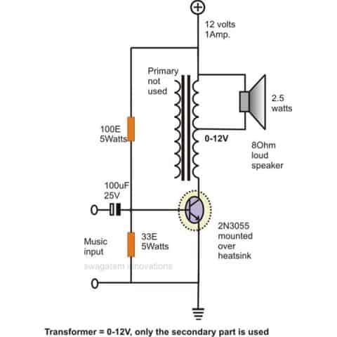 Although the amplifier above looks too simple to make, the low-tech design forces the 2N3055 to dissipate a lot power through heat.
For a more efficient and Hi-Fi amplifier design, I recommend the following mini crescendo, which is perhaps one of the most classic and efficient amplifier circuits using just a pair of 2N3055 transistors.
For complete details you can read this article
Although the amplifier above looks too simple to make, the low-tech design forces the 2N3055 to dissipate a lot power through heat.
For a more efficient and Hi-Fi amplifier design, I recommend the following mini crescendo, which is perhaps one of the most classic and efficient amplifier circuits using just a pair of 2N3055 transistors.
For complete details you can read this article
 Tiniest Inverter using 2N3055
I am sure you might have already come across this little inverter circuit.
This circuit using only two 2N3055 and a transformer for creating a reasonably powered 60 to 100 watt 50 Hz power inverter.
An ideal project for all new hobbyists and school students.
Tiniest Inverter using 2N3055
I am sure you might have already come across this little inverter circuit.
This circuit using only two 2N3055 and a transformer for creating a reasonably powered 60 to 100 watt 50 Hz power inverter.
An ideal project for all new hobbyists and school students.
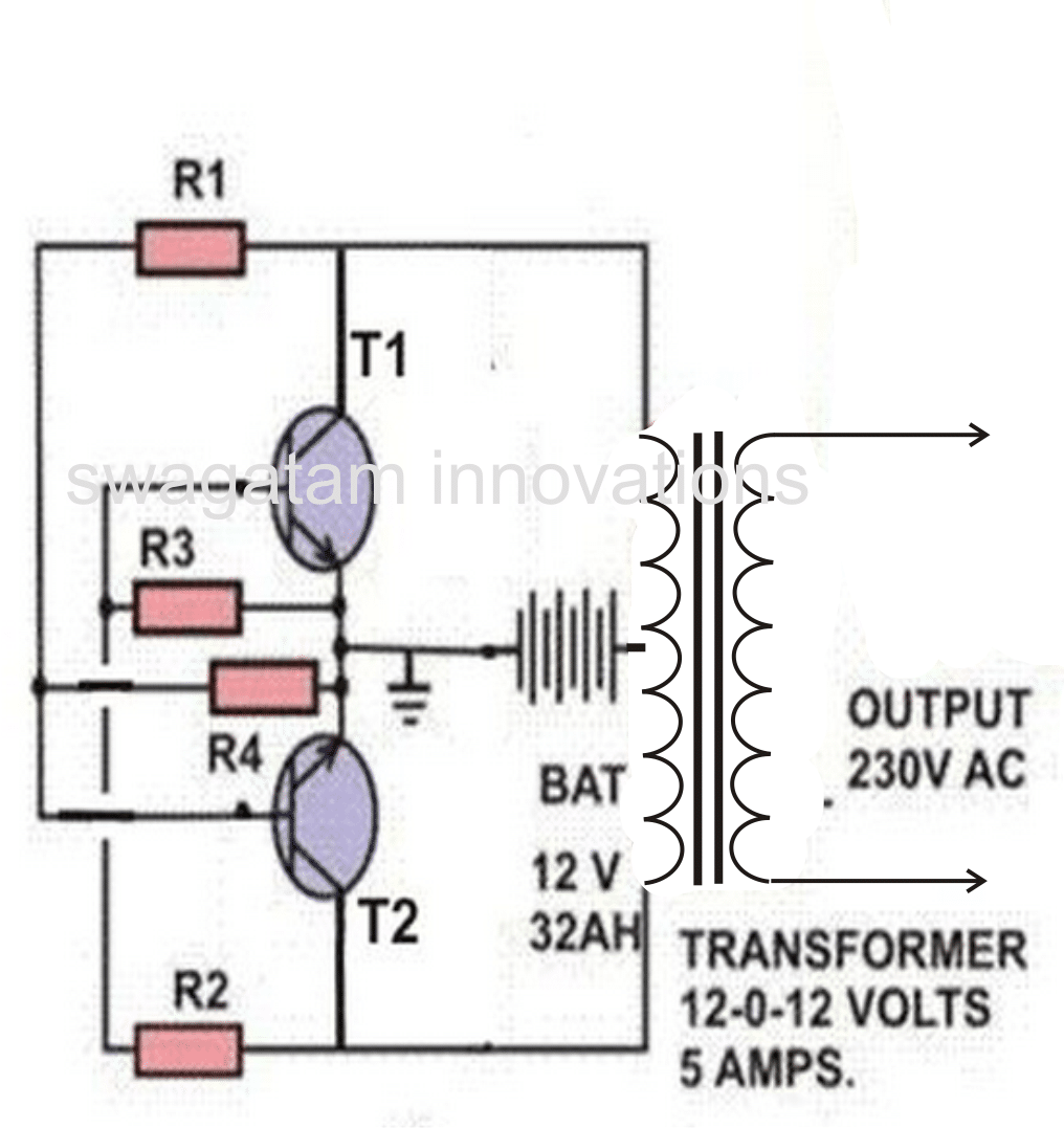 R1, R2= 100 OHMS./ 10 WATTS WIRE WOUND
R3, R4= 15 OHMS/ 10 WATTS WIRE WOUND
T1, T2 = 2N3055 POWER TRANSISTORS
R1, R2= 100 OHMS./ 10 WATTS WIRE WOUND
R3, R4= 15 OHMS/ 10 WATTS WIRE WOUND
T1, T2 = 2N3055 POWER TRANSISTORS
Power Inverter 100 watts using 2N3055
If you are not satisfied with the power output from the above design, you can always upgrade it to a full-fledged, 100 to 500 watt power inverter, using a single or many 2N3055 transistors in parallel, as shown below: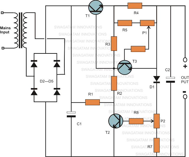 For more description and parts list you can visit this post
12V to 48V Battery Charger using 2N3055
For more description and parts list you can visit this post
12V to 48V Battery Charger using 2N3055
 Please connect a 100 Ohm 1 watt resistor in series with the transistor base
This simple automatic 2N3055 based battery charger circuit can be used for charging any lead acid battery from 12V to 48V.
The high current handling capacity upto 7 amps of this device will allow an ideal, charging for any battery from 7 Ah to 150 Ah using the above circuit.
It has an automatic cut-off feature which will never allow the battery to get over charged.
Conclusion
From the above posting we learned the main specifications and datasheet of the versatile workhorse transistor 2N3055.
This transistor is a universal power BJT that can be used in almost all higher power based applications where high current and efficient switching of current is expected.
The maximum voltage this device can handle is 70V which looks very impressive, and a continuous current for around 15 amp, when the device is mounted over a well ventilated heatsink.
We also studied a few cool application circuits using 2N3055, and how to connect it through its pinout diagram.
If you have any further doubts please use the comment box below for interacting.
Please connect a 100 Ohm 1 watt resistor in series with the transistor base
This simple automatic 2N3055 based battery charger circuit can be used for charging any lead acid battery from 12V to 48V.
The high current handling capacity upto 7 amps of this device will allow an ideal, charging for any battery from 7 Ah to 150 Ah using the above circuit.
It has an automatic cut-off feature which will never allow the battery to get over charged.
Conclusion
From the above posting we learned the main specifications and datasheet of the versatile workhorse transistor 2N3055.
This transistor is a universal power BJT that can be used in almost all higher power based applications where high current and efficient switching of current is expected.
The maximum voltage this device can handle is 70V which looks very impressive, and a continuous current for around 15 amp, when the device is mounted over a well ventilated heatsink.
We also studied a few cool application circuits using 2N3055, and how to connect it through its pinout diagram.
If you have any further doubts please use the comment box below for interacting.
LM3915 IC Datasheet, Pinout, Application Circuits
If you are having difficulty in understanding how to use an LM3915 IC, this article will help you to easily construct any desired applicable circuit using this IC. Here, we will discuss the datasheet of the IC LM3915, its pinout functions, its main electrical specifications, and also a few useful application circuits.General Description
The LM3915 is a monolytthic IC designed to sense analogue voltage signals, and produce an incremental or sequential logic switching across its 10 output. Inidicating devices likes LEDs, LCD or vaccum displays can be attached with these outputs to obtain a corresponding visual indication in response to the varying input analogue signal. The IC has one pinout for designating whether the output LEDs will sequence individually (dot mode) or in form of a bar graph. The LED can be connected without limiting resistors since the IC includes internal programmable current regulation for the 10 outputs. The IC circuit including all the 10 LEDs can be operated using as low as 3V supply and upto 25V. The IC features an adaptable voltage reference and a precise 10 step voltage divider. The high-impedance input buffer can be fed with analogue voltages from 0V to within +1.5V. Further more, the inputs are well protected against signals upto the range of ˇŔ35V. The input buffer runs 10 opamp comparators which are all referenced to the precision divider network. Accuracy level of the system is normally in the vicinity of 1 dB. The LM3915ˇŻs 3 dB/step display is built for accepting input signals with broad dynamic range. For example the input can be in the form of audio or music signal, varying light intensity or vibrational electricity. Audio applications could be in the form of average or peak level indicators, power meters and RF signal strength meters. Upgrading traditional analogue VU meters with an LM3915 based LED bar graph gives a better illuminated response, a durable display with improved field of vision enabling better interpretation of input signal. The LM3915 is very simple to use. In addition to the ten LEDs you can even use a 1.2V full-scale-deflection meter with just one resistor. Another separate resistor sets up the full-scale range between 1.2V to 12V regardless of supply voltage value. The brightness of the LED is easily controllable with a single external pot.Typical LM3915 Circuit Configuration
The following image shows how the IC LM3915 can be setup in its most typical or basic functional mode.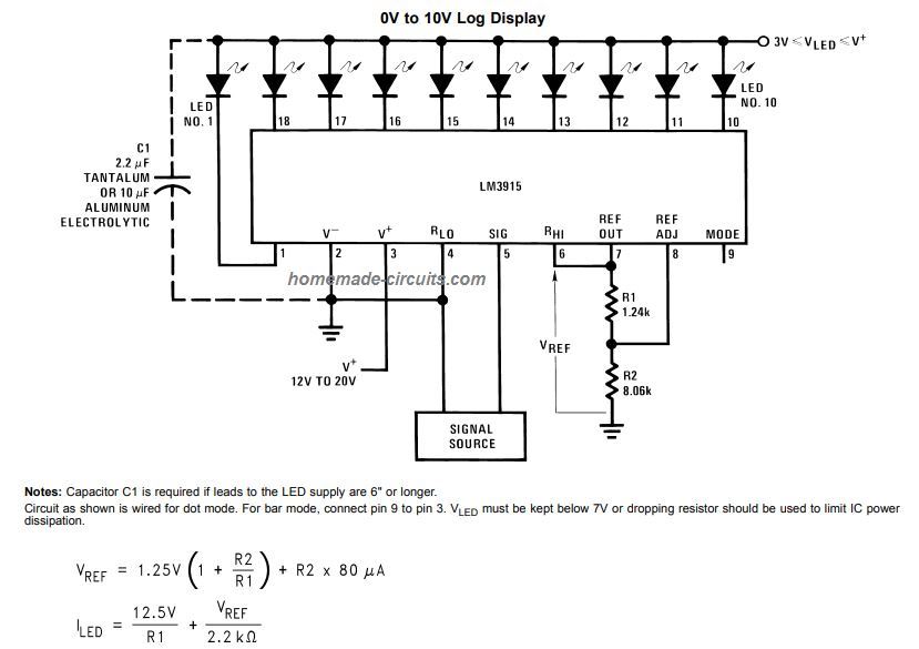 If you are a new hobbyists and want to configure the pinouts of IC LM3915 or LM3914 quickly to get the required actions, then the following diagram could be used.
The pinout details are explained below:
If you are a new hobbyists and want to configure the pinouts of IC LM3915 or LM3914 quickly to get the required actions, then the following diagram could be used.
The pinout details are explained below:
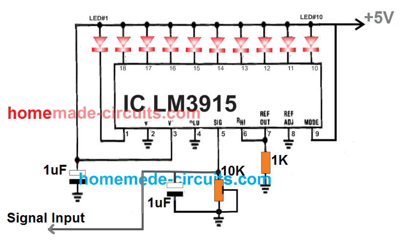 pin#10, pin#11, pin#12, pin#13, pin#14, pin#15, pin#16, pin#17, pin#18, and pin#1 = All are outputs for LED connection.
LEDs do not need an external resistance, but preferably the LED supply line must be restricted to 5V to keep the dissipation on the lower side.
Pin#3 is the VDD or the positive supply input for the IC, which can take any supply between 3V and 25V, but I recommend using 5V to keep the LED dissipation on the lower side.
Pin#8 is the Vss or the ground (negative) supply pin of the IC.
Pin#6 and pin#7 can be joined together and terminated to ground line via a 1K resistor.
Pin#5 must be configured as shown in the above diagram through a 10k preset and a capacitor.
This preset can be adjusted for setting the full scale LED illumination range depending on the strength of the input signal.
Pin#9 could be left unconnected (open) or connected to the +supply line.
When left unconnected, the LEDs sequence up/down individually appearing like a running "DOT" and hence called the DOT mode.
When pin#9 is connected to the positive line, the LED sequence like a up/down moving illuminated bar, hence called the bar mode.
Once this is done, it's just about feeding the input signal and watch the wonderful movement of the LEDs as per the varying input signal or music amplitudes
pin#10, pin#11, pin#12, pin#13, pin#14, pin#15, pin#16, pin#17, pin#18, and pin#1 = All are outputs for LED connection.
LEDs do not need an external resistance, but preferably the LED supply line must be restricted to 5V to keep the dissipation on the lower side.
Pin#3 is the VDD or the positive supply input for the IC, which can take any supply between 3V and 25V, but I recommend using 5V to keep the LED dissipation on the lower side.
Pin#8 is the Vss or the ground (negative) supply pin of the IC.
Pin#6 and pin#7 can be joined together and terminated to ground line via a 1K resistor.
Pin#5 must be configured as shown in the above diagram through a 10k preset and a capacitor.
This preset can be adjusted for setting the full scale LED illumination range depending on the strength of the input signal.
Pin#9 could be left unconnected (open) or connected to the +supply line.
When left unconnected, the LEDs sequence up/down individually appearing like a running "DOT" and hence called the DOT mode.
When pin#9 is connected to the positive line, the LED sequence like a up/down moving illuminated bar, hence called the bar mode.
Once this is done, it's just about feeding the input signal and watch the wonderful movement of the LEDs as per the varying input signal or music amplitudes
Absolute Maximum Ratings
The absolute maximum rating of LM3915 indicates the maximum voltage and current parameters the device is permitted to handle. Supply Voltage = 25V Output Supply on the LEDs if you are using a separate supply here = 25V (same as above) Maximum Input Signal Range = +/-35V Divider Reference Voltage = -100mV to Supply Level. Power Dissipation = 1365 mWInternal Layout of the IC
The following diagram shows the internal layout of the IC. We can see how the opam comparators are arranged for processing the input signal at pin#5. The reference at pin#7 applied in an incremental order across the opamp non-inverting inputs through a ladder type resistor divider network.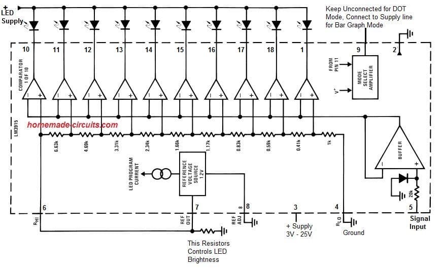
Functional Description
The above basic LM3915 block diagram provides the general perception of the circuitˇŻs functioning. A high input impedance voltage follower buffer responds to the input pin#5 signals. This pinout is secured against over-voltage and reverse polarity signals. The signal from buffer then goes to a group of 10 comparators. Each of this opamps are biased to an incrementing reference levels through the resistor divider series. In the image above, the resistor network is linked with the internal 1.25V reference voltage. Here, , for every 3 dB rise in the input signal, a switch in the comparator level is triggered causing the respective LED to move and sequence accordingly, interpreting the signal response. This internal resistor divider could be operated with potential of 0 - 2 volts at pin#5, through an external resistive divider network.INTERNAL VOLTAGE REFERENCE
The reference voltage for the IC LM3915 is intended to be variable so that it builds up a tiny 1.25V across REF OUT (pin #7) and REF ADJ (pin #8).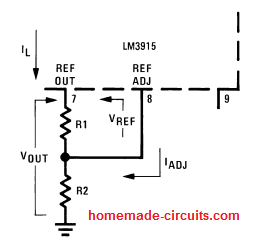 The reference voltage is implemented across the resistor R1 which can be changed as per preference.
Because we have a constant supply DC voltage, a constant current I1 is allowed to move through the output setting resistor R2 enabling an output voltage of:
VOUT = VREF (1 + R2/R1) + IADJ R2
The current taken in by the reference voltage pin #7 decides the amount of LED current.
We can expect around 10 times this current that may be permissible to be consumed by each illuminated output LED.
This current is more or less constant regardless of supply voltage variations and temperature changes.
Current used by the internal 10-resistor divider, and the external current and voltage-setting divider must be taken into account while calculating LED drive current.
The IC provides a feature for modulating real time referenced LED brightness, or in response to input voltage variations and other signals.
This allows inclusion of many innovative displays or options for producing input over-voltages, alarms, etc.
The outputs of LM3915 are all internally current controlled NPN BJT buffers as shown below.
An internal feedback hook restricts the transistor from over current situations.
Output current for the LEDs is fixed at roughly to 10 times the reference load current, irrespective of variations in the output voltage until of course the transistors are not saturated with high input supply.
The reference voltage is implemented across the resistor R1 which can be changed as per preference.
Because we have a constant supply DC voltage, a constant current I1 is allowed to move through the output setting resistor R2 enabling an output voltage of:
VOUT = VREF (1 + R2/R1) + IADJ R2
The current taken in by the reference voltage pin #7 decides the amount of LED current.
We can expect around 10 times this current that may be permissible to be consumed by each illuminated output LED.
This current is more or less constant regardless of supply voltage variations and temperature changes.
Current used by the internal 10-resistor divider, and the external current and voltage-setting divider must be taken into account while calculating LED drive current.
The IC provides a feature for modulating real time referenced LED brightness, or in response to input voltage variations and other signals.
This allows inclusion of many innovative displays or options for producing input over-voltages, alarms, etc.
The outputs of LM3915 are all internally current controlled NPN BJT buffers as shown below.
An internal feedback hook restricts the transistor from over current situations.
Output current for the LEDs is fixed at roughly to 10 times the reference load current, irrespective of variations in the output voltage until of course the transistors are not saturated with high input supply.
How to Use the MODE Pin #9
This pin is configured to enforce two functions. Please see the following simplified block diagram.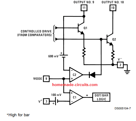 DOT OR BAR MODE SELECTION
When the pin #9 is connected to the + supply line (or between -100mV and supply level), the comparator C1 senses this, and sets the output in the bar graph mode.
In this mode all the LEDs respond in an illuminated "bar" like fashion which moves up/down in response to the varying signals at pin #5.
If the pin #9 is unconnected, the outputs are set in the "DOT" mode.
Meaning the LEDs sequence up/down individually one at a time, producing a pulsating illuminated DOT or point like appearance.
The basic way to configure pin #9 is either keep it open or unconnected for implementing dot mode or connect it to supply V+ for implementing the bar mode.
In bar mode operation, pin #9 should be hooked up straight away with pin #3. The LED + line that supplies large currents to the LED chain should not be used with pin #9 so that large IR drops is kept aloof from this pin.
To ensure that the output LED display works correctly when more than one LM3915s are cascaded in dot mode, special circuitry in built-in such that the LED at pin #10 shuts off for the first LM3915 IC at the momenet when LED #1 of the second LM3915 is switched ON.
The design for cascading LM3915 ICs together in dot mode can be witnessed below.
DOT OR BAR MODE SELECTION
When the pin #9 is connected to the + supply line (or between -100mV and supply level), the comparator C1 senses this, and sets the output in the bar graph mode.
In this mode all the LEDs respond in an illuminated "bar" like fashion which moves up/down in response to the varying signals at pin #5.
If the pin #9 is unconnected, the outputs are set in the "DOT" mode.
Meaning the LEDs sequence up/down individually one at a time, producing a pulsating illuminated DOT or point like appearance.
The basic way to configure pin #9 is either keep it open or unconnected for implementing dot mode or connect it to supply V+ for implementing the bar mode.
In bar mode operation, pin #9 should be hooked up straight away with pin #3. The LED + line that supplies large currents to the LED chain should not be used with pin #9 so that large IR drops is kept aloof from this pin.
To ensure that the output LED display works correctly when more than one LM3915s are cascaded in dot mode, special circuitry in built-in such that the LED at pin #10 shuts off for the first LM3915 IC at the momenet when LED #1 of the second LM3915 is switched ON.
The design for cascading LM3915 ICs together in dot mode can be witnessed below.
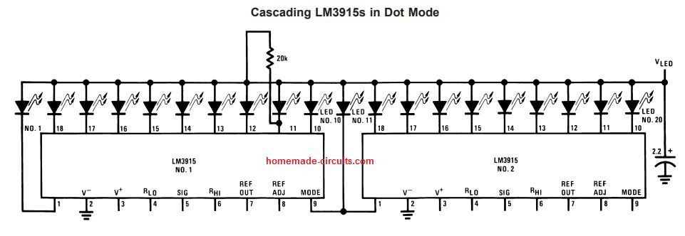 With the condition that the input signal voltage is below the threshold of the second LM3915, LED #11 stays switched off.
Pin #9 of the first LM3915 hence experiences an effective open circuit which causes the IC to run in dot mode.
However the moment the input signal crosses over the threshold of LED #11, pin #9 of the first LM3915 is dropped by a level equal to the LED's forward voltage (1.5V or more) below VLED.
This situation is instantly picked up by comparator C2, referenced 0.6 V below VLED.
It compels C2 output to go low, shutting off output transistor Q2, subsequently switching OFF LED #10.
VLED is detected through the resistor 20k attached to pin #11. The tiny current (under 100 ¦ĚA) which is redirected from LED #9 does not produce any recognizable effect on the intensity of the LED.
An additional current source at pin #1 maintains a minimum of 100 ¦ĚA running through LED #11 regardless of whether or not the input signal rise is enough to switch OFF the LED.
This means that pin #9 of the first LM3915 is kept sufficiently low such that it keeps LED #10 shut off while any of the upper LEDs in the sequence is illuminated.
Although 100 ¦ĚA doesn't usually create considerable LED brightness, it might be visible just enough if high-efficiency LEDs are employed and in total darkness.
If this sounds unacceptable, the easy remedy would be to shunt LED #11 with a 10k resistor.
The 1V IR drop is higher than the minimum 900 mV necessary to maintain LED #10 switched OFF, but small enough ensuring that the LED #11 does not conduct over undesired limits.
The most challenging issue arises when substantial LED currents happen to be consumed, specifically in bar graph mode.
Such currents moving away from the ground pin lead to voltage drops within outer wiring, causing glitches and fluctuations.
Getting the returning cables from signal ports, ground references and from bottom-side of the resistor chain to a single common terminal that may be closest to pin #2 becomes an ideal approach.
Extended wire connections from VLED towards the common LED anodes may trigger oscillations.
Based on how serious the issue is a 0.05 ¦ĚF to 2.2 ¦ĚF decoupling capacitors can be used between LED anode common and pin #2.
This helps to dampen any developed oscillations.
If LED anode supply line wiring is unreachable, identical decoupling across pin #1 to pin #2 proves just adequate for cancelling the interference.
With the condition that the input signal voltage is below the threshold of the second LM3915, LED #11 stays switched off.
Pin #9 of the first LM3915 hence experiences an effective open circuit which causes the IC to run in dot mode.
However the moment the input signal crosses over the threshold of LED #11, pin #9 of the first LM3915 is dropped by a level equal to the LED's forward voltage (1.5V or more) below VLED.
This situation is instantly picked up by comparator C2, referenced 0.6 V below VLED.
It compels C2 output to go low, shutting off output transistor Q2, subsequently switching OFF LED #10.
VLED is detected through the resistor 20k attached to pin #11. The tiny current (under 100 ¦ĚA) which is redirected from LED #9 does not produce any recognizable effect on the intensity of the LED.
An additional current source at pin #1 maintains a minimum of 100 ¦ĚA running through LED #11 regardless of whether or not the input signal rise is enough to switch OFF the LED.
This means that pin #9 of the first LM3915 is kept sufficiently low such that it keeps LED #10 shut off while any of the upper LEDs in the sequence is illuminated.
Although 100 ¦ĚA doesn't usually create considerable LED brightness, it might be visible just enough if high-efficiency LEDs are employed and in total darkness.
If this sounds unacceptable, the easy remedy would be to shunt LED #11 with a 10k resistor.
The 1V IR drop is higher than the minimum 900 mV necessary to maintain LED #10 switched OFF, but small enough ensuring that the LED #11 does not conduct over undesired limits.
The most challenging issue arises when substantial LED currents happen to be consumed, specifically in bar graph mode.
Such currents moving away from the ground pin lead to voltage drops within outer wiring, causing glitches and fluctuations.
Getting the returning cables from signal ports, ground references and from bottom-side of the resistor chain to a single common terminal that may be closest to pin #2 becomes an ideal approach.
Extended wire connections from VLED towards the common LED anodes may trigger oscillations.
Based on how serious the issue is a 0.05 ¦ĚF to 2.2 ¦ĚF decoupling capacitors can be used between LED anode common and pin #2.
This helps to dampen any developed oscillations.
If LED anode supply line wiring is unreachable, identical decoupling across pin #1 to pin #2 proves just adequate for cancelling the interference.
Power Dissipation
Power dissipation, specifically in bar mode needs to be taken into account. For instance, with a 5V supply and all LEDs set up to work with 20 mA current, the LED driver section of the IC can be expected to dissipate over 600 mW. In cases like this a 7.5 resistor can be used in series with the LED supply line, which might help to bring down the dissipation level to half the original value. The negative end of this resistor must be reinforced with a 2.2 ¦ĚF solid tantalum bypass capacitor with pin #2.CASCADING LM3915 ICs
For using display signals of 60 dB or 90 dB dynamic range, you may require a few LM3915 ICs to be cascaded together. A straightforward, affordable method of cascading a couple of LM3915s would be to fix the reference voltages of the two ICs 30 dB apart as indicated in the . Potentiometer R1 is employed to regulate the full scale voltage of the first LM3915 IC to 316 mV marginally while the second ICˇŻs reference is scheduled at 10V by R4. The disadvantage of this technique is that the switch ON threshold of LED #1 is merely 14 mV and, considering that the LM3915 may have an offset voltage of up to 10 mV, substantial errors can take place. This method is absolutely not advised for 60 dB displays necessitating decent precision at the few initial display thresholds.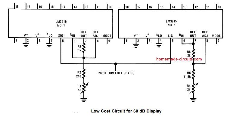 A superior technique shown in the below figure keeps the reference at 10V for each of the two LM3915 ICs and boosts the input signal to the lower LM3915 by 30 dB.
Given that a pair of 1% resistors are able to fix the amplifier gain at ˇŔ0.2 dB, the need for a gain reduction becomes unnecessary.
A superior technique shown in the below figure keeps the reference at 10V for each of the two LM3915 ICs and boosts the input signal to the lower LM3915 by 30 dB.
Given that a pair of 1% resistors are able to fix the amplifier gain at ˇŔ0.2 dB, the need for a gain reduction becomes unnecessary.
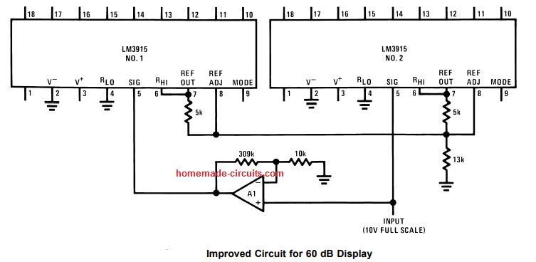 However, an 5 mV opamp offset voltage might be able to alter the first LED switching limit by around 4 dB, which necessitates an offset trimming.
Remember that just one adjustment may help to nullify the offset across the two the precision rectifier along with the 30 dB gain stage.
On the other hand, rather than amplifying, input signals of reasonably high amplitude could be supplied right to the lower LM3915 and subsequently attenuated by 30 dB to push the 2nd LM3915 IC.
However, an 5 mV opamp offset voltage might be able to alter the first LED switching limit by around 4 dB, which necessitates an offset trimming.
Remember that just one adjustment may help to nullify the offset across the two the precision rectifier along with the 30 dB gain stage.
On the other hand, rather than amplifying, input signals of reasonably high amplitude could be supplied right to the lower LM3915 and subsequently attenuated by 30 dB to push the 2nd LM3915 IC.
LM3915 Application Circuits
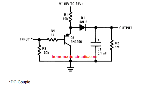 Half-Wave Peak Detector
The best way to exhibit an AC signal through IC LM3915 is to implement it directly to pin 5 unrectified.
Because the LED illuminated signifies the instantaneous magnitude of the applied AC waveform, it becomes possible to determine both maximum and average values of audio signals in the same method.
The LM3915 responds well to positive half-cycles specifically but will not be harmed any input signals as much as ˇŔ35V (or even way up to ˇŔ100V if a 39k resistor is used series with the input signal).
It's advised that you operate the circuit in the DOT mode and allow each LED to draw 30mA in order to get optimum brightness from the set up.
In order to detect mean value of the AC or for peak detection, rectification of the signal will be required.
If an LM3915 is setup with 10V full scale across its voltage divider, the switching threshold for the first LED will be just 450 mV.
An ordinary silicon diode rectifier might not work effectively at the lower levels because of the 0.6 V diode threshold.
The half-wave peak detector in the above Figure employs a PNP emitter-follower ahead of the diode.
Due to the fact that the transistorˇŻs base-emitter voltage blocks the diode offset in the range of around 100 mV, the method works good enough with single LM3915 applications using a 30 dB display.
Half-Wave Peak Detector
The best way to exhibit an AC signal through IC LM3915 is to implement it directly to pin 5 unrectified.
Because the LED illuminated signifies the instantaneous magnitude of the applied AC waveform, it becomes possible to determine both maximum and average values of audio signals in the same method.
The LM3915 responds well to positive half-cycles specifically but will not be harmed any input signals as much as ˇŔ35V (or even way up to ˇŔ100V if a 39k resistor is used series with the input signal).
It's advised that you operate the circuit in the DOT mode and allow each LED to draw 30mA in order to get optimum brightness from the set up.
In order to detect mean value of the AC or for peak detection, rectification of the signal will be required.
If an LM3915 is setup with 10V full scale across its voltage divider, the switching threshold for the first LED will be just 450 mV.
An ordinary silicon diode rectifier might not work effectively at the lower levels because of the 0.6 V diode threshold.
The half-wave peak detector in the above Figure employs a PNP emitter-follower ahead of the diode.
Due to the fact that the transistorˇŻs base-emitter voltage blocks the diode offset in the range of around 100 mV, the method works good enough with single LM3915 applications using a 30 dB display.
More Application Circuits
There are actually a huge number of circuit applications which you can build using the IC LM3915. I have already discussed a a handful of them in this website, which you can refer by visiting HERE: So folks this was a short description explaining the datasheet and pinout details of the IC LM3915. If you have any further doubts please let us know through the comment box below, we'll try to get in touch at an earliest. References https://www.digchip.com/datasheets/download_datasheet.php?id=514550&part-number=LM3915 https://es.wikipedia.org/wiki/LM3915High Current Zener Diode Datasheet, Application Circuit
Zener diodes that are normally available are mostly 1/4 watt or 1/2 watt types. And it is quite valid since the basic function of zener is to create stabilized reference voltage. Zener diodes are not designed for current regulation directly. However, for some applications where shunting excess voltage and current is necessary a high current or high watt zener diode becomes useful. The 1N53 series provides a complete range of high watt zener diodes specially created for high current and voltage regulation. The maximum power is 5 watt and voltage is upto 200V. Dividing the wattage with the voltage rating of the diode gives its effective current handling capacity. The pinout and marking diagram are shown below: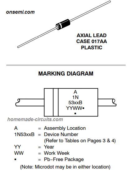 Main Features can be studied as given below:
Voltage Range 3.3 V to 200 V
ESD Rating of Class 3 (>16 kV) per Human Body Model
Surge Handling Capacity of up to 180 W for 8.3 ms
Maximum Steady State Power Dissipation @ TL = 25ˇăC, Lead Length = 3/8 in Derate above 25ˇăC is 5 watts
Main Features can be studied as given below:
Voltage Range 3.3 V to 200 V
ESD Rating of Class 3 (>16 kV) per Human Body Model
Surge Handling Capacity of up to 180 W for 8.3 ms
Maximum Steady State Power Dissipation @ TL = 25ˇăC, Lead Length = 3/8 in Derate above 25ˇăC is 5 watts
ELECTRICAL CHARACTERISTICS
The following list gives the various symbols used for indicating the electrical parameters and tolerance levels of the device. (TA = 25ˇăC unless otherwise noted, VF = 1.2 V Max @ IF = 1.0 A for all types). VZ= Reverse Zener Voltage @ IZT IZT= Reverse Current ZZT= Maximum Zener Impedance @ IZT IZK= Reverse Current ZZK= Maximum Zener Impedance @ IZK IR= Reverse Leakage Current @ VR VR= Breakdown Voltage IF= Forward Current VF= Forward Voltage @ IF IR= Maximum Surge Current @ TA = 25ˇăC VZ= Reverse Zener Voltage Change IZM= Maximum DC Zener Current By referring to the above symbols we can easily check the voltage and current specifications of the high power zeners diodes from the following table. This table can be used for selecting the preferred zener diode as per our requirements: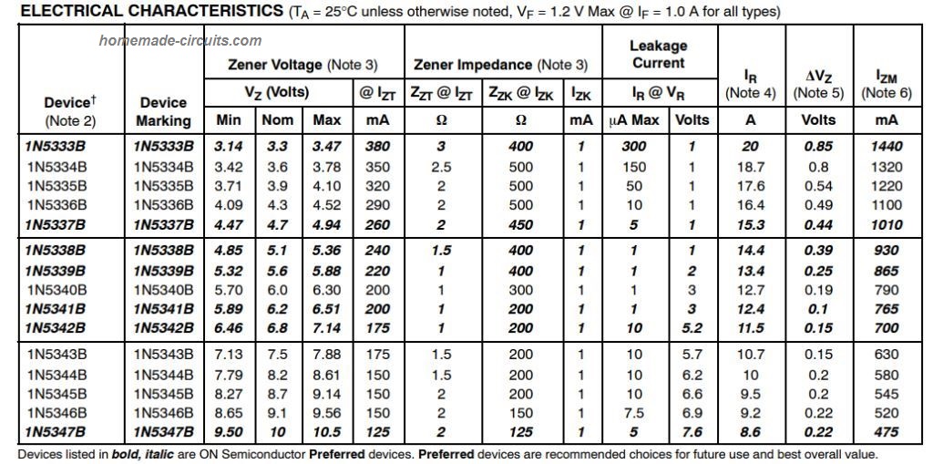 TOLERANCE AND TYPE NUMBER DESIGNATION: The JEDEC type numbers shown above symbolize a tolerance of ˇŔ5%.
ZENER VOLTAGE (VZ) and IMPEDANCE (IZT and IZK): Thezener voltage test condition and its impedance can be learned from this data:
Current IZ is applied 40ms ˇŔ10% before the measurements.
Mounting terminals are positioned 3/8ˇĺ to 1/2ˇĺ above the inner margin of mounting clips to the diode case (TA = 25ˇăC +8ˇăC, 2ˇăC).
SURGE CURRENT (IR): Surge current is defined as the maximum peak, nonrecurrent squarewave current having a pulse width, of 8.3 ms that can be tolerated by the device.
The information available in the following image can be referred to identify the maximum surge current for a square wave of any pulse width between 1 ms and 1000 ms.
TOLERANCE AND TYPE NUMBER DESIGNATION: The JEDEC type numbers shown above symbolize a tolerance of ˇŔ5%.
ZENER VOLTAGE (VZ) and IMPEDANCE (IZT and IZK): Thezener voltage test condition and its impedance can be learned from this data:
Current IZ is applied 40ms ˇŔ10% before the measurements.
Mounting terminals are positioned 3/8ˇĺ to 1/2ˇĺ above the inner margin of mounting clips to the diode case (TA = 25ˇăC +8ˇăC, 2ˇăC).
SURGE CURRENT (IR): Surge current is defined as the maximum peak, nonrecurrent squarewave current having a pulse width, of 8.3 ms that can be tolerated by the device.
The information available in the following image can be referred to identify the maximum surge current for a square wave of any pulse width between 1 ms and 1000 ms.
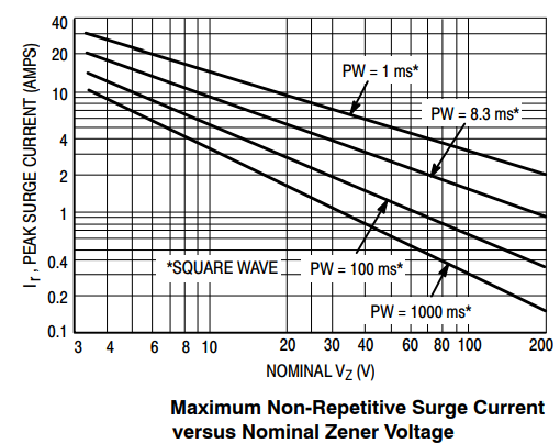 This may be implemented by plotting the relevant points on logarithmic paper.
The above figure shows an example result for a 3.3 V and 200 V zener.
VOLTAGE REGULATION (DVZ): The voltage regulation specifications for this series can be studied as given below:
VZ measurements are established at 10% and subsequently at 50% of the IZ max value as per the info provided in the electrical characteristics table.
The time duration for the test current for each VZ reading was recorded as 40 ms ˇŔ10%.
This may be implemented by plotting the relevant points on logarithmic paper.
The above figure shows an example result for a 3.3 V and 200 V zener.
VOLTAGE REGULATION (DVZ): The voltage regulation specifications for this series can be studied as given below:
VZ measurements are established at 10% and subsequently at 50% of the IZ max value as per the info provided in the electrical characteristics table.
The time duration for the test current for each VZ reading was recorded as 40 ms ˇŔ10%.
How to Identify Maximum Current Handling Capacity
MAXIMUM REGULATOR CURRENT (IZM): This can be calculated by referring to the maximum voltage of a 5% type unit. Meaning this is applicable only to the Bsuffix device. The effective current handling capacity IZM for any of these high current zener diodes cannot be exceeded the over 5 watts divided by the actual VZ of the device. With a condition where TL = 25ˇăC at 3/8ˇĺ for the device body. Meaning, suppose you are using a 3.3V zener, then the maximum tolerable current for this device can be calculated by dividing 5 with 3.3. That's equal to around 1.5 amp. The ˇ°GˇŻˇŻ suffix tells us about PbFree package or PbFree packages that are presently available.High Current Zener Diode Application
As stated earlier a high current diode can be used in applications where power dissipation may be OK and not a factor to be considered. Solar Panel Output Control For example it can be used for controlling a solar panel output effectively without involving complex and expensive controllers. The following image shows the bare minimum setup required for implementing a panel output control using a high power zener diode.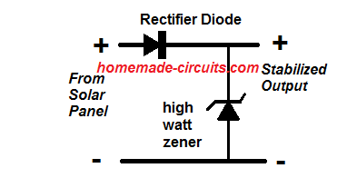 Simple LED Driver
A high current diode can be also effectively used for manufacturing cheap yet highly reliable LED drivers, as shown below:
Simple LED Driver
A high current diode can be also effectively used for manufacturing cheap yet highly reliable LED drivers, as shown below:
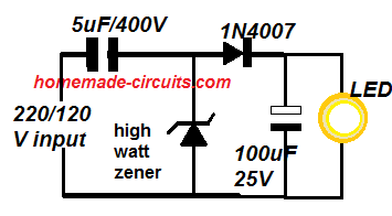 Over to You
OK so this was a short description regarding the specifications of high watt zener diode IN53. The tutorial explained us regarding the electrical features, tolerance, and how to use this type of zener diodes in practical application designs.
I hope you liked.
If you have any further doubts or suggestions, you may express them through comments below.
Over to You
OK so this was a short description regarding the specifications of high watt zener diode IN53. The tutorial explained us regarding the electrical features, tolerance, and how to use this type of zener diodes in practical application designs.
I hope you liked.
If you have any further doubts or suggestions, you may express them through comments below.
PIR Sensor Datasheet, Pinout Specifications, Working
In this post we are going to explore the datasheet of PIR or Pyroelectric Infrared Radial Sensor HC-SR501. We will understand for what purpose PIR sensor is used? Its basic trigger operations, pin connection details, technical specifications and finally we will be looking at some real life applications. We will begin by understanding the actual PIR sensor unit which are installed inside standard PIR modules and learn its internal characteristics, pinout details and internal working details.
What is a PIR Sensor?
PIR stands for Pyroelectic Infrared Radial Sensor or Passive Infrared Sensor. PIR is an electronic sensor which detects the changes in the infrared light across certain distance and gives out an electrical signal at its output in response to a detected IR signal. It can detect any infrared emitting object such as human beings or animals if it is the range of the sensor, or moves away from the range, or moves within the range of the sensor. The PIR sensor module can be divided in to two parts an infrared sensitive crystal and the processing circuit.Illustration of PIR sensitive crystal:
 The dark portion of the metal where the IR sensitive crystal is housed, the sensitive crystal can detect the level of infrared in the surroundings.
It actually houses two pyroelectic sensors for detecting moving objects.
If one of the sensitive crystals detects change in infrared (increment or decrement) than the other sensitive crystal, the output gets triggered.
A dome shaped plastic structure is normally placed over this sensitive crystal which acts as lens to focus the infrared light on the sensors.
The dark portion of the metal where the IR sensitive crystal is housed, the sensitive crystal can detect the level of infrared in the surroundings.
It actually houses two pyroelectic sensors for detecting moving objects.
If one of the sensitive crystals detects change in infrared (increment or decrement) than the other sensitive crystal, the output gets triggered.
A dome shaped plastic structure is normally placed over this sensitive crystal which acts as lens to focus the infrared light on the sensors.
How PIR Works
The sensing operation of a pyroelectric infrared sensor is based on the property or characteristic which becomes responsible for altering the polarization of its material in response to temperature changes. These sensors employ a dual or a pair of sensing elements for sensing the IR signals in two steps, which ensures a foolproof detection by cancelling the unwanted temperature variations within the existing EMI stage. This two-step sensing process improves the overall stability of the sensor and helps to detect IR signals only from human presence. When a human being or a relevant IR source moves past a PIR sensor, the radiation cuts into the pair of sensing elements in an alternate manner, triggering the output to generate a pair of ON/OFF or high and low pulses, as depicted in the following waveform: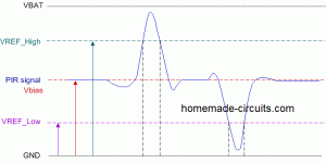 The following rough Gif simulation shows how a PIR sensor responds to a moving human and develops a couple of short sharp pulses across its output leads for the required processing or triggering an appropriately configured relay stage

Internal Layout of a PIR
The following figure shows the internal layout or the configuration inside a standard PIR sensor.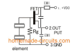 On the left we can see a pair of IR sensing elements connected in series.
The upper end of this series is connected with the gate of an in-built FET which acts as a small IR signal amplifier.
The Rg pull down resistor provides the required standby zero logic to the FET to makes sure that it stays completely switched OFF in the absence of an IR signal.
When a moving IR signal is detected by the pair of sensing elements, it generates a corresponding pair of hi and low logic signals as discussed above:
These pulses are appropriately amplified by the FET and replicated at its output pin for further processing by an attached circuitry.
The associated EMI stages along with the capacitor provide extra filtration to the process, in order to produce a clean set of pulses at the indicated output pin of the PIR.
On the left we can see a pair of IR sensing elements connected in series.
The upper end of this series is connected with the gate of an in-built FET which acts as a small IR signal amplifier.
The Rg pull down resistor provides the required standby zero logic to the FET to makes sure that it stays completely switched OFF in the absence of an IR signal.
When a moving IR signal is detected by the pair of sensing elements, it generates a corresponding pair of hi and low logic signals as discussed above:
These pulses are appropriately amplified by the FET and replicated at its output pin for further processing by an attached circuitry.
The associated EMI stages along with the capacitor provide extra filtration to the process, in order to produce a clean set of pulses at the indicated output pin of the PIR.
Testing Set Up for the PIR Sensor
The following image shows a standard PIR sensor test set up. The output and Vss pins (negative pin) of the PIR is connected with an external pull down resistor, the Vdd pin is supplied with a 5V supply.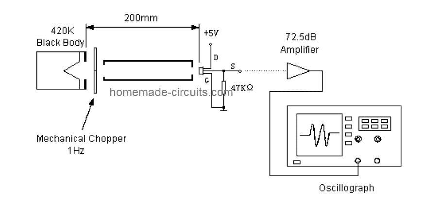 A stationery black body generates the required equivalent infrared radiation for the PIR sensor through a chopper mechanism.
The chopper plate alternately cuts the IR signals imitating a moving IR target.
This chopped IR signal hits the PIR sensor generating the specified pulses across its output pin, which is suitably amplified through an opamp for analysis on a scope.
The Ideal Test Conditions for the above set up can be seen below:
A stationery black body generates the required equivalent infrared radiation for the PIR sensor through a chopper mechanism.
The chopper plate alternately cuts the IR signals imitating a moving IR target.
This chopped IR signal hits the PIR sensor generating the specified pulses across its output pin, which is suitably amplified through an opamp for analysis on a scope.
The Ideal Test Conditions for the above set up can be seen below:
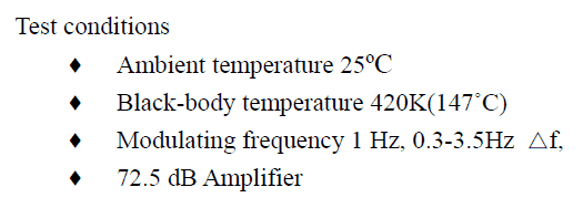
Balancing the Sensing Element output
Since a dual sensing mechanism is employed in PIRs, it becomes necessary to ensure that the processing through the pair of lenses is correctly balanced. The sensing elements are tested and appropriately configured by evaluating the respective single signal output voltage (SSOV) through the following formula: Balance: |Va ¨C Vb| / (Va + Vb) x 100% Where, Va = Sensitivity of side A (mV peak to peak) Vb = Sensitivity side B (mV peak to peak)Main Specifications
The main technical specifications and dimension parameters of a PIR sensor can be learned from the following details: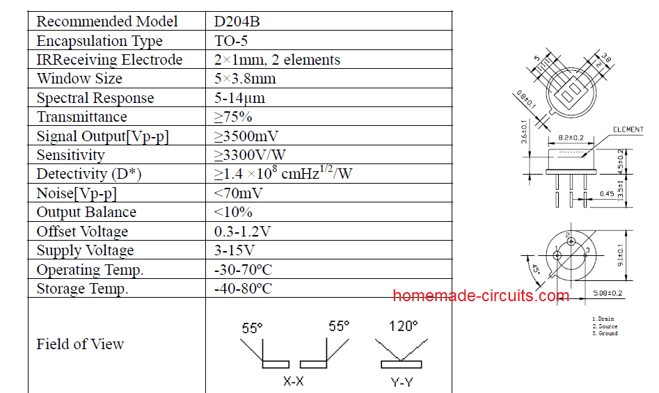
Using PIR Inside Modules
Today you will find PIR modules having a PIR sensor integrated with specialized processing circuit and lens. This enhances the performance of the PIR many folds and allows the end user to get well defined optimized, amplified output from the module. This output now only needs to be configured with a relay stage for the required ON/OFF switching of a load in response to a human presence across the stipulated zone. The circuit inside standard modules consist of IC BISS0001 which is specifically designed for motion detection applications. Two knobs are provided, one for adjusting the sensitivity of the module and another knob is for adjusting the time length for how long the output should stay HIGH after the module is triggered.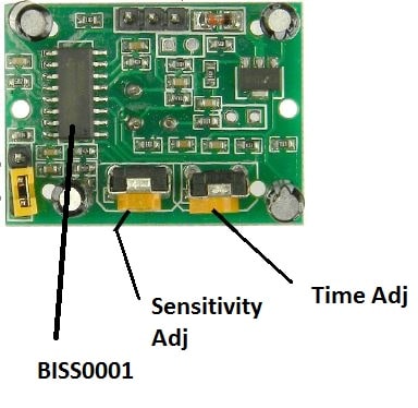 Now letˇŻs investigate the technical details of the PIR sensor HC-SR501.
Operating Voltage:
The HC-SR501 is from 5 V to 20 V, which makes great flexibility for circuit designers.
Current consumption:
The HC-SR501 is a battery friendly device; its current consumption is 65 mA when it detects any change in IR light.
Output Voltage:
When the module detects a motion of infrared the output goes HIGH at 3.3 V, if the module detects no motion it goes LOW or 0 V after a fixed period.
Delay time:
A knob is provided to adjust the time for the output to stay HIGH after detecting the IR.
This is time period can be adjusted from 5 seconds to 5 minute.
Sensitivity Range:
The angle of the detection area is around 110 degree cone.
A knob is given to adjust the sensitivity; we can vary from 3 meter to 7 meters perpendicular to senor.
The sensitivity reduces as we move either sides of the sensor.
Operating Temperature:
The HC-SR501 has an impressive operating temperature ranging from -15 to +70 degree Celsius.
Quiescent current:
The Quiescent current is the current consumed from the supply, when the sensor is not detecting any motion or when it is in idle.
It consumes less than 50 uA, which makes the sensor battery friendly.
Now letˇŻs investigate the technical details of the PIR sensor HC-SR501.
Operating Voltage:
The HC-SR501 is from 5 V to 20 V, which makes great flexibility for circuit designers.
Current consumption:
The HC-SR501 is a battery friendly device; its current consumption is 65 mA when it detects any change in IR light.
Output Voltage:
When the module detects a motion of infrared the output goes HIGH at 3.3 V, if the module detects no motion it goes LOW or 0 V after a fixed period.
Delay time:
A knob is provided to adjust the time for the output to stay HIGH after detecting the IR.
This is time period can be adjusted from 5 seconds to 5 minute.
Sensitivity Range:
The angle of the detection area is around 110 degree cone.
A knob is given to adjust the sensitivity; we can vary from 3 meter to 7 meters perpendicular to senor.
The sensitivity reduces as we move either sides of the sensor.
Operating Temperature:
The HC-SR501 has an impressive operating temperature ranging from -15 to +70 degree Celsius.
Quiescent current:
The Quiescent current is the current consumed from the supply, when the sensor is not detecting any motion or when it is in idle.
It consumes less than 50 uA, which makes the sensor battery friendly.
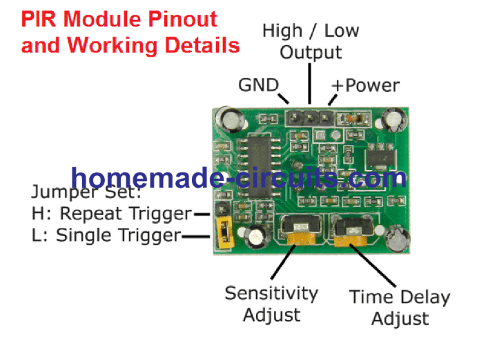 PIR pinouts and trigger modes
Trigger modes:
The PIR module has two trigger modes: Single trigger / non-repeat mode and repeat trigger. These two modes can be access by changing the jumper position given in the module. Single Trigger Mode / Non-repeat Mode: When the PIR sensor is set in single trigger mode (and the timer knob / delay time is set for 5 seconds (say)), when a human is detected the output turns HIGH for 5 seconds and turns LOW. Repeat Trigger Mode: When the PIR sensor is set in repeat trigger mode, when a human is detected the output turns HIGH the timer counts for 5 seconds, but when another human is detected with in those 5 seconds the timer reset to zero and counts another 5 seconds after 2nd human is detected. Block Time: The block time is the time interval where the sensor is disabled or will not detect motion. The block time for HC- SR501 is 3 seconds by default. This occurs after the delay time (which was set by timer knob) the output goes LOW for 3 seconds; during this interval no motion will be detected. After the 3 seconds (LOW) the sensor will be ready to detect motion again. In other words, when the sensor detects motion the output goes HIGH, the output remains HIGH as per the timer knob (say 5 seconds), after 5 seconds the PIR sensor goes LOW, the LOW signal will remain for 3 seconds regardless of the new motion if any. Dimensions of the module: The sensor is compact enough to hide from peopleˇŻs view so that it wonˇŻt affect decorates etc. It measures 32 mm x 24 mm. Lens Size: The white dome structure which encloses the pyroelectric sensor is called Fresnel lenses, which increase the detection range and it looks opaque. It measures 23 mm in diameter.Applications:
Security systems. Automatic lights. Industrial Automaton Control. Automatic doors. You can find some of the projects using PIR sensor in this site.Typical PIR Module Internal Circuit Diagram
For enthusiasts who intend to build the complete PIR module along with the sensor and a full fledged amplifier, the following standard PIR schematic can be employed and used for any relevant PIR sensor based application triggering.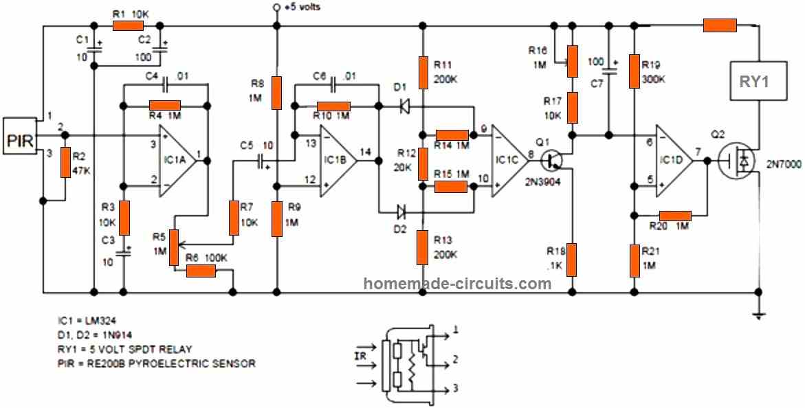 Have further doubts or questions? Please feel free to put them forth through the below given comment box
400V 40A Darlington Power Transistor Datasheet Specifications
In this post we investigate the datasheet and technical specifications of a 400V, 40A (ampere) power Darlington transistor MJ10022 and MJ10023, and also learn the main features of the device. We mostly find it difficult when it comes to finding a BJT with extreme voltage and current specifications such as with a 400V and 40 Amp limits. Here's one such device which is rated with extreme V and I specs, yet it is easily accessible across local electronic markets. This power BJT could be applied in all DC high voltage and high current applications This power transistor becomes even more special since it has an in-built Darlington feature ensuring maximum efficiency and high current gain, which allows the device to be switched with nominal input triggers and operate huge load using voltages upto 400V and current upto 40 amps.Main Features
The BJT MJ10022 and MJ10023 are Darlington power transistors are designed to work with fast switching high voltage and high current inductive circuits in which the fall time are typically critical, such as in line operated SMPS topologies. The main features of this device can be summarized as given below: High current and high voltage operations High speed switching Incorporates high-speed base-emitter diode Darlington high Gain output Designed for heavy duty Inductive loads.Maximum Absolute Ratings
Peak Collector-Emitter Voltage (Vcev) = 450V for MJ10022, and 600V for MJ10023 Sustained Collector-Emitter Voltage = 350V for MJ10022, and 400V for MJ10023 Maximum Emitter-Base Voltage (Vebo) = 8V Peak Collector Current Icm = 80A (ampere) Sustained Collector Current = 40A (ampere) Maximum Base Current (Ib) = 20A (ampere) Maximum Permissible Power Dissipation (Pd) = 250W (watts) at 25 degrees Celsius, and 143W (watts) at 100 degrees Celsius.Thermal Dissipation Graph
 Pinout Diagram of MJ10022, and MJ120023 (similar to any other TO3 package such as 2N3055)
 Actual Image of the Discussed 400V 40A BJT MJ10022/MJ10023

L293 Quad Half-H Driver IC Pinout, Datasheet, Application Circuit
In this post we investigate the technical specifications and pinout details of the IC L293 which is a versatile quad half-H driver IC, and can be used for implementing many interesting motordriver based circuit applications, such as for operating motors, solenoids and other inductive loads (4 units separately or in pairs through push-pull mode).How it Works
The IC L293 basically includes a two pairs of outputs which can be be independently used for operating two separate loads in a push pull mode or in a bidirectional manner, also referred to as totem pole mode.Alternatively these couple of pair of outputs can be individually used for operating 4 individual loads in a unidirectional manner. The above operations of the loads is controlled through corresponding input pinouts, triggered from a external oscillator circuit or a PWM source. For example if the load is required to be operated in a totem pole manner, the corresponding inputs of the two driver stages of the IC could be triggered from an external oscillator such as through a couple of NAND gates, wherein one gate could be wired as an oscillator while the other as an inverter. The two anti-phase signals from these NAND gates then could be connected with the inputs of the L293 for operating the relevant outputs in a totem pole (push-pull) manner, which in turn would run the connected load in the same fashion.Pinouts assignment of the IC L293
Now let's learn the pinout functions of the IC L293 by referring to the following diagram and from the following explanation: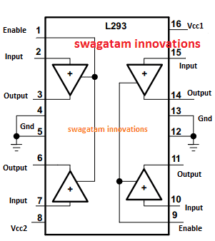 Pin#2 is the control input, which controls the output pin#3.
Similarly, pin#7 is the control input for the output pin#6.
Pin#1 is used for either enabling or disabling the above sets of pinouts.
A positive at pin#1 keeps the above sets of pinouts enabled and active, while a negative or 0V supply instantly disables them.
Quite identically, Pin#15 and pin#10 become the control inputs for the corresponding pin#14 and pin#11 outputs, and these remain operational only as long as pin#9 is held at positive logic and is disabled when a 0V logic is applied on this pinout.
As explained previously, pin#3 and pin#6 can be used as totem pole pairs by feeding an anti-phase logic signal on their input pin#7 and pin#2. Meaning, when pin#2 is being fed with a positive logic, pin#7 must be at a negative logic and vice versa.
This will allow the outputs pin#6 and pin#3 to be operate the connected load in a corresponding direction, and conversely when the input logic signals are reversed, the load polarity is also reversed and it will start rotating in the opposite direction.
If this sequence is rapidly switched then the load operates correspondingly in a to-and-fro manner or in a push pull manner.
The above operation can be replicated across the other side pair of drivers also.
The Vcc or the supply positive inputs for the IC are configured independently for two different supply inputs.
Pin#16, (Vcc1) is used for operating the enable pinouts and for operating other internal logic stages of the IC, and this could be supplied with an input of 5V, although maximum limitation is 36V
Pin#8, (Vcc2) is specifically used for powering the motors, and this can be fed with anything from 4.5V to 36V
Pin#2 is the control input, which controls the output pin#3.
Similarly, pin#7 is the control input for the output pin#6.
Pin#1 is used for either enabling or disabling the above sets of pinouts.
A positive at pin#1 keeps the above sets of pinouts enabled and active, while a negative or 0V supply instantly disables them.
Quite identically, Pin#15 and pin#10 become the control inputs for the corresponding pin#14 and pin#11 outputs, and these remain operational only as long as pin#9 is held at positive logic and is disabled when a 0V logic is applied on this pinout.
As explained previously, pin#3 and pin#6 can be used as totem pole pairs by feeding an anti-phase logic signal on their input pin#7 and pin#2. Meaning, when pin#2 is being fed with a positive logic, pin#7 must be at a negative logic and vice versa.
This will allow the outputs pin#6 and pin#3 to be operate the connected load in a corresponding direction, and conversely when the input logic signals are reversed, the load polarity is also reversed and it will start rotating in the opposite direction.
If this sequence is rapidly switched then the load operates correspondingly in a to-and-fro manner or in a push pull manner.
The above operation can be replicated across the other side pair of drivers also.
The Vcc or the supply positive inputs for the IC are configured independently for two different supply inputs.
Pin#16, (Vcc1) is used for operating the enable pinouts and for operating other internal logic stages of the IC, and this could be supplied with an input of 5V, although maximum limitation is 36V
Pin#8, (Vcc2) is specifically used for powering the motors, and this can be fed with anything from 4.5V to 36V
Electrical Specification of the IC L293
The IC L293 is designed to operate with a any supply between 4.5V and 36V, with a maximum current handling specification of not more than 1 amp (2 Amp in pulse mode, 5ms max) Therefore any load within the above mentioned specifications can be operated across the discussed outputs of the IC L293. The Input control logic should not be exceeded above 7V, whether as a continuous supply or PWM supply.Using L293 IC for Motor Control Application
Now let's learn how to implement motor controller circuits using the IC L293 through different modes of operations, and by using as many as 4 motors with separate control facility. In our previous post we studied the pinout and functioning details of the IC L293, here we learn how the same IC can be used for controlling motors through specific modes and configurations.Control Modes
The IC L293 can be used for controlling motors in the following modes: 1) 4 motors through independent PWM inputs. 2) 2 Motors in a bidirectional or totem pole mode with speed control through PWM 3) One 2-phase BLDC motor using PWM input The image below shows how the IC could be used for controlling motors with independent controls, and also how a single motor could be used for achieving a bidirectional control: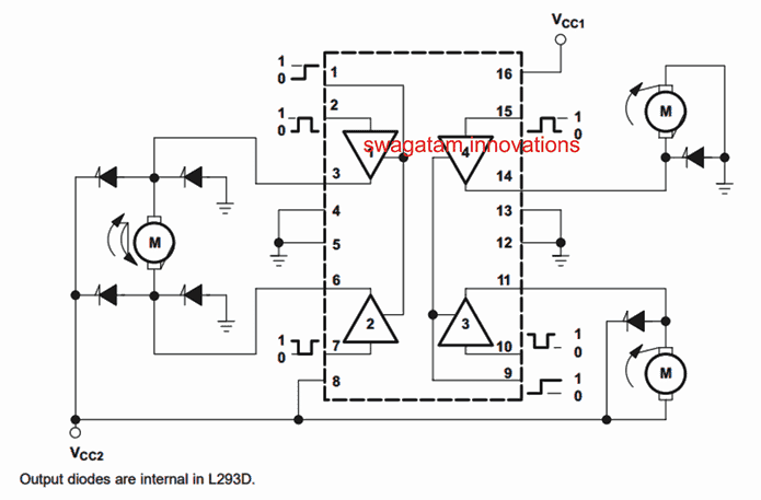 The left side of the IC shows a motor being configured to work in the bidirectional mode.
To ensure that the motor spins in one of the selected directions, pin#1 and pin#7 must be applied with an anti-phase 5V DC input.
To change the direction of the motor rotation, this 5V polarity could be changed across the mentioned input pinouts.
Pin#1 must be held at logic high in order to keep the motor and the IC functioning enabled, a logic 0 here will instantly stop the motor.
The supply at the control inputpinouts could be in the form of a PWM, this could be additionally used for controlling the speed of the motor from 0 to maximum simply by varying the PWM duty cycle.
The right side of the IC depicts an arrangement wherein a couple of motors are controlled independently through independent PWM inputs at the respective pin#15 and pin#10.
Pin#9 must be held at logic high in order to keep the motor and the IC functioning.
A logic zero at this pinout will instantly stop and disable the function of the attached motors.
Since the left side and the right side sections of the IC are identical with their pinout functioning details, the shown arrangement of the motors could be swapped across the relevant pinouts to achieve identical functioning as explained above, meaning two individual motors could be connected at the left side of the IC exactly as implemented at the right side of the IC in the diagram.
Similarly the bidirectional system could be incorporated at the right side of the IC pinouts exactly as achieved at the left side of the IC in the above shown diagram.
The above example shows how the IC L293 can be used for controlling 4 motors individually, or 2 motors in a bidirectional mode, and how the speed also can be controlled using a PWM feed at the relevant input pinouts of the IC.
The left side of the IC shows a motor being configured to work in the bidirectional mode.
To ensure that the motor spins in one of the selected directions, pin#1 and pin#7 must be applied with an anti-phase 5V DC input.
To change the direction of the motor rotation, this 5V polarity could be changed across the mentioned input pinouts.
Pin#1 must be held at logic high in order to keep the motor and the IC functioning enabled, a logic 0 here will instantly stop the motor.
The supply at the control inputpinouts could be in the form of a PWM, this could be additionally used for controlling the speed of the motor from 0 to maximum simply by varying the PWM duty cycle.
The right side of the IC depicts an arrangement wherein a couple of motors are controlled independently through independent PWM inputs at the respective pin#15 and pin#10.
Pin#9 must be held at logic high in order to keep the motor and the IC functioning.
A logic zero at this pinout will instantly stop and disable the function of the attached motors.
Since the left side and the right side sections of the IC are identical with their pinout functioning details, the shown arrangement of the motors could be swapped across the relevant pinouts to achieve identical functioning as explained above, meaning two individual motors could be connected at the left side of the IC exactly as implemented at the right side of the IC in the diagram.
Similarly the bidirectional system could be incorporated at the right side of the IC pinouts exactly as achieved at the left side of the IC in the above shown diagram.
The above example shows how the IC L293 can be used for controlling 4 motors individually, or 2 motors in a bidirectional mode, and how the speed also can be controlled using a PWM feed at the relevant input pinouts of the IC.
Using L293 to control a 2-phase BLDC motor
 In the above image we can see how the IC L293 can be configured to control a 2-phase BLDC motor using the indicated pinouts and through a couple of control inputs shown as control A and control B.
A single 2-phase motor can be seen connected across the outputs of the IC, while the inputs are wired with a set of NOT gates which become responsible for creating the required anti-phase input logic for the motor control.
Control A and Control B points may be subjected to an alternating logic for enabling the 2-phase motor to rotate correctly.
The polarity of the alternating logic decides the rotational direction of the motor.
For achieving a linear speed control on the motor, a PWM form of logic could be implemented across the control A and control B inputs and its duty cycle could be varied for achieving the desired speed control on the connected motor.
If you have further doubts regarding the technical specifications, or the datasheet or the pinout details of the IC, you can always feel free to comment below for instant replies.
In the above image we can see how the IC L293 can be configured to control a 2-phase BLDC motor using the indicated pinouts and through a couple of control inputs shown as control A and control B.
A single 2-phase motor can be seen connected across the outputs of the IC, while the inputs are wired with a set of NOT gates which become responsible for creating the required anti-phase input logic for the motor control.
Control A and Control B points may be subjected to an alternating logic for enabling the 2-phase motor to rotate correctly.
The polarity of the alternating logic decides the rotational direction of the motor.
For achieving a linear speed control on the motor, a PWM form of logic could be implemented across the control A and control B inputs and its duty cycle could be varied for achieving the desired speed control on the connected motor.
If you have further doubts regarding the technical specifications, or the datasheet or the pinout details of the IC, you can always feel free to comment below for instant replies.
LM35 Pinout, Datasheet, Application Circuit
The post explains how to make an LM35 application circuit by understanding its datasheet, pinouts and other technical specifications. By: SS kopparthyLM35 Main Specifications
The IC LM35 is a temperature measuring device that looks like a transistor (most popular package is TO-92 package). This device is found in most of the circuits that need to measure temperature as this device is a low-cost, reliable and with an accuracy as high as +-3/4 degrees Celsius. The low cost of the sensor is because of its wafer-level trimming and calibration. This IC is much better than the thermistor due to the accuracy in temperature measurement.
Pinout Details
As you can see in the above figure, the LM35 IC consists of three pins out of which two are for powering the sensor and the other one is the output signal pin. The sensor can work anywhere from -55 to 150 degrees Celsius. The output temperature is directly proportional to the temperature change in Celsius. Also the other variant LM35C is available and its temperature range is -40 to 110 degrees Celsius.Technical Specifications and Features
This device gives out 10mV per degree Celsius rise in temperature. This device consumes just 60¦ĚA current. So it does not drain much of power from the battery or power source. Also, due to this low current, self heating of the device is as low as 0.1ˇăC. Other variants of this device that have different packages are also available such as TO-46 and TO-220. These work same as the traditional one but differ in their usage areas and feasibility for a particular application. For example, TO-46 metal package can be used to measure surface temperature as the metal package can be directly kept in contact with the surface whose temperature needs to be measured, while the TO-92 package could not as the device measures the temperature mostly based on the temperature of the terminals of the device as metal terminals conduct more temperature than the plastic casing. Hence the TO-92 packaged LM35 is used to measure air temperatures in most of the circuits.
Block Diagram and Internal Functioning
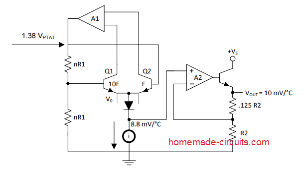 The above image shows the internal block diagram of the IC LM35. Here we can see that the IC is internally configured around a couple of opamps A1 and A2. The first opamp A1 is configured as an accurate temperature sensor through a feedback loop formed by a couple of BJTs configured as a current mirror.
The current mirror ensures a perfectly linear and a stabilized rate of temperature detection and prevents false triggering or inaccurate temperature readings at the output.
The sensed temperature is produced at the emitter side of the current mirror at a rate of 8.8mV per degree Celsius.
The output is applied to a buffer stage using another opamp A2 which is configured as a high impedance voltage follower.
This A2 stage acts as a buffer to reinforce the temperature to voltage conversion, and presents it at the final output pin of the IC via another high impedance BJT stage configured as an emitter follower.
The final output thus becomes highly isolated from the actual temperature sensor stage and delivers highly accurate temperature sensing response, which can be used by the user with an external switching stage such as a relay driver stage or a triac.
The above image shows the internal block diagram of the IC LM35. Here we can see that the IC is internally configured around a couple of opamps A1 and A2. The first opamp A1 is configured as an accurate temperature sensor through a feedback loop formed by a couple of BJTs configured as a current mirror.
The current mirror ensures a perfectly linear and a stabilized rate of temperature detection and prevents false triggering or inaccurate temperature readings at the output.
The sensed temperature is produced at the emitter side of the current mirror at a rate of 8.8mV per degree Celsius.
The output is applied to a buffer stage using another opamp A2 which is configured as a high impedance voltage follower.
This A2 stage acts as a buffer to reinforce the temperature to voltage conversion, and presents it at the final output pin of the IC via another high impedance BJT stage configured as an emitter follower.
The final output thus becomes highly isolated from the actual temperature sensor stage and delivers highly accurate temperature sensing response, which can be used by the user with an external switching stage such as a relay driver stage or a triac.
Using a Heatsink
The LM35 sensor IC can also be soldered to a heatsink fin to increase the accuracy and to decrease the sensing and response time in slowly moving air. To understand much better, letˇŻs take a look at the following circuit that uses LM35 to give an indication when the temperature is above the specified level:
Temperature Detector Circuit Using LM35 IC
The LM35 circuit uses an op-amp IC741 as comparator. The op-amp is configured as an non-inverting amplifier. That means when the LM35 detects high temperature, the output of the op-amp becomes +ve and the red LED lights up and the temperature falls below the specified level, the output of op-amp becomes ¨Cve and the green LED lights up. The high temperature level can be set with the help of preset in the circuit. To set the temperature level for which the red LED lights up, you need to know the actual temperature where the circuit is being tested. For that you can use a multimeter. As we know that the LM35ˇŻs output voltage increases 10mV per degree Celsius rise in temperature, we can use the multimeter to measure the output voltage and for example the voltage is 322mV, then the temperature at the place is 32.2ˇăC. You can even test the IC if itˇŻs working or not using the above procedure. You can measure the actual temperature using an atmospheric thermometer and compare it with the values obtained with the LM35. You might not get the exact values but you should get close values.LM35 Relay Control Circuit
An accurate LM35 based temperature controller can be built for controlling an external load such as a heater or a fan by attaching a relay driver stage to our previous as shown below: After understanding how the above LM35 circuit works, you should have understood how LM35 works practically in circuits.
Alarm Signal Generator IC ZSD100 Datasheet, Application
The ZSD100 is an alarm frequency generator IC which incorporates a frequency swept alarm signal generator designed solely for fixed and vehicle protection alarm systems.Circuit Operation
For acquiring the specified alarm sound from this IC, just a single ZSD100, two timing capacitors, an in-expensive TO92 darlington, piezo transducer and coupling transformer is everything that becomes necessary to generate an extremely loud, ear piercing 120 dB warning siren. Together with an acoustic frequency signal generator, low frequency sweep generator, shut down circuitry and output driver stages, the ZSD100 has been attributed with all functionality crucial to generating an approved alarm indication. You may get this IC with a choice between an 8 pin DIL or SO bundle the IC grants an inexpensive stream-lined approach to siren signal technology. The system may be powered from inputs of 4V as much as 18V which specifically becomes suited for security detectors in battery driven products, burglar alarms and vehicle anti robbery techniquesFUNCTIONAL Information
The acoustic indication of the ZSD100 is created employing a squarewave oscillator whose operation is competent of directly triggering numerous output circuits. To generate a peculiar alarm siren sound, the frequency of the audio oscillator is swept over an allocated 2:1 spectrum by another, lower frequency oscillator. The frequencies of both the oscillators are regulated by R T (INT) and capacitors C MOD and C OUTPINOUT DESCRIPTIONS
Pin#1. RT: Non-obligatory superficial resistor for enhanced frequency management. An peripheral resistor boosts the domination of each the modulating and output oscillators. The RT pin is furthermore employed to energize the gadget down. Possibly attaching RT to VCC or an open circuit would probably bring about the device getting crippled. Pin#2. SAW: Choice of modulation waveform is done employing the SAW pin. An open circuit generates a triangle wave, sawtooth is accomplished by joining SAW to the CMOD pin. Pin#3. CMOD: An exterior capacitor would be used to program the low frequency modulating oscillator. The worth of CMOD advisable is between 0.1¦ĚF and 10 0¦ĚF. Pin#4. GND Pin#5. COUT: An secondary capacitor would be used to program the output oscillator. The value of COUT endorsed is between 1nF and 100nF. Pin#6. Q Non inverted output driver Pin#7.Q Inverted output driver Pin#8. VCCAlarm Circuits Using ZSD100
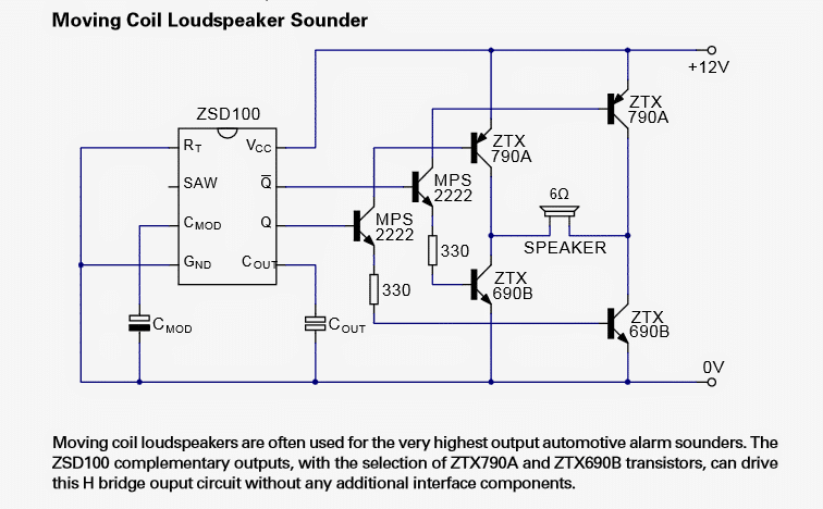
High Voltage Transistor MJ11021(PNP) MJ11022 (NPN) Datasheet ¨C Complementary Pair
MJ11021(PNP) MJ11022 (NPN) are high voltage complementary pair Darlington transistors suitable for all applications that involve high voltage high current such as in motor control, inverters, etc. Let's understand the datasheet and the main specifications of the devices:Main Electrical Features
MJ11021(PNP) MJ11022 (NPN) are 250V, 15 amp complementary Darlington transistors Being Darlington by nature, the devices exhibit a high Dc current gain, typically at 10amp, the hFe could be at least 400 The collector to emitter continuously voltage handling capacity is minimum 250V Low saturating voltage requirement for collector emitter, at around 1V when current is @ 5amps. The devices are SOA verified @ 44V VCE and 4 amp current for 250ms These are manufactured without any Pb content.Pinout Diagram
Maximum Ratings of the MJ11021(PNP) MJ11022 (NPN) transistors are as given under
CollectorEmitter Voltage VCEO 250 Vdc CollectorBase Voltage VCBO 250 Vdc EmitterBase Voltage VEBO 50 Vdc Collector Current Continuous 15amps DC Peak 30amps DC Base Current IB 0.5 Adc Total Power Dissipation PD 175 Watts @ TC = 25ˇăC Derate Above 25ˇăC 1.16W/ˇăC Operating and Storage Junction TJ, Tstg ¨C65 to +175Temperature Range 65 to +200ˇăC The above are those figures which may not be exceeded under any situation in order to prevent permanet damage to the devices.IC 4040 Datasheet, Pinout, Application
The IC 4040 is technically a 12-stage binary ripple counter chip, in simple words a device which will produce a calculated delayed frequency output in response to every pulse applied at its clock input. This delay is incremented at the rate of 2n where n is the pinout order in the sequence of its outputs.
Main Technical Specifications
The main features and specifications of the IC may be understood as follows: Fully buffered 12 outputs which divide the input clocks at the rate 2n where n = the pinout order starting from Q0 until Q11. The above sequencing of the outputs happens in response to every falling edge of the clock applied at its clock input CP pinout. The IC will respond even to a relatively slow falling clock pulse as effectively. A single asynchronous master reset (MR) input which resets all outputs to zero when a high logic is applied, whereas a constant low logic enables the IC to stay active. The IC becomes fully operational with Vdd as low as of 3V and sustains a constant operational characteristic even at voltages around 15V. Let's examine the parameters which shouldn't be exceeded for the IC 4040 Supply Voltage (Vdd) = Typically between 3 V and 15 V, 18 V being the maximum limit. Input Voltage (Vi) = The voltage that may be applied at the inputs such as CP, MR etc should be typically below Vdd or at the most = Vdd+ 0.5V Optimal Operating Current Requirement = 50mA since so many outputs are involved and each outputPinout Details
 The diagram above depicts the pinout configuration of the IC 4040, they may be evaluated as given under:
Pinouts Q0 to Q11 are the outputs of the IC.
Vss is the ground pin.
Vdd is the positive pin.
MR is the reset pinout
CP is the clock input.
The diagram above depicts the pinout configuration of the IC 4040, they may be evaluated as given under:
Pinouts Q0 to Q11 are the outputs of the IC.
Vss is the ground pin.
Vdd is the positive pin.
MR is the reset pinout
CP is the clock input.
Timing Sequence
Now let's analyze the output timing sequence of the IC 4040. As shown in the following diagram, we are able to see and understand the following details: As long as the MR input is high, the IC outputs produce no response. As soon as it goes low, the IC starts responding and counting the input clock at the CP input. The first output pin Q0 goes high after 2n clock at CP, that's = 20 = 1, meaning Q0 becomes high at the falling edge of the first pulse and goes low in response to the falling edge of the subsequent clock and so on. Similarly Q1 goes high after 21 = 2, meaning it goes high as soon as a falling edge of the second clock is detected and goes low at the falling edge of the 4th subsequent clock and so on. Identically Q2 goes high and low after 22 = 4th clock's falling edges, and so on. The above sequence is continued until Q11, in response to the sustained clock inputs at CP . It means if suppose the CP is clocked with a 1Hz pulse, Q11 would go high after 211 seconds or after 2048 seconds that's equal to 34 minutes approximately, just imagine the range of delay that you can achieve by simply increasing the clock input by seconds or perhaps by minutes.
Application Hints
From the above detailed analysis of the IC 4040 datasheet we can conclude that the IC is typically suited for all application which involve frequency division requirements or delayed time period generation requirements. Therefore it could become specifically suited for frequency divider circuit applications, long duration timers, flashers and other such similar applications.TSOP1738 Infrared Sensor IC Datasheet, Pinout, Working
The TSOP17XX series of ICs are infrared sensor devices designed for sensing infrared frequencies only with a specific range of modulated frequency, and interpreting them into a proportionate magnitude of electrical pulses at the output. This is specifically done to make the sensor immune to other forms of infrared signals present in the atmosphere such as from sunlight, fluorescent tube lights etc. This feature allows the device to be used in various forms of remote control applications without worrying about any form of external false triggering. The TSOP 1738 series ICs are commonly used in many infrared remote control systems, such TV, remote handsets, or setop box remote controls etc. The lead frame is used to assemble the preamplifier and PIN diode along with the IR filter which is a design of the epoxy package. A microprocessor is used to decode the output signal directly which is demodulated in an easy way. The TSOP 1738 series is considered as the standard series for the infrared remote control receiver which in turn supports all the important transmission codes.Remote IR Sensor Pinout Details
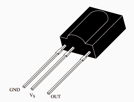
Available IR Sensor Types
TSOP1730 - 30 kHzTSOP1733 - 33 kHzTSOP1736 - 36 kHzTSOP1737 - 36.7 kHzTSOP1738 - 38 kHzTSOP1740 - 40 kHzTSOP1756 - 56 kHz Typical application circuit and connections are shown below
Main Electrical Specifications
The TSOP 17XX series provides two benefits of preamplifier an photo detector in a single package An internal filter is present for the facilitation of PCM frequency TSOP 17XX series provides an enhanced shielding against the disturbances produced by the various kinds of electrical fields It is also compatible to TTL and CMOS The output active given by the TSOP 17ˇ series is low It consumes low power The immunity provided by TSOP 17ˇ series against ambient light is high TSOP 17XX series enables a continuous data transmission of up to 2400 bps The device provides 10 cycles/burst which is considered as the most appropriate burst lengthAbsolute Maximum Rating
Basic Characteristics
Testing with 38 kHz Frequency - Video
How TSOP1738 IC Works
The circuit design of the TSOP 1738 series has been designed to work in such a way that it avoids any kind of output pulses which occurs unexpectedly due to the signal disturbances and noise. In order to suppress or avoid this noise and signal disturbances, the TSOP 1738 series works by using different applications such as an integrator stage, a bandpassfilter, and an automatic gain control. The distinction between a disturbance signal and a data signal can be carried out by reading the burst length, carrier frequency, and the duty cycle.The criteria or conditions which a data signal needs to fulfill are as follows:
The carrier frequency of the data signal needs to be close to the bandpassfilterˇŻs center frequency such as at a frequency of 38kHz The burst length of a data signal must be either 10 cycles/burst or longer than that A gap time after each burst which usually ranges between 10 cycles to 70 cycles for a data signal should necessarily be at the minimum of 14 cycles. For every burst of the data signal which occurs for duration of more than 1.8ms, the corresponding gap time is essential at some time of the process within the data stream. The length of this gap time must be at least equal to the burst length. In a data signal, approximately 1400 short burst can be received every second on a continuous basis The various data formats which are considered suitable are: Toshiba Micom Format, NEC Code, RC5 Code, R-2000 Code, Sharp Code, RC6 code, and SIRCS (Sony Format). The data signal can be received in a TSOP 17xx series even when a disturbance signal is applied to the TSOP 17xx series. But, the sensitivity in this case is reduced to a specific level where the occurrences of unexpected pulses can happen. The different disturbance signals, which can be suppressed when TSOP 17xx series is used, are: DC light which can range from a simple tungsten ball to the more powerful natural resource of sunlight The signal which are continuously received at 38kHz or signal received at frequency other than 38kHz The signals which are received from fluorescent lamps which consist of electronic ballast. The figure given below shows a sample of how the signal modulation occurs.
High Voltage, High Current Transistor TIP150/TIP151/TIP152 Datasheet
The TIP150, TIP151, TIP152 series are high voltage, high current Darlington transistors which can be used for applications involving voltages at mains 120V or 220V levels. The datasheet and other related details can be read in the following article. The typical applications of this transistor could be for high voltage motor control, automotive ignition, inverter converter switching, SMPS and in many other similar areas.Main Specifications
The main datasheet, specifications and features are as follows: Collector to Emitter Continuous Voltage: VCEO(sustained) = 300V minimum for (TIP150) VCEO(sustained) = 350V minimum for (TIP151) VCEO(sustained) = 400V minimum for (TIP152) CollectorEmitter Saturation Voltage: VCE(sat) = 2V maximum at I current of 5A The maximum current for the above voltages is 7 amps (continuous) and 10 amps for instantaneous peaks. The base/emitter saturation voltage for TIP150, 151, 152 is 1.5V at 100mA for a typical 2 amp collector load, while it could be around 250mA at 2.3V for a 5amp collector load.
Pinout Details
In the shown image above the pinouts of the transistor can be identified as follows: The center lead is the collector, it's connected with the metal tab of the device therefore the back steel tab also becomes the collector. The right side lead is the emitter. The left side lead is the base of the transistor.
Internal schematic of the transistor TIP150/TIP151/TIP152
The above figure shows the internal Darlington structure of the transistor. A typical paired transistors could be seen here which forms the Darlington configuration. This configuration helps to provide the device with extremely high gain and sensitivity even at the specified high power inputs.IC 4033 Pinouts, Datasheet, Application
Here we learn the main features, specifications and datasheet of the IC 4033 through a detailed technical analysis.How IC 4033 Works
The IC 4033 is another Johnson decade counter/decoder IC specifically designed for working with 7 segment displays. Basically itˇŻs a clock or pulse counter IC which responds to positive pulses at its clock input and decodes it serially to produce a directly readable display of the count number through the connected 7 segment display module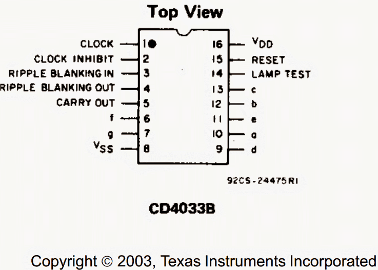
Pinout Specification of IC 4033
LetˇŻs try to understand how to use the IC 4043 by knowing the functions of its pinouts: Pin#1: ItˇŻs the clock input pinout of the IC, which is assigned for accepting positive clock signals or the pulses which needs to be checked or counted. Pin#2: ItˇŻs the clock inhibit pinout of the IC, As the name refers to, this pinout could be used for inhibiting the IC from responding to the input pulses by configuring this pinout to the positive supply or the Vdd. Conversely in order to allow normal functioning of the IC this pinout should be grounded. Pin#3/#4: These are the Ripple blanking IN and Ripple blanking OUT pinouts of the IC, which provides the user with the option of either allowing the non-significant zeros to be displayed or to be left out from the connected digital displays. For example suppose you have cascaded 8 nos 4033 ICs for reading 8 digit displays and have reached a reading of say 0050.0700. Expressing this number as 50.07 makes more sense than 0050.0700, for implementing this we need to assign pin3/4 which are blanking IN and blanking out respectively in a certain unique manner across the 8 ICs. To understand the procedure weˇŻll need to take account of the digits which is most significant in the order, and which is least significant.Automaticnon-significant Zero Suppressing
In the number 0050.0700, the most significant digit on the integer side is ˇ°0ˇ± in between 5 and the decimal, conversely in the fractional side the least significant digit is ˇ°0ˇ± at the extreme right. For enabling the RBI and the RBO (pin#3/#4) correctly on the integer side, we need to connect RBI of the IC associated with the most significant digit to a low logic or ground and the RBO of that IC to the preceding lower significant ICˇŻs RBI. This should continued until we reach the first IC associated with the extreme left digit of the integer side. Now for suppressing the non-significant zeros at the fractional side, we need to connect the RBI of the IC 4033 associated with the least significant display to ground and connect its RBO with the previous ICˇŻs RBI, and continue this until we reach the extreme digit of the display situated just before or just at the right side of the decimal point. The above feature of the IC is called automatic non-significant zero suppressing. However if the display is intended to display a purely fractional number, then the RBI pinout of the IC associated with the display thatˇŻs touching the decimal point on the integer side must be terminated to the positive supply. For example, for a number 0.7643, the IC associated with ˇ°0ˇ± must be tackled as explained above, same for the IC associated with the digit ˇ°0ˇ± for the number 764.0 The above feature of suppressing non-significant zeros might look ˇ°insignificantˇ± however the feature heps to save ˇ°significantˇ± amount of power and becomes incredibly useful for applications that employ battery as the power source. Pin#14: ItˇŻs the ˇ°lamp testˇ± pinout of the IC. As the name signifies it is used for testing the connected digital displays in terms of illumination level. When this pinout is connected to a high level or the positive supply, the normal function of the IC is disabled and all the digits of the 7 segment display are applied with a high state so that the digits are allowed to get illuminated together. This allows us to test the intensity levels of the digits and if any of the display digits are not functioning optimally or are dim due to some malfunction. Pin#6,7,9,10,11,12,13: All these pinouts are the outputs of the IC which are configured with the discussed 7 segment digital display module. Pin#15: ItˇŻs the reset input of the IC, a high logic or applying the supply voltage to this pin resets the IC completely, resulting in clearing all the data from the display and restoring it to zero. Pin#5: ItˇŻs the carryout pinout of the IC, it sends a high logic output after every 10 legit clocks at the clock pin#1 of the IC. Thus pin#5 is used as a clock output or a carry forward extension for the next corresponding IC 4033 when many of these are cascaded together in a multi-digit display counter systems. Pin#16 is the Vdd or the supply input of the IC. Pin#8 is the Vss, or the ground or the negative supply input pinout of the IC 4033. The IC works best with supply voltages between 5V and 20V.IC 4047 Datasheet, Pinouts, Application Notes
The IC 4047 is one of those devices which promises an unlimited range of circuit application solutions. The IC is so versatile that on many occasions it easily outsmarts it's close rival, the IC 555, let's study the datasheet and pinout details of this versatile chip.Main Datasheet and Specifications:
In-built oscillator with variable frequency option through an external RC network. Complementary push-pull outputs with a separate active clock output, the clock output is actually an extension of the internal oscillator frequency output. Duty cycle locked to 50% for precision, fail proof operation of the external stages. The IC 4047 can be configured as a free running astable MV, and also as a monostable MV. In the astable mode the chip provides the option of integrating external triggering inputs, also called true gating and complement gating modes. The monostable mode enables positive edge triggering as well as negative edge triggering of the IC. It further allowsretriggerable feature for extending the output timing to the desired calculated level. Meaning after the normal trigger is applied to the IC, more number subsequent triggers can be applied so that the output adds up the timing, generating further delay at the output. Internal Logic Diagram
Pinout Details
The following explanation suggests how the pinouts of the IC 4047 may be configured for implementing the above discussed operating modes: In the free running astable mode, connect pins4, 5, 6, 14 to positive or Vdd, connect pins 7, 8, 9, 12 to ground or Vss. Vdd must be supplied with a recommended 3V to 15V and maximum 18V (absolute). In gated astable mode connect pins4, 6, 14 to positive or Vdd, connect pins 7, 8, 9, 12 to ground or Vss, connect pin 5 to the reset pin of the external trigger IC, while output of the external chip to pin 4 of the IC 4047. For the above modes, the output may be obtained across pin 10, 11 (push-pull) while clocks at pin 13. In positive trigger monostable mode, connect pins 4, 14 to positive or Vdd, connect pins5, 6, 7, 9, 12 to ground or Vss, connect pin 8 to the reset pin of the external trigger IC, while output of the external chip to pin 6 of the IC 4047. For the above modes, the output may be obtained across pin 10, 11.Fundamental Free Running Astable Mode Circuit Diagram Using IC 4047
 As shown in the figure above, the IC 4047 can be used as a free running astable multivibrator or oscillator by configuring the chip in the above suggested method.
Here R1, P1 and C1 determine the oscillator frequency of the IC and the output at pin10, 11 and 13.
Basically R1, P1 togeter must not be less than 10K, and above 1M, while C1 should not be less than 100pF (higher value have no restrictions) in order to maintain proper functioning of the chip.
Pin 10 and 11 are complementary outputs which behave in a push-pull manner, meaning when pin10 is high pin11 is low and vice versa.
Pin 13 is the clock output of the IC 4047, each high pulse measured at this output enables pin10/11 to change positions with their logic levels, while low logics does not influence any response on pin10/11.
Pin13 is normally kept open when not in use, it may be applied in cases where a frequency or pulsed output may be required for the other stages of the circuit for enhancing purposes, such as for making modified PWM based inverters etc.
As shown in the figure above, the IC 4047 can be used as a free running astable multivibrator or oscillator by configuring the chip in the above suggested method.
Here R1, P1 and C1 determine the oscillator frequency of the IC and the output at pin10, 11 and 13.
Basically R1, P1 togeter must not be less than 10K, and above 1M, while C1 should not be less than 100pF (higher value have no restrictions) in order to maintain proper functioning of the chip.
Pin 10 and 11 are complementary outputs which behave in a push-pull manner, meaning when pin10 is high pin11 is low and vice versa.
Pin 13 is the clock output of the IC 4047, each high pulse measured at this output enables pin10/11 to change positions with their logic levels, while low logics does not influence any response on pin10/11.
Pin13 is normally kept open when not in use, it may be applied in cases where a frequency or pulsed output may be required for the other stages of the circuit for enhancing purposes, such as for making modified PWM based inverters etc.
Electrical Specifications
Application Notes:
The IC is best suited for all types of inverter, converter, SMPS and timer applications. One typical simple square wave inverter application using the IC 4047 can be witnessed below: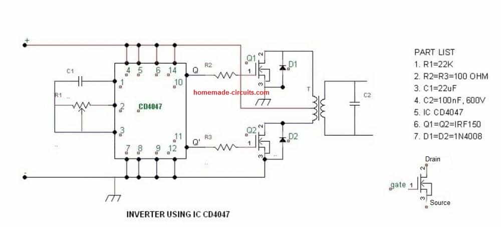
The formula for calculating the frequency or the RC components are:
f = 1/8.8RC at pin#10 and pin#11 f = 1/4.4RC at pin#13 Where f is in Hz, R in Ohms and C in Farads. Pulse time may be obtained by solving: t = 2.48RC where t is in seconds, R in Ohms and C in FaradsHalf-Bridge Mosfet Driver IC IRS2153(1)D Datasheet
The post details the datasheet, specifications, pinout configurations and a few application circuit for the IC IRS2153 which is a half-bridge IC from Texas Instruments. The unique feature of this half bridge driver is that it does not have to depend on external logic sources for the operations, rather allows configuring its own oscillator through a simple RC network. The IC IRS2153(1)D which is fundamentally a half-bridge mosfet driver chip can be actually used for a number of different interesting circuit applications such as boost converters, solar compact inverters, and if two of them are coupled can be even configured as a full bridge mosfet driver circuit. Let's learn more about this interesting device.Main Electrical Specifications
Before we discuss the potential applications of this chip, let's learn a few of its main features first: The chip is designed to withstand and operate with voltages as high as 600V DC (15.4 V Zener clamp on VCC). Consists of an internal built-in oscillator circuit with a 50% fixed duty cycle, while its frequency can be simply determined through two external R/C components (CT, RT programmable oscillator). Consists of a built-in high side driver network which allows a fail-proof conduction of the high-side mosfet (upper mosfet) with the required essential boot-strapped gate voltage. Allows an external shut-down feature to be enforced just by adding an additional transistor stage with the IC(Non-latched shutdown on CT pin (1/6th VCC). This feature can be very useful for applications where an automatic current or voltage regulation is crucial. The chip also includes aMicropower start-up feature which assures guaranteed initialization even under relatively minimal voltage and current conditions. An internal dead time feature ensures perfect separation between the outputs for fail proof operations. All the the pinouts are ESD protected internally for safeguarding the chip against static voltages during packaging and handling.Basic Circuit Configuration of the IC
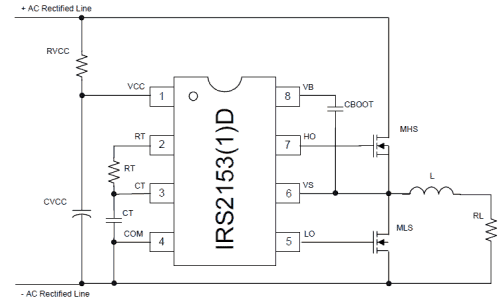
Understanding Pinouts of the Half-Bridge Driver IC IRS2153(1)D
The figure above shows the standard circuit configuration of the proposed half bridge IC. The pinout functions may be understood as follows: Pin#1 is the Vcc of the IC and is internally clamped to 15.4V for safeguarding the IC from high supply voltages. The RC network made from RVCC and CVCC has two important functions, the resistor hleps to control the current to the internal zener while the capacitor provides a start up delay to the chip so that the outputs are able to initiate with zero logic until the built-in oscillator has begun oscillating. The resistor Rt and Ct across pin#2,3,4 is the external RC network which determine the oscillator frequency (duty cycle being fixed to 50% internally). The following formula can be used for determining the oscillator frequency: f = 1/1.453ˇÁ Rt x Ct Pin#4 is the ground terminal of the IC. Pin#7 and pin#5 are the High and Low side outputs of the IC, meaning pin#7 drives the mosfet which is connected with the supply voltage while pin#5 is responsible for driving the mosfet connected with the ground rail. Pin#8 is terminated with a Cboot capacitor which ensures that the HO and LO never conduct together and also steps-up the required bootstrapped voltage for the HO pinout of the IC. Application Note: The main application of this IC hovers around inverters and converter topologies. One standard inverter application design can be seen in the below given diagram: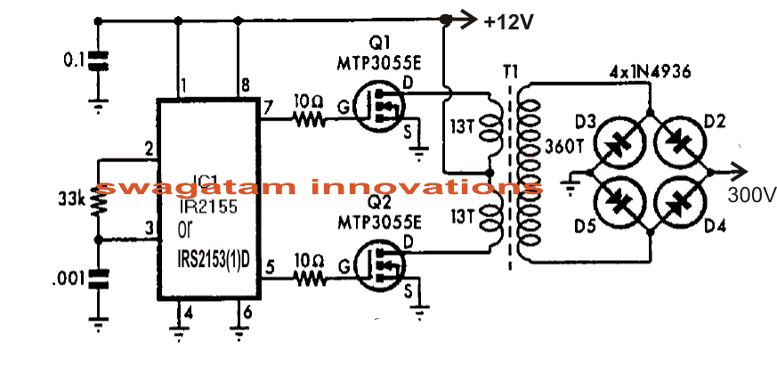 The simple inverter design shown above using the IC IRS2153 can be used for driving mains CFL lamps from 12V supplies.
Here the Cboot feature is eliminated because the configuration is an ordinary center tap type inverter which does not call for boot-strapped supply due to the absence of high side mosfet network here.
The transformer may be wound over any standard 27mm E-core type ferrite assembly, as shown below.
For the complete datasheet you may refer to the following post:
irf.com/product-info/datasheets/data/irs2153d.pdf
The simple inverter design shown above using the IC IRS2153 can be used for driving mains CFL lamps from 12V supplies.
Here the Cboot feature is eliminated because the configuration is an ordinary center tap type inverter which does not call for boot-strapped supply due to the absence of high side mosfet network here.
The transformer may be wound over any standard 27mm E-core type ferrite assembly, as shown below.
For the complete datasheet you may refer to the following post:
irf.com/product-info/datasheets/data/irs2153d.pdf
Low Power MOSFET 200mA, 60 Volts Datasheet
The post explains the main specs and pinouts of a small signal, low power N-channel mosfet 2N7000G.Mosfets vs BJTs
When we talk of mosfets we normally associate it with high current, high voltage, and with high power applications. However, just like ordinary BJTs, small signal mosftes are also available which may be as effectively used as their BJT counterparts. Mosfets are popular for their extremely high power delivering capabilities yet being smaller with their overall dimensions. Unlike the BJTs, mosfets would handle huge currents and voltages without getting bigger itself in size and without involving intermediate buffer stages or high current driver stages.How Mosfet is Triggered
The biggest advantage of using a mosfet is that, it can be triggered as desired for operating a given load irrespective of the gate drive current. The above feature allows mosfets to be triggered directly from low current sources such CMOS or TTL outputs without the need of buffer stages, a big difference when compared with BJTs. The above feature also applies to small signal mosfets which can be directly replaced for small signal BJTs such as a BC547 for acquiring much efficient results. One such small signal mosfet datasheet, specification is discussed here. ItˇŻs the N-channel 2N7000G mosfet, typically suited for small signal applications in the range of 200mA and 60V maximum. The On state resistance across its drain and source terminals is typically around 5 ohms. The mains features of this small signal, low power mosfet is listed below:Main Electrical Features:
Drain to source voltage Vdss = 60V DCGate to Source voltage Vgs = +/- 20V DC, +/- 40V DC peak non-repetitive, not exceeding 50microsecondDrain current Id = 200mA DC continuous, 500mA pulsed Total power dissipation Pd at Tc = 250 C(junction temp) = 350 mW The pinouts, and package details can be seen here: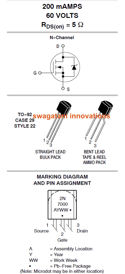
High Current MOSFET IRFP2907 Datasheet
The post explains the main features datasheet of high current N-Channel mosfet IRFP2907 which is rated to handle up to a staggering 209 amps of continuous current at a reasonably massive 75 volts.High Current Specs
With the advent of mosfets, switching huge power through compact packages has become particularly feasible. Take for example the proposed high current mosfet IRFP2907 (has no relation to 2N2907) which could be used for triggering currents exceeding 200 amps, exclusively suitable for wind turbine generators. application Although this device is designed specifically for automotive applications, the extreme range of this device can be effectively employed for many other applications such as inverters, wind turbines, soar inverters etc. Precisely, this N-Channel device would be ideally suited for wind turbine inverter applications since this application incorporates alternators which is an automotive component.Main Specifications and Features
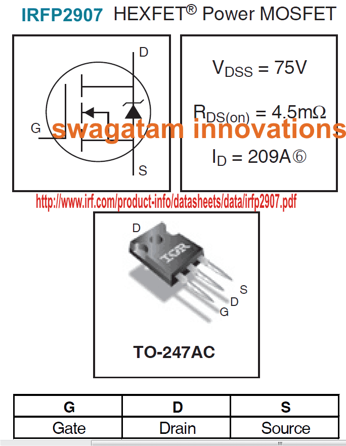 Let's learn about the main features of the mosfet IRFP2907
Advanced Process Technology: ensures a rugged foolproof design and operation parameters.
Ultra Low On-Resistance: allows optimal delivery of the source current across the load thereby enhancing the overall efficiency of the system.
Dynamic dv/dt Rating: makes the unit extremely desirable with high power critical systems.
175ˇăC Operating Temperature: this extreme range allows better sustaining, and consistency even under stressful operating conditions
Fast Switching: Makes the device specifically suitable for rapid high current switching applications without the fear of device breakdown yet with maximum efficiency.
Repetitive Avalanche Allowed up to Tjmax: Avalanche current is no more an issue with this device which is well guarded to make it completely failproof even under worst case scenarios.
Let's learn about the main features of the mosfet IRFP2907
Advanced Process Technology: ensures a rugged foolproof design and operation parameters.
Ultra Low On-Resistance: allows optimal delivery of the source current across the load thereby enhancing the overall efficiency of the system.
Dynamic dv/dt Rating: makes the unit extremely desirable with high power critical systems.
175ˇăC Operating Temperature: this extreme range allows better sustaining, and consistency even under stressful operating conditions
Fast Switching: Makes the device specifically suitable for rapid high current switching applications without the fear of device breakdown yet with maximum efficiency.
Repetitive Avalanche Allowed up to Tjmax: Avalanche current is no more an issue with this device which is well guarded to make it completely failproof even under worst case scenarios.
Technical Datasheet
The Datasheet of the High Current Mosfet IRFP2907 may be understood with the following points: Extremely Low RDS(on) = Typically around 4.5 milliOhm, that's almost zero resistance across the drain and the source terminals when the device is fully saturated. Saturating Voltage = The saturating voltage VGS is around 10V which may be exceeded to not more than 20V. Applying this range of voltage across the gate and the source terminals would allow full saturation and almost zero resistance across the drain/source terminals. High Switching Current: With the above parameters applied, the maximum allowable current across the drain and the source terminals would be anything up to 200 amps....that's huge. Breakdown Voltage = It should not be exceeded preferably above 70 volts. This is applied across the drain and the source with a load in series at current levels that may exceed the 200 amp mark, as explained above.55V 110A N-Channel Mosfet IRF3205 Datasheet
The following postexplainsthe main features of mosfet IRF3205 which is fundamentally rated with drain current at a massive 110 Amps, and voltage ranging up to 55V, ideally suitable for inverter, motor control, choppers, and converter applications.Main Features
The IRF3205 leading-edge N-Channel HEXFET Power MOSFETs from International Rectifier implements hi-tech processing solutions to attain incredibly minimal on-resistance per silicon space. This advantage, along with the rapid converting rate and ruggedized system layout that HEXFET power MOSFETs are popular for, offers the developer with an exceptionally cost-efficient and dependable product to be used in an array of programs. The TO-220 bundle is globally favored for most of commercial-industrial purposes at power dissipation stages to around 50 watts. The minimal thermal resistance and reduced packet price of the TO-220 play a role to its extensive recognition all through the market.Technical Specifications
It's technical specifications may be understood with the following data: Continuous Drain Current, VGS @ 10V = 110 A Pulsed Drain Current = 390 A At 25ˇăC Power Dissipation = 200 W Linear Derating Factor = 1.3 W/ˇăC Gate-to-Source Voltage = ˇŔ 20 V Avalanche Current = 62 A Repetitive Avalanche Energy = 20 mJdv/dt Peak Diode Recovery dv/dt = 5.0 V/ns Operating Junction and Soldering Temperature, for 10 seconds = 300 (1.6mm from case )ˇăCYou may refer to the original datasheet for more infoPinout Details
The pinout details of the mosfet IRF3205 can be witnessed in the below shown image: Holding the device straight with its printed side towards you, the left side pin will be the gate, the center will be the drain, while the right side pinout will be the source of the mosfet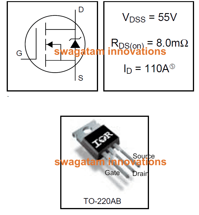
A Typical Application
Making a simple 500 to 5000 watt inverter using IRF3205 mosfet. A fifty watt inverter discussed in one of my previous posts can be easily turned into a massive 500 watt inverter by simply replacing its MOSFETs by the above type. Refer to the following link for the required circuit diagram, just use the IRF3205 for the mosfets, 24-0-24V /30A transformer and 24V 200AH battery. The inverter can be made to produce upto 5kva if the transformer voltage is increased to 50-0-50V/100amps. https://www.homemade-circuits.com/2012/09/mini-50-watt-mosfet-inverter-circuit.htmlCree XLamp XM-L LED Datasheet
The XLamp XM-LED can beconsideredas the highest performing, single die solid state LED module which is able to produce lights at ultra bright intensities. Let's learn it's datasheet, specifications.High Illumination Efficacy
Due to it'sultrabright and high efficiency values, the Xlamp becomes highly suitable for applications such as in automotive headlamps, stadium flood lights, for home lighting, street lighting, practically anywhere which requires high illumination at minimum space and consumption. To be precise an Xlamp is able to generate 1000 lumen with 100 lumen per watt efficacy. The main features which makes this breakthrough device exceptionally desirable for lighting applications may be studied with the following data:Main Electrical Specifications
Operating current: 3000 mA or 3 Amps Operating Voltage: 3.3V Low thermal resistance: 2.5 ˇăC/W Maximum junction temperature: 150 ˇăC Viewing angle: 125ˇă Available in cool white, 80CRIminimum neutral white and 80CRI, 85CRI and 90CRI warm white ANSIcompatible chromaticity bins Infinite Store life at ˇÜ 30 oC/85% RH Re flowsolderable - JEDEC JSTD020C Electrically neutral thermal path RoHS- and REAChcompliant UL-recognized component (E349212)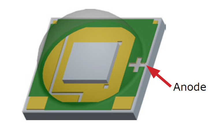
How to Drive a Cree Xlamp XM-LED
Since the the performance and life of the Cree Xlamp isinverselyproportional to its junction temperature, a high quality current controlled driver becomes a must for operating these ultra bright LEDs. Let's learn a few of the application circuits forsafelydriving the proposedLEDdevices.Applying In Automotive Headlights.
When used for automotive headlamp applications, the following circuit may be employed: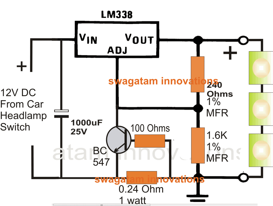
For Home Lighting
The same circuit may be used for home lightingapplications, the design is given below: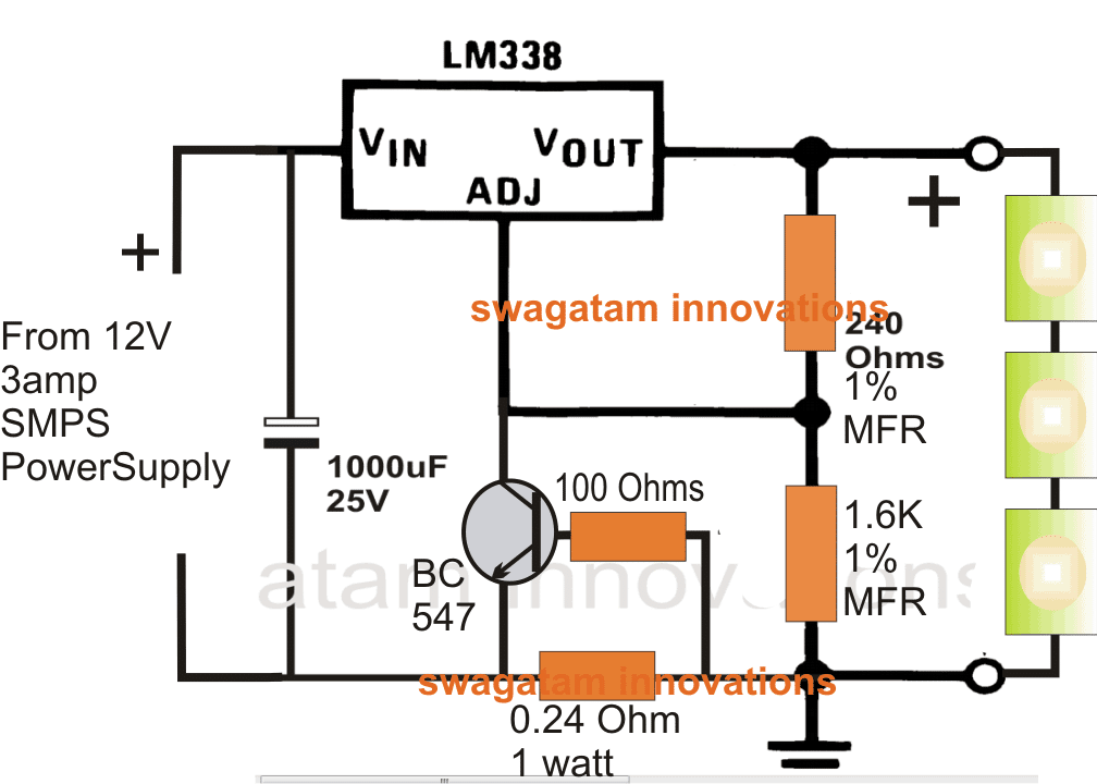 For all applications, the LEDs must be mounted on suitable heatsinks for getting optimal performance.
For more info on this, you may refer to the original datasheet
For all applications, the LEDs must be mounted on suitable heatsinks for getting optimal performance.
For more info on this, you may refer to the original datasheet
12V 5 Amp Fixed Voltage Regulator IC 78H12A Datasheet
The postexplainsthe technical specifications, datasheet, and application notes of the IC 78H12A which is a voltage regulator IC capable of providing a fixed regulated 12V output at maximum 5 amp current.5 Amp Regulator Specifications
We are familiar with the popular 78XX ICs such as the 7812 IC which can produce 12V fixed voltage at its output with input supplies anywherefrom 15V to 24V. However the above device is capable of handling at the most 1 Amp of current which may be not sufficient for many standard applications. For circuit applications which require currents as high as 5 amps, a higher rated alternative may beselectedin the form of the IC 78H12A which is quite similar to its youngerbrother7812 but is capable of handling up to 5 amps of current. The main technical specifications or datasheet of this IC 78H12A may be studied with the following explanation: The 78H12A is a three terminal linear, positive fixed voltage regulator IC rated forcontinuouslydelivering around 5 amps of current with typical fixed 12 volts at its output. The IC is internally fully protected aagainstshort circuits or over loads at its output which makes it highly rugged and versatile. In an event of a short circuit or over load across its output terminals, the device instantly shuts down the supply of power across its output leads, thus inhibiting any possibility of electrical hazards. The situationalsoprotects the IC from getting damaged. The above feature ensures safe operations of the connected electronics and also avoids the inclusion of external safety circuits reducing the cost and the component count of the over all configuration. The device is available in a hermetically sealed TO-3 metal package, and facilitates easy fitting of an heatsink for better efficiency and working of the device.Main Technical Features of the IC
The main features of the IC may be summarized as follows: Output Voltage: 12V, fixed, regulated Output Current: Maximum 5 Amps Protections: In-built short circuit and over load protected. Power Dissipation: 12 x 5 = 50 to 60 Amp Approximately Package: TO-3 metal body
Pin Outs of IC 78H12A
The figure below shows the pinout details of the IC 78H12A, if the device is held with the pins toward us and with the larger plain section of the area upwards, the right pin is the input, the left pin is the output while the body becomes the ground of the IC.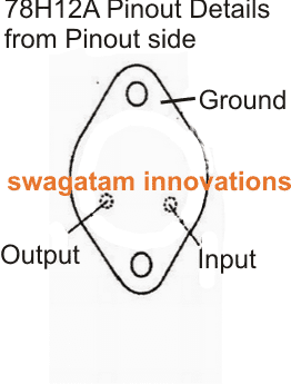
Application Notes
The IC 78H12A is fundamentally suited for all electronic circuit application where a fixed 12V is imperative and with requirements upto 5 amp, example for driving 12V DC motors, for driving high watt white LeDs for flood lighting, and also for charging lead acid batteries (with some modifications). The following diagrams illustrate a couple of main applications which may be implemented with this versatile 12V 5 amp fixed voltage regulator IC.12V 50 AH Battery Charger Circuit
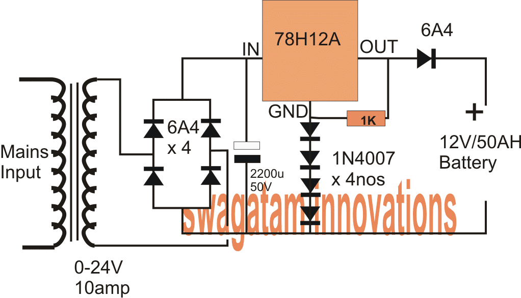
30 watt LED Driver Circuit
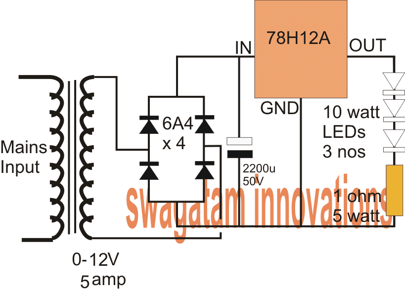
Using LM338
In case you are unable to get the above IC, you can create an equivalent 12V 5 amp fixed regulator using the following LM338 based configuration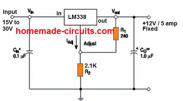
12V 5Amp from IC 7812
In the above designs we learned how to get 12V fixed voltage at 5 amp current from specialized IC, however the same could be easily acquired from a simple 7812 IC, through a little modification as given below. The diodes at the center lead of the IC 7812 allows us to alter the output to any desired value that may be higher than 12V. For example for charging a 50 Ah battery you may require 14V 5 amp, which can quickly tweaked by adding the shown diodes. So this design is actually is quite customizable for many different 12V 5 amp applications. For adjusting the current output, simply alter the value of the lower 1 ohm 5 watt resistor, it's as simple as that! The indicated TIP36 will allow upto 25 A, however if you are only interested to get 5 amps, you can easily replace it with a TIP32C transistor over a heatsink.
LM567 Tone Decoder IC Features, Datasheet and Applications
The post discuses the main specifications, datasheet and working principle of the IC LM567, which is a precise phase-locked loop with synchronous AM lock detection and power output device. In simpler terms the IC LM567 IC is a tone decoder chip which is designed basically for recognizing a specified frequency band, and activating the output inresponseto the detection. Needless to say this chip can be used for a number of different applications, the most common being in the field of remote controls, and security systems.Block Diagram
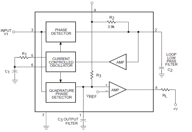
Absolute Maximum Rating
Absolute maximum rating refers to the values indicating the maximum tolerable capacity of the IC in terms of voltage, current, and power dissipation. The following table explains the absolute maximum rating of the IC LM567 for the relevant parameters:
Pinout Working and Specifications
Referring to the the above shown IC LM 567 internal configuration diagram, the pinout function of the IC may be understood from the following points: Pin#4 and Pin#7 are the positive (Vdd) and the negative (Vss) supply inputs respectively for the IC. Pin#3 is the sensing input of the input, which is used for detecting a given phase-locked loop frequency, in other words this pin will lock-on with the matching center frequency which may be set inside the IC through a pair of external RC network. The Pin#5 and 6 are used for creating the center frequency by setting up the values of R1, C1 as required, and this frequency is used by the sensing input pin#3 to lock-in and create a logic zero at pin#8 which is the output pin of the IC. Output Pin#8 is normally logic high and becomes logic zero as soon as a matching frequency is detected at pin#3 of the IC. Pin#1 and pin#2 are used for ensuring proper filtration of the involved frequencies so that the IC does not create any false output due to any existing spurious or stray noise interferences.Main Features of LM567:
Extensive settable frequency range (0.01 Hz to 500 kHz), meaning the sensing passband may be set right from 0.1 to 500 kHz, giving an option of a huge range so that unlimited unique configuration can be achieved from this chip. Highly stable of center frequency, which assures precise passband limits making the unit very reliable with the detection functions. Independently controllable bandwidth (up to 14%), as the feature suggests, the bandwidth is also adjustable to a reasonable degree. High out-band signal, and noise rejection, which again assures high reliability during the detection and implementation of the said functions. Logic-compatible output with 100 mA current sinking capability, which allows the output to handle relatively higher loads without employing an additional buffer stage such as a transistor driver stage. Inherent immunity to false signals, which ensures that the chip never produces false results due to incorrect frequencydetectionor in the presence of stray or spurious instantaneous signals. Frequency adjustment over a 20-to-1 range with an externalresistor, this feature again makes the chip highly flexible and dynamic. The threeimportantParameters Associated with the IC LM567 may be understood with the following points:Phase locked loop center frequency
ItˇŻs the free running frequency of the in-built current controlled oscillator circuitry in the absence of an input signal.Detection Bandwidth
This is the frequency range which may be provided to the above center frequency, within which the presence of an input signal having a threshold voltage of above 20mV causes the output of the IC to become low. This feature refers to the loop capture range.Lock Range
It is the maximum range of frequency which would enable the output to switch to logic zero in the presence of a relevant input signal having a threshold voltage above 20mV.Detection Band
It is the magnitude which indicates the level of optimaldetection,focused around the center frequency. ItˇŻs given by the formula: Detection Band = (fmax + fmin ¨C 2fo)/2fo, where fmax and fmin are the frequencies thresholds of the detection band, fo is the center frequencyApplication Hints
The IC567 may be considered as a versatile chip because it provides an unlimited range of applications in the field of electronics, some of them are discussed below: Touch-Tone decoding: The human touch response may produce different frequencies whenemployedwith this chip, it can be suitably decoded by using many IC LM567 configurations. Carrier current remote controls: Our existing mains wiring can be very effectively used as a medium of transfer for communicating between the rooms or for controlling appliances remotely from one room to the other. The actions can be implemented by using a LM567 IC. Infrared controls (remote TV, etc.): Since the center frequency of LM567 is tightly locked, it may be used for detecting IR waves precisely from the given handset. Unlike ordinary IR remote controls, this circuit is better immune to stray RF or IR disturbances created from switching AC mains appliances. Frequency monitoring and control: Again since the LM567 IC has an inbuilt precise frequency detection range, which can be used for monitoring a given range of frequency accurately. Wireless intercom: Just like Carrier current remote controls, the IC LM567 may also be suitably implemented in wireless intercom systems. Precision oscillator: The phase locked loop feature in the proposed IC also facilitates its application as a precision oscillator for achieving precisely adjusted oscillations or frequencies.High Voltage Transistor MJE13005 ¨C Datasheet, Application Notes
The article relates us with the important features and specifications of MJE13005 device, which is a high voltage, high speed transistor, applicable for manydifferentelectronic circuit designs. Let's try to understand the pin outs andtechnicalspecs of the device:Pinout Diagram
Main Features
Package - TO-220AB (typicallyrecommended) Type - NPN Silicon Power Handling Capaciy - 75 Watts, Maximum Current Handling Capacity - 4 Amps Maximum Voltage Handling Capacity - Not less than 400VMain Application Areas
High voltage circuits, switch mode power supplies, motor control, switching regulators, inverters, solenoid drivers.Maximum Tolerable Ratings
Maximum sustainable collector to emitter voltage = 400V DC (700V DC pulsed) Maximum tolerable emitter to base voltage = 9V DC Maximumsustainablecollector to emitter current = 4 amps (8 amps pulsed) Maximum continuous base current = 2 amps (4 amps pulsed)Technical Specifications
Base emitter saturation voltage =typically1.2V DC current gain (hFE) = typically around 20 to 60 Application Circuits A couple of application circuits using the MJE13005 have been discussed in the following articles: Simple SMPS Circuit Simple Transformerless Power SupplyIRF540N MOSFET Pinout, Datasheet, Application Explained
The IRF540N is an advanced HEXFET N-channel power mosfet, from International Rectifier. The device is extremely versatile with its current, voltage switching capabilities, and thus becomes ideal for numerous electronic applications. The datasheet and pinout details of the device has been explained in the following article.Main Features:
Sophisticated, cutting-edge processing technology used. Extremely low resistance across load path. Flexible dv/dt plot. Operating temperature tolerance capacity as high as 175 degrees Celsius. Very fast switching capability. Fully resistant against avalanche or peak surge currents.Pinout Image
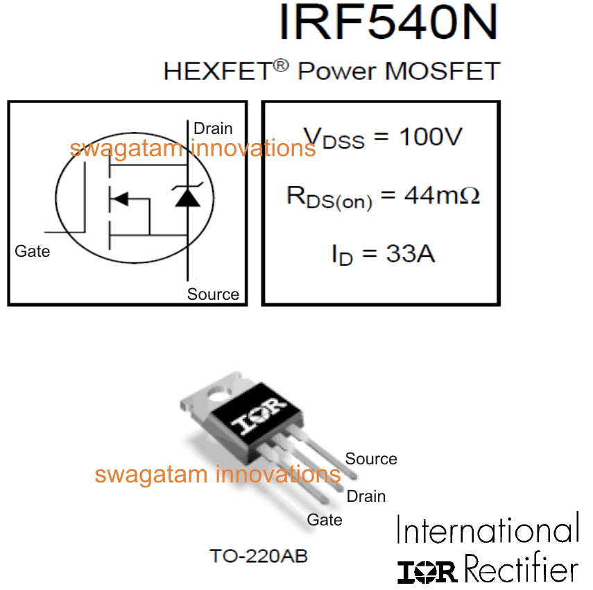
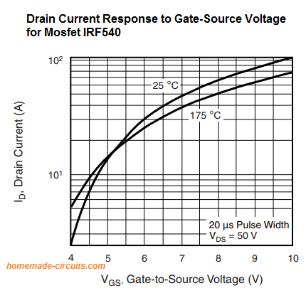 Maximum tolerable limits of IRF540N are stated as under:
ID = 33 Amps Max at 10V (VGS), ItˇŻs the maximum current handling capacity of the device across the drain to the source, via the load, with gate voltage at 10V, at normal temperatures (25 to 35 degrees Cel.)
IDM = 110 Amps Max, ItˇŻs the maximum current handling capacity of the device across the drain to the source, via the load, in a pulsed mode (NOT continuous).
PD = 130 Watts Max, The maximum power the FET can dissipate with and infinite (cool) heat sink
VGS = 10 Volts typical +/-20%.
ItˇŻs the maximum trigger voltage that may be applied across the gate and the source for optimal performance.
V(BR)DSS= 100 volts, ItˇŻs the maximum voltage that may be applied across drain to source of the device.
Maximum tolerable limits of IRF540N are stated as under:
ID = 33 Amps Max at 10V (VGS), ItˇŻs the maximum current handling capacity of the device across the drain to the source, via the load, with gate voltage at 10V, at normal temperatures (25 to 35 degrees Cel.)
IDM = 110 Amps Max, ItˇŻs the maximum current handling capacity of the device across the drain to the source, via the load, in a pulsed mode (NOT continuous).
PD = 130 Watts Max, The maximum power the FET can dissipate with and infinite (cool) heat sink
VGS = 10 Volts typical +/-20%.
ItˇŻs the maximum trigger voltage that may be applied across the gate and the source for optimal performance.
V(BR)DSS= 100 volts, ItˇŻs the maximum voltage that may be applied across drain to source of the device.
Applications Areas
This device is best suited for high power DC switching applications, such as in high current SMPS power supplies, compact ferrite inverter circuits, iron core inverter circuits, buck and boost converters, power amplifiers, motor sped controllers, robotics etc.How to Connect IRF540N MOSFET
ItˇŻs quite simple, and must be done as explained in the following points: The source should be preferably connected to the ground or the negative line of the supply. The drain should be connected to the positive terminal of the supply via the load which needs to be operated by the device. Finally, the gate which is the trigger lead of the device should be connected to the trigger point of the circuit, this trigger input should be preferably a +5V supply from a CMOS logic source. If the trigger input is not a logic source make sure the gate is permanently connected to ground via a high value resistor. When the device is being used for switching inductive loads like a transformer or a motor, a flyback diode should be normally connected across the load, with the cathode of the diode connected to the positive side of the load. However, the IRF540N has a built in avalanche protective diode, therefore typically an external diode may not be required; it may be incorporated in case you wish to provide extra safety to the device.Application Circuits
Motor Control: All motor control applications require the power device to be rugged, high current, and high voltage rated, and also with a high speed switching. The IRF540 satisfies all these criteria and becomes perfectly suitable for all DC motor control designs, as depicted below: Source Follower Switching
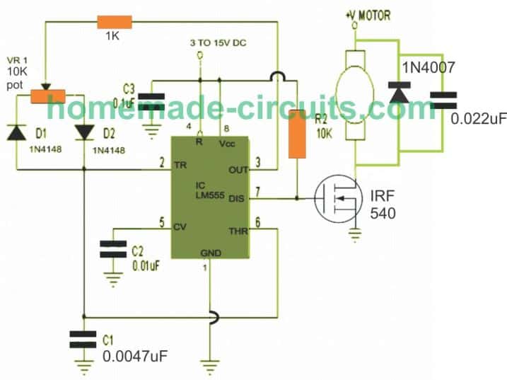 PWM Motor Switching
Buck Converter: Buck converter cannot work with devices rated with ordinary voltage, current and switching levels.
The IRF540 as we have discussed in the above datasheet and features is equipped adequately to work under moderately high voltage, high current and outstanding switching speeds, which makes it a perfect candidate for all buck boost switching applications.
PWM Motor Switching
Buck Converter: Buck converter cannot work with devices rated with ordinary voltage, current and switching levels.
The IRF540 as we have discussed in the above datasheet and features is equipped adequately to work under moderately high voltage, high current and outstanding switching speeds, which makes it a perfect candidate for all buck boost switching applications.
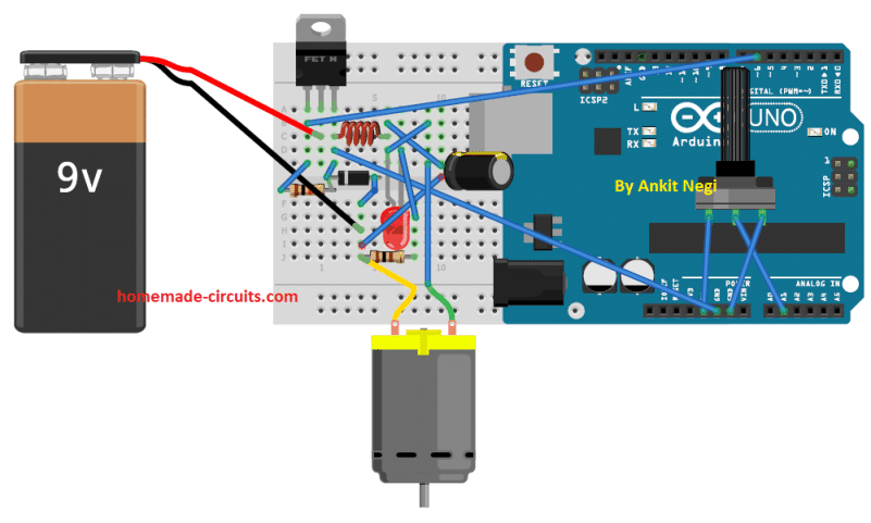 Power Inverter: IRF540 are rated with massive power which allows it to be ideally used for making power inverters as shown below.
The complete code can e found in this artcile.
Power Inverter: IRF540 are rated with massive power which allows it to be ideally used for making power inverters as shown below.
The complete code can e found in this artcile.
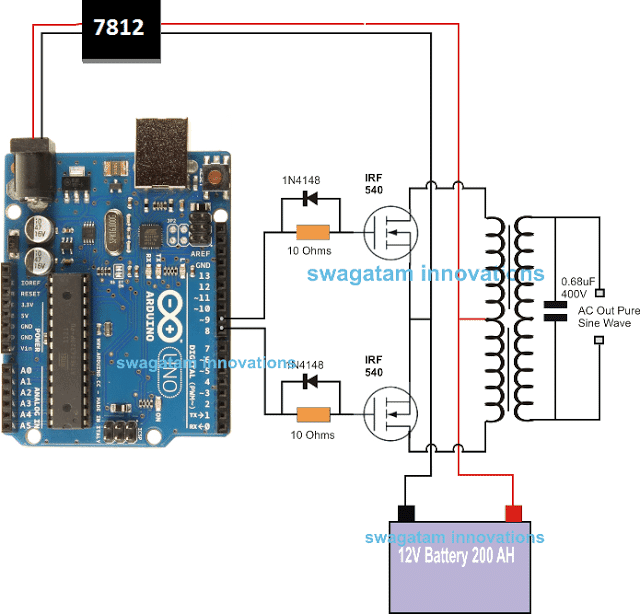 Zero Drop Solar Switch: Solar panels today are rated massively, and this calls for controller with substantial power handling capacity.
The IRF540 become highly suitable for all high power solar controller applications simply due to its impressive power switching capabilities.
Corrections to the above explanations is welcome.
Zero Drop Solar Switch: Solar panels today are rated massively, and this calls for controller with substantial power handling capacity.
The IRF540 become highly suitable for all high power solar controller applications simply due to its impressive power switching capabilities.
Corrections to the above explanations is welcome.
How Shunt Regulator TL431 Works, Datasheet, Application
In this post we learn how a shunt regulator IC works typically in SMPS circuits. We take the example of the popular TL431 device and try to understand its use in electronic circuits through a few of its application notes.Electrical Specifications
Technically the device TL431 is called a programmable shunt regulator, in simple terms it may be understood as an adjustable zener diode. Let's learn more about its specifications and application notes. The TL431 is attributed with the following main features: Output voltagesettableor programmable from 2.5V (minimum reference) up to 36 volts. OutputImpedancelow dynamic, around 0.2 Ohm. Sink current handling capacity up to maximum 100mA Unlike normal zeners, noise generation is negligible. Switchingresponse lightning fast.How the IC TL431 works?
The TL431 is a three pin transistor like (such as BC547) adjustable or programmable voltage regulator. The output voltage can be dimensioned using just two resistors across the specified pin outs of the device. The diagram below shows the internal block diagram of the device and also the pin out designations.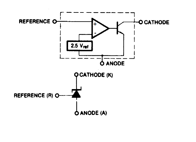 The following diagram indicates the pin outs of the actual device.
Let's see how this device can be configured into practical circuits.
The following diagram indicates the pin outs of the actual device.
Let's see how this device can be configured into practical circuits.
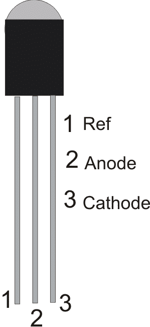
Circuit Examples using TL431
The circuit below shows how the above device TL431 can be used as a typical shunt regulator.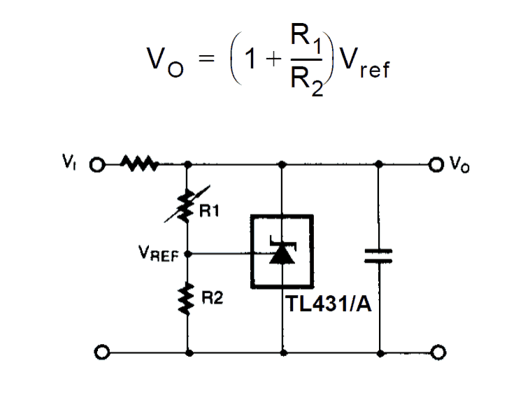 The above figure shows how with the help of just a couple of resistors the TL431 can be wired up as a shunt regulator for generating outputs between 2.5v to 36v.
R1 is a variable resistor which is used for adjusting the output voltage.
The series resistor at the supply positive input can be calculated using Ohm's law:
R = Vi / I = Vi / 0.1
Here Vi is the supply input which must be below 35 V.
The 0.1 or 100 mA is the maximum shunting current specification of the IC, and R is the resistor in Ohms.
The above figure shows how with the help of just a couple of resistors the TL431 can be wired up as a shunt regulator for generating outputs between 2.5v to 36v.
R1 is a variable resistor which is used for adjusting the output voltage.
The series resistor at the supply positive input can be calculated using Ohm's law:
R = Vi / I = Vi / 0.1
Here Vi is the supply input which must be below 35 V.
The 0.1 or 100 mA is the maximum shunting current specification of the IC, and R is the resistor in Ohms.
Calculating Shunt Regulator Resistors
The following formula holds good foracquiringthe values of the various components used for fixing the shunt voltage. Vo = (1 + R1/R2)Vref In case a 78XX needs to be used in conjunction with the device, thefollowingcircuit can be used: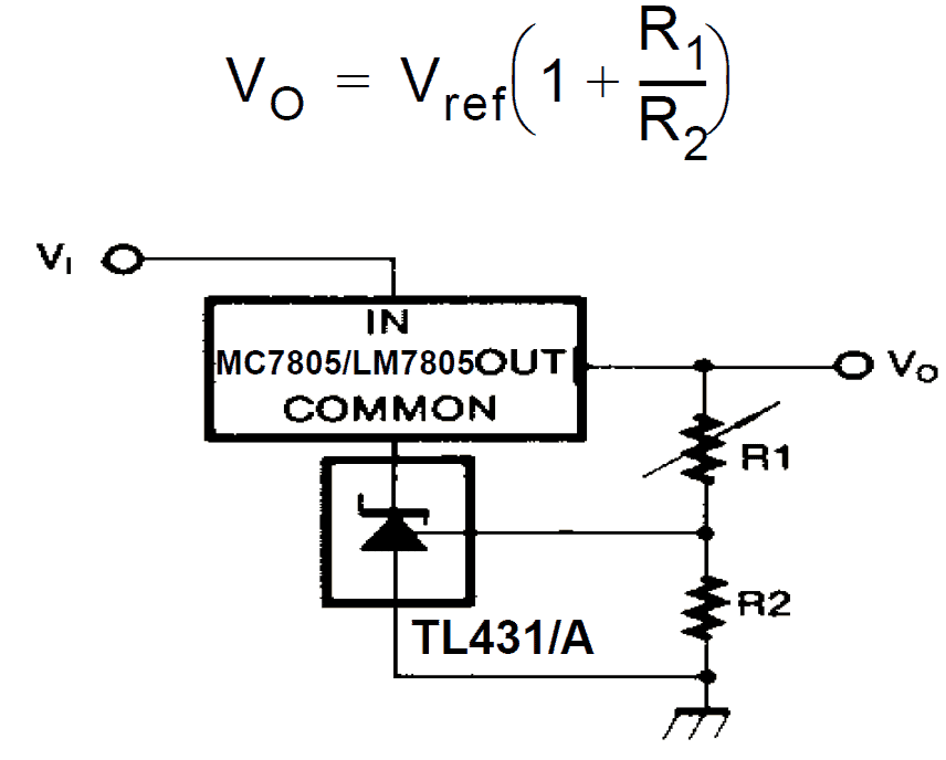 The ground of the TL431 cathode is connected with the ground pin of the 78XX.
The output from the 78XX IC is connected with the potential divider network which determines the output voltage.
The parts can be identified through the formula shown in the diagram.
The above configurations are restricted to a max 100 mA current at the output.
For getting higher current a transistor buffer may be used, as shown in the following circuit.
The ground of the TL431 cathode is connected with the ground pin of the 78XX.
The output from the 78XX IC is connected with the potential divider network which determines the output voltage.
The parts can be identified through the formula shown in the diagram.
The above configurations are restricted to a max 100 mA current at the output.
For getting higher current a transistor buffer may be used, as shown in the following circuit.
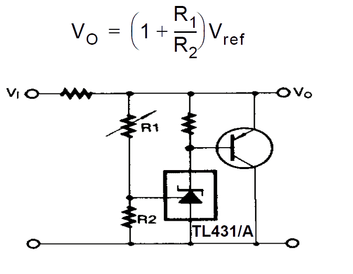 In the above diagram most of the parts placement is similar to the first shunt regulator design, except that here the cathode is provided with a resistor to positive and the point also becomes the base trigger of the connected buffer transistor.
The output current will depend on the magnitude of current the transistor is able to sink.
In the above diagram we can see two resistors whose values are not mentioned, one in series with the input supply line, another at the base of the PNP transistor.
The resistor at the input side limits the maximum tolerable current that can be sinked or shunted by the PNP transistor.
This can be calculated in the same way as discussed previously for the first TL431 regulator diagram.
This resistor protects the transistor from burning due to short circuit at the output.
The resistor at the base of the transistor is not critical and may arbitrarily selected anything between 1k and 4k7.
In the above diagram most of the parts placement is similar to the first shunt regulator design, except that here the cathode is provided with a resistor to positive and the point also becomes the base trigger of the connected buffer transistor.
The output current will depend on the magnitude of current the transistor is able to sink.
In the above diagram we can see two resistors whose values are not mentioned, one in series with the input supply line, another at the base of the PNP transistor.
The resistor at the input side limits the maximum tolerable current that can be sinked or shunted by the PNP transistor.
This can be calculated in the same way as discussed previously for the first TL431 regulator diagram.
This resistor protects the transistor from burning due to short circuit at the output.
The resistor at the base of the transistor is not critical and may arbitrarily selected anything between 1k and 4k7.
Application Areas of the IC TL431
Although the above configurations can be used in any place where precision voltage setting and references may be required, it's extensively used in SMPS circuits nowadays for generating precise reference voltage for the connected opto coupler, which in turn prompts the input mosfetof the SMPS to regulate the output voltage precisely to the desired levels. For more info please go tohttps://www.fairchildsemi.com/ds/TL/TL431A.pdfHigh Current Triac BTA41/600B ¨C Datasheet, Application Note
Triacs are one of the most important active electronic components which are exclusively used for power switching applications, these devices are especially suited to AC mains loads, and are able to switch large currents consistently. Triacs are the solid state replacements tomechanicalrelays, and come configured as static relays. The modern triacs today are high sophisticated with their specifications and make, one such example is the BTA41, 600B, let's understand its technical specification anddatasheetfrom the following points:Identifying Print Value of BTA41/600B
BT indicates series number, "A" represents that the device is insulated, while B would mean non-insulated. The insulation is provided on the Tab of the device upto 2500 volts. 41 = 4 and "one" zero, that equals 40 Amps 600 is the voltage handling capacity, therefore here it's 600 volts. B represents the triggering sensitivity that's 50mA in this case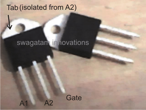 Absolute Maximum Rating (at around 25 to 40 degrees Celsius)
RMS, continuous current handling capacity = 40 Amps
Nonrepetitivepeak current = 400 Amp, only for max 20ms.
Absolute Maximum Rating (at around 25 to 40 degrees Celsius)
RMS, continuous current handling capacity = 40 Amps
Nonrepetitivepeak current = 400 Amp, only for max 20ms.
How to Connect
The pin outs are connected just as we connect other normal triacs. Let's learn them yet again: A1 should be always connected to ground. The ground doesn't have to be necessarily the neutral of the AC, it can be any one wire out of the two mains input. The other wire will go to one of the load terminals, while the second wire of the load will go to A2 of the triac. The gate should be connected with the desired trigger input which must be a DC, because the triac will conduct with every rising positive edge of the DC trigger. Here the minimum triggering gate current is 50 mA. A1 should be made common with one of the AC terminals as well as the ground of the DC trigger circuit, in case an external triggering circuit isincorporated.Application Notes
As suggested in the above sections, the triac BTA41/600B is best suitable for applicationsconcerningcontrol of AC loads such heater coils, high power halogen lamps, AC motor pumps or simply motors such as in dryers, blowers and so forth. The following circuit illustrates how the device may be utilized for controlling heater coils such as in furnaces, induction cookers etc.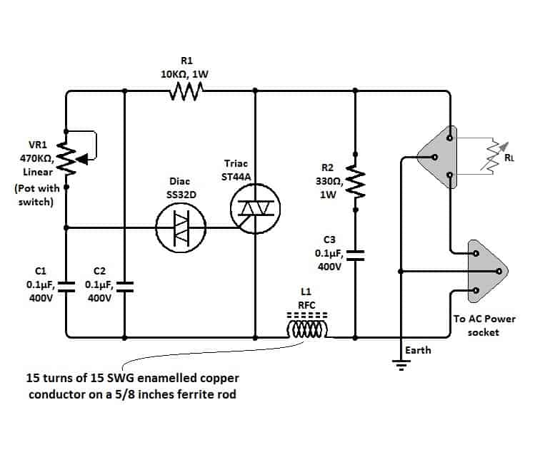 The above circuit can also be used for controlling AC motor speeds simply by replacing theheatercoil with the motor wires.
The adjoining diagram depicts another application of BTA41/600 where it has been configured as a PWM assisted AC motor controller or even heater coils.
The above circuit can also be used for controlling AC motor speeds simply by replacing theheatercoil with the motor wires.
The adjoining diagram depicts another application of BTA41/600 where it has been configured as a PWM assisted AC motor controller or even heater coils.

High Current Transistor TIP36 ¨C Datasheet, Application Note
If you are looking for a power transistor able to support high current upto 25 amps and yet not incorporate the traditional cumbersome TO-3 package, then the TIP36 wouldcertainlyimpress you.High Current from Smaller Package
The package of TIP36 is TO-3P which means the accompanied heatsinkwould require just a single hole to be drilled and the device could be easily soldered over a PCB along with the heatsink, quite unlike the devices which are in TO-3 packages. You would be surprised to know that this device is a lot advanced and powerful than the more popular MJ2955 (complementary pair of 2N3055) in terms of voltage and current ratings. Comparatively a TIP36 exhibits excellent high gain performance even at low orcompressedsaturation base voltages.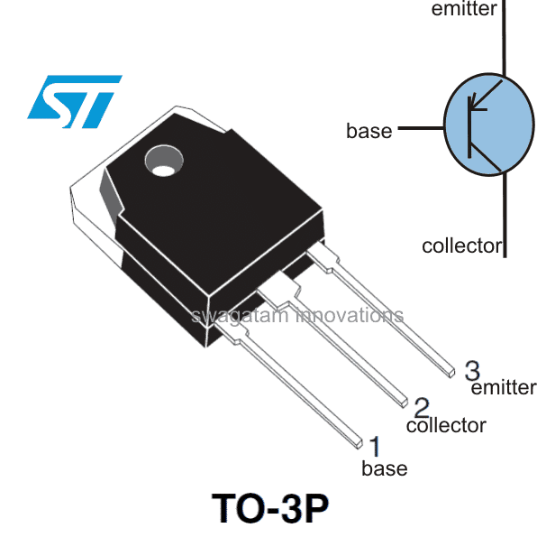 Let's proceed and learn the datasheet and the specifications of this outstanding high current transistor - the TIP36:
Typical Applications:
Audio Amplifier Inverters Motor Control Solar Chargers.Absolute Maximum Ratings:
The device will not tolerate anythingabovethe following parameter magnitudes: Collector-base Voltage (Vcbo) = 100 volts Collector Emitter Voltage (Vceo) = 100 volts Emitter Base Voltage (Vebo) = 5 volts Collector Current (Ic) = 25 Amp continuous, peak 50 Amp for 5 ms only. Base Current (Ib) = 5 Amps Max Operating Junction Temperature = 150degreesCelsiusComplementary Pair
TIP36 can be paired with TIP35, they both are ideally suited as complementary pairs.Application Note:
One interesting and very useful application circuit using a couple of TIP36 transistor can be made for charging high current batteries in the order of 150 AH, directly from solar panels.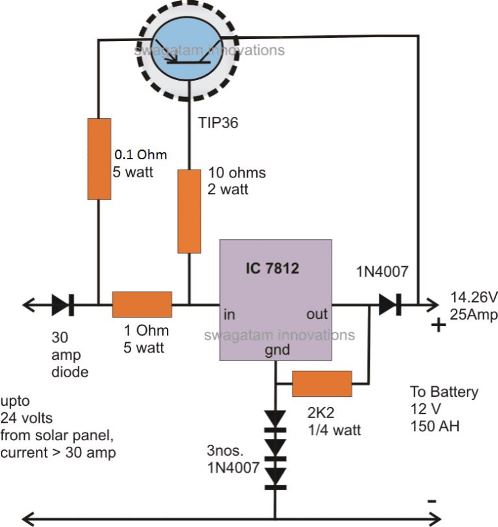 NOTE: Derate linearly to 150ˇăC case temperature at the rate of 1 W/ˇăC.
Derate linearly to 150ˇăC free air temperature at the rate of 28 mW/ˇă
The circuit shown above may be used for charging 12 V batteries having in excess of 100 AH capacities.
To enhance the current gain of the circuit, you can add a TIP127 with the TIP36, as shown below.
Remember both the transistors will require a large heatsink, possibly with a fan cooling.
NOTE: Derate linearly to 150ˇăC case temperature at the rate of 1 W/ˇăC.
Derate linearly to 150ˇăC free air temperature at the rate of 28 mW/ˇă
The circuit shown above may be used for charging 12 V batteries having in excess of 100 AH capacities.
To enhance the current gain of the circuit, you can add a TIP127 with the TIP36, as shown below.
Remember both the transistors will require a large heatsink, possibly with a fan cooling.
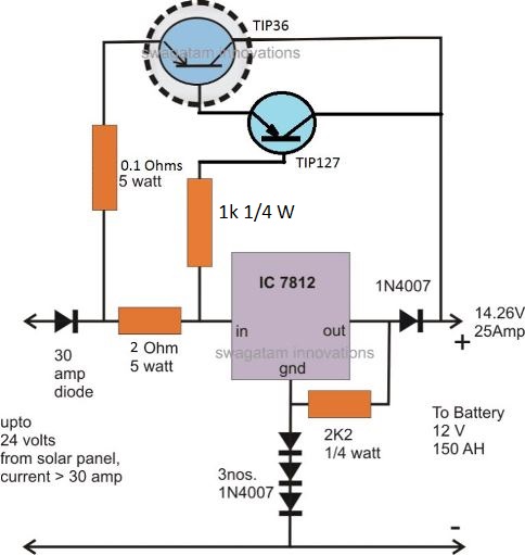 The circuit may be understood as follows:
How TIP36 Works to Produce High Current
The voltage from the solar panel enters the IC7812 first, the three diodes connected at the GND of the IC elevates the output voltage to about 14.26V which is the ideal voltage for charging 12V batteries. However at this point the TIP36 stays inactive, because of the absence of any voltage across its base/emitter 1 Ohm resistor. Once the output of the IC 7812 is loaded, sufficient voltage develops across the 1 Ohm resistor for saturating the TIP36 transistor. The transistor conducts and shifts the required amount of current at the output. However, in the course the transistor also tries to transfer the entire solar panel voltage to the output. As this tends to happen and the instant voltage at the output tends to go beyond the 14.26 mark, the IC7812 becomes reverse biased and stops conducting. With 7812 not conducting, voltage across 1 Ohm resistor becomes zero and the transistor inhibits the flow of the voltage. Due to the above action, the voltage tends to fall back below the 14.26 mark, which instantly prompts te IC to conduct and the cycle switches rapidly producing a voltage that's exactly 14.26 at the output. Thus the IC is only responsible for holding the voltage to the set limit while the transistor TIP36 becomes responsible for delivering the required high currents. Note: Use a common heatsink for the IC7812 and the transistor, this will ensure complete safety to the transistor from thermal runaway situation. Be sure to use mica isolation kit for fixing the devices over the common heatsink.3 Watt LED Datasheet
The following article explains the main technical features and specifications of 3 watt white LEDs. Let's learn moreregardingtheir operating parameters and safe-operating limitations.Main Features
Extremeluminositycapability Extreme working life > 50K hours. Very Low thermal resistance. SMDtechnologyallows embedded PCB type sodering. Completely UV free design Enhanced ESD protections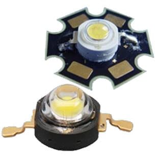 Image Courtesy -https://www.led-display.cc/High-Power-LED/Q1B/LP5W-80-SERIES:-5-watt-high-power-LED.jpg
The soldering details and dimensions of a typical 3 watt LED may be checked in the following diagram:
Image Courtesy -https://www.led-display.cc/High-Power-LED/Q1B/LP5W-80-SERIES:-5-watt-high-power-LED.jpg
The soldering details and dimensions of a typical 3 watt LED may be checked in the following diagram:
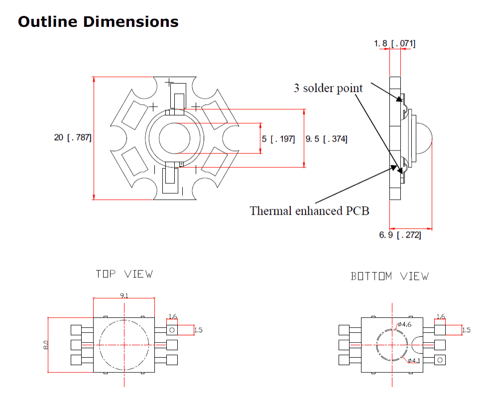 The dimensions are inmillimeters.
The anode side of the LED can be identified by the given hole on that particular side.
The PCB heatsink pad must be tightly in contact with the body metal or the slug of the device.
Remember the body metal is neutral and has no connection with either the anode or the cathode of the device, and must not be linked with any of the leads of the LED.
The lens of the device is sensitive to rough cntacts so excercize caution not to brush any hard or shrp material with the lens which might considerably reduce the light intensity from the LED
The dimensions are inmillimeters.
The anode side of the LED can be identified by the given hole on that particular side.
The PCB heatsink pad must be tightly in contact with the body metal or the slug of the device.
Remember the body metal is neutral and has no connection with either the anode or the cathode of the device, and must not be linked with any of the leads of the LED.
The lens of the device is sensitive to rough cntacts so excercize caution not to brush any hard or shrp material with the lens which might considerably reduce the light intensity from the LED
Technical parameters of the device:
Luminous Flux - 100 to 120 lm Forward Voltage - 3.3V to 4 Vmaximum. These are the minimum and the maximum limits for operating the LED. Optimal viewing angle - 90 degrees.Absolute Maximum Ratings
These are the values which indicate the extreme limits of the relevant parameters above which the device might get instantly damaged. Forward Current - 1 ampere Power Dissipation - 4 watts Junction Temperature - 125 degreesCelsius Operatingtemperature- minus 30 to 85 degrees Celsius WARNING - THEEXPLAINED3 WATT LED SHOULD BE OPERATED WITH THE ABOVE PARAMETERS ONLY AFTER MOUNTING IT OVER A SUITABLE HEATSINK FACILITATED PCB. THE DEVICE WILL NOT WITHSTAND THE OPERATIONS FOR MORE THAN 5 SECONDS WITHOUT A SUITABLE HEATSINKATTACHEDTO ITS BODY. Courtesy -https://www.futurashop.it/pdf_eng/8220-L-HP3PW.pdfBEL188 Transistor ¨C Specification and Datasheet
The transistor 188 is one of my favorites, simply because even being so tiny it's able to handle currents as high as 1 Amp.Understanding BEL188 Transistor Specification/Datasheet
The transistor BEL188 is a general purpose transistor, and due to its wide voltage and current rating can be used for almost all small to medium power circuit applications. The pin-out of the transistor BEL188 is given in the following data: Looking at the figure we see that it's pin configuration is similar to the small signal general purpose transistors like BC547 etc. Holding the printed surface toward you, the right pin becomes the emitter, the center is the base and the left pin may be identified as the collector.Other important specifications:
The material inside it is silicon (Si) Polarity is PNP type Maximum collector to emitter current handling capacity of BEL188 is around 1 Amp which constitutes to a power of around o.6 watts. Maximum collector to base voltage or UCB is 25V, Maximum safe voltage that may be applied across collector to emitter must not exceed 15 volts. Maximum base to emitter saturation voltage must not exceed 1V. Maximum tolerable junction temperature of BEL188 should not cross 150 degree Celsius. The hfE of this transistor is very impressive, at around 150, it pretty well suits high gain circuit applications also. Frequency handling capacity is at 250 MHz, again a very high range, that's double of the esteemed BC547, which is rated at just 100MHz.Its Absolute Maximum Ratings are:
Collector to Emitter breakdown Voltage, VCEO = 80V Collector to Base breakdown Voltage, VCB = 80V Emitter to Base breakdown Voltage, VEB = 4V Continuous sustainable Collector Current, IC = 2A Total Power Dissipation (TA = +25ˇăC), PD = 1W Derate Above 25ˇăC 8mW/ˇăC Total Power Dissipation (TC = +25ˇăC), PD = 10WApplications:
With a current handling capacity that's as high as 1Amp, the transistor may be used in circuits which involve relatively higher output currents, for example for switching lamps, in amplifiers, for switching small solenoids or for operating DC motors etc. Configuring BEL188 is very similar to the standard wiring used with general purpose small signal transistors, you may want to read this relay driver article for knowing the exact details.BJT 2N2222, 2N2222A Datasheet and Application Notes
This article explains the main specifications, pinouts and application related information regarding the transistor NPN BJT 2N2222, 2N2222A, and also its complimentary PNP pair 2N2907 BJTIntroduction
In one of my earlier posts we discussed regarding a few low signal type of transistors like BC547, BC557 etc. Here we are going to study the ubiquitous 2N2222 family of transistors and also regarding implementing their specs and thresholds. The transistor 2N2222 is one of the important and very commonly used transistor type which finds numerous switching application in electronic circuts. The main feature of this transistor is its ability to handle relatively high magnitudes of currents compared to other simiar small signal types of transistors. Typically, a 2N2222 transistor is able to switch 800 mA of load current through it, which may be considered quite high compared to the miniature size owned by these devices. High current switching capability also makes this device ideally suited for linear amplifier applications.The main characteristics of this device may be understood with the following points:
 The transistor 2N2222 or 2N2222A are NPN types and has the following electrical parameters:
The deviceˇŻs maximum voltage tolerance (breakdown voltage) across its collector and base is 60 volts for 2N2222 and 75 volts for 2N2222A, with the emitters kept open.
With their base open, the above tolerance across their collector and emitter leads is 30 volts for 2N2222 and 40 volts for 2N2222A.
As expressed earlier, the maximum current that can be applied across the transistors collector and emitter, via a load is not more than 800 mA.
Total power dissipation of the device should not exceed above 500 mW.
hFE or the dC current gain of 2N2222 transistors will be around 75 minimum, at voltages near 10, with 10 mA collector current.
Maximum frequency handling capacity or the transition frequency is 250 MHz for 2N2222 and 300 MHz for 2N2222A.
The transistor 2N2222 or 2N2222A are NPN types and has the following electrical parameters:
The deviceˇŻs maximum voltage tolerance (breakdown voltage) across its collector and base is 60 volts for 2N2222 and 75 volts for 2N2222A, with the emitters kept open.
With their base open, the above tolerance across their collector and emitter leads is 30 volts for 2N2222 and 40 volts for 2N2222A.
As expressed earlier, the maximum current that can be applied across the transistors collector and emitter, via a load is not more than 800 mA.
Total power dissipation of the device should not exceed above 500 mW.
hFE or the dC current gain of 2N2222 transistors will be around 75 minimum, at voltages near 10, with 10 mA collector current.
Maximum frequency handling capacity or the transition frequency is 250 MHz for 2N2222 and 300 MHz for 2N2222A.
2N2222 Pinout Details
 ˇ¤ The base-emitter saturation voltage for 2N2222 is typically 1.3 volts @ 15 mA, when the collector current is around 150 mA.
With collector current exceeding 500 mA, the base optimal trigger voltage becomes 2.6 volts.
For a 2N2222A, the figures are 1.2 and 2 volts respectively.
ˇ¤ The base-emitter saturation voltage for 2N2222 is typically 1.3 volts @ 15 mA, when the collector current is around 150 mA.
With collector current exceeding 500 mA, the base optimal trigger voltage becomes 2.6 volts.
For a 2N2222A, the figures are 1.2 and 2 volts respectively.
Configuring the device practically in electronic circuits for any relevant application:
This may be done by following the below explained steps: The pin out or the leg thatˇŻs marked emitter must be connected to the negative line of the supply rail. The load which needs to be switched must be connected in between the collector of the transistor and the positive supply, that is, the positive lead of the load goes to the positive supply while the other lead of the load gets connected to the collector lead of the transistor. The base goes to the source voltage or the triggering voltage via a current limiting resistor. The value of the current limiting resistor may be calculated by using the formula explained at the end of this article. The transistor 2N2907 is complementary pair for 2N2222 and has identical specs as above, however being a PNP type the associated polarities are exactly opposite.Complete 2N2222 Datasheet
How to Understand and Use white LEDs ¨C Datasheet
If you are wondering how to correctly use white LEDs in circuits so that they can be illuminated safely without damaging, then this post might help you to evaluate the same.Introduction
White LEDs are the future lighting solutions for our cities and homes. They will be easily replacing the traditional CFL and other flurescent types of light producing devices. LEDs are extremely efficient when it comes to power consumption issues and are also highly durable and reliable with its specified features. The invention of LED technology was a complete revelation, and it opened the doors to the researchers for exploring a whole new concept of lighting involving tiny devices which could produce immense illumination using very little electric power. Today the concept may look old, yet still, LEDs especially white LED technology is improving at a very rapid pace.
LED industry is surely growing and introducing advanced and more efficient versions of LEDs to us.
Also these devices are getting very popular even with the common population and folks are seen using them and customizing them as per there own preferences.
Though white LEDs may look simple devices and illuminating them may not require more than a couple of pen light cells, white LEDs if not maintained or operated within a specific power range, might just fail in every respect.
Here we are going to discuss some of the basic tips regarding operating or illuminating these wonderful devices safely and optimally.
Before studying the above through a simple application circuit, it would be important to understand some of the following important specifications related to white LEDs.
Today the concept may look old, yet still, LEDs especially white LED technology is improving at a very rapid pace.
LED industry is surely growing and introducing advanced and more efficient versions of LEDs to us.
Also these devices are getting very popular even with the common population and folks are seen using them and customizing them as per there own preferences.
Though white LEDs may look simple devices and illuminating them may not require more than a couple of pen light cells, white LEDs if not maintained or operated within a specific power range, might just fail in every respect.
Here we are going to discuss some of the basic tips regarding operating or illuminating these wonderful devices safely and optimally.
Before studying the above through a simple application circuit, it would be important to understand some of the following important specifications related to white LEDs.
Important Specifications associated with White LEDs
In general most of the white LED types are specified with a maximum forward voltage drop of not more than 3.5 volts AC/DC. Forward voltage drop means the maximum safe operating voltage of a particular LED at which the LED illuminates with maximum intensity without the danger of getting damaged. The minimum current required by most white LED types at the above voltage is 10 mA, 20 mA being the optimal range, however these devices are able to operate even with 40 mA of current, producing dazzling brightness, almost at eye blinding levels. Normal 5mm and 3mm types of white LEDs have two lead terminals, assigned as the cathode and the anode, or in laymanˇŻs words, a positive and a negative. The cathode or the negative lead is relatively smaller in length than the anode or the positive lead and this also makes the terminals easily distinguishable. For operating the device, the longer lead is connected to the positive while the smaller lead is connected with the negative of the power supply. If the connected power to the LED is within the specified 3.5 volt range, then a series resistor may not be required to be connected with the LED. However, if the supply voltage is more than the above limit, inclusion of a resistor becomes imperative. Failing to do so may the burn the LED and damage it instantly.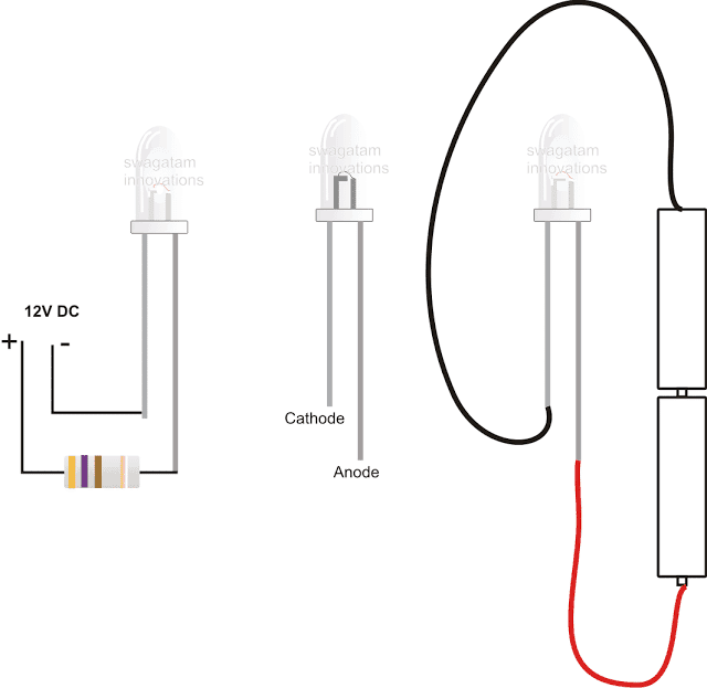 The value of the of the resistor will depend on the magnitude of the applied voltage, and may be calculated using the following formula:
R = (Us ¨C Fwd.)/I(current),
where R is the resistance value which needs to be calculated, Us is the supply voltage, Fwd is the forward voltage drop of the LED and I is the current magnitude which is required to be supplied to the LED.Suppose the supply voltage is 12, the forward voltage drop and the current as explained above are taken as 3.5 and 20 respectively, R may be calculated as:
R = (12 ¨C 3.5)/0.02 = 425 Ohms.
In general the forward voltage drop of a particular LED becomes the important factor while issuing the operating input to the device, rest of the parameters ae not absolutely critical.
The forward voltage drop of an LED may be easily found out by connecting the particular device to a digital multimeter prods selected at the diode range.
The displayed figure directly provides the forward voltage range of the particular LED.
The value of the of the resistor will depend on the magnitude of the applied voltage, and may be calculated using the following formula:
R = (Us ¨C Fwd.)/I(current),
where R is the resistance value which needs to be calculated, Us is the supply voltage, Fwd is the forward voltage drop of the LED and I is the current magnitude which is required to be supplied to the LED.Suppose the supply voltage is 12, the forward voltage drop and the current as explained above are taken as 3.5 and 20 respectively, R may be calculated as:
R = (12 ¨C 3.5)/0.02 = 425 Ohms.
In general the forward voltage drop of a particular LED becomes the important factor while issuing the operating input to the device, rest of the parameters ae not absolutely critical.
The forward voltage drop of an LED may be easily found out by connecting the particular device to a digital multimeter prods selected at the diode range.
The displayed figure directly provides the forward voltage range of the particular LED.
Proximity Detector IC CS209A Pinouts ¨C Datasheet Explained
The post details the main specifications and pinout functions of the IC CS209A along with other technical aspecst of the chip.Introduction
The device CS209A is a bipolar monolithic IC specifically designed for metal detecting circuit applications. The IC fundamentally has a built-in oscillator stage, a couple of current regulator stages, a low level feed back circuit, and a few other relevant stages like peak detection/demodulation stage, a comparator stage and a couple of complementary output blocks.How IC CS209A is Designed to Work
An external LC tank circuit becomes imperative while applying the IC in a metal detector configuration. The externally connected LC circuit in association with the in built oscillator circuit initiates the required oscillations in the circuit in a controlled manner. The amplitude of the oscillations largely depends on the Q factor of the connected LC tank network. When the LC network responds with a low Q levels, the adjustable low level feedback circuit enables drive for sustaining the oscillations. The peak demodulator stage detects the falling section of the oscillator package and feeds a demodulated waveform to the comparator stage as input information. The comparator initiates and set up the complementary outputs by comparing the received information from the demodulator stage with an internal reference level.The main features of the IC include the following:
Separate current regulator stage for the oscillator, Negative transient blocking, Adjustable low level feedback, Enhanced temperature compensation, Minimal current consumption = 6 mA @ 12V DC, Output current sinking feature = 20mA @ 4 V DC, and 100 mA @ 24 V DC. The absolute maximum rating of the chip are given below: Supply voltage not to exceed 24 V DC. Maximum allowable power dissipation is 200 mW, Maximum temperature limits at which the chip needs to be stored should not cross -55 and +165 degree Celsius. Junction temperature must be maintained within -40 and +150 degree Ce;cius. Electrostatic discharge should never cross the potential of 2 kV, except the tank pin out. While soldering the chip, the maximum contact time of 10 seconds is permissible @ 260 degree Celsius for each individual pins of the IC.Electrical Characteristics of the IC
Some of the important electrical characteristic of the IC CS209A as observed for a given set of tests may be understood with the following points: Supply current consumed b the IC was noted as 3.5 to 6 mA @ 4 volts, 6 to 12 mA at 12 volts and 11 to 20 mA @ 24 volts. For the tank circuit, the current consumption was noted as -300 to -100 uA @ 20 volts. Demodulator charge current was noted to be in between -30 to -10 uA @ 20 volts. Output leakage current was witnessed to be 0.01 to 10 uA @ the maximum volts of 24.
Pinout Functions
The pin-outs of the IC may be understood with the following description: Pin #1 is denoted as OSC, when connected with a feedback resistor between this pin and the RF, configures the detection range of the chip. Pin #2 is assigned as the TANK pin out and is responsible for connecting the parallel tank network. Pin #3 is the ground input of the IC. Pin #4 and the pin #5 are the complementary outputs of the IC denoted as OUT1 and OUT2 respectively. OUT1 shows a open collector output in response to a ˇ°LOWˇ±, that is when a metal presence is sensed. OUT2 shows an opposite response with the above conditions. Pin #6 (for DIP-8 and SO-8) and pin #10 (SO-14) which are denoted as DEMOD, is the input pin out to the comparator responsible for controlling the pair of complementary outputs. Pin #7 (for DIP-8 and SO-8) and pin #12 (SO-14) is the supply voltage input. Pin #8 (for DIP-8 and SO-8) and pin #13 (SO-14), assigned as RF is associated with the adjustable feedback resistor which is connected between the OSC and the RF. Remaining pin outs are all NC (not connected).RGB Light Strip Controller Circuits
In this post we are going to see how we can construct an RGB LED light strip controller circuit for PC cabinets and also for general decoration purposes. In this post we will construct a couple of RGB light strip controller designs, one for a PC cabinets and one for general purpose which can be operated using any IR remote and push buttons. RGB LED light strip overview:
 LED light strips are long flexible PCB (with sticky back) with RGB LEDs soldered on it; they can be cut into different lengths as we wish and can be powered with the same voltage regardless of the customized length.
There are single colored and multi-colored LED light strips.
A single colored light strip contains only one color LED, obviously and doesnˇŻt need a control circuitry unless you want it for flashing or controlling brightness.
The most common light strips are multi-colored RGB and RGBW; RGB light strip contains red, green and blue LEDs and RGBW consists of one additional pure white LED, because achieving white color by mixing RGB may not always look pleasant.
RGB LEDs illuminate together with different brightness to achieve several different colors that individual LEDs cannot.
The RGB light strip requires a control circuitry.
LED light strips are long flexible PCB (with sticky back) with RGB LEDs soldered on it; they can be cut into different lengths as we wish and can be powered with the same voltage regardless of the customized length.
There are single colored and multi-colored LED light strips.
A single colored light strip contains only one color LED, obviously and doesnˇŻt need a control circuitry unless you want it for flashing or controlling brightness.
The most common light strips are multi-colored RGB and RGBW; RGB light strip contains red, green and blue LEDs and RGBW consists of one additional pure white LED, because achieving white color by mixing RGB may not always look pleasant.
RGB LEDs illuminate together with different brightness to achieve several different colors that individual LEDs cannot.
The RGB light strip requires a control circuitry.
PC cabinet RGB strip controller circuit: Static illumination
The proposed circuit is segregated into multiple sections for better understanding and illustration. The proposed RGB controller for the PC cabinet can illuminate 7 different colors and after the 7th color the strip turns OFF. The circuit shown below is responsible for selecting an illumination color. The above circuit consists of IC 4017, bunch of NPN transistors and diodes which are connected to a RGB LED strip.
An IC 4017 is employed, which is a Johnson decade counter which can count from 0 to 9 (it can make its output sequentially HIGH according to the incoming clock pulse).
The outputs of IC 4017 are fed to the base terminal of the transistors which will turn ON and OFF specific LED color of the light strip.
We can also see there are a bunch of diodes connected to collector terminals, this is for selecting multiple LEDs simultaneously to generate a new color and also to prevent current passing to inactive transistors which will light up unwanted LEDs.
The last two transistors are connected in parallel to create white color, since it needs to illuminate all the LEDs in a strip which will demand a larger current.
If you have an RGBW light strip you may connect the last transistor to white LED terminal.
The above circuit consists of IC 4017, bunch of NPN transistors and diodes which are connected to a RGB LED strip.
An IC 4017 is employed, which is a Johnson decade counter which can count from 0 to 9 (it can make its output sequentially HIGH according to the incoming clock pulse).
The outputs of IC 4017 are fed to the base terminal of the transistors which will turn ON and OFF specific LED color of the light strip.
We can also see there are a bunch of diodes connected to collector terminals, this is for selecting multiple LEDs simultaneously to generate a new color and also to prevent current passing to inactive transistors which will light up unwanted LEDs.
The last two transistors are connected in parallel to create white color, since it needs to illuminate all the LEDs in a strip which will demand a larger current.
If you have an RGBW light strip you may connect the last transistor to white LED terminal.
 The above circuit is responsible for providing a proper clock signal to IC 4017 which in turns changes the LED illumination color.
The above circuit is a monostable multivibrator / debouncing stage which takes a (noisy) negative pulse from the push button and gives out a clean HIGH signal for a pre-determined period of time, so that the IC 4017 wonˇŻt register multiple button presses or skip some colors.
A potentiometer is provided to adjust the output timing and please try to keep the pulse at pin #3 between 0.5 to 1 second for optimum operation.
The above circuit is responsible for providing a proper clock signal to IC 4017 which in turns changes the LED illumination color.
The above circuit is a monostable multivibrator / debouncing stage which takes a (noisy) negative pulse from the push button and gives out a clean HIGH signal for a pre-determined period of time, so that the IC 4017 wonˇŻt register multiple button presses or skip some colors.
A potentiometer is provided to adjust the output timing and please try to keep the pulse at pin #3 between 0.5 to 1 second for optimum operation.
Incorporating brightness control:
Many PC enthusiasts will love to have brightness control for their RGB light illumination, using the below shown circuit modification one can achieve variable brightness control. The above circuit is employed with a couple of logic AND gates, the upper one controls the upper four transistors and lower AND gate controls the rest of the three transistors.
One of the inputs of all AND gates are tied together and connected to a PWM source.
The other inputs of all AND gates are connected to IC 4017ˇŻs output for selecting an illumination color.
NOTE: Please note that the above circuit also needs the debouncing stage for button input.
The above circuit is employed with a couple of logic AND gates, the upper one controls the upper four transistors and lower AND gate controls the rest of the three transistors.
One of the inputs of all AND gates are tied together and connected to a PWM source.
The other inputs of all AND gates are connected to IC 4017ˇŻs output for selecting an illumination color.
NOTE: Please note that the above circuit also needs the debouncing stage for button input.
PWM source:
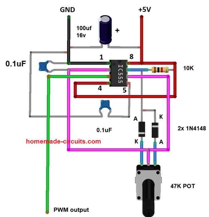 The above circuit generates a PWM signal which will be fed to AND gate.
By adjusting the provided 47K potentiometer you can adjust the brightness of the LED strip.
The above circuit generates a PWM signal which will be fed to AND gate.
By adjusting the provided 47K potentiometer you can adjust the brightness of the LED strip.
Running light for PC cabinet:
If you are not a fan of static illumination of LED light strips, you can try this circuit which flashes red, green and blue.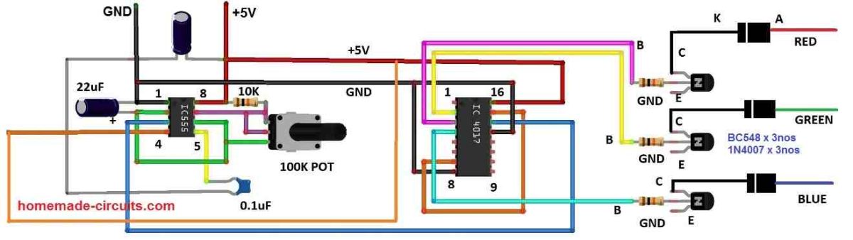 The circuit is very easy to build; it has an astable multivibrator using IC 555 and IC 4017 to flash between red, green and blue.
The astable multivibrator circuit generates a steady clock pulse which is fed to IC 4017. Every time when the IC 4017 receives a clock signal the output will be switched to a new color.
You can set how fast switching of RGB color you want by adjusting the 100K potentiometer.
The circuit is very easy to build; it has an astable multivibrator using IC 555 and IC 4017 to flash between red, green and blue.
The astable multivibrator circuit generates a steady clock pulse which is fed to IC 4017. Every time when the IC 4017 receives a clock signal the output will be switched to a new color.
You can set how fast switching of RGB color you want by adjusting the 100K potentiometer.
Incorporating brightness control:
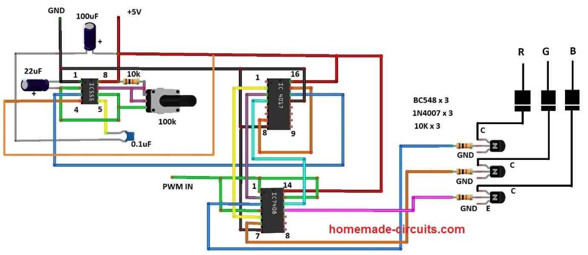 The above circuit is same as the previous one, only the difference is the addition of logic AND gate.
There are four AND gates in the IC 7408 and we are utilizing three of them.
One of the AND gate input of all three gates are tied together and connected to a PWM source and the other three inputs are for selecting illumination color.
The above circuit is same as the previous one, only the difference is the addition of logic AND gate.
There are four AND gates in the IC 7408 and we are utilizing three of them.
One of the AND gate input of all three gates are tied together and connected to a PWM source and the other three inputs are for selecting illumination color.
IR controlled RGB light strip: (for general purpose)
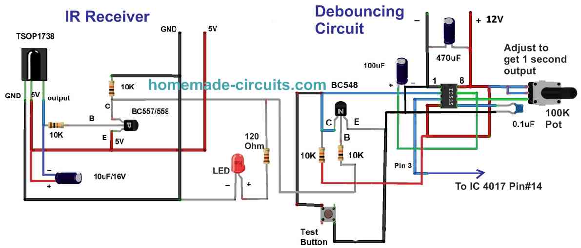 The above circuit is an IR receiver stage which can detect IR signals from any commonly used IR remote controllers.
When an infrared signal is targeted towards the circuit, the incoming signal will be picked by TSOP1738 and converted to pulsating electrical pulses; the pulses are encoded with information which is irrelevant for this project, so we are using a capacitor to smooth it out.
The output after smoothing is feeble and needs amplification, to accomplish this we are using a low power PNP transistor.
A LED is connected to the IR stage which indicates that the IR signal has been detected.
The amplified output is fed to a debouncing circuit which gives out a steady HIGH signal to the next stage.
The purpose of debouncing circuit is to pick the received signal from the IR stage which could be noisy and gives a smooth output signal, thus noise and unintended multiple button clicks are eliminated.
The clock signal from the debouncing stage is fed to pin 14 of IC 4017 which will switch the light stripˇŻs illumination color.
By pressing any button on the IR remote you can switch to your desired illumination color, after white color which is the last one you can turn off the LEDs in the light strip and by pressing a button on the remote we can cycle through all the colors again.
The above circuit is an IR receiver stage which can detect IR signals from any commonly used IR remote controllers.
When an infrared signal is targeted towards the circuit, the incoming signal will be picked by TSOP1738 and converted to pulsating electrical pulses; the pulses are encoded with information which is irrelevant for this project, so we are using a capacitor to smooth it out.
The output after smoothing is feeble and needs amplification, to accomplish this we are using a low power PNP transistor.
A LED is connected to the IR stage which indicates that the IR signal has been detected.
The amplified output is fed to a debouncing circuit which gives out a steady HIGH signal to the next stage.
The purpose of debouncing circuit is to pick the received signal from the IR stage which could be noisy and gives a smooth output signal, thus noise and unintended multiple button clicks are eliminated.
The clock signal from the debouncing stage is fed to pin 14 of IC 4017 which will switch the light stripˇŻs illumination color.
By pressing any button on the IR remote you can switch to your desired illumination color, after white color which is the last one you can turn off the LEDs in the light strip and by pressing a button on the remote we can cycle through all the colors again.